US20040036118A1 - Concurrent Fin-FET and thick-body device fabrication - Google Patents
Concurrent Fin-FET and thick-body device fabricationDownload PDFInfo
- Publication number
- US20040036118A1 US20040036118A1US10/227,995US22799502AUS2004036118A1US 20040036118 A1US20040036118 A1US 20040036118A1US 22799502 AUS22799502 AUS 22799502AUS 2004036118 A1US2004036118 A1US 2004036118A1
- Authority
- US
- United States
- Prior art keywords
- mesa
- gate
- fin
- concurrently
- drain
- Prior art date
- Legal status (The legal status is an assumption and is not a legal conclusion. Google has not performed a legal analysis and makes no representation as to the accuracy of the status listed.)
- Granted
Links
- 238000004519manufacturing processMethods0.000titleclaimsabstractdescription26
- 238000000034methodMethods0.000claimsabstractdescription86
- XUIMIQQOPSSXEZ-UHFFFAOYSA-NSiliconChemical compound[Si]XUIMIQQOPSSXEZ-UHFFFAOYSA-N0.000claimsabstractdescription58
- 230000005669field effectEffects0.000claimsabstractdescription21
- 229910052710siliconInorganic materials0.000claimsabstractdescription19
- 239000010703siliconSubstances0.000claimsabstractdescription19
- 239000000463materialSubstances0.000claimsdescription72
- 238000005530etchingMethods0.000claimsdescription56
- 239000010410layerSubstances0.000claimsdescription53
- FVBUAEGBCNSCDD-UHFFFAOYSA-Nsilicide(4-)Chemical compound[Si-4]FVBUAEGBCNSCDD-UHFFFAOYSA-N0.000claimsdescription48
- 238000000059patterningMethods0.000claimsdescription40
- 238000005468ion implantationMethods0.000claimsdescription35
- 239000000758substrateSubstances0.000claimsdescription32
- 229910021332silicideInorganic materials0.000claimsdescription31
- 239000004065semiconductorSubstances0.000claimsdescription29
- 238000000151depositionMethods0.000claimsdescription20
- 150000004767nitridesChemical class0.000claimsdescription19
- 229910021421monocrystalline siliconInorganic materials0.000claimsdescription12
- 230000015572biosynthetic processEffects0.000claimsdescription11
- 150000002500ionsChemical class0.000claimsdescription7
- 239000002355dual-layerSubstances0.000claimsdescription4
- 230000000873masking effectEffects0.000claimsdescription3
- BOTDANWDWHJENH-UHFFFAOYSA-NTetraethyl orthosilicateChemical compoundCCO[Si](OCC)(OCC)OCCBOTDANWDWHJENH-UHFFFAOYSA-N0.000claims3
- 238000001020plasma etchingMethods0.000claims1
- 230000000284resting effectEffects0.000claims1
- 239000007943implantSubstances0.000description8
- 229910052751metalInorganic materials0.000description7
- 239000002184metalSubstances0.000description7
- WFKWXMTUELFFGS-UHFFFAOYSA-NtungstenChemical compound[W]WFKWXMTUELFFGS-UHFFFAOYSA-N0.000description7
- 229910052721tungstenInorganic materials0.000description7
- 239000010937tungstenSubstances0.000description7
- 239000004020conductorSubstances0.000description6
- 238000002513implantationMethods0.000description5
- 239000012212insulatorSubstances0.000description5
- 238000005516engineering processMethods0.000description4
- 229910021420polycrystalline siliconInorganic materials0.000description4
- 229920005591polysiliconPolymers0.000description4
- 125000006850spacer groupChemical group0.000description4
- 230000006399behaviorEffects0.000description3
- 230000008021depositionEffects0.000description3
- 230000009977dual effectEffects0.000description2
- 239000000126substanceSubstances0.000description2
- 206010010144Completed suicideDiseases0.000description1
- 230000000903blocking effectEffects0.000description1
- 238000003486chemical etchingMethods0.000description1
- 230000002860competitive effectEffects0.000description1
- 238000010586diagramMethods0.000description1
- 238000004377microelectronicMethods0.000description1
Images


Classifications
- H—ELECTRICITY
- H10—SEMICONDUCTOR DEVICES; ELECTRIC SOLID-STATE DEVICES NOT OTHERWISE PROVIDED FOR
- H10D—INORGANIC ELECTRIC SEMICONDUCTOR DEVICES
- H10D30/00—Field-effect transistors [FET]
- H10D30/60—Insulated-gate field-effect transistors [IGFET]
- H10D30/67—Thin-film transistors [TFT]
- H—ELECTRICITY
- H10—SEMICONDUCTOR DEVICES; ELECTRIC SOLID-STATE DEVICES NOT OTHERWISE PROVIDED FOR
- H10D—INORGANIC ELECTRIC SEMICONDUCTOR DEVICES
- H10D30/00—Field-effect transistors [FET]
- H10D30/60—Insulated-gate field-effect transistors [IGFET]
- H10D30/67—Thin-film transistors [TFT]
- H10D30/6704—Thin-film transistors [TFT] having supplementary regions or layers in the thin films or in the insulated bulk substrates for controlling properties of the device
- H10D30/6708—Thin-film transistors [TFT] having supplementary regions or layers in the thin films or in the insulated bulk substrates for controlling properties of the device for preventing the kink effect or the snapback effect, e.g. discharging the minority carriers of the channel region for preventing bipolar effect
- H10D30/6711—Thin-film transistors [TFT] having supplementary regions or layers in the thin films or in the insulated bulk substrates for controlling properties of the device for preventing the kink effect or the snapback effect, e.g. discharging the minority carriers of the channel region for preventing bipolar effect by using electrodes contacting the supplementary regions or layers
- H—ELECTRICITY
- H10—SEMICONDUCTOR DEVICES; ELECTRIC SOLID-STATE DEVICES NOT OTHERWISE PROVIDED FOR
- H10D—INORGANIC ELECTRIC SEMICONDUCTOR DEVICES
- H10D86/00—Integrated devices formed in or on insulating or conducting substrates, e.g. formed in silicon-on-insulator [SOI] substrates or on stainless steel or glass substrates
- H10D86/01—Manufacture or treatment
- H10D86/011—Manufacture or treatment comprising FinFETs
- H—ELECTRICITY
- H10—SEMICONDUCTOR DEVICES; ELECTRIC SOLID-STATE DEVICES NOT OTHERWISE PROVIDED FOR
- H10D—INORGANIC ELECTRIC SEMICONDUCTOR DEVICES
- H10D86/00—Integrated devices formed in or on insulating or conducting substrates, e.g. formed in silicon-on-insulator [SOI] substrates or on stainless steel or glass substrates
- H10D86/201—Integrated devices formed in or on insulating or conducting substrates, e.g. formed in silicon-on-insulator [SOI] substrates or on stainless steel or glass substrates the substrates comprising an insulating layer on a semiconductor body, e.g. SOI
- H10D86/215—Integrated devices formed in or on insulating or conducting substrates, e.g. formed in silicon-on-insulator [SOI] substrates or on stainless steel or glass substrates the substrates comprising an insulating layer on a semiconductor body, e.g. SOI comprising FinFETs
- H—ELECTRICITY
- H10—SEMICONDUCTOR DEVICES; ELECTRIC SOLID-STATE DEVICES NOT OTHERWISE PROVIDED FOR
- H10D—INORGANIC ELECTRIC SEMICONDUCTOR DEVICES
- H10D30/00—Field-effect transistors [FET]
- H10D30/60—Insulated-gate field-effect transistors [IGFET]
- H10D30/67—Thin-film transistors [TFT]
- H10D30/6729—Thin-film transistors [TFT] characterised by the electrodes
- H10D30/6737—Thin-film transistors [TFT] characterised by the electrodes characterised by the electrode materials
- H10D30/6739—Conductor-insulator-semiconductor electrodes
Definitions
- the present inventionrelates generally to the field of semiconductor manufacturing and, more specifically, to methods of manufacturing thick-body devices on the same chip with fin-type field effect transistors (FETs).
- FETsfin-type field effect transistors
- the present inventionalso relates to increasing the density of transistors on an integrated circuit chip and to fabricating thick-body devices such as, single-sidewall, body-contacted mesa FETs; double-sidewall, body-contacted mesa FETs; and planar mesa-top FETs.
- FETsfield effect transistors
- FETsfield effect transistors
- FinFETsare low-power, high speed, vertically scaled transistors that can be densely packed on a chip.
- Vertical scalinginvolves creating a thin wall of semiconductor (the “fin”) and creating the FET on the side of the wall. Thin typically refers to widths that are less than minimum lithographic dimension.
- FinFETsare not suitable for all purposes. Different applications require different transistor device behaviors. Thin devices such as FinFETs reach full depletion during operation. This is desirable for many applications. Different behavior is required for other applications. Thick-body devices behave differently because they do not reach full depletion.
- the present inventionprovides methods for fabrication of microelectronic circuit chips having fin-type field effect transistors (FinFETs) and thick-body devices on the same chip while using fewer masks and steps than prior methods.
- the reduction in the number of masks and stepsis achieved by using common masks and steps with several scaling strategies.
- the structure normally associated with a FinFETis created on the side of a thick silicon mesa, the bulk of which is doped to form a body contact on the side of the mesa opposite the source and drain.
- the inventionincludes methods for concurrently fabricating FinFETs with single-sidewall mesa FETs, double-sidewall mesa FETs, mesa-top planar FETs and combinations thereof.
- the inventionalso includes FinFETs, thick-body devices, and chips fabricated by the methods.
- FIG. 1Ais a process flow chart showing exemplary steps of fabrication of embodiments of the invention without body contacts
- FIG. 1Bis a process flow chart showing exemplary steps of fabrication of embodiments of the invention with body contacts such as for sidewall mesa FETs;
- FIG. 1Cis a process flow chart showing exemplary steps of fabrication of an embodiment of the invention comprising fabrication of a double-sidewall mesa FET;
- FIG. 1Dis a process flow chart showing exemplary steps of fabrication of an embodiment of the invention comprising a mesa-top planar FET;
- FIGS. 2 - 9 Bare views of an exemplary thick-body device during the steps of fabrication of an embodiment of a single-sidewall body-contacted mesa FET;
- FIG. 2is a vertical section view of an exemplary silicon-on-insulator substrate on a wafer having a hardmask
- FIG. 3shows an example of some results of the steps of patterning and etching the substrate to form a mesa
- FIG. 4shows an example of some results of the steps of growing a gate oxide, depositing gate material, and depositing a gate mask
- FIG. 5shows an example of some results of the steps of opening the gate mask and etching the gate material as viewed in a vertical section plane through the gate;
- FIG. 6shows an example of some results of the steps of depositing a resist mask and doping the gate, source and drain;
- FIG. 6contains two vertical section planes: one through the gate (for the gate, gate oxide, and mask) and another, nearer, plane through the drain region of the mesa (within the mesa);
- FIG. 7shows an example of some results of the steps of removing the resist mask of FIG. 6, depositing a new resist mask, and doping the body, as viewed in two vertical section planes: one through the gate (for the gate, gate oxide, and mask) and another, nearer, plane through the drain region of the mesa (within the mesa);
- FIG. 8shows an example of some results of the steps of removing the resist mask of FIG. 7, and forming a silicide, as viewed in two vertical section planes: one through the gate (for the gate, gate oxide, and silicide) and another, nearer, plane through the source region of the mesa (within the mesa);
- FIG. 9Ashows an example of some results of the steps of encasing the device in an oxide, planarizing the encasing oxide, patterning and etching the planarized oxide to form holes for electrical contacts, and filling the holes with electrical contact material, as viewed in two vertical sections: one through the gate (for the gate, gate oxide, electrical contacts, and encasing oxide,) and another nearer plane through the source region of the mesa (within the mesa); FIG. 9A also defines a horizontal section plane A-A′.
- FIG. 9Bshows an example of the device as viewed in horizontal section plane A-A′ as defined in FIG. 9A.
- FIGS. 10 - 11 Dare views of exemplary thick-body device during the steps of fabrication of an alternate embodiment of the single-sidewall mesa FET of FIGS. 2 - 9 B;
- FIG. 10picks up where FIG. 4 left off and shows an example of some results of the steps of opening the gate mask and etching the gate material as viewed in a vertical section through the gate centerline;
- FIG. 11shows an example of some results of the steps of removing the gate mask of FIG. 10, doping the gate, sources and drains as in FIG. 6, doping the body as in FIG. 7, and forming a silicide as in FIG. 8, as viewed in a vertical section plane through the gate centerline;
- FIG. 12Ashows an example of some results of the steps of patterning the mesa hardmask and etching through the mesa hardmask to the body contact, encasing the device in oxide, patterning and etching the oxide to form holes for electrical contacts, and filling the holes with electrical contact material;
- FIG. 12Adefines two horizontal section planes A-A′ and B-B′;
- FIG. 12Bis a view of horizontal section B-B′ as defined in FIG. 12A;
- FIG. 12Bdefines vertical section plane F-F′, which is the plane of FIGS. 10 - 12 A.
- FIG. 12Cis a view of horizontal section A-A′ as defined in FIG. 12A;
- FIG. 12Cdefines vertical section plane D-D′ and repeats F-F′;
- D-D′is the plane of FIG. 12D;
- F-F′shows the intersection with two electrical contacts not previously shown;
- FIG. 12Dis a view of horizontal section D-D′ as defined in FIG. 12C;
- FIGS. 13 - 18are views of an exemplary fin FET and an exemplary planer mesa FET during the steps of fabrication of an embodiment of the invention
- FIG. 13shows a vertical section view of an example of some results of the steps of patterning and etching exemplary substrate as from FIG. 2 to form a fin and a mesa;
- FIG. 14shows a vertical section view of an example of some results of the step of depositing a blocking mask over the fin and selectively etching the hardmask from the mesa;
- FIG. 15is a vertical section view wherein the section plane is nearer the observer then the previous sections used for this embodiment, showing an example of some results of the steps of growing a gate oxide on the fin and the mesa and of ion implanting source and drain wells into the mesa and the fin;
- FIG. 16shows a vertical section view, wherein the section plane is through the center line of the yet-to-be-formed gate, of an example of some results of the step of depositing gate material over the mesa and the fin;
- FIG. 17shows a vertical section view, wherein the section plane is through the center line of the newly-formed gates, of an example of some results of the steps of patterning and etching the gate material over the mesa and the fin;
- FIG. 18shows a planar view, wherein the section plane is through the center line of the gates, of an example of some results of the steps of encasing the mesa and the fin in oxide, patterning and etching the oxide to form holes for electrical contacts, and filling the holes with electrical contact material;
- FIG. 18Ashows a planar view of an example of some results of forming a planar mesa FET with body contacts concurrently with a fin FET;
- FIG. 18Bshows a planar view of an example of some results of forming a planar mesa FET with body contacts, and showing sectional view lines G-G′ and H-H′ for FIGS. 18C and 18D respectively.
- FIG. 18Cshows a vertical section (G-G′) view of an example of some results of forming a planar mesa FET with body contacts.
- FIG. 18Dshows a vertical section (H-H′) view of an example of some results of forming a planar mesa FET with body contacts;
- FIGS. 19 - 26 Dare views of exemplary fin and mesa FETS during the steps of fabrication of a body-contacted double-sided mesa FET embodiment of the invention.
- FIG. 19is a vertical section view of an exemplary silicon-on-insulator substrate on a wafer having a hardmask comprising two layers;
- FIG. 20shows an example of some results of the steps of patterning and etching the dual-layer hardmask to form a mesa and a fin
- FIG. 21shows an example of some results of the step of chemically undercutting the lower layer of the two hardmask layers to achieve a narrowing of the lower hardmask layer
- FIG. 22shows an example of some results of the step of removing the hardmask caps from the narrowed mesa and fin;
- FIG. 23shows an example of some results of selectively etching the active layer of the substrate down to the insulator to further form the mesa and the fin;
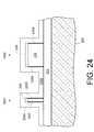
- FIG. 24shows an example of some results of the steps of forming a gate oxide and depositing gate material
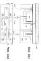
- FIG. 25Ashows a plain view of some results of the steps of patterning and etching the gate material on the mesa and the fin;
- FIG. 24Adefines a vertical section plane A-A′
- FIG. 25Bshows a vertical section view of plane A-A′ illustrating some results of the steps of patterning and etching the gate material on the mesa and the fin;
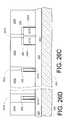
- FIG. 26Ashows a plan view of some results of the steps of encasing the mesa and the fin in oxide, patterning and etching the oxide to form holes for electrical contacts, and filling the holes with electrical contact material;
- FIG. 24Adefines a vertical section planes A-A′ and B-B′. Plane A-A′ is through the centerline of the gates and gate electrical contacts. Plane B-B′ is through the drains and drain electrical contacts.
- FIG. 26Bshows a vertical section view of plane A-A′ illustrating some results of the steps of encasing the mesa and the fin in oxide, patterning and etching the oxide to form holes, and filling the holes with electrical contact material;
- FIG. 26Cshows a vertical section view of plane B-B′ illustrating some results of the steps of encasing the mesa and the fin in oxide, patterning and etching the oxide to form holes, and filling the holes with electrical contact material;
- FIG. 26Dshows a vertical section view of plane A-A′ illustrating some results of the step of forming an alternate embodiment of a fin drain electrical contact
- the present inventionprovides methods for concurrently fabricating fin-type field-effect transistors (FinFETs) and thick-body FETS, also called thick body devices, on the same chip.
- Concurrent fabricationmeans fabrication by a series of fabrication steps wherein at least one fabrication step uses one mask and at least one process associated with that mask for fabricating both a thick-body device and a FinFET. Efficiency is achieved by using concurrent masks and processes, whenever possible, to form the FinFETs and the thick-body devices.
- Devicesare considered to be thick, or to be thick-body devices, when the thickness of the silicon upon which the device is made is greater than that needed to form the source, drain, and gate-influenced regions of the transistor.
- Devicesare thin, or fin-like, when their smallest dimension is the minimum lithographic dimension or smaller. In thin devices, the transistor is typically formed through the entire thin dimension. That is, the source, drain, and gate-influenced regions can be contacted on either or both sides of the thin dimension of the device.
- FIG. 1Ashows an example of an embodiment of a process 100 for concurrently forming thick and thin devices on the same chip.
- Process 100begins by patterning 101 a hard-masked semiconductor substrate for both thin and thick structures.
- the substrateis typically silicon-on-insulator (SOI) with a buried oxide insulator.
- SOIsilicon-on-insulator
- Other substratesas known in the art, may be used.
- the single patternmay create any arrangement of thin and thick devices: thin and thick devices do not have to be segregated on the chip.
- the active sidewallsare those which will be doped to form the sources and the drains for transistors.
- the details of patterning a hard maskare otherwise well known in the art of semiconductor fabrication.
- step 102 of an example of an embodiment of a process 100the substrate is etched down to the buried oxide layer.
- the thin finsare typically thinner than the minimum lithographic dimension. Chemical etching may be included within step 102 to achieve a fin thickness of less than minimum lithographic dimension. Those skilled in the art will appreciate that other methods for achieving sub-minimal lithographic dimensions may be used.
- step 104 of an example of an embodiment of a process 100gate structures are formed on the fins and the thick-body devices.
- Step 104comprises forming a gate oxide, depositing a gate material such as polysilicon, patterning the gate material, and selectively etching the gate material to achieve the desired shape and size.
- the gate materialis etched to leave a thin block of gate material perpendicular to the fin and adjacent to both sides of the fin and adjacent portions of the buried oxide.
- a very thin gate oxide layerseparates the gate material from the body.
- the top of the finis insulated from contact with the gate by an insulating remnant of hardmask on the top of the fin.
- the gate materialmay be etched with a wider portion extended over the buried oxide to receive an electrical contact.
- the size and shape etched out of the gate material on the thick-body devicedepends on the type of device being formed. However the FET is created on the mesa, the gate is etched to divide the transistor's active surface into at least two regions: source and drain.
- sources, drains, and gates for N-FET devicesare formed by N+ doping of their respective regions via ion implantation through an implantation mask.
- source and drain regions and gates for the fins and mesasare doped N+ concurrently.
- the pertinent regions of the various thin and thick-body devices on the chipare doped N+ in step 106 .
- the depth of ion implantationis the same for thin and thick devices. The depth used may deposit ions completely through the thickness of the fins but not the mesas. In other embodiments, depth of ion implantation may be varied as to create the desired device behavior.
- N-FET devices and P-FET devicesdiffer also in their body doping. Body doping may be accomplished by ion implantation or by forming the semiconductor layer with pre-doped material. P-FET devices are referred to as “complimentary devices” in reference to N-FET devices, and vice versa. The “N” or “P” designation may be referred to as the polarity of the N-FET or P-FET device.
- step 107 of an example of an embodiment of process 100a complimentary mask is provided, and sources, drains, and gates for P-FET devices are formed by doping their respective regions via ion implantation through an implantation mask.
- steps 106 and 107FinFET sidewalls, mesa FET sidewalls, and planar FETs on mesa tops may be implanted at the same time.
- the order of steps 106 and 107may be reversed.
- the dopingmay be accomplished by angled ion implantation.
- step 108 of an example of an embodiment of a process 100the thin and thick devices are encased in oxide.
- the oxideis then planarized and holes are patterned and etched to receive electrical contact material to form electrical contacts with the gates, the sources and the drains.
- the electrical contact materialmay be tungsten or other suitable metal as is known in the art.
- step 114gate structures are formed for single-active-sidewall mesa FETs.
- Single-active-sidewall mesa FETshave a FET vertically scaled on one sidewall of the mesa.
- the gateis formed on a gate oxide perpendicularly over the middle of the FET, dividing source and drain regions. The gate further rests on the top of the mesa and on the base oxide of the chip.
- the sources, drains, and gates of the N-FET devices, as well as the body contacts of any complimentary (P-FET) devicesare doped N+ via ion implantation through an implantation mask. While the P+ body contacts are formed in step 122 for the mesa N-FETs, the sources, drains, and gates of the complimentary devices are also formed via ion implantation through an implantation mask. This is accomplished by selectively covering sources, drains and gates of the mesa N-FET as well as the body contact region of any complimentary mesa FET with the implantation mask.
- the body contactis formed 118 by doping the mesa body through the inactive sidewall to form a body contact region adjacent to the body.
- the steps 110 - 112 of embodiment 130are similar to the steps of the same name in process 100 , but are adapted to the creation of body contacts.
- the pattern of step 110 for a device using body contactsmay be different from the pattern of the step 101 of a device that does not use body contacts.
- Step 124includes the sub-steps of forming sidewall spacers on the vertical surfaces of the gate and then growing a silicide layer over the exposed silicon surfaces of the thick-body devices and FinFETs to provide ohmic connections between the electrical contacts and the sources, drains, gates, and body contacts.
- the FinFET body contactmay be formed (deposited, planarized, patterned, and etched) during the gate formation step 114 and doped during steps 118 and 122 .
- the gate and the body contactmay both be formed from one deposition of polysilicon wherein the gate and body contact are later differently doped.
- the FinFET body contactmay be formed separately from the gate formation step 114 .
- the devicesare encased in oxide which is planarized, patterned, etched to form holes and the holes are filled with metal to form the electrical contacts with the devices.
- steps 152 - 164specific to forming mesa FETS with two active sidewalls on the same chip with FinFETs.
- Steps 152 and 154form, among other structures, mesas dimensioned specifically to be double-sidewall FETs. Additional sub-steps may be required for the second sidewall FET, depending on the design of the specific doublesidewall FET.
- the ion implantation stepsmay be performed in reverse order.
- the source and drain regions, as well as the gate on a first mesa sidewall on each mesa and each FinFET,are all concurrently doped N+.
- Step 158further comprises doping the source and drain regions and the gate on a second mesa sidewall.
- the FinFETsmay be masked during the second sidewall source, drain and gate doping 158 to prevent excessive doping of the FinFETs.
- the FinFETscan be masked during the first sidewall source, drain, and gate doping 158 , and the FinFETs can then be doped concurrently with the second mesa sidewall source and drain doping 158 .
- Step 158concurrently dopes the body contacts of any P-FET devices on the same chip.
- the source and drain regions of the doublesidewall mesa FETsare doped in step 158 to meet within the mesa to form a single, continuous source region and a single, continuous drain region in each doublesidewall mesa FET.
- the source and drainare ion-implanted 158 through one sidewall only, and the doping reaches completely through the width of the mesa.
- the bodymay be formed as an un-doped volume of the mesa body beneath the gate and between the two active sidewalls.
- the mesamay be doped as a body before the gates, sources, and drains are formed and the portion of the mesa that remains as the body after step 158 retains the original body doping of the mesa.
- Step 160is the P+ compliment of step 158 .
- the body contacts of N-FET devices on the chipare concurrently doped 160 .
- the body contact of a double-sidewall mesa FETis typically through the top of the mesa, so an etching sub-step is typically required.
- the etching through the top hardmask to the mesa body to allow doping of a body contact regionmay be done as part of the gate etching step.
- Step 164includes encasing the device in an insulating oxide, planarizing the oxide, patterning the oxide for electrical contact holes, etching the electrical contact holes for the source, drain, gate and body contact, and filling the electrical contact holes with electrical contact material such as tungsten or other suitable conductor as is known in the art.
- Source, drain, and gate electrical contacts for the FinFETsare also formed concurrently as part of step 164 .
- FIG. 1Dshows an example of an embodiment of a process 170 specific to forming planar FETs without body contacts on mesa tops while forming FinFETs on the same chip.
- the pattern used in step 171sets the dimensions for, among other structures, at least one mesa suitable for having a planar FET formed on the top surface of the mesa.
- the etching step 172includes removing the hardmask from the mesa tops but not from the tops of the fins. This is accomplished by depositing a block mask over the fins and etching away the hardmask on the exposed mesa tops selective to the block mask. The mesa top must be exposed for planar FET fabrication. The block mask over the fins is then stripped.
- a gate oxideis grown on exposed silicon surfaces. Growing the gate oxide may be achieved by a uniform growth method, a resist-based dual oxide, or N 2 ion-implant dual oxide process to get different oxide thicknesses on fins and mesa tops. Gate material is then deposited over the gate oxide. The gate material is next planarized, patterned, and etched to form the gate and remove the gate oxide except where it is covered by remaining gate material. Note that, because process 170 produces no body contacts, the gate forming-step 174 , may be performed after doping steps 175 and 177 .
- step 175begins with the formation of a sacrificial oxide followed by ion implantation and stripping of the sacrificial oxide.
- step 175concurrently dopes me body contacts of other types of P-FET thick body devices elsewhere on the chip.
- Step 176is the P+ compliment of step 175 .
- the sources, drains, and gates of mesa-top planar P-FETsare doped concurrently with the body contacts of N-FET devices of other types of thick-body devices elsewhere on the chip. Note that the mesa-top planar FETs produced by process 170 , like FinFETs, do not usually have body contacts.
- step 178the chip is encased in an oxide, planarized, patterned for electrical contact holes, etched, and the etched holes filled with electrical contact material to make electrical contact with the sources, drains, and gates.
- FIG. 1Eshows an example of an embodiment of a process 180 for forming mesa-top FETs with body contacts.
- step 183an “H”-shaped gate structure is formed on the mesa top, dividing the mesa top into four regions. See FIG. 1 8 A.
- the “H”comprises a crossbar and two sidebars generally perpendicular to the crossbar.
- the regions above and below the crossbarare the drain and source regions, respectively.
- the areas to the left and right of the vertical barsare the body contact regions.
- the patterning 181 and etching 182 stepsmay be adapted to support this gate shape.
- a block maskis opened for N+ doping of the sources and drains of the N-FET devices while the body contact regions of the N-FET devices are closed by a block mask and while the body contact regions of the P-FET devices are doped.
- a block maskis opened for P+ doping of the sources and drains of the PFET devices while the body contact regions of the P-FET devices are closed by a block mask and while the body contact regions of the N-FET devices are doped.
- Step 187is adapted to the specific configuration of the “H”-shaped gate to provide electrical contacts to the gates, sources, drains, and body contacts.
- a concurrent patterning stepcan include steps 101 , 110 , 152 , 171 , and 181 .
- concurrent etching, gate forming, ion implanting, and electrical contacting stepsare possible.
- FIG. 2shows an exemplary embodiment of a fabrication process 130 (FIG. 1B) for a thick-body device to be formed concurrently with FinFETs.
- Embodiment of a process 130begins with a SOI substrate 200 , 204 , and 202 having a hardmask 208 .
- the substratecomprises a wafer 200 , a buried oxide 204 , and single crystal silicon 202 which is doped P ⁇ . Additional embodiments may use other substrates.
- FIG. 3illustrates the result of patterning 110 (FIG. 1B) and etching 112 (FIG. 1B) the thick-body device in an embodiment of a process 130 (FIG. 1B).
- the resultis a mesa of silicon 202 on the buried oxide 204 having a hardmask cap 208 .
- Fin devices on the same substrate in the exemplary embodiment of the process 130 (FIG. 1B)are not shown, but appear much like the mesa, only thinner.
- FIGS. 3 through FIG. 12Dshow one single-sidewall mesa FET, a thick-body device, as representative of all similar devices on the chip.
- FIG. 4diagrams some results of growing a gate oxide 306 , depositing gate material 402 , and depositing a gate hardmask 404 as part of step 114 (FIG. 1B).
- the view of FIG. 4is a vertical section through the portion of gate material 402 that will ultimately become the gate structure: the portion over the middle of the mesa.
- the gate material 402completely surrounds and covers the mesa 202 , 208 , and 306 .
- the gate hardmask 404covers the gate material 402 .
- the gate material 402may be polysilicon. This step also deposits gate material 402 and hardmask 404 on the fin structures on the same chip.
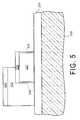
- FIG. 5shows some results of patterning the gate hardmask 404 , opening the hardmask 404 , and etching the gate 402 .
- the view of FIG. 5is a vertical section through the gate centerline.
- the resulting gate 402contacts the active sidewall of the mesa midway between the ends, thereby dividing the active sidewall into source and drain regions.
- a portion of the gate material 402extends away from the mesa 202 , 208 , and 306 on the buried oxide 204 to provide a connection point for the gate electrical contact.
- a portion of the gate 402extends over the top of the mesa 208 .
- gate material 402is patterned and etched to remain in contact with the gate oxide on both sides of the fin (not shown, but same materials as 202 and 306 ).
- the fin gate material 402is continuous over the top layer (same material as 208 ) of the fin, and gate material 402 contacts the buried oxide 204 on both sides of the fin.
- the formation of gate structures on the mesas and finscompletes step 114 (FIG. 1B)
- FIG. 6shows some results of depositing a resist implant mask 602 and some results of N+ ion implantation as part of step 118 (FIG. 1B).
- the angle of the ion implantationis from the upper left in the vertical section view given in FIG. 6.
- the vertical section view of the gate 402 , gate oxide 306 , gate hardmask 404 , and resist mask 602is through the gate centerline.
- the vertical section view through the mesais in a plane nearer the observer and not through the gate. Ion implantation changes most of the gate material to N+ polysilicon 402 .
- a portion of the gate material 604is typically not reached by the ion implantation. Portion 604 may be implanted in some embodiments.
- the mask 602 for the N+ ion implantation of sources 606 , drains 607 (see FIG. 9B) and gates 402also opens the body contacts of P-FET devices to N+ ion implantation.
- source 606 and drain 607 (see FIG. 9B) regionsare formed (step 118 FIG. 1B) by the same N+ ion implantation step which dopes the gate 402 .
- the processconcurrently dopes the sources, drains, and gates of N-FinFETs: the resist implant mask 602 , which also covers the fins, is open to the gate material 402 on both sides of the fins. Consequently, the same doping process does not create undoped regions like 604 over the fins.
- the doping 118 (FIG. 1B) that creates source 606 and drain 607 (See FIG. 9B) regions in the mesacreates source and drain regions completely through the fins in the source and drain ends of the fins. The source and drain ends of the fin are separated by the
- FIG. 7shows the result of removing the resist implant mask 602 (FIG.6), depositing a new resist implant mask 702 , and implanting P+ ions from the upper right, as viewed in FIG. 7.
- Ion-implantationchanges a portion of the P ⁇ silicon mesa body 202 into a P+ silicon body contact 710 .
- the mask 702descends over region 604 to cover a portion of hardmask cap 208 , as shown in FIG. 7.
- mask 702ends at the right-hand edge of the gate hardmask 404 .
- a small portion of gate material 604is unavoidably doped to become P+ gate material 708 .
- the mask 702 for the P+ ion implantation step 122 (FIG. 1B) of the body contact 710is also open to the sources, drains, and gates of P-FET devices.
- the N-FinFETsmay be masked by the resist implant mask 702 during this step.
- the N-FinFETsusually do not have body contacts 710 .
- the FinFET body contactmay be doped concurrently with the body contacts of the thick-body devices.
- FIG. 8shows some results of beginning step 124 (FIG. 1B) comprising removing the resist implant mask 702 (FIG. 7), removing the gate hard mask 404 , creating sidewall spacers 805 on the gate 402 , and then growing a silicide layer 802 on the exposed silicon of the gate 402 , the source 606 and drain 607 (see FIG. 9B) regions, and the body contact 710 . Exposed portions of gate oxide 306 are consumed in this process, as is the P+ gate material 708 and perhaps the un-doped gate material 604 . Silicide is also grown on the fins located elsewhere on the chip.
- the silicide growth processconsumes some of the silicon of the mesa 710 and 606 and of the gate 402 in the thick-body device, and some of the fin and gate in the FinFETs.
- the formation of the silicide layeris a preliminary sub-step of step 124 (FIG. 1B)
- FIG. 9Ashows some further results of step 124 (FIG. 1B), further comprising encasing the thick-body device in oxide 904 , planarizing the oxide 904 , patterning and etching the oxide 904 to form holes for electrical contacts 902 and 903 , and then forming the electrical contacts 902 , 903 , 1002 (FIG. 9B) and 1004 (FIG. 9B) to the body contact 710 , the gate 402 , the source 606 , and the drain 607 (FIG. 9B), respectively.
- the electrical contacts 902 , 903 , 1002 , and 1004are made of metal.
- FIG. 9Ahas a sectional viewing plane (A-A′) defined for use in FIG. 9B. Electrical contacts are formed concurrently for the fins' sources, drains, and gates and, in an alternate embodiment, fin body contacts.
- the FinFETsdo not usually have body contacts 710 . In embodiments of an apparatus comprising FinFETs with body contacts, the electrical connections thereto would also be formed in step 124 (FIG. 1B).
- FIG. 9Bshows the plan view defined by plane A-A′ in FIG. 9A.
- the thick-body device shown by example, other thick-body devices concurrently formed, and the concurrently formed finsare encased in an insulating oxide 904 .
- the body of the transistor 202is contacted along its length by body contact 710 which is connected electrically through the silicide layer 802 to the body electrical contact 902 .
- the source and drain regions 607 and 606are doped regions in the body 202 and have silicide 802 grown on their surfaces as ohmic connections to the drain electrical contact 1004 and the source electrical contact 1002 .
- the gate oxide 306 that is covered by the gatesurvived the silicide 802 formation process.
- the gate 402makes ohmic contact with the body 202 through the gate oxide 306 .
- the gate 402has undergone dimensional reduction due to the formation of the silicide 802 .
- Gate electrical contact 903connects through the silicide layer 802 in a plane below section plane A-A′.
- the body electrical contact 902is formed through the top of the mesa.
- FIG. 10which illustrates the result of a step in this alternate embodiment, we take up where FIG. 4 of the original embodiment left off.
- FIG. 10is a vertical section view through the centerline of the gate.
- the gate material 402 and the gate hardmask 404are patterned and etched to extend over the mesa 202 and 208 .
- the N+ ion implantation doping of the gate material 402 , source 606 (shown, in a plane nearer the viewer than the gate center line) and drain 607 (not shown) (step 118 of FIG. 1B), and the P+ ion implantation doping of the mesa 202 (step 122 of FIG. 1B)then proceed as in the original embodiment but from opposite sides in the view of FIG. 10.
- FIG. 11shows the result of P+ doping the mesa (step 122 of FIG. 1B).
- the P+ dopingforms the body contact 710 which contacts the body 202 on the side of the body 202 opposite the active sidewall.
- Sidewall spacers 805are then formed on the vertical surfaces of the gate 402 .
- a suicide layer 802is formed over the exposed silicon surfaces on the thick-body device as shown as well as over the FinFETs and additional thick-body devices not shown in FIG. 11. Note that the mesa hardmask 208 is not consumed by the silicide 802 growth process.
- a portion of the gate oxide 306 which survived the silicide 802 formation processremains between the gate and the body 202 , but is not significantly present elsewhere on mesa.
- this step 185concurrently dopes the sources and drains of P-FETs elsewhere on the chip.
- this step 122concurrently dopes the sources and drains and gates of P-FETs elsewhere on the chip.
- FIG. 12Ashows the device of FIG. 11 encased in planarized oxide 904 .
- the planarized oxide 904has been patterned and etched to form holes for electrical contacts 1152 , 1154 , 1002 (FIG. 12B), and 1004 (FIG. 12B). Note that the etching for the body contact electrical contact 1152 penetrates the mesa hardmask 208 to reach the body contact 710 .
- the etched holeshave been filled with tungsten or other suitable conductor to form electrical contacts 1152 , 1154 , 1002 (FIG. 12B), and 1004 (FIG. 12B).
- the body contact electrical contact 1152 and the gate electrical contact 1154are illustrated in FIG. 12A.
- step 187(FIG. 1E).
- Two horizontal sectionsare defined in FIG. 12A as A-A′ and B-B′.
- FIG. 12Bshows the B-B′ horizontal section defined in FIG. 11B with electrical contacts for the source 1004 and drain 1002 added.
- Silicide layer 802provides an ohmic contact for the source 607 and drain 606 regions to their electrical contacts 1004 and 1002 .
- a widened portion of the gate 402 over the buried oxideserves as the connection point for the gate electrical contact (above this section plane).
- the thin portion of gate material 402 between the widened portion and the gate oxide 306may be of minimum lithographic dimension or less. This same width of gate material 402 makes contact up the vertical face of the active sidewall of the mesa (on the right, in the view of FIG. 12B).
- the body contact 710contacts the body 202 along its length and height. Source 607 and drain 606 regions have been doped into the body 202 and a silicide layer 802 grown into the source 607 and drain 606 .
- FIG. 12Bdefines vertical section plane F-F′ which is the section plane of FIG. 12A.
- FIG. 12Cshows horizontal section A-A′ as defined in FIG. 12A with electrical contacts 1002 , 1004 , 1152 , and 1154 for the drain, source, body contact, and gate contact, respectively.
- the gatehas been formed to divide the mesa top into three regions corresponding to electrical contacts for the source 1004 , drain 1002 , and body contact 1152 .
- Sidewall spacers 805are formed on the vertical surfaces of the gate 402 .
- Silicide 802is formed on the exposed silicon surfaces of the gate structure 402 , the mesa active sidewall 606 and 607 (hidden in FIG. 12C and denoted by dashed vertical line along right-hand side of mesa; shown in FIG. 12B), and the body contact 710 sidewall (FIG. 12B)
- Source and drain electrical contacts 1004 and 1002make an ohmic connection to their respective regions through silicide 802 .
- the deviceis encased in oxide 904 which is planarized, patterned, and etched to form holes for electrical contacts 1152 , 1002 , 1004 , and 1154 .
- oxide 904planarized, patterned, and etched to form holes for electrical contacts 1152 , 1002 , 1004 , and 1154 .
- the mesa hardmask 208is patterned and etched to deepen the body electrical contact hole in the oxide 904 and etch down to the body contact 710 (below the horizontal section plane of FIG. 12C).
- the portion of body contact 710 exposed by the holeis doped to provide an ohmic connection for the electrical contact 1152 .
- the holeis then filled with metal to form the electrical contact 1152 .
- FIG. 12Cdefines two vertical section planes: D-D′ and E-E′.
- Plane E-E′is the plane viewed in FIG. 12A.
- Plane D-D′is the plane viewed in FIG. 12D.
- FIG. 12Dshows the doping interior to the mesa in detail.
- the body contact 710may be created by ion implantation doping from the upper left, in the view of FIG. 12D.
- Drain region 606may be formed by ion implantation doping from the upper right, in the view of FIG. 12D.
- Silicide 802is grown after ion implantation of the source 607 (FIG. 12B) drain 606 , and the gate 402 .
- oxide 904is deposited, planarized, and etched to form holes for electrical contact 1002 , as well as electrical contacts 1004 , 1152 , and 1154 (FIG. 12C).
- the holeis filled with electrical contact material such as tungsten or other metal to form the electrical contact 1002 for the source 606 .
- Electrical contact 1002has an ohmic electrical connection with the source 606 through the silicide layer 802 .
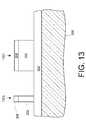
- FIG. 13shows some results of patterning 171 (FIG. 1D) and etching 172 (FIG. 1D) an SOI substrate ( 200 , 204 , 202 , and 208 ), such as the one shown in FIG. 2, to form a mesa 1301 and a fin 1303 .
- Eachhas a remnant of hardmask 208 above a silicon body 202 , on a base oxide 204 on a wafer 200 .
- FIG. 14shows further results of step 172 (FIG. 1D) of an exemplary embodiment of the process 170 (FIG. 1D) of encasing the fin 1303 in a block mask 1202 and selectively etching the hardmask 208 from the mesa 1301 . This exposes the top surface of the mesa 202 upon which a planar FET will be formed.
- step 172(FIG. 1D) is completed when the block mask 1202 is stripped away.
- step 174the planar mesa FET 1301 is masked while gates are formed for at least one mesa sidewall FET device.
- the mask for step 174may include the block mask 1202 .
- FIG. 15shows some results of further steps of an exemplary embodiment of the process 170 (FIG. 1D) in a vertical section through the drain region of the mesa 1301 and the fin 1303 .
- the further stepscomprise stripping the block mask 1202 (FIG. 14) from the fin 1303 to complete step 172 (FIG. 1D), growing a sacrificial oxide (not shown) to begin steps 175 (FIG. 1D), ion-implanting the source (not shown) and drain 1506 region (step 175 , FIG. 1D) on the mesa 1301 top and on the fin 1303 side 1508 through a block mask (not shown), stripping the sacrificial oxide (not shown) and growing a gate oxide 1304 .
- the source and drain 1506 implantsmay be done concurrently on the fin 1303 and mesa 1301 .
- the fin 1303is masked for customized ion implantation of the mesa 1301 and then the mesa 1301 is masked for customized ion implantation of the fin 1303 .
- the mesa 1301is masked first while the fin 1303 is implanted and then the fin 1303 is masked while the mesa 1301 is implanted.
- gatesare formed for both the fin and the mesa-top planar FET before ion implantation.
- the source, drain, and gate of the fin and mesa-top planar FETare doped through the same mask.
- FIG. 16shows the fin 1303 and mesa 1301 during step 177 (FIG. 1D) with the gate material 1402 deposited and planarized.
- the view of FIG. 16is of a vertical section plane though what will become the centerline of the gate. Note that the fin 1303 retains its hardmask cap 208 and that the gate oxide 1304 covers both sides of the fin 1303 and the sides and the top of the mesa 1301 .
- FIG. 17shows the fin 1303 and mesa 1301 with patterned and etched gates 1504 and 1502 , respectively.
- the etched gates 1502 and 1504are thin structures generally perpendicular to the mesa and fin, respectively.
- FIG. 17represents the completion of step 177 (FIG. 1D).
- FIG. 18shows a plan view of the fin 1303 and mesa 1301 showing the fin 1303 and mesa 1301 encased in oxide 1650 .
- the oxide 1650has been planarized, patterned and etched to form holes for the planar mesa FET source electrical contact 1604 , planar mesa FET drain electrical contact 1602 , the planar mesa FET gate electrical contact 1609 , the FinFET gate electrical contact 1606 , FinFET source electrical contact 1603 , and the FinFET drain electrical contact 1601 .
- the top of the mesais covered in a gate oxide 1304 which is partially covered by the gate 1502 .
- exposed gate oxide layer 1304is etched away to expose the body 202 (FIG.
- FIG. 18represents the completion of step 178 (FIG. 1D).
- FIG. 18Ashows a plan view of an exemplary embodiment of a mesa-top FET 1321 with body contacts 1800 and a concurrently formed FinFET 1303 , all encased in oxide 1650 .
- the gate 1502is “H”-shaped to divide the top of the mesa into four regions. To the left and right of the gate 1502 side bars lie body contacts 1800 .
- the gate 1502is formed in step 183 (FIG. 1E), after steps 181 and 182 (FIG. 1E), as adapted to this embodiment 180 . Step 183 (FIG.
- the electrical contact 1609 for the gate 1502is formed by etching a hole in the encasing oxide 1650 and filling the hole with tungsten or similar electrical conductor as known in the art.
- Step 184uses a block mask that opens the middle portion of the mesa top device and the FinFET to ion implantation.
- the source 1802 , drain 1506 , and gate 1502are doped N+ in step 184 (FIG. 1E).
- the P-FET body contactsare doped.
- the block mask openingdoes not completely open the entire gate 1502 , leaving the left and right edges of the “vertical” bars of the “H”-shaped gate partially covered. Angled ion implantation will still dope substantially all of the gate 1502 .
- step 185(FIG.
- the gate, source, and drain regions of the mesa-top N-FET 1321are closed by a block mask and the body contact 1800 regions are opened for P+ doping.
- the gate, source, and drain regions of mesa top P-FETsare doped P+.
- Other thick body FETS, as disclosed elsewhere herein, and FinFETsare concurrently doped during steps 184 and 185 (FIG. 1E), as appropriate for their FET types.
- Step 187includes forming a silicide layer over the exposed doped silicon 1800 , 1506 , and 1802 on the top and sides of the mesa (not shown in FIGS. 18 A-D).
- This silicide layerprovides ohmic connection for the electrical contacts 1602 , 1604 , 1609 and 1800 for the source 1802 , drain 1506 , gate 1502 , and body contacts 1800 , respectively.
- FIG. 18Bis a plan view of a body-contacted mesa FET 1321 showing section lines G-G′ and H-H′.
- FIG. 18Cis the vertical section view of section G-G′.
- the body 1830lies beneath the gate 1502 and the gate oxide 1304 .
- the body 1830is the portion of the mesa not doped by the ion implantations which create the body contacts 1800 and then create the gate 1502 , source 1802 , and drain 1506 .
- the electrical contacts 1810are formed by etching holes in the encasing oxide 1650 and filling the hole with tungsten or similar electrical conductor as known in the art. Electrical contacts 1810 make ohmic connection through the silicide layer (not shown) covering the body contacts.
- FIG. 18Dshows vertical section H-H′ through the drain 1506 .
- the electrical contacts 1604 and 1602(FIG. 18B) are formed by etching holes in the encasing oxide 1650 and filling the hole with tungsten or similar electrical conductor as known in the art.
- the body 1830also underlies the side-bars of the gate 1502 as well as the crossbar (FIG. 18C). In some embodiments, the electrical contacts 1810 connect in a connection plane above the device shown in FIG. 18D).
- a fourth exemplary embodiment of a process 150concurrently produces a FinFET and a double-sided mesa FET.
- the embodiment 150begins with a substrate 200 , 204 , 202 , 208 , and 206 , as shown in FIG. 19, having a hardmask consisting of an oxide layer 208 on the single crystal silicon 202 and a nitride layer 206 on the oxide layer 208 .
- the oxide layer 208may be a tetraehtyl oxisilate (TEOS) oxide.
- TEOStetraehtyl oxisilate
- the buried oxide layer 204 beneath the single-crystal silicon 202is grown on the silicon wafer 200 .
- Other similar substratesmay be used in additional embodiments.
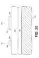
- FIG. 20shows the result of additional steps in an embodiment 150 (FIG. 1C) of the process wherein the nitride layer 206 has been patterned per step 152 (FIG. 1C) and the nitride layer 206 and the oxide layer 208 have been selectively etched (still step 152 , FIG. 1C) to the single crystal silicon layer 202 to form a thin structure 1801 and a thick structure 1802 .
- the width of the thin structure 1801is the minimum lithographic dimension.
- FIG. 21shows some results of chemically undercutting the oxide layer 208 without reacting the nitride layer 206 or the single-crystal silicon layer 202 .
- the purpose of the chemical undercuttingis to achieve a fin 1801 thickness of less than the minimum lithographic dimension.
- the methodleaves an oxide 208 strip on the single crystal silicon 202 , the oxide 208 strip having a nitride 206 cap.
- the reduction in the size of the mesa 1802 oxide 208 stripis unavoidable and can be compensated for by patterning the mesa 1802 hardmask 206 , 208 larger than the final desired size. Because chemical undercutting is performed to create a pattern for the width of the fin 1801 , these actions are included in the patterning step 152 .
- FIG. 22shows some results of selectively etching away the nitride 206 (FIG. 20) caps and leaving the oxide 208 strips on the single-crystal silicon 202 . These strips define the dimensions of the fin 1801 and mesa 1802 in subsequent steps. As such, etching away the nitride cap is the final sub-step of step 152 (FIG. 1C).
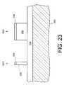
- FIG. 23shows some results of etching 154 (FIG. 1C) the single-crystal silicon 202 selective to the top oxide layer 208 down to the buried oxide 204 .
- the etching step 154(FIG. 1C) forms a fin 1801 with a thickness less than minimal lithographic dimension and a mesa 1802 .
- Transistorswill next be formed on three surfaces: one sidewall of the fin 1801 and two sidewalls of the mesa 1802 .
- FIG. 24shows some results of growing a gate oxide 2204 and depositing gate material 2202 over the fin 1801 and mesa 1802 .
- step 156FIG. 1C: forming the gate structures.
- Gate oxide 2204will provide ohmic contact between the gate material 2202 and the body 202 .
- step 156The gate material 2202 is concurrently patterned and concurrently etched to achieve the correct size and shape, completing step 156 (FIG. 1C).
- the sources and drainsare formed concurrently by ion implantation, completing step 158 (FIG. 1C).
- step 158concurrently dopes the sources and drains of other N-FETs on the same chip as well as body contacts of other P-FET devices on the same chip.
- FIG. 25Ashows a plan view of the fin 1801 and the mesa 1802 .
- the gate material 2202 and the top oxide 208are visible.
- the result of patterning and etching the gates 2202(part of step 156 , FIG. 1C) can be seen in FIG. 25A.
- the gate material 2202 and the top oxide 208are also visible, along with a view of the mesa body 202 as seen through a hole etched through the gate material 2202 and through the top oxide 208 to the mesa body.
- the holeprovides a means for making an electrical connection with the body 202 .
- the single-crystal silicon body 202is doped in step 160 (FIG. 1C) to create a body contact.
- FIG. 25Adefines a vertical section A-A′ which is illustrated in FIG. 25B.
- the fin 1801is double-gated by the gate material 2202 adjacent to both sides of the fin making electrical contact through the gate oxide 2204 on both sides of the fin 1801 , and so requires no body contact.
- the gate 2202 contacting the mesa 1802provides a common gate for the FETs on the two sidewalls.
- the FETs on opposite mesa 1802 sidesare electrically in parallel, forming a higher powered FET than either a single-sidewall FET or a FinFET.
- FIG. 26Ashows, in embodiment of the process 150 (FIG. 1C), a plan view of some results of encasing the devices 1801 and 1802 in oxide 2302 , planarizing the oxide 2302 , patterning the oxide 2302 for holes for electrical contacts, etching the holes, and filling the holes with metal or other suitable conductors to form electrical contacts 2304 , 2306 , 2308 , 2310 , and 2312 to the gates, sources, drains and the body contact on the thick-body device 1802 (Step 164 , FIG. 1C).
- FIG. 26Adefines a vertical section A-A′ which is shown in FIG. 26B.
- the FinFET gate electrical contact 2304 , the body contact electrical contact 2310 , and the double-sidewall mesa FET gate electrical contact 2308are shown in cross section.
- the fin 1801 gate electrical contact 2304contacts a portion of the gate 2202 that is deposited on the buried oxide 204 .
- the body electrical contact 2310penetrates the gate 2202 and the hardmask remnant 208 to reach the portion of the body 202 which has not been doped as a source or a drain.
- mesa body 202 and fin body 202are unaffected by source and drain ion implantation.
- FIG. 26Aalso defines a vertical section B-B′ through the drain 2210 regions of the fin 1801 and the double-sidewall mesa FET 1802 .
- FIG. 26Cshows the vertical section through the drains 2210 .
- the fin 1801 source contact 2306hidden behind 2312 in this view, see FIG. 26A
- drain contact 2312are based partially on the buried oxide 204 and partially on the hardmask remnant cap 208 on top of the fin 1801 .
- the fin 1801 source contact 2306 and drain contact 2312make contact with the vertical face of the fin over the source and drain regions, respectively.
- a silicide layermay be grown on exposed silicon surfaces of the fin 1801 and mesa 1802 as a first sub-step in step 164 (FIG. 1C) to ensure ohmic contacts for the electrical contacts 2304 , 2306 , 2307 , 2308 , 2310 , 2312 , and 2313 .
- the thick-body device 1802has a drain contact 2313 which penetrates the hardmask remnant 208 to contact both drain regions 2210 (left and right, as viewed) in the single-crystal silicon substrate 202 .
- the thick-body device 1802also has a source electrical contact 2307 that penetrates the hardmask remnant 208 to contact both source regions (left and right, out of view) in the single-crystal silicon substrate 202 .
- the FET on the right sidewall of mesa 1801 and the FET on the left sidewall of mesa 1801are electrically connected at the sources, drains, gates, and body. Consequently, the FETs operate in parallel as a higher-powered FET.
- the source and drain regions of the opposite sidewall FETsmeet.
- the view of FIG. 26Cwould show no silicon 202 between drain regions 2210 , which would appear as a single region completely across the widht of the mesa.
- FIG. 26Dshows an alternate embodiment a fin source or drain electrical contact 2314 which contacts both sides of the source or drain region of the fin.
- a sub-step required for only one embodimentcan be achieved at some cost to efficiency by masking all other embodiments while the unique sub-step is executed.
- Those skilled in the artcan vary and combine embodiments of the devices on a single chip within the bounds of the present invention.
Landscapes
- Metal-Oxide And Bipolar Metal-Oxide Semiconductor Integrated Circuits (AREA)
- Thin Film Transistor (AREA)
Abstract
Description
- 1. Technical Field[0001]
- The present invention relates generally to the field of semiconductor manufacturing and, more specifically, to methods of manufacturing thick-body devices on the same chip with fin-type field effect transistors (FETs). The present invention also relates to increasing the density of transistors on an integrated circuit chip and to fabricating thick-body devices such as, single-sidewall, body-contacted mesa FETs; double-sidewall, body-contacted mesa FETs; and planar mesa-top FETs.[0002]
- 2. Background[0003]
- The need to remain cost and performance competitive in the production of semiconductor devices has caused continually increasing device density in integrated circuits. To facilitate the increase in device density, new technologies are constantly needed to allow the feature size of these semiconductor devices to be reduced. High device density also requires low-power operation.[0004]
- The push for ever increasing device densities is particularly strong in CMOS technologies, such as in the design and fabrication of field effect transistors (FETs). FETs are used in almost all types of integrated circuit design (i.e., microprocessors, memory, etc.). Fin-type field effect transistors (FinFETs) are low-power, high speed, vertically scaled transistors that can be densely packed on a chip. Vertical scaling involves creating a thin wall of semiconductor (the “fin”) and creating the FET on the side of the wall. Thin typically refers to widths that are less than minimum lithographic dimension.[0005]
- Unfortunately, FinFETs are not suitable for all purposes. Different applications require different transistor device behaviors. Thin devices such as FinFETs reach full depletion during operation. This is desirable for many applications. Different behavior is required for other applications. Thick-body devices behave differently because they do not reach full depletion.[0006]
- Some applications could benefit from having FinFETs and thick-body devices on the same chip. This has been difficult to achieve economically because the manufacturing steps for FinFETs and thick-body devices are different. Currently, one entire set of masks must be created and the associated steps taken for FinFETs and then another entire set of masks created and steps taken for thick-body devices. The masks protect thin technology devices while forming thick-technology devices, or vice versa. The use of a great multiplicity of masks and steps is expensive. Thus, there is a need for improved methods of fabrication of integrated circuits that use both FinFETs and thick-body devices on the same chip.[0007]
- Accordingly, the present invention provides methods for fabrication of microelectronic circuit chips having fin-type field effect transistors (FinFETs) and thick-body devices on the same chip while using fewer masks and steps than prior methods. The reduction in the number of masks and steps is achieved by using common masks and steps with several scaling strategies. In one embodiment, the structure normally associated with a FinFET is created on the side of a thick silicon mesa, the bulk of which is doped to form a body contact on the side of the mesa opposite the source and drain. The invention includes methods for concurrently fabricating FinFETs with single-sidewall mesa FETs, double-sidewall mesa FETs, mesa-top planar FETs and combinations thereof. The invention also includes FinFETs, thick-body devices, and chips fabricated by the methods.[0008]
- The preferred exemplary embodiment of the present invention will hereinafter be described in conjunction with the appended drawings, where like designations denote like elements, and[0009]
- FIG. 1A is a process flow chart showing exemplary steps of fabrication of embodiments of the invention without body contacts;[0010]
- FIG. 1B is a process flow chart showing exemplary steps of fabrication of embodiments of the invention with body contacts such as for sidewall mesa FETs;[0011]
- FIG. 1C is a process flow chart showing exemplary steps of fabrication of an embodiment of the invention comprising fabrication of a double-sidewall mesa FET;[0012]
- FIG. 1D is a process flow chart showing exemplary steps of fabrication of an embodiment of the invention comprising a mesa-top planar FET;[0013]
- FIGS.[0014]2-9B are views of an exemplary thick-body device during the steps of fabrication of an embodiment of a single-sidewall body-contacted mesa FET;
- FIG. 2 is a vertical section view of an exemplary silicon-on-insulator substrate on a wafer having a hardmask;[0015]
- FIG. 3 shows an example of some results of the steps of patterning and etching the substrate to form a mesa;[0016]
- FIG. 4 shows an example of some results of the steps of growing a gate oxide, depositing gate material, and depositing a gate mask;[0017]
- FIG. 5 shows an example of some results of the steps of opening the gate mask and etching the gate material as viewed in a vertical section plane through the gate;[0018]
- FIG. 6 shows an example of some results of the steps of depositing a resist mask and doping the gate, source and drain; FIG. 6 contains two vertical section planes: one through the gate (for the gate, gate oxide, and mask) and another, nearer, plane through the drain region of the mesa (within the mesa);[0019]
- FIG. 7 shows an example of some results of the steps of removing the resist mask of FIG. 6, depositing a new resist mask, and doping the body, as viewed in two vertical section planes: one through the gate (for the gate, gate oxide, and mask) and another, nearer, plane through the drain region of the mesa (within the mesa);[0020]
- FIG. 8 shows an example of some results of the steps of removing the resist mask of FIG. 7, and forming a silicide, as viewed in two vertical section planes: one through the gate (for the gate, gate oxide, and silicide) and another, nearer, plane through the source region of the mesa (within the mesa);[0021]
- FIG. 9A shows an example of some results of the steps of encasing the device in an oxide, planarizing the encasing oxide, patterning and etching the planarized oxide to form holes for electrical contacts, and filling the holes with electrical contact material, as viewed in two vertical sections: one through the gate (for the gate, gate oxide, electrical contacts, and encasing oxide,) and another nearer plane through the source region of the mesa (within the mesa); FIG. 9A also defines a horizontal section plane A-A′.[0022]
- FIG. 9B shows an example of the device as viewed in horizontal section plane A-A′ as defined in FIG. 9A.[0023]
- FIGS.[0024]10-11D are views of exemplary thick-body device during the steps of fabrication of an alternate embodiment of the single-sidewall mesa FET of FIGS.2-9B;
- FIG. 10 picks up where FIG. 4 left off and shows an example of some results of the steps of opening the gate mask and etching the gate material as viewed in a vertical section through the gate centerline;[0025]
- FIG. 11 shows an example of some results of the steps of removing the gate mask of FIG. 10, doping the gate, sources and drains as in FIG. 6, doping the body as in FIG. 7, and forming a silicide as in FIG. 8, as viewed in a vertical section plane through the gate centerline;[0026]
- FIG. 12A shows an example of some results of the steps of patterning the mesa hardmask and etching through the mesa hardmask to the body contact, encasing the device in oxide, patterning and etching the oxide to form holes for electrical contacts, and filling the holes with electrical contact material; FIG. 12A defines two horizontal section planes A-A′ and B-B′;[0027]
- FIG. 12B is a view of horizontal section B-B′ as defined in FIG. 12A; FIG. 12B defines vertical section plane F-F′, which is the plane of FIGS.[0028]10-12A.
- FIG. 12C is a view of horizontal section A-A′ as defined in FIG. 12A; FIG. 12C defines vertical section plane D-D′ and repeats F-F′; D-D′ is the plane of FIG. 12D; F-F′ shows the intersection with two electrical contacts not previously shown;[0029]
- FIG. 12D is a view of horizontal section D-D′ as defined in FIG. 12C;[0030]
- FIGS.[0031]13-18 are views of an exemplary fin FET and an exemplary planer mesa FET during the steps of fabrication of an embodiment of the invention;
- FIG. 13 shows a vertical section view of an example of some results of the steps of patterning and etching exemplary substrate as from FIG. 2 to form a fin and a mesa;[0032]
- FIG. 14 shows a vertical section view of an example of some results of the step of depositing a blocking mask over the fin and selectively etching the hardmask from the mesa;[0033]
- FIG. 15 is a vertical section view wherein the section plane is nearer the observer then the previous sections used for this embodiment, showing an example of some results of the steps of growing a gate oxide on the fin and the mesa and of ion implanting source and drain wells into the mesa and the fin;[0034]
- FIG. 16 shows a vertical section view, wherein the section plane is through the center line of the yet-to-be-formed gate, of an example of some results of the step of depositing gate material over the mesa and the fin;[0035]
- FIG. 17 shows a vertical section view, wherein the section plane is through the center line of the newly-formed gates, of an example of some results of the steps of patterning and etching the gate material over the mesa and the fin;[0036]
- FIG. 18 shows a planar view, wherein the section plane is through the center line of the gates, of an example of some results of the steps of encasing the mesa and the fin in oxide, patterning and etching the oxide to form holes for electrical contacts, and filling the holes with electrical contact material;[0037]
- FIG. 18A shows a planar view of an example of some results of forming a planar mesa FET with body contacts concurrently with a fin FET;[0038]
- FIG. 18B shows a planar view of an example of some results of forming a planar mesa FET with body contacts, and showing sectional view lines G-G′ and H-H′ for FIGS. 18C and 18D respectively.[0039]
- FIG. 18C shows a vertical section (G-G′) view of an example of some results of forming a planar mesa FET with body contacts.[0040]
- FIG. 18D shows a vertical section (H-H′) view of an example of some results of forming a planar mesa FET with body contacts;[0041]
- FIGS.[0042]19-26D are views of exemplary fin and mesa FETS during the steps of fabrication of a body-contacted double-sided mesa FET embodiment of the invention;
- FIG. 19 is a vertical section view of an exemplary silicon-on-insulator substrate on a wafer having a hardmask comprising two layers;[0043]
- FIG. 20 shows an example of some results of the steps of patterning and etching the dual-layer hardmask to form a mesa and a fin;[0044]
- FIG. 21 shows an example of some results of the step of chemically undercutting the lower layer of the two hardmask layers to achieve a narrowing of the lower hardmask layer;[0045]
- FIG. 22 shows an example of some results of the step of removing the hardmask caps from the narrowed mesa and fin;[0046]
- FIG. 23 shows an example of some results of selectively etching the active layer of the substrate down to the insulator to further form the mesa and the fin;[0047]
- FIG. 24 shows an example of some results of the steps of forming a gate oxide and depositing gate material;[0048]
- FIG. 25A shows a plain view of some results of the steps of patterning and etching the gate material on the mesa and the fin; FIG. 24A defines a vertical section plane A-A′[0049]
- FIG. 25B shows a vertical section view of plane A-A′ illustrating some results of the steps of patterning and etching the gate material on the mesa and the fin;[0050]
- FIG. 26A shows a plan view of some results of the steps of encasing the mesa and the fin in oxide, patterning and etching the oxide to form holes for electrical contacts, and filling the holes with electrical contact material; FIG. 24A defines a vertical section planes A-A′ and B-B′. Plane A-A′ is through the centerline of the gates and gate electrical contacts. Plane B-B′ is through the drains and drain electrical contacts.[0051]
- FIG. 26B shows a vertical section view of plane A-A′ illustrating some results of the steps of encasing the mesa and the fin in oxide, patterning and etching the oxide to form holes, and filling the holes with electrical contact material;[0052]
- FIG. 26C shows a vertical section view of plane B-B′ illustrating some results of the steps of encasing the mesa and the fin in oxide, patterning and etching the oxide to form holes, and filling the holes with electrical contact material;[0053]
- FIG. 26D shows a vertical section view of plane A-A′ illustrating some results of the step of forming an alternate embodiment of a fin drain electrical contact;[0054]
- Accordingly, the present invention provides methods for concurrently fabricating fin-type field-effect transistors (FinFETs) and thick-body FETS, also called thick body devices, on the same chip. Concurrent fabrication, as defined and used herein, means fabrication by a series of fabrication steps wherein at least one fabrication step uses one mask and at least one process associated with that mask for fabricating both a thick-body device and a FinFET. Efficiency is achieved by using concurrent masks and processes, whenever possible, to form the FinFETs and the thick-body devices.[0055]
- Devices are considered to be thick, or to be thick-body devices, when the thickness of the silicon upon which the device is made is greater than that needed to form the source, drain, and gate-influenced regions of the transistor. Devices are thin, or fin-like, when their smallest dimension is the minimum lithographic dimension or smaller. In thin devices, the transistor is typically formed through the entire thin dimension. That is, the source, drain, and gate-influenced regions can be contacted on either or both sides of the thin dimension of the device.[0056]
- FIG. 1A shows an example of an embodiment of a[0057]
process 100 for concurrently forming thick and thin devices on the same chip.Process 100 begins by patterning101 a hard-masked semiconductor substrate for both thin and thick structures. The substrate is typically silicon-on-insulator (SOI) with a buried oxide insulator. Other substrates, as known in the art, may be used. The single pattern may create any arrangement of thin and thick devices: thin and thick devices do not have to be segregated on the chip. The active sidewalls are those which will be doped to form the sources and the drains for transistors. The details of patterning a hard mask are otherwise well known in the art of semiconductor fabrication. - In[0058]
step 102 of an example of an embodiment of aprocess 100, the substrate is etched down to the buried oxide layer. The thin fins are typically thinner than the minimum lithographic dimension. Chemical etching may be included withinstep 102 to achieve a fin thickness of less than minimum lithographic dimension. Those skilled in the art will appreciate that other methods for achieving sub-minimal lithographic dimensions may be used. - In[0059]
step 104 of an example of an embodiment of aprocess 100, gate structures are formed on the fins and the thick-body devices. Step104 comprises forming a gate oxide, depositing a gate material such as polysilicon, patterning the gate material, and selectively etching the gate material to achieve the desired shape and size. For the FinFETs ofprocess embodiment 100, the gate material is etched to leave a thin block of gate material perpendicular to the fin and adjacent to both sides of the fin and adjacent portions of the buried oxide. A very thin gate oxide layer separates the gate material from the body. The top of the fin is insulated from contact with the gate by an insulating remnant of hardmask on the top of the fin. The gate material may be etched with a wider portion extended over the buried oxide to receive an electrical contact. The size and shape etched out of the gate material on the thick-body device depends on the type of device being formed. However the FET is created on the mesa, the gate is etched to divide the transistor's active surface into at least two regions: source and drain. - In[0060]
step 106 of an example of an embodiment of aprocess 100, sources, drains, and gates for N-FET devices are formed by N+ doping of their respective regions via ion implantation through an implantation mask. In thisembodiment 100, source and drain regions and gates for the fins and mesas are doped N+ concurrently. The pertinent regions of the various thin and thick-body devices on the chip are doped N+ instep 106. In most embodiments, the depth of ion implantation is the same for thin and thick devices. The depth used may deposit ions completely through the thickness of the fins but not the mesas. In other embodiments, depth of ion implantation may be varied as to create the desired device behavior. Customizing ion implantation depth generally requires additional masks and steps. N-FET devices and P-FET devices differ also in their body doping. Body doping may be accomplished by ion implantation or by forming the semiconductor layer with pre-doped material. P-FET devices are referred to as “complimentary devices” in reference to N-FET devices, and vice versa. The “N” or “P” designation may be referred to as the polarity of the N-FET or P-FET device. - In[0061]
step 107 of an example of an embodiment ofprocess 100, a complimentary mask is provided, and sources, drains, and gates for P-FET devices are formed by doping their respective regions via ion implantation through an implantation mask. Insteps steps - In[0062]
step 108 of an example of an embodiment of aprocess 100, the thin and thick devices are encased in oxide. The oxide is then planarized and holes are patterned and etched to receive electrical contact material to form electrical contacts with the gates, the sources and the drains. The electrical contact material may be tungsten or other suitable metal as is known in the art. - Another example of an embodiment of a[0063]
process 130 shown in FIG. 1B features the modifiedsteps electrical contacts 124 for the body contacts. Because the FinFETs are usually fully depleted, body contacts would be superfluous and are ordinarily not used. Instep 114, gate structures are formed for single-active-sidewall mesa FETs. Single-active-sidewall mesa FETs have a FET vertically scaled on one sidewall of the mesa. In most embodiments, the gate is formed on a gate oxide perpendicularly over the middle of the FET, dividing source and drain regions. The gate further rests on the top of the mesa and on the base oxide of the chip. - In[0064]
step 118, the sources, drains, and gates of the N-FET devices, as well as the body contacts of any complimentary (P-FET) devices, are doped N+ via ion implantation through an implantation mask. While the P+ body contacts are formed instep 122 for the mesa N-FETs, the sources, drains, and gates of the complimentary devices are also formed via ion implantation through an implantation mask. This is accomplished by selectively covering sources, drains and gates of the mesa N-FET as well as the body contact region of any complimentary mesa FET with the implantation mask. For a single-active-sidewall mesa FET, the body contact is formed118 by doping the mesa body through the inactive sidewall to form a body contact region adjacent to the body. The steps110-112 ofembodiment 130 are similar to the steps of the same name inprocess 100, but are adapted to the creation of body contacts. For example, the pattern ofstep 110 for a device using body contacts may be different from the pattern of thestep 101 of a device that does not use body contacts. - [0065]
Step 124 includes the sub-steps of forming sidewall spacers on the vertical surfaces of the gate and then growing a silicide layer over the exposed silicon surfaces of the thick-body devices and FinFETs to provide ohmic connections between the electrical contacts and the sources, drains, gates, and body contacts. In an alternate embodiment in which FinFETs with body contacts are used, the FinFET body contact may be formed (deposited, planarized, patterned, and etched) during thegate formation step 114 and doped duringsteps gate formation step 114. To completestep 124, the devices are encased in oxide which is planarized, patterned, etched to form holes and the holes are filled with metal to form the electrical contacts with the devices. - Another example of an embodiment of the[0066]
process 150, as shown in FIG. 1C, provides steps152-164 specific to forming mesa FETS with two active sidewalls on the same chip with FinFETs.Steps step 158, the source and drain regions, as well as the gate on a first mesa sidewall on each mesa and each FinFET, are all concurrently doped N+. Step158 further comprises doping the source and drain regions and the gate on a second mesa sidewall. In some embodiments, the FinFETs may be masked during the second sidewall source, drain andgate doping 158 to prevent excessive doping of the FinFETs. Alternatively, the FinFETs can be masked during the first sidewall source, drain, andgate doping 158, and the FinFETs can then be doped concurrently with the second mesa sidewall source and draindoping 158. Step158 concurrently dopes the body contacts of any P-FET devices on the same chip. - In yet another set of embodiments, the source and drain regions of the doublesidewall mesa FETs are doped in[0067]
step 158 to meet within the mesa to form a single, continuous source region and a single, continuous drain region in each doublesidewall mesa FET. In a subset of double-sidewall mesa FETs with continuous source and drain regions, the source and drain are ion-implanted158 through one sidewall only, and the doping reaches completely through the width of the mesa. The body may be formed as an un-doped volume of the mesa body beneath the gate and between the two active sidewalls. In an alternative embodiment, the mesa may be doped as a body before the gates, sources, and drains are formed and the portion of the mesa that remains as the body afterstep 158 retains the original body doping of the mesa. - [0068]
Step 160 is the P+ compliment ofstep 158. Instep 160, the body contacts of N-FET devices on the chip are concurrently doped160. Note that the body contact of a double-sidewall mesa FET is typically through the top of the mesa, so an etching sub-step is typically required. In an embodiment, the etching through the top hardmask to the mesa body to allow doping of a body contact region may be done as part of the gate etching step. - Electrical contact access to the body is gained by patterning and etching a hole through the gate material and the hardmask and[0069]
doping 160 the body portion thereby exposed for good ohmic connection with the electrical contact. The portion of the body doped for ohmic electrical connectivity is known as the body contact. Step164 includes encasing the device in an insulating oxide, planarizing the oxide, patterning the oxide for electrical contact holes, etching the electrical contact holes for the source, drain, gate and body contact, and filling the electrical contact holes with electrical contact material such as tungsten or other suitable conductor as is known in the art. Source, drain, and gate electrical contacts for the FinFETs are also formed concurrently as part ofstep 164. - FIG. 1D shows an example of an embodiment of a[0070]
process 170 specific to forming planar FETs without body contacts on mesa tops while forming FinFETs on the same chip. The pattern used instep 171 sets the dimensions for, among other structures, at least one mesa suitable for having a planar FET formed on the top surface of the mesa. Theetching step 172 includes removing the hardmask from the mesa tops but not from the tops of the fins. This is accomplished by depositing a block mask over the fins and etching away the hardmask on the exposed mesa tops selective to the block mask. The mesa top must be exposed for planar FET fabrication. The block mask over the fins is then stripped. - In[0071]
step 174, a gate oxide is grown on exposed silicon surfaces. Growing the gate oxide may be achieved by a uniform growth method, a resist-based dual oxide, or N2 ion-implant dual oxide process to get different oxide thicknesses on fins and mesa tops. Gate material is then deposited over the gate oxide. The gate material is next planarized, patterned, and etched to form the gate and remove the gate oxide except where it is covered by remaining gate material. Note that, becauseprocess 170 produces no body contacts, the gate forming-step 174, may be performed after doping steps175 and177. - The N+ doping of sources, drains, and gates,[0072]
step 175, begins with the formation of a sacrificial oxide followed by ion implantation and stripping of the sacrificial oxide. Inembodiment 170,step 175 concurrently dopes me body contacts of other types of P-FET thick body devices elsewhere on the chip. - [0073]
Step 176 is the P+ compliment ofstep 175. Instep 176, the sources, drains, and gates of mesa-top planar P-FETs are doped concurrently with the body contacts of N-FET devices of other types of thick-body devices elsewhere on the chip. Note that the mesa-top planar FETs produced byprocess 170, like FinFETs, do not usually have body contacts. - Finally, in[0074]
step 178, the chip is encased in an oxide, planarized, patterned for electrical contact holes, etched, and the etched holes filled with electrical contact material to make electrical contact with the sources, drains, and gates. - FIG. 1E shows an example of an embodiment of a[0075]
process 180 for forming mesa-top FETs with body contacts. Instep 183, an “H”-shaped gate structure is formed on the mesa top, dividing the mesa top into four regions. See FIG. 18A. The “H” comprises a crossbar and two sidebars generally perpendicular to the crossbar. The regions above and below the crossbar are the drain and source regions, respectively. The areas to the left and right of the vertical bars are the body contact regions. Thepatterning 181 and etching182 steps may be adapted to support this gate shape. Instep 184, a block mask is opened for N+ doping of the sources and drains of the N-FET devices while the body contact regions of the N-FET devices are closed by a block mask and while the body contact regions of the P-FET devices are doped. Instep 185, a block mask is opened for P+ doping of the sources and drains of the PFET devices while the body contact regions of the P-FET devices are closed by a block mask and while the body contact regions of the N-FET devices are doped. Step187 is adapted to the specific configuration of the “H”-shaped gate to provide electrical contacts to the gates, sources, drains, and body contacts. - The[0076]
processes steps processes - FIG. 2 shows an exemplary embodiment of a fabrication process[0077]130 (FIG. 1B) for a thick-body device to be formed concurrently with FinFETs. Embodiment of a process130 (FIG. 1B) begins with a
SOI substrate hardmask 208. The substrate comprises awafer 200, a buriedoxide 204, andsingle crystal silicon 202 which is doped P−. Additional embodiments may use other substrates. - FIG. 3 illustrates the result of patterning[0078]110 (FIG. 1B) and etching112 (FIG. 1B) the thick-body device in an embodiment of a process130 (FIG. 1B). The result is a mesa of
silicon 202 on the buriedoxide 204 having ahardmask cap 208. Fin devices on the same substrate in the exemplary embodiment of the process130 (FIG. 1B) are not shown, but appear much like the mesa, only thinner. FIGS.3 through FIG. 12D show one single-sidewall mesa FET, a thick-body device, as representative of all similar devices on the chip. - FIG. 4 diagrams some results of growing a[0079]
gate oxide 306, depositinggate material 402, and depositing agate hardmask 404 as part of step114 (FIG. 1B). The view of FIG. 4 is a vertical section through the portion ofgate material 402 that will ultimately become the gate structure: the portion over the middle of the mesa. Thegate material 402 completely surrounds and covers themesa gate material 402. Thegate material 402 may be polysilicon. This step alsodeposits gate material 402 andhardmask 404 on the fin structures on the same chip. - FIG. 5 shows some results of patterning the[0080]
gate hardmask 404, opening thehardmask 404, and etching thegate 402. The view of FIG. 5 is a vertical section through the gate centerline. The resultinggate 402 contacts the active sidewall of the mesa midway between the ends, thereby dividing the active sidewall into source and drain regions. A portion of thegate material 402 extends away from themesa oxide 204 to provide a connection point for the gate electrical contact. A portion of thegate 402 extends over the top of themesa 208. The process concurrently forms gates for the fins located elsewhere on the chip:gate material 402 is patterned and etched to remain in contact with the gate oxide on both sides of the fin (not shown, but same materials as202 and306). Thefin gate material 402 is continuous over the top layer (same material as208) of the fin, andgate material 402 contacts the buriedoxide 204 on both sides of the fin. The formation of gate structures on the mesas and fins completes step114 (FIG. 1B) - FIG. 6 shows some results of depositing a resist[0081]
implant mask 602 and some results of N+ ion implantation as part of step118 (FIG. 1B). The angle of the ion implantation is from the upper left in the vertical section view given in FIG. 6. The vertical section view of thegate 402,gate oxide 306,gate hardmask 404, and resistmask 602 is through the gate centerline. The vertical section view through the mesa is in a plane nearer the observer and not through the gate. Ion implantation changes most of the gate material toN+ polysilicon 402. A portion of thegate material 604 is typically not reached by the ion implantation.Portion 604 may be implanted in some embodiments. Themask 602 for the N+ ion implantation ofsources 606, drains607 (see FIG. 9B) andgates 402 also opens the body contacts of P-FET devices to N+ ion implantation. In an embodiment,source 606 and drain607 (see FIG. 9B) regions are formed (step118 FIG. 1B) by the same N+ ion implantation step which dopes thegate 402. The process concurrently dopes the sources, drains, and gates of N-FinFETs: the resistimplant mask 602, which also covers the fins, is open to thegate material 402 on both sides of the fins. Consequently, the same doping process does not create undoped regions like604 over the fins. The doping118 (FIG. 1B) that createssource 606 and drain607 (See FIG. 9B) regions in the mesa creates source and drain regions completely through the fins in the source and drain ends of the fins. The source and drain ends of the fin are separated by the fin gate. - FIG. 7 shows the result of removing the resist implant mask[0082]602 (FIG.6), depositing a new resist
implant mask 702, and implanting P+ ions from the upper right, as viewed in FIG. 7. Ion-implantation changes a portion of the P−silicon mesa body 202 into a P+silicon body contact 710. In an embodiment, themask 702 descends overregion 604 to cover a portion ofhardmask cap 208, as shown in FIG. 7. In another embodiment,mask 702 ends at the right-hand edge of thegate hardmask 404. In this embodiment, a small portion ofgate material 604 is unavoidably doped to becomeP+ gate material 708. Themask 702 for the P+ ion implantation step122 (FIG. 1B) of thebody contact 710 is also open to the sources, drains, and gates of P-FET devices. The N-FinFETs may be masked by the resistimplant mask 702 during this step. The N-FinFETs usually do not havebody contacts 710. In an alternate embodiment in which at least one FinFET does have a body contact, the FinFET body contact may be doped concurrently with the body contacts of the thick-body devices. - FIG. 8 shows some results of beginning step[0083]124 (FIG. 1B) comprising removing the resist implant mask702 (FIG. 7), removing the gate
hard mask 404, creatingsidewall spacers 805 on thegate 402, and then growing asilicide layer 802 on the exposed silicon of thegate 402, thesource 606 and drain607 (see FIG. 9B) regions, and thebody contact 710. Exposed portions ofgate oxide 306 are consumed in this process, as is theP+ gate material 708 and perhaps theun-doped gate material 604. Silicide is also grown on the fins located elsewhere on the chip. The silicide growth process consumes some of the silicon of themesa gate 402 in the thick-body device, and some of the fin and gate in the FinFETs. The formation of the silicide layer is a preliminary sub-step of step124 (FIG. 1B) - FIG. 9A shows some further results of step[0084]124 (FIG. 1B), further comprising encasing the thick-body device in
oxide 904, planarizing theoxide 904, patterning and etching theoxide 904 to form holes forelectrical contacts electrical contacts body contact 710, thegate 402, thesource 606, and the drain607 (FIG. 9B), respectively. In most embodiments, theelectrical contacts silicide layer 802 between theelectrical contacts gate 402 andbody contact 710, respectively, provide ohmic connections between the metal electrical contacts and the semiconductor material. FIG. 9A has a sectional viewing plane (A-A′) defined for use in FIG. 9B. Electrical contacts are formed concurrently for the fins' sources, drains, and gates and, in an alternate embodiment, fin body contacts. The FinFETs do not usually havebody contacts 710. In embodiments of an apparatus comprising FinFETs with body contacts, the electrical connections thereto would also be formed in step124 (FIG. 1B). - FIG. 9B shows the plan view defined by plane A-A′ in FIG. 9A. The thick-body device shown by example, other thick-body devices concurrently formed, and the concurrently formed fins are encased in an insulating[0085]
oxide 904. The body of thetransistor 202 is contacted along its length bybody contact 710 which is connected electrically through thesilicide layer 802 to the bodyelectrical contact 902. The source and drainregions body 202 and have silicide802 grown on their surfaces as ohmic connections to the drainelectrical contact 1004 and the sourceelectrical contact 1002. Thegate oxide 306 that is covered by the gate survived thesilicide 802 formation process. Thegate 402 makes ohmic contact with thebody 202 through thegate oxide 306. Thegate 402 has undergone dimensional reduction due to the formation of thesilicide 802. Gateelectrical contact 903 connects through thesilicide layer 802 in a plane below section plane A-A′. - In an alternate embodiment, the body[0086]
electrical contact 902 is formed through the top of the mesa. In FIG. 10, which illustrates the result of a step in this alternate embodiment, we take up where FIG. 4 of the original embodiment left off. FIG. 10 is a vertical section view through the centerline of the gate. In this alternate embodiment, thegate material 402 and thegate hardmask 404 are patterned and etched to extend over themesa gate material 402, source606 (shown, in a plane nearer the viewer than the gate center line) and drain607 (not shown) (step118 of FIG. 1B), and the P+ ion implantation doping of the mesa202 (step122 of FIG. 1B) then proceed as in the original embodiment but from opposite sides in the view of FIG. 10. - FIG. 11 shows the result of P+ doping the mesa (step[0087]122 of FIG. 1B). The P+ doping forms the
body contact 710 which contacts thebody 202 on the side of thebody 202 opposite the active sidewall.Sidewall spacers 805 are then formed on the vertical surfaces of thegate 402. Next, asuicide layer 802 is formed over the exposed silicon surfaces on the thick-body device as shown as well as over the FinFETs and additional thick-body devices not shown in FIG. 11. Note that the mesa hardmask208 is not consumed by thesilicide 802 growth process. A portion of thegate oxide 306 which survived thesilicide 802 formation process remains between the gate and thebody 202, but is not significantly present elsewhere on mesa. In an embodiment, this step185 (FIG. 1E) concurrently dopes the sources and drains of P-FETs elsewhere on the chip. In another embodiment, this step122 (FIG. 1B) concurrently dopes the sources and drains and gates of P-FETs elsewhere on the chip. - FIG. 12A shows the device of FIG. 11 encased in[0088]
planarized oxide 904. Theplanarized oxide 904 has been patterned and etched to form holes forelectrical contacts electrical contact 1152 penetrates the mesa hardmask208 to reach thebody contact 710. The etched holes have been filled with tungsten or other suitable conductor to formelectrical contacts electrical contact 1152 and the gateelectrical contact 1154 are illustrated in FIG. 12A. The formation of theelectrical contacts - FIG. 12B shows the B-B′ horizontal section defined in FIG. 11B with electrical contacts for the[0089]
source 1004 and drain1002 added.Silicide layer 802 provides an ohmic contact for thesource 607 and drain606 regions to theirelectrical contacts gate 402 over the buried oxide serves as the connection point for the gate electrical contact (above this section plane). The thin portion ofgate material 402 between the widened portion and thegate oxide 306 may be of minimum lithographic dimension or less. This same width ofgate material 402 makes contact up the vertical face of the active sidewall of the mesa (on the right, in the view of FIG. 12B). Thebody contact 710 contacts thebody 202 along its length and height.Source 607 and drain606 regions have been doped into thebody 202 and asilicide layer 802 grown into thesource 607 and drain606. FIG. 12B defines vertical section plane F-F′ which is the section plane of FIG. 12A. - FIG. 12C shows horizontal section A-A′ as defined in FIG. 12A with[0090]
electrical contacts source 1004,drain 1002, andbody contact 1152.Sidewall spacers 805 are formed on the vertical surfaces of thegate 402.Silicide 802 is formed on the exposed silicon surfaces of thegate structure 402, the mesaactive sidewall 606 and607 (hidden in FIG. 12C and denoted by dashed vertical line along right-hand side of mesa; shown in FIG. 12B), and thebody contact 710 sidewall (FIG. 12B) Source and drainelectrical contacts silicide 802. - The device is encased in[0091]
oxide 904 which is planarized, patterned, and etched to form holes forelectrical contacts electrical contact 1152, the mesa hardmask208 is patterned and etched to deepen the body electrical contact hole in theoxide 904 and etch down to the body contact710 (below the horizontal section plane of FIG. 12C). The portion ofbody contact 710 exposed by the hole is doped to provide an ohmic connection for theelectrical contact 1152. The hole is then filled with metal to form theelectrical contact 1152. Holes in the insulatingencasing oxide 904 for the sources drains, and gates, and for the electrical contacts for the other thick-body devices and for the fins are patterned in a sub-step of step124 (FIG. 1B) and etched in a sub-step of step124 (FIG. 1B). FIG. 12C defines two vertical section planes: D-D′ and E-E′. Plane E-E′ is the plane viewed in FIG. 12A. Plane D-D′ is the plane viewed in FIG. 12D. FIG. 12D shows the doping interior to the mesa in detail. Thebody contact 710 may be created by ion implantation doping from the upper left, in the view of FIG. 12D.Drain region 606 may be formed by ion implantation doping from the upper right, in the view of FIG. 12D.Silicide 802 is grown after ion implantation of the source607 (FIG. 12B)drain 606, and thegate 402. After thesilicide 802 is grown,oxide 904 is deposited, planarized, and etched to form holes forelectrical contact 1002, as well aselectrical contacts electrical contact 1002 for thesource 606.Electrical contact 1002 has an ohmic electrical connection with thesource 606 through thesilicide layer 802. - In an exemplary embodiment of the process[0092]170 (FIG. 1D), a planar FET is formed on a mesa top concurrently with the formation of a FinFET elsewhere on the chip. FIG. 13 shows some results of patterning171 (FIG. 1D) and etching172 (FIG. 1D) an SOI substrate (200,204,202, and208), such as the one shown in FIG. 2, to form a
mesa 1301 and afin 1303. Each has a remnant ofhardmask 208 above asilicon body 202, on abase oxide 204 on awafer 200. - FIG. 14 shows further results of step[0093]172 (FIG. 1D) of an exemplary embodiment of the process170 (FIG. 1D) of encasing the
fin 1303 in ablock mask 1202 and selectively etching thehardmask 208 from themesa 1301. This exposes the top surface of themesa 202 upon which a planar FET will be formed. In embodiment170 (FIG. 1D), step172 (FIG. 1D) is completed when theblock mask 1202 is stripped away. - In step[0094]174 (FIG. 1D), the
planar mesa FET 1301 is masked while gates are formed for at least one mesa sidewall FET device. In an alternate embodiment, the mask for step174 (FIG. 1D) may include theblock mask 1202. - FIG. 15 shows some results of further steps of an exemplary embodiment of the process[0095]170 (FIG. 1D) in a vertical section through the drain region of the
mesa 1301 and thefin 1303. The further steps comprise stripping the block mask1202 (FIG. 14) from thefin 1303 to complete step172 (FIG. 1D), growing a sacrificial oxide (not shown) to begin steps175 (FIG. 1D), ion-implanting the source (not shown) anddrain 1506 region (step 175, FIG. 1D) on themesa 1301 top and on thefin 1303side 1508 through a block mask (not shown), stripping the sacrificial oxide (not shown) and growing agate oxide 1304. The source and drain1506 implants may be done concurrently on thefin 1303 andmesa 1301. In an embodiment of the method, thefin 1303 is masked for customized ion implantation of themesa 1301 and then themesa 1301 is masked for customized ion implantation of thefin 1303. In another embodiment of the method, themesa 1301 is masked first while thefin 1303 is implanted and then thefin 1303 is masked while themesa 1301 is implanted. In yet another embodiment, gates are formed for both the fin and the mesa-top planar FET before ion implantation. In a variation of that embodiment, the source, drain, and gate of the fin and mesa-top planar FET are doped through the same mask. - FIG. 16 shows the[0096]
fin 1303 andmesa 1301 during step177 (FIG. 1D) with thegate material 1402 deposited and planarized. The view of FIG. 16 is of a vertical section plane though what will become the centerline of the gate. Note that thefin 1303 retains itshardmask cap 208 and that thegate oxide 1304 covers both sides of thefin 1303 and the sides and the top of themesa 1301. - FIG. 17 shows the[0097]
fin 1303 andmesa 1301 with patterned and etchedgates gates - FIG. 18 shows a plan view of the[0098]
fin 1303 andmesa 1301 showing thefin 1303 andmesa 1301 encased inoxide 1650. Theoxide 1650 has been planarized, patterned and etched to form holes for the planar mesa FET sourceelectrical contact 1604, planar mesa FET drainelectrical contact 1602, the planar mesa FET gateelectrical contact 1609, the FinFET gate electrical contact1606, FinFET sourceelectrical contact 1603, and the FinFET drainelectrical contact 1601. The top of the mesa is covered in agate oxide 1304 which is partially covered by thegate 1502. In another embodiment, exposedgate oxide layer 1304 is etched away to expose the body202 (FIG. 17) prior to the deposition of the encasing oxide. The top of thefin 1303 is a remnant of thehardmask 208 that is original to the substrate. Thehardmask remnant 208 is partially overlaid by thegate 1504. Tne extension of themesa gate 1502 is to provide a connecting point for the gateelectrical contact 1609. Likewise, thefin gate 1504 is extended outward from the body to provide a connecting point for the fin gateelectrical contact 1607. FIG. 18 represents the completion of step178 (FIG. 1D). - In yet another exemplary embodiment of the process[0099]180 (FIG. 1E), the gate for the mesa-top planar FET is formed before ion-implantation of the sources and drains. FIG. 18A shows a plan view of an exemplary embodiment of a mesa-
top FET 1321 withbody contacts 1800 and a concurrently formedFinFET 1303, all encased inoxide 1650. Thegate 1502 is “H”-shaped to divide the top of the mesa into four regions. To the left and right of thegate 1502 side bars liebody contacts 1800. Thegate 1502 is formed in step183 (FIG. 1E), aftersteps 181 and182 (FIG. 1E), as adapted to thisembodiment 180. Step183 (FIG. 1E) includes growing agate oxide 1304 on the mesa top prior to deposition of the gate material. A portion of thegate 1502, as finally etched in step183 (FIG. 1E), extends beyond the edge of the mesa top to contact the gate oxide on the side of the mesa and rest upon the substrate204 (FIG. 17). Theelectrical contact 1609 for thegate 1502 is formed by etching a hole in theencasing oxide 1650 and filling the hole with tungsten or similar electrical conductor as known in the art. - Step[0100]184 (FIG. 1E) uses a block mask that opens the middle portion of the mesa top device and the FinFET to ion implantation. For an N-FET, the
source 1802,drain 1506, andgate 1502 are doped N+ in step184 (FIG. 1E). At the same time, the P-FET body contacts are doped. The block mask opening does not completely open theentire gate 1502, leaving the left and right edges of the “vertical” bars of the “H”-shaped gate partially covered. Angled ion implantation will still dope substantially all of thegate 1502. In step185 (FIG. 1E) the gate, source, and drain regions of the mesa-top N-FET 1321 are closed by a block mask and thebody contact 1800 regions are opened for P+ doping. At the same time, the gate, source, and drain regions of mesa top P-FETs are doped P+. Other thick body FETS, as disclosed elsewhere herein, and FinFETs are concurrently doped duringsteps 184 and185 (FIG. 1E), as appropriate for their FET types. - Step[0101]187 (FIG. 1E) includes forming a silicide layer over the exposed
doped silicon electrical contacts source 1802,drain 1506,gate 1502, andbody contacts 1800, respectively. FIG. 18B is a plan view of a body-contactedmesa FET 1321 showing section lines G-G′ and H-H′. FIG. 18C is the vertical section view of section G-G′. Thebody 1830 lies beneath thegate 1502 and thegate oxide 1304. Thebody 1830 is the portion of the mesa not doped by the ion implantations which create thebody contacts 1800 and then create thegate 1502,source 1802, anddrain 1506. Theelectrical contacts 1810 are formed by etching holes in theencasing oxide 1650 and filling the hole with tungsten or similar electrical conductor as known in the art.Electrical contacts 1810 make ohmic connection through the silicide layer (not shown) covering the body contacts. FIG. 18D shows vertical section H-H′ through thedrain 1506. Theelectrical contacts 1604 and1602 (FIG. 18B) are formed by etching holes in theencasing oxide 1650 and filling the hole with tungsten or similar electrical conductor as known in the art. Thebody 1830 also underlies the side-bars of thegate 1502 as well as the crossbar (FIG. 18C). In some embodiments, theelectrical contacts 1810 connect in a connection plane above the device shown in FIG. 18D). - A fourth exemplary embodiment of a process[0102]150 (FIG. 1C) concurrently produces a FinFET and a double-sided mesa FET. The embodiment150 (FIG. 1C) begins with a
substrate oxide layer 208 on thesingle crystal silicon 202 and anitride layer 206 on theoxide layer 208. Theoxide layer 208 may be a tetraehtyl oxisilate (TEOS) oxide. The buriedoxide layer 204 beneath the single-crystal silicon 202 is grown on thesilicon wafer 200. Other similar substrates may be used in additional embodiments. - FIG. 20 shows the result of additional steps in an embodiment[0103]150 (FIG. 1C) of the process wherein the
nitride layer 206 has been patterned per step152 (FIG. 1C) and thenitride layer 206 and theoxide layer 208 have been selectively etched (still step152, FIG. 1C) to the singlecrystal silicon layer 202 to form athin structure 1801 and athick structure 1802. In an embodiment150 (FIG. 1C), the width of thethin structure 1801 is the minimum lithographic dimension. - FIG. 21 shows some results of chemically undercutting the[0104]
oxide layer 208 without reacting thenitride layer 206 or the single-crystal silicon layer 202. The purpose of the chemical undercutting is to achieve afin 1801 thickness of less than the minimum lithographic dimension. The method leaves anoxide 208 strip on thesingle crystal silicon 202 , theoxide 208 strip having anitride 206 cap. The reduction in the size of themesa 1802oxide 208 strip is unavoidable and can be compensated for by patterning themesa 1802hardmask fin 1801, these actions are included in thepatterning step 152. - FIG. 22 shows some results of selectively etching away the nitride[0105]206 (FIG. 20) caps and leaving the
oxide 208 strips on the single-crystal silicon 202. These strips define the dimensions of thefin 1801 andmesa 1802 in subsequent steps. As such, etching away the nitride cap is the final sub-step of step152 (FIG. 1C). - FIG. 23 shows some results of etching[0106]154 (FIG. 1C) the single-
crystal silicon 202 selective to thetop oxide layer 208 down to the buriedoxide 204. The etching step154 (FIG. 1C) forms afin 1801 with a thickness less than minimal lithographic dimension and amesa 1802. Transistors will next be formed on three surfaces: one sidewall of thefin 1801 and two sidewalls of themesa 1802. - FIG. 24 shows some results of growing a[0107]
gate oxide 2204 and depositinggate material 2202 over thefin 1801 andmesa 1802. Thus begins step156 (FIG. 1C): forming the gate structures.Gate oxide 2204 will provide ohmic contact between thegate material 2202 and thebody 202. - The[0108]
gate material 2202 is concurrently patterned and concurrently etched to achieve the correct size and shape, completing step156 (FIG. 1C). The sources and drains are formed concurrently by ion implantation, completing step158 (FIG. 1C). In an embodiment, step158 concurrently dopes the sources and drains of other N-FETs on the same chip as well as body contacts of other P-FET devices on the same chip. - FIG. 25A shows a plan view of the[0109]
fin 1801 and themesa 1802. From the plan view of thefin 1801, thegate material 2202 and thetop oxide 208 are visible. The result of patterning and etching the gates2202 (part ofstep 156, FIG. 1C) can be seen in FIG. 25A. From the plan view of themesa 1802, thegate material 2202 and thetop oxide 208 are also visible, along with a view of themesa body 202 as seen through a hole etched through thegate material 2202 and through thetop oxide 208 to the mesa body. The hole provides a means for making an electrical connection with thebody 202. At the point of contact onbody 202, the single-crystal silicon body 202 is doped in step160 (FIG. 1C) to create a body contact. FIG. 25A defines a vertical section A-A′ which is illustrated in FIG. 25B. - Referring to FIG. 25B, the[0110]
fin 1801 is double-gated by thegate material 2202 adjacent to both sides of the fin making electrical contact through thegate oxide 2204 on both sides of thefin 1801, and so requires no body contact. Thegate 2202 contacting themesa 1802 provides a common gate for the FETs on the two sidewalls. The FETs on oppositemesa 1802 sides are electrically in parallel, forming a higher powered FET than either a single-sidewall FET or a FinFET. - FIG. 26A shows, in embodiment of the process[0111]150 (FIG. 1C), a plan view of some results of encasing the
devices oxide 2302, planarizing theoxide 2302, patterning theoxide 2302 for holes for electrical contacts, etching the holes, and filling the holes with metal or other suitable conductors to formelectrical contacts Step 164, FIG. 1C). FIG. 26A defines a vertical section A-A′ which is shown in FIG. 26B. - Referring to FIG. 26B the FinFET gate[0112]
electrical contact 2304, the body contactelectrical contact 2310, and the double-sidewall mesa FET gateelectrical contact 2308 are shown in cross section. Thefin 1801 gateelectrical contact 2304 contacts a portion of thegate 2202 that is deposited on the buriedoxide 204. The bodyelectrical contact 2310 penetrates thegate 2202 and thehardmask remnant 208 to reach the portion of thebody 202 which has not been doped as a source or a drain. In the vertical A-A′ plane,mesa body 202 andfin body 202 are unaffected by source and drain ion implantation. - FIG. 26A also defines a vertical section B-B′ through the[0113]
drain 2210 regions of thefin 1801 and the double-sidewall mesa FET 1802. FIG. 26C shows the vertical section through thedrains 2210. Referring to FIG. 26C, thefin 1801 source contact2306 (hidden behind2312 in this view, see FIG. 26A) anddrain contact 2312 are based partially on the buriedoxide 204 and partially on thehardmask remnant cap 208 on top of thefin 1801. Thefin 1801source contact 2306 anddrain contact 2312 make contact with the vertical face of the fin over the source and drain regions, respectively. A silicide layer may be grown on exposed silicon surfaces of thefin 1801 andmesa 1802 as a first sub-step in step164 (FIG. 1C) to ensure ohmic contacts for theelectrical contacts body device 1802 has adrain contact 2313 which penetrates thehardmask remnant 208 to contact both drain regions2210 (left and right, as viewed) in the single-crystal silicon substrate 202. The thick-body device 1802 also has a sourceelectrical contact 2307 that penetrates thehardmask remnant 208 to contact both source regions (left and right, out of view) in the single-crystal silicon substrate 202. The FET on the right sidewall ofmesa 1801 and the FET on the left sidewall ofmesa 1801, are electrically connected at the sources, drains, gates, and body. Consequently, the FETs operate in parallel as a higher-powered FET. In an embodiment, the source and drain regions of the opposite sidewall FETs meet. In such an embodiment, the view of FIG. 26C would show nosilicon 202 betweendrain regions 2210, which would appear as a single region completely across the widht of the mesa. - FIG. 26D shows an alternate embodiment a fin source or drain[0114]
electrical contact 2314 which contacts both sides of the source or drain region of the fin. - Those skilled in the art will appreciate that combinations and variations of the four illustrated embodiments can be made to allow creation of FinFETs, single-sidewall body-contacted mesa FETs, double-sided body-contacted mesa FETs, and planar mesa-top FETs on the same chip. For example, embodiments of the processes[0115]130 (FIG. 1B, single-sidewall body-contacted mesa FET) and170 (FIG. 1D, mesa-top planar FETs) can be altered to form the gate before the sources and drains are ion-implanted, thereby allowing a common gate-formation step for all four of the exemplary embodiments on one chip. Likewise, a sub-step required for only one embodiment can be achieved at some cost to efficiency by masking all other embodiments while the unique sub-step is executed. Those skilled in the art can vary and combine embodiments of the devices on a single chip within the bounds of the present invention.
Claims (29)
Priority Applications (4)
| Application Number | Priority Date | Filing Date | Title |
|---|---|---|---|
| US10/227,995US7163851B2 (en) | 2002-08-26 | 2002-08-26 | Concurrent Fin-FET and thick-body device fabrication |
| JP2003287197AJP3935869B2 (en) | 2002-08-26 | 2003-08-05 | Integrated circuit and manufacturing method thereof |
| US11/481,120US7473970B2 (en) | 2002-08-26 | 2006-07-05 | Concurrent fin-fet and thick body device fabrication |
| US12/348,344US7872310B2 (en) | 2002-08-26 | 2009-01-05 | Semiconductor structure and system for fabricating an integrated circuit chip |
Applications Claiming Priority (1)
| Application Number | Priority Date | Filing Date | Title |
|---|---|---|---|
| US10/227,995US7163851B2 (en) | 2002-08-26 | 2002-08-26 | Concurrent Fin-FET and thick-body device fabrication |
Related Child Applications (1)
| Application Number | Title | Priority Date | Filing Date |
|---|---|---|---|
| US11/481,120DivisionUS7473970B2 (en) | 2002-08-26 | 2006-07-05 | Concurrent fin-fet and thick body device fabrication |
Publications (2)
| Publication Number | Publication Date |
|---|---|
| US20040036118A1true US20040036118A1 (en) | 2004-02-26 |
| US7163851B2 US7163851B2 (en) | 2007-01-16 |
Family
ID=31887564
Family Applications (3)
| Application Number | Title | Priority Date | Filing Date |
|---|---|---|---|
| US10/227,995Expired - LifetimeUS7163851B2 (en) | 2002-08-26 | 2002-08-26 | Concurrent Fin-FET and thick-body device fabrication |
| US11/481,120Expired - LifetimeUS7473970B2 (en) | 2002-08-26 | 2006-07-05 | Concurrent fin-fet and thick body device fabrication |
| US12/348,344Expired - LifetimeUS7872310B2 (en) | 2002-08-26 | 2009-01-05 | Semiconductor structure and system for fabricating an integrated circuit chip |
Family Applications After (2)
| Application Number | Title | Priority Date | Filing Date |
|---|---|---|---|
| US11/481,120Expired - LifetimeUS7473970B2 (en) | 2002-08-26 | 2006-07-05 | Concurrent fin-fet and thick body device fabrication |
| US12/348,344Expired - LifetimeUS7872310B2 (en) | 2002-08-26 | 2009-01-05 | Semiconductor structure and system for fabricating an integrated circuit chip |
Country Status (2)
| Country | Link |
|---|---|
| US (3) | US7163851B2 (en) |
| JP (1) | JP3935869B2 (en) |
Cited By (59)
| Publication number | Priority date | Publication date | Assignee | Title |
|---|---|---|---|---|
| US20040036126A1 (en)* | 2002-08-23 | 2004-02-26 | Chau Robert S. | Tri-gate devices and methods of fabrication |
| US20040188749A1 (en)* | 2003-03-27 | 2004-09-30 | Taiwan Semiconductor Manufacturing Co., Ltd. | Method for forming a box shaped polygate |
| US6800885B1 (en)* | 2003-03-12 | 2004-10-05 | Advance Micro Devices, Inc. | Asymmetrical double gate or all-around gate MOSFET devices and methods for making same |
| US20040266115A1 (en)* | 2003-06-25 | 2004-12-30 | Bor-Wen Chan | Method of making a gate electrode on a semiconductor device |
| US20050062088A1 (en)* | 2003-09-22 | 2005-03-24 | Texas Instruments Incorporated | Multi-gate one-transistor dynamic random access memory |
| US20050148137A1 (en)* | 2003-12-30 | 2005-07-07 | Brask Justin K. | Nonplanar transistors with metal gate electrodes |
| US20050158970A1 (en)* | 2004-01-16 | 2005-07-21 | Robert Chau | Tri-gate transistors and methods to fabricate same |
| US20050186738A1 (en)* | 2002-09-05 | 2005-08-25 | Infineon Technologies Ag | High-density NROM-FINFET |
| US20050193143A1 (en)* | 2003-12-30 | 2005-09-01 | Meyers Brian R. | Framework for user interaction with multiple network devices |
| US20050218438A1 (en)* | 2004-03-31 | 2005-10-06 | Nick Lindert | Bulk non-planar transistor having strained enhanced mobility and methods of fabrication |
| US20050224786A1 (en)* | 2004-04-06 | 2005-10-13 | Taiwan Semiconductor Manufacturing Co., Ltd. | Microelectronic device with depth adjustable sill and method of fabrication thereof |
| US20050230763A1 (en)* | 2004-04-15 | 2005-10-20 | Taiwan Semiconductor Manufacturing Co., Ltd. | Method of manufacturing a microelectronic device with electrode perturbing sill |
| US20050242406A1 (en)* | 2003-06-27 | 2005-11-03 | Hareland Scott A | Nonplanar device with stress incorporation layer and method of fabrication |
| US6969659B1 (en) | 2004-08-12 | 2005-11-29 | International Business Machines Corporation | FinFETs (Fin Field Effect Transistors) |
| US20050266692A1 (en)* | 2004-06-01 | 2005-12-01 | Brask Justin K | Method of patterning a film |
| US20060063332A1 (en)* | 2004-09-23 | 2006-03-23 | Brian Doyle | U-gate transistors and methods of fabrication |
| US20060068550A1 (en)* | 2004-09-29 | 2006-03-30 | Intel Corporation | Independently accessed double-gate and tri-gate transistors in same process flow |
| US20060081895A1 (en)* | 2004-10-19 | 2006-04-20 | Deok-Huyng Lee | Semiconductor device having fin transistor and planar transistor and associated methods of manufacture |
| US20060086977A1 (en)* | 2004-10-25 | 2006-04-27 | Uday Shah | Nonplanar device with thinned lower body portion and method of fabrication |
| US20060138552A1 (en)* | 2004-09-30 | 2006-06-29 | Brask Justin K | Nonplanar transistors with metal gate electrodes |
| US20060157687A1 (en)* | 2005-01-18 | 2006-07-20 | Doyle Brian S | Non-planar MOS structure with a strained channel region |
| US20060172497A1 (en)* | 2003-06-27 | 2006-08-03 | Hareland Scott A | Nonplanar semiconductor device with partially or fully wrapped around gate electrode and methods of fabrication |
| US20060177977A1 (en)* | 2005-02-08 | 2006-08-10 | The Hong Kong University Of Science And Technology | Method for patterning fins and gates in a FinFET device using trimmed hard-mask capped with imaging layer |
| US20060186484A1 (en)* | 2005-02-23 | 2006-08-24 | Chau Robert S | Field effect transistor with narrow bandgap source and drain regions and method of fabrication |
| US20060202266A1 (en)* | 2005-03-14 | 2006-09-14 | Marko Radosavljevic | Field effect transistor with metal source/drain regions |
| US20060286755A1 (en)* | 2005-06-15 | 2006-12-21 | Brask Justin K | Method for fabricating transistor with thinned channel |
| US20070001173A1 (en)* | 2005-06-21 | 2007-01-04 | Brask Justin K | Semiconductor device structures and methods of forming semiconductor structures |
| US20070004224A1 (en)* | 2005-06-29 | 2007-01-04 | Amberwave Systems Corporation | Methods for forming dielectrics and metal electrodes |
| US20070001231A1 (en)* | 2005-06-29 | 2007-01-04 | Amberwave Systems Corporation | Material systems for dielectrics and metal electrodes |
| US20070012997A1 (en)* | 2005-07-15 | 2007-01-18 | Hynix Semiconductor Inc. | Transistor for semiconductor device and method of forming the same |
| US20070040223A1 (en)* | 2005-08-17 | 2007-02-22 | Intel Corporation | Lateral undercut of metal gate in SOI device |
| US20070090416A1 (en)* | 2005-09-28 | 2007-04-26 | Doyle Brian S | CMOS devices with a single work function gate electrode and method of fabrication |
| US20070090408A1 (en)* | 2005-09-29 | 2007-04-26 | Amlan Majumdar | Narrow-body multiple-gate FET with dominant body transistor for high performance |
| US20070148837A1 (en)* | 2005-12-27 | 2007-06-28 | Uday Shah | Method of fabricating a multi-cornered film |
| US20070152266A1 (en)* | 2005-12-29 | 2007-07-05 | Intel Corporation | Method and structure for reducing the external resistance of a three-dimensional transistor through use of epitaxial layers |
| US20070187682A1 (en)* | 2003-08-28 | 2007-08-16 | Nec Corporation | Semiconductor device having fin-type effect transistor |
| US7279375B2 (en) | 2005-06-30 | 2007-10-09 | Intel Corporation | Block contact architectures for nanoscale channel transistors |
| JP2007533121A (en)* | 2004-03-18 | 2007-11-15 | インターナショナル・ビジネス・マシーンズ・コーポレーション | Multi-dielectric FINFET structure and method |
| US7348284B2 (en) | 2004-08-10 | 2008-03-25 | Intel Corporation | Non-planar pMOS structure with a strained channel region and an integrated strained CMOS flow |
| US20080111163A1 (en)* | 2006-11-14 | 2008-05-15 | Infineon Technologies Ag | Field effect transistor with a fin structure |
| US20080157225A1 (en)* | 2006-12-29 | 2008-07-03 | Suman Datta | SRAM and logic transistors with variable height multi-gate transistor architecture |
| US20080176363A1 (en)* | 2005-07-27 | 2008-07-24 | Anderson Brent A | Virtual body-contacted trigate |
| US20090001426A1 (en)* | 2007-06-29 | 2009-01-01 | Kangguo Cheng | Integrated Fin-Local Interconnect Structure |
| US20090007036A1 (en)* | 2007-06-29 | 2009-01-01 | International Business Machines Corporation | Integrated Fin-Local Interconnect Structure |
| US7479421B2 (en) | 2005-09-28 | 2009-01-20 | Intel Corporation | Process for integrating planar and non-planar CMOS transistors on a bulk substrate and article made thereby |
| US20090026523A1 (en)* | 2007-07-24 | 2009-01-29 | International Business Machines Corporation | Partially gated finfet |
| US20090149531A1 (en)* | 2007-12-11 | 2009-06-11 | Apoteknos Para La Piel, S.L. | Chemical composition derived from p-hydroxyphenyl propionic acid for the treatment of psoriasis |
| US20110156145A1 (en)* | 2004-09-29 | 2011-06-30 | Marko Radosavljevic | Fabrication of channel wraparound gate structure for field-effect transistor |
| US7989280B2 (en) | 2005-11-30 | 2011-08-02 | Intel Corporation | Dielectric interface for group III-V semiconductor device |
| US20110210379A1 (en)* | 2007-11-19 | 2011-09-01 | Micron Technology, Inc. | Fin-jfet |
| US8084818B2 (en) | 2004-06-30 | 2011-12-27 | Intel Corporation | High mobility tri-gate devices and methods of fabrication |
| US20120168833A1 (en)* | 2010-02-17 | 2012-07-05 | Globalfoundries Inc. | Formation of finfet gate spacer |
| US20130009222A1 (en)* | 2005-12-16 | 2013-01-10 | Freescale Semiconductor, Inc. | Transistors with immersed contacts |
| US8362566B2 (en) | 2008-06-23 | 2013-01-29 | Intel Corporation | Stress in trigate devices using complimentary gate fill materials |
| US8617945B2 (en) | 2006-08-02 | 2013-12-31 | Intel Corporation | Stacking fault and twin blocking barrier for integrating III-V on Si |
| WO2014166146A1 (en)* | 2013-04-08 | 2014-10-16 | 中国科学院微电子研究所 | Finfet and manufacturing method for same |
| US9837413B2 (en) | 2015-07-09 | 2017-12-05 | Stmicroelectronics Sa | Substrate contact land for an MOS transistor in an SOI substrate, in particular an FDSOI substrate |
| US10096708B2 (en) | 2016-03-30 | 2018-10-09 | Stmicroelectronics Sa | Enhanced substrate contact for MOS transistor in an SOI substrate, in particular an FDSOI substrate |
| US10367068B2 (en)* | 2016-07-05 | 2019-07-30 | STMicroelectronics SAA | Transistor structure |
Families Citing this family (24)
| Publication number | Priority date | Publication date | Assignee | Title |
|---|---|---|---|---|
| KR100769418B1 (en) | 2003-03-20 | 2007-10-22 | 마츠시타 덴끼 산교 가부시키가이샤 | Finfet-type semiconductor device and method for fabricating the same |
| US6911383B2 (en) | 2003-06-26 | 2005-06-28 | International Business Machines Corporation | Hybrid planar and finFET CMOS devices |
| US7224029B2 (en) | 2004-01-28 | 2007-05-29 | International Business Machines Corporation | Method and structure to create multiple device widths in FinFET technology in both bulk and SOI |
| DE102004020593A1 (en)* | 2004-04-27 | 2005-11-24 | Infineon Technologies Ag | Fin field effect transistor arrangement and method for producing a fin field effect transistor arrangement |
| JPWO2006006438A1 (en)* | 2004-07-12 | 2008-04-24 | 日本電気株式会社 | Semiconductor device and manufacturing method thereof |
| KR100610421B1 (en)* | 2005-03-25 | 2006-08-08 | 주식회사 하이닉스반도체 | Manufacturing Method of Semiconductor Device |
| JP5085859B2 (en)* | 2005-10-28 | 2012-11-28 | 株式会社ジャパンディスプレイイースト | Image display device and manufacturing method thereof |
| JP4989921B2 (en)* | 2006-06-05 | 2012-08-01 | ラピスセミコンダクタ株式会社 | Semiconductor device |
| JP2008124423A (en) | 2006-10-20 | 2008-05-29 | Oki Electric Ind Co Ltd | Semiconductor device manufacturing method and semiconductor device |
| US7452758B2 (en)* | 2007-03-14 | 2008-11-18 | International Business Machines Corporation | Process for making FinFET device with body contact and buried oxide junction isolation |
| FR2917896B1 (en)* | 2007-06-21 | 2009-11-06 | Commissariat Energie Atomique | FIELD EFFECT TRANSISTOR WITH ALTERNATE ELECTRICAL CONTACTS. |
| JP2009049097A (en) | 2007-08-16 | 2009-03-05 | Oki Electric Ind Co Ltd | Semiconductor nonvolatile memory cell and manufacturing method thereof, and semiconductor nonvolatile memory having the semiconductor nonvolatile memory cell and manufacturing method thereof |
| JP5525127B2 (en)* | 2007-11-12 | 2014-06-18 | ピーエスフォー ルクスコ エスエイアールエル | Semiconductor device and manufacturing method thereof |
| JP2009123762A (en)* | 2007-11-12 | 2009-06-04 | Sharp Corp | Semiconductor memory device and manufacturing method thereof |
| JP5086797B2 (en)* | 2007-12-26 | 2012-11-28 | 株式会社東芝 | Semiconductor device |
| US7902000B2 (en)* | 2008-06-04 | 2011-03-08 | International Business Machines Corporation | MugFET with stub source and drain regions |
| US8227867B2 (en)* | 2008-12-23 | 2012-07-24 | International Business Machines Corporation | Body contacted hybrid surface semiconductor-on-insulator devices |
| JP2010258124A (en) | 2009-04-23 | 2010-11-11 | Renesas Electronics Corp | Semiconductor device and manufacturing method of semiconductor device |
| US8957478B2 (en) | 2013-06-24 | 2015-02-17 | International Business Machines Corporation | Semiconductor device including source/drain formed on bulk and gate channel formed on oxide layer |
| US9524902B2 (en) | 2013-12-12 | 2016-12-20 | Taiwan Semiconductor Manufacturing Company, Ltd. | Method of forming integrated circuit with conductive line having line-ends |
| US9281303B2 (en) | 2014-05-28 | 2016-03-08 | International Business Machines Corporation | Electrostatic discharge devices and methods of manufacture |
| KR102352154B1 (en) | 2015-03-03 | 2022-01-17 | 삼성전자주식회사 | Integrated circuit device |
| KR102269415B1 (en) | 2015-03-16 | 2021-06-24 | 삼성전자주식회사 | Semiconductor device |
| US10340364B2 (en) | 2017-11-14 | 2019-07-02 | International Business Machines Corporation | H-shaped VFET with increased current drivability |
Citations (12)
| Publication number | Priority date | Publication date | Assignee | Title |
|---|---|---|---|---|
| US4057824A (en)* | 1976-04-30 | 1977-11-08 | Rca Corporation | P+ Silicon integrated circuit interconnection lines |
| US5498882A (en)* | 1994-03-16 | 1996-03-12 | Texas Instruments Incorporated | Efficient control of the body voltage of a field effect transistor |
| US5670388A (en)* | 1994-09-22 | 1997-09-23 | International Business Machines Corporation | Method of making contacted body silicon-on-insulator field effect transistor |
| US5684319A (en)* | 1995-08-24 | 1997-11-04 | National Semiconductor Corporation | Self-aligned source and body contact structure for high performance DMOS transistors and method of fabricating same |
| US5767549A (en)* | 1996-07-03 | 1998-06-16 | International Business Machines Corporation | SOI CMOS structure |
| US5929490A (en)* | 1997-04-17 | 1999-07-27 | Nec Corporation | Semiconductor device with an improved body contact hole structure |
| US6191450B1 (en)* | 1997-06-27 | 2001-02-20 | Mitsubishi Denki Kabushiki Kaisha | Semiconductor device with field shield electrode |
| US6204532B1 (en)* | 1998-01-28 | 2001-03-20 | International Business Machines Corporation | Pillar transistor incorporating a body contact |
| US6207985B1 (en)* | 1998-02-02 | 2001-03-27 | Texas Instruments Incorporated | DRAM memory cell and array having pass transistors with surrounding gate |
| US6303425B1 (en)* | 1994-05-26 | 2001-10-16 | Mitsubishi Denki Kabushiki Kaisha | Semiconductor device and method of manufacturing the same |
| US6413802B1 (en)* | 2000-10-23 | 2002-07-02 | The Regents Of The University Of California | Finfet transistor structures having a double gate channel extending vertically from a substrate and methods of manufacture |
| US20060038216A1 (en)* | 2002-04-12 | 2006-02-23 | Fried David M | Formation of capacitor having a Fin structure |
Family Cites Families (7)
| Publication number | Priority date | Publication date | Assignee | Title |
|---|---|---|---|---|
| JPH0214578A (en)* | 1988-07-01 | 1990-01-18 | Fujitsu Ltd | semiconductor equipment |
| US6069390A (en)* | 1998-01-15 | 2000-05-30 | International Business Machines Corporation | Semiconductor integrated circuits with mesas |
| US6097065A (en)* | 1998-03-30 | 2000-08-01 | Micron Technology, Inc. | Circuits and methods for dual-gated transistors |
| US6252284B1 (en)* | 1999-12-09 | 2001-06-26 | International Business Machines Corporation | Planarized silicon fin device |
| US6300182B1 (en)* | 2000-12-11 | 2001-10-09 | Advanced Micro Devices, Inc. | Field effect transistor having dual gates with asymmetrical doping for reduced threshold voltage |
| US6870225B2 (en)* | 2001-11-02 | 2005-03-22 | International Business Machines Corporation | Transistor structure with thick recessed source/drain structures and fabrication process of same |
| US7358121B2 (en)* | 2002-08-23 | 2008-04-15 | Intel Corporation | Tri-gate devices and methods of fabrication |
- 2002
- 2002-08-26USUS10/227,995patent/US7163851B2/ennot_activeExpired - Lifetime
- 2003
- 2003-08-05JPJP2003287197Apatent/JP3935869B2/ennot_activeExpired - Lifetime
- 2006
- 2006-07-05USUS11/481,120patent/US7473970B2/ennot_activeExpired - Lifetime
- 2009
- 2009-01-05USUS12/348,344patent/US7872310B2/ennot_activeExpired - Lifetime
Patent Citations (12)
| Publication number | Priority date | Publication date | Assignee | Title |
|---|---|---|---|---|
| US4057824A (en)* | 1976-04-30 | 1977-11-08 | Rca Corporation | P+ Silicon integrated circuit interconnection lines |
| US5498882A (en)* | 1994-03-16 | 1996-03-12 | Texas Instruments Incorporated | Efficient control of the body voltage of a field effect transistor |
| US6303425B1 (en)* | 1994-05-26 | 2001-10-16 | Mitsubishi Denki Kabushiki Kaisha | Semiconductor device and method of manufacturing the same |
| US5670388A (en)* | 1994-09-22 | 1997-09-23 | International Business Machines Corporation | Method of making contacted body silicon-on-insulator field effect transistor |
| US5684319A (en)* | 1995-08-24 | 1997-11-04 | National Semiconductor Corporation | Self-aligned source and body contact structure for high performance DMOS transistors and method of fabricating same |
| US5767549A (en)* | 1996-07-03 | 1998-06-16 | International Business Machines Corporation | SOI CMOS structure |
| US5929490A (en)* | 1997-04-17 | 1999-07-27 | Nec Corporation | Semiconductor device with an improved body contact hole structure |
| US6191450B1 (en)* | 1997-06-27 | 2001-02-20 | Mitsubishi Denki Kabushiki Kaisha | Semiconductor device with field shield electrode |
| US6204532B1 (en)* | 1998-01-28 | 2001-03-20 | International Business Machines Corporation | Pillar transistor incorporating a body contact |
| US6207985B1 (en)* | 1998-02-02 | 2001-03-27 | Texas Instruments Incorporated | DRAM memory cell and array having pass transistors with surrounding gate |
| US6413802B1 (en)* | 2000-10-23 | 2002-07-02 | The Regents Of The University Of California | Finfet transistor structures having a double gate channel extending vertically from a substrate and methods of manufacture |
| US20060038216A1 (en)* | 2002-04-12 | 2006-02-23 | Fried David M | Formation of capacitor having a Fin structure |
Cited By (170)
| Publication number | Priority date | Publication date | Assignee | Title |
|---|---|---|---|---|
| US20050199950A1 (en)* | 2002-08-23 | 2005-09-15 | Chau Robert S. | Tri-gate devices and methods of fabrication |
| US7504678B2 (en) | 2002-08-23 | 2009-03-17 | Intel Corporation | Tri-gate devices and methods of fabrication |
| US7427794B2 (en) | 2002-08-23 | 2008-09-23 | Intel Corporation | Tri-gate devices and methods of fabrication |
| US7368791B2 (en) | 2002-08-23 | 2008-05-06 | Intel Corporation | Multi-gate carbon nano-tube transistors |
| US7358121B2 (en) | 2002-08-23 | 2008-04-15 | Intel Corporation | Tri-gate devices and methods of fabrication |
| US20060228840A1 (en)* | 2002-08-23 | 2006-10-12 | Chau Robert S | Tri-gate devices and methods of fabrication |
| US7514346B2 (en) | 2002-08-23 | 2009-04-07 | Intel Corporation | Tri-gate devices and methods of fabrication |
| US20040036126A1 (en)* | 2002-08-23 | 2004-02-26 | Chau Robert S. | Tri-gate devices and methods of fabrication |
| US20040094807A1 (en)* | 2002-08-23 | 2004-05-20 | Chau Robert S. | Tri-gate devices and methods of fabrication |
| US20070034972A1 (en)* | 2002-08-23 | 2007-02-15 | Chau Robert S | Tri-gate devices and methods of fabrication |
| US20070281409A1 (en)* | 2002-08-23 | 2007-12-06 | Yuegang Zhang | Multi-gate carbon nano-tube transistors |
| US7560756B2 (en) | 2002-08-23 | 2009-07-14 | Intel Corporation | Tri-gate devices and methods of fabrication |
| US20050186738A1 (en)* | 2002-09-05 | 2005-08-25 | Infineon Technologies Ag | High-density NROM-FINFET |
| US7208794B2 (en)* | 2002-09-05 | 2007-04-24 | Infineon Technologies Ag | High-density NROM-FINFET |
| US6800885B1 (en)* | 2003-03-12 | 2004-10-05 | Advance Micro Devices, Inc. | Asymmetrical double gate or all-around gate MOSFET devices and methods for making same |
| US6855602B2 (en)* | 2003-03-27 | 2005-02-15 | Taiwan Semiconductor Manufacturing Co., Ltd. | Method for forming a box shaped polygate |
| US20040188749A1 (en)* | 2003-03-27 | 2004-09-30 | Taiwan Semiconductor Manufacturing Co., Ltd. | Method for forming a box shaped polygate |
| US20040266115A1 (en)* | 2003-06-25 | 2004-12-30 | Bor-Wen Chan | Method of making a gate electrode on a semiconductor device |
| US7714397B2 (en) | 2003-06-27 | 2010-05-11 | Intel Corporation | Tri-gate transistor device with stress incorporation layer and method of fabrication |
| US20060261411A1 (en)* | 2003-06-27 | 2006-11-23 | Hareland Scott A | Nonplanar device with stress incorporation layer and method of fabrication |
| US7456476B2 (en) | 2003-06-27 | 2008-11-25 | Intel Corporation | Nonplanar semiconductor device with partially or fully wrapped around gate electrode and methods of fabrication |
| US20050242406A1 (en)* | 2003-06-27 | 2005-11-03 | Hareland Scott A | Nonplanar device with stress incorporation layer and method of fabrication |
| US7241653B2 (en) | 2003-06-27 | 2007-07-10 | Intel Corporation | Nonplanar device with stress incorporation layer and method of fabrication |
| US20110020987A1 (en)* | 2003-06-27 | 2011-01-27 | Hareland Scott A | Nonplanar semiconductor device with partially or fully wrapped around gate electrode and methods of fabrication |
| US8405164B2 (en) | 2003-06-27 | 2013-03-26 | Intel Corporation | Tri-gate transistor device with stress incorporation layer and method of fabrication |
| US7820513B2 (en) | 2003-06-27 | 2010-10-26 | Intel Corporation | Nonplanar semiconductor device with partially or fully wrapped around gate electrode and methods of fabrication |
| US8273626B2 (en) | 2003-06-27 | 2012-09-25 | Intel Corporationn | Nonplanar semiconductor device with partially or fully wrapped around gate electrode and methods of fabrication |
| US20060172497A1 (en)* | 2003-06-27 | 2006-08-03 | Hareland Scott A | Nonplanar semiconductor device with partially or fully wrapped around gate electrode and methods of fabrication |
| US20070187682A1 (en)* | 2003-08-28 | 2007-08-16 | Nec Corporation | Semiconductor device having fin-type effect transistor |
| US20050062088A1 (en)* | 2003-09-22 | 2005-03-24 | Texas Instruments Incorporated | Multi-gate one-transistor dynamic random access memory |
| US20050193143A1 (en)* | 2003-12-30 | 2005-09-01 | Meyers Brian R. | Framework for user interaction with multiple network devices |
| US7624192B2 (en) | 2003-12-30 | 2009-11-24 | Microsoft Corporation | Framework for user interaction with multiple network devices |
| US20050148137A1 (en)* | 2003-12-30 | 2005-07-07 | Brask Justin K. | Nonplanar transistors with metal gate electrodes |
| US7105390B2 (en) | 2003-12-30 | 2006-09-12 | Intel Corporation | Nonplanar transistors with metal gate electrodes |
| US7329913B2 (en) | 2003-12-30 | 2008-02-12 | Intel Corporation | Nonplanar transistors with metal gate electrodes |
| US20050156171A1 (en)* | 2003-12-30 | 2005-07-21 | Brask Justin K. | Nonplanar transistors with metal gate electrodes |
| US7268058B2 (en) | 2004-01-16 | 2007-09-11 | Intel Corporation | Tri-gate transistors and methods to fabricate same |
| US20070262389A1 (en)* | 2004-01-16 | 2007-11-15 | Robert Chau | Tri-gate transistors and methods to fabricate same |
| US20050158970A1 (en)* | 2004-01-16 | 2005-07-21 | Robert Chau | Tri-gate transistors and methods to fabricate same |
| JP2007533121A (en)* | 2004-03-18 | 2007-11-15 | インターナショナル・ビジネス・マシーンズ・コーポレーション | Multi-dielectric FINFET structure and method |
| US20050218438A1 (en)* | 2004-03-31 | 2005-10-06 | Nick Lindert | Bulk non-planar transistor having strained enhanced mobility and methods of fabrication |
| US20080142841A1 (en)* | 2004-03-31 | 2008-06-19 | Nick Lindert | Bulk non-planar transistor having strained enhanced mobility and methods of fabrication |
| US7326634B2 (en) | 2004-03-31 | 2008-02-05 | Intel Corporation | Bulk non-planar transistor having strained enhanced mobility and methods of fabrication |
| US7781771B2 (en) | 2004-03-31 | 2010-08-24 | Intel Corporation | Bulk non-planar transistor having strained enhanced mobility and methods of fabrication |
| US20050224786A1 (en)* | 2004-04-06 | 2005-10-13 | Taiwan Semiconductor Manufacturing Co., Ltd. | Microelectronic device with depth adjustable sill and method of fabrication thereof |
| US7078723B2 (en)* | 2004-04-06 | 2006-07-18 | Taiwan Semiconductor Manufacturing Company, Ltd. | Microelectronic device with depth adjustable sill |
| US20050230763A1 (en)* | 2004-04-15 | 2005-10-20 | Taiwan Semiconductor Manufacturing Co., Ltd. | Method of manufacturing a microelectronic device with electrode perturbing sill |
| US20050266692A1 (en)* | 2004-06-01 | 2005-12-01 | Brask Justin K | Method of patterning a film |
| US7579280B2 (en) | 2004-06-01 | 2009-08-25 | Intel Corporation | Method of patterning a film |
| US8084818B2 (en) | 2004-06-30 | 2011-12-27 | Intel Corporation | High mobility tri-gate devices and methods of fabrication |
| US7348284B2 (en) | 2004-08-10 | 2008-03-25 | Intel Corporation | Non-planar pMOS structure with a strained channel region and an integrated strained CMOS flow |
| US7960794B2 (en) | 2004-08-10 | 2011-06-14 | Intel Corporation | Non-planar pMOS structure with a strained channel region and an integrated strained CMOS flow |
| US6969659B1 (en) | 2004-08-12 | 2005-11-29 | International Business Machines Corporation | FinFETs (Fin Field Effect Transistors) |
| US20060063332A1 (en)* | 2004-09-23 | 2006-03-23 | Brian Doyle | U-gate transistors and methods of fabrication |
| US20060128131A1 (en)* | 2004-09-29 | 2006-06-15 | Chang Peter L | Independently accessed double-gate and tri-gate transistors in same process flow |
| US20110156145A1 (en)* | 2004-09-29 | 2011-06-30 | Marko Radosavljevic | Fabrication of channel wraparound gate structure for field-effect transistor |
| US8268709B2 (en) | 2004-09-29 | 2012-09-18 | Intel Corporation | Independently accessed double-gate and tri-gate transistors in same process flow |
| US8399922B2 (en) | 2004-09-29 | 2013-03-19 | Intel Corporation | Independently accessed double-gate and tri-gate transistors |
| US7422946B2 (en) | 2004-09-29 | 2008-09-09 | Intel Corporation | Independently accessed double-gate and tri-gate transistors in same process flow |
| US7859053B2 (en) | 2004-09-29 | 2010-12-28 | Intel Corporation | Independently accessed double-gate and tri-gate transistors in same process flow |
| US20060068550A1 (en)* | 2004-09-29 | 2006-03-30 | Intel Corporation | Independently accessed double-gate and tri-gate transistors in same process flow |
| US20060071299A1 (en)* | 2004-09-29 | 2006-04-06 | Doyle Brian S | Independently accessed double-gate and tri-gate transistors in same process flow |
| WO2006039600A1 (en)* | 2004-09-29 | 2006-04-13 | Intel Corporation | Independently accessed double-gate and tri-gate transistors in same process flow |
| US20100297838A1 (en)* | 2004-09-29 | 2010-11-25 | Chang Peter L D | Independently accessed double-gate and tri-gate transistors in same process flow |
| US7326656B2 (en) | 2004-09-30 | 2008-02-05 | Intel Corporation | Method of forming a metal oxide dielectric |
| US20060138552A1 (en)* | 2004-09-30 | 2006-06-29 | Brask Justin K | Nonplanar transistors with metal gate electrodes |
| US20060138553A1 (en)* | 2004-09-30 | 2006-06-29 | Brask Justin K | Nonplanar transistors with metal gate electrodes |
| US7531437B2 (en) | 2004-09-30 | 2009-05-12 | Intel Corporation | Method of forming metal gate electrodes using sacrificial gate electrode material and sacrificial gate dielectric material |
| US20060081895A1 (en)* | 2004-10-19 | 2006-04-20 | Deok-Huyng Lee | Semiconductor device having fin transistor and planar transistor and associated methods of manufacture |
| US20090174001A1 (en)* | 2004-10-19 | 2009-07-09 | Samsung Electronics Co., Ltd. | Semiconductor device having fin transistor and planar transistor and associated methods of manufacture |
| US7501674B2 (en) | 2004-10-19 | 2009-03-10 | Samsung Electronics Co., Ltd. | Semiconductor device having fin transistor and planar transistor and associated methods of manufacture |
| US8067818B2 (en) | 2004-10-25 | 2011-11-29 | Intel Corporation | Nonplanar device with thinned lower body portion and method of fabrication |
| US20060086977A1 (en)* | 2004-10-25 | 2006-04-27 | Uday Shah | Nonplanar device with thinned lower body portion and method of fabrication |
| US8502351B2 (en) | 2004-10-25 | 2013-08-06 | Intel Corporation | Nonplanar device with thinned lower body portion and method of fabrication |
| US8749026B2 (en) | 2004-10-25 | 2014-06-10 | Intel Corporation | Nonplanar device with thinned lower body portion and method of fabrication |
| US7550333B2 (en) | 2004-10-25 | 2009-06-23 | Intel Corporation | Nonplanar device with thinned lower body portion and method of fabrication |
| US20110062512A1 (en)* | 2004-10-25 | 2011-03-17 | Uday Shah | Nonplanar device with thinned lower body portion and method of fabrication |
| US9741809B2 (en) | 2004-10-25 | 2017-08-22 | Intel Corporation | Nonplanar device with thinned lower body portion and method of fabrication |
| US9190518B2 (en) | 2004-10-25 | 2015-11-17 | Intel Corporation | Nonplanar device with thinned lower body portion and method of fabrication |
| US10236356B2 (en) | 2004-10-25 | 2019-03-19 | Intel Corporation | Nonplanar device with thinned lower body portion and method of fabrication |
| US20060214231A1 (en)* | 2004-10-25 | 2006-09-28 | Uday Shah | Nonplanar device with thinned lower body portion and method of fabrication |
| US7531393B2 (en) | 2005-01-18 | 2009-05-12 | Intel Corporation | Non-planar MOS structure with a strained channel region |
| US20060157687A1 (en)* | 2005-01-18 | 2006-07-20 | Doyle Brian S | Non-planar MOS structure with a strained channel region |
| US7193279B2 (en) | 2005-01-18 | 2007-03-20 | Intel Corporation | Non-planar MOS structure with a strained channel region |
| US20060157794A1 (en)* | 2005-01-18 | 2006-07-20 | Doyle Brian S | Non-planar MOS structure with a strained channel region |
| US20060177977A1 (en)* | 2005-02-08 | 2006-08-10 | The Hong Kong University Of Science And Technology | Method for patterning fins and gates in a FinFET device using trimmed hard-mask capped with imaging layer |
| US9368583B2 (en) | 2005-02-23 | 2016-06-14 | Intel Corporation | Field effect transistor with narrow bandgap source and drain regions and method of fabrication |
| US7518196B2 (en) | 2005-02-23 | 2009-04-14 | Intel Corporation | Field effect transistor with narrow bandgap source and drain regions and method of fabrication |
| US7893506B2 (en) | 2005-02-23 | 2011-02-22 | Intel Corporation | Field effect transistor with narrow bandgap source and drain regions and method of fabrication |
| US20110121393A1 (en)* | 2005-02-23 | 2011-05-26 | Chau Robert S | Field effect transistor with narrow bandgap source and drain regions and method of fabrication |
| US20090142897A1 (en)* | 2005-02-23 | 2009-06-04 | Chau Robert S | Field effect transistor with narrow bandgap source and drain regions and method of fabrication |
| US9048314B2 (en) | 2005-02-23 | 2015-06-02 | Intel Corporation | Field effect transistor with narrow bandgap source and drain regions and method of fabrication |
| US8368135B2 (en) | 2005-02-23 | 2013-02-05 | Intel Corporation | Field effect transistor with narrow bandgap source and drain regions and method of fabrication |
| US20060186484A1 (en)* | 2005-02-23 | 2006-08-24 | Chau Robert S | Field effect transistor with narrow bandgap source and drain regions and method of fabrication |
| US7825481B2 (en) | 2005-02-23 | 2010-11-02 | Intel Corporation | Field effect transistor with narrow bandgap source and drain regions and method of fabrication |
| US8183646B2 (en) | 2005-02-23 | 2012-05-22 | Intel Corporation | Field effect transistor with narrow bandgap source and drain regions and method of fabrication |
| US8816394B2 (en) | 2005-02-23 | 2014-08-26 | Intel Corporation | Field effect transistor with narrow bandgap source and drain regions and method of fabrication |
| US8664694B2 (en) | 2005-02-23 | 2014-03-04 | Intel Corporation | Field effect transistor with narrow bandgap source and drain regions and method of fabrication |
| US7879675B2 (en) | 2005-03-14 | 2011-02-01 | Intel Corporation | Field effect transistor with metal source/drain regions |
| US20060202266A1 (en)* | 2005-03-14 | 2006-09-14 | Marko Radosavljevic | Field effect transistor with metal source/drain regions |
| US20090325350A1 (en)* | 2005-03-14 | 2009-12-31 | Marko Radosavljevic | Field effect transistor with metal source/drain regions |
| US7858481B2 (en) | 2005-06-15 | 2010-12-28 | Intel Corporation | Method for fabricating transistor with thinned channel |
| US11978799B2 (en) | 2005-06-15 | 2024-05-07 | Tahoe Research, Ltd. | Method for fabricating transistor with thinned channel |
| US9806195B2 (en) | 2005-06-15 | 2017-10-31 | Intel Corporation | Method for fabricating transistor with thinned channel |
| US20060286755A1 (en)* | 2005-06-15 | 2006-12-21 | Brask Justin K | Method for fabricating transistor with thinned channel |
| US20110062520A1 (en)* | 2005-06-15 | 2011-03-17 | Brask Justin K | Method for fabricating transistor with thinned channel |
| US9337307B2 (en) | 2005-06-15 | 2016-05-10 | Intel Corporation | Method for fabricating transistor with thinned channel |
| US7547637B2 (en) | 2005-06-21 | 2009-06-16 | Intel Corporation | Methods for patterning a semiconductor film |
| US8071983B2 (en) | 2005-06-21 | 2011-12-06 | Intel Corporation | Semiconductor device structures and methods of forming semiconductor structures |
| US8581258B2 (en) | 2005-06-21 | 2013-11-12 | Intel Corporation | Semiconductor device structures and methods of forming semiconductor structures |
| US9761724B2 (en) | 2005-06-21 | 2017-09-12 | Intel Corporation | Semiconductor device structures and methods of forming semiconductor structures |
| US8933458B2 (en) | 2005-06-21 | 2015-01-13 | Intel Corporation | Semiconductor device structures and methods of forming semiconductor structures |
| US20070001173A1 (en)* | 2005-06-21 | 2007-01-04 | Brask Justin K | Semiconductor device structures and methods of forming semiconductor structures |
| US20090218603A1 (en)* | 2005-06-21 | 2009-09-03 | Brask Justin K | Semiconductor device structures and methods of forming semiconductor structures |
| US9385180B2 (en) | 2005-06-21 | 2016-07-05 | Intel Corporation | Semiconductor device structures and methods of forming semiconductor structures |
| US20070001231A1 (en)* | 2005-06-29 | 2007-01-04 | Amberwave Systems Corporation | Material systems for dielectrics and metal electrodes |
| US20070004224A1 (en)* | 2005-06-29 | 2007-01-04 | Amberwave Systems Corporation | Methods for forming dielectrics and metal electrodes |
| US7432139B2 (en) | 2005-06-29 | 2008-10-07 | Amberwave Systems Corp. | Methods for forming dielectrics and metal electrodes |
| US7898041B2 (en) | 2005-06-30 | 2011-03-01 | Intel Corporation | Block contact architectures for nanoscale channel transistors |
| US7279375B2 (en) | 2005-06-30 | 2007-10-09 | Intel Corporation | Block contact architectures for nanoscale channel transistors |
| US20080258207A1 (en)* | 2005-06-30 | 2008-10-23 | Marko Radosavljevic | Block Contact Architectures for Nanoscale Channel Transistors |
| US20070012997A1 (en)* | 2005-07-15 | 2007-01-18 | Hynix Semiconductor Inc. | Transistor for semiconductor device and method of forming the same |
| US7691699B2 (en)* | 2005-07-15 | 2010-04-06 | Hynix Semiconductor Inc. | Transistor for semiconductor device and method of forming the same |
| US7700446B2 (en) | 2005-07-27 | 2010-04-20 | International Business Machines Corporation | Virtual body-contacted trigate |
| US20080176363A1 (en)* | 2005-07-27 | 2008-07-24 | Anderson Brent A | Virtual body-contacted trigate |
| EP1908111A4 (en)* | 2005-07-27 | 2008-09-03 | Ibm | VIRTUAL BODY-CONTACTED TRIGATE |
| US20080188041A1 (en)* | 2005-08-17 | 2008-08-07 | Suman Datta | Lateral undercut of metal gate in SOI device |
| US7736956B2 (en) | 2005-08-17 | 2010-06-15 | Intel Corporation | Lateral undercut of metal gate in SOI device |
| US20070040223A1 (en)* | 2005-08-17 | 2007-02-22 | Intel Corporation | Lateral undercut of metal gate in SOI device |
| US7402875B2 (en) | 2005-08-17 | 2008-07-22 | Intel Corporation | Lateral undercut of metal gate in SOI device |
| US20070111419A1 (en)* | 2005-09-28 | 2007-05-17 | Doyle Brian S | CMOS Devices with a single work function gate electrode and method of fabrication |
| US7902014B2 (en) | 2005-09-28 | 2011-03-08 | Intel Corporation | CMOS devices with a single work function gate electrode and method of fabrication |
| US8193567B2 (en) | 2005-09-28 | 2012-06-05 | Intel Corporation | Process for integrating planar and non-planar CMOS transistors on a bulk substrate and article made thereby |
| US8294180B2 (en) | 2005-09-28 | 2012-10-23 | Intel Corporation | CMOS devices with a single work function gate electrode and method of fabrication |
| US20090090976A1 (en)* | 2005-09-28 | 2009-04-09 | Intel Corporation | Process for integrating planar and non-planar cmos transistors on a bulk substrate and article made thereby |
| US7479421B2 (en) | 2005-09-28 | 2009-01-20 | Intel Corporation | Process for integrating planar and non-planar CMOS transistors on a bulk substrate and article made thereby |
| US20070090416A1 (en)* | 2005-09-28 | 2007-04-26 | Doyle Brian S | CMOS devices with a single work function gate electrode and method of fabrication |
| US20110180851A1 (en)* | 2005-09-28 | 2011-07-28 | Doyle Brian S | Cmos devices with a single work function gate electrode and method of fabrication |
| US20070090408A1 (en)* | 2005-09-29 | 2007-04-26 | Amlan Majumdar | Narrow-body multiple-gate FET with dominant body transistor for high performance |
| US7989280B2 (en) | 2005-11-30 | 2011-08-02 | Intel Corporation | Dielectric interface for group III-V semiconductor device |
| US20130009222A1 (en)* | 2005-12-16 | 2013-01-10 | Freescale Semiconductor, Inc. | Transistors with immersed contacts |
| US8633515B2 (en)* | 2005-12-16 | 2014-01-21 | Freescale Semiconductor, Inc. | Transistors with immersed contacts |
| US7396711B2 (en) | 2005-12-27 | 2008-07-08 | Intel Corporation | Method of fabricating a multi-cornered film |
| US20070148837A1 (en)* | 2005-12-27 | 2007-06-28 | Uday Shah | Method of fabricating a multi-cornered film |
| US20070152266A1 (en)* | 2005-12-29 | 2007-07-05 | Intel Corporation | Method and structure for reducing the external resistance of a three-dimensional transistor through use of epitaxial layers |
| US8617945B2 (en) | 2006-08-02 | 2013-12-31 | Intel Corporation | Stacking fault and twin blocking barrier for integrating III-V on Si |
| US20080111163A1 (en)* | 2006-11-14 | 2008-05-15 | Infineon Technologies Ag | Field effect transistor with a fin structure |
| US7646046B2 (en)* | 2006-11-14 | 2010-01-12 | Infineon Technologies Ag | Field effect transistor with a fin structure |
| US20080157225A1 (en)* | 2006-12-29 | 2008-07-03 | Suman Datta | SRAM and logic transistors with variable height multi-gate transistor architecture |
| US20090007036A1 (en)* | 2007-06-29 | 2009-01-01 | International Business Machines Corporation | Integrated Fin-Local Interconnect Structure |
| US20090001426A1 (en)* | 2007-06-29 | 2009-01-01 | Kangguo Cheng | Integrated Fin-Local Interconnect Structure |
| US7859044B2 (en)* | 2007-07-24 | 2010-12-28 | International Business Machines Corporation | Partially gated FINFET with gate dielectric on only one sidewall |
| US20090026523A1 (en)* | 2007-07-24 | 2009-01-29 | International Business Machines Corporation | Partially gated finfet |
| US20110210379A1 (en)* | 2007-11-19 | 2011-09-01 | Micron Technology, Inc. | Fin-jfet |
| US9076662B2 (en) | 2007-11-19 | 2015-07-07 | Micron Technology, Inc. | Fin-JFET |
| US8502280B2 (en)* | 2007-11-19 | 2013-08-06 | Micron Technology, Inc. | Fin-JFET |
| US20090149531A1 (en)* | 2007-12-11 | 2009-06-11 | Apoteknos Para La Piel, S.L. | Chemical composition derived from p-hydroxyphenyl propionic acid for the treatment of psoriasis |
| US9450092B2 (en) | 2008-06-23 | 2016-09-20 | Intel Corporation | Stress in trigate devices using complimentary gate fill materials |
| US9224754B2 (en) | 2008-06-23 | 2015-12-29 | Intel Corporation | Stress in trigate devices using complimentary gate fill materials |
| US8741733B2 (en) | 2008-06-23 | 2014-06-03 | Intel Corporation | Stress in trigate devices using complimentary gate fill materials |
| US9806193B2 (en) | 2008-06-23 | 2017-10-31 | Intel Corporation | Stress in trigate devices using complimentary gate fill materials |
| US8362566B2 (en) | 2008-06-23 | 2013-01-29 | Intel Corporation | Stress in trigate devices using complimentary gate fill materials |
| US20120168833A1 (en)* | 2010-02-17 | 2012-07-05 | Globalfoundries Inc. | Formation of finfet gate spacer |
| US8525234B2 (en)* | 2010-02-17 | 2013-09-03 | Globalfoundries Inc. | Formation of FinFET gate spacer |
| WO2014166146A1 (en)* | 2013-04-08 | 2014-10-16 | 中国科学院微电子研究所 | Finfet and manufacturing method for same |
| US9837413B2 (en) | 2015-07-09 | 2017-12-05 | Stmicroelectronics Sa | Substrate contact land for an MOS transistor in an SOI substrate, in particular an FDSOI substrate |
| US10128242B2 (en) | 2015-07-09 | 2018-11-13 | Stmicroelectronics Sa | Substrate contact land for an MOS transistor in an SOI substrate, in particular an FDSOI substrate |
| US10096708B2 (en) | 2016-03-30 | 2018-10-09 | Stmicroelectronics Sa | Enhanced substrate contact for MOS transistor in an SOI substrate, in particular an FDSOI substrate |
| US10367068B2 (en)* | 2016-07-05 | 2019-07-30 | STMicroelectronics SAA | Transistor structure |
| US11380766B2 (en) | 2016-07-05 | 2022-07-05 | Stmicroelectronics Sa | Transistor structure |
Also Published As
| Publication number | Publication date |
|---|---|
| JP3935869B2 (en) | 2007-06-27 |
| US7473970B2 (en) | 2009-01-06 |
| US20060249799A1 (en) | 2006-11-09 |
| US20090134463A1 (en) | 2009-05-28 |
| JP2004088101A (en) | 2004-03-18 |
| US7872310B2 (en) | 2011-01-18 |
| US7163851B2 (en) | 2007-01-16 |
Similar Documents
| Publication | Publication Date | Title |
|---|---|---|
| US7163851B2 (en) | Concurrent Fin-FET and thick-body device fabrication | |
| US7402483B2 (en) | Methods of forming a multi-bridge-channel MOSFET | |
| US6967351B2 (en) | Finfet SRAM cell using low mobility plane for cell stability and method for forming | |
| US8399922B2 (en) | Independently accessed double-gate and tri-gate transistors | |
| US6995412B2 (en) | Integrated circuit with capacitors having a fin structure | |
| US6962838B2 (en) | High mobility transistors in SOI and method for forming | |
| US7470951B2 (en) | Hybrid-FET and its application as SRAM | |
| US7923315B2 (en) | Manufacturing method for planar independent-gate or gate-all-around transistors | |
| KR20020037297A (en) | Double gate trench transistor | |
| KR20010015148A (en) | Soi cmos contact through gate, self-aligned to source-drain diffusions | |
| US11888064B2 (en) | Semiconductor device and method | |
| US12002717B2 (en) | Semiconductor device and method | |
| US20240371689A1 (en) | Transistor gate contacts | |
| US11158741B2 (en) | Nanostructure device and method | |
| KR100653536B1 (en) | Fin field effect transistor manufacturing method of semiconductor device | |
| US7879663B2 (en) | Trench formation in a semiconductor material | |
| JP2005268553A (en) | Semiconductor device and method of manufacturing the same | |
| KR20250088373A (en) | Semiconductor device structure | |
| KR100223912B1 (en) | Manufacturing method of semiconductor device | |
| KR20050093216A (en) | Meethod for fabricating soi device | |
| JPS63246863A (en) | Method for manufacturing complementary insulated gate semiconductor device | |
| JPH06236973A (en) | Manufacture of nonvolatile semiconductor memory |
Legal Events
| Date | Code | Title | Description |
|---|---|---|---|
| AS | Assignment | Owner name:INTERNATIONAL BUSINESS MACHINES CORPORATION, NEW Y Free format text:ASSIGNMENT OF ASSIGNORS INTEREST;ASSIGNORS:ABADEER, WAGDI W.;BROWN, JEFFREY S.;GAUTHIER, ROBERT J., JR.;AND OTHERS;REEL/FRAME:013238/0123;SIGNING DATES FROM 20020813 TO 20020820 | |
| FEPP | Fee payment procedure | Free format text:PAYOR NUMBER ASSIGNED (ORIGINAL EVENT CODE: ASPN); ENTITY STATUS OF PATENT OWNER: LARGE ENTITY | |
| STCF | Information on status: patent grant | Free format text:PATENTED CASE | |
| REMI | Maintenance fee reminder mailed | ||
| FPAY | Fee payment | Year of fee payment:4 | |
| SULP | Surcharge for late payment | ||
| REMI | Maintenance fee reminder mailed | ||
| FPAY | Fee payment | Year of fee payment:8 | |
| SULP | Surcharge for late payment | Year of fee payment:7 | |
| AS | Assignment | Owner name:GLOBALFOUNDRIES U.S. 2 LLC, NEW YORK Free format text:ASSIGNMENT OF ASSIGNORS INTEREST;ASSIGNOR:INTERNATIONAL BUSINESS MACHINES CORPORATION;REEL/FRAME:036550/0001 Effective date:20150629 | |
| AS | Assignment | Owner name:GLOBALFOUNDRIES INC., CAYMAN ISLANDS Free format text:ASSIGNMENT OF ASSIGNORS INTEREST;ASSIGNORS:GLOBALFOUNDRIES U.S. 2 LLC;GLOBALFOUNDRIES U.S. INC.;REEL/FRAME:036779/0001 Effective date:20150910 | |
| MAFP | Maintenance fee payment | Free format text:PAYMENT OF MAINTENANCE FEE, 12TH YEAR, LARGE ENTITY (ORIGINAL EVENT CODE: M1553) Year of fee payment:12 | |
| AS | Assignment | Owner name:WILMINGTON TRUST, NATIONAL ASSOCIATION, DELAWARE Free format text:SECURITY AGREEMENT;ASSIGNOR:GLOBALFOUNDRIES INC.;REEL/FRAME:049490/0001 Effective date:20181127 | |
| AS | Assignment | Owner name:GLOBALFOUNDRIES U.S. INC., CALIFORNIA Free format text:ASSIGNMENT OF ASSIGNORS INTEREST;ASSIGNOR:GLOBALFOUNDRIES INC.;REEL/FRAME:054633/0001 Effective date:20201022 | |
| AS | Assignment | Owner name:GLOBALFOUNDRIES INC., CAYMAN ISLANDS Free format text:RELEASE BY SECURED PARTY;ASSIGNOR:WILMINGTON TRUST, NATIONAL ASSOCIATION;REEL/FRAME:054636/0001 Effective date:20201117 | |
| AS | Assignment | Owner name:GLOBALFOUNDRIES U.S. INC., NEW YORK Free format text:RELEASE BY SECURED PARTY;ASSIGNOR:WILMINGTON TRUST, NATIONAL ASSOCIATION;REEL/FRAME:056987/0001 Effective date:20201117 |