US20040035366A1 - Heating crucible and deposition apparatus using the same - Google Patents
Heating crucible and deposition apparatus using the sameDownload PDFInfo
- Publication number
- US20040035366A1 US20040035366A1US10/619,512US61951203AUS2004035366A1US 20040035366 A1US20040035366 A1US 20040035366A1US 61951203 AUS61951203 AUS 61951203AUS 2004035366 A1US2004035366 A1US 2004035366A1
- Authority
- US
- United States
- Prior art keywords
- nozzle
- organic compound
- heating crucible
- inner member
- main body
- Prior art date
- Legal status (The legal status is an assumption and is not a legal conclusion. Google has not performed a legal analysis and makes no representation as to the accuracy of the status listed.)
- Granted
Links
Images


Classifications
- H—ELECTRICITY
- H05—ELECTRIC TECHNIQUES NOT OTHERWISE PROVIDED FOR
- H05B—ELECTRIC HEATING; ELECTRIC LIGHT SOURCES NOT OTHERWISE PROVIDED FOR; CIRCUIT ARRANGEMENTS FOR ELECTRIC LIGHT SOURCES, IN GENERAL
- H05B33/00—Electroluminescent light sources
- H05B33/10—Apparatus or processes specially adapted to the manufacture of electroluminescent light sources
- C—CHEMISTRY; METALLURGY
- C23—COATING METALLIC MATERIAL; COATING MATERIAL WITH METALLIC MATERIAL; CHEMICAL SURFACE TREATMENT; DIFFUSION TREATMENT OF METALLIC MATERIAL; COATING BY VACUUM EVAPORATION, BY SPUTTERING, BY ION IMPLANTATION OR BY CHEMICAL VAPOUR DEPOSITION, IN GENERAL; INHIBITING CORROSION OF METALLIC MATERIAL OR INCRUSTATION IN GENERAL
- C23C—COATING METALLIC MATERIAL; COATING MATERIAL WITH METALLIC MATERIAL; SURFACE TREATMENT OF METALLIC MATERIAL BY DIFFUSION INTO THE SURFACE, BY CHEMICAL CONVERSION OR SUBSTITUTION; COATING BY VACUUM EVAPORATION, BY SPUTTERING, BY ION IMPLANTATION OR BY CHEMICAL VAPOUR DEPOSITION, IN GENERAL
- C23C14/00—Coating by vacuum evaporation, by sputtering or by ion implantation of the coating forming material
- C23C14/22—Coating by vacuum evaporation, by sputtering or by ion implantation of the coating forming material characterised by the process of coating
- C23C14/24—Vacuum evaporation
- C—CHEMISTRY; METALLURGY
- C23—COATING METALLIC MATERIAL; COATING MATERIAL WITH METALLIC MATERIAL; CHEMICAL SURFACE TREATMENT; DIFFUSION TREATMENT OF METALLIC MATERIAL; COATING BY VACUUM EVAPORATION, BY SPUTTERING, BY ION IMPLANTATION OR BY CHEMICAL VAPOUR DEPOSITION, IN GENERAL; INHIBITING CORROSION OF METALLIC MATERIAL OR INCRUSTATION IN GENERAL
- C23C—COATING METALLIC MATERIAL; COATING MATERIAL WITH METALLIC MATERIAL; SURFACE TREATMENT OF METALLIC MATERIAL BY DIFFUSION INTO THE SURFACE, BY CHEMICAL CONVERSION OR SUBSTITUTION; COATING BY VACUUM EVAPORATION, BY SPUTTERING, BY ION IMPLANTATION OR BY CHEMICAL VAPOUR DEPOSITION, IN GENERAL
- C23C14/00—Coating by vacuum evaporation, by sputtering or by ion implantation of the coating forming material
- C23C14/06—Coating by vacuum evaporation, by sputtering or by ion implantation of the coating forming material characterised by the coating material
- C23C14/12—Organic material
- C—CHEMISTRY; METALLURGY
- C23—COATING METALLIC MATERIAL; COATING MATERIAL WITH METALLIC MATERIAL; CHEMICAL SURFACE TREATMENT; DIFFUSION TREATMENT OF METALLIC MATERIAL; COATING BY VACUUM EVAPORATION, BY SPUTTERING, BY ION IMPLANTATION OR BY CHEMICAL VAPOUR DEPOSITION, IN GENERAL; INHIBITING CORROSION OF METALLIC MATERIAL OR INCRUSTATION IN GENERAL
- C23C—COATING METALLIC MATERIAL; COATING MATERIAL WITH METALLIC MATERIAL; SURFACE TREATMENT OF METALLIC MATERIAL BY DIFFUSION INTO THE SURFACE, BY CHEMICAL CONVERSION OR SUBSTITUTION; COATING BY VACUUM EVAPORATION, BY SPUTTERING, BY ION IMPLANTATION OR BY CHEMICAL VAPOUR DEPOSITION, IN GENERAL
- C23C14/00—Coating by vacuum evaporation, by sputtering or by ion implantation of the coating forming material
- C23C14/22—Coating by vacuum evaporation, by sputtering or by ion implantation of the coating forming material characterised by the process of coating
- C23C14/24—Vacuum evaporation
- C23C14/243—Crucibles for source material
Definitions
- the present inventionrelates to a heating crucible and a vacuum deposition apparatus using the same, and more particularly, to a vacuum deposition apparatus using an improved heating crucible that prevents scattering of a vaporable material.
- An electroluminescent (EL) devicewhich is a spontaneous emission display panel, is attracting attention as a next-generation display panel.
- An EL deviceprovides a wide viewing angle, an excellent contrast, and a fast response characteristic.
- EL devicesare classified into an inorganic EL device and an organic EL device according to a material that forms an emitting layer thereof.
- An organic EL deviceprovides high brightness, excellent driving voltage, and a fast response speed, and performs polychromy, compared to an inorganic EL device.
- an anode layer of a predetermined patternis formed on a substrate. Then, a hole transport layer, an emitting layer, an electron transport layer are sequentially formed on the anode layer. A cathode layer is formed on the electron transport layer so as to have cathodes orthogonal to the anode layer.
- the hole transport layer, the emitting layer, and the electron transport layerare thin organic films made of organic compounds.
- the deposition apparatusincludes a vacuum chamber whose internal pressure is controlled to be between 10 ⁇ 6 and 10 ⁇ 7 torr, a heating crucible that is installed opposite to a substrate within the vacuum chamber to contain an organic compound, and a heater that is installed at the heating crucible and heats and vaporizes the organic compound.
- a deposition lumpmay be attached to an opening of a deposition mask. Accordingly, a material is not deposited on a desired area. This problem continuously occurs unless the deposition mask is replaced, thus hindering a mass production. Also, the deposition material lump may be attached to the substrate, which decreases the evenness of a deposited film. Whereupon a portion of the substrate, on which the deposition material lump is deposited, appears dark upon image display. Furthermore, where a part of an organic compound lump is attached to a nozzle, the organic compound lump is continuously deposited and grown inside the nozzle, consequently blocking the nozzle of the deposition apparatus.
- Korean Patent Publication No. 2000-54211discloses a heating crucible for a vacuum deposition apparatus having a net-type curtain installed on an opening through which a heated and vaporized organic compound is discharged.
- the net-type curtain installed on the opening in the heating crucibleprevents smooth heat conduction from a heater, such that a foreign material first vaporized from the heating crucible and then deposited on the net curtain is not smoothly vaporized.
- a Japanese Patent Publication No. hei 10-195639discloses a vaporization source having a vaporization crucible that contains an organic vaporization material.
- An orifice which controls the amount of vaporization of the organic materialis installed within the vaporization crucible. Since an organic compound is heated by a heater installed over an outer circumferential surface of the disclosed heating crucible, the organic compound is not evenly heated. In addition, the organic compound cannot vaporize uniformly from the entire portion of the crucible.
- a Japanese Patent Publication No. 2000-160328discloses a heating crucible for evaporating an organic compound, including a main body which contains an organic compound, a heater which is installed around an outer circumferential surface of the heating crucible, and a heat shield layer which is installed around an outer circumferential surface of the heater.
- a Japanese Patent Publication No. 2000-68055discloses a deposition source for an organic EL device.
- Another aspect of the preset inventionis to provide a heating crucible which prevents a formation of a dark image due to an emission failure of deposition films on a substrate of a display, and a deposition apparatus using the heating crucible.
- Yet another aspect of the present inventionis to provide a heating crucible which reduces improper deposition due to scattered organic compound lumps created by a sudden vaporization of the organic compound, and a deposition apparatus using the heating crucible.
- Still another aspect of the present inventionis to provide a heating crucible which prevents a reduction of energy due to severe collision among evaporating organic compound molecules, and a deposition apparatus using the heating crucible.
- a heating cruciblecomprising a main body and an inner member.
- the main bodyincludes a space which receives an organic compound and a nozzle through which vaporized organic compound is discharged.
- the inner memberis installed within the main body and includes one or more openings formed around an edge of an area thereof facing the nozzle so as to transmit the vaporized organic compound.
- the inner membermay have a cross-section which is substantially the same as that of the space of the main body, and the openings may be continuously or discontinuously formed along the edge of the inner member.
- the sum of areas of the openings of the inner membermay be equal to or greater than an area of the nozzle.
- the distance between the nozzle and the inner membermay be from a radius of the nozzle to 9 / 10 of a distance between the nozzle and an inner bottom surface of the main body.
- the main bodymay comprise a cap on which the nozzle is formed and a main body part in which the space is formed.
- the heating cruciblemay further comprise a heater which is provided in the main body and/or the nozzle.
- a deposition apparatusfor forming a deposition film on a substrate, comprising a vacuum chamber which receives the substrate and a heating crucible which is installed opposite to the substrate and vaporizes an organic compound provided thereto.
- the heating cruciblecomprises a main body having a space which receives the organic compound and a nozzle through which vaporized organic compound is discharged, and an inner member installed within the main body and having one or more openings formed around an edge of an area thereof facing the nozzle so as to transmit the vaporized organic compound.
- a mask having a pattern to be depositedmay closely attached to the substrate facing the heat crucible.
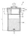
- FIG. 1is a schematic cross-sectional view of a vacuum deposition apparatus according to an embodiment of the present invention
- FIG. 2is an exploded perspective view of a heating crucible according to an embodiment of the present invention.
- FIG. 3is a cross-sectional view of the heating crucible of FIG. 2;
- FIG. 4is a perspective view of another embodiment of an inner plate of the deposition apparatus according to the present invention.
- FIG. 1shows a vacuum deposition apparatus according to an embodiment of the present invention.
- the vacuum deposition apparatusincludes a vacuum chamber 11 , a substrate support 12 that is installed within the chamber 11 to support a deposition substrate 100 , a deposition mask 13 that is closely attached to the substrate 100 and has, for example, a pattern of slots, and a heating crucible 20 that is installed opposite to the substrate 100 so as to position the deposition mask 13 between the heating crucible 20 and the substrate 100 .
- the substrate support 12supports an edge of the substrate 100 so as to have a surface of the substrate, on which deposition is performed, face the heating crucible 20 .
- the present inventionis not limited to the above described structure.
- the substrate support 12may further include a unit which prevents the substrate 100 from bending due to its tare and a unit which closely adheres the deposition mask 13 to the substrate 100 .
- the heating crucible 20vaporizes an organic compound provided therein so as to deposit the organic compound on the substrate 100 or the deposition mask 13 , not in a form of lumps, but in molecules.
- FIGS. 2 and 3show an embodiment of the heating crucible 20 .
- the heating crucible 20includes a space 21 in which an organic compound 200 is contained, a main body 23 having a nozzle 22 through which an evaporated organic compound 200 is discharged, and an inner plate 30 that is installed within the main body 23 and has at least one opening 31 . As shown in FIG. 2, the openings 31 are formed around an edge of an area facing the nozzle 22 so as to transmit a vaporized organic compound 200 .
- the main body 23 of the heating crucible 20comprises a cap 23 a which has the nozzle 22 formed in a centre thereof, and a main body part 23 b which is coupled to the cap 23 a and has the space 21 .
- the main body part 23 bmay have a can shape, and may include a temperature sensing unit (not shown) on a bottom surface of the main body part 23 b .
- the temperature sensing unitmay be a thermocouple which measures a temperature of the vaporized organic compound 200 .
- a heater 27is installed around the main body part 23 b . It is understood that the heater 27 can be installed independently of the main body part 23 b .
- the nozzle 22is installed in the centre of the cap 23 a , and an auxiliary heater (not shown) can be installed on a portion of the cap 23 a around the nozzle 22 so as to prevent the organic compound 200 from being deposited on the nozzle 22 .
- the inner plate 30 installed in the space 21 of the main body 23includes a baffle board 32 on which at least one opening 31 is formed around an edge of an area corresponding to the nozzle 22 , and at least one fixing portion 33 which extends upward from the baffle board 32 to support the baffle board 32 .
- the openings 31can be continuously or discontinuously formed around the edge of the baffle board 32 .
- FIG. 4shows that the openings 31 are linked together along the edge of the baffle board 32 , and the fixing portion 33 extends downward from a bottom surface of the baffle board 32 . Where the openings 31 are formed at predetermined intervals on the edge of the baffle board 32 , such intervals may be equal to one another.
- the inner plate 30that is, the baffle board 32
- the baffle board 32may be as wide as or wider than the nozzle 22 .
- the baffle board 32may be narrower than a sectional area of the space 21 , and the area of the opening 31 may be controlled so as to prevent a large pressure difference from being generated between upper and lower spaces S 1 and S 2 defined by the baffle board 32 of the space 21 (see FIG. 3).
- the distance (L) between the nozzle 22 and the inner plate 30is from the radius (D/2) of the nozzle 22 to ⁇ fraction (9/10 ) ⁇ of the distance (T) between the nozzle 22 and an inner bottom surface of the main body 23 .
- an organic compound 200 to form a deposited thin filmthat is, an electron transport layer, an emitting layer, or a hole transport layer
- a predetermined voltageis applied to the heater 27 and the auxiliary heater (not shown) to heat the main body 32 to vaporize the organic compound 200 .
- the organic compound 200vaporizes into molecule lumps.
- the inner plate 30 installed within the space 21prevents the organic compound 200 , evaporated in a form of lumps, from being deposited on the substrate 100 or the deposition mask 13 , via the nozzle 22 . That is, although the evaporated organic compound lumps are lead to be discharged to the nozzle 22 , via the openings 31 , the baffle board 32 installed to face the nozzle 22 blocks the evaporated organic compound lumps. Consequently, the evaporated organic compound lumps are not transmitted by the nozzle 22 .
- the location of the inner plate 30 within the space 21is an important factor as it affects the amount of organic compound charged and the conductance of organic compound vapor molecules. Where the inner plate 30 is installed too low (based on a bottom of the main body part 23 b ), the amount of organic compound charged decreases and affects the effectiveness of the process. Where the inner plate 30 is installed too high, the volume of the upper space S 1 is reduced, and accordingly, the conductance of the vapor molecules of the vaporized organic compound is reduced. Also, the collision of molecules becomes severe, such that the kinetic energy of the molecules is reduced. Due to the reduction of the kinetic energy, the organic compound molecules do not move freely and congeals and adheres to a relatively cooler surrounding place or adheres to a surrounding area of the nozzle 22 .
- the distance (L) between the nozzle 22 and the inner plate 30is from the radius (D/2) of the nozzle 22 to ⁇ fraction (9/10 ) ⁇ of the distance between the nozzle 22 and the inner bottom surface of the main body 23 . Therefore, the nozzle 22 is prevented from being blocked by the organic compound 200 .
- a deposition apparatus adopting a heating crucible according to the present inventioncan prevent an evaporation of organic compound lumps from being discharged through a nozzle. Accordingly, display of dark images due to deposition of organic compound lumps on a substrate is prevented. Furthermore, formation of a poor deposition pattern on a substrate, due to the deposition of organic compound lumps on a deposition mask, is also prevented.
Landscapes
- Chemical & Material Sciences (AREA)
- Engineering & Computer Science (AREA)
- Chemical Kinetics & Catalysis (AREA)
- Materials Engineering (AREA)
- Mechanical Engineering (AREA)
- Metallurgy (AREA)
- Organic Chemistry (AREA)
- Manufacturing & Machinery (AREA)
- Physical Vapour Deposition (AREA)
- Electroluminescent Light Sources (AREA)
Abstract
Description
- This application claims the benefit of Korean Patent Application No. 2002-43272, filed Jul. 23, 2002 in the Korean Intellectual Property Office, the disclosure of which is incorporated herein by reference.[0001]
- 1. Field of the Invention[0002]
- The present invention relates to a heating crucible and a vacuum deposition apparatus using the same, and more particularly, to a vacuum deposition apparatus using an improved heating crucible that prevents scattering of a vaporable material.[0003]
- 2. Description of the Related Art[0004]
- An electroluminescent (EL) device, which is a spontaneous emission display panel, is attracting attention as a next-generation display panel. An EL device provides a wide viewing angle, an excellent contrast, and a fast response characteristic. EL devices are classified into an inorganic EL device and an organic EL device according to a material that forms an emitting layer thereof. An organic EL device provides high brightness, excellent driving voltage, and a fast response speed, and performs polychromy, compared to an inorganic EL device.[0005]
- Generally, in an organic EL device, an anode layer of a predetermined pattern is formed on a substrate. Then, a hole transport layer, an emitting layer, an electron transport layer are sequentially formed on the anode layer. A cathode layer is formed on the electron transport layer so as to have cathodes orthogonal to the anode layer. The hole transport layer, the emitting layer, and the electron transport layer are thin organic films made of organic compounds.[0006]
- To manufacture an organic EL device having such a structure, thin organic films, such as, the hole transport layer, the emitting layer, the electron transport layer, or the like, are formed using a deposition apparatus. The deposition apparatus includes a vacuum chamber whose internal pressure is controlled to be between 10[0007]−6and 10−7torr, a heating crucible that is installed opposite to a substrate within the vacuum chamber to contain an organic compound, and a heater that is installed at the heating crucible and heats and vaporizes the organic compound.
- While it is preferable to have the organic compound vaporize into molecules during a deposition operation, a sudden vaporization may occur within the organic compound during the heating, resulting in the organic compound being vaporized in lumps.[0008]
- Some of the problems caused by this lump-by-lump basis vaporization are as follows. During the deposition operation, a deposition lump may be attached to an opening of a deposition mask. Accordingly, a material is not deposited on a desired area. This problem continuously occurs unless the deposition mask is replaced, thus hindering a mass production. Also, the deposition material lump may be attached to the substrate, which decreases the evenness of a deposited film. Whereupon a portion of the substrate, on which the deposition material lump is deposited, appears dark upon image display. Furthermore, where a part of an organic compound lump is attached to a nozzle, the organic compound lump is continuously deposited and grown inside the nozzle, consequently blocking the nozzle of the deposition apparatus.[0009]
- To solve the above problems, Korean Patent Publication No. 2000-54211 discloses a heating crucible for a vacuum deposition apparatus having a net-type curtain installed on an opening through which a heated and vaporized organic compound is discharged. However, the net-type curtain installed on the opening in the heating crucible prevents smooth heat conduction from a heater, such that a foreign material first vaporized from the heating crucible and then deposited on the net curtain is not smoothly vaporized. In addition, it is difficult to install the net curtain within the heating crucible.[0010]
- A Japanese Patent Publication No. hei 10-195639 discloses a vaporization source having a vaporization crucible that contains an organic vaporization material. An orifice which controls the amount of vaporization of the organic material is installed within the vaporization crucible. Since an organic compound is heated by a heater installed over an outer circumferential surface of the disclosed heating crucible, the organic compound is not evenly heated. In addition, the organic compound cannot vaporize uniformly from the entire portion of the crucible.[0011]
- A Japanese Patent Publication No. 2000-160328 discloses a heating crucible for evaporating an organic compound, including a main body which contains an organic compound, a heater which is installed around an outer circumferential surface of the heating crucible, and a heat shield layer which is installed around an outer circumferential surface of the heater. A Japanese Patent Publication No. 2000-68055 discloses a deposition source for an organic EL device.[0012]
- Accordingly, it is an aspect of the present invention to provide a heating crucible in which although an organic compound may not vaporize into molecules during a vaporization of the organic compound, improper deposition of the organic compound on a substrate, due to a deposition of organic compound in lumps on a deposition mask and the substrate, is prevented, and a deposition apparatus using the heating crucible.[0013]
- Another aspect of the preset invention is to provide a heating crucible which prevents a formation of a dark image due to an emission failure of deposition films on a substrate of a display, and a deposition apparatus using the heating crucible.[0014]
- Yet another aspect of the present invention is to provide a heating crucible which reduces improper deposition due to scattered organic compound lumps created by a sudden vaporization of the organic compound, and a deposition apparatus using the heating crucible.[0015]
- Still another aspect of the present invention is to provide a heating crucible which prevents a reduction of energy due to severe collision among evaporating organic compound molecules, and a deposition apparatus using the heating crucible.[0016]
- Additional aspects and/or advantages of the invention will be set forth in part in the description which follows and, in part, will be obvious from the description, or may be learned by practice of the invention.[0017]
- To achieve the above and/or other aspects of the present invention, there is provided a heating crucible comprising a main body and an inner member. The main body includes a space which receives an organic compound and a nozzle through which vaporized organic compound is discharged. The inner member is installed within the main body and includes one or more openings formed around an edge of an area thereof facing the nozzle so as to transmit the vaporized organic compound.[0018]
- The inner member may have a cross-section which is substantially the same as that of the space of the main body, and the openings may be continuously or discontinuously formed along the edge of the inner member. The sum of areas of the openings of the inner member may be equal to or greater than an area of the nozzle. The distance between the nozzle and the inner member may be from a radius of the nozzle to[0019]9/10 of a distance between the nozzle and an inner bottom surface of the main body.
- The main body may comprise a cap on which the nozzle is formed and a main body part in which the space is formed.[0020]
- The heating crucible may further comprise a heater which is provided in the main body and/or the nozzle.[0021]
- To achieve the above and/or other aspects of the present invention, there is provided a deposition apparatus for forming a deposition film on a substrate, comprising a vacuum chamber which receives the substrate and a heating crucible which is installed opposite to the substrate and vaporizes an organic compound provided thereto. The heating crucible comprises a main body having a space which receives the organic compound and a nozzle through which vaporized organic compound is discharged, and an inner member installed within the main body and having one or more openings formed around an edge of an area thereof facing the nozzle so as to transmit the vaporized organic compound.[0022]
- In the present invention, a mask having a pattern to be deposited may closely attached to the substrate facing the heat crucible.[0023]
- These and/or other aspects and advantages of the invention will become apparent and more readily appreciated from the following description of the embodiments taken in conjunction with the accompanying drawings in which:[0024]
- FIG. 1 is a schematic cross-sectional view of a vacuum deposition apparatus according to an embodiment of the present invention;[0025]
- FIG. 2 is an exploded perspective view of a heating crucible according to an embodiment of the present invention;[0026]
- FIG. 3 is a cross-sectional view of the heating crucible of FIG. 2; and[0027]
- FIG. 4 is a perspective view of another embodiment of an inner plate of the deposition apparatus according to the present invention.[0028]
- Reference will now be made in detail to the present preferred embodiments of the present invention, examples of which are illustrated in the accompanying drawings, wherein like reference numerals refer to the like elements throughout. The embodiments are described below in order to explain the present invention by referring to the figures.[0029]
- FIG. 1 shows a vacuum deposition apparatus according to an embodiment of the present invention. The vacuum deposition apparatus includes a[0030]
vacuum chamber 11, asubstrate support 12 that is installed within thechamber 11 to support adeposition substrate 100, adeposition mask 13 that is closely attached to thesubstrate 100 and has, for example, a pattern of slots, and aheating crucible 20 that is installed opposite to thesubstrate 100 so as to position thedeposition mask 13 between theheating crucible 20 and thesubstrate 100. - The[0031]
substrate support 12 supports an edge of thesubstrate 100 so as to have a surface of the substrate, on which deposition is performed, face theheating crucible 20. However, the present invention is not limited to the above described structure. For example, thesubstrate support 12 may further include a unit which prevents thesubstrate 100 from bending due to its tare and a unit which closely adheres thedeposition mask 13 to thesubstrate 100. - The[0032]
heating crucible 20 vaporizes an organic compound provided therein so as to deposit the organic compound on thesubstrate 100 or thedeposition mask 13, not in a form of lumps, but in molecules. - FIGS. 2 and 3 show an embodiment of the[0033]
heating crucible 20. Theheating crucible 20 includes aspace 21 in which anorganic compound 200 is contained, amain body 23 having anozzle 22 through which an evaporatedorganic compound 200 is discharged, and aninner plate 30 that is installed within themain body 23 and has at least oneopening 31. As shown in FIG. 2, theopenings 31 are formed around an edge of an area facing thenozzle 22 so as to transmit a vaporizedorganic compound 200. - The[0034]
main body 23 of theheating crucible 20 comprises acap 23awhich has thenozzle 22 formed in a centre thereof, and amain body part 23bwhich is coupled to thecap 23aand has thespace 21. Themain body part 23bmay have a can shape, and may include a temperature sensing unit (not shown) on a bottom surface of themain body part 23b. The temperature sensing unit may be a thermocouple which measures a temperature of the vaporizedorganic compound 200. Aheater 27 is installed around themain body part 23b. It is understood that theheater 27 can be installed independently of themain body part 23b. Thenozzle 22 is installed in the centre of thecap 23a, and an auxiliary heater (not shown) can be installed on a portion of thecap 23aaround thenozzle 22 so as to prevent theorganic compound 200 from being deposited on thenozzle 22. - The[0035]
inner plate 30 installed in thespace 21 of themain body 23 includes abaffle board 32 on which at least oneopening 31 is formed around an edge of an area corresponding to thenozzle 22, and at least one fixingportion 33 which extends upward from thebaffle board 32 to support thebaffle board 32. Theopenings 31 can be continuously or discontinuously formed around the edge of thebaffle board 32. For example, FIG. 4 shows that theopenings 31 are linked together along the edge of thebaffle board 32, and the fixingportion 33 extends downward from a bottom surface of thebaffle board 32. Where theopenings 31 are formed at predetermined intervals on the edge of thebaffle board 32, such intervals may be equal to one another. - The[0036]
inner plate 30, that is, thebaffle board 32, may be as wide as or wider than thenozzle 22. Thebaffle board 32 may be narrower than a sectional area of thespace 21, and the area of theopening 31 may be controlled so as to prevent a large pressure difference from being generated between upper and lower spaces S1 and S2 defined by thebaffle board 32 of the space21 (see FIG. 3). - Referring to FIG. 3, the distance (L) between the[0037]
nozzle 22 and theinner plate 30 is from the radius (D/2) of thenozzle 22 to {fraction (9/10 )} of the distance (T) between thenozzle 22 and an inner bottom surface of themain body 23. - An operation of a[0038]
heating crucible 20 having the above-described configuration and a deposition apparatus adopting theheating crucible 20 will now be described. For example, anorganic compound 200 to form a deposited thin film (that is, an electron transport layer, an emitting layer, or a hole transport layer), which is an organic film of an organic electroluminescent display device, is injected into thespace 21 within theheating crucible 20. In this state, a predetermined voltage is applied to theheater 27 and the auxiliary heater (not shown) to heat themain body 32 to vaporize theorganic compound 200. - During the vaporization of the[0039]
organic compound 200, where sudden vaporization of theorganic compound 200 occurs within thespace 21 of themain body 23, theorganic compound 200 vaporizes into molecule lumps. However, theinner plate 30 installed within thespace 21 prevents theorganic compound 200, evaporated in a form of lumps, from being deposited on thesubstrate 100 or thedeposition mask 13, via thenozzle 22. That is, although the evaporated organic compound lumps are lead to be discharged to thenozzle 22, via theopenings 31, thebaffle board 32 installed to face thenozzle 22 blocks the evaporated organic compound lumps. Consequently, the evaporated organic compound lumps are not transmitted by thenozzle 22. Even where the organic compound lumps pass through theopening 31, since a vertical axis of thenozzle 21 does not match with that of theopening 31, the organic compound lumps collide with an inner wall of thespace 21 defined by themain body part 23band thecap 23a. Consequently, the organic compound lumps fail to pass through thenozzle 22. - Since the sum of areas of the[0040]
openings 31 formed around the edge of thebaffle board 32 facing thenozzle 22 is greater than the area of thenozzle 22, a reduction of pressure of theorganic compound 200 discharged through thenozzle 22 can be avoided. Where the sum of the areas of theopenings 31 is smaller than the area of thenozzle 22, the vaporized organic compound collides with one another by failing to move from the lower space S2 to the upper space S1, and the pressure of the lower space S2 increases. Where the pressure of the lower space S2 increases, a vaporization temperature of theorganic compound 200 increases. As the vaporization temperature of theorganic compound 200 is equal to or greater than a decomposition temperature, theorganic compound 200 is decomposed. The decomposition of theorganic compound 200 negatively affects deposition films and serves as an important factor of shortening the durability of an organic electroluminescent display device. - The location of the[0041]
inner plate 30 within thespace 21 is an important factor as it affects the amount of organic compound charged and the conductance of organic compound vapor molecules. Where theinner plate 30 is installed too low (based on a bottom of themain body part 23b), the amount of organic compound charged decreases and affects the effectiveness of the process. Where theinner plate 30 is installed too high, the volume of the upper space S1 is reduced, and accordingly, the conductance of the vapor molecules of the vaporized organic compound is reduced. Also, the collision of molecules becomes severe, such that the kinetic energy of the molecules is reduced. Due to the reduction of the kinetic energy, the organic compound molecules do not move freely and congeals and adheres to a relatively cooler surrounding place or adheres to a surrounding area of thenozzle 22. Accordingly, the distance (L) between thenozzle 22 and theinner plate 30 is from the radius (D/2) of thenozzle 22 to {fraction (9/10 )} of the distance between thenozzle 22 and the inner bottom surface of themain body 23. Therefore, thenozzle 22 is prevented from being blocked by theorganic compound 200. - According to an experiment of the inventors of the present invention, where an organic material was deposited on a substrate at 1 Ås, and values obtained by dividing the distance (L) between the[0042]
nozzle 22 and theinner plate 30 by the radius of thenozzle 22 were 0.40 and 0.67, thenozzle 22 was blocked by the organic material within 2 hours and 12 hours, respectively. Also, where a value obtained by dividing an installation height of theinner plate 30 by the radius of thenozzle 22 was equal to or greater than 1.0, thenozzle 22 was not blocked. - As described above, a deposition apparatus adopting a heating crucible according to the present invention can prevent an evaporation of organic compound lumps from being discharged through a nozzle. Accordingly, display of dark images due to deposition of organic compound lumps on a substrate is prevented. Furthermore, formation of a poor deposition pattern on a substrate, due to the deposition of organic compound lumps on a deposition mask, is also prevented.[0043]
- Although a few embodiments of the present invention have been shown and described, it would be appreciated by those skilled in the art that changes may be made in this embodiment without departing from the principles and spirit of the invention, the scope of which is defined in the claims and their equivalents.[0044]
Claims (33)
Applications Claiming Priority (3)
| Application Number | Priority Date | Filing Date | Title |
|---|---|---|---|
| KR2002-43272 | 2002-07-23 | ||
| KR10-2002-0043272AKR100490537B1 (en) | 2002-07-23 | 2002-07-23 | Heating crucible and deposit apparatus utilizing the same |
| KR10-2002-0043272 | 2002-07-23 |
Publications (2)
| Publication Number | Publication Date |
|---|---|
| US20040035366A1true US20040035366A1 (en) | 2004-02-26 |
| US8025733B2 US8025733B2 (en) | 2011-09-27 |
Family
ID=31884877
Family Applications (1)
| Application Number | Title | Priority Date | Filing Date |
|---|---|---|---|
| US10/619,512Active2027-10-20US8025733B2 (en) | 2002-07-23 | 2003-07-16 | Heating crucible and deposition apparatus using the same |
Country Status (5)
| Country | Link |
|---|---|
| US (1) | US8025733B2 (en) |
| EP (1) | EP1433873B1 (en) |
| JP (1) | JP2004052113A (en) |
| KR (1) | KR100490537B1 (en) |
| CN (1) | CN100402693C (en) |
Cited By (27)
| Publication number | Priority date | Publication date | Assignee | Title |
|---|---|---|---|---|
| US20010006827A1 (en)* | 1999-12-27 | 2001-07-05 | Semiconductor Energy Laboratory Co., Ltd. | Film formation apparatus and method for forming a film |
| US20020009538A1 (en)* | 2000-05-12 | 2002-01-24 | Yasuyuki Arai | Method of manufacturing a light-emitting device |
| US20030162314A1 (en)* | 2002-02-25 | 2003-08-28 | Shunpei Yamazaki | Fabrication system and a fabrication method of light emitting device |
| US20030194484A1 (en)* | 2002-04-15 | 2003-10-16 | Semiconductor Engergy Laboratory Co., Ltd. | Method of fabricating light-emitting device and apparatus for manufacturing light-emitting device |
| US20050034671A1 (en)* | 2003-08-15 | 2005-02-17 | Semiconductor Energy Laboratory Co., Ltd. | Deposition apparatus and manufacturing apparatus |
| US20050150461A1 (en)* | 2004-01-08 | 2005-07-14 | Samsung Electronics Co., Ltd. | Apparatus of depositing thin film with high uniformity |
| US20060278167A1 (en)* | 2005-06-06 | 2006-12-14 | Createc Fischer & Co. Gmbh | High-temperature evaporator cell and process for evaporating high-melting materials |
| EP1770186A1 (en)* | 2005-09-30 | 2007-04-04 | Samsung SDI Co., Ltd. | Evaporation source and vacuum deposition apparatus using the same |
| US20070119849A1 (en)* | 2005-08-30 | 2007-05-31 | Jeong Min J | Heater and vapor deposition source having the same |
| US20070178225A1 (en)* | 2005-12-14 | 2007-08-02 | Keiji Takanosu | Vapor deposition crucible, thin-film forming apparatus comprising the same, and method of producing display device |
| US20090050053A1 (en)* | 2007-08-23 | 2009-02-26 | Samsung Sdi Co., Ltd | Crucible heating apparatus and deposition apparatus including the same |
| US20090176036A1 (en)* | 2005-08-25 | 2009-07-09 | Eiichi Matsumoto | Method of organic material vacuum evaporation and apparatus thereof |
| US20100043710A1 (en)* | 2008-08-22 | 2010-02-25 | Kyung-Soo Min | Inner plate and crucible assembly for deposition having the same |
| US20100159124A1 (en)* | 2000-05-02 | 2010-06-24 | Semiconductor Energy Laboratory Co., Ltd. | Film-forming apparatus, method of cleaning the same, and method of manufacturing a light-emitting device |
| EP2278043A1 (en)* | 2004-11-09 | 2011-01-26 | Global OLED Technology LLC | Controlling the application of vaporized organic material |
| US7943443B2 (en) | 2002-09-20 | 2011-05-17 | Semiconductor Energy Laboratory Co., Ltd. | Manufacturing method of light-emitting device |
| US20120160171A1 (en)* | 2010-12-27 | 2012-06-28 | Riber | Injector for a vacuum evaporation source |
| CN102994958A (en)* | 2012-12-14 | 2013-03-27 | 深圳先进技术研究院 | Heat evaporation source of heat evaporation coating equipment |
| US20140193581A1 (en)* | 2009-09-01 | 2014-07-10 | Samsung Display Co., Ltd. | Thin film deposition apparatus |
| US20140352616A1 (en)* | 2013-05-31 | 2014-12-04 | Samsung Display Co., Ltd. | Crucible apparatus and deposition apparatus with the same |
| US20150218690A1 (en)* | 2013-12-30 | 2015-08-06 | Shenzhen China Star Optoelectronics Technology Co., Ltd. | Vacuum Vapor Deposition Apparatus and Method |
| CN106560524A (en)* | 2015-10-06 | 2017-04-12 | 三星显示有限公司 | Deposition Source And Method Of Manufacturing The Same |
| CN111139436A (en)* | 2018-11-06 | 2020-05-12 | 瑞必尔 | Evaporation device for vacuum evaporation system, apparatus and method for depositing material films |
| CN114381714A (en)* | 2021-12-30 | 2022-04-22 | 复旦大学 | A miniature in-situ temperature measurement high temperature atomic and molecular evaporation and emission device |
| CN114585770A (en)* | 2019-11-29 | 2022-06-03 | Lg电子株式会社 | Deposition apparatus |
| US11643749B2 (en)* | 2018-04-26 | 2023-05-09 | Showa Denko K.K. | Crucible and SiC single crystal growth apparatus |
| US11971216B1 (en) | 2021-12-23 | 2024-04-30 | Rolls-Royce High Temperature Composites, Inc. | Retort with loading window |
Families Citing this family (20)
| Publication number | Priority date | Publication date | Assignee | Title |
|---|---|---|---|---|
| KR100646514B1 (en) | 2004-10-22 | 2006-11-15 | 삼성에스디아이 주식회사 | Organic material deposition apparatus |
| JP4557170B2 (en)* | 2004-11-26 | 2010-10-06 | 三星モバイルディスプレイ株式會社 | Evaporation source |
| KR100646961B1 (en)* | 2005-01-06 | 2006-11-23 | 삼성에스디아이 주식회사 | Control Method of Deposition Source of Deposition System |
| JP4911345B2 (en) | 2005-07-25 | 2012-04-04 | セイコーエプソン株式会社 | PATTERNING METHOD AND ELECTRONIC DEVICE MANUFACTURING METHOD USING THE SAME |
| KR100696531B1 (en)* | 2005-09-07 | 2007-03-19 | 삼성에스디아이 주식회사 | Heating vessel and deposition apparatus using the same |
| KR100723627B1 (en)* | 2006-08-01 | 2007-06-04 | 세메스 주식회사 | The evaporation source of the organic thin film deposition apparatus |
| KR101094299B1 (en) | 2009-12-17 | 2011-12-19 | 삼성모바일디스플레이주식회사 | Linear evaporation source and deposition apparatus comprising the same |
| KR101182265B1 (en)* | 2009-12-22 | 2012-09-12 | 삼성디스플레이 주식회사 | Evaporation Source and Deposition Apparatus having the same |
| KR101723506B1 (en) | 2010-10-22 | 2017-04-19 | 삼성디스플레이 주식회사 | Apparatus for organic layer deposition and method for manufacturing of organic light emitting display apparatus using the same |
| KR101052435B1 (en)* | 2011-04-13 | 2011-07-28 | 에스엔유 프리시젼 주식회사 | Thin film deposition equipment |
| CN106381466B (en) | 2012-08-06 | 2019-04-05 | 铣益系统有限责任公司 | Organic deposition device and organic deposition method |
| KR101237507B1 (en)* | 2012-08-06 | 2013-02-26 | 주식회사 선익시스템 | Apparatus for depositing organic material and method for depositing organic material |
| KR101398640B1 (en)* | 2012-11-05 | 2014-05-27 | 한국표준과학연구원 | An apparatus for storing while maintaining high temperature |
| KR102053249B1 (en)* | 2013-05-02 | 2020-01-09 | 삼성디스플레이 주식회사 | Deposition source and deposition apparatus including the same |
| CN104593729B (en)* | 2014-12-24 | 2017-04-05 | 深圳市华星光电技术有限公司 | Prevent the crucible of deposition material splash and consent |
| CN104988463B (en)* | 2015-06-24 | 2018-11-06 | 深圳市华星光电技术有限公司 | A kind of evaporator of heating source and Organic Light Emitting Diode |
| KR101749570B1 (en)* | 2015-10-28 | 2017-07-03 | 한국표준과학연구원 | Inductive Heating Linear Evaporation Deposition Apparatus |
| CN108456855B (en)* | 2017-02-17 | 2024-09-03 | 京东方科技集团股份有限公司 | Crucible, vapor deposition preparation device, vapor deposition equipment and vapor deposition method |
| CN114555854A (en)* | 2019-11-11 | 2022-05-27 | 韩商则舒穆公司 | Mask for manufacturing OLED and OLED manufacturing method |
| CN113445006B (en)* | 2020-04-09 | 2023-01-31 | 重庆康佳光电技术研究院有限公司 | Evaporation lining pot |
Citations (15)
| Publication number | Priority date | Publication date | Assignee | Title |
|---|---|---|---|---|
| US2793609A (en)* | 1953-01-26 | 1957-05-28 | British Dielectric Res Ltd | Means for the deposition of materials by evaporation in a vacuum |
| US2799764A (en)* | 1953-10-15 | 1957-07-16 | Edward F Chandler | Panel heating device |
| US3466424A (en)* | 1967-08-31 | 1969-09-09 | Nasa | Evaporant source for vapor deposition |
| US3842241A (en)* | 1973-02-09 | 1974-10-15 | Biozonics Corp | Electrically heated aquarium tank |
| US5157240A (en)* | 1989-09-13 | 1992-10-20 | Chow Loren A | Deposition heaters |
| US5272298A (en)* | 1991-04-03 | 1993-12-21 | Mitsubishi Jukogyo Kabushiki Kaisha | Apparatus for vacuum deposition of sublimative substance |
| US5432341A (en)* | 1992-07-29 | 1995-07-11 | Gspann; Juergen | Process and apparatus for producing agglomerate rays |
| US5944903A (en)* | 1997-06-25 | 1999-08-31 | Tiedje; Henry Franklin | Effusion cell crucible with thermocouple |
| US6162300A (en)* | 1998-09-25 | 2000-12-19 | Bichrt; Craig E. | Effusion cell |
| US6202591B1 (en)* | 1998-11-12 | 2001-03-20 | Flex Products, Inc. | Linear aperture deposition apparatus and coating process |
| US6237529B1 (en)* | 2000-03-03 | 2001-05-29 | Eastman Kodak Company | Source for thermal physical vapor deposition of organic electroluminescent layers |
| US6242719B1 (en)* | 1998-06-11 | 2001-06-05 | Shin-Etsu Handotai Co., Ltd. | Multiple-layered ceramic heater |
| US20010008121A1 (en)* | 1998-06-23 | 2001-07-19 | Hiroshi Tanabe | Apparatus and method for preparing organic el device |
| US6358466B1 (en)* | 2000-04-17 | 2002-03-19 | Iowa State University Research Foundation, Inc. | Thermal sprayed composite melt containment tubular component and method of making same |
| US20030101937A1 (en)* | 2001-11-28 | 2003-06-05 | Eastman Kodak Company | Thermal physical vapor deposition source for making an organic light-emitting device |
Family Cites Families (27)
| Publication number | Priority date | Publication date | Assignee | Title |
|---|---|---|---|---|
| CH593347A5 (en) | 1976-03-03 | 1977-11-30 | Bbc Brown Boveri & Cie | |
| JPS58221273A (en)* | 1982-06-18 | 1983-12-22 | Hitachi Ltd | Evaporation boat |
| JPS6043480A (en)* | 1983-08-19 | 1985-03-08 | Toshiba Corp | Crucible as evaporating source for vacuum deposition |
| JPS60116772A (en) | 1983-11-29 | 1985-06-24 | Ulvac Corp | Vapor source device for cluster ion beam |
| JPS60137896A (en)* | 1983-12-23 | 1985-07-22 | Hitachi Ltd | Crucible for molecular beam source |
| JPS60162771A (en)* | 1984-02-01 | 1985-08-24 | Mitsubishi Electric Corp | Crucible |
| JPS61132589A (en)* | 1984-11-30 | 1986-06-20 | Agency Of Ind Science & Technol | Crucible for vapor deposition |
| JPS61156809A (en)* | 1984-12-28 | 1986-07-16 | Mitsubishi Electric Corp | Steam injection device for molten substances |
| JPS61163267A (en)* | 1985-01-14 | 1986-07-23 | Mitsubishi Electric Corp | Vacuum deposition equipment |
| JPS63238264A (en)* | 1987-03-26 | 1988-10-04 | Mitsubishi Electric Corp | Vapor and cluster ejection device for vapor deposition material |
| JPS63293157A (en)* | 1987-05-25 | 1988-11-30 | Fuji Photo Film Co Ltd | Boat for vapor deposition |
| JPH02247374A (en)* | 1989-03-20 | 1990-10-03 | Hitachi Ltd | Crucible for evaporation source and thin film formation using same |
| JPH02290963A (en)* | 1989-04-28 | 1990-11-30 | Matsushita Electric Ind Co Ltd | Crucible for vapor deposition |
| US5075055A (en) | 1990-06-06 | 1991-12-24 | Union Carbide Coatings Service Technology Corporation | Process for producing a boron nitride crucible |
| JPH0452273A (en) | 1990-06-18 | 1992-02-20 | Mitsubishi Electric Corp | Thin film forming equipment |
| JPH05339709A (en)* | 1992-06-04 | 1993-12-21 | Hitachi Denshi Ltd | Vacuum evaporation boat |
| JP3091573B2 (en) | 1992-06-11 | 2000-09-25 | ティーディーケイ株式会社 | Vacuum deposition equipment |
| CN1103112A (en) | 1993-11-20 | 1995-05-31 | 三菱电机株式会社 | Film forming device |
| CN1039247C (en) | 1994-09-10 | 1998-07-22 | 冶金工业部钢铁研究总院 | Crucible with titanium diboride coating and its manufacture |
| JP3483719B2 (en)* | 1997-01-09 | 2004-01-06 | 株式会社アルバック | Evaporation source for organic material and organic thin film forming apparatus using the same |
| JP2000068055A (en)* | 1998-08-26 | 2000-03-03 | Tdk Corp | Evaporation source for organic el element, manufacturing device for organic el element using the same and manufacture thereof |
| DE19852325C1 (en)* | 1998-11-12 | 2000-05-11 | Siemens Ag | Continuous gallium(I) compound vapor stream, especially for doping x-ray absorbing phosphors produced by reducing divalent or trivalent gallium compound vapor with gallium metal in a closed crucible having a small vapor outlet |
| JP4469430B2 (en)* | 1998-11-30 | 2010-05-26 | 株式会社アルバック | Vapor deposition equipment |
| KR100340732B1 (en)* | 2000-05-26 | 2002-06-20 | 천웅기 | Heating crucible of apparatus for depositing a organic materials |
| CN1317420C (en) | 2000-08-31 | 2007-05-23 | 住友钛株式会社 | Silicon monoxide vapor deposition material, method for producing the same, raw material for production, and production device |
| CN1308145A (en) | 2000-11-17 | 2001-08-15 | 武汉大学 | Gallium nitride film preparing technology and special equipment |
| KR100461283B1 (en)* | 2000-12-30 | 2004-12-14 | 현대엘씨디주식회사 | Organic source boat structure for organic electro-luminescent display fabricating apparatus |
- 2002
- 2002-07-23KRKR10-2002-0043272Apatent/KR100490537B1/ennot_activeExpired - Lifetime
- 2003
- 2003-07-16USUS10/619,512patent/US8025733B2/enactiveActive
- 2003-07-22EPEP03254571.7Apatent/EP1433873B1/ennot_activeExpired - Lifetime
- 2003-07-23JPJP2003278270Apatent/JP2004052113A/enactivePending
- 2003-07-23CNCNB031331815Apatent/CN100402693C/ennot_activeExpired - Lifetime
Patent Citations (15)
| Publication number | Priority date | Publication date | Assignee | Title |
|---|---|---|---|---|
| US2793609A (en)* | 1953-01-26 | 1957-05-28 | British Dielectric Res Ltd | Means for the deposition of materials by evaporation in a vacuum |
| US2799764A (en)* | 1953-10-15 | 1957-07-16 | Edward F Chandler | Panel heating device |
| US3466424A (en)* | 1967-08-31 | 1969-09-09 | Nasa | Evaporant source for vapor deposition |
| US3842241A (en)* | 1973-02-09 | 1974-10-15 | Biozonics Corp | Electrically heated aquarium tank |
| US5157240A (en)* | 1989-09-13 | 1992-10-20 | Chow Loren A | Deposition heaters |
| US5272298A (en)* | 1991-04-03 | 1993-12-21 | Mitsubishi Jukogyo Kabushiki Kaisha | Apparatus for vacuum deposition of sublimative substance |
| US5432341A (en)* | 1992-07-29 | 1995-07-11 | Gspann; Juergen | Process and apparatus for producing agglomerate rays |
| US5944903A (en)* | 1997-06-25 | 1999-08-31 | Tiedje; Henry Franklin | Effusion cell crucible with thermocouple |
| US6242719B1 (en)* | 1998-06-11 | 2001-06-05 | Shin-Etsu Handotai Co., Ltd. | Multiple-layered ceramic heater |
| US20010008121A1 (en)* | 1998-06-23 | 2001-07-19 | Hiroshi Tanabe | Apparatus and method for preparing organic el device |
| US6162300A (en)* | 1998-09-25 | 2000-12-19 | Bichrt; Craig E. | Effusion cell |
| US6202591B1 (en)* | 1998-11-12 | 2001-03-20 | Flex Products, Inc. | Linear aperture deposition apparatus and coating process |
| US6237529B1 (en)* | 2000-03-03 | 2001-05-29 | Eastman Kodak Company | Source for thermal physical vapor deposition of organic electroluminescent layers |
| US6358466B1 (en)* | 2000-04-17 | 2002-03-19 | Iowa State University Research Foundation, Inc. | Thermal sprayed composite melt containment tubular component and method of making same |
| US20030101937A1 (en)* | 2001-11-28 | 2003-06-05 | Eastman Kodak Company | Thermal physical vapor deposition source for making an organic light-emitting device |
Cited By (56)
| Publication number | Priority date | Publication date | Assignee | Title |
|---|---|---|---|---|
| US20010006827A1 (en)* | 1999-12-27 | 2001-07-05 | Semiconductor Energy Laboratory Co., Ltd. | Film formation apparatus and method for forming a film |
| US20100021624A1 (en)* | 1999-12-27 | 2010-01-28 | Semiconductor Energy Laboratory Co., Ltd | Film Formation Apparatus and Method for Forming a Film |
| US8119189B2 (en) | 1999-12-27 | 2012-02-21 | Semiconductor Energy Laboratory Co., Ltd. | Method of manufacturing a display device |
| US9559302B2 (en) | 1999-12-27 | 2017-01-31 | Semiconductor Energy Laboratory Co., Ltd. | Method of manufacturing a display device |
| US8968823B2 (en) | 1999-12-27 | 2015-03-03 | Semiconductor Energy Laboratory Co., Ltd. | Method of manufacturing a light emitting device |
| US20100159124A1 (en)* | 2000-05-02 | 2010-06-24 | Semiconductor Energy Laboratory Co., Ltd. | Film-forming apparatus, method of cleaning the same, and method of manufacturing a light-emitting device |
| US8815331B2 (en) | 2000-05-02 | 2014-08-26 | Semiconductor Energy Laboratory Co., Ltd. | Film-forming apparatus, method of cleaning the same, and method of manufacturing a light-emitting device |
| US20020009538A1 (en)* | 2000-05-12 | 2002-01-24 | Yasuyuki Arai | Method of manufacturing a light-emitting device |
| US7517551B2 (en) | 2000-05-12 | 2009-04-14 | Semiconductor Energy Laboratory Co., Ltd. | Method of manufacturing a light-emitting device |
| US20090074952A1 (en)* | 2002-02-25 | 2009-03-19 | Semiconductor Energy Laboratory Co., Ltd. | Fabrication System and a Fabrication Method of a Light Emitting Device |
| US9551063B2 (en) | 2002-02-25 | 2017-01-24 | Semiconductor Energy Laboratory Co., Ltd. | Fabrication system and a fabrication method of a light emitting device |
| US20030162314A1 (en)* | 2002-02-25 | 2003-08-28 | Shunpei Yamazaki | Fabrication system and a fabrication method of light emitting device |
| US7309269B2 (en) | 2002-04-15 | 2007-12-18 | Semiconductor Energy Laboratory Co., Ltd. | Method of fabricating light-emitting device and apparatus for manufacturing light-emitting device |
| US20080282984A1 (en)* | 2002-04-15 | 2008-11-20 | Semiconductor Energy Laboratory Co., Ltd. | Method of fabricating light-emitting device and apparatus for manufacturing light-emitting device |
| US9209427B2 (en) | 2002-04-15 | 2015-12-08 | Semiconductor Energy Laboratory Co., Ltd. | Method of fabricating light-emitting device and apparatus for manufacturing light-emitting device |
| US20030194484A1 (en)* | 2002-04-15 | 2003-10-16 | Semiconductor Engergy Laboratory Co., Ltd. | Method of fabricating light-emitting device and apparatus for manufacturing light-emitting device |
| US8377764B2 (en) | 2002-09-20 | 2013-02-19 | Semiconductor Energy Laboratory Co., Ltd. | Manufacturing method for light emitting device |
| US8168483B2 (en) | 2002-09-20 | 2012-05-01 | Semiconductor Energy Laboratory Co., Ltd. | Manufacturing method for light emitting device |
| US8609476B2 (en) | 2002-09-20 | 2013-12-17 | Semiconductor Energy Laboratory Co., Ltd. | Manufacturing method of light emitting device |
| US20110217802A1 (en)* | 2002-09-20 | 2011-09-08 | Semiconductor Energy Laboratory Co., Ltd. | Fabrication System and Manufacturing Method of Light Emitting Device |
| US7943443B2 (en) | 2002-09-20 | 2011-05-17 | Semiconductor Energy Laboratory Co., Ltd. | Manufacturing method of light-emitting device |
| US8123862B2 (en)* | 2003-08-15 | 2012-02-28 | Semiconductor Energy Laboratory Co., Ltd. | Deposition apparatus and manufacturing apparatus |
| US20050034671A1 (en)* | 2003-08-15 | 2005-02-17 | Semiconductor Energy Laboratory Co., Ltd. | Deposition apparatus and manufacturing apparatus |
| US8524313B2 (en) | 2003-08-15 | 2013-09-03 | Semiconductor Energy Laboratory Co., Ltd. | Method for manufacturing a device |
| US20050150461A1 (en)* | 2004-01-08 | 2005-07-14 | Samsung Electronics Co., Ltd. | Apparatus of depositing thin film with high uniformity |
| US6966952B2 (en)* | 2004-01-08 | 2005-11-22 | Samsung Electronics Co., Ltd. | Apparatus of depositing thin film with high uniformity |
| EP2278043A1 (en)* | 2004-11-09 | 2011-01-26 | Global OLED Technology LLC | Controlling the application of vaporized organic material |
| US7700166B2 (en)* | 2005-06-06 | 2010-04-20 | Createc Fischer & Co. Gmbh | Process for evaporating high-melting materials |
| US20060278167A1 (en)* | 2005-06-06 | 2006-12-14 | Createc Fischer & Co. Gmbh | High-temperature evaporator cell and process for evaporating high-melting materials |
| US20100154708A1 (en)* | 2005-06-06 | 2010-06-24 | Createc Fischer & Co. Gmbh | High-temperature evaporator cell for evaporating high-melting materials |
| TWI396758B (en)* | 2005-08-25 | 2013-05-21 | Canon Tokki Corp | Vacuum evaporation method and device for organic material |
| US20090176036A1 (en)* | 2005-08-25 | 2009-07-09 | Eiichi Matsumoto | Method of organic material vacuum evaporation and apparatus thereof |
| US8357241B2 (en)* | 2005-08-25 | 2013-01-22 | Canon Tokki Corporation | Method of organic material vacuum evaporation and apparatus thereof |
| US20070119849A1 (en)* | 2005-08-30 | 2007-05-31 | Jeong Min J | Heater and vapor deposition source having the same |
| US20070074654A1 (en)* | 2005-09-30 | 2007-04-05 | Lee Jeong-Yeol | Evaporation source machine and vaccum deposition apparatus using the same |
| EP1770186A1 (en)* | 2005-09-30 | 2007-04-04 | Samsung SDI Co., Ltd. | Evaporation source and vacuum deposition apparatus using the same |
| US20070178225A1 (en)* | 2005-12-14 | 2007-08-02 | Keiji Takanosu | Vapor deposition crucible, thin-film forming apparatus comprising the same, and method of producing display device |
| US20090050053A1 (en)* | 2007-08-23 | 2009-02-26 | Samsung Sdi Co., Ltd | Crucible heating apparatus and deposition apparatus including the same |
| US8075693B2 (en) | 2007-08-23 | 2011-12-13 | Samsung Mobile Display Co., Ltd. | Crucible heating apparatus and deposition apparatus including the same |
| TWI404812B (en)* | 2008-08-22 | 2013-08-11 | Samsung Display Co Ltd | Inner plate and crucible assembly for deposition having the same |
| US20100043710A1 (en)* | 2008-08-22 | 2010-02-25 | Kyung-Soo Min | Inner plate and crucible assembly for deposition having the same |
| US8137470B2 (en)* | 2008-08-22 | 2012-03-20 | Samsung Mobile Display Co., Ltd. | Inner plate and crucible assembly for deposition having the same |
| US20140193581A1 (en)* | 2009-09-01 | 2014-07-10 | Samsung Display Co., Ltd. | Thin film deposition apparatus |
| US9624580B2 (en)* | 2009-09-01 | 2017-04-18 | Samsung Display Co., Ltd. | Thin film deposition apparatus |
| KR101755534B1 (en)* | 2010-12-27 | 2017-07-07 | 리베르 | Injector for a vacuum evaporation source |
| US8858714B2 (en)* | 2010-12-27 | 2014-10-14 | Riber | Injector for a vacuum evaporation source |
| US20120160171A1 (en)* | 2010-12-27 | 2012-06-28 | Riber | Injector for a vacuum evaporation source |
| CN102994958A (en)* | 2012-12-14 | 2013-03-27 | 深圳先进技术研究院 | Heat evaporation source of heat evaporation coating equipment |
| US20140352616A1 (en)* | 2013-05-31 | 2014-12-04 | Samsung Display Co., Ltd. | Crucible apparatus and deposition apparatus with the same |
| US20150218690A1 (en)* | 2013-12-30 | 2015-08-06 | Shenzhen China Star Optoelectronics Technology Co., Ltd. | Vacuum Vapor Deposition Apparatus and Method |
| CN106560524A (en)* | 2015-10-06 | 2017-04-12 | 三星显示有限公司 | Deposition Source And Method Of Manufacturing The Same |
| US11643749B2 (en)* | 2018-04-26 | 2023-05-09 | Showa Denko K.K. | Crucible and SiC single crystal growth apparatus |
| CN111139436A (en)* | 2018-11-06 | 2020-05-12 | 瑞必尔 | Evaporation device for vacuum evaporation system, apparatus and method for depositing material films |
| CN114585770A (en)* | 2019-11-29 | 2022-06-03 | Lg电子株式会社 | Deposition apparatus |
| US11971216B1 (en) | 2021-12-23 | 2024-04-30 | Rolls-Royce High Temperature Composites, Inc. | Retort with loading window |
| CN114381714A (en)* | 2021-12-30 | 2022-04-22 | 复旦大学 | A miniature in-situ temperature measurement high temperature atomic and molecular evaporation and emission device |
Also Published As
| Publication number | Publication date |
|---|---|
| JP2004052113A (en) | 2004-02-19 |
| CN100402693C (en) | 2008-07-16 |
| KR100490537B1 (en) | 2005-05-17 |
| EP1433873A3 (en) | 2004-07-07 |
| EP1433873B1 (en) | 2013-09-18 |
| US8025733B2 (en) | 2011-09-27 |
| EP1433873A2 (en) | 2004-06-30 |
| CN1478918A (en) | 2004-03-03 |
| KR20040009349A (en) | 2004-01-31 |
Similar Documents
| Publication | Publication Date | Title |
|---|---|---|
| US8025733B2 (en) | Heating crucible and deposition apparatus using the same | |
| KR100697663B1 (en) | Organic material deposition apparatus | |
| US8177912B2 (en) | Evaporation source and vacuum evaporator using the same | |
| KR101094299B1 (en) | Linear evaporation source and deposition apparatus comprising the same | |
| JP4767000B2 (en) | Vacuum deposition equipment | |
| KR101182265B1 (en) | Evaporation Source and Deposition Apparatus having the same | |
| CN1904130A (en) | Vapor deposition device | |
| JP5400653B2 (en) | Vacuum deposition equipment | |
| US20070272156A1 (en) | Linear evaporator for manufacturing organic light emitting device using numerous crucibles | |
| JP2003077662A (en) | Method and device for manufacturing organic electroluminescent element | |
| JP2007500794A (en) | Thin film evaporation evaporator | |
| JP4860091B2 (en) | Large area substrate coating equipment | |
| KR101589521B1 (en) | Metalizing crucible device with improved sealing sutructure | |
| KR102036597B1 (en) | Linear evaporation source, apparatus having the same and method using the same | |
| KR20110062604A (en) | Source for Organic Thin Film Vacuum Thermal Deposition Equipment | |
| JP4153713B2 (en) | Evaporation source and thin film forming apparatus using the same | |
| TWI394854B (en) | Vapor deposition source with minimized condensation effects | |
| JPH10195639A (en) | Evaporation source for organic material and organic thin film forming apparatus using the same | |
| KR100829736B1 (en) | Heating vessel of vacuum deposition equipment | |
| JP4442558B2 (en) | Evaporation source heating control method, evaporation source cooling control method, and evaporation source control method | |
| KR100696531B1 (en) | Heating vessel and deposition apparatus using the same | |
| JP4156891B2 (en) | Thin film forming equipment | |
| KR20190134367A (en) | Angle controlling plate for deposition and deposition apparatus including the same | |
| KR20230102868A (en) | Linear Type Evaporator for Vapor Deposition of Thin Film | |
| KR20080036427A (en) | Deposition equipment |
Legal Events
| Date | Code | Title | Description |
|---|---|---|---|
| AS | Assignment | Owner name:SAMSUNG NEC MOBILE DISPLAY CO., LTD., KOREA, REPUB Free format text:ASSIGNMENT OF ASSIGNORS INTEREST;ASSIGNORS:KEUM, JI HWAN;JI, CHANG SOON;KIM, HYUNG MIN;AND OTHERS;REEL/FRAME:014284/0062 Effective date:20030627 | |
| AS | Assignment | Owner name:SAMSUNG OLED CO., LTD., KOREA, REPUBLIC OF Free format text:ASSIGNMENT OF ASSIGNORS INTEREST;ASSIGNOR:SAMSUNG NEC MOBILE DISPLAY CO., LTD.;REEL/FRAME:015486/0952 Effective date:20040610 | |
| AS | Assignment | Owner name:SAMSUNG SDI CO., LTD., KOREA, REPUBLIC OF Free format text:ASSIGNMENT OF ASSIGNORS INTEREST;ASSIGNOR:SAMSUNG OLED CO., LTD.;REEL/FRAME:016540/0121 Effective date:20050401 | |
| AS | Assignment | Owner name:SAMSUNG MOBILE DISPLAY CO., LTD., KOREA, REPUBLIC Free format text:ASSIGNMENT OF ASSIGNORS INTEREST;ASSIGNOR:SAMSUNG SDI CO., LTD.;REEL/FRAME:022010/0001 Effective date:20081209 Owner name:SAMSUNG MOBILE DISPLAY CO., LTD.,KOREA, REPUBLIC O Free format text:ASSIGNMENT OF ASSIGNORS INTEREST;ASSIGNOR:SAMSUNG SDI CO., LTD.;REEL/FRAME:022010/0001 Effective date:20081209 | |
| FEPP | Fee payment procedure | Free format text:PAYOR NUMBER ASSIGNED (ORIGINAL EVENT CODE: ASPN); ENTITY STATUS OF PATENT OWNER: LARGE ENTITY | |
| STCF | Information on status: patent grant | Free format text:PATENTED CASE | |
| AS | Assignment | Owner name:SAMSUNG DISPLAY CO., LTD., KOREA, REPUBLIC OF Free format text:MERGER;ASSIGNOR:SAMSUNG MOBILE DISPLAY CO., LTD.;REEL/FRAME:028816/0306 Effective date:20120702 | |
| FPAY | Fee payment | Year of fee payment:4 | |
| MAFP | Maintenance fee payment | Free format text:PAYMENT OF MAINTENANCE FEE, 8TH YEAR, LARGE ENTITY (ORIGINAL EVENT CODE: M1552); ENTITY STATUS OF PATENT OWNER: LARGE ENTITY Year of fee payment:8 | |
| MAFP | Maintenance fee payment | Free format text:PAYMENT OF MAINTENANCE FEE, 12TH YEAR, LARGE ENTITY (ORIGINAL EVENT CODE: M1553); ENTITY STATUS OF PATENT OWNER: LARGE ENTITY Year of fee payment:12 |