US20040026687A1 - Method for depinning the fermi level of a semiconductor at an electrical junction and devices incorporating such junctions - Google Patents
Method for depinning the fermi level of a semiconductor at an electrical junction and devices incorporating such junctionsDownload PDFInfo
- Publication number
- US20040026687A1 US20040026687A1US10/217,758US21775802AUS2004026687A1US 20040026687 A1US20040026687 A1US 20040026687A1US 21775802 AUS21775802 AUS 21775802AUS 2004026687 A1US2004026687 A1US 2004026687A1
- Authority
- US
- United States
- Prior art keywords
- semiconductor
- electrical device
- approximately
- interface layer
- less
- Prior art date
- Legal status (The legal status is an assumption and is not a legal conclusion. Google has not performed a legal analysis and makes no representation as to the accuracy of the status listed.)
- Granted
Links
- 239000004065semiconductorSubstances0.000titleclaimsabstractdescription300
- 238000000034methodMethods0.000titleclaimsdescription38
- 239000010410layerSubstances0.000claimsabstractdescription190
- 229910052751metalInorganic materials0.000claimsabstractdescription122
- 239000002184metalSubstances0.000claimsabstractdescription122
- 239000000463materialSubstances0.000claimsabstractdescription78
- IJGRMHOSHXDMSA-UHFFFAOYSA-NAtomic nitrogenChemical compoundN#NIJGRMHOSHXDMSA-UHFFFAOYSA-N0.000claimsabstractdescription36
- 229910052739hydrogenInorganic materials0.000claimsabstractdescription15
- 229910052757nitrogenInorganic materials0.000claimsabstractdescription15
- 239000001257hydrogenSubstances0.000claimsabstractdescription14
- 238000000926separation methodMethods0.000claimsabstractdescription14
- UFHFLCQGNIYNRP-UHFFFAOYSA-NHydrogenChemical compound[H][H]UFHFLCQGNIYNRP-UHFFFAOYSA-N0.000claimsabstractdescription13
- 229910052731fluorineInorganic materials0.000claimsabstractdescription13
- 239000011737fluorineSubstances0.000claimsabstractdescription13
- 239000002356single layerSubstances0.000claimsabstractdescription13
- HYIMSNHJOBLJNT-UHFFFAOYSA-NnifedipineChemical compoundCOC(=O)C1=C(C)NC(C)=C(C(=O)OC)C1C1=CC=CC=C1[N+]([O-])=OHYIMSNHJOBLJNT-UHFFFAOYSA-N0.000claimsabstractdescription10
- -1oxynitrideChemical compound0.000claimsabstractdescription4
- 238000002161passivationMethods0.000claimsdescription48
- XUIMIQQOPSSXEZ-UHFFFAOYSA-NSiliconChemical compound[Si]XUIMIQQOPSSXEZ-UHFFFAOYSA-N0.000claimsdescription46
- 229910052710siliconInorganic materials0.000claimsdescription46
- 239000010703siliconSubstances0.000claimsdescription42
- 239000004020conductorSubstances0.000claimsdescription35
- QGZKDVFQNNGYKY-UHFFFAOYSA-NAmmoniaChemical compoundNQGZKDVFQNNGYKY-UHFFFAOYSA-N0.000claimsdescription29
- 230000000694effectsEffects0.000claimsdescription26
- 150000004767nitridesChemical class0.000claimsdescription17
- QJGQUHMNIGDVPM-UHFFFAOYSA-Nnitrogen groupChemical group[N]QJGQUHMNIGDVPM-UHFFFAOYSA-N0.000claimsdescription15
- 229910021529ammoniaInorganic materials0.000claimsdescription12
- 238000010438heat treatmentMethods0.000claimsdescription11
- 150000004678hydridesChemical class0.000claimsdescription11
- KRHYYFGTRYWZRS-UHFFFAOYSA-MFluoride anionChemical compound[F-]KRHYYFGTRYWZRS-UHFFFAOYSA-M0.000claimsdescription10
- 229910000069nitrogen hydrideInorganic materials0.000claimsdescription5
- 238000007654immersionMethods0.000claimsdescription2
- 239000007788liquidSubstances0.000claimsdescription2
- QVGXLLKOCUKJST-UHFFFAOYSA-Natomic oxygenChemical compound[O]QVGXLLKOCUKJST-UHFFFAOYSA-N0.000abstractdescription6
- 229910052760oxygenInorganic materials0.000abstractdescription6
- 239000001301oxygenSubstances0.000abstractdescription6
- 229910052785arsenicInorganic materials0.000abstractdescription4
- RQNWIZPPADIBDY-UHFFFAOYSA-Narsenic atomChemical compound[As]RQNWIZPPADIBDY-UHFFFAOYSA-N0.000abstractdescription3
- PXGOKWXKJXAPGV-UHFFFAOYSA-NFluorineChemical compoundFFPXGOKWXKJXAPGV-UHFFFAOYSA-N0.000abstract1
- 230000004888barrier functionEffects0.000description94
- 150000002739metalsChemical class0.000description19
- VYPSYNLAJGMNEJ-UHFFFAOYSA-NSilicium dioxideChemical compoundO=[Si]=OVYPSYNLAJGMNEJ-UHFFFAOYSA-N0.000description16
- 229910021332silicideInorganic materials0.000description15
- 239000000758substrateSubstances0.000description13
- YCKRFDGAMUMZLT-UHFFFAOYSA-NFluorine atomChemical compound[F]YCKRFDGAMUMZLT-UHFFFAOYSA-N0.000description10
- FVBUAEGBCNSCDD-UHFFFAOYSA-Nsilicide(4-)Chemical compound[Si-4]FVBUAEGBCNSCDD-UHFFFAOYSA-N0.000description10
- 230000008569processEffects0.000description8
- 235000012239silicon dioxideNutrition0.000description8
- 239000000377silicon dioxideSubstances0.000description8
- 230000002829reductive effectEffects0.000description7
- 230000005641tunnelingEffects0.000description7
- 238000004519manufacturing processMethods0.000description6
- 229910045601alloyInorganic materials0.000description5
- 239000000956alloySubstances0.000description5
- 239000013078crystalSubstances0.000description5
- 230000005669field effectEffects0.000description5
- 230000008901benefitEffects0.000description4
- 230000015572biosynthetic processEffects0.000description4
- 150000001875compoundsChemical class0.000description4
- 239000000126substanceSubstances0.000description4
- XLYOFNOQVPJJNP-UHFFFAOYSA-NwaterChemical compoundOXLYOFNOQVPJJNP-UHFFFAOYSA-N0.000description4
- KRHYYFGTRYWZRS-UHFFFAOYSA-NFluoraneChemical compoundFKRHYYFGTRYWZRS-UHFFFAOYSA-N0.000description3
- PXHVJJICTQNCMI-UHFFFAOYSA-NNickelChemical compound[Ni]PXHVJJICTQNCMI-UHFFFAOYSA-N0.000description3
- KDLHZDBZIXYQEI-UHFFFAOYSA-NPalladiumChemical compound[Pd]KDLHZDBZIXYQEI-UHFFFAOYSA-N0.000description3
- 229910000577Silicon-germaniumInorganic materials0.000description3
- 229910052782aluminiumInorganic materials0.000description3
- 125000004429atomChemical group0.000description3
- 238000005452bendingMethods0.000description3
- 239000002800charge carrierSubstances0.000description3
- 239000008367deionised waterSubstances0.000description3
- 229910021641deionized waterInorganic materials0.000description3
- 238000010586diagramMethods0.000description3
- 230000008030eliminationEffects0.000description3
- 238000003379elimination reactionMethods0.000description3
- 238000002474experimental methodMethods0.000description3
- 239000007789gasSubstances0.000description3
- 229910000040hydrogen fluorideInorganic materials0.000description3
- BASFCYQUMIYNBI-UHFFFAOYSA-NplatinumChemical compound[Pt]BASFCYQUMIYNBI-UHFFFAOYSA-N0.000description3
- 238000012545processingMethods0.000description3
- 230000002441reversible effectEffects0.000description3
- 238000012546transferMethods0.000description3
- 230000005428wave functionEffects0.000description3
- GWEVSGVZZGPLCZ-UHFFFAOYSA-NTitan oxideChemical compoundO=[Ti]=OGWEVSGVZZGPLCZ-UHFFFAOYSA-N0.000description2
- XAGFODPZIPBFFR-UHFFFAOYSA-NaluminiumChemical compound[Al]XAGFODPZIPBFFR-UHFFFAOYSA-N0.000description2
- 238000013459approachMethods0.000description2
- 230000008859changeEffects0.000description2
- 239000011651chromiumSubstances0.000description2
- 238000004140cleaningMethods0.000description2
- 239000000470constituentSubstances0.000description2
- 239000010949copperSubstances0.000description2
- 230000003247decreasing effectEffects0.000description2
- 230000007547defectEffects0.000description2
- 230000001419dependent effectEffects0.000description2
- 229910001873dinitrogenInorganic materials0.000description2
- 239000002019doping agentSubstances0.000description2
- 239000010931goldSubstances0.000description2
- 150000002431hydrogenChemical class0.000description2
- 239000012535impuritySubstances0.000description2
- 230000000670limiting effectEffects0.000description2
- 239000011777magnesiumSubstances0.000description2
- 239000011572manganeseSubstances0.000description2
- 230000035515penetrationEffects0.000description2
- 230000009467reductionEffects0.000description2
- 239000010936titaniumSubstances0.000description2
- VLJQDHDVZJXNQL-UHFFFAOYSA-N4-methyl-n-(oxomethylidene)benzenesulfonamideChemical compoundCC1=CC=C(S(=O)(=O)N=C=O)C=C1VLJQDHDVZJXNQL-UHFFFAOYSA-N0.000description1
- ZOXJGFHDIHLPTG-UHFFFAOYSA-NBoronChemical compound[B]ZOXJGFHDIHLPTG-UHFFFAOYSA-N0.000description1
- VYZAMTAEIAYCRO-UHFFFAOYSA-NChromiumChemical compound[Cr]VYZAMTAEIAYCRO-UHFFFAOYSA-N0.000description1
- 206010010144Completed suicideDiseases0.000description1
- RYGMFSIKBFXOCR-UHFFFAOYSA-NCopperChemical compound[Cu]RYGMFSIKBFXOCR-UHFFFAOYSA-N0.000description1
- 229910052691ErbiumInorganic materials0.000description1
- FYYHWMGAXLPEAU-UHFFFAOYSA-NMagnesiumChemical compound[Mg]FYYHWMGAXLPEAU-UHFFFAOYSA-N0.000description1
- PWHULOQIROXLJO-UHFFFAOYSA-NManganeseChemical compound[Mn]PWHULOQIROXLJO-UHFFFAOYSA-N0.000description1
- ZOKXTWBITQBERF-UHFFFAOYSA-NMolybdenumChemical compound[Mo]ZOKXTWBITQBERF-UHFFFAOYSA-N0.000description1
- 241000589614Pseudomonas stutzeriSpecies0.000description1
- 229910052581Si3N4Inorganic materials0.000description1
- BQCADISMDOOEFD-UHFFFAOYSA-NSilverChemical compound[Ag]BQCADISMDOOEFD-UHFFFAOYSA-N0.000description1
- RTAQQCXQSZGOHL-UHFFFAOYSA-NTitaniumChemical compound[Ti]RTAQQCXQSZGOHL-UHFFFAOYSA-N0.000description1
- 229910052769YtterbiumInorganic materials0.000description1
- 238000000137annealingMethods0.000description1
- 238000000861blow dryingMethods0.000description1
- 229910052796boronInorganic materials0.000description1
- 239000013590bulk materialSubstances0.000description1
- 229910052792caesiumInorganic materials0.000description1
- TVFDJXOCXUVLDH-UHFFFAOYSA-Ncaesium atomChemical compound[Cs]TVFDJXOCXUVLDH-UHFFFAOYSA-N0.000description1
- 238000004364calculation methodMethods0.000description1
- 239000000969carrierSubstances0.000description1
- 230000015556catabolic processEffects0.000description1
- 238000006388chemical passivation reactionMethods0.000description1
- 238000006243chemical reactionMethods0.000description1
- 229910052804chromiumInorganic materials0.000description1
- 229910017052cobaltInorganic materials0.000description1
- 239000010941cobaltSubstances0.000description1
- GUTLYIVDDKVIGB-UHFFFAOYSA-Ncobalt atomChemical compound[Co]GUTLYIVDDKVIGB-UHFFFAOYSA-N0.000description1
- 238000009833condensationMethods0.000description1
- 230000005494condensationEffects0.000description1
- 229910052802copperInorganic materials0.000description1
- 230000007423decreaseEffects0.000description1
- 230000008021depositionEffects0.000description1
- 238000011161developmentMethods0.000description1
- 230000018109developmental processEffects0.000description1
- 238000009792diffusion processMethods0.000description1
- 238000006073displacement reactionMethods0.000description1
- 230000005684electric fieldEffects0.000description1
- UYAHIZSMUZPPFV-UHFFFAOYSA-NerbiumChemical compound[Er]UYAHIZSMUZPPFV-UHFFFAOYSA-N0.000description1
- 230000002349favourable effectEffects0.000description1
- 150000002222fluorine compoundsChemical class0.000description1
- 239000003574free electronSubstances0.000description1
- PCHJSUWPFVWCPO-UHFFFAOYSA-NgoldChemical compound[Au]PCHJSUWPFVWCPO-UHFFFAOYSA-N0.000description1
- 229910052737goldInorganic materials0.000description1
- 229910052738indiumInorganic materials0.000description1
- APFVFJFRJDLVQX-UHFFFAOYSA-Nindium atomChemical compound[In]APFVFJFRJDLVQX-UHFFFAOYSA-N0.000description1
- 239000012212insulatorSubstances0.000description1
- 230000002045lasting effectEffects0.000description1
- 229910052749magnesiumInorganic materials0.000description1
- 229910052748manganeseInorganic materials0.000description1
- 238000004377microelectronicMethods0.000description1
- 230000037230mobilityEffects0.000description1
- 238000012986modificationMethods0.000description1
- 230000004048modificationEffects0.000description1
- 229910052750molybdenumInorganic materials0.000description1
- 239000011733molybdenumSubstances0.000description1
- 229910021421monocrystalline siliconInorganic materials0.000description1
- 229910052759nickelInorganic materials0.000description1
- 230000001151other effectEffects0.000description1
- 229910052763palladiumInorganic materials0.000description1
- 230000036961partial effectEffects0.000description1
- 230000000149penetrating effectEffects0.000description1
- 229910052697platinumInorganic materials0.000description1
- 229910021340platinum monosilicideInorganic materials0.000description1
- 229910021420polycrystalline siliconInorganic materials0.000description1
- 229920005591polysiliconPolymers0.000description1
- 238000005036potential barrierMethods0.000description1
- 230000001681protective effectEffects0.000description1
- 238000003908quality control methodMethods0.000description1
- 239000003870refractory metalSubstances0.000description1
- 238000005389semiconductor device fabricationMethods0.000description1
- HQVNEWCFYHHQES-UHFFFAOYSA-Nsilicon nitrideChemical compoundN12[Si]34N5[Si]62N3[Si]51N64HQVNEWCFYHHQES-UHFFFAOYSA-N0.000description1
- 229910052709silverInorganic materials0.000description1
- 239000004332silverSubstances0.000description1
- 239000007787solidSubstances0.000description1
- 125000006850spacer groupChemical group0.000description1
- 238000005308sum ruleMethods0.000description1
- 229910052715tantalumInorganic materials0.000description1
- GUVRBAGPIYLISA-UHFFFAOYSA-Ntantalum atomChemical compound[Ta]GUVRBAGPIYLISA-UHFFFAOYSA-N0.000description1
- JBQYATWDVHIOAR-UHFFFAOYSA-NtellanylidenegermaniumChemical compound[Te]=[Ge]JBQYATWDVHIOAR-UHFFFAOYSA-N0.000description1
- 229910052719titaniumInorganic materials0.000description1
- WFKWXMTUELFFGS-UHFFFAOYSA-NtungstenChemical compound[W]WFKWXMTUELFFGS-UHFFFAOYSA-N0.000description1
- 229910052721tungstenInorganic materials0.000description1
- 239000010937tungstenSubstances0.000description1
- NAWDYIZEMPQZHO-UHFFFAOYSA-NytterbiumChemical compound[Yb]NAWDYIZEMPQZHO-UHFFFAOYSA-N0.000description1
- 229910052727yttriumInorganic materials0.000description1
- VWQVUPCCIRVNHF-UHFFFAOYSA-Nyttrium atomChemical compound[Y]VWQVUPCCIRVNHF-UHFFFAOYSA-N0.000description1
Images


Classifications
- H—ELECTRICITY
- H10—SEMICONDUCTOR DEVICES; ELECTRIC SOLID-STATE DEVICES NOT OTHERWISE PROVIDED FOR
- H10D—INORGANIC ELECTRIC SEMICONDUCTOR DEVICES
- H10D62/00—Semiconductor bodies, or regions thereof, of devices having potential barriers
- H10D62/80—Semiconductor bodies, or regions thereof, of devices having potential barriers characterised by the materials
- H10D62/83—Semiconductor bodies, or regions thereof, of devices having potential barriers characterised by the materials being Group IV materials, e.g. B-doped Si or undoped Ge
- H—ELECTRICITY
- H01—ELECTRIC ELEMENTS
- H01L—SEMICONDUCTOR DEVICES NOT COVERED BY CLASS H10
- H01L21/00—Processes or apparatus adapted for the manufacture or treatment of semiconductor or solid state devices or of parts thereof
- H01L21/02—Manufacture or treatment of semiconductor devices or of parts thereof
- H01L21/04—Manufacture or treatment of semiconductor devices or of parts thereof the devices having potential barriers, e.g. a PN junction, depletion layer or carrier concentration layer
- H01L21/18—Manufacture or treatment of semiconductor devices or of parts thereof the devices having potential barriers, e.g. a PN junction, depletion layer or carrier concentration layer the devices having semiconductor bodies comprising elements of Group IV of the Periodic Table or AIIIBV compounds with or without impurities, e.g. doping materials
- H01L21/28—Manufacture of electrodes on semiconductor bodies using processes or apparatus not provided for in groups H01L21/20 - H01L21/268
- H01L21/283—Deposition of conductive or insulating materials for electrodes conducting electric current
- H01L21/285—Deposition of conductive or insulating materials for electrodes conducting electric current from a gas or vapour, e.g. condensation
- H01L21/28506—Deposition of conductive or insulating materials for electrodes conducting electric current from a gas or vapour, e.g. condensation of conductive layers
- H01L21/28512—Deposition of conductive or insulating materials for electrodes conducting electric current from a gas or vapour, e.g. condensation of conductive layers on semiconductor bodies comprising elements of Group IV of the Periodic Table
- H01L21/28537—Deposition of Schottky electrodes
- H—ELECTRICITY
- H10—SEMICONDUCTOR DEVICES; ELECTRIC SOLID-STATE DEVICES NOT OTHERWISE PROVIDED FOR
- H10D—INORGANIC ELECTRIC SEMICONDUCTOR DEVICES
- H10D30/00—Field-effect transistors [FET]
- H10D30/01—Manufacture or treatment
- H10D30/021—Manufacture or treatment of FETs having insulated gates [IGFET]
- H10D30/027—Manufacture or treatment of FETs having insulated gates [IGFET] of lateral single-gate IGFETs
- H10D30/0277—Manufacture or treatment of FETs having insulated gates [IGFET] of lateral single-gate IGFETs forming conductor-insulator-semiconductor or Schottky barrier source or drain regions
- H—ELECTRICITY
- H10—SEMICONDUCTOR DEVICES; ELECTRIC SOLID-STATE DEVICES NOT OTHERWISE PROVIDED FOR
- H10D—INORGANIC ELECTRIC SEMICONDUCTOR DEVICES
- H10D30/00—Field-effect transistors [FET]
- H10D30/60—Insulated-gate field-effect transistors [IGFET]
- H—ELECTRICITY
- H10—SEMICONDUCTOR DEVICES; ELECTRIC SOLID-STATE DEVICES NOT OTHERWISE PROVIDED FOR
- H10D—INORGANIC ELECTRIC SEMICONDUCTOR DEVICES
- H10D30/00—Field-effect transistors [FET]
- H10D30/80—FETs having rectifying junction gate electrodes
- H10D30/87—FETs having Schottky gate electrodes, e.g. metal-semiconductor FETs [MESFET]
- H—ELECTRICITY
- H10—SEMICONDUCTOR DEVICES; ELECTRIC SOLID-STATE DEVICES NOT OTHERWISE PROVIDED FOR
- H10D—INORGANIC ELECTRIC SEMICONDUCTOR DEVICES
- H10D62/00—Semiconductor bodies, or regions thereof, of devices having potential barriers
- H10D62/10—Shapes, relative sizes or dispositions of the regions of the semiconductor bodies; Shapes of the semiconductor bodies
- H10D62/13—Semiconductor regions connected to electrodes carrying current to be rectified, amplified or switched, e.g. source or drain regions
- H10D62/165—Tunnel injectors
- H—ELECTRICITY
- H10—SEMICONDUCTOR DEVICES; ELECTRIC SOLID-STATE DEVICES NOT OTHERWISE PROVIDED FOR
- H10D—INORGANIC ELECTRIC SEMICONDUCTOR DEVICES
- H10D62/00—Semiconductor bodies, or regions thereof, of devices having potential barriers
- H10D62/80—Semiconductor bodies, or regions thereof, of devices having potential barriers characterised by the materials
- H10D62/83—Semiconductor bodies, or regions thereof, of devices having potential barriers characterised by the materials being Group IV materials, e.g. B-doped Si or undoped Ge
- H10D62/832—Semiconductor bodies, or regions thereof, of devices having potential barriers characterised by the materials being Group IV materials, e.g. B-doped Si or undoped Ge being Group IV materials comprising two or more elements, e.g. SiGe
- H10D62/8325—Silicon carbide
- H—ELECTRICITY
- H10—SEMICONDUCTOR DEVICES; ELECTRIC SOLID-STATE DEVICES NOT OTHERWISE PROVIDED FOR
- H10D—INORGANIC ELECTRIC SEMICONDUCTOR DEVICES
- H10D64/00—Electrodes of devices having potential barriers
- H10D64/60—Electrodes characterised by their materials
- H10D64/62—Electrodes ohmically coupled to a semiconductor
- H—ELECTRICITY
- H10—SEMICONDUCTOR DEVICES; ELECTRIC SOLID-STATE DEVICES NOT OTHERWISE PROVIDED FOR
- H10D—INORGANIC ELECTRIC SEMICONDUCTOR DEVICES
- H10D64/00—Electrodes of devices having potential barriers
- H10D64/60—Electrodes characterised by their materials
- H10D64/64—Electrodes comprising a Schottky barrier to a semiconductor
- H10D64/647—Schottky drain or source electrodes for IGFETs
- H—ELECTRICITY
- H10—SEMICONDUCTOR DEVICES; ELECTRIC SOLID-STATE DEVICES NOT OTHERWISE PROVIDED FOR
- H10D—INORGANIC ELECTRIC SEMICONDUCTOR DEVICES
- H10D64/00—Electrodes of devices having potential barriers
- H10D64/60—Electrodes characterised by their materials
- H10D64/64—Electrodes comprising a Schottky barrier to a semiconductor
- H10D64/649—Schottky drain or source electrodes for FETs having rectifying junction gate electrodes
- H—ELECTRICITY
- H10—SEMICONDUCTOR DEVICES; ELECTRIC SOLID-STATE DEVICES NOT OTHERWISE PROVIDED FOR
- H10D—INORGANIC ELECTRIC SEMICONDUCTOR DEVICES
- H10D8/00—Diodes
- H10D8/01—Manufacture or treatment
- H10D8/051—Manufacture or treatment of Schottky diodes
- H—ELECTRICITY
- H10—SEMICONDUCTOR DEVICES; ELECTRIC SOLID-STATE DEVICES NOT OTHERWISE PROVIDED FOR
- H10D—INORGANIC ELECTRIC SEMICONDUCTOR DEVICES
- H10D8/00—Diodes
- H10D8/60—Schottky-barrier diodes
- H—ELECTRICITY
- H10—SEMICONDUCTOR DEVICES; ELECTRIC SOLID-STATE DEVICES NOT OTHERWISE PROVIDED FOR
- H10D—INORGANIC ELECTRIC SEMICONDUCTOR DEVICES
- H10D30/00—Field-effect transistors [FET]
- H10D30/60—Insulated-gate field-effect transistors [IGFET]
- H10D30/62—Fin field-effect transistors [FinFET]
Definitions
- the inventionrelates generally to semiconductor processing and semiconductor devices. More particularly, the invention relates to a process for depinning the Fermi level of a semiconductor at a metal-interface layer-semiconductor junction and to devices that employ such a junction.
- junctionsOne of the most basic electrical junctions used in modern devices is the metal-semiconductor junction.
- a metalsuch as aluminum
- a semiconductorsuch as silicon
- the junctionmay be ohmic in nature (i.e., the contact may have negligible resistance regardless of the direction of current flow).
- Grondahl and Geigerfirst studied the rectifying form of these junctions in 1926, and by 1938 Schottky had developed a theoretical explanation for the rectification that was observed.
- ⁇ Bis the barrier height
- ⁇ Mis the work function of the metal
- ⁇ Sis the electron affinity of the semiconductor.
- FIG. 1shows a cross-section of an un-passivated silicon surface labeled 100 .
- the particular silicon surface shownis an Si(100) 2 ⁇ 1 surface.
- the silicon atoms at the surfacesuch as atom 110
- dangling bond 120are not fully coordinated and contain un-satisfied dangling bonds, such as dangling bond 120 . These dangling bonds may be responsible for surface states that trap electrical charges.
- Bardeen's modelassumes that surface states are sufficient to pin the Fermi level in the semiconductor at a point between the valence and conduction bands. If true, the barrier height at a metal-semiconductor junction should be independent of the metal's work function. This condition is rarely observed experimentally, however, and so Bardeen's model (like Schottky's) is best considered as a limiting case.
- Tersoff s model(which is built on work by Heine and Flores & Tejedor, and see also Louie, Chelikowsky, and Cohen, “Ionicity and the theory of Schottky barriers,” Phys. Rev. B 15, 2154 (1977)) proposes that the Fermi level of a semiconductor at a metal-semiconductor interface is pinned near an effective “gap center”, which is related to the bulk semiconductor energy band structure. The pinning is due to so-called metal induced gap states (MIGS), which are energy states in the bandgap of the semiconductor that become populated due to the proximity of the metal.
- MIGSmetal induced gap states
- the wave functions of the electrons in the metaldo not terminate abruptly at the surface of the metal, but rather decay in proportion to the distance from that surface (i.e., extending inside the semiconductor).
- electrons near the surfaceoccupy energy states in the gap derived from the valence band such that the density of states in the valence band is reduced.
- the highest occupied state(which defines the Fermi level of the semiconductor) will then lie at the crossover point from states derived from the valence band to those derived from the conduction band. This crossover occurs at the branch point of the band structure.
- barrier heighte.g., density of surface states
- the resulting properties of the junctionare found not to be a linear combination of the properties of the different regions.
- a classic metal-semiconductor junctionis characterized by a Schottky barrier, the properties of which (e.g., barrier height) depend on surface states, MIGS and inhomogeneities.
- barrier height at a metal-semiconductor interfacedetermines the electrical properties of the junction.
- barrier height tuningmay become even more important as device sizes shrink even further.
- the present inventorshave achieved this goal in a device that still permits substantial current flow between the metal and the semiconductor.
- the present inventorshave determined that for thin interface layers disposed between a metal and a silicon-based semiconductor (e.g., Si, SiC and SiGe), so as to form a metal—interface layer—semiconductor junction, there exist corresponding minimum specific contact resistances.
- the interface layer thickness corresponding to this minimum specific contact resistancewill vary depending upon the materials used, however, it is a thickness that allows for depinning the Fermi level of the semiconductor while still permitting current to flow between the metal and the semiconductor when the junction is biased (e.g., forward or reverse biased).
- the present inventorsmean a condition wherein all, or substantially all, dangling bonds that may otherwise be present at the semiconductor surface have been terminated, and the effect of MIGS has been overcome, or at least reduced, by displacing the semiconductor a sufficient distance from the metal.
- Minimum specific contact resistances of less than or equal to approximately 10 ⁇ - ⁇ m 2 or even less than or equal to approximately 1 ⁇ - ⁇ m 2may be achieved for such junctions in accordance with the present invention.
- the present inventionprovides an electrical device in which an interface layer is disposed between and in contact with a metal and a silicon-based semiconductor and is configured to depin the Fermi level of the semiconductor while still permitting current flow between the metal and the semiconductor when the electrical device is biased.
- the specific contact resistance of the electrical deviceis less than approximately 10 ⁇ - ⁇ m 2 .
- the interface layermay include a passivating material (e.g., a nitride, oxide, oxynitride, arsenide, hydride and/or fluoride) and sometimes also includes a separation layer.
- the interface layermay be essentially a monolayer (or several monolayers) of a semiconductor passivating material.
- the interface layeris made up of a passivation layer fabricated by heating the semiconductor in the presence of nitrogenous material, for example ammonia (NH 3 ), nitrogen (N 2 ) or unbound gaseous nitrogen (N) generated from a plasma process.
- nitrogenous materialfor example ammonia (NH 3 ), nitrogen (N 2 ) or unbound gaseous nitrogen (N) generated from a plasma process.
- the interface layermay be fabricated by heating the semiconductor while in a vacuum chamber and exposing the semiconductor to the nitrogenous material.
- a further embodiment of the present inventionprovides for depinning the Fermi level of a semiconductor in an electrical junction through the use of an interface layer disposed between a surface of the semiconductor and a conductor.
- the interface layerpreferably (i) is of a thickness sufficient to reduce effects of MIGS in the semiconductor, and (ii) passivates the surface of the semiconductor.
- significant currentmay flow between the conductor and the semiconductor because the thickness of the interface layer may be chosen to provide a minimum (or near minimum) specific contact resistance for the junction.
- the interface layermay include a passivating material such as a nitride, oxide, oxynitride, arsenide, hydride and/or fluoride.
- specific contact resistancesof less than or equal to approximately 2500 ⁇ - ⁇ m 2 , 1000 ⁇ - ⁇ m 2 , 100 ⁇ - ⁇ m 2 , 50 ⁇ - ⁇ m 2 , 10 ⁇ - ⁇ m 2 or even less than or equal to 1 ⁇ - ⁇ m 2 may be achieved.
- FIG. 1shows a cross-section of an un-passivated silicon surface containing surface silicon atoms with dangling bonds.
- FIG. 2illustrates various energy levels for metals and semiconductors and is labeled to show the work function of a metal and the electron affinity of a semiconductor.
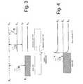
- FIG. 3shows an energy band diagram for a conventional metal—n-type semiconductor junction and also illustrates the concept of a depletion region formed in the semiconductor when the materials are brought into contact with one another.
- FIG. 4illustrates band bending at a conventional metal—n-type semiconductor junction.
- FIG. 5shows a semiconductor device containing a semiconductor material having a surface across which electrical current flows during operation of the semiconductor device, and containing an interface layer formed on the surface according to one embodiment of the present invention.
- FIG. 6shows an electrical junction containing an interface layer that is disposed between a semiconductor and a conductor in accordance with one embodiment of the present invention.
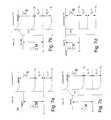
- FIGS. 7 a , 7 b , 7 c and 7 dshow relationships between Fermi energy, conduction-band energy, and valence-band energy for an unpassivated Schottky diode, a passivated Schottky diode in which MIGS are not removed, an unpassivated Schottky diode in which MIGS are removed and a passivated Schottky diode in which MIGS are removed according to one embodiment of the present invention, respectively.
- FIG. 8shows a curve of interface layer resistance versus interface layer thickness for an electrical junction containing an interface layer disposed between a semiconductor and a conductor in accordance with one embodiment of the present invention.
- Described hereinare processes for depinning the Fermi level of a silicon-based semiconductor (e.g., Si, SiC or SiGe) at a metal-semiconductor junction as well as devices that use such a junction.
- a silicon-based semiconductore.g., Si, SiC or SiGe
- an interface layeris introduced between the semiconductor and the metal.
- the interface layerfunctions to passivate the semiconductor surface (that is, terminate dangling bonds that may otherwise be present at the semiconductor surface so as to assure chemical stability of the surface) and to displace the semiconductor from the metal so as to reduce the effect of MIGS.
- the present inventorshave determined that for thin interface layers disposed between a metal and a silicon-based semiconductor (e.g., Si, SiC and SiGe), so as to form a metal—interface layer—semiconductor junction, there exist corresponding minimum specific contact resistances. Indeed, minimum specific contact resistances of less than or equal to approximately 10 ⁇ - ⁇ m 2 or even less than or equal to approximately 1 ⁇ - ⁇ m 2 may be achieved for such junctions in accordance with the present invention. To achieve such low contact resistances, a metal that has a work function near the conduction band of the semiconductor for n-type semiconductors, or a work function that is near the valence band for p-type semiconductors, is selected.
- a silicon-based semiconductore.g., Si, SiC and SiGe
- the Schottky barrier in such junctionsis already minimized, meaning that it is much less than the Schottky barrier presented by a junction in which the Fermi level is pinned, generally near the middle of the semiconductor's bandgap.
- the current versus voltage (IV) characteristic of these junctionsis non-linear, generally having a slope that increases as the voltage increases, such that the derivative of current with respect to voltage is increasing with voltage. This results in a decreasing differential resistance (dV/dI) and a decreasing resistance (V/I).
- a junction that has high resistance or high differential resistance near the origin of the IV characteristicmay have significantly lower resistance or lower differential resistance at higher voltages.
- the present inventionachieves low resistance and low differential resistance near the origin of the current-voltage characteristic for a metal—interface layer—semiconductor junction.
- the voltage around the originshould be less than about 100 mV, or more preferably less than about 10 mV for purposes of measuring, determining, or utilizing such junctions of low resistance. At higher voltages, the junction resistance will be even lower. It is thus a feature of the present invention to set an upper bound on the resistance of a contact, where the upper bound occurs at low voltages.
- the IV characteristicwill be nearly symmetric, especially at low voltage.
- the term “forward bias”is not defined in the usual sense of a diode wherein forward bias corresponds to the direction of bias for which greater current flows.
- the voltagemay be either positive or negative.
- junctionswhere the Schottky barrier is higher than it would be if the Fermi level at the junction interface were pinned, usually around mid-gap of the semiconductor.
- Such junctionsare formed in the present invention between a metal with a workfunction near or substantially equal to the conduction band edge of a p-type semiconductor, or between a metal with a workfunction near or substantially equal to the valence band edge of an n-type semiconductor.
- These junctionsare diodes, in that little current will flow if the n-type (p-type) semiconductor is biased positive (negative) with respect to the metal, and large currents will flow if the voltage is reversed.
- the low-current flow stateis referred to as reverse bias
- the high-current flow stateis referred to as positive bias.
- Low resistance in the case of a diodeis only relevant in forward bias conditions.
- the resistance contribution of the interface layeris smaller than the resistance due to the Schottky barrier. That is, in forward bias conditions for junctions created in accordance with the present invention, the transport of charge is limited mainly by the thermal emission of carriers from the semiconductor over the barrier at the interface, and not by the tunneling through the interface dielectric.
- low resistance in the case of a dioderefers to a resistance lower than the resistance presented by the Schottky barrier.
- junctions created in accordance with still another embodiment of the present inventionprovide high-voltage diodes capable of withstanding voltages higher than could otherwise be achieved if the Fermi level of the semiconductor in the junction were pinned.
- the so-called vacuum level (E 0 )represents the minimum energy that an electron needs to possess in order to completely free itself from a metal or semiconductor.
- the Fermi level (E F )represents the highest occupied energy level for the material. That is, nearly all energy states below the Fermi level are filled, while nearly all states above the Fermi level are empty.
- the work function of the metal ( ⁇ M )is then defined as the energy required to free an electron at the Fermi level and mathematically it is the difference between the vacuum level and the Fermi level.
- the work functionis an invariant bulk property of the metal.
- semiconductorsalso have a Fermi level (E F ) and a work function ( ⁇ S ), however, the work function is not an invariant property of the semiconductor.
- the Fermi levelvaries depending on the doping level in the semiconductor (i.e., the relative amounts of impurities introduced into the semiconductor crystal which change the electron and hole carrier concentrations)
- a separate parameter, the electron affinity ( ⁇ S )is defined.
- the electron affinityis an invariant property of the semiconductor and is the difference between the vacuum level and the conduction band edge of the semiconductor. In a semiconductor, almost all energy states are filled in the valence band (E V ) while the conduction band (E C ) is almost empty.
- n-type semiconductoris one in which electrons are the majority charge carriers (in p-type semiconductors, holes are the majority charge carrier).
- a depletion regioni.e., a region in which there are no free charge carriers
- the formation of the depletion regiongives rise to an electric field and so-called “band bending”, as one approaches the junction interface from the semiconductor side (see FIG. 4).
- the band bendingcreates an energy barrier (discussed above) that blocks further transfer of electrons into or out of the semiconductor.
- Similar barriersare formed for a junction between a metal and a p-type semiconductor when the work function of the metal is less than the work function of the semiconductor.
- a metal—n-type semiconductor junctionin which the work function of the semiconductor is greater than that of the metal or a metal-p-type semiconductor junction in which the work function of the semiconductor is less than that of the metal, no such energy barriers are created and the contact is said to be ohmic in nature.
- the present inventorshave created a technique which is believed to depin the Fermi level of a Si-based semiconductor at a junction with a metal (and thus allow for control or tuning of the barrier height) by both passivating the semiconductor surface (to eliminate or at least reduce the effects of surface states and possibly inhomogeneities) and displacing the metal from the semiconductor (to eliminate or at least reduce the effects of MIGS).
- This depinningis achieved by introducing an interface layer between the semiconductor and the metal to create a semiconductor—interface layer—metal junction, which still permits significant current to flow between the metal and the semiconductor when the junction is forward biased.
- a common processing operation performed during semiconductor device fabricationis silicon surface passivation.
- Surface passivation(whether by an oxide or another material) chemically neutralizes and physically protects the underlying silicon. For example, exposing a silicon surface to oxygen (under the appropriate conditions to grow a protective film of silicon dioxide) will allow the oxygen to react with the dangling bonds of the silicon surface to form covalent bonds that satisfy the surface silicon atoms' valency and render the surface fully coordinated. These covalent bonds provide chemical stability to the silicon surface. The covalent bonds also tie up unbound charges that exist on the silicon surface as a result of the discontinuation of the semiconductor crystal at the surface.
- silicon dioxideis a dielectric insulator that poses a significant barrier to the flow of current. Accordingly, a layer of silicon dioxide deposited or grown on a silicon surface may significantly reduce the ability for electrical current to flow through that surface. As a result, the use of silicon dioxide has been limited in practicality to surfaces external to the active region of semiconductor devices through which current passes during device operation (e.g., as a gate oxide layer). This disadvantage is compounded by the fact that the silicon dioxide grows very rapidly and readily on the silicon surface so that it is difficult to limit the growth to a thin layer. Silicon dioxide is also a poor diffusion barrier to semiconductor dopants such as boron.
- the present inventorsutilize a nitrided semiconductor surface to provide chemical passivation. That is, a nitride layer is introduced to passivate the semiconductor surface by eliminating or at least reducing the effects of surface states and possibly inhomogeneities. The nitride layer also displaces the metal from the semiconductor and eliminates or at least reduces the effects of MIGS.
- the result of introducing the nitride layer as an interface between the semiconductor and the metalis a depinning of the Fermi level of the semiconductor. When the Fermi level of the semiconductor is depinned, the Fermi level of the metal at the interface will be that of the bulk metal, and will not be dependent upon the interface.
- the present inventorspropose techniques for providing non-insulating, passivated semiconductor surfaces using materials other than nitrogen; for example, oxides, hydrides, arsenides and/or fluorides.
- FIG. 5shows a semiconductor device 510 that contains a semiconductor 530 and an interface layer 520 formed on a surface 540 of the semiconductor in accordance with the present invention.
- semiconductor devicemicroelectronic device, monolithic device, chip, and integrated circuit are often used interchangeably in this field. Any or all such devices may each contain an interface layer formed on a semiconductor surface in accordance with the present invention.
- the semiconductor 530contains a semiconductor material.
- semiconductor materialrefers to a material having a bandgap that is greater than about 0.1 eV and less than about 4 eV.
- bandgaprefers to an energy gap of forbidden energy levels separating the conduction band, which is an upper energy band that is mostly devoid of electrons and wherein electrons can conduct, and the valence band, which is an energy band that is mostly filled with electrons and wherein electrons cannot conduct.
- the semiconductor materialmay have a wide range of doping levels including no doping at all.
- the semiconductor 530has a surface 540 that is passivated by the interface layer 520 .
- passivationmeans the elimination or at least the reduction of the effects of surface states due to defects or dangling bonds of the semiconductor surface 540 . Note that passivation does not, as a practical matter, require that all surface states be eliminated. Rather, it is the effect of surface states on the device properties that is limited or eliminated in passivation.
- the semiconductor 530is operable to be electrically coupled with a first voltage associated with the semiconductor device 510 and to conduct electrical current 550 across the passivated surface 540 .
- the interface layer 520is formed on the semiconductor 530 and may contain a passivation material that bonds to the semiconductor material by way of a covalent (or other) bond formed between the passivation material and the semiconductor material.
- a passivation materialmay covalently bond with a dangling bond of a surface silicon atom to fully coordinate the silicon atom and thereby help passivate the silicon atom.
- the passivation materialmay be the sole component of the interface layer 520 , while in other cases the interface layer 520 may be a compound layer that includes both a passivation layer and a separation layer.
- the interface layerserves to (i) chemically passivate the semiconductor surface 540 , and (ii) displace the semiconductor from the metal sufficiently to eliminate or at least reduce the effect of MIGS. As explained below, this may necessitate including a separation layer in addition to a passivation layer within the interface layer, depending on the passivation material selected. Of course, the combination of the passivation layer and the separation layer must be sufficiently thin to permit the low specific contact resistances described herein.
- the interface layer 520is formed using a material that is preferably selected from the group consisting of hydrogen (H), oxygen (O), nitrogen (N), arsenic (As), and fluorine (F) (that is, the interface layer 520 may include a nitride, an oxide, a hydride, an arsenide and/or a fluoride). Other materials having chemical characteristics or valences similar to these materials may also be used.
- distinct separation layersmay be needed where H, As, or F passivation layers are used, as these tend to form monolayer coverage, rather than a layer of a compound with Si of process-dependent thickness.
- passivation layers made using N and/or Omay not require distinct separation layers, as these elements may form a layer of a compound of Si with a thickness that can be varied depending on processing.
- the interface layer 520includes or is made up of a passivation layer with a thickness of between approximately 0.1 nm and about 5 nm.
- the thicknessmay be less than about 1 nm, less than about 0.5 nm, less than about 0.2 nm, may be the thickness corresponding to a single layer or monolayer of passivation material that is bonded to the semiconductor surface, or may even be the number of atoms of passivation material required to passivate substantially all the dangling bonds associated with the semiconductor surface 540 .
- passivation of the semiconductor surface 540will include removing (or terminating) dangling bonds located proximate to the surface of the semiconductor material, including those at the surface as well as those within a few molecular dimensions from the surface. This process may stabilize the surface of the semiconductor material and may improve the controllability of subsequent fabrication operations. Passivation may also reduce the density of surface states that may exist at the semiconductor surface as a result of the discontinuation of the semiconductor crystal at the surface. This may improve consistency and performance of the semiconductor device, inasmuch as such states are known to interfere with proper device operation. For example, they may provide surface charge states that result in a pinning of the Fermi level.
- Exemplary methods for forming interface layers to provide (i) passivation of semiconductor surfaces, and (ii) displacement of the semiconductor from the metal to eliminate or at least reduce of the effects of MIGS within the semiconductor when in the presence of the metal (collectively referred to herein as depinning the Fermi level of the semiconductor) with hydrogen, fluorine or nitrogenare presented below to further illustrate the concepts of the present invention.
- Other passivation materialsmay include arsenic, oxygen or an oxynitride, and in some cases such passivation layers are combined with separation layers (e.g., made of an oxide) to complete the interface layer.
- An interface layermay contain hydrogen, fluorine, or both hydrogen and fluorine (e.g., in the form of a hydride and/or a fluoride).
- One method for forming an interface layer on a semiconductor surface with hydrogen and fluorineincludes cleaning the semiconductor substrate with a cleaning solution, immersing the cleaned substrate in a hydrogen fluoride solution (or other liquid containing hydrogen and fluorine ions) having an effective concentration typically between about 1%-50% by weight, waiting an effective period of time, typically between about several seconds and about 5 minutes, removing the substrate from the hydrogen fluoride solution, optionally rinsing the substrate in deionized water, and blow-drying the substrate with nitrogen.
- Such a methodmay form an interface layer containing hydrogen and fluorine that are bonded (e.g., covalently) to the semiconductor surface.
- deionized water rinsesmight advantageously be kept to less than about 30 seconds to maintain the hydrogen passivation of the surface.
- concentration of the hydrogen fluoride during the immersionthe greater the concentration of fluorine passivation.
- methodsare also contemplated where the ratio of hydrogen to fluorine passivation is altered by removing either the hydrogen or the fluorine.
- An interface layer formed in this fashionmay be best suited for applications where a subsequent metal layer is deposited over the interface layer in a generally non-invasive fashion, for example using a thermally evaporated source.
- a subsequent metal layeris deposited over the interface layer in a generally non-invasive fashion, for example using a thermally evaporated source.
- plasma depositionmay cause damage to the thin (e.g., monolayer thick) interface layer contemplated as part of the present invention.
- an interface layermay contain nitrogen (e.g., in the form of silicon nitride).
- One method for forming an interface over a semiconductor surface with nitrogenincludes heating a substrate containing the semiconductor surface in the presence of a nitrogenous material (that is, a gas or other material containing nitrogen).
- a substrate containing an exposed silicon surfacemay be annealed at a temperature between about 300° C. and about 750° C., which is lower than temperatures conventionally used for Rapid Thermal Nitridation (RTN), under a gaseous ambient having, for example, ammonia (NH 3 ) at some effective partial pressure.
- RTNRapid Thermal Nitridation
- NH 3ammonia
- an interface layer that includes nitrogenmay be formed on an exposed surface of a semiconductor material by a method that includes heating a semiconductor material to a substantially high temperature under vacuum and exposing the semiconductor material to a substantially small amount of a nitrogenous material, such as ammonia.
- the methodmay include placing a semiconductor having an exposed semiconductor surface in a heating chamber, pulling a vacuum of less than about one millionth of a Torr, or more favorably an ultra high vacuum of less than 10 ⁇ 9 Torr, and then heating the semiconductor in the heating chamber to a substantially high temperature.
- the higher the vacuumthe longer the substrate may be heated without growth of an oxide from residual oxygen or water in the chamber.
- the processmay include heating the semiconductor to a temperature that is between about 900° C.
- the semiconductormay be exposed to hydrogen gas, or an equivalent, to reduce any native oxide on the semiconductor.
- hydrogen gasor an equivalent, to reduce any native oxide on the semiconductor.
- the heated semiconductormay be exposed to a substantially small amount of a nitrogenous material, such as ammonia.
- a nitrogenous materialsuch as ammonia.
- Thismay include exposing the semiconductor surface to ammonia for a substantially short period of time.
- the surfacemay be subjected to a burst or pulse of ammonia lasting for a time period between about 0.5 seconds and about 5 seconds.
- the surfacemay be exposed to a controlled, small amount of ammonia over an arbitrarily longer period of time. In this way, the substantially small amount of ammonia will react with the surface to form a nitrogenous interface layer, such as a nitride layer, thereon and then further growth of the interface layer will cease.
- the semiconductormay be cooled from the substantially high temperature to ambient temperature and removed from the heating chamber. Further annealing of the substrate and the grown nitride layer may also be performed in the vacuum chamber before removal, at a substantially elevated temperature between about 700° C. and 1000° C., or higher.
- a process such as that described above and incorporating substantially high temperature exposure for substantially short periodsmay be used to controllably form thin yet effective interface layers. That is, the present inventors have observed that in the creation of thin interface layers that include nitrogenous materials, temperature appears to be a dominant factor in controlling thickness. For example, by such methods effective interface layers may be formed having a thickness that is less than about 1 nm, less than about 0.5 nm, less than about 0.2 nm, or having a thickness that corresponds to essentially a single monolayer sufficient to passivate essentially all dangling bonds proximate the semiconductor surface.
- thin interface layersmay be advantageously grown on a semiconductor in the presence of nitrogen gas, or other inert nitrogen-containing gas.
- the reaction rate of a semiconductor such as silicon with nitrogen gasis significantly lower than that of a reactive nitrogen-containing gas such as ammonia.
- the slow growth ratemay be desirable for better control of the growth of films of nitrogen on a semiconductor of a thickness of less than about 1 nm, less than about 0.5 nm, less than about 0.2 nm, or having a thickness that corresponds to essentially a single monolayer sufficient to passivate essentially all dangling bonds proximate the silicon surface.
- Diodes made from Schottky barriersare widely used in rectifiers in power supply and control applications.
- Schottky diode, metal-semiconductor junction diode, diode, and rectifierare all related and appear in order from more specific at the left to more general at the right.
- Schottky barrier, metal-semiconductor barrier, conductor-semiconductor junction, and multi-material junctionare all related and appear in order from more specific at the left to more general at the right.
- the term Schottky diodewill be used to refer to a diode containing a Schottky barrier.
- the present inventorshave devised a scheme to control or adjust a Schottky barrier height by forming an interface layer (which includes or sometimes consists of a passivation layer that includes an oxide, oxynitride, nitride, arsenide, hydride, fluoride, or an equivalent) between a metal and a semiconductor.
- This schemediffers from past attempts by others to control barrier height, which attempts generally involved either using a silicide as a contact metal (and thus limiting the choices of available contact metals to those that can form silicides), or using esoteric substrates that exhibit wide bandgaps.
- the Fermi level of the semiconductorremains pinned, with the barrier height being virtually independent of the metal used.
- doping of substrateshas also been attempted, however, it has not been shown to truly affect the barrier height of the substrate material.
- PtSi contactshave reduced resistance due to high silicon doping such that the current across the junction is dominated by tunneling through the barrier. Doping may thus lead to cases where the top of the barrier may be so thin as to be essentially transparent to electrons, however, doping does not appear to allow actual tuning of the barrier height.
- FIG. 6shows an example of a diode 600 containing, according to one embodiment of the present invention, an interface layer 620 disposed between and attached to both a semiconductor 610 and a conductor 630 .
- the conductor and the semiconductorare operable to be electrically coupled with different voltages associated with the operation of the diode 600 and to pass electrical current through a passivated semiconductor surface formed at the junction between the semiconductor 610 and the interface layer 620 .
- the conductor 630contains a conductive material such as a metal or an alloy of a metal.
- a conductive materialsuch as a metal or an alloy of a metal.
- metal, conductive material, and conductorare all related and appear in order from specific at the left to general at the right. In general, the terms refer to a highly electrically conductive substance that has a Fermi energy level that sits in a partially filled band.
- conductorsinclude metals (e.g., pure metals and alloys), and other conductors such as doped polysilicon (a nonporous silicon containing randomly oriented crystallites), doped single crystal silicon, and metal silicides. Note that alloys may have workfunctions different than their constituents and may be designed to have specific workfunctions though selective use of ratios of the constituent metals.
- the conductoris a metal since metals may offer advantages over conductive semiconductors including lower resistance, higher carrier mobilities that provide superior high frequency performance and switching, favorable low power characteristics, and ease of manufacturing control. Use of metals may also avoid the need to perform semiconductor doping, which may simplify manufacturing and improve quality control.
- Metals that are contemplatedinclude pure metals, alloys, refractory metals, metals that do not form silicides, metals physically deposited by substantially non-invasive processes such as by condensation of a thermally evaporated metal vapor, and metals having a predetermined work function.
- the use of non-invasively deposited metalsmay allow for forming the metal on a thin interface layer without disrupting the passivation properties of the layer.
- a metal having a predetermined work functionmay be a metal having a work function smaller or greater than that of the semiconductor, depending on the desired application.
- the semiconductorwill be silicon.
- the work function of a semiconductor or siliconwe mean the energy in the middle of the semiconductor bandgap.
- Exemplary metals that have a work function smaller than siliconinclude Group 3A elements, aluminum (Al), indium (In), titanium (Ti), chromium (Cr), tantalum (Ta), cesium (Cs), magnesium (Mg), erbium (Er), ytterbium (Yb), manganese (Mn), lead (Pb), silver (Ag), yttrium (Y), and zinc (Zn).
- Exemplary metals that have a work function greater than siliconinclude platinum (Pt), gold (Au), tungsten (W), nickel (Ni), molybdenum (Mo), copper (Cu), cobalt (Co), and palladium (Pd).
- the semiconductor-interface layer-conductor configuration illustrated in FIG. 6defines what the present inventors have chosen to call a “passivated Schottky barrier”.
- the passivated Schottky barrieris a naturally formed electrical potential barrier to an electron or hole at the Fermi energy (the electrochemical potential) in the conductor due to a depletion region formed in the semiconductor adjacent the conductor.
- the passivated Schottky barriermay deviate in barrier height from a standard un-passivated Schottky barrier that would form naturally at a contact junction between the semiconductor and the conductor without the interface layer disposed therebetween. That is, the passivated Schottky barrier may have a barrier height that depends predominantly upon the bulk characteristics of the semiconductor and the conductor, rather than on surface properties, and may depend in part on the characteristics of the interface layer.
- the present inventorshave determined that changes in barrier height are approximately monotonic and continuous for variations in surface passivation thickness by nitridation of the semiconductor substrate. More specifically, experiments by the present inventors in a regime where the nitride layer is sufficiently thick to remove MIGS show that temperature of interface layer formation has the strongest effect on barrier height. In other regimes, thickness may be critical. Ideally, if all surface states are removed, barrier height should be controllable simply by the choice of metal used.
- FIG. 8a graph of interface-specific contact resistance versus interface thickness is shown.
- the graphis for a structure where the workfunction of the metal is the same as the electron affinity in the semiconductor, such that the Fermi level of the metal lines up with the conduction band of the semiconductor.
- the interface layerposes significant resistance to current.
- resistancefalls due to increased tunneling current.
- MIGSwhich increasingly pull the Fermi level of the metal down towards mid-gap of the semiconductor, creating a Schottky barrier.
- Characteristics that may be adjusted to provide a desired barrier heightthus include the passivation material used (e.g., selection based on bandgap), the interface layer thickness (e.g., especially where the interface layer is a compound layer formed of a passivation layer and a separation layer), the method of forming the interface layer (e.g., control of parameters such as temperature), the interface layer thickness that is substantially similar to a penetration depth of MIGS formed at a metal interface, the metal used for the source and/or drain, and other characteristics.
- the passivation material usede.g., selection based on bandgap
- the interface layer thicknesse.g., especially where the interface layer is a compound layer formed of a passivation layer and a separation layer
- the method of forming the interface layere.g., control of parameters such as temperature
- the interface layer thicknessthat is substantially similar to a penetration depth of MIGS formed at a metal interface, the metal used for the source and/or drain, and other characteristics.
- One advantage of the ability to adjust the Schottky barrier height with the introduction of interface layer 620is the ability to form a substantially high barrier height.
- an interface layermay be used to create a Schottky barrier having a barrier height that is greater than can be achieved through the use of metal silicides, greater than about 2.0 eV, or greater than about 2.5 eV (using a semiconductor with a bandgap at least this large), or nearly 1.0 V using silicon.
- metal silicidesgreater than about 2.0 eV, or greater than about 2.5 eV (using a semiconductor with a bandgap at least this large), or nearly 1.0 V using silicon.
- Such high barrier heightsimply the ability to withstand high voltages before breakdown occurs.
- Schottky barriers having such high barrier heightsmay be particularly useful in high-voltage Schottky diodes.
- Another advantage achieved through the use of the interface layer 620is greater flexibility afforded in selecting a conductor 630 .
- metals chosen for application in classic Schottky diodesare those that can form a silicide with a silicon semiconductor. The formation of the silicide helps to reduce surface states (resulting from dangling bonds), but not the effects of MIGS. Thus, the Fermi level at the semiconductor surface is still pinned. Using metals that form silicides upon contact with silicon may thus help to make the devices more reproducible in a manufacturing environment, but such devices still suffer from the drawback of having a barrier height that is fixed.
- the metal suicideis not needed because the interface layer provided in accordance with the present invention passivates the semiconductor surface and also reduces or eliminates the effect of MIGS. This may allow for selection of a metal that has properties such as a desirable work function or Fermi level energy, even though that metal may not form a metal silicide.
- a metalmay be selected that has a work function that is either substantially equal to the valence band energy of the semiconductor or that is within about 0.1 eV to about 0.3 eV of the valence band energy of the semiconductor.
- a metalmay be selected that has a work function substantially equal to the conduction band energy of the semiconductor.
- the Fermi level of the metalmay lie anywhere in the bandgap of the semiconductor when an interface layer is disposed within the junction, resulting in diodes of various barrier heights. The Fermi level of the metal may also lie in the conduction or valence band of the semiconductor.
- interface layer 620thus provides a way to tune, adjust, or control the height of the barrier between the conductor and the semiconductor. Without the interface layer 620 , the barrier height would be substantially un-tunable, un-adjustable, and fixed (as discussed above).
- the role played by interface layer 620 in tuning, adjusting, or controlling the height of the barrier between the conductor 630 and the semiconductor 610may be understood as a depinning of the Fermi level of the semiconductor. That is, the interface layer may reduce surface states by bonding to the semiconductor material to consume dangling bonds. Additionally, the interface layer may reduce the formation of MIGS in the semiconductor by providing a thickness and bandgap that prevent the electron wave function (of the metal) from penetrating into the semiconductor. The electron wave function may instead penetrate into the interface layer and form MIGS within the interface layer at an energy related to the states of the interface layer material. As desired, the density of the MIGS and the depth of MIGS penetration into the interface layer may be reduced by choosing an interface layer material or materials having a larger bandgap or higher effective mass than the semiconductor.
- the interface layer 620is incorporated into a device operable to pass current through the semiconductor surface and the interface layer during device operation.
- such interface layersmay be sufficiently thin to provide low impedance to current flow (due to the exponential dependence of direct tunneling on barrier thickness), which is desirable for many semiconductor devices, while also providing sufficient semiconductor surface passivation to allow an adjustable barrier height. That is, the interface layer may allow passivation of surface states and reduction (or elimination) of MIGS in the semiconductor to allow for an adjustable barrier height with a substantially thin layer that allows sufficient current to be transferred across the interface layer.
- the barrier heightcan be made adjustable. For example, adjustment may be made by tuning the degree of Fermi level pinning. In other words, some embodiments may allow for a sufficiently thin interface layer so that not all of the effects of MIGS in the Si are eliminated. Further, the pinning may be varied by combinations of thickness of the interface layer and the choice of interface material. The metal in contact with the interface layer may be pinned by MIGS at different levels in different materials. Conversely, or in addition, the passivation may be left incomplete to allow for an effective level of unpassivated states.
- Equation (1)Complete depinning of the Fermi level (that is removal of all surface states in Si including MIGS) is another option, in which case one could tune the barrier height simply by choosing a pure metal or an alloy that possesses the desired workfunction. In that case, the barrier height is determined by Equation (1), which until now has been an unrealizable idealization. Note that the type of tuning being discussed here is adjustment of the barrier height by altering the structure of the junction at the time of manufacture, not by varying an externally applied condition during junction operation.
- FIGS. 7 a - 7 dshow relationships between Fermi energy, conduction band energy, and valence band energy for various Schottky barriers containing a metal in contact with (or in close proximity to) a semiconductor, where the bandgap (E g ) of the semiconductor exists between the conduction band (E c ) and the valence band (E v ).
- the work function of the metal ⁇ Mis chosen to be approximately equal to the electron affinity ⁇ S of the semiconductor.
- FIG. 7 aan unpassivated Schottky barrier 700 is shown.
- the Fermi level (E F ) of the metal 730is pinned in the bandgap of the semiconductor 710 . This results in a discontinuity in the vacuum level caused by a charged dipole at the interface.
- the interface layer 720 bis thick enough to passivate dangling bonds at the surface of the semiconductor 710 , but not thick enough to eliminate or sufficiently reduce the effect of MIGS.
- the band structureis largely unaltered from that seen in the previous illustration.
- FIG. 7 cwhen the interface layer 720 c is sufficiently thick to eliminate or reduce the effect of MIGS but not to passivate the semiconductor surface, little change in the energy band structure is observed.
- FIG. 7 cwhen the interface layer 720 c is sufficiently thick to eliminate or reduce the effect of MIGS but not to passivate the semiconductor surface, little change in the energy band structure is observed.
- FIG. 7 cwhen the interface layer 720 c is sufficiently thick to eliminate or reduce the effect of MIGS but not to passivate the semiconductor surface, little change in the energy band structure is observed.
- FIG. 7 cwhen the interface layer 720 c is sufficiently thick to eliminate or reduce the effect of MIGS but not to passivate the semiconductor surface, little change in the energy band structure is
- the interface layer 720 dwhen the interface layer 720 d is sufficient to both eliminate or reduce the effect of MIGS and to passivate the semiconductor surface, we see the Fermi level of the metal aligning with the conduction band of the semiconductor (i.e., the Fermi level of the semiconductor has been depinned and no longer lines up with the Fermi level of the metal).
- the vacuum levelis now continuous as there is no charged dipole at the interface.
- the band structure of a device constructed in this fashionis a result of only bulk material properties, not properties of the surface.
- the interface layers described hereinmay be used in connection with a semiconductor surface of a channel in a field effect transistor. That is, an interface layer may be disposed between a source and a channel, a channel and a drain, or both of an insulated gate field effect transistor. Such use of an interface layer is described in detail in co-pending U.S. Patent Application No. ______ entitled “INSULATED GATE FIELD EFFECT TRANSISTOR HAVING PASSIVATED SCHOTTKY BARRIERS TO THE CHANNEL”, filed ______, 2002 by the present inventors, and assigned to the assignee of the present invention.
- the source and drain contacts at the channel of a field effect transistorare examples of a broader category of metal-interface layer-semiconductor contacts that make up the present invention.
- such contactsgenerally comprised a silicide-n + -Si junction, which formed a somewhat “leaky” Schottky diode, with a Fermi level of the semiconductor pinned at the midgap.
- the present inventionprovides a contact wherein the Fermi level of the metal is aligned with the conduction band of the semiconductor (e.g., as shown in FIG. 7 d ). Note that in other cases, depending on the type of semiconductor material and conductors used, the Fermi level of the metal may align with the valence band of the semiconductor.
- junctionsi.e., the new passivated Schottky barrier junction and the conventional silicide-semiconductor junction
- the present junctioncan be fabricated with a much thinner interface layer as compared to the thickness of the silicide layer used previously. Indeed, thickness of an order of magnitude less than the silicide thickness can be expected.
- a Schottky barrieris formed which is comprised of a depletion layer.
- the tunnel barrier presented by such a depletion layermay be an order of magnitude thicker than the dielectric tunnel barrier in the present invention.
- the thinner interface layers provided by the present inventionpermit higher current across the junction (i.e., lower junction specific contact resistance).
- the tradeoffmay be a higher tunnel barrier (e.g., 2 eV for nitride, compared with about half the gap of 0.6 eV for silicide).
- Spacer layersmay be used with lower barriers (e.g., TiO 2 has a barrier of less than 1 eV). Nevertheless, even with the higher barrier to electrons, the present inventors have determined that the resistance can still be one hundred times lower than a contact to silicon with a silicide barrier.
- the second propertyis the effective mass of electrons in the dielectric. Larger mass electrons will not penetrate as far (i.e., because of their shorter wavelength) from the metal into the semiconductor. The less the electrons penetrate into the dielectric, the less the effect of MIGS in the dielectric. Thus, MIGS in the dielectric are reduced with larger bandgap and larger effective mass.
- the junction of the present inventioncan be used in making contacts to source or drain implanted wells and will have the advantage of reducing the need for high doping levels (which are now reaching their limits of solid solubility).
- the high doping profileswere required in the past in order to keep the junction depletion layer relatively thin, so as to increase the tunneling current, thus reducing the junction resistance.
- the present inventionis used with high doping levels, the resistance will be further reduced.
Landscapes
- Engineering & Computer Science (AREA)
- Physics & Mathematics (AREA)
- Condensed Matter Physics & Semiconductors (AREA)
- General Physics & Mathematics (AREA)
- Manufacturing & Machinery (AREA)
- Computer Hardware Design (AREA)
- Microelectronics & Electronic Packaging (AREA)
- Power Engineering (AREA)
- Electrodes Of Semiconductors (AREA)
Abstract
Description
- The present application is related to co-pending U.S. Patent Application No. ______, entitled “INSULATED GATE FIELD EFFECT TRANSISTOR HAVING PASSIVATED SCHOTTKY BARRIERS TO THE CHANNEL”, filed on ______, 2002, by the present inventors and assigned to the same assignee as the present application. This related patent application is hereby incorporated by reference in its entirety.[0001]
- The invention relates generally to semiconductor processing and semiconductor devices. More particularly, the invention relates to a process for depinning the Fermi level of a semiconductor at a metal-interface layer-semiconductor junction and to devices that employ such a junction.[0002]
- One of the most basic electrical junctions used in modern devices is the metal-semiconductor junction. In these junctions, a metal (such as aluminum) is brought in contact with a semiconductor (such as silicon). This forms a device (a diode) which can be inherently rectifying; that is, the junction will tend to conduct current in one direction more favorably than in the other direction. In other cases, depending on the materials used, the junction may be ohmic in nature (i.e., the contact may have negligible resistance regardless of the direction of current flow). Grondahl and Geiger first studied the rectifying form of these junctions in 1926, and by 1938 Schottky had developed a theoretical explanation for the rectification that was observed.[0003]
- Schottky's theory explained the rectifying behavior of a metal-semiconductor contact as depending on a barrier at the surface of contact between the metal and the semiconductor. In this model, the height of the barrier (as measured by the potential necessary for an electron to pass from the metal to the semiconductor) was postulated as the difference between the work function of the metal (the work function is the energy required to free an electron at the Fermi level of the metal, the Fermi level being the highest occupied energy state of the metal at T=0) and the electron affinity of the semiconductor (the electron affinity is the difference between the energy of a free electron and the conduction band edge of the semiconductor). Expressed mathematically:[0004]
- φB=φM−χS [1]
- where Φ[0005]Bis the barrier height, ΦMis the work function of the metal and χSis the electron affinity of the semiconductor.
- Not surprisingly, many attempts were made to verify this theory experimentally. If the theory is correct, one should be able to observe direct variations in barrier heights for metals of different work functions when put in contact with a common semiconductor. What is observed, however, is not direct scaling, but instead only a much weaker variation of barrier height with work function than implied by the model.[0006]
- Bardeen sought to explain this difference between theoretical prediction and experimental observation by introducing the concept that surface states of the semiconductor play a role in determining the barrier height. Surface states are energy states (within the bandgap between the valence and conduction bands) at the edge of the semiconductor crystal that arise from incomplete covalent bonds, impurities, and other effects of crystal termination. FIG. 1 shows a cross-section of an un-passivated silicon surface labeled[0007]100. The particular silicon surface shown is an Si(100) 2×1 surface. As shown, the silicon atoms at the surface, such as
atom 110, are not fully coordinated and contain un-satisfied dangling bonds, such as danglingbond 120. These dangling bonds may be responsible for surface states that trap electrical charges. - Bardeen's model assumes that surface states are sufficient to pin the Fermi level in the semiconductor at a point between the valence and conduction bands. If true, the barrier height at a metal-semiconductor junction should be independent of the metal's work function. This condition is rarely observed experimentally, however, and so Bardeen's model (like Schottky's) is best considered as a limiting case.[0008]
- For many years, the cause underlying the Fermi level pinning of the semiconductor at a metal-semiconductor junction remained unexplained. Indeed, to this day no one explanation satisfies all experimental observations regarding such junctions. Nevertheless, in 1984, Tersoff proposed a model that goes a long way towards explaining the physics of such junctions. See J. Tersoff, “Schottky Barrier Heights and the Continuum of Gap States,” Phys. Rev. Lett. 52 (6), Feb. 6, 1984.[0009]
- Tersoff s model (which is built on work by Heine and Flores & Tejedor, and see also Louie, Chelikowsky, and Cohen, “Ionicity and the theory of Schottky barriers,” Phys. Rev. B 15, 2154 (1977)) proposes that the Fermi level of a semiconductor at a metal-semiconductor interface is pinned near an effective “gap center”, which is related to the bulk semiconductor energy band structure. The pinning is due to so-called metal induced gap states (MIGS), which are energy states in the bandgap of the semiconductor that become populated due to the proximity of the metal. That is, the wave functions of the electrons in the metal do not terminate abruptly at the surface of the metal, but rather decay in proportion to the distance from that surface (i.e., extending inside the semiconductor). To maintain the sum rule on the density of states in the semiconductor, electrons near the surface occupy energy states in the gap derived from the valence band such that the density of states in the valence band is reduced. To maintain charge neutrality, the highest occupied state (which defines the Fermi level of the semiconductor) will then lie at the crossover point from states derived from the valence band to those derived from the conduction band. This crossover occurs at the branch point of the band structure. Although calculations of barrier heights based on Tersoff's model do not satisfy all experimentally observed barrier heights for all metal-semiconductor junctions, there is generally good agreement for a number of such junctions.[0010]
- One final source of surface effects on diode characteristics is inhomogeneity. That is, if factors affecting the barrier height (e.g., density of surface states) vary across the plane of the junction, the resulting properties of the junction are found not to be a linear combination of the properties of the different regions. In summary then, a classic metal-semiconductor junction is characterized by a Schottky barrier, the properties of which (e.g., barrier height) depend on surface states, MIGS and inhomogeneities.[0011]
- The importance of the barrier height at a metal-semiconductor interface is that it determines the electrical properties of the junction. Thus, if one were able to control or adjust the barrier height of a metal-semiconductor junction, one could produce electrical devices of desired characteristics. Such barrier height tuning may become even more important as device sizes shrink even further. Before one can tune the barrier height, however, one must depin the Fermi level of the semiconductor. As discussed in detail below, the present inventors have achieved this goal in a device that still permits substantial current flow between the metal and the semiconductor.[0012]
- The present inventors have determined that for thin interface layers disposed between a metal and a silicon-based semiconductor (e.g., Si, SiC and SiGe), so as to form a metal—interface layer—semiconductor junction, there exist corresponding minimum specific contact resistances. The interface layer thickness corresponding to this minimum specific contact resistance will vary depending upon the materials used, however, it is a thickness that allows for depinning the Fermi level of the semiconductor while still permitting current to flow between the metal and the semiconductor when the junction is biased (e.g., forward or reverse biased). By depinning the Fermi level, the present inventors mean a condition wherein all, or substantially all, dangling bonds that may otherwise be present at the semiconductor surface have been terminated, and the effect of MIGS has been overcome, or at least reduced, by displacing the semiconductor a sufficient distance from the metal. Minimum specific contact resistances of less than or equal to approximately 10 Ω-μm[0013]2or even less than or equal to approximately 1 Ω-μm2may be achieved for such junctions in accordance with the present invention.
- Thus, in one embodiment, the present invention provides an electrical device in which an interface layer is disposed between and in contact with a metal and a silicon-based semiconductor and is configured to depin the Fermi level of the semiconductor while still permitting current flow between the metal and the semiconductor when the electrical device is biased. The specific contact resistance of the electrical device is less than approximately 10 Ω-μm[0014]2. The interface layer may include a passivating material (e.g., a nitride, oxide, oxynitride, arsenide, hydride and/or fluoride) and sometimes also includes a separation layer. In some cases, the interface layer may be essentially a monolayer (or several monolayers) of a semiconductor passivating material.
- In another embodiment, the interface layer is made up of a passivation layer fabricated by heating the semiconductor in the presence of nitrogenous material, for example ammonia (NH[0015]3), nitrogen (N2) or unbound gaseous nitrogen (N) generated from a plasma process. In such cases, the interface layer may be fabricated by heating the semiconductor while in a vacuum chamber and exposing the semiconductor to the nitrogenous material.
- A further embodiment of the present invention provides for depinning the Fermi level of a semiconductor in an electrical junction through the use of an interface layer disposed between a surface of the semiconductor and a conductor. The interface layer preferably (i) is of a thickness sufficient to reduce effects of MIGS in the semiconductor, and (ii) passivates the surface of the semiconductor. Despite the presence of the interface layer, significant current may flow between the conductor and the semiconductor because the thickness of the interface layer may be chosen to provide a minimum (or near minimum) specific contact resistance for the junction. As indicated above, the interface layer may include a passivating material such as a nitride, oxide, oxynitride, arsenide, hydride and/or fluoride.[0016]
- Further embodiments of the present invention provide a junction between a semiconductor and a conductor separated from the semiconductor by an interface layer configured to allow a Fermi level of the conductor to (i) align with a conduction band of the semiconductor, (ii) align with a valence band of the semiconductor, or (iii) to be independent of the Fermi level of the semiconductor. In some or all of these cases, current may flow between the conductor and the semiconductor when the junction is biased because the interface layer has a thickness corresponding to a minimum or near minimum specific contact resistance for the junction. For example, specific contact resistances of less than or equal to approximately 2500 Ω-μm[0017]2, 1000 Ω-μm2, 100 Ω-μm2, 50 Ω-μm2, 10 Ω-μm2or even less than or equal to 1 Ω-μm2may be achieved.
- The present invention is illustrated by way of example, and not by way of limitation, in the figures of the accompanying drawings.[0018]
- FIG. 1 shows a cross-section of an un-passivated silicon surface containing surface silicon atoms with dangling bonds.[0019]
- FIG. 2 illustrates various energy levels for metals and semiconductors and is labeled to show the work function of a metal and the electron affinity of a semiconductor.[0020]
- FIG. 3 shows an energy band diagram for a conventional metal—n-type semiconductor junction and also illustrates the concept of a depletion region formed in the semiconductor when the materials are brought into contact with one another.[0021]
- FIG. 4 illustrates band bending at a conventional metal—n-type semiconductor junction.[0022]
- FIG. 5 shows a semiconductor device containing a semiconductor material having a surface across which electrical current flows during operation of the semiconductor device, and containing an interface layer formed on the surface according to one embodiment of the present invention.[0023]
- FIG. 6 shows an electrical junction containing an interface layer that is disposed between a semiconductor and a conductor in accordance with one embodiment of the present invention.[0024]
- FIGS. 7[0025]a,7b,7cand7dshow relationships between Fermi energy, conduction-band energy, and valence-band energy for an unpassivated Schottky diode, a passivated Schottky diode in which MIGS are not removed, an unpassivated Schottky diode in which MIGS are removed and a passivated Schottky diode in which MIGS are removed according to one embodiment of the present invention, respectively.
- FIG. 8 shows a curve of interface layer resistance versus interface layer thickness for an electrical junction containing an interface layer disposed between a semiconductor and a conductor in accordance with one embodiment of the present invention.[0026]
- Described herein are processes for depinning the Fermi level of a silicon-based semiconductor (e.g., Si, SiC or SiGe) at a metal-semiconductor junction as well as devices that use such a junction. As more fully discussed below, an interface layer is introduced between the semiconductor and the metal. The interface layer functions to passivate the semiconductor surface (that is, terminate dangling bonds that may otherwise be present at the semiconductor surface so as to assure chemical stability of the surface) and to displace the semiconductor from the metal so as to reduce the effect of MIGS.[0027]
- As discussed more fully below, the present inventors have determined that for thin interface layers disposed between a metal and a silicon-based semiconductor (e.g., Si, SiC and SiGe), so as to form a metal—interface layer—semiconductor junction, there exist corresponding minimum specific contact resistances. Indeed, minimum specific contact resistances of less than or equal to approximately 10 Ω-μm[0028]2or even less than or equal to approximately 1 Ω-μm2may be achieved for such junctions in accordance with the present invention. To achieve such low contact resistances, a metal that has a work function near the conduction band of the semiconductor for n-type semiconductors, or a work function that is near the valence band for p-type semiconductors, is selected.
- The Schottky barrier in such junctions is already minimized, meaning that it is much less than the Schottky barrier presented by a junction in which the Fermi level is pinned, generally near the middle of the semiconductor's bandgap. The current versus voltage (IV) characteristic of these junctions is non-linear, generally having a slope that increases as the voltage increases, such that the derivative of current with respect to voltage is increasing with voltage. This results in a decreasing differential resistance (dV/dI) and a decreasing resistance (V/I). Thus, a junction that has high resistance or high differential resistance near the origin of the IV characteristic (zero volts) may have significantly lower resistance or lower differential resistance at higher voltages.[0029]
- The present invention achieves low resistance and low differential resistance near the origin of the current-voltage characteristic for a metal—interface layer—semiconductor junction. Generally, the voltage around the origin should be less than about 100 mV, or more preferably less than about 10 mV for purposes of measuring, determining, or utilizing such junctions of low resistance. At higher voltages, the junction resistance will be even lower. It is thus a feature of the present invention to set an upper bound on the resistance of a contact, where the upper bound occurs at low voltages.[0030]
- It is further noted that in junctions where the Schottky barrier is minimized as described above, such that the Fermi level at the junction interface at zero volts lies at or near the conduction band edge or valence band edge (for n- and p-type semiconductors, respectively), the IV characteristic will be nearly symmetric, especially at low voltage. In this case, the term “forward bias” is not defined in the usual sense of a diode wherein forward bias corresponds to the direction of bias for which greater current flows. Thus, in determining or utilizing low resistance junctions of the present invention, the voltage may be either positive or negative.[0031]
- It is also possible (in accordance with a further embodiment of the present invention) to make junctions where the Schottky barrier is higher than it would be if the Fermi level at the junction interface were pinned, usually around mid-gap of the semiconductor. Such junctions are formed in the present invention between a metal with a workfunction near or substantially equal to the conduction band edge of a p-type semiconductor, or between a metal with a workfunction near or substantially equal to the valence band edge of an n-type semiconductor. These junctions are diodes, in that little current will flow if the n-type (p-type) semiconductor is biased positive (negative) with respect to the metal, and large currents will flow if the voltage is reversed. The low-current flow state is referred to as reverse bias, and the high-current flow state is referred to as positive bias.[0032]
- Low resistance in the case of a diode is only relevant in forward bias conditions. In junctions created in accordance with the present invention the resistance contribution of the interface layer is smaller than the resistance due to the Schottky barrier. That is, in forward bias conditions for junctions created in accordance with the present invention, the transport of charge is limited mainly by the thermal emission of carriers from the semiconductor over the barrier at the interface, and not by the tunneling through the interface dielectric. Thus, low resistance in the case of a diode refers to a resistance lower than the resistance presented by the Schottky barrier.[0033]
- In certain applications of diodes, the ability to withstand high reverse biases may be more desirable than high current flow in forward bias. These applications would be considered high voltage/low power applications. In such cases, a low resistance is not essential, and junctions created in accordance with still another embodiment of the present invention provide high-voltage diodes capable of withstanding voltages higher than could otherwise be achieved if the Fermi level of the semiconductor in the junction were pinned.[0034]
- The present invention is discussed below in terms of presently preferred embodiments thereof, however, this discussion is not meant to limit the scope of the invention. By studying the present disclosure, others of ordinary skill in the art may recognize equivalent procedures, materials or structures that can be substituted for those described herein to achieve the same effect. The reader is advised and reminded that the use of such equivalents is deemed to be within the scope of the present invention. For example, where the discussion refers to well-known structures and devices, block diagrams are used, in part to demonstrate the broad applicability of the present invention to a wide range of such structures and devices.[0035]
- I. Introduction and Definitions[0036]
- The present discussion makes use of terms that, although well known in the art, may not be familiar to all readers. Therefore, before beginning a detailed discussion of the present invention, it is helpful to define certain terms and concepts. To understand the properties of metal-semiconductor junctions and the impact of the present invention, one must refer to some important energy scales, which are shown graphically in FIG. 2. The so-called vacuum level (E[0037]0) represents the minimum energy that an electron needs to possess in order to completely free itself from a metal or semiconductor. For a metal, the Fermi level (EF) represents the highest occupied energy level for the material. That is, nearly all energy states below the Fermi level are filled, while nearly all states above the Fermi level are empty. The work function of the metal (ΦM) is then defined as the energy required to free an electron at the Fermi level and mathematically it is the difference between the vacuum level and the Fermi level. The work function is an invariant bulk property of the metal.
- As illustrated in the diagram, semiconductors also have a Fermi level (E[0038]F) and a work function (ΦS), however, the work function is not an invariant property of the semiconductor. Because the Fermi level varies depending on the doping level in the semiconductor (i.e., the relative amounts of impurities introduced into the semiconductor crystal which change the electron and hole carrier concentrations), a separate parameter, the electron affinity (χS), is defined. The electron affinity is an invariant property of the semiconductor and is the difference between the vacuum level and the conduction band edge of the semiconductor. In a semiconductor, almost all energy states are filled in the valence band (EV) while the conduction band (EC) is almost empty.
- Now consider a conventional junction between a metal and an n-type semiconductor that has a work function smaller than the work function of the metal (i.e., Φ[0039]S<ΦM). An n-type semiconductor is one in which electrons are the majority charge carriers (in p-type semiconductors, holes are the majority charge carrier). As shown in FIG. 3, because the Fermi level in the semiconductor is higher than the Fermi level in the metal, electrons transfer from the
semiconductor 310 to themetal 320 when the materials are brought into contact. Thus, a depletion region (i.e., a region in which there are no free charge carriers)330 forms near thejunction interface 340. - The formation of the depletion region gives rise to an electric field and so-called “band bending”, as one approaches the junction interface from the semiconductor side (see FIG. 4). The band bending creates an energy barrier (discussed above) that blocks further transfer of electrons into or out of the semiconductor. Similar barriers are formed for a junction between a metal and a p-type semiconductor when the work function of the metal is less than the work function of the semiconductor. However, in the case of a metal—n-type semiconductor junction in which the work function of the semiconductor is greater than that of the metal or a metal-p-type semiconductor junction in which the work function of the semiconductor is less than that of the metal, no such energy barriers are created and the contact is said to be ohmic in nature.[0040]
- As discussed above, although Schottky first postulated that the height of the energy barrier (Φ[0041]b) formed at a metal-semiconductor junction was simply the difference between the work function of the metal and the electron affinity of the semiconductor, experiments have not verified this relationship. Instead a more complex explanation that takes into account the effects of surface defect states, inhomogeneities and MIGS appears to provide more accurate estimates of barrier heights by explaining the pinning of the Fermi level in the semiconductor. The present inventors have created a technique which is believed to depin the Fermi level of a Si-based semiconductor at a junction with a metal (and thus allow for control or tuning of the barrier height) by both passivating the semiconductor surface (to eliminate or at least reduce the effects of surface states and possibly inhomogeneities) and displacing the metal from the semiconductor (to eliminate or at least reduce the effects of MIGS). This depinning is achieved by introducing an interface layer between the semiconductor and the metal to create a semiconductor—interface layer—metal junction, which still permits significant current to flow between the metal and the semiconductor when the junction is forward biased.
- This latter point is important. As discussed further below, for contacts where the energy bands of the semiconductor and the conductor align (i.e., where the Fermi level of the conductor aligns with the conduction or valence band of the semiconductor depending on semiconductor type and/or contact application), if the interface layer is too thin, the specific contact resistance of the junction increases because of the presence of MIGS, resulting in an increased barrier height; thus, current flow is hampered. Conversely, if the interface layer is too thick, the specific contact resistance is again increased and one gets low current across the junction because of tunneling limitations. The present invention achieves an interface layer that is thick enough to reduce or eliminate the effect of MIGS, while still thin enough to permit significant current flow.[0042]
- II. Passivation of Semiconductor Surfaces[0043]
- A common processing operation performed during semiconductor device fabrication is silicon surface passivation. Surface passivation (whether by an oxide or another material) chemically neutralizes and physically protects the underlying silicon. For example, exposing a silicon surface to oxygen (under the appropriate conditions to grow a protective film of silicon dioxide) will allow the oxygen to react with the dangling bonds of the silicon surface to form covalent bonds that satisfy the surface silicon atoms' valency and render the surface fully coordinated. These covalent bonds provide chemical stability to the silicon surface. The covalent bonds also tie up unbound charges that exist on the silicon surface as a result of the discontinuation of the semiconductor crystal at the surface.[0044]
- However, passivation with silicon dioxide has several significant disadvantages. For example, silicon dioxide is a dielectric insulator that poses a significant barrier to the flow of current. Accordingly, a layer of silicon dioxide deposited or grown on a silicon surface may significantly reduce the ability for electrical current to flow through that surface. As a result, the use of silicon dioxide has been limited in practicality to surfaces external to the active region of semiconductor devices through which current passes during device operation (e.g., as a gate oxide layer). This disadvantage is compounded by the fact that the silicon dioxide grows very rapidly and readily on the silicon surface so that it is difficult to limit the growth to a thin layer. Silicon dioxide is also a poor diffusion barrier to semiconductor dopants such as boron.[0045]
- Instead of making use of silicon dioxide then, in one embodiment the present inventors utilize a nitrided semiconductor surface to provide chemical passivation. That is, a nitride layer is introduced to passivate the semiconductor surface by eliminating or at least reducing the effects of surface states and possibly inhomogeneities. The nitride layer also displaces the metal from the semiconductor and eliminates or at least reduces the effects of MIGS. The result of introducing the nitride layer as an interface between the semiconductor and the metal is a depinning of the Fermi level of the semiconductor. When the Fermi level of the semiconductor is depinned, the Fermi level of the metal at the interface will be that of the bulk metal, and will not be dependent upon the interface. In addition to the above, the present inventors propose techniques for providing non-insulating, passivated semiconductor surfaces using materials other than nitrogen; for example, oxides, hydrides, arsenides and/or fluorides.[0046]
- These developments have wide applicability in connection with the fabrication of Schottky diodes, Schottky-barrier transistors and other electrical components. For example, in Schottky diodes, the ability to control the energy barrier height at the diode junction is important if the device is to be tailored to specific applications. Use of the present techniques allows for tuning of the barrier height. Further, for other three-terminal devices with Schottky-barrier-isolated channels, control of device characteristics is made possible through the present invention by allowing n- and p-type devices to be fabricated without dopants, relying instead on the use of metals with different work functions.[0047]
- FIG. 5 shows a[0048]
semiconductor device 510 that contains asemiconductor 530 and aninterface layer 520 formed on asurface 540 of the semiconductor in accordance with the present invention. The terms semiconductor device, microelectronic device, monolithic device, chip, and integrated circuit are often used interchangeably in this field. Any or all such devices may each contain an interface layer formed on a semiconductor surface in accordance with the present invention. - The[0049]
semiconductor 530 contains a semiconductor material. The term semiconductor material refers to a material having a bandgap that is greater than about 0.1 eV and less than about 4 eV. The term bandgap refers to an energy gap of forbidden energy levels separating the conduction band, which is an upper energy band that is mostly devoid of electrons and wherein electrons can conduct, and the valence band, which is an energy band that is mostly filled with electrons and wherein electrons cannot conduct. The semiconductor material may have a wide range of doping levels including no doping at all. - The[0050]
semiconductor 530 has asurface 540 that is passivated by theinterface layer 520. In this context (and as used elsewhere herein) the term passivation means the elimination or at least the reduction of the effects of surface states due to defects or dangling bonds of thesemiconductor surface 540. Note that passivation does not, as a practical matter, require that all surface states be eliminated. Rather, it is the effect of surface states on the device properties that is limited or eliminated in passivation. Note further that the presence of MIGS may be regarded as a surface state, however, as used herein the term passivation is not meant to infer the elimination of MIGS (though in some cases, a passivation layer may have sufficient thickness to provide a separation layer between the semiconductor and the metal sufficient to reduce or eliminate MIGS). Thesemiconductor 530 is operable to be electrically coupled with a first voltage associated with thesemiconductor device 510 and to conduct electrical current550 across the passivatedsurface 540. - The[0051]
interface layer 520 is formed on thesemiconductor 530 and may contain a passivation material that bonds to the semiconductor material by way of a covalent (or other) bond formed between the passivation material and the semiconductor material. For example, an atom of passivation material may covalently bond with a dangling bond of a surface silicon atom to fully coordinate the silicon atom and thereby help passivate the silicon atom. In some cases, the passivation material may be the sole component of theinterface layer 520, while in other cases theinterface layer 520 may be a compound layer that includes both a passivation layer and a separation layer. That is, the interface layer serves to (i) chemically passivate thesemiconductor surface 540, and (ii) displace the semiconductor from the metal sufficiently to eliminate or at least reduce the effect of MIGS. As explained below, this may necessitate including a separation layer in addition to a passivation layer within the interface layer, depending on the passivation material selected. Of course, the combination of the passivation layer and the separation layer must be sufficiently thin to permit the low specific contact resistances described herein. - Different passivation materials are contemplated. According to one embodiment, the[0052]
interface layer 520 is formed using a material that is preferably selected from the group consisting of hydrogen (H), oxygen (O), nitrogen (N), arsenic (As), and fluorine (F) (that is, theinterface layer 520 may include a nitride, an oxide, a hydride, an arsenide and/or a fluoride). Other materials having chemical characteristics or valences similar to these materials may also be used. Note that distinct separation layers (i.e., in addition to the passivation layer(s)) may be needed where H, As, or F passivation layers are used, as these tend to form monolayer coverage, rather than a layer of a compound with Si of process-dependent thickness. In contrast, passivation layers made using N and/or O may not require distinct separation layers, as these elements may form a layer of a compound of Si with a thickness that can be varied depending on processing. - Different amounts of passivation material are contemplated to be useful for different embodiments of the present invention. Often, the[0053]
interface layer 520 includes or is made up of a passivation layer with a thickness of between approximately 0.1 nm and about 5 nm. For example, depending upon the particular implementation, the thickness may be less than about 1 nm, less than about 0.5 nm, less than about 0.2 nm, may be the thickness corresponding to a single layer or monolayer of passivation material that is bonded to the semiconductor surface, or may even be the number of atoms of passivation material required to passivate substantially all the dangling bonds associated with thesemiconductor surface 540. - In some cases, passivation of the[0054]
semiconductor surface 540 will include removing (or terminating) dangling bonds located proximate to the surface of the semiconductor material, including those at the surface as well as those within a few molecular dimensions from the surface. This process may stabilize the surface of the semiconductor material and may improve the controllability of subsequent fabrication operations. Passivation may also reduce the density of surface states that may exist at the semiconductor surface as a result of the discontinuation of the semiconductor crystal at the surface. This may improve consistency and performance of the semiconductor device, inasmuch as such states are known to interfere with proper device operation. For example, they may provide surface charge states that result in a pinning of the Fermi level. - III. Forming Interface Layers[0055]
- Exemplary methods for forming interface layers to provide (i) passivation of semiconductor surfaces, and (ii) displacement of the semiconductor from the metal to eliminate or at least reduce of the effects of MIGS within the semiconductor when in the presence of the metal (collectively referred to herein as depinning the Fermi level of the semiconductor) with hydrogen, fluorine or nitrogen are presented below to further illustrate the concepts of the present invention. Other passivation materials may include arsenic, oxygen or an oxynitride, and in some cases such passivation layers are combined with separation layers (e.g., made of an oxide) to complete the interface layer.[0056]
- A. Hydrogen and Fluorine[0057]
- An interface layer may contain hydrogen, fluorine, or both hydrogen and fluorine (e.g., in the form of a hydride and/or a fluoride). One method for forming an interface layer on a semiconductor surface with hydrogen and fluorine includes cleaning the semiconductor substrate with a cleaning solution, immersing the cleaned substrate in a hydrogen fluoride solution (or other liquid containing hydrogen and fluorine ions) having an effective concentration typically between about 1%-50% by weight, waiting an effective period of time, typically between about several seconds and about 5 minutes, removing the substrate from the hydrogen fluoride solution, optionally rinsing the substrate in deionized water, and blow-drying the substrate with nitrogen. Such a method may form an interface layer containing hydrogen and fluorine that are bonded (e.g., covalently) to the semiconductor surface.[0058]
- It should be noted that long rinses in deionized water, generally longer than about 30 seconds, might remove the hydrogen passivation. Thus, deionized water rinses might advantageously be kept to less than about 30 seconds to maintain the hydrogen passivation of the surface. Also, the higher the concentration of the hydrogen fluoride during the immersion, the greater the concentration of fluorine passivation. Finally, methods are also contemplated where the ratio of hydrogen to fluorine passivation is altered by removing either the hydrogen or the fluorine.[0059]
- An interface layer formed in this fashion may be best suited for applications where a subsequent metal layer is deposited over the interface layer in a generally non-invasive fashion, for example using a thermally evaporated source. Experiments by the present inventors to date suggest that using other approaches (e.g., plasma deposition) may cause damage to the thin (e.g., monolayer thick) interface layer contemplated as part of the present invention.[0060]
- B. Nitrogen[0061]
- In a further embodiment, an interface layer may contain nitrogen (e.g., in the form of silicon nitride). One method for forming an interface over a semiconductor surface with nitrogen includes heating a substrate containing the semiconductor surface in the presence of a nitrogenous material (that is, a gas or other material containing nitrogen). For example, a substrate containing an exposed silicon surface may be annealed at a temperature between about 300° C. and about 750° C., which is lower than temperatures conventionally used for Rapid Thermal Nitridation (RTN), under a gaseous ambient having, for example, ammonia (NH[0062]3) at some effective partial pressure. By exposed, we mean a clean surface, free of everything except silicon. Such a method may form an interface layer containing nitrogen, often in the form of a nitride, bonded to the semiconductor surface. Note that the present inventors have observed indications suggesting that in these low temperature conditions interface layer growth is self-limiting, depending only on temperature.
- According to another embodiment, an interface layer that includes nitrogen may be formed on an exposed surface of a semiconductor material by a method that includes heating a semiconductor material to a substantially high temperature under vacuum and exposing the semiconductor material to a substantially small amount of a nitrogenous material, such as ammonia. The method may include placing a semiconductor having an exposed semiconductor surface in a heating chamber, pulling a vacuum of less than about one millionth of a Torr, or more favorably an ultra high vacuum of less than 10[0063]−9Torr, and then heating the semiconductor in the heating chamber to a substantially high temperature. The higher the vacuum, the longer the substrate may be heated without growth of an oxide from residual oxygen or water in the chamber. Thus, the process may include heating the semiconductor to a temperature that is between about 900° C. and about 1000° C., or higher, in an inert ambient. As desired, the semiconductor may be exposed to hydrogen gas, or an equivalent, to reduce any native oxide on the semiconductor. These high temperatures may provide for greater passivation of the semiconductor surface as compared with results that may be achieved at lower temperatures.
- Then, the heated semiconductor may be exposed to a substantially small amount of a nitrogenous material, such as ammonia. This may include exposing the semiconductor surface to ammonia for a substantially short period of time. For example, the surface may be subjected to a burst or pulse of ammonia lasting for a time period between about 0.5 seconds and about 5 seconds. Alternatively, the surface may be exposed to a controlled, small amount of ammonia over an arbitrarily longer period of time. In this way, the substantially small amount of ammonia will react with the surface to form a nitrogenous interface layer, such as a nitride layer, thereon and then further growth of the interface layer will cease. Then the semiconductor may be cooled from the substantially high temperature to ambient temperature and removed from the heating chamber. Further annealing of the substrate and the grown nitride layer may also be performed in the vacuum chamber before removal, at a substantially elevated temperature between about 700° C. and 1000° C., or higher.[0064]
- Advantageously, it has been unexpectedly observed that a process such as that described above and incorporating substantially high temperature exposure for substantially short periods may be used to controllably form thin yet effective interface layers. That is, the present inventors have observed that in the creation of thin interface layers that include nitrogenous materials, temperature appears to be a dominant factor in controlling thickness. For example, by such methods effective interface layers may be formed having a thickness that is less than about 1 nm, less than about 0.5 nm, less than about 0.2 nm, or having a thickness that corresponds to essentially a single monolayer sufficient to passivate essentially all dangling bonds proximate the semiconductor surface.[0065]
- Further, thin interface layers may be advantageously grown on a semiconductor in the presence of nitrogen gas, or other inert nitrogen-containing gas. The reaction rate of a semiconductor such as silicon with nitrogen gas is significantly lower than that of a reactive nitrogen-containing gas such as ammonia. The slow growth rate may be desirable for better control of the growth of films of nitrogen on a semiconductor of a thickness of less than about 1 nm, less than about 0.5 nm, less than about 0.2 nm, or having a thickness that corresponds to essentially a single monolayer sufficient to passivate essentially all dangling bonds proximate the silicon surface.[0066]
- IV. Diodes Containing Passivated Semiconductor Surfaces[0067]
- Diodes made from Schottky barriers (i.e., asymmetric electrical potentials formed at a junction between a metal and a semiconductor) are widely used in rectifiers in power supply and control applications. As used herein, the terms Schottky diode, metal-semiconductor junction diode, diode, and rectifier are all related and appear in order from more specific at the left to more general at the right. Likewise, the terms Schottky barrier, metal-semiconductor barrier, conductor-semiconductor junction, and multi-material junction are all related and appear in order from more specific at the left to more general at the right. The term Schottky diode will be used to refer to a diode containing a Schottky barrier.[0068]
- As mentioned above, the present inventors have devised a scheme to control or adjust a Schottky barrier height by forming an interface layer (which includes or sometimes consists of a passivation layer that includes an oxide, oxynitride, nitride, arsenide, hydride, fluoride, or an equivalent) between a metal and a semiconductor. This scheme differs from past attempts by others to control barrier height, which attempts generally involved either using a silicide as a contact metal (and thus limiting the choices of available contact metals to those that can form silicides), or using esoteric substrates that exhibit wide bandgaps. Further, in previous devices the Fermi level of the semiconductor remains pinned, with the barrier height being virtually independent of the metal used. Finally, doping of substrates has also been attempted, however, it has not been shown to truly affect the barrier height of the substrate material. For example, PtSi contacts have reduced resistance due to high silicon doping such that the current across the junction is dominated by tunneling through the barrier. Doping may thus lead to cases where the top of the barrier may be so thin as to be essentially transparent to electrons, however, doping does not appear to allow actual tuning of the barrier height.[0069]
- FIG. 6 shows an example of a[0070]
diode 600 containing, according to one embodiment of the present invention, aninterface layer 620 disposed between and attached to both asemiconductor 610 and aconductor 630. The conductor and the semiconductor are operable to be electrically coupled with different voltages associated with the operation of thediode 600 and to pass electrical current through a passivated semiconductor surface formed at the junction between thesemiconductor 610 and theinterface layer 620. - The[0071]
conductor 630 contains a conductive material such as a metal or an alloy of a metal. The terms metal, conductive material, and conductor are all related and appear in order from specific at the left to general at the right. In general, the terms refer to a highly electrically conductive substance that has a Fermi energy level that sits in a partially filled band. Unless otherwise specified, conductors include metals (e.g., pure metals and alloys), and other conductors such as doped polysilicon (a nonporous silicon containing randomly oriented crystallites), doped single crystal silicon, and metal silicides. Note that alloys may have workfunctions different than their constituents and may be designed to have specific workfunctions though selective use of ratios of the constituent metals. - Often, the conductor is a metal since metals may offer advantages over conductive semiconductors including lower resistance, higher carrier mobilities that provide superior high frequency performance and switching, favorable low power characteristics, and ease of manufacturing control. Use of metals may also avoid the need to perform semiconductor doping, which may simplify manufacturing and improve quality control.[0072]
- Metals that are contemplated include pure metals, alloys, refractory metals, metals that do not form silicides, metals physically deposited by substantially non-invasive processes such as by condensation of a thermally evaporated metal vapor, and metals having a predetermined work function. The use of non-invasively deposited metals may allow for forming the metal on a thin interface layer without disrupting the passivation properties of the layer.[0073]
- A metal having a predetermined work function may be a metal having a work function smaller or greater than that of the semiconductor, depending on the desired application. Often, the semiconductor will be silicon. In this case by the work function of a semiconductor or silicon we mean the energy in the middle of the semiconductor bandgap. Exemplary metals that have a work function smaller than silicon include Group 3A elements, aluminum (Al), indium (In), titanium (Ti), chromium (Cr), tantalum (Ta), cesium (Cs), magnesium (Mg), erbium (Er), ytterbium (Yb), manganese (Mn), lead (Pb), silver (Ag), yttrium (Y), and zinc (Zn). Exemplary metals that have a work function greater than silicon include platinum (Pt), gold (Au), tungsten (W), nickel (Ni), molybdenum (Mo), copper (Cu), cobalt (Co), and palladium (Pd).[0074]
- The semiconductor-interface layer-conductor configuration illustrated in FIG. 6 defines what the present inventors have chosen to call a “passivated Schottky barrier”. The passivated Schottky barrier is a naturally formed electrical potential barrier to an electron or hole at the Fermi energy (the electrochemical potential) in the conductor due to a depletion region formed in the semiconductor adjacent the conductor. The passivated Schottky barrier may deviate in barrier height from a standard un-passivated Schottky barrier that would form naturally at a contact junction between the semiconductor and the conductor without the interface layer disposed therebetween. That is, the passivated Schottky barrier may have a barrier height that depends predominantly upon the bulk characteristics of the semiconductor and the conductor, rather than on surface properties, and may depend in part on the characteristics of the interface layer.[0075]
- Indeed, the present inventors have determined that changes in barrier height are approximately monotonic and continuous for variations in surface passivation thickness by nitridation of the semiconductor substrate. More specifically, experiments by the present inventors in a regime where the nitride layer is sufficiently thick to remove MIGS show that temperature of interface layer formation has the strongest effect on barrier height. In other regimes, thickness may be critical. Ideally, if all surface states are removed, barrier height should be controllable simply by the choice of metal used.[0076]
- To understand why thickness of the interface layer is important, refer briefly to FIG. 8 where a graph of interface-specific contact resistance versus interface thickness is shown. The graph is for a structure where the workfunction of the metal is the same as the electron affinity in the semiconductor, such that the Fermi level of the metal lines up with the conduction band of the semiconductor. At large thicknesses, the interface layer poses significant resistance to current. As thickness decreases, resistance falls due to increased tunneling current. However, there comes a point where even as the interface layer continues to get thinner, resistance increases. This is due to the effect of MIGS, which increasingly pull the Fermi level of the metal down towards mid-gap of the semiconductor, creating a Schottky barrier. The present inventors have discovered that this competition results in an optimum thickness, as shown in the illustration, where the resistance is a minimum. At this thickness the effect of MIGS has been sufficiently reduced to depin the metal and lower the Schottky barrier, and the layer is still sufficiently thin to allow significant current flow across the interface layer. Contact resistances of less than or equal to approximately 2500 Ω-μm[0077]2, 1000 Ω-μm2, 100 Ω-μm2, 50 Ω-μm2, 10 Ω-μm2or even less than or equal to 1 Ω-μm2may be achieved.
- Characteristics that may be adjusted to provide a desired barrier height thus include the passivation material used (e.g., selection based on bandgap), the interface layer thickness (e.g., especially where the interface layer is a compound layer formed of a passivation layer and a separation layer), the method of forming the interface layer (e.g., control of parameters such as temperature), the interface layer thickness that is substantially similar to a penetration depth of MIGS formed at a metal interface, the metal used for the source and/or drain, and other characteristics.[0078]
- One advantage of the ability to adjust the Schottky barrier height with the introduction of[0079]
interface layer 620 is the ability to form a substantially high barrier height. For example, an interface layer may be used to create a Schottky barrier having a barrier height that is greater than can be achieved through the use of metal silicides, greater than about 2.0 eV, or greater than about 2.5 eV (using a semiconductor with a bandgap at least this large), or nearly 1.0 V using silicon. Such high barrier heights imply the ability to withstand high voltages before breakdown occurs. Thus, Schottky barriers having such high barrier heights may be particularly useful in high-voltage Schottky diodes. - Another advantage achieved through the use of the[0080]
interface layer 620 is greater flexibility afforded in selecting aconductor 630. Typically, metals chosen for application in classic Schottky diodes are those that can form a silicide with a silicon semiconductor. The formation of the silicide helps to reduce surface states (resulting from dangling bonds), but not the effects of MIGS. Thus, the Fermi level at the semiconductor surface is still pinned. Using metals that form silicides upon contact with silicon may thus help to make the devices more reproducible in a manufacturing environment, but such devices still suffer from the drawback of having a barrier height that is fixed. - According to one embodiment of the present invention, however, one may select a conductor that is not able (or not readily able) to form a silicide with the semiconductor. The metal suicide is not needed because the interface layer provided in accordance with the present invention passivates the semiconductor surface and also reduces or eliminates the effect of MIGS. This may allow for selection of a metal that has properties such as a desirable work function or Fermi level energy, even though that metal may not form a metal silicide.[0081]
- For example, to make large-barrier diodes, for an n-type doped silicon semiconductor, a metal may be selected that has a work function that is either substantially equal to the valence band energy of the semiconductor or that is within about 0.1 eV to about 0.3 eV of the valence band energy of the semiconductor. Similarly, for a p-type doped silicon semiconductor, a metal may be selected that has a work function substantially equal to the conduction band energy of the semiconductor. For Schottky diodes configured in accordance with the present invention, the Fermi level of the metal may lie anywhere in the bandgap of the semiconductor when an interface layer is disposed within the junction, resulting in diodes of various barrier heights. The Fermi level of the metal may also lie in the conduction or valence band of the semiconductor.[0082]
- The use of[0083]
interface layer 620 thus provides a way to tune, adjust, or control the height of the barrier between the conductor and the semiconductor. Without theinterface layer 620, the barrier height would be substantially un-tunable, un-adjustable, and fixed (as discussed above). - The role played by[0084]
interface layer 620 in tuning, adjusting, or controlling the height of the barrier between theconductor 630 and thesemiconductor 610 may be understood as a depinning of the Fermi level of the semiconductor. That is, the interface layer may reduce surface states by bonding to the semiconductor material to consume dangling bonds. Additionally, the interface layer may reduce the formation of MIGS in the semiconductor by providing a thickness and bandgap that prevent the electron wave function (of the metal) from penetrating into the semiconductor. The electron wave function may instead penetrate into the interface layer and form MIGS within the interface layer at an energy related to the states of the interface layer material. As desired, the density of the MIGS and the depth of MIGS penetration into the interface layer may be reduced by choosing an interface layer material or materials having a larger bandgap or higher effective mass than the semiconductor. - According to one embodiment of the present invention then, the[0085]
interface layer 620 is incorporated into a device operable to pass current through the semiconductor surface and the interface layer during device operation. In such an embodiment, it may be desirable to use an interface layer having a thickness of a monolayer, or, for example between about 0.1 nm and about 0.3 nm, and also having a wide bandgap (as compared to that of the semiconductor) so that the interface layer both de-pins the Fermi level (so that the barrier height depends predominantly on bulk properties of the junction materials) and allows sufficient current transfer across it. Advantageously, such interface layers may be sufficiently thin to provide low impedance to current flow (due to the exponential dependence of direct tunneling on barrier thickness), which is desirable for many semiconductor devices, while also providing sufficient semiconductor surface passivation to allow an adjustable barrier height. That is, the interface layer may allow passivation of surface states and reduction (or elimination) of MIGS in the semiconductor to allow for an adjustable barrier height with a substantially thin layer that allows sufficient current to be transferred across the interface layer. - There are several methods by which the barrier height can be made adjustable. For example, adjustment may be made by tuning the degree of Fermi level pinning. In other words, some embodiments may allow for a sufficiently thin interface layer so that not all of the effects of MIGS in the Si are eliminated. Further, the pinning may be varied by combinations of thickness of the interface layer and the choice of interface material. The metal in contact with the interface layer may be pinned by MIGS at different levels in different materials. Conversely, or in addition, the passivation may be left incomplete to allow for an effective level of unpassivated states. Complete depinning of the Fermi level (that is removal of all surface states in Si including MIGS) is another option, in which case one could tune the barrier height simply by choosing a pure metal or an alloy that possesses the desired workfunction. In that case, the barrier height is determined by Equation (1), which until now has been an unrealizable idealization. Note that the type of tuning being discussed here is adjustment of the barrier height by altering the structure of the junction at the time of manufacture, not by varying an externally applied condition during junction operation.[0086]
- FIGS. 7[0087]a-7dshow relationships between Fermi energy, conduction band energy, and valence band energy for various Schottky barriers containing a metal in contact with (or in close proximity to) a semiconductor, where the bandgap (Eg) of the semiconductor exists between the conduction band (Ec) and the valence band (Ev). In this example, the work function of the metal ΦMis chosen to be approximately equal to the electron affinity χSof the semiconductor. In FIG. 7a, an
unpassivated Schottky barrier 700 is shown. In this example, the Fermi level (EF) of themetal 730 is pinned in the bandgap of thesemiconductor 710. This results in a discontinuity in the vacuum level caused by a charged dipole at the interface. - In FIG. 7[0088]b, the
interface layer 720bis thick enough to passivate dangling bonds at the surface of thesemiconductor 710, but not thick enough to eliminate or sufficiently reduce the effect of MIGS. As a result, the band structure is largely unaltered from that seen in the previous illustration. Similarly, in FIG. 7c, when theinterface layer 720cis sufficiently thick to eliminate or reduce the effect of MIGS but not to passivate the semiconductor surface, little change in the energy band structure is observed. However, as shown in FIG. 7d, when theinterface layer 720dis sufficient to both eliminate or reduce the effect of MIGS and to passivate the semiconductor surface, we see the Fermi level of the metal aligning with the conduction band of the semiconductor (i.e., the Fermi level of the semiconductor has been depinned and no longer lines up with the Fermi level of the metal). The vacuum level is now continuous as there is no charged dipole at the interface. Thus, the band structure of a device constructed in this fashion is a result of only bulk material properties, not properties of the surface. By way of example, the materials in such cases may be Al and Si, with a work function for Al of approximately ΦM=4.1 eV and the electron affinity for Si of approximately χS=4.05 eV. - V. Transistors Containing Passivated Semiconductor Surfaces[0089]
- The interface layers described herein may be used in connection with a semiconductor surface of a channel in a field effect transistor. That is, an interface layer may be disposed between a source and a channel, a channel and a drain, or both of an insulated gate field effect transistor. Such use of an interface layer is described in detail in co-pending U.S. Patent Application No. ______ entitled “INSULATED GATE FIELD EFFECT TRANSISTOR HAVING PASSIVATED SCHOTTKY BARRIERS TO THE CHANNEL”, filed ______, 2002 by the present inventors, and assigned to the assignee of the present invention.[0090]
- The source and drain contacts at the channel of a field effect transistor are examples of a broader category of metal-interface layer-semiconductor contacts that make up the present invention. In the past, such contacts generally comprised a silicide-n[0091]+-Si junction, which formed a somewhat “leaky” Schottky diode, with a Fermi level of the semiconductor pinned at the midgap. In contrast, the present invention provides a contact wherein the Fermi level of the metal is aligned with the conduction band of the semiconductor (e.g., as shown in FIG. 7d). Note that in other cases, depending on the type of semiconductor material and conductors used, the Fermi level of the metal may align with the valence band of the semiconductor.
- Although both types of junctions (i.e., the new passivated Schottky barrier junction and the conventional silicide-semiconductor junction) permit tunneling currents, the present junction can be fabricated with a much thinner interface layer as compared to the thickness of the silicide layer used previously. Indeed, thickness of an order of magnitude less than the silicide thickness can be expected. In a conventional silicide—semiconductor junction a Schottky barrier is formed which is comprised of a depletion layer. The tunnel barrier presented by such a depletion layer may be an order of magnitude thicker than the dielectric tunnel barrier in the present invention. The thinner interface layers provided by the present invention permit higher current across the junction (i.e., lower junction specific contact resistance).[0092]
- Two other properties of the dielectric deserve mention. First is the property of the height of the barrier compared to the semiconductor conduction band (for electrons). In making the barrier thinner than a silicide barrier, the tradeoff may be a higher tunnel barrier (e.g., 2 eV for nitride, compared with about half the gap of 0.6 eV for silicide). Spacer layers may be used with lower barriers (e.g., TiO[0093]2has a barrier of less than 1 eV). Nevertheless, even with the higher barrier to electrons, the present inventors have determined that the resistance can still be one hundred times lower than a contact to silicon with a silicide barrier.
- The second property is the effective mass of electrons in the dielectric. Larger mass electrons will not penetrate as far (i.e., because of their shorter wavelength) from the metal into the semiconductor. The less the electrons penetrate into the dielectric, the less the effect of MIGS in the dielectric. Thus, MIGS in the dielectric are reduced with larger bandgap and larger effective mass.[0094]
- In addition the junction of the present invention can be used in making contacts to source or drain implanted wells and will have the advantage of reducing the need for high doping levels (which are now reaching their limits of solid solubility). The high doping profiles were required in the past in order to keep the junction depletion layer relatively thin, so as to increase the tunneling current, thus reducing the junction resistance. However, it is becoming increasingly difficult to increase doping profiles in order to provide low resistance junctions. It may be possible to reach the same level of resistance with a lower doping concentration using the present invention. It may further be possible to achieve much lower resistance even with lower doping concentration. When the present invention is used with high doping levels, the resistance will be further reduced.[0095]
- Thus, methods and applications for semiconductor-interface layer-metal junctions have been described. Although described with reference to specific embodiments it should be remembered that various modifications and changes may be made to the techniques described herein without departing from the broader spirit and scope of the invention. The specification and drawings are accordingly to be regarded in an illustrative rather than a restrictive sense and the invention measured only in terms of the claims, which follow.[0096]
Claims (61)
Priority Applications (45)
| Application Number | Priority Date | Filing Date | Title |
|---|---|---|---|
| US10/217,758US7084423B2 (en) | 2002-08-12 | 2002-08-12 | Method for depinning the Fermi level of a semiconductor at an electrical junction and devices incorporating such junctions |
| US10/342,576US6833556B2 (en) | 2002-08-12 | 2003-01-14 | Insulated gate field effect transistor having passivated schottky barriers to the channel |
| EP16154220.4AEP3038158B1 (en) | 2002-08-12 | 2003-08-08 | Semiconductor/metal junction with depinned fermi level |
| EP03785158.1AEP1535343B1 (en) | 2002-08-12 | 2003-08-08 | Insulated gate field effect transistor having passivated schottky barriers to the channel |
| AU2003255256AAU2003255256A1 (en) | 2002-08-12 | 2003-08-08 | Method for depinning the fermi level of a semiconductor at an electrical junction and devices incorporating such junctions |
| KR1020057002427AKR101025378B1 (en) | 2002-08-12 | 2003-08-08 | Method for Defining Fermi Levels of Semiconductors in Electrical Junctions and Apparatus Integrating the Junctions |
| CNB038194961ACN100557816C (en) | 2002-08-12 | 2003-08-08 | Insulated Gate Field Effect Transistor with Passivated Schottky Barrier to Channel |
| PCT/US2003/025054WO2004030104A1 (en) | 2002-08-12 | 2003-08-08 | Method for depinning the fermi level of a semiconductor at an electrical junction and devices incorporating such junctions |
| JP2004539828AJP4847699B2 (en) | 2002-08-12 | 2003-08-08 | Method for unpinning the Fermi level of a semiconductor in an electrical junction and device incorporating the junction |
| JP2004527994AJP4713884B2 (en) | 2002-08-12 | 2003-08-08 | Insulated gate field effect transistor with passive Schottky barrier to channel |
| EP16156295.4AEP3043385B1 (en) | 2002-08-12 | 2003-08-08 | Devices incorporating electrical junctions with the semiconductor fermi level depinned |
| AU2003255257AAU2003255257A1 (en) | 2002-08-12 | 2003-08-08 | Insulated gate field effect transistor having passivated schottky barriers to the channel |
| PCT/US2003/025057WO2004015782A1 (en) | 2002-08-12 | 2003-08-08 | Insulated gate field effect transistor having passivated schottky barriers to the channel |
| EP03798689.0AEP1543561B1 (en) | 2002-08-12 | 2003-08-08 | Devices with depinned fermi level of a semiconductor at an electrical junction |
| CNB03819497XACN100530682C (en) | 2002-08-12 | 2003-08-08 | Method for depinning the fermi level of a semiconductor at an electrical junction and devices incorporating such junctions |
| KR1020057002426AKR101018103B1 (en) | 2002-08-12 | 2003-08-08 | Isolated Gate Field Effect Transistors with Passivating Schottky Barriers for Channels |
| TW092122031ATWI310608B (en) | 2002-08-12 | 2003-08-11 | Insulated gate field effect transistor having passivated schottky barriers to the channel |
| TW092122115ATWI327376B (en) | 2002-08-12 | 2003-08-12 | Method for deplnntng the fermi level of a semiconductor at an electrical junction and devices incorporating such junctions |
| US10/753,504US7176483B2 (en) | 2002-08-12 | 2004-01-07 | Method for depinning the Fermi level of a semiconductor at an electrical junction and devices incorporating such junctions |
| US10/754,966US7112478B2 (en) | 2002-08-12 | 2004-01-09 | Insulated gate field effect transistor having passivated Schottky barriers to the channel |
| US11/010,048US7382021B2 (en) | 2002-08-12 | 2004-12-09 | Insulated gate field-effect transistor having III-VI source/drain layer(s) |
| US11/166,286US7902029B2 (en) | 2002-08-12 | 2005-06-23 | Process for fabricating a self-aligned deposited source/drain insulated gate field-effect transistor |
| US11/181,217US7462860B2 (en) | 2002-08-12 | 2005-07-13 | Method for depinning the Fermi level of a semiconductor at an electrical junction and devices incorporating such junctions |
| US11/403,185US7883980B2 (en) | 2002-08-12 | 2006-04-11 | Insulated gate field effect transistor having passivated schottky barriers to the channel |
| US12/197,996US7884003B2 (en) | 2002-08-12 | 2008-08-25 | Method for depinning the fermi level of a semiconductor at an electrical junction and devices incorporating such junctions |
| US13/019,789US8263467B2 (en) | 2002-08-12 | 2011-02-02 | Process for fabricating a self-aligned deposited source/drain insulated gate field-effect transistor |
| US13/022,559US8377767B2 (en) | 2002-08-12 | 2011-02-07 | Insulated gate field effect transistor having passivated schottky barriers to the channel |
| US13/022,522US8431469B2 (en) | 2002-08-12 | 2011-02-07 | Method for depinning the Fermi level of a semiconductor at an electrical junction and devices incorporating such junctions |
| US13/552,556US9425277B2 (en) | 2002-08-12 | 2012-07-18 | Method for depinning the Fermi level of a semiconductor at an electrical junction and devices incorporating such junctions |
| US13/687,907US8766336B2 (en) | 2002-08-12 | 2012-11-28 | Method for depinning the fermi level of a semiconductor at an electrical junction and devices incorporating such junctions |
| US13/757,597US8916437B2 (en) | 2002-08-12 | 2013-02-01 | Insulated gate field effect transistor having passivated schottky barriers to the channel |
| US14/298,810US9583614B2 (en) | 2002-08-12 | 2014-06-06 | Insulated gate field effect transistor having passivated schottky barriers to the channel |
| US14/743,916US9209261B2 (en) | 2002-08-12 | 2015-06-18 | Method for depinning the fermi level of a semiconductor at an electrical junction and devices incorporating such junctions |
| US15/048,877US9905691B2 (en) | 2002-08-12 | 2016-02-19 | Method for depinning the fermi level of a semiconductor at an electrical junction and devices incorporating such junctions |
| US15/048,893US9461167B2 (en) | 2002-08-12 | 2016-02-19 | Method for depinning the Fermi level of a semiconductor at an electrical junction and devices incorporating such junctions |
| US15/251,210US9812542B2 (en) | 2002-08-12 | 2016-08-30 | Method for depinning the Fermi level of a semiconductor at an electrical junction and devices incorporating such junctions |
| US15/418,360US11043571B2 (en) | 2002-08-12 | 2017-01-27 | Insulated gate field effect transistor having passivated schottky barriers to the channel |
| US15/728,002US10388748B2 (en) | 2002-08-12 | 2017-10-09 | Method for depinning the fermi level of a semiconductor at an electrical junction and devices incorporating such junctions |
| US15/877,837US10090395B2 (en) | 2002-08-12 | 2018-01-23 | Method for depinning the Fermi level of a semiconductor at an electrical junction and devices incorporating such junctions |
| US15/981,594US10186592B2 (en) | 2002-08-12 | 2018-05-16 | Method for depinning the fermi level of a semiconductor at an electrical junction and devices incorporating such junctions |
| US16/506,022US11056569B2 (en) | 2002-08-12 | 2019-07-09 | Method for depinning the fermi level of a semiconductor at an electrical junction and devices incorporating such junctions |
| US16/847,878US11018237B2 (en) | 2002-08-12 | 2020-04-14 | Method for depinning the fermi level of a semiconductor at an electrical junction and devices incorporating such junctions |
| US15/929,593US10950707B2 (en) | 2002-08-12 | 2020-05-12 | Method for depinning the Fermi level of a semiconductor at an electrical junction and devices incorporating such junctions |
| US15/929,592US10937880B2 (en) | 2002-08-12 | 2020-05-12 | Method for depinning the Fermi level of a semiconductor at an electrical junction and devices incorporating such junctions |
| US17/304,108US11355613B2 (en) | 2002-08-12 | 2021-06-14 | Method for depinning the Fermi level of a semiconductor at an electrical junction and devices incorporating such junctions |
Applications Claiming Priority (1)
| Application Number | Priority Date | Filing Date | Title |
|---|---|---|---|
| US10/217,758US7084423B2 (en) | 2002-08-12 | 2002-08-12 | Method for depinning the Fermi level of a semiconductor at an electrical junction and devices incorporating such junctions |
Related Parent Applications (1)
| Application Number | Title | Priority Date | Filing Date |
|---|---|---|---|
| US10/754,966Continuation-In-PartUS7112478B2 (en) | 2002-08-12 | 2004-01-09 | Insulated gate field effect transistor having passivated Schottky barriers to the channel |
Related Child Applications (5)
| Application Number | Title | Priority Date | Filing Date |
|---|---|---|---|
| US10/342,576Continuation-In-PartUS6833556B2 (en) | 2002-08-12 | 2003-01-14 | Insulated gate field effect transistor having passivated schottky barriers to the channel |
| US10/753,504Continuation-In-PartUS7176483B2 (en) | 2002-08-12 | 2004-01-07 | Method for depinning the Fermi level of a semiconductor at an electrical junction and devices incorporating such junctions |
| US11/010,048Continuation-In-PartUS7382021B2 (en) | 2002-08-12 | 2004-12-09 | Insulated gate field-effect transistor having III-VI source/drain layer(s) |
| US11/166,286Continuation-In-PartUS7902029B2 (en) | 2002-08-12 | 2005-06-23 | Process for fabricating a self-aligned deposited source/drain insulated gate field-effect transistor |
| US11/181,217ContinuationUS7462860B2 (en) | 2002-08-12 | 2005-07-13 | Method for depinning the Fermi level of a semiconductor at an electrical junction and devices incorporating such junctions |
Publications (2)
| Publication Number | Publication Date |
|---|---|
| US20040026687A1true US20040026687A1 (en) | 2004-02-12 |
| US7084423B2 US7084423B2 (en) | 2006-08-01 |
Family
ID=31495225
Family Applications (18)
| Application Number | Title | Priority Date | Filing Date |
|---|---|---|---|
| US10/217,758Expired - LifetimeUS7084423B2 (en) | 2002-08-12 | 2002-08-12 | Method for depinning the Fermi level of a semiconductor at an electrical junction and devices incorporating such junctions |
| US11/181,217Expired - Fee RelatedUS7462860B2 (en) | 2002-08-12 | 2005-07-13 | Method for depinning the Fermi level of a semiconductor at an electrical junction and devices incorporating such junctions |
| US12/197,996Expired - LifetimeUS7884003B2 (en) | 2002-08-12 | 2008-08-25 | Method for depinning the fermi level of a semiconductor at an electrical junction and devices incorporating such junctions |
| US13/022,522Expired - Fee RelatedUS8431469B2 (en) | 2002-08-12 | 2011-02-07 | Method for depinning the Fermi level of a semiconductor at an electrical junction and devices incorporating such junctions |
| US13/552,556Expired - Fee RelatedUS9425277B2 (en) | 2002-08-12 | 2012-07-18 | Method for depinning the Fermi level of a semiconductor at an electrical junction and devices incorporating such junctions |
| US13/687,907Expired - LifetimeUS8766336B2 (en) | 2002-08-12 | 2012-11-28 | Method for depinning the fermi level of a semiconductor at an electrical junction and devices incorporating such junctions |
| US14/743,916Expired - Fee RelatedUS9209261B2 (en) | 2002-08-12 | 2015-06-18 | Method for depinning the fermi level of a semiconductor at an electrical junction and devices incorporating such junctions |
| US15/048,877Expired - LifetimeUS9905691B2 (en) | 2002-08-12 | 2016-02-19 | Method for depinning the fermi level of a semiconductor at an electrical junction and devices incorporating such junctions |
| US15/048,893Expired - Fee RelatedUS9461167B2 (en) | 2002-08-12 | 2016-02-19 | Method for depinning the Fermi level of a semiconductor at an electrical junction and devices incorporating such junctions |
| US15/251,210Expired - LifetimeUS9812542B2 (en) | 2002-08-12 | 2016-08-30 | Method for depinning the Fermi level of a semiconductor at an electrical junction and devices incorporating such junctions |
| US15/728,002Expired - Fee RelatedUS10388748B2 (en) | 2002-08-12 | 2017-10-09 | Method for depinning the fermi level of a semiconductor at an electrical junction and devices incorporating such junctions |
| US15/877,837Expired - LifetimeUS10090395B2 (en) | 2002-08-12 | 2018-01-23 | Method for depinning the Fermi level of a semiconductor at an electrical junction and devices incorporating such junctions |
| US15/981,594Expired - LifetimeUS10186592B2 (en) | 2002-08-12 | 2018-05-16 | Method for depinning the fermi level of a semiconductor at an electrical junction and devices incorporating such junctions |
| US16/506,022Expired - Fee RelatedUS11056569B2 (en) | 2002-08-12 | 2019-07-09 | Method for depinning the fermi level of a semiconductor at an electrical junction and devices incorporating such junctions |
| US16/847,878Expired - Fee RelatedUS11018237B2 (en) | 2002-08-12 | 2020-04-14 | Method for depinning the fermi level of a semiconductor at an electrical junction and devices incorporating such junctions |
| US15/929,593Expired - Fee RelatedUS10950707B2 (en) | 2002-08-12 | 2020-05-12 | Method for depinning the Fermi level of a semiconductor at an electrical junction and devices incorporating such junctions |
| US15/929,592Expired - Fee RelatedUS10937880B2 (en) | 2002-08-12 | 2020-05-12 | Method for depinning the Fermi level of a semiconductor at an electrical junction and devices incorporating such junctions |
| US17/304,108Expired - LifetimeUS11355613B2 (en) | 2002-08-12 | 2021-06-14 | Method for depinning the Fermi level of a semiconductor at an electrical junction and devices incorporating such junctions |
Family Applications After (17)
| Application Number | Title | Priority Date | Filing Date |
|---|---|---|---|
| US11/181,217Expired - Fee RelatedUS7462860B2 (en) | 2002-08-12 | 2005-07-13 | Method for depinning the Fermi level of a semiconductor at an electrical junction and devices incorporating such junctions |
| US12/197,996Expired - LifetimeUS7884003B2 (en) | 2002-08-12 | 2008-08-25 | Method for depinning the fermi level of a semiconductor at an electrical junction and devices incorporating such junctions |
| US13/022,522Expired - Fee RelatedUS8431469B2 (en) | 2002-08-12 | 2011-02-07 | Method for depinning the Fermi level of a semiconductor at an electrical junction and devices incorporating such junctions |
| US13/552,556Expired - Fee RelatedUS9425277B2 (en) | 2002-08-12 | 2012-07-18 | Method for depinning the Fermi level of a semiconductor at an electrical junction and devices incorporating such junctions |
| US13/687,907Expired - LifetimeUS8766336B2 (en) | 2002-08-12 | 2012-11-28 | Method for depinning the fermi level of a semiconductor at an electrical junction and devices incorporating such junctions |
| US14/743,916Expired - Fee RelatedUS9209261B2 (en) | 2002-08-12 | 2015-06-18 | Method for depinning the fermi level of a semiconductor at an electrical junction and devices incorporating such junctions |
| US15/048,877Expired - LifetimeUS9905691B2 (en) | 2002-08-12 | 2016-02-19 | Method for depinning the fermi level of a semiconductor at an electrical junction and devices incorporating such junctions |
| US15/048,893Expired - Fee RelatedUS9461167B2 (en) | 2002-08-12 | 2016-02-19 | Method for depinning the Fermi level of a semiconductor at an electrical junction and devices incorporating such junctions |
| US15/251,210Expired - LifetimeUS9812542B2 (en) | 2002-08-12 | 2016-08-30 | Method for depinning the Fermi level of a semiconductor at an electrical junction and devices incorporating such junctions |
| US15/728,002Expired - Fee RelatedUS10388748B2 (en) | 2002-08-12 | 2017-10-09 | Method for depinning the fermi level of a semiconductor at an electrical junction and devices incorporating such junctions |
| US15/877,837Expired - LifetimeUS10090395B2 (en) | 2002-08-12 | 2018-01-23 | Method for depinning the Fermi level of a semiconductor at an electrical junction and devices incorporating such junctions |
| US15/981,594Expired - LifetimeUS10186592B2 (en) | 2002-08-12 | 2018-05-16 | Method for depinning the fermi level of a semiconductor at an electrical junction and devices incorporating such junctions |
| US16/506,022Expired - Fee RelatedUS11056569B2 (en) | 2002-08-12 | 2019-07-09 | Method for depinning the fermi level of a semiconductor at an electrical junction and devices incorporating such junctions |
| US16/847,878Expired - Fee RelatedUS11018237B2 (en) | 2002-08-12 | 2020-04-14 | Method for depinning the fermi level of a semiconductor at an electrical junction and devices incorporating such junctions |
| US15/929,593Expired - Fee RelatedUS10950707B2 (en) | 2002-08-12 | 2020-05-12 | Method for depinning the Fermi level of a semiconductor at an electrical junction and devices incorporating such junctions |
| US15/929,592Expired - Fee RelatedUS10937880B2 (en) | 2002-08-12 | 2020-05-12 | Method for depinning the Fermi level of a semiconductor at an electrical junction and devices incorporating such junctions |
| US17/304,108Expired - LifetimeUS11355613B2 (en) | 2002-08-12 | 2021-06-14 | Method for depinning the Fermi level of a semiconductor at an electrical junction and devices incorporating such junctions |
Country Status (7)
| Country | Link |
|---|---|
| US (18) | US7084423B2 (en) |
| EP (3) | EP1543561B1 (en) |
| JP (1) | JP4847699B2 (en) |
| KR (1) | KR101025378B1 (en) |
| CN (1) | CN100530682C (en) |
| AU (1) | AU2003255256A1 (en) |
| WO (1) | WO2004030104A1 (en) |
Cited By (23)
| Publication number | Priority date | Publication date | Assignee | Title |
|---|---|---|---|---|
| US20050093027A1 (en)* | 2002-08-12 | 2005-05-05 | Grupp Daniel E. | Method for depinning the fermi level of a semiconductor at an electrical junction and devices incorporating such junctions |
| US20050233530A1 (en)* | 2003-08-29 | 2005-10-20 | Barnak John P | Enhanced gate structure |
| US20050287759A1 (en)* | 2004-06-23 | 2005-12-29 | Chih-Hao Wang | Method and apparatus for a semiconductor device with a high-k gate dielectric |
| US20060017112A1 (en)* | 2004-07-21 | 2006-01-26 | Chih-Hao Wang | Semiconductor device with high-k gate dielectric and quasi-metal gate, and method of forming thereof |
| US20060131675A1 (en)* | 2004-12-22 | 2006-06-22 | Chih-Hao Wang | Semiconductor device and method for high-K gate dielectrics |
| US20070026591A1 (en)* | 2002-08-12 | 2007-02-01 | Grupp Daniel E | Insulated gate field effect transistor having passivated schottky barriers to the channel |
| US20070187725A1 (en)* | 2004-12-23 | 2007-08-16 | Chih-Hao Wang | Method and apparatus for a semiconductor device with a high-k gate dielectric |
| WO2007101120A1 (en)* | 2006-02-23 | 2007-09-07 | Acorn Technologies, Inc. | Method for making semiconductor insulated-gate field-effect transistor having multilayer deposited metal source (s) and/or drain (s) |
| US20070262363A1 (en)* | 2003-02-28 | 2007-11-15 | Board Of Regents, University Of Texas System | Low temperature fabrication of discrete silicon-containing substrates and devices |
| US20080258219A1 (en)* | 2007-04-18 | 2008-10-23 | Freescale Semiconductor, Inc. | Method to selectively modulate gate work function through selective Ge condensation and high-K dielectric layer |
| US20090104770A1 (en)* | 2002-08-12 | 2009-04-23 | Grupp Daniel E | Method for depinning the fermi level of a semiconductor at an electrical junction and devices incorporating such junctions |
| US20100176478A1 (en)* | 2007-09-03 | 2010-07-15 | The University Of Tokyo | Semiconductor device and method for manufacturing the same |
| WO2012087660A3 (en)* | 2010-12-23 | 2013-01-03 | Intel Corporation | Semiconductor device contacts |
| US20130069126A1 (en)* | 2011-06-23 | 2013-03-21 | Peking University | Germanium-based nmos device and method for fabricating the same |
| US8415722B2 (en) | 2004-07-28 | 2013-04-09 | Micron Technology, Inc. | Memory devices and memory cells |
| JP2013175760A (en)* | 2006-01-09 | 2013-09-05 | Technion Research And Development Foundation Ltd | Transistor structure and method of manufacturing the same |
| US20140183434A1 (en)* | 2013-01-03 | 2014-07-03 | Samsung Electronics Co., Ltd. | Variable resistance memory devices and methods of forming the same |
| US8952541B2 (en) | 2008-12-19 | 2015-02-10 | Intel Corporation | Method of fabricating metal-insulator-semiconductor tunneling contacts using conformal deposition and thermal growth processes |
| US20160181441A1 (en)* | 2014-12-17 | 2016-06-23 | Infineon Technologies Austria Ag | Semiconductor Device and Method for Manufacturing a Semiconductor Device |
| US9620611B1 (en) | 2016-06-17 | 2017-04-11 | Acorn Technology, Inc. | MIS contact structure with metal oxide conductor |
| US10170627B2 (en) | 2016-11-18 | 2019-01-01 | Acorn Technologies, Inc. | Nanowire transistor with source and drain induced by electrical contacts with negative schottky barrier height |
| US20190279981A1 (en)* | 2018-03-06 | 2019-09-12 | International Business Machines Corporation | Vertical transport complimentary metal-oxide-semiconductor with varying threshold voltages |
| US11901430B2 (en) | 2020-05-14 | 2024-02-13 | Kabushiki Kaisha Toshiba | Semiconductor device, method of manufacturing semiconductor device, inverter circuit, drive device, vehicle, and elevator |
Families Citing this family (22)
| Publication number | Priority date | Publication date | Assignee | Title |
|---|---|---|---|---|
| FR2871936B1 (en)* | 2004-06-21 | 2006-10-06 | Commissariat Energie Atomique | METHOD OF METALLIZING THE PRE-PASSIVE SURFACE OF A SEMICONDUCTOR MATERIAL AND MATERIAL OBTAINED THEREBY |
| US7355254B2 (en)* | 2006-06-30 | 2008-04-08 | Intel Corporation | Pinning layer for low resistivity N-type source drain ohmic contacts |
| BRPI0810647A2 (en) | 2007-04-13 | 2014-11-04 | Diffusion Pharmaceuticals Llc | "Use of Bipolar Trans Carotenoids as a Pretreatment and in the Treatment of Peripheral Vascular Disease". |
| US8236638B2 (en) | 2007-04-18 | 2012-08-07 | Freescale Semiconductor, Inc. | Shallow trench isolation for SOI structures combining sidewall spacer and bottom liner |
| CN102037547B (en) | 2008-04-28 | 2014-05-14 | 台湾积体电路制造股份有限公司 | Method of forming dielectric layer containing nanoclusters and device comprising same |
| GB2526951B (en) | 2011-11-23 | 2016-04-20 | Acorn Tech Inc | Improving metal contacts to group IV semiconductors by inserting interfacial atomic monolayers |
| TWI756657B (en)* | 2013-05-07 | 2022-03-01 | 美商艾肯科技股份有限公司 | Improving metal contacts to group iv semiconductors by inserting interfacial atomic monolayers |
| TWI802231B (en)* | 2013-05-07 | 2023-05-11 | 美商艾肯科技股份有限公司 | Improving metal contacts to group iv semiconductors by inserting interfacial atomic monolayers |
| TWI692849B (en)* | 2013-05-07 | 2020-05-01 | 美商艾肯科技股份有限公司 | Improving metal contacts to group iv semiconductors by inserting interfacial atomic monolayers |
| US9917158B2 (en)* | 2013-07-30 | 2018-03-13 | Samsung Electronics Co., Ltd. | Device contact structures including heterojunctions for low contact resistance |
| US9685509B2 (en) | 2013-07-30 | 2017-06-20 | Samsung Electronics Co., Ltd. | Finfet devices including high mobility channel materials with materials of graded composition in recessed source/drain regions |
| US9653570B2 (en)* | 2015-02-12 | 2017-05-16 | International Business Machines Corporation | Junction interlayer dielectric for reducing leakage current in semiconductor devices |
| US10680108B2 (en)* | 2015-12-04 | 2020-06-09 | Imec Vzw | Field-effect transistor comprising germanium and manufacturing method thereof |
| US20180076324A1 (en)* | 2016-09-14 | 2018-03-15 | Applied Materials, Inc. | Method of contact formation between metal and semiconductor |
| JP6439774B2 (en)* | 2016-11-21 | 2018-12-19 | トヨタ自動車株式会社 | Manufacturing method of semiconductor device |
| CN108573910B (en)* | 2017-03-07 | 2020-10-09 | 中芯国际集成电路制造(上海)有限公司 | Semiconductor structure and forming method thereof |
| JP7273764B2 (en)* | 2020-08-06 | 2023-05-15 | 株式会社東芝 | Semiconductor devices, inverter circuits, drive devices, vehicles, and elevators |
| US20220231023A1 (en)* | 2021-01-15 | 2022-07-21 | Taiwan Semiconductor Manufacturing Co., Ltd. | Finfet device and method |
| KR102563383B1 (en)* | 2021-03-04 | 2023-08-03 | 고려대학교 산학협력단 | Interface defect extraction device that extract characteristic of interface satae on source/drain contact technoiogy and operation method thereof |
| US11626288B2 (en) | 2021-07-30 | 2023-04-11 | Applied Materials, Inc. | Integrated contact silicide with tunable work functions |
| CN118280825B (en)* | 2024-06-04 | 2024-08-27 | 粤芯半导体技术股份有限公司 | A semiconductor structure and a method for manufacturing the same |
| US12154961B1 (en) | 2024-06-13 | 2024-11-26 | Globalfoundries U.S. Inc. | Ohmic contacts for a high-electron-mobility transistor |
Citations (26)
| Publication number | Priority date | Publication date | Assignee | Title |
|---|---|---|---|---|
| US3590471A (en)* | 1969-02-04 | 1971-07-06 | Bell Telephone Labor Inc | Fabrication of insulated gate field-effect transistors involving ion implantation |
| US3708360A (en)* | 1970-06-09 | 1973-01-02 | Texas Instruments Inc | Self-aligned gate field effect transistor with schottky barrier drain and source |
| US3983264A (en)* | 1972-07-20 | 1976-09-28 | Texas Instruments Incorporated | Metal-semiconductor ohmic contacts and methods of fabrication |
| US4056642A (en)* | 1976-05-14 | 1977-11-01 | Data General Corporation | Method of fabricating metal-semiconductor interfaces |
| US4300152A (en)* | 1980-04-07 | 1981-11-10 | Bell Telephone Laboratories, Incorporated | Complementary field-effect transistor integrated circuit device |
| US4485550A (en)* | 1982-07-23 | 1984-12-04 | At&T Bell Laboratories | Fabrication of schottky-barrier MOS FETs |
| US4583110A (en)* | 1984-06-14 | 1986-04-15 | International Business Machines Corporation | Intermetallic semiconductor ohmic contact |
| US5021365A (en)* | 1986-06-16 | 1991-06-04 | International Business Machines Corporation | Compound semiconductor interface control using cationic ingredient oxide to prevent fermi level pinning |
| US5098859A (en)* | 1986-06-19 | 1992-03-24 | International Business Machines Corporation | Method for forming distributed barrier compound semiconductor contacts |
| US5399206A (en)* | 1993-04-06 | 1995-03-21 | Hughes Aircraft Company | Arsenic passivation for epitaxial deposition of ternary chalcogenide semiconductor films onto silicon substrates |
| US5578848A (en)* | 1994-05-04 | 1996-11-26 | Regents Of The University Of Texas System | Ultra thin dielectric for electronic devices and method of making same |
| US5596218A (en)* | 1993-10-18 | 1997-01-21 | Digital Equipment Corporation | Hot carrier-hard gate oxides by nitrogen implantation before gate oxidation |
| US5612567A (en)* | 1996-05-13 | 1997-03-18 | North Carolina State University | Schottky barrier rectifiers and methods of forming same |
| US5663584A (en)* | 1994-05-31 | 1997-09-02 | Welch; James D. | Schottky barrier MOSFET systems and fabrication thereof |
| US5801398A (en)* | 1994-10-18 | 1998-09-01 | Frontec Corporation | Field effect transistor |
| US5888891A (en)* | 1996-08-23 | 1999-03-30 | International Rectifier Corporation | Process for manufacturing a schottky diode with enhanced barrier height and high thermal stability |
| US5939763A (en)* | 1996-09-05 | 1999-08-17 | Advanced Micro Devices, Inc. | Ultrathin oxynitride structure and process for VLSI applications |
| US6037605A (en)* | 1996-08-20 | 2000-03-14 | Kabushiki Kaisha Toshiba | Semiconductor device and method of manufacturing the same |
| US6096590A (en)* | 1996-07-18 | 2000-08-01 | International Business Machines Corporation | Scalable MOS field effect transistor |
| US6150286A (en)* | 2000-01-03 | 2000-11-21 | Advanced Micro Devices, Inc. | Method of making an ultra thin silicon nitride film |
| US6198113B1 (en)* | 1999-04-22 | 2001-03-06 | Acorn Technologies, Inc. | Electrostatically operated tunneling transistor |
| US6207976B1 (en)* | 1997-12-17 | 2001-03-27 | Fujitsu Limited | Semiconductor device with ohmic contacts on compound semiconductor and manufacture thereof |
| US6261932B1 (en)* | 1999-07-29 | 2001-07-17 | Fairchild Semiconductor Corp. | Method of fabricating Schottky diode and related structure |
| US6291867B1 (en)* | 1997-07-24 | 2001-09-18 | Texas Instruments Incorporated | Zirconium and/or hafnium silicon-oxynitride gate dielectric |
| US6303479B1 (en)* | 1999-12-16 | 2001-10-16 | Spinnaker Semiconductor, Inc. | Method of manufacturing a short-channel FET with Schottky-barrier source and drain contacts |
| US20030127700A1 (en)* | 2001-05-21 | 2003-07-10 | Garret Moddel | High speed electron tunneling device and applications |
Family Cites Families (268)
| Publication number | Priority date | Publication date | Assignee | Title |
|---|---|---|---|---|
| US789388A (en)* | 1904-03-09 | 1905-05-09 | Crompton & Knowles Loom Works | Brake mechanism for looms. |
| GB122594A (en) | 1918-08-08 | 1919-01-30 | George Knight Letts | Improvements relating to Kettles, Saucepans, and the like. |
| US2981877A (en) | 1959-07-30 | 1961-04-25 | Fairchild Semiconductor | Semiconductor device-and-lead structure |
| US3513366A (en)* | 1968-08-21 | 1970-05-19 | Motorola Inc | High voltage schottky barrier diode |
| US3623925A (en) | 1969-01-10 | 1971-11-30 | Fairchild Camera Instr Co | Schottky-barrier diode process and devices |
| JPS5514531B1 (en) | 1969-06-18 | 1980-04-17 | ||
| US3719797A (en) | 1971-12-16 | 1973-03-06 | Bell Telephone Labor Inc | Solid state temperature sensor employing a pair of dissimilar schottky-barrier diodes |
| US3877054A (en) | 1973-03-01 | 1975-04-08 | Bell Telephone Labor Inc | Semiconductor memory apparatus with a multilayer insulator contacting the semiconductor |
| US3983574A (en) | 1973-06-01 | 1976-09-28 | Raytheon Company | Semiconductor devices having surface state control |
| US4019113A (en) | 1974-11-20 | 1977-04-19 | James Keith Hartman | Energy conversion device |
| US4110488A (en) | 1976-04-09 | 1978-08-29 | Rca Corporation | Method for making schottky barrier diodes |
| US4278830A (en) | 1977-09-29 | 1981-07-14 | Nasa | Schottky barrier solar cell |
| US4304042A (en) | 1978-11-13 | 1981-12-08 | Xerox Corporation | Self-aligned MESFETs having reduced series resistance |
| DE2926874A1 (en) | 1979-07-03 | 1981-01-22 | Siemens Ag | METHOD FOR PRODUCING LOW-RESISTANT, DIFFUSED AREAS IN SILICON GATE TECHNOLOGY |
| US4422090A (en) | 1979-07-25 | 1983-12-20 | Northern Telecom Limited | Thin film transistors |
| US4338616A (en) | 1980-02-19 | 1982-07-06 | Xerox Corporation | Self-aligned Schottky metal semi-conductor field effect transistor with buried source and drain |
| US4801984A (en) | 1980-06-12 | 1989-01-31 | International Business Machines Corporation | Semiconductor ohmic contact |
| JPS5932902B2 (en) | 1980-06-12 | 1984-08-11 | インターナシヨナルビジネス マシーンズ コーポレーシヨン | Semiconductor ohmic contacts |
| US4691219A (en) | 1980-07-08 | 1987-09-01 | International Business Machines Corporation | Self-aligned polysilicon base contact structure |
| JPS57113289A (en) | 1980-12-30 | 1982-07-14 | Fujitsu Ltd | Semiconductor device and its manufacture |
| JPS584924A (en) | 1981-07-01 | 1983-01-12 | Hitachi Ltd | Forming method for semiconductor device electrode |
| US4521800A (en)* | 1982-10-15 | 1985-06-04 | Standard Oil Company (Indiana) | Multilayer photoelectrodes utilizing exotic materials |
| US4485265A (en) | 1982-11-22 | 1984-11-27 | President And Fellows Of Harvard College | Photovoltaic cell |
| EP0111364B1 (en) | 1982-12-08 | 1989-03-08 | Koninklijke Philips Electronics N.V. | A semiconductor device comprising at least one schottkytype rectifier having controllable barrier height |
| KR910006249B1 (en) | 1983-04-01 | 1991-08-17 | 가부시기가이샤 히다찌세이사꾸쇼 | Semiconductor devices |
| US4696828A (en) | 1984-02-17 | 1987-09-29 | Stauffer Chemical Company | Passivation of InP by plasma deposited phosphorus |
| JPH0673375B2 (en) | 1984-03-19 | 1994-09-14 | 富士通株式会社 | Method for manufacturing semiconductor device |
| US4845050A (en) | 1984-04-02 | 1989-07-04 | General Electric Company | Method of making mo/tiw or w/tiw ohmic contacts to silicon |
| JPS60239066A (en) | 1984-05-11 | 1985-11-27 | Hitachi Ltd | Semiconductor device |
| US4538342A (en) | 1984-06-15 | 1985-09-03 | At&T Bell Laboratories | Forming platinum contacts to in-based group III-V compound devices |
| US4752815A (en) | 1984-06-15 | 1988-06-21 | Gould Inc. | Method of fabricating a Schottky barrier field effect transistor |
| US4800415A (en) | 1984-09-21 | 1989-01-24 | American Telephone And Telegraph Company, At&T Bell Laboratories | Bipolar inversion channel device |
| JPS61133646A (en) | 1984-12-03 | 1986-06-20 | Toshiba Corp | Manufacture of semiconductor device |
| JPS61285762A (en)* | 1985-06-12 | 1986-12-16 | Toshiba Corp | Semiconductor device and its manufacturing method |
| JPS6261363A (en) | 1985-09-11 | 1987-03-18 | Hitachi Ltd | Semiconductor device |
| US4723197A (en)* | 1985-12-16 | 1988-02-02 | National Semiconductor Corporation | Bonding pad interconnection structure |
| JPH0624251B2 (en) | 1986-01-08 | 1994-03-30 | 富士通株式会社 | Optical semiconductor device |
| US4689869A (en) | 1986-04-07 | 1987-09-01 | International Business Machines Corporation | Fabrication of insulated gate gallium arsenide FET with self-aligned source/drain and submicron channel length |
| US4794444A (en) | 1986-04-10 | 1988-12-27 | General Electric Company | Ohmic contact and method for making same |
| US4772934A (en) | 1986-06-06 | 1988-09-20 | American Telephone And Telegraph Company, At&T Bell Laboratories | Delta-doped ohmic metal to semiconductor contacts |
| US4843450A (en)* | 1986-06-16 | 1989-06-27 | International Business Machines Corporation | Compound semiconductor interface control |
| EP0272303A1 (en) | 1986-06-24 | 1988-06-29 | AT&T Corp. | Method for fabricating devices in iii-v semiconductor substrates and devices formed thereby |
| JPS63157466A (en) | 1986-12-20 | 1988-06-30 | Fujitsu Ltd | shot key barrier diode |
| JPH0728025B2 (en) | 1987-01-16 | 1995-03-29 | 日本電信電話株式会社 | Semiconductor device |
| US4960732A (en) | 1987-02-19 | 1990-10-02 | Advanced Micro Devices, Inc. | Contact plug and interconnect employing a barrier lining and a backfilled conductor material |
| JPH065737B2 (en) | 1987-03-12 | 1994-01-19 | 日本電気株式会社 | Shoutoki-Joint structure |
| US4796082A (en) | 1987-03-16 | 1989-01-03 | International Business Machines Corporation | Thermally stable ohmic contact for gallium-arsenide |
| DE3881922T2 (en) | 1987-03-18 | 1993-10-07 | Fujitsu Ltd | Composite semiconductor device with non-alloy ohmic contacts. |
| GB2204066A (en) | 1987-04-06 | 1988-11-02 | Philips Electronic Associated | A method for manufacturing a semiconductor device having a layered structure |
| US4835580A (en) | 1987-04-30 | 1989-05-30 | Texas Instruments Incorporated | Schottky barrier diode and method |
| US4897368A (en) | 1987-05-21 | 1990-01-30 | Matsushita Electric Industrial Co., Ltd. | Method of fabricating a polycidegate employing nitrogen/oxygen implantation |
| US4811077A (en)* | 1987-06-18 | 1989-03-07 | International Business Machines Corporation | Compound semiconductor surface termination |
| US5021840A (en) | 1987-08-18 | 1991-06-04 | Texas Instruments Incorporated | Schottky or PN diode with composite sidewall |
| US5093280A (en) | 1987-10-13 | 1992-03-03 | Northrop Corporation | Refractory metal ohmic contacts and method |
| US4914500A (en) | 1987-12-04 | 1990-04-03 | At&T Bell Laboratories | Method for fabricating semiconductor devices which include sources and drains having metal-containing material regions, and the resulting devices |
| US5027166A (en)* | 1987-12-04 | 1991-06-25 | Sanken Electric Co., Ltd. | High voltage, high speed Schottky semiconductor device and method of fabrication |
| JPH01186672A (en) | 1988-01-14 | 1989-07-26 | Nec Corp | Schottky junction structure |
| JP2678017B2 (en)* | 1988-06-13 | 1997-11-17 | シャープ株式会社 | Active matrix display device |
| US5086321A (en) | 1988-06-15 | 1992-02-04 | International Business Machines Corporation | Unpinned oxide-compound semiconductor structures and method of forming same |
| US4987095A (en) | 1988-06-15 | 1991-01-22 | International Business Machines Corp. | Method of making unpinned oxide-compound semiconductor structures |
| US4999685A (en) | 1989-05-16 | 1991-03-12 | United States Of America As Represented By The Secretary Of The Air Force | Schotiky barrier height for metal contacts to III-V semiconductor compounds |
| JPH0329355A (en) | 1989-06-26 | 1991-02-07 | Sanyo Electric Co Ltd | Semiconductor device |
| US5801444A (en)* | 1989-09-29 | 1998-09-01 | International Business Machines Corporation | Multilevel electronic structures containing copper layer and copper-semiconductor layers |
| US5013685A (en) | 1989-11-02 | 1991-05-07 | At&T Bell Laboratories | Method of making a non-alloyed ohmic contact to III-V semiconductors-on-silicon |
| JPH03191518A (en) | 1989-12-20 | 1991-08-21 | Nec Corp | Semiconductor device and manufacture thereof |
| JP2513055B2 (en) | 1990-02-14 | 1996-07-03 | 日本電装株式会社 | Method for manufacturing semiconductor device |
| JPH03274735A (en) | 1990-03-26 | 1991-12-05 | Hitachi Ltd | Method for manufacturing a semiconductor device having a Schottky electrode |
| US5019530A (en) | 1990-04-20 | 1991-05-28 | International Business Machines Corporation | Method of making metal-insulator-metal junction structures with adjustable barrier heights |
| US5045502A (en) | 1990-05-10 | 1991-09-03 | Bell Communications Research, Inc. | PdIn ohmic contact to GaAs |
| US5285109A (en) | 1990-05-24 | 1994-02-08 | Sumitomo Electric Industries, Ltd. | Ohmic contact electrodes for n-type semiconductor cubic boron nitride |
| DE69111929T2 (en) | 1990-07-09 | 1996-03-28 | Sony Corp | Semiconductor device on a dielectric insulated substrate. |
| GB9015871D0 (en) | 1990-07-19 | 1990-09-05 | Secr Defence | Ohmic contact for p-type gaas |
| KR970009120B1 (en) | 1990-07-27 | 1997-06-05 | Samsung Electronics Co Ltd | Printing control method for a video color printer |
| JP3061406B2 (en) | 1990-09-28 | 2000-07-10 | 株式会社東芝 | Semiconductor device |
| JPH04199628A (en) | 1990-11-29 | 1992-07-20 | Seiko Epson Corp | Manufacturing method of semiconductor device |
| US5238872A (en) | 1990-12-11 | 1993-08-24 | Samsung Semiconductor, Inc. | Barrier metal contact architecture |
| JP2794678B2 (en) | 1991-08-26 | 1998-09-10 | 株式会社 半導体エネルギー研究所 | Insulated gate semiconductor device and method of manufacturing the same |
| JPH04284668A (en) | 1991-03-14 | 1992-10-09 | Fujitsu Ltd | Semiconductor device and manufacture thereof |
| JP2756886B2 (en) | 1991-08-30 | 1998-05-25 | 三菱電機株式会社 | Semiconductor device and manufacturing method thereof |
| US5216282A (en) | 1991-10-29 | 1993-06-01 | International Business Machines Corporation | Self-aligned contact studs for semiconductor structures |
| WO1993011558A1 (en) | 1991-11-26 | 1993-06-10 | Materials Research Corporation | Method of modifying contact resistance in semiconductor devices and articles produced thereby |
| JPH05206054A (en)* | 1992-01-29 | 1993-08-13 | Nec Corp | Al contact structure and manufacture thereof |
| US5231306A (en) | 1992-01-31 | 1993-07-27 | Micron Technology, Inc. | Titanium/aluminum/nitrogen material for semiconductor devices |
| US5216262A (en)* | 1992-03-02 | 1993-06-01 | Raphael Tsu | Quantum well structures useful for semiconductor devices |
| JP3152739B2 (en) | 1992-05-19 | 2001-04-03 | 株式会社日立製作所 | Method for manufacturing semiconductor integrated circuit device |
| JP3208599B2 (en) | 1992-05-28 | 2001-09-17 | ソニー株式会社 | Connection hole filling method |
| US5294834A (en) | 1992-06-01 | 1994-03-15 | Sverdrup Technology, Inc. | Low resistance contacts for shallow junction semiconductors |
| JPH0653165A (en) | 1992-07-28 | 1994-02-25 | Sony Corp | Method of forming metal plug |
| US5292677A (en) | 1992-09-18 | 1994-03-08 | Micron Technology, Inc. | Reduced mask CMOS process for fabricating stacked capacitor multi-megabit dynamic random access memories utilizing single etch stop layer for contacts |
| KR950010873B1 (en) | 1993-02-27 | 1995-09-25 | 삼성전자주식회사 | Manufacturing Method of Semiconductor Device |
| KR960008558B1 (en) | 1993-03-02 | 1996-06-28 | Samsung Electronics Co Ltd | Low resistance contact structure and manufacturing method of high integrated semiconductor device |
| US5480829A (en) | 1993-06-25 | 1996-01-02 | Motorola, Inc. | Method of making a III-V complementary heterostructure device with compatible non-gold ohmic contacts |
| TW295703B (en)* | 1993-06-25 | 1997-01-11 | Handotai Energy Kenkyusho Kk | |
| JP3688727B2 (en) | 1993-08-20 | 2005-08-31 | 財団法人国際科学振興財団 | Manufacturing method of semiconductor device |
| US5592736A (en) | 1993-09-03 | 1997-01-14 | Micron Technology, Inc. | Fabricating an interconnect for testing unpackaged semiconductor dice having raised bond pads |
| US5438210A (en) | 1993-10-22 | 1995-08-01 | Worley; Eugene R. | Optical isolation connections using integrated circuit techniques |
| US5358574A (en) | 1993-11-22 | 1994-10-25 | Midwest Research Institute | Dry texturing of solar cells |
| JPH07183493A (en) | 1993-12-24 | 1995-07-21 | Mitsubishi Electric Corp | Semiconductor device |
| KR100362751B1 (en) | 1994-01-19 | 2003-02-11 | 소니 가부시끼 가이샤 | Contact hole and method for forming the semiconductor device |
| JP3294041B2 (en) | 1994-02-21 | 2002-06-17 | 株式会社東芝 | Semiconductor device |
| JPH07235672A (en) | 1994-02-21 | 1995-09-05 | Mitsubishi Electric Corp | Insulated gate type semiconductor device and manufacturing method thereof |
| DE4405716C2 (en) | 1994-02-23 | 1996-10-31 | Telefunken Microelectron | Process for the production of ohmic contacts for compound semiconductors |
| US5962883A (en) | 1994-03-23 | 1999-10-05 | Lucent Technologies Inc. | Article comprising an oxide layer on a GaAs-based semiconductor body |
| US5624869A (en)* | 1994-04-13 | 1997-04-29 | International Business Machines Corporation | Method of forming a film for a multilayer Semiconductor device for improving thermal stability of cobalt silicide using platinum or nitrogen |
| US5624868A (en) | 1994-04-15 | 1997-04-29 | Micron Technology, Inc. | Techniques for improving adhesion of silicon dioxide to titanium |
| US6011271A (en)* | 1994-04-28 | 2000-01-04 | Fujitsu Limited | Semiconductor device and method of fabricating the same |
| US5442200A (en) | 1994-06-03 | 1995-08-15 | Advanced Technology Materials, Inc. | Low resistance, stable ohmic contacts to silcon carbide, and method of making the same |
| JPH11307633A (en) | 1997-11-17 | 1999-11-05 | Sony Corp | Semiconductor device having low dielectric constant film and method of manufacturing the same |
| JPH0864800A (en) | 1994-08-25 | 1996-03-08 | Hitachi Ltd | Silicon carbide semiconductor device |
| JP2630279B2 (en) | 1994-10-12 | 1997-07-16 | 日本電気株式会社 | Schottky photodetector and driving method thereof |
| KR0148597B1 (en) | 1994-11-23 | 1998-10-15 | 정선종 | Metal / Semiconductor Junction Schottky Diode Optical Device Using Distorted Growth Layer |
| JP3198453B2 (en) | 1994-12-15 | 2001-08-13 | シャープ株式会社 | Semiconductor device and manufacturing method thereof |
| US5689125A (en) | 1995-06-12 | 1997-11-18 | The United States Of America As Represented By The Secretary Of The Air Force | Cadmium sulfide interface layers for improving III-V semiconductor device performance and characteristics |
| US5534449A (en) | 1995-07-17 | 1996-07-09 | Micron Technology, Inc. | Methods of forming complementary metal oxide semiconductor (CMOS) integrated circuitry |
| EP0757393A3 (en) | 1995-08-02 | 1999-11-03 | Matsushita Electric Industrial Co., Ltd. | Semiconductor light emitting element and method for fabricating the same |
| JPH0964336A (en) | 1995-08-25 | 1997-03-07 | Advantest Corp | Ohmic electrode structure of semiconductor by atomic layer doping and method of forming the same |
| JP2995284B2 (en)* | 1995-08-25 | 1999-12-27 | 工業技術院長 | Electrode making method |
| KR970030333A (en) | 1995-11-03 | 1997-06-26 | 김주용 | Method for manufacturing conductive wiring contact of semiconductor device |
| KR100197653B1 (en) | 1995-12-15 | 1999-06-15 | 김영환 | Contact formation method of semiconductor device |
| GB9525784D0 (en) | 1995-12-16 | 1996-02-14 | Philips Electronics Nv | Hot carrier transistors and their manufacture |
| FR2742924B1 (en) | 1995-12-22 | 1998-03-20 | Jorge Luis Regolini | METHOD FOR THE SELECTIVE DEPOSITION OF A REFRACTORY METAL SILICIDE ON SILICON AND METALLIC SILICON WAFER BY THIS PROCESS |
| SG46751A1 (en) | 1996-01-11 | 1998-02-20 | Taiwan Semiconductor Mfg | A modified tungsten-plug contact process |
| SE9600199D0 (en) | 1996-01-19 | 1996-01-19 | Abb Research Ltd | A semiconductor device with a low resistance ohmic contact between a metal layer and a SiC layer |
| TW367528B (en) | 1996-02-02 | 1999-08-21 | Applied Materials Inc | Titanium aluminide wetting layer for aluminum contacts |
| JPH09289178A (en) | 1996-02-22 | 1997-11-04 | Matsushita Electric Ind Co Ltd | Semiconductor device and manufacturing method thereof |
| US5929523A (en) | 1996-03-07 | 1999-07-27 | 3C Semiconductor Corporation | Os rectifying Schottky and ohmic junction and W/WC/TiC ohmic contacts on SiC |
| US6388272B1 (en) | 1996-03-07 | 2002-05-14 | Caldus Semiconductor, Inc. | W/WC/TAC ohmic and rectifying contacts on SiC |
| US5654234A (en) | 1996-04-29 | 1997-08-05 | Taiwan Semiconductor Manufacturing Company, Ltd. | Method for forming a void-free tungsten-plug contact in the presence of a contact opening overhang |
| FR2749977B1 (en) | 1996-06-14 | 1998-10-09 | Commissariat Energie Atomique | QUANTUM WELL MOS TRANSISTOR AND METHODS OF MANUFACTURE THEREOF |
| JPH1027847A (en) | 1996-07-09 | 1998-01-27 | Mitsubishi Electric Corp | Integrated semiconductor device |
| US5869364A (en) | 1996-07-22 | 1999-02-09 | The United States Of America As Represented By The Secretary Of The Air Force | Single layer integrated metal process for metal semiconductor field effect transistor (MESFET) |
| US5763923A (en) | 1996-08-13 | 1998-06-09 | Micron Technology, Inc. | Compound PVD target material for semiconductor metallization |
| KR100495543B1 (en) | 1996-09-17 | 2005-09-08 | 마츠시타 덴끼 산교 가부시키가이샤 | Semiconductor device and method of producing the same |
| US6399970B2 (en) | 1996-09-17 | 2002-06-04 | Matsushita Electric Industrial Co., Ltd. | FET having a Si/SiGeC heterojunction channel |
| US5789312A (en) | 1996-10-30 | 1998-08-04 | International Business Machines Corporation | Method of fabricating mid-gap metal gates compatible with ultra-thin dielectrics |
| US5897331A (en) | 1996-11-08 | 1999-04-27 | Midwest Research Institute | High efficiency low cost thin film silicon solar cell design and method for making |
| JPH10163468A (en)* | 1996-12-03 | 1998-06-19 | Kagaku Gijutsu Shinko Jigyodan | Membranous composite structure |
| US6320238B1 (en) | 1996-12-23 | 2001-11-20 | Agere Systems Guardian Corp. | Gate structure for integrated circuit fabrication |
| US5908313A (en) | 1996-12-31 | 1999-06-01 | Intel Corporation | Method of forming a transistor |
| JPH10209569A (en) | 1997-01-16 | 1998-08-07 | Hewlett Packard Co <Hp> | P-type nitride semiconductor device and method of manufacturing the same |
| JP3060976B2 (en) | 1997-01-21 | 2000-07-10 | 日本電気株式会社 | MOSFET and manufacturing method thereof |
| US6015997A (en) | 1997-02-19 | 2000-01-18 | Micron Technology, Inc. | Semiconductor structure having a doped conductive layer |
| US6130503A (en) | 1997-03-04 | 2000-10-10 | Pioneer Electronic Corporation | Electron emission device and display using the same |
| JPH10335265A (en) | 1997-05-27 | 1998-12-18 | Sony Corp | Manufacture of semiconductor device |
| JPH10335637A (en) | 1997-05-30 | 1998-12-18 | Sony Corp | Heterojunction field effect transistor |
| US6222267B1 (en) | 1997-06-17 | 2001-04-24 | Yamaha Corporation | Semiconductor device and manufacturing thereof |
| JP3191728B2 (en) | 1997-06-23 | 2001-07-23 | 日本電気株式会社 | Semiconductor device and manufacturing method thereof |
| JPH1126713A (en) | 1997-06-30 | 1999-01-29 | Hitachi Ltd | Semiconductor integrated circuit device and method of manufacturing the same |
| DE19729396A1 (en) | 1997-07-09 | 1999-01-14 | Siemens Ag | Electrical contact for a II-VI semiconductor device and method for producing the electrical contact |
| JP3457511B2 (en) | 1997-07-30 | 2003-10-20 | 株式会社東芝 | Semiconductor device and manufacturing method thereof |
| KR19990025041A (en) | 1997-09-10 | 1999-04-06 | 김영환 | Capacitor Manufacturing Method of Semiconductor Device |
| JPH11150084A (en) | 1997-09-12 | 1999-06-02 | Canon Inc | Semiconductor device and method of forming amorphous titanium titanium nitride on substrate |
| US6462931B1 (en)* | 1997-10-23 | 2002-10-08 | Texas Instruments Incorporated | High-dielectric constant capacitor and memory |
| JP4067159B2 (en) | 1997-12-01 | 2008-03-26 | 新電元工業株式会社 | Semiconductor device and manufacturing method of semiconductor device |
| KR100290467B1 (en) | 1997-12-31 | 2001-08-07 | 박종섭 | Method of forming a metal barrier film in a semiconductor device |
| US6268233B1 (en) | 1998-01-26 | 2001-07-31 | Canon Kabushiki Kaisha | Photovoltaic device |
| JP3855019B2 (en) | 1998-02-10 | 2006-12-06 | 独立行政法人 日本原子力研究開発機構 | Laminated structure made of metal, oxide film and silicon carbide semiconductor |
| US5985759A (en) | 1998-02-24 | 1999-11-16 | Applied Materials, Inc. | Oxygen enhancement of ion metal plasma (IMP) sputter deposited barrier layers |
| US6303942B1 (en) | 1998-03-17 | 2001-10-16 | Farmer, Ii Kenneth Rudolph | Multi-layer charge injection barrier and uses thereof |
| US6303969B1 (en) | 1998-05-01 | 2001-10-16 | Allen Tan | Schottky diode with dielectric trench |
| KR100261170B1 (en) | 1998-05-06 | 2000-07-01 | 김영환 | Semiconductor device and method for fabricating the same |
| JP3436132B2 (en) | 1998-05-13 | 2003-08-11 | セイコーエプソン株式会社 | Semiconductor device |
| JP3699823B2 (en) | 1998-05-19 | 2005-09-28 | 株式会社東芝 | Semiconductor device |
| US6225168B1 (en) | 1998-06-04 | 2001-05-01 | Advanced Micro Devices, Inc. | Semiconductor device having metal gate electrode and titanium or tantalum nitride gate dielectric barrier layer and process of fabrication thereof |
| US6657300B2 (en) | 1998-06-05 | 2003-12-02 | Lumileds Lighting U.S., Llc | Formation of ohmic contacts in III-nitride light emitting devices |
| JP3175696B2 (en) | 1998-06-10 | 2001-06-11 | 日本電気株式会社 | Method for manufacturing semiconductor device |
| US6017790A (en) | 1998-07-06 | 2000-01-25 | United Microelectronics Corp. | Method of manufacturing embedded dynamic random access memory |
| US6071783A (en) | 1998-08-13 | 2000-06-06 | Taiwan Semiconductor Manufacturing Company | Pseudo silicon on insulator MOSFET device |
| US6972436B2 (en) | 1998-08-28 | 2005-12-06 | Cree, Inc. | High voltage, high temperature capacitor and interconnection structures |
| DE59914269D1 (en) | 1998-09-02 | 2007-05-03 | Siced Elect Dev Gmbh & Co Kg | SEMICONDUCTOR DEVICE WITH OHMSCHER CONTACT AND METHOD FOR OHMCHEN CONTACTING A SEMICONDUCTOR DEVICE |
| US6555455B1 (en) | 1998-09-03 | 2003-04-29 | Micron Technology, Inc. | Methods of passivating an oxide surface subjected to a conductive material anneal |
| JP3361062B2 (en) | 1998-09-17 | 2003-01-07 | 株式会社東芝 | Semiconductor device |
| JP2000101064A (en) | 1998-09-25 | 2000-04-07 | Sanyo Electric Co Ltd | ELECTRODE, SiC ELECTRODE, AND SiC DEVICE |
| JP3606095B2 (en) | 1998-10-06 | 2005-01-05 | セイコーエプソン株式会社 | Manufacturing method of semiconductor device |
| KR100434534B1 (en) | 1998-10-13 | 2004-07-16 | 삼성전자주식회사 | Single Electronic Transistor Using Schottky Tunnel Barrier and Manufacturing Method Thereof |
| JP3528665B2 (en) | 1998-10-20 | 2004-05-17 | セイコーエプソン株式会社 | Method for manufacturing semiconductor device |
| KR20000027908A (en) | 1998-10-29 | 2000-05-15 | 로버트 에이치. 씨. 챠오 | Method for manufacturing an embedded dram |
| JP3381690B2 (en) | 1998-12-02 | 2003-03-04 | 日本電気株式会社 | Field effect transistor and method of manufacturing the same |
| JP4228250B2 (en) | 1998-12-02 | 2009-02-25 | 富士通株式会社 | Compound semiconductor device |
| JP4540142B2 (en) | 1999-01-19 | 2010-09-08 | ルネサスエレクトロニクス株式会社 | Manufacturing method of semiconductor device |
| JP2000216241A (en) | 1999-01-20 | 2000-08-04 | Applied Materials Inc | Method for manufacturing semiconductor device |
| US6737716B1 (en) | 1999-01-29 | 2004-05-18 | Kabushiki Kaisha Toshiba | Semiconductor device and method of manufacturing the same |
| JP3223903B2 (en) | 1999-02-17 | 2001-10-29 | 日本電気株式会社 | Field effect transistor and method of manufacturing the same |
| US6291282B1 (en) | 1999-02-26 | 2001-09-18 | Texas Instruments Incorporated | Method of forming dual metal gate structures or CMOS devices |
| US6396191B1 (en) | 1999-03-11 | 2002-05-28 | Eneco, Inc. | Thermal diode for energy conversion |
| US6459095B1 (en) | 1999-03-29 | 2002-10-01 | Hewlett-Packard Company | Chemically synthesized and assembled electronics devices |
| JP3934822B2 (en) | 1999-04-13 | 2007-06-20 | 新日本無線株式会社 | Schottky diode and manufacturing method thereof |
| US6724088B1 (en) | 1999-04-20 | 2004-04-20 | International Business Machines Corporation | Quantum conductive barrier for contact to shallow diffusion region |
| US6117781A (en) | 1999-04-22 | 2000-09-12 | Advanced Micro Devices, Inc. | Optimized trench/via profile for damascene processing |
| US6287946B1 (en) | 1999-05-05 | 2001-09-11 | Hrl Laboratories, Llc | Fabrication of low resistance, non-alloyed, ohmic contacts to InP using non-stoichiometric InP layers |
| FR2793602B1 (en) | 1999-05-12 | 2001-08-03 | Univ Claude Bernard Lyon | METHOD AND DEVICE FOR EXTRACTING ELECTRONS IN A VACUUM AND EMISSION CATHODES FOR SUCH A DEVICE |
| US6293137B1 (en)* | 2000-05-04 | 2001-09-25 | National Science Council | Hydrogen sensor |
| JP2000349285A (en) | 1999-06-04 | 2000-12-15 | Hitachi Ltd | Method of manufacturing semiconductor integrated circuit device and semiconductor integrated circuit device |
| US6274905B1 (en) | 1999-06-30 | 2001-08-14 | Fairchild Semiconductor Corporation | Trench structure substantially filled with high-conductivity material |
| US6344673B1 (en) | 1999-07-01 | 2002-02-05 | International Business Machines Corporation | Multilayered quantum conducting barrier structures |
| US6339232B1 (en) | 1999-09-20 | 2002-01-15 | Kabushika Kaisha Toshiba | Semiconductor device |
| US20030132452A1 (en) | 1999-09-20 | 2003-07-17 | Masatada Boriuchi | Semiconductor device and method of producing the same |
| JP3329380B2 (en)* | 1999-09-21 | 2002-09-30 | 日本電気株式会社 | Semiconductor device and method of manufacturing the same |
| US6284557B1 (en) | 1999-10-12 | 2001-09-04 | Taiwan Semiconductor Manufacturing Company | Optical sensor by using tunneling diode |
| JP2003512153A (en) | 1999-10-20 | 2003-04-02 | ネオキスメット エルエルシー | Solid surface catalytic reactor |
| US6373076B1 (en) | 1999-12-07 | 2002-04-16 | Philips Electronics North America Corporation | Passivated silicon carbide devices with low leakage current and method of fabricating |
| US20030235936A1 (en) | 1999-12-16 | 2003-12-25 | Snyder John P. | Schottky barrier CMOS device and method |
| US6228732B1 (en)* | 1999-12-22 | 2001-05-08 | Sony Corporation | Tunnel nitride for improved polysilicon emitter |
| US6509254B1 (en) | 2000-01-20 | 2003-01-21 | Matsushita Electric Industrial Co., Ltd. | Method of forming electrode structure and method of fabricating semiconductor device |
| FR2805395B1 (en) | 2000-02-23 | 2002-05-10 | Centre Nat Rech Scient | MOS TRANSISTOR FOR HIGH INTEGRATION DENSITY CIRCUITS |
| DE10010821A1 (en) | 2000-02-29 | 2001-09-13 | Infineon Technologies Ag | Method for increasing the capacitance in a storage trench and trench capacitor with increased capacitance |
| TW497120B (en) | 2000-03-06 | 2002-08-01 | Toshiba Corp | Transistor, semiconductor device and manufacturing method of semiconductor device |
| US6451690B1 (en) | 2000-03-13 | 2002-09-17 | Matsushita Electronics Corporation | Method of forming electrode structure and method of fabricating semiconductor device |
| JP4751498B2 (en) | 2000-03-30 | 2011-08-17 | 富士通株式会社 | Semiconductor three-terminal device |
| US6509586B2 (en) | 2000-03-31 | 2003-01-21 | Fujitsu Limited | Semiconductor device, method for fabricating the semiconductor device and semiconductor integrated circuit |
| JP2001298186A (en) | 2000-04-14 | 2001-10-26 | Hitachi Ltd | Semiconductor device and method of manufacturing the same |
| US6326294B1 (en) | 2000-04-27 | 2001-12-04 | Kwangju Institute Of Science And Technology | Method of fabricating an ohmic metal electrode for use in nitride compound semiconductor devices |
| US6686616B1 (en) | 2000-05-10 | 2004-02-03 | Cree, Inc. | Silicon carbide metal-semiconductor field effect transistors |
| US8346580B2 (en)* | 2000-06-09 | 2013-01-01 | Flash Seats, Llc | System and method for managing transfer of ownership rights to access to a venue and allowing access to the venue to patron with the ownership right |
| US6380021B1 (en)* | 2000-06-20 | 2002-04-30 | Taiwan Semiconductor Manufacturing Company | Ultra-shallow junction formation by novel process sequence for PMOSFET |
| US6444516B1 (en) | 2000-07-07 | 2002-09-03 | International Business Machines Corporation | Semi-insulating diffusion barrier for low-resistivity gate conductors |
| JP3833903B2 (en) | 2000-07-11 | 2006-10-18 | 株式会社東芝 | Manufacturing method of semiconductor device |
| JP3563032B2 (en) | 2000-12-18 | 2004-09-08 | 株式会社東芝 | Semiconductor device and manufacturing method thereof |
| JP3305301B2 (en) | 2000-08-02 | 2002-07-22 | 松下電器産業株式会社 | Method for forming electrode structure and method for manufacturing semiconductor device |
| US6521502B1 (en) | 2000-08-07 | 2003-02-18 | Advanced Micro Devices, Inc. | Solid phase epitaxy activation process for source/drain junction extensions and halo regions |
| US7082838B2 (en) | 2000-08-31 | 2006-08-01 | Tdk Corporation | Extraordinary piezoconductance in inhomogeneous semiconductors |
| JP4179492B2 (en) | 2000-09-01 | 2008-11-12 | 日産自動車株式会社 | Ohmic electrode structure, manufacturing method thereof, and semiconductor device using ohmic electrode |
| US6563151B1 (en) | 2000-09-05 | 2003-05-13 | Samsung Electronics Co., Ltd. | Field effect transistors having gate and sub-gate electrodes that utilize different work function materials and methods of forming same |
| JP4671314B2 (en) | 2000-09-18 | 2011-04-13 | 独立行政法人産業技術総合研究所 | Method of manufacturing ohmic electrode structure, method of manufacturing ohmic electrode structure of junction type FET or junction type SIT, and method of manufacturing semiconductor device |
| FR2814856B1 (en) | 2000-10-03 | 2003-07-11 | St Microelectronics Sa | METHOD FOR MAKING A CONTACT ON A SILICON VARBIDE |
| US6599644B1 (en) | 2000-10-06 | 2003-07-29 | Foundation For Research & Technology-Hellas | Method of making an ohmic contact to p-type silicon carbide, comprising titanium carbide and nickel silicide |
| US7132309B2 (en) | 2003-04-22 | 2006-11-07 | Chien-Min Sung | Semiconductor-on-diamond devices and methods of forming |
| JP4058231B2 (en) | 2000-11-13 | 2008-03-05 | 株式会社東芝 | Manufacturing method of semiconductor device |
| WO2002043109A2 (en)* | 2000-11-21 | 2002-05-30 | Infineon Technologies Ag | Method for producing a planar field effect transistor and a planar field effect transistor |
| US6646302B2 (en) | 2000-11-21 | 2003-11-11 | Cornell Research Foundation, Inc. | Embedded metal nanocrystals |
| JP3992439B2 (en) | 2001-01-16 | 2007-10-17 | 株式会社ルネサステクノロジ | Manufacturing method of semiconductor device |
| JP2002217425A (en) | 2001-01-16 | 2002-08-02 | Sanken Electric Co Ltd | Electrode for semiconductor device, semiconductor device and its manufacturing method |
| US6844604B2 (en) | 2001-02-02 | 2005-01-18 | Samsung Electronics Co., Ltd. | Dielectric layer for semiconductor device and method of manufacturing the same |
| US7945592B2 (en) | 2001-03-20 | 2011-05-17 | Verizon Business Global Llc | XML based transaction detail records |
| JP2002359437A (en) | 2001-03-29 | 2002-12-13 | Toshiba Electronic Engineering Corp | Optical semiconductor device and method for manufacturing optical semiconductor device |
| JP3696119B2 (en) | 2001-04-26 | 2005-09-14 | 株式会社日立製作所 | Semiconductor device and manufacturing method of semiconductor device |
| US6423604B1 (en)* | 2001-05-01 | 2002-07-23 | Advanced Micro Devices, Inc. | Determination of thermal resistance for field effect transistor formed in SOI technology |
| KR100403313B1 (en)* | 2001-05-22 | 2003-10-30 | 주식회사 하이닉스반도체 | Magnetic random access memory using bipolar junction transistor and Method for forming the same |
| US6580141B2 (en) | 2001-06-01 | 2003-06-17 | General Semiconductor, Inc. | Trench schottky rectifier |
| US7291884B2 (en) | 2001-07-03 | 2007-11-06 | Siliconix Incorporated | Trench MIS device having implanted drain-drift region and thick bottom oxide |
| JP2003092271A (en) | 2001-07-13 | 2003-03-28 | Seiko Epson Corp | Semiconductor device and manufacturing method thereof |
| US6947392B2 (en) | 2001-07-16 | 2005-09-20 | International Business Machines Corporation | Methods and arrangements for building a subsource address multicast distribution tree using traced routes |
| US20030015707A1 (en) | 2001-07-17 | 2003-01-23 | Motorola, Inc. | Integrated radio frequency , optical, photonic, analog and digital functions in a semiconductor structure and method for fabricating semiconductor structure utilizing the formation of a compliant substrate for materials used to form the same |
| GB0118000D0 (en) | 2001-07-24 | 2001-09-19 | Koninkl Philips Electronics Nv | Manufacture of semiconductor devices with schottky barriers |
| US20030020069A1 (en) | 2001-07-25 | 2003-01-30 | Motorola, Inc. | Structure and method for optimizing transmission media through dielectric layering and doping in semiconductor structures and devices utilizing the formation of a compliant substrate |
| US6605832B2 (en) | 2001-07-31 | 2003-08-12 | Xerox Corporation | Semiconductor structures having reduced contact resistance |
| DE10138981B4 (en) | 2001-08-08 | 2005-09-08 | Infineon Technologies Ag | A method of forming silicon oxide by electrochemical oxidation of a well semiconductor substrate |
| CN100359638C (en)* | 2001-10-22 | 2008-01-02 | 耶鲁大学 | Method for superdoping semiconductor materials and superdoped semiconductor materials and devices |
| US20030098489A1 (en) | 2001-11-29 | 2003-05-29 | International Business Machines Corporation | High temperature processing compatible metal gate electrode for pFETS and methods for fabrication |
| JP2003179049A (en) | 2001-12-11 | 2003-06-27 | Matsushita Electric Ind Co Ltd | Method of forming insulating film, semiconductor device and method of manufacturing the same |
| US6511905B1 (en) | 2002-01-04 | 2003-01-28 | Promos Technologies Inc. | Semiconductor device with Si-Ge layer-containing low resistance, tunable contact |
| JP2003332582A (en) | 2002-05-13 | 2003-11-21 | Toshiba Corp | Semiconductor device and manufacturing method thereof |
| US6690072B2 (en) | 2002-05-24 | 2004-02-10 | International Business Machines Corporation | Method and structure for ultra-low contact resistance CMOS formed by vertically self-aligned COSI2 on raised source drain Si/SiGe device |
| US6995430B2 (en) | 2002-06-07 | 2006-02-07 | Amberwave Systems Corporation | Strained-semiconductor-on-insulator device structures |
| JP4643884B2 (en) | 2002-06-27 | 2011-03-02 | ルネサスエレクトロニクス株式会社 | Semiconductor device and manufacturing method thereof |
| US6943575B2 (en) | 2002-07-29 | 2005-09-13 | Micron Technology, Inc. | Method, circuit and system for determining burn-in reliability from wafer level burn-in |
| US20040029087A1 (en) | 2002-08-08 | 2004-02-12 | Rodney White | System and method for training and managing gaming personnel |
| US7084423B2 (en) | 2002-08-12 | 2006-08-01 | Acorn Technologies, Inc. | Method for depinning the Fermi level of a semiconductor at an electrical junction and devices incorporating such junctions |
| US7176483B2 (en)* | 2002-08-12 | 2007-02-13 | Acorn Technologies, Inc. | Method for depinning the Fermi level of a semiconductor at an electrical junction and devices incorporating such junctions |
| US6833556B2 (en) | 2002-08-12 | 2004-12-21 | Acorn Technologies, Inc. | Insulated gate field effect transistor having passivated schottky barriers to the channel |
| JP4238041B2 (en) | 2003-02-06 | 2009-03-11 | アドバンスト ダイシング テクノロジース リミテッド | Dicing apparatus, dicing method, and manufacturing method of semiconductor device |
| US7030430B2 (en) | 2003-08-15 | 2006-04-18 | Intel Corporation | Transition metal alloys for use as a gate electrode and devices incorporating these alloys |
| US7358196B2 (en) | 2005-02-07 | 2008-04-15 | Applied Materials, Inc. | Wet chemical treatment to form a thin oxide for high k gate dielectrics |
| US20070141798A1 (en)* | 2005-12-20 | 2007-06-21 | Intel Corporation | Silicide layers in contacts for high-k/metal gate transistors |
| US7851325B1 (en) | 2008-09-12 | 2010-12-14 | Acorn Technologies, Inc. | Strained semiconductor using elastic edge relaxation, a buried stressor layer and a sacrificial stressor layer |
| US8110877B2 (en) | 2008-12-19 | 2012-02-07 | Intel Corporation | Metal-insulator-semiconductor tunneling contacts having an insulative layer disposed between source/drain contacts and source/drain regions |
| CN102227001B (en)* | 2011-06-23 | 2013-03-06 | 北京大学 | Germanium-based NMOS (N-channel metal oxide semiconductor) device and manufacturing method thereof |
| US9224610B2 (en)* | 2013-06-28 | 2015-12-29 | GlobalFoundries, Inc. | Integrated circuits having improved high-K dielectric layers and methods for fabrication of same |
- 2002
- 2002-08-12USUS10/217,758patent/US7084423B2/ennot_activeExpired - Lifetime
- 2003
- 2003-08-08KRKR1020057002427Apatent/KR101025378B1/ennot_activeExpired - Fee Related
- 2003-08-08WOPCT/US2003/025054patent/WO2004030104A1/enactiveApplication Filing
- 2003-08-08EPEP03798689.0Apatent/EP1543561B1/ennot_activeExpired - Lifetime
- 2003-08-08EPEP16156295.4Apatent/EP3043385B1/ennot_activeExpired - Lifetime
- 2003-08-08CNCNB03819497XApatent/CN100530682C/ennot_activeExpired - Fee Related
- 2003-08-08JPJP2004539828Apatent/JP4847699B2/ennot_activeExpired - Fee Related
- 2003-08-08EPEP16154220.4Apatent/EP3038158B1/ennot_activeExpired - Lifetime
- 2003-08-08AUAU2003255256Apatent/AU2003255256A1/ennot_activeAbandoned
- 2005
- 2005-07-13USUS11/181,217patent/US7462860B2/ennot_activeExpired - Fee Related
- 2008
- 2008-08-25USUS12/197,996patent/US7884003B2/ennot_activeExpired - Lifetime
- 2011
- 2011-02-07USUS13/022,522patent/US8431469B2/ennot_activeExpired - Fee Related
- 2012
- 2012-07-18USUS13/552,556patent/US9425277B2/ennot_activeExpired - Fee Related
- 2012-11-28USUS13/687,907patent/US8766336B2/ennot_activeExpired - Lifetime
- 2015
- 2015-06-18USUS14/743,916patent/US9209261B2/ennot_activeExpired - Fee Related
- 2016
- 2016-02-19USUS15/048,877patent/US9905691B2/ennot_activeExpired - Lifetime
- 2016-02-19USUS15/048,893patent/US9461167B2/ennot_activeExpired - Fee Related
- 2016-08-30USUS15/251,210patent/US9812542B2/ennot_activeExpired - Lifetime
- 2017
- 2017-10-09USUS15/728,002patent/US10388748B2/ennot_activeExpired - Fee Related
- 2018
- 2018-01-23USUS15/877,837patent/US10090395B2/ennot_activeExpired - Lifetime
- 2018-05-16USUS15/981,594patent/US10186592B2/ennot_activeExpired - Lifetime
- 2019
- 2019-07-09USUS16/506,022patent/US11056569B2/ennot_activeExpired - Fee Related
- 2020
- 2020-04-14USUS16/847,878patent/US11018237B2/ennot_activeExpired - Fee Related
- 2020-05-12USUS15/929,593patent/US10950707B2/ennot_activeExpired - Fee Related
- 2020-05-12USUS15/929,592patent/US10937880B2/ennot_activeExpired - Fee Related
- 2021
- 2021-06-14USUS17/304,108patent/US11355613B2/ennot_activeExpired - Lifetime
Patent Citations (27)
| Publication number | Priority date | Publication date | Assignee | Title |
|---|---|---|---|---|
| US3590471A (en)* | 1969-02-04 | 1971-07-06 | Bell Telephone Labor Inc | Fabrication of insulated gate field-effect transistors involving ion implantation |
| US3708360A (en)* | 1970-06-09 | 1973-01-02 | Texas Instruments Inc | Self-aligned gate field effect transistor with schottky barrier drain and source |
| US3983264A (en)* | 1972-07-20 | 1976-09-28 | Texas Instruments Incorporated | Metal-semiconductor ohmic contacts and methods of fabrication |
| US4056642A (en)* | 1976-05-14 | 1977-11-01 | Data General Corporation | Method of fabricating metal-semiconductor interfaces |
| US4300152A (en)* | 1980-04-07 | 1981-11-10 | Bell Telephone Laboratories, Incorporated | Complementary field-effect transistor integrated circuit device |
| US4485550A (en)* | 1982-07-23 | 1984-12-04 | At&T Bell Laboratories | Fabrication of schottky-barrier MOS FETs |
| US4583110A (en)* | 1984-06-14 | 1986-04-15 | International Business Machines Corporation | Intermetallic semiconductor ohmic contact |
| US5021365A (en)* | 1986-06-16 | 1991-06-04 | International Business Machines Corporation | Compound semiconductor interface control using cationic ingredient oxide to prevent fermi level pinning |
| US5098859A (en)* | 1986-06-19 | 1992-03-24 | International Business Machines Corporation | Method for forming distributed barrier compound semiconductor contacts |
| US5399206A (en)* | 1993-04-06 | 1995-03-21 | Hughes Aircraft Company | Arsenic passivation for epitaxial deposition of ternary chalcogenide semiconductor films onto silicon substrates |
| US5596218A (en)* | 1993-10-18 | 1997-01-21 | Digital Equipment Corporation | Hot carrier-hard gate oxides by nitrogen implantation before gate oxidation |
| US5578848A (en)* | 1994-05-04 | 1996-11-26 | Regents Of The University Of Texas System | Ultra thin dielectric for electronic devices and method of making same |
| US5663584A (en)* | 1994-05-31 | 1997-09-02 | Welch; James D. | Schottky barrier MOSFET systems and fabrication thereof |
| US5801398A (en)* | 1994-10-18 | 1998-09-01 | Frontec Corporation | Field effect transistor |
| US5612567A (en)* | 1996-05-13 | 1997-03-18 | North Carolina State University | Schottky barrier rectifiers and methods of forming same |
| US6096590A (en)* | 1996-07-18 | 2000-08-01 | International Business Machines Corporation | Scalable MOS field effect transistor |
| US6037605A (en)* | 1996-08-20 | 2000-03-14 | Kabushiki Kaisha Toshiba | Semiconductor device and method of manufacturing the same |
| US5888891A (en)* | 1996-08-23 | 1999-03-30 | International Rectifier Corporation | Process for manufacturing a schottky diode with enhanced barrier height and high thermal stability |
| US5939763A (en)* | 1996-09-05 | 1999-08-17 | Advanced Micro Devices, Inc. | Ultrathin oxynitride structure and process for VLSI applications |
| US6291867B1 (en)* | 1997-07-24 | 2001-09-18 | Texas Instruments Incorporated | Zirconium and/or hafnium silicon-oxynitride gate dielectric |
| US6291866B1 (en)* | 1997-07-24 | 2001-09-18 | Texas Instruments Incorporated | Zirconium and/or hafnium oxynitride gate dielectric |
| US6207976B1 (en)* | 1997-12-17 | 2001-03-27 | Fujitsu Limited | Semiconductor device with ohmic contacts on compound semiconductor and manufacture thereof |
| US6198113B1 (en)* | 1999-04-22 | 2001-03-06 | Acorn Technologies, Inc. | Electrostatically operated tunneling transistor |
| US6261932B1 (en)* | 1999-07-29 | 2001-07-17 | Fairchild Semiconductor Corp. | Method of fabricating Schottky diode and related structure |
| US6303479B1 (en)* | 1999-12-16 | 2001-10-16 | Spinnaker Semiconductor, Inc. | Method of manufacturing a short-channel FET with Schottky-barrier source and drain contacts |
| US6150286A (en)* | 2000-01-03 | 2000-11-21 | Advanced Micro Devices, Inc. | Method of making an ultra thin silicon nitride film |
| US20030127700A1 (en)* | 2001-05-21 | 2003-07-10 | Garret Moddel | High speed electron tunneling device and applications |
Cited By (71)
| Publication number | Priority date | Publication date | Assignee | Title |
|---|---|---|---|---|
| US7884003B2 (en)* | 2002-08-12 | 2011-02-08 | Acorn Technologies, Inc. | Method for depinning the fermi level of a semiconductor at an electrical junction and devices incorporating such junctions |
| US8916437B2 (en) | 2002-08-12 | 2014-12-23 | Acorn Technologies, Inc. | Insulated gate field effect transistor having passivated schottky barriers to the channel |
| US10388748B2 (en) | 2002-08-12 | 2019-08-20 | Acorn Technologies, Inc. | Method for depinning the fermi level of a semiconductor at an electrical junction and devices incorporating such junctions |
| US9461167B2 (en) | 2002-08-12 | 2016-10-04 | Acorn Technologies, Inc. | Method for depinning the Fermi level of a semiconductor at an electrical junction and devices incorporating such junctions |
| US9812542B2 (en) | 2002-08-12 | 2017-11-07 | Acorn Technologies, Inc. | Method for depinning the Fermi level of a semiconductor at an electrical junction and devices incorporating such junctions |
| US20070026591A1 (en)* | 2002-08-12 | 2007-02-01 | Grupp Daniel E | Insulated gate field effect transistor having passivated schottky barriers to the channel |
| US7176483B2 (en)* | 2002-08-12 | 2007-02-13 | Acorn Technologies, Inc. | Method for depinning the Fermi level of a semiconductor at an electrical junction and devices incorporating such junctions |
| US10937880B2 (en) | 2002-08-12 | 2021-03-02 | Acorn Semi, Llc | Method for depinning the Fermi level of a semiconductor at an electrical junction and devices incorporating such junctions |
| US9425277B2 (en) | 2002-08-12 | 2016-08-23 | Acorn Technologies, Inc. | Method for depinning the Fermi level of a semiconductor at an electrical junction and devices incorporating such junctions |
| US9905691B2 (en) | 2002-08-12 | 2018-02-27 | Acorn Technologies, Inc. | Method for depinning the fermi level of a semiconductor at an electrical junction and devices incorporating such junctions |
| US9209261B2 (en) | 2002-08-12 | 2015-12-08 | Acorn Technologies, Inc. | Method for depinning the fermi level of a semiconductor at an electrical junction and devices incorporating such junctions |
| US9583614B2 (en) | 2002-08-12 | 2017-02-28 | Acorn Technologies, Inc. | Insulated gate field effect transistor having passivated schottky barriers to the channel |
| US8377767B2 (en) | 2002-08-12 | 2013-02-19 | Acorn Technologies, Inc. | Insulated gate field effect transistor having passivated schottky barriers to the channel |
| US10090395B2 (en) | 2002-08-12 | 2018-10-02 | Acorn Technologies, Inc. | Method for depinning the Fermi level of a semiconductor at an electrical junction and devices incorporating such junctions |
| US10950707B2 (en) | 2002-08-12 | 2021-03-16 | Acorn Semi, Llc | Method for depinning the Fermi level of a semiconductor at an electrical junction and devices incorporating such junctions |
| US10186592B2 (en) | 2002-08-12 | 2019-01-22 | Acorn Technologies, Inc. | Method for depinning the fermi level of a semiconductor at an electrical junction and devices incorporating such junctions |
| US7883980B2 (en) | 2002-08-12 | 2011-02-08 | Acorn Technologies, Inc. | Insulated gate field effect transistor having passivated schottky barriers to the channel |
| US20050093027A1 (en)* | 2002-08-12 | 2005-05-05 | Grupp Daniel E. | Method for depinning the fermi level of a semiconductor at an electrical junction and devices incorporating such junctions |
| US11056569B2 (en) | 2002-08-12 | 2021-07-06 | Acorn Semi, Llc | Method for depinning the fermi level of a semiconductor at an electrical junction and devices incorporating such junctions |
| US11043571B2 (en) | 2002-08-12 | 2021-06-22 | Acorn Semi, Llc | Insulated gate field effect transistor having passivated schottky barriers to the channel |
| US11355613B2 (en) | 2002-08-12 | 2022-06-07 | Acorn Semi, Llc | Method for depinning the Fermi level of a semiconductor at an electrical junction and devices incorporating such junctions |
| US8431469B2 (en) | 2002-08-12 | 2013-04-30 | Acorn Technologies, Inc. | Method for depinning the Fermi level of a semiconductor at an electrical junction and devices incorporating such junctions |
| US20090104770A1 (en)* | 2002-08-12 | 2009-04-23 | Grupp Daniel E | Method for depinning the fermi level of a semiconductor at an electrical junction and devices incorporating such junctions |
| US11018237B2 (en) | 2002-08-12 | 2021-05-25 | Acorn Semi, Llc | Method for depinning the fermi level of a semiconductor at an electrical junction and devices incorporating such junctions |
| US20110169124A1 (en)* | 2002-08-12 | 2011-07-14 | Grupp Daniel E | Method for depinning the fermi level of a semiconductor at an electrical junction and devices incorporating such junctions |
| US20110210376A1 (en)* | 2002-08-12 | 2011-09-01 | Grupp Daniel E | Insulated gate field effect transistor having passivated schottky barriers to the channel |
| US20070262363A1 (en)* | 2003-02-28 | 2007-11-15 | Board Of Regents, University Of Texas System | Low temperature fabrication of discrete silicon-containing substrates and devices |
| US20050233530A1 (en)* | 2003-08-29 | 2005-10-20 | Barnak John P | Enhanced gate structure |
| US7229893B2 (en) | 2004-06-23 | 2007-06-12 | Taiwan Semiconductor Manufacturing Company, Ltd. | Method and apparatus for a semiconductor device with a high-k gate dielectric |
| US20050287759A1 (en)* | 2004-06-23 | 2005-12-29 | Chih-Hao Wang | Method and apparatus for a semiconductor device with a high-k gate dielectric |
| US7279756B2 (en) | 2004-07-21 | 2007-10-09 | Taiwan Semiconductor Manufacturing Company, Ltd. | Semiconductor device with high-k gate dielectric and quasi-metal gate, and method of forming thereof |
| US20060017112A1 (en)* | 2004-07-21 | 2006-01-26 | Chih-Hao Wang | Semiconductor device with high-k gate dielectric and quasi-metal gate, and method of forming thereof |
| US8415722B2 (en) | 2004-07-28 | 2013-04-09 | Micron Technology, Inc. | Memory devices and memory cells |
| US8470666B2 (en) | 2004-07-28 | 2013-06-25 | Micron Technology, Inc. | Methods of making random access memory devices, transistors, and memory cells |
| US8703566B2 (en) | 2004-07-28 | 2014-04-22 | Micron Technology, Inc. | Transistors comprising a SiC-containing channel |
| US7355235B2 (en) | 2004-12-22 | 2008-04-08 | Taiwan Semiconductor Manufacturing Company, Ltd. | Semiconductor device and method for high-k gate dielectrics |
| US20060131675A1 (en)* | 2004-12-22 | 2006-06-22 | Chih-Hao Wang | Semiconductor device and method for high-K gate dielectrics |
| US7332407B2 (en) | 2004-12-23 | 2008-02-19 | Taiwan Semiconductor Manufacturing Company, Ltd. | Method and apparatus for a semiconductor device with a high-k gate dielectric |
| US20070187725A1 (en)* | 2004-12-23 | 2007-08-16 | Chih-Hao Wang | Method and apparatus for a semiconductor device with a high-k gate dielectric |
| JP2013175760A (en)* | 2006-01-09 | 2013-09-05 | Technion Research And Development Foundation Ltd | Transistor structure and method of manufacturing the same |
| US7816240B2 (en) | 2006-02-23 | 2010-10-19 | Acorn Technologies, Inc. | Method for making semiconductor insulated-gate field-effect transistor having multilayer deposited metal source(s) and/or drain(s) |
| US8658523B2 (en) | 2006-02-23 | 2014-02-25 | Acorn Technologies, Inc. | Method for making semiconductor insulated-gate field-effect transistor having multilayer deposited metal source(s) and/or drain(s) |
| US20070224739A1 (en)* | 2006-02-23 | 2007-09-27 | Faulkner Carl M | Method for making semiconductor insulated-gate field-effect transistor having multilayer deposited metal source(s) and/or drain(s) |
| WO2007101120A1 (en)* | 2006-02-23 | 2007-09-07 | Acorn Technologies, Inc. | Method for making semiconductor insulated-gate field-effect transistor having multilayer deposited metal source (s) and/or drain (s) |
| US7659156B2 (en) | 2007-04-18 | 2010-02-09 | Freescale Semiconductor, Inc. | Method to selectively modulate gate work function through selective Ge condensation and high-K dielectric layer |
| US7911002B2 (en) | 2007-04-18 | 2011-03-22 | Freescale Semiconductor, Inc. | Semiconductor device with selectively modulated gate work function |
| US20100230756A1 (en)* | 2007-04-18 | 2010-09-16 | Freescale Semiconductor Inc. | Semiconductor device with selectively modulated gate work function |
| US20080258219A1 (en)* | 2007-04-18 | 2008-10-23 | Freescale Semiconductor, Inc. | Method to selectively modulate gate work function through selective Ge condensation and high-K dielectric layer |
| US20100176478A1 (en)* | 2007-09-03 | 2010-07-15 | The University Of Tokyo | Semiconductor device and method for manufacturing the same |
| US8952541B2 (en) | 2008-12-19 | 2015-02-10 | Intel Corporation | Method of fabricating metal-insulator-semiconductor tunneling contacts using conformal deposition and thermal growth processes |
| US9437706B2 (en) | 2008-12-19 | 2016-09-06 | Intel Corporation | Method of fabricating metal-insulator-semiconductor tunneling contacts using conformal deposition and thermal growth processes |
| US9166004B2 (en) | 2010-12-23 | 2015-10-20 | Intel Corporation | Semiconductor device contacts |
| US9577057B2 (en) | 2010-12-23 | 2017-02-21 | Intel Corporation | Semiconductor device contacts |
| WO2012087660A3 (en)* | 2010-12-23 | 2013-01-03 | Intel Corporation | Semiconductor device contacts |
| US20130069126A1 (en)* | 2011-06-23 | 2013-03-21 | Peking University | Germanium-based nmos device and method for fabricating the same |
| US20140183434A1 (en)* | 2013-01-03 | 2014-07-03 | Samsung Electronics Co., Ltd. | Variable resistance memory devices and methods of forming the same |
| US10199514B2 (en) | 2014-12-17 | 2019-02-05 | Infineon Technologies Austria Ag | Methods for manufacturing a semiconductor device having a non-ohmic contact formed between a semiconductor material and an electrically conductive contact layer |
| US10431698B2 (en) | 2014-12-17 | 2019-10-01 | Infineon Technologies Austria Ag | Semiconductor device with non-ohmic contact between SiC and a contact layer containing metal nitride |
| US20160181441A1 (en)* | 2014-12-17 | 2016-06-23 | Infineon Technologies Austria Ag | Semiconductor Device and Method for Manufacturing a Semiconductor Device |
| US11843040B2 (en) | 2016-06-17 | 2023-12-12 | Acorn Semi, Llc | MIS contact structure with metal oxide conductor |
| US10147798B2 (en) | 2016-06-17 | 2018-12-04 | Acorn Technologies, Inc. | MIS contact structure with metal oxide conductor |
| US10553695B2 (en) | 2016-06-17 | 2020-02-04 | Acorn Semi, Llc | MIS contact structure with metal oxide conductor |
| US10872964B2 (en) | 2016-06-17 | 2020-12-22 | Acorn Semi, Llc | MIS contact structure with metal oxide conductor |
| US9620611B1 (en) | 2016-06-17 | 2017-04-11 | Acorn Technology, Inc. | MIS contact structure with metal oxide conductor |
| US10170627B2 (en) | 2016-11-18 | 2019-01-01 | Acorn Technologies, Inc. | Nanowire transistor with source and drain induced by electrical contacts with negative schottky barrier height |
| US10833199B2 (en) | 2016-11-18 | 2020-11-10 | Acorn Semi, Llc | Nanowire transistor with source and drain induced by electrical contacts with negative Schottky barrier height |
| US10505047B2 (en) | 2016-11-18 | 2019-12-10 | Acorn Semi, Llc | Nanowire transistor with source and drain induced by electrical contacts with negative Schottky barrier height |
| US11462643B2 (en) | 2016-11-18 | 2022-10-04 | Acorn Semi, Llc | Nanowire transistor with source and drain induced by electrical contacts with negative Schottky barrier height |
| US12034078B2 (en) | 2016-11-18 | 2024-07-09 | Acorn Semi, Llc | Nanowire transistor with source and drain induced by electrical contacts with negative Schottky barrier height |
| US20190279981A1 (en)* | 2018-03-06 | 2019-09-12 | International Business Machines Corporation | Vertical transport complimentary metal-oxide-semiconductor with varying threshold voltages |
| US11901430B2 (en) | 2020-05-14 | 2024-02-13 | Kabushiki Kaisha Toshiba | Semiconductor device, method of manufacturing semiconductor device, inverter circuit, drive device, vehicle, and elevator |
Also Published As
Similar Documents
| Publication | Publication Date | Title |
|---|---|---|
| US11355613B2 (en) | Method for depinning the Fermi level of a semiconductor at an electrical junction and devices incorporating such junctions | |
| US7176483B2 (en) | Method for depinning the Fermi level of a semiconductor at an electrical junction and devices incorporating such junctions |
Legal Events
| Date | Code | Title | Description |
|---|---|---|---|
| AS | Assignment | Owner name:ACORN TECHNOLOGIES, INC., CALIFORNIA Free format text:ASSIGNMENT OF ASSIGNORS INTEREST;ASSIGNORS:GRUPP, DANIEL E.;CONNELLY, DANIEL J.;REEL/FRAME:013195/0068;SIGNING DATES FROM 20020807 TO 20020808 | |
| STCF | Information on status: patent grant | Free format text:PATENTED CASE | |
| FEPP | Fee payment procedure | Free format text:PAT HOLDER CLAIMS SMALL ENTITY STATUS, ENTITY STATUS SET TO SMALL (ORIGINAL EVENT CODE: LTOS); ENTITY STATUS OF PATENT OWNER: SMALL ENTITY | |
| REFU | Refund | Free format text:REFUND - PAYMENT OF MAINTENANCE FEE, 4TH YEAR, LARGE ENTITY (ORIGINAL EVENT CODE: R1551); ENTITY STATUS OF PATENT OWNER: SMALL ENTITY | |
| FPAY | Fee payment | Year of fee payment:4 | |
| FPAY | Fee payment | Year of fee payment:8 | |
| MAFP | Maintenance fee payment | Free format text:PAYMENT OF MAINTENANCE FEE, 12TH YR, SMALL ENTITY (ORIGINAL EVENT CODE: M2553) Year of fee payment:12 | |
| AS | Assignment | Owner name:THE PETER NORTON LIVING TRUST DATED APRIL 28, 1989 Free format text:SECURITY INTEREST;ASSIGNOR:ACORN SEMI LLC;REEL/FRAME:049320/0634 Effective date:20190502 Owner name:THE PETER NORTON LIVING TRUST DATED APRIL 28, 1989,, NEW YORK Free format text:SECURITY INTEREST;ASSIGNOR:ACORN SEMI LLC;REEL/FRAME:049320/0634 Effective date:20190502 | |
| AS | Assignment | Owner name:ACORN SEMI, LLC, CALIFORNIA Free format text:ASSIGNMENT OF ASSIGNORS INTEREST;ASSIGNOR:ACORN TECHNOLOGIES, INC.;REEL/FRAME:049602/0324 Effective date:20190530 | |
| IPR | Aia trial proceeding filed before the patent and appeal board: inter partes review | Free format text:TRIAL NO: IPR2020-01182 Opponent name:SAMSUNG ELECTRONICS AMERICA, INC. Effective date:20200624 | |
| AS | Assignment | Owner name:ACORN TECHNOLOGIES, INC., CALIFORNIA Free format text:RELEASE BY SECURED PARTY;ASSIGNOR:THE PETER NORTON LIVING TRUST;REEL/FRAME:069792/0208 Effective date:20241223 Owner name:ACORN SEMI, LLC, CALIFORNIA Free format text:RELEASE BY SECURED PARTY;ASSIGNOR:THE PETER NORTON LIVING TRUST;REEL/FRAME:069792/0173 Effective date:20241223 Owner name:OAK IP, LLC, TEXAS Free format text:ASSIGNMENT OF ASSIGNORS INTEREST;ASSIGNOR:ACORN SEMI, LLC;REEL/FRAME:069681/0837 Effective date:20241226 |