US20040025786A1 - Substrate processing apparatus and reaction container - Google Patents
Substrate processing apparatus and reaction containerDownload PDFInfo
- Publication number
- US20040025786A1 US20040025786A1US10/406,279US40627903AUS2004025786A1US 20040025786 A1US20040025786 A1US 20040025786A1US 40627903 AUS40627903 AUS 40627903AUS 2004025786 A1US2004025786 A1US 2004025786A1
- Authority
- US
- United States
- Prior art keywords
- gas
- buffer chamber
- substrate processing
- processing apparatus
- chamber
- Prior art date
- Legal status (The legal status is an assumption and is not a legal conclusion. Google has not performed a legal analysis and makes no representation as to the accuracy of the status listed.)
- Abandoned
Links
- 238000006243chemical reactionMethods0.000titleclaimsabstractdescription156
- 239000000758substrateSubstances0.000titleclaimsabstractdescription121
- 238000012545processingMethods0.000titleclaimsabstractdescription104
- 239000007789gasSubstances0.000claimsdescription345
- 238000011144upstream manufacturingMethods0.000claimsdescription23
- 230000001965increasing effectEffects0.000claimsdescription18
- 239000011261inert gasSubstances0.000claimsdescription9
- 230000003213activating effectEffects0.000claimsdescription5
- 235000012431wafersNutrition0.000description104
- 239000010408filmSubstances0.000description47
- QGZKDVFQNNGYKY-UHFFFAOYSA-NAmmoniaChemical compoundNQGZKDVFQNNGYKY-UHFFFAOYSA-N0.000description44
- 238000000034methodMethods0.000description42
- 239000012495reaction gasSubstances0.000description36
- 238000000231atomic layer depositionMethods0.000description27
- 229910021529ammoniaInorganic materials0.000description21
- 230000008569processEffects0.000description14
- 238000005229chemical vapour depositionMethods0.000description13
- MROCJMGDEKINLD-UHFFFAOYSA-NdichlorosilaneChemical compoundCl[SiH2]ClMROCJMGDEKINLD-UHFFFAOYSA-N0.000description10
- 238000012546transferMethods0.000description9
- 230000007246mechanismEffects0.000description7
- 239000011295pitchSubstances0.000description5
- 229910052581Si3N4Inorganic materials0.000description4
- 239000002245particleSubstances0.000description4
- HQVNEWCFYHHQES-UHFFFAOYSA-Nsilicon nitrideChemical compoundN12[Si]34N5[Si]62N3[Si]51N64HQVNEWCFYHHQES-UHFFFAOYSA-N0.000description4
- 239000010409thin filmSubstances0.000description4
- 229910004205SiNXInorganic materials0.000description3
- 230000009849deactivationEffects0.000description3
- 239000010453quartzSubstances0.000description3
- 239000002994raw materialSubstances0.000description3
- VYPSYNLAJGMNEJ-UHFFFAOYSA-Nsilicon dioxideInorganic materialsO=[Si]=OVYPSYNLAJGMNEJ-UHFFFAOYSA-N0.000description3
- 238000006557surface reactionMethods0.000description3
- IJGRMHOSHXDMSA-UHFFFAOYSA-NAtomic nitrogenChemical compoundN#NIJGRMHOSHXDMSA-UHFFFAOYSA-N0.000description2
- 238000004891communicationMethods0.000description2
- 238000007796conventional methodMethods0.000description2
- 125000004433nitrogen atomChemical groupN*0.000description2
- 229910000069nitrogen hydrideInorganic materials0.000description2
- 238000005192partitionMethods0.000description2
- 238000010926purgeMethods0.000description2
- 230000008961swellingEffects0.000description2
- 230000002411adverseEffects0.000description1
- QVGXLLKOCUKJST-UHFFFAOYSA-Natomic oxygenChemical compound[O]QVGXLLKOCUKJST-UHFFFAOYSA-N0.000description1
- 239000006227byproductSubstances0.000description1
- 230000006866deteriorationEffects0.000description1
- 238000009826distributionMethods0.000description1
- 230000000694effectsEffects0.000description1
- 230000002708enhancing effectEffects0.000description1
- 230000005284excitationEffects0.000description1
- 239000012530fluidSubstances0.000description1
- 238000010438heat treatmentMethods0.000description1
- 230000006872improvementEffects0.000description1
- 238000004519manufacturing processMethods0.000description1
- 230000007935neutral effectEffects0.000description1
- 229910052757nitrogenInorganic materials0.000description1
- 239000001301oxygenSubstances0.000description1
- 229910052760oxygenInorganic materials0.000description1
- 238000005268plasma chemical vapour depositionMethods0.000description1
- 230000036470plasma concentrationEffects0.000description1
- 238000003672processing methodMethods0.000description1
- 239000004065semiconductorSubstances0.000description1
- WFKWXMTUELFFGS-UHFFFAOYSA-NtungstenChemical compound[W]WFKWXMTUELFFGS-UHFFFAOYSA-N0.000description1
- 229910052721tungstenInorganic materials0.000description1
- 239000010937tungstenSubstances0.000description1
- 239000012808vapor phaseSubstances0.000description1
Images


Classifications
- C—CHEMISTRY; METALLURGY
- C23—COATING METALLIC MATERIAL; COATING MATERIAL WITH METALLIC MATERIAL; CHEMICAL SURFACE TREATMENT; DIFFUSION TREATMENT OF METALLIC MATERIAL; COATING BY VACUUM EVAPORATION, BY SPUTTERING, BY ION IMPLANTATION OR BY CHEMICAL VAPOUR DEPOSITION, IN GENERAL; INHIBITING CORROSION OF METALLIC MATERIAL OR INCRUSTATION IN GENERAL
- C23C—COATING METALLIC MATERIAL; COATING MATERIAL WITH METALLIC MATERIAL; SURFACE TREATMENT OF METALLIC MATERIAL BY DIFFUSION INTO THE SURFACE, BY CHEMICAL CONVERSION OR SUBSTITUTION; COATING BY VACUUM EVAPORATION, BY SPUTTERING, BY ION IMPLANTATION OR BY CHEMICAL VAPOUR DEPOSITION, IN GENERAL
- C23C16/00—Chemical coating by decomposition of gaseous compounds, without leaving reaction products of surface material in the coating, i.e. chemical vapour deposition [CVD] processes
- C23C16/44—Chemical coating by decomposition of gaseous compounds, without leaving reaction products of surface material in the coating, i.e. chemical vapour deposition [CVD] processes characterised by the method of coating
- C23C16/455—Chemical coating by decomposition of gaseous compounds, without leaving reaction products of surface material in the coating, i.e. chemical vapour deposition [CVD] processes characterised by the method of coating characterised by the method used for introducing gases into reaction chamber or for modifying gas flows in reaction chamber
- C23C16/45523—Pulsed gas flow or change of composition over time
- C23C16/45525—Atomic layer deposition [ALD]
- C23C16/45544—Atomic layer deposition [ALD] characterized by the apparatus
- C23C16/45546—Atomic layer deposition [ALD] characterized by the apparatus specially adapted for a substrate stack in the ALD reactor
- C—CHEMISTRY; METALLURGY
- C23—COATING METALLIC MATERIAL; COATING MATERIAL WITH METALLIC MATERIAL; CHEMICAL SURFACE TREATMENT; DIFFUSION TREATMENT OF METALLIC MATERIAL; COATING BY VACUUM EVAPORATION, BY SPUTTERING, BY ION IMPLANTATION OR BY CHEMICAL VAPOUR DEPOSITION, IN GENERAL; INHIBITING CORROSION OF METALLIC MATERIAL OR INCRUSTATION IN GENERAL
- C23C—COATING METALLIC MATERIAL; COATING MATERIAL WITH METALLIC MATERIAL; SURFACE TREATMENT OF METALLIC MATERIAL BY DIFFUSION INTO THE SURFACE, BY CHEMICAL CONVERSION OR SUBSTITUTION; COATING BY VACUUM EVAPORATION, BY SPUTTERING, BY ION IMPLANTATION OR BY CHEMICAL VAPOUR DEPOSITION, IN GENERAL
- C23C16/00—Chemical coating by decomposition of gaseous compounds, without leaving reaction products of surface material in the coating, i.e. chemical vapour deposition [CVD] processes
- C23C16/44—Chemical coating by decomposition of gaseous compounds, without leaving reaction products of surface material in the coating, i.e. chemical vapour deposition [CVD] processes characterised by the method of coating
- C23C16/448—Chemical coating by decomposition of gaseous compounds, without leaving reaction products of surface material in the coating, i.e. chemical vapour deposition [CVD] processes characterised by the method of coating characterised by the method used for generating reactive gas streams, e.g. by evaporation or sublimation of precursor materials
- C23C16/452—Chemical coating by decomposition of gaseous compounds, without leaving reaction products of surface material in the coating, i.e. chemical vapour deposition [CVD] processes characterised by the method of coating characterised by the method used for generating reactive gas streams, e.g. by evaporation or sublimation of precursor materials by activating reactive gas streams before their introduction into the reaction chamber, e.g. by ionisation or addition of reactive species
- C—CHEMISTRY; METALLURGY
- C23—COATING METALLIC MATERIAL; COATING MATERIAL WITH METALLIC MATERIAL; CHEMICAL SURFACE TREATMENT; DIFFUSION TREATMENT OF METALLIC MATERIAL; COATING BY VACUUM EVAPORATION, BY SPUTTERING, BY ION IMPLANTATION OR BY CHEMICAL VAPOUR DEPOSITION, IN GENERAL; INHIBITING CORROSION OF METALLIC MATERIAL OR INCRUSTATION IN GENERAL
- C23C—COATING METALLIC MATERIAL; COATING MATERIAL WITH METALLIC MATERIAL; SURFACE TREATMENT OF METALLIC MATERIAL BY DIFFUSION INTO THE SURFACE, BY CHEMICAL CONVERSION OR SUBSTITUTION; COATING BY VACUUM EVAPORATION, BY SPUTTERING, BY ION IMPLANTATION OR BY CHEMICAL VAPOUR DEPOSITION, IN GENERAL
- C23C16/00—Chemical coating by decomposition of gaseous compounds, without leaving reaction products of surface material in the coating, i.e. chemical vapour deposition [CVD] processes
- C23C16/44—Chemical coating by decomposition of gaseous compounds, without leaving reaction products of surface material in the coating, i.e. chemical vapour deposition [CVD] processes characterised by the method of coating
- C23C16/455—Chemical coating by decomposition of gaseous compounds, without leaving reaction products of surface material in the coating, i.e. chemical vapour deposition [CVD] processes characterised by the method of coating characterised by the method used for introducing gases into reaction chamber or for modifying gas flows in reaction chamber
- C23C16/45523—Pulsed gas flow or change of composition over time
- C23C16/45525—Atomic layer deposition [ALD]
- C23C16/45527—Atomic layer deposition [ALD] characterized by the ALD cycle, e.g. different flows or temperatures during half-reactions, unusual pulsing sequence, use of precursor mixtures or auxiliary reactants or activations
- C23C16/45536—Use of plasma, radiation or electromagnetic fields
- C23C16/45542—Plasma being used non-continuously during the ALD reactions
- C—CHEMISTRY; METALLURGY
- C23—COATING METALLIC MATERIAL; COATING MATERIAL WITH METALLIC MATERIAL; CHEMICAL SURFACE TREATMENT; DIFFUSION TREATMENT OF METALLIC MATERIAL; COATING BY VACUUM EVAPORATION, BY SPUTTERING, BY ION IMPLANTATION OR BY CHEMICAL VAPOUR DEPOSITION, IN GENERAL; INHIBITING CORROSION OF METALLIC MATERIAL OR INCRUSTATION IN GENERAL
- C23C—COATING METALLIC MATERIAL; COATING MATERIAL WITH METALLIC MATERIAL; SURFACE TREATMENT OF METALLIC MATERIAL BY DIFFUSION INTO THE SURFACE, BY CHEMICAL CONVERSION OR SUBSTITUTION; COATING BY VACUUM EVAPORATION, BY SPUTTERING, BY ION IMPLANTATION OR BY CHEMICAL VAPOUR DEPOSITION, IN GENERAL
- C23C16/00—Chemical coating by decomposition of gaseous compounds, without leaving reaction products of surface material in the coating, i.e. chemical vapour deposition [CVD] processes
- C23C16/44—Chemical coating by decomposition of gaseous compounds, without leaving reaction products of surface material in the coating, i.e. chemical vapour deposition [CVD] processes characterised by the method of coating
- C23C16/455—Chemical coating by decomposition of gaseous compounds, without leaving reaction products of surface material in the coating, i.e. chemical vapour deposition [CVD] processes characterised by the method of coating characterised by the method used for introducing gases into reaction chamber or for modifying gas flows in reaction chamber
- C23C16/45563—Gas nozzles
- C23C16/45578—Elongated nozzles, tubes with holes
- C—CHEMISTRY; METALLURGY
- C23—COATING METALLIC MATERIAL; COATING MATERIAL WITH METALLIC MATERIAL; CHEMICAL SURFACE TREATMENT; DIFFUSION TREATMENT OF METALLIC MATERIAL; COATING BY VACUUM EVAPORATION, BY SPUTTERING, BY ION IMPLANTATION OR BY CHEMICAL VAPOUR DEPOSITION, IN GENERAL; INHIBITING CORROSION OF METALLIC MATERIAL OR INCRUSTATION IN GENERAL
- C23C—COATING METALLIC MATERIAL; COATING MATERIAL WITH METALLIC MATERIAL; SURFACE TREATMENT OF METALLIC MATERIAL BY DIFFUSION INTO THE SURFACE, BY CHEMICAL CONVERSION OR SUBSTITUTION; COATING BY VACUUM EVAPORATION, BY SPUTTERING, BY ION IMPLANTATION OR BY CHEMICAL VAPOUR DEPOSITION, IN GENERAL
- C23C16/00—Chemical coating by decomposition of gaseous compounds, without leaving reaction products of surface material in the coating, i.e. chemical vapour deposition [CVD] processes
- C23C16/44—Chemical coating by decomposition of gaseous compounds, without leaving reaction products of surface material in the coating, i.e. chemical vapour deposition [CVD] processes characterised by the method of coating
- C23C16/458—Chemical coating by decomposition of gaseous compounds, without leaving reaction products of surface material in the coating, i.e. chemical vapour deposition [CVD] processes characterised by the method of coating characterised by the method used for supporting substrates in the reaction chamber
- C23C16/4582—Rigid and flat substrates, e.g. plates or discs
- C23C16/4583—Rigid and flat substrates, e.g. plates or discs the substrate being supported substantially horizontally
- H—ELECTRICITY
- H01—ELECTRIC ELEMENTS
- H01J—ELECTRIC DISCHARGE TUBES OR DISCHARGE LAMPS
- H01J37/00—Discharge tubes with provision for introducing objects or material to be exposed to the discharge, e.g. for the purpose of examination or processing thereof
- H01J37/32—Gas-filled discharge tubes
- H01J37/32431—Constructional details of the reactor
- H01J37/3244—Gas supply means
Definitions
- the present inventionrelates to a substrate processing apparatus and a reaction container, more particularly, to a substrate processing apparatus and a reaction container used in one step of producing process of a semiconductor device for processing a substrate in a reaction chamber, and more particularly, to an improvement of a gas introducing portion which supplies gas to a substrate.
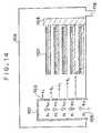
- a conventional technique for processing a substrate in a reaction chamber by a CVD (Chemical Vapor Deposition) method or an ALD (Atomic Layer Deposition) methodwill be briefly explained with reference to FIG. 14 while taking a vertical type substrate processing apparatus as an example.
- FIG. 14is a schematic sectional view of the inside of a reaction tube which is a reaction chamber in the conventional vertical type substrate processing apparatus.
- a plurality of wafers 107are stacked on a boat 108 as substrates to be processed.
- the boat 108is inserted into a reaction tube 106 .
- a gas nozzle 101 as a gas introducing portion for processing the wafers 107 in the reaction tube 106is provided in the reaction tube 106 .
- the gas nozzle 101is provided with a plurality of gas nozzle holes 103 (five in the example shown in FIG. 14). With this arrangement, processing gas flows into the gas nozzle 101 from a gas introducing opening 105 , and is supplied to the wafers 107 from the gas nozzle holes 103 .
- the gas supplied to each wafer 107passes through a process for forming a desired film on the wafer 107 and then, is discharged out from the reaction tube 106 through an exhaust opening 118 .
- the five gas nozzle holes 103 provided in the gas nozzle 101are defines as a first hole, a second hole, . . . and a fifth hole from the upstream side closer to the gas introducing opening 105 of the gas nozzle 101 toward the downstream further from the opening 105 , and if the flow rates of gas supplied from the respective gas nozzle holes 103 are defined as q1, q2 . . . q5, a relation of q1>q2> . . . >q5 is established.
- a gas flow rate between the introducing opening 105 and the first gas nozzle hole 103is defined as q00 and a gas pressure therebetween is defined as p0.
- a gas flow rate between the first and second gas nozzle holes 103is defined as q01 and a gas pressure therebetween is defined as p1.
- a gas flow rate between the n ⁇ 1-th and n-th gas nozzle holes 103is defined as q0(n ⁇ 1) and a gas pressure therebetween is defined as pn ⁇ 1.
- a flow rate of gas injecting from the n-th gas nozzle hole 103is defined as qn.
- a gas concentration of fluid in the gas nozzle 101is reduced by a flow rate of gas injecting from the gas holes from the upstream side toward the downstream side. Since there is a correlation between the gas concentration and gas pressure, a gas pressure pn at a location in the gas nozzle 101 corresponding to the gas nozzle hole 103 is reduced from the upstream side toward the downstream side as shown in the following expression (3):
- Vqn/S (4)
- opening areas of the gas nozzle hole 103are increased from the upstream side toward the downstream side, and a gas flow rate which is reduced toward the downstream side is supplemented by increasing the opening area.
- the gas flow ratesare equalized by adjusting the opening areas, the gas flow velocities are adversely varied depending upon the size of the opening area. Therefore, gas injecting from the gas nozzle holes 103 is nonuniform in the flow velocity.
- a capacity of the gas nozzle itselfis increased to such a degree that such a large amount of gas that the injecting amount can be ignored is stored so that even if gas is injected from the gas nozzle holes 103 from the upstream side toward the downstream side, gas pressures in the gas nozzle 101 at locations corresponding to the respective gas nozzle holes 103 are not changed, thereby equalizing the flow rates of gas injecting from the gas nozzle holes 103 .
- the capacity of the gas nozzle itselfis increased to such a size that the gas pressure in the gas nozzle 101 is not affected by the gas injecting amount, since there is limitation in space of the reaction chamber which accommodates the gas nozzle, this is not practical.
- the above problemis not limited to a wafer, and a substrate in general also has the same problem.
- a substrate processing apparatuscomprising:
- the gas introducing portionis provided along a stacking direction of the substrates, and introduces substrate processing gas into the buffer chamber,
- the buffer chamberincludes a plurality of gas-supply openings provided along the stacking direction of the substrates, and the processing gas introduced from the gas introducing portion is supplied from the gas-supply openings to the reaction chamber.
- a substrate processing apparatuscomprising:
- the buffer chambersrespectively include a plurality of gas-supply openings provided in a stacking direction of the substrates, and the substrate processing gas introduced from each of the gas introducing portions is supplied to the reaction chamber from the gas-supply openings of each of the buffer chambers.
- a reaction containercomprising:
- the gas introducing portionis provided along a stacking direction of the substrates, and introduces substrate processing gas into the buffer chamber,
- the buffer chamberincludes a plurality of gas-supply openings provided along the stacking direction of the substrates, and the processing gas introduced from the gas introducing portion is supplied from the gas-supply openings to the reaction chamber.
- FIG. 1is a schematic sectional view of a inside of a reaction tube of a substrate processing apparatus according to a first embodiment of the present invention
- FIG. 2Ais a schematic lateral sectional view of a reaction tube of a substrate processing apparatus according to a first embodiment of the present invention
- FIG. 2Bis a longitudinal sectional view taken along a line aa′ of FIG. 2A;
- FIG. 3Ais a perspective view of a gas nozzle according to a first embodiment of the present invention.
- FIG. 3Bis a perspective view of a buffer chamber according to a first embodiment of the present invention.
- FIG. 4is a schematic view for explaining a mechanism of a vertical type substrate processing apparatus according to embodiments of the present invention.
- FIG. 5Ais a view showing an outward appearance of a reaction tube of a substrate processing apparatus according to a second embodiment of the present invention.
- FIG. 5Bis a schematic longitudinal sectional view of a reaction tube of a substrate processing apparatus according to a second embodiment of the present invention.
- FIG. 5Cis a schematic longitudinal partial sectional view of a reaction tube of a substrate processing apparatus according to a second embodiment of the present invention.
- FIG. 6is a lateral sectional view taken along a line A-A of FIG. 5A;
- FIG. 7is a lateral sectional view of a reaction tube of a substrate processing apparatus according to a third embodiment of the present invention.
- FIG. 8is a lateral sectional view of a reaction tube of a substrate processing apparatus according to a forth embodiment of the present invention.
- FIG. 9is a lateral sectional view of a reaction tube of a substrate processing apparatus according to a fifth embodiment of the present invention.
- FIG. 10is a lateral partial sectional view of a reaction tube of a substrate processing apparatus according to a sixth embodiment of the present invention.
- FIG. 11is a lateral partial sectional view of a reaction tube of a substrate processing apparatus according to a seventh embodiment of the present invention.
- FIG. 12is a lateral partial sectional view of a reaction tube of a substrate processing apparatus according to a eighth embodiment of the present invention.
- FIG. 13is a lateral sectional view of a reaction tube of a substrate processing apparatus according to a ninth embodiment of the present invention.
- FIG. 14is a schematic sectional view of a inside of a reaction tube of a substrate processing apparatus according to a conventional technique.
- a substrate processing apparatuscomprises
- the gas introducing portionis provided along a stacking direction of the substrates, and introduces substrate processing gas into the buffer chamber,
- the buffer chamberincludes a plurality of gas-supply openings provided along the stacking direction of the substrates, and the processing gas introduced from the gas introducing portion is supplied from the gas-supply openings to the reaction chamber.
- nonuniform flow velocity of gas supplied from the gas introducing portioncan be equalized in the buffer chamber, and gas can be supplied to the stacked substrates uniformly.
- opening areas of the gas-supply openings provided in the buffer chamberare substantially equal to each other.
- the buffer chamberis provided therein with electrodes for generating plasma.
- the electrodes for generating plasmaare provided in the buffer chamber, active species are produced by plasma at a location close to the substrates and in a state in which pressure is uniform, and uniform and more active species can be supplied to the substrates.
- one kind (or more kinds) of gases which are raw material used for forming a filmare mixed and supplied onto a substrate under a certain film forming condition (temperature, time or the like), the gas is adsorbed and reacted on the substrate using both vapor-phase reaction and surface reaction, or only surface reaction, thereby forming a film.
- the ALD methodtwo kinds (or more kinds) of gases which are raw material used for forming a film are alternately supplied onto a substrate one kind gas by one kind gas under a certain film forming condition (temperature, time or the like), the gas is adsorbed in one atomic layer unit, and a film is formed utilizing the surface reaction.
- a film thicknessis controlled based on the number of cycles of supply of reaction gas (assuming that a film forming velocity is 1 ⁇ /cycle for example, when a film of 20 ⁇ is to be formed, the processing is carried out through 20 cycles), and in the CVD method, a film thickness is controlled based on time.
- FIGS. 1 to 13An embodiment of the present invention will be explained with reference to FIGS. 1 to 13 .
- FIG. 4shows an outward appearance of an example of a vertical type substrate processing apparatus in which a plurality of wafers which are substrates to be processed and which have diameter of 200 mm are loaded in a reaction tube which is a reaction chamber and made of quartz, and films are formed by the CVD method or the ALD method which is one of the CVD method as processing method.
- the vertical type substrate processing apparatushas a body 60 and a utility portion 61 which supplies electric power or the like to the body 60 .
- a reaction tube 6as a vertical type reaction chamber for processing wafers, and a heater 16 for appropriately heating the reaction tube 6 .
- a boat 8 for loading and unloading the wafers into and from the reaction tube 6 , and a boat elevator 36 for vertically moving the boat 8are disposed below the reaction tube 6 .
- electrodes 52are provided in the reaction tube 6 , high frequency electric power is applied to the electrodes 52 from a high frequency power supply 51 through an RF matching unit 53 .
- cassette shelves 34for temporarily storing cassettes in which wafers to be supplied to the boat 8 are accommodated, and a wafer transfer apparatus 38 for supplying wafers which are not yet processed (pre-process wafers, hereinafter) from the cassette shelves 34 to the boat 8 and for transferring out wafers which were processed (post-process wafers, hereinafter).
- a cassette loader 35transfers a cassette 32 between the cassette shelves 34 and an I/O stage 33 which receives and delivers the cassette 32 of the wafer from and to outside.
- the I/O stage 33is disposed on a front surface of the apparatus, and delivers and receives the cassette 32 accommodating wafers to and from outside.
- the cassettes 32 accommodating the wafersare set to the I/O stage 33 .
- the cassettes 32 set in the I/O stage 33are transferred to the cassette shelves 34 by the cassette loader 35 in succession.
- the wafer transfer apparatus 38transfers the wafers out from the cassette shelves 34 and transfers the same to the quartz boat 8 . Since 100 wafers can be loaded into the boat 8 , the transfer operation by the wafer transfer apparatus 38 is repeated several times.
- the gasis exhausted from the reaction tube 6 through an exhaust opening (not shown) using a pump, and if a pressure in the reaction tube 6 reaches a predetermined value, the boat 8 is rotated by a rotating mechanism (not shown), and film-forming processing gas of a certain flow rate is supplied into the reaction tube 6 .
- a pressure of the supplied processing gasis maintained at a constant value by a pressure adjusting mechanism (not shown). At that time, the wafers in the reaction tube 6 are maintained at a predetermined temperature.
- the filmis formed by a plasma CVD method or the ALD method
- high frequency electric poweris applied to the electrodes 52 from the high frequency power supply 51 through the RF matching unit 53 , plasma is produced in the film-forming gas, and the film-forming gas is activated. This activating operation will also be described later.
- the wafer boat 8is moved down from the reaction tube 6 by the boat elevator 36 , the wafer boat 8 is transferred to the I/O stage 33 through the wafer transfer apparatus 38 , the cassette shelves 34 and the cassette loader 35 , and transferred out from the apparatus.
- FIG. 2Ais a schematic lateral sectional view of the reaction tube in the vertical type substrate processing apparatus according to this embodiment
- FIG. 2Bis a vertical sectional view taken along a line a-a′ in FIG. 2A.
- a heater 16is provided on an outer periphery of the reaction tube 6 which is a vertical type reaction chamber.
- a plurality of wafers 7 as substrates to be processedare stacked and placed in the reaction tube 6 .
- a buffer chamber 17is provided on an inner wall of the reaction tube 6 from its lower portion to its upper portion along a stacking direction of the wafers 7 .
- Buffer chamber holes 3as gas-supply openings are provided in an end of a wall of the buffer chamber 17 which is adjacent to the wafer 7 .
- the buffer chamber holes 3are opened toward a center of the reaction tube 6 .
- An end of the buffer chamber 17 which is opposite from the buffer chamber holes 3is provided with a gas nozzle 2 formed in the gas introducing portion from the lower portion to the upper portion of the reaction tube 6 along the stacking direction of the wafers 7 .
- the gas nozzle 2is provided with a plurality of gas nozzle holes 4 .
- an outer periphery of the reaction tube 6is covered with the heater 16 .
- the reaction tube 6is supported on a furnace opening flange 25 .
- a furnace opening of the furnace opening flange 25is air-tightly closed with a furnace opening cap 27 .
- the boat 8is provided in a central portion in the reaction tube 6 .
- the plurality of wafers 7are placed in the boat 8 at equal distances from one another in a multistage manner.
- the boat 8can come into and go out from the reaction tube 6 by the boat elevator.
- the boat 8is provided at its lower portion with a rotating mechanism 15 for rotating the boat 8 .
- the wafers 7 placed in the multistage mannerare placed at an equal distance from the buffer chamber 17 .
- the buffer chamber 17is provided along the inner wall of the reaction tube 6 , the gas nozzle 2 is disposed in the buffer chamber 17 from the lower portion to the upper portion of a side surface of the reaction tube 6 , and a portion of the gas nozzle 2 at the lower portion becomes a gas introducing opening 5 .
- the gas nozzle 2 and the buffer chamber 17are provided with the gas nozzle holes and the buffer chamber holes, respectively. Examples of opening states of these holes will be explained using FIGS. 3A and 3B.
- FIG. 3Ais a perspective view of the gas nozzle shown in FIGS. 2A and 2B.
- FIG. 3Bis a perspective view of the buffer chamber also shown in FIGS. 2A and 2B.
- the gas nozzle 2 shown in FIG. 3Ais a pipe having a circular cross section.
- the gas nozzle holes 4are straightly arranged in a side surface of the gas nozzle 2 from its substantially uppermost portion to a bottom of the buffer chamber 17 from an upstream side toward a downstream side of gas flow. Opening areas of the gas nozzle holes 4 are increased from the upstream side (lower portion in FIG. 3A) toward the downstream side (upper portion in FIG. 3A) as viewed from the gas introducing opening.
- the buffer chamber 17 shown in FIG. 3Bis a pipe having an arc cross section.
- the buffer chamber holes 3 having the same opening areasare straightly arranged in an end of a curve inner surface of the buffer chamber 17 along the stacking direction of the wafers 7 .
- reaction tube 6is provided at its lower portion with an exhaust opening 18 connected to an exhaust pump (not shown).
- the processing gas which is raw materialis supplied to the gas nozzle 2 from the gas introducing opening 5 .
- the gas nozzle 2is provided with the plurality of gas nozzle holes 4 , and the gas nozzle 2 injects gas into the buffer chamber 17 .
- the opening areas of the gas nozzle holes 4are increased from the upstream side toward the downstream side.
- gas of substantially the same flow rateis injected from each of the gas nozzle holes 4 although there is a difference in the flow velocity of gas. Then, the gas injected from the gas nozzle holes 4 is not injected into the reaction tube 6 , but the gas once injected and introduced into the buffer chamber 17 , and the flow velocities of the gas are uniformed.
- the gas injected from each the gas nozzle holes 4 in the buffer chamber 17is moderated in the particle velocity of gas in the buffer chamber 17 and then, is injected into the reaction tube 6 from the buffer chamber holes 3 .
- kinetic energies of the gas injected from the gas nozzle holes 4are exchanged and thus, when the gas is injected from the buffer chamber holes 3 , gas having the uniform flow rate and flow velocity can be injected.
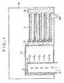
- FIG. 1is a schematic sectional view showing a relation between the gas nozzle, the buffer chamber and the reaction tube in the reaction tube of the vertical type substrate processing apparatus of the invention.
- the buffer chamber 17is provided in the reaction tube 6 .
- the gas nozzle 2is disposed in the buffer chamber 17 , and the reaction tube 6 is provided with the exhaust opening 18 for exhausting gas in the reaction tube 6 to outside.
- the boat 8 having wafers 7(five wafers in FIG. 1) is provided adjacent to the buffer chamber 17 .
- the gas nozzle 2 and the buffer chamber 17are respectively provided with the gas nozzle holes 4 and the buffer chamber holes 3 (five each in FIG. 1).
- the opening areas of the gas nozzle holes 4are increased from the upstream side toward the downstream side as viewed from the gas introducing opening 5 so that the injecting amounts of gas from the gas nozzle holes 4 become the same.
- Gas having the same flow rates but different flow velocities Q1 to Q5is once introduced into the buffer chamber 17 . During that time, gas having the flow velocities Q1 to Q5 is uniformed in flow velocity by exchanging kinetic energies, and a pressure in the buffer chamber 17 is substantially equalized.
- the opening positions of the buffer chamber holes 3have the same pitches as the wafers 7 which are respectively adjacent to the buffer chamber holes. 3 , and the gas is supplied to gaps between the wafers 7 . Therefore, gas having uniform flow velocities and flow rates can efficiently be supplied to the wafers 7 preferably.
- the gas having uniform flow velocities and flow ratescan efficiently be supplied to the wafers 7 , the film forming states of the wafers 7 are equalized, and the processing speed of the wafers 7 can largely be enhanced.
- the above-described vertical type substrate processing apparatuscan be used.
- the ALD methodif it is required to activate the processing gas by plasma or the like, an apparatus and an operation required for this process are added.
- FIGS. 5A, 5B and 5 Cshow, from a side, an outward appearance and the inside of the reaction tube which is the reaction chamber in the vertical type substrate processing apparatus of the invention used for forming films by the ALD method.
- FIG. 6is a lateral sectional view taken along a line A-A.
- FIG. 5Ashows the outward appearance of the reaction chamber.
- FIGS. 5B and Care vertical sectional views of the reaction chamber. In the drawings, connected portions of the furnace opening flange with respect to the heater, the wafers, the boat and the reaction tube, as well as the boat rotating mechanism are omitted.
- the reaction tube 6is provided at its outer periphery with a heater 16 , and the plurality of wafers 7 as substrates to be processed are stacked inside the reaction tube 6 .
- the buffer chamber 17is provided in the arc space between the wafers 7 and the inner wall of the reaction tube 6 along the stacking direction of the wafers 7 to the inner wall of the reaction tube 6 , and the buffer chamber holes 3 are provided in the end of the wall which is adjacent to the wafers.
- the reaction tube 6is provided at its lower portion with the exhaust opening 18 .
- the gas nozzleis provided in the end which is opposite from the buffer chamber hole in the buffer chamber.
- a gas supply chamber 43is provided as the gas introducing portion in the reaction tube instead of the gas nozzle.
- the gas supply chamber 43is provided at its lower portion with the gas introducing opening 5 .
- a partition wall between the gas supply chamber 43 and the buffer chamber 17is provided with gas supply chamber holes 47 having the same structure as that of the gas nozzle holes provided in the above-described gas nozzle.
- the opening positions of the buffer chamber holes 3 provided in the buffer chamber 17have the same pitches as those of the adjacent wafers 7 .
- gasis once introduced from the gas introducing portion, and gas can be supplied to the stacked wafers 7 uniformly.
- the electrode 52is disposed in the buffer chamber 17 such that the electrode 52 is protected by an electrode-protecting tube 50 from its upper portion to lower portion.
- the electrode 52is connected to the high frequency power supply 51 through the RF matching unit 53 .
- the electrode 52can generate plasma 14 in the buffer chamber 17 .
- a reaction gas buffer chamber 42is provided on an inner wall of the reaction tube 6 at a location away from the opening of the buffer chamber hole 3 through 120° along the inner periphery of the reaction tube 6 .
- This reaction gas buffer chamber 42contains gas different from that contained in the buffer chamber 17 .
- the reaction gas buffer chamber 42 and the buffer chamber 17supply different kinds of gases to the wafers 7 alternately.
- the reaction gas buffer chamber 42has reaction gas buffer chamber holes 48 with the same pitches at locations adjacent to the wafers.
- the reaction gas buffer chamber 42is provided at its lower portion with a reaction gas introducing opening 45 .
- the reaction gas buffer chamber 42does not have the gas supply chamber 43 and the electrode 52 . Opening areas of the reaction gas buffer chamber holes 48 are increased from the upstream side toward the downstream side.
- the reaction tube 6is provided at its lower portion with the exhaust opening 18 .
- the exhaust opening 18can exhaust inside gas from the reaction tube 6 .
- FIG. 5Ashows an outward appearance and the inside (shown with broken lines) of the reaction tube 6 as viewed from a front surface of the buffer chamber 17 .
- the buffer chamber 17is provided in the reaction tube 6 such as to extend from its upper portion to lower portion.
- the gas supply chamber 43is provided adjacent to the buffer chamber 17 .
- the electrode 52 covered with the electrode-protecting tube 50is disposed in the buffer chamber 17 from its upper portion to lower portion.
- the gas supply chamber 43is provided at its lower portion with the gas introducing opening 5 .
- This electrode-protecting tube 50can be inserted into the buffer chamber 17 in a state in which the thin and long electrode 52 is isolated from atmosphere in the buffer chamber 17 .
- the electrode 52 inserted into the electrode-protecting tube 50is oxidized by heat from the heater. Therefore, an inert gas purging mechanism is provided in the electro-deprotecting tube 50 for charging or purging inert gas such as nitrogen to suppress the oxygen concentration to sufficiently low level.
- the reaction gas buffer chamber 42is provided in the reaction tube 6 along its inner wall from its upper portion to lower portion away from the buffer chamber 17 .
- the reaction gas buffer chamber 42is provided at its lower portion with the reaction gas introducing opening 45 .
- the reaction tube 6is provided at its lower portion with the exhaust opening 18 along the inner wall of the reaction tube 6 at a location opposed from the reaction gas buffer chamber 42 with respect to the buffer chamber 17 .
- FIG. 5Bshows the inside of the reaction tube 6 as viewed from front surfaces of the buffer chamber holes 3 and the reaction gas buffer chamber holes 48 .
- the buffer chamber 17 and the gas supply chamber 43 adjacent to the buffer chamber 17extend from the upper portion to the lower portion in the reaction tube 6 .
- the buffer chamber holes 3 having the same pitchesare provided at positions adjacent to the wafers (not shown) from the upper portion to the lower portion in the buffer chamber 17 .
- the buffer chamber holes 3have the same opening areas in the wall of the buffer chamber 17 having the same thickness.
- the reaction gas buffer chamber 42is provided in the reaction tube 6 along its inner wall from its upper portion to lower portion away from the buffer chamber 17 .
- the reaction gas buffer chamber holes 48 having the same pitchesare provided adjacent to the wafers (not shown) from the upper portion to the lower portion in the reaction gas buffer chamber 42 .
- the opening areas of the reaction gas buffer chamber holes 48are increased from the upstream side toward the downstream side, from the lower portion to the upper portion in FIGS. 5A, 5B and 5 C.
- FIG. 5Cis a vertical sectional view of the reaction tube 6 as viewed from front surfaces of the gas supply chamber holes 47 provided in the gas supply chamber 43 .
- the gas supply chamber 43is provided in the reaction tube 6 from the upper portion to the lower portion adjacent to the buffer chamber 17 .
- a partition wall between the buffer chamber 17 and the gas supply chamber 43is provided with the gas supply chamber holes 47 from the upper portion to a location lower than the lower portion where the gas supply chamber holes 47 are adjacent to the wafers (not shown). The reason why the gas supply chamber holes 47 are opened up to the lowermost end of the buffer chamber 17 is that stagnation of gas is not generated in the buffer chamber 17 .
- the opening areas of the gas supply chamber holes 47are increased from the upstream side toward the downstream side of the gas flow.
- active species of ammonia (NH 3 ) and dichlorsilane (SiH 2 Cl 2 )are alternately supplied as processing gas, and SiNx film (silicon nitride film) is formed by an atomic layer film-forming method.
- the opening areas of the gas supply chamber holes 47 provided in the gas supply chamber 43are gradually increased from the upstream side toward the downstream side of the gas flow so that the flow rates of ammonia injected into the buffer chamber 17 from the gas supply chamber 43 become the same.
- the active species produced by the effect of plasmahas lifetime, and if a distance between a plasma producing portion and the wafer 7 is long, the species are deactivated before they are supplied to the wafers 7 , and an amount of active species which contribute to the reaction on the wafers 7 is largely reduced. Therefore, it is preferable that the plasma is produced in the vicinity of the wafers 7 .
- the distance between the two electrode-protecting tubes 50is set to an appropriate value so that a place where the plasma 14 is generated is limited to inside the buffer chamber 17 , and a preferable distance is about 20 mm.
- the plasma 14may be produced anywhere inside the buffer chamber 17 , and it is preferable that the gas introduced into the buffer chamber 17 passes through the plasma.
- the plasma 14is produced between the buffer chamber hole 3 and the gas supply chamber hole 47 .
- a distance between the electrode-protecting tube 50 and the buffer chamber hole 3is adjusted to an appropriate value so that the plasma 14 generated in the buffer chamber 17 is not dispersed and leaked outside the buffer chamber 17 .
- the buffer chamber holes 3are located at intermediate portions of the gap between the adjacent wafers 7 placed in the multistage manner, the processing gas is sufficiently supplied to the stacked wafers 7 .
- the inside of the reaction tube 6is purged by inert gas such as N 2 or Ar and in this state, the gas is exhausted from the exhaust opening 18 . If the concentration of the active species of ammonia in the reaction tube 6 has sufficiently reduced, the supply of the inert gas is stopped, and dichlorsilane is introduced into the reaction gas buffer chamber 42 from the reaction gas introducing opening 45 .
- inert gassuch as N 2 or Ar
- reaction gas buffer chamber holes 48whose opening areas are gradually increased from the upstream side toward the downstream side of the reaction gas introducing opening 45 are provided in the reaction gas buffer chamber 42 toward the center of the reaction tube 6 .
- the dichlorsilane supplied to the wafers from the reaction gas buffer chamber holes 48has different flow velocities but has the same flow rates and is injected into the reaction tube 6 .
- a SiNx film of about 1 ⁇is formed through this series of process.
- a SiNx film of 500 ⁇is to be formed on a wafer 7 , the above process is repeated about 500 times.
- the boat (not shown) in which the wafers 7 are placedis rotated at a constant speed, even if gas is supplied from a side of the wafers 7 , more uniform film forming processing is realized over the entire surfaces of the wafers 7 .
- the rotating speed of 1 to 10 rpmis sufficient.
- FIG. 7is a lateral sectional view of a reaction tube of a vertical type substrate processing apparatus according to a third embodiment of the present invention.
- the reaction tube 6 shown in FIG. 7has the same structure as that shown in FIG. 6.
- the electrode for producing plasmais disposed in the buffer chamber 17 .
- an ultraviolet lamp 54 for activating gas and a reflection plate 58 for preventing ultraviolet from radiating out from the buffer chamber 17are provided in combination.
- Reaction gasis activated by light energy of the lamp 54 .
- the processing gas which is brought into the active species in the buffer chamber 17 having the above structureis injected toward the wafers 7 from the buffer chamber holes 3 , and films are formed on the wafers 7 by the ALD method.
- FIG. 8is a lateral sectional view of a reaction tube of a vertical type substrate processing apparatus according to a fourth embodiment of the invention.
- the reaction tube 6 shown in FIG. 8has the same structure as that shown in FIG. 7.
- the reaction gasis activated by light energy.
- an exotherm (hot wire, hereinafter) 55 having appropriate electrical resistance valueis heated by a power supply 57 to a temperature of 1,600° C. or higher, and gas which comes into contact with the hot wire is activated.
- a W (tungsten) wire having about 0.5 mm or the likecan be suitably used as the hot wire 55 having the appropriate electrical resistance value and generating the active species.
- This hot wire 55is heated to 1,600° C. or higher by electric power of the power supply 57 , and processing gas which comes into contact with the hot wire 55 is activated by the thermal energy.
- the processing gas which is brought into the active species in the buffer chamber 17 having the above structureis injected toward the wafers 7 from the buffer chamber holes 3 , and films are formed on the wafers 7 by the ALD method.
- FIG. 9is a lateral sectional view of a reaction tube of a vertical type substrate processing apparatus according to a fifth embodiment of the invention.
- the reaction tube 6 shown in FIG. 9has the same structure as that shown in FIG. 6.
- the plasma generating electrodeis disposed in the buffer chamber 17 .
- a remote plasma unit 56is disposed on a gas passage upstream from the gas introducing opening 5 through which processing gas is introduced into the reaction tube 6 , and gas passing through the remote plasma unit 56 is allow to produce plasma.
- the processing gas passing through the remote plasma unit 56is reacted with plasma and brought into active species, the gas which was brought into the active species enters the reaction tube 6 from the gas introducing opening 5 , and is supplied to the buffer chamber 17 through the gas supply chamber 43 , and is further supplied to the wafers 7 as uniform gas from the buffer chamber holes 3 provided in the buffer chamber 17 . Then, films are formed on the wafers 7 by the ALD method.
- An ICP coil or the likeis suitably used as the remote plasma unit 56 .
- FIGS. 10, 11 and 12are lateral sectional views of left halves of reaction tubes 6 used for substrate processing apparatuses of the sixth, seventh and eighth embodiments of the invention, respectively.
- a gas nozzle 102is disposed in the buffer chamber 17 from the lower portion to the upper portion of the reaction tube 6 in the stacking direction of the wafers 7 .
- the gas introducing opening 5is in communication with a lower portion of the gas nozzle 102 .
- a large number of gas nozzle holesare provided in the gas nozzle 102 in the vertical direction.
- the exhaust openingwhich is in communication with an exhaust pump (not shown) is formed in a side surface of a lower portion of the reaction tube 6 .
- a wall 172 which is a portion of the buffer chamber 17is a portion of a wall of the reaction tube 6 .
- Two electrode-protecting tubes 50are disposed closer to a wall surface 173 of a portion of a wall 171 of the buffer chamber 17 provided with the buffer chamber holes 3 than a wall surface 174 of the wall 172 .
- Two electrodes 52 protected by the two electrode-protecting tubes 50are also disposed closer to the wall surface 173 of the wall 171 than the wall surface 174 of the wall 172 .
- the two electrode-protecting tubes 50are located in the vicinity of the wall 171 of the buffer chamber 17 provided with the buffer chamber holes 3 (preferably, a distance between the electrode-protecting tubes 50 and the wall surface of the wall 171 of the buffer chamber 17 is 0 to 5 mm.
- 0 mmmeans a case in which the electrode-protecting tubes 50 are tightly connected to the wall surface).
- the two electrodes 52 and the two electrode-protecting tubes 50are disposed astride the buffer chamber holes 3 (that is, the buffer chamber holes 3 are located between the two electrode-protecting tubes 50 ). With this arrangement, a distance between the plasma 14 and the buffer chamber hole 3 can be shortest.
- the two electrode-protecting tubes 50are brought close to the wall surface 173 of the wall 171 constituting the buffer chamber 17 , it is possible to limit a main gas flow path. If the buffer chamber holes 3 are provided at location where the limited main gas flow path passes between the two electrode-protecting tubes 50 , the reaction gas can efficiently pass through a region where the concentration of the plasma 14 is high, and it is possible to increase the concentration of the active species.
- the reaction gas path in the buffer chamber 17can roughly be divided into paths D, E, e and f.
- the paths D and Eare main gas flow path, and most of reaction gas passes between the two electrode-protecting tubes 50 , i.e., passes through the region where the concentration of the plasma 14 is high.
- the active speciescan be activated with plasma having high concentration (concentration of the active species is increased at the time of excitation)
- a substrate to be processedcan be carried without deactivating the active species.
- This embodimentalso has a feature that it is unnecessary to control the gas flow paths before the gas is brought into active species so that concentration of the active species is not different in the paths D and E.
- FIG. 11shows the seventh Embodiment.
- the gas nozzle 102 and the buffer chamber holes 3are disposed between the two electrode-protecting tubes 50 so that gas supplied from the gas nozzle 102 straightly pass through (path F), the plasma 14 and the buffer chamber holes 3 .
- the concentration of the active speciescan be increased like the structure shown in FIG. 10.
- FIG. 12shows the eighth embodiment.
- one of the two electrode-protecting tubes 50is brought close to the wall surface 173 of the wall 171 provided with the buffer chamber holes 3
- the other electrode-protecting tube 50is brought close to the wall surface 174 of the portion of the wall 172 of the buffer chamber 17 which is the portion of the wall of the reaction tube 6 , so that the main gas flow path is limited.
- the buffer chamber holes 3are provided at locations where the main gas flow path I passes between the two electrode-protecting tubes 50 .
- the concentration of the active species of the reaction gascan be increased by optimizing the layout of the buffer chamber 17 , the electrode-protecting tubes 50 and the buffer chamber holes 3 .
- the concentration of the active species of the reaction gascan be enhanced by optimizing the relative position of the buffer chamber 17 , the electrode-protecting tubes 50 and the buffer chamber holes 3 as described above.
- the processing uniformity between apparatuses, the reliability and repeatabilityare taken into consideration, it is preferable that there is no variation in the relative position.
- the apparatuscan be used as the CVD apparatus like the first embodiment, and if a buffer chamber 42 is added in addition to the buffer chamber 17 as shown in FIG. 6, the apparatus can be used as the ALD apparatus.
- a ninth embodiment of the inventionwill be explained with reference to FIG. 13.
- the buffer chamber 42 shown in FIG. 6is added to the apparatus of the sixth embodiment shown in FIG. 10, and the apparatus is formed into the ALD apparatus.
- the gas nozzle 102is provided with a large number of gas nozzle hole 103 in the vertical direction.
- the gas nozzle holes 103is provided toward a wall surface 176 of a wall 175 of the buffer chamber 17 . If gas nozzle holes 103 are provided toward the inside of the buffer chamber 17 which is on the other side from the wall surface 176 , when silicon nitride films are to be formed using the ALD method by alternately supplying ammonia from the gas nozzle 102 and dichlorsilane from the buffer chamber 42 like the second embodiment, and when ammonia stays and dichlorsilane flows, reaction byproduct is generated, which becomes a cause of particles.
- the gas nozzle holes 103are directed toward the wall surface 176 of the wall 175 of the buffer chamber 17 , and after ammonia is supplied, the chamber is purged with inert gas for not allowing ammonia to stay and for preventing particles from being generated.
- the gas nozzle 102is provided at its side surface with the large number of gas nozzle holes (not shown) in the vertical direction.
- the gas nozzle 102is provided at its side surface with the large number of gas nozzle holes 103 .
- the gas nozzle 102may have a predetermined length, and the gas nozzle holes may be opened at the upper portion of the gas nozzle 102 . In this case, it is preferable that a height of the gas nozzle 102 is lower than the loading position of the wafer 7 .
Landscapes
- Chemical & Material Sciences (AREA)
- Engineering & Computer Science (AREA)
- Metallurgy (AREA)
- Chemical Kinetics & Catalysis (AREA)
- Materials Engineering (AREA)
- Mechanical Engineering (AREA)
- General Chemical & Material Sciences (AREA)
- Organic Chemistry (AREA)
- Physics & Mathematics (AREA)
- Plasma & Fusion (AREA)
- Electromagnetism (AREA)
- Analytical Chemistry (AREA)
- Chemical Vapour Deposition (AREA)
Abstract
Description
- 1. Field of the Invention[0001]
- The present invention relates to a substrate processing apparatus and a reaction container, more particularly, to a substrate processing apparatus and a reaction container used in one step of producing process of a semiconductor device for processing a substrate in a reaction chamber, and more particularly, to an improvement of a gas introducing portion which supplies gas to a substrate.[0002]
- 2. Description of the Related Art[0003]
- A conventional technique for processing a substrate in a reaction chamber by a CVD (Chemical Vapor Deposition) method or an ALD (Atomic Layer Deposition) method will be briefly explained with reference to FIG. 14 while taking a vertical type substrate processing apparatus as an example.[0004]
- FIG. 14 is a schematic sectional view of the inside of a reaction tube which is a reaction chamber in the conventional vertical type substrate processing apparatus.[0005]
- A plurality of[0006]
wafers 107 are stacked on a boat108 as substrates to be processed. The boat108 is inserted into areaction tube 106. Agas nozzle 101 as a gas introducing portion for processing thewafers 107 in thereaction tube 106 is provided in thereaction tube 106. - The[0007]
gas nozzle 101 is provided with a plurality of gas nozzle holes103 (five in the example shown in FIG. 14). With this arrangement, processing gas flows into thegas nozzle 101 from a gas introducing opening105, and is supplied to thewafers 107 from thegas nozzle holes 103. - The gas supplied to each[0008]
wafer 107 passes through a process for forming a desired film on thewafer 107 and then, is discharged out from thereaction tube 106 through anexhaust opening 118. - However, when all of the[0009]
gas nozzle holes 103 provided in thegas nozzle 101 have the same opening areas, there is a problem that a flow rate and flow velocity of gas supplied from thegas nozzle holes 103 to thewafers 107 are reduced from an upstream side closer to the gas introducing opening105 toward a downstream side further from theopening 105. - That is, if the apparatus for collectively processing the plurality of[0010]
wafers 107 shown in FIG. 14 is considered from a viewpoint of gas supply with respect to each of the wafers, it seems that thegas nozzle 101 supplies gas uniformly to thewafers 107, but in reality, a difference in the gas flow rate or flow velocity is generated, and the gas is not supplied to all of thewafers 107 under the same conditions. - For example, if the five[0011]
gas nozzle holes 103 provided in thegas nozzle 101 are defines as a first hole, a second hole, . . . and a fifth hole from the upstream side closer to the gas introducing opening105 of thegas nozzle 101 toward the downstream further from theopening 105, and if the flow rates of gas supplied from the respectivegas nozzle holes 103 are defined as q1, q2 . . . q5, a relation of q1>q2> . . . >q5 is established. - Concerning the flow velocities of gas also, a velocity of gas from the first[0012]
gas nozzle holes 103 is the fastest, and velocities of gas from the second, third, . . . are gradually reduced. - As a result, the flow rates and flow velocities of gas supplied to the[0013]
wafers 107 become nonuniform. - Therefore, in the process of wafers which largely depends of a supply amount of gas, the film forming states of the[0014]
stacked wafers 107 become nonuniform. - Referring back to FIG. 14, a cause of the nonuniformity of the supply amount of gas will be considered.[0015]
- In the[0016]
gas nozzle 101 in a state in which gas is supplied to thewafers 107, a gas flow rate between the introducing opening105 and the firstgas nozzle hole 103 is defined as q00 and a gas pressure therebetween is defined as p0. Next, a gas flow rate between the first and secondgas nozzle holes 103 is defined as q01 and a gas pressure therebetween is defined as p1. Similarly, a gas flow rate between the n−1-th and n-thgas nozzle holes 103 is defined as q0(n−1) and a gas pressure therebetween is defined as pn−1. - A flow rate of gas injecting from the n-th[0017]
gas nozzle hole 103 is defined as qn. - At that time, gas flow rates qn (n=1, 2, . . . ) injecting from the plurality of[0018]
gas nozzle holes 103 provided from the upstream side to the downstream side and having the same opening areas are reduced from the upstream gas nozzle hole toward the downstream gas nozzle hole as shown in the following expression (1): - q1>q2> . . . >qn−1>qn (1).
- This is because, in the case of gas flowing from the upstream side toward the downstream side through the[0019]
gas nozzle 101, its gas flow rate q0(n−1) is reduced by a gas flow rate qn injecting from thegas nozzle hole 103 when the gas passes through thegas nozzle hole 103, and the gas flows toward a next gas nozzle hole. A flow rate of gas after the gas passed through thegas nozzle hole 103 is reduced from the upstream side toward the downstream side as shown in the following expression (2): - q0n=q0(n−1)−qn (2)
- At that time, a gas concentration of fluid in the[0020]
gas nozzle 101 is reduced by a flow rate of gas injecting from the gas holes from the upstream side toward the downstream side. Since there is a correlation between the gas concentration and gas pressure, a gas pressure pn at a location in thegas nozzle 101 corresponding to thegas nozzle hole 103 is reduced from the upstream side toward the downstream side as shown in the following expression (3): - p1>p2> . . . >pn−1>pn (3)
- Therefore, flow rates of gas injecting from the respective[0021]
gas nozzle holes 103 do not become equal to each other. If an opening area of thegas nozzle hole 103 is defined as S, a flow velocity V of gas injecting from the gas nozzle hole is expressed as shown in the following expression (4): - V=qn/S (4)
- Since the flow rates of gas injected from the respective[0022]
gas nozzle holes 103 are not equal to each other, if the opening areas of the nozzle holes are the same, flow velocities of gas injected from the respectivegas nozzle holes 103 become different. In the above-describedconventional gas nozzle 101, since the flow rates and flow velocities of gas injected from the respectivegas nozzle holes 103 are different, it is considered that gas can not be supplied to the wafers uniformly. - To solve the above problem, two conventional solutions have been proposed.[0023]
- According to a first solution, opening areas of the[0024]
gas nozzle hole 103 are increased from the upstream side toward the downstream side, and a gas flow rate which is reduced toward the downstream side is supplemented by increasing the opening area. However, if the gas flow rates are equalized by adjusting the opening areas, the gas flow velocities are adversely varied depending upon the size of the opening area. Therefore, gas injecting from thegas nozzle holes 103 is nonuniform in the flow velocity. - According to a second solution, a capacity of the gas nozzle itself is increased to such a degree that such a large amount of gas that the injecting amount can be ignored is stored so that even if gas is injected from the[0025]
gas nozzle holes 103 from the upstream side toward the downstream side, gas pressures in thegas nozzle 101 at locations corresponding to the respectivegas nozzle holes 103 are not changed, thereby equalizing the flow rates of gas injecting from thegas nozzle holes 103. However, if the capacity of the gas nozzle itself is increased to such a size that the gas pressure in thegas nozzle 101 is not affected by the gas injecting amount, since there is limitation in space of the reaction chamber which accommodates the gas nozzle, this is not practical. - The above problem is not limited to a wafer, and a substrate in general also has the same problem.[0026]
- Thereupon, it is a main object of the present invention to provide, from a viewpoint different from the above structure, a substrate processing apparatus capable of achieving the uniformity of process between substrates by uniformly supplying gas.[0027]
- According to a first aspect of the present invention, there is provided a substrate processing apparatus, comprising:[0028]
- a reaction chamber which is to accommodate stacked substrates,[0029]
- a gas introducing portion, and[0030]
- a buffer chamber, wherein[0031]
- the gas introducing portion is provided along a stacking direction of the substrates, and introduces substrate processing gas into the buffer chamber,[0032]
- the buffer chamber includes a plurality of gas-supply openings provided along the stacking direction of the substrates, and the processing gas introduced from the gas introducing portion is supplied from the gas-supply openings to the reaction chamber.[0033]
- According to a second aspect of the present invention, there is provided a substrate processing apparatus, comprising:[0034]
- a reaction chamber which is to accommodate stacked substrates,[0035]
- a plurality of buffer chambers, and[0036]
- a plurality of gas introducing portions for respectively introducing substrate processing gases to the buffer chambers, wherein[0037]
- the buffer chambers respectively include a plurality of gas-supply openings provided in a stacking direction of the substrates, and the substrate processing gas introduced from each of the gas introducing portions is supplied to the reaction chamber from the gas-supply openings of each of the buffer chambers.[0038]
- According to a third aspect of the present invention, there is provided a reaction container, comprising:[0039]
- a reaction chamber which is to accommodate stacked substrates,[0040]
- a plurality of buffer chambers, and[0041]
- a plurality of gas introducing portions for respectively introducing substrate processing gases to the buffer chambers, wherein[0042]
- the buffer chambers respectively include a plurality of gas-supply openings provided in a stacking direction of the substrates, and the substrate processing gas introduced from each of the gas introducing portions is supplied to the reaction chamber from the gas-supply openings of each of the buffer chambers.[0043]
- According to a forth aspect of the present invention, there is provided a reaction container, comprising:[0044]
- a reaction chamber which is to accommodate stacked substrates,[0045]
- a gas introducing portion, and[0046]
- a buffer chamber, wherein[0047]
- the gas introducing portion is provided along a stacking direction of the substrates, and introduces substrate processing gas into the buffer chamber,[0048]
- the buffer chamber includes a plurality of gas-supply openings provided along the stacking direction of the substrates, and the processing gas introduced from the gas introducing portion is supplied from the gas-supply openings to the reaction chamber.[0049]
- The above and further objects, features and advantages of the present invention will become more apparent from the following detailed description taken in conjunction with the accompanying drawings, wherein:[0050]
- FIG. 1 is a schematic sectional view of a inside of a reaction tube of a substrate processing apparatus according to a first embodiment of the present invention;[0051]
- FIG. 2A is a schematic lateral sectional view of a reaction tube of a substrate processing apparatus according to a first embodiment of the present invention;[0052]
- FIG. 2B is a longitudinal sectional view taken along a line aa′ of FIG. 2A;[0053]
- FIG. 3A is a perspective view of a gas nozzle according to a first embodiment of the present invention;[0054]
- FIG. 3B is a perspective view of a buffer chamber according to a first embodiment of the present invention;[0055]
- FIG. 4 is a schematic view for explaining a mechanism of a vertical type substrate processing apparatus according to embodiments of the present invention;[0056]
- FIG. 5A is a view showing an outward appearance of a reaction tube of a substrate processing apparatus according to a second embodiment of the present invention;[0057]
- FIG. 5B is a schematic longitudinal sectional view of a reaction tube of a substrate processing apparatus according to a second embodiment of the present invention;[0058]
- FIG. 5C is a schematic longitudinal partial sectional view of a reaction tube of a substrate processing apparatus according to a second embodiment of the present invention;[0059]
- FIG. 6 is a lateral sectional view taken along a line A-A of FIG. 5A;[0060]
- FIG. 7 is a lateral sectional view of a reaction tube of a substrate processing apparatus according to a third embodiment of the present invention;[0061]
- FIG. 8 is a lateral sectional view of a reaction tube of a substrate processing apparatus according to a forth embodiment of the present invention;[0062]
- FIG. 9 is a lateral sectional view of a reaction tube of a substrate processing apparatus according to a fifth embodiment of the present invention;[0063]
- FIG. 10 is a lateral partial sectional view of a reaction tube of a substrate processing apparatus according to a sixth embodiment of the present invention;[0064]
- FIG. 11 is a lateral partial sectional view of a reaction tube of a substrate processing apparatus according to a seventh embodiment of the present invention;[0065]
- FIG. 12 is a lateral partial sectional view of a reaction tube of a substrate processing apparatus according to a eighth embodiment of the present invention;[0066]
- FIG. 13 is a lateral sectional view of a reaction tube of a substrate processing apparatus according to a ninth embodiment of the present invention; and[0067]
- FIG. 14 is a schematic sectional view of a inside of a reaction tube of a substrate processing apparatus according to a conventional technique.[0068]
- According to a preferred embodiment of the present invention, there is provided a substrate processing apparatus comprises[0069]
- a reaction chamber which is to accommodate stacked substrates,[0070]
- a gas introducing portion, and[0071]
- a buffer chamber, wherein[0072]
- the gas introducing portion is provided along a stacking direction of the substrates, and introduces substrate processing gas into the buffer chamber,[0073]
- the buffer chamber includes a plurality of gas-supply openings provided along the stacking direction of the substrates, and the processing gas introduced from the gas introducing portion is supplied from the gas-supply openings to the reaction chamber.[0074]
- With this structure, the substrate processing apparatus according to the present invention, nonuniform flow velocity of gas supplied from the gas introducing portion can be equalized in the buffer chamber, and gas can be supplied to the stacked substrates uniformly.[0075]
- Preferably, opening areas of the gas-supply openings provided in the buffer chamber are substantially equal to each other.[0076]
- It is possible to further equalize the gas supply to the substrates by providing the gas-supply openings having the same opening areas.[0077]
- Preferably, the buffer chamber is provided therein with electrodes for generating plasma.[0078]
- Since the electrodes for generating plasma are provided in the buffer chamber, active species are produced by plasma at a location close to the substrates and in a state in which pressure is uniform, and uniform and more active species can be supplied to the substrates.[0079]
- Next, embodiments of the present invention will be explained with reference to the drawings.[0080]
- First, as an example of process for a substrate carried out in the embodiment of the invention, film forming processing using the CVD method and the ALD method will briefly be explained based on a comparison the methods.[0081]
- In the CVD method, one kind (or more kinds) of gases which are raw material used for forming a film are mixed and supplied onto a substrate under a certain film forming condition (temperature, time or the like), the gas is adsorbed and reacted on the substrate using both vapor-phase reaction and surface reaction, or only surface reaction, thereby forming a film.[0082]
- According to the ALD method, two kinds (or more kinds) of gases which are raw material used for forming a film are alternately supplied onto a substrate one kind gas by one kind gas under a certain film forming condition (temperature, time or the like), the gas is adsorbed in one atomic layer unit, and a film is formed utilizing the surface reaction.[0083]
- That is, when a SiN (silicon nitride) film is to be formed for example, in the case of the ALD method, DCS (dichlorsilane) and NH[0084]3(ammonia) are used for carrying out chemical reaction to be utilized, and a film having high quality can be formed at a low temperature of 300 to 600C.°. Whereas, in the case of a normal CVD method, a film forming temperature is relatively high as high as 600 to 800C.°. In the case of the ALD method, a plurality of kinds of reaction gases are alternately supplied one kind gas by one kind gas (not at the same time), and in the case of the normal CVD method, a plurality of kinds of gases are supplied at the same time. In the ALD method, a film thickness is controlled based on the number of cycles of supply of reaction gas (assuming that a film forming velocity is 1 Å/cycle for example, when a film of 20 Å is to be formed, the processing is carried out through 20 cycles), and in the CVD method, a film thickness is controlled based on time.
- An embodiment of the present invention will be explained with reference to FIGS.[0085]1 to13.
- The same elements are designated with the same symbols in FIGS.[0086]1 to13.
- First, an outline of a mechanism of a vertical type substrate processing apparatus of each of embodiments of the present invention will be briefly explained using FIG. 4.[0087]
- FIG. 4 shows an outward appearance of an example of a vertical type substrate processing apparatus in which a plurality of wafers which are substrates to be processed and which have diameter of 200 mm are loaded in a reaction tube which is a reaction chamber and made of quartz, and films are formed by the CVD method or the ALD method which is one of the CVD method as processing method.[0088]
- The vertical type substrate processing apparatus has a[0089]
body 60 and autility portion 61 which supplies electric power or the like to thebody 60. - In the[0090]
body 60, there are provided areaction tube 6 as a vertical type reaction chamber for processing wafers, and aheater 16 for appropriately heating thereaction tube 6. Aboat 8 for loading and unloading the wafers into and from thereaction tube 6, and aboat elevator 36 for vertically moving theboat 8 are disposed below thereaction tube 6. - If it is necessary to produce plasma in the[0091]
reaction tube 6,electrodes 52 are provided in thereaction tube 6, high frequency electric power is applied to theelectrodes 52 from a highfrequency power supply 51 through anRF matching unit 53. - Further, provided in the[0092]
body 60 arecassette shelves 34 for temporarily storing cassettes in which wafers to be supplied to theboat 8 are accommodated, and awafer transfer apparatus 38 for supplying wafers which are not yet processed (pre-process wafers, hereinafter) from thecassette shelves 34 to theboat 8 and for transferring out wafers which were processed (post-process wafers, hereinafter). - A[0093]
cassette loader 35 transfers acassette 32 between thecassette shelves 34 and an I/O stage 33 which receives and delivers thecassette 32 of the wafer from and to outside. - The I/[0094]
O stage 33 is disposed on a front surface of the apparatus, and delivers and receives thecassette 32 accommodating wafers to and from outside. - The operation of the above-described vertical type substrate processing apparatus will be explained briefly.[0095]
- The[0096]
cassettes 32 accommodating the wafers are set to the I/O stage 33. - The[0097]
cassettes 32 set in the I/O stage 33 are transferred to thecassette shelves 34 by thecassette loader 35 in succession. - In the[0098]
cassette - The[0099]
wafer transfer apparatus 38 transfers the wafers out from thecassette shelves 34 and transfers the same to thequartz boat 8. Since 100 wafers can be loaded into theboat 8, the transfer operation by thewafer transfer apparatus 38 is repeated several times. - If the transfer operation of the wafers to the[0100]
boat 8 is completed, theboat 8 is moved upward by theboat elevator 36 and inserted into thereaction tube 6 and then, the inside of thereaction tube 6 is held air-tightly. - The gas is exhausted from the[0101]
reaction tube 6 through an exhaust opening (not shown) using a pump, and if a pressure in thereaction tube 6 reaches a predetermined value, theboat 8 is rotated by a rotating mechanism (not shown), and film-forming processing gas of a certain flow rate is supplied into thereaction tube 6. A pressure of the supplied processing gas is maintained at a constant value by a pressure adjusting mechanism (not shown). At that time, the wafers in thereaction tube 6 are maintained at a predetermined temperature. - The process for forming films on the wafers is proceeded in this manner, and further details thereof will be described later.[0102]
- If the film is formed by a plasma CVD method or the ALD method, high frequency electric power is applied to the[0103]
electrodes 52 from the highfrequency power supply 51 through theRF matching unit 53, plasma is produced in the film-forming gas, and the film-forming gas is activated. This activating operation will also be described later. - If the process for forming film is completed, the[0104]
wafer boat 8 is moved down from thereaction tube 6 by theboat elevator 36, thewafer boat 8 is transferred to the I/O stage 33 through thewafer transfer apparatus 38, thecassette shelves 34 and thecassette loader 35, and transferred out from the apparatus. - Next, embodiments using the above-described vertical type substrate processing apparatus will be explained.[0105]
- (First Embodiment)[0106]
- Embodiment Using CVD Method for Film Forming Process[0107]
- FIG. 2A is a schematic lateral sectional view of the reaction tube in the vertical type substrate processing apparatus according to this embodiment, and FIG. 2B is a vertical sectional view taken along a line a-a′ in FIG. 2A.[0108]
- In FIG. 2A, a[0109]
heater 16 is provided on an outer periphery of thereaction tube 6 which is a vertical type reaction chamber. A plurality ofwafers 7 as substrates to be processed are stacked and placed in thereaction tube 6. In an arc space between thewafers 7 and an inner wall of thereaction tube 6, abuffer chamber 17 is provided on an inner wall of thereaction tube 6 from its lower portion to its upper portion along a stacking direction of thewafers 7. Buffer chamber holes3 as gas-supply openings are provided in an end of a wall of thebuffer chamber 17 which is adjacent to thewafer 7. The buffer chamber holes3 are opened toward a center of thereaction tube 6. - An end of the[0110]
buffer chamber 17 which is opposite from the buffer chamber holes3 is provided with agas nozzle 2 formed in the gas introducing portion from the lower portion to the upper portion of thereaction tube 6 along the stacking direction of thewafers 7. Thegas nozzle 2 is provided with a plurality of gas nozzle holes4. - As shown in FIG. 2B, an outer periphery of the[0111]
reaction tube 6 is covered with theheater 16. Thereaction tube 6 is supported on afurnace opening flange 25. A furnace opening of thefurnace opening flange 25 is air-tightly closed with afurnace opening cap 27. - The[0112]
boat 8 is provided in a central portion in thereaction tube 6. The plurality ofwafers 7 are placed in theboat 8 at equal distances from one another in a multistage manner. Theboat 8 can come into and go out from thereaction tube 6 by the boat elevator. In order to enhancing the uniformity of the processing, theboat 8 is provided at its lower portion with arotating mechanism 15 for rotating theboat 8. - When the[0113]
boat 8 enters thereaction tube 6 to form films on thewafers 7, thewafers 7 placed in the multistage manner are placed at an equal distance from thebuffer chamber 17. - The[0114]
buffer chamber 17 is provided along the inner wall of thereaction tube 6, thegas nozzle 2 is disposed in thebuffer chamber 17 from the lower portion to the upper portion of a side surface of thereaction tube 6, and a portion of thegas nozzle 2 at the lower portion becomes agas introducing opening 5. - The[0115]
gas nozzle 2 and thebuffer chamber 17 are provided with the gas nozzle holes and the buffer chamber holes, respectively. Examples of opening states of these holes will be explained using FIGS. 3A and 3B. - FIG. 3A is a perspective view of the gas nozzle shown in FIGS. 2A and 2B. FIG. 3B is a perspective view of the buffer chamber also shown in FIGS. 2A and 2B.[0116]
- The[0117]
gas nozzle 2 shown in FIG. 3A is a pipe having a circular cross section. The gas nozzle holes4 are straightly arranged in a side surface of thegas nozzle 2 from its substantially uppermost portion to a bottom of thebuffer chamber 17 from an upstream side toward a downstream side of gas flow. Opening areas of the gas nozzle holes4 are increased from the upstream side (lower portion in FIG. 3A) toward the downstream side (upper portion in FIG. 3A) as viewed from the gas introducing opening. - The[0118]
buffer chamber 17 shown in FIG. 3B is a pipe having an arc cross section. The buffer chamber holes3 having the same opening areas are straightly arranged in an end of a curve inner surface of thebuffer chamber 17 along the stacking direction of thewafers 7. - Referring back to FIG. 2B, the[0119]
reaction tube 6 is provided at its lower portion with anexhaust opening 18 connected to an exhaust pump (not shown). - The film forming process by the CVD method on the[0120]
wafer 7 in thereaction tube 6 will be explained with reference to FIGS. 2A and 2B. - The processing gas which is raw material is supplied to the[0121]
gas nozzle 2 from thegas introducing opening 5. Thegas nozzle 2 is provided with the plurality of gas nozzle holes4, and thegas nozzle 2 injects gas into thebuffer chamber 17. As described as the conventional solution, however, it is difficult to uniform the flow rate and the flow velocity of gas injected from the plurality of gas nozzle holes4 by controlling only the opening areas of the gas nozzle holes4. - Thereupon, in the present invention, the opening areas of the gas nozzle holes[0122]4 are increased from the upstream side toward the downstream side. With this arrangement, gas of substantially the same flow rate is injected from each of the gas nozzle holes4 although there is a difference in the flow velocity of gas. Then, the gas injected from the gas nozzle holes4 is not injected into the
reaction tube 6, but the gas once injected and introduced into thebuffer chamber 17, and the flow velocities of the gas are uniformed. - That is, the gas injected from each the gas nozzle holes[0123]4 in the
buffer chamber 17 is moderated in the particle velocity of gas in thebuffer chamber 17 and then, is injected into thereaction tube 6 from the buffer chamber holes3. During that time, kinetic energies of the gas injected from the gas nozzle holes4 are exchanged and thus, when the gas is injected from the buffer chamber holes3, gas having the uniform flow rate and flow velocity can be injected. - The equalizing operation of the gas supply amount in the[0124]
buffer chamber 17 will be explained in more detail using FIG. 1. - FIG. 1 is a schematic sectional view showing a relation between the gas nozzle, the buffer chamber and the reaction tube in the reaction tube of the vertical type substrate processing apparatus of the invention.[0125]
- In FIG. 1, the[0126]
buffer chamber 17 is provided in thereaction tube 6. Thegas nozzle 2 is disposed in thebuffer chamber 17, and thereaction tube 6 is provided with theexhaust opening 18 for exhausting gas in thereaction tube 6 to outside. - In the[0127]
reaction tube 6, theboat 8 having wafers7 (five wafers in FIG. 1) is provided adjacent to thebuffer chamber 17. - The[0128]
gas nozzle 2 and thebuffer chamber 17 are respectively provided with the gas nozzle holes4 and the buffer chamber holes3 (five each in FIG. 1). The opening areas of the gas nozzle holes4 are increased from the upstream side toward the downstream side as viewed from thegas introducing opening 5 so that the injecting amounts of gas from the gas nozzle holes4 become the same. - With this structure, if the gas nozzle holes[0129]4 of the
gas nozzle 2 are respectively defined as the first, second . . . fifth gas nozzle hole from the upstream side closer to the introducingopening 5 toward the downstream side further from the introducingopening 5, and if the flow rates of gas supplied from the respective gas nozzle holes4 are respectively defined as Q1, Q2 . . . Q5, it is possible to obtain a state of Q1=Q2= . . . =Q5. - In the flow velocities of gas as explained in the conventional solution, however, gas from the first gas nozzle hole[0130]4 is the fastest, and the flow velocity is gradually reduced in the order of the second, third, forth and fifth gas nozzle holes.
- Gas having the same flow rates but different flow velocities Q1 to Q5 is once introduced into the[0131]
buffer chamber 17. During that time, gas having the flow velocities Q1 to Q5 is uniformed in flow velocity by exchanging kinetic energies, and a pressure in thebuffer chamber 17 is substantially equalized. - As a result, if the flow rates of gas injected from the buffer chamber holes[0132]3 are respectively defined as R1, R2 . . . R5, even if the buffer chamber holes3 have the same opening areas, since the pressure in the
buffer chamber 17 is uniform, a state of R1=R2= . . . =R5 can be obtained, and the flow velocities become equal to each other. - Further, the opening positions of the buffer chamber holes[0133]3 have the same pitches as the
wafers 7 which are respectively adjacent to the buffer chamber holes.3, and the gas is supplied to gaps between thewafers 7. Therefore, gas having uniform flow velocities and flow rates can efficiently be supplied to thewafers 7 preferably. - Since the gas having uniform flow velocities and flow rates can efficiently be supplied to the[0134]
wafers 7, the film forming states of thewafers 7 are equalized, and the processing speed of thewafers 7 can largely be enhanced. - Although the gas nozzle and the buffer chamber are described in the above explanation based on the CVD method, the invention can also be applied based on the ALD method also.[0135]
- (Second Embodiment)[0136]
- Embodiment Using ALD Method for Film Forming Process[0137]
- An embodiment for forming films by the ALD method will be explained concretely.[0138]
- When films are formed on the[0139]
wafers 7 by the ALD method also, the above-described vertical type substrate processing apparatus can be used. In the case of the ALD method, however, if it is required to activate the processing gas by plasma or the like, an apparatus and an operation required for this process are added. - A case for forming films by the ALD method will be explained below using FIGS. 5A, 5B and[0140]5C and FIG. 6.
- FIGS. 5A, 5B and[0141]5C show, from a side, an outward appearance and the inside of the reaction tube which is the reaction chamber in the vertical type substrate processing apparatus of the invention used for forming films by the ALD method. FIG. 6 is a lateral sectional view taken along a line A-A.
- FIG. 5A shows the outward appearance of the reaction chamber. FIGS. 5B and C are vertical sectional views of the reaction chamber. In the drawings, connected portions of the furnace opening flange with respect to the heater, the wafers, the boat and the reaction tube, as well as the boat rotating mechanism are omitted.[0142]
- In FIG. 6, the[0143]
reaction tube 6 is provided at its outer periphery with aheater 16, and the plurality ofwafers 7 as substrates to be processed are stacked inside thereaction tube 6. Thebuffer chamber 17 is provided in the arc space between thewafers 7 and the inner wall of thereaction tube 6 along the stacking direction of thewafers 7 to the inner wall of thereaction tube 6, and the buffer chamber holes3 are provided in the end of the wall which is adjacent to the wafers. - The[0144]
reaction tube 6 is provided at its lower portion with theexhaust opening 18. - In the reaction tube explained in FIG. 2A, the gas nozzle is provided in the end which is opposite from the buffer chamber hole in the buffer chamber. In this embodiment, a[0145]
gas supply chamber 43 is provided as the gas introducing portion in the reaction tube instead of the gas nozzle. Thegas supply chamber 43 is provided at its lower portion with thegas introducing opening 5. - A partition wall between the[0146]
gas supply chamber 43 and thebuffer chamber 17 is provided with gas supply chamber holes47 having the same structure as that of the gas nozzle holes provided in the above-described gas nozzle. The opening positions of the buffer chamber holes3 provided in thebuffer chamber 17 have the same pitches as those of theadjacent wafers 7. - As a result, like the first embodiment, gas is once introduced from the gas introducing portion, and gas can be supplied to the[0147]
stacked wafers 7 uniformly. - In this embodiment, the[0148]
electrode 52 is disposed in thebuffer chamber 17 such that theelectrode 52 is protected by an electrode-protectingtube 50 from its upper portion to lower portion. Theelectrode 52 is connected to the highfrequency power supply 51 through theRF matching unit 53. As a result, theelectrode 52 can generateplasma 14 in thebuffer chamber 17. - In addition, in this embodiment, a reaction[0149]
gas buffer chamber 42 is provided on an inner wall of thereaction tube 6 at a location away from the opening of thebuffer chamber hole 3 through 120° along the inner periphery of thereaction tube 6. This reactiongas buffer chamber 42 contains gas different from that contained in thebuffer chamber 17. When the films are to be formed by the ALD method, the reactiongas buffer chamber 42 and thebuffer chamber 17 supply different kinds of gases to thewafers 7 alternately. - Like the[0150]
buffer chamber 17, the reactiongas buffer chamber 42 has reaction gas buffer chamber holes48 with the same pitches at locations adjacent to the wafers. The reactiongas buffer chamber 42 is provided at its lower portion with a reactiongas introducing opening 45. Unlike thebuffer chamber 17, the reactiongas buffer chamber 42 does not have thegas supply chamber 43 and theelectrode 52. Opening areas of the reaction gas buffer chamber holes48 are increased from the upstream side toward the downstream side. - The[0151]
reaction tube 6 is provided at its lower portion with theexhaust opening 18. When different kinds of gases are alternately supplied to thewafers 7 to form films by the ALD method, theexhaust opening 18 can exhaust inside gas from thereaction tube 6. - FIG. 5A shows an outward appearance and the inside (shown with broken lines) of the[0152]
reaction tube 6 as viewed from a front surface of thebuffer chamber 17. - The[0153]
buffer chamber 17 is provided in thereaction tube 6 such as to extend from its upper portion to lower portion. Thegas supply chamber 43 is provided adjacent to thebuffer chamber 17. Theelectrode 52 covered with the electrode-protectingtube 50 is disposed in thebuffer chamber 17 from its upper portion to lower portion. Thegas supply chamber 43 is provided at its lower portion with thegas introducing opening 5. - This electrode-protecting[0154]
tube 50 can be inserted into thebuffer chamber 17 in a state in which the thin andlong electrode 52 is isolated from atmosphere in thebuffer chamber 17. Here, since the inside has the same atmosphere as outside air, theelectrode 52 inserted into the electrode-protectingtube 50 is oxidized by heat from the heater. Therefore, an inert gas purging mechanism is provided in the electro-deprotecting tube 50 for charging or purging inert gas such as nitrogen to suppress the oxygen concentration to sufficiently low level. - The reaction[0155]
gas buffer chamber 42 is provided in thereaction tube 6 along its inner wall from its upper portion to lower portion away from thebuffer chamber 17. The reactiongas buffer chamber 42 is provided at its lower portion with the reactiongas introducing opening 45. - The[0156]
reaction tube 6 is provided at its lower portion with theexhaust opening 18 along the inner wall of thereaction tube 6 at a location opposed from the reactiongas buffer chamber 42 with respect to thebuffer chamber 17. - FIG. 5B shows the inside of the[0157]
reaction tube 6 as viewed from front surfaces of the buffer chamber holes3 and the reaction gas buffer chamber holes48. - In the[0158]
reaction tube 6, thebuffer chamber 17 and thegas supply chamber 43 adjacent to thebuffer chamber 17 extend from the upper portion to the lower portion in thereaction tube 6. The buffer chamber holes3 having the same pitches are provided at positions adjacent to the wafers (not shown) from the upper portion to the lower portion in thebuffer chamber 17. The buffer chamber holes3 have the same opening areas in the wall of thebuffer chamber 17 having the same thickness. - The reaction[0159]
gas buffer chamber 42 is provided in thereaction tube 6 along its inner wall from its upper portion to lower portion away from thebuffer chamber 17. The reaction gas buffer chamber holes48 having the same pitches are provided adjacent to the wafers (not shown) from the upper portion to the lower portion in the reactiongas buffer chamber 42. The opening areas of the reaction gas buffer chamber holes48 are increased from the upstream side toward the downstream side, from the lower portion to the upper portion in FIGS. 5A, 5B and5C. - FIG. 5C is a vertical sectional view of the[0160]
reaction tube 6 as viewed from front surfaces of the gas supply chamber holes47 provided in thegas supply chamber 43. - The[0161]
gas supply chamber 43 is provided in thereaction tube 6 from the upper portion to the lower portion adjacent to thebuffer chamber 17. A partition wall between thebuffer chamber 17 and thegas supply chamber 43 is provided with the gas supply chamber holes47 from the upper portion to a location lower than the lower portion where the gas supply chamber holes47 are adjacent to the wafers (not shown). The reason why the gas supply chamber holes47 are opened up to the lowermost end of thebuffer chamber 17 is that stagnation of gas is not generated in thebuffer chamber 17. - Like the gas nozzle holes provided in the gas nozzle explained in FIG. 3A, the opening areas of the gas supply chamber holes[0162]47 are increased from the upstream side toward the downstream side of the gas flow.
- Here, the film forming operation on the[0163]
wafers 7 in thereaction tube 6 by the ALD method will be explained with reference to FIGS. 5A, 5B,5C and6. - In this film forming example, active species of ammonia (NH[0164]3) and dichlorsilane (SiH2Cl2) are alternately supplied as processing gas, and SiNx film (silicon nitride film) is formed by an atomic layer film-forming method.
- First, 100[0165]
wafers 7 are loaded into thereaction tube 6, and the inside of thereaction tube 6 is brought into the air-tight state and maintained in this state. Thereaction tube 6 is exhausted by a pump (not shown) through an exhaust pipe, and a temperature in thereaction tube 6 is constantly maintained in a range of 300 to 600° C. by adjusting the temperature using theheater 16. - The supply of ammonia to the[0166]
gas supply chamber 43 from thegas introducing opening 5 is started. - The opening areas of the gas supply chamber holes[0167]47 provided in the
gas supply chamber 43 are gradually increased from the upstream side toward the downstream side of the gas flow so that the flow rates of ammonia injected into thebuffer chamber 17 from thegas supply chamber 43 become the same. - Therefore, the flow velocity of ammonia injected into the[0168]
buffer chamber 17 through the gas supply chamber holes47 is fast at the upstream side and slow at the downstream side, but the flow rates of the ammonia through all of the gas supply chamber holes47 are the same. - The ammonia injected to the[0169]
buffer chamber 17 once stay therein, kinetic energies are exchanged, the flow velocities are equalized and the pressure in thebuffer chamber 17 becomes uniform. - In a state in which the ammonia is introduced into the[0170]
buffer chamber 17 and a pressure in the space between the pair of electrode-protecting tubes becomes uniform, high frequency electric power from the highfrequency power supply 51 is supplied to the rod-like electrodes 52 inserted into the two electrode-protectingtubes 50 through theRF matching unit 53,plasma 14 is produced between the electro-deprotecting tubes 50. - By bringing the ammonia into plasma state in the[0171]
buffer chamber 17, active species of ammonia is produced. At that time, since the plasma is produced in a state in which the pressure in thebuffer chamber 17 is uniform, an electron temperature and plasma concentration distribution which affect the production of active species also become uniform. Therefore, more uniform active species can be produced. - The active species produced by the effect of plasma has lifetime, and if a distance between a plasma producing portion and the[0172]
wafer 7 is long, the species are deactivated before they are supplied to thewafers 7, and an amount of active species which contribute to the reaction on thewafers 7 is largely reduced. Therefore, it is preferable that the plasma is produced in the vicinity of thewafers 7. - According to this structure, since the active species of ammonia is produced in the[0173]
buffer chamber 17 which is in the vicinity of thewafers 7, it is possible to efficiently supply a large amount of active species of produced ammonia to thewafers 7. - It is preferable that the distance between the two electrode-protecting[0174]
tubes 50 is set to an appropriate value so that a place where theplasma 14 is generated is limited to inside thebuffer chamber 17, and a preferable distance is about 20 mm. Theplasma 14 may be produced anywhere inside thebuffer chamber 17, and it is preferable that the gas introduced into thebuffer chamber 17 passes through the plasma. Preferably, theplasma 14 is produced between thebuffer chamber hole 3 and the gassupply chamber hole 47. - A distance between the electrode-protecting[0175]
tube 50 and thebuffer chamber hole 3 is adjusted to an appropriate value so that theplasma 14 generated in thebuffer chamber 17 is not dispersed and leaked outside thebuffer chamber 17. - As a result, only electrically neutral active species of ammonia are supplied from the buffer chamber holes[0176]3 to the
wafers 7, and it is possible to avoid the damage caused by charge-up of thewafer 7. - Since all the buffer chamber holes[0177]3 provided in the
buffer chamber 17 have the same opening areas, the active species supplied to thewafers 7 have uniform flow rates and flow velocities and thus, uniform film forming processing is carried out for thewafers 7. - Since the buffer chamber holes[0178]3 are located at intermediate portions of the gap between the
adjacent wafers 7 placed in the multistage manner, the processing gas is sufficiently supplied to thestacked wafers 7. - In the ALD method in which different kinds of processing gases are alternately supplied to form extremely thin films by one layer by one layer, if one layer of the extremely thin film including N atom is formed by supply of the active species of ammonia, the thickness is limited by appropriately setting a pressure or a temperature inside the[0179]
reaction tube 6, and the thickness of the film is not further increased. - If the extremely thin film including the N atom is formed on the entire surface of the[0180]
wafer 7, the supply of RF electric power applied to theelectrode 52 is cut off, and the supply of ammonia is stopped. - Next, the inside of the[0181]
reaction tube 6 is purged by inert gas such as N2or Ar and in this state, the gas is exhausted from theexhaust opening 18. If the concentration of the active species of ammonia in thereaction tube 6 has sufficiently reduced, the supply of the inert gas is stopped, and dichlorsilane is introduced into the reactiongas buffer chamber 42 from the reactiongas introducing opening 45. - The reaction gas buffer chamber holes[0182]48 whose opening areas are gradually increased from the upstream side toward the downstream side of the reaction
gas introducing opening 45 are provided in the reactiongas buffer chamber 42 toward the center of thereaction tube 6. As a result, the dichlorsilane supplied to the wafers from the reaction gas buffer chamber holes48 has different flow velocities but has the same flow rates and is injected into thereaction tube 6. - If another set of[0183]
gas supply chamber 43 andbuffer chamber 17 which is adjacent to thegas supply chamber 43 which are same as those used for supplying ammonia are disposed in thereaction tube 6 instead of the reactiongas buffer chamber 42, and dichlorsilane is supplied from the buffer chamber holes3, it is preferable because the flow rater and flow velocities become uniform. - In this embodiment, if the flow rates of dichlorsilane is equalized using the reaction[0184]
gas buffer chamber 42 which is more simple than the combination of thegas supply chamber 43 and thebuffer chamber 17, it is possible to form sufficiently uniform films on thewafers 7. - If particles including Si is adsorbed on the[0185]
wafer 7 in the extremely thin film form, the supply of the dichlorsilane is stopped. Then, the inside of thereaction tube 6 is purged by inert gas such as N2or Ar, the gas is exhausted from theexhaust opening 18 and when the concentration of dichlorsilane in thereaction tube 6 is reduced sufficiently, the supply of the inert gas is stopped. - A SiNx film of about 1 Å is formed through this series of process. When a SiNx film of 500 Å is to be formed on a[0186]
wafer 7, the above process is repeated about 500 times. - If the boat (not shown) in which the[0187]
wafers 7 are placed is rotated at a constant speed, even if gas is supplied from a side of thewafers 7, more uniform film forming processing is realized over the entire surfaces of thewafers 7. In this embodiment, the rotating speed of 1 to 10 rpm is sufficient. - When the boat was not rotated, uniformity of film thickness of the[0188]
wafer 7 is about ±5%, but when the boat was rotated, the uniformity was <±1%. - (Third to Fifth Embodiments)[0189]
- Different Embodiments Using ALD Method for Film Forming[0190]
- FIG. 7 is a lateral sectional view of a reaction tube of a vertical type substrate processing apparatus according to a third embodiment of the present invention.[0191]
- The[0192]
reaction tube 6 shown in FIG. 7 has the same structure as that shown in FIG. 6. In FIG. 6, the electrode for producing plasma is disposed in thebuffer chamber 17. In FIG. 7, anultraviolet lamp 54 for activating gas and areflection plate 58 for preventing ultraviolet from radiating out from thebuffer chamber 17 are provided in combination. - Reaction gas is activated by light energy of the[0193]
lamp 54. - The processing gas which is brought into the active species in the[0194]
buffer chamber 17 having the above structure is injected toward thewafers 7 from the buffer chamber holes3, and films are formed on thewafers 7 by the ALD method. - FIG. 8 is a lateral sectional view of a reaction tube of a vertical type substrate processing apparatus according to a fourth embodiment of the invention.[0195]
- The[0196]
reaction tube 6 shown in FIG. 8 has the same structure as that shown in FIG. 7. In FIG. 7, the reaction gas is activated by light energy. In the fourth embodiment, an exotherm (hot wire, hereinafter)55 having appropriate electrical resistance value is heated by apower supply 57 to a temperature of 1,600° C. or higher, and gas which comes into contact with the hot wire is activated. - As the[0197]
hot wire 55 having the appropriate electrical resistance value and generating the active species, a W (tungsten) wire having about 0.5 mm or the like can be suitably used. - This[0198]
hot wire 55 is heated to 1,600° C. or higher by electric power of thepower supply 57, and processing gas which comes into contact with thehot wire 55 is activated by the thermal energy. - The processing gas which is brought into the active species in the[0199]
buffer chamber 17 having the above structure is injected toward thewafers 7 from the buffer chamber holes3, and films are formed on thewafers 7 by the ALD method. - FIG. 9 is a lateral sectional view of a reaction tube of a vertical type substrate processing apparatus according to a fifth embodiment of the invention.[0200]
- The[0201]
reaction tube 6 shown in FIG. 9 has the same structure as that shown in FIG. 6. In FIG. 6, the plasma generating electrode is disposed in thebuffer chamber 17. In the fifth embodiment shown in FIG. 9, aremote plasma unit 56 is disposed on a gas passage upstream from thegas introducing opening 5 through which processing gas is introduced into thereaction tube 6, and gas passing through theremote plasma unit 56 is allow to produce plasma. - The processing gas passing through the[0202]
remote plasma unit 56 is reacted with plasma and brought into active species, the gas which was brought into the active species enters thereaction tube 6 from thegas introducing opening 5, and is supplied to thebuffer chamber 17 through thegas supply chamber 43, and is further supplied to thewafers 7 as uniform gas from the buffer chamber holes3 provided in thebuffer chamber 17. Then, films are formed on thewafers 7 by the ALD method. - An ICP coil or the like is suitably used as the[0203]
remote plasma unit 56. - According to this structure, an amount of active species to be supplied to the wafers is reduced and processing efficiency is deteriorated as compared with the apparatus shown in FIG. 6. This fifth embodiment is used for a case in which the deterioration in the processing efficiency makes no problem.[0204]
- (Sixth to Eighth Embodiments)[0205]
- Sixth to eighth embodiments of the present invention will be explained with reference to FIGS. 10, 11 and[0206]12. FIGS. 10, 11 and12 are lateral sectional views of left halves of
reaction tubes 6 used for substrate processing apparatuses of the sixth, seventh and eighth embodiments of the invention, respectively. - In the sixth, seventh and eighth embodiments shown in FIGS. 10, 11 and[0207]12, respectively, a
gas nozzle 102 is disposed in thebuffer chamber 17 from the lower portion to the upper portion of thereaction tube 6 in the stacking direction of thewafers 7. Thegas introducing opening 5 is in communication with a lower portion of thegas nozzle 102. A large number of gas nozzle holes (not shown) are provided in thegas nozzle 102 in the vertical direction. Like the first to fifth embodiments, the exhaust opening which is in communication with an exhaust pump (not shown) is formed in a side surface of a lower portion of thereaction tube 6. - In the sixth embodiment shown in FIG. 10, a[0208]
wall 172 which is a portion of thebuffer chamber 17 is a portion of a wall of thereaction tube 6. Two electrode-protectingtubes 50 are disposed closer to awall surface 173 of a portion of awall 171 of thebuffer chamber 17 provided with the buffer chamber holes3 than awall surface 174 of thewall 172. Twoelectrodes 52 protected by the two electrode-protectingtubes 50 are also disposed closer to thewall surface 173 of thewall 171 than thewall surface 174 of thewall 172. The two electrode-protectingtubes 50 are located in the vicinity of thewall 171 of thebuffer chamber 17 provided with the buffer chamber holes3 (preferably, a distance between the electrode-protectingtubes 50 and the wall surface of thewall 171 of thebuffer chamber 17 is 0 to 5 mm. Here, 0 mm means a case in which the electrode-protectingtubes 50 are tightly connected to the wall surface). The twoelectrodes 52 and the two electrode-protectingtubes 50 are disposed astride the buffer chamber holes3 (that is, the buffer chamber holes3 are located between the two electrode-protecting tubes50). With this arrangement, a distance between theplasma 14 and thebuffer chamber hole 3 can be shortest. - If the two electrode-protecting[0209]
tubes 50 are brought close to thewall surface 173 of thewall 171 constituting thebuffer chamber 17, it is possible to limit a main gas flow path. If the buffer chamber holes3 are provided at location where the limited main gas flow path passes between the two electrode-protectingtubes 50, the reaction gas can efficiently pass through a region where the concentration of theplasma 14 is high, and it is possible to increase the concentration of the active species. - In the case of FIG. 10, the reaction gas path in the[0210]
buffer chamber 17 can roughly be divided into paths D, E, e and f. The paths D and E are main gas flow path, and most of reaction gas passes between the two electrode-protectingtubes 50, i.e., passes through the region where the concentration of theplasma 14 is high. - Since the[0211]
plasma 14 and the buffer chamber holes3 are located very close to each other, and unnecessary swelling portion becomes minimum. Therefore, deactivation of active species generated in the paths D and E can be suppressed as low as possible. Even if the active species are deactivated before the active species enter the buffer chamber holes3, the active species can be activated again by theplasma 14. - The paths e and f which do not pass between the two electrode-protecting[0212]
tubes 50 also pass near theplasma 14 just in front of the buffer chamber holes3. Therefore, the concentration of the active species is increased, and deactivation of active species until the active species are introduced into thereaction tube 6 is small like the paths C and D. - That is, according to this embodiment, the following points become possible.[0213]
- 1) The active species can be activated with plasma having high concentration (concentration of the active species is increased at the time of excitation)[0214]
- 2) A substrate to be processed (wafer) can be carried without deactivating the active species.[0215]
- This embodiment also has a feature that it is unnecessary to control the gas flow paths before the gas is brought into active species so that concentration of the active species is not different in the paths D and E.[0216]
- If the electrode-protecting[0217]
tubes 50 and thebuffer chamber 17 are brought into tight contact with each other, since the paths e and f are cut off, and the gas paths can be limited to the paths D and E. This is effective because the active species having high concentration are supplied to a substrate. There is no clearance for the paths e and f. This is preferable because there is no variation in concentration of reaction gas active species between apparatuses. - FIG. 11 shows the seventh Embodiment. In this embodiment, the[0218]
gas nozzle 102 and the buffer chamber holes3 are disposed between the two electrode-protectingtubes 50 so that gas supplied from thegas nozzle 102 straightly pass through (path F), theplasma 14 and the buffer chamber holes3. In this structure, the concentration of the active species can be increased like the structure shown in FIG. 10. - FIG. 12 shows the eighth embodiment. In this embodiment, one of the two electrode-protecting[0219]
tubes 50 is brought close to thewall surface 173 of thewall 171 provided with the buffer chamber holes3, and the other electrode-protectingtube 50 is brought close to thewall surface 174 of the portion of thewall 172 of thebuffer chamber 17 which is the portion of the wall of thereaction tube 6, so that the main gas flow path is limited. The The buffer chamber holes3 are provided at locations where the main gas flow path I passes between the two electrode-protectingtubes 50. - If this embodiment shown in FIG. 12 is compared with the embodiments shown in FIGS. 10 and 11, a distance between the[0220]
plasma 14 and thebuffer chamber hole 3 becomes long and correspondingly, a swelling portion is generated, but the deactivation can be reduced by bringing one of the electrode-protectingtubes 50 closer to thewall surface 173 of thewall 171 constituting thebuffer chamber 17. - As described above, the concentration of the active species of the reaction gas can be increased by optimizing the layout of the[0221]
buffer chamber 17, the electrode-protectingtubes 50 and the buffer chamber holes3. - The concentration of the active species of the reaction gas can be enhanced by optimizing the relative position of the[0222]
buffer chamber 17, the electrode-protectingtubes 50 and the buffer chamber holes3 as described above. When the processing uniformity between apparatuses, the reliability and repeatability are taken into consideration, it is preferable that there is no variation in the relative position. - In the above example, since the electrode-protecting[0223]
tubes 50, thebuffer chamber 17 and the buffer chamber holes3 are independent from one another, an assembling error is generated and thus, it is considered that the concentration of the active species of the reaction gas is varied between the apparatuses. - Therefore, if a reaction tube in which the[0224]
reaction tube 6, a wall constituting thebuffer chamber 17, the buffer chamber holes3 and the electrode-protectingtubes 50 are integrally formed is used, it is possible to suppress the variation. There is no problem if these elements are made of quartz and integrally welded to each other. - In the above example, the positions of the electrode-protecting[0225]
tubes 50 are explained because the electrode-protectingtubes 50 are used, but when the electrode-protectingtubes 50 are not used, theelectrodes 52 should be located at same positions of the electro-deprotecting tubes 50. - If the structures shown in the sixth to eighth embodiments are used, the apparatus can be used as the CVD apparatus like the first embodiment, and if a[0226]
buffer chamber 42 is added in addition to thebuffer chamber 17 as shown in FIG. 6, the apparatus can be used as the ALD apparatus. - (Ninth Embodiment)[0227]
- A ninth embodiment of the invention will be explained with reference to FIG. 13. In this embodiment, the[0228]
buffer chamber 42 shown in FIG. 6 is added to the apparatus of the sixth embodiment shown in FIG. 10, and the apparatus is formed into the ALD apparatus. - The[0229]
gas nozzle 102 is provided with a large number ofgas nozzle hole 103 in the vertical direction. The gas nozzle holes103 is provided toward awall surface 176 of awall 175 of thebuffer chamber 17. If gas nozzle holes103 are provided toward the inside of thebuffer chamber 17 which is on the other side from thewall surface 176, when silicon nitride films are to be formed using the ALD method by alternately supplying ammonia from thegas nozzle 102 and dichlorsilane from thebuffer chamber 42 like the second embodiment, and when ammonia stays and dichlorsilane flows, reaction byproduct is generated, which becomes a cause of particles. Therefore, the gas nozzle holes103 are directed toward thewall surface 176 of thewall 175 of thebuffer chamber 17, and after ammonia is supplied, the chamber is purged with inert gas for not allowing ammonia to stay and for preventing particles from being generated. - In the sixth to eighth embodiments, the[0230]
gas nozzle 102 is provided at its side surface with the large number of gas nozzle holes (not shown) in the vertical direction. In the ninth embodiment, thegas nozzle 102 is provided at its side surface with the large number of gas nozzle holes103. Thegas nozzle 102 may have a predetermined length, and the gas nozzle holes may be opened at the upper portion of thegas nozzle 102. In this case, it is preferable that a height of thegas nozzle 102 is lower than the loading position of thewafer 7. - The entire disclosures of Japanese Patent Application No. 2002-104011 filed on Apr. 5, 2002 and Japanese Patent Application No. 2002-203397 filed on Jul. 12, 2002 including specifications, claims, drawings and abstracts are incorporated herein by reference in their entireties.[0231]
- Although various exemplary embodiments have been shown and described, the invention is not limited to the embodiments shown. Therefore, the scope of the invention is intended to be limited solely by the scope of the claims that follow.[0232]
Claims (20)
1. A substrate processing apparatus, comprising;
a reaction chamber which is to accommodate stacked substrates,
a gas introducing portion, and
a buffer chamber, wherein
said gas introducing portion is provided along a stacking direction of said substrates, and introduces substrate processing gas into said buffer chamber,
said buffer chamber includes a plurality of gas-supply openings provided along the stacking direction of said substrates, and said processing gas introduced from said gas introducing portion is supplied from said gas-supply openings to said reaction chamber.
2. A substrate processing apparatus as recited inclaim 1 , wherein
opening areas of said gas-supply openings provided in said buffer chamber are substantially equal to each other.
3. A substrate processing apparatus as recited inclaim 1 , wherein
said gas introducing portion is provided with a plurality of gas introducing openings along the stacking directions of said substrates.
4. A substrate processing apparatus as recited inclaim 1 , wherein
said gas introducing portion includes a gas-supply tube provided in said buffer chamber, and said gas-supply tube is provided with a plurality of gas introducing openings along the stacking direction of said substrates.
5. A substrate processing apparatus as recited inclaim 3 , wherein
opening areas of said gas introducing openings of said gas introducing portion are increased from an upstream side toward a downstream side.
6. A substrate processing apparatus as recited inclaim 1 , wherein
said gas-supply openings of said buffer chamber are disposed with the same pitch as that of the stacked substrates.
7. A substrate processing apparatus as recited inclaim 1 , further comprising another buffer chamber.
8. A substrate processing apparatus as recited in claim1, wherein
said gas-supply openings of said buffer chamber are provided lower than a position where said substrates are disposed.
9. A substrate processing apparatus as recited inclaim 1 , wherein
said buffer chamber is provided therein with a gas activating member for activating said substrate processing gas.
10. A substrate processing apparatus as recited inclaim 9 , wherein
said gas activating member is electrodes for generating plasma.
11. A substrate processing apparatus as recited inclaim 10 , wherein
each of said electrodes is provided with a protecting member, atmosphere in said buffer chamber and said electrodes are not in contact with each other.
12. A substrate processing apparatus as recited inclaim 11 , wherein
inert gas is charged into said protecting member, or said protecting member is purged with inert gas.
13. A substrate processing apparatus as recited inclaim 10 , wherein
said gas-supply openings of said buffer chamber are provided between said electrodes.
14. A substrate processing apparatus as recited inclaim 1 , wherein
said buffer chamber is provided in said reaction chamber,
said buffer chamber includes first and second wall surfaces,
said gas-supply openings are provided in said first wall surface of said buffer chamber,
said second wall surface of said buffer chamber is a portion of a wall surface of said reaction chamber,
said buffer chamber is provided therein with electrodes for generating plasma, and
at least one of said electrode is brought closer to said first wall surface than said second wall surface.
15. A substrate processing apparatus as recited in claim1, wherein
said buffer chamber is provided in said reaction chamber,
said buffer chamber includes first and second wall surfaces,
said gas-supply openings are provided in said first wall surface of said buffer chamber,
said second wall surface of said buffer chamber is a portion of a wall surface of said reaction chamber,
said buffer chamber is provided therein with electrodes for generating plasma,
each of said electrodes is provided with a protecting member, atmosphere in said buffer chamber and said electrodes are not in contact with each other, and
at least one of said electrode is brought closer to said first wall surface than said second wall surface.
16. A substrate processing apparatus as recited inclaim 1 , wherein
said apparatus further comprising a remote plasma unit connected to said gas introducing portion,
said substrate processing gas activated by said remote plasma unit is introduced into said buffer chamber from said gas introducing portion.
17. A substrate processing apparatus, comprising:
a reaction chamber which is to accommodate stacked substrates,
a plurality of buffer chambers, and
a plurality of gas introducing portions for respectively introducing substrate processing gases to said buffer chambers, wherein
said buffer chambers respectively include a plurality of gas-supply openings provided in a stacking direction of said substrates, and said substrate processing gas introduced from each of said gas introducing portions is supplied to said reaction chamber from said gas-supply openings of each of said buffer chambers.
18. A reaction container, comprising:
a reaction chamber which is to accommodate stacked substrates,
a plurality of buffer chambers, and
a plurality of gas introducing portions for respectively introducing substrate processing gases to said buffer chambers, wherein
said buffer chambers respectively include a plurality of gas-supply openings provided in a stacking direction of said substrates, and said substrate processing gas introduced from each of said gas introducing portions is supplied to said reaction chamber from said gas-supply openings of each of said buffer chambers.
19. A reaction container as recited inclaim 18 , wherein
at least one of said gas introducing portions is provided along a stacking direction of said substrates.
20. A reaction container, comprising:
a reaction chamber which is to accommodate stacked substrates,
a gas introducing portion, and
a buffer chamber, wherein
said gas introducing portion is provided along a stacking direction of said substrates, and introduces substrate processing gas into said buffer chamber,
said buffer chamber includes a plurality of gas-supply openings provided along the stacking direction of said substrates, and said processing gas introduced from said gas introducing portion is supplied from said gas-supply openings to said reaction chamber.
Priority Applications (4)
| Application Number | Priority Date | Filing Date | Title |
|---|---|---|---|
| US11/933,208US7900580B2 (en) | 2002-04-05 | 2007-10-31 | Substrate processing apparatus and reaction container |
| US11/933,169US8047158B2 (en) | 2002-04-05 | 2007-10-31 | Substrate processing apparatus and reaction container |
| US11/933,190US20080251015A1 (en) | 2002-04-05 | 2007-10-31 | Substrate Processing Apparatus and Reaction Container |
| US12/823,001US8261692B2 (en) | 2002-04-05 | 2010-06-24 | Substrate processing apparatus and reaction container |
Applications Claiming Priority (4)
| Application Number | Priority Date | Filing Date | Title |
|---|---|---|---|
| JP2002104011AJP3957549B2 (en) | 2002-04-05 | 2002-04-05 | Substrate processing equipment |
| JP2002-104011 | 2002-04-05 | ||
| JP2002203397AJP4281986B2 (en) | 2002-07-12 | 2002-07-12 | Substrate processing equipment |
| JP2002-203397 | 2002-07-12 |
Related Child Applications (3)
| Application Number | Title | Priority Date | Filing Date |
|---|---|---|---|
| US11/933,190ContinuationUS20080251015A1 (en) | 2002-04-05 | 2007-10-31 | Substrate Processing Apparatus and Reaction Container |
| US11/933,169ContinuationUS8047158B2 (en) | 2002-04-05 | 2007-10-31 | Substrate processing apparatus and reaction container |
| US11/933,208ContinuationUS7900580B2 (en) | 2002-04-05 | 2007-10-31 | Substrate processing apparatus and reaction container |
Publications (1)
| Publication Number | Publication Date |
|---|---|
| US20040025786A1true US20040025786A1 (en) | 2004-02-12 |
Family
ID=29272309
Family Applications (5)
| Application Number | Title | Priority Date | Filing Date |
|---|---|---|---|
| US10/406,279AbandonedUS20040025786A1 (en) | 2002-04-05 | 2003-04-04 | Substrate processing apparatus and reaction container |
| US11/933,169Expired - Fee RelatedUS8047158B2 (en) | 2002-04-05 | 2007-10-31 | Substrate processing apparatus and reaction container |
| US11/933,208Expired - LifetimeUS7900580B2 (en) | 2002-04-05 | 2007-10-31 | Substrate processing apparatus and reaction container |
| US11/933,190AbandonedUS20080251015A1 (en) | 2002-04-05 | 2007-10-31 | Substrate Processing Apparatus and Reaction Container |
| US12/823,001Expired - Fee RelatedUS8261692B2 (en) | 2002-04-05 | 2010-06-24 | Substrate processing apparatus and reaction container |
Family Applications After (4)
| Application Number | Title | Priority Date | Filing Date |
|---|---|---|---|
| US11/933,169Expired - Fee RelatedUS8047158B2 (en) | 2002-04-05 | 2007-10-31 | Substrate processing apparatus and reaction container |
| US11/933,208Expired - LifetimeUS7900580B2 (en) | 2002-04-05 | 2007-10-31 | Substrate processing apparatus and reaction container |
| US11/933,190AbandonedUS20080251015A1 (en) | 2002-04-05 | 2007-10-31 | Substrate Processing Apparatus and Reaction Container |
| US12/823,001Expired - Fee RelatedUS8261692B2 (en) | 2002-04-05 | 2010-06-24 | Substrate processing apparatus and reaction container |
Country Status (4)
| Country | Link |
|---|---|
| US (5) | US20040025786A1 (en) |
| KR (4) | KR100829327B1 (en) |
| CN (2) | CN101985747A (en) |
| TW (1) | TWI222677B (en) |
Cited By (349)
| Publication number | Priority date | Publication date | Assignee | Title |
|---|---|---|---|---|
| US20040226507A1 (en)* | 2003-04-24 | 2004-11-18 | Carpenter Craig M. | Methods for controlling mass flow rates and pressures in passageways coupled to reaction chambers and systems for depositing material onto microfeature workpieces in reaction chambers |
| US20050016984A1 (en)* | 2002-08-15 | 2005-01-27 | Dando Ross S. | Reactors with isolated gas connectors and methods for depositing materials onto micro-device workpieces |
| US20050022739A1 (en)* | 2002-07-08 | 2005-02-03 | Carpenter Craig M. | Apparatus and method for depositing materials onto microelectronic workpieces |
| US20050028734A1 (en)* | 2003-02-11 | 2005-02-10 | Carpenter Craig M. | Reactors with isolated gas connectors and methods for depositing materials onto micro-device workpieces |
| US20050039680A1 (en)* | 2003-08-21 | 2005-02-24 | Beaman Kevin L. | Methods and apparatus for processing microfeature workpieces; methods for conditioning ALD reaction chambers |
| US20050045102A1 (en)* | 2003-08-28 | 2005-03-03 | Zheng Lingyi A. | Methods and apparatus for processing microfeature workpieces, e.g., for depositing materials on microfeature workpieces |
| US20050087302A1 (en)* | 2003-10-10 | 2005-04-28 | Mardian Allen P. | Apparatus and methods for manufacturing microfeatures on workpieces using plasma vapor processes |
| US20050126489A1 (en)* | 2003-12-10 | 2005-06-16 | Beaman Kevin L. | Methods and systems for controlling temperature during microfeature workpiece processing, e.g., CVD deposition |
| US20050150861A1 (en)* | 2004-01-13 | 2005-07-14 | Kwang-Myung Lee | Etching apparatus and etching method |
| US20050228530A1 (en)* | 2004-04-08 | 2005-10-13 | Taiwan Semiconductor Manufacturing Co. Ltd. | Automatic N2 purge system for 300mm full automation fab |
| US20050249887A1 (en)* | 2004-05-06 | 2005-11-10 | Dando Ross S | Methods for depositing material onto microfeature workpieces in reaction chambers and systems for depositing materials onto microfeature workpieces |
| US20050249873A1 (en)* | 2004-05-05 | 2005-11-10 | Demetrius Sarigiannis | Apparatuses and methods for producing chemically reactive vapors used in manufacturing microelectronic devices |
| US20050268856A1 (en)* | 2004-06-02 | 2005-12-08 | Miller Matthew W | Reactors, systems and methods for depositing thin films onto microfeature workpieces |
| US20050287806A1 (en)* | 2004-06-24 | 2005-12-29 | Hiroyuki Matsuura | Vertical CVD apparatus and CVD method using the same |
| US20060060137A1 (en)* | 2004-09-22 | 2006-03-23 | Albert Hasper | Deposition of TiN films in a batch reactor |
| US20060090851A1 (en)* | 2004-10-28 | 2006-05-04 | Sung-Ho Kang | Diffuser and method for using a diffuser in equipment for manufacturing semiconductor devices |
| US20060115957A1 (en)* | 2003-09-17 | 2006-06-01 | Cem Basceri | Microfeature workpiece processing apparatus and methods for controlling deposition of materials on microfeature workpieces |
| US20060165873A1 (en)* | 2005-01-25 | 2006-07-27 | Micron Technology, Inc. | Plasma detection and associated systems and methods for controlling microfeature workpiece deposition processes |
| US20060198955A1 (en)* | 2003-08-21 | 2006-09-07 | Micron Technology, Inc. | Microfeature workpiece processing apparatus and methods for batch deposition of materials on microfeature workpieces |
| US20070034158A1 (en)* | 2003-08-07 | 2007-02-15 | Hitachi Kokusai Electric Inc. | Substrate processing apparatus and semiconductor device producing method |
| US20070218204A1 (en)* | 2004-09-21 | 2007-09-20 | Diwakar Garg | Apparatus and process for surface treatment of substrate using an activated reactive gas |
| US7282239B2 (en) | 2003-09-18 | 2007-10-16 | Micron Technology, Inc. | Systems and methods for depositing material onto microfeature workpieces in reaction chambers |
| US20070240644A1 (en)* | 2006-03-24 | 2007-10-18 | Hiroyuki Matsuura | Vertical plasma processing apparatus for semiconductor process |
| US7323231B2 (en) | 2003-10-09 | 2008-01-29 | Micron Technology, Inc. | Apparatus and methods for plasma vapor deposition processes |
| US20080035055A1 (en)* | 2006-08-08 | 2008-02-14 | Tokyo Electron Limited | Thermal processing system with improved process gas flow and method for injecting a process gas into a thermal processing system |
| US20080083372A1 (en)* | 2006-08-04 | 2008-04-10 | Hisashi Inoue | Heat processing apparatus for semiconductor process |
| US20080121180A1 (en)* | 2002-04-05 | 2008-05-29 | Tadashi Kontani | Substrate Processing Apparatus and Reaction Container |
| US20080153308A1 (en)* | 2004-02-27 | 2008-06-26 | Hitachi Kokusai Electric Inc. | Substrate Processing Apparatus |
| US20080286981A1 (en)* | 2007-05-14 | 2008-11-20 | Asm International N.V. | In situ silicon and titanium nitride deposition |
| US20080286980A1 (en)* | 2005-03-01 | 2008-11-20 | Hitachi Kokusai Electric Inc. | Substrate Processing Apparatus and Semiconductor Device Producing Method |
| US7481887B2 (en) | 2002-05-24 | 2009-01-27 | Micron Technology, Inc. | Apparatus for controlling gas pulsing in processes for depositing materials onto micro-device workpieces |
| US20090035463A1 (en)* | 2007-08-03 | 2009-02-05 | Tokyo Electron Limited | Thermal processing system and method for forming an oxide layer on substrates |
| US20090074984A1 (en)* | 2007-09-19 | 2009-03-19 | Hitachi Kokusai Electric, Inc. | Substrate processing apparatus and coating method |
| US20090124083A1 (en)* | 2007-10-16 | 2009-05-14 | Nobutake Nodera | Film formation apparatus and method for using same |
| US20090151632A1 (en)* | 2006-03-28 | 2009-06-18 | Hitachi Kokusai Electric Inc. | Substrate Processing Apparatus |
| US20090197425A1 (en)* | 2008-02-04 | 2009-08-06 | Hitachi-Kokusai Electric Inc. | Substrate processing apparatus |
| US7584942B2 (en) | 2004-03-31 | 2009-09-08 | Micron Technology, Inc. | Ampoules for producing a reaction gas and systems for depositing materials onto microfeature workpieces in reaction chambers |
| US20090241835A1 (en)* | 2008-04-01 | 2009-10-01 | Hitachi Kokusai Electric Inc. | Substrate processing apparatus |
| US20090255468A1 (en)* | 2006-05-01 | 2009-10-15 | Hitachi Kokusai Electric Inc. | Substrate Processing Apparatus |
| US20090305517A1 (en)* | 2006-03-27 | 2009-12-10 | Hitachi Kokusai Electric Inc. | Method of Manufacturing Semiconductor Device and Substrate Processing Apparatus |
| US20100035440A1 (en)* | 2008-08-06 | 2010-02-11 | Hitachi-Kokusai Electric, Inc. | Substrate processing apparatus and method of manufacturing semiconductor device |
| US20100055347A1 (en)* | 2008-08-29 | 2010-03-04 | Tokyo Electron Limited | Activated gas injector, film deposition apparatus, and film deposition method |
| US7691757B2 (en) | 2006-06-22 | 2010-04-06 | Asm International N.V. | Deposition of complex nitride films |
| US20100221427A1 (en)* | 2009-02-27 | 2010-09-02 | Goodrich Corporation | Methods and apparatus for controlled chemical vapor deposition |
| US7833906B2 (en) | 2008-12-11 | 2010-11-16 | Asm International N.V. | Titanium silicon nitride deposition |
| US20100300357A1 (en)* | 2009-05-29 | 2010-12-02 | Hitachi-Kokusai Electric Inc. | Substrate processing apparatus |
| US20100319853A1 (en)* | 2005-10-18 | 2010-12-23 | Woo-Seok Kim | Gas supply device and apparatus for processing a substrate |
| US20110032927A1 (en)* | 2009-08-04 | 2011-02-10 | Weisheng Chen | Methods, systems, and computer readable media for intelligent optimization of digital signal processor (dsp) resource utilization in a media gateway |
| US20110045675A1 (en)* | 2004-10-07 | 2011-02-24 | Hironobu Miya | Substrate processing apparatus and producing method of semiconductor device |
| US20110100489A1 (en)* | 2009-11-04 | 2011-05-05 | Tokyo Electron Limited | Substrate process apparatus, substrate process method, and computer readable storage medium |
| US20110139074A1 (en)* | 2009-12-10 | 2011-06-16 | Tokyo Electron Limited | Film deposition apparatus |
| US20120192792A1 (en)* | 2006-05-05 | 2012-08-02 | Applied Materials, Inc. | Plasma, uv and ion/neutral assisted ald or cvd in a batch tool |
| US20130068161A1 (en)* | 2011-09-15 | 2013-03-21 | Applied Materials, Inc. | Gas delivery and distribution for uniform process in linear-type large-area plasma reactor |
| US20130137279A1 (en)* | 2011-11-29 | 2013-05-30 | Hitachi Kokusai Electric Inc. | Exhaust Unit, Substrate Processing Apparatus, and Method of Manufacturing Semiconductor Device |
| CN103215570A (en)* | 2006-05-05 | 2013-07-24 | 应用材料公司 | Method and apparatus for photo-excitation of chemicals for atomic layer deposition of dielectric film |
| US20140154414A1 (en)* | 2012-12-03 | 2014-06-05 | Taiwan Semiconductor Manufacturing Company, Ltd. | Atomic layer deposition apparatus and method |
| US20150275369A1 (en)* | 2014-03-31 | 2015-10-01 | Kabushiki Kaisha Toshiba | Gas supply pipe, and gas treatment equipment |
| US9175395B2 (en) | 2010-10-26 | 2015-11-03 | Hitachi Kokusai Electric Inc. | Substrate processing apparatus and semiconductor device manufacturing method |
| US20170207078A1 (en)* | 2016-01-15 | 2017-07-20 | Taiwan Semiconductor Manufacturing Co., Ltd. | Atomic layer deposition apparatus and semiconductor process |
| FR3055468A1 (en)* | 2016-08-30 | 2018-03-02 | Semco Tech | DEVICE FOR PROCESSING PARTS |
| US20180135179A1 (en)* | 2016-11-14 | 2018-05-17 | Tokyo Electron Limited | Gas Injector and Vertical Heat Treatment Apparatus |
| CN109314054A (en)* | 2016-07-21 | 2019-02-05 | 株式会社国际电气 | Plasma generating apparatus, substrate processing apparatus, and manufacturing method of semiconductor device |
| CN109559975A (en)* | 2017-09-26 | 2019-04-02 | 株式会社国际电气 | The manufacturing method and program of substrate board treatment, reaction tube, semiconductor device |
| CN110323118A (en)* | 2018-03-29 | 2019-10-11 | Asm Ip控股有限公司 | Substrate rack and base plate processing system and method |
| US11004977B2 (en) | 2017-07-19 | 2021-05-11 | Asm Ip Holding B.V. | Method for depositing a group IV semiconductor and related semiconductor device structures |
| US11001925B2 (en) | 2016-12-19 | 2021-05-11 | Asm Ip Holding B.V. | Substrate processing apparatus |
| US11015245B2 (en) | 2014-03-19 | 2021-05-25 | Asm Ip Holding B.V. | Gas-phase reactor and system having exhaust plenum and components thereof |
| US11018002B2 (en) | 2017-07-19 | 2021-05-25 | Asm Ip Holding B.V. | Method for selectively depositing a Group IV semiconductor and related semiconductor device structures |
| US11022879B2 (en) | 2017-11-24 | 2021-06-01 | Asm Ip Holding B.V. | Method of forming an enhanced unexposed photoresist layer |
| US11031242B2 (en) | 2018-11-07 | 2021-06-08 | Asm Ip Holding B.V. | Methods for depositing a boron doped silicon germanium film |
| USD922229S1 (en) | 2019-06-05 | 2021-06-15 | Asm Ip Holding B.V. | Device for controlling a temperature of a gas supply unit |
| US11049751B2 (en) | 2018-09-14 | 2021-06-29 | Asm Ip Holding B.V. | Cassette supply system to store and handle cassettes and processing apparatus equipped therewith |
| US11053591B2 (en) | 2018-08-06 | 2021-07-06 | Asm Ip Holding B.V. | Multi-port gas injection system and reactor system including same |
| US11056344B2 (en) | 2017-08-30 | 2021-07-06 | Asm Ip Holding B.V. | Layer forming method |
| US11069510B2 (en) | 2017-08-30 | 2021-07-20 | Asm Ip Holding B.V. | Substrate processing apparatus |
| US11081345B2 (en) | 2018-02-06 | 2021-08-03 | Asm Ip Holding B.V. | Method of post-deposition treatment for silicon oxide film |
| US11087997B2 (en) | 2018-10-31 | 2021-08-10 | Asm Ip Holding B.V. | Substrate processing apparatus for processing substrates |
| US11094546B2 (en) | 2017-10-05 | 2021-08-17 | Asm Ip Holding B.V. | Method for selectively depositing a metallic film on a substrate |
| US11094582B2 (en) | 2016-07-08 | 2021-08-17 | Asm Ip Holding B.V. | Selective deposition method to form air gaps |
| US11101370B2 (en) | 2016-05-02 | 2021-08-24 | Asm Ip Holding B.V. | Method of forming a germanium oxynitride film |
| US11107676B2 (en) | 2016-07-28 | 2021-08-31 | Asm Ip Holding B.V. | Method and apparatus for filling a gap |
| US11114294B2 (en) | 2019-03-08 | 2021-09-07 | Asm Ip Holding B.V. | Structure including SiOC layer and method of forming same |
| US11114283B2 (en) | 2018-03-16 | 2021-09-07 | Asm Ip Holding B.V. | Reactor, system including the reactor, and methods of manufacturing and using same |
| USD930782S1 (en) | 2019-08-22 | 2021-09-14 | Asm Ip Holding B.V. | Gas distributor |
| US11127589B2 (en) | 2019-02-01 | 2021-09-21 | Asm Ip Holding B.V. | Method of topology-selective film formation of silicon oxide |
| US11127617B2 (en) | 2017-11-27 | 2021-09-21 | Asm Ip Holding B.V. | Storage device for storing wafer cassettes for use with a batch furnace |
| US20210292892A1 (en)* | 2020-03-17 | 2021-09-23 | Kokusai Electric Corporation | Substrate processing apparatus |
| USD931978S1 (en) | 2019-06-27 | 2021-09-28 | Asm Ip Holding B.V. | Showerhead vacuum transport |
| US11139308B2 (en) | 2015-12-29 | 2021-10-05 | Asm Ip Holding B.V. | Atomic layer deposition of III-V compounds to form V-NAND devices |
| US11139191B2 (en) | 2017-08-09 | 2021-10-05 | Asm Ip Holding B.V. | Storage apparatus for storing cassettes for substrates and processing apparatus equipped therewith |
| US11158513B2 (en) | 2018-12-13 | 2021-10-26 | Asm Ip Holding B.V. | Methods for forming a rhenium-containing film on a substrate by a cyclical deposition process and related semiconductor device structures |
| US11164955B2 (en) | 2017-07-18 | 2021-11-02 | Asm Ip Holding B.V. | Methods for forming a semiconductor device structure and related semiconductor device structures |
| US11171025B2 (en) | 2019-01-22 | 2021-11-09 | Asm Ip Holding B.V. | Substrate processing device |
| US11168395B2 (en) | 2018-06-29 | 2021-11-09 | Asm Ip Holding B.V. | Temperature-controlled flange and reactor system including same |
| USD935572S1 (en) | 2019-05-24 | 2021-11-09 | Asm Ip Holding B.V. | Gas channel plate |
| US11183372B2 (en)* | 2017-10-11 | 2021-11-23 | Eugene Technology Co., Ltd. | Batch type plasma substrate processing apparatus |
| US11205585B2 (en) | 2016-07-28 | 2021-12-21 | Asm Ip Holding B.V. | Substrate processing apparatus and method of operating the same |
| US11217444B2 (en) | 2018-11-30 | 2022-01-04 | Asm Ip Holding B.V. | Method for forming an ultraviolet radiation responsive metal oxide-containing film |
| USD940837S1 (en) | 2019-08-22 | 2022-01-11 | Asm Ip Holding B.V. | Electrode |
| US11222772B2 (en) | 2016-12-14 | 2022-01-11 | Asm Ip Holding B.V. | Substrate processing apparatus |
| US11227789B2 (en) | 2019-02-20 | 2022-01-18 | Asm Ip Holding B.V. | Method and apparatus for filling a recess formed within a substrate surface |
| US11227782B2 (en) | 2019-07-31 | 2022-01-18 | Asm Ip Holding B.V. | Vertical batch furnace assembly |
| US11233133B2 (en) | 2015-10-21 | 2022-01-25 | Asm Ip Holding B.V. | NbMC layers |
| US11232963B2 (en) | 2018-10-03 | 2022-01-25 | Asm Ip Holding B.V. | Substrate processing apparatus and method |
| US11230766B2 (en)* | 2018-03-29 | 2022-01-25 | Asm Ip Holding B.V. | Substrate processing apparatus and method |
| US11244825B2 (en) | 2018-11-16 | 2022-02-08 | Asm Ip Holding B.V. | Methods for depositing a transition metal chalcogenide film on a substrate by a cyclical deposition process |
| US11242598B2 (en) | 2015-06-26 | 2022-02-08 | Asm Ip Holding B.V. | Structures including metal carbide material, devices including the structures, and methods of forming same |
| US11251068B2 (en) | 2018-10-19 | 2022-02-15 | Asm Ip Holding B.V. | Substrate processing apparatus and substrate processing method |
| US11251040B2 (en) | 2019-02-20 | 2022-02-15 | Asm Ip Holding B.V. | Cyclical deposition method including treatment step and apparatus for same |
| US11251035B2 (en) | 2016-12-22 | 2022-02-15 | Asm Ip Holding B.V. | Method of forming a structure on a substrate |
| USD944946S1 (en) | 2019-06-14 | 2022-03-01 | Asm Ip Holding B.V. | Shower plate |
| US11270899B2 (en) | 2018-06-04 | 2022-03-08 | Asm Ip Holding B.V. | Wafer handling chamber with moisture reduction |
| US11274369B2 (en) | 2018-09-11 | 2022-03-15 | Asm Ip Holding B.V. | Thin film deposition method |
| US11282698B2 (en) | 2019-07-19 | 2022-03-22 | Asm Ip Holding B.V. | Method of forming topology-controlled amorphous carbon polymer film |
| US11289326B2 (en) | 2019-05-07 | 2022-03-29 | Asm Ip Holding B.V. | Method for reforming amorphous carbon polymer film |
| US11286562B2 (en) | 2018-06-08 | 2022-03-29 | Asm Ip Holding B.V. | Gas-phase chemical reactor and method of using same |
| US11286558B2 (en) | 2019-08-23 | 2022-03-29 | Asm Ip Holding B.V. | Methods for depositing a molybdenum nitride film on a surface of a substrate by a cyclical deposition process and related semiconductor device structures including a molybdenum nitride film |
| US11296189B2 (en) | 2018-06-21 | 2022-04-05 | Asm Ip Holding B.V. | Method for depositing a phosphorus doped silicon arsenide film and related semiconductor device structures |
| USD947913S1 (en) | 2019-05-17 | 2022-04-05 | Asm Ip Holding B.V. | Susceptor shaft |
| US11295980B2 (en) | 2017-08-30 | 2022-04-05 | Asm Ip Holding B.V. | Methods for depositing a molybdenum metal film over a dielectric surface of a substrate by a cyclical deposition process and related semiconductor device structures |
| USD948463S1 (en) | 2018-10-24 | 2022-04-12 | Asm Ip Holding B.V. | Susceptor for semiconductor substrate supporting apparatus |
| USD949319S1 (en) | 2019-08-22 | 2022-04-19 | Asm Ip Holding B.V. | Exhaust duct |
| US11306395B2 (en) | 2017-06-28 | 2022-04-19 | Asm Ip Holding B.V. | Methods for depositing a transition metal nitride film on a substrate by atomic layer deposition and related deposition apparatus |
| US11315794B2 (en) | 2019-10-21 | 2022-04-26 | Asm Ip Holding B.V. | Apparatus and methods for selectively etching films |
| US11342216B2 (en) | 2019-02-20 | 2022-05-24 | Asm Ip Holding B.V. | Cyclical deposition method and apparatus for filling a recess formed within a substrate surface |
| US11339476B2 (en) | 2019-10-08 | 2022-05-24 | Asm Ip Holding B.V. | Substrate processing device having connection plates, substrate processing method |
| US11345999B2 (en) | 2019-06-06 | 2022-05-31 | Asm Ip Holding B.V. | Method of using a gas-phase reactor system including analyzing exhausted gas |
| US11355338B2 (en) | 2019-05-10 | 2022-06-07 | Asm Ip Holding B.V. | Method of depositing material onto a surface and structure formed according to the method |
| US11361990B2 (en) | 2018-05-28 | 2022-06-14 | Asm Ip Holding B.V. | Substrate processing method and device manufactured by using the same |
| US11374112B2 (en) | 2017-07-19 | 2022-06-28 | Asm Ip Holding B.V. | Method for depositing a group IV semiconductor and related semiconductor device structures |
| US11378337B2 (en) | 2019-03-28 | 2022-07-05 | Asm Ip Holding B.V. | Door opener and substrate processing apparatus provided therewith |
| US11387106B2 (en) | 2018-02-14 | 2022-07-12 | Asm Ip Holding B.V. | Method for depositing a ruthenium-containing film on a substrate by a cyclical deposition process |
| US11387120B2 (en) | 2017-09-28 | 2022-07-12 | Asm Ip Holding B.V. | Chemical dispensing apparatus and methods for dispensing a chemical to a reaction chamber |
| US11390945B2 (en) | 2019-07-03 | 2022-07-19 | Asm Ip Holding B.V. | Temperature control assembly for substrate processing apparatus and method of using same |
| US11390950B2 (en) | 2017-01-10 | 2022-07-19 | Asm Ip Holding B.V. | Reactor system and method to reduce residue buildup during a film deposition process |
| US11393690B2 (en) | 2018-01-19 | 2022-07-19 | Asm Ip Holding B.V. | Deposition method |
| US11390946B2 (en) | 2019-01-17 | 2022-07-19 | Asm Ip Holding B.V. | Methods of forming a transition metal containing film on a substrate by a cyclical deposition process |
| US11398382B2 (en) | 2018-03-27 | 2022-07-26 | Asm Ip Holding B.V. | Method of forming an electrode on a substrate and a semiconductor device structure including an electrode |
| US11396702B2 (en) | 2016-11-15 | 2022-07-26 | Asm Ip Holding B.V. | Gas supply unit and substrate processing apparatus including the gas supply unit |
| US11396700B2 (en)* | 2018-08-03 | 2022-07-26 | Kokusai Electric Corporation | Substrate processing apparatus |
| US11401605B2 (en) | 2019-11-26 | 2022-08-02 | Asm Ip Holding B.V. | Substrate processing apparatus |
| US11410851B2 (en) | 2017-02-15 | 2022-08-09 | Asm Ip Holding B.V. | Methods for forming a metallic film on a substrate by cyclical deposition and related semiconductor device structures |
| US11411088B2 (en) | 2018-11-16 | 2022-08-09 | Asm Ip Holding B.V. | Methods for forming a metal silicate film on a substrate in a reaction chamber and related semiconductor device structures |
| US11417545B2 (en) | 2017-08-08 | 2022-08-16 | Asm Ip Holding B.V. | Radiation shield |
| US11414760B2 (en) | 2018-10-08 | 2022-08-16 | Asm Ip Holding B.V. | Substrate support unit, thin film deposition apparatus including the same, and substrate processing apparatus including the same |
| US11424119B2 (en) | 2019-03-08 | 2022-08-23 | Asm Ip Holding B.V. | Method for selective deposition of silicon nitride layer and structure including selectively-deposited silicon nitride layer |
| US11430640B2 (en) | 2019-07-30 | 2022-08-30 | Asm Ip Holding B.V. | Substrate processing apparatus |
| US11430674B2 (en) | 2018-08-22 | 2022-08-30 | Asm Ip Holding B.V. | Sensor array, apparatus for dispensing a vapor phase reactant to a reaction chamber and related methods |
| US11437241B2 (en) | 2020-04-08 | 2022-09-06 | Asm Ip Holding B.V. | Apparatus and methods for selectively etching silicon oxide films |
| US11443926B2 (en) | 2019-07-30 | 2022-09-13 | Asm Ip Holding B.V. | Substrate processing apparatus |
| US11447864B2 (en) | 2019-04-19 | 2022-09-20 | Asm Ip Holding B.V. | Layer forming method and apparatus |
| US11450524B2 (en)* | 2017-03-24 | 2022-09-20 | Kokusai Electric Corporation | Substrate processing apparatus, method of manufacturing semiconductor device, and recording medium |
| US11447861B2 (en) | 2016-12-15 | 2022-09-20 | Asm Ip Holding B.V. | Sequential infiltration synthesis apparatus and a method of forming a patterned structure |
| US11453943B2 (en) | 2016-05-25 | 2022-09-27 | Asm Ip Holding B.V. | Method for forming carbon-containing silicon/metal oxide or nitride film by ALD using silicon precursor and hydrocarbon precursor |
| US11453942B2 (en)* | 2017-02-23 | 2022-09-27 | Kokusai Electric Corporation | Substrate processing apparatus and method of manufacturing semiconductor device |
| USD965044S1 (en) | 2019-08-19 | 2022-09-27 | Asm Ip Holding B.V. | Susceptor shaft |
| USD965524S1 (en) | 2019-08-19 | 2022-10-04 | Asm Ip Holding B.V. | Susceptor support |
| US11469098B2 (en) | 2018-05-08 | 2022-10-11 | Asm Ip Holding B.V. | Methods for depositing an oxide film on a substrate by a cyclical deposition process and related device structures |
| US11476109B2 (en) | 2019-06-11 | 2022-10-18 | Asm Ip Holding B.V. | Method of forming an electronic structure using reforming gas, system for performing the method, and structure formed using the method |
| US11473195B2 (en) | 2018-03-01 | 2022-10-18 | Asm Ip Holding B.V. | Semiconductor processing apparatus and a method for processing a substrate |
| US11482533B2 (en) | 2019-02-20 | 2022-10-25 | Asm Ip Holding B.V. | Apparatus and methods for plug fill deposition in 3-D NAND applications |
| US11482418B2 (en) | 2018-02-20 | 2022-10-25 | Asm Ip Holding B.V. | Substrate processing method and apparatus |
| US11482412B2 (en) | 2018-01-19 | 2022-10-25 | Asm Ip Holding B.V. | Method for depositing a gap-fill layer by plasma-assisted deposition |
| US11488819B2 (en) | 2018-12-04 | 2022-11-01 | Asm Ip Holding B.V. | Method of cleaning substrate processing apparatus |
| US11488854B2 (en) | 2020-03-11 | 2022-11-01 | Asm Ip Holding B.V. | Substrate handling device with adjustable joints |
| US11492703B2 (en) | 2018-06-27 | 2022-11-08 | Asm Ip Holding B.V. | Cyclic deposition methods for forming metal-containing material and films and structures including the metal-containing material |
| US11495477B2 (en)* | 2015-08-04 | 2022-11-08 | Kokusai Electric Corporation | Substrate processing apparatus |
| US11495459B2 (en) | 2019-09-04 | 2022-11-08 | Asm Ip Holding B.V. | Methods for selective deposition using a sacrificial capping layer |
| US11501956B2 (en) | 2012-10-12 | 2022-11-15 | Asm Ip Holding B.V. | Semiconductor reaction chamber showerhead |
| US11499222B2 (en) | 2018-06-27 | 2022-11-15 | Asm Ip Holding B.V. | Cyclic deposition methods for forming metal-containing material and films and structures including the metal-containing material |
| US11501968B2 (en) | 2019-11-15 | 2022-11-15 | Asm Ip Holding B.V. | Method for providing a semiconductor device with silicon filled gaps |
| US11499226B2 (en) | 2018-11-02 | 2022-11-15 | Asm Ip Holding B.V. | Substrate supporting unit and a substrate processing device including the same |
| US11501973B2 (en) | 2018-01-16 | 2022-11-15 | Asm Ip Holding B.V. | Method for depositing a material film on a substrate within a reaction chamber by a cyclical deposition process and related device structures |
| US11515187B2 (en) | 2020-05-01 | 2022-11-29 | Asm Ip Holding B.V. | Fast FOUP swapping with a FOUP handler |
| US11515188B2 (en) | 2019-05-16 | 2022-11-29 | Asm Ip Holding B.V. | Wafer boat handling device, vertical batch furnace and method |
| US11521851B2 (en) | 2020-02-03 | 2022-12-06 | Asm Ip Holding B.V. | Method of forming structures including a vanadium or indium layer |
| US11527400B2 (en) | 2019-08-23 | 2022-12-13 | Asm Ip Holding B.V. | Method for depositing silicon oxide film having improved quality by peald using bis(diethylamino)silane |
| US11527403B2 (en) | 2019-12-19 | 2022-12-13 | Asm Ip Holding B.V. | Methods for filling a gap feature on a substrate surface and related semiconductor structures |
| US11530483B2 (en) | 2018-06-21 | 2022-12-20 | Asm Ip Holding B.V. | Substrate processing system |
| US11530876B2 (en) | 2020-04-24 | 2022-12-20 | Asm Ip Holding B.V. | Vertical batch furnace assembly comprising a cooling gas supply |
| US11532757B2 (en) | 2016-10-27 | 2022-12-20 | Asm Ip Holding B.V. | Deposition of charge trapping layers |
| US20220406622A1 (en)* | 2021-06-22 | 2022-12-22 | Mitsubishi Electric Corporation | Gas heating apparatus, semiconductor manufacturing apparatus, heating element, and semiconductor manufacturing method |
| US11542601B2 (en)* | 2016-02-09 | 2023-01-03 | Hitachi Kokusai Electric Inc. | Substrate processing apparatus and method of manufacturing semiconductor device |
| US11551912B2 (en) | 2020-01-20 | 2023-01-10 | Asm Ip Holding B.V. | Method of forming thin film and method of modifying surface of thin film |
| US11551925B2 (en) | 2019-04-01 | 2023-01-10 | Asm Ip Holding B.V. | Method for manufacturing a semiconductor device |
| US11557474B2 (en) | 2019-07-29 | 2023-01-17 | Asm Ip Holding B.V. | Methods for selective deposition utilizing n-type dopants and/or alternative dopants to achieve high dopant incorporation |
| USD975665S1 (en) | 2019-05-17 | 2023-01-17 | Asm Ip Holding B.V. | Susceptor shaft |
| US11562901B2 (en) | 2019-09-25 | 2023-01-24 | Asm Ip Holding B.V. | Substrate processing method |
| US11572620B2 (en) | 2018-11-06 | 2023-02-07 | Asm Ip Holding B.V. | Methods for selectively depositing an amorphous silicon film on a substrate |
| US11581186B2 (en) | 2016-12-15 | 2023-02-14 | Asm Ip Holding B.V. | Sequential infiltration synthesis apparatus |
| US11587821B2 (en) | 2017-08-08 | 2023-02-21 | Asm Ip Holding B.V. | Substrate lift mechanism and reactor including same |
| US11587814B2 (en) | 2019-07-31 | 2023-02-21 | Asm Ip Holding B.V. | Vertical batch furnace assembly |
| US11587815B2 (en) | 2019-07-31 | 2023-02-21 | Asm Ip Holding B.V. | Vertical batch furnace assembly |
| US20230055506A1 (en)* | 2021-08-20 | 2023-02-23 | Kokusai Electric Corporation | Substrate processing apparatus, method of manufacturing semiconductor device, method of processing substrate, and gas injector |
| USD979506S1 (en) | 2019-08-22 | 2023-02-28 | Asm Ip Holding B.V. | Insulator |
| US11594600B2 (en) | 2019-11-05 | 2023-02-28 | Asm Ip Holding B.V. | Structures with doped semiconductor layers and methods and systems for forming same |
| US11594450B2 (en) | 2019-08-22 | 2023-02-28 | Asm Ip Holding B.V. | Method for forming a structure with a hole |
| USD980814S1 (en) | 2021-05-11 | 2023-03-14 | Asm Ip Holding B.V. | Gas distributor for substrate processing apparatus |
| USD980813S1 (en) | 2021-05-11 | 2023-03-14 | Asm Ip Holding B.V. | Gas flow control plate for substrate processing apparatus |
| US11605528B2 (en) | 2019-07-09 | 2023-03-14 | Asm Ip Holding B.V. | Plasma device using coaxial waveguide, and substrate treatment method |
| US11610775B2 (en) | 2016-07-28 | 2023-03-21 | Asm Ip Holding B.V. | Method and apparatus for filling a gap |
| US11610774B2 (en) | 2019-10-02 | 2023-03-21 | Asm Ip Holding B.V. | Methods for forming a topographically selective silicon oxide film by a cyclical plasma-enhanced deposition process |
| US11615970B2 (en) | 2019-07-17 | 2023-03-28 | Asm Ip Holding B.V. | Radical assist ignition plasma system and method |
| USD981973S1 (en) | 2021-05-11 | 2023-03-28 | Asm Ip Holding B.V. | Reactor wall for substrate processing apparatus |
| US11626308B2 (en) | 2020-05-13 | 2023-04-11 | Asm Ip Holding B.V. | Laser alignment fixture for a reactor system |
| US11626316B2 (en) | 2019-11-20 | 2023-04-11 | Asm Ip Holding B.V. | Method of depositing carbon-containing material on a surface of a substrate, structure formed using the method, and system for forming the structure |
| US11629406B2 (en) | 2018-03-09 | 2023-04-18 | Asm Ip Holding B.V. | Semiconductor processing apparatus comprising one or more pyrometers for measuring a temperature of a substrate during transfer of the substrate |
| US11629407B2 (en) | 2019-02-22 | 2023-04-18 | Asm Ip Holding B.V. | Substrate processing apparatus and method for processing substrates |
| US11637011B2 (en) | 2019-10-16 | 2023-04-25 | Asm Ip Holding B.V. | Method of topology-selective film formation of silicon oxide |
| US11637014B2 (en) | 2019-10-17 | 2023-04-25 | Asm Ip Holding B.V. | Methods for selective deposition of doped semiconductor material |
| US11639548B2 (en) | 2019-08-21 | 2023-05-02 | Asm Ip Holding B.V. | Film-forming material mixed-gas forming device and film forming device |
| US11639811B2 (en) | 2017-11-27 | 2023-05-02 | Asm Ip Holding B.V. | Apparatus including a clean mini environment |
| US11646184B2 (en) | 2019-11-29 | 2023-05-09 | Asm Ip Holding B.V. | Substrate processing apparatus |
| US11643724B2 (en) | 2019-07-18 | 2023-05-09 | Asm Ip Holding B.V. | Method of forming structures using a neutral beam |
| US11644758B2 (en) | 2020-07-17 | 2023-05-09 | Asm Ip Holding B.V. | Structures and methods for use in photolithography |
| US11646204B2 (en) | 2020-06-24 | 2023-05-09 | Asm Ip Holding B.V. | Method for forming a layer provided with silicon |
| US11646205B2 (en) | 2019-10-29 | 2023-05-09 | Asm Ip Holding B.V. | Methods of selectively forming n-type doped material on a surface, systems for selectively forming n-type doped material, and structures formed using same |
| US11646197B2 (en) | 2018-07-03 | 2023-05-09 | Asm Ip Holding B.V. | Method for depositing silicon-free carbon-containing film as gap-fill layer by pulse plasma-assisted deposition |
| CN116114051A (en)* | 2020-09-18 | 2023-05-12 | 株式会社国际电气 | Substrate processing device, plasma light emitting device, manufacturing method and program of semiconductor device |
| US11649546B2 (en) | 2016-07-08 | 2023-05-16 | Asm Ip Holding B.V. | Organic reactants for atomic layer deposition |
| US11658029B2 (en) | 2018-12-14 | 2023-05-23 | Asm Ip Holding B.V. | Method of forming a device structure using selective deposition of gallium nitride and system for same |
| US11658030B2 (en) | 2017-03-29 | 2023-05-23 | Asm Ip Holding B.V. | Method for forming doped metal oxide films on a substrate by cyclical deposition and related semiconductor device structures |
| US11658035B2 (en) | 2020-06-30 | 2023-05-23 | Asm Ip Holding B.V. | Substrate processing method |
| US11664199B2 (en) | 2018-10-19 | 2023-05-30 | Asm Ip Holding B.V. | Substrate processing apparatus and substrate processing method |
| US11664245B2 (en) | 2019-07-16 | 2023-05-30 | Asm Ip Holding B.V. | Substrate processing device |
| US11664267B2 (en) | 2019-07-10 | 2023-05-30 | Asm Ip Holding B.V. | Substrate support assembly and substrate processing device including the same |
| US11676812B2 (en) | 2016-02-19 | 2023-06-13 | Asm Ip Holding B.V. | Method for forming silicon nitride film selectively on top/bottom portions |
| US11674220B2 (en) | 2020-07-20 | 2023-06-13 | Asm Ip Holding B.V. | Method for depositing molybdenum layers using an underlayer |
| US11680839B2 (en) | 2019-08-05 | 2023-06-20 | Asm Ip Holding B.V. | Liquid level sensor for a chemical source vessel |
| USD990441S1 (en) | 2021-09-07 | 2023-06-27 | Asm Ip Holding B.V. | Gas flow control plate |
| US11688603B2 (en) | 2019-07-17 | 2023-06-27 | Asm Ip Holding B.V. | Methods of forming silicon germanium structures |
| US11685991B2 (en) | 2018-02-14 | 2023-06-27 | Asm Ip Holding B.V. | Method for depositing a ruthenium-containing film on a substrate by a cyclical deposition process |
| USD990534S1 (en) | 2020-09-11 | 2023-06-27 | Asm Ip Holding B.V. | Weighted lift pin |
| US11705333B2 (en) | 2020-05-21 | 2023-07-18 | Asm Ip Holding B.V. | Structures including multiple carbon layers and methods of forming and using same |
| US11718913B2 (en) | 2018-06-04 | 2023-08-08 | Asm Ip Holding B.V. | Gas distribution system and reactor system including same |
| US11725277B2 (en) | 2011-07-20 | 2023-08-15 | Asm Ip Holding B.V. | Pressure transmitter for a semiconductor processing environment |
| US11725280B2 (en) | 2020-08-26 | 2023-08-15 | Asm Ip Holding B.V. | Method for forming metal silicon oxide and metal silicon oxynitride layers |
| US11735422B2 (en) | 2019-10-10 | 2023-08-22 | Asm Ip Holding B.V. | Method of forming a photoresist underlayer and structure including same |
| US11742189B2 (en) | 2015-03-12 | 2023-08-29 | Asm Ip Holding B.V. | Multi-zone reactor, system including the reactor, and method of using the same |
| US11742198B2 (en) | 2019-03-08 | 2023-08-29 | Asm Ip Holding B.V. | Structure including SiOCN layer and method of forming same |
| US11767589B2 (en) | 2020-05-29 | 2023-09-26 | Asm Ip Holding B.V. | Substrate processing device |
| US11769682B2 (en) | 2017-08-09 | 2023-09-26 | Asm Ip Holding B.V. | Storage apparatus for storing cassettes for substrates and processing apparatus equipped therewith |
| US11776846B2 (en) | 2020-02-07 | 2023-10-03 | Asm Ip Holding B.V. | Methods for depositing gap filling fluids and related systems and devices |
| US11781221B2 (en) | 2019-05-07 | 2023-10-10 | Asm Ip Holding B.V. | Chemical source vessel with dip tube |
| US11781243B2 (en) | 2020-02-17 | 2023-10-10 | Asm Ip Holding B.V. | Method for depositing low temperature phosphorous-doped silicon |
| US11795545B2 (en) | 2014-10-07 | 2023-10-24 | Asm Ip Holding B.V. | Multiple temperature range susceptor, assembly, reactor and system including the susceptor, and methods of using the same |
| US11804388B2 (en) | 2018-09-11 | 2023-10-31 | Asm Ip Holding B.V. | Substrate processing apparatus and method |
| US11804364B2 (en) | 2020-05-19 | 2023-10-31 | Asm Ip Holding B.V. | Substrate processing apparatus |
| US11802338B2 (en) | 2017-07-26 | 2023-10-31 | Asm Ip Holding B.V. | Chemical treatment, deposition and/or infiltration apparatus and method for using the same |
| US11810788B2 (en) | 2016-11-01 | 2023-11-07 | Asm Ip Holding B.V. | Methods for forming a transition metal niobium nitride film on a substrate by atomic layer deposition and related semiconductor device structures |
| US11814747B2 (en) | 2019-04-24 | 2023-11-14 | Asm Ip Holding B.V. | Gas-phase reactor system-with a reaction chamber, a solid precursor source vessel, a gas distribution system, and a flange assembly |
| US11823876B2 (en) | 2019-09-05 | 2023-11-21 | Asm Ip Holding B.V. | Substrate processing apparatus |
| US11823866B2 (en) | 2020-04-02 | 2023-11-21 | Asm Ip Holding B.V. | Thin film forming method |
| US11821078B2 (en) | 2020-04-15 | 2023-11-21 | Asm Ip Holding B.V. | Method for forming precoat film and method for forming silicon-containing film |
| US11830738B2 (en) | 2020-04-03 | 2023-11-28 | Asm Ip Holding B.V. | Method for forming barrier layer and method for manufacturing semiconductor device |
| US11830730B2 (en) | 2017-08-29 | 2023-11-28 | Asm Ip Holding B.V. | Layer forming method and apparatus |
| US11828707B2 (en) | 2020-02-04 | 2023-11-28 | Asm Ip Holding B.V. | Method and apparatus for transmittance measurements of large articles |
| US11827981B2 (en) | 2020-10-14 | 2023-11-28 | Asm Ip Holding B.V. | Method of depositing material on stepped structure |
| US11840761B2 (en) | 2019-12-04 | 2023-12-12 | Asm Ip Holding B.V. | Substrate processing apparatus |
| US11848200B2 (en) | 2017-05-08 | 2023-12-19 | Asm Ip Holding B.V. | Methods for selectively forming a silicon nitride film on a substrate and related semiconductor device structures |
| US11873557B2 (en) | 2020-10-22 | 2024-01-16 | Asm Ip Holding B.V. | Method of depositing vanadium metal |
| US11876356B2 (en) | 2020-03-11 | 2024-01-16 | Asm Ip Holding B.V. | Lockout tagout assembly and system and method of using same |
| US11885013B2 (en) | 2019-12-17 | 2024-01-30 | Asm Ip Holding B.V. | Method of forming vanadium nitride layer and structure including the vanadium nitride layer |
| US11887857B2 (en) | 2020-04-24 | 2024-01-30 | Asm Ip Holding B.V. | Methods and systems for depositing a layer comprising vanadium, nitrogen, and a further element |
| US11885023B2 (en) | 2018-10-01 | 2024-01-30 | Asm Ip Holding B.V. | Substrate retaining apparatus, system including the apparatus, and method of using same |
| US11885020B2 (en) | 2020-12-22 | 2024-01-30 | Asm Ip Holding B.V. | Transition metal deposition method |
| US11885024B2 (en)* | 2020-09-17 | 2024-01-30 | Tokyo Electron Limited | Gas introduction structure and processing apparatus |
| USD1012873S1 (en) | 2020-09-24 | 2024-01-30 | Asm Ip Holding B.V. | Electrode for semiconductor processing apparatus |
| US11891696B2 (en) | 2020-11-30 | 2024-02-06 | Asm Ip Holding B.V. | Injector configured for arrangement within a reaction chamber of a substrate processing apparatus |
| US11898243B2 (en) | 2020-04-24 | 2024-02-13 | Asm Ip Holding B.V. | Method of forming vanadium nitride-containing layer |
| US11901179B2 (en) | 2020-10-28 | 2024-02-13 | Asm Ip Holding B.V. | Method and device for depositing silicon onto substrates |
| US11915929B2 (en) | 2019-11-26 | 2024-02-27 | Asm Ip Holding B.V. | Methods for selectively forming a target film on a substrate comprising a first dielectric surface and a second metallic surface |
| US11923190B2 (en) | 2018-07-03 | 2024-03-05 | Asm Ip Holding B.V. | Method for depositing silicon-free carbon-containing film as gap-fill layer by pulse plasma-assisted deposition |
| US11923181B2 (en) | 2019-11-29 | 2024-03-05 | Asm Ip Holding B.V. | Substrate processing apparatus for minimizing the effect of a filling gas during substrate processing |
| US11929251B2 (en) | 2019-12-02 | 2024-03-12 | Asm Ip Holding B.V. | Substrate processing apparatus having electrostatic chuck and substrate processing method |
| US11939673B2 (en) | 2018-02-23 | 2024-03-26 | Asm Ip Holding B.V. | Apparatus for detecting or monitoring for a chemical precursor in a high temperature environment |
| US11946137B2 (en) | 2020-12-16 | 2024-04-02 | Asm Ip Holding B.V. | Runout and wobble measurement fixtures |
| US11959168B2 (en) | 2020-04-29 | 2024-04-16 | Asm Ip Holding B.V. | Solid source precursor vessel |
| US11961741B2 (en) | 2020-03-12 | 2024-04-16 | Asm Ip Holding B.V. | Method for fabricating layer structure having target topological profile |
| US11967488B2 (en) | 2013-02-01 | 2024-04-23 | Asm Ip Holding B.V. | Method for treatment of deposition reactor |
| USD1023959S1 (en) | 2021-05-11 | 2024-04-23 | Asm Ip Holding B.V. | Electrode for substrate processing apparatus |
| US11976359B2 (en) | 2020-01-06 | 2024-05-07 | Asm Ip Holding B.V. | Gas supply assembly, components thereof, and reactor system including same |
| CN118007104A (en)* | 2024-02-19 | 2024-05-10 | 南京京胜科技有限公司 | A semiconductor silicon wafer coating device and method thereof |
| US11986868B2 (en) | 2020-02-28 | 2024-05-21 | Asm Ip Holding B.V. | System dedicated for parts cleaning |
| US11987881B2 (en) | 2020-05-22 | 2024-05-21 | Asm Ip Holding B.V. | Apparatus for depositing thin films using hydrogen peroxide |
| US11996309B2 (en) | 2019-05-16 | 2024-05-28 | Asm Ip Holding B.V. | Wafer boat handling device, vertical batch furnace and method |
| US11996289B2 (en) | 2020-04-16 | 2024-05-28 | Asm Ip Holding B.V. | Methods of forming structures including silicon germanium and silicon layers, devices formed using the methods, and systems for performing the methods |
| US11996292B2 (en) | 2019-10-25 | 2024-05-28 | Asm Ip Holding B.V. | Methods for filling a gap feature on a substrate surface and related semiconductor structures |
| US11993847B2 (en) | 2020-01-08 | 2024-05-28 | Asm Ip Holding B.V. | Injector |
| US12009241B2 (en) | 2019-10-14 | 2024-06-11 | Asm Ip Holding B.V. | Vertical batch furnace assembly with detector to detect cassette |
| US12009224B2 (en) | 2020-09-29 | 2024-06-11 | Asm Ip Holding B.V. | Apparatus and method for etching metal nitrides |
| US12006572B2 (en) | 2019-10-08 | 2024-06-11 | Asm Ip Holding B.V. | Reactor system including a gas distribution assembly for use with activated species and method of using same |
| US12020934B2 (en) | 2020-07-08 | 2024-06-25 | Asm Ip Holding B.V. | Substrate processing method |
| US12027365B2 (en) | 2020-11-24 | 2024-07-02 | Asm Ip Holding B.V. | Methods for filling a gap and related systems and devices |
| US12025484B2 (en) | 2018-05-08 | 2024-07-02 | Asm Ip Holding B.V. | Thin film forming method |
| US12033885B2 (en) | 2020-01-06 | 2024-07-09 | Asm Ip Holding B.V. | Channeled lift pin |
| US12040184B2 (en) | 2017-10-30 | 2024-07-16 | Asm Ip Holding B.V. | Methods for forming a semiconductor structure and related semiconductor structures |
| US12040200B2 (en) | 2017-06-20 | 2024-07-16 | Asm Ip Holding B.V. | Semiconductor processing apparatus and methods for calibrating a semiconductor processing apparatus |
| US12040177B2 (en) | 2020-08-18 | 2024-07-16 | Asm Ip Holding B.V. | Methods for forming a laminate film by cyclical plasma-enhanced deposition processes |
| US12040199B2 (en) | 2018-11-28 | 2024-07-16 | Asm Ip Holding B.V. | Substrate processing apparatus for processing substrates |
| US12051602B2 (en) | 2020-05-04 | 2024-07-30 | Asm Ip Holding B.V. | Substrate processing system for processing substrates with an electronics module located behind a door in a front wall of the substrate processing system |
| US12051567B2 (en) | 2020-10-07 | 2024-07-30 | Asm Ip Holding B.V. | Gas supply unit and substrate processing apparatus including gas supply unit |
| US12057314B2 (en) | 2020-05-15 | 2024-08-06 | Asm Ip Holding B.V. | Methods for silicon germanium uniformity control using multiple precursors |
| US12074022B2 (en) | 2020-08-27 | 2024-08-27 | Asm Ip Holding B.V. | Method and system for forming patterned structures using multiple patterning process |
| US12087586B2 (en) | 2020-04-15 | 2024-09-10 | Asm Ip Holding B.V. | Method of forming chromium nitride layer and structure including the chromium nitride layer |
| US12107005B2 (en) | 2020-10-06 | 2024-10-01 | Asm Ip Holding B.V. | Deposition method and an apparatus for depositing a silicon-containing material |
| US12106944B2 (en) | 2020-06-02 | 2024-10-01 | Asm Ip Holding B.V. | Rotating substrate support |
| US12112940B2 (en) | 2019-07-19 | 2024-10-08 | Asm Ip Holding B.V. | Method of forming topology-controlled amorphous carbon polymer film |
| US12125700B2 (en) | 2020-01-16 | 2024-10-22 | Asm Ip Holding B.V. | Method of forming high aspect ratio features |
| US12131885B2 (en) | 2020-12-22 | 2024-10-29 | Asm Ip Holding B.V. | Plasma treatment device having matching box |
| US12129545B2 (en) | 2020-12-22 | 2024-10-29 | Asm Ip Holding B.V. | Precursor capsule, a vessel and a method |
| US12148609B2 (en) | 2020-09-16 | 2024-11-19 | Asm Ip Holding B.V. | Silicon oxide deposition method |
| US12154824B2 (en) | 2020-08-14 | 2024-11-26 | Asm Ip Holding B.V. | Substrate processing method |
| US12159788B2 (en) | 2020-12-14 | 2024-12-03 | Asm Ip Holding B.V. | Method of forming structures for threshold voltage control |
| US12169361B2 (en) | 2019-07-30 | 2024-12-17 | Asm Ip Holding B.V. | Substrate processing apparatus and method |
| US12173402B2 (en) | 2018-02-15 | 2024-12-24 | Asm Ip Holding B.V. | Method of forming a transition metal containing film on a substrate by a cyclical deposition process, a method for supplying a transition metal halide compound to a reaction chamber, and related vapor deposition apparatus |
| US12173404B2 (en) | 2020-03-17 | 2024-12-24 | Asm Ip Holding B.V. | Method of depositing epitaxial material, structure formed using the method, and system for performing the method |
| US12195852B2 (en) | 2020-11-23 | 2025-01-14 | Asm Ip Holding B.V. | Substrate processing apparatus with an injector |
| US12211742B2 (en) | 2020-09-10 | 2025-01-28 | Asm Ip Holding B.V. | Methods for depositing gap filling fluid |
| US12209308B2 (en) | 2020-11-12 | 2025-01-28 | Asm Ip Holding B.V. | Reactor and related methods |
| US12218269B2 (en) | 2020-02-13 | 2025-02-04 | Asm Ip Holding B.V. | Substrate processing apparatus including light receiving device and calibration method of light receiving device |
| US12218000B2 (en) | 2020-09-25 | 2025-02-04 | Asm Ip Holding B.V. | Semiconductor processing method |
| USD1060598S1 (en) | 2021-12-03 | 2025-02-04 | Asm Ip Holding B.V. | Split showerhead cover |
| US12217954B2 (en) | 2020-08-25 | 2025-02-04 | Asm Ip Holding B.V. | Method of cleaning a surface |
| US12217946B2 (en) | 2020-10-15 | 2025-02-04 | Asm Ip Holding B.V. | Method of manufacturing semiconductor device, and substrate treatment apparatus using ether-CAT |
| US12221357B2 (en) | 2020-04-24 | 2025-02-11 | Asm Ip Holding B.V. | Methods and apparatus for stabilizing vanadium compounds |
| US20250051917A1 (en)* | 2021-09-07 | 2025-02-13 | Beijing Naura Microelectronics Equipment Co., Ltd. | Gas injection device of semiconductor thermal processing equipment and semiconductor thermal processing equipment |
| US12230531B2 (en) | 2018-04-09 | 2025-02-18 | Asm Ip Holding B.V. | Substrate supporting apparatus, substrate processing apparatus including the same, and substrate processing method |
| US12243742B2 (en) | 2020-04-21 | 2025-03-04 | Asm Ip Holding B.V. | Method for processing a substrate |
| US12241158B2 (en) | 2020-07-20 | 2025-03-04 | Asm Ip Holding B.V. | Method for forming structures including transition metal layers |
| US12243747B2 (en) | 2020-04-24 | 2025-03-04 | Asm Ip Holding B.V. | Methods of forming structures including vanadium boride and vanadium phosphide layers |
| US12240760B2 (en) | 2016-03-18 | 2025-03-04 | Asm Ip Holding B.V. | Aligned carbon nanotubes |
| US12243757B2 (en) | 2020-05-21 | 2025-03-04 | Asm Ip Holding B.V. | Flange and apparatus for processing substrates |
| US12247286B2 (en) | 2019-08-09 | 2025-03-11 | Asm Ip Holding B.V. | Heater assembly including cooling apparatus and method of using same |
| US12255053B2 (en) | 2020-12-10 | 2025-03-18 | Asm Ip Holding B.V. | Methods and systems for depositing a layer |
| US12252785B2 (en) | 2019-06-10 | 2025-03-18 | Asm Ip Holding B.V. | Method for cleaning quartz epitaxial chambers |
| US12266524B2 (en) | 2020-06-16 | 2025-04-01 | Asm Ip Holding B.V. | Method for depositing boron containing silicon germanium layers |
| US12272527B2 (en) | 2018-05-09 | 2025-04-08 | Asm Ip Holding B.V. | Apparatus for use with hydrogen radicals and method of using same |
| US12276023B2 (en) | 2017-08-04 | 2025-04-15 | Asm Ip Holding B.V. | Showerhead assembly for distributing a gas within a reaction chamber |
| US12278129B2 (en) | 2020-03-04 | 2025-04-15 | Asm Ip Holding B.V. | Alignment fixture for a reactor system |
| US12288710B2 (en) | 2020-12-18 | 2025-04-29 | Asm Ip Holding B.V. | Wafer processing apparatus with a rotatable table |
| US12322591B2 (en) | 2020-07-27 | 2025-06-03 | Asm Ip Holding B.V. | Thin film deposition process |
| US12378665B2 (en) | 2018-10-26 | 2025-08-05 | Asm Ip Holding B.V. | High temperature coatings for a preclean and etch apparatus and related methods |
| US12406846B2 (en) | 2020-05-26 | 2025-09-02 | Asm Ip Holding B.V. | Method for depositing boron and gallium containing silicon germanium layers |
| US12410515B2 (en) | 2020-01-29 | 2025-09-09 | Asm Ip Holding B.V. | Contaminant trap system for a reactor system |
| US12431334B2 (en) | 2020-02-13 | 2025-09-30 | Asm Ip Holding B.V. | Gas distribution assembly |
| US12431354B2 (en) | 2020-07-01 | 2025-09-30 | Asm Ip Holding B.V. | Silicon nitride and silicon oxide deposition methods using fluorine inhibitor |
| US12428726B2 (en) | 2019-10-08 | 2025-09-30 | Asm Ip Holding B.V. | Gas injection system and reactor system including same |
| US12444599B2 (en) | 2021-12-08 | 2025-10-14 | Asm Ip Holding B.V. | Method for forming an ultraviolet radiation responsive metal oxide-containing film |
Families Citing this family (44)
| Publication number | Priority date | Publication date | Assignee | Title |
|---|---|---|---|---|
| US20030164143A1 (en)* | 2002-01-10 | 2003-09-04 | Hitachi Kokusai Electric Inc. | Batch-type remote plasma processing apparatus |
| TWI264758B (en)* | 2004-03-11 | 2006-10-21 | Hitachi Int Electric Inc | A substrate processing apparatus and a semiconductor device manufacturing method use the same |
| CN100372052C (en)* | 2004-06-18 | 2008-02-27 | 友达光电股份有限公司 | Manufacturing equipment capable of adjusting temperature of input gas |
| KR100876050B1 (en) | 2004-12-28 | 2008-12-26 | 가부시키가이샤 히다치 고쿠사이 덴키 | Substrate processing equipment |
| JP2007019145A (en)* | 2005-07-06 | 2007-01-25 | Tokyo Electron Ltd | Silicon oxynitride film forming method, silicon oxynitride film forming apparatus and program |
| JP4857849B2 (en)* | 2006-03-24 | 2012-01-18 | 東京エレクトロン株式会社 | Plasma processing apparatus and plasma processing method |
| US9157152B2 (en)* | 2007-03-29 | 2015-10-13 | Tokyo Electron Limited | Vapor deposition system |
| WO2009051597A1 (en)* | 2007-10-19 | 2009-04-23 | Mks Instruments, Inc. | Toroidal plasma chamber for high gas flow rate process |
| US20090197424A1 (en)* | 2008-01-31 | 2009-08-06 | Hitachi Kokusai Electric Inc. | Substrate processing apparatus and method for manufacturing semiconductor device |
| JP2010153467A (en)* | 2008-12-24 | 2010-07-08 | Hitachi Kokusai Electric Inc | Substrate processing apparatus, and method of manufacturing semiconductor device |
| JP2010212321A (en)* | 2009-03-09 | 2010-09-24 | Hitachi Kokusai Electric Inc | Semiconductor manufacturing apparatus |
| JP5136574B2 (en) | 2009-05-01 | 2013-02-06 | 東京エレクトロン株式会社 | Plasma processing apparatus and plasma processing method |
| JP5751895B2 (en) | 2010-06-08 | 2015-07-22 | 株式会社日立国際電気 | Semiconductor device manufacturing method, cleaning method, and substrate processing apparatus |
| JP5718031B2 (en)* | 2010-11-26 | 2015-05-13 | 株式会社日立国際電気 | Substrate processing apparatus and semiconductor device manufacturing method |
| CN102468203A (en)* | 2010-11-05 | 2012-05-23 | 家登精密工业股份有限公司 | Front-opening wafer box configured with inflatable support piece module |
| CN102610547A (en)* | 2011-01-25 | 2012-07-25 | 家登精密工业股份有限公司 | Front opening wafer box configured with inflatable support member module |
| US20120269967A1 (en)* | 2011-04-22 | 2012-10-25 | Applied Materials, Inc. | Hot Wire Atomic Layer Deposition Apparatus And Methods Of Use |
| US8709949B2 (en)* | 2011-05-13 | 2014-04-29 | Raytheon Company | System and method for removing oxide from a sensor clip assembly |
| US20130164445A1 (en)* | 2011-12-23 | 2013-06-27 | Garry K. Kwong | Self-Contained Heating Element |
| KR101427726B1 (en)* | 2011-12-27 | 2014-08-07 | 가부시키가이샤 히다치 고쿠사이 덴키 | Substrate processing apparatus and method of manufacturing semiconductor device |
| KR101867364B1 (en)* | 2012-01-03 | 2018-06-15 | 삼성전자주식회사 | Batch type apparatus for manufacturing of semiconductor device |
| KR101619308B1 (en) | 2014-04-02 | 2016-05-10 | (주)아이작리서치 | Atomic layer deposition system |
| TWM489155U (en)* | 2014-06-09 | 2014-11-01 | Gudeng Precision Industrial Co Ltd | Gas diffusion device of wafer pod |
| KR20160026572A (en)* | 2014-09-01 | 2016-03-09 | 삼성전자주식회사 | Apparatus for processing a substrate |
| KR101682154B1 (en)* | 2015-04-14 | 2016-12-02 | 주식회사 유진테크 | Substrate Processing Apparatus |
| WO2017037937A1 (en)* | 2015-09-04 | 2017-03-09 | 株式会社日立国際電気 | Reaction tube, substrate processing device and semiconductor device manufacturing method |
| JP2017168788A (en)* | 2016-03-18 | 2017-09-21 | 株式会社日立国際電気 | Semiconductor device manufacturing method, substrate processing apparatus, and program |
| KR200487956Y1 (en) | 2016-08-22 | 2018-12-31 | (주)산호이엔지 | Extension connector with Moisture sensor of Location distinguish to Lifesaving |
| KR101985764B1 (en)* | 2017-05-10 | 2019-09-03 | 세메스 주식회사 | Air conditioner and apparatus for treating substrate the same |
| JP6925214B2 (en)* | 2017-09-22 | 2021-08-25 | 東京エレクトロン株式会社 | Substrate processing method and substrate processing equipment |
| JP6647260B2 (en)* | 2017-09-25 | 2020-02-14 | 株式会社Kokusai Electric | Semiconductor device manufacturing method, substrate processing apparatus, and program |
| KR102169217B1 (en) | 2018-05-08 | 2020-10-23 | 김민주 | Portable GPS Device Active Type |
| JP7109331B2 (en)* | 2018-10-02 | 2022-07-29 | 東京エレクトロン株式会社 | SUBSTRATE PROCESSING APPARATUS AND SUBSTRATE PROCESSING METHOD |
| KR20200088191A (en) | 2019-01-14 | 2020-07-22 | 김민주 | The portable GPS device of Power separation |
| JP6999596B2 (en)* | 2019-03-25 | 2022-01-18 | 株式会社Kokusai Electric | Substrate processing equipment, semiconductor equipment manufacturing methods and programs |
| JP7199286B2 (en)* | 2019-03-29 | 2023-01-05 | 東京エレクトロン株式会社 | Substrate processing equipment |
| WO2020245492A1 (en)* | 2019-06-06 | 2020-12-10 | Picosun Oy | Porous inlet |
| CN110408912A (en)* | 2019-09-11 | 2019-11-05 | 光驰科技(上海)有限公司 | A kind of multiple-piece rotating plasma enhancing atomic layer deposition film formation device |
| WO2021181450A1 (en)* | 2020-03-09 | 2021-09-16 | 株式会社Kokusai Electric | Substrate treatment device, production method for semiconductor device, and program |
| CN114369813B (en)* | 2020-10-15 | 2023-05-26 | 长鑫存储技术有限公司 | Diffusion furnace |
| CN112466794B (en)* | 2020-11-24 | 2021-12-03 | 长江存储科技有限责任公司 | Thin film deposition device and wafer boat assembly |
| JP7273079B2 (en)* | 2021-02-15 | 2023-05-12 | 株式会社Kokusai Electric | SUBSTRATE PROCESSING APPARATUS, SEMICONDUCTOR DEVICE MANUFACTURING METHOD, PROGRAM, AND SUBSTRATE PROCESSING METHOD |
| CN118497718A (en)* | 2023-02-14 | 2024-08-16 | 盛美半导体设备(上海)股份有限公司 | Furnace tube for plasma enhanced thin film deposition |
| CN115821215B (en)* | 2023-02-20 | 2023-04-28 | 成都富林达新材料有限公司 | Spraying device for suspension evaporation aluminum oxide |
Citations (22)
| Publication number | Priority date | Publication date | Assignee | Title |
|---|---|---|---|---|
| US3644191A (en)* | 1968-03-15 | 1972-02-22 | Tokyo Shibaura Electric Co | Sputtering apparatus |
| US4096822A (en)* | 1975-09-29 | 1978-06-27 | Nippondenso Co., Ltd. | Gaseous atmosphere control apparatus for a semiconductor manufacturing system |
| US4612207A (en)* | 1985-01-14 | 1986-09-16 | Xerox Corporation | Apparatus and process for the fabrication of large area thin film multilayers |
| US4657616A (en)* | 1985-05-17 | 1987-04-14 | Benzing Technologies, Inc. | In-situ CVD chamber cleaner |
| US4747368A (en)* | 1985-05-17 | 1988-05-31 | Mitel Corp. | Chemical vapor deposition apparatus with manifold enveloped by cooling means |
| US4854266A (en)* | 1987-11-02 | 1989-08-08 | Btu Engineering Corporation | Cross-flow diffusion furnace |
| US5217560A (en)* | 1991-02-19 | 1993-06-08 | Tokyo Electron Limited | Vertical type processing apparatus |
| US5279670A (en)* | 1990-03-31 | 1994-01-18 | Tokyo Electron Sagami Limited | Vertical type diffusion apparatus |
| US5383984A (en)* | 1992-06-17 | 1995-01-24 | Tokyo Electron Limited | Plasma processing apparatus etching tunnel-type |
| US5558719A (en)* | 1994-04-18 | 1996-09-24 | Canon Kabushiki Kaisha | Plasma processing apparatus |
| US5567243A (en)* | 1994-06-03 | 1996-10-22 | Sony Corporation | Apparatus for producing thin films by low temperature plasma-enhanced chemical vapor deposition using a rotating susceptor reactor |
| US5618349A (en)* | 1993-07-24 | 1997-04-08 | Yamaha Corporation | Thermal treatment with enhanced intra-wafer, intra-and inter-batch uniformity |
| US5770098A (en)* | 1993-03-19 | 1998-06-23 | Tokyo Electron Kabushiki Kaisha | Etching process |
| US5925188A (en)* | 1995-10-30 | 1999-07-20 | Tokyo Electron Limited | Film forming apparatus |
| US6146461A (en)* | 1999-09-17 | 2000-11-14 | Samsung Electronics Co., Ltd. | Chemical vapor deposition apparatus having a gas diffusing nozzle designed to diffuse gas equally at all levels |
| US6145469A (en)* | 1996-05-21 | 2000-11-14 | Canon Kabushiki Kaisha | Plasma processing apparatus and processing method |
| US20010025605A1 (en)* | 2000-03-28 | 2001-10-04 | Nec Corporation | Air-tight vessel equipped with gas feeder uniformly supplying gaseous component around plural wafers |
| US6402849B2 (en)* | 2000-03-17 | 2002-06-11 | Samsung Electronics Co., Ltd. | Process tube having slit type process gas injection portion and hole type waste gas exhaust portion, and apparatus for fabricating semiconductor device |
| US6446572B1 (en)* | 2000-08-18 | 2002-09-10 | Tokyo Electron Limited | Embedded plasma source for plasma density improvement |
| US20020124800A1 (en)* | 1997-06-05 | 2002-09-12 | Nec Corporation | Apparatus for producing thin films |
| US6500500B1 (en)* | 1997-07-16 | 2002-12-31 | Canon Kabushiki Kaisha | Method for forming a deposited film by plasma chemical vapor deposition |
| US20030049372A1 (en)* | 1997-08-11 | 2003-03-13 | Cook Robert C. | High rate deposition at low pressures in a small batch reactor |
Family Cites Families (48)
| Publication number | Priority date | Publication date | Assignee | Title |
|---|---|---|---|---|
| US4401689A (en)* | 1980-01-31 | 1983-08-30 | Rca Corporation | Radiation heated reactor process for chemical vapor deposition on substrates |
| US4499853A (en)* | 1983-12-09 | 1985-02-19 | Rca Corporation | Distributor tube for CVD reactor |
| JPS62159433A (en) | 1986-01-08 | 1987-07-15 | Hitachi Ltd | Resist removal method and device |
| JPS62245626A (en) | 1986-04-18 | 1987-10-26 | Furendo Tec Kenkyusho:Kk | Semiconductor manufacturing apparatus |
| JP2594051B2 (en)* | 1987-02-02 | 1997-03-26 | 東京エレクトロン株式会社 | Plasma processing method |
| JPH01125821A (en)* | 1987-11-10 | 1989-05-18 | Matsushita Electric Ind Co Ltd | Vapor growth device |
| JP2752235B2 (en)* | 1990-06-26 | 1998-05-18 | 株式会社東芝 | Semiconductor substrate manufacturing method |
| JP3129777B2 (en) | 1990-11-16 | 2001-01-31 | 東京エレクトロン株式会社 | Heat treatment apparatus and heat treatment method |
| JP2669168B2 (en) | 1991-03-29 | 1997-10-27 | 住友金属工業株式会社 | Microwave plasma processing equipment |
| JPH05251391A (en) | 1992-03-04 | 1993-09-28 | Tokyo Electron Tohoku Kk | Plasma processing device for semiconductor wafer |
| JP3225694B2 (en) | 1993-05-31 | 2001-11-05 | ソニー株式会社 | Method for forming silicon nitride film and CVD apparatus |
| JPH06349761A (en) | 1993-06-03 | 1994-12-22 | Kokusai Electric Co Ltd | Gas supply nozzle for semiconductor manufacturing equipment and semiconductor manufacturing equipment |
| JPH0758047A (en)* | 1993-08-11 | 1995-03-03 | Kokusai Electric Co Ltd | Load-lock type vertical diffusion / CVD equipment |
| KR950009910A (en)* | 1993-09-28 | 1995-04-26 | 엄길용 | Remote Plasma Chemical Vapor Deposition System |
| JP3154883B2 (en) | 1993-10-29 | 2001-04-09 | 東京エレクトロン株式会社 | Heat treatment equipment |
| US5591268A (en)* | 1994-10-14 | 1997-01-07 | Fujitsu Limited | Plasma process with radicals |
| US5811022A (en)* | 1994-11-15 | 1998-09-22 | Mattson Technology, Inc. | Inductive plasma reactor |
| JPH08199359A (en)* | 1995-01-19 | 1996-08-06 | Hitachi Ltd | Vertical chemical vapor deposition system |
| JP2748886B2 (en)* | 1995-03-31 | 1998-05-13 | 日本電気株式会社 | Plasma processing equipment |
| JPH0955372A (en)* | 1995-08-11 | 1997-02-25 | Nippon Steel Corp | Plasma processing device |
| US6140773A (en)* | 1996-09-10 | 2000-10-31 | The Regents Of The University Of California | Automated control of linear constricted plasma source array |
| US6388381B2 (en)* | 1996-09-10 | 2002-05-14 | The Regents Of The University Of California | Constricted glow discharge plasma source |
| KR100492258B1 (en)* | 1996-10-11 | 2005-09-02 | 가부시키가이샤 에바라 세이사꾸쇼 | Reaction gas ejection head |
| JPH11195647A (en) | 1997-12-26 | 1999-07-21 | Kokusai Electric Co Ltd | Thin film forming apparatus and reaction by-product removal method |
| DE69929271T2 (en)* | 1998-10-26 | 2006-09-21 | Matsushita Electric Works, Ltd., Kadoma | Apparatus and method for plasma treatment |
| KR20000015193U (en)* | 1998-12-31 | 2000-07-25 | 김영환 | Jet |
| KR100347379B1 (en)* | 1999-05-01 | 2002-08-07 | 주식회사 피케이엘 | Atomic layer deposition apparatus for depositing multi substrate |
| TW452635B (en) | 1999-05-21 | 2001-09-01 | Silicon Valley Group Thermal | Gas delivery metering tube and gas delivery metering device using the same |
| US20020134507A1 (en)* | 1999-12-22 | 2002-09-26 | Silicon Valley Group, Thermal Systems Llc | Gas delivery metering tube |
| JP2001284307A (en)* | 2000-03-29 | 2001-10-12 | Ftl:Kk | Surface treatment method of semiconductor |
| JP2001332546A (en) | 2000-05-24 | 2001-11-30 | Rohm Co Ltd | Oxidizing method, manufacturing method of silicon oxide film, and oxidizing device |
| JP3794243B2 (en) | 2000-05-31 | 2006-07-05 | 東京エレクトロン株式会社 | Oxidation processing method and apparatus |
| TW578214B (en)* | 2000-05-29 | 2004-03-01 | Tokyo Electron Ltd | Method of forming oxynitride film or the like and system for carrying out the same |
| US20020153103A1 (en)* | 2001-04-20 | 2002-10-24 | Applied Process Technologies, Inc. | Plasma treatment apparatus |
| US20030164143A1 (en)* | 2002-01-10 | 2003-09-04 | Hitachi Kokusai Electric Inc. | Batch-type remote plasma processing apparatus |
| JP3957549B2 (en) | 2002-04-05 | 2007-08-15 | 株式会社日立国際電気 | Substrate processing equipment |
| KR100829327B1 (en)* | 2002-04-05 | 2008-05-13 | 가부시키가이샤 히다치 고쿠사이 덴키 | Substrate Processing Unit and Reaction Vessel |
| US20060124058A1 (en)* | 2002-11-11 | 2006-06-15 | Hitachi Kokusai Electric Inc. | Substrate processing device |
| US20060260544A1 (en)* | 2003-03-04 | 2006-11-23 | Hitachi Kokusai Electric Inc. | Substrate processing and method of manufacturing device |
| JP4396547B2 (en)* | 2004-06-28 | 2010-01-13 | 東京エレクトロン株式会社 | Film forming method, film forming apparatus, and storage medium |
| KR100876050B1 (en)* | 2004-12-28 | 2008-12-26 | 가부시키가이샤 히다치 고쿠사이 덴키 | Substrate processing equipment |
| JP4951501B2 (en)* | 2005-03-01 | 2012-06-13 | 株式会社日立国際電気 | Substrate processing apparatus and semiconductor device manufacturing method |
| KR101047230B1 (en)* | 2006-03-28 | 2011-07-06 | 가부시키가이샤 히다치 고쿠사이 덴키 | Substrate treating apparatus |
| JP4929811B2 (en)* | 2006-04-05 | 2012-05-09 | 東京エレクトロン株式会社 | Plasma processing equipment |
| JP4978355B2 (en)* | 2007-07-19 | 2012-07-18 | 富士通セミコンダクター株式会社 | Film forming apparatus and coating method thereof |
| JP2009209447A (en)* | 2008-02-04 | 2009-09-17 | Hitachi Kokusai Electric Inc | Substrate processing apparatus |
| JP2010129666A (en)* | 2008-11-26 | 2010-06-10 | Hitachi Kokusai Electric Inc | Substrate processing apparatus and method of manufacturing semiconductor device |
| JP5787488B2 (en)* | 2009-05-28 | 2015-09-30 | 株式会社日立国際電気 | Semiconductor device manufacturing method and substrate processing apparatus |
- 2003
- 2003-04-03KRKR1020030021100Apatent/KR100829327B1/ennot_activeExpired - Lifetime
- 2003-04-04TWTW092107724Apatent/TWI222677B/ennot_activeIP Right Cessation
- 2003-04-04CNCN2010102436568Apatent/CN101985747A/enactivePending
- 2003-04-04USUS10/406,279patent/US20040025786A1/ennot_activeAbandoned
- 2003-04-04CNCNB031093434Apatent/CN100459028C/ennot_activeExpired - Lifetime
- 2007
- 2007-10-31USUS11/933,169patent/US8047158B2/ennot_activeExpired - Fee Related
- 2007-10-31USUS11/933,208patent/US7900580B2/ennot_activeExpired - Lifetime
- 2007-10-31USUS11/933,190patent/US20080251015A1/ennot_activeAbandoned
- 2007-11-01KRKR1020070110898Apatent/KR100802232B1/ennot_activeExpired - Lifetime
- 2007-11-01KRKR1020070110899Apatent/KR100802233B1/ennot_activeExpired - Lifetime
- 2007-11-13KRKR1020070115418Apatent/KR100813367B1/ennot_activeExpired - Lifetime
- 2010
- 2010-06-24USUS12/823,001patent/US8261692B2/ennot_activeExpired - Fee Related
Patent Citations (23)
| Publication number | Priority date | Publication date | Assignee | Title |
|---|---|---|---|---|
| US3644191A (en)* | 1968-03-15 | 1972-02-22 | Tokyo Shibaura Electric Co | Sputtering apparatus |
| US4096822A (en)* | 1975-09-29 | 1978-06-27 | Nippondenso Co., Ltd. | Gaseous atmosphere control apparatus for a semiconductor manufacturing system |
| US4612207A (en)* | 1985-01-14 | 1986-09-16 | Xerox Corporation | Apparatus and process for the fabrication of large area thin film multilayers |
| US4657616A (en)* | 1985-05-17 | 1987-04-14 | Benzing Technologies, Inc. | In-situ CVD chamber cleaner |
| US4747368A (en)* | 1985-05-17 | 1988-05-31 | Mitel Corp. | Chemical vapor deposition apparatus with manifold enveloped by cooling means |
| US4854266A (en)* | 1987-11-02 | 1989-08-08 | Btu Engineering Corporation | Cross-flow diffusion furnace |
| US5279670A (en)* | 1990-03-31 | 1994-01-18 | Tokyo Electron Sagami Limited | Vertical type diffusion apparatus |
| US5217560A (en)* | 1991-02-19 | 1993-06-08 | Tokyo Electron Limited | Vertical type processing apparatus |
| US5383984A (en)* | 1992-06-17 | 1995-01-24 | Tokyo Electron Limited | Plasma processing apparatus etching tunnel-type |
| US5770098A (en)* | 1993-03-19 | 1998-06-23 | Tokyo Electron Kabushiki Kaisha | Etching process |
| US5618349A (en)* | 1993-07-24 | 1997-04-08 | Yamaha Corporation | Thermal treatment with enhanced intra-wafer, intra-and inter-batch uniformity |
| US5558719A (en)* | 1994-04-18 | 1996-09-24 | Canon Kabushiki Kaisha | Plasma processing apparatus |
| US5567243A (en)* | 1994-06-03 | 1996-10-22 | Sony Corporation | Apparatus for producing thin films by low temperature plasma-enhanced chemical vapor deposition using a rotating susceptor reactor |
| US5925188A (en)* | 1995-10-30 | 1999-07-20 | Tokyo Electron Limited | Film forming apparatus |
| US6145469A (en)* | 1996-05-21 | 2000-11-14 | Canon Kabushiki Kaisha | Plasma processing apparatus and processing method |
| US6558507B1 (en)* | 1996-05-21 | 2003-05-06 | Canon Kabushiki Kaisha | Plasma processing apparatus |
| US20020124800A1 (en)* | 1997-06-05 | 2002-09-12 | Nec Corporation | Apparatus for producing thin films |
| US6500500B1 (en)* | 1997-07-16 | 2002-12-31 | Canon Kabushiki Kaisha | Method for forming a deposited film by plasma chemical vapor deposition |
| US20030049372A1 (en)* | 1997-08-11 | 2003-03-13 | Cook Robert C. | High rate deposition at low pressures in a small batch reactor |
| US6146461A (en)* | 1999-09-17 | 2000-11-14 | Samsung Electronics Co., Ltd. | Chemical vapor deposition apparatus having a gas diffusing nozzle designed to diffuse gas equally at all levels |
| US6402849B2 (en)* | 2000-03-17 | 2002-06-11 | Samsung Electronics Co., Ltd. | Process tube having slit type process gas injection portion and hole type waste gas exhaust portion, and apparatus for fabricating semiconductor device |
| US20010025605A1 (en)* | 2000-03-28 | 2001-10-04 | Nec Corporation | Air-tight vessel equipped with gas feeder uniformly supplying gaseous component around plural wafers |
| US6446572B1 (en)* | 2000-08-18 | 2002-09-10 | Tokyo Electron Limited | Embedded plasma source for plasma density improvement |
Cited By (471)
| Publication number | Priority date | Publication date | Assignee | Title |
|---|---|---|---|---|
| US7900580B2 (en)* | 2002-04-05 | 2011-03-08 | Hitachi Kokusai Electric Inc. | Substrate processing apparatus and reaction container |
| US8047158B2 (en)* | 2002-04-05 | 2011-11-01 | Hitachi Kokusai Electric Inc. | Substrate processing apparatus and reaction container |
| US20080251014A1 (en)* | 2002-04-05 | 2008-10-16 | Tadashi Kontani | Substrate Processing Apparatus and Reaction Container |
| US20080121180A1 (en)* | 2002-04-05 | 2008-05-29 | Tadashi Kontani | Substrate Processing Apparatus and Reaction Container |
| US7481887B2 (en) | 2002-05-24 | 2009-01-27 | Micron Technology, Inc. | Apparatus for controlling gas pulsing in processes for depositing materials onto micro-device workpieces |
| US7387685B2 (en) | 2002-07-08 | 2008-06-17 | Micron Technology, Inc. | Apparatus and method for depositing materials onto microelectronic workpieces |
| US20050022739A1 (en)* | 2002-07-08 | 2005-02-03 | Carpenter Craig M. | Apparatus and method for depositing materials onto microelectronic workpieces |
| US20050016984A1 (en)* | 2002-08-15 | 2005-01-27 | Dando Ross S. | Reactors with isolated gas connectors and methods for depositing materials onto micro-device workpieces |
| US7588804B2 (en) | 2002-08-15 | 2009-09-15 | Micron Technology, Inc. | Reactors with isolated gas connectors and methods for depositing materials onto micro-device workpieces |
| US7427425B2 (en) | 2003-02-11 | 2008-09-23 | Micron Technology, Inc. | Reactors with isolated gas connectors and methods for depositing materials onto micro-device workpieces |
| US20050028734A1 (en)* | 2003-02-11 | 2005-02-10 | Carpenter Craig M. | Reactors with isolated gas connectors and methods for depositing materials onto micro-device workpieces |
| US7335396B2 (en) | 2003-04-24 | 2008-02-26 | Micron Technology, Inc. | Methods for controlling mass flow rates and pressures in passageways coupled to reaction chambers and systems for depositing material onto microfeature workpieces in reaction chambers |
| US20040226507A1 (en)* | 2003-04-24 | 2004-11-18 | Carpenter Craig M. | Methods for controlling mass flow rates and pressures in passageways coupled to reaction chambers and systems for depositing material onto microfeature workpieces in reaction chambers |
| US7622007B2 (en)* | 2003-08-07 | 2009-11-24 | Hitachi Kokusai Electric Inc. | Substrate processing apparatus and semiconductor device producing method |
| US20070034158A1 (en)* | 2003-08-07 | 2007-02-15 | Hitachi Kokusai Electric Inc. | Substrate processing apparatus and semiconductor device producing method |
| US20100081288A1 (en)* | 2003-08-07 | 2010-04-01 | Naoharu Nakaiso | Substrate processing apparatus and semiconductor device producing method |
| US8673076B2 (en) | 2003-08-07 | 2014-03-18 | Hitachi Kokusai Electric Inc. | Substrate processing apparatus and semiconductor device producing method |
| US7344755B2 (en) | 2003-08-21 | 2008-03-18 | Micron Technology, Inc. | Methods and apparatus for processing microfeature workpieces; methods for conditioning ALD reaction chambers |
| US20060198955A1 (en)* | 2003-08-21 | 2006-09-07 | Micron Technology, Inc. | Microfeature workpiece processing apparatus and methods for batch deposition of materials on microfeature workpieces |
| US20050039680A1 (en)* | 2003-08-21 | 2005-02-24 | Beaman Kevin L. | Methods and apparatus for processing microfeature workpieces; methods for conditioning ALD reaction chambers |
| US20060205187A1 (en)* | 2003-08-28 | 2006-09-14 | Micron Technology, Inc. | Methods and apparatus for processing microfeature workpieces, e.g., for depositing materials on microfeature workpieces |
| US7422635B2 (en)* | 2003-08-28 | 2008-09-09 | Micron Technology, Inc. | Methods and apparatus for processing microfeature workpieces, e.g., for depositing materials on microfeature workpieces |
| US20050045102A1 (en)* | 2003-08-28 | 2005-03-03 | Zheng Lingyi A. | Methods and apparatus for processing microfeature workpieces, e.g., for depositing materials on microfeature workpieces |
| US7279398B2 (en) | 2003-09-17 | 2007-10-09 | Micron Technology, Inc. | Microfeature workpiece processing apparatus and methods for controlling deposition of materials on microfeature workpieces |
| US20060115957A1 (en)* | 2003-09-17 | 2006-06-01 | Cem Basceri | Microfeature workpiece processing apparatus and methods for controlling deposition of materials on microfeature workpieces |
| US7282239B2 (en) | 2003-09-18 | 2007-10-16 | Micron Technology, Inc. | Systems and methods for depositing material onto microfeature workpieces in reaction chambers |
| US7323231B2 (en) | 2003-10-09 | 2008-01-29 | Micron Technology, Inc. | Apparatus and methods for plasma vapor deposition processes |
| US20050087302A1 (en)* | 2003-10-10 | 2005-04-28 | Mardian Allen P. | Apparatus and methods for manufacturing microfeatures on workpieces using plasma vapor processes |
| US7581511B2 (en) | 2003-10-10 | 2009-09-01 | Micron Technology, Inc. | Apparatus and methods for manufacturing microfeatures on workpieces using plasma vapor processes |
| US7258892B2 (en) | 2003-12-10 | 2007-08-21 | Micron Technology, Inc. | Methods and systems for controlling temperature during microfeature workpiece processing, e.g., CVD deposition |
| US7771537B2 (en) | 2003-12-10 | 2010-08-10 | Micron Technology, Inc. | Methods and systems for controlling temperature during microfeature workpiece processing, E.G. CVD deposition |
| US8518184B2 (en) | 2003-12-10 | 2013-08-27 | Micron Technology, Inc. | Methods and systems for controlling temperature during microfeature workpiece processing, E.G., CVD deposition |
| US20050126489A1 (en)* | 2003-12-10 | 2005-06-16 | Beaman Kevin L. | Methods and systems for controlling temperature during microfeature workpiece processing, e.g., CVD deposition |
| US20060204649A1 (en)* | 2003-12-10 | 2006-09-14 | Micron Technology, Inc. | Methods and systems for controlling temperature during microfeature workpiece processing, E.G. CVD deposition |
| US8361274B2 (en)* | 2004-01-13 | 2013-01-29 | Samsung Electronics Co., Ltd | Etching apparatus and etching method |
| US20050150861A1 (en)* | 2004-01-13 | 2005-07-14 | Kwang-Myung Lee | Etching apparatus and etching method |
| US20080153308A1 (en)* | 2004-02-27 | 2008-06-26 | Hitachi Kokusai Electric Inc. | Substrate Processing Apparatus |
| US7958842B2 (en) | 2004-02-27 | 2011-06-14 | Hitachi Kokusai Electric Inc. | Substrate processing apparatus |
| US8518182B2 (en) | 2004-02-27 | 2013-08-27 | Hitachi Kokusai Electric Inc. | Substrate processing apparatus |
| US7584942B2 (en) | 2004-03-31 | 2009-09-08 | Micron Technology, Inc. | Ampoules for producing a reaction gas and systems for depositing materials onto microfeature workpieces in reaction chambers |
| US20050228530A1 (en)* | 2004-04-08 | 2005-10-13 | Taiwan Semiconductor Manufacturing Co. Ltd. | Automatic N2 purge system for 300mm full automation fab |
| US7203563B2 (en)* | 2004-04-08 | 2007-04-10 | Taiwan Semiconductor Manufacturing Company, Ltd. | Automatic N2 purge system for 300 mm full automation fab |
| US20050249873A1 (en)* | 2004-05-05 | 2005-11-10 | Demetrius Sarigiannis | Apparatuses and methods for producing chemically reactive vapors used in manufacturing microelectronic devices |
| US20050249887A1 (en)* | 2004-05-06 | 2005-11-10 | Dando Ross S | Methods for depositing material onto microfeature workpieces in reaction chambers and systems for depositing materials onto microfeature workpieces |
| US9023436B2 (en) | 2004-05-06 | 2015-05-05 | Micron Technology, Inc. | Methods for depositing material onto microfeature workpieces in reaction chambers and systems for depositing materials onto microfeature workpieces |
| US8133554B2 (en) | 2004-05-06 | 2012-03-13 | Micron Technology, Inc. | Methods for depositing material onto microfeature workpieces in reaction chambers and systems for depositing materials onto microfeature workpieces |
| US7699932B2 (en) | 2004-06-02 | 2010-04-20 | Micron Technology, Inc. | Reactors, systems and methods for depositing thin films onto microfeature workpieces |
| US20050268856A1 (en)* | 2004-06-02 | 2005-12-08 | Miller Matthew W | Reactors, systems and methods for depositing thin films onto microfeature workpieces |
| US20050287806A1 (en)* | 2004-06-24 | 2005-12-29 | Hiroyuki Matsuura | Vertical CVD apparatus and CVD method using the same |
| US7927662B2 (en) | 2004-06-24 | 2011-04-19 | Tokyo Electron Limited | CVD method in vertical CVD apparatus using different reactive gases |
| US20080213478A1 (en)* | 2004-06-24 | 2008-09-04 | Tokyo Electron Limited | Vertical cvd apparatus and cvd method using the same |
| US20070218204A1 (en)* | 2004-09-21 | 2007-09-20 | Diwakar Garg | Apparatus and process for surface treatment of substrate using an activated reactive gas |
| US7732350B2 (en) | 2004-09-22 | 2010-06-08 | Asm International N.V. | Chemical vapor deposition of TiN films in a batch reactor |
| US20060060137A1 (en)* | 2004-09-22 | 2006-03-23 | Albert Hasper | Deposition of TiN films in a batch reactor |
| US20070077775A1 (en)* | 2004-09-22 | 2007-04-05 | Albert Hasper | Deposition of TiN films in a batch reactor |
| US7966969B2 (en) | 2004-09-22 | 2011-06-28 | Asm International N.V. | Deposition of TiN films in a batch reactor |
| EP1641031A3 (en)* | 2004-09-22 | 2007-09-05 | Asm International N.V. | Deposition of TiN films in a batch reactor |
| US20110045675A1 (en)* | 2004-10-07 | 2011-02-24 | Hironobu Miya | Substrate processing apparatus and producing method of semiconductor device |
| US20060090851A1 (en)* | 2004-10-28 | 2006-05-04 | Sung-Ho Kang | Diffuser and method for using a diffuser in equipment for manufacturing semiconductor devices |
| US20060165873A1 (en)* | 2005-01-25 | 2006-07-27 | Micron Technology, Inc. | Plasma detection and associated systems and methods for controlling microfeature workpiece deposition processes |
| US20080286980A1 (en)* | 2005-03-01 | 2008-11-20 | Hitachi Kokusai Electric Inc. | Substrate Processing Apparatus and Semiconductor Device Producing Method |
| US8251012B2 (en)* | 2005-03-01 | 2012-08-28 | Hitachi Kokusai Electric Inc. | Substrate processing apparatus and semiconductor device producing method |
| US20100319853A1 (en)* | 2005-10-18 | 2010-12-23 | Woo-Seok Kim | Gas supply device and apparatus for processing a substrate |
| US20090078201A1 (en)* | 2006-03-24 | 2009-03-26 | Hiroyuki Matsuura | Vertical plasma processing apparatus for semiconductor process |
| US8394200B2 (en)* | 2006-03-24 | 2013-03-12 | Tokyo Electron Limited | Vertical plasma processing apparatus for semiconductor process |
| US20070240644A1 (en)* | 2006-03-24 | 2007-10-18 | Hiroyuki Matsuura | Vertical plasma processing apparatus for semiconductor process |
| US20090305517A1 (en)* | 2006-03-27 | 2009-12-10 | Hitachi Kokusai Electric Inc. | Method of Manufacturing Semiconductor Device and Substrate Processing Apparatus |
| US8679989B2 (en)* | 2006-03-27 | 2014-03-25 | Hitachi Kokusai Electric Inc. | Method of manufacturing semiconductor device including removal of deposits from process chamber and supply portion |
| US8176871B2 (en)* | 2006-03-28 | 2012-05-15 | Hitachi Kokusai Electric Inc. | Substrate processing apparatus |
| US20090151632A1 (en)* | 2006-03-28 | 2009-06-18 | Hitachi Kokusai Electric Inc. | Substrate Processing Apparatus |
| US20090255468A1 (en)* | 2006-05-01 | 2009-10-15 | Hitachi Kokusai Electric Inc. | Substrate Processing Apparatus |
| US8555808B2 (en)* | 2006-05-01 | 2013-10-15 | Hitachi Kokusai Electric Inc. | Substrate processing apparatus |
| CN103215570A (en)* | 2006-05-05 | 2013-07-24 | 应用材料公司 | Method and apparatus for photo-excitation of chemicals for atomic layer deposition of dielectric film |
| US20120192792A1 (en)* | 2006-05-05 | 2012-08-02 | Applied Materials, Inc. | Plasma, uv and ion/neutral assisted ald or cvd in a batch tool |
| US7691757B2 (en) | 2006-06-22 | 2010-04-06 | Asm International N.V. | Deposition of complex nitride films |
| US8002895B2 (en)* | 2006-08-04 | 2011-08-23 | Tokyo Electron Limited | Heat processing apparatus for semiconductor process |
| US20080083372A1 (en)* | 2006-08-04 | 2008-04-10 | Hisashi Inoue | Heat processing apparatus for semiconductor process |
| US7632354B2 (en) | 2006-08-08 | 2009-12-15 | Tokyo Electron Limited | Thermal processing system with improved process gas flow and method for injecting a process gas into a thermal processing system |
| US20080035055A1 (en)* | 2006-08-08 | 2008-02-14 | Tokyo Electron Limited | Thermal processing system with improved process gas flow and method for injecting a process gas into a thermal processing system |
| US7629256B2 (en) | 2007-05-14 | 2009-12-08 | Asm International N.V. | In situ silicon and titanium nitride deposition |
| US20080286981A1 (en)* | 2007-05-14 | 2008-11-20 | Asm International N.V. | In situ silicon and titanium nitride deposition |
| US20090035463A1 (en)* | 2007-08-03 | 2009-02-05 | Tokyo Electron Limited | Thermal processing system and method for forming an oxide layer on substrates |
| US20090074984A1 (en)* | 2007-09-19 | 2009-03-19 | Hitachi Kokusai Electric, Inc. | Substrate processing apparatus and coating method |
| US8697578B2 (en)* | 2007-10-16 | 2014-04-15 | Tokyo Electron Limited | Film formation apparatus and method for using same |
| US20090124083A1 (en)* | 2007-10-16 | 2009-05-14 | Nobutake Nodera | Film formation apparatus and method for using same |
| US20090197425A1 (en)* | 2008-02-04 | 2009-08-06 | Hitachi-Kokusai Electric Inc. | Substrate processing apparatus |
| US8297224B2 (en)* | 2008-02-04 | 2012-10-30 | Hitachi Kokusai Electric Inc. | Substrate processing apparatus |
| US8875656B2 (en) | 2008-04-01 | 2014-11-04 | Hitachi Kokusai Electric Inc. | Substrate processing apparatus |
| US20090241835A1 (en)* | 2008-04-01 | 2009-10-01 | Hitachi Kokusai Electric Inc. | Substrate processing apparatus |
| US10290494B2 (en)* | 2008-08-06 | 2019-05-14 | Kokusai Electric Corporation | Method of manufacturing semiconductor device and method of processing substrate |
| US20100035440A1 (en)* | 2008-08-06 | 2010-02-11 | Hitachi-Kokusai Electric, Inc. | Substrate processing apparatus and method of manufacturing semiconductor device |
| US9053909B2 (en)* | 2008-08-29 | 2015-06-09 | Tokyo Electron Limited | Activated gas injector, film deposition apparatus, and film deposition method |
| US20100055347A1 (en)* | 2008-08-29 | 2010-03-04 | Tokyo Electron Limited | Activated gas injector, film deposition apparatus, and film deposition method |
| US7833906B2 (en) | 2008-12-11 | 2010-11-16 | Asm International N.V. | Titanium silicon nitride deposition |
| US20100221427A1 (en)* | 2009-02-27 | 2010-09-02 | Goodrich Corporation | Methods and apparatus for controlled chemical vapor deposition |
| US10415138B2 (en) | 2009-02-27 | 2019-09-17 | Goodrich Corporation | Methods and apparatus for controlled chemical vapor deposition |
| US8372482B2 (en) | 2009-02-27 | 2013-02-12 | Goodrich Corporation | Methods and apparatus for controlled chemical vapor deposition |
| US20100300357A1 (en)* | 2009-05-29 | 2010-12-02 | Hitachi-Kokusai Electric Inc. | Substrate processing apparatus |
| US9209015B2 (en)* | 2009-05-29 | 2015-12-08 | Hitachi Kokusai Electric Inc. | Substrate processing apparatus |
| US20110032927A1 (en)* | 2009-08-04 | 2011-02-10 | Weisheng Chen | Methods, systems, and computer readable media for intelligent optimization of digital signal processor (dsp) resource utilization in a media gateway |
| US8746170B2 (en)* | 2009-11-04 | 2014-06-10 | Tokyo Electron Limited | Substrate process apparatus, substrate process method, and computer readable storage medium |
| US20110100489A1 (en)* | 2009-11-04 | 2011-05-05 | Tokyo Electron Limited | Substrate process apparatus, substrate process method, and computer readable storage medium |
| US20110139074A1 (en)* | 2009-12-10 | 2011-06-16 | Tokyo Electron Limited | Film deposition apparatus |
| US8721790B2 (en)* | 2009-12-10 | 2014-05-13 | Tokyo Electron Limited | Film deposition apparatus |
| US9963785B2 (en) | 2010-10-26 | 2018-05-08 | Hitachi Kokusai Electric Inc. | Substrate processing apparatus and semiconductor device manufacturing method |
| US9175395B2 (en) | 2010-10-26 | 2015-11-03 | Hitachi Kokusai Electric Inc. | Substrate processing apparatus and semiconductor device manufacturing method |
| US9593422B2 (en) | 2010-10-26 | 2017-03-14 | Hitachi Kokusai Electric Inc. | Substrate processing apparatus and semiconductor device manufacturing method |
| US11725277B2 (en) | 2011-07-20 | 2023-08-15 | Asm Ip Holding B.V. | Pressure transmitter for a semiconductor processing environment |
| CN103797155A (en)* | 2011-09-15 | 2014-05-14 | 应用材料公司 | Gas Delivery and Distribution for Uniform Processing in Linear Large Area Plasma Reactors |
| US20130068161A1 (en)* | 2011-09-15 | 2013-03-21 | Applied Materials, Inc. | Gas delivery and distribution for uniform process in linear-type large-area plasma reactor |
| US20130137279A1 (en)* | 2011-11-29 | 2013-05-30 | Hitachi Kokusai Electric Inc. | Exhaust Unit, Substrate Processing Apparatus, and Method of Manufacturing Semiconductor Device |
| US11501956B2 (en) | 2012-10-12 | 2022-11-15 | Asm Ip Holding B.V. | Semiconductor reaction chamber showerhead |
| US9512519B2 (en)* | 2012-12-03 | 2016-12-06 | Taiwan Semiconductor Manufacturing Company, Ltd. | Atomic layer deposition apparatus and method |
| US20140154414A1 (en)* | 2012-12-03 | 2014-06-05 | Taiwan Semiconductor Manufacturing Company, Ltd. | Atomic layer deposition apparatus and method |
| US10858736B2 (en) | 2012-12-03 | 2020-12-08 | Taiwan Semiconductor Manufacturing Company, Ltd. | Atomic layer deposition method |
| US11967488B2 (en) | 2013-02-01 | 2024-04-23 | Asm Ip Holding B.V. | Method for treatment of deposition reactor |
| US11015245B2 (en) | 2014-03-19 | 2021-05-25 | Asm Ip Holding B.V. | Gas-phase reactor and system having exhaust plenum and components thereof |
| US20150275369A1 (en)* | 2014-03-31 | 2015-10-01 | Kabushiki Kaisha Toshiba | Gas supply pipe, and gas treatment equipment |
| US10364498B2 (en)* | 2014-03-31 | 2019-07-30 | Kabushiki Kaisha Toshiba | Gas supply pipe, and gas treatment equipment |
| US11795545B2 (en) | 2014-10-07 | 2023-10-24 | Asm Ip Holding B.V. | Multiple temperature range susceptor, assembly, reactor and system including the susceptor, and methods of using the same |
| US11742189B2 (en) | 2015-03-12 | 2023-08-29 | Asm Ip Holding B.V. | Multi-zone reactor, system including the reactor, and method of using the same |
| US11242598B2 (en) | 2015-06-26 | 2022-02-08 | Asm Ip Holding B.V. | Structures including metal carbide material, devices including the structures, and methods of forming same |
| US11495477B2 (en)* | 2015-08-04 | 2022-11-08 | Kokusai Electric Corporation | Substrate processing apparatus |
| US11233133B2 (en) | 2015-10-21 | 2022-01-25 | Asm Ip Holding B.V. | NbMC layers |
| US11139308B2 (en) | 2015-12-29 | 2021-10-05 | Asm Ip Holding B.V. | Atomic layer deposition of III-V compounds to form V-NAND devices |
| US11956977B2 (en) | 2015-12-29 | 2024-04-09 | Asm Ip Holding B.V. | Atomic layer deposition of III-V compounds to form V-NAND devices |
| US20170207078A1 (en)* | 2016-01-15 | 2017-07-20 | Taiwan Semiconductor Manufacturing Co., Ltd. | Atomic layer deposition apparatus and semiconductor process |
| US11952664B2 (en) | 2016-02-09 | 2024-04-09 | Kokusai Electric Corporation | Substrate processing apparatus and method of manufacturing semiconductor device |
| US11542601B2 (en)* | 2016-02-09 | 2023-01-03 | Hitachi Kokusai Electric Inc. | Substrate processing apparatus and method of manufacturing semiconductor device |
| US11676812B2 (en) | 2016-02-19 | 2023-06-13 | Asm Ip Holding B.V. | Method for forming silicon nitride film selectively on top/bottom portions |
| US12240760B2 (en) | 2016-03-18 | 2025-03-04 | Asm Ip Holding B.V. | Aligned carbon nanotubes |
| US11101370B2 (en) | 2016-05-02 | 2021-08-24 | Asm Ip Holding B.V. | Method of forming a germanium oxynitride film |
| US11453943B2 (en) | 2016-05-25 | 2022-09-27 | Asm Ip Holding B.V. | Method for forming carbon-containing silicon/metal oxide or nitride film by ALD using silicon precursor and hydrocarbon precursor |
| US11749562B2 (en) | 2016-07-08 | 2023-09-05 | Asm Ip Holding B.V. | Selective deposition method to form air gaps |
| US11094582B2 (en) | 2016-07-08 | 2021-08-17 | Asm Ip Holding B.V. | Selective deposition method to form air gaps |
| US11649546B2 (en) | 2016-07-08 | 2023-05-16 | Asm Ip Holding B.V. | Organic reactants for atomic layer deposition |
| CN109314054A (en)* | 2016-07-21 | 2019-02-05 | 株式会社国际电气 | Plasma generating apparatus, substrate processing apparatus, and manufacturing method of semiconductor device |
| US11967490B2 (en) | 2016-07-21 | 2024-04-23 | Kokusai Electric Corporation | Plasma generating device, substrate processing apparatus, and method of manufacturing semiconductor device |
| US11749510B2 (en) | 2016-07-21 | 2023-09-05 | Kokusai Electric Corporation | Plasma generating device, substrate processing apparatus, and method of manufacturing semiconductor device |
| US11469081B2 (en)* | 2016-07-21 | 2022-10-11 | Kokusai Electric Corporation | Plasma generating device, substrate processing apparatus, and method of manufacturing semiconductor device |
| US11469083B2 (en)* | 2016-07-21 | 2022-10-11 | Kokusai Electric Corporation | Plasma generating device, substrate processing apparatus, and method of manufacturing semiconductor device |
| US11107676B2 (en) | 2016-07-28 | 2021-08-31 | Asm Ip Holding B.V. | Method and apparatus for filling a gap |
| US11610775B2 (en) | 2016-07-28 | 2023-03-21 | Asm Ip Holding B.V. | Method and apparatus for filling a gap |
| US11205585B2 (en) | 2016-07-28 | 2021-12-21 | Asm Ip Holding B.V. | Substrate processing apparatus and method of operating the same |
| US11694892B2 (en) | 2016-07-28 | 2023-07-04 | Asm Ip Holding B.V. | Method and apparatus for filling a gap |
| CN109891606A (en)* | 2016-08-30 | 2019-06-14 | 塞姆科技术公司 | Device for processing component |
| WO2018042120A1 (en)* | 2016-08-30 | 2018-03-08 | Semco Technologies | Device for treating parts |
| FR3055468A1 (en)* | 2016-08-30 | 2018-03-02 | Semco Tech | DEVICE FOR PROCESSING PARTS |
| TWI744378B (en)* | 2016-08-30 | 2021-11-01 | 法商Ecm綠色科技公司 | Piece treatment device |
| US11532757B2 (en) | 2016-10-27 | 2022-12-20 | Asm Ip Holding B.V. | Deposition of charge trapping layers |
| US11810788B2 (en) | 2016-11-01 | 2023-11-07 | Asm Ip Holding B.V. | Methods for forming a transition metal niobium nitride film on a substrate by atomic layer deposition and related semiconductor device structures |
| US20180135179A1 (en)* | 2016-11-14 | 2018-05-17 | Tokyo Electron Limited | Gas Injector and Vertical Heat Treatment Apparatus |
| US11396702B2 (en) | 2016-11-15 | 2022-07-26 | Asm Ip Holding B.V. | Gas supply unit and substrate processing apparatus including the gas supply unit |
| US11222772B2 (en) | 2016-12-14 | 2022-01-11 | Asm Ip Holding B.V. | Substrate processing apparatus |
| US11970766B2 (en) | 2016-12-15 | 2024-04-30 | Asm Ip Holding B.V. | Sequential infiltration synthesis apparatus |
| US11447861B2 (en) | 2016-12-15 | 2022-09-20 | Asm Ip Holding B.V. | Sequential infiltration synthesis apparatus and a method of forming a patterned structure |
| US11851755B2 (en) | 2016-12-15 | 2023-12-26 | Asm Ip Holding B.V. | Sequential infiltration synthesis apparatus and a method of forming a patterned structure |
| US11581186B2 (en) | 2016-12-15 | 2023-02-14 | Asm Ip Holding B.V. | Sequential infiltration synthesis apparatus |
| US12000042B2 (en) | 2016-12-15 | 2024-06-04 | Asm Ip Holding B.V. | Sequential infiltration synthesis apparatus and a method of forming a patterned structure |
| US11001925B2 (en) | 2016-12-19 | 2021-05-11 | Asm Ip Holding B.V. | Substrate processing apparatus |
| US11251035B2 (en) | 2016-12-22 | 2022-02-15 | Asm Ip Holding B.V. | Method of forming a structure on a substrate |
| US12043899B2 (en) | 2017-01-10 | 2024-07-23 | Asm Ip Holding B.V. | Reactor system and method to reduce residue buildup during a film deposition process |
| US11390950B2 (en) | 2017-01-10 | 2022-07-19 | Asm Ip Holding B.V. | Reactor system and method to reduce residue buildup during a film deposition process |
| US12106965B2 (en) | 2017-02-15 | 2024-10-01 | Asm Ip Holding B.V. | Methods for forming a metallic film on a substrate by cyclical deposition and related semiconductor device structures |
| US11410851B2 (en) | 2017-02-15 | 2022-08-09 | Asm Ip Holding B.V. | Methods for forming a metallic film on a substrate by cyclical deposition and related semiconductor device structures |
| US11859280B2 (en) | 2017-02-23 | 2024-01-02 | Kokusai Electric Corporation | Substrate processing apparatus and method of manufacturing semiconductor device |
| US11453942B2 (en)* | 2017-02-23 | 2022-09-27 | Kokusai Electric Corporation | Substrate processing apparatus and method of manufacturing semiconductor device |
| US12203167B2 (en) | 2017-02-23 | 2025-01-21 | Kokusai Electric Corporation | Substrate processing apparatus and method of manufacturing semiconductor device |
| US11450524B2 (en)* | 2017-03-24 | 2022-09-20 | Kokusai Electric Corporation | Substrate processing apparatus, method of manufacturing semiconductor device, and recording medium |
| US11658030B2 (en) | 2017-03-29 | 2023-05-23 | Asm Ip Holding B.V. | Method for forming doped metal oxide films on a substrate by cyclical deposition and related semiconductor device structures |
| US11848200B2 (en) | 2017-05-08 | 2023-12-19 | Asm Ip Holding B.V. | Methods for selectively forming a silicon nitride film on a substrate and related semiconductor device structures |
| US12040200B2 (en) | 2017-06-20 | 2024-07-16 | Asm Ip Holding B.V. | Semiconductor processing apparatus and methods for calibrating a semiconductor processing apparatus |
| US11306395B2 (en) | 2017-06-28 | 2022-04-19 | Asm Ip Holding B.V. | Methods for depositing a transition metal nitride film on a substrate by atomic layer deposition and related deposition apparatus |
| US11976361B2 (en) | 2017-06-28 | 2024-05-07 | Asm Ip Holding B.V. | Methods for depositing a transition metal nitride film on a substrate by atomic layer deposition and related deposition apparatus |
| US11164955B2 (en) | 2017-07-18 | 2021-11-02 | Asm Ip Holding B.V. | Methods for forming a semiconductor device structure and related semiconductor device structures |
| US11695054B2 (en) | 2017-07-18 | 2023-07-04 | Asm Ip Holding B.V. | Methods for forming a semiconductor device structure and related semiconductor device structures |
| US12363960B2 (en) | 2017-07-19 | 2025-07-15 | Asm Ip Holding B.V. | Method for depositing a Group IV semiconductor and related semiconductor device structures |
| US11004977B2 (en) | 2017-07-19 | 2021-05-11 | Asm Ip Holding B.V. | Method for depositing a group IV semiconductor and related semiconductor device structures |
| US11374112B2 (en) | 2017-07-19 | 2022-06-28 | Asm Ip Holding B.V. | Method for depositing a group IV semiconductor and related semiconductor device structures |
| US11018002B2 (en) | 2017-07-19 | 2021-05-25 | Asm Ip Holding B.V. | Method for selectively depositing a Group IV semiconductor and related semiconductor device structures |
| US11802338B2 (en) | 2017-07-26 | 2023-10-31 | Asm Ip Holding B.V. | Chemical treatment, deposition and/or infiltration apparatus and method for using the same |
| US12276023B2 (en) | 2017-08-04 | 2025-04-15 | Asm Ip Holding B.V. | Showerhead assembly for distributing a gas within a reaction chamber |
| US11587821B2 (en) | 2017-08-08 | 2023-02-21 | Asm Ip Holding B.V. | Substrate lift mechanism and reactor including same |
| US11417545B2 (en) | 2017-08-08 | 2022-08-16 | Asm Ip Holding B.V. | Radiation shield |
| US11139191B2 (en) | 2017-08-09 | 2021-10-05 | Asm Ip Holding B.V. | Storage apparatus for storing cassettes for substrates and processing apparatus equipped therewith |
| US11769682B2 (en) | 2017-08-09 | 2023-09-26 | Asm Ip Holding B.V. | Storage apparatus for storing cassettes for substrates and processing apparatus equipped therewith |
| US11830730B2 (en) | 2017-08-29 | 2023-11-28 | Asm Ip Holding B.V. | Layer forming method and apparatus |
| US11581220B2 (en) | 2017-08-30 | 2023-02-14 | Asm Ip Holding B.V. | Methods for depositing a molybdenum metal film over a dielectric surface of a substrate by a cyclical deposition process and related semiconductor device structures |
| US11069510B2 (en) | 2017-08-30 | 2021-07-20 | Asm Ip Holding B.V. | Substrate processing apparatus |
| US11295980B2 (en) | 2017-08-30 | 2022-04-05 | Asm Ip Holding B.V. | Methods for depositing a molybdenum metal film over a dielectric surface of a substrate by a cyclical deposition process and related semiconductor device structures |
| US11056344B2 (en) | 2017-08-30 | 2021-07-06 | Asm Ip Holding B.V. | Layer forming method |
| US10453735B2 (en)* | 2017-09-26 | 2019-10-22 | Kokusai Electric Corporation | Substrate processing apparatus, reaction tube, semiconductor device manufacturing method, and recording medium |
| CN109559975A (en)* | 2017-09-26 | 2019-04-02 | 株式会社国际电气 | The manufacturing method and program of substrate board treatment, reaction tube, semiconductor device |
| US11387120B2 (en) | 2017-09-28 | 2022-07-12 | Asm Ip Holding B.V. | Chemical dispensing apparatus and methods for dispensing a chemical to a reaction chamber |
| US12033861B2 (en) | 2017-10-05 | 2024-07-09 | Asm Ip Holding B.V. | Method for selectively depositing a metallic film on a substrate |
| US11094546B2 (en) | 2017-10-05 | 2021-08-17 | Asm Ip Holding B.V. | Method for selectively depositing a metallic film on a substrate |
| US11183372B2 (en)* | 2017-10-11 | 2021-11-23 | Eugene Technology Co., Ltd. | Batch type plasma substrate processing apparatus |
| US12040184B2 (en) | 2017-10-30 | 2024-07-16 | Asm Ip Holding B.V. | Methods for forming a semiconductor structure and related semiconductor structures |
| US11022879B2 (en) | 2017-11-24 | 2021-06-01 | Asm Ip Holding B.V. | Method of forming an enhanced unexposed photoresist layer |
| US11639811B2 (en) | 2017-11-27 | 2023-05-02 | Asm Ip Holding B.V. | Apparatus including a clean mini environment |
| US11682572B2 (en) | 2017-11-27 | 2023-06-20 | Asm Ip Holdings B.V. | Storage device for storing wafer cassettes for use with a batch furnace |
| US11127617B2 (en) | 2017-11-27 | 2021-09-21 | Asm Ip Holding B.V. | Storage device for storing wafer cassettes for use with a batch furnace |
| US11501973B2 (en) | 2018-01-16 | 2022-11-15 | Asm Ip Holding B.V. | Method for depositing a material film on a substrate within a reaction chamber by a cyclical deposition process and related device structures |
| US11393690B2 (en) | 2018-01-19 | 2022-07-19 | Asm Ip Holding B.V. | Deposition method |
| US12119228B2 (en) | 2018-01-19 | 2024-10-15 | Asm Ip Holding B.V. | Deposition method |
| US11972944B2 (en) | 2018-01-19 | 2024-04-30 | Asm Ip Holding B.V. | Method for depositing a gap-fill layer by plasma-assisted deposition |
| US11482412B2 (en) | 2018-01-19 | 2022-10-25 | Asm Ip Holding B.V. | Method for depositing a gap-fill layer by plasma-assisted deposition |
| US11735414B2 (en) | 2018-02-06 | 2023-08-22 | Asm Ip Holding B.V. | Method of post-deposition treatment for silicon oxide film |
| US11081345B2 (en) | 2018-02-06 | 2021-08-03 | Asm Ip Holding B.V. | Method of post-deposition treatment for silicon oxide film |
| US11685991B2 (en) | 2018-02-14 | 2023-06-27 | Asm Ip Holding B.V. | Method for depositing a ruthenium-containing film on a substrate by a cyclical deposition process |
| US11387106B2 (en) | 2018-02-14 | 2022-07-12 | Asm Ip Holding B.V. | Method for depositing a ruthenium-containing film on a substrate by a cyclical deposition process |
| US12173402B2 (en) | 2018-02-15 | 2024-12-24 | Asm Ip Holding B.V. | Method of forming a transition metal containing film on a substrate by a cyclical deposition process, a method for supplying a transition metal halide compound to a reaction chamber, and related vapor deposition apparatus |
| US11482418B2 (en) | 2018-02-20 | 2022-10-25 | Asm Ip Holding B.V. | Substrate processing method and apparatus |
| US11939673B2 (en) | 2018-02-23 | 2024-03-26 | Asm Ip Holding B.V. | Apparatus for detecting or monitoring for a chemical precursor in a high temperature environment |
| US11473195B2 (en) | 2018-03-01 | 2022-10-18 | Asm Ip Holding B.V. | Semiconductor processing apparatus and a method for processing a substrate |
| US11629406B2 (en) | 2018-03-09 | 2023-04-18 | Asm Ip Holding B.V. | Semiconductor processing apparatus comprising one or more pyrometers for measuring a temperature of a substrate during transfer of the substrate |
| US11114283B2 (en) | 2018-03-16 | 2021-09-07 | Asm Ip Holding B.V. | Reactor, system including the reactor, and methods of manufacturing and using same |
| US11398382B2 (en) | 2018-03-27 | 2022-07-26 | Asm Ip Holding B.V. | Method of forming an electrode on a substrate and a semiconductor device structure including an electrode |
| US12020938B2 (en) | 2018-03-27 | 2024-06-25 | Asm Ip Holding B.V. | Method of forming an electrode on a substrate and a semiconductor device structure including an electrode |
| CN110323118A (en)* | 2018-03-29 | 2019-10-11 | Asm Ip控股有限公司 | Substrate rack and base plate processing system and method |
| US11088002B2 (en) | 2018-03-29 | 2021-08-10 | Asm Ip Holding B.V. | Substrate rack and a substrate processing system and method |
| US11230766B2 (en)* | 2018-03-29 | 2022-01-25 | Asm Ip Holding B.V. | Substrate processing apparatus and method |
| US12230531B2 (en) | 2018-04-09 | 2025-02-18 | Asm Ip Holding B.V. | Substrate supporting apparatus, substrate processing apparatus including the same, and substrate processing method |
| US11469098B2 (en) | 2018-05-08 | 2022-10-11 | Asm Ip Holding B.V. | Methods for depositing an oxide film on a substrate by a cyclical deposition process and related device structures |
| US12025484B2 (en) | 2018-05-08 | 2024-07-02 | Asm Ip Holding B.V. | Thin film forming method |
| US12272527B2 (en) | 2018-05-09 | 2025-04-08 | Asm Ip Holding B.V. | Apparatus for use with hydrogen radicals and method of using same |
| US11361990B2 (en) | 2018-05-28 | 2022-06-14 | Asm Ip Holding B.V. | Substrate processing method and device manufactured by using the same |
| US11908733B2 (en) | 2018-05-28 | 2024-02-20 | Asm Ip Holding B.V. | Substrate processing method and device manufactured by using the same |
| US11718913B2 (en) | 2018-06-04 | 2023-08-08 | Asm Ip Holding B.V. | Gas distribution system and reactor system including same |
| US11270899B2 (en) | 2018-06-04 | 2022-03-08 | Asm Ip Holding B.V. | Wafer handling chamber with moisture reduction |
| US11837483B2 (en) | 2018-06-04 | 2023-12-05 | Asm Ip Holding B.V. | Wafer handling chamber with moisture reduction |
| US11286562B2 (en) | 2018-06-08 | 2022-03-29 | Asm Ip Holding B.V. | Gas-phase chemical reactor and method of using same |
| US11296189B2 (en) | 2018-06-21 | 2022-04-05 | Asm Ip Holding B.V. | Method for depositing a phosphorus doped silicon arsenide film and related semiconductor device structures |
| US11530483B2 (en) | 2018-06-21 | 2022-12-20 | Asm Ip Holding B.V. | Substrate processing system |
| US11499222B2 (en) | 2018-06-27 | 2022-11-15 | Asm Ip Holding B.V. | Cyclic deposition methods for forming metal-containing material and films and structures including the metal-containing material |
| US11952658B2 (en) | 2018-06-27 | 2024-04-09 | Asm Ip Holding B.V. | Cyclic deposition methods for forming metal-containing material and films and structures including the metal-containing material |
| US11814715B2 (en) | 2018-06-27 | 2023-11-14 | Asm Ip Holding B.V. | Cyclic deposition methods for forming metal-containing material and films and structures including the metal-containing material |
| US11492703B2 (en) | 2018-06-27 | 2022-11-08 | Asm Ip Holding B.V. | Cyclic deposition methods for forming metal-containing material and films and structures including the metal-containing material |
| US11168395B2 (en) | 2018-06-29 | 2021-11-09 | Asm Ip Holding B.V. | Temperature-controlled flange and reactor system including same |
| US11923190B2 (en) | 2018-07-03 | 2024-03-05 | Asm Ip Holding B.V. | Method for depositing silicon-free carbon-containing film as gap-fill layer by pulse plasma-assisted deposition |
| US11646197B2 (en) | 2018-07-03 | 2023-05-09 | Asm Ip Holding B.V. | Method for depositing silicon-free carbon-containing film as gap-fill layer by pulse plasma-assisted deposition |
| US11396700B2 (en)* | 2018-08-03 | 2022-07-26 | Kokusai Electric Corporation | Substrate processing apparatus |
| US11053591B2 (en) | 2018-08-06 | 2021-07-06 | Asm Ip Holding B.V. | Multi-port gas injection system and reactor system including same |
| US11430674B2 (en) | 2018-08-22 | 2022-08-30 | Asm Ip Holding B.V. | Sensor array, apparatus for dispensing a vapor phase reactant to a reaction chamber and related methods |
| US11804388B2 (en) | 2018-09-11 | 2023-10-31 | Asm Ip Holding B.V. | Substrate processing apparatus and method |
| US11274369B2 (en) | 2018-09-11 | 2022-03-15 | Asm Ip Holding B.V. | Thin film deposition method |
| US11049751B2 (en) | 2018-09-14 | 2021-06-29 | Asm Ip Holding B.V. | Cassette supply system to store and handle cassettes and processing apparatus equipped therewith |
| US11885023B2 (en) | 2018-10-01 | 2024-01-30 | Asm Ip Holding B.V. | Substrate retaining apparatus, system including the apparatus, and method of using same |
| US11232963B2 (en) | 2018-10-03 | 2022-01-25 | Asm Ip Holding B.V. | Substrate processing apparatus and method |
| US11414760B2 (en) | 2018-10-08 | 2022-08-16 | Asm Ip Holding B.V. | Substrate support unit, thin film deposition apparatus including the same, and substrate processing apparatus including the same |
| US11664199B2 (en) | 2018-10-19 | 2023-05-30 | Asm Ip Holding B.V. | Substrate processing apparatus and substrate processing method |
| US11251068B2 (en) | 2018-10-19 | 2022-02-15 | Asm Ip Holding B.V. | Substrate processing apparatus and substrate processing method |
| USD948463S1 (en) | 2018-10-24 | 2022-04-12 | Asm Ip Holding B.V. | Susceptor for semiconductor substrate supporting apparatus |
| US12378665B2 (en) | 2018-10-26 | 2025-08-05 | Asm Ip Holding B.V. | High temperature coatings for a preclean and etch apparatus and related methods |
| US11735445B2 (en) | 2018-10-31 | 2023-08-22 | Asm Ip Holding B.V. | Substrate processing apparatus for processing substrates |
| US11087997B2 (en) | 2018-10-31 | 2021-08-10 | Asm Ip Holding B.V. | Substrate processing apparatus for processing substrates |
| US11866823B2 (en) | 2018-11-02 | 2024-01-09 | Asm Ip Holding B.V. | Substrate supporting unit and a substrate processing device including the same |
| US11499226B2 (en) | 2018-11-02 | 2022-11-15 | Asm Ip Holding B.V. | Substrate supporting unit and a substrate processing device including the same |
| US11572620B2 (en) | 2018-11-06 | 2023-02-07 | Asm Ip Holding B.V. | Methods for selectively depositing an amorphous silicon film on a substrate |
| US11031242B2 (en) | 2018-11-07 | 2021-06-08 | Asm Ip Holding B.V. | Methods for depositing a boron doped silicon germanium film |
| US11798999B2 (en) | 2018-11-16 | 2023-10-24 | Asm Ip Holding B.V. | Methods for forming a metal silicate film on a substrate in a reaction chamber and related semiconductor device structures |
| US11244825B2 (en) | 2018-11-16 | 2022-02-08 | Asm Ip Holding B.V. | Methods for depositing a transition metal chalcogenide film on a substrate by a cyclical deposition process |
| US11411088B2 (en) | 2018-11-16 | 2022-08-09 | Asm Ip Holding B.V. | Methods for forming a metal silicate film on a substrate in a reaction chamber and related semiconductor device structures |
| US12040199B2 (en) | 2018-11-28 | 2024-07-16 | Asm Ip Holding B.V. | Substrate processing apparatus for processing substrates |
| US11217444B2 (en) | 2018-11-30 | 2022-01-04 | Asm Ip Holding B.V. | Method for forming an ultraviolet radiation responsive metal oxide-containing film |
| US11488819B2 (en) | 2018-12-04 | 2022-11-01 | Asm Ip Holding B.V. | Method of cleaning substrate processing apparatus |
| US11769670B2 (en) | 2018-12-13 | 2023-09-26 | Asm Ip Holding B.V. | Methods for forming a rhenium-containing film on a substrate by a cyclical deposition process and related semiconductor device structures |
| US11158513B2 (en) | 2018-12-13 | 2021-10-26 | Asm Ip Holding B.V. | Methods for forming a rhenium-containing film on a substrate by a cyclical deposition process and related semiconductor device structures |
| US11658029B2 (en) | 2018-12-14 | 2023-05-23 | Asm Ip Holding B.V. | Method of forming a device structure using selective deposition of gallium nitride and system for same |
| US11390946B2 (en) | 2019-01-17 | 2022-07-19 | Asm Ip Holding B.V. | Methods of forming a transition metal containing film on a substrate by a cyclical deposition process |
| US11959171B2 (en) | 2019-01-17 | 2024-04-16 | Asm Ip Holding B.V. | Methods of forming a transition metal containing film on a substrate by a cyclical deposition process |
| US11171025B2 (en) | 2019-01-22 | 2021-11-09 | Asm Ip Holding B.V. | Substrate processing device |
| US11127589B2 (en) | 2019-02-01 | 2021-09-21 | Asm Ip Holding B.V. | Method of topology-selective film formation of silicon oxide |
| US11227789B2 (en) | 2019-02-20 | 2022-01-18 | Asm Ip Holding B.V. | Method and apparatus for filling a recess formed within a substrate surface |
| US11342216B2 (en) | 2019-02-20 | 2022-05-24 | Asm Ip Holding B.V. | Cyclical deposition method and apparatus for filling a recess formed within a substrate surface |
| US12176243B2 (en) | 2019-02-20 | 2024-12-24 | Asm Ip Holding B.V. | Method and apparatus for filling a recess formed within a substrate surface |
| US11482533B2 (en) | 2019-02-20 | 2022-10-25 | Asm Ip Holding B.V. | Apparatus and methods for plug fill deposition in 3-D NAND applications |
| US11798834B2 (en) | 2019-02-20 | 2023-10-24 | Asm Ip Holding B.V. | Cyclical deposition method and apparatus for filling a recess formed within a substrate surface |
| US11251040B2 (en) | 2019-02-20 | 2022-02-15 | Asm Ip Holding B.V. | Cyclical deposition method including treatment step and apparatus for same |
| US11615980B2 (en) | 2019-02-20 | 2023-03-28 | Asm Ip Holding B.V. | Method and apparatus for filling a recess formed within a substrate surface |
| US11629407B2 (en) | 2019-02-22 | 2023-04-18 | Asm Ip Holding B.V. | Substrate processing apparatus and method for processing substrates |
| US12410522B2 (en) | 2019-02-22 | 2025-09-09 | Asm Ip Holding B.V. | Substrate processing apparatus and method for processing substrates |
| US11901175B2 (en) | 2019-03-08 | 2024-02-13 | Asm Ip Holding B.V. | Method for selective deposition of silicon nitride layer and structure including selectively-deposited silicon nitride layer |
| US11424119B2 (en) | 2019-03-08 | 2022-08-23 | Asm Ip Holding B.V. | Method for selective deposition of silicon nitride layer and structure including selectively-deposited silicon nitride layer |
| US11742198B2 (en) | 2019-03-08 | 2023-08-29 | Asm Ip Holding B.V. | Structure including SiOCN layer and method of forming same |
| US11114294B2 (en) | 2019-03-08 | 2021-09-07 | Asm Ip Holding B.V. | Structure including SiOC layer and method of forming same |
| US11378337B2 (en) | 2019-03-28 | 2022-07-05 | Asm Ip Holding B.V. | Door opener and substrate processing apparatus provided therewith |
| US11551925B2 (en) | 2019-04-01 | 2023-01-10 | Asm Ip Holding B.V. | Method for manufacturing a semiconductor device |
| US11447864B2 (en) | 2019-04-19 | 2022-09-20 | Asm Ip Holding B.V. | Layer forming method and apparatus |
| US11814747B2 (en) | 2019-04-24 | 2023-11-14 | Asm Ip Holding B.V. | Gas-phase reactor system-with a reaction chamber, a solid precursor source vessel, a gas distribution system, and a flange assembly |
| US11781221B2 (en) | 2019-05-07 | 2023-10-10 | Asm Ip Holding B.V. | Chemical source vessel with dip tube |
| US11289326B2 (en) | 2019-05-07 | 2022-03-29 | Asm Ip Holding B.V. | Method for reforming amorphous carbon polymer film |
| US11355338B2 (en) | 2019-05-10 | 2022-06-07 | Asm Ip Holding B.V. | Method of depositing material onto a surface and structure formed according to the method |
| US11996309B2 (en) | 2019-05-16 | 2024-05-28 | Asm Ip Holding B.V. | Wafer boat handling device, vertical batch furnace and method |
| US11515188B2 (en) | 2019-05-16 | 2022-11-29 | Asm Ip Holding B.V. | Wafer boat handling device, vertical batch furnace and method |
| USD947913S1 (en) | 2019-05-17 | 2022-04-05 | Asm Ip Holding B.V. | Susceptor shaft |
| USD975665S1 (en) | 2019-05-17 | 2023-01-17 | Asm Ip Holding B.V. | Susceptor shaft |
| USD935572S1 (en) | 2019-05-24 | 2021-11-09 | Asm Ip Holding B.V. | Gas channel plate |
| USD922229S1 (en) | 2019-06-05 | 2021-06-15 | Asm Ip Holding B.V. | Device for controlling a temperature of a gas supply unit |
| US11345999B2 (en) | 2019-06-06 | 2022-05-31 | Asm Ip Holding B.V. | Method of using a gas-phase reactor system including analyzing exhausted gas |
| US11453946B2 (en) | 2019-06-06 | 2022-09-27 | Asm Ip Holding B.V. | Gas-phase reactor system including a gas detector |
| US12195855B2 (en) | 2019-06-06 | 2025-01-14 | Asm Ip Holding B.V. | Gas-phase reactor system including a gas detector |
| US12252785B2 (en) | 2019-06-10 | 2025-03-18 | Asm Ip Holding B.V. | Method for cleaning quartz epitaxial chambers |
| US11476109B2 (en) | 2019-06-11 | 2022-10-18 | Asm Ip Holding B.V. | Method of forming an electronic structure using reforming gas, system for performing the method, and structure formed using the method |
| US11908684B2 (en) | 2019-06-11 | 2024-02-20 | Asm Ip Holding B.V. | Method of forming an electronic structure using reforming gas, system for performing the method, and structure formed using the method |
| USD944946S1 (en) | 2019-06-14 | 2022-03-01 | Asm Ip Holding B.V. | Shower plate |
| USD931978S1 (en) | 2019-06-27 | 2021-09-28 | Asm Ip Holding B.V. | Showerhead vacuum transport |
| US11390945B2 (en) | 2019-07-03 | 2022-07-19 | Asm Ip Holding B.V. | Temperature control assembly for substrate processing apparatus and method of using same |
| US11746414B2 (en) | 2019-07-03 | 2023-09-05 | Asm Ip Holding B.V. | Temperature control assembly for substrate processing apparatus and method of using same |
| US11605528B2 (en) | 2019-07-09 | 2023-03-14 | Asm Ip Holding B.V. | Plasma device using coaxial waveguide, and substrate treatment method |
| US12107000B2 (en) | 2019-07-10 | 2024-10-01 | Asm Ip Holding B.V. | Substrate support assembly and substrate processing device including the same |
| US11664267B2 (en) | 2019-07-10 | 2023-05-30 | Asm Ip Holding B.V. | Substrate support assembly and substrate processing device including the same |
| US11996304B2 (en) | 2019-07-16 | 2024-05-28 | Asm Ip Holding B.V. | Substrate processing device |
| US11664245B2 (en) | 2019-07-16 | 2023-05-30 | Asm Ip Holding B.V. | Substrate processing device |
| US11688603B2 (en) | 2019-07-17 | 2023-06-27 | Asm Ip Holding B.V. | Methods of forming silicon germanium structures |
| US11615970B2 (en) | 2019-07-17 | 2023-03-28 | Asm Ip Holding B.V. | Radical assist ignition plasma system and method |
| US11643724B2 (en) | 2019-07-18 | 2023-05-09 | Asm Ip Holding B.V. | Method of forming structures using a neutral beam |
| US12129548B2 (en) | 2019-07-18 | 2024-10-29 | Asm Ip Holding B.V. | Method of forming structures using a neutral beam |
| US12112940B2 (en) | 2019-07-19 | 2024-10-08 | Asm Ip Holding B.V. | Method of forming topology-controlled amorphous carbon polymer film |
| US11282698B2 (en) | 2019-07-19 | 2022-03-22 | Asm Ip Holding B.V. | Method of forming topology-controlled amorphous carbon polymer film |
| US11557474B2 (en) | 2019-07-29 | 2023-01-17 | Asm Ip Holding B.V. | Methods for selective deposition utilizing n-type dopants and/or alternative dopants to achieve high dopant incorporation |
| US11430640B2 (en) | 2019-07-30 | 2022-08-30 | Asm Ip Holding B.V. | Substrate processing apparatus |
| US11443926B2 (en) | 2019-07-30 | 2022-09-13 | Asm Ip Holding B.V. | Substrate processing apparatus |
| US12169361B2 (en) | 2019-07-30 | 2024-12-17 | Asm Ip Holding B.V. | Substrate processing apparatus and method |
| US11587815B2 (en) | 2019-07-31 | 2023-02-21 | Asm Ip Holding B.V. | Vertical batch furnace assembly |
| US11227782B2 (en) | 2019-07-31 | 2022-01-18 | Asm Ip Holding B.V. | Vertical batch furnace assembly |
| US11587814B2 (en) | 2019-07-31 | 2023-02-21 | Asm Ip Holding B.V. | Vertical batch furnace assembly |
| US11876008B2 (en) | 2019-07-31 | 2024-01-16 | Asm Ip Holding B.V. | Vertical batch furnace assembly |
| US11680839B2 (en) | 2019-08-05 | 2023-06-20 | Asm Ip Holding B.V. | Liquid level sensor for a chemical source vessel |
| US12247286B2 (en) | 2019-08-09 | 2025-03-11 | Asm Ip Holding B.V. | Heater assembly including cooling apparatus and method of using same |
| USD965524S1 (en) | 2019-08-19 | 2022-10-04 | Asm Ip Holding B.V. | Susceptor support |
| USD965044S1 (en) | 2019-08-19 | 2022-09-27 | Asm Ip Holding B.V. | Susceptor shaft |
| US11639548B2 (en) | 2019-08-21 | 2023-05-02 | Asm Ip Holding B.V. | Film-forming material mixed-gas forming device and film forming device |
| USD940837S1 (en) | 2019-08-22 | 2022-01-11 | Asm Ip Holding B.V. | Electrode |
| USD930782S1 (en) | 2019-08-22 | 2021-09-14 | Asm Ip Holding B.V. | Gas distributor |
| USD979506S1 (en) | 2019-08-22 | 2023-02-28 | Asm Ip Holding B.V. | Insulator |
| USD949319S1 (en) | 2019-08-22 | 2022-04-19 | Asm Ip Holding B.V. | Exhaust duct |
| US12040229B2 (en) | 2019-08-22 | 2024-07-16 | Asm Ip Holding B.V. | Method for forming a structure with a hole |
| US11594450B2 (en) | 2019-08-22 | 2023-02-28 | Asm Ip Holding B.V. | Method for forming a structure with a hole |
| US11827978B2 (en) | 2019-08-23 | 2023-11-28 | Asm Ip Holding B.V. | Methods for depositing a molybdenum nitride film on a surface of a substrate by a cyclical deposition process and related semiconductor device structures including a molybdenum nitride film |
| US11898242B2 (en) | 2019-08-23 | 2024-02-13 | Asm Ip Holding B.V. | Methods for forming a polycrystalline molybdenum film over a surface of a substrate and related structures including a polycrystalline molybdenum film |
| US12033849B2 (en) | 2019-08-23 | 2024-07-09 | Asm Ip Holding B.V. | Method for depositing silicon oxide film having improved quality by PEALD using bis(diethylamino)silane |
| US11286558B2 (en) | 2019-08-23 | 2022-03-29 | Asm Ip Holding B.V. | Methods for depositing a molybdenum nitride film on a surface of a substrate by a cyclical deposition process and related semiconductor device structures including a molybdenum nitride film |
| US11527400B2 (en) | 2019-08-23 | 2022-12-13 | Asm Ip Holding B.V. | Method for depositing silicon oxide film having improved quality by peald using bis(diethylamino)silane |
| US11495459B2 (en) | 2019-09-04 | 2022-11-08 | Asm Ip Holding B.V. | Methods for selective deposition using a sacrificial capping layer |
| US11823876B2 (en) | 2019-09-05 | 2023-11-21 | Asm Ip Holding B.V. | Substrate processing apparatus |
| US11562901B2 (en) | 2019-09-25 | 2023-01-24 | Asm Ip Holding B.V. | Substrate processing method |
| US11610774B2 (en) | 2019-10-02 | 2023-03-21 | Asm Ip Holding B.V. | Methods for forming a topographically selective silicon oxide film by a cyclical plasma-enhanced deposition process |
| US12230497B2 (en) | 2019-10-02 | 2025-02-18 | Asm Ip Holding B.V. | Methods for forming a topographically selective silicon oxide film by a cyclical plasma-enhanced deposition process |
| US12428726B2 (en) | 2019-10-08 | 2025-09-30 | Asm Ip Holding B.V. | Gas injection system and reactor system including same |
| US12006572B2 (en) | 2019-10-08 | 2024-06-11 | Asm Ip Holding B.V. | Reactor system including a gas distribution assembly for use with activated species and method of using same |
| US11339476B2 (en) | 2019-10-08 | 2022-05-24 | Asm Ip Holding B.V. | Substrate processing device having connection plates, substrate processing method |
| US11735422B2 (en) | 2019-10-10 | 2023-08-22 | Asm Ip Holding B.V. | Method of forming a photoresist underlayer and structure including same |
| US12009241B2 (en) | 2019-10-14 | 2024-06-11 | Asm Ip Holding B.V. | Vertical batch furnace assembly with detector to detect cassette |
| US11637011B2 (en) | 2019-10-16 | 2023-04-25 | Asm Ip Holding B.V. | Method of topology-selective film formation of silicon oxide |
| US11637014B2 (en) | 2019-10-17 | 2023-04-25 | Asm Ip Holding B.V. | Methods for selective deposition of doped semiconductor material |
| US11315794B2 (en) | 2019-10-21 | 2022-04-26 | Asm Ip Holding B.V. | Apparatus and methods for selectively etching films |
| US11996292B2 (en) | 2019-10-25 | 2024-05-28 | Asm Ip Holding B.V. | Methods for filling a gap feature on a substrate surface and related semiconductor structures |
| US11646205B2 (en) | 2019-10-29 | 2023-05-09 | Asm Ip Holding B.V. | Methods of selectively forming n-type doped material on a surface, systems for selectively forming n-type doped material, and structures formed using same |
| US11594600B2 (en) | 2019-11-05 | 2023-02-28 | Asm Ip Holding B.V. | Structures with doped semiconductor layers and methods and systems for forming same |
| US12266695B2 (en) | 2019-11-05 | 2025-04-01 | Asm Ip Holding B.V. | Structures with doped semiconductor layers and methods and systems for forming same |
| US11501968B2 (en) | 2019-11-15 | 2022-11-15 | Asm Ip Holding B.V. | Method for providing a semiconductor device with silicon filled gaps |
| US11626316B2 (en) | 2019-11-20 | 2023-04-11 | Asm Ip Holding B.V. | Method of depositing carbon-containing material on a surface of a substrate, structure formed using the method, and system for forming the structure |
| US11401605B2 (en) | 2019-11-26 | 2022-08-02 | Asm Ip Holding B.V. | Substrate processing apparatus |
| US11915929B2 (en) | 2019-11-26 | 2024-02-27 | Asm Ip Holding B.V. | Methods for selectively forming a target film on a substrate comprising a first dielectric surface and a second metallic surface |
| US11923181B2 (en) | 2019-11-29 | 2024-03-05 | Asm Ip Holding B.V. | Substrate processing apparatus for minimizing the effect of a filling gas during substrate processing |
| US11646184B2 (en) | 2019-11-29 | 2023-05-09 | Asm Ip Holding B.V. | Substrate processing apparatus |
| US11929251B2 (en) | 2019-12-02 | 2024-03-12 | Asm Ip Holding B.V. | Substrate processing apparatus having electrostatic chuck and substrate processing method |
| US11840761B2 (en) | 2019-12-04 | 2023-12-12 | Asm Ip Holding B.V. | Substrate processing apparatus |
| US11885013B2 (en) | 2019-12-17 | 2024-01-30 | Asm Ip Holding B.V. | Method of forming vanadium nitride layer and structure including the vanadium nitride layer |
| US12119220B2 (en) | 2019-12-19 | 2024-10-15 | Asm Ip Holding B.V. | Methods for filling a gap feature on a substrate surface and related semiconductor structures |
| US11527403B2 (en) | 2019-12-19 | 2022-12-13 | Asm Ip Holding B.V. | Methods for filling a gap feature on a substrate surface and related semiconductor structures |
| US11976359B2 (en) | 2020-01-06 | 2024-05-07 | Asm Ip Holding B.V. | Gas supply assembly, components thereof, and reactor system including same |
| US12033885B2 (en) | 2020-01-06 | 2024-07-09 | Asm Ip Holding B.V. | Channeled lift pin |
| US11993847B2 (en) | 2020-01-08 | 2024-05-28 | Asm Ip Holding B.V. | Injector |
| US12125700B2 (en) | 2020-01-16 | 2024-10-22 | Asm Ip Holding B.V. | Method of forming high aspect ratio features |
| US11551912B2 (en) | 2020-01-20 | 2023-01-10 | Asm Ip Holding B.V. | Method of forming thin film and method of modifying surface of thin film |
| US12410515B2 (en) | 2020-01-29 | 2025-09-09 | Asm Ip Holding B.V. | Contaminant trap system for a reactor system |
| US11521851B2 (en) | 2020-02-03 | 2022-12-06 | Asm Ip Holding B.V. | Method of forming structures including a vanadium or indium layer |
| US11828707B2 (en) | 2020-02-04 | 2023-11-28 | Asm Ip Holding B.V. | Method and apparatus for transmittance measurements of large articles |
| US11776846B2 (en) | 2020-02-07 | 2023-10-03 | Asm Ip Holding B.V. | Methods for depositing gap filling fluids and related systems and devices |
| US12431334B2 (en) | 2020-02-13 | 2025-09-30 | Asm Ip Holding B.V. | Gas distribution assembly |
| US12218269B2 (en) | 2020-02-13 | 2025-02-04 | Asm Ip Holding B.V. | Substrate processing apparatus including light receiving device and calibration method of light receiving device |
| US11781243B2 (en) | 2020-02-17 | 2023-10-10 | Asm Ip Holding B.V. | Method for depositing low temperature phosphorous-doped silicon |
| US11986868B2 (en) | 2020-02-28 | 2024-05-21 | Asm Ip Holding B.V. | System dedicated for parts cleaning |
| US12278129B2 (en) | 2020-03-04 | 2025-04-15 | Asm Ip Holding B.V. | Alignment fixture for a reactor system |
| US11876356B2 (en) | 2020-03-11 | 2024-01-16 | Asm Ip Holding B.V. | Lockout tagout assembly and system and method of using same |
| US11837494B2 (en) | 2020-03-11 | 2023-12-05 | Asm Ip Holding B.V. | Substrate handling device with adjustable joints |
| US11488854B2 (en) | 2020-03-11 | 2022-11-01 | Asm Ip Holding B.V. | Substrate handling device with adjustable joints |
| US11961741B2 (en) | 2020-03-12 | 2024-04-16 | Asm Ip Holding B.V. | Method for fabricating layer structure having target topological profile |
| US20210292892A1 (en)* | 2020-03-17 | 2021-09-23 | Kokusai Electric Corporation | Substrate processing apparatus |
| US12173404B2 (en) | 2020-03-17 | 2024-12-24 | Asm Ip Holding B.V. | Method of depositing epitaxial material, structure formed using the method, and system for performing the method |
| US11823866B2 (en) | 2020-04-02 | 2023-11-21 | Asm Ip Holding B.V. | Thin film forming method |
| US11830738B2 (en) | 2020-04-03 | 2023-11-28 | Asm Ip Holding B.V. | Method for forming barrier layer and method for manufacturing semiconductor device |
| US11437241B2 (en) | 2020-04-08 | 2022-09-06 | Asm Ip Holding B.V. | Apparatus and methods for selectively etching silicon oxide films |
| US12087586B2 (en) | 2020-04-15 | 2024-09-10 | Asm Ip Holding B.V. | Method of forming chromium nitride layer and structure including the chromium nitride layer |
| US11821078B2 (en) | 2020-04-15 | 2023-11-21 | Asm Ip Holding B.V. | Method for forming precoat film and method for forming silicon-containing film |
| US11996289B2 (en) | 2020-04-16 | 2024-05-28 | Asm Ip Holding B.V. | Methods of forming structures including silicon germanium and silicon layers, devices formed using the methods, and systems for performing the methods |
| US12243742B2 (en) | 2020-04-21 | 2025-03-04 | Asm Ip Holding B.V. | Method for processing a substrate |
| US11898243B2 (en) | 2020-04-24 | 2024-02-13 | Asm Ip Holding B.V. | Method of forming vanadium nitride-containing layer |
| US11530876B2 (en) | 2020-04-24 | 2022-12-20 | Asm Ip Holding B.V. | Vertical batch furnace assembly comprising a cooling gas supply |
| US11887857B2 (en) | 2020-04-24 | 2024-01-30 | Asm Ip Holding B.V. | Methods and systems for depositing a layer comprising vanadium, nitrogen, and a further element |
| US12243747B2 (en) | 2020-04-24 | 2025-03-04 | Asm Ip Holding B.V. | Methods of forming structures including vanadium boride and vanadium phosphide layers |
| US12130084B2 (en) | 2020-04-24 | 2024-10-29 | Asm Ip Holding B.V. | Vertical batch furnace assembly comprising a cooling gas supply |
| US12221357B2 (en) | 2020-04-24 | 2025-02-11 | Asm Ip Holding B.V. | Methods and apparatus for stabilizing vanadium compounds |
| US11959168B2 (en) | 2020-04-29 | 2024-04-16 | Asm Ip Holding B.V. | Solid source precursor vessel |
| US11798830B2 (en) | 2020-05-01 | 2023-10-24 | Asm Ip Holding B.V. | Fast FOUP swapping with a FOUP handler |
| US11515187B2 (en) | 2020-05-01 | 2022-11-29 | Asm Ip Holding B.V. | Fast FOUP swapping with a FOUP handler |
| US12051602B2 (en) | 2020-05-04 | 2024-07-30 | Asm Ip Holding B.V. | Substrate processing system for processing substrates with an electronics module located behind a door in a front wall of the substrate processing system |
| US11626308B2 (en) | 2020-05-13 | 2023-04-11 | Asm Ip Holding B.V. | Laser alignment fixture for a reactor system |
| US12057314B2 (en) | 2020-05-15 | 2024-08-06 | Asm Ip Holding B.V. | Methods for silicon germanium uniformity control using multiple precursors |
| US11804364B2 (en) | 2020-05-19 | 2023-10-31 | Asm Ip Holding B.V. | Substrate processing apparatus |
| US11705333B2 (en) | 2020-05-21 | 2023-07-18 | Asm Ip Holding B.V. | Structures including multiple carbon layers and methods of forming and using same |
| US12243757B2 (en) | 2020-05-21 | 2025-03-04 | Asm Ip Holding B.V. | Flange and apparatus for processing substrates |
| US11987881B2 (en) | 2020-05-22 | 2024-05-21 | Asm Ip Holding B.V. | Apparatus for depositing thin films using hydrogen peroxide |
| US12406846B2 (en) | 2020-05-26 | 2025-09-02 | Asm Ip Holding B.V. | Method for depositing boron and gallium containing silicon germanium layers |
| US11767589B2 (en) | 2020-05-29 | 2023-09-26 | Asm Ip Holding B.V. | Substrate processing device |
| US12106944B2 (en) | 2020-06-02 | 2024-10-01 | Asm Ip Holding B.V. | Rotating substrate support |
| US12266524B2 (en) | 2020-06-16 | 2025-04-01 | Asm Ip Holding B.V. | Method for depositing boron containing silicon germanium layers |
| US11646204B2 (en) | 2020-06-24 | 2023-05-09 | Asm Ip Holding B.V. | Method for forming a layer provided with silicon |
| US11658035B2 (en) | 2020-06-30 | 2023-05-23 | Asm Ip Holding B.V. | Substrate processing method |
| US12431354B2 (en) | 2020-07-01 | 2025-09-30 | Asm Ip Holding B.V. | Silicon nitride and silicon oxide deposition methods using fluorine inhibitor |
| US12020934B2 (en) | 2020-07-08 | 2024-06-25 | Asm Ip Holding B.V. | Substrate processing method |
| US11644758B2 (en) | 2020-07-17 | 2023-05-09 | Asm Ip Holding B.V. | Structures and methods for use in photolithography |
| US12055863B2 (en) | 2020-07-17 | 2024-08-06 | Asm Ip Holding B.V. | Structures and methods for use in photolithography |
| US11674220B2 (en) | 2020-07-20 | 2023-06-13 | Asm Ip Holding B.V. | Method for depositing molybdenum layers using an underlayer |
| US12241158B2 (en) | 2020-07-20 | 2025-03-04 | Asm Ip Holding B.V. | Method for forming structures including transition metal layers |
| US12322591B2 (en) | 2020-07-27 | 2025-06-03 | Asm Ip Holding B.V. | Thin film deposition process |
| US12154824B2 (en) | 2020-08-14 | 2024-11-26 | Asm Ip Holding B.V. | Substrate processing method |
| US12040177B2 (en) | 2020-08-18 | 2024-07-16 | Asm Ip Holding B.V. | Methods for forming a laminate film by cyclical plasma-enhanced deposition processes |
| US12217954B2 (en) | 2020-08-25 | 2025-02-04 | Asm Ip Holding B.V. | Method of cleaning a surface |
| US11725280B2 (en) | 2020-08-26 | 2023-08-15 | Asm Ip Holding B.V. | Method for forming metal silicon oxide and metal silicon oxynitride layers |
| US12074022B2 (en) | 2020-08-27 | 2024-08-27 | Asm Ip Holding B.V. | Method and system for forming patterned structures using multiple patterning process |
| US12211742B2 (en) | 2020-09-10 | 2025-01-28 | Asm Ip Holding B.V. | Methods for depositing gap filling fluid |
| USD990534S1 (en) | 2020-09-11 | 2023-06-27 | Asm Ip Holding B.V. | Weighted lift pin |
| US12148609B2 (en) | 2020-09-16 | 2024-11-19 | Asm Ip Holding B.V. | Silicon oxide deposition method |
| US11885024B2 (en)* | 2020-09-17 | 2024-01-30 | Tokyo Electron Limited | Gas introduction structure and processing apparatus |
| US20230187179A1 (en)* | 2020-09-18 | 2023-06-15 | Kokusai Electric Corporation | Substrate processing apparatus, plasma light emitting apparatus and method of manufacturing semiconductor device |
| CN116114051A (en)* | 2020-09-18 | 2023-05-12 | 株式会社国际电气 | Substrate processing device, plasma light emitting device, manufacturing method and program of semiconductor device |
| USD1012873S1 (en) | 2020-09-24 | 2024-01-30 | Asm Ip Holding B.V. | Electrode for semiconductor processing apparatus |
| US12218000B2 (en) | 2020-09-25 | 2025-02-04 | Asm Ip Holding B.V. | Semiconductor processing method |
| US12009224B2 (en) | 2020-09-29 | 2024-06-11 | Asm Ip Holding B.V. | Apparatus and method for etching metal nitrides |
| US12107005B2 (en) | 2020-10-06 | 2024-10-01 | Asm Ip Holding B.V. | Deposition method and an apparatus for depositing a silicon-containing material |
| US12051567B2 (en) | 2020-10-07 | 2024-07-30 | Asm Ip Holding B.V. | Gas supply unit and substrate processing apparatus including gas supply unit |
| US11827981B2 (en) | 2020-10-14 | 2023-11-28 | Asm Ip Holding B.V. | Method of depositing material on stepped structure |
| US12217946B2 (en) | 2020-10-15 | 2025-02-04 | Asm Ip Holding B.V. | Method of manufacturing semiconductor device, and substrate treatment apparatus using ether-CAT |
| US11873557B2 (en) | 2020-10-22 | 2024-01-16 | Asm Ip Holding B.V. | Method of depositing vanadium metal |
| US11901179B2 (en) | 2020-10-28 | 2024-02-13 | Asm Ip Holding B.V. | Method and device for depositing silicon onto substrates |
| US12209308B2 (en) | 2020-11-12 | 2025-01-28 | Asm Ip Holding B.V. | Reactor and related methods |
| US12195852B2 (en) | 2020-11-23 | 2025-01-14 | Asm Ip Holding B.V. | Substrate processing apparatus with an injector |
| US12027365B2 (en) | 2020-11-24 | 2024-07-02 | Asm Ip Holding B.V. | Methods for filling a gap and related systems and devices |
| US11891696B2 (en) | 2020-11-30 | 2024-02-06 | Asm Ip Holding B.V. | Injector configured for arrangement within a reaction chamber of a substrate processing apparatus |
| US12255053B2 (en) | 2020-12-10 | 2025-03-18 | Asm Ip Holding B.V. | Methods and systems for depositing a layer |
| US12159788B2 (en) | 2020-12-14 | 2024-12-03 | Asm Ip Holding B.V. | Method of forming structures for threshold voltage control |
| US11946137B2 (en) | 2020-12-16 | 2024-04-02 | Asm Ip Holding B.V. | Runout and wobble measurement fixtures |
| US12288710B2 (en) | 2020-12-18 | 2025-04-29 | Asm Ip Holding B.V. | Wafer processing apparatus with a rotatable table |
| US12129545B2 (en) | 2020-12-22 | 2024-10-29 | Asm Ip Holding B.V. | Precursor capsule, a vessel and a method |
| US12131885B2 (en) | 2020-12-22 | 2024-10-29 | Asm Ip Holding B.V. | Plasma treatment device having matching box |
| US11885020B2 (en) | 2020-12-22 | 2024-01-30 | Asm Ip Holding B.V. | Transition metal deposition method |
| US12442082B2 (en) | 2021-05-04 | 2025-10-14 | Asm Ip Holding B.V. | Reactor system comprising a tuning circuit |
| USD980814S1 (en) | 2021-05-11 | 2023-03-14 | Asm Ip Holding B.V. | Gas distributor for substrate processing apparatus |
| USD981973S1 (en) | 2021-05-11 | 2023-03-28 | Asm Ip Holding B.V. | Reactor wall for substrate processing apparatus |
| USD980813S1 (en) | 2021-05-11 | 2023-03-14 | Asm Ip Holding B.V. | Gas flow control plate for substrate processing apparatus |
| USD1023959S1 (en) | 2021-05-11 | 2024-04-23 | Asm Ip Holding B.V. | Electrode for substrate processing apparatus |
| US20220406622A1 (en)* | 2021-06-22 | 2022-12-22 | Mitsubishi Electric Corporation | Gas heating apparatus, semiconductor manufacturing apparatus, heating element, and semiconductor manufacturing method |
| US20230055506A1 (en)* | 2021-08-20 | 2023-02-23 | Kokusai Electric Corporation | Substrate processing apparatus, method of manufacturing semiconductor device, method of processing substrate, and gas injector |
| USD990441S1 (en) | 2021-09-07 | 2023-06-27 | Asm Ip Holding B.V. | Gas flow control plate |
| US20250051917A1 (en)* | 2021-09-07 | 2025-02-13 | Beijing Naura Microelectronics Equipment Co., Ltd. | Gas injection device of semiconductor thermal processing equipment and semiconductor thermal processing equipment |
| USD1060598S1 (en) | 2021-12-03 | 2025-02-04 | Asm Ip Holding B.V. | Split showerhead cover |
| US12444599B2 (en) | 2021-12-08 | 2025-10-14 | Asm Ip Holding B.V. | Method for forming an ultraviolet radiation responsive metal oxide-containing film |
| CN118007104A (en)* | 2024-02-19 | 2024-05-10 | 南京京胜科技有限公司 | A semiconductor silicon wafer coating device and method thereof |
Also Published As
| Publication number | Publication date |
|---|---|
| TW200307998A (en) | 2003-12-16 |
| US20080251015A1 (en) | 2008-10-16 |
| US7900580B2 (en) | 2011-03-08 |
| US20080251014A1 (en) | 2008-10-16 |
| TWI222677B (en) | 2004-10-21 |
| KR20070112446A (en) | 2007-11-26 |
| KR100829327B1 (en) | 2008-05-13 |
| US8047158B2 (en) | 2011-11-01 |
| CN100459028C (en) | 2009-02-04 |
| KR100802232B1 (en) | 2008-02-11 |
| KR20070112745A (en) | 2007-11-27 |
| KR20070110478A (en) | 2007-11-19 |
| US20080121180A1 (en) | 2008-05-29 |
| US8261692B2 (en) | 2012-09-11 |
| KR100813367B1 (en) | 2008-03-12 |
| US20100263593A1 (en) | 2010-10-21 |
| CN101985747A (en) | 2011-03-16 |
| CN1455434A (en) | 2003-11-12 |
| KR20030079786A (en) | 2003-10-10 |
| KR100802233B1 (en) | 2008-02-11 |
Similar Documents
| Publication | Publication Date | Title |
|---|---|---|
| US7900580B2 (en) | Substrate processing apparatus and reaction container | |
| JP3957549B2 (en) | Substrate processing equipment | |
| US11859280B2 (en) | Substrate processing apparatus and method of manufacturing semiconductor device | |
| JP4305427B2 (en) | Film forming method, film forming apparatus, and storage medium | |
| US8555808B2 (en) | Substrate processing apparatus | |
| US9209015B2 (en) | Substrate processing apparatus | |
| US20110212625A1 (en) | Substrate processing apparatus and method of manufacturing semiconductor device | |
| US11915927B2 (en) | Substrate processing apparatus, method of manufacturing semiconductor device and non-transitory computer-readable recording medium | |
| JP6462139B2 (en) | Gas supply unit, substrate processing apparatus, and method for manufacturing semiconductor device | |
| JP3960987B2 (en) | Reaction vessel | |
| US20240006164A1 (en) | Electrode structure, substrate processing apparatus, method of manufacturing semiconductor device and non-transitory computer-readable recording medium | |
| US20230116953A1 (en) | Substrate retainer, substrate processing apparatus and method of manufacturing semiconductor device | |
| JP2011142347A (en) | Substrate processing apparatus | |
| JP4746581B2 (en) | Substrate processing equipment | |
| US20250218738A1 (en) | Substrate processing apparatus, electrode assembly, substrate processing method, method of manufacturing semiconductor device and non-transitory computer-readable recording medium | |
| US20230307212A1 (en) | Substrate Processing Apparatus, Electrode Structure and Method of Manufacturing Semiconductor Device | |
| WO2025004367A1 (en) | Substrate processing device, gas supply unit, substrate processing method, production method for semiconductor device, and program |
Legal Events
| Date | Code | Title | Description |
|---|---|---|---|
| AS | Assignment | Owner name:HITACHI KOKUSAI ELECTRIC INC., JAPAN Free format text:ASSIGNMENT OF ASSIGNORS INTEREST;ASSIGNORS:KONTANI, TADASHI;TOYODA, KAZUYUKI;SATO, TAKETOSHI;AND OTHERS;REEL/FRAME:014561/0517;SIGNING DATES FROM 20030906 TO 20030911 | |
| STCB | Information on status: application discontinuation | Free format text:ABANDONED -- FAILURE TO RESPOND TO AN OFFICE ACTION |