US20040025091A1 - Method and apparatus for detecting and determining event characteristics with reduced data collection - Google Patents
Method and apparatus for detecting and determining event characteristics with reduced data collectionDownload PDFInfo
- Publication number
- US20040025091A1 US20040025091A1US10/208,518US20851802AUS2004025091A1US 20040025091 A1US20040025091 A1US 20040025091A1US 20851802 AUS20851802 AUS 20851802AUS 2004025091 A1US2004025091 A1US 2004025091A1
- Authority
- US
- United States
- Prior art keywords
- pld
- event
- sensor elements
- state
- break
- Prior art date
- Legal status (The legal status is an assumption and is not a legal conclusion. Google has not performed a legal analysis and makes no representation as to the accuracy of the status listed.)
- Granted
Links
Images


Classifications
- G—PHYSICS
- G01—MEASURING; TESTING
- G01N—INVESTIGATING OR ANALYSING MATERIALS BY DETERMINING THEIR CHEMICAL OR PHYSICAL PROPERTIES
- G01N3/00—Investigating strength properties of solid materials by application of mechanical stress
- G01N3/02—Details
- G01N3/06—Special adaptations of indicating or recording means
- G01N3/066—Special adaptations of indicating or recording means with electrical indicating or recording means
- G—PHYSICS
- G01—MEASURING; TESTING
- G01N—INVESTIGATING OR ANALYSING MATERIALS BY DETERMINING THEIR CHEMICAL OR PHYSICAL PROPERTIES
- G01N2203/00—Investigating strength properties of solid materials by application of mechanical stress
- G01N2203/0058—Kind of property studied
- G01N2203/006—Crack, flaws, fracture or rupture
- G01N2203/0062—Crack or flaws
- G01N2203/0066—Propagation of crack
- G—PHYSICS
- G01—MEASURING; TESTING
- G01N—INVESTIGATING OR ANALYSING MATERIALS BY DETERMINING THEIR CHEMICAL OR PHYSICAL PROPERTIES
- G01N2203/00—Investigating strength properties of solid materials by application of mechanical stress
- G01N2203/02—Details not specific for a particular testing method
- G01N2203/06—Indicating or recording means; Sensing means
- G01N2203/0617—Electrical or magnetic indicating, recording or sensing means
- G01N2203/0623—Electrical or magnetic indicating, recording or sensing means using piezoelectric gauges
Definitions
- the present inventionrelates generally to the detection and determination of an event characteristic and, more particularly, to detecting and determining one or more characteristics of an event, such as, for example, the material failure of a monitored component.
- material testingis often performed to determine mechanical behavior of a specific material or a particular component configuration under specified conditions.
- Such behaviormight include the determination of, for example, yield strength, fracture toughness, impact strength, fatigue limits, temperature induced effects, corrosion or degradation rates, crack rate propagation or any of a number of other mechanical, material or physical properties.
- TDCBtapered double cantilevered beam
- a TDCB testinvolves a test specimen 100 having an adhesive bond 102 between two similarly configured tapered beams 104 and 106 .
- a force “F” of known magnitudeis applied to each beam 104 and 106 so as to pull the beams 104 and 106 in opposing directions.
- the resulting structurethus includes two beams 104 and 106 loaded in a cantilevered manner.
- the force F applied to the beams 104 and 106is ultimately transferred into the adhesive bond 102 which is then monitored for material failure which manifests itself through propagation of a crack.
- Conventional means of monitoring the adhesive bond 102 for failureinclude visual inspection and/or use of electronic equipment including, for example, one or more resistive-type propagation gages adhered to the location of interest (e.g., adjacent the adhesive bond 102 ) and electrically coupled to a data acquisition system.
- electronic equipmentincluding, for example, one or more resistive-type propagation gages adhered to the location of interest (e.g., adjacent the adhesive bond 102 ) and electrically coupled to a data acquisition system.
- Such conventional means of monitoring the adhesive bondare labor intensive and, particularly when utilizing electronic equipment, involve considerable expense.
- such conventional meansare not highly efficient. For example, if a testing specimen becomes unstable, a crack may propagate at a very high rate approaching the speed of sound for the given material being tested. In such a circumstance, it becomes impossible to obtain useful information about the crack propagation by way of visual inspection.
- the cost associated with the equipment capable of sampling and recording such a large number of data pointsmay often be prohibitive.
- an individual resistive-type propagation gagemay cost $300 (and isn't reusable) while the data acquisition equipment having an adequate sample rate may cost $8,000-$10,000 or more.
- an apparatusfor monitoring and detecting event characteristics.
- the apparatusincludes a sensor array including a plurality of sensor elements.
- a programmable logic device (PLD)is operatively coupled to the plurality of sensor elements.
- the PLDis configured to operate in a default passive state and an event triggered active state.
- a change of state detected by any of the sensor elementsmay cause the PLD to switch from the passive state to the active state wherein data associated with the change of state may be stored in memory.
- the apparatusmay include as sensor elements, for example, break-wire sensors, piezoelectric sensors, photosensitive sensors or magnetic type sensors.
- the apparatusmay further include as a PLD, for example, a simple or complex PLD or a field programmable gate array (FPGA).
- PLDfor example, a simple or complex PLD or a field programmable gate array (FPGA).
- a systemfor determining fracture characteristics of an adhesive material.
- the systemincludes a test specimen comprised of a first member and a second member which are coupled together with the adhesive material.
- a load applying apparatuswhich includes at least one load applying member is configured to apply a load to the test specimen such that the first and second members are loaded in a cantilevered manner.
- a plurality of break-wire conductorsare coupled the test specimen such that they traverse the adhesive bond.
- the break-wire conductorsmay be disposed on a thin sheet of dielectric material such as, for example, a polymer, to maintain a desired configuration and orientation with respect to the test specimen.
- a PLDis operatively coupled to the plurality break-wire conductors and is configured to operate in a passive state and an active state. Upon the breaking of one of any of the plurality of break-wire conductors, the PLD records information in memory regarding which of the break-wire conductors broke and at what time it broke.
- a methodfor monitoring an event.
- the methodincludes establishing an event trigger such as, for example, the initiation or propagation of a crack in a material failure.
- An event triggersuch as, for example, the initiation or propagation of a crack in a material failure.
- a plurality of sensor elementsis provided with each sensor element being configured to individually detect the event trigger.
- a PLDis provided and configured to operated in a passive state and an active state. Upon the detection of an event trigger in one or more of the sensor elements, the PLD switches from the passive state to the active state and data is recorded and stored corresponding with the detection of the event trigger. Such data may include which of the plurality sensor elements detected the event trigger and at what time the event trigger was detected thereby.
- FIG. 1is a perspective view of an exemplary conventional configuration used in one type of fracture testing
- FIG. 2shows an apparatus used in acquiring characteristic data associated with an event according to an embodiment of the present invention
- FIG. 3shows an exemplary apparatus used in acquiring data associated with a material test according to an embodiment of the present invention
- FIG. 4is a schematic showing the input and output functions of a controller utilized in accordance with the present invention.
- FIG. 5shows an exemplary apparatus used in acquiring data associated with mapping the velocity and acceleration of a projectile according to an embodiment of the present invention
- FIG. 6is a flow chart showing the method of detecting and determining an event characteristic according to an embodiment of the present invention
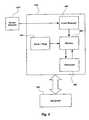
- an exemplary monitoring apparatus 120for detecting and/or determining one or more specified characteristics of a monitored event.
- the apparatus 120includes a sensor array 122 including a plurality of individual sensor elements 124 .
- the sensor elements 124may include any of various types of known sensors such as, for example, electrically conductive break-type elements, pressure transducers, accelerometers, photodiodes, phototransistors, magnetic or Hall effect-type sensors, ultrasound transmitters and receivers, piezoelectric transducers and the like.
- the sensor array 122may include multiple types of sensors arranged in combination for detection of various characteristics of the monitored event.
- the sensor array 122is operatively coupled to a programmable logic device (PLD) 126 which may include, for example, a simple programmable logic device (SPLD) (such as a programmable logic array (PLA)), a complex programmable logic device (CPLD) or a field programmable gate array (FPGA).
- PLDprogrammable logic device
- SPLDsimple programmable logic device
- CPLDcomplex programmable logic device
- FPGAfield programmable gate array
- the PLD 126desirably includes a high resolution internal clock and some memory storage capacity such as, for example, random access memory (RAM).
- RAMrandom access memory
- the sensor array 122may be coupled to and communicate with the PLD 126 by way of electrical, optical or radio frequency transmission as will be appreciated by those of ordinary skill in the art.
- the PLD 126may further be operatively coupled with a computer 128 for downloading and processing of the data acquired thereby.
- the PLD 126is configured such that each individual sensor element 124 of the sensor array 122 is independently identifiable therewith and, upon the change of state in any given sensor element 124 , the PLD 126 records which sensor element 124 experienced such a change of state and at what time the change in state occurred.
- the change of statemay be associated with a change in voltage such as, for example, if the sensor elements 124 include piezoelectric transducers.
- the PLD 126upon detecting such a change in state, the PLD 126 will note which of the sensor elements (e.g., 124 A) experienced the change, record the time at which the change took place and store the acquired information in the memory associated with the PLD 126 .
- Such a processmay be efficiently accomplished by utilizing a PLD 126 operatively coupled with the individual sensor elements 124 and configured to remain in a passive or latent state until a triggering event occurs and is detected by one or more of the sensor elements 124 .
- a PLD 126operatively coupled with the individual sensor elements 124 and configured to remain in a passive or latent state until a triggering event occurs and is detected by one or more of the sensor elements 124 .
- the use of a such a device in conjunction with a clock or timing element having high resolutionallows for more efficient gathering of data since no data is recorded or stored in memory unless and until the triggering event causes the change in state of one or more of the sensor elements 124 .
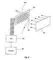
- an exemplary monitoring apparatus 120 ′is shown which is configured for acquiring data, in conjunction with a fracture testing apparatus 130 .
- the testing apparatusmay be configured to test an exemplary specimen 100 as shown and described above with reference to FIG. 1.
- the fracture testing apparatus 130may include load applying members 132 and 134 configured to apply a predetermined load to the specimen 100 . It is noted that, in another embodiment, instead of two load applying members 132 and 134 , a single load applying member may be utilized wherein a portion of the specimen 100 is secured to a stationary fixture in substantial opposition to the load applying member.
- a control system 136is operatively coupled with the fracture testing apparatus 130 to regulate and monitor the load applied to the specimen 100 and to record the magnitude of load as a function of time. As will be appreciated by those of skill in the art, such information will be significant in the analysis of the failure of the specimen 100 .
- the load applying members 132 and 134are coupled to the specimen 100 and configured to apply a load thereto in a substantially perpendicular manner relative to the axis or plane 140 along which failure is intended or expected.
- the magnitude and/or duration of the applied loadmay be set via the control system 136 .
- the applied loadmay be constant or may vary as a function of time as is desired or necessary for a given test.
- the monitoring apparatus 120 ′is utilized to detect the occurrence of a crack or fracture within the specimen 100 , as well as to determine the rate at which such a crack propagates once it is present.
- the monitoring apparatus 120 ′includes a sensor array 122 ′ having a plurality of individual sensor elements 124 ′.
- the sensor elements 124 ′may include, for example, electrically conductive break-type elements, also referred to as break-wires. Such break-wires 124 ′ may be formed of, for example, small diameter copper conductors.
- the sensor elements 124 ′may be deposited on a sheet 142 of thin material such as, for example, polyimide sheeting having an exemplary thickness of approximately 1 mil (0.001 inch) and which is commercially available from DuPont under the trademarked name KAPTON®.
- copper wires or copper traces exhibiting a thickness of approximately 3 mils (0.003 inch)may be deposited on the sheet 142 of thin material. It is noted that the break wires 124 ′ have been described as being deposited on the sheet 142 indicating that they may be left exposed on a surface thereof. However, if desired, the break wires 124 ′ may be formed within the sheet 142 or, alternatively, sandwiched between multiple sheets such that they are not exposed to the environment.
- the sensor elements 124 ′are arranged on the sheet 142 in accordance with an expected event behavior. For example, with the expectation that a failure may occur along the axis of expected failure 140 of the specimen 100 , the sensor elements 124 ′ may be arranged in a substantially parallel manner along the sheet 142 . Spacing of the sensor elements 124 ′ may vary depending on the event being monitored, the configuration of the specimen 100 being tested and the desired resolution of data acquisition. One exemplary mutual spacing of the sensor elements 124 ′ may include 0.050 inches.
- the sensor elements 124 ′are operatively coupled with a PLD which, in the exemplary embodiment shown, includes an FPGA 126 ′.
- An exemplary FPGA 126 ′may include a Spartan II® Field Programmable Gate Array commercially available from Xilinx, Inc., of San Jose, Calif., although other devices are also contemplated.
- the sheet 142may increase in material thickness for protection of the sensor elements 124 ′ in areas where event detection is not expected (e.g., locations away from the expected failure plane or axis 140 ).
- the sheet 142may increase in thickness from approximately 1 mil in the region adjacent the specimen 100 , to approximately 3 mils in the region adjacent the FPGA 126 ′.
- the FPGA 126 ′may be coupled to a computer 128 for downloading data from the FPGA 126 ′.
- the computer 128may also be utilized in conjunction with the control system 136 so as to correlate data associated with the operation of the testing apparatus 130 (e.g., load characteristics such as magnitude, duration and variation of load over time) with the data obtained from the FPGA 126 ′.
- a portion of the sheet 142may be coupled to the fracture specimen 100 adjacent the bond line of the adhesive bond 102 being tested.
- An exemplary adhesive material which may be used to adhere the sheet 142 to the specimen 100includes a cyanoacrylate adhesive (CA) although other adhesives may be utilized. It may be desirable in certain embodiments and implementations of the present invention to use an adhesive which cures to a brittle state so as to enhance the rate at which a displacement experienced by the fracture specimen 100 is transferred, via a tear or fracture in the adhesive, to the sensor elements 124 ′ for detection thereby.
- CAcyanoacrylate adhesive
- the sensor array 122 ′is configured and oriented such that the sensor elements 124 ′ are angularly positioned relative to the axis of expected failure 140 , and are desirably substantially perpendicular to the axis of expected failure 140 .
- the testing apparatus 130applies a force to the specimen 100 and electrical current is passed through the sensor elements 124 ′ of the sensor array 122 ′.
- the specimen 100Upon experiencing sufficient loading, the specimen 100 will begin to fail exhibiting a crack or fracture within the adhesive bond 102 .
- the occurrence of a crack within the adhesive bond 102will also induce a break in a sensor element 124 ′ most adjacent to the point of failure.
- the break in the sensor element 124 ′will be detected as a change in voltage by the FPGA 126 ′ which will then record the event by indicating which sensor element 124 ′ experienced a change in voltage and at what time the change in voltage (or wire breaking) occurred.
- This informationis stored in associated memory of the FPGA 126 ′ for subsequent downloading by the computer 128 and may be used, for example, in determining the location and time of crack initiation and the rate of crack propagation.
- the FPGA 126 ′desirably includes an internal clock which has resolution of, for example, approximately 10 ⁇ 6 seconds so that data may be recorded at extremely high resolution with respect to the time element.
- the FPGAmay be seen as bimodal, operable in both a passive state (which in the presently disclosed embodiment is the default state) and an event triggered active state with regard to data acquisition. While the specimen 100 is under loading but not exhibiting any failure, the FPGA 126 ′ responsively operates in a passive state in that it does not record any data or initiate any other particular functions. However, upon noting the detection of an event (e.g., a change in current or voltage) by one of the sensor elements 124 ′, the FPGA 126 ′ operates in the active state so as to identify which sensor element 124 ′ has detected the event, provide a time stamp associated with such detection, and then record such information in memory. The FPGA 126 ′ may then go back to its passive state until another event detection is made and continue in such a manner over an indefinite period of time.
- an evente.g., a change in current or voltage
- the exemplary system and apparatus shown in FIG. 3significantly reduces the cost of data acquisition over conventional electronic means discussed above herein. For example, it is estimated that such a sensor array 124 ′ may be obtained for approximately $20 while a suitable FPGA 126 ′ may be obtained for approximately $150.
- the FPGA 126 ′includes an event detector 150 configured to detect the transmission of an event from a sensor element 124 ′.
- a sensor element 124 ′may indicate that an event has occurred by way of a predetermined change in voltage or current.
- the event detectornotes the change in voltage or current and also notes from which sensor element 124 ′ of the sensor array 122 ′ (FIG. 3) such information was transmitted.
- the event detector 150records this information into memory 152 , such as on a random access memory (RAM) chip or module where, it is stored with a time stamp indicating the time at which the detection event occurred as determined by the internal clock and timing mechanism 154 .
- RAMrandom access memory
- a processor 156is coupled with the memory 152 and configures the memory with regard to which location in memory will be associated with a given sensor element 124 ′ and also reads such stored information so as to relay it to an external device such as the computer 128 .
- Communication between the FPGA 126 ′ and the computer 128may be accomplished, for example, through a universal asynchronous receiver-transmitter (UART) and an RS-232 link as will be appreciated by those of skill in the art.
- UARTuniversal asynchronous receiver-transmitter
- the FPGA 126 ′ shownis exemplary and may include additional features and components as will be recognized and appreciated by those of skill in the art. For example, various clock and software reset functions may be built into the FPGA 126 ′. Also, while the exemplary FPGA 126 ′ has been shown as including an internal clock 154 , other embodiments may include an external clock coupled with an internal timer/counter.
- a monitoring apparatus 120 ′′is shown according to another embodiment of the present invention.
- the monitoring apparatus 120 ′′is configured to monitor and detect the movement of a component 160 as it travels through a field or region.
- a sensor array 122 ′′includes a plurality of sensor elements 124 ′′.
- the sensor elements 124 ′′may include, for example photo diodes, and are coupled with a PLD 126 .
- a light source 162is positioned a spaced distance from the sensor array 122 ′′ and provides a source of light for the sensor elements 124 ′′ to detect.
- the component 160As the component 160 travels between the sensor array 122 ′′ and the light source 162 it temporarily blocks light to individual sensor elements 124 ′′. As the light is blocked from an individual sensor element 124 ′′ it indicates such to the PLD 126 by way of a signal comprising a change in current or voltage such as previously described. Again, the PLD 126 records which sensor element 124 ′′ detected the event, notes the time at which it occurred and stores such information in memory.
- the light source 162need not be employed and the triggering event associated with collecting data may be the illumination of the photo sensitive sensor elements 124 ′′ rather than the blockage of light therefrom.
- the datamay be downloaded to a computer 128 and analyzed to determine such characteristics as velocity (including both speed and direction) and acceleration of the component 160 .
- the sensor elements 124 ′′might include magnetic or Hall-effect sensors.
- such sensor elements 124 ′′may detect the induction of a magnetic field by the component 160 as it passes thereby or, alternatively, detect the change induced by the component as it travels through an already present magnetic field. The detection of such changes may again be selectively recorded by the PLD 128 and communicated to the computer 128 for appropriate processing and analysis.
- the sensor elements 124 ′′may include ultrasound receivers and the light source 162 may be replaced with ultrasound transmitters to detect characteristics of a projectile passing therethrough and altering the ultrasound signal passing between such transmitters and receivers.
- the present inventionmay be applied in various fields of endeavor to monitor and detect numerous types of events.
- a monitoring system120 , 120 ′, 120 ′′
- Such a monitoring systemmay likewise be used to detect a shock wave in virtually any medium (gas, liquid or solid), or to measure the speed of sound in a specified material.
- the present inventionmay be used to monitor the rate at which a material erodes under given parameters, such as high heat and pressure conditions including, for example, the erosion of material in a rocket motor during ignition.
- Other examplesmay include the depth of penetration of a projectile into a specified material, the trajectory of shrapnel after a detonation or explosion, or the rate of such a detonation or explosion.
- Another exemplary application of the present inventionmay be the determination of the speed of a flame front traveling down the bore of a rocket motor upon ignition thereof. Such may be detected, for example, by arranging the sensor array as a plurality of photocells which produce a voltage spike upon detecting light from the rocket's flame.
- Another exemplary application of the present inventionmay be the monitoring of the deployment of an air bag within an automobile.
- use of accelerometers or piezovelocity transducersmight be coupled to a PLD and used to monitor the deployment of an airbag in order to determine the rapidity at which such an air bag deploys and/or the force generated by such a deployment.
- Yet another exemplary application of the present inventionmay include analysis of shaped charges including the analysis of the liner upon collapse and formation of the jet produced upon detonation.
- conventional methods of monitoring shaped chargesinclude high speed photography.
- the present inventionenables high speed monitoring of the detonation of a shaped charge.
- using a two dimensional array of sensorse.g., similar to that shown an described with respect to FIG. 5
- the shape of the jetmay be mapped as the jet will manifest itself by triggering sensor elements over a substantial area of an associated sensor array rather than just triggering lineal (or curvilinear) string of sensor elements as was described with respect to monitoring a projectile.
- the present inventionmay be used for detection of events which occur over significant as well as greatly extended periods of time.
- the present inventionmay be used to detect and measure the growth of agricultural plants or the movement of the earth's crust along known fault lines.
- the present inventionmay be used for monitoring events which happen at intermediate rates as well.
- data acquisition according to the present inventionis an event triggered or event initiated process wherein only discrete and discriminate data points are recorded upon occurrence of the triggering event
- the present inventionmay be utilized in the monitoring of events which will occur, if at all, at some indeterminate future time.
- the present inventionmay be used in monitoring for an event such as an earthquake, the structural failure of a bridge or the shifting of a structure's foundation wherein the time of failure may not be for several years or decades.
- the present inventionmay operate in a passive state for a considerable period of time and requiring a minimal power draw until an event is detected at which time it would operate in an active state to collect and store the discrete and discriminate data associated with the event.
- the methodincludes establishing an event trigger as indicated at 200 .
- Establishing the event triggermay include, for example, the initiation or propagation of a crack as disclosed above.
- a monitoring apparatussuch as described above with reference to FIGS. 2 - 5 , may be used to monitor for and detect such an event trigger as shown at 202 . If an event trigger is not detected, the process continues to wait for such a detection as indicated by loop 204 . If an event trigger is detected, the location of the event trigger (e.g., which sensor element of the above described monitoring systems detected the event trigger) and the time at which the event trigger occurred is recorded in memory as shown at 206 .
- loop 208If monitoring is still desired, the process continues as indicated by loop 208 . It is noted, however, that loop 208 should not be taken to indicate a feedback loop or to indicate to the continual and sequential sampling of the sensor elements. Rather, loop 208 is simply indicative of the reiterative process of the switching between a passive state of waiting (e.g., no collection or storage of data) and an event triggered active state of recording data associated with the event trigger.
- a passive state of waitinge.g., no collection or storage of data
- the acquired datamay be extracted from memory for subsequent analysis as indicated at 212 .
- Such analysismay include, for example, creating a time map of the detected events showing the location and timing of the detected events. Further analysis may include comparing such information with other data acquired such as, for example, from the load applying apparatus 130 shown in FIG. 3.
- such a methodmay be utilized in various applications and may be carried out over various periods of time.
- the methodmay be practiced and completed in a matter of a few seconds or minutes.
- the methodmay take place over a period of weeks, months or years.
- the triggering event(s)may be, for example, associated with catastrophic failure or with the minute growth or movement of a given object.
Landscapes
- Physics & Mathematics (AREA)
- Health & Medical Sciences (AREA)
- Life Sciences & Earth Sciences (AREA)
- Chemical & Material Sciences (AREA)
- Analytical Chemistry (AREA)
- Biochemistry (AREA)
- General Health & Medical Sciences (AREA)
- General Physics & Mathematics (AREA)
- Immunology (AREA)
- Pathology (AREA)
- Testing Of Devices, Machine Parts, Or Other Structures Thereof (AREA)
Abstract
Description
- [0001] The United States Government has rights in the following invention pursuant to Contract No. NAS8-97238 between NASA and Thiokol Corporation.
- 1. Field of the Invention[0002]
- The present invention relates generally to the detection and determination of an event characteristic and, more particularly, to detecting and determining one or more characteristics of an event, such as, for example, the material failure of a monitored component.[0003]
- 2. State of the Art[0004]
- It is often desirable to detect and determine various event characteristics associated with the physical response or reaction of a given component or material when subjected to various influences such as, for example, application of a force or exposure to a specific environment for given period of time. It is desirable to determine the response of such a component so as to accurately predict future behavior and to properly design systems and components which react and perform in a predictable manner.[0005]
- For example, material testing is often performed to determine mechanical behavior of a specific material or a particular component configuration under specified conditions. Such behavior might include the determination of, for example, yield strength, fracture toughness, impact strength, fatigue limits, temperature induced effects, corrosion or degradation rates, crack rate propagation or any of a number of other mechanical, material or physical properties.[0006]
- In a more particular example, fracture tests are conventionally conducted to determine the fracture energy of an adhesive bond. One such fracture test is known as a tapered double cantilevered beam (TDCB) test. As shown in FIG. 1, a TDCB test involves a[0007]
test specimen 100 having anadhesive bond 102 between two similarly configuredtapered beams beam beams beams beams adhesive bond 102 which is then monitored for material failure which manifests itself through propagation of a crack. - Conventional means of monitoring the[0008]
adhesive bond 102 for failure include visual inspection and/or use of electronic equipment including, for example, one or more resistive-type propagation gages adhered to the location of interest (e.g., adjacent the adhesive bond102) and electrically coupled to a data acquisition system. Such conventional means of monitoring the adhesive bond are labor intensive and, particularly when utilizing electronic equipment, involve considerable expense. Furthermore, such conventional means are not highly efficient. For example, if a testing specimen becomes unstable, a crack may propagate at a very high rate approaching the speed of sound for the given material being tested. In such a circumstance, it becomes impossible to obtain useful information about the crack propagation by way of visual inspection. - On the other hand, when using conventional electronic monitoring equipment, data is continuously collected over time and sample rates of up to several megahertz are required for accurate data acquisition. Thus, if a testing specimen fails over a period of time which is in excess of, for example, twenty minutes, the acquired data will include several billion data points for subsequent processing and analysis. Storing such a large amount of data wastes valuable memory or storage space since only a few of the collected data points are actually relevant and desirable for purposes of proper fracture analysis.[0009]
- Additionally, as alluded to above, the cost associated with the equipment capable of sampling and recording such a large number of data points may often be prohibitive. For example, an individual resistive-type propagation gage may cost $300 (and isn't reusable) while the data acquisition equipment having an adequate sample rate may cost $8,000-$10,000 or more.[0010]
- In view of the shortcomings in the art, it would be advantageous to provide an apparatus and method for determining event characteristics, such as, for example, acquiring data relative to a material or component failure, which is simple in its operation and configuration, highly efficient and relatively inexpensive.[0011]
- In accordance with one aspect of the invention an apparatus is provided for monitoring and detecting event characteristics. The apparatus includes a sensor array including a plurality of sensor elements. A programmable logic device (PLD) is operatively coupled to the plurality of sensor elements. The PLD is configured to operate in a default passive state and an event triggered active state. A change of state detected by any of the sensor elements may cause the PLD to switch from the passive state to the active state wherein data associated with the change of state may be stored in memory.[0012]
- The apparatus may include as sensor elements, for example, break-wire sensors, piezoelectric sensors, photosensitive sensors or magnetic type sensors. The apparatus may further include as a PLD, for example, a simple or complex PLD or a field programmable gate array (FPGA).[0013]
- In accordance with another aspect of the present invention, a system is provided for determining fracture characteristics of an adhesive material. The system includes a test specimen comprised of a first member and a second member which are coupled together with the adhesive material. A load applying apparatus which includes at least one load applying member is configured to apply a load to the test specimen such that the first and second members are loaded in a cantilevered manner.[0014]
- A plurality of break-wire conductors are coupled the test specimen such that they traverse the adhesive bond. The break-wire conductors may be disposed on a thin sheet of dielectric material such as, for example, a polymer, to maintain a desired configuration and orientation with respect to the test specimen.[0015]
- A PLD is operatively coupled to the plurality break-wire conductors and is configured to operate in a passive state and an active state. Upon the breaking of one of any of the plurality of break-wire conductors, the PLD records information in memory regarding which of the break-wire conductors broke and at what time it broke.[0016]
- In accordance with another aspect of the present invention, a method is provided for monitoring an event. The method includes establishing an event trigger such as, for example, the initiation or propagation of a crack in a material failure. A plurality of sensor elements is provided with each sensor element being configured to individually detect the event trigger. A PLD is provided and configured to operated in a passive state and an active state. Upon the detection of an event trigger in one or more of the sensor elements, the PLD switches from the passive state to the active state and data is recorded and stored corresponding with the detection of the event trigger. Such data may include which of the plurality sensor elements detected the event trigger and at what time the event trigger was detected thereby.[0017]
- The foregoing and other advantages of the invention will become apparent upon reading the following detailed description and upon reference to the drawings in which:[0018]
- FIG. 1 is a perspective view of an exemplary conventional configuration used in one type of fracture testing;[0019]
- FIG. 2 shows an apparatus used in acquiring characteristic data associated with an event according to an embodiment of the present invention;[0020]
- FIG. 3 shows an exemplary apparatus used in acquiring data associated with a material test according to an embodiment of the present invention;[0021]
- FIG. 4 is a schematic showing the input and output functions of a controller utilized in accordance with the present invention;[0022]
- FIG. 5 shows an exemplary apparatus used in acquiring data associated with mapping the velocity and acceleration of a projectile according to an embodiment of the present invention; and[0023]
- FIG. 6 is a flow chart showing the method of detecting and determining an event characteristic according to an embodiment of the present invention[0024]
- Referring to FIG. 2, an[0025]
exemplary monitoring apparatus 120 is shown for detecting and/or determining one or more specified characteristics of a monitored event. Theapparatus 120 includes asensor array 122 including a plurality ofindividual sensor elements 124. Thesensor elements 124 may include any of various types of known sensors such as, for example, electrically conductive break-type elements, pressure transducers, accelerometers, photodiodes, phototransistors, magnetic or Hall effect-type sensors, ultrasound transmitters and receivers, piezoelectric transducers and the like. Further, in some embodiments, thesensor array 122 may include multiple types of sensors arranged in combination for detection of various characteristics of the monitored event. - The[0026]
sensor array 122 is operatively coupled to a programmable logic device (PLD)126 which may include, for example, a simple programmable logic device (SPLD) (such as a programmable logic array (PLA)), a complex programmable logic device (CPLD) or a field programmable gate array (FPGA). As shall be discussed in more detail below, thePLD 126 desirably includes a high resolution internal clock and some memory storage capacity such as, for example, random access memory (RAM). - The[0027]
sensor array 122 may be coupled to and communicate with thePLD 126 by way of electrical, optical or radio frequency transmission as will be appreciated by those of ordinary skill in the art. ThePLD 126 may further be operatively coupled with acomputer 128 for downloading and processing of the data acquired thereby. - The[0028]
PLD 126 is configured such that eachindividual sensor element 124 of thesensor array 122 is independently identifiable therewith and, upon the change of state in any givensensor element 124, thePLD 126 records whichsensor element 124 experienced such a change of state and at what time the change in state occurred. For example, the change of state may be associated with a change in voltage such as, for example, if thesensor elements 124 include piezoelectric transducers. Thus, upon detecting such a change in state, thePLD 126 will note which of the sensor elements (e.g.,124A) experienced the change, record the time at which the change took place and store the acquired information in the memory associated with thePLD 126. - Acquiring event information in such a manner enables extraneous information (i.e., data which might be collected from the sensor elements when no change of state is occurring) to be excluded. As noted above, such extraneous information is largely irrelevant and wastes valuable memory or storage space. Thus, the acquisition of data in accordance with the present invention may be termed as being selective and “on-demand.” In other words, data acquisition is an event-triggered or event-initiated process such that only discrete and discriminate data points are recorded upon occurrence of the triggering event (e.g. that which causes the change in state in a sensor element). Such is in contradistinction to the continual collection of data, regardless of its relevance, as is done in conventional prior art systems and processes.[0029]
- Such a process may be efficiently accomplished by utilizing a[0030]
PLD 126 operatively coupled with theindividual sensor elements 124 and configured to remain in a passive or latent state until a triggering event occurs and is detected by one or more of thesensor elements 124. As will be addressed in further detail below, the use of a such a device in conjunction with a clock or timing element having high resolution allows for more efficient gathering of data since no data is recorded or stored in memory unless and until the triggering event causes the change in state of one or more of thesensor elements 124. - Referring now to FIG. 3, an[0031]
exemplary monitoring apparatus 120′ is shown which is configured for acquiring data, in conjunction with afracture testing apparatus 130. The testing apparatus may be configured to test anexemplary specimen 100 as shown and described above with reference to FIG. 1. Thefracture testing apparatus 130 may includeload applying members specimen 100. It is noted that, in another embodiment, instead of twoload applying members specimen 100 is secured to a stationary fixture in substantial opposition to the load applying member. - A[0032]
control system 136 is operatively coupled with thefracture testing apparatus 130 to regulate and monitor the load applied to thespecimen 100 and to record the magnitude of load as a function of time. As will be appreciated by those of skill in the art, such information will be significant in the analysis of the failure of thespecimen 100. - The[0033]
load applying members specimen 100 and configured to apply a load thereto in a substantially perpendicular manner relative to the axis orplane 140 along which failure is intended or expected. The magnitude and/or duration of the applied load may be set via thecontrol system 136. The applied load may be constant or may vary as a function of time as is desired or necessary for a given test. - With the load being applied by the[0034]
testing apparatus 130, themonitoring apparatus 120′ is utilized to detect the occurrence of a crack or fracture within thespecimen 100, as well as to determine the rate at which such a crack propagates once it is present. - The[0035]
monitoring apparatus 120′ includes asensor array 122′ having a plurality ofindividual sensor elements 124′. Thesensor elements 124′ may include, for example, electrically conductive break-type elements, also referred to as break-wires. Such break-wires 124′ may be formed of, for example, small diameter copper conductors. Thesensor elements 124′ may be deposited on asheet 142 of thin material such as, for example, polyimide sheeting having an exemplary thickness of approximately 1 mil (0.001 inch) and which is commercially available from DuPont under the trademarked name KAPTON®. In one exemplary embodiment, copper wires or copper traces exhibiting a thickness of approximately 3 mils (0.003 inch) may be deposited on thesheet 142 of thin material. It is noted that thebreak wires 124′ have been described as being deposited on thesheet 142 indicating that they may be left exposed on a surface thereof. However, if desired, thebreak wires 124′ may be formed within thesheet 142 or, alternatively, sandwiched between multiple sheets such that they are not exposed to the environment. - The[0036]
sensor elements 124′ are arranged on thesheet 142 in accordance with an expected event behavior. For example, with the expectation that a failure may occur along the axis of expectedfailure 140 of thespecimen 100, thesensor elements 124′ may be arranged in a substantially parallel manner along thesheet 142. Spacing of thesensor elements 124′ may vary depending on the event being monitored, the configuration of thespecimen 100 being tested and the desired resolution of data acquisition. One exemplary mutual spacing of thesensor elements 124′ may include 0.050 inches. - The[0037]
sensor elements 124′ are operatively coupled with a PLD which, in the exemplary embodiment shown, includes anFPGA 126′. Anexemplary FPGA 126′ may include a Spartan II® Field Programmable Gate Array commercially available from Xilinx, Inc., of San Jose, Calif., although other devices are also contemplated. - It is noted that, as the[0038]
sensor elements 124′ extend toward theFPGA 126′, thesheet 142, which likewise extends towards theFPGA 126′, may increase in material thickness for protection of thesensor elements 124′ in areas where event detection is not expected (e.g., locations away from the expected failure plane or axis140). Thus, for example, thesheet 142 may increase in thickness from approximately 1 mil in the region adjacent thespecimen 100, to approximately 3 mils in the region adjacent theFPGA 126′. - As with previously described embodiments, the[0039]
FPGA 126′ may be coupled to acomputer 128 for downloading data from theFPGA 126′. Thecomputer 128 may also be utilized in conjunction with thecontrol system 136 so as to correlate data associated with the operation of the testing apparatus130 (e.g., load characteristics such as magnitude, duration and variation of load over time) with the data obtained from theFPGA 126′. - For testing purposes, a portion of the[0040]
sheet 142 may be coupled to thefracture specimen 100 adjacent the bond line of theadhesive bond 102 being tested. An exemplary adhesive material which may be used to adhere thesheet 142 to thespecimen 100 includes a cyanoacrylate adhesive (CA) although other adhesives may be utilized. It may be desirable in certain embodiments and implementations of the present invention to use an adhesive which cures to a brittle state so as to enhance the rate at which a displacement experienced by thefracture specimen 100 is transferred, via a tear or fracture in the adhesive, to thesensor elements 124′ for detection thereby. - The[0041]
sensor array 122′ is configured and oriented such that thesensor elements 124′ are angularly positioned relative to the axis of expectedfailure 140, and are desirably substantially perpendicular to the axis of expectedfailure 140. - In operation, the[0042]
testing apparatus 130 applies a force to thespecimen 100 and electrical current is passed through thesensor elements 124′ of thesensor array 122′. Upon experiencing sufficient loading, thespecimen 100 will begin to fail exhibiting a crack or fracture within theadhesive bond 102. The occurrence of a crack within theadhesive bond 102 will also induce a break in asensor element 124′ most adjacent to the point of failure. The break in thesensor element 124′ will be detected as a change in voltage by theFPGA 126′ which will then record the event by indicating whichsensor element 124′ experienced a change in voltage and at what time the change in voltage (or wire breaking) occurred. This information is stored in associated memory of theFPGA 126′ for subsequent downloading by thecomputer 128 and may be used, for example, in determining the location and time of crack initiation and the rate of crack propagation. - As a crack grows or propagates,[0043]
additional sensor elements 124′ will break, with each in turn registering the same with theFPGA 126′ to be stored in memory along with an associated time stamp. TheFPGA 126′ desirably includes an internal clock which has resolution of, for example, approximately 10−6seconds so that data may be recorded at extremely high resolution with respect to the time element. - Thus, during testing, the FPGA may be seen as bimodal, operable in both a passive state (which in the presently disclosed embodiment is the default state) and an event triggered active state with regard to data acquisition. While the[0044]
specimen 100 is under loading but not exhibiting any failure, theFPGA 126′ responsively operates in a passive state in that it does not record any data or initiate any other particular functions. However, upon noting the detection of an event (e.g., a change in current or voltage) by one of thesensor elements 124′, theFPGA 126′ operates in the active state so as to identify whichsensor element 124′ has detected the event, provide a time stamp associated with such detection, and then record such information in memory. TheFPGA 126′ may then go back to its passive state until another event detection is made and continue in such a manner over an indefinite period of time. - It is noted that the exemplary system and apparatus shown in FIG. 3 significantly reduces the cost of data acquisition over conventional electronic means discussed above herein. For example, it is estimated that such a[0045]
sensor array 124′ may be obtained for approximately $20 while asuitable FPGA 126′ may be obtained for approximately $150. - Referring briefly to FIG. 4, a schematic is shown of an[0046]
exemplary FPGA 126′. TheFPGA 126′ includes anevent detector 150 configured to detect the transmission of an event from asensor element 124′. Thus, for example, asensor element 124′ may indicate that an event has occurred by way of a predetermined change in voltage or current. The event detector notes the change in voltage or current and also notes from whichsensor element 124′ of thesensor array 122′ (FIG. 3) such information was transmitted. Theevent detector 150 records this information intomemory 152, such as on a random access memory (RAM) chip or module where, it is stored with a time stamp indicating the time at which the detection event occurred as determined by the internal clock andtiming mechanism 154. - A[0047]
processor 156 is coupled with thememory 152 and configures the memory with regard to which location in memory will be associated with a givensensor element 124′ and also reads such stored information so as to relay it to an external device such as thecomputer 128. Communication between theFPGA 126′ and thecomputer 128 may be accomplished, for example, through a universal asynchronous receiver-transmitter (UART) and an RS-232 link as will be appreciated by those of skill in the art. - It is noted that the[0048]
FPGA 126′ shown is exemplary and may include additional features and components as will be recognized and appreciated by those of skill in the art. For example, various clock and software reset functions may be built into theFPGA 126′. Also, while theexemplary FPGA 126′ has been shown as including aninternal clock 154, other embodiments may include an external clock coupled with an internal timer/counter. - Referring now to FIG. 5, a[0049]
monitoring apparatus 120″ is shown according to another embodiment of the present invention. Themonitoring apparatus 120″ is configured to monitor and detect the movement of acomponent 160 as it travels through a field or region. As with previous embodiments, asensor array 122″ includes a plurality ofsensor elements 124″. Thesensor elements 124″ may include, for example photo diodes, and are coupled with aPLD 126. Alight source 162 is positioned a spaced distance from thesensor array 122″ and provides a source of light for thesensor elements 124″ to detect. - As the[0050]
component 160 travels between thesensor array 122″ and thelight source 162 it temporarily blocks light toindividual sensor elements 124″. As the light is blocked from anindividual sensor element 124″ it indicates such to thePLD 126 by way of a signal comprising a change in current or voltage such as previously described. Again, thePLD 126 records whichsensor element 124″ detected the event, notes the time at which it occurred and stores such information in memory. - It is noted that in certain embodiments wherein the projectile or object being monitored emits light, the[0051]
light source 162 need not be employed and the triggering event associated with collecting data may be the illumination of the photosensitive sensor elements 124″ rather than the blockage of light therefrom. - In either case, as the plurality of[0052]
sensor elements 124″ record data, the data may be downloaded to acomputer 128 and analyzed to determine such characteristics as velocity (including both speed and direction) and acceleration of thecomponent 160. - In another embodiment, the[0053]
sensor elements 124″ might include magnetic or Hall-effect sensors. Thus,such sensor elements 124″ may detect the induction of a magnetic field by thecomponent 160 as it passes thereby or, alternatively, detect the change induced by the component as it travels through an already present magnetic field. The detection of such changes may again be selectively recorded by thePLD 128 and communicated to thecomputer 128 for appropriate processing and analysis. - In yet another embodiment, the[0054]
sensor elements 124″ may include ultrasound receivers and thelight source 162 may be replaced with ultrasound transmitters to detect characteristics of a projectile passing therethrough and altering the ultrasound signal passing between such transmitters and receivers. - It is noted that, while described in terms of exemplary embodiments, the present invention may be applied in various fields of endeavor to monitor and detect numerous types of events. For example, such a monitoring system ([0055]120,120′,120″) may be used to detect one or more event characteristics in association with various structural failures including the rupturing of a pressure vessel (including the location, rate and direction of such a rupture), an explosion or detonation, a vehicle crash or collision. Such a monitoring system may likewise be used to detect a shock wave in virtually any medium (gas, liquid or solid), or to measure the speed of sound in a specified material. Furthermore, the present invention may be used to monitor the rate at which a material erodes under given parameters, such as high heat and pressure conditions including, for example, the erosion of material in a rocket motor during ignition. Other examples may include the depth of penetration of a projectile into a specified material, the trajectory of shrapnel after a detonation or explosion, or the rate of such a detonation or explosion.
- Another exemplary application of the present invention may be the determination of the speed of a flame front traveling down the bore of a rocket motor upon ignition thereof. Such may be detected, for example, by arranging the sensor array as a plurality of photocells which produce a voltage spike upon detecting light from the rocket's flame.[0056]
- Another exemplary application of the present invention may be the monitoring of the deployment of an air bag within an automobile. For example, use of accelerometers or piezovelocity transducers might be coupled to a PLD and used to monitor the deployment of an airbag in order to determine the rapidity at which such an air bag deploys and/or the force generated by such a deployment.[0057]
- Yet another exemplary application of the present invention may include analysis of shaped charges including the analysis of the liner upon collapse and formation of the jet produced upon detonation. For example, conventional methods of monitoring shaped charges include high speed photography. However, the present invention enables high speed monitoring of the detonation of a shaped charge. Furthermore, using a two dimensional array of sensors (e.g., similar to that shown an described with respect to FIG. 5) the shape of the jet may be mapped as the jet will manifest itself by triggering sensor elements over a substantial area of an associated sensor array rather than just triggering lineal (or curvilinear) string of sensor elements as was described with respect to monitoring a projectile.[0058]
- Additionally, if multiple types of sensor elements are utilized, other characteristics may be monitored. For example, if photo sensitive and magnetic sensor elements are strategically combined, one may analyze the jet produced upon detonation with the photo sensitive sensor elements and also analyze the effect of detonation upon the liner with the magnetic sensors if the liner is constructed with a ferromagnetic material.[0059]
- It is further noted, that while the above exemplary embodiments have discussed events which occur in a relatively short period of time, the present invention may be used for detection of events which occur over significant as well as greatly extended periods of time. For example, the present invention may be used to detect and measure the growth of agricultural plants or the movement of the earth's crust along known fault lines. Of course, the present invention may be used for monitoring events which happen at intermediate rates as well.[0060]
- Because data acquisition according to the present invention is an event triggered or event initiated process wherein only discrete and discriminate data points are recorded upon occurrence of the triggering event, the present invention may be utilized in the monitoring of events which will occur, if at all, at some indeterminate future time. For example, the present invention may be used in monitoring for an event such as an earthquake, the structural failure of a bridge or the shifting of a structure's foundation wherein the time of failure may not be for several years or decades. Thus, as described above, the present invention may operate in a passive state for a considerable period of time and requiring a minimal power draw until an event is detected at which time it would operate in an active state to collect and store the discrete and discriminate data associated with the event.[0061]
- Referring now to FIG. 6, a method is shown for detecting and determining event characteristics according to an embodiment of the present invention. The method includes establishing an event trigger as indicated at[0062]200. Establishing the event trigger may include, for example, the initiation or propagation of a crack as disclosed above. Once an event trigger is established, a monitoring apparatus, such as described above with reference to FIGS.2-5, may be used to monitor for and detect such an event trigger as shown at202. If an event trigger is not detected, the process continues to wait for such a detection as indicated by
loop 204. If an event trigger is detected, the location of the event trigger (e.g., which sensor element of the above described monitoring systems detected the event trigger) and the time at which the event trigger occurred is recorded in memory as shown at206. - If monitoring is still desired, the process continues as indicated by[0063]
loop 208. It is noted, however, thatloop 208 should not be taken to indicate a feedback loop or to indicate to the continual and sequential sampling of the sensor elements. Rather,loop 208 is simply indicative of the reiterative process of the switching between a passive state of waiting (e.g., no collection or storage of data) and an event triggered active state of recording data associated with the event trigger. - If the monitoring process is halted, either by a system command (for example due to the passage of a predetermined period of time without the occurrence of another event trigger) or by some type of manual override as indicated at[0064]210, the acquired data may be extracted from memory for subsequent analysis as indicated at212. Such analysis may include, for example, creating a time map of the detected events showing the location and timing of the detected events. Further analysis may include comparing such information with other data acquired such as, for example, from the
load applying apparatus 130 shown in FIG. 3. - As noted above, such a method may be utilized in various applications and may be carried out over various periods of time. For example, the method may be practiced and completed in a matter of a few seconds or minutes. On the other hand, the method may take place over a period of weeks, months or years. Similarly, the triggering event(s) may be, for example, associated with catastrophic failure or with the minute growth or movement of a given object.[0065]
- While the invention may be susceptible to various modifications and alternative forms, specific embodiments have been shown by way of example in the drawings and have been described in detail herein. However, it should be understood that the invention is not intended to be limited to the particular forms disclosed. Rather, the invention includes all modifications, equivalents, and alternatives falling within the spirit and scope of the invention as defined by the following appended claims.[0066]
Claims (48)
Priority Applications (1)
| Application Number | Priority Date | Filing Date | Title |
|---|---|---|---|
| US10/208,518US7240564B2 (en) | 2002-07-30 | 2002-07-30 | Method and apparatus for detecting and determining event characteristics with reduced data collection |
Applications Claiming Priority (1)
| Application Number | Priority Date | Filing Date | Title |
|---|---|---|---|
| US10/208,518US7240564B2 (en) | 2002-07-30 | 2002-07-30 | Method and apparatus for detecting and determining event characteristics with reduced data collection |
Publications (2)
| Publication Number | Publication Date |
|---|---|
| US20040025091A1true US20040025091A1 (en) | 2004-02-05 |
| US7240564B2 US7240564B2 (en) | 2007-07-10 |
Family
ID=31186837
Family Applications (1)
| Application Number | Title | Priority Date | Filing Date |
|---|---|---|---|
| US10/208,518Expired - Fee RelatedUS7240564B2 (en) | 2002-07-30 | 2002-07-30 | Method and apparatus for detecting and determining event characteristics with reduced data collection |
Country Status (1)
| Country | Link |
|---|---|
| US (1) | US7240564B2 (en) |
Cited By (16)
| Publication number | Priority date | Publication date | Assignee | Title |
|---|---|---|---|---|
| US8501620B2 (en) | 2008-12-10 | 2013-08-06 | Novellus Systems, Inc. | Method for depositing tungsten film having low resistivity, low roughness and high reflectivity |
| US8835317B2 (en) | 2009-08-04 | 2014-09-16 | Novellus Systems, Inc. | Depositing tungsten into high aspect ratio features |
| US9034768B2 (en) | 2010-07-09 | 2015-05-19 | Novellus Systems, Inc. | Depositing tungsten into high aspect ratio features |
| US9082826B2 (en) | 2013-05-24 | 2015-07-14 | Lam Research Corporation | Methods and apparatuses for void-free tungsten fill in three-dimensional semiconductor features |
| US9240347B2 (en) | 2012-03-27 | 2016-01-19 | Novellus Systems, Inc. | Tungsten feature fill |
| US9548228B2 (en) | 2009-08-04 | 2017-01-17 | Lam Research Corporation | Void free tungsten fill in different sized features |
| US9972504B2 (en) | 2015-08-07 | 2018-05-15 | Lam Research Corporation | Atomic layer etching of tungsten for enhanced tungsten deposition fill |
| US9978610B2 (en) | 2015-08-21 | 2018-05-22 | Lam Research Corporation | Pulsing RF power in etch process to enhance tungsten gapfill performance |
| US10256142B2 (en) | 2009-08-04 | 2019-04-09 | Novellus Systems, Inc. | Tungsten feature fill with nucleation inhibition |
| US20190324592A1 (en)* | 2012-10-04 | 2019-10-24 | Corning Incorporated | Pressure sensing touch systems and methods |
| US10566211B2 (en) | 2016-08-30 | 2020-02-18 | Lam Research Corporation | Continuous and pulsed RF plasma for etching metals |
| US10638675B2 (en)* | 2011-02-25 | 2020-05-05 | The Toro Company | Irrigation controller with weather station |
| US11167711B2 (en)* | 2019-02-20 | 2021-11-09 | Faurecia Interior Systems, Inc. | Airbag deployment data collection |
| JP2022023451A (en)* | 2020-07-27 | 2022-02-08 | Agc株式会社 | Splitting adhesion strength testing machine |
| WO2025078745A1 (en)* | 2023-10-13 | 2025-04-17 | Safran Aircraft Engines | Improved test for characterising the fracture toughness of interfaces in mode ii and associated test specimen |
| US12444651B2 (en) | 2022-06-28 | 2025-10-14 | Novellus Systems, Inc. | Tungsten feature fill with nucleation inhibition |
Families Citing this family (2)
| Publication number | Priority date | Publication date | Assignee | Title |
|---|---|---|---|---|
| JP4752245B2 (en)* | 2004-11-16 | 2011-08-17 | 株式会社日立製作所 | Sensor drive control method and wireless terminal device with sensor |
| US11519836B1 (en)* | 2022-04-13 | 2022-12-06 | Tactun Llc | FPGA-based materials testing |
Citations (20)
| Publication number | Priority date | Publication date | Assignee | Title |
|---|---|---|---|---|
| US3858439A (en)* | 1971-02-25 | 1975-01-07 | Gen Dynamics Corp | Method and apparatus for acoustic emission non- destructive testing |
| US4559946A (en)* | 1982-06-18 | 1985-12-24 | Mieczyslaw Mirowski | Method and apparatus for correcting abnormal cardiac activity by low energy shocks |
| US4831325A (en)* | 1987-04-01 | 1989-05-16 | General Signal Corporation | Capacitance measuring circuit |
| US5023901A (en)* | 1988-08-22 | 1991-06-11 | Vorec Corporation | Surveillance system having a voice verification unit |
| US5319291A (en)* | 1993-02-17 | 1994-06-07 | Pitney Bowes Inc. | Brushless motor utilizing FET drivers |
| US5389795A (en)* | 1991-02-11 | 1995-02-14 | Rye; Timothy W. | Method and apparatus for directing air and optical signals to detect edge cracks and other absences of product |
| US5519643A (en)* | 1991-07-18 | 1996-05-21 | Robert Bosch Gmbh | Method of operating a microprocessor |
| US5563526A (en)* | 1994-01-03 | 1996-10-08 | Texas Instruments Incorporated | Programmable mixed-mode integrated circuit architecture |
| US5959214A (en)* | 1997-12-22 | 1999-09-28 | Delco Electronics Corp. | Strain gauge with steel substrate |
| US6055180A (en)* | 1997-06-17 | 2000-04-25 | Thin Film Electronics Asa | Electrically addressable passive device, method for electrical addressing of the same and uses of the device and the method |
| US6243242B1 (en)* | 1998-08-18 | 2001-06-05 | Richard F. Davis | Photographic lightning trigger devices |
| US6269179B1 (en)* | 1996-05-31 | 2001-07-31 | Georgia Tech Research Corporation | Inspection system and method for bond detection and validation of surface mount devices using sensor fusion and active perception |
| US6281564B1 (en)* | 1996-10-18 | 2001-08-28 | California Micro Devices, Inc. | Programmable integrated passive devices |
| US6303916B1 (en)* | 1998-12-24 | 2001-10-16 | Mitutoyo Corporation | Systems and methods for generating reproducible illumination |
| US6386038B1 (en)* | 1999-11-24 | 2002-05-14 | Lewis, Iii Carl Edwin | Acoustic apparatus and inspection methods |
| US6388404B1 (en)* | 1996-01-03 | 2002-05-14 | Decotex 2000 Corporation | Remote controlled window treatment and/or lighting system |
| US6666857B2 (en)* | 2002-01-29 | 2003-12-23 | Robert F. Smith | Integrated wavefront-directed topography-controlled photoablation |
| US6741177B2 (en)* | 2002-03-28 | 2004-05-25 | Verifeye Inc. | Method and apparatus for detecting items on the bottom tray of a cart |
| US6791085B2 (en)* | 2000-11-30 | 2004-09-14 | Commissariat A L'energie Atomique | Infrared radiation detection device |
| US6963036B1 (en)* | 2002-11-01 | 2005-11-08 | Heinz Zicher | Accurate, high speed weighing apparatus and method |
Family Cites Families (1)
| Publication number | Priority date | Publication date | Assignee | Title |
|---|---|---|---|---|
| GB9919975D0 (en) | 1999-08-24 | 1999-10-27 | Philipp Harald | Seat occupancy sensor for vehicular use |
- 2002
- 2002-07-30USUS10/208,518patent/US7240564B2/ennot_activeExpired - Fee Related
Patent Citations (20)
| Publication number | Priority date | Publication date | Assignee | Title |
|---|---|---|---|---|
| US3858439A (en)* | 1971-02-25 | 1975-01-07 | Gen Dynamics Corp | Method and apparatus for acoustic emission non- destructive testing |
| US4559946A (en)* | 1982-06-18 | 1985-12-24 | Mieczyslaw Mirowski | Method and apparatus for correcting abnormal cardiac activity by low energy shocks |
| US4831325A (en)* | 1987-04-01 | 1989-05-16 | General Signal Corporation | Capacitance measuring circuit |
| US5023901A (en)* | 1988-08-22 | 1991-06-11 | Vorec Corporation | Surveillance system having a voice verification unit |
| US5389795A (en)* | 1991-02-11 | 1995-02-14 | Rye; Timothy W. | Method and apparatus for directing air and optical signals to detect edge cracks and other absences of product |
| US5519643A (en)* | 1991-07-18 | 1996-05-21 | Robert Bosch Gmbh | Method of operating a microprocessor |
| US5319291A (en)* | 1993-02-17 | 1994-06-07 | Pitney Bowes Inc. | Brushless motor utilizing FET drivers |
| US5563526A (en)* | 1994-01-03 | 1996-10-08 | Texas Instruments Incorporated | Programmable mixed-mode integrated circuit architecture |
| US6388404B1 (en)* | 1996-01-03 | 2002-05-14 | Decotex 2000 Corporation | Remote controlled window treatment and/or lighting system |
| US6269179B1 (en)* | 1996-05-31 | 2001-07-31 | Georgia Tech Research Corporation | Inspection system and method for bond detection and validation of surface mount devices using sensor fusion and active perception |
| US6281564B1 (en)* | 1996-10-18 | 2001-08-28 | California Micro Devices, Inc. | Programmable integrated passive devices |
| US6055180A (en)* | 1997-06-17 | 2000-04-25 | Thin Film Electronics Asa | Electrically addressable passive device, method for electrical addressing of the same and uses of the device and the method |
| US5959214A (en)* | 1997-12-22 | 1999-09-28 | Delco Electronics Corp. | Strain gauge with steel substrate |
| US6243242B1 (en)* | 1998-08-18 | 2001-06-05 | Richard F. Davis | Photographic lightning trigger devices |
| US6303916B1 (en)* | 1998-12-24 | 2001-10-16 | Mitutoyo Corporation | Systems and methods for generating reproducible illumination |
| US6386038B1 (en)* | 1999-11-24 | 2002-05-14 | Lewis, Iii Carl Edwin | Acoustic apparatus and inspection methods |
| US6791085B2 (en)* | 2000-11-30 | 2004-09-14 | Commissariat A L'energie Atomique | Infrared radiation detection device |
| US6666857B2 (en)* | 2002-01-29 | 2003-12-23 | Robert F. Smith | Integrated wavefront-directed topography-controlled photoablation |
| US6741177B2 (en)* | 2002-03-28 | 2004-05-25 | Verifeye Inc. | Method and apparatus for detecting items on the bottom tray of a cart |
| US6963036B1 (en)* | 2002-11-01 | 2005-11-08 | Heinz Zicher | Accurate, high speed weighing apparatus and method |
Cited By (23)
| Publication number | Priority date | Publication date | Assignee | Title |
|---|---|---|---|---|
| US9589835B2 (en) | 2008-12-10 | 2017-03-07 | Novellus Systems, Inc. | Method for forming tungsten film having low resistivity, low roughness and high reflectivity |
| US8501620B2 (en) | 2008-12-10 | 2013-08-06 | Novellus Systems, Inc. | Method for depositing tungsten film having low resistivity, low roughness and high reflectivity |
| US10103058B2 (en) | 2009-08-04 | 2018-10-16 | Novellus Systems, Inc. | Tungsten feature fill |
| US9548228B2 (en) | 2009-08-04 | 2017-01-17 | Lam Research Corporation | Void free tungsten fill in different sized features |
| US9653353B2 (en) | 2009-08-04 | 2017-05-16 | Novellus Systems, Inc. | Tungsten feature fill |
| US8835317B2 (en) | 2009-08-04 | 2014-09-16 | Novellus Systems, Inc. | Depositing tungsten into high aspect ratio features |
| US10256142B2 (en) | 2009-08-04 | 2019-04-09 | Novellus Systems, Inc. | Tungsten feature fill with nucleation inhibition |
| US9034768B2 (en) | 2010-07-09 | 2015-05-19 | Novellus Systems, Inc. | Depositing tungsten into high aspect ratio features |
| US10638675B2 (en)* | 2011-02-25 | 2020-05-05 | The Toro Company | Irrigation controller with weather station |
| US9240347B2 (en) | 2012-03-27 | 2016-01-19 | Novellus Systems, Inc. | Tungsten feature fill |
| US20190324592A1 (en)* | 2012-10-04 | 2019-10-24 | Corning Incorporated | Pressure sensing touch systems and methods |
| US9082826B2 (en) | 2013-05-24 | 2015-07-14 | Lam Research Corporation | Methods and apparatuses for void-free tungsten fill in three-dimensional semiconductor features |
| US9972504B2 (en) | 2015-08-07 | 2018-05-15 | Lam Research Corporation | Atomic layer etching of tungsten for enhanced tungsten deposition fill |
| US11069535B2 (en) | 2015-08-07 | 2021-07-20 | Lam Research Corporation | Atomic layer etch of tungsten for enhanced tungsten deposition fill |
| US10395944B2 (en) | 2015-08-21 | 2019-08-27 | Lam Research Corporation | Pulsing RF power in etch process to enhance tungsten gapfill performance |
| US9978610B2 (en) | 2015-08-21 | 2018-05-22 | Lam Research Corporation | Pulsing RF power in etch process to enhance tungsten gapfill performance |
| US10566211B2 (en) | 2016-08-30 | 2020-02-18 | Lam Research Corporation | Continuous and pulsed RF plasma for etching metals |
| US11167711B2 (en)* | 2019-02-20 | 2021-11-09 | Faurecia Interior Systems, Inc. | Airbag deployment data collection |
| JP2022023451A (en)* | 2020-07-27 | 2022-02-08 | Agc株式会社 | Splitting adhesion strength testing machine |
| JP7415833B2 (en) | 2020-07-27 | 2024-01-17 | Agc株式会社 | Split adhesive strength tester |
| US12444651B2 (en) | 2022-06-28 | 2025-10-14 | Novellus Systems, Inc. | Tungsten feature fill with nucleation inhibition |
| WO2025078745A1 (en)* | 2023-10-13 | 2025-04-17 | Safran Aircraft Engines | Improved test for characterising the fracture toughness of interfaces in mode ii and associated test specimen |
| FR3154188A1 (en)* | 2023-10-13 | 2025-04-18 | Safran Aircraft Engines | Improved test for the characterization of interface toughness in mode II and associated test specimen |
Also Published As
| Publication number | Publication date |
|---|---|
| US7240564B2 (en) | 2007-07-10 |
Similar Documents
| Publication | Publication Date | Title |
|---|---|---|
| US7240564B2 (en) | Method and apparatus for detecting and determining event characteristics with reduced data collection | |
| EP0005372B1 (en) | Apparatus for monitoring the vibrational behaviour of structural elements in a composite structure | |
| US7075424B1 (en) | System for damage location using a single channel continuous acoustic emission sensor | |
| US6399939B1 (en) | Sensor array system | |
| US11022501B2 (en) | Apparatus and method for measuring temperature of batteries and internal battery components | |
| US7533578B2 (en) | Triangulation with co-located sensors | |
| Park et al. | Wireless impedance sensor nodes for functions of structural damage identification andsensor self-diagnosis | |
| Mousavi et al. | A Shannon entropy approach for structural damage identification based on self-powered sensor data | |
| CN102034330A (en) | Fire-prevention and invasion-prevention synchronous early warning system and signal processing method thereof | |
| US20060257066A1 (en) | Fibre-optic surveillance system | |
| US7430911B2 (en) | Method of detecting and analyzing changes in the external loading conditions of a structure | |
| US9151733B1 (en) | Acoustic emission sensor array | |
| CA2291544A1 (en) | Prodder with force feedback | |
| JPH11352043A (en) | Method for measuring degree of damage to base rock | |
| JP2004219075A (en) | AE measurement body, method for checking function of AE measurement body, AE measurement method, and active ground stability evaluation method | |
| USRE38148E1 (en) | Prodder with force feedback | |
| Burchell et al. | A new cosmic dust detector with a novel method using a resistive grid sensitive to hypervelocity impacts | |
| US4932264A (en) | Microballoon tagged materials | |
| Kessler et al. | Validation of a Lamb wave-based structural health monitoring system for aircraft applications | |
| KR20230075891A (en) | Real-time determination method of onsite earthquake early warning with low-cost auxiliary accelerometers | |
| KIRIKERA | An artificial neural system with distributed parallel processing for structural health monitoring | |
| US4375168A (en) | Apparatus for low g-level vibrational pulse detection | |
| Derriso et al. | Crack detection using combinations of acoustic emission and guided wave signals from bonded piezoelectric transducers | |
| Pozhanka et al. | A Structural Health Monitoring System for Impact and Damage Detection in Space Structures | |
| JP2007051952A (en) | Acoustic sensor device, acoustic analysis diagnosis device, and method of manufacturing acoustic sensor |
Legal Events
| Date | Code | Title | Description |
|---|---|---|---|
| AS | Assignment | Owner name:ALLIANT TECHSYSTEMS INC., MINNESOTA Free format text:ASSIGNMENT OF ASSIGNORS INTEREST;ASSIGNORS:EVERTON, RANDY L.;EGGET, MARK R.;MACON, DAVID J.;REEL/FRAME:013161/0784 Effective date:20020725 | |
| AS | Assignment | Owner name:ALLIANT TECHSYSTEMS INC., MINNESOTA Free format text:ASSIGNMENT OF ASSIGNORS INTEREST;ASSIGNOR:TOTMAN, PETER D.;REEL/FRAME:013508/0358 Effective date:20021110 | |
| AS | Assignment | Owner name:BANK OF AMERICA, N.A., NORTH CAROLINA Free format text:SECURITY INTEREST;ASSIGNORS:ALLIANT TECHSYSTEMS INC.;ALLIANT AMMUNITION AND POWDER COMPANY LLC;ALLIANT AMMUNITION SYSTEMS COMPANY LLC;AND OTHERS;REEL/FRAME:014729/0574 Effective date:20040331 | |
| FEPP | Fee payment procedure | Free format text:PAYOR NUMBER ASSIGNED (ORIGINAL EVENT CODE: ASPN); ENTITY STATUS OF PATENT OWNER: LARGE ENTITY | |
| STCF | Information on status: patent grant | Free format text:PATENTED CASE | |
| CC | Certificate of correction | ||
| AS | Assignment | Owner name:BANK OF AMERICA, N.A., CALIFORNIA Free format text:SECURITY AGREEMENT;ASSIGNORS:ALLIANT TECHSYSTEMS INC.;AMMUNITION ACCESSORIES INC.;ATK COMMERCIAL AMMUNITION COMPANY INC.;AND OTHERS;REEL/FRAME:025321/0291 Effective date:20101007 | |
| FPAY | Fee payment | Year of fee payment:4 | |
| AS | Assignment | Owner name:BANK OF AMERICA, N.A., CALIFORNIA Free format text:SECURITY AGREEMENT;ASSIGNORS:ALLIANT TECHSYSTEMS INC.;CALIBER COMPANY;EAGLE INDUSTRIES UNLIMITED, INC.;AND OTHERS;REEL/FRAME:031731/0281 Effective date:20131101 | |
| FPAY | Fee payment | Year of fee payment:8 | |
| AS | Assignment | Owner name:ORBITAL ATK, INC., VIRGINIA Free format text:CHANGE OF NAME;ASSIGNOR:ALLIANT TECHSYSTEMS INC.;REEL/FRAME:035753/0373 Effective date:20150209 | |
| AS | Assignment | Owner name:WELLS FARGO BANK, NATIONAL ASSOCIATION, AS ADMINISTRATIVE AGENT, NORTH CAROLINA Free format text:SECURITY AGREEMENT;ASSIGNORS:ORBITAL ATK, INC.;ORBITAL SCIENCES CORPORATION;REEL/FRAME:036732/0170 Effective date:20150929 Owner name:WELLS FARGO BANK, NATIONAL ASSOCIATION, AS ADMINIS Free format text:SECURITY AGREEMENT;ASSIGNORS:ORBITAL ATK, INC.;ORBITAL SCIENCES CORPORATION;REEL/FRAME:036732/0170 Effective date:20150929 | |
| AS | Assignment | Owner name:ALLIANT TECHSYSTEMS INC., VIRGINIA Free format text:RELEASE BY SECURED PARTY;ASSIGNOR:BANK OF AMERICA, N.A.;REEL/FRAME:036726/0385 Effective date:20150929 | |
| AS | Assignment | Owner name:ORBITAL ATK, INC. (F/K/A ALLIANT TECHSYSTEMS INC.), VIRGINIA Free format text:RELEASE BY SECURED PARTY;ASSIGNOR:BANK OF AMERICA, N.A.;REEL/FRAME:036816/0624 Effective date:20150929 Owner name:ALLIANT TECHSYSTEMS INC., VIRGINIA Free format text:RELEASE BY SECURED PARTY;ASSIGNOR:BANK OF AMERICA, N.A.;REEL/FRAME:036816/0624 Effective date:20150929 Owner name:EAGLE INDUSTRIES UNLIMITED, INC., MISSOURI Free format text:RELEASE BY SECURED PARTY;ASSIGNOR:BANK OF AMERICA, N.A.;REEL/FRAME:036816/0624 Effective date:20150929 Owner name:AMMUNITION ACCESSORIES, INC., ALABAMA Free format text:RELEASE BY SECURED PARTY;ASSIGNOR:BANK OF AMERICA, N.A.;REEL/FRAME:036816/0624 Effective date:20150929 Owner name:ORBITAL ATK, INC. (F/K/A ALLIANT TECHSYSTEMS INC.) Free format text:RELEASE BY SECURED PARTY;ASSIGNOR:BANK OF AMERICA, N.A.;REEL/FRAME:036816/0624 Effective date:20150929 Owner name:FEDERAL CARTRIDGE CO., MINNESOTA Free format text:RELEASE BY SECURED PARTY;ASSIGNOR:BANK OF AMERICA, N.A.;REEL/FRAME:036816/0624 Effective date:20150929 | |
| AS | Assignment | Owner name:ORBITAL ATK, INC., VIRGINIA Free format text:TERMINATION AND RELEASE OF SECURITY INTEREST IN PATENTS;ASSIGNOR:WELLS FARGO BANK, NATIONAL ASSOCIATION, AS ADMINISTRATIVE AGENT;REEL/FRAME:046477/0874 Effective date:20180606 | |
| AS | Assignment | Owner name:NORTHROP GRUMMAN INNOVATION SYSTEMS, INC., MINNESOTA Free format text:CHANGE OF NAME;ASSIGNOR:ORBITAL ATK, INC.;REEL/FRAME:047400/0381 Effective date:20180606 Owner name:NORTHROP GRUMMAN INNOVATION SYSTEMS, INC., MINNESO Free format text:CHANGE OF NAME;ASSIGNOR:ORBITAL ATK, INC.;REEL/FRAME:047400/0381 Effective date:20180606 | |
| FEPP | Fee payment procedure | Free format text:MAINTENANCE FEE REMINDER MAILED (ORIGINAL EVENT CODE: REM.); ENTITY STATUS OF PATENT OWNER: LARGE ENTITY | |
| LAPS | Lapse for failure to pay maintenance fees | Free format text:PATENT EXPIRED FOR FAILURE TO PAY MAINTENANCE FEES (ORIGINAL EVENT CODE: EXP.); ENTITY STATUS OF PATENT OWNER: LARGE ENTITY | |
| STCH | Information on status: patent discontinuation | Free format text:PATENT EXPIRED DUE TO NONPAYMENT OF MAINTENANCE FEES UNDER 37 CFR 1.362 | |
| FP | Lapsed due to failure to pay maintenance fee | Effective date:20190710 | |
| AS | Assignment | Owner name:NORTHROP GRUMMAN INNOVATION SYSTEMS LLC, MINNESOTA Free format text:CHANGE OF NAME;ASSIGNOR:NORTHROP GRUMMAN INNOVATION SYSTEMS, INC.;REEL/FRAME:055223/0425 Effective date:20200731 | |
| AS | Assignment | Owner name:NORTHROP GRUMMAN SYSTEMS CORPORATION, MINNESOTA Free format text:ASSIGNMENT OF ASSIGNORS INTEREST;ASSIGNOR:NORTHROP GRUMMAN INNOVATION SYSTEMS LLC;REEL/FRAME:055256/0892 Effective date:20210111 |