US20040023461A1 - Atomic layer deposited nanolaminates of HfO2/ZrO2 films as gate dielectrics - Google Patents
Atomic layer deposited nanolaminates of HfO2/ZrO2 films as gate dielectricsDownload PDFInfo
- Publication number
- US20040023461A1 US20040023461A1US10/209,581US20958102AUS2004023461A1US 20040023461 A1US20040023461 A1US 20040023461A1US 20958102 AUS20958102 AUS 20958102AUS 2004023461 A1US2004023461 A1US 2004023461A1
- Authority
- US
- United States
- Prior art keywords
- layer
- forming
- hfo
- zro
- zirconium oxide
- Prior art date
- Legal status (The legal status is an assumption and is not a legal conclusion. Google has not performed a legal analysis and makes no representation as to the accuracy of the status listed.)
- Granted
Links
Images


Classifications
- H—ELECTRICITY
- H01—ELECTRIC ELEMENTS
- H01L—SEMICONDUCTOR DEVICES NOT COVERED BY CLASS H10
- H01L21/00—Processes or apparatus adapted for the manufacture or treatment of semiconductor or solid state devices or of parts thereof
- H01L21/02—Manufacture or treatment of semiconductor devices or of parts thereof
- H01L21/02104—Forming layers
- H01L21/02107—Forming insulating materials on a substrate
- H01L21/02109—Forming insulating materials on a substrate characterised by the type of layer, e.g. type of material, porous/non-porous, pre-cursors, mixtures or laminates
- H01L21/022—Forming insulating materials on a substrate characterised by the type of layer, e.g. type of material, porous/non-porous, pre-cursors, mixtures or laminates the layer being a laminate, i.e. composed of sublayers, e.g. stacks of alternating high-k metal oxides
- C—CHEMISTRY; METALLURGY
- C23—COATING METALLIC MATERIAL; COATING MATERIAL WITH METALLIC MATERIAL; CHEMICAL SURFACE TREATMENT; DIFFUSION TREATMENT OF METALLIC MATERIAL; COATING BY VACUUM EVAPORATION, BY SPUTTERING, BY ION IMPLANTATION OR BY CHEMICAL VAPOUR DEPOSITION, IN GENERAL; INHIBITING CORROSION OF METALLIC MATERIAL OR INCRUSTATION IN GENERAL
- C23C—COATING METALLIC MATERIAL; COATING MATERIAL WITH METALLIC MATERIAL; SURFACE TREATMENT OF METALLIC MATERIAL BY DIFFUSION INTO THE SURFACE, BY CHEMICAL CONVERSION OR SUBSTITUTION; COATING BY VACUUM EVAPORATION, BY SPUTTERING, BY ION IMPLANTATION OR BY CHEMICAL VAPOUR DEPOSITION, IN GENERAL
- C23C16/00—Chemical coating by decomposition of gaseous compounds, without leaving reaction products of surface material in the coating, i.e. chemical vapour deposition [CVD] processes
- C23C16/22—Chemical coating by decomposition of gaseous compounds, without leaving reaction products of surface material in the coating, i.e. chemical vapour deposition [CVD] processes characterised by the deposition of inorganic material, other than metallic material
- C23C16/30—Deposition of compounds, mixtures or solid solutions, e.g. borides, carbides, nitrides
- C23C16/40—Oxides
- C23C16/405—Oxides of refractory metals or yttrium
- C—CHEMISTRY; METALLURGY
- C23—COATING METALLIC MATERIAL; COATING MATERIAL WITH METALLIC MATERIAL; CHEMICAL SURFACE TREATMENT; DIFFUSION TREATMENT OF METALLIC MATERIAL; COATING BY VACUUM EVAPORATION, BY SPUTTERING, BY ION IMPLANTATION OR BY CHEMICAL VAPOUR DEPOSITION, IN GENERAL; INHIBITING CORROSION OF METALLIC MATERIAL OR INCRUSTATION IN GENERAL
- C23C—COATING METALLIC MATERIAL; COATING MATERIAL WITH METALLIC MATERIAL; SURFACE TREATMENT OF METALLIC MATERIAL BY DIFFUSION INTO THE SURFACE, BY CHEMICAL CONVERSION OR SUBSTITUTION; COATING BY VACUUM EVAPORATION, BY SPUTTERING, BY ION IMPLANTATION OR BY CHEMICAL VAPOUR DEPOSITION, IN GENERAL
- C23C16/00—Chemical coating by decomposition of gaseous compounds, without leaving reaction products of surface material in the coating, i.e. chemical vapour deposition [CVD] processes
- C23C16/44—Chemical coating by decomposition of gaseous compounds, without leaving reaction products of surface material in the coating, i.e. chemical vapour deposition [CVD] processes characterised by the method of coating
- C23C16/455—Chemical coating by decomposition of gaseous compounds, without leaving reaction products of surface material in the coating, i.e. chemical vapour deposition [CVD] processes characterised by the method of coating characterised by the method used for introducing gases into reaction chamber or for modifying gas flows in reaction chamber
- C23C16/45523—Pulsed gas flow or change of composition over time
- C23C16/45525—Atomic layer deposition [ALD]
- C23C16/45527—Atomic layer deposition [ALD] characterized by the ALD cycle, e.g. different flows or temperatures during half-reactions, unusual pulsing sequence, use of precursor mixtures or auxiliary reactants or activations
- C23C16/45529—Atomic layer deposition [ALD] characterized by the ALD cycle, e.g. different flows or temperatures during half-reactions, unusual pulsing sequence, use of precursor mixtures or auxiliary reactants or activations specially adapted for making a layer stack of alternating different compositions or gradient compositions
- H—ELECTRICITY
- H01—ELECTRIC ELEMENTS
- H01L—SEMICONDUCTOR DEVICES NOT COVERED BY CLASS H10
- H01L21/00—Processes or apparatus adapted for the manufacture or treatment of semiconductor or solid state devices or of parts thereof
- H01L21/02—Manufacture or treatment of semiconductor devices or of parts thereof
- H01L21/02104—Forming layers
- H01L21/02107—Forming insulating materials on a substrate
- H01L21/02109—Forming insulating materials on a substrate characterised by the type of layer, e.g. type of material, porous/non-porous, pre-cursors, mixtures or laminates
- H01L21/02205—Forming insulating materials on a substrate characterised by the type of layer, e.g. type of material, porous/non-porous, pre-cursors, mixtures or laminates the layer being characterised by the precursor material for deposition
- H—ELECTRICITY
- H01—ELECTRIC ELEMENTS
- H01L—SEMICONDUCTOR DEVICES NOT COVERED BY CLASS H10
- H01L21/00—Processes or apparatus adapted for the manufacture or treatment of semiconductor or solid state devices or of parts thereof
- H01L21/02—Manufacture or treatment of semiconductor devices or of parts thereof
- H01L21/02104—Forming layers
- H01L21/02107—Forming insulating materials on a substrate
- H01L21/02225—Forming insulating materials on a substrate characterised by the process for the formation of the insulating layer
- H01L21/0226—Forming insulating materials on a substrate characterised by the process for the formation of the insulating layer formation by a deposition process
- H01L21/02263—Forming insulating materials on a substrate characterised by the process for the formation of the insulating layer formation by a deposition process deposition from the gas or vapour phase
- H01L21/02266—Forming insulating materials on a substrate characterised by the process for the formation of the insulating layer formation by a deposition process deposition from the gas or vapour phase deposition by physical ablation of a target, e.g. sputtering, reactive sputtering, physical vapour deposition or pulsed laser deposition
- H—ELECTRICITY
- H01—ELECTRIC ELEMENTS
- H01L—SEMICONDUCTOR DEVICES NOT COVERED BY CLASS H10
- H01L21/00—Processes or apparatus adapted for the manufacture or treatment of semiconductor or solid state devices or of parts thereof
- H01L21/02—Manufacture or treatment of semiconductor devices or of parts thereof
- H01L21/02104—Forming layers
- H01L21/02107—Forming insulating materials on a substrate
- H01L21/02225—Forming insulating materials on a substrate characterised by the process for the formation of the insulating layer
- H01L21/0226—Forming insulating materials on a substrate characterised by the process for the formation of the insulating layer formation by a deposition process
- H01L21/02263—Forming insulating materials on a substrate characterised by the process for the formation of the insulating layer formation by a deposition process deposition from the gas or vapour phase
- H01L21/02269—Forming insulating materials on a substrate characterised by the process for the formation of the insulating layer formation by a deposition process deposition from the gas or vapour phase deposition by thermal evaporation
- H—ELECTRICITY
- H01—ELECTRIC ELEMENTS
- H01L—SEMICONDUCTOR DEVICES NOT COVERED BY CLASS H10
- H01L21/00—Processes or apparatus adapted for the manufacture or treatment of semiconductor or solid state devices or of parts thereof
- H01L21/02—Manufacture or treatment of semiconductor devices or of parts thereof
- H01L21/02104—Forming layers
- H01L21/02107—Forming insulating materials on a substrate
- H01L21/02225—Forming insulating materials on a substrate characterised by the process for the formation of the insulating layer
- H01L21/0226—Forming insulating materials on a substrate characterised by the process for the formation of the insulating layer formation by a deposition process
- H01L21/02263—Forming insulating materials on a substrate characterised by the process for the formation of the insulating layer formation by a deposition process deposition from the gas or vapour phase
- H01L21/02271—Forming insulating materials on a substrate characterised by the process for the formation of the insulating layer formation by a deposition process deposition from the gas or vapour phase deposition by decomposition or reaction of gaseous or vapour phase compounds, i.e. chemical vapour deposition
- H—ELECTRICITY
- H01—ELECTRIC ELEMENTS
- H01L—SEMICONDUCTOR DEVICES NOT COVERED BY CLASS H10
- H01L21/00—Processes or apparatus adapted for the manufacture or treatment of semiconductor or solid state devices or of parts thereof
- H01L21/02—Manufacture or treatment of semiconductor devices or of parts thereof
- H01L21/04—Manufacture or treatment of semiconductor devices or of parts thereof the devices having potential barriers, e.g. a PN junction, depletion layer or carrier concentration layer
- H01L21/18—Manufacture or treatment of semiconductor devices or of parts thereof the devices having potential barriers, e.g. a PN junction, depletion layer or carrier concentration layer the devices having semiconductor bodies comprising elements of Group IV of the Periodic Table or AIIIBV compounds with or without impurities, e.g. doping materials
- H01L21/28—Manufacture of electrodes on semiconductor bodies using processes or apparatus not provided for in groups H01L21/20 - H01L21/268
- H01L21/28008—Making conductor-insulator-semiconductor electrodes
- H01L21/28017—Making conductor-insulator-semiconductor electrodes the insulator being formed after the semiconductor body, the semiconductor being silicon
- H01L21/28158—Making the insulator
- H01L21/28167—Making the insulator on single crystalline silicon, e.g. using a liquid, i.e. chemical oxidation
- H01L21/28185—Making the insulator on single crystalline silicon, e.g. using a liquid, i.e. chemical oxidation with a treatment, e.g. annealing, after the formation of the gate insulator and before the formation of the definitive gate conductor
- H—ELECTRICITY
- H01—ELECTRIC ELEMENTS
- H01L—SEMICONDUCTOR DEVICES NOT COVERED BY CLASS H10
- H01L21/00—Processes or apparatus adapted for the manufacture or treatment of semiconductor or solid state devices or of parts thereof
- H01L21/02—Manufacture or treatment of semiconductor devices or of parts thereof
- H01L21/04—Manufacture or treatment of semiconductor devices or of parts thereof the devices having potential barriers, e.g. a PN junction, depletion layer or carrier concentration layer
- H01L21/18—Manufacture or treatment of semiconductor devices or of parts thereof the devices having potential barriers, e.g. a PN junction, depletion layer or carrier concentration layer the devices having semiconductor bodies comprising elements of Group IV of the Periodic Table or AIIIBV compounds with or without impurities, e.g. doping materials
- H01L21/28—Manufacture of electrodes on semiconductor bodies using processes or apparatus not provided for in groups H01L21/20 - H01L21/268
- H01L21/28008—Making conductor-insulator-semiconductor electrodes
- H01L21/28017—Making conductor-insulator-semiconductor electrodes the insulator being formed after the semiconductor body, the semiconductor being silicon
- H01L21/28158—Making the insulator
- H01L21/28167—Making the insulator on single crystalline silicon, e.g. using a liquid, i.e. chemical oxidation
- H01L21/28194—Making the insulator on single crystalline silicon, e.g. using a liquid, i.e. chemical oxidation by deposition, e.g. evaporation, ALD, CVD, sputtering, laser deposition
- H—ELECTRICITY
- H01—ELECTRIC ELEMENTS
- H01L—SEMICONDUCTOR DEVICES NOT COVERED BY CLASS H10
- H01L21/00—Processes or apparatus adapted for the manufacture or treatment of semiconductor or solid state devices or of parts thereof
- H01L21/02—Manufacture or treatment of semiconductor devices or of parts thereof
- H01L21/04—Manufacture or treatment of semiconductor devices or of parts thereof the devices having potential barriers, e.g. a PN junction, depletion layer or carrier concentration layer
- H01L21/18—Manufacture or treatment of semiconductor devices or of parts thereof the devices having potential barriers, e.g. a PN junction, depletion layer or carrier concentration layer the devices having semiconductor bodies comprising elements of Group IV of the Periodic Table or AIIIBV compounds with or without impurities, e.g. doping materials
- H01L21/28—Manufacture of electrodes on semiconductor bodies using processes or apparatus not provided for in groups H01L21/20 - H01L21/268
- H01L21/28008—Making conductor-insulator-semiconductor electrodes
- H01L21/28017—Making conductor-insulator-semiconductor electrodes the insulator being formed after the semiconductor body, the semiconductor being silicon
- H01L21/28158—Making the insulator
- H01L21/28167—Making the insulator on single crystalline silicon, e.g. using a liquid, i.e. chemical oxidation
- H01L21/28202—Making the insulator on single crystalline silicon, e.g. using a liquid, i.e. chemical oxidation in a nitrogen-containing ambient, e.g. nitride deposition, growth, oxynitridation, NH3 nitridation, N2O oxidation, thermal nitridation, RTN, plasma nitridation, RPN
- H—ELECTRICITY
- H01—ELECTRIC ELEMENTS
- H01L—SEMICONDUCTOR DEVICES NOT COVERED BY CLASS H10
- H01L21/00—Processes or apparatus adapted for the manufacture or treatment of semiconductor or solid state devices or of parts thereof
- H01L21/02—Manufacture or treatment of semiconductor devices or of parts thereof
- H01L21/04—Manufacture or treatment of semiconductor devices or of parts thereof the devices having potential barriers, e.g. a PN junction, depletion layer or carrier concentration layer
- H01L21/18—Manufacture or treatment of semiconductor devices or of parts thereof the devices having potential barriers, e.g. a PN junction, depletion layer or carrier concentration layer the devices having semiconductor bodies comprising elements of Group IV of the Periodic Table or AIIIBV compounds with or without impurities, e.g. doping materials
- H01L21/28—Manufacture of electrodes on semiconductor bodies using processes or apparatus not provided for in groups H01L21/20 - H01L21/268
- H01L21/28008—Making conductor-insulator-semiconductor electrodes
- H01L21/28017—Making conductor-insulator-semiconductor electrodes the insulator being formed after the semiconductor body, the semiconductor being silicon
- H01L21/28158—Making the insulator
- H01L21/28229—Making the insulator by deposition of a layer, e.g. metal, metal compound or poysilicon, followed by transformation thereof into an insulating layer
- H—ELECTRICITY
- H10—SEMICONDUCTOR DEVICES; ELECTRIC SOLID-STATE DEVICES NOT OTHERWISE PROVIDED FOR
- H10D—INORGANIC ELECTRIC SEMICONDUCTOR DEVICES
- H10D64/00—Electrodes of devices having potential barriers
- H10D64/60—Electrodes characterised by their materials
- H10D64/66—Electrodes having a conductor capacitively coupled to a semiconductor by an insulator, e.g. MIS electrodes
- H10D64/68—Electrodes having a conductor capacitively coupled to a semiconductor by an insulator, e.g. MIS electrodes characterised by the insulator, e.g. by the gate insulator
- H10D64/681—Electrodes having a conductor capacitively coupled to a semiconductor by an insulator, e.g. MIS electrodes characterised by the insulator, e.g. by the gate insulator having a compositional variation, e.g. multilayered
- H10D64/685—Electrodes having a conductor capacitively coupled to a semiconductor by an insulator, e.g. MIS electrodes characterised by the insulator, e.g. by the gate insulator having a compositional variation, e.g. multilayered being perpendicular to the channel plane
- H—ELECTRICITY
- H10—SEMICONDUCTOR DEVICES; ELECTRIC SOLID-STATE DEVICES NOT OTHERWISE PROVIDED FOR
- H10D—INORGANIC ELECTRIC SEMICONDUCTOR DEVICES
- H10D64/00—Electrodes of devices having potential barriers
- H10D64/60—Electrodes characterised by their materials
- H10D64/66—Electrodes having a conductor capacitively coupled to a semiconductor by an insulator, e.g. MIS electrodes
- H10D64/68—Electrodes having a conductor capacitively coupled to a semiconductor by an insulator, e.g. MIS electrodes characterised by the insulator, e.g. by the gate insulator
- H10D64/691—Electrodes having a conductor capacitively coupled to a semiconductor by an insulator, e.g. MIS electrodes characterised by the insulator, e.g. by the gate insulator comprising metallic compounds, e.g. metal oxides or metal silicates
- H—ELECTRICITY
- H01—ELECTRIC ELEMENTS
- H01L—SEMICONDUCTOR DEVICES NOT COVERED BY CLASS H10
- H01L21/00—Processes or apparatus adapted for the manufacture or treatment of semiconductor or solid state devices or of parts thereof
- H01L21/02—Manufacture or treatment of semiconductor devices or of parts thereof
- H01L21/02104—Forming layers
- H01L21/02107—Forming insulating materials on a substrate
- H01L21/02109—Forming insulating materials on a substrate characterised by the type of layer, e.g. type of material, porous/non-porous, pre-cursors, mixtures or laminates
- H01L21/02112—Forming insulating materials on a substrate characterised by the type of layer, e.g. type of material, porous/non-porous, pre-cursors, mixtures or laminates characterised by the material of the layer
- H01L21/02172—Forming insulating materials on a substrate characterised by the type of layer, e.g. type of material, porous/non-porous, pre-cursors, mixtures or laminates characterised by the material of the layer the material containing at least one metal element, e.g. metal oxides, metal nitrides, metal oxynitrides or metal carbides
- H01L21/02175—Forming insulating materials on a substrate characterised by the type of layer, e.g. type of material, porous/non-porous, pre-cursors, mixtures or laminates characterised by the material of the layer the material containing at least one metal element, e.g. metal oxides, metal nitrides, metal oxynitrides or metal carbides characterised by the metal
- H01L21/02178—Forming insulating materials on a substrate characterised by the type of layer, e.g. type of material, porous/non-porous, pre-cursors, mixtures or laminates characterised by the material of the layer the material containing at least one metal element, e.g. metal oxides, metal nitrides, metal oxynitrides or metal carbides characterised by the metal the material containing aluminium, e.g. Al2O3
- H—ELECTRICITY
- H01—ELECTRIC ELEMENTS
- H01L—SEMICONDUCTOR DEVICES NOT COVERED BY CLASS H10
- H01L21/00—Processes or apparatus adapted for the manufacture or treatment of semiconductor or solid state devices or of parts thereof
- H01L21/02—Manufacture or treatment of semiconductor devices or of parts thereof
- H01L21/02104—Forming layers
- H01L21/02107—Forming insulating materials on a substrate
- H01L21/02109—Forming insulating materials on a substrate characterised by the type of layer, e.g. type of material, porous/non-porous, pre-cursors, mixtures or laminates
- H01L21/02112—Forming insulating materials on a substrate characterised by the type of layer, e.g. type of material, porous/non-porous, pre-cursors, mixtures or laminates characterised by the material of the layer
- H01L21/02172—Forming insulating materials on a substrate characterised by the type of layer, e.g. type of material, porous/non-porous, pre-cursors, mixtures or laminates characterised by the material of the layer the material containing at least one metal element, e.g. metal oxides, metal nitrides, metal oxynitrides or metal carbides
- H01L21/02175—Forming insulating materials on a substrate characterised by the type of layer, e.g. type of material, porous/non-porous, pre-cursors, mixtures or laminates characterised by the material of the layer the material containing at least one metal element, e.g. metal oxides, metal nitrides, metal oxynitrides or metal carbides characterised by the metal
- H01L21/02181—Forming insulating materials on a substrate characterised by the type of layer, e.g. type of material, porous/non-porous, pre-cursors, mixtures or laminates characterised by the material of the layer the material containing at least one metal element, e.g. metal oxides, metal nitrides, metal oxynitrides or metal carbides characterised by the metal the material containing hafnium, e.g. HfO2
- H—ELECTRICITY
- H01—ELECTRIC ELEMENTS
- H01L—SEMICONDUCTOR DEVICES NOT COVERED BY CLASS H10
- H01L21/00—Processes or apparatus adapted for the manufacture or treatment of semiconductor or solid state devices or of parts thereof
- H01L21/02—Manufacture or treatment of semiconductor devices or of parts thereof
- H01L21/02104—Forming layers
- H01L21/02107—Forming insulating materials on a substrate
- H01L21/02109—Forming insulating materials on a substrate characterised by the type of layer, e.g. type of material, porous/non-porous, pre-cursors, mixtures or laminates
- H01L21/02112—Forming insulating materials on a substrate characterised by the type of layer, e.g. type of material, porous/non-porous, pre-cursors, mixtures or laminates characterised by the material of the layer
- H01L21/02172—Forming insulating materials on a substrate characterised by the type of layer, e.g. type of material, porous/non-porous, pre-cursors, mixtures or laminates characterised by the material of the layer the material containing at least one metal element, e.g. metal oxides, metal nitrides, metal oxynitrides or metal carbides
- H01L21/02175—Forming insulating materials on a substrate characterised by the type of layer, e.g. type of material, porous/non-porous, pre-cursors, mixtures or laminates characterised by the material of the layer the material containing at least one metal element, e.g. metal oxides, metal nitrides, metal oxynitrides or metal carbides characterised by the metal
- H01L21/02189—Forming insulating materials on a substrate characterised by the type of layer, e.g. type of material, porous/non-porous, pre-cursors, mixtures or laminates characterised by the material of the layer the material containing at least one metal element, e.g. metal oxides, metal nitrides, metal oxynitrides or metal carbides characterised by the metal the material containing zirconium, e.g. ZrO2
- H—ELECTRICITY
- H01—ELECTRIC ELEMENTS
- H01L—SEMICONDUCTOR DEVICES NOT COVERED BY CLASS H10
- H01L21/00—Processes or apparatus adapted for the manufacture or treatment of semiconductor or solid state devices or of parts thereof
- H01L21/02—Manufacture or treatment of semiconductor devices or of parts thereof
- H01L21/02104—Forming layers
- H01L21/02107—Forming insulating materials on a substrate
- H01L21/02109—Forming insulating materials on a substrate characterised by the type of layer, e.g. type of material, porous/non-porous, pre-cursors, mixtures or laminates
- H01L21/02112—Forming insulating materials on a substrate characterised by the type of layer, e.g. type of material, porous/non-porous, pre-cursors, mixtures or laminates characterised by the material of the layer
- H01L21/02172—Forming insulating materials on a substrate characterised by the type of layer, e.g. type of material, porous/non-porous, pre-cursors, mixtures or laminates characterised by the material of the layer the material containing at least one metal element, e.g. metal oxides, metal nitrides, metal oxynitrides or metal carbides
- H01L21/02175—Forming insulating materials on a substrate characterised by the type of layer, e.g. type of material, porous/non-porous, pre-cursors, mixtures or laminates characterised by the material of the layer the material containing at least one metal element, e.g. metal oxides, metal nitrides, metal oxynitrides or metal carbides characterised by the metal
- H01L21/02194—Forming insulating materials on a substrate characterised by the type of layer, e.g. type of material, porous/non-porous, pre-cursors, mixtures or laminates characterised by the material of the layer the material containing at least one metal element, e.g. metal oxides, metal nitrides, metal oxynitrides or metal carbides characterised by the metal the material containing more than one metal element
- H—ELECTRICITY
- H01—ELECTRIC ELEMENTS
- H01L—SEMICONDUCTOR DEVICES NOT COVERED BY CLASS H10
- H01L21/00—Processes or apparatus adapted for the manufacture or treatment of semiconductor or solid state devices or of parts thereof
- H01L21/02—Manufacture or treatment of semiconductor devices or of parts thereof
- H01L21/02104—Forming layers
- H01L21/02107—Forming insulating materials on a substrate
- H01L21/02225—Forming insulating materials on a substrate characterised by the process for the formation of the insulating layer
- H01L21/0226—Forming insulating materials on a substrate characterised by the process for the formation of the insulating layer formation by a deposition process
- H01L21/02263—Forming insulating materials on a substrate characterised by the process for the formation of the insulating layer formation by a deposition process deposition from the gas or vapour phase
- H01L21/02271—Forming insulating materials on a substrate characterised by the process for the formation of the insulating layer formation by a deposition process deposition from the gas or vapour phase deposition by decomposition or reaction of gaseous or vapour phase compounds, i.e. chemical vapour deposition
- H01L21/0228—Forming insulating materials on a substrate characterised by the process for the formation of the insulating layer formation by a deposition process deposition from the gas or vapour phase deposition by decomposition or reaction of gaseous or vapour phase compounds, i.e. chemical vapour deposition deposition by cyclic CVD, e.g. ALD, ALE, pulsed CVD
- Y—GENERAL TAGGING OF NEW TECHNOLOGICAL DEVELOPMENTS; GENERAL TAGGING OF CROSS-SECTIONAL TECHNOLOGIES SPANNING OVER SEVERAL SECTIONS OF THE IPC; TECHNICAL SUBJECTS COVERED BY FORMER USPC CROSS-REFERENCE ART COLLECTIONS [XRACs] AND DIGESTS
- Y10—TECHNICAL SUBJECTS COVERED BY FORMER USPC
- Y10S—TECHNICAL SUBJECTS COVERED BY FORMER USPC CROSS-REFERENCE ART COLLECTIONS [XRACs] AND DIGESTS
- Y10S977/00—Nanotechnology
- Y10S977/70—Nanostructure
- Y10S977/811—Of specified metal oxide composition, e.g. conducting or semiconducting compositions such as ITO, ZnOx
- Y—GENERAL TAGGING OF NEW TECHNOLOGICAL DEVELOPMENTS; GENERAL TAGGING OF CROSS-SECTIONAL TECHNOLOGIES SPANNING OVER SEVERAL SECTIONS OF THE IPC; TECHNICAL SUBJECTS COVERED BY FORMER USPC CROSS-REFERENCE ART COLLECTIONS [XRACs] AND DIGESTS
- Y10—TECHNICAL SUBJECTS COVERED BY FORMER USPC
- Y10S—TECHNICAL SUBJECTS COVERED BY FORMER USPC CROSS-REFERENCE ART COLLECTIONS [XRACs] AND DIGESTS
- Y10S977/00—Nanotechnology
- Y10S977/84—Manufacture, treatment, or detection of nanostructure
- Y10S977/842—Manufacture, treatment, or detection of nanostructure for carbon nanotubes or fullerenes
- Y10S977/843—Gas phase catalytic growth, i.e. chemical vapor deposition
- Y—GENERAL TAGGING OF NEW TECHNOLOGICAL DEVELOPMENTS; GENERAL TAGGING OF CROSS-SECTIONAL TECHNOLOGIES SPANNING OVER SEVERAL SECTIONS OF THE IPC; TECHNICAL SUBJECTS COVERED BY FORMER USPC CROSS-REFERENCE ART COLLECTIONS [XRACs] AND DIGESTS
- Y10—TECHNICAL SUBJECTS COVERED BY FORMER USPC
- Y10S—TECHNICAL SUBJECTS COVERED BY FORMER USPC CROSS-REFERENCE ART COLLECTIONS [XRACs] AND DIGESTS
- Y10S977/00—Nanotechnology
- Y10S977/84—Manufacture, treatment, or detection of nanostructure
- Y10S977/89—Deposition of materials, e.g. coating, cvd, or ald
- Y10S977/891—Vapor phase deposition
Definitions
- the inventionrelates to semiconductor devices and device fabrication. Specifically, the invention relates to gate dielectric layers of transistor devices and their method of fabrication.
- the semiconductor device industryhas a market driven need to improve speed performance, improve its low static (off-state) power requirements, and adapt to a wide range of power supply and output voltage requirements for it silicon based microelectronic products.
- transistorsthere is continuous pressure to reduce the size of devices such as transistors.
- the ultimate goalis to fabricate increasingly smaller and more reliable integrated circuits (ICs) for use in products such as processor chips, mobile telephones, or memory devices such as DRAMs.
- ICsintegrated circuits
- the smaller devicesare frequently powered by batteries, where there is also pressure to reduce the size of the batteries, and to extend the time between battery charges. This forces the industry to not only design smaller transistors, but to design them to operate reliably with lower power supplies.
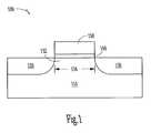
- FIG. 1A common configuration of such a transistor is shown in FIG. 1. While the following discussion uses FIG. 1 to illustrate a transistor from the prior art, one skilled in the art will recognize that the present invention could be incorporated into the transistor shown in FIG. 1 to form a novel transistor according to the invention.
- the transistor 100is fabricated in a substrate 110 that is typically silicon, but could be fabricated from other semiconductor materials as well.
- the transistor 100has a first source/drain region 120 and a second source/drain region 130 .
- a body region 132is located between the first source/drain region and the second source/drain region, where the body region 132 defines a channel of the transistor with a channel length 134 .
- a gate dielectric, or gate oxide 140is located on the body region 132 with a gate 150 located over the gate dielectric.
- the gate dielectriccan be formed from materials other than oxides, the gate dielectric is typically an oxide, and is commonly referred to as a gate oxide.
- the gatemay be fabricated from polycrystalline silicon (polysilicon), or other conducting materials such as metal may be used.
- the gate dielectric 140In fabricating transistors to be smaller in size and reliably operate on lower power supplies, one important design criteria is the gate dielectric 140 .
- the mainstay for forming the gate dielectrichas been silicon dioxide, SiO 2 .
- a thermally grown amorphous SiO 2 layerprovides an electrically and thermodynamically stable material, where the interface of the SiO 2 layer with underlying Si provides a high quality interface as well as superior electrical isolation properties.
- use of SiO 2 on Sihas provided defect charge densities on the order of 10 10 /cm 2 , midgap interface state densities of approximately 10 10 /cm 2 eV, and breakdown voltages in the range of 15 MV/cm. With such qualities, there would be no apparent need to use a material other than SiO 2 , but increased scaling and other requirements for gate dielectrics create the need to find other dielectric materials to be used for a gate dielectric.
- a method of forming a gate dielectric on a transistor body regionincludes the formation of HfO 2 /ZrO 2 nanolaminates by atomic layer deposition (ALD) of HfO 2 using a HfI 4 precursor followed by the formation of ZrO 2 on the HfO 2 layer.
- ALDatomic layer deposition
- the ALD formation of the HfO 2 layeris performed according to a sequence including pulsing the HfI 4 precursor into a reaction chamber containing a substrate, pulsing a purging gas into the chamber, pulsing a first oxygen containing precursor into the reaction chamber, and pulsing the purging gas into the chamber into the reaction chamber.
- the HfO 2 layer thicknessis controlled by repeating for a number of cycles the pulsing of the HfI 4 precursor, the purging gas, and the first oxygen containing precursor until the desired thickness is formed. Then, the layer of ZrO 2 layer is formed on the HfO 2 layer.
- Various embodimentsinclude forming the ZrO 2 layer by ALD, thermal evaporation followed by krypton/oxygen mixed plasma oxidation, pulsed-laser deposition, and jet-vapor deposition.
- a gate dielectric formed as nanolaminates of HfO 2 /ZrO 2has a larger dielectric constant than silicon dioxide, a relatively small leakage current, and good stability with respect to a silicon based substrate.
- Embodiments according to the teachings of the present inventioninclude forming transistors, memory devices, and electronic systems having dielectric layers containing nanolaminates of HfO 2 /ZrO 2 .
- Other embodimentsinclude structures for transistors, memory devices, and electronic systems with gate dielectrics containing nanolaminates of HfO 2 /ZrO 2 Such gate dielectrics provide a significantly thinner equivalent oxide thickness compared with a silicon oxide gate having the same physical thickness. Alternatively, such gate dielectrics provide a significantly thicker physical thickness than a silicon oxide gate dielectric having the same equivalent oxide thickness.
- FIG. 1shows a common configuration of a transistor in which an embodiment of a gate dielectric can be formed, according to the teaching of the present invention.
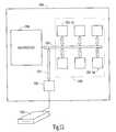
- FIG. 2Ashows an embodiment of an atomic layer deposition system for processing a layer of HfO 2 and a nanolaminate of HfO 2 /ZrO 2 , according to the teachings of the present invention.
- FIG. 2Bshows an embodiment of a gas-distribution fixture of an atomic layer deposition chamber for processing a layer of HfO 2 and a nanolaminate of HfO 2 /ZrO 2 , according to the teachings of the present invention.
- FIG. 3illustrates a flow diagram of elements for an embodiment of a method to process a nanolaminate of HfO 2 /ZrO 2 , according to the teachings of the present invention.
- FIG. 4illustrates a flow diagram of elements for another embodiment of a method to process a nanolaminate of HfO 2 /ZrO 2 by atomic layer deposition, according to the teachings of the present invention.
- FIG. 5illustrates a flow diagram of elements for an embodiment of a method to process a nanolaminate of HfO 2 /ZrO 2 using atomic layer deposition and thermal evaporation/plasma oxidation, according to the teachings of the present invention.
- FIG. 6shows an embodiment of an electron beam evaporation process for forming a layer of zirconium on a layer of HfO 2 to process a nanolaminate of HfO 2 /ZrO 2 , according to the teachings of the present invention.
- FIG. 7Ashows an embodiment of a zirconium layer deposited on a layer of HfO 2 , according to the teachings of the present invention.
- FIG. 7Bshows an embodiment of a partially oxidized zirconium layer deposited on a layer of HfO 2 , according to the teachings of the present invention.
- FIG. 7Cshows an embodiment of a ZrO 2 substantially completely oxidized and formed on a layer of HfO 2 to form a nanolaminate of HfO 2 /ZrO 2 , according to the teachings of the present invention.
- FIG. 8illustrates a flow diagram of elements for an embodiment of a method to process a nanolaminate of HfO 2 /ZrO 2 using atomic layer deposition and chemical vapor deposition, according to the teachings of the present invention.
- FIG. 9illustrates a flow diagram of elements for an embodiment of a method to process a nanolaminate of HfO 2 /ZrO 2 using atomic layer deposition and pulsed-laser deposition, according to the teachings of the present invention.
- FIG. 10illustrates a flow diagram of elements for an embodiment of a method to process a nanolaminate of HfO 2 /ZrO 2 using atomic layer deposition and jet-vapor deposition, according to the teachings of the present invention.
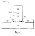
- FIG. 11shows an embodiment of a configuration of a transistor capable of being fabricated, according to the teachings of the present invention.
- FIG. 12shows an embodiment of a personal computer incorporating devices, according to the teachings of the present invention.
- FIG. 13illustrates a schematic view of an embodiment of a central processing unit incorporating devices, according to the teachings of the present invention.
- FIG. 14illustrates a schematic view of an embodiment of a DRAM memory device, according to the teachings of the present invention.
- wafer and substrate used in the following descriptioninclude any structure having an exposed surface with which to form the integrated circuit (IC) structure of the invention.
- substrateis understood to include semiconductor wafers.
- substrateis also used to refer to semiconductor structures during processing, and may include other layers that have been fabricated thereupon. Both wafer and substrate include doped and undoped semiconductors, epitaxial semiconductor layers supported by a base semiconductor or insulator, as well as other semiconductor structures well known to one skilled in the art.
- conductoris understood to include semiconductors, and the term insulator or dielectric is defined to include any material that is less electrically conductive than the materials referred to as conductors.
- the term “horizontal” as used in this applicationis defined as a plane parallel to the conventional plane or surface of a wafer or substrate, regardless of the orientation of the wafer or substrate.
- the term “vertical”refers to a direction perpendicular to the horizontal as defined above. Prepositions, such as “on”, “side” (as in “sidewall”), “higher”, “lower”, “over” and “under” are defined with respect to the conventional plane or surface being on the top surface of the wafer or substrate, regardless of the orientation of the wafer or substrate.
- a gate dielectric 140 of FIG. 1when operating in a transistor, has both a physical gate dielectric thickness and an equivalent oxide thickness (t eq ).
- the equivalent oxide thicknessquantifies the electrical properties, such as capacitance, of a gate dielectric 140 in terms of a representative physical thickness.
- t eqis defined as the thickness of a theoretical SiO 2 layer that would be required to have the same capacitance density as a given dielectric, ignoring leakage current and reliability considerations.
- a SiO 2 layer of thickness, t, deposited on a Si surface as a gate dielectricwill have a t eq larger than its thickness, t.
- This t eqresults from the capacitance in the surface channel on which the SiO 2 is deposited due to the formation of a depletion/inversion region.
- This depletion/inversion regioncan result in t eq being from 3 to 6 Angstroms ( ⁇ ) larger than the SiO 2 thickness, t.
- the gate dielectric equivalent oxide thicknessto under 10 ⁇
- the physical thickness requirement for a SiO 2 layer used for a gate dielectricwould be need to be approximately 4 to 7 ⁇ .
- SiO 2 layerAdditional requirements on a SiO 2 layer would depend on the gate electrode used in conjunction with the SiO 2 gate dielectric. Using a conventional polysilicon gate would result in an additional increase in t eq for the SiO 2 layer. This additional thickness could be eliminated by using a metal gate electrode, though metal gates are not currently used in complementary metal-oxide-semiconductor field effect transistor (CMOS) technology. Thus, future devices would be designed towards a physical SiO 2 gate dielectric layer of about 5 ⁇ or less. Such a small thickness requirement for a SiO 2 oxide layer creates additional problems.
- CMOScomplementary metal-oxide-semiconductor field effect transistor
- Silicon dioxideis used as a gate dielectric, in part, due to its electrical isolation properties in a SiO 2 —Si based structure. This electrical isolation is due to the relatively large band gap of SiO 2 (8.9 eV) making it a good insulator from electrical conduction. Signification reductions in its band gap would eliminate it as a material for a gate dielectric. As the thickness of a SiO 2 layer decreases, the number of atomic layers, or monolayers of the material in the thickness decreases. At a certain thickness, the number of monolayers will be sufficiently small that the SiO 2 layer will not have a complete arrangement of atoms as in a larger or bulk layer.
- a thin SiO 2 layer of only one or two monolayerswill not form a full band gap.
- the lack of a full band gap in a SiO 2 gate dielectricwould cause an effective short between an underlying Si channel and an overlying polysilicon gate.
- This undesirable propertysets a limit on the physical thickness to which a SiO 2 layer can be scaled.
- the minimum thickness due to this monolayer effectis thought to be about 7-8 ⁇ . Therefore, for future devices to have a t eq less than about 10 ⁇ , other dielectrics than SiO 2 need to be considered for use as a gate dielectric.
- materials with a dielectric constant greater than that of SiO 2 , 3.9will have a physical thickness that can be considerably larger than a desired t eq , while providing the desired equivalent oxide thickness.
- an alternate dielectric material with a dielectric constant of 10could have a thickness of about 25.6 ⁇ to provide a t eq of 10 ⁇ , not including any depletion/inversion layer effects.
- the reduced equivalent oxide thickness of transistorscan be realized by using dielectric materials with higher dielectric constants than SiO 2 .
- the thinner equivalent oxide thickness required for lower transistor operating voltages and smaller transistor dimensionsmay be realized by a significant number of materials, but additional fabricating requirements makes determining a suitable replacement for SiO 2 difficult.
- the current view for the microelectronics industryis still for Si based devices. This requires that the gate dielectric employed be grown on a silicon substrate or silicon layer, which places significant restraints on the substitute dielectric material. During the formation of the dielectric on the silicon layer, there exists the possibility that a small layer of SiO 2 could be formed in addition to the desired dielectric. The result would effectively be a dielectric layer consisting of two sublayers in parallel with each other and the silicon layer on which the dielectric is formed.
- the resulting capacitancewould be that of two dielectrics in series.
- the t eq of the dielectric layerwould be the sum of the SiO 2 thickness and a multiplicative factor of the thickness of the dielectric being formed, written as
- the teqis again limited by a SiO 2 layer.
- the t eqwould be limited by the layer with the lowest dielectric constant.
- the layer interfacing with the silicon layermust provide a high quality interface to maintain a high channel carrier mobility.
- the dielectric constant of Al 2 O 3is only 9, where thin layers may have a dielectric constant of about 8 to about 10. Though the dielectric constant of Al 2 O 3 is in an improvement over SiO 2 , a higher dielectric constant for a gate dielectric is desirable.
- Other dielectrics and their properties discussed by Wilkinclude Dielectric Constant Band gap Material ( ⁇ ) E g (eV) Crystal Structure(s) SiO 2 3.9 8.9 Amorphous Si 3 N 4 7 5.1 Amorphous Al 2 O 3 9 8.7 Amorphous Y 2 O 3 15 5.6 Cubic La 2 O 3 30 4.3 Hexagonal, Cubic Ta 2 O 5 26 4.5 Orthorhombic TiO 2 80 3.5 Tetrag. (rutile, anatase) HfO 2 25 5.7 Mono., Tetrag., Cubic ZrO 2 25 7.8 Mono., Tetrag., Cubic
- SiO 2as a gate dielectric
- Having an amorphous structure for a gate dielectricis advantageous because grain boundaries in polycrystalline gate dielectrics provide high leakage paths. Additionally, grain size and orientation changes throughout a polycrystalline gate dielectric can cause variations in the film's dielectric constant.
- the abovementioned material properties including crystal structureare for the materials in a bulk form.
- the materials having the advantage of a high dielectric constants relative to SiO 2also have the disadvantage of a crystalline form, at least in a bulk configuration.
- the best candidates for replacing SiO 2 as a gate dielectricare those with high dielectric constant, which can be fabricated as a thin layer with an amorphous form.
- a gate dielectricincludes thin layers of HfO 2 and ZrO 2 forming a nanolaminate.
- nanolaminatemeans a composite film of ultra thin layers of two or more materials in a layered stack, where the layers are alternating layers of materials of the composite film.
- nanolaminatestypically have thicknesses of an order of magnitude in the nanometer range.
- Each individual material layer of the nanolaminatecan have thicknesses as low as a monolayer of the material.
- a nanolaminate of HfO 2 and ZrO 2includes at least one thin layer of HfO 2 , and one thin layer of ZrO 2 , and is typically written as a nanolaminate of HfO 2 /ZrO 2 .
- nanolaminates of HfO 2 /ZrO 2are grown using atomic layer deposition (ALD), also known as atomic layer epitaxy (ALE).
- ALDatomic layer deposition
- ALEatomic layer epitaxy
- ALDwas developed in the early 1970 's as a modification of chemical vapor deposition (CVD) and is also called “alternatively pulsed-CVD.”
- CVDchemical vapor deposition
- gaseous precursorsare introduced one at a time to the substrate surface mounted within a reaction chamber (or reactor). This introduction of the gaseous precursors takes the form of pulses of each gaseous precursor. Between the pulses, the reaction chamber is purged with a gas, which in many cases is an inert gas, or evacuated.
- CS-ALDchemisorption-saturated ALD
- the second pulsing phaseintroduces another precursor on the substrate where the growth reaction of the desired film takes place. Subsequent to the film growth reaction, reaction byproducts and precursor excess are purged from the reaction chamber.
- precursor pulse timesrange from about 0.5 sec to about 2 to 3 seconds.
- ALDALD
- the saturation of all the reaction and purging phasesmakes the growth self-limiting.
- This self-limiting growthresults in large area uniformity and conformality, which has important applications for such cases as planar substrates, deep trenches, and in the processing of porous silicon and high surface area silica and alumina powders.
- ALDprovides for controlling film thickness in a straightforward, simple manner by controlling the number of growth cycles.
- ALDwas originally developed to manufacture luminescent and dielectric films needed in electroluminescent displays. Significant efforts have been made to apply ALD to the growth of doped zinc sulfide and alkaline earth metal sulfide films. Additionally, ALD has been studied for the growth of different epitaxial II-V and II-VI films, nonepitaxial crystalline or amorphous oxide and nitride films and multilayer structures of these. There also has been considerable interest towards the ALD growth of silicon and germanium films, but due to the difficult precursor chemistry, this has not been very successful.
- the precursors used in an ALD processmay be gaseous, liquid or solid. However, liquid or solid precursors must be volatile. The vapor pressure must be high enough for effective mass transportation. Also, solid and some liquid precursors need to be heated inside the reaction chamber and introduced through heated tubes to the substrates. The necessary vapor pressure must be reached at a temperature below the substrate temperature to avoid the condensation of the precursors on the substrate. Due to the self-limiting growth mechanisms of ALD, relatively low vapor pressure solid precursors can be used though evaporation rates may somewhat vary during the process because of changes in their surface area.
- precursors used in ALDthere are several other requirements for precursors used in ALD.
- the precursorsmust be thermally stable at the substrate temperature because their decomposition would destroy the surface control and accordingly the advantages of the ALD method which relies on the reactant of the precursor at the substrate surface. Of course, a slight decomposition, if slow compared to the ALD growth, can be tolerated.
- the precursorshave to chemisorb on or react with the surface, though the interaction between the precursor and the surface as well as the mechanism for the adsorption is different for different precursors.
- the molecules at the substrate surfacemust react aggressively with the second precursor to form the desired solid film. Additionally, precursors should not react with the film to cause etching, and precursors should not dissolve in the film. Using highly reactive precursors in ALD contrasts with the selection of precursors for conventional CVD.
- the by-products in the reactionmust be gaseous in order to allow their easy removal from the reaction chamber. Further, the by-products should not react or adsorb on the surface.
- RS-ALDreaction sequence ALD
- the self-limiting process sequenceinvolves sequential surface chemical reactions.
- RS-ALDrelies on chemistry between a reactive surface and a reactive molecular precursor.
- molecular precursorsare pulsed into the ALD reaction chamber separately.
- the metal precursor reaction at the substrateis typically followed by an inert gas pulse to remove excess precursor and by-products from the reaction chamber prior to pulsing the next precursor of the fabrication sequence.
- RS-ALDfilms can be layered in equal metered sequences that are all identical in chemical kinetics, deposition per cycle, composition, and thickness.
- RS-ALD sequencesgenerally deposit less than a full layer per cycle.
- a deposition or growth rate of about 0.25 to about 2.00 ⁇ per RS-ALD cyclecan be realized.
- RS-ALDprovides advantages at an interface, conformality over a substrate, use of low temperature and mildly oxidizing processes, growth thickness dependent solely on the number of cycles performed, and ability to engineer multilayer laminate films with resolution of one to two monolayers.
- RS-ALDallows for deposition control on the order on monolayers and the ability to deposit monolayers of amorphous films.
- RS-ALD processesprovide for the formation of nanolaminates. These nanolaminates can be engineered in various forms. In one form, the transition between material layers of the nanolaminate can be made abrupt. In another form, the transition between material layers of the nanolaminate can be constructed with a graded composition. The graded composition can be formed by RS-ALD due its control of the deposition thickness per cycle.
- a layer of HfO 2is formed on a substrate mounted in a reaction chamber using ALD in a repetitive sequence including pulsing a hafnium containing precursor into the reaction chamber followed by pulsing a purging gas, and then pulsing a first oxygen containing precursor into the chamber.
- ALDa layer of HfO 2 is formed using Hfl 4 as a hafnium containing precursor, water vapor as a first oxygen containing precursor, and nitrogen as a purging gas and carrier gas.
- a ZrO 2 layeris formed on the HfO 2 layer.
- the layer of ZrO 2is formed by ALD.
- a repetitive sequenceincludes using ZrI 4 as a zirconium containing precursor along with a vapor solution of HO 2 —H 2 O 2 as a second oxygen containing precursor, and nitrogen as a purging gas and carrier gas.
- the ZrO 2 layeris formed by depositing a layer of zirconium on the HfO 2 layer by thermal evaporation, and oxidizing the zirconium layer using a krypton(Kr)/oxygen(O 2 ) mixed plasma to form a HfO 2 /ZrO 2 composite layer.
- the ZrO 2 layeris formed by pulsed-laser deposition.
- the ZrO 2 layeris formed by jet-vapor deposition.
- precursor gasesin particular HfI 4
- HfI 4are used to form the HfO 2 layer for the HfO 2 /ZrO 2 nanolaminate films used as a gate dielectric on a transistor body.
- solid or liquid precursorscan be used in an appropriately designed reaction chamber.
- ALD formation of other materialsis disclosed in co-pending, commonly assigned U.S. patent application: entitled “Atomic Layer Deposition and Conversion,” attorney docket no. 303.802US1, Ser. No. 10/137,058, and “Methods, Systems, and Apparatus for Atomic-Layer Deposition of Aluminum Oxides in Integrated Circuits,” attorney docket no. 1303.048US1, Ser. No. 10/137,168.
- FIG. 2Ashows an embodiment of an atomic layer deposition system for processing layers of HfO 2 and nanolaminates of HfO 2 /ZrO 2 according to the teachings of the present invention.
- the elements depictedare those elements necessary for discussion of the present invention such that those skilled in the art may practice the present invention without undue experimentation.
- a further discussion of the ALD reaction chambercan be found in co-pending, commonly assigned U.S. patent application: entitled “Methods, Systems, and Apparatus for Uniform Chemical-Vapor Depositions,” attorney docket no. 303.717US1, Ser. No. 09/797,324, incorporated herein by reference.
- a substrate 210is located inside a reaction chamber 220 of ALD system 200 . Also located within the reaction chamber 220 is a heating element 230 which is thermally coupled to substrate 210 to control the substrate temperature.
- a gas-distribution fixture 240introduces precursor gases to the substrate 210 .
- Each precursor gasoriginates from individual gas sources 251 - 254 whose flow is controlled by mass-flow controllers 256 - 259 , respectively.
- the gas sources 251 - 254provide a precursor gas either by storing the precursor as a gas or by providing a location and apparatus for evaporating a solid or liquid material to form the selected precursor gas.
- purging gas sources 261 , 262are also included in the ALD system, each of which is coupled to mass-flow controllers 266 , 267 , respectively.
- the gas sources 251 - 254 and the purging gas sources 261 - 262are coupled by their associated mass-flow controllers to a common gas line or conduit 270 which is coupled to the gas-distribution fixture 240 inside the reaction chamber 220 .
- Gas conduit 270is also coupled to vacuum pump, or exhaust pump, 281 by mass-flow controller 286 to remove excess precursor gases, purging gases, and by-product gases at the end of a purging sequence from the gas conduit.
- Vacuum pump, or exhaust pump, 282is coupled by mass-flow controller 287 to remove excess precursor gases, purging gases, and by-product gases at the end of a purging sequence from the reaction chamber 220 .
- mass-flow controller 287to remove excess precursor gases, purging gases, and by-product gases at the end of a purging sequence from the reaction chamber 220 .
- control displays, mounting apparatus, temperature sensing devices, substrate maneuvering apparatus, and necessary electrical connections as are known to those skilled in the artare not shown in FIG. 2A.
- FIG. 2Bshows an embodiment of a gas-distribution fixture of an atomic layer deposition chamber for processing layers of HfO 2 and nanolaminates of HfO 2 /ZrO 2 , according to the teachings of the present invention.
- Gas-distribution fixture 240includes a gas-distribution member 242 , and a gas inlet 244 .
- Gas inlet 244couples the gas-distribution member 242 to the gas conduit 270 of FIG. 2A.
- Gas-distribution member 242includes gas-distribution holes, or orifices, 246 and gas-distribution channels 248 .
- holes 246are substantially circular with a common diameter in the range of 15-20 microns
- gas-distribution channels 248have a common width in the range of 20-45 microns.
- the surface 249 of the gas distribution member having gas-distribution holes 246is substantially planar and parallel to the substrate 210 of FIG. 2A.
- other embodimentsuse other surface forms as well as shapes and sizes of holes and channels.
- the distribution and size of holesmay also affect deposition thickness and thus might be used to assist thickness control.
- Holes 246are coupled through gas-distribution channels 248 to gas inlet 244 . Though the ALD system 200 is well suited for practicing the present invention, other ALD systems commercially available can be used.
- reaction chambers for deposition of filmsare understood by those of ordinary skill in the art of semiconductor fabrication.
- the present inventionman be practiced on a variety of such reaction chambers without undue experimentation.
- one of ordinary skill in the artwill comprehend the necessary detection, measurement, and control techniques in the art of semiconductor fabrication upon reading the disclosure.
- FIG. 3illustrates a flow diagram of elements for an embodiment of a method to process a nanolaminate of HfO 2 /ZrO 2 , according to the teachings of the present invention.
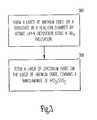
- This embodiment of a method for forming a HfO 2 /ZrO 2 nanolaminateincludes forming a layer of hafnium oxide on a substrate in a reaction chamber by atomic layer deposition using a Hfl 4 precursor, at block 305 , and forming a layer of zirconium oxide on the layer of hafnium oxide to form a HfO 2 /ZrO 2 composite, at block 310 .
- the HfO 2 /ZrO 2 composite formedis a HfO 2 /ZrO 2 nanolaminate.
- the HfO 2 /ZrO 2 nanolaminateis composed of one HfO 2 layer and one layer ZrO 2 layer.
- the HfO 2 /ZrO 2 nanolaminateincludes multiple layers of the HfO 2 /ZrO 2 composite, where the initial layer disposed on a substrate is a HfO 2 layer. After this initial HfO 2 layer, there are alternating layers of HfO 2 and ZrO 2 , with the terminating layer being a ZrO 2 layer in one embodiment and HfO 2 layer in another embodiment.
- Forming the HfO 2 layer on a substrate by atomic layer depositioninvolves using a deposition sequence including pulsing the HfI 4 precursor into the reaction chamber, followed by pulsing a purging gas, pulsing a first oxygen containing precursor, and pulsing the purging gas.
- the first oxygen precursoris water vapor.
- Each precursoris pulsed for a short time ranging from 0.5 seconds to two or three seconds.
- a purging gassuch as nitrogen is pulsed for a longer period such as five to fifteen seconds to insure that all excess precursor gases and by-products are removed from the reaction chamber. Pulsing times are selected to enable the controlled growth of the HfO 2 layer on a one to two monolayer basis.
- the HfO 2 layer growth rateis at a relatively fixed rate, where a desired thickness of the HfO 2 layer is obtained by performing the ALD sequence for a predetermined number of cycles.
- FIG. 4illustrates a flow diagram of elements for another embodiment of a method to process a nanolaminate of HfO 2 /ZrO 2 by atomic layer deposition, according to the teachings of the present invention.
- a method for forming a dielectric filmincludes forming a layer of HfI 2 on a substrate in a reaction chamber by atomic layer deposition using a HfI 4 precursor, and forming a layer of ZrO 2 on the HfO 2 layer by atomic layer deposition to form a HfO 2 /ZrO 2 composite.
- Using the ALD processprovides for the formation of the HfO 2 /ZrO 2 composite as a nanolaminate.
- An embodiment of this methodcan be implemented with the atomic layer deposition system of FIGS. 2A,B.
- a substrateis prepared.
- the substrate used for forming a transistoris typically a silicon or silicon containing material.
- germanium, gallium arsenide, silicon-on-sapphire substrates, or other suitable substratesmay be used.
- This preparation processincludes cleaning of the substrate 210 and forming layers and regions of the substrate, such as drains and sources of a metal oxide semiconductor (MOS) transistor, prior to forming a gate dielectric.
- MOSmetal oxide semiconductor
- the sequencing of the formation of the regions of the transistor being processedfollows typical sequencing that is generally performed in the fabrication of a MOS transistor as is well known to those skilled in the art.
- the processing prior to forming a gate dielectricis the masking of substrate regions to be protected during the gate dielectric formation, as is typically performed in MOS fabrication.
- the unmasked regionincludes a body region of a transistor, however one skilled in the art will recognize that other semiconductor device structures may utilize this process.
- the substrate 210 in its ready for processing formis conveyed into a position in reaction chamber 220 for ALD processing.
- a precursor containing hafniumis pulsed into reaction chamber 220 .
- HfI 4is used as a source material.
- the HfI 4is pulsed into reaction chamber 220 through the gas-distribution fixture 240 onto substrate 210 .
- the flow of the HfI 4is controlled by mass-flow controller 256 from gas source 251 .
- the substrate temperatureis maintained between about 225° C. and about 500° C. In another embodiment, the substrate temperature is maintained between about 250° C. and about 325° C.
- the lower temperatureallows for forming a dielectric film suited for use as a gate dielectric, since an amorphous layer tends to more readily form at lower processing temperatures.
- the HfI 4reacts with the surface of the substrate 210 in the desired region defined by the unmasked areas of the substrate 210 .
- a first purging gasis pulsed into the reaction chamber 220 .
- pure nitrogenwith a purity greater than 99.99% is used as a purging gas for HfI 4 .
- the nitrogen flowis controlled by mass-flow controller 266 from the purging gas source 261 into the gas conduit 270 .
- a nitrogen gascan also be used as a carrier gas for the precursors.
- a first oxygen containing precursoris pulsed into the reaction chamber 220 , at block 420 .
- water vaporis selected as the precursor acting as an oxidizing reactant to form a HfO 2 on the substrate 210 .
- a vapor solution of H 2 O-H 2 O 2can be used as the oxygen containing precursor.
- the water vaporis pulsed into the reaction chamber 220 through gas conduit 270 from gas source 252 by mass-flow controller 257 .
- the water vaporaggressively reacts at the surface of substrate 210 .
- the first purging gasis injected into the reaction chamber 220 , at block 425 .
- pure nitrogen gasis used to purge the reaction chamber after pulsing each precursor gas. Excess precursor gas, and reaction by-products are removed from the system by the purge gas in conjunction with the exhausting of the reaction chamber 220 using vacuum pump 282 through mass-flow controller 287 , and exhausting of the gas conduit 270 by the vacuum pump 281 through mass-flow controller 286 .
- the substrateis held between about 250° C. and about 325° C. by the heating element 230 . In other embodiments the substrate is held between about 225° C. and 500° C.
- the HfI 4 pulse timeranges from about 1.0 sec to about 2.0 sec.
- the hafnium sequencecontinues with a purge pulse followed by a water vapor pulse followed by a purge pulse. In one embodiment, performing a purge pulse followed by a water vapor pulse followed by a purge pulse takes about 2 seconds.
- each pulse in the hafnium sequencehas a 2 second pulse period.
- the pulse periods for the precursorsare 2 seconds, while the purge gas pulse period ranges from five second to twenty seconds.
- the thickness of a HfO 2 film after one cycleis determined by a fixed growth rate for the pulsing periods and precursors used in the hafnium sequence, set at a value such as N nm/cycle.
- tin an application such as forming a gate dielectric of a MOS transistor, the ALD process should be repeated for t/N cycles. The desired thickness should be attained after t/N cycles.
- the processstarts over at block 410 with the pulsing of the precursor containing hafnium, which in the embodiment discussed above is a HfI 4 gas. If t/N cycles have completed, no further ALD processing of HfO 2 is required and the HfO 2 layer is ready to be formed as a composite with a ZrO 2 layer.
- a precursor containing zirconiumis pulsed into the reaction chamber 220 .
- ZrI 4is used as the zirconium containing precursor.
- ZrCl 4is used as the zirconium containing precursor.
- the ZrI 4is evaporated from a containment area held at about 250° C. in gas source 253 . It is pulsed to the surface of the substrate 210 through gas-distribution fixture 240 from gas source 253 by mass-flow controller 258 .
- the ZrI 4is introduced onto the HfO 2 layer that was formed during the HfI 4 /water vapor sequence.
- a second purging gasis introduced into the system.
- nitrogen gasis used as a purging and carrier gas.
- the nitrogen flowis controlled by mass-flow controller 267 from the purging gas source 262 into the gas conduit 270 and subsequently into the reaction chamber 220 .
- a second oxygen containing precursoris pulsed into the reaction chamber 220 .
- a vapor solution of H 2 O—H 2 O 2is selected as the precursor acting as an oxidizing reactant to interact with the zirconium deposited on the HfO 2 layer on the substrate 210 .
- the H 2 O—H 2 O 2 vapor solutionis pulsed into the reaction chamber 220 through gas conduit 270 from gas source 254 , held at about room temperature, by mass-flow controller 259 .
- the H 2 O—H 2 O 2 vapor solutionaggressively reacts at the surface of substrate 210 to form a ZrO 2 layer.
- the nitrogen purging gasis injected into the reaction chamber 200 , at block 450 .
- nitrogen gasis used to purge the reaction chamber after pulsing each precursor gas.
- argon gasis used as the purging gas. Excess precursor gas, and reaction by-products are removed from the system by the purge gas in conjunction with the exhausting of the reaction chamber 220 using vacuum pump 282 through mass-flow controller 287 , and exhausting of the gas conduit 270 by the vacuum pump 281 through mass-flow controller 286 .
- the substrateis held between about 250° C. and about 325° C. by the heating element 230 . In other embodiments, the substrate is held between about 275° C. and about 500° C. In one embodiment, the process pressure is maintained at about 250 Pa during the zirconium sequence. Pulse times for the ZrI 4 and the H 2 O—H 2 O 2 vapor solution were about 2 sec for both precursors, with purging pulse times of about 2 secs.
- the nanolaminatecan be annealed.
- the annealingcan be performed at a temperature between about 300° C. and about 800° C. in an inert or nitrogen atmosphere.
- processing the device containing the HfO 2 /ZrO 2 nanolaminateis completed.
- completing the deviceincludes completing the formation of a transistor.
- completing the processincludes completing the construction of a memory device having a array with access transistors formed with gate dielectrics containing HfO 2 /ZrO 2 nanolaminates.
- completing the processincludes the formation of an electronic system including an information handling device that uses electronic devices with transistors formed with gate dielectrics containing HfO 2 /ZrO 2 nanolaminates.
- information handling devicessuch as computers include many memory devices, having many access transistors.
- a HfO 2 /ZrO 2 nanolaminateincludes one HfO 2 layer and one HfO 2 /ZrO 2 layer.
- the completed HfO 2 /ZrO 2 nanolaminatehas a thickness in which the thickness of the HfO 2 layer is about one-half the thickness of the completed HfO 2 /ZrO 2 nanolaminate.
- a completed HfO 2 /ZrO 2 nanolaminateincludes multiple alternating layers of HfO 2 and ZrO 2 , which requires that at block 455 , once a given ZrO 2 layer has been formed with a desired thickness, a hafnium sequence is then started at block 410 .
- HfO 2 /ZrO 2 nanolaminate formationbegins with forming a HfO 2 layer, but may end with forming ZrO 2 layer or a HfO 2 layer.
- ALDprovides for the engineering of a HfO 2 /ZrO 2 nanolaminate.
- nanolaminatescan be formed with n number of HfO 2 /ZrO 2 composite layers where the HfO 2 layer is formed with x number of hafnium cycles and y number of zirconium cycles.
- nanolaminatescan be formed with n number of HfO 2 /ZrO 2 composite layers where the first composite layer has a HfO 2 layer formed with x 1 number of hafnium cycles and y 1 number of zirconium cycles, a second composite layer has a HfO 2 layer formed with x 2 number of hafnium cycles and y 2 number of zirconium cycles, extended to the nth composite layer having a HfO 2 layer formed with x n number of hafnium cycles and y n number of zirconium cycles.
- Such tailoring of the HfO 2 /ZrO 2 nanolaminateprovides for forming dielectric films with a designed physical thickness, t, and equivalent oxide thickness, t eq .
- pulsing each precursor into the reaction chamberis controlled for a predetermined period, the predetermined period being individually controlled for each precursor pulsed into the reaction chamber. Additionally, the substrate is maintained at a selected temperature for forming each layer, where the selected temperature set independently for forming each layer.
- FIG. 5illustrates a flow diagram of elements for an embodiment of a method to process a nanolaminate of HfO 2 /ZrO 2 using atomic layer deposition and thermal evaporation/plasma oxidation, according to the teachings of the present invention.
- a nanolaminate of HfO 2 /ZrO 2is formed by a method that includes forming a layer of hafnium oxide on a substrate in a reaction chamber by atomic layer deposition using a HfI 4 precursor, at block 505 , forming a layer of zirconium on the layer of hafnium oxide by thermal evaporation, at block 510 , and oxidizing the zirconium layer using a krypton(Kr)/oxygen(O 2 ) mixed plasma to form a HfO 2 /ZrO 2 composite, at block 515 .
- the HfO 2 /ZrO 2 compositeis a nanolaminate, whose thickness can be controlled by precisely controlling the ALD formation of HfO 2 , and thermal deposition of zirconium.
- the thermal evaporation of zirconiumis performed using electron beam evaporation.
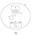
- FIG. 6shows an embodiment of an electron beam evaporation process for forming a layer of zirconium on a layer of HfO 2 to process a nanolaminate of HfO 2 /ZrO 2 , according to the teachings of the present invention.
- a substrate 610is located inside a deposition chamber 660 .
- the substrate in this embodimentis masked by a first masking structure 670 and a second masking structure 671 .
- the unmasked region 633includes a body region of a transistor on which a layer of HfO 2 is formed.
- other semiconductor device structuresmay utilize this process.
- the electron gun 663provides an electron beam 664 directed at target 661 containing a source material for forming ZrO 2 on the unmasked region HfO 2 layer 633 of the substrate 610 .
- the electron gun 663includes a rate monitor for controlling the rate of evaporation of the material in the target 661 at which the electron beam 664 is directed. For convenience, control displays and necessary electrical connections as are known to those skilled in the art are not shown in FIG. 6.
- the electron gun 663generates an electron beam 664 that hits target 661 .
- target 661contains a zirconium metal source, which is evaporated due to the impact of the electron beam 664 .
- the evaporated material 668is then distributed throughout the chamber 660 .
- a layer of zirconiumis grown forming a film 640 on the surface of the HfO 2 layer 633 on substrate 610 , which is maintained at a temperature between 150° C. and 200° C. The growth rate can vary with a typical rate of 0.1 ⁇ /s. After depositing a zirconium layer on the HfO 2 layer 633 , the zirconium layer is oxidized.
- the evaporation chamber 660can be included as part of an overall processing system including ALD system 200 of FIG. 2. To avoid contamination of the surface of the HfO 2 layer 633 , evaporation chamber 660 can be connected to ALD system 200 using sealable connections to maintain the substrate, which is substrate 210 in FIG. 2 and substrate 610 of FIG. 6, in an appropriate environment between ALD processing of the HfO 2 layer and Zr evaporation. Other means as are known to those skilled in the art can be employed for maintaining an appropriate environment between different processing procedures.
- FIGS. 7 A- 7 Cshow a low temperature oxidation process that is used in one embodiment to form a layer of ZrO 2 on a layer of HfO 2 .
- FIG. 7Ashows an embodiment of a zirconium layer 720 deposited on a HfO 2 layer 710 , according to the teachings of the present invention.
- the HfO 2 layer 710is formed on substrate 700 using an ALD process, as previously discussed, having an substrate interface 730 .
- the Zr layer 720is deposited on the HfO 2 layer 710 by electron beam evaporation, as discussed above, forming an interface 740 with the HfO 2 layer 710 and having an outer surface 750 .
- the combined film with the Zr layer 720 deposited on the HfO 2 layer 710has a total thickness 752 .
- the layers 710 , 720are deposited over a body region of a transistor, however the layers may be deposited on any surface within the scope of the invention.
- FIG. 7Bshows an embodiment of a partially oxidized zirconium layer 770 deposited on a HfO 2 layer 710 , according to the teachings of the present invention.
- the layer 720is in the process of being oxidized.
- the oxidation processincludes a krypton/oxygen mixed plasma oxidation process.
- the mixed plasma processgenerates atomic oxygen or oxygen radicals in contrast to molecular oxygen or O 2 used in conventional thermal oxidation.
- the atomic oxygenis introduced to the layer from all exposed directions as indicated by arrows 760 , creating an oxide portion 770 .
- the atomic oxygencontinues to react with the layer and creates an oxidation interface 742 . As the reaction progresses, atomic oxygen diffuses through the oxide portion 770 and reacts at the oxidation interface 742 until the layer is completely converted to an oxide of the deposited material layer.
- FIG. 7Cshows an embodiment of a ZrO 2 substantially completely oxidized and formed on a layer of HfO 2 to form a nanolaminate of HfO 2 /ZrO 2 , according to the teachings of the present invention.
- FIG. 7Cshows the resulting oxide layer 770 which spans a physical thickness 772 from the outer surface 750 to the interface 740 .
- the overall thickness 752 of the HfO 2 /ZrO 2 composite in FIG. 7Chas increased from that of the Zr layer deposited on the HfO 2 layer in FIG. 7A, due to the oxidation of the zirconium.
- the processing variables for the mixed plasma oxidationinclude a low ion bombardment energy of less than 7 eV, a high plasma density above 10 12 /cm 3 and a low electron temperature below 1.3 eV.
- the substrate temperatureis approximately 400° C.
- a mixed gas of 3% oxygen with the balance being krypton at a pressure of 1 Torris used.
- a microwave power density of 5 W/cm 2is used. The oxidation process provides a growth rate of 1.5 nm/min.
- the low temperature mixed plasma oxidation process described aboveallows the deposited layer to be oxidized at a low temperature.
- the mixed plasma processin one embodiment is performed at approximately 400° C. in contrast to prior thermal oxidation processes that are performed at approximately 1000° C.
- FIG. 8illustrates a flow diagram of elements for an embodiment of a method to process a nanolaminate of HfO 2 /ZrO 2 using atomic layer deposition and chemical vapor deposition (CVD), according to the teachings of the present invention.
- This embodiment of the methodincludes forming a layer of hafnium oxide on a substrate in a reaction chamber by atomic layer deposition using a HfI 4 precursor, at block 805 , and forming a layer of zirconium oxide on the layer of hafnium oxide by chemical vapor deposition to form a HfO 2 /ZrO 2 composite, at block 810 .
- the HfO 2 layeris formed by ALD as discussed in the embodiments above.
- the ZrO 2 layeris formed by rapid thermal CVD at about 500° C. Subsequently, a nitrogen anneal is performed between about 700° C. and about 800° C. for about 30 sec. A rapid thermal CVD system, as is known to those skilled in the art, is used to form the ZrO 2 layer.
- FIG. 9illustrates a flow diagram of elements for an embodiment of a method to process a nanolaminate of HfO 2 /ZrO 2 using atomic layer deposition and pulsed-laser deposition, according to the teachings of the present invention.
- This embodiment of the methodincludes forming a layer of hafnium oxide on a substrate in a reaction chamber by atomic layer deposition using a HfI 4 precursor, at block 905 , and forming a layer of zirconium oxide on the layer of hafnium oxide by pulsed-laser deposition to form a HfO 2 /ZrO 2 composite, at block 910 .
- the HfO 2 layeris formed by ALD as discussed in the embodiments above.
- a pulsed-laser deposition systemis similar to the electron beam evaporation system 660 of FIG. 6 with the electron gun 663 replaced by a laser and focusing optics, though the laser and focusing optics need not be located in the evaporation reaction chamber.
- a beam from the laseris focused on a target, which causes an ablation of material from the target.
- the material removed from the targetdeposits on an unmasked HfO 2 layer located on a substrate. Controlling the focusing of the beam from the laser on the source target provides for precision growth rate of the ZrO 2 layer.
- a substrate temperatureis maintained between about 200° C. to about 800° C. during pulsed-laser deposition.
- a beam from a laser sourcesuch as a excimer laser is focused on a rotating zirconium target source in a deposition chamber with an O 2 pressure of about 0.2 Torr to form a ZrO 2 layer on a HfO 2 layer.
- Other laser sources and configurationscan be used as is known by those skilled in the art.
- FIG. 10illustrates a flow diagram of elements for an embodiment of a method to process a nanolaminate of HfO 2 /ZrO 2 using atomic layer deposition and jet-vapor deposition, according to the teachings of the present invention.
- This embodiment of the methodincludes forming a layer of hafnium oxide on a substrate in a reaction chamber by atomic layer deposition using a Hfl 4 precursor, at block 1005 , and forming a layer of zirconium oxide on the layer of hafnium oxide by jet-vapor deposition to form a HfO 2 /ZrO 2 composite, at block 1010 .
- the HfO 2 layeris formed by ALD as discussed in the embodiments above.
- the ZrO 2 layercan be formed using jet-vapor deposition techniques as is known to those skilled in the art.
- the jet-vapor deposition zirconium and oxygen vaporsare directed to the HfO 2 layer out of source nozzles by supersonic Ar jets.
- Using jet-vapor deposition in a low pressure atmosphereallows for forming the ZrO 2 layer at at room temperature.
- annealingis performed subsequent to forming the ZrO 2 layer at a about 800° C.
- the annealingis performed using a nitrogen rapid thermal annealing (RTA). The annealing can be performed after each ZrO 2 layer is formed in the composite of alternating layers of the HfO 2 /ZrO 2 nanolaminate and/or at the completion of the HfO 2 /ZrO 2 nanolaminate.
- RTAnitrogen rapid thermal annealing
- the HfO 2 /ZrO 2 nanolaminatescan be annealed in a temperature range from between 300° C. to 800° C. Typically the annealing is for a short time and in performed in a nitrogen atmosphere or in some other inert atmosphere.
- ZrO 2 formed on silicon substratesmay result in an interfacial region where silicon diffuses through a layer of ZrO 2 to form a poly-silicon/ZrO 2 /silicon interfacial region, as reported by C. H. Lee et al., IEDM 2000, 27-30 (2000). Further, nanolaminates of ZrO 2 /HfO 2 were reported to have SiO 2 interfacial layer when formed by ALD using ZrCl 4 and HfCl 4 precursors. See H. Zhang et al., Journal of the Electrochemical Society , vol. 148, no. 4, pp. F63-F66 (2001). To eliminate the SiO 2 interfacial layer, Zhang et al.
- HfO 2 /ZrO 2 nanolaminatesare formed by ALD of HfO 2 on substrates using a HfI 4 precursor. Subsequently, a layer of ZrO 2 is formed on the HfO 2 layer by various deposition techniques. These HfO 2 /ZrO 2 nanolaminates form a stable interface with a silicon substrate. Using ALD, the size and effect of interfacial layer between the silicon substrate and the first HfO 2 layer will depend on the reactivity of the HfO 2 in forming an abrupt transition from silicon surface to HfO 2 layer.
- dielectric films containing HfO 2 /ZrO 2 nanolaminatescan have dielectric constants ranging from 9 or 10 to 25. Additionally, forming the HfO 2 layer at relatively low temperatures provides a means for enabling the formation of HfO 2 /ZrO 2 nanolaminates that are amorphous.
- Another factor setting a lower limit for the scaling of a dielectric layeris the number of monolayers of the dielectric structure necessary to develop a full band gap such that good insulation is maintained between an underlying silicon layer and an overlying conductive layer on the dielectric layer or film. This requirement is necessary to avoid possible short circuit effects between the underlying silicon layer and the overlying conductive layer used.
- an expected lower limit for the physical thickness of a dielectric layer grown by forming HfO 2 /ZrO 2 nanolaminatesis anticipated to be in about the 2-4 nm range.
- HfO 2 /ZrO 2 nanolaminateshaving physical thickness in the range of 4 to 10 nm.
- HfO 2 used as the initial layeris expected to provide excellent overall results with respect to reliability, current leakage, and ultra-thin t eq .
- ALDatomic layer deposition
- HfO 2 /ZrO 2 nanolaminatescan have a wide range of thicknesses and dielectric constants.
- the physical thicknessescan range from about 2 nm to about 10 nm with typical thickness ranging from about 4 nm to about 10 nm.
- Such layershave an effective dielectric constant ranging from 9 or 10 to 25.
- the lower limit on the scaling of a layer containing HfO 2 /ZrO 2 nanolaminatesdepends on the monolayers of the film necessary to develop a full band gap such that good insulation is maintained between an underlying silicon layer and an overlying conductive layer to the HfO 2 /ZrO 2 nanolaminate film. From above, it is apparent that a film containing HfO 2 /ZrO 2 nanolaminates can be attained with a t eq ranging from 3 ⁇ to 12 ⁇ . Further, a dielectric film with completely formed band structures and monolayer formations can provide a t eq significantly less than 2 or 3 ⁇ .
- novel process described aboveprovides significant advantages by performing atomic layer deposition of HfO 2 /ZrO 2 in a hafnium sequence using HfI 4 precursors followed by the formation of a ZrO 2 layer on the HfO 2 layer. Further, by independently controlling the various parameters for each sequence a gate dielectric with a selected dielectric constant can be formed. Additionally, the novel process can be implemented to form transistors, memory devices, and information handling devices. With careful preparation and engineering of the HfO 2 /ZrO 2 nanolaminates limiting the size of interfacial regions, a t eq down to 2.5 ⁇ or lower is anticipated.
- a transistor 100 as depicted in FIG. 1can be formed by forming a source/drain region 120 and another source/drain region 130 in a silicon based substrate 110 where the two source/drain regions 120 , 130 are separated by a body region 132 .
- the body region 132 separated by the source/drain 120 and the source/drain 130defines a channel having a channel length 134 .
- a dielectric filmis formed on the substrate 110 by forming a layer of hafnium oxide on substrate 110 in a reaction chamber by atomic layer deposition using a HfI 4 precursor and forming a layer of zirconium oxide on the layer of hafnium oxide to form a HfO 2 /ZrO 2 composite.
- the resulting HfO 2 /ZrO 2 compositeis a nanolaminate.
- These HfO 2 /ZrO 2 nanolaminatescan be formed using any of the various embodiments previously discussed.
- These HfO 2 /ZrO 2 nanolaminatesare contained in a dielectric film defining the gate dielectric 140 .
- a gateis formed over the gate dielectric 140 .
- forming the gateincludes forming a polysilicon layer, though a metal gate can be formed in an alternative process.
- Forming the substrate, source/region regions, and the gateis performed using standard processes known to those skilled in the art. Additionally, the sequencing of the various elements of the process for forming a transistor is conducted with standard fabrication processes, also as known to those skilled in the art.
- FIG. 11shows an embodiment of a configuration of a transistor capable of being fabricated, according to the teachings of the present invention.
- the transistor 1100includes a silicon based substrate 1110 with two source/drain regions 1120 , 1130 separated by a body region 1132 .
- the body region 1132 between the two source/drain regions 1120 , 1130defines a channel region having a channel length 1134 .
- a stack 1155including a gate dielectric 1140 , a floating gate 1152 , a floating gate dielectric 1142 , and control gate 1150 .
- the gate dielectric 1140 containing HfO 2 /ZrO 2 nanolaminatesis formed according to the teachings of the present invention as described above with the remaining elements of the transistor 1100 formed using processes known to those skilled in the art. Alternately, both the gate dielectric 1140 and the floating gate dielectric 1142 can be formed containing HfO 2 /ZrO 2 nanolaminates, in accordance with the present invention as described above.
- Transistors created by the methods described abovemay be implemented into memory devices and electronic systems including information handling devices.
- Information handling devices having a dielectric layer containing HfO 2 /ZrO 2 nanolaminatescan be constructed using various embodiments of the methods described above.
- Such information devicescan include wireless systems, telecommunication systems, and computers.
- An embodiment of a computer having a dielectric layer containing HfO 2 /ZrO 2 nanolaminatesis shown in FIGS. 12 - 14 and described below. While specific types of memory devices and computing devices are shown below, it will be recognized by one skilled in the art that several types of memory devices and electronic systems including information handling devices utilize the invention.
- FIG. 12shows an embodiment of a personal computer 1200 incorporating devices, according to the teachings of the present invention.
- Personal computer 1200includes a monitor 1201 , keyboard input 1202 and a central processing unit 1204 .
- FIG. 13illustrates a schematic view of an embodiment of a central processing unit 1204 incorporating devices, according to the teachings of the present invention.
- the central processing unit 1204typically includes microprocessor 1306 , memory bus circuit 1308 having a plurality of memory slots 1312 ( a - n ), and other peripheral circuitry 1310 .
- Peripheral circuitry 1310permits various peripheral devices 1324 to interface processor-memory bus 1320 over input/output (I/O) bus 1322 .
- the personal computer 1200 shown in FIGS. 12 and 13also includes at least one transistor having a gate dielectric containing HfO 2 /ZrO 2 nanolaminates in an embodiment according to the teachings of the present invention.
- Microprocessor 1306produces control and address signals to control the exchange of data between memory bus circuit 1308 and microprocessor 1306 and between memory bus circuit 1308 and peripheral circuitry 1310 . This exchange of data is accomplished over high speed memory bus 1320 and over high speed I/O bus 1322 .
- Coupled to memory bus 1320are a plurality of memory slots 1312 ( a - n ) which receive memory devices well known to those skilled in the art.
- memory slots 1312For example, single inline memory modules (SIMMs) and dual in-line memory modules (DIMMs) may be used in the implementation of the present invention.
- Page mode operations in a DRAMare defined by the method of accessing a row of a memory cell arrays and randomly accessing different columns of the array. Data stored at the row and column intersection can be read and output while that column is accessed. Page mode DRAMs require access steps which limit the communication speed of memory circuit 1308 .
- An alternate type of deviceis the extended data output (EDO) memory which allows data stored at a memory array address to be available as output after the addressed column has been closed. This memory can increase some communication speeds by allowing shorter access signals without reducing the time in which memory output data is available on memory bus 1320 .
- EDOextended data output
- Other alternative types of devicesinclude SDRAM, DDR SDRAM, SLDRAM and Direct RDRAM as well as others such as SRAM or Flash memories.
- FIG. 14illustrates a schematic view of an embodiment of a DRAM memory device 1400 according to the teachings of the present invention.
- DRAM device 1400is compatible with memory slots 1312 ( a - n ).
- the description of DRAM 1400has been simplified for purposes of illustrating a DRAM memory device and is not intended to be a complete description of all the features of a DRAM. Those skilled in the art will recognize that a wide variety of memory devices may be used in the implementation of the present invention.
- the example of a DRAM memory device shown in FIG. 14includes at least one transistor having a gate dielectric containing HfO 2 /ZrO 2 nanolaminates in an embodiment according to the teachings of the present invention.
- Control, address and data information provided over memory bus 1320is further represented by individual inputs to DRAM 1400 , as shown in FIG. 14. These individual representations are illustrated by data lines 1402 , address lines 1404 and various discrete lines directed to control logic 1406 .
- DRAM 1400includes memory array 1410 which in turn comprises rows and columns of addressable memory cells. Each memory cell in a row is coupled to a common word line. The word line is coupled to gates of individual transistors, where at least one transistor has a gate coupled to a gate dielectric containing HfO 2 /ZrO 2 nanolaminates in accordance with the method and structure previously described above. Additionally, each memory cell in a column is coupled to a common bit line. Each cell in memory array 1410 includes a storage capacitor and an access transistor as is conventional in the art.
- DRAM 1400interfaces with, for example, microprocessor 1306 through address lines 1404 and data lines 1402 .
- DRAM 1400may interface with a DRAM controller, a micro-controller, a chip set or other electronic system.
- Microprocessor 1306also provides a number of control signals to DRAM 1400 , including but not limited to, row and column address strobe signals RAS and CAS, write enable signal WE, an output enable signal OE and other conventional control signals.
- Row address buffer 1412 and row decoder 1414receive and decode row addresses from row address signals provided on address lines 1404 by microprocessor 1306 . Each unique row address corresponds to a row of cells in memory array 1410 .
- Row decoder 1414includes a word line driver, an address decoder tree, and circuitry which translates a given row address received from row address buffers 1412 and selectively activates the appropriate word line of memory array 1410 via the word line drivers.
- Column address buffer 1416 and column decoder 1418receive and decode column address signals provided on address lines 1404 .
- Column decoder 1418also determines when a column is defective and the address of a replacement column.
- Column decoder 1418is coupled to sense amplifiers 1420 .
- Sense amplifiers 1420are coupled to complementary pairs of bit lines of memory array 1410 .
- Sense amplifiers 1420are coupled to data-in buffers 1422 and data-out buffers 1424 .
- Data-in buffers 1422 and data-out buffers 1424are coupled to data lines 1402 .
- data lines 1402provide data to data-in buffers 1422 .
- Sense amplifier 1420receives data from data-in buffers 1422 and stores the data in memory array 1410 as a charge on a capacitor of a cell at an address specified on address lines 1404 .
- DRAM 1400transfers data to microprocessor 1306 from memory array 1410 .
- Complementary bit lines for the accessed cellare equilibrated during a precharge operation to a reference voltage provided by an equilibration circuit and a reference voltage supply.
- the charge stored in the accessed cellis then shared with the associated bit lines.
- a sense amplifier of sense amplifiers 1420detects and amplifies a difference in voltage between the complementary bit lines.
- the sense amplifierpasses the amplified voltage to data-out buffers 1424 .
- Control logic 1406is used to control the many available functions of DRAM 1400 .
- various control circuits and signals not detailed hereininitiate and synchronize DRAM 1400 operation as known to those skilled in the art.
- the description of DRAM 1400has been simplified for purposes of illustrating the present invention and is not intended to be a complete description of all the features of a DRAM.
- memory devicesincluding but not limited to, SDRAMs, SLDRAMs, RDRAMs and other DRAMs and SRAMs, VRAMs and EEPROMs, may be used in the implementation of the present invention.
- the DRAM implementation described hereinis illustrative only and not intended to be exclusive or limiting.
- a gate dielectric containing HfO 2 /ZrO 2 nanolaminates and a method of fabricating such a gateproduces a reliable gate dielectric having an equivalent oxide thickness thinner than attainable using SiO 2 .
- Gate dielectrics containing HfO 2 /ZrO 2 nanolaminates formed using the methods described hereinare thermodynamically stable such that the gate dielectrics formed will have minimal reactions with a silicon substrate or other structures during processing.
- Transistors, higher level ICs or devices, and systemsare constructed utilizing the novel process for forming a gate dielectric having an ultra thin equivalent oxide thickness, t eq .
- Gate dielectric layers or films containing HfO 2 /ZrO 2 nanolaminatesare formed having a high dielectric constant (K), where the gate dielectrics are capable of a t eq thinner than 10 ⁇ , thinner than the expected limit for SiO 2 gate dielectrics.
- Kdielectric constant
- the physical thickness of the HfO 2 /ZrO 2 nanolaminatesis much larger than the SiO 2 thickness associated with the t eq limit of SiO 2 . Forming the larger thickness provides advantages in processing the gate dielectric.
- HfO 2 /ZrO 2 nanolaminates processed in relatively low temperaturescan provide amorphous dielectric films having relatively low leakage current for use as dielectric layers in electronic devices and systems.
Landscapes
- Engineering & Computer Science (AREA)
- Chemical & Material Sciences (AREA)
- Physics & Mathematics (AREA)
- Condensed Matter Physics & Semiconductors (AREA)
- General Physics & Mathematics (AREA)
- Manufacturing & Machinery (AREA)
- Computer Hardware Design (AREA)
- Microelectronics & Electronic Packaging (AREA)
- Power Engineering (AREA)
- Chemical Kinetics & Catalysis (AREA)
- General Chemical & Material Sciences (AREA)
- Crystallography & Structural Chemistry (AREA)
- Metallurgy (AREA)
- Materials Engineering (AREA)
- Mechanical Engineering (AREA)
- Organic Chemistry (AREA)
- Optics & Photonics (AREA)
- Inorganic Chemistry (AREA)
- Formation Of Insulating Films (AREA)
- Semiconductor Memories (AREA)
- Insulated Gate Type Field-Effect Transistor (AREA)
- Chemical Vapour Deposition (AREA)
Abstract
Description
- This application is related to the following, co-pending, commonly assigned applications, incorporated herein by reference:[0001]
- U.S. application Ser. No. ______, attorney docket no. 1303.056US1 entitled: “Atomic Layer-Deposited HfAlO[0002]3Films for Gate Dielectrics,”
- U.S. application Ser. No. 10/137,499, attorney docket no. 1303.050US1 entitled: “Atomic Layer-Deposited LaAlO[0003]3Films for Gate Dielectrics,”
- U.S. application Ser. No. 10/137,058, attorney docket no. 303.802US1 entitled: “Atomic Layer Deposition and Conversion,”[0004]
- U.S. application Ser. No. 10/137,058, attorney docket no. 1303.026US1 entitled: “Highly Reliable Amorphous High-K Gate Oxide ZrO[0005]2,”
- U.S. application Ser. No. 10/137,168, attorney docket no. 1303.048US1 entitled: “Methods, Systems, and Apparatus for Atomic-Layer Deposition of Aluminum Oxides in Integrated Circuits,” and[0006]
- U.S. application Ser. No. 09/797,324, attorney docket no. 303.717US1 entitled: “Methods, Systems, and Apparatus for Uniform Chemical-Vapor Depositions.”[0007]
- The invention relates to semiconductor devices and device fabrication. Specifically, the invention relates to gate dielectric layers of transistor devices and their method of fabrication.[0008]
- The semiconductor device industry has a market driven need to improve speed performance, improve its low static (off-state) power requirements, and adapt to a wide range of power supply and output voltage requirements for it silicon based microelectronic products. In particular, in the fabrication of transistors, there is continuous pressure to reduce the size of devices such as transistors. The ultimate goal is to fabricate increasingly smaller and more reliable integrated circuits (ICs) for use in products such as processor chips, mobile telephones, or memory devices such as DRAMs. The smaller devices are frequently powered by batteries, where there is also pressure to reduce the size of the batteries, and to extend the time between battery charges. This forces the industry to not only design smaller transistors, but to design them to operate reliably with lower power supplies.[0009]
- Currently, the semiconductor industry relies on the ability to reduce or scale the dimensions of its basic devices, primarily, the silicon based metal-oxide-semiconductor field effect transistor (MOSFET). A common configuration of such a transistor is shown in FIG. 1. While the following discussion uses FIG. 1 to illustrate a transistor from the prior art, one skilled in the art will recognize that the present invention could be incorporated into the transistor shown in FIG. 1 to form a novel transistor according to the invention. The[0010]
transistor 100 is fabricated in asubstrate 110 that is typically silicon, but could be fabricated from other semiconductor materials as well. Thetransistor 100 has a first source/drain region 120 and a second source/drain region 130. Abody region 132 is located between the first source/drain region and the second source/drain region, where thebody region 132 defines a channel of the transistor with achannel length 134. A gate dielectric, orgate oxide 140 is located on thebody region 132 with agate 150 located over the gate dielectric. Although the gate dielectric can be formed from materials other than oxides, the gate dielectric is typically an oxide, and is commonly referred to as a gate oxide. The gate may be fabricated from polycrystalline silicon (polysilicon), or other conducting materials such as metal may be used. - In fabricating transistors to be smaller in size and reliably operate on lower power supplies, one important design criteria is the gate dielectric[0011]140. The mainstay for forming the gate dielectric has been silicon dioxide, SiO2. A thermally grown amorphous SiO2layer provides an electrically and thermodynamically stable material, where the interface of the SiO2layer with underlying Si provides a high quality interface as well as superior electrical isolation properties. In typical processing, use of SiO2on Si has provided defect charge densities on the order of 1010/cm2, midgap interface state densities of approximately 1010/cm2eV, and breakdown voltages in the range of 15 MV/cm. With such qualities, there would be no apparent need to use a material other than SiO2, but increased scaling and other requirements for gate dielectrics create the need to find other dielectric materials to be used for a gate dielectric.
- What is needed is an alternate dielectric material for forming a gate dielectric that has a high dielectric constant relative to SiO[0012]2, and is thermodynamically stable with respect to silicon such that forming the dielectric on a silicon layer will not result in SiO2formation, or diffusion of material, such as dopants, into the gate dielectric from the underlying silicon layer.
- A solution to the problems as discussed above is addressed in embodiments according to the teachings of the present invention. In one embodiment, a method of forming a gate dielectric on a transistor body region includes the formation of HfO[0013]2/ZrO2nanolaminates by atomic layer deposition (ALD) of HfO2using a HfI4precursor followed by the formation of ZrO2on the HfO2layer. The ALD formation of the HfO2layer is performed according to a sequence including pulsing the HfI4precursor into a reaction chamber containing a substrate, pulsing a purging gas into the chamber, pulsing a first oxygen containing precursor into the reaction chamber, and pulsing the purging gas into the chamber into the reaction chamber. The HfO2layer thickness is controlled by repeating for a number of cycles the pulsing of the HfI4precursor, the purging gas, and the first oxygen containing precursor until the desired thickness is formed. Then, the layer of ZrO2layer is formed on the HfO2layer. Various embodiments include forming the ZrO2layer by ALD, thermal evaporation followed by krypton/oxygen mixed plasma oxidation, pulsed-laser deposition, and jet-vapor deposition.
- A gate dielectric formed as nanolaminates of HfO[0014]2/ZrO2has a larger dielectric constant than silicon dioxide, a relatively small leakage current, and good stability with respect to a silicon based substrate. Embodiments according to the teachings of the present invention include forming transistors, memory devices, and electronic systems having dielectric layers containing nanolaminates of HfO2/ZrO2.
- Other embodiments include structures for transistors, memory devices, and electronic systems with gate dielectrics containing nanolaminates of HfO[0015]2/ZrO2Such gate dielectrics provide a significantly thinner equivalent oxide thickness compared with a silicon oxide gate having the same physical thickness. Alternatively, such gate dielectrics provide a significantly thicker physical thickness than a silicon oxide gate dielectric having the same equivalent oxide thickness.
- These and other embodiments, aspects, advantages, and features of the present invention will be set forth in part in the description which follows, and in part will become apparent to those skilled in the art by reference to the following description of the invention and referenced drawings or by practice of the invention. The aspects, advantages, and features of the invention are realized and attained by means of the instrumentalities, procedures, and combinations particularly pointed out in the appended claims.[0016]
- FIG. 1 shows a common configuration of a transistor in which an embodiment of a gate dielectric can be formed, according to the teaching of the present invention.[0017]
- FIG. 2A shows an embodiment of an atomic layer deposition system for processing a layer of HfO[0018]2and a nanolaminate of HfO2/ZrO2, according to the teachings of the present invention.
- FIG. 2B shows an embodiment of a gas-distribution fixture of an atomic layer deposition chamber for processing a layer of HfO[0019]2and a nanolaminate of HfO2/ZrO2, according to the teachings of the present invention.
- FIG. 3 illustrates a flow diagram of elements for an embodiment of a method to process a nanolaminate of HfO[0020]2/ZrO2, according to the teachings of the present invention.
- FIG. 4 illustrates a flow diagram of elements for another embodiment of a method to process a nanolaminate of HfO[0021]2/ZrO2by atomic layer deposition, according to the teachings of the present invention.
- FIG. 5 illustrates a flow diagram of elements for an embodiment of a method to process a nanolaminate of HfO[0022]2/ZrO2using atomic layer deposition and thermal evaporation/plasma oxidation, according to the teachings of the present invention.
- FIG. 6 shows an embodiment of an electron beam evaporation process for forming a layer of zirconium on a layer of HfO[0023]2to process a nanolaminate of HfO2/ZrO2, according to the teachings of the present invention.
- FIG. 7A shows an embodiment of a zirconium layer deposited on a layer of HfO[0024]2, according to the teachings of the present invention.
- FIG. 7B shows an embodiment of a partially oxidized zirconium layer deposited on a layer of HfO[0025]2, according to the teachings of the present invention.
- FIG. 7C shows an embodiment of a ZrO[0026]2substantially completely oxidized and formed on a layer of HfO2to form a nanolaminate of HfO2/ZrO2, according to the teachings of the present invention.
- FIG. 8 illustrates a flow diagram of elements for an embodiment of a method to process a nanolaminate of HfO[0027]2/ZrO2using atomic layer deposition and chemical vapor deposition, according to the teachings of the present invention.
- FIG. 9 illustrates a flow diagram of elements for an embodiment of a method to process a nanolaminate of HfO[0028]2/ZrO2using atomic layer deposition and pulsed-laser deposition, according to the teachings of the present invention.
- FIG. 10 illustrates a flow diagram of elements for an embodiment of a method to process a nanolaminate of HfO[0029]2/ZrO2using atomic layer deposition and jet-vapor deposition, according to the teachings of the present invention.
- FIG. 11 shows an embodiment of a configuration of a transistor capable of being fabricated, according to the teachings of the present invention.[0030]
- FIG. 12 shows an embodiment of a personal computer incorporating devices, according to the teachings of the present invention.[0031]
- FIG. 13 illustrates a schematic view of an embodiment of a central processing unit incorporating devices, according to the teachings of the present invention.[0032]
- FIG. 14 illustrates a schematic view of an embodiment of a DRAM memory device, according to the teachings of the present invention.[0033]
- In the following detailed description of the invention, reference is made to the accompanying drawings which form a part hereof, and in which is shown, by way of illustration, specific embodiments in which the invention may be practiced. These embodiments are described in sufficient detail to enable those skilled in the art to practice the invention. Other embodiments may be utilized and structural, logical, and electrical changes may be made without departing from the scope of the present invention.[0034]
- The terms wafer and substrate used in the following description include any structure having an exposed surface with which to form the integrated circuit (IC) structure of the invention. The term substrate is understood to include semiconductor wafers. The term substrate is also used to refer to semiconductor structures during processing, and may include other layers that have been fabricated thereupon. Both wafer and substrate include doped and undoped semiconductors, epitaxial semiconductor layers supported by a base semiconductor or insulator, as well as other semiconductor structures well known to one skilled in the art. The term conductor is understood to include semiconductors, and the term insulator or dielectric is defined to include any material that is less electrically conductive than the materials referred to as conductors.[0035]
- The term “horizontal” as used in this application is defined as a plane parallel to the conventional plane or surface of a wafer or substrate, regardless of the orientation of the wafer or substrate. The term “vertical” refers to a direction perpendicular to the horizontal as defined above. Prepositions, such as “on”, “side” (as in “sidewall”), “higher”, “lower”, “over” and “under” are defined with respect to the conventional plane or surface being on the top surface of the wafer or substrate, regardless of the orientation of the wafer or substrate. The following detailed description is, therefore, not to be taken in a limiting sense, and the scope of the present invention is defined only by the appended claims, along with the full scope of equivalents to which such claims are entitled.[0036]
- A[0037]
gate dielectric 140 of FIG. 1, when operating in a transistor, has both a physical gate dielectric thickness and an equivalent oxide thickness (teq). The equivalent oxide thickness quantifies the electrical properties, such as capacitance, of agate dielectric 140 in terms of a representative physical thickness. teqis defined as the thickness of a theoretical SiO2layer that would be required to have the same capacitance density as a given dielectric, ignoring leakage current and reliability considerations. - A SiO[0038]2layer of thickness, t, deposited on a Si surface as a gate dielectric will have a teqlarger than its thickness, t. This teqresults from the capacitance in the surface channel on which the SiO2is deposited due to the formation of a depletion/inversion region. This depletion/inversion region can result in teqbeing from 3 to 6 Angstroms (Å) larger than the SiO2thickness, t. Thus, with the semiconductor industry driving to someday scale the gate dielectric equivalent oxide thickness to under 10 Å, the physical thickness requirement for a SiO2layer used for a gate dielectric would be need to be approximately 4 to 7 Å.
- Additional requirements on a SiO[0039]2layer would depend on the gate electrode used in conjunction with the SiO2gate dielectric. Using a conventional polysilicon gate would result in an additional increase in teqfor the SiO2layer. This additional thickness could be eliminated by using a metal gate electrode, though metal gates are not currently used in complementary metal-oxide-semiconductor field effect transistor (CMOS) technology. Thus, future devices would be designed towards a physical SiO2gate dielectric layer of about 5 Å or less. Such a small thickness requirement for a SiO2oxide layer creates additional problems.
- Silicon dioxide is used as a gate dielectric, in part, due to its electrical isolation properties in a SiO[0040]2—Si based structure. This electrical isolation is due to the relatively large band gap of SiO2(8.9 eV) making it a good insulator from electrical conduction. Signification reductions in its band gap would eliminate it as a material for a gate dielectric. As the thickness of a SiO2layer decreases, the number of atomic layers, or monolayers of the material in the thickness decreases. At a certain thickness, the number of monolayers will be sufficiently small that the SiO2layer will not have a complete arrangement of atoms as in a larger or bulk layer. As a result of incomplete formation relative to a bulk structure, a thin SiO2layer of only one or two monolayers will not form a full band gap. The lack of a full band gap in a SiO2gate dielectric would cause an effective short between an underlying Si channel and an overlying polysilicon gate. This undesirable property sets a limit on the physical thickness to which a SiO2layer can be scaled. The minimum thickness due to this monolayer effect is thought to be about 7-8 Å. Therefore, for future devices to have a teqless than about 10 Å, other dielectrics than SiO2need to be considered for use as a gate dielectric.
- For a typical dielectric layer used as a gate dielectric, the capacitance is determined as one for a parallel plate capacitance: C=κε[0041]0A/t, where κ is the dielectric constant, ε0is the permittivity of free space, A is the area of the capacitor, and t is the thickness of the dielectric. The thickness, t, of a material is related to teqfor a given capacitance with the dielectric constant of SiO2, κox=3.9, associated with teq, as
- t=(κ/κox)teq=(κ/3.9)teq.
- Thus, materials with a dielectric constant greater than that of SiO[0042]2, 3.9, will have a physical thickness that can be considerably larger than a desired teq, while providing the desired equivalent oxide thickness. For example, an alternate dielectric material with a dielectric constant of 10 could have a thickness of about 25.6 Å to provide a teqof 10 Å, not including any depletion/inversion layer effects. Thus, the reduced equivalent oxide thickness of transistors can be realized by using dielectric materials with higher dielectric constants than SiO2.
- The thinner equivalent oxide thickness required for lower transistor operating voltages and smaller transistor dimensions may be realized by a significant number of materials, but additional fabricating requirements makes determining a suitable replacement for SiO[0043]2difficult. The current view for the microelectronics industry is still for Si based devices. This requires that the gate dielectric employed be grown on a silicon substrate or silicon layer, which places significant restraints on the substitute dielectric material. During the formation of the dielectric on the silicon layer, there exists the possibility that a small layer of SiO2could be formed in addition to the desired dielectric. The result would effectively be a dielectric layer consisting of two sublayers in parallel with each other and the silicon layer on which the dielectric is formed. In such a case, the resulting capacitance would be that of two dielectrics in series. As a result, the teqof the dielectric layer would be the sum of the SiO2thickness and a multiplicative factor of the thickness of the dielectric being formed, written as
- teq=tSiO2+(κox/κ)t.
- Thus, if a SiO[0044]2layer is formed in the process, the teq is again limited by a SiO2layer. In the event that a barrier layer is formed between the silicon layer and the desired dielectric in which the barrier layer prevents the formation of a SiO2layer, the teqwould be limited by the layer with the lowest dielectric constant. However, whether a single dielectric layer with a high dielectric constant or a barrier layer with a higher dielectric constant than SiO2is employed, the layer interfacing with the silicon layer must provide a high quality interface to maintain a high channel carrier mobility.
- In a recent article by G. D. Wilk et al.,[0045]Journal of Applied Physics, vol. 89: no. 10, pp. 5243-5275 (2001), material properties of high dielectric materials for gate dielectrics were discussed. Among the information disclosed was the viability of Al2O3as a substitute for SiO2. Al2O3was disclosed has having favourable properties for use as a gate dielectric such as high band gap, thermodynamic stability on Si up to high temperatures, and an amorphous structure. In addition, Wilk disclosed that forming a layer of Al2O3on silicon does not result in a SiO2interfacial layer. However, the dielectric constant of Al2O3is only 9, where thin layers may have a dielectric constant of about 8 to about 10. Though the dielectric constant of Al2O3is in an improvement over SiO2, a higher dielectric constant for a gate dielectric is desirable. Other dielectrics and their properties discussed by Wilk include
Dielectric Constant Band gap Material (κ) Eg(eV) Crystal Structure(s) SiO2 3.9 8.9 Amorphous Si3N4 7 5.1 Amorphous Al2O3 9 8.7 Amorphous Y2O3 15 5.6 Cubic La2O3 30 4.3 Hexagonal, Cubic Ta2O5 26 4.5 Orthorhombic TiO2 80 3.5 Tetrag. (rutile, anatase) HfO2 25 5.7 Mono., Tetrag., Cubic ZrO2 25 7.8 Mono., Tetrag., Cubic - One of the advantages using SiO[0046]2as a gate dielectric has been that the formation of the SiO2layer results in an amorphous gate dielectric. Having an amorphous structure for a gate dielectric is advantageous because grain boundaries in polycrystalline gate dielectrics provide high leakage paths. Additionally, grain size and orientation changes throughout a polycrystalline gate dielectric can cause variations in the film's dielectric constant. The abovementioned material properties including crystal structure are for the materials in a bulk form. The materials having the advantage of a high dielectric constants relative to SiO2also have the disadvantage of a crystalline form, at least in a bulk configuration. The best candidates for replacing SiO2as a gate dielectric are those with high dielectric constant, which can be fabricated as a thin layer with an amorphous form.
- In an embodiment according to the teachings of the present invention, a gate dielectric includes thin layers of HfO[0047]2and ZrO2forming a nanolaminate. The term “nanolaminate” means a composite film of ultra thin layers of two or more materials in a layered stack, where the layers are alternating layers of materials of the composite film. Typically, nanolaminates have thicknesses of an order of magnitude in the nanometer range. Each individual material layer of the nanolaminate can have thicknesses as low as a monolayer of the material. A nanolaminate of HfO2and ZrO2includes at least one thin layer of HfO2, and one thin layer of ZrO2, and is typically written as a nanolaminate of HfO2/ZrO2. In one embodiment, nanolaminates of HfO2/ZrO2are grown using atomic layer deposition (ALD), also known as atomic layer epitaxy (ALE).
- ALD was developed in the early[0048]1970's as a modification of chemical vapor deposition (CVD) and is also called “alternatively pulsed-CVD.” In ALD, gaseous precursors are introduced one at a time to the substrate surface mounted within a reaction chamber (or reactor). This introduction of the gaseous precursors takes the form of pulses of each gaseous precursor. Between the pulses, the reaction chamber is purged with a gas, which in many cases is an inert gas, or evacuated.
- In a chemisorption-saturated ALD (CS-ALD) process, during the first pulsing phase, reaction with the substrate occurs with the precursor saturatively chemisorbed at the substrate surface. Subsequent pulsing with a purging gas removes precursor excess from the reaction chamber.[0049]
- The second pulsing phase introduces another precursor on the substrate where the growth reaction of the desired film takes place. Subsequent to the film growth reaction, reaction byproducts and precursor excess are purged from the reaction chamber. With favourable precursor chemistry where the precursors adsorb and react with each other on the substrate aggressively, one ALD cycle can be preformed in less than one second in properly designed flow type reaction chambers. Typically, precursor pulse times range from about 0.5 sec to about 2 to 3 seconds.[0050]
- In ALD, the saturation of all the reaction and purging phases makes the growth self-limiting. This self-limiting growth results in large area uniformity and conformality, which has important applications for such cases as planar substrates, deep trenches, and in the processing of porous silicon and high surface area silica and alumina powders. Significantly, ALD provides for controlling film thickness in a straightforward, simple manner by controlling the number of growth cycles.[0051]
- ALD was originally developed to manufacture luminescent and dielectric films needed in electroluminescent displays. Significant efforts have been made to apply ALD to the growth of doped zinc sulfide and alkaline earth metal sulfide films. Additionally, ALD has been studied for the growth of different epitaxial II-V and II-VI films, nonepitaxial crystalline or amorphous oxide and nitride films and multilayer structures of these. There also has been considerable interest towards the ALD growth of silicon and germanium films, but due to the difficult precursor chemistry, this has not been very successful.[0052]
- The precursors used in an ALD process may be gaseous, liquid or solid. However, liquid or solid precursors must be volatile. The vapor pressure must be high enough for effective mass transportation. Also, solid and some liquid precursors need to be heated inside the reaction chamber and introduced through heated tubes to the substrates. The necessary vapor pressure must be reached at a temperature below the substrate temperature to avoid the condensation of the precursors on the substrate. Due to the self-limiting growth mechanisms of ALD, relatively low vapor pressure solid precursors can be used though evaporation rates may somewhat vary during the process because of changes in their surface area.[0053]
- There are several other requirements for precursors used in ALD. The precursors must be thermally stable at the substrate temperature because their decomposition would destroy the surface control and accordingly the advantages of the ALD method which relies on the reactant of the precursor at the substrate surface. Of course, a slight decomposition, if slow compared to the ALD growth, can be tolerated.[0054]
- The precursors have to chemisorb on or react with the surface, though the interaction between the precursor and the surface as well as the mechanism for the adsorption is different for different precursors. The molecules at the substrate surface must react aggressively with the second precursor to form the desired solid film. Additionally, precursors should not react with the film to cause etching, and precursors should not dissolve in the film. Using highly reactive precursors in ALD contrasts with the selection of precursors for conventional CVD.[0055]
- The by-products in the reaction must be gaseous in order to allow their easy removal from the reaction chamber. Further, the by-products should not react or adsorb on the surface.[0056]
- In a reaction sequence ALD (RS-ALD) process, the self-limiting process sequence involves sequential surface chemical reactions. RS-ALD relies on chemistry between a reactive surface and a reactive molecular precursor. In an RS-ALD process, molecular precursors are pulsed into the ALD reaction chamber separately. The metal precursor reaction at the substrate is typically followed by an inert gas pulse to remove excess precursor and by-products from the reaction chamber prior to pulsing the next precursor of the fabrication sequence.[0057]
- By RS-ALD, films can be layered in equal metered sequences that are all identical in chemical kinetics, deposition per cycle, composition, and thickness. RS-ALD sequences generally deposit less than a full layer per cycle. Typically, a deposition or growth rate of about 0.25 to about 2.00 Å per RS-ALD cycle can be realized.[0058]
- The advantages of RS-ALD include continuity at an interface, conformality over a substrate, use of low temperature and mildly oxidizing processes, growth thickness dependent solely on the number of cycles performed, and ability to engineer multilayer laminate films with resolution of one to two monolayers. RS-ALD allows for deposition control on the order on monolayers and the ability to deposit monolayers of amorphous films.[0059]
- RS-ALD processes provide for the formation of nanolaminates. These nanolaminates can be engineered in various forms. In one form, the transition between material layers of the nanolaminate can be made abrupt. In another form, the transition between material layers of the nanolaminate can be constructed with a graded composition. The graded composition can be formed by RS-ALD due its control of the deposition thickness per cycle.[0060]
- In an embodiment, a layer of HfO[0061]2is formed on a substrate mounted in a reaction chamber using ALD in a repetitive sequence including pulsing a hafnium containing precursor into the reaction chamber followed by pulsing a purging gas, and then pulsing a first oxygen containing precursor into the chamber. In one embodiment using ALD, a layer of HfO2is formed using Hfl4as a hafnium containing precursor, water vapor as a first oxygen containing precursor, and nitrogen as a purging gas and carrier gas. After forming a HfO2layer, a ZrO2layer is formed on the HfO2layer.
- In one embodiment, the layer of ZrO[0062]2is formed by ALD. In particular, a repetitive sequence includes using ZrI4as a zirconium containing precursor along with a vapor solution of HO2—H2O2as a second oxygen containing precursor, and nitrogen as a purging gas and carrier gas. In another embodiment, the ZrO2layer is formed by depositing a layer of zirconium on the HfO2layer by thermal evaporation, and oxidizing the zirconium layer using a krypton(Kr)/oxygen(O2) mixed plasma to form a HfO2/ZrO2composite layer. In another embodiment, the ZrO2layer is formed by pulsed-laser deposition. In yet another embodiment, the ZrO2layer is formed by jet-vapor deposition.
- In one embodiment, precursor gases, in particular HfI[0063]4, are used to form the HfO2layer for the HfO2/ZrO2nanolaminate films used as a gate dielectric on a transistor body. Alternately, solid or liquid precursors can be used in an appropriately designed reaction chamber. ALD formation of other materials is disclosed in co-pending, commonly assigned U.S. patent application: entitled “Atomic Layer Deposition and Conversion,” attorney docket no. 303.802US1, Ser. No. 10/137,058, and “Methods, Systems, and Apparatus for Atomic-Layer Deposition of Aluminum Oxides in Integrated Circuits,” attorney docket no. 1303.048US1, Ser. No. 10/137,168.
- FIG. 2A shows an embodiment of an atomic layer deposition system for processing layers of HfO[0064]2and nanolaminates of HfO2/ZrO2according to the teachings of the present invention. The elements depicted are those elements necessary for discussion of the present invention such that those skilled in the art may practice the present invention without undue experimentation. A further discussion of the ALD reaction chamber can be found in co-pending, commonly assigned U.S. patent application: entitled “Methods, Systems, and Apparatus for Uniform Chemical-Vapor Depositions,” attorney docket no. 303.717US1, Ser. No. 09/797,324, incorporated herein by reference.
- In FIG. 2A, a[0065]
substrate 210 is located inside areaction chamber 220 ofALD system 200. Also located within thereaction chamber 220 is aheating element 230 which is thermally coupled tosubstrate 210 to control the substrate temperature. A gas-distribution fixture 240 introduces precursor gases to thesubstrate 210. Each precursor gas originates from individual gas sources251-254 whose flow is controlled by mass-flow controllers256-259, respectively. The gas sources251-254 provide a precursor gas either by storing the precursor as a gas or by providing a location and apparatus for evaporating a solid or liquid material to form the selected precursor gas. - Also included in the ALD system are purging[0066]
gas sources flow controllers conduit 270 which is coupled to the gas-distribution fixture 240 inside thereaction chamber 220.Gas conduit 270 is also coupled to vacuum pump, or exhaust pump,281 by mass-flow controller 286 to remove excess precursor gases, purging gases, and by-product gases at the end of a purging sequence from the gas conduit. - Vacuum pump, or exhaust pump,[0067]282 is coupled by mass-
flow controller 287 to remove excess precursor gases, purging gases, and by-product gases at the end of a purging sequence from thereaction chamber 220. For convenience, control displays, mounting apparatus, temperature sensing devices, substrate maneuvering apparatus, and necessary electrical connections as are known to those skilled in the art are not shown in FIG. 2A. - FIG. 2B shows an embodiment of a gas-distribution fixture of an atomic layer deposition chamber for processing layers of HfO[0068]2and nanolaminates of HfO2/ZrO2, according to the teachings of the present invention. Gas-
distribution fixture 240 includes a gas-distribution member 242, and agas inlet 244.Gas inlet 244 couples the gas-distribution member 242 to thegas conduit 270 of FIG. 2A. Gas-distribution member 242 includes gas-distribution holes, or orifices,246 and gas-distribution channels 248. In the exemplary embodiment, holes246 are substantially circular with a common diameter in the range of 15-20 microns, gas-distribution channels 248 have a common width in the range of 20-45 microns. Thesurface 249 of the gas distribution member having gas-distribution holes 246 is substantially planar and parallel to thesubstrate 210 of FIG. 2A. However, other embodiments use other surface forms as well as shapes and sizes of holes and channels. The distribution and size of holes may also affect deposition thickness and thus might be used to assist thickness control.Holes 246 are coupled through gas-distribution channels 248 togas inlet 244. Though theALD system 200 is well suited for practicing the present invention, other ALD systems commercially available can be used. - The use, construction and fundamental operation of reaction chambers for deposition of films are understood by those of ordinary skill in the art of semiconductor fabrication. The present invention man be practiced on a variety of such reaction chambers without undue experimentation. Furthermore, one of ordinary skill in the art will comprehend the necessary detection, measurement, and control techniques in the art of semiconductor fabrication upon reading the disclosure.[0069]
- FIG. 3 illustrates a flow diagram of elements for an embodiment of a method to process a nanolaminate of HfO[0070]2/ZrO2, according to the teachings of the present invention. This embodiment of a method for forming a HfO2/ZrO2nanolaminate includes forming a layer of hafnium oxide on a substrate in a reaction chamber by atomic layer deposition using a Hfl4precursor, at
block 305, and forming a layer of zirconium oxide on the layer of hafnium oxide to form a HfO2/ZrO2composite, atblock 310. By strictly controlling the processing of the HfO2layer and the ZrO2layer, the HfO2/ZrO2composite formed is a HfO2/ZrO2nanolaminate. In one embodiment, the HfO2/ZrO2nanolaminate is composed of one HfO2layer and one layer ZrO2layer. In another embodiment, the HfO2/ZrO2nanolaminate includes multiple layers of the HfO2/ZrO2composite, where the initial layer disposed on a substrate is a HfO2layer. After this initial HfO2layer, there are alternating layers of HfO2and ZrO2, with the terminating layer being a ZrO2layer in one embodiment and HfO2layer in another embodiment. - Forming the HfO[0071]2layer on a substrate by atomic layer deposition involves using a deposition sequence including pulsing the HfI4precursor into the reaction chamber, followed by pulsing a purging gas, pulsing a first oxygen containing precursor, and pulsing the purging gas. In one embodiment, the first oxygen precursor is water vapor. Each precursor is pulsed for a short time ranging from 0.5 seconds to two or three seconds. A purging gas such as nitrogen is pulsed for a longer period such as five to fifteen seconds to insure that all excess precursor gases and by-products are removed from the reaction chamber. Pulsing times are selected to enable the controlled growth of the HfO2layer on a one to two monolayer basis. For a fixed ALD sequence or cycle, including fixed pulsing times and substrate temperatures, the HfO2layer growth rate is at a relatively fixed rate, where a desired thickness of the HfO2layer is obtained by performing the ALD sequence for a predetermined number of cycles.
- FIG. 4 illustrates a flow diagram of elements for another embodiment of a method to process a nanolaminate of HfO[0072]2/ZrO2by atomic layer deposition, according to the teachings of the present invention. In this embodiment, a method for forming a dielectric film includes forming a layer of HfI2on a substrate in a reaction chamber by atomic layer deposition using a HfI4precursor, and forming a layer of ZrO2on the HfO2layer by atomic layer deposition to form a HfO2/ZrO2composite. Using the ALD process provides for the formation of the HfO2/ZrO2composite as a nanolaminate. An embodiment of this method can be implemented with the atomic layer deposition system of FIGS. 2A,B.
- At[0073]
block 405, a substrate is prepared. The substrate used for forming a transistor is typically a silicon or silicon containing material. In other embodiments, germanium, gallium arsenide, silicon-on-sapphire substrates, or other suitable substrates may be used. This preparation process includes cleaning of thesubstrate 210 and forming layers and regions of the substrate, such as drains and sources of a metal oxide semiconductor (MOS) transistor, prior to forming a gate dielectric. The sequencing of the formation of the regions of the transistor being processed follows typical sequencing that is generally performed in the fabrication of a MOS transistor as is well known to those skilled in the art. Included in the processing prior to forming a gate dielectric is the masking of substrate regions to be protected during the gate dielectric formation, as is typically performed in MOS fabrication. In this embodiment, the unmasked region includes a body region of a transistor, however one skilled in the art will recognize that other semiconductor device structures may utilize this process. Additionally, thesubstrate 210 in its ready for processing form is conveyed into a position inreaction chamber 220 for ALD processing. - At[0074]
block 410, a precursor containing hafnium is pulsed intoreaction chamber 220. In particular, HfI4is used as a source material. The HfI4is pulsed intoreaction chamber 220 through the gas-distribution fixture 240 ontosubstrate 210. The flow of the HfI4is controlled by mass-flow controller 256 fromgas source 251. In one embodiment, the substrate temperature is maintained between about 225° C. and about 500° C. In another embodiment, the substrate temperature is maintained between about 250° C. and about 325° C. The lower temperature allows for forming a dielectric film suited for use as a gate dielectric, since an amorphous layer tends to more readily form at lower processing temperatures. The HfI4reacts with the surface of thesubstrate 210 in the desired region defined by the unmasked areas of thesubstrate 210. - At[0075]
block 415, a first purging gas is pulsed into thereaction chamber 220. In particular, pure nitrogen with a purity greater than 99.99% is used as a purging gas for HfI4. The nitrogen flow is controlled by mass-flow controller 266 from the purginggas source 261 into thegas conduit 270. Using the pure nitrogen purge avoids overlap of the precursor pulses and possible gas phase reactions. A nitrogen gas can also be used as a carrier gas for the precursors. Following the purge, a first oxygen containing precursor is pulsed into thereaction chamber 220, atblock 420. For the hafnium sequence using HfI4as the precursor, water vapor is selected as the precursor acting as an oxidizing reactant to form a HfO2on thesubstrate 210. Alternately, a vapor solution of H2O-H2O2can be used as the oxygen containing precursor. The water vapor is pulsed into thereaction chamber 220 throughgas conduit 270 fromgas source 252 by mass-flow controller 257. The water vapor aggressively reacts at the surface ofsubstrate 210. - Following the pulsing of oxidizing reactant water vapor, the first purging gas is injected into the[0076]
reaction chamber 220, atblock 425. In the HfI4/water vapor sequence, pure nitrogen gas is used to purge the reaction chamber after pulsing each precursor gas. Excess precursor gas, and reaction by-products are removed from the system by the purge gas in conjunction with the exhausting of thereaction chamber 220 usingvacuum pump 282 through mass-flow controller 287, and exhausting of thegas conduit 270 by thevacuum pump 281 through mass-flow controller 286. - During the HfI[0077]4/water vapor sequence, the substrate is held between about 250° C. and about 325° C. by the
heating element 230. In other embodiments the substrate is held between about 225° C. and 500° C. The HfI4pulse time ranges from about 1.0 sec to about 2.0 sec. After the Hfl4pulse, the hafnium sequence continues with a purge pulse followed by a water vapor pulse followed by a purge pulse. In one embodiment, performing a purge pulse followed by a water vapor pulse followed by a purge pulse takes about 2 seconds. In another embodiment, each pulse in the hafnium sequence has a 2 second pulse period. In another embodiment, the pulse periods for the precursors are 2 seconds, while the purge gas pulse period ranges from five second to twenty seconds. - At[0078]
block 430, a determination is made as to whether a desired thickness of the HfO2layer has been formed. The thickness of a HfO2film after one cycle is determined by a fixed growth rate for the pulsing periods and precursors used in the hafnium sequence, set at a value such as N nm/cycle. For a desired HfO2film thickness, t, in an application such as forming a gate dielectric of a MOS transistor, the ALD process should be repeated for t/N cycles. The desired thickness should be attained after t/N cycles. If less than t/N cycles have been completed, the process starts over atblock 410 with the pulsing of the precursor containing hafnium, which in the embodiment discussed above is a HfI4gas. If t/N cycles have completed, no further ALD processing of HfO2is required and the HfO2layer is ready to be formed as a composite with a ZrO2layer. - At[0079]
block 435, a precursor containing zirconium is pulsed into thereaction chamber 220. In one embodiment, ZrI4is used as the zirconium containing precursor. In another embodiment, ZrCl4is used as the zirconium containing precursor. The ZrI4is evaporated from a containment area held at about 250° C. ingas source 253. It is pulsed to the surface of thesubstrate 210 through gas-distribution fixture 240 fromgas source 253 by mass-flow controller 258. The ZrI4is introduced onto the HfO2layer that was formed during the HfI4/water vapor sequence. - At[0080]
block 440, a second purging gas is introduced into the system. For a ZrI4precursor, nitrogen gas is used as a purging and carrier gas. The nitrogen flow is controlled by mass-flow controller 267 from the purginggas source 262 into thegas conduit 270 and subsequently into thereaction chamber 220. Following the nitrogen purge, atblock 445, a second oxygen containing precursor is pulsed into thereaction chamber 220. For the zirconium sequence using ZrI4as the precursor, a vapor solution of H2O—H2O2is selected as the precursor acting as an oxidizing reactant to interact with the zirconium deposited on the HfO2layer on thesubstrate 210. The H2O—H2O2vapor solution is pulsed into thereaction chamber 220 throughgas conduit 270 fromgas source 254, held at about room temperature, by mass-flow controller 259. The H2O—H2O2vapor solution aggressively reacts at the surface ofsubstrate 210 to form a ZrO2layer. - Following the pulsing of the H[0081]2O—H2O2vapor solution acting as an oxidizing reactant, the nitrogen purging gas is injected into the
reaction chamber 200, atblock 450. In the ZrI4/H2O—H2O2vapor solution sequence, nitrogen gas is used to purge the reaction chamber after pulsing each precursor gas. In another embodiment, argon gas is used as the purging gas. Excess precursor gas, and reaction by-products are removed from the system by the purge gas in conjunction with the exhausting of thereaction chamber 220 usingvacuum pump 282 through mass-flow controller 287, and exhausting of thegas conduit 270 by thevacuum pump 281 through mass-flow controller 286. - During the ZrI[0082]4/H2O—H2O2vapor solution sequence, the substrate is held between about 250° C. and about 325° C. by the
heating element 230. In other embodiments, the substrate is held between about 275° C. and about 500° C. In one embodiment, the process pressure is maintained at about 250 Pa during the zirconium sequence. Pulse times for the ZrI4and the H2O—H2O2vapor solution were about 2 sec for both precursors, with purging pulse times of about 2 secs. - At[0083]455, similar to the HfO2layer formation, a determination is made as to whether the ZrO2layer has the desired thickness by determining if a desired number of zirconium cycles have been performed. If the number of zirconium cycles performed is less than the number needed to form the desired thickness, the zirconium containing precursor is pulsed into the reaction chamber, at
block 435, and the process continues. If the desired number of zirconium cycles has been performed, this completes not only the ZrI4/H2O—H2O2vapor solution sequence, but it also completes a hafnium sequence/zirconium sequence cycle forming a HfO2/ZrO2nanolaminate. - Upon completing the formation of the HfO[0084]2/ZrO2nanolaminate, the nanolaminate can be annealed. The annealing can be performed at a temperature between about 300° C. and about 800° C. in an inert or nitrogen atmosphere.
- At[0085]
block 460, after forming the HfO2/ZrO2nanolaminate, processing the device containing the HfO2/ZrO2nanolaminate is completed. In one embodiment, completing the device includes completing the formation of a transistor. Alternately, completing the process includes completing the construction of a memory device having a array with access transistors formed with gate dielectrics containing HfO2/ZrO2nanolaminates. Further, in another embodiment, completing the process includes the formation of an electronic system including an information handling device that uses electronic devices with transistors formed with gate dielectrics containing HfO2/ZrO2nanolaminates. Typically, information handling devices such as computers include many memory devices, having many access transistors. - In one embodiment, a HfO[0086]2/ZrO2nanolaminate includes one HfO2layer and one HfO2/ZrO2layer. The completed HfO2/ZrO2nanolaminate has a thickness in which the thickness of the HfO2layer is about one-half the thickness of the completed HfO2/ZrO2nanolaminate. In another embodiment, a completed HfO2/ZrO2nanolaminate includes multiple alternating layers of HfO2and ZrO2, which requires that at
block 455, once a given ZrO2layer has been formed with a desired thickness, a hafnium sequence is then started atblock 410. This process, proceeding from completing the zirconium sequence atblock 455 to starting the hafnium sequence atblock 410, continues until the desired number of alternating layers of HfO2and ZrO2have been formed. The HfO2/ZrO2nanolaminate formation begins with forming a HfO2layer, but may end with forming ZrO2layer or a HfO2layer. ALD provides for the engineering of a HfO2/ZrO2nanolaminate. For example, nanolaminates can be formed with n number of HfO2/ZrO2composite layers where the HfO2layer is formed with x number of hafnium cycles and y number of zirconium cycles. Alternately, nanolaminates can be formed with n number of HfO2/ZrO2composite layers where the first composite layer has a HfO2layer formed with x1number of hafnium cycles and y1number of zirconium cycles, a second composite layer has a HfO2layer formed with x2number of hafnium cycles and y2number of zirconium cycles, extended to the nth composite layer having a HfO2layer formed with xnnumber of hafnium cycles and ynnumber of zirconium cycles. Such tailoring of the HfO2/ZrO2nanolaminate provides for forming dielectric films with a designed physical thickness, t, and equivalent oxide thickness, teq. - In the hafnium sequence and in the zirconium sequence, pulsing each precursor into the reaction chamber is controlled for a predetermined period, the predetermined period being individually controlled for each precursor pulsed into the reaction chamber. Additionally, the substrate is maintained at a selected temperature for forming each layer, where the selected temperature set independently for forming each layer.[0087]
- In a recent article by O. Sneh et al.,[0088]Thin Solid Films, vol. 402, pp. 248-261 (2002), atomic layer deposition of thin films was discussed. The article noted that the growth rate for HfO2is, typically, about 0.8 Å/cycle. Similarly, in a recent article by K. Kukli et al.,Journal of the Electrochemical Society, vol. 148, no. 12, pp. F227-F232 (2001), dealing with ZrO2formed by ALD using ZrI4, it was noted that at about a growth temperature of about 300° C., ZrO2growth rate was about 0.075 nm/cycle. Thus, in the embodiments for forming HfO2/ZrO2nanolaminates using ALD for all composite layers, each material layer can be grown at about 0.75-0.80 Å/cycle.
- FIG. 5 illustrates a flow diagram of elements for an embodiment of a method to process a nanolaminate of HfO[0089]2/ZrO2using atomic layer deposition and thermal evaporation/plasma oxidation, according to the teachings of the present invention. In one embodiment, a nanolaminate of HfO2/ZrO2is formed by a method that includes forming a layer of hafnium oxide on a substrate in a reaction chamber by atomic layer deposition using a HfI4precursor, at
block 505, forming a layer of zirconium on the layer of hafnium oxide by thermal evaporation, atblock 510, and oxidizing the zirconium layer using a krypton(Kr)/oxygen(O2) mixed plasma to form a HfO2/ZrO2composite, atblock 515. The HfO2/ZrO2composite is a nanolaminate, whose thickness can be controlled by precisely controlling the ALD formation of HfO2, and thermal deposition of zirconium. In one embodiment, the thermal evaporation of zirconium is performed using electron beam evaporation. - FIG. 6 shows an embodiment of an electron beam evaporation process for forming a layer of zirconium on a layer of HfO[0090]2to process a nanolaminate of HfO2/ZrO2, according to the teachings of the present invention. In the embodiment of FIG. 6, a
substrate 610 is located inside adeposition chamber 660. The substrate in this embodiment is masked by afirst masking structure 670 and asecond masking structure 671. In this embodiment, theunmasked region 633 includes a body region of a transistor on which a layer of HfO2is formed. However one skilled in the art will recognize that other semiconductor device structures may utilize this process. Also located within thedeposition chamber 660 is anelectron gun 663 and atarget 661. Theelectron gun 663 provides anelectron beam 664 directed attarget 661 containing a source material for forming ZrO2on the unmasked region HfO2layer633 of thesubstrate 610. Theelectron gun 663 includes a rate monitor for controlling the rate of evaporation of the material in thetarget 661 at which theelectron beam 664 is directed. For convenience, control displays and necessary electrical connections as are known to those skilled in the art are not shown in FIG. 6. - During the evaporation process, the[0091]
electron gun 663 generates anelectron beam 664 that hitstarget 661. In one embodiment,target 661 contains a zirconium metal source, which is evaporated due to the impact of theelectron beam 664. The evaporatedmaterial 668 is then distributed throughout thechamber 660. A layer of zirconium is grown forming afilm 640 on the surface of the HfO2layer633 onsubstrate 610, which is maintained at a temperature between 150° C. and 200° C. The growth rate can vary with a typical rate of 0.1 Å/s. After depositing a zirconium layer on the HfO2layer633, the zirconium layer is oxidized. - The[0092]
evaporation chamber 660 can be included as part of an overall processing system includingALD system 200 of FIG. 2. To avoid contamination of the surface of the HfO2layer633,evaporation chamber 660 can be connected toALD system 200 using sealable connections to maintain the substrate, which issubstrate 210 in FIG. 2 andsubstrate 610 of FIG. 6, in an appropriate environment between ALD processing of the HfO2layer and Zr evaporation. Other means as are known to those skilled in the art can be employed for maintaining an appropriate environment between different processing procedures. - FIGS.[0093]7A-7C show a low temperature oxidation process that is used in one embodiment to form a layer of ZrO2on a layer of HfO2. FIG. 7A shows an embodiment of a
zirconium layer 720 deposited on a HfO2layer710, according to the teachings of the present invention. The HfO2layer710 is formed onsubstrate 700 using an ALD process, as previously discussed, having ansubstrate interface 730. TheZr layer 720 is deposited on the HfO2layer710 by electron beam evaporation, as discussed above, forming aninterface 740 with the HfO2layer710 and having anouter surface 750. The combined film with theZr layer 720 deposited on the HfO2layer710 has atotal thickness 752. Thelayers - FIG. 7B shows an embodiment of a partially oxidized[0094]
zirconium layer 770 deposited on a HfO2layer710, according to the teachings of the present invention. In FIG. 7B, thelayer 720 is in the process of being oxidized. In one embodiment, the oxidation process includes a krypton/oxygen mixed plasma oxidation process. The mixed plasma process generates atomic oxygen or oxygen radicals in contrast to molecular oxygen or O2used in conventional thermal oxidation. The atomic oxygen is introduced to the layer from all exposed directions as indicated byarrows 760, creating anoxide portion 770. The atomic oxygen continues to react with the layer and creates anoxidation interface 742. As the reaction progresses, atomic oxygen diffuses through theoxide portion 770 and reacts at theoxidation interface 742 until the layer is completely converted to an oxide of the deposited material layer. - FIG. 7C shows an embodiment of a ZrO[0095]2substantially completely oxidized and formed on a layer of HfO2to form a nanolaminate of HfO2/ZrO2, according to the teachings of the present invention. FIG. 7C shows the resulting
oxide layer 770 which spans aphysical thickness 772 from theouter surface 750 to theinterface 740. Theoverall thickness 752 of the HfO2/ZrO2composite in FIG. 7C has increased from that of the Zr layer deposited on the HfO2layer in FIG. 7A, due to the oxidation of the zirconium. - In an embodiment, the processing variables for the mixed plasma oxidation include a low ion bombardment energy of less than 7 eV, a high plasma density above 10[0096]12/cm3and a low electron temperature below 1.3 eV. In another embodiment, the substrate temperature is approximately 400° C. In another embodiment, a mixed gas of 3% oxygen with the balance being krypton at a pressure of 1 Torr is used. In one embodiment, a microwave power density of 5 W/cm2is used. The oxidation process provides a growth rate of 1.5 nm/min.
- The low temperature mixed plasma oxidation process described above allows the deposited layer to be oxidized at a low temperature. The mixed plasma process in one embodiment is performed at approximately 400° C. in contrast to prior thermal oxidation processes that are performed at approximately 1000° C.[0097]
- FIG. 8 illustrates a flow diagram of elements for an embodiment of a method to process a nanolaminate of HfO[0098]2/ZrO2using atomic layer deposition and chemical vapor deposition (CVD), according to the teachings of the present invention. This embodiment of the method includes forming a layer of hafnium oxide on a substrate in a reaction chamber by atomic layer deposition using a HfI4precursor, at
block 805, and forming a layer of zirconium oxide on the layer of hafnium oxide by chemical vapor deposition to form a HfO2/ZrO2composite, atblock 810. The HfO2layer is formed by ALD as discussed in the embodiments above. In one embodiment, the ZrO2layer is formed by rapid thermal CVD at about 500° C. Subsequently, a nitrogen anneal is performed between about 700° C. and about 800° C. for about 30 sec. A rapid thermal CVD system, as is known to those skilled in the art, is used to form the ZrO2layer. - FIG. 9 illustrates a flow diagram of elements for an embodiment of a method to process a nanolaminate of HfO[0099]2/ZrO2using atomic layer deposition and pulsed-laser deposition, according to the teachings of the present invention. This embodiment of the method includes forming a layer of hafnium oxide on a substrate in a reaction chamber by atomic layer deposition using a HfI4precursor, at
block 905, and forming a layer of zirconium oxide on the layer of hafnium oxide by pulsed-laser deposition to form a HfO2/ZrO2composite, atblock 910. The HfO2layer is formed by ALD as discussed in the embodiments above. A pulsed-laser deposition system is similar to the electronbeam evaporation system 660 of FIG. 6 with theelectron gun 663 replaced by a laser and focusing optics, though the laser and focusing optics need not be located in the evaporation reaction chamber. A beam from the laser is focused on a target, which causes an ablation of material from the target. The material removed from the target deposits on an unmasked HfO2layer located on a substrate. Controlling the focusing of the beam from the laser on the source target provides for precision growth rate of the ZrO2layer. - In one embodiment, a substrate temperature is maintained between about 200° C. to about 800° C. during pulsed-laser deposition. A beam from a laser source such as a excimer laser is focused on a rotating zirconium target source in a deposition chamber with an O[0100]2pressure of about 0.2 Torr to form a ZrO2layer on a HfO2layer. Other laser sources and configurations can be used as is known by those skilled in the art.
- FIG. 10 illustrates a flow diagram of elements for an embodiment of a method to process a nanolaminate of HfO[0101]2/ZrO2using atomic layer deposition and jet-vapor deposition, according to the teachings of the present invention. This embodiment of the method includes forming a layer of hafnium oxide on a substrate in a reaction chamber by atomic layer deposition using a Hfl4precursor, at
block 1005, and forming a layer of zirconium oxide on the layer of hafnium oxide by jet-vapor deposition to form a HfO2/ZrO2composite, atblock 1010. The HfO2layer is formed by ALD as discussed in the embodiments above. The ZrO2layer can be formed using jet-vapor deposition techniques as is known to those skilled in the art. - In one embodiment, the jet-vapor deposition zirconium and oxygen vapors are directed to the HfO[0102]2layer out of source nozzles by supersonic Ar jets. Using jet-vapor deposition in a low pressure atmosphere allows for forming the ZrO2layer at at room temperature. In one embodiment, annealing is performed subsequent to forming the ZrO2layer at a about 800° C. In one embodiment, the annealing is performed using a nitrogen rapid thermal annealing (RTA). The annealing can be performed after each ZrO2layer is formed in the composite of alternating layers of the HfO2/ZrO2nanolaminate and/or at the completion of the HfO2/ZrO2nanolaminate.
- In each of the various embodiments for forming ZrO[0103]2layers, the HfO2/ZrO2nanolaminates can be annealed in a temperature range from between 300° C. to 800° C. Typically the annealing is for a short time and in performed in a nitrogen atmosphere or in some other inert atmosphere.
- Bulk layers of HfO[0104]2and bulk layers of ZrO2both have a dielectric constant of about 25. Consequently, a material film composed of bulk layers of HfO2and ZrO2will also have a dielectric constant of about 25. However, thin layers of a material, typically, have dielectric constants somewhat less than their bulk counterparts. The reduced value of the dielectric constants for ultra thin material films is due in part to the formation of an interfacial layer between the material film and the substrate. Some materials formed on silicon substrates form a SiO2interfacial layer, while other materials form an silicide interfacial layer. The material silicide in many cases will have a dielectric greater than SiO2, but less than the bulk material dielectric constant. ZrO2formed on silicon substrates may result in an interfacial region where silicon diffuses through a layer of ZrO2to form a poly-silicon/ZrO2/silicon interfacial region, as reported by C. H. Lee et al.,IEDM2000, 27-30 (2000). Further, nanolaminates of ZrO2/HfO2were reported to have SiO2interfacial layer when formed by ALD using ZrCl4and HfCl4precursors. See H. Zhang et al.,Journal of the Electrochemical Society, vol. 148, no. 4, pp. F63-F66 (2001). To eliminate the SiO2interfacial layer, Zhang et al. grew ZrO2/HfO2nanolaminates on nitrated Si substrates producing dielectric constants ranging from 9 to 14 with low leakage currents ranging from 2.2×10⁻⁶to 1.2×10⁻⁸Å/cm3at 1 MV/cm.
- In the various embodiments according to the teachings of the present invention, HfO[0105]2/ZrO2nanolaminates are formed by ALD of HfO2on substrates using a HfI4precursor. Subsequently, a layer of ZrO2is formed on the HfO2layer by various deposition techniques. These HfO2/ZrO2nanolaminates form a stable interface with a silicon substrate. Using ALD, the size and effect of interfacial layer between the silicon substrate and the first HfO2layer will depend on the reactivity of the HfO2in forming an abrupt transition from silicon surface to HfO2layer. Consequently, dielectric films containing HfO2/ZrO2nanolaminates can have dielectric constants ranging from 9 or 10 to 25. Additionally, forming the HfO2layer at relatively low temperatures provides a means for enabling the formation of HfO2/ZrO2nanolaminates that are amorphous.
- Another factor setting a lower limit for the scaling of a dielectric layer is the number of monolayers of the dielectric structure necessary to develop a full band gap such that good insulation is maintained between an underlying silicon layer and an overlying conductive layer on the dielectric layer or film. This requirement is necessary to avoid possible short circuit effects between the underlying silicon layer and the overlying conductive layer used. In one embodiment, for several HfO[0106]2monolayers and several ZrO2monolayers forming a nanolaminate, an expected lower limit for the physical thickness of a dielectric layer grown by forming HfO2/ZrO2nanolaminates is anticipated to be in about the 2-4 nm range. Consequently, typical dielectric layers or films can be grown by forming HfO2/ZrO2nanolaminates having physical thickness in the range of 4 to 10 nm. HfO2used as the initial layer is expected to provide excellent overall results with respect to reliability, current leakage, and ultra-thin teq. Further, using ALD for processing all layers of a HfO2/ZrO2nanolaminate, the transitions between such oxide layers can be engineered to be abrupt or graded. Thus, the number of layers used, the thickness of each layer, and the nature of the interface between each layer can be engineered to provide the desired electrical characteristics.
- With HfO[0107]2layers formed by ALD and ZrO2layers formed according to one of the various embodiments described herein, HfO2/ZrO2nanolaminates can have a wide range of thicknesses and dielectric constants. The physical thicknesses can range from about 2 nm to about 10 nm with typical thickness ranging from about 4 nm to about 10 nm. Such layers have an effective dielectric constant ranging from 9 or 10 to 25. The expected teqranges for various effective dielectric constants are shown in the following:
Physical Thickness Physical Thickness Physical Thickness t = 0.5 nm(5 Å) t = 1.0 nm(10 Å) t = 5.0 nm(50 Å) κ teq(Å) teq(Å) teq(Å) 9 2.17 4.33 21.67 17 1.15 2.29 11.47 21 .93 1.86 9.29 25 .78 1.56 7.8 - As mentioned, the lower limit on the scaling of a layer containing HfO[0108]2/ZrO2nanolaminates depends on the monolayers of the film necessary to develop a full band gap such that good insulation is maintained between an underlying silicon layer and an overlying conductive layer to the HfO2/ZrO2nanolaminate film. From above, it is apparent that a film containing HfO2/ZrO2nanolaminates can be attained with a teqranging from 3 Å to 12 Å. Further, a dielectric film with completely formed band structures and monolayer formations can provide a teqsignificantly less than 2 or 3 Å.
- The novel process described above provides significant advantages by performing atomic layer deposition of HfO[0109]2/ZrO2in a hafnium sequence using HfI4precursors followed by the formation of a ZrO2layer on the HfO2layer. Further, by independently controlling the various parameters for each sequence a gate dielectric with a selected dielectric constant can be formed. Additionally, the novel process can be implemented to form transistors, memory devices, and information handling devices. With careful preparation and engineering of the HfO2/ZrO2nanolaminates limiting the size of interfacial regions, a teqdown to 2.5 Å or lower is anticipated.
- A[0110]
transistor 100 as depicted in FIG. 1 can be formed by forming a source/drain region 120 and another source/drain region 130 in a silicon basedsubstrate 110 where the two source/drain regions body region 132. Thebody region 132 separated by the source/drain 120 and the source/drain 130 defines a channel having achannel length 134. A dielectric film is formed on thesubstrate 110 by forming a layer of hafnium oxide onsubstrate 110 in a reaction chamber by atomic layer deposition using a HfI4precursor and forming a layer of zirconium oxide on the layer of hafnium oxide to form a HfO2/ZrO2composite. The resulting HfO2/ZrO2composite is a nanolaminate. These HfO2/ZrO2nanolaminates can be formed using any of the various embodiments previously discussed. These HfO2/ZrO2nanolaminates are contained in a dielectric film defining thegate dielectric 140. - A gate is formed over the[0111]
gate dielectric 140. Typically, forming the gate includes forming a polysilicon layer, though a metal gate can be formed in an alternative process. Forming the substrate, source/region regions, and the gate is performed using standard processes known to those skilled in the art. Additionally, the sequencing of the various elements of the process for forming a transistor is conducted with standard fabrication processes, also as known to those skilled in the art. - Embodiments of the method of forming HfO[0112]2/ZrO2nanolaminates as a gate dielectric can be applied to other transistor structures having dielectric layers. For example, FIG. 11 shows an embodiment of a configuration of a transistor capable of being fabricated, according to the teachings of the present invention. The
transistor 1100 includes a silicon basedsubstrate 1110 with two source/drain regions body region 1132. Thebody region 1132 between the two source/drain regions channel length 1134. Located above thebody region 1132 is astack 1155 including agate dielectric 1140, a floatinggate 1152, a floatinggate dielectric 1142, andcontrol gate 1150. The gate dielectric1140 containing HfO2/ZrO2nanolaminates is formed according to the teachings of the present invention as described above with the remaining elements of thetransistor 1100 formed using processes known to those skilled in the art. Alternately, both thegate dielectric 1140 and the floating gate dielectric1142 can be formed containing HfO2/ZrO2nanolaminates, in accordance with the present invention as described above. - Transistors created by the methods described above may be implemented into memory devices and electronic systems including information handling devices. Information handling devices having a dielectric layer containing HfO[0113]2/ZrO2nanolaminates can be constructed using various embodiments of the methods described above. Such information devices can include wireless systems, telecommunication systems, and computers. An embodiment of a computer having a dielectric layer containing HfO2/ZrO2nanolaminates is shown in FIGS.12-14 and described below. While specific types of memory devices and computing devices are shown below, it will be recognized by one skilled in the art that several types of memory devices and electronic systems including information handling devices utilize the invention.
- FIG. 12 shows an embodiment of a[0114]
personal computer 1200 incorporating devices, according to the teachings of the present invention.Personal computer 1200 includes amonitor 1201,keyboard input 1202 and acentral processing unit 1204. - FIG. 13 illustrates a schematic view of an embodiment of a[0115]
central processing unit 1204 incorporating devices, according to the teachings of the present invention. Thecentral processing unit 1204 typically includesmicroprocessor 1306,memory bus circuit 1308 having a plurality of memory slots1312(a-n), and otherperipheral circuitry 1310.Peripheral circuitry 1310 permits variousperipheral devices 1324 to interface processor-memory bus 1320 over input/output (I/O)bus 1322. Thepersonal computer 1200 shown in FIGS. 12 and 13 also includes at least one transistor having a gate dielectric containing HfO2/ZrO2nanolaminates in an embodiment according to the teachings of the present invention. - [0116]
Microprocessor 1306 produces control and address signals to control the exchange of data betweenmemory bus circuit 1308 andmicroprocessor 1306 and betweenmemory bus circuit 1308 andperipheral circuitry 1310. This exchange of data is accomplished over highspeed memory bus 1320 and over high speed I/O bus 1322. - Coupled to[0117]
memory bus 1320 are a plurality of memory slots1312(a-n) which receive memory devices well known to those skilled in the art. For example, single inline memory modules (SIMMs) and dual in-line memory modules (DIMMs) may be used in the implementation of the present invention. - These memory devices can be produced in a variety of designs which provide different methods of reading from and writing to the dynamic memory cells of[0118]
memory slots 1312. One such method is the page mode operation. Page mode operations in a DRAM are defined by the method of accessing a row of a memory cell arrays and randomly accessing different columns of the array. Data stored at the row and column intersection can be read and output while that column is accessed. Page mode DRAMs require access steps which limit the communication speed ofmemory circuit 1308. - An alternate type of device is the extended data output (EDO) memory which allows data stored at a memory array address to be available as output after the addressed column has been closed. This memory can increase some communication speeds by allowing shorter access signals without reducing the time in which memory output data is available on[0119]
memory bus 1320. Other alternative types of devices include SDRAM, DDR SDRAM, SLDRAM and Direct RDRAM as well as others such as SRAM or Flash memories. - FIG. 14 illustrates a schematic view of an embodiment of a[0120]
DRAM memory device 1400 according to the teachings of the present invention.DRAM device 1400 is compatible with memory slots1312(a-n). The description ofDRAM 1400 has been simplified for purposes of illustrating a DRAM memory device and is not intended to be a complete description of all the features of a DRAM. Those skilled in the art will recognize that a wide variety of memory devices may be used in the implementation of the present invention. The example of a DRAM memory device shown in FIG. 14 includes at least one transistor having a gate dielectric containing HfO2/ZrO2nanolaminates in an embodiment according to the teachings of the present invention. - Control, address and data information provided over[0121]
memory bus 1320 is further represented by individual inputs toDRAM 1400, as shown in FIG. 14. These individual representations are illustrated bydata lines 1402,address lines 1404 and various discrete lines directed to controllogic 1406. - As is well known in the art,[0122]
DRAM 1400 includesmemory array 1410 which in turn comprises rows and columns of addressable memory cells. Each memory cell in a row is coupled to a common word line. The word line is coupled to gates of individual transistors, where at least one transistor has a gate coupled to a gate dielectric containing HfO2/ZrO2nanolaminates in accordance with the method and structure previously described above. Additionally, each memory cell in a column is coupled to a common bit line. Each cell inmemory array 1410 includes a storage capacitor and an access transistor as is conventional in the art. - [0123]
DRAM 1400 interfaces with, for example,microprocessor 1306 throughaddress lines 1404 anddata lines 1402. Alternatively,DRAM 1400 may interface with a DRAM controller, a micro-controller, a chip set or other electronic system.Microprocessor 1306 also provides a number of control signals toDRAM 1400, including but not limited to, row and column address strobe signals RAS and CAS, write enable signal WE, an output enable signal OE and other conventional control signals. - [0124]
Row address buffer 1412 androw decoder 1414 receive and decode row addresses from row address signals provided onaddress lines 1404 bymicroprocessor 1306. Each unique row address corresponds to a row of cells inmemory array 1410.Row decoder 1414 includes a word line driver, an address decoder tree, and circuitry which translates a given row address received fromrow address buffers 1412 and selectively activates the appropriate word line ofmemory array 1410 via the word line drivers. - [0125]
Column address buffer 1416 andcolumn decoder 1418 receive and decode column address signals provided onaddress lines 1404.Column decoder 1418 also determines when a column is defective and the address of a replacement column.Column decoder 1418 is coupled tosense amplifiers 1420.Sense amplifiers 1420 are coupled to complementary pairs of bit lines ofmemory array 1410. - [0126]
Sense amplifiers 1420 are coupled to data-inbuffers 1422 and data-out buffers 1424. Data-inbuffers 1422 and data-outbuffers 1424 are coupled todata lines 1402. During a write operation,data lines 1402 provide data to data-inbuffers 1422.Sense amplifier 1420 receives data from data-inbuffers 1422 and stores the data inmemory array 1410 as a charge on a capacitor of a cell at an address specified onaddress lines 1404. - During a read operation,[0127]
DRAM 1400 transfers data tomicroprocessor 1306 frommemory array 1410. Complementary bit lines for the accessed cell are equilibrated during a precharge operation to a reference voltage provided by an equilibration circuit and a reference voltage supply. The charge stored in the accessed cell is then shared with the associated bit lines. A sense amplifier ofsense amplifiers 1420 detects and amplifies a difference in voltage between the complementary bit lines. The sense amplifier passes the amplified voltage to data-out buffers 1424. - [0128]
Control logic 1406 is used to control the many available functions ofDRAM 1400. In addition, various control circuits and signals not detailed herein initiate and synchronizeDRAM 1400 operation as known to those skilled in the art. As stated above, the description ofDRAM 1400 has been simplified for purposes of illustrating the present invention and is not intended to be a complete description of all the features of a DRAM. Those skilled in the art will recognize that a wide variety of memory devices, including but not limited to, SDRAMs, SLDRAMs, RDRAMs and other DRAMs and SRAMs, VRAMs and EEPROMs, may be used in the implementation of the present invention. The DRAM implementation described herein is illustrative only and not intended to be exclusive or limiting. - A gate dielectric containing HfO[0129]2/ZrO2nanolaminates and a method of fabricating such a gate produces a reliable gate dielectric having an equivalent oxide thickness thinner than attainable using SiO2. Gate dielectrics containing HfO2/ZrO2nanolaminates formed using the methods described herein are thermodynamically stable such that the gate dielectrics formed will have minimal reactions with a silicon substrate or other structures during processing.
- Transistors, higher level ICs or devices, and systems are constructed utilizing the novel process for forming a gate dielectric having an ultra thin equivalent oxide thickness, t[0130]eq. Gate dielectric layers or films containing HfO2/ZrO2nanolaminates are formed having a high dielectric constant (K), where the gate dielectrics are capable of a teqthinner than 10 Å, thinner than the expected limit for SiO2gate dielectrics. At the same time, the physical thickness of the HfO2/ZrO2nanolaminates is much larger than the SiO2thickness associated with the teqlimit of SiO2. Forming the larger thickness provides advantages in processing the gate dielectric. Further, HfO2/ZrO2nanolaminates processed in relatively low temperatures can provide amorphous dielectric films having relatively low leakage current for use as dielectric layers in electronic devices and systems.
- Although specific embodiments have been illustrated and described herein, it will be appreciated by those of ordinary skill in the art that any arrangement which is calculated to achieve the same purpose may be substituted for the specific embodiment shown. This application is intended to cover any adaptations or variations of the present invention. It is to be understood that the above description is intended to be illustrative, and not restrictive. Combinations of the above embodiments, and other embodiments will be apparent to those of skill in the art upon reviewing the above description. The scope of the invention includes any other applications in which the above structures and fabrication methods are used. The scope of the invention should be determined with reference to the appended claims, along with the full scope of equivalents to which such claims are entitled.[0131]
Claims (73)
Priority Applications (5)
| Application Number | Priority Date | Filing Date | Title |
|---|---|---|---|
| US10/209,581US6921702B2 (en) | 2002-07-30 | 2002-07-30 | Atomic layer deposited nanolaminates of HfO2/ZrO2 films as gate dielectrics |
| US11/148,505US7169673B2 (en) | 2002-07-30 | 2005-06-09 | Atomic layer deposited nanolaminates of HfO2/ZrO2 films as gate dielectrics |
| US11/178,914US8125038B2 (en) | 2002-07-30 | 2005-07-11 | Nanolaminates of hafnium oxide and zirconium oxide |
| US11/457,978US20060252211A1 (en) | 2002-07-30 | 2006-07-17 | ATOMIC LAYER DEPOSITED NANOLAMINATES OF HfO2/ZrO2 FILMS AS GATE DIELECTRICS |
| US11/457,987US20060246741A1 (en) | 2002-07-30 | 2006-07-17 | ATOMIC LAYER DEPOSITED NANOLAMINATES OF HfO2/ZrO2 FILMS AS GATE DIELECTRICS |
Applications Claiming Priority (1)
| Application Number | Priority Date | Filing Date | Title |
|---|---|---|---|
| US10/209,581US6921702B2 (en) | 2002-07-30 | 2002-07-30 | Atomic layer deposited nanolaminates of HfO2/ZrO2 films as gate dielectrics |
Related Child Applications (2)
| Application Number | Title | Priority Date | Filing Date |
|---|---|---|---|
| US11/148,505DivisionUS7169673B2 (en) | 2002-07-30 | 2005-06-09 | Atomic layer deposited nanolaminates of HfO2/ZrO2 films as gate dielectrics |
| US11/178,914DivisionUS8125038B2 (en) | 2002-07-30 | 2005-07-11 | Nanolaminates of hafnium oxide and zirconium oxide |
Publications (2)
| Publication Number | Publication Date |
|---|---|
| US20040023461A1true US20040023461A1 (en) | 2004-02-05 |
| US6921702B2 US6921702B2 (en) | 2005-07-26 |
Family
ID=31187088
Family Applications (5)
| Application Number | Title | Priority Date | Filing Date |
|---|---|---|---|
| US10/209,581Expired - LifetimeUS6921702B2 (en) | 2002-07-30 | 2002-07-30 | Atomic layer deposited nanolaminates of HfO2/ZrO2 films as gate dielectrics |
| US11/148,505Expired - LifetimeUS7169673B2 (en) | 2002-07-30 | 2005-06-09 | Atomic layer deposited nanolaminates of HfO2/ZrO2 films as gate dielectrics |
| US11/178,914Expired - LifetimeUS8125038B2 (en) | 2002-07-30 | 2005-07-11 | Nanolaminates of hafnium oxide and zirconium oxide |
| US11/457,978AbandonedUS20060252211A1 (en) | 2002-07-30 | 2006-07-17 | ATOMIC LAYER DEPOSITED NANOLAMINATES OF HfO2/ZrO2 FILMS AS GATE DIELECTRICS |
| US11/457,987AbandonedUS20060246741A1 (en) | 2002-07-30 | 2006-07-17 | ATOMIC LAYER DEPOSITED NANOLAMINATES OF HfO2/ZrO2 FILMS AS GATE DIELECTRICS |
Family Applications After (4)
| Application Number | Title | Priority Date | Filing Date |
|---|---|---|---|
| US11/148,505Expired - LifetimeUS7169673B2 (en) | 2002-07-30 | 2005-06-09 | Atomic layer deposited nanolaminates of HfO2/ZrO2 films as gate dielectrics |
| US11/178,914Expired - LifetimeUS8125038B2 (en) | 2002-07-30 | 2005-07-11 | Nanolaminates of hafnium oxide and zirconium oxide |
| US11/457,978AbandonedUS20060252211A1 (en) | 2002-07-30 | 2006-07-17 | ATOMIC LAYER DEPOSITED NANOLAMINATES OF HfO2/ZrO2 FILMS AS GATE DIELECTRICS |
| US11/457,987AbandonedUS20060246741A1 (en) | 2002-07-30 | 2006-07-17 | ATOMIC LAYER DEPOSITED NANOLAMINATES OF HfO2/ZrO2 FILMS AS GATE DIELECTRICS |
Country Status (1)
| Country | Link |
|---|---|
| US (5) | US6921702B2 (en) |
Cited By (104)
| Publication number | Priority date | Publication date | Assignee | Title |
|---|---|---|---|---|
| US20030043637A1 (en)* | 2001-08-30 | 2003-03-06 | Micron Technology, Inc | Flash memory with low tunnel barrier interpoly insulators |
| US20030045078A1 (en)* | 2001-08-30 | 2003-03-06 | Micron Technology, Inc. | Highly reliable amorphous high-K gate oxide ZrO2 |
| US20030207032A1 (en)* | 2002-05-02 | 2003-11-06 | Micron Technology, Inc. | Methods, systems, and apparatus for atomic-layer deposition of aluminum oxides in integrated circuits |
| US20030227033A1 (en)* | 2002-06-05 | 2003-12-11 | Micron Technology, Inc. | Atomic layer-deposited HfA1O3 films for gate dielectrics |
| US20030232501A1 (en)* | 2002-06-14 | 2003-12-18 | Kher Shreyas S. | Surface pre-treatment for enhancement of nucleation of high dielectric constant materials |
| US20030232511A1 (en)* | 2002-06-14 | 2003-12-18 | Applied Materials, Inc. | ALD metal oxide deposition process using direct oxidation |
| US20030235961A1 (en)* | 2002-04-17 | 2003-12-25 | Applied Materials, Inc. | Cyclical sequential deposition of multicomponent films |
| US20040018723A1 (en)* | 2000-06-27 | 2004-01-29 | Applied Materials, Inc. | Formation of boride barrier layers using chemisorption techniques |
| US20040043541A1 (en)* | 2002-08-29 | 2004-03-04 | Ahn Kie Y. | Atomic layer deposited lanthanide doped TiOx dielectric films |
| US20040164357A1 (en)* | 2002-05-02 | 2004-08-26 | Micron Technology, Inc. | Atomic layer-deposited LaAIO3 films for gate dielectrics |
| US20040164365A1 (en)* | 2002-08-15 | 2004-08-26 | Micron Technology, Inc. | Lanthanide doped TiOx dielectric films |
| US20040175882A1 (en)* | 2003-03-04 | 2004-09-09 | Micron Technology, Inc. | Atomic layer deposited dielectric layers |
| US20040185654A1 (en)* | 2001-12-20 | 2004-09-23 | Micron Technology, Inc. | Low-temperature growth high-quality ultra-thin praseodymium gate dielectrics |
| US20040198069A1 (en)* | 2003-04-04 | 2004-10-07 | Applied Materials, Inc. | Method for hafnium nitride deposition |
| US20040212025A1 (en)* | 2003-04-28 | 2004-10-28 | Wilman Tsai | High k oxide |
| US20040214399A1 (en)* | 2003-04-22 | 2004-10-28 | Micron Technology, Inc. | Atomic layer deposited ZrTiO4 films |
| US20040233010A1 (en)* | 2003-05-22 | 2004-11-25 | Salman Akram | Atomic layer deposition (ALD) high permeability layered magnetic films to reduce noise in high speed interconnection |
| US20040262700A1 (en)* | 2003-06-24 | 2004-12-30 | Micron Technology, Inc. | Lanthanide oxide / hafnium oxide dielectrics |
| US20050009371A1 (en)* | 2002-06-14 | 2005-01-13 | Metzner Craig R. | System and method for forming a gate dielectric |
| US20050008779A1 (en)* | 2002-04-08 | 2005-01-13 | Yang Michael Xi | Multiple precursor cyclical depositon system |
| US20050020017A1 (en)* | 2003-06-24 | 2005-01-27 | Micron Technology, Inc. | Lanthanide oxide / hafnium oxide dielectric layers |
| US20050023625A1 (en)* | 2002-08-28 | 2005-02-03 | Micron Technology, Inc. | Atomic layer deposited HfSiON dielectric films |
| US20050023627A1 (en)* | 2002-08-15 | 2005-02-03 | Micron Technology, Inc. | Lanthanide doped TiOx dielectric films by plasma oxidation |
| US20050023594A1 (en)* | 2002-06-05 | 2005-02-03 | Micron Technology, Inc. | Pr2O3-based la-oxide gate dielectrics |
| US20050034662A1 (en)* | 2001-03-01 | 2005-02-17 | Micro Technology, Inc. | Methods, systems, and apparatus for uniform chemical-vapor depositions |
| US20050054165A1 (en)* | 2003-03-31 | 2005-03-10 | Micron Technology, Inc. | Atomic layer deposited ZrAlxOy dielectric layers |
| US20050153571A1 (en)* | 2003-11-17 | 2005-07-14 | Yoshihide Senzaki | Nitridation of high-k dielectric films |
| US20050239298A1 (en)* | 2004-04-27 | 2005-10-27 | Commissariat A L'energie Atomique | Process for deposition of a thin layer on an oxidized layer of a substrate |
| US20050252449A1 (en)* | 2004-05-12 | 2005-11-17 | Nguyen Son T | Control of gas flow and delivery to suppress the formation of particles in an MOCVD/ALD system |
| US20050260357A1 (en)* | 2004-05-21 | 2005-11-24 | Applied Materials, Inc. | Stabilization of high-k dielectric materials |
| US20050266700A1 (en)* | 2004-05-05 | 2005-12-01 | Jursich Gregory M | Codeposition of hafnium-germanium oxides on substrates used in or for semiconductor devices |
| US20050277256A1 (en)* | 2002-07-30 | 2005-12-15 | Micron Technology, Inc. | Nanolaminates of hafnium oxide and zirconium oxide |
| US20050282400A1 (en)* | 2003-01-17 | 2005-12-22 | Fujitsu Limited | Method of forming a dielectric film |
| US20060008999A1 (en)* | 2004-01-21 | 2006-01-12 | Nima Mohklesi | Creating a dielectric layer using ALD to deposit multiple components |
| US20060019033A1 (en)* | 2004-05-21 | 2006-01-26 | Applied Materials, Inc. | Plasma treatment of hafnium-containing materials |
| US20060043504A1 (en)* | 2004-08-31 | 2006-03-02 | Micron Technology, Inc. | Atomic layer deposited titanium aluminum oxide films |
| US20060043492A1 (en)* | 2004-08-26 | 2006-03-02 | Micron Technology, Inc. | Ruthenium gate for a lanthanide oxide dielectric layer |
| US20060046522A1 (en)* | 2004-08-31 | 2006-03-02 | Micron Technology, Inc. | Atomic layer deposited lanthanum aluminum oxide dielectric layer |
| US20060062917A1 (en)* | 2004-05-21 | 2006-03-23 | Shankar Muthukrishnan | Vapor deposition of hafnium silicate materials with tris(dimethylamino)silane |
| US20060125030A1 (en)* | 2004-12-13 | 2006-06-15 | Micron Technology, Inc. | Hybrid ALD-CVD of PrxOy/ZrO2 films as gate dielectrics |
| US20060128168A1 (en)* | 2004-12-13 | 2006-06-15 | Micron Technology, Inc. | Atomic layer deposited lanthanum hafnium oxide dielectrics |
| WO2006060978A1 (en)* | 2004-12-08 | 2006-06-15 | Forschungszentrum Jülich GmbH | Wide band-gap, high relative permittivity material |
| US20060131702A1 (en)* | 1999-07-30 | 2006-06-22 | Micron Technology, Inc. | Novel transmission lines for CMOS integrated circuits |
| US20060131671A1 (en)* | 2004-12-22 | 2006-06-22 | Freescale Semiconductor, Inc. | Electronic device including dielectric layer, and a process for forming the electronic device |
| US20060153995A1 (en)* | 2004-05-21 | 2006-07-13 | Applied Materials, Inc. | Method for fabricating a dielectric stack |
| US20060176645A1 (en)* | 2005-02-08 | 2006-08-10 | Micron Technology, Inc. | Atomic layer deposition of Dy doped HfO2 films as gate dielectrics |
| US20060177975A1 (en)* | 2005-02-10 | 2006-08-10 | Micron Technology, Inc. | Atomic layer deposition of CeO2/Al2O3 films as gate dielectrics |
| US20060183272A1 (en)* | 2005-02-15 | 2006-08-17 | Micron Technology, Inc. | Atomic layer deposition of Zr3N4/ZrO2 films as gate dielectrics |
| US20060189154A1 (en)* | 2005-02-23 | 2006-08-24 | Micron Technology, Inc. | Atomic layer deposition of Hf3N4/HfO2 films as gate dielectrics |
| US20060223337A1 (en)* | 2005-03-29 | 2006-10-05 | Micron Technology, Inc. | Atomic layer deposited titanium silicon oxide films |
| US20060228868A1 (en)* | 2005-03-29 | 2006-10-12 | Micron Technology, Inc. | ALD of amorphous lanthanide doped TiOx films |
| US20060244100A1 (en)* | 2005-04-28 | 2006-11-02 | Micron Technology, Inc. | Atomic layer deposited zirconium silicon oxide films |
| US20060270147A1 (en)* | 2005-05-27 | 2006-11-30 | Micron Technology, Inc. | Hafnium titanium oxide films |
| US20070007635A1 (en)* | 2005-07-07 | 2007-01-11 | Micron Technology, Inc. | Self aligned metal gates on high-k dielectrics |
| US20070026688A1 (en)* | 2005-07-16 | 2007-02-01 | Samsung Electronics Co., Ltd. | Method of forming a ZrO2 thin film using plasma enhanced atomic layer deposition and method of fabricating a capacitor of a semiconductor memory device having the thin film |
| US20070049054A1 (en)* | 2005-08-31 | 2007-03-01 | Micron Technology, Inc. | Cobalt titanium oxide dielectric films |
| US20070045752A1 (en)* | 2005-08-31 | 2007-03-01 | Leonard Forbes | Self aligned metal gates on high-K dielectrics |
| US20070048926A1 (en)* | 2005-08-31 | 2007-03-01 | Micron Technology, Inc. | Lanthanum aluminum oxynitride dielectric films |
| US20070049023A1 (en)* | 2005-08-29 | 2007-03-01 | Micron Technology, Inc. | Zirconium-doped gadolinium oxide films |
| US20070049043A1 (en)* | 2005-08-23 | 2007-03-01 | Applied Materials, Inc. | Nitrogen profile engineering in HI-K nitridation for device performance enhancement and reliability improvement |
| US20070049053A1 (en)* | 2005-08-26 | 2007-03-01 | Applied Materials, Inc. | Pretreatment processes within a batch ALD reactor |
| US20070059945A1 (en)* | 2005-09-12 | 2007-03-15 | Nima Mohklesi | Atomic layer deposition with nitridation and oxidation |
| US20070065578A1 (en)* | 2005-09-21 | 2007-03-22 | Applied Materials, Inc. | Treatment processes for a batch ALD reactor |
| FR2890982A1 (en)* | 2005-09-21 | 2007-03-23 | St Microelectronics Sa | Formation of a dielectric layer on a carrier material by circulating a metal precursor gas with two stages of oxidation, notably for the realization of a condenser in an integrated circuit |
| US20070181931A1 (en)* | 2005-01-05 | 2007-08-09 | Micron Technology, Inc. | Hafnium tantalum oxide dielectrics |
| US20070207624A1 (en)* | 2006-03-02 | 2007-09-06 | Applied Materials, Inc. | Multiple nitrogen plasma treatments for thin SiON dielectrics |
| US20070252299A1 (en)* | 2006-04-27 | 2007-11-01 | Applied Materials, Inc. | Synchronization of precursor pulsing and wafer rotation |
| US20070259110A1 (en)* | 2006-05-05 | 2007-11-08 | Applied Materials, Inc. | Plasma, uv and ion/neutral assisted ald or cvd in a batch tool |
| US20070281105A1 (en)* | 2006-06-02 | 2007-12-06 | Nima Mokhlesi | Atomic Layer Deposition of Oxides Using Krypton as an Ion Generating Feeding Gas |
| US20080044595A1 (en)* | 2005-07-19 | 2008-02-21 | Randhir Thakur | Method for semiconductor processing |
| US20080164476A1 (en)* | 2007-01-09 | 2008-07-10 | Sang Hee Park | METHOD OF MANUFACTURING P-TYPE ZnO SEMICONDUCTOR LAYER USING ATOMIC LAYER DEPOSITION AND THIN FILM TRANSISTOR INCLUDING THE P-TYPE ZnO SEMICONDUCTOR LAYER |
| US20080233762A1 (en)* | 2007-03-23 | 2008-09-25 | Hynix Semiconductor Inc. | Method of manufacturing semiconductor device |
| US20090085082A1 (en)* | 2007-09-27 | 2009-04-02 | Gilbert Dewey | Controlled intermixing of hfo2 and zro2 dielectrics enabling higher dielectric constant and reduced gate leakage |
| US20090112331A1 (en)* | 2004-09-16 | 2009-04-30 | Gordon Hunter | Method of surface oxidizing zirconium and zirconium alloys and resulting product |
| GB2455993A (en)* | 2007-12-28 | 2009-07-01 | Hauzer Techno Coating Bv | Article coated by ALD and CVD/PVD |
| US7560793B2 (en) | 2002-05-02 | 2009-07-14 | Micron Technology, Inc. | Atomic layer deposition and conversion |
| US7601649B2 (en) | 2004-08-02 | 2009-10-13 | Micron Technology, Inc. | Zirconium-doped tantalum oxide films |
| US7605030B2 (en) | 2006-08-31 | 2009-10-20 | Micron Technology, Inc. | Hafnium tantalum oxynitride high-k dielectric and metal gates |
| US7659158B2 (en) | 2008-03-31 | 2010-02-09 | Applied Materials, Inc. | Atomic layer deposition processes for non-volatile memory devices |
| US7662729B2 (en) | 2005-04-28 | 2010-02-16 | Micron Technology, Inc. | Atomic layer deposition of a ruthenium layer to a lanthanide oxide dielectric layer |
| US20100062614A1 (en)* | 2008-09-08 | 2010-03-11 | Ma Paul F | In-situ chamber treatment and deposition process |
| US20100074789A1 (en)* | 2008-09-25 | 2010-03-25 | Smith & Nephew Inc. | Medical implants having a porous coated suface |
| US7709402B2 (en) | 2006-02-16 | 2010-05-04 | Micron Technology, Inc. | Conductive layers for hafnium silicon oxynitride films |
| US7728626B2 (en) | 2002-07-08 | 2010-06-01 | Micron Technology, Inc. | Memory utilizing oxide nanolaminates |
| US20100151261A1 (en)* | 2006-07-21 | 2010-06-17 | Ce Ma | Methods and apparatus for the vaporization and delivery of solution precursors for atomic layer deposition |
| US20110008602A1 (en)* | 2007-12-28 | 2011-01-13 | Hauzer Techno Coating Bv | Method of Giving an Article a Colored Appearance and an Article Having a Colored Appearance |
| US8119210B2 (en) | 2004-05-21 | 2012-02-21 | Applied Materials, Inc. | Formation of a silicon oxynitride layer on a high-k dielectric material |
| US8501563B2 (en) | 2005-07-20 | 2013-08-06 | Micron Technology, Inc. | Devices with nanocrystals and methods of formation |
| US9115755B2 (en) | 2012-02-15 | 2015-08-25 | Picosun Oy | Current insulated bearing components and bearings |
| US9115426B2 (en) | 2012-02-15 | 2015-08-25 | Picosun Oy | Coated article of martensitic steel and a method of forming a coated article of steel |
| WO2015091781A3 (en)* | 2013-12-18 | 2015-08-27 | Imec Vzw | Method of producing transition metal dichalcogenide layer |
| WO2016122584A1 (en)* | 2015-01-30 | 2016-08-04 | Hewlett Packard Development Company, L.P. | Atomic layer deposition passivation for via |
| US9418890B2 (en) | 2008-09-08 | 2016-08-16 | Applied Materials, Inc. | Method for tuning a deposition rate during an atomic layer deposition process |
| CN106167895A (en)* | 2015-05-22 | 2016-11-30 | 朗姆研究公司 | For improving the low volume shower nozzle with panel hole of flow uniformity |
| US10221484B2 (en) | 2007-10-16 | 2019-03-05 | Novellus Systems, Inc. | Temperature controlled showerhead |
| US10400333B2 (en) | 2011-03-04 | 2019-09-03 | Novellus Systems, Inc. | Hybrid ceramic showerhead |
| US10494717B2 (en) | 2015-05-26 | 2019-12-03 | Lam Research Corporation | Anti-transient showerhead |
| US10741365B2 (en) | 2014-05-05 | 2020-08-11 | Lam Research Corporation | Low volume showerhead with porous baffle |
| CN112582539A (en)* | 2019-09-30 | 2021-03-30 | 三星电子株式会社 | Thin film structure, method for manufacturing same, and electronic device including same |
| US20220020862A1 (en)* | 2020-07-16 | 2022-01-20 | Entegris, Inc. | Carbon-free laminated hafnium oxide/zirconium oxide films for ferroelectric memories |
| US11239258B2 (en)* | 2016-07-19 | 2022-02-01 | Applied Materials, Inc. | High-k dielectric materials comprising zirconium oxide utilized in display devices |
| US11424271B2 (en)* | 2019-08-23 | 2022-08-23 | University Of Florida Research Foundation, Inc. | Ferroelectricity and thermal retention through in situ hydrogen plasma treatment of doped hafnium oxide |
| US12203168B2 (en) | 2019-08-28 | 2025-01-21 | Lam Research Corporation | Metal deposition |
| US12336063B2 (en)* | 2021-08-24 | 2025-06-17 | Lumineq Oy | Inorganic TFEL display element and manufacturing method |
Families Citing this family (85)
| Publication number | Priority date | Publication date | Assignee | Title |
|---|---|---|---|---|
| US7476925B2 (en) | 2001-08-30 | 2009-01-13 | Micron Technology, Inc. | Atomic layer deposition of metal oxide and/or low asymmetrical tunnel barrier interploy insulators |
| US6953730B2 (en) | 2001-12-20 | 2005-10-11 | Micron Technology, Inc. | Low-temperature grown high quality ultra-thin CoTiO3 gate dielectrics |
| US7221017B2 (en) | 2002-07-08 | 2007-05-22 | Micron Technology, Inc. | Memory utilizing oxide-conductor nanolaminates |
| US20040036129A1 (en)* | 2002-08-22 | 2004-02-26 | Micron Technology, Inc. | Atomic layer deposition of CMOS gates with variable work functions |
| US7037863B2 (en)* | 2002-09-10 | 2006-05-02 | Samsung Electronics Co., Ltd. | Post thermal treatment methods of forming high dielectric layers over interfacial layers in integrated circuit devices |
| US7101813B2 (en) | 2002-12-04 | 2006-09-05 | Micron Technology Inc. | Atomic layer deposited Zr-Sn-Ti-O films |
| US6958302B2 (en) | 2002-12-04 | 2005-10-25 | Micron Technology, Inc. | Atomic layer deposited Zr-Sn-Ti-O films using TiI4 |
| US7534729B2 (en)* | 2003-02-28 | 2009-05-19 | Board Of Regents, The University Of Texas System | Modification of semiconductor surfaces in a liquid |
| US20070262363A1 (en)* | 2003-02-28 | 2007-11-15 | Board Of Regents, University Of Texas System | Low temperature fabrication of discrete silicon-containing substrates and devices |
| US20040266211A1 (en)* | 2003-02-28 | 2004-12-30 | Board Of Regents, The University Of Texas System | Semiconductor interfaces |
| US7456476B2 (en) | 2003-06-27 | 2008-11-25 | Intel Corporation | Nonplanar semiconductor device with partially or fully wrapped around gate electrode and methods of fabrication |
| US6909151B2 (en) | 2003-06-27 | 2005-06-21 | Intel Corporation | Nonplanar device with stress incorporation layer and method of fabrication |
| US7221018B2 (en)* | 2004-02-10 | 2007-05-22 | Micron Technology, Inc. | NROM flash memory with a high-permittivity gate dielectric |
| US7098150B2 (en)* | 2004-03-05 | 2006-08-29 | Air Liquide America L.P. | Method for novel deposition of high-k MSiON dielectric films |
| US7154118B2 (en) | 2004-03-31 | 2006-12-26 | Intel Corporation | Bulk non-planar transistor having strained enhanced mobility and methods of fabrication |
| US7579280B2 (en) | 2004-06-01 | 2009-08-25 | Intel Corporation | Method of patterning a film |
| US7042009B2 (en) | 2004-06-30 | 2006-05-09 | Intel Corporation | High mobility tri-gate devices and methods of fabrication |
| US7348284B2 (en) | 2004-08-10 | 2008-03-25 | Intel Corporation | Non-planar pMOS structure with a strained channel region and an integrated strained CMOS flow |
| US7332439B2 (en) | 2004-09-29 | 2008-02-19 | Intel Corporation | Metal gate transistors with epitaxial source and drain regions |
| US7422946B2 (en) | 2004-09-29 | 2008-09-09 | Intel Corporation | Independently accessed double-gate and tri-gate transistors in same process flow |
| US7361958B2 (en) | 2004-09-30 | 2008-04-22 | Intel Corporation | Nonplanar transistors with metal gate electrodes |
| US20060086977A1 (en) | 2004-10-25 | 2006-04-27 | Uday Shah | Nonplanar device with thinned lower body portion and method of fabrication |
| US7877112B2 (en)* | 2004-11-19 | 2011-01-25 | Nextel Communications Inc. | SIM card data transfer system and methods |
| US7316962B2 (en)* | 2005-01-07 | 2008-01-08 | Infineon Technologies Ag | High dielectric constant materials |
| US7518196B2 (en) | 2005-02-23 | 2009-04-14 | Intel Corporation | Field effect transistor with narrow bandgap source and drain regions and method of fabrication |
| KR100634262B1 (en)* | 2005-03-05 | 2006-10-13 | 삼성전자주식회사 | Manufacturing Method of Semiconductor Device Having Composite Dielectric Film |
| US20060202266A1 (en) | 2005-03-14 | 2006-09-14 | Marko Radosavljevic | Field effect transistor with metal source/drain regions |
| US8088676B2 (en)* | 2005-04-28 | 2012-01-03 | The Hong Kong University Of Science And Technology | Metal-induced crystallization of amorphous silicon, polycrystalline silicon thin films produced thereby and thin film transistors produced therefrom |
| US20060273370A1 (en)* | 2005-06-07 | 2006-12-07 | Micron Technology, Inc. | NROM flash memory with vertical transistors and surrounding gates |
| US7510983B2 (en) | 2005-06-14 | 2009-03-31 | Micron Technology, Inc. | Iridium/zirconium oxide structure |
| US7858481B2 (en) | 2005-06-15 | 2010-12-28 | Intel Corporation | Method for fabricating transistor with thinned channel |
| US7547637B2 (en) | 2005-06-21 | 2009-06-16 | Intel Corporation | Methods for patterning a semiconductor film |
| JP2007005534A (en)* | 2005-06-23 | 2007-01-11 | Toshiba Corp | Semiconductor device |
| US7279375B2 (en) | 2005-06-30 | 2007-10-09 | Intel Corporation | Block contact architectures for nanoscale channel transistors |
| US7473637B2 (en) | 2005-07-20 | 2009-01-06 | Micron Technology, Inc. | ALD formed titanium nitride films |
| US7989290B2 (en) | 2005-08-04 | 2011-08-02 | Micron Technology, Inc. | Methods for forming rhodium-based charge traps and apparatus including rhodium-based charge traps |
| US7575978B2 (en) | 2005-08-04 | 2009-08-18 | Micron Technology, Inc. | Method for making conductive nanoparticle charge storage element |
| US7402875B2 (en) | 2005-08-17 | 2008-07-22 | Intel Corporation | Lateral undercut of metal gate in SOI device |
| US7393736B2 (en) | 2005-08-29 | 2008-07-01 | Micron Technology, Inc. | Atomic layer deposition of Zrx Hfy Sn1-x-y O2 films as high k gate dielectrics |
| US7544596B2 (en) | 2005-08-30 | 2009-06-09 | Micron Technology, Inc. | Atomic layer deposition of GdScO3 films as gate dielectrics |
| US8110469B2 (en) | 2005-08-30 | 2012-02-07 | Micron Technology, Inc. | Graded dielectric layers |
| US20070090416A1 (en) | 2005-09-28 | 2007-04-26 | Doyle Brian S | CMOS devices with a single work function gate electrode and method of fabrication |
| US7479421B2 (en) | 2005-09-28 | 2009-01-20 | Intel Corporation | Process for integrating planar and non-planar CMOS transistors on a bulk substrate and article made thereby |
| TW200720499A (en)* | 2005-11-24 | 2007-06-01 | Univ Nat Tsing Hua | Manufacturing method of substrate used for forming MOSFET device and products thereof |
| US7485503B2 (en) | 2005-11-30 | 2009-02-03 | Intel Corporation | Dielectric interface for group III-V semiconductor device |
| US7972974B2 (en) | 2006-01-10 | 2011-07-05 | Micron Technology, Inc. | Gallium lanthanide oxide films |
| US20070164323A1 (en)* | 2006-01-18 | 2007-07-19 | Micron Technology, Inc. | CMOS gates with intermetallic compound tunable work functions |
| US8273407B2 (en)* | 2006-01-30 | 2012-09-25 | Bergendahl Albert S | Systems and methods for forming magnetic nanocomposite materials |
| US7582161B2 (en) | 2006-04-07 | 2009-09-01 | Micron Technology, Inc. | Atomic layer deposited titanium-doped indium oxide films |
| US8143646B2 (en) | 2006-08-02 | 2012-03-27 | Intel Corporation | Stacking fault and twin blocking barrier for integrating III-V on Si |
| US7985995B2 (en) | 2006-08-03 | 2011-07-26 | Micron Technology, Inc. | Zr-substituted BaTiO3 films |
| US7727908B2 (en) | 2006-08-03 | 2010-06-01 | Micron Technology, Inc. | Deposition of ZrA1ON films |
| US7749879B2 (en)* | 2006-08-03 | 2010-07-06 | Micron Technology, Inc. | ALD of silicon films on germanium |
| US7582549B2 (en) | 2006-08-25 | 2009-09-01 | Micron Technology, Inc. | Atomic layer deposited barium strontium titanium oxide films |
| US7432548B2 (en) | 2006-08-31 | 2008-10-07 | Micron Technology, Inc. | Silicon lanthanide oxynitride films |
| US7544604B2 (en) | 2006-08-31 | 2009-06-09 | Micron Technology, Inc. | Tantalum lanthanide oxynitride films |
| US7759747B2 (en) | 2006-08-31 | 2010-07-20 | Micron Technology, Inc. | Tantalum aluminum oxynitride high-κ dielectric |
| US7776765B2 (en) | 2006-08-31 | 2010-08-17 | Micron Technology, Inc. | Tantalum silicon oxynitride high-k dielectrics and metal gates |
| US7563730B2 (en) | 2006-08-31 | 2009-07-21 | Micron Technology, Inc. | Hafnium lanthanide oxynitride films |
| US20080087890A1 (en)* | 2006-10-16 | 2008-04-17 | Micron Technology, Inc. | Methods to form dielectric structures in semiconductor devices and resulting devices |
| KR100819002B1 (en)* | 2006-10-20 | 2008-04-02 | 삼성전자주식회사 | Nonvolatile Memory Device Manufacturing Method |
| US7498230B2 (en)* | 2007-02-13 | 2009-03-03 | Micron Technology, Inc. | Magnesium-doped zinc oxide structures and methods |
| US7833913B2 (en)* | 2007-03-20 | 2010-11-16 | Tokyo Electron Limited | Method of forming crystallographically stabilized doped hafnium zirconium based films |
| US8367506B2 (en) | 2007-06-04 | 2013-02-05 | Micron Technology, Inc. | High-k dielectrics with gold nano-particles |
| US8017182B2 (en)* | 2007-06-21 | 2011-09-13 | Asm International N.V. | Method for depositing thin films by mixed pulsed CVD and ALD |
| US7910497B2 (en)* | 2007-07-30 | 2011-03-22 | Applied Materials, Inc. | Method of forming dielectric layers on a substrate and apparatus therefor |
| WO2009093171A1 (en)* | 2008-01-23 | 2009-07-30 | Nxp B.V. | Improved phase control in hf- or zr-based high-k oxides |
| US8362566B2 (en) | 2008-06-23 | 2013-01-29 | Intel Corporation | Stress in trigate devices using complimentary gate fill materials |
| KR101451716B1 (en)* | 2008-08-11 | 2014-10-16 | 도쿄엘렉트론가부시키가이샤 | Film forming method and film forming apparatus |
| US8106487B2 (en)* | 2008-12-23 | 2012-01-31 | Pratt & Whitney Rocketdyne, Inc. | Semiconductor device having an inorganic coating layer applied over a junction termination extension |
| US20120282783A1 (en)* | 2011-05-03 | 2012-11-08 | Jui-Chen Chang | Method for fabricating high-k dielectric layer |
| US9478627B2 (en)* | 2012-05-18 | 2016-10-25 | United Microelectronics Corp. | Semiconductor structure and process thereof |
| KR102264257B1 (en)* | 2014-12-30 | 2021-06-14 | 삼성전자주식회사 | Method of forming a layer band method of manufacturing a semiconductor device using the same |
| US10816891B2 (en) | 2016-12-14 | 2020-10-27 | Taiwan Semiconductor Manufacturing Company, Ltd. | Photomask and fabrication method therefor |
| CN106835020B (en)* | 2017-01-03 | 2019-05-17 | 中国科学院上海光学精密机械研究所 | Reduce hafnium oxide-silicon oxide multi-layer surface roughness method |
| US10668511B2 (en)* | 2018-03-20 | 2020-06-02 | Taiwan Semiconductor Manufacturing Co., Ltd. | Method of cleaning process chamber |
| US10872763B2 (en) | 2019-05-03 | 2020-12-22 | Applied Materials, Inc. | Treatments to enhance material structures |
| US12249511B2 (en) | 2019-05-03 | 2025-03-11 | Applied Materials, Inc. | Treatments to improve device performance |
| US11417517B2 (en) | 2019-05-03 | 2022-08-16 | Applied Materials, Inc. | Treatments to enhance material structures |
| KR102796863B1 (en) | 2019-10-21 | 2025-04-17 | 삼성전자주식회사 | Method of manufacturing a metal nitride layer and electronic device including the metal nitride layer |
| JP7397186B2 (en) | 2019-11-01 | 2023-12-12 | アプライド マテリアルズ インコーポレイテッド | Cap oxidation for FinFET formation |
| KR102787125B1 (en) | 2020-05-14 | 2025-03-25 | 삼성전자주식회사 | Semiconductor device |
| US11145710B1 (en) | 2020-06-26 | 2021-10-12 | Micron Technology, Inc. | Electrode/dielectric barrier material formation and structures |
| US12382640B2 (en) | 2020-10-30 | 2025-08-05 | Taiwan Semiconductor Manufacturing Company, Ltd. | Memory device and method for fabricating the same |
| US11706928B2 (en) | 2020-10-30 | 2023-07-18 | Taiwan Semiconductor Manufacturing Company, Ltd. | Memory device and method for fabricating the same |
Citations (28)
| Publication number | Priority date | Publication date | Assignee | Title |
|---|---|---|---|---|
| US4058430A (en)* | 1974-11-29 | 1977-11-15 | Tuomo Suntola | Method for producing compound thin films |
| US5055319A (en)* | 1990-04-02 | 1991-10-08 | The Regents Of The University Of California | Controlled high rate deposition of metal oxide films |
| US5912797A (en)* | 1997-09-24 | 1999-06-15 | Lucent Technologies Inc. | Dielectric materials of amorphous compositions and devices employing same |
| US6207589B1 (en)* | 1999-07-19 | 2001-03-27 | Sharp Laboratories Of America, Inc. | Method of forming a doped metal oxide dielectric film |
| US20010009695A1 (en)* | 2000-01-18 | 2001-07-26 | Saanila Ville Antero | Process for growing metalloid thin films |
| US6291866B1 (en)* | 1997-07-24 | 2001-09-18 | Texas Instruments Incorporated | Zirconium and/or hafnium oxynitride gate dielectric |
| US20020094632A1 (en)* | 2000-08-31 | 2002-07-18 | Agarwal Vishnu K. | Capacitor fabrication methods and capacitor constructions |
| US6451641B1 (en)* | 2002-02-27 | 2002-09-17 | Advanced Micro Devices, Inc. | Non-reducing process for deposition of polysilicon gate electrode over high-K gate dielectric material |
| US6451695B2 (en)* | 1999-03-11 | 2002-09-17 | Genus, Inc. | Radical-assisted sequential CVD |
| US20020146916A1 (en)* | 2001-03-29 | 2002-10-10 | Kiyoshi Irino | Semiconductor device having a high-dielectric gate insulation film and fabrication process thereof |
| US6465334B1 (en)* | 2000-10-05 | 2002-10-15 | Advanced Micro Devices, Inc. | Enhanced electroless deposition of dielectric precursor materials for use in in-laid gate MOS transistors |
| US6521911B2 (en)* | 2000-07-20 | 2003-02-18 | North Carolina State University | High dielectric constant metal silicates formed by controlled metal-surface reactions |
| US20030048666A1 (en)* | 2001-08-30 | 2003-03-13 | Micron Technology, Inc. | Graded composition metal oxide tunnel barrier interpoly insulators |
| US6537613B1 (en)* | 2000-04-10 | 2003-03-25 | Air Products And Chemicals, Inc. | Process for metal metalloid oxides and nitrides with compositional gradients |
| US6544875B1 (en)* | 1999-01-13 | 2003-04-08 | Texas Instruments Incorporated | Chemical vapor deposition of silicate high dielectric constant materials |
| US6586349B1 (en)* | 2002-02-21 | 2003-07-01 | Advanced Micro Devices, Inc. | Integrated process for fabrication of graded composite dielectric material layers for semiconductor devices |
| US6627503B2 (en)* | 2000-02-11 | 2003-09-30 | Sharp Laboratories Of America, Inc. | Method of forming a multilayer dielectric stack |
| US20030193061A1 (en)* | 2000-08-03 | 2003-10-16 | Hans-Joerg Osten | Electronic component and method for producing an electronic component |
| US20030207593A1 (en)* | 2002-05-02 | 2003-11-06 | Micron Technology, Inc. | Atomic layer deposition and conversion |
| US6645882B1 (en)* | 2002-01-17 | 2003-11-11 | Advanced Micro Devices, Inc. | Preparation of composite high-K/standard-K dielectrics for semiconductor devices |
| US6660660B2 (en)* | 2000-10-10 | 2003-12-09 | Asm International, Nv. | Methods for making a dielectric stack in an integrated circuit |
| US20040004859A1 (en)* | 2002-07-08 | 2004-01-08 | Micron Technology, Inc. | Memory utilizing oxide nanolaminates |
| US6696332B2 (en)* | 2001-12-26 | 2004-02-24 | Texas Instruments Incorporated | Bilayer deposition to avoid unwanted interfacial reactions during high K gate dielectric processing |
| US20040038525A1 (en)* | 2002-08-26 | 2004-02-26 | Shuang Meng | Enhanced atomic layer deposition |
| US6713846B1 (en)* | 2001-01-26 | 2004-03-30 | Aviza Technology, Inc. | Multilayer high κ dielectric films |
| US6740605B1 (en)* | 2003-05-05 | 2004-05-25 | Advanced Micro Devices, Inc. | Process for reducing hydrogen contamination in dielectric materials in memory devices |
| US6767795B2 (en)* | 2002-01-17 | 2004-07-27 | Micron Technology, Inc. | Highly reliable amorphous high-k gate dielectric ZrOXNY |
| US20040214399A1 (en)* | 2003-04-22 | 2004-10-28 | Micron Technology, Inc. | Atomic layer deposited ZrTiO4 films |
Family Cites Families (271)
| Publication number | Priority date | Publication date | Assignee | Title |
|---|---|---|---|---|
| US2501563A (en)* | 1946-02-20 | 1950-03-21 | Libbey Owens Ford Glass Co | Method of forming strongly adherent metallic compound films by glow discharge |
| FI118158B (en)* | 1999-10-15 | 2007-07-31 | Asm Int | Process for modifying the starting chemical in an ALD process |
| US3381114A (en) | 1963-12-28 | 1968-04-30 | Nippon Electric Co | Device for manufacturing epitaxial crystals |
| US4215156A (en) | 1977-08-26 | 1980-07-29 | International Business Machines Corporation | Method for fabricating tantalum semiconductor contacts |
| FI57975C (en) | 1979-02-28 | 1980-11-10 | Lohja Ab Oy | OVER ANCHORING VIDEO UPDATE FOR AVAILABILITY |
| US4333808A (en) | 1979-10-30 | 1982-06-08 | International Business Machines Corporation | Method for manufacture of ultra-thin film capacitor |
| GB2085166A (en) | 1980-10-07 | 1982-04-21 | Itt Ind Ltd | Semiconductor gas sensor |
| DE3364607D1 (en) | 1982-03-15 | 1986-08-28 | Toshiba Kk | Optical type information recording medium |
| JPS58167472A (en)* | 1982-03-29 | 1983-10-03 | 呉羽化学工業株式会社 | Double structure composite ceramic powder, manufacture and manufacturing equipment |
| JPS59171157A (en)* | 1983-03-18 | 1984-09-27 | Hitachi Ltd | Semiconductor device |
| US4608215A (en) | 1983-12-23 | 1986-08-26 | Allied Corporation | Preparation of ceramics |
| US4641313A (en)* | 1984-06-15 | 1987-02-03 | Monash University | Room temperature metal vapour laser |
| DE3445251A1 (en) | 1984-12-12 | 1986-06-12 | Dornier System Gmbh, 7990 Friedrichshafen | ELECTRICALLY CONDUCTIVE CERAMICS |
| US4590042A (en) | 1984-12-24 | 1986-05-20 | Tegal Corporation | Plasma reactor having slotted manifold |
| US4920071A (en) | 1985-03-15 | 1990-04-24 | Fairchild Camera And Instrument Corporation | High temperature interconnect system for an integrated circuit |
| JPS62199019A (en) | 1986-02-27 | 1987-09-02 | Oki Electric Ind Co Ltd | Wafer treatment device |
| DE3606959A1 (en) | 1986-03-04 | 1987-09-10 | Leybold Heraeus Gmbh & Co Kg | DEVICE FOR PLASMA TREATMENT OF SUBSTRATES IN A PLASMA DISCHARGE EXCITED BY HIGH FREQUENCY |
| JPH0231076Y2 (en) | 1986-06-09 | 1990-08-22 | ||
| JPH029115A (en) | 1988-06-28 | 1990-01-12 | Mitsubishi Electric Corp | semiconductor manufacturing equipment |
| US4993358A (en) | 1989-07-28 | 1991-02-19 | Watkins-Johnson Company | Chemical vapor deposition reactor and method of operation |
| EP0435765B1 (en) | 1989-12-22 | 1997-04-02 | Sumitomo Electric Industries, Ltd. | Method of fabricating a superconductive microwave component |
| US5840897A (en) | 1990-07-06 | 1998-11-24 | Advanced Technology Materials, Inc. | Metal complex source reagents for chemical vapor deposition |
| US6110529A (en) | 1990-07-06 | 2000-08-29 | Advanced Tech Materials | Method of forming metal films on a substrate by chemical vapor deposition |
| US5100825A (en)* | 1990-11-16 | 1992-03-31 | Micron Technology, Inc. | Method of making stacked surrounding reintrant wall capacitor |
| JPH0590169A (en) | 1991-09-25 | 1993-04-09 | Hitachi Ltd | Gas feeder, and microwave plasma film forming device equipped with same |
| EP0540993A1 (en) | 1991-11-06 | 1993-05-12 | Ramtron International Corporation | Structure and fabrication of high transconductance MOS field effect transistor using a buffer layer/ferroelectric/buffer layer stack as the gate dielectric |
| US5302461A (en) | 1992-06-05 | 1994-04-12 | Hewlett-Packard Company | Dielectric films for use in magnetoresistive transducers |
| US5592415A (en) | 1992-07-06 | 1997-01-07 | Hitachi, Ltd. | Non-volatile semiconductor memory |
| US5572052A (en) | 1992-07-24 | 1996-11-05 | Mitsubishi Denki Kabushiki Kaisha | Electronic device using zirconate titanate and barium titanate ferroelectrics in insulating layer |
| JP3328389B2 (en) | 1993-09-14 | 2002-09-24 | 康夫 垂井 | Manufacturing method of ferroelectric thin film |
| US5608246A (en)* | 1994-02-10 | 1997-03-04 | Ramtron International Corporation | Integration of high value capacitor with ferroelectric memory |
| JPH07263751A (en)* | 1994-03-24 | 1995-10-13 | Sharp Corp | II-VI COMPOUND SEMICONDUCTOR DEVICE AND METHOD FOR MANUFACTURING THE SAME |
| US5828080A (en) | 1994-08-17 | 1998-10-27 | Tdk Corporation | Oxide thin film, electronic device substrate and electronic device |
| US5822256A (en) | 1994-09-06 | 1998-10-13 | Intel Corporation | Method and circuitry for usage of partially functional nonvolatile memory |
| US5625233A (en) | 1995-01-13 | 1997-04-29 | Ibm Corporation | Thin film multi-layer oxygen diffusion barrier consisting of refractory metal, refractory metal aluminide, and aluminum oxide |
| US5749937A (en)* | 1995-03-14 | 1998-05-12 | Lockheed Idaho Technologies Company | Fast quench reactor and method |
| JP3360098B2 (en) | 1995-04-20 | 2002-12-24 | 東京エレクトロン株式会社 | Shower head structure of processing equipment |
| US5753934A (en) | 1995-08-04 | 1998-05-19 | Tok Corporation | Multilayer thin film, substrate for electronic device, electronic device, and preparation of multilayer oxide thin film |
| KR0164072B1 (en) | 1995-11-13 | 1999-02-01 | 김주용 | Method of forming shallow junction in a semiconductor device |
| US5735960A (en) | 1996-04-02 | 1998-04-07 | Micron Technology, Inc. | Apparatus and method to increase gas residence time in a reactor |
| US5765214A (en)* | 1996-04-22 | 1998-06-09 | Cypress Semiconductor Corporation | Memory access method and apparatus and multi-plane memory device with prefetch |
| US6342277B1 (en) | 1996-08-16 | 2002-01-29 | Licensee For Microelectronics: Asm America, Inc. | Sequential chemical vapor deposition |
| JP3193302B2 (en) | 1996-06-26 | 2001-07-30 | ティーディーケイ株式会社 | Film structure, electronic device, recording medium, and method of manufacturing ferroelectric thin film |
| US5698022A (en) | 1996-08-14 | 1997-12-16 | Advanced Technology Materials, Inc. | Lanthanide/phosphorus precursor compositions for MOCVD of lanthanide/phosphorus oxide films |
| US5916365A (en) | 1996-08-16 | 1999-06-29 | Sherman; Arthur | Sequential chemical vapor deposition |
| KR100492258B1 (en) | 1996-10-11 | 2005-09-02 | 가부시키가이샤 에바라 세이사꾸쇼 | Reaction gas ejection head |
| US6114216A (en) | 1996-11-13 | 2000-09-05 | Applied Materials, Inc. | Methods for shallow trench isolation |
| EP0854210B1 (en) | 1996-12-19 | 2002-03-27 | Toshiba Ceramics Co., Ltd. | Vapor deposition apparatus for forming thin film |
| DE19709002A1 (en) | 1997-03-05 | 1998-09-24 | Siemens Ag | Bridged doped zone manufacturing method e.g. for DMOS transistor |
| JPH10321736A (en)* | 1997-05-15 | 1998-12-04 | Sony Corp | NAND type memory |
| US6060743A (en) | 1997-05-21 | 2000-05-09 | Kabushiki Kaisha Toshiba | Semiconductor memory device having multilayer group IV nanocrystal quantum dot floating gate and method of manufacturing the same |
| US6020024A (en) | 1997-08-04 | 2000-02-01 | Motorola, Inc. | Method for forming high dielectric constant metal oxides |
| US6063202A (en) | 1997-09-26 | 2000-05-16 | Novellus Systems, Inc. | Apparatus for backside and edge exclusion of polymer film during chemical vapor deposition |
| US6161500A (en) | 1997-09-30 | 2000-12-19 | Tokyo Electron Limited | Apparatus and method for preventing the premature mixture of reactant gases in CVD and PECVD reactions |
| US5998264A (en) | 1998-03-06 | 1999-12-07 | Wu; Shye-Lin | Method of forming high density flash memories with MIM structure |
| US6025627A (en) | 1998-05-29 | 2000-02-15 | Micron Technology, Inc. | Alternate method and structure for improved floating gate tunneling devices |
| US6225168B1 (en) | 1998-06-04 | 2001-05-01 | Advanced Micro Devices, Inc. | Semiconductor device having metal gate electrode and titanium or tantalum nitride gate dielectric barrier layer and process of fabrication thereof |
| US6093944A (en) | 1998-06-04 | 2000-07-25 | Lucent Technologies Inc. | Dielectric materials of amorphous compositions of TI-O2 doped with rare earth elements and devices employing same |
| US6302964B1 (en) | 1998-06-16 | 2001-10-16 | Applied Materials, Inc. | One-piece dual gas faceplate for a showerhead in a semiconductor wafer processing system |
| US6027961A (en) | 1998-06-30 | 2000-02-22 | Motorola, Inc. | CMOS semiconductor devices and method of formation |
| US6391769B1 (en) | 1998-08-19 | 2002-05-21 | Samsung Electronics Co., Ltd. | Method for forming metal interconnection in semiconductor device and interconnection structure fabricated thereby |
| EP1001459B1 (en) | 1998-09-09 | 2011-11-09 | Texas Instruments Incorporated | Integrated circuit comprising a capacitor and method |
| US6423613B1 (en) | 1998-11-10 | 2002-07-23 | Micron Technology, Inc. | Low temperature silicon wafer bond process with bulk material bond strength |
| US6436801B1 (en) | 1999-02-26 | 2002-08-20 | Texas Instruments Incorporated | Hafnium nitride gate dielectric |
| US6445023B1 (en) | 1999-03-16 | 2002-09-03 | Micron Technology, Inc. | Mixed metal nitride and boride barrier layers |
| KR100319884B1 (en) | 1999-04-12 | 2002-01-10 | 윤종용 | Capacitor of semiconductor device and method for fabricating the same |
| US6171900B1 (en) | 1999-04-15 | 2001-01-09 | Taiwan Semiconductor Manufacturing Company | CVD Ta2O5/oxynitride stacked gate insulator with TiN gate electrode for sub-quarter micron MOSFET |
| US6206972B1 (en) | 1999-07-08 | 2001-03-27 | Genus, Inc. | Method and apparatus for providing uniform gas delivery to substrates in CVD and PECVD processes |
| US6297539B1 (en)* | 1999-07-19 | 2001-10-02 | Sharp Laboratories Of America, Inc. | Doped zirconia, or zirconia-like, dielectric film transistor structure and deposition method for same |
| US6498362B1 (en)* | 1999-08-26 | 2002-12-24 | Micron Technology, Inc. | Weak ferroelectric transistor |
| FI117942B (en) | 1999-10-14 | 2007-04-30 | Asm Int | Process for making oxide thin films |
| US6203613B1 (en) | 1999-10-19 | 2001-03-20 | International Business Machines Corporation | Atomic layer deposition with nitrate containing precursors |
| KR100304714B1 (en) | 1999-10-20 | 2001-11-02 | 윤종용 | Method for fabricating metal layer of semiconductor device using metal-halide gas |
| SG99871A1 (en) | 1999-10-25 | 2003-11-27 | Motorola Inc | Method for fabricating a semiconductor structure including a metal oxide interface with silicon |
| US6541079B1 (en) | 1999-10-25 | 2003-04-01 | International Business Machines Corporation | Engineered high dielectric constant oxide and oxynitride heterostructure gate dielectrics by an atomic beam deposition technique |
| JP4397491B2 (en)* | 1999-11-30 | 2010-01-13 | 財団法人国際科学振興財団 | Semiconductor device using silicon having 111 plane orientation on surface and method of forming the same |
| US6780704B1 (en) | 1999-12-03 | 2004-08-24 | Asm International Nv | Conformal thin films over textured capacitor electrodes |
| US6503330B1 (en) | 1999-12-22 | 2003-01-07 | Genus, Inc. | Apparatus and method to achieve continuous interface and ultrathin film during atomic layer deposition |
| KR100313091B1 (en) | 1999-12-29 | 2001-11-07 | 박종섭 | Method of forming gate dielectric layer with TaON |
| US6417537B1 (en) | 2000-01-18 | 2002-07-09 | Micron Technology, Inc. | Metal oxynitride capacitor barrier layer |
| US6527866B1 (en) | 2000-02-09 | 2003-03-04 | Conductus, Inc. | Apparatus and method for deposition of thin films |
| US6319766B1 (en) | 2000-02-22 | 2001-11-20 | Applied Materials, Inc. | Method of tantalum nitride deposition by tantalum oxide densification |
| DE10010821A1 (en) | 2000-02-29 | 2001-09-13 | Infineon Technologies Ag | Method for increasing the capacitance in a storage trench and trench capacitor with increased capacitance |
| US6444039B1 (en) | 2000-03-07 | 2002-09-03 | Simplus Systems Corporation | Three-dimensional showerhead apparatus |
| US20020009695A1 (en)* | 2000-03-24 | 2002-01-24 | Raheela Rasheed | Drawing kit for imparting the appearance of texture to paper |
| FI117979B (en) | 2000-04-14 | 2007-05-15 | Asm Int | Process for making oxide thin films |
| US6984591B1 (en) | 2000-04-20 | 2006-01-10 | International Business Machines Corporation | Precursor source mixtures |
| US20020195056A1 (en) | 2000-05-12 | 2002-12-26 | Gurtej Sandhu | Versatile atomic layer deposition apparatus |
| JP5173101B2 (en)* | 2000-05-15 | 2013-03-27 | エイエスエム インターナショナル エヌ.ヴェー. | Integrated circuit manufacturing method |
| US6432779B1 (en) | 2000-05-18 | 2002-08-13 | Motorola, Inc. | Selective removal of a metal oxide dielectric |
| JP2001332546A (en) | 2000-05-24 | 2001-11-30 | Rohm Co Ltd | Oxidizing method, manufacturing method of silicon oxide film, and oxidizing device |
| US6573160B2 (en) | 2000-05-26 | 2003-06-03 | Motorola, Inc. | Method of recrystallizing an amorphous region of a semiconductor |
| US6444512B1 (en) | 2000-06-12 | 2002-09-03 | Motorola, Inc. | Dual metal gate transistors for CMOS process |
| US6444592B1 (en)* | 2000-06-20 | 2002-09-03 | International Business Machines Corporation | Interfacial oxidation process for high-k gate dielectric process integration |
| KR100351056B1 (en)* | 2000-06-27 | 2002-09-05 | 삼성전자 주식회사 | Method of manufacturing semiconductor device including step of selectively forming metal oxide layer |
| JP3786566B2 (en) | 2000-06-27 | 2006-06-14 | 株式会社東芝 | Semiconductor device and manufacturing method thereof |
| US6551929B1 (en) | 2000-06-28 | 2003-04-22 | Applied Materials, Inc. | Bifurcated deposition process for depositing refractory metal layers employing atomic layer deposition and chemical vapor deposition techniques |
| US6592942B1 (en)* | 2000-07-07 | 2003-07-15 | Asm International N.V. | Method for vapour deposition of a film onto a substrate |
| US6835278B2 (en) | 2000-07-07 | 2004-12-28 | Mattson Technology Inc. | Systems and methods for remote plasma clean |
| DE10034003A1 (en)* | 2000-07-07 | 2002-01-24 | Infineon Technologies Ag | Trench capacitor with insulation collar and corresponding manufacturing process |
| US6458416B1 (en) | 2000-07-19 | 2002-10-01 | Micron Technology, Inc. | Deposition methods |
| EP1308992A4 (en) | 2000-08-11 | 2006-01-18 | Tokyo Electron Ltd | Device and method for processing substrate |
| KR100821456B1 (en) | 2000-08-14 | 2008-04-11 | 샌디스크 쓰리디 엘엘씨 | Dense array and charge storage device and manufacturing method thereof |
| JP3875470B2 (en)* | 2000-08-29 | 2007-01-31 | 三星エスディアイ株式会社 | Display drive circuit and display device |
| US7094690B1 (en) | 2000-08-31 | 2006-08-22 | Micron Technology, Inc. | Deposition methods and apparatuses providing surface activation |
| US6420230B1 (en) | 2000-08-31 | 2002-07-16 | Micron Technology, Inc. | Capacitor fabrication methods and capacitor constructions |
| US7217615B1 (en) | 2000-08-31 | 2007-05-15 | Micron Technology, Inc. | Capacitor fabrication methods including forming a conductive layer |
| US6541353B1 (en) | 2000-08-31 | 2003-04-01 | Micron Technology, Inc. | Atomic layer doping apparatus and method |
| US6300203B1 (en) | 2000-10-05 | 2001-10-09 | Advanced Micro Devices, Inc. | Electrolytic deposition of dielectric precursor materials for use in in-laid gate MOS transistors |
| JP3681632B2 (en)* | 2000-11-06 | 2005-08-10 | 松下電器産業株式会社 | Semiconductor device and manufacturing method thereof |
| US6368941B1 (en) | 2000-11-08 | 2002-04-09 | United Microelectronics Corp. | Fabrication of a shallow trench isolation by plasma oxidation |
| US6355561B1 (en) | 2000-11-21 | 2002-03-12 | Micron Technology, Inc. | ALD method to improve surface coverage |
| US6613695B2 (en) | 2000-11-24 | 2003-09-02 | Asm America, Inc. | Surface preparation prior to deposition |
| KR100385947B1 (en) | 2000-12-06 | 2003-06-02 | 삼성전자주식회사 | Method of forming thin film by atomic layer deposition |
| KR20020056260A (en) | 2000-12-29 | 2002-07-10 | 박종섭 | Method for forming metal gate of semiconductor devoie |
| US7112543B2 (en) | 2001-01-04 | 2006-09-26 | Micron Technology, Inc. | Methods of forming assemblies comprising silicon-doped aluminum oxide |
| US20020089023A1 (en) | 2001-01-05 | 2002-07-11 | Motorola, Inc. | Low leakage current metal oxide-nitrides and method of fabricating same |
| US20020089063A1 (en) | 2001-01-08 | 2002-07-11 | Ahn Kie Y. | Copper dual damascene interconnect technology |
| US7087482B2 (en) | 2001-01-19 | 2006-08-08 | Samsung Electronics Co., Ltd. | Method of forming material using atomic layer deposition and method of forming capacitor of semiconductor device using the same |
| US6844604B2 (en) | 2001-02-02 | 2005-01-18 | Samsung Electronics Co., Ltd. | Dielectric layer for semiconductor device and method of manufacturing the same |
| US6528374B2 (en) | 2001-02-05 | 2003-03-04 | International Business Machines Corporation | Method for forming dielectric stack without interfacial layer |
| US6495437B1 (en) | 2001-02-09 | 2002-12-17 | Advanced Micro Devices, Inc. | Low temperature process to locally form high-k gate dielectrics |
| US6495436B2 (en) | 2001-02-09 | 2002-12-17 | Micron Technology, Inc. | Formation of metal oxide gate dielectric |
| US6613656B2 (en) | 2001-02-13 | 2003-09-02 | Micron Technology, Inc. | Sequential pulse deposition |
| KR100384558B1 (en)* | 2001-02-22 | 2003-05-22 | 삼성전자주식회사 | Method for forming dielectric layer and capacitor using thereof |
| US6858865B2 (en) | 2001-02-23 | 2005-02-22 | Micron Technology, Inc. | Doped aluminum oxide dielectrics |
| US6852167B2 (en) | 2001-03-01 | 2005-02-08 | Micron Technology, Inc. | Methods, systems, and apparatus for uniform chemical-vapor depositions |
| US6586792B2 (en)* | 2001-03-15 | 2003-07-01 | Micron Technology, Inc. | Structures, methods, and systems for ferroelectric memory transistors |
| US6441417B1 (en) | 2001-03-28 | 2002-08-27 | Sharp Laboratories Of America, Inc. | Single c-axis PGO thin film on ZrO2 for non-volatile memory applications and methods of making the same |
| US6448192B1 (en)* | 2001-04-16 | 2002-09-10 | Motorola, Inc. | Method for forming a high dielectric constant material |
| US6348386B1 (en)* | 2001-04-16 | 2002-02-19 | Motorola, Inc. | Method for making a hafnium-based insulating film |
| US6514828B2 (en) | 2001-04-20 | 2003-02-04 | Micron Technology, Inc. | Method of fabricating a highly reliable gate oxide |
| US20020167089A1 (en) | 2001-05-14 | 2002-11-14 | Micron Technology, Inc. | Copper dual damascene interconnect technology |
| US7037574B2 (en) | 2001-05-23 | 2006-05-02 | Veeco Instruments, Inc. | Atomic layer deposition for fabricating thin films |
| US7037862B2 (en) | 2001-06-13 | 2006-05-02 | Micron Technology, Inc. | Dielectric layer forming method and devices formed therewith |
| JP3863391B2 (en) | 2001-06-13 | 2006-12-27 | Necエレクトロニクス株式会社 | Semiconductor device |
| US6511873B2 (en)* | 2001-06-15 | 2003-01-28 | International Business Machines Corporation | High-dielectric constant insulators for FEOL capacitors |
| US6709989B2 (en) | 2001-06-21 | 2004-03-23 | Motorola, Inc. | Method for fabricating a semiconductor structure including a metal oxide interface with silicon |
| US6420279B1 (en)* | 2001-06-28 | 2002-07-16 | Sharp Laboratories Of America, Inc. | Methods of using atomic layer deposition to deposit a high dielectric constant material on a substrate |
| US20030008243A1 (en) | 2001-07-09 | 2003-01-09 | Micron Technology, Inc. | Copper electroless deposition technology for ULSI metalization |
| US6746930B2 (en) | 2001-07-11 | 2004-06-08 | Micron Technology, Inc. | Oxygen barrier for cell container process |
| US6534420B2 (en) | 2001-07-18 | 2003-03-18 | Micron Technology, Inc. | Methods for forming dielectric materials and methods for forming semiconductor devices |
| US6919266B2 (en) | 2001-07-24 | 2005-07-19 | Micron Technology, Inc. | Copper technology for ULSI metallization |
| JP4921652B2 (en)* | 2001-08-03 | 2012-04-25 | エイエスエム インターナショナル エヌ.ヴェー. | Method for depositing yttrium oxide and lanthanum oxide thin films |
| KR20030018134A (en) | 2001-08-27 | 2003-03-06 | 한국전자통신연구원 | Method of forming an insulation layer of a semiconductor device for controlling the composition and the doping concentration |
| US6573199B2 (en) | 2001-08-30 | 2003-06-03 | Micron Technology, Inc. | Methods of treating dielectric materials with oxygen, and methods of forming capacitor constructions |
| US8026161B2 (en) | 2001-08-30 | 2011-09-27 | Micron Technology, Inc. | Highly reliable amorphous high-K gate oxide ZrO2 |
| US7042043B2 (en)* | 2001-08-30 | 2006-05-09 | Micron Technology, Inc. | Programmable array logic or memory devices with asymmetrical tunnel barriers |
| US7132711B2 (en)* | 2001-08-30 | 2006-11-07 | Micron Technology, Inc. | Programmable array logic or memory with p-channel devices and asymmetrical tunnel barriers |
| US6778441B2 (en)* | 2001-08-30 | 2004-08-17 | Micron Technology, Inc. | Integrated circuit memory device and method |
| US6730575B2 (en) | 2001-08-30 | 2004-05-04 | Micron Technology, Inc. | Methods of forming perovskite-type material and capacitor dielectric having perovskite-type crystalline structure |
| US7476925B2 (en) | 2001-08-30 | 2009-01-13 | Micron Technology, Inc. | Atomic layer deposition of metal oxide and/or low asymmetrical tunnel barrier interploy insulators |
| US7068544B2 (en) | 2001-08-30 | 2006-06-27 | Micron Technology, Inc. | Flash memory with low tunnel barrier interpoly insulators |
| US6844203B2 (en) | 2001-08-30 | 2005-01-18 | Micron Technology, Inc. | Gate oxides, and methods of forming |
| US6754108B2 (en)* | 2001-08-30 | 2004-06-22 | Micron Technology, Inc. | DRAM cells with repressed floating gate memory, low tunnel barrier interpoly insulators |
| US6806145B2 (en) | 2001-08-31 | 2004-10-19 | Asm International, N.V. | Low temperature method of forming a gate stack with a high k layer deposited over an interfacial oxide layer |
| US6542229B1 (en) | 2001-09-12 | 2003-04-01 | Peter J. Kalal | Sensors, methods of manufacture and sensing methods |
| US6960537B2 (en) | 2001-10-02 | 2005-11-01 | Asm America, Inc. | Incorporation of nitrogen into high k dielectric film |
| US6720259B2 (en) | 2001-10-02 | 2004-04-13 | Genus, Inc. | Passivation method for improved uniformity and repeatability for atomic layer deposition and chemical vapor deposition |
| US7524528B2 (en) | 2001-10-05 | 2009-04-28 | Cabot Corporation | Precursor compositions and methods for the deposition of passive electrical components on a substrate |
| US6559014B1 (en) | 2001-10-15 | 2003-05-06 | Advanced Micro Devices, Inc. | Preparation of composite high-K / standard-K dielectrics for semiconductor devices |
| US6562491B1 (en)* | 2001-10-15 | 2003-05-13 | Advanced Micro Devices, Inc. | Preparation of composite high-K dielectrics |
| US6683011B2 (en) | 2001-11-14 | 2004-01-27 | Regents Of The University Of Minnesota | Process for forming hafnium oxide films |
| US6551893B1 (en) | 2001-11-27 | 2003-04-22 | Micron Technology, Inc. | Atomic layer deposition of capacitor dielectric |
| US6900122B2 (en) | 2001-12-20 | 2005-05-31 | Micron Technology, Inc. | Low-temperature grown high-quality ultra-thin praseodymium gate dielectrics |
| US6953730B2 (en)* | 2001-12-20 | 2005-10-11 | Micron Technology, Inc. | Low-temperature grown high quality ultra-thin CoTiO3 gate dielectrics |
| US6674138B1 (en) | 2001-12-31 | 2004-01-06 | Advanced Micro Devices, Inc. | Use of high-k dielectric materials in modified ONO structure for semiconductor devices |
| US6821873B2 (en) | 2002-01-10 | 2004-11-23 | Texas Instruments Incorporated | Anneal sequence for high-κ film property optimization |
| US6528858B1 (en) | 2002-01-11 | 2003-03-04 | Advanced Micro Devices, Inc. | MOSFETs with differing gate dielectrics and method of formation |
| US20030141560A1 (en) | 2002-01-25 | 2003-07-31 | Shi-Chung Sun | Incorporating TCS-SiN barrier layer in dual gate CMOS devices |
| US6455330B1 (en) | 2002-01-28 | 2002-09-24 | Taiwan Semiconductor Manufacturing Company | Methods to create high-k dielectric gate electrodes with backside cleaning |
| US6893984B2 (en)* | 2002-02-20 | 2005-05-17 | Micron Technology Inc. | Evaporated LaA1O3 films for gate dielectrics |
| US6787185B2 (en) | 2002-02-25 | 2004-09-07 | Micron Technology, Inc. | Deposition methods for improved delivery of metastable species |
| US6730367B2 (en) | 2002-03-05 | 2004-05-04 | Micron Technology, Inc. | Atomic layer deposition method with point of use generated reactive gas species |
| US6893506B2 (en) | 2002-03-11 | 2005-05-17 | Micron Technology, Inc. | Atomic layer deposition apparatus and method |
| US6812100B2 (en) | 2002-03-13 | 2004-11-02 | Micron Technology, Inc. | Evaporation of Y-Si-O films for medium-k dielectrics |
| US6717226B2 (en)* | 2002-03-15 | 2004-04-06 | Motorola, Inc. | Transistor with layered high-K gate dielectric and method therefor |
| US6800134B2 (en) | 2002-03-26 | 2004-10-05 | Micron Technology, Inc. | Chemical vapor deposition methods and atomic layer deposition methods |
| JP4014431B2 (en)* | 2002-03-27 | 2007-11-28 | 富士通株式会社 | Semiconductor memory device and manufacturing method of semiconductor memory device |
| US6750066B1 (en) | 2002-04-08 | 2004-06-15 | Advanced Micro Devices, Inc. | Precision high-K intergate dielectric layer |
| US6989565B1 (en)* | 2002-04-15 | 2006-01-24 | Lsi Logic Corporation | Memory device having an electron trapping layer in a high-K dielectric gate stack |
| US20030235961A1 (en) | 2002-04-17 | 2003-12-25 | Applied Materials, Inc. | Cyclical sequential deposition of multicomponent films |
| US7160577B2 (en) | 2002-05-02 | 2007-01-09 | Micron Technology, Inc. | Methods for atomic-layer deposition of aluminum oxides in integrated circuits |
| US7045430B2 (en) | 2002-05-02 | 2006-05-16 | Micron Technology Inc. | Atomic layer-deposited LaAlO3 films for gate dielectrics |
| JP4951202B2 (en) | 2002-05-07 | 2012-06-13 | エーエスエム アメリカ インコーポレイテッド | Method for manufacturing silicon-on-insulator structure |
| US6656764B1 (en)* | 2002-05-15 | 2003-12-02 | Taiwan Semiconductor Manufacturing Company | Process for integration of a high dielectric constant gate insulator layer in a CMOS device |
| US7164165B2 (en) | 2002-05-16 | 2007-01-16 | Micron Technology, Inc. | MIS capacitor |
| US7135421B2 (en) | 2002-06-05 | 2006-11-14 | Micron Technology, Inc. | Atomic layer-deposited hafnium aluminum oxide |
| US7205218B2 (en) | 2002-06-05 | 2007-04-17 | Micron Technology, Inc. | Method including forming gate dielectrics having multiple lanthanide oxide layers |
| US7067439B2 (en) | 2002-06-14 | 2006-06-27 | Applied Materials, Inc. | ALD metal oxide deposition process using direct oxidation |
| US6617639B1 (en)* | 2002-06-21 | 2003-09-09 | Advanced Micro Devices, Inc. | Use of high-K dielectric material for ONO and tunnel oxide to improve floating gate flash memory coupling |
| US7005697B2 (en) | 2002-06-21 | 2006-02-28 | Micron Technology, Inc. | Method of forming a non-volatile electron storage memory and the resulting device |
| US6804136B2 (en) | 2002-06-21 | 2004-10-12 | Micron Technology, Inc. | Write once read only memory employing charge trapping in insulators |
| US6888739B2 (en)* | 2002-06-21 | 2005-05-03 | Micron Technology Inc. | Nanocrystal write once read only memory for archival storage |
| US7847344B2 (en) | 2002-07-08 | 2010-12-07 | Micron Technology, Inc. | Memory utilizing oxide-nitride nanolaminates |
| US7221017B2 (en) | 2002-07-08 | 2007-05-22 | Micron Technology, Inc. | Memory utilizing oxide-conductor nanolaminates |
| US20040012043A1 (en) | 2002-07-17 | 2004-01-22 | Gealy F. Daniel | Novel dielectric stack and method of making same |
| US6921702B2 (en) | 2002-07-30 | 2005-07-26 | Micron Technology Inc. | Atomic layer deposited nanolaminates of HfO2/ZrO2 films as gate dielectrics |
| US6790791B2 (en) | 2002-08-15 | 2004-09-14 | Micron Technology, Inc. | Lanthanide doped TiOx dielectric films |
| US6884739B2 (en)* | 2002-08-15 | 2005-04-26 | Micron Technology Inc. | Lanthanide doped TiOx dielectric films by plasma oxidation |
| US6960538B2 (en) | 2002-08-21 | 2005-11-01 | Micron Technology, Inc. | Composite dielectric forming methods and composite dielectrics |
| US6673701B1 (en) | 2002-08-27 | 2004-01-06 | Micron Technology, Inc. | Atomic layer deposition methods |
| US6794284B2 (en)* | 2002-08-28 | 2004-09-21 | Micron Technology, Inc. | Systems and methods for forming refractory metal nitride layers using disilazanes |
| US6967159B2 (en)* | 2002-08-28 | 2005-11-22 | Micron Technology, Inc. | Systems and methods for forming refractory metal nitride layers using organic amines |
| US6730164B2 (en) | 2002-08-28 | 2004-05-04 | Micron Technology, Inc. | Systems and methods for forming strontium- and/or barium-containing layers |
| US8617312B2 (en)* | 2002-08-28 | 2013-12-31 | Micron Technology, Inc. | Systems and methods for forming layers that contain niobium and/or tantalum |
| US7030042B2 (en)* | 2002-08-28 | 2006-04-18 | Micron Technology, Inc. | Systems and methods for forming tantalum oxide layers and tantalum precursor compounds |
| US6984592B2 (en)* | 2002-08-28 | 2006-01-10 | Micron Technology, Inc. | Systems and methods for forming metal-doped alumina |
| US7112485B2 (en)* | 2002-08-28 | 2006-09-26 | Micron Technology, Inc. | Systems and methods for forming zirconium and/or hafnium-containing layers |
| US6995081B2 (en)* | 2002-08-28 | 2006-02-07 | Micron Technology, Inc. | Systems and methods for forming tantalum silicide layers |
| US7199023B2 (en) | 2002-08-28 | 2007-04-03 | Micron Technology, Inc. | Atomic layer deposited HfSiON dielectric films wherein each precursor is independendently pulsed |
| US6784049B2 (en)* | 2002-08-28 | 2004-08-31 | Micron Technology, Inc. | Method for forming refractory metal oxide layers with tetramethyldisiloxane |
| US7253122B2 (en) | 2002-08-28 | 2007-08-07 | Micron Technology, Inc. | Systems and methods for forming metal oxides using metal diketonates and/or ketoimines |
| US7084078B2 (en) | 2002-08-29 | 2006-08-01 | Micron Technology, Inc. | Atomic layer deposited lanthanide doped TiOx dielectric films |
| US6958302B2 (en) | 2002-12-04 | 2005-10-25 | Micron Technology, Inc. | Atomic layer deposited Zr-Sn-Ti-O films using TiI4 |
| US7101813B2 (en)* | 2002-12-04 | 2006-09-05 | Micron Technology Inc. | Atomic layer deposited Zr-Sn-Ti-O films |
| US20040144980A1 (en) | 2003-01-27 | 2004-07-29 | Ahn Kie Y. | Atomic layer deposition of metal oxynitride layers as gate dielectrics and semiconductor device structures utilizing metal oxynitride layers |
| JP4574951B2 (en)* | 2003-02-26 | 2010-11-04 | 株式会社東芝 | Semiconductor device and manufacturing method thereof |
| US7192892B2 (en) | 2003-03-04 | 2007-03-20 | Micron Technology, Inc. | Atomic layer deposited dielectric layers |
| US7135369B2 (en) | 2003-03-31 | 2006-11-14 | Micron Technology, Inc. | Atomic layer deposited ZrAlxOy dielectric layers including Zr4AlO9 |
| US7115528B2 (en)* | 2003-04-29 | 2006-10-03 | Micron Technology, Inc. | Systems and method for forming silicon oxide layers |
| US6970053B2 (en)* | 2003-05-22 | 2005-11-29 | Micron Technology, Inc. | Atomic layer deposition (ALD) high permeability layered magnetic films to reduce noise in high speed interconnection |
| JP4153833B2 (en)* | 2003-06-03 | 2008-09-24 | 日本電産サンキョー株式会社 | Data reading method for card reader and card reader using the same |
| US7049192B2 (en) | 2003-06-24 | 2006-05-23 | Micron Technology, Inc. | Lanthanide oxide / hafnium oxide dielectrics |
| US7192824B2 (en) | 2003-06-24 | 2007-03-20 | Micron Technology, Inc. | Lanthanide oxide / hafnium oxide dielectric layers |
| US6785120B1 (en) | 2003-07-03 | 2004-08-31 | Micron Technology, Inc. | Methods of forming hafnium-containing materials, methods of forming hafnium oxide, and capacitor constructions comprising hafnium oxide |
| US7125815B2 (en)* | 2003-07-07 | 2006-10-24 | Micron Technology, Inc. | Methods of forming a phosphorous doped silicon dioxide comprising layer |
| JP2005044593A (en)* | 2003-07-28 | 2005-02-17 | Toyota Industries Corp | Vacuum film forming method and vacuum film forming apparatus |
| US6989573B2 (en) | 2003-10-10 | 2006-01-24 | Micron Technology, Inc. | Lanthanide oxide/zirconium oxide atomic layer deposited nanolaminate gate dielectrics |
| US7157769B2 (en)* | 2003-12-18 | 2007-01-02 | Micron Technology, Inc. | Flash memory having a high-permittivity tunnel dielectric |
| US7221018B2 (en)* | 2004-02-10 | 2007-05-22 | Micron Technology, Inc. | NROM flash memory with a high-permittivity gate dielectric |
| US7323424B2 (en)* | 2004-06-29 | 2008-01-29 | Micron Technology, Inc. | Semiconductor constructions comprising cerium oxide and titanium oxide |
| US7323423B2 (en)* | 2004-06-30 | 2008-01-29 | Intel Corporation | Forming high-k dielectric layers on smooth substrates |
| US7601649B2 (en)* | 2004-08-02 | 2009-10-13 | Micron Technology, Inc. | Zirconium-doped tantalum oxide films |
| US7164168B2 (en)* | 2004-08-03 | 2007-01-16 | Micron Technology, Inc. | Non-planar flash memory having shielding between floating gates |
| US7388251B2 (en)* | 2004-08-11 | 2008-06-17 | Micron Technology, Inc. | Non-planar flash memory array with shielded floating gates on silicon mesas |
| US7494939B2 (en)* | 2004-08-31 | 2009-02-24 | Micron Technology, Inc. | Methods for forming a lanthanum-metal oxide dielectric layer |
| US7235501B2 (en) | 2004-12-13 | 2007-06-26 | Micron Technology, Inc. | Lanthanum hafnium oxide dielectrics |
| US7560395B2 (en)* | 2005-01-05 | 2009-07-14 | Micron Technology, Inc. | Atomic layer deposited hafnium tantalum oxide dielectrics |
| US7316962B2 (en)* | 2005-01-07 | 2008-01-08 | Infineon Technologies Ag | High dielectric constant materials |
| US7508648B2 (en) | 2005-02-08 | 2009-03-24 | Micron Technology, Inc. | Atomic layer deposition of Dy doped HfO2 films as gate dielectrics |
| US7399666B2 (en) | 2005-02-15 | 2008-07-15 | Micron Technology, Inc. | Atomic layer deposition of Zr3N4/ZrO2 films as gate dielectrics |
| US7498247B2 (en) | 2005-02-23 | 2009-03-03 | Micron Technology, Inc. | Atomic layer deposition of Hf3N4/HfO2 films as gate dielectrics |
| US7687409B2 (en) | 2005-03-29 | 2010-03-30 | Micron Technology, Inc. | Atomic layer deposited titanium silicon oxide films |
| US7365027B2 (en) | 2005-03-29 | 2008-04-29 | Micron Technology, Inc. | ALD of amorphous lanthanide doped TiOx films |
| US7662729B2 (en)* | 2005-04-28 | 2010-02-16 | Micron Technology, Inc. | Atomic layer deposition of a ruthenium layer to a lanthanide oxide dielectric layer |
| US7390756B2 (en) | 2005-04-28 | 2008-06-24 | Micron Technology, Inc. | Atomic layer deposited zirconium silicon oxide films |
| DE102005021337A1 (en)* | 2005-05-04 | 2006-11-16 | Abb Patent Gmbh | System and method for corrective planning and optimization of processing |
| US7510983B2 (en) | 2005-06-14 | 2009-03-31 | Micron Technology, Inc. | Iridium/zirconium oxide structure |
| US7619275B2 (en)* | 2005-07-25 | 2009-11-17 | Freescale Semiconductor, Inc. | Process for forming an electronic device including discontinuous storage elements |
| US20070018214A1 (en) | 2005-07-25 | 2007-01-25 | Micron Technology, Inc. | Magnesium titanium oxide films |
| US7393736B2 (en) | 2005-08-29 | 2008-07-01 | Micron Technology, Inc. | Atomic layer deposition of Zrx Hfy Sn1-x-y O2 films as high k gate dielectrics |
| US8110469B2 (en)* | 2005-08-30 | 2012-02-07 | Micron Technology, Inc. | Graded dielectric layers |
| US8071476B2 (en) | 2005-08-31 | 2011-12-06 | Micron Technology, Inc. | Cobalt titanium oxide dielectric films |
| US7410910B2 (en) | 2005-08-31 | 2008-08-12 | Micron Technology, Inc. | Lanthanum aluminum oxynitride dielectric films |
| US7592251B2 (en)* | 2005-12-08 | 2009-09-22 | Micron Technology, Inc. | Hafnium tantalum titanium oxide films |
| US7615438B2 (en)* | 2005-12-08 | 2009-11-10 | Micron Technology, Inc. | Lanthanide yttrium aluminum oxide dielectric films |
| US7727908B2 (en) | 2006-08-03 | 2010-06-01 | Micron Technology, Inc. | Deposition of ZrA1ON films |
| US7985995B2 (en) | 2006-08-03 | 2011-07-26 | Micron Technology, Inc. | Zr-substituted BaTiO3 films |
| US7749879B2 (en) | 2006-08-03 | 2010-07-06 | Micron Technology, Inc. | ALD of silicon films on germanium |
| US7582549B2 (en) | 2006-08-25 | 2009-09-01 | Micron Technology, Inc. | Atomic layer deposited barium strontium titanium oxide films |
| US7605030B2 (en) | 2006-08-31 | 2009-10-20 | Micron Technology, Inc. | Hafnium tantalum oxynitride high-k dielectric and metal gates |
| US7563730B2 (en) | 2006-08-31 | 2009-07-21 | Micron Technology, Inc. | Hafnium lanthanide oxynitride films |
| US7759747B2 (en) | 2006-08-31 | 2010-07-20 | Micron Technology, Inc. | Tantalum aluminum oxynitride high-κ dielectric |
| US20080087890A1 (en) | 2006-10-16 | 2008-04-17 | Micron Technology, Inc. | Methods to form dielectric structures in semiconductor devices and resulting devices |
| US7727910B2 (en) | 2007-02-13 | 2010-06-01 | Micron Technology, Inc. | Zirconium-doped zinc oxide structures and methods |
| US7517783B2 (en) | 2007-02-13 | 2009-04-14 | Micron Technology, Inc. | Molybdenum-doped indium oxide structures and methods |
| US7498230B2 (en) | 2007-02-13 | 2009-03-03 | Micron Technology, Inc. | Magnesium-doped zinc oxide structures and methods |
| US7927996B2 (en) | 2007-02-13 | 2011-04-19 | Micron Technology, Inc. | Tungsten-doped indium oxide structures and methods |
| US7759237B2 (en)* | 2007-06-28 | 2010-07-20 | Micron Technology, Inc. | Method of forming lutetium and lanthanum dielectric structures |
| KR100997379B1 (en)* | 2008-08-08 | 2010-11-30 | 한국과학기술연구원 | Dielectric thin film composition exhibiting linear dielectric properties |
- 2002
- 2002-07-30USUS10/209,581patent/US6921702B2/ennot_activeExpired - Lifetime
- 2005
- 2005-06-09USUS11/148,505patent/US7169673B2/ennot_activeExpired - Lifetime
- 2005-07-11USUS11/178,914patent/US8125038B2/ennot_activeExpired - Lifetime
- 2006
- 2006-07-17USUS11/457,978patent/US20060252211A1/ennot_activeAbandoned
- 2006-07-17USUS11/457,987patent/US20060246741A1/ennot_activeAbandoned
Patent Citations (28)
| Publication number | Priority date | Publication date | Assignee | Title |
|---|---|---|---|---|
| US4058430A (en)* | 1974-11-29 | 1977-11-15 | Tuomo Suntola | Method for producing compound thin films |
| US5055319A (en)* | 1990-04-02 | 1991-10-08 | The Regents Of The University Of California | Controlled high rate deposition of metal oxide films |
| US6291866B1 (en)* | 1997-07-24 | 2001-09-18 | Texas Instruments Incorporated | Zirconium and/or hafnium oxynitride gate dielectric |
| US5912797A (en)* | 1997-09-24 | 1999-06-15 | Lucent Technologies Inc. | Dielectric materials of amorphous compositions and devices employing same |
| US6544875B1 (en)* | 1999-01-13 | 2003-04-08 | Texas Instruments Incorporated | Chemical vapor deposition of silicate high dielectric constant materials |
| US6451695B2 (en)* | 1999-03-11 | 2002-09-17 | Genus, Inc. | Radical-assisted sequential CVD |
| US6207589B1 (en)* | 1999-07-19 | 2001-03-27 | Sharp Laboratories Of America, Inc. | Method of forming a doped metal oxide dielectric film |
| US20010009695A1 (en)* | 2000-01-18 | 2001-07-26 | Saanila Ville Antero | Process for growing metalloid thin films |
| US6627503B2 (en)* | 2000-02-11 | 2003-09-30 | Sharp Laboratories Of America, Inc. | Method of forming a multilayer dielectric stack |
| US6537613B1 (en)* | 2000-04-10 | 2003-03-25 | Air Products And Chemicals, Inc. | Process for metal metalloid oxides and nitrides with compositional gradients |
| US6521911B2 (en)* | 2000-07-20 | 2003-02-18 | North Carolina State University | High dielectric constant metal silicates formed by controlled metal-surface reactions |
| US20030193061A1 (en)* | 2000-08-03 | 2003-10-16 | Hans-Joerg Osten | Electronic component and method for producing an electronic component |
| US20020094632A1 (en)* | 2000-08-31 | 2002-07-18 | Agarwal Vishnu K. | Capacitor fabrication methods and capacitor constructions |
| US6465334B1 (en)* | 2000-10-05 | 2002-10-15 | Advanced Micro Devices, Inc. | Enhanced electroless deposition of dielectric precursor materials for use in in-laid gate MOS transistors |
| US6660660B2 (en)* | 2000-10-10 | 2003-12-09 | Asm International, Nv. | Methods for making a dielectric stack in an integrated circuit |
| US6713846B1 (en)* | 2001-01-26 | 2004-03-30 | Aviza Technology, Inc. | Multilayer high κ dielectric films |
| US20020146916A1 (en)* | 2001-03-29 | 2002-10-10 | Kiyoshi Irino | Semiconductor device having a high-dielectric gate insulation film and fabrication process thereof |
| US20030048666A1 (en)* | 2001-08-30 | 2003-03-13 | Micron Technology, Inc. | Graded composition metal oxide tunnel barrier interpoly insulators |
| US6696332B2 (en)* | 2001-12-26 | 2004-02-24 | Texas Instruments Incorporated | Bilayer deposition to avoid unwanted interfacial reactions during high K gate dielectric processing |
| US6767795B2 (en)* | 2002-01-17 | 2004-07-27 | Micron Technology, Inc. | Highly reliable amorphous high-k gate dielectric ZrOXNY |
| US6645882B1 (en)* | 2002-01-17 | 2003-11-11 | Advanced Micro Devices, Inc. | Preparation of composite high-K/standard-K dielectrics for semiconductor devices |
| US6586349B1 (en)* | 2002-02-21 | 2003-07-01 | Advanced Micro Devices, Inc. | Integrated process for fabrication of graded composite dielectric material layers for semiconductor devices |
| US6451641B1 (en)* | 2002-02-27 | 2002-09-17 | Advanced Micro Devices, Inc. | Non-reducing process for deposition of polysilicon gate electrode over high-K gate dielectric material |
| US20030207593A1 (en)* | 2002-05-02 | 2003-11-06 | Micron Technology, Inc. | Atomic layer deposition and conversion |
| US20040004859A1 (en)* | 2002-07-08 | 2004-01-08 | Micron Technology, Inc. | Memory utilizing oxide nanolaminates |
| US20040038525A1 (en)* | 2002-08-26 | 2004-02-26 | Shuang Meng | Enhanced atomic layer deposition |
| US20040214399A1 (en)* | 2003-04-22 | 2004-10-28 | Micron Technology, Inc. | Atomic layer deposited ZrTiO4 films |
| US6740605B1 (en)* | 2003-05-05 | 2004-05-25 | Advanced Micro Devices, Inc. | Process for reducing hydrogen contamination in dielectric materials in memory devices |
Cited By (289)
| Publication number | Priority date | Publication date | Assignee | Title |
|---|---|---|---|---|
| US7554829B2 (en) | 1999-07-30 | 2009-06-30 | Micron Technology, Inc. | Transmission lines for CMOS integrated circuits |
| US20060131702A1 (en)* | 1999-07-30 | 2006-06-22 | Micron Technology, Inc. | Novel transmission lines for CMOS integrated circuits |
| US7501343B2 (en) | 2000-06-27 | 2009-03-10 | Applied Materials, Inc. | Formation of boride barrier layers using chemisorption techniques |
| US20050118804A1 (en)* | 2000-06-27 | 2005-06-02 | Applied Materials, Inc. | Formation of boride barrier layers using chemisorption techniques |
| US7208413B2 (en) | 2000-06-27 | 2007-04-24 | Applied Materials, Inc. | Formation of boride barrier layers using chemisorption techniques |
| US7501344B2 (en) | 2000-06-27 | 2009-03-10 | Applied Materials, Inc. | Formation of boride barrier layers using chemisorption techniques |
| US6831004B2 (en) | 2000-06-27 | 2004-12-14 | Applied Materials, Inc. | Formation of boride barrier layers using chemisorption techniques |
| US20040018723A1 (en)* | 2000-06-27 | 2004-01-29 | Applied Materials, Inc. | Formation of boride barrier layers using chemisorption techniques |
| US20050034662A1 (en)* | 2001-03-01 | 2005-02-17 | Micro Technology, Inc. | Methods, systems, and apparatus for uniform chemical-vapor depositions |
| US20050087134A1 (en)* | 2001-03-01 | 2005-04-28 | Micron Technology, Inc. | Methods, systems, and apparatus for uniform chemical-vapor depositions |
| US7410668B2 (en) | 2001-03-01 | 2008-08-12 | Micron Technology, Inc. | Methods, systems, and apparatus for uniform chemical-vapor depositions |
| US7545674B2 (en) | 2001-08-30 | 2009-06-09 | Micron Technology, Inc. | Flash memory with low tunnel barrier interpoly insulators |
| US8026161B2 (en) | 2001-08-30 | 2011-09-27 | Micron Technology, Inc. | Highly reliable amorphous high-K gate oxide ZrO2 |
| US8652957B2 (en) | 2001-08-30 | 2014-02-18 | Micron Technology, Inc. | High-K gate dielectric oxide |
| US20070048923A1 (en)* | 2001-08-30 | 2007-03-01 | Micron Technology, Inc. | Flash memory with low tunnel barrier interpoly insulators |
| US7068544B2 (en) | 2001-08-30 | 2006-06-27 | Micron Technology, Inc. | Flash memory with low tunnel barrier interpoly insulators |
| US20050029605A1 (en)* | 2001-08-30 | 2005-02-10 | Micron Technology, Inc. | Highly reliable amorphous high-k gate oxide ZrO2 |
| US20030045078A1 (en)* | 2001-08-30 | 2003-03-06 | Micron Technology, Inc. | Highly reliable amorphous high-K gate oxide ZrO2 |
| US7259434B2 (en) | 2001-08-30 | 2007-08-21 | Micron Technology, Inc. | Highly reliable amorphous high-k gate oxide ZrO2 |
| US20030043637A1 (en)* | 2001-08-30 | 2003-03-06 | Micron Technology, Inc | Flash memory with low tunnel barrier interpoly insulators |
| US20050026349A1 (en)* | 2001-08-30 | 2005-02-03 | Micron Technology, Inc. | Flash memory with low tunnel barrier interpoly insulators |
| US20040185654A1 (en)* | 2001-12-20 | 2004-09-23 | Micron Technology, Inc. | Low-temperature growth high-quality ultra-thin praseodymium gate dielectrics |
| US7064058B2 (en) | 2001-12-20 | 2006-06-20 | Micron Technology, Inc. | Low-temperature growth high-quality ultra-thin praseodymium gate dieletrics |
| US6979855B2 (en) | 2001-12-20 | 2005-12-27 | Micron Technology, Inc. | High-quality praseodymium gate dielectrics |
| US20050008779A1 (en)* | 2002-04-08 | 2005-01-13 | Yang Michael Xi | Multiple precursor cyclical depositon system |
| US7396565B2 (en) | 2002-04-08 | 2008-07-08 | Applied Materials, Inc. | Multiple precursor cyclical deposition system |
| US20030235961A1 (en)* | 2002-04-17 | 2003-12-25 | Applied Materials, Inc. | Cyclical sequential deposition of multicomponent films |
| US20040164357A1 (en)* | 2002-05-02 | 2004-08-26 | Micron Technology, Inc. | Atomic layer-deposited LaAIO3 films for gate dielectrics |
| US20060000412A1 (en)* | 2002-05-02 | 2006-01-05 | Micron Technology, Inc. | Systems and apparatus for atomic-layer deposition |
| US7160577B2 (en) | 2002-05-02 | 2007-01-09 | Micron Technology, Inc. | Methods for atomic-layer deposition of aluminum oxides in integrated circuits |
| US7670646B2 (en) | 2002-05-02 | 2010-03-02 | Micron Technology, Inc. | Methods for atomic-layer deposition |
| US20030207032A1 (en)* | 2002-05-02 | 2003-11-06 | Micron Technology, Inc. | Methods, systems, and apparatus for atomic-layer deposition of aluminum oxides in integrated circuits |
| US7589029B2 (en) | 2002-05-02 | 2009-09-15 | Micron Technology, Inc. | Atomic layer deposition and conversion |
| US7560793B2 (en) | 2002-05-02 | 2009-07-14 | Micron Technology, Inc. | Atomic layer deposition and conversion |
| US20050023624A1 (en)* | 2002-06-05 | 2005-02-03 | Micron Technology, Inc. | Atomic layer-deposited HfAlO3 films for gate dielectrics |
| US8093638B2 (en) | 2002-06-05 | 2012-01-10 | Micron Technology, Inc. | Systems with a gate dielectric having multiple lanthanide oxide layers |
| US20050023594A1 (en)* | 2002-06-05 | 2005-02-03 | Micron Technology, Inc. | Pr2O3-based la-oxide gate dielectrics |
| US7205218B2 (en) | 2002-06-05 | 2007-04-17 | Micron Technology, Inc. | Method including forming gate dielectrics having multiple lanthanide oxide layers |
| US7554161B2 (en) | 2002-06-05 | 2009-06-30 | Micron Technology, Inc. | HfAlO3 films for gate dielectrics |
| US7135421B2 (en) | 2002-06-05 | 2006-11-14 | Micron Technology, Inc. | Atomic layer-deposited hafnium aluminum oxide |
| US20030227033A1 (en)* | 2002-06-05 | 2003-12-11 | Micron Technology, Inc. | Atomic layer-deposited HfA1O3 films for gate dielectrics |
| US7067439B2 (en) | 2002-06-14 | 2006-06-27 | Applied Materials, Inc. | ALD metal oxide deposition process using direct oxidation |
| US20030232511A1 (en)* | 2002-06-14 | 2003-12-18 | Applied Materials, Inc. | ALD metal oxide deposition process using direct oxidation |
| US20030232501A1 (en)* | 2002-06-14 | 2003-12-18 | Kher Shreyas S. | Surface pre-treatment for enhancement of nucleation of high dielectric constant materials |
| US8071167B2 (en) | 2002-06-14 | 2011-12-06 | Applied Materials, Inc. | Surface pre-treatment for enhancement of nucleation of high dielectric constant materials |
| US6858547B2 (en) | 2002-06-14 | 2005-02-22 | Applied Materials, Inc. | System and method for forming a gate dielectric |
| US20100239758A1 (en)* | 2002-06-14 | 2010-09-23 | Kher Shreyas S | Surface pre-treatment for enhancement of nucleation of high dielectric constant materials |
| US20060264067A1 (en)* | 2002-06-14 | 2006-11-23 | Kher Shreyas S | Surface pre-treatment for enhancement of nucleation of high dielectric constant materials |
| US7569500B2 (en) | 2002-06-14 | 2009-08-04 | Applied Materials, Inc. | ALD metal oxide deposition process using direct oxidation |
| US7304004B2 (en) | 2002-06-14 | 2007-12-04 | Applied Materials, Inc. | System and method for forming a gate dielectric |
| US20080057737A1 (en)* | 2002-06-14 | 2008-03-06 | Metzner Craig R | System and method for forming a gate dielectric |
| US20050009371A1 (en)* | 2002-06-14 | 2005-01-13 | Metzner Craig R. | System and method for forming a gate dielectric |
| US20060223339A1 (en)* | 2002-06-14 | 2006-10-05 | Metzner Craig R | Ald metal oxide deposition process using direct oxidation |
| US7531468B2 (en) | 2002-06-14 | 2009-05-12 | Applied Materials, Inc. | System and method for forming a gate dielectric |
| US7728626B2 (en) | 2002-07-08 | 2010-06-01 | Micron Technology, Inc. | Memory utilizing oxide nanolaminates |
| US8228725B2 (en) | 2002-07-08 | 2012-07-24 | Micron Technology, Inc. | Memory utilizing oxide nanolaminates |
| US20050277256A1 (en)* | 2002-07-30 | 2005-12-15 | Micron Technology, Inc. | Nanolaminates of hafnium oxide and zirconium oxide |
| US20060246741A1 (en)* | 2002-07-30 | 2006-11-02 | Micron Technology, Inc. | ATOMIC LAYER DEPOSITED NANOLAMINATES OF HfO2/ZrO2 FILMS AS GATE DIELECTRICS |
| US8125038B2 (en) | 2002-07-30 | 2012-02-28 | Micron Technology, Inc. | Nanolaminates of hafnium oxide and zirconium oxide |
| US20050124174A1 (en)* | 2002-08-15 | 2005-06-09 | Micron Technology, Inc. | Lanthanide doped TiOx dielectric films by plasma oxidation |
| US7235854B2 (en) | 2002-08-15 | 2007-06-26 | Micron Technology, Inc. | Lanthanide doped TiOx dielectric films |
| US7026694B2 (en) | 2002-08-15 | 2006-04-11 | Micron Technology, Inc. | Lanthanide doped TiOx dielectric films by plasma oxidation |
| US7439194B2 (en) | 2002-08-15 | 2008-10-21 | Micron Technology, Inc. | Lanthanide doped TiOx dielectric films by plasma oxidation |
| US20040164365A1 (en)* | 2002-08-15 | 2004-08-26 | Micron Technology, Inc. | Lanthanide doped TiOx dielectric films |
| US20050023627A1 (en)* | 2002-08-15 | 2005-02-03 | Micron Technology, Inc. | Lanthanide doped TiOx dielectric films by plasma oxidation |
| US20050023625A1 (en)* | 2002-08-28 | 2005-02-03 | Micron Technology, Inc. | Atomic layer deposited HfSiON dielectric films |
| US7199023B2 (en) | 2002-08-28 | 2007-04-03 | Micron Technology, Inc. | Atomic layer deposited HfSiON dielectric films wherein each precursor is independendently pulsed |
| US7326980B2 (en) | 2002-08-28 | 2008-02-05 | Micron Technology, Inc. | Devices with HfSiON dielectric films which are Hf-O rich |
| US7388246B2 (en) | 2002-08-29 | 2008-06-17 | Micron Technology, Inc. | Lanthanide doped TiOx dielectric films |
| US20040043541A1 (en)* | 2002-08-29 | 2004-03-04 | Ahn Kie Y. | Atomic layer deposited lanthanide doped TiOx dielectric films |
| US7084078B2 (en) | 2002-08-29 | 2006-08-01 | Micron Technology, Inc. | Atomic layer deposited lanthanide doped TiOx dielectric films |
| US20060237764A1 (en)* | 2002-08-29 | 2006-10-26 | Micron Technology, Inc. | LANTHANIDE DOPED TiOx DIELECTRIC FILMS |
| US20050282400A1 (en)* | 2003-01-17 | 2005-12-22 | Fujitsu Limited | Method of forming a dielectric film |
| US7563729B2 (en)* | 2003-01-17 | 2009-07-21 | Fujitsu Microelectronics Limited | Method of forming a dielectric film |
| US20040175882A1 (en)* | 2003-03-04 | 2004-09-09 | Micron Technology, Inc. | Atomic layer deposited dielectric layers |
| US7405454B2 (en) | 2003-03-04 | 2008-07-29 | Micron Technology, Inc. | Electronic apparatus with deposited dielectric layers |
| US7192892B2 (en) | 2003-03-04 | 2007-03-20 | Micron Technology, Inc. | Atomic layer deposited dielectric layers |
| US7625794B2 (en) | 2003-03-31 | 2009-12-01 | Micron Technology, Inc. | Methods of forming zirconium aluminum oxide |
| US20070059881A1 (en)* | 2003-03-31 | 2007-03-15 | Micron Technology, Inc. | Atomic layer deposited zirconium aluminum oxide |
| US7135369B2 (en) | 2003-03-31 | 2006-11-14 | Micron Technology, Inc. | Atomic layer deposited ZrAlxOy dielectric layers including Zr4AlO9 |
| US20050054165A1 (en)* | 2003-03-31 | 2005-03-10 | Micron Technology, Inc. | Atomic layer deposited ZrAlxOy dielectric layers |
| US20060255470A1 (en)* | 2003-03-31 | 2006-11-16 | Micron Technology, Inc. | ZrAlxOy DIELECTRIC LAYERS |
| US7547952B2 (en) | 2003-04-04 | 2009-06-16 | Applied Materials, Inc. | Method for hafnium nitride deposition |
| US20040198069A1 (en)* | 2003-04-04 | 2004-10-07 | Applied Materials, Inc. | Method for hafnium nitride deposition |
| US20050280067A1 (en)* | 2003-04-22 | 2005-12-22 | Micron Technology, Inc. | Atomic layer deposited zirconium titanium oxide films |
| US7183186B2 (en) | 2003-04-22 | 2007-02-27 | Micro Technology, Inc. | Atomic layer deposited ZrTiO4 films |
| US7863667B2 (en) | 2003-04-22 | 2011-01-04 | Micron Technology, Inc. | Zirconium titanium oxide films |
| US20040214399A1 (en)* | 2003-04-22 | 2004-10-28 | Micron Technology, Inc. | Atomic layer deposited ZrTiO4 films |
| US20040212025A1 (en)* | 2003-04-28 | 2004-10-28 | Wilman Tsai | High k oxide |
| US20040233010A1 (en)* | 2003-05-22 | 2004-11-25 | Salman Akram | Atomic layer deposition (ALD) high permeability layered magnetic films to reduce noise in high speed interconnection |
| US20050140462A1 (en)* | 2003-05-22 | 2005-06-30 | Micron Technology, Inc. | High permeability layered magnetic films to reduce noise in high speed interconnection |
| US6970053B2 (en) | 2003-05-22 | 2005-11-29 | Micron Technology, Inc. | Atomic layer deposition (ALD) high permeability layered magnetic films to reduce noise in high speed interconnection |
| US7154354B2 (en) | 2003-05-22 | 2006-12-26 | Micron Technology, Inc. | High permeability layered magnetic films to reduce noise in high speed interconnection |
| US7049192B2 (en) | 2003-06-24 | 2006-05-23 | Micron Technology, Inc. | Lanthanide oxide / hafnium oxide dielectrics |
| US20060261397A1 (en)* | 2003-06-24 | 2006-11-23 | Micron Technology, Inc. | Lanthanide oxide/hafnium oxide dielectric layers |
| US7129553B2 (en) | 2003-06-24 | 2006-10-31 | Micron Technology, Inc. | Lanthanide oxide/hafnium oxide dielectrics |
| US20040262700A1 (en)* | 2003-06-24 | 2004-12-30 | Micron Technology, Inc. | Lanthanide oxide / hafnium oxide dielectrics |
| US20050020017A1 (en)* | 2003-06-24 | 2005-01-27 | Micron Technology, Inc. | Lanthanide oxide / hafnium oxide dielectric layers |
| US20050023626A1 (en)* | 2003-06-24 | 2005-02-03 | Micron Technology, Inc. | Lanthanide oxide / hafnium oxide dielectrics |
| US20050029547A1 (en)* | 2003-06-24 | 2005-02-10 | Micron Technology, Inc. | Lanthanide oxide / hafnium oxide dielectric layers |
| US7312494B2 (en) | 2003-06-24 | 2007-12-25 | Micron Technology, Inc. | Lanthanide oxide / hafnium oxide dielectric layers |
| US7192824B2 (en) | 2003-06-24 | 2007-03-20 | Micron Technology, Inc. | Lanthanide oxide / hafnium oxide dielectric layers |
| US20050153571A1 (en)* | 2003-11-17 | 2005-07-14 | Yoshihide Senzaki | Nitridation of high-k dielectric films |
| US20060027882A1 (en)* | 2004-01-21 | 2006-02-09 | Nima Mokhlesi | Dielectric layer created using ALD to deposit multiple components |
| US20060008999A1 (en)* | 2004-01-21 | 2006-01-12 | Nima Mohklesi | Creating a dielectric layer using ALD to deposit multiple components |
| EP1591558A1 (en)* | 2004-04-27 | 2005-11-02 | Commissariat A L'Energie Atomique | Process to deposit a thin layer on an oxidized substrate layer |
| US20050239298A1 (en)* | 2004-04-27 | 2005-10-27 | Commissariat A L'energie Atomique | Process for deposition of a thin layer on an oxidized layer of a substrate |
| US7030043B2 (en) | 2004-04-27 | 2006-04-18 | Commissariat A L'energie Atomique | Process for deposition of a thin layer on an oxidized layer of a substrate |
| FR2869325A1 (en)* | 2004-04-27 | 2005-10-28 | Commissariat Energie Atomique | METHOD FOR DEPOSITING A THIN LAYER ON AN OXIDE LAYER OF A SUBSTRATE |
| US20050266700A1 (en)* | 2004-05-05 | 2005-12-01 | Jursich Gregory M | Codeposition of hafnium-germanium oxides on substrates used in or for semiconductor devices |
| US7312165B2 (en)* | 2004-05-05 | 2007-12-25 | Jursich Gregory M | Codeposition of hafnium-germanium oxides on substrates used in or for semiconductor devices |
| US20050252449A1 (en)* | 2004-05-12 | 2005-11-17 | Nguyen Son T | Control of gas flow and delivery to suppress the formation of particles in an MOCVD/ALD system |
| US20080044569A1 (en)* | 2004-05-12 | 2008-02-21 | Myo Nyi O | Methods for atomic layer deposition of hafnium-containing high-k dielectric materials |
| US20050271813A1 (en)* | 2004-05-12 | 2005-12-08 | Shreyas Kher | Apparatuses and methods for atomic layer deposition of hafnium-containing high-k dielectric materials |
| US8343279B2 (en) | 2004-05-12 | 2013-01-01 | Applied Materials, Inc. | Apparatuses for atomic layer deposition |
| US7794544B2 (en) | 2004-05-12 | 2010-09-14 | Applied Materials, Inc. | Control of gas flow and delivery to suppress the formation of particles in an MOCVD/ALD system |
| US8282992B2 (en) | 2004-05-12 | 2012-10-09 | Applied Materials, Inc. | Methods for atomic layer deposition of hafnium-containing high-K dielectric materials |
| US20050260357A1 (en)* | 2004-05-21 | 2005-11-24 | Applied Materials, Inc. | Stabilization of high-k dielectric materials |
| US20060062917A1 (en)* | 2004-05-21 | 2006-03-23 | Shankar Muthukrishnan | Vapor deposition of hafnium silicate materials with tris(dimethylamino)silane |
| US8119210B2 (en) | 2004-05-21 | 2012-02-21 | Applied Materials, Inc. | Formation of a silicon oxynitride layer on a high-k dielectric material |
| US20060019033A1 (en)* | 2004-05-21 | 2006-01-26 | Applied Materials, Inc. | Plasma treatment of hafnium-containing materials |
| US20060153995A1 (en)* | 2004-05-21 | 2006-07-13 | Applied Materials, Inc. | Method for fabricating a dielectric stack |
| US8323754B2 (en) | 2004-05-21 | 2012-12-04 | Applied Materials, Inc. | Stabilization of high-k dielectric materials |
| US7727905B2 (en) | 2004-08-02 | 2010-06-01 | Micron Technology, Inc. | Zirconium-doped tantalum oxide films |
| US8288809B2 (en) | 2004-08-02 | 2012-10-16 | Micron Technology, Inc. | Zirconium-doped tantalum oxide films |
| US8765616B2 (en) | 2004-08-02 | 2014-07-01 | Micron Technology, Inc. | Zirconium-doped tantalum oxide films |
| US7601649B2 (en) | 2004-08-02 | 2009-10-13 | Micron Technology, Inc. | Zirconium-doped tantalum oxide films |
| US20100301406A1 (en)* | 2004-08-02 | 2010-12-02 | Ahn Kie Y | Zirconium-doped tantalum oxide films |
| US7776762B2 (en) | 2004-08-02 | 2010-08-17 | Micron Technology, Inc. | Zirconium-doped tantalum oxide films |
| US20060046505A1 (en)* | 2004-08-26 | 2006-03-02 | Micron Technology, Inc. | Ruthenium gate for a lanthanide oxide dielectric layer |
| US8558325B2 (en) | 2004-08-26 | 2013-10-15 | Micron Technology, Inc. | Ruthenium for a dielectric containing a lanthanide |
| US20060043492A1 (en)* | 2004-08-26 | 2006-03-02 | Micron Technology, Inc. | Ruthenium gate for a lanthanide oxide dielectric layer |
| US7719065B2 (en) | 2004-08-26 | 2010-05-18 | Micron Technology, Inc. | Ruthenium layer for a dielectric layer containing a lanthanide oxide |
| US8907486B2 (en) | 2004-08-26 | 2014-12-09 | Micron Technology, Inc. | Ruthenium for a dielectric containing a lanthanide |
| US7081421B2 (en) | 2004-08-26 | 2006-07-25 | Micron Technology, Inc. | Lanthanide oxide dielectric layer |
| US8237216B2 (en) | 2004-08-31 | 2012-08-07 | Micron Technology, Inc. | Apparatus having a lanthanum-metal oxide semiconductor device |
| US7588988B2 (en) | 2004-08-31 | 2009-09-15 | Micron Technology, Inc. | Method of forming apparatus having oxide films formed using atomic layer deposition |
| US7867919B2 (en) | 2004-08-31 | 2011-01-11 | Micron Technology, Inc. | Method of fabricating an apparatus having a lanthanum-metal oxide dielectric layer |
| US20070090441A1 (en)* | 2004-08-31 | 2007-04-26 | Micron Technology, Inc. | Titanium aluminum oxide films |
| US8541276B2 (en) | 2004-08-31 | 2013-09-24 | Micron Technology, Inc. | Methods of forming an insulating metal oxide |
| US7494939B2 (en) | 2004-08-31 | 2009-02-24 | Micron Technology, Inc. | Methods for forming a lanthanum-metal oxide dielectric layer |
| US8154066B2 (en) | 2004-08-31 | 2012-04-10 | Micron Technology, Inc. | Titanium aluminum oxide films |
| US20060046522A1 (en)* | 2004-08-31 | 2006-03-02 | Micron Technology, Inc. | Atomic layer deposited lanthanum aluminum oxide dielectric layer |
| US20110037117A1 (en)* | 2004-08-31 | 2011-02-17 | Ahn Kie Y | Lanthanum-metal oxide dielectric apparatus, methods, and systems |
| US20060043504A1 (en)* | 2004-08-31 | 2006-03-02 | Micron Technology, Inc. | Atomic layer deposited titanium aluminum oxide films |
| US7896926B2 (en)* | 2004-09-16 | 2011-03-01 | Smith & Nephew, Inc. | Method of surface oxidizing zirconium and zirconium alloys and resulting product |
| US20110139312A1 (en)* | 2004-09-16 | 2011-06-16 | Smith & Nephew, Inc. | Method of providing a zirconium surface and resulting product |
| US9764061B2 (en) | 2004-09-16 | 2017-09-19 | Smith & Nephew, Inc. | Method of providing a zirconium surface and resulting product |
| US20090112331A1 (en)* | 2004-09-16 | 2009-04-30 | Gordon Hunter | Method of surface oxidizing zirconium and zirconium alloys and resulting product |
| US8556987B2 (en) | 2004-09-16 | 2013-10-15 | Smith & Nephew, Inc. | Method of providing a zirconium surface and resulting product |
| WO2006060978A1 (en)* | 2004-12-08 | 2006-06-15 | Forschungszentrum Jülich GmbH | Wide band-gap, high relative permittivity material |
| US7915174B2 (en) | 2004-12-13 | 2011-03-29 | Micron Technology, Inc. | Dielectric stack containing lanthanum and hafnium |
| US20060128168A1 (en)* | 2004-12-13 | 2006-06-15 | Micron Technology, Inc. | Atomic layer deposited lanthanum hafnium oxide dielectrics |
| US20070037415A1 (en)* | 2004-12-13 | 2007-02-15 | Micron Technology, Inc. | Lanthanum hafnium oxide dielectrics |
| US20060125030A1 (en)* | 2004-12-13 | 2006-06-15 | Micron Technology, Inc. | Hybrid ALD-CVD of PrxOy/ZrO2 films as gate dielectrics |
| US7235501B2 (en) | 2004-12-13 | 2007-06-26 | Micron Technology, Inc. | Lanthanum hafnium oxide dielectrics |
| US7411237B2 (en) | 2004-12-13 | 2008-08-12 | Micron Technology, Inc. | Lanthanum hafnium oxide dielectrics |
| US20090032910A1 (en)* | 2004-12-13 | 2009-02-05 | Micron Technology, Inc. | Dielectric stack containing lanthanum and hafnium |
| US20060131671A1 (en)* | 2004-12-22 | 2006-06-22 | Freescale Semiconductor, Inc. | Electronic device including dielectric layer, and a process for forming the electronic device |
| US7091568B2 (en) | 2004-12-22 | 2006-08-15 | Freescale Semiconductor, Inc. | Electronic device including dielectric layer, and a process for forming the electronic device |
| US7560395B2 (en) | 2005-01-05 | 2009-07-14 | Micron Technology, Inc. | Atomic layer deposited hafnium tantalum oxide dielectrics |
| US7602030B2 (en) | 2005-01-05 | 2009-10-13 | Micron Technology, Inc. | Hafnium tantalum oxide dielectrics |
| US20070181931A1 (en)* | 2005-01-05 | 2007-08-09 | Micron Technology, Inc. | Hafnium tantalum oxide dielectrics |
| US8524618B2 (en) | 2005-01-05 | 2013-09-03 | Micron Technology, Inc. | Hafnium tantalum oxide dielectrics |
| US8278225B2 (en) | 2005-01-05 | 2012-10-02 | Micron Technology, Inc. | Hafnium tantalum oxide dielectrics |
| US20100029054A1 (en)* | 2005-01-05 | 2010-02-04 | Ahn Kie Y | Hafnium tantalum oxide dielectrics |
| US20060176645A1 (en)* | 2005-02-08 | 2006-08-10 | Micron Technology, Inc. | Atomic layer deposition of Dy doped HfO2 films as gate dielectrics |
| US7508648B2 (en) | 2005-02-08 | 2009-03-24 | Micron Technology, Inc. | Atomic layer deposition of Dy doped HfO2 films as gate dielectrics |
| US7374964B2 (en) | 2005-02-10 | 2008-05-20 | Micron Technology, Inc. | Atomic layer deposition of CeO2/Al2O3 films as gate dielectrics |
| US7518246B2 (en) | 2005-02-10 | 2009-04-14 | Micron Technology, Inc. | Atomic layer deposition of CeO2/Al2O3 films as gate dielectrics |
| US20080248618A1 (en)* | 2005-02-10 | 2008-10-09 | Micron Technology, Inc. | ATOMIC LAYER DEPOSITION OF CeO2/Al2O3 FILMS AS GATE DIELECTRICS |
| US20060177975A1 (en)* | 2005-02-10 | 2006-08-10 | Micron Technology, Inc. | Atomic layer deposition of CeO2/Al2O3 films as gate dielectrics |
| US7754618B2 (en) | 2005-02-10 | 2010-07-13 | Micron Technology, Inc. | Method of forming an apparatus having a dielectric containing cerium oxide and aluminum oxide |
| US20060183272A1 (en)* | 2005-02-15 | 2006-08-17 | Micron Technology, Inc. | Atomic layer deposition of Zr3N4/ZrO2 films as gate dielectrics |
| US20060263972A1 (en)* | 2005-02-15 | 2006-11-23 | Micron Technology, Inc. | ATOMIC LAYER DEPOSITION OF Zr3N4/ZrO2 FILMS AS GATE DIELECTRICS |
| US7423311B2 (en) | 2005-02-15 | 2008-09-09 | Micron Technology, Inc. | Atomic layer deposition of Zr3N4/ZrO2 films as gate dielectrics |
| US7399666B2 (en) | 2005-02-15 | 2008-07-15 | Micron Technology, Inc. | Atomic layer deposition of Zr3N4/ZrO2 films as gate dielectrics |
| US20060189154A1 (en)* | 2005-02-23 | 2006-08-24 | Micron Technology, Inc. | Atomic layer deposition of Hf3N4/HfO2 films as gate dielectrics |
| US7960803B2 (en) | 2005-02-23 | 2011-06-14 | Micron Technology, Inc. | Electronic device having a hafnium nitride and hafnium oxide film |
| US7498247B2 (en) | 2005-02-23 | 2009-03-03 | Micron Technology, Inc. | Atomic layer deposition of Hf3N4/HfO2 films as gate dielectrics |
| US7365027B2 (en) | 2005-03-29 | 2008-04-29 | Micron Technology, Inc. | ALD of amorphous lanthanide doped TiOx films |
| US8076249B2 (en) | 2005-03-29 | 2011-12-13 | Micron Technology, Inc. | Structures containing titanium silicon oxide |
| US20090173979A1 (en)* | 2005-03-29 | 2009-07-09 | Micron Technology, Inc. | ALD OF AMORPHOUS LANTHANIDE DOPED TiOX FILMS |
| US20060223337A1 (en)* | 2005-03-29 | 2006-10-05 | Micron Technology, Inc. | Atomic layer deposited titanium silicon oxide films |
| US20060228868A1 (en)* | 2005-03-29 | 2006-10-12 | Micron Technology, Inc. | ALD of amorphous lanthanide doped TiOx films |
| US8399365B2 (en) | 2005-03-29 | 2013-03-19 | Micron Technology, Inc. | Methods of forming titanium silicon oxide |
| US7511326B2 (en) | 2005-03-29 | 2009-03-31 | Micron Technology, Inc. | ALD of amorphous lanthanide doped TiOx films |
| US7687409B2 (en) | 2005-03-29 | 2010-03-30 | Micron Technology, Inc. | Atomic layer deposited titanium silicon oxide films |
| US8102013B2 (en) | 2005-03-29 | 2012-01-24 | Micron Technology, Inc. | Lanthanide doped TiOx films |
| US20060244100A1 (en)* | 2005-04-28 | 2006-11-02 | Micron Technology, Inc. | Atomic layer deposited zirconium silicon oxide films |
| US8084808B2 (en) | 2005-04-28 | 2011-12-27 | Micron Technology, Inc. | Zirconium silicon oxide films |
| US7662729B2 (en) | 2005-04-28 | 2010-02-16 | Micron Technology, Inc. | Atomic layer deposition of a ruthenium layer to a lanthanide oxide dielectric layer |
| US20080220618A1 (en)* | 2005-04-28 | 2008-09-11 | Micron Technology, Inc. | Zirconium silicon oxide films |
| US20080217676A1 (en)* | 2005-04-28 | 2008-09-11 | Micron Technology, Inc. | Zirconium silicon oxide films |
| US7390756B2 (en) | 2005-04-28 | 2008-06-24 | Micron Technology, Inc. | Atomic layer deposited zirconium silicon oxide films |
| US7572695B2 (en) | 2005-05-27 | 2009-08-11 | Micron Technology, Inc. | Hafnium titanium oxide films |
| US20060270147A1 (en)* | 2005-05-27 | 2006-11-30 | Micron Technology, Inc. | Hafnium titanium oxide films |
| US7700989B2 (en) | 2005-05-27 | 2010-04-20 | Micron Technology, Inc. | Hafnium titanium oxide films |
| US20070090439A1 (en)* | 2005-05-27 | 2007-04-26 | Micron Technology, Inc. | Hafnium titanium oxide films |
| US7211492B2 (en) | 2005-07-07 | 2007-05-01 | Micron Technology, Inc. | Self aligned metal gates on high-k dielectrics |
| US20070007635A1 (en)* | 2005-07-07 | 2007-01-11 | Micron Technology, Inc. | Self aligned metal gates on high-k dielectrics |
| US7750379B2 (en)* | 2005-07-07 | 2010-07-06 | Micron Technology, Inc. | Metal-substituted transistor gates |
| US20070007560A1 (en)* | 2005-07-07 | 2007-01-11 | Micron Technology, Inc. | Metal-substituted transistor gates |
| US20070010060A1 (en)* | 2005-07-07 | 2007-01-11 | Micron Technology, Inc. | Metal-substituted transistor gates |
| US7674698B2 (en)* | 2005-07-07 | 2010-03-09 | Micron Technology, Inc. | Metal-substituted transistor gates |
| US7195999B2 (en)* | 2005-07-07 | 2007-03-27 | Micron Technology, Inc. | Metal-substituted transistor gates |
| US20070010061A1 (en)* | 2005-07-07 | 2007-01-11 | Micron Technology, Inc. | Metal-substituted transistor gates |
| US20070026688A1 (en)* | 2005-07-16 | 2007-02-01 | Samsung Electronics Co., Ltd. | Method of forming a ZrO2 thin film using plasma enhanced atomic layer deposition and method of fabricating a capacitor of a semiconductor memory device having the thin film |
| US7491654B2 (en)* | 2005-07-16 | 2009-02-17 | Samsung Electronics Co., Ltd. | Method of forming a ZrO2 thin film using plasma enhanced atomic layer deposition and method of fabricating a capacitor of a semiconductor memory device having the thin film |
| US20080044595A1 (en)* | 2005-07-19 | 2008-02-21 | Randhir Thakur | Method for semiconductor processing |
| US8501563B2 (en) | 2005-07-20 | 2013-08-06 | Micron Technology, Inc. | Devices with nanocrystals and methods of formation |
| US8921914B2 (en) | 2005-07-20 | 2014-12-30 | Micron Technology, Inc. | Devices with nanocrystals and methods of formation |
| US20070049043A1 (en)* | 2005-08-23 | 2007-03-01 | Applied Materials, Inc. | Nitrogen profile engineering in HI-K nitridation for device performance enhancement and reliability improvement |
| US20080261413A1 (en)* | 2005-08-26 | 2008-10-23 | Maitreyee Mahajani | Pretreatment processes within a batch ald reactor |
| US7402534B2 (en) | 2005-08-26 | 2008-07-22 | Applied Materials, Inc. | Pretreatment processes within a batch ALD reactor |
| US20070049053A1 (en)* | 2005-08-26 | 2007-03-01 | Applied Materials, Inc. | Pretreatment processes within a batch ALD reactor |
| US7972978B2 (en) | 2005-08-26 | 2011-07-05 | Applied Materials, Inc. | Pretreatment processes within a batch ALD reactor |
| US20070049023A1 (en)* | 2005-08-29 | 2007-03-01 | Micron Technology, Inc. | Zirconium-doped gadolinium oxide films |
| US20070048926A1 (en)* | 2005-08-31 | 2007-03-01 | Micron Technology, Inc. | Lanthanum aluminum oxynitride dielectric films |
| US8071476B2 (en) | 2005-08-31 | 2011-12-06 | Micron Technology, Inc. | Cobalt titanium oxide dielectric films |
| US20070045676A1 (en)* | 2005-08-31 | 2007-03-01 | Micron Technology, Inc. | Self aligned metal gates on high-k dielectrics |
| US20070049054A1 (en)* | 2005-08-31 | 2007-03-01 | Micron Technology, Inc. | Cobalt titanium oxide dielectric films |
| US20070045752A1 (en)* | 2005-08-31 | 2007-03-01 | Leonard Forbes | Self aligned metal gates on high-K dielectrics |
| US8895442B2 (en) | 2005-08-31 | 2014-11-25 | Micron Technology, Inc. | Cobalt titanium oxide dielectric films |
| US7410910B2 (en) | 2005-08-31 | 2008-08-12 | Micron Technology, Inc. | Lanthanum aluminum oxynitride dielectric films |
| US7531869B2 (en) | 2005-08-31 | 2009-05-12 | Micron Technology, Inc. | Lanthanum aluminum oxynitride dielectric films |
| US8455959B2 (en) | 2005-08-31 | 2013-06-04 | Micron Technology, Inc. | Apparatus containing cobalt titanium oxide |
| US20070090440A1 (en)* | 2005-08-31 | 2007-04-26 | Micron Technology, Inc. | Lanthanum aluminum oxynitride dielectric films |
| US7214994B2 (en)* | 2005-08-31 | 2007-05-08 | Micron Technology, Inc. | Self aligned metal gates on high-k dielectrics |
| US20070059945A1 (en)* | 2005-09-12 | 2007-03-15 | Nima Mohklesi | Atomic layer deposition with nitridation and oxidation |
| US20070065578A1 (en)* | 2005-09-21 | 2007-03-22 | Applied Materials, Inc. | Treatment processes for a batch ALD reactor |
| FR2890982A1 (en)* | 2005-09-21 | 2007-03-23 | St Microelectronics Sa | Formation of a dielectric layer on a carrier material by circulating a metal precursor gas with two stages of oxidation, notably for the realization of a condenser in an integrated circuit |
| US20070082502A1 (en)* | 2005-09-21 | 2007-04-12 | Stmicroelectronics S.A. | Method for producing a dielectric layer on a carrier material and an integrated circuit comprising a capacitor incorporating a dielectric layer |
| US7709402B2 (en) | 2006-02-16 | 2010-05-04 | Micron Technology, Inc. | Conductive layers for hafnium silicon oxynitride films |
| US20100207181A1 (en)* | 2006-02-16 | 2010-08-19 | Ahn Kie Y | Conductive layers for hafnium silicon oxynitride films |
| US8785312B2 (en) | 2006-02-16 | 2014-07-22 | Micron Technology, Inc. | Conductive layers for hafnium silicon oxynitride |
| US8067794B2 (en) | 2006-02-16 | 2011-11-29 | Micron Technology, Inc. | Conductive layers for hafnium silicon oxynitride films |
| US20070207624A1 (en)* | 2006-03-02 | 2007-09-06 | Applied Materials, Inc. | Multiple nitrogen plasma treatments for thin SiON dielectrics |
| US20070252299A1 (en)* | 2006-04-27 | 2007-11-01 | Applied Materials, Inc. | Synchronization of precursor pulsing and wafer rotation |
| US20070259110A1 (en)* | 2006-05-05 | 2007-11-08 | Applied Materials, Inc. | Plasma, uv and ion/neutral assisted ald or cvd in a batch tool |
| US7798096B2 (en) | 2006-05-05 | 2010-09-21 | Applied Materials, Inc. | Plasma, UV and ion/neutral assisted ALD or CVD in a batch tool |
| US20070281105A1 (en)* | 2006-06-02 | 2007-12-06 | Nima Mokhlesi | Atomic Layer Deposition of Oxides Using Krypton as an Ion Generating Feeding Gas |
| US20100151261A1 (en)* | 2006-07-21 | 2010-06-17 | Ce Ma | Methods and apparatus for the vaporization and delivery of solution precursors for atomic layer deposition |
| TWI427182B (en)* | 2006-07-21 | 2014-02-21 | Boc Group Inc | Methods and apparatus for the vaporization and delivery of solution precursors for atomic layer deposition |
| US8084370B2 (en) | 2006-08-31 | 2011-12-27 | Micron Technology, Inc. | Hafnium tantalum oxynitride dielectric |
| US8759170B2 (en) | 2006-08-31 | 2014-06-24 | Micron Technology, Inc. | Hafnium tantalum oxynitride dielectric |
| US7605030B2 (en) | 2006-08-31 | 2009-10-20 | Micron Technology, Inc. | Hafnium tantalum oxynitride high-k dielectric and metal gates |
| US8466016B2 (en) | 2006-08-31 | 2013-06-18 | Micron Technolgy, Inc. | Hafnium tantalum oxynitride dielectric |
| US20080164476A1 (en)* | 2007-01-09 | 2008-07-10 | Sang Hee Park | METHOD OF MANUFACTURING P-TYPE ZnO SEMICONDUCTOR LAYER USING ATOMIC LAYER DEPOSITION AND THIN FILM TRANSISTOR INCLUDING THE P-TYPE ZnO SEMICONDUCTOR LAYER |
| US7875559B2 (en)* | 2007-01-09 | 2011-01-25 | Electronics And Telecommunications Research Institute | Method of manufacturing P-type ZnO semiconductor layer using atomic layer deposition and thin film transistor including the P-type ZnO semiconductor layer |
| US20110084274A1 (en)* | 2007-01-09 | 2011-04-14 | Electronics And Telecommunications Research Institute | METHOD OF MANUFACTURING P-TYPE ZnO SEMICONDUCTOR LAYER USING ATOMIC LAYER DEPOSITION AND THIN FILM TRANSISTOR INCLUDING THE P-TYPE ZnO SEMICONDUCTOR LAYER |
| US8148722B2 (en) | 2007-01-09 | 2012-04-03 | Electronics And Telecommunications Research Institute | Method of manufacturing P-type ZnO semiconductor layer using atomic layer deposition and thin film transistor including the P-type ZnO semiconductor layer |
| US20080233762A1 (en)* | 2007-03-23 | 2008-09-25 | Hynix Semiconductor Inc. | Method of manufacturing semiconductor device |
| US20090085082A1 (en)* | 2007-09-27 | 2009-04-02 | Gilbert Dewey | Controlled intermixing of hfo2 and zro2 dielectrics enabling higher dielectric constant and reduced gate leakage |
| US10584415B2 (en) | 2007-10-16 | 2020-03-10 | Novellus Systems, Inc. | Temperature controlled showerhead |
| US10221484B2 (en) | 2007-10-16 | 2019-03-05 | Novellus Systems, Inc. | Temperature controlled showerhead |
| GB2455993B (en)* | 2007-12-28 | 2012-09-05 | Hauzer Techno Coating Bv | A corrosion resistant coated article |
| US20110008602A1 (en)* | 2007-12-28 | 2011-01-13 | Hauzer Techno Coating Bv | Method of Giving an Article a Colored Appearance and an Article Having a Colored Appearance |
| GB2455993A (en)* | 2007-12-28 | 2009-07-01 | Hauzer Techno Coating Bv | Article coated by ALD and CVD/PVD |
| US7659158B2 (en) | 2008-03-31 | 2010-02-09 | Applied Materials, Inc. | Atomic layer deposition processes for non-volatile memory devices |
| US8043907B2 (en) | 2008-03-31 | 2011-10-25 | Applied Materials, Inc. | Atomic layer deposition processes for non-volatile memory devices |
| US20100062614A1 (en)* | 2008-09-08 | 2010-03-11 | Ma Paul F | In-situ chamber treatment and deposition process |
| US8491967B2 (en) | 2008-09-08 | 2013-07-23 | Applied Materials, Inc. | In-situ chamber treatment and deposition process |
| US9418890B2 (en) | 2008-09-08 | 2016-08-16 | Applied Materials, Inc. | Method for tuning a deposition rate during an atomic layer deposition process |
| US20100074789A1 (en)* | 2008-09-25 | 2010-03-25 | Smith & Nephew Inc. | Medical implants having a porous coated suface |
| US8361381B2 (en) | 2008-09-25 | 2013-01-29 | Smith & Nephew, Inc. | Medical implants having a porous coated surface |
| US10400333B2 (en) | 2011-03-04 | 2019-09-03 | Novellus Systems, Inc. | Hybrid ceramic showerhead |
| US9115755B2 (en) | 2012-02-15 | 2015-08-25 | Picosun Oy | Current insulated bearing components and bearings |
| US9115426B2 (en) | 2012-02-15 | 2015-08-25 | Picosun Oy | Coated article of martensitic steel and a method of forming a coated article of steel |
| WO2015091781A3 (en)* | 2013-12-18 | 2015-08-27 | Imec Vzw | Method of producing transition metal dichalcogenide layer |
| US9984874B2 (en) | 2013-12-18 | 2018-05-29 | Imec Vzw | Method of producing transition metal dichalcogenide layer |
| US10741365B2 (en) | 2014-05-05 | 2020-08-11 | Lam Research Corporation | Low volume showerhead with porous baffle |
| US10232613B2 (en) | 2015-01-30 | 2019-03-19 | Hewlett-Packard Development Company, L.P. | Atomic layer deposition passivation for via |
| WO2016122584A1 (en)* | 2015-01-30 | 2016-08-04 | Hewlett Packard Development Company, L.P. | Atomic layer deposition passivation for via |
| US10378107B2 (en)* | 2015-05-22 | 2019-08-13 | Lam Research Corporation | Low volume showerhead with faceplate holes for improved flow uniformity |
| CN106167895B (en)* | 2015-05-22 | 2020-05-01 | 朗姆研究公司 | Low volume showerhead with faceplate holes for improved flow uniformity |
| CN106167895A (en)* | 2015-05-22 | 2016-11-30 | 朗姆研究公司 | For improving the low volume shower nozzle with panel hole of flow uniformity |
| US10494717B2 (en) | 2015-05-26 | 2019-12-03 | Lam Research Corporation | Anti-transient showerhead |
| US11894396B2 (en) | 2016-07-19 | 2024-02-06 | Applied Materials, Inc. | High-K dielectric materials comprising zirconium oxide utilized in display devices |
| US12148766B2 (en) | 2016-07-19 | 2024-11-19 | Applied Materials, Inc. | High-K dielectric materials comprising zirconium oxide utilized in display devices |
| US11239258B2 (en)* | 2016-07-19 | 2022-02-01 | Applied Materials, Inc. | High-k dielectric materials comprising zirconium oxide utilized in display devices |
| US11424271B2 (en)* | 2019-08-23 | 2022-08-23 | University Of Florida Research Foundation, Inc. | Ferroelectricity and thermal retention through in situ hydrogen plasma treatment of doped hafnium oxide |
| US12203168B2 (en) | 2019-08-28 | 2025-01-21 | Lam Research Corporation | Metal deposition |
| CN112582539A (en)* | 2019-09-30 | 2021-03-30 | 三星电子株式会社 | Thin film structure, method for manufacturing same, and electronic device including same |
| US20210098596A1 (en)* | 2019-09-30 | 2021-04-01 | Samsung Electronics Co., Ltd. | Thin film structure and electronic device including the same |
| JP2023534936A (en)* | 2020-07-16 | 2023-08-15 | インテグリス・インコーポレーテッド | Carbon-Free Stacked Hafnium Oxide/Zirconium Oxide Films for Ferroelectric Memories |
| US20220020862A1 (en)* | 2020-07-16 | 2022-01-20 | Entegris, Inc. | Carbon-free laminated hafnium oxide/zirconium oxide films for ferroelectric memories |
| JP7665009B2 (en) | 2020-07-16 | 2025-04-18 | インテグリス・インコーポレーテッド | Carbon-free stacked hafnium oxide/zirconium oxide films for ferroelectric memories |
| US12336063B2 (en)* | 2021-08-24 | 2025-06-17 | Lumineq Oy | Inorganic TFEL display element and manufacturing method |
Also Published As
| Publication number | Publication date |
|---|---|
| US20060246741A1 (en) | 2006-11-02 |
| US7169673B2 (en) | 2007-01-30 |
| US6921702B2 (en) | 2005-07-26 |
| US20050227442A1 (en) | 2005-10-13 |
| US8125038B2 (en) | 2012-02-28 |
| US20060252211A1 (en) | 2006-11-09 |
| US20050277256A1 (en) | 2005-12-15 |
Similar Documents
| Publication | Publication Date | Title |
|---|---|---|
| US6921702B2 (en) | Atomic layer deposited nanolaminates of HfO2/ZrO2 films as gate dielectrics | |
| US7135421B2 (en) | Atomic layer-deposited hafnium aluminum oxide | |
| US7326980B2 (en) | Devices with HfSiON dielectric films which are Hf-O rich | |
| US7045430B2 (en) | Atomic layer-deposited LaAlO3 films for gate dielectrics | |
| US7084078B2 (en) | Atomic layer deposited lanthanide doped TiOx dielectric films | |
| US7192892B2 (en) | Atomic layer deposited dielectric layers | |
| US7101813B2 (en) | Atomic layer deposited Zr-Sn-Ti-O films | |
| US7135369B2 (en) | Atomic layer deposited ZrAlxOy dielectric layers including Zr4AlO9 | |
| US7923381B2 (en) | Methods of forming electronic devices containing Zr-Sn-Ti-O films |
Legal Events
| Date | Code | Title | Description |
|---|---|---|---|
| AS | Assignment | Owner name:MICRON TECHNOLOGY, INC., IDAHO Free format text:ASSIGNMENT OF ASSIGNORS INTEREST;ASSIGNORS:AHN, KIE Y.;FORBES, LEONARD;REEL/FRAME:013167/0001;SIGNING DATES FROM 20020715 TO 20020722 | |
| FEPP | Fee payment procedure | Free format text:PAYOR NUMBER ASSIGNED (ORIGINAL EVENT CODE: ASPN); ENTITY STATUS OF PATENT OWNER: LARGE ENTITY | |
| STCF | Information on status: patent grant | Free format text:PATENTED CASE | |
| CC | Certificate of correction | ||
| FPAY | Fee payment | Year of fee payment:4 | |
| FPAY | Fee payment | Year of fee payment:8 | |
| AS | Assignment | Owner name:U.S. BANK NATIONAL ASSOCIATION, AS COLLATERAL AGENT, CALIFORNIA Free format text:SECURITY INTEREST;ASSIGNOR:MICRON TECHNOLOGY, INC.;REEL/FRAME:038669/0001 Effective date:20160426 Owner name:U.S. BANK NATIONAL ASSOCIATION, AS COLLATERAL AGEN Free format text:SECURITY INTEREST;ASSIGNOR:MICRON TECHNOLOGY, INC.;REEL/FRAME:038669/0001 Effective date:20160426 | |
| AS | Assignment | Owner name:MORGAN STANLEY SENIOR FUNDING, INC., AS COLLATERAL AGENT, MARYLAND Free format text:PATENT SECURITY AGREEMENT;ASSIGNOR:MICRON TECHNOLOGY, INC.;REEL/FRAME:038954/0001 Effective date:20160426 Owner name:MORGAN STANLEY SENIOR FUNDING, INC., AS COLLATERAL Free format text:PATENT SECURITY AGREEMENT;ASSIGNOR:MICRON TECHNOLOGY, INC.;REEL/FRAME:038954/0001 Effective date:20160426 | |
| FPAY | Fee payment | Year of fee payment:12 | |
| AS | Assignment | Owner name:U.S. BANK NATIONAL ASSOCIATION, AS COLLATERAL AGENT, CALIFORNIA Free format text:CORRECTIVE ASSIGNMENT TO CORRECT THE REPLACE ERRONEOUSLY FILED PATENT #7358718 WITH THE CORRECT PATENT #7358178 PREVIOUSLY RECORDED ON REEL 038669 FRAME 0001. ASSIGNOR(S) HEREBY CONFIRMS THE SECURITY INTEREST;ASSIGNOR:MICRON TECHNOLOGY, INC.;REEL/FRAME:043079/0001 Effective date:20160426 Owner name:U.S. BANK NATIONAL ASSOCIATION, AS COLLATERAL AGEN Free format text:CORRECTIVE ASSIGNMENT TO CORRECT THE REPLACE ERRONEOUSLY FILED PATENT #7358718 WITH THE CORRECT PATENT #7358178 PREVIOUSLY RECORDED ON REEL 038669 FRAME 0001. ASSIGNOR(S) HEREBY CONFIRMS THE SECURITY INTEREST;ASSIGNOR:MICRON TECHNOLOGY, INC.;REEL/FRAME:043079/0001 Effective date:20160426 | |
| AS | Assignment | Owner name:JPMORGAN CHASE BANK, N.A., AS COLLATERAL AGENT, ILLINOIS Free format text:SECURITY INTEREST;ASSIGNORS:MICRON TECHNOLOGY, INC.;MICRON SEMICONDUCTOR PRODUCTS, INC.;REEL/FRAME:047540/0001 Effective date:20180703 Owner name:JPMORGAN CHASE BANK, N.A., AS COLLATERAL AGENT, IL Free format text:SECURITY INTEREST;ASSIGNORS:MICRON TECHNOLOGY, INC.;MICRON SEMICONDUCTOR PRODUCTS, INC.;REEL/FRAME:047540/0001 Effective date:20180703 | |
| AS | Assignment | Owner name:MICRON TECHNOLOGY, INC., IDAHO Free format text:RELEASE BY SECURED PARTY;ASSIGNOR:U.S. BANK NATIONAL ASSOCIATION, AS COLLATERAL AGENT;REEL/FRAME:047243/0001 Effective date:20180629 | |
| AS | Assignment | Owner name:MICRON TECHNOLOGY, INC., IDAHO Free format text:RELEASE BY SECURED PARTY;ASSIGNOR:MORGAN STANLEY SENIOR FUNDING, INC., AS COLLATERAL AGENT;REEL/FRAME:050937/0001 Effective date:20190731 | |
| AS | Assignment | Owner name:MICRON SEMICONDUCTOR PRODUCTS, INC., IDAHO Free format text:RELEASE BY SECURED PARTY;ASSIGNOR:JPMORGAN CHASE BANK, N.A., AS COLLATERAL AGENT;REEL/FRAME:051028/0001 Effective date:20190731 Owner name:MICRON TECHNOLOGY, INC., IDAHO Free format text:RELEASE BY SECURED PARTY;ASSIGNOR:JPMORGAN CHASE BANK, N.A., AS COLLATERAL AGENT;REEL/FRAME:051028/0001 Effective date:20190731 |