US20040022888A1 - Alignment systems for imprint lithography - Google Patents
Alignment systems for imprint lithographyDownload PDFInfo
- Publication number
- US20040022888A1 US20040022888A1US10/210,894US21089402AUS2004022888A1US 20040022888 A1US20040022888 A1US 20040022888A1US 21089402 AUS21089402 AUS 21089402AUS 2004022888 A1US2004022888 A1US 2004022888A1
- Authority
- US
- United States
- Prior art keywords
- substrate
- template
- coupled
- patterned template
- motion stage
- Prior art date
- Legal status (The legal status is an assumption and is not a legal conclusion. Google has not performed a legal analysis and makes no representation as to the accuracy of the status listed.)
- Granted
Links
Images


Classifications
- G—PHYSICS
- G03—PHOTOGRAPHY; CINEMATOGRAPHY; ANALOGOUS TECHNIQUES USING WAVES OTHER THAN OPTICAL WAVES; ELECTROGRAPHY; HOLOGRAPHY
- G03F—PHOTOMECHANICAL PRODUCTION OF TEXTURED OR PATTERNED SURFACES, e.g. FOR PRINTING, FOR PROCESSING OF SEMICONDUCTOR DEVICES; MATERIALS THEREFOR; ORIGINALS THEREFOR; APPARATUS SPECIALLY ADAPTED THEREFOR
- G03F7/00—Photomechanical, e.g. photolithographic, production of textured or patterned surfaces, e.g. printing surfaces; Materials therefor, e.g. comprising photoresists; Apparatus specially adapted therefor
- G03F7/0002—Lithographic processes using patterning methods other than those involving the exposure to radiation, e.g. by stamping
- B—PERFORMING OPERATIONS; TRANSPORTING
- B29—WORKING OF PLASTICS; WORKING OF SUBSTANCES IN A PLASTIC STATE IN GENERAL
- B29C—SHAPING OR JOINING OF PLASTICS; SHAPING OF MATERIAL IN A PLASTIC STATE, NOT OTHERWISE PROVIDED FOR; AFTER-TREATMENT OF THE SHAPED PRODUCTS, e.g. REPAIRING
- B29C35/00—Heating, cooling or curing, e.g. crosslinking or vulcanising; Apparatus therefor
- B29C35/02—Heating or curing, e.g. crosslinking or vulcanizing during moulding, e.g. in a mould
- B29C35/08—Heating or curing, e.g. crosslinking or vulcanizing during moulding, e.g. in a mould by wave energy or particle radiation
- B29C35/0888—Heating or curing, e.g. crosslinking or vulcanizing during moulding, e.g. in a mould by wave energy or particle radiation using transparant moulds
- B—PERFORMING OPERATIONS; TRANSPORTING
- B29—WORKING OF PLASTICS; WORKING OF SUBSTANCES IN A PLASTIC STATE IN GENERAL
- B29C—SHAPING OR JOINING OF PLASTICS; SHAPING OF MATERIAL IN A PLASTIC STATE, NOT OTHERWISE PROVIDED FOR; AFTER-TREATMENT OF THE SHAPED PRODUCTS, e.g. REPAIRING
- B29C59/00—Surface shaping of articles, e.g. embossing; Apparatus therefor
- B29C59/02—Surface shaping of articles, e.g. embossing; Apparatus therefor by mechanical means, e.g. pressing
- B—PERFORMING OPERATIONS; TRANSPORTING
- B82—NANOTECHNOLOGY
- B82Y—SPECIFIC USES OR APPLICATIONS OF NANOSTRUCTURES; MEASUREMENT OR ANALYSIS OF NANOSTRUCTURES; MANUFACTURE OR TREATMENT OF NANOSTRUCTURES
- B82Y10/00—Nanotechnology for information processing, storage or transmission, e.g. quantum computing or single electron logic
- B—PERFORMING OPERATIONS; TRANSPORTING
- B82—NANOTECHNOLOGY
- B82Y—SPECIFIC USES OR APPLICATIONS OF NANOSTRUCTURES; MEASUREMENT OR ANALYSIS OF NANOSTRUCTURES; MANUFACTURE OR TREATMENT OF NANOSTRUCTURES
- B82Y40/00—Manufacture or treatment of nanostructures
- B—PERFORMING OPERATIONS; TRANSPORTING
- B29—WORKING OF PLASTICS; WORKING OF SUBSTANCES IN A PLASTIC STATE IN GENERAL
- B29C—SHAPING OR JOINING OF PLASTICS; SHAPING OF MATERIAL IN A PLASTIC STATE, NOT OTHERWISE PROVIDED FOR; AFTER-TREATMENT OF THE SHAPED PRODUCTS, e.g. REPAIRING
- B29C35/00—Heating, cooling or curing, e.g. crosslinking or vulcanising; Apparatus therefor
- B29C35/02—Heating or curing, e.g. crosslinking or vulcanizing during moulding, e.g. in a mould
- B29C35/08—Heating or curing, e.g. crosslinking or vulcanizing during moulding, e.g. in a mould by wave energy or particle radiation
- B29C35/0805—Heating or curing, e.g. crosslinking or vulcanizing during moulding, e.g. in a mould by wave energy or particle radiation using electromagnetic radiation
- B29C2035/0827—Heating or curing, e.g. crosslinking or vulcanizing during moulding, e.g. in a mould by wave energy or particle radiation using electromagnetic radiation using UV radiation
- B—PERFORMING OPERATIONS; TRANSPORTING
- B29—WORKING OF PLASTICS; WORKING OF SUBSTANCES IN A PLASTIC STATE IN GENERAL
- B29C—SHAPING OR JOINING OF PLASTICS; SHAPING OF MATERIAL IN A PLASTIC STATE, NOT OTHERWISE PROVIDED FOR; AFTER-TREATMENT OF THE SHAPED PRODUCTS, e.g. REPAIRING
- B29C59/00—Surface shaping of articles, e.g. embossing; Apparatus therefor
- B29C59/02—Surface shaping of articles, e.g. embossing; Apparatus therefor by mechanical means, e.g. pressing
- B29C59/022—Surface shaping of articles, e.g. embossing; Apparatus therefor by mechanical means, e.g. pressing characterised by the disposition or the configuration, e.g. dimensions, of the embossments or the shaping tools therefor
- B29C2059/023—Microembossing
- B—PERFORMING OPERATIONS; TRANSPORTING
- B29—WORKING OF PLASTICS; WORKING OF SUBSTANCES IN A PLASTIC STATE IN GENERAL
- B29C—SHAPING OR JOINING OF PLASTICS; SHAPING OF MATERIAL IN A PLASTIC STATE, NOT OTHERWISE PROVIDED FOR; AFTER-TREATMENT OF THE SHAPED PRODUCTS, e.g. REPAIRING
- B29C59/00—Surface shaping of articles, e.g. embossing; Apparatus therefor
- B29C59/02—Surface shaping of articles, e.g. embossing; Apparatus therefor by mechanical means, e.g. pressing
- B29C59/026—Surface shaping of articles, e.g. embossing; Apparatus therefor by mechanical means, e.g. pressing of layered or coated substantially flat surfaces
Definitions
- Embodiments presented hereinrelate to methods and systems for imprint lithography. More particularly, embodiments relate to methods and systems for micro- and nano-imprint lithography processes.
- Optical lithography techniquesare currently used to make most microelectronic devices. However, it is believed that these methods are reaching their limits in resolution.
- Sub-micron scale lithographyhas been a critical process in the microelectronics industry. The use of sub-micron scale lithography allows manufacturers to meet the increased demand for smaller and industry will pursue structures that are as small or smaller than about 50 nm. Further, there are emerging applications of nanometer scale lithography in the areas of opto-electronics and magnetic storage. For example, photonic crystals and high-density patterned magnetic memory of the order of terabytes per square inch may require sub-100 nanometer scale lithography.
- optical lithography techniquesmay require the use of very short wavelengths of light (e.g., about 13.2 nm). At these short wavelengths, many common materials are not optically transparent and therefore imaging systems typically have to be constructed using complicated reflective optics. Furthermore, obtaining a light source that has sufficient output intensity at these wavelengths is difficult. Such systems lead to extremely complicated equipment and processes that may be prohibitively expensive. It is also believed that high-resolution e-beam lithography techniques, though very precise, are too slow for high-volume commercial applications.
- Imprint lithography techniqueshave been investigated as low cost, high volume manufacturing alternatives to conventional photolithography for high-resolution patterning.
- Imprint lithography techniquesare similar in that they use a template containing topography to replicate a surface relief in a film on the substrate.
- One form of imprint lithographyis known as hot embossing.
- Hot embossing techniquesface several challenges: i) pressure greater than 10 MPa are typically required to imprint relief structures, ii) temperatures must be greater than the T g of the polymer film, iii) patterns (in the substrate film) have been limited to isolation trenches or dense features, similar to repeated lines and spaces. Hot embossing is unsuited for printing isolated raised structures such as lines and dots. This is because the highly viscous liquids resulting from increasing the temperature of the substrate films require extremely high pressures and long time durations to move the large volume of liquids needed to create isolated structures. This pattern dependency makes hot embossing unattractive.
- Hot embossing and related inventionsinclude.
- a patterned layeris formed by curing a curable liquid disposed on a substrate in the presence of a patterned template.
- a system for forming a patterned layer on a substrateincludes an imprint head and a motion stage.
- the imprint headis configured to hold a patterned template.
- the imprint headalso includes a fine orientation system.
- the fine orientation systemallows motion of the patterned template with respect to a substrate to achieve a substantially parallel orientation of the patterned template.
- the fine orientation systemis a passive system that allows the template to self-correct for non-planarity when the template contacts a liquid disposed on the substrate.
- the imprint headfurther includes a force detector.
- the force detectoris coupled to the template and is configured to determine a resistive force applied to the template by the curable liquid disposed on the substrate.
- the substrateis coupled to a motion stage.
- the motion stageis configured to support the substrate and to move the substrate in a plane substantially parallel to the template.
- the imprint lithography systemalso includes a liquid dispenser.
- the liquid dispensermay be coupled to the imprint head or a portion of the system body.
- the liquid dispenseris configured to dispense an activating light curable liquid onto the substrate.
- the imprint lithography systemalso includes a light source optically coupled to the patterned template. The light source is configured to direct activating light through the patterned template and onto the curable liquid during use.
- a number of optical imaging devicesare coupled to the imprint lithography system.
- a first optical imaging deviceis coupled to the imprint head in a position that is outside the optical path of the activating light source.
- a second optical deviceis coupled to the motion stage. The second optical device is configured to move with the motion stage during use.
- An additional optical imaging deviceis optically coupled to the template, wherein the optical imaging device is configured to obtain image data of the substrate through at least two different portions of the template.
- Imprint lithography systems for forming features having a feature size below 100 nmare typically sensitive to changes in temperature.
- the supportsi.e., components that support the template, substrate and other components of the imprint lithography system
- Expansion of the supportsmay contribute to errors due to misalignment of the template with the substrate.
- supportsare formed from a material that has a low coefficient of thermal expansion (e.g., less than about 20 ppm/° C.).
- the imprint lithography systemmay be placed in an enclosure. The enclosure is configured to inhibit temperature variations of greater than about 1° C. within the enclosure.
- an imprint lithography systemincludes an imprint head, a motion stage, a liquid dispenser, a force detector and an activating light source.
- a fine orientation systemis coupled to the motion stage instead of the imprint head.
- fine orientationis achieved by altering the orientation of the substrate until the portion of the substrate to be imprinted and the template are substantially parallel.
- imprint headis coupled to a support in a fixed position, while motion stage is configured to move a substrate about an X-Y plane under the template.
- the other components of the imprint lithography systemare substantially the same as described previously for other embodiments.
- an imprint lithography systemin another embodiment, includes an imprint head, a motion stage, a substrate support, a liquid dispenser, a force detector and an activating light source.
- the imprint headis configured to hold a patterned template.
- the imprint headalso includes a fine orientation system.
- the fine orientation systemis a passive system that allows the template to self-correct for non-planarity when the template contacts a liquid disposed on the substrate.
- the imprint headis coupled to a motion stage.
- the motion stageis configured to move the imprint head in a plane substantially parallel to the substrate.
- the substrateis coupled to a substrate support.
- Substrate supportis configured to hold the substrate in a fixed position during use.
- the other components of the imprint lithography systemare substantially the same as described previously for other embodiments.
- an imprint lithography systemin another embodiment, includes an imprint head, a motion stage, a substrate support, a liquid dispenser, a force detector and an activating light source.
- the imprint headis configured to hold a patterned template.
- the imprint headis coupled to a motion stage.
- the motion stageis configured to move the imprint head in a plane substantially parallel to the substrate.
- the substrateis coupled to a substrate support.
- Substrate supportis configured to hold the substrate in a fixed position during use.
- Substrate supportalso includes a fine orientation system.
- the fine orientation systemis configured to alter the orientation of the substrate until the portion of the substrate to be imprinted and the template are substantially parallel.
- the other components of the imprint lithography systemare substantially the same as described previously for other embodiments.
- the borderis formed as a recess that extends from the first surface toward the second surface.
- the depth of the borderis substantially greater than the depth of the recesses that define the features of the template.
- Patterned templates that include bordersmay be used in any of the herein described systems.
- FIG. 1depicts an embodiment of a system for imprint lithography
- FIG. 2depicts an imprint lithography system enclosure
- FIG. 3depicts an embodiment of an imprint lithography head coupled to an imprint lithography system
- FIG. 4depicts a projection view of an imprint head
- FIG. 5depicts an exploded view of an imprint head
- FIG. 6depicts a projection view of a first flexure member
- FIG. 7depicts a projection view of a second flexure member
- FIG. 8depicts a projection view of first and second flexure members coupled together
- FIG. 9depicts a projection view of a fine orientation system coupled to a pre-calibration system of an imprint head
- FIG. 10depicts a cross-sectional view of a pre-calibration system
- FIG. 11depicts a schematic diagram of a flexure system
- FIG. 12depicts a projection view of a motion stage and an imprint head of an imprint lithography system
- FIG. 13depicts a schematic diagram of a liquid dispense system
- FIG. 14depicts a projection view of an imprint head with a light source and camera optically coupled to the imprint head
- FIGS. 15 and 16depict side views of an interface between a liquid droplet and a portion of a template
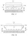
- FIG. 17depicts a cross-sectional view a first embodiment of template configured for liquid confinement at the perimeter of the template
- FIG. 18depicts a cross-sectional view a second embodiment of template configured for liquid confinement at the perimeter of the template
- FIGS. 19 A-Ddepict cross-sectional views of a sequence of steps of a template contacting a liquid disposed on a substrate.
- FIGS. 20 A-Bdepict top and cross-sectional views, respectively, of a template having a plurality of patterning areas and borders;
- FIG. 21depicts a projection view of a rigid template support system coupled to a pre-calibration system of an imprint head
- FIG. 22depicts an imprint head coupled to an X-Y motion system
- FIGS. 23 A- 23 Fdepict cross-sectional views of a negative imprint lithography process
- FIGS. 24 A- 24 Ddepict cross-sectional views of a negative imprint lithography process with a transfer layer
- FIGS. 25 A- 25 Ddepict cross-sectional views of a positive imprint lithography process
- FIGS. 26 A- 26 Cdepict cross-sectional views of a positive imprint lithography process with a transfer layer
- FIGS. 27 A- 27 Edepict cross-sectional views of a combined positive and negative imprint lithography process
- FIG. 28depicts a schematic of an optical alignment measuring device positioned over a template and substrate
- FIG. 29depicts a scheme for determining the alignment of a template with respect to a substrate using alignment marks by sequentially viewing and refocusing
- FIG. 30depicts a scheme for determining the alignment of a template with respect to a substrate using alignment marks and polarized filters
- FIG. 31depicts a top view of an alignment mark that is formed from polarizing lines
- FIGS. 32 A- 32 Cdepict top views of patterns of curable liquid applied to a substrate
- FIGS. 33 A- 33 Cdepict a scheme for removing a template from a substrate after curing
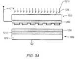
- FIG. 34depicts an embodiment of a template positioned over a substrate for electric field based lithography
- FIGS. 35 A- 35 Ddepict a first embodiment of a process for forming nanoscale structures using contact with a template
- FIGS. 36 A- 36 Cdepict a first embodiment of a process for forming nanoscale structures without contacting a template
- FIGS. 37 A- 37 Cdepict a template that includes a continuous patterned conductive layer disposed on a non-conductive base
- FIG. 38depicts a motion stage having a substrate tilt module
- FIG. 39depicts a motion stage that includes a fine orientation system.
- FIG. 40depicts a schematic drawing of a substrate support
- FIG. 41depicts a schematic drawing of an imprint lithography system that includes an imprint head disposed below a substrate support;
- FIG. 42depicts a schematic view of the degrees of motion of the template and the substrate
- FIG. 43depicts a schematic view of an interferometer based position detector
- FIG. 44depicts a projection view of a an interferometer based position detector
- FIG. 45depicts a cross sectional view of a patterned template that includes an alignment mark surrounded by a border
- FIGS. 46 A- 46 Ddepict schematic views of an off axis alignment method
- FIGS. 47 A- 47 Edepict overhead views of a theta alignment process
- FIG. 48Adepicts a top view of an alignment target that includes a diffraction grating
- FIG. 48Bdepicts a cross-sectional view of an diffraction grating
- FIG. 48Cdepicts a top view of an alignment target that includes diffraction gratings having different spacings
- FIG. 49depicts a schematic view of a scatterometry system for analyzing multiple wavelengths on N order scattered light
- FIG. 50depicts a schematic view of a scatterometry system for analyzing multiple wavelengths on N order scattered light through an optical element
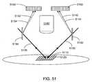
- FIG. 51depicts a schematic view of a scatterometry system for analyzing zero order scattered light at non-normal angles
- FIG. 52depicts a schematic view of a scatterometry system for analyzing zero order scattered light at non-normal angles through optical elements
- FIG. 53depicts a schematic view of a scatterometry system for analyzing zero order scattered light at non-normal angles through a fiber optic system
- FIG. 54depicts a schematic view of a scatterometry system for analyzing N order scattered light at non-normal angles through a fiber optic system.
- Embodiments presented hereingenerally relate to systems, devices, and related processes of manufacturing small devices. More specifically, embodiments presented herein relate to systems, devices, and related processes of imprint lithography. For example, these embodiments may be used for imprinting sub 100 nm features on a substrate, such as a semiconductor wafer. It should be understood that these embodiments may also be used to manufacture other kinds of devices including, but not limited to: patterned magnetic media for data storage, micro-optical devices, micro-electro-mechanical system, biological testing devices, chemical testing and reaction devices, and X-ray optical devices.
- Imprint lithography processeshave demonstrated the ability to replicate high-resolution (sub-50 nm) images on substrates using templates that contain images as topography on their surfaces.
- Imprint lithographymay be used in patterning substrates in the manufacture of microelectronic devices, optical devices, MEMS, opto-electronics, patterned magnetic media for storage applications, etc.
- Imprint lithography techniquesmay be superior to optical lithography for making three-dimensional structures such as micro lenses and T-gate structures.
- Components of an imprint lithography systemincluding the template, substrate, liquid and any other materials that may affect the physical properties of the system, including but not limited to surface energy, interfacial energies, Hamacker constants, Van der Waals' forces, viscosity, density, opacity, etc., are engineered to properly accommodate a repeatable process.
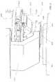
- FIG. 1depicts an embodiment of a system for imprint lithography 3900 .
- System 3900includes an imprint head 3100 .
- Imprint head 3100is mounted to an imprint head support 3910 .
- Imprint head 3100is configured to hold a patterned template 3700 .
- Patterned template 3700includes a plurality of recesses that define a pattern of features to be imprinted into a substrate.
- Imprint head 3100 or motion stage 3600is further configured to move patterned template 3700 toward and away from a substrate to be imprinted during use.
- System 3900also includes a motion stage 3600 .
- Motion stage 3600is mounted to motion stage support 3920 .
- Motion stage 3600is configured to hold a substrate and move the substrate in a generally planar motion about motion stage support 3920 .
- System 3900further includes a curing light system 3500 coupled to imprint head 3100 .
- Activating light system 3500is configured to produce a curing light and direct the produced curing light through patterned template 3700 coupled to imprint head 3100 .
- Curing lightincludes light at an appropriate wavelength to cure a polymerizable liquid. Curing light includes ultraviolet light, visible light, infrared light, x-ray radiation and electron beam radiation.
- Imprint head support 3910is coupled to motion stage support 3920 by bridging supports 3930 . In this manner imprint head 3100 is positioned above motion stage 3600 .
- Imprint head support 3910 , motion stage support 3920 and bridging supports 3930are herein collectively referred to as the system “body.”
- the components of the system bodymay be formed from thermally stable materials. Thermally stable materials have a thermal expansion coefficient of less than about 10 ppm/deg. C. at about room temperature (e.g. 25 deg C.). In some embodiments, the material of construction may have a thermal expansion coefficient of less than about 10 ppm/deg. C., or less than 1 ppm/deg. C.
- Motion stage support 3920 and bridging supports 3930are coupled to a support table 3940 .
- Support table 3940provides a substantially vibration free support for the components of system 3900 .
- Support table 3940isolates system 3900 from ambient vibrations (e.g., due to works, other machinery, etc.).
- Motion stages and vibration isolation support tablesare commercially available from Newport Corporation of Irvine, Calif.
- the “X-axis”refers to the axis that runs between bridging supports 3930 .
- the “Y-axis”refers to the axis that is orthogonal to the X-axis.
- the “X-Y plane”is a plane defined by the X-axis and the Y-axis.
- the “Z-axis”refers to an axis running from motion stage support 3920 to imprint head support 3910 , orthogonal to the X-Y plane.
- an imprint processinvolves moving the substrate, or the imprint head, along an X-Y plane until the proper position of the substrate with respect to the patterned template is achieved. Movement of the template, or motion stage, along the Z-axis, will bring the patterned template to a position that allows contact between the patterned template and a liquid disposed on a surface of the substrate.
- System 3900may be placed in an enclosure 3960 , as depicted in FIG. 2.
- Enclosure 3960encompasses imprint lithography system 3900 and provides a thermal and air barrier to the lithography components.
- Enclosure 3960includes a movable access panel 3962 that allows access to the imprint head and motion stage when moved to an “open” position, as depicted in FIG. 2. When in a “closed” position, the components of system 3900 are at least partially isolated from the room atmosphere.
- Access panel 3962also serves as a thermal barrier to reduce the effects of temperature changes within the room on the temperature of the components within enclosure 3960 .
- Enclosure 3960includes a temperature control system. A temperature control system is used to control the temperature of components with enclosure 3960 .
- temperature control systemis configured to inhibit temperature variations of greater than about 1° C. within enclosure 3960 . In some embodiments, a temperature control system inhibits variations of greater than about 0.1° C. In one embodiment, thermostats or other temperature measuring devices in combination with one or more fans may be used to maintain a substantially constant temperature with enclosure 3960 .
- a computer controlled user interface 3964may be coupled to enclosure 3960 .
- User interface 3964may depict the operating parameters, diagnostic information, job progress and other information related to the functioning of the enclosed imprint system 3900 .
- User interface 3964may also be configured to receive operator commands to alter the operating parameters of system 3900 .
- a staging support 3966may also be coupled to enclosure 3960 .
- Staging support 3966is used by an operator to support substrates, templates and other equipment during an imprint lithography process.
- staging support 3966may include one or more indentations 3967 configured to hold a substrate (e.g., a circular indentation for a semiconductor wafer).
- Staging support 3966may also include one or more indentations 3968 for holding a template.
- Additional componentsmay be present depending on the processes that the imprint lithography system is designed to implement.
- semiconductor processing equipmentincluding, but not limited to, an automatic wafer loader, an automatic template loader and an interface to a cassette loader (all not shown) may be coupled to imprint lithography system 3900 .
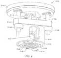
- FIG. 3depicts an embodiment of a portion of an imprint head 3100 .
- Imprint head 3100includes a pre-calibration system 3109 and a fine orientation system 3111 coupled to the pre-calibration system.
- Template support 3130is coupled to fine orientation system 3111 .
- Template support 3130is designed to support and couple a template 3700 to fine orientation system 3111 .
- a disk-shaped flexure ring 3124which makes up a portion of the pre-calibration system 3109 is coupled to imprint head housing 3120 .
- Imprint head housing 3120is coupled to a middle frame 3114 with guide shafts 3112 a, 3112 b.
- three (3) guide shaftsmay be used (the back guide shaft is not visible in FIG. 4) to provide a support for housing 3120 .
- Sliders 3116 a and 3116 b coupled to corresponding guide shafts 3112 a, 3112 b about middle frame 3114are used to facilitate the up and down motion of housing 3120 .
- a disk-shaped base plate 3122is coupled to the bottom portion of housing 3120 .
- Base plate 3122may be coupled to flexure ring 3124 .
- Flexure ring 3124supports the fine orientation system components that include first flexure member 3126 and second flexure member 3128 . The operation and configuration of the flexure members 3126 , 3128 are discussed in detail below.
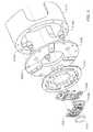
- FIG. 5depicts an exploded view of imprint head 3700 .
- actuators 3134 a, 3134 b, 3134 care fixed within housing 3120 and coupled to base plate 3122 and flexure ring 3124 .
- motion of actuators 3134 a, 3134 b, and 3134 ccontrols the movement of flexure ring 3124 .
- Motion of actuators 3134 a, 3134 b, and 3134 cmay allow for a coarse pre-calibration.
- actuators 3134 a, 3134 b, and 3134 cmay be equally spaced around housing 3120 .
- Actuators 3134 a, 3134 b, 3134 c and flexure ring 3124together form the pre-calibration system. Actuators 3134 a, 3134 b, 3134 c allow translation of flexure ring 3124 along the Z-axis to control the gap accurately.
- Imprint head 3100also include a mechanism that enables fine orientation control of template 3700 so that proper orientation alignment may be achieved and a uniform gap may be maintained by the template with respect to a substrate surface. Alignment and gap control is achieved, in one embodiment, by the use of first and second flexure members, 3126 and 3128 , respectively.
- first flexure member 3126includes a plurality of flexure joints 3160 coupled to corresponding rigid bodies 3164 and 3166 .
- Flexure joints 3160may be notch shaped to provide motion of rigid bodies 3164 and 3166 about pivot axes that are located along the thinnest cross section of the flexure joints.
- Flexure joints 3160 and rigid body 3164together form arm 3172
- additional flexure joints 3160 and rigid body 3166together form arm 3174 .
- Arms 3172 and 3174are coupled to and extend from first flexure frame 3170 .
- First flexure frame 3170has an opening 3182 , which allows curing light (e.g., ultraviolet light) to pass through first flexure member 3126 .
- curing lighte.g., ultraviolet light
- four flexure joints 3160allow motion of first flexure frame 3170 about a first orientation axis 3180 . It should be understood, however, that more or less flexure joints may be used to achieve the desired control.
- First flexure member 3126is coupled to second flexure member 3128 through fist flexure frame 3170 , as depicted in FIG. 8.
- First flexure member 3126also includes two coupling members 3184 and 3186 .
- Coupling members 3184 and 3186include openings that allow attachment of the coupling members to flexure ring 3124 using any suitable fastening means. Coupling members 3184 and 3186 are coupled to first flexure frame 3170 via arms 3172 and 3174 as depicted.
- Second flexure member 3128includes a pair of arms 3202 and 3204 extending from second flexure frame 3206 , as depicted in FIG. 7. Flexure joints 3162 and rigid body 3208 together form arm 3202 , while additional flexure joints 3162 and rigid body 3210 together form arm 3204 . Flexure joints 3162 may be notch shaped to provide motion of rigid bodies 3210 and 3204 about pivot axes that are located along the thinnest cross section of the flexure joints. Arms 3202 and 3204 are coupled to and extend from template support 3130 . Template support 3130 is configured to hold and retain at least a portion of a patterned template.
- Template support 3130also has an opening 3212 , which allows curing light (e.g., ultraviolet light) to pass through second flexure member 3128 .
- curing lighte.g., ultraviolet light
- four flexure joints 3162allow motion of template support 3130 about a second orientation axis 3200 . It should be understood, however, that more or less flexure joints may be used to achieve the desired control.
- Second flexure member 3128also includes braces 3220 and 3222 . Braces 3220 and 3222 include openings that allow attachment of the braces to portions of first flexure member 3126 .
- first flexure member 3126 and second flexure member 3128are joined as shown in FIG. 8 to form fine orientation section 3111 .
- Braces 3220 and 3222are coupled to first flexure frame 3170 such that the first orientation axis 3180 of first flexure member 3126 and second orientation axis 3200 of second flexure member are substantially orthogonal to each other.
- first orientation axis 3180 and second orientation axis 3200intersect at a pivot point 3252 at approximately the center region of a patterned template 3700 disposed in template support 3130 .
- This coupling of the first and second flexure memberallows fine alignment and gap control of patterned template 3700 during use.
- first and second flexure membersare depicted as discrete elements, it should be understood that the first and second flexure member may be formed from a single machined part where the flexure members are integrated together.
- Flexure members 3126 and 3128are coupled by mating of surfaces such that motion of patterned template 3700 occurs about pivot point 3252 , substantially reducing “swinging” and other motions that may shear imprinted features following imprint lithography.
- Fine orientation sectionimparts negligible lateral motion at the template surface and negligible twisting motion about the normal to the template surface due to selectively constrained high structural stiffness of the flexure joints.
- Another advantage of using the herein described flexure membersis that they do not generate substantial amounts of particles, especially when compared with frictional joints. This is offers an advantage for imprint lithography processes, as particles may be disrupt such processes.
- FIG. 9depicts the assembled fine orientation system coupled to the pre-calibration system.
- Patterned template 3700is positioned within template support 3130 that is part of second flexure member 3128 .
- Second flexure member 3128is coupled to first flexure member 3126 in a substantially orthogonal orientation.
- First flexure member 3124is coupled to flexure ring 3124 via coupling members 3186 and 3184 .
- Flexure ring 3124is coupled to base plate 3122 , as has been described above.
- FIG. 10represents a cross-section of the pre-calibration system looking through cross-section 3260 .
- flexure ring 3124is coupled to base plate 3122 with actuator 3134 .
- Actuator 3134includes an end 3270 coupled to a force detector 3135 that contacts flexure ring 3124 .
- force detector 3135that contacts flexure ring 3124 .
- actuator 3134causes movement of end 3270 toward or away from flexure ring 3124 .
- the movement of end 3270 toward flexure ring 3124induces a deformation of the flexure ring and causes translation of the fine orientation system along the Z-axis toward the substrate.
- Movement of base 3270 away from flexure ringallows the flexure ring to move to its original shape and, in the process, moves the fine orientation stage away from the substrate.
- the templateis disposed in a template holder coupled to the fine orientation system, as depicted in previous figures.
- the templateis brought into contact with a liquid on a surface of a substrate. Compression of the liquid on the substrate as the template is brought closer to the substrate causes a resistive force to be applied by the liquid onto the template.
- This resistive forceis translated through the fine orientation system and to flexure ring 3124 as shown in both FIGS. 9 and 10.
- the force applied against flexure ring 3124will also be translated as a resistive force to actuators 3134 .
- the resistive force applied to an actuator 3134may be determined using force sensor 3135 . Force sensor 3135 may be coupled to actuator 3134 such that a resistive force applied to actuator 3135 during use may be determined and controlled.
- FIG. 11depicts a flexure model, denoted generally as 3300 , useful in understanding the principles of operation of a fine decoupled orientation stage, such as the fine orientation section described herein.
- Flexure model 3300may include four parallel joints: Joints 1 , 2 , 3 and 4 , that provide a four-bar-linkage system in its nominal and rotated configurations.
- Line 3310denotes an axis of alignment of Joints 1 and 2 .
- Line 3312denotes an axis of alignment of Joints 3 and 4 .
- Angle ⁇ 1represents an angle between a perpendicular axis through the center of template 3700 and line 3310 .
- Angle ⁇ 2represents a perpendicular axis through the center of template 3700 and line 3310 .
- Angles ⁇ 1 and ⁇ 2are selected so that the compliant alignment axis (or orientation axis) lies substantially at the surface of template 3700 .
- rigid body 3314 between Joints 2 and 3may rotate about an axis depicted by Point C.
- Rigid body 3314may be representative of template support 3130 of second flexure member 3128 .
- Fine orientation systemgenerates pure tilting motions with no substantial lateral motions at the surface of a template coupled to the fine orientation system.
- the use of flexure armsmay provide fine orientation system with high stiffness in the directions where side motions or rotations are undesirable and lower stiffness in directions where necessary orientation motions are desirable.
- Fine orientation systemtherefore allows rotations of the template support, and therefore the template, about the pivot point at the surface of template, while providing sufficient resistance in a direction perpendicular to the template and parallel to the template to maintain the proper position with respect to the substrate. In this manner a passive orientation system is used for orientation of the template to a parallel orientation with respect to a template.
- Passiverefers to a motion that occurs without any user or programmable controller intervention, i.e., the system self-corrects to a proper orientation by contact of the template with the liquid.
- Alternate embodiments in which the motion of the flexure arms is controlled by motors to produce an active flexuremay also be implemented.
- Motion of the fine orientation stagemay be activated by direct or indirect contact with the liquid.
- the fine orientation stageis passive, then it is, in one embodiment, designed to have the most dominant compliance about two orientation axes.
- the two orientation axeslie orthogonal to each other and lie on the imprinting surface of an imprinting member disposed on the fine orientation stage.
- the two orthogonal torsional compliance valuesare set to be the same for a symmetrical imprinting member.
- a passive fine orientation stageis designed to alter the orientation of the template when the template is not parallel with respect to a substrate. When the template makes contact with liquid on the substrate, the flexure members compensate for the resulting uneven liquid pressure on the template. Such compensation may be affected with minimal or no overshoot.
- a fine orientation stage as described abovemay hold the substantially parallel orientation between the template and substrate for a sufficiently long period to allow curing of the liquid.
- Imprint head 3100is mounted to imprint head support 3910 as depicted in FIG. 1.
- imprint head 3910is mounted such that the imprint head remains in a fixed position at all times. During use, all movement along the X-Y plane is performed to the substrate by motion stage 3600 .
- Motion stage 3600is used to support a substrate to be imprinted and move the substrate along an X-Y plane during use.
- Motion stagein some embodiments, is capable of moving a substrate over distances of up to several hundred millimeters with an accuracy of at least ⁇ 30 nm, preferably with an accuracy of about ⁇ 10 nm.
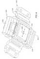
- motion stageincludes a substrate chuck 3610 that is coupled to carriage 3620 , as depicted in FIG. 12.
- Carriage 3620is moved about a base 3630 on a frictional bearing system or a non-frictional bearing system.
- a non-frictional bearing systemthat includes an air bearing is used.
- Carriage 3620is suspended above base 3630 of motion stage using, in one embodiment, an air layer (i.e., the “air bearing”).
- an air layeri.e., the “air bearing”.
- Magnetic or vacuum systemsmay be used to provide a counter balancing force to the air bearing level. Both magnetic based and vacuum based systems are commercially available from a variety of suppliers and any such systems may be used in an imprint lithography process.
- One example of a motion stage that is applicable to imprint lithography processesis the Dynam YX motion stage commercially available from Newport Corporation, Irvine Calif.
- the motion stagealso may include a tip tilt stage similar to the calibration stage, designed to approximately level the substrate to the X Y motion plane. It also may include one or more theta stages to orient the patterns on the substrate to the X Y motion axes.
- System 3900also includes a liquid dispense system which is used to dispense a curable liquid onto a substrate.
- Liquid dispense systemis coupled to the system body.
- a liquid dispense systemis coupled to imprint head 3100 .
- FIG. 3depicts liquid dispenser head 2507 of a liquid dispense system extending out from cover 3127 of imprint head 3100 .
- Various components of liquid dispense system 3125may be disposed in cover 3127 of imprint head 3100 .
- a liquid dispense systemincludes a liquid container 2501 .
- Liquid container 2501is configured to hold an activating light curable liquid.
- Liquid container 2501is coupled to a pump 2504 via inlet conduit 2502 .
- An inlet valve 2503is positioned between liquid container 2501 and pump 2504 to control flow of through inlet conduit 2502 .
- Pump 2504is coupled to a liquid dispenser head 2507 via outlet conduit 2506 .
- Liquid dispense systemis configured to allow precise volume control of the amount of liquid dispensed onto an underlying substrate.
- liquid controlis achieved using a piezoelectric valve as pump 2504 .
- Piezoelectric valvesare available commercially available from the Lee Company, Westbrook, Conn.
- a curable liquidis drawn into pump 2504 through inlet conduit 2502 .
- pump 2504is activated to force a predetermined volume of liquid through outlet conduit 2506 .
- the liquidis then dispensed through liquid dispenser head 2507 onto the substrate.
- liquid volume controlis achieved by control of pump 2504 .
- Pump 2504is configured to dispense liquid in volumes of less than about 1 ⁇ L.
- the operation of pump 2504may allow either droplets of liquid or a continuous pattern of liquid to be dispensed onto the substrate. Droplets of liquid are applied by rapidly cycling the pump from an open to closed state. A stream of liquid is produced on the substrate by leaving the pump in an open state and moving the substrate under the liquid dispenser head.
- liquid volume controlmay be achieved by use of liquid dispenser head 2507 .
- pump 2504is used to supply a curable liquid to liquid dispenser head 2507 .
- Small drops of liquid whose volume may be accurately specifiedare dispensed using a liquid dispensing actuator.
- liquid dispensing actuatorsinclude micro-solenoid valves or piezo-actuated dispensers. Piezo-actuated dispensers are commercially available from MicroFab Technologies, Inc., Plano, Tex.
- Liquid dispensing actuatorsare incorporated into liquid dispenser head to allow control of liquid dispensing. Liquid dispensing actuators are configured to dispense between about 50 ⁇ L to about 1000 ⁇ L of liquid per drop of liquid dispensed.
- Linear encodersinclude a scale coupled to the moving object and a reader coupled to the body.
- the scalemay be formed from a variety of materials including glass, glass ceramics, and steel.
- the scaleincludes a number of markings that are read by the reader to determine a relative or absolute position of the moving object.
- the scaleis coupled to the motion stage by means that are known in the art.
- a readeris coupled to the body and optically coupled to the scale.
- an exposed linear encodermay be used.
- Encodersmay be configured to determine the position of the motion stage along either a single axis, or in a two-axis plane.
- An example of an exposed two-axis linear encoderis the PP model encoder available from Heidenhain Corporation, Schaumburg, Ill.
- encodersare built into many commercially available X-Y motion stages. For example, the Dynam YX motion stage available from Newport Corp has a two-axis encoder built into the system.
- the coarse position of the template along the Z-axisis also determined using a linear encoder.
- an exposed linear encodermay be used to measure the position of the template.
- a scale of the linear encoderin one embodiment, is coupled to the pre-calibration ring of the imprint head. Alternatively, the scale may be coupled directly to the template support 3130 .
- the readeris coupled to the body and optically coupled to the scale. Position of the template is determined along the Z-axis by use of encoders.
- the detection of the position of the template and substrate during an imprint lithography processneeds to be known to a degree of accuracy of less than 100 nm. Since many features on a patterned template in a high-resolution semiconductor process are smaller than 100 nm, such control is important to allow proper alignment of the features. Fine position detection, in one embodiment, may be determined using interferometers (e.g., laser interferometers).
- FIG. 42depicts the axis of rotation and movement that may be determined during an imprint lithography process.
- Substrate positionis determined along the X W axis, the Y W aixs and the Z W axis. Rotation of the substrate may also be determined about the X-axis ( ⁇ W ), about the Y-axis ( ⁇ W ) and about the Z-axis ( ⁇ W ).
- the position of the templateis determined along the X, Y and Z axis. Rotation of the template may also be determined about the X-axis ( ⁇ T ), about the Y-axis ( ⁇ T ) and about the Z-axis ( ⁇ T ).
- the X,Y, and Z coordinates as well as the ⁇ , ⁇ and about the ⁇ anglesshould be matched.
- Linear encodersmay be used to determine X-axis, Y-axis and Z-axis positions of the template and substrate. However, such encoders typically do not provide the rotational information about these axes.
- interferometersmay be used to determine the X-axis and Y-axis position of the template and substrate and the rotational angles ⁇ , ⁇ , and ⁇ .
- FIG. 43A schematic of an interferometer based position detection system is depicted in FIG. 43.
- An interferometer system 4300includes a first three axis laser interferometer 4310 and a second three axis laser interferometer 4320 .
- Mirror 4330 and mirror 4335are coupled to the substrate and/or template.
- Mirror 4330 and mirror 4335are optically coupled to first and second laser interferometers, respectively.
- Mirror 4330is positioned on a portion of the template and/or substrate that is perpendicular to a side that mirror 4335 is placed on the template and/or substrate. As depicted in FIG. 43, this allows five degrees of motion to be determined substantially simultaneously.
- First laser interferometer 4310will provide sensing of the position of the substrate and/or template along the X-axis and the rotational angles ⁇ and ⁇ .
- Second laser interferometer 4320will provide sensing of the position of the substrate and/or template along the Y-axis and the rotational angles ⁇ and ⁇ .
- Position detector 4400is mounted to a portion of the body of system 3900 .
- position detectormay be mounted to support 3930 of the body.
- Position detector 440includes, in one embodiment, four interferometers. Interferometers are, in one embodiment, laser based. Either differential or absolute interferometers may be used. Two interferometers 4410 and 4415 are used for position determination of the template. The other two interferometers 4420 and 4425 are used for position determination of the substrate. In one embodiment, all of the interferometers are three axis interferometers.
- interferometersallow five degrees of movement (e.g., X and Y position and ⁇ , ⁇ and ⁇ rotation) of both the template and the substrate.
- Laser 4430provides light for the interferometers.
- Light from the laseris conducted to interferometers 4410 , 4415 , 4420 , and 4425 through optical components 4440 (note: not all optical components have been referenced).
- Optical componentsinclude beam splitters and mirror systems to conduct light from the laser to the interferometers. Interferometer systems and the appropriate optical systems are commercially available from several sources.
- an air gauge 3135may be coupled to imprint head 3100 , as depicted in FIG. 3. Air gauge 3135 is used to determine whether a substrate disposed on a motion stage is substantially parallel to a reference plane.
- an “air gauge”refers to a device that measures the pressure of a stream of air directed toward a surface. When a substrate is disposed under an outlet of air gauge 3135 , the distance the substrate is from the outlet of air gauge 3135 will influence the pressure the air gauge senses. Generally, the further away from the air gauge the substrate is, the lesser the pressure.
- air gauge 3135may be used to determine differences in pressure resulting from changes in the distance between the substrate surface and the air gauge. By moving air gauge 3135 along the surface of the substrate, the air gauge determines the distance between the air gauge and the substrate surface at the various points measured. The degree of planarity of the substrate with respect to the air gauge is determined by comparing the distance between the air gauge and substrate at the various points measured. The distance between at least three points on the substrate and the air gauge is used to determine if a substrate is planar. If the distance is substantially the same, the substrate is considered to be planar. Significant differences in the distances measured between the substrate and the air gauge indicates a non-planar relationship between the substrate and the air gauge.
- This non-planar relationshipmay be caused by the non-planarity of the substrate or a tilt of the substrate.
- a tilt of the substratePrior to use, a tilt of the substrate is corrected to establish a planar relationship between the substrate and the template.
- Suitable air gaugesmay be obtained from Senex Inc.
- the substrate or templateis placed within the measuring range of the air gauge.
- Motion of the substrate toward the air gaugemay be accomplished by either Z-axis motion of the imprint head or Z-axis motion of the motion stage.
- a light curable liquidis disposed on a surface of the substrate.
- a patterned templateis brought into contact with the light curable liquid and activating light is applied to the light curable liquid.
- activating lightmeans light that may affect a chemical change. Activating light may include ultraviolet light (e.g., light having a wavelength between about 200 nm to about 400 nm), actinic light, visible light or infrared light. Generally, any wavelength of light capable of affecting a chemical change may be classified as activating. Chemical changes may be manifested in a number of forms. A chemical change may include, but is not limited to, any chemical reaction that causes a polymerization or a cross-linking reaction to take place.
- the activating lightin one embodiment, is passed through the template prior to reaching the composition. In this manner the light curable liquid is cured to form structures complementary to the structures formed on the template.
- activating light source 3500is an ultraviolet light source capable of producing light having a wavelength between about 200 nm to about 400 nm.
- Activating light source 3500is optically coupled to the template as depicted in FIG. 1.
- activating light source 3500is positioned proximate to imprint head 3100 .
- Imprint head 3100includes a mirror 3121 (depicted in FIG. 4, which reflects light from the activating light source to the patterned template. Light passes through an opening in the body of imprint head 3100 and is reflected by mirror 3121 toward 3700 . In this manner, activating light source irradiates a patterned template without being disposed in imprint head 3100 .
- activating light sourcesproduce a significant amount of heat during use. If activating light source 3500 is too close to imprint system 3500 , heat from the light source will radiate toward the body of the imprint system and may cause the temperature of portions of the body to increase. Since many metals expand when heated, the increase in temperature of a portion of the body of the imprint system may cause an expansion of the body to expand. This expansion may affect the accuracy of the imprint system when sub-100 nm features are being produced.
- activating light sourceis positioned at a sufficient distance from the body such that system body is insulated from heat produced by activating light source 3500 by the intervening air between activating light source 3500 and imprint head 3100 .
- FIG. 14depicts an activating light source 3500 optically coupled to imprint head 3100 .
- Activating light source 3500includes an optical system 3510 that projects light generated by a light source toward imprint head 3100 . Light passes from optical system 3510 into imprint head 3100 via opening 3123 . Light is then reflected toward a template coupled to imprint head 3110 by mirror 3121 disposed within the imprint head (see FIG. 4). In this manner, the light source is thermally insulated from the body.
- a suitable light sourcemay be obtained from OAI Inc, Santa Clara Calif.
- One or more optical measuring devicesmay be coupled to imprint head 3910 and/or motion stage 3920 .
- an optical measuring deviceis any device that allows the position and/or orientation of a template with respect to a substrate to be determined.
- Optical imaging system 3800includes an optical imaging device 3810 and an optical system 3820 .
- Optical imaging device 3810in one embodiment, is a CCD microscope.
- Optical imaging system 3800is optically coupled to the template through imprint head.
- Optical imaging system 3800is also optically coupled to a substrate, when the substrate is disposed under the patterned template.
- Optical imaging system 3800is used to determine the placement error between a patterned template and an underlying substrate as described herein.
- mirror 3121(depicted in FIG. 4) is movable within the imprint head. During an alignment or optical inspection process, mirror 3121 is moved out of the optical path of the optical imaging system.
- the substrate or templateis placed within the measuring range (e.g., the field of view) of the optical imaging system.
- Motion of the substrate toward the optical imaging systemmay be accomplished by either Z-axis motion of the imprint head or Z-axis motion of the motion stage.
- Off axis positionsare herein defined as a position that is not in the optical path of the activating light source.
- An off axis optical imaging system 3830is coupled to imprint head 3100 as depicted in FIG. 14.
- Off axis optical imaging system 3830includes an optical imaging device 3832 and an optical system 3834 .
- Optical imaging device 3810in one embodiment, is a CCD microscope.
- Off axis imaging system 3830is used to scan the substrate without having the template in the optical path. Off axis optical imaging system 3830 may be used for off-axis alignment processes as described herein.
- off-axis optical imaging system 3830may be used to perform coarse alignment of the template with the substrate, while the through the template optical imaging system 3800 is used for fine alignment of the template with the substrate.
- Additional off-axis optical systemsmay be coupled to the imprint head 3100 .
- FIG. 12depicts an additional off-axis optical system 3840 coupled to imprint head 3100 .
- An additional optical imaging devicemay be coupled to the motion stage for viewing the template.
- a template optical imaging system 3850is coupled to motion stage 3600 as depicted in FIG. 12.
- Template optical imaging system 3850includes an optical imaging device 3852 and an optical system 3854 .
- Optical imaging device 3852in one embodiment, is a CCD microscope.
- Template optical imaging system 3850is used to scan the surface of the template without having to scan through the bulk of the template.
- Template optical imaging system 3830may be used for off-axis alignment processes as described herein.
- optical imaging systemsmay be disposed in alternate system embodiments described herein.
- an optical imaging systemmay be coupled to a motion stage that is configured to move the imprint head.
- the substrateis mounted to a substrate support that also includes an optical imaging device.
- a light curable liquidis placed on a substrate and a template is brought into contact with the liquid during an imprint lithography process.
- the curable liquidis a low viscosity liquid monomer solution.
- a suitable solutionmay have a viscosity ranging from about 0.01 cps to about 100 cps (measured at 25° C.).
- Low viscositiesare especially desirable for high-resolution (e.g., sub-100 nm) structures. Low viscosities also lead to faster gap closing. Additionally, low viscosities result in faster liquid filling of the gap area at low pressures.
- the viscosity of the solutionshould be at or below about 30 cps, or more preferably below about 5 cps (measured at 25° C.).
- the curable liquidmay be composed of a variety of polymerizable materials. Generally, any photopolymerizable material may be used. Photopolymerizable materials may include a mixture of monomers and a photoinitiator. In some embodiments, the curable liquid may include one or more commercially available negative photoresist materials. The viscosity of the photoresist material may be reduced by diluting the liquid photoresist with a suitable solvent.
- a suitable curable liquidincludes a monomer, a silylated monomer, and an initiator.
- a crosslinking agent and a dimethyl siloxane derivativemay also be included.
- Monomersinclude, but are not limited to, acrylate and methacylate monomers. Examples of monomers include, but are not limited to, butyl acrylate, methyl acrylate, methyl methacrylate, or mixtures thereof.
- the monomermakes up approximately 25 to 50% by weight of the curable liquid. It is believed that the monomer ensures adequate solubility of the photoinitiator in the curable liquid. It is further believed that the monomer provides adhesion to an underlying organic transfer layer, when used.
- the curable liquidmay also include a silylated monomer.
- Silylated monomersin general are polymerizable compounds that include a silicon group. Classes of silylated monomers include, but are not limited to, silane acrylyl and silane methacrylyl derivatives. Specific examples include methacryloxypropyl tris(tri-methylsiloxy)silane and (3-acryloxypropyl)tris(tri-methoxysiloxy)-silane. Silylated monomers may be present in amounts from 25 to 50% by weight.
- the curable liquidmay also include a dimethyl siloxane derivative.
- dimethyl siloxane derivativesinclude, but are not limited to, (acryloxypropyl) methylsiloxane dimethylsiloxane copolymer, acryloxypropyl methylsiloxane homopolymer, and acryloxy terminated polydimethylsiloxane.
- Dimethyl siloxane derivativesare present in amounts from about 0 to 50% by weight. It is believed that the silylated monomers and the dimethyl siloxane derivatives may impart a high oxygen etch resistance to the cured liquid. Additionally, both the silylated monomers and the dimethyl siloxane derivatives are believed to reduce the surface energy of the cured liquid, therefore increasing the ability of the template to release from the surface.
- the silylated monomers and dimethyl siloxane derivatives listed hereinare all commercially available from Gelest, Inc.
- any material that may initiate a free radical reactionmay be used as the initiator.
- the initiatoris a photoinitiator.
- examples of initiatorsinclude, but are not limited to, alpha-hydroxyketones (e.g., 1-hydroxycyclohexyl phenyl ketone, sold by Ciba-Geigy Specialty Chemical Division as Irgacure 184), and acylphosphine oxide initiators (e.g., phenylbis(2,4,6-trimethyl benzoyl) phosphine oxide, sold by Ciba-Geigy Specialty Chemical Division as Irgacure 819).
- alpha-hydroxyketonese.g., 1-hydroxycyclohexyl phenyl ketone, sold by Ciba-Geigy Specialty Chemical Division as Irgacure 184
- acylphosphine oxide initiatorse.g., phenylbis(2,4,6-trimethyl
- the curable liquidmay also include a crosslinking agent.
- Crosslinking agentsare monomers that include two or more polymerizable groups.
- polyfunctional siloxane derivativesmay be used as a crosslinking agent.
- An example of a polyfunctional siloxane derivativeis 1,3-bis(3-methacryloxypropyl)-tetramethyl disiloxane.
- a curable liquidmay include a mixture of 50% by weight of n-butyl acrylate and 50% (3-acryloxypropyl) tris-trimethylsiloxane-silane. To this mixture 3% by weight mixture of a 1:1 Irgacure 819 and Irgacure 184 and 5% of the crosslinker 1,3-bis(3-methacryloxypropyl)-tetramethyl disiloxane may be added. The viscosity of this mixture is less than 30 cps measured at about 25° C.
- the curable liquidmay be formed of a monomer, an acid-generating photo-agent, and a base-generating photo-agent.
- the monomerinclude, but are not limited to, phenolic polymers and epoxy resins.
- the acid-generating photo-agentis a compound that releases acid when treated with activating light. The generated acid catalyzes polymerization of the monomer.
- the acid-generating additiveis selected to be sensitive to radiation at the first wavelength ⁇ 1 , which, in some implementations, is in the visible or near ultraviolet (near UV) range.
- the first wavelength ⁇ 1is selected to be approximately 400 nm or longer.
- a base generating photo-agentis also added to the monomer.
- the base-generating photo-agentmay inhibit curing of the monomer near the interface of the template.
- the base generating photo-agentmay be sensitive to radiation at a second wavelength ⁇ 2 , yet inert or substantially inert to radiation at the first wavelength ⁇ 1 .
- the second wavelength ⁇ 2should be selected so that radiation at the second wavelength is primarily absorbed near the surface of the monomer at the interface with the template and does not penetrate very far into the curable liquid.
- a base generating additivethat is sensitive to radiation having a wavelength ⁇ 2 in the deep UV range, in other words, radiation having a wavelength in the range of about 190-280 nm, may be used.
- a curable liquidthat includes a monomer, an acid-generating photo-agent and a base-generating photo-agent is deposited onto a substrate.
- a templateis brought into contact with the curable liquid.
- the curable liquidis then exposed to radiation at a first wavelength ⁇ 1 and a second wavelength ⁇ 2 of light at substantially the same time.
- the curing liquidmay be exposed to the radiation at the second wavelength ⁇ 2 and subsequently to the radiation at the first wavelength ⁇ 1 . Exposure of the curable liquid to radiation at the second wavelength ⁇ 2 produces an excess of base near the interface with the template.
- the excess baseserves to neutralize the acid that is produced by exposure of the curable liquid to radiation at the first wavelength ⁇ 1 , thereby inhibiting the acid from curing the curable liquid. Since the radiation at the second wavelength ⁇ 2 has a shallow penetration depth into the curable liquid, the base produced by that radiation only inhibits curing of the curable liquid at or near the interface with the template. The remainder of the curable liquid is cured by exposure to the longer wavelength radiation ( ⁇ 1 ) which penetrates throughout the curable liquid.
- U.S. Pat. No. 6,218,316 entitled “Planarization of Non-Planar Surfaces in Device Fabrication”describes additional details concerning this process and is incorporated herein by reference.
- the curable liquidmay include a photosensitive agent which, when exposed, for example, to deep UV radiation, decomposes to produce one or more gases such as hydrogen (H 2 ), nitrogen (N 2 ), nitrous oxide (N 2 O), sulfur tri-oxide (SO 3 ), acetylene (C 2 H 2 ), carbon dioxide (CO 2 ), ammonia (NH 3 ) or methane (CH 4 ).
- a photosensitive agentwhich, when exposed, for example, to deep UV radiation, decomposes to produce one or more gases such as hydrogen (H 2 ), nitrogen (N 2 ), nitrous oxide (N 2 O), sulfur tri-oxide (SO 3 ), acetylene (C 2 H 2 ), carbon dioxide (CO 2 ), ammonia (NH 3 ) or methane (CH 4 ).
- Radiation at a first wavelength ⁇ 1such as visible or near UV, may be used to cure the curable liquid, and the deep UV radiation ( ⁇ 2 ) may be used to produce one or more of the for
- a curable liquidmay be composed of a monomer that cures to form a polymer that may be decomposed by exposure to light.
- a polymer with a doubly substituted carbon backboneis deposited on the substrate.
- the curable liquidis exposed to radiation at a first wavelength ⁇ 1 (e.g., greater than 400 nm) and radiation at the second wavelength ⁇ 2 in the deep UV range. Radiation at the first wavelength serves to cure the curable liquid.
- ⁇ 1e.g., greater than 400 nm
- an imprint lithography templateis manufactured using processes including, but not limited to: optical lithography, electron beam lithography, ion-beam lithography, x-ray lithography, extreme ultraviolet lithography, scanning probe lithography, focused ion beam milling, interferometric lithography, epitaxial growth, thin film deposition, chemical etch, plasma etch, ion milling, reactive ion etch or a combination of the above.
- Methods for making patterned templatesare described in U.S. patent application Ser. No. 10/136,188 filed May 1, 2002 entitled “Methods of Manufacturing a Lithography Template” to Voison which is incorporated herein by reference.
- the imprint lithography templateis substantially transparent to activating light.
- the templateincludes a body having a lower surface.
- the templatefurther includes a plurality of recesses on the lower surface extending toward the top surface of the body.
- the recessesmay be of any suitable size, although typically at least a portion of the recesses has a feature size of less than about 250 nm.
- a templateis formed from quartz.
- Other materialsmay be used to form the template and include, but are not limited to: silicon germanium carbon, gallium nitride, silicon germanium, sapphire, gallium arsinide, epitaxial silicon, poly-silicon, gate oxide, silicon dioxide or combinations thereof.
- Templatesmay also include materials used to form detectable features, such as alignment markings.
- detectable featuresmay be formed of SiO x , where X is less than 2. In some embodiments, X is about 1.5. In another example, detectable features may be formed of a molybdenum silicide.
- Both SiOx and molybdenum silicideare optically transparent to light used to cure the polymerizable liquid. Both materials, however, are substantially opaque to visible light. Use of these materials allows alignment marks to be created on the template that will not interfere with curing of the underlying substrate.
- the templateis treated with a surface treatment material to form a thin layer on the surface of the template.
- a surface treatment processis optimized to yield a low surface energy coating.
- Such a coatingis used in preparing imprint templates for imprint lithography.
- Treated templateshave desirable release characteristics relative to untreated templates.
- Untreated template surfacespossess surface free energies of about 65 dynes/cm or more.
- a treatment procedure disclosed hereinyields a surface treatment layer that exhibits a high level of durability. Durability of the surface treatment layer allows a template to be used for numerous imprints without having to replace the surface treatment layer.
- the surface treatment layerin some embodiments, reduces the surface free energy of the lower surface measured at 25° C. to less than about 40 dynes/cm, or in some cases, to less than about 20 dynes/cm.
- a surface treatment layerin one embodiment, is formed by the reaction product of an alkylsilane, a fluoroalkylsilane, or a fluoroalkyltrichlorosilane with water. This reaction forms a silinated coating layer on the surface of the patterned template.
- a silinated surface treatment layeris formed from a reaction product of tridecafluoro-1,1,2,2-tetrahydrooctyl trichlorosilane with water.
- a surface treatment layermay be formed using either a liquid-phase process or a vapor-phase process. In a liquid-phase process, the substrate is immersed in a solution of precursor and solvent.
- a precursoris delivered via an inert carrier gas. It may be difficult to obtain a purely anhydrous solvent for use in a liquid-phase treatment. Water in the bulk phase during treatment may result in clump deposition, which will adversely affect the final quality or coverage of the coating.
- the templateis placed in a vacuum chamber, after which the chamber is cycle-purged to remove excess water. Some adsorbed water, however, remains on the surface of the template. A small amount of water, however, is believed to be needed to initiate a surface reaction, which forms the coating. It is believed that the reaction may be described by the formula:
- the templateis brought to a desired reaction temperature via a temperature-controlled chuck.
- the precursoris then fed into the reaction chamber for a prescribed time.
- Reaction parameterssuch as template temperature, precursor concentration, flow geometries, etc. are tailored to the specific precursor and template substrate combination.
- the thickness of the surface treatment layeris controlled.
- the thickness of the surface treatment layeris kept at a minimal value to minimize the interference of the surface treatment layer with the feature size.
- a monolayer of the surface treatment layeris formed.
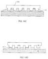
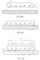
- FIGS. 20A and 20Bdepict top and cross-sectional views, respectively, of a patterned template with recesses having two depths.
- a templateincludes one or more patterning areas 401 .
- a first relatively shallow depthis associated with the recesses in the patterning areas of the template, as depicted in FIG. 20B.
- the patterning areaincludes the area replicated during patterning of the template.
- the patterning areasare positioned within a region defined by the edges 407 of the template.
- Outer region 409is defined as the region that extends from an outer edge of any of the patterning areas to the edge of the template.
- the outer regionhas a depth that is substantially greater than the depth of the recesses in the patterning areas.
- the perimeter of the templateis herein defined as the patterning areas that are confined by outer region 409 . As depicted in FIG. 20A four patterning areas are positioned within the area defined by the template. The patterning areas are separated from the edges 407 of the template by outer region 409 .
- the “perimeter” of the templateis defined by edges 403 a, 403 b, 403 c, 403 d, 403 e, 403 f, 403 g, and 403 h of the patterning areas.
- the patterning areasmay be separated from each other by border regions 405 .
- Borders regionsare recesses that are positioned between the patterning areas that have a greater depth than the recesses of the pattering areas. As described below, both border regions and outer region inhibits the flow of liquid between the patterning regions or beyond the perimeter of the patterning areas, respectively.
- the design of the templateis chosen based on the type of lithography process used.
- a template for positive imprint lithographyhas a design that favors the formation of discontinuous films on the substrate.
- a template 12is formed such that the depth of one or more structures is relatively large compared to the depth of structures used to form the patterning region, as depicted in FIG. 15.
- template 12is placed in a desired spaced relationship to substrate 20 .
- the gap (h 1 ) between the lower surface 536 of template 12 and substrate 20is much smaller than the gap (h 2 ) between recessed surface 534 and substrate 20 .
- h 1may be less than about 200 nm, while h 2 may be greater than about 10,000 nm.
- liquid 40leaves the region under recessed surface 534 and fills the gap between lower surface 536 and substrate 20 (as depicted in FIG. 16). It is believed that combinations of surface energies and capillary forces draw the liquid from the larger recess into the narrower region. As h 1 is decreased, forces applied to the liquid by template 12 may overcome capillary forces drawing the liquid under lower surface 536 . These forces may cause spreading of the liquid into the area under recessed surface 534 .
- the minimum value of h 1 at which the liquid is inhibited from spreading into a recess 532is referred to herein as the “minimum film thickness.” Additionally, as h 1 increases, the capillary forces are reduced, eventually allowing the liquid to spread into the deeper recessed regions. The maximum value of h 1 at which the capillary forces are sufficient to inhibit flow of liquid into the deeper recessed region is herein known as the “maximum film thickness.”
- template 12is formed such that a curable liquid placed on substrate 20 is inhibited from flowing beyond perimeter 412 of template 12 .
- height h 1is measured from substrate 20 to shallow recessed surface 552 .
- Shallow recessed surface 552extends to the perimeter of template 12 .
- the edge of the templateforms the height h 2 and is effectively infinite in comparison to height h 1 .
- a deep recessis formed at the outer edge of template 12 .
- Height h 2is measured between substrate 20 and deep recessed surface 554 .
- Height h 1is again measured between substrate 20 and shallow recessed surface 552 .
- height h 2is much larger than height h 1 . If h 1 is small enough, the activating light curable liquid remains in the gap between template 12 and substrate 20 while a curing agent is applied. Deeply recessed portions are particularly useful for liquid confinement in step and repeat processes as described herein.
- template 12 and substrate 20each have one or more alignment marks.
- Alignment marksmay be used to align template 12 and substrate 20 .
- one or more optical imaging devicese.g., microscopes, cameras, imaging arrays, etc. are used to determine alignment of the alignment marks.
- an alignment mark on the templatemay be substantially transparent to activating light.
- the alignment markmay be substantially opaque to alignment mark detection light.
- alignment mark detection light and light used for other measurement and analysis purposesis referred to as “analyzing light.”
- analyzing lightincludes, but is not limited to: visible light and/or infrared light.
- the alignment markmay be formed of a material different than the material of the body.
- the alignment markmay be formed from SiO x where x is about 1.5.
- the alignment markmay be formed of molybdenum silicide.
- the alignment markmay include a plurality of lines etched on a surface of the body. The lines are configured to substantially diffuse activating light, but produce an analyzable mark under analyzing light.
- one or more deep recesses as described abovemay project entirely through the body of the template to form openings in the template.
- An advantage of such openingsis that they may effectively ensure that height h 2 is very large with respect to h 1 , at each opening.
- pressurized gas or vacuummay be applied to the openings. Pressurized gas or vacuum may also be applied to one or more openings after curing the liquid. For example, pressurized gas may be applied after curing as part of a peel and pull process to assist in separating the template from the cured liquid.
- one or more alignment marksmay be formed in a patterned template. As described herein, alignment marks formed in the template may be used to align a template with a patterned area on a substrate.
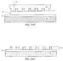
- a template that includes alignment marksis depicted in FIG. 45.
- Patterned template 4500includes patterning areas 4510 , alignment mark 4520 , and alignment mark patterning area 4530 .
- Alignment mark 4520is separated from patterning areas 4510 and 4512 by borders 4540 and 4542 , respectively. Borders 4540 and 4542 have a depth that is substantially greater than the depth of the alignment marks.
- Keeping the activating light curable liquid out of the alignment areamay offer advantages when alignment measurements are being taken.
- optical measurementsare taken thorough the template to the underlying substrate alignment marks (e.g., alignment marks 4550 ) to determine if the alignment marks are aligned.
- the presence of a liquid between the template and the substrate during alignment measurementsmay interfere with optical measurements.
- the index of refraction of a liquidis substantially similar to the template material.
- the templateWhen a template is used for imprinting one of multiple layers to be formed on a substrate, it is advantageous that the template not only include an alignment mark for alignment with an underlying substrate, but also an alignment patterning area. As depicted in FIG. 10, alignment mark patterning area 4530 contacts a portion of the applied activating light curable liquid. During curing, the alignment mark defined by alignment mark patterning area 4530 is imprinted into the cured layer. During subsequent processing, the alignment mark formed from alignment mark patterning area 4530 may be used to assist in alignment of a template with the substrate.
- an imprint headincludes a fine orientation system that allows for a “passive” orientation of the template with respect to the substrate.
- fine orientation systemmay include actuators coupled to the flexure arms. The actuators may allow “active” control of the fine orientation system.
- an operator or a programmable controllermonitors the orientation of the template with respect to the substrate. The operators or a programmable controller then alters the orientation of the template with respect to the substrate by operating the actuators. Movement of the actuators causes motion of the flexure arms to alter the orientation of the template. In this manner an “active” control of fine positioning of the template with respect to the substrate may be achieved.
- An active fine orientation systemis further described in U.S. Ser. No. 09/920,341 filed August 1, 2001 entitled “Methods for High-Precision Gap Orientation Sensing Between a Transparent Template and Substrate for Imprint Lithography” which is incorporated herein by reference.
- imprint headmay include a pre-calibration system, as described above.
- Pre-calibration systemincludes a flexure ring 3124 as depicted in FIG. 21.
- a template support system 3125is coupled to pre-calibration ring.
- template support system 3125is formed of substantially rigid and non-compliant members 3127 . These members provide a substantially rigid support for a template 3700 disposed in template support 3130 .
- fine orientationmay be achieved using motion stage instead of template support.
- imprint head 3100is coupled to the body in a fixed position.
- imprint head 3100may be mounted to a motion system that allows the imprint head to be moved along the X-Y plane, as depicted in FIG. 22.
- Imprint head 3100is configured to support a patterned template as described in any of the embodiments herein.
- Imprint head 3100is coupled to a motion system that includes an imprint head chuck 3121 and a imprint motion stage 3123 .
- Imprint head 3100is mounted to imprint head chuck 3121 .
- Imprint head chuckinteracts with imprint motion stage 3123 to move imprint head along an X-Y plane. Mechanical or electromagnetic motion systems may be used.
- Electromagnetic systemsrely on the use of magnets to produce an X-Y planar motion the imprint chuck.
- an electromagnetic systemincorporates permanent and electromagnetic magnets into the imprint motion stage 3123 and the imprint head chuck 3121 .
- the attractive forces of these magnetsis overcome by a cushion of air between imprint head chuck 3121 and imprint head motion stage 3123 such that an “air bearing” is produced.
- Imprint head chuck, and therefore the imprint headis moved along an X-Y plane on a cushion of air.
- Electromagnetic X-Y motion stagesare described in further detail in U.S. Pat. No. 6,389,702, entitled “Method and Apparatus for Motion Control,” which is incorporated herein by reference.
- imprint head chuckis attached to a motion stage.
- the motion stageis then moved by use of various mechanical means to alter the position of the imprint head chuck, and thus the imprint head, along the X-Y plane.
- imprint headmay include a passive compliant fine orientation system, an actuated fine orientation system, or a rigid template support system, as described herein.
- the substratemay be mounted to a stationary support.
- imprint head 3100is coupled to an X-Y axis motion stage as described herein.
- a substrateis mounted to a substantially stationary substrate support.
- a stationary substrate supportis depicted in FIG. 40.
- Stationary substrate support 3640includes a base 3642 and a substrate chuck 3644 .
- Substrate chuck 3644is configured to support a substrate during imprint lithography processes.
- Substrate chuckmay employ any suitable means to retain a substrate to the substrate chuck.
- substrate chuck 3644may include a vacuum system which applies a vacuum to the substrate to couple the substrate to the substrate chuck.
- Substrate chuck 3644is coupled to a base 3642 .
- Base 3642is coupled to support 3920 of an imprint lithography system (See FIG. 1).
- stationary substrate support 3640remains in a fixed position on support 3920 while the imprint head position is varied to access different portions of the substrate.
- Coupling an imprint head to a motion stagecan offer advantages over techniques in which the substrate is on a motion stage.
- Motion stagesgenerally rely on an air bearing to allow substantially frictionless motion of the motion stage.
- motion stagesare not designed to accommodate significant pressure applied along the Z-axis. When pressure is applied to a motion stage chuck along the Z-axis, the motion stage chuck position will change slightly in response to this pressure.
- a templatethat has a smaller area than the area of the substrate is used to form multiple imprinted areas.
- the substrate motion stageis relatively large compared to the template, to accommodate the larger substrates. When a template contacts the substrate motion stage in a position that is off-center, the motion stage will tilt to accommodate the increased pressure.
- This tiltis compensated for by tilting the imprint head to ensure proper alignment. If, however, the imprint head is coupled to the motion stage, all of the forces along the Z-axis will be centers on the template, regardless of where on the substrate the imprinting is taking place. This leads to increased ease in alignment and may also increase the throughput of the system.
- a substrate tilt modulemay be formed in a substrate support as depicted in FIG. 38.
- Substrate support 3650includes a substrate chuck 3652 , coupled to a substrate tilt module 3654 .
- Substrate tilt module 3654is coupled to a base 3656 .
- Base 3656in one embodiment, is coupled to a motion stage which allows X-Y motion of the substrate support.
- base 3656is coupled to a support (e.g., 3920 ) such that the substrate support is mounted to an imprint system in a fixed position.
- Substrate chuck 3652may employ any suitable means to retain a substrate to the substrate chuck.
- substrate chuck 3654may include a vacuum system which applies a vacuum to the substrate to couple the substrate to the substrate chuck.
- Substrate tilt module 3654includes a flexure ring 3658 coupled to flexure ring support 3660 .
- a plurality of actuators 3662are coupled to flexure ring 3658 and flexure ring support 3660 .
- Actuators 3662are operated to alter the tilt of flexure ring 3658 .
- Actuatorsin one embodiment, use a differential gear mechanism that may be manually or automatically operated. In an alternate embodiment, actuators use an eccentric roller mechanism.
- An eccentric roller mechanismgenerally provides more vertical stiffness to the substrate support than a differential gear system.
- substrate tilt modulehas a stiffness that will inhibit tilt of the substrate when the template applies a force of between about 1 lb. to about 10 lbs. to a liquid disposed on the substrate.
- substrate tilt moduleis configured to allow no more than 5 micro radians of tilt when pressure up to about 10 lbs. are applied to the substrate through the liquid on the template.
- sensors coupled to the substrate chuckmay be used to determine the tilt of the substrate.
- the tilt of the substrateis adjusted by actuators 3662 . In this manner tilt correction of the substrate may be achieved.
- Substrate tilt modulemay also include a fine orientation system.
- a substrate support that includes a fine orientation systemis depicted in FIG. 39.
- flexure ring 3658includes a central recess in which substrate chuck 3652 is disposed. The depth of the central recess is such that an upper surface of a substrate disposed on substrate chuck 3652 is substantially even with an upper surface of flexure ring 3658 .
- Fine orientationmay be achieved using actuators 3662 . Fine orientation is achieved by the use of actuators capable of controlled motion in the nanometer range. Alternatively, fine orientation may be achieved in a passive manner. Actuators may be substantially compliant.
- the compliance of the actuatorsmay allow the substrate to self-correct for variations in tilt when a template is in contact with a liquid disposed on a substrate surface. By disposing the substrate in a position that is substantially even with the flexure ring, fine orientation may be achieved at the substrate-liquid interface during use. Compliance of actuators is thus transferred to the upper surface of the substrate to allow fine orientation of the substrate.
- FIG. 41depicts a schematic drawing of an embodiment of a system 4100 that is configured such that the template is positioned below a substrate.
- System 4100includes an imprint head 4110 and a substrate support 4120 positioned above imprint head 4110 .
- Imprint headis configured to hold a template 3700 .
- Imprint headmay have a similar in design to any of the herein described imprint heads.
- imprint head 4110may include a fine orientation system as described herein.
- Imprint headis be coupled to imprint head support 4130 .
- Imprint headmay be coupled in a fixed position and remain substantially motionless during use.
- imprint headmay be placed on a motion stage that allows X-Y planar motion of imprint head 4130 during use.
- substrate support 4120has a similar design to any of the herein described substrate supports.
- substrate support 4120may include a fine orientation system as described herein.
- Substrate support 4120may be coupled to a support 4140 in a fixed position and remain substantially motionless during use.
- substrate support 4120may be placed on a motion stage that allows X-Y planar motion of substrate support during use.
- an activating light curable liquidis placed on a template 3700 disposed in imprint head.
- the templatemay be patterned or planar, depending on the type of operation to be performed. Patterned templates may be configured for use in positive, negative, or combinations of positive and negative imprint lithography systems as described herein.
- FIGS. 23 A- 23 FA typical imprint lithography process is shown in FIGS. 23 A- 23 F.
- template 12is positioned in a spaced relation to the substrate 20 such that a gap is formed between template 12 and substrate 20 .
- Template 12may include a surface that defines one or more desired features, which may be transferred to the substrate 20 during patterning.
- a “feature size”generally refers to a width, length and/or depth of one of the desired features.
- the desired featuresmay be defined on the surface of template 12 as recesses and or a conductive pattern formed on a surface of the template.
- Surface 14 of template 12may be treated with a thin layer 13 that lowers the template surface energy and assists in separation of template 12 from substrate 20 . Surface treatment layers for templates are described herein.
- substance 40may be dispensed upon substrate 20 prior to moving template 12 into a desired position relative to substrate 20 .
- Substance 40may be a curable liquid that conforms to the shape of desired features of template 12 .
- substance 40is a low viscosity liquid that at least partially fills the space of gap 31 without the use of high temperatures. Low viscosity liquids may also allow the gap between the template and the substrate to be closed without requiring high pressures.
- the term “low viscosity liquids”refer to liquids having a viscosity of less than about 30 centipoise measured at about 25° C. Further details regarding appropriate selections for substance 40 are discussed below.
- Template 12may interact with curable liquid 40 to conform the liquid into a desire shape.
- curable liquid 40may conform to the shape of template 12 as depicted in FIG. 23B.
- the position of template 12may be adjusted to create a desired gap distance between the template and substrate 20 .
- the position of template 12may also be adjusted to properly align the template with the substrate.
- substance 40is cured to form a masking layer 42 on the substrate.
- substance 40is cured using activating light 32 to form masking layer 42 .
- Application of activating light through template 12 to cure the liquidis depicted in FIG. 23C.
- template 12is removed from masking layer 42 , leaving the cured masking layer on the surface of substrate 20 , as depicted in FIG. 23D.
- Masking layer 42has a pattern that is complementary to the pattern of template 12 .
- Masking layer 42may include a “base layer” (also called a “residual layer”) between one or more desired features. The separation of template 12 from masking layer 42 is done so that desired features remain intact without shearing or tearing from the surface of substrate 20 . Further details regarding separation of template 12 from substrate 20 following imprinting are discussed below.
- Masking layer 42may be used in a variety of ways.
- masking layer 42may be a functional layer.
- curable liquid 40may be curable to form a conductive layer, a semiconductive layer, a dielectric layer and/or a layer having a desired mechanical or optical property.
- masking layer 42may be used to cover portions of substrate 20 during further processing of substrate 20 .
- masking layer 42may be used during a material deposition process to inhibit deposition of the material on certain portions of the substrate.
- masking layer 42may be used as a mask for etching substrate 20 .
- To simplify further discussion of masking layer 42only its use as a mask for an etching process will be discussed in embodiments described below. However, it is recognized that masking layers in embodiments described herein may be used in a variety of processes as previously described.
- masking layer 42may be etched using an etch process until portions of substrate 20 are exposed through masking layer 42 , as depicted in FIG. 23E. That is, portions of the base layer may be etched away. Portions 44 of masking layer 42 may remain on substrate 20 for use in inhibiting etching of portions of substrate 20 . After etching of masking layer 42 is complete, substrate 20 may be etched using known etching processes. Portions of substrate 20 disposed under portions 44 of masking layer 42 may remain substantially unetched while the exposed portions of substrate 20 are etched. In this manner, a pattern corresponding to the pattern of template 12 may be transferred to substrate 20 . The remaining portions 44 of masking layer 42 may be removed leaving a patterned substrate 20 , depicted in FIG. 23F.
- FIGS. 24 A- 24 Dillustrate an embodiment of an imprint lithography process using a transfer layer.
- a transfer layer 18may be formed upon an upper surface of substrate 20 .
- Transfer layer 18may be formed from a material that has different etch characteristics than underlying substrate 20 and/or a masking layer formed from a curable liquid 40 . That is, each layer (e.g., transfer layer 18 , masking layer and/or substrate 20 ) may be etched at least somewhat selectively with respect to the other layers.
- a masking layer 44is formed on the surface of transfer layer 18 by depositing a curable liquid on the surface of transfer layer 18 and curing the masking layer as described with reference to FIGS. 23 A- 23 C.
- Masking layer 42may be used as a mask for etching transfer layer 18 .
- Masking layer 42is etched using an etch process until portions of transfer layer 18 are exposed through masking layer 42 , as depicted in FIG. 24B.
- Portions 44 of masking layer 42remain on transfer layer 18 and may be used to inhibit etching of portions of the transfer layer.
- transfer layer 18may be etched using known etching processes. Portions of transfer layer 18 disposed under portions 44 of masking layer 42 may remain substantially unetched while the exposed portions of transfer layer 18 are etched. In this manner, the pattern of masking layer 42 is replicated in transfer layer 18 .
- portions 44 and etched portions of transfer layer 18together form a masking stack 46 that may be used to inhibit etching of portions of the underlying substrate 20 .
- Etching of substrate 20may be performed using a known etch process (e.g., a plasma etching process, a reactive ion etching process, etc.).
- the masking stackmay inhibit etching of the underlying portions of substrate 20 .
- Etching of the exposed portions of substrate 20may be continued until a predetermined depth is reached.
- An advantage of using a masking stack as a mask for etching of substrate 20is that the combined stack of layers may create a high aspect ratio mask (i.e., a mask that has a greater height than width).
- a high aspect ratio masking layermay be desirable during the etching process to inhibit undercutting of the mask portions.
- FIGS. 23 A- 23 F and FIGS. 24 A- 24 Dare examples of negative imprint lithography processes.
- a “negative imprint lithography” processgenerally refers to a process in which the curable liquid is substantially conformed to the shape of the template before curing. That is, a negative image of the template is formed in the cured liquid. As depicted in these figures, the non-recessed portions of the template become the recessed portions of the mask layer.
- the templatetherefore, is designed to have a pattern that represents a negative image of the pattern to be imparted to the mask layer.
- a “positive imprint lithography” processgenerally refers to a process in which the pattern formed in the mask layer is a mirror image of the pattern of the template. As will be further described below, the non-recessed portions of the template become the non-recessed portions of the mask layer.
- FIGS. 25 A- 25 DA typical positive imprint lithography process is shown in FIGS. 25 A- 25 D.
- template 12is positioned in a spaced relation to the substrate 20 such that a gap is formed between template 12 and substrate 20 .
- Surface of template 12may be treated with a thin surface treatment layer 13 that lowers the template surface energy and assists in separation of template 12 from the cured masking layer.
- a curable liquid 40is disposed on the surface of substrate 20 .
- Template 12is brought into contact with curable liquid 40 .
- the curable liquidfills the gap between the lower surface of the template and the substrate.
- curable liquid 40is substantially absent from regions of the substrate approximately below at least a portion of the recesses of the template.
- curable liquid 40is maintained as a discontinuous film on the substrate that is defined by the location of at least a portion of the recesses of template 12 .
- curable liquid 40is cured to form a masking layer 42 on the substrate.
- Template 12is removed from masking layer 42 , leaving the cured masking layer on the surface of substrate 20 , as depicted in FIG. 25C.
- Masking layer 42has a pattern that is complementary to the pattern of template 12 .
- Masking layer 42may be used to inhibit etching of portions of substrate 20 . After formation of masking layer 42 is complete, substrate 20 may be etched using known etching processes. Portions of substrate 20 disposed under masking layer 42 may remain substantially unetched while the exposed portions of substrate 20 are etched, as depicted in FIG. 25D. In this manner, the pattern of template 12 may be replicated in substrate 20 . The remaining portions 44 of masking layer 42 may be removed to create a patterned substrate 20 .
- FIGS. 26 A- 26 Cillustrate an embodiment of a positive imprint lithography process using a transfer layer.
- a transfer layer 18may be formed upon an upper surface of a substrate 20 .
- Transfer layer 18is formed from a material that has different etch characteristics than the underlying transfer layer 18 and/or substrate 20 .
- a masking layer 42is formed on the surface of transfer layer 18 by depositing a curable liquid on the surface of transfer layer 18 and curing the masking layer as described with reference to FIGS. 25 A- 25 C.
- Masking layer 42may be used as a mask for etching transfer layer 18 .
- Masking layer 42may inhibit etching of portions of transfer layer 18 .
- Transfer layer 18may be etched using known etching processes. Portions of transfer layer 18 , disposed under masking layer 42 may remain substantially unetched while the exposed portions of transfer layer 18 are etched. In this manner, the pattern of masking layer 42 may be replicated in transfer layer 18 .
- masking layer 42 and etched portions of transfer layer 18together form a masking stack 46 that may be used to inhibit etching of portions of the underlying substrate 20 .
- Etching of substrate 20may be performed using known etching processes (e.g., a plasma etching process, a reactive ion etching process, etc.).
- the masking stackmay inhibit etching of the underlying portions of substrate 20 .
- Etching of the exposed portions of substrate 20may be continued until a predetermined depth is reached.
- a processmay combine positive and negative imprint lithography.
- a template for a combined positive and negative imprint lithography processmay include recesses suitable for positive lithography and recesses suitable for negative lithography.
- FIG. 27AAn embodiment of a template for combined positive and negative imprint lithography is depicted in FIG. 27A.
- Template 12as depicted in FIG. 27A, includes a lower surface 566 , at least one first recess 562 , and at least one second recess 564 .
- First recess 562is configured to create a discontinuous portion of curable liquid 40 when the template contacts the curable liquid.
- a height of first recess (h 2 )is substantially greater than a height of second recess (h 1 ).
- FIGS. 27 A- 27 EA typical combined imprint lithography process is shown in FIGS. 27 A- 27 E.
- template 12is positioned in a spaced relation to the substrate 20 such that a gap is formed between template 12 and substrate 20 .
- At least the lower surface 566 of template 12may be treated with a thin surface treatment layer (not shown) that lowers the template surface energy and assists in separation of template 12 from the cured masking layer.
- surfaces of first recesses 562 and/or second recesses 564may be treated with the thin surface treatment layer.
- a curable liquid 40is disposed on the surface of substrate 20 .
- Template 12is brought into contact with curable liquid 40 .
- the curable liquidfills the gap between the lower surface of the template 566 and substrate 20 .
- Curable liquid 40also fills first recesses 562 .
- curable liquid 40is substantially absent from regions of the substrate approximately below second recesses 564 .
- curable liquid 40is maintained as a discontinuous film on the substrate that includes surface topography corresponding to the pattern formed by first recesses 562 .
- curable liquid 40is cured to form a masking layer 42 on the substrate.
- Mask layer 42may include a region 568 that resembles a mask layer formed by negative imprint lithography.
- mask layer 42may include a region 569 that does not include any masking material.
- mask layer 42is composed of a material that has the same or a similar etch rate as the underlying substrate.
- An etch processis be applied to masking layer 42 to remove the masking layer and substrate at substantially the same etch rate.
- the multilayer pattern of the templatemay be transferred to the substrate, as depicted in FIG. 27D.
- This processmay also be performed using a transfer layer as described in other embodiments.
- a combination of positive and negative lithographyis also useful for patterning multiple regions of a template.
- a substratemay include a plurality of regions that require patterning.
- a template with multiple depth recessesincludes two patterning regions 568 with an intervening “border” region 569 . Border region 569 inhibits flow of a liquid beyond the patterning area of the template.
- a “step and repeat” processrefers to using a template smaller than the substrate to form a plurality of patterned regions on the substrate.
- a step and repeat imprint processincludes depositing a light curable liquid on a portion of a substrate, aligning a pattern in the cured liquid to previous patterns on the substrate, impressing a template into the liquid, curing the liquid, and separating the template from the cured liquid. Separating the template from the substrate may leave an image of the topography of the template in the cured liquid. Since the template is smaller than the total surface area of the substrate, only a portion of the substrate includes the patterned cured liquid.
- the “repeat” portion of the processincludes depositing a light curable liquid on a different portion of the substrate.
- a patterned templateis then aligned with the substrate and contacted with the curable liquid.
- the curable liquidis cured using activating light to form a second area of cured liquid. This process may be continually repeated until most of the substrate is patterned.
- Step and repeat processesmay be used with positive, negative, or positive/negative imprint processes. Step and repeat processes may be performed with any embodiments of equipment described herein.
- Step and repeat imprint lithography processesoffer a number of advantages over other techniques. Step and repeat processes described herein are based on imprint lithography that uses low viscosity light curable liquids and rigid, transparent templates. The templates are transparent to liquid activating light and alignment mark detection light thus offering the potential for layer-to-layer alignment. For production-scale imprint lithography of multi-level devices, it is advantageous to possess very high-resolution layer-to-layer alignment (e.g., as low as 1 ⁇ 3 rd of the minimum feature size (“MFS”)).
- MFSminimum feature size
- Step and repeat processesare used so that only a portion of a substrate is processed during a given step.
- the size of the field processed during each stepshould be small enough to possess pattern distortions of less than 1 ⁇ 3 rd the MFS. This necessitates step and repeat patterning in high-resolution imprint lithography. This is also the reason why most optical lithography tools are step and repeat systems. Also, as discussed before, a need for low CD variations and defect inspection/repair also favors processing of small fields.
- lithographyis one of many unit processes used in the production of devices.
- the cost of all these processes, particularly in multi-layer devices,makes it highly desirable to place patterned regions as close as possible to each other without interfering with subsequent patterns. This effectively maximizes the usable area and hence the usage of the substrate.
- imprint lithographymay be used in a “mix-and-match” mode with other kinds of lithography (such as optical lithography) wherein different levels of the same device are made from different lithography technologies. It is advantageous to make the imprint lithography process compatible with other lithography techniques.
- a border regionis the region that separates two adjacent fields on a substrate.
- this border regionmay be as small as 50-100 microns.
- the size of the borderis typically limited by the size of the blades used to separate the patterned regions. This small border is expected to get smaller as the dicing blades that dice the individual chips get thinner. In order to accomplish this stringent border size requirement, the location of any excess liquid that is expelled from the patterned area should be well confined and repeatable.
- the individual componentsincluding the template, substrate, liquid and any other materials that affect the physical properties of the system, including but not limited to surface energy, interfacial energies, Hamacker constants, Van der Waals' forces, viscosity, density, opacity, etc., are engineered as described herein to properly accommodate a repeatable process.
- discontinuous filmsare formed using an appropriately patterned template.
- a template with high aspect ratio recesses that define a border regioncan inhibit the flow of a liquid beyond the border area.
- the inhibition of the liquid within a border areais influenced by a number of factors.
- template designplays a role in the confinement of a liquid. Additionally, the process by which the template is contacted with the liquid also influences the confinement of the liquid.
- FIGS. 19 A-Cdepict a cross-sectional view of a process wherein discontinuous films are formed on a surface.
- a curable liquid 40is dispensed onto a substrate 20 as a pattern of lines or droplets, as depicted in FIG. 19A. Curable liquid 40 , therefore, does not cover an entire area of substrate 20 to be imprinted.
- the force of the template on the liquidcauses the liquid to spread over the surface of substrate 20 , as depicted in FIG. 19B.
- the more force that is applied by the template to the liquidthe further the liquid will spread over the substrate.
- the liquidmay be forced beyond a perimeter of the template, as depicted in FIG. 19C.
- the liquidis confined within the predetermined borders of the template, as depicted in FIG. 19D.
- the amount of force applied to the liquidis related to the amount of liquid dispensed on the substrate and the distance the template is from the substrate during curing.
- the amount of fluid dispensed onto the substrateshould be less than or equal to a volume defined by: the volume of liquid required to substantially fill the recesses of the patterned template, the area of the substrate to be patterned, and the desired thickness of the cured layer. If the amount of cured liquid exceeds this volume, the liquid will be displaced from the perimeter of the template when the template is brought to the appropriate distance from the substrate.
- the amount of liquid dispensed onto the substrateshould be less than the volume defined by: the desired thickness of the cured layer (i.e., the distance between the non-recessed portions of the template and the substrate and the surface area of the portion of the substrate to be patterned.
- the distance between the non-recessed surface of the template and the substrateis set between the minimum film thickness and the maximum film thickness, as previously described. Setting the height between these values allows the appropriate capillary forces to contain the liquid within the border defined areas of the template. Additionally, the thickness of the layer should be approximately comparable to the height of the patterned features. If the cured layer is too thick, the features formed in the cured layer may be eroded before the features can be transferred to the underlying substrate. It is therefore desirable to control the volume as described above to fall to allow the appropriate film thickness to be used.
- the force applied by the template to the liquidis also influenced by the rate at which the template is brought into contact with the liquid. Generally, the faster the template is brought into contact the more force is applied to the liquid. Thus, some measure of control of the spread of liquid on the surface of the substrate may be achieved by controlling the rate at which the template is brought into contact with the liquid.
- Overlay alignment schemesinclude measurement of alignment errors followed by compensation of these errors to achieve accurate alignment of a patterned template and a desired imprint location on a substrate. Correct placement of the template with respect to the substrate is important for achieving proper alignment of the patterned layer with any previously formed layers on the substrate.
- Placement errorgenerally refers to X-Y positioning errors between a template and substrate (that is, translation along the X and/or Y-axis). Placement errors, in one embodiment, are determined and corrected for by using a through the template optical device, as depicted in FIG. 14.
- FIG. 28illustrates a schematic diagram of an optical system 3820 of through the template optical imaging system 3800 (See also FIG. 14).
- Optical system 3820is configured to focus two alignment marks from different planes onto a single focal plane.
- Optical system 3820may use the change of focal length resulting from light with distinct wavelengths to determine the alignment of the template with an underlying substrate.
- Optical system 3820may include an optical imaging device 3810 , an illumination source (not shown), and a focusing device 3805 .
- Light with distinct wavelengthsmay be generated either by using individual light sources or by using a single broad band light source and inserting optical band-pass filters between the imaging plane and the alignment marks.
- each overlay markmay produce two images on the imaging plane as depicted in FIG. 29.
- a first image 2601using a specific wavelength of light, is a clearly focused image.
- a second image 2602using the same wavelength of light, is an out-of-focus image. In order to eliminate each out-of-focus image, several methods may be used.
- image 2602corresponds to an overlay alignment mark on the substrate.
- Image 2601corresponds to an overlay alignment mark on the template.
- image 2601is out of focus.
- an image processing techniquemay be used to erase geometric data corresponding to pixels associated with image 2602 . Thus, the out of focus image of the substrate mark may be eliminated, leaving only image 2601 .
- image 2605 and 2606may be formed on optical imaging device 3810 .
- the out of focus image 2606is then eliminated, leaving only image 2605 .
- the two remaining focused images 2601 and 2605are then combined onto a single imaging plane 2603 for making overlay error measurements.
- a second methodmay utilize two coplanar polarizing arrays, as depicted in FIG. 30, and polarized illumination sources.
- FIG. 30illustrates overlay marks 2701 and orthogonally polarized arrays 2702 .
- Polarizing arrays 2702are formed on the template surface or placed above the surface. Under two polarized illumination sources, only focused images 2703 (each corresponding to a distinct wavelength and polarization) may appear on the imaging plane. Thus, out of focus images are filtered out by polarizing arrays 2702 .
- An advantage of this methodmay be that it may not require an image processing technique to eliminate out-focused images.
- More pattern based overlay measurementhas been used for optical lithography processes.
- imprint lithography processeswhere two layers of Moire patterns are not on the same plane but still overlapped in the imaging array, acquiring two individual focused images may be difficult to achieve.
- carefully controlling the gap between the template and substrate within the depth of focus of the optical measurement tool and without direct contact between the template and substratemay allow two layers of Moire patterns to be simultaneously acquired with minimal focusing problems. It is believed that other standard overlay schemes based on the Moire patterns may be directly implemented to imprint lithography process.
- the template overlay marksare not opaque lines. Rather, the template overlay marks are topographical features of the template surface. In some embodiment, the marks are made of the same material as the template.
- UV curable liquidsmay have a refractive index that is similar to the refractive index of the template materials (e.g., quartz). Therefore, when the UV curable liquid fills the gap between the template and the substrate, template overlay marks may become very difficult to recognize. If the template overlay marks are made with an opaque material (e.g., chromium), the UV curable liquid below the overlay marks may not be properly exposed to the UV light.
- overlay marksare used on the template that are seen by the optical imaging system 3800 but are opaque to the curing light (e.g., UV light).
- curing lighte.g., UV light
- FIG. 31An embodiment of this approach is illustrated in FIG. 31.
- overlay marks 3102 on the templatemay be formed of fine polarizing lines 3101 .
- suitable fine polarizing lineshave a width about 1 ⁇ 2 to 1 ⁇ 4 of the wavelength of activating light used as the curing agent.
- the line width of polarizing lines 3101should be small enough so that activating light passing between two lines is diffracted sufficiently to cause curing of all the liquid below the lines.
- the activating lightmay be polarized according to the polarization of overlay marks 3102 .
- Polarizing the activating lightprovides a relatively uniform exposure to all the template regions including regions having overlay marks 3102 .
- Light used to locate overlay marks 3102 on the templatemay be broadband light or a specific wavelength that may not cure the liquid material. This light need not be polarized.
- Polarized lines 3101are substantially opaque to the measuring light, thus making the overlay marks visible using established overlay error measuring tools. Fine polarized overlay marks are fabricated on the template using existing techniques, such as electron beam lithography.
- overlay marksare formed of a different material than the template.
- a material selected to form the template overlay marksmay be substantially opaque to visible light, but transparent to activating light used as the curing agent (e.g., UV light).
- the curing agente.g., UV light
- SiOx where X is less than 2may be used as such a material.
- structures formed of SiOx where X is about 1.5are substantially opaque to visible light, but transparent to UV curing light.
- alignment of one or more template alignment marksmay be accomplished using an off-axis alignment process.
- a systemmay include off axis optical imaging devices coupled to the imprint head and the motion stage. While the following description is directed to systems that have the substrate mounted to a motion stage, it should be understood that the process may be readily modified for system that have an imprint head mounted to a motion stage. Additionally, it should be understood that the following description assumes that magnification errors have been corrected prior to performing an alignment process. Magnification errors occur when materials expand or contract due to changes in temperature. Techniques for correcting magnification errors are described in U.S. Ser. No. 09/907,512 filed Jul.
- magnification correctionsthat are different in two orthogonal directions in the plane of the pattering areas of the template may also be required before aligning.
- FIGS. 46 A-Ddepict schematic views of a system for off axis alignment of a template with a substrate.
- Imprint head 3100includes a template 3700 and an off axis imaging device 3840 .
- Substrate 4600is mounted to a substrate chuck 3610 which is coupled to a motion stage 3620 .
- Motion stage 3620is configured to control motion of the substrate in a direction substantially parallel to the template.
- Template optical imaging system 3850is coupled to motion stage 3620 such that the optical imaging system will move with the motion stage.
- the systemalso includes a system alignment target 4630 .
- System alignment target 4630is coupled to a fixed portion of the system in optical alignment with an optical imaging system.
- System alignment target 4630may be coupled to the body of an imprint lithography system or a non-moving optical imaging system (e.g., optical imaging system 3840 ).
- System alignment targetis used as a fixed reference point for alignment measurements.
- Template 3700 and substrate 4600include at least one, preferably two alignment marks as shown in FIG. 46A.
- alignment marks on the templateare aligned with corresponding alignment marks on the substrate prior to curing a liquid disposed on the substrate.
- alignmentmay be performed by using off axis optical imaging devices.
- FIG. 46Adepicts the system in an initialized state. In this initial state the template alignment marks are not aligned with the substrate alignment marks.
- the optical alignment systems 3840 and 3850are aligned with system alignment target 4630 . Thus, the starting position of each of motion with respect to a fixed point in the system is known.
- the positions of the alignment marks with respect to the system alignment targetare determined.
- motion stage 3610is moved until a template alignment target is in the field of view of optical imaging device 3850 , FIG. 46B.
- the movement of the motion stage required to find the alignment markis used to determine the position of the template alignment marks relative to the system alignment target.
- the position of the substrate alignment targetsmay be determined by moving the substrate with motion stage 3610 until a substrate alignment mark is in the field of view of the off axis optical imaging system 3840 , as depicted in FIG. 46C.
- the movement of the motion stage required to find the alignment markis used to determine the position of the template alignment marks relative to the system alignment target.
- the motion stagemay be brought back to the initial positions (e.g., as depicted in FIG. 46A) prior to determining the position of the substrate alignment marks.
- FIG. 46Ddepicts the final aligned state of the template and substrate.
- the position of the substrate with respect to the templateis selected to allow alignment of alignment marks on the template and substrate.
- two or more alignment marksare formed on a template.
- Corresponding alignment marksare also formed on the substrate.
- the templatemay be rotated about the Z-axis with respect to the substrate. In such embodiments, it may not be possible to align multiple alignment marks on a template with corresponding alignment marks on the substrate by simple X-Y motion of the substrate. To properly align the template with the selected field on a substrate, the substrate (or template) is rotated about the Z-axis. This rotational correction is herein referred to as a “theta alignment.”
- FIG. 47Adepicts an overhead view of a template 4710 positioned over a substrate 4720 .
- Template 4710includes at least two alignment marks and substrate 4720 includes at least two corresponding alignment marks. When properly aligned, all of the template alignment marks should align with all of the corresponding substrate alignment marks.
- Initial alignmentis conducted by moving the substrate (or the template) to a position such that at least one of the alignment marks on the template is aligned with at least one of the alignment marks on the substrate, as depicted in FIG. 47B.
- the other alignment marksshould match up without any further movement of the substrate.
- theta alignment errorswill cause the other alignment marks on the template and substrate to be misaligned.
- theta error correctionis performed before further imprinting is performed.
- Theta error correctionis accomplished by rotating the substrate (or template) about the Z-axis (i.e., the axis extending out of the page perpendicular to the X and Y axis of the page). Rotation of the substrate will allow alignment of all of the template and substrate alignment marks, as depicted in FIG. 47C.
- FIG. 47Ddepicts an overhead view of a template 4710 positioned over a substrate 4720 .
- Template 4710includes at least two alignment marks and substrate 4720 includes at least two corresponding alignment marks.
- the position of the two template alignment marks and the two substrate alignment marksis determined relative to the system alignment target 4730 .
- the system alignment target 4730defines the vertex of an X reference axis and a Y reference axis.
- the direction of the X reference axis and Y reference axis with respect to the system alignment targetis determined by the direction of X-motion and Y-motion of the motion stage, respectively.
- the positions of the template alignment marksare used to determine the angle of a line 4740 that passes through the template alignment marks with respect the X and Y reference axis.
- the positions of the substrate alignment marksare used to determine the angle of a line 4750 , that passes through the substrate alignment marks, with respect the X and Y reference axis.
- the angles of the lines 4740 and 4750may be determined using standard geometric functions.
- the difference in determined angle of 4740 and 4750 with respect to the X and Y reference axisrepresents the theta alignment error.
- the motion stageis rotated be the appropriate amount to correct for this error.
- the angle of line 4740 , drawn through the template alignment marks, and line 4750 , drawn through the substrate alignment marks, with respect to the X and Y reference axisshould be substantially the same.
- the template and substrate alignment marksare brought into final alignment by X-Y movement of the motion stage. Imprinting processes are afterward performed with the properly aligned template and substrate.
- the template alignment methodsmay be used to correct for theta errors and align the template with the substrate.
- the template alignment techniquesare conducted by observing the alignment of a template alignment mark with respect to a corresponding substrate alignment mark by observing both marks. As described herein, this may be accomplished using an optical system that allows viewing the template and substrate alignment marks through the template.
- FIG. 47Edepicts an overhead view of a template 4710 positioned over a substrate 4720 .
- Template 4710includes at least two alignment marks and substrate 4720 includes at least two corresponding alignment marks.
- the motion stageis moved such that a first template alignment mark is aligned with a first substrate alignment mark, as depicted in FIG. 47E.
- the positions of the second template alignment mark and the second substrate alignment markare determined by moving the optical imaging device across the template until the alignment marks are found.
- imaginary lines 4740 (between the template alignment marks) and 4750 (between the substrate alignment marks)are calculated and used to determine the theta angle between the two lines. This angle represents the theta error.
- the position of the second template and substrate alignment marksis determined by the movements of the motion stage. Initially the first template and substrate alignment marks are aligned as depicted in FIG. 47E. The optical imaging device is moved to find the second template alignment mark. After finding this mark, the motion stage is moved, while the optical imaging device is maintained in the same position, until the first template alignment mark is brought back into the field of view of the optical imaging device. The movement of the motion stage is monitored and this movement is used to calculate the position of the second template alignment mark with respect to the first template alignment mark. The position of the second template alignment mark with respect to the first template alignment mark is determined based on an X-Y reference plane defined by the direction of X-motion and Y-motion of the motion stage. In a similar manner, the position of the second substrate alignment mark is determined with respect to the first substrate alignment mark.
- the motion stageAfter determining the theta error, the motion stage is rotated be the appropriate amount to correct for this error. After theta correction is completed, the template and substrate alignment marks are brought into final alignment by X-Y movement of the motion stage. Imprinting processes are afterward performed with the properly aligned template and substrate.
- both off-axis and through the template alignmentmay be used together to align the template with the substrate.
- off-axis methodsmay be used to perform a first alignment
- through the template alignmentmay be used to refine the alignment of the template with the substrate.
- Both theta correction and X-Y correctionsare performed using both techniques.
- Step and repeat alignmentmay be conducted either by global or field-by-field alignment.
- two or more fields of a substratewill include at least two alignment marks.
- Off-axis or through the template alignmentis conducted at two or more fields and the theta alignment error and X-Y alignment error at each field is determined.
- alignment at each fieldmay be accompanied by an imprinting step.
- the theta alignment errors and X-Y alignment errors at each fieldare then average to determine an “average alignment error.”
- the average alignment erroris used to determine the correction necessary to apply at any field on the substrate.
- each field's positionis predetermined and stored in a database of the lithography system.
- the motion stageis moved such that template is oriented over the desired position of the substrate based on the coordinates stored in the database.
- the template and substrateare then subjected to an alignment correction based on the average alignment error.
- Activating light curable liquidmay be placed on the substrate prior to or after alignment correction. Activating light is applied to cure the activating light curable liquid and the template separated from the cured liquid.
- the motion stageis moved to orient the template over another portion of the substrate and the process is repeated.
- a field by field alignment processmay be used.
- the motion stageis moved such that template is oriented over the desired field of the substrate based on the coordinates stored in the database.
- Each field of the substrateincludes two or more alignment marks that correspond to alignment marks on the template.
- the template alignment marksare then aligned with the substrate alignment marks at the specific field being imprinted using wither off-axis, through the template, or a combination of these alignment techniques.
- Activating light curable liquidmay be placed on the substrate prior to or after alignment. Activating light is applied to cure the activating light curable liquid and the template separated from the cured liquid.
- the motion stageis moved to orient the template over another field of the substrate and the template. Alignment is conducted with each individual field of the substrate.
- alignmentmay be performed using scatterometry.
- Scatterometryis a technique used to measure the properties of light scattered off of a surface.
- scatterometryuses diffraction gratings on the substrate and the template. In imprint lithography an alignment mark on the template and an alignment mark on the substrate can be separated from each other by less than 200 nm. The alignment system may, therefore, look at both alignment marks simultaneously. Generally, incident light on the alignment marks will be scattered from the alignment marks in a predictable manner depending on the orientation of the alignment marks with respect to each other.
- the scattering of light when the alignment marks are alignedis calculated to generate a scattering profile. During use, alignment is achieved by moving ether the substrate or the template until the scattered light profile from the alignment marks substantially matches the predetermined scattering profile.
- the patterned templateis positioned over a predetermined portion of the substrate.
- the portion of the substrate which is being imprintedwill have structures previously formed.
- the patterned templatePrior to imprinting the patterned template needs to be aligned with the previously formed structures on the substrate.
- alignment of a template with features on a substrateshould be possible with an accuracy of less than about 25 nm, for some embodiments, less than about 10 nm.
- Alignment of the template with a substrateis typically achieved by the use of alignment marks. Matching alignment marks are formed in the substrate and the template and positioned in a predetermined position. When the alignment marks are properly aligned, the template is properly aligned with the substrate and the imprint process is performed.
- alignmentmay be performed using high power microscopes. Such microscopes collect images of the alignment marks. The collected images are analyzed by a user and the user may alter the position of the template with respect to the substrate to bring the images into alignment, and therefore bring the template into alignment with the underlying substrate. High power microscopes that can achieve alignment accuracies of less than 10 nm are very expensive and may be difficult to implement within an imprint lithography system.
- the scatterometry toolincludes optical hardware, such as an ellipsometer or reflectometer, and a data processing unit loaded with a scatterometry software application for processing data collected by the optical hardware.
- the scatterometry toolgenerally includes an analyzing light source and a detector which are positionable proximate to alignment marks on the substrate and template.
- the light sourcemay illuminate at least a portion of a diffraction grating structure of an alignment mark.
- the detectortakes optical measurements, such as intensity or phase, of the reflected light the data processing unit receives the optical measurements from the detector and processes the data to determine the scattering profile of light off of the diffraction grating.
- the scatterometry toolmay use monochromatic light, white light, or some other wavelength or combinations of wavelengths, depending on the specific implementation.
- the angle of incidence of the lightmay also vary, depending on the specific implementation.
- the light analyzed by the scatterometry tooltypically includes a reflected component (i.e., incident angle equals reflected angle) and a scattered component (i.e., incident angle does not equal the reflected angle).
- incident anglei.e., incident angle equals reflected angle
- scattered componenti.e., incident angle does not equal the reflected angle
- the alignment mark on a templateWhen the alignment mark on a template is aligned with an alignment mark on a substrate, light is reflected off of the surfaces in a manner that can be characterized by a reflection profile. Misalignment of the template alignment mark with the substrate alignment mark causes changes in the reflection profile (e.g., intensity, phase, polarization, etc.) measured by the scatterometry tool as compared to the light reflection profile that would be present when the marks are aligned. During use, the scatterometry tool measures reflection profiles for the alignment marks. A difference in the reflection profiles measured for the alignment marks during use indicates a misalignment of the template with the substrate.
- the reflection profilee.g., intensity, phase, polarization, etc.
- a data processing unit of the scatterometry toolcompares the measured reflection profile to the reference reflection profile library. The differences are between the measured reflection profile and the reference reflection profiles are used to determine the alignment of the template alignment mark with the substrate alignment mark.
- the scattering pattern from a normal incident beamshould be symmetric, ie the + and ⁇ 1 orders should be the same, or any order (including zero) from two opposing low angle incident beams should be the same.
- the symmetric signals from multiple wavelengthswould be subtracted, and the differences summed to measure alignment and the wafer or template moved to minimize the sum.
- Scatterometryoffers advantages over optical imaging processes.
- the optical requirements of a scatterometry toolare much less than for an optical imaging system.
- the scatterometryallows additional optical information (such as light phase and polarization) to be collected that can not be collected using an optical imaging device such as a microscope.
- a first group of trenches 4825define a diffraction grating for alignment along a first axis (e.g., the X-axis).
- a second group of trenches 4827define a diffraction grating for alignment along a second axis (e.g., the Y-axis).
- FIG. 48CAn alternate embodiment of an alignment mark is depicted in FIG. 48C.
- At least four sets of diffraction gratingsare used for alignment of a template with a substrate.
- Diffraction gratingsare formed from a plurality of trenches etched into the substrate as described above.
- Two of the diffraction gratings, 4830 and 4840are used for a coarse alignment of the template with the substrate.
- the coarse alignment gratingsare formed from a plurality of trenches that have substantially the same width and depth and are evenly spaced.
- the coarse alignment diffraction grating trenchesmay be spaced at distances of between about 1 ⁇ m to about 3 ⁇ m.
- Diffraction gratings having a spacing in this rangemay be used to align a template with a substrate with an accuracy of up to about 100 nm.
- Diffraction grating 4830is used for alignment along a first axis (e.g., the X-axis).
- Diffraction grating 4840is used for alignment along a second axis (e.g., the Y-axis).
- Additional grating structures, 4850 and 4860may be used for a fine alignment.
- the fine diffraction gratingsare formed from a plurality of trenches that have substantially the same width and depth and are evenly spaced.
- the fine alignment diffraction grating trenchesmay be spaced at distances of between about 100 nm to about 1000 nm. Diffraction gratings having a spacing in this range may be used to align a template with a substrate with an accuracy of up to about 5 nm.
- Diffraction grating 4850is used for alignment along a first axis (e.g., the X-axis).
- Diffraction grating 4860is used for alignment along a second axis (e.g., the Y-axis).
- FIG. 49depicts a configuration of a scatterometry tool used to determine alignment between a template alignment mark 4910 and a substrate alignment mark 4920 .
- Scatterometry toolproduces an incident light beam 4930 which is directed to the alignment marks as depicted.
- Incident light beam 4930is directed in a direction that is substantially normal to the plane of the template (or substrate).
- Incident light beam 4930may be produced from a white light source or any other source of light that is capable of producing multiple wavelengths of light.
- the light source used to produce the lightmay be disposed in the imprint head of an imprint system as described herein. Alternatively, a light source may be coupled to a body outside of the imprint head and an optical system may be used to conduct light to the template.
- light rays 4942 and 4944represent light produced along the positive first order (i.e., order +1) and light rays 4952 and 4954 represent light produced along the negative first order (i.e., order ⁇ 1). While the +1 and ⁇ 1 orders are depicted, it should be understood that other orders of light (e.g., N order, where n is greater than zero) may be used.
- Detector 4960in one embodiment is an array detector capable of simultaneously measuring light properties at a plurality of positions.
- Detector 4960is an array detector capable of simultaneously measuring light properties at a plurality of positions.
- FIG. 49shows how two different wavelengths of light are reflected along the +1 and ⁇ 1 orders. It should be noted that the difference in scattering angle has been exaggerated for the purposes of this discussion. Turning to the +1 order, light beam 4942 represents red light while light beam 4944 represents blue light.
- light beam 4952represents red light while light beam 4954 represents blue light.
- Detector 4960includes an array of light detection elements. The size and location of the light detection elements are such to allow analysis of the different wavelengths of light. As depicted in FIG. 49, red light 4942 hits a different light detection element than blue light 4944 . Thus the scatterometry tool may simultaneously measure light properties at multiple wavelengths.
- phase errorsmay be averaged out.
- Phase errorsare caused by irregularities in the etching of the trenches that form the diffraction grating. For example, if the walls are non-parallel or the bottom of the trench is angled, light scattering may not follow the predicted model. Such errors tend to vary depending on the wavelength of light used for analysis. For example, processing errors in forming the trench may cause more deviation for red light than for blue light. By taking readings at multiple wavelengths the singles may be average to create a more accurate guide for alignment.
- the reflected light from the alignment marksmay be scattered as described above for FIG. 49.
- the reflected lightmay be split using an optical element 5070 .
- a template alignment mark 5010 and a substrate alignment mark 5020are illuminated with incident light 5030 .
- Incident light 5030is directed in a direction that is normal to the plane defined by the template.
- Light reflected from the diffraction gratings of the alignment marksis analyzed along the +1 order ( 5040 ) and ⁇ 1 order ( 5050 ).
- an optical element 5070is placed in the optical path between the substrate and the detector 5060 .
- Optical element 5070is configured to diffract light at different angles based on the wavelength of light.
- Optical element 5070may be, for example, a diffraction grating (e.g., as part of a spectrophotometer) or a prism. Both prisms and diffraction gratings will diffract light at different angles based on the wavelength of the light. As depicted in FIG. 50 red light is diffracted at a different angle than the blue light. While depicted as a single element in FIG. 50 it should be understood that optical element 5070 may be composed of two individual elements.
- optical element 5070 and detector 5060are depicted as individual elements, it should be understood that the elements may be incorporated into a single device (e.g., a spectrophotometer).
- optical element 5070may be a lens.
- diffractionoccurs when the light passes through the lens.
- the extent of diffractionis based, in part, on the index of refraction of the lens material.
- the extent of diffractionis also based on the wavelength of the light. Different wavelengths of light will be diffracted at different angles. This causes what is known as “chromatic aberration.” Chromatic aberration may be taken advantage of to enhance the separation of light into different wavelengths.
- two lensesmay be used, one for each order of light.
- Scatterometry as described abovemay be used for an imprint lithography process.
- a predetermined amount of an activating light curable liquidis placed on a portion of a substrate to be imprinted.
- a patterned templateis positioned proximate to the substrate. Generally, the template is separated from the substrate by a distance of less than about 200 nm.
- a template alignment targetis aligned with a substrate alignment target.
- the template alignment targetincludes a diffraction grating to allow a scattering technique to be used for alignment.
- Initial alignment of the template alignment mark with the substrate alignment markis accomplished using optical imaging of the marks.
- the marksare aligned using pattern recognition software. Such alignment may be used to achieve an alignment accuracy within about 1 micron.
- an alignment markmay include a coarse alignment diffraction grating and a fine alignment diffraction grating, such as the alignment mark depicted in FIG. 48C.
- a coarse alignment of the alignment marksmay be performed using the coarse alignment diffraction gratings.
- a fine alignment of the alignment marksmay be performed using the fine alignment diffraction gratings. All alignment measurements may be performed with the activating light curable liquid disposed between the template and the substrate.
- an optical imaging devicemay be sued to perform the initial alignment. Prior to performing scatterometry, the optical imaging device may be moved out of the optical path between a light source and the template. Alternatively, light from the light source may be directed in such a manner that the optical imaging device does not lie in the optical path between the light source and the template.
- lightmay be directed to the template and substrate alignment marks normal to the plane defined by the template.
- Light scattering along the +1 and ⁇ 1 ordersmay be analyzed at a plurality of wavelengths. Intensity levels of light scattered at the +1 order are compared to light intensity levels of light scattered at the ⁇ 1 order. If the template alignment mark and the substrate alignment mark are aligned, the intensities should be substantially identical at any given wavelength. Differences in the intensity of light between the +1 and ⁇ 1 orders indicate that the alignment marks may be misaligned. Comparison of the degree of misalignment at a plurality of wavelength is used to produce an “average” misalignment of the alignment marks.
- the average misalignment of the template and substrate alignment marksmay be used to determine a correction needed in the position of the template with respect to the substrate to properly align the alignment marks.
- the substrateis disposed on a substrate motion stage. Alignment may be achieved by moving the substrate in an appropriate manner as determined by the average misalignment calculated using scatterometry. After the template and substrate are properly aligned, curing of the liquid followed by separation of the template from the cured liquid may be performed.
- FIG. 51depicts an alternate configuration of a scatterometry tool used to determine alignment between a template alignment mark 5110 and a substrate alignment mark 5120 .
- Scatterometry tool 5100uses measurements of two zero order reflection s off the substrate to determine the alignment of the alignment marks.
- Two light sourcesproduce two incident light beams 5130 and 5135 which are directed to the alignment marks as depicted.
- Incident light beams 5130 and 5135are directed in a direction that is substantially non-normal to the plane of the template (or substrate).
- Incident light beams 5130 and 5135may be produced from a white light source or any other source of light that is capable of producing multiple wavelengths of light.
- Incident light beams 5130 and 5135are passed through beam splitter 5192 and 5194 respectively.
- Detectors 5160 and 5162are array detectors capable of simultaneously measuring light properties at a plurality of positions.
- individually wavelengths of lightare scattered differently. Generally, all wavelengths will be scattered along one of the diffraction orders, however, the different wavelength of light will be scattered at slightly different angles, as discussed before.
- Detector 5160includes an array of light detection elements. The size and location of the light detection elements are such to allow analysis of the different wavelengths of light. As depicted in FIG. 51, red light 5142 hits a different light detection element than blue light 5144 . Thus the scatterometry tool may simultaneously measure light properties at multiple wavelengths.
- the use of an array detectorhas the additional advantage that any small changes in the orientation of the wafer or template or any other mechanical changes that cause changes in the positions of the order peaks can be detected and the intensities can be correctly measured.
- Scatterometry system depicted in FIG. 51takes advantage of the strongest reflected signals (i.e., the zero order signals) for alignment. Generally, the differences in the alignment of the gratings is not very great along the zero order when the incident light is normal to the gratings. By using non-normal angles of incidence it is believed that that the zero order shows more sensitivity to misalignment of the gratings. Additionally, the optical path for the scatterometry system allows the placement of an optical imaging device 5180 in the center of the system. As described herein, optical imaging device 5180 may be used for coarse alignment of the template and substrate alignment marks. During alignment of the template and substrate using scatterometry system, movement of the optical imaging device may not be required.
- the reflected light from the alignment marksmay be scattered as described above for FIG. 51.
- the reflected lightmay be split using an optical elements 5272 and 5274 .
- a template alignment mark 5210 and a substrate alignment mark 5220are illuminated with two beams of incident light 5230 and 5235 .
- Incident light beams 5230 and 5235are directed in a direction that is non-normal to the plane defined by the template.
- Light reflected from the diffraction gratings of the alignment marksis analyzed along the zero order by reflecting the light with beam splitters 5292 and 5294 .
- optical elements 5272 and 5274are placed in the optical path between the substrate and the detector 5260 .
- Optical elements 5272 and 5274are configured to diffract light at different angles based on the wavelength of light.
- Optical elements 5272 and 5274may be, for example, a diffraction grating (e.g., as part of a spectrophotometer) or a prism.
- optical elements 5272 and 5274may be a lens that exhibits a chromatic aberrations.
- the reflected light from the alignment marksmay be scattered as described above for FIG. 51.
- the reflected lightmay be split using optical elements 5372 and 5374 .
- Light that is reflected off of the alignment marksis directed by beam splitters 5392 and 5394 into fiber optic cables 5376 and 5378 , respectively.
- the fiber optic cablescarry the light from the imprint system to optical elements 5372 and 5374 .
- Optical elements 5372 and 5374are configured to diffract light at different angles based on the wavelength of light.
- Optical elements 5372 and 5374may be, for example, a diffraction grating (e.g., as part of a spectrophotometer) or a prism.
- optical elements 5372 and 5374may be a lens that exhibits a chromatic aberrations.
- FIG. 54An alternate embodiment of a configuration of a scatterometry tool used to determine alignment between a template alignment mark 5410 and a substrate alignment mark 5420 is depicted in FIG. 54.
- Two light sourcesproduce two incident light beams 5430 and 5435 which are directed to the alignment marks as depicted.
- Incident light beams 5430 and 5435are directed in a direction that is substantially non-normal to the plane of the template (or substrate).
- Incident light beams 5430 and 5435may be produced from a white light source or any other source of light that is capable of producing multiple wavelengths of light.
- Incident light beams 5430 and 5435are passed through beam splitter 5492 and 5494 respectively.
- Optical elements 5472 and 5474are configured to diffract light at different angles based on the wavelength of light.
- Optical elements 5472 and 5474may be, for example, a diffraction grating (e.g., as part of a spectrophotometer) or a prism.
- optical elements 5472 and 5474may be a lens that exhibits a chromatic aberrations.
- Beam splitters 5492 and 5494will allow a portion of the reflected light to pass through the beam splitter.
- the portion of the light that passes through the beam splittersis analyzed using light detectors 5462 and 5464 .
- Light detectorsare used to determine the total intensity of all light passing through beam splitters 5492 and 5494 .
- Data concerning the total intensity of lightmay be used to determine the alignment of the template and substrate alignment marks.
- the alignmentis determined as an average of the error measurements determined by the spectrophotometric analysis of the n order (e.g. +1 order) reflected light and the light intensity measurements.
- a liquidis dispensed onto a substrate. While the following description is directed to dispensing liquids on substrate, it should be understood that the same liquid dispensing techniques are also used when dispensing liquids onto a template.
- Liquid dispensingis a carefully controlled process. In general, liquid dispensing is controlled such that a predetermined amount of liquid is dispensed in the proper location on the substrate. Additionally, the volume of liquid is also controlled. The combination of the proper volume of liquid and the proper location of the liquid is controlled by using the liquid dispensing systems described herein. Step and repeat processes, in particular, use a combination of liquid volume control and liquid placement to confine patterning to a specified field.
- Patternsmay be in the form a continuous lines or patterns of droplets of liquid.
- relative motion between a displacement based liquid dispenser tip and an imprinting memberis used to form a pattern with substantially continuous lines on a portion of the imprinting member. Balancing rates of dispensing and relative motion is used to control the size of the cross section of the line and the shape of the line.
- the dispenser tipsare fixed near (e.g., on the order of tens of microns) to the substrate.
- Two examples of continuous patternsare depicted in FIGS. 32A and 32B.
- the pattern depicted in FIGS. 32A and 32Bis a sinusoidal pattern; however, other patterns are possible.
- continuous line patternmay be drawn using either a single dispenser tip 2401 or multiple dispenser tips 2402 .
- a pattern of dropletsmay be used, as depicted in FIG. 32C.
- a pattern of droplets that has a central droplet that has a greater volume than surrounding dropletsis used.
- Dispensing rate, v d , and relative lateral velocity of an imprinting member, v smay be related as follows:
- the width of the initial line patternmay normally depend on the tip size of a dispenser.
- the dispenser tipmay be fixed.
- a liquid dispensing controlleris used to control the volume of liquid dispensed (V d ) and the time taken to dispense the liquid (t d ). If V d and t d are fixed, increasing the length of the line leads to lower height of the cross section of the line patterned. Increasing pattern length may be achieved by increasing the spatial frequency of the periodic patterns. Lower height of the pattern may lead to a decrease in the amount of liquid to be displaced during imprint processes.
- line patterns with long lengthsmay be formed faster as compared to the case of a single dispenser tip.
- a plurality of closely spaced dropsis used to form a line with an accurate volume.
- the templateis separated from the cured liquid. Since the template and substrate are almost perfectly parallel, the assembly of the template, imprinted layer, and substrate leads to a substantially uniform contact between the template and the cured liquid. Such a system may require a large separation force to separate the template from the cured liquid.
- the separationin one embodiment, is performed using a “peeling process.” However, use of a flexible template or substrate may be undesirable for high-resolution overlay alignment. In the case of a quartz template and a silicon substrate, a peeling process may be difficult to implement.
- a “peel and pull” processis performed to separate the template from an imprinted layer. An embodiment of a peel and pull process is illustrated in FIGS. 33A, 33B, and 33 C.
- FIG. 33Adepicts a template 12 embedded in a cured layer 40 after curing.
- either the template 12 or substrate 20may be tilted to intentionally induce an angle 3604 between the template 12 and substrate 20 , as depicted in FIG. 35B.
- a pre-calibration stageeither coupled to the template or the substrate may be used to induce a tilt between the template and the cured layer 40 .
- the relative lateral motion between the template 12 and substrate 20may be insignificant during the tilting motion if the tilting axis is located close to the template-substrate interface.
- angle 3604 between template 12 and substrate 20is large enough, template 12 may be separated from the substrate 20 using only Z-axis motion (i.e., vertical motion). This peel and pull method may result in desired features 44 being left intact on a transfer layer 18 and substrate 20 without undesirable shearing.
- embodiments described hereininclude forming patterned structures by using electric fields. Cured layers formed using electric fields to induce a pattern in the cured layer may be used for single imprinting or step and repeat processes.
- FIG. 34depicts an embodiment of template 1200 and substrate 1202 .
- Template 1200in one embodiment, is formed from a material that is transparent to activating light to allow curing of the activating light curable liquid by exposure to activating light. Forming template 1200 from a transparent material also allows the use of established optical techniques to measure the gap between template 1200 and substrate 1202 and to measure overlay marks to perform overlay alignment and magnification correction during formation of the structures. Template 1200 is also thermally and mechanically stable to provide nano-resolution patterning capability. Template 1200 includes an electrically conducting material and/or layer 1204 to allow electric fields to be generated at template-substrate interface.
- a blank of fused silica(e.g., quartz) is used as the material for base 1206 of template 1200 .
- Indium Tin Oxide (ITO)is deposited onto base 1206 .
- ITOis transparent to visible and UV light and is a conducting material.
- ITOmay be patterned using high-resolution electron beam lithography.
- a low-surface energy coatingas previously described, may be coated onto the template to improve the release characteristics between the template and the polymerized composition.
- Substrate 1202may include standard wafer materials such as Si, GaAs, SiGeC and InP.
- a UV curable liquid and/or a thermally curable liquidmay be used as activating light curable liquid 1208 .
- activating light curable liquid 1208may be spin coated onto the wafer 1210 .
- a predetermined volume of activating light curable liquid 1208may be dispensed onto the substrate in a predetermined pattern, as described herein.
- transfer layer 1212may be placed between wafer 1210 and activating light curable liquid 1208 . Transfer layer 1212 material properties and thickness may be chosen to allow for the creation of high-aspect ratio structures from low-aspect ratio structures created in the cured liquid material. Connecting ITO to a voltage source 1214 may generate an electric field between template 1200 and substrate 1202 .
- FIGS. 35 A-D and FIGS. 36 A-Ctwo embodiments of the above-described process are illustrated.
- a desired uniform gapmay be maintained between the template and the substrate.
- An electric field of the desired magnitudemay be applied resulting in the attraction of activating light curable liquid 1208 towards the raised portions 1216 of template 1200 .
- the gap and field magnitudesare such that activating light curable liquid 1208 makes direct contact and adheres to template 1200 .
- a curing agente.g., activating light 1218 and/or heat
- template 1200may be separated from substrate 1202 by methods described herein.
- the gap and field magnitudesmay be chosen such that activating light curable liquid 1208 achieves a topography that is essentially the same as that of template 1200 . This topography may be achieved without making direct contact with the template.
- a curing agente.g. activating light 1218
- a subsequent etch processmay be used to remove the cured material 1220 .
- a further etchmay also be used if transfer layer 1212 is present between cured material 1220 and wafer 1210 as shown in FIGS. 35 A-D and FIGS. 36 A-C.
- FIG. 37Adepicts an electrically conductive template that includes a continuous layer of electrically conductive portions 1504 coupled to a non-conductive base 1502 .
- the non-conductive portions 1502 of the templateare isolated from each other by the conductive portions 1504 .
- the templatemay be used to in a “positive” imprint process as described above.
- lithographic patterned structuresto be formed, in some instances in a time of less than about 1 second.
- the structuresgenerally have sizes of tens of nanometers.
- curing a activating light curable liquid in the presence of electric fieldscreates a patterned layer on a substrate.
- the patternis created by placing a template with specific nanometer-scale topography at a controlled distance (e.g., within nanometers) from the surface of a thin layer of the curable liquid on a substrate. If all or a portion of the desired structures are regularly repeating patterns (such as an array of dots), the pattern on the template may be considerably larger than the size of the desired repeating structures.
- the replication of the pattern on the templatemay be achieved by applying an electric field between the template and the substrate. Because the liquid and air (or vacuum) have different dielectric constants and the electric field varies locally due to the presence of the topography of the template, an electrostatic force may be generated that attracts regions of the liquid toward the template. Surface tension or capillary pressures tend to stabilize the film. At high electric field strengths, the activating light curable liquid may be made to attach to the template and dewet from the substrate at certain points. However, the attachment of the liquid film will occur provided the ratio of electrostatic forces are comparable to the capillary forces, which is measured by the dimensionless number ⁇ .
- the magnitude of the electrostatic forceis approximately ⁇ E 2 d 2 , where ⁇ is the permittivity of vacuum, E is the magnitude of the electric field, and d is the feature size.
- the magnitude of the capillary forcesis approximately ⁇ d, where ⁇ is the liquid-gas surface tension.
- the electric fieldIn order to deform the interface and cause it to attach to the upper surface, the electric field must be such that L is approximately unity. The precise value depends on the details of the topography of the plates and the ratio of liquid-gas permittivities and heights, but this number will be 0(1). Thus, the electric field is approximately given by E ⁇ ( ⁇ / ⁇ d) 1/2 .
- This activating light curable liquidmay be hardened in place by polymerization of the composition.
- the templatemay be treated with a low energy self-assembled monolayer film (e.g., a fluorinated surfactant) to aid in detachment of the template the polymerized composition.
- a low energy self-assembled monolayer filme.g., a fluorinated surfactant
- the activating light curable liquidmay be deposited on top of a transfer layer as previously described.
- a bi-layer processallows low aspect ratio, high-resolution structures formed using electrical fields to be followed by an etch process to yield high-aspect ratio, high-resolution structures.
- Such a bi-layer processmay also be used to perform a “metal lift-off process” to deposit a metal on the substrate such that the metal is left behind after lift-off in the trench areas of the originally created structures.
- pattern formation using electric fieldsmay be fast (e.g., less than about 1 sec.), and the structure may be rapidly cured. Avoiding temperature variations in the substrate and the activating light curable liquid may also avoid undesirable pattern distortion that makes nano-resolution layer-to-layer alignment impractical. In addition, as mentioned above, it is possible to quickly form a pattern without contact with the template, thus eliminating defects associated with imprint methods that require direct contact.
Landscapes
- Engineering & Computer Science (AREA)
- Nanotechnology (AREA)
- Physics & Mathematics (AREA)
- Chemical & Material Sciences (AREA)
- Health & Medical Sciences (AREA)
- General Physics & Mathematics (AREA)
- Crystallography & Structural Chemistry (AREA)
- Manufacturing & Machinery (AREA)
- Condensed Matter Physics & Semiconductors (AREA)
- Toxicology (AREA)
- Oral & Maxillofacial Surgery (AREA)
- Thermal Sciences (AREA)
- Mechanical Engineering (AREA)
- Mathematical Physics (AREA)
- Theoretical Computer Science (AREA)
- Exposure Of Semiconductors, Excluding Electron Or Ion Beam Exposure (AREA)
- Shaping Of Tube Ends By Bending Or Straightening (AREA)
Abstract
Description
- 1. Field of the Invention[0001]
- Embodiments presented herein relate to methods and systems for imprint lithography. More particularly, embodiments relate to methods and systems for micro- and nano-imprint lithography processes.[0002]
- 2. Description of the Relevant Art[0003]
- Optical lithography techniques are currently used to make most microelectronic devices. However, it is believed that these methods are reaching their limits in resolution. Sub-micron scale lithography has been a critical process in the microelectronics industry. The use of sub-micron scale lithography allows manufacturers to meet the increased demand for smaller and industry will pursue structures that are as small or smaller than about 50 nm. Further, there are emerging applications of nanometer scale lithography in the areas of opto-electronics and magnetic storage. For example, photonic crystals and high-density patterned magnetic memory of the order of terabytes per square inch may require sub-100 nanometer scale lithography.[0004]
- For making sub-50 nm structures, optical lithography techniques may require the use of very short wavelengths of light (e.g., about 13.2 nm). At these short wavelengths, many common materials are not optically transparent and therefore imaging systems typically have to be constructed using complicated reflective optics. Furthermore, obtaining a light source that has sufficient output intensity at these wavelengths is difficult. Such systems lead to extremely complicated equipment and processes that may be prohibitively expensive. It is also believed that high-resolution e-beam lithography techniques, though very precise, are too slow for high-volume commercial applications.[0005]
- Several imprint lithography techniques have been investigated as low cost, high volume manufacturing alternatives to conventional photolithography for high-resolution patterning. Imprint lithography techniques are similar in that they use a template containing topography to replicate a surface relief in a film on the substrate. One form of imprint lithography is known as hot embossing.[0006]
- Hot embossing techniques face several challenges: i) pressure greater than 10 MPa are typically required to imprint relief structures, ii) temperatures must be greater than the T[0007]gof the polymer film, iii) patterns (in the substrate film) have been limited to isolation trenches or dense features, similar to repeated lines and spaces. Hot embossing is unsuited for printing isolated raised structures such as lines and dots. This is because the highly viscous liquids resulting from increasing the temperature of the substrate films require extremely high pressures and long time durations to move the large volume of liquids needed to create isolated structures. This pattern dependency makes hot embossing unattractive. Also, high pressures and temperatures, thermal expansion, and material deformation generate severe technical challenges in the development of layer-to-layer alignment at the accuracies needed for device fabrication. Such pattern placement distortions lead to problems in applications such as patterned magnetic media for storage applications. The addressing of the patterned medium bit by the read-write head becomes very challenging unless the pattern placement distortions can be kept to a minimum. Hot embossing and related inventions include.
- In one embodiment, a patterned layer is formed by curing a curable liquid disposed on a substrate in the presence of a patterned template. In an embodiment, a system for forming a patterned layer on a substrate includes an imprint head and a motion stage. The imprint head is configured to hold a patterned template. The imprint head also includes a fine orientation system. The fine orientation system allows motion of the patterned template with respect to a substrate to achieve a substantially parallel orientation of the patterned template. In one embodiment, the fine orientation system is a passive system that allows the template to self-correct for non-planarity when the template contacts a liquid disposed on the substrate. The imprint head further includes a force detector. The force detector is coupled to the template and is configured to determine a resistive force applied to the template by the curable liquid disposed on the substrate. The substrate is coupled to a motion stage. The motion stage is configured to support the substrate and to move the substrate in a plane substantially parallel to the template. The imprint lithography system also includes a liquid dispenser. The liquid dispenser may be coupled to the imprint head or a portion of the system body. The liquid dispenser is configured to dispense an activating light curable liquid onto the substrate. The imprint lithography system also includes a light source optically coupled to the patterned template. The light source is configured to direct activating light through the patterned template and onto the curable liquid during use.[0008]
- A number of optical imaging devices are coupled to the imprint lithography system. In one embodiment, a first optical imaging device is coupled to the imprint head in a position that is outside the optical path of the activating light source. A second optical device is coupled to the motion stage. The second optical device is configured to move with the motion stage during use. An additional optical imaging device is optically coupled to the template, wherein the optical imaging device is configured to obtain image data of the substrate through at least two different portions of the template.[0009]
- Imprint lithography systems for forming features having a feature size below 100 nm are typically sensitive to changes in temperature. As the temperature of the system increases, the supports (i.e., components that support the template, substrate and other components of the imprint lithography system) may expand. Expansion of the supports may contribute to errors due to misalignment of the template with the substrate. In one embodiment, supports are formed from a material that has a low coefficient of thermal expansion (e.g., less than about 20 ppm/° C.). In addition, the imprint lithography system may be placed in an enclosure. The enclosure is configured to inhibit temperature variations of greater than about 1° C. within the enclosure.[0010]
- In an alternate embodiment, an imprint lithography system includes an imprint head, a motion stage, a liquid dispenser, a force detector and an activating light source. In this embodiment, a fine orientation system is coupled to the motion stage instead of the imprint head. Thus, fine orientation is achieved by altering the orientation of the substrate until the portion of the substrate to be imprinted and the template are substantially parallel. In this embodiment, imprint head is coupled to a support in a fixed position, while motion stage is configured to move a substrate about an X-Y plane under the template. The other components of the imprint lithography system are substantially the same as described previously for other embodiments.[0011]
- In another embodiment, an imprint lithography system includes an imprint head, a motion stage, a substrate support, a liquid dispenser, a force detector and an activating light source. The imprint head is configured to hold a patterned template. The imprint head also includes a fine orientation system. In one embodiment, the fine orientation system is a passive system that allows the template to self-correct for non-planarity when the template contacts a liquid disposed on the substrate. The imprint head is coupled to a motion stage. The motion stage is configured to move the imprint head in a plane substantially parallel to the substrate. The substrate is coupled to a substrate support. Substrate support is configured to hold the substrate in a fixed position during use. The other components of the imprint lithography system are substantially the same as described previously for other embodiments.[0012]
- In another embodiment, an imprint lithography system includes an imprint head, a motion stage, a substrate support, a liquid dispenser, a force detector and an activating light source. The imprint head is configured to hold a patterned template. The imprint head is coupled to a motion stage. The motion stage is configured to move the imprint head in a plane substantially parallel to the substrate. The substrate is coupled to a substrate support. Substrate support is configured to hold the substrate in a fixed position during use. Substrate support also includes a fine orientation system. The fine orientation system is configured to alter the orientation of the substrate until the portion of the substrate to be imprinted and the template are substantially parallel. The other components of the imprint lithography system are substantially the same as described previously for other embodiments.[0013]
- In some embodiments, a patterned template may be designed to allow improved liquid control. When a template is brought into contact with a liquid disposed on a substrate, the liquid will tend to expand to cover a larger area of the substrate than the liquid originally covered. In some processes it is advantageous that the liquid remains within an area defined by the template. Proper design of a template will, in some embodiments, inhibit flow of liquid substantially beyond a perimeter of the template. A patterned template includes a first surface and a plurality of recesses formed in one or more patterning areas of the template extending from the first surface toward an opposed second surface. The recesses define a plurality of features that are to be imprinted onto the substrate. The template also includes a border formed about the perimeter of the patterning areas. The border is formed as a recess that extends from the first surface toward the second surface. The depth of the border is substantially greater than the depth of the recesses that define the features of the template. Patterned templates that include borders may be used in any of the herein described systems.[0014]
- During use, the template is brought into contact with a curable liquid disposed on the surface of the substrate. The force applied to the substrate by the template may cause the substrate to tilt, particularly when the template is positioned near an edge of the substrate. In one embodiment, the substrate is coupled to a substrate support that includes a substrate tilt module. The substrate tilt module is configured to calibrate the tilt of the substrate surface during use. Additionally, the substrate tilt module is configured to inhibit tilt of the substrate due to compliance of the tilt module when pressure is exerted on the substrate. The substrate tilt module may be incorporated into either a motion stage that allows motion of the substrate during use or a fixed substrate support.[0015]
- Other objects and advantages of the invention will become apparent upon reading the following detailed description and upon reference to the accompanying drawings in which:[0016]
- FIG. 1 depicts an embodiment of a system for imprint lithography;[0017]
- FIG. 2 depicts an imprint lithography system enclosure;[0018]
- FIG. 3 depicts an embodiment of an imprint lithography head coupled to an imprint lithography system;[0019]
- FIG. 4 depicts a projection view of an imprint head;[0020]
- FIG. 5 depicts an exploded view of an imprint head;[0021]
- FIG. 6 depicts a projection view of a first flexure member;[0022]
- FIG. 7 depicts a projection view of a second flexure member;[0023]
- FIG. 8 depicts a projection view of first and second flexure members coupled together;[0024]
- FIG. 9 depicts a projection view of a fine orientation system coupled to a pre-calibration system of an imprint head;[0025]
- FIG. 10 depicts a cross-sectional view of a pre-calibration system;[0026]
- FIG. 11 depicts a schematic diagram of a flexure system;[0027]
- FIG. 12 depicts a projection view of a motion stage and an imprint head of an imprint lithography system;[0028]
- FIG. 13 depicts a schematic diagram of a liquid dispense system;[0029]
- FIG. 14 depicts a projection view of an imprint head with a light source and camera optically coupled to the imprint head;[0030]
- FIGS. 15 and 16 depict side views of an interface between a liquid droplet and a portion of a template;[0031]
- FIG. 17 depicts a cross-sectional view a first embodiment of template configured for liquid confinement at the perimeter of the template;[0032]
- FIG. 18 depicts a cross-sectional view a second embodiment of template configured for liquid confinement at the perimeter of the template;[0033]
- FIGS.[0034]19 A-D depict cross-sectional views of a sequence of steps of a template contacting a liquid disposed on a substrate.
- FIGS.[0035]20 A-B depict top and cross-sectional views, respectively, of a template having a plurality of patterning areas and borders;
- FIG. 21 depicts a projection view of a rigid template support system coupled to a pre-calibration system of an imprint head;[0036]
- FIG. 22 depicts an imprint head coupled to an X-Y motion system;[0037]
- FIGS.[0038]23A-23F depict cross-sectional views of a negative imprint lithography process;
- FIGS.[0039]24A-24D depict cross-sectional views of a negative imprint lithography process with a transfer layer;
- FIGS.[0040]25A-25D depict cross-sectional views of a positive imprint lithography process;
- FIGS.[0041]26A-26C depict cross-sectional views of a positive imprint lithography process with a transfer layer;
- FIGS.[0042]27A-27E depict cross-sectional views of a combined positive and negative imprint lithography process;
- FIG. 28 depicts a schematic of an optical alignment measuring device positioned over a template and substrate;[0043]
- FIG. 29 depicts a scheme for determining the alignment of a template with respect to a substrate using alignment marks by sequentially viewing and refocusing;[0044]
- FIG. 30 depicts a scheme for determining the alignment of a template with respect to a substrate using alignment marks and polarized filters;[0045]
- FIG. 31 depicts a top view of an alignment mark that is formed from polarizing lines;[0046]
- FIGS.[0047]32A-32C depict top views of patterns of curable liquid applied to a substrate;
- FIGS.[0048]33A-33C depict a scheme for removing a template from a substrate after curing;
- FIG. 34 depicts an embodiment of a template positioned over a substrate for electric field based lithography;[0049]
- FIGS.[0050]35A-35D depict a first embodiment of a process for forming nanoscale structures using contact with a template;
- FIGS.[0051]36A-36C depict a first embodiment of a process for forming nanoscale structures without contacting a template;
- FIGS.[0052]37A-37C depict a template that includes a continuous patterned conductive layer disposed on a non-conductive base;
- FIG. 38 depicts a motion stage having a substrate tilt module;[0053]
- FIG. 39 depicts a motion stage that includes a fine orientation system.[0054]
- FIG. 40 depicts a schematic drawing of a substrate support;[0055]
- FIG. 41 depicts a schematic drawing of an imprint lithography system that includes an imprint head disposed below a substrate support;[0056]
- FIG. 42 depicts a schematic view of the degrees of motion of the template and the substrate;[0057]
- FIG. 43 depicts a schematic view of an interferometer based position detector;[0058]
- FIG. 44 depicts a projection view of a an interferometer based position detector;[0059]
- FIG. 45 depicts a cross sectional view of a patterned template that includes an alignment mark surrounded by a border;[0060]
- FIGS.[0061]46A-46D depict schematic views of an off axis alignment method;
- FIGS.[0062]47A-47E depict overhead views of a theta alignment process;
- FIG. 48A depicts a top view of an alignment target that includes a diffraction grating;[0063]
- FIG. 48B depicts a cross-sectional view of an diffraction grating;[0064]
- FIG. 48C depicts a top view of an alignment target that includes diffraction gratings having different spacings;[0065]
- FIG. 49 depicts a schematic view of a scatterometry system for analyzing multiple wavelengths on N order scattered light;[0066]
- FIG. 50 depicts a schematic view of a scatterometry system for analyzing multiple wavelengths on N order scattered light through an optical element;[0067]
- FIG. 51 depicts a schematic view of a scatterometry system for analyzing zero order scattered light at non-normal angles;[0068]
- FIG. 52 depicts a schematic view of a scatterometry system for analyzing zero order scattered light at non-normal angles through optical elements;[0069]
- FIG. 53 depicts a schematic view of a scatterometry system for analyzing zero order scattered light at non-normal angles through a fiber optic system; and[0070]
- FIG. 54 depicts a schematic view of a scatterometry system for analyzing N order scattered light at non-normal angles through a fiber optic system.[0071]
- While the invention is susceptible to various modifications and alternative forms, specific embodiments thereof are shown by way of example in the drawing and will herein be described in detail. It should be understood, however, that the drawings and detailed description thereto are not intended to limit the invention to the particular form disclosed, but on the contrary, the intention is to cover all modifications, equivalents, and alternatives falling within the spirit and scope of the present invention as defined by the appended claims.[0072]
- Embodiments presented herein generally relate to systems, devices, and related processes of manufacturing small devices. More specifically, embodiments presented herein relate to systems, devices, and related processes of imprint lithography. For example, these embodiments may be used for imprinting sub 100 nm features on a substrate, such as a semiconductor wafer. It should be understood that these embodiments may also be used to manufacture other kinds of devices including, but not limited to: patterned magnetic media for data storage, micro-optical devices, micro-electro-mechanical system, biological testing devices, chemical testing and reaction devices, and X-ray optical devices.[0073]
- Imprint lithography processes have demonstrated the ability to replicate high-resolution (sub-50 nm) images on substrates using templates that contain images as topography on their surfaces. Imprint lithography may be used in patterning substrates in the manufacture of microelectronic devices, optical devices, MEMS, opto-electronics, patterned magnetic media for storage applications, etc. Imprint lithography techniques may be superior to optical lithography for making three-dimensional structures such as micro lenses and T-gate structures. Components of an imprint lithography system, including the template, substrate, liquid and any other materials that may affect the physical properties of the system, including but not limited to surface energy, interfacial energies, Hamacker constants, Van der Waals' forces, viscosity, density, opacity, etc., are engineered to properly accommodate a repeatable process.[0074]
- Methods and systems for imprint lithography are discussed in U.S. Pat. No. 6,334,960 to Willson et al. entitled “Step and Flash Imprint Lithography” which is incorporated herein by reference. Additional methods and systems for imprint lithography are further discussed in U.S. patent applications: U.S. Ser. No. 09/908,455 filed Jul. 17, 2001, entitled “Method and System of Automatic Fluid Dispensing for Imprint Lithography Processes”; U.S. Ser. No. 09/907,512 filed Jul. 16, 2001 entitled “High-Resolution Overlay Alignment Methods and Systems for Imprint Lithography”; U.S. Ser. No. 09/920,341 filed Aug. 1, 2001 entitled “Methods for High-Precision Gap Orientation Sensing Between a Transparent Template and Substrate for Imprint Lithography”; U.S. Ser. No. 09/934,248 filed Aug. 21, 2001 entitled “Flexure Based Macro Motion Translation Stage”; U.S. Ser. No. 09/698,317 filed Oct. 27, 2000 entitled “High-Precision Orientation Alignment and Gap Control Stages for Imprint Lithography Processes”; U.S. Ser. No. 09/976,681 filed Oct. 12, 2001 entitled “Template Design for Room Temperature, Low Pressure Micro- and Nano-Imprint Lithography”; U.S. Ser. No. 10/136,188 filed May 1, 2002 entitled “Methods of Manufacturing a Lithography Template” to Voison; and U.S. patent application entitled “Method and System for Fabricating Nanoscale Patterns in Light Curable Compositions Using an Electric Field to Willson, et al. filed May 16, 2001 all of which are incorporated herein by reference. Further methods and systems are discussed in the following publications, all of which are incorporated herein by reference, “Design of Orientation Stages for Step and Flash Imprint Lithography,” B. J. Choi, S. Johnson, M. Colburn, S. V. Sreenivasan, C. G. Willson, To appear in J. of Precision Engineering; “Large area high density quantized magnetic disks fabricated using nanoimprint lithography,” W. Wu, B. Cui, X. Y. Sun, W. Zhang, L. Zhunag, and S. Y. Chou., J. Vac Sci Technol B 16 (6) 3825-3829 November-December 1998; “Lithographically-induced Self-assembly of Periodic Polymer Micropillar Arrays,” S. Y. Chou, L. Zhunag, J Vac Sci Tech B 17 (6), 3197-3202, 1999 and “Large Area Domain Alignment in Block Copolymer Thin Films Using Electric Fields,” P. Mansky, J. DeRouchey, J. Mays, M. Pitsikalis, T. Morkved, H. Jaeger and T. Russell,[0075]
Macromolecules 13, 4399 (1998). - System for Imprint Lithography[0076]
- Overall System Description[0077]
- FIG. 1 depicts an embodiment of a system for[0078]
imprint lithography 3900.System 3900 includes animprint head 3100.Imprint head 3100 is mounted to animprint head support 3910.Imprint head 3100 is configured to hold apatterned template 3700.Patterned template 3700 includes a plurality of recesses that define a pattern of features to be imprinted into a substrate.Imprint head 3100 ormotion stage 3600 is further configured to move patternedtemplate 3700 toward and away from a substrate to be imprinted during use.System 3900 also includes amotion stage 3600.Motion stage 3600 is mounted tomotion stage support 3920.Motion stage 3600 is configured to hold a substrate and move the substrate in a generally planar motion aboutmotion stage support 3920.System 3900 further includes a curinglight system 3500 coupled toimprint head 3100. Activatinglight system 3500 is configured to produce a curing light and direct the produced curing light through patternedtemplate 3700 coupled toimprint head 3100. Curing light includes light at an appropriate wavelength to cure a polymerizable liquid. Curing light includes ultraviolet light, visible light, infrared light, x-ray radiation and electron beam radiation. - [0079]
Imprint head support 3910 is coupled tomotion stage support 3920 by bridgingsupports 3930. In thismanner imprint head 3100 is positioned abovemotion stage 3600.Imprint head support 3910,motion stage support 3920 and bridgingsupports 3930 are herein collectively referred to as the system “body.” The components of the system body may be formed from thermally stable materials. Thermally stable materials have a thermal expansion coefficient of less than about 10 ppm/deg. C. at about room temperature (e.g. 25 deg C.). In some embodiments, the material of construction may have a thermal expansion coefficient of less than about 10 ppm/deg. C., or less than 1 ppm/deg. C. Examples of such materials include silicon carbide, certain alloys of iron, including but not limited to: certain alloys of steel and nickel (e.g., alloys commercially available under the name INVAR®), and certain alloys of steel, nickel and cobalt (e.g., alloys commercially available under the name SUPER INVAR™). Additional examples of such materials include certain ceramics, including but not limited to: ZERODUR® ceramic.Motion stage support 3920 and bridgingsupports 3930 are coupled to a support table3940. Support table3940 provides a substantially vibration free support for the components ofsystem 3900. Support table3940 isolatessystem 3900 from ambient vibrations (e.g., due to works, other machinery, etc.). Motion stages and vibration isolation support tables are commercially available from Newport Corporation of Irvine, Calif. - As used herein, the “X-axis” refers to the axis that runs between bridging supports[0080]3930. As used herein the “Y-axis” refers to the axis that is orthogonal to the X-axis. As used herein the “X-Y plane” is a plane defined by the X-axis and the Y-axis. As used herein the “Z-axis” refers to an axis running from
motion stage support 3920 toimprint head support 3910, orthogonal to the X-Y plane. Generally an imprint process involves moving the substrate, or the imprint head, along an X-Y plane until the proper position of the substrate with respect to the patterned template is achieved. Movement of the template, or motion stage, along the Z-axis, will bring the patterned template to a position that allows contact between the patterned template and a liquid disposed on a surface of the substrate. - [0081]
System 3900 may be placed in anenclosure 3960, as depicted in FIG. 2.Enclosure 3960 encompassesimprint lithography system 3900 and provides a thermal and air barrier to the lithography components.Enclosure 3960 includes amovable access panel 3962 that allows access to the imprint head and motion stage when moved to an “open” position, as depicted in FIG. 2. When in a “closed” position, the components ofsystem 3900 are at least partially isolated from the room atmosphere.Access panel 3962 also serves as a thermal barrier to reduce the effects of temperature changes within the room on the temperature of the components withinenclosure 3960.Enclosure 3960 includes a temperature control system. A temperature control system is used to control the temperature of components withenclosure 3960. In one embodiment, temperature control system is configured to inhibit temperature variations of greater than about 1° C. withinenclosure 3960. In some embodiments, a temperature control system inhibits variations of greater than about 0.1° C. In one embodiment, thermostats or other temperature measuring devices in combination with one or more fans may be used to maintain a substantially constant temperature withenclosure 3960. - Various user interfaces may also be present on[0082]
enclosure 3960. A computer controlleduser interface 3964 may be coupled toenclosure 3960.User interface 3964 may depict the operating parameters, diagnostic information, job progress and other information related to the functioning of theenclosed imprint system 3900.User interface 3964 may also be configured to receive operator commands to alter the operating parameters ofsystem 3900. Astaging support 3966 may also be coupled toenclosure 3960.Staging support 3966 is used by an operator to support substrates, templates and other equipment during an imprint lithography process. In some embodiments, stagingsupport 3966 may include one ormore indentations 3967 configured to hold a substrate (e.g., a circular indentation for a semiconductor wafer).Staging support 3966 may also include one ormore indentations 3968 for holding a template. - Additional components may be present depending on the processes that the imprint lithography system is designed to implement. For example, for semiconductor processing equipment including, but not limited to, an automatic wafer loader, an automatic template loader and an interface to a cassette loader (all not shown) may be coupled to[0083]
imprint lithography system 3900. - Imprint Head[0084]
- FIG. 3 depicts an embodiment of a portion of an[0085]
imprint head 3100.Imprint head 3100 includes apre-calibration system 3109 and afine orientation system 3111 coupled to the pre-calibration system.Template support 3130 is coupled tofine orientation system 3111.Template support 3130 is designed to support and couple atemplate 3700 tofine orientation system 3111. - Referring to FIG. 4, a disk-shaped[0086]
flexure ring 3124, which makes up a portion of thepre-calibration system 3109 is coupled toimprint head housing 3120.Imprint head housing 3120 is coupled to amiddle frame 3114 withguide shafts housing 3120. Sliders3116aand3116bcoupled tocorresponding guide shafts middle frame 3114 are used to facilitate the up and down motion ofhousing 3120. A disk-shapedbase plate 3122 is coupled to the bottom portion ofhousing 3120.Base plate 3122 may be coupled toflexure ring 3124.Flexure ring 3124 supports the fine orientation system components that includefirst flexure member 3126 andsecond flexure member 3128. The operation and configuration of theflexure members - FIG. 5 depicts an exploded view of[0087]
imprint head 3700. As shown in FIG. 5,actuators housing 3120 and coupled tobase plate 3122 andflexure ring 3124. In operation, motion ofactuators flexure ring 3124. Motion ofactuators actuators housing 3120. Actuators3134a,3134b,3134candflexure ring 3124 together form the pre-calibration system. Actuators3134a,3134b,3134callow translation offlexure ring 3124 along the Z-axis to control the gap accurately. - [0088]
Imprint head 3100 also include a mechanism that enables fine orientation control oftemplate 3700 so that proper orientation alignment may be achieved and a uniform gap may be maintained by the template with respect to a substrate surface. Alignment and gap control is achieved, in one embodiment, by the use of first and second flexure members,3126 and3128, respectively. - FIGS. 6 and 7 depicted embodiments of first and second flexure members,[0089]3126 and3128, respectively, in more detail. As depicted in FIG. 6,
first flexure member 3126 includes a plurality offlexure joints 3160 coupled to correspondingrigid bodies Flexure joints 3160 may be notch shaped to provide motion ofrigid bodies Flexure joints 3160 andrigid body 3164 together form arm3172, whileadditional flexure joints 3160 andrigid body 3166 together formarm 3174.Arms 3172 and3174 are coupled to and extend fromfirst flexure frame 3170.First flexure frame 3170 has anopening 3182, which allows curing light (e.g., ultraviolet light) to pass throughfirst flexure member 3126. In the depicted embodiment, fourflexure joints 3160 allow motion offirst flexure frame 3170 about afirst orientation axis 3180. It should be understood, however, that more or less flexure joints may be used to achieve the desired control.First flexure member 3126 is coupled tosecond flexure member 3128 throughfist flexure frame 3170, as depicted in FIG. 8.First flexure member 3126 also includes twocoupling members 3184 and3186. Couplingmembers 3184 and3186 include openings that allow attachment of the coupling members toflexure ring 3124 using any suitable fastening means. Couplingmembers 3184 and3186 are coupled tofirst flexure frame 3170 viaarms 3172 and3174 as depicted. - [0090]
Second flexure member 3128 includes a pair ofarms second flexure frame 3206, as depicted in FIG. 7.Flexure joints 3162 andrigid body 3208 together formarm 3202, whileadditional flexure joints 3162 andrigid body 3210 together formarm 3204.Flexure joints 3162 may be notch shaped to provide motion ofrigid bodies Arms template support 3130.Template support 3130 is configured to hold and retain at least a portion of a patterned template.Template support 3130 also has anopening 3212, which allows curing light (e.g., ultraviolet light) to pass throughsecond flexure member 3128. In the depicted embodiment, fourflexure joints 3162 allow motion oftemplate support 3130 about asecond orientation axis 3200. It should be understood, however, that more or less flexure joints may be used to achieve the desired control.Second flexure member 3128 also includesbraces Braces first flexure member 3126. - In one embodiment,[0091]
first flexure member 3126 andsecond flexure member 3128 are joined as shown in FIG. 8 to formfine orientation section 3111.Braces first flexure frame 3170 such that thefirst orientation axis 3180 offirst flexure member 3126 andsecond orientation axis 3200 of second flexure member are substantially orthogonal to each other. In such a configuration,first orientation axis 3180 andsecond orientation axis 3200 intersect at apivot point 3252 at approximately the center region of apatterned template 3700 disposed intemplate support 3130. This coupling of the first and second flexure member allows fine alignment and gap control of patternedtemplate 3700 during use. While the first and second flexure members are depicted as discrete elements, it should be understood that the first and second flexure member may be formed from a single machined part where the flexure members are integrated together.Flexure members template 3700 occurs aboutpivot point 3252, substantially reducing “swinging” and other motions that may shear imprinted features following imprint lithography. Fine orientation section imparts negligible lateral motion at the template surface and negligible twisting motion about the normal to the template surface due to selectively constrained high structural stiffness of the flexure joints. Another advantage of using the herein described flexure members is that they do not generate substantial amounts of particles, especially when compared with frictional joints. This is offers an advantage for imprint lithography processes, as particles may be disrupt such processes. - FIG. 9 depicts the assembled fine orientation system coupled to the pre-calibration system.[0092]
Patterned template 3700 is positioned withintemplate support 3130 that is part ofsecond flexure member 3128.Second flexure member 3128 is coupled tofirst flexure member 3126 in a substantially orthogonal orientation.First flexure member 3124 is coupled toflexure ring 3124 viacoupling members 3186 and3184.Flexure ring 3124 is coupled tobase plate 3122, as has been described above. - FIG. 10 represents a cross-section of the pre-calibration system looking through[0093]
cross-section 3260. As shown in FIG. 10,flexure ring 3124 is coupled tobase plate 3122 withactuator 3134.Actuator 3134 includes anend 3270 coupled to aforce detector 3135 thatcontacts flexure ring 3124. During use activation ofactuator 3134 causes movement ofend 3270 toward or away fromflexure ring 3124. The movement ofend 3270 towardflexure ring 3124 induces a deformation of the flexure ring and causes translation of the fine orientation system along the Z-axis toward the substrate. Movement of base3270 away from flexure ring allows the flexure ring to move to its original shape and, in the process, moves the fine orientation stage away from the substrate. - In a typical imprint process the template is disposed in a template holder coupled to the fine orientation system, as depicted in previous figures. The template is brought into contact with a liquid on a surface of a substrate. Compression of the liquid on the substrate as the template is brought closer to the substrate causes a resistive force to be applied by the liquid onto the template. This resistive force is translated through the fine orientation system and to[0094]
flexure ring 3124 as shown in both FIGS. 9 and 10. The force applied againstflexure ring 3124 will also be translated as a resistive force toactuators 3134. The resistive force applied to anactuator 3134 may be determined usingforce sensor 3135.Force sensor 3135 may be coupled to actuator3134 such that a resistive force applied to actuator3135 during use may be determined and controlled. - FIG. 11 depicts a flexure model, denoted generally as[0095]3300, useful in understanding the principles of operation of a fine decoupled orientation stage, such as the fine orientation section described herein.
Flexure model 3300 may include four parallel joints:Joints Line 3310 denotes an axis of alignment ofJoints Line 3312 denotes an axis of alignment ofJoints template 3700 andline 3310. Angle α2represents a perpendicular axis through the center oftemplate 3700 andline 3310. Angles α1and α2, in some embodiments, are selected so that the compliant alignment axis (or orientation axis) lies substantially at the surface oftemplate 3700. For fine orientation changes,rigid body 3314 betweenJoints Rigid body 3314 may be representative oftemplate support 3130 ofsecond flexure member 3128. - Fine orientation system generates pure tilting motions with no substantial lateral motions at the surface of a template coupled to the fine orientation system. The use of flexure arms may provide fine orientation system with high stiffness in the directions where side motions or rotations are undesirable and lower stiffness in directions where necessary orientation motions are desirable. Fine orientation system, therefore allows rotations of the template support, and therefore the template, about the pivot point at the surface of template, while providing sufficient resistance in a direction perpendicular to the template and parallel to the template to maintain the proper position with respect to the substrate. In this manner a passive orientation system is used for orientation of the template to a parallel orientation with respect to a template. The term “passive” refers to a motion that occurs without any user or programmable controller intervention, i.e., the system self-corrects to a proper orientation by contact of the template with the liquid. Alternate embodiments in which the motion of the flexure arms is controlled by motors to produce an active flexure may also be implemented.[0096]
- Motion of the fine orientation stage may be activated by direct or indirect contact with the liquid. If the fine orientation stage is passive, then it is, in one embodiment, designed to have the most dominant compliance about two orientation axes. The two orientation axes lie orthogonal to each other and lie on the imprinting surface of an imprinting member disposed on the fine orientation stage. The two orthogonal torsional compliance values are set to be the same for a symmetrical imprinting member. A passive fine orientation stage is designed to alter the orientation of the template when the template is not parallel with respect to a substrate. When the template makes contact with liquid on the substrate, the flexure members compensate for the resulting uneven liquid pressure on the template. Such compensation may be affected with minimal or no overshoot. Further, a fine orientation stage as described above may hold the substantially parallel orientation between the template and substrate for a sufficiently long period to allow curing of the liquid.[0097]
- [0098]
Imprint head 3100 is mounted toimprint head support 3910 as depicted in FIG. 1. In this embodiment,imprint head 3910 is mounted such that the imprint head remains in a fixed position at all times. During use, all movement along the X-Y plane is performed to the substrate bymotion stage 3600. - Motion Stage[0099]
- [0100]
Motion stage 3600 is used to support a substrate to be imprinted and move the substrate along an X-Y plane during use. Motion stage, in some embodiments, is capable of moving a substrate over distances of up to several hundred millimeters with an accuracy of at least ±30 nm, preferably with an accuracy of about ±10 nm. In one embodiment, motion stage includes asubstrate chuck 3610 that is coupled tocarriage 3620, as depicted in FIG. 12.Carriage 3620 is moved about abase 3630 on a frictional bearing system or a non-frictional bearing system. In one embodiment, a non-frictional bearing system that includes an air bearing is used.Carriage 3620 is suspended abovebase 3630 of motion stage using, in one embodiment, an air layer (i.e., the “air bearing”). Magnetic or vacuum systems may be used to provide a counter balancing force to the air bearing level. Both magnetic based and vacuum based systems are commercially available from a variety of suppliers and any such systems may be used in an imprint lithography process. One example of a motion stage that is applicable to imprint lithography processes is the Dynam YX motion stage commercially available from Newport Corporation, Irvine Calif. The motion stage also may include a tip tilt stage similar to the calibration stage, designed to approximately level the substrate to the X Y motion plane. It also may include one or more theta stages to orient the patterns on the substrate to the X Y motion axes. - Liquid Dispenser[0101]
- [0102]
System 3900 also includes a liquid dispense system which is used to dispense a curable liquid onto a substrate. Liquid dispense system is coupled to the system body. In one embodiment, a liquid dispense system is coupled toimprint head 3100. FIG. 3 depictsliquid dispenser head 2507 of a liquid dispense system extending out fromcover 3127 ofimprint head 3100. Various components of liquid dispensesystem 3125 may be disposed incover 3127 ofimprint head 3100. - A schematic of a liquid dispense system is depicted in FIG. 13. In an embodiment, a liquid dispense system includes a[0103]
liquid container 2501.Liquid container 2501 is configured to hold an activating light curable liquid.Liquid container 2501 is coupled to apump 2504 viainlet conduit 2502. Aninlet valve 2503 is positioned betweenliquid container 2501 and pump2504 to control flow of throughinlet conduit 2502.Pump 2504 is coupled to aliquid dispenser head 2507 via outlet conduit2506. - Liquid dispense system is configured to allow precise volume control of the amount of liquid dispensed onto an underlying substrate. In one embodiment, liquid control is achieved using a piezoelectric valve as[0104]
pump 2504. Piezoelectric valves are available commercially available from the Lee Company, Westbrook, Conn. During use, a curable liquid is drawn intopump 2504 throughinlet conduit 2502. When a substrate is properly positioned below,pump 2504 is activated to force a predetermined volume of liquid through outlet conduit2506. The liquid is then dispensed throughliquid dispenser head 2507 onto the substrate. In this embodiment, liquid volume control is achieved by control ofpump 2504. Rapid switching of the pump from an open to closed state allows a controlled amount of liquid to be sent todispenser head 2507.Pump 2504 is configured to dispense liquid in volumes of less than about 1 μL. The operation ofpump 2504 may allow either droplets of liquid or a continuous pattern of liquid to be dispensed onto the substrate. Droplets of liquid are applied by rapidly cycling the pump from an open to closed state. A stream of liquid is produced on the substrate by leaving the pump in an open state and moving the substrate under the liquid dispenser head. - In another embodiment, liquid volume control may be achieved by use of[0105]
liquid dispenser head 2507. In such a system,pump 2504 is used to supply a curable liquid toliquid dispenser head 2507. Small drops of liquid whose volume may be accurately specified are dispensed using a liquid dispensing actuator. Examples of liquid dispensing actuators include micro-solenoid valves or piezo-actuated dispensers. Piezo-actuated dispensers are commercially available from MicroFab Technologies, Inc., Plano, Tex. Liquid dispensing actuators are incorporated into liquid dispenser head to allow control of liquid dispensing. Liquid dispensing actuators are configured to dispense between about 50 μL to about 1000 μL of liquid per drop of liquid dispensed. Advantages of a system with a liquid dispensing actuator include faster dispensing time and more accurate volume control. Liquid dispensing systems are further described in U.S. Ser. No. 09/908,455 filed Jul. 17, 2001, entitled “Method and System of Automatic Fluid Dispensing for Imprint Lithography Processes” which is incorporated herein by reference. - Coarse Measurement System[0106]
- Coarse determination of the position of the template and the substrate is determined by the use of linear encoders (e.g., exposed linear encoders). Encoders offer a coarse measurement on the order of 0.01 μm. Linear encoders include a scale coupled to the moving object and a reader coupled to the body. The scale may be formed from a variety of materials including glass, glass ceramics, and steel. The scale includes a number of markings that are read by the reader to determine a relative or absolute position of the moving object. The scale is coupled to the motion stage by means that are known in the art. A reader is coupled to the body and optically coupled to the scale. In one embodiment, an exposed linear encoder may be used. Encoders may be configured to determine the position of the motion stage along either a single axis, or in a two-axis plane. An example of an exposed two-axis linear encoder is the PP model encoder available from Heidenhain Corporation, Schaumburg, Ill. Generally, encoders are built into many commercially available X-Y motion stages. For example, the Dynam YX motion stage available from Newport Corp has a two-axis encoder built into the system.[0107]
- The coarse position of the template along the Z-axis is also determined using a linear encoder. In one embodiment, an exposed linear encoder may be used to measure the position of the template. A scale of the linear encoder, in one embodiment, is coupled to the pre-calibration ring of the imprint head. Alternatively, the scale may be coupled directly to the[0108]
template support 3130. The reader is coupled to the body and optically coupled to the scale. Position of the template is determined along the Z-axis by use of encoders. - Interferometers[0109]
- In some embodiments, the detection of the position of the template and substrate during an imprint lithography process needs to be known to a degree of accuracy of less than 100 nm. Since many features on a patterned template in a high-resolution semiconductor process are smaller than 100 nm, such control is important to allow proper alignment of the features. Fine position detection, in one embodiment, may be determined using interferometers (e.g., laser interferometers).[0110]
- FIG. 42 depicts the axis of rotation and movement that may be determined during an imprint lithography process. Substrate position is determined along the X[0111]Waxis, the YWaixs and the ZWaxis. Rotation of the substrate may also be determined about the X-axis (αW), about the Y-axis (βW) and about the Z-axis (θW). Similarly the position of the template is determined along the X, Y and Z axis. Rotation of the template may also be determined about the X-axis (αT), about the Y-axis (βT) and about the Z-axis (θT). To produce alignment of the template with the substrate the X,Y, and Z coordinates as well as the α, β and about the θ angles should be matched.
- Linear encoders may be used to determine X-axis, Y-axis and Z-axis positions of the template and substrate. However, such encoders typically do not provide the rotational information about these axes. In one embodiment, interferometers may be used to determine the X-axis and Y-axis position of the template and substrate and the rotational angles α, β, and θ. A schematic of an interferometer based position detection system is depicted in FIG. 43. An interferometer system[0112]4300 includes a first three
axis laser interferometer 4310 and a second threeaxis laser interferometer 4320. Mirror4330 andmirror 4335 are coupled to the substrate and/or template. Mirror4330 andmirror 4335 are optically coupled to first and second laser interferometers, respectively. Mirror4330 is positioned on a portion of the template and/or substrate that is perpendicular to a side that mirror4335 is placed on the template and/or substrate. As depicted in FIG. 43, this allows five degrees of motion to be determined substantially simultaneously.First laser interferometer 4310 will provide sensing of the position of the substrate and/or template along the X-axis and the rotational angles β and θ.Second laser interferometer 4320 will provide sensing of the position of the substrate and/or template along the Y-axis and the rotational angles α and θ. - An embodiment of an interferometer based position detector[0113]4400 for use in
imprint lithography system 3900 is depicted in FIG. 44. Position detector4400 is mounted to a portion of the body ofsystem 3900. For example, position detector may be mounted to support3930 of the body. Position detector440 includes, in one embodiment, four interferometers. Interferometers are, in one embodiment, laser based. Either differential or absolute interferometers may be used. Twointerferometers interferometers Laser 4430 provides light for the interferometers. Light from the laser is conducted tointerferometers - Air Gauges[0114]
- In an embodiment, an[0115]
air gauge 3135 may be coupled toimprint head 3100, as depicted in FIG. 3.Air gauge 3135 is used to determine whether a substrate disposed on a motion stage is substantially parallel to a reference plane. As used herein, an “air gauge” refers to a device that measures the pressure of a stream of air directed toward a surface. When a substrate is disposed under an outlet ofair gauge 3135, the distance the substrate is from the outlet ofair gauge 3135 will influence the pressure the air gauge senses. Generally, the further away from the air gauge the substrate is, the lesser the pressure. - In such a configuration,[0116]
air gauge 3135 may be used to determine differences in pressure resulting from changes in the distance between the substrate surface and the air gauge. By movingair gauge 3135 along the surface of the substrate, the air gauge determines the distance between the air gauge and the substrate surface at the various points measured. The degree of planarity of the substrate with respect to the air gauge is determined by comparing the distance between the air gauge and substrate at the various points measured. The distance between at least three points on the substrate and the air gauge is used to determine if a substrate is planar. If the distance is substantially the same, the substrate is considered to be planar. Significant differences in the distances measured between the substrate and the air gauge indicates a non-planar relationship between the substrate and the air gauge. This non-planar relationship may be caused by the non-planarity of the substrate or a tilt of the substrate. Prior to use, a tilt of the substrate is corrected to establish a planar relationship between the substrate and the template. template using the tip tilt stage attached to the X Y stage. Suitable air gauges may be obtained from Senex Inc. - During use of air gauges, the substrate or template is placed within the measuring range of the air gauge. Motion of the substrate toward the air gauge may be accomplished by either Z-axis motion of the imprint head or Z-axis motion of the motion stage.[0117]
- Light Source[0118]
- In an imprint lithography process, a light curable liquid is disposed on a surface of the substrate. A patterned template is brought into contact with the light curable liquid and activating light is applied to the light curable liquid. As used herein “activating light” means light that may affect a chemical change. Activating light may include ultraviolet light (e.g., light having a wavelength between about 200 nm to about 400 nm), actinic light, visible light or infrared light. Generally, any wavelength of light capable of affecting a chemical change may be classified as activating. Chemical changes may be manifested in a number of forms. A chemical change may include, but is not limited to, any chemical reaction that causes a polymerization or a cross-linking reaction to take place. The activating light, in one embodiment, is passed through the template prior to reaching the composition. In this manner the light curable liquid is cured to form structures complementary to the structures formed on the template.[0119]
- In some embodiment, activating[0120]
light source 3500 is an ultraviolet light source capable of producing light having a wavelength between about 200 nm to about 400 nm. Activatinglight source 3500 is optically coupled to the template as depicted in FIG. 1. In one embodiment, activatinglight source 3500 is positioned proximate toimprint head 3100.Imprint head 3100 includes a mirror3121 (depicted in FIG. 4, which reflects light from the activating light source to the patterned template. Light passes through an opening in the body ofimprint head 3100 and is reflected bymirror 3121 toward3700. In this manner, activating light source irradiates a patterned template without being disposed inimprint head 3100. - Most activating light sources produce a significant amount of heat during use. If activating[0121]
light source 3500 is too close toimprint system 3500, heat from the light source will radiate toward the body of the imprint system and may cause the temperature of portions of the body to increase. Since many metals expand when heated, the increase in temperature of a portion of the body of the imprint system may cause an expansion of the body to expand. This expansion may affect the accuracy of the imprint system when sub-100 nm features are being produced. - In one embodiment, activating light source is positioned at a sufficient distance from the body such that system body is insulated from heat produced by activating[0122]
light source 3500 by the intervening air between activatinglight source 3500 andimprint head 3100. FIG. 14 depicts an activatinglight source 3500 optically coupled toimprint head 3100. Activatinglight source 3500 includes anoptical system 3510 that projects light generated by a light source towardimprint head 3100. Light passes fromoptical system 3510 intoimprint head 3100 viaopening 3123. Light is then reflected toward a template coupled toimprint head 3110 bymirror 3121 disposed within the imprint head (see FIG. 4). In this manner, the light source is thermally insulated from the body. A suitable light source may be obtained from OAI Inc, Santa Clara Calif. - Optical Alignment Devices[0123]
- One or more optical measuring devices may be coupled to[0124]
imprint head 3910 and/ormotion stage 3920. Generally, an optical measuring device is any device that allows the position and/or orientation of a template with respect to a substrate to be determined. - Turning to FIG. 14, a through the template[0125]
optical imaging system 3800 is optically coupled to the imprint head.Optical imaging system 3800 includes anoptical imaging device 3810 and anoptical system 3820.Optical imaging device 3810, in one embodiment, is a CCD microscope.Optical imaging system 3800 is optically coupled to the template through imprint head.Optical imaging system 3800 is also optically coupled to a substrate, when the substrate is disposed under the patterned template.Optical imaging system 3800 is used to determine the placement error between a patterned template and an underlying substrate as described herein. In one embodiment, mirror3121 (depicted in FIG. 4) is movable within the imprint head. During an alignment or optical inspection process,mirror 3121 is moved out of the optical path of the optical imaging system. - During use of an optical alignment device, the substrate or template is placed within the measuring range (e.g., the field of view) of the optical imaging system. Motion of the substrate toward the optical imaging system may be accomplished by either Z-axis motion of the imprint head or Z-axis motion of the motion stage.[0126]
- Additional optical imaging devices may be coupled to the imprint head for viewing the substrate in an off-axis position. Off axis positions are herein defined as a position that is not in the optical path of the activating light source. An off axis[0127]
optical imaging system 3830 is coupled toimprint head 3100 as depicted in FIG. 14. Off axisoptical imaging system 3830 includes anoptical imaging device 3832 and anoptical system 3834.Optical imaging device 3810, in one embodiment, is a CCD microscope. Offaxis imaging system 3830 is used to scan the substrate without having the template in the optical path. Off axisoptical imaging system 3830 may be used for off-axis alignment processes as described herein. Additionally, the off-axisoptical imaging system 3830 may be used to perform coarse alignment of the template with the substrate, while the through the templateoptical imaging system 3800 is used for fine alignment of the template with the substrate. Additional off-axis optical systems may be coupled to theimprint head 3100. FIG. 12 depicts an additional off-axisoptical system 3840 coupled toimprint head 3100. - An additional optical imaging device may be coupled to the motion stage for viewing the template. A template[0128]
optical imaging system 3850 is coupled tomotion stage 3600 as depicted in FIG. 12. Templateoptical imaging system 3850 includes anoptical imaging device 3852 and anoptical system 3854.Optical imaging device 3852, in one embodiment, is a CCD microscope. Templateoptical imaging system 3850 is used to scan the surface of the template without having to scan through the bulk of the template. Templateoptical imaging system 3830 may be used for off-axis alignment processes as described herein. - It should be understood that optical imaging systems may be disposed in alternate system embodiments described herein. For example, in an alternate system embodiment, an optical imaging system may be coupled to a motion stage that is configured to move the imprint head. In such embodiments, the substrate is mounted to a substrate support that also includes an optical imaging device.[0129]
- Light Curable Liquid[0130]
- As previously mentioned, a light curable liquid is placed on a substrate and a template is brought into contact with the liquid during an imprint lithography process. The curable liquid is a low viscosity liquid monomer solution. A suitable solution may have a viscosity ranging from about 0.01 cps to about 100 cps (measured at 25° C.). Low viscosities are especially desirable for high-resolution (e.g., sub-100 nm) structures. Low viscosities also lead to faster gap closing. Additionally, low viscosities result in faster liquid filling of the gap area at low pressures. In particular, in the sub-50 nm regime, the viscosity of the solution should be at or below about 30 cps, or more preferably below about 5 cps (measured at 25° C.).[0131]
- Many of the problems encountered with other lithography techniques may be solved by using a low viscosity light curable liquid in an imprint lithography process. Patterning of low viscosity light curable liquids solves each of the issues facing hot embossing techniques by utilizing a low-viscosity, light-sensitive liquid. Also use of a thick, rigid, transparent template offers the potential for easier layer-to-layer alignment. The rigid template is, in general, transparent to both liquid activating light and alignment mark measurement light.[0132]
- The curable liquid may be composed of a variety of polymerizable materials. Generally, any photopolymerizable material may be used. Photopolymerizable materials may include a mixture of monomers and a photoinitiator. In some embodiments, the curable liquid may include one or more commercially available negative photoresist materials. The viscosity of the photoresist material may be reduced by diluting the liquid photoresist with a suitable solvent.[0133]
- In an embodiment, a suitable curable liquid includes a monomer, a silylated monomer, and an initiator. A crosslinking agent and a dimethyl siloxane derivative may also be included. Monomers include, but are not limited to, acrylate and methacylate monomers. Examples of monomers include, but are not limited to, butyl acrylate, methyl acrylate, methyl methacrylate, or mixtures thereof. The monomer makes up approximately 25 to 50% by weight of the curable liquid. It is believed that the monomer ensures adequate solubility of the photoinitiator in the curable liquid. It is further believed that the monomer provides adhesion to an underlying organic transfer layer, when used.[0134]
- The curable liquid may also include a silylated monomer. Silylated monomers in general are polymerizable compounds that include a silicon group. Classes of silylated monomers include, but are not limited to, silane acrylyl and silane methacrylyl derivatives. Specific examples include methacryloxypropyl tris(tri-methylsiloxy)silane and (3-acryloxypropyl)tris(tri-methoxysiloxy)-silane. Silylated monomers may be present in amounts from 25 to 50% by weight. The curable liquid may also include a dimethyl siloxane derivative. Examples of dimethyl siloxane derivatives include, but are not limited to, (acryloxypropyl) methylsiloxane dimethylsiloxane copolymer, acryloxypropyl methylsiloxane homopolymer, and acryloxy terminated polydimethylsiloxane. Dimethyl siloxane derivatives are present in amounts from about 0 to 50% by weight. It is believed that the silylated monomers and the dimethyl siloxane derivatives may impart a high oxygen etch resistance to the cured liquid. Additionally, both the silylated monomers and the dimethyl siloxane derivatives are believed to reduce the surface energy of the cured liquid, therefore increasing the ability of the template to release from the surface. The silylated monomers and dimethyl siloxane derivatives listed herein are all commercially available from Gelest, Inc.[0135]
- Any material that may initiate a free radical reaction may be used as the initiator. For activating light curing of the curable material, it is preferred that the initiator is a photoinitiator. Examples of initiators include, but are not limited to, alpha-hydroxyketones (e.g., 1-hydroxycyclohexyl phenyl ketone, sold by Ciba-Geigy Specialty Chemical Division as Irgacure 184), and acylphosphine oxide initiators (e.g., phenylbis(2,4,6-trimethyl benzoyl) phosphine oxide, sold by Ciba-Geigy Specialty Chemical Division as Irgacure 819).[0136]
- The curable liquid may also include a crosslinking agent. Crosslinking agents are monomers that include two or more polymerizable groups. In one embodiment, polyfunctional siloxane derivatives may be used as a crosslinking agent. An example of a polyfunctional siloxane derivative is 1,3-bis(3-methacryloxypropyl)-tetramethyl disiloxane.[0137]
- In one example, a curable liquid may include a mixture of 50% by weight of n-butyl acrylate and 50% (3-acryloxypropyl) tris-trimethylsiloxane-silane. To this[0138]
mixture 3% by weight mixture of a 1:1 Irgacure 819 and Irgacure 184 and 5% of thecrosslinker 1,3-bis(3-methacryloxypropyl)-tetramethyl disiloxane may be added. The viscosity of this mixture is less than 30 cps measured at about 25° C. - Curable Liquid with Gas Release[0139]
- In an alternate embodiment, the curable liquid may be formed of a monomer, an acid-generating photo-agent, and a base-generating photo-agent. Examples of the monomer include, but are not limited to, phenolic polymers and epoxy resins. The acid-generating photo-agent is a compound that releases acid when treated with activating light. The generated acid catalyzes polymerization of the monomer. Those of ordinary skill in the art know such acid-generating additives, and the specific acid-generating additive used depends on the monomer and the desired curing conditions. In general, the acid-generating additive is selected to be sensitive to radiation at the first wavelength λ[0140]1, which, in some implementations, is in the visible or near ultraviolet (near UV) range. For example, in some implementations, the first wavelength λ1is selected to be approximately 400 nm or longer. A base generating photo-agent is also added to the monomer. The base-generating photo-agent may inhibit curing of the monomer near the interface of the template. The base generating photo-agent may be sensitive to radiation at a second wavelength λ2, yet inert or substantially inert to radiation at the first wavelength λ1. Moreover, the second wavelength λ2should be selected so that radiation at the second wavelength is primarily absorbed near the surface of the monomer at the interface with the template and does not penetrate very far into the curable liquid. For example, in some implementations, a base generating additive that is sensitive to radiation having a wavelength λ2in the deep UV range, in other words, radiation having a wavelength in the range of about 190-280 nm, may be used.
- According to an embodiment, a curable liquid that includes a monomer, an acid-generating photo-agent and a base-generating photo-agent is deposited onto a substrate. A template is brought into contact with the curable liquid. The curable liquid is then exposed to radiation at a first wavelength λ[0141]1and a second wavelength λ2of light at substantially the same time. Alternatively, the curing liquid may be exposed to the radiation at the second wavelength λ2and subsequently to the radiation at the first wavelength λ1. Exposure of the curable liquid to radiation at the second wavelength λ2produces an excess of base near the interface with the template. The excess base serves to neutralize the acid that is produced by exposure of the curable liquid to radiation at the first wavelength λ1, thereby inhibiting the acid from curing the curable liquid. Since the radiation at the second wavelength λ2has a shallow penetration depth into the curable liquid, the base produced by that radiation only inhibits curing of the curable liquid at or near the interface with the template. The remainder of the curable liquid is cured by exposure to the longer wavelength radiation (λ1) which penetrates throughout the curable liquid. U.S. Pat. No. 6,218,316 entitled “Planarization of Non-Planar Surfaces in Device Fabrication” describes additional details concerning this process and is incorporated herein by reference.
- In another embodiment, the curable liquid may include a photosensitive agent which, when exposed, for example, to deep UV radiation, decomposes to produce one or more gases such as hydrogen (H[0142]2), nitrogen (N2), nitrous oxide (N2O), sulfur tri-oxide (SO3), acetylene (C2H2), carbon dioxide (CO2), ammonia (NH3) or methane (CH4). Radiation at a first wavelength λ1, such as visible or near UV, may be used to cure the curable liquid, and the deep UV radiation (λ2) may be used to produce one or more of the foregoing gases. The generation of the gases produces localized pressure near the interface between the cured liquid and the template to facilitate separation of the template from the cured liquid. U.S. Pat. No. 6,218,316 describes additional details concerning this process and is incorporated herein by reference.
- In another embodiment, a curable liquid may be composed of a monomer that cures to form a polymer that may be decomposed by exposure to light. In one embodiment, a polymer with a doubly substituted carbon backbone is deposited on the substrate. After the template is brought into contact with the curable liquid, the curable liquid is exposed to radiation at a first wavelength λ[0143]1(e.g., greater than 400 nm) and radiation at the second wavelength λ2in the deep UV range. Radiation at the first wavelength serves to cure the curable liquid. When the curable liquid is exposed to the second wavelength λ2, scission occurs at the substituted carbon atoms. Since deep UV radiation does not penetrate deeply into the curable liquid, the polymer decomposes only near the interface with the template. The decomposed surface of the cured liquid facilitates separation from the template. Other functional groups which facilitate the photo-decomposition of the polymer also can be used. U.S. Pat. No. 6,218,316 describes additional details concerning this process and is incorporated herein by reference.
- Patterned Templates[0144]
- In various embodiments, an imprint lithography template is manufactured using processes including, but not limited to: optical lithography, electron beam lithography, ion-beam lithography, x-ray lithography, extreme ultraviolet lithography, scanning probe lithography, focused ion beam milling, interferometric lithography, epitaxial growth, thin film deposition, chemical etch, plasma etch, ion milling, reactive ion etch or a combination of the above. Methods for making patterned templates are described in U.S. patent application Ser. No. 10/136,188 filed May 1, 2002 entitled “Methods of Manufacturing a Lithography Template” to Voison which is incorporated herein by reference.[0145]
- In an embodiment, the imprint lithography template is substantially transparent to activating light. The template includes a body having a lower surface. The template further includes a plurality of recesses on the lower surface extending toward the top surface of the body. The recesses may be of any suitable size, although typically at least a portion of the recesses has a feature size of less than about 250 nm.[0146]
- With respect to imprint lithography processes, the durability of the template and its release characteristics may be of concern. In one embodiment, a template is formed from quartz. Other materials may be used to form the template and include, but are not limited to: silicon germanium carbon, gallium nitride, silicon germanium, sapphire, gallium arsinide, epitaxial silicon, poly-silicon, gate oxide, silicon dioxide or combinations thereof. Templates may also include materials used to form detectable features, such as alignment markings. For example, detectable features may be formed of SiO[0147]x, where X is less than 2. In some embodiments, X is about 1.5. In another example, detectable features may be formed of a molybdenum silicide. Both SiOx and molybdenum silicide are optically transparent to light used to cure the polymerizable liquid. Both materials, however, are substantially opaque to visible light. Use of these materials allows alignment marks to be created on the template that will not interfere with curing of the underlying substrate.
- As previously mentioned, the template is treated with a surface treatment material to form a thin layer on the surface of the template. A surface treatment process is optimized to yield a low surface energy coating. Such a coating is used in preparing imprint templates for imprint lithography. Treated templates have desirable release characteristics relative to untreated templates. Untreated template surfaces possess surface free energies of about 65 dynes/cm or more. A treatment procedure disclosed herein yields a surface treatment layer that exhibits a high level of durability. Durability of the surface treatment layer allows a template to be used for numerous imprints without having to replace the surface treatment layer. The surface treatment layer, in some embodiments, reduces the surface free energy of the lower surface measured at 25° C. to less than about 40 dynes/cm, or in some cases, to less than about 20 dynes/cm.[0148]
- A surface treatment layer, in one embodiment, is formed by the reaction product of an alkylsilane, a fluoroalkylsilane, or a fluoroalkyltrichlorosilane with water. This reaction forms a silinated coating layer on the surface of the patterned template. For example, a silinated surface treatment layer is formed from a reaction product of tridecafluoro-1,1,2,2-tetrahydrooctyl trichlorosilane with water. A surface treatment layer may be formed using either a liquid-phase process or a vapor-phase process. In a liquid-phase process, the substrate is immersed in a solution of precursor and solvent. In a vapor-phase process, a precursor is delivered via an inert carrier gas. It may be difficult to obtain a purely anhydrous solvent for use in a liquid-phase treatment. Water in the bulk phase during treatment may result in clump deposition, which will adversely affect the final quality or coverage of the coating. In an embodiment of a vapor-phase process, the template is placed in a vacuum chamber, after which the chamber is cycle-purged to remove excess water. Some adsorbed water, however, remains on the surface of the template. A small amount of water, however, is believed to be needed to initiate a surface reaction, which forms the coating. It is believed that the reaction may be described by the formula:[0149]
- R—SiCl3+3H2O═>R—Si(OH)3+3HCl
- To facilitate the reaction, the template is brought to a desired reaction temperature via a temperature-controlled chuck. The precursor is then fed into the reaction chamber for a prescribed time. Reaction parameters such as template temperature, precursor concentration, flow geometries, etc. are tailored to the specific precursor and template substrate combination. By controlling these conditions, the thickness of the surface treatment layer is controlled. The thickness of the surface treatment layer is kept at a minimal value to minimize the interference of the surface treatment layer with the feature size. In one embodiment, a monolayer of the surface treatment layer is formed.[0150]
- Discontinuous Template[0151]
- In an embodiment, there are at least two separate depths associated with the recesses on the lower surface of the template. FIGS. 20A and 20B depict top and cross-sectional views, respectively, of a patterned template with recesses having two depths. Referring to FIGS. 20A and 20B, a template includes one or[0152]
more patterning areas 401. In such embodiments, a first relatively shallow depth is associated with the recesses in the patterning areas of the template, as depicted in FIG. 20B. The patterning area includes the area replicated during patterning of the template. The patterning areas are positioned within a region defined by theedges 407 of the template.Outer region 409 is defined as the region that extends from an outer edge of any of the patterning areas to the edge of the template. The outer region has a depth that is substantially greater than the depth of the recesses in the patterning areas. The perimeter of the template is herein defined as the patterning areas that are confined byouter region 409. As depicted in FIG. 20A four patterning areas are positioned within the area defined by the template. The patterning areas are separated from theedges 407 of the template byouter region 409. The “perimeter” of the template is defined byedges - The patterning areas may be separated from each other by[0153]
border regions 405. Borders regions are recesses that are positioned between the patterning areas that have a greater depth than the recesses of the pattering areas. As described below, both border regions and outer region inhibits the flow of liquid between the patterning regions or beyond the perimeter of the patterning areas, respectively. - The design of the template is chosen based on the type of lithography process used. For example, a template for positive imprint lithography has a design that favors the formation of discontinuous films on the substrate. In one embodiment, a[0154]
template 12 is formed such that the depth of one or more structures is relatively large compared to the depth of structures used to form the patterning region, as depicted in FIG. 15. During use,template 12 is placed in a desired spaced relationship tosubstrate 20. In such an embodiment, the gap (h1) between thelower surface 536 oftemplate 12 andsubstrate 20 is much smaller than the gap (h2) between recessedsurface 534 andsubstrate 20. For example, h1may be less than about 200 nm, while h2may be greater than about 10,000 nm. When the template is brought into contact withliquid 40 onsubstrate 20, liquid40 leaves the region under recessedsurface 534 and fills the gap betweenlower surface 536 and substrate20 (as depicted in FIG. 16). It is believed that combinations of surface energies and capillary forces draw the liquid from the larger recess into the narrower region. As h1is decreased, forces applied to the liquid bytemplate 12 may overcome capillary forces drawing the liquid underlower surface 536. These forces may cause spreading of the liquid into the area under recessedsurface 534. The minimum value of h1at which the liquid is inhibited from spreading into arecess 532 is referred to herein as the “minimum film thickness.” Additionally, as h1increases, the capillary forces are reduced, eventually allowing the liquid to spread into the deeper recessed regions. The maximum value of h1at which the capillary forces are sufficient to inhibit flow of liquid into the deeper recessed region is herein known as the “maximum film thickness.” - As depicted in FIGS. 17 and 18, in various embodiments,[0155]
template 12 is formed such that a curable liquid placed onsubstrate 20 is inhibited from flowing beyondperimeter 412 oftemplate 12. In the embodiment depicted in FIG. 17, height h1is measured fromsubstrate 20 to shallow recessedsurface 552. Shallow recessedsurface 552 extends to the perimeter oftemplate 12. Thus, the edge of the template forms the height h2and is effectively infinite in comparison to height h1. In the embodiment depicted in FIG. 18, a deep recess is formed at the outer edge oftemplate 12. Height h2is measured betweensubstrate 20 and deep recessedsurface 554. Height h1is again measured betweensubstrate 20 and shallow recessedsurface 552. In either embodiment, height h2is much larger than height h1. If h1is small enough, the activating light curable liquid remains in the gap betweentemplate 12 andsubstrate 20 while a curing agent is applied. Deeply recessed portions are particularly useful for liquid confinement in step and repeat processes as described herein. - In an embodiment,[0156]
template 12 andsubstrate 20 each have one or more alignment marks. Alignment marks may be used to aligntemplate 12 andsubstrate 20. For example, one or more optical imaging devices (e.g., microscopes, cameras, imaging arrays, etc.) are used to determine alignment of the alignment marks. - In some embodiments, an alignment mark on the template may be substantially transparent to activating light. Alternatively, the alignment mark may be substantially opaque to alignment mark detection light. As used herein, alignment mark detection light and light used for other measurement and analysis purposes is referred to as “analyzing light.” In an embodiment, analyzing light includes, but is not limited to: visible light and/or infrared light. The alignment mark may be formed of a material different than the material of the body. For example, the alignment mark may be formed from SiO[0157]xwhere x is about 1.5. In another example, the alignment mark may be formed of molybdenum silicide. Alternately, the alignment mark may include a plurality of lines etched on a surface of the body. The lines are configured to substantially diffuse activating light, but produce an analyzable mark under analyzing light.
- In various embodiments, one or more deep recesses as described above may project entirely through the body of the template to form openings in the template. An advantage of such openings is that they may effectively ensure that height h[0158]2is very large with respect to h1, at each opening. Additionally, in some embodiments, pressurized gas or vacuum may be applied to the openings. Pressurized gas or vacuum may also be applied to one or more openings after curing the liquid. For example, pressurized gas may be applied after curing as part of a peel and pull process to assist in separating the template from the cured liquid.
- In one embodiment, one or more alignment marks may be formed in a patterned template. As described herein, alignment marks formed in the template may be used to align a template with a patterned area on a substrate. One embodiment of a template that includes alignment marks is depicted in FIG. 45.[0159]
Patterned template 4500 includespatterning areas 4510,alignment mark 4520, and alignmentmark patterning area 4530.Alignment mark 4520 is separated frompatterning areas borders Borders template 4500 is brought into contact with an activating lightcurable liquid 4560, liquid spreads to thepatterning areas alignment mark 4520 area by the borders, as depicted in FIG. 45. - Keeping the activating light curable liquid out of the alignment area may offer advantages when alignment measurements are being taken. During a typical alignment procedure, optical measurements are taken thorough the template to the underlying substrate alignment marks (e.g., alignment marks[0160]4550) to determine if the alignment marks are aligned. The presence of a liquid between the template and the substrate during alignment measurements, may interfere with optical measurements. Typically the index of refraction of a liquid is substantially similar to the template material. By keeping the liquid out of the alignment region, optical alignment techniques may be simplified and the optical requirements of the alignment systems reduced.
- When a template is used for imprinting one of multiple layers to be formed on a substrate, it is advantageous that the template not only include an alignment mark for alignment with an underlying substrate, but also an alignment patterning area. As depicted in FIG. 10, alignment[0161]
mark patterning area 4530 contacts a portion of the applied activating light curable liquid. During curing, the alignment mark defined by alignmentmark patterning area 4530 is imprinted into the cured layer. During subsequent processing, the alignment mark formed from alignmentmark patterning area 4530 may be used to assist in alignment of a template with the substrate. - Alternate System Embodiments[0162]
- The above described imprint lithography system may be modified according to alternate embodiments discussed below. It should be understood that any of the described alternative embodiments may be combined, singly or in combination, with any other system described herein.[0163]
- As described above, an imprint head includes a fine orientation system that allows for a “passive” orientation of the template with respect to the substrate. In another embodiment, fine orientation system may include actuators coupled to the flexure arms. The actuators may allow “active” control of the fine orientation system. During use an operator or a programmable controller monitors the orientation of the template with respect to the substrate. The operators or a programmable controller then alters the orientation of the template with respect to the substrate by operating the actuators. Movement of the actuators causes motion of the flexure arms to alter the orientation of the template. In this manner an “active” control of fine positioning of the template with respect to the substrate may be achieved. An active fine orientation system is further described in U.S. Ser. No. 09/920,341 filed August 1, 2001 entitled “Methods for High-Precision Gap Orientation Sensing Between a Transparent Template and Substrate for Imprint Lithography” which is incorporated herein by reference.[0164]
- In an alternate embodiment, imprint head may include a pre-calibration system, as described above. Pre-calibration system includes a[0165]
flexure ring 3124 as depicted in FIG. 21. In place of the fine orientation system as described above, atemplate support system 3125 is coupled to pre-calibration ring. In contrast to the fine orientation system,template support system 3125 is formed of substantially rigid andnon-compliant members 3127. These members provide a substantially rigid support for atemplate 3700 disposed intemplate support 3130. In this embodiment, fine orientation may be achieved using motion stage instead of template support. - In previous embodiments,[0166]
imprint head 3100 is coupled to the body in a fixed position. In an alternate embodiment,imprint head 3100 may be mounted to a motion system that allows the imprint head to be moved along the X-Y plane, as depicted in FIG. 22.Imprint head 3100 is configured to support a patterned template as described in any of the embodiments herein.Imprint head 3100 is coupled to a motion system that includes animprint head chuck 3121 and aimprint motion stage 3123.Imprint head 3100 is mounted toimprint head chuck 3121. Imprint head chuck interacts withimprint motion stage 3123 to move imprint head along an X-Y plane. Mechanical or electromagnetic motion systems may be used. Electromagnetic systems rely on the use of magnets to produce an X-Y planar motion the imprint chuck. Generally, an electromagnetic system incorporates permanent and electromagnetic magnets into theimprint motion stage 3123 and theimprint head chuck 3121. The attractive forces of these magnets is overcome by a cushion of air betweenimprint head chuck 3121 and imprinthead motion stage 3123 such that an “air bearing” is produced. Imprint head chuck, and therefore the imprint head, is moved along an X-Y plane on a cushion of air. Electromagnetic X-Y motion stages are described in further detail in U.S. Pat. No. 6,389,702, entitled “Method and Apparatus for Motion Control,” which is incorporated herein by reference. In a mechanical motion system, imprint head chuck is attached to a motion stage. The motion stage is then moved by use of various mechanical means to alter the position of the imprint head chuck, and thus the imprint head, along the X-Y plane. In this embodiment, imprint head may include a passive compliant fine orientation system, an actuated fine orientation system, or a rigid template support system, as described herein. - With[0167]
imprint head 3100 coupled to a moving support, the substrate may be mounted to a stationary support. Thus, in an alternate embodiment,imprint head 3100 is coupled to an X-Y axis motion stage as described herein. A substrate is mounted to a substantially stationary substrate support. A stationary substrate support is depicted in FIG. 40.Stationary substrate support 3640 includes abase 3642 and asubstrate chuck 3644.Substrate chuck 3644 is configured to support a substrate during imprint lithography processes. Substrate chuck may employ any suitable means to retain a substrate to the substrate chuck. In one embodiment,substrate chuck 3644 may include a vacuum system which applies a vacuum to the substrate to couple the substrate to the substrate chuck.Substrate chuck 3644 is coupled to abase 3642.Base 3642 is coupled to support3920 of an imprint lithography system (See FIG. 1). During use,stationary substrate support 3640 remains in a fixed position onsupport 3920 while the imprint head position is varied to access different portions of the substrate. - Coupling an imprint head to a motion stage can offer advantages over techniques in which the substrate is on a motion stage. Motion stages generally rely on an air bearing to allow substantially frictionless motion of the motion stage. Generally, motion stages are not designed to accommodate significant pressure applied along the Z-axis. When pressure is applied to a motion stage chuck along the Z-axis, the motion stage chuck position will change slightly in response to this pressure. During a step and repeat process, a template that has a smaller area than the area of the substrate is used to form multiple imprinted areas. The substrate motion stage is relatively large compared to the template, to accommodate the larger substrates. When a template contacts the substrate motion stage in a position that is off-center, the motion stage will tilt to accommodate the increased pressure. This tilt is compensated for by tilting the imprint head to ensure proper alignment. If, however, the imprint head is coupled to the motion stage, all of the forces along the Z-axis will be centers on the template, regardless of where on the substrate the imprinting is taking place. This leads to increased ease in alignment and may also increase the throughput of the system.[0168]
- In an embodiment, a substrate tilt module may be formed in a substrate support as depicted in FIG. 38.[0169]
Substrate support 3650 includes asubstrate chuck 3652, coupled to asubstrate tilt module 3654.Substrate tilt module 3654 is coupled to abase 3656.Base 3656, in one embodiment, is coupled to a motion stage which allows X-Y motion of the substrate support. Alternatively,base 3656 is coupled to a support (e.g.,3920) such that the substrate support is mounted to an imprint system in a fixed position. - [0170]
Substrate chuck 3652 may employ any suitable means to retain a substrate to the substrate chuck. In one embodiment,substrate chuck 3654 may include a vacuum system which applies a vacuum to the substrate to couple the substrate to the substrate chuck.Substrate tilt module 3654 includes aflexure ring 3658 coupled toflexure ring support 3660. A plurality ofactuators 3662 are coupled toflexure ring 3658 andflexure ring support 3660.Actuators 3662 are operated to alter the tilt offlexure ring 3658. Actuators, in one embodiment, use a differential gear mechanism that may be manually or automatically operated. In an alternate embodiment, actuators use an eccentric roller mechanism. An eccentric roller mechanism generally provides more vertical stiffness to the substrate support than a differential gear system. In one embodiment, substrate tilt module has a stiffness that will inhibit tilt of the substrate when the template applies a force of between about 1 lb. to about 10 lbs. to a liquid disposed on the substrate. Specifically, substrate tilt module is configured to allow no more than 5 micro radians of tilt when pressure up to about 10 lbs. are applied to the substrate through the liquid on the template. - During use sensors coupled to the substrate chuck may be used to determine the tilt of the substrate. The tilt of the substrate is adjusted by[0171]
actuators 3662. In this manner tilt correction of the substrate may be achieved. - Substrate tilt module may also include a fine orientation system. A substrate support that includes a fine orientation system is depicted in FIG. 39. To achieve fine orientation control,[0172]
flexure ring 3658 includes a central recess in whichsubstrate chuck 3652 is disposed. The depth of the central recess is such that an upper surface of a substrate disposed onsubstrate chuck 3652 is substantially even with an upper surface offlexure ring 3658. Fine orientation may be achieved usingactuators 3662. Fine orientation is achieved by the use of actuators capable of controlled motion in the nanometer range. Alternatively, fine orientation may be achieved in a passive manner. Actuators may be substantially compliant. The compliance of the actuators may allow the substrate to self-correct for variations in tilt when a template is in contact with a liquid disposed on a substrate surface. By disposing the substrate in a position that is substantially even with the flexure ring, fine orientation may be achieved at the substrate-liquid interface during use. Compliance of actuators is thus transferred to the upper surface of the substrate to allow fine orientation of the substrate. - The above described systems are generally configured to systems in which an activating light curable liquid is dispensed onto a substrate and the substrate and template are brought into proximity to each other. It should be understood, however, that the above-described systems may be modified to allow an activating light curable liquid to be applied to a template rather than the substrate. In such an embodiment, the template is placed below the substrate. FIG. 41 depicts a schematic drawing of an embodiment of a[0173]
system 4100 that is configured such that the template is positioned below a substrate.System 4100 includes animprint head 4110 and asubstrate support 4120 positioned aboveimprint head 4110. Imprint head is configured to hold atemplate 3700. Imprint head may have a similar in design to any of the herein described imprint heads. For example,imprint head 4110 may include a fine orientation system as described herein. Imprint head is be coupled toimprint head support 4130. Imprint head may be coupled in a fixed position and remain substantially motionless during use. Alternatively, imprint head may be placed on a motion stage that allows X-Y planar motion ofimprint head 4130 during use. - The substrate to be imprinted is mounted onto a[0174]
substrate support 4120.Substrate support 4120 has a similar design to any of the herein described substrate supports. For example,substrate support 4120 may include a fine orientation system as described herein.Substrate support 4120 may be coupled to asupport 4140 in a fixed position and remain substantially motionless during use. Alternatively,substrate support 4120 may be placed on a motion stage that allows X-Y planar motion of substrate support during use. - During use an activating light curable liquid is placed on a[0175]
template 3700 disposed in imprint head. The template may be patterned or planar, depending on the type of operation to be performed. Patterned templates may be configured for use in positive, negative, or combinations of positive and negative imprint lithography systems as described herein. - Imprint Lithography Processes[0176]
- Negative Imprint Lithography Process[0177]
- A typical imprint lithography process is shown in FIGS.[0178]23A-23F. As depicted in FIG. 23A,
template 12 is positioned in a spaced relation to thesubstrate 20 such that a gap is formed betweentemplate 12 andsubstrate 20.Template 12 may include a surface that defines one or more desired features, which may be transferred to thesubstrate 20 during patterning. As used herein, a “feature size” generally refers to a width, length and/or depth of one of the desired features. In various embodiments, the desired features may be defined on the surface oftemplate 12 as recesses and or a conductive pattern formed on a surface of the template.Surface 14 oftemplate 12 may be treated with athin layer 13 that lowers the template surface energy and assists in separation oftemplate 12 fromsubstrate 20. Surface treatment layers for templates are described herein. - In an embodiment,[0179]
substance 40 may be dispensed uponsubstrate 20 prior to movingtemplate 12 into a desired position relative tosubstrate 20.Substance 40 may be a curable liquid that conforms to the shape of desired features oftemplate 12. In an embodiment,substance 40 is a low viscosity liquid that at least partially fills the space ofgap 31 without the use of high temperatures. Low viscosity liquids may also allow the gap between the template and the substrate to be closed without requiring high pressures. As used herein the term “low viscosity liquids” refer to liquids having a viscosity of less than about 30 centipoise measured at about 25° C. Further details regarding appropriate selections forsubstance 40 are discussed below.Template 12 may interact with curable liquid40 to conform the liquid into a desire shape. For example,curable liquid 40 may conform to the shape oftemplate 12 as depicted in FIG. 23B. The position oftemplate 12 may be adjusted to create a desired gap distance between the template andsubstrate 20. The position oftemplate 12 may also be adjusted to properly align the template with the substrate. - After[0180]
template 12 is properly positioned,substance 40 is cured to form amasking layer 42 on the substrate. In an embodiment,substance 40 is cured using activatinglight 32 to form maskinglayer 42. Application of activating light throughtemplate 12 to cure the liquid is depicted in FIG. 23C. After the liquid is substantially cured,template 12 is removed from maskinglayer 42, leaving the cured masking layer on the surface ofsubstrate 20, as depicted in FIG. 23D. Maskinglayer 42 has a pattern that is complementary to the pattern oftemplate 12. Maskinglayer 42 may include a “base layer” (also called a “residual layer”) between one or more desired features. The separation oftemplate 12 from maskinglayer 42 is done so that desired features remain intact without shearing or tearing from the surface ofsubstrate 20. Further details regarding separation oftemplate 12 fromsubstrate 20 following imprinting are discussed below. - [0181]
Masking layer 42 may be used in a variety of ways. For example, in some embodiments, maskinglayer 42 may be a functional layer. In such embodiments,curable liquid 40 may be curable to form a conductive layer, a semiconductive layer, a dielectric layer and/or a layer having a desired mechanical or optical property. In another embodiment, maskinglayer 42 may be used to cover portions ofsubstrate 20 during further processing ofsubstrate 20. For example, maskinglayer 42 may be used during a material deposition process to inhibit deposition of the material on certain portions of the substrate. Similarly, maskinglayer 42 may be used as a mask for etchingsubstrate 20. To simplify further discussion of maskinglayer 42, only its use as a mask for an etching process will be discussed in embodiments described below. However, it is recognized that masking layers in embodiments described herein may be used in a variety of processes as previously described. - For use in an etch process, masking[0182]
layer 42 may be etched using an etch process until portions ofsubstrate 20 are exposed throughmasking layer 42, as depicted in FIG. 23E. That is, portions of the base layer may be etched away.Portions 44 of maskinglayer 42 may remain onsubstrate 20 for use in inhibiting etching of portions ofsubstrate 20. After etching of maskinglayer 42 is complete,substrate 20 may be etched using known etching processes. Portions ofsubstrate 20 disposed underportions 44 of maskinglayer 42 may remain substantially unetched while the exposed portions ofsubstrate 20 are etched. In this manner, a pattern corresponding to the pattern oftemplate 12 may be transferred tosubstrate 20. The remainingportions 44 of maskinglayer 42 may be removed leaving a patternedsubstrate 20, depicted in FIG. 23F. - FIGS.[0183]24A-24D illustrate an embodiment of an imprint lithography process using a transfer layer. A
transfer layer 18 may be formed upon an upper surface ofsubstrate 20.Transfer layer 18 may be formed from a material that has different etch characteristics than underlyingsubstrate 20 and/or a masking layer formed from acurable liquid 40. That is, each layer (e.g.,transfer layer 18, masking layer and/or substrate20) may be etched at least somewhat selectively with respect to the other layers. - A[0184]
masking layer 44 is formed on the surface oftransfer layer 18 by depositing a curable liquid on the surface oftransfer layer 18 and curing the masking layer as described with reference to FIGS.23A-23C. Maskinglayer 42 may be used as a mask foretching transfer layer 18. Maskinglayer 42 is etched using an etch process until portions oftransfer layer 18 are exposed throughmasking layer 42, as depicted in FIG. 24B.Portions 44 of maskinglayer 42 remain ontransfer layer 18 and may be used to inhibit etching of portions of the transfer layer. After etching of maskinglayer 42 is complete,transfer layer 18 may be etched using known etching processes. Portions oftransfer layer 18 disposed underportions 44 of maskinglayer 42 may remain substantially unetched while the exposed portions oftransfer layer 18 are etched. In this manner, the pattern of maskinglayer 42 is replicated intransfer layer 18. - In FIG. 24C,[0185]
portions 44 and etched portions oftransfer layer 18 together form a maskingstack 46 that may be used to inhibit etching of portions of theunderlying substrate 20. Etching ofsubstrate 20 may be performed using a known etch process (e.g., a plasma etching process, a reactive ion etching process, etc.). As depicted in FIG. 24D, the masking stack may inhibit etching of the underlying portions ofsubstrate 20. Etching of the exposed portions ofsubstrate 20 may be continued until a predetermined depth is reached. An advantage of using a masking stack as a mask for etching ofsubstrate 20 is that the combined stack of layers may create a high aspect ratio mask (i.e., a mask that has a greater height than width). A high aspect ratio masking layer may be desirable during the etching process to inhibit undercutting of the mask portions. - The processes depicted in FIGS.[0186]23A-23F and FIGS.24A-24D are examples of negative imprint lithography processes. As used herein a “negative imprint lithography” process generally refers to a process in which the curable liquid is substantially conformed to the shape of the template before curing. That is, a negative image of the template is formed in the cured liquid. As depicted in these figures, the non-recessed portions of the template become the recessed portions of the mask layer. The template, therefore, is designed to have a pattern that represents a negative image of the pattern to be imparted to the mask layer.
- Positive Imprint Lithography[0187]
- As used herein a “positive imprint lithography” process generally refers to a process in which the pattern formed in the mask layer is a mirror image of the pattern of the template. As will be further described below, the non-recessed portions of the template become the non-recessed portions of the mask layer.[0188]
- A typical positive imprint lithography process is shown in FIGS.[0189]25A-25D. As depicted in FIG. 25A,
template 12 is positioned in a spaced relation to thesubstrate 20 such that a gap is formed betweentemplate 12 andsubstrate 20. Surface oftemplate 12 may be treated with a thinsurface treatment layer 13 that lowers the template surface energy and assists in separation oftemplate 12 from the cured masking layer. - A[0190]
curable liquid 40 is disposed on the surface ofsubstrate 20.Template 12 is brought into contact withcurable liquid 40. As depicted in FIG. 25B, the curable liquid fills the gap between the lower surface of the template and the substrate. In contrast to a negative imprint lithography process,curable liquid 40 is substantially absent from regions of the substrate approximately below at least a portion of the recesses of the template. Thus,curable liquid 40 is maintained as a discontinuous film on the substrate that is defined by the location of at least a portion of the recesses oftemplate 12. Aftertemplate 12 is properly positioned,curable liquid 40 is cured to form amasking layer 42 on the substrate.Template 12 is removed from maskinglayer 42, leaving the cured masking layer on the surface ofsubstrate 20, as depicted in FIG. 25C. Maskinglayer 42 has a pattern that is complementary to the pattern oftemplate 12. - [0191]
Masking layer 42 may be used to inhibit etching of portions ofsubstrate 20. After formation of maskinglayer 42 is complete,substrate 20 may be etched using known etching processes. Portions ofsubstrate 20 disposed under maskinglayer 42 may remain substantially unetched while the exposed portions ofsubstrate 20 are etched, as depicted in FIG. 25D. In this manner, the pattern oftemplate 12 may be replicated insubstrate 20. The remainingportions 44 of maskinglayer 42 may be removed to create a patternedsubstrate 20. - FIGS.[0192]26A-26C illustrate an embodiment of a positive imprint lithography process using a transfer layer. A
transfer layer 18 may be formed upon an upper surface of asubstrate 20.Transfer layer 18 is formed from a material that has different etch characteristics than theunderlying transfer layer 18 and/orsubstrate 20. Amasking layer 42 is formed on the surface oftransfer layer 18 by depositing a curable liquid on the surface oftransfer layer 18 and curing the masking layer as described with reference to FIGS.25A-25C. - [0193]
Masking layer 42 may be used as a mask foretching transfer layer 18. Maskinglayer 42 may inhibit etching of portions oftransfer layer 18.Transfer layer 18 may be etched using known etching processes. Portions oftransfer layer 18, disposed under maskinglayer 42 may remain substantially unetched while the exposed portions oftransfer layer 18 are etched. In this manner, the pattern of maskinglayer 42 may be replicated intransfer layer 18. - In FIG. 26B, masking[0194]
layer 42 and etched portions oftransfer layer 18 together form a maskingstack 46 that may be used to inhibit etching of portions of theunderlying substrate 20. Etching ofsubstrate 20 may be performed using known etching processes (e.g., a plasma etching process, a reactive ion etching process, etc.). As depicted in FIG. 26C, the masking stack may inhibit etching of the underlying portions ofsubstrate 20. Etching of the exposed portions ofsubstrate 20 may be continued until a predetermined depth is reached. - Positive/Negative Imprint Lithography[0195]
- In an embodiment, a process may combine positive and negative imprint lithography. A template for a combined positive and negative imprint lithography process may include recesses suitable for positive lithography and recesses suitable for negative lithography. For example, an embodiment of a template for combined positive and negative imprint lithography is depicted in FIG. 27A.[0196]
Template 12, as depicted in FIG. 27A, includes alower surface 566, at least onefirst recess 562, and at least onesecond recess 564.First recess 562 is configured to create a discontinuous portion ofcurable liquid 40 when the template contacts the curable liquid. A height of first recess (h2) is substantially greater than a height of second recess (h1). - A typical combined imprint lithography process is shown in FIGS.[0197]27A-27E. As depicted in FIG. 27A,
template 12 is positioned in a spaced relation to thesubstrate 20 such that a gap is formed betweentemplate 12 andsubstrate 20. At least thelower surface 566 oftemplate 12 may be treated with a thin surface treatment layer (not shown) that lowers the template surface energy and assists in separation oftemplate 12 from the cured masking layer. Additionally, surfaces offirst recesses 562 and/orsecond recesses 564 may be treated with the thin surface treatment layer. - A[0198]
curable liquid 40 is disposed on the surface ofsubstrate 20.Template 12 is brought into contact withcurable liquid 40. As depicted in FIG. 27B, the curable liquid fills the gap between the lower surface of thetemplate 566 andsubstrate 20. Curable liquid40 also fills first recesses562. However,curable liquid 40 is substantially absent from regions of the substrate approximately belowsecond recesses 564. Thus,curable liquid 40 is maintained as a discontinuous film on the substrate that includes surface topography corresponding to the pattern formed byfirst recesses 562. Aftertemplate 12 is properly positioned,curable liquid 40 is cured to form amasking layer 42 on the substrate.Template 12 is removed from maskinglayer 42, leaving the cured masking layer on the surface ofsubstrate 20, as depicted in FIG. 27C.Mask layer 42 may include aregion 568 that resembles a mask layer formed by negative imprint lithography. In addition,mask layer 42 may include aregion 569 that does not include any masking material. - In one embodiment,[0199]
mask layer 42 is composed of a material that has the same or a similar etch rate as the underlying substrate. An etch process is be applied to maskinglayer 42 to remove the masking layer and substrate at substantially the same etch rate. In this manner the multilayer pattern of the template may be transferred to the substrate, as depicted in FIG. 27D. This process may also be performed using a transfer layer as described in other embodiments. - A combination of positive and negative lithography is also useful for patterning multiple regions of a template. For example, a substrate may include a plurality of regions that require patterning. As depicted in FIG. 27C, a template with multiple depth recesses includes two patterning[0200]
regions 568 with an intervening “border”region 569.Border region 569 inhibits flow of a liquid beyond the patterning area of the template. - Step and Repeat[0201]
- As used herein, a “step and repeat” process refers to using a template smaller than the substrate to form a plurality of patterned regions on the substrate. A step and repeat imprint process includes depositing a light curable liquid on a portion of a substrate, aligning a pattern in the cured liquid to previous patterns on the substrate, impressing a template into the liquid, curing the liquid, and separating the template from the cured liquid. Separating the template from the substrate may leave an image of the topography of the template in the cured liquid. Since the template is smaller than the total surface area of the substrate, only a portion of the substrate includes the patterned cured liquid. The “repeat” portion of the process includes depositing a light curable liquid on a different portion of the substrate. A patterned template is then aligned with the substrate and contacted with the curable liquid. The curable liquid is cured using activating light to form a second area of cured liquid. This process may be continually repeated until most of the substrate is patterned. Step and repeat processes may be used with positive, negative, or positive/negative imprint processes. Step and repeat processes may be performed with any embodiments of equipment described herein.[0202]
- Step and repeat imprint lithography processes offer a number of advantages over other techniques. Step and repeat processes described herein are based on imprint lithography that uses low viscosity light curable liquids and rigid, transparent templates. The templates are transparent to liquid activating light and alignment mark detection light thus offering the potential for layer-to-layer alignment. For production-scale imprint lithography of multi-level devices, it is advantageous to possess very high-resolution layer-to-layer alignment (e.g., as low as ⅓[0203]rdof the minimum feature size (“MFS”)).
- There are various sources of distortion errors in making of the templates. Step and repeat processes are used so that only a portion of a substrate is processed during a given step. The size of the field processed during each step should be small enough to possess pattern distortions of less than ⅓[0204]rdthe MFS. This necessitates step and repeat patterning in high-resolution imprint lithography. This is also the reason why most optical lithography tools are step and repeat systems. Also, as discussed before, a need for low CD variations and defect inspection/repair also favors processing of small fields.
- In order to keep process costs low, it is important for lithography equipment to possess sufficiently high throughput. Throughput requirements put a stringent limit on the patterning time allowed per field. Low viscosity liquids that are light curable are attractive from a throughput point of view. These liquids move much faster to properly fill the gap between the template and the substrate and the lithography capability is pattern independent. The resulting low pressure, room temperature processing is suitable for high throughput, while retaining the benefits of layer-to-layer alignment.[0205]
- While prior inventions have addressed patterning of low viscosity light curable liquids, they have not addressed this for a step and repeat process. In photolithography as well as in hot embossing, a film is spin coated and hard baked onto the substrate prior to its patterning. If such an approach is used with low viscosity liquids, there are three major problems. Low viscosity liquids are difficult to spin coat since they tend to de-wet and cannot retain the form of a continuous film. Also, in a step and repeat process, the liquid undergoes evaporation thereby causing varying amounts of liquid to be left behind on the substrate as the template steps and repeats over the substrate. Finally, a blanket light exposure tends to disperse beyond the specific field being patterned. This tends to cause partial curing of the subsequent field, thereby affecting the fluid properties of the liquid prior to imprinting. An approach that dispenses liquid suitable for a single field onto the substrate, one field at a time, may solve the above three problems. However, it is important to accurately confine the liquid to that particular field to avoid loss of usable area on the substrate.[0206]
- In general, lithography is one of many unit processes used in the production of devices. The cost of all these processes, particularly in multi-layer devices, makes it highly desirable to place patterned regions as close as possible to each other without interfering with subsequent patterns. This effectively maximizes the usable area and hence the usage of the substrate. Also, imprint lithography may be used in a “mix-and-match” mode with other kinds of lithography (such as optical lithography) wherein different levels of the same device are made from different lithography technologies. It is advantageous to make the imprint lithography process compatible with other lithography techniques. A border region is the region that separates two adjacent fields on a substrate. In state-of-the-art optical lithography tools this border region may be as small as 50-100 microns. The size of the border is typically limited by the size of the blades used to separate the patterned regions. This small border is expected to get smaller as the dicing blades that dice the individual chips get thinner. In order to accomplish this stringent border size requirement, the location of any excess liquid that is expelled from the patterned area should be well confined and repeatable. As such, the individual components, including the template, substrate, liquid and any other materials that affect the physical properties of the system, including but not limited to surface energy, interfacial energies, Hamacker constants, Van der Waals' forces, viscosity, density, opacity, etc., are engineered as described herein to properly accommodate a repeatable process.[0207]
- Formation of Discontinuous Films[0208]
- As discussed previously, discontinuous films are formed using an appropriately patterned template. For example, a template with high aspect ratio recesses that define a border region can inhibit the flow of a liquid beyond the border area. The inhibition of the liquid within a border area is influenced by a number of factors. As discussed above template design plays a role in the confinement of a liquid. Additionally, the process by which the template is contacted with the liquid also influences the confinement of the liquid.[0209]
- FIGS.[0210]19 A-C depict a cross-sectional view of a process wherein discontinuous films are formed on a surface. In one embodiment, a
curable liquid 40 is dispensed onto asubstrate 20 as a pattern of lines or droplets, as depicted in FIG. 19A.Curable liquid 40, therefore, does not cover an entire area ofsubstrate 20 to be imprinted. As thelower surface 536 oftemplate 12 contacts liquid40, the force of the template on the liquid causes the liquid to spread over the surface ofsubstrate 20, as depicted in FIG. 19B. Generally, the more force that is applied by the template to the liquid, the further the liquid will spread over the substrate. Thus, if a sufficient amount of force is applied, the liquid may be forced beyond a perimeter of the template, as depicted in FIG. 19C. By controlling the forces applied to the liquid by the template the liquid is confined within the predetermined borders of the template, as depicted in FIG. 19D. - The amount of force applied to the liquid is related to the amount of liquid dispensed on the substrate and the distance the template is from the substrate during curing. For a negative imprint lithography process the amount of fluid dispensed onto the substrate should be less than or equal to a volume defined by: the volume of liquid required to substantially fill the recesses of the patterned template, the area of the substrate to be patterned, and the desired thickness of the cured layer. If the amount of cured liquid exceeds this volume, the liquid will be displaced from the perimeter of the template when the template is brought to the appropriate distance from the substrate. For a positive imprint lithography process the amount of liquid dispensed onto the substrate should be less than the volume defined by: the desired thickness of the cured layer (i.e., the distance between the non-recessed portions of the template and the substrate and the surface area of the portion of the substrate to be patterned.[0211]
- For an imprint lithography processes that uses a template that includes one or more borders, the distance between the non-recessed surface of the template and the substrate is set between the minimum film thickness and the maximum film thickness, as previously described. Setting the height between these values allows the appropriate capillary forces to contain the liquid within the border defined areas of the template. Additionally, the thickness of the layer should be approximately comparable to the height of the patterned features. If the cured layer is too thick, the features formed in the cured layer may be eroded before the features can be transferred to the underlying substrate. It is therefore desirable to control the volume as described above to fall to allow the appropriate film thickness to be used.[0212]
- The force applied by the template to the liquid is also influenced by the rate at which the template is brought into contact with the liquid. Generally, the faster the template is brought into contact the more force is applied to the liquid. Thus, some measure of control of the spread of liquid on the surface of the substrate may be achieved by controlling the rate at which the template is brought into contact with the liquid.[0213]
- All of these features are considered when positioning the template with respect to the substrate for an imprint lithography process. By controlling these variables in a predetermined manner, the flow of liquid may be controlled to stay confined within a predetermine area.[0214]
- Alignment Techniques[0215]
- Overlay alignment schemes include measurement of alignment errors followed by compensation of these errors to achieve accurate alignment of a patterned template and a desired imprint location on a substrate. Correct placement of the template with respect to the substrate is important for achieving proper alignment of the patterned layer with any previously formed layers on the substrate. Placement error, as used herein, generally refers to X-Y positioning errors between a template and substrate (that is, translation along the X and/or Y-axis). Placement errors, in one embodiment, are determined and corrected for by using a through the template optical device, as depicted in FIG. 14.[0216]
- FIG. 28 illustrates a schematic diagram of an[0217]
optical system 3820 of through the template optical imaging system3800 (See also FIG. 14).Optical system 3820 is configured to focus two alignment marks from different planes onto a single focal plane.Optical system 3820 may use the change of focal length resulting from light with distinct wavelengths to determine the alignment of the template with an underlying substrate.Optical system 3820 may include anoptical imaging device 3810, an illumination source (not shown), and a focusing device3805. Light with distinct wavelengths may be generated either by using individual light sources or by using a single broad band light source and inserting optical band-pass filters between the imaging plane and the alignment marks. Depending on the gap between thetemplate 3700 andsubstrate 2500, different wavelengths are selected to adjust the focal lengths. Under each wavelength of light used, each overlay mark may produce two images on the imaging plane as depicted in FIG. 29. Afirst image 2601, using a specific wavelength of light, is a clearly focused image. Asecond image 2602, using the same wavelength of light, is an out-of-focus image. In order to eliminate each out-of-focus image, several methods may be used. - In a first method, under illumination with a first wavelength of light, two images may be received by[0218]
optical imaging device 3810. Images are depicted in FIG. 29 and generally referenced by numeral2604. While images are depicted as squares, it should be understood that any other shape may be used, including crosses.Image 2602 corresponds to an overlay alignment mark on the substrate.Image 2601 corresponds to an overlay alignment mark on the template. Whenimage 2602 is focused,image 2601 is out of focus. In an embodiment, an image processing technique may be used to erase geometric data corresponding to pixels associated withimage 2602. Thus, the out of focus image of the substrate mark may be eliminated, leavingonly image 2601. Using the same procedure and a second wavelength of light,image optical imaging device 3810. The out offocus image 2606 is then eliminated, leavingonly image 2605. The two remainingfocused images single imaging plane 2603 for making overlay error measurements. - A second method may utilize two coplanar polarizing arrays, as depicted in FIG. 30, and polarized illumination sources. FIG. 30 illustrates overlay marks[0219]2701 and orthogonally polarized arrays2702. Polarizing arrays2702 are formed on the template surface or placed above the surface. Under two polarized illumination sources, only focused images2703 (each corresponding to a distinct wavelength and polarization) may appear on the imaging plane. Thus, out of focus images are filtered out by polarizing arrays2702. An advantage of this method may be that it may not require an image processing technique to eliminate out-focused images.
- More pattern based overlay measurement has been used for optical lithography processes. For imprint lithography processes, where two layers of Moire patterns are not on the same plane but still overlapped in the imaging array, acquiring two individual focused images may be difficult to achieve. However, carefully controlling the gap between the template and substrate within the depth of focus of the optical measurement tool and without direct contact between the template and substrate may allow two layers of Moire patterns to be simultaneously acquired with minimal focusing problems. It is believed that other standard overlay schemes based on the Moire patterns may be directly implemented to imprint lithography process.[0220]
- Another concern with overlay alignment for imprint lithography processes that use UV curable liquid materials may be the visibility of the alignment marks. For the overlay placement error measurement, two overlay marks, one on the template and the other on substrate are used. However, since it is desirable for the template to be transparent to a curing agent, the template overlay marks, in some embodiments, are not opaque lines. Rather, the template overlay marks are topographical features of the template surface. In some embodiment, the marks are made of the same material as the template. In addition, UV curable liquids may have a refractive index that is similar to the refractive index of the template materials (e.g., quartz). Therefore, when the UV curable liquid fills the gap between the template and the substrate, template overlay marks may become very difficult to recognize. If the template overlay marks are made with an opaque material (e.g., chromium), the UV curable liquid below the overlay marks may not be properly exposed to the UV light.[0221]
- In an embodiment, overlay marks are used on the template that are seen by the[0222]
optical imaging system 3800 but are opaque to the curing light (e.g., UV light). An embodiment of this approach is illustrated in FIG. 31. In FIG. 31, instead of completely opaque lines, overlay marks3102 on the template may be formed of finepolarizing lines 3101. For example, suitable fine polarizing lines have a width about ½ to ¼ of the wavelength of activating light used as the curing agent. The line width ofpolarizing lines 3101 should be small enough so that activating light passing between two lines is diffracted sufficiently to cause curing of all the liquid below the lines. In such an embodiment, the activating light may be polarized according to the polarization of overlay marks3102. Polarizing the activating light provides a relatively uniform exposure to all the template regions including regions having overlay marks3102. Light used to locateoverlay marks 3102 on the template may be broadband light or a specific wavelength that may not cure the liquid material. This light need not be polarized.Polarized lines 3101 are substantially opaque to the measuring light, thus making the overlay marks visible using established overlay error measuring tools. Fine polarized overlay marks are fabricated on the template using existing techniques, such as electron beam lithography. - In another embodiment, overlay marks are formed of a different material than the template. For example, a material selected to form the template overlay marks may be substantially opaque to visible light, but transparent to activating light used as the curing agent (e.g., UV light). For example, SiOx where X is less than 2 may be used as such a material. In particular, structures formed of SiOx where X is about 1.5 are substantially opaque to visible light, but transparent to UV curing light.[0223]
- Off-Axis Alignment[0224]
- In one embodiment, alignment of one or more template alignment marks may be accomplished using an off-axis alignment process. As described above, a system may include off axis optical imaging devices coupled to the imprint head and the motion stage. While the following description is directed to systems that have the substrate mounted to a motion stage, it should be understood that the process may be readily modified for system that have an imprint head mounted to a motion stage. Additionally, it should be understood that the following description assumes that magnification errors have been corrected prior to performing an alignment process. Magnification errors occur when materials expand or contract due to changes in temperature. Techniques for correcting magnification errors are described in U.S. Ser. No. 09/907,512 filed Jul. 16, 2001 entitled “High-Resolution Overlay Alignment Methods and Systems for Imprint Lithography” which is incorporated herein by reference. Also, magnification corrections that are different in two orthogonal directions in the plane of the pattering areas of the template may also be required before aligning.[0225]
- FIGS.[0226]46 A-D depict schematic views of a system for off axis alignment of a template with a substrate.
Imprint head 3100 includes atemplate 3700 and an offaxis imaging device 3840.Substrate 4600 is mounted to asubstrate chuck 3610 which is coupled to amotion stage 3620.Motion stage 3620 is configured to control motion of the substrate in a direction substantially parallel to the template. Templateoptical imaging system 3850 is coupled tomotion stage 3620 such that the optical imaging system will move with the motion stage. The system also includes asystem alignment target 4630.System alignment target 4630 is coupled to a fixed portion of the system in optical alignment with an optical imaging system.System alignment target 4630 may be coupled to the body of an imprint lithography system or a non-moving optical imaging system (e.g., optical imaging system3840). System alignment target is used as a fixed reference point for alignment measurements. - [0227]
Template 3700 andsubstrate 4600 include at least one, preferably two alignment marks as shown in FIG. 46A. During an imprinting process, alignment marks on the template are aligned with corresponding alignment marks on the substrate prior to curing a liquid disposed on the substrate. In one embodiment, alignment may be performed by using off axis optical imaging devices. FIG. 46A depicts the system in an initialized state. In this initial state the template alignment marks are not aligned with the substrate alignment marks. Theoptical alignment systems system alignment target 4630. Thus, the starting position of each of motion with respect to a fixed point in the system is known. - To perform alignment of the template and substrate alignment marks the positions of the alignment marks with respect to the system alignment target are determined. To determine the positions of the template alignment marks with respect to the system alignment target,[0228]
motion stage 3610 is moved until a template alignment target is in the field of view ofoptical imaging device 3850, FIG. 46B. The movement of the motion stage required to find the alignment mark (in an X-Y plane) is used to determine the position of the template alignment marks relative to the system alignment target. The position of the substrate alignment targets may be determined by moving the substrate withmotion stage 3610 until a substrate alignment mark is in the field of view of the off axisoptical imaging system 3840, as depicted in FIG. 46C. The movement of the motion stage required to find the alignment mark (in an X-Y plane) is used to determine the position of the template alignment marks relative to the system alignment target. In an embodiment, the motion stage may be brought back to the initial positions (e.g., as depicted in FIG. 46A) prior to determining the position of the substrate alignment marks. - Once the position of the substrate and template alignment marks is determined, alignment is achieved by moving the substrate to the appropriate position. FIG. 46D depicts the final aligned state of the template and substrate.[0229]
- Theta Alignment[0230]
- To properly align a template with a field on a substrate, the position of the substrate with respect to the template is selected to allow alignment of alignment marks on the template and substrate. Typically, two or more alignment marks are formed on a template. Corresponding alignment marks are also formed on the substrate. When the alignment marks on the template are all properly aligned with the alignment marks on the substrate, the imprinting process is performed.[0231]
- In some embodiments, the template may be rotated about the Z-axis with respect to the substrate. In such embodiments, it may not be possible to align multiple alignment marks on a template with corresponding alignment marks on the substrate by simple X-Y motion of the substrate. To properly align the template with the selected field on a substrate, the substrate (or template) is rotated about the Z-axis. This rotational correction is herein referred to as a “theta alignment.”[0232]
- FIG. 47A depicts an overhead view of a[0233]
template 4710 positioned over asubstrate 4720.Template 4710 includes at least two alignment marks andsubstrate 4720 includes at least two corresponding alignment marks. When properly aligned, all of the template alignment marks should align with all of the corresponding substrate alignment marks. - Initial alignment is conducted by moving the substrate (or the template) to a position such that at least one of the alignment marks on the template is aligned with at least one of the alignment marks on the substrate, as depicted in FIG. 47B. In the absence of any theta alignment error (and magnification errors), the other alignment marks should match up without any further movement of the substrate. As depicted in FIG. 47B, however, theta alignment errors will cause the other alignment marks on the template and substrate to be misaligned. Before further imprinting is performed, theta error correction is performed.[0234]
- Theta error correction is accomplished by rotating the substrate (or template) about the Z-axis (i.e., the axis extending out of the page perpendicular to the X and Y axis of the page). Rotation of the substrate will allow alignment of all of the template and substrate alignment marks, as depicted in FIG. 47C.[0235]
- Theta error may be detected (and corrected for) using either off-axis or through the template alignment procedures. As described herein, off-axis alignment techniques allow the position of various alignment marks to be determined with respect to a fixed references point (e.g., the system alignment target). FIG. 47D depicts an overhead view of a[0236]
template 4710 positioned over asubstrate 4720.Template 4710 includes at least two alignment marks andsubstrate 4720 includes at least two corresponding alignment marks. - Initially, using off-axis imaging devices, the position of the two template alignment marks and the two substrate alignment marks is determined relative to the[0237]
system alignment target 4730. Thesystem alignment target 4730 defines the vertex of an X reference axis and a Y reference axis. The direction of the X reference axis and Y reference axis with respect to the system alignment target is determined by the direction of X-motion and Y-motion of the motion stage, respectively. The positions of the template alignment marks are used to determine the angle of aline 4740 that passes through the template alignment marks with respect the X and Y reference axis. The positions of the substrate alignment marks are used to determine the angle of aline 4750, that passes through the substrate alignment marks, with respect the X and Y reference axis. The angles of thelines - After determining the theta error, the motion stage is rotated be the appropriate amount to correct for this error. Once corrected, the angle of[0238]
line 4740, drawn through the template alignment marks, andline 4750, drawn through the substrate alignment marks, with respect to the X and Y reference axis should be substantially the same. After theta correction is completed, the template and substrate alignment marks are brought into final alignment by X-Y movement of the motion stage. Imprinting processes are afterward performed with the properly aligned template and substrate. - In another embodiment, through the template alignment methods may be used to correct for theta errors and align the template with the substrate. Through the template alignment techniques are conducted by observing the alignment of a template alignment mark with respect to a corresponding substrate alignment mark by observing both marks. As described herein, this may be accomplished using an optical system that allows viewing the template and substrate alignment marks through the template.[0239]
- FIG. 47E depicts an overhead view of a[0240]
template 4710 positioned over asubstrate 4720.Template 4710 includes at least two alignment marks andsubstrate 4720 includes at least two corresponding alignment marks. - Initially, using a through the template optical imaging device, the motion stage is moved such that a first template alignment mark is aligned with a first substrate alignment mark, as depicted in FIG. 47E. The positions of the second template alignment mark and the second substrate alignment mark are determined by moving the optical imaging device across the template until the alignment marks are found. Once the location of the template marks are found, imaginary lines[0241]4740 (between the template alignment marks) and4750 (between the substrate alignment marks) are calculated and used to determine the theta angle between the two lines. This angle represents the theta error.
- In one embodiment, the position of the second template and substrate alignment marks is determined by the movements of the motion stage. Initially the first template and substrate alignment marks are aligned as depicted in FIG. 47E. The optical imaging device is moved to find the second template alignment mark. After finding this mark, the motion stage is moved, while the optical imaging device is maintained in the same position, until the first template alignment mark is brought back into the field of view of the optical imaging device. The movement of the motion stage is monitored and this movement is used to calculate the position of the second template alignment mark with respect to the first template alignment mark. The position of the second template alignment mark with respect to the first template alignment mark is determined based on an X-Y reference plane defined by the direction of X-motion and Y-motion of the motion stage. In a similar manner, the position of the second substrate alignment mark is determined with respect to the first substrate alignment mark.[0242]
- After determining the theta error, the motion stage is rotated be the appropriate amount to correct for this error. After theta correction is completed, the template and substrate alignment marks are brought into final alignment by X-Y movement of the motion stage. Imprinting processes are afterward performed with the properly aligned template and substrate.[0243]
- In another embodiment, both off-axis and through the template alignment may be used together to align the template with the substrate. In this embodiment, off-axis methods may be used to perform a first alignment, while through the template alignment may be used to refine the alignment of the template with the substrate. Both theta correction and X-Y corrections are performed using both techniques.[0244]
- The above-described theta correction alignment processes may be used for step and repeat processes. Step and repeat alignment may be conducted either by global or field-by-field alignment. For global alignment, two or more fields of a substrate will include at least two alignment marks. Off-axis or through the template alignment is conducted at two or more fields and the theta alignment error and X-Y alignment error at each field is determined. Optionally, alignment at each field may be accompanied by an imprinting step. The theta alignment errors and X-Y alignment errors at each field are then average to determine an “average alignment error.” The average alignment error is used to determine the correction necessary to apply at any field on the substrate.[0245]
- The average alignment error is then used in a step and repeat process. In the step and repeat process, each field's position is predetermined and stored in a database of the lithography system. During imprinting the motion stage is moved such that template is oriented over the desired position of the substrate based on the coordinates stored in the database. The template and substrate are then subjected to an alignment correction based on the average alignment error. Activating light curable liquid may be placed on the substrate prior to or after alignment correction. Activating light is applied to cure the activating light curable liquid and the template separated from the cured liquid. The motion stage is moved to orient the template over another portion of the substrate and the process is repeated.[0246]
- Alternatively, a field by field alignment process may be used. During imprinting the motion stage is moved such that template is oriented over the desired field of the substrate based on the coordinates stored in the database. Each field of the substrate includes two or more alignment marks that correspond to alignment marks on the template. The template alignment marks are then aligned with the substrate alignment marks at the specific field being imprinted using wither off-axis, through the template, or a combination of these alignment techniques. Activating light curable liquid may be placed on the substrate prior to or after alignment. Activating light is applied to cure the activating light curable liquid and the template separated from the cured liquid. The motion stage is moved to orient the template over another field of the substrate and the template. Alignment is conducted with each individual field of the substrate.[0247]
- Scatterometry Alignment Techniques[0248]
- In one embodiment, alignment may be performed using scatterometry. Scatterometry is a technique used to measure the properties of light scattered off of a surface. For alignment of a template with a substrate, scatterometry uses diffraction gratings on the substrate and the template. In imprint lithography an alignment mark on the template and an alignment mark on the substrate can be separated from each other by less than 200 nm. The alignment system may, therefore, look at both alignment marks simultaneously. Generally, incident light on the alignment marks will be scattered from the alignment marks in a predictable manner depending on the orientation of the alignment marks with respect to each other. In one embodiment, the scattering of light when the alignment marks are aligned is calculated to generate a scattering profile. During use, alignment is achieved by moving ether the substrate or the template until the scattered light profile from the alignment marks substantially matches the predetermined scattering profile.[0249]
- During patterning of a substrate using imprint lithography, the patterned template is positioned over a predetermined portion of the substrate. Typically, the portion of the substrate which is being imprinted will have structures previously formed. Prior to imprinting the patterned template needs to be aligned with the previously formed structures on the substrate. For sub 100 nm imprint lithography, alignment of a template with features on a substrate should be possible with an accuracy of less than about 25 nm, for some embodiments, less than about 10 nm. Alignment of the template with a substrate is typically achieved by the use of alignment marks. Matching alignment marks are formed in the substrate and the template and positioned in a predetermined position. When the alignment marks are properly aligned, the template is properly aligned with the substrate and the imprint process is performed.[0250]
- Generally, alignment may be performed using high power microscopes. Such microscopes collect images of the alignment marks. The collected images are analyzed by a user and the user may alter the position of the template with respect to the substrate to bring the images into alignment, and therefore bring the template into alignment with the underlying substrate. High power microscopes that can achieve alignment accuracies of less than 10 nm are very expensive and may be difficult to implement within an imprint lithography system.[0251]
- Scatterometry offers a technique for collecting image data without having to image the features. In general, the scatterometry tool includes optical hardware, such as an ellipsometer or reflectometer, and a data processing unit loaded with a scatterometry software application for processing data collected by the optical hardware. The scatterometry tool, generally includes an analyzing light source and a detector which are positionable proximate to alignment marks on the substrate and template. The light source may illuminate at least a portion of a diffraction grating structure of an alignment mark. The detector takes optical measurements, such as intensity or phase, of the reflected light the data processing unit receives the optical measurements from the detector and processes the data to determine the scattering profile of light off of the diffraction grating.[0252]
- The scatterometry tool may use monochromatic light, white light, or some other wavelength or combinations of wavelengths, depending on the specific implementation. The angle of incidence of the light may also vary, depending on the specific implementation. The light analyzed by the scatterometry tool typically includes a reflected component (i.e., incident angle equals reflected angle) and a scattered component (i.e., incident angle does not equal the reflected angle). For purposes of discussion hereinafter, the term “reflected” light is meant to encompass both components.[0253]
- When the alignment mark on a template is aligned with an alignment mark on a substrate, light is reflected off of the surfaces in a manner that can be characterized by a reflection profile. Misalignment of the template alignment mark with the substrate alignment mark causes changes in the reflection profile (e.g., intensity, phase, polarization, etc.) measured by the scatterometry tool as compared to the light reflection profile that would be present when the marks are aligned. During use, the scatterometry tool measures reflection profiles for the alignment marks. A difference in the reflection profiles measured for the alignment marks during use indicates a misalignment of the template with the substrate.[0254]
- A data processing unit of the scatterometry tool compares the measured reflection profile to the reference reflection profile library. The differences are between the measured reflection profile and the reference reflection profiles are used to determine the alignment of the template alignment mark with the substrate alignment mark. Alternatively, when the two gratings are aligned, the scattering pattern from a normal incident beam should be symmetric, ie the + and −1 orders should be the same, or any order (including zero) from two opposing low angle incident beams should be the same. The symmetric signals from multiple wavelengths would be subtracted, and the differences summed to measure alignment and the wafer or template moved to minimize the sum.[0255]
- Scatterometry offers advantages over optical imaging processes. The optical requirements of a scatterometry tool are much less than for an optical imaging system. Additionally, the scatterometry allows additional optical information (such as light phase and polarization) to be collected that can not be collected using an optical imaging device such as a microscope.[0256]
- An illustrative alignment mark is depicted in FIG. 48A.[0257]
Alignment mark 4800 includes a plurality oftrenches 4810 formed in a substrate4820 (e.g., the template or the substrate upon which the imprinted layer is being formed) that together define a diffraction gratings (e.g.,4825 and4827).Alignment mark 4800 is shown in cross-section in FIG. 48B. Typically, a diffraction grating may be formed by etching a plurality of grooves in a substrate. The grooves have substantially the same width and depth and are evenly spaced. To allow alignment along the X and Y axis, at least two sets of diffraction gratings are used. As depicted in FIG. 48A, a first group oftrenches 4825 define a diffraction grating for alignment along a first axis (e.g., the X-axis). A second group oftrenches 4827 define a diffraction grating for alignment along a second axis (e.g., the Y-axis). - An alternate embodiment of an alignment mark is depicted in FIG. 48C. At least four sets of diffraction gratings are used for alignment of a template with a substrate. Diffraction gratings are formed from a plurality of trenches etched into the substrate as described above. Two of the diffraction gratings,[0258]4830 and4840 are used for a coarse alignment of the template with the substrate. The coarse alignment gratings are formed from a plurality of trenches that have substantially the same width and depth and are evenly spaced. The coarse alignment diffraction grating trenches may be spaced at distances of between about 1 μm to about 3 μm. Diffraction gratings having a spacing in this range may be used to align a template with a substrate with an accuracy of up to about 100 nm.
Diffraction grating 4830 is used for alignment along a first axis (e.g., the X-axis).Diffraction grating 4840 is used for alignment along a second axis (e.g., the Y-axis). - When imprinting structures having a feature size of less than about 100 nm onto a surface, such accuracy is not sufficient to allow proper orientation of different pattering layers. Additional grating structures,[0259]4850 and4860 may be used for a fine alignment. The fine diffraction gratings are formed from a plurality of trenches that have substantially the same width and depth and are evenly spaced. The fine alignment diffraction grating trenches may be spaced at distances of between about 100 nm to about 1000 nm. Diffraction gratings having a spacing in this range may be used to align a template with a substrate with an accuracy of up to about 5 nm.
Diffraction grating 4850 is used for alignment along a first axis (e.g., the X-axis).Diffraction grating 4860 is used for alignment along a second axis (e.g., the Y-axis). - FIG. 49 depicts a configuration of a scatterometry tool used to determine alignment between a[0260]
template alignment mark 4910 and asubstrate alignment mark 4920. Scatterometry tool produces anincident light beam 4930 which is directed to the alignment marks as depicted.Incident light beam 4930 is directed in a direction that is substantially normal to the plane of the template (or substrate).Incident light beam 4930 may be produced from a white light source or any other source of light that is capable of producing multiple wavelengths of light. The light source used to produce the light may be disposed in the imprint head of an imprint system as described herein. Alternatively, a light source may be coupled to a body outside of the imprint head and an optical system may be used to conduct light to the template. - When light from the light source contacts the alignment marks, the light is scattered as depicted in FIG. 49. As is known in the art, scattering of light occurs to produce maximum light intensities at different angles. The angles at which the different light maxima are produced correspond to different diffraction orders. Typically ; pluralities of orders are produced when light is reflected off of a diffraction grating. The Zero order, as used herein, refers to light that is reflected back to the light source along the same optical path as the incident light. As depicted in FIG. 49, light reflected back to light source along[0261]
incident light beam 4930 would be the zero order. First order light is reflected off the diffraction gratings along an angle that differs from the angle of incidence. As depicted in FIG. 49,light rays light rays - During use, light reflected from the substrate (and the through the template) is collected by[0262]
detector 4960.Detector 4960, in one embodiment is an array detector capable of simultaneously measuring light properties at a plurality of positions. When light is scattered from a diffraction grating, individually wavelengths of light are scattered differently. Generally, all wavelengths will be scattered along one of the diffraction orders, however, the different wavelength of light will be scattered at slightly different angles. FIG. 49 shows how two different wavelengths of light are reflected along the +1 and −1 orders. It should be noted that the difference in scattering angle has been exaggerated for the purposes of this discussion. Turning to the +1 order,light beam 4942 represents red light whilelight beam 4944 represents blue light. For the −1 order,light beam 4952 represents red light whilelight beam 4954 represents blue light. As depicted, the red light beams and blue light beams contact different portions of the detector.Detector 4960 includes an array of light detection elements. The size and location of the light detection elements are such to allow analysis of the different wavelengths of light. As depicted in FIG. 49, red light4942 hits a different light detection element than blue light4944. Thus the scatterometry tool may simultaneously measure light properties at multiple wavelengths. - An advantage of measuring scattering at multiple wavelengths of light is that phase errors may be averaged out. Phase errors are caused by irregularities in the etching of the trenches that form the diffraction grating. For example, if the walls are non-parallel or the bottom of the trench is angled, light scattering may not follow the predicted model. Such errors tend to vary depending on the wavelength of light used for analysis. For example, processing errors in forming the trench may cause more deviation for red light than for blue light. By taking readings at multiple wavelengths the singles may be average to create a more accurate guide for alignment.[0263]
- In an alternate embodiment, depicted in FIG. 50, the reflected light from the alignment marks may be scattered as described above for FIG. 49. Instead of relying on the resolution of the detector to capture the different wavelengths of light, the reflected light may be split using an[0264]
optical element 5070. As described above, atemplate alignment mark 5010 and asubstrate alignment mark 5020 are illuminated withincident light 5030.Incident light 5030 is directed in a direction that is normal to the plane defined by the template. Light reflected from the diffraction gratings of the alignment marks is analyzed along the +1 order (5040) and −1 order (5050). In this embodiment, anoptical element 5070, is placed in the optical path between the substrate and thedetector 5060.Optical element 5070 is configured to diffract light at different angles based on the wavelength of light.Optical element 5070 may be, for example, a diffraction grating (e.g., as part of a spectrophotometer) or a prism. Both prisms and diffraction gratings will diffract light at different angles based on the wavelength of the light. As depicted in FIG. 50 red light is diffracted at a different angle than the blue light. While depicted as a single element in FIG. 50 it should be understood thatoptical element 5070 may be composed of two individual elements. Additionally, whileoptical element 5070 anddetector 5060 are depicted as individual elements, it should be understood that the elements may be incorporated into a single device (e.g., a spectrophotometer). Alternatively,optical element 5070 may be a lens. Whenoptical element 5070 is a lens, diffraction occurs when the light passes through the lens. The extent of diffraction is based, in part, on the index of refraction of the lens material. The extent of diffraction is also based on the wavelength of the light. Different wavelengths of light will be diffracted at different angles. This causes what is known as “chromatic aberration.” Chromatic aberration may be taken advantage of to enhance the separation of light into different wavelengths. In some embodiments, two lenses may be used, one for each order of light. - Scatterometry as described above may be used for an imprint lithography process. In an embodiment, a predetermined amount of an activating light curable liquid is placed on a portion of a substrate to be imprinted. A patterned template is positioned proximate to the substrate. Generally, the template is separated from the substrate by a distance of less than about 200 nm. To ensure proper alignment of the patterned template with previously formed structures on the substrate, a template alignment target is aligned with a substrate alignment target. The template alignment target includes a diffraction grating to allow a scattering technique to be used for alignment. Initial alignment of the template alignment mark with the substrate alignment mark is accomplished using optical imaging of the marks. The marks are aligned using pattern recognition software. Such alignment may be used to achieve an alignment accuracy within about 1 micron.[0265]
- Scatterometry is used for the next iteration of alignment. In one embodiment, an alignment mark may include a coarse alignment diffraction grating and a fine alignment diffraction grating, such as the alignment mark depicted in FIG. 48C. A coarse alignment of the alignment marks may be performed using the coarse alignment diffraction gratings. A fine alignment of the alignment marks may be performed using the fine alignment diffraction gratings. All alignment measurements may be performed with the activating light curable liquid disposed between the template and the substrate. As described herein, an optical imaging device may be sued to perform the initial alignment. Prior to performing scatterometry, the optical imaging device may be moved out of the optical path between a light source and the template. Alternatively, light from the light source may be directed in such a manner that the optical imaging device does not lie in the optical path between the light source and the template.[0266]
- In an embodiment, light may be directed to the template and substrate alignment marks normal to the plane defined by the template. Light scattering along the +1 and −1 orders may be analyzed at a plurality of wavelengths. Intensity levels of light scattered at the +1 order are compared to light intensity levels of light scattered at the −1 order. If the template alignment mark and the substrate alignment mark are aligned, the intensities should be substantially identical at any given wavelength. Differences in the intensity of light between the +1 and −1 orders indicate that the alignment marks may be misaligned. Comparison of the degree of misalignment at a plurality of wavelength is used to produce an “average” misalignment of the alignment marks.[0267]
- The average misalignment of the template and substrate alignment marks may be used to determine a correction needed in the position of the template with respect to the substrate to properly align the alignment marks. In one embodiment, the substrate is disposed on a substrate motion stage. Alignment may be achieved by moving the substrate in an appropriate manner as determined by the average misalignment calculated using scatterometry. After the template and substrate are properly aligned, curing of the liquid followed by separation of the template from the cured liquid may be performed.[0268]
- FIG. 51 depicts an alternate configuration of a scatterometry tool used to determine alignment between a[0269]
template alignment mark 5110 and asubstrate alignment mark 5120. Scatterometry tool5100 uses measurements of two zero order reflection s off the substrate to determine the alignment of the alignment marks. Two light sources produce twoincident light beams Incident light beams Incident light beams Incident light beams beam splitter - When light from the light source contacts the alignment marks, the light is scattered as described above. Zero order light is the light that is reflected back to the light source along the same optical path as the incident light. Light reflected back toward the light is further reflected by[0270]
beam splitters detectors Detectors incident light beam 5130,light beam 5142 represents red light whilelight beam 5144 represents blue light. Forincident light beam 5135,light beam 5152 represents red light whilelight beam 5154 represents blue light. As depicted, the red light beam and blue light beams contact a different portions of the detector.Detector 5160 includes an array of light detection elements. The size and location of the light detection elements are such to allow analysis of the different wavelengths of light. As depicted in FIG. 51, red light5142 hits a different light detection element than blue light5144. Thus the scatterometry tool may simultaneously measure light properties at multiple wavelengths. The use of an array detector has the additional advantage that any small changes in the orientation of the wafer or template or any other mechanical changes that cause changes in the positions of the order peaks can be detected and the intensities can be correctly measured. - Scatterometry system depicted in FIG. 51 takes advantage of the strongest reflected signals (i.e., the zero order signals) for alignment. Generally, the differences in the alignment of the gratings is not very great along the zero order when the incident light is normal to the gratings. By using non-normal angles of incidence it is believed that that the zero order shows more sensitivity to misalignment of the gratings. Additionally, the optical path for the scatterometry system allows the placement of an[0271]
optical imaging device 5180 in the center of the system. As described herein,optical imaging device 5180 may be used for coarse alignment of the template and substrate alignment marks. During alignment of the template and substrate using scatterometry system, movement of the optical imaging device may not be required. - In an alternate embodiment, depicted in FIG. 52, the reflected light from the alignment marks may be scattered as described above for FIG. 51. Instead of relying on the resolution of the detector to capture the different wavelengths of light, the reflected light may be split using an[0272]
optical elements template alignment mark 5210 and asubstrate alignment mark 5220 are illuminated with two beams of incident light5230 and5235.Incident light beams beam splitters optical elements detector 5260.Optical elements Optical elements optical elements - In an alternate embodiment, depicted in FIG. 53, the reflected light from the alignment marks may be scattered as described above for FIG. 51. Instead of relying on the resolution of the detector to capture the different wavelengths of light, the reflected light may be split using[0273]
optical elements fiber optic cables optical elements Optical elements Optical elements optical elements - An alternate embodiment of a configuration of a scatterometry tool used to determine alignment between a[0274]
template alignment mark 5410 and asubstrate alignment mark 5420 is depicted in FIG. 54. Two light sources produce twoincident light beams Incident light beams Incident light beams Incident light beams beam splitter - When light from the light source contacts the alignment marks, the light is scattered as depicted in FIG. 54. As depicted in FIG. 54, light reflected back to light source along[0275]
incident light beam 5430 andincident light beam 5435 would be the zero order. First order light is reflected off the diffraction gratings along an angle that differs from the angle of incidence. As depicted in FIG. 54,light rays 5440 represent light produced along the +1 order ofincident light beam 5430.Light rays 5450 represent the +1 order ofincident light beam 5440. −1 order beams are not depicted. While the +1 orders are depicted, it should be understood that other orders of light (e.g., N order, where n is greater than zero) may be used. - Light that is reflected off of the alignment marks is directed by[0276]
beam splitters fiber optic cables optical elements Optical elements Optical elements optical elements - [0277]
Beam splitters light detectors 5462 and5464. Light detectors are used to determine the total intensity of all light passing throughbeam splitters - It should be understood that any of the above described embodiments may be combined to for different configurations. Furthermore, it should be understood that the light properties used to determine the alignment of the template and substrate marks include intensity of light and polarization of light.[0278]
- Liquid Dispensing Patterns[0279]
- In all embodiments of an imprint lithography process, a liquid is dispensed onto a substrate. While the following description is directed to dispensing liquids on substrate, it should be understood that the same liquid dispensing techniques are also used when dispensing liquids onto a template. Liquid dispensing is a carefully controlled process. In general, liquid dispensing is controlled such that a predetermined amount of liquid is dispensed in the proper location on the substrate. Additionally, the volume of liquid is also controlled. The combination of the proper volume of liquid and the proper location of the liquid is controlled by using the liquid dispensing systems described herein. Step and repeat processes, in particular, use a combination of liquid volume control and liquid placement to confine patterning to a specified field.[0280]
- A variety of liquid dispensing patterns are used. Patterns may be in the form a continuous lines or patterns of droplets of liquid. In some embodiments, relative motion between a displacement based liquid dispenser tip and an imprinting member is used to form a pattern with substantially continuous lines on a portion of the imprinting member. Balancing rates of dispensing and relative motion is used to control the size of the cross section of the line and the shape of the line. During the dispensing process, the dispenser tips are fixed near (e.g., on the order of tens of microns) to the substrate. Two examples of continuous patterns are depicted in FIGS. 32A and 32B. The pattern depicted in FIGS. 32A and 32B is a sinusoidal pattern; however, other patterns are possible. As depicted in FIGS. 32A and 32B continuous line pattern may be drawn using either a[0281]
single dispenser tip 2401 ormultiple dispenser tips 2402. Alternate, a pattern of droplets may be used, as depicted in FIG. 32C. In one embodiment, a pattern of droplets that has a central droplet that has a greater volume than surrounding droplets is used. When the template contacts the droplets, the liquid spreads to fill the patterning area of the template as indicated in the FIG. 32C. - Dispensing rate, v[0282]d, and relative lateral velocity of an imprinting member, vs, may be related as follows:
- vd=Vd/td(dispensing volume/dispensing period), (1)
- vs=L/td(line length/dispensing period), (2)
- vd=a L(where, ‘a’ is the cross section area of line pattern), (3)
- Therefore,[0283]
- vd=a vs. (4)
- The width of the initial line pattern may normally depend on the tip size of a dispenser. The dispenser tip may be fixed. In an embodiment, a liquid dispensing controller is used to control the volume of liquid dispensed (V[0284]d) and the time taken to dispense the liquid (td). If Vdand tdare fixed, increasing the length of the line leads to lower height of the cross section of the line patterned. Increasing pattern length may be achieved by increasing the spatial frequency of the periodic patterns. Lower height of the pattern may lead to a decrease in the amount of liquid to be displaced during imprint processes. By using multiple tips connected to the same dispensing line, line patterns with long lengths may be formed faster as compared to the case of a single dispenser tip. Alternatively a plurality of closely spaced drops is used to form a line with an accurate volume.
- Separation of Template[0285]
- After curing of the liquid is completed, the template is separated from the cured liquid. Since the template and substrate are almost perfectly parallel, the assembly of the template, imprinted layer, and substrate leads to a substantially uniform contact between the template and the cured liquid. Such a system may require a large separation force to separate the template from the cured liquid. In the case of a flexible template or substrate, the separation, in one embodiment, is performed using a “peeling process.” However, use of a flexible template or substrate may be undesirable for high-resolution overlay alignment. In the case of a quartz template and a silicon substrate, a peeling process may be difficult to implement. In one embodiment, a “peel and pull” process is performed to separate the template from an imprinted layer. An embodiment of a peel and pull process is illustrated in FIGS. 33A, 33B, and[0286]33C.
- FIG. 33A depicts a[0287]
template 12 embedded in a curedlayer 40 after curing. After curing of thesubstance 40, either thetemplate 12 orsubstrate 20 may be tilted to intentionally induce anangle 3604 between thetemplate 12 andsubstrate 20, as depicted in FIG. 35B. A pre-calibration stage, either coupled to the template or the substrate may be used to induce a tilt between the template and the curedlayer 40. The relative lateral motion between thetemplate 12 andsubstrate 20 may be insignificant during the tilting motion if the tilting axis is located close to the template-substrate interface. Onceangle 3604 betweentemplate 12 andsubstrate 20 is large enough,template 12 may be separated from thesubstrate 20 using only Z-axis motion (i.e., vertical motion). This peel and pull method may result in desiredfeatures 44 being left intact on atransfer layer 18 andsubstrate 20 without undesirable shearing. - Electrostatic Curing Process[0288]
- In addition to the above-described embodiments, embodiments described herein include forming patterned structures by using electric fields. Cured layers formed using electric fields to induce a pattern in the cured layer may be used for single imprinting or step and repeat processes.[0289]
- FIG. 34 depicts an embodiment of[0290]
template 1200 andsubstrate 1202.Template 1200, in one embodiment, is formed from a material that is transparent to activating light to allow curing of the activating light curable liquid by exposure to activating light. Formingtemplate 1200 from a transparent material also allows the use of established optical techniques to measure the gap betweentemplate 1200 andsubstrate 1202 and to measure overlay marks to perform overlay alignment and magnification correction during formation of the structures.Template 1200 is also thermally and mechanically stable to provide nano-resolution patterning capability.Template 1200 includes an electrically conducting material and/orlayer 1204 to allow electric fields to be generated at template-substrate interface. - In one embodiment, a blank of fused silica (e.g., quartz) is used as the material for[0291]
base 1206 oftemplate 1200. Indium Tin Oxide (ITO) is deposited ontobase 1206. ITO is transparent to visible and UV light and is a conducting material. ITO may be patterned using high-resolution electron beam lithography. A low-surface energy coating, as previously described, may be coated onto the template to improve the release characteristics between the template and the polymerized composition.Substrate 1202 may include standard wafer materials such as Si, GaAs, SiGeC and InP. A UV curable liquid and/or a thermally curable liquid may be used as activating lightcurable liquid 1208. In an embodiment, activating lightcurable liquid 1208 may be spin coated onto thewafer 1210. In another embodiment, a predetermined volume of activating lightcurable liquid 1208 may be dispensed onto the substrate in a predetermined pattern, as described herein. In some embodiments,transfer layer 1212 may be placed betweenwafer 1210 and activating lightcurable liquid 1208.Transfer layer 1212 material properties and thickness may be chosen to allow for the creation of high-aspect ratio structures from low-aspect ratio structures created in the cured liquid material. Connecting ITO to avoltage source 1214 may generate an electric field betweentemplate 1200 andsubstrate 1202. - In FIGS.[0292]35 A-D and FIGS.36 A-C, two embodiments of the above-described process are illustrated. In each embodiment, a desired uniform gap may be maintained between the template and the substrate. An electric field of the desired magnitude may be applied resulting in the attraction of activating light curable liquid1208 towards the raised
portions 1216 oftemplate 1200. In FIGS.35 A-D, the gap and field magnitudes are such that activating lightcurable liquid 1208 makes direct contact and adheres totemplate 1200. A curing agent (e.g., activating light1218 and/or heat) may be used to cure the liquid. Once desired structures have been formed,template 1200 may be separated fromsubstrate 1202 by methods described herein. - In FIGS.[0293]36 A-C, the gap and field magnitudes may be chosen such that activating light
curable liquid 1208 achieves a topography that is essentially the same as that oftemplate 1200. This topography may be achieved without making direct contact with the template. A curing agent (e.g. activating light1218) may be used to cure the liquid. In the embodiment of FIGS.35 A-D and FIGS.36 A-C, a subsequent etch process may be used to remove the curedmaterial 1220. A further etch may also be used iftransfer layer 1212 is present between curedmaterial 1220 andwafer 1210 as shown in FIGS.35 A-D and FIGS.36 A-C. - In another embodiment, FIG. 37A depicts an electrically conductive template that includes a continuous layer of electrically[0294]
conductive portions 1504 coupled to anon-conductive base 1502. As shown in FIG. 37B thenon-conductive portions 1502 of the template are isolated from each other by theconductive portions 1504. The template may be used to in a “positive” imprint process as described above. - Use of electric fields allows lithographic patterned structures to be formed, in some instances in a time of less than about 1 second. The structures generally have sizes of tens of nanometers. In one embodiment, curing a activating light curable liquid in the presence of electric fields creates a patterned layer on a substrate. The pattern is created by placing a template with specific nanometer-scale topography at a controlled distance (e.g., within nanometers) from the surface of a thin layer of the curable liquid on a substrate. If all or a portion of the desired structures are regularly repeating patterns (such as an array of dots), the pattern on the template may be considerably larger than the size of the desired repeating structures.[0295]
- The replication of the pattern on the template may be achieved by applying an electric field between the template and the substrate. Because the liquid and air (or vacuum) have different dielectric constants and the electric field varies locally due to the presence of the topography of the template, an electrostatic force may be generated that attracts regions of the liquid toward the template. Surface tension or capillary pressures tend to stabilize the film. At high electric field strengths, the activating light curable liquid may be made to attach to the template and dewet from the substrate at certain points. However, the attachment of the liquid film will occur provided the ratio of electrostatic forces are comparable to the capillary forces, which is measured by the dimensionless number Λ. The magnitude of the electrostatic force is approximately εE[0296]2d2, where ε is the permittivity of vacuum, E is the magnitude of the electric field, and d is the feature size. The magnitude of the capillary forces is approximately γd, where γ is the liquid-gas surface tension. The ratio of these two forces is Λ=εE2d/γ. In order to deform the interface and cause it to attach to the upper surface, the electric field must be such that L is approximately unity. The precise value depends on the details of the topography of the plates and the ratio of liquid-gas permittivities and heights, but this number will be 0(1). Thus, the electric field is approximately given by E˜(γ/εd)1/2. This activating light curable liquid may be hardened in place by polymerization of the composition. The template may be treated with a low energy self-assembled monolayer film (e.g., a fluorinated surfactant) to aid in detachment of the template the polymerized composition.
- An example of the above approximations is given below. For d=100 nm and γ=30 mJ/m and ε=8.85×10⁻¹² C[0297]2/J-m, E=1.8×10⁸V/m, which corresponds to a potential difference between the plates of modest 18 V if the plate spacing is 100 nm and 180 V is the plate spacing is 1000 nm. Note that the feature size d˜γ/εE2, which means that the size of the feature decreases with the square of the electric field. Thus, 50 nm features would require voltages on the order of 25 or 250 volts for 100 and 1000 nm plate spacings.
- It may be possible to control the electric field, the design of the topography of the template and the proximity of the template to the liquid surface so as to create a pattern in the activating light curable liquid that does not come into contact with the surface of the template. This technique may eliminate the need for mechanical separation of the template from the polymerized composition. This technique may also eliminate a potential source of defects in the pattern. In the absence of contact, however, the liquid may not form sharp, high-resolution structures that are as well defined as in the case of contact. This may be addressed by first creating structures in the activating light curable liquid that are partially defined at a given electric field. Subsequently, the gap may be increased between the template and substrate while simultaneously increasing the magnitude of the electric field to “draw-out” the liquid to form clearly defined structures without requiring contact.[0298]
- The activating light curable liquid may be deposited on top of a transfer layer as previously described. Such a bi-layer process allows low aspect ratio, high-resolution structures formed using electrical fields to be followed by an etch process to yield high-aspect ratio, high-resolution structures. Such a bi-layer process may also be used to perform a “metal lift-off process” to deposit a metal on the substrate such that the metal is left behind after lift-off in the trench areas of the originally created structures.[0299]
- Using a low viscosity activating light curable liquid, pattern formation using electric fields may be fast (e.g., less than about 1 sec.), and the structure may be rapidly cured. Avoiding temperature variations in the substrate and the activating light curable liquid may also avoid undesirable pattern distortion that makes nano-resolution layer-to-layer alignment impractical. In addition, as mentioned above, it is possible to quickly form a pattern without contact with the template, thus eliminating defects associated with imprint methods that require direct contact.[0300]
- In this patent, certain U.S. patents, and U.S. patent applications have been incorporated by reference. The text of such U.S. patents, and U.S. patent applications is, however, only incorporated by reference to the extent that no conflict exists between such text and the other statements and drawings set forth herein. In the event of such conflict, then any such conflicting text in such incorporated by reference U.S. patents, and U.S. patent applications is specifically not incorporated by reference in this patent.[0301]
- While this invention has been described with references to various illustrative embodiments, the description is not intended to be construed in a limiting sense. Various modifications and combinations of the illustrative embodiments as well as other embodiments of the invention, will be apparent to persons skilled in the art upon reference to the description. It is, therefore, intended that the appended claims encompass any such modifications or embodiments.[0302]
Claims (45)
Priority Applications (8)
| Application Number | Priority Date | Filing Date | Title |
|---|---|---|---|
| US10/210,894US7070405B2 (en) | 2002-08-01 | 2002-08-01 | Alignment systems for imprint lithography |
| PCT/US2003/023948WO2004013693A2 (en) | 2002-08-01 | 2003-07-31 | Scatterometry alignment for imprint lithography |
| KR1020057001792AKR20050026088A (en) | 2002-08-01 | 2003-07-31 | Scatterometry alignment for imprint lithography |
| AU2003261317AAU2003261317A1 (en) | 2002-08-01 | 2003-07-31 | Scatterometry alignment for imprint lithography |
| JP2004526254AJP2006516065A (en) | 2002-08-01 | 2003-07-31 | Scatter measurement alignment for imprint lithography |
| TW092120993ATWI266970B (en) | 2002-08-01 | 2003-07-31 | Scatterometry alignment for imprint lithography |
| EP03767009AEP1573395A4 (en) | 2002-08-01 | 2003-07-31 | Scatterometry alignment for imprint lithography |
| JP2010248314AJP5421221B2 (en) | 2002-08-01 | 2010-11-05 | Scatter measurement alignment for imprint lithography |
Applications Claiming Priority (1)
| Application Number | Priority Date | Filing Date | Title |
|---|---|---|---|
| US10/210,894US7070405B2 (en) | 2002-08-01 | 2002-08-01 | Alignment systems for imprint lithography |
Publications (2)
| Publication Number | Publication Date |
|---|---|
| US20040022888A1true US20040022888A1 (en) | 2004-02-05 |
| US7070405B2 US7070405B2 (en) | 2006-07-04 |
Family
ID=31187456
Family Applications (1)
| Application Number | Title | Priority Date | Filing Date |
|---|---|---|---|
| US10/210,894Expired - LifetimeUS7070405B2 (en) | 2002-08-01 | 2002-08-01 | Alignment systems for imprint lithography |
Country Status (1)
| Country | Link |
|---|---|
| US (1) | US7070405B2 (en) |
Cited By (149)
| Publication number | Priority date | Publication date | Assignee | Title |
|---|---|---|---|---|
| US20020093122A1 (en)* | 2000-08-01 | 2002-07-18 | Choi Byung J. | Methods for high-precision gap and orientation sensing between a transparent template and substrate for imprint lithography |
| US20020094496A1 (en)* | 2000-07-17 | 2002-07-18 | Choi Byung J. | Method and system of automatic fluid dispensing for imprint lithography processes |
| US20020150398A1 (en)* | 2000-08-21 | 2002-10-17 | Choi Byung J. | Flexure based macro motion translation stage |
| US20040021866A1 (en)* | 2002-08-01 | 2004-02-05 | Watts Michael P.C. | Scatterometry alignment for imprint lithography |
| US20040053146A1 (en)* | 2000-07-16 | 2004-03-18 | University Of Texas System Board Of Regents, Ut System | Method of varying template dimensions to achieve alignment during imprint lithography |
| US20040065976A1 (en)* | 2002-10-04 | 2004-04-08 | Sreenivasan Sidlgata V. | Method and a mold to arrange features on a substrate to replicate features having minimal dimensional variability |
| US20040089979A1 (en)* | 2002-11-13 | 2004-05-13 | Molecular Imprints, Inc. | Method of reducing pattern distortions during imprint lithography processes |
| US20040116548A1 (en)* | 2002-12-12 | 2004-06-17 | Molecular Imprints, Inc. | Compositions for dark-field polymerization and method of using the same for imprint lithography processes |
| US20040124566A1 (en)* | 2002-07-11 | 2004-07-01 | Sreenivasan Sidlgata V. | Step and repeat imprint lithography processes |
| US20040141163A1 (en)* | 2000-07-16 | 2004-07-22 | The University Of Texas System, Board Of Regents, Ut System | Device for holding a template for use in imprint lithography |
| US20040146792A1 (en)* | 2002-12-13 | 2004-07-29 | Molecular Imprints, Inc. | Magnification correction employing out-of-plane distortion of a substrate |
| US20040168588A1 (en)* | 1999-10-29 | 2004-09-02 | Board Of Regents, The University Of Texas System | Method of orientating a template with respect to a substrate in response to a force exerted on the template |
| US20040168613A1 (en)* | 2003-02-27 | 2004-09-02 | Molecular Imprints, Inc. | Composition and method to form a release layer |
| US20040188381A1 (en)* | 2003-03-25 | 2004-09-30 | Molecular Imprints, Inc. | Positive tone bi-layer imprint lithography method |
| US6805054B1 (en)* | 2003-05-14 | 2004-10-19 | Molecular Imprints, Inc. | Method, system and holder for transferring templates during imprint lithography processes |
| US20040219803A1 (en)* | 2003-03-17 | 2004-11-04 | Jens Staecker | Arrangement for transferring information/structures to wafers |
| US20040223131A1 (en)* | 2002-11-13 | 2004-11-11 | Molecular Imprints, Inc. | Chucking system for modulating shapes of substrates |
| US20040241324A1 (en)* | 2002-07-09 | 2004-12-02 | Molecular Imprints, Inc. | System for dispensing liquids |
| US20040256764A1 (en)* | 2003-06-17 | 2004-12-23 | University Of Texas System Board Of Regents | Method to reduce adhesion between a conformable region and a pattern of a mold |
| US20050006343A1 (en)* | 2003-07-09 | 2005-01-13 | Molecular Imprints, Inc. | Systems for magnification and distortion correction for imprint lithography processes |
| US20050028618A1 (en)* | 2002-12-12 | 2005-02-10 | Molecular Imprints, Inc. | System for determining characteristics of substrates employing fluid geometries |
| US20050051698A1 (en)* | 2002-07-08 | 2005-03-10 | Molecular Imprints, Inc. | Conforming template for patterning liquids disposed on substrates |
| US20050061773A1 (en)* | 2003-08-21 | 2005-03-24 | Byung-Jin Choi | Capillary imprinting technique |
| US20050067379A1 (en)* | 2003-09-25 | 2005-03-31 | Molecular Imprints, Inc. | Imprint lithography template having opaque alignment marks |
| US20050072757A1 (en)* | 2003-10-02 | 2005-04-07 | University Of Texas System Board Of Regents | Method of creating a turbulent flow of fluid between a mold and a substrate |
| US20050084804A1 (en)* | 2003-10-16 | 2005-04-21 | Molecular Imprints, Inc. | Low surface energy templates |
| US20050098534A1 (en)* | 2003-11-12 | 2005-05-12 | Molecular Imprints, Inc. | Formation of conductive templates employing indium tin oxide |
| US20050106321A1 (en)* | 2003-11-14 | 2005-05-19 | Molecular Imprints, Inc. | Dispense geometery to achieve high-speed filling and throughput |
| US20050160011A1 (en)* | 2004-01-20 | 2005-07-21 | Molecular Imprints, Inc. | Method for concurrently employing differing materials to form a layer on a substrate |
| US20050156353A1 (en)* | 2004-01-15 | 2005-07-21 | Watts Michael P. | Method to improve the flow rate of imprinting material |
| US20050160934A1 (en)* | 2004-01-23 | 2005-07-28 | Molecular Imprints, Inc. | Materials and methods for imprint lithography |
| US20050185169A1 (en)* | 2004-02-19 | 2005-08-25 | Molecular Imprints, Inc. | Method and system to measure characteristics of a film disposed on a substrate |
| US20050187339A1 (en)* | 2004-02-23 | 2005-08-25 | Molecular Imprints, Inc. | Materials for imprint lithography |
| US20050189676A1 (en)* | 2004-02-27 | 2005-09-01 | Molecular Imprints, Inc. | Full-wafer or large area imprinting with multiple separated sub-fields for high throughput lithography |
| US20050192421A1 (en)* | 2004-02-27 | 2005-09-01 | Molecular Imprints, Inc. | Composition for an etching mask comprising a silicon-containing material |
| US20050193944A1 (en)* | 2004-03-04 | 2005-09-08 | Asml Netherlands B.V. | Printing apparatus and device manufacturing method |
| US20050214398A1 (en)* | 2003-05-14 | 2005-09-29 | Molecular Imprints, Inc | Assembly and method for transferring imprint lithography templates |
| US20050236360A1 (en)* | 2004-04-27 | 2005-10-27 | Molecular Imprints, Inc. | Compliant hard template for UV imprinting |
| US20050236739A1 (en)* | 1999-03-11 | 2005-10-27 | Board Of Regents, The University Of Texas System | Step and flash imprint lithography |
| US20050253307A1 (en)* | 2004-05-11 | 2005-11-17 | Molecualr Imprints, Inc. | Method of patterning a conductive layer on a substrate |
| WO2005040932A3 (en)* | 2003-10-24 | 2005-11-24 | Obducat Ab | Apparatus and method for aligning surfaces |
| US20050260848A1 (en)* | 2004-05-21 | 2005-11-24 | Molecular Imprints, Inc. | Method of forming a recessed structure employing a reverse tone process |
| US20050263077A1 (en)* | 2004-05-28 | 2005-12-01 | Board Of Regents, The University Of Texas System | Adaptive shape substrate support method |
| US20050275311A1 (en)* | 2004-06-01 | 2005-12-15 | Molecular Imprints, Inc. | Compliant device for nano-scale manufacturing |
| US20050276919A1 (en)* | 2004-06-01 | 2005-12-15 | Molecular Imprints, Inc. | Method for dispensing a fluid on a substrate |
| US20050274219A1 (en)* | 2004-06-01 | 2005-12-15 | Molecular Imprints, Inc. | Method and system to control movement of a body for nano-scale manufacturing |
| US20050281982A1 (en)* | 2002-11-29 | 2005-12-22 | Ingenia Technology Ltd | Template |
| US20060017876A1 (en)* | 2004-07-23 | 2006-01-26 | Molecular Imprints, Inc. | Displays and method for fabricating displays |
| US20060019183A1 (en)* | 2004-07-20 | 2006-01-26 | Molecular Imprints, Inc. | Imprint alignment method, system, and template |
| US20060035464A1 (en)* | 2004-08-13 | 2006-02-16 | Molecular Imprints, Inc. | Method of planarizing a semiconductor substrate |
| US20060036051A1 (en)* | 2004-08-16 | 2006-02-16 | Molecular Imprints, Inc. | Composition to provide a layer with uniform etch characteristics |
| US20060035029A1 (en)* | 2004-08-16 | 2006-02-16 | Molecular Imprints, Inc. | Method to provide a layer with uniform etch characteristics |
| US20060032437A1 (en)* | 2004-08-13 | 2006-02-16 | Molecular Imprints, Inc. | Moat system for an imprint lithography template |
| US20060063387A1 (en)* | 2004-09-21 | 2006-03-23 | Molecular Imprints, Inc. | Method of Patterning Surfaces While Providing Greater Control of Recess Anisotropy |
| US20060062922A1 (en)* | 2004-09-23 | 2006-03-23 | Molecular Imprints, Inc. | Polymerization technique to attenuate oxygen inhibition of solidification of liquids and composition therefor |
| US20060063277A1 (en)* | 2004-09-21 | 2006-03-23 | Molecular Imprints, Inc. | Method of forming an in-situ recessed structure |
| US20060063112A1 (en)* | 2004-09-21 | 2006-03-23 | Molecular Imprints, Inc. | Pattern reversal employing thick residual layers |
| US20060063359A1 (en)* | 2004-09-21 | 2006-03-23 | Molecular Imprints, Inc. | Patterning substrates employing multi-film layers defining etch differential interfaces |
| US20060060557A1 (en)* | 2004-09-21 | 2006-03-23 | Sreenivasan Sidlgata V | Reverse tone patterning on surfaces having surface planarity perturbations |
| US20060081557A1 (en)* | 2004-10-18 | 2006-04-20 | Molecular Imprints, Inc. | Low-k dielectric functional imprinting materials |
| US20060108710A1 (en)* | 2004-11-24 | 2006-05-25 | Molecular Imprints, Inc. | Method to reduce adhesion between a conformable region and a mold |
| US20060111454A1 (en)* | 2004-11-24 | 2006-05-25 | Molecular Imprints, Inc. | Composition to reduce adhesion between a conformable region and a mold |
| US20060113697A1 (en)* | 2004-12-01 | 2006-06-01 | Molecular Imprints, Inc. | Eliminating printability of sub-resolution defects in imprint lithography |
| US20060115999A1 (en)* | 2004-12-01 | 2006-06-01 | Molecular Imprints, Inc. | Methods of exposure for the purpose of thermal management for imprint lithography processes |
| US20060121141A1 (en)* | 2004-12-07 | 2006-06-08 | Molecular Imprints, Inc. | System for controlling a volume of material on a mold |
| US20060126058A1 (en)* | 2004-11-30 | 2006-06-15 | Molecular Imprints, Inc. | Interferometric analysis for the manufacture of nano-scale devices |
| US20060137555A1 (en)* | 2004-12-23 | 2006-06-29 | Asml Netherlands B.V. | Imprint lithography |
| US20060145398A1 (en)* | 2004-12-30 | 2006-07-06 | Board Of Regents, The University Of Texas System | Release layer comprising diamond-like carbon (DLC) or doped DLC with tunable composition for imprint lithography templates and contact masks |
| US20060144274A1 (en)* | 2004-12-30 | 2006-07-06 | Asml Netherlands B.V. | Imprint lithography |
| US20060144275A1 (en)* | 2004-12-30 | 2006-07-06 | Asml Netherlands B.V. | Imprint lithography |
| US20060144814A1 (en)* | 2004-12-30 | 2006-07-06 | Asml Netherlands B.V. | Imprint lithography |
| US20060150849A1 (en)* | 2004-12-30 | 2006-07-13 | Asml Netherlands B.V. | Imprint lithography |
| US20060154179A1 (en)* | 2005-01-07 | 2006-07-13 | Asml Netherlands B. V. | Imprint lithography |
| US20060177535A1 (en)* | 2005-02-04 | 2006-08-10 | Molecular Imprints, Inc. | Imprint lithography template to facilitate control of liquid movement |
| US20060180952A1 (en)* | 2005-02-17 | 2006-08-17 | Asml Netherlands B.V. | Imprint lithography |
| US20060196377A1 (en)* | 2005-03-07 | 2006-09-07 | Asml Netherlands B.V. | Imprint lithography |
| US7122482B2 (en) | 2003-10-27 | 2006-10-17 | Molecular Imprints, Inc. | Methods for fabricating patterned features utilizing imprint lithography |
| US20060230959A1 (en)* | 2005-04-19 | 2006-10-19 | Asml Netherlands B.V. | Imprint lithography |
| US20060231979A1 (en)* | 2005-04-19 | 2006-10-19 | Asml Netherlands B.V. | Imprint lithography |
| US20060254446A1 (en)* | 2005-05-16 | 2006-11-16 | Asml Netherlands B.V. | Imprint lithography |
| US20060266916A1 (en)* | 2005-05-25 | 2006-11-30 | Molecular Imprints, Inc. | Imprint lithography template having a coating to reflect and/or absorb actinic energy |
| US20060268256A1 (en)* | 2005-05-27 | 2006-11-30 | Asml Netherlands B.V. | Imprint lithography |
| US20060267231A1 (en)* | 2005-05-27 | 2006-11-30 | Asml Netherlands B.V. | Imprint lithography |
| US20060280829A1 (en)* | 2005-06-13 | 2006-12-14 | Asml Netherlands B.V. | Imprint lithography |
| US20070018360A1 (en)* | 2005-07-21 | 2007-01-25 | Asml Netherlands B.V. | Imprint lithography |
| US20070017899A1 (en)* | 2005-07-19 | 2007-01-25 | Molecular Imprints, Inc. | Method of controlling the critical dimension of structures formed on a substrate |
| US20070021520A1 (en)* | 2005-07-22 | 2007-01-25 | Molecular Imprints, Inc. | Composition for adhering materials together |
| US20070054097A1 (en)* | 2005-09-06 | 2007-03-08 | Canon Kabushiki Kaisha | Mold, imprint apparatus, and process for producing structure |
| US20070090574A1 (en)* | 2005-09-06 | 2007-04-26 | Canon Kabushiki Kaisha | Mold and imprint apparatus |
| US20070102838A1 (en)* | 2005-11-04 | 2007-05-10 | Asml Netherlands B.V. | Imprint lithography |
| US20070102844A1 (en)* | 2005-11-04 | 2007-05-10 | Asml Netherlands B.V. | Imprint lithography |
| US20070126156A1 (en)* | 2005-12-01 | 2007-06-07 | Molecular Imprints, Inc. | Technique for separating a mold from solidified imprinting material |
| US20070138699A1 (en)* | 2005-12-21 | 2007-06-21 | Asml Netherlands B.V. | Imprint lithography |
| US20070141191A1 (en)* | 2005-12-21 | 2007-06-21 | Asml Netherlands B.V. | Imprint lithography |
| US7244386B2 (en) | 2004-09-27 | 2007-07-17 | Molecular Imprints, Inc. | Method of compensating for a volumetric shrinkage of a material disposed upon a substrate to form a substantially planar structure therefrom |
| US20070200276A1 (en)* | 2006-02-24 | 2007-08-30 | Micron Technology, Inc. | Method for rapid printing of near-field and imprint lithographic features |
| US20070228589A1 (en)* | 2002-11-13 | 2007-10-04 | Molecular Imprints, Inc. | Method for expelling gas positioned between a substrate and a mold |
| US20070231422A1 (en)* | 2006-04-03 | 2007-10-04 | Molecular Imprints, Inc. | System to vary dimensions of a thin template |
| US20080003827A1 (en)* | 2006-06-30 | 2008-01-03 | Asml Netherlands B.V. | Imprintable medium dispenser |
| US20080011934A1 (en)* | 2006-06-30 | 2008-01-17 | Asml Netherlands B.V. | Imprint lithography |
| US7396475B2 (en) | 2003-04-25 | 2008-07-08 | Molecular Imprints, Inc. | Method of forming stepped structures employing imprint lithography |
| US20080196607A1 (en)* | 2006-10-31 | 2008-08-21 | Oy Modines Ltd | Method and arrangement for manufacturing optical products with complex three-dimensional forms |
| US7418902B2 (en) | 2005-05-31 | 2008-09-02 | Asml Netherlands B.V. | Imprint lithography including alignment |
| EP1891662A4 (en)* | 2005-06-13 | 2008-12-10 | Korea Mach & Materials Inst | PRINTING DEVICE FOR FORMING A UNIFORM CONTACT PATTERN BY CONSTANT ADDITIONAL PRESSURE |
| US20090038636A1 (en)* | 2007-08-09 | 2009-02-12 | Asml Netherlands B.V. | Cleaning method |
| US20090057267A1 (en)* | 2007-09-05 | 2009-03-05 | Asml Netherlands B.V. | Imprint lithography |
| US20090260213A1 (en)* | 2008-04-17 | 2009-10-22 | Vijay Shilpiekandula | Diaphragm flexure with large range and high load capacity |
| US7630067B2 (en) | 2004-11-30 | 2009-12-08 | Molecular Imprints, Inc. | Interferometric analysis method for the manufacture of nano-scale devices |
| US20100002750A1 (en)* | 2008-01-29 | 2010-01-07 | Sony Corporation | Systems and Methods for Securing a Digital Communications Link |
| US20100053578A1 (en)* | 2002-07-11 | 2010-03-04 | Molecular Imprints, Inc. | Apparatus for imprint lithography using an electric field |
| US20100078860A1 (en)* | 2008-09-26 | 2010-04-01 | Ikuo Yoneda | Imprint method |
| US20100105742A1 (en)* | 2008-10-24 | 2010-04-29 | Conopco, Inc., D/B/A Unilever | Pearlescent liquid cosmetic composition |
| US20100110434A1 (en)* | 2008-11-04 | 2010-05-06 | Molecular Imprints, Inc. | Alignment for Edge Field Nano-Imprinting |
| US20100148407A1 (en)* | 2008-12-15 | 2010-06-17 | Dae-Jin Park | Imprint Mold, Imprint Apparatus and Method of Forming Pattern |
| US7854877B2 (en) | 2007-08-14 | 2010-12-21 | Asml Netherlands B.V. | Lithography meandering order |
| US20100330807A1 (en)* | 2009-06-29 | 2010-12-30 | Yoshihito Kobayashi | Semiconductor apparatus manufacturing method and imprint template |
| US20110133354A1 (en)* | 2009-12-09 | 2011-06-09 | Canon Kabushiki Kaisha | Imprint apparatus and article manufacturing method |
| US8319968B2 (en) | 2008-09-11 | 2012-11-27 | Asml Netherlands B.V. | Imprint lithography |
| US9081193B2 (en)* | 2006-06-13 | 2015-07-14 | The Arizona Board Of Regents On Behalf Of The University Of Arizona | Interferometric systems and methods |
| US9327488B2 (en) | 2011-11-30 | 2016-05-03 | SCREEN Holdings Co., Ltd. | Alignment method, transfer method and transfer apparatus |
| WO2016205249A1 (en)* | 2015-06-15 | 2016-12-22 | Magic Leap, Inc. | Virtual and augmented reality systems and methods |
| US20170307367A1 (en)* | 2016-04-25 | 2017-10-26 | Canon Kabushiki Kaisha | Measurement device, imprint apparatus, method for manufacturing product, light amount determination method, and light amount adjustment method |
| WO2018001416A1 (en)* | 2016-07-01 | 2018-01-04 | Physik Instrumente (Pi) Gmbh & Co. Kg | Sensor device |
| KR20180059565A (en)* | 2014-01-24 | 2018-06-04 | 캐논 가부시끼가이샤 | Imprint apparatus and method of manufacturing article |
| US10156725B2 (en) | 2014-09-29 | 2018-12-18 | Magic Leap, Inc. | Architectures and methods for outputting different wavelength light out of waveguides |
| CN109923658A (en)* | 2016-11-03 | 2019-06-21 | 分子印记公司 | Substrate loading system |
| US10371896B2 (en) | 2016-12-22 | 2019-08-06 | Magic Leap, Inc. | Color separation in planar waveguides using dichroic filters |
| KR20200041262A (en)* | 2018-10-11 | 2020-04-21 | 캐논 가부시끼가이샤 | Imprint apparatus and method of manufacturing article |
| US10895784B2 (en) | 2016-12-14 | 2021-01-19 | Magic Leap, Inc. | Patterning of liquid crystals using soft-imprint replication of surface alignment patterns |
| US10908423B2 (en) | 2016-11-18 | 2021-02-02 | Magic Leap, Inc. | Multilayer liquid crystal diffractive gratings for redirecting light of wide incident angle ranges |
| US20210033967A1 (en)* | 2016-06-01 | 2021-02-04 | Canon Kabushiki Kaisha | Method for disposing substrate and method for manufacturing article |
| US10921630B2 (en) | 2016-11-18 | 2021-02-16 | Magic Leap, Inc. | Spatially variable liquid crystal diffraction gratings |
| US20210070611A1 (en)* | 2018-09-21 | 2021-03-11 | Taiwan Semiconductor Manufacturing Co., Ltd. | Method of making ohmic contact on low doped bulk silicon for optical alignment |
| US10962855B2 (en) | 2017-02-23 | 2021-03-30 | Magic Leap, Inc. | Display system with variable power reflector |
| US10969588B2 (en) | 2015-03-16 | 2021-04-06 | Magic Leap, Inc. | Methods and systems for diagnosing contrast sensitivity |
| US10976632B2 (en) | 2016-12-08 | 2021-04-13 | Magic Leap, Inc. | Diffractive devices based on cholesteric liquid crystal |
| US11067860B2 (en) | 2016-11-18 | 2021-07-20 | Magic Leap, Inc. | Liquid crystal diffractive devices with nano-scale pattern and methods of manufacturing the same |
| US11073695B2 (en) | 2017-03-21 | 2021-07-27 | Magic Leap, Inc. | Eye-imaging apparatus using diffractive optical elements |
| US11086125B2 (en) | 2016-05-12 | 2021-08-10 | Magic Leap, Inc. | Distributed light manipulation over imaging waveguide |
| US11106041B2 (en) | 2016-04-08 | 2021-08-31 | Magic Leap, Inc. | Augmented reality systems and methods with variable focus lens elements |
| US11204462B2 (en) | 2017-01-23 | 2021-12-21 | Magic Leap, Inc. | Eyepiece for virtual, augmented, or mixed reality systems |
| US11237393B2 (en) | 2018-11-20 | 2022-02-01 | Magic Leap, Inc. | Eyepieces for augmented reality display system |
| US11347063B2 (en) | 2017-12-15 | 2022-05-31 | Magic Leap, Inc. | Eyepieces for augmented reality display system |
| US11378864B2 (en) | 2016-11-18 | 2022-07-05 | Magic Leap, Inc. | Waveguide light multiplexer using crossed gratings |
| US20220291129A1 (en)* | 2014-10-29 | 2022-09-15 | Lumencor, Inc. | Integrated fluorescence scanning system |
| CN115236950A (en)* | 2022-08-03 | 2022-10-25 | 福建省晋华集成电路有限公司 | Positioning system of motion table and photoetching equipment |
| US11650423B2 (en) | 2019-06-20 | 2023-05-16 | Magic Leap, Inc. | Eyepieces for augmented reality display system |
| US11841481B2 (en) | 2017-09-21 | 2023-12-12 | Magic Leap, Inc. | Augmented reality display with waveguide configured to capture images of eye and/or environment |
| US11868042B2 (en)* | 2018-08-31 | 2024-01-09 | Samsung Display Co., Ltd. | Master stamp for nano imprint and method for manufacturing the same |
Families Citing this family (65)
| Publication number | Priority date | Publication date | Assignee | Title |
|---|---|---|---|---|
| US20080160129A1 (en)* | 2006-05-11 | 2008-07-03 | Molecular Imprints, Inc. | Template Having a Varying Thickness to Facilitate Expelling a Gas Positioned Between a Substrate and the Template |
| US7565219B2 (en)* | 2003-12-09 | 2009-07-21 | Asml Netherlands B.V. | Lithographic apparatus, method of determining a model parameter, device manufacturing method, and device manufactured thereby |
| US7435074B2 (en)* | 2004-03-13 | 2008-10-14 | International Business Machines Corporation | Method for fabricating dual damascence structures using photo-imprint lithography, methods for fabricating imprint lithography molds for dual damascene structures, materials for imprintable dielectrics and equipment for photo-imprint lithography used in dual damascence patterning |
| US7229266B2 (en)* | 2004-03-23 | 2007-06-12 | Komag, Inc. | Press die alignment |
| US7768624B2 (en)* | 2004-06-03 | 2010-08-03 | Board Of Regents, The University Of Texas System | Method for obtaining force combinations for template deformation using nullspace and methods optimization techniques |
| EP1774407B1 (en)* | 2004-06-03 | 2017-08-09 | Board of Regents, The University of Texas System | System and method for improvement of alignment and overlay for microlithography |
| US7654816B2 (en)* | 2004-10-07 | 2010-02-02 | Hewlett-Packard Development Company, L.P. | Lithographic mask alignment |
| US20070231421A1 (en)* | 2006-04-03 | 2007-10-04 | Molecular Imprints, Inc. | Enhanced Multi Channel Alignment |
| TWI261308B (en)* | 2005-03-02 | 2006-09-01 | Ind Tech Res Inst | Micro-nanometer transfer printer |
| JP4700996B2 (en)* | 2005-04-19 | 2011-06-15 | 東芝機械株式会社 | Transfer device |
| US7648354B2 (en)* | 2005-04-28 | 2010-01-19 | Toshiba Kikai Kabushiki Kaisha | Transfer apparatus having gimbal mechanism and transfer method using the transfer apparatus |
| JP4729338B2 (en)* | 2005-05-10 | 2011-07-20 | 東芝機械株式会社 | Transfer device |
| JP4701008B2 (en)* | 2005-05-25 | 2011-06-15 | 東芝機械株式会社 | Transfer device with gimbal mechanism |
| US20070064384A1 (en)* | 2005-08-25 | 2007-03-22 | Molecular Imprints, Inc. | Method to transfer a template transfer body between a motion stage and a docking plate |
| US7665981B2 (en)* | 2005-08-25 | 2010-02-23 | Molecular Imprints, Inc. | System to transfer a template transfer body between a motion stage and a docking plate |
| US20070074635A1 (en)* | 2005-08-25 | 2007-04-05 | Molecular Imprints, Inc. | System to couple a body and a docking plate |
| JP4330168B2 (en)* | 2005-09-06 | 2009-09-16 | キヤノン株式会社 | Mold, imprint method, and chip manufacturing method |
| US7670530B2 (en) | 2006-01-20 | 2010-03-02 | Molecular Imprints, Inc. | Patterning substrates employing multiple chucks |
| MY144847A (en) | 2005-12-08 | 2011-11-30 | Molecular Imprints Inc | Method and system for double-sided patterning of substrates |
| DE102006008997A1 (en)* | 2006-02-23 | 2007-10-11 | Integrated Dynamics Engineering Inc., Randolph | Method and device for picking up and / or transporting substrates |
| US8142850B2 (en) | 2006-04-03 | 2012-03-27 | Molecular Imprints, Inc. | Patterning a plurality of fields on a substrate to compensate for differing evaporation times |
| US8850980B2 (en) | 2006-04-03 | 2014-10-07 | Canon Nanotechnologies, Inc. | Tessellated patterns in imprint lithography |
| US8012395B2 (en) | 2006-04-18 | 2011-09-06 | Molecular Imprints, Inc. | Template having alignment marks formed of contrast material |
| US8215946B2 (en) | 2006-05-18 | 2012-07-10 | Molecular Imprints, Inc. | Imprint lithography system and method |
| JP5027468B2 (en)* | 2006-09-15 | 2012-09-19 | 日本ミクロコーティング株式会社 | Probe cleaning or probe processing sheet and probe processing method |
| JP2010503993A (en) | 2006-09-19 | 2010-02-04 | モレキュラー・インプリンツ・インコーポレーテッド | Improved etching techniques for lift-off patterning |
| US20080090312A1 (en)* | 2006-10-17 | 2008-04-17 | Inkyu Park | LITHOGRAPHY ALIGNMENT SYSTEM AND METHOD USING nDSE-BASED FEEDBACK CONTROL |
| US7612882B2 (en)* | 2006-10-20 | 2009-11-03 | Hewlett-Packard Development Company, L.P. | Optical gratings, lithography tools including such optical gratings and methods for using same for alignment |
| US7837907B2 (en)* | 2007-07-20 | 2010-11-23 | Molecular Imprints, Inc. | Alignment system and method for a substrate in a nano-imprint process |
| US7906274B2 (en)* | 2007-11-21 | 2011-03-15 | Molecular Imprints, Inc. | Method of creating a template employing a lift-off process |
| US20090147237A1 (en)* | 2007-12-05 | 2009-06-11 | Molecular Imprints, Inc. | Spatial Phase Feature Location |
| US8012394B2 (en)* | 2007-12-28 | 2011-09-06 | Molecular Imprints, Inc. | Template pattern density doubling |
| US20090212012A1 (en)* | 2008-02-27 | 2009-08-27 | Molecular Imprints, Inc. | Critical dimension control during template formation |
| US20100015270A1 (en)* | 2008-07-15 | 2010-01-21 | Molecular Imprints, Inc. | Inner cavity system for nano-imprint lithography |
| TW201022017A (en)* | 2008-09-30 | 2010-06-16 | Molecular Imprints Inc | Particle mitigation for imprint lithography |
| US20100092599A1 (en)* | 2008-10-10 | 2010-04-15 | Molecular Imprints, Inc. | Complementary Alignment Marks for Imprint Lithography |
| US20100096764A1 (en)* | 2008-10-20 | 2010-04-22 | Molecular Imprints, Inc. | Gas Environment for Imprint Lithography |
| US20100095862A1 (en)* | 2008-10-22 | 2010-04-22 | Molecular Imprints, Inc. | Double Sidewall Angle Nano-Imprint Template |
| US8877073B2 (en)* | 2008-10-27 | 2014-11-04 | Canon Nanotechnologies, Inc. | Imprint lithography template |
| US8345242B2 (en)* | 2008-10-28 | 2013-01-01 | Molecular Imprints, Inc. | Optical system for use in stage control |
| US9122148B2 (en)* | 2008-11-03 | 2015-09-01 | Canon Nanotechnologies, Inc. | Master template replication |
| US8231821B2 (en)* | 2008-11-04 | 2012-07-31 | Molecular Imprints, Inc. | Substrate alignment |
| US8529778B2 (en)* | 2008-11-13 | 2013-09-10 | Molecular Imprints, Inc. | Large area patterning of nano-sized shapes |
| NL2003871A (en)* | 2009-02-04 | 2010-08-05 | Asml Netherlands Bv | Imprint lithography. |
| WO2010111307A1 (en)* | 2009-03-23 | 2010-09-30 | Intevac, Inc. | A process for optimization of island to trench ratio in patterned media |
| US8351036B1 (en) | 2009-03-26 | 2013-01-08 | J. A. Woollam Co., Inc. | System for naturally adjusting the cross-sectional area of a beam of electromagnetic radiation entered to a focusing means |
| NL2004735A (en) | 2009-07-06 | 2011-01-10 | Asml Netherlands Bv | Imprint lithography apparatus and method. |
| NL2004681A (en)* | 2009-07-06 | 2011-01-10 | Asml Netherlands Bv | Imprint lithography apparatus. |
| JP5671302B2 (en) | 2009-11-10 | 2015-02-18 | 富士フイルム株式会社 | Curable composition for imprint, pattern forming method and pattern |
| US9625811B2 (en) | 2009-12-18 | 2017-04-18 | Asml Netherlands B.V. | Imprint lithography |
| WO2011097514A2 (en) | 2010-02-05 | 2011-08-11 | Molecular Imprints, Inc. | Templates having high contrast alignment marks |
| EP2618978B1 (en) | 2010-09-24 | 2016-11-09 | Canon Nanotechnologies, Inc. | High contrast alignment marks through multiple stage imprinting |
| KR102046933B1 (en) | 2010-11-05 | 2019-11-20 | 캐논 나노테크놀로지즈 인코퍼레이티드 | Patterning of non-convex shaped nanostructures |
| US20120261849A1 (en) | 2011-04-14 | 2012-10-18 | Canon Kabushiki Kaisha | Imprint apparatus, and article manufacturing method using same |
| US8967992B2 (en) | 2011-04-25 | 2015-03-03 | Canon Nanotechnologies, Inc. | Optically absorptive material for alignment marks |
| JP5535164B2 (en)* | 2011-09-22 | 2014-07-02 | 株式会社東芝 | Imprint method and imprint apparatus |
| US8834146B2 (en) | 2012-10-24 | 2014-09-16 | Massachusetts Institute Of Technology | System for passive alignment of surfaces |
| US9377683B2 (en) | 2013-03-22 | 2016-06-28 | HGST Netherlands B.V. | Imprint template with optically-detectable alignment marks and method for making using block copolymers |
| US9921395B1 (en) | 2015-06-09 | 2018-03-20 | J.A. Woollam Co., Inc. | Beam focusing and beam collecting optics with wavelength dependent filter element adjustment of beam area |
| US10338362B1 (en) | 2014-06-06 | 2019-07-02 | J.A. Woollam Co., Inc. | Beam focusing and reflecting optics with enhanced detector system |
| US10209528B1 (en) | 2015-06-09 | 2019-02-19 | J.A. Woollam Co., Inc. | Operation of an electromagnetic radiation focusing element |
| US10018815B1 (en) | 2014-06-06 | 2018-07-10 | J.A. Woolam Co., Inc. | Beam focusing and reflective optics |
| JP6385299B2 (en)* | 2015-03-03 | 2018-09-05 | 株式会社日立ハイテクノロジーズ | Far-UV absorbance detector for liquid chromatography |
| JP6448469B2 (en)* | 2015-05-27 | 2019-01-09 | 東芝メモリ株式会社 | Template and pattern forming method |
| JP2020035924A (en)* | 2018-08-30 | 2020-03-05 | キオクシア株式会社 | Original |
Citations (94)
| Publication number | Priority date | Publication date | Assignee | Title |
|---|---|---|---|---|
| US3783520A (en)* | 1970-09-28 | 1974-01-08 | Bell Telephone Labor Inc | High accuracy alignment procedure utilizing moire patterns |
| US4070116A (en)* | 1975-06-23 | 1978-01-24 | International Business Machines Corporation | Gap measuring device for defining the distance between two or more surfaces |
| US4201800A (en)* | 1978-04-28 | 1980-05-06 | International Business Machines Corp. | Hardened photoresist master image mask process |
| US4326805A (en)* | 1980-04-11 | 1982-04-27 | Bell Telephone Laboratories, Incorporated | Method and apparatus for aligning mask and wafer members |
| US4426247A (en)* | 1982-04-12 | 1984-01-17 | Nippon Telegraph & Telephone Public Corporation | Method for forming micropattern |
| US4451507A (en)* | 1982-10-29 | 1984-05-29 | Rca Corporation | Automatic liquid dispensing apparatus for spinning surface of uniform thickness |
| US4507331A (en)* | 1983-12-12 | 1985-03-26 | International Business Machines Corporation | Dry process for forming positive tone micro patterns |
| US4512848A (en)* | 1984-02-06 | 1985-04-23 | Exxon Research And Engineering Co. | Procedure for fabrication of microstructures over large areas using physical replication |
| US4600309A (en)* | 1982-12-30 | 1986-07-15 | Thomson-Csf | Process and apparatus for theoptical alignment of patterns in two close-up planes in an exposure means incorporating a divergent radiation source |
| US4657845A (en)* | 1986-01-14 | 1987-04-14 | International Business Machines Corporation | Positive tone oxygen plasma developable photoresist |
| US4724222A (en)* | 1986-04-28 | 1988-02-09 | American Telephone And Telegraph Company, At&T Bell Laboratories | Wafer chuck comprising a curved reference surface |
| US4731155A (en)* | 1987-04-15 | 1988-03-15 | General Electric Company | Process for forming a lithographic mask |
| US4737425A (en)* | 1986-06-10 | 1988-04-12 | International Business Machines Corporation | Patterned resist and process |
| US4808511A (en)* | 1987-05-19 | 1989-02-28 | International Business Machines Corporation | Vapor phase photoresist silylation process |
| US4826943A (en)* | 1986-07-25 | 1989-05-02 | Oki Electric Industry Co., Ltd. | Negative resist material |
| US4848911A (en)* | 1986-06-11 | 1989-07-18 | Kabushiki Kaisha Toshiba | Method for aligning first and second objects, relative to each other, and apparatus for practicing this method |
| US4891303A (en)* | 1988-05-26 | 1990-01-02 | Texas Instruments Incorporated | Trilayer microlithographic process using a silicon-based resist as the middle layer |
| US4908298A (en)* | 1985-03-19 | 1990-03-13 | International Business Machines Corporation | Method of creating patterned multilayer films for use in production of semiconductor circuits and systems |
| US4919748A (en)* | 1989-06-30 | 1990-04-24 | At&T Bell Laboratories | Method for tapered etching |
| US4921778A (en)* | 1988-07-29 | 1990-05-01 | Shipley Company Inc. | Photoresist pattern fabrication employing chemically amplified metalized material |
| US4931351A (en)* | 1987-01-12 | 1990-06-05 | Eastman Kodak Company | Bilayer lithographic process |
| US4999280A (en)* | 1989-03-17 | 1991-03-12 | International Business Machines Corporation | Spray silylation of photoresist images |
| US5028366A (en)* | 1988-01-12 | 1991-07-02 | Air Products And Chemicals, Inc. | Water based mold release compositions for making molded polyurethane foam |
| US5108875A (en)* | 1988-07-29 | 1992-04-28 | Shipley Company Inc. | Photoresist pattern fabrication employing chemically amplified metalized material |
| US5179863A (en)* | 1990-03-05 | 1993-01-19 | Kabushiki Kaisha Toshiba | Method and apparatus for setting the gap distance between a mask and a wafer at a predetermined distance |
| US5198326A (en)* | 1990-05-24 | 1993-03-30 | Matsushita Electric Industrial Co., Ltd. | Process for forming fine pattern |
| US5204739A (en)* | 1992-02-07 | 1993-04-20 | Karl Suss America, Inc. | Proximity mask alignment using a stored video image |
| US5212147A (en)* | 1991-05-15 | 1993-05-18 | Hewlett-Packard Company | Method of forming a patterned in-situ high Tc superconductive film |
| US5314772A (en)* | 1990-10-09 | 1994-05-24 | Arizona Board Of Regents | High resolution, multi-layer resist for microlithography and method therefor |
| US5318870A (en)* | 1989-10-18 | 1994-06-07 | Massachusetts Institute Of Technology | Method of patterning a phenolic polymer film without photoactive additive through exposure to high energy radiation below 225 nm with subsequent organometallic treatment and the associated imaged article |
| US5324683A (en)* | 1993-06-02 | 1994-06-28 | Motorola, Inc. | Method of forming a semiconductor structure having an air region |
| US5328810A (en)* | 1990-05-07 | 1994-07-12 | Micron Technology, Inc. | Method for reducing, by a factor or 2-N, the minimum masking pitch of a photolithographic process |
| US5380474A (en)* | 1993-05-20 | 1995-01-10 | Sandia Corporation | Methods for patterned deposition on a substrate |
| US5414514A (en)* | 1993-06-01 | 1995-05-09 | Massachusetts Institute Of Technology | On-axis interferometric alignment of plates using the spatial phase of interference patterns |
| US5417802A (en)* | 1994-03-18 | 1995-05-23 | At&T Corp. | Integrated circuit manufacturing |
| US5422295A (en)* | 1992-12-10 | 1995-06-06 | Samsung Electronics Co., Ltd. | Method for forming a semiconductor memory device having a vertical multi-layered storage electrode |
| US5421981A (en)* | 1991-06-26 | 1995-06-06 | Ppg Industries, Inc. | Electrochemical sensor storage device |
| US5424549A (en)* | 1991-12-20 | 1995-06-13 | Board Of Supervisors Of Louisiana State University And Agricultural And Mechanical College | Scanning systems for high resolution e-beam and X-ray lithography |
| US5425848A (en)* | 1993-03-16 | 1995-06-20 | U.S. Philips Corporation | Method of providing a patterned relief of cured photoresist on a flat substrate surface and device for carrying out such a method |
| US5508527A (en)* | 1992-01-31 | 1996-04-16 | Canon Kabushiki Kaisha | Method of detecting positional displacement between mask and wafer, and exposure apparatus adopting the method |
| US5601641A (en)* | 1992-07-21 | 1997-02-11 | Tse Industries, Inc. | Mold release composition with polybutadiene and method of coating a mold core |
| US5723176A (en)* | 1994-03-02 | 1998-03-03 | Telecommunications Research Laboratories | Method and apparatus for making optical components by direct dispensing of curable liquid |
| US5726548A (en)* | 1992-12-18 | 1998-03-10 | Canon Kabushiki Kaisha | Moving stage apparatus and system using the same |
| US5737064A (en)* | 1994-03-15 | 1998-04-07 | Matsushita Electric Industrial Co., Ltd. | Exposure apparatus for transferring a mask pattern onto a substrate |
| US5736424A (en)* | 1987-02-27 | 1998-04-07 | Lucent Technologies Inc. | Device fabrication involving planarization |
| US5743998A (en)* | 1995-04-19 | 1998-04-28 | Park Scientific Instruments | Process for transferring microminiature patterns using spin-on glass resist media |
| US5747102A (en)* | 1995-11-16 | 1998-05-05 | Nordson Corporation | Method and apparatus for dispensing small amounts of liquid material |
| US5772905A (en)* | 1995-11-15 | 1998-06-30 | Regents Of The University Of Minnesota | Nanoimprint lithography |
| US5855686A (en)* | 1994-05-24 | 1999-01-05 | Depositech, Inc. | Method and apparatus for vacuum deposition of highly ionized media in an electromagnetic controlled environment |
| US5876550A (en)* | 1988-10-05 | 1999-03-02 | Helisys, Inc. | Laminated object manufacturing apparatus and method |
| US5895263A (en)* | 1996-12-19 | 1999-04-20 | International Business Machines Corporation | Process for manufacture of integrated circuit device |
| US5907782A (en)* | 1998-08-15 | 1999-05-25 | Acer Semiconductor Manufacturing Inc. | Method of forming a multiple fin-pillar capacitor for a high density dram cell |
| US5912049A (en)* | 1997-08-12 | 1999-06-15 | Micron Technology, Inc. | Process liquid dispense method and apparatus |
| US6033977A (en)* | 1997-06-30 | 2000-03-07 | Siemens Aktiengesellschaft | Dual damascene structure |
| US6049373A (en)* | 1997-02-28 | 2000-04-11 | Sumitomo Heavy Industries, Ltd. | Position detection technique applied to proximity exposure |
| US6176767B1 (en)* | 1997-07-04 | 2001-01-23 | Lidkoping Machine Tools Ab | Double face abrading machine |
| US6245581B1 (en)* | 2000-04-19 | 2001-06-12 | Advanced Micro Devices, Inc. | Method and apparatus for control of critical dimension using feedback etch control |
| US6334960B1 (en)* | 1999-03-11 | 2002-01-01 | Board Of Regents, The University Of Texas System | Step and flash imprint lithography |
| US20020042027A1 (en)* | 1998-10-09 | 2002-04-11 | Chou Stephen Y. | Microscale patterning and articles formed thereby |
| US6383888B1 (en)* | 2001-04-18 | 2002-05-07 | Advanced Micro Devices, Inc. | Method and apparatus for selecting wafer alignment marks based on film thickness variation |
| US6383928B1 (en)* | 1999-09-02 | 2002-05-07 | Texas Instruments Incorporated | Post copper CMP clean |
| US6388755B1 (en)* | 1998-12-03 | 2002-05-14 | Advanced Optical Technologies, Inc. | Wireless position and orientation detecting system |
| US6387783B1 (en)* | 1999-04-26 | 2002-05-14 | International Business Machines Corporation | Methods of T-gate fabrication using a hybrid resist |
| US6388253B1 (en)* | 1999-06-29 | 2002-05-14 | Applied Materials, Inc. | Integrated critical dimension control for semiconductor device manufacturing |
| US6391217B2 (en)* | 1999-12-23 | 2002-05-21 | University Of Massachusetts | Methods and apparatus for forming submicron patterns on films |
| US6391798B1 (en)* | 1987-02-27 | 2002-05-21 | Agere Systems Guardian Corp. | Process for planarization a semiconductor substrate |
| US20020069525A1 (en)* | 2000-09-18 | 2002-06-13 | Junichi Hada | Apparatus and method for mounting components on substrate |
| US6514672B2 (en)* | 1999-06-17 | 2003-02-04 | Taiwan Semiconductor Manufacturing Company | Dry development process for a bi-layer resist system |
| US6517995B1 (en)* | 1999-09-14 | 2003-02-11 | Massachusetts Institute Of Technology | Fabrication of finely featured devices by liquid embossing |
| US6517977B2 (en)* | 2001-03-28 | 2003-02-11 | Motorola, Inc. | Lithographic template and method of formation and use |
| US6518189B1 (en)* | 1995-11-15 | 2003-02-11 | Regents Of The University Of Minnesota | Method and apparatus for high density nanostructures |
| US6522411B1 (en)* | 1999-05-25 | 2003-02-18 | Massachusetts Institute Of Technology | Optical gap measuring apparatus and method having two-dimensional grating mark with chirp in one direction |
| US20030034329A1 (en)* | 1998-06-30 | 2003-02-20 | Chou Stephen Y. | Lithographic method for molding pattern with nanoscale depth |
| US6534418B1 (en)* | 2001-04-30 | 2003-03-18 | Advanced Micro Devices, Inc. | Use of silicon containing imaging layer to define sub-resolution gate structures |
| US6541360B1 (en)* | 2001-04-30 | 2003-04-01 | Advanced Micro Devices, Inc. | Bi-layer trim etch process to form integrated circuit gate structures |
| US20030080471A1 (en)* | 2001-10-29 | 2003-05-01 | Chou Stephen Y. | Lithographic method for molding pattern with nanoscale features |
| US20030081193A1 (en)* | 2001-06-01 | 2003-05-01 | White Donald L. | Holder, system, and process for improving overlay in lithography |
| US6561706B2 (en)* | 2001-06-28 | 2003-05-13 | Advanced Micro Devices, Inc. | Critical dimension monitoring from latent image |
| US6565928B2 (en)* | 1999-03-08 | 2003-05-20 | Tokyo Electron Limited | Film forming method and film forming apparatus |
| US6580172B2 (en)* | 2001-03-02 | 2003-06-17 | Motorola, Inc. | Lithographic template and method of formation and use |
| US6676983B2 (en)* | 1999-03-29 | 2004-01-13 | The Quaker Oats Company | Puffed food starch product |
| US6677252B2 (en)* | 1998-10-22 | 2004-01-13 | Micron Technology, Inc. | Methods for planarization of non-planar surfaces in device fabrication |
| US20040021866A1 (en)* | 2002-08-01 | 2004-02-05 | Watts Michael P.C. | Scatterometry alignment for imprint lithography |
| US20040029041A1 (en)* | 2002-02-27 | 2004-02-12 | Brewer Science, Inc. | Novel planarization method for multi-layer lithography processing |
| US20040033515A1 (en)* | 2002-04-16 | 2004-02-19 | Han Cao | Gradient structures interfacing microfluidics and nanofluidics, methods for fabrication and uses thereof |
| US6696220B2 (en)* | 2000-10-12 | 2004-02-24 | Board Of Regents, The University Of Texas System | Template for room temperature, low pressure micro-and nano-imprint lithography |
| US20040036201A1 (en)* | 2000-07-18 | 2004-02-26 | Princeton University | Methods and apparatus of field-induced pressure imprint lithography |
| US6703190B2 (en)* | 1999-12-07 | 2004-03-09 | Infineon Technologies Ag | Method for producing resist structures |
| US20040046288A1 (en)* | 2000-07-18 | 2004-03-11 | Chou Stephen Y. | Laset assisted direct imprint lithography |
| US6730256B1 (en)* | 2000-08-04 | 2004-05-04 | Massachusetts Institute Of Technology | Stereolithographic patterning with interlayer surface modifications |
| US6737202B2 (en)* | 2002-02-22 | 2004-05-18 | Motorola, Inc. | Method of fabricating a tiered structure using a multi-layered resist stack and use |
| US6743713B2 (en)* | 2002-05-15 | 2004-06-01 | Institute Of Microelectronics | Method of forming dual damascene pattern using dual bottom anti-reflective coatings (BARC) |
| US20040110856A1 (en)* | 2002-12-04 | 2004-06-10 | Young Jung Gun | Polymer solution for nanoimprint lithography to reduce imprint temperature and pressure |
| US6842229B2 (en)* | 2000-07-16 | 2005-01-11 | Board Of Regents, The University Of Texas System | Imprint lithography template comprising alignment marks |
Family Cites Families (84)
| Publication number | Priority date | Publication date | Assignee | Title |
|---|---|---|---|---|
| IT1068535B (en) | 1975-11-03 | 1985-03-21 | Ibm | APPARATUS AND GRAPHIC ELECTROLYTE PROCESS |
| JPS577931Y2 (en) | 1977-06-03 | 1982-02-16 | ||
| JPS605935Y2 (en) | 1978-12-05 | 1985-02-25 | アイダエンジニアリング株式会社 | feeder moving device |
| JPS5884808A (en) | 1981-11-13 | 1983-05-21 | Nippon Synthetic Chem Ind Co Ltd:The | Preparation of resinous material |
| US4552833A (en) | 1984-05-14 | 1985-11-12 | International Business Machines Corporation | Radiation sensitive and oxygen plasma developable resist |
| US5554336A (en)* | 1984-08-08 | 1996-09-10 | 3D Systems, Inc. | Method and apparatus for production of three-dimensional objects by stereolithography |
| EP0228671A1 (en) | 1985-12-23 | 1987-07-15 | General Electric Company | Method for the production of a coated substrate with controlled surface characteristics |
| US4692205A (en) | 1986-01-31 | 1987-09-08 | International Business Machines Corporation | Silicon-containing polyimides as oxygen etch stop and dual dielectric coatings |
| JPS6376330A (en) | 1986-09-18 | 1988-04-06 | Oki Electric Ind Co Ltd | Manufacture of semiconductor device |
| US4707218A (en) | 1986-10-28 | 1987-11-17 | International Business Machines Corporation | Lithographic image size reduction |
| JPS63162132A (en) | 1986-12-26 | 1988-07-05 | Nippon Thompson Co Ltd | Xy table |
| JPS63138730U (en) | 1987-03-03 | 1988-09-13 | ||
| KR930000293B1 (en) | 1987-10-26 | 1993-01-15 | 마쯔시다덴기산교 가부시기가이샤 | Fine pattern formation method |
| ATE87545T1 (en) | 1988-04-22 | 1993-04-15 | Mannesmann Ag | PROCESS FOR MANUFACTURING ARMATURES OF THE ELECTROMAGNETIC COIL ARMATURE SYSTEM FOR MATRIX PRINT HEADS AND ARMATURES, ESPECIALLY. THE FOLDING ANCHOR DESIGN. |
| JPH0269936A (en) | 1988-07-28 | 1990-03-08 | Siemens Ag | Method for forming resin structures on semiconductor materials |
| EP0355496A3 (en) | 1988-08-15 | 1990-10-10 | Sumitomo Heavy Industries Co., Ltd. | Position detector employing a sector fresnel zone plate |
| JP2546350B2 (en) | 1988-09-09 | 1996-10-23 | キヤノン株式会社 | Alignment device |
| JPH0292603A (en) | 1988-09-30 | 1990-04-03 | Hoya Corp | Manufacture of data recording board with guide groove |
| US5171490A (en)* | 1988-11-29 | 1992-12-15 | Fudim Efrem V | Method and apparatus for production of three-dimensional objects by irradiation of photopolymers |
| US4964945A (en) | 1988-12-09 | 1990-10-23 | Minnesota Mining And Manufacturing Company | Lift off patterning process on a flexible substrate |
| US5439766A (en) | 1988-12-30 | 1995-08-08 | International Business Machines Corporation | Composition for photo imaging |
| CA2010169A1 (en) | 1989-02-21 | 1990-08-21 | Masakazu Uekita | Multi-layer resist |
| US5169494A (en) | 1989-03-27 | 1992-12-08 | Matsushita Electric Industrial Co., Ltd. | Fine pattern forming method |
| DE59010728D1 (en) | 1989-04-24 | 1997-07-31 | Siemens Ag | Process for producing etch-resistant structures |
| JP3001607B2 (en) | 1989-04-24 | 2000-01-24 | シーメンス、アクチエンゲゼルシヤフト | Dimensionally stable structure transfer method in two-layer method |
| US5053318A (en) | 1989-05-18 | 1991-10-01 | Shipley Company Inc. | Plasma processing with metal mask integration |
| CA2011927C (en) | 1989-06-02 | 1996-12-24 | Alan Lee Sidman | Microlithographic method for producing thick, vertically-walled photoresist patterns |
| JP2704001B2 (en) | 1989-07-18 | 1998-01-26 | キヤノン株式会社 | Position detection device |
| DE4031637C2 (en) | 1989-10-06 | 1997-04-10 | Toshiba Kawasaki Kk | Arrangement for measuring a displacement between two objects |
| US5362606A (en) | 1989-10-18 | 1994-11-08 | Massachusetts Institute Of Technology | Positive resist pattern formation through focused ion beam exposure and surface barrier silylation |
| JP2524436B2 (en) | 1990-09-18 | 1996-08-14 | インターナショナル・ビジネス・マシーンズ・コーポレイション | Surface treatment method |
| US5240878A (en) | 1991-04-26 | 1993-08-31 | International Business Machines Corporation | Method for forming patterned films on a substrate |
| EP0524759A1 (en) | 1991-07-23 | 1993-01-27 | AT&T Corp. | Device fabrication process |
| US5242711A (en) | 1991-08-16 | 1993-09-07 | Rockwell International Corp. | Nucleation control of diamond films by microlithographic patterning |
| US5244818A (en) | 1992-04-08 | 1993-09-14 | Georgia Tech Research Corporation | Processes for lift-off of thin film materials and for the fabrication of three dimensional integrated circuits |
| US5376810A (en) | 1992-06-26 | 1994-12-27 | California Institute Of Technology | Growth of delta-doped layers on silicon CCD/S for enhanced ultraviolet response |
| US5431777A (en) | 1992-09-17 | 1995-07-11 | International Business Machines Corporation | Methods and compositions for the selective etching of silicon |
| US6776094B1 (en) | 1993-10-04 | 2004-08-17 | President & Fellows Of Harvard College | Kit For Microcontact Printing |
| KR970009858B1 (en) | 1994-01-12 | 1997-06-18 | 엘지반도체 주식회사 | Multi-layer photoresist patterning method |
| US5453157A (en) | 1994-05-16 | 1995-09-26 | Texas Instruments Incorporated | Low temperature anisotropic ashing of resist for semiconductor fabrication |
| US5458520A (en) | 1994-12-13 | 1995-10-17 | International Business Machines Corporation | Method for producing planar field emission structure |
| US5849209A (en) | 1995-03-31 | 1998-12-15 | Johnson & Johnson Vision Products, Inc. | Mold material made with additives |
| US5948570A (en) | 1995-05-26 | 1999-09-07 | Lucent Technologies Inc. | Process for dry lithographic etching |
| US5808742A (en) | 1995-05-31 | 1998-09-15 | Massachusetts Institute Of Technology | Optical alignment apparatus having multiple parallel alignment marks |
| US5654238A (en) | 1995-08-03 | 1997-08-05 | International Business Machines Corporation | Method for etching vertical contact holes without substrate damage caused by directional etching |
| US5849222A (en) | 1995-09-29 | 1998-12-15 | Johnson & Johnson Vision Products, Inc. | Method for reducing lens hole defects in production of contact lens blanks |
| US6482742B1 (en) | 2000-07-18 | 2002-11-19 | Stephen Y. Chou | Fluid pressure imprint lithography |
| US20040137734A1 (en) | 1995-11-15 | 2004-07-15 | Princeton University | Compositions and processes for nanoimprinting |
| US7758794B2 (en) | 2001-10-29 | 2010-07-20 | Princeton University | Method of making an article comprising nanoscale patterns with reduced edge roughness |
| EP0938597B1 (en) | 1996-09-06 | 2003-08-20 | Obducat Aktiebolag | Method for anisotropic etching of structures in conducting materials |
| JP3296239B2 (en) | 1997-03-27 | 2002-06-24 | ウシオ電機株式会社 | Proximity exposure apparatus with gap setting mechanism |
| US5948219A (en) | 1997-05-07 | 1999-09-07 | Advanced Micro Devices, Inc. | Apparatus for selectively exposing a semiconductor topography to an electric field |
| US5926690A (en) | 1997-05-28 | 1999-07-20 | Advanced Micro Devices, Inc. | Run-to-run control process for controlling critical dimensions |
| AU3818997A (en) | 1997-07-25 | 1999-02-16 | Regents Of The University Of Minnesota | Single-electron floating-gate mos memory |
| US6150680A (en) | 1998-03-05 | 2000-11-21 | Welch Allyn, Inc. | Field effect semiconductor device having dipole barrier |
| JP3780700B2 (en) | 1998-05-26 | 2006-05-31 | セイコーエプソン株式会社 | Pattern forming method, pattern forming apparatus, pattern forming plate, pattern forming plate manufacturing method, color filter manufacturing method, conductive film manufacturing method, and liquid crystal panel manufacturing method |
| US6150231A (en) | 1998-06-15 | 2000-11-21 | Siemens Aktiengesellschaft | Overlay measurement technique using moire patterns |
| US6096655A (en) | 1998-09-02 | 2000-08-01 | International Business Machines, Corporation | Method for forming vias and trenches in an insulation layer for a dual-damascene multilevel interconnection structure |
| WO2000021689A1 (en) | 1998-10-09 | 2000-04-20 | The Trustees Of Princeton University | Microscale patterning and articles formed thereby |
| US6248486B1 (en)* | 1998-11-23 | 2001-06-19 | U.S. Philips Corporation | Method of detecting aberrations of an optical imaging system |
| JP4846888B2 (en) | 1998-12-01 | 2011-12-28 | キヤノン株式会社 | Alignment method |
| US6274294B1 (en) | 1999-02-03 | 2001-08-14 | Electroformed Stents, Inc. | Cylindrical photolithography exposure process and apparatus |
| JP4286374B2 (en) | 1999-03-30 | 2009-06-24 | 新日鐵化学株式会社 | Silicone resin and photosensitive resin composition containing the same |
| US6329256B1 (en) | 1999-09-24 | 2001-12-11 | Advanced Micro Devices, Inc. | Self-aligned damascene gate formation with low gate resistance |
| US6355994B1 (en) | 1999-11-05 | 2002-03-12 | Multibeam Systems, Inc. | Precision stage |
| US7635262B2 (en) | 2000-07-18 | 2009-12-22 | Princeton University | Lithographic apparatus for fluid pressure imprint lithography |
| US6326627B1 (en) | 2000-08-02 | 2001-12-04 | Archimedes Technology Group, Inc. | Mass filtering sputtered ion source |
| US6777170B1 (en) | 2000-08-04 | 2004-08-17 | Massachusetts Institute Of Technology | Stereolithographic patterning by variable dose light delivery |
| US6451705B1 (en) | 2000-08-31 | 2002-09-17 | Micron Technology, Inc. | Self-aligned PECVD etch mask |
| US6455411B1 (en) | 2000-09-11 | 2002-09-24 | Texas Instruments Incorporated | Defect and etch rate control in trench etch for dual damascene patterning of low-k dielectrics |
| US6632742B2 (en) | 2001-04-18 | 2003-10-14 | Promos Technologies Inc. | Method for avoiding defects produced in the CMP process |
| US6489068B1 (en) | 2001-02-21 | 2002-12-03 | Advanced Micro Devices, Inc. | Process for observing overlay errors on lithographic masks |
| US6791669B2 (en) | 2001-04-12 | 2004-09-14 | Nikon Corporation | Positioning device and exposure apparatus including the same |
| TW488080B (en) | 2001-06-08 | 2002-05-21 | Au Optronics Corp | Method for producing thin film transistor |
| SG169225A1 (en) | 2001-07-25 | 2011-03-30 | Univ Princeton | Nanochannel arrays and their preparation and use for high throughput macromolecular analysis |
| US6716767B2 (en) | 2001-10-31 | 2004-04-06 | Brewer Science, Inc. | Contact planarization materials that generate no volatile byproducts or residue during curing |
| US6890688B2 (en) | 2001-12-18 | 2005-05-10 | Freescale Semiconductor, Inc. | Lithographic template and method of formation and use |
| AU2003230676A1 (en) | 2002-03-15 | 2003-09-29 | Princeton University | Laser assisted direct imprint lithography |
| CN1678443B (en) | 2002-05-24 | 2012-12-19 | 斯蒂文·Y·周 | Method and apparatus for field pressure-sensitive imprint lithography |
| MY164487A (en) | 2002-07-11 | 2017-12-29 | Molecular Imprints Inc | Step and repeat imprint lithography processes |
| WO2004013693A2 (en) | 2002-08-01 | 2004-02-12 | Molecular Imprints, Inc. | Scatterometry alignment for imprint lithography |
| US6770852B1 (en) | 2003-02-27 | 2004-08-03 | Lam Research Corporation | Critical dimension variation compensation across a wafer by means of local wafer temperature control |
| US6943117B2 (en) | 2003-03-27 | 2005-09-13 | Korea Institute Of Machinery & Materials | UV nanoimprint lithography process using elementwise embossed stamp and selectively additive pressurization |
| WO2004114016A2 (en) | 2003-06-09 | 2004-12-29 | Princeton University Office Of Technology Licensing And Intellectual Property | Imprint lithography with improved monitoring and control and apparatus therefor |
- 2002
- 2002-08-01USUS10/210,894patent/US7070405B2/ennot_activeExpired - Lifetime
Patent Citations (99)
| Publication number | Priority date | Publication date | Assignee | Title |
|---|---|---|---|---|
| US3783520A (en)* | 1970-09-28 | 1974-01-08 | Bell Telephone Labor Inc | High accuracy alignment procedure utilizing moire patterns |
| US4070116A (en)* | 1975-06-23 | 1978-01-24 | International Business Machines Corporation | Gap measuring device for defining the distance between two or more surfaces |
| US4201800A (en)* | 1978-04-28 | 1980-05-06 | International Business Machines Corp. | Hardened photoresist master image mask process |
| US4326805A (en)* | 1980-04-11 | 1982-04-27 | Bell Telephone Laboratories, Incorporated | Method and apparatus for aligning mask and wafer members |
| US4426247A (en)* | 1982-04-12 | 1984-01-17 | Nippon Telegraph & Telephone Public Corporation | Method for forming micropattern |
| US4451507A (en)* | 1982-10-29 | 1984-05-29 | Rca Corporation | Automatic liquid dispensing apparatus for spinning surface of uniform thickness |
| US4600309A (en)* | 1982-12-30 | 1986-07-15 | Thomson-Csf | Process and apparatus for theoptical alignment of patterns in two close-up planes in an exposure means incorporating a divergent radiation source |
| US4507331A (en)* | 1983-12-12 | 1985-03-26 | International Business Machines Corporation | Dry process for forming positive tone micro patterns |
| US4512848A (en)* | 1984-02-06 | 1985-04-23 | Exxon Research And Engineering Co. | Procedure for fabrication of microstructures over large areas using physical replication |
| US4908298A (en)* | 1985-03-19 | 1990-03-13 | International Business Machines Corporation | Method of creating patterned multilayer films for use in production of semiconductor circuits and systems |
| US4657845A (en)* | 1986-01-14 | 1987-04-14 | International Business Machines Corporation | Positive tone oxygen plasma developable photoresist |
| US4724222A (en)* | 1986-04-28 | 1988-02-09 | American Telephone And Telegraph Company, At&T Bell Laboratories | Wafer chuck comprising a curved reference surface |
| US4737425A (en)* | 1986-06-10 | 1988-04-12 | International Business Machines Corporation | Patterned resist and process |
| US4848911A (en)* | 1986-06-11 | 1989-07-18 | Kabushiki Kaisha Toshiba | Method for aligning first and second objects, relative to each other, and apparatus for practicing this method |
| US4826943A (en)* | 1986-07-25 | 1989-05-02 | Oki Electric Industry Co., Ltd. | Negative resist material |
| US4931351A (en)* | 1987-01-12 | 1990-06-05 | Eastman Kodak Company | Bilayer lithographic process |
| US5736424A (en)* | 1987-02-27 | 1998-04-07 | Lucent Technologies Inc. | Device fabrication involving planarization |
| US6391798B1 (en)* | 1987-02-27 | 2002-05-21 | Agere Systems Guardian Corp. | Process for planarization a semiconductor substrate |
| US4731155A (en)* | 1987-04-15 | 1988-03-15 | General Electric Company | Process for forming a lithographic mask |
| US4808511A (en)* | 1987-05-19 | 1989-02-28 | International Business Machines Corporation | Vapor phase photoresist silylation process |
| US5028366A (en)* | 1988-01-12 | 1991-07-02 | Air Products And Chemicals, Inc. | Water based mold release compositions for making molded polyurethane foam |
| US4891303A (en)* | 1988-05-26 | 1990-01-02 | Texas Instruments Incorporated | Trilayer microlithographic process using a silicon-based resist as the middle layer |
| US4921778A (en)* | 1988-07-29 | 1990-05-01 | Shipley Company Inc. | Photoresist pattern fabrication employing chemically amplified metalized material |
| US5108875A (en)* | 1988-07-29 | 1992-04-28 | Shipley Company Inc. | Photoresist pattern fabrication employing chemically amplified metalized material |
| US5876550A (en)* | 1988-10-05 | 1999-03-02 | Helisys, Inc. | Laminated object manufacturing apparatus and method |
| US4999280A (en)* | 1989-03-17 | 1991-03-12 | International Business Machines Corporation | Spray silylation of photoresist images |
| US4919748A (en)* | 1989-06-30 | 1990-04-24 | At&T Bell Laboratories | Method for tapered etching |
| US5318870A (en)* | 1989-10-18 | 1994-06-07 | Massachusetts Institute Of Technology | Method of patterning a phenolic polymer film without photoactive additive through exposure to high energy radiation below 225 nm with subsequent organometallic treatment and the associated imaged article |
| US5179863A (en)* | 1990-03-05 | 1993-01-19 | Kabushiki Kaisha Toshiba | Method and apparatus for setting the gap distance between a mask and a wafer at a predetermined distance |
| US5328810A (en)* | 1990-05-07 | 1994-07-12 | Micron Technology, Inc. | Method for reducing, by a factor or 2-N, the minimum masking pitch of a photolithographic process |
| US5198326A (en)* | 1990-05-24 | 1993-03-30 | Matsushita Electric Industrial Co., Ltd. | Process for forming fine pattern |
| US5527662A (en)* | 1990-05-24 | 1996-06-18 | Matsushita Electric Industrial Co., Ltd. | Process for forming fine pattern |
| US5314772A (en)* | 1990-10-09 | 1994-05-24 | Arizona Board Of Regents | High resolution, multi-layer resist for microlithography and method therefor |
| US5212147A (en)* | 1991-05-15 | 1993-05-18 | Hewlett-Packard Company | Method of forming a patterned in-situ high Tc superconductive film |
| US5421981A (en)* | 1991-06-26 | 1995-06-06 | Ppg Industries, Inc. | Electrochemical sensor storage device |
| US5424549A (en)* | 1991-12-20 | 1995-06-13 | Board Of Supervisors Of Louisiana State University And Agricultural And Mechanical College | Scanning systems for high resolution e-beam and X-ray lithography |
| US5508527A (en)* | 1992-01-31 | 1996-04-16 | Canon Kabushiki Kaisha | Method of detecting positional displacement between mask and wafer, and exposure apparatus adopting the method |
| US5204739A (en)* | 1992-02-07 | 1993-04-20 | Karl Suss America, Inc. | Proximity mask alignment using a stored video image |
| US5601641A (en)* | 1992-07-21 | 1997-02-11 | Tse Industries, Inc. | Mold release composition with polybutadiene and method of coating a mold core |
| US5422295A (en)* | 1992-12-10 | 1995-06-06 | Samsung Electronics Co., Ltd. | Method for forming a semiconductor memory device having a vertical multi-layered storage electrode |
| US5726548A (en)* | 1992-12-18 | 1998-03-10 | Canon Kabushiki Kaisha | Moving stage apparatus and system using the same |
| US5425848A (en)* | 1993-03-16 | 1995-06-20 | U.S. Philips Corporation | Method of providing a patterned relief of cured photoresist on a flat substrate surface and device for carrying out such a method |
| US5380474A (en)* | 1993-05-20 | 1995-01-10 | Sandia Corporation | Methods for patterned deposition on a substrate |
| US5414514A (en)* | 1993-06-01 | 1995-05-09 | Massachusetts Institute Of Technology | On-axis interferometric alignment of plates using the spatial phase of interference patterns |
| US5324683A (en)* | 1993-06-02 | 1994-06-28 | Motorola, Inc. | Method of forming a semiconductor structure having an air region |
| US5723176A (en)* | 1994-03-02 | 1998-03-03 | Telecommunications Research Laboratories | Method and apparatus for making optical components by direct dispensing of curable liquid |
| US5737064A (en)* | 1994-03-15 | 1998-04-07 | Matsushita Electric Industrial Co., Ltd. | Exposure apparatus for transferring a mask pattern onto a substrate |
| US5417802A (en)* | 1994-03-18 | 1995-05-23 | At&T Corp. | Integrated circuit manufacturing |
| US5855686A (en)* | 1994-05-24 | 1999-01-05 | Depositech, Inc. | Method and apparatus for vacuum deposition of highly ionized media in an electromagnetic controlled environment |
| US6035805A (en)* | 1994-05-24 | 2000-03-14 | Depositech, Inc. | Method and apparatus for vacuum deposition of highly ionized media in an electromagnetic controlled environment |
| US5743998A (en)* | 1995-04-19 | 1998-04-28 | Park Scientific Instruments | Process for transferring microminiature patterns using spin-on glass resist media |
| US5772905A (en)* | 1995-11-15 | 1998-06-30 | Regents Of The University Of Minnesota | Nanoimprint lithography |
| US6518189B1 (en)* | 1995-11-15 | 2003-02-11 | Regents Of The University Of Minnesota | Method and apparatus for high density nanostructures |
| US5747102A (en)* | 1995-11-16 | 1998-05-05 | Nordson Corporation | Method and apparatus for dispensing small amounts of liquid material |
| US5895263A (en)* | 1996-12-19 | 1999-04-20 | International Business Machines Corporation | Process for manufacture of integrated circuit device |
| US6049373A (en)* | 1997-02-28 | 2000-04-11 | Sumitomo Heavy Industries, Ltd. | Position detection technique applied to proximity exposure |
| US6033977A (en)* | 1997-06-30 | 2000-03-07 | Siemens Aktiengesellschaft | Dual damascene structure |
| US6176767B1 (en)* | 1997-07-04 | 2001-01-23 | Lidkoping Machine Tools Ab | Double face abrading machine |
| US5912049A (en)* | 1997-08-12 | 1999-06-15 | Micron Technology, Inc. | Process liquid dispense method and apparatus |
| US20030034329A1 (en)* | 1998-06-30 | 2003-02-20 | Chou Stephen Y. | Lithographic method for molding pattern with nanoscale depth |
| US5907782A (en)* | 1998-08-15 | 1999-05-25 | Acer Semiconductor Manufacturing Inc. | Method of forming a multiple fin-pillar capacitor for a high density dram cell |
| US20040118809A1 (en)* | 1998-10-09 | 2004-06-24 | Chou Stephen Y. | Microscale patterning and articles formed thereby |
| US20020042027A1 (en)* | 1998-10-09 | 2002-04-11 | Chou Stephen Y. | Microscale patterning and articles formed thereby |
| US6713238B1 (en)* | 1998-10-09 | 2004-03-30 | Stephen Y. Chou | Microscale patterning and articles formed thereby |
| US6677252B2 (en)* | 1998-10-22 | 2004-01-13 | Micron Technology, Inc. | Methods for planarization of non-planar surfaces in device fabrication |
| US6388755B1 (en)* | 1998-12-03 | 2002-05-14 | Advanced Optical Technologies, Inc. | Wireless position and orientation detecting system |
| US6565928B2 (en)* | 1999-03-08 | 2003-05-20 | Tokyo Electron Limited | Film forming method and film forming apparatus |
| US6334960B1 (en)* | 1999-03-11 | 2002-01-01 | Board Of Regents, The University Of Texas System | Step and flash imprint lithography |
| US6676983B2 (en)* | 1999-03-29 | 2004-01-13 | The Quaker Oats Company | Puffed food starch product |
| US6387783B1 (en)* | 1999-04-26 | 2002-05-14 | International Business Machines Corporation | Methods of T-gate fabrication using a hybrid resist |
| US6522411B1 (en)* | 1999-05-25 | 2003-02-18 | Massachusetts Institute Of Technology | Optical gap measuring apparatus and method having two-dimensional grating mark with chirp in one direction |
| US6514672B2 (en)* | 1999-06-17 | 2003-02-04 | Taiwan Semiconductor Manufacturing Company | Dry development process for a bi-layer resist system |
| US6388253B1 (en)* | 1999-06-29 | 2002-05-14 | Applied Materials, Inc. | Integrated critical dimension control for semiconductor device manufacturing |
| US6383928B1 (en)* | 1999-09-02 | 2002-05-07 | Texas Instruments Incorporated | Post copper CMP clean |
| US6517995B1 (en)* | 1999-09-14 | 2003-02-11 | Massachusetts Institute Of Technology | Fabrication of finely featured devices by liquid embossing |
| US6703190B2 (en)* | 1999-12-07 | 2004-03-09 | Infineon Technologies Ag | Method for producing resist structures |
| US6391217B2 (en)* | 1999-12-23 | 2002-05-21 | University Of Massachusetts | Methods and apparatus for forming submicron patterns on films |
| US6245581B1 (en)* | 2000-04-19 | 2001-06-12 | Advanced Micro Devices, Inc. | Method and apparatus for control of critical dimension using feedback etch control |
| US6842229B2 (en)* | 2000-07-16 | 2005-01-11 | Board Of Regents, The University Of Texas System | Imprint lithography template comprising alignment marks |
| US20040046288A1 (en)* | 2000-07-18 | 2004-03-11 | Chou Stephen Y. | Laset assisted direct imprint lithography |
| US20040036201A1 (en)* | 2000-07-18 | 2004-02-26 | Princeton University | Methods and apparatus of field-induced pressure imprint lithography |
| US6730256B1 (en)* | 2000-08-04 | 2004-05-04 | Massachusetts Institute Of Technology | Stereolithographic patterning with interlayer surface modifications |
| US20020069525A1 (en)* | 2000-09-18 | 2002-06-13 | Junichi Hada | Apparatus and method for mounting components on substrate |
| US6696220B2 (en)* | 2000-10-12 | 2004-02-24 | Board Of Regents, The University Of Texas System | Template for room temperature, low pressure micro-and nano-imprint lithography |
| US6580172B2 (en)* | 2001-03-02 | 2003-06-17 | Motorola, Inc. | Lithographic template and method of formation and use |
| US6517977B2 (en)* | 2001-03-28 | 2003-02-11 | Motorola, Inc. | Lithographic template and method of formation and use |
| US6383888B1 (en)* | 2001-04-18 | 2002-05-07 | Advanced Micro Devices, Inc. | Method and apparatus for selecting wafer alignment marks based on film thickness variation |
| US6534418B1 (en)* | 2001-04-30 | 2003-03-18 | Advanced Micro Devices, Inc. | Use of silicon containing imaging layer to define sub-resolution gate structures |
| US6541360B1 (en)* | 2001-04-30 | 2003-04-01 | Advanced Micro Devices, Inc. | Bi-layer trim etch process to form integrated circuit gate structures |
| US20030081193A1 (en)* | 2001-06-01 | 2003-05-01 | White Donald L. | Holder, system, and process for improving overlay in lithography |
| US6561706B2 (en)* | 2001-06-28 | 2003-05-13 | Advanced Micro Devices, Inc. | Critical dimension monitoring from latent image |
| US20030080472A1 (en)* | 2001-10-29 | 2003-05-01 | Chou Stephen Y. | Lithographic method with bonded release layer for molding small patterns |
| US20030080471A1 (en)* | 2001-10-29 | 2003-05-01 | Chou Stephen Y. | Lithographic method for molding pattern with nanoscale features |
| US6737202B2 (en)* | 2002-02-22 | 2004-05-18 | Motorola, Inc. | Method of fabricating a tiered structure using a multi-layered resist stack and use |
| US20040029041A1 (en)* | 2002-02-27 | 2004-02-12 | Brewer Science, Inc. | Novel planarization method for multi-layer lithography processing |
| US20040033515A1 (en)* | 2002-04-16 | 2004-02-19 | Han Cao | Gradient structures interfacing microfluidics and nanofluidics, methods for fabrication and uses thereof |
| US6743713B2 (en)* | 2002-05-15 | 2004-06-01 | Institute Of Microelectronics | Method of forming dual damascene pattern using dual bottom anti-reflective coatings (BARC) |
| US20040021866A1 (en)* | 2002-08-01 | 2004-02-05 | Watts Michael P.C. | Scatterometry alignment for imprint lithography |
| US20040110856A1 (en)* | 2002-12-04 | 2004-06-10 | Young Jung Gun | Polymer solution for nanoimprint lithography to reduce imprint temperature and pressure |
Cited By (333)
| Publication number | Priority date | Publication date | Assignee | Title |
|---|---|---|---|---|
| US20050236739A1 (en)* | 1999-03-11 | 2005-10-27 | Board Of Regents, The University Of Texas System | Step and flash imprint lithography |
| US7060402B2 (en) | 1999-10-29 | 2006-06-13 | Board Of Regents, The University Of Texas System | Method of orientating a template with respect to a substrate in response to a force exerted on the template |
| US20040168588A1 (en)* | 1999-10-29 | 2004-09-02 | Board Of Regents, The University Of Texas System | Method of orientating a template with respect to a substrate in response to a force exerted on the template |
| US20040053146A1 (en)* | 2000-07-16 | 2004-03-18 | University Of Texas System Board Of Regents, Ut System | Method of varying template dimensions to achieve alignment during imprint lithography |
| US20040141163A1 (en)* | 2000-07-16 | 2004-07-22 | The University Of Texas System, Board Of Regents, Ut System | Device for holding a template for use in imprint lithography |
| US7186483B2 (en) | 2000-07-16 | 2007-03-06 | Board Of Regents, The University Of Texas System | Method of determining alignment of a template and a substrate having a liquid disposed therebetween |
| US20040086793A1 (en)* | 2000-07-16 | 2004-05-06 | University Of Texas System Board Of Regents, Ut System | High resolution overlay alignment systems for imprint lithography |
| US6919152B2 (en) | 2000-07-16 | 2005-07-19 | Board Of Regents, The University Of Texas System | High resolution overlay alignment systems for imprint lithography |
| US6916585B2 (en) | 2000-07-16 | 2005-07-12 | Board Of Regents, The University Of Texas Systems | Method of varying template dimensions to achieve alignment during imprint lithography |
| US6986975B2 (en) | 2000-07-16 | 2006-01-17 | Board Of Regents, The University Of Texas System | Method of aligning a template with a substrate employing moire patterns |
| US7708542B2 (en) | 2000-07-16 | 2010-05-04 | Board Of Regents, The University Of Texas System | Device for holding a template for use in imprint lithography |
| US20070264588A1 (en)* | 2000-07-16 | 2007-11-15 | Board Of Regents, The University Of Texas System | Imprint lithography system to produce light to impinge upon and polymerize a liquid in superimposition with template overlay marks |
| US20040189994A1 (en)* | 2000-07-16 | 2004-09-30 | Board Of Regents, The University Of Texas System | Method of determining alignment of a template and a substrate having a liquid disposed therebetween |
| US7303383B1 (en) | 2000-07-16 | 2007-12-04 | Board Of Regents, The University Of Texas System | Imprint lithography system to produce light to impinge upon and polymerize a liquid in superimposition with template overlay marks |
| US20020094496A1 (en)* | 2000-07-17 | 2002-07-18 | Choi Byung J. | Method and system of automatic fluid dispensing for imprint lithography processes |
| US6954275B2 (en) | 2000-08-01 | 2005-10-11 | Boards Of Regents, The University Of Texas System | Methods for high-precision gap and orientation sensing between a transparent template and substrate for imprint lithography |
| US20020093122A1 (en)* | 2000-08-01 | 2002-07-18 | Choi Byung J. | Methods for high-precision gap and orientation sensing between a transparent template and substrate for imprint lithography |
| US20020150398A1 (en)* | 2000-08-21 | 2002-10-17 | Choi Byung J. | Flexure based macro motion translation stage |
| US8016277B2 (en) | 2000-08-21 | 2011-09-13 | Board Of Regents, The University Of Texas System | Flexure based macro motion translation stage |
| US7229273B2 (en) | 2000-10-12 | 2007-06-12 | Board Of Regents, The University Of Texas System | Imprint lithography template having a feature size under 250 nm |
| US20040168586A1 (en)* | 2000-10-12 | 2004-09-02 | Board Of Regents, The University Of Texas System | Imprint lithography template having a feature size under 250 nm |
| US20050051698A1 (en)* | 2002-07-08 | 2005-03-10 | Molecular Imprints, Inc. | Conforming template for patterning liquids disposed on substrates |
| US7179079B2 (en) | 2002-07-08 | 2007-02-20 | Molecular Imprints, Inc. | Conforming template for patterning liquids disposed on substrates |
| US20040241324A1 (en)* | 2002-07-09 | 2004-12-02 | Molecular Imprints, Inc. | System for dispensing liquids |
| US7252715B2 (en) | 2002-07-09 | 2007-08-07 | Molecular Imprints, Inc. | System for dispensing liquids |
| US7077992B2 (en) | 2002-07-11 | 2006-07-18 | Molecular Imprints, Inc. | Step and repeat imprint lithography processes |
| US20100053578A1 (en)* | 2002-07-11 | 2010-03-04 | Molecular Imprints, Inc. | Apparatus for imprint lithography using an electric field |
| US20040124566A1 (en)* | 2002-07-11 | 2004-07-01 | Sreenivasan Sidlgata V. | Step and repeat imprint lithography processes |
| US7027156B2 (en) | 2002-08-01 | 2006-04-11 | Molecular Imprints, Inc. | Scatterometry alignment for imprint lithography |
| US20040021866A1 (en)* | 2002-08-01 | 2004-02-05 | Watts Michael P.C. | Scatterometry alignment for imprint lithography |
| US8349241B2 (en) | 2002-10-04 | 2013-01-08 | Molecular Imprints, Inc. | Method to arrange features on a substrate to replicate features having minimal dimensional variability |
| US20040065976A1 (en)* | 2002-10-04 | 2004-04-08 | Sreenivasan Sidlgata V. | Method and a mold to arrange features on a substrate to replicate features having minimal dimensional variability |
| US7691313B2 (en)* | 2002-11-13 | 2010-04-06 | Molecular Imprints, Inc. | Method for expelling gas positioned between a substrate and a mold |
| US20040223131A1 (en)* | 2002-11-13 | 2004-11-11 | Molecular Imprints, Inc. | Chucking system for modulating shapes of substrates |
| US20070228589A1 (en)* | 2002-11-13 | 2007-10-04 | Molecular Imprints, Inc. | Method for expelling gas positioned between a substrate and a mold |
| US20040089979A1 (en)* | 2002-11-13 | 2004-05-13 | Molecular Imprints, Inc. | Method of reducing pattern distortions during imprint lithography processes |
| US7641840B2 (en)* | 2002-11-13 | 2010-01-05 | Molecular Imprints, Inc. | Method for expelling gas positioned between a substrate and a mold |
| US6929762B2 (en) | 2002-11-13 | 2005-08-16 | Molecular Imprints, Inc. | Method of reducing pattern distortions during imprint lithography processes |
| US20070114686A1 (en)* | 2002-11-13 | 2007-05-24 | Molecular Imprints, Inc. | Method for expelling gas positioned between a substrate and a mold |
| US6982783B2 (en) | 2002-11-13 | 2006-01-03 | Molecular Imprints, Inc. | Chucking system for modulating shapes of substrates |
| US20050281982A1 (en)* | 2002-11-29 | 2005-12-22 | Ingenia Technology Ltd | Template |
| US20040116548A1 (en)* | 2002-12-12 | 2004-06-17 | Molecular Imprints, Inc. | Compositions for dark-field polymerization and method of using the same for imprint lithography processes |
| US6990870B2 (en) | 2002-12-12 | 2006-01-31 | Molecular Imprints, Inc. | System for determining characteristics of substrates employing fluid geometries |
| US20050028618A1 (en)* | 2002-12-12 | 2005-02-10 | Molecular Imprints, Inc. | System for determining characteristics of substrates employing fluid geometries |
| US7365103B2 (en) | 2002-12-12 | 2008-04-29 | Board Of Regents, The University Of Texas System | Compositions for dark-field polymerization and method of using the same for imprint lithography processes |
| US7323130B2 (en) | 2002-12-13 | 2008-01-29 | Molecular Imprints, Inc. | Magnification correction employing out-of-plane distortion of a substrate |
| US20040146792A1 (en)* | 2002-12-13 | 2004-07-29 | Molecular Imprints, Inc. | Magnification correction employing out-of-plane distortion of a substrate |
| US20040168613A1 (en)* | 2003-02-27 | 2004-09-02 | Molecular Imprints, Inc. | Composition and method to form a release layer |
| US7401549B2 (en) | 2003-03-17 | 2008-07-22 | Infineon Technologies Ag | Arrangement for transferring information/structures to wafers |
| US20040219803A1 (en)* | 2003-03-17 | 2004-11-04 | Jens Staecker | Arrangement for transferring information/structures to wafers |
| US7179396B2 (en) | 2003-03-25 | 2007-02-20 | Molecular Imprints, Inc. | Positive tone bi-layer imprint lithography method |
| US20040188381A1 (en)* | 2003-03-25 | 2004-09-30 | Molecular Imprints, Inc. | Positive tone bi-layer imprint lithography method |
| US7396475B2 (en) | 2003-04-25 | 2008-07-08 | Molecular Imprints, Inc. | Method of forming stepped structures employing imprint lithography |
| US6805054B1 (en)* | 2003-05-14 | 2004-10-19 | Molecular Imprints, Inc. | Method, system and holder for transferring templates during imprint lithography processes |
| US6951173B1 (en)* | 2003-05-14 | 2005-10-04 | Molecular Imprints, Inc. | Assembly and method for transferring imprint lithography templates |
| US20050214398A1 (en)* | 2003-05-14 | 2005-09-29 | Molecular Imprints, Inc | Assembly and method for transferring imprint lithography templates |
| US7157036B2 (en) | 2003-06-17 | 2007-01-02 | Molecular Imprints, Inc | Method to reduce adhesion between a conformable region and a pattern of a mold |
| US20040256764A1 (en)* | 2003-06-17 | 2004-12-23 | University Of Texas System Board Of Regents | Method to reduce adhesion between a conformable region and a pattern of a mold |
| US20050006343A1 (en)* | 2003-07-09 | 2005-01-13 | Molecular Imprints, Inc. | Systems for magnification and distortion correction for imprint lithography processes |
| US7150622B2 (en) | 2003-07-09 | 2006-12-19 | Molecular Imprints, Inc. | Systems for magnification and distortion correction for imprint lithography processes |
| US7442336B2 (en) | 2003-08-21 | 2008-10-28 | Molecular Imprints, Inc. | Capillary imprinting technique |
| US20050061773A1 (en)* | 2003-08-21 | 2005-03-24 | Byung-Jin Choi | Capillary imprinting technique |
| US7136150B2 (en) | 2003-09-25 | 2006-11-14 | Molecular Imprints, Inc. | Imprint lithography template having opaque alignment marks |
| US20050067379A1 (en)* | 2003-09-25 | 2005-03-31 | Molecular Imprints, Inc. | Imprint lithography template having opaque alignment marks |
| US20050074512A1 (en)* | 2003-10-02 | 2005-04-07 | University Of Texas System Board Of Regents | System for creating a turbulent flow of fluid between a mold and a substrate |
| US20050072757A1 (en)* | 2003-10-02 | 2005-04-07 | University Of Texas System Board Of Regents | Method of creating a turbulent flow of fluid between a mold and a substrate |
| US7531025B2 (en) | 2003-10-02 | 2009-05-12 | Molecular Imprints, Inc. | Method of creating a turbulent flow of fluid between a mold and a substrate |
| US7270533B2 (en) | 2003-10-02 | 2007-09-18 | University Of Texas System, Board Of Regents | System for creating a turbulent flow of fluid between a mold and a substrate |
| US20050084804A1 (en)* | 2003-10-16 | 2005-04-21 | Molecular Imprints, Inc. | Low surface energy templates |
| WO2005040932A3 (en)* | 2003-10-24 | 2005-11-24 | Obducat Ab | Apparatus and method for aligning surfaces |
| US7122482B2 (en) | 2003-10-27 | 2006-10-17 | Molecular Imprints, Inc. | Methods for fabricating patterned features utilizing imprint lithography |
| US20050098534A1 (en)* | 2003-11-12 | 2005-05-12 | Molecular Imprints, Inc. | Formation of conductive templates employing indium tin oxide |
| US20050106321A1 (en)* | 2003-11-14 | 2005-05-19 | Molecular Imprints, Inc. | Dispense geometery to achieve high-speed filling and throughput |
| US20050156353A1 (en)* | 2004-01-15 | 2005-07-21 | Watts Michael P. | Method to improve the flow rate of imprinting material |
| US20050160011A1 (en)* | 2004-01-20 | 2005-07-21 | Molecular Imprints, Inc. | Method for concurrently employing differing materials to form a layer on a substrate |
| US20050160934A1 (en)* | 2004-01-23 | 2005-07-28 | Molecular Imprints, Inc. | Materials and methods for imprint lithography |
| US7019835B2 (en) | 2004-02-19 | 2006-03-28 | Molecular Imprints, Inc. | Method and system to measure characteristics of a film disposed on a substrate |
| US20050185169A1 (en)* | 2004-02-19 | 2005-08-25 | Molecular Imprints, Inc. | Method and system to measure characteristics of a film disposed on a substrate |
| US8076386B2 (en) | 2004-02-23 | 2011-12-13 | Molecular Imprints, Inc. | Materials for imprint lithography |
| US20050187339A1 (en)* | 2004-02-23 | 2005-08-25 | Molecular Imprints, Inc. | Materials for imprint lithography |
| US20050192421A1 (en)* | 2004-02-27 | 2005-09-01 | Molecular Imprints, Inc. | Composition for an etching mask comprising a silicon-containing material |
| US20050189676A1 (en)* | 2004-02-27 | 2005-09-01 | Molecular Imprints, Inc. | Full-wafer or large area imprinting with multiple separated sub-fields for high throughput lithography |
| US7122079B2 (en) | 2004-02-27 | 2006-10-17 | Molecular Imprints, Inc. | Composition for an etching mask comprising a silicon-containing material |
| US20050211161A1 (en)* | 2004-03-04 | 2005-09-29 | Asml Netherlands B.V. | Printing apparatus and device manufacturing method |
| US20050193944A1 (en)* | 2004-03-04 | 2005-09-08 | Asml Netherlands B.V. | Printing apparatus and device manufacturing method |
| US7730834B2 (en) | 2004-03-04 | 2010-06-08 | Asml Netherlands B.V. | Printing apparatus and device manufacturing method |
| US7698999B2 (en) | 2004-03-04 | 2010-04-20 | Asml Netherlands B.V. | Printing apparatus and device manufacturing method |
| US7140861B2 (en) | 2004-04-27 | 2006-11-28 | Molecular Imprints, Inc. | Compliant hard template for UV imprinting |
| US20050236360A1 (en)* | 2004-04-27 | 2005-10-27 | Molecular Imprints, Inc. | Compliant hard template for UV imprinting |
| US20050253307A1 (en)* | 2004-05-11 | 2005-11-17 | Molecualr Imprints, Inc. | Method of patterning a conductive layer on a substrate |
| US7186656B2 (en) | 2004-05-21 | 2007-03-06 | Molecular Imprints, Inc. | Method of forming a recessed structure employing a reverse tone process |
| US20050260848A1 (en)* | 2004-05-21 | 2005-11-24 | Molecular Imprints, Inc. | Method of forming a recessed structure employing a reverse tone process |
| US7504268B2 (en) | 2004-05-28 | 2009-03-17 | Board Of Regents, The University Of Texas System | Adaptive shape substrate support method |
| US20050263077A1 (en)* | 2004-05-28 | 2005-12-01 | Board Of Regents, The University Of Texas System | Adaptive shape substrate support method |
| US20050274219A1 (en)* | 2004-06-01 | 2005-12-15 | Molecular Imprints, Inc. | Method and system to control movement of a body for nano-scale manufacturing |
| US20050276919A1 (en)* | 2004-06-01 | 2005-12-15 | Molecular Imprints, Inc. | Method for dispensing a fluid on a substrate |
| US20050275311A1 (en)* | 2004-06-01 | 2005-12-15 | Molecular Imprints, Inc. | Compliant device for nano-scale manufacturing |
| US20100278955A1 (en)* | 2004-07-20 | 2010-11-04 | Molecular Imprints, Inc. | Imprint Alignment Method, System and Template |
| US7785526B2 (en) | 2004-07-20 | 2010-08-31 | Molecular Imprints, Inc. | Imprint alignment method, system, and template |
| US20060019183A1 (en)* | 2004-07-20 | 2006-01-26 | Molecular Imprints, Inc. | Imprint alignment method, system, and template |
| US8366434B2 (en)* | 2004-07-20 | 2013-02-05 | Molecular Imprints, Inc. | Imprint alignment method, system and template |
| US20060017876A1 (en)* | 2004-07-23 | 2006-01-26 | Molecular Imprints, Inc. | Displays and method for fabricating displays |
| US20060032437A1 (en)* | 2004-08-13 | 2006-02-16 | Molecular Imprints, Inc. | Moat system for an imprint lithography template |
| US7105452B2 (en) | 2004-08-13 | 2006-09-12 | Molecular Imprints, Inc. | Method of planarizing a semiconductor substrate with an etching chemistry |
| US20060035464A1 (en)* | 2004-08-13 | 2006-02-16 | Molecular Imprints, Inc. | Method of planarizing a semiconductor substrate |
| US7309225B2 (en) | 2004-08-13 | 2007-12-18 | Molecular Imprints, Inc. | Moat system for an imprint lithography template |
| US20060035029A1 (en)* | 2004-08-16 | 2006-02-16 | Molecular Imprints, Inc. | Method to provide a layer with uniform etch characteristics |
| US7939131B2 (en) | 2004-08-16 | 2011-05-10 | Molecular Imprints, Inc. | Method to provide a layer with uniform etch characteristics |
| US7282550B2 (en) | 2004-08-16 | 2007-10-16 | Molecular Imprints, Inc. | Composition to provide a layer with uniform etch characteristics |
| US20060036051A1 (en)* | 2004-08-16 | 2006-02-16 | Molecular Imprints, Inc. | Composition to provide a layer with uniform etch characteristics |
| US20060060557A1 (en)* | 2004-09-21 | 2006-03-23 | Sreenivasan Sidlgata V | Reverse tone patterning on surfaces having surface planarity perturbations |
| US20060063359A1 (en)* | 2004-09-21 | 2006-03-23 | Molecular Imprints, Inc. | Patterning substrates employing multi-film layers defining etch differential interfaces |
| US20060063387A1 (en)* | 2004-09-21 | 2006-03-23 | Molecular Imprints, Inc. | Method of Patterning Surfaces While Providing Greater Control of Recess Anisotropy |
| US7252777B2 (en) | 2004-09-21 | 2007-08-07 | Molecular Imprints, Inc. | Method of forming an in-situ recessed structure |
| US7041604B2 (en) | 2004-09-21 | 2006-05-09 | Molecular Imprints, Inc. | Method of patterning surfaces while providing greater control of recess anisotropy |
| US7241395B2 (en) | 2004-09-21 | 2007-07-10 | Molecular Imprints, Inc. | Reverse tone patterning on surfaces having planarity perturbations |
| US7205244B2 (en) | 2004-09-21 | 2007-04-17 | Molecular Imprints | Patterning substrates employing multi-film layers defining etch-differential interfaces |
| US20060063277A1 (en)* | 2004-09-21 | 2006-03-23 | Molecular Imprints, Inc. | Method of forming an in-situ recessed structure |
| US20060063112A1 (en)* | 2004-09-21 | 2006-03-23 | Molecular Imprints, Inc. | Pattern reversal employing thick residual layers |
| US7547504B2 (en) | 2004-09-21 | 2009-06-16 | Molecular Imprints, Inc. | Pattern reversal employing thick residual layers |
| US20060062922A1 (en)* | 2004-09-23 | 2006-03-23 | Molecular Imprints, Inc. | Polymerization technique to attenuate oxygen inhibition of solidification of liquids and composition therefor |
| US7244386B2 (en) | 2004-09-27 | 2007-07-17 | Molecular Imprints, Inc. | Method of compensating for a volumetric shrinkage of a material disposed upon a substrate to form a substantially planar structure therefrom |
| US20060081557A1 (en)* | 2004-10-18 | 2006-04-20 | Molecular Imprints, Inc. | Low-k dielectric functional imprinting materials |
| US7307118B2 (en) | 2004-11-24 | 2007-12-11 | Molecular Imprints, Inc. | Composition to reduce adhesion between a conformable region and a mold |
| US20060108710A1 (en)* | 2004-11-24 | 2006-05-25 | Molecular Imprints, Inc. | Method to reduce adhesion between a conformable region and a mold |
| US20060111454A1 (en)* | 2004-11-24 | 2006-05-25 | Molecular Imprints, Inc. | Composition to reduce adhesion between a conformable region and a mold |
| US20060126058A1 (en)* | 2004-11-30 | 2006-06-15 | Molecular Imprints, Inc. | Interferometric analysis for the manufacture of nano-scale devices |
| US7292326B2 (en) | 2004-11-30 | 2007-11-06 | Molecular Imprints, Inc. | Interferometric analysis for the manufacture of nano-scale devices |
| US7630067B2 (en) | 2004-11-30 | 2009-12-08 | Molecular Imprints, Inc. | Interferometric analysis method for the manufacture of nano-scale devices |
| US7357876B2 (en) | 2004-12-01 | 2008-04-15 | Molecular Imprints, Inc. | Eliminating printability of sub-resolution defects in imprint lithography |
| US20060113697A1 (en)* | 2004-12-01 | 2006-06-01 | Molecular Imprints, Inc. | Eliminating printability of sub-resolution defects in imprint lithography |
| US20060115999A1 (en)* | 2004-12-01 | 2006-06-01 | Molecular Imprints, Inc. | Methods of exposure for the purpose of thermal management for imprint lithography processes |
| US20060121141A1 (en)* | 2004-12-07 | 2006-06-08 | Molecular Imprints, Inc. | System for controlling a volume of material on a mold |
| US7281919B2 (en)* | 2004-12-07 | 2007-10-16 | Molecular Imprints, Inc. | System for controlling a volume of material on a mold |
| US20060137555A1 (en)* | 2004-12-23 | 2006-06-29 | Asml Netherlands B.V. | Imprint lithography |
| US8131078B2 (en) | 2004-12-23 | 2012-03-06 | Asml Netherlands B.V. | Imprint lithography |
| US7636475B2 (en) | 2004-12-23 | 2009-12-22 | Asml Netherlands B.V. | Imprint lithography |
| US20100050893A1 (en)* | 2004-12-23 | 2010-03-04 | Asml Netherlands B.V. | Imprint lithography |
| US7676088B2 (en) | 2004-12-23 | 2010-03-09 | Asml Netherlands B.V. | Imprint lithography |
| US8571318B2 (en) | 2004-12-23 | 2013-10-29 | Asml Netherlands B.V. | Imprint lithography |
| US20060159305A1 (en)* | 2004-12-23 | 2006-07-20 | Asml Netherlands B.V. | Imprint lithography |
| US20060144274A1 (en)* | 2004-12-30 | 2006-07-06 | Asml Netherlands B.V. | Imprint lithography |
| US20060144275A1 (en)* | 2004-12-30 | 2006-07-06 | Asml Netherlands B.V. | Imprint lithography |
| US20060144814A1 (en)* | 2004-12-30 | 2006-07-06 | Asml Netherlands B.V. | Imprint lithography |
| US9341944B2 (en) | 2004-12-30 | 2016-05-17 | Asml Netherlands B.V. | Imprint lithography |
| US20100139862A1 (en)* | 2004-12-30 | 2010-06-10 | Asml Netherlands B.V. | Imprint lithography |
| US7490547B2 (en) | 2004-12-30 | 2009-02-17 | Asml Netherlands B.V. | Imprint lithography |
| US20060150849A1 (en)* | 2004-12-30 | 2006-07-13 | Asml Netherlands B.V. | Imprint lithography |
| US20060145398A1 (en)* | 2004-12-30 | 2006-07-06 | Board Of Regents, The University Of Texas System | Release layer comprising diamond-like carbon (DLC) or doped DLC with tunable composition for imprint lithography templates and contact masks |
| US7686970B2 (en) | 2004-12-30 | 2010-03-30 | Asml Netherlands B.V. | Imprint lithography |
| US20060154179A1 (en)* | 2005-01-07 | 2006-07-13 | Asml Netherlands B. V. | Imprint lithography |
| US7354698B2 (en) | 2005-01-07 | 2008-04-08 | Asml Netherlands B.V. | Imprint lithography |
| US20060177535A1 (en)* | 2005-02-04 | 2006-08-10 | Molecular Imprints, Inc. | Imprint lithography template to facilitate control of liquid movement |
| US7922474B2 (en) | 2005-02-17 | 2011-04-12 | Asml Netherlands B.V. | Imprint lithography |
| US20060180952A1 (en)* | 2005-02-17 | 2006-08-17 | Asml Netherlands B.V. | Imprint lithography |
| US20060196377A1 (en)* | 2005-03-07 | 2006-09-07 | Asml Netherlands B.V. | Imprint lithography |
| US7906059B2 (en) | 2005-03-07 | 2011-03-15 | Asml Netherlands B.V. | Imprint lithography |
| US7523701B2 (en) | 2005-03-07 | 2009-04-28 | Asml Netherlands B.V. | Imprint lithography method and apparatus |
| US20060230959A1 (en)* | 2005-04-19 | 2006-10-19 | Asml Netherlands B.V. | Imprint lithography |
| US20060231979A1 (en)* | 2005-04-19 | 2006-10-19 | Asml Netherlands B.V. | Imprint lithography |
| US7611348B2 (en) | 2005-04-19 | 2009-11-03 | Asml Netherlands B.V. | Imprint lithography |
| US8349238B2 (en) | 2005-04-19 | 2013-01-08 | Asml Netherlands B.V. | Imprint lithography |
| US7762186B2 (en) | 2005-04-19 | 2010-07-27 | Asml Netherlands B.V. | Imprint lithography |
| US7931844B2 (en) | 2005-05-16 | 2011-04-26 | Asml Netherlands B.V. | Imprint lithography |
| US7442029B2 (en) | 2005-05-16 | 2008-10-28 | Asml Netherlands B.V. | Imprint lithography |
| US20060254446A1 (en)* | 2005-05-16 | 2006-11-16 | Asml Netherlands B.V. | Imprint lithography |
| US20060266916A1 (en)* | 2005-05-25 | 2006-11-30 | Molecular Imprints, Inc. | Imprint lithography template having a coating to reflect and/or absorb actinic energy |
| US8241550B2 (en) | 2005-05-27 | 2012-08-14 | Asml Netherlands B.V. | Imprint lithography |
| US20060268256A1 (en)* | 2005-05-27 | 2006-11-30 | Asml Netherlands B.V. | Imprint lithography |
| US20060267231A1 (en)* | 2005-05-27 | 2006-11-30 | Asml Netherlands B.V. | Imprint lithography |
| US7618250B2 (en) | 2005-05-27 | 2009-11-17 | Asml Netherlands B.V. | Imprint lithography |
| US20060275524A1 (en)* | 2005-05-27 | 2006-12-07 | Asml Netherlands B.V. | Imprint lithography |
| US7692771B2 (en) | 2005-05-27 | 2010-04-06 | Asml Netherlands B.V. | Imprint lithography |
| US7418902B2 (en) | 2005-05-31 | 2008-09-02 | Asml Netherlands B.V. | Imprint lithography including alignment |
| US20060280829A1 (en)* | 2005-06-13 | 2006-12-14 | Asml Netherlands B.V. | Imprint lithography |
| US7377764B2 (en) | 2005-06-13 | 2008-05-27 | Asml Netherlands B.V. | Imprint lithography |
| EP1891662A4 (en)* | 2005-06-13 | 2008-12-10 | Korea Mach & Materials Inst | PRINTING DEVICE FOR FORMING A UNIFORM CONTACT PATTERN BY CONSTANT ADDITIONAL PRESSURE |
| US7256131B2 (en) | 2005-07-19 | 2007-08-14 | Molecular Imprints, Inc. | Method of controlling the critical dimension of structures formed on a substrate |
| US20070017899A1 (en)* | 2005-07-19 | 2007-01-25 | Molecular Imprints, Inc. | Method of controlling the critical dimension of structures formed on a substrate |
| US7708924B2 (en) | 2005-07-21 | 2010-05-04 | Asml Netherlands B.V. | Imprint lithography |
| US20070018360A1 (en)* | 2005-07-21 | 2007-01-25 | Asml Netherlands B.V. | Imprint lithography |
| US7759407B2 (en) | 2005-07-22 | 2010-07-20 | Molecular Imprints, Inc. | Composition for adhering materials together |
| US20070021520A1 (en)* | 2005-07-22 | 2007-01-25 | Molecular Imprints, Inc. | Composition for adhering materials together |
| CN101666974A (en)* | 2005-09-06 | 2010-03-10 | 佳能株式会社 | Mold, imprint apparatus, and process for producing structure |
| US8011916B2 (en) | 2005-09-06 | 2011-09-06 | Canon Kabushiki Kaisha | Mold, imprint apparatus, and process for producing structure |
| US20110198783A1 (en)* | 2005-09-06 | 2011-08-18 | Canon Kabushiki Kaisha | Process for producing a device using a mold |
| EP1942374A1 (en) | 2005-09-06 | 2008-07-09 | Canon Kabushiki Kaisha | Imprint process for producing structure |
| KR100907573B1 (en)* | 2005-09-06 | 2009-07-14 | 캐논 가부시끼가이샤 | Manufacturing method of mold, imprint apparatus and structure |
| US8568639B2 (en) | 2005-09-06 | 2013-10-29 | Canon Kabushiki Kaisha | Process for producing a device using a mold |
| US20070090574A1 (en)* | 2005-09-06 | 2007-04-26 | Canon Kabushiki Kaisha | Mold and imprint apparatus |
| US20070054097A1 (en)* | 2005-09-06 | 2007-03-08 | Canon Kabushiki Kaisha | Mold, imprint apparatus, and process for producing structure |
| EP1762893A1 (en)* | 2005-09-06 | 2007-03-14 | Canon Kabushiki Kaisha | Mold, imprint apparatus, and process for producing structure |
| US7878791B2 (en) | 2005-11-04 | 2011-02-01 | Asml Netherlands B.V. | Imprint lithography |
| US10025206B2 (en) | 2005-11-04 | 2018-07-17 | Asml Netherlands B.V. | Imprint lithography |
| US9864271B2 (en) | 2005-11-04 | 2018-01-09 | Asml Netherlands B.V. | Imprint lithography |
| US8011915B2 (en) | 2005-11-04 | 2011-09-06 | Asml Netherlands B.V. | Imprint lithography |
| US20070102838A1 (en)* | 2005-11-04 | 2007-05-10 | Asml Netherlands B.V. | Imprint lithography |
| US20070102844A1 (en)* | 2005-11-04 | 2007-05-10 | Asml Netherlands B.V. | Imprint lithography |
| US9778563B2 (en) | 2005-11-04 | 2017-10-03 | Asml Netherlands B.V. | Imprint lithography |
| US7803308B2 (en) | 2005-12-01 | 2010-09-28 | Molecular Imprints, Inc. | Technique for separating a mold from solidified imprinting material |
| US20070126156A1 (en)* | 2005-12-01 | 2007-06-07 | Molecular Imprints, Inc. | Technique for separating a mold from solidified imprinting material |
| US7517211B2 (en) | 2005-12-21 | 2009-04-14 | Asml Netherlands B.V. | Imprint lithography |
| US20070138699A1 (en)* | 2005-12-21 | 2007-06-21 | Asml Netherlands B.V. | Imprint lithography |
| US20070141191A1 (en)* | 2005-12-21 | 2007-06-21 | Asml Netherlands B.V. | Imprint lithography |
| US9610727B2 (en) | 2005-12-21 | 2017-04-04 | Asml Netherlands B.V. | Imprint lithography |
| US8100684B2 (en) | 2005-12-21 | 2012-01-24 | Asml Netherlands B.V. | Imprint lithography |
| US8753557B2 (en) | 2005-12-21 | 2014-06-17 | Asml Netherlands B.V. | Imprint lithography |
| US20090212462A1 (en)* | 2005-12-21 | 2009-08-27 | Asml Netherlans B.V. | Imprint lithography |
| WO2007102987A1 (en)* | 2006-02-24 | 2007-09-13 | Micron Technology, Inc. | Method und apparatus for rapid printing of near-field and imprint lithographic features |
| US20070200276A1 (en)* | 2006-02-24 | 2007-08-30 | Micron Technology, Inc. | Method for rapid printing of near-field and imprint lithographic features |
| US20070231422A1 (en)* | 2006-04-03 | 2007-10-04 | Molecular Imprints, Inc. | System to vary dimensions of a thin template |
| US9081193B2 (en)* | 2006-06-13 | 2015-07-14 | The Arizona Board Of Regents On Behalf Of The University Of Arizona | Interferometric systems and methods |
| US8015939B2 (en) | 2006-06-30 | 2011-09-13 | Asml Netherlands B.V. | Imprintable medium dispenser |
| US20080003827A1 (en)* | 2006-06-30 | 2008-01-03 | Asml Netherlands B.V. | Imprintable medium dispenser |
| US20080011934A1 (en)* | 2006-06-30 | 2008-01-17 | Asml Netherlands B.V. | Imprint lithography |
| US8318253B2 (en) | 2006-06-30 | 2012-11-27 | Asml Netherlands B.V. | Imprint lithography |
| US8486485B2 (en) | 2006-06-30 | 2013-07-16 | Asml Netherlands B.V. | Method of dispensing imprintable medium |
| US8371215B2 (en) | 2006-10-31 | 2013-02-12 | Modilis Holdings Llc | Method and arrangement for manufacturing optical products with complex three-dimensional forms |
| AU2007316112B2 (en)* | 2006-10-31 | 2012-03-15 | Modilis Holdings Llc | Method and arrangement for manufacturing optical products with complex three-dimensional forms |
| US20080196607A1 (en)* | 2006-10-31 | 2008-08-21 | Oy Modines Ltd | Method and arrangement for manufacturing optical products with complex three-dimensional forms |
| EP2079574B1 (en)* | 2006-10-31 | 2017-03-08 | Modilis Holdings LLC | Method and arrangement for manufacturing optical products with complex three-dimensional forms |
| US20090038636A1 (en)* | 2007-08-09 | 2009-02-12 | Asml Netherlands B.V. | Cleaning method |
| US7854877B2 (en) | 2007-08-14 | 2010-12-21 | Asml Netherlands B.V. | Lithography meandering order |
| US8323541B2 (en) | 2007-09-05 | 2012-12-04 | Asml Netherlands B.V. | Imprint lithography |
| US8144309B2 (en) | 2007-09-05 | 2012-03-27 | Asml Netherlands B.V. | Imprint lithography |
| US20090057267A1 (en)* | 2007-09-05 | 2009-03-05 | Asml Netherlands B.V. | Imprint lithography |
| US20100002750A1 (en)* | 2008-01-29 | 2010-01-07 | Sony Corporation | Systems and Methods for Securing a Digital Communications Link |
| US8210840B2 (en) | 2008-04-17 | 2012-07-03 | Massachusetts Institute Of Technology | Diaphragm flexure with large range and high load capacity |
| WO2009129443A3 (en)* | 2008-04-17 | 2010-02-18 | Massachusetts Institute Of Technology | Diaphragm flexure with large range and high load capacity |
| US20090260213A1 (en)* | 2008-04-17 | 2009-10-22 | Vijay Shilpiekandula | Diaphragm flexure with large range and high load capacity |
| US8319968B2 (en) | 2008-09-11 | 2012-11-27 | Asml Netherlands B.V. | Imprint lithography |
| US20100078860A1 (en)* | 2008-09-26 | 2010-04-01 | Ikuo Yoneda | Imprint method |
| US8419995B2 (en)* | 2008-09-26 | 2013-04-16 | Kabushiki Kaisha Toshiba | Imprint method |
| US20100105742A1 (en)* | 2008-10-24 | 2010-04-29 | Conopco, Inc., D/B/A Unilever | Pearlescent liquid cosmetic composition |
| US8432548B2 (en)* | 2008-11-04 | 2013-04-30 | Molecular Imprints, Inc. | Alignment for edge field nano-imprinting |
| US20100110434A1 (en)* | 2008-11-04 | 2010-05-06 | Molecular Imprints, Inc. | Alignment for Edge Field Nano-Imprinting |
| US20100148407A1 (en)* | 2008-12-15 | 2010-06-17 | Dae-Jin Park | Imprint Mold, Imprint Apparatus and Method of Forming Pattern |
| US20100330807A1 (en)* | 2009-06-29 | 2010-12-30 | Yoshihito Kobayashi | Semiconductor apparatus manufacturing method and imprint template |
| US8496462B2 (en)* | 2009-12-09 | 2013-07-30 | Canon Kabushiki Kaisha | Imprint apparatus and article manufacturing method |
| US20110133354A1 (en)* | 2009-12-09 | 2011-06-09 | Canon Kabushiki Kaisha | Imprint apparatus and article manufacturing method |
| US9327488B2 (en) | 2011-11-30 | 2016-05-03 | SCREEN Holdings Co., Ltd. | Alignment method, transfer method and transfer apparatus |
| US10300640B2 (en)* | 2014-01-24 | 2019-05-28 | Canon Kabushiki Kaisha | Imprint apparatus and method of manufacturing article |
| US10919195B2 (en)* | 2014-01-24 | 2021-02-16 | Canon Kabushiki Kaisha | Imprint apparatus and method of manufacturing article |
| KR101996771B1 (en) | 2014-01-24 | 2019-07-04 | 캐논 가부시끼가이샤 | Imprint apparatus and method of manufacturing article |
| KR20180059565A (en)* | 2014-01-24 | 2018-06-04 | 캐논 가부시끼가이샤 | Imprint apparatus and method of manufacturing article |
| US11042032B2 (en) | 2014-09-29 | 2021-06-22 | Magic Leap, Inc. | Architectures and methods for outputting different wavelength light out of waveguides |
| US11016300B2 (en) | 2014-09-29 | 2021-05-25 | Magic Leap, Inc. | Architectures and methods for outputting different wavelength light out of waveguides |
| US10901219B2 (en) | 2014-09-29 | 2021-01-26 | Magic Leap, Inc. | Architectures and methods for outputting different wavelength light out of waveguides |
| US10261318B2 (en) | 2014-09-29 | 2019-04-16 | Magic Leap, Inc. | Architectures and methods for outputting different wavelength light out of waveguides |
| US10156725B2 (en) | 2014-09-29 | 2018-12-18 | Magic Leap, Inc. | Architectures and methods for outputting different wavelength light out of waveguides |
| US11796814B2 (en) | 2014-09-29 | 2023-10-24 | Magic Leap, Inc. | Architectures and methods for outputting different wavelength light out of waveguides |
| US12181676B2 (en) | 2014-09-29 | 2024-12-31 | Magic Leap, Inc. | Architectures and methods for outputting different wavelength light out of waveguides |
| US12360043B2 (en)* | 2014-10-29 | 2025-07-15 | Lumencor, Inc. | Integrated fluorescence scanning system |
| US20220291129A1 (en)* | 2014-10-29 | 2022-09-15 | Lumencor, Inc. | Integrated fluorescence scanning system |
| US11747627B2 (en) | 2015-03-16 | 2023-09-05 | Magic Leap, Inc. | Augmented and virtual reality display systems and methods for diagnosing health conditions based on visual fields |
| US12345892B2 (en) | 2015-03-16 | 2025-07-01 | Magic Leap, Inc. | Augmented and virtual reality display systems and methods for diagnosing health conditions based on visual fields |
| US11256096B2 (en) | 2015-03-16 | 2022-02-22 | Magic Leap, Inc. | Methods and systems for diagnosing and treating presbyopia |
| US10983351B2 (en) | 2015-03-16 | 2021-04-20 | Magic Leap, Inc. | Augmented and virtual reality display systems and methods for diagnosing health conditions based on visual fields |
| US10969588B2 (en) | 2015-03-16 | 2021-04-06 | Magic Leap, Inc. | Methods and systems for diagnosing contrast sensitivity |
| US11474359B2 (en) | 2015-03-16 | 2022-10-18 | Magic Leap, Inc. | Augmented and virtual reality display systems and methods for diagnosing health conditions based on visual fields |
| US11156835B2 (en) | 2015-03-16 | 2021-10-26 | Magic Leap, Inc. | Methods and systems for diagnosing and treating health ailments |
| US12326585B2 (en) | 2015-06-15 | 2025-06-10 | Magic Leap, Inc. | Display system with optical elements for in-coupling multiplexed light streams |
| WO2016205249A1 (en)* | 2015-06-15 | 2016-12-22 | Magic Leap, Inc. | Virtual and augmented reality systems and methods |
| US10254454B2 (en) | 2015-06-15 | 2019-04-09 | Magic Leap, Inc. | Display system with optical elements for in-coupling multiplexed light streams |
| US11067732B2 (en) | 2015-06-15 | 2021-07-20 | Magic Leap, Inc. | Virtual and augmented reality systems and methods |
| US11789189B2 (en) | 2015-06-15 | 2023-10-17 | Magic Leap, Inc. | Display system with optical elements for in-coupling multiplexed light streams |
| US10948642B2 (en) | 2015-06-15 | 2021-03-16 | Magic Leap, Inc. | Display system with optical elements for in-coupling multiplexed light streams |
| US11733443B2 (en) | 2015-06-15 | 2023-08-22 | Magic Leap, Inc. | Virtual and augmented reality systems and methods |
| US10690826B2 (en) | 2015-06-15 | 2020-06-23 | Magic Leap, Inc. | Virtual and augmented reality systems and methods |
| US11106041B2 (en) | 2016-04-08 | 2021-08-31 | Magic Leap, Inc. | Augmented reality systems and methods with variable focus lens elements |
| US11614626B2 (en) | 2016-04-08 | 2023-03-28 | Magic Leap, Inc. | Augmented reality systems and methods with variable focus lens elements |
| US11181363B2 (en)* | 2016-04-25 | 2021-11-23 | Canon Kabushiki Kaisha | Measurement device, imprint apparatus, method for manufacturing product, light amount determination method, and light amount adjustment method |
| US20170307367A1 (en)* | 2016-04-25 | 2017-10-26 | Canon Kabushiki Kaisha | Measurement device, imprint apparatus, method for manufacturing product, light amount determination method, and light amount adjustment method |
| US11314091B2 (en) | 2016-05-12 | 2022-04-26 | Magic Leap, Inc. | Wavelength multiplexing in waveguides |
| US11086125B2 (en) | 2016-05-12 | 2021-08-10 | Magic Leap, Inc. | Distributed light manipulation over imaging waveguide |
| US20210033967A1 (en)* | 2016-06-01 | 2021-02-04 | Canon Kabushiki Kaisha | Method for disposing substrate and method for manufacturing article |
| US11774850B2 (en)* | 2016-06-01 | 2023-10-03 | Canon Kabushiki Kaisha | Method for disposing substrate and method for manufacturing article |
| CN109564108A (en)* | 2016-07-01 | 2019-04-02 | 物理仪器(Pi)两合有限公司 | Sensor device |
| WO2018001416A1 (en)* | 2016-07-01 | 2018-01-04 | Physik Instrumente (Pi) Gmbh & Co. Kg | Sensor device |
| JP2019525157A (en)* | 2016-07-01 | 2019-09-05 | フィジック インストゥルメント(ピーアイ)ゲーエムベーハー アンド ツェーオー.カーゲー | Sensor device |
| US10627263B2 (en) | 2016-07-01 | 2020-04-21 | Physik Instrumente (Pi) Gmbh & Co. Kg | Sensor device |
| CN109923658A (en)* | 2016-11-03 | 2019-06-21 | 分子印记公司 | Substrate loading system |
| US11378864B2 (en) | 2016-11-18 | 2022-07-05 | Magic Leap, Inc. | Waveguide light multiplexer using crossed gratings |
| US11573424B2 (en) | 2016-11-18 | 2023-02-07 | Magic Leap, Inc. | Multilayer liquid crystal diffractive gratings for redirecting light of wide incident angle ranges |
| US10908423B2 (en) | 2016-11-18 | 2021-02-02 | Magic Leap, Inc. | Multilayer liquid crystal diffractive gratings for redirecting light of wide incident angle ranges |
| US12001091B2 (en) | 2016-11-18 | 2024-06-04 | Magic Leap, Inc. | Spatially variable liquid crystal diffraction gratings |
| US12044952B2 (en) | 2016-11-18 | 2024-07-23 | Magic Leap, Inc. | Waveguide light multiplexer using crossed gratings |
| US11693282B2 (en) | 2016-11-18 | 2023-07-04 | Magic Leap, Inc. | Liquid crystal diffractive devices with nano-scale pattern and methods of manufacturing the same |
| US12353101B2 (en) | 2016-11-18 | 2025-07-08 | Magic Leap, Inc. | Liquid crystal diffractive devices with nano-scale pattern and methods of manufacturing the same |
| US11119327B2 (en) | 2016-11-18 | 2021-09-14 | Magic Leap, Inc. | Multilayer liquid crystal diffractive gratings for redirecting light of wide incident angle ranges |
| US10921630B2 (en) | 2016-11-18 | 2021-02-16 | Magic Leap, Inc. | Spatially variable liquid crystal diffraction gratings |
| US11067860B2 (en) | 2016-11-18 | 2021-07-20 | Magic Leap, Inc. | Liquid crystal diffractive devices with nano-scale pattern and methods of manufacturing the same |
| US12222594B2 (en) | 2016-11-18 | 2025-02-11 | Magic Leap, Inc. | Spatially variable liquid crystal diffraction gratings |
| US11609480B2 (en) | 2016-11-18 | 2023-03-21 | Magic Leap, Inc. | Waveguide light multiplexer using crossed gratings |
| US11586065B2 (en) | 2016-11-18 | 2023-02-21 | Magic Leap, Inc. | Spatially variable liquid crystal diffraction gratings |
| US11668989B2 (en) | 2016-12-08 | 2023-06-06 | Magic Leap, Inc. | Diffractive devices based on cholesteric liquid crystal |
| US11256153B2 (en) | 2016-12-08 | 2022-02-22 | Magic Leap, Inc. | Diffractive devices based on cholesteric liquid crystal |
| US10976632B2 (en) | 2016-12-08 | 2021-04-13 | Magic Leap, Inc. | Diffractive devices based on cholesteric liquid crystal |
| US11567371B2 (en) | 2016-12-14 | 2023-01-31 | Magic Leap, Inc. | Patterning of liquid crystals using soft-imprint replication of surface alignment patterns |
| US10895784B2 (en) | 2016-12-14 | 2021-01-19 | Magic Leap, Inc. | Patterning of liquid crystals using soft-imprint replication of surface alignment patterns |
| US10852481B2 (en) | 2016-12-22 | 2020-12-01 | Magic Leap, Inc. | Color separation in planar waveguides using wavelength filters |
| US10371896B2 (en) | 2016-12-22 | 2019-08-06 | Magic Leap, Inc. | Color separation in planar waveguides using dichroic filters |
| US11249255B2 (en) | 2016-12-22 | 2022-02-15 | Magic Leap, Inc. | Color separation in planar waveguides using an optical filter between two diffractive optical elements (DOE) |
| US10551568B2 (en)* | 2016-12-22 | 2020-02-04 | Magic Leap, Inc. | Eyepiece providing color separation in planar waveguides using dichroic filters |
| US11204462B2 (en) | 2017-01-23 | 2021-12-21 | Magic Leap, Inc. | Eyepiece for virtual, augmented, or mixed reality systems |
| US11733456B2 (en) | 2017-01-23 | 2023-08-22 | Magic Leap, Inc. | Eyepiece for virtual, augmented, or mixed reality systems |
| US12216311B2 (en) | 2017-01-23 | 2025-02-04 | Magic Leap, Inc. | Eyepiece for virtual, augmented, or mixed reality systems |
| US11300844B2 (en) | 2017-02-23 | 2022-04-12 | Magic Leap, Inc. | Display system with variable power reflector |
| US10962855B2 (en) | 2017-02-23 | 2021-03-30 | Magic Leap, Inc. | Display system with variable power reflector |
| US11774823B2 (en) | 2017-02-23 | 2023-10-03 | Magic Leap, Inc. | Display system with variable power reflector |
| US12055726B2 (en) | 2017-03-21 | 2024-08-06 | Magic Leap, Inc. | Eye-imaging apparatus using diffractive optical elements |
| US12429698B2 (en) | 2017-03-21 | 2025-09-30 | Magic Leap, Inc. | Eye-imaging apparatus using diffractive optical elements |
| US11073695B2 (en) | 2017-03-21 | 2021-07-27 | Magic Leap, Inc. | Eye-imaging apparatus using diffractive optical elements |
| US11754840B2 (en) | 2017-03-21 | 2023-09-12 | Magic Leap, Inc. | Eye-imaging apparatus using diffractive optical elements |
| US11841481B2 (en) | 2017-09-21 | 2023-12-12 | Magic Leap, Inc. | Augmented reality display with waveguide configured to capture images of eye and/or environment |
| US12298517B2 (en) | 2017-09-21 | 2025-05-13 | Magic Leap, Inc. | Augmented reality display with waveguide configured to capture images of eye and/or environment |
| US12181682B2 (en) | 2017-12-15 | 2024-12-31 | Magic Leap, Inc. | Eyepieces for augmented reality display system |
| US11347063B2 (en) | 2017-12-15 | 2022-05-31 | Magic Leap, Inc. | Eyepieces for augmented reality display system |
| US11977233B2 (en) | 2017-12-15 | 2024-05-07 | Magic Leap, Inc. | Eyepieces for augmented reality display system |
| US11868042B2 (en)* | 2018-08-31 | 2024-01-09 | Samsung Display Co., Ltd. | Master stamp for nano imprint and method for manufacturing the same |
| US11530130B2 (en)* | 2018-09-21 | 2022-12-20 | Taiwan Semiconductor Manufacturing Company, Ltd. | Method of making ohmic contact on low doped bulk silicon for optical alignment |
| US11485631B2 (en)* | 2018-09-21 | 2022-11-01 | Taiwan Semiconductor Manufacturing Company, Ltd. | Method of making ohmic contact on low doped bulk silicon for optical alignment |
| US20210070611A1 (en)* | 2018-09-21 | 2021-03-11 | Taiwan Semiconductor Manufacturing Co., Ltd. | Method of making ohmic contact on low doped bulk silicon for optical alignment |
| US11740554B2 (en)* | 2018-10-11 | 2023-08-29 | Canon Kabushiki Kaisha | Imprint apparatus and method of manufacturing article |
| KR20200041262A (en)* | 2018-10-11 | 2020-04-21 | 캐논 가부시끼가이샤 | Imprint apparatus and method of manufacturing article |
| KR102605547B1 (en) | 2018-10-11 | 2023-11-24 | 캐논 가부시끼가이샤 | Imprint apparatus and method of manufacturing article |
| US12306407B2 (en) | 2018-11-20 | 2025-05-20 | Magic Leap, Inc. | Eyepieces for augmented reality display system |
| US11237393B2 (en) | 2018-11-20 | 2022-02-01 | Magic Leap, Inc. | Eyepieces for augmented reality display system |
| US11754841B2 (en) | 2018-11-20 | 2023-09-12 | Magic Leap, Inc. | Eyepieces for augmented reality display system |
| US11650423B2 (en) | 2019-06-20 | 2023-05-16 | Magic Leap, Inc. | Eyepieces for augmented reality display system |
| US12181678B2 (en) | 2019-06-20 | 2024-12-31 | Magic Leap, Inc. | Eyepieces for augmented reality display system |
| US12379600B2 (en) | 2019-06-20 | 2025-08-05 | Magic Leap, Inc. | Eyepieces for augmented reality display system |
| CN115236950A (en)* | 2022-08-03 | 2022-10-25 | 福建省晋华集成电路有限公司 | Positioning system of motion table and photoetching equipment |
Also Published As
| Publication number | Publication date |
|---|---|
| US7070405B2 (en) | 2006-07-04 |
Similar Documents
| Publication | Publication Date | Title |
|---|---|---|
| US7027156B2 (en) | Scatterometry alignment for imprint lithography | |
| US6916584B2 (en) | Alignment methods for imprint lithography | |
| US7070405B2 (en) | Alignment systems for imprint lithography | |
| US6900881B2 (en) | Step and repeat imprint lithography systems | |
| US7727453B2 (en) | Step and repeat imprint lithography processes | |
| US6932934B2 (en) | Formation of discontinuous films during an imprint lithography process | |
| US6908861B2 (en) | Method for imprint lithography using an electric field | |
| JP5421221B2 (en) | Scatter measurement alignment for imprint lithography | |
| EP2388119B1 (en) | An imprint lithography process | |
| KR101031528B1 (en) | Templates for room temperature low pressure micro- and nano-imprint lithography | |
| EP1303793B1 (en) | Method and system of automatic fluid dispensing for imprint lithography processes | |
| KR20030040378A (en) | Methods for high-precision gap and orientation sensing between a transparent template and substrate for imprint lithography |
Legal Events
| Date | Code | Title | Description |
|---|---|---|---|
| AS | Assignment | Owner name:MOLECULAR IMPRINTS, INC., TEXAS Free format text:ASSIGNMENT OF ASSIGNORS INTEREST;ASSIGNORS:SREENIVASAN, SIDLGATA V.;WATTS, MICHAEL P.C.;CHOI, BYUNG J.;AND OTHERS;REEL/FRAME:013420/0724;SIGNING DATES FROM 20021010 TO 20021014 | |
| AS | Assignment | Owner name:VENTURE LENDING & LEASING III, INC., CALIFORNIA Free format text:SECURITY INTEREST;ASSIGNOR:MOLECULAR IMPRINTS, INC.;REEL/FRAME:013760/0150 Effective date:20030131 | |
| AS | Assignment | Owner name:VENTURE LENDING & LEASING IV, INC., CALIFORNIA Free format text:SECURITY INTEREST;ASSIGNOR:MOLECULAR IMPRINTS, INC.;REEL/FRAME:016133/0369 Effective date:20040928 Owner name:VENTURE LENDING & LEASING IV, INC.,CALIFORNIA Free format text:SECURITY INTEREST;ASSIGNOR:MOLECULAR IMPRINTS, INC.;REEL/FRAME:016133/0369 Effective date:20040928 | |
| STCF | Information on status: patent grant | Free format text:PATENTED CASE | |
| AS | Assignment | Owner name:MOLECULAR IMPRINTS, INC.,TEXAS Free format text:RELEASE BY SECURED PARTY;ASSIGNOR:VENTURE LENDING & LEASING IV, INC.;REEL/FRAME:019072/0882 Effective date:20070326 Owner name:MOLECULAR IMPRINTS, INC., TEXAS Free format text:RELEASE BY SECURED PARTY;ASSIGNOR:VENTURE LENDING & LEASING IV, INC.;REEL/FRAME:019072/0882 Effective date:20070326 | |
| FPAY | Fee payment | Year of fee payment:4 | |
| AS | Assignment | Owner name:MOLECULAR IMPRINTS, INC., TEXAS Free format text:RELEASE BY SECURED PARTY;ASSIGNOR:VENTURE LENDING & LEASING III, INC.;REEL/FRAME:026821/0159 Effective date:20110829 | |
| AS | Assignment | Owner name:CANON INC., JAPAN Free format text:ASSIGNMENT OF ASSIGNORS INTEREST;ASSIGNOR:MOLECULAR IMPRINTS, INC.;REEL/FRAME:026842/0929 Effective date:20110901 | |
| AS | Assignment | Owner name:CANON INC., JAPAN Free format text:CORRECTIVE ASSIGNMENT TO CORRECT THE NATURE OF CONVEYANCE FROM AN "ASSIGNMENT" TO "SECURITY AGREEMENT" PREVIOUSLY RECORDED ON REEL 026842 FRAME 0929. ASSIGNOR(S) HEREBY CONFIRMS THE THE ORIGINAL DOCUMENT SUBMITTED WAS A "SECURITY AGREEMENT";ASSIGNOR:MOLECULAR IMPRINTS, INC.;REEL/FRAME:031003/0031 Effective date:20110901 | |
| FPAY | Fee payment | Year of fee payment:8 | |
| AS | Assignment | Owner name:CANON INC., JAPAN Free format text:RELEASE OF SECURITY INTEREST;ASSIGNOR:MOLECULAR IMPRINTS, INC.;REEL/FRAME:033161/0705 Effective date:20140613 | |
| AS | Assignment | Owner name:MOLECULAR IMPRINTS, INC., TEXAS Free format text:CORRECTIVE ASSIGNMENT TO CORRECT THE ASSIGNOR AND ASSIGNEE PREVIOUSLY RECORDED ON REEL 033161 FRAME 0705. ASSIGNOR(S) HEREBY CONFIRMS THE ASSIGNMENT;ASSIGNOR:CANON INC.;REEL/FRAME:033227/0398 Effective date:20140613 | |
| AS | Assignment | Owner name:MII NEWCO, INC., TEXAS Free format text:ASSIGNMENT OF JOINT OWNERSHIP;ASSIGNOR:MOLECULAR IMPRINTS, INC.;REEL/FRAME:033329/0280 Effective date:20140710 | |
| AS | Assignment | Owner name:CANON NANOTECHNOLOGIES, INC., TEXAS Free format text:CHANGE OF NAME;ASSIGNOR:MOLECULAR IMPRINTS, INC.;REEL/FRAME:033400/0184 Effective date:20140417 | |
| AS | Assignment | Owner name:MOLECULAR IMPRINTS, INC., TEXAS Free format text:CHANGE OF NAME;ASSIGNOR:MII NEWCO, INC.;REEL/FRAME:033449/0684 Effective date:20140423 | |
| AS | Assignment | Owner name:MOLECULAR IMPRINTS, INC., TEXAS Free format text:CONFIRMATORY ASSIGNMENT OF JOINT PATENT OWNERSHIP;ASSIGNOR:CANON NANOTECHNOLOGIES, INC.;REEL/FRAME:035507/0559 Effective date:20150427 | |
| MAFP | Maintenance fee payment | Free format text:PAYMENT OF MAINTENANCE FEE, 12TH YEAR, LARGE ENTITY (ORIGINAL EVENT CODE: M1553) Year of fee payment:12 | |
| AS | Assignment | Owner name:JP MORGAN CHASE BANK, N.A., NEW YORK Free format text:PATENT SECURITY AGREEMENT;ASSIGNORS:MAGIC LEAP, INC.;MOLECULAR IMPRINTS, INC.;MENTOR ACQUISITION ONE, LLC;REEL/FRAME:050138/0287 Effective date:20190820 | |
| AS | Assignment | Owner name:CITIBANK, N.A., NEW YORK Free format text:ASSIGNMENT OF SECURITY INTEREST IN PATENTS;ASSIGNOR:JPMORGAN CHASE BANK, N.A.;REEL/FRAME:050967/0138 Effective date:20191106 |