US20040021199A1 - Edge intensive antifuse device structure - Google Patents
Edge intensive antifuse device structureDownload PDFInfo
- Publication number
- US20040021199A1 US20040021199A1US10/211,476US21147602AUS2004021199A1US 20040021199 A1US20040021199 A1US 20040021199A1US 21147602 AUS21147602 AUS 21147602AUS 2004021199 A1US2004021199 A1US 2004021199A1
- Authority
- US
- United States
- Prior art keywords
- interlayer
- members
- antifuse
- longitudinal members
- forming
- Prior art date
- Legal status (The legal status is an assumption and is not a legal conclusion. Google has not performed a legal analysis and makes no representation as to the accuracy of the status listed.)
- Granted
Links
- 230000015572biosynthetic processEffects0.000claimsabstractdescription11
- 239000011229interlayerSubstances0.000claimsdescription49
- 239000004065semiconductorSubstances0.000claimsdescription44
- 238000000034methodMethods0.000claimsdescription40
- 239000010410layerSubstances0.000claimsdescription35
- 239000000463materialSubstances0.000claimsdescription22
- 239000000758substrateSubstances0.000claimsdescription12
- 239000003989dielectric materialSubstances0.000claimsdescription6
- 229910052721tungstenInorganic materials0.000claimsdescription6
- 239000010937tungstenSubstances0.000claimsdescription6
- WFKWXMTUELFFGS-UHFFFAOYSA-NtungstenChemical compound[W]WFKWXMTUELFFGS-UHFFFAOYSA-N0.000claimsdescription5
- 230000005684electric fieldEffects0.000abstractdescription3
- 238000004519manufacturing processMethods0.000description14
- 235000012431wafersNutrition0.000description8
- 239000004020conductorSubstances0.000description6
- 239000003990capacitorSubstances0.000description5
- XUIMIQQOPSSXEZ-UHFFFAOYSA-NSiliconChemical compound[Si]XUIMIQQOPSSXEZ-UHFFFAOYSA-N0.000description3
- 238000005516engineering processMethods0.000description3
- 229910052710siliconInorganic materials0.000description3
- 239000010703siliconSubstances0.000description3
- 125000006850spacer groupChemical group0.000description3
- 238000009966trimmingMethods0.000description3
- 229910052581Si3N4Inorganic materials0.000description2
- VYPSYNLAJGMNEJ-UHFFFAOYSA-NSilicium dioxideChemical compoundO=[Si]=OVYPSYNLAJGMNEJ-UHFFFAOYSA-N0.000description2
- BOTDANWDWHJENH-UHFFFAOYSA-NTetraethyl orthosilicateChemical compoundCCO[Si](OCC)(OCC)OCCBOTDANWDWHJENH-UHFFFAOYSA-N0.000description2
- 238000005229chemical vapour depositionMethods0.000description2
- 230000007423decreaseEffects0.000description2
- 230000002950deficientEffects0.000description2
- 239000012212insulatorSubstances0.000description2
- 229910052751metalInorganic materials0.000description2
- 239000002184metalSubstances0.000description2
- 238000001465metallisationMethods0.000description2
- 238000000623plasma-assisted chemical vapour depositionMethods0.000description2
- 230000008439repair processEffects0.000description2
- 239000005368silicate glassSubstances0.000description2
- HQVNEWCFYHHQES-UHFFFAOYSA-Nsilicon nitrideChemical compoundN12[Si]34N5[Si]62N3[Si]51N64HQVNEWCFYHHQES-UHFFFAOYSA-N0.000description2
- 229910052814silicon oxideInorganic materials0.000description2
- JBRZTFJDHDCESZ-UHFFFAOYSA-NAsGaChemical compound[As]#[Ga]JBRZTFJDHDCESZ-UHFFFAOYSA-N0.000description1
- ZOXJGFHDIHLPTG-UHFFFAOYSA-NBoronChemical compound[B]ZOXJGFHDIHLPTG-UHFFFAOYSA-N0.000description1
- 229910001218Gallium arsenideInorganic materials0.000description1
- 229910000577Silicon-germaniumInorganic materials0.000description1
- LEVVHYCKPQWKOP-UHFFFAOYSA-N[Si].[Ge]Chemical compound[Si].[Ge]LEVVHYCKPQWKOP-UHFFFAOYSA-N0.000description1
- 238000007664blowingMethods0.000description1
- 229910052796boronInorganic materials0.000description1
- 238000010276constructionMethods0.000description1
- 229910052732germaniumInorganic materials0.000description1
- GNPVGFCGXDBREM-UHFFFAOYSA-Ngermanium atomChemical compound[Ge]GNPVGFCGXDBREM-UHFFFAOYSA-N0.000description1
- 239000011521glassSubstances0.000description1
- 230000010354integrationEffects0.000description1
- 238000002955isolationMethods0.000description1
- 230000007257malfunctionEffects0.000description1
- 230000008018meltingEffects0.000description1
- 238000002844meltingMethods0.000description1
- 238000012986modificationMethods0.000description1
- 230000004048modificationEffects0.000description1
- 150000004767nitridesChemical class0.000description1
- 230000003647oxidationEffects0.000description1
- 238000007254oxidation reactionMethods0.000description1
- 229910021420polycrystalline siliconInorganic materials0.000description1
- 229920005591polysiliconPolymers0.000description1
- 229910052594sapphireInorganic materials0.000description1
- 239000010980sapphireSubstances0.000description1
- 239000002356single layerSubstances0.000description1
- 230000003068static effectEffects0.000description1
- -1tungsten nitrideChemical class0.000description1
Images


Classifications
- H—ELECTRICITY
- H01—ELECTRIC ELEMENTS
- H01L—SEMICONDUCTOR DEVICES NOT COVERED BY CLASS H10
- H01L23/00—Details of semiconductor or other solid state devices
- H01L23/52—Arrangements for conducting electric current within the device in operation from one component to another, i.e. interconnections, e.g. wires, lead frames
- H01L23/522—Arrangements for conducting electric current within the device in operation from one component to another, i.e. interconnections, e.g. wires, lead frames including external interconnections consisting of a multilayer structure of conductive and insulating layers inseparably formed on the semiconductor body
- H01L23/525—Arrangements for conducting electric current within the device in operation from one component to another, i.e. interconnections, e.g. wires, lead frames including external interconnections consisting of a multilayer structure of conductive and insulating layers inseparably formed on the semiconductor body with adaptable interconnections
- H01L23/5252—Arrangements for conducting electric current within the device in operation from one component to another, i.e. interconnections, e.g. wires, lead frames including external interconnections consisting of a multilayer structure of conductive and insulating layers inseparably formed on the semiconductor body with adaptable interconnections comprising anti-fuses, i.e. connections having their state changed from non-conductive to conductive
- G—PHYSICS
- G11—INFORMATION STORAGE
- G11C—STATIC STORES
- G11C17/00—Read-only memories programmable only once; Semi-permanent stores, e.g. manually-replaceable information cards
- G11C17/14—Read-only memories programmable only once; Semi-permanent stores, e.g. manually-replaceable information cards in which contents are determined by selectively establishing, breaking or modifying connecting links by permanently altering the state of coupling elements, e.g. PROM
- G11C17/16—Read-only memories programmable only once; Semi-permanent stores, e.g. manually-replaceable information cards in which contents are determined by selectively establishing, breaking or modifying connecting links by permanently altering the state of coupling elements, e.g. PROM using electrically-fusible links
- H—ELECTRICITY
- H01—ELECTRIC ELEMENTS
- H01L—SEMICONDUCTOR DEVICES NOT COVERED BY CLASS H10
- H01L23/00—Details of semiconductor or other solid state devices
- H01L23/52—Arrangements for conducting electric current within the device in operation from one component to another, i.e. interconnections, e.g. wires, lead frames
- H01L23/522—Arrangements for conducting electric current within the device in operation from one component to another, i.e. interconnections, e.g. wires, lead frames including external interconnections consisting of a multilayer structure of conductive and insulating layers inseparably formed on the semiconductor body
- H01L23/525—Arrangements for conducting electric current within the device in operation from one component to another, i.e. interconnections, e.g. wires, lead frames including external interconnections consisting of a multilayer structure of conductive and insulating layers inseparably formed on the semiconductor body with adaptable interconnections
- H01L23/5252—Arrangements for conducting electric current within the device in operation from one component to another, i.e. interconnections, e.g. wires, lead frames including external interconnections consisting of a multilayer structure of conductive and insulating layers inseparably formed on the semiconductor body with adaptable interconnections comprising anti-fuses, i.e. connections having their state changed from non-conductive to conductive
- H01L23/5254—Arrangements for conducting electric current within the device in operation from one component to another, i.e. interconnections, e.g. wires, lead frames including external interconnections consisting of a multilayer structure of conductive and insulating layers inseparably formed on the semiconductor body with adaptable interconnections comprising anti-fuses, i.e. connections having their state changed from non-conductive to conductive the change of state resulting from the use of an external beam, e.g. laser beam or ion beam
- H—ELECTRICITY
- H10—SEMICONDUCTOR DEVICES; ELECTRIC SOLID-STATE DEVICES NOT OTHERWISE PROVIDED FOR
- H10B—ELECTRONIC MEMORY DEVICES
- H10B10/00—Static random access memory [SRAM] devices
- H—ELECTRICITY
- H10—SEMICONDUCTOR DEVICES; ELECTRIC SOLID-STATE DEVICES NOT OTHERWISE PROVIDED FOR
- H10B—ELECTRONIC MEMORY DEVICES
- H10B10/00—Static random access memory [SRAM] devices
- H10B10/12—Static random access memory [SRAM] devices comprising a MOSFET load element
- H—ELECTRICITY
- H10—SEMICONDUCTOR DEVICES; ELECTRIC SOLID-STATE DEVICES NOT OTHERWISE PROVIDED FOR
- H10B—ELECTRONIC MEMORY DEVICES
- H10B10/00—Static random access memory [SRAM] devices
- H10B10/18—Peripheral circuit regions
- H—ELECTRICITY
- H01—ELECTRIC ELEMENTS
- H01L—SEMICONDUCTOR DEVICES NOT COVERED BY CLASS H10
- H01L2924/00—Indexing scheme for arrangements or methods for connecting or disconnecting semiconductor or solid-state bodies as covered by H01L24/00
- H01L2924/0001—Technical content checked by a classifier
- H01L2924/0002—Not covered by any one of groups H01L24/00, H01L24/00 and H01L2224/00
- Y—GENERAL TAGGING OF NEW TECHNOLOGICAL DEVELOPMENTS; GENERAL TAGGING OF CROSS-SECTIONAL TECHNOLOGIES SPANNING OVER SEVERAL SECTIONS OF THE IPC; TECHNICAL SUBJECTS COVERED BY FORMER USPC CROSS-REFERENCE ART COLLECTIONS [XRACs] AND DIGESTS
- Y10—TECHNICAL SUBJECTS COVERED BY FORMER USPC
- Y10T—TECHNICAL SUBJECTS COVERED BY FORMER US CLASSIFICATION
- Y10T29/00—Metal working
- Y10T29/49—Method of mechanical manufacture
- Y10T29/49002—Electrical device making
- Y10T29/49016—Antenna or wave energy "plumbing" making
- Y—GENERAL TAGGING OF NEW TECHNOLOGICAL DEVELOPMENTS; GENERAL TAGGING OF CROSS-SECTIONAL TECHNOLOGIES SPANNING OVER SEVERAL SECTIONS OF THE IPC; TECHNICAL SUBJECTS COVERED BY FORMER USPC CROSS-REFERENCE ART COLLECTIONS [XRACs] AND DIGESTS
- Y10—TECHNICAL SUBJECTS COVERED BY FORMER USPC
- Y10T—TECHNICAL SUBJECTS COVERED BY FORMER US CLASSIFICATION
- Y10T29/00—Metal working
- Y10T29/49—Method of mechanical manufacture
- Y10T29/49002—Electrical device making
- Y10T29/49107—Fuse making
- Y—GENERAL TAGGING OF NEW TECHNOLOGICAL DEVELOPMENTS; GENERAL TAGGING OF CROSS-SECTIONAL TECHNOLOGIES SPANNING OVER SEVERAL SECTIONS OF THE IPC; TECHNICAL SUBJECTS COVERED BY FORMER USPC CROSS-REFERENCE ART COLLECTIONS [XRACs] AND DIGESTS
- Y10—TECHNICAL SUBJECTS COVERED BY FORMER USPC
- Y10T—TECHNICAL SUBJECTS COVERED BY FORMER US CLASSIFICATION
- Y10T29/00—Metal working
- Y10T29/49—Method of mechanical manufacture
- Y10T29/49002—Electrical device making
- Y10T29/49117—Conductor or circuit manufacturing
- Y10T29/49124—On flat or curved insulated base, e.g., printed circuit, etc.
- Y10T29/4913—Assembling to base an electrical component, e.g., capacitor, etc.
- Y10T29/49144—Assembling to base an electrical component, e.g., capacitor, etc. by metal fusion
- Y—GENERAL TAGGING OF NEW TECHNOLOGICAL DEVELOPMENTS; GENERAL TAGGING OF CROSS-SECTIONAL TECHNOLOGIES SPANNING OVER SEVERAL SECTIONS OF THE IPC; TECHNICAL SUBJECTS COVERED BY FORMER USPC CROSS-REFERENCE ART COLLECTIONS [XRACs] AND DIGESTS
- Y10—TECHNICAL SUBJECTS COVERED BY FORMER USPC
- Y10T—TECHNICAL SUBJECTS COVERED BY FORMER US CLASSIFICATION
- Y10T29/00—Metal working
- Y10T29/49—Method of mechanical manufacture
- Y10T29/49002—Electrical device making
- Y10T29/49117—Conductor or circuit manufacturing
- Y10T29/49124—On flat or curved insulated base, e.g., printed circuit, etc.
- Y10T29/49147—Assembling terminal to base
- Y—GENERAL TAGGING OF NEW TECHNOLOGICAL DEVELOPMENTS; GENERAL TAGGING OF CROSS-SECTIONAL TECHNOLOGIES SPANNING OVER SEVERAL SECTIONS OF THE IPC; TECHNICAL SUBJECTS COVERED BY FORMER USPC CROSS-REFERENCE ART COLLECTIONS [XRACs] AND DIGESTS
- Y10—TECHNICAL SUBJECTS COVERED BY FORMER USPC
- Y10T—TECHNICAL SUBJECTS COVERED BY FORMER US CLASSIFICATION
- Y10T29/00—Metal working
- Y10T29/49—Method of mechanical manufacture
- Y10T29/49002—Electrical device making
- Y10T29/49117—Conductor or circuit manufacturing
- Y10T29/49124—On flat or curved insulated base, e.g., printed circuit, etc.
- Y10T29/49155—Manufacturing circuit on or in base
- Y10T29/49158—Manufacturing circuit on or in base with molding of insulated base
- Y10T29/4916—Simultaneous circuit manufacturing
- Y—GENERAL TAGGING OF NEW TECHNOLOGICAL DEVELOPMENTS; GENERAL TAGGING OF CROSS-SECTIONAL TECHNOLOGIES SPANNING OVER SEVERAL SECTIONS OF THE IPC; TECHNICAL SUBJECTS COVERED BY FORMER USPC CROSS-REFERENCE ART COLLECTIONS [XRACs] AND DIGESTS
- Y10—TECHNICAL SUBJECTS COVERED BY FORMER USPC
- Y10T—TECHNICAL SUBJECTS COVERED BY FORMER US CLASSIFICATION
- Y10T29/00—Metal working
- Y10T29/49—Method of mechanical manufacture
- Y10T29/49002—Electrical device making
- Y10T29/49117—Conductor or circuit manufacturing
- Y10T29/49124—On flat or curved insulated base, e.g., printed circuit, etc.
- Y10T29/49155—Manufacturing circuit on or in base
- Y10T29/49165—Manufacturing circuit on or in base by forming conductive walled aperture in base
Definitions
- the present inventiongenerally relates to integrated circuit design and fabrication, and more particularly, to an antifuse structure and method for fabricating the same.
- Fuses and antifusesare common components in conventional integrated circuits. Fuses are commonly formed from a metal or polycide layer which is narrowed down in the region of the fuse. Fuses are then typically blown by applying a voltage or laser to heat the metal or polycide above a melting point, causing the fuse to open and the conductive link.
- an antifuseis a circuit element that is normally open circuited until it is programmed, at which point the antifuse assumes a relatively low resistance.
- Conventional antifusesare similar in construction to capacitors in that they include a pair of conductive plates separated from each other by a dielectric or insulator. Antifuses are typically characterized by the nature of the dielectric which may be, for example, oxide or nitride. Antifuses are programmed or blown by applying a differential voltage between the plates that is sufficient to break down the dielectric thereby causing the plates to electrically contact each other.
- Fuses and antifusesare used in a variety of applications.
- One such applicationis to selectively enable certain features of integrated circuits.
- semiconductor devicesare often designed to be operated in multiple modes of operation, with the specific mode of operation programmed after the fabrication of the device has been completed.
- One method for programming the deviceis through the use of a fuse or antifuse.
- fuses and antifusesare used to perform repairs of integrated circuits, such as in redundancy technology. Repairs of integrated circuits are typically accomplished by blowing the appropriate fuses or antifuses to signal defective portions of the integrated circuit that they should be replaced with redundant circuits. For example, a defective row of memory cells in the array of a dynamic random access memory (DRAM) devices can be replaced with a redundant row of cells provided for that purpose.
- DRAMdynamic random access memory
- redundancy technologycan be used to improve the fabrication yield of high-density memory devices, such as DRAM and static random access memory (SRAM) devices, by replacing failed memory cells with spare ones using redundant circuitry activated by programming the fuses or antifuses.
- high-density memory devicessuch as DRAM and static random access memory (SRAM) devices
- antifusesare similar in structure to semiconductor capacitors. Consequently, the fabrication of antifuses can be easily integrated into conventional DRAM device fabrication processes, since, as well known in the art, DRAM devices rely on semiconductor capacitors to store data. However, in devices where capacitors are not typically formed, such as in SRAM devices, integrating the fabrication of antifuses into the conventional process flow is difficult. As a result, fuses are used typically used in SRAM devices rather than antifuses.
- antifusesprovide several advantages over their fuse counterparts.
- one advantage with antifusesis the ease of programming while the device is on a tester, as opposed to fuses, where the wafers must be transferred to a laser trimmer.
- the additional stepintroduces another point in the process at which catastrophic mistakes can occur.
- wafers of a lotcan be accidentally trimmed using the fuse trimming profile of another lot, or wafers can be rearranged within a lot such that the reordered wafers are trimmed using the incorrect fuse trimming profile.
- fusesinstead of antifuses
- conventional fuse fabrication processestypically form fuses from a polycide layer, which is deposited early in the fabrication process of the device. That is, the polycide layer from which fuses are formed is covered by multiple layers that are formed later in the processing of the device.
- semiconductor devices having multiple levels of metallizationsuch as in SRAM devices, it is becoming very difficult to etch down through the multiple layers of oxide between the levels of metallization to expose the polycide fuses. If the oxide is not sufficiently etched, the fuses may not be completely blown by the laser trimmer, which typically results in malfunction of the device.
- the present inventionis directed to an antifuse including a bottom plate having a plurality of longitudinal members arranged substantially parallel to a first axis, a dielectric layer formed on the bottom plate, and a top plate having a plurality of longitudinal members arranged substantially parallel to a second axis, the top plate formed over the dielectric layer.
- the longitudinal members of the bottom plate and the top platecan be arranged orthogonally with respect to each other.
- the longitudinal members of the bottom platecan have at least one edge over which the dielectric material and the longitudinal members of the top plate are formed.
- the antifusecan further include a first interlayer, a first plurality of slots formed in the first interlayer in which the longitudinal members of the bottom plate are formed, a second interlayer formed over the first interlayer, and a second plurality of slots formed in the second interlayer in which the longitudinal members of the top plate are formed.
- One aspect of the inventionincludes multiple edges at the interfaces between the top and bottom plates. Consequently, edges, such as the ones formed from the arrangement, result in regions of localized charge concentration when a programming voltage is applied across the antifuse. As a result, the formation of the antifuse dielectric over the corners of the bottom plates enhance the electric field during programming of the antifuse. Reduced programming voltages can be used in programming the antifuse. The resulting filament, that is, the conductive path, between the top and bottom plates will likely form along the multiple edges.
- FIG. 1is a simplified cross-sectional view of a semiconductor substrate that can be processed to form an antifuse in accordance with an embodiment of the present invention.
- FIG. 2is a simplified cross-sectional view of the substrate of FIG. 1 at a later point in processing, in accordance with an embodiment of the present invention.
- FIG. 3is a simplified cross-sectional view of the substrate of FIG. 2 at a later point in processing, in accordance with an embodiment of the present invention.
- FIG. 4is a simplified cross-sectional view of the substrate of FIG. 3 at a later point in processing, in accordance with an embodiment of the present invention.
- FIG. 5is a simplified cross-sectional view of the substrate of FIG. 4 at a later point in processing, in accordance with an embodiment of the present invention.
- Embodiments of the present inventionare directed to an antifuse structure and method for forming the same that can be integrated into fabrication processes that include a damascene local interconnect and contact formation processes.
- the inventionis described with reference to an SRAM memory device. However, it should be understood that the invention pertains to any applications where formation of an antifuse is desired. Additionally, in the following detailed description, reference is made to various specific embodiments in which the invention may be practiced. These embodiments are described with sufficient detail to enable those skilled in the art to practice the invention, and it is to be understood that other embodiments may be employed, and that structural and process changes may be made without departing from the teachings of the invention.
- waferor “substrate” used in the following description may include any semiconductor-based structure that has an exposed silicon surface. Wafer and structure must be understood to include silicon-on insulator (SOI), silicon-on sapphire (SOS), doped and undoped semiconductors, epitaxial layers of silicon supported by a base semiconductor foundation, and other semiconductor structures.
- SOIsilicon-on insulator
- SOSsilicon-on sapphire
- doped and undoped semiconductorsepitaxial layers of silicon supported by a base semiconductor foundation, and other semiconductor structures.
- the semiconductorneed not be silicon-based.
- the semiconductorcould be silicon-germanium, germanium, or gallium arsenide.
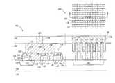
- FIG. 1is a simplified cross-sectional view of an antifuse region 100 shown along side a portion of an SRAM memory cell 102 at a stage of processing on a substrate 104 .
- the antifuse region 100 and SRAM memory cell 102are shown to be adjacent in FIG. 1, the antifuse region 100 is typically located outside of a memory array in which the SRAM memory cell 102 is located.
- the dashed lineis provided to avoid any confusion over the relative location of the antifuse region 100 with respect to the SRAM memory cell 102 .
- the antifuse region 100 and SRAM memory cell 102are shown in FIG.
- FIGS. 2 through 5illustrate an antifuse and the SRAM memory cell 102 at various stages of processing.
- the portion of the SRAM memory cell 102 that is shown in FIG. 1is where an exhumed contact and local interconnect will be formed.
- the portion of the SRAM memory cell 102 shown in FIG. 1includes first, second and third gate structures 110 , 114 , 118 formed on a doped well region 106 .
- the well region 106is typically doped to a predetermined conductivity, for example, p-type or n-type, depending on whether NMOS or PMOS transistors will be formed therein. Formation of the well region 106 in the substrate 104 can be accomplished using well-known semiconductor processing techniques.
- the gate structure 110is formed over a shallow trench isolation (STI) structure 112 .
- STIshallow trench isolation
- An STI structure 140is also formed in the antifuse region 110 , on which an antifuse will be formed.
- Each of the gate structures 110 , 114 , 118includes a gate oxide 120 , a gate layer 122 , a conductive layer 124 , and a dielectric cap 130 .
- the gate oxide 120 , the gate layer 122 , the conductive layer 124 , and the dielectric cap 130can be formed using conventional processes and materials known by those of ordinary skill in the art.
- the gate oxide 120can be a silicon oxide material formed a thermal oxidation process
- the gate layer 122can be formed from a doped polysilicon material deposited using conventional chemical vapor deposition (CVD) techniques, plasma-enhanced CVD (PECVD) techniques, or the like.
- the conductive layer 124provides a relatively low resistance current path and can be formed from a tungsten or tungsten nitride material.
- Dielectric spacers 134are formed along the sides to cover the gate oxide 120 , gate layer 122 , conductive layer 124 and dielectric cap 130 .
- a tetraethyl orthosilicate (TEOS) glass materialcan be used for the dielectric cap 130 and the dielectric spacers 134 .
- TEOStetraethyl orthosilicate
- the dielectric cap 130 of the gate structure 110has been partially removed to expose a portion of the conductive layer 124 on which the exhumed contact will be formed.
- An etch stop layer 150 and an interlayer 152are formed over the SRAM memory cell 102 and the antifuse region 100 .
- the etch stop layer 150can be formed from a silicon nitride material and the interlayer 152 can be formed from a boron silicate glass (BSG), a borophosphorous silicate glass (BPSG), or similar material.
- BSGboron silicate glass
- BPSGborophosphorous silicate glass
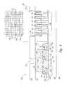
- FIG. 2is a simplified cross-sectional view of the antifuse region 100 and the SRAM memory cell 102 (FIG. 1) at a later stage of processing.
- FIG. 2includes a top plan view of the antifuse region 100 .
- the interlayer 152is masked, and the interlayer 152 and the etch stop layer 150 are subsequently etched to form a exhume contact opening 160 exposing a portion of the well region 106 .
- openings 164are concurrently formed with the exhume contact opening 160 .
- etch processes used to etch the interlayer 152 and the etch stop layer 150are selective to the material of the dielectric cap 130 , dielectric spacers 134 , and the conductive layer 124 .
- Conventional photolithographic and etch processescan be used in the formation of the exhume contact opening 160 and the openings 164 , as is well known in the art.
- FIG. 3is a simplified cross-sectional view of the antifuse region 100 and the SRAM memory cell 102 (FIG. 2) at a later stage of processing.
- a conductive materialis deposited over the interlayer 152 to fill the exhume contact opening 160 and the openings 164 , and subsequently etched to remove the conductive material from the surface of the interlayer 152 .
- a local interconnect 168is formed in the exhume contact opening 160 and conductive plates 170 are formed in the openings 164 .
- the local interconnect 168is in electrical contact with the exposed portion of the conductive layer 124 of the gate structure 110 .
- a second interlayer 172is formed over the interlayer 152 , covering the local interconnect 168 and the conductive plates 170 .
- the second interlayer 172can be formed from the same material from which the interlayer 152 is formed.
- the conductive material from which the local interconnect 168 and the conductive plates 170 are formedcan be a conventional material, such as tungsten. However, it will be appreciated that other suitable materials may be used as well without departing from the scope of the present invention.
- FIG. 4is a simplified cross-sectional view of the antifuse region 100 and the SRAM memory cell 102 (FIG. 3) at a later stage of processing.
- the second interlayer 172is masked and etched to form openings 174 and 176 over the local interconnect 168 and the antifuse region 100 , respectively.
- the openings 176are etched generally perpendicular to the length of the conductive plates 170 to form a “crisscross” pattern. This is illustrated in the plan view included in FIG. 4.
- the openings 176are etched to a depth of D below the top of the conductive plates 170 .
- the etch process used to form the openings 174 and 176is selective to the material from which the local interconnect 168 and the conductive plates 170 are formed. In the present example, the etch process is selective to tungsten.
- the second interlayer 172is then masked to cover the SRAM memory cell 102 while leaving the openings 176 exposed.
- An antifuse dielectric 178is formed over the exposed surfaces of the openings 176 , including the exposed surfaces of the conductive plates 170 .
- the antifuse dielectric 178can be formed from conventional dielectric materials, such as silicon oxide, silicon nitride, and the like.
- the present exampleemploys a single layer dielectric, it may be desirable to employ a multi-layer antifuse dielectric instead. Fabrication of such a dielectric structure is well known in the art.
- FIG. 5is a simplified cross-sectional view of the antifuse region 100 and the SRAM memory cell 102 (FIG. 4) at a later stage of processing.
- a conductive materialis deposited over the second interlayer 172 to fill the openings 174 and 176 , and subsequently etched to remove the conductive material from the surface of the second interlayer 172 .
- a conductive plug 180is formed in the opening 174 , which can be used to electrically connect the local interconnect 168 to a later formed conductive interconnect (not shown).
- Second conductive plates 182are also formed in the openings 176 over the antifuse dielectric 178 from the conductive material.
- An antifuse 200is formed from the orthogonally arranged conductive plates 170 and 182 , and the antifuse dielectric 178 .
- the antifuse 200is electrically coupled to a conventional antifuse programming circuit.
- the antifuse programming circuitis used to program the antifuse 200 when desired.
- a conventional sensing circuitmay also be electrically coupled to the antifuse 200 as well where sensing the programmable state of the antifuse is desired. Such circuits are well known in the art, and will not be discussed in detail herein in order to avoid obscuring the present invention.
- edgessuch as the ones formed from the arrangement of the present example, result in regions of localized charge concentration when a voltage is applied across the antifuse dielectric 178 .
- the orthogonal corner formation of the antifuse dielectric 178 with the first and second conductive plates 170 , 182enhances the electric field during programming of the antifuse 200 . Consequently, reduced programming voltages can be used.
- the resulting filamentthat is, the conductive path, between the first and second conductive plates 170 , 182 will consistently form along the edges.
- the arrangement of embodiments of the present inventionalso provide the ability to adjust the magnitude of the programming voltage by designing the grid of the first and second conductive plates 170 , 182 with fewer or greater conductive crisscrossing plates. That is, the programming voltage for antifuses on a device can be tailored to the specific use, with some antifuses having a higher or lower programming voltage than other antifuses, if so desired. Moreover, fabrication of antifuses according to embodiments of the present invention can be easily integrated into with processes including a damascene local interconnect and contact formation processes, such as in the example of the SRAM memory cell 100 provided above.
Landscapes
- Physics & Mathematics (AREA)
- Condensed Matter Physics & Semiconductors (AREA)
- General Physics & Mathematics (AREA)
- Engineering & Computer Science (AREA)
- Computer Hardware Design (AREA)
- Microelectronics & Electronic Packaging (AREA)
- Power Engineering (AREA)
- Design And Manufacture Of Integrated Circuits (AREA)
- Semiconductor Memories (AREA)
Abstract
Description
- The present invention generally relates to integrated circuit design and fabrication, and more particularly, to an antifuse structure and method for fabricating the same.[0001]
- Fuses and antifuses are common components in conventional integrated circuits. Fuses are commonly formed from a metal or polycide layer which is narrowed down in the region of the fuse. Fuses are then typically blown by applying a voltage or laser to heat the metal or polycide above a melting point, causing the fuse to open and the conductive link. In contrast, an antifuse is a circuit element that is normally open circuited until it is programmed, at which point the antifuse assumes a relatively low resistance. Conventional antifuses are similar in construction to capacitors in that they include a pair of conductive plates separated from each other by a dielectric or insulator. Antifuses are typically characterized by the nature of the dielectric which may be, for example, oxide or nitride. Antifuses are programmed or blown by applying a differential voltage between the plates that is sufficient to break down the dielectric thereby causing the plates to electrically contact each other.[0002]
- Fuses and antifuses are used in a variety of applications. One such application is to selectively enable certain features of integrated circuits. For example, semiconductor devices are often designed to be operated in multiple modes of operation, with the specific mode of operation programmed after the fabrication of the device has been completed. One method for programming the device is through the use of a fuse or antifuse. More commonly, however, fuses and antifuses are used to perform repairs of integrated circuits, such as in redundancy technology. Repairs of integrated circuits are typically accomplished by blowing the appropriate fuses or antifuses to signal defective portions of the integrated circuit that they should be replaced with redundant circuits. For example, a defective row of memory cells in the array of a dynamic random access memory (DRAM) devices can be replaced with a redundant row of cells provided for that purpose. As demonstrated by this example, redundancy technology can be used to improve the fabrication yield of high-density memory devices, such as DRAM and static random access memory (SRAM) devices, by replacing failed memory cells with spare ones using redundant circuitry activated by programming the fuses or antifuses.[0003]
- As previously discussed, antifuses are similar in structure to semiconductor capacitors. Consequently, the fabrication of antifuses can be easily integrated into conventional DRAM device fabrication processes, since, as well known in the art, DRAM devices rely on semiconductor capacitors to store data. However, in devices where capacitors are not typically formed, such as in SRAM devices, integrating the fabrication of antifuses into the conventional process flow is difficult. As a result, fuses are used typically used in SRAM devices rather than antifuses.[0004]
- Although fuses have been used extensively in semiconductor devices, antifuses provide several advantages over their fuse counterparts. For example, one advantage with antifuses is the ease of programming while the device is on a tester, as opposed to fuses, where the wafers must be transferred to a laser trimmer. Not only does the laser trimming process add time to the entire process, the additional step introduces another point in the process at which catastrophic mistakes can occur. For example, wafers of a lot can be accidentally trimmed using the fuse trimming profile of another lot, or wafers can be rearranged within a lot such that the reordered wafers are trimmed using the incorrect fuse trimming profile. These types of errors typically result in scrapping the mistrimmed wafers.[0005]
- Additionally, as the size of semiconductor devices decreases, using lasers to blow fuses has become more difficult. That is, as semiconductor devices decrease in size and the degree of integration increases, the critical dimensions, including fuse pitch, become smaller. The availability of lasers suitable to blow the fuse becomes limited since the diameter of the laser beam should not be smaller than the fuse pitch. Thus, the fuse pitch, and the size of semiconductor devices, becomes dictated by minimum diameter of laser beams obtainable by current laser technology.[0006]
- Moreover, another disadvantage with employing fuses instead of antifuses is related to conventional fuse fabrication processes. As previously discussed, conventional fuse fabrication processes typically form fuses from a polycide layer, which is deposited early in the fabrication process of the device. That is, the polycide layer from which fuses are formed is covered by multiple layers that are formed later in the processing of the device. For semiconductor devices having multiple levels of metallization, such as in SRAM devices, it is becoming very difficult to etch down through the multiple layers of oxide between the levels of metallization to expose the polycide fuses. If the oxide is not sufficiently etched, the fuses may not be completely blown by the laser trimmer, which typically results in malfunction of the device.[0007]
- Therefore, there is a need for an antifuse structure and method for forming the same that can be integrated into the fabrication processes for devices that typically do not include the formation of semiconductor capacitors.[0008]
- The present invention is directed to an antifuse including a bottom plate having a plurality of longitudinal members arranged substantially parallel to a first axis, a dielectric layer formed on the bottom plate, and a top plate having a plurality of longitudinal members arranged substantially parallel to a second axis, the top plate formed over the dielectric layer. The longitudinal members of the bottom plate and the top plate can be arranged orthogonally with respect to each other. The longitudinal members of the bottom plate can have at least one edge over which the dielectric material and the longitudinal members of the top plate are formed. The antifuse can further include a first interlayer, a first plurality of slots formed in the first interlayer in which the longitudinal members of the bottom plate are formed, a second interlayer formed over the first interlayer, and a second plurality of slots formed in the second interlayer in which the longitudinal members of the top plate are formed.[0009]
- One aspect of the invention includes multiple edges at the interfaces between the top and bottom plates. Consequently, edges, such as the ones formed from the arrangement, result in regions of localized charge concentration when a programming voltage is applied across the antifuse. As a result, the formation of the antifuse dielectric over the corners of the bottom plates enhance the electric field during programming of the antifuse. Reduced programming voltages can be used in programming the antifuse. The resulting filament, that is, the conductive path, between the top and bottom plates will likely form along the multiple edges.[0010]
- FIG. 1 is a simplified cross-sectional view of a semiconductor substrate that can be processed to form an antifuse in accordance with an embodiment of the present invention.[0011]
- FIG. 2 is a simplified cross-sectional view of the substrate of FIG. 1 at a later point in processing, in accordance with an embodiment of the present invention.[0012]
- FIG. 3 is a simplified cross-sectional view of the substrate of FIG. 2 at a later point in processing, in accordance with an embodiment of the present invention.[0013]
- FIG. 4 is a simplified cross-sectional view of the substrate of FIG. 3 at a later point in processing, in accordance with an embodiment of the present invention.[0014]
- FIG. 5 is a simplified cross-sectional view of the substrate of FIG. 4 at a later point in processing, in accordance with an embodiment of the present invention.[0015]
- As is conventional in the field of integrated circuit representation, the lateral sizes and thicknesses of the various layers are not drawn to scale, and portions of the various layers may have been arbitrarily enlarged or reduced to improve drawing legibility.[0016]
- Embodiments of the present invention are directed to an antifuse structure and method for forming the same that can be integrated into fabrication processes that include a damascene local interconnect and contact formation processes. In the discussion which follows, the invention is described with reference to an SRAM memory device. However, it should be understood that the invention pertains to any applications where formation of an antifuse is desired. Additionally, in the following detailed description, reference is made to various specific embodiments in which the invention may be practiced. These embodiments are described with sufficient detail to enable those skilled in the art to practice the invention, and it is to be understood that other embodiments may be employed, and that structural and process changes may be made without departing from the teachings of the invention.[0017]
- It will be appreciated that the terms “wafer” or “substrate” used in the following description may include any semiconductor-based structure that has an exposed silicon surface. Wafer and structure must be understood to include silicon-on insulator (SOI), silicon-on sapphire (SOS), doped and undoped semiconductors, epitaxial layers of silicon supported by a base semiconductor foundation, and other semiconductor structures. The semiconductor need not be silicon-based. The semiconductor could be silicon-germanium, germanium, or gallium arsenide. When reference is made to a wafer or substrate in the following description, previous process steps may have been utilized to form regions or junctions or layers in or on the base semiconductor or foundation.[0018]
- FIG. 1 is a simplified cross-sectional view of an[0019]
antifuse region 100 shown along side a portion of anSRAM memory cell 102 at a stage of processing on asubstrate 104. Although theantifuse region 100 andSRAM memory cell 102 are shown to be adjacent in FIG. 1, theantifuse region 100 is typically located outside of a memory array in which theSRAM memory cell 102 is located. The dashed line is provided to avoid any confusion over the relative location of theantifuse region 100 with respect to theSRAM memory cell 102. Theantifuse region 100 andSRAM memory cell 102 are shown in FIG. 1 in this manner to illustrate the process steps in forming antifuses according to embodiments of the present invention with relation to forming an exhumed contact and local interconnect of theSRAM memory cell 102. A more detailed description of an antifuse will be provided with respect to FIGS. 2 through 5, which illustrate an antifuse and theSRAM memory cell 102 at various stages of processing. - As previously mentioned, the portion of the[0020]
SRAM memory cell 102 that is shown in FIG. 1 is where an exhumed contact and local interconnect will be formed. The portion of theSRAM memory cell 102 shown in FIG. 1 includes first, second andthird gate structures doped well region 106. Thewell region 106 is typically doped to a predetermined conductivity, for example, p-type or n-type, depending on whether NMOS or PMOS transistors will be formed therein. Formation of thewell region 106 in thesubstrate 104 can be accomplished using well-known semiconductor processing techniques. Thegate structure 110 is formed over a shallow trench isolation (STI)structure 112. AnSTI structure 140 is also formed in theantifuse region 110, on which an antifuse will be formed. Each of thegate structures gate oxide 120, agate layer 122, aconductive layer 124, and adielectric cap 130. Thegate oxide 120, thegate layer 122, theconductive layer 124, and thedielectric cap 130 can be formed using conventional processes and materials known by those of ordinary skill in the art. For example, thegate oxide 120 can be a silicon oxide material formed a thermal oxidation process, and thegate layer 122 can be formed from a doped polysilicon material deposited using conventional chemical vapor deposition (CVD) techniques, plasma-enhanced CVD (PECVD) techniques, or the like. Theconductive layer 124 provides a relatively low resistance current path and can be formed from a tungsten or tungsten nitride material.Dielectric spacers 134 are formed along the sides to cover thegate oxide 120,gate layer 122,conductive layer 124 anddielectric cap 130. A tetraethyl orthosilicate (TEOS) glass material can be used for thedielectric cap 130 and thedielectric spacers 134. It will be appreciated that although specific materials and processes have been described in the present example, other suitable materials and fabrication processes can be used in forming the various layers of thegate structures - The[0021]
dielectric cap 130 of thegate structure 110 has been partially removed to expose a portion of theconductive layer 124 on which the exhumed contact will be formed. Anetch stop layer 150 and aninterlayer 152 are formed over theSRAM memory cell 102 and theantifuse region 100. Theetch stop layer 150 can be formed from a silicon nitride material and theinterlayer 152 can be formed from a boron silicate glass (BSG), a borophosphorous silicate glass (BPSG), or similar material. - FIG. 2 is a simplified cross-sectional view of the[0022]
antifuse region 100 and the SRAM memory cell102 (FIG. 1) at a later stage of processing. FIG. 2 includes a top plan view of theantifuse region 100. Although not shown in FIG. 2, theinterlayer 152 is masked, and theinterlayer 152 and theetch stop layer 150 are subsequently etched to form aexhume contact opening 160 exposing a portion of thewell region 106. In theantifuse region 100,openings 164 are concurrently formed with theexhume contact opening 160. It will be appreciated that the etch processes used to etch theinterlayer 152 and theetch stop layer 150 are selective to the material of thedielectric cap 130,dielectric spacers 134, and theconductive layer 124. Conventional photolithographic and etch processes can be used in the formation of theexhume contact opening 160 and theopenings 164, as is well known in the art. - FIG. 3 is a simplified cross-sectional view of the[0023]
antifuse region 100 and the SRAM memory cell102 (FIG. 2) at a later stage of processing. A conductive material is deposited over theinterlayer 152 to fill theexhume contact opening 160 and theopenings 164, and subsequently etched to remove the conductive material from the surface of theinterlayer 152. As a result, alocal interconnect 168 is formed in theexhume contact opening 160 andconductive plates 170 are formed in theopenings 164. Thelocal interconnect 168 is in electrical contact with the exposed portion of theconductive layer 124 of thegate structure 110. Asecond interlayer 172 is formed over theinterlayer 152, covering thelocal interconnect 168 and theconductive plates 170. Thesecond interlayer 172 can be formed from the same material from which theinterlayer 152 is formed. The conductive material from which thelocal interconnect 168 and theconductive plates 170 are formed can be a conventional material, such as tungsten. However, it will be appreciated that other suitable materials may be used as well without departing from the scope of the present invention. - FIG. 4 is a simplified cross-sectional view of the[0024]
antifuse region 100 and the SRAM memory cell102 (FIG. 3) at a later stage of processing. Thesecond interlayer 172 is masked and etched to formopenings local interconnect 168 and theantifuse region 100, respectively. Theopenings 176 are etched generally perpendicular to the length of theconductive plates 170 to form a “crisscross” pattern. This is illustrated in the plan view included in FIG. 4. Theopenings 176 are etched to a depth of D below the top of theconductive plates 170. The etch process used to form theopenings local interconnect 168 and theconductive plates 170 are formed. In the present example, the etch process is selective to tungsten. Thesecond interlayer 172 is then masked to cover theSRAM memory cell 102 while leaving theopenings 176 exposed. Anantifuse dielectric 178 is formed over the exposed surfaces of theopenings 176, including the exposed surfaces of theconductive plates 170. Theantifuse dielectric 178 can be formed from conventional dielectric materials, such as silicon oxide, silicon nitride, and the like. Moreover, although the present example employs a single layer dielectric, it may be desirable to employ a multi-layer antifuse dielectric instead. Fabrication of such a dielectric structure is well known in the art. - FIG. 5 is a simplified cross-sectional view of the[0025]
antifuse region 100 and the SRAM memory cell102 (FIG. 4) at a later stage of processing. A conductive material is deposited over thesecond interlayer 172 to fill theopenings second interlayer 172. As a result, aconductive plug 180 is formed in theopening 174, which can be used to electrically connect thelocal interconnect 168 to a later formed conductive interconnect (not shown). Secondconductive plates 182 are also formed in theopenings 176 over theantifuse dielectric 178 from the conductive material. - An[0026]
antifuse 200 is formed from the orthogonally arrangedconductive plates antifuse dielectric 178. Although not shown in FIGS.1-5, theantifuse 200 is electrically coupled to a conventional antifuse programming circuit. As well known in the art, the antifuse programming circuit is used to program theantifuse 200 when desired. A conventional sensing circuit may also be electrically coupled to theantifuse 200 as well where sensing the programmable state of the antifuse is desired. Such circuits are well known in the art, and will not be discussed in detail herein in order to avoid obscuring the present invention. - It will be appreciated that the arrangement of the[0027]
antifuse 200 shown in FIG. 5 provides multiple edges at the interfaces between the firstconductive plates 170, theantifuse dielectric 178, and the secondconductive plates 182. As well known in the art, edges, such as the ones formed from the arrangement of the present example, result in regions of localized charge concentration when a voltage is applied across theantifuse dielectric 178. As a result, the orthogonal corner formation of theantifuse dielectric 178 with the first and secondconductive plates antifuse 200. Consequently, reduced programming voltages can be used. The resulting filament, that is, the conductive path, between the first and secondconductive plates - The arrangement of embodiments of the present invention also provide the ability to adjust the magnitude of the programming voltage by designing the grid of the first and second[0028]
conductive plates SRAM memory cell 100 provided above. - From the foregoing it will be appreciated that, although specific embodiments of the invention have been described herein for purposes of illustration, various modifications may be made without deviating from the spirit and scope of the invention. For example, the previously discussed embodiment includes arranging the first and second[0029]
conductive plates conductive plates
Claims (35)
Priority Applications (9)
| Application Number | Priority Date | Filing Date | Title |
|---|---|---|---|
| US10/211,476US6683365B1 (en) | 2002-08-01 | 2002-08-01 | Edge intensive antifuse device structure |
| US10/290,958US6740575B2 (en) | 2002-08-01 | 2002-11-07 | Method for forming an antifuse |
| US10/409,724US7189634B2 (en) | 2002-08-01 | 2003-04-08 | Edge intensive antifuse |
| US10/824,238US7210224B2 (en) | 2002-08-01 | 2004-04-13 | Method for forming an antifuse |
| US10/883,601US7279772B2 (en) | 2002-08-01 | 2004-06-30 | Edge intensive antifuse and method for making the same |
| US10/882,987US7235858B2 (en) | 2002-08-01 | 2004-06-30 | Edge intensive antifuse and method for making the same |
| US10/882,969US7057218B2 (en) | 2002-08-01 | 2004-06-30 | Edge intensive antifuse |
| US11/543,322US20070022599A1 (en) | 2002-08-01 | 2006-10-04 | Edge intensive antifuse and method for making the same |
| US11/543,542US7269898B2 (en) | 2002-08-01 | 2006-10-04 | Method for making an edge intensive antifuse |
Applications Claiming Priority (1)
| Application Number | Priority Date | Filing Date | Title |
|---|---|---|---|
| US10/211,476US6683365B1 (en) | 2002-08-01 | 2002-08-01 | Edge intensive antifuse device structure |
Related Child Applications (2)
| Application Number | Title | Priority Date | Filing Date |
|---|---|---|---|
| US10/290,958DivisionUS6740575B2 (en) | 2002-08-01 | 2002-11-07 | Method for forming an antifuse |
| US10/409,724DivisionUS7189634B2 (en) | 2002-08-01 | 2003-04-08 | Edge intensive antifuse |
Publications (2)
| Publication Number | Publication Date |
|---|---|
| US6683365B1 US6683365B1 (en) | 2004-01-27 |
| US20040021199A1true US20040021199A1 (en) | 2004-02-05 |
Family
ID=30115254
Family Applications (9)
| Application Number | Title | Priority Date | Filing Date |
|---|---|---|---|
| US10/211,476Expired - LifetimeUS6683365B1 (en) | 2002-08-01 | 2002-08-01 | Edge intensive antifuse device structure |
| US10/290,958Expired - LifetimeUS6740575B2 (en) | 2002-08-01 | 2002-11-07 | Method for forming an antifuse |
| US10/409,724Expired - LifetimeUS7189634B2 (en) | 2002-08-01 | 2003-04-08 | Edge intensive antifuse |
| US10/824,238Expired - LifetimeUS7210224B2 (en) | 2002-08-01 | 2004-04-13 | Method for forming an antifuse |
| US10/883,601Expired - LifetimeUS7279772B2 (en) | 2002-08-01 | 2004-06-30 | Edge intensive antifuse and method for making the same |
| US10/882,969Expired - LifetimeUS7057218B2 (en) | 2002-08-01 | 2004-06-30 | Edge intensive antifuse |
| US10/882,987Expired - LifetimeUS7235858B2 (en) | 2002-08-01 | 2004-06-30 | Edge intensive antifuse and method for making the same |
| US11/543,322AbandonedUS20070022599A1 (en) | 2002-08-01 | 2006-10-04 | Edge intensive antifuse and method for making the same |
| US11/543,542Expired - LifetimeUS7269898B2 (en) | 2002-08-01 | 2006-10-04 | Method for making an edge intensive antifuse |
Family Applications After (8)
| Application Number | Title | Priority Date | Filing Date |
|---|---|---|---|
| US10/290,958Expired - LifetimeUS6740575B2 (en) | 2002-08-01 | 2002-11-07 | Method for forming an antifuse |
| US10/409,724Expired - LifetimeUS7189634B2 (en) | 2002-08-01 | 2003-04-08 | Edge intensive antifuse |
| US10/824,238Expired - LifetimeUS7210224B2 (en) | 2002-08-01 | 2004-04-13 | Method for forming an antifuse |
| US10/883,601Expired - LifetimeUS7279772B2 (en) | 2002-08-01 | 2004-06-30 | Edge intensive antifuse and method for making the same |
| US10/882,969Expired - LifetimeUS7057218B2 (en) | 2002-08-01 | 2004-06-30 | Edge intensive antifuse |
| US10/882,987Expired - LifetimeUS7235858B2 (en) | 2002-08-01 | 2004-06-30 | Edge intensive antifuse and method for making the same |
| US11/543,322AbandonedUS20070022599A1 (en) | 2002-08-01 | 2006-10-04 | Edge intensive antifuse and method for making the same |
| US11/543,542Expired - LifetimeUS7269898B2 (en) | 2002-08-01 | 2006-10-04 | Method for making an edge intensive antifuse |
Country Status (1)
| Country | Link |
|---|---|
| US (9) | US6683365B1 (en) |
Cited By (4)
| Publication number | Priority date | Publication date | Assignee | Title |
|---|---|---|---|---|
| US20050082635A1 (en)* | 2003-10-07 | 2005-04-21 | Min-Sung Kang | Semiconductor fuse box and method for fabricating the same |
| US20060258140A1 (en)* | 2003-10-23 | 2006-11-16 | Armin Fischer | Integrated circuit with additional mini-pads connected by an under-bump metallization and method for production thereof |
| KR101025738B1 (en)* | 2008-08-07 | 2011-04-04 | 주식회사 하이닉스반도체 | Fuse of Semiconductor Device and Manufacturing Method Thereof |
| EP2894668A1 (en)* | 2014-01-14 | 2015-07-15 | Broadcom Corporation | Dummy end-gate based anti-fuse device for finFET technologies |
Families Citing this family (23)
| Publication number | Priority date | Publication date | Assignee | Title |
|---|---|---|---|---|
| ATE404528T1 (en)* | 2001-03-13 | 2008-08-15 | Paratek Pharm Innc | 7.9 SUBSTITUTED TETRACYCLINE COMPOUNDS |
| TW540151B (en)* | 2002-07-19 | 2003-07-01 | Nanya Technology Corp | Fuse structure |
| US6683365B1 (en)* | 2002-08-01 | 2004-01-27 | Micron Technology, Inc. | Edge intensive antifuse device structure |
| US6882027B2 (en)* | 2003-05-28 | 2005-04-19 | Infineon Technologies Ag | Methods and apparatus for providing an antifuse function |
| JP2006294527A (en)* | 2005-04-14 | 2006-10-26 | Nec Corp | Connector and manufacturing method thereof |
| US7528015B2 (en)* | 2005-06-28 | 2009-05-05 | Freescale Semiconductor, Inc. | Tunable antifuse element and method of manufacture |
| US7361968B2 (en)* | 2006-03-23 | 2008-04-22 | Taiwan Semiconductor Manufacturing Co., Ltd. | Method for integrally forming an electrical fuse device and a MOS transistor |
| BRPI0810168A2 (en)* | 2007-04-09 | 2014-12-30 | Usv Ltd | PHARMACEUTICAL COMPOSITIONS OF CLOPIDOGREL BISULPHATE AND PREPARATION PROCESSES |
| US7572682B2 (en)* | 2007-05-31 | 2009-08-11 | International Business Machines Corporation | Semiconductor structure for fuse and anti-fuse applications |
| TWI387656B (en)* | 2009-07-06 | 2013-03-01 | Modern Islands Co Ltd | Preparation of Low Lead Brass Alloy and Its |
| US8030736B2 (en)* | 2009-08-10 | 2011-10-04 | International Business Machines Corporation | Fin anti-fuse with reduced programming voltage |
| US20110081272A1 (en)* | 2009-10-07 | 2011-04-07 | Modern Islands Co., Ltd. | Low-lead copper alloy |
| US20110081271A1 (en)* | 2009-10-07 | 2011-04-07 | Modern Islands Co., Ltd. | Low-lead copper alloy |
| US8158967B2 (en)* | 2009-11-23 | 2012-04-17 | Micron Technology, Inc. | Integrated memory arrays |
| US20110142715A1 (en)* | 2009-12-11 | 2011-06-16 | Globe Union Industrial Corporation | Brass alloy |
| US8227890B2 (en)* | 2009-12-18 | 2012-07-24 | United Microelectronics Corporation | Method of forming an electrical fuse and a metal gate transistor and the related electrical fuse |
| TWI398532B (en) | 2010-01-22 | 2013-06-11 | Modern Islands Co Ltd | Lead-free brass alloy |
| CN103456711B (en)* | 2012-06-05 | 2016-03-23 | 中芯国际集成电路制造(上海)有限公司 | Fin-type anti-fuse structure and manufacture method thereof |
| US8975724B2 (en) | 2012-09-13 | 2015-03-10 | Qualcomm Incorporated | Anti-fuse device |
| CN103915440B (en)* | 2013-01-08 | 2017-09-22 | 中芯国际集成电路制造(上海)有限公司 | Can repeatedly programming device, the preparation method of semiconductor devices |
| CN107785348B (en)* | 2016-08-24 | 2019-12-10 | 中芯国际集成电路制造(上海)有限公司 | Antifuse structure, semiconductor device, and electronic apparatus |
| CN112420663B (en)* | 2019-08-23 | 2022-05-10 | 长鑫存储技术有限公司 | Anti-fuse structure and manufacturing method thereof |
| US11641741B2 (en) | 2020-09-09 | 2023-05-02 | Micron Technology, Inc. | Microelectronic devices with tiered blocks separated by progressively spaced slits, and related methods and systems |
Citations (3)
| Publication number | Priority date | Publication date | Assignee | Title |
|---|---|---|---|---|
| US20020088998A1 (en)* | 2000-04-28 | 2002-07-11 | Knall N. Johan | Three-dimensional memory array and method of fabrication |
| US6541312B2 (en)* | 2000-12-22 | 2003-04-01 | Matrix Semiconductor, Inc. | Formation of antifuse structure in a three dimensional memory |
| US6627530B2 (en)* | 2000-12-22 | 2003-09-30 | Matrix Semiconductor, Inc. | Patterning three dimensional structures |
Family Cites Families (15)
| Publication number | Priority date | Publication date | Assignee | Title |
|---|---|---|---|---|
| US5701027A (en) | 1991-04-26 | 1997-12-23 | Quicklogic Corporation | Programmable interconnect structures and programmable integrated circuits |
| US5300456A (en)* | 1993-06-17 | 1994-04-05 | Texas Instruments Incorporated | Metal-to-metal antifuse structure |
| JP3256603B2 (en)* | 1993-07-05 | 2002-02-12 | 株式会社東芝 | Semiconductor device and manufacturing method thereof |
| US5807786A (en)* | 1997-07-30 | 1998-09-15 | Taiwan Semiconductor Manufacturing Company, Ltd. | Method of making a barrier layer to protect programmable antifuse structure from damage during fabrication sequence |
| US7034353B2 (en)* | 1998-02-27 | 2006-04-25 | Micron Technology, Inc. | Methods for enhancing capacitors having roughened features to increase charge-storage capacity |
| US6034882A (en)* | 1998-11-16 | 2000-03-07 | Matrix Semiconductor, Inc. | Vertically stacked field programmable nonvolatile memory and method of fabrication |
| US6888750B2 (en) | 2000-04-28 | 2005-05-03 | Matrix Semiconductor, Inc. | Nonvolatile memory on SOI and compound semiconductor substrates and method of fabrication |
| US6522011B1 (en)* | 2000-08-15 | 2003-02-18 | Micron Technology, Inc. | Low capacitance wiring layout and method for making same |
| US6486065B2 (en) | 2000-12-22 | 2002-11-26 | Matrix Semiconductor, Inc. | Method of forming nonvolatile memory device utilizing a hard mask |
| US6599796B2 (en)* | 2001-06-29 | 2003-07-29 | Hewlett-Packard Development Company, L.P. | Apparatus and fabrication process to reduce crosstalk in pirm memory array |
| JP2003060036A (en) | 2001-08-08 | 2003-02-28 | Mitsubishi Electric Corp | Semiconductor device and method of manufacturing the same |
| US6549447B1 (en)* | 2001-10-31 | 2003-04-15 | Peter Fricke | Memory cell structure |
| US20040084713A1 (en) | 2002-10-30 | 2004-05-06 | Taiwan Semiconductor Manufacturing Company | Structure with composite floating gate by poly spacer in flash |
| US6853049B2 (en)* | 2002-03-13 | 2005-02-08 | Matrix Semiconductor, Inc. | Silicide-silicon oxide-semiconductor antifuse device and method of making |
| US6683365B1 (en)* | 2002-08-01 | 2004-01-27 | Micron Technology, Inc. | Edge intensive antifuse device structure |
- 2002
- 2002-08-01USUS10/211,476patent/US6683365B1/ennot_activeExpired - Lifetime
- 2002-11-07USUS10/290,958patent/US6740575B2/ennot_activeExpired - Lifetime
- 2003
- 2003-04-08USUS10/409,724patent/US7189634B2/ennot_activeExpired - Lifetime
- 2004
- 2004-04-13USUS10/824,238patent/US7210224B2/ennot_activeExpired - Lifetime
- 2004-06-30USUS10/883,601patent/US7279772B2/ennot_activeExpired - Lifetime
- 2004-06-30USUS10/882,969patent/US7057218B2/ennot_activeExpired - Lifetime
- 2004-06-30USUS10/882,987patent/US7235858B2/ennot_activeExpired - Lifetime
- 2006
- 2006-10-04USUS11/543,322patent/US20070022599A1/ennot_activeAbandoned
- 2006-10-04USUS11/543,542patent/US7269898B2/ennot_activeExpired - Lifetime
Patent Citations (3)
| Publication number | Priority date | Publication date | Assignee | Title |
|---|---|---|---|---|
| US20020088998A1 (en)* | 2000-04-28 | 2002-07-11 | Knall N. Johan | Three-dimensional memory array and method of fabrication |
| US6541312B2 (en)* | 2000-12-22 | 2003-04-01 | Matrix Semiconductor, Inc. | Formation of antifuse structure in a three dimensional memory |
| US6627530B2 (en)* | 2000-12-22 | 2003-09-30 | Matrix Semiconductor, Inc. | Patterning three dimensional structures |
Cited By (11)
| Publication number | Priority date | Publication date | Assignee | Title |
|---|---|---|---|---|
| US20050082635A1 (en)* | 2003-10-07 | 2005-04-21 | Min-Sung Kang | Semiconductor fuse box and method for fabricating the same |
| US7154160B2 (en)* | 2003-10-07 | 2006-12-26 | Samsung Electronics Co., Ltd. | Semiconductor fuse box and method for fabricating the same |
| US20090014829A1 (en)* | 2003-10-07 | 2009-01-15 | Min-Sung Kang | Semiconductor fuse box and method for fabricating the same |
| US7750432B2 (en)* | 2003-10-07 | 2010-07-06 | Samsung Electronics Co., Ltd. | Semiconductor fuse box and method for fabricating the same |
| US20060258140A1 (en)* | 2003-10-23 | 2006-11-16 | Armin Fischer | Integrated circuit with additional mini-pads connected by an under-bump metallization and method for production thereof |
| US7919363B2 (en)* | 2003-10-23 | 2011-04-05 | Infineon Technologies Ag | Integrated circuit with additional mini-pads connected by an under-bump metallization and method for production thereof |
| US20110140236A1 (en)* | 2003-10-23 | 2011-06-16 | Armin Fischer | Integrated Circuit with Pads Connected by an Under-Bump Metallization and Method for Production Thereof |
| US8487453B2 (en) | 2003-10-23 | 2013-07-16 | Infineon Technologies Ag | Integrated circuit with pads connected by an under-bump metallization and method for production thereof |
| KR101025738B1 (en)* | 2008-08-07 | 2011-04-04 | 주식회사 하이닉스반도체 | Fuse of Semiconductor Device and Manufacturing Method Thereof |
| EP2894668A1 (en)* | 2014-01-14 | 2015-07-15 | Broadcom Corporation | Dummy end-gate based anti-fuse device for finFET technologies |
| US9165936B2 (en) | 2014-01-14 | 2015-10-20 | Broadcom Corporation | Dummy end-gate based anti-fuse device for finFET technologies |
Also Published As
| Publication number | Publication date |
|---|---|
| US6683365B1 (en) | 2004-01-27 |
| US7279772B2 (en) | 2007-10-09 |
| US7057218B2 (en) | 2006-06-06 |
| US6740575B2 (en) | 2004-05-25 |
| US20040023441A1 (en) | 2004-02-05 |
| US20070022599A1 (en) | 2007-02-01 |
| US20040238917A1 (en) | 2004-12-02 |
| US7189634B2 (en) | 2007-03-13 |
| US20040238916A1 (en) | 2004-12-02 |
| US20070029639A1 (en) | 2007-02-08 |
| US7269898B2 (en) | 2007-09-18 |
| US20040021200A1 (en) | 2004-02-05 |
| US20050001285A1 (en) | 2005-01-06 |
| US20040188800A1 (en) | 2004-09-30 |
| US7210224B2 (en) | 2007-05-01 |
| US7235858B2 (en) | 2007-06-26 |
Similar Documents
| Publication | Publication Date | Title |
|---|---|---|
| US7269898B2 (en) | Method for making an edge intensive antifuse | |
| KR101966278B1 (en) | Anti fuse arrary of semiconductor device and method for fabricating the same | |
| US10192823B2 (en) | Semiconductor device and method of manufacturing the same | |
| KR20010109209A (en) | Structures and methods of anti-fuse formation in soi | |
| US11315918B2 (en) | Semiconductor structure and semiconductor layout structure | |
| WO2006107384A1 (en) | Antifuse element and electrically redundant antifuse array for controlled rupture location | |
| US6249010B1 (en) | Dielectric-based anti-fuse cell with polysilicon contact plug and method for its manufacture | |
| US9287274B2 (en) | Antifuse of semiconductor device and method of fabricating the same | |
| US9305786B2 (en) | Semiconductor device and fabrication method | |
| US7442626B2 (en) | Rectangular contact used as a low voltage fuse element | |
| US10692811B1 (en) | Semiconductor structure | |
| JP2000021986A (en) | Ion exclusion structure for fuse window | |
| KR100853478B1 (en) | Semiconductor device and manufacturing method thereof | |
| US20030038304A1 (en) | Semiconductor devices | |
| KR100799130B1 (en) | Manufacturing method of semiconductor device with double fuse structure | |
| KR20030058280A (en) | Semiconductor device with fuse of impurity region |
Legal Events
| Date | Code | Title | Description |
|---|---|---|---|
| AS | Assignment | Owner name:MICRON TECHNOLOGY, INC., IDAHO Free format text:ASSIGNMENT OF ASSIGNORS INTEREST;ASSIGNOR:TRIVEDI, JIGISH D.;REEL/FRAME:013168/0660 Effective date:20020712 | |
| FEPP | Fee payment procedure | Free format text:PAYOR NUMBER ASSIGNED (ORIGINAL EVENT CODE: ASPN); ENTITY STATUS OF PATENT OWNER: LARGE ENTITY | |
| STCF | Information on status: patent grant | Free format text:PATENTED CASE | |
| CC | Certificate of correction | ||
| FPAY | Fee payment | Year of fee payment:4 | |
| FPAY | Fee payment | Year of fee payment:8 | |
| FPAY | Fee payment | Year of fee payment:12 | |
| AS | Assignment | Owner name:U.S. BANK NATIONAL ASSOCIATION, AS COLLATERAL AGENT, CALIFORNIA Free format text:SECURITY INTEREST;ASSIGNOR:MICRON TECHNOLOGY, INC.;REEL/FRAME:038669/0001 Effective date:20160426 Owner name:U.S. BANK NATIONAL ASSOCIATION, AS COLLATERAL AGEN Free format text:SECURITY INTEREST;ASSIGNOR:MICRON TECHNOLOGY, INC.;REEL/FRAME:038669/0001 Effective date:20160426 | |
| AS | Assignment | Owner name:MORGAN STANLEY SENIOR FUNDING, INC., AS COLLATERAL AGENT, MARYLAND Free format text:PATENT SECURITY AGREEMENT;ASSIGNOR:MICRON TECHNOLOGY, INC.;REEL/FRAME:038954/0001 Effective date:20160426 Owner name:MORGAN STANLEY SENIOR FUNDING, INC., AS COLLATERAL Free format text:PATENT SECURITY AGREEMENT;ASSIGNOR:MICRON TECHNOLOGY, INC.;REEL/FRAME:038954/0001 Effective date:20160426 | |
| AS | Assignment | Owner name:U.S. BANK NATIONAL ASSOCIATION, AS COLLATERAL AGENT, CALIFORNIA Free format text:CORRECTIVE ASSIGNMENT TO CORRECT THE REPLACE ERRONEOUSLY FILED PATENT #7358718 WITH THE CORRECT PATENT #7358178 PREVIOUSLY RECORDED ON REEL 038669 FRAME 0001. ASSIGNOR(S) HEREBY CONFIRMS THE SECURITY INTEREST;ASSIGNOR:MICRON TECHNOLOGY, INC.;REEL/FRAME:043079/0001 Effective date:20160426 Owner name:U.S. BANK NATIONAL ASSOCIATION, AS COLLATERAL AGEN Free format text:CORRECTIVE ASSIGNMENT TO CORRECT THE REPLACE ERRONEOUSLY FILED PATENT #7358718 WITH THE CORRECT PATENT #7358178 PREVIOUSLY RECORDED ON REEL 038669 FRAME 0001. ASSIGNOR(S) HEREBY CONFIRMS THE SECURITY INTEREST;ASSIGNOR:MICRON TECHNOLOGY, INC.;REEL/FRAME:043079/0001 Effective date:20160426 | |
| AS | Assignment | Owner name:JPMORGAN CHASE BANK, N.A., AS COLLATERAL AGENT, ILLINOIS Free format text:SECURITY INTEREST;ASSIGNORS:MICRON TECHNOLOGY, INC.;MICRON SEMICONDUCTOR PRODUCTS, INC.;REEL/FRAME:047540/0001 Effective date:20180703 Owner name:JPMORGAN CHASE BANK, N.A., AS COLLATERAL AGENT, IL Free format text:SECURITY INTEREST;ASSIGNORS:MICRON TECHNOLOGY, INC.;MICRON SEMICONDUCTOR PRODUCTS, INC.;REEL/FRAME:047540/0001 Effective date:20180703 | |
| AS | Assignment | Owner name:MICRON TECHNOLOGY, INC., IDAHO Free format text:RELEASE BY SECURED PARTY;ASSIGNOR:U.S. BANK NATIONAL ASSOCIATION, AS COLLATERAL AGENT;REEL/FRAME:047243/0001 Effective date:20180629 | |
| AS | Assignment | Owner name:MICRON TECHNOLOGY, INC., IDAHO Free format text:RELEASE BY SECURED PARTY;ASSIGNOR:MORGAN STANLEY SENIOR FUNDING, INC., AS COLLATERAL AGENT;REEL/FRAME:050937/0001 Effective date:20190731 | |
| AS | Assignment | Owner name:MICRON TECHNOLOGY, INC., IDAHO Free format text:RELEASE BY SECURED PARTY;ASSIGNOR:JPMORGAN CHASE BANK, N.A., AS COLLATERAL AGENT;REEL/FRAME:051028/0001 Effective date:20190731 Owner name:MICRON SEMICONDUCTOR PRODUCTS, INC., IDAHO Free format text:RELEASE BY SECURED PARTY;ASSIGNOR:JPMORGAN CHASE BANK, N.A., AS COLLATERAL AGENT;REEL/FRAME:051028/0001 Effective date:20190731 |