US20040018680A1 - Method to enhance epi-regrowth in amorphous poly CB contacts - Google Patents
Method to enhance epi-regrowth in amorphous poly CB contactsDownload PDFInfo
- Publication number
- US20040018680A1 US20040018680A1US10/206,875US20687502AUS2004018680A1US 20040018680 A1US20040018680 A1US 20040018680A1US 20687502 AUS20687502 AUS 20687502AUS 2004018680 A1US2004018680 A1US 2004018680A1
- Authority
- US
- United States
- Prior art keywords
- amorphous
- affecting
- clean
- contact
- poly
- Prior art date
- Legal status (The legal status is an assumption and is not a legal conclusion. Google has not performed a legal analysis and makes no representation as to the accuracy of the status listed.)
- Granted
Links
Images


Classifications
- H—ELECTRICITY
- H01—ELECTRIC ELEMENTS
- H01L—SEMICONDUCTOR DEVICES NOT COVERED BY CLASS H10
- H01L21/00—Processes or apparatus adapted for the manufacture or treatment of semiconductor or solid state devices or of parts thereof
- H01L21/02—Manufacture or treatment of semiconductor devices or of parts thereof
- H01L21/02041—Cleaning
- H01L21/02043—Cleaning before device manufacture, i.e. Begin-Of-Line process
- H01L21/02046—Dry cleaning only
- H—ELECTRICITY
- H01—ELECTRIC ELEMENTS
- H01L—SEMICONDUCTOR DEVICES NOT COVERED BY CLASS H10
- H01L21/00—Processes or apparatus adapted for the manufacture or treatment of semiconductor or solid state devices or of parts thereof
- H01L21/02—Manufacture or treatment of semiconductor devices or of parts thereof
- H01L21/04—Manufacture or treatment of semiconductor devices or of parts thereof the devices having potential barriers, e.g. a PN junction, depletion layer or carrier concentration layer
- H01L21/18—Manufacture or treatment of semiconductor devices or of parts thereof the devices having potential barriers, e.g. a PN junction, depletion layer or carrier concentration layer the devices having semiconductor bodies comprising elements of Group IV of the Periodic Table or AIIIBV compounds with or without impurities, e.g. doping materials
- H01L21/28—Manufacture of electrodes on semiconductor bodies using processes or apparatus not provided for in groups H01L21/20 - H01L21/268
- H01L21/283—Deposition of conductive or insulating materials for electrodes conducting electric current
- H01L21/285—Deposition of conductive or insulating materials for electrodes conducting electric current from a gas or vapour, e.g. condensation
- H01L21/28506—Deposition of conductive or insulating materials for electrodes conducting electric current from a gas or vapour, e.g. condensation of conductive layers
- H01L21/28512—Deposition of conductive or insulating materials for electrodes conducting electric current from a gas or vapour, e.g. condensation of conductive layers on semiconductor bodies comprising elements of Group IV of the Periodic Table
- H01L21/28525—Deposition of conductive or insulating materials for electrodes conducting electric current from a gas or vapour, e.g. condensation of conductive layers on semiconductor bodies comprising elements of Group IV of the Periodic Table the conductive layers comprising semiconducting material
- H—ELECTRICITY
- H01—ELECTRIC ELEMENTS
- H01L—SEMICONDUCTOR DEVICES NOT COVERED BY CLASS H10
- H01L21/00—Processes or apparatus adapted for the manufacture or treatment of semiconductor or solid state devices or of parts thereof
- H01L21/02—Manufacture or treatment of semiconductor devices or of parts thereof
- H01L21/02104—Forming layers
- H01L21/02365—Forming inorganic semiconducting materials on a substrate
- H01L21/02367—Substrates
- H01L21/0237—Materials
- H01L21/02373—Group 14 semiconducting materials
- H01L21/02381—Silicon, silicon germanium, germanium
- H—ELECTRICITY
- H01—ELECTRIC ELEMENTS
- H01L—SEMICONDUCTOR DEVICES NOT COVERED BY CLASS H10
- H01L21/00—Processes or apparatus adapted for the manufacture or treatment of semiconductor or solid state devices or of parts thereof
- H01L21/02—Manufacture or treatment of semiconductor devices or of parts thereof
- H01L21/02104—Forming layers
- H01L21/02365—Forming inorganic semiconducting materials on a substrate
- H01L21/02518—Deposited layers
- H01L21/02521—Materials
- H01L21/02524—Group 14 semiconducting materials
- H01L21/02532—Silicon, silicon germanium, germanium
- H—ELECTRICITY
- H01—ELECTRIC ELEMENTS
- H01L—SEMICONDUCTOR DEVICES NOT COVERED BY CLASS H10
- H01L21/00—Processes or apparatus adapted for the manufacture or treatment of semiconductor or solid state devices or of parts thereof
- H01L21/02—Manufacture or treatment of semiconductor devices or of parts thereof
- H01L21/02104—Forming layers
- H01L21/02365—Forming inorganic semiconducting materials on a substrate
- H01L21/02656—Special treatments
- H01L21/02664—Aftertreatments
- H01L21/02667—Crystallisation or recrystallisation of non-monocrystalline semiconductor materials, e.g. regrowth
- H—ELECTRICITY
- H10—SEMICONDUCTOR DEVICES; ELECTRIC SOLID-STATE DEVICES NOT OTHERWISE PROVIDED FOR
- H10B—ELECTRONIC MEMORY DEVICES
- H10B12/00—Dynamic random access memory [DRAM] devices
- H10B12/01—Manufacture or treatment
- H10B12/02—Manufacture or treatment for one transistor one-capacitor [1T-1C] memory cells
- H10B12/05—Making the transistor
Definitions
- the inventionrelates to a process that allows in-situ, lower cost processing of fabrication of complementary bipolar (CB)liner RIE and CB oxide RIE using the same high plasma power tool, while simultaneously allowing epitaxial(epi)-regrowth of amorphous Si in DRAM production.
- CBcomplementary bipolar
- DRAMdynamic random access memory
- CBcomplementary bipolar
- a method of manufacturing a MOSFETis disclosed in U.S. Pat. No. 5,824,586. The method comprises:
- a method for forming thickened source/drain contact regions for FETsis disclosed in U.S. Pat. No. 5,250,454. The method entails:
- U.S. Pat. No. 5,980,265discloses stable, high temperature electrical contacts to silicon carbide formed using a unique silicide formation process that employs a sacrificial silicon layer between the silicon carbide and a contacting metal, which forms a metal silicide interlayer providing the resulting contact with low specific contact resistance and high electrical and structural stability.
- the contact interfaceis formed by reaction below the semiconductor surface, thereby making the in-situ silicide formation process insensitive to surface impurities and oxides and permitting the controlled formation of silicides without the formation of excess carbon and carbides at the contact interface.
- the silicon layermay optionally be doped in situ during growth or implanted with dopants after growth, to lower the contact resistance and enhance its operational stability.
- a method of forming a device quality silicon carbide epitaxial filmis disclosed in U.S. Pat. No. 6,329,088 B1.
- the methodcomprises: depositing the film at sub-atmospheric pressure conditions on a silicon carbide substrate of hexagonal crystal form, off cut towards the ⁇ 1100> crystalline direction of the substrate, wherein the silicon carbide epitaxial film has a smooth surface morphology, within an edge exclusion area, and has a root mean square roughness not exceeding about 2 nanometers in a 20 ⁇ 20 ⁇ m 2 area.
- U.S. Pat. No. 6,107,197discloses a method of removing a carbon-contaminated layer from a silicon substrate surface for subsequent selective silicon epitaxial growth thereon.
- the methodcomprises:
- One object of the present inventionis to provide an in-situ lower cost processing means to allow a CB liner RIE and a CB oxide RIE to be conducted in the same high plasma power system.
- Another object of the present inventionis to provide an in-situ lower cost processing means to allow a CB liner RIE and CB oxide RIE to be conducted in the same high plasma power system, and at the same time enable epi-regrowth of amorphous Si.
- a further object of the present inventionis to provide an in-situ lower cost processing means to allow a CB liner RIE and a CB oxide RIE to be conducted in the same high plasma power system, and at the same time enable epi-regrowth of amorphous Si by disrupting the Si—C bonding.
- the invention methodmay be accomplished by:
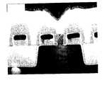
- FIG. 1is a transmission electron microscopic (TEM) picture showing a reduced CB contact resistant chip structure of the invention showing the epi-regrowth CB contact.
- TEMtransmission electron microscopic
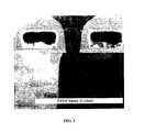
- FIG. 2is a transmission electron microscopic (TEM) picture of a CB contact wherein the Si—C bonding prevents Si epi-regrowth in the CB contact.
- TEMtransmission electron microscopic
- FIG. 3is a transmission electron microscopic (TEM) picture showing RIE into Si, followed by O plasma treatment to break the C—Si bonding and replace C with O for the terminated Si surface, wherein the amorphous Si in the poly contact stud is epitaxial growm poly Si.
- TEMtransmission electron microscopic
- oxide RIE systemsare conducted at relatively high plasma power, in order to conduct an in-situ liner RIE, the liner process must be run in a high plasma power system.
- the present inventionallows an in-situ lower cost processing scheme that permits the CB liner RIE and CB oxide RIE to be run in the same high plasma power system that is equal to or greater than about 500 W.
- the method to enhance epi-growth in amorphous poly CB contactsis accomplished by:
- the method to enhance epi-regrowth in amorphous poly CB contactsis accomplished by:
- the Huang AB cleanis a sequential one wherein cleaning is first affected by using 5 parts of water to 1 part hydrogen peroxide or 1 part ammonium hydroxide following by cleaning with 5 parts of water to 1 part of nitric acid.
- the invention methods to enhance epi-regrowth in amorphous poly CB contactspermits in-situ, lower cost processing to allow CB liner RIE and CB oxide RIE to be conducted in the same high plasma power tool, while at the same time, allowing epi-regrowth of amorphous Si.
- Amorphous poly-Sican be recrystallized very easily on top of Si with a thin O terminated Si surface.
- the Si surfaceis terminated by a C atom, which forms Si—C bonding.
- Normal process cleaningsuch as DHF or Huang AB does not work on the Si—C bonding surface.
- the only way to clean the surfaceis to introduce O-plasma to break the bond between Si and C, and to form CO or CO 2 .
- This cleaning processis implemented at the very end of the RIE process with the introduction of O plasma to remove monolayer C at the surface of Si.
- slight oxidation of Si surface through O-plasmaresults in a O terminated Si surface, which can be easily cleaned by the DHF wet cleaning process.
- FIG. 2shows the RIE process etched into Si. Without O-plasma at the very end to remove C, epitaxial growth of amorphous Si does not occur.
- FIG. 1shows that the RIE process did not etch into Si, where the Si base is flat. In that figure, we clearly observed epitaxial growth in the amorphous-Si in the poly contact stud.
- FIG. 3shows the RIE process etched into Si.
- O plasma treatmentwhich breaks Si—C bonding and replaces C with O for the O terminated Si surface
- the amorphous Si in the poly contact studbecomes an epitaxial grown poly Si.
- the epitaxial grown Sigoes all the way up to the top of the poly Si stud, which is superior in epitaxial grown poly Si compared with FIG. 1, where the RIE did not go through to the Si substrate.
- the epitaxial grown poly-Si contact studhas much better contact resistance than the non-epitaxial grown poly-Si contact stud.
- an epitaxial grown Si contact stud and a non-epitaxial grown Si studhave 700 ohm and 3000 ohm, respectively; and better contact resistance results in faster DRAM reading and writing, and high retention time for single cell devices.
Landscapes
- Engineering & Computer Science (AREA)
- Physics & Mathematics (AREA)
- Condensed Matter Physics & Semiconductors (AREA)
- General Physics & Mathematics (AREA)
- Manufacturing & Machinery (AREA)
- Computer Hardware Design (AREA)
- Microelectronics & Electronic Packaging (AREA)
- Power Engineering (AREA)
- Semiconductor Memories (AREA)
- Electrodes Of Semiconductors (AREA)
- Internal Circuitry In Semiconductor Integrated Circuit Devices (AREA)
Abstract
Description
- 1. Field of the Invention[0001]
- The invention relates to a process that allows in-situ, lower cost processing of fabrication of complementary bipolar (CB)liner RIE and CB oxide RIE using the same high plasma power tool, while simultaneously allowing epitaxial(epi)-regrowth of amorphous Si in DRAM production.[0002]
- 2. The Prior Art[0003]
- In dynamic random access memory (DRAM) development, doped poly-Si is used as the complementary bipolar (CB) contact as well as the source of doping in the contact region.[0004]
- A method of manufacturing a MOSFET is disclosed in U.S. Pat. No. 5,824,586. The method comprises:[0005]
- forming a source region and a drain region in a substrate;[0006]
- forming a gate oxide region on a surface of the substrate;[0007]
- forming a gate on the gate oxide region;[0008]
- forming gate oxide spacers adjacent to the gate and contiguous with the gate oxide region;[0009]
- depositing undoped amorphous silicon;[0010]
- ion implanting wherein the source and drain junctions are formed;[0011]
- a first rapid thermal anneal wherein limited solid phase epitaxial silicon growth takes place in regions of the amorphous silicon with underlying silicon; and[0012]
- etching the remaining amorphous silicon.[0013]
- A method for forming thickened source/drain contact regions for FETs is disclosed in U.S. Pat. No. 5,250,454. The method entails:[0014]
- depositing a layer of amorphous silicon covering the source and drain contact regions, the gate and the side wall spacer;[0015]
- heating the layer of amorphous silicon to a temperature sufficient to induce epitaxial regrowth of the amorphous silicon layer in the source and drain regions to form thickened source and drain contact regions; and[0016]
- wet-etching the substrate to remove the uncrystallized portion of the amorphous silicon in the regions where epitaxial regrowth was not induced and to remove at least a portion of the side wall spacer leaving a groove circumscribing the gate.[0017]
- U.S. Pat. No. 5,980,265 discloses stable, high temperature electrical contacts to silicon carbide formed using a unique silicide formation process that employs a sacrificial silicon layer between the silicon carbide and a contacting metal, which forms a metal silicide interlayer providing the resulting contact with low specific contact resistance and high electrical and structural stability. The contact interface is formed by reaction below the semiconductor surface, thereby making the in-situ silicide formation process insensitive to surface impurities and oxides and permitting the controlled formation of silicides without the formation of excess carbon and carbides at the contact interface. The silicon layer may optionally be doped in situ during growth or implanted with dopants after growth, to lower the contact resistance and enhance its operational stability.[0018]
- A method of forming a device quality silicon carbide epitaxial film is disclosed in U.S. Pat. No. 6,329,088 B1. The method comprises: depositing the film at sub-atmospheric pressure conditions on a silicon carbide substrate of hexagonal crystal form, off cut towards the <1100> crystalline direction of the substrate, wherein the silicon carbide epitaxial film has a smooth surface morphology, within an edge exclusion area, and has a root mean square roughness not exceeding about 2 nanometers in a 20×20 μm[0019]2area.
- U.S. Pat. No. 6,107,197 discloses a method of removing a carbon-contaminated layer from a silicon substrate surface for subsequent selective silicon epitaxial growth thereon.[0020]
- The method comprises:[0021]
- exposing a carbon-contaminated layer on the silicon substrate surface to a chlorine radical to cause a reaction of the chlorine radical with carbon atoms of the carbon-contaminated layer for removal of the carbon-contaminated layer from the silicon substrate surface, wherein the chlorine radical has been generated by passing a chlorine gas through a heated filament.[0022]
- R. Basir, et al, in “A Simple Process to Produce a High Quality Silicon Surface Prior To Selective Epitaxial growth”, IEEE Electron Device Letters Vol. 16, No. 7, July 1995, disclose a process for eliminating etch damage resulting from oxide etching using RIE on a seed-hole prior to selective epitaxial growth of silicon.[0023]
- There is a need to provide an in-situ low cost processing means to allow a CB liner RIE and a CB oxide RIE to be conducted in the same high plasma power system while at the same time enabling epi-regrowth of amorphous Si by disrupting the Si—C bonding.[0024]
- One object of the present invention is to provide an in-situ lower cost processing means to allow a CB liner RIE and a CB oxide RIE to be conducted in the same high plasma power system.[0025]
- Another object of the present invention is to provide an in-situ lower cost processing means to allow a CB liner RIE and CB oxide RIE to be conducted in the same high plasma power system, and at the same time enable epi-regrowth of amorphous Si.[0026]
- A further object of the present invention is to provide an in-situ lower cost processing means to allow a CB liner RIE and a CB oxide RIE to be conducted in the same high plasma power system, and at the same time enable epi-regrowth of amorphous Si by disrupting the Si—C bonding.[0027]
- In general, the invention is accomplished by:[0028]
- a) affecting a CB reactive ion etch on a substrate to remove SiN and SiO;[0029]
- b) affecting an 0 plasma ex-situ clean;[0030]
- c) affecting a Huang AB clean;[0031]
- d) affecting a dilute hydrofluoric acid (DHF) clean;[0032]
- e) depositing amorphous Si; and[0033]
- f) annealing to recrystallize and regrow amorphous CB[0034]
- Alternatively, the invention method may be accomplished by:[0035]
- a) affecting a CB reactive ion etch on a substrate to remove SiN and SiO followed by introducing an 0 plasma in-situ clean;[0036]
- b) affecting a Huang AB clean;[0037]
- c) affecting a dilute hydrofluoric acid (DHF) clean;[0038]
- d) depositing amorphous Si; and[0039]
- e) annealing to recrystallize and regrow amorphous CB.[0040]
- FIG. 1 is a transmission electron microscopic (TEM) picture showing a reduced CB contact resistant chip structure of the invention showing the epi-regrowth CB contact.[0041]
- FIG. 2 is a transmission electron microscopic (TEM) picture of a CB contact wherein the Si—C bonding prevents Si epi-regrowth in the CB contact.[0042]
- FIG. 3 is a transmission electron microscopic (TEM) picture showing RIE into Si, followed by O plasma treatment to break the C—Si bonding and replace C with O for the terminated Si surface, wherein the amorphous Si in the poly contact stud is epitaxial growm poly Si.[0043]
- It has been discovered that if the CB liner formed by reactive ion etching (RIE) is performed at plasma powers equal to or greater than about 500 W, an amorphous layer of about 0.8 Å forms between the crystalline Si and the amorphous Si and there is no CB epi-regrowth. This leads to a high CB contact resistance of from about 5-10 kilo-ohm.[0044]
- This problem is traced to the RIE damage of the Si surface as a result of the formation of Si—C termination. Normally, if there is less 2 nm SiO[0045]2on top of the Si surface, the amorphous Si can still form epi-regrowth, because at high temperatures, SiO2tends to form small precipitates, thereby allowing amorphous Si to crystallize on top of the Si single crystal. The Si—C does not form a precipitate and at the same time cannot be cleaned by normal organic cleaning solvents, since the Si—C is not an organic material.
- Accordingly, even with a 0.8 Å thick amorphous layer, CB epi-regrowth of amorphous Si on top of the contaminated Si surface is prevented.[0046]
- This Si—C bonding is not easily broken by normal wet cleaning, and it is this bonding that prevents Si epi-regrowth in the CB contact, as depicted in FIG. 2.[0049]
- To solve the Si—C bonding problem that prevents epi-regrowth of amorphous CB contacts, O plasma cleaning is used to break the bond of the Si—C.[0050]
- Since oxide RIE systems are conducted at relatively high plasma power, in order to conduct an in-situ liner RIE, the liner process must be run in a high plasma power system. The present invention allows an in-situ lower cost processing scheme that permits the CB liner RIE and CB oxide RIE to be run in the same high plasma power system that is equal to or greater than about 500 W.[0051]
- In one embodiment of the invention process, the method to enhance epi-growth in amorphous poly CB contacts is accomplished by:[0052]
- a) affecting a CB reactive ion etch on a substrate to remove SiN and SiO;[0053]
- b) affecting an O plasma ex-situ clean;[0054]
- c) affecting a Huang AB clean;[0055]
- d) affecting a dilute hydrofluoric acid (DHF) clean;[0056]
- e) depositing amorphous Si; and[0057]
- f) annealing to recrystallize and regrow amorphous CB.[0058]
- In a second embodiment of the invention process, the method to enhance epi-regrowth in amorphous poly CB contacts is accomplished by:[0059]
- a) affecting a CB reactive ion etch on a substrate to remove SiN and SiO followed by introducing an O plasma in-situ clean;[0060]
- b) affecting a Huang AB clean;[0061]
- c) affecting a dilute hydrofluoric acid (DHF) clean;[0062]
- d) depositing amorphous Si; and[0063]
- e) annealing to recrystallize and regrow amorphous CB.[0064]
- In connection with the invention process, it should be noted that the Huang AB clean is a sequential one wherein cleaning is first affected by using 5 parts of water to 1 part hydrogen peroxide or 1 part ammonium hydroxide following by cleaning with 5 parts of water to 1 part of nitric acid.[0065]
- The invention methods to enhance epi-regrowth in amorphous poly CB contacts, permits in-situ, lower cost processing to allow CB liner RIE and CB oxide RIE to be conducted in the same high plasma power tool, while at the same time, allowing epi-regrowth of amorphous Si.[0066]
- Amorphous poly-Si can be recrystallized very easily on top of Si with a thin O terminated Si surface. However, due to the oxide and nitride reactive ion etch process (RIE), the Si surface is terminated by a C atom, which forms Si—C bonding. Normal process cleaning such as DHF or Huang AB does not work on the Si—C bonding surface. The only way to clean the surface is to introduce O-plasma to break the bond between Si and C, and to form CO or CO[0067]2. This cleaning process is implemented at the very end of the RIE process with the introduction of O plasma to remove monolayer C at the surface of Si. In addition to this, slight oxidation of Si surface through O-plasma results in a O terminated Si surface, which can be easily cleaned by the DHF wet cleaning process.
- This phenomenon is apparent in FIG. 2, which shows the RIE process etched into Si. Without O-plasma at the very end to remove C, epitaxial growth of amorphous Si does not occur.[0068]
- On the other hand, FIG. 1 shows that the RIE process did not etch into Si, where the Si base is flat. In that figure, we clearly observed epitaxial growth in the amorphous-Si in the poly contact stud.[0069]
- FIG. 3 shows the RIE process etched into Si. With O plasma treatment, which breaks Si—C bonding and replaces C with O for the O terminated Si surface, the amorphous Si in the poly contact stud becomes an epitaxial grown poly Si. The epitaxial grown Si goes all the way up to the top of the poly Si stud, which is superior in epitaxial grown poly Si compared with FIG. 1, where the RIE did not go through to the Si substrate.[0070]
- In the invention process, the epitaxial grown poly-Si contact stud has much better contact resistance than the non-epitaxial grown poly-Si contact stud.[0071]
- For the same kind of poly-Si stud, an epitaxial grown Si contact stud and a non-epitaxial grown Si stud have 700 ohm and 3000 ohm, respectively; and better contact resistance results in faster DRAM reading and writing, and high retention time for single cell devices.[0072]


Claims (8)
Priority Applications (2)
| Application Number | Priority Date | Filing Date | Title |
|---|---|---|---|
| US10/206,875US6740568B2 (en) | 2002-07-29 | 2002-07-29 | Method to enhance epitaxial regrowth in amorphous silicon contacts |
| DE10331195ADE10331195B4 (en) | 2002-07-29 | 2003-07-10 | Process for improved epitaxial growth of amorphous polysilicon CB contacts |
Applications Claiming Priority (1)
| Application Number | Priority Date | Filing Date | Title |
|---|---|---|---|
| US10/206,875US6740568B2 (en) | 2002-07-29 | 2002-07-29 | Method to enhance epitaxial regrowth in amorphous silicon contacts |
Publications (2)
| Publication Number | Publication Date |
|---|---|
| US20040018680A1true US20040018680A1 (en) | 2004-01-29 |
| US6740568B2 US6740568B2 (en) | 2004-05-25 |
Family
ID=30443666
Family Applications (1)
| Application Number | Title | Priority Date | Filing Date |
|---|---|---|---|
| US10/206,875Expired - LifetimeUS6740568B2 (en) | 2002-07-29 | 2002-07-29 | Method to enhance epitaxial regrowth in amorphous silicon contacts |
Country Status (2)
| Country | Link |
|---|---|
| US (1) | US6740568B2 (en) |
| DE (1) | DE10331195B4 (en) |
Cited By (1)
| Publication number | Priority date | Publication date | Assignee | Title |
|---|---|---|---|---|
| KR20160010290A (en)* | 2014-07-18 | 2016-01-27 | 에이에스엠 아이피 홀딩 비.브이. | Process for forming silicon-filled openings with a reduced occurrence of voids |
Citations (12)
| Publication number | Priority date | Publication date | Assignee | Title |
|---|---|---|---|---|
| US5213989A (en)* | 1992-06-24 | 1993-05-25 | Motorola, Inc. | Method for forming a grown bipolar electrode contact using a sidewall seed |
| US5250454A (en)* | 1992-12-10 | 1993-10-05 | Allied Signal Inc. | Method for forming thickened source/drain contact regions for field effect transistors |
| US5824586A (en)* | 1996-10-23 | 1998-10-20 | Advanced Micro Devices, Inc. | Method of manufacturing a raised source/drain MOSFET |
| US5980265A (en)* | 1994-06-03 | 1999-11-09 | Advanced Technology Materials, Inc. | Low resistance, stable ohmic contacts to silicon carbide, and method of making the same |
| US6107197A (en)* | 1996-01-10 | 2000-08-22 | Nec Corporation | Method of removing a carbon-contaminated layer from a silicon substrate surface for subsequent selective silicon epitaxial growth thereon and apparatus for selective silicon epitaxial growth |
| US6174754B1 (en)* | 2000-03-17 | 2001-01-16 | Taiwan Semiconductor Manufacturing Company | Methods for formation of silicon-on-insulator (SOI) and source/drain-on-insulator(SDOI) transistors |
| US6316320B1 (en)* | 1997-04-04 | 2001-11-13 | Mitsubishi Denki Kabushiki Kaisha | DRAM device with improved memory cell reliability |
| US6329088B1 (en)* | 1999-06-24 | 2001-12-11 | Advanced Technology Materials, Inc. | Silicon carbide epitaxial layers grown on substrates offcut towards <1{overscore (1)}00> |
| US6395621B1 (en)* | 1999-05-14 | 2002-05-28 | Kabushiki Kaisha Toshiba | Method of manufacturing a semiconductor device with oxide mediated epitaxial layer |
| US6399993B1 (en)* | 1999-07-07 | 2002-06-04 | Matsushita Electric Industrial Co., Ltd. | Semiconductor device and method for fabricating the same |
| US20020168868A1 (en)* | 2001-02-12 | 2002-11-14 | Todd Michael A. | Deposition Over Mixed Substrates |
| US20030068885A1 (en)* | 2001-10-08 | 2003-04-10 | Woo Seock Cheong | Method of forming a contact plug for a semiconductor device |
- 2002
- 2002-07-29USUS10/206,875patent/US6740568B2/ennot_activeExpired - Lifetime
- 2003
- 2003-07-10DEDE10331195Apatent/DE10331195B4/ennot_activeExpired - Lifetime
Patent Citations (12)
| Publication number | Priority date | Publication date | Assignee | Title |
|---|---|---|---|---|
| US5213989A (en)* | 1992-06-24 | 1993-05-25 | Motorola, Inc. | Method for forming a grown bipolar electrode contact using a sidewall seed |
| US5250454A (en)* | 1992-12-10 | 1993-10-05 | Allied Signal Inc. | Method for forming thickened source/drain contact regions for field effect transistors |
| US5980265A (en)* | 1994-06-03 | 1999-11-09 | Advanced Technology Materials, Inc. | Low resistance, stable ohmic contacts to silicon carbide, and method of making the same |
| US6107197A (en)* | 1996-01-10 | 2000-08-22 | Nec Corporation | Method of removing a carbon-contaminated layer from a silicon substrate surface for subsequent selective silicon epitaxial growth thereon and apparatus for selective silicon epitaxial growth |
| US5824586A (en)* | 1996-10-23 | 1998-10-20 | Advanced Micro Devices, Inc. | Method of manufacturing a raised source/drain MOSFET |
| US6316320B1 (en)* | 1997-04-04 | 2001-11-13 | Mitsubishi Denki Kabushiki Kaisha | DRAM device with improved memory cell reliability |
| US6395621B1 (en)* | 1999-05-14 | 2002-05-28 | Kabushiki Kaisha Toshiba | Method of manufacturing a semiconductor device with oxide mediated epitaxial layer |
| US6329088B1 (en)* | 1999-06-24 | 2001-12-11 | Advanced Technology Materials, Inc. | Silicon carbide epitaxial layers grown on substrates offcut towards <1{overscore (1)}00> |
| US6399993B1 (en)* | 1999-07-07 | 2002-06-04 | Matsushita Electric Industrial Co., Ltd. | Semiconductor device and method for fabricating the same |
| US6174754B1 (en)* | 2000-03-17 | 2001-01-16 | Taiwan Semiconductor Manufacturing Company | Methods for formation of silicon-on-insulator (SOI) and source/drain-on-insulator(SDOI) transistors |
| US20020168868A1 (en)* | 2001-02-12 | 2002-11-14 | Todd Michael A. | Deposition Over Mixed Substrates |
| US20030068885A1 (en)* | 2001-10-08 | 2003-04-10 | Woo Seock Cheong | Method of forming a contact plug for a semiconductor device |
Cited By (2)
| Publication number | Priority date | Publication date | Assignee | Title |
|---|---|---|---|---|
| KR20160010290A (en)* | 2014-07-18 | 2016-01-27 | 에이에스엠 아이피 홀딩 비.브이. | Process for forming silicon-filled openings with a reduced occurrence of voids |
| KR102310413B1 (en) | 2014-07-18 | 2021-10-12 | 에이에스엠 아이피 홀딩 비.브이. | Process for forming silicon-filled openings with a reduced occurrence of voids |
Also Published As
| Publication number | Publication date |
|---|---|
| US6740568B2 (en) | 2004-05-25 |
| DE10331195A1 (en) | 2004-02-12 |
| DE10331195B4 (en) | 2006-12-28 |
Similar Documents
| Publication | Publication Date | Title |
|---|---|---|
| JP3600399B2 (en) | Fabrication process for devices with thin layers of cobalt silicide | |
| US6509239B1 (en) | Method of fabricating a field effect transistor | |
| US6399429B1 (en) | Method of forming monocrystalline silicon layer, method for manufacturing semiconductor device, and semiconductor device | |
| US20090311835A1 (en) | Nanowire mosfet with doped epitaxial contacts for source and drain | |
| US6797558B2 (en) | Methods of forming a capacitor with substantially selective deposite of polysilicon on a substantially crystalline capacitor dielectric layer | |
| US5858852A (en) | Fabrication process of a stack type semiconductor capacitive element | |
| US20020008291A1 (en) | Mis transistor and method of fabricating the same | |
| KR100460066B1 (en) | Method for fabricating semiconductor device | |
| JP3149910B2 (en) | Method for manufacturing semiconductor device | |
| JPH0722338A (en) | Semiconductor device and manufacturing method thereof | |
| JP3492973B2 (en) | Method for manufacturing semiconductor device | |
| US6740568B2 (en) | Method to enhance epitaxial regrowth in amorphous silicon contacts | |
| JPH11289087A (en) | Semiconductor device and manufacturing method thereof | |
| US5776809A (en) | Method for forming a capacitor | |
| JPH06112222A (en) | Thin film semiconductor device and manufacturing method thereof | |
| US6121120A (en) | Method for manufacturing semiconductor device capable of flattening surface of selectively-grown silicon layer | |
| KR100650715B1 (en) | Method for forming contact plug of semiconductor device | |
| JP3329628B2 (en) | Method for manufacturing semiconductor device | |
| US20050017282A1 (en) | Dram buried strap process with silicon carbide | |
| JP2000223712A (en) | Thin film transistor and method of manufacturing the same | |
| JP3042803B2 (en) | TFT polysilicon thin film making method | |
| TW200305222A (en) | Method and device to form high quality oxide layers of different thickness in one processing step | |
| KR100356479B1 (en) | Method of manufacturing a flash memory cell | |
| JPH02174237A (en) | Manufacture of semiconductor device | |
| JPH04286335A (en) | Manufacture of thin film semiconductor device |
Legal Events
| Date | Code | Title | Description |
|---|---|---|---|
| AS | Assignment | Owner name:INFINEON TECHNOLOGIES NORTH AMERICA CORP., CALIFOR Free format text:ASSIGNMENT OF ASSIGNORS INTEREST;ASSIGNORS:MALDEI, MICHAEL;RAMACHANDRAN, RAVIKUMAR;REEL/FRAME:013966/0902;SIGNING DATES FROM 20030814 TO 20030910 Owner name:INTERNATIONAL BUSINESS MACHINES CORPORATION, NEW Y Free format text:ASSIGNMENT OF ASSIGNORS INTEREST;ASSIGNORS:WANG, YUN YU;FALTERMEIER, JOHNATHAN;SNAVELY, COLLEEN M.;AND OTHERS;REEL/FRAME:013975/0041;SIGNING DATES FROM 20021001 TO 20030915 | |
| AS | Assignment | Owner name:INFINEON TECHNOLOGIES AG, GERMANY Free format text:ASSIGNMENT OF ASSIGNORS INTEREST;ASSIGNOR:INFINEON TECHNOLOGIES NORTH AMERICA CORP.;REEL/FRAME:014259/0572 Effective date:20040108 | |
| STCF | Information on status: patent grant | Free format text:PATENTED CASE | |
| FPAY | Fee payment | Year of fee payment:4 | |
| FEPP | Fee payment procedure | Free format text:PAYOR NUMBER ASSIGNED (ORIGINAL EVENT CODE: ASPN); ENTITY STATUS OF PATENT OWNER: LARGE ENTITY | |
| AS | Assignment | Owner name:QIMONDA AG, GERMANY Free format text:ASSIGNMENT OF ASSIGNORS INTEREST;ASSIGNOR:INFINEON TECHNOLOGIES AG;REEL/FRAME:023788/0535 Effective date:20060425 | |
| FPAY | Fee payment | Year of fee payment:8 | |
| AS | Assignment | Owner name:INFINEON TECHNOLOGIES AG, GERMANY Free format text:ASSIGNMENT OF ASSIGNORS INTEREST;ASSIGNOR:QIMONDA AG;REEL/FRAME:035623/0001 Effective date:20141009 | |
| FPAY | Fee payment | Year of fee payment:12 | |
| AS | Assignment | Owner name:SAMSUNG ELECTRONICS CO., LTD., KOREA, REPUBLIC OF Free format text:ASSIGNMENT OF ASSIGNORS INTEREST;ASSIGNOR:INFINEON TECHNOLOGIES AG;REEL/FRAME:037221/0885 Effective date:20150930 |