US20040014314A1 - Evaporative deposition with enhanced film uniformity and stoichiometry - Google Patents
Evaporative deposition with enhanced film uniformity and stoichiometryDownload PDFInfo
- Publication number
- US20040014314A1 US20040014314A1US10/128,349US12834902AUS2004014314A1US 20040014314 A1US20040014314 A1US 20040014314A1US 12834902 AUS12834902 AUS 12834902AUS 2004014314 A1US2004014314 A1US 2004014314A1
- Authority
- US
- United States
- Prior art keywords
- source
- inert medium
- container
- source materials
- mole
- Prior art date
- Legal status (The legal status is an assumption and is not a legal conclusion. Google has not performed a legal analysis and makes no representation as to the accuracy of the status listed.)
- Abandoned
Links
- 238000002207thermal evaporationMethods0.000titledescription9
- 239000000463materialSubstances0.000claimsabstractdescription99
- 238000000034methodMethods0.000claimsabstractdescription53
- 238000001704evaporationMethods0.000claimsdescription28
- 230000008020evaporationEffects0.000claimsdescription27
- 239000011669seleniumSubstances0.000claimsdescription24
- 238000010438heat treatmentMethods0.000claimsdescription20
- 239000004065semiconductorSubstances0.000claimsdescription17
- BQCADISMDOOEFD-UHFFFAOYSA-NSilverChemical compound[Ag]BQCADISMDOOEFD-UHFFFAOYSA-N0.000claimsdescription14
- 239000004332silverSubstances0.000claimsdescription14
- 229910052709silverInorganic materials0.000claimsdescription14
- BUGBHKTXTAQXES-UHFFFAOYSA-NSeleniumChemical compound[Se]BUGBHKTXTAQXES-UHFFFAOYSA-N0.000claimsdescription12
- 229910052711seleniumInorganic materials0.000claimsdescription12
- 230000008018meltingEffects0.000claimsdescription11
- 238000002844meltingMethods0.000claimsdescription11
- XUIMIQQOPSSXEZ-UHFFFAOYSA-NSiliconChemical group[Si]XUIMIQQOPSSXEZ-UHFFFAOYSA-N0.000claimsdescription7
- 229910052710siliconInorganic materials0.000claimsdescription7
- 239000010703siliconSubstances0.000claimsdescription7
- 238000009835boilingMethods0.000claimsdescription5
- 239000000919ceramicSubstances0.000claimsdescription5
- 230000008016vaporizationEffects0.000claimsdescription4
- 239000000654additiveSubstances0.000claims5
- 230000000996additive effectEffects0.000claims5
- 238000001465metallisationMethods0.000claims2
- 238000005289physical depositionMethods0.000claims1
- KRRRBSZQCHDZMP-UHFFFAOYSA-NselanylidenesilverChemical compound[Ag]=[Se]KRRRBSZQCHDZMP-UHFFFAOYSA-N0.000claims1
- 239000010408filmSubstances0.000abstractdescription27
- 239000010409thin filmSubstances0.000abstractdescription21
- 239000008188pelletSubstances0.000description8
- 238000000151depositionMethods0.000description5
- 230000008021depositionEffects0.000description5
- 238000010494dissociation reactionMethods0.000description5
- 230000005593dissociationsEffects0.000description5
- 239000000758substrateSubstances0.000description4
- 238000010420art techniqueMethods0.000description3
- 230000015572biosynthetic processEffects0.000description2
- 238000010894electron beam technologyMethods0.000description2
- 238000002474experimental methodMethods0.000description2
- 229910052732germaniumInorganic materials0.000description2
- GNPVGFCGXDBREM-UHFFFAOYSA-Ngermanium atomChemical compound[Ge]GNPVGFCGXDBREM-UHFFFAOYSA-N0.000description2
- 239000007787solidSubstances0.000description2
- 239000000126substanceSubstances0.000description2
- 238000009834vaporizationMethods0.000description2
- BSFODEXXVBBYOC-UHFFFAOYSA-N8-[4-(dimethylamino)butan-2-ylamino]quinolin-6-olChemical compoundC1=CN=C2C(NC(CCN(C)C)C)=CC(O)=CC2=C1BSFODEXXVBBYOC-UHFFFAOYSA-N0.000description1
- JBRZTFJDHDCESZ-UHFFFAOYSA-NAsGaChemical compound[As]#[Ga]JBRZTFJDHDCESZ-UHFFFAOYSA-N0.000description1
- 229910001218Gallium arsenideInorganic materials0.000description1
- BOTDANWDWHJENH-UHFFFAOYSA-NTetraethyl orthosilicateChemical compoundCCO[Si](OCC)(OCC)OCCBOTDANWDWHJENH-UHFFFAOYSA-N0.000description1
- 230000000903blocking effectEffects0.000description1
- 238000009833condensationMethods0.000description1
- 230000005494condensationEffects0.000description1
- 230000003292diminished effectEffects0.000description1
- RDYMFSUJUZBWLH-UHFFFAOYSA-NendosulfanChemical compoundC12COS(=O)OCC2C2(Cl)C(Cl)=C(Cl)C1(Cl)C2(Cl)ClRDYMFSUJUZBWLH-UHFFFAOYSA-N0.000description1
- 239000012634fragmentSubstances0.000description1
- 230000008014freezingEffects0.000description1
- 238000007710freezingMethods0.000description1
- 230000003116impacting effectEffects0.000description1
- 239000012212insulatorSubstances0.000description1
- 230000002452interceptive effectEffects0.000description1
- 239000004579marbleSubstances0.000description1
- 239000000155meltSubstances0.000description1
- 239000002245particleSubstances0.000description1
- 238000000926separation methodMethods0.000description1
- 239000011343solid materialSubstances0.000description1
- 230000008022sublimationEffects0.000description1
- 238000000859sublimationMethods0.000description1
- 238000006467substitution reactionMethods0.000description1
- 230000001360synchronised effectEffects0.000description1
- 238000007738vacuum evaporationMethods0.000description1
- 239000011364vaporized materialSubstances0.000description1
Images


Classifications
- H—ELECTRICITY
- H01—ELECTRIC ELEMENTS
- H01L—SEMICONDUCTOR DEVICES NOT COVERED BY CLASS H10
- H01L21/00—Processes or apparatus adapted for the manufacture or treatment of semiconductor or solid state devices or of parts thereof
- H01L21/02—Manufacture or treatment of semiconductor devices or of parts thereof
- H01L21/04—Manufacture or treatment of semiconductor devices or of parts thereof the devices having potential barriers, e.g. a PN junction, depletion layer or carrier concentration layer
- H01L21/18—Manufacture or treatment of semiconductor devices or of parts thereof the devices having potential barriers, e.g. a PN junction, depletion layer or carrier concentration layer the devices having semiconductor bodies comprising elements of Group IV of the Periodic Table or AIIIBV compounds with or without impurities, e.g. doping materials
- H01L21/28—Manufacture of electrodes on semiconductor bodies using processes or apparatus not provided for in groups H01L21/20 - H01L21/268
- H01L21/283—Deposition of conductive or insulating materials for electrodes conducting electric current
- H01L21/285—Deposition of conductive or insulating materials for electrodes conducting electric current from a gas or vapour, e.g. condensation
- H01L21/28506—Deposition of conductive or insulating materials for electrodes conducting electric current from a gas or vapour, e.g. condensation of conductive layers
- H01L21/28512—Deposition of conductive or insulating materials for electrodes conducting electric current from a gas or vapour, e.g. condensation of conductive layers on semiconductor bodies comprising elements of Group IV of the Periodic Table
- H01L21/2855—Deposition of conductive or insulating materials for electrodes conducting electric current from a gas or vapour, e.g. condensation of conductive layers on semiconductor bodies comprising elements of Group IV of the Periodic Table by physical means, e.g. sputtering, evaporation
- C—CHEMISTRY; METALLURGY
- C23—COATING METALLIC MATERIAL; COATING MATERIAL WITH METALLIC MATERIAL; CHEMICAL SURFACE TREATMENT; DIFFUSION TREATMENT OF METALLIC MATERIAL; COATING BY VACUUM EVAPORATION, BY SPUTTERING, BY ION IMPLANTATION OR BY CHEMICAL VAPOUR DEPOSITION, IN GENERAL; INHIBITING CORROSION OF METALLIC MATERIAL OR INCRUSTATION IN GENERAL
- C23C—COATING METALLIC MATERIAL; COATING MATERIAL WITH METALLIC MATERIAL; SURFACE TREATMENT OF METALLIC MATERIAL BY DIFFUSION INTO THE SURFACE, BY CHEMICAL CONVERSION OR SUBSTITUTION; COATING BY VACUUM EVAPORATION, BY SPUTTERING, BY ION IMPLANTATION OR BY CHEMICAL VAPOUR DEPOSITION, IN GENERAL
- C23C14/00—Coating by vacuum evaporation, by sputtering or by ion implantation of the coating forming material
- C23C14/06—Coating by vacuum evaporation, by sputtering or by ion implantation of the coating forming material characterised by the coating material
- C23C14/14—Metallic material, boron or silicon
- C23C14/16—Metallic material, boron or silicon on metallic substrates or on substrates of boron or silicon
Definitions
- This inventionrelates to the field of deposition of thin fil composed of multiple materials by thermal evaporation.
- Evaporative deposition techniquesare extremely importan the semiconductor industry where there is a necessity for highly uniform an very thin films of various materials.
- evapora depositionis useful in forming a material layer of a desired stoichiometry frc plurality of different materials.
- vapor particlescan be generated in high vacuum by sublimation or vaporization of a material via a variety of heating sources and then condensed on a substrate.
- Heating souinclude resistive heating sources, lasers, and electron beam sources.
- Typical material sourceis placed in an evaporation crucible or boat and a heat sourc such as resistive heating coils, applies thermal energy to the crucible or boat (indirect resistive heating) causing the material source to melt and vaporize.
- a heat sourcsuch as resistive heating coils
- This inventionprovides a method for improving the stoichiometric character of a thermal-vapor-deposited material layer formed materials having different physical (e.g., melting and boiling points) and chemical properties.
- An inert mediumis added to the source materials with evaporation container (e.g., a crucible) that are to form a binary (or greater upon vaporization and condensation.
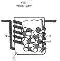
- FIG. 1is a cut-away illustration showing source material prior art techniques
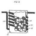
- FIG. 2is a cut-away illustration of materials used for evaporative deposition of a thin film in accordance with an embodiment of invention
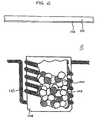
- FIG. 3is an illustration of a technique of thin film deposit in accordance with an embodiment of the invention.
- FIG. 4is an illustration of a thin film deposited by prior a techniques
- FIG. 5is an illustration of a thin film deposited in accord with an embodiment of the invention.
- FIG. 6is an illustration relating to an example of a thin fil produced in accordance with an embodiment of the invention.
- the inventionrelates to thin films that are at least binary i nature and their deposition by evaporative techniques.
- thermal evaporationis an inexpe and commonly used method of forming such films.
- This inventionutilizes; method of increasing the surface area of an evaporation container, preferabl using an inert medium added to source materials held by the container that to form the binary (or greater) film. By this method, films of increased uniformity and maintained stoichiometry are achievable.
- substrateand “wafer” can be used interchangeably in the following description and may include any foundatio surface, but preferably a semiconductor-based structure.
- the structuresho be understood to include silicon, silicon-on insulator (SOI), silicon-on-sapp (SOS), doped and undoped semiconductors, epitaxial layers of silicon supp by a base semiconductor foundation, and other semiconductor structures.
- semiconductorneed not be silicon-based.
- the semiconductorcould be sili germanium, germanium, or gallium arsenide.
- FIG. 1shows an example of how evaporative depositio techniques in the prior art utilized source material.
- Prior art binary films wproduced by thermal evaporation by applying thermal energy to source: mat until they vaporized and then condensed on the desired target (e.g., a semiconductor wafer).
- the desired targete.g., a semiconductor wafer.
- source materialscomprising a first source material 14 and a second source material 16 are ad to an evaporation container 10 , such as a crucible or boat.
- evaporation container 10such as a crucible or boat.
- These two sourc materials 14 and 16generally in the form of solid pellets shaped like marble pebbles, are the two components that are desired to physically or chemical combine to form the binary film.
- the source materials 14 and 16can be in form of two sets of pellets, each respective set comprising one of the first or second source materials 14 and 16 as shown in FIGS. 1 and 2.
- two source materialscan be preliminarily combined in a desired stoichiome form one set of pellets.
- the source materials 14 andcan be in the form of a single solid entity comprising the entire mass of sou material.
- the two source materials 14 and 16once added evaporation container 10 , were subjected to thermal energy from a heat so 12 , typically a resistive heating coil, laser, or electron beam. Upon applicat enough thermal energy, the materials 12 and 16 melt and then vaporize to the thin filn upon condensing.
- the source materials 14 16often have very divergent physical characteristics (e.g., melting and boili points), one of the materials 14 typically melts and vaporizes, and subseque condenses on the target before the other of the source materials 16 , leading undesirable film stoichiometric distribution and uniformity. These diverger physical characteristics can also lead to dissociation (the separation of chemi components into simpler fragments) during evaporation, also negatively impacting film quality.
- the problems associate the prior art techniquescan be mitigated, as shown in FIG. 2, by the additi an inert medium 18 to the source materials 14 and 16 (be them in any of t alternative forms) prior to the addition of thermal energy.
- the inert maximis preferably a material that has a high melting temperature (above that of e source material 14 and 16 ), and is non-reactive in general, and particularly the source materials 14 and 16 .
- the inert medium 18for instance, can be silicon or a ceramic based material.
- the inert medium 18consists of solid material si in shape and size to the source materials 14 and 16 (e.g., pellets); however, will be readily apparent to those of skill in the art that a multitude of variati size and shape of the inert medium 18 are possible and, depending on the circumstances, desirable.
- the shape of the inert medium 18can va generally spherical shapes are preferred because such a design achieves the maximum relative surface area without interfering with the evaporation pro (because of folds, sharp corners, etc.).
- the added inert medium 18preferably large enough to effectively maximize evaporation container 10 su area by contacting the container 10 itself, as well as the source materials 14 16 .
- the size of the inert medium 18should not be so large as to interfere with the evaporation process (e.g., by blocking the evaporation container 10 opening).
- the inert medium 18is dispersed throughout the source material 14 and 16 within the evaporation container
- enough inert medium 18is added to the source materials 14 an so that the thermal energy used for evaporation can be efficiently transferre from the evaporation container 10 to the source materials 14 and 16 as equ as possible.
- the added inert medium 18 of the inventionserves to increase the heating area during the evaporation process
- the addition of the inert medium 18also reduces the amount of power nee to melt the source material 14 and 16 , even towards the middle of the evaporation container 10 , which typically in the prior art required additiona energy.
- the heat source 12preferably in a vacuum chamber 11
- the source material 14 and 16 in the evaporation container meform a liquefied source material 24 , which upon continued application of thermal energy becomes a vaporized source material 26 .
- This vaporized so material 26condenses upon contacting the cooler wafer 20 , which is positi in proximity to the evaporation container (preferably within a vacuum evaporation chamber 11 , positioned above and facing the source material).
- the vaporized source material 26forms a thin film 22 comprising a combination of source materials 14 and 16 , desirably in the sa stoichiometric ratio as initially present in the evaporation container.
- Typical film of about 25 ⁇ to about 5 ⁇ mis desired as useful in the semiconductor industry, which can be produced using the invention.
- first portion 28 of the thin film 22was, in general, predominantly comprise whichever of the source materials 14 and 16 has the lowest melting and boil points, wherein the second portion 30 of the thin film 22 has closer to the desired stoichiometry, being deposited once the second of the source mater 14 and 16 reaches its boiling point. It is also possible that under the circumstances of the prior art that the outermost portion of the thin film 22 would have an undesirably high amount of the second source material 14 o to vaporize, which would continue to be deposited even after the first sourc material is exhausted.
- a gradient 32would be created in the thin film where the proportional amounts of source material 14 and 16 shifts from o extreme to the other through the thickness of the film 22 .
- an uneven surface 34could develop on the thin film 22 shown in FIG. 5, when compared to the thin film 22 of the prior art, the invention can achieve a thinner, more uniform thin film 22 of a more consis desired stoichiometry.
- Each experimental runwas conducted in a vacuum chamb and used a standard ceramic crucible 108 as an evaporation container 10 an standard resistive heating coils 110 for a heat source 12 , as is known in the As a deposition target, a 3500 ⁇ layer of TEOS oxide over a 200 mm silico wafer having a ( 111 ) crystalline orientation served as a substrate 104 upon to condense the thin film.
- the source material used in all runswere pellets formed of silver and selenium (Ag 2 Se), manufactured on site to be of know stoichiometry.
- the target stoichiometry for the deposited thin filmswas Ag 66 Se 33 and the initial stoichiometry of the source material reflected this de film stoichiometry in a 2:1 ratio (with Ag being no greater than 2).
- thermal energywas applied to the crucible 108 and its contents by the resistive heating coils 110 as a function of the % total power.
- the Ag 2 Se so pellets 100were heated for a minimum of 60 seconds to vaporize. Time to boiling was subjective and a function of the % power used.
- the desired thi for each deposited experimental filmwas 500 ⁇ .
- Run 1utilized the same Ag 2 Se sour pellets 100 , but inert silicon (Si) media 102 was added in accordance with t invention. Thermal energy was applied by the resistive heating coils at abo 13% total power. The 500 ⁇ film was deposited and determined by su analysis to have close to target stoichiometry. Run 2 also utilized inert (Si) media 102 in accordance with the invention. For Run 2, thermal e was applied at about 16% total power. The resulting film was not as do target stoichiometry as with Run 1, but was still closer than the Control which used no inert media.
- Sisilicon
Landscapes
- Chemical & Material Sciences (AREA)
- Engineering & Computer Science (AREA)
- Manufacturing & Machinery (AREA)
- Chemical Kinetics & Catalysis (AREA)
- Physics & Mathematics (AREA)
- Computer Hardware Design (AREA)
- Microelectronics & Electronic Packaging (AREA)
- Power Engineering (AREA)
- Condensed Matter Physics & Semiconductors (AREA)
- General Physics & Mathematics (AREA)
- Materials Engineering (AREA)
- Mechanical Engineering (AREA)
- Metallurgy (AREA)
- Organic Chemistry (AREA)
- Physical Vapour Deposition (AREA)
- Physical Deposition Of Substances That Are Components Of Semiconductor Devices (AREA)
Abstract
Description
- This invention relates to the field of deposition of thin fil[0001]composed of multiple materials by thermal evaporation.

- Evaporative deposition techniques are extremely importan[0002]the semiconductor industry where there is a necessity for highly uniform anvery thin films of various materials. In the semiconductor industry, evaporadeposition is useful in forming a material layer of a desired stoichiometry frcplurality of different materials.
- In thermal evaporation techniques, vapor particles can be generated in high vacuum by sublimation or vaporization of a material via a variety of heating sources and then condensed on a substrate. Heating sou[0003]include resistive heating sources, lasers, and electron beam sources. Typical material source is placed in an evaporation crucible or boat and a heat sourcsuch as resistive heating coils, applies thermal energy to the crucible or boat (indirect resistive heating) causing the material source to melt and vaporize. Upon contacting a cooler surface the vaporized material condenses and forfilm.
- Formation of a homogenous thin film having high unifor[0004]and desired stoichiometry by thermal evaporation of a single material is a sirprocedure because a homogenous material source will have only a single bopoint, a single freezing point, and there is no opportunity for dissociation. Therefore, under appropriate conditions, a very thin film that is useful for vpurposes can be easily formed. However, when a binary (or tertiary or greafilm is desired, problems are presented because of the differing physical characteristics (e.g., melting and boiling points) of the multiple source mateand the ever-present problem of dissociation. Often, when forming binaryby thermal evaporation for semiconductor industrial purposes, a material gradient is unintentionally formed in the thin film where the initial material deposited does not have the desired stoichiometry. This requires longer formation times to reach the desired or required stoichiometric levels and clead to films that are not as uniform as desired. Such problems increase and exaggerated as the physical characteristics of the different source materials become increasingly divergent.
- This invention provides a method for improving the stoichiometric character of a thermal-vapor-deposited material layer formed materials having different physical (e.g., melting and boiling points) and chemical properties. An inert medium is added to the source materials with evaporation container (e.g., a crucible) that are to form a binary (or greater upon vaporization and condensation. By this method, films of increased uniformity and maintained stoichiometry are achievable.[0005]
- These and other advantages and features of the invention[0006]be more clearly understood from the following detailed description which is provided in conjunction with the accompanying drawings.
- FIG. 1 is a cut-away illustration showing source material[0007]prior art techniques;
- FIG. 2 is a cut-away illustration of materials used for evaporative deposition of a thin film in accordance with an embodiment of[0008]invention;
- FIG. 3 is an illustration of a technique of thin film deposit in accordance with an embodiment of the invention;[0009]
- FIG. 4 is an illustration of a thin film deposited by prior a[0010]techniques;
- FIG. 5 is an illustration of a thin film deposited in accord[0011]with an embodiment of the invention; and
- FIG. 6 is an illustration relating to an example of a thin fil[0012]produced in accordance with an embodiment of the invention.
- The invention relates to thin films that are at least binary i[0013]nature and their deposition by evaporative techniques. In the semiconductindustry it is often important to maintain both the stoichiometry in thin filand as well as the uniformity of the films. Thermal evaporation is an inexpeand commonly used method of forming such films. This invention utilizes; method of increasing the surface area of an evaporation container, preferablusing an inert medium added to source materials held by the container that to form the binary (or greater) film. By this method, films of increased uniformity and maintained stoichiometry are achievable.
- In the following detailed description, reference is made to various specific embodiments in which the invention may be practiced. The embodiments are described with sufficient detail to enable those skilled in t[0014]to practice the invention, and it is to be understood that other embodiment may be employed, and that structural and electrical changes may be made without departing from the spirit or scope of the present invention.
- The terms “substrate” and “wafer” can be used interchangeably in the following description and may include any foundatio[0015]surface, but preferably a semiconductor-based structure. The structure shobe understood to include silicon, silicon-on insulator (SOI), silicon-on-sapp(SOS), doped and undoped semiconductors, epitaxial layers of silicon suppby a base semiconductor foundation, and other semiconductor structures.semiconductor need not be silicon-based. The semiconductor could be siligermanium, germanium, or gallium arsenide. When reference is made to tsubstrate in the following description, previous process steps may have been utilized to form regions or junctions in or over the base semiconductor or foundation.
- Now referring to the figures, where like reference number denote like features, FIG. 1 shows an example of how evaporative depositio[0016]techniques in the prior art utilized source material. Prior art binary films wproduced by thermal evaporation by applying thermal energy to source: matuntil they vaporized and then condensed on the desired target (e.g., a semiconductor wafer). As is shown, to form a binary film, source materials comprising a
first source material 14 and asecond source material 16 are adto anevaporation container 10, such as a crucible or boat. These twosourc materialspebbles, are the two components that are desired to physically or chemicalcombine to form the binary film. Thesource materials second source materials form one set of pellets. As another alternative, thesource materials 14 and can be in the form of a single solid entity comprising the entire mass of soumaterial. In the prior art, the twosource materials evaporation container 10, were subjected to thermal energy from a heat so12, typically a resistive heating coil, laser, or electron beam. Upon applicatenough thermal energy, thematerials source materials 1416 often have very divergent physical characteristics (e.g., melting and boilipoints), one of thematerials 14 typically melts and vaporizes, and subseque condenses on the target before the other of thesource materials 16, leading undesirable film stoichiometric distribution and uniformity. These divergerphysical characteristics can also lead to dissociation (the separation of chemicomponents into simpler fragments) during evaporation, also negatively impacting film quality. - In accordance with the invention, the problems associate[0017]the prior art techniques can be mitigated, as shown in FIG. 2, by the additian
inert medium 18 to thesource materials 14 and16 (be them in any of talternative forms) prior to the addition of thermal energy. The inert mediuis preferably a material that has a high melting temperature (above that ofe 14 and16), and is non-reactive in general, and particularlysource materialthesource materials inert medium 18, for instance, can be silicon or a ceramic based material. - Typically the[0018]
inert medium 18 consists of solid material siin shape and size to thesource materials 14 and16 (e.g., pellets); however, will be readily apparent to those of skill in the art that a multitude of variatisize and shape of theinert medium 18 are possible and, depending on the circumstances, desirable. Though the shape of theinert medium 18 can vagenerally spherical shapes are preferred because such a design achieves the maximum relative surface area without interfering with the evaporation pro (because of folds, sharp corners, etc.). Further, the addedinert medium 18 preferably large enough to effectively maximizeevaporation container 10 suarea by contacting thecontainer 10 itself, as well as thesource materials 1416. However, the size of theinert medium 18 should not be so large as to interfere with the evaporation process (e.g., by blocking theevaporation container 10 opening). - As shown in FIG. 2, the[0019]
inert medium 18 is dispersed throughout thesource material inert medium 18 is added to thesource materials 14 anso that the thermal energy used for evaporation can be efficiently transferrefrom theevaporation container 10 to thesource materials as possible. - As shown in FIG. 3, The added[0020]
inert medium 18 of the invention serves to increase the heating area during the evaporation process The addition of theinert medium 18 also reduces the amount of power neeto melt thesource material evaporation container 10, which typically in the prior art required additionaenergy. When heat is applied by theheat source 12, preferably in avacuum chamber 11, thesource material liquefied source material 24, which upon continued application of thermal energy becomes a vaporizedsource material 26. This vaporized somaterial 26 condenses upon contacting thecooler wafer 20, which is positiin proximity to the evaporation container (preferably within avacuum evaporation chamber 11, positioned above and facing the source material). Upon condensing, the vaporizedsource material 26 forms athin film 22 comprising a combination ofsource materials stoichiometric ratio as initially present in the evaporation container. Typical film of about 25 Å to about 5 μm is desired as useful in the semiconductor industry, which can be produced using the invention. - The uneven heating, melting, and evaporation of the[0021]
sour materialssou materialsThe result is that the resultant film deposits in less time, leading to more unfilms, and has a more desirable stoichiometry due, in part, to less dissociatio - As illustrated in FIG. 4, because of the uneven heating, melting, evaporation, and dissociation of components found in the prior art[0022]
first portion 28 of thethin film 22 was, in general, predominantly comprisewhichever of thesource materials second portion 30 of thethin film 22 has closer to the desired stoichiometry, being deposited once the second of thesource mater 14 and16 reaches its boiling point. It is also possible that under the circumstances of the prior art that the outermost portion of thethin film 22 would have an undesirably high amount of the second source material14 oto vaporize, which would continue to be deposited even after the first sourcmaterial is exhausted. Thus, agradient 32 would be created in the thin filmwhere the proportional amounts ofsource material extreme to the other through the thickness of thefilm 22. Additionally, unsuch circumstances, anuneven surface 34 could develop on thethin film 22 shown in FIG. 5, when compared to thethin film 22 of the prior art, the invention can achieve a thinner, more uniformthin film 22 of a more consisdesired stoichiometry. - Though this invention has been described primarily with reference to binary films utilizing two[0023]
source materials achievethin films 22 of desired uniformity and stoichiometry utilizing three more source materials. - The following supporting data was obtained in experiment[0024]using actual embodiments of the invention. Table I below shows experimeresults. The experiments are explained in reference to FIG. 6.
TABLE I Inert Source Power Film Silver Film Sele Medium Material (% maximum) (mole %) (mole %) Control None Ag2Se 11% 59.60 40.4 added Run 1 Si added Ag2Se 13% 64.80 35.2 Run 2 Si added Ag2Se 16% 68.90 31.1 - Each experimental run was conducted in a vacuum chamb and used a standard[0025]
ceramic crucible 108 as anevaporation container 10 anstandard resistive heating coils110 for aheat source 12, as is known in theAs a deposition target, a 3500 Å layer of TEOS oxide over a 200 mm silicowafer having a (111) crystalline orientation served as asubstrate 104 uponto condense the thin film. The source material used in all runs were pellets formed of silver and selenium (Ag2Se), manufactured on site to be of knowstoichiometry. The target stoichiometry for the deposited thin films was Ag66Se33and the initial stoichiometry of the source material reflected this defilm stoichiometry in a 2:1 ratio (with Ag being no greater than 2). For eacrun, thermal energy was applied to thecrucible 108 and its contents by the resistive heating coils110 as a function of the % total power. The Ag2Se sopellets 100 were heated for a minimum of 60 seconds to vaporize. Time to boiling was subjective and a function of the % power used. The desired thifor each deposited experimental film was 500 Å. - For the Control Run (reflecting prior art techniques), no medium was added to the Ag[0026]2
Se source pellets 100. The power used was a11% of total power. As is shown in Table I, the resulting stoichiometry of tdeposited film did not achieve the target 2:1 Ag to Se ratio, but the resultinratio did reflect results common to techniques used in the prior art. The undesired stoichiometry was due to the dissimilar physical characteristics of silver and selenium, uneven heating, and dissociation, resulting in uneven deposition rates and amounts between the source materials. - As shown in Table 1, Run 1 utilized the same Ag[0027]2Se
sour 100, but inert silicon (Si)pelletsmedia 102 was added in accordance with tinvention. Thermal energy was applied by the resistive heating coils at abo13% total power. The 500 Å film was deposited and determined by suanalysis to have close to target stoichiometry. Run 2 also utilized inert(Si)media 102 in accordance with the invention. For Run 2, thermal ewas applied at about 16% total power. The resulting film was not as do target stoichiometry as with Run 1, but was still closer than the Control which used no inert media. - The above description, examples, and accompanying d[0028]are only illustrative of exemplary embodiments, which can achieve the feand advantages of the present invention. It is not intended that the invelimited to the embodiments shown and described in detail herein. The invention can be modified to incorporate any number of variations, altersubstitutions or equivalent arrangements not heretofore described, but wcommensurate with the spirit and scope of the invention. Accordingly, tinvention is not to be considered as being limited by the foregoing describut is only limited by the scope of the appended claims.
Claims (40)
1. A method of forming a film, comprising:
providing a source material comprising at least two components;
providing an inert medium interspersed throughout said source mate heating said source material to evaporate at least a portion of said so material; and

condensing said evaporated source material on a surface.
2. The method ofclaim 1 , wherein said at least two components of said source material have an original stoichiometry that is at least approximately maintained throughout said film.
3. The method ofclaim 1 , said source material comprises a plurality of masses, each of said plurality of masses comprising said at least t components of said source material.
4. The method ofclaim 1 , wherein each of said inert medium and said least two components of said source material have respective mel points such that said inert medium has a melting point above tha the components of said source material.
5. The method ofclaim 1 , wherein said inert medium is silicon-based.
6. The method ofclaim 1 , wherein said inert medium is ceramic-based.
7. The method ofclaim 1 , wherein said heating is achieved by a resistiv heating coil.
8. The method ofclaim 1 , wherein said surface is a surface of a semiconductor wafer.
9. The method ofclaim 1 , wherein said source material comprises silver selenium.
10. The method ofclaim 1 , wherein said source material is Ag2Se.
11. The method ofclaim 10 , wherein said film comprises about 65 mole silver and about 35 mole % selenium.
12. The method ofclaim 10 , wherein said film comprises about 66 mole silver and about 33 mole % selenium.
13. The method ofclaim 1 , wherein said acts of heating, evaporating an condensing occur in a vacuum chamber.
14. A method of forming a film, said method comprising:
providing a container;
providing a first source material and a second source material within container;
providing an inert medium within said container; and
applying thermal energy to said container, thereby causing the evaporation of said first and said second source materials, but no said inert medium.
15. The method ofclaim 14 , wherein said first and second source mater have an original stoichiometry which is approximately maintaine said film.
16. The method ofclaim 14 , wherein said inert medium dissipates said thermal energy within said container.
17. The method ofclaim 14 , wherein said inert medium and said first a second source materials each have a respective melting point, sai inert medium having a melting point above that of said first and second source materials.
18. The method ofclaim 14 , wherein said inert medium comprises silic
19. The method ofclaim 14 , wherein said inert medium comprises a cer
20. The method ofclaim 14 , wherein said act of applying thermal energ achieved by an electric coil.
21. The method ofclaim 14 , wherein said inert medium causes evaporat of said first and second source materials to occur approximately contemporaneously.
22. The method ofclaim 14 , further comprising condensing said first an second source materials onto a semiconductor wafer upon which film is formed.
23. The method ofclaim 14 , wherein said first source material is silver a said second source material is selenium in a ratio of two to one, respectively.
24. The method ofclaim 23 , wherein said film comprises about 65 mole silver and about 35 mole % seleaum.
25. The method ofclaim 23 , wherein said film comprises about 66 mole silver and about 33 mole % selenium.
26. The method ofclaim 14 , wherein said evaporation occurs in a vacuu chamber.
27. A method of forming a material layer on a semiconductor device, comprising:
providing a vacuum chamber comprising a resistive heating coil;
positioning a semiconductor wafer within said vacuum chamber;
positioning an evaporation container within said vacuum chamber an contact with said resistive heating coil;
providing a plurality of source materials within said evaporation cont said plurality of source materials comprising at least two material components;
providing an additive to said plurality of source materials within said evaporation container, said additive being non-reactive with said plurality of source materials;
vaporizing said plurality of source materials, without vaporizing said additive; and
condensing said plurality of source materials on a surface of said semiconductor wafer.
28. The method ofclaim 27 , wherein said additive comprises silicon.
29. The method ofclaim 27 , wherein said additive comprises a ceramic.
30. The method ofclaim 27 , wherein said at least two components of sa source materials within said evaporation container have an origin stoichiometry that is approximately maintained throughout said material layer.
31. The method ofclaim 27 , wherein said at least two components com silver and selenium.
32. The method ofclaim 31 , wherein said silver and selenium are presen Ag2Se.
33. The method ofclaim 32 , wherein said metallization layer comprises 65 mole % silver and about 35 mole % selenium.
34. The method ofclaim 32 , wherein said metallization layer comprises 66 mole % silver and about 33 mole % selenium.
35. An apparatus for physical deposition of a film by thermal evaporatio comprising:
a vacuum chamber;
a container suitable to withstand temperatures in excess of a first temperature;
at least two source materials within said container, each of said at lea two source materials having a boiling point up to said first temperature;
an inert medium within said container and interspersed among said least two source materials, said inert medium having a melting po in excess of said first temperature; and
a thermal energy generator capable of raising the temperature of sai container, said at least two source materials, and said inert mediu said first temperature.
36. The apparatus ofclaim 35 , wherein said inert medium comprises sili
37. The apparatus ofclaim 35 , wherein said inert medium comprises a ceramic.
38. The apparatus ofclaim 35 , wherein said thermal energy generator comprises a resistive heating coil.
39. The apparatus ofclaim 35 , wherein said at least two source materials comprise silver and selenium.
40. The apparatus ofclaim 35 , wherein said silver and selenium are in th form of Ag2Se.
Priority Applications (2)
| Application Number | Priority Date | Filing Date | Title |
|---|---|---|---|
| US10/128,349US20040014314A1 (en) | 2002-04-24 | 2002-04-24 | Evaporative deposition with enhanced film uniformity and stoichiometry |
| US11/202,139US20050268855A1 (en) | 2002-04-24 | 2005-08-12 | Evaporative deposition with enhanced film uniformity and stoichiometry |
Applications Claiming Priority (1)
| Application Number | Priority Date | Filing Date | Title |
|---|---|---|---|
| US10/128,349US20040014314A1 (en) | 2002-04-24 | 2002-04-24 | Evaporative deposition with enhanced film uniformity and stoichiometry |
Related Child Applications (1)
| Application Number | Title | Priority Date | Filing Date |
|---|---|---|---|
| US11/202,139DivisionUS20050268855A1 (en) | 2002-04-24 | 2005-08-12 | Evaporative deposition with enhanced film uniformity and stoichiometry |
Publications (1)
| Publication Number | Publication Date |
|---|---|
| US20040014314A1true US20040014314A1 (en) | 2004-01-22 |
Family
ID=30442290
Family Applications (2)
| Application Number | Title | Priority Date | Filing Date |
|---|---|---|---|
| US10/128,349AbandonedUS20040014314A1 (en) | 2002-04-24 | 2002-04-24 | Evaporative deposition with enhanced film uniformity and stoichiometry |
| US11/202,139AbandonedUS20050268855A1 (en) | 2002-04-24 | 2005-08-12 | Evaporative deposition with enhanced film uniformity and stoichiometry |
Family Applications After (1)
| Application Number | Title | Priority Date | Filing Date |
|---|---|---|---|
| US11/202,139AbandonedUS20050268855A1 (en) | 2002-04-24 | 2005-08-12 | Evaporative deposition with enhanced film uniformity and stoichiometry |
Country Status (1)
| Country | Link |
|---|---|
| US (2) | US20040014314A1 (en) |
Cited By (3)
| Publication number | Priority date | Publication date | Assignee | Title |
|---|---|---|---|---|
| US20110168539A1 (en)* | 2010-01-13 | 2011-07-14 | Feng-Kuei Chen | Distilling maching able to produce distilled water with mineral substances |
| US20140224646A1 (en)* | 2002-08-29 | 2014-08-14 | Micron Technology, Inc. | Silver selenide film stoichiometry and morphology control in sputter deposition |
| TWI485276B (en)* | 2013-12-05 | 2015-05-21 | Nat Inst Chung Shan Science & Technology | Evaporation apparatus with improved selenium compound film growing quality |
Families Citing this family (2)
| Publication number | Priority date | Publication date | Assignee | Title |
|---|---|---|---|---|
| US7842534B2 (en)* | 2008-04-02 | 2010-11-30 | Sunlight Photonics Inc. | Method for forming a compound semi-conductor thin-film |
| US20180037981A1 (en)* | 2016-08-03 | 2018-02-08 | Beijing Apollo Ding Rong Solar Technology Co., Ltd. | Temperature-controlled chalcogen vapor distribution apparatus and method for uniform cigs deposition |
Citations (18)
| Publication number | Priority date | Publication date | Assignee | Title |
|---|---|---|---|---|
| US2447789A (en)* | 1945-03-23 | 1948-08-24 | Polaroid Corp | Evaporating crucible for coating apparatus |
| US2867541A (en)* | 1957-02-25 | 1959-01-06 | Gen Electric | Method of preparing transparent luminescent screens |
| US3271562A (en)* | 1964-06-30 | 1966-09-06 | Ibm | Evaporant source |
| US3405251A (en)* | 1966-05-31 | 1968-10-08 | Trw Inc | Vacuum evaporation source |
| US3634647A (en)* | 1967-07-14 | 1972-01-11 | Ernest Brock Dale Jr | Evaporation of multicomponent alloys |
| US3843394A (en)* | 1971-10-11 | 1974-10-22 | Canon Kk | Photosensitive member |
| US4015029A (en)* | 1975-06-27 | 1977-03-29 | Xerox Corporation | Selenium and selenium alloy evaporation technique |
| US4035574A (en)* | 1974-10-11 | 1977-07-12 | Jersey Nuclear-Avco Isotopes, Inc. | Mixed phase evaporation source |
| US4513031A (en)* | 1983-09-09 | 1985-04-23 | Xerox Corporation | Process for forming alloy layer |
| US5030477A (en)* | 1988-11-14 | 1991-07-09 | Xerox Corporation | Processes for the preparation and processes for suppressing the fractionation of chalcogenide alloys |
| US5377429A (en)* | 1993-04-19 | 1995-01-03 | Micron Semiconductor, Inc. | Method and appartus for subliming precursors |
| US5552547A (en)* | 1995-02-13 | 1996-09-03 | Shi; Song Q. | Organometallic complexes with built-in fluorescent dyes for use in light emitting devices |
| US5807613A (en)* | 1994-11-09 | 1998-09-15 | Cametoid Advanced Technologies, Inc. | Method of producing reactive element modified-aluminide diffusion coatings |
| US5989305A (en)* | 1995-03-09 | 1999-11-23 | Shin-Etsu Chemical Co., Ltd. | Feeder of a solid organometallic compound |
| US20010021415A1 (en)* | 2000-03-09 | 2001-09-13 | Junji Kido | Vapor deposition method of organic compound and refinement method of organic compound |
| US6365502B1 (en)* | 1998-12-22 | 2002-04-02 | Cvc Products, Inc. | Microelectronic interconnect material with adhesion promotion layer and fabrication method |
| US20030008071A1 (en)* | 2001-07-03 | 2003-01-09 | Eastman Kodak Company | Method of handling organic material in making an organic light-emitting device |
| US6660328B1 (en)* | 2000-03-31 | 2003-12-09 | Florida State University Research Foundation | Powder precursor delivery system for chemical vapor deposition |
Family Cites Families (2)
| Publication number | Priority date | Publication date | Assignee | Title |
|---|---|---|---|---|
| US6890987B2 (en)* | 2000-10-18 | 2005-05-10 | Nanofilm, Ltd. | Product for vapor deposition of films of amphiphilic molecules or polymers |
| US6610363B2 (en)* | 2000-10-18 | 2003-08-26 | Nanofilm, Ltd. | Composition with film forming alkylsilsesquioxane polymer and method for applying hydrophobic films to surfaces |
- 2002
- 2002-04-24USUS10/128,349patent/US20040014314A1/ennot_activeAbandoned
- 2005
- 2005-08-12USUS11/202,139patent/US20050268855A1/ennot_activeAbandoned
Patent Citations (18)
| Publication number | Priority date | Publication date | Assignee | Title |
|---|---|---|---|---|
| US2447789A (en)* | 1945-03-23 | 1948-08-24 | Polaroid Corp | Evaporating crucible for coating apparatus |
| US2867541A (en)* | 1957-02-25 | 1959-01-06 | Gen Electric | Method of preparing transparent luminescent screens |
| US3271562A (en)* | 1964-06-30 | 1966-09-06 | Ibm | Evaporant source |
| US3405251A (en)* | 1966-05-31 | 1968-10-08 | Trw Inc | Vacuum evaporation source |
| US3634647A (en)* | 1967-07-14 | 1972-01-11 | Ernest Brock Dale Jr | Evaporation of multicomponent alloys |
| US3843394A (en)* | 1971-10-11 | 1974-10-22 | Canon Kk | Photosensitive member |
| US4035574A (en)* | 1974-10-11 | 1977-07-12 | Jersey Nuclear-Avco Isotopes, Inc. | Mixed phase evaporation source |
| US4015029A (en)* | 1975-06-27 | 1977-03-29 | Xerox Corporation | Selenium and selenium alloy evaporation technique |
| US4513031A (en)* | 1983-09-09 | 1985-04-23 | Xerox Corporation | Process for forming alloy layer |
| US5030477A (en)* | 1988-11-14 | 1991-07-09 | Xerox Corporation | Processes for the preparation and processes for suppressing the fractionation of chalcogenide alloys |
| US5377429A (en)* | 1993-04-19 | 1995-01-03 | Micron Semiconductor, Inc. | Method and appartus for subliming precursors |
| US5807613A (en)* | 1994-11-09 | 1998-09-15 | Cametoid Advanced Technologies, Inc. | Method of producing reactive element modified-aluminide diffusion coatings |
| US5552547A (en)* | 1995-02-13 | 1996-09-03 | Shi; Song Q. | Organometallic complexes with built-in fluorescent dyes for use in light emitting devices |
| US5989305A (en)* | 1995-03-09 | 1999-11-23 | Shin-Etsu Chemical Co., Ltd. | Feeder of a solid organometallic compound |
| US6365502B1 (en)* | 1998-12-22 | 2002-04-02 | Cvc Products, Inc. | Microelectronic interconnect material with adhesion promotion layer and fabrication method |
| US20010021415A1 (en)* | 2000-03-09 | 2001-09-13 | Junji Kido | Vapor deposition method of organic compound and refinement method of organic compound |
| US6660328B1 (en)* | 2000-03-31 | 2003-12-09 | Florida State University Research Foundation | Powder precursor delivery system for chemical vapor deposition |
| US20030008071A1 (en)* | 2001-07-03 | 2003-01-09 | Eastman Kodak Company | Method of handling organic material in making an organic light-emitting device |
Cited By (4)
| Publication number | Priority date | Publication date | Assignee | Title |
|---|---|---|---|---|
| US20140224646A1 (en)* | 2002-08-29 | 2014-08-14 | Micron Technology, Inc. | Silver selenide film stoichiometry and morphology control in sputter deposition |
| US9552986B2 (en)* | 2002-08-29 | 2017-01-24 | Micron Technology, Inc. | Forming a memory device using sputtering to deposit silver-selenide film |
| US20110168539A1 (en)* | 2010-01-13 | 2011-07-14 | Feng-Kuei Chen | Distilling maching able to produce distilled water with mineral substances |
| TWI485276B (en)* | 2013-12-05 | 2015-05-21 | Nat Inst Chung Shan Science & Technology | Evaporation apparatus with improved selenium compound film growing quality |
Also Published As
| Publication number | Publication date |
|---|---|
| US20050268855A1 (en) | 2005-12-08 |
Similar Documents
| Publication | Publication Date | Title |
|---|---|---|
| US6608378B2 (en) | Formation of metal oxide gate dielectric | |
| US2938816A (en) | Vaporization method of producing thin layers of semiconducting compounds | |
| US5912797A (en) | Dielectric materials of amorphous compositions and devices employing same | |
| US5108843A (en) | Thin film semiconductor and process for producing the same | |
| JP2002146516A (en) | Vapor deposition method for organic thin film | |
| JPS6392012A (en) | Laminated article and manufacture of the same | |
| EP1727922B1 (en) | High thickness uniformity vaporization source | |
| US20040014314A1 (en) | Evaporative deposition with enhanced film uniformity and stoichiometry | |
| JP3483719B2 (en) | Evaporation source for organic material and organic thin film forming apparatus using the same | |
| US7727335B2 (en) | Device and method for the evaporative deposition of a coating material | |
| US3392056A (en) | Method of making single crystal films and the product resulting therefrom | |
| US4649024A (en) | Method for forming evaporated pnictide and alkali metal polypnictide films | |
| JPS6158976B2 (en) | ||
| CA1056658A (en) | Method of vapor deposition | |
| US7670645B1 (en) | Method of treating metal and metal salts to enable thin layer deposition in semiconductor processing | |
| US5332482A (en) | Method and apparatus for depositing an oxide film | |
| JPS61280927A (en) | Multilayer article containing crystallization preventive layer and manufacture thereof | |
| Yamanishi et al. | Industrial applications of ICB deposition for the fabrication of electronic devices | |
| Komarenko et al. | Jet Vapor Deposition | |
| JPS62180067A (en) | Method and apparatus for electron beam vapor deposition | |
| JPH03202468A (en) | Film formation | |
| JPH0834173B2 (en) | Thin film forming method and thin film forming apparatus | |
| JPS58110047A (en) | Manufacture of semiconductor device | |
| JPS5976418A (en) | Manufacture of thin film | |
| JPH0314233A (en) | Formation of wiring |
Legal Events
| Date | Code | Title | Description |
|---|---|---|---|
| AS | Assignment | Owner name:MICRON TECHNOLOGY, INC., IDAHO Free format text:ASSIGNMENT OF ASSIGNORS INTEREST;ASSIGNOR:BROOKS, JOSEPH F.;REEL/FRAME:013080/0103 Effective date:20020418 | |
| STCB | Information on status: application discontinuation | Free format text:ABANDONED -- FAILURE TO RESPOND TO AN OFFICE ACTION |