US20040012009A1 - Sublithographic contact structure, phase change memory cell with optimized heater shape, and manufacturing method thereof - Google Patents
Sublithographic contact structure, phase change memory cell with optimized heater shape, and manufacturing method thereofDownload PDFInfo
- Publication number
- US20040012009A1 US20040012009A1US10/371,154US37115403AUS2004012009A1US 20040012009 A1US20040012009 A1US 20040012009A1US 37115403 AUS37115403 AUS 37115403AUS 2004012009 A1US2004012009 A1US 2004012009A1
- Authority
- US
- United States
- Prior art keywords
- forming
- layer
- thin portion
- dimension
- sublithographic
- Prior art date
- Legal status (The legal status is an assumption and is not a legal conclusion. Google has not performed a legal analysis and makes no representation as to the accuracy of the status listed.)
- Granted
Links
- 230000008859changeEffects0.000titleclaimsdescription19
- 238000004519manufacturing processMethods0.000titleclaimsdescription16
- 239000004065semiconductorSubstances0.000claimsabstractdescription6
- 238000000034methodMethods0.000claimsdescription27
- 230000008569processEffects0.000claimsdescription23
- 125000006850spacer groupChemical group0.000claimsdescription16
- 238000000151depositionMethods0.000claimsdescription14
- 239000003989dielectric materialSubstances0.000claimsdescription7
- 238000005530etchingMethods0.000claimsdescription6
- 239000012782phase change materialSubstances0.000claimsdescription5
- 239000000463materialSubstances0.000description9
- 230000008021depositionEffects0.000description8
- 150000004770chalcogenidesChemical class0.000description7
- 238000010438heat treatmentMethods0.000description7
- 230000004888barrier functionEffects0.000description6
- 229910052751metalInorganic materials0.000description5
- 239000002184metalSubstances0.000description5
- 230000015572biosynthetic processEffects0.000description3
- 238000002425crystallisationMethods0.000description3
- 230000008025crystallizationEffects0.000description3
- 230000008018meltingEffects0.000description3
- 238000002844meltingMethods0.000description3
- 150000004767nitridesChemical class0.000description3
- 238000000623plasma-assisted chemical vapour depositionMethods0.000description3
- 229910052710siliconInorganic materials0.000description3
- WFKWXMTUELFFGS-UHFFFAOYSA-NtungstenChemical compound[W]WFKWXMTUELFFGS-UHFFFAOYSA-N0.000description3
- 229910052721tungstenInorganic materials0.000description3
- 239000010937tungstenSubstances0.000description3
- 229910010037TiAlNInorganic materials0.000description2
- 229910008482TiSiNInorganic materials0.000description2
- 238000005516engineering processMethods0.000description2
- QRXWMOHMRWLFEY-UHFFFAOYSA-NisoniazideChemical compoundNNC(=O)C1=CC=NC=C1QRXWMOHMRWLFEY-UHFFFAOYSA-N0.000description2
- 230000006911nucleationEffects0.000description2
- 238000010899nucleationMethods0.000description2
- 230000003287optical effectEffects0.000description2
- 239000000758substrateSubstances0.000description2
- 229910016570AlCuInorganic materials0.000description1
- 229910000927Ge alloyInorganic materials0.000description1
- 229910001245Sb alloyInorganic materials0.000description1
- XUIMIQQOPSSXEZ-UHFFFAOYSA-NSiliconChemical compound[Si]XUIMIQQOPSSXEZ-UHFFFAOYSA-N0.000description1
- 229910001215Te alloyInorganic materials0.000description1
- BOTDANWDWHJENH-UHFFFAOYSA-NTetraethyl orthosilicateChemical compoundCCO[Si](OCC)(OCC)OCCBOTDANWDWHJENH-UHFFFAOYSA-N0.000description1
- ATJFFYVFTNAWJD-UHFFFAOYSA-NTinChemical compound[Sn]ATJFFYVFTNAWJD-UHFFFAOYSA-N0.000description1
- 229910045601alloyInorganic materials0.000description1
- 239000000956alloySubstances0.000description1
- 238000013459approachMethods0.000description1
- 238000005229chemical vapour depositionMethods0.000description1
- 238000001312dry etchingMethods0.000description1
- 230000000694effectsEffects0.000description1
- 239000011521glassSubstances0.000description1
- 238000009413insulationMethods0.000description1
- 238000012986modificationMethods0.000description1
- 230000004048modificationEffects0.000description1
- 230000000737periodic effectEffects0.000description1
- 238000005498polishingMethods0.000description1
- 238000007493shaping processMethods0.000description1
- 239000010703siliconSubstances0.000description1
- 239000000126substanceSubstances0.000description1
- 229910052714telluriumInorganic materials0.000description1
Images


Classifications
- G—PHYSICS
- G11—INFORMATION STORAGE
- G11C—STATIC STORES
- G11C11/00—Digital stores characterised by the use of particular electric or magnetic storage elements; Storage elements therefor
- G11C11/56—Digital stores characterised by the use of particular electric or magnetic storage elements; Storage elements therefor using storage elements with more than two stable states represented by steps, e.g. of voltage, current, phase, frequency
- G11C11/5678—Digital stores characterised by the use of particular electric or magnetic storage elements; Storage elements therefor using storage elements with more than two stable states represented by steps, e.g. of voltage, current, phase, frequency using amorphous/crystalline phase transition storage elements
- G—PHYSICS
- G11—INFORMATION STORAGE
- G11C—STATIC STORES
- G11C13/00—Digital stores characterised by the use of storage elements not covered by groups G11C11/00, G11C23/00, or G11C25/00
- G11C13/0002—Digital stores characterised by the use of storage elements not covered by groups G11C11/00, G11C23/00, or G11C25/00 using resistive RAM [RRAM] elements
- G11C13/0004—Digital stores characterised by the use of storage elements not covered by groups G11C11/00, G11C23/00, or G11C25/00 using resistive RAM [RRAM] elements comprising amorphous/crystalline phase transition cells
- H—ELECTRICITY
- H10—SEMICONDUCTOR DEVICES; ELECTRIC SOLID-STATE DEVICES NOT OTHERWISE PROVIDED FOR
- H10B—ELECTRONIC MEMORY DEVICES
- H10B63/00—Resistance change memory devices, e.g. resistive RAM [ReRAM] devices
- H10B63/30—Resistance change memory devices, e.g. resistive RAM [ReRAM] devices comprising selection components having three or more electrodes, e.g. transistors
- H10B63/32—Resistance change memory devices, e.g. resistive RAM [ReRAM] devices comprising selection components having three or more electrodes, e.g. transistors of the bipolar type
- H—ELECTRICITY
- H10—SEMICONDUCTOR DEVICES; ELECTRIC SOLID-STATE DEVICES NOT OTHERWISE PROVIDED FOR
- H10N—ELECTRIC SOLID-STATE DEVICES NOT OTHERWISE PROVIDED FOR
- H10N70/00—Solid-state devices having no potential barriers, and specially adapted for rectifying, amplifying, oscillating or switching
- H10N70/011—Manufacture or treatment of multistable switching devices
- H10N70/061—Shaping switching materials
- H10N70/068—Shaping switching materials by processes specially adapted for achieving sub-lithographic dimensions, e.g. using spacers
- H—ELECTRICITY
- H10—SEMICONDUCTOR DEVICES; ELECTRIC SOLID-STATE DEVICES NOT OTHERWISE PROVIDED FOR
- H10N—ELECTRIC SOLID-STATE DEVICES NOT OTHERWISE PROVIDED FOR
- H10N70/00—Solid-state devices having no potential barriers, and specially adapted for rectifying, amplifying, oscillating or switching
- H10N70/20—Multistable switching devices, e.g. memristors
- H10N70/231—Multistable switching devices, e.g. memristors based on solid-state phase change, e.g. between amorphous and crystalline phases, Ovshinsky effect
- H—ELECTRICITY
- H10—SEMICONDUCTOR DEVICES; ELECTRIC SOLID-STATE DEVICES NOT OTHERWISE PROVIDED FOR
- H10N—ELECTRIC SOLID-STATE DEVICES NOT OTHERWISE PROVIDED FOR
- H10N70/00—Solid-state devices having no potential barriers, and specially adapted for rectifying, amplifying, oscillating or switching
- H10N70/801—Constructional details of multistable switching devices
- H10N70/821—Device geometry
- H10N70/826—Device geometry adapted for essentially vertical current flow, e.g. sandwich or pillar type devices
- H—ELECTRICITY
- H10—SEMICONDUCTOR DEVICES; ELECTRIC SOLID-STATE DEVICES NOT OTHERWISE PROVIDED FOR
- H10N—ELECTRIC SOLID-STATE DEVICES NOT OTHERWISE PROVIDED FOR
- H10N70/00—Solid-state devices having no potential barriers, and specially adapted for rectifying, amplifying, oscillating or switching
- H10N70/801—Constructional details of multistable switching devices
- H10N70/841—Electrodes
- H10N70/8413—Electrodes adapted for resistive heating
- H—ELECTRICITY
- H10—SEMICONDUCTOR DEVICES; ELECTRIC SOLID-STATE DEVICES NOT OTHERWISE PROVIDED FOR
- H10N—ELECTRIC SOLID-STATE DEVICES NOT OTHERWISE PROVIDED FOR
- H10N70/00—Solid-state devices having no potential barriers, and specially adapted for rectifying, amplifying, oscillating or switching
- H10N70/801—Constructional details of multistable switching devices
- H10N70/881—Switching materials
- H10N70/882—Compounds of sulfur, selenium or tellurium, e.g. chalcogenides
- H10N70/8828—Tellurides, e.g. GeSbTe
Definitions
- the present inventionrelates to a sublithographic contact structure, a phase change memory cell, and to a manufacturing process thereof.
- phase change memory (PCM) elementsexploit the characteristics of materials which have the property of changing between two phases having distinct electrical characteristics. For example, these materials may change from an amorphous phase, which is disorderly, to a crystalline or polycrystalline phase, which is orderly, and the two phases are associated to considerably different resistivity.
- alloys of group VI of the periodic tablesuch as Te or Se, referred to as chalcogenides or chalcogenic materials, can advantageously be used in phase change cells.
- the chalcogenide that currently offers the most promiseis formed by a Ge, Sb and Te alloy (Ge 2 Sb 2 Te 5 ), which is currently widely used for storing information in overwritable disks.
- the resistivityvaries by two or more magnitude orders when the material passes from the amorphous phase (more resistive) to the polycrystalline phase (more conductive) and vice versa.
- the characteristics of chalcogenides in the two phasesare shown in FIG. 1. As may be noted, at a given read voltage, here designated by Vr, there is a resistance variation of more than 10.
- Phase changemay be obtained by locally increasing the temperature, as shown in FIG. 2. Below 150° C. both phases are stable. Above 200° C. (temperature of start of nucleation, designated by T x ), fast nucleation of the crystallites takes place, and, if the material is kept at the crystallization temperature for a sufficient length of time (time t 2 ), it changes its phase and becomes crystalline. To bring the chalcogenide back into the amorphous state, it is necessary to raise the temperature above the melting temperature T m (approximately 600° C.) and then to cool the chalcogenide off rapidly (time t 1 ).
- FIG. 3The basic structure of a PCM element 1 which operates according to the principles described above is shown in FIG. 3 and comprises a resistive element 2 (heater) and a programmable element 3 .
- the programmable element 3is made of a chalcogenide and is normally in the polycrystalline state in order to enable a good flow of current.
- One part of the programmable element 3is in direct contact with the resistive element 2 and forms the area affected by phase change, hereinafter referred to as the phase change portion 4 .
- the PCM element of FIG. 3for forming memory cells has already been proposed.
- the PCM elementis generally associated to a selection element, such a MOS transistor, a bipolar transistor, or a diode.
- An embodiment of the inventionprovides a contact structure in a semiconductor electronic device.
- the contact structureincludes a cup-shaped first conductive region having vertical walls that form a first thin portion having a first dimension in a first direction; and a second conductive region having a second thin portion having a second sublithographic dimension in a second direction transverse to the first dimension.
- the first and second conductive regionsare in direct electrical contact at the first and second thin portions and define a contact area having a sublithographic extension.
- the first conductive regionextends, in top plan view, along a closed line having an elongated shape in the first direction.
- phase change memory cellthat includes a cup-shaped resistive element comprising vertical walls forming a first sublithographic portion in a first direction; and a memory region of a phase change material including a second thin portion having a second sublithographic dimension in a second direction transverse to the first dimension.
- the resistive element and the memory regionare in direct electrical contact at the first thin portion and the second thin portion and define a contact area having a sublithographic extension, and the resistive element extends, in top plan view, along a closed line having an elongated shape in the first direction.
- Other embodimentsprovide a process for manufacturing a semiconductor electronic device having a contact area as described above and a process for manufacturing a phase change memory cell as described above.
- FIG. 1shows the current versus voltage characteristic of a phase change material
- FIG. 2shows the temperature versus current plot of a phase change material
- FIG. 3shows the basic structure of a PCM memory element
- FIG. 4shows a cross section of a wafer of semiconductor material in a manufacturing step of the cell of FIG. 3, according to the parent patent application;
- FIG. 5shows the layout of some masks used for forming the structure of FIG. 4;
- FIG. 6is a cross-section taken along line VI-VI of FIG. 5;
- FIGS. 7 - 14are cross-section of the structure of the parent patent application, in successive manufacture steps
- FIG. 15is a top plan view, with parts removed and at an enlarged scale, of a detail of FIG. 4;
- FIGS. 16A and 16Bare top plan views, with parts removed, of a detail of FIG. 14, in two different manufacture conditions;
- FIG. 17shows the layout of some masks used for forming the structure of FIG. 7, according to an embodiment of the invention.
- FIG. 18is a cross-section similar to FIG. 8, in a manufacture step according to an embodiment of the invention.
- FIG. 19shows the layout of some masks used for forming the structure of FIG. 18;
- FIGS. 20 and 21are cross-sections, similar to FIG. 18, in successive manufacture steps according to an embodiment of the invention.
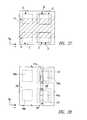
- FIG. 22is a top plan view of the structure of FIG. 21;
- FIG. 23is a cross-section, similar to FIG. 21, in a subsequent manufacture step
- FIG. 24shows the layout of same masks used for forming the structure of FIG. 23;
- FIG. 25is a cross-section, similar to FIG. 14, in a final manufacture step according to an embodiment of the invention.
- FIGS. 26A and 26Bare top plan views of the contact area, in two different manufacture conditions.
- FIG. 27shows the layout of some masks used after forming the structure of FIG. 10, according to a different embodiment of the invention.
- FIG. 28shows the structure obtained using the masks of FIG. 27.
- the parent applicationteaches forming the contact area as an intersection of two thin portions extending transversely with respect to one another and each of a sublithographic size.
- deposition of layersis adopted instead of a lithographic process, given that deposition makes it possible to obtain very thin layers, i.e., having a thickness much smaller than the current minimum size that can be achieved using lithographic techniques.
- a wafer 10comprising a P-type substrate 11 is subjected to standard front end steps.
- insulation regions 12are formed and delimit active areas 16 ; then, in succession, N-type base regions 13 , N + -type base contact regions 14 , and P + -type emitter regions 15 are implanted.
- the base regions 13 , base contact regions 14 , and emitter regions 15form diodes that form selection elements for the memory cells.
- a first dielectric layer 18is deposited and planarized; openings are formed in the first dielectric layer 18 above the base contact regions 13 and emitter regions 15 , and the openings are filled with tungsten to form base contacts 19 b and emitter contacts 19 a.
- the base contacts 19 bare thus in direct electrical contact with the base contact regions 13
- the emitter contacts 19 aare in direct electrical contact with the emitter regions 15 .
- the openings in the first dielectric layer 18can be covered by a barrier layer, for example a Ti/TiN layer, before being filled with tungsten. In this way, the structure of FIG. 4 is obtained.
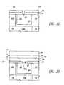
- FIG. 5shows the layout of some masks used for forming the structure of FIG. 4 regarding a pair of memory cells 5 that are adjacent in a perpendicular direction to the sectional plane of FIG. 4 (Y direction).
- the figureshows a mask A used for defining the active areas 16 , a mask B used for implanting the emitter regions 15 , and a mask C for forming the openings where the base contacts 19 b and the emitter contacts 19 a are to be formed.
- FIG. 4is a cross-section taken along line IV-IV of FIG. 5, while FIG. 6 shows the same structure sectioned along the section line VI-VI of FIG. 5.
- a second dielectric layer 20for example, an undoped silicon glass (USG) layer- is deposited, and openings 21 are formed in the second dielectric layer 20 above the emitter contact 19 a.
- the openings 21have dimensions dictated by the lithographic process and are, for example, circle-shaped.
- a heating layerfor example of TiSiN, TiAlN or TiSiC, is deposited for a thickness of 10-50 nm, preferably 20 nm.
- the heating layerdesigned to form the resistive element 2 of FIG. 3, conformally coats the walls and bottom of the openings 21 and is subsequently removed outside the openings 21 . The remaining portions of the heating layer thus form a cup-shaped region 22 and are then filled with dielectric material 23 .
- a mold layer 27for instance USG having a thickness of 20 nm, an adhesion layer 28 , for instance Ti or Si with a thickness of 5 nm, and a first delimiting layer 29 , for example nitride or another material that enables selective etching with respect to the mold layer 27 , are deposited in sequence.
- the first delimiting layer 29has a thickness of, for instance, 150 nm.
- one part of the first delimiting layer 29is removed by dry etching to form a step which has a vertical side 30 that extends vertically on top of the dielectric material 23 .
- the structure shown in FIG. 8is thus obtained.
- a sacrificial layer 31for example TiN with a thickness of 30 nm, is deposited conformally.
- the sacrificial layerforms a vertical wall 31 a that extends along the vertical side 30 of the first delimiting layer 29 .
- the sacrificial layer 31is undergoes an etch back that results in removal of the horizontal portions of the sacrificial layer 31 and of part of the vertical wall 31 a.
- a second delimiting layer 35of the same material as the first delimiting layer 29 , for example nitride, with a thickness of 300 nm, is deposited.
- the delimiting layers 29 , 35 and the vertical wall 31 aare thinned by chemical mechanical polishing (CMP).
- CMPchemical mechanical polishing
- the sacrificial region 36is removed.
- the adhesion layer 28is isotropically etched, and the mold layer 27 is dry etched to form a slit 37 in the mold layer 27 , the slit 37 having a width W1 equal to the width of the sacrificial region 36 .
- a chalcogenic layer 38for example of Ge 2 Sb 2 Te 5 with a thickness of 60 nm, is deposited conformally.
- the portion 38 a of the chalcogenic layer 38fills the slit 37 and forms, at the intersection with the cup-shaped region 22 , a phase change region similar to the phase change portion 4 of FIG. 3.
- a barrier layer 39for example of Ti/TiN, and a metal layer 40 , for example of AlCu, are deposited.
- a barrier layer 39for example of Ti/TiN
- a metal layer 40for example of AlCu
- FIG. 14the stack formed by the metal layer 40 , the barrier layer 39 and the chalcogenic layer 38 is defined using a same mask, thus forming a bit line 41 .
- a third dielectric layer 42is deposited, which is opened above the base contacts 19 b. The openings thus formed are filled with tungsten to form top contacts 43 in order to prolong upwards the base contacts 19 b.
- standard stepsare performed for forming the connection lines for connection to the base contacts 19 b and to the bits lines 41 , and the final structure of FIG. 14 is thus obtained.
- the intersection between the cup-shaped region 22 and the thin portion 38 a of the chalcogenic layer 38forms a contact area 45 which is approximately square and has sublithographic dimensions. This is due to the fact that both the cup-shaped region 22 and the thin portion 38 a have a width equal to the thickness of a deposited layer. In fact, the width of the cup-shaped region 22 is given by the thickness of the heating layer, and the width of the thin portions 38 a is determined by the thickness of the sacrificial layer 31 along the vertical side 30 .
- the cup-shaped region 22has a sublithographic dimension in a first direction (Y direction), and the thin portion 38 a has a sublithographic dimension (width W1 of FIG. 10) in a second direction (X direction) which is transverse to the first direction.
- sublithographic dimensionmeans a linear dimension smaller than the limit dimension achievable with current optical (UV) lithographic techniques, and hence smaller than 100 nm, preferably 50-60 nm, down to approximately 20 nm.
- the dimensions of the contact area 45depend upon the alignment tolerances between the mask used for forming the openings 21 and the mask used for removing part of the first delimiting layer 29 and for forming the vertical side 30 (FIG. 8).
- FIGS. 16 a and 16 bwhich are top plan views of the contact area 45
- an alignment error of even only 0.05 ⁇ m between the two masksresults in the thin portions 38 a no longer crossing the cup-shaped regions 22 perpendicularly, with a consequent considerable increase in the dimensions of the contact area 45 (see FIG. 16 b ) and hence a considerable increase in the flowing current, the value whereof would be uncontrollable.
- the thin portion 38 acrosses each cup-shaped region 22 in two points, thus doubling the total contact area between the thin portions 38 a and the cup-shaped regions 22 , and consequently also increasing the programming current.
- just one contact areais even obtained which has dimensions far greater than the requirements.
- the presence of a double contactgives rise to functional problems, given that in this situation it would be impossible to know which of the two contact areas 45 first causes switching of the overlying thin portion 38 a (i.e., the phase change portion), nor would it be possible to be certain that both of the thin portions 38 a overlying the two contact areas will switch.
- the process according to an embodiment of the present inventioncomprises initial steps equal to those described above, up to deposition of the second dielectric layer 20 (FIG. 7).
- the openings 21 and the cup-shaped regions 22are formed.
- a heater mask Dis used which has rectangular windows (the term “rectangular” also comprising the particular case of a square shape). Consequently, the openings 21 have a substantially rectangular shape.
- the heating layerfor example of TiSiN, TiAlN or TiSiC, with a thickness of 10-50 nm, preferably 20 nm, is deposited. The heating layer coats the walls and bottom of the openings 21 conformally.
- the cup-like regions 22here define an ideally rectangular shape, possibly with rounded edges (on account of the lithographic limits), or at the most an ovalized shape, with the longer side, or main direction, parallel to the X direction (FIG. 22).
- the heating layeris removed outside the openings 21 to form the cup-shaped regions 22 , which are then filled with the dielectric material 23 .
- a stop layer 48for example of nitride deposited by PECVD (Plasma Enhanced Chemical Vapor Deposition) with a thickness of 20-40 nm
- a mold layer 49for example of USG deposited by PECVD or SACVD (Sub-Atmospheric Chemical Vapor Deposition) with a thickness of 50-70 nm
- an adhesion layer 50for example of Ti or Si with a thickness of 20-40 nm
- the minitrench mask Ehas a rectangular window that extends between two adjacent cells 5 in the Y direction (perpendicular to the alignment direction of the base and emitter regions 14 , 15 of each memory cell 5 , FIG. 7).
- part of the layers 48 , 49 and 50is removed, so as to form an opening 51 having a rectangular shape, corresponding to that of the minitrench mask E.
- the width of the opening 51 in the X directionis, for example, 160 nm.
- the opening 51uncovers part of the dielectric material 23 of the two adjacent cells 5 and crosses each cup-shaped region 22 only once, as can be clearly seen from the superposition of the heater mask D and minitrench mask E in FIG. 19.
- a spacer layer 55for example an oxide layer, is deposited (in particular, TEOS with a thickness of 50 nm) is deposited.
- the spacer layer 55covers the adhesion layer 50 , as well as the walls and bottom of the opening 51 .
- the spacer layer 55is anisotropically etched by etching back until the horizontal portions thereof are removed, according to the Well known spacer formation technique.
- the spacer layer 55is then completely removed above the adhesion layer 50 and is partially removed from the bottom of the opening 51 to form a spacer region 55 a which extends along the vertical sides of the opening 51 (along the perimeter of a rectangle or of an oval) and delimits a slit 56 , the base whereof forms a rectangular strip 57 having a sublithographic Width W2 (in the X direction) of approximately 60 nm.
- FIG. 21the spacer layer 55 is anisotropically etched by etching back until the horizontal portions thereof are removed, according to the Well known spacer formation technique.
- the spacer layer 55is then completely removed above the adhesion layer 50 and is partially removed from the bottom of the opening 51 to form a spacer region 55 a which extends along the vertical sides of the opening 51 (along the perimeter of a rectangle or of an oval) and
- each cup-shaped region 22is a top plan view of the structure thus obtained, and highlights how the strip 57 uncovers only one portion of the cup-shaped region 22 of each cell 5 , shown with dashed line in the figure.
- the uncovered portion of each cup-shaped region 22forms a contact area 58 , as will be explained hereinafter.
- the chalcogenic layer 38(also in the present case, for instance, of Ge 2 Sb 2 Te 5 with a thickness of 60 nm), the barrier layer 39 , and the metal layer 40 are deposited in succession,,to form a stack of layers 41 .
- the chalcogenic layer 38is in direct contact with the adhesion layer 50 , to which it adheres properly, and fills the slit 56 with a thin portion 38 a.
- the thin portion 38 a of the chalcogenic layer 38deposits on the strip 57 , contacting the cup-shaped regions 22 at the contact areas 58 .
- the inclined wall formed by the spacer region 55 afavors filling of the slit 56 , so preventing problems linked to a poor aspect ratio of the opening 51 .
- the stack of layers 41is defined using a stack mask F (FIG. 24).
- the thin portion 38 a of the chalcogenic layer 38is formed using the technology described in the parent patent application, and the second crossing-over of the cup-shaped region 22 by the thin portion 38 a is avoided by using a special mask, called self-rapier mask, as described hereinafter.
- the processcomprises the same initial steps described with reference to FIGS. 4 - 9 , with the sole difference that the cup-shaped region 22 is shaped using the heater mask D illustrated in FIG. 17, so as to obtain a rectangular, or at the most oval, shape owing to the lithographic limits.
- the vertical wall 31 a of the first delimitation layer 29is present on the step 30 , and the rest of the sacrificial layer has already been removed.
- self-rapier mask Gillustrated in FIG. 27, part of the vertical wall 31 a is removed so that the latter will intersect the cup-shaped region 22 of each cell 5 only in one point.
- the self-rapier mask Gcovers a strip that bestrides two cells 5 in a direction parallel to the X direction.
- the portions of the vertical wall 31 a not covered by the self-rapier mask Gare then removed.
- just one portion of vertical wall 31 aremains at the side of the step 30 , the cross section whereof in the X-Z plane coincides with that of FIG. 10 described above.
- the remaining portion of vertical wall 31 aintersects each cup-shaped region 22 just once, as is highlighted by the hatched area which, later, forms the contact area 45 .
- deposition of the chalcogenic layer 38 which fills the slit 37 of the mold layer 27deposition of the barrier layer 39 and of the metal layer 40 ; shaping of the stack formed by the metal layer 40 , the barrier layer 39 and the chalcogenic layer 38 ; deposition of the third dielectric layer 42 ; and the final steps described above for obtaining the structure illustrated in FIG. 14.
- thin portions 38 aare formed, that have a roughly parallelepipedal shape and short length, i.e., smaller than the overall dimensions of two cells 5 in the Y direction.
- the thin portion 38 ais delimited by the spacer region 55 a; in the second embodiment, the thin portion 38 a is delimited directly by the mold layer 27 .
- the rectangular or ovalized shape of the cup-shaped region 22reduces the dimension spread of the contact area 58 also when its shape, instead of being rectangular, as in the ideal case, is oval, as highlighted by the comparison between FIG. 26 a, showing the relative position of the cup-shaped region 22 and the thin region 38 a in absence of mask misalignment, and FIG. 26 b, which illustrates this position in presence of misalignment.
- FIG. 26 ashowing the relative position of the cup-shaped region 22 and the thin region 38 a in absence of mask misalignment
- FIG. 26 bwhich illustrates this position in presence of misalignment.
- misalignments between the heater mask D and the minitrench mask E or the mask defining the first delimitation layer 29lead to a negligible variation in the contact area.
- the variation in dimensionsis even zero.
- the shape of the minitrench mask E or the use of the self-rapier mask Gmakes it possible to obtain a single contact area 58 for each cup-shaped region 22 , and thus for each cell 5 .
Landscapes
- Engineering & Computer Science (AREA)
- Chemical & Material Sciences (AREA)
- Crystallography & Structural Chemistry (AREA)
- Computer Hardware Design (AREA)
- Manufacturing & Machinery (AREA)
- Semiconductor Memories (AREA)
Abstract
Description
- This application is a continuation-in-part of U.S. patent application Ser. No. 10/313,991, filed Dec. 5, 2002, now pending, which application is incorporated herein by reference in its entirety.[0001]
- 1. Field of the Invention[0002]
- The present invention relates to a sublithographic contact structure, a phase change memory cell, and to a manufacturing process thereof.[0003]
- 2. Description of the Related Art[0004]
- As is known, phase change memory (PCM) elements exploit the characteristics of materials which have the property of changing between two phases having distinct electrical characteristics. For example, these materials may change from an amorphous phase, which is disorderly, to a crystalline or polycrystalline phase, which is orderly, and the two phases are associated to considerably different resistivity.[0005]
- At present, alloys of group VI of the periodic table, such as Te or Se, referred to as chalcogenides or chalcogenic materials, can advantageously be used in phase change cells. The chalcogenide that currently offers the most promise is formed by a Ge, Sb and Te alloy (Ge[0006]2Sb2Te5), which is currently widely used for storing information in overwritable disks.
- In chalcogenides, the resistivity varies by two or more magnitude orders when the material passes from the amorphous phase (more resistive) to the polycrystalline phase (more conductive) and vice versa. The characteristics of chalcogenides in the two phases are shown in FIG. 1. As may be noted, at a given read voltage, here designated by Vr, there is a resistance variation of more than 10.[0007]
- Phase change may be obtained by locally increasing the temperature, as shown in FIG. 2. Below 150° C. both phases are stable. Above 200° C. (temperature of start of nucleation, designated by T[0008]x), fast nucleation of the crystallites takes place, and, if the material is kept at the crystallization temperature for a sufficient length of time (time t2), it changes its phase and becomes crystalline. To bring the chalcogenide back into the amorphous state, it is necessary to raise the temperature above the melting temperature Tm(approximately 600° C.) and then to cool the chalcogenide off rapidly (time t1).
- From the electrical standpoint, it is possible to reach both critical temperatures, namely the crystallization temperature and the melting point, by causing a current to flow through a resistive element which heats the chalcogenic material by the Joule effect.[0009]
- The basic structure of a[0010]
PCM element 1 which operates according to the principles described above is shown in FIG. 3 and comprises a resistive element2 (heater) and aprogrammable element 3. Theprogrammable element 3 is made of a chalcogenide and is normally in the polycrystalline state in order to enable a good flow of current. One part of theprogrammable element 3 is in direct contact with theresistive element 2 and forms the area affected by phase change, hereinafter referred to as thephase change portion 4. - If an electric current having an appropriate value is caused to pass through the[0011]
resistive element 2, it is possible to heat thephase change portion 4 selectively up to the crystallization temperature or to the melting temperature and to cause phase change. In particular, if a current I flows through aresistive element 2 having resistance R, the heat generated is equal to I2R. - The use of the PCM element of FIG. 3 for forming memory cells has already been proposed. In order to prevent noise caused by adjacent memory cells, the PCM element is generally associated to a selection element, such a MOS transistor, a bipolar transistor, or a diode.[0012]
- All the known approaches are, however, disadvantageous due to the difficulty in finding solutions that meet present requirements as regards capacity for withstanding the operating currents and voltages, as well as functionality and compatibility with present CMOS technologies.[0013]
- In particular, considerations of a technological and electrical nature impose the creation of a contact area of small dimensions, preferably 20 nm×20 nm, between the chalcogenic region and a resistive element. However, these dimensions are much smaller than those that can be obtained with current optical (UV) lithographic techniques, which scarcely reach[0014]100 linear nm.
- An embodiment of the invention provides a contact structure in a semiconductor electronic device. The contact structure includes a cup-shaped first conductive region having vertical walls that form a first thin portion having a first dimension in a first direction; and a second conductive region having a second thin portion having a second sublithographic dimension in a second direction transverse to the first dimension. The first and second conductive regions are in direct electrical contact at the first and second thin portions and define a contact area having a sublithographic extension. The first conductive region extends, in top plan view, along a closed line having an elongated shape in the first direction.[0015]
- Another embodiment of the invention provides a phase change memory cell that includes a cup-shaped resistive element comprising vertical walls forming a first sublithographic portion in a first direction; and a memory region of a phase change material including a second thin portion having a second sublithographic dimension in a second direction transverse to the first dimension. The resistive element and the memory region are in direct electrical contact at the first thin portion and the second thin portion and define a contact area having a sublithographic extension, and the resistive element extends, in top plan view, along a closed line having an elongated shape in the first direction.[0016]
- Other embodiments provide a process for manufacturing a semiconductor electronic device having a contact area as described above and a process for manufacturing a phase change memory cell as described above.[0017]
- For a better understanding of the present invention, a preferred embodiment thereof is now described, purely by way of non-limiting example, with reference to the attached drawings, in which:[0018]
- FIG. 1 shows the current versus voltage characteristic of a phase change material;[0019]
- FIG. 2 shows the temperature versus current plot of a phase change material;[0020]
- FIG. 3 shows the basic structure of a PCM memory element;[0021]
- FIG. 4 shows a cross section of a wafer of semiconductor material in a manufacturing step of the cell of FIG. 3, according to the parent patent application;[0022]
- FIG. 5 shows the layout of some masks used for forming the structure of FIG. 4;[0023]
- FIG. 6 is a cross-section taken along line VI-VI of FIG. 5;[0024]
- FIGS.[0025]7-14 are cross-section of the structure of the parent patent application, in successive manufacture steps;
- FIG. 15 is a top plan view, with parts removed and at an enlarged scale, of a detail of FIG. 4;[0026]
- FIGS. 16A and 16B are top plan views, with parts removed, of a detail of FIG. 14, in two different manufacture conditions;[0027]
- FIG. 17 shows the layout of some masks used for forming the structure of FIG. 7, according to an embodiment of the invention;[0028]
- FIG. 18 is a cross-section similar to FIG. 8, in a manufacture step according to an embodiment of the invention;[0029]
- FIG. 19 shows the layout of some masks used for forming the structure of FIG. 18;[0030]
- FIGS. 20 and 21 are cross-sections, similar to FIG. 18, in successive manufacture steps according to an embodiment of the invention;[0031]
- FIG. 22 is a top plan view of the structure of FIG. 21;[0032]
- FIG. 23 is a cross-section, similar to FIG. 21, in a subsequent manufacture step;[0033]
- FIG. 24 shows the layout of same masks used for forming the structure of FIG. 23;[0034]
- FIG. 25 is a cross-section, similar to FIG. 14, in a final manufacture step according to an embodiment of the invention;[0035]
- FIGS. 26A and 26B are top plan views of the contact area, in two different manufacture conditions; and[0036]
- FIG. 27 shows the layout of some masks used after forming the structure of FIG. 10, according to a different embodiment of the invention; and[0037]
- FIG. 28 shows the structure obtained using the masks of FIG. 27.[0038]
- The parent application teaches forming the contact area as an intersection of two thin portions extending transversely with respect to one another and each of a sublithographic size. In order to form the thin portions, deposition of layers is adopted instead of a lithographic process, given that deposition makes it possible to obtain very thin layers, i.e., having a thickness much smaller than the current minimum size that can be achieved using lithographic techniques.[0039]
- For a better understanding of the problem of the present invention, the manufacturing process of the parent patent application will now be described.[0040]
- With reference to FIG. 4, initially a[0041]
wafer 10 comprising a P-type substrate 11 is subjected to standard front end steps. In particular, inside thesubstrate 11insulation regions 12 are formed and delimitactive areas 16; then, in succession, N-type base regions 13, N+-typebase contact regions 14, and P+-type emitter regions 15 are implanted. Thebase regions 13,base contact regions 14, andemitter regions 15 form diodes that form selection elements for the memory cells. - Next, a[0042]
first dielectric layer 18 is deposited and planarized; openings are formed in thefirst dielectric layer 18 above thebase contact regions 13 andemitter regions 15, and the openings are filled with tungsten to formbase contacts 19bandemitter contacts 19a.Thebase contacts 19bare thus in direct electrical contact with thebase contact regions 13, and theemitter contacts 19aare in direct electrical contact with theemitter regions 15. Advantageously, the openings in thefirst dielectric layer 18 can be covered by a barrier layer, for example a Ti/TiN layer, before being filled with tungsten. In this way, the structure of FIG. 4 is obtained. - FIG. 5 shows the layout of some masks used for forming the structure of FIG. 4 regarding a pair of[0043]
memory cells 5 that are adjacent in a perpendicular direction to the sectional plane of FIG. 4 (Y direction). In particular, the figure shows a mask A used for defining theactive areas 16, a mask B used for implanting theemitter regions 15, and a mask C for forming the openings where thebase contacts 19band theemitter contacts 19aare to be formed. FIG. 4 is a cross-section taken along line IV-IV of FIG. 5, while FIG. 6 shows the same structure sectioned along the section line VI-VI of FIG. 5. - Next (FIG. 7), a[0044]
second dielectric layer 20—for example, an undoped silicon glass (USG) layer- is deposited, andopenings 21 are formed in thesecond dielectric layer 20 above theemitter contact 19a.Theopenings 21 have dimensions dictated by the lithographic process and are, for example, circle-shaped. Next, a heating layer, for example of TiSiN, TiAlN or TiSiC, is deposited for a thickness of 10-50 nm, preferably 20 nm. The heating layer, designed to form theresistive element 2 of FIG. 3, conformally coats the walls and bottom of theopenings 21 and is subsequently removed outside theopenings 21. The remaining portions of the heating layer thus form a cup-shapedregion 22 and are then filled withdielectric material 23. - Next, as shown in the enlarged detail of FIG. 8, a[0045]
mold layer 27, for instance USG having a thickness of 20 nm, anadhesion layer 28, for instance Ti or Si with a thickness of 5 nm, and afirst delimiting layer 29, for example nitride or another material that enables selective etching with respect to themold layer 27, are deposited in sequence. Thefirst delimiting layer 29 has a thickness of, for instance, 150 nm. Then, using a mask, one part of thefirst delimiting layer 29 is removed by dry etching to form a step which has avertical side 30 that extends vertically on top of thedielectric material 23. The structure shown in FIG. 8 is thus obtained. - Next (FIG. 9), a[0046]
sacrificial layer 31, for example TiN with a thickness of 30 nm, is deposited conformally. In particular, the sacrificial layer forms avertical wall 31athat extends along thevertical side 30 of thefirst delimiting layer 29. - Next (FIG. 10), the[0047]
sacrificial layer 31 is undergoes an etch back that results in removal of the horizontal portions of thesacrificial layer 31 and of part of thevertical wall 31a.By appropriately choosing the thickness of thefirst delimiting layer 29 and the thickness of thesacrificial layer 31, as well as the time and type of etching, it is possible to obtain the desired sublithographic width W1 for the bottom part of the remainingvertical wall 31a. - As shown in FIG. 11, a[0048]
second delimiting layer 35, of the same material as thefirst delimiting layer 29, for example nitride, with a thickness of 300 nm, is deposited. Next, the delimiting layers29,35 and thevertical wall 31aare thinned by chemical mechanical polishing (CMP). At the end, the remaining portions of the delimiting layers29,35 form a hard mask, and the remaining portion of the vertical wall forms asacrificial region 36. - Next (FIG. 12), the[0049]
sacrificial region 36 is removed. Theadhesion layer 28 is isotropically etched, and themold layer 27 is dry etched to form aslit 37 in themold layer 27, theslit 37 having a width W1 equal to the width of thesacrificial region 36. - Next (FIG. 13), the delimiting layers[0050]29,35 are removed, and a
chalcogenic layer 38, for example of Ge2Sb2Te5with a thickness of 60 nm, is deposited conformally. Theportion 38aof thechalcogenic layer 38 fills theslit 37 and forms, at the intersection with the cup-shapedregion 22, a phase change region similar to thephase change portion 4 of FIG. 3. Then, on top of thechalcogenic layer 38 abarrier layer 39, for example of Ti/TiN, and ametal layer 40, for example of AlCu, are deposited. The structure of FIG. 13 is thus obtained. - Next (FIG. 14), the stack formed by the[0051]
metal layer 40, thebarrier layer 39 and thechalcogenic layer 38 is defined using a same mask, thus forming abit line 41. Finally, athird dielectric layer 42 is deposited, which is opened above thebase contacts 19b.The openings thus formed are filled with tungsten to formtop contacts 43 in order to prolong upwards thebase contacts 19b.Then standard steps are performed for forming the connection lines for connection to thebase contacts 19band to the bits lines41, and the final structure of FIG. 14 is thus obtained. - In practice, as shown in FIG. 15, the intersection between the cup-shaped[0052]
region 22 and thethin portion 38aof thechalcogenic layer 38 forms acontact area 45 which is approximately square and has sublithographic dimensions. This is due to the fact that both the cup-shapedregion 22 and thethin portion 38ahave a width equal to the thickness of a deposited layer. In fact, the width of the cup-shapedregion 22 is given by the thickness of the heating layer, and the width of thethin portions 38ais determined by the thickness of thesacrificial layer 31 along thevertical side 30. In greater detail, in the proximity of thecontact area 45, the cup-shapedregion 22 has a sublithographic dimension in a first direction (Y direction), and thethin portion 38ahas a sublithographic dimension (width W1 of FIG. 10) in a second direction (X direction) which is transverse to the first direction. Hereinafter, the term “sublithographic dimension” means a linear dimension smaller than the limit dimension achievable with current optical (UV) lithographic techniques, and hence smaller than 100 nm, preferably 50-60 nm, down to approximately 20 nm. - In the process described above, forming the[0053]
thin portion 38aof thechalcogenic layer 38 entails numerous steps and is somewhat complex. Consequently, it is desirable to avail a simpler alternative process. - In addition, the dimensions of the[0054]
contact area 45 depend upon the alignment tolerances between the mask used for forming theopenings 21 and the mask used for removing part of thefirst delimiting layer 29 and for forming the vertical side30 (FIG. 8). In fact, as emerges clearly from a comparison between FIGS. 16aand16bwhich are top plan views of thecontact area 45, in the case of a cup-like region 22 having a circular shape and a diameter of approximately 0.2 μm, an alignment error of even only 0.05 μm between the two masks results in thethin portions 38ano longer crossing the cup-shapedregions 22 perpendicularly, with a consequent considerable increase in the dimensions of the contact area45 (see FIG. 16b) and hence a considerable increase in the flowing current, the value whereof would be uncontrollable. - Furthermore, the[0055]
thin portion 38acrosses each cup-shapedregion 22 in two points, thus doubling the total contact area between thethin portions 38aand the cup-shapedregions 22, and consequently also increasing the programming current. In the case of a marked misalignment between the two above masks, just one contact area is even obtained which has dimensions far greater than the requirements. The presence of a double contact gives rise to functional problems, given that in this situation it would be impossible to know which of the twocontact areas 45 first causes switching of the overlyingthin portion 38a(i.e., the phase change portion), nor would it be possible to be certain that both of thethin portions 38aoverlying the two contact areas will switch. - In the following description, parts that are the same as those previously described with reference to FIGS.[0056]4-14 are designated by the same reference numbers.
- The process according to an embodiment of the present invention comprises initial steps equal to those described above, up to deposition of the second dielectric layer[0057]20 (FIG. 7). Next, also here the
openings 21 and the cup-shapedregions 22 are formed. However, as shown in FIG. 17, for the definition of theopenings 21, a heater mask D is used which has rectangular windows (the term “rectangular” also comprising the particular case of a square shape). Consequently, theopenings 21 have a substantially rectangular shape. Then the heating layer, for example of TiSiN, TiAlN or TiSiC, with a thickness of 10-50 nm, preferably 20 nm, is deposited. The heating layer coats the walls and bottom of theopenings 21 conformally. Consequently, in top plan view, the cup-like regions 22 here define an ideally rectangular shape, possibly with rounded edges (on account of the lithographic limits), or at the most an ovalized shape, with the longer side, or main direction, parallel to the X direction (FIG. 22). Next, the heating layer is removed outside theopenings 21 to form the cup-shapedregions 22, which are then filled with thedielectric material 23. - Then (FIG. 18), a[0058]
stop layer 48, for example of nitride deposited by PECVD (Plasma Enhanced Chemical Vapor Deposition) with a thickness of 20-40 nm, amold layer 49, for example of USG deposited by PECVD or SACVD (Sub-Atmospheric Chemical Vapor Deposition) with a thickness of 50-70 nm, and anadhesion layer 50, for example of Ti or Si with a thickness of 20-40 nm, are deposited in sequence. - Next, using a minitrench mask, designated by E in FIG. 19, the[0059]
adhesion layer 50, themold layer 49 and thestop layer 48 are etched. As shown in FIG. 18, the minitrench mask E has a rectangular window that extends between twoadjacent cells 5 in the Y direction (perpendicular to the alignment direction of the base andemitter regions memory cell 5, FIG. 7). - Following upon etching, part of the[0060]
layers opening 51 having a rectangular shape, corresponding to that of the minitrench mask E. The width of theopening 51 in the X direction is, for example, 160 nm. Theopening 51 uncovers part of thedielectric material 23 of the twoadjacent cells 5 and crosses each cup-shapedregion 22 only once, as can be clearly seen from the superposition of the heater mask D and minitrench mask E in FIG. 19. - Next, FIG. 20, a[0061]
spacer layer 55, for example an oxide layer, is deposited (in particular, TEOS with a thickness of 50 nm) is deposited. Thespacer layer 55 covers theadhesion layer 50, as well as the walls and bottom of theopening 51. - Then, FIG. 21, the[0062]
spacer layer 55 is anisotropically etched by etching back until the horizontal portions thereof are removed, according to the Well known spacer formation technique. Thespacer layer 55 is then completely removed above theadhesion layer 50 and is partially removed from the bottom of theopening 51 to form aspacer region 55awhich extends along the vertical sides of the opening51 (along the perimeter of a rectangle or of an oval) and delimits aslit 56, the base whereof forms arectangular strip 57 having a sublithographic Width W2 (in the X direction) of approximately 60 nm. FIG. 22 is a top plan view of the structure thus obtained, and highlights how thestrip 57 uncovers only one portion of the cup-shapedregion 22 of eachcell 5, shown with dashed line in the figure. The uncovered portion of each cup-shapedregion 22 forms acontact area 58, as will be explained hereinafter. - Next, FIG. 23, the chalcogenic layer[0063]38 (also in the present case, for instance, of Ge2Sb2Te5with a thickness of 60 nm), the
barrier layer 39, and themetal layer 40 are deposited in succession,,to form a stack oflayers 41. Thechalcogenic layer 38 is in direct contact with theadhesion layer 50, to which it adheres properly, and fills theslit 56 with athin portion 38a.In particular, thethin portion 38aof thechalcogenic layer 38 deposits on thestrip 57, contacting the cup-shapedregions 22 at thecontact areas 58. The inclined wall formed by thespacer region 55afavors filling of theslit 56, so preventing problems linked to a poor aspect ratio of theopening 51. - Next, the stack of[0064]
layers 41 is defined using a stack mask F (FIG. 24). - The process continues with the steps described previously, which comprise deposition of the[0065]
third dielectric layer 42, opening of thethird dielectric layer 42 above thebase contacts 19b,formation of thetop contacts 43, and formation of connection lines for connection to thebase contacts 19band to the bit lines41, so as to obtain the final structure shown in FIG. 25. - According to a different embodiment, the[0066]
thin portion 38aof thechalcogenic layer 38 is formed using the technology described in the parent patent application, and the second crossing-over of the cup-shapedregion 22 by thethin portion 38ais avoided by using a special mask, called self-rapier mask, as described hereinafter. - In detail, the process comprises the same initial steps described with reference to FIGS.[0067]4-9, with the sole difference that the cup-shaped
region 22 is shaped using the heater mask D illustrated in FIG. 17, so as to obtain a rectangular, or at the most oval, shape owing to the lithographic limits. - At this point in the fabrication process, the[0068]
vertical wall 31aof thefirst delimitation layer 29 is present on thestep 30, and the rest of the sacrificial layer has already been removed. - Next, using an appropriate mask, referred to as self-rapier mask G, illustrated in FIG. 27, part of the[0069]
vertical wall 31ais removed so that the latter will intersect the cup-shapedregion 22 of eachcell 5 only in one point. In detail, the self-rapier mask G covers a strip that bestrides twocells 5 in a direction parallel to the X direction. The portions of thevertical wall 31anot covered by the self-rapier mask G are then removed. In this way, as shown in the top plan view of FIG. 28 of the twoadjacent cells 5, just one portion ofvertical wall 31aremains at the side of thestep 30, the cross section whereof in the X-Z plane coincides with that of FIG. 10 described above. As may be noted, the remaining portion ofvertical wall 31aintersects each cup-shapedregion 22 just once, as is highlighted by the hatched area which, later, forms thecontact area 45. - The process proceeds with the same steps described above with reference to FIGS.[0070]11-14, and then with deposition of the
second delimitation layer 35; thinning-out of the delimitation layers35 and29, as well as of thevertical wall 31 until the structure illustrated in FIG. 11 is obtained; removal of thesacrificial portion 36 and etching of the adhesion layers28 and of the mold layer27 (FIG. 12); deposition of thechalcogenic layer 38 which fills theslit 37 of themold layer 27; deposition of thebarrier layer 39 and of themetal layer 40; shaping of the stack formed by themetal layer 40, thebarrier layer 39 and thechalcogenic layer 38; deposition of thethird dielectric layer 42; and the final steps described above for obtaining the structure illustrated in FIG. 14. - In practice, in both of the embodiments,[0071]
thin portions 38aare formed, that have a roughly parallelepipedal shape and short length, i.e., smaller than the overall dimensions of twocells 5 in the Y direction. In the first embodiment, thethin portion 38ais delimited by thespacer region 55a;in the second embodiment, thethin portion 38ais delimited directly by themold layer 27. - The advantages of the process and structure described herein are illustrated hereinafter. First place, the rectangular or ovalized shape of the cup-shaped[0072]
region 22 reduces the dimension spread of thecontact area 58 also when its shape, instead of being rectangular, as in the ideal case, is oval, as highlighted by the comparison between FIG. 26a,showing the relative position of the cup-shapedregion 22 and thethin region 38ain absence of mask misalignment, and FIG. 26b,which illustrates this position in presence of misalignment. In particular, as may be seen in the case of a cup-shapedregion 22 having an ovalized shape, misalignments between the heater mask D and the minitrench mask E or the mask defining thefirst delimitation layer 29 lead to a negligible variation in the contact area. In the ideal case in which the cup-shapedregion 22 has a rectangular shape, the variation in dimensions is even zero. - In the embodiment illustrated in FIGS.[0073]17-25, the sequence of steps required for forming the
thin portion 38ais simplified, and thechalcogenic layer 38 adheres perfectly to the underlying layers and fills theopening 51 correctly, thanks to the inclination of thespacer region 55a,as already mentioned previously. - Furthermore, the shape of the minitrench mask E or the use of the self-rapier mask G makes it possible to obtain a[0074]
single contact area 58 for each cup-shapedregion 22, and thus for eachcell 5. - Finally, it is clear that numerous modifications and variations may be made to the process and to the memory cell described and illustrated herein, all falling within the scope of the invention, as defined in the attached claims. In particular, although the invention has been illustrated with particular reference to a phase change memory cell, it is applicable to any sublithographic contact area between two regions each having just one sublithographic dimension, affected by the same problem of dimension variability, for example on account of the misalignment of the corresponding masks.[0075]
- All of the above U.S. patents, U.S. patent application publications, U.S. patent applications, foreign patents, foreign patent applications and non-patent publications referred to in this specification and/or listed in the Application Data Sheet, are incorporated herein by reference, in their entirety.[0076]
Claims (20)
Priority Applications (2)
| Application Number | Priority Date | Filing Date | Title |
|---|---|---|---|
| US10/371,154US6972430B2 (en) | 2002-02-20 | 2003-02-20 | Sublithographic contact structure, phase change memory cell with optimized heater shape, and manufacturing method thereof |
| US11/258,340US7372166B2 (en) | 2002-02-20 | 2005-10-24 | Sublithographic contact structure, phase change memory cell with optimized heater shape, and manufacturing method thereof |
Applications Claiming Priority (4)
| Application Number | Priority Date | Filing Date | Title |
|---|---|---|---|
| EP02425088.8 | 2002-02-20 | ||
| EP02425088AEP1339103B1 (en) | 2002-02-20 | 2002-02-20 | Sublithographic contact structure, phase change memory cell with optimized heater shape, and manufacturing method thereof |
| US10/313,991US7227171B2 (en) | 2001-12-05 | 2002-12-05 | Small area contact region, high efficiency phase change memory cell and fabrication method thereof |
| US10/371,154US6972430B2 (en) | 2002-02-20 | 2003-02-20 | Sublithographic contact structure, phase change memory cell with optimized heater shape, and manufacturing method thereof |
Related Parent Applications (1)
| Application Number | Title | Priority Date | Filing Date |
|---|---|---|---|
| US10/313,991Continuation-In-PartUS7227171B2 (en) | 2001-12-05 | 2002-12-05 | Small area contact region, high efficiency phase change memory cell and fabrication method thereof |
Related Child Applications (1)
| Application Number | Title | Priority Date | Filing Date |
|---|---|---|---|
| US11/258,340DivisionUS7372166B2 (en) | 2002-02-20 | 2005-10-24 | Sublithographic contact structure, phase change memory cell with optimized heater shape, and manufacturing method thereof |
Publications (2)
| Publication Number | Publication Date |
|---|---|
| US20040012009A1true US20040012009A1 (en) | 2004-01-22 |
| US6972430B2 US6972430B2 (en) | 2005-12-06 |
Family
ID=46299003
Family Applications (2)
| Application Number | Title | Priority Date | Filing Date |
|---|---|---|---|
| US10/371,154Expired - LifetimeUS6972430B2 (en) | 2002-02-20 | 2003-02-20 | Sublithographic contact structure, phase change memory cell with optimized heater shape, and manufacturing method thereof |
| US11/258,340Expired - LifetimeUS7372166B2 (en) | 2002-02-20 | 2005-10-24 | Sublithographic contact structure, phase change memory cell with optimized heater shape, and manufacturing method thereof |
Family Applications After (1)
| Application Number | Title | Priority Date | Filing Date |
|---|---|---|---|
| US11/258,340Expired - LifetimeUS7372166B2 (en) | 2002-02-20 | 2005-10-24 | Sublithographic contact structure, phase change memory cell with optimized heater shape, and manufacturing method thereof |
Country Status (1)
| Country | Link |
|---|---|
| US (2) | US6972430B2 (en) |
Cited By (40)
| Publication number | Priority date | Publication date | Assignee | Title |
|---|---|---|---|---|
| US20030214856A1 (en)* | 2002-02-20 | 2003-11-20 | Stmicroelectronics S. R. I. | Contact structure, phase change memory cell, and manufacturing method thereof with elimination of double contacts |
| US20030219924A1 (en)* | 2001-12-05 | 2003-11-27 | Stmicroelectronics S.R.L. | Small area contact region, high efficiency phase change memory cell and fabrication method thereof |
| US20030231530A1 (en)* | 2002-02-20 | 2003-12-18 | Stmicroelectronics S.R.L. | Phase change memory cell and manufacturing method thereof using minitrenches |
| US20040087074A1 (en)* | 2002-11-01 | 2004-05-06 | Young-Nam Hwang | Phase changeable memory cells and methods of fabricating the same |
| US20040211953A1 (en)* | 2003-01-15 | 2004-10-28 | Stmicroelectronics S.R.L. | Sublithographic contact structure, in particular for a phase change memory cell, and fabrication process thereof |
| US20050002227A1 (en)* | 2003-02-24 | 2005-01-06 | Horii Hideki | Phase changeable memory devices including nitrogen and/or silicon and methods for fabricating the same |
| US20050239237A1 (en)* | 2004-04-27 | 2005-10-27 | Infineon Technologies Ag | Method for producing a BGA chip module and BGA chip module |
| US6972430B2 (en) | 2002-02-20 | 2005-12-06 | Stmicroelectronics S.R.L. | Sublithographic contact structure, phase change memory cell with optimized heater shape, and manufacturing method thereof |
| EP1675183A1 (en)* | 2004-12-21 | 2006-06-28 | STMicroelectronics S.r.l. | Phase change memory cell with diode junction selection and manufacturing method thereof |
| US20060226410A1 (en)* | 2005-04-11 | 2006-10-12 | Wicker Guy C | Heating phase change material |
| US20060273066A1 (en)* | 2005-06-01 | 2006-12-07 | Hitachi Global Storage Technologies | Method for manufacturing a magnetic sensor having an ultra-narrow track width |
| US20060281217A1 (en)* | 2003-02-24 | 2006-12-14 | Samsung Electronics Co., Ltd. | Methods For Fabricating Phase Changeable Memory Devices |
| EP1764847A1 (en)* | 2005-09-14 | 2007-03-21 | STMicroelectronics S.r.l. | Ring heater for a phase change memory device |
| US20070114510A1 (en)* | 2005-11-19 | 2007-05-24 | Elpida Memory, Inc. | Electrically rewritable non-volatile memory element |
| US20070215853A1 (en)* | 2003-02-24 | 2007-09-20 | Samsung Electronics Co., Ltd. | Multi-layer phase-changeable memory devices and methods of fabricating the same |
| US20070267721A1 (en)* | 2006-05-19 | 2007-11-22 | Samsung Electronics Co., Ltd. | Phase Change Memory Cell Employing a GeBiTe Layer as a Phase Change Material Layer, Phase Change Memory Device Including the Same, Electronic System Including the Same and Method of Fabricating the Same |
| KR100809437B1 (en)* | 2006-12-05 | 2008-03-05 | 한국전자통신연구원 | A phase change memory device having a shielding layer between an upper electrode layer and a phase change layer, and a manufacturing method thereof |
| US20080068879A1 (en)* | 2006-09-20 | 2008-03-20 | Samsung Electronics Co., Ltd. | Phase change memory devices including memory cells having different phase change materials and related methods and systems |
| US20080164452A1 (en)* | 2007-01-05 | 2008-07-10 | Eric Andrew Joseph | Scaled-Down Phase Change Memory Cell in Recessed Heater |
| US20080237562A1 (en)* | 2007-03-30 | 2008-10-02 | Industrial Technology Research Institute | Phase change memory devices and fabrication methods thereof |
| CN100440486C (en)* | 2005-12-05 | 2008-12-03 | 旺宏电子股份有限公司 | Method for manufacturing phase change random access memory with electrode layer processing |
| US20090087561A1 (en)* | 2007-09-28 | 2009-04-02 | Advanced Technology Materials, Inc. | Metal and metalloid silylamides, ketimates, tetraalkylguanidinates and dianionic guanidinates useful for cvd/ald of thin films |
| US20090215225A1 (en)* | 2008-02-24 | 2009-08-27 | Advanced Technology Materials, Inc. | Tellurium compounds useful for deposition of tellurium containing materials |
| US20090315010A1 (en)* | 2006-03-30 | 2009-12-24 | International Business Machines Corporation | Three-terminal cascade switch for controlling static power consumption in integrated circuits |
| US20100279011A1 (en)* | 2007-10-31 | 2010-11-04 | Advanced Technology Materials, Inc. | Novel bismuth precursors for cvd/ald of thin films |
| US20110001107A1 (en)* | 2009-07-02 | 2011-01-06 | Advanced Technology Materials, Inc. | Hollow gst structure with dielectric fill |
| US7868312B2 (en) | 2006-04-20 | 2011-01-11 | Elpida Memory, Inc. | Semiconductor memory device and manufacturing method thereof |
| US20110111556A1 (en)* | 2008-05-02 | 2011-05-12 | Advanced Technology Materials, Inc. | Antimony compounds useful for deposition of antimony-containing materials |
| US20110124182A1 (en)* | 2009-11-20 | 2011-05-26 | Advanced Techology Materials, Inc. | System for the delivery of germanium-based precursor |
| US20110180905A1 (en)* | 2008-06-10 | 2011-07-28 | Advanced Technology Materials, Inc. | GeSbTe MATERIAL INCLUDING SUPERFLOW LAYER(S), AND USE OF Ge TO PREVENT INTERACTION OF Te FROM SbXTeY AND GeXTeY RESULTING IN HIGH Te CONTENT AND FILM CRYSTALLINITY |
| US20110260132A1 (en)* | 2008-12-05 | 2011-10-27 | Advanced Technology Materials, Inc. | High concentration nitrogen-containing germanium telluride based memory devices and processes of making |
| US8268665B2 (en) | 2006-11-02 | 2012-09-18 | Advanced Technology Materials, Inc. | Antimony and germanium complexes useful for CVD/ALD of metal thin films |
| US8288198B2 (en) | 2006-05-12 | 2012-10-16 | Advanced Technology Materials, Inc. | Low temperature deposition of phase change memory materials |
| US8617972B2 (en) | 2009-05-22 | 2013-12-31 | Advanced Technology Materials, Inc. | Low temperature GST process |
| US8834968B2 (en) | 2007-10-11 | 2014-09-16 | Samsung Electronics Co., Ltd. | Method of forming phase change material layer using Ge(II) source, and method of fabricating phase change memory device |
| US8852686B2 (en) | 2007-10-11 | 2014-10-07 | Samsung Electronics Co., Ltd. | Method of forming phase change material layer using Ge(II) source, and method of fabricating phase change memory device |
| US20150060750A1 (en)* | 2013-08-30 | 2015-03-05 | Taiwan Semiconductor Manufacturing Company, Ltd. | Resistance Variable Memory Structure and Method of Forming the Same |
| US9012876B2 (en) | 2010-03-26 | 2015-04-21 | Entegris, Inc. | Germanium antimony telluride materials and devices incorporating same |
| US9190609B2 (en) | 2010-05-21 | 2015-11-17 | Entegris, Inc. | Germanium antimony telluride materials and devices incorporating same |
| US9640757B2 (en) | 2012-10-30 | 2017-05-02 | Entegris, Inc. | Double self-aligned phase change memory device structure |
Families Citing this family (111)
| Publication number | Priority date | Publication date | Assignee | Title |
|---|---|---|---|---|
| US6864503B2 (en) | 2002-08-09 | 2005-03-08 | Macronix International Co., Ltd. | Spacer chalcogenide memory method and device |
| AU2003283730A1 (en)* | 2002-12-19 | 2004-07-14 | Koninklijke Philips Electronics N.V. | Electric device comprising a layer of phase change material and method of manufacturing the same |
| DE60328960D1 (en)* | 2003-04-16 | 2009-10-08 | St Microelectronics Srl | Self-aligning process for making a phase change memory cell and phase change memory cell made thereby |
| KR100626381B1 (en)* | 2004-07-19 | 2006-09-20 | 삼성전자주식회사 | Phase change memory device and its formation method |
| US7135696B2 (en)* | 2004-09-24 | 2006-11-14 | Intel Corporation | Phase change memory with damascene memory element |
| US7338857B2 (en)* | 2004-10-14 | 2008-03-04 | Ovonyx, Inc. | Increasing adherence of dielectrics to phase change materials |
| US7608503B2 (en) | 2004-11-22 | 2009-10-27 | Macronix International Co., Ltd. | Side wall active pin memory and manufacturing method |
| US7238994B2 (en) | 2005-06-17 | 2007-07-03 | Macronix International Co., Ltd. | Thin film plate phase change ram circuit and manufacturing method |
| US7786460B2 (en) | 2005-11-15 | 2010-08-31 | Macronix International Co., Ltd. | Phase change memory device and manufacturing method |
| US7394088B2 (en) | 2005-11-15 | 2008-07-01 | Macronix International Co., Ltd. | Thermally contained/insulated phase change memory device and method (combined) |
| US7450411B2 (en)* | 2005-11-15 | 2008-11-11 | Macronix International Co., Ltd. | Phase change memory device and manufacturing method |
| US7635855B2 (en) | 2005-11-15 | 2009-12-22 | Macronix International Co., Ltd. | I-shaped phase change memory cell |
| US7414258B2 (en)* | 2005-11-16 | 2008-08-19 | Macronix International Co., Ltd. | Spacer electrode small pin phase change memory RAM and manufacturing method |
| US7449710B2 (en) | 2005-11-21 | 2008-11-11 | Macronix International Co., Ltd. | Vacuum jacket for phase change memory element |
| US7599217B2 (en) | 2005-11-22 | 2009-10-06 | Macronix International Co., Ltd. | Memory cell device and manufacturing method |
| US7459717B2 (en) | 2005-11-28 | 2008-12-02 | Macronix International Co., Ltd. | Phase change memory cell and manufacturing method |
| US7688619B2 (en)* | 2005-11-28 | 2010-03-30 | Macronix International Co., Ltd. | Phase change memory cell and manufacturing method |
| US7531825B2 (en) | 2005-12-27 | 2009-05-12 | Macronix International Co., Ltd. | Method for forming self-aligned thermal isolation cell for a variable resistance memory array |
| US8062833B2 (en) | 2005-12-30 | 2011-11-22 | Macronix International Co., Ltd. | Chalcogenide layer etching method |
| US7741636B2 (en) | 2006-01-09 | 2010-06-22 | Macronix International Co., Ltd. | Programmable resistive RAM and manufacturing method |
| US7560337B2 (en) | 2006-01-09 | 2009-07-14 | Macronix International Co., Ltd. | Programmable resistive RAM and manufacturing method |
| US7432206B2 (en) | 2006-01-24 | 2008-10-07 | Macronix International Co., Ltd. | Self-aligned manufacturing method, and manufacturing method for thin film fuse phase change ram |
| KR100728983B1 (en)* | 2006-04-14 | 2007-06-15 | 주식회사 하이닉스반도체 | Phase change memory device and manufacturing method thereof |
| US7554144B2 (en) | 2006-04-17 | 2009-06-30 | Macronix International Co., Ltd. | Memory device and manufacturing method |
| US7928421B2 (en)* | 2006-04-21 | 2011-04-19 | Macronix International Co., Ltd. | Phase change memory cell with vacuum spacer |
| US7423300B2 (en)* | 2006-05-24 | 2008-09-09 | Macronix International Co., Ltd. | Single-mask phase change memory element |
| US7696506B2 (en)* | 2006-06-27 | 2010-04-13 | Macronix International Co., Ltd. | Memory cell with memory material insulation and manufacturing method |
| US7785920B2 (en) | 2006-07-12 | 2010-08-31 | Macronix International Co., Ltd. | Method for making a pillar-type phase change memory element |
| US7772581B2 (en) | 2006-09-11 | 2010-08-10 | Macronix International Co., Ltd. | Memory device having wide area phase change element and small electrode contact area |
| US7504653B2 (en) | 2006-10-04 | 2009-03-17 | Macronix International Co., Ltd. | Memory cell device with circumferentially-extending memory element |
| US7863655B2 (en) | 2006-10-24 | 2011-01-04 | Macronix International Co., Ltd. | Phase change memory cells with dual access devices |
| US7759764B2 (en)* | 2006-10-31 | 2010-07-20 | Taiwan Semiconductor Manufacturing Company, Ltd. | Elevated bipolar transistor structure |
| US7541609B2 (en)* | 2006-11-17 | 2009-06-02 | International Business Machines Corporation | Phase change memory cell having a sidewall contact |
| US7473576B2 (en) | 2006-12-06 | 2009-01-06 | Macronix International Co., Ltd. | Method for making a self-converged void and bottom electrode for memory cell |
| US7476587B2 (en) | 2006-12-06 | 2009-01-13 | Macronix International Co., Ltd. | Method for making a self-converged memory material element for memory cell |
| US7903447B2 (en) | 2006-12-13 | 2011-03-08 | Macronix International Co., Ltd. | Method, apparatus and computer program product for read before programming process on programmable resistive memory cell |
| US7718989B2 (en) | 2006-12-28 | 2010-05-18 | Macronix International Co., Ltd. | Resistor random access memory cell device |
| US7619311B2 (en) | 2007-02-02 | 2009-11-17 | Macronix International Co., Ltd. | Memory cell device with coplanar electrode surface and method |
| US7483292B2 (en) | 2007-02-07 | 2009-01-27 | Macronix International Co., Ltd. | Memory cell with separate read and program paths |
| US7884343B2 (en) | 2007-02-14 | 2011-02-08 | Macronix International Co., Ltd. | Phase change memory cell with filled sidewall memory element and method for fabricating the same |
| US7956344B2 (en) | 2007-02-27 | 2011-06-07 | Macronix International Co., Ltd. | Memory cell with memory element contacting ring-shaped upper end of bottom electrode |
| US7786461B2 (en) | 2007-04-03 | 2010-08-31 | Macronix International Co., Ltd. | Memory structure with reduced-size memory element between memory material portions |
| US8610098B2 (en) | 2007-04-06 | 2013-12-17 | Macronix International Co., Ltd. | Phase change memory bridge cell with diode isolation device |
| US7569844B2 (en) | 2007-04-17 | 2009-08-04 | Macronix International Co., Ltd. | Memory cell sidewall contacting side electrode |
| JPWO2008149605A1 (en)* | 2007-06-04 | 2010-08-19 | 日本電気株式会社 | Resistance change element and semiconductor device including the same |
| US7777215B2 (en) | 2007-07-20 | 2010-08-17 | Macronix International Co., Ltd. | Resistive memory structure with buffer layer |
| US7884342B2 (en) | 2007-07-31 | 2011-02-08 | Macronix International Co., Ltd. | Phase change memory bridge cell |
| US7729161B2 (en) | 2007-08-02 | 2010-06-01 | Macronix International Co., Ltd. | Phase change memory with dual word lines and source lines and method of operating same |
| US7642125B2 (en) | 2007-09-14 | 2010-01-05 | Macronix International Co., Ltd. | Phase change memory cell in via array with self-aligned, self-converged bottom electrode and method for manufacturing |
| US8178386B2 (en) | 2007-09-14 | 2012-05-15 | Macronix International Co., Ltd. | Phase change memory cell array with self-converged bottom electrode and method for manufacturing |
| US7551473B2 (en) | 2007-10-12 | 2009-06-23 | Macronix International Co., Ltd. | Programmable resistive memory with diode structure |
| US7919766B2 (en) | 2007-10-22 | 2011-04-05 | Macronix International Co., Ltd. | Method for making self aligning pillar memory cell device |
| US7646631B2 (en) | 2007-12-07 | 2010-01-12 | Macronix International Co., Ltd. | Phase change memory cell having interface structures with essentially equal thermal impedances and manufacturing methods |
| US7639527B2 (en) | 2008-01-07 | 2009-12-29 | Macronix International Co., Ltd. | Phase change memory dynamic resistance test and manufacturing methods |
| US7879643B2 (en) | 2008-01-18 | 2011-02-01 | Macronix International Co., Ltd. | Memory cell with memory element contacting an inverted T-shaped bottom electrode |
| US7879645B2 (en) | 2008-01-28 | 2011-02-01 | Macronix International Co., Ltd. | Fill-in etching free pore device |
| US8158965B2 (en) | 2008-02-05 | 2012-04-17 | Macronix International Co., Ltd. | Heating center PCRAM structure and methods for making |
| US7935564B2 (en)* | 2008-02-25 | 2011-05-03 | International Business Machines Corporation | Self-converging bottom electrode ring |
| US20090230375A1 (en)* | 2008-03-17 | 2009-09-17 | Taiwan Semiconductor Manufacturing Company, Ltd. | Phase Change Memory Device |
| US8084842B2 (en) | 2008-03-25 | 2011-12-27 | Macronix International Co., Ltd. | Thermally stabilized electrode structure |
| US8030634B2 (en) | 2008-03-31 | 2011-10-04 | Macronix International Co., Ltd. | Memory array with diode driver and method for fabricating the same |
| US7825398B2 (en) | 2008-04-07 | 2010-11-02 | Macronix International Co., Ltd. | Memory cell having improved mechanical stability |
| US7791057B2 (en) | 2008-04-22 | 2010-09-07 | Macronix International Co., Ltd. | Memory cell having a buried phase change region and method for fabricating the same |
| US8077505B2 (en) | 2008-05-07 | 2011-12-13 | Macronix International Co., Ltd. | Bipolar switching of phase change device |
| US7701750B2 (en) | 2008-05-08 | 2010-04-20 | Macronix International Co., Ltd. | Phase change device having two or more substantial amorphous regions in high resistance state |
| US8415651B2 (en) | 2008-06-12 | 2013-04-09 | Macronix International Co., Ltd. | Phase change memory cell having top and bottom sidewall contacts |
| US8134857B2 (en) | 2008-06-27 | 2012-03-13 | Macronix International Co., Ltd. | Methods for high speed reading operation of phase change memory and device employing same |
| US7932506B2 (en) | 2008-07-22 | 2011-04-26 | Macronix International Co., Ltd. | Fully self-aligned pore-type memory cell having diode access device |
| US7903457B2 (en) | 2008-08-19 | 2011-03-08 | Macronix International Co., Ltd. | Multiple phase change materials in an integrated circuit for system on a chip application |
| US7719913B2 (en) | 2008-09-12 | 2010-05-18 | Macronix International Co., Ltd. | Sensing circuit for PCRAM applications |
| US7848139B2 (en)* | 2008-09-18 | 2010-12-07 | Seagate Technology Llc | Memory device structures including phase-change storage cells |
| US8324605B2 (en) | 2008-10-02 | 2012-12-04 | Macronix International Co., Ltd. | Dielectric mesh isolated phase change structure for phase change memory |
| US7897954B2 (en)* | 2008-10-10 | 2011-03-01 | Macronix International Co., Ltd. | Dielectric-sandwiched pillar memory device |
| US8036014B2 (en) | 2008-11-06 | 2011-10-11 | Macronix International Co., Ltd. | Phase change memory program method without over-reset |
| US8907316B2 (en) | 2008-11-07 | 2014-12-09 | Macronix International Co., Ltd. | Memory cell access device having a pn-junction with polycrystalline and single crystal semiconductor regions |
| US8664689B2 (en) | 2008-11-07 | 2014-03-04 | Macronix International Co., Ltd. | Memory cell access device having a pn-junction with polycrystalline plug and single-crystal semiconductor regions |
| US7869270B2 (en) | 2008-12-29 | 2011-01-11 | Macronix International Co., Ltd. | Set algorithm for phase change memory cell |
| US8089137B2 (en) | 2009-01-07 | 2012-01-03 | Macronix International Co., Ltd. | Integrated circuit memory with single crystal silicon on silicide driver and manufacturing method |
| US8107283B2 (en) | 2009-01-12 | 2012-01-31 | Macronix International Co., Ltd. | Method for setting PCRAM devices |
| US8030635B2 (en) | 2009-01-13 | 2011-10-04 | Macronix International Co., Ltd. | Polysilicon plug bipolar transistor for phase change memory |
| US8064247B2 (en) | 2009-01-14 | 2011-11-22 | Macronix International Co., Ltd. | Rewritable memory device based on segregation/re-absorption |
| US8933536B2 (en) | 2009-01-22 | 2015-01-13 | Macronix International Co., Ltd. | Polysilicon pillar bipolar transistor with self-aligned memory element |
| US8084760B2 (en) | 2009-04-20 | 2011-12-27 | Macronix International Co., Ltd. | Ring-shaped electrode and manufacturing method for same |
| US8173987B2 (en) | 2009-04-27 | 2012-05-08 | Macronix International Co., Ltd. | Integrated circuit 3D phase change memory array and manufacturing method |
| US8097871B2 (en) | 2009-04-30 | 2012-01-17 | Macronix International Co., Ltd. | Low operational current phase change memory structures |
| US7933139B2 (en) | 2009-05-15 | 2011-04-26 | Macronix International Co., Ltd. | One-transistor, one-resistor, one-capacitor phase change memory |
| US7968876B2 (en) | 2009-05-22 | 2011-06-28 | Macronix International Co., Ltd. | Phase change memory cell having vertical channel access transistor |
| US8350316B2 (en) | 2009-05-22 | 2013-01-08 | Macronix International Co., Ltd. | Phase change memory cells having vertical channel access transistor and memory plane |
| US8809829B2 (en) | 2009-06-15 | 2014-08-19 | Macronix International Co., Ltd. | Phase change memory having stabilized microstructure and manufacturing method |
| US8406033B2 (en) | 2009-06-22 | 2013-03-26 | Macronix International Co., Ltd. | Memory device and method for sensing and fixing margin cells |
| US8238149B2 (en) | 2009-06-25 | 2012-08-07 | Macronix International Co., Ltd. | Methods and apparatus for reducing defect bits in phase change memory |
| US8363463B2 (en) | 2009-06-25 | 2013-01-29 | Macronix International Co., Ltd. | Phase change memory having one or more non-constant doping profiles |
| US8110822B2 (en) | 2009-07-15 | 2012-02-07 | Macronix International Co., Ltd. | Thermal protect PCRAM structure and methods for making |
| US8198619B2 (en) | 2009-07-15 | 2012-06-12 | Macronix International Co., Ltd. | Phase change memory cell structure |
| US7894254B2 (en) | 2009-07-15 | 2011-02-22 | Macronix International Co., Ltd. | Refresh circuitry for phase change memory |
| US8064248B2 (en) | 2009-09-17 | 2011-11-22 | Macronix International Co., Ltd. | 2T2R-1T1R mix mode phase change memory array |
| KR20110035783A (en)* | 2009-09-30 | 2011-04-06 | 주식회사 하이닉스반도체 | Phase change memory device manufacturing method |
| US8178387B2 (en) | 2009-10-23 | 2012-05-15 | Macronix International Co., Ltd. | Methods for reducing recrystallization time for a phase change material |
| CN102237492B (en)* | 2010-04-29 | 2013-04-17 | 中芯国际集成电路制造(上海)有限公司 | Formation method for phase-change memory unit |
| US8729521B2 (en) | 2010-05-12 | 2014-05-20 | Macronix International Co., Ltd. | Self aligned fin-type programmable memory cell |
| US8310864B2 (en) | 2010-06-15 | 2012-11-13 | Macronix International Co., Ltd. | Self-aligned bit line under word line memory array |
| US8395935B2 (en) | 2010-10-06 | 2013-03-12 | Macronix International Co., Ltd. | Cross-point self-aligned reduced cell size phase change memory |
| US8497705B2 (en) | 2010-11-09 | 2013-07-30 | Macronix International Co., Ltd. | Phase change device for interconnection of programmable logic device |
| US8467238B2 (en) | 2010-11-15 | 2013-06-18 | Macronix International Co., Ltd. | Dynamic pulse operation for phase change memory |
| KR20130043471A (en)* | 2011-10-20 | 2013-04-30 | 에스케이하이닉스 주식회사 | Phase change memory device having multi level cell and method of manufacturing the same |
| US8987700B2 (en) | 2011-12-02 | 2015-03-24 | Macronix International Co., Ltd. | Thermally confined electrode for programmable resistance memory |
| US9336879B2 (en) | 2014-01-24 | 2016-05-10 | Macronix International Co., Ltd. | Multiple phase change materials in an integrated circuit for system on a chip application |
| US9559113B2 (en) | 2014-05-01 | 2017-01-31 | Macronix International Co., Ltd. | SSL/GSL gate oxide in 3D vertical channel NAND |
| US9672906B2 (en) | 2015-06-19 | 2017-06-06 | Macronix International Co., Ltd. | Phase change memory with inter-granular switching |
| US11038106B1 (en) | 2019-11-22 | 2021-06-15 | International Business Machines Corporation | Phase change memory cell with a metal layer |
| US12256653B2 (en) | 2021-12-09 | 2025-03-18 | International Business Machines Corporation | PCM cell with nanoheater surrounded with airgaps |
Citations (16)
| Publication number | Priority date | Publication date | Assignee | Title |
|---|---|---|---|---|
| US5789277A (en)* | 1996-07-22 | 1998-08-04 | Micron Technology, Inc. | Method of making chalogenide memory device |
| US5814527A (en)* | 1996-07-22 | 1998-09-29 | Micron Technology, Inc. | Method of making small pores defined by a disposable internal spacer for use in chalcogenide memories |
| US5952671A (en)* | 1997-05-09 | 1999-09-14 | Micron Technology, Inc. | Small electrode for a chalcogenide switching device and method for fabricating same |
| US5970336A (en)* | 1996-08-22 | 1999-10-19 | Micron Technology, Inc. | Method of making memory cell incorporating a chalcogenide element |
| US6031287A (en)* | 1997-06-18 | 2000-02-29 | Micron Technology, Inc. | Contact structure and memory element incorporating the same |
| US6238946B1 (en)* | 1999-08-17 | 2001-05-29 | International Business Machines Corporation | Process for fabricating single crystal resonant devices that are compatible with integrated circuit processing |
| US20020017701A1 (en)* | 1999-03-25 | 2002-02-14 | Patrick Klersy | Electrically programmable memory element with raised pore |
| US20020036931A1 (en)* | 1999-03-25 | 2002-03-28 | Tyler Lowrey | Electrically programmable memory element with reduced area of contact and method for making same |
| US20020060334A1 (en)* | 1998-06-12 | 2002-05-23 | Shoji Shukuri | Semiconductor integrated circuit device and method of manufacturing the same |
| US20020070401A1 (en)* | 1997-12-02 | 2002-06-13 | Nippon Steel Corporation | Semiconductor storage device and method of fabricating thereof |
| US6512241B1 (en)* | 2001-12-31 | 2003-01-28 | Intel Corporation | Phase change material memory device |
| US20030075778A1 (en)* | 1997-10-01 | 2003-04-24 | Patrick Klersy | Programmable resistance memory element and method for making same |
| US6613604B2 (en)* | 2001-08-02 | 2003-09-02 | Ovonyx, Inc. | Method for making small pore for use in programmable resistance memory element |
| US20030219924A1 (en)* | 2001-12-05 | 2003-11-27 | Stmicroelectronics S.R.L. | Small area contact region, high efficiency phase change memory cell and fabrication method thereof |
| US20030231530A1 (en)* | 2002-02-20 | 2003-12-18 | Stmicroelectronics S.R.L. | Phase change memory cell and manufacturing method thereof using minitrenches |
| US6750079B2 (en)* | 1999-03-25 | 2004-06-15 | Ovonyx, Inc. | Method for making programmable resistance memory element |
Family Cites Families (12)
| Publication number | Priority date | Publication date | Assignee | Title |
|---|---|---|---|---|
| US6969866B1 (en)* | 1997-10-01 | 2005-11-29 | Ovonyx, Inc. | Electrically programmable memory element with improved contacts |
| US6617192B1 (en)* | 1997-10-01 | 2003-09-09 | Ovonyx, Inc. | Electrically programmable memory element with multi-regioned contact |
| US6440837B1 (en)* | 2000-07-14 | 2002-08-27 | Micron Technology, Inc. | Method of forming a contact structure in a semiconductor device |
| WO2002009206A1 (en) | 2000-07-22 | 2002-01-31 | Ovonyx, Inc. | Electrically programmable memory element |
| US6313604B1 (en)* | 2000-08-01 | 2001-11-06 | Han-Liang Chen | Charging seat for a rechargeable flashlight |
| US6774387B2 (en)* | 2001-06-26 | 2004-08-10 | Ovonyx, Inc. | Programmable resistance memory element |
| US6545287B2 (en)* | 2001-09-07 | 2003-04-08 | Intel Corporation | Using selective deposition to form phase-change memory cells |
| US6586761B2 (en)* | 2001-09-07 | 2003-07-01 | Intel Corporation | Phase change material memory device |
| US6972430B2 (en) | 2002-02-20 | 2005-12-06 | Stmicroelectronics S.R.L. | Sublithographic contact structure, phase change memory cell with optimized heater shape, and manufacturing method thereof |
| US20040011381A1 (en) | 2002-07-17 | 2004-01-22 | Klebanoff Leonard E. | Method for removing carbon contamination from optic surfaces |
| US6867425B2 (en)* | 2002-12-13 | 2005-03-15 | Intel Corporation | Lateral phase change memory and method therefor |
| US7323734B2 (en)* | 2003-02-25 | 2008-01-29 | Samsung Electronics Co., Ltd. | Phase changeable memory cells |
- 2003
- 2003-02-20USUS10/371,154patent/US6972430B2/ennot_activeExpired - Lifetime
- 2005
- 2005-10-24USUS11/258,340patent/US7372166B2/ennot_activeExpired - Lifetime
Patent Citations (17)
| Publication number | Priority date | Publication date | Assignee | Title |
|---|---|---|---|---|
| US5814527A (en)* | 1996-07-22 | 1998-09-29 | Micron Technology, Inc. | Method of making small pores defined by a disposable internal spacer for use in chalcogenide memories |
| US5789277A (en)* | 1996-07-22 | 1998-08-04 | Micron Technology, Inc. | Method of making chalogenide memory device |
| US5970336A (en)* | 1996-08-22 | 1999-10-19 | Micron Technology, Inc. | Method of making memory cell incorporating a chalcogenide element |
| US20010002046A1 (en)* | 1997-05-09 | 2001-05-31 | Reinberg Alan R. | Small electrode for a chalcogenide switching device and method for fabricating same |
| US5952671A (en)* | 1997-05-09 | 1999-09-14 | Micron Technology, Inc. | Small electrode for a chalcogenide switching device and method for fabricating same |
| US6031287A (en)* | 1997-06-18 | 2000-02-29 | Micron Technology, Inc. | Contact structure and memory element incorporating the same |
| US20030075778A1 (en)* | 1997-10-01 | 2003-04-24 | Patrick Klersy | Programmable resistance memory element and method for making same |
| US20020070401A1 (en)* | 1997-12-02 | 2002-06-13 | Nippon Steel Corporation | Semiconductor storage device and method of fabricating thereof |
| US20020060334A1 (en)* | 1998-06-12 | 2002-05-23 | Shoji Shukuri | Semiconductor integrated circuit device and method of manufacturing the same |
| US20020017701A1 (en)* | 1999-03-25 | 2002-02-14 | Patrick Klersy | Electrically programmable memory element with raised pore |
| US20020036931A1 (en)* | 1999-03-25 | 2002-03-28 | Tyler Lowrey | Electrically programmable memory element with reduced area of contact and method for making same |
| US6750079B2 (en)* | 1999-03-25 | 2004-06-15 | Ovonyx, Inc. | Method for making programmable resistance memory element |
| US6238946B1 (en)* | 1999-08-17 | 2001-05-29 | International Business Machines Corporation | Process for fabricating single crystal resonant devices that are compatible with integrated circuit processing |
| US6613604B2 (en)* | 2001-08-02 | 2003-09-02 | Ovonyx, Inc. | Method for making small pore for use in programmable resistance memory element |
| US20030219924A1 (en)* | 2001-12-05 | 2003-11-27 | Stmicroelectronics S.R.L. | Small area contact region, high efficiency phase change memory cell and fabrication method thereof |
| US6512241B1 (en)* | 2001-12-31 | 2003-01-28 | Intel Corporation | Phase change material memory device |
| US20030231530A1 (en)* | 2002-02-20 | 2003-12-18 | Stmicroelectronics S.R.L. | Phase change memory cell and manufacturing method thereof using minitrenches |
Cited By (100)
| Publication number | Priority date | Publication date | Assignee | Title |
|---|---|---|---|---|
| US7227171B2 (en) | 2001-12-05 | 2007-06-05 | Stmicroelectronics S.R.L. | Small area contact region, high efficiency phase change memory cell and fabrication method thereof |
| US20030219924A1 (en)* | 2001-12-05 | 2003-11-27 | Stmicroelectronics S.R.L. | Small area contact region, high efficiency phase change memory cell and fabrication method thereof |
| US20050255665A1 (en)* | 2002-02-20 | 2005-11-17 | Stmicroelectronics S.R.I | Manufacturing method of a contact structure and phase change memory cell with elimination of double contacts |
| US6972430B2 (en) | 2002-02-20 | 2005-12-06 | Stmicroelectronics S.R.L. | Sublithographic contact structure, phase change memory cell with optimized heater shape, and manufacturing method thereof |
| US9876166B2 (en)* | 2002-02-20 | 2018-01-23 | Micron Technology, Inc. | Phase change memory cell and manufacturing method thereof using minitrenches |
| US7402455B2 (en) | 2002-02-20 | 2008-07-22 | Stmicroelectronics S.R.L. | Manufacturing method of a contact structure and phase change memory cell with elimination of double contacts |
| US6891747B2 (en)* | 2002-02-20 | 2005-05-10 | Stmicroelectronics S.R.L. | Phase change memory cell and manufacturing method thereof using minitrenches |
| US20050152208A1 (en)* | 2002-02-20 | 2005-07-14 | Stmicroelectronics S.R.L. | Phase change memory cell and manufacturing method thereof using minitrenches |
| US6930913B2 (en)* | 2002-02-20 | 2005-08-16 | Stmicroelectronics S.R.L. | Contact structure, phase change memory cell, and manufacturing method thereof with elimination of double contacts |
| US20030214856A1 (en)* | 2002-02-20 | 2003-11-20 | Stmicroelectronics S. R. I. | Contact structure, phase change memory cell, and manufacturing method thereof with elimination of double contacts |
| US20030231530A1 (en)* | 2002-02-20 | 2003-12-18 | Stmicroelectronics S.R.L. | Phase change memory cell and manufacturing method thereof using minitrenches |
| US20110237045A1 (en)* | 2002-02-20 | 2011-09-29 | Roberto Bez | Phase change memory cell and manufacturing method thereof using minitrenches |
| US20060049391A1 (en)* | 2002-02-20 | 2006-03-09 | Stmicroelectronics S.R.L. | Sublithographic contact structure, phase change memory cell with optimized heater shape, and manufacturing method thereof |
| US7372166B2 (en) | 2002-02-20 | 2008-05-13 | Stmicroelectronics S.R.L. | Sublithographic contact structure, phase change memory cell with optimized heater shape, and manufacturing method thereof |
| US7993957B2 (en) | 2002-02-20 | 2011-08-09 | Micron Technology, Inc. | Phase change memory cell and manufacturing method thereof using minitrenches |
| US7105396B2 (en)* | 2002-11-01 | 2006-09-12 | Samsung Electronics Co., Ltd. | Phase changeable memory cells and methods of fabricating the same |
| US20040087074A1 (en)* | 2002-11-01 | 2004-05-06 | Young-Nam Hwang | Phase changeable memory cells and methods of fabricating the same |
| US7618840B2 (en) | 2003-01-15 | 2009-11-17 | Stmicroelectronics S.R.L. | Sublithographic contact structure, in particular for a phase change memory cell, and fabrication process thereof |
| US7122824B2 (en) | 2003-01-15 | 2006-10-17 | Stmicroelectronics S.R.L. | Sublithographic contact structure, in particular for a phase change memory cell, and fabrication process thereof |
| US20040211953A1 (en)* | 2003-01-15 | 2004-10-28 | Stmicroelectronics S.R.L. | Sublithographic contact structure, in particular for a phase change memory cell, and fabrication process thereof |
| US20060284160A1 (en)* | 2003-01-15 | 2006-12-21 | Stmicroelectronics S.R.L. | Sublithographic contact structure, in particular for a phase change memory cell, and fabrication process thereof |
| US7615401B2 (en) | 2003-02-24 | 2009-11-10 | Samsung Electronics Co., Ltd. | Methods of fabricating multi-layer phase-changeable memory devices |
| US7425735B2 (en) | 2003-02-24 | 2008-09-16 | Samsung Electronics Co., Ltd. | Multi-layer phase-changeable memory devices |
| US7704787B2 (en) | 2003-02-24 | 2010-04-27 | Samsung Electronics Co., Ltd. | Methods for fabricating phase changeable memory devices |
| US20070215853A1 (en)* | 2003-02-24 | 2007-09-20 | Samsung Electronics Co., Ltd. | Multi-layer phase-changeable memory devices and methods of fabricating the same |
| US20060281217A1 (en)* | 2003-02-24 | 2006-12-14 | Samsung Electronics Co., Ltd. | Methods For Fabricating Phase Changeable Memory Devices |
| US20090004773A1 (en)* | 2003-02-24 | 2009-01-01 | Samsung Electronics Co., Ltd. | Methods of fabricating multi-layer phase-changeable memory devices |
| US7462900B2 (en) | 2003-02-24 | 2008-12-09 | Samsung Electronics Co., Ltd. | Phase changeable memory devices including nitrogen and/or silicon |
| US7943918B2 (en) | 2003-02-24 | 2011-05-17 | Samsung Electronics Co., Ltd. | Multi-layer phase-changeable memory devices |
| US7476917B2 (en) | 2003-02-24 | 2009-01-13 | Samsung Electronics Co., Ltd. | Phase-changeable memory devices including nitrogen and/or silicon dopants |
| US20100019216A1 (en)* | 2003-02-24 | 2010-01-28 | Samsung Electronics Co., Ltd. | Multi-layer phase-changeable memory devices |
| US20080169457A1 (en)* | 2003-02-24 | 2008-07-17 | Samsung Electronics Co., Ltd. | Phase changeable memory devices including nitrogen and/or silicon |
| US20050002227A1 (en)* | 2003-02-24 | 2005-01-06 | Horii Hideki | Phase changeable memory devices including nitrogen and/or silicon and methods for fabricating the same |
| US7402851B2 (en)* | 2003-02-24 | 2008-07-22 | Samsung Electronics Co., Ltd. | Phase changeable memory devices including nitrogen and/or silicon and methods for fabricating the same |
| US20050239237A1 (en)* | 2004-04-27 | 2005-10-27 | Infineon Technologies Ag | Method for producing a BGA chip module and BGA chip module |
| EP1675183A1 (en)* | 2004-12-21 | 2006-06-28 | STMicroelectronics S.r.l. | Phase change memory cell with diode junction selection and manufacturing method thereof |
| US7436692B2 (en) | 2004-12-21 | 2008-10-14 | Fabio Pellizzer | Phase change memory cell with junction selector and manufacturing method thereof |
| US20060158928A1 (en)* | 2004-12-21 | 2006-07-20 | Stmicroelectronics S.R.I. | Phase change memory cell with junction selector and manufacturing method thereof |
| US9343676B2 (en) | 2005-04-11 | 2016-05-17 | Micron Technology, Inc. | Heating phase change material |
| US8653495B2 (en)* | 2005-04-11 | 2014-02-18 | Micron Technology, Inc. | Heating phase change material |
| US20060226410A1 (en)* | 2005-04-11 | 2006-10-12 | Wicker Guy C | Heating phase change material |
| US20160211017A1 (en)* | 2005-04-11 | 2016-07-21 | Micron Technology, Inc. | Heating phase change material |
| US20060273066A1 (en)* | 2005-06-01 | 2006-12-07 | Hitachi Global Storage Technologies | Method for manufacturing a magnetic sensor having an ultra-narrow track width |
| US20110070715A1 (en)* | 2005-09-14 | 2011-03-24 | Stmicroelectronics S.R.L. | Manufacturing a phase change memory device having a ring heater |
| US8187946B2 (en)* | 2005-09-14 | 2012-05-29 | Stmicroelectronics S.R.L. | Manufacturing a phase change memory device having a ring heater |
| US20080067486A1 (en)* | 2005-09-14 | 2008-03-20 | Stmicroelectronics S.R.L. | Ring heater for a phase change memory device |
| US7863596B2 (en) | 2005-09-14 | 2011-01-04 | Stmicroelectronics S.R.L. | Ring heater for a phase change memory device |
| EP1764847A1 (en)* | 2005-09-14 | 2007-03-21 | STMicroelectronics S.r.l. | Ring heater for a phase change memory device |
| US7528402B2 (en) | 2005-11-19 | 2009-05-05 | Elpida Memory, Inc. | Electrically rewritable non-volatile memory element |
| US20070114510A1 (en)* | 2005-11-19 | 2007-05-24 | Elpida Memory, Inc. | Electrically rewritable non-volatile memory element |
| CN100440486C (en)* | 2005-12-05 | 2008-12-03 | 旺宏电子股份有限公司 | Method for manufacturing phase change random access memory with electrode layer processing |
| US20090315010A1 (en)* | 2006-03-30 | 2009-12-24 | International Business Machines Corporation | Three-terminal cascade switch for controlling static power consumption in integrated circuits |
| US8143609B2 (en)* | 2006-03-30 | 2012-03-27 | International Business Machines Corporation | Three-terminal cascade switch for controlling static power consumption in integrated circuits |
| US20090321710A1 (en)* | 2006-03-30 | 2009-12-31 | International Business Machines Corporation | Three-terminal cascade switch for controlling static power consumption in integrated circuits |
| US8466444B2 (en) | 2006-03-30 | 2013-06-18 | International Business Machines Corporation | Three-terminal cascade switch for controlling static power consumption in integrated circuits |
| US8586957B2 (en) | 2006-03-30 | 2013-11-19 | International Business Machines Corporation | Three-terminal cascade switch for controlling static power consumption in integrated circuits |
| US7868312B2 (en) | 2006-04-20 | 2011-01-11 | Elpida Memory, Inc. | Semiconductor memory device and manufacturing method thereof |
| US8679894B2 (en) | 2006-05-12 | 2014-03-25 | Advanced Technology Materials, Inc. | Low temperature deposition of phase change memory materials |
| US8288198B2 (en) | 2006-05-12 | 2012-10-16 | Advanced Technology Materials, Inc. | Low temperature deposition of phase change memory materials |
| US20070267721A1 (en)* | 2006-05-19 | 2007-11-22 | Samsung Electronics Co., Ltd. | Phase Change Memory Cell Employing a GeBiTe Layer as a Phase Change Material Layer, Phase Change Memory Device Including the Same, Electronic System Including the Same and Method of Fabricating the Same |
| US7817464B2 (en) | 2006-05-19 | 2010-10-19 | Samsung Electronics Co., Ltd. | Phase change memory cell employing a GeBiTe layer as a phase change material layer, phase change memory device including the same, electronic system including the same and method of fabricating the same |
| US7558100B2 (en) | 2006-09-20 | 2009-07-07 | Samsung Electronics Co., Ltd. | Phase change memory devices including memory cells having different phase change materials and related methods and systems |
| US20080068879A1 (en)* | 2006-09-20 | 2008-03-20 | Samsung Electronics Co., Ltd. | Phase change memory devices including memory cells having different phase change materials and related methods and systems |
| US8268665B2 (en) | 2006-11-02 | 2012-09-18 | Advanced Technology Materials, Inc. | Antimony and germanium complexes useful for CVD/ALD of metal thin films |
| US8709863B2 (en) | 2006-11-02 | 2014-04-29 | Advanced Technology Materials, Inc. | Antimony and germanium complexes useful for CVD/ALD of metal thin films |
| US9219232B2 (en) | 2006-11-02 | 2015-12-22 | Entegris, Inc. | Antimony and germanium complexes useful for CVD/ALD of metal thin films |
| KR100809437B1 (en)* | 2006-12-05 | 2008-03-05 | 한국전자통신연구원 | A phase change memory device having a shielding layer between an upper electrode layer and a phase change layer, and a manufacturing method thereof |
| US20080164452A1 (en)* | 2007-01-05 | 2008-07-10 | Eric Andrew Joseph | Scaled-Down Phase Change Memory Cell in Recessed Heater |
| US8426967B2 (en)* | 2007-01-05 | 2013-04-23 | International Business Machines Corporation | Scaled-down phase change memory cell in recessed heater |
| US20080237562A1 (en)* | 2007-03-30 | 2008-10-02 | Industrial Technology Research Institute | Phase change memory devices and fabrication methods thereof |
| US20090087561A1 (en)* | 2007-09-28 | 2009-04-02 | Advanced Technology Materials, Inc. | Metal and metalloid silylamides, ketimates, tetraalkylguanidinates and dianionic guanidinates useful for cvd/ald of thin films |
| US8834968B2 (en) | 2007-10-11 | 2014-09-16 | Samsung Electronics Co., Ltd. | Method of forming phase change material layer using Ge(II) source, and method of fabricating phase change memory device |
| US8852686B2 (en) | 2007-10-11 | 2014-10-07 | Samsung Electronics Co., Ltd. | Method of forming phase change material layer using Ge(II) source, and method of fabricating phase change memory device |
| US20100279011A1 (en)* | 2007-10-31 | 2010-11-04 | Advanced Technology Materials, Inc. | Novel bismuth precursors for cvd/ald of thin films |
| US20090215225A1 (en)* | 2008-02-24 | 2009-08-27 | Advanced Technology Materials, Inc. | Tellurium compounds useful for deposition of tellurium containing materials |
| US8796068B2 (en) | 2008-02-24 | 2014-08-05 | Advanced Technology Materials, Inc. | Tellurium compounds useful for deposition of tellurium containing materials |
| US9537095B2 (en) | 2008-02-24 | 2017-01-03 | Entegris, Inc. | Tellurium compounds useful for deposition of tellurium containing materials |
| US8674127B2 (en) | 2008-05-02 | 2014-03-18 | Advanced Technology Materials, Inc. | Antimony compounds useful for deposition of antimony-containing materials |
| US20110111556A1 (en)* | 2008-05-02 | 2011-05-12 | Advanced Technology Materials, Inc. | Antimony compounds useful for deposition of antimony-containing materials |
| US9034688B2 (en) | 2008-05-02 | 2015-05-19 | Entegris, Inc. | Antimony compounds useful for deposition of antimony-containing materials |
| US20110180905A1 (en)* | 2008-06-10 | 2011-07-28 | Advanced Technology Materials, Inc. | GeSbTe MATERIAL INCLUDING SUPERFLOW LAYER(S), AND USE OF Ge TO PREVENT INTERACTION OF Te FROM SbXTeY AND GeXTeY RESULTING IN HIGH Te CONTENT AND FILM CRYSTALLINITY |
| US8330136B2 (en)* | 2008-12-05 | 2012-12-11 | Advanced Technology Materials, Inc. | High concentration nitrogen-containing germanium telluride based memory devices and processes of making |
| US20110260132A1 (en)* | 2008-12-05 | 2011-10-27 | Advanced Technology Materials, Inc. | High concentration nitrogen-containing germanium telluride based memory devices and processes of making |
| US9070875B2 (en) | 2009-05-22 | 2015-06-30 | Entegris, Inc. | Low temperature GST process |
| US8617972B2 (en) | 2009-05-22 | 2013-12-31 | Advanced Technology Materials, Inc. | Low temperature GST process |
| US8410468B2 (en) | 2009-07-02 | 2013-04-02 | Advanced Technology Materials, Inc. | Hollow GST structure with dielectric fill |
| US20110001107A1 (en)* | 2009-07-02 | 2011-01-06 | Advanced Technology Materials, Inc. | Hollow gst structure with dielectric fill |
| US20110124182A1 (en)* | 2009-11-20 | 2011-05-26 | Advanced Techology Materials, Inc. | System for the delivery of germanium-based precursor |
| US9012876B2 (en) | 2010-03-26 | 2015-04-21 | Entegris, Inc. | Germanium antimony telluride materials and devices incorporating same |
| US9190609B2 (en) | 2010-05-21 | 2015-11-17 | Entegris, Inc. | Germanium antimony telluride materials and devices incorporating same |
| US9640757B2 (en) | 2012-10-30 | 2017-05-02 | Entegris, Inc. | Double self-aligned phase change memory device structure |
| US9419218B2 (en) | 2013-08-30 | 2016-08-16 | Taiwan Semiconductor Manufacturing Company, Ltd. | Resistance variable memory structure and method of forming the same |
| US9040951B2 (en)* | 2013-08-30 | 2015-05-26 | Taiwan Semiconductor Manufacturing Company, Ltd. | Resistance variable memory structure and method of forming the same |
| CN104425715A (en)* | 2013-08-30 | 2015-03-18 | 台湾积体电路制造股份有限公司 | Resistance Variable Memory Structure and Method of Forming the Same |
| US20150060750A1 (en)* | 2013-08-30 | 2015-03-05 | Taiwan Semiconductor Manufacturing Company, Ltd. | Resistance Variable Memory Structure and Method of Forming the Same |
| US9837606B2 (en) | 2013-08-30 | 2017-12-05 | Taiwan Semiconductor Manufacturing Company, Ltd. | Resistance variable memory structure and method of forming the same |
| KR101573145B1 (en) | 2013-08-30 | 2015-12-01 | 타이완 세미콘덕터 매뉴팩쳐링 컴퍼니 리미티드 | Resistance variable memory structure and method of forming the same |
| US10164184B2 (en) | 2013-08-30 | 2018-12-25 | Taiwan Semiconductor Manufacturing Company, Ltd. | Resistance variable memory structure and method of forming the same |
| US10629811B2 (en) | 2013-08-30 | 2020-04-21 | Taiwan Semiconductor Manufacturing Company, Ltd. | Resistance variable memory structure and method of forming the same |
| US10957852B2 (en) | 2013-08-30 | 2021-03-23 | Taiwan Semiconductor Manufacturing Company, Ltd. | Resistance variable memory structure and method of forming the same |
Also Published As
| Publication number | Publication date |
|---|---|
| US7372166B2 (en) | 2008-05-13 |
| US6972430B2 (en) | 2005-12-06 |
| US20060049391A1 (en) | 2006-03-09 |
Similar Documents
| Publication | Publication Date | Title |
|---|---|---|
| US6972430B2 (en) | Sublithographic contact structure, phase change memory cell with optimized heater shape, and manufacturing method thereof | |
| US6891747B2 (en) | Phase change memory cell and manufacturing method thereof using minitrenches | |
| US7244956B2 (en) | Self-aligned process for manufacturing a phase change memory cell and phase change memory cell thereby manufactured | |
| US7402455B2 (en) | Manufacturing method of a contact structure and phase change memory cell with elimination of double contacts | |
| US7227171B2 (en) | Small area contact region, high efficiency phase change memory cell and fabrication method thereof | |
| US7122824B2 (en) | Sublithographic contact structure, in particular for a phase change memory cell, and fabrication process thereof | |
| US7514362B2 (en) | Integrated circuit including sub-lithographic structures | |
| EP2156481B1 (en) | An electronic device comprising a convertible structure, and a method of manufacturing an electronic device | |
| US7473921B2 (en) | Nonvolatile memory cell with concentric phase change material formed around a pillar arrangement | |
| EP1729355B1 (en) | Self-aligned process for manufacturing phase change memory cells | |
| CN101164176A (en) | Fabrication of phase change resistors using back end of line processing | |
| EP1339111B1 (en) | Contact structure, phase change memory cell, and manufacturing method thereof with elimination of double contacts | |
| EP1339110B1 (en) | Phase change memory cell and manufacturing method thereof using minitrenches | |
| US7606056B2 (en) | Process for manufacturing a phase change memory array in Cu-damascene technology and phase change memory array thereby manufactured | |
| EP1339103B1 (en) | Sublithographic contact structure, phase change memory cell with optimized heater shape, and manufacturing method thereof |
Legal Events
| Date | Code | Title | Description |
|---|---|---|---|
| AS | Assignment | Owner name:OVONYX INC., IDAHO Free format text:ASSIGNMENT OF ASSIGNORS INTEREST;ASSIGNORS:CASAGRANDE, GIULIO;BEZ, ROBERTO;PELLIZZER, FABIO;REEL/FRAME:014248/0402 Effective date:20030616 Owner name:STMICROELECTRONICS S.R.L., ITALY Free format text:ASSIGNMENT OF ASSIGNORS INTEREST;ASSIGNORS:CASAGRANDE, GIULIO;BEZ, ROBERTO;PELLIZZER, FABIO;REEL/FRAME:014248/0402 Effective date:20030616 | |
| FEPP | Fee payment procedure | Free format text:PAYOR NUMBER ASSIGNED (ORIGINAL EVENT CODE: ASPN); ENTITY STATUS OF PATENT OWNER: LARGE ENTITY | |
| STCF | Information on status: patent grant | Free format text:PATENTED CASE | |
| CC | Certificate of correction | ||
| FPAY | Fee payment | Year of fee payment:4 | |
| FPAY | Fee payment | Year of fee payment:8 | |
| AS | Assignment | Owner name:MICRON TECHNOLOGY, INC., IDAHO Free format text:ASSIGNMENT OF ASSIGNORS INTEREST;ASSIGNOR:STMICROELECTRONICS, S.R.L. (FORMERLY KNOWN AS SGS-THMSON MICROELECTRONICS S.R.L.);REEL/FRAME:031796/0348 Effective date:20120523 | |
| AS | Assignment | Owner name:CARLOW INNOVATIONS LLC, VIRGINIA Free format text:ASSIGNMENT OF ASSIGNORS INTEREST;ASSIGNOR:OVONYX, INC.;REEL/FRAME:037244/0954 Effective date:20150731 | |
| AS | Assignment | Owner name:OVONYX MEMORY TECHNOLOGY, LLC, VIRGINIA Free format text:CHANGE OF NAME;ASSIGNOR:CARLOW INNOVATIONS, LLC;REEL/FRAME:039379/0077 Effective date:20160708 | |
| AS | Assignment | Owner name:OVONYX MEMORY TECHNOLOGY, LLC, VIRGINIA Free format text:ASSIGNMENT OF ASSIGNORS INTEREST;ASSIGNOR:MICRON TECHNOLOGY, INC;REEL/FRAME:039974/0496 Effective date:20160829 | |
| FPAY | Fee payment | Year of fee payment:12 |