US20040007779A1 - Wafer-level method for fine-pitch, high aspect ratio chip interconnect - Google Patents
Wafer-level method for fine-pitch, high aspect ratio chip interconnectDownload PDFInfo
- Publication number
- US20040007779A1 US20040007779A1US10/195,273US19527302AUS2004007779A1US 20040007779 A1US20040007779 A1US 20040007779A1US 19527302 AUS19527302 AUS 19527302AUS 2004007779 A1US2004007779 A1US 2004007779A1
- Authority
- US
- United States
- Prior art keywords
- metal
- metallization
- windows
- column
- layer
- Prior art date
- Legal status (The legal status is an assumption and is not a legal conclusion. Google has not performed a legal analysis and makes no representation as to the accuracy of the status listed.)
- Abandoned
Links
Images


Classifications
- H—ELECTRICITY
- H01—ELECTRIC ELEMENTS
- H01L—SEMICONDUCTOR DEVICES NOT COVERED BY CLASS H10
- H01L24/00—Arrangements for connecting or disconnecting semiconductor or solid-state bodies; Methods or apparatus related thereto
- H01L24/01—Means for bonding being attached to, or being formed on, the surface to be connected, e.g. chip-to-package, die-attach, "first-level" interconnects; Manufacturing methods related thereto
- H01L24/02—Bonding areas ; Manufacturing methods related thereto
- H01L24/03—Manufacturing methods
- H—ELECTRICITY
- H01—ELECTRIC ELEMENTS
- H01L—SEMICONDUCTOR DEVICES NOT COVERED BY CLASS H10
- H01L24/00—Arrangements for connecting or disconnecting semiconductor or solid-state bodies; Methods or apparatus related thereto
- H01L24/01—Means for bonding being attached to, or being formed on, the surface to be connected, e.g. chip-to-package, die-attach, "first-level" interconnects; Manufacturing methods related thereto
- H01L24/10—Bump connectors ; Manufacturing methods related thereto
- H01L24/11—Manufacturing methods
- H—ELECTRICITY
- H01—ELECTRIC ELEMENTS
- H01L—SEMICONDUCTOR DEVICES NOT COVERED BY CLASS H10
- H01L24/00—Arrangements for connecting or disconnecting semiconductor or solid-state bodies; Methods or apparatus related thereto
- H01L24/01—Means for bonding being attached to, or being formed on, the surface to be connected, e.g. chip-to-package, die-attach, "first-level" interconnects; Manufacturing methods related thereto
- H01L24/10—Bump connectors ; Manufacturing methods related thereto
- H01L24/12—Structure, shape, material or disposition of the bump connectors prior to the connecting process
- H01L24/13—Structure, shape, material or disposition of the bump connectors prior to the connecting process of an individual bump connector
- H—ELECTRICITY
- H01—ELECTRIC ELEMENTS
- H01L—SEMICONDUCTOR DEVICES NOT COVERED BY CLASS H10
- H01L2224/00—Indexing scheme for arrangements for connecting or disconnecting semiconductor or solid-state bodies and methods related thereto as covered by H01L24/00
- H01L2224/01—Means for bonding being attached to, or being formed on, the surface to be connected, e.g. chip-to-package, die-attach, "first-level" interconnects; Manufacturing methods related thereto
- H01L2224/02—Bonding areas; Manufacturing methods related thereto
- H01L2224/03—Manufacturing methods
- H01L2224/034—Manufacturing methods by blanket deposition of the material of the bonding area
- H01L2224/03444—Manufacturing methods by blanket deposition of the material of the bonding area in gaseous form
- H01L2224/0345—Physical vapour deposition [PVD], e.g. evaporation, or sputtering
- H—ELECTRICITY
- H01—ELECTRIC ELEMENTS
- H01L—SEMICONDUCTOR DEVICES NOT COVERED BY CLASS H10
- H01L2224/00—Indexing scheme for arrangements for connecting or disconnecting semiconductor or solid-state bodies and methods related thereto as covered by H01L24/00
- H01L2224/01—Means for bonding being attached to, or being formed on, the surface to be connected, e.g. chip-to-package, die-attach, "first-level" interconnects; Manufacturing methods related thereto
- H01L2224/02—Bonding areas; Manufacturing methods related thereto
- H01L2224/03—Manufacturing methods
- H01L2224/036—Manufacturing methods by patterning a pre-deposited material
- H01L2224/0361—Physical or chemical etching
- H—ELECTRICITY
- H01—ELECTRIC ELEMENTS
- H01L—SEMICONDUCTOR DEVICES NOT COVERED BY CLASS H10
- H01L2224/00—Indexing scheme for arrangements for connecting or disconnecting semiconductor or solid-state bodies and methods related thereto as covered by H01L24/00
- H01L2224/01—Means for bonding being attached to, or being formed on, the surface to be connected, e.g. chip-to-package, die-attach, "first-level" interconnects; Manufacturing methods related thereto
- H01L2224/02—Bonding areas; Manufacturing methods related thereto
- H01L2224/03—Manufacturing methods
- H01L2224/038—Post-treatment of the bonding area
- H01L2224/0381—Cleaning, e.g. oxide removal step, desmearing
- H—ELECTRICITY
- H01—ELECTRIC ELEMENTS
- H01L—SEMICONDUCTOR DEVICES NOT COVERED BY CLASS H10
- H01L2224/00—Indexing scheme for arrangements for connecting or disconnecting semiconductor or solid-state bodies and methods related thereto as covered by H01L24/00
- H01L2224/01—Means for bonding being attached to, or being formed on, the surface to be connected, e.g. chip-to-package, die-attach, "first-level" interconnects; Manufacturing methods related thereto
- H01L2224/02—Bonding areas; Manufacturing methods related thereto
- H01L2224/03—Manufacturing methods
- H01L2224/039—Methods of manufacturing bonding areas involving a specific sequence of method steps
- H01L2224/03912—Methods of manufacturing bonding areas involving a specific sequence of method steps the bump being used as a mask for patterning the bonding area
- H—ELECTRICITY
- H01—ELECTRIC ELEMENTS
- H01L—SEMICONDUCTOR DEVICES NOT COVERED BY CLASS H10
- H01L2224/00—Indexing scheme for arrangements for connecting or disconnecting semiconductor or solid-state bodies and methods related thereto as covered by H01L24/00
- H01L2224/01—Means for bonding being attached to, or being formed on, the surface to be connected, e.g. chip-to-package, die-attach, "first-level" interconnects; Manufacturing methods related thereto
- H01L2224/02—Bonding areas; Manufacturing methods related thereto
- H01L2224/04—Structure, shape, material or disposition of the bonding areas prior to the connecting process
- H01L2224/0401—Bonding areas specifically adapted for bump connectors, e.g. under bump metallisation [UBM]
- H—ELECTRICITY
- H01—ELECTRIC ELEMENTS
- H01L—SEMICONDUCTOR DEVICES NOT COVERED BY CLASS H10
- H01L2224/00—Indexing scheme for arrangements for connecting or disconnecting semiconductor or solid-state bodies and methods related thereto as covered by H01L24/00
- H01L2224/01—Means for bonding being attached to, or being formed on, the surface to be connected, e.g. chip-to-package, die-attach, "first-level" interconnects; Manufacturing methods related thereto
- H01L2224/02—Bonding areas; Manufacturing methods related thereto
- H01L2224/04—Structure, shape, material or disposition of the bonding areas prior to the connecting process
- H01L2224/05—Structure, shape, material or disposition of the bonding areas prior to the connecting process of an individual bonding area
- H01L2224/05001—Internal layers
- H01L2224/05073—Single internal layer
- H—ELECTRICITY
- H01—ELECTRIC ELEMENTS
- H01L—SEMICONDUCTOR DEVICES NOT COVERED BY CLASS H10
- H01L2224/00—Indexing scheme for arrangements for connecting or disconnecting semiconductor or solid-state bodies and methods related thereto as covered by H01L24/00
- H01L2224/01—Means for bonding being attached to, or being formed on, the surface to be connected, e.g. chip-to-package, die-attach, "first-level" interconnects; Manufacturing methods related thereto
- H01L2224/02—Bonding areas; Manufacturing methods related thereto
- H01L2224/04—Structure, shape, material or disposition of the bonding areas prior to the connecting process
- H01L2224/05—Structure, shape, material or disposition of the bonding areas prior to the connecting process of an individual bonding area
- H01L2224/05001—Internal layers
- H01L2224/05099—Material
- H01L2224/051—Material with a principal constituent of the material being a metal or a metalloid, e.g. boron [B], silicon [Si], germanium [Ge], arsenic [As], antimony [Sb], tellurium [Te] and polonium [Po], and alloys thereof
- H01L2224/05117—Material with a principal constituent of the material being a metal or a metalloid, e.g. boron [B], silicon [Si], germanium [Ge], arsenic [As], antimony [Sb], tellurium [Te] and polonium [Po], and alloys thereof the principal constituent melting at a temperature of greater than or equal to 400°C and less than 950°C
- H01L2224/05124—Aluminium [Al] as principal constituent
- H—ELECTRICITY
- H01—ELECTRIC ELEMENTS
- H01L—SEMICONDUCTOR DEVICES NOT COVERED BY CLASS H10
- H01L2224/00—Indexing scheme for arrangements for connecting or disconnecting semiconductor or solid-state bodies and methods related thereto as covered by H01L24/00
- H01L2224/01—Means for bonding being attached to, or being formed on, the surface to be connected, e.g. chip-to-package, die-attach, "first-level" interconnects; Manufacturing methods related thereto
- H01L2224/02—Bonding areas; Manufacturing methods related thereto
- H01L2224/04—Structure, shape, material or disposition of the bonding areas prior to the connecting process
- H01L2224/05—Structure, shape, material or disposition of the bonding areas prior to the connecting process of an individual bonding area
- H01L2224/05001—Internal layers
- H01L2224/05099—Material
- H01L2224/051—Material with a principal constituent of the material being a metal or a metalloid, e.g. boron [B], silicon [Si], germanium [Ge], arsenic [As], antimony [Sb], tellurium [Te] and polonium [Po], and alloys thereof
- H01L2224/05138—Material with a principal constituent of the material being a metal or a metalloid, e.g. boron [B], silicon [Si], germanium [Ge], arsenic [As], antimony [Sb], tellurium [Te] and polonium [Po], and alloys thereof the principal constituent melting at a temperature of greater than or equal to 950°C and less than 1550°C
- H01L2224/05147—Copper [Cu] as principal constituent
- H—ELECTRICITY
- H01—ELECTRIC ELEMENTS
- H01L—SEMICONDUCTOR DEVICES NOT COVERED BY CLASS H10
- H01L2224/00—Indexing scheme for arrangements for connecting or disconnecting semiconductor or solid-state bodies and methods related thereto as covered by H01L24/00
- H01L2224/01—Means for bonding being attached to, or being formed on, the surface to be connected, e.g. chip-to-package, die-attach, "first-level" interconnects; Manufacturing methods related thereto
- H01L2224/02—Bonding areas; Manufacturing methods related thereto
- H01L2224/04—Structure, shape, material or disposition of the bonding areas prior to the connecting process
- H01L2224/05—Structure, shape, material or disposition of the bonding areas prior to the connecting process of an individual bonding area
- H01L2224/0554—External layer
- H01L2224/05599—Material
- H01L2224/056—Material with a principal constituent of the material being a metal or a metalloid, e.g. boron [B], silicon [Si], germanium [Ge], arsenic [As], antimony [Sb], tellurium [Te] and polonium [Po], and alloys thereof
- H01L2224/05638—Material with a principal constituent of the material being a metal or a metalloid, e.g. boron [B], silicon [Si], germanium [Ge], arsenic [As], antimony [Sb], tellurium [Te] and polonium [Po], and alloys thereof the principal constituent melting at a temperature of greater than or equal to 950°C and less than 1550°C
- H01L2224/05647—Copper [Cu] as principal constituent
- H—ELECTRICITY
- H01—ELECTRIC ELEMENTS
- H01L—SEMICONDUCTOR DEVICES NOT COVERED BY CLASS H10
- H01L2224/00—Indexing scheme for arrangements for connecting or disconnecting semiconductor or solid-state bodies and methods related thereto as covered by H01L24/00
- H01L2224/01—Means for bonding being attached to, or being formed on, the surface to be connected, e.g. chip-to-package, die-attach, "first-level" interconnects; Manufacturing methods related thereto
- H01L2224/02—Bonding areas; Manufacturing methods related thereto
- H01L2224/04—Structure, shape, material or disposition of the bonding areas prior to the connecting process
- H01L2224/05—Structure, shape, material or disposition of the bonding areas prior to the connecting process of an individual bonding area
- H01L2224/0554—External layer
- H01L2224/05599—Material
- H01L2224/056—Material with a principal constituent of the material being a metal or a metalloid, e.g. boron [B], silicon [Si], germanium [Ge], arsenic [As], antimony [Sb], tellurium [Te] and polonium [Po], and alloys thereof
- H01L2224/05638—Material with a principal constituent of the material being a metal or a metalloid, e.g. boron [B], silicon [Si], germanium [Ge], arsenic [As], antimony [Sb], tellurium [Te] and polonium [Po], and alloys thereof the principal constituent melting at a temperature of greater than or equal to 950°C and less than 1550°C
- H01L2224/05655—Nickel [Ni] as principal constituent
- H—ELECTRICITY
- H01—ELECTRIC ELEMENTS
- H01L—SEMICONDUCTOR DEVICES NOT COVERED BY CLASS H10
- H01L2224/00—Indexing scheme for arrangements for connecting or disconnecting semiconductor or solid-state bodies and methods related thereto as covered by H01L24/00
- H01L2224/01—Means for bonding being attached to, or being formed on, the surface to be connected, e.g. chip-to-package, die-attach, "first-level" interconnects; Manufacturing methods related thereto
- H01L2224/02—Bonding areas; Manufacturing methods related thereto
- H01L2224/04—Structure, shape, material or disposition of the bonding areas prior to the connecting process
- H01L2224/05—Structure, shape, material or disposition of the bonding areas prior to the connecting process of an individual bonding area
- H01L2224/0554—External layer
- H01L2224/05599—Material
- H01L2224/056—Material with a principal constituent of the material being a metal or a metalloid, e.g. boron [B], silicon [Si], germanium [Ge], arsenic [As], antimony [Sb], tellurium [Te] and polonium [Po], and alloys thereof
- H01L2224/05663—Material with a principal constituent of the material being a metal or a metalloid, e.g. boron [B], silicon [Si], germanium [Ge], arsenic [As], antimony [Sb], tellurium [Te] and polonium [Po], and alloys thereof the principal constituent melting at a temperature of greater than 1550°C
- H01L2224/05666—Titanium [Ti] as principal constituent
- H—ELECTRICITY
- H01—ELECTRIC ELEMENTS
- H01L—SEMICONDUCTOR DEVICES NOT COVERED BY CLASS H10
- H01L2224/00—Indexing scheme for arrangements for connecting or disconnecting semiconductor or solid-state bodies and methods related thereto as covered by H01L24/00
- H01L2224/01—Means for bonding being attached to, or being formed on, the surface to be connected, e.g. chip-to-package, die-attach, "first-level" interconnects; Manufacturing methods related thereto
- H01L2224/02—Bonding areas; Manufacturing methods related thereto
- H01L2224/04—Structure, shape, material or disposition of the bonding areas prior to the connecting process
- H01L2224/05—Structure, shape, material or disposition of the bonding areas prior to the connecting process of an individual bonding area
- H01L2224/0554—External layer
- H01L2224/05599—Material
- H01L2224/056—Material with a principal constituent of the material being a metal or a metalloid, e.g. boron [B], silicon [Si], germanium [Ge], arsenic [As], antimony [Sb], tellurium [Te] and polonium [Po], and alloys thereof
- H01L2224/05663—Material with a principal constituent of the material being a metal or a metalloid, e.g. boron [B], silicon [Si], germanium [Ge], arsenic [As], antimony [Sb], tellurium [Te] and polonium [Po], and alloys thereof the principal constituent melting at a temperature of greater than 1550°C
- H01L2224/05672—Vanadium [V] as principal constituent
- H—ELECTRICITY
- H01—ELECTRIC ELEMENTS
- H01L—SEMICONDUCTOR DEVICES NOT COVERED BY CLASS H10
- H01L2224/00—Indexing scheme for arrangements for connecting or disconnecting semiconductor or solid-state bodies and methods related thereto as covered by H01L24/00
- H01L2224/01—Means for bonding being attached to, or being formed on, the surface to be connected, e.g. chip-to-package, die-attach, "first-level" interconnects; Manufacturing methods related thereto
- H01L2224/02—Bonding areas; Manufacturing methods related thereto
- H01L2224/04—Structure, shape, material or disposition of the bonding areas prior to the connecting process
- H01L2224/05—Structure, shape, material or disposition of the bonding areas prior to the connecting process of an individual bonding area
- H01L2224/0554—External layer
- H01L2224/05599—Material
- H01L2224/056—Material with a principal constituent of the material being a metal or a metalloid, e.g. boron [B], silicon [Si], germanium [Ge], arsenic [As], antimony [Sb], tellurium [Te] and polonium [Po], and alloys thereof
- H01L2224/05663—Material with a principal constituent of the material being a metal or a metalloid, e.g. boron [B], silicon [Si], germanium [Ge], arsenic [As], antimony [Sb], tellurium [Te] and polonium [Po], and alloys thereof the principal constituent melting at a temperature of greater than 1550°C
- H01L2224/05681—Tantalum [Ta] as principal constituent
- H—ELECTRICITY
- H01—ELECTRIC ELEMENTS
- H01L—SEMICONDUCTOR DEVICES NOT COVERED BY CLASS H10
- H01L2224/00—Indexing scheme for arrangements for connecting or disconnecting semiconductor or solid-state bodies and methods related thereto as covered by H01L24/00
- H01L2224/01—Means for bonding being attached to, or being formed on, the surface to be connected, e.g. chip-to-package, die-attach, "first-level" interconnects; Manufacturing methods related thereto
- H01L2224/10—Bump connectors; Manufacturing methods related thereto
- H01L2224/11—Manufacturing methods
- H01L2224/114—Manufacturing methods by blanket deposition of the material of the bump connector
- H01L2224/1146—Plating
- H01L2224/11462—Electroplating
- H—ELECTRICITY
- H01—ELECTRIC ELEMENTS
- H01L—SEMICONDUCTOR DEVICES NOT COVERED BY CLASS H10
- H01L2224/00—Indexing scheme for arrangements for connecting or disconnecting semiconductor or solid-state bodies and methods related thereto as covered by H01L24/00
- H01L2224/01—Means for bonding being attached to, or being formed on, the surface to be connected, e.g. chip-to-package, die-attach, "first-level" interconnects; Manufacturing methods related thereto
- H01L2224/10—Bump connectors; Manufacturing methods related thereto
- H01L2224/11—Manufacturing methods
- H01L2224/1147—Manufacturing methods using a lift-off mask
- H01L2224/11472—Profile of the lift-off mask
- H—ELECTRICITY
- H01—ELECTRIC ELEMENTS
- H01L—SEMICONDUCTOR DEVICES NOT COVERED BY CLASS H10
- H01L2224/00—Indexing scheme for arrangements for connecting or disconnecting semiconductor or solid-state bodies and methods related thereto as covered by H01L24/00
- H01L2224/01—Means for bonding being attached to, or being formed on, the surface to be connected, e.g. chip-to-package, die-attach, "first-level" interconnects; Manufacturing methods related thereto
- H01L2224/10—Bump connectors; Manufacturing methods related thereto
- H01L2224/11—Manufacturing methods
- H01L2224/118—Post-treatment of the bump connector
- H01L2224/1181—Cleaning, e.g. oxide removal step, desmearing
- H—ELECTRICITY
- H01—ELECTRIC ELEMENTS
- H01L—SEMICONDUCTOR DEVICES NOT COVERED BY CLASS H10
- H01L2224/00—Indexing scheme for arrangements for connecting or disconnecting semiconductor or solid-state bodies and methods related thereto as covered by H01L24/00
- H01L2224/01—Means for bonding being attached to, or being formed on, the surface to be connected, e.g. chip-to-package, die-attach, "first-level" interconnects; Manufacturing methods related thereto
- H01L2224/10—Bump connectors; Manufacturing methods related thereto
- H01L2224/11—Manufacturing methods
- H01L2224/118—Post-treatment of the bump connector
- H01L2224/11848—Thermal treatments, e.g. annealing, controlled cooling
- H01L2224/11849—Reflowing
- H—ELECTRICITY
- H01—ELECTRIC ELEMENTS
- H01L—SEMICONDUCTOR DEVICES NOT COVERED BY CLASS H10
- H01L2224/00—Indexing scheme for arrangements for connecting or disconnecting semiconductor or solid-state bodies and methods related thereto as covered by H01L24/00
- H01L2224/01—Means for bonding being attached to, or being formed on, the surface to be connected, e.g. chip-to-package, die-attach, "first-level" interconnects; Manufacturing methods related thereto
- H01L2224/10—Bump connectors; Manufacturing methods related thereto
- H01L2224/11—Manufacturing methods
- H01L2224/119—Methods of manufacturing bump connectors involving a specific sequence of method steps
- H01L2224/11901—Methods of manufacturing bump connectors involving a specific sequence of method steps with repetition of the same manufacturing step
- H—ELECTRICITY
- H01—ELECTRIC ELEMENTS
- H01L—SEMICONDUCTOR DEVICES NOT COVERED BY CLASS H10
- H01L2224/00—Indexing scheme for arrangements for connecting or disconnecting semiconductor or solid-state bodies and methods related thereto as covered by H01L24/00
- H01L2224/01—Means for bonding being attached to, or being formed on, the surface to be connected, e.g. chip-to-package, die-attach, "first-level" interconnects; Manufacturing methods related thereto
- H01L2224/10—Bump connectors; Manufacturing methods related thereto
- H01L2224/12—Structure, shape, material or disposition of the bump connectors prior to the connecting process
- H01L2224/13—Structure, shape, material or disposition of the bump connectors prior to the connecting process of an individual bump connector
- H01L2224/13001—Core members of the bump connector
- H01L2224/1301—Shape
- H01L2224/13016—Shape in side view
- H01L2224/13017—Shape in side view being non uniform along the bump connector
- H—ELECTRICITY
- H01—ELECTRIC ELEMENTS
- H01L—SEMICONDUCTOR DEVICES NOT COVERED BY CLASS H10
- H01L2224/00—Indexing scheme for arrangements for connecting or disconnecting semiconductor or solid-state bodies and methods related thereto as covered by H01L24/00
- H01L2224/01—Means for bonding being attached to, or being formed on, the surface to be connected, e.g. chip-to-package, die-attach, "first-level" interconnects; Manufacturing methods related thereto
- H01L2224/10—Bump connectors; Manufacturing methods related thereto
- H01L2224/12—Structure, shape, material or disposition of the bump connectors prior to the connecting process
- H01L2224/13—Structure, shape, material or disposition of the bump connectors prior to the connecting process of an individual bump connector
- H01L2224/13001—Core members of the bump connector
- H01L2224/13075—Plural core members
- H01L2224/1308—Plural core members being stacked
- H01L2224/13082—Two-layer arrangements
- H—ELECTRICITY
- H01—ELECTRIC ELEMENTS
- H01L—SEMICONDUCTOR DEVICES NOT COVERED BY CLASS H10
- H01L2224/00—Indexing scheme for arrangements for connecting or disconnecting semiconductor or solid-state bodies and methods related thereto as covered by H01L24/00
- H01L2224/01—Means for bonding being attached to, or being formed on, the surface to be connected, e.g. chip-to-package, die-attach, "first-level" interconnects; Manufacturing methods related thereto
- H01L2224/10—Bump connectors; Manufacturing methods related thereto
- H01L2224/12—Structure, shape, material or disposition of the bump connectors prior to the connecting process
- H01L2224/13—Structure, shape, material or disposition of the bump connectors prior to the connecting process of an individual bump connector
- H01L2224/13001—Core members of the bump connector
- H01L2224/13075—Plural core members
- H01L2224/1308—Plural core members being stacked
- H01L2224/13083—Three-layer arrangements
- H—ELECTRICITY
- H01—ELECTRIC ELEMENTS
- H01L—SEMICONDUCTOR DEVICES NOT COVERED BY CLASS H10
- H01L2224/00—Indexing scheme for arrangements for connecting or disconnecting semiconductor or solid-state bodies and methods related thereto as covered by H01L24/00
- H01L2224/01—Means for bonding being attached to, or being formed on, the surface to be connected, e.g. chip-to-package, die-attach, "first-level" interconnects; Manufacturing methods related thereto
- H01L2224/10—Bump connectors; Manufacturing methods related thereto
- H01L2224/12—Structure, shape, material or disposition of the bump connectors prior to the connecting process
- H01L2224/13—Structure, shape, material or disposition of the bump connectors prior to the connecting process of an individual bump connector
- H01L2224/13001—Core members of the bump connector
- H01L2224/13075—Plural core members
- H01L2224/1308—Plural core members being stacked
- H01L2224/13084—Four-layer arrangements
- H—ELECTRICITY
- H01—ELECTRIC ELEMENTS
- H01L—SEMICONDUCTOR DEVICES NOT COVERED BY CLASS H10
- H01L2224/00—Indexing scheme for arrangements for connecting or disconnecting semiconductor or solid-state bodies and methods related thereto as covered by H01L24/00
- H01L2224/01—Means for bonding being attached to, or being formed on, the surface to be connected, e.g. chip-to-package, die-attach, "first-level" interconnects; Manufacturing methods related thereto
- H01L2224/10—Bump connectors; Manufacturing methods related thereto
- H01L2224/12—Structure, shape, material or disposition of the bump connectors prior to the connecting process
- H01L2224/13—Structure, shape, material or disposition of the bump connectors prior to the connecting process of an individual bump connector
- H01L2224/13001—Core members of the bump connector
- H01L2224/13099—Material
- H01L2224/131—Material with a principal constituent of the material being a metal or a metalloid, e.g. boron [B], silicon [Si], germanium [Ge], arsenic [As], antimony [Sb], tellurium [Te] and polonium [Po], and alloys thereof
- H01L2224/13101—Material with a principal constituent of the material being a metal or a metalloid, e.g. boron [B], silicon [Si], germanium [Ge], arsenic [As], antimony [Sb], tellurium [Te] and polonium [Po], and alloys thereof the principal constituent melting at a temperature of less than 400°C
- H01L2224/13109—Indium [In] as principal constituent
- H—ELECTRICITY
- H01—ELECTRIC ELEMENTS
- H01L—SEMICONDUCTOR DEVICES NOT COVERED BY CLASS H10
- H01L2224/00—Indexing scheme for arrangements for connecting or disconnecting semiconductor or solid-state bodies and methods related thereto as covered by H01L24/00
- H01L2224/01—Means for bonding being attached to, or being formed on, the surface to be connected, e.g. chip-to-package, die-attach, "first-level" interconnects; Manufacturing methods related thereto
- H01L2224/10—Bump connectors; Manufacturing methods related thereto
- H01L2224/12—Structure, shape, material or disposition of the bump connectors prior to the connecting process
- H01L2224/13—Structure, shape, material or disposition of the bump connectors prior to the connecting process of an individual bump connector
- H01L2224/13001—Core members of the bump connector
- H01L2224/13099—Material
- H01L2224/131—Material with a principal constituent of the material being a metal or a metalloid, e.g. boron [B], silicon [Si], germanium [Ge], arsenic [As], antimony [Sb], tellurium [Te] and polonium [Po], and alloys thereof
- H01L2224/13101—Material with a principal constituent of the material being a metal or a metalloid, e.g. boron [B], silicon [Si], germanium [Ge], arsenic [As], antimony [Sb], tellurium [Te] and polonium [Po], and alloys thereof the principal constituent melting at a temperature of less than 400°C
- H01L2224/13111—Tin [Sn] as principal constituent
- H—ELECTRICITY
- H01—ELECTRIC ELEMENTS
- H01L—SEMICONDUCTOR DEVICES NOT COVERED BY CLASS H10
- H01L2224/00—Indexing scheme for arrangements for connecting or disconnecting semiconductor or solid-state bodies and methods related thereto as covered by H01L24/00
- H01L2224/01—Means for bonding being attached to, or being formed on, the surface to be connected, e.g. chip-to-package, die-attach, "first-level" interconnects; Manufacturing methods related thereto
- H01L2224/10—Bump connectors; Manufacturing methods related thereto
- H01L2224/12—Structure, shape, material or disposition of the bump connectors prior to the connecting process
- H01L2224/13—Structure, shape, material or disposition of the bump connectors prior to the connecting process of an individual bump connector
- H01L2224/13001—Core members of the bump connector
- H01L2224/13099—Material
- H01L2224/131—Material with a principal constituent of the material being a metal or a metalloid, e.g. boron [B], silicon [Si], germanium [Ge], arsenic [As], antimony [Sb], tellurium [Te] and polonium [Po], and alloys thereof
- H01L2224/13138—Material with a principal constituent of the material being a metal or a metalloid, e.g. boron [B], silicon [Si], germanium [Ge], arsenic [As], antimony [Sb], tellurium [Te] and polonium [Po], and alloys thereof the principal constituent melting at a temperature of greater than or equal to 950°C and less than 1550°C
- H01L2224/13139—Silver [Ag] as principal constituent
- H—ELECTRICITY
- H01—ELECTRIC ELEMENTS
- H01L—SEMICONDUCTOR DEVICES NOT COVERED BY CLASS H10
- H01L2224/00—Indexing scheme for arrangements for connecting or disconnecting semiconductor or solid-state bodies and methods related thereto as covered by H01L24/00
- H01L2224/01—Means for bonding being attached to, or being formed on, the surface to be connected, e.g. chip-to-package, die-attach, "first-level" interconnects; Manufacturing methods related thereto
- H01L2224/10—Bump connectors; Manufacturing methods related thereto
- H01L2224/12—Structure, shape, material or disposition of the bump connectors prior to the connecting process
- H01L2224/13—Structure, shape, material or disposition of the bump connectors prior to the connecting process of an individual bump connector
- H01L2224/13001—Core members of the bump connector
- H01L2224/13099—Material
- H01L2224/131—Material with a principal constituent of the material being a metal or a metalloid, e.g. boron [B], silicon [Si], germanium [Ge], arsenic [As], antimony [Sb], tellurium [Te] and polonium [Po], and alloys thereof
- H01L2224/13138—Material with a principal constituent of the material being a metal or a metalloid, e.g. boron [B], silicon [Si], germanium [Ge], arsenic [As], antimony [Sb], tellurium [Te] and polonium [Po], and alloys thereof the principal constituent melting at a temperature of greater than or equal to 950°C and less than 1550°C
- H01L2224/13144—Gold [Au] as principal constituent
- H—ELECTRICITY
- H01—ELECTRIC ELEMENTS
- H01L—SEMICONDUCTOR DEVICES NOT COVERED BY CLASS H10
- H01L2224/00—Indexing scheme for arrangements for connecting or disconnecting semiconductor or solid-state bodies and methods related thereto as covered by H01L24/00
- H01L2224/01—Means for bonding being attached to, or being formed on, the surface to be connected, e.g. chip-to-package, die-attach, "first-level" interconnects; Manufacturing methods related thereto
- H01L2224/10—Bump connectors; Manufacturing methods related thereto
- H01L2224/12—Structure, shape, material or disposition of the bump connectors prior to the connecting process
- H01L2224/13—Structure, shape, material or disposition of the bump connectors prior to the connecting process of an individual bump connector
- H01L2224/13001—Core members of the bump connector
- H01L2224/13099—Material
- H01L2224/131—Material with a principal constituent of the material being a metal or a metalloid, e.g. boron [B], silicon [Si], germanium [Ge], arsenic [As], antimony [Sb], tellurium [Te] and polonium [Po], and alloys thereof
- H01L2224/13138—Material with a principal constituent of the material being a metal or a metalloid, e.g. boron [B], silicon [Si], germanium [Ge], arsenic [As], antimony [Sb], tellurium [Te] and polonium [Po], and alloys thereof the principal constituent melting at a temperature of greater than or equal to 950°C and less than 1550°C
- H01L2224/13147—Copper [Cu] as principal constituent
- H—ELECTRICITY
- H01—ELECTRIC ELEMENTS
- H01L—SEMICONDUCTOR DEVICES NOT COVERED BY CLASS H10
- H01L2224/00—Indexing scheme for arrangements for connecting or disconnecting semiconductor or solid-state bodies and methods related thereto as covered by H01L24/00
- H01L2224/01—Means for bonding being attached to, or being formed on, the surface to be connected, e.g. chip-to-package, die-attach, "first-level" interconnects; Manufacturing methods related thereto
- H01L2224/10—Bump connectors; Manufacturing methods related thereto
- H01L2224/12—Structure, shape, material or disposition of the bump connectors prior to the connecting process
- H01L2224/13—Structure, shape, material or disposition of the bump connectors prior to the connecting process of an individual bump connector
- H01L2224/13001—Core members of the bump connector
- H01L2224/13099—Material
- H01L2224/131—Material with a principal constituent of the material being a metal or a metalloid, e.g. boron [B], silicon [Si], germanium [Ge], arsenic [As], antimony [Sb], tellurium [Te] and polonium [Po], and alloys thereof
- H01L2224/13138—Material with a principal constituent of the material being a metal or a metalloid, e.g. boron [B], silicon [Si], germanium [Ge], arsenic [As], antimony [Sb], tellurium [Te] and polonium [Po], and alloys thereof the principal constituent melting at a temperature of greater than or equal to 950°C and less than 1550°C
- H01L2224/13155—Nickel [Ni] as principal constituent
- H—ELECTRICITY
- H01—ELECTRIC ELEMENTS
- H01L—SEMICONDUCTOR DEVICES NOT COVERED BY CLASS H10
- H01L2224/00—Indexing scheme for arrangements for connecting or disconnecting semiconductor or solid-state bodies and methods related thereto as covered by H01L24/00
- H01L2224/01—Means for bonding being attached to, or being formed on, the surface to be connected, e.g. chip-to-package, die-attach, "first-level" interconnects; Manufacturing methods related thereto
- H01L2224/10—Bump connectors; Manufacturing methods related thereto
- H01L2224/12—Structure, shape, material or disposition of the bump connectors prior to the connecting process
- H01L2224/13—Structure, shape, material or disposition of the bump connectors prior to the connecting process of an individual bump connector
- H01L2224/13001—Core members of the bump connector
- H01L2224/13099—Material
- H01L2224/131—Material with a principal constituent of the material being a metal or a metalloid, e.g. boron [B], silicon [Si], germanium [Ge], arsenic [As], antimony [Sb], tellurium [Te] and polonium [Po], and alloys thereof
- H01L2224/13163—Material with a principal constituent of the material being a metal or a metalloid, e.g. boron [B], silicon [Si], germanium [Ge], arsenic [As], antimony [Sb], tellurium [Te] and polonium [Po], and alloys thereof the principal constituent melting at a temperature of greater than 1550°C
- H01L2224/13164—Palladium [Pd] as principal constituent
- H—ELECTRICITY
- H01—ELECTRIC ELEMENTS
- H01L—SEMICONDUCTOR DEVICES NOT COVERED BY CLASS H10
- H01L2224/00—Indexing scheme for arrangements for connecting or disconnecting semiconductor or solid-state bodies and methods related thereto as covered by H01L24/00
- H01L2224/01—Means for bonding being attached to, or being formed on, the surface to be connected, e.g. chip-to-package, die-attach, "first-level" interconnects; Manufacturing methods related thereto
- H01L2224/10—Bump connectors; Manufacturing methods related thereto
- H01L2224/12—Structure, shape, material or disposition of the bump connectors prior to the connecting process
- H01L2224/13—Structure, shape, material or disposition of the bump connectors prior to the connecting process of an individual bump connector
- H01L2224/13001—Core members of the bump connector
- H01L2224/13099—Material
- H01L2224/131—Material with a principal constituent of the material being a metal or a metalloid, e.g. boron [B], silicon [Si], germanium [Ge], arsenic [As], antimony [Sb], tellurium [Te] and polonium [Po], and alloys thereof
- H01L2224/13163—Material with a principal constituent of the material being a metal or a metalloid, e.g. boron [B], silicon [Si], germanium [Ge], arsenic [As], antimony [Sb], tellurium [Te] and polonium [Po], and alloys thereof the principal constituent melting at a temperature of greater than 1550°C
- H01L2224/13166—Titanium [Ti] as principal constituent
- H—ELECTRICITY
- H01—ELECTRIC ELEMENTS
- H01L—SEMICONDUCTOR DEVICES NOT COVERED BY CLASS H10
- H01L2224/00—Indexing scheme for arrangements for connecting or disconnecting semiconductor or solid-state bodies and methods related thereto as covered by H01L24/00
- H01L2224/01—Means for bonding being attached to, or being formed on, the surface to be connected, e.g. chip-to-package, die-attach, "first-level" interconnects; Manufacturing methods related thereto
- H01L2224/10—Bump connectors; Manufacturing methods related thereto
- H01L2224/12—Structure, shape, material or disposition of the bump connectors prior to the connecting process
- H01L2224/13—Structure, shape, material or disposition of the bump connectors prior to the connecting process of an individual bump connector
- H01L2224/13001—Core members of the bump connector
- H01L2224/13099—Material
- H01L2224/131—Material with a principal constituent of the material being a metal or a metalloid, e.g. boron [B], silicon [Si], germanium [Ge], arsenic [As], antimony [Sb], tellurium [Te] and polonium [Po], and alloys thereof
- H01L2224/13163—Material with a principal constituent of the material being a metal or a metalloid, e.g. boron [B], silicon [Si], germanium [Ge], arsenic [As], antimony [Sb], tellurium [Te] and polonium [Po], and alloys thereof the principal constituent melting at a temperature of greater than 1550°C
- H01L2224/13181—Tantalum [Ta] as principal constituent
- H—ELECTRICITY
- H01—ELECTRIC ELEMENTS
- H01L—SEMICONDUCTOR DEVICES NOT COVERED BY CLASS H10
- H01L2224/00—Indexing scheme for arrangements for connecting or disconnecting semiconductor or solid-state bodies and methods related thereto as covered by H01L24/00
- H01L2224/01—Means for bonding being attached to, or being formed on, the surface to be connected, e.g. chip-to-package, die-attach, "first-level" interconnects; Manufacturing methods related thereto
- H01L2224/10—Bump connectors; Manufacturing methods related thereto
- H01L2224/12—Structure, shape, material or disposition of the bump connectors prior to the connecting process
- H01L2224/13—Structure, shape, material or disposition of the bump connectors prior to the connecting process of an individual bump connector
- H01L2224/13001—Core members of the bump connector
- H01L2224/13099—Material
- H01L2224/131—Material with a principal constituent of the material being a metal or a metalloid, e.g. boron [B], silicon [Si], germanium [Ge], arsenic [As], antimony [Sb], tellurium [Te] and polonium [Po], and alloys thereof
- H01L2224/13163—Material with a principal constituent of the material being a metal or a metalloid, e.g. boron [B], silicon [Si], germanium [Ge], arsenic [As], antimony [Sb], tellurium [Te] and polonium [Po], and alloys thereof the principal constituent melting at a temperature of greater than 1550°C
- H01L2224/13184—Tungsten [W] as principal constituent
- H—ELECTRICITY
- H01—ELECTRIC ELEMENTS
- H01L—SEMICONDUCTOR DEVICES NOT COVERED BY CLASS H10
- H01L2224/00—Indexing scheme for arrangements for connecting or disconnecting semiconductor or solid-state bodies and methods related thereto as covered by H01L24/00
- H01L2224/01—Means for bonding being attached to, or being formed on, the surface to be connected, e.g. chip-to-package, die-attach, "first-level" interconnects; Manufacturing methods related thereto
- H01L2224/10—Bump connectors; Manufacturing methods related thereto
- H01L2224/12—Structure, shape, material or disposition of the bump connectors prior to the connecting process
- H01L2224/13—Structure, shape, material or disposition of the bump connectors prior to the connecting process of an individual bump connector
- H01L2224/13001—Core members of the bump connector
- H01L2224/13099—Material
- H01L2224/13198—Material with a principal constituent of the material being a combination of two or more materials in the form of a matrix with a filler, i.e. being a hybrid material, e.g. segmented structures, foams
- H01L2224/13199—Material of the matrix
- H01L2224/1329—Material of the matrix with a principal constituent of the material being a polymer, e.g. polyester, phenolic based polymer, epoxy
- H—ELECTRICITY
- H01—ELECTRIC ELEMENTS
- H01L—SEMICONDUCTOR DEVICES NOT COVERED BY CLASS H10
- H01L2224/00—Indexing scheme for arrangements for connecting or disconnecting semiconductor or solid-state bodies and methods related thereto as covered by H01L24/00
- H01L2224/01—Means for bonding being attached to, or being formed on, the surface to be connected, e.g. chip-to-package, die-attach, "first-level" interconnects; Manufacturing methods related thereto
- H01L2224/10—Bump connectors; Manufacturing methods related thereto
- H01L2224/12—Structure, shape, material or disposition of the bump connectors prior to the connecting process
- H01L2224/13—Structure, shape, material or disposition of the bump connectors prior to the connecting process of an individual bump connector
- H01L2224/13001—Core members of the bump connector
- H01L2224/13099—Material
- H01L2224/13198—Material with a principal constituent of the material being a combination of two or more materials in the form of a matrix with a filler, i.e. being a hybrid material, e.g. segmented structures, foams
- H01L2224/13298—Fillers
- H01L2224/13299—Base material
- H01L2224/133—Base material with a principal constituent of the material being a metal or a metalloid, e.g. boron [B], silicon [Si], germanium [Ge], arsenic [As], antimony [Sb], tellurium [Te] and polonium [Po], and alloys thereof
- H—ELECTRICITY
- H01—ELECTRIC ELEMENTS
- H01L—SEMICONDUCTOR DEVICES NOT COVERED BY CLASS H10
- H01L2224/00—Indexing scheme for arrangements for connecting or disconnecting semiconductor or solid-state bodies and methods related thereto as covered by H01L24/00
- H01L2224/01—Means for bonding being attached to, or being formed on, the surface to be connected, e.g. chip-to-package, die-attach, "first-level" interconnects; Manufacturing methods related thereto
- H01L2224/10—Bump connectors; Manufacturing methods related thereto
- H01L2224/12—Structure, shape, material or disposition of the bump connectors prior to the connecting process
- H01L2224/13—Structure, shape, material or disposition of the bump connectors prior to the connecting process of an individual bump connector
- H01L2224/1354—Coating
- H01L2224/1356—Disposition
- H01L2224/13562—On the entire exposed surface of the core
- H—ELECTRICITY
- H01—ELECTRIC ELEMENTS
- H01L—SEMICONDUCTOR DEVICES NOT COVERED BY CLASS H10
- H01L2224/00—Indexing scheme for arrangements for connecting or disconnecting semiconductor or solid-state bodies and methods related thereto as covered by H01L24/00
- H01L2224/01—Means for bonding being attached to, or being formed on, the surface to be connected, e.g. chip-to-package, die-attach, "first-level" interconnects; Manufacturing methods related thereto
- H01L2224/10—Bump connectors; Manufacturing methods related thereto
- H01L2224/15—Structure, shape, material or disposition of the bump connectors after the connecting process
- H01L2224/16—Structure, shape, material or disposition of the bump connectors after the connecting process of an individual bump connector
- H01L2224/161—Disposition
- H01L2224/16151—Disposition the bump connector connecting between a semiconductor or solid-state body and an item not being a semiconductor or solid-state body, e.g. chip-to-substrate, chip-to-passive
- H01L2224/16221—Disposition the bump connector connecting between a semiconductor or solid-state body and an item not being a semiconductor or solid-state body, e.g. chip-to-substrate, chip-to-passive the body and the item being stacked
- H01L2224/16225—Disposition the bump connector connecting between a semiconductor or solid-state body and an item not being a semiconductor or solid-state body, e.g. chip-to-substrate, chip-to-passive the body and the item being stacked the item being non-metallic, e.g. insulating substrate with or without metallisation
- H01L2224/16227—Disposition the bump connector connecting between a semiconductor or solid-state body and an item not being a semiconductor or solid-state body, e.g. chip-to-substrate, chip-to-passive the body and the item being stacked the item being non-metallic, e.g. insulating substrate with or without metallisation the bump connector connecting to a bond pad of the item
- H—ELECTRICITY
- H01—ELECTRIC ELEMENTS
- H01L—SEMICONDUCTOR DEVICES NOT COVERED BY CLASS H10
- H01L2224/00—Indexing scheme for arrangements for connecting or disconnecting semiconductor or solid-state bodies and methods related thereto as covered by H01L24/00
- H01L2224/80—Methods for connecting semiconductor or other solid state bodies using means for bonding being attached to, or being formed on, the surface to be connected
- H01L2224/81—Methods for connecting semiconductor or other solid state bodies using means for bonding being attached to, or being formed on, the surface to be connected using a bump connector
- H01L2224/81009—Pre-treatment of the bump connector or the bonding area
- H01L2224/8101—Cleaning the bump connector, e.g. oxide removal step, desmearing
- H01L2224/81011—Chemical cleaning, e.g. etching, flux
- H—ELECTRICITY
- H01—ELECTRIC ELEMENTS
- H01L—SEMICONDUCTOR DEVICES NOT COVERED BY CLASS H10
- H01L2224/00—Indexing scheme for arrangements for connecting or disconnecting semiconductor or solid-state bodies and methods related thereto as covered by H01L24/00
- H01L2224/80—Methods for connecting semiconductor or other solid state bodies using means for bonding being attached to, or being formed on, the surface to be connected
- H01L2224/81—Methods for connecting semiconductor or other solid state bodies using means for bonding being attached to, or being formed on, the surface to be connected using a bump connector
- H01L2224/8119—Arrangement of the bump connectors prior to mounting
- H01L2224/81191—Arrangement of the bump connectors prior to mounting wherein the bump connectors are disposed only on the semiconductor or solid-state body
- H—ELECTRICITY
- H01—ELECTRIC ELEMENTS
- H01L—SEMICONDUCTOR DEVICES NOT COVERED BY CLASS H10
- H01L2224/00—Indexing scheme for arrangements for connecting or disconnecting semiconductor or solid-state bodies and methods related thereto as covered by H01L24/00
- H01L2224/80—Methods for connecting semiconductor or other solid state bodies using means for bonding being attached to, or being formed on, the surface to be connected
- H01L2224/81—Methods for connecting semiconductor or other solid state bodies using means for bonding being attached to, or being formed on, the surface to be connected using a bump connector
- H01L2224/8138—Bonding interfaces outside the semiconductor or solid-state body
- H01L2224/81399—Material
- H01L2224/814—Material with a principal constituent of the material being a metal or a metalloid, e.g. boron [B], silicon [Si], germanium [Ge], arsenic [As], antimony [Sb], tellurium [Te] and polonium [Po], and alloys thereof
- H01L2224/81438—Material with a principal constituent of the material being a metal or a metalloid, e.g. boron [B], silicon [Si], germanium [Ge], arsenic [As], antimony [Sb], tellurium [Te] and polonium [Po], and alloys thereof the principal constituent melting at a temperature of greater than or equal to 950°C and less than 1550°C
- H01L2224/81444—Gold [Au] as principal constituent
- H—ELECTRICITY
- H01—ELECTRIC ELEMENTS
- H01L—SEMICONDUCTOR DEVICES NOT COVERED BY CLASS H10
- H01L2224/00—Indexing scheme for arrangements for connecting or disconnecting semiconductor or solid-state bodies and methods related thereto as covered by H01L24/00
- H01L2224/80—Methods for connecting semiconductor or other solid state bodies using means for bonding being attached to, or being formed on, the surface to be connected
- H01L2224/81—Methods for connecting semiconductor or other solid state bodies using means for bonding being attached to, or being formed on, the surface to be connected using a bump connector
- H01L2224/8138—Bonding interfaces outside the semiconductor or solid-state body
- H01L2224/81399—Material
- H01L2224/814—Material with a principal constituent of the material being a metal or a metalloid, e.g. boron [B], silicon [Si], germanium [Ge], arsenic [As], antimony [Sb], tellurium [Te] and polonium [Po], and alloys thereof
- H01L2224/81438—Material with a principal constituent of the material being a metal or a metalloid, e.g. boron [B], silicon [Si], germanium [Ge], arsenic [As], antimony [Sb], tellurium [Te] and polonium [Po], and alloys thereof the principal constituent melting at a temperature of greater than or equal to 950°C and less than 1550°C
- H01L2224/81447—Copper [Cu] as principal constituent
- H—ELECTRICITY
- H01—ELECTRIC ELEMENTS
- H01L—SEMICONDUCTOR DEVICES NOT COVERED BY CLASS H10
- H01L2224/00—Indexing scheme for arrangements for connecting or disconnecting semiconductor or solid-state bodies and methods related thereto as covered by H01L24/00
- H01L2224/80—Methods for connecting semiconductor or other solid state bodies using means for bonding being attached to, or being formed on, the surface to be connected
- H01L2224/81—Methods for connecting semiconductor or other solid state bodies using means for bonding being attached to, or being formed on, the surface to be connected using a bump connector
- H01L2224/818—Bonding techniques
- H01L2224/81801—Soldering or alloying
- H01L2224/81815—Reflow soldering
- H—ELECTRICITY
- H01—ELECTRIC ELEMENTS
- H01L—SEMICONDUCTOR DEVICES NOT COVERED BY CLASS H10
- H01L23/00—Details of semiconductor or other solid state devices
- H01L23/28—Encapsulations, e.g. encapsulating layers, coatings, e.g. for protection
- H01L23/31—Encapsulations, e.g. encapsulating layers, coatings, e.g. for protection characterised by the arrangement or shape
- H01L23/3157—Partial encapsulation or coating
- H01L23/3192—Multilayer coating
- H—ELECTRICITY
- H01—ELECTRIC ELEMENTS
- H01L—SEMICONDUCTOR DEVICES NOT COVERED BY CLASS H10
- H01L24/00—Arrangements for connecting or disconnecting semiconductor or solid-state bodies; Methods or apparatus related thereto
- H01L24/01—Means for bonding being attached to, or being formed on, the surface to be connected, e.g. chip-to-package, die-attach, "first-level" interconnects; Manufacturing methods related thereto
- H01L24/10—Bump connectors ; Manufacturing methods related thereto
- H01L24/15—Structure, shape, material or disposition of the bump connectors after the connecting process
- H01L24/16—Structure, shape, material or disposition of the bump connectors after the connecting process of an individual bump connector
- H—ELECTRICITY
- H01—ELECTRIC ELEMENTS
- H01L—SEMICONDUCTOR DEVICES NOT COVERED BY CLASS H10
- H01L24/00—Arrangements for connecting or disconnecting semiconductor or solid-state bodies; Methods or apparatus related thereto
- H01L24/80—Methods for connecting semiconductor or other solid state bodies using means for bonding being attached to, or being formed on, the surface to be connected
- H01L24/81—Methods for connecting semiconductor or other solid state bodies using means for bonding being attached to, or being formed on, the surface to be connected using a bump connector
- H—ELECTRICITY
- H01—ELECTRIC ELEMENTS
- H01L—SEMICONDUCTOR DEVICES NOT COVERED BY CLASS H10
- H01L2924/00—Indexing scheme for arrangements or methods for connecting or disconnecting semiconductor or solid-state bodies as covered by H01L24/00
- H01L2924/0001—Technical content checked by a classifier
- H01L2924/00013—Fully indexed content
- H—ELECTRICITY
- H01—ELECTRIC ELEMENTS
- H01L—SEMICONDUCTOR DEVICES NOT COVERED BY CLASS H10
- H01L2924/00—Indexing scheme for arrangements or methods for connecting or disconnecting semiconductor or solid-state bodies as covered by H01L24/00
- H01L2924/01—Chemical elements
- H01L2924/01004—Beryllium [Be]
- H—ELECTRICITY
- H01—ELECTRIC ELEMENTS
- H01L—SEMICONDUCTOR DEVICES NOT COVERED BY CLASS H10
- H01L2924/00—Indexing scheme for arrangements or methods for connecting or disconnecting semiconductor or solid-state bodies as covered by H01L24/00
- H01L2924/01—Chemical elements
- H01L2924/01005—Boron [B]
- H—ELECTRICITY
- H01—ELECTRIC ELEMENTS
- H01L—SEMICONDUCTOR DEVICES NOT COVERED BY CLASS H10
- H01L2924/00—Indexing scheme for arrangements or methods for connecting or disconnecting semiconductor or solid-state bodies as covered by H01L24/00
- H01L2924/01—Chemical elements
- H01L2924/01006—Carbon [C]
- H—ELECTRICITY
- H01—ELECTRIC ELEMENTS
- H01L—SEMICONDUCTOR DEVICES NOT COVERED BY CLASS H10
- H01L2924/00—Indexing scheme for arrangements or methods for connecting or disconnecting semiconductor or solid-state bodies as covered by H01L24/00
- H01L2924/01—Chemical elements
- H01L2924/01013—Aluminum [Al]
- H—ELECTRICITY
- H01—ELECTRIC ELEMENTS
- H01L—SEMICONDUCTOR DEVICES NOT COVERED BY CLASS H10
- H01L2924/00—Indexing scheme for arrangements or methods for connecting or disconnecting semiconductor or solid-state bodies as covered by H01L24/00
- H01L2924/01—Chemical elements
- H01L2924/01015—Phosphorus [P]
- H—ELECTRICITY
- H01—ELECTRIC ELEMENTS
- H01L—SEMICONDUCTOR DEVICES NOT COVERED BY CLASS H10
- H01L2924/00—Indexing scheme for arrangements or methods for connecting or disconnecting semiconductor or solid-state bodies as covered by H01L24/00
- H01L2924/01—Chemical elements
- H01L2924/01018—Argon [Ar]
- H—ELECTRICITY
- H01—ELECTRIC ELEMENTS
- H01L—SEMICONDUCTOR DEVICES NOT COVERED BY CLASS H10
- H01L2924/00—Indexing scheme for arrangements or methods for connecting or disconnecting semiconductor or solid-state bodies as covered by H01L24/00
- H01L2924/01—Chemical elements
- H01L2924/01019—Potassium [K]
- H—ELECTRICITY
- H01—ELECTRIC ELEMENTS
- H01L—SEMICONDUCTOR DEVICES NOT COVERED BY CLASS H10
- H01L2924/00—Indexing scheme for arrangements or methods for connecting or disconnecting semiconductor or solid-state bodies as covered by H01L24/00
- H01L2924/01—Chemical elements
- H01L2924/01022—Titanium [Ti]
- H—ELECTRICITY
- H01—ELECTRIC ELEMENTS
- H01L—SEMICONDUCTOR DEVICES NOT COVERED BY CLASS H10
- H01L2924/00—Indexing scheme for arrangements or methods for connecting or disconnecting semiconductor or solid-state bodies as covered by H01L24/00
- H01L2924/01—Chemical elements
- H01L2924/01023—Vanadium [V]
- H—ELECTRICITY
- H01—ELECTRIC ELEMENTS
- H01L—SEMICONDUCTOR DEVICES NOT COVERED BY CLASS H10
- H01L2924/00—Indexing scheme for arrangements or methods for connecting or disconnecting semiconductor or solid-state bodies as covered by H01L24/00
- H01L2924/01—Chemical elements
- H01L2924/01024—Chromium [Cr]
- H—ELECTRICITY
- H01—ELECTRIC ELEMENTS
- H01L—SEMICONDUCTOR DEVICES NOT COVERED BY CLASS H10
- H01L2924/00—Indexing scheme for arrangements or methods for connecting or disconnecting semiconductor or solid-state bodies as covered by H01L24/00
- H01L2924/01—Chemical elements
- H01L2924/01029—Copper [Cu]
- H—ELECTRICITY
- H01—ELECTRIC ELEMENTS
- H01L—SEMICONDUCTOR DEVICES NOT COVERED BY CLASS H10
- H01L2924/00—Indexing scheme for arrangements or methods for connecting or disconnecting semiconductor or solid-state bodies as covered by H01L24/00
- H01L2924/01—Chemical elements
- H01L2924/01033—Arsenic [As]
- H—ELECTRICITY
- H01—ELECTRIC ELEMENTS
- H01L—SEMICONDUCTOR DEVICES NOT COVERED BY CLASS H10
- H01L2924/00—Indexing scheme for arrangements or methods for connecting or disconnecting semiconductor or solid-state bodies as covered by H01L24/00
- H01L2924/01—Chemical elements
- H01L2924/01046—Palladium [Pd]
- H—ELECTRICITY
- H01—ELECTRIC ELEMENTS
- H01L—SEMICONDUCTOR DEVICES NOT COVERED BY CLASS H10
- H01L2924/00—Indexing scheme for arrangements or methods for connecting or disconnecting semiconductor or solid-state bodies as covered by H01L24/00
- H01L2924/01—Chemical elements
- H01L2924/01047—Silver [Ag]
- H—ELECTRICITY
- H01—ELECTRIC ELEMENTS
- H01L—SEMICONDUCTOR DEVICES NOT COVERED BY CLASS H10
- H01L2924/00—Indexing scheme for arrangements or methods for connecting or disconnecting semiconductor or solid-state bodies as covered by H01L24/00
- H01L2924/01—Chemical elements
- H01L2924/01049—Indium [In]
- H—ELECTRICITY
- H01—ELECTRIC ELEMENTS
- H01L—SEMICONDUCTOR DEVICES NOT COVERED BY CLASS H10
- H01L2924/00—Indexing scheme for arrangements or methods for connecting or disconnecting semiconductor or solid-state bodies as covered by H01L24/00
- H01L2924/01—Chemical elements
- H01L2924/01073—Tantalum [Ta]
- H—ELECTRICITY
- H01—ELECTRIC ELEMENTS
- H01L—SEMICONDUCTOR DEVICES NOT COVERED BY CLASS H10
- H01L2924/00—Indexing scheme for arrangements or methods for connecting or disconnecting semiconductor or solid-state bodies as covered by H01L24/00
- H01L2924/01—Chemical elements
- H01L2924/01074—Tungsten [W]
- H—ELECTRICITY
- H01—ELECTRIC ELEMENTS
- H01L—SEMICONDUCTOR DEVICES NOT COVERED BY CLASS H10
- H01L2924/00—Indexing scheme for arrangements or methods for connecting or disconnecting semiconductor or solid-state bodies as covered by H01L24/00
- H01L2924/01—Chemical elements
- H01L2924/01075—Rhenium [Re]
- H—ELECTRICITY
- H01—ELECTRIC ELEMENTS
- H01L—SEMICONDUCTOR DEVICES NOT COVERED BY CLASS H10
- H01L2924/00—Indexing scheme for arrangements or methods for connecting or disconnecting semiconductor or solid-state bodies as covered by H01L24/00
- H01L2924/01—Chemical elements
- H01L2924/01078—Platinum [Pt]
- H—ELECTRICITY
- H01—ELECTRIC ELEMENTS
- H01L—SEMICONDUCTOR DEVICES NOT COVERED BY CLASS H10
- H01L2924/00—Indexing scheme for arrangements or methods for connecting or disconnecting semiconductor or solid-state bodies as covered by H01L24/00
- H01L2924/01—Chemical elements
- H01L2924/01079—Gold [Au]
- H—ELECTRICITY
- H01—ELECTRIC ELEMENTS
- H01L—SEMICONDUCTOR DEVICES NOT COVERED BY CLASS H10
- H01L2924/00—Indexing scheme for arrangements or methods for connecting or disconnecting semiconductor or solid-state bodies as covered by H01L24/00
- H01L2924/01—Chemical elements
- H01L2924/01082—Lead [Pb]
- H—ELECTRICITY
- H01—ELECTRIC ELEMENTS
- H01L—SEMICONDUCTOR DEVICES NOT COVERED BY CLASS H10
- H01L2924/00—Indexing scheme for arrangements or methods for connecting or disconnecting semiconductor or solid-state bodies as covered by H01L24/00
- H01L2924/01—Chemical elements
- H01L2924/01087—Francium [Fr]
- H—ELECTRICITY
- H01—ELECTRIC ELEMENTS
- H01L—SEMICONDUCTOR DEVICES NOT COVERED BY CLASS H10
- H01L2924/00—Indexing scheme for arrangements or methods for connecting or disconnecting semiconductor or solid-state bodies as covered by H01L24/00
- H01L2924/013—Alloys
- H01L2924/014—Solder alloys
- H—ELECTRICITY
- H01—ELECTRIC ELEMENTS
- H01L—SEMICONDUCTOR DEVICES NOT COVERED BY CLASS H10
- H01L2924/00—Indexing scheme for arrangements or methods for connecting or disconnecting semiconductor or solid-state bodies as covered by H01L24/00
- H01L2924/10—Details of semiconductor or other solid state devices to be connected
- H01L2924/102—Material of the semiconductor or solid state bodies
- H01L2924/1025—Semiconducting materials
- H01L2924/10251—Elemental semiconductors, i.e. Group IV
- H01L2924/10253—Silicon [Si]
- H—ELECTRICITY
- H01—ELECTRIC ELEMENTS
- H01L—SEMICONDUCTOR DEVICES NOT COVERED BY CLASS H10
- H01L2924/00—Indexing scheme for arrangements or methods for connecting or disconnecting semiconductor or solid-state bodies as covered by H01L24/00
- H01L2924/10—Details of semiconductor or other solid state devices to be connected
- H01L2924/11—Device type
- H01L2924/14—Integrated circuits
- H—ELECTRICITY
- H01—ELECTRIC ELEMENTS
- H01L—SEMICONDUCTOR DEVICES NOT COVERED BY CLASS H10
- H01L2924/00—Indexing scheme for arrangements or methods for connecting or disconnecting semiconductor or solid-state bodies as covered by H01L24/00
- H01L2924/15—Details of package parts other than the semiconductor or other solid state devices to be connected
- H01L2924/151—Die mounting substrate
- H01L2924/156—Material
- H01L2924/15786—Material with a principal constituent of the material being a non metallic, non metalloid inorganic material
- H01L2924/15787—Ceramics, e.g. crystalline carbides, nitrides or oxides
- H—ELECTRICITY
- H01—ELECTRIC ELEMENTS
- H01L—SEMICONDUCTOR DEVICES NOT COVERED BY CLASS H10
- H01L2924/00—Indexing scheme for arrangements or methods for connecting or disconnecting semiconductor or solid-state bodies as covered by H01L24/00
- H01L2924/30—Technical effects
- H01L2924/35—Mechanical effects
- H01L2924/351—Thermal stress
- H—ELECTRICITY
- H01—ELECTRIC ELEMENTS
- H01L—SEMICONDUCTOR DEVICES NOT COVERED BY CLASS H10
- H01L2924/00—Indexing scheme for arrangements or methods for connecting or disconnecting semiconductor or solid-state bodies as covered by H01L24/00
- H01L2924/30—Technical effects
- H01L2924/38—Effects and problems related to the device integration
- H01L2924/381—Pitch distance
Definitions
- the present inventionis related in general to the field of semiconductor devices and processes and more specifically to the wafer-level fabrication of fine-pitch, high aspect ratio solder interconnections.
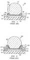
- FIG. 1illustrates schematically an example of the metallurgical requirements in known technology for a contact pad of a small portion of an IC chip generally designated 100 .
- a semiconductor material 101typically silicon, has patterned aluminum metallization 102 and is protected by a dielectric, moisture-impermeable protective overcoat 103 , usually silicon nitride or oxynitride.
- a windowhas bee opened in the overcoat 103 to expose metallization 102 and leave a protective perimeter 103 a around metallization 102 .
- An additional “under bump” metallization 104has been deposited unto metallization 102 and patterned so that it overlaps by a distance 104 a over the overcoat 103 .
- This additional metallization 104usually consists of a sequence of thin layers.
- the bottom layeris typically a refractory metal 105 , such as chromium, titanium, or tungsten, which provides an ohmic contact to aluminum 102 and a moisture-impenetrable interface to overcoat 103 .
- the top metal 106has to be solderable; examples are gold, copper, nickel, or palladium.
- solder materialis deposited, commonly by evaporation, plating or screen-printing, and reflown to form bump 107 .
- These solder bumpsassume various shapes (examples are semi-spheres, domes and truncated balls) after the reflow process, influenced by the forces of surface tension during the reflow process; the height/width aspect ratio is ⁇ 1.0.
- One commonly practiced methodaims at absorbing part of the thermomechanical stress on the solder joints by plastic material surrounding the joints and filling the gap between chip and substrate. See for instance, U.S. Pat. Nos. 6,228,680, issued on May 8, 2001; No. 6,213,347, issued on Apr. 10, 2001, and No. 6,245,583, issued on Jun. 12, 2001 (Thomas et al., Low Stress Method and Apparatus for Underfilling Flip-Chip Electronic Devices).
- the underfilling methodrepresents an unwelcome process step after device attachment to the motherboard.
- Another methodapplies a polymer layer on top of the protective overcoat with the aim of reducing the stress to the overcoat perimeter and the dielectric material underlying the contact pad. See for instance the publication “A Silicon and Aluminum Dynamic Memory Technology” by Richard A. Larsen (IBM J. Res. Develop., vol. 24, May 1980, pp. 268-282).
- the articleincludes description of a flip-chip packaging technology using a solder bump on an under-bump metallization, which is resting its perimeter on a thick polyimide layer. The bump structure is often supported by another polyimide layer.
- FIG. 2illustrates schematically an example of a contact pad, generally designated 200 , including a polymer overcoat.
- a silicon chip 201has patterned aluminum metallization 202 and is protected by a moisture-impermeable inorganic overcoat 203 (silicon nitride) and a polymeric layer 210 (benzocyclobutene or polyimide).
- a windowhas been opened through both overcoats.
- Layers of under-bump metallization 204establishes contact to the aluminum, adhesion to both overcoats, and solderability to the solder bump 207 .
- the inventiondescribes a metal structure for an integrated circuit having a plurality of contact pads and a patterned metallization protected by an overcoat layer.
- the structurecomprises a plurality of windows in the overcoat, selectively exposing the chip metallization, wherein the windows are spaced apart by less than 150 ⁇ m center to center.
- a metal columnis positioned on each of the windows; the preferred metal is copper; the column has a height-to-width aspect ratio larger than 1.25 and an upper surface wettable by re-flowable metal.
- the preferred column height-to-width aspect ratiois between 2.0 and 4.0, operable to absorb thermomechanical stress.
- a cap of a re-flowable metalis positioned on each of the columns.
- the present inventionis related to high density and high speed ICs with copper interconnecting metallization, especially those having high numbers of metallized inputs/outputs for flip-chip assembly. These circuits can be found in many device families such as processors, digital and analog devices, logic devices, high frequency and high power devices, and in both large and small area chip categories.
- Another aspect of the inventionis to fabricate contact pad copper columns directly on the IC copper metallization without any intermediate barrier layer, so that the resulting minimum electrical resistance enhances the high speed performance of the IC.
- Another aspect of the inventionis the flexibility to deposit the copper columns in windows of thick photoresist (preferably a Novolak resin) by electroplating the copper column onto the copper metallization or onto a metal layer suitable to receive a plated coating, thereby enabling an electroplating process for depositing the copper columns, providing small pitch center-to-center columns.
- thick photoresistpreferably a Novolak resin
- Another aspect of the inventionis to advance the reliability of chip assemblies by selecting column height-to-width aspect ratios for optimum thermomechanical stress absorption.
- Another object of the inventionis to provide design and process concepts which are flexible so that they can be applied to many families of semiconductor products, and are general so that they can be applied to several generations of products.
- Another object of the inventionis to use only designs and processes most commonly employed and accepted in the fabrication of IC devices, thus avoiding the cost of new capital investment and using the installed fabrication equipment base.
- the whole surface of the metal columnis wettable; consequently the whole column surface is covered by a film of the cap metal after completion of the cap reflow process, preventing any oxidation of the column metal.
- the metal columnis not wettable and an additional wettable metal layer is needed on the upper surface of the column for reliable attachment of the reflow metal. Consequently, the reflowed metal remains exclusively on the upper surface of the column after the cap reflow process.
- the preferred method of fabricating the connecting columnsis electro-plating.
- a photoresist layerpreferably a Novolak resin, is applied having a thickness comparable to the intended height of the column.
- a plurality of windowsare then opened in this photoresist layer and the columns are electro-plated in these windows.
- the preferred column metalincludes copper, nickel, gold, and copper alloy.
- FIG. 1is a schematic cross section of a solder bump and undermetal layer for flip-chip assembly, as fabricated by known technology.
- FIG. 2is a schematic cross section of a solder bump and undermetal arrangement over the chip contact pad metallization for flip-chip application according to known technology.
- FIG. 3is a schematic cross section of a high aspect ratio interconnection column with reflowable cap, fabricated by electroplating according to the invention, attached to an external part.
- FIG. 4Ais a schematic perspective view of a plurality of high aspect ratio interconnection columns, fabricated on fine pitch IC chip contact pads according to the invention.
- FIG. 4Bis a schematic top view of the interconnection columns of FIG. 4A to demonstrate the fine pitch center-to-center spacing of the columns.
- FIGS. 5 to 11are schematic cross sections of a chip contact, indicating the major process steps for fabricating a column-shaped interconnection suitable for attachment to external parts.
- FIG. 12is a block diagram of the process flow for fabricating wafer-level fine-pitch high aspect ratio chip interconnects.
- the present inventionis related to U.S. patent application No. 10/086,117, filed on Feb. 26, 2002 (Bojkov et al., “Waferlevel Method for Direct Bumping on Copper Pads in Integrated Circuits”), which is herewith included by reference.
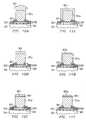
- FIG. 3illustrates schematically the cross section of a metallic interconnection, generally designated 300 , between a contact pad of an integrated circuit (IC) chip and a terminal pad of an external part, such as a printed circuit board.
- the example of the interconnection shownexhibits the high aspect ratio provided by the fabrication method of the present invention.
- the top metallization, the patterned layer 301 of the IC,is located over insulating material 302 and protected by inorganic overcoat 303 and polymeric overcoat 306 .
- Patterned metallization 301is selected from a group consisting of aluminum, aluminum alloy, copper, and copper alloy.
- the inorganic overcoat 303consists preferably of moisture-impermeable silicon nitride, silicon oxynitride, silicon carbide, or multi-layers thereof, preferably in the thickness range from 0.2 to 2.5 ⁇ m.
- the organic overcoat 306consists preferably of polyimide, benzocyclobutene or related materials, preferably in the thickness range from 2.0 to 8.0 ⁇ m.
- Overcoat 303overlaps the metallization 301 by a length 303 a.
- the prime function of the organic material 306is to help absorb thermomechanical stress after completion of the device assembly on external parts.
- Overcoat 303 and especially the thicker overcoat 306exhibit a slope 306 a towards metallization layer 301 , brought about by the etching of the overcoats during the window opening process for exposing metallization 301 .
- under-bump metal 307is then also copper.
- the interface of copper 301 to the copper layer 307contributes no measurable electrical resistance to the resistance of contact pad 300 .
- under-bump metal 307is commonly made of one or more metal layers selected from titanium, tungsten, tantalum, nickel, vanadium, or other refractory metals.
- the preferred thickness range of the under-bump metal layer 307is 0.1 to 2.0 ⁇ m.
- under-bump metal layer 307is patterned; it has then the configuration to overlay metallization surface 301 b and overcoat slope 306 a, as indicated in FIG. 3.
- metal column 308On the under-bump metal layer 307 is plated metal column 308 .
- This metalis elected from a group consisting of copper, gold, silver, nickel, palladium, and alloys thereof. Examples of alloys include copper/nickel alloy, preferably having 69 to 89 weight % copper, and silver/copper alloy, preferably having 28.1 weight % copper.
- the metal for column 308is selected to give column 308 a stiffness suitable for absorbing thermomechanical stress, which arises in the interconnection 300 during temperature cycles, when the semiconductor chip and the external part have different coefficients of thermal expansion. (As defined herein, in the elastic stress/strain regime, “stiff” is used for high ratios, and “compliant” for low ratios).
- column 308has a height-to-width aspect ratio between 1.25 and 5.0, preferably between 2.0 to 4.0.
- the column heightas measured from the surface of the overcoat 306 , is marked 308 a, and the column width 308 b.
- the aspect ratio height/widthin the range 2.0 to 4.0, column 308 is optimally operable to absorb thermomechanical stress.
- the metals used in column 308do not melt in the typical assembly temperature ranges, an additional layer 309 is needed, made of a metal or metal alloy capable of reflowing.
- the outlines of layer 309 in FIG. 3are only schematic; more realistic embodiments are shown in FIGS. 10A, 10B, 10 C, and 11 A and 11 B.
- the metal for layer 309is selected from a group consisting of tin, indium, tin alloys including tin/indium, tin/silver, tin/bismuth, and tin/lead; other choices include conductive adhesives and z-axis conductive materials.
- the preferred deposition method for metalsis plating.
- Layer 309 as a cap on column 308has a preferred thickness in the range from 1.0 to 25.0 ⁇ m.
- the reflowable metal 309is attached to the terminal pad 310 of the external part 311 .
- part 311is a printed wiring board, a ceramic substrate, or a flexible polymer substrate.
- Terminal pad 310is typically made of copper, often with a gold flash.
- FIG. 4Aschematically depicts two rows of interconnecting columns 401 attached to windows in the overcoat 402 on IC chip 403 .
- Each column 401has a cap 404 made of reflowable metal.
- FIG. 4Bshows the reflowable caps 404 so that the center-to-center distances can be measured.
- the interconnectionsare arranged in “closest packing” configuration; the centers have an equidistant pitch. Between the interconnections 410 , 411 , and 412 , the pitch is designated 420 .
- the large aspect ratio of the columns, provided by the invention,enables a minimization of the pitch.
- the center-to-center spacingis less than 150 ⁇ m.
- the pitchis preferably less than 80 ⁇ m, for instance 75 ⁇ m.
- FIGS. 5 through 11illustrate the process flow for fabricating a high aspect ratio interconnect on a contact pad of an IC chip; the process flow is differentiated to demonstrate the creation of two embodiments of the invention, as well as a couple of variations. It should be stressed that the fabrication process is for a whole semiconductor wafer.
- FIG. 5shows a patterned layer 502 of the top metallization of IC wafer 501 , located over insulating material 503 and protected by one or more overcoat layers 506 .
- Patterned metallization 502is preferably an aluminum alloy or copper.
- the overcoat 506consists preferably of an inorganic, moisture-impermeable layer and an organic, stress-absorbing layer. Overcoat 506 overlaps the metallization 502 for a short, sloped length 506 a.
- a window 508has been opened in the overcoat 506 , exposing the metallization 502 .
- the “under-bump” metal layer 507is deposited continuously over the whole wafer. If the metallization 502 is copper, layer 507 is preferably copper; if metallization 502 is aluminum, layer 507 contains refractory metals.
- a photoresist layer 610has been applied over the whole semiconductor wafer.
- the resistis a cresol Novalak resin, which typically contains propylene glycol monomethyl ether acetate (PGMEA).
- PMEApropylene glycol monomethyl ether acetate
- Suitable resistsare, for example, commercially available from Clariant Corp., Somerville, N.J., USA, under the brand names AZ4620, PLP100, and AZ49xt.
- the thickness 610 a of layer 610is at least 50% greater than overcoat window diameter 508 (in FIG. 5); a typical thickness is 100 ⁇ m.
- the layer thicknesscan be manufactured in a single or multi-coat application.
- a window 611has been opened in resist 610 by exposing the resist to broadband or I-line light sources.
- the diameter of window 611is related to the resist thickness 610 a so that the intended electroplated column will obtain the desired height-to-width aspect ratio between 1.25 and 5.0, preferably between 2.0 and 4.0.
- the column wallsmay not be exactly parallel to each other, but rather slightly inclined such that the column is somewhat wider on top than on the bottom interface with the IC contact pad.
- FIG. 7illustrates the electroplated metal column 701 in the photoresist window.
- the preferred metal for column 701is copper or a copper/nickel alloy.
- the diameter 711 of column 701is identical with the diameter 611 of the photoresist window, but the height 710 a of the column should preferably be less than the photoresist thickness 610 a in order to reserve some leftover height for plating the reflowable metal (see FIG. 9).
- the surface of under-bump layer 507has to be carefully cleaned by exposing the wafer to a hydrogen and nitrogen/argon plasma, thereby cleaning and passivating the under-bump layer in the photoresist window.
- the metal column 701is electroplated onto the exposed under-bump layer 507 .
- Columns 701 which are made of wettable metalwill now be designated 701 a; bump columns 701 which are made of non-wettable metal, will now be designated 701 b.
- FIG. 8depicts the second embodiment of the invention involving the process step, which has to be performed whenever a metal or metal alloy is chosen for column 701 which cannot be wetted by reflowable metal.
- metals for columns 701 binclude titanium, tantalum, tungsten, nickel vanadium, or alloys thereof.
- a layer 801has to be electroplated to the top end of column 701 b, which adheres to the metal of column 701 b and is wettable on its outer surface.
- a preferred choice for layer 801is nickel in the thickness range from about 15 to 20 ⁇ m; the outer surface may have a flash of palladium.
- the interface layer 801acts as a diffusion barrier for some of the metals of the column 701 b.
- FIGS. 9A, 9B, and 9 Cillustrate the process step of electroplating a cap of reflowable metal or metal alloy (“solder”).
- soldersinclude tin, indium, tin alloys including tin/indium, tin/silver, tin bismuth, and tin/lead.
- the cap thicknesscan vary widely from about 1.0 to about 25.0 ⁇ m without overplating, and from 1.0 to 65 ⁇ m with overplating. So-called over-plating will result in a mushroom-shaped cap 901 as depicted in FIG. 9A. Just plating to the top of the photoresist thickness creates a layer 902 as depicted in FIG.
- FIG. 9Bfor the case of a wettable column 701 a, or a layer 903 as depicted in FIG. 9C for the case of a wettable interface layer 801 on a non-wettable column 701 b.
- an overall photoresist window of 100 ⁇ m heightcould be filled with a 70 ⁇ m high metal column 701 b, followed by 15 ⁇ m interface layer 801 , followed by 15 ⁇ m solder cap 903 .
- the finished high aspect ratio interconnectis shown in FIG. 10A for the case of an overplated solder cap 901 ; in FIG. 10B for the case of a not overplated solder cap 902 ; and in FIG. 10C for the case of a not overplated solder cap 903 on an wettable interface layer 801 .
- the interconnects shown in FIGS. 10A, 10B, and 10 Care ready for assembly, which involves solder reflow.
- FIGS. 11A, 11B, and 11 Cillustrate the effect of the additional process step of reflowing the solder at the solder melting temperature.
- the plated column 701 ais made of a wettable metal; consequently, the solders 901 a and 902 a are distributed over the whole column surface.
- the plated column 701 bis made of non-wettable metal; consequently, the solder remains as a cap 903 a only on top of the barrier layer 801 .
- FIG. 12shows a block diagram of the preferred wafer-level process flow for fabricating fine-pitch, high aspect ratio chip interconnects, first and second embodiments.
- Step 1201Input: IC wafer from the wafer Fab.
- the waferhas copper interconnecting metallization.
- Step 1202Etching the contact window: Etching the polymeric overcoat (for instance, benzocylobutene or polyimide) using a hot wet etch in basic developer (tetramethyl ammonium hydroxide) in order to open the window for the contact pad.
- the wet etchresults in a relatively gentle slope of the overcoat around the window perimeter towards the copper of the pad.
- the inorganic overcoatfor instance, silicon nitride or silicon oxynitride
- a fluoride-containing plasmain order to expose the copper pad of the IC metallization.
- the padstill has an (uncontrolled) copper oxide surface; it may further be contaminated with organic residues (such as photoresist) and/or particulates.
- Step 1203Exposing the wafer to organic solvents, thereby removing organic contamination and mechanical particles from the copper contact pads.
- suitable cleaning processesinclude:
- Step 1204Drying the wafer in dry nitrogen.
- Step 1205Exposing the wafer to an oxygen and nitrogen/helium/argon plasma, thereby ashing any further organic residues on the copper contact pads and oxidizing the copper surface to a controlled thickness of less than 10 nm.
- Preferred plasma pressurebetween 0.1 and 10 Torr at 0.2 to 1.0 mol fraction oxygen and 0 to 0.8 mol fraction helium/argon; flow rate between 2.0 and 4.0 slpm.
- Temperature rangeis between 25 and 250° C., time from 0.5 to 5 min.
- Step 1206Without breaking the vacuum, exposing the wafer to a first hydrogen and nitrogen/helium/argon plasma, thereby removing the controlled copper oxide from the pad surface and passivating the cleaned surface.
- Preferred plasma pressurebetween 0.1 to 10 Torr at 0.2 to 1.0 mol fraction hydrogen, 0 to 0.8 mol fraction nitrogen, and 0 to 0.8 mol fraction helium/argon; flow rate between 2.0 and 4.0 slpm.
- Temperature rangeis between 25 and 25° C., time from 0.5 to 5.0 min.
- Step 1207Deciding whether to transfer the wafer directly to further processing under vacuum, or, alternately submit it to wet cleaning.
- Step 1208Wet cleaning the wafer in order to remove the oxidized (“ashed”) materials.
- Wet cleaning agentsinclude, for example, dilute citric, acetic, or oxalic acids. Temperature range is between 25 and 80° C., time from 0.5 to 15 min.
- Step 1209Exposing the wafer to a hydrogen and nitrogen/argon plasma, thereby cleaning and passivating the copper layer in the photoresist window.
- Step 1210Sputter-etching the passivated pad surface with energetic ions, thereby creating a fresh surface and concurrently activating it.
- Preferred plasma pressurebetween 5 and 100 mTorr at 750 to 1000 V bias.
- Temperature rangeis between 25 and 400° C., time from 1.0 to 4.0 min.
- Step 1211Sputter-depositing a UBM or copper layer, covering the fresh pad surface and pad perimeter, this layer providing minimal thermo-mechanical stress to the pad.
- Step 1212Creating a window in thick photoresist cover:
- UVultra-violet
- Step 1213Exposing the wafer to a hydrogen and nitrogen/argon plasma, thereby cleaning and passivating the UBM or copper layer in the photoresist window.
- Step 1214Without exposing the UBM/passivated copper layer to fresh contamination, electroplating a copper column onto the exposed UBM/copper layer.
- Step 1215Electroplating a tin/solder cap onto the copper column.
- Step 1216Stripping the photoresist.
- Step 1217Etching the UBM/copper layer in order to electrically isolate the columns with caps from one another.
- Step 1218Cleaning in DI water.
- Step 1219Output: IC wafers with high aspect ratio interconnects (columns and solderable caps).
- Step 1218 aFluxing and reflowing solder cap.
- Step 1218 bCleaning and de-fluxing.
Landscapes
- Engineering & Computer Science (AREA)
- Computer Hardware Design (AREA)
- Microelectronics & Electronic Packaging (AREA)
- Power Engineering (AREA)
- Manufacturing & Machinery (AREA)
- Internal Circuitry In Semiconductor Integrated Circuit Devices (AREA)
- Wire Bonding (AREA)
Abstract
Description
- The present invention is related in general to the field of semiconductor devices and processes and more specifically to the wafer-level fabrication of fine-pitch, high aspect ratio solder interconnections.[0001]
- The structure of contact pad metallizations and solder bumps for connecting integrated circuit (IC) chips to semiconductor packages or outside parts, as well as the thermomechanical stresses and reliability risks involved, have been described in a series of detailed publications by the International Business Machines Corporation in 1969 (IBM J. Res. Develop., Vol. 13, pp. 226-296): P. A. Totta et al., SLT Device Metallurgy and its Monolithic Extension, L. F. Miller, Controlled Collapse Reflow Chip Joining, L. S. Goldmann, Geometric Optimization of Controlled Collapse Interconnections, K. C. Norris et al., Reliability of Controlled Collapse Interconnections, S. Oktay, Parametric Study of Temperature Profiles in Chips Joined by Controlled Collapse Techniques, B. S. Berry et al., Studies of the SLT Chip Terminal Metallurgy.[0002]
- Based on these publications, FIG. 1 illustrates schematically an example of the metallurgical requirements in known technology for a contact pad of a small portion of an IC chip generally designated[0003]100. A
semiconductor material 101, typically silicon, has patternedaluminum metallization 102 and is protected by a dielectric, moisture-impermeableprotective overcoat 103, usually silicon nitride or oxynitride. A window has bee opened in theovercoat 103 to exposemetallization 102 and leave aprotective perimeter 103aaroundmetallization 102. An additional “under bump”metallization 104 has been deposited untometallization 102 and patterned so that it overlaps by adistance 104aover theovercoat 103. Thisadditional metallization 104 usually consists of a sequence of thin layers. The bottom layer is typically arefractory metal 105, such as chromium, titanium, or tungsten, which provides an ohmic contact toaluminum 102 and a moisture-impenetrable interface to overcoat103. Thetop metal 106 has to be solderable; examples are gold, copper, nickel, or palladium. Finally, solder material is deposited, commonly by evaporation, plating or screen-printing, and reflown to formbump 107. These solder bumps assume various shapes (examples are semi-spheres, domes and truncated balls) after the reflow process, influenced by the forces of surface tension during the reflow process; the height/width aspect ratio is <1.0. - During and after assembly of the IC chip to an outside part such as a substrate or circuit board by solder reflow, and then during device operation, significant temperature differences and temperature cycles appear between[0004]
semiconductor chip 100 and the substrate. The reliability of the solder joint is strongly influenced by the coefficients of thermal expansion of the semiconductor material and the substrate material. For example, there is more than one order of magnitude difference between the coefficients of thermal expansion of silicon and FR-4. This difference causes thermomechanical stresses, which the solder joints have to absorb. Detailed calculations, in the literature cited above and in other publications of the early 1980's (for instance, C. G. M. van Kessel et al., “The Quality of Die Attachment and its Relationship to Stresses and Vertical Die-Cracking”, IEEE 1983; E. Suhir, “Calculated Thermally Induced Stresses in Adhesively Bonded and Soldered Assemblies, ISHM Int. Symp. Microel., October 1886; “Die Attachment Design and its Influence on Thermal Stresses in the Die and the Attachment”, IEEE 1987) involving the optimum height and volume of the solder connection and the expected onset of fatigue and cracking proposed a number of solder design solutions. It was found for solder that an aspect ratio>1.0 reduces thermomechanical stresses and postpones cracking of joints. - One commonly practiced method aims at absorbing part of the thermomechanical stress on the solder joints by plastic material surrounding the joints and filling the gap between chip and substrate. See for instance, U.S. Pat. Nos. 6,228,680, issued on May 8, 2001; No. 6,213,347, issued on Apr. 10, 2001, and No. 6,245,583, issued on Jun. 12, 2001 (Thomas et al., Low Stress Method and Apparatus for Underfilling Flip-Chip Electronic Devices). However, the underfilling method represents an unwelcome process step after device attachment to the motherboard.[0005]
- Another method applies a polymer layer on top of the protective overcoat with the aim of reducing the stress to the overcoat perimeter and the dielectric material underlying the contact pad. See for instance the publication “A Silicon and Aluminum Dynamic Memory Technology” by Richard A. Larsen (IBM J. Res. Develop., vol. 24, May 1980, pp. 268-282). The article includes description of a flip-chip packaging technology using a solder bump on an under-bump metallization, which is resting its perimeter on a thick polyimide layer. The bump structure is often supported by another polyimide layer.[0006]
- FIG. 2 illustrates schematically an example of a contact pad, generally designated[0007]200, including a polymer overcoat. A
silicon chip 201 has patternedaluminum metallization 202 and is protected by a moisture-impermeable inorganic overcoat203 (silicon nitride) and a polymeric layer210 (benzocyclobutene or polyimide). A window has been opened through both overcoats. Layers of under-bump metallization 204 establishes contact to the aluminum, adhesion to both overcoats, and solderability to thesolder bump 207. - In high-speed, low electromigration IC's, aluminum has been replaced by copper as chip metallization. Due to bondability and contact resistance issues of copper oxide, it is problematic to establish reliable contact to solder material. Approaches based on adding an interface layer of aluminum or of metals with higher affinity to oxygen than copper are costly and not very effective. On the other hand, a method has been described to fabricate a copper layer followed by solder balls onto copper-metallized pads (U.S. patent application Ser. No. 10/086,117, filed Feb. 26, 2002, Bojkov et al., “Wafer-level Method for Direct Bumping an Copper Pads in Integrated Circuits”). An urgent need has therefore arisen for a coherent, low-cost method of flip-chip assembly of semiconductor devices offering a fundamental solution of metal contact to copper and of thermomechanical stress reliability. The method should be flexible enough to be applied for different semiconductor product families and a wide spectrum of design and process variations. Preferably, these innovations should be accomplished using the installed equipment base so that no investment in new manufacturing machines is needed.[0008]
- The invention describes a metal structure for an integrated circuit having a plurality of contact pads and a patterned metallization protected by an overcoat layer. The structure comprises a plurality of windows in the overcoat, selectively exposing the chip metallization, wherein the windows are spaced apart by less than 150 μm center to center. A metal column is positioned on each of the windows; the preferred metal is copper; the column has a height-to-width aspect ratio larger than 1.25 and an upper surface wettable by re-flowable metal. The preferred column height-to-width aspect ratio is between 2.0 and 4.0, operable to absorb thermomechanical stress. A cap of a re-flowable metal is positioned on each of the columns.[0009]
- The present invention is related to high density and high speed ICs with copper interconnecting metallization, especially those having high numbers of metallized inputs/outputs for flip-chip assembly. These circuits can be found in many device families such as processors, digital and analog devices, logic devices, high frequency and high power devices, and in both large and small area chip categories.[0010]
- It is an aspect of the present invention to be applicable to contact pad area reduction and fine-pitch interconnect, and thus supports the shrinking of IC chips. Consequently, the invention helps to alleviate the space constraint of continually shrinking applications such as cellular communication, pagers, hard disk drives, laptop computers and other portable electronic devices.[0011]
- Another aspect of the invention is to fabricate contact pad copper columns directly on the IC copper metallization without any intermediate barrier layer, so that the resulting minimum electrical resistance enhances the high speed performance of the IC.[0012]
- Another aspect of the invention is the flexibility to deposit the copper columns in windows of thick photoresist (preferably a Novolak resin) by electroplating the copper column onto the copper metallization or onto a metal layer suitable to receive a plated coating, thereby enabling an electroplating process for depositing the copper columns, providing small pitch center-to-center columns.[0013]
- Another aspect of the invention is to advance the reliability of chip assemblies by selecting column height-to-width aspect ratios for optimum thermomechanical stress absorption.[0014]
- Another object of the invention is to provide design and process concepts which are flexible so that they can be applied to many families of semiconductor products, and are general so that they can be applied to several generations of products.[0015]
- Another object of the invention is to use only designs and processes most commonly employed and accepted in the fabrication of IC devices, thus avoiding the cost of new capital investment and using the installed fabrication equipment base.[0016]
- These objects have been achieved by the teachings of the invention concerning selection criteria and process flows suitable for mass production. Various modifications have been successfully employed to satisfy different selections of materials and plating technologies.[0017]
- In the first embodiment of the invention, the whole surface of the metal column is wettable; consequently the whole column surface is covered by a film of the cap metal after completion of the cap reflow process, preventing any oxidation of the column metal.[0018]
- In the second embodiment of the invention, the metal column is not wettable and an additional wettable metal layer is needed on the upper surface of the column for reliable attachment of the reflow metal. Consequently, the reflowed metal remains exclusively on the upper surface of the column after the cap reflow process.[0019]
- The preferred method of fabricating the connecting columns is electro-plating. A photoresist layer, preferably a Novolak resin, is applied having a thickness comparable to the intended height of the column. A plurality of windows are then opened in this photoresist layer and the columns are electro-plated in these windows. The preferred column metal includes copper, nickel, gold, and copper alloy.[0020]
- The technical advances represented by the invention, as well as the aspects thereof, will become apparent from the following description of the preferred embodiments of the invention, when considered in conjunction with the accompanying drawings and the novel features set forth in the appended claims.[0021]
- FIG. 1 is a schematic cross section of a solder bump and undermetal layer for flip-chip assembly, as fabricated by known technology.[0022]
- FIG. 2 is a schematic cross section of a solder bump and undermetal arrangement over the chip contact pad metallization for flip-chip application according to known technology.[0023]
- FIG. 3 is a schematic cross section of a high aspect ratio interconnection column with reflowable cap, fabricated by electroplating according to the invention, attached to an external part.[0024]
- FIG. 4A is a schematic perspective view of a plurality of high aspect ratio interconnection columns, fabricated on fine pitch IC chip contact pads according to the invention.[0025]
- FIG. 4B is a schematic top view of the interconnection columns of FIG. 4A to demonstrate the fine pitch center-to-center spacing of the columns.[0026]
- FIGS.[0027]5 to11 are schematic cross sections of a chip contact, indicating the major process steps for fabricating a column-shaped interconnection suitable for attachment to external parts.
- FIG. 12 is a block diagram of the process flow for fabricating wafer-level fine-pitch high aspect ratio chip interconnects.[0028]
- The present invention is related to U.S. patent application No. 10/086,117, filed on Feb. 26, 2002 (Bojkov et al., “Waferlevel Method for Direct Bumping on Copper Pads in Integrated Circuits”), which is herewith included by reference.[0029]
- FIG. 3 illustrates schematically the cross section of a metallic interconnection, generally designated[0030]300, between a contact pad of an integrated circuit (IC) chip and a terminal pad of an external part, such as a printed circuit board. The example of the interconnection shown exhibits the high aspect ratio provided by the fabrication method of the present invention.
- The top metallization, the patterned[0031]
layer 301 of the IC, is located over insulatingmaterial 302 and protected byinorganic overcoat 303 andpolymeric overcoat 306.Patterned metallization 301 is selected from a group consisting of aluminum, aluminum alloy, copper, and copper alloy. Theinorganic overcoat 303 consists preferably of moisture-impermeable silicon nitride, silicon oxynitride, silicon carbide, or multi-layers thereof, preferably in the thickness range from 0.2 to 2.5 μm. Theorganic overcoat 306 consists preferably of polyimide, benzocyclobutene or related materials, preferably in the thickness range from 2.0 to 8.0 μm.Overcoat 303 overlaps themetallization 301 by alength 303a.The prime function of theorganic material 306 is to help absorb thermomechanical stress after completion of the device assembly on external parts.Overcoat 303 and especially thethicker overcoat 306 exhibit aslope 306atowardsmetallization layer 301, brought about by the etching of the overcoats during the window opening process for exposingmetallization 301. - If the[0032]
metallization 301 is copper, thesurface 301bof the exposed copper is carefully cleaned after opening thewindow 301a;see the process detail below. The “under-bump metal”307 is then also copper. The interface ofcopper 301 to thecopper layer 307 contributes no measurable electrical resistance to the resistance ofcontact pad 300. If themetallization 301 is aluminum or an aluminum alloy, under-bump metal 307 is commonly made of one or more metal layers selected from titanium, tungsten, tantalum, nickel, vanadium, or other refractory metals. The preferred thickness range of the under-bump metal layer 307 is 0.1 to 2.0 μm. As described below, after the plating process for the tall column, under-bump metal layer 307 is patterned; it has then the configuration tooverlay metallization surface 301bandovercoat slope 306a,as indicated in FIG. 3. - On the under-[0033]
bump metal layer 307 is platedmetal column 308. This metal is elected from a group consisting of copper, gold, silver, nickel, palladium, and alloys thereof. Examples of alloys include copper/nickel alloy, preferably having 69 to 89 weight % copper, and silver/copper alloy, preferably having 28.1 weight % copper. The metal forcolumn 308 is selected to give column308 a stiffness suitable for absorbing thermomechanical stress, which arises in theinterconnection 300 during temperature cycles, when the semiconductor chip and the external part have different coefficients of thermal expansion. (As defined herein, in the elastic stress/strain regime, “stiff” is used for high ratios, and “compliant” for low ratios). - It is pivotally important for the present invention that[0034]
column 308 has a height-to-width aspect ratio between 1.25 and 5.0, preferably between 2.0 to 4.0. In FIG. 3, the column height, as measured from the surface of theovercoat 306, is marked308a,and thecolumn width 308b.With the aspect ratio height/width in the range 2.0 to 4.0,column 308 is optimally operable to absorb thermomechanical stress. - Since the metals used in[0035]
column 308 do not melt in the typical assembly temperature ranges, anadditional layer 309 is needed, made of a metal or metal alloy capable of reflowing. The outlines oflayer 309 in FIG. 3 are only schematic; more realistic embodiments are shown in FIGS. 10A, 10B,10C, and11A and11B. The metal forlayer 309 is selected from a group consisting of tin, indium, tin alloys including tin/indium, tin/silver, tin/bismuth, and tin/lead; other choices include conductive adhesives and z-axis conductive materials. The preferred deposition method for metals is plating.Layer 309 as a cap oncolumn 308, has a preferred thickness in the range from 1.0 to 25.0 μm. - As indicated in FIG. 3, the[0036]
reflowable metal 309 is attached to theterminal pad 310 of theexternal part 311. Commonly,part 311 is a printed wiring board, a ceramic substrate, or a flexible polymer substrate.Terminal pad 310 is typically made of copper, often with a gold flash. - Another important characteristic of the interconnect structure of the present invention is the fine pitch center-to-center of the interconnecting columns. The perspective view of FIG. 4A schematically depicts two rows of interconnecting[0037]
columns 401 attached to windows in theovercoat 402 onIC chip 403. Eachcolumn 401 has acap 404 made of reflowable metal. - In top view, FIG. 4B shows the[0038]
reflowable caps 404 so that the center-to-center distances can be measured. In the examples shown in FIG. 4B, the interconnections are arranged in “closest packing” configuration; the centers have an equidistant pitch. Between theinterconnections - The schematic cross sections of FIGS. 5 through 11 illustrate the process flow for fabricating a high aspect ratio interconnect on a contact pad of an IC chip; the process flow is differentiated to demonstrate the creation of two embodiments of the invention, as well as a couple of variations. It should be stressed that the fabrication process is for a whole semiconductor wafer.[0039]
- FIG. 5 shows a[0040]
patterned layer 502 of the top metallization ofIC wafer 501, located over insulatingmaterial 503 and protected by one or more overcoat layers506.Patterned metallization 502 is preferably an aluminum alloy or copper. Theovercoat 506 consists preferably of an inorganic, moisture-impermeable layer and an organic, stress-absorbing layer.Overcoat 506 overlaps themetallization 502 for a short,sloped length 506a.Awindow 508 has been opened in theovercoat 506, exposing themetallization 502. For purposes of electroplating, the “under-bump”metal layer 507 is deposited continuously over the whole wafer. If themetallization 502 is copper,layer 507 is preferably copper; ifmetallization 502 is aluminum,layer 507 contains refractory metals. - Especially in the case of a copper “under-bump” (UBM)[0041]
layer 507 deposited on a patternedcopper metallization 502, the exposedcopper metallization 502 has to be carefully cleaned before depositinglayer 507 by subjecting the wafer to the steps of: - exposing the wafer to organic solvents, thereby removing organic contamination and mechanical particles from the metallization contact pads, and drying the wafer;[0042]
- exposing the wafer to an oxygen and nitrogen/argon/helium plasma, thereby ashing any organic residue on the metallization contact pads and oxidizing the metallization surface to a controlled thickness of less than 10 nm;[0043]
- without breaking the vacuum, exposing the wafer to a hydrogen and nitrogen/helium/argon plasma, thereby removing the controlled metallization oxide from the pad surface and passivating the cleaned surface; and[0044]
- sputter-etching the passivated pad surface with energetic ions, thereby creating a fresh surface and concurrently activating it.[0045]
- In FIG. 6, a[0046]
photoresist layer 610 has been applied over the whole semiconductor wafer. Preferably, the resist is a cresol Novalak resin, which typically contains propylene glycol monomethyl ether acetate (PGMEA). Suitable resists are, for example, commercially available from Clariant Corp., Somerville, N.J., USA, under the brand names AZ4620, PLP100, and AZ49xt. Thethickness 610aoflayer 610 is at least 50% greater than overcoat window diameter508 (in FIG. 5); a typical thickness is 100 μm. Dependent on the resist type, the layer thickness can be manufactured in a single or multi-coat application. Awindow 611 has been opened in resist610 by exposing the resist to broadband or I-line light sources. The diameter ofwindow 611 is related to the resistthickness 610aso that the intended electroplated column will obtain the desired height-to-width aspect ratio between 1.25 and 5.0, preferably between 2.0 and 4.0. In actual manufacturing, the column walls may not be exactly parallel to each other, but rather slightly inclined such that the column is somewhat wider on top than on the bottom interface with the IC contact pad. - Care should be taken to position[0047]
photoresist window 611 so that it matches the position of therespective overcoat window 508. Theovercoat window 508 is nested within therespective photoresist window 611 so that thephotoresist window 611 has a diameter more than 5% larger than the diameter of theovercoat window 508. - FIG. 7 illustrates the electroplated[0048]
metal column 701 in the photoresist window. The preferred metal forcolumn 701 is copper or a copper/nickel alloy. Obviously, thediameter 711 ofcolumn 701 is identical with thediameter 611 of the photoresist window, but the height710aof the column should preferably be less than thephotoresist thickness 610ain order to reserve some leftover height for plating the reflowable metal (see FIG. 9). Before the electroplating step of the column, the surface of under-bump layer 507 has to be carefully cleaned by exposing the wafer to a hydrogen and nitrogen/argon plasma, thereby cleaning and passivating the under-bump layer in the photoresist window. Without exposing the passivated under-bump layer 507 to fresh contamination, themetal column 701 is electroplated onto the exposed under-bump layer 507.Columns 701 which are made of wettable metal will now be designated701a;bumpcolumns 701 which are made of non-wettable metal, will now be designated701b. - FIG. 8 depicts the second embodiment of the invention involving the process step, which has to be performed whenever a metal or metal alloy is chosen for[0049]
column 701 which cannot be wetted by reflowable metal. Such metals forcolumns 701binclude titanium, tantalum, tungsten, nickel vanadium, or alloys thereof. In this second embodiment of the invention, alayer 801 has to be electroplated to the top end ofcolumn 701b,which adheres to the metal ofcolumn 701band is wettable on its outer surface. A preferred choice forlayer 801 is nickel in the thickness range from about 15 to 20 μm; the outer surface may have a flash of palladium. Further, theinterface layer 801 acts as a diffusion barrier for some of the metals of thecolumn 701b. - FIGS. 9A, 9B, and[0050]9C illustrate the process step of electroplating a cap of reflowable metal or metal alloy (“solder”). Such solders include tin, indium, tin alloys including tin/indium, tin/silver, tin bismuth, and tin/lead. The cap thickness can vary widely from about 1.0 to about 25.0 μm without overplating, and from 1.0 to 65 μm with overplating. So-called over-plating will result in a mushroom-shaped
cap 901 as depicted in FIG. 9A. Just plating to the top of the photoresist thickness creates alayer 902 as depicted in FIG. 9B for the case of awettable column 701a,or alayer 903 as depicted in FIG. 9C for the case of awettable interface layer 801 on anon-wettable column 701b.By way of example for FIG. 9C, an overall photoresist window of 100 μm height could be filled with a 70 μmhigh metal column 701b,followed by 15μm interface layer 801, followed by 15μm solder cap 903. - After removing the[0051]
photoresist 610 and etching the under-bump metal (UBM)layer 507, the finished high aspect ratio interconnect is shown in FIG. 10A for the case of anoverplated solder cap 901; in FIG. 10B for the case of a notoverplated solder cap 902; and in FIG. 10C for the case of a notoverplated solder cap 903 on anwettable interface layer 801. The interconnects shown in FIGS. 10A, 10B, and10C are ready for assembly, which involves solder reflow. - FIGS. 11A, 11B, and[0052]11C illustrate the effect of the additional process step of reflowing the solder at the solder melting temperature. In FIGS. 11A and 11B, the plated
column 701ais made of a wettable metal; consequently, thesolders 901aand902aare distributed over the whole column surface. In FIG. 11C, the platedcolumn 701bis made of non-wettable metal; consequently, the solder remains as acap 903aonly on top of thebarrier layer 801. - FIG. 12 shows a block diagram of the preferred wafer-level process flow for fabricating fine-pitch, high aspect ratio chip interconnects, first and second embodiments.[0053]
- Step[0054]1201: Input: IC wafer from the wafer Fab. The wafer has copper interconnecting metallization.
- Step[0055]1202: Etching the contact window: Etching the polymeric overcoat (for instance, benzocylobutene or polyimide) using a hot wet etch in basic developer (tetramethyl ammonium hydroxide) in order to open the window for the contact pad. The wet etch results in a relatively gentle slope of the overcoat around the window perimeter towards the copper of the pad.
- Etching the inorganic overcoat (for instance, silicon nitride or silicon oxynitride) using a fluoride-containing plasma in order to expose the copper pad of the IC metallization. At this stage, the pad still has an (uncontrolled) copper oxide surface; it may further be contaminated with organic residues (such as photoresist) and/or particulates.[0056]
- Step[0057]1203: Exposing the wafer to organic solvents, thereby removing organic contamination and mechanical particles from the copper contact pads. Examples of suitable cleaning processes include:
- submerging the wafer in agitated isopropyl alcohol, methanol, glycol, N-methyl pyrrolidone and other solvents;[0058]
- adding ultrasonic/megasonic energy to these solvents;[0059]
- spraying the wafer with an organic solvent;[0060]
- treating the wafer in dry chemical vapor.[0061]
- Step[0062]1204: Drying the wafer in dry nitrogen.
- Step[0063]1205: Exposing the wafer to an oxygen and nitrogen/helium/argon plasma, thereby ashing any further organic residues on the copper contact pads and oxidizing the copper surface to a controlled thickness of less than 10 nm. Preferred plasma pressure between 0.1 and 10 Torr at 0.2 to 1.0 mol fraction oxygen and 0 to 0.8 mol fraction helium/argon; flow rate between 2.0 and 4.0 slpm. Temperature range is between 25 and 250° C., time from 0.5 to 5 min.
- Step[0064]1206: Without breaking the vacuum, exposing the wafer to a first hydrogen and nitrogen/helium/argon plasma, thereby removing the controlled copper oxide from the pad surface and passivating the cleaned surface. Preferred plasma pressure between 0.1 to 10 Torr at 0.2 to 1.0 mol fraction hydrogen, 0 to 0.8 mol fraction nitrogen, and 0 to 0.8 mol fraction helium/argon; flow rate between 2.0 and 4.0 slpm. Temperature range is between 25 and 25° C., time from 0.5 to 5.0 min.
- Step[0065]1207: Deciding whether to transfer the wafer directly to further processing under vacuum, or, alternately submit it to wet cleaning.
- Step[0066]1208: Wet cleaning the wafer in order to remove the oxidized (“ashed”) materials. Wet cleaning agents include, for example, dilute citric, acetic, or oxalic acids. Temperature range is between 25 and 80° C., time from 0.5 to 15 min.
- Step[0067]1209: Exposing the wafer to a hydrogen and nitrogen/argon plasma, thereby cleaning and passivating the copper layer in the photoresist window.
- Step[0068]1210: Sputter-etching the passivated pad surface with energetic ions, thereby creating a fresh surface and concurrently activating it. Preferred plasma pressure between 5 and 100 mTorr at 750 to 1000 V bias. Temperature range is between 25 and 400° C., time from 1.0 to 4.0 min.
- Step[0069]1211: Sputter-depositing a UBM or copper layer, covering the fresh pad surface and pad perimeter, this layer providing minimal thermo-mechanical stress to the pad.
- Step[0070]1212: Creating a window in thick photoresist cover:
- coating the wafer with thick photoresist;[0071]
- exposing the window and masking the remainder;[0072]
- developing the photoresist; and[0073]
- ultra-violet (UV) curing the photoresist.[0074]
- Step[0075]1213: Exposing the wafer to a hydrogen and nitrogen/argon plasma, thereby cleaning and passivating the UBM or copper layer in the photoresist window.
- Step[0076]1214: Without exposing the UBM/passivated copper layer to fresh contamination, electroplating a copper column onto the exposed UBM/copper layer.
- Step[0077]1215: Electroplating a tin/solder cap onto the copper column.
- When the column has been plated of a metal or alloy which cannot be wetted by tin/solder, a layer of metal (preferably nickel) has to be plated onto the column first, which adheres to the column metal and is wettable on its external surface.[0078]
- Step[0079]1216: Stripping the photoresist.
- Step[0080]1217: Etching the UBM/copper layer in order to electrically isolate the columns with caps from one another.
- Step[0081]1218: Cleaning in DI water.
- Step[0082]1219: Output: IC wafers with high aspect ratio interconnects (columns and solderable caps).
- Second embodiment:[0083]
- [0084]
Step 1218a:Fluxing and reflowing solder cap. - Step[0085]1218b:Cleaning and de-fluxing.
- While this invention has been described in reference to illustrative embodiments, this description is not intended to be construed in a limiting sense. Various modifications and combinations of the illustrative embodiments, as well as other embodiments of the invention, will be apparent to persons skilled in the art upon reference to the description. As an example, the invention can be applied to IC bond pad metallizations other than copper, which are difficult or impossible to contact by conventional tin or solder techniques, such as alloys of refractory metals and noble metals. As another example, the invention can be extended to batch processing, further reducing fabrication costs. As another example, the invention can be used in hybrid technologies of wire/ribbon bonding and solder interconnections. It is therefore intended that the appended claims encompass any such modifications or embodiments.[0086]
Claims (26)
1. A metal structure for an integrated circuit having a plurality of contact pads and a patterned metallization protected by an overcoat layer, comprising:
a plurality of windows in said overcoat, selectively exposing said metallization, said windows spaced apart by less than 150 μm center to center;
a metal column positioned on each of said windows, said column having a height-to-width aspect ratio larger than 1.25 and an upper surface wettable by re-flowable metal; and
a cap of a re-flowable metal positioned on each of said columns.
2. A metal structure for an integrated circuit having a plurality of contact pads and a patterned metallization protected by an overcoat layer, comprising:
a plurality of windows in said overcoat, selectively exposing said metallization, said windows spaced apart by less than 150 μm center to center;
a patterned layer of a first metal, suitable to receive a plated coating, directly positioned on said exposed metallization in each of said windows, said layer overlapping the perimeter of each of said windows, providing adhesion to said metallization;
a column of a second metal positioned on each of said patterned first metal layers, following the contours of said first metal layers, said column having a height-to-width aspect ratio larger than 1.25 and an upper surface wettable by re-flowable metal; and
a cap of a re-flowable third metal positioned on each of said columns.
3. The interconnect structure according toclaim 2 wherein said interconnecting metallization is selected from a group consisting of aluminum, aluminum alloy, copper, and copper alloy.
4. The interconnect structure according toclaim 2 wherein said overcoat layer is selected from a group consisting of silicon nitride, silicon oxynitride, polyimide, benzocyclobutene, and stacked layers thereof.
5. The interconnect structure according toclaim 4 wherein said layer has a thickness in the range from 0.2 to 8.0 μm.
6. The interconnect structure according toclaim 2 wherein said first metal is selected from a group consisting of titanium, tantalum, tungsten, nickel vanadium, and copper.
7. The interconnect structure according toclaim 6 wherein said first metal has a layer thickness in the range from 0.1 to 2.0 μm.
8. The interconnect structure according toclaim 2 wherein said second metal is selected from a group consisting of copper, gold, silver, nickel, palladium, and alloys thereof, wherein said second metal has a stiffness suitable for absorbing thermomechanical stress.
9. The interconnect structure according toclaim 8 wherein said second metal has a column height-to-width aspect ratio between 1.25 and 5.0.
10. The interconnect structure according toclaim 8 wherein said second metal has a preferred column height-to-width aspect ratio between 2.0 and 4.0, operable to absorb thermomechanical stress.
11. The interconnect structure according toclaim 2 wherein said top end of said column has an additional metal layer, adhering to said top end and wettable on its outer surface.
12. The interconnect structure according toclaim 2 wherein said third metal is selected from a group consisting of tin, indium, tin alloys including tin/indium, tin/silver, tin/bismuth, and tin/lead, conductive adhesives, and z-axis conductive materials.
13. The interconnect structure according toclaim 12 wherein said third metal has a cap thickness in the range from 1.0 to 25.0 μm without overplating, and from 1.0 to 65 μm with overplating.
14. The interconnect structure according toclaim 2 wherein said third metal does not only form a cap on said column, but also is re-flowed along the sides of said column.
15. An assembly of an integrated circuit chip and an external part, comprising:
an integrated circuit chip having a plurality of contact pads and a patterned metallization protected by an overcoat layer;
said chip further having a plurality of windows in said overcoat, selectively exposing said metallization, said windows spaced apart by less than 150 μm center to center;
a metal column positioned on each of said windows, said column having a height-to-width aspect ratio larger than 1.25 and an upper surface wettable by re-flowable metal;
a cap of a re-flowable metal positioned on each of said columns, said cap re-flowed for connection to an external part; and
an external part attached to said chip by said re-flowed metal, thereby forming an assembly with said chip.
16. The assembly according toclaim 15 wherein said body is a printed circuit board having attachment pads in locations matching the locations of said chip contact pads.
17. A wafer-level method for fabricating fine-pitch, high aspect ratio metal interconnects on integrated circuit contact pads suitable for assembly and interconnection with external parts, comprising the steps of:
providing an integrated circuit wafer having a patterned metallization protected by an overcoat layer;
opening a plurality of windows in said overcoat to selectively expose said metallization, said windows spaced apart by less than 150 μm center to center, each window having a diameter of less than 80 μm;
sputter-depositing a layer of first metal, suitable to receive a plated coating, to provide adhesion and minimal thermomechanical stress to said metallization;
depositing a photoresist layer having a thickness at least 50% greater than said window diameter;
opening a plurality of windows in said photoresist to expose said first metal, each of said photoresist windows having a diameter more than 5% larger than the diameter of said overcoat windows, the positions of said photoresist windows matching the positions of said overcoat windows respectively, each of said overcoat windows nested within its respective photoresist window;
electroplating a column of a second metal onto said first metal exposed in each of said photoresist windows, said column having a height-to-width aspect ratio larger than 1.25 and an upper surface wettable by re-flowable metal; and
electroplating a cap of re-flowable metal positioned on each of said columns.
18. The method according toclaim 17 further comprising the steps of:
filling at least the remaining height of said photoresist window to complete said metal interconnects for assembly with external parts;
removing said photoresist layer; and
etching the remaining first metal layer.
19. The method according toclaim 17 wherein said first metal is selected from a group consisting of titanium, tantalum, tungsten, nickel vanadium, and copper.
20. The method according toclaim 17 wherein said second metal is selected from a group consisting of copper, gold, silver, nickel, palladium, and alloys thereof.
21. The method according toclaim 17 further comprising a step of cleaning said exposed patterned metallization before said step of sputter-depositing said first metal.
22. The method according to step21 wherein said cleaning step comprises the steps of:
exposing said wafer to organic solvents, thereby removing organic contamination and mechanical particles from said metallization contact pads, and drying said wafer;
exposing said wafer to an oxygen and nitrogen/argon/helium plasma, thereby ashing any organic residue on said metallization contact pads and oxidizing said metallization surface to a controlled thickness of less than 10 nm;
without breaking the vacuum, exposing said wafer to a hydrogen and nitrogen/helium/argon plasma, thereby removing said controlled metallization oxide from said pad surface and passivating said cleaned surface; and
sputter-etching said passivated pad surface with energetic ions, thereby creating a fresh surface and concurrently activating it.
23. The method according toclaim 17 further comprising the process step of reflowing said metal cap after said step of etching the remaining first metal layer.
24. The method according toclaim 23 wherein said reflow process distributes a layer of reflowable metal over all wettable portions of the outer column surface.
25. The method according toclaim 23 further comprising the steps of applying flux before the reflowing step and cleansing said flux after completing said reflowing step.
26. The method according toclaim 17 wherein said photoresist is a cresol Novolak resin.
Priority Applications (3)
| Application Number | Priority Date | Filing Date | Title |
|---|---|---|---|
| US10/195,273US20040007779A1 (en) | 2002-07-15 | 2002-07-15 | Wafer-level method for fine-pitch, high aspect ratio chip interconnect |
| JP2003193323AJP2004048012A (en) | 2002-07-15 | 2003-07-08 | Fin pitch and high aspect ratio wiring structure and interconnection method for the same |
| EP03102098.5AEP1387402A3 (en) | 2002-07-15 | 2003-07-10 | Wafer-level method for fine-pitch, high aspect ratio chip interconnect |
Applications Claiming Priority (1)
| Application Number | Priority Date | Filing Date | Title |
|---|---|---|---|
| US10/195,273US20040007779A1 (en) | 2002-07-15 | 2002-07-15 | Wafer-level method for fine-pitch, high aspect ratio chip interconnect |
Publications (1)
| Publication Number | Publication Date |
|---|---|
| US20040007779A1true US20040007779A1 (en) | 2004-01-15 |
Family
ID=30114947
Family Applications (1)
| Application Number | Title | Priority Date | Filing Date |
|---|---|---|---|
| US10/195,273AbandonedUS20040007779A1 (en) | 2002-07-15 | 2002-07-15 | Wafer-level method for fine-pitch, high aspect ratio chip interconnect |
Country Status (3)
| Country | Link |
|---|---|
| US (1) | US20040007779A1 (en) |
| EP (1) | EP1387402A3 (en) |
| JP (1) | JP2004048012A (en) |
Cited By (66)
| Publication number | Priority date | Publication date | Assignee | Title |
|---|---|---|---|---|
| US20040070042A1 (en)* | 2002-10-15 | 2004-04-15 | Megic Corporation | Method of wire bonding over active area of a semiconductor circuit |
| US20040084206A1 (en)* | 2002-11-06 | 2004-05-06 | I-Chung Tung | Fine pad pitch organic circuit board for flip chip joints and board to board solder joints and method |
| US20050017355A1 (en)* | 2003-05-27 | 2005-01-27 | Chien-Kang Chou | Water level processing method and structure to manufacture two kinds of bumps, gold and solder, on one wafer |
| US20050017376A1 (en)* | 2003-07-23 | 2005-01-27 | Advanced Semiconductor Engineering Inc. | IC chip with improved pillar bumps |
| US20050032349A1 (en)* | 2001-03-05 | 2005-02-10 | Megic Corporation | Low fabrication cost, fine pitch and high reliability solder bump |
| US20050266670A1 (en)* | 2004-05-05 | 2005-12-01 | Mou-Shiung Lin | Chip bonding process |
| US20060060961A1 (en)* | 2004-07-09 | 2006-03-23 | Mou-Shiung Lin | Chip structure |
| US20060125094A1 (en)* | 2004-09-20 | 2006-06-15 | Mou-Shiung Lin | Solder interconnect on IC chip |
| US20060148255A1 (en)* | 2005-01-05 | 2006-07-06 | Wei Lu | Method for CuO reduction by using two step nitrogen oxygen and reducing plasma treatment |
| US20060220259A1 (en)* | 2005-01-25 | 2006-10-05 | Ke-Hung Chen | Multi-chip structure and method of assembling chips |
| US20070026631A1 (en)* | 2005-07-29 | 2007-02-01 | Mou-Shiung Lin | Metal pad or metal bump over pad exposed by passivation layer |
| US20070023919A1 (en)* | 2005-07-29 | 2007-02-01 | Mou-Shiung Lin | Bonding pad on ic substrate and method for making the same |
| US20070045855A1 (en)* | 2005-07-22 | 2007-03-01 | Megica Corporation | Method for forming a double embossing structure |
| US20080042280A1 (en)* | 2006-06-28 | 2008-02-21 | Megica Corporation | Semiconductor chip structure |
| US20080099928A1 (en)* | 2001-09-17 | 2008-05-01 | Megica Corporation | Low fabrication cost, high performance, high reliability chip scale package |
| US20080111236A1 (en)* | 2001-09-17 | 2008-05-15 | Megica Corporation | Low fabrication cost, high performance, high reliability chip scale package |
| WO2007027994A3 (en)* | 2005-09-01 | 2008-09-12 | Texas Instruments Inc | Method for fabricating low resistance, low inductance interconnections in high current semiconductor devices |
| US20080227237A1 (en)* | 2002-10-25 | 2008-09-18 | Megica Corporation | Method of assembling chips |
| US20080224326A1 (en)* | 2003-12-08 | 2008-09-18 | Megica Corporation | Chip structure with bumps and testing pads |
| US20080230896A1 (en)* | 2007-03-23 | 2008-09-25 | Ting Zhong | Copper die bumps with electromigration cap and plated solder |
| US20080251940A1 (en)* | 2007-04-12 | 2008-10-16 | Megica Corporation | Chip package |
| US20080251927A1 (en)* | 2007-04-13 | 2008-10-16 | Texas Instruments Incorporated | Electromigration-Resistant Flip-Chip Solder Joints |
| US20080265413A1 (en)* | 2005-10-28 | 2008-10-30 | Megica Corporation | Semiconductor chip with post-passivation scheme formed over passivation layer |
| US20080284014A1 (en)* | 2007-03-13 | 2008-11-20 | Megica Corporation | Chip assembly |
| US20080284016A1 (en)* | 2001-02-15 | 2008-11-20 | Megica Corporation | Reliable metal bumps on top of I/O pads after removal of test probe marks |
| US20090057894A1 (en)* | 2004-07-09 | 2009-03-05 | Megica Corporation | Structure of Gold Bumps and Gold Conductors on one IC Die and Methods of Manufacturing the Structures |
| US20090057895A1 (en)* | 2005-05-06 | 2009-03-05 | Megica Corporation | Post passivation structure for a semiconductor device and packaging process for same |
| US20090104769A1 (en)* | 2005-05-18 | 2009-04-23 | Megica Corporation | Semiconductor chip with coil element over passivation layer |
| US20090108453A1 (en)* | 2004-08-12 | 2009-04-30 | Megica Corporation | Chip structure and method for fabricating the same |
| US20090283903A1 (en)* | 2005-12-02 | 2009-11-19 | Nepes Corporation | Bump with multiple vias for semiconductor package and fabrication method thereof, and semiconductor package utilizing the same |
| US20100038777A1 (en)* | 2008-08-12 | 2010-02-18 | International Business Machines Corporation | Method of making a sidewall-protected metallic pillar on a semiconductor substrate |
| US20100102423A1 (en)* | 2007-01-23 | 2010-04-29 | Seiko Epson Corporation | Semiconductor device manufacturing method, semiconductor device, and wiring board |
| US20110079926A1 (en)* | 2009-10-01 | 2011-04-07 | Samsung Electro-Mechanics Co., Ltd. | Method of manufacturing substrate for flip chip and substrate for flip chip manufactured using the same |
| US20110101527A1 (en)* | 2009-11-05 | 2011-05-05 | Taiwan Semiconductor Manufacturing Company, Ltd. | Mechanisms for forming copper pillar bumps |
| US20110108973A1 (en)* | 2009-11-12 | 2011-05-12 | Industrial Technology Research Institute | Chip package structure and method for fabricating the same |
| US7960270B2 (en) | 2002-01-07 | 2011-06-14 | Megica Corporation | Method for fabricating circuit component |
| CN102194760A (en)* | 2010-03-16 | 2011-09-21 | 台湾积体电路制造股份有限公司 | Semiconductor structure and method of forming semiconductor device |
| US20110287628A1 (en)* | 2010-05-20 | 2011-11-24 | Taiwan Semiconductor Manufacturing Company, Ltd. | Activation Treatments in Plating Processes |
| US8242601B2 (en) | 2004-10-29 | 2012-08-14 | Megica Corporation | Semiconductor chip with passivation layer comprising metal interconnect and contact pads |
| US20120306073A1 (en)* | 2011-05-30 | 2012-12-06 | Taiwan Semiconductor Manufacturing Company, Ltd. | Connector Design for Packaging Integrated Circuits |
| US20130015574A1 (en)* | 2007-10-11 | 2013-01-17 | Maxim Integrated Products, Inc. | Bump i/o contact for semiconductor device |
| US8373282B2 (en)* | 2011-06-16 | 2013-02-12 | Taiwan Semiconductor Manufacturing Company, Ltd. | Wafer level chip scale package with reduced stress on solder balls |
| US20130234104A1 (en)* | 2010-02-02 | 2013-09-12 | Sandisk 3D Llc | Memory cell that includes a sidewall collar for pillar isolation and methods of forming the same |
| US20140113445A1 (en)* | 2012-10-24 | 2014-04-24 | Applied Materials, Inc. | Al bond pad clean method |
| US20140117532A1 (en)* | 2012-10-25 | 2014-05-01 | Taiwan Semiconductor Manufacturing Co., Ltd. | Bump Interconnection Ratio for Robust CPI Window |
| US20150048499A1 (en)* | 2013-08-16 | 2015-02-19 | Macrotech Technology Inc. | Fine-pitch pillar bump layout structure on chip |
| TWI479624B (en)* | 2010-09-10 | 2015-04-01 | Taiwan Semiconductor Mfg Co Ltd | Semiconductor device and process for manufacturing the same |
| US20150162292A1 (en)* | 2013-12-10 | 2015-06-11 | Shinko Electric Industries Co., Ltd. | Semiconductor package and method of manufacturing semiconductor package |
| US9299674B2 (en) | 2012-04-18 | 2016-03-29 | Taiwan Semiconductor Manufacturing Company, Ltd. | Bump-on-trace interconnect |
| US9324667B2 (en) | 2012-01-13 | 2016-04-26 | Freescale Semiconductor, Inc. | Semiconductor devices with compliant interconnects |
| US20160225888A1 (en)* | 2015-01-30 | 2016-08-04 | Sumitomo Electric Device Innovations, Inc. | Semiconductor device having plated metal in electrode and process to form the same |
| US9412686B2 (en)* | 2014-08-26 | 2016-08-09 | United Microelectronics Corp. | Interposer structure and manufacturing method thereof |
| US9425136B2 (en) | 2012-04-17 | 2016-08-23 | Taiwan Semiconductor Manufacturing Company, Ltd. | Conical-shaped or tier-shaped pillar connections |
| US9508668B2 (en) | 2012-09-18 | 2016-11-29 | Taiwan Semiconductor Manufacturing Company, Ltd. | Conductive contacts having varying widths and method of manufacturing same |
| US9508666B2 (en) | 2011-05-30 | 2016-11-29 | Taiwan Semiconductor Manufacturing Company, Ltd. | Packaging structures and methods with a metal pillar |
| US20170005035A1 (en)* | 2015-06-30 | 2017-01-05 | Taiwan Semiconductor Manufacturing Company, Ltd. | Stacked Semiconductor Devices and Methods of Forming Same |
| US9773755B2 (en) | 2010-05-20 | 2017-09-26 | Taiwan Semiconductor Manufacturing Company, Ltd. | Substrate interconnections having different sizes |
| US20180108633A1 (en)* | 2016-10-14 | 2018-04-19 | Samsung Electronics Co., Ltd. | Semiconductor device |
| US20180247907A1 (en)* | 2010-02-04 | 2018-08-30 | Taiwan Semiconductor Manufacturing Company, Ltd. | Semiconductor Device And Bump Formation Process |
| TWI690613B (en)* | 2016-05-16 | 2020-04-11 | 日商愛發科股份有限公司 | Method of forming inner stress control film |
| US10833036B2 (en) | 2018-12-27 | 2020-11-10 | Texas Instruments Incorporated | Interconnect for electronic device |
| US10957664B2 (en)* | 2019-05-29 | 2021-03-23 | Taiwan Semiconductor Manufacturing Company Ltd. | Semiconductor structure and manufacturing method thereof |
| US10985300B2 (en) | 2015-09-11 | 2021-04-20 | Quan Ke | Encapsulation method for flip chip |
| US20220216143A1 (en)* | 2021-01-06 | 2022-07-07 | Taiwan Semiconductor Manufacturing Company, Ltd. | Chip structure with conductive via structure and method for forming the same |
| US11553599B2 (en)* | 2018-12-24 | 2023-01-10 | AT&S(Chongqing) Company Limited | Component carrier comprising pillars on a coreless substrate |
| JP2023126644A (en)* | 2019-03-29 | 2023-09-07 | ローム株式会社 | Semiconductor device and semiconductor package |
Families Citing this family (19)
| Publication number | Priority date | Publication date | Assignee | Title |
|---|---|---|---|---|
| JP4327656B2 (en) | 2004-05-20 | 2009-09-09 | Necエレクトロニクス株式会社 | Semiconductor device |
| US7582556B2 (en) | 2005-06-24 | 2009-09-01 | Megica Corporation | Circuitry component and method for forming the same |
| DE102006051491A1 (en)* | 2006-10-31 | 2008-05-15 | Advanced Micro Devices, Inc., Sunnyvale | Metallization layer stack with an aluminum termination metal layer |
| US8258625B2 (en)* | 2007-04-06 | 2012-09-04 | Hitachi, Ltd. | Semiconductor device |
| JP5629580B2 (en)* | 2007-09-28 | 2014-11-19 | テッセラ,インコーポレイテッド | Flip chip interconnect with double posts |
| JP5363839B2 (en)* | 2008-05-12 | 2013-12-11 | 田中貴金属工業株式会社 | Bump, method for forming bump, and method for mounting substrate on which bump is formed |
| WO2011002778A2 (en)* | 2009-07-02 | 2011-01-06 | Flipchip International, Llc | Methods and structures for a vertical pillar interconnect |
| US9627254B2 (en) | 2009-07-02 | 2017-04-18 | Flipchip International, Llc | Method for building vertical pillar interconnect |
| US8296940B2 (en)* | 2010-04-19 | 2012-10-30 | General Electric Company | Method of forming a micro pin hybrid interconnect array |
| US8580607B2 (en) | 2010-07-27 | 2013-11-12 | Tessera, Inc. | Microelectronic packages with nanoparticle joining |
| US8853558B2 (en) | 2010-12-10 | 2014-10-07 | Tessera, Inc. | Interconnect structure |
| US9184144B2 (en)* | 2011-07-21 | 2015-11-10 | Qualcomm Incorporated | Interconnect pillars with directed compliance geometry |
| KR101283432B1 (en) | 2012-11-27 | 2013-07-08 | 민선미 | The travelling worktable for test repair reparailroad cars |
| US20150171039A1 (en)* | 2013-12-13 | 2015-06-18 | Chipmos Technologies Inc. | Redistribution layer alloy structure and manufacturing method thereof |
| US20150276945A1 (en) | 2014-03-25 | 2015-10-01 | Oy Ajat Ltd. | Semiconductor bump-bonded x-ray imaging device |
| US9633971B2 (en) | 2015-07-10 | 2017-04-25 | Invensas Corporation | Structures and methods for low temperature bonding using nanoparticles |
| US10886250B2 (en) | 2015-07-10 | 2021-01-05 | Invensas Corporation | Structures and methods for low temperature bonding using nanoparticles |
| TWI822659B (en) | 2016-10-27 | 2023-11-21 | 美商艾德亞半導體科技有限責任公司 | Structures and methods for low temperature bonding |
| JP2024501559A (en) | 2020-12-30 | 2024-01-12 | アデイア セミコンダクター ボンディング テクノロジーズ インコーポレイテッド | Structures with conductive features and methods of forming the same |
Citations (48)
| Publication number | Priority date | Publication date | Assignee | Title |
|---|---|---|---|---|
| US4626479A (en)* | 1984-10-26 | 1986-12-02 | Kyocera Corporation | Covering metal structure for metallized metal layer in electronic part |
| US5059553A (en)* | 1991-01-14 | 1991-10-22 | Ibm Corporation | Metal bump for a thermal compression bond and method for making same |
| US5134460A (en)* | 1986-08-11 | 1992-07-28 | International Business Machines Corporation | Aluminum bump, reworkable bump, and titanium nitride structure for tab bonding |
| US5251806A (en)* | 1990-06-19 | 1993-10-12 | International Business Machines Corporation | Method of forming dual height solder interconnections |
| US5470787A (en)* | 1994-05-02 | 1995-11-28 | Motorola, Inc. | Semiconductor device solder bump having intrinsic potential for forming an extended eutectic region and method for making and using the same |
| US5536362A (en)* | 1992-11-17 | 1996-07-16 | Fujitsu Limited | Wire interconnect structures for connecting an integrated circuit to a substrate |
| US5640052A (en)* | 1993-03-10 | 1997-06-17 | Nec Corporation | Interconnection structure of electronic parts |
| US5767010A (en)* | 1995-03-20 | 1998-06-16 | Mcnc | Solder bump fabrication methods and structure including a titanium barrier layer |
| US5796591A (en)* | 1995-06-07 | 1998-08-18 | International Business Machines Corporation | Direct chip attach circuit card |
| US5801446A (en)* | 1995-03-28 | 1998-09-01 | Tessera, Inc. | Microelectronic connections with solid core joining units |
| US5872404A (en)* | 1994-06-02 | 1999-02-16 | Lsi Logic Corporation | Interconnect bump for flip-chip integrated circuit including integral standoff and hourglass shaped solder coating |
| US5895231A (en)* | 1996-10-29 | 1999-04-20 | Lg Semicon Co., Ltd. | External terminal fabrication method for semiconductor device package |
| US5975408A (en)* | 1997-10-23 | 1999-11-02 | Lucent Technologies Inc. | Solder bonding of electrical components |
| US6030512A (en)* | 1997-03-31 | 2000-02-29 | Shinko Electric Industries, Co. Ltd. | Device for forming bumps by metal plating |
| US6077765A (en)* | 1996-10-16 | 2000-06-20 | Casio Computer Co., Ltd. | Structure of bump electrode and method of forming the same |
| US6107180A (en)* | 1998-01-30 | 2000-08-22 | Motorola, Inc. | Method for forming interconnect bumps on a semiconductor die |
| US6196443B1 (en)* | 1997-07-22 | 2001-03-06 | International Business Machines Corporation | Pb-In-Sn tall C-4 for fatigue enhancement |
| US6211937B1 (en)* | 1997-10-06 | 2001-04-03 | Sharp Kabushiki Kaisha | Liquid crystal display device including spacers located in positions indicative of rubbing/orientation direction |
| US6213347B1 (en)* | 1998-05-06 | 2001-04-10 | Texas Instruments Incorporated | Low stress method and apparatus of underfilling flip-chip electronic devices |
| US6218281B1 (en)* | 1997-12-26 | 2001-04-17 | Fujitsu Limited | Semiconductor device with flip chip bonding pads and manufacture thereof |
| US6228680B1 (en)* | 1998-05-06 | 2001-05-08 | Texas Instruments Incorporated | Low stress method and apparatus for underfilling flip-chip electronic devices |
| US6245583B1 (en)* | 1998-05-06 | 2001-06-12 | Texas Instruments Incorporated | Low stress method and apparatus of underfilling flip-chip electronic devices |
| US20010004134A1 (en)* | 1999-12-15 | 2001-06-21 | Kazuto Saitoh | Electronic device and method of producing same |
| US6271107B1 (en)* | 1999-03-31 | 2001-08-07 | Fujitsu Limited | Semiconductor with polymeric layer |
| US20010014523A1 (en)* | 1995-07-14 | 2001-08-16 | Matsushita Electric Industrial Co., Ltd. | Electrode structure for semiconductor device, method for forming the same, mounted body including semiconductor device and semiconductor device |
| US6285085B1 (en)* | 1997-08-13 | 2001-09-04 | Citizen Watch Co., Ltd. | Semiconductor device, method of fabricating the same and structure for mounting the same |
| US6344695B1 (en)* | 1998-10-12 | 2002-02-05 | Shinko Electric Industries Co., Ltd. | Semiconductor device to be mounted on main circuit board and process for manufacturing same device |
| US6346469B1 (en)* | 2000-01-03 | 2002-02-12 | Motorola, Inc. | Semiconductor device and a process for forming the semiconductor device |
| US6362090B1 (en)* | 1999-11-06 | 2002-03-26 | Korea Advanced Institute Of Science And Technology | Method for forming flip chip bump and UBM for high speed copper interconnect chip using electroless plating method |
| US6372622B1 (en)* | 1999-10-26 | 2002-04-16 | Motorola, Inc. | Fine pitch bumping with improved device standoff and bump volume |
| US6417089B1 (en)* | 2000-01-03 | 2002-07-09 | Samsung Electronics, Co., Ltd. | Method of forming solder bumps with reduced undercutting of under bump metallurgy (UBM) |
| US20020121692A1 (en)* | 2001-03-05 | 2002-09-05 | Megic Corporation | Low fabrication cost, fine pitch and high reliability solder bump |
| US20020127836A1 (en)* | 2001-01-16 | 2002-09-12 | Taiwan Semiconductor Manufacturing Company | Method to form bump in bumping technology |
| US6461954B1 (en)* | 1999-09-02 | 2002-10-08 | Intel Corporation | Method and an apparatus for forming an under bump metallization structure |
| US20020163069A1 (en)* | 2001-05-01 | 2002-11-07 | Industrial Technology Research Institute | Method for forming wafer level package having serpentine-shaped electrode along scribe line and package formed |
| US6492197B1 (en)* | 2000-05-23 | 2002-12-10 | Unitive Electronics Inc. | Trilayer/bilayer solder bumps and fabrication methods therefor |
| US20020192935A1 (en)* | 2001-06-15 | 2002-12-19 | Rajeev Joshi | Semiconductor die including conductive columns |
| US20030006062A1 (en)* | 2001-07-06 | 2003-01-09 | Stone William M. | Interconnect system and method of fabrication |
| US6555052B2 (en)* | 2000-06-12 | 2003-04-29 | Hitachi, Ltd. | Electron device and semiconductor device |
| US20030104686A1 (en)* | 1999-08-27 | 2003-06-05 | Nec Corporation | Semiconductor device and method for manufacturing the same |
| US6578754B1 (en)* | 2000-04-27 | 2003-06-17 | Advanpack Solutions Pte. Ltd. | Pillar connections for semiconductor chips and method of manufacture |
| US6605524B1 (en)* | 2001-09-10 | 2003-08-12 | Taiwan Semiconductor Manufacturing Company | Bumping process to increase bump height and to create a more robust bump structure |
| US6620720B1 (en)* | 2000-04-10 | 2003-09-16 | Agere Systems Inc | Interconnections to copper IC's |
| US6649507B1 (en)* | 2001-06-18 | 2003-11-18 | Taiwan Semiconductor Manufacturing Company | Dual layer photoresist method for fabricating a mushroom bumping plating structure |
| US20040130034A1 (en)* | 2001-06-13 | 2004-07-08 | Advanpack Solutions Pte Ltd. | Method for forming a wafer level chip scale package |
| US20040135251A1 (en)* | 2002-12-31 | 2004-07-15 | Tellkamp John P. | Composite metal column for mounting semiconductor device |
| US6784087B2 (en)* | 2002-01-07 | 2004-08-31 | Megic Corporation | Method of fabricating cylindrical bonding structure |
| US20040175803A1 (en)* | 2001-02-20 | 2004-09-09 | Jean-Francois Meritet | Interferon-alpha induced gene |
Family Cites Families (2)
| Publication number | Priority date | Publication date | Assignee | Title |
|---|---|---|---|---|
| TW448524B (en)* | 1997-01-17 | 2001-08-01 | Seiko Epson Corp | Electronic component, semiconductor device, manufacturing method therefor, circuit board and electronic equipment |
| GB0001918D0 (en)* | 2000-01-27 | 2000-03-22 | Marconi Caswell Ltd | Flip-chip bonding arrangement |
- 2002
- 2002-07-15USUS10/195,273patent/US20040007779A1/ennot_activeAbandoned
- 2003
- 2003-07-08JPJP2003193323Apatent/JP2004048012A/enactivePending
- 2003-07-10EPEP03102098.5Apatent/EP1387402A3/ennot_activeWithdrawn
Patent Citations (48)
| Publication number | Priority date | Publication date | Assignee | Title |
|---|---|---|---|---|
| US4626479A (en)* | 1984-10-26 | 1986-12-02 | Kyocera Corporation | Covering metal structure for metallized metal layer in electronic part |
| US5134460A (en)* | 1986-08-11 | 1992-07-28 | International Business Machines Corporation | Aluminum bump, reworkable bump, and titanium nitride structure for tab bonding |
| US5251806A (en)* | 1990-06-19 | 1993-10-12 | International Business Machines Corporation | Method of forming dual height solder interconnections |
| US5059553A (en)* | 1991-01-14 | 1991-10-22 | Ibm Corporation | Metal bump for a thermal compression bond and method for making same |
| US5536362A (en)* | 1992-11-17 | 1996-07-16 | Fujitsu Limited | Wire interconnect structures for connecting an integrated circuit to a substrate |
| US5640052A (en)* | 1993-03-10 | 1997-06-17 | Nec Corporation | Interconnection structure of electronic parts |
| US5470787A (en)* | 1994-05-02 | 1995-11-28 | Motorola, Inc. | Semiconductor device solder bump having intrinsic potential for forming an extended eutectic region and method for making and using the same |
| US5872404A (en)* | 1994-06-02 | 1999-02-16 | Lsi Logic Corporation | Interconnect bump for flip-chip integrated circuit including integral standoff and hourglass shaped solder coating |
| US5767010A (en)* | 1995-03-20 | 1998-06-16 | Mcnc | Solder bump fabrication methods and structure including a titanium barrier layer |
| US5801446A (en)* | 1995-03-28 | 1998-09-01 | Tessera, Inc. | Microelectronic connections with solid core joining units |
| US5796591A (en)* | 1995-06-07 | 1998-08-18 | International Business Machines Corporation | Direct chip attach circuit card |
| US20010014523A1 (en)* | 1995-07-14 | 2001-08-16 | Matsushita Electric Industrial Co., Ltd. | Electrode structure for semiconductor device, method for forming the same, mounted body including semiconductor device and semiconductor device |
| US6077765A (en)* | 1996-10-16 | 2000-06-20 | Casio Computer Co., Ltd. | Structure of bump electrode and method of forming the same |
| US5895231A (en)* | 1996-10-29 | 1999-04-20 | Lg Semicon Co., Ltd. | External terminal fabrication method for semiconductor device package |
| US6030512A (en)* | 1997-03-31 | 2000-02-29 | Shinko Electric Industries, Co. Ltd. | Device for forming bumps by metal plating |
| US6196443B1 (en)* | 1997-07-22 | 2001-03-06 | International Business Machines Corporation | Pb-In-Sn tall C-4 for fatigue enhancement |
| US6285085B1 (en)* | 1997-08-13 | 2001-09-04 | Citizen Watch Co., Ltd. | Semiconductor device, method of fabricating the same and structure for mounting the same |
| US6211937B1 (en)* | 1997-10-06 | 2001-04-03 | Sharp Kabushiki Kaisha | Liquid crystal display device including spacers located in positions indicative of rubbing/orientation direction |
| US5975408A (en)* | 1997-10-23 | 1999-11-02 | Lucent Technologies Inc. | Solder bonding of electrical components |
| US6218281B1 (en)* | 1997-12-26 | 2001-04-17 | Fujitsu Limited | Semiconductor device with flip chip bonding pads and manufacture thereof |
| US6107180A (en)* | 1998-01-30 | 2000-08-22 | Motorola, Inc. | Method for forming interconnect bumps on a semiconductor die |
| US6228680B1 (en)* | 1998-05-06 | 2001-05-08 | Texas Instruments Incorporated | Low stress method and apparatus for underfilling flip-chip electronic devices |
| US6245583B1 (en)* | 1998-05-06 | 2001-06-12 | Texas Instruments Incorporated | Low stress method and apparatus of underfilling flip-chip electronic devices |
| US6213347B1 (en)* | 1998-05-06 | 2001-04-10 | Texas Instruments Incorporated | Low stress method and apparatus of underfilling flip-chip electronic devices |
| US6344695B1 (en)* | 1998-10-12 | 2002-02-05 | Shinko Electric Industries Co., Ltd. | Semiconductor device to be mounted on main circuit board and process for manufacturing same device |
| US6271107B1 (en)* | 1999-03-31 | 2001-08-07 | Fujitsu Limited | Semiconductor with polymeric layer |
| US20030104686A1 (en)* | 1999-08-27 | 2003-06-05 | Nec Corporation | Semiconductor device and method for manufacturing the same |
| US6461954B1 (en)* | 1999-09-02 | 2002-10-08 | Intel Corporation | Method and an apparatus for forming an under bump metallization structure |
| US6372622B1 (en)* | 1999-10-26 | 2002-04-16 | Motorola, Inc. | Fine pitch bumping with improved device standoff and bump volume |
| US6362090B1 (en)* | 1999-11-06 | 2002-03-26 | Korea Advanced Institute Of Science And Technology | Method for forming flip chip bump and UBM for high speed copper interconnect chip using electroless plating method |
| US20010004134A1 (en)* | 1999-12-15 | 2001-06-21 | Kazuto Saitoh | Electronic device and method of producing same |
| US6417089B1 (en)* | 2000-01-03 | 2002-07-09 | Samsung Electronics, Co., Ltd. | Method of forming solder bumps with reduced undercutting of under bump metallurgy (UBM) |
| US6346469B1 (en)* | 2000-01-03 | 2002-02-12 | Motorola, Inc. | Semiconductor device and a process for forming the semiconductor device |
| US6620720B1 (en)* | 2000-04-10 | 2003-09-16 | Agere Systems Inc | Interconnections to copper IC's |
| US6578754B1 (en)* | 2000-04-27 | 2003-06-17 | Advanpack Solutions Pte. Ltd. | Pillar connections for semiconductor chips and method of manufacture |
| US6492197B1 (en)* | 2000-05-23 | 2002-12-10 | Unitive Electronics Inc. | Trilayer/bilayer solder bumps and fabrication methods therefor |
| US6555052B2 (en)* | 2000-06-12 | 2003-04-29 | Hitachi, Ltd. | Electron device and semiconductor device |
| US20020127836A1 (en)* | 2001-01-16 | 2002-09-12 | Taiwan Semiconductor Manufacturing Company | Method to form bump in bumping technology |
| US20040175803A1 (en)* | 2001-02-20 | 2004-09-09 | Jean-Francois Meritet | Interferon-alpha induced gene |
| US20020121692A1 (en)* | 2001-03-05 | 2002-09-05 | Megic Corporation | Low fabrication cost, fine pitch and high reliability solder bump |
| US20020163069A1 (en)* | 2001-05-01 | 2002-11-07 | Industrial Technology Research Institute | Method for forming wafer level package having serpentine-shaped electrode along scribe line and package formed |
| US20040130034A1 (en)* | 2001-06-13 | 2004-07-08 | Advanpack Solutions Pte Ltd. | Method for forming a wafer level chip scale package |
| US20020192935A1 (en)* | 2001-06-15 | 2002-12-19 | Rajeev Joshi | Semiconductor die including conductive columns |
| US6649507B1 (en)* | 2001-06-18 | 2003-11-18 | Taiwan Semiconductor Manufacturing Company | Dual layer photoresist method for fabricating a mushroom bumping plating structure |
| US20030006062A1 (en)* | 2001-07-06 | 2003-01-09 | Stone William M. | Interconnect system and method of fabrication |
| US6605524B1 (en)* | 2001-09-10 | 2003-08-12 | Taiwan Semiconductor Manufacturing Company | Bumping process to increase bump height and to create a more robust bump structure |
| US6784087B2 (en)* | 2002-01-07 | 2004-08-31 | Megic Corporation | Method of fabricating cylindrical bonding structure |
| US20040135251A1 (en)* | 2002-12-31 | 2004-07-15 | Tellkamp John P. | Composite metal column for mounting semiconductor device |
Cited By (162)
| Publication number | Priority date | Publication date | Assignee | Title |
|---|---|---|---|---|
| US20080233733A1 (en)* | 1998-12-21 | 2008-09-25 | Megica Corporation | Method of wire bonding over active area of a semiconductor circuit |
| US8138079B2 (en) | 1998-12-21 | 2012-03-20 | Megica Corporation | Method of wire bonding over active area of a semiconductor circuit |
| US8901733B2 (en) | 2001-02-15 | 2014-12-02 | Qualcomm Incorporated | Reliable metal bumps on top of I/O pads after removal of test probe marks |
| US20080284016A1 (en)* | 2001-02-15 | 2008-11-20 | Megica Corporation | Reliable metal bumps on top of I/O pads after removal of test probe marks |
| US8072070B2 (en) | 2001-03-05 | 2011-12-06 | Megica Corporation | Low fabrication cost, fine pitch and high reliability solder bump |
| US20090261473A1 (en)* | 2001-03-05 | 2009-10-22 | Megica Corporation | Low fabrication cost, fine pitch and high reliability solder bump |
| US20080048320A1 (en)* | 2001-03-05 | 2008-02-28 | Megica Corporation | Low fabrication cost, fine pitch and high reliability solder bump |
| US8368213B2 (en) | 2001-03-05 | 2013-02-05 | Megica Corporation | Low fabrication cost, fine pitch and high reliability solder bump |
| US20050032349A1 (en)* | 2001-03-05 | 2005-02-10 | Megic Corporation | Low fabrication cost, fine pitch and high reliability solder bump |
| US7863739B2 (en) | 2001-03-05 | 2011-01-04 | Megica Corporation | Low fabrication cost, fine pitch and high reliability solder bump |
| US20100038803A9 (en)* | 2001-09-17 | 2010-02-18 | Megica Corporation | Low fabrication cost, high performance, high reliability chip scale package |
| US20080111236A1 (en)* | 2001-09-17 | 2008-05-15 | Megica Corporation | Low fabrication cost, high performance, high reliability chip scale package |
| US9369175B2 (en) | 2001-09-17 | 2016-06-14 | Qualcomm Incorporated | Low fabrication cost, high performance, high reliability chip scale package |
| US8178967B2 (en) | 2001-09-17 | 2012-05-15 | Megica Corporation | Low fabrication cost, high performance, high reliability chip scale package |
| US20080099928A1 (en)* | 2001-09-17 | 2008-05-01 | Megica Corporation | Low fabrication cost, high performance, high reliability chip scale package |
| US8890336B2 (en) | 2002-01-07 | 2014-11-18 | Qualcomm Incorporated | Cylindrical bonding structure and method of manufacture |
| US7960270B2 (en) | 2002-01-07 | 2011-06-14 | Megica Corporation | Method for fabricating circuit component |
| US20110215476A1 (en)* | 2002-01-07 | 2011-09-08 | Megica Corporation | Method for fabricating circuit component |
| US8461679B2 (en) | 2002-01-07 | 2013-06-11 | Megica Corporation | Method for fabricating circuit component |
| US8481418B2 (en) | 2002-05-01 | 2013-07-09 | Megica Corporation | Low fabrication cost, high performance, high reliability chip scale package |
| US20040070042A1 (en)* | 2002-10-15 | 2004-04-15 | Megic Corporation | Method of wire bonding over active area of a semiconductor circuit |
| US8026588B2 (en) | 2002-10-15 | 2011-09-27 | Megica Corporation | Method of wire bonding over active area of a semiconductor circuit |
| US8021976B2 (en) | 2002-10-15 | 2011-09-20 | Megica Corporation | Method of wire bonding over active area of a semiconductor circuit |
| US8742580B2 (en) | 2002-10-15 | 2014-06-03 | Megit Acquisition Corp. | Method of wire bonding over active area of a semiconductor circuit |
| US20070164441A1 (en)* | 2002-10-15 | 2007-07-19 | Megica Corporation | Method of wire bonding over active area of a semiconductor circuit |
| US9153555B2 (en) | 2002-10-15 | 2015-10-06 | Qualcomm Incorporated | Method of wire bonding over active area of a semiconductor circuit |
| US20070273031A1 (en)* | 2002-10-15 | 2007-11-29 | Jin-Yuan Lee | Method of wire bonding over active area of a semiconductor circuit |
| US9142527B2 (en) | 2002-10-15 | 2015-09-22 | Qualcomm Incorporated | Method of wire bonding over active area of a semiconductor circuit |
| US20070164412A1 (en)* | 2002-10-15 | 2007-07-19 | Megica Corporation | Method of wire bonding over active area of a semiconductor circuit |
| US20080227237A1 (en)* | 2002-10-25 | 2008-09-18 | Megica Corporation | Method of assembling chips |
| US8021921B2 (en) | 2002-10-25 | 2011-09-20 | Megica Corporation | Method of joining chips utilizing copper pillar |
| US8421222B2 (en) | 2002-10-25 | 2013-04-16 | Megica Corporation | Chip package having a chip combined with a substrate via a copper pillar |
| US20040084206A1 (en)* | 2002-11-06 | 2004-05-06 | I-Chung Tung | Fine pad pitch organic circuit board for flip chip joints and board to board solder joints and method |
| US20050017355A1 (en)* | 2003-05-27 | 2005-01-27 | Chien-Kang Chou | Water level processing method and structure to manufacture two kinds of bumps, gold and solder, on one wafer |
| US8674507B2 (en) | 2003-05-27 | 2014-03-18 | Megit Acquisition Corp. | Wafer level processing method and structure to manufacture two kinds of interconnects, gold and solder, on one wafer |
| US20050017376A1 (en)* | 2003-07-23 | 2005-01-27 | Advanced Semiconductor Engineering Inc. | IC chip with improved pillar bumps |
| US7855461B2 (en) | 2003-12-08 | 2010-12-21 | Megica Corporation | Chip structure with bumps and testing pads |
| US20080224326A1 (en)* | 2003-12-08 | 2008-09-18 | Megica Corporation | Chip structure with bumps and testing pads |
| US20050266670A1 (en)* | 2004-05-05 | 2005-12-01 | Mou-Shiung Lin | Chip bonding process |
| US8232192B2 (en) | 2004-05-05 | 2012-07-31 | Megica Corporation | Process of bonding circuitry components |
| US20060060961A1 (en)* | 2004-07-09 | 2006-03-23 | Mou-Shiung Lin | Chip structure |
| US8519552B2 (en) | 2004-07-09 | 2013-08-27 | Megica Corporation | Chip structure |
| US20090057894A1 (en)* | 2004-07-09 | 2009-03-05 | Megica Corporation | Structure of Gold Bumps and Gold Conductors on one IC Die and Methods of Manufacturing the Structures |
| US8022544B2 (en) | 2004-07-09 | 2011-09-20 | Megica Corporation | Chip structure |
| US8581404B2 (en) | 2004-07-09 | 2013-11-12 | Megit Acquistion Corp. | Structure of gold bumps and gold conductors on one IC die and methods of manufacturing the structures |
| US20090108453A1 (en)* | 2004-08-12 | 2009-04-30 | Megica Corporation | Chip structure and method for fabricating the same |
| US7964973B2 (en) | 2004-08-12 | 2011-06-21 | Megica Corporation | Chip structure |
| US8159074B2 (en) | 2004-08-12 | 2012-04-17 | Megica Corporation | Chip structure |
| US20110204510A1 (en)* | 2004-08-12 | 2011-08-25 | Megica Corporation | Chip structure and method for fabricating the same |
| US8067837B2 (en) | 2004-09-20 | 2011-11-29 | Megica Corporation | Metallization structure over passivation layer for IC chip |
| US8742582B2 (en) | 2004-09-20 | 2014-06-03 | Megit Acquisition Corp. | Solder interconnect on IC chip |
| US20060125094A1 (en)* | 2004-09-20 | 2006-06-15 | Mou-Shiung Lin | Solder interconnect on IC chip |
| US8242601B2 (en) | 2004-10-29 | 2012-08-14 | Megica Corporation | Semiconductor chip with passivation layer comprising metal interconnect and contact pads |
| US20060148255A1 (en)* | 2005-01-05 | 2006-07-06 | Wei Lu | Method for CuO reduction by using two step nitrogen oxygen and reducing plasma treatment |
| US7332422B2 (en)* | 2005-01-05 | 2008-02-19 | Chartered Semiconductor Manufacturing, Ltd. | Method for CuO reduction by using two step nitrogen oxygen and reducing plasma treatment |
| US20060220259A1 (en)* | 2005-01-25 | 2006-10-05 | Ke-Hung Chen | Multi-chip structure and method of assembling chips |
| US8294279B2 (en) | 2005-01-25 | 2012-10-23 | Megica Corporation | Chip package with dam bar restricting flow of underfill |
| US8558383B2 (en) | 2005-05-06 | 2013-10-15 | Megica Corporation | Post passivation structure for a semiconductor device and packaging process for same |
| US20090057895A1 (en)* | 2005-05-06 | 2009-03-05 | Megica Corporation | Post passivation structure for a semiconductor device and packaging process for same |
| US8362588B2 (en) | 2005-05-18 | 2013-01-29 | Megica Corporation | Semiconductor chip with coil element over passivation layer |
| US20090104769A1 (en)* | 2005-05-18 | 2009-04-23 | Megica Corporation | Semiconductor chip with coil element over passivation layer |
| US7985653B2 (en) | 2005-05-18 | 2011-07-26 | Megica Corporation | Semiconductor chip with coil element over passivation layer |
| US20070045855A1 (en)* | 2005-07-22 | 2007-03-01 | Megica Corporation | Method for forming a double embossing structure |
| US20110215469A1 (en)* | 2005-07-22 | 2011-09-08 | Megica Corporation | Method for forming a double embossing structure |
| US7960269B2 (en) | 2005-07-22 | 2011-06-14 | Megica Corporation | Method for forming a double embossing structure |
| US20070023919A1 (en)* | 2005-07-29 | 2007-02-01 | Mou-Shiung Lin | Bonding pad on ic substrate and method for making the same |
| US20070026631A1 (en)* | 2005-07-29 | 2007-02-01 | Mou-Shiung Lin | Metal pad or metal bump over pad exposed by passivation layer |
| US8399989B2 (en) | 2005-07-29 | 2013-03-19 | Megica Corporation | Metal pad or metal bump over pad exposed by passivation layer |
| US8148822B2 (en) | 2005-07-29 | 2012-04-03 | Megica Corporation | Bonding pad on IC substrate and method for making the same |
| WO2007027994A3 (en)* | 2005-09-01 | 2008-09-12 | Texas Instruments Inc | Method for fabricating low resistance, low inductance interconnections in high current semiconductor devices |
| USRE46618E1 (en)* | 2005-09-01 | 2017-11-28 | Texas Instruments Incorporated | Method for fabricating low resistance, low inductance interconnections in high current semiconductor devices |
| EP1932173A4 (en)* | 2005-09-01 | 2013-06-05 | Texas Instruments Inc | Method for fabricating low resistance, low inductance interconnections in high current semiconductor devices |
| USRE48420E1 (en)* | 2005-09-01 | 2021-02-02 | Texas Instruments Incorporated | Method for fabricating low resistance, low inductance interconnections in high current semiconductor devices |
| US20080265413A1 (en)* | 2005-10-28 | 2008-10-30 | Megica Corporation | Semiconductor chip with post-passivation scheme formed over passivation layer |
| US8319354B2 (en) | 2005-10-28 | 2012-11-27 | Megica Corporation | Semiconductor chip with post-passivation scheme formed over passivation layer |
| US8004092B2 (en) | 2005-10-28 | 2011-08-23 | Megica Corporation | Semiconductor chip with post-passivation scheme formed over passivation layer |
| US20090283903A1 (en)* | 2005-12-02 | 2009-11-19 | Nepes Corporation | Bump with multiple vias for semiconductor package and fabrication method thereof, and semiconductor package utilizing the same |
| US7977789B2 (en)* | 2005-12-02 | 2011-07-12 | Nepes Corporation | Bump with multiple vias for semiconductor package and fabrication method thereof, and semiconductor package utilizing the same |
| US20080042280A1 (en)* | 2006-06-28 | 2008-02-21 | Megica Corporation | Semiconductor chip structure |
| US8421227B2 (en) | 2006-06-28 | 2013-04-16 | Megica Corporation | Semiconductor chip structure |
| US20100102423A1 (en)* | 2007-01-23 | 2010-04-29 | Seiko Epson Corporation | Semiconductor device manufacturing method, semiconductor device, and wiring board |
| US8193636B2 (en) | 2007-03-13 | 2012-06-05 | Megica Corporation | Chip assembly with interconnection by metal bump |
| US20080284014A1 (en)* | 2007-03-13 | 2008-11-20 | Megica Corporation | Chip assembly |
| KR101158174B1 (en)* | 2007-03-23 | 2012-06-19 | 인텔 코오퍼레이션 | Copper die bumps with electromigration cap and plated solder |
| US20080230896A1 (en)* | 2007-03-23 | 2008-09-25 | Ting Zhong | Copper die bumps with electromigration cap and plated solder |
| US7919859B2 (en)* | 2007-03-23 | 2011-04-05 | Intel Corporation | Copper die bumps with electromigration cap and plated solder |
| US7964961B2 (en) | 2007-04-12 | 2011-06-21 | Megica Corporation | Chip package |
| US20080251940A1 (en)* | 2007-04-12 | 2008-10-16 | Megica Corporation | Chip package |
| US20110210441A1 (en)* | 2007-04-12 | 2011-09-01 | Megica Corporation | Chip package |
| US20080251927A1 (en)* | 2007-04-13 | 2008-10-16 | Texas Instruments Incorporated | Electromigration-Resistant Flip-Chip Solder Joints |
| US20130015574A1 (en)* | 2007-10-11 | 2013-01-17 | Maxim Integrated Products, Inc. | Bump i/o contact for semiconductor device |
| US9368466B2 (en)* | 2007-10-11 | 2016-06-14 | Maxim Integrated Products, Inc. | Bump I/O contact for semiconductor device |
| US20100038777A1 (en)* | 2008-08-12 | 2010-02-18 | International Business Machines Corporation | Method of making a sidewall-protected metallic pillar on a semiconductor substrate |
| US7855137B2 (en) | 2008-08-12 | 2010-12-21 | International Business Machines Corporation | Method of making a sidewall-protected metallic pillar on a semiconductor substrate |
| US8486760B2 (en)* | 2009-10-01 | 2013-07-16 | Samsung Electro-Mechanics Co., Ltd. | Method of manufacturing substrate for flip chip and substrate for flip chip manufactured using the same |
| US20110079926A1 (en)* | 2009-10-01 | 2011-04-07 | Samsung Electro-Mechanics Co., Ltd. | Method of manufacturing substrate for flip chip and substrate for flip chip manufactured using the same |
| US8659155B2 (en) | 2009-11-05 | 2014-02-25 | Taiwan Semiconductor Manufacturing Company, Ltd. | Mechanisms for forming copper pillar bumps |
| US20110101527A1 (en)* | 2009-11-05 | 2011-05-05 | Taiwan Semiconductor Manufacturing Company, Ltd. | Mechanisms for forming copper pillar bumps |
| US20110108973A1 (en)* | 2009-11-12 | 2011-05-12 | Industrial Technology Research Institute | Chip package structure and method for fabricating the same |
| US8102058B2 (en) | 2009-11-12 | 2012-01-24 | Industrial Technology Research Institute | Chip package structure and method for fabricating the same |
| US20130234104A1 (en)* | 2010-02-02 | 2013-09-12 | Sandisk 3D Llc | Memory cell that includes a sidewall collar for pillar isolation and methods of forming the same |
| US8679901B2 (en)* | 2010-02-02 | 2014-03-25 | Sandisk 3D Llc | Memory cell that includes a sidewall collar for pillar isolation and methods of forming the same |
| US8981347B2 (en) | 2010-02-02 | 2015-03-17 | Sandisk 3D Llc | Memory cell that includes a sidewall collar for pillar isolation and methods of forming the same |
| US10522491B2 (en)* | 2010-02-04 | 2019-12-31 | Taiwan Semiconductor Manufacturing Company, Ltd. | Semiconductor device and bump formation process |
| US20180247907A1 (en)* | 2010-02-04 | 2018-08-30 | Taiwan Semiconductor Manufacturing Company, Ltd. | Semiconductor Device And Bump Formation Process |
| US11348889B2 (en) | 2010-02-04 | 2022-05-31 | Taiwan Semiconductor Manufacturing Company, Ltd. | Semiconductor device and bump formation process |
| CN102194760A (en)* | 2010-03-16 | 2011-09-21 | 台湾积体电路制造股份有限公司 | Semiconductor structure and method of forming semiconductor device |
| US8703546B2 (en)* | 2010-05-20 | 2014-04-22 | Taiwan Semiconductor Manufacturing Company, Ltd. | Activation treatments in plating processes |
| US20110287628A1 (en)* | 2010-05-20 | 2011-11-24 | Taiwan Semiconductor Manufacturing Company, Ltd. | Activation Treatments in Plating Processes |
| US9773755B2 (en) | 2010-05-20 | 2017-09-26 | Taiwan Semiconductor Manufacturing Company, Ltd. | Substrate interconnections having different sizes |
| TWI479624B (en)* | 2010-09-10 | 2015-04-01 | Taiwan Semiconductor Mfg Co Ltd | Semiconductor device and process for manufacturing the same |
| US8664760B2 (en)* | 2011-05-30 | 2014-03-04 | Taiwan Semiconductor Manufacturing Company, Ltd. | Connector design for packaging integrated circuits |
| US8901735B2 (en) | 2011-05-30 | 2014-12-02 | Taiwan Semiconductor Manufacturing Company, Ltd. | Connector design for packaging integrated circuits |
| US9508666B2 (en) | 2011-05-30 | 2016-11-29 | Taiwan Semiconductor Manufacturing Company, Ltd. | Packaging structures and methods with a metal pillar |
| US20120306073A1 (en)* | 2011-05-30 | 2012-12-06 | Taiwan Semiconductor Manufacturing Company, Ltd. | Connector Design for Packaging Integrated Circuits |
| US8373282B2 (en)* | 2011-06-16 | 2013-02-12 | Taiwan Semiconductor Manufacturing Company, Ltd. | Wafer level chip scale package with reduced stress on solder balls |
| US9324667B2 (en) | 2012-01-13 | 2016-04-26 | Freescale Semiconductor, Inc. | Semiconductor devices with compliant interconnects |
| US9425136B2 (en) | 2012-04-17 | 2016-08-23 | Taiwan Semiconductor Manufacturing Company, Ltd. | Conical-shaped or tier-shaped pillar connections |
| US11315896B2 (en) | 2012-04-17 | 2022-04-26 | Taiwan Semiconductor Manufacturing Company, Ltd. | Conical-shaped or tier-shaped pillar connections |
| US10056345B2 (en) | 2012-04-17 | 2018-08-21 | Taiwan Semiconductor Manufacturing Company, Ltd. | Conical-shaped or tier-shaped pillar connections |
| US10847493B2 (en) | 2012-04-18 | 2020-11-24 | Taiwan Semiconductor Manufacturing, Ltd. | Bump-on-trace interconnect |
| US9991224B2 (en) | 2012-04-18 | 2018-06-05 | Taiwan Semiconductor Manufacturing Company, Ltd. | Bump-on-trace interconnect having varying widths and methods of forming same |
| US9299674B2 (en) | 2012-04-18 | 2016-03-29 | Taiwan Semiconductor Manufacturing Company, Ltd. | Bump-on-trace interconnect |
| US10510710B2 (en) | 2012-04-18 | 2019-12-17 | Taiwan Semiconductor Manufacturing Company, Ltd. | Bump-on-trace interconnect |
| US11682651B2 (en) | 2012-04-18 | 2023-06-20 | Taiwan Semiconductor Manufacturing Company | Bump-on-trace interconnect |
| US11043462B2 (en) | 2012-09-18 | 2021-06-22 | Taiwan Semiconductor Manufacturing Company | Solderless interconnection structure and method of forming same |
| US9508668B2 (en) | 2012-09-18 | 2016-11-29 | Taiwan Semiconductor Manufacturing Company, Ltd. | Conductive contacts having varying widths and method of manufacturing same |
| US10319691B2 (en) | 2012-09-18 | 2019-06-11 | Taiwan Semiconductor Manufacturing Company | Solderless interconnection structure and method of forming same |
| US9953939B2 (en) | 2012-09-18 | 2018-04-24 | Taiwan Semiconductor Manufacturing Company, Ltd. | Conductive contacts having varying widths and method of manufacturing same |
| US11961810B2 (en) | 2012-09-18 | 2024-04-16 | Taiwan Semiconductor Manufacturing Company | Solderless interconnection structure and method of forming same |
| US10008459B2 (en) | 2012-09-18 | 2018-06-26 | Taiwan Semiconductor Manufacturing Company | Structures having a tapering curved profile and methods of making same |
| US20140113445A1 (en)* | 2012-10-24 | 2014-04-24 | Applied Materials, Inc. | Al bond pad clean method |
| US9082828B2 (en)* | 2012-10-24 | 2015-07-14 | Applied Materials, Inc. | Al bond pad clean method |
| US9053990B2 (en)* | 2012-10-25 | 2015-06-09 | Taiwan Semiconductor Manufacturing Co., Ltd. | Bump interconnection techniques |
| US20140117532A1 (en)* | 2012-10-25 | 2014-05-01 | Taiwan Semiconductor Manufacturing Co., Ltd. | Bump Interconnection Ratio for Robust CPI Window |
| US20150048499A1 (en)* | 2013-08-16 | 2015-02-19 | Macrotech Technology Inc. | Fine-pitch pillar bump layout structure on chip |
| US9293433B2 (en)* | 2013-12-10 | 2016-03-22 | Shinko Electric Industries Co., Ltd. | Intermetallic compound layer on a pillar between a chip and substrate |
| US20150162292A1 (en)* | 2013-12-10 | 2015-06-11 | Shinko Electric Industries Co., Ltd. | Semiconductor package and method of manufacturing semiconductor package |
| US9412686B2 (en)* | 2014-08-26 | 2016-08-09 | United Microelectronics Corp. | Interposer structure and manufacturing method thereof |
| US10199467B2 (en)* | 2015-01-30 | 2019-02-05 | Sumitomo Electric Device Innovations, Inc. | Semiconductor device having plated metal in electrode and process to form the same |
| US20160225888A1 (en)* | 2015-01-30 | 2016-08-04 | Sumitomo Electric Device Innovations, Inc. | Semiconductor device having plated metal in electrode and process to form the same |
| US11430670B2 (en) | 2015-06-30 | 2022-08-30 | Taiwan Semiconductor Manufacturing Company, Ltd. | Stacked semiconductor devices and methods of forming same |
| US20170005035A1 (en)* | 2015-06-30 | 2017-01-05 | Taiwan Semiconductor Manufacturing Company, Ltd. | Stacked Semiconductor Devices and Methods of Forming Same |
| US10847383B2 (en) | 2015-06-30 | 2020-11-24 | Taiwan Semiconductor Manufacturing Company Ltd. | Stacked semiconductor devices and methods of forming same |
| US10163661B2 (en)* | 2015-06-30 | 2018-12-25 | Taiwan Semiconductor Manufacturing Company, Ltd. | Stacked semiconductor devices and methods of forming same |
| US12170207B2 (en) | 2015-06-30 | 2024-12-17 | Taiwan Semiconductor Manufacturing Company Ltd. | Stacked semiconductor devices and methods of forming same |
| US11823912B2 (en) | 2015-06-30 | 2023-11-21 | Taiwan Semiconductor Manufacturing Company Ltd. | Stacked semiconductor devices and methods of forming same |
| US10510562B2 (en) | 2015-06-30 | 2019-12-17 | Taiwan Semiconductor Manufacturing Company Ltd. | Stacked semiconductor devices and methods of forming same |
| CN106328627A (en)* | 2015-06-30 | 2017-01-11 | 台湾积体电路制造股份有限公司 | Stacked semiconductor devices and methods of forming same |
| US10985300B2 (en) | 2015-09-11 | 2021-04-20 | Quan Ke | Encapsulation method for flip chip |
| US10975465B2 (en) | 2016-05-16 | 2021-04-13 | Ulvac, Inc. | Method of forming internal stress control film |
| TWI690613B (en)* | 2016-05-16 | 2020-04-11 | 日商愛發科股份有限公司 | Method of forming inner stress control film |
| TWI728143B (en)* | 2016-10-14 | 2021-05-21 | 南韓商三星電子股份有限公司 | Semiconductor device |
| US20180108633A1 (en)* | 2016-10-14 | 2018-04-19 | Samsung Electronics Co., Ltd. | Semiconductor device |
| US10163838B2 (en)* | 2016-10-14 | 2018-12-25 | Samsung Electronics Co., Ltd. | Semiconductor device |
| US11553599B2 (en)* | 2018-12-24 | 2023-01-10 | AT&S(Chongqing) Company Limited | Component carrier comprising pillars on a coreless substrate |
| US11616038B2 (en) | 2018-12-27 | 2023-03-28 | Texas Instruments Incorporated | Interconnect for electronic device |
| US10833036B2 (en) | 2018-12-27 | 2020-11-10 | Texas Instruments Incorporated | Interconnect for electronic device |
| JP2023126644A (en)* | 2019-03-29 | 2023-09-07 | ローム株式会社 | Semiconductor device and semiconductor package |
| US10957664B2 (en)* | 2019-05-29 | 2021-03-23 | Taiwan Semiconductor Manufacturing Company Ltd. | Semiconductor structure and manufacturing method thereof |
| US11908790B2 (en)* | 2021-01-06 | 2024-02-20 | Taiwan Semiconductor Manufacturing Company, Ltd. | Chip structure with conductive via structure and method for forming the same |
| US20220216143A1 (en)* | 2021-01-06 | 2022-07-07 | Taiwan Semiconductor Manufacturing Company, Ltd. | Chip structure with conductive via structure and method for forming the same |
Also Published As
| Publication number | Publication date |
|---|---|
| JP2004048012A (en) | 2004-02-12 |
| EP1387402A2 (en) | 2004-02-04 |
| EP1387402A3 (en) | 2013-09-04 |
Similar Documents
| Publication | Publication Date | Title |
|---|---|---|
| US20040007779A1 (en) | Wafer-level method for fine-pitch, high aspect ratio chip interconnect | |
| EP1321982B1 (en) | Wafer-level method of fabricating a contact pad copper cap layer | |
| US6914332B2 (en) | Flip-chip without bumps and polymer for board assembly | |
| US7665652B2 (en) | Electronic devices including metallurgy structures for wire and solder bonding | |
| KR100367702B1 (en) | Solder bump fabrication methods and structure including a titanium barrier layer | |
| US6642136B1 (en) | Method of making a low fabrication cost, high performance, high reliability chip scale package | |
| US6621164B2 (en) | Chip size package having concave pattern in the bump pad area of redistribution patterns and method for manufacturing the same | |
| US7906425B2 (en) | Fluxless bumping process | |
| US6417089B1 (en) | Method of forming solder bumps with reduced undercutting of under bump metallurgy (UBM) | |
| US7932169B2 (en) | Interconnection for flip-chip using lead-free solders and having improved reaction barrier layers | |
| US8481418B2 (en) | Low fabrication cost, high performance, high reliability chip scale package | |
| US20080251927A1 (en) | Electromigration-Resistant Flip-Chip Solder Joints | |
| US6583039B2 (en) | Method of forming a bump on a copper pad | |
| US6768210B2 (en) | Bumpless wafer scale device and board assembly | |
| CN101183668B (en) | Semiconductor device having projecting electrode formed by electrolytic plating, and manufacturing method thereof | |
| CN111508919A (en) | Semiconductor device and method of manufacturing the same | |
| KR20210096044A (en) | Semiconductor device with bump structure and method of making semiconductor device | |
| US6649507B1 (en) | Dual layer photoresist method for fabricating a mushroom bumping plating structure | |
| US20120326299A1 (en) | Semiconductor chip with dual polymer film interconnect structures | |
| US6893799B2 (en) | Dual-solder flip-chip solder bump | |
| EP1316998B1 (en) | Bumpless Chip Scale Device (CSP) and board assembly | |
| US7112522B1 (en) | Method to increase bump height and achieve robust bump structure | |
| US6723630B2 (en) | Solder ball fabrication process | |
| US7910471B2 (en) | Bumpless wafer scale device and board assembly | |
| US20040084508A1 (en) | Method for constraining the spread of solder during reflow for preplated high wettability lead frame flip chip assembly |
Legal Events
| Date | Code | Title | Description |
|---|---|---|---|
| AS | Assignment | Owner name:TEXAS INSTRUMENTS INCORPORATED, TEXAS Free format text:ASSIGNMENT OF ASSIGNORS INTEREST;ASSIGNORS:ARBUTHNOT, DIANE;EMMETT, JEFF R.;AMADOR, GONZALO;REEL/FRAME:013250/0972 Effective date:20020802 | |
| STCB | Information on status: application discontinuation | Free format text:ABANDONED -- FAILURE TO RESPOND TO AN OFFICE ACTION |