US20040007326A1 - Wafer probe for measuring plasma and surface characteristics in plasma processing enviroments - Google Patents
Wafer probe for measuring plasma and surface characteristics in plasma processing enviromentsDownload PDFInfo
- Publication number
- US20040007326A1 US20040007326A1US10/194,526US19452602AUS2004007326A1US 20040007326 A1US20040007326 A1US 20040007326A1US 19452602 AUS19452602 AUS 19452602AUS 2004007326 A1US2004007326 A1US 2004007326A1
- Authority
- US
- United States
- Prior art keywords
- plasma
- sensor
- processing system
- plasma processing
- substrate
- Prior art date
- Legal status (The legal status is an assumption and is not a legal conclusion. Google has not performed a legal analysis and makes no representation as to the accuracy of the status listed.)
- Granted
Links
- 238000012545processingMethods0.000titleclaimsabstractdescription64
- 239000000523sampleSubstances0.000titleclaimsabstractdescription54
- 238000007600chargingMethods0.000claimsabstractdescription45
- 238000000034methodMethods0.000claimsabstractdescription45
- 238000004891communicationMethods0.000claimsabstractdescription40
- 239000000758substrateSubstances0.000claimsabstractdescription26
- 238000007667floatingMethods0.000claimsabstractdescription25
- 239000003990capacitorSubstances0.000claimsabstractdescription21
- 230000001419dependent effectEffects0.000claimsabstractdescription14
- 230000009977dual effectEffects0.000claimsabstractdescription5
- 238000005259measurementMethods0.000claimsdescription34
- 238000012544monitoring processMethods0.000claimsdescription11
- 230000008569processEffects0.000abstractdescription35
- 210000002381plasmaAnatomy0.000description125
- 150000002500ionsChemical class0.000description29
- 230000000694effectsEffects0.000description19
- 230000004907fluxEffects0.000description17
- 238000004519manufacturing processMethods0.000description14
- 239000004065semiconductorSubstances0.000description14
- 230000003287optical effectEffects0.000description11
- 238000005070samplingMethods0.000description11
- 230000003750conditioning effectEffects0.000description10
- 239000002245particleSubstances0.000description10
- XUIMIQQOPSSXEZ-UHFFFAOYSA-NSiliconChemical compound[Si]XUIMIQQOPSSXEZ-UHFFFAOYSA-N0.000description9
- 239000007789gasSubstances0.000description9
- 229910052710siliconInorganic materials0.000description9
- 239000010703siliconSubstances0.000description9
- 238000004458analytical methodMethods0.000description8
- 238000005530etchingMethods0.000description8
- 239000000463materialSubstances0.000description8
- 238000003860storageMethods0.000description8
- 230000002123temporal effectEffects0.000description8
- 238000013461designMethods0.000description7
- 230000004044responseEffects0.000description7
- 239000010409thin filmSubstances0.000description7
- 238000010586diagramMethods0.000description6
- 238000002405diagnostic procedureMethods0.000description5
- 238000009826distributionMethods0.000description5
- 238000005513bias potentialMethods0.000description4
- 230000000903blocking effectEffects0.000description4
- 238000006243chemical reactionMethods0.000description4
- 238000000151depositionMethods0.000description4
- 238000011065in-situ storageMethods0.000description4
- 238000002955isolationMethods0.000description4
- 235000014676Phragmites communisNutrition0.000description3
- 239000013078crystalSubstances0.000description3
- 230000008021depositionEffects0.000description3
- 230000007246mechanismEffects0.000description3
- 229910052751metalInorganic materials0.000description3
- 239000002184metalSubstances0.000description3
- 230000032258transportEffects0.000description3
- 208000033999Device damageDiseases0.000description2
- 238000002835absorbanceMethods0.000description2
- 238000010521absorption reactionMethods0.000description2
- 238000009825accumulationMethods0.000description2
- 230000005540biological transmissionEffects0.000description2
- 239000000919ceramicSubstances0.000description2
- 150000001875compoundsChemical class0.000description2
- 238000013480data collectionMethods0.000description2
- 238000005137deposition processMethods0.000description2
- 238000001514detection methodMethods0.000description2
- 238000011161developmentMethods0.000description2
- 238000012631diagnostic techniqueMethods0.000description2
- 238000007786electrostatic chargingMethods0.000description2
- 238000005516engineering processMethods0.000description2
- 239000010408filmSubstances0.000description2
- 230000006870functionEffects0.000description2
- 230000036039immunityEffects0.000description2
- 239000012212insulatorSubstances0.000description2
- 230000037427ion transportEffects0.000description2
- 238000011068loading methodMethods0.000description2
- 238000012986modificationMethods0.000description2
- 230000004048modificationEffects0.000description2
- 239000004033plasticSubstances0.000description2
- 229910021420polycrystalline siliconInorganic materials0.000description2
- 229920005591polysiliconPolymers0.000description2
- 238000010248power generationMethods0.000description2
- 230000001105regulatory effectEffects0.000description2
- 230000000979retarding effectEffects0.000description2
- 230000003068static effectEffects0.000description2
- 239000000126substanceSubstances0.000description2
- 230000002459sustained effectEffects0.000description2
- 230000001960triggered effectEffects0.000description2
- 101000931570Dictyostelium discoideum Farnesyl diphosphate synthaseProteins0.000description1
- SFRALHFBKRAJPW-UHFFFAOYSA-NIDFPChemical compoundCCCCCCCCCCCCP(F)(=O)OC(C)CSFRALHFBKRAJPW-UHFFFAOYSA-N0.000description1
- 230000006978adaptationEffects0.000description1
- 229910052782aluminiumInorganic materials0.000description1
- XAGFODPZIPBFFR-UHFFFAOYSA-NaluminiumChemical compound[Al]XAGFODPZIPBFFR-UHFFFAOYSA-N0.000description1
- 230000003466anti-cipated effectEffects0.000description1
- 238000001636atomic emission spectroscopyMethods0.000description1
- 238000009529body temperature measurementMethods0.000description1
- 238000004140cleaningMethods0.000description1
- 238000000576coating methodMethods0.000description1
- 239000002826coolantSubstances0.000description1
- 238000001816coolingMethods0.000description1
- 230000008878couplingEffects0.000description1
- 238000010168coupling processMethods0.000description1
- 238000005859coupling reactionMethods0.000description1
- 238000001723curingMethods0.000description1
- 238000006073displacement reactionMethods0.000description1
- 230000005669field effectEffects0.000description1
- 238000001914filtrationMethods0.000description1
- 239000012530fluidSubstances0.000description1
- 239000011521glassSubstances0.000description1
- 239000001307heliumSubstances0.000description1
- 229910052734heliumInorganic materials0.000description1
- SWQJXJOGLNCZEY-UHFFFAOYSA-Nhelium atomChemical compound[He]SWQJXJOGLNCZEY-UHFFFAOYSA-N0.000description1
- 238000012625in-situ measurementMethods0.000description1
- 230000006698inductionEffects0.000description1
- 238000009616inductively coupled plasmaMethods0.000description1
- 238000002329infrared spectrumMethods0.000description1
- 238000002347injectionMethods0.000description1
- 239000007924injectionSubstances0.000description1
- -1lifting pinSubstances0.000description1
- 230000005055memory storageEffects0.000description1
- 230000007935neutral effectEffects0.000description1
- 238000004806packaging method and processMethods0.000description1
- 230000003071parasitic effectEffects0.000description1
- 230000003094perturbing effectEffects0.000description1
- 230000000704physical effectEffects0.000description1
- 238000001020plasma etchingMethods0.000description1
- 238000004886process controlMethods0.000description1
- 238000011165process developmentMethods0.000description1
- 238000003672processing methodMethods0.000description1
- 230000001681protective effectEffects0.000description1
- 238000005086pumpingMethods0.000description1
- 230000000717retained effectEffects0.000description1
- 238000009738saturatingMethods0.000description1
- 238000006557surface reactionMethods0.000description1
- 238000012360testing methodMethods0.000description1
- 238000000427thin-film depositionMethods0.000description1
- 238000012876topographyMethods0.000description1
- 238000012546transferMethods0.000description1
- 230000001052transient effectEffects0.000description1
- 230000035899viabilityEffects0.000description1
- 239000012855volatile organic compoundSubstances0.000description1
- IGELFKKMDLGCJO-UHFFFAOYSA-Nxenon difluorideChemical compoundF[Xe]FIGELFKKMDLGCJO-UHFFFAOYSA-N0.000description1
Images


Classifications
- H—ELECTRICITY
- H01—ELECTRIC ELEMENTS
- H01J—ELECTRIC DISCHARGE TUBES OR DISCHARGE LAMPS
- H01J37/00—Discharge tubes with provision for introducing objects or material to be exposed to the discharge, e.g. for the purpose of examination or processing thereof
- H01J37/32—Gas-filled discharge tubes
- H01J37/32917—Plasma diagnostics
- H01J37/32935—Monitoring and controlling tubes by information coming from the object and/or discharge
- H—ELECTRICITY
- H01—ELECTRIC ELEMENTS
- H01L—SEMICONDUCTOR DEVICES NOT COVERED BY CLASS H10
- H01L21/00—Processes or apparatus adapted for the manufacture or treatment of semiconductor or solid state devices or of parts thereof
- H01L21/67—Apparatus specially adapted for handling semiconductor or electric solid state devices during manufacture or treatment thereof; Apparatus specially adapted for handling wafers during manufacture or treatment of semiconductor or electric solid state devices or components ; Apparatus not specifically provided for elsewhere
- H01L21/67005—Apparatus not specifically provided for elsewhere
- H01L21/67242—Apparatus for monitoring, sorting or marking
- H01L21/67253—Process monitoring, e.g. flow or thickness monitoring
Definitions
- This inventionrelates generally to apparatus and methods in which surface-based sensors measure incident charged-particle currents, charging voltages, temperatures and other physical parameters at a work piece surface during plasma processing, and more particularly to a semiconductor wafer utilizing surface-based sensors to provide real time measurement of plasma characteristics adjacent to the wafer surface as well as select physical properties during plasma processing.
- etch rates and etch profile controlvariations in physical plasma parameters that occur adjacent to the process work piece directly impact process metrics which may include the following: (1) etch rates and etch profile control, (2) surface charging effects and device or film damage, and (3) thin film deposition rates, density, coverage, morphology, stress and adhesion.
- Some common plasma parameters that drive surface processes on a work piece, such as a semiconductor substrate waferinclude charged-particle density and flux (ion and electron density), apparent electron temperature, ion energies, neutral gas temperature, density and flux of reactive gas species, and plasma radiative emissions. It is also known that surface temperature of the work piece or wafer can play a very critical role in many of the surface reactions and results of the plasma process.
- diagnostic probesthat are directly mounted to a work piece, such as a semiconductor wafer substrate.
- diagnostic probessuch as thermocouples, DC-biased electrical probes, ion energy analyzers, and surface charging collectors have been used to measure spatial and temporal variation of surface temperature, selected plasma parameters, and plasma-induced charging effects.
- SPORTStanford Plasma On-wafer Real Time
- the SPORT probeis capable of measuring electrostatic charging and plasma-induced currents at the wafer surface.
- the SPORT probeutilizes large conductive pads placed on a thick oxide layer of a silicon wafer. Polysilicon leads make direct current contact to the pads and the silicon substrate. Wire leads connected to the edge of the wafer carry current and voltage signals outside the plasma-processing chamber to a low pass RF filter to a dc measurement circuit.
- plasma induced charging voltagesare measured between the pads and the substrate in order to quantify plasma induced electrostatic charging effects that could result in damage to electrically sensitive semiconductor device structures during plasma processing and fabrication.
- the workersalso disclosed how a plurality of these monitors, each with different loading resistances, can be integrated onto a single chip to measure the magnitude of the charging voltage and the plasma-induced current between the antenna and common or ground of the chip.
- the charging voltage and pad-to-common currentsare determined by electrically measuring the voltages of the storage capacitors after the sensor or chip is removed from the plasma processing environment.
- the workersillustrate how a van der Pauw sheet resistance device may be adapted with CMOS processing methods for measuring polysilicon etch rates. They demonstrate the viability of this sensor with a wired wafer as applied to a XeF 2 (non-plasma) etching reactor. These devices have varying degrees of effectiveness in monitoring the wafer temperature or the characteristics of a plasma body adjacent to the wafer when disposed in a plasma processing environments.
- all the examples of the prior arthave several limitations that restrict their use for obtaining real-time plasma and substrate temperature measurement within a plasma processing system. Many of these measuring devices are intrusive in that they require the use of wires into the plasma processing system and others are passive recording devices that cannot make real-time measurements.
- the apparatusis generally comprised of at least one integrated sensor circuit mounted on a work piece such as a silicon wafer substrate.
- the sensoris comprised of either a dual floating probe to measure ion currents from the plasma, a topographical dependent charging structure to measure plasma induced surface charging effects, filtered photodiodes to measure optical emissions signals, a thermal sensing device to monitor surface temperature or a combination thereof
- the sensor inputsare transmitted to a central microprocessor and transceiver that is provided for processing sensor signals, memory storage, and real-time transmission of data via infrared- or rf-wireless communication to a receiver outside the plasma chamber.
- a batteryis contained within the apparatus to provide power to the integrated sensor devices, microprocessor and wireless transceiver.
- the apparatusmay include one or more topographically dependent charging structures to electrostatically couple power from the plasma boundary that is then regulated and used to provide all or part of the power to the apparatus electronics.
- the apparatusis particularly useful in spatial and real-time monitoring of plasma and substrate conditions in plasma-based non-depositing processes such as etching, photo-resist stripping or surface cleaning, but could be applied to some plasma-based deposition processes with the appropriate configuration or adaptation of the integrated sensing devices.
- FIG. 1illustrates a simplified cross-sectional view of a semiconductor manufacturing process chamber in which to utilize the sensor apparatus for measurements across the surface of a wafer or work piece;
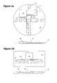
- FIG. 2 aillustrates the sensor apparatus of the invention as manufactured on a silicon wafer substrate and which is comprised of a plurality of integrated circuit sensors and a central microprocessor with wireless communication capability;
- FIG. 2 billustrates the sensor apparatus of the invention as manufactured on a vacuum compatible work piece and which is comprised of a plurality of integrated circuit sensors and a central microprocessor with wireless communication capability;
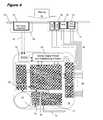
- FIG. 3illustrates a schematic diagram that is representative of the electrical architecture of invention in which output of a discrete sensor is collected by microprocessor with signal processing and wireless communication capability;
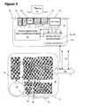
- FIG. 4illustrates a schematic diagram that is representative of electrical architecture of invention in which the analog output of a plurality of discrete sensors are transmitted to a central microprocessor with multiplexing, analog-to-digital conversion, signal processing and wireless communication capability;
- FIG. 5illustrates a schematic diagram that is representative of electrical architecture of invention in which a plurality of discrete sensors have an integrated analog-to-digital and signal conditioning capability and are digitally tied to a central microprocessor with signal processing and wireless communication capability;
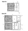
- FIG. 6 aillustrates the diagram of an integrated sensor which includes a thermocouple or thermistor device for monitoring surface temperatures, a dual-floating Langmuir probe for monitoring ion currents and apparent electron temperature, one or more topographical dependent charging structures for monitoring plasma-induced surface charging effect;
- FIG. 6 billustrates the diagram of an integrated sensor which includes a thermocouple or thermistor device for monitoring surface temperatures, a dual-floating Langmuir probe for monitoring ion currents and apparent electron temperature, one or more topographical dependent charging structures for monitoring plasma-induced surface charging effect, signal conditioning circuitry and a microprocessor for analog-to-digital conversion of sensor output and serial communication;
- FIG. 7illustrates a block diagram of a dual floating probe (DFP) structure with a typical current-voltage response curve when exposed to a plasma and voltage bias signal;
- DFPdual floating probe
- FIG. 8illustrates a capacitively-coupled circuit for pulsing the DFP device and the typical current response when exposed to a plasma
- FIG. 9illustrates a topography dependent charging (TDC) structure in the presence of a plasma and means by which a voltage is induced on the structure by a plasma;
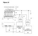
- FIG. 10illustrates how multiple TDC structures can be ganged together to provide power to one or more DC-to-DC converter sub-components in order to power multiple integrated sensors;
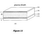
- FIG. 11illustrates an a surface charging structure utilizing stacked capacitors
- FIG. 12 aillustrates how a TDC structure sensor can be dynamically loaded to obtain current and voltage characteristics for the purpose of measuring current flux and surface charging effects resulting from ion transport within the TDC structure
- FIG. 12 bis a graph that illustrates a load line and power line obtained from the loaded TDC device diagnostic circuit.
- FIG. 1there is illustrated an apparatus 10 that is capable of making real-time measurements of incident plasma current flux and surface temperatures of a work piece in a plasma processing system 12 .
- a diagnostic probe 14is comprised of a silicon wafer substrate that incorporates plasma probe and surface temperature diagnostic circuitry and wireless communications and a stored power system.
- the probe 14is powered up outside the plasma processing system 12 to enable diagnostic communications prior to use for real-time measurements.
- the plasma processing system of FIG. 1is one of many possible plasma processing systems and is presented here to illustrate the function and use of the present invention.
- the processing systemis comprised of a vacuum processing chamber 16 , a pumping manifold 18 , a plasma source electrode mounted to the top of the chamber 20 , a gas delivery manifold or gas shroud 22 , gas flow and power connections to the plasma source electrode 24 , an wafer chuck 26 with clamp ring 28 , RF power, fluid coolant, lifting pin, and helium backside-cooling services to the chuck 30 , and a load lock transfer stage with mechanical robotics 32 to manipulate the wafer into the chamber 16 onto the chuck 26 .
- Plasma 34is ignited to perform an etching or deposition process on the surface of the wafer at which time the apparatus sensors and microprocessor is triggered to collect surface properties or plasma properties in close proximity to the apparatus surface in real time.
- An on-board wireless transceiver system 36is used to communicate data and instruction with a base station transceiver 38 outside the plasma processing system.
- the base station transceiver 38allows for communication of data and instructions between the software of the external computer 40 and the probe 14 in real time. Alternatively, it is possible to have the probe collect information inside the process and then download data once it is removed from the process chamber.
- the sensorscan be fabricated on a semiconductor wafer such as a 200 mm or 300 mm diameter silicon wafer. However, they may also be fabricated on any process work piece such as a ceramic, plastic, metal or glass work piece surface that can be introduced into the vacuum chamber.
- FIGS. 2 a and 2 bshow how an array of spatially distributed sensor elements 42 are disposed on the semiconductor wafer 14 with multiple interconnects 44 for communication and/or power distribution from a central processor and wireless communication subsystem 46 .
- FIG. 2 bshows how a similar device with sensors 42 , interconnects 44 and central processor with wireless communication module 46 could be patterned on any flat article or work piece 14 to be placed into the plasma processing system.
- thermocouplefor measuring work piece temperatures
- DFPdual-floating Langmuir probe
- TDCtopographically dependent charging
- sensing devicesthat can be electrically floated and thus they are viable for sensing process properties on a work piece when the work piece is electrically floating or if there is an active RF self-bias applied to the work piece. In such cases there can be no ground connection between the processing system ground and the work piece.
- These sensing devicesmay be used alone or in certain combinations depending upon the needs or the application. While these three specific devices are used to describe the apparatus or the present invention, there are other possible sensors that may be used in the context of the apparatus, which are described in the following specification.
- FIG. 3is an illustration of a single point sensing architecture of the apparatus of the present invention.
- the sensorsare mounted to a surface of the wafer 14 such that they are exposed to the flux of charged-particle species from the plasma 34 .
- the multiple sensorsinclude electrodes to a dual-floating Langmuir probe 48 , a surface temperature sensor 50 , topographically dependent charging sensors 52 with varying aspect ratio and a TDC bank 54 that feeds a voltage to a DC-DC converter and regulator 56 for optional or auxiliary sensor power.
- a protective package 58is used to shield most all other electronics from the exposure to the plasma environment.
- the supporting electronic architectureincludes a sensor signal power and conditioning circuit 60 , an A/D converter section for analog signals 62 , a central microprocessor 64 , additional memory 66 , a crystal oscillator 68 and the wireless transceiver 36 that includes a radio antenna 70 .
- the transceivermaybe infrared LEDs 72 as a means for wireless communications.
- the waferalso includes an energy source 74 which may be a capacitor or battery that powers the system through a magnetic reed switch 76 and DC-DC regulator 56 . This particular arrangement is preferred when temporal data from the sensors is a critical single point or zone that is required to monitor the phenomenon in real-time.
- FIG. 4is an illustration of a multiple-point or distributed sensing architecture wherein several sensor signals are multiplexed to a central signal condition circuitry, A/D converter, microprocessor.
- the sensorsare mounted to a surface of the wafer 14 such that they are exposed to the flux of charged-particle species from the plasma 34 .
- several multi-sensor modules 78are separate from the electronics enclosure 58 , yet have communication lines 80 to a multiplexing component 82 .
- the signal from several multi-sensor moduleswhich may be built up from repeated hybrid devices or system-on-chip modules, can be spatially polled through an array of distributed communication lines 84 .
- Each multi-sensor module 78includes electrodes for the DFP 48 , the surface temperature sensor 50 , and a TDC sensor 52 for recording surface charging.
- An optional TDC bank 54may be included in a separate module package 88 in order to power the DC-DC converter and regulator 56 for optional or auxiliary sensor power.
- the supporting electronic architectureincludes the multiplexer 82 , the sensor signal power and conditioning circuit 60 , the A/D converter section for analog signals 62 , the central microprocessor 64 , additional memory 66 , the crystal oscillator 68 and wireless transceiver 36 that has either the radio antenna 70 or the infrared LEDs 72 as a means for wireless communications.
- the second architectureincludes an energy source 74 which may be a capacitor or battery that powers the system through the magnetic reed switch 76 and DC-DC regulator 56 .
- This particular arrangementis preferred when temporal and spatial data from several replicated sensor modules 78 can be collected with little risk of noise and interference along patterned communication lines 80 and 84 . It would be economical to use this particular architecture as the collective elements of the central microprocessor, signal conditioning circuit, and multiplexer could be incorporated into a single Application Specific Integrated Circuit (ASIC) component or, alternatively, into an integrated multi-chip hybrid circuit.
- ASICApplication Specific Integrated Circuit
- FIG. 5is an illustration of a multiple-point sensing architecture wherein several replicated sensing modules with dedicated signal conditioning circuitry, A/D converter, and optional TDC-base power source are connected to a central microprocessor and wireless transceiver through shared serial communications.
- several sensor modules or subsystems 78are mounted to mounted to a surface of the wafer 14 such that the sensing components are exposed to the flux of charged-particle species from the plasma 34 .
- Each sensor module 78is comprised of a DFP sensor 48 , a temperature sensor 50 and at least one TDC sensor 52 .
- An additional bank of TDC devices 54may be used to couple power from the plasma boundary to a DC-DC regulators 56 to locally power the sensor module in when operated in the presence of a plasma.
- each sensor module 78has a sensor signal power and conditioning circuit module 96 , a local microprocessor 98 with A/D conversion 100 and isolation for serial communications 102 .
- Datais transmitted to the central processor 64 within package 58 through communication lines 103 and serial interface 106 as distributed along a shared serial bus 108 .
- the main microprocessor module 64has additional memory 66 , a crystal oscillator 68 and a wireless transceiver 36 that has either a radio antenna 70 or infrared LEDs 72 as a means for wireless communications.
- the modulealso includes an energy source 74 which may be a capacitor or battery that powers the system through a magnetic reed switch 76 and DC-DC converter 56 .
- an energy source 74which may be a capacitor or battery that powers the system through a magnetic reed switch 76 and DC-DC converter 56 .
- This arrangementis preferred when temporal and spatial data from several replicated sensor modules 78 can be fabricated from an ASIC or hybrid circuit component.
- the digital communications between the sensors and the central processorshould provide good immunity to noise and address common mode voltage issues since analog signals are not being spatially routed over the apparatus surface.
- the localized sampling and storage capability of the local microprocessors 98may enable faster sampling rates and real-time transmission of the sensor data when compared to a multiplexed architecture as illustrated in FIG. 4.
- the surface sensor devicescould be fabricated from a hybrid circuit components or an ASIC to form the replicated sensor modules 78 as shown in FIGS. 4 and 5.
- Such modular sub-componentscould be mounted on a discrete circuit substrate such as a ceramic or high temperature thermal plastic with output leads bonded to patterned interconnections on the wafer 14 .
- the sensor modules and interconnectionscould be patterned directly into the surface of a silicon wafer 14 to provide an integrated sensor array.
- FIGS. 6a and 6bshow a representative top view of sensor modules.
- FIG. 6ashows a layout of a sensor module 78 as applicable to the multiplexed architecture of FIG. 4.
- This sensor moduleincludes DFP collection probes 48 , surface temperature sensor 50 and four separate TDC sensors 52 along with bondable pad connections 110 to the various sensors.
- FIG. 6 bshows a layout of a sensor module 78 as applicable to the serial architecture of FIG. 5.
- this modulealso includes a secondary TDC bank 54 for local power generation, DC-DC converters 56 , signal conditioning circuitry 60 , a local microprocessor 98 with A/D 100 and isolated serial communications 102 , and bondable pads connections for serial communications 112 and distribution of auxiliary power 114 .
- thermocouples and thermistorsthat are encapsulated in integrated circuit package for surface mounting to the wafer and which provide a varying bi-metal voltage or electrical impedance with respect to temperature
- IC packaged thermocouple or thermistorswhich have integrated electronics and which provide a digital output of temperature
- thermocouple or thermistor devicesthat have been patterned and integrated into the surface of the wafer with conventional semiconductor-IC manufacturing methods.
- Those thermal sensors that are based on IC packagesare economically advantageous in architectures where hybrid electronics are used, but because of their local thermal mass, they provide only an estimated measure of the wafer surface temperature. Sensors that are fabricated directly into the wafer surface are preferable because of their exactness, but their use can involve considerable cost in pattering and manufacture when compared to IC surface mount devices.
- the double-floating Langmuir probe or DFPis used to collect some of these plasma parameters. Described in the early 1950s, the double- floating Langmuir probe allows one to obtain I-V characteristics of a plasma between two conductive probes that are allowed to electrically float apart from an electrical common or ground.
- FIGS. 7 a and 7 billustrate the basic working principles of the DFP.
- Two planar conductive probes 48are isolated from the wafer surface 14 and exposed to plasma 34 .
- a floating bias potential 116is induced between the probes to force a net current 118 through the plasma and DFP circuit.
- the net DFP currentis limited by ion current flux 120 to the negatively biased probe surface due to the rejection of electrons currents 122 to the probe; this is known as the ion saturation current.
- the ion current 124 and electron current 126 to the second probecompensate in order to sum all plasma currents to zero.).
- an I-V trace 128is produced that is similar to back-to-back diode I-V characteristics shown in FIG. 7 b.
- the saturating current regions 130 and 132correspond to ion saturation currents 120 and 124 respectively.
- the intermediate region of the I-V curve 134is determined by the electron currents 122 and 126 between the probes and may be used to determine the apparent electron temperature, ⁇ T e >, which is indicative of “high-energy” electron population of the electron energy distribution as manifested at the boundary of the wafer surface 14 .
- Equation 1may be modified to take into non-ideal situations that include effective probe area expansion with increasing bias potential, asymmetric probe areas, non-uniform plasmas and non-Maxwellian electron energy distributions.
- the conventional analysis that results in Eq. 1is for a DC floating DFP case, but there is no-where in the prior art where workers experimentally or theoretically examined the DFP I-V characteristics when the DFP is placed on an RF-biased work piece.
- an RF-bias 136would distort the I-V characteristics and potentially confound the probe technique and analysis. Such distortion could be due to RF modulation of the plasma sheath boundary and potential disruption of electron currents 122 and 126 to the probe electrodes 48 . As a result the I-V characteristics properties under RF-biased conditions might not resemble 128 or follow Eq. 1 when the wafer 14 is placed on an RF biased electrode, as often done in plasma processing systems.
- FIG. 8 aTo see how the DFP sensor responds in the presence of an RF-bias signal, an arrangement shown in FIG. 8 a was prepared in which several pairs of square DFP aluminum thin film probes 48 ( ⁇ 0.7 cm 2 ) were sputter-deposited over a 200 mm silicon wafer 14 with a ⁇ 1.5 um thick insulating oxide 140 . The probes were attached to an external AC floating power source 142 that was swept with at peak differential voltage about 40 V p-p at 30 Hz to simulate a slow voltage sweep. Currents were sensed with a floating resistor and a differential voltage probe.
- the silicon waferwas placed in a commercial oxide etching chamber which had a 13.56 MHz inductively-coupled plasma source with planar induction coil (top) and a 13.56 MHz capacitively-coupled electrode (bottom) in a manner commonly used in high-density plasma semiconductor manufacture, i.e. with the wafer on the bottom capacitively-coupled electrode 144 to provide an RF induced self-bias in order to accelerate ions to the wafer surface).
- the oscilloscope traceshows the 30 Hz sinusoidal sweep 152 and the responding DPF current 154 .
- FIG. 9Such a means is illustrated in FIG. 9, wherein the DFP pads 48 are capacitively-coupled through isolation capacitors 156 and 158 to an input signal from a storage capacitor 160 and charge-pump circuit 162 tied to a floating common 164 .
- FETsfield effect transistors
- a sampling resistor 170is used to sense DFP current and a voltage divider 172 is used to sample the DFP bias voltage level.
- the signal trends against timeare also illustrated in FIG. 9.
- the representative signal levelsshow how the DPF current is allowed to flow through the circuit and plasma 34 once the DFP pulse FET 166 is turned on.
- the apparatus microprocessorsamples the I DFP current and DFP bias level. For repeated sampling under the same or different DFP bias levels, it is necessary to equalize or reset the charge state of the isolation capacitors 156 and 158 . This is accomplished through a shunting FET 168 that is turned on between DFP pulses and A/D sampling.
- FIG. 9allows one to sample the DFP current and voltage dynamically as the bias voltage and responding DFP current relaxes in time or, alternatively, at discretely pulsed intervals and bias level as controlled through the charge-pump circuitry and timing of the DFP pulse and A/D sampling.
- the circuit of FIG. 9can be adapted to other electrically floating sensing devices such as photodiodes detection devices for light emission diagnostic methods, thermistors, various micro-electro-mechanical (MEM) sensors and other impedance-based sensing devices.
- the topographically dependent charging (TDC) deviceis another component that has several possible applications in the apparatus of the present invention.
- FIG. 10illustrates the general principles of the TDC device 52 .
- the TDC deviceis generally comprised of a substrate 174 , a lower conductive electrode 176 , a patterned insulator with relatively high aspect ratio lines or holes with sub-micron dimensions 178 and a top conductive electrode 180 .
- the typical dimensions for a TDC deviceis an opening of ⁇ 1 um with aspect ratios that are about 5 or greater.
- a typical TDC devicemay have a hole or line opening of 0.3 um and feature depth of 1-1.5 um.
- the differences in ion and electron transport to the top electrode 180 and the buried bottom electrode 176results in a positive potential on the bottom electrode.
- This charging effectis well known in the industry since such charging effects can influence the quality producing high aspect ratio sub-micron features and can lead to surface charging effects that result in device damage during semiconductor IC manufacture. Such surface charging and potential charge damage effects are dependent upon the plasma conditions and spatial uniformity of the plasma.
- one use of the TDC in the present inventionis a monitor of static charges across various TDC devices with varying aspect ratios for spatial and temporal measure of surface charging effects.
- TDC 52provides a source of DC power to various electrical components and sub-systems that have been illustrated in the various proposed architectures. Since the TDC devices provide a DC potential from the charged carrier transport against the plasma boundary, they may be used as a continuously charged power source when the plasma is active. As with a battery or storage capacitor, a TDC-based power source would also need a DC-DC converter to adjust and regulate the power to appropriate DC voltage levels. In this application the top electrode 180 of the TDC is used as the local common.
- the TDCmay power one DC-DC converter 182 for the charge pump and sampling circuitry 184 for the DFP diagnostic system 186 and a second DC-DC converter 188 to power a local microprocessor 190 used for sampling, A/D conversion and serial communications.
- the power available from the TDC device or bank of TDC devicesis limited by the ion current flux collected at the base electrode 176 and effective DC potential when electrically connected to a load.
- a typical processing plasma systemmay have ion current flux densities on the order of 1-5 mA/cm 2 , and under typical RF self-bias voltages of a few hundred volts, the charging of a TDC device may be several 10s of volts.
- the power densitythat may be derived as much as much as 0.1 W/cm 2 for a TDC structure that has 40% open ion collection area.
- a 1-2 cm 2 TDC device or bank exposed to a plasmacould be integrated with a DC-DC converter to provide the same DC power of a 3.2 V coin battery with a peak trickle-current rating of about 30 mA.
- the power derived from the TDC devicemay be used as an auxiliary source or DC power for sensor devices or for recharging of the main charge capacitor or battery.
- TDC devicefor providing auxilary electronic power from the plasma process
- other chargeable structuressuch as a thin film capacitor stack, which is patterned on the wafer surface
- a devicecan accumulate a net DC charge and thus provide a differential DC voltage when it is exposed an RF bias in a plasma process.
- This DC voltagemay then be regulated by a DC-DC converter in order to power the device electronics or to recharge the device battery.
- the principle of such a charging capacitor 192is illustrated in FIG. 11.
- the charging capacitormay be formed from a bottom conductive electrode 194 attached to the base of the substrate or wafer 174 , an insulating thin film 196 and a top conductive electrode 198 .
- Various multi-layer, inter-digitated capacitor configurationscan be used to increase the capacitance.
- a net DC voltageis sustained across the insulator.
- a charging devicemay be constructed to provide the appropriate DC voltage and current capacity levels for auxiliary power generation.
- such an electrically floating capacitive device with collection area of ⁇ 10 cm 2can provide a net DC voltage on the order of 1 to 10 V and draw currents on the order of 100s of microamperes
- FIG. 12 aillustrates an application of the TDC for the apparatus of the present invention wherein the loaded I-V characteristics or “load-line” of the TDC device is probed.
- the bottom conductive electrode 176 of a TCD sensor device 52or several TDC devices of varying aspect ratios, are individually tied to a FET 200 .
- the FETis operated in a linear resistive region through a controlled gate voltage signal 202 .
- the output of the FETis connected to a current sensing resistor 204 which is tied to common or the top electrode of the TDC 180 and, thereby, allows one to sample the draining TDC current 206 as the loading resistance of FET is changed.
- a high impedance voltage divider 208is used to sample the voltage of the loaded TDC device. In this manner both one may collect a load-line characteristic of the TDC device when exposed to the processing plasma environment.
- FIG. 12 bA typical load-line characteristic is illustrated in FIG. 12 b as it might arise from a TDC structure.
- TDC structures with different aspect ratiomay provide somewhat different load lines when exposed to different plasma processing environments and RF biases.
- the TDC device voltage and currentarises from the differences between net ion and electron transport through the TDC structure when exposed to a plasma.
- the top and bottom electrodes of the TDC deviceare connected (short circuit)
- the connection between top and bottom electrodesis open (open circuit), a voltage is sustained due to the imbalance of charged-particle fluxes and net accumulation of positive charge at the base of the device.
- the exemplary load-line characteristic of FIG. 12 bshows the response of the TDC device's current and voltage as it is loaded between the shorted and open conditions.
- the TDC device load-lineis determined by factors that influence the spatial density, effective mass, phase velocity and energy of charged species to the TDC. These factors can include gas pressure, plasma chemistry, power density, chamber surface conditions and RF bias levels. As such, a detailed measure of the load line response of one or several TDC devices can provide far more subtle information about the plasma processing conditions than just the open-circuit voltages or short-circuit currents.
- the load-lineprovides a power line that can be used to match the output of TDC devices to DC-DC converter circuitry when using the TDC devices as a DC power source in the apparatus architecture.
- the probing componentmust be vacuum compatible and must not steadily outgas any significant compounds that would contaminate the process or process chamber. Also, when placed under high bias potential, the sputtered surface materials should not contaminate the process or process chamber.
- hermetically sealed packagingshould be used or monolithically thick dielectric coatings should be considered with optional use of metal electrostatic shielding from deposited thin films.
- the overall height of the probing component that enters into the vacuum processing chambershould be small enough to pass through conventional load-lock gate valves and associated slits with the aid of conventional handling systems and robotics. This clearance height is usually 1 cm or less.
- the probing componentshould also be well balanced for manipulation with common handling mechanisms such as lifting pins, robotic paddles and rollers.
- the probing devicemust be electrically self-contained and operable when placed in a plasma and stimulated with an RF-self bias, as would be the case for wafer or work piece in a conventional plasma processing system.
- the apparatusshould be constructed so as to allow wireless communications in either or two modes: first, in real-time from within processing system and second, post process download from the processing system chamber or load lock or from outside the processing system altogether.
- the features and scale of sensor devices within the probing apparatusshould be relatively small to allow spatial resolution of surface temperatures or plasma body properties.
- the scale of each sensoris preferably, but not limited to, 1 cm 2 .
- the apparatusmay include any number of additional sensors.
- MEMs devicesmay include MEMs devices, optical sensor, bulk resistivity devices that are sensitive to rates of etching, curing or deposition or inducement or magnetic fields.
- MEMs devicesmight be particularly useful sensors in that they are often fashioned from materials that are compatible with plasma-based process environments.
- One examples of a useful MEMs deviceis a CMOS-based resonant beam sensor.
- Such sensorsuse a micro-machined cantilevered mechanism whose stimulated resonant frequency is dependent upon thermal and mass properties of the beam when exposed to the heat flux of the plasma, gaseous chemical absorbance, or mass changes due to reactive gas etching or deposition.
- MEMs sensor technologyexamples include the following devices.
- a single-chip resonant beam gas sensoras described by Hagleitiner et. al, “A single-chip CMOS Resonant Beam Gas Sensor” 2001 IEEE International Solid-State Circuits Conference, Feb. 6, 2001.
- This devicewhich was designed to detect the mass absorption of volatile organic compounds could be used in conjunction with present invention to monitor the mass absorption, accumulation or removal as related to a plasma assisted process.
- Another exampleis a Hall magnetic sensor as described by Frounchi et al. “Integrated Hall Sensor Array Microsystem” 2001 IEEE International Solid-State Circuits Conference, Feb. 6, 2001.
- This integrated micro-sensoris a device for monitoring magnetic field strengths and could be used to monitor magnetic fields that are routinely used to enhance in plasma processing system to either control or enhance the process.
- Another deviceis micro-scale retarding field energy analyzer (or ion energy analyzer) as described by Blain, et al. “High-resolution submicron retarding field analyzer for low-temperature plasma analysis” Applied Physics Letters, Vol. 75, pp 3923, 1999.
- This deviceshows how a submicron-level ion energy analyzer could be constructed as a sensor on a patterned wafer. Such a device could be effectively operated with an electrical variant of dual floating probe circuitry as described earlier in order to obtain ion energy distributions for this type of analyzer.
- Yet another class of sensing technologyare various integrated thin film optical photo sensor or photo spectrometer sensors that incorporate thin-film bandwidth specific optical filters that are fabricated with conventional CMOS chip fabrication methods.
- Optical emission and absorbancehas been widely used to study the ultraviolet, optical and infrared spectra of processing plasmas for process development and control.
- Optical sensorssuch as photodiodes, with or without passive optical filtering, can also be used to measure optical emission as radiated to the surface of the work piece.
- Use of multiple optical emissions sensorscan enable the measure of multiple wavelength intensities as would be required for in situ actinometry or other optical emission spectroscopy methods.
- the self-contained DC power source or reservoirmay be formed provided by a number of means.
- Low-profile, commercially available coin-style batteriesare widely available and can be used if they meet thermal specifications, trickle current levels, mA/hr ratings and are packaged (i.e. hermetically sealed) so as not to outgas electrolytic compounds.
- thin-film, multi-layer charge-capacitors deviceswhich may be re-charged prior to use or within the plasma process from an optional TDC device and DC-DC converter.
- Yet other variations of low profile batteries, re-chargeable batteries, and charge-storage capacitorscan be incorporated into the design to provide power to the apparatus during the plasma process or for external testing, device configuration and calibration when outside of the plasma processing system.
Landscapes
- Physics & Mathematics (AREA)
- Engineering & Computer Science (AREA)
- Plasma & Fusion (AREA)
- Chemical & Material Sciences (AREA)
- Analytical Chemistry (AREA)
- Drying Of Semiconductors (AREA)
- Plasma Technology (AREA)
- Testing Or Measuring Of Semiconductors Or The Like (AREA)
Abstract
Description
- 1. Field of the Invention[0001]
- This invention relates generally to apparatus and methods in which surface-based sensors measure incident charged-particle currents, charging voltages, temperatures and other physical parameters at a work piece surface during plasma processing, and more particularly to a semiconductor wafer utilizing surface-based sensors to provide real time measurement of plasma characteristics adjacent to the wafer surface as well as select physical properties during plasma processing.[0002]
- 2. Brief Description of the Prior Art[0003]
- Spatial and temporal variation in plasma characteristics and the work piece surface temperature can strongly influence the performance and yield of plasma-based processes, such as those encountered in semiconductor manufacture. In such processes, variations in physical plasma parameters that occur adjacent to the process work piece directly impact process metrics which may include the following: (1) etch rates and etch profile control, (2) surface charging effects and device or film damage, and (3) thin film deposition rates, density, coverage, morphology, stress and adhesion. Some common plasma parameters that drive surface processes on a work piece, such as a semiconductor substrate wafer, include charged-particle density and flux (ion and electron density), apparent electron temperature, ion energies, neutral gas temperature, density and flux of reactive gas species, and plasma radiative emissions. It is also known that surface temperature of the work piece or wafer can play a very critical role in many of the surface reactions and results of the plasma process.[0004]
- Because of the criticality of both plasma characteristics and substrate temperature and their impact on process yield, several workers have attempted to monitor plasma characteristics and surface temperatures during processes by means of diagnostic probes that are directly mounted to a work piece, such as a semiconductor wafer substrate. In these devices, diagnostic probes such as thermocouples, DC-biased electrical probes, ion energy analyzers, and surface charging collectors have been used to measure spatial and temporal variation of surface temperature, selected plasma parameters, and plasma-induced charging effects. One such device is the Stanford Plasma On-wafer Real Time (SPORT) probe as described in an article by S. Ma and J. P. McVittie in the proceedings of the 1966 International Symposium on Plasma Process-Induced Damage pg. 20-23. The SPORT probe is capable of measuring electrostatic charging and plasma-induced currents at the wafer surface. The SPORT probe utilizes large conductive pads placed on a thick oxide layer of a silicon wafer. Polysilicon leads make direct current contact to the pads and the silicon substrate. Wire leads connected to the edge of the wafer carry current and voltage signals outside the plasma-processing chamber to a low pass RF filter to a dc measurement circuit. By means of the external measurement circuit, plasma induced charging voltages are measured between the pads and the substrate in order to quantify plasma induced electrostatic charging effects that could result in damage to electrically sensitive semiconductor device structures during plasma processing and fabrication.[0005]
- Another apparatus is described in U.S. Pat. No. 5,801,386 issued to Valentin N. Todorov et al. This patent discloses an apparatus that comprises a plurality of conductive collector pads for detection of plasma induced ion currents and self-biased voltages. The collector pads are arranged in an array so that plasma-induced properties of ion current and self-bias voltage can be spatially resolved over the wafer surface in real time. Each collector pad is connected to a conductive lead that extends outside the chamber to an external data acquisition system.[0006]
- Also in U.S. Pat. No. 5,959,309 entitled “Sensor to Monitor Plasma Induced Charging Damage”, Tsui, et al. describe a discrete monitoring circuit that measures the plasma-induced voltage and currents to a sampling pad or antenna that is in communication with a ground or common. In this device, the sampling pad is connected to ground through a blocking diode, a blocking transistor, and a storage capacitor. Once the monitor is exposed to the plasma, the voltage between the charged pad or antenna and the electrical common or ground is recorded by charging a storage capacitor. The workers also disclosed how a plurality of these monitors, each with different loading resistances, can be integrated onto a single chip to measure the magnitude of the charging voltage and the plasma-induced current between the antenna and common or ground of the chip. The charging voltage and pad-to-common currents are determined by electrically measuring the voltages of the storage capacitors after the sensor or chip is removed from the plasma processing environment.[0007]
- Freed et al. describe the development of sensor methods in “Autonomous On-Wafer Sensors for Process Modeling, Diagnostic and Control” (IEEE Transactions on Semiconductor Manufacturing, Vol. 14, No. 3, pp 225-264). This paper describes the basic design challenges faced in the development of an in situ or in-line wafer sensor including power source concepts, wireless communications methods, and electrical isolation of on-wafer electronics. In their examples, they illustrate two design concepts. In the first design concept is an on-wafer thermistor sensor powered with re-chargeable batteries and voltage regulator. The design also includes an A/D converter and LED optical communication electronics for transferring data off the wafer in a thermally elevated process environment and a plasma etching environment. In another version of the design, the workers illustrate how a van der Pauw sheet resistance device may be adapted with CMOS processing methods for measuring polysilicon etch rates. They demonstrate the viability of this sensor with a wired wafer as applied to a XeF[0008]2(non-plasma) etching reactor. These devices have varying degrees of effectiveness in monitoring the wafer temperature or the characteristics of a plasma body adjacent to the wafer when disposed in a plasma processing environments. However, all the examples of the prior art have several limitations that restrict their use for obtaining real-time plasma and substrate temperature measurement within a plasma processing system. Many of these measuring devices are intrusive in that they require the use of wires into the plasma processing system and others are passive recording devices that cannot make real-time measurements. Also, those devices that do not use external wires, are limited in on-time operation, and power supply current draw since they rely entirely upon on-board battery power sources that have limited milliamp-per-hour capacity or limited sustainable trickle current capacity when attempting to power a sizable array of sensors, microprocessor(s) and wireless communication subsystems. Moreover, in the context of these in situ measurement apparatuses, none of the prior art teachings discuss in detail how to devise a sensor capable of obtaining plasma measurements, such as charged-particle (ion or electron) fluxes, densities and energies that can be adapted to a wireless sensing apparatus.
- It would be desirable if there were provided a surface-based sensor apparatus that could make spatially resolved, real-time measurements of plasma properties adjacent to the surface of the apparatus, as well as other properties such as surface temperature. It would also be desirable if the device were non-invasive to the plasma process and if the time-dynamic data recorded by the device could be either transmitted in real-time through a wireless interface or, alternatively, be recorded for downloading once the sensor apparatus is removed from the plasma process chamber. It would be further desirable if the device had a self-contained power supply means that did not rely entirely upon the limited lifetime or trickle current ratings of a battery or alternative conventionally power source.[0009]
- There is provided by this invention an apparatus for making real time measurements of incident plasma currents, charging surface voltages, and other plasma related parameters as well as surface temperatures within a plasma processing environment. The apparatus is generally comprised of at least one integrated sensor circuit mounted on a work piece such as a silicon wafer substrate. The sensor is comprised of either a dual floating probe to measure ion currents from the plasma, a topographical dependent charging structure to measure plasma induced surface charging effects, filtered photodiodes to measure optical emissions signals, a thermal sensing device to monitor surface temperature or a combination thereof The sensor inputs are transmitted to a central microprocessor and transceiver that is provided for processing sensor signals, memory storage, and real-time transmission of data via infrared- or rf-wireless communication to a receiver outside the plasma chamber. To power the apparatus, a battery is contained within the apparatus to provide power to the integrated sensor devices, microprocessor and wireless transceiver. Alternately, the apparatus may include one or more topographically dependent charging structures to electrostatically couple power from the plasma boundary that is then regulated and used to provide all or part of the power to the apparatus electronics. The apparatus is particularly useful in spatial and real-time monitoring of plasma and substrate conditions in plasma-based non-depositing processes such as etching, photo-resist stripping or surface cleaning, but could be applied to some plasma-based deposition processes with the appropriate configuration or adaptation of the integrated sensing devices.[0010]
- FIG. 1 illustrates a simplified cross-sectional view of a semiconductor manufacturing process chamber in which to utilize the sensor apparatus for measurements across the surface of a wafer or work piece;[0011]
- FIG. 2[0012]aillustrates the sensor apparatus of the invention as manufactured on a silicon wafer substrate and which is comprised of a plurality of integrated circuit sensors and a central microprocessor with wireless communication capability;
- FIG. 2[0013]billustrates the sensor apparatus of the invention as manufactured on a vacuum compatible work piece and which is comprised of a plurality of integrated circuit sensors and a central microprocessor with wireless communication capability;
- FIG. 3 illustrates a schematic diagram that is representative of the electrical architecture of invention in which output of a discrete sensor is collected by microprocessor with signal processing and wireless communication capability;[0014]
- FIG. 4 illustrates a schematic diagram that is representative of electrical architecture of invention in which the analog output of a plurality of discrete sensors are transmitted to a central microprocessor with multiplexing, analog-to-digital conversion, signal processing and wireless communication capability;[0015]
- FIG. 5 illustrates a schematic diagram that is representative of electrical architecture of invention in which a plurality of discrete sensors have an integrated analog-to-digital and signal conditioning capability and are digitally tied to a central microprocessor with signal processing and wireless communication capability;[0016]
- FIG. 6[0017]aillustrates the diagram of an integrated sensor which includes a thermocouple or thermistor device for monitoring surface temperatures, a dual-floating Langmuir probe for monitoring ion currents and apparent electron temperature, one or more topographical dependent charging structures for monitoring plasma-induced surface charging effect;
- FIG. 6[0018]billustrates the diagram of an integrated sensor which includes a thermocouple or thermistor device for monitoring surface temperatures, a dual-floating Langmuir probe for monitoring ion currents and apparent electron temperature, one or more topographical dependent charging structures for monitoring plasma-induced surface charging effect, signal conditioning circuitry and a microprocessor for analog-to-digital conversion of sensor output and serial communication;
- FIG. 7 illustrates a block diagram of a dual floating probe (DFP) structure with a typical current-voltage response curve when exposed to a plasma and voltage bias signal;[0019]
- FIG. 8 illustrates a capacitively-coupled circuit for pulsing the DFP device and the typical current response when exposed to a plasma;[0020]
- FIG. 9 illustrates a topography dependent charging (TDC) structure in the presence of a plasma and means by which a voltage is induced on the structure by a plasma;[0021]
- FIG. 10 illustrates how multiple TDC structures can be ganged together to provide power to one or more DC-to-DC converter sub-components in order to power multiple integrated sensors;[0022]
- FIG. 11 illustrates an a surface charging structure utilizing stacked capacitors;[0023]
- FIG. 12[0024]aillustrates how a TDC structure sensor can be dynamically loaded to obtain current and voltage characteristics for the purpose of measuring current flux and surface charging effects resulting from ion transport within the TDC structure; and
- FIG. 12[0025]bis a graph that illustrates a load line and power line obtained from the loaded TDC device diagnostic circuit.
- Referring to FIG. 1 there is illustrated an[0026]
apparatus 10 that is capable of making real-time measurements of incident plasma current flux and surface temperatures of a work piece in aplasma processing system 12. In this particular illustration adiagnostic probe 14 is comprised of a silicon wafer substrate that incorporates plasma probe and surface temperature diagnostic circuitry and wireless communications and a stored power system. In the preferred embodiment, theprobe 14 is powered up outside theplasma processing system 12 to enable diagnostic communications prior to use for real-time measurements. The plasma processing system of FIG. 1 is one of many possible plasma processing systems and is presented here to illustrate the function and use of the present invention. The processing system is comprised of avacuum processing chamber 16, a pumpingmanifold 18, a plasma source electrode mounted to the top of thechamber 20, a gas delivery manifold orgas shroud 22, gas flow and power connections to theplasma source electrode 24, anwafer chuck 26 withclamp ring 28, RF power, fluid coolant, lifting pin, and helium backside-cooling services to thechuck 30, and a load lock transfer stage withmechanical robotics 32 to manipulate the wafer into thechamber 16 onto thechuck 26.Plasma 34 is ignited to perform an etching or deposition process on the surface of the wafer at which time the apparatus sensors and microprocessor is triggered to collect surface properties or plasma properties in close proximity to the apparatus surface in real time. An on-boardwireless transceiver system 36 is used to communicate data and instruction with abase station transceiver 38 outside the plasma processing system. Thebase station transceiver 38 allows for communication of data and instructions between the software of theexternal computer 40 and theprobe 14 in real time. Alternatively, it is possible to have the probe collect information inside the process and then download data once it is removed from the process chamber. - In the preferred embodiment the sensors can be fabricated on a semiconductor wafer such as a 200 mm or 300 mm diameter silicon wafer. However, they may also be fabricated on any process work piece such as a ceramic, plastic, metal or glass work piece surface that can be introduced into the vacuum chamber. These configurations are illustrated in FIGS. 2[0027]aand2brespectively. FIG. 2ashows how an array of spatially distributed
sensor elements 42 are disposed on thesemiconductor wafer 14 withmultiple interconnects 44 for communication and/or power distribution from a central processor andwireless communication subsystem 46. FIG. 2bshows how a similar device withsensors 42, interconnects44 and central processor withwireless communication module 46 could be patterned on any flat article orwork piece 14 to be placed into the plasma processing system. - There are three specific architectures of interest that may be used in within the apparatus of the present invention. These are given as[0028]
- (1) single-point sensing devices with dedicated single conditioning circuitry, analog-to-digital (A/D) converter, micro-processor, wireless communications and power source;[0029]
- (2) multiple-point or distributed sensing devices with analog and control signals multiplexed to a central signal condition circuitry, A/D converter, micro-processor, wireless communications and power source; and[0030]
- (3) multiple-point or distributed sensing devices with dedicated signal conditioning circuitry, A/D converter, local power source and with serial communications to a central micro-processor, wireless communications and power source. The choice of any particular architecture is dependent upon the need for collecting real-time spatial information, use of materials and manufacture constraints, and data collection issues related to noise immunity and speed of data collection over a distributed serial or multiplexed electrical system. These basic architectures are described in more detail hereinafter.[0031]
- There are three sensor devices or means that are of particular interest for measurement of parameters at the work piece surface or from the adjacent plasma body. These sensors are used in examples to illustrate the operation and function of the apparatus. These sensors are:[0032]
- a) a thermal sensing element, such as a thermocouple or thermistor, for measuring work piece temperatures;[0033]
- b) a dual-floating Langmuir probe (DFP) for measuring plasma ion current fluxes, apparent electron temperatures and estimates of ion and electron densities;[0034]
- c) a topographically dependent charging (TDC) devices for measuring surface charging effects and for coupling power from the plasma sheath.[0035]
- The common aspect of these particular sensor devices is that they are examples of sensing devices that can be electrically floated and thus they are viable for sensing process properties on a work piece when the work piece is electrically floating or if there is an active RF self-bias applied to the work piece. In such cases there can be no ground connection between the processing system ground and the work piece. These sensing devices may be used alone or in certain combinations depending upon the needs or the application. While these three specific devices are used to describe the apparatus or the present invention, there are other possible sensors that may be used in the context of the apparatus, which are described in the following specification.[0036]
- FIG. 3 is an illustration of a single point sensing architecture of the apparatus of the present invention. The sensors are mounted to a surface of the[0037]
wafer 14 such that they are exposed to the flux of charged-particle species from theplasma 34. In this case the multiple sensors include electrodes to a dual-floatingLangmuir probe 48, asurface temperature sensor 50, topographically dependent chargingsensors 52 with varying aspect ratio and aTDC bank 54 that feeds a voltage to a DC-DC converter andregulator 56 for optional or auxiliary sensor power. Aprotective package 58 is used to shield most all other electronics from the exposure to the plasma environment. The supporting electronic architecture includes a sensor signal power andconditioning circuit 60, an A/D converter section foranalog signals 62, acentral microprocessor 64,additional memory 66, acrystal oscillator 68 and thewireless transceiver 36 that includes aradio antenna 70. Alternately, the transceiver maybeinfrared LEDs 72 as a means for wireless communications. The wafer also includes anenergy source 74 which may be a capacitor or battery that powers the system through amagnetic reed switch 76 and DC-DC regulator 56. This particular arrangement is preferred when temporal data from the sensors is a critical single point or zone that is required to monitor the phenomenon in real-time. - FIG. 4 is an illustration of a multiple-point or distributed sensing architecture wherein several sensor signals are multiplexed to a central signal condition circuitry, A/D converter, microprocessor. As with the prior architecture, the sensors are mounted to a surface of the[0038]
wafer 14 such that they are exposed to the flux of charged-particle species from theplasma 34. However in this arrangement, severalmulti-sensor modules 78 are separate from theelectronics enclosure 58, yet havecommunication lines 80 to amultiplexing component 82. In this manner, the signal from several multi-sensor modules, which may be built up from repeated hybrid devices or system-on-chip modules, can be spatially polled through an array of distributed communication lines84. Eachmulti-sensor module 78 includes electrodes for theDFP 48, thesurface temperature sensor 50, and aTDC sensor 52 for recording surface charging. Anoptional TDC bank 54 may be included in aseparate module package 88 in order to power the DC-DC converter andregulator 56 for optional or auxiliary sensor power. In this multiplexing arrangement, the supporting electronic architecture includes themultiplexer 82, the sensor signal power andconditioning circuit 60, the A/D converter section foranalog signals 62, thecentral microprocessor 64,additional memory 66, thecrystal oscillator 68 andwireless transceiver 36 that has either theradio antenna 70 or theinfrared LEDs 72 as a means for wireless communications. As with the first architecture, the second architecture includes anenergy source 74 which may be a capacitor or battery that powers the system through themagnetic reed switch 76 and DC-DC regulator 56. This particular arrangement is preferred when temporal and spatial data from several replicatedsensor modules 78 can be collected with little risk of noise and interference along patternedcommunication lines enclosure 58 and electrically insulated connections to deposited or printed conductive traces forcommunication lines connections 94 between TDCauxiliary power bank 54 and DC-DC regulator 56. Such preferred methods of fabrication would allow the apparatus to be fabricated on asemiconductor wafer 14 with materials that are compatible with semiconductor plasma processing environments. - FIG. 5 is an illustration of a multiple-point sensing architecture wherein several replicated sensing modules with dedicated signal conditioning circuitry, A/D converter, and optional TDC-base power source are connected to a central microprocessor and wireless transceiver through shared serial communications. In this version of the architecture several sensor modules or[0039]
subsystems 78 are mounted to mounted to a surface of thewafer 14 such that the sensing components are exposed to the flux of charged-particle species from theplasma 34. Eachsensor module 78 is comprised of aDFP sensor 48, atemperature sensor 50 and at least oneTDC sensor 52. An additional bank ofTDC devices 54 may be used to couple power from the plasma boundary to a DC-DC regulators 56 to locally power the sensor module in when operated in the presence of a plasma. In order to make local measurements, eachsensor module 78 has a sensor signal power andconditioning circuit module 96, alocal microprocessor 98 with A/D conversion 100 and isolation forserial communications 102. Data is transmitted to thecentral processor 64 withinpackage 58 throughcommunication lines 103 andserial interface 106 as distributed along a sharedserial bus 108. As with previous apparatus architectures, themain microprocessor module 64 hasadditional memory 66, acrystal oscillator 68 and awireless transceiver 36 that has either aradio antenna 70 orinfrared LEDs 72 as a means for wireless communications. The module also includes anenergy source 74 which may be a capacitor or battery that powers the system through amagnetic reed switch 76 and DC-DC converter 56. This arrangement is preferred when temporal and spatial data from several replicatedsensor modules 78 can be fabricated from an ASIC or hybrid circuit component. The digital communications between the sensors and the central processor should provide good immunity to noise and address common mode voltage issues since analog signals are not being spatially routed over the apparatus surface. Moreover, the localized sampling and storage capability of thelocal microprocessors 98 may enable faster sampling rates and real-time transmission of the sensor data when compared to a multiplexed architecture as illustrated in FIG. 4. - As mentioned earlier, the surface sensor devices could be fabricated from a hybrid circuit components or an ASIC to form the replicated[0040]
sensor modules 78 as shown in FIGS. 4 and 5. Such modular sub-components could be mounted on a discrete circuit substrate such as a ceramic or high temperature thermal plastic with output leads bonded to patterned interconnections on thewafer 14. Alternatively, the sensor modules and interconnections could be patterned directly into the surface of asilicon wafer 14 to provide an integrated sensor array. FIGS. 6a and 6b show a representative top view of sensor modules. In particular FIG. 6a shows a layout of asensor module 78 as applicable to the multiplexed architecture of FIG. 4. This sensor module includes DFP collection probes48,surface temperature sensor 50 and fourseparate TDC sensors 52 along withbondable pad connections 110 to the various sensors. FIG. 6bshows a layout of asensor module 78 as applicable to the serial architecture of FIG. 5. Along with the DFP collection probes48,surface temperature sensor 50 andTDC sensors 52, this module also includes asecondary TDC bank 54 for local power generation, DC-DC converters 56,signal conditioning circuitry 60, alocal microprocessor 98 with A/D 100 and isolatedserial communications 102, and bondable pads connections forserial communications 112 and distribution ofauxiliary power 114. - With respect to surface temperature sensing devices, there are three types that may be used. These include 1) thermocouples and thermistors that are encapsulated in integrated circuit package for surface mounting to the wafer and which provide a varying bi-metal voltage or electrical impedance with respect to temperature, 2) IC packaged thermocouple or thermistors which have integrated electronics and which provide a digital output of temperature and 3) thermocouple or thermistor devices that have been patterned and integrated into the surface of the wafer with conventional semiconductor-IC manufacturing methods. Those thermal sensors that are based on IC packages are economically advantageous in architectures where hybrid electronics are used, but because of their local thermal mass, they provide only an estimated measure of the wafer surface temperature. Sensors that are fabricated directly into the wafer surface are preferable because of their exactness, but their use can involve considerable cost in pattering and manufacture when compared to IC surface mount devices.[0041]
- Detailed knowledge of plasma parameters in proximity to the wafer surface can be extremely helpful in understanding the dynamics of plasma-based processes. Spatial and temporal measurements of plasma parameters such as ion current flux, charged-particle density, electron energies (or apparent electron temperatures) and ion energies are physical parameters of the plasma that directly influence rates and quality of surface modification and material deposition and etching. In the preferred embodiment of this invention, the double-floating Langmuir probe or DFP is used to collect some of these plasma parameters. Described in the early 1950s, the double- floating Langmuir probe allows one to obtain I-V characteristics of a plasma between two conductive probes that are allowed to electrically float apart from an electrical common or ground. A detailed description of the DFP diagnostic technique and theory has been given by Swift, J. D. and Schwar, M. J. R.,[0042]Electric Probes for Plasma Diagnostics,Chapter 7, pp. 137 -155, (Elsevier, N.Y., 1969).
- FIGS. 7[0043]aand7billustrate the basic working principles of the DFP. Two planar
conductive probes 48 are isolated from thewafer surface 14 and exposed toplasma 34. A floatingbias potential 116 is induced between the probes to force a net current118 through the plasma and DFP circuit. When placed at relatively high bias potentials, the net DFP current is limited by ioncurrent flux 120 to the negatively biased probe surface due to the rejection ofelectrons currents 122 to the probe; this is known as the ion saturation current. The ion current124 and electron current126 to the second probe compensate in order to sum all plasma currents to zero.). When the probes are nearly symmetric and the plasma is relatively uniform across the surface, anI-V trace 128 is produced that is similar to back-to-back diode I-V characteristics shown in FIG. 7b.The saturatingcurrent regions ion saturation currents I-V curve 134 is determined by theelectron currents wafer surface 14. - where I[0045]+satis the ion saturation current, V0is the floating potential of the probes when no bias is applied, VDPFis the differentially applied probe voltage, and Teis the apparent electron temperature.
Equation 1 may be modified to take into non-ideal situations that include effective probe area expansion with increasing bias potential, asymmetric probe areas, non-uniform plasmas and non-Maxwellian electron energy distributions. The conventional analysis that results in Eq. 1 is for a DC floating DFP case, but there is no-where in the prior art where workers experimentally or theoretically examined the DFP I-V characteristics when the DFP is placed on an RF-biased work piece. Without analysis or experimentation, one may suspect that an RF-bias 136 would distort the I-V characteristics and potentially confound the probe technique and analysis. Such distortion could be due to RF modulation of the plasma sheath boundary and potential disruption ofelectron currents probe electrodes 48. As a result the I-V characteristics properties under RF-biased conditions might not resemble128 or follow Eq. 1 when thewafer 14 is placed on an RF biased electrode, as often done in plasma processing systems. - To see how the DFP sensor responds in the presence of an RF-bias signal, an arrangement shown in FIG. 8[0046]awas prepared in which several pairs of square DFP aluminum thin film probes48 (˜0.7 cm2) were sputter-deposited over a 200
mm silicon wafer 14 with a ˜1.5 um thickinsulating oxide 140. The probes were attached to an external AC floating power source142 that was swept with at peak differential voltage about 40 Vp-pat 30 Hz to simulate a slow voltage sweep. Currents were sensed with a floating resistor and a differential voltage probe. The silicon wafer was placed in a commercial oxide etching chamber which had a 13.56 MHz inductively-coupled plasma source with planar induction coil (top) and a 13.56 MHz capacitively-coupled electrode (bottom) in a manner commonly used in high-density plasma semiconductor manufacture, i.e. with the wafer on the bottom capacitively-coupledelectrode 144 to provide an RF induced self-bias in order to accelerate ions to the wafer surface). In order to inject the AC signals without disrupting the RF induced self-bias, two pairs of balanced series RF resonant choke filters tuned to 13.56MHz 146 and 27.12MHz 148 were placed in line with low pass filters150 to allow external injection of the 30 Hz AC sweep yet allow the wafer and DFPs to follow RF signal and obtain an effective self-bias of several hundred volts of −100 to −300 V. Such RF blocking circuits have been commonly used in plasma-based diagnostic systems and manufacturing fixtures in order to mix DC or low frequency AC signals without perturbing concurrent RF-signals and circuitry within the processing system. The measured I-V trace of the DFP under RF self-bias conditions is shown in FIG. 8b.The oscilloscope trace shows the 30 Hzsinusoidal sweep 152 and the responding DPF current154. After accounting for small displacement current offset due to parasitic capacitances between the probes and the shape of the sinusoidal DFP voltage sweep, it is clear that the measured I-V trend is virtually identical to that seen with no RF self-bias. This suggests that the DFP diagnostic method can effectively be used to sample plasma charged-particle characteristics even in the presence of an RF-induced negative self-bias of several hundreds of volts. - To corroborate the unexpected result and to make certain that the balanced RF blocking filter mechanism has no bearing on the experimental results, an analysis of the dual-floating Langmuir probe theory was made which included the effects of a high-amplitude common-mode RF signal, as induced by the RF self-bias, on top of the floating V[0047]DPFsignal in the electron currents to the probes. The analysis assumes that ion transport across the plasma sheath above the RF-biased wafer is relatively constant with time as is the case when operating at well above 1 MHz. Provided this assumption, the classic I-V characteristics of the DFP diagnostic method given in Eq. 1 are retained, despite the presence of the high-amplitude common-mode RF signal. Thus both experimental and theoretical analysis show that the DFP diagnostic method can provide good measurements of ion saturation currents and apparent electron temperatures in accordance with the classical DFP diagnostic method. It should be noted that the experimental result and theoretical analysis for the DFP diagnostic as disposed on an RF-biased work piece have not been discussed or taught in the prior art, yet the unique result has great utility in that it provides a viable in situ plasma sensor for the apparatus of the present invention.
- In order to practically implement the DFP diagnostic technique on an in situ sensor module, it is necessary to provide a floating probe bias mean that may be completely contained within the electrically floating apparatus. Such a means is illustrated in FIG. 9, wherein the[0048]
DFP pads 48 are capacitively-coupled throughisolation capacitors storage capacitor 160 and charge-pump circuit 162 tied to a floating common164. In this circuit, two field effect transistors (FETs)166 and168 are used to allow the flow of current through DFP device and to reset the charging condition prior to sampling the DFP current and voltage. Asampling resistor 170 is used to sense DFP current and avoltage divider 172 is used to sample the DFP bias voltage level. The signal trends against time are also illustrated in FIG. 9. The representative signal levels show how the DPF current is allowed to flow through the circuit andplasma 34 once the DFPpulseFET166 is turned on. At this time the apparatus microprocessor samples the IDFPcurrent and DFP bias level. For repeated sampling under the same or different DFP bias levels, it is necessary to equalize or reset the charge state of theisolation capacitors FET 168 that is turned on between DFP pulses and A/D sampling. The circuit illustrated in FIG. 9 allows one to sample the DFP current and voltage dynamically as the bias voltage and responding DFP current relaxes in time or, alternatively, at discretely pulsed intervals and bias level as controlled through the charge-pump circuitry and timing of the DFP pulse and A/D sampling. Moreover, the circuit of FIG. 9 can be adapted to other electrically floating sensing devices such as photodiodes detection devices for light emission diagnostic methods, thermistors, various micro-electro-mechanical (MEM) sensors and other impedance-based sensing devices. - The topographically dependent charging (TDC) device is another component that has several possible applications in the apparatus of the present invention. FIG. 10 illustrates the general principles of the[0049]
TDC device 52. The TDC device is generally comprised of asubstrate 174, a lowerconductive electrode 176, a patterned insulator with relatively high aspect ratio lines or holes withsub-micron dimensions 178 and a topconductive electrode 180. The typical dimensions for a TDC device is an opening of<1 um with aspect ratios that are about 5 or greater. For example, a typical TDC device may have a hole or line opening of 0.3 um and feature depth of 1-1.5 um. When exposed to a plasma, the differences in ion and electron transport to thetop electrode 180 and the buriedbottom electrode 176 results in a positive potential on the bottom electrode. This charging effect is well known in the industry since such charging effects can influence the quality producing high aspect ratio sub-micron features and can lead to surface charging effects that result in device damage during semiconductor IC manufacture. Such surface charging and potential charge damage effects are dependent upon the plasma conditions and spatial uniformity of the plasma. Thus one use of the TDC in the present invention is a monitor of static charges across various TDC devices with varying aspect ratios for spatial and temporal measure of surface charging effects. - This charging effect is well known in the industry since such charging effects can influence the quality producing high aspect ratio sub-micron features and can lead to surface charging effects that result in device damage during semiconductor IC manufacture. Such surface charging and potential charge damage effects are dependent upon the plasma conditions and spatial uniformity of the plasma. Thus one use of the TDC in the present invention is a monitor of static charges across various TDC devices with varying aspect ratios for spatial and temporal measure of surface charging effects.[0050]
- An application of the TDC device is also shown in FIG. 10. In this case the[0051]
TDC 52 provides a source of DC power to various electrical components and sub-systems that have been illustrated in the various proposed architectures. Since the TDC devices provide a DC potential from the charged carrier transport against the plasma boundary, they may be used as a continuously charged power source when the plasma is active. As with a battery or storage capacitor, a TDC-based power source would also need a DC-DC converter to adjust and regulate the power to appropriate DC voltage levels. In this application thetop electrode 180 of the TDC is used as the local common. As an example, the TDC may power one DC-DC converter 182 for the charge pump andsampling circuitry 184 for the DFPdiagnostic system 186 and a second DC-DC converter 188 to power alocal microprocessor 190 used for sampling, A/D conversion and serial communications. The power available from the TDC device or bank of TDC devices is limited by the ion current flux collected at thebase electrode 176 and effective DC potential when electrically connected to a load. A typical processing plasma system may have ion current flux densities on the order of 1-5 mA/cm2, and under typical RF self-bias voltages of a few hundred volts, the charging of a TDC device may be several 10s of volts. Thus the power density that may be derived as much as much as 0.1 W/cm2for a TDC structure that has 40% open ion collection area. Thus a 1-2 cm2TDC device or bank exposed to a plasma could be integrated with a DC-DC converter to provide the same DC power of a 3.2 V coin battery with a peak trickle-current rating of about 30 mA. In general, the power derived from the TDC device may be used as an auxiliary source or DC power for sensor devices or for recharging of the main charge capacitor or battery. - While we illustrate a TDC device for providing auxilary electronic power from the plasma process, other chargeable structures, such as a thin film capacitor stack, which is patterned on the wafer surface, may also serve this purpose. As with the TDC structure, such a device can accumulate a net DC charge and thus provide a differential DC voltage when it is exposed an RF bias in a plasma process. This DC voltage may then be regulated by a DC-DC converter in order to power the device electronics or to recharge the device battery. The principle of such a[0052]
charging capacitor 192 is illustrated in FIG. 11. In this illustration, the charging capacitor may be formed from a bottomconductive electrode 194 attached to the base of the substrate orwafer 174, an insulatingthin film 196 and a topconductive electrode 198. Various multi-layer, inter-digitated capacitor configurations can be used to increase the capacitance. When the substrate is exposed to a plasma and, more particularly, to an RF bias, a net DC voltage is sustained across the insulator. With the appropriate selection of insulating film thickness, dielectric constant and capacitor area, a charging device may be constructed to provide the appropriate DC voltage and current capacity levels for auxiliary power generation. For example, such an electrically floating capacitive device with collection area of ˜10 cm2can provide a net DC voltage on the order of 1 to 10 V and draw currents on the order of 100s of microamperes - FIG. 12[0053]aillustrates an application of the TDC for the apparatus of the present invention wherein the loaded I-V characteristics or “load-line” of the TDC device is probed. In this configuration, the bottom
conductive electrode 176 of aTCD sensor device 52, or several TDC devices of varying aspect ratios, are individually tied to aFET 200. The FET is operated in a linear resistive region through a controlledgate voltage signal 202. The output of the FET is connected to acurrent sensing resistor 204 which is tied to common or the top electrode of theTDC 180 and, thereby, allows one to sample the draining TDC current206 as the loading resistance of FET is changed. A highimpedance voltage divider 208 is used to sample the voltage of the loaded TDC device. In this manner both one may collect a load-line characteristic of the TDC device when exposed to the processing plasma environment. - A typical load-line characteristic is illustrated in FIG. 12[0054]bas it might arise from a TDC structure. TDC structures with different aspect ratio may provide somewhat different load lines when exposed to different plasma processing environments and RF biases. As described earlier, the TDC device voltage and current arises from the differences between net ion and electron transport through the TDC structure when exposed to a plasma. When the top and bottom electrodes of the TDC device are connected (short circuit), it is possible to drive a current through the connection as the net negative electron flux is allowed to neutralize the net positive ion flux that reaches the bottom electrode. When the connection between top and bottom electrodes is open (open circuit), a voltage is sustained due to the imbalance of charged-particle fluxes and net accumulation of positive charge at the base of the device. The exemplary load-line characteristic of FIG. 12bshows the response of the TDC device's current and voltage as it is loaded between the shorted and open conditions. Aside from the aspect ratio and scale of the TDC structure, the TDC device load-line is determined by factors that influence the spatial density, effective mass, phase velocity and energy of charged species to the TDC. These factors can include gas pressure, plasma chemistry, power density, chamber surface conditions and RF bias levels. As such, a detailed measure of the load line response of one or several TDC devices can provide far more subtle information about the plasma processing conditions than just the open-circuit voltages or short-circuit currents. Moreover, the load-line provides a power line that can be used to match the output of TDC devices to DC-DC converter circuitry when using the TDC devices as a DC power source in the apparatus architecture.
- It should be noted that while a FET is specifically used in this illustration as the means by which to collect the loaded I-V characteristics of the TDC sensing device, there may be other methods by which to electrically load the TDC device and sense the I-V response and, thereby, quantify the state of charged-particles of the plasma adjacent to the sensor.[0055]
- While any practical method of fabrication may be used to form the probing component of the apparatus of the present invention, there are several pragmatic issues that have bearing on its ultimate use. Some of these issues include the selection of materials, limit in thermal range of operation, profile or height and balance, and chemical robustness and compatibility with the processing vacuum environment, and deign features to limit wear of components after cycled use. The following list emphasizes some of the common design constraints.[0056]
- 1) The probing component must be vacuum compatible and must not steadily outgas any significant compounds that would contaminate the process or process chamber. Also, when placed under high bias potential, the sputtered surface materials should not contaminate the process or process chamber.[0057]
- 2) For most applications related to plasma processes, the electrical components and materials placed into the vacuum processing chamber should be able to operate at the peak temperature levels usually observed. As an example, for common etching operations materials that are rated to 125° C. are appropriate.[0058]
- 3) For complex hybrid or ASIC-based circuitry that contain multiple interconnections to other sub-system electronics, hermetically sealed packaging should be used or monolithically thick dielectric coatings should be considered with optional use of metal electrostatic shielding from deposited thin films.[0059]
- 4) The overall height of the probing component that enters into the vacuum processing chamber should be small enough to pass through conventional load-lock gate valves and associated slits with the aid of conventional handling systems and robotics. This clearance height is usually 1 cm or less. The probing component should also be well balanced for manipulation with common handling mechanisms such as lifting pins, robotic paddles and rollers.[0060]
- 5) The probing device must be electrically self-contained and operable when placed in a plasma and stimulated with an RF-self bias, as would be the case for wafer or work piece in a conventional plasma processing system.[0061]
- 6) The apparatus should be constructed so as to allow wireless communications in either or two modes: first, in real-time from within processing system and second, post process download from the processing system chamber or load lock or from outside the processing system altogether.[0062]
- 7) The features and scale of sensor devices within the probing apparatus should be relatively small to allow spatial resolution of surface temperatures or plasma body properties. The scale of each sensor is preferably, but not limited to, 1 cm[0063]2.
- 8) In order to capture a transient response of a process, it is desirable that the storage or reporting or real-time data be triggered by a sensor measurement such as an anticipated signal threshold, signal slope, or statistical deviation. As such it is desirable that apparatus be able to record sensor responses just before or at the advent of the process being monitored.[0064]
- While thermal sensors, the DFP device and the TDC device have been mentioned in detail here, it is clearly understood by one skilled in the art that the apparatus may include any number of additional sensors. These may include MEMs devices, optical sensor, bulk resistivity devices that are sensitive to rates of etching, curing or deposition or inducement or magnetic fields. In some processes, MEMs devices might be particularly useful sensors in that they are often fashioned from materials that are compatible with plasma-based process environments. One examples of a useful MEMs device is a CMOS-based resonant beam sensor. Such sensors use a micro-machined cantilevered mechanism whose stimulated resonant frequency is dependent upon thermal and mass properties of the beam when exposed to the heat flux of the plasma, gaseous chemical absorbance, or mass changes due to reactive gas etching or deposition.[0065]
- Some examples of useful MEMs sensor technology include the following devices. A single-chip resonant beam gas sensor as described by Hagleitiner et. al, “A single-chip CMOS Resonant Beam Gas Sensor” 2001 IEEE International Solid-State Circuits Conference, Feb. 6, 2001. This device which was designed to detect the mass absorption of volatile organic compounds could be used in conjunction with present invention to monitor the mass absorption, accumulation or removal as related to a plasma assisted process. Another example is a Hall magnetic sensor as described by Frounchi et al. “Integrated Hall Sensor Array Microsystem” 2001 IEEE International Solid-State Circuits Conference, Feb. 6, 2001. This integrated micro-sensor is a device for monitoring magnetic field strengths and could be used to monitor magnetic fields that are routinely used to enhance in plasma processing system to either control or enhance the process. Another device is micro-scale retarding field energy analyzer (or ion energy analyzer) as described by Blain, et al. “High-resolution submicron retarding field analyzer for low-temperature plasma analysis” Applied Physics Letters, Vol. 75, pp 3923, 1999. This device shows how a submicron-level ion energy analyzer could be constructed as a sensor on a patterned wafer. Such a device could be effectively operated with an electrical variant of dual floating probe circuitry as described earlier in order to obtain ion energy distributions for this type of analyzer. Yet another class of sensing technology are various integrated thin film optical photo sensor or photo spectrometer sensors that incorporate thin-film bandwidth specific optical filters that are fabricated with conventional CMOS chip fabrication methods. Optical emission and absorbance has been widely used to study the ultraviolet, optical and infrared spectra of processing plasmas for process development and control.[0066]
- Optical sensors such as photodiodes, with or without passive optical filtering, can also be used to measure optical emission as radiated to the surface of the work piece. Use of multiple optical emissions sensors can enable the measure of multiple wavelength intensities as would be required for in situ actinometry or other optical emission spectroscopy methods.[0067]
- The self-contained DC power source or reservoir may be formed provided by a number of means. Low-profile, commercially available coin-style batteries are widely available and can be used if they meet thermal specifications, trickle current levels, mA/hr ratings and are packaged (i.e. hermetically sealed) so as not to outgas electrolytic compounds. Also it is possible to use thin-film, multi-layer charge-capacitors devices which may be re-charged prior to use or within the plasma process from an optional TDC device and DC-DC converter. Yet other variations of low profile batteries, re-chargeable batteries, and charge-storage capacitors can be incorporated into the design to provide power to the apparatus during the plasma process or for external testing, device configuration and calibration when outside of the plasma processing system.[0068]
- Although there is illustrated and described specific structure and details of operation, it is clearly understood that the same were merely for purposes of illustration and that changes and modifications may be readily made therein by those skilled in the art without departing from the spirit and the scope of this invention.[0069]

Claims (12)
Priority Applications (4)
| Application Number | Priority Date | Filing Date | Title |
|---|---|---|---|
| US10/194,526US6830650B2 (en) | 2002-07-12 | 2002-07-12 | Wafer probe for measuring plasma and surface characteristics in plasma processing environments |
| US10/920,138US20050011611A1 (en) | 2002-07-12 | 2004-08-17 | Wafer probe for measuring plasma and surface characteristics in plasma processing environments |
| US10/951,162US7192505B2 (en) | 2002-07-12 | 2004-09-27 | Wafer probe for measuring plasma and surface characteristics in plasma processing environments |
| US10/951,084US20050039852A1 (en) | 2002-07-12 | 2004-09-27 | Wafer probe for measuring plasma and surface characteristics in plasma processing enviroments |
Applications Claiming Priority (1)
| Application Number | Priority Date | Filing Date | Title |
|---|---|---|---|
| US10/194,526US6830650B2 (en) | 2002-07-12 | 2002-07-12 | Wafer probe for measuring plasma and surface characteristics in plasma processing environments |
Related Child Applications (3)
| Application Number | Title | Priority Date | Filing Date |
|---|---|---|---|
| US10/920,138Continuation-In-PartUS20050011611A1 (en) | 2002-07-12 | 2004-08-17 | Wafer probe for measuring plasma and surface characteristics in plasma processing environments |
| US10/951,162ContinuationUS7192505B2 (en) | 2002-07-12 | 2004-09-27 | Wafer probe for measuring plasma and surface characteristics in plasma processing environments |
| US10/951,084DivisionUS20050039852A1 (en) | 2002-07-12 | 2004-09-27 | Wafer probe for measuring plasma and surface characteristics in plasma processing enviroments |
Publications (2)
| Publication Number | Publication Date |
|---|---|
| US20040007326A1true US20040007326A1 (en) | 2004-01-15 |
| US6830650B2 US6830650B2 (en) | 2004-12-14 |
Family
ID=30114767
Family Applications (3)
| Application Number | Title | Priority Date | Filing Date |
|---|---|---|---|
| US10/194,526Expired - LifetimeUS6830650B2 (en) | 2002-07-12 | 2002-07-12 | Wafer probe for measuring plasma and surface characteristics in plasma processing environments |
| US10/951,084AbandonedUS20050039852A1 (en) | 2002-07-12 | 2004-09-27 | Wafer probe for measuring plasma and surface characteristics in plasma processing enviroments |
| US10/951,162Expired - LifetimeUS7192505B2 (en) | 2002-07-12 | 2004-09-27 | Wafer probe for measuring plasma and surface characteristics in plasma processing environments |
Family Applications After (2)
| Application Number | Title | Priority Date | Filing Date |
|---|---|---|---|
| US10/951,084AbandonedUS20050039852A1 (en) | 2002-07-12 | 2004-09-27 | Wafer probe for measuring plasma and surface characteristics in plasma processing enviroments |
| US10/951,162Expired - LifetimeUS7192505B2 (en) | 2002-07-12 | 2004-09-27 | Wafer probe for measuring plasma and surface characteristics in plasma processing environments |
Country Status (1)
| Country | Link |
|---|---|
| US (3) | US6830650B2 (en) |
Cited By (66)
| Publication number | Priority date | Publication date | Assignee | Title |
|---|---|---|---|---|
| US20030093166A1 (en)* | 2001-11-09 | 2003-05-15 | Erko Robert J. | Information management system device and method of use for surface maintenance vehicles and equipment |
| US20040112293A1 (en)* | 2002-12-10 | 2004-06-17 | Sharp Kabushiki Kaisha | Semiconductor device production apparatus, and semiconductor device production method employing the same |
| US20040128021A1 (en)* | 2002-12-31 | 2004-07-01 | Tokyo Electron Limited | Method and apparatus for monitoring a material processing system |
| US20040127030A1 (en)* | 2002-12-31 | 2004-07-01 | Tokyo Electron Limited | Method and apparatus for monitoring a material processing system |
| US20040126906A1 (en)* | 2002-12-31 | 2004-07-01 | Tokyo Electron Limited | Method and apparatus for monitoring a material processing system |
| US20040128014A1 (en)* | 2002-12-31 | 2004-07-01 | Tokyo Electron Limited | Method and apparatus for monitoring parts in a plasma in a material processing system |
| US20040127031A1 (en)* | 2002-12-31 | 2004-07-01 | Tokyo Electron Limited | Method and apparatus for monitoring a plasma in a material processing system |
| US20040214435A1 (en)* | 2003-02-07 | 2004-10-28 | Mitsuhiro Yuasa | Semiconductor fabricating apparatus |
| US20050115673A1 (en)* | 2002-03-26 | 2005-06-02 | Seiji Samukawa | On-wafer monitoring system |
| US20050284570A1 (en)* | 2004-06-24 | 2005-12-29 | Doran Daniel B | Diagnostic plasma measurement device having patterned sensors and features |
| US20060008951A1 (en)* | 2002-10-31 | 2006-01-12 | Mitsuhiro Yuasa | Process monitor and system for producing semiconductor |
| US20060052883A1 (en)* | 2004-09-08 | 2006-03-09 | Lee Sang H | System and method for optimizing data acquisition of plasma using a feedback control module |
| US20060171848A1 (en)* | 2005-01-31 | 2006-08-03 | Advanced Energy Industries, Inc. | Diagnostic plasma sensors for endpoint and end-of-life detection |
| US20060234398A1 (en)* | 2005-04-15 | 2006-10-19 | International Business Machines Corporation | Single ic-chip design on wafer with an embedded sensor utilizing rf capabilities to enable real-time data transmission |
| US20070037300A1 (en)* | 2005-08-11 | 2007-02-15 | Micron Technology, Inc. | Systems and methods for plasma processing of microfeature workpieces |
| US20070193517A1 (en)* | 2006-02-17 | 2007-08-23 | Noritsu Koki Co., Ltd. | Plasma generation apparatus and work processing apparatus |
| US20080017616A1 (en)* | 2004-07-07 | 2008-01-24 | Amarante Technologies, Inc. | Microwave Plasma Nozzle With Enhanced Plume Stability And Heating Efficiency |
| WO2008014196A3 (en)* | 2006-07-26 | 2008-05-02 | Advanced Energy Ind Inc | Inductively coupled plasma system with internal coil |
| US20080227420A1 (en)* | 2007-03-14 | 2008-09-18 | Mks Instruments, Inc. | Multipoint Voltage and Current Probe System |
| US20090242790A1 (en)* | 2008-03-31 | 2009-10-01 | Tokyo Electron Limited | Ion energy analyzer and methods of manufacturing and operating |
| US20100074810A1 (en)* | 2008-09-23 | 2010-03-25 | Sang Hun Lee | Plasma generating system having tunable plasma nozzle |
| US20100140509A1 (en)* | 2008-12-08 | 2010-06-10 | Sang Hun Lee | Plasma generating nozzle having impedance control mechanism |
| US20100201272A1 (en)* | 2009-02-09 | 2010-08-12 | Sang Hun Lee | Plasma generating system having nozzle with electrical biasing |
| US20100254853A1 (en)* | 2009-04-06 | 2010-10-07 | Sang Hun Lee | Method of sterilization using plasma generated sterilant gas |
| US20110009999A1 (en)* | 2009-07-13 | 2011-01-13 | Applied Materials, Inc. | Plasma reactor with rf generator and automatic impedance match with minimum reflected power-seeking control |
| US7960670B2 (en) | 2005-05-03 | 2011-06-14 | Kla-Tencor Corporation | Methods of and apparatuses for measuring electrical parameters of a plasma process |
| US20110144950A1 (en)* | 2009-12-11 | 2011-06-16 | Corsair Memory Inc. | Monitoring memory module parameters in high performance computers |
| US20110144951A1 (en)* | 2009-12-11 | 2011-06-16 | Lieberman Donald A | Monitoring memory module parameters in high performance computers |
| US8104342B2 (en) | 2007-02-23 | 2012-01-31 | Kla-Tencor Corporation | Process condition measuring device |
| US20120283973A1 (en)* | 2011-05-05 | 2012-11-08 | Imec | Plasma probe and method for plasma diagnostics |
| US20130013253A1 (en)* | 2010-03-16 | 2013-01-10 | Tohoku Technoarch Co., Ltd. | System, method, and program for predicting processing shape by plasma process |
| JP2013518370A (en)* | 2010-01-21 | 2013-05-20 | ケーエルエー−テンカー コーポレイション | Process condition detection device for plasma chamber |
| WO2012173999A3 (en)* | 2011-06-17 | 2013-07-04 | Kla-Tencor Corporation | Wafer level spectrometer |
| US8816281B2 (en) | 2011-03-28 | 2014-08-26 | Tokyo Electron Limited | Ion energy analyzer and methods of manufacturing the same |
| US20140265852A1 (en)* | 2013-03-15 | 2014-09-18 | Lam Research Corporation | Dual Control Modes |
| US20160048111A1 (en)* | 2014-08-15 | 2016-02-18 | Applied Materials, Inc. | Method of real time in-situ chamber condition monitoring using sensors and rf communication |
| US9360302B2 (en) | 2011-12-15 | 2016-06-07 | Kla-Tencor Corporation | Film thickness monitor |
| WO2017089391A1 (en)* | 2015-11-25 | 2017-06-01 | Asml Netherlands B.V. | A measurement substrate and a measurement method |
| US9721854B2 (en) | 2012-12-05 | 2017-08-01 | International Business Machines Corporation | Structure and method for in-line defect non-contact tests |
| US20170365531A1 (en)* | 2016-06-20 | 2017-12-21 | Applied Materials, Inc. | Wafer processing equipment having capacitive micro sensors |
| US20180174800A1 (en)* | 2016-12-15 | 2018-06-21 | Toyota Jidosha Kabushiki Kaisha | Plasma device |
| JP2018538518A (en)* | 2015-11-06 | 2018-12-27 | アプライド マテリアルズ インコーポレイテッドApplied Materials,Incorporated | Particle monitoring device |
| US10225919B2 (en)* | 2011-06-30 | 2019-03-05 | Aes Global Holdings, Pte. Ltd | Projected plasma source |
| US10325759B2 (en) | 2012-02-22 | 2019-06-18 | Lam Research Corporation | Multiple control modes |
| WO2021231035A1 (en)* | 2020-05-11 | 2021-11-18 | Aes Global Holdings, Pte. Ltd. | Surface charge and power feedback and control using a switch mode bias system |
| US11189454B2 (en) | 2012-08-28 | 2021-11-30 | Aes Global Holdings, Pte. Ltd. | Systems and methods for monitoring faults, anomalies, and other characteristics of a switched mode ion energy distribution system |
| US11264209B2 (en) | 2017-11-17 | 2022-03-01 | Advanced Energy Industries, Inc. | Application of modulating supplies in a plasma processing system |
| US11282677B2 (en) | 2017-11-17 | 2022-03-22 | Advanced Energy Industries, Inc. | Spatial monitoring and control of plasma processing environments |
| JP2022046448A (en)* | 2020-09-10 | 2022-03-23 | インペダンズ リミテッド | Equipment for ion energy analysis of plasma process |
| US11315767B2 (en) | 2017-09-25 | 2022-04-26 | Toyota Jidosha Kabushiki Kaisha | Plasma processing apparatus |
| WO2022097760A1 (en)* | 2020-11-03 | 2022-05-12 | 광운대학교 산학협력단 | Plasma diagnosis system and plasma diagnosis method |
| US11437221B2 (en) | 2017-11-17 | 2022-09-06 | Advanced Energy Industries, Inc. | Spatial monitoring and control of plasma processing environments |
| US20220285185A1 (en)* | 2018-12-17 | 2022-09-08 | Applied Materials, Inc. | Wireless in-situ real-time measurement of electrostatic chucking force in semiconductor wafer processing |
| CN115790855A (en)* | 2023-02-08 | 2023-03-14 | 中国空气动力研究与发展中心低速空气动力研究所 | Device and method for measuring temperature field of dielectric barrier discharge plasma induced airflow |
| US11610761B2 (en) | 2017-11-17 | 2023-03-21 | Advanced Energy Industries, Inc. | Synchronization between an excitation source and a substrate bias supply |
| US11615941B2 (en) | 2009-05-01 | 2023-03-28 | Advanced Energy Industries, Inc. | System, method, and apparatus for controlling ion energy distribution in plasma processing systems |
| US11670487B1 (en) | 2022-01-26 | 2023-06-06 | Advanced Energy Industries, Inc. | Bias supply control and data processing |
| US20230335382A1 (en)* | 2020-10-09 | 2023-10-19 | Dublin City University | Non-invasive measurement of plasma systems |
| US11887812B2 (en) | 2019-07-12 | 2024-01-30 | Advanced Energy Industries, Inc. | Bias supply with a single controlled switch |
| US11942309B2 (en) | 2022-01-26 | 2024-03-26 | Advanced Energy Industries, Inc. | Bias supply with resonant switching |
| US11978613B2 (en) | 2022-09-01 | 2024-05-07 | Advanced Energy Industries, Inc. | Transition control in a bias supply |
| US20240242944A1 (en)* | 2023-01-18 | 2024-07-18 | Samsung Electronics Co., Ltd. | Plasma diagnostic apparatus and operating method thereof |
| US12046448B2 (en) | 2022-01-26 | 2024-07-23 | Advanced Energy Industries, Inc. | Active switch on time control for bias supply |
| WO2024157600A1 (en)* | 2023-01-26 | 2024-08-02 | 国立大学法人大阪大学 | Circuit system and semiconductor manufacturing method |
| US12230476B2 (en) | 2017-11-17 | 2025-02-18 | Advanced Energy Industries, Inc. | Integrated control of a plasma processing system |
| US12444590B2 (en)* | 2022-08-30 | 2025-10-14 | Samsung Electronics Co., Ltd. | Plasma sensor module |
Families Citing this family (84)
| Publication number | Priority date | Publication date | Assignee | Title |
|---|---|---|---|---|
| US6151532A (en)* | 1998-03-03 | 2000-11-21 | Lam Research Corporation | Method and apparatus for predicting plasma-process surface profiles |
| US6244121B1 (en)* | 1998-03-06 | 2001-06-12 | Applied Materials, Inc. | Sensor device for non-intrusive diagnosis of a semiconductor processing system |
| US20030139043A1 (en)* | 2001-12-11 | 2003-07-24 | Steve Marcus | Apparatus and method for monitoring a plasma etch process |
| US6982197B2 (en)* | 2002-02-07 | 2006-01-03 | Hewlett-Packard Development Company, L.P. | Method and apparatus for building up large scale on chip de-coupling capacitor on standard CMOS/SOI technology |
| US7013834B2 (en)* | 2002-04-19 | 2006-03-21 | Nordson Corporation | Plasma treatment system |
| DE10260614B4 (en)* | 2002-12-23 | 2008-01-31 | Advanced Micro Devices, Inc., Sunnyvale | Plasma parameter control using learning data |
| WO2004080615A2 (en)* | 2003-03-10 | 2004-09-23 | Sensor Wireless Incorporated | Apparatus for detecting and reporting environmental conditions in bulk processing and handling of goods |
| JP4008899B2 (en)* | 2003-09-08 | 2007-11-14 | 株式会社東芝 | Semiconductor device manufacturing system and semiconductor device manufacturing method |
| JP3868427B2 (en)* | 2004-02-23 | 2007-01-17 | 株式会社半導体理工学研究センター | Real-time monitoring device for plasma process |
| US7068226B1 (en)* | 2004-03-29 | 2006-06-27 | The United States Of America As Represented By The Secretary Of The Air Force | Pulsed plasma antenna |
| JP4181522B2 (en)* | 2004-04-12 | 2008-11-19 | 沖電気工業株式会社 | Manufacturing process management method |
| TWI336823B (en)* | 2004-07-10 | 2011-02-01 | Onwafer Technologies Inc | Methods of and apparatuses for maintenance, diagnosis, and optimization of processes |
| US20060180570A1 (en)* | 2005-02-14 | 2006-08-17 | Mahoney Leonard J | Application of in-situ plasma measurements to performance and control of a plasma processing system |
| US7482576B2 (en)* | 2005-05-03 | 2009-01-27 | Kla-Tencor Corporation | Apparatuses for and methods of monitoring optical radiation parameters for substrate processing operations |
| US7479207B2 (en)* | 2006-03-15 | 2009-01-20 | Lam Research Corporation | Adjustable height PIF probe |
| US7540188B2 (en)* | 2006-05-01 | 2009-06-02 | Lynn Karl Wiese | Process condition measuring device with shielding |
| US7555948B2 (en)* | 2006-05-01 | 2009-07-07 | Lynn Karl Wiese | Process condition measuring device with shielding |
| US7560007B2 (en)* | 2006-09-11 | 2009-07-14 | Lam Research Corporation | In-situ wafer temperature measurement and control |
| US7795817B2 (en)* | 2006-11-24 | 2010-09-14 | Huettinger Elektronik Gmbh + Co. Kg | Controlled plasma power supply |
| TW200839835A (en)* | 2007-03-16 | 2008-10-01 | Promos Technologies Inc | System for detecting a plasma reactions and method for using the same |
| US8343305B2 (en) | 2007-09-04 | 2013-01-01 | Lam Research Corporation | Method and apparatus for diagnosing status of parts in real time in plasma processing equipment |
| US7808413B2 (en)* | 2009-01-23 | 2010-10-05 | Honeywell International Inc. | System and method for processing signals from multiple input devices |
| US20100327873A1 (en)* | 2009-05-28 | 2010-12-30 | Dorf Leonid A | Multi-diagnostic apparatus for substrate-level measurements |
| US8712571B2 (en)* | 2009-08-07 | 2014-04-29 | Taiwan Semiconductor Manufacturing Company, Ltd. | Method and apparatus for wireless transmission of diagnostic information |
| US8676537B2 (en)* | 2009-08-07 | 2014-03-18 | Taiwan Semiconductor Manufacturing Company, Ltd. | Portable wireless sensor |
| US20110074341A1 (en)* | 2009-09-25 | 2011-03-31 | Kla- Tencor Corporation | Non-contact interface system |
| KR101108337B1 (en)* | 2009-12-31 | 2012-01-25 | 주식회사 디엠에스 | Temperature control device of electrostatic chuck including two stages of refrigerant passage |
| IES20100241A2 (en) | 2010-04-21 | 2011-10-26 | Impedans Ltd | Sensing of process parameters |
| US9831071B2 (en) | 2013-05-09 | 2017-11-28 | Lam Research Corporation | Systems and methods for using multiple inductive and capacitive fixtures for applying a variety of plasma conditions to determine a match network model |
| KR102059716B1 (en) | 2013-05-30 | 2019-12-26 | 케이엘에이 코포레이션 | Method and system for measuring heat flux |
| RU2596807C1 (en)* | 2015-07-06 | 2016-09-10 | Общество с ограниченной ответственностью "Смартер" | Vehicle electric power supply system |
| US10818561B2 (en) | 2016-01-28 | 2020-10-27 | Applied Materials, Inc. | Process monitor device having a plurality of sensors arranged in concentric circles |
| US9978621B1 (en) | 2016-11-14 | 2018-05-22 | Applied Materials, Inc. | Selective etch rate monitor |
| CN111051986B (en)* | 2017-08-28 | 2024-04-16 | Asml控股股份有限公司 | Apparatus and method for cleaning a support member in a lithographic apparatus |
| US10510575B2 (en) | 2017-09-20 | 2019-12-17 | Applied Materials, Inc. | Substrate support with multiple embedded electrodes |
| US12288673B2 (en) | 2017-11-29 | 2025-04-29 | COMET Technologies USA, Inc. | Retuning for impedance matching network control |
| US11290080B2 (en) | 2017-11-29 | 2022-03-29 | COMET Technologies USA, Inc. | Retuning for impedance matching network control |
| US10555412B2 (en) | 2018-05-10 | 2020-02-04 | Applied Materials, Inc. | Method of controlling ion energy distribution using a pulse generator with a current-return output stage |
| DE102018115389B3 (en)* | 2018-06-26 | 2019-08-14 | RUHR-UNIVERSITäT BOCHUM | Probe for measuring plasma parameters |
| US11476145B2 (en) | 2018-11-20 | 2022-10-18 | Applied Materials, Inc. | Automatic ESC bias compensation when using pulsed DC bias |
| KR102827481B1 (en) | 2019-01-22 | 2025-06-30 | 어플라이드 머티어리얼스, 인코포레이티드 | Feedback loop to control pulse voltage waveform |
| US11508554B2 (en) | 2019-01-24 | 2022-11-22 | Applied Materials, Inc. | High voltage filter assembly |
| US11114279B2 (en) | 2019-06-28 | 2021-09-07 | COMET Technologies USA, Inc. | Arc suppression device for plasma processing equipment |
| US11527385B2 (en) | 2021-04-29 | 2022-12-13 | COMET Technologies USA, Inc. | Systems and methods for calibrating capacitors of matching networks |
| US11596309B2 (en) | 2019-07-09 | 2023-03-07 | COMET Technologies USA, Inc. | Hybrid matching network topology |
| US11107661B2 (en) | 2019-07-09 | 2021-08-31 | COMET Technologies USA, Inc. | Hybrid matching network topology |
| EP4022656A4 (en) | 2019-08-28 | 2023-10-04 | Comet Technologies USA, Inc | HIGH POWER LOW FREQUENCY COILS |
| US11670488B2 (en) | 2020-01-10 | 2023-06-06 | COMET Technologies USA, Inc. | Fast arc detecting match network |
| US12027351B2 (en) | 2020-01-10 | 2024-07-02 | COMET Technologies USA, Inc. | Plasma non-uniformity detection |
| US11521832B2 (en) | 2020-01-10 | 2022-12-06 | COMET Technologies USA, Inc. | Uniformity control for radio frequency plasma processing systems |
| US11887820B2 (en) | 2020-01-10 | 2024-01-30 | COMET Technologies USA, Inc. | Sector shunts for plasma-based wafer processing systems |
| US11830708B2 (en) | 2020-01-10 | 2023-11-28 | COMET Technologies USA, Inc. | Inductive broad-band sensors for electromagnetic waves |
| US11605527B2 (en) | 2020-01-20 | 2023-03-14 | COMET Technologies USA, Inc. | Pulsing control match network |
| US11961711B2 (en) | 2020-01-20 | 2024-04-16 | COMET Technologies USA, Inc. | Radio frequency match network and generator |
| US11589474B2 (en)* | 2020-06-02 | 2023-02-21 | Applied Materials, Inc. | Diagnostic disc with a high vacuum and temperature tolerant power source |
| US11924972B2 (en) | 2020-06-02 | 2024-03-05 | Applied Materials, Inc. | Diagnostic disc with a high vacuum and temperature tolerant power source |
| US11848176B2 (en) | 2020-07-31 | 2023-12-19 | Applied Materials, Inc. | Plasma processing using pulsed-voltage and radio-frequency power |
| US11373844B2 (en) | 2020-09-28 | 2022-06-28 | COMET Technologies USA, Inc. | Systems and methods for repetitive tuning of matching networks |
| US11798790B2 (en) | 2020-11-16 | 2023-10-24 | Applied Materials, Inc. | Apparatus and methods for controlling ion energy distribution |
| US11901157B2 (en) | 2020-11-16 | 2024-02-13 | Applied Materials, Inc. | Apparatus and methods for controlling ion energy distribution |
| CN114695051B (en)* | 2020-12-31 | 2025-02-21 | 拓荆科技股份有限公司 | Semiconductor processing equipment and method |
| US12057296B2 (en) | 2021-02-22 | 2024-08-06 | COMET Technologies USA, Inc. | Electromagnetic field sensing device |
| US11495470B1 (en) | 2021-04-16 | 2022-11-08 | Applied Materials, Inc. | Method of enhancing etching selectivity using a pulsed plasma |
| US11791138B2 (en) | 2021-05-12 | 2023-10-17 | Applied Materials, Inc. | Automatic electrostatic chuck bias compensation during plasma processing |
| US11948780B2 (en) | 2021-05-12 | 2024-04-02 | Applied Materials, Inc. | Automatic electrostatic chuck bias compensation during plasma processing |
| US11967483B2 (en) | 2021-06-02 | 2024-04-23 | Applied Materials, Inc. | Plasma excitation with ion energy control |
| US12394596B2 (en) | 2021-06-09 | 2025-08-19 | Applied Materials, Inc. | Plasma uniformity control in pulsed DC plasma chamber |
| US20220399185A1 (en) | 2021-06-09 | 2022-12-15 | Applied Materials, Inc. | Plasma chamber and chamber component cleaning methods |
| US11810760B2 (en) | 2021-06-16 | 2023-11-07 | Applied Materials, Inc. | Apparatus and method of ion current compensation |
| US11569066B2 (en) | 2021-06-23 | 2023-01-31 | Applied Materials, Inc. | Pulsed voltage source for plasma processing applications |
| US11776788B2 (en) | 2021-06-28 | 2023-10-03 | Applied Materials, Inc. | Pulsed voltage boost for substrate processing |
| US11923175B2 (en) | 2021-07-28 | 2024-03-05 | COMET Technologies USA, Inc. | Systems and methods for variable gain tuning of matching networks |
| US12062529B2 (en)* | 2021-08-05 | 2024-08-13 | Applied Materials, Inc. | Microwave resonator array for plasma diagnostics |
| US11476090B1 (en) | 2021-08-24 | 2022-10-18 | Applied Materials, Inc. | Voltage pulse time-domain multiplexing |
| US12106938B2 (en) | 2021-09-14 | 2024-10-01 | Applied Materials, Inc. | Distortion current mitigation in a radio frequency plasma processing chamber |
| US12243717B2 (en) | 2022-04-04 | 2025-03-04 | COMET Technologies USA, Inc. | Variable reactance device having isolated gate drive power supplies |
| US11657980B1 (en) | 2022-05-09 | 2023-05-23 | COMET Technologies USA, Inc. | Dielectric fluid variable capacitor |
| US12040139B2 (en) | 2022-05-09 | 2024-07-16 | COMET Technologies USA, Inc. | Variable capacitor with linear impedance and high voltage breakdown |
| US11972924B2 (en) | 2022-06-08 | 2024-04-30 | Applied Materials, Inc. | Pulsed voltage source for plasma processing applications |
| US12315732B2 (en) | 2022-06-10 | 2025-05-27 | Applied Materials, Inc. | Method and apparatus for etching a semiconductor substrate in a plasma etch chamber |
| US12051549B2 (en) | 2022-08-02 | 2024-07-30 | COMET Technologies USA, Inc. | Coaxial variable capacitor |
| US12272524B2 (en) | 2022-09-19 | 2025-04-08 | Applied Materials, Inc. | Wideband variable impedance load for high volume manufacturing qualification and on-site diagnostics |
| US12111341B2 (en) | 2022-10-05 | 2024-10-08 | Applied Materials, Inc. | In-situ electric field detection method and apparatus |
| US12132435B2 (en) | 2022-10-27 | 2024-10-29 | COMET Technologies USA, Inc. | Method for repeatable stepper motor homing |
Citations (18)
| Publication number | Priority date | Publication date | Assignee | Title |
|---|---|---|---|---|
| US5444637A (en)* | 1993-09-28 | 1995-08-22 | Advanced Micro Devices, Inc. | Programmable semiconductor wafer for sensing, recording and retrieving fabrication process conditions to which the wafer is exposed |
| US5526293A (en)* | 1993-12-17 | 1996-06-11 | Texas Instruments Inc. | System and method for controlling semiconductor wafer processing |
| US5594328A (en)* | 1995-02-14 | 1997-01-14 | Lukaszek; Wieslaw A. | Passive probe employing cluster of charge monitors for determining simultaneous charging characteristics of wafer environment inside IC process equipment |
| US5801386A (en)* | 1995-12-11 | 1998-09-01 | Applied Materials, Inc. | Apparatus for measuring plasma characteristics within a semiconductor wafer processing system and a method of fabricating and using same |
| US5959309A (en)* | 1997-04-07 | 1999-09-28 | Industrial Technology Research Institute | Sensor to monitor plasma induced charging damage |
| US5967661A (en)* | 1997-06-02 | 1999-10-19 | Sensarray Corporation | Temperature calibration substrate |
| US5969639A (en)* | 1997-07-28 | 1999-10-19 | Lockheed Martin Energy Research Corporation | Temperature measuring device |
| US6033922A (en)* | 1997-12-19 | 2000-03-07 | Advanced Micro Devices, Inc. | Monitoring wafer temperature during thermal processing of wafers by measuring sheet resistance of a test wafer |
| US6051443A (en)* | 1996-12-16 | 2000-04-18 | Stmicroelectronics S.R.L | Method for assessing the effects of plasma treatments on wafers of semiconductor material |
| US6190040B1 (en)* | 1999-05-10 | 2001-02-20 | Sensarray Corporation | Apparatus for sensing temperature on a substrate in an integrated circuit fabrication tool |
| US6244121B1 (en)* | 1998-03-06 | 2001-06-12 | Applied Materials, Inc. | Sensor device for non-intrusive diagnosis of a semiconductor processing system |
| US6325536B1 (en)* | 1998-07-10 | 2001-12-04 | Sensarray Corporation | Integrated wafer temperature sensors |
| US20020173059A1 (en)* | 2001-05-18 | 2002-11-21 | Shawming Ma | Method of real-time plasma charging voltage measurement on powered electrode with electrostatic chuck in plasma process chambers |
| US6576922B1 (en)* | 2001-12-21 | 2003-06-10 | Texas Instruments Incorporated | Ferroelectric capacitor plasma charging monitor |
| US6614051B1 (en)* | 2002-05-10 | 2003-09-02 | Applied Materials, Inc. | Device for monitoring substrate charging and method of fabricating same |
| US6616332B1 (en)* | 1999-11-18 | 2003-09-09 | Sensarray Corporation | Optical techniques for measuring parameters such as temperature across a surface |
| US6691068B1 (en)* | 2000-08-22 | 2004-02-10 | Onwafer Technologies, Inc. | Methods and apparatus for obtaining data for process operation, optimization, monitoring, and control |
| US6738722B2 (en)* | 2001-04-19 | 2004-05-18 | Onwafer Technologies, Inc. | Data collection and correction methods and apparatus |
Family Cites Families (7)
| Publication number | Priority date | Publication date | Assignee | Title |
|---|---|---|---|---|
| JP3152762B2 (en)* | 1992-10-06 | 2001-04-03 | 富士通株式会社 | Nonvolatile semiconductor memory device |
| JP3498116B2 (en)* | 1995-10-26 | 2004-02-16 | 株式会社ルネサステクノロジ | Nonvolatile semiconductor memory device |
| US5885402A (en)* | 1996-07-17 | 1999-03-23 | Applied Materials | Diagnostic head assembly for plasma chamber |
| GB9620151D0 (en)* | 1996-09-27 | 1996-11-13 | Surface Tech Sys Ltd | Plasma processing apparatus |
| US5869877A (en)* | 1997-04-23 | 1999-02-09 | Lam Research Corporation | Methods and apparatus for detecting pattern dependent charging on a workpiece in a plasma processing system |
| US6445030B1 (en)* | 2001-01-30 | 2002-09-03 | Advanced Micro Devices, Inc. | Flash memory erase speed by fluorine implant or fluorination |
| JP4175456B2 (en)* | 2002-03-26 | 2008-11-05 | 株式会社 東北テクノアーチ | On-wafer monitoring system |
- 2002
- 2002-07-12USUS10/194,526patent/US6830650B2/ennot_activeExpired - Lifetime
- 2004
- 2004-09-27USUS10/951,084patent/US20050039852A1/ennot_activeAbandoned
- 2004-09-27USUS10/951,162patent/US7192505B2/ennot_activeExpired - Lifetime
Patent Citations (18)
| Publication number | Priority date | Publication date | Assignee | Title |
|---|---|---|---|---|
| US5444637A (en)* | 1993-09-28 | 1995-08-22 | Advanced Micro Devices, Inc. | Programmable semiconductor wafer for sensing, recording and retrieving fabrication process conditions to which the wafer is exposed |
| US5526293A (en)* | 1993-12-17 | 1996-06-11 | Texas Instruments Inc. | System and method for controlling semiconductor wafer processing |
| US5594328A (en)* | 1995-02-14 | 1997-01-14 | Lukaszek; Wieslaw A. | Passive probe employing cluster of charge monitors for determining simultaneous charging characteristics of wafer environment inside IC process equipment |
| US5801386A (en)* | 1995-12-11 | 1998-09-01 | Applied Materials, Inc. | Apparatus for measuring plasma characteristics within a semiconductor wafer processing system and a method of fabricating and using same |
| US6051443A (en)* | 1996-12-16 | 2000-04-18 | Stmicroelectronics S.R.L | Method for assessing the effects of plasma treatments on wafers of semiconductor material |
| US5959309A (en)* | 1997-04-07 | 1999-09-28 | Industrial Technology Research Institute | Sensor to monitor plasma induced charging damage |
| US5967661A (en)* | 1997-06-02 | 1999-10-19 | Sensarray Corporation | Temperature calibration substrate |
| US5969639A (en)* | 1997-07-28 | 1999-10-19 | Lockheed Martin Energy Research Corporation | Temperature measuring device |
| US6033922A (en)* | 1997-12-19 | 2000-03-07 | Advanced Micro Devices, Inc. | Monitoring wafer temperature during thermal processing of wafers by measuring sheet resistance of a test wafer |
| US6244121B1 (en)* | 1998-03-06 | 2001-06-12 | Applied Materials, Inc. | Sensor device for non-intrusive diagnosis of a semiconductor processing system |
| US6325536B1 (en)* | 1998-07-10 | 2001-12-04 | Sensarray Corporation | Integrated wafer temperature sensors |
| US6190040B1 (en)* | 1999-05-10 | 2001-02-20 | Sensarray Corporation | Apparatus for sensing temperature on a substrate in an integrated circuit fabrication tool |
| US6616332B1 (en)* | 1999-11-18 | 2003-09-09 | Sensarray Corporation | Optical techniques for measuring parameters such as temperature across a surface |
| US6691068B1 (en)* | 2000-08-22 | 2004-02-10 | Onwafer Technologies, Inc. | Methods and apparatus for obtaining data for process operation, optimization, monitoring, and control |
| US6738722B2 (en)* | 2001-04-19 | 2004-05-18 | Onwafer Technologies, Inc. | Data collection and correction methods and apparatus |
| US20020173059A1 (en)* | 2001-05-18 | 2002-11-21 | Shawming Ma | Method of real-time plasma charging voltage measurement on powered electrode with electrostatic chuck in plasma process chambers |
| US6576922B1 (en)* | 2001-12-21 | 2003-06-10 | Texas Instruments Incorporated | Ferroelectric capacitor plasma charging monitor |
| US6614051B1 (en)* | 2002-05-10 | 2003-09-02 | Applied Materials, Inc. | Device for monitoring substrate charging and method of fabricating same |
Cited By (134)
| Publication number | Priority date | Publication date | Assignee | Title |
|---|---|---|---|---|
| US9029728B2 (en) | 2001-04-19 | 2015-05-12 | Kla-Tencor Corporation | Methods of and apparatuses for measuring electrical parameters of a plasma process |
| US6895363B2 (en)* | 2001-11-09 | 2005-05-17 | Tennant Company | Information management system device and method of use for surface maintenance vehicles and equipment |
| US20030093166A1 (en)* | 2001-11-09 | 2003-05-15 | Erko Robert J. | Information management system device and method of use for surface maintenance vehicles and equipment |
| US7520956B2 (en)* | 2002-03-26 | 2009-04-21 | Tohoku Techno Arch Co., Ltd. | On-wafer monitoring system |
| US20050115673A1 (en)* | 2002-03-26 | 2005-06-02 | Seiji Samukawa | On-wafer monitoring system |
| US20060008951A1 (en)* | 2002-10-31 | 2006-01-12 | Mitsuhiro Yuasa | Process monitor and system for producing semiconductor |
| US7303928B2 (en)* | 2002-10-31 | 2007-12-04 | Tokyo Electron Limited | Process monitor and system for producing semiconductor |
| US8010228B2 (en) | 2002-10-31 | 2011-08-30 | Tokyo Electron Limited | Process monitoring apparatus and method for monitoring process |
| US20040112293A1 (en)* | 2002-12-10 | 2004-06-17 | Sharp Kabushiki Kaisha | Semiconductor device production apparatus, and semiconductor device production method employing the same |
| US20040128021A1 (en)* | 2002-12-31 | 2004-07-01 | Tokyo Electron Limited | Method and apparatus for monitoring a material processing system |
| US20040127031A1 (en)* | 2002-12-31 | 2004-07-01 | Tokyo Electron Limited | Method and apparatus for monitoring a plasma in a material processing system |
| US20040126906A1 (en)* | 2002-12-31 | 2004-07-01 | Tokyo Electron Limited | Method and apparatus for monitoring a material processing system |
| US6985787B2 (en)* | 2002-12-31 | 2006-01-10 | Tokyo Electron Limited | Method and apparatus for monitoring parts in a material processing system |
| WO2004061902A3 (en)* | 2002-12-31 | 2004-10-14 | Tokyo Electron Ltd | Method and apparatus for monitoring a material processing system |
| US20040128014A1 (en)* | 2002-12-31 | 2004-07-01 | Tokyo Electron Limited | Method and apparatus for monitoring parts in a plasma in a material processing system |
| US6898558B2 (en)* | 2002-12-31 | 2005-05-24 | Tokyo Electron Limited | Method and apparatus for monitoring a material processing system |
| US20040127030A1 (en)* | 2002-12-31 | 2004-07-01 | Tokyo Electron Limited | Method and apparatus for monitoring a material processing system |
| US20040214435A1 (en)* | 2003-02-07 | 2004-10-28 | Mitsuhiro Yuasa | Semiconductor fabricating apparatus |
| US7072798B2 (en)* | 2003-02-07 | 2006-07-04 | Tokyo Electron Limited | Semiconductor fabricating apparatus |
| US20050284570A1 (en)* | 2004-06-24 | 2005-12-29 | Doran Daniel B | Diagnostic plasma measurement device having patterned sensors and features |
| WO2006011954A3 (en)* | 2004-06-24 | 2009-04-16 | Advanced Energy Ind Inc | Diagnostic plasma measurement device having patterned sensors and features |
| US8035057B2 (en) | 2004-07-07 | 2011-10-11 | Amarante Technologies, Inc. | Microwave plasma nozzle with enhanced plume stability and heating efficiency |
| US20080017616A1 (en)* | 2004-07-07 | 2008-01-24 | Amarante Technologies, Inc. | Microwave Plasma Nozzle With Enhanced Plume Stability And Heating Efficiency |
| US20070294037A1 (en)* | 2004-09-08 | 2007-12-20 | Lee Sang H | System and Method for Optimizing Data Acquisition of Plasma Using a Feedback Control Module |
| WO2006028619A1 (en)* | 2004-09-08 | 2006-03-16 | Noritsu Koki Co., Ltd. | System and method for optimizing data acquisition of plasma using a feedback control module |
| US20060052883A1 (en)* | 2004-09-08 | 2006-03-09 | Lee Sang H | System and method for optimizing data acquisition of plasma using a feedback control module |
| WO2006083627A1 (en)* | 2005-01-31 | 2006-08-10 | Advanced Plasma Inc | Plasma sensors for endpoint and end-of-life detection with self-diagnostic sensor |
| US20060171848A1 (en)* | 2005-01-31 | 2006-08-03 | Advanced Energy Industries, Inc. | Diagnostic plasma sensors for endpoint and end-of-life detection |
| US20080050847A1 (en)* | 2005-04-15 | 2008-02-28 | International Business Machines Corporation | Single ic-chip design on wafer with an embedded sensor utilizing rf capabilities to enable real-time data transmission |
| US20060234398A1 (en)* | 2005-04-15 | 2006-10-19 | International Business Machines Corporation | Single ic-chip design on wafer with an embedded sensor utilizing rf capabilities to enable real-time data transmission |
| US7960670B2 (en) | 2005-05-03 | 2011-06-14 | Kla-Tencor Corporation | Methods of and apparatuses for measuring electrical parameters of a plasma process |
| US8671879B2 (en) | 2005-08-11 | 2014-03-18 | Micron Technology, Inc. | Systems and methods for plasma processing of microfeature workpieces |
| US20090120581A1 (en)* | 2005-08-11 | 2009-05-14 | Micron Technology, Inc. | Systems and methods for plasma processing of microfeature workpieces |
| US9786475B2 (en) | 2005-08-11 | 2017-10-10 | Micron Technology, Inc. | Systems and methods for plasma processing of microfeature workpieces |
| US7476556B2 (en)* | 2005-08-11 | 2009-01-13 | Micron Technology, Inc. | Systems and methods for plasma processing of microfeature workpieces |
| US20070037300A1 (en)* | 2005-08-11 | 2007-02-15 | Micron Technology, Inc. | Systems and methods for plasma processing of microfeature workpieces |
| US8698037B2 (en) | 2005-09-30 | 2014-04-15 | Kla-Tencor Corporation | Methods of and apparatuses for maintenance, diagnosis, and optimization of processes |
| US20070193517A1 (en)* | 2006-02-17 | 2007-08-23 | Noritsu Koki Co., Ltd. | Plasma generation apparatus and work processing apparatus |
| US7976672B2 (en) | 2006-02-17 | 2011-07-12 | Saian Corporation | Plasma generation apparatus and work processing apparatus |
| WO2008014196A3 (en)* | 2006-07-26 | 2008-05-02 | Advanced Energy Ind Inc | Inductively coupled plasma system with internal coil |
| US8104342B2 (en) | 2007-02-23 | 2012-01-31 | Kla-Tencor Corporation | Process condition measuring device |
| US8190380B2 (en) | 2007-03-14 | 2012-05-29 | Mks Instruments, Inc. | Multipoint voltage and current probe system |
| EP1995759A3 (en)* | 2007-03-14 | 2010-07-07 | MKS Instruments, Inc. | Multipoint voltage and current probe system |
| US8055203B2 (en) | 2007-03-14 | 2011-11-08 | Mks Instruments, Inc. | Multipoint voltage and current probe system |
| US20080227420A1 (en)* | 2007-03-14 | 2008-09-18 | Mks Instruments, Inc. | Multipoint Voltage and Current Probe System |
| US7875859B2 (en)* | 2008-03-31 | 2011-01-25 | Tokyo Electron Limited | Ion energy analyzer and methods of manufacturing and operating |
| US20090242790A1 (en)* | 2008-03-31 | 2009-10-01 | Tokyo Electron Limited | Ion energy analyzer and methods of manufacturing and operating |
| US20100074810A1 (en)* | 2008-09-23 | 2010-03-25 | Sang Hun Lee | Plasma generating system having tunable plasma nozzle |
| US20100140509A1 (en)* | 2008-12-08 | 2010-06-10 | Sang Hun Lee | Plasma generating nozzle having impedance control mechanism |
| US7921804B2 (en) | 2008-12-08 | 2011-04-12 | Amarante Technologies, Inc. | Plasma generating nozzle having impedance control mechanism |
| US20100201272A1 (en)* | 2009-02-09 | 2010-08-12 | Sang Hun Lee | Plasma generating system having nozzle with electrical biasing |
| US20100254853A1 (en)* | 2009-04-06 | 2010-10-07 | Sang Hun Lee | Method of sterilization using plasma generated sterilant gas |
| US11615941B2 (en) | 2009-05-01 | 2023-03-28 | Advanced Energy Industries, Inc. | System, method, and apparatus for controlling ion energy distribution in plasma processing systems |
| WO2011008595A3 (en)* | 2009-07-13 | 2011-04-14 | Applied Materials, Inc | Plasma reactor with rf generator and automatic impedance match with minimum reflected power-seeking control |
| US20110009999A1 (en)* | 2009-07-13 | 2011-01-13 | Applied Materials, Inc. | Plasma reactor with rf generator and automatic impedance match with minimum reflected power-seeking control |
| US9026401B2 (en)* | 2009-12-11 | 2015-05-05 | Cosair Memory, Inc. | Monitoring memory module parameters in high performance computers |
| US20110144950A1 (en)* | 2009-12-11 | 2011-06-16 | Corsair Memory Inc. | Monitoring memory module parameters in high performance computers |
| US9020781B2 (en)* | 2009-12-11 | 2015-04-28 | Corsair Memory, Inc. | Monitoring memory module parameters in high performance computers |
| US20110144951A1 (en)* | 2009-12-11 | 2011-06-16 | Lieberman Donald A | Monitoring memory module parameters in high performance computers |
| US20180114681A1 (en)* | 2010-01-21 | 2018-04-26 | Kla-Tencor Corporation | Process condition sensing device and method for plasma chamber |
| TWI612852B (en)* | 2010-01-21 | 2018-01-21 | 克萊譚克公司 | Process condition sensing device and method for plasma chamber |
| US10777393B2 (en)* | 2010-01-21 | 2020-09-15 | Kla-Tencor Corporation | Process condition sensing device and method for plasma chamber |
| US20150020972A1 (en)* | 2010-01-21 | 2015-01-22 | Kla-Tencor Corporation | Process condition sensing device and method for plasma chamber |
| JP2013518370A (en)* | 2010-01-21 | 2013-05-20 | ケーエルエー−テンカー コーポレイション | Process condition detection device for plasma chamber |
| EP2526743A4 (en)* | 2010-01-21 | 2015-05-06 | Kla Tencor Corp | CONDITIONING DETECTION DEVICE FOR PLASMA CHAMBER |
| JP2017069212A (en)* | 2010-01-21 | 2017-04-06 | ケーエルエー−テンカー コーポレイション | Process condition sensing device and method for plasma chamber |
| US20130013253A1 (en)* | 2010-03-16 | 2013-01-10 | Tohoku Technoarch Co., Ltd. | System, method, and program for predicting processing shape by plasma process |
| US9620338B2 (en)* | 2010-03-16 | 2017-04-11 | Mizuho Information & Research Institute, Inc. | System, method, and program for predicting processing shape by plasma process |
| CN102959638A (en)* | 2010-04-20 | 2013-03-06 | 海盗船存储器公司 | Monitoring memory module parameters in high performance computers |
| US8847159B2 (en) | 2011-03-28 | 2014-09-30 | Tokyo Electron Limited | Ion energy analyzer |
| US9087677B2 (en) | 2011-03-28 | 2015-07-21 | Tokyo Electron Limited | Methods of electrical signaling in an ion energy analyzer |
| US8816281B2 (en) | 2011-03-28 | 2014-08-26 | Tokyo Electron Limited | Ion energy analyzer and methods of manufacturing the same |
| US20120283973A1 (en)* | 2011-05-05 | 2012-11-08 | Imec | Plasma probe and method for plasma diagnostics |
| US9140604B2 (en) | 2011-06-17 | 2015-09-22 | Kla-Tencor Corporation | Wafer level spectrometer |
| WO2012173999A3 (en)* | 2011-06-17 | 2013-07-04 | Kla-Tencor Corporation | Wafer level spectrometer |
| US9964440B2 (en) | 2011-06-17 | 2018-05-08 | Kla-Tencor Corporation | Wafer level spectrometer |
| US10225919B2 (en)* | 2011-06-30 | 2019-03-05 | Aes Global Holdings, Pte. Ltd | Projected plasma source |
| US9360302B2 (en) | 2011-12-15 | 2016-06-07 | Kla-Tencor Corporation | Film thickness monitor |
| US10325759B2 (en) | 2012-02-22 | 2019-06-18 | Lam Research Corporation | Multiple control modes |
| US11189454B2 (en) | 2012-08-28 | 2021-11-30 | Aes Global Holdings, Pte. Ltd. | Systems and methods for monitoring faults, anomalies, and other characteristics of a switched mode ion energy distribution system |
| US12142452B2 (en) | 2012-08-28 | 2024-11-12 | Advanced Energy Industries, Inc. | Systems and methods for monitoring faults, anomalies, and other characteristics of a switched mode ion energy distribution system |
| US9721854B2 (en) | 2012-12-05 | 2017-08-01 | International Business Machines Corporation | Structure and method for in-line defect non-contact tests |
| KR20140113612A (en)* | 2013-03-15 | 2014-09-24 | 램 리써치 코포레이션 | Dual control mode |
| US20140265852A1 (en)* | 2013-03-15 | 2014-09-18 | Lam Research Corporation | Dual Control Modes |
| KR102223863B1 (en) | 2013-03-15 | 2021-03-05 | 램 리써치 코포레이션 | Dual control mode |
| US9530620B2 (en)* | 2013-03-15 | 2016-12-27 | Lam Research Corporation | Dual control modes |
| US20190096641A1 (en)* | 2014-08-15 | 2019-03-28 | Applied Materials, Inc. | Method of Real Time In-Situ Chamber Condition Monitoring Using Sensors and Rf Communication |
| US20160048111A1 (en)* | 2014-08-15 | 2016-02-18 | Applied Materials, Inc. | Method of real time in-situ chamber condition monitoring using sensors and rf communication |
| US10141166B2 (en)* | 2014-08-15 | 2018-11-27 | Applied Materials, Inc. | Method of real time in-situ chamber condition monitoring using sensors and RF communication |
| US10395904B2 (en)* | 2014-08-15 | 2019-08-27 | Applied Materials, Inc. | Method of real time in-situ chamber condition monitoring using sensors and RF communication |
| JP2018538518A (en)* | 2015-11-06 | 2018-12-27 | アプライド マテリアルズ インコーポレイテッドApplied Materials,Incorporated | Particle monitoring device |
| JP2020161850A (en)* | 2015-11-25 | 2020-10-01 | エーエスエムエル ネザーランズ ビー.ブイ. | Measurement substrate and measurement method |
| KR20180085004A (en)* | 2015-11-25 | 2018-07-25 | 에이에스엠엘 네델란즈 비.브이. | Measuring board and measuring method |
| JP2019504477A (en)* | 2015-11-25 | 2019-02-14 | エーエスエムエル ネザーランズ ビー.ブイ. | Measurement board and measurement method |
| TWI647773B (en)* | 2015-11-25 | 2019-01-11 | 荷蘭商Asml荷蘭公司 | Measuring substrate and measuring method |
| WO2017089391A1 (en)* | 2015-11-25 | 2017-06-01 | Asml Netherlands B.V. | A measurement substrate and a measurement method |
| US20180340767A1 (en)* | 2015-11-25 | 2018-11-29 | Asml Netherlands B.V. | Measurement substrate and a measurement method |
| US10508896B2 (en) | 2015-11-25 | 2019-12-17 | Asml Netherlands B.V. | Measurement substrate and a measurement method |
| KR102136779B1 (en)* | 2015-11-25 | 2020-07-23 | 에이에스엠엘 네델란즈 비.브이. | Measuring substrate and measuring method |
| EP3380894A1 (en)* | 2015-11-25 | 2018-10-03 | ASML Netherlands B.V. | A measurement substrate and a measurement method |
| IL259462A (en)* | 2015-11-25 | 2018-07-31 | Asml Netherlands Bv | A measurement substrate and a measurement method |
| CN108604064A (en)* | 2015-11-25 | 2018-09-28 | Asml荷兰有限公司 | Measurement substrate and measurement method |
| US10923405B2 (en) | 2016-06-20 | 2021-02-16 | Applied Materials, Inc. | Wafer processing equipment having capacitive micro sensors |
| US10083883B2 (en)* | 2016-06-20 | 2018-09-25 | Applied Materials, Inc. | Wafer processing equipment having capacitive micro sensors |
| US20170365531A1 (en)* | 2016-06-20 | 2017-12-21 | Applied Materials, Inc. | Wafer processing equipment having capacitive micro sensors |
| US20180174800A1 (en)* | 2016-12-15 | 2018-06-21 | Toyota Jidosha Kabushiki Kaisha | Plasma device |
| US11251019B2 (en)* | 2016-12-15 | 2022-02-15 | Toyota Jidosha Kabushiki Kaisha | Plasma device |
| US11315767B2 (en) | 2017-09-25 | 2022-04-26 | Toyota Jidosha Kabushiki Kaisha | Plasma processing apparatus |
| US11264209B2 (en) | 2017-11-17 | 2022-03-01 | Advanced Energy Industries, Inc. | Application of modulating supplies in a plasma processing system |
| US12230476B2 (en) | 2017-11-17 | 2025-02-18 | Advanced Energy Industries, Inc. | Integrated control of a plasma processing system |
| US11282677B2 (en) | 2017-11-17 | 2022-03-22 | Advanced Energy Industries, Inc. | Spatial monitoring and control of plasma processing environments |
| US12159767B2 (en) | 2017-11-17 | 2024-12-03 | Advanced Energy Industries, Inc. | Spatial control of plasma processing environments |
| US11437221B2 (en) | 2017-11-17 | 2022-09-06 | Advanced Energy Industries, Inc. | Spatial monitoring and control of plasma processing environments |
| US11610761B2 (en) | 2017-11-17 | 2023-03-21 | Advanced Energy Industries, Inc. | Synchronization between an excitation source and a substrate bias supply |
| US11842884B2 (en) | 2017-11-17 | 2023-12-12 | Advanced Energy Industries, Inc. | Spatial monitoring and control of plasma processing environments |
| US20220285185A1 (en)* | 2018-12-17 | 2022-09-08 | Applied Materials, Inc. | Wireless in-situ real-time measurement of electrostatic chucking force in semiconductor wafer processing |
| US12033875B2 (en)* | 2018-12-17 | 2024-07-09 | Applied Materials, Inc. | Wireless in-situ real-time measurement of electrostatic chucking force in semiconductor wafer processing |
| US11887812B2 (en) | 2019-07-12 | 2024-01-30 | Advanced Energy Industries, Inc. | Bias supply with a single controlled switch |
| WO2021231035A1 (en)* | 2020-05-11 | 2021-11-18 | Aes Global Holdings, Pte. Ltd. | Surface charge and power feedback and control using a switch mode bias system |
| US12125674B2 (en) | 2020-05-11 | 2024-10-22 | Advanced Energy Industries, Inc. | Surface charge and power feedback and control using a switch mode bias system |
| JP2022046448A (en)* | 2020-09-10 | 2022-03-23 | インペダンズ リミテッド | Equipment for ion energy analysis of plasma process |
| JP7743276B2 (en) | 2020-09-10 | 2025-09-24 | インペダンズ リミテッド | Apparatus for ion energy analysis of plasma processes. |
| JP2022046459A (en)* | 2020-09-10 | 2022-03-23 | インペダンズ リミテッド | Apparatus for ion energy analysis of plasma processes |
| US20230335382A1 (en)* | 2020-10-09 | 2023-10-19 | Dublin City University | Non-invasive measurement of plasma systems |
| WO2022097760A1 (en)* | 2020-11-03 | 2022-05-12 | 광운대학교 산학협력단 | Plasma diagnosis system and plasma diagnosis method |
| US12315710B2 (en) | 2020-11-03 | 2025-05-27 | Kwangwoon University Industry-Academic Collaboration Foundation | Plasma diagnosis system and plasma diagnosis method |
| US11670487B1 (en) | 2022-01-26 | 2023-06-06 | Advanced Energy Industries, Inc. | Bias supply control and data processing |
| US11942309B2 (en) | 2022-01-26 | 2024-03-26 | Advanced Energy Industries, Inc. | Bias supply with resonant switching |
| US12046448B2 (en) | 2022-01-26 | 2024-07-23 | Advanced Energy Industries, Inc. | Active switch on time control for bias supply |
| US12444590B2 (en)* | 2022-08-30 | 2025-10-14 | Samsung Electronics Co., Ltd. | Plasma sensor module |
| US11978613B2 (en) | 2022-09-01 | 2024-05-07 | Advanced Energy Industries, Inc. | Transition control in a bias supply |
| US20240242944A1 (en)* | 2023-01-18 | 2024-07-18 | Samsung Electronics Co., Ltd. | Plasma diagnostic apparatus and operating method thereof |
| WO2024157600A1 (en)* | 2023-01-26 | 2024-08-02 | 国立大学法人大阪大学 | Circuit system and semiconductor manufacturing method |
| CN115790855A (en)* | 2023-02-08 | 2023-03-14 | 中国空气动力研究与发展中心低速空气动力研究所 | Device and method for measuring temperature field of dielectric barrier discharge plasma induced airflow |
Also Published As
| Publication number | Publication date |
|---|---|
| US7192505B2 (en) | 2007-03-20 |
| US6830650B2 (en) | 2004-12-14 |
| US20050039852A1 (en) | 2005-02-24 |
| US20050034812A1 (en) | 2005-02-17 |
Similar Documents
| Publication | Publication Date | Title |
|---|---|---|
| US6830650B2 (en) | Wafer probe for measuring plasma and surface characteristics in plasma processing environments | |
| US20050011611A1 (en) | Wafer probe for measuring plasma and surface characteristics in plasma processing environments | |
| US10777393B2 (en) | Process condition sensing device and method for plasma chamber | |
| CN114167482B (en) | Ion energy analysis device for plasma treatment | |
| US7555948B2 (en) | Process condition measuring device with shielding | |
| US20040153279A1 (en) | Method and apparatus for monitoring integrated circuit fabrication | |
| CN118098918A (en) | Shielding for ion energy analysis in plasma processing | |
| US7482576B2 (en) | Apparatuses for and methods of monitoring optical radiation parameters for substrate processing operations | |
| JP3698991B2 (en) | Plasma potential difference and current measuring device and sample processing method using the same | |
| KR20250000719A (en) | Plasma diagnostic apparatus, and apparatus for fabricating semiconductor using the same | |
| WO1998037436A1 (en) | Method, apparatus and arrangement for determination of radiation |
Legal Events
| Date | Code | Title | Description |
|---|---|---|---|
| AS | Assignment | Owner name:ADVANCED ENERGY INDUSTRIES, INC., COLORADO Free format text:ASSIGNMENT OF ASSIGNORS INTEREST;ASSIGNORS:ROCHE, GREGORY A.;MAHONEY, LEONARD J.;CARTER, DANIEL C.;AND OTHERS;REEL/FRAME:013102/0550 Effective date:20020710 | |
| STCF | Information on status: patent grant | Free format text:PATENTED CASE | |
| AS | Assignment | Owner name:ADVANCED PLASMA, INC., CALIFORNIA Free format text:SECURITY AGREEMENT;ASSIGNOR:ADVANCED ENERGY INDUSTRIES, INC.;REEL/FRAME:017089/0881 Effective date:20051209 | |
| AS | Assignment | Owner name:ADVANCED ENERGY INDUSTRIES, INC., COLORADO Free format text:CORRECTIVE ASSIGNMENT TO CORRECT THE RECORDAL OF THE SECURITY AGREEMENT PREVIOUSLY RECORDED ON REEL 017089 FRAME 0881;ASSIGNOR:ADVANCED PLASMA, INC.;REEL/FRAME:017251/0365 Effective date:20051209 | |
| AS | Assignment | Owner name:ADVANCED ENERGY INDUSTRIES, INC., COLORADO Free format text:ASSIGNMENT OF ASSIGNORS INTEREST;ASSIGNOR:AVANCED PLASMA, INC.;REEL/FRAME:017366/0240 Effective date:20060301 | |
| AS | Assignment | Owner name:ONWAFER TECHNOLOGIES, INC., CALIFORNIA Free format text:ASSIGNMENT OF ASSIGNORS INTEREST;ASSIGNOR:ADVANCED ENERGY INDUSTRIES, INC.;REEL/FRAME:018654/0653 Effective date:20060609 | |
| AS | Assignment | Owner name:KLA-TENCOR CORPORATION, CALIFORNIA Free format text:MERGER;ASSIGNOR:ONWAFER TECHNOLOGIES INC.;REEL/FRAME:020417/0596 Effective date:20070116 Owner name:KLA-TENCOR CORPORATION,CALIFORNIA Free format text:MERGER;ASSIGNOR:ONWAFER TECHNOLOGIES INC.;REEL/FRAME:020417/0596 Effective date:20070116 | |
| FPAY | Fee payment | Year of fee payment:4 | |
| REMI | Maintenance fee reminder mailed | ||
| FPAY | Fee payment | Year of fee payment:8 | |
| FPAY | Fee payment | Year of fee payment:12 |