US20040005770A1 - Semiconductor devices with permanent polymer stencil and method for manufacturing the same - Google Patents
Semiconductor devices with permanent polymer stencil and method for manufacturing the sameDownload PDFInfo
- Publication number
- US20040005770A1 US20040005770A1US10/191,424US19142402AUS2004005770A1US 20040005770 A1US20040005770 A1US 20040005770A1US 19142402 AUS19142402 AUS 19142402AUS 2004005770 A1US2004005770 A1US 2004005770A1
- Authority
- US
- United States
- Prior art keywords
- layer
- semiconductor device
- aperture
- polymer
- contact pad
- Prior art date
- Legal status (The legal status is an assumption and is not a legal conclusion. Google has not performed a legal analysis and makes no representation as to the accuracy of the status listed.)
- Granted
Links
Images


Classifications
- H—ELECTRICITY
- H01—ELECTRIC ELEMENTS
- H01L—SEMICONDUCTOR DEVICES NOT COVERED BY CLASS H10
- H01L23/00—Details of semiconductor or other solid state devices
- H01L23/544—Marks applied to semiconductor devices or parts, e.g. registration marks, alignment structures, wafer maps
- H—ELECTRICITY
- H01—ELECTRIC ELEMENTS
- H01L—SEMICONDUCTOR DEVICES NOT COVERED BY CLASS H10
- H01L23/00—Details of semiconductor or other solid state devices
- H01L23/28—Encapsulations, e.g. encapsulating layers, coatings, e.g. for protection
- H01L23/29—Encapsulations, e.g. encapsulating layers, coatings, e.g. for protection characterised by the material, e.g. carbon
- H01L23/293—Organic, e.g. plastic
- H—ELECTRICITY
- H01—ELECTRIC ELEMENTS
- H01L—SEMICONDUCTOR DEVICES NOT COVERED BY CLASS H10
- H01L23/00—Details of semiconductor or other solid state devices
- H01L23/28—Encapsulations, e.g. encapsulating layers, coatings, e.g. for protection
- H01L23/31—Encapsulations, e.g. encapsulating layers, coatings, e.g. for protection characterised by the arrangement or shape
- H01L23/3157—Partial encapsulation or coating
- B—PERFORMING OPERATIONS; TRANSPORTING
- B33—ADDITIVE MANUFACTURING TECHNOLOGY
- B33Y—ADDITIVE MANUFACTURING, i.e. MANUFACTURING OF THREE-DIMENSIONAL [3-D] OBJECTS BY ADDITIVE DEPOSITION, ADDITIVE AGGLOMERATION OR ADDITIVE LAYERING, e.g. BY 3-D PRINTING, STEREOLITHOGRAPHY OR SELECTIVE LASER SINTERING
- B33Y30/00—Apparatus for additive manufacturing; Details thereof or accessories therefor
- B—PERFORMING OPERATIONS; TRANSPORTING
- B33—ADDITIVE MANUFACTURING TECHNOLOGY
- B33Y—ADDITIVE MANUFACTURING, i.e. MANUFACTURING OF THREE-DIMENSIONAL [3-D] OBJECTS BY ADDITIVE DEPOSITION, ADDITIVE AGGLOMERATION OR ADDITIVE LAYERING, e.g. BY 3-D PRINTING, STEREOLITHOGRAPHY OR SELECTIVE LASER SINTERING
- B33Y80/00—Products made by additive manufacturing
- H—ELECTRICITY
- H01—ELECTRIC ELEMENTS
- H01L—SEMICONDUCTOR DEVICES NOT COVERED BY CLASS H10
- H01L21/00—Processes or apparatus adapted for the manufacture or treatment of semiconductor or solid state devices or of parts thereof
- H01L21/02—Manufacture or treatment of semiconductor devices or of parts thereof
- H01L21/04—Manufacture or treatment of semiconductor devices or of parts thereof the devices having potential barriers, e.g. a PN junction, depletion layer or carrier concentration layer
- H01L21/50—Assembly of semiconductor devices using processes or apparatus not provided for in a single one of the groups H01L21/18 - H01L21/326 or H10D48/04 - H10D48/07 e.g. sealing of a cap to a base of a container
- H01L21/56—Encapsulations, e.g. encapsulation layers, coatings
- H01L21/563—Encapsulation of active face of flip-chip device, e.g. underfilling or underencapsulation of flip-chip, encapsulation preform on chip or mounting substrate
- H—ELECTRICITY
- H01—ELECTRIC ELEMENTS
- H01L—SEMICONDUCTOR DEVICES NOT COVERED BY CLASS H10
- H01L2223/00—Details relating to semiconductor or other solid state devices covered by the group H01L23/00
- H01L2223/544—Marks applied to semiconductor devices or parts
- H01L2223/54473—Marks applied to semiconductor devices or parts for use after dicing
- H01L2223/5448—Located on chip prior to dicing and remaining on chip after dicing
- H—ELECTRICITY
- H01—ELECTRIC ELEMENTS
- H01L—SEMICONDUCTOR DEVICES NOT COVERED BY CLASS H10
- H01L2224/00—Indexing scheme for arrangements for connecting or disconnecting semiconductor or solid-state bodies and methods related thereto as covered by H01L24/00
- H01L2224/01—Means for bonding being attached to, or being formed on, the surface to be connected, e.g. chip-to-package, die-attach, "first-level" interconnects; Manufacturing methods related thereto
- H01L2224/02—Bonding areas; Manufacturing methods related thereto
- H01L2224/04—Structure, shape, material or disposition of the bonding areas prior to the connecting process
- H01L2224/05—Structure, shape, material or disposition of the bonding areas prior to the connecting process of an individual bonding area
- H01L2224/0554—External layer
- H01L2224/0556—Disposition
- H01L2224/05571—Disposition the external layer being disposed in a recess of the surface
- H—ELECTRICITY
- H01—ELECTRIC ELEMENTS
- H01L—SEMICONDUCTOR DEVICES NOT COVERED BY CLASS H10
- H01L2224/00—Indexing scheme for arrangements for connecting or disconnecting semiconductor or solid-state bodies and methods related thereto as covered by H01L24/00
- H01L2224/01—Means for bonding being attached to, or being formed on, the surface to be connected, e.g. chip-to-package, die-attach, "first-level" interconnects; Manufacturing methods related thereto
- H01L2224/02—Bonding areas; Manufacturing methods related thereto
- H01L2224/04—Structure, shape, material or disposition of the bonding areas prior to the connecting process
- H01L2224/05—Structure, shape, material or disposition of the bonding areas prior to the connecting process of an individual bonding area
- H01L2224/0554—External layer
- H01L2224/05573—Single external layer
- H—ELECTRICITY
- H01—ELECTRIC ELEMENTS
- H01L—SEMICONDUCTOR DEVICES NOT COVERED BY CLASS H10
- H01L2224/00—Indexing scheme for arrangements for connecting or disconnecting semiconductor or solid-state bodies and methods related thereto as covered by H01L24/00
- H01L2224/01—Means for bonding being attached to, or being formed on, the surface to be connected, e.g. chip-to-package, die-attach, "first-level" interconnects; Manufacturing methods related thereto
- H01L2224/10—Bump connectors; Manufacturing methods related thereto
- H01L2224/11—Manufacturing methods
- H01L2224/11001—Involving a temporary auxiliary member not forming part of the manufacturing apparatus, e.g. removable or sacrificial coating, film or substrate
- H01L2224/11005—Involving a temporary auxiliary member not forming part of the manufacturing apparatus, e.g. removable or sacrificial coating, film or substrate for aligning the bump connector, e.g. marks, spacers
- H—ELECTRICITY
- H01—ELECTRIC ELEMENTS
- H01L—SEMICONDUCTOR DEVICES NOT COVERED BY CLASS H10
- H01L2224/00—Indexing scheme for arrangements for connecting or disconnecting semiconductor or solid-state bodies and methods related thereto as covered by H01L24/00
- H01L2224/01—Means for bonding being attached to, or being formed on, the surface to be connected, e.g. chip-to-package, die-attach, "first-level" interconnects; Manufacturing methods related thereto
- H01L2224/10—Bump connectors; Manufacturing methods related thereto
- H01L2224/11—Manufacturing methods
- H01L2224/1147—Manufacturing methods using a lift-off mask
- H01L2224/11472—Profile of the lift-off mask
- H—ELECTRICITY
- H01—ELECTRIC ELEMENTS
- H01L—SEMICONDUCTOR DEVICES NOT COVERED BY CLASS H10
- H01L2224/00—Indexing scheme for arrangements for connecting or disconnecting semiconductor or solid-state bodies and methods related thereto as covered by H01L24/00
- H01L2224/01—Means for bonding being attached to, or being formed on, the surface to be connected, e.g. chip-to-package, die-attach, "first-level" interconnects; Manufacturing methods related thereto
- H01L2224/10—Bump connectors; Manufacturing methods related thereto
- H01L2224/15—Structure, shape, material or disposition of the bump connectors after the connecting process
- H01L2224/16—Structure, shape, material or disposition of the bump connectors after the connecting process of an individual bump connector
- H—ELECTRICITY
- H01—ELECTRIC ELEMENTS
- H01L—SEMICONDUCTOR DEVICES NOT COVERED BY CLASS H10
- H01L2224/00—Indexing scheme for arrangements for connecting or disconnecting semiconductor or solid-state bodies and methods related thereto as covered by H01L24/00
- H01L2224/01—Means for bonding being attached to, or being formed on, the surface to be connected, e.g. chip-to-package, die-attach, "first-level" interconnects; Manufacturing methods related thereto
- H01L2224/26—Layer connectors, e.g. plate connectors, solder or adhesive layers; Manufacturing methods related thereto
- H01L2224/28—Structure, shape, material or disposition of the layer connectors prior to the connecting process
- H01L2224/29—Structure, shape, material or disposition of the layer connectors prior to the connecting process of an individual layer connector
- H01L2224/29001—Core members of the layer connector
- H01L2224/29099—Material
- H01L2224/29198—Material with a principal constituent of the material being a combination of two or more materials in the form of a matrix with a filler, i.e. being a hybrid material, e.g. segmented structures, foams
- H01L2224/29298—Fillers
- H01L2224/29299—Base material
- H01L2224/293—Base material with a principal constituent of the material being a metal or a metalloid, e.g. boron [B], silicon [Si], germanium [Ge], arsenic [As], antimony [Sb], tellurium [Te] and polonium [Po], and alloys thereof
- H—ELECTRICITY
- H01—ELECTRIC ELEMENTS
- H01L—SEMICONDUCTOR DEVICES NOT COVERED BY CLASS H10
- H01L2224/00—Indexing scheme for arrangements for connecting or disconnecting semiconductor or solid-state bodies and methods related thereto as covered by H01L24/00
- H01L2224/80—Methods for connecting semiconductor or other solid state bodies using means for bonding being attached to, or being formed on, the surface to be connected
- H01L2224/81—Methods for connecting semiconductor or other solid state bodies using means for bonding being attached to, or being formed on, the surface to be connected using a bump connector
- H01L2224/81009—Pre-treatment of the bump connector or the bonding area
- H01L2224/8101—Cleaning the bump connector, e.g. oxide removal step, desmearing
- H01L2224/81011—Chemical cleaning, e.g. etching, flux
- H—ELECTRICITY
- H01—ELECTRIC ELEMENTS
- H01L—SEMICONDUCTOR DEVICES NOT COVERED BY CLASS H10
- H01L2224/00—Indexing scheme for arrangements for connecting or disconnecting semiconductor or solid-state bodies and methods related thereto as covered by H01L24/00
- H01L2224/80—Methods for connecting semiconductor or other solid state bodies using means for bonding being attached to, or being formed on, the surface to be connected
- H01L2224/81—Methods for connecting semiconductor or other solid state bodies using means for bonding being attached to, or being formed on, the surface to be connected using a bump connector
- H01L2224/812—Applying energy for connecting
- H01L2224/8121—Applying energy for connecting using a reflow oven
- H—ELECTRICITY
- H01—ELECTRIC ELEMENTS
- H01L—SEMICONDUCTOR DEVICES NOT COVERED BY CLASS H10
- H01L2224/00—Indexing scheme for arrangements for connecting or disconnecting semiconductor or solid-state bodies and methods related thereto as covered by H01L24/00
- H01L2224/80—Methods for connecting semiconductor or other solid state bodies using means for bonding being attached to, or being formed on, the surface to be connected
- H01L2224/81—Methods for connecting semiconductor or other solid state bodies using means for bonding being attached to, or being formed on, the surface to be connected using a bump connector
- H01L2224/818—Bonding techniques
- H01L2224/81801—Soldering or alloying
- H01L2224/81815—Reflow soldering
- H—ELECTRICITY
- H01—ELECTRIC ELEMENTS
- H01L—SEMICONDUCTOR DEVICES NOT COVERED BY CLASS H10
- H01L2224/00—Indexing scheme for arrangements for connecting or disconnecting semiconductor or solid-state bodies and methods related thereto as covered by H01L24/00
- H01L2224/80—Methods for connecting semiconductor or other solid state bodies using means for bonding being attached to, or being formed on, the surface to be connected
- H01L2224/83—Methods for connecting semiconductor or other solid state bodies using means for bonding being attached to, or being formed on, the surface to be connected using a layer connector
- H01L2224/838—Bonding techniques
- H01L2224/8385—Bonding techniques using a polymer adhesive, e.g. an adhesive based on silicone, epoxy, polyimide, polyester
- H01L2224/83851—Bonding techniques using a polymer adhesive, e.g. an adhesive based on silicone, epoxy, polyimide, polyester being an anisotropic conductive adhesive
- H—ELECTRICITY
- H01—ELECTRIC ELEMENTS
- H01L—SEMICONDUCTOR DEVICES NOT COVERED BY CLASS H10
- H01L24/00—Arrangements for connecting or disconnecting semiconductor or solid-state bodies; Methods or apparatus related thereto
- H01L24/80—Methods for connecting semiconductor or other solid state bodies using means for bonding being attached to, or being formed on, the surface to be connected
- H01L24/81—Methods for connecting semiconductor or other solid state bodies using means for bonding being attached to, or being formed on, the surface to be connected using a bump connector
- H—ELECTRICITY
- H01—ELECTRIC ELEMENTS
- H01L—SEMICONDUCTOR DEVICES NOT COVERED BY CLASS H10
- H01L24/00—Arrangements for connecting or disconnecting semiconductor or solid-state bodies; Methods or apparatus related thereto
- H01L24/80—Methods for connecting semiconductor or other solid state bodies using means for bonding being attached to, or being formed on, the surface to be connected
- H01L24/83—Methods for connecting semiconductor or other solid state bodies using means for bonding being attached to, or being formed on, the surface to be connected using a layer connector
- H—ELECTRICITY
- H01—ELECTRIC ELEMENTS
- H01L—SEMICONDUCTOR DEVICES NOT COVERED BY CLASS H10
- H01L2924/00—Indexing scheme for arrangements or methods for connecting or disconnecting semiconductor or solid-state bodies as covered by H01L24/00
- H01L2924/0001—Technical content checked by a classifier
- H01L2924/00014—Technical content checked by a classifier the subject-matter covered by the group, the symbol of which is combined with the symbol of this group, being disclosed without further technical details
- H—ELECTRICITY
- H01—ELECTRIC ELEMENTS
- H01L—SEMICONDUCTOR DEVICES NOT COVERED BY CLASS H10
- H01L2924/00—Indexing scheme for arrangements or methods for connecting or disconnecting semiconductor or solid-state bodies as covered by H01L24/00
- H01L2924/01—Chemical elements
- H01L2924/01078—Platinum [Pt]
- H—ELECTRICITY
- H01—ELECTRIC ELEMENTS
- H01L—SEMICONDUCTOR DEVICES NOT COVERED BY CLASS H10
- H01L2924/00—Indexing scheme for arrangements or methods for connecting or disconnecting semiconductor or solid-state bodies as covered by H01L24/00
- H01L2924/10—Details of semiconductor or other solid state devices to be connected
- H01L2924/11—Device type
- H01L2924/12—Passive devices, e.g. 2 terminal devices
- H01L2924/1204—Optical Diode
- H01L2924/12042—LASER
- H—ELECTRICITY
- H01—ELECTRIC ELEMENTS
- H01L—SEMICONDUCTOR DEVICES NOT COVERED BY CLASS H10
- H01L2924/00—Indexing scheme for arrangements or methods for connecting or disconnecting semiconductor or solid-state bodies as covered by H01L24/00
- H01L2924/10—Details of semiconductor or other solid state devices to be connected
- H01L2924/11—Device type
- H01L2924/12—Passive devices, e.g. 2 terminal devices
- H01L2924/1204—Optical Diode
- H01L2924/12044—OLED
- H—ELECTRICITY
- H01—ELECTRIC ELEMENTS
- H01L—SEMICONDUCTOR DEVICES NOT COVERED BY CLASS H10
- H01L2924/00—Indexing scheme for arrangements or methods for connecting or disconnecting semiconductor or solid-state bodies as covered by H01L24/00
- H01L2924/10—Details of semiconductor or other solid state devices to be connected
- H01L2924/11—Device type
- H01L2924/14—Integrated circuits
- H—ELECTRICITY
- H01—ELECTRIC ELEMENTS
- H01L—SEMICONDUCTOR DEVICES NOT COVERED BY CLASS H10
- H01L2924/00—Indexing scheme for arrangements or methods for connecting or disconnecting semiconductor or solid-state bodies as covered by H01L24/00
- H01L2924/19—Details of hybrid assemblies other than the semiconductor or other solid state devices to be connected
- H01L2924/1901—Structure
- H01L2924/1904—Component type
- H01L2924/19041—Component type being a capacitor
Definitions
- the present inventionrelates generally to electronic packaging in the semiconductor industry. More specifically, the present invention relates to electronic components using a permanent or temporary barrier or underfill layer of a polymer material containing apertures that also acts as a stencil in the application of solder and flux mixtures or polymer conductive pastes to effect mechanical and electrical connections of the substrates to electronic circuits.
- Electronic devicesa combination of a plurality of electronic components, such as resistors, capacitors, inductors, transistors, and the like, mechanically and electrically mounted to contact pads interconnected by conductive paths in a substrate or printed circuit board (PCB)—are essential gadgets of modem life found in equipments or technologies ranging from every day items such televisions, microwaves, and simple digital clocks to all sorts of sophisticated medical equipments, computers, airplanes, and satellites.
- PCBprinted circuit board
- FIG. 1 of the prior artillustrates an electronic circuit assembly 2 wherein an electronic component 4 is surface-mounted to the PCB or substrate 8 .
- like elementsare identified by like numbers to facilitate the description and disclosure of the invention.
- the contact pads 10 disposed on the PCB surfacecorresponding to the same pattern of connector leads or surface contacts 6 in the electronic component, is supplied with a uniform amount of solder.
- the solder pasteis melted momentarily and subsequently allowed to cool, thus forming the desired mechanical and electrical connection between the connector leads and contact pads.
- Other forms of surface mounting electronic components to high-density semiconductor packagesare also available, including ball grid array (BGA), chip-on-board, tape automated bonding, or flip-chip methods to mention a few.
- FIG. 2 of the prior artillustrates generally a PCB/stencil assembly 14 for this purpose.
- Stencil 16with a plurality of apertures 18 formed in predetermined locations corresponding to the pattern of the contact pads 10 on the printed circuit board 8 , is placed near or on the PCB surface, aligned over the contact pads to which the solder paste is to be applied, and removed after the solder paste is deposited.
- a sectional view of this solder deposition process taken along line A-A of FIG. 2 for a single apertureis illustrated in FIG. 3 of the prior art.
- solder bump manufacturing apparatus 20 of FIG. 3Athe stencil 16 is placed on the surface of the PCB or substrate 8 , its aperture 18 aligned with the contact pad 10 , and solder paste 24 is deposited on top surface of the stencil 16 , and, by use of a solder applicator 22 , forced into each aperture 18 as shown in FIG. 3B. Subsequently, as shown FIG. 3C, the stencil is removed, leaving on each contact pad 10 a solder bump 28 .
- Electropolishingis similar to chemical etching with the exception of an additional electrochemical-etching step that attempts to smooth the surface of aperture walls; therefore, a typical electropolished stencil still has all of the drawbacks associated with an etched stencil, although paste release is enhanced to a certain degree because of the relatively smoother aperture walls.
- Electroformed stencilsare formed by plating a suitable desired metal on a substrate having the desired aperture shapes thereon. Electroformed stencils have smooth aperture shapes and smooth surfaces.
- Laser cut stencilsare made by removing material from the metal stencil with a laser beam. Laser cut metal stencils are significantly more expensive and the aperture sidewalls are relatively rough, with uncontrolled build up as molten metal re-deposits upon cooling. This limits the usefulness of the finer geometry in a laser cut stencil as solder pastes will not release well.
- the techniqueis plagued with several other problems.
- the ratio of the height to the occupied area of the resulting solder bumpis limited and variation on solder amount from bump to bump is affected by the release of the solder paste from the apertures in the stencil.
- the base cross-sectional area of the aperturedecreases; however, it is still desirable to keep the material being applied through the aperture in the stencil at the same vertical size or height, or greater. Further, such material applied through the apertures of the stencil must be placed very close together.
- FIG. 4 of the prior artillustrates a metal stencil design disclosed on U.S. Pat. No. 5,460,316, issued Oct.
- FIG. 5 of the prior artillustrates yet another improvement to metal stencil designs in order to minimize the problem of insufficient deposition and/or removal of solder material deposited on the contact pad after the metal stencil is removed.
- the stencilconsists primarily of an aperture 18 having walls 19 and 21 of two different diameters, thus minimizing the wall shear stress between the stencil and the solder material being applied to the semiconductor device. Since the material only contacts a small area of the portion formed by the first wall of the aperture in the stencil (as shown in FIG. 5B), substantially all the material applied through the aperture remains on the semiconductor device and not in the aperture of the stencil. However, although the problem of solder removal when the stencil is lifted is minimized (FIG. 5C), the pitch or spacing of the apertures in the stencil is reduced because of the required larger aperture diameter next to the substrate surface.
- Another typical problem of surface mountingis the fact that the materials used to make the electronic components, the solder, and the circuit board have different coefficients of thermal expansion. During operation, increases in temperature will cause the circuit board to expand more than the component or chip, while cooling produces the opposite result. The net effect is that the joints or solder contacts are strained, resulting in early fracture failures.
- a solution to this problemis the use of an underfill or barrier material between the substrate and the electronic component.
- An underfillcan be thought of as an adhesive that mechanically couples the low-expansion chip to the high-expansion substrate, including the solder joints.
- U.S. Pat. No. 6,253,675discloses a polymer solder paste stencil printing apparatus and method for applying a controlled pattern and volume of solder paste onto a single area array component site on a populated PCB for rework or repair purposes.
- the stencilis a disposable, adhesive-backed, flexible membrane with several apertures and including a periphery area that can be folded or shaped to fit into the available space to be stenciled.
- a protective-adhesive-backed layeris removed, the stencil is locally attached to the surface of the PCB to be repaired, solder is applied, and the removable-adhesive-backed stencil is peeled from the PCB and disposed.
- the need to peel off the adhesive-backed stencilwill certainly lead to variations on the amount of deposited solder material in the different apertures, leading to problems of uneven mounting and/or possibly shorting or bridging because of excess solder paste that may still leak through.
- Problems with this techniqueinclude (i) the reduction in chip productivity associated with the separate application steps of solder and flux; (ii) the wasteful use of excess solder material extending a distance beyond the underfill material because solder is generally expensive and unfriendly to the environment when excess amounts have to be discarded; and (iii) difficulties in handling the substrate with excess solder and flux on it because of the sticky nature of these materials.
- the present inventionis directed to semiconductor devices, and methods of manufacturing the same, that use permanent or temporary polymer layers to cover the active surfaces thereof.
- the polymer layershave apertures that are made either before or after applying the polymer layers to the semiconductor devices, exposing the contact pads on the active surfaces of the semiconductor devices.
- Several preferred methods to fabricate the polymer layerscan be used, including, for example, photolithographic and stereolithographic processes.
- the polymer layerWhen applied temporarily, the polymer layer will act as a polymer stencil for the application of solder/flux mixtures or polymer conductive pastes to the exposed contact pads before reflow to form contact bumps for connecting electronic components to the semiconductor devices.
- the polymer layerwill also act as a barrier material, minimizing the problems associated with different coefficients of thermal expansion between the semiconductor devices, solder bumps, and electronic components connected thereto.
- FIG. 1 of the prior artis a schematic of an electronic circuit assembly illustrating a electronic component surface-mounted to a PCB or substrate;
- FIG. 2 of the prior artis a schematic of a PCB/stencil assembly illustrating the use of a metal stencil with apertures for depositing solder paste to contact pads in a PCB or substrate for the purpose of surface-mounting an electronic component thereto;
- FIG. 3 of the prior artis a sectional view along line A-A of FIG. 2 illustrating the formation of a solder bump on the contact pad of a substrate, including the steps of disposing a metal stencil on top of the substrate (FIG. 3A), depositing and forcing solder paste in the aperture of the stencil (FIG. 3B), and subsequent removal of the metal stencil before reflow (FIG. 3C);
- FIG. 4 of the prior artillustrates a metal stencil with tapered walls and raised lower edges to minimize solder leakage and release problems
- FIG. 5 of the prior artillustrates another metal stencil with apertures having two different diameters to minimize the problem of insufficient deposition and/or removal of solder material deposited on the contact pad after the metal stencil is removed;
- FIG. 6 of the prior artillustrates a wear-resistant metal stencil with a protective diamond coating covering the exposed edges thereof
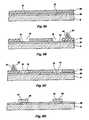
- FIG. 7illustrates one of the preferred embodiments of the present invention wherein a polymer layer is deposited on the active surface of a substrate (FIG. 7A), apertures are formed therein (FIG. 7B) and filled with a solder and flux mixture (FIG. 7C), and the deposited mixture is reflowed to form solder bumps (FIG. 7D);
- FIG. 8is a perspective view of an stereolithographic apparatus exemplifying one of the preferred embodiments of the present invention to deposit a polymer layer on the active surface of a substrate and to form apertures thereon;
- FIG. 9illustrates another one of the preferred embodiments of the present invention, wherein a removable polymer layer is deposited on the active surface of a substrate (FIG. 9A), apertures are formed therein (FIG. 9B) and filled with a polymer conductive paste (FIG. 9C), and the polymer layer is removed if desired before an electronic component is cured effecting the desired mechanical and electrical contact with substrate; and
- FIG. 10illustrates a block diagram of a computer system, wherein electronic components are connected to printed circuit boards or the like using the methods and procedures of the present invention.
- the present inventionrelates to polymer layers deposited on the surface of a substrate to act as either a temporary polymer stencil in the application of solder paste that is later removed after reflow of the solder paste or a permanent polymer stencil for the application of solder paste that is not removed after reflow and remain on the substrate surface and acts as an underfill or barrier layer.
- FIG. 7illustrates a polymer stencil/underfill assembly 32 manufactured according to the method of the present invention.
- a substrate 8is provided with contact pads 10 together with an isolation layer 36 disposed on top of the active surface 94 of the substrate 8 , wherein the isolation layer 36 surrounds the contact pads 10 so as to expose only the top surface 96 thereof.
- the term “active surface”is used herein to denote the actual surface as well as vertical projections thereof.
- Two contact pads 10are illustrated in FIG. 7, but as known to one of ordinary skill in the art, the invention disclosed herein is not limited by the number of contact pads in the substrate surface; therefore, substrate 8 may have only one or a plurality of contact pads 10 disposed thereon.
- Polymer layer 38is then disposed on top of the surface 98 of the isolation layer 36 covering also the top surface 96 of the contact pads 10 .
- Polymer layer 38can be a single layer of material or it can be composed of a plurality of sublayers, each superimposed, contiguous with, and mutually adhered to the each other, depending on the manufacturing method used to deposit the layer as further disclosed herein below.
- apertures 18are developed on the polymer layer 38 so as to expose the contact pads 10 .
- apertures 18could have at least the same or larger cross-sectional dimensions 100 and the same or a different cross-sectional shape as that of the contact pads 10 as illustrated in FIG. 7B.
- a mixture of solder and flux 41is applied using solder applicator 22 so as to fill apertures 18 to a level that is even with the top surface 102 of the polymer layer 38 (FIG. 7C). As indicated in FIG.
- solder bumps 28are then formed by raising the temperature of the polymer/underfill assembly sufficiently to cause the mixture of solder and flux to reflow. Subsequent connection of the stencil/underfill assembly to an electronic circuit can be effected by positioning it relative to the circuit such that each of its solder bumps contacts corresponding contact pads thereon and applying sufficient heating to cause the solder bumps to melt and form a permanent mechanical and electrical contact between the assembly and the electronic circuit.
- another embodiment of the present inventionuses the polymer layer 36 only as a stencil for the application of the mixture of solder and flux and formation of the solder bumps after reflow, thus said polymer layer maybe removed before effecting the connection of the polymer/stencil assembly to an electronic circuit just described.
- Polymer layer 38may be deposited using a variety of techniques available in the art, including photolithographic processes, deposition of a mixture of a solvent and polymer material and subsequent evaporation of the solvent, spraying a sheet of polymer material using film coaters, meniscus coating, spin coating, stencil or screen printing, needle deposition, or separately curing a layer of polymer and later attaching this layer on the substrate surface as a preform. Further, attaching the preform layer to the active surface 94 may be accomplished, for example, by use of an adhesive layer disposed on the surface of the preform to be attached or by use of heating after disposing the preform onto the active surface. Also, formation of the apertures in the preform may be accomplished by any of the methods disclosed herein before or after the preform is attached to the substrate.
- Photosensitive materialsmay be of the positive or negative type.
- material protected by itis removed by wet, or chemical etching, or by dry or sputter etching.
- a negative-type photoresitmaterial not protected by the photoresist is removed by the same techniques.
- stereolithographyalso known as “layered manufacturing”
- stereolithographyalso known as “layered manufacturing”
- Another preferred embodiment of the instant inventionis to use stereolithography to deposit the polymer layer 38 and to form apertures therein.
- stereolithographyas conventionally practiced, involves utilizing a computer to generate a three-dimensional (3-D) mathematical simulation or model of an object to be fabricated, such generation usually effected with 3-D computer-aided design (CAD) software.
- CADcomputer-aided design
- the model or simulationis mathematically separated or “sliced” into a large number of relatively thin, parallel, usually vertically superimposed layers, each layer having defined boundaries and other features associated with the model (and thus the actual object to be fabricated) at the level of that layer within the exterior boundaries of the object.
- a complete assembly or stack of all of the layersdefines the entire object and surface resolution of the object is, in part, dependent upon the thickness of the layers.
- the mathematical simulation or modelis then employed to generate an actual object by building the object, layer by superimposed layer.
- stereolithographic techniquesusually involve disposition of a layer of unconsolidated or unfixed material corresponding to each layer within the object boundaries.
- the layer of materialis selectively consolidated or fixated to at least a semisolid state in those areas of a given layer corresponding to portions of the object, the consolidated or fixed material also at that time being substantially concurrently bonded to a lower layer.
- the unconsolidated material employed to build an objectmay be supplied in particulate or liquid form and the material itself may be consolidated, fixed or cured, or a separate binder material may be employed to bond material particles to one another and to those of a previously formed layer.
- a separate binder materialmay be employed to bond material particles to one another and to those of a previously formed layer.
- thin sheets of materialmay be superimposed to build an object, each sheet being fixed to a next lower sheet and unwanted portions of each sheet removed, a stack of such sheets defining the completed object.
- particulate materialsare employed, resolution of object surfaces is highly dependent upon particle size.
- resolutionis highly dependent upon the minimum surface area of the liquid which can be fixed (cured) and the minimum thickness of a layer which can be generated, given the viscosity of the liquid and other parameters, such as transparency to radiation or particle bombardment (see below) used to effect at least a partial cure of the liquid to a structurally stable state.
- resolution and accuracy of object reproduction from the CAD fileis also dependent upon the ability of the apparatus used to fix the material to precisely track the mathematical instructions indicating solid areas and boundaries for each layer of material.
- fixation approachesincluding particle bombardment (electron beams), disposing a binder or other fixative (such as by ink-jet printing techniques), or irradiation using heat or specific wavelength ranges from lasers or other radiation sources.
- particle bombardmentelectron beams
- disposing a binder or other fixativesuch as by ink-jet printing techniques
- irradiation using heat or specific wavelength ranges from lasers or other radiation sourcesinclude particle bombardment (electron beams), disposing a binder or other fixative (such as by ink-jet printing techniques), or irradiation using heat or specific wavelength ranges from lasers or other radiation sources.
- stereolithographyhas been employed to develop and refine object designs in relatively inexpensive materials and has also been used to fabricate small quantities of objects where the cost of conventional fabrication techniques is prohibitive for the same, such as in the case of plastic objects conventionally formed by injection molding.
- Stereolithographyis also employed in the custom fabrication of products generally built in small quantities or where a product design is rendered only once.
- stereolithographyprovides a capability to fabricate products, such as those including closed interior chambers or convoluted passageways, which cannot be fabricated satisfactorily using conventional manufacturing techniques.
- stereolithographyis another method used in the present invention for the deposition of the polymer layer 38 .
- FIG. 8schematically depicts various components and operation of an exemplary stereolithography apparatus 44 to facilitate the reader's understanding of the technology employed in implementation of one of the preferred methods to deposit the polymer layer 38 in the present invention, although those of ordinary skill in the art will understand and appreciate that apparatus of other designs and manufacture may be employed in practicing such methods.
- the preferred stereolithography apparatus for implementation of the present invention, as well as operation of such apparatus,are described in great detail in United States Patents assigned to 3D Systems, Inc. of Valencia, Calif., such as patents including, without limitation, U.S. Pat. Nos.
- Improvements in the conventional stereolithographic apparatusrelate to a so-called “machine vision” system in combination with suitable programming of the computer controlling the stereolithographic process. This improvement eliminates the need for accurate positioning or mechanical alignment of workpieces to which material is stereolithographically applied.
- alignment of the laser beam or other fixing agentmay be item specific (i.e., substrate specific) so that a large number of distinct semiconductor devices may each be accurately coated with a polymer layer 38 to the same or differing specifications with regard to numbers of sub-layers and layer thickness 98 (FIG. 7).
- a 3-D CAD drawing of an object such as a polymer layer 38 to be fabricated in the form of a data fileis placed in the memory of a computer 46 controlling the operation of apparatus 44 , if computer 46 is not a CAD computer in which the original object design is effected.
- an object designmay be effected in a first computer in an engineering or research facility and the data files transferred via wide or local area network, tape, disc, CD-ROM or otherwise as known in the art to computer 46 of apparatus 44 to fabricate the polymer layer 38 or another object comprising one or more applied sub-layers.
- Each sub-layeris formed or consolidated by a pass of the laser beam 62 into a layer of photo-curable material or photopolymer, resulting in a partial cure of the deposited material.
- Each sub-layermay also be additionally cured by further exposing it to a secondary curing for further solidification of the sub-layer material, including curing by increasing the assembly's temperature. Such additional curing step may be either partial or full before another sub-layer of material is subsequently deposited until the desired thickness of the final polymer layer is obtained. It should also be understood by one of ordinary skill in the art that in the stereolithographic process of depositing polymer layer 38 apertures may be formed therein by purposely not curing and later removing some of the material in the unconsolidated state from at least the contact pad areas.
- the dataare preferably formatted in an STL type computer file, STL being a standardized format employed by a majority of manufacturers of stereolithography equipment. Fortunately, the format has been adopted for use in many solid-modeling CAD programs, so often translation from another internal geometric database format is unnecessary. In the particular case where the apparatus 44 is to be used for applying only a single polymer layer 38 of uniform thickness, the program may be somewhat simplified.
- Apparatus 44also includes a reservoir 48 , which may comprise a removable reservoir interchangeable with others containing different materials, of liquid material 50 to be employed in applying the intended polymer layer 38 of protective material to the substrate 8 .
- the liquid material 50is a photo-curable polymer (hereinafter “photopolymer”) responsive to light in the UV wavelength range.
- the surface level 52 of the liquid material 50is automatically maintained at a precise, constant magnitude by devices known in the art responsive to output of sensors within apparatus 44 and preferably under control of computer 46 .
- a support platform or elevator 54precisely vertically movable in fine, repeatable increments in directions 68 responsive to control of computer 46 , is located for movement downward into and upward out of liquid material 50 in reservoir 48 .
- a UV wavelength range laser plus associated optics and galvanometersfor controlling the scan of laser beam 60 in the X-Y plane across platform 54 has associated therewith mirror 58 to reflect beam 60 downwardly as beam 62 toward surface 64 of platform 54 , or more particularly toward surface 94 of a substrate 8 positioned on surface 64 .
- Beam 62is traversed in a selected pattern in the X-Y plane, that is to say in a plane parallel to surface 64 , by initiation of the galvanometers under control of computer 46 to at least partially cure, by impingement thereon, selected portions of liquid material 50 disposed over surface 94 to at least a semi-solid state.
- the use of mirror 58lengthens the path of the laser beam 60 , effectively doubling same, and provides a more vertical beam 62 than would be possible if the laser 56 itself were mounted directly above platform surface 64 , thus enhancing resolution.
- Polymer layers 38can be made of thermoplastic or thermoset materials.
- thermoplastic materials to be used in the present inventionincludes, for example, phenoxy resins, acrylic resins, methacrylic resins, polycarbonate resins, polyamid resins, polybutene resins, polyester resins, polyolefin resins and mixtures thereof. If the material will remain as an underfill, its composition can be changed so as to control its coefficient of thermal expansion, thus minimizing cyclic strain on the solder connections due to heating and cooling encountered during normal operation of electronic devices.
- thermoset epoxiesare used as underfill material
- fillerssuch as silica particles
- the reflow temperature profileis more closely monitored so as to minimize adverse effects to the polymer layer 38 that will remain as an underfill or barrier on the substrate 8 .
- the polymer layer 38is used as temporary polymer stencil, the effect of reflow temperature may be neglected and its removal after reflow may be accomplished, as for example, by melting the temporary polymer stencil during or after the reflow operation.
- apertures 18 on the polymer layer 38may be made separately from the substrate as a preform with aperture already formed therein and later laminated to the substrate surface by use of an adhesive layer applied to the appropriate surface of the polymer layer 38 . Otherwise, the preform layer can also be applied to the substrate surface and attached thereto by the application of heating either separately or concurrently with the solder paste reflow process.
- One of the preferred methods to develop apertures 18 on the polymer layer 38 in the present inventionis to use stereolithography.
- One of the advantages of depositing polymer layer 38 using stereolithographyis the fact that the geometry of apertures 18 can be varied so as to minimize disturbing the solder paste deposited on top of the contact pads 10 in case the polymer layer 38 is used as a polymer stencil and thus removed after applying the solder paste and reflow.
- solder pasteis a high viscosity material made as a mixture of fine solder particles, the size of the particle being associated with the type of solder, such as types 1 through 5, and flux.
- the diameter of solder particlesare chosen as the largest possible that can be used in a given application. It should be clear to one of ordinary skill in the art that use of a solder paste instead of the sequential application of separate solder material and flux, will significantly minimize the overall time to complete the packaging process and thus increase productivity. Methods to be used in applying the solder paste are those well know in the art, including a squeegee or solder applicator 22 , stencil or screen printing, and pin transfer.
- FIG. 9illustrates another preferred embodiment of the present invention, wherein a polymer stencil/underfill assembly 32 is manufactured according to the method of the present invention as described hereinabove.
- a substrate 8is provided with contact pads 10 disposed on the active surface 94 thereof together with an isolation layer 36 deposited on top of the active surface 94 and surrounding the contact pads 10 so as to expose only the top surface 96 of the contact pads 10 .
- a polymer layer 38is then disposed on top of the surface 98 of the isolation layer 36 covering also the top surface 96 of the contact pads 10 .
- apertures 18are developed on the polymer layer 38 so as to expose the contact pads 10 .
- a polymer conductive paste 40is applied using the same methods and techniques previously described (FIG. 9C).
- polymer bumps 40can be exposed by simply removing the polymer layer 38 before connecting the assembly to other electronic components and curing the polymer bumps after the resulting assembly is connected to an electronic circuit in order to effect a permanent mechanical and electrical contact.
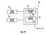
- FIG. 10where a schematic is illustrated of an electronic system 84 , such as a personal computer, including input device 90 (such as a keyboard and mouse) and an output device 92 (such as a display or printer interface) coupled or otherwise in electrical communication with a processor device 86 .
- Processor device 86is also coupled or otherwise in operable electrical communication such as through traces of a mother board with one or more memory modules 88 incorporating one or a plurality of electronic packages manufactured according to the present invention such as 110 , 110 ′, 110 ′′ or variations thereof.
- the memory module 88may include a memory board 112 having an electrical circuit formed therein, such as a PCB.
- processor device 86may be directly embodied in a module with several electronic packages that incorporate the teachings hereof and further include, without limitation, a microprocessor, a first level cache memory, or a memory management processor. Variations of the electronic system 84 shown in FIG. 10 should be understood by persons of ordinary skill in the art to include not only systems to implement the embodiments of the present invention disclosed herein but others as well.
Landscapes
- Physics & Mathematics (AREA)
- Condensed Matter Physics & Semiconductors (AREA)
- General Physics & Mathematics (AREA)
- Engineering & Computer Science (AREA)
- Computer Hardware Design (AREA)
- Microelectronics & Electronic Packaging (AREA)
- Power Engineering (AREA)
- Wire Bonding (AREA)
- Electric Connection Of Electric Components To Printed Circuits (AREA)
Abstract
Description
- 1. Field of the Invention[0001]
- The present invention relates generally to electronic packaging in the semiconductor industry. More specifically, the present invention relates to electronic components using a permanent or temporary barrier or underfill layer of a polymer material containing apertures that also acts as a stencil in the application of solder and flux mixtures or polymer conductive pastes to effect mechanical and electrical connections of the substrates to electronic circuits.[0002]
- 2. State of the Art[0003]
- Electronic devices—a combination of a plurality of electronic components, such as resistors, capacitors, inductors, transistors, and the like, mechanically and electrically mounted to contact pads interconnected by conductive paths in a substrate or printed circuit board (PCB)—are essential gadgets of modem life found in equipments or technologies ranging from every day items such televisions, microwaves, and simple digital clocks to all sorts of sophisticated medical equipments, computers, airplanes, and satellites. As these different technologies become more and more sophisticated and advanced, the manufacturers of electronic devices or integrated circuits are faced with the conflicting requirement of packing significantly higher numbers of electronic components on substrates that continue to shrink in size because of the ever increasing desire of component and equipment miniaturization. Therefore, as the size of semiconductor devices decreases with each generation, a greater precision is required in placing and connecting the different electronic components to the substrates.[0004]
- Initially electronic components were mounted to printed circuit boards by feeding component leads through pre-drilled holes and soldering the leads to the contact pads on the circuit board. Such a mounting approach made it simple to remove and repair defective components by melting the previously deposited solder, removing the inoperative element, and soldering a new one in its place. As the size of integrated circuits decreased and the number of components in a board increased, surface mounting technologies were developed to allow the electronic elements to be mounted directly to the surface of the printed circuit board, thus reducing the size of contact pads and their proximity in the board. FIG. 1 of the prior art illustrates an[0005]
electronic circuit assembly 2 wherein an electronic component4 is surface-mounted to the PCB orsubstrate 8. Herein after, like elements are identified by like numbers to facilitate the description and disclosure of the invention. First, thecontact pads 10 disposed on the PCB surface, corresponding to the same pattern of connector leads orsurface contacts 6 in the electronic component, is supplied with a uniform amount of solder. Secondly, once the electronic component is placed on the appropriate contact pads on top of the PCB, the solder paste is melted momentarily and subsequently allowed to cool, thus forming the desired mechanical and electrical connection between the connector leads and contact pads. Other forms of surface mounting electronic components to high-density semiconductor packages are also available, including ball grid array (BGA), chip-on-board, tape automated bonding, or flip-chip methods to mention a few. - Until recently, the use of metal masks or stencils was one of the preferred methods to apply solder paste onto PCB surfaces for connecting the contact pads of surface-mounted components. FIG. 2 of the prior art illustrates generally a PCB/[0006]
stencil assembly 14 for this purpose.Stencil 16, with a plurality ofapertures 18 formed in predetermined locations corresponding to the pattern of thecontact pads 10 on the printedcircuit board 8, is placed near or on the PCB surface, aligned over the contact pads to which the solder paste is to be applied, and removed after the solder paste is deposited. A sectional view of this solder deposition process taken along line A-A of FIG. 2 for a single aperture is illustrated in FIG. 3 of the prior art. In the solderbump manufacturing apparatus 20 of FIG. 3A thestencil 16 is placed on the surface of the PCB orsubstrate 8, itsaperture 18 aligned with thecontact pad 10, andsolder paste 24 is deposited on top surface of thestencil 16, and, by use of asolder applicator 22, forced into eachaperture 18 as shown in FIG. 3B. Subsequently, as shown FIG. 3C, the stencil is removed, leaving on each contact pad10 asolder bump 28. - Current metal stencil fabrication processes include chemical etching, electropolishing, and laser cutting. In chemical etching the desired aperture pattern on a brass or stainless steel sheet is created by selectively removing material by a chemical process. Because of the nature of the process (i) uncertainty in the size and position of the solder pads is common due to misregistration errors, (ii) only limited stencil aspect ratios (thickness to diameter ratio) are possible, and (iii) accurate etching is nearly impossible when fine-pitched pads are mixed with wide pads since etching speed is dependent on pad width. Electropolishing is similar to chemical etching with the exception of an additional electrochemical-etching step that attempts to smooth the surface of aperture walls; therefore, a typical electropolished stencil still has all of the drawbacks associated with an etched stencil, although paste release is enhanced to a certain degree because of the relatively smoother aperture walls. Electroformed stencils are formed by plating a suitable desired metal on a substrate having the desired aperture shapes thereon. Electroformed stencils have smooth aperture shapes and smooth surfaces. Laser cut stencils are made by removing material from the metal stencil with a laser beam. Laser cut metal stencils are significantly more expensive and the aperture sidewalls are relatively rough, with uncontrolled build up as molten metal re-deposits upon cooling. This limits the usefulness of the finer geometry in a laser cut stencil as solder pastes will not release well.[0007]
- One of the limitations on how much an electronic circuit can shrink in size is associated with the soldering process just summarized. This is so because it is important that an equal amount of solder paste be placed on top of each contact pad so as to assure that the component will not be mounted crookedly, each and every connection will be made, and contact pads in proximity of one another will not be inadvertently shorted or bridged because of excess solder paste. These limitations are exacerbated when one considers, for example, that currently the tolerances in PCB using flip-chip technology are critical and spacing between chips on the circuit board are typically in the range of 0.2 to 3.0 mils.[0008]
- Besides the aforementioned problems associated with the use of metal stencils for the application of solder for surface mounting electronic components, i.e., variation on the amount of solder deposited in each contact pad, including bridging caused by solder excess, the technique is plagued with several other problems. First, the ratio of the height to the occupied area of the resulting solder bump is limited and variation on solder amount from bump to bump is affected by the release of the solder paste from the apertures in the stencil. As the size of the aperture dimensions decreases, the base cross-sectional area of the aperture decreases; however, it is still desirable to keep the material being applied through the aperture in the stencil at the same vertical size or height, or greater. Further, such material applied through the apertures of the stencil must be placed very close together. Unfortunately, current technology requires that as the vertical size or height increases, the base cross-sectional area of an aperture of the stencil must increase as well for release of the material applied through the apertures. This limits the pitch or spacing of the apertures in the stencil. Further, because it is difficult to perfectly seal the lower edge of the aperture against the top surface of the contact pad, solder material leaks, depositing paste on unwanted locations in the substrate. FIG. 4 of the prior art illustrates a metal stencil design disclosed on U.S. Pat. No. 5,460,316, issued Oct. 24, 1995, that attempts to solve these two problems by providing apertures with tapered walls, so that the aperture is wider or has a larger cross-sectional base area on the substrate side to provide an improved release of the material from the aperture, and with raised[0009]
lower edges 26 in order to minimize the solder leakage problem. Unfortunately, since the taper of the aperture in the stencil is small with the aperture wall being substantially vertical, the material applied through the aperture can be pulled away from the substrate when the stencil is removed, thus resulting in the same problem that the modified metal stencil design attempted to solve. - FIG. 5 of the prior art (U.S. Pat. No. 6,089,151, issued Jul. 18, 2000) illustrates yet another improvement to metal stencil designs in order to minimize the problem of insufficient deposition and/or removal of solder material deposited on the contact pad after the metal stencil is removed. The stencil consists primarily of an[0010]
aperture 18 havingwalls - Another known problem of these metal stencils is that their quality deteriorate with time because of damage, particularly the edges and junctions between the upper surface of the stencil and the side walls of the apertures, caused by mechanical pressure applied by solder applicators as individual stencils are normally used several times over in high-volume manufacturing processes. In order to ameliorate this wear problem, as illustrate in FIG. 6 of the prior art, wear-[0011]
resistant metal stencils 16 have been proposed with aprotective diamond coating 30 covering the exposed edges of the metal stencil (U.S. Pat. No. 5,460,316, issued Oct. 25, 1995). Although the wear problem is reduced, the price of the stencil is certainly increased because of the need for the additional protective coating made of an expensive material. - Another typical problem of surface mounting is the fact that the materials used to make the electronic components, the solder, and the circuit board have different coefficients of thermal expansion. During operation, increases in temperature will cause the circuit board to expand more than the component or chip, while cooling produces the opposite result. The net effect is that the joints or solder contacts are strained, resulting in early fracture failures. A solution to this problem is the use of an underfill or barrier material between the substrate and the electronic component. An underfill can be thought of as an adhesive that mechanically couples the low-expansion chip to the high-expansion substrate, including the solder joints. As chip assembly becomes better understood and reliable packaging methods become available in the market place, mounting methods that increase productivity are highly desirable. Together with application of solder and flux materials, underfill processes are clearly the bottlenecks to increased productivity in the manufacturing of these electronic devices.[0012]
- Recently, as an attempt to ameliorate some of the problems with fabrication and use of metal stencils, U.S. Pat. No. 6,253,675, issued Jul. 3, 2001, discloses a polymer solder paste stencil printing apparatus and method for applying a controlled pattern and volume of solder paste onto a single area array component site on a populated PCB for rework or repair purposes. The stencil is a disposable, adhesive-backed, flexible membrane with several apertures and including a periphery area that can be folded or shaped to fit into the available space to be stenciled. In use, a protective-adhesive-backed layer is removed, the stencil is locally attached to the surface of the PCB to be repaired, solder is applied, and the removable-adhesive-backed stencil is peeled from the PCB and disposed. As previously discussed, the need to peel off the adhesive-backed stencil will certainly lead to variations on the amount of deposited solder material in the different apertures, leading to problems of uneven mounting and/or possibly shorting or bridging because of excess solder paste that may still leak through.[0013]
- The use of a permanently attached polymer stencil is disclosed in U.S. Pat. No. 6,228,678, issued on May 8, 2001, wherein a polymer material is applied to the surface of a semiconductor wafer as an underfill and processed to form apertures, exposing contact pads in the semiconductor wafer. The apertures are filled with a solder material, extending a distance above the underfill polymer material, and, separately from the solder past application process, a flux material is either applied separately to the face of the entire semiconductor wafer or alternatively only to the portion of the bumps that extends above the underfill material. Problems with this technique include (i) the reduction in chip productivity associated with the separate application steps of solder and flux; (ii) the wasteful use of excess solder material extending a distance beyond the underfill material because solder is generally expensive and unfriendly to the environment when excess amounts have to be discarded; and (iii) difficulties in handling the substrate with excess solder and flux on it because of the sticky nature of these materials.[0014]
- Accordingly, surface mounting electronic components or chips using permanent and/or temporary polymer underfills or barriers attached to the face of the substrate that also act as stencils in the application of solder/flux pastes or polymer stencils that can later be removed after reflow would be advantageous to overcome the problems inherent in the prior art solutions to the problems of using metal and polymer stencils summarized hereinabove.[0015]
- The present invention is directed to semiconductor devices, and methods of manufacturing the same, that use permanent or temporary polymer layers to cover the active surfaces thereof. The polymer layers have apertures that are made either before or after applying the polymer layers to the semiconductor devices, exposing the contact pads on the active surfaces of the semiconductor devices. Several preferred methods to fabricate the polymer layers can be used, including, for example, photolithographic and stereolithographic processes. When applied temporarily, the polymer layer will act as a polymer stencil for the application of solder/flux mixtures or polymer conductive pastes to the exposed contact pads before reflow to form contact bumps for connecting electronic components to the semiconductor devices. If applied permanently, besides serving the stencil purpose for the application of solder/flux mixtures or polymer conductive pastes, the polymer layer will also act as a barrier material, minimizing the problems associated with different coefficients of thermal expansion between the semiconductor devices, solder bumps, and electronic components connected thereto.[0016]
- In the drawings, which illustrate what is currently considered to be the best mode for carrying out the invention:[0017]
- FIG. 1 of the prior art is a schematic of an electronic circuit assembly illustrating a electronic component surface-mounted to a PCB or substrate;[0018]
- FIG. 2 of the prior art is a schematic of a PCB/stencil assembly illustrating the use of a metal stencil with apertures for depositing solder paste to contact pads in a PCB or substrate for the purpose of surface-mounting an electronic component thereto;[0019]
- FIG. 3 of the prior art is a sectional view along line A-A of FIG. 2 illustrating the formation of a solder bump on the contact pad of a substrate, including the steps of disposing a metal stencil on top of the substrate (FIG. 3A), depositing and forcing solder paste in the aperture of the stencil (FIG. 3B), and subsequent removal of the metal stencil before reflow (FIG. 3C);[0020]
- FIG. 4 of the prior art illustrates a metal stencil with tapered walls and raised lower edges to minimize solder leakage and release problems;[0021]
- FIG. 5 of the prior art illustrates another metal stencil with apertures having two different diameters to minimize the problem of insufficient deposition and/or removal of solder material deposited on the contact pad after the metal stencil is removed;[0022]
- FIG. 6 of the prior art illustrates a wear-resistant metal stencil with a protective diamond coating covering the exposed edges thereof;[0023]
- FIG. 7 illustrates one of the preferred embodiments of the present invention wherein a polymer layer is deposited on the active surface of a substrate (FIG. 7A), apertures are formed therein (FIG. 7B) and filled with a solder and flux mixture (FIG. 7C), and the deposited mixture is reflowed to form solder bumps (FIG. 7D);[0024]
- FIG. 8 is a perspective view of an stereolithographic apparatus exemplifying one of the preferred embodiments of the present invention to deposit a polymer layer on the active surface of a substrate and to form apertures thereon;[0025]
- FIG. 9 illustrates another one of the preferred embodiments of the present invention, wherein a removable polymer layer is deposited on the active surface of a substrate (FIG. 9A), apertures are formed therein (FIG. 9B) and filled with a polymer conductive paste (FIG. 9C), and the polymer layer is removed if desired before an electronic component is cured effecting the desired mechanical and electrical contact with substrate; and[0026]
- FIG. 10 illustrates a block diagram of a computer system, wherein electronic components are connected to printed circuit boards or the like using the methods and procedures of the present invention.[0027]
- The present invention relates to polymer layers deposited on the surface of a substrate to act as either a temporary polymer stencil in the application of solder paste that is later removed after reflow of the solder paste or a permanent polymer stencil for the application of solder paste that is not removed after reflow and remain on the substrate surface and acts as an underfill or barrier layer.[0028]
- FIG. 7 illustrates a polymer stencil/underfill assembly[0029]32 manufactured according to the method of the present invention. Initially, as shown in FIG. 7A, a
substrate 8 is provided withcontact pads 10 together with anisolation layer 36 disposed on top of theactive surface 94 of thesubstrate 8, wherein theisolation layer 36 surrounds thecontact pads 10 so as to expose only thetop surface 96 thereof. The term “active surface” is used herein to denote the actual surface as well as vertical projections thereof. Twocontact pads 10 are illustrated in FIG. 7, but as known to one of ordinary skill in the art, the invention disclosed herein is not limited by the number of contact pads in the substrate surface; therefore,substrate 8 may have only one or a plurality ofcontact pads 10 disposed thereon. Apolymer layer 38 is then disposed on top of thesurface 98 of theisolation layer 36 covering also thetop surface 96 of thecontact pads 10.Polymer layer 38 can be a single layer of material or it can be composed of a plurality of sublayers, each superimposed, contiguous with, and mutually adhered to the each other, depending on the manufacturing method used to deposit the layer as further disclosed herein below. - Subsequently, as illustrated in FIG. 7B,[0030]
apertures 18 are developed on thepolymer layer 38 so as to expose thecontact pads 10. Depending on the type of solder paste to be used,apertures 18 could have at least the same or largercross-sectional dimensions 100 and the same or a different cross-sectional shape as that of thecontact pads 10 as illustrated in FIG. 7B. Onceapertures 18 are formed on thepolymer layer 36, a mixture of solder andflux 41 is applied usingsolder applicator 22 so as to fillapertures 18 to a level that is even with thetop surface 102 of the polymer layer38 (FIG. 7C). As indicated in FIG. 7D, solder bumps28 are then formed by raising the temperature of the polymer/underfill assembly sufficiently to cause the mixture of solder and flux to reflow. Subsequent connection of the stencil/underfill assembly to an electronic circuit can be effected by positioning it relative to the circuit such that each of its solder bumps contacts corresponding contact pads thereon and applying sufficient heating to cause the solder bumps to melt and form a permanent mechanical and electrical contact between the assembly and the electronic circuit. Further, another embodiment of the present invention uses thepolymer layer 36 only as a stencil for the application of the mixture of solder and flux and formation of the solder bumps after reflow, thus said polymer layer maybe removed before effecting the connection of the polymer/stencil assembly to an electronic circuit just described. - [0031]
Polymer layer 38 may be deposited using a variety of techniques available in the art, including photolithographic processes, deposition of a mixture of a solvent and polymer material and subsequent evaporation of the solvent, spraying a sheet of polymer material using film coaters, meniscus coating, spin coating, stencil or screen printing, needle deposition, or separately curing a layer of polymer and later attaching this layer on the substrate surface as a preform. Further, attaching the preform layer to theactive surface 94 may be accomplished, for example, by use of an adhesive layer disposed on the surface of the preform to be attached or by use of heating after disposing the preform onto the active surface. Also, formation of the apertures in the preform may be accomplished by any of the methods disclosed herein before or after the preform is attached to the substrate. - In photolithographic processes the substrate is coated with a photoresit, i.e., a photosensitive material, which is later exposed to ultraviolet light by use of a pattern in a glass plate in order to mark material to be removed or left on the substrate surface. Photosensitive materials may be of the positive or negative type. In a positive type photoresit, material protected by it is removed by wet, or chemical etching, or by dry or sputter etching. Contrariwise, when using a negative-type photoresit, material not protected by the photoresist is removed by the same techniques.[0032]
- In the past decade, a manufacturing technique termed “stereolithography”, also known as “layered manufacturing”, has evolved to a degree where it is employed in many industries. Another preferred embodiment of the instant invention is to use stereolithography to deposit the[0033]
polymer layer 38 and to form apertures therein. Essentially, stereolithography, as conventionally practiced, involves utilizing a computer to generate a three-dimensional (3-D) mathematical simulation or model of an object to be fabricated, such generation usually effected with 3-D computer-aided design (CAD) software. The model or simulation is mathematically separated or “sliced” into a large number of relatively thin, parallel, usually vertically superimposed layers, each layer having defined boundaries and other features associated with the model (and thus the actual object to be fabricated) at the level of that layer within the exterior boundaries of the object. A complete assembly or stack of all of the layers defines the entire object and surface resolution of the object is, in part, dependent upon the thickness of the layers. The mathematical simulation or model is then employed to generate an actual object by building the object, layer by superimposed layer. - A wide variety of approaches to stereolithography by different companies has resulted in techniques for fabrication of objects from both metallic and nonmetallic materials. Regardless of the material employed to fabricate an object, stereolithographic techniques usually involve disposition of a layer of unconsolidated or unfixed material corresponding to each layer within the object boundaries. The layer of material is selectively consolidated or fixated to at least a semisolid state in those areas of a given layer corresponding to portions of the object, the consolidated or fixed material also at that time being substantially concurrently bonded to a lower layer. The unconsolidated material employed to build an object may be supplied in particulate or liquid form and the material itself may be consolidated, fixed or cured, or a separate binder material may be employed to bond material particles to one another and to those of a previously formed layer. In some instances, thin sheets of material may be superimposed to build an object, each sheet being fixed to a next lower sheet and unwanted portions of each sheet removed, a stack of such sheets defining the completed object. When particulate materials are employed, resolution of object surfaces is highly dependent upon particle size. When a liquid is employed, resolution is highly dependent upon the minimum surface area of the liquid which can be fixed (cured) and the minimum thickness of a layer which can be generated, given the viscosity of the liquid and other parameters, such as transparency to radiation or particle bombardment (see below) used to effect at least a partial cure of the liquid to a structurally stable state. Of course, in either case, resolution and accuracy of object reproduction from the CAD file is also dependent upon the ability of the apparatus used to fix the material to precisely track the mathematical instructions indicating solid areas and boundaries for each layer of material. Toward that end, and depending upon the layer being fixed, various fixation approaches have been employed, including particle bombardment (electron beams), disposing a binder or other fixative (such as by ink-jet printing techniques), or irradiation using heat or specific wavelength ranges from lasers or other radiation sources.[0034]
- An early application of stereolithography was to enable rapid fabrication of molds and prototypes of objects from CAD files. Thus, either male or female forms on which mold material might be disposed might be rapidly generated. Prototypes of objects might be built to verify the accuracy of the CAD file defining the object and to detect any design deficiencies and possible fabrication problems before a design was committed to large-scale production.[0035]
- In more recent years, stereolithography has been employed to develop and refine object designs in relatively inexpensive materials and has also been used to fabricate small quantities of objects where the cost of conventional fabrication techniques is prohibitive for the same, such as in the case of plastic objects conventionally formed by injection molding. Stereolithography is also employed in the custom fabrication of products generally built in small quantities or where a product design is rendered only once. Finally, it has been appreciated in some industries that stereolithography provides a capability to fabricate products, such as those including closed interior chambers or convoluted passageways, which cannot be fabricated satisfactorily using conventional manufacturing techniques. As disclosed hereinabove, stereolithography is another method used in the present invention for the deposition of the[0036]
polymer layer 38. - FIG. 8 schematically depicts various components and operation of an[0037]
exemplary stereolithography apparatus 44 to facilitate the reader's understanding of the technology employed in implementation of one of the preferred methods to deposit thepolymer layer 38 in the present invention, although those of ordinary skill in the art will understand and appreciate that apparatus of other designs and manufacture may be employed in practicing such methods. The preferred stereolithography apparatus for implementation of the present invention, as well as operation of such apparatus, are described in great detail in United States Patents assigned to 3D Systems, Inc. of Valencia, Calif., such as patents including, without limitation, U.S. Pat. Nos. 4,575,330; 4,929,402; 4,996,010; 4,999,143; 5,015,424; 5,058,988; 5,059,021; 5,059,359; 5,071,337; 5,076,974; 5,096,530; 5,104,592; 5,123,734; 5,130,064; 5,133,987; 5,141,680; 5,143,663; 5,164,128; 5,174,931; 5,174,943; 5,182,055; 5,182,056; 5,182,715; 5,184,307; 5,192,469; 5,192,559; 5,209,878; 5,234,636; 5,236,637; 5,238,639; 5,248,456; 5,256,340; 5,258,146; 5,267,013; 5,273,691; 5,321,622; 5,344,298; 5,345,391; 5,358,673; 5,447,822; 5,481,470; 5,495,328; 5,501,824; 5,554,336; 5,556,590; 5,569,349; 5,569,431; 5,571,471; 5,573,722; 5,609,812; 5,609,813; 5,610,824; 5,630,981; 5,637,169; 5,651,934; 5,667,820; 5,672,312; 5,676,904; 5,688,464; 5,693,144; 5,695,707; 5,711,911; 5,776,409; 5,779,967; 5,814,265; 5,850,239; 5,854,748; 5,855,718; 5,855,836; 5,885,511; 5,897,825; 5,902,537; 5,902,538; 5,904,889; 5,943,235; and 5,945,058. The disclosure of each of the foregoing patents is hereby incorporated herein by reference. - Improvements in the conventional stereolithographic apparatus relate to a so-called “machine vision” system in combination with suitable programming of the computer controlling the stereolithographic process. This improvement eliminates the need for accurate positioning or mechanical alignment of workpieces to which material is stereolithographically applied. Referring to FIG. 8, alignment of the laser beam or other fixing agent may be item specific (i.e., substrate specific) so that a large number of distinct semiconductor devices may each be accurately coated with a[0038]
polymer layer 38 to the same or differing specifications with regard to numbers of sub-layers and layer thickness98 (FIG. 7). - With reference to FIGS.[0039]8 and as noted above, a 3-D CAD drawing of an object such as a
polymer layer 38 to be fabricated in the form of a data file is placed in the memory of acomputer 46 controlling the operation ofapparatus 44, ifcomputer 46 is not a CAD computer in which the original object design is effected. In other words, an object design may be effected in a first computer in an engineering or research facility and the data files transferred via wide or local area network, tape, disc, CD-ROM or otherwise as known in the art tocomputer 46 ofapparatus 44 to fabricate thepolymer layer 38 or another object comprising one or more applied sub-layers. Each sub-layer is formed or consolidated by a pass of thelaser beam 62 into a layer of photo-curable material or photopolymer, resulting in a partial cure of the deposited material. Each sub-layer may also be additionally cured by further exposing it to a secondary curing for further solidification of the sub-layer material, including curing by increasing the assembly's temperature. Such additional curing step may be either partial or full before another sub-layer of material is subsequently deposited until the desired thickness of the final polymer layer is obtained. It should also be understood by one of ordinary skill in the art that in the stereolithographic process of depositingpolymer layer 38 apertures may be formed therein by purposely not curing and later removing some of the material in the unconsolidated state from at least the contact pad areas. - The data are preferably formatted in an STL type computer file, STL being a standardized format employed by a majority of manufacturers of stereolithography equipment. Fortunately, the format has been adopted for use in many solid-modeling CAD programs, so often translation from another internal geometric database format is unnecessary. In the particular case where the[0040]
apparatus 44 is to be used for applying only asingle polymer layer 38 of uniform thickness, the program may be somewhat simplified. - [0041]
Apparatus 44 also includes areservoir 48, which may comprise a removable reservoir interchangeable with others containing different materials, ofliquid material 50 to be employed in applying the intendedpolymer layer 38 of protective material to thesubstrate 8. In a currently preferred embodiment, theliquid material 50 is a photo-curable polymer (hereinafter “photopolymer”) responsive to light in the UV wavelength range. Thesurface level 52 of theliquid material 50 is automatically maintained at a precise, constant magnitude by devices known in the art responsive to output of sensors withinapparatus 44 and preferably under control ofcomputer 46. A support platform orelevator 54, precisely vertically movable in fine, repeatable increments indirections 68 responsive to control ofcomputer 46, is located for movement downward into and upward out ofliquid material 50 inreservoir 48. A UV wavelength range laser plus associated optics and galvanometers (collectively identified as56) for controlling the scan oflaser beam 60 in the X-Y plane acrossplatform 54 has associated therewithmirror 58 to reflectbeam 60 downwardly asbeam 62 towardsurface 64 ofplatform 54, or more particularly towardsurface 94 of asubstrate 8 positioned onsurface 64.Beam 62 is traversed in a selected pattern in the X-Y plane, that is to say in a plane parallel to surface64, by initiation of the galvanometers under control ofcomputer 46 to at least partially cure, by impingement thereon, selected portions ofliquid material 50 disposed oversurface 94 to at least a semi-solid state. The use ofmirror 58 lengthens the path of thelaser beam 60, effectively doubling same, and provides a morevertical beam 62 than would be possible if thelaser 56 itself were mounted directly aboveplatform surface 64, thus enhancing resolution. - It should also be understood by one of ordinary skill in the art of the present invention that the exemplary methods described herein to form polymer layers in a single substrate is also applicable and operational for a wafer containing several semiconductor dice followed by singulation of the resulting assembly into individual dice. Further, while the invention is described in terms of a liquid material polymerizable to a semi-solid and/or solid, the process may be varied to use a powdered material, for example. The term “unconsolidated” will be used herein to denote the unpolymerized material, which becomes “altered” or “consolidated” by the laser radiation to at least a semi-solid state.[0042]
- Different polymeric materials can be used to form the[0043]
polymer layer 38, depending on the method used to deposit the layer and whether or not the layer will remain on the substrate surface as an underfill after the reflow procedure. Polymer layers38 can be made of thermoplastic or thermoset materials. Example of thermoplastic materials to be used in the present invention includes, for example, phenoxy resins, acrylic resins, methacrylic resins, polycarbonate resins, polyamid resins, polybutene resins, polyester resins, polyolefin resins and mixtures thereof. If the material will remain as an underfill, its composition can be changed so as to control its coefficient of thermal expansion, thus minimizing cyclic strain on the solder connections due to heating and cooling encountered during normal operation of electronic devices. Normally when thermoset epoxies are used as underfill material, fillers, such as silica particles, are used as additives in order to control the coefficient of thermal expansion of the resulting mixture. Also, if thepolymer layer 38 will not be removed after the reflow operation, the reflow temperature profile is more closely monitored so as to minimize adverse effects to thepolymer layer 38 that will remain as an underfill or barrier on thesubstrate 8. If thepolymer layer 38 is used as temporary polymer stencil, the effect of reflow temperature may be neglected and its removal after reflow may be accomplished, as for example, by melting the temporary polymer stencil during or after the reflow operation. - Several methods exist in the art to make[0044]
apertures 18 on thepolymer layer 38, such as, for example, laser machining, including optical diffraction and photoablation using different types of lasers. Other aperture fabrication processes include chemical etching, electropolishing, laser cutting, and various combinations thereof. Also,polymer layer 38 may be formed separately from the substrate as a preform with aperture already formed therein and later laminated to the substrate surface by use of an adhesive layer applied to the appropriate surface of thepolymer layer 38. Otherwise, the preform layer can also be applied to the substrate surface and attached thereto by the application of heating either separately or concurrently with the solder paste reflow process. One of the preferred methods to developapertures 18 on thepolymer layer 38 in the present invention is to use stereolithography. One of the advantages of depositingpolymer layer 38 using stereolithography is the fact that the geometry ofapertures 18 can be varied so as to minimize disturbing the solder paste deposited on top of thecontact pads 10 in case thepolymer layer 38 is used as a polymer stencil and thus removed after applying the solder paste and reflow. - Typically, solder paste is a high viscosity material made as a mixture of fine solder particles, the size of the particle being associated with the type of solder, such as types 1 through 5, and flux. Typically the diameter of solder particles are chosen as the largest possible that can be used in a given application. It should be clear to one of ordinary skill in the art that use of a solder paste instead of the sequential application of separate solder material and flux, will significantly minimize the overall time to complete the packaging process and thus increase productivity. Methods to be used in applying the solder paste are those well know in the art, including a squeegee or[0045]
solder applicator 22, stencil or screen printing, and pin transfer. - FIG. 9 illustrates another preferred embodiment of the present invention, wherein a polymer stencil/underfill assembly[0046]32 is manufactured according to the method of the present invention as described hereinabove. Initially, as shown in FIG. 9A, a
substrate 8 is provided withcontact pads 10 disposed on theactive surface 94 thereof together with anisolation layer 36 deposited on top of theactive surface 94 and surrounding thecontact pads 10 so as to expose only thetop surface 96 of thecontact pads 10. Apolymer layer 38 is then disposed on top of thesurface 98 of theisolation layer 36 covering also thetop surface 96 of thecontact pads 10. - Subsequently, as illustrated in FIG. 9B,[0047]
apertures 18 are developed on thepolymer layer 38 so as to expose thecontact pads 10. Onceapertures 18 are formed on thepolymer layer 36, a polymerconductive paste 40 is applied using the same methods and techniques previously described (FIG. 9C). As indicated in FIG. 9D, polymer bumps40 can be exposed by simply removing thepolymer layer 38 before connecting the assembly to other electronic components and curing the polymer bumps after the resulting assembly is connected to an electronic circuit in order to effect a permanent mechanical and electrical contact. - Referring now to the drawing of FIG. 10 where a schematic is illustrated of an[0048]
electronic system 84, such as a personal computer, including input device90 (such as a keyboard and mouse) and an output device92 (such as a display or printer interface) coupled or otherwise in electrical communication with aprocessor device 86.Processor device 86 is also coupled or otherwise in operable electrical communication such as through traces of a mother board with one ormore memory modules 88 incorporating one or a plurality of electronic packages manufactured according to the present invention such as110,110′,110″ or variations thereof. Thememory module 88 may include amemory board 112 having an electrical circuit formed therein, such as a PCB. Furthermore,processor device 86 may be directly embodied in a module with several electronic packages that incorporate the teachings hereof and further include, without limitation, a microprocessor, a first level cache memory, or a memory management processor. Variations of theelectronic system 84 shown in FIG. 10 should be understood by persons of ordinary skill in the art to include not only systems to implement the embodiments of the present invention disclosed herein but others as well. - Although a few typical embodiments and details have been explained herein above with the intention of illustrating several best modes of the present invention as applied to applying permanent polymer underfill layers or temporary polymer stencils to the face of electronic substrates, it will be clear to those persons of ordinary skill in the applicable arts that several changes and variations in the methods, apparatuses and systems disclosed herein may be implemented within the scope of the present invention to be used in electronic packaging methods, such as, for example, direct chip attachment, a flip-chip attachment, wafer scale attachment, etc. The scope of the invention is then appropriately determined by the claims appended below, particularly pointing out and distinctly claiming the subject matter that the applicant regards as his invention.[0049]
Claims (71)
Priority Applications (2)
| Application Number | Priority Date | Filing Date | Title |
|---|---|---|---|
| US10/191,424US6998334B2 (en) | 2002-07-08 | 2002-07-08 | Semiconductor devices with permanent polymer stencil and method for manufacturing the same |
| US11/210,606US7589010B2 (en) | 2002-07-08 | 2005-08-23 | Semiconductor devices with permanent polymer stencil and method for manufacturing the same |
Applications Claiming Priority (1)
| Application Number | Priority Date | Filing Date | Title |
|---|---|---|---|
| US10/191,424US6998334B2 (en) | 2002-07-08 | 2002-07-08 | Semiconductor devices with permanent polymer stencil and method for manufacturing the same |
Related Child Applications (1)
| Application Number | Title | Priority Date | Filing Date |
|---|---|---|---|
| US11/210,606ContinuationUS7589010B2 (en) | 2002-07-08 | 2005-08-23 | Semiconductor devices with permanent polymer stencil and method for manufacturing the same |
Publications (2)
| Publication Number | Publication Date |
|---|---|
| US20040005770A1true US20040005770A1 (en) | 2004-01-08 |
| US6998334B2 US6998334B2 (en) | 2006-02-14 |
Family
ID=29999989
Family Applications (2)
| Application Number | Title | Priority Date | Filing Date |
|---|---|---|---|
| US10/191,424Expired - LifetimeUS6998334B2 (en) | 2002-07-08 | 2002-07-08 | Semiconductor devices with permanent polymer stencil and method for manufacturing the same |
| US11/210,606Expired - LifetimeUS7589010B2 (en) | 2002-07-08 | 2005-08-23 | Semiconductor devices with permanent polymer stencil and method for manufacturing the same |
Family Applications After (1)
| Application Number | Title | Priority Date | Filing Date |
|---|---|---|---|
| US11/210,606Expired - LifetimeUS7589010B2 (en) | 2002-07-08 | 2005-08-23 | Semiconductor devices with permanent polymer stencil and method for manufacturing the same |
Country Status (1)
| Country | Link |
|---|---|
| US (2) | US6998334B2 (en) |
Cited By (16)
| Publication number | Priority date | Publication date | Assignee | Title |
|---|---|---|---|---|
| US20040014255A1 (en)* | 2002-07-22 | 2004-01-22 | Grigg Ford B. | Thick solder mask for confining encapsulant material over selected locations of a substrate, assemblies including the solder mask, and methods |
| US20050003640A1 (en)* | 2003-05-30 | 2005-01-06 | Seiko Epson Corporation | Method for fabricating thin film pattern, device and fabricating method therefor, method for fabricating liquid crystal display, liquid crystal display, method for fabricating active matrix substrate, electro-optical apparatus, and electrical apparatus |
| US20050139643A1 (en)* | 2003-12-30 | 2005-06-30 | Texas Instruments Incorporated | Method and system for applying solder |
| US20050253261A1 (en)* | 2003-02-20 | 2005-11-17 | Farnworth Warren M | Electronic device package structures |
| US20080042247A1 (en)* | 2005-12-07 | 2008-02-21 | Wood Alan G | Stacked Semiconductor Components With Through Wire Interconnects (TWI) |
| US7368391B2 (en) | 2002-04-10 | 2008-05-06 | Micron Technology, Inc. | Methods for designing carrier substrates with raised terminals |
| US20080229573A1 (en)* | 2005-05-19 | 2008-09-25 | Wood Alan G | System For Fabricating Semiconductor Components With Conductive Interconnects |
| US20090212429A1 (en)* | 2008-02-22 | 2009-08-27 | Stats Chippac, Ltd. | Semiconductor Device and Method of Supporting a Wafer During Backgrinding and Reflow of Solder Bumps |
| US20100140753A1 (en)* | 2005-04-08 | 2010-06-10 | Hembree David R | Stacked Semiconductor Component Having Through Wire Interconnect And Method Of Fabrication |
| US20110229822A1 (en)* | 2008-11-25 | 2011-09-22 | Stapleton Russell A | Methods for protecting a die surface with photocurable materials |
| US8120167B2 (en) | 2006-04-24 | 2012-02-21 | Micron Technology, Inc. | System with semiconductor components having encapsulated through wire interconnects (TWI) |
| US20120228782A1 (en)* | 2009-11-27 | 2012-09-13 | Sumitomo Bakelite Co, Ltd | Method for manufacturing electronic device, electronic device, method for manufacturing electronic device package and electronic device package |
| US20130208411A1 (en)* | 2005-06-29 | 2013-08-15 | Patricia A. Brusso | Underfill device and method |
| GR1008100B (en)* | 2012-12-06 | 2014-02-04 | Παναγιωτης Ανδρεα Καρυδοπουλος | Permanent bga (ball grid array) stencil made from elastomeric materials and method of application to bga component rework |
| US20150072515A1 (en)* | 2013-09-09 | 2015-03-12 | Rajendra C. Dias | Laser ablation method and recipe for sacrificial material patterning and removal |
| US9093448B2 (en) | 2008-11-25 | 2015-07-28 | Lord Corporation | Methods for protecting a die surface with photocurable materials |
Families Citing this family (17)
| Publication number | Priority date | Publication date | Assignee | Title |
|---|---|---|---|---|
| TWI313507B (en) | 2002-10-25 | 2009-08-11 | Megica Corporatio | Method for assembling chips |
| US7275925B2 (en)* | 2001-08-30 | 2007-10-02 | Micron Technology, Inc. | Apparatus for stereolithographic processing of components and assemblies |
| US7394161B2 (en) | 2003-12-08 | 2008-07-01 | Megica Corporation | Chip structure with pads having bumps or wirebonded wires formed thereover or used to be tested thereto |
| US20050189402A1 (en)* | 2004-02-11 | 2005-09-01 | Bandjwet Enterprises | Area array and leaded SMT component stenciling apparatus and area array reballing method |
| US9929080B2 (en)* | 2004-11-15 | 2018-03-27 | Intel Corporation | Forming a stress compensation layer and structures formed thereby |
| US8294279B2 (en)* | 2005-01-25 | 2012-10-23 | Megica Corporation | Chip package with dam bar restricting flow of underfill |
| US20060273138A1 (en)* | 2005-06-07 | 2006-12-07 | Samsung Electronics Co., Ltd. | Soldering apparatus for printed circuit board, soldering method for printed circuit board and soldering cream printing unit for soldering printed circuit board |
| US20090061161A1 (en)* | 2007-08-27 | 2009-03-05 | Lynn Sheehan | Laser patterning of a cross-linked polymer |
| US8540922B2 (en)* | 2007-08-27 | 2013-09-24 | Hewlett-Packard Development Company, L.P. | Laser patterning of a carbon nanotube layer |
| DE102007050433B4 (en)* | 2007-10-22 | 2014-01-02 | Qimonda Ag | Semiconductor module, method for manufacturing a semiconductor module and board with a semiconductor module |
| US7867817B2 (en)* | 2008-01-31 | 2011-01-11 | Qimonda Ag | Method for manufacturing a wafer level package |
| US20090260862A1 (en)* | 2008-04-16 | 2009-10-22 | Andrew Yaung | Circuit modification device for printed circuit boards |
| US7704796B2 (en)* | 2008-06-04 | 2010-04-27 | Stats Chippac, Ltd. | Semiconductor device and method of forming recessed conductive vias in saw streets |
| US7847382B2 (en)* | 2009-03-26 | 2010-12-07 | Stats Chippac Ltd. | Integrated circuit packaging system with package stacking and method of manufacture thereof |
| US20110068478A1 (en)* | 2009-03-26 | 2011-03-24 | Reza Argenty Pagaila | Integrated circuit packaging system with package stacking and method of manufacture thereof |
| US9293404B2 (en)* | 2013-01-23 | 2016-03-22 | Taiwan Semiconductor Manufacturing Company, Ltd. | Pre-applying supporting materials between bonded package components |
| WO2019066089A1 (en)* | 2018-10-29 | 2019-04-04 | 株式会社小松製作所 | CYLINDER HEAD |
Citations (25)
| Publication number | Priority date | Publication date | Assignee | Title |
|---|---|---|---|---|
| US5196371A (en)* | 1989-12-18 | 1993-03-23 | Epoxy Technology, Inc. | Flip chip bonding method using electrically conductive polymer bumps |
| US5359928A (en)* | 1992-03-12 | 1994-11-01 | Amtx, Inc. | Method for preparing and using a screen printing stencil having raised edges |
| US5460316A (en)* | 1993-09-15 | 1995-10-24 | At&T Global Information Solutions Company | Stencils having enhanced wear-resistance and methods of manufacturing the same |
| US5762259A (en)* | 1995-07-13 | 1998-06-09 | Motorola Inc. | Method for forming bumps on a substrate |
| US5990230A (en)* | 1995-05-22 | 1999-11-23 | Dainippon Ink And Chemicals Inc. | Finely particulate polymer for stencil ink |
| US6054761A (en)* | 1998-12-01 | 2000-04-25 | Fujitsu Limited | Multi-layer circuit substrates and electrical assemblies having conductive composition connectors |
| US6089151A (en)* | 1998-02-24 | 2000-07-18 | Micron Technology, Inc. | Method and stencil for extruding material on a substrate |
| US6138348A (en)* | 1989-12-18 | 2000-10-31 | Polymer Flip Chip Corporation | Method of forming electrically conductive polymer interconnects on electrical substrates |
| US6150726A (en)* | 1996-09-06 | 2000-11-21 | International Business Machines Corp. | Component carrier with raised bonding sites |
| US6159769A (en)* | 1996-05-21 | 2000-12-12 | Micron Technology, Inc. | Use of palladium in IC manufacturing |
| US6207475B1 (en)* | 1999-03-30 | 2001-03-27 | Industrial Technology Research Institute | Method for dispensing underfill and devices formed |
| US6211049B1 (en)* | 1998-09-10 | 2001-04-03 | Micron Technology, Inc. | Forming submicron integrated-circuit wiring from gold, silver, copper, and other metals |
| US6228678B1 (en)* | 1998-04-27 | 2001-05-08 | Fry's Metals, Inc. | Flip chip with integrated mask and underfill |
| US6238223B1 (en)* | 1997-08-20 | 2001-05-29 | Micro Technology, Inc. | Method of depositing a thermoplastic polymer in semiconductor fabrication |
| US6242935B1 (en)* | 1999-01-21 | 2001-06-05 | Micron Technology, Inc. | Interconnect for testing semiconductor components and method of fabrication |
| US6251488B1 (en)* | 1999-05-05 | 2001-06-26 | Optomec Design Company | Precision spray processes for direct write electronic components |
| US6253675B1 (en)* | 1999-06-29 | 2001-07-03 | Carl P. Mayer | Solder paste stenciling apparatus and method of use for rework |
| US6259962B1 (en)* | 1999-03-01 | 2001-07-10 | Objet Geometries Ltd. | Apparatus and method for three dimensional model printing |
| US6263566B1 (en)* | 1999-05-03 | 2001-07-24 | Micron Technology, Inc. | Flexible semiconductor interconnect fabricated by backslide thinning |
| US6268584B1 (en)* | 1998-01-22 | 2001-07-31 | Optomec Design Company | Multiple beams and nozzles to increase deposition rate |
| US20010017414A1 (en)* | 1998-04-27 | 2001-08-30 | Gilleo Kenneth Burton | Flip chip with integrated mask and underfill |
| US6294837B1 (en)* | 1997-12-18 | 2001-09-25 | Micron Technology, Inc. | Semiconductor interconnect having laser machined contacts |
| US6316289B1 (en)* | 1998-11-12 | 2001-11-13 | Amerasia International Technology Inc. | Method of forming fine-pitch interconnections employing a standoff mask |
| US6391251B1 (en)* | 1999-07-07 | 2002-05-21 | Optomec Design Company | Forming structures from CAD solid models |
| US6593220B1 (en)* | 2002-01-03 | 2003-07-15 | Taiwan Semiconductor Manufacturing Company | Elastomer plating mask sealed wafer level package method |
Family Cites Families (7)
| Publication number | Priority date | Publication date | Assignee | Title |
|---|---|---|---|---|
| US6924171B2 (en)* | 2001-02-13 | 2005-08-02 | International Business Machines Corporation | Bilayer wafer-level underfill |
| US20020171177A1 (en) | 2001-03-21 | 2002-11-21 | Kritchman Elisha M. | System and method for printing and supporting three dimensional objects |
| US7275925B2 (en) | 2001-08-30 | 2007-10-02 | Micron Technology, Inc. | Apparatus for stereolithographic processing of components and assemblies |
| US20030151167A1 (en) | 2002-01-03 | 2003-08-14 | Kritchman Eliahu M. | Device, system and method for accurate printing of three dimensional objects |
| SG107584A1 (en) | 2002-04-02 | 2004-12-29 | Micron Technology Inc | Solder masks for use on carrier substrates, carrier substrates and semiconductor device assemblies including such masks |
| US6984545B2 (en) | 2002-07-22 | 2006-01-10 | Micron Technology, Inc. | Methods of encapsulating selected locations of a semiconductor die assembly using a thick solder mask |
| US7043830B2 (en) | 2003-02-20 | 2006-05-16 | Micron Technology, Inc. | Method of forming conductive bumps |
- 2002
- 2002-07-08USUS10/191,424patent/US6998334B2/ennot_activeExpired - Lifetime
- 2005
- 2005-08-23USUS11/210,606patent/US7589010B2/ennot_activeExpired - Lifetime
Patent Citations (26)
| Publication number | Priority date | Publication date | Assignee | Title |
|---|---|---|---|---|
| US5196371A (en)* | 1989-12-18 | 1993-03-23 | Epoxy Technology, Inc. | Flip chip bonding method using electrically conductive polymer bumps |
| US6138348A (en)* | 1989-12-18 | 2000-10-31 | Polymer Flip Chip Corporation | Method of forming electrically conductive polymer interconnects on electrical substrates |
| US5359928A (en)* | 1992-03-12 | 1994-11-01 | Amtx, Inc. | Method for preparing and using a screen printing stencil having raised edges |
| US5460316A (en)* | 1993-09-15 | 1995-10-24 | At&T Global Information Solutions Company | Stencils having enhanced wear-resistance and methods of manufacturing the same |
| US5990230A (en)* | 1995-05-22 | 1999-11-23 | Dainippon Ink And Chemicals Inc. | Finely particulate polymer for stencil ink |
| US5762259A (en)* | 1995-07-13 | 1998-06-09 | Motorola Inc. | Method for forming bumps on a substrate |
| US6159769A (en)* | 1996-05-21 | 2000-12-12 | Micron Technology, Inc. | Use of palladium in IC manufacturing |
| US6150726A (en)* | 1996-09-06 | 2000-11-21 | International Business Machines Corp. | Component carrier with raised bonding sites |
| US6238223B1 (en)* | 1997-08-20 | 2001-05-29 | Micro Technology, Inc. | Method of depositing a thermoplastic polymer in semiconductor fabrication |
| US6294837B1 (en)* | 1997-12-18 | 2001-09-25 | Micron Technology, Inc. | Semiconductor interconnect having laser machined contacts |
| US6268584B1 (en)* | 1998-01-22 | 2001-07-31 | Optomec Design Company | Multiple beams and nozzles to increase deposition rate |
| US6089151A (en)* | 1998-02-24 | 2000-07-18 | Micron Technology, Inc. | Method and stencil for extruding material on a substrate |
| US6228678B1 (en)* | 1998-04-27 | 2001-05-08 | Fry's Metals, Inc. | Flip chip with integrated mask and underfill |
| US20010017414A1 (en)* | 1998-04-27 | 2001-08-30 | Gilleo Kenneth Burton | Flip chip with integrated mask and underfill |
| US6211049B1 (en)* | 1998-09-10 | 2001-04-03 | Micron Technology, Inc. | Forming submicron integrated-circuit wiring from gold, silver, copper, and other metals |
| US6316289B1 (en)* | 1998-11-12 | 2001-11-13 | Amerasia International Technology Inc. | Method of forming fine-pitch interconnections employing a standoff mask |
| US6054761A (en)* | 1998-12-01 | 2000-04-25 | Fujitsu Limited | Multi-layer circuit substrates and electrical assemblies having conductive composition connectors |
| US6242935B1 (en)* | 1999-01-21 | 2001-06-05 | Micron Technology, Inc. | Interconnect for testing semiconductor components and method of fabrication |
| US6314641B1 (en)* | 1999-01-21 | 2001-11-13 | Micron Technology, Inc. | Interconnect for testing semiconductor components and method of fabrication |
| US6259962B1 (en)* | 1999-03-01 | 2001-07-10 | Objet Geometries Ltd. | Apparatus and method for three dimensional model printing |
| US6207475B1 (en)* | 1999-03-30 | 2001-03-27 | Industrial Technology Research Institute | Method for dispensing underfill and devices formed |
| US6263566B1 (en)* | 1999-05-03 | 2001-07-24 | Micron Technology, Inc. | Flexible semiconductor interconnect fabricated by backslide thinning |
| US6251488B1 (en)* | 1999-05-05 | 2001-06-26 | Optomec Design Company | Precision spray processes for direct write electronic components |
| US6253675B1 (en)* | 1999-06-29 | 2001-07-03 | Carl P. Mayer | Solder paste stenciling apparatus and method of use for rework |
| US6391251B1 (en)* | 1999-07-07 | 2002-05-21 | Optomec Design Company | Forming structures from CAD solid models |
| US6593220B1 (en)* | 2002-01-03 | 2003-07-15 | Taiwan Semiconductor Manufacturing Company | Elastomer plating mask sealed wafer level package method |
Cited By (44)
| Publication number | Priority date | Publication date | Assignee | Title |
|---|---|---|---|---|
| US7368391B2 (en) | 2002-04-10 | 2008-05-06 | Micron Technology, Inc. | Methods for designing carrier substrates with raised terminals |
| US7125748B2 (en) | 2002-07-22 | 2006-10-24 | Micron Technology, Inc. | Methods of encapsulating selected locations of a semiconductor die assembly using a thick solder mask |
| US20040014255A1 (en)* | 2002-07-22 | 2004-01-22 | Grigg Ford B. | Thick solder mask for confining encapsulant material over selected locations of a substrate, assemblies including the solder mask, and methods |
| US20050181545A1 (en)* | 2002-07-22 | 2005-08-18 | Grigg Ford B. | Methods of encapsulating selected locations of a semiconductor die assembly using a thick solder mask |
| US7138724B2 (en) | 2002-07-22 | 2006-11-21 | Micron Technology, Inc. | Thick solder mask for confining encapsulant material over selected locations of a substrate and assemblies including the solder mask |
| US6984545B2 (en)* | 2002-07-22 | 2006-01-10 | Micron Technology, Inc. | Methods of encapsulating selected locations of a semiconductor die assembly using a thick solder mask |
| US20060205117A1 (en)* | 2002-07-22 | 2006-09-14 | Grigg Ford B | Solder masks used in encapsulation, assemblies including the solar mask, and methods |
| US20050253261A1 (en)* | 2003-02-20 | 2005-11-17 | Farnworth Warren M | Electronic device package structures |
| US8129839B2 (en) | 2003-02-20 | 2012-03-06 | Micron Technology, Inc. | Electronic device package structures |
| US7410905B2 (en)* | 2003-05-30 | 2008-08-12 | Seiko Epson Corporation | Method for fabricating thin film pattern, device and fabricating method therefor, method for fabricating liquid crystal display, liquid crystal display, method for fabricating active matrix substrate, electro-optical apparatus, and electrical apparatus |
| US20080272388A1 (en)* | 2003-05-30 | 2008-11-06 | Seiko Epson Corporation | Method for fabricating thin film pattern, device and fabricating method therefor, method for fabricating liquid crystal display, liquid crystal display, method for fabricating active matrix substrate, electro-optical apparatus, and electrical apparatus |
| US20050003640A1 (en)* | 2003-05-30 | 2005-01-06 | Seiko Epson Corporation | Method for fabricating thin film pattern, device and fabricating method therefor, method for fabricating liquid crystal display, liquid crystal display, method for fabricating active matrix substrate, electro-optical apparatus, and electrical apparatus |
| US20050139643A1 (en)* | 2003-12-30 | 2005-06-30 | Texas Instruments Incorporated | Method and system for applying solder |
| US7919846B2 (en) | 2005-04-08 | 2011-04-05 | Micron Technology, Inc. | Stacked semiconductor component having through wire interconnect |
| US8053909B2 (en) | 2005-04-08 | 2011-11-08 | Micron Technology, Inc. | Semiconductor component having through wire interconnect with compressed bump |
| US20100140753A1 (en)* | 2005-04-08 | 2010-06-10 | Hembree David R | Stacked Semiconductor Component Having Through Wire Interconnect And Method Of Fabrication |
| US20110108959A1 (en)* | 2005-04-08 | 2011-05-12 | Hembree David R | Semiconductor Component Having Through Wire Interconnect With Compressed Bump |
| US20110175223A1 (en)* | 2005-05-19 | 2011-07-21 | Wood Alan G | Stacked Semiconductor Components Having Conductive Interconnects |
| US20080229573A1 (en)* | 2005-05-19 | 2008-09-25 | Wood Alan G | System For Fabricating Semiconductor Components With Conductive Interconnects |
| US8546931B2 (en) | 2005-05-19 | 2013-10-01 | Micron Technology, Inc. | Stacked semiconductor components having conductive interconnects |
| US7768096B2 (en)* | 2005-05-19 | 2010-08-03 | Micron Technology, Inc. | System for fabricating semiconductor components with conductive interconnects |
| US7951702B2 (en) | 2005-05-19 | 2011-05-31 | Micron Technology, Inc. | Methods for fabricating semiconductor components with conductive interconnects having planar surfaces |
| US9516752B2 (en)* | 2005-06-29 | 2016-12-06 | Intel Corporation | Underfill device and method |
| US20130208411A1 (en)* | 2005-06-29 | 2013-08-15 | Patricia A. Brusso | Underfill device and method |
| US9013044B2 (en) | 2005-12-07 | 2015-04-21 | Micron Technology, Inc. | Through wire interconnect (TWI) for semiconductor components having wire in via and bonded connection with substrate contact |
| US20100264521A1 (en)* | 2005-12-07 | 2010-10-21 | Wood Alan G | Semiconductor Component Having Through Wire Interconnect (TWI) With Compressed Wire |
| US20080042247A1 (en)* | 2005-12-07 | 2008-02-21 | Wood Alan G | Stacked Semiconductor Components With Through Wire Interconnects (TWI) |
| US8193646B2 (en) | 2005-12-07 | 2012-06-05 | Micron Technology, Inc. | Semiconductor component having through wire interconnect (TWI) with compressed wire |
| US8513797B2 (en) | 2005-12-07 | 2013-08-20 | Micron Technology, Inc. | Stacked semiconductor component having through wire interconnect (TWI) with compressed wire |
| US7786605B2 (en) | 2005-12-07 | 2010-08-31 | Micron Technology, Inc. | Stacked semiconductor components with through wire interconnects (TWI) |
| US8120167B2 (en) | 2006-04-24 | 2012-02-21 | Micron Technology, Inc. | System with semiconductor components having encapsulated through wire interconnects (TWI) |
| US8217510B2 (en) | 2006-04-24 | 2012-07-10 | Micron Technology, Inc. | Semiconductor module system having stacked components with encapsulated through wire interconnects (TWI) |
| US8581387B1 (en) | 2006-04-24 | 2013-11-12 | Micron Technology, Inc. | Through wire interconnect (TWI) having bonded connection and encapsulating polymer layer |
| US8404523B2 (en) | 2006-04-24 | 2013-03-26 | Micron Technoloy, Inc. | Method for fabricating stacked semiconductor system with encapsulated through wire interconnects (TWI) |
| US9018751B2 (en) | 2006-04-24 | 2015-04-28 | Micron Technology, Inc. | Semiconductor module system having encapsulated through wire interconnect (TWI) |
| US8741667B2 (en) | 2006-04-24 | 2014-06-03 | Micron Technology, Inc. | Method for fabricating a through wire interconnect (TWI) on a semiconductor substrate having a bonded connection and an encapsulating polymer layer |
| US8048776B2 (en)* | 2008-02-22 | 2011-11-01 | Stats Chippac, Ltd. | Semiconductor device and method of supporting a wafer during backgrinding and reflow of solder bumps |
| US20090212429A1 (en)* | 2008-02-22 | 2009-08-27 | Stats Chippac, Ltd. | Semiconductor Device and Method of Supporting a Wafer During Backgrinding and Reflow of Solder Bumps |
| US8568961B2 (en) | 2008-11-25 | 2013-10-29 | Lord Corporation | Methods for protecting a die surface with photocurable materials |
| US20110229822A1 (en)* | 2008-11-25 | 2011-09-22 | Stapleton Russell A | Methods for protecting a die surface with photocurable materials |
| US9093448B2 (en) | 2008-11-25 | 2015-07-28 | Lord Corporation | Methods for protecting a die surface with photocurable materials |
| US20120228782A1 (en)* | 2009-11-27 | 2012-09-13 | Sumitomo Bakelite Co, Ltd | Method for manufacturing electronic device, electronic device, method for manufacturing electronic device package and electronic device package |
| GR1008100B (en)* | 2012-12-06 | 2014-02-04 | Παναγιωτης Ανδρεα Καρυδοπουλος | Permanent bga (ball grid array) stencil made from elastomeric materials and method of application to bga component rework |
| US20150072515A1 (en)* | 2013-09-09 | 2015-03-12 | Rajendra C. Dias | Laser ablation method and recipe for sacrificial material patterning and removal |
Also Published As
| Publication number | Publication date |
|---|---|
| US7589010B2 (en) | 2009-09-15 |
| US20060003569A1 (en) | 2006-01-05 |
| US6998334B2 (en) | 2006-02-14 |
Similar Documents
| Publication | Publication Date | Title |
|---|---|---|
| US6998334B2 (en) | Semiconductor devices with permanent polymer stencil and method for manufacturing the same | |
| US6764933B2 (en) | Stereolithographically fabricated conductive elements, semiconductor device components and assemblies including such conductive elements, and methods | |
| US6586685B2 (en) | Bump electrode and printed circuit board | |
| US6703105B2 (en) | Stereolithographically marked semiconductor devices and methods | |
| US6875640B1 (en) | Stereolithographic methods for forming a protective layer on a semiconductor device substrate and substrates including protective layers so formed | |
| US20070148818A1 (en) | Electrical connection methods employing corresponding, insulator-coated members of interconnection elements | |
| US6762502B1 (en) | Semiconductor device packages including a plurality of layers substantially encapsulating leads thereof |
Legal Events
| Date | Code | Title | Description |
|---|---|---|---|
| AS | Assignment | Owner name:MICRON TECHNOLOGY, INC., IDAHO Free format text:ASSIGNMENT OF ASSIGNORS INTEREST;ASSIGNORS:FARNWORTH, WARREN M.;WOOD, ALAN G.;WARK, JAMES M.;AND OTHERS;REEL/FRAME:013097/0330 Effective date:20020618 | |
| FEPP | Fee payment procedure | Free format text:PAYOR NUMBER ASSIGNED (ORIGINAL EVENT CODE: ASPN); ENTITY STATUS OF PATENT OWNER: LARGE ENTITY | |
| STCF | Information on status: patent grant | Free format text:PATENTED CASE | |
| CC | Certificate of correction | ||
| FPAY | Fee payment | Year of fee payment:4 | |
| FPAY | Fee payment | Year of fee payment:8 | |
| AS | Assignment | Owner name:U.S. BANK NATIONAL ASSOCIATION, AS COLLATERAL AGENT, CALIFORNIA Free format text:SECURITY INTEREST;ASSIGNOR:MICRON TECHNOLOGY, INC.;REEL/FRAME:038669/0001 Effective date:20160426 Owner name:U.S. BANK NATIONAL ASSOCIATION, AS COLLATERAL AGEN Free format text:SECURITY INTEREST;ASSIGNOR:MICRON TECHNOLOGY, INC.;REEL/FRAME:038669/0001 Effective date:20160426 | |
| AS | Assignment | Owner name:MORGAN STANLEY SENIOR FUNDING, INC., AS COLLATERAL AGENT, MARYLAND Free format text:PATENT SECURITY AGREEMENT;ASSIGNOR:MICRON TECHNOLOGY, INC.;REEL/FRAME:038954/0001 Effective date:20160426 Owner name:MORGAN STANLEY SENIOR FUNDING, INC., AS COLLATERAL Free format text:PATENT SECURITY AGREEMENT;ASSIGNOR:MICRON TECHNOLOGY, INC.;REEL/FRAME:038954/0001 Effective date:20160426 | |
| AS | Assignment | Owner name:U.S. BANK NATIONAL ASSOCIATION, AS COLLATERAL AGENT, CALIFORNIA Free format text:CORRECTIVE ASSIGNMENT TO CORRECT THE REPLACE ERRONEOUSLY FILED PATENT #7358718 WITH THE CORRECT PATENT #7358178 PREVIOUSLY RECORDED ON REEL 038669 FRAME 0001. ASSIGNOR(S) HEREBY CONFIRMS THE SECURITY INTEREST;ASSIGNOR:MICRON TECHNOLOGY, INC.;REEL/FRAME:043079/0001 Effective date:20160426 Owner name:U.S. BANK NATIONAL ASSOCIATION, AS COLLATERAL AGEN Free format text:CORRECTIVE ASSIGNMENT TO CORRECT THE REPLACE ERRONEOUSLY FILED PATENT #7358718 WITH THE CORRECT PATENT #7358178 PREVIOUSLY RECORDED ON REEL 038669 FRAME 0001. ASSIGNOR(S) HEREBY CONFIRMS THE SECURITY INTEREST;ASSIGNOR:MICRON TECHNOLOGY, INC.;REEL/FRAME:043079/0001 Effective date:20160426 | |
| FPAY | Fee payment | Year of fee payment:12 | |
| AS | Assignment | Owner name:JPMORGAN CHASE BANK, N.A., AS COLLATERAL AGENT, ILLINOIS Free format text:SECURITY INTEREST;ASSIGNORS:MICRON TECHNOLOGY, INC.;MICRON SEMICONDUCTOR PRODUCTS, INC.;REEL/FRAME:047540/0001 Effective date:20180703 Owner name:JPMORGAN CHASE BANK, N.A., AS COLLATERAL AGENT, IL Free format text:SECURITY INTEREST;ASSIGNORS:MICRON TECHNOLOGY, INC.;MICRON SEMICONDUCTOR PRODUCTS, INC.;REEL/FRAME:047540/0001 Effective date:20180703 | |
| AS | Assignment | Owner name:MICRON TECHNOLOGY, INC., IDAHO Free format text:RELEASE BY SECURED PARTY;ASSIGNOR:U.S. BANK NATIONAL ASSOCIATION, AS COLLATERAL AGENT;REEL/FRAME:047243/0001 Effective date:20180629 | |
| AS | Assignment | Owner name:MICRON TECHNOLOGY, INC., IDAHO Free format text:RELEASE BY SECURED PARTY;ASSIGNOR:MORGAN STANLEY SENIOR FUNDING, INC., AS COLLATERAL AGENT;REEL/FRAME:050937/0001 Effective date:20190731 | |
| AS | Assignment | Owner name:MICRON TECHNOLOGY, INC., IDAHO Free format text:RELEASE BY SECURED PARTY;ASSIGNOR:JPMORGAN CHASE BANK, N.A., AS COLLATERAL AGENT;REEL/FRAME:051028/0001 Effective date:20190731 Owner name:MICRON SEMICONDUCTOR PRODUCTS, INC., IDAHO Free format text:RELEASE BY SECURED PARTY;ASSIGNOR:JPMORGAN CHASE BANK, N.A., AS COLLATERAL AGENT;REEL/FRAME:051028/0001 Effective date:20190731 |