US20040004859A1 - Memory utilizing oxide nanolaminates - Google Patents
Memory utilizing oxide nanolaminatesDownload PDFInfo
- Publication number
- US20040004859A1 US20040004859A1US10/190,717US19071702AUS2004004859A1US 20040004859 A1US20040004859 A1US 20040004859A1US 19071702 AUS19071702 AUS 19071702AUS 2004004859 A1US2004004859 A1US 2004004859A1
- Authority
- US
- United States
- Prior art keywords
- transistor
- region
- gate
- insulator
- source
- Prior art date
- Legal status (The legal status is an assumption and is not a legal conclusion. Google has not performed a legal analysis and makes no representation as to the accuracy of the status listed.)
- Granted
Links
- 230000015654memoryEffects0.000titleclaimsdescription78
- 239000012212insulatorSubstances0.000claimsabstractdescription267
- 238000000034methodMethods0.000claimsabstractdescription59
- 229910052710siliconInorganic materials0.000claimsdescription60
- 239000010703siliconSubstances0.000claimsdescription60
- XUIMIQQOPSSXEZ-UHFFFAOYSA-NSiliconChemical compound[Si]XUIMIQQOPSSXEZ-UHFFFAOYSA-N0.000claimsdescription59
- 238000000231atomic layer depositionMethods0.000claimsdescription51
- VYPSYNLAJGMNEJ-UHFFFAOYSA-NSilicium dioxideChemical compoundO=[Si]=OVYPSYNLAJGMNEJ-UHFFFAOYSA-N0.000claimsdescription38
- 239000000758substrateSubstances0.000claimsdescription33
- 239000004065semiconductorSubstances0.000claimsdescription30
- 229910000314transition metal oxideInorganic materials0.000claimsdescription29
- 238000002347injectionMethods0.000claimsdescription18
- 239000007924injectionSubstances0.000claimsdescription18
- 239000002784hot electronSubstances0.000claimsdescription15
- 239000000377silicon dioxideSubstances0.000claimsdescription14
- 238000005229chemical vapour depositionMethods0.000claimsdescription13
- 229910044991metal oxideInorganic materials0.000claimsdescription11
- 238000003860storageMethods0.000claimsdescription9
- 238000003491arrayMethods0.000claimsdescription8
- 150000004706metal oxidesChemical class0.000claimsdescription8
- 230000005669field effectEffects0.000claimsdescription6
- 230000005540biological transmissionEffects0.000claimsdescription3
- 230000003321amplificationEffects0.000claimsdescription2
- 238000003199nucleic acid amplification methodMethods0.000claimsdescription2
- 235000012239silicon dioxideNutrition0.000claims2
- 239000010410layerSubstances0.000description107
- 239000010408filmSubstances0.000description27
- 230000006870functionEffects0.000description20
- 238000007667floatingMethods0.000description18
- 239000000463materialSubstances0.000description18
- MCMNRKCIXSYSNV-UHFFFAOYSA-NZirconium dioxideChemical compoundO=[Zr]=OMCMNRKCIXSYSNV-UHFFFAOYSA-N0.000description16
- 229910052814silicon oxideInorganic materials0.000description14
- 239000002800charge carrierSubstances0.000description13
- 239000002243precursorSubstances0.000description13
- 238000000151depositionMethods0.000description12
- 238000010586diagramMethods0.000description12
- 238000005516engineering processMethods0.000description11
- CJNBYAVZURUTKZ-UHFFFAOYSA-Nhafnium(IV) oxideInorganic materialsO=[Hf]=OCJNBYAVZURUTKZ-UHFFFAOYSA-N0.000description11
- 230000008569processEffects0.000description11
- GWEVSGVZZGPLCZ-UHFFFAOYSA-NTitan oxideChemical compoundO=[Ti]=OGWEVSGVZZGPLCZ-UHFFFAOYSA-N0.000description10
- 230000008021depositionEffects0.000description10
- 229910052681coesiteInorganic materials0.000description9
- 229910052906cristobaliteInorganic materials0.000description9
- 229910052682stishoviteInorganic materials0.000description9
- 229910052905tridymiteInorganic materials0.000description9
- 230000008859changeEffects0.000description8
- 239000003989dielectric materialSubstances0.000description8
- 230000015556catabolic processEffects0.000description7
- 239000002184metalSubstances0.000description7
- 239000010409thin filmSubstances0.000description7
- 230000000694effectsEffects0.000description6
- 238000004519manufacturing processMethods0.000description6
- 229910052751metalInorganic materials0.000description6
- 238000012512characterization methodMethods0.000description5
- 238000006243chemical reactionMethods0.000description5
- 230000000295complement effectEffects0.000description5
- 238000006731degradation reactionMethods0.000description5
- 238000012545processingMethods0.000description5
- HBMJWWWQQXIZIP-UHFFFAOYSA-Nsilicon carbideChemical compound[Si+]#[C-]HBMJWWWQQXIZIP-UHFFFAOYSA-N0.000description5
- 235000012431wafersNutrition0.000description5
- PNEYBMLMFCGWSK-UHFFFAOYSA-Naluminium oxideInorganic materials[O-2].[O-2].[O-2].[Al+3].[Al+3]PNEYBMLMFCGWSK-UHFFFAOYSA-N0.000description4
- 230000008901benefitEffects0.000description4
- 239000003990capacitorSubstances0.000description4
- 238000012986modificationMethods0.000description4
- 230000004048modificationEffects0.000description4
- 229910010271silicon carbideInorganic materials0.000description4
- PBCFLUZVCVVTBY-UHFFFAOYSA-Ntantalum pentoxideInorganic materialsO=[Ta](=O)O[Ta](=O)=OPBCFLUZVCVVTBY-UHFFFAOYSA-N0.000description4
- 230000005641tunnelingEffects0.000description4
- 229910021417amorphous siliconInorganic materials0.000description3
- 238000013459approachMethods0.000description3
- 238000000277atomic layer chemical vapour depositionMethods0.000description3
- 230000006399behaviorEffects0.000description3
- 230000015572biosynthetic processEffects0.000description3
- 239000004020conductorSubstances0.000description3
- 238000012937correctionMethods0.000description3
- 229910052593corundumInorganic materials0.000description3
- 125000004122cyclic groupChemical group0.000description3
- 230000014759maintenance of locationEffects0.000description3
- 229910021424microcrystalline siliconInorganic materials0.000description3
- 239000013642negative controlSubstances0.000description3
- 229910021426porous siliconInorganic materials0.000description3
- 239000002356single layerSubstances0.000description3
- 238000012546transferMethods0.000description3
- 229910001845yogo sapphireInorganic materials0.000description3
- 229910052581Si3N4Inorganic materials0.000description2
- 229910004481Ta2O3Inorganic materials0.000description2
- 229910003074TiCl4Inorganic materials0.000description2
- 229910008047ZrI4Inorganic materials0.000description2
- JCFISKANHFQUCT-UHFFFAOYSA-N[Y].[La]Chemical group[Y].[La]JCFISKANHFQUCT-UHFFFAOYSA-N0.000description2
- 238000004891communicationMethods0.000description2
- 230000007547defectEffects0.000description2
- 238000010893electron trapMethods0.000description2
- 239000011521glassSubstances0.000description2
- YCJQNNVSZNFWAH-UHFFFAOYSA-Jhafnium(4+);tetraiodideChemical compoundI[Hf](I)(I)IYCJQNNVSZNFWAH-UHFFFAOYSA-J0.000description2
- 230000007246mechanismEffects0.000description2
- 230000005693optoelectronicsEffects0.000description2
- 230000001590oxidative effectEffects0.000description2
- 238000002161passivationMethods0.000description2
- 238000010926purgeMethods0.000description2
- 238000011160researchMethods0.000description2
- HQVNEWCFYHHQES-UHFFFAOYSA-Nsilicon nitrideChemical compoundN12[Si]34N5[Si]62N3[Si]51N64HQVNEWCFYHHQES-UHFFFAOYSA-N0.000description2
- 239000007787solidSubstances0.000description2
- XJDNKRIXUMDJCW-UHFFFAOYSA-Jtitanium tetrachlorideChemical compoundCl[Ti](Cl)(Cl)ClXJDNKRIXUMDJCW-UHFFFAOYSA-J0.000description2
- XLMQAUWIRARSJG-UHFFFAOYSA-Jzirconium(iv) iodideChemical compound[Zr+4].[I-].[I-].[I-].[I-]XLMQAUWIRARSJG-UHFFFAOYSA-J0.000description2
- 208000000044AmnesiaDiseases0.000description1
- 208000031091Amnestic diseaseDiseases0.000description1
- 229910000967As alloyInorganic materials0.000description1
- 102100037807GATOR complex protein MIOSHuman genes0.000description1
- 229910003865HfCl4Inorganic materials0.000description1
- 101000950705Homo sapiens GATOR complex protein MIOSProteins0.000description1
- 101150022794IDS2 geneProteins0.000description1
- 101100491259Oryza sativa subsp. japonica AP2-2 geneProteins0.000description1
- 229910004160TaO2Inorganic materials0.000description1
- 239000005083Zinc sulfideSubstances0.000description1
- 229910008251Zr2O2Inorganic materials0.000description1
- 229910007932ZrCl4Inorganic materials0.000description1
- 230000003213activating effectEffects0.000description1
- 229910052784alkaline earth metalInorganic materials0.000description1
- -1alkaline earth metal sulfideChemical class0.000description1
- 230000006986amnesiaEffects0.000description1
- 238000004630atomic force microscopyMethods0.000description1
- 239000006227byproductSubstances0.000description1
- 239000011248coating agentSubstances0.000description1
- 238000000576coating methodMethods0.000description1
- 239000002131composite materialSubstances0.000description1
- 239000013078crystalSubstances0.000description1
- 238000013500data storageMethods0.000description1
- 238000011161developmentMethods0.000description1
- 238000009792diffusion processMethods0.000description1
- NQKXFODBPINZFK-UHFFFAOYSA-NdioxotantalumChemical compoundO=[Ta]=ONQKXFODBPINZFK-UHFFFAOYSA-N0.000description1
- 230000002349favourable effectEffects0.000description1
- 229910052732germaniumInorganic materials0.000description1
- GNPVGFCGXDBREM-UHFFFAOYSA-Ngermanium atomChemical compound[Ge]GNPVGFCGXDBREM-UHFFFAOYSA-N0.000description1
- 229910000449hafnium oxideInorganic materials0.000description1
- PDPJQWYGJJBYLF-UHFFFAOYSA-Jhafnium tetrachlorideChemical compoundCl[Hf](Cl)(Cl)ClPDPJQWYGJJBYLF-UHFFFAOYSA-J0.000description1
- XMBWDFGMSWQBCA-UHFFFAOYSA-Nhydrogen iodideChemical compoundIXMBWDFGMSWQBCA-UHFFFAOYSA-N0.000description1
- 238000011065in-situ storageMethods0.000description1
- 239000011261inert gasSubstances0.000description1
- 150000004694iodide saltsChemical class0.000description1
- 239000005001laminate filmSubstances0.000description1
- 239000011159matrix materialSubstances0.000description1
- 230000008018meltingEffects0.000description1
- 238000002844meltingMethods0.000description1
- 238000012544monitoring processMethods0.000description1
- 150000004767nitridesChemical class0.000description1
- 230000003287optical effectEffects0.000description1
- 238000013386optimize processMethods0.000description1
- 230000003647oxidationEffects0.000description1
- 238000007254oxidation reactionMethods0.000description1
- TWNQGVIAIRXVLR-UHFFFAOYSA-Noxo(oxoalumanyloxy)alumaneChemical compoundO=[Al]O[Al]=OTWNQGVIAIRXVLR-UHFFFAOYSA-N0.000description1
- RVTZCBVAJQQJTK-UHFFFAOYSA-Noxygen(2-);zirconium(4+)Chemical compound[O-2].[O-2].[Zr+4]RVTZCBVAJQQJTK-UHFFFAOYSA-N0.000description1
- 230000002093peripheral effectEffects0.000description1
- 230000000704physical effectEffects0.000description1
- 238000000623plasma-assisted chemical vapour depositionMethods0.000description1
- 238000002360preparation methodMethods0.000description1
- 238000004886process controlMethods0.000description1
- 238000011165process developmentMethods0.000description1
- 239000000047productSubstances0.000description1
- 230000001681protective effectEffects0.000description1
- 230000000191radiation effectEffects0.000description1
- 238000012776robust processMethods0.000description1
- 229920006395saturated elastomerPolymers0.000description1
- 230000035945sensitivityEffects0.000description1
- 238000000926separation methodMethods0.000description1
- 239000000243solutionSubstances0.000description1
- 239000000126substanceSubstances0.000description1
- 230000003746surface roughnessEffects0.000description1
- 239000004408titanium dioxideSubstances0.000description1
- 229910052723transition metalInorganic materials0.000description1
- 150000003624transition metalsChemical class0.000description1
- 229910052721tungstenInorganic materials0.000description1
- 239000010937tungstenSubstances0.000description1
- 229910052720vanadiumInorganic materials0.000description1
- XLYOFNOQVPJJNP-UHFFFAOYSA-NwaterSubstancesOXLYOFNOQVPJJNP-UHFFFAOYSA-N0.000description1
- 229910052984zinc sulfideInorganic materials0.000description1
- DRDVZXDWVBGGMH-UHFFFAOYSA-Nzinc;sulfideChemical compound[S-2].[Zn+2]DRDVZXDWVBGGMH-UHFFFAOYSA-N0.000description1
- 229910001928zirconium oxideInorganic materials0.000description1
- DUNKXUFBGCUVQW-UHFFFAOYSA-Jzirconium tetrachlorideChemical compoundCl[Zr](Cl)(Cl)ClDUNKXUFBGCUVQW-UHFFFAOYSA-J0.000description1
Images


Classifications
- H—ELECTRICITY
- H10—SEMICONDUCTOR DEVICES; ELECTRIC SOLID-STATE DEVICES NOT OTHERWISE PROVIDED FOR
- H10D—INORGANIC ELECTRIC SEMICONDUCTOR DEVICES
- H10D64/00—Electrodes of devices having potential barriers
- H10D64/60—Electrodes characterised by their materials
- H10D64/66—Electrodes having a conductor capacitively coupled to a semiconductor by an insulator, e.g. MIS electrodes
- H10D64/68—Electrodes having a conductor capacitively coupled to a semiconductor by an insulator, e.g. MIS electrodes characterised by the insulator, e.g. by the gate insulator
- H10D64/681—Electrodes having a conductor capacitively coupled to a semiconductor by an insulator, e.g. MIS electrodes characterised by the insulator, e.g. by the gate insulator having a compositional variation, e.g. multilayered
- H10D64/685—Electrodes having a conductor capacitively coupled to a semiconductor by an insulator, e.g. MIS electrodes characterised by the insulator, e.g. by the gate insulator having a compositional variation, e.g. multilayered being perpendicular to the channel plane
- G—PHYSICS
- G11—INFORMATION STORAGE
- G11C—STATIC STORES
- G11C11/00—Digital stores characterised by the use of particular electric or magnetic storage elements; Storage elements therefor
- G11C11/56—Digital stores characterised by the use of particular electric or magnetic storage elements; Storage elements therefor using storage elements with more than two stable states represented by steps, e.g. of voltage, current, phase, frequency
- G11C11/5671—Digital stores characterised by the use of particular electric or magnetic storage elements; Storage elements therefor using storage elements with more than two stable states represented by steps, e.g. of voltage, current, phase, frequency using charge trapping in an insulator
- G—PHYSICS
- G11—INFORMATION STORAGE
- G11C—STATIC STORES
- G11C16/00—Erasable programmable read-only memories
- G11C16/02—Erasable programmable read-only memories electrically programmable
- G11C16/04—Erasable programmable read-only memories electrically programmable using variable threshold transistors, e.g. FAMOS
- G11C16/0408—Erasable programmable read-only memories electrically programmable using variable threshold transistors, e.g. FAMOS comprising cells containing floating gate transistors
- G11C16/0416—Erasable programmable read-only memories electrically programmable using variable threshold transistors, e.g. FAMOS comprising cells containing floating gate transistors comprising cells containing a single floating gate transistor and no select transistor, e.g. UV EPROM
- G—PHYSICS
- G11—INFORMATION STORAGE
- G11C—STATIC STORES
- G11C16/00—Erasable programmable read-only memories
- G11C16/02—Erasable programmable read-only memories electrically programmable
- G11C16/04—Erasable programmable read-only memories electrically programmable using variable threshold transistors, e.g. FAMOS
- G11C16/0466—Erasable programmable read-only memories electrically programmable using variable threshold transistors, e.g. FAMOS comprising cells with charge storage in an insulating layer, e.g. metal-nitride-oxide-silicon [MNOS], silicon-oxide-nitride-oxide-silicon [SONOS]
- H—ELECTRICITY
- H10—SEMICONDUCTOR DEVICES; ELECTRIC SOLID-STATE DEVICES NOT OTHERWISE PROVIDED FOR
- H10B—ELECTRONIC MEMORY DEVICES
- H10B69/00—Erasable-and-programmable ROM [EPROM] devices not provided for in groups H10B41/00 - H10B63/00, e.g. ultraviolet erasable-and-programmable ROM [UVEPROM] devices
- H—ELECTRICITY
- H10—SEMICONDUCTOR DEVICES; ELECTRIC SOLID-STATE DEVICES NOT OTHERWISE PROVIDED FOR
- H10D—INORGANIC ELECTRIC SEMICONDUCTOR DEVICES
- H10D30/00—Field-effect transistors [FET]
- H10D30/60—Insulated-gate field-effect transistors [IGFET]
- H10D30/69—IGFETs having charge trapping gate insulators, e.g. MNOS transistors
- G—PHYSICS
- G11—INFORMATION STORAGE
- G11C—STATIC STORES
- G11C16/00—Erasable programmable read-only memories
- G11C16/02—Erasable programmable read-only memories electrically programmable
- G11C16/04—Erasable programmable read-only memories electrically programmable using variable threshold transistors, e.g. FAMOS
- G11C16/0491—Virtual ground arrays
- H—ELECTRICITY
- H01—ELECTRIC ELEMENTS
- H01L—SEMICONDUCTOR DEVICES NOT COVERED BY CLASS H10
- H01L2924/00—Indexing scheme for arrangements or methods for connecting or disconnecting semiconductor or solid-state bodies as covered by H01L24/00
- H01L2924/0001—Technical content checked by a classifier
- H01L2924/0002—Not covered by any one of groups H01L24/00, H01L24/00 and H01L2224/00
- H—ELECTRICITY
- H10—SEMICONDUCTOR DEVICES; ELECTRIC SOLID-STATE DEVICES NOT OTHERWISE PROVIDED FOR
- H10D—INORGANIC ELECTRIC SEMICONDUCTOR DEVICES
- H10D64/00—Electrodes of devices having potential barriers
- H10D64/60—Electrodes characterised by their materials
- H10D64/66—Electrodes having a conductor capacitively coupled to a semiconductor by an insulator, e.g. MIS electrodes
- H10D64/68—Electrodes having a conductor capacitively coupled to a semiconductor by an insulator, e.g. MIS electrodes characterised by the insulator, e.g. by the gate insulator
- H10D64/691—Electrodes having a conductor capacitively coupled to a semiconductor by an insulator, e.g. MIS electrodes characterised by the insulator, e.g. by the gate insulator comprising metallic compounds, e.g. metal oxides or metal silicates
- H—ELECTRICITY
- H10—SEMICONDUCTOR DEVICES; ELECTRIC SOLID-STATE DEVICES NOT OTHERWISE PROVIDED FOR
- H10D—INORGANIC ELECTRIC SEMICONDUCTOR DEVICES
- H10D64/00—Electrodes of devices having potential barriers
- H10D64/60—Electrodes characterised by their materials
- H10D64/66—Electrodes having a conductor capacitively coupled to a semiconductor by an insulator, e.g. MIS electrodes
- H10D64/68—Electrodes having a conductor capacitively coupled to a semiconductor by an insulator, e.g. MIS electrodes characterised by the insulator, e.g. by the gate insulator
- H10D64/693—Electrodes having a conductor capacitively coupled to a semiconductor by an insulator, e.g. MIS electrodes characterised by the insulator, e.g. by the gate insulator the insulator comprising nitrogen, e.g. nitrides, oxynitrides or nitrogen-doped materials
Definitions
- the present inventionrelates generally to semiconductor integrated circuits and, more particularly, to memory utilizing oxide nanolaminates.
- DRAMdynamic random access memory
- MOSFETmetal oxide semiconducting field effect transistor
- a conventional horizontal floating gate transistor structureincludes a source region and a drain region separated by a channel region in a horizontal substrate.
- a floating gateis separated by a thin tunnel gate oxide.
- the structureis programmed by storing a charge on the floating gate.
- a control gateis separated from the floating gate by an intergate dielectric.
- a charge stored on the floating gateeffects the conductivity of the cell when a read voltage potential is applied to the control gate. The state of cell can thus be determined by sensing a change in the device conductivity between the programmed and un-programmed states.
- Multilayer insulatorshave been previously employed in memory devices.
- the devices in the above referencesemployed oxide-tungsten oxide-oxide layers.
- Other previously described structures describedhave employed charge-trapping layers implanted into graded layer insulator structures. (See generally, an article by DiMaria, D.
- MNOSmetal-nitride-oxide-silicon
- transistor cellsare fabricated on a DRAM chip with little or no modification of the DRAM process flow. It is further desirable that such transistor cells provide increased density and high access and read speeds.
- oxide insulator nanolaminate layers with charge trappingin potential wells formed by the different electron affinities of the insulator layers.
- Two different types of materialsare used for the nanolaminated insulator layers.
- the two different types of materialsare transition metal oxides and silicon oxycarbide.
- transition metal oxide layersthese are formed by ALD and have atomic dimensions, or nanolaminates, with precisely controlled interfaces and layer thickness.
- silicon oxycarbidethese are deposited using chemical vapor deposition techniques since an ALD process has not yet been developed.
- an embodiment of the present inventionincludes a transistor utilizing oxide nanolaminates.
- the transistorincludes a first source/drain region, a second source/drain region, and a channel region therebetween.
- a gateis separated from the channel region by a gate insulator.
- the gate insulatorincludes oxide insulator nanolaminate layers with charge trapping in potential wells formed by different electron affinities of the insulator nanolaminate layers.
- FIG. 1Ais a block diagram of a metal oxide semiconductor field effect transistor (MOSFET) in a substrate according to the teachings of the prior art.
- MOSFETmetal oxide semiconductor field effect transistor
- FIG. 1Billustrates the MOSFET of FIG. 1A operated in the forward direction showing some degree of device degradation due to electrons being trapped in the gate oxide near the drain region over gradual use.
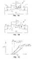
- FIG. 1Cis a graph showing the square root of the current signal (Ids) taken at the drain region of the conventional MOSFET versus the voltage potential (VGS) established between the gate and the source region.
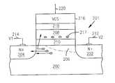
- FIG. 2Ais a diagram of an embodiment for a programmed MOSFET, having oxide insulator nanolaminate layers, which can be used as a transistor cell according to the teachings of the present invention.
- FIG. 2Bis a diagram suitable for explaining a method embodiment by which a MOSFET, having oxide insulator nanolaminate layers, can be programmed to achieve the embodiments of the present invention.
- FIG. 2Cis a graph plotting the current signal (Ids) detected at the drain region versus a voltage potential, or drain voltage, (VDS) set up between the drain region and the source region (Ids vs. VDS).
- FIG. 3illustrates a portion of an embodiment of a memory array according to the teachings of the present invention.
- FIG. 4illustrates an electrical equivalent circuit 400 for the portion of the memory array shown in FIG. 3.
- FIG. 5illustrates an energy band diagram for an embodiment of a gate stack according to the teachings of the present invention.
- FIG. 6is a graph which plots electron affinity versus the energy bandgap for various insulators.
- FIGS. 7 A- 7 Billustrates an embodiment for the operation of a transistor cell having oxide insulator nanolaminate layers according to the teachings of the present invention.
- FIG. 8illustrates the operation of a conventional DRAM cell.
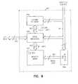
- FIG. 9illustrates an embodiment of a memory device according to the teachings of the present invention.
- FIG. 10is a schematic diagram illustrating a conventional NOR-NOR programmable logic array.
- FIG. 11is a schematic diagram illustrating generally an architecture of one embodiment of a programmable logic array (PLA) with logic cells, having oxide insulator nanolaminate layers according to the teachings of the present invention.
- PLAprogrammable logic array
- FIG. 12is a block diagram of an electrical system, or processor-based system, utilizing oxide nanolaminates constructed in accordance with the present invention.
- wafer and substrate used in the following descriptioninclude any structure having an exposed surface with which to form the integrated circuit (IC) structure of the invention.
- substrateis understood to include semiconductor wafers.
- substrateis also used to refer to semiconductor structures during processing, and may include other layers that have been fabricated thereupon. Both wafer and substrate include doped and undoped semiconductors, epitaxial semiconductor layers supported by a base semiconductor or insulator, as well as other semiconductor structures well known to one skilled in the art.
- conductoris understood to include semiconductors, and the term insulator is defined to include any material that is less electrically conductive than the materials referred to as conductors.
- FIG. 1Ais useful in illustrating the conventional operation of a MOSFET such as can be used in a DRAM array.
- FIG. 1Aillustrates the normal hot electron injection and degradation of devices operated in the forward direction. As is explained below, since the electrons are trapped near the drain they are not very effective in changing the device characteristics.
- FIG. 1Ais a block diagram of a metal oxide semiconductor field effect transistor (MOSFET) 101 in a substrate 100 .
- the MOSFET 101includes a source region 102 , a drain region 104 , a channel region 106 in the substrate 100 between the source region 102 and the drain region 104 .
- a gate 108is separated from the channel region 108 by a gate oxide 110 .
- a sourceline 112is coupled to the source region 102 .
- a bitline 114is coupled to the drain region 104 .
- a wordline 116is coupled to the gate 108 .
- a drain to source voltage potential(Vds) is set up between the drain region 104 and the source region 102 .
- a voltage potentialis then applied to the gate 108 via a wordline 116 .
- Vtcharacteristic voltage threshold
- a channel 106forms in the substrate 100 between the drain region 104 and the source region 102 . Formation of the channel 106 permits conduction between the drain region 104 and the source region 102 , and a current signal (Ids) can be detected at the drain region 104 .
- FIG. 1Cillustrates this point.
- FIG. 1Cis a graph showing the square root of the current signal (Ids) taken at the drain region versus the voltage potential (VGS) established between the gate 108 and the source region 102 .
- the change in the slope of the plot of ⁇ square root ⁇ square root over (Ids) ⁇ versus VGSrepresents the change in the charge carrier mobility in the channel 106 .
- ⁇ VTrepresents the minimal change in the MOSFET's threshold voltage resulting from electrons gradually being trapped in the gate oxide 110 near the drain region 104 , under normal operation, due to device degradation. This results in a fixed trapped charge in the gate oxide 110 near the drain region 104 .
- Slope 1represents the charge carrier mobility in the channel 106 for FIG. 1A having no electrons trapped in the gate oxide 110 .
- Slope 2represents the charge mobility in the channel 106 for the conventional MOSFET of FIG. 1B having electrons 117 trapped in the gate oxide 110 near the drain region 104 .
- slope 1 and slope 2 in FIG. 1Cthe electrons 117 trapped in the gate oxide 110 near the drain region 104 of the conventional MOSFET do not significantly change the charge mobility in the channel 106 .
- One componentincludes a threshold voltage shift due to the trapped electrons and a second component includes mobility degradation due to additional scattering of carrier electrons caused by this trapped charge and additional surface states.
- a conventional MOSFETdegrades, or is “stressed,” over operation in the forward direction, electrons do gradually get injected and become trapped in the gate oxide near the drain. In this portion of the conventional MOSFET there is virtually no channel underneath the gate oxide. Thus the trapped charge modulates the threshold voltage and charge mobility only slightly.
- the inventorshave previously described programmable memory devices and functions based on the reverse stressing of MOSFET's in a conventional CMOS process and technology in order to form programmable address decode and correction. (See generally, L. Forbes, W. P. Noble and E. H. Cloud, “MOSFET technology for programmable address decode and correction,” application Ser. No. 09/383,804). That disclosure, however, did not describe write once read only memory solutions, but rather address decode and correction issues. The inventors also describe write once read only memory cells employing charge trapping in gate insulators for conventional MOSFETs and write once read only memory employing floating gates. The same are described in co-pending, commonly assigned U.S.
- normal flash memory type cellscan be programmed by operation in the reverse direction and utilizing avalanche hot electron injection to trap electrons in the gate insulator nanolaminate.
- the programmed floating gate transistoris subsequently operated in the forward direction the electrons trapped in the gate insulator nanolaminate cause the channel to have a different threshold voltage.
- the novel programmed flash memory type transistors of the present inventionconduct significantly less current than conventional flash cells which have not been programmed. These electrons will remain trapped in the gate insulator nanolaminate unless negative control gate voltages are applied. The electrons will not be removed from the gate insulator nanolaminate when positive or zero control gate voltages are applied. Erasure can be accomplished by applying negative control gate voltages and/or increasing the temperature with negative control gate bias applied to cause the trapped electrons in the gate insulator nanolaminate to be re-emitted back into the silicon channel of the MOSFET.
- FIG. 2Ais a diagram of an embodiment for a programmed transistor cell 201 having oxide insulator nanolaminate layers according to the teachings of the present invention.
- the transistor cell 201includes a transistor in a substrate 200 which has a first source/drain region 202 , a second source/drain region 204 , and a channel region 206 between the first and second source/drain regions, 202 and 204 .
- the first source/drain region 202includes a source region 202 for the transistor cell 201 and the second source/drain region 204 includes a drain region 204 for the transistor cell 201 .
- FIG. 2Afurther illustrates the transistor cell 201 having oxide insulator nanolaminate layers 208 separated from the channel region 206 by an oxide 210 .
- An sourceline or array plate 212is coupled to the first source/drain region 202 and a transmission line 214 is coupled to the second source/drain region 204 .
- the transmission line 214includes a bit line 214 .
- a gate 216is separated from the oxide insulator nanolaminate layers 208 by another oxide 218 .
- transistor cell 201illustrates an embodiment of a programmed transistor.
- This programmed transistorhas a charge 217 trapped in potential wells in the oxide insulator nanolaminate layers 208 formed by the different electron affinities of the insulators 208 , 210 and 218 .
- the charge 217 trapped on the floating gate 208includes a trapped electron charge 217 .
- FIG. 2Bis a diagram suitable for explaining the method by which the oxide insulator nanolaminate layers 208 of the transistor cell 201 of the present invention can be programmed to achieve the embodiments of the present invention.
- the methodincludes programming the floating gate transistor.
- Programming the floating gate transistorincludes applying a first voltage potential VI to a drain region 204 of the floating gate transistor and a second voltage potential V 2 to the source region 202 .
- applying a first voltage potential VI to the drain region 204 of the floating gate transistorincludes grounding the drain region 204 of the floating gate transistor as shown in FIG. 2B.
- applying a second voltage potential V 2 to the source region 202includes biasing the array plate 212 to a voltage higher than VDD, as shown in FIG. 2B.
- a gate potential VGSis applied to the control gate 216 of the transistor.
- the gate potential VGSincludes a voltage potential which is less than the second voltage potential V 2 , but which is sufficient to establish conduction in the channel 206 of the transistor between the drain region 204 and the source region 202 . As shown in FIG.
- applying the first, second and gate potentials (V 1 , V 2 , and VGS respectively) to the transistorcreates a hot electron injection into the oxide insulator nanolaminate layers 208 of the transistor adjacent to the source region 202 .
- applying the first, second and gate potentials (V 1 , V 2 , and VGS respectively)provides enough energy to the charge carriers, e.g. electrons, being conducted across the channel 206 that, once the charge carriers are near the source region 202 , a number of the charge carriers get excited into the oxide insulator nanolaminate layers 208 adjacent to the source region 202 .
- the charge carriersbecome trapped in potential wells in the oxide insulator nanolaminate layers 208 formed by the different electron affinities of the insulators 208 , 210 and 218 .
- applying a first voltage potential VI to the drain region 204 of the transistorincludes biasing the drain region 204 of the transistor to a voltage higher than VDD.
- applying a second voltage potential V 2 to the source region 202includes grounding the sourceline or array plate 212 .
- a gate potential VGSis applied to the control gate 216 of the transistor.
- the gate potential VGSincludes a voltage potential which is less than the first voltage potential VI, but which is sufficient to establish conduction in the channel 206 of the transistor between the drain region 204 and the source region 202 .
- applying the first, second and gate potentials (V 1 , V 2 , and VGS respectively)provides enough energy to the charge carriers, e.g. electrons, being conducted across the channel 206 that, once the charge carriers are near the drain region 204 , a number of the charge carriers get excited into the oxide insulator nanolaminate layers 208 adjacent to the drain region 204 .
- the charge carriersbecome trapped in potential wells in the oxide insulator nanolaminate layers 208 formed by the different electron affinities of the insulators 208 , 210 and 218 , as shown in FIG. 2A.
- the methodis continued by subsequently operating the transistor in the forward direction in its programmed state during a read operation.
- the read operationincludes grounding the source region 202 and precharging the drain region a fractional voltage of VDD. If the device is addressed by a wordline coupled to the gate, then its conductivity will be determined by the presence or absence of stored charge in the oxide insulator nanolaminate layers 208 . That is, a gate potential can be applied to the gate 216 by a wordline 220 in an effort to form a conduction channel between the source and the drain regions as done with addressing and reading conventional DRAM cells.
- the conduction channel 206 of the transistorwill have a higher voltage threshold and will not conduct.
- FIG. 2Cis a graph plotting a current signal (IDS) detected at the second source/drain region 204 versus a voltage potential, or drain voltage, (VDS) set up between the second source/drain region 204 and the first source/drain region 202 (IDS vs. VDS).
- VDSrepresents the voltage potential set up between the drain region 204 and the source region 202 .
- the curve plotted as D 1represents the conduction behavior of a conventional transistor which is not programmed according to the teachings of the present invention.
- the curve D 2represents the conduction behavior of the programmed transistor, described above in connection with FIG. 2A, according to the teachings of the present invention. As shown in FIG.
- the current signal (IDS 2 ) detected at the second source/drain region 204 for the programmed transistor(curve D 2 ) is significantly lower than the current signal (IDS 1 ) detected at the second source/drain region 204 for the conventional transistor cell which is not programmed according to the teachings of the present invention. Again, this is attributed to the fact that the channel 206 in the programmed transistor of the present invention has a different voltage threshold.
- NROMNonvolatile Memory Cell
- B. Eitan et al.“Characterization of Channel Hot Electron Injection by the Subthreshold Slope of NROM device,” IEEE Electron Device Lett., Vol. 22, No. 11, pp. 556-558, (November 2001); B. Etian et al., “NROM: A novel localized Trapping, 2-Bit Nonvolatile Memory Cell,” IEEE Electron Device Lett., Vol. 21, No. 11, pp.
- FIG. 3illustrates an embodiment for a portion of a memory array 300 according to the teachings of the present invention.
- the memory in FIG. 3is shown illustrating a number of vertical pillars, or transistor cells, 301 - 1 , 301 - 2 , . . . , 301 -N, formed according to the teachings of the present invention.
- the number of vertical pillarare formed in rows and columns extending outwardly from a substrate 303 .
- the number of vertical pillars, 301 - 1 , 301 - 2 , . . . , 301 -Nare separated by a number of trenches 340 .
- the number of vertical pillars, 301 - 1 , 301 - 2 , . . . , 301 -Nserve as transistors including a first source/drain region, e.g. 302 - 1 and 302 - 2 respectively.
- the first source/drain region, 302 - 1 and 302 - 2is coupled to a sourceline 304 .
- the sourceline 304is formed in a bottom of the trenches 340 between rows of the vertical pillars, 301 - 1 , 301 - 2 , . . . , 301 -N.
- the sourceline 304is formed from a doped region implanted in the bottom of the trenches 340 .
- a second source/drain regione.g. 306 - 1 and 306 - 2 respectively, is coupled to a bitline (not shown).
- a channel region 305is located between the first and the second source/drain regions.
- oxide insulator nanolaminate layersare separated from the channel region 305 by a first oxide layer 307 in the trenches 340 along rows of the vertical pillars, 301 - 1 , 301 - 2 , . . . , 301 -N.
- a wordline 313is formed across the number of pillars and in the trenches 340 between the oxide insulator nanolaminate layers 309 .
- the wordline 313is separated from the pillars and the oxide insulator nanolaminate layers 309 by a second oxide layer 317 .
- FIG. 4illustrates an electrical equivalent circuit 400 for the portion of the memory array shown in FIG. 3.
- a number of vertical transistor cells401 - 1 , 401 - 2 , . . . , 401 -N, are provided.
- Each vertical transistor cell, 401 - 1 , 401 - 2 , . . . , 401 -Nincludes a first source/drain region, e.g. 402 - 1 and 402 - 2 , a second source/drain region, e.g. 406 - 1 and 406 - 2 , a channel region 405 between the first and the second source/drain regions, and oxide insulator nanolaminate layers, shown generally as 409 , separated from the channel region by a first oxide layer.
- FIG. 4further illustrates a number of bit lines, e.g. 411 - 1 and 411 - 2 .
- a single bit line, e.g. 411 - 1is coupled to the second source/drain regions, e.g. 406 - 1 and 406 - 2 , for a pair of transistor cells 401 - 1 and 401 - 2 since, as shown in FIG. 3, each pillar contains two transistor cells.
- the number of bit lines, 411 - 1 and 411 - 2are coupled to the second source/drain regions, e.g.
- a number of word linessuch as wordline 413 in FIG. 4, are coupled to a gate 412 of each transistor cell along columns of the memory array.
- a number of sourcelines, 415 - 1 , 415 - 2 , . . . , 415 -Nare formed in a bottom of the trenches between rows of the vertical pillars, described in connection with FIG. 3, such that first source/drain regions, e.g. 402 - 2 and 402 - 3 , in column adjacent transistor cells, e.g.
- 401 - 2 and 401 - 3separated by a trench, share a common sourceline, e.g. 415 - 1 .
- the number of sourcelines, 415 - 1 , 415 - 2 , . . . , 415 -Nare shared by column adjacent transistor cells, e.g. 401 - 2 and 401 - 3 , separated by a trench, along rows of the memory array 400 .
- column adjacent transistor cellse.g. 401 - 2 and 401 - 3 , separated by a trench, when one column adjacent transistor cell, e.g. 401 - 2 , is being read its complement column adjacent transistor cell, e.g. 401 - 3 , can operate as a reference cell.
- This disclosuredescribes the use of oxide insulator nanolaminate layers with charge trapping in potential wells formed by the different electron affinities of the insulator layers.
- Two different types of materialsare used for the nanolaminated insulator layers, transition metal oxides and silicon oxycarbide.
- Wilk, G. D. et al.“High-k gate dielectric: Current status and materials properties considerations,” Jour. Appl. Phys., 89(10), 5243-75 (2001); Robertson, J., “Band offsets of wide-band-gap oxides and implications for future electronic devices,” J. Vac. Sci. Technol. B, 18(3), 1785-91 (2000); Luan, H. F.
- transition metal oxide layersin embodiments of the present invention these are formed by ALD and have atomic dimensions, or nanolaminates, with precisely controlled interfaces and layer thickness.
- silicon oxycarbidein embodiments of the present invention these are deposited using chemical vapor deposition techniques since an ALD process has not yet been developed.
- Embodiments of the present inventionuse the atomic controlled deposition method to form the gate insulators if transition metal oxides are employed for the electron trapping layer.
- Atomic Layer Deposition(ALD), developed in the early 70s, is a modification of CVD and can also be called as “alternately pulsed-CVD.” (See generally, Ofer Sneh et al., “Thin film atomic layer deposition equipment for semiconductor processing,” Thin Solid Films, 402, 248-261 (2002)). Gaseous precursors are introduced one at a time to the substrate surface, and between the pulses the reactor is purged with an inert gas or evacuated.
- the precursoris saturatively chemisorbed at the substrate surface, and during the subsequent purging the precursor is removed from the reactor.
- the second stepanother precursor is introduced on the substrate and the desired films growth reaction takes place. After that the reaction byproducts and the precursor excess are purged out from the reactor.
- the precursor chemistryis favorable, i.e., the precursor adsorb and react with each other aggressively, one ALD cycle can be preformed in less than one second in the properly designed flow type reactors.
- ALDALD-dielectric deposition
- Reaction sequence ALD (RS-ALD) filmshave several unique and unmatched advantages:
- This abilitycomes from the combination of being able to control deposition with monolayer precision and the ability to deposit continuous monolayers of amorphous films (that is unique to RS-ALD).
- RS-ALD processesare free of first wafer effects and the chamber dependence. Accordingly, RS-ALD processes will be easier to transfer from development to production and from 200 to 300 mm wafer size.
- Thicknessdepends solely on the number of cycles. Thickness can be “dialed in” as a simple recipe change bearing no need for additional process development upon technology generation advance.
- FIG. 5illustrates an energy band diagram for an embodiment of a gate stack according to the teachings of the present invention.
- the embodimentconsists of insulator stacks, 501 - 1 , 501 - 2 and 501 - 3 , e.g. SiO 2 /oxide insulator nanolaminate layers/SiO 2 .
- the first and the last layer, 501 - 1 and 501 - 3are done by atomic layer deposition.
- layers 501 - 1 and 501 - 3are deposited by cyclic exposures of CH 3 OSi(NCO) 3 and H 2 O 2 at room temperature.
- the deposition rateis saturated at about 2 ⁇ /cycle, i.e., equal to the ideal quasi-monolayer/cycle.
- the surface roughness for 100 deposition cyclesis found to be less than ⁇ 10 ⁇ by atomic force microscopy.
- metallic oxideswere used. Those metallic oxides included HfO 2 , Zr 2 O 2 , Ta 2 O 3 , La- and Y-based oxides, TiO 2 , and Al 2 O 3 and are discussed in the following paragraphs.
- Zhang et al.reported the thin stacks as high-permittivity insulators for possible gate applications. These thin layers were deposited on silicon substrates using atomic layer deposition. Nanolaminate with silicon oxide equivalent thickness of about 2 nm had dielectric constants of around ten and leakage current densities at 1 MV/cm of around 10 -318 ⁇ /cm 2 . Of the three kinds of nanolaminates investigated, ZrO 2 /HfO 2 structure showed the highest breakdown field and the lowest leakage current. Zhang et al.
- nanolaminates of HfO 2 and ZrO 2are described as a dielectric material in new device structures with silicon oxide-metal oxide-silicon oxide insulator nanolaminates.
- Films with ALD of HfO 2are prepared with substrate temperature of 225-500° C. using HfI 4 as precursor, instead of HfCl 4 .
- HfI 4as precursor
- HfCl 4a process temperature for the HfO 2 is at 325° C. as practiced by Kukli et al.
- the breakdown fieldexceeded 2 MV/cm in the films grown at 325-500° C.
- the relative permittivity measured at 10 kHzwas 20-24 in the films deposited at 275-325° C.
- the dissipation factor of these filmswas as low as 0.02-0.03.
- a temperature of 250 to 325° C.would be recommended.
- Other references for ZrO 2may be useful to note. (See generally, Kukli, Kaupo et al., “Tailoring the dielectric properties of HfO 2 -Ta 2 O 3 nanolaminates,” Appl. Phys. Lett., 68(26), 3737-39 (1996)).
- Guha et al.reported on the electrical and microstructural characteristics of La- and Y-based oxides grown on silicon substrates by ultrahigh vacuum atomic beam deposition. (See generally, Guha, S. et al., “Atomic beam deposition of lanthanum- and yttrium-based oxide thin films for gate dielectrics,” Appl. Phys. Lett., 77(17), 2710-2712 (2000)). The Guha et al. group was interested in examining the potential of lanthanum- and yttrium-based oxide thin films as alternate gate dielectrics for Si complementary metal oxide semiconductor technology. Guha et al.
- nanolaminates of HfO 2 and ZrO 2are also described as a dielectric material in new device structures with silicon oxide-metal oxide-silicon oxide insulator nanolaminates.
- Niilisk et al.studied the initial growth of TiO 2 films by ALD. (See generally, Niilisk, A. et al., “Atomic-scale optical monitoring of the initial growth of TiO 2 thin films,” Proc. of the SPIE, 4318, 72-77 (2001)). The initial atomic-layer-chemical-vapor-deposition growth of titanium dioxide from TiCl 4 and water on quartz glass substrate was monitored in real time by incremental dielectric reflection. In the Niilisk et al. reference an interesting means for beginning the growth from the very beginning into a time-homogeneous mode was proposed and preliminarily studied.
- the means for beginning the growth from the very beginning into a time-homogeneous modeconsists of an in situ TiCl 4 -treatment procedure.
- the crystal structure and surface morphology of the prepared ultra thin filmswere characterized by Niilisk et al.
- nanolaminates of TiO 2are also described as a dielectric material in new device structures with silicon oxide-metal oxide-silicon oxide insulator nanolaminates.
- nanolaminates of Al 2 O 3are described as a dielectric material for new device structures with silicon oxide-metal oxide-silicon oxide insulator nanolaminates.
- Al 2 O 3can be deposited by ALD.
- ALDSee generally, DiMaria, D. J. “Graded or stepped energy band-gap-insulator MIS structures (GI-MIS or SI-MIS),” Journal of Applied Physics, 50(9), 5826-9 (September 1979) for one technique appropriate for performing the ALD deposition).
- Silicon oxycarbideis a wide band gap semiconductor, with a band gap energy which can vary between that of silicon carbide and that of silicon oxide. (See generally, Yoder, M. N., Wide bandgap semiconductor materials and devices,” IEEE Trans. on Electron Devices, 43, 1633-1636 (October 1996)).
- FIG. 6is a graph which plots electron affinity versus the energy bandgap for various insulators. That is FIG. 6 illustrates the inventors estimates of the variation of the electron affinity with the bandgap energy.
- the insulatoris crystalline and has a small band gap, near that of silicon carbide, then the insulator can be doped and be conductive, however if undoped and in an amorphous state with a larger band gap, it will be an insulator.
- the inventors of the present case, Ahn, K. Y. and Forbes, L.have previously described silicon oxycarbide for use as an insulator in integrated circuits. (See generally, U.S. Pat. No. 6,313,518, by Ahn, K. Y. and Forbes, L., entitled “Porous silicon oxycarbide integrated circuit insulator”).
- Silicon oxycarbidecan be deposited by chemical vapor deposition, CVD, techniques.
- CVDchemical vapor deposition
- an initial gate oxideis grown by thermal oxidation of silicon and then the silicon oxycarbide and final oxide layer is deposited by CVD.
- the gate insulator structure shown in FIG. 5is employed in a wide variety of different flash memory type devices. That is, in embodiments of the present invention, the gate structure embodiment of FIG. 5, having silicon oxide-oxide insulator nanolaminates-silicon oxide, is used in place of the gate structure provided in the following commonly assigned patents: U.S. Pat. Nos. 5,936,274; 6,143,636; 5,973,356; 6,238,976; 5,991,225; 6,153,468; and 6,124,729.
- the gate structure embodiment of FIG. 5, having silicon oxide-oxide insulator nanolaminates-silicon oxideis used in place of the gate structure provided in the following commonly assigned pending applications: Forbes, L., “Write once read only memory based on DRAM technology employing charge trapping in gate insulators,” application Ser. No. ______; Forbes, L., “Write once read only memory based on a modification of DRAM technology employing floating gates,” application Ser. No. ______; Forbes, L., “Write once read only memory with long retention for archival storage,” application Ser. No. ______; Forbes, L., “Nanoncrystal write once read only memory with long retention for archival storage,” application Ser. No.
- embodiments of the novel transistor hereinwhich are substituted for the gate structures described in the references above, are programmed by grounding a source line and applying a gate voltage and a voltage to the drain to cause channel hot electron injection.
- the drain and ground or sourcehave the normal connections and the conductivity of the transistor determined using low voltages so as not to disturb the memory state.
- the devicescan be erased by applying a large negative voltage to the gate.
- the gate structure embodiment of FIG. 5, having silicon oxide-oxide insulator nanolaminates-silicon oxideis used in place of the gate structure provided in the following commonly assigned patents: U.S. Pat. Nos. 5,936,274, 6,143,636, 5,973,356 and 6,238,976 (vertical flash memory devices with high density); U.S. Pat. Nos. 5,991,225 and 6,153,468 (programmable memory address and decode circuits); and U.S. Pat. No. 6,124,729 (programmable logic arrays).
- the gate structure embodiment of FIG. 5, having silicon oxide-oxide insulator nanolaminates-silicon oxideis used in place of the gate structure provided in the following US patents: Etian, B. et al., “NROM: A novel localized Trapping, 2-Bit Nonvolatile Memory Cell,” IEEE Electron Device Lett., 21(11), 543-545 (November 2000); Eitan, B. et al., “Characterization of Channel Hot Electron Injection by the Subthreshold Slope of NROM device, IEEE Electron Device Lett., 22(11), 556-558 (November 2001); Maayan, E.
- the gate structure embodiment of FIG. 5having silicon oxide-oxide insulator nanolaminates-silicon oxide used in place of the gate structures in those references, can be programmed in the reverse direction and read in the forward direction to obtain more sensitivity in the device characteristics to the stored charge.
- FIGS. 7 A-B and 8are embodiments useful in illustrating the use of charge storage in the oxide insulator nanolaminate layers to modulate the conductivity of the transistor cell according to the teachings of the present invention. That is, FIGS. 7 A- 7 B illustrates the operation of an embodiment for a novel transistor cell 701 formed according to the teachings of the present invention. And, FIG. 8 illustrates the operation of a conventional DRAM cell 701 . As shown in FIG. 7A, the embodiment consists of a gate insulator stack having insulator layers, 710 , 708 and 718 , e.g. SiO 2 /oxide insulator nanolaminate layers/SiO 2 . In the embodiment of FIG.
- the gate insulator stack having insulator layers, 710 , 708 and 718is made thicker than in a conventional DRAM cell, e.g. 801 and is equal to or greater than 10 nm or 100 ⁇ (10 ⁇ 6 cm).
- a transistor cellis illustrated having dimensions of 0.1 ⁇ m (10 ⁇ 5 cm) by 0.1 ⁇ m.
- a charge of 10 12 electrons/cm 2is programmed into the oxide insulator nanolaminate layers of the transistor cell.
- the charge carriersbecome trapped in potential wells in the oxide insulator nanolaminate layers 708 formed by the different electron affinities of the insulators 710 , 708 and 718 , as shown in FIG. 7A.
- ⁇ Q10 12 electrons/cm 2 ⁇ 1.6 ⁇ 10 ⁇ 19 Coulombs.
- this embodiment of the present inventioninvolves trapping a charge of approximately 100 electrons in the oxide insulator nanolaminate layers 708 of the transistor cell.
- FIG. 7Baids to further illustrate the conduction behavior of the novel transistor cell of the present invention.
- Vthe nominal threshold voltage without the floating gate charged
- the oxide insulator nanolaminate layersare charged the transistor cell of the present invention will be off and not conduct.
- an unwritten, or un-programmed transistor cellcan conduct a current of the order 12.5 ⁇ A, whereas if the oxide insulator nanolaminate layers are charged then the transistor cell will not conduct.
- the sense amplifiers used in DRAM arrayscan easily detect such differences in current on the bit lines.
- the transistor cellshaving the gate structure with oxide insulator nanolaminate layers, in the array are utilized not just as passive on or off switches as transfer devices in DRAM arrays but rather as active devices providing gain.
- to program the transistor cell “off,”requires only a stored charge in the oxide insulator nanolaminate layers of about 100 electrons if the area is 0.1 ⁇ m by 0.1 ⁇ m.
- the transistor cellis un-programmed, e.g. no stored charge trapped in the oxide insulator nanolaminate layers, and if the transistor cell is addressed over 10 nS a current of 12.5 ⁇ A is provided.
- the integrated drain currentthen has a charge of 125 fC or 800,000 electrons. This is in comparison to the charge on a DRAM capacitor of 50 fC which is only about 300,000 electrons.
- the use of transistor cells, having the gate structure with oxide insulator nanolaminate layers, in the array as active devices with gain, rather than just switches,provides an amplification of the stored charge, in the oxide insulator nanolaminate layers, from 100 to 800,000 electrons over a read address period of 10 nS.
- the memory device 940contains a memory array 942 , row and column decoders 944 , 948 and a sense amplifier circuit 946 .
- the memory array 942consists of a plurality of transistor cells 900 , having oxide insulator nanolaminate layers in the gate stack, whose word lines 980 and bit lines 960 are commonly arranged into rows and columns, respectively.
- the bit lines 960 of the memory array 942are connected to the sense amplifier circuit 946 , while its word lines 980 are connected to the row decoder 944 .
- Address and control signalsare input on address/control lines 961 into the memory device 940 and connected to the column decoder 948 , sense amplifier circuit 946 and row decoder 944 and are used to gain read and write access, among other things, to the memory array 942 .
- the column decoder 948is connected to the sense amplifier circuit 946 via control and column select signals on column select lines 962 .
- the sense amplifier circuit 946receives input data destined for the memory array 942 and outputs data read from the memory array 942 over input/output (I/O) data lines 963 .
- Datais read from the cells of the memory array 942 by activating a word line 980 (via the row decoder 944 ), which couples all of the memory cells corresponding to that word line to respective bit lines 960 , which define the columns of the array.
- One or more bit lines 960are also activated.
- the sense amplifier circuit 946 connected to a bit line columndetects and amplifies the conduction sensed through a given transistor cell and transferred to its bit line 960 by measuring the potential difference between the activated bit line 960 and a reference line which may be an inactive bit line. Again, in the read operation the source region of a given cell is couple to a grounded sourceline or array plate (not shown).
- the operation of Memory device sense amplifiersis described, for example, in U.S. Pat. Nos. 5,627,785; 5,280,205; and 5,042,011, all assigned to Micron Technology Inc., and incorporated by reference herein.
- FIG. 10shows a conventional NOR-NOR logic array 1000 which is programmable at the gate mask level by either fabricating a thin oxide gate transistor, e.g. logic cells 1001 - 1 , 1001 - 2 , . . . , 1001 -N and 1003 - 1 , 1003 - 2 , . . . , 1003 -N, at the intersection of lines in the array or not fabricating a thin oxide gate transistor, e.g. missing thin oxide transistors, 1002 - 1 , 1002 - 2 , . . . , 1002 -N, at such an intersection.
- a thin oxide gate transistore.g. logic cells 1001 - 1 , 1001 - 2 , . . . , 1001 -N and 1003 - 1 , 1003 - 2 , . . . , 1003 -N, at such an intersection.
- NMOS transistors1016 and 1018 respectively, are used as load devices.
- the conventional logic array shown in FIG. 10includes a first logic plane 1010 which receives a number of input signals at input lines 1012 .
- first logic plane 1010can include inverters to produce the complementary signals when needed in a specific application.
- First logic plane 1010includes a number of thin oxide gate transistors, e.g. transistors 1001 - 1 , 1001 - 2 , . . . , 1001 -N.
- the thin oxide gate transistors, 1001 - 1 , 1001 - 2 , . . . , 1001 -Nare located at the intersection of input lines 1012 , and interconnect lines 1014 .
- this selective fabrication of thin oxide gate transistore.g. transistors 1001 - 1 , 1001 - 2 , . . .
- 1001 -Nis referred to as programming since the logical function implemented by the programmable logic array is entered into the array by the selective arrangement of the thin oxide gate transistors, or logic cells, 1001 - 1 , 1001 - 2 , . . . , 1001 -N, at the intersections of input lines 1012 , and interconnect lines 1014 in the array.
- each of the interconnect lines 1014acts as a NOR gate for the input lines 1012 that are connected to the interconnect lines 1014 through the thin oxide gate transistors, 1001 - 1 , 1001 - 2 , . . . , 1001 -N, of the array.
- interconnection line 1014 Aacts as a NOR gate for the signals on input lines 1012 A and 1012 B. That is, interconnect line 1014 A is maintained at a high potential unless one or more of the thin oxide gate transistors, 1001 - 1 , 1001 - 2 , . . .
- each thin oxide gate transistore.g. transistors 1001 - 1 , 1001 - 2 , . . . , 1001 -N, conducts which performs the NOR positive logic circuit function, an inversion of the OR circuit function results from inversion of data onto the interconnect lines 1014 through the thin oxide gate transistors, 1001 - 1 , 1001 - 2 , . . . , 1001 -N, of the array.
- a second logic plane 1024which includes a number of thin oxide gate transistor, e.g. transistors 1003 - 1 , 1003 - 2 , . . . , 1003 -N.
- the thin oxide gate transistors, 1003 - 1 , 1003 - 2 , . . . , 1003 -N,are located at the intersection of interconnect lines 1014 , and output lines 1020 .
- the logical function of the second logic plane 1024is implemented by the selective arrangement of the thin oxide gate transistors, 1003 - 1 , 1003 - 2 , . . .
- the second logic plane 1024is also configured such that the output lines 1020 comprise a logical NOR function of the signals from the interconnection lines 1014 that are coupled to particular output lines 1020 through the thin oxide gate transistors, 1003 - 1 , 1003 - 2 , . . . , 1003 -N, of the second logic plane 1024 .
- the incoming signals on each lineare used to drive the gates of transistors in the NOR logic array as the same is known by one of ordinary skill in the art and will be understood by reading this disclosure.
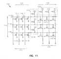
- FIG. 11illustrates an embodiment of a novel in-service programmable logic array (PLA) formed with logic cells having a gate structure with oxide insulator nanolaminate layers, according to the teachings of the present invention.
- PLA 1100implements an illustrative logical function using a two level logic approach. Specifically, PLA 1100 includes first and second logic planes 1110 and 1122 . In this example, the logic function is implemented using NOR-NOR logic. As shown in FIG. 11, first and second logic planes 1110 and 1122 each include an array of, logic cells, having a gate structure with oxide insulator nanolaminate layers, which serve as driver transistors, 1101 - 1 , 1101 - 2 , . . .
- the driver transistors, 1101 - 1 , 1101 - 2 , . . . , 1101 -N, and 1102 - 1 , 1102 - 2 , . . . , 1102 -Nhave their first source/drain regions coupled to source lines or a conductive source plane.
- the driver transistors, 1101 - 1 , 1101 - 2 , . . . , 1101 -N, and 1102 - 1 , 1102 - 2 , . . . , 1102 -Nare shown as n-channel transistors., However, the invention is not so limited. Also, as shown in FIG. 11, a number of p-channel metal oxide semiconductor (PMOS) transistors are provided as load device transistors, 1116 and 1124 respectively, having their source regions coupled to a voltage potential (VDD).
- PMOSmetal oxide semiconductor
- load device transistors, 1116 and 1124respectively, operate in complement to the driver transistors, 1101 - 1 , 1101 - 2 , . . . , 1101 -N, and 1102 - 1 , 1102 - 2 , . . . , 1102 -N to form load inverters.
- FIG. 11is provided by way of example and not by way of limitation. Specifically, the teachings of the present application are not limited to programmable logic arrays in the NOR-NOR approach. Further, the teachings of the present application are not limited to the specific logical function shown in FIG. 11. Other logical functions can be implemented in a programmable logic array, with the driver transistors, having a gate structure with oxide insulator nanolaminate layers, 1101 - 1 , 1101 - 2 , . . . , 1101 -N, and 1102 - 1 , 1102 - 2 , . . . , 1102 -N and load device transistors, 1116 and 1124 respectively, of the present invention, using any one of the various two level logic approaches.
- First logic plane 1110receives a number of input signals at input lines 1112 .
- no invertersare provided for generating complements of the input signals.
- first logic plane 1110can include inverters to produce the complementary signals when needed in a specific application.
- First logic plane 1110includes a number of driver transistors, having a gate structure with oxide insulator nanolaminate layers, 1101 - 1 , 1101 - 2 , . . . , 1101 -N, that form an array.
- the driver transistors, 1101 - 1 , 1101 - 2 , . . . , 1101 -Nare located at the intersection of input lines 1112 , and interconnect lines 1114 . Not all of the driver transistors, 1101 - 1 , 1101 - 2 , . . . , 1101 -N, are operatively conductive in the first logic plane. Rather, the driver transistors, 1101 - 1 , 1101 - 2 , .
- . . , 1101 -Nare selectively programmed, as has been described herein, to respond to the input lines 1112 and change the potential of the interconnect lines 1114 so as to implement a desired logic function.
- This selective interconnectionis referred to as programming since the logical function implemented by the programmable logic array is entered into the array by the driver transistors, 1101 - 1 , 1101 - 2 , . . . , 1101 -N, that are used at the intersections of input lines 1112 , and interconnect lines 1114 in the array.
- each of the interconnect lines 1114acts as a NOR gate for the input lines 1112 that are connected to the interconnect lines 1114 through the driver transistors, 1101 - 1 , 1101 - 2 , . . . , 1101 -N, of the array 1100 .
- interconnection line 1114 Aacts as a NOR gate for the signals on input lines 1112 A, 1112 B and 1112 C.
- Programmability of the driver transistors, 1101 - 1 , 1101 - 2 , . . . , 1101 -Nis achieved by trapping charge carriers in potential wells in the oxide insulator nanolaminate layers of the gate stack, as described herein.
- That driver transistor, 1101 - 1 , 11012 , . . . , 1101 -Nwill remain in an off state until it is reprogrammed.
- Applying and removing a charge to the oxide insulator nanolaminate layersis performed by tunneling charge into the oxide insulator nanolaminate layers of the driver transistors, 1101 - 1 , 1101 - 2 , . . . , 1101 -N.
- a driver transistors, 1101 - 1 , 1101 - 2 , . . . , 1101 -N programmed in an off stateremains in that state until the charge is removed from the oxide insulator nanolaminate layers.
- Driver transistors, 1101 - 1 , 1101 - 2 , . . . , 1101 -N not having their corresponding gate structure with oxide insulator nanolaminate layers chargedoperate in either an on state or an off state, wherein input signals received by the input lines 1112 A, 1112 B and 1112 C determine the applicable state. If any of the input lines 1112 A, 1112 B and 1112 C are turned on by input signals received by the input lines 1112 A, 1112 B and 1112 C, then a ground is provided to load device transistors 1116 . The load device transistors 1116 are attached to the interconnect lines 1114 .
- the load device transistors 1116provide a low voltage level when any one of the driver transistors, 1101 - 1 , 1101 - 2 , . . . , 1101 -N connected to the corresponding interconnect line 1114 is activated. This performs the NOR logic circuit function, an inversion of the OR circuit function results from inversion of data onto the interconnect lines 1114 through the driver transistors, 1101 - 1 , 1101 - 2 , . . . , 1101 -N of the array 1100 . When the driver transistors, 1101 - 1 , 1101 - 2 , . . . , 1101 -N are in an off state, an open is provided to the drain of the load device transistors 1116 .
- the VDD voltage levelis applied to corresponding input lines, e.g. the interconnect lines 1114 for second logic plane 1122 when a load device transistors 1116 is turned on by a clock signal received at the gate of the load device transistors 1116 .
- Each of the driver transistors, 1101 - 1 , 1101 - 2 , . . . , 1101 -N described hereinare formed according to the teachings of the present, having a gate structure with oxide insulator nanolaminate layers.
- second logic plane 1122comprises a second array of driver transistors, 1102 - 1 , 1102 - 2 , . . . , 1102 -N that are selectively programmed to provide the second level of the two level logic needed to implement a specific logical function.
- the array of driver transistors, 1102 - 1 , 1102 - 2 , . . . , 1102 -Nis also configured such that the output lines 1120 comprise a logical NOR function of the signals from the interconnection lines 1114 that are coupled to particular output lines 1120 through the driver transistors, 1102 - 1 , 1102 - 2 , . . . , 1102 -N of the second logic plane 1122 .
- a driver transistore.g. 1102 - 1 , 1102 - 2 , . . . , 1102 -N, programmed in an off state remains in that state until the charge is removed from the oxide insulator nanolaminate layers.
- Driver transistors, 1102 - 1 , 1102 - 2 , . . . , 1102 -N not having their corresponding gate structure with oxide insulator nanolaminate layers chargedoperate in either an on state or an off state, wherein signals received by the interconnect lines 1114 determine the applicable state. If any of the interconnect lines 1114 are turned on, then a ground is provided to load device transistors 1124 by applying a ground potential to the source line or conductive source plane coupled to the transistors first source/drain region as described herein. The load device transistors 1124 are attached to the output lines 1120 . The load device transistors 1124 provide a low voltage level when any one of the driver transistors, 1102 - 1 , 1102 - 2 , .
- the VDD voltage levelis applied to corresponding output lines 1120 for second logic plane 1122 when a load device transistor 1124 is turned on by a clock signal received at the gate of the load device transistors 1124 .
- NOR-NOR electrically programmable logic arrayis most easily implemented utilizing the normal PLA array structure.
- Each of the driver transistors, 1102 - 1 , 1102 - 2 , . . . , 1102 -N described hereinare formed according to the teachings of the present, having a gate structure with oxide insulator nanolaminate layers.
- FIG. 11shows an embodiment for the application of the novel transistor cells, having a gate structure with oxide insulator nanolaminate layers, in a logic array.
- a driver transistors1101 - 1 , 1101 - 2 , . . . , 1101 -N, and 1102 - 1 , 1102 - 2 , 1102 -N, is programmed with a negative charge trapped in potential wells, formed with the oxide insulator nanolaminate layers, it is effectively removed from the array.
- the array logic functionscan be programmed even when the circuit is in the final circuit or in the field and being used in a system.
- the absence or presence of charge trapped in potential wells, formed by the oxide insulator nanolaminate layers,is read by addressing the input lines 1112 or control gate lines and y-column/sourcelines to form a coincidence in address at a particular logic cell.
- the control gate linewould for instance be driven positive at some voltage of 1.0 Volts and the y-column/sourceline grounded, if the oxide insulator nanolaminate layers are not charged with electrons then the transistor would turn on tending to hold the interconnect line on that particular row down indicating the presence of a stored “one” in the cell.
- this particular transistor cellhas charge trapped in potential wells, formed by the oxide insulator nanolaminate layers, the transistor will not turn on and the presence of a stored “zero” is indicated in the cell. In this manner, data stored on a particular transistor cell can be read.
- Programmingcan be achieved by hot electron injection.
- the interconnect lines, coupled to the second source/drain region for the transistor cells in the first logic plane,are driven with a higher drain voltage like 2 Volts for 0.1 micron technology and the control gate line is addressed by some nominal voltage in the range of twice this value. Erasure is accomplished by driving the control gate line with a large positive voltage and the sourceline and/or backgate or substrate/well address line of the transistor with a negative bias so the total voltage difference is in the order of 3 Volts causing electrons to tunnel out of the oxide insulator nanolaminate layers of the driver transistors.
- FIG. 12is a block diagram of an electrical system, or processor-based system, 1200 utilizing transistor cells with a gate structure having oxide insulator nanolaminate layers.
- memory 1212is constructed in accordance with the present invention to have transistor cells with a gate structure having oxide insulator nanolaminate layers. The same applies to transistors in the CPU, etc., the invention is not so limited.
- the processor-based system 1200may be a computer system, a process control system or any other system employing a processor and associated memory.
- the system 1200includes a central processing unit (CPU) 1202 , e.g., a microprocessor, that communicates with the NOR flash memory 1212 and an I/O device 1208 over a bus 1220 .
- CPUcentral processing unit
- the bus 1220may be a series of buses and bridges commonly used in a processor-based system, but for convenience purposes only, the bus 1220 has been illustrated as a single bus.
- a second I/O device 1210is illustrated, but is not necessary to practice the invention.
- the processor-based system 1200can also includes read-only memory (ROM) 1214 and may include peripheral devices such as a floppy disk drive 1204 and a compact disk (CD) ROM drive 1206 that also communicates with the CPU 1202 over the bus 1220 as is well known in the art.
- ROMread-only memory
- peripheral devicessuch as a floppy disk drive 1204 and a compact disk (CD) ROM drive 1206 that also communicates with the CPU 1202 over the bus 1220 as is well known in the art.
- CDcompact disk
- At least one of the transistor cells, having a gate structure with oxide insulator nanolaminate layers in memory 1212includes a programmed transistor cell according to the teachings of the present invention.
- FIG. 12illustrates an embodiment for electronic system circuitry in which the novel transistor cells of the present invention are used.
- the illustration of system 1200is intended to provide a general understanding of one application for the structure and circuitry of the present invention, and is not intended to serve as a complete description of all the elements and features of an electronic system using the novel transistor cell structures.
- the inventionis equally applicable to any size and type of memory device 1200 using the novel transistor cells of the present invention and is not intended to be limited to that described above.
- such an electronic systemcan be fabricated in single-package processing units, or even on a single semiconductor chip, in order to reduce the communication time between the processor and the memory device.
- Applications containing the novel transistor cell of the present invention as described in this disclosureinclude electronic systems for use in memory modules, device drivers, power modules, communication modems, processor modules, and application-specific modules, and may include multilayer, multichip modules.
- Such circuitrycan further be a subcomponent of a variety of electronic systems, such as a clock, a television, a cell phone, a personal computer, an automobile, an industrial control system, an aircraft, and others.
- This disclosuredescribes the use of oxide insulator nanolaminate layers with charge trapping in potential wells formed by the different electron affinities of the insulator layers.
- Two different types of materialsare used for the nanolaminated insulator layers.
- the two different types of materialsare transition metal oxides and silicon oxycarbide.
- transition metal oxide layersthese are formed by ALD and have atomic dimensions, or nanolaminates, with precisely controlled interfaces and layer thickness.
- silicon oxycarbidethese are deposited using chemical vapor deposition techniques since an ALD process has not yet been developed.
- the gate insulator structure embodiments of the present invention, having silicon oxide-metal oxide-silicon oxide insulator nanolaminates,are employed in a wide variety of different device applications.
Landscapes
- Engineering & Computer Science (AREA)
- Microelectronics & Electronic Packaging (AREA)
- Computer Hardware Design (AREA)
- Semiconductor Memories (AREA)
- Non-Volatile Memory (AREA)
Abstract
Description
- This application is related to the following co-pending, commonly assigned U.S. patent applications: “Memory Utilizing Oxide-Nitride Nanolaminates,” attorney docket no.[0001]1303.067US1, Ser. No. ______, and “Memory Utilizing Oxide-Conductor Nanolaminates,” attorney docket no. 1303.068US1, Ser. No. ______, each of which disclosure is herein incorporated by reference.
- The present invention relates generally to semiconductor integrated circuits and, more particularly, to memory utilizing oxide nanolaminates.[0002]
- Many electronic products need various amounts of memory to store information, e.g. data. One common type of high speed, low cost memory includes dynamic random access memory (DRAM) comprised of individual DRAM cells arranged in arrays. DRAM cells include an access transistor, e.g a metal oxide semiconducting field effect transistor (MOSFET), coupled to a capacitor cell.[0003]
- Another type of high speed, low cost memory includes floating gate memory cells. A conventional horizontal floating gate transistor structure includes a source region and a drain region separated by a channel region in a horizontal substrate. A floating gate is separated by a thin tunnel gate oxide. The structure is programmed by storing a charge on the floating gate. A control gate is separated from the floating gate by an intergate dielectric. A charge stored on the floating gate effects the conductivity of the cell when a read voltage potential is applied to the control gate. The state of cell can thus be determined by sensing a change in the device conductivity between the programmed and un-programmed states.[0004]
- With successive generations of DRAM chips, an emphasis continues to be placed on increasing array density and maximizing chip real estate while minimizing the cost of manufacture. It is further desirable to increase array density with little or no modification of the DRAM optimized process flow.[0005]
- Multilayer insulators have been previously employed in memory devices. (See generally, U.S. Pat. No. 3,877,054, Boulin et al., Apr. 8, 1975, entitled “Semiconductor memory apparatus with a multi-layer insulator contacting the semiconductor,” and U.S. Pat. No. 3,964,085, Kahng et al., Jun. 15, 1976, entitled “Method for fabricating multilayer insulator-semiconductor memory apparatus”). The devices in the above references employed oxide-tungsten oxide-oxide layers. Other previously described structures described have employed charge-trapping layers implanted into graded layer insulator structures. (See generally, an article by DiMaria, D. J., “Graded or stepped energy band-gap-insulator MIS structures (GI-MIS or SI-MIS),”[0006]Journal of Applied Physics,50(9), 5826-9 (September 1979); U.S. Pat. No. 4,217,601, DeKeersmaecker et al., Aug. 12, 1980, entitled “Non-volatile memory devices fabricated from graded or stepped energy band gap insulator MIM or MIS structure,” also RE31,083 DeKeersmaecker et al., Nov. 16, 1982, “Non-volatile memory devices fabricated from graded or stepped energy band gap insulator MIM or MIS structure;” and U.S. Pat. No. 5,768,192 Eitan, Jun. 16, 1998, entitled “Non-volatile semiconductor memory cell utilizing asymmetrical charge trapping”).
- More recently oxide-nitride-oxide structures have been described for high density nonvolatile memories. (See generally, Etian, B. et al., “NROM: A novel localized Trapping, 2-Bit Nonvolatile Memory Cell,”[0007]IEEE Electron Device Lett.,21(11), 543-545 (November 2000), and Eitan, B. et al., “Characterization of Channel Hot Electron Injection by the Subthreshold Slope of NROM device,IEEE Electron Device Lett.,22(11), 556-558 (November 2001)). All of these are variations on the original MNOS memory structure (see generally, Frohman-Bentchkowsky, D., “An integrated metal-nitride-oxide-silicon (MNOS) memory,”Proceedings of the IEEE,57(6), 1190-2 (June 1969)) described by Fairchild Semiconductor in 1969 which was conceptually generalized to include trapping insulators in general for constructing memory arrays. (See generally, U.S. Pat. No. 3,665,423 Nakamuma et al., May 23, 1972, entitled “Memory matrix using MIS semiconductor element”).
- Studies of charge trapping in MNOS structures have also been conducted by White and others. (See generally, White, M. H., “Direct tunneling in metal-nitrideoxide-silicon (MNOS) structures,” Conference: Program of the 31st physical electronics conference (abstracts), page: 1 pp., Publisher: U.S. Dept. Commerce, Washington, D.C., USA, 1971, viii+46 Pages, Sponsor: American Phys. Soc., division of electron and atomic phys, 15-17 March 1971, Gaithersburg, Md., USA; White, M. H., Criechi, J. R., “Characterization of thin-oxide MNOS memory transistors,”[0008]IEEE Transactions on Electron Devices, ED-19(12), 1280-8 (December 1972), Wei, L. S., Simmons, J. G. “Trapping, emission and generation in MNOS memory devices,”Solid-State Electronics,17(6), 591-8 (June 1974), Ferris-Prabhu, A. V., “Charge transfer in layered insulators,”Solid-State Electronics,16(9), 1086-7 (September 1973); Ferris-Prabhu, A. V., Lareau, L. J., “Amnesia in layered insulator FET memory devices,” Conference: 1973 International Electron Devices Meeting Technical Digest, Page: 75-7, Publisher: IEEE, New York, N.Y., USA, 1973, xvi+575 Pages, Sponsor: IEEE, 3-5 December1973, Washington, D.C., USA; Ferris-Prabhu, A. V., “Tunneling theories of non-volatile semiconductor memories,”Physica Status Solidi A,35(1), 243-50 (16 May 1976)).
- Some commercial and military applications utilized non-volatile MNOS memories. (See generally, Britton, J. et al., “Metal-nitride-oxide IC memory retains data for meter reader,”[0009]Electronics,45(22); 119-23 (23 October 1972); and Cricchi, J. R. et al., “Hardened MNOS/SOS electrically reprogrammable nonvolatile memory,”IEEE Transactions on Nuclear Science, ns-24(6), 2185-9 (December 1977), Conference: IEEE Annual Conference on Nuclear and Space Radiation Effects, Sponsor: IEEE, 12-15 July 1977, Williamsburg, Va., USA).
- However, these structures did not gain widespread acceptance and use due to their variability in characteristics and unpredictable charge trapping phenomena. They all depended upon the trapping of charge at interface states between the oxide and other insulator layers or poorly characterized charge trapping centers in the insulator layers themselves. Since the layers were deposited by CVD, they are thick, have poorly controlled thickness and large surface state charge-trapping center densities between the layers.[0010]
- Thus, there is an ongoing need for improved DRAM technology compatible transistor cells. It is desirable that such transistor cells be fabricated on a DRAM chip with little or no modification of the DRAM process flow. It is further desirable that such transistor cells provide increased density and high access and read speeds.[0011]
- The above mentioned problems for creating DRAM technology compatible transistor cells as well as other problems are addressed by the present invention and will be understood by reading and studying the following specification. This disclosure describes the use of oxide insulator nanolaminate layers with charge trapping in potential wells formed by the different electron affinities of the insulator layers. Two different types of materials are used for the nanolaminated insulator layers. The two different types of materials are transition metal oxides and silicon oxycarbide. In the case of transition metal oxide layers, these are formed by ALD and have atomic dimensions, or nanolaminates, with precisely controlled interfaces and layer thickness. In the case of silicon oxycarbide, these are deposited using chemical vapor deposition techniques since an ALD process has not yet been developed.[0012]
- In particular, an embodiment of the present invention includes a transistor utilizing oxide nanolaminates. The transistor includes a first source/drain region, a second source/drain region, and a channel region therebetween. A gate is separated from the channel region by a gate insulator. The gate insulator includes oxide insulator nanolaminate layers with charge trapping in potential wells formed by different electron affinities of the insulator nanolaminate layers.[0013]
- These and other embodiments, aspects, advantages, and features of the present invention will be set forth in part in the description which follows, and in part will become apparent to those skilled in the art by reference to the following description of the invention and referenced drawings or by practice of the invention. The aspects, advantages, and features of the invention are realized and attained by means of the instrumentalities, procedures, and combinations particularly pointed out in the appended claims.[0014]
- FIG. 1A is a block diagram of a metal oxide semiconductor field effect transistor (MOSFET) in a substrate according to the teachings of the prior art.[0015]
- FIG. 1B illustrates the MOSFET of FIG. 1A operated in the forward direction showing some degree of device degradation due to electrons being trapped in the gate oxide near the drain region over gradual use.[0016]
- FIG. 1C is a graph showing the square root of the current signal (Ids) taken at the drain region of the conventional MOSFET versus the voltage potential (VGS) established between the gate and the source region.[0017]
- FIG. 2A is a diagram of an embodiment for a programmed MOSFET, having oxide insulator nanolaminate layers, which can be used as a transistor cell according to the teachings of the present invention.[0018]
- FIG. 2B is a diagram suitable for explaining a method embodiment by which a MOSFET, having oxide insulator nanolaminate layers, can be programmed to achieve the embodiments of the present invention.[0019]
- FIG. 2C is a graph plotting the current signal (Ids) detected at the drain region versus a voltage potential, or drain voltage, (VDS) set up between the drain region and the source region (Ids vs. VDS).[0020]
- FIG. 3 illustrates a portion of an embodiment of a memory array according to the teachings of the present invention.[0021]
- FIG. 4 illustrates an electrical[0022]
equivalent circuit 400 for the portion of the memory array shown in FIG. 3. - FIG. 5 illustrates an energy band diagram for an embodiment of a gate stack according to the teachings of the present invention.[0023]
- FIG. 6 is a graph which plots electron affinity versus the energy bandgap for various insulators.[0024]
- FIGS.[0025]7A-7B illustrates an embodiment for the operation of a transistor cell having oxide insulator nanolaminate layers according to the teachings of the present invention.
- FIG. 8 illustrates the operation of a conventional DRAM cell.[0026]
- FIG. 9 illustrates an embodiment of a memory device according to the teachings of the present invention.[0027]
- FIG. 10 is a schematic diagram illustrating a conventional NOR-NOR programmable logic array.[0028]
- FIG. 11 is a schematic diagram illustrating generally an architecture of one embodiment of a programmable logic array (PLA) with logic cells, having oxide insulator nanolaminate layers according to the teachings of the present invention.[0029]
- FIG. 12 is a block diagram of an electrical system, or processor-based system, utilizing oxide nanolaminates constructed in accordance with the present invention.[0030]
- In the following detailed description of the invention, reference is made to the accompanying drawings which form a part hereof, and in which is shown, by way of illustration, specific embodiments in which the invention may be practiced. In the drawings, like numerals describe substantially similar components throughout the several views. These embodiments are described in sufficient detail to enable those skilled in the art to practice the invention. Other embodiments may be utilized and structural, logical, and electrical changes may be made without departing from the scope of the present invention.[0031]
- The terms wafer and substrate used in the following description include any structure having an exposed surface with which to form the integrated circuit (IC) structure of the invention. The term substrate is understood to include semiconductor wafers. The term substrate is also used to refer to semiconductor structures during processing, and may include other layers that have been fabricated thereupon. Both wafer and substrate include doped and undoped semiconductors, epitaxial semiconductor layers supported by a base semiconductor or insulator, as well as other semiconductor structures well known to one skilled in the art. The term conductor is understood to include semiconductors, and the term insulator is defined to include any material that is less electrically conductive than the materials referred to as conductors. The following detailed description is, therefore, not to be taken in a limiting sense, and the scope of the present invention is defined only by the appended claims, along with the full scope of equivalents to which such claims are entitled.[0032]
- FIG. 1A is useful in illustrating the conventional operation of a MOSFET such as can be used in a DRAM array. FIG. 1A illustrates the normal hot electron injection and degradation of devices operated in the forward direction. As is explained below, since the electrons are trapped near the drain they are not very effective in changing the device characteristics.[0033]
- FIG. 1A is a block diagram of a metal oxide semiconductor field effect transistor (MOSFET)[0034]101 in a
substrate 100. TheMOSFET 101 includes asource region 102, adrain region 104, achannel region 106 in thesubstrate 100 between thesource region 102 and thedrain region 104. Agate 108 is separated from thechannel region 108 by agate oxide 110. Asourceline 112 is coupled to thesource region 102. Abitline 114 is coupled to thedrain region 104. Awordline 116 is coupled to thegate 108. - In conventional operation, a drain to source voltage potential (Vds) is set up between the[0035]
drain region 104 and thesource region 102. A voltage potential is then applied to thegate 108 via awordline 116. Once the voltage potential applied to thegate 108 surpasses the characteristic voltage threshold (Vt) of the MOSFET achannel 106 forms in thesubstrate 100 between thedrain region 104 and thesource region 102. Formation of thechannel 106 permits conduction between thedrain region 104 and thesource region 102, and a current signal (Ids) can be detected at thedrain region 104. - In operation of the conventional MOSFET of FIG. 1A, some degree of device degradation does gradually occur for MOSFETs operated in the forward direction by[0036]
electrons 117 becoming trapped in thegate oxide 110 near thedrain region 104. This effect is illustrated in FIG. 1B. However, since theelectrons 117 are trapped near thedrain region 104 they are not very effective in changing the MOSFET characteristics. - FIG. 1C illustrates this point. FIG. 1C is a graph showing the square root of the current signal (Ids) taken at the drain region versus the voltage potential (VGS) established between the[0037]
gate 108 and thesource region 102. The change in the slope of the plot of {square root}{square root over (Ids)} versus VGS represents the change in the charge carrier mobility in thechannel 106. - In FIG. 1C, ΔVT represents the minimal change in the MOSFET's threshold voltage resulting from electrons gradually being trapped in the[0038]
gate oxide 110 near thedrain region 104, under normal operation, due to device degradation. This results in a fixed trapped charge in thegate oxide 110 near thedrain region 104.Slope 1 represents the charge carrier mobility in thechannel 106 for FIG. 1A having no electrons trapped in thegate oxide 110.Slope 2 represents the charge mobility in thechannel 106 for the conventional MOSFET of FIG.1B having electrons 117 trapped in thegate oxide 110 near thedrain region 104. As shown by a comparison ofslope 1 andslope 2 in FIG. 1C, theelectrons 117 trapped in thegate oxide 110 near thedrain region 104 of the conventional MOSFET do not significantly change the charge mobility in thechannel 106. - There are two components to the effects of stress and hot electron injection. One component includes a threshold voltage shift due to the trapped electrons and a second component includes mobility degradation due to additional scattering of carrier electrons caused by this trapped charge and additional surface states. When a conventional MOSFET degrades, or is “stressed,” over operation in the forward direction, electrons do gradually get injected and become trapped in the gate oxide near the drain. In this portion of the conventional MOSFET there is virtually no channel underneath the gate oxide. Thus the trapped charge modulates the threshold voltage and charge mobility only slightly.[0039]
- The inventors have previously described programmable memory devices and functions based on the reverse stressing of MOSFET's in a conventional CMOS process and technology in order to form programmable address decode and correction. (See generally, L. Forbes, W. P. Noble and E. H. Cloud, “MOSFET technology for programmable address decode and correction,” application Ser. No. 09/383,804). That disclosure, however, did not describe write once read only memory solutions, but rather address decode and correction issues. The inventors also describe write once read only memory cells employing charge trapping in gate insulators for conventional MOSFETs and write once read only memory employing floating gates. The same are described in co-pending, commonly assigned U.S. patent applications, entitled “Write Once Read Only Memory Employing Charge Trapping in Insulators,” attorney docket no. 1303.052US1, Ser. No. ______, and “Write Once Read Only Memory Employing Floating Gates,” attorney docket no. 1303.051US1, Ser. No. ______. The present application, however, describes transistor cells having oxide insulator nanolaminate layers and used in integrated circuit device structures.[0040]
- According to the teachings of the present invention, normal flash memory type cells can be programmed by operation in the reverse direction and utilizing avalanche hot electron injection to trap electrons in the gate insulator nanolaminate. When the programmed floating gate transistor is subsequently operated in the forward direction the electrons trapped in the gate insulator nanolaminate cause the channel to have a different threshold voltage. The novel programmed flash memory type transistors of the present invention conduct significantly less current than conventional flash cells which have not been programmed. These electrons will remain trapped in the gate insulator nanolaminate unless negative control gate voltages are applied. The electrons will not be removed from the gate insulator nanolaminate when positive or zero control gate voltages are applied. Erasure can be accomplished by applying negative control gate voltages and/or increasing the temperature with negative control gate bias applied to cause the trapped electrons in the gate insulator nanolaminate to be re-emitted back into the silicon channel of the MOSFET.[0041]
- FIG. 2A is a diagram of an embodiment for a programmed[0042]
transistor cell 201 having oxide insulator nanolaminate layers according to the teachings of the present invention. As shown in FIG. 2A thetransistor cell 201 includes a transistor in asubstrate 200 which has a first source/drain region 202, a second source/drain region 204, and achannel region 206 between the first and second source/drain regions,202 and204. In one embodiment, the first source/drain region 202 includes asource region 202 for thetransistor cell 201 and the second source/drain region 204 includes adrain region 204 for thetransistor cell 201. FIG. 2A further illustrates thetransistor cell 201 having oxide insulator nanolaminate layers208 separated from thechannel region 206 by anoxide 210. An sourceline orarray plate 212 is coupled to the first source/drain region 202 and atransmission line 214 is coupled to the second source/drain region 204. In one embodiment, thetransmission line 214 includes abit line 214. Further as shown in FIG. 2A, agate 216 is separated from the oxide insulator nanolaminate layers208 by anotheroxide 218. - As stated above,[0043]
transistor cell 201 illustrates an embodiment of a programmed transistor. This programmed transistor has acharge 217 trapped in potential wells in the oxide insulator nanolaminate layers208 formed by the different electron affinities of theinsulators charge 217 trapped on the floatinggate 208 includes a trappedelectron charge 217. - FIG. 2B is a diagram suitable for explaining the method by which the oxide insulator nanolaminate layers[0044]208 of the
transistor cell 201 of the present invention can be programmed to achieve the embodiments of the present invention. As shown in FIG. 2B the method includes programming the floating gate transistor. Programming the floating gate transistor includes applying a first voltage potential VI to adrain region 204 of the floating gate transistor and a second voltage potential V2 to thesource region 202. - In one embodiment, applying a first voltage potential VI to the[0045]
drain region 204 of the floating gate transistor includes grounding thedrain region 204 of the floating gate transistor as shown in FIG. 2B. In this embodiment, applying a second voltage potential V2 to thesource region 202 includes biasing thearray plate 212 to a voltage higher than VDD, as shown in FIG. 2B. A gate potential VGS is applied to thecontrol gate 216 of the transistor. In one embodiment, the gate potential VGS includes a voltage potential which is less than the second voltage potential V2, but which is sufficient to establish conduction in thechannel 206 of the transistor between thedrain region 204 and thesource region 202. As shown in FIG. 2B, applying the first, second and gate potentials (V1, V2, and VGS respectively) to the transistor creates a hot electron injection into the oxide insulator nanolaminate layers208 of the transistor adjacent to thesource region 202. In other words, applying the first, second and gate potentials (V1, V2, and VGS respectively) provides enough energy to the charge carriers, e.g. electrons, being conducted across thechannel 206 that, once the charge carriers are near thesource region 202, a number of the charge carriers get excited into the oxide insulator nanolaminate layers208 adjacent to thesource region 202. Here the charge carriers become trapped in potential wells in the oxide insulator nanolaminate layers208 formed by the different electron affinities of theinsulators - In an alternative embodiment, applying a first voltage potential VI to the[0046]
drain region 204 of the transistor includes biasing thedrain region 204 of the transistor to a voltage higher than VDD. In this embodiment, applying a second voltage potential V2 to thesource region 202 includes grounding the sourceline orarray plate 212. A gate potential VGS is applied to thecontrol gate 216 of the transistor. In one embodiment, the gate potential VGS includes a voltage potential which is less than the first voltage potential VI, but which is sufficient to establish conduction in thechannel 206 of the transistor between thedrain region 204 and thesource region 202. Applying the first, second and gate potentials (V1, V2, and VGS respectively) to the transistor creates a hot electron injection into the oxide insulator nanolaminate layers208 of the transistor adjacent to thedrain region 204. In other words, applying the first, second and gate potentials (V1, V2, and VGS respectively) provides enough energy to the charge carriers, e.g. electrons, being conducted across thechannel 206 that, once the charge carriers are near thedrain region 204, a number of the charge carriers get excited into the oxide insulator nanolaminate layers208 adjacent to thedrain region 204. Here the charge carriers become trapped in potential wells in the oxide insulator nanolaminate layers208 formed by the different electron affinities of theinsulators - In one embodiment of the present invention, the method is continued by subsequently operating the transistor in the forward direction in its programmed state during a read operation. Accordingly, the read operation includes grounding the[0047]
source region 202 and precharging the drain region a fractional voltage of VDD. If the device is addressed by a wordline coupled to the gate, then its conductivity will be determined by the presence or absence of stored charge in the oxide insulator nanolaminate layers208. That is, a gate potential can be applied to thegate 216 by awordline 220 in an effort to form a conduction channel between the source and the drain regions as done with addressing and reading conventional DRAM cells. - However, now in its programmed state, the[0048]
conduction channel 206 of the transistor will have a higher voltage threshold and will not conduct. - FIG. 2C is a graph plotting a current signal (IDS) detected at the second source/[0049]
drain region 204 versus a voltage potential, or drain voltage, (VDS) set up between the second source/drain region 204 and the first source/drain region202 (IDS vs. VDS). In one embodiment, VDS represents the voltage potential set up between thedrain region 204 and thesource region 202. In FIG. 2C, the curve plotted as D1 represents the conduction behavior of a conventional transistor which is not programmed according to the teachings of the present invention. The curve D2 represents the conduction behavior of the programmed transistor, described above in connection with FIG. 2A, according to the teachings of the present invention. As shown in FIG. 2C, for a particular drain voltage, VDS, the current signal (IDS2) detected at the second source/drain region 204 for the programmed transistor (curve D2) is significantly lower than the current signal (IDS1) detected at the second source/drain region 204 for the conventional transistor cell which is not programmed according to the teachings of the present invention. Again, this is attributed to the fact that thechannel 206 in the programmed transistor of the present invention has a different voltage threshold. - Some of these effects have recently been described for use in a different device structure, called an NROM, for flash memories. This latter work in Israel and Germany is based on employing charge trapping in a silicon nitride layer in a non-conventional flash memory device structure. (See generally, B. Eitan et al., “Characterization of Channel Hot Electron Injection by the Subthreshold Slope of NROM device,” IEEE Electron Device Lett., Vol. 22, No. 11, pp. 556-558, (November 2001); B. Etian et al., “NROM: A novel localized Trapping, 2-Bit Nonvolatile Memory Cell,” IEEE Electron Device Lett., Vol. 21, No. 11, pp. 543-545, (November 2000)). Charge trapping in silicon nitride gate insulators was the basic mechanism used in MNOS memory devices (see generally, S. Sze, Physics of Semiconductor Devices, Wiley, N.Y., 1981, pp. 504-506), charge trapping in aluminum oxide gates was the mechanism used in MIOS memory devices (see generally, S. Sze, Physics of Semiconductor Devices, Wiley, N.Y., 1981, pp. 504-506), and the present inventors have previously disclosed charge trapping at isolated point defects in gate insulators (see generally, L. Forbes and J. Geusic, “Memory using insulator traps,” U.S. Pat. No. 6,140,181, issued Oct. 31, 2000). However, none of the above described references addressed forming transistor cells utilizing charge trapping in potential wells in oxide insulator nanolaminate layers formed by the different electron affinities of the insulators.[0050]
- FIG. 3 illustrates an embodiment for a portion of a[0051]
memory array 300 according to the teachings of the present invention. The memory in FIG. 3, is shown illustrating a number of vertical pillars, or transistor cells,301-1,301-2, . . . ,301-N, formed according to the teachings of the present invention. As one of ordinary skill in the art will appreciate upon reading this disclosure, the number of vertical pillar are formed in rows and columns extending outwardly from asubstrate 303. As shown in FIG. 3, the number of vertical pillars,301-1,301-2, . . . ,301-N, are separated by a number oftrenches 340. According to the teachings of the present invention, the number of vertical pillars,301-1,301-2, . . . ,301-N, serve as transistors including a first source/drain region, e.g.302-1 and302-2 respectively. The first source/drain region,302-1 and302-2, is coupled to asourceline 304. As shown in FIG. 3, thesourceline 304 is formed in a bottom of thetrenches 340 between rows of the vertical pillars,301-1,301-2, . . . ,301-N. According to the teachings of the present invention, thesourceline 304 is formed from a doped region implanted in the bottom of thetrenches 340. A second source/drain region, e.g.306-1 and306-2 respectively, is coupled to a bitline (not shown). Achannel region 305 is located between the first and the second source/drain regions. - As shown in FIG. 3, oxide insulator nanolaminate layers, shown generally as[0052]309, are separated from the
channel region 305 by afirst oxide layer 307 in thetrenches 340 along rows of the vertical pillars,301-1,301-2, . . . ,301-N. In the embodiment shown in FIG. 3, awordline 313 is formed across the number of pillars and in thetrenches 340 between the oxide insulator nanolaminate layers309. Thewordline 313 is separated from the pillars and the oxide insulator nanolaminate layers309 by asecond oxide layer 317. - FIG. 4 illustrates an electrical[0053]
equivalent circuit 400 for the portion of the memory array shown in FIG. 3. As shown in FIG. 4, a number of vertical transistor cells,401-1,401-2, . . . ,401-N, are provided. Each vertical transistor cell,401-1,401-2, . . . ,401-N, includes a first source/drain region, e.g.402-1 and402-2, a second source/drain region, e.g.406-1 and406-2, achannel region 405 between the first and the second source/drain regions, and oxide insulator nanolaminate layers, shown generally as409, separated from the channel region by a first oxide layer. - FIG. 4 further illustrates a number of bit lines, e.g.[0054]411-1 and411-2. According to the teachings of the present invention as shown in the embodiment of FIG. 4, a single bit line, e.g.411-1 is coupled to the second source/drain regions, e.g.406-1 and406-2, for a pair of transistor cells401-1 and401-2 since, as shown in FIG. 3, each pillar contains two transistor cells. As shown in FIG. 4, the number of bit lines,411-1 and411-2, are coupled to the second source/drain regions, e.g.406-1 and406-2, along rows of the memory array. A number of word lines, such as
wordline 413 in FIG. 4, are coupled to agate 412 of each transistor cell along columns of the memory array. According to the teachings of the present invention, a number of sourcelines,415-1,415-2, . . . ,415-N, are formed in a bottom of the trenches between rows of the vertical pillars, described in connection with FIG. 3, such that first source/drain regions, e.g.402-2 and402-3, in column adjacent transistor cells, e.g.401-2 and401-3, separated by a trench, share a common sourceline, e.g.415-1. And additionally, the number of sourcelines,415-1,415-2, . . . ,415-N, are shared by column adjacent transistor cells, e.g.401-2 and401-3, separated by a trench, along rows of thememory array 400. In this manner, by way of example and not by way of limitation referring to column adjacent transistor cells, e.g.401-2 and401-3, separated by a trench, when one column adjacent transistor cell, e.g.401-2, is being read its complement column adjacent transistor cell, e.g.401-3, can operate as a reference cell. - Method of Formation[0055]
- This disclosure describes the use of oxide insulator nanolaminate layers with charge trapping in potential wells formed by the different electron affinities of the insulator layers. Two different types of materials are used for the nanolaminated insulator layers, transition metal oxides and silicon oxycarbide. (See generally, Wilk, G. D. et al., “High-k gate dielectric: Current status and materials properties considerations,”[0056]Jour. Appl. Phys.,89(10), 5243-75 (2001); Robertson, J., “Band offsets of wide-band-gap oxides and implications for future electronic devices,”J. Vac. Sci. Technol. B,18(3), 1785-91 (2000); Luan, H. F. et al., “High quality Ta2O5gate dielectrics with Toxequil. 10 Angstroms,”IEDM Tech. Digest,141-144 (1999); Zhu, W. J. et al., “Current transport in metal/hafnium oxide/silicon structure,”IEEE Electron Device Letters,23(2), 97-99 (2002) for discussion on transition metal properties). (See generally, Yoder, M. N., “Wide bandgap semiconductor materials and devices,”IEEE Trans. on Electron Devices,43, 1633-36 (October 1996); Ahn, K. Y. and Forbes, L., “Porous silicon oxycarbide integrated circuit insulator,” U.S. Pat. No. 6,313,518; Forbes, L. et al., “Transistor with silicon oxycarbide gate and methods of fabrication and use,” U.S. Pat. No. 5,886,368, for discussion on silicon oxycarbide properties).
- In the case of transition metal oxide layers, in embodiments of the present invention these are formed by ALD and have atomic dimensions, or nanolaminates, with precisely controlled interfaces and layer thickness. In the case of silicon oxycarbide, in embodiments of the present invention these are deposited using chemical vapor deposition techniques since an ALD process has not yet been developed.[0057]
- Transition Metal Oxides[0058]
- Atomic Layer Deposition[0059]
- Embodiments of the present invention use the atomic controlled deposition method to form the gate insulators if transition metal oxides are employed for the electron trapping layer. Atomic Layer Deposition (ALD), developed in the early 70s, is a modification of CVD and can also be called as “alternately pulsed-CVD.” (See generally, Ofer Sneh et al., “Thin film atomic layer deposition equipment for semiconductor processing,”[0060]Thin Solid Films,402, 248-261 (2002)). Gaseous precursors are introduced one at a time to the substrate surface, and between the pulses the reactor is purged with an inert gas or evacuated. In the first reaction step, the precursor is saturatively chemisorbed at the substrate surface, and during the subsequent purging the precursor is removed from the reactor. In the second step, another precursor is introduced on the substrate and the desired films growth reaction takes place. After that the reaction byproducts and the precursor excess are purged out from the reactor. When the precursor chemistry is favorable, i.e., the precursor adsorb and react with each other aggressively, one ALD cycle can be preformed in less than one second in the properly designed flow type reactors.
- The striking feature of ALD is the saturation of all the reaction and purging steps which makes the growth self-limiting. This brings the large area uniformity and conformality, the most important properties of ALD, as shown in very different cases, viz. planar substrates, deep trenches, and in the extreme cases of porous silicon and high surface area silica and alumina powers. Also the control of the film thickness is straightforward and can be made by simply calculating the growth cycles. ALD was originally developed to manufacture luminescent and dielectric films needed in electroluminescent displays, and a lot of effort has been put to the growth of doped zinc sulfide and alkaline earth metal sulfide films. Later ALD has been studied for the growth of different epitaxial II-V and II-VI films, nonepitaxial crystalline or amorphous oxide and nitride films are their multilayer structures. There has been considerable interest towards the ALD growth of silicon and germanium films but due to the difficult precursor chemistry, the results have not been very successful.[0061]
- Reaction sequence ALD (RS-ALD) films have several unique and unmatched advantages:[0062]
- Continuity at the interface avoiding poorly defined nucleating regions that are typical for CVD (<20 Å) and PVD (<50 Å) films. To achieve this continuity, the substrate surface must be activated to react directly with the first exposure of RS-ALD precursor.[0063]
- Unmatched conformality over toughest substrate topologies with robust processes that can only be achieved with a layer-by-layer deposition technique.[0064]
- Typically, low temperature and mildly oxidizing processes. This is thought to be a major advantage for gate insulator processing where deposition of non-silicon based dielectrics without oxidizing the substrate (with the oxidation-precursor) is a major concern.[0065]
- RS-ALD ability to engineer multilayer laminate films, possibly down to monolayer resolution, as well as alloy composite films appear to be unique.[0066]
- This ability comes from the combination of being able to control deposition with monolayer precision and the ability to deposit continuous monolayers of amorphous films (that is unique to RS-ALD).[0067]
- Unprecedented process robustness. RS-ALD processes are free of first wafer effects and the chamber dependence. Accordingly, RS-ALD processes will be easier to transfer from development to production and from 200 to 300 mm wafer size.[0068]
- Thickness depends solely on the number of cycles. Thickness can be “dialed in” as a simple recipe change bearing no need for additional process development upon technology generation advance.[0069]
- (See generally, Shunsuke Morishita et al., “Atomic-Layer Chemical-Vapor-Deposition of SiO[0070]2by Cyclic Exposure of CHOSi(NCO)3and H2O2,” Jpn. J. Appl. Phys.,34, 5738-42 (1955)).
- ALD Processes for Disclosed Structure with Transition Metal Oxides[0071]
- FIG. 5 illustrates an energy band diagram for an embodiment of a gate stack according to the teachings of the present invention. As shown in FIG. 5, the embodiment consists of insulator stacks,[0072]501-1,501-2 and501-3, e.g. SiO2/oxide insulator nanolaminate layers/SiO2. The first and the last layer,501-1 and501-3, are done by atomic layer deposition. In some embodiments, layers501-1 and501-3 are deposited by cyclic exposures of CH3OSi(NCO)3and H2O2at room temperature. (See generally, Shunsuke Morishita et al., “Atomic-Layer Chemical-Vapor-SLWK Deposition of SiO2by Cyclic Exposure of CHOSi(NCO)3and H2O2,” Jpn. J. Appl. Phys.,34, 5738-42 (1955)). In this embodiment, the deposition rate is saturated at about 2 Å/cycle, i.e., equal to the ideal quasi-monolayer/cycle. In one example the surface roughness for100 deposition cycles is found to be less than ±10 Å by atomic force microscopy.
- In the Morishita reference, metallic oxides were used. Those metallic oxides included HfO[0073]2, Zr2O2, Ta2O3, La- and Y-based oxides, TiO2, and Al2O3and are discussed in the following paragraphs.
- Recently a special technical meeting on ‘Atomic Layer Deposition’ was held by the American Vacuum Society. (See generally, Forsgren, Katarina et al., “Atomic Layer Deposition of HfO[0074]2using hafnium iodide,” one page summary of work, Conference held in Monterey, Calif., May 14-15, 2001). In the printed form, the above reference showed a summary of HfO2growth using HfI4for the first time, which results in a high melting material with a low leakage current and dielectric constant of 16-30. Together with a high chemical stability in contact with silicon, this makes HfO2a possible replacement for SiO2as a gate oxide. Previous work in the Forsgren group has shown that iodides can be used as metal sources in ALD of high-purity oxide films, e.g., Ta2O5, TaO2, ZrO2. Their study demonstrates the use of HfI4in ALD for the first time. In a recent paper by Zhang et al., they published work on thin stacks comprised of alternate layers of Ta2O5/HfO2, Ta2O5/ZrO2, and ZrO2/HfO2. (See generally, Zhang, H. and Solanki, R., “Atomic Layer Deposition of High Dielectric Constant Nanolaminates,” Jour. of the Electrochemical Soc., 148(4) F63-F66 (2001)). Zhang et al. reported the thin stacks as high-permittivity insulators for possible gate applications. These thin layers were deposited on silicon substrates using atomic layer deposition. Nanolaminate with silicon oxide equivalent thickness of about 2 nm had dielectric constants of around ten and leakage current densities at 1 MV/cm of around10-318Å/cm2. Of the three kinds of nanolaminates investigated, ZrO2/HfO2structure showed the highest breakdown field and the lowest leakage current. Zhang et al. report that by growing nanolaminates of high-permittivity thin films, leakage current of about 5×10⁻⁷Å/cm2and k values of around 10 can be obtained for films of equivalent SiO2thickness, e.g. less than 3 nm.
- In embodiments of the present invention, nanolaminates of HfO[0075]2and ZrO2are described as a dielectric material in new device structures with silicon oxide-metal oxide-silicon oxide insulator nanolaminates. Films with ALD of HfO2are prepared with substrate temperature of 225-500° C. using HfI4as precursor, instead of HfCl4. (See generally, Forsgren, Katarina et al., “Atomic Layer Deposition of HfO2, using hafnium iodide,” one page summary of work, Conference held in Monterey, Calif., May 14-15, 2001). Another process temperature for the HfO2is at 325° C. as practiced by Kukli et al. (See generally, Kukli, Kaupo et al., “Dielectric Properties of Zirconium Oxide Grown by Atomic Layer Deposition from Iodide Precursor,” Jour. of the Electrochemical Soc., 148(12), F227-F232 (2001)). For deposition of ALD ZrO2, an alternative precursor of ZrI4would be used instead of ZrCl4. ZrO2films were previously grown from ZrI4and H2O-H2O using the same atomic layer deposition technique. (See generally, Carter, R. J. et al., “Electrical Characterization of High-k Materials Prepared by Atomic Layer CVD,” IWGI, 94-99 (2001)). The breakdown field exceeded2 MV/cm in the films grown at 325-500° C. The relative permittivity measured at 10 kHz was 20-24 in the films deposited at 275-325° C. The dissipation factor of these films was as low as 0.02-0.03. Thus, for the deposition of nanolaminates, a temperature of 250 to 325° C. would be recommended. Other references for ZrO2may be useful to note. (See generally, Kukli, Kaupo et al., “Tailoring the dielectric properties of HfO2-Ta2O3nanolaminates,”Appl. Phys. Lett.,68(26), 3737-39 (1996)).
- Guha et al. reported on the electrical and microstructural characteristics of La- and Y-based oxides grown on silicon substrates by ultrahigh vacuum atomic beam deposition. (See generally, Guha, S. et al., “Atomic beam deposition of lanthanum- and yttrium-based oxide thin films for gate dielectrics,”[0076]Appl. Phys. Lett.,77(17), 2710-2712 (2000)). The Guha et al. group was interested in examining the potential of lanthanum- and yttrium-based oxide thin films as alternate gate dielectrics for Si complementary metal oxide semiconductor technology. Guha et al. examined the issue of the polycrystallinity and interfacial silicon oxide formation in these films and their effect on the leakage currents and the ability to deposit films with low electrical thinness. They found that the interfacial SiO2is much thicker at ˜1.5 nm for the Y-based oxide compared to the La-based oxide where the thickness <0.5 nm. They also showed that while the Y-based oxide films show excellent electrical properties, the La-based films exhibit a large flat band voltage shift indicative of positive charge in the films. In embodiments of the present invention, nanolaminates of HfO2and ZrO2are also described as a dielectric material in new device structures with silicon oxide-metal oxide-silicon oxide insulator nanolaminates.
- Niilisk et al. studied the initial growth of TiO[0077]2films by ALD. (See generally, Niilisk, A. et al., “Atomic-scale optical monitoring of the initial growth of TiO2thin films,”Proc. of the SPIE,4318, 72-77 (2001)). The initial atomic-layer-chemical-vapor-deposition growth of titanium dioxide from TiCl4and water on quartz glass substrate was monitored in real time by incremental dielectric reflection. In the Niilisk et al. reference an interesting means for beginning the growth from the very beginning into a time-homogeneous mode was proposed and preliminarily studied. The means for beginning the growth from the very beginning into a time-homogeneous mode consists of an in situ TiCl4-treatment procedure. The crystal structure and surface morphology of the prepared ultra thin films were characterized by Niilisk et al. In embodiments of the present invention, nanolaminates of TiO2are also described as a dielectric material in new device structures with silicon oxide-metal oxide-silicon oxide insulator nanolaminates.
- Further, in embodiments of the present invention, nanolaminates of Al[0078]2O3are described as a dielectric material for new device structures with silicon oxide-metal oxide-silicon oxide insulator nanolaminates. In these embodiments, Al2O3can be deposited by ALD. (See generally, DiMaria, D. J. “Graded or stepped energy band-gap-insulator MIS structures (GI-MIS or SI-MIS),”Journal of Applied Physics,50(9), 5826-9 (September 1979) for one technique appropriate for performing the ALD deposition).
- Silicon Oxycarbide[0079]
- Silicon oxycarbide is a wide band gap semiconductor, with a band gap energy which can vary between that of silicon carbide and that of silicon oxide. (See generally, Yoder, M. N., Wide bandgap semiconductor materials and devices,”[0080]IEEE Trans. on Electron Devices,43, 1633-1636 (October 1996)). FIG. 6 is a graph which plots electron affinity versus the energy bandgap for various insulators. That is FIG. 6 illustrates the inventors estimates of the variation of the electron affinity with the bandgap energy. If the insulator is crystalline and has a small band gap, near that of silicon carbide, then the insulator can be doped and be conductive, however if undoped and in an amorphous state with a larger band gap, it will be an insulator. The inventors of the present case, Ahn, K. Y. and Forbes, L., have previously described silicon oxycarbide for use as an insulator in integrated circuits. (See generally, U.S. Pat. No. 6,313,518, by Ahn, K. Y. and Forbes, L., entitled “Porous silicon oxycarbide integrated circuit insulator”). The inventors of the present case, Ahn, K. Y. and Forbes, L., have previously described doped and microcrystalline silicon oxycarbide to be conductive for use as a gate material. (See generally, U.S. Pat. No. 5,886,368, by Forbes, L. et al., entitled “Transistor with silicon oxycarbide gate and methods of fabrication and use”). Additionally, silicon oxycarbide has been described for passivation of integrated circuit chips. (See generally, U.S. Pat. No. 5,530,581, by S. F. Cogan, entitled “Protective overlay material and electro-optical coating using same”).
- Silicon oxycarbide can be deposited by chemical vapor deposition, CVD, techniques. (See generally, Fauchet, P. M. et al., “Optoelectronics and photovoltaic applications of microcrystalline SiC,” Symp. on Materials Issues in Microcrystalline Semiconductors, pp. 291-2 (1989); Demichelis, F. et al., “Physical properties of undoped and doped microcrystalline SiC:H deposited by PECVD,” Symp. on Amorphous Silicon Technology, pp. 413-18 (1991); Demichelis, F. et al., “Influence of doping on the structural and optoelectronic properties of amorphous and microcrystalline silicon carbine,”[0081]J. Appl. Phys.,72(4), 1327-33 (1992); Chang, C. Y. et al., “Novel passivation dielectrics—the boron- or phosphorus-doped hydrogenated amorphous silicon carbide films,”J. Electrochemical Society,132(2), 418-22 (February 1995); Martins, R. et al., “Transport properties of doped silicon oxycarbide microcrystalline films produced by spatial separation techniques,”Solar Energy Materials and Solar Cells,41-42, 493-517 (June, 1996); Martins, R. et al., “Wide band-gap microcrystalline silicon thin films,” Diffusion Defect Data Part B (Solid State Phenomena), Vol. 44-46, pt. 2, p. 299-346 (1995); Renlund, G. M. et al., “Silicon oxycarbide glasses, I. Preparation and chemistry,J. Materials Research,6(12), 2716-22 (December 1991); Renlund, G. M. et al., “Silicon oxycarbide glasses, II. Structure and properties,”J. Materials Research,6(12), 2723-34 (December 1991)). In the silicon oxycarbide embodiments of the present invention, an initial gate oxide is grown by thermal oxidation of silicon and then the silicon oxycarbide and final oxide layer is deposited by CVD.
- Memory Devices[0082]
- According to the teachings of the present invention, the gate insulator structure shown in FIG. 5 is employed in a wide variety of different flash memory type devices. That is, in embodiments of the present invention, the gate structure embodiment of FIG. 5, having silicon oxide-oxide insulator nanolaminates-silicon oxide, is used in place of the gate structure provided in the following commonly assigned patents: U.S. Pat. Nos. 5,936,274; 6,143,636; 5,973,356; 6,238,976; 5,991,225; 6,153,468; and 6,124,729.[0083]
- In embodiments of the present invention, the gate structure embodiment of FIG. 5, having silicon oxide-oxide insulator nanolaminates-silicon oxide, is used in place of the gate structure provided in the following commonly assigned pending applications: Forbes, L., “Write once read only memory based on DRAM technology employing charge trapping in gate insulators,” application Ser. No. ______; Forbes, L., “Write once read only memory based on a modification of DRAM technology employing floating gates,” application Ser. No. ______; Forbes, L., “Write once read only memory with long retention for archival storage,” application Ser. No. ______; Forbes, L., “Nanoncrystal write once read only memory with long retention for archival storage,” application Ser. No. ______; Forbes, L., “Ferroelectric write once read only memory with long retention for archival storage,” application Ser. No. ______; Forbes, L., “Vertical NROM 1F[0084]2/bit flash memory cell,” application Ser. No. ______; Forbes, L., “Multistate NROM with <<1F2/bit storage density,” application Ser. No. ______; Forbes, L., “NOR flash memory cell with high storage density,” application Ser. No. ______.
- According to the teachings of the present invention, embodiments of the novel transistor herein, which are substituted for the gate structures described in the references above, are programmed by grounding a source line and applying a gate voltage and a voltage to the drain to cause channel hot electron injection. To read the memory state, the drain and ground or source have the normal connections and the conductivity of the transistor determined using low voltages so as not to disturb the memory state. The devices can be erased by applying a large negative voltage to the gate.[0085]
- In embodiments of the present invention, the gate structure embodiment of FIG. 5, having silicon oxide-oxide insulator nanolaminates-silicon oxide, is used in place of the gate structure provided in the following commonly assigned patents: U.S. Pat. Nos. 5,936,274, 6,143,636, 5,973,356 and 6,238,976 (vertical flash memory devices with high density); U.S. Pat. Nos. 5,991,225 and 6,153,468 (programmable memory address and decode circuits); and U.S. Pat. No. 6,124,729 (programmable logic arrays).[0086]
- Further, in embodiments of the present invention, the gate structure embodiment of FIG. 5, having silicon oxide-oxide insulator nanolaminates-silicon oxide, is used in place of the gate structure provided in the following US patents: Etian, B. et al., “NROM: A novel localized Trapping, 2-Bit Nonvolatile Memory Cell,”[0087]IEEE Electron Device Lett.,21(11), 543-545 (November 2000); Eitan, B. et al., “Characterization of Channel Hot Electron Injection by the Subthreshold Slope of NROM device,IEEE Electron Device Lett.,22(11), 556-558 (November 2001); Maayan, E. et al., “A 512 Mb NROM Flash Data Storage Memory with 8 MB/s Data Rate,” Dig. IEEE Int. Solid-State Circuits Conf., 100-101 (2002). In these embodiments, the gate structure embodiment of FIG. 5, having silicon oxide-oxide insulator nanolaminates-silicon oxide used in place of the gate structures in those references, can be programmed in the reverse direction and read in the forward direction to obtain more sensitivity in the device characteristics to the stored charge.
- All of the above references are incorporated herein in full. The gate structure embodiment of FIG. 5, having silicon oxide-oxide insulator nanolaminates-silicon oxide, are herein used in place of the gate structure provided in those references to support the various embodiments of the present invention. That is, the present invention incorporates the multitude of device structures described in those references to create a multitude of new embodiments which utilize electron trapping in the insulator nanolaminate gate structure shown in FIG. 5, rather than employing floating gates, as recited in many of the above references.[0088]
- Sample Operation[0089]
- FIGS.[0090]7A-B and8 are embodiments useful in illustrating the use of charge storage in the oxide insulator nanolaminate layers to modulate the conductivity of the transistor cell according to the teachings of the present invention. That is, FIGS.7A-7B illustrates the operation of an embodiment for a novel transistor cell701 formed according to the teachings of the present invention. And, FIG. 8 illustrates the operation of a conventional DRAM cell701. As shown in FIG. 7A, the embodiment consists of a gate insulator stack having insulator layers,710,708 and718, e.g. SiO2/oxide insulator nanolaminate layers/SiO2. In the embodiment of FIG. 7A, the gate insulator stack having insulator layers,710,708 and718, is made thicker than in a conventional DRAM cell, e.g.801 and is equal to or greater than 10 nm or 100 Å (10−6cm). In the embodiment shown in FIG. 7A a transistor cell is illustrated having dimensions of 0.1 μm (10−5cm) by 0.1 μm. The capacitance, Ci, of the structure depends on the dielectric constant, εi, (given here as 0.3×10⁻¹²F/cm), and the thickness of the insulating layers, t, (given here as 10−6cm), such that Ci=εi/t, Farads/cm2or 3×10⁻⁷F/cm2. In one embodiment, a charge of 1012electrons/cm2is programmed into the oxide insulator nanolaminate layers of the transistor cell. Here the charge carriers become trapped in potential wells in the oxide insulator nanolaminate layers708 formed by the different electron affinities of the
insulators - FIG. 7B aids to further illustrate the conduction behavior of the novel transistor cell of the present invention. As one of ordinary skill in the art will understand upon reading this disclosure, if the transistor cell is being driven with a control gate voltage of 1.0 Volt (V) and the nominal threshold voltage without the floating gate charged is ½ V, then if the oxide insulator nanolaminate layers are charged the transistor cell of the present invention will be off and not conduct. That is, by trapping a charge of approximately 100 electrons in the oxide insulator nanolaminate layers of the transistor cell, having dimensions of 0.1 μm (10[0091]−5cm) by 0.1 μm, will raise the threshold voltage of the transistor cell to 1.0 Volt and a 1.0 Volt control gate potential will not be sufficient to turn the device on, e.g. Vt=1.0 V, I=0.
- Conversely, if the nominal threshold voltage without the oxide insulator nanolaminate layers charged is ½ V, then I=μC[0092]ox×(W/L)×((Vgs−Vt)2/2), or 12.5 μA, with μCox=C1=100 μA/V2and W/L=1. That is, the transistor cell of the present invention, having the dimensions describe above will produce a current I=100 μA/V2×(¼)×(½)=12.5 μA. Thus, in the present invention an unwritten, or un-programmed transistor cell can conduct a current of the order 12.5 μA, whereas if the oxide insulator nanolaminate layers are charged then the transistor cell will not conduct. As one of ordinary skill in the art will understand upon reading this disclosure, the sense amplifiers used in DRAM arrays, and as describe above, can easily detect such differences in current on the bit lines.
- By way of comparison, in a conventional DRAM with 30 femtoFarad (fF) storage capacitors charged to 50 femtoColumbs (fC), if these are read over 5 nS then the average current on the bit line is only 10 μA. This is illustrated in connection with FIG. 8. As shown in FIG. 8, storing a 50 fC charge on the storage capacitor equates to storing 300,000 electrons.[0093]
- According to the teachings of the present invention, the transistor cells, having the gate structure with oxide insulator nanolaminate layers, in the array are utilized not just as passive on or off switches as transfer devices in DRAM arrays but rather as active devices providing gain. In the present invention, to program the transistor cell “off,” requires only a stored charge in the oxide insulator nanolaminate layers of about 100 electrons if the area is 0.1 μm by 0.1 μm. And, if the transistor cell is un-programmed, e.g. no stored charge trapped in the oxide insulator nanolaminate layers, and if the transistor cell is addressed over 10 nS a current of 12.5 μA is provided. The integrated drain current then has a charge of 125 fC or 800,000 electrons. This is in comparison to the charge on a DRAM capacitor of 50 fC which is only about 300,000 electrons. Hence, the use of transistor cells, having the gate structure with oxide insulator nanolaminate layers, in the array as active devices with gain, rather than just switches, provides an amplification of the stored charge, in the oxide insulator nanolaminate layers, from 100 to 800,000 electrons over a read address period of 10 nS.[0094]
- Sample Device Applications[0095]
- In FIG. 9 a memory device is illustrated according to the teachings of the present invention. The[0096]
memory device 940 contains amemory array 942, row andcolumn decoders sense amplifier circuit 946. Thememory array 942 consists of a plurality oftransistor cells 900, having oxide insulator nanolaminate layers in the gate stack, whose word lines980 andbit lines 960 are commonly arranged into rows and columns, respectively. The bit lines960 of thememory array 942 are connected to thesense amplifier circuit 946, while itsword lines 980 are connected to therow decoder 944. Address and control signals are input on address/control lines 961 into thememory device 940 and connected to thecolumn decoder 948,sense amplifier circuit 946 androw decoder 944 and are used to gain read and write access, among other things, to thememory array 942. - The[0097]
column decoder 948 is connected to thesense amplifier circuit 946 via control and column select signals on columnselect lines 962. Thesense amplifier circuit 946 receives input data destined for thememory array 942 and outputs data read from thememory array 942 over input/output (I/O) data lines963. Data is read from the cells of thememory array 942 by activating a word line980 (via the row decoder944), which couples all of the memory cells corresponding to that word line torespective bit lines 960, which define the columns of the array. One ormore bit lines 960 are also activated. When aparticular word line 980 andbit lines 960 are activated, thesense amplifier circuit 946 connected to a bit line column detects and amplifies the conduction sensed through a given transistor cell and transferred to itsbit line 960 by measuring the potential difference between the activatedbit line 960 and a reference line which may be an inactive bit line. Again, in the read operation the source region of a given cell is couple to a grounded sourceline or array plate (not shown). The operation of Memory device sense amplifiers is described, for example, in U.S. Pat. Nos. 5,627,785; 5,280,205; and 5,042,011, all assigned to Micron Technology Inc., and incorporated by reference herein. - FIG. 10 shows a conventional NOR-NOR[0098]
logic array 1000 which is programmable at the gate mask level by either fabricating a thin oxide gate transistor, e.g. logic cells1001-1,1001-2, . . . ,1001-N and1003-1,1003-2, . . . ,1003-N, at the intersection of lines in the array or not fabricating a thin oxide gate transistor, e.g. missing thin oxide transistors,1002-1,1002-2, . . . ,1002-N, at such an intersection. As one of ordinary skill in the art will understand upon reading this disclosure, the same technique is conventionally used to form other types of logic arrays not shown. As shown in FIG. 10, a number of depletion mode NMOS transistors,1016 and1018 respectively, are used as load devices. - The conventional logic array shown in FIG. 10 includes a[0099]
first logic plane 1010 which receives a number of input signals atinput lines 1012. In this example, no inverters are provided for generating complements of the input signals. However,first logic plane 1010 can include inverters to produce the complementary signals when needed in a specific application. - [0100]
First logic plane 1010 includes a number of thin oxide gate transistors, e.g. transistors1001-1,1001-2, . . . ,1001-N. The thin oxide gate transistors,1001-1,1001-2, . . . ,1001-N, are located at the intersection ofinput lines 1012, andinterconnect lines 1014. In the conventional PLA of FIG. 10, this selective fabrication of thin oxide gate transistor, e.g. transistors1001-1,1001-2, . . . ,1001-N, is referred to as programming since the logical function implemented by the programmable logic array is entered into the array by the selective arrangement of the thin oxide gate transistors, or logic cells,1001-1,1001-2, . . . ,1001-N, at the intersections ofinput lines 1012, andinterconnect lines 1014 in the array. - In this embodiment, each of the[0101]
interconnect lines 1014 acts as a NOR gate for theinput lines 1012 that are connected to theinterconnect lines 1014 through the thin oxide gate transistors,1001-1,1001-2, . . . ,1001-N, of the array. For example,interconnection line 1014A acts as a NOR gate for the signals oninput lines interconnect line 1014A is maintained at a high potential unless one or more of the thin oxide gate transistors,1001-1,1001-2, . . . ,1001-N, that are coupled to interconnectline 1014A are turned on by a high logic level signal on one of the input lines1012. When a control gate address is activated, throughinput lines 1012, each thin oxide gate transistor, e.g. transistors1001-1,1001-2, . . . ,1001-N, conducts which performs the NOR positive logic circuit function, an inversion of the OR circuit function results from inversion of data onto theinterconnect lines 1014 through the thin oxide gate transistors,1001-1,1001-2, . . . ,1001-N, of the array. - As shown in FIG. 10, a[0102]
second logic plane 1024 is provided which includes a number of thin oxide gate transistor, e.g. transistors1003-1,1003-2, . . . ,1003-N. The thin oxide gate transistors,1003-1,1003-2, . . . ,1003-N, are located at the intersection ofinterconnect lines 1014, andoutput lines 1020. Here again, the logical function of thesecond logic plane 1024 is implemented by the selective arrangement of the thin oxide gate transistors,1003-1,1003-2, . . . ,1003-N, at the intersections ofinterconnect lines 1014, andoutput lines 1020 in thesecond logic plane 1024. Thesecond logic plane 1024 is also configured such that theoutput lines 1020 comprise a logical NOR function of the signals from theinterconnection lines 1014 that are coupled toparticular output lines 1020 through the thin oxide gate transistors,1003-1,1003-2, . . . ,1003-N, of thesecond logic plane 1024. Thus, in FIG. 10, the incoming signals on each line are used to drive the gates of transistors in the NOR logic array as the same is known by one of ordinary skill in the art and will be understood by reading this disclosure. - FIG. 11 illustrates an embodiment of a novel in-service programmable logic array (PLA) formed with logic cells having a gate structure with oxide insulator nanolaminate layers, according to the teachings of the present invention. In FIG. 11,[0103]
PLA 1100 implements an illustrative logical function using a two level logic approach. Specifically,PLA 1100 includes first andsecond logic planes second logic planes FPLA 1100. The driver transistors,1101-1,1101-2, . . . ,1101-N, and1102-1,1102-2, . . . ,1102-N are shown as n-channel transistors., However, the invention is not so limited. Also, as shown in FIG. 11, a number of p-channel metal oxide semiconductor (PMOS) transistors are provided as load device transistors,1116 and1124 respectively, having their source regions coupled to a voltage potential (VDD). These load device transistors,1116 and1124 respectively, operate in complement to the driver transistors,1101-1,1101-2, . . . ,1101-N, and1102-1,1102-2, . . . ,1102-N to form load inverters. - It is noted that the configuration of FIG. 11 is provided by way of example and not by way of limitation. Specifically, the teachings of the present application are not limited to programmable logic arrays in the NOR-NOR approach. Further, the teachings of the present application are not limited to the specific logical function shown in FIG. 11. Other logical functions can be implemented in a programmable logic array, with the driver transistors, having a gate structure with oxide insulator nanolaminate layers,[0104]1101-1,1101-2, . . . ,1101-N, and1102-1,1102-2, . . . ,1102-N and load device transistors,1116 and1124 respectively, of the present invention, using any one of the various two level logic approaches.
- [0105]
First logic plane 1110 receives a number of input signals atinput lines 1112. In this example, no inverters are provided for generating complements of the input signals. However,first logic plane 1110 can include inverters to produce the complementary signals when needed in a specific application. - [0106]
First logic plane 1110 includes a number of driver transistors, having a gate structure with oxide insulator nanolaminate layers,1101-1,1101-2, . . . ,1101-N, that form an array. The driver transistors,1101-1,1101-2, . . . ,1101-N, are located at the intersection ofinput lines 1112, andinterconnect lines 1114. Not all of the driver transistors,1101-1,1101-2, . . . ,1101-N, are operatively conductive in the first logic plane. Rather, the driver transistors,1101-1,1101-2, . . . ,1101-N, are selectively programmed, as has been described herein, to respond to theinput lines 1112 and change the potential of theinterconnect lines 1114 so as to implement a desired logic function. This selective interconnection is referred to as programming since the logical function implemented by the programmable logic array is entered into the array by the driver transistors,1101-1,1101-2, . . . ,1101-N, that are used at the intersections ofinput lines 1112, andinterconnect lines 1114 in the array. - In this embodiment, each of the[0107]
interconnect lines 1114 acts as a NOR gate for theinput lines 1112 that are connected to theinterconnect lines 1114 through the driver transistors,1101-1,1101-2, . . . ,1101-N, of thearray 1100. For example,interconnection line 1114A acts as a NOR gate for the signals oninput lines - Driver transistors,[0108]1101-1,1101-2, . . . ,1101-N not having their corresponding gate structure with oxide insulator nanolaminate layers charged operate in either an on state or an off state, wherein input signals received by the input lines1112A,1112B and1112C determine the applicable state. If any of the input lines1112A,1112B and1112C are turned on by input signals received by the input lines1112A,1112B and1112C, then a ground is provided to load
device transistors 1116. Theload device transistors 1116 are attached to the interconnect lines1114. Theload device transistors 1116 provide a low voltage level when any one of the driver transistors,1101-1,1101-2, . . . ,1101-N connected to thecorresponding interconnect line 1114 is activated. This performs the NOR logic circuit function, an inversion of the OR circuit function results from inversion of data onto theinterconnect lines 1114 through the driver transistors,1101-1,1101-2, . . . ,1101-N of thearray 1100. When the driver transistors,1101-1,1101-2, . . . ,1101-N are in an off state, an open is provided to the drain of theload device transistors 1116. The VDD voltage level is applied to corresponding input lines, e.g. theinterconnect lines 1114 forsecond logic plane 1122 when aload device transistors 1116 is turned on by a clock signal received at the gate of theload device transistors 1116. Each of the driver transistors,1101-1,1101-2, . . . ,1101-N described herein are formed according to the teachings of the present, having a gate structure with oxide insulator nanolaminate layers. - In a similar manner,[0109]
second logic plane 1122 comprises a second array of driver transistors,1102-1,1102-2, . . . ,1102-N that are selectively programmed to provide the second level of the two level logic needed to implement a specific logical function. In this embodiment, the array of driver transistors,1102-1,1102-2, . . . ,1102-N is also configured such that theoutput lines 1120 comprise a logical NOR function of the signals from theinterconnection lines 1114 that are coupled toparticular output lines 1120 through the driver transistors,1102-1,1102-2, . . . ,1102-N of thesecond logic plane 1122. - Programmability of the driver transistors,[0110]1102-1,1102-2, . . . ,1102-N is achieved by trapping charge carriers in potential wells in the oxide insulator nanolaminate layers of the gate stack, as described herein. When the oxide insulator nanolaminate layers are charged, that driver transistor,1102-1,1102-2, . . . ,1102-N will remain in an off state until it is reprogrammed. Applying and removing a charge to the oxide insulator nanolaminate layers are performed by tunneling charge into the oxide insulator nanolaminate layers of the driver transistors,1101-1,1101-2, . . . ,1101-N. A driver transistor, e.g.1102-1,1102-2, . . . ,1102-N, programmed in an off state remains in that state until the charge is removed from the oxide insulator nanolaminate layers.
- Driver transistors,[0111]1102-1,1102-2, . . . ,1102-N not having their corresponding gate structure with oxide insulator nanolaminate layers charged operate in either an on state or an off state, wherein signals received by the
interconnect lines 1114 determine the applicable state. If any of theinterconnect lines 1114 are turned on, then a ground is provided to loaddevice transistors 1124 by applying a ground potential to the source line or conductive source plane coupled to the transistors first source/drain region as described herein. Theload device transistors 1124 are attached to theoutput lines 1120. Theload device transistors 1124 provide a low voltage level when any one of the driver transistors,1102-1,1102-2, . . . ,1102-N connected to the corresponding output line is activated. This performs the NOR logic circuit function, an inversion of the OR circuit function results from inversion of data onto theoutput lines 1120 through the driver transistors,1102-1,1102-2, . . . ,1102-N of thearray 1100. When the driver transistors,1102-1,1102-2, . . . ,1102-N are in an off state, an open is provided to the drain of theload device transistors 1124. The VDD voltage level is applied tocorresponding output lines 1120 forsecond logic plane 1122 when aload device transistor 1124 is turned on by a clock signal received at the gate of theload device transistors 1124. In this manner a NOR-NOR electrically programmable logic array is most easily implemented utilizing the normal PLA array structure. Each of the driver transistors,1102-1,1102-2, . . . ,1102-N described herein are formed according to the teachings of the present, having a gate structure with oxide insulator nanolaminate layers. - Thus FIG. 11 shows an embodiment for the application of the novel transistor cells, having a gate structure with oxide insulator nanolaminate layers, in a logic array. If a driver transistors,[0112]1101-1,1101-2, . . . ,1101-N, and1102-1,1102-2,1102-N, is programmed with a negative charge trapped in potential wells, formed with the oxide insulator nanolaminate layers, it is effectively removed from the array. In this manner the array logic functions can be programmed even when the circuit is in the final circuit or in the field and being used in a system.
- The absence or presence of charge trapped in potential wells, formed by the oxide insulator nanolaminate layers, is read by addressing the[0113]
input lines 1112 or control gate lines and y-column/sourcelines to form a coincidence in address at a particular logic cell. The control gate line would for instance be driven positive at some voltage of 1.0 Volts and the y-column/sourceline grounded, if the oxide insulator nanolaminate layers are not charged with electrons then the transistor would turn on tending to hold the interconnect line on that particular row down indicating the presence of a stored “one” in the cell. If this particular transistor cell has charge trapped in potential wells, formed by the oxide insulator nanolaminate layers, the transistor will not turn on and the presence of a stored “zero” is indicated in the cell. In this manner, data stored on a particular transistor cell can be read. - Programming can be achieved by hot electron injection. In this case, the interconnect lines, coupled to the second source/drain region for the transistor cells in the first logic plane, are driven with a higher drain voltage like 2 Volts for 0.1 micron technology and the control gate line is addressed by some nominal voltage in the range of twice this value. Erasure is accomplished by driving the control gate line with a large positive voltage and the sourceline and/or backgate or substrate/well address line of the transistor with a negative bias so the total voltage difference is in the order of 3 Volts causing electrons to tunnel out of the oxide insulator nanolaminate layers of the driver transistors. Writing can be performed, as also described above, by normal channel hot electron injection One of ordinary skill in the art will appreciate upon reading this disclosure that a number of different configurations for the spatial relationship, or orientation of the[0114]
input lines 1112,interconnect lines 1114, andoutput lines 1120 are possible. - FIG. 12 is a block diagram of an electrical system, or processor-based system,[0115]1200 utilizing transistor cells with a gate structure having oxide insulator nanolaminate layers. By way of example and not by way of limitation, memory1212 is constructed in accordance with the present invention to have transistor cells with a gate structure having oxide insulator nanolaminate layers. The same applies to transistors in the CPU, etc., the invention is not so limited. The processor-based
system 1200 may be a computer system, a process control system or any other system employing a processor and associated memory. Thesystem 1200 includes a central processing unit (CPU)1202, e.g., a microprocessor, that communicates with the NOR flash memory1212 and an I/O device 1208 over abus 1220. It must be noted that thebus 1220 may be a series of buses and bridges commonly used in a processor-based system, but for convenience purposes only, thebus 1220 has been illustrated as a single bus. A second I/O device1210 is illustrated, but is not necessary to practice the invention. The processor-basedsystem 1200 can also includes read-only memory (ROM)1214 and may include peripheral devices such as afloppy disk drive 1204 and a compact disk (CD)ROM drive 1206 that also communicates with theCPU 1202 over thebus 1220 as is well known in the art. - It will be appreciated by those skilled in the art that additional circuitry and control signals can be provided, and that the[0116]
memory device 1200 has been simplified to help focus on the invention. In one embodiment, at least one of the transistor cells, having a gate structure with oxide insulator nanolaminate layers in memory1212 includes a programmed transistor cell according to the teachings of the present invention. - It will be understood that the embodiment shown in FIG. 12 illustrates an embodiment for electronic system circuitry in which the novel transistor cells of the present invention are used. The illustration of[0117]
system 1200, as shown in FIG. 12, is intended to provide a general understanding of one application for the structure and circuitry of the present invention, and is not intended to serve as a complete description of all the elements and features of an electronic system using the novel transistor cell structures. Further, the invention is equally applicable to any size and type ofmemory device 1200 using the novel transistor cells of the present invention and is not intended to be limited to that described above. As one of ordinary skill in the art will understand, such an electronic system can be fabricated in single-package processing units, or even on a single semiconductor chip, in order to reduce the communication time between the processor and the memory device. - Applications containing the novel transistor cell of the present invention as described in this disclosure include electronic systems for use in memory modules, device drivers, power modules, communication modems, processor modules, and application-specific modules, and may include multilayer, multichip modules. Such circuitry can further be a subcomponent of a variety of electronic systems, such as a clock, a television, a cell phone, a personal computer, an automobile, an industrial control system, an aircraft, and others.[0118]
- This disclosure describes the use of oxide insulator nanolaminate layers with charge trapping in potential wells formed by the different electron affinities of the insulator layers. Two different types of materials are used for the nanolaminated insulator layers. The two different types of materials are transition metal oxides and silicon oxycarbide. In the case of transition metal oxide layers, these are formed by ALD and have atomic dimensions, or nanolaminates, with precisely controlled interfaces and layer thickness. In the case of silicon oxycarbide, these are deposited using chemical vapor deposition techniques since an ALD process has not yet been developed. The gate insulator structure embodiments of the present invention, having silicon oxide-metal oxide-silicon oxide insulator nanolaminates, are employed in a wide variety of different device applications.[0119]
- It is to be understood that the above description is intended to be illustrative, and not restrictive. Many other embodiments will be apparent to those of skill in the art upon reviewing the above description. The scope of the invention should, therefore, be determined with reference to the appended claims, along with the full scope of equivalents to which such claims are entitled.[0120]
Claims (85)
Priority Applications (4)
| Application Number | Priority Date | Filing Date | Title |
|---|---|---|---|
| US10/190,717US7221586B2 (en) | 2002-07-08 | 2002-07-08 | Memory utilizing oxide nanolaminates |
| US11/458,854US7433237B2 (en) | 2002-07-08 | 2006-07-20 | Memory utilizing oxide nanolaminates |
| US12/205,338US7728626B2 (en) | 2002-07-08 | 2008-09-05 | Memory utilizing oxide nanolaminates |
| US12/790,625US8228725B2 (en) | 2002-07-08 | 2010-05-28 | Memory utilizing oxide nanolaminates |
Applications Claiming Priority (1)
| Application Number | Priority Date | Filing Date | Title |
|---|---|---|---|
| US10/190,717US7221586B2 (en) | 2002-07-08 | 2002-07-08 | Memory utilizing oxide nanolaminates |
Related Child Applications (1)
| Application Number | Title | Priority Date | Filing Date |
|---|---|---|---|
| US11/458,854ContinuationUS7433237B2 (en) | 2002-07-08 | 2006-07-20 | Memory utilizing oxide nanolaminates |
Publications (2)
| Publication Number | Publication Date |
|---|---|
| US20040004859A1true US20040004859A1 (en) | 2004-01-08 |
| US7221586B2 US7221586B2 (en) | 2007-05-22 |
Family
ID=29999901
Family Applications (4)
| Application Number | Title | Priority Date | Filing Date |
|---|---|---|---|
| US10/190,717Expired - LifetimeUS7221586B2 (en) | 2002-07-08 | 2002-07-08 | Memory utilizing oxide nanolaminates |
| US11/458,854Expired - Fee RelatedUS7433237B2 (en) | 2002-07-08 | 2006-07-20 | Memory utilizing oxide nanolaminates |
| US12/205,338Expired - LifetimeUS7728626B2 (en) | 2002-07-08 | 2008-09-05 | Memory utilizing oxide nanolaminates |
| US12/790,625Expired - Fee RelatedUS8228725B2 (en) | 2002-07-08 | 2010-05-28 | Memory utilizing oxide nanolaminates |
Family Applications After (3)
| Application Number | Title | Priority Date | Filing Date |
|---|---|---|---|
| US11/458,854Expired - Fee RelatedUS7433237B2 (en) | 2002-07-08 | 2006-07-20 | Memory utilizing oxide nanolaminates |
| US12/205,338Expired - LifetimeUS7728626B2 (en) | 2002-07-08 | 2008-09-05 | Memory utilizing oxide nanolaminates |
| US12/790,625Expired - Fee RelatedUS8228725B2 (en) | 2002-07-08 | 2010-05-28 | Memory utilizing oxide nanolaminates |
Country Status (1)
| Country | Link |
|---|---|
| US (4) | US7221586B2 (en) |
Cited By (50)
| Publication number | Priority date | Publication date | Assignee | Title |
|---|---|---|---|---|
| US20020122885A1 (en)* | 2001-03-01 | 2002-09-05 | Micron Technology, Inc. | Methods, systems, and apparatus for uniform chemical-vapor depositions |
| US20030043637A1 (en)* | 2001-08-30 | 2003-03-06 | Micron Technology, Inc | Flash memory with low tunnel barrier interpoly insulators |
| US20030042534A1 (en)* | 2001-08-30 | 2003-03-06 | Micron Technology, Inc. | Scalable flash/NV structures and devices with extended endurance |
| US20030081456A1 (en)* | 2001-10-30 | 2003-05-01 | Thomas Mikolajick | Charge trapping memory cell, method for fabricating it, and semiconductor memory device |
| US20030151948A1 (en)* | 2002-02-12 | 2003-08-14 | Micron Technology, Inc. | Asymmetric band-gap engineered nonvolatile memory device |
| US20030207032A1 (en)* | 2002-05-02 | 2003-11-06 | Micron Technology, Inc. | Methods, systems, and apparatus for atomic-layer deposition of aluminum oxides in integrated circuits |
| US20030227033A1 (en)* | 2002-06-05 | 2003-12-11 | Micron Technology, Inc. | Atomic layer-deposited HfA1O3 films for gate dielectrics |
| US20040023461A1 (en)* | 2002-07-30 | 2004-02-05 | Micron Technology, Inc. | Atomic layer deposited nanolaminates of HfO2/ZrO2 films as gate dielectrics |
| US20040043541A1 (en)* | 2002-08-29 | 2004-03-04 | Ahn Kie Y. | Atomic layer deposited lanthanide doped TiOx dielectric films |
| US20040110391A1 (en)* | 2002-12-04 | 2004-06-10 | Micron Technology, Inc. | Atomic layer deposited Zr-Sn-Ti-O films |
| US20040110348A1 (en)* | 2002-12-04 | 2004-06-10 | Micron Technology, Inc. | Atomic layer deposited Zr-Sn-Ti-O films using TiI4 |
| US20040144980A1 (en)* | 2003-01-27 | 2004-07-29 | Ahn Kie Y. | Atomic layer deposition of metal oxynitride layers as gate dielectrics and semiconductor device structures utilizing metal oxynitride layers |
| US20040151029A1 (en)* | 1999-08-26 | 2004-08-05 | Micron Technology, Inc. | Programmable memory cell using charge trapping in a gate oxide |
| US20040214399A1 (en)* | 2003-04-22 | 2004-10-28 | Micron Technology, Inc. | Atomic layer deposited ZrTiO4 films |
| US20050020017A1 (en)* | 2003-06-24 | 2005-01-27 | Micron Technology, Inc. | Lanthanide oxide / hafnium oxide dielectric layers |
| US20050023584A1 (en)* | 2002-05-02 | 2005-02-03 | Micron Technology, Inc. | Atomic layer deposition and conversion |
| US20050023594A1 (en)* | 2002-06-05 | 2005-02-03 | Micron Technology, Inc. | Pr2O3-based la-oxide gate dielectrics |
| US20050024945A1 (en)* | 2001-08-30 | 2005-02-03 | Micron Technology, Inc. | Programmable memory address and decode circuits with low tunnel barrier interpoly insulators |
| US20050128804A1 (en)* | 2003-12-16 | 2005-06-16 | Micron Technology, Inc. | Multi-state NROM device |
| US6956772B2 (en) | 2001-02-13 | 2005-10-18 | Micron Technology, Inc. | Programmable fuse and antifuse and method thereof |
| US20050233477A1 (en)* | 2004-03-05 | 2005-10-20 | Tokyo Electron Limited | Substrate processing apparatus, substrate processing method, and program for implementing the method |
| US20060006548A1 (en)* | 2003-08-05 | 2006-01-12 | Micron Technology, Inc. | H2 plasma treatment |
| US20060046522A1 (en)* | 2004-08-31 | 2006-03-02 | Micron Technology, Inc. | Atomic layer deposited lanthanum aluminum oxide dielectric layer |
| US20060043492A1 (en)* | 2004-08-26 | 2006-03-02 | Micron Technology, Inc. | Ruthenium gate for a lanthanide oxide dielectric layer |
| US20060046406A1 (en)* | 2004-08-31 | 2006-03-02 | Chindalore Gowrishankar L | Programming, erasing, and reading structure for an NVM cell |
| US20060043504A1 (en)* | 2004-08-31 | 2006-03-02 | Micron Technology, Inc. | Atomic layer deposited titanium aluminum oxide films |
| WO2005052991A3 (en)* | 2003-11-12 | 2006-06-08 | Freescale Semiconductor Inc | High k dielectric film |
| US20060126398A1 (en)* | 2002-06-21 | 2006-06-15 | Micron Technologies, Inc. | NROM memory cell, memory array, related devices and methods |
| US20060128103A1 (en)* | 2003-12-16 | 2006-06-15 | Micron Technology, Inc. | NROM memory cell, memory array, related devices and methods |
| US20060128168A1 (en)* | 2004-12-13 | 2006-06-15 | Micron Technology, Inc. | Atomic layer deposited lanthanum hafnium oxide dielectrics |
| US20060134871A1 (en)* | 2004-12-20 | 2006-06-22 | Stefan Jakschik | Charge-trapping memory device and method of production |
| US20060223337A1 (en)* | 2005-03-29 | 2006-10-05 | Micron Technology, Inc. | Atomic layer deposited titanium silicon oxide films |
| US20060244082A1 (en)* | 2005-04-28 | 2006-11-02 | Micron Technology, Inc. | Atomic layer desposition of a ruthenium layer to a lanthanide oxide dielectric layer |
| US20070029602A1 (en)* | 2005-08-03 | 2007-02-08 | Cha-Hsin Lin | Non-volatile memory device and fabricating method thereof |
| US20070048926A1 (en)* | 2005-08-31 | 2007-03-01 | Micron Technology, Inc. | Lanthanum aluminum oxynitride dielectric films |
| US20070049054A1 (en)* | 2005-08-31 | 2007-03-01 | Micron Technology, Inc. | Cobalt titanium oxide dielectric films |
| US20070059881A1 (en)* | 2003-03-31 | 2007-03-15 | Micron Technology, Inc. | Atomic layer deposited zirconium aluminum oxide |
| US7221586B2 (en) | 2002-07-08 | 2007-05-22 | Micron Technology, Inc. | Memory utilizing oxide nanolaminates |
| US20070161185A1 (en)* | 2006-01-10 | 2007-07-12 | Chieh-Shuo Liang | Method of manufacturing charge storage device |
| US20080124907A1 (en)* | 2006-08-31 | 2008-05-29 | Micron Technology, Inc. | Hafnium lanthanide oxynitride films |
| US7405454B2 (en) | 2003-03-04 | 2008-07-29 | Micron Technology, Inc. | Electronic apparatus with deposited dielectric layers |
| US20080220577A1 (en)* | 2005-05-26 | 2008-09-11 | Micron Technology, Inc. | Scalable high density non-volatile memory cells in a contactless memory array |
| US8501563B2 (en) | 2005-07-20 | 2013-08-06 | Micron Technology, Inc. | Devices with nanocrystals and methods of formation |
| TWI496142B (en)* | 2010-02-05 | 2015-08-11 | Semiconductor Energy Lab | Semiconductor device and method of driving the same |
| US20180175185A1 (en)* | 2016-12-15 | 2018-06-21 | National Chiao Tung University | Semiconductor device and method of manufacturing the same |
| US11186909B2 (en) | 2019-08-26 | 2021-11-30 | Applied Materials, Inc. | Methods of depositing low-K films |
| US11447865B2 (en)* | 2020-11-17 | 2022-09-20 | Applied Materials, Inc. | Deposition of low-κ films |
| US11549181B2 (en) | 2013-11-22 | 2023-01-10 | Applied Materials, Inc. | Methods for atomic layer deposition of SiCO(N) using halogenated silylamides |
| US11670699B2 (en) | 2016-12-15 | 2023-06-06 | National Yang Ming Chiao Tung University | Semiconductor device and method of manufacturing the same |
| US11823893B2 (en) | 2016-05-06 | 2023-11-21 | Applied Materials, Inc. | Methods of depositing SiCON with C, O, and N compositional control |
Families Citing this family (39)
| Publication number | Priority date | Publication date | Assignee | Title |
|---|---|---|---|---|
| US20060180851A1 (en)* | 2001-06-28 | 2006-08-17 | Samsung Electronics Co., Ltd. | Non-volatile memory devices and methods of operating the same |
| US7253467B2 (en) | 2001-06-28 | 2007-08-07 | Samsung Electronics Co., Ltd. | Non-volatile semiconductor memory devices |
| US8253183B2 (en) | 2001-06-28 | 2012-08-28 | Samsung Electronics Co., Ltd. | Charge trapping nonvolatile memory devices with a high-K blocking insulation layer |
| US6804136B2 (en)* | 2002-06-21 | 2004-10-12 | Micron Technology, Inc. | Write once read only memory employing charge trapping in insulators |
| US7847344B2 (en)* | 2002-07-08 | 2010-12-07 | Micron Technology, Inc. | Memory utilizing oxide-nitride nanolaminates |
| US7221017B2 (en) | 2002-07-08 | 2007-05-22 | Micron Technology, Inc. | Memory utilizing oxide-conductor nanolaminates |
| US6919251B2 (en)* | 2002-07-31 | 2005-07-19 | Texas Instruments Incorporated | Gate dielectric and method |
| US6903969B2 (en) | 2002-08-30 | 2005-06-07 | Micron Technology Inc. | One-device non-volatile random access memory cell |
| JP2005093808A (en)* | 2003-09-18 | 2005-04-07 | Fujio Masuoka | Memory cell unit, nonvolatile semiconductor memory device including the same, and memory cell array driving method |
| US7560395B2 (en) | 2005-01-05 | 2009-07-14 | Micron Technology, Inc. | Atomic layer deposited hafnium tantalum oxide dielectrics |
| US7374964B2 (en) | 2005-02-10 | 2008-05-20 | Micron Technology, Inc. | Atomic layer deposition of CeO2/Al2O3 films as gate dielectrics |
| US8367493B1 (en)* | 2005-04-20 | 2013-02-05 | Spansion Llc | Void free interlayer dielectric |
| US7572695B2 (en) | 2005-05-27 | 2009-08-11 | Micron Technology, Inc. | Hafnium titanium oxide films |
| US7575978B2 (en) | 2005-08-04 | 2009-08-18 | Micron Technology, Inc. | Method for making conductive nanoparticle charge storage element |
| US7989290B2 (en) | 2005-08-04 | 2011-08-02 | Micron Technology, Inc. | Methods for forming rhodium-based charge traps and apparatus including rhodium-based charge traps |
| US8110469B2 (en) | 2005-08-30 | 2012-02-07 | Micron Technology, Inc. | Graded dielectric layers |
| US7709402B2 (en) | 2006-02-16 | 2010-05-04 | Micron Technology, Inc. | Conductive layers for hafnium silicon oxynitride films |
| KR100717770B1 (en)* | 2006-04-24 | 2007-05-11 | 주식회사 하이닉스반도체 | Flash memory device having a dielectric film having a laminated structure including a zirconium oxide film and a manufacturing method thereof |
| US7615385B2 (en) | 2006-09-20 | 2009-11-10 | Hypres, Inc | Double-masking technique for increasing fabrication yield in superconducting electronics |
| US8686490B2 (en) | 2006-12-20 | 2014-04-01 | Sandisk Corporation | Electron blocking layers for electronic devices |
| US20080150009A1 (en)* | 2006-12-20 | 2008-06-26 | Nanosys, Inc. | Electron Blocking Layers for Electronic Devices |
| US20080150004A1 (en)* | 2006-12-20 | 2008-06-26 | Nanosys, Inc. | Electron Blocking Layers for Electronic Devices |
| US7847341B2 (en) | 2006-12-20 | 2010-12-07 | Nanosys, Inc. | Electron blocking layers for electronic devices |
| US20080150003A1 (en)* | 2006-12-20 | 2008-06-26 | Jian Chen | Electron blocking layers for electronic devices |
| US7973357B2 (en)* | 2007-12-20 | 2011-07-05 | Samsung Electronics Co., Ltd. | Non-volatile memory devices |
| US7728392B2 (en)* | 2008-01-03 | 2010-06-01 | International Business Machines Corporation | SRAM device structure including same band gap transistors having gate stacks with high-K dielectrics and same work function |
| US7811840B2 (en)* | 2008-05-28 | 2010-10-12 | Micron Technology, Inc. | Diodes, and methods of forming diodes |
| JP5851172B2 (en)* | 2011-09-27 | 2016-02-03 | ラピスセミコンダクタ株式会社 | Semiconductor nonvolatile memory and data writing method |
| US8658490B2 (en)* | 2012-04-04 | 2014-02-25 | Globalfoundries Inc. | Passivating point defects in high-K gate dielectric layers during gate stack formation |
| US9654107B2 (en)* | 2012-04-27 | 2017-05-16 | Semiconductor Energy Laboratory Co., Ltd. | Programmable LSI |
| CN103943505B (en)* | 2013-01-22 | 2017-05-10 | 中芯国际集成电路制造(上海)有限公司 | Semiconductor device and manufacturing method thereof |
| JP6347548B2 (en)* | 2014-09-08 | 2018-06-27 | 株式会社日立国際電気 | Semiconductor device manufacturing method, substrate processing apparatus, and program |
| US9540729B1 (en)* | 2015-08-25 | 2017-01-10 | Asm Ip Holding B.V. | Deposition of titanium nanolaminates for use in integrated circuit fabrication |
| KR102025007B1 (en)* | 2018-02-23 | 2019-09-24 | 서울대학교산학협력단 | Non-volatile ferroelectric memory device and method of driving the same |
| US10453531B1 (en) | 2018-06-29 | 2019-10-22 | Sandisk Technologies Llc | Content addressable memory using threshold-adjustable vertical transistors and methods of forming the same |
| US10741585B2 (en)* | 2018-06-29 | 2020-08-11 | Sandisk Technologies Llc | Content addressable memory using threshold-adjustable vertical transistors and methods of forming the same |
| US10861550B1 (en)* | 2019-06-06 | 2020-12-08 | Microchip Technology Incorporated | Flash memory cell adapted for low voltage and/or non-volatile performance |
| TWI696177B (en) | 2019-10-02 | 2020-06-11 | 力晶積成電子製造股份有限公司 | Bit line structure for two-transistor static random access memory |
| TWI854564B (en)* | 2023-03-30 | 2024-09-01 | 華邦電子股份有限公司 | Semiconductor device and method forming the same |
Citations (87)
| Publication number | Priority date | Publication date | Assignee | Title |
|---|---|---|---|---|
| US3641516A (en)* | 1969-09-15 | 1972-02-08 | Ibm | Write once read only store semiconductor memory |
| US3665423A (en)* | 1969-03-15 | 1972-05-23 | Nippon Electric Co | Memory matrix using mis semiconductor element |
| US3877054A (en)* | 1973-03-01 | 1975-04-08 | Bell Telephone Labor Inc | Semiconductor memory apparatus with a multilayer insulator contacting the semiconductor |
| US3964085A (en)* | 1975-08-18 | 1976-06-15 | Bell Telephone Laboratories, Incorporated | Method for fabricating multilayer insulator-semiconductor memory apparatus |
| US3978577A (en)* | 1975-06-30 | 1976-09-07 | International Business Machines Corporation | Fixed and variable threshold N-channel MNOSFET integration technique |
| US4152627A (en)* | 1977-06-10 | 1979-05-01 | Monolithic Memories Inc. | Low power write-once, read-only memory array |
| US4217601A (en)* | 1979-02-15 | 1980-08-12 | International Business Machines Corporation | Non-volatile memory devices fabricated from graded or stepped energy band gap insulator MIM or MIS structure |
| US4449205A (en)* | 1982-02-19 | 1984-05-15 | International Business Machines Corp. | Dynamic RAM with non-volatile back-up storage and method of operation thereof |
| US4495219A (en)* | 1981-10-09 | 1985-01-22 | Fujitsu Limited | Process for producing dielectric layers for semiconductor devices |
| US4507673A (en)* | 1979-10-13 | 1985-03-26 | Tokyo Shibaura Denki Kabushiki Kaisha | Semiconductor memory device |
| US4661833A (en)* | 1984-10-30 | 1987-04-28 | Kabushiki Kaisha Toshiba | Electrically erasable and programmable read only memory |
| US4717943A (en)* | 1984-06-25 | 1988-01-05 | International Business Machines | Charge storage structure for nonvolatile memories |
| US4757360A (en)* | 1983-07-06 | 1988-07-12 | Rca Corporation | Floating gate memory device with facing asperities on floating and control gates |
| US4829482A (en)* | 1985-10-18 | 1989-05-09 | Xicor, Inc. | Current metering apparatus for optimally inducing field emission of electrons in tunneling devices and the like |
| US4870470A (en)* | 1987-10-16 | 1989-09-26 | International Business Machines Corporation | Non-volatile memory cell having Si rich silicon nitride charge trapping layer |
| US4939559A (en)* | 1981-12-14 | 1990-07-03 | International Business Machines Corporation | Dual electron injector structures using a conductive oxide between injectors |
| US5021999A (en)* | 1987-12-17 | 1991-06-04 | Mitsubishi Denki Kabushiki Kaisha | Non-volatile semiconductor memory device with facility of storing tri-level data |
| US5027171A (en)* | 1989-08-28 | 1991-06-25 | The United States Of America As Represented By The Secretary Of The Navy | Dual polarity floating gate MOS analog memory device |
| US5042011A (en)* | 1989-05-22 | 1991-08-20 | Micron Technology, Inc. | Sense amplifier pulldown device with tailored edge input |
| US5043946A (en)* | 1988-02-09 | 1991-08-27 | Sharp Kabushiki Kaisha | Semiconductor memory device |
| US5141260A (en)* | 1991-02-04 | 1992-08-25 | Fluid Controls, Inc. | Force-transferring double-containment plastic pipe assembly |
| US5280205A (en)* | 1992-04-16 | 1994-01-18 | Micron Technology, Inc. | Fast sense amplifier |
| US5399516A (en)* | 1992-03-12 | 1995-03-21 | International Business Machines Corporation | Method of making shadow RAM cell having a shallow trench EEPROM |
| US5410504A (en)* | 1994-05-03 | 1995-04-25 | Ward; Calvin B. | Memory based on arrays of capacitors |
| US5530668A (en)* | 1995-04-12 | 1996-06-25 | Ramtron International Corporation | Ferroelectric memory sensing scheme using bit lines precharged to a logic one voltage |
| US5530581A (en)* | 1995-05-31 | 1996-06-25 | Eic Laboratories, Inc. | Protective overlayer material and electro-optical coating using same |
| US5539668A (en)* | 1993-07-30 | 1996-07-23 | Mitsubishi Denki Kabushiki Kaisha | Optical switching apparatus |
| US5539279A (en)* | 1993-06-23 | 1996-07-23 | Hitachi, Ltd. | Ferroelectric memory |
| US5541871A (en)* | 1994-01-18 | 1996-07-30 | Rohm Co., Ltd. | Nonvolatile ferroelectric-semiconductor memory |
| US5541872A (en)* | 1993-12-30 | 1996-07-30 | Micron Technology, Inc. | Folded bit line ferroelectric memory device |
| US5550770A (en)* | 1992-08-27 | 1996-08-27 | Hitachi, Ltd. | Semiconductor memory device having ferroelectric capacitor memory cells with reading, writing and forced refreshing functions and a method of operating the same |
| US5600587A (en)* | 1995-01-27 | 1997-02-04 | Nec Corporation | Ferroelectric random-access memory |
| US5627785A (en)* | 1996-03-15 | 1997-05-06 | Micron Technology, Inc. | Memory device with a sense amplifier |
| US5740104A (en)* | 1997-01-29 | 1998-04-14 | Micron Technology, Inc. | Multi-state flash memory cell and method for programming single electron differences |
| US5768192A (en)* | 1996-07-23 | 1998-06-16 | Saifun Semiconductors, Ltd. | Non-volatile semiconductor memory cell utilizing asymmetrical charge trapping |
| US5801401A (en)* | 1997-01-29 | 1998-09-01 | Micron Technology, Inc. | Flash memory with microcrystalline silicon carbide film floating gate |
| US5856688A (en)* | 1997-05-09 | 1999-01-05 | Samsung Electronics Co., Ltd. | Integrated circuit memory devices having nonvolatile single transistor unit cells therein |
| US5886368A (en)* | 1997-07-29 | 1999-03-23 | Micron Technology, Inc. | Transistor with silicon oxycarbide gate and methods of fabrication and use |
| US5912488A (en)* | 1996-07-30 | 1999-06-15 | Samsung Electronics Co., Ltd | Stacked-gate flash EEPROM memory devices having mid-channel injection characteristics for high speed programming |
| US5936274A (en)* | 1997-07-08 | 1999-08-10 | Micron Technology, Inc. | High density flash memory |
| US5943262A (en)* | 1997-12-31 | 1999-08-24 | Samsung Electronics Co., Ltd. | Non-volatile memory device and method for operating and fabricating the same |
| US6011725A (en)* | 1997-08-01 | 2000-01-04 | Saifun Semiconductors, Ltd. | Two bit non-volatile electrically erasable and programmable semiconductor memory cell utilizing asymmetrical charge trapping |
| US6031263A (en)* | 1997-07-29 | 2000-02-29 | Micron Technology, Inc. | DEAPROM and transistor with gallium nitride or gallium aluminum nitride gate |
| US6034882A (en)* | 1998-11-16 | 2000-03-07 | Matrix Semiconductor, Inc. | Vertically stacked field programmable nonvolatile memory and method of fabrication |
| US6072209A (en)* | 1997-07-08 | 2000-06-06 | Micro Technology, Inc. | Four F2 folded bit line DRAM cell structure having buried bit and word lines |
| US6212103B1 (en)* | 1999-07-28 | 2001-04-03 | Xilinx, Inc. | Method for operating flash memory |
| US6232643B1 (en)* | 1997-11-13 | 2001-05-15 | Micron Technology, Inc. | Memory using insulator traps |
| US6238976B1 (en)* | 1997-07-08 | 2001-05-29 | Micron Technology, Inc. | Method for forming high density flash memory |
| US6243300B1 (en)* | 2000-02-16 | 2001-06-05 | Advanced Micro Devices, Inc. | Substrate hole injection for neutralizing spillover charge generated during programming of a non-volatile memory cell |
| US6252793B1 (en)* | 1997-11-14 | 2001-06-26 | Ramtron International Corporation | Reference cell configuration for a 1T/1C ferroelectric memory |
| US6269023B1 (en)* | 2000-05-19 | 2001-07-31 | Advanced Micro Devices, Inc. | Method of programming a non-volatile memory cell using a current limiter |
| US20010013621A1 (en)* | 1999-12-09 | 2001-08-16 | Kazuo Nakazato | Memory Device |
| US6337805B1 (en)* | 1999-08-30 | 2002-01-08 | Micron Technology, Inc. | Discrete devices including EAPROM transistor and NVRAM memory cell with edge defined ferroelectric capacitance, methods for operating same, and apparatuses including same |
| US20020003252A1 (en)* | 1998-09-03 | 2002-01-10 | Ravi Iyer | Flash memory circuit with with resistance to disturb effect |
| US20020027264A1 (en)* | 1999-08-26 | 2002-03-07 | Micron Technology, Inc. | MOSFET technology for programmable address decode and correction |
| US20020036939A1 (en)* | 2000-08-02 | 2002-03-28 | Wen-Jer Tsai | Qualfication test method and circuit for a non-volatile memory |
| US6407435B1 (en)* | 2000-02-11 | 2002-06-18 | Sharp Laboratories Of America, Inc. | Multilayer dielectric stack and method |
| US20020074565A1 (en)* | 2000-06-29 | 2002-06-20 | Flagan Richard C. | Aerosol silicon nanoparticles for use in semiconductor device fabrication |
| US20020106536A1 (en)* | 2001-02-02 | 2002-08-08 | Jongho Lee | Dielectric layer for semiconductor device and method of manufacturing the same |
| US20020109158A1 (en)* | 2001-02-09 | 2002-08-15 | Leonard Forbes | Dynamic memory based on single electron storage |
| US6438031B1 (en)* | 2000-02-16 | 2002-08-20 | Advanced Micro Devices, Inc. | Method of programming a non-volatile memory cell using a substrate bias |
| US20020115252A1 (en)* | 2000-10-10 | 2002-08-22 | Haukka Suvi P. | Dielectric interface films and methods therefor |
| US20030017717A1 (en)* | 2001-07-18 | 2003-01-23 | Ahn Kie Y. | Methods for forming dielectric materials and methods for forming semiconductor devices |
| US6514828B2 (en)* | 2001-04-20 | 2003-02-04 | Micron Technology, Inc. | Method of fabricating a highly reliable gate oxide |
| US20030043632A1 (en)* | 2001-08-30 | 2003-03-06 | Micron Technology, Inc. | Programmable memory address and decode circuits with low tunnel barrier interpoly insulators |
| US20030042527A1 (en)* | 2001-08-30 | 2003-03-06 | Micron Technology, Inc. | Programmable array logic or memory devices with asymmetrical tunnel barriers |
| US20030043637A1 (en)* | 2001-08-30 | 2003-03-06 | Micron Technology, Inc | Flash memory with low tunnel barrier interpoly insulators |
| US20030043630A1 (en)* | 2001-08-30 | 2003-03-06 | Micron Technology, Inc. | Deaprom with insulating metal oxide interpoly insulators |
| US20030043622A1 (en)* | 2001-08-30 | 2003-03-06 | Micron Technology, Inc. | DRAM Cells with repressed floating gate memory, low tunnel barrier interpoly insulators |
| US20030043633A1 (en)* | 2001-08-30 | 2003-03-06 | Micron Technology, Inc. | Programmable array logic or memory with p-channel devices and asymmetrical tunnel barriers |
| US20030045082A1 (en)* | 2001-08-30 | 2003-03-06 | Micron Technology, Inc. | Atomic layer deposition of metal oxide and/or low asymmetrical tunnel barrier interploy insulators |
| US20030042532A1 (en)* | 2001-08-30 | 2003-03-06 | Micron Technology, Inc. | In service programmable logic arrays with low tunnel barrier interpoly insulators |
| US20030048666A1 (en)* | 2001-08-30 | 2003-03-13 | Micron Technology, Inc. | Graded composition metal oxide tunnel barrier interpoly insulators |
| US6541816B2 (en)* | 2000-11-28 | 2003-04-01 | Advanced Micro Devices, Inc. | Planar structure for non-volatile memory devices |
| US6552387B1 (en)* | 1997-07-30 | 2003-04-22 | Saifun Semiconductors Ltd. | Non-volatile electrically erasable and programmable semiconductor memory cell utilizing asymmetrical charge trapping |
| US6559014B1 (en)* | 2001-10-15 | 2003-05-06 | Advanced Micro Devices, Inc. | Preparation of composite high-K / standard-K dielectrics for semiconductor devices |
| US6567303B1 (en)* | 2001-01-31 | 2003-05-20 | Advanced Micro Devices, Inc. | Charge injection |
| US6567312B1 (en)* | 2000-05-15 | 2003-05-20 | Fujitsu Limited | Non-volatile semiconductor memory device having a charge storing insulation film and data holding method therefor |
| US6570787B1 (en)* | 2002-04-19 | 2003-05-27 | Advanced Micro Devices, Inc. | Programming with floating source for low power, low leakage and high density flash memory devices |
| US6580124B1 (en)* | 2000-08-14 | 2003-06-17 | Matrix Semiconductor Inc. | Multigate semiconductor device with vertical channel current and method of fabrication |
| US6674138B1 (en)* | 2001-12-31 | 2004-01-06 | Advanced Micro Devices, Inc. | Use of high-k dielectric materials in modified ONO structure for semiconductor devices |
| US20040004247A1 (en)* | 2002-07-08 | 2004-01-08 | Micron Technology, Inc. | Memory utilizing oxide-nitride nanolaminates |
| US20040004245A1 (en)* | 2002-07-08 | 2004-01-08 | Micron Technology, Inc. | Memory utilizing oxide-conductor nanolaminates |
| US20040063276A1 (en)* | 2001-03-12 | 2004-04-01 | Naoki Yamamoto | Process for producing semiconductor integated circuit device |
| US6867097B1 (en)* | 1999-10-28 | 2005-03-15 | Advanced Micro Devices, Inc. | Method of making a memory cell with polished insulator layer |
| US20060001080A1 (en)* | 2002-06-21 | 2006-01-05 | Micron Technology, Inc. | Write once read only memory employing floating gates |
| US6996009B2 (en)* | 2002-06-21 | 2006-02-07 | Micron Technology, Inc. | NOR flash memory cell with high storage density |
Family Cites Families (468)
| Publication number | Priority date | Publication date | Assignee | Title |
|---|---|---|---|---|
| JP2645585B2 (en) | 1989-03-10 | 1997-08-25 | 工業技術院長 | Semiconductor nonvolatile memory and writing method thereof |
| US3381114A (en) | 1963-12-28 | 1968-04-30 | Nippon Electric Co | Device for manufacturing epitaxial crystals |
| US3357961A (en) | 1965-05-24 | 1967-12-12 | Exxon Research Engineering Co | Copolymers of ethylene and hexadiene 1, 5 |
| US3918033A (en) | 1974-11-11 | 1975-11-04 | Ibm | SCR memory cell |
| SE393967B (en) | 1974-11-29 | 1977-05-31 | Sateko Oy | PROCEDURE AND PERFORMANCE OF LAYING BETWEEN THE STORAGE IN A LABOR PACKAGE |
| US4215156A (en) | 1977-08-26 | 1980-07-29 | International Business Machines Corporation | Method for fabricating tantalum semiconductor contacts |
| US4173791A (en) | 1977-09-16 | 1979-11-06 | Fairchild Camera And Instrument Corporation | Insulated gate field-effect transistor read-only memory array |
| DE2845328C2 (en) | 1978-10-18 | 1986-04-30 | Deutsche Itt Industries Gmbh, 7800 Freiburg | Memory transistor |
| FI57975C (en) | 1979-02-28 | 1980-11-10 | Lohja Ab Oy | OVER ANCHORING VIDEO UPDATE FOR AVAILABILITY |
| US4333808A (en) | 1979-10-30 | 1982-06-08 | International Business Machines Corporation | Method for manufacture of ultra-thin film capacitor |
| US4394673A (en) | 1980-09-29 | 1983-07-19 | International Business Machines Corporation | Rare earth silicide Schottky barriers |
| GB2085166A (en) | 1980-10-07 | 1982-04-21 | Itt Ind Ltd | Semiconductor gas sensor |
| CA1168762A (en) | 1981-06-22 | 1984-06-05 | Osamu Michikami | Method of fabrication for josephson tunnel junction |
| DE3175263D1 (en) | 1981-06-25 | 1986-10-09 | Ibm | Electrically programmable read-only memory |
| DE3364607D1 (en) | 1982-03-15 | 1986-08-28 | Toshiba Kk | Optical type information recording medium |
| US4791604A (en) | 1984-02-15 | 1988-12-13 | Joseph J. Bednarz | Sheet random access memory |
| US4590042A (en) | 1984-12-24 | 1986-05-20 | Tegal Corporation | Plasma reactor having slotted manifold |
| JPS61166078A (en) | 1985-01-17 | 1986-07-26 | Matsushita Electronics Corp | Floating gate type non-volatile memory device |
| US4920071A (en) | 1985-03-15 | 1990-04-24 | Fairchild Camera And Instrument Corporation | High temperature interconnect system for an integrated circuit |
| US5017977A (en)* | 1985-03-26 | 1991-05-21 | Texas Instruments Incorporated | Dual EPROM cells on trench walls with virtual ground buried bit lines |
| DE3606959A1 (en) | 1986-03-04 | 1987-09-10 | Leybold Heraeus Gmbh & Co Kg | DEVICE FOR PLASMA TREATMENT OF SUBSTRATES IN A PLASMA DISCHARGE EXCITED BY HIGH FREQUENCY |
| US4725877A (en) | 1986-04-11 | 1988-02-16 | American Telephone And Telegraph Company, At&T Bell Laboratories | Metallized semiconductor device including an interface layer |
| US4794565A (en) | 1986-09-15 | 1988-12-27 | The Regents Of The University Of California | Electrically programmable memory device employing source side injection |
| US6120531A (en) | 1987-05-20 | 2000-09-19 | Micron, Technology | Physiotherapy fiber, shoes, fabric, and clothes utilizing electromagnetic energy |
| US4780424A (en) | 1987-09-28 | 1988-10-25 | Intel Corporation | Process for fabricating electrically alterable floating gate memory devices |
| US5016215A (en) | 1987-09-30 | 1991-05-14 | Texas Instruments Incorporated | High speed EPROM with reverse polarity voltages applied to source and drain regions during reading and writing |
| JPH07120719B2 (en) | 1987-12-02 | 1995-12-20 | 三菱電機株式会社 | Semiconductor memory device |
| US5677867A (en) | 1991-06-12 | 1997-10-14 | Hazani; Emanuel | Memory with isolatable expandable bit lines |
| US5293560A (en) | 1988-06-08 | 1994-03-08 | Eliyahou Harari | Multi-state flash EEPROM system using incremental programing and erasing methods |
| JPH029115A (en) | 1988-06-28 | 1990-01-12 | Mitsubishi Electric Corp | semiconductor manufacturing equipment |
| US4888733A (en) | 1988-09-12 | 1989-12-19 | Ramtron Corporation | Non-volatile memory cell and sensing method |
| DE4020007C2 (en) | 1989-06-22 | 1994-09-29 | Nippon Telegraph & Telephone | Non-volatile memory |
| US4993358A (en) | 1989-07-28 | 1991-02-19 | Watkins-Johnson Company | Chemical vapor deposition reactor and method of operation |
| US5198029A (en) | 1989-08-01 | 1993-03-30 | Gte Products Corporation | Apparatus for coating small solids |
| EP0435765B1 (en) | 1989-12-22 | 1997-04-02 | Sumitomo Electric Industries, Ltd. | Method of fabricating a superconductive microwave component |
| JPH03222367A (en) | 1990-01-26 | 1991-10-01 | Fujitsu Ltd | Insulated gate type field effect transistor |
| US5055319A (en) | 1990-04-02 | 1991-10-08 | The Regents Of The University Of California | Controlled high rate deposition of metal oxide films |
| US5071782A (en) | 1990-06-28 | 1991-12-10 | Texas Instruments Incorporated | Vertical memory cell array and method of fabrication |
| US6110529A (en) | 1990-07-06 | 2000-08-29 | Advanced Tech Materials | Method of forming metal films on a substrate by chemical vapor deposition |
| US5840897A (en) | 1990-07-06 | 1998-11-24 | Advanced Technology Materials, Inc. | Metal complex source reagents for chemical vapor deposition |
| US5080928A (en) | 1990-10-05 | 1992-01-14 | Gte Laboratories Incorporated | Method for making moisture insensitive zinc sulfide based luminescent materials |
| US5032545A (en) | 1990-10-30 | 1991-07-16 | Micron Technology, Inc. | Process for preventing a native oxide from forming on the surface of a semiconductor material and integrated circuit capacitors produced thereby |
| US5073519A (en) | 1990-10-31 | 1991-12-17 | Texas Instruments Incorporated | Method of fabricating a vertical FET device with low gate to drain overlap capacitance |
| US5089084A (en) | 1990-12-03 | 1992-02-18 | Micron Technology, Inc. | Hydrofluoric acid etcher and cascade rinser |
| US5253196A (en) | 1991-01-09 | 1993-10-12 | The United States Of America As Represented By The Secretary Of The Navy | MOS analog memory with injection capacitors |
| JP2923372B2 (en) | 1991-03-27 | 1999-07-26 | 財団法人国際超電導産業技術研究センター | Manufacturing method of oxide superconductor film |
| US5264384A (en) | 1991-08-30 | 1993-11-23 | Texas Instruments Incorporated | Method of making a non-volatile memory cell |
| US5449941A (en) | 1991-10-29 | 1995-09-12 | Semiconductor Energy Laboratory Co., Ltd. | Semiconductor memory device |
| JPH05121764A (en) | 1991-10-30 | 1993-05-18 | Rohm Co Ltd | Semiconductor memory device |
| EP0540993A1 (en) | 1991-11-06 | 1993-05-12 | Ramtron International Corporation | Structure and fabrication of high transconductance MOS field effect transistor using a buffer layer/ferroelectric/buffer layer stack as the gate dielectric |
| US5303182A (en) | 1991-11-08 | 1994-04-12 | Rohm Co., Ltd. | Nonvolatile semiconductor memory utilizing a ferroelectric film |
| US5274249A (en) | 1991-12-20 | 1993-12-28 | University Of Maryland | Superconducting field effect devices with thin channel layer |
| US5391510A (en) | 1992-02-28 | 1995-02-21 | International Business Machines Corporation | Formation of self-aligned metal gate FETs using a benignant removable gate material during high temperature steps |
| US5467305A (en) | 1992-03-12 | 1995-11-14 | International Business Machines Corporation | Three-dimensional direct-write EEPROM arrays and fabrication methods |
| US5388069A (en) | 1992-03-19 | 1995-02-07 | Fujitsu Limited | Nonvolatile semiconductor memory device for preventing erroneous operation caused by over-erase phenomenon |
| US5302461A (en) | 1992-06-05 | 1994-04-12 | Hewlett-Packard Company | Dielectric films for use in magnetoresistive transducers |
| US5317535A (en) | 1992-06-19 | 1994-05-31 | Intel Corporation | Gate/source disturb protection for sixteen-bit flash EEPROM memory arrays |
| EP0579018B1 (en) | 1992-07-02 | 1998-09-30 | Balzers Aktiengesellschaft | Process for production of a metal oxide layer, vacuum treatment apparatus for the process and article coated with at least one metal oxide layer |
| US5572052A (en) | 1992-07-24 | 1996-11-05 | Mitsubishi Denki Kabushiki Kaisha | Electronic device using zirconate titanate and barium titanate ferroelectrics in insulating layer |
| US5323022A (en) | 1992-09-10 | 1994-06-21 | North Carolina State University | Platinum ohmic contact to p-type silicon carbide |
| JPH06151872A (en) | 1992-11-09 | 1994-05-31 | Mitsubishi Kasei Corp | Fet device |
| JP3321899B2 (en) | 1992-12-04 | 2002-09-09 | 株式会社デンソー | Semiconductor device |
| US5379255A (en) | 1992-12-14 | 1995-01-03 | Texas Instruments Incorporated | Three dimensional famos memory devices and methods of fabricating |
| TW235363B (en) | 1993-01-25 | 1994-12-01 | Hitachi Seisakusyo Kk | |
| JPH06224431A (en) | 1993-01-26 | 1994-08-12 | Sharp Corp | Thin-film transistor and liquid crystal display panel |
| JPH06275087A (en) | 1993-03-19 | 1994-09-30 | Fujitsu Ltd | Nonvolatile semiconductor memory device |
| JPH06302828A (en) | 1993-04-14 | 1994-10-28 | Matsushita Electric Ind Co Ltd | Nonvolatile semiconductor memory device |
| US5522932A (en) | 1993-05-14 | 1996-06-04 | Applied Materials, Inc. | Corrosion-resistant apparatus |
| JP2839819B2 (en) | 1993-05-28 | 1998-12-16 | 株式会社東芝 | Nonvolatile semiconductor memory device |
| US6521950B1 (en) | 1993-06-30 | 2003-02-18 | The United States Of America As Represented By The Secretary Of The Navy | Ultra-high resolution liquid crystal display on silicon-on-sapphire |
| US5493140A (en) | 1993-07-05 | 1996-02-20 | Sharp Kabushiki Kaisha | Nonvolatile memory cell and method of producing the same |
| US5298447A (en) | 1993-07-22 | 1994-03-29 | United Microelectronics Corporation | Method of fabricating a flash memory cell |
| US5497494A (en) | 1993-07-23 | 1996-03-05 | International Business Machines Corporation | Method for saving and restoring the state of a CPU executing code in protected mode |
| JP3328389B2 (en) | 1993-09-14 | 2002-09-24 | 康夫 垂井 | Manufacturing method of ferroelectric thin film |
| US5467306A (en) | 1993-10-04 | 1995-11-14 | Texas Instruments Incorporated | Method of using source bias to increase threshold voltages and/or to correct for over-erasure of flash eproms |
| US5557569A (en) | 1993-10-12 | 1996-09-17 | Texas Instruments Incorporated | Low voltage flash EEPROM C-cell using fowler-nordheim tunneling |
| US5430670A (en) | 1993-11-08 | 1995-07-04 | Elantec, Inc. | Differential analog memory cell and method for adjusting same |
| DE69408405T2 (en) | 1993-11-11 | 1998-08-20 | Nissin Electric Co Ltd | Plasma CVD method and device |
| US5424993A (en) | 1993-11-15 | 1995-06-13 | Micron Technology, Inc. | Programming method for the selective healing of over-erased cells on a flash erasable programmable read-only memory device |
| US5434815A (en) | 1994-01-19 | 1995-07-18 | Atmel Corporation | Stress reduction for non-volatile memory cell |
| US5508543A (en) | 1994-04-29 | 1996-04-16 | International Business Machines Corporation | Low voltage memory |
| US5498558A (en) | 1994-05-06 | 1996-03-12 | Lsi Logic Corporation | Integrated circuit structure having floating electrode with discontinuous phase of metal silicide formed on a surface thereof and process for making same |
| US5485422A (en) | 1994-06-02 | 1996-01-16 | Intel Corporation | Drain bias multiplexing for multiple bit flash cell |
| KR960015375B1 (en) | 1994-06-08 | 1996-11-11 | 현대전자산업 주식회사 | Ferroelectric thin film manufacturing apparatus and ferroelectric thin film manufacturing method using the same |
| US5828080A (en) | 1994-08-17 | 1998-10-27 | Tdk Corporation | Oxide thin film, electronic device substrate and electronic device |
| US5457649A (en) | 1994-08-26 | 1995-10-10 | Microchip Technology, Inc. | Semiconductor memory device and write-once, read-only semiconductor memory array using amorphous-silicon and method therefor |
| US5510278A (en) | 1994-09-06 | 1996-04-23 | Motorola Inc. | Method for forming a thin film transistor |
| US5822256A (en) | 1994-09-06 | 1998-10-13 | Intel Corporation | Method and circuitry for usage of partially functional nonvolatile memory |
| US5455792A (en) | 1994-09-09 | 1995-10-03 | Yi; Yong-Wan | Flash EEPROM devices employing mid channel injection |
| US5572459A (en) | 1994-09-16 | 1996-11-05 | Ramtron International Corporation | Voltage reference for a ferroelectric 1T/1C based memory |
| JP3160160B2 (en) | 1994-09-28 | 2001-04-23 | シャープ株式会社 | Semiconductor storage device |
| US6013199A (en) | 1997-03-04 | 2000-01-11 | Symyx Technologies | Phosphor materials |
| JP3610621B2 (en) | 1994-11-11 | 2005-01-19 | ソニー株式会社 | Nonvolatile semiconductor memory device |
| US5445984A (en) | 1994-11-28 | 1995-08-29 | United Microelectronics Corporation | Method of making a split gate flash memory cell |
| GB9424598D0 (en) | 1994-12-06 | 1995-01-25 | Philips Electronics Uk Ltd | Semiconductor memory with non-volatile memory transistor |
| US5619642A (en) | 1994-12-23 | 1997-04-08 | Emc Corporation | Fault tolerant memory system which utilizes data from a shadow memory device upon the detection of erroneous data in a main memory device |
| US5625233A (en) | 1995-01-13 | 1997-04-29 | Ibm Corporation | Thin film multi-layer oxygen diffusion barrier consisting of refractory metal, refractory metal aluminide, and aluminum oxide |
| US5477485A (en) | 1995-02-22 | 1995-12-19 | National Semiconductor Corporation | Method for programming a single EPROM or FLASH memory cell to store multiple levels of data that utilizes a floating substrate |
| US6353554B1 (en) | 1995-02-27 | 2002-03-05 | Btg International Inc. | Memory apparatus including programmable non-volatile multi-bit memory cell, and apparatus and method for demarcating memory states of the cell |
| JP2692639B2 (en) | 1995-03-10 | 1997-12-17 | 日本電気株式会社 | Manufacturing method of nonvolatile semiconductor memory device |
| JPH08255878A (en) | 1995-03-16 | 1996-10-01 | Fujitsu Ltd | Floating gate transistor and manufacturing method thereof |
| KR0141160B1 (en) | 1995-03-22 | 1998-06-01 | 김광호 | Ferroelectric memory and manufacturing method thereof |
| JP3360098B2 (en) | 1995-04-20 | 2002-12-24 | 東京エレクトロン株式会社 | Shower head structure of processing equipment |
| JP3719613B2 (en) | 1995-04-24 | 2005-11-24 | シャープ株式会社 | Semiconductor light emitting device |
| JP3878681B2 (en) | 1995-06-15 | 2007-02-07 | 株式会社ルネサステクノロジ | Nonvolatile semiconductor memory device |
| US5753934A (en) | 1995-08-04 | 1998-05-19 | Tok Corporation | Multilayer thin film, substrate for electronic device, electronic device, and preparation of multilayer oxide thin film |
| JP3745015B2 (en) | 1995-09-21 | 2006-02-15 | 株式会社東芝 | Electronic devices |
| US5714766A (en) | 1995-09-29 | 1998-02-03 | International Business Machines Corporation | Nano-structure memory device |
| KR0164072B1 (en) | 1995-11-13 | 1999-02-01 | 김주용 | Method of forming shallow junction in a semiconductor device |
| US5756404A (en) | 1995-12-07 | 1998-05-26 | Micron Technologies, Inc. | Two-step nitride deposition |
| US5646583A (en) | 1996-01-04 | 1997-07-08 | Rockwell International Corporation | Acoustic isolator having a high impedance layer of hafnium oxide |
| AU2269597A (en) | 1996-02-13 | 1997-09-02 | Optical Corporation Of America | External cavity semiconductor laser with monolithic prism assembly |
| US5789030A (en) | 1996-03-18 | 1998-08-04 | Micron Technology, Inc. | Method for depositing doped amorphous or polycrystalline silicon on a substrate |
| US5856943A (en) | 1996-03-18 | 1999-01-05 | Integrated Memory Technologies, Inc. | Scalable flash EEPROM memory cell and array |
| US5745334A (en) | 1996-03-25 | 1998-04-28 | International Business Machines Corporation | Capacitor formed within printed circuit board |
| US5614026A (en) | 1996-03-29 | 1997-03-25 | Lam Research Corporation | Showerhead for uniform distribution of process gas |
| US5735960A (en) | 1996-04-02 | 1998-04-07 | Micron Technology, Inc. | Apparatus and method to increase gas residence time in a reactor |
| US5877860A (en) | 1996-05-13 | 1999-03-02 | Boxer Cross, Inc. | System and method for measuring the microroughness of a surface of a substrate |
| US5674574A (en) | 1996-05-20 | 1997-10-07 | Micron Technology, Inc. | Vapor delivery system for solid precursors and method regarding same |
| US5939333A (en) | 1996-05-30 | 1999-08-17 | Micron Technology, Inc. | Silicon nitride deposition method |
| US6313035B1 (en) | 1996-05-31 | 2001-11-06 | Micron Technology, Inc. | Chemical vapor deposition using organometallic precursors |
| US6342277B1 (en) | 1996-08-16 | 2002-01-29 | Licensee For Microelectronics: Asm America, Inc. | Sequential chemical vapor deposition |
| JP3193302B2 (en) | 1996-06-26 | 2001-07-30 | ティーディーケイ株式会社 | Film structure, electronic device, recording medium, and method of manufacturing ferroelectric thin film |
| US6429120B1 (en) | 2000-01-18 | 2002-08-06 | Micron Technology, Inc. | Methods and apparatus for making integrated-circuit wiring from copper, silver, gold, and other metals |
| US5963833A (en) | 1996-07-03 | 1999-10-05 | Micron Technology, Inc. | Method for cleaning semiconductor wafers and |
| US6020247A (en) | 1996-08-05 | 2000-02-01 | Texas Instruments Incorporated | Method for thin film deposition on single-crystal semiconductor substrates |
| US5698022A (en) | 1996-08-14 | 1997-12-16 | Advanced Technology Materials, Inc. | Lanthanide/phosphorus precursor compositions for MOCVD of lanthanide/phosphorus oxide films |
| US5916365A (en) | 1996-08-16 | 1999-06-29 | Sherman; Arthur | Sequential chemical vapor deposition |
| US5691230A (en) | 1996-09-04 | 1997-11-25 | Micron Technology, Inc. | Technique for producing small islands of silicon on insulator |
| WO1998010471A1 (en) | 1996-09-05 | 1998-03-12 | Macronix International Co., Ltd. | Triple well floating gate memory and operating method with isolated channel program, preprogram and erase processes |
| KR100232190B1 (en) | 1996-10-01 | 1999-12-01 | 김영환 | Nonvolatile semiconductor memory device |
| US6010969A (en) | 1996-10-02 | 2000-01-04 | Micron Technology, Inc. | Method of depositing films on semiconductor devices by using carboxylate complexes |
| US5923056A (en) | 1996-10-10 | 1999-07-13 | Lucent Technologies Inc. | Electronic components with doped metal oxide dielectric materials and a process for making electronic components with doped metal oxide dielectric materials |
| KR100492258B1 (en) | 1996-10-11 | 2005-09-02 | 가부시키가이샤 에바라 세이사꾸쇼 | Reaction gas ejection head |
| EP0843360A1 (en) | 1996-11-15 | 1998-05-20 | Hitachi Europe Limited | Memory device |
| EP0854210B1 (en) | 1996-12-19 | 2002-03-27 | Toshiba Ceramics Co., Ltd. | Vapor deposition apparatus for forming thin film |
| US5852306A (en) | 1997-01-29 | 1998-12-22 | Micron Technology, Inc. | Flash memory with nanocrystalline silicon film floating gate |
| US5754477A (en) | 1997-01-29 | 1998-05-19 | Micron Technology, Inc. | Differential flash memory cell and method for programming |
| US5926730A (en) | 1997-02-19 | 1999-07-20 | Micron Technology, Inc. | Conductor layer nitridation |
| US6699745B1 (en) | 1997-03-27 | 2004-03-02 | Texas Instruments Incorporated | Capacitor and memory structure and method |
| US5880991A (en) | 1997-04-14 | 1999-03-09 | International Business Machines Corporation | Structure for low cost mixed memory integration, new NVRAM structure, and process for forming the mixed memory and NVRAM structure |
| US6232847B1 (en) | 1997-04-28 | 2001-05-15 | Rockwell Science Center, Llc | Trimmable singleband and tunable multiband integrated oscillator using micro-electromechanical system (MEMS) technology |
| US6115281A (en) | 1997-06-09 | 2000-09-05 | Telcordia Technologies, Inc. | Methods and structures to cure the effects of hydrogen annealing on ferroelectric capacitors |
| US6089184A (en) | 1997-06-11 | 2000-07-18 | Tokyo Electron Limited | CVD apparatus and CVD method |
| US5986932A (en) | 1997-06-30 | 1999-11-16 | Cypress Semiconductor Corp. | Non-volatile static random access memory and methods for using same |
| US5909618A (en) | 1997-07-08 | 1999-06-01 | Micron Technology, Inc. | Method of making memory cell with vertical transistor and buried word and body lines |
| US6191470B1 (en) | 1997-07-08 | 2001-02-20 | Micron Technology, Inc. | Semiconductor-on-insulator memory cell with buried word and body lines |
| US6150687A (en) | 1997-07-08 | 2000-11-21 | Micron Technology, Inc. | Memory cell having a vertical transistor with buried source/drain and dual gates |
| US6013553A (en) | 1997-07-24 | 2000-01-11 | Texas Instruments Incorporated | Zirconium and/or hafnium oxynitride gate dielectric |
| US6069380A (en) | 1997-07-25 | 2000-05-30 | Regents Of The University Of Minnesota | Single-electron floating-gate MOS memory |
| US6020024A (en) | 1997-08-04 | 2000-02-01 | Motorola, Inc. | Method for forming high dielectric constant metal oxides |
| US6323844B1 (en) | 1997-08-11 | 2001-11-27 | Fu-Kuo Yeh | Cursor controlling device and the method of the same |
| JP3425853B2 (en) | 1997-08-29 | 2003-07-14 | Necエレクトロニクス株式会社 | Nonvolatile semiconductor memory device |
| US5912797A (en) | 1997-09-24 | 1999-06-15 | Lucent Technologies Inc. | Dielectric materials of amorphous compositions and devices employing same |
| TW432636B (en) | 1997-09-26 | 2001-05-01 | Thunderbird Tech Inc | Metal gate fermi-threshold field effect transistor |
| US6063202A (en) | 1997-09-26 | 2000-05-16 | Novellus Systems, Inc. | Apparatus for backside and edge exclusion of polymer film during chemical vapor deposition |
| US6161500A (en) | 1997-09-30 | 2000-12-19 | Tokyo Electron Limited | Apparatus and method for preventing the premature mixture of reactant gases in CVD and PECVD reactions |
| JP3495889B2 (en) | 1997-10-03 | 2004-02-09 | シャープ株式会社 | Semiconductor storage element |
| US6066869A (en) | 1997-10-06 | 2000-05-23 | Micron Technology, Inc. | Circuit and method for a folded bit line memory cell with vertical transistor and trench capacitor |
| US6350704B1 (en) | 1997-10-14 | 2002-02-26 | Micron Technology Inc. | Porous silicon oxycarbide integrated circuit insulator |
| US5828605A (en) | 1997-10-14 | 1998-10-27 | Taiwan Semiconductor Manufacturing Company Ltd. | Snapback reduces the electron and hole trapping in the tunneling oxide of flash EEPROM |
| JPH11195768A (en) | 1997-10-22 | 1999-07-21 | Fujitsu Ltd | Electronic device including perovskite oxide film, method of manufacturing the same, and ferroelectric capacitor |
| US5981335A (en) | 1997-11-20 | 1999-11-09 | Vanguard International Semiconductor Corporation | Method of making stacked gate memory cell structure |
| US5953587A (en) | 1997-11-24 | 1999-09-14 | The Trustees Of Princeton University | Method for deposition and patterning of organic thin film |
| US6025228A (en) | 1997-11-25 | 2000-02-15 | Advanced Micro Devices, Inc. | Method of fabricating an oxynitride-capped high dielectric constant interpolysilicon dielectric structure for a low voltage non-volatile memory |
| JP3698386B2 (en) | 1997-11-27 | 2005-09-21 | ローム株式会社 | Data storage |
| US6198168B1 (en) | 1998-01-20 | 2001-03-06 | Micron Technologies, Inc. | Integrated circuits using high aspect ratio vias through a semiconductor wafer and method for forming same |
| US6025225A (en) | 1998-01-22 | 2000-02-15 | Micron Technology, Inc. | Circuits with a trench capacitor having micro-roughened semiconductor surfaces and methods for forming the same |
| US5972847A (en) | 1998-01-28 | 1999-10-26 | Lockheed Martin Energy | Method for making high-critical-current-density YBa2 Cu3 O7 superconducting layers on metallic substrates |
| US6291886B1 (en) | 1998-02-18 | 2001-09-18 | Kabushiki Kaisha Toshiba | Semiconductor device having wirings with reflection preventing film and method of manufacturing the same |
| US5963469A (en) | 1998-02-24 | 1999-10-05 | Micron Technology, Inc. | Vertical bipolar read access for low voltage memory cell |
| US6592661B1 (en) | 1998-02-25 | 2003-07-15 | Micron Technology, Inc. | Method for processing wafers in a semiconductor fabrication system |
| US6150188A (en) | 1998-02-26 | 2000-11-21 | Micron Technology Inc. | Integrated circuits using optical fiber interconnects formed through a semiconductor wafer and methods for forming same |
| US6090636A (en) | 1998-02-26 | 2000-07-18 | Micron Technology, Inc. | Integrated circuits using optical waveguide interconnects formed through a semiconductor wafer and methods for forming same |
| US5991225A (en) | 1998-02-27 | 1999-11-23 | Micron Technology, Inc. | Programmable memory address decode array with vertical transistors |
| US6124729A (en) | 1998-02-27 | 2000-09-26 | Micron Technology, Inc. | Field programmable logic arrays with vertical transistors |
| US6287673B1 (en) | 1998-03-03 | 2001-09-11 | Acktar Ltd. | Method for producing high surface area foil electrodes |
| JPH11274327A (en) | 1998-03-23 | 1999-10-08 | Oki Electric Ind Co Ltd | Nonvolatile storage device and method of manufacturing nonvolatile storage device |
| US6043527A (en) | 1998-04-14 | 2000-03-28 | Micron Technology, Inc. | Circuits and methods for a memory cell with a trench plate trench capacitor and a vertical bipolar read device |
| US6043530A (en) | 1998-04-15 | 2000-03-28 | Chang; Ming-Bing | Flash EEPROM device employing polysilicon sidewall spacer as an erase gate |
| US6445032B1 (en) | 1998-05-04 | 2002-09-03 | International Business Machines Corporation | Floating back gate electrically erasable programmable read-only memory(EEPROM) |
| US6104045A (en) | 1998-05-13 | 2000-08-15 | Micron Technology, Inc. | High density planar SRAM cell using bipolar latch-up and gated diode breakdown |
| US6545297B1 (en) | 1998-05-13 | 2003-04-08 | Micron Technology, Inc. | High density vertical SRAM cell using bipolar latchup induced by gated diode breakdown |
| US6215148B1 (en) | 1998-05-20 | 2001-04-10 | Saifun Semiconductors Ltd. | NROM cell with improved programming, erasing and cycling |
| US5981350A (en) | 1998-05-29 | 1999-11-09 | Micron Technology, Inc. | Method for forming high capacitance memory cells |
| US6025627A (en) | 1998-05-29 | 2000-02-15 | Micron Technology, Inc. | Alternate method and structure for improved floating gate tunneling devices |
| US6225168B1 (en) | 1998-06-04 | 2001-05-01 | Advanced Micro Devices, Inc. | Semiconductor device having metal gate electrode and titanium or tantalum nitride gate dielectric barrier layer and process of fabrication thereof |
| US6093944A (en) | 1998-06-04 | 2000-07-25 | Lucent Technologies Inc. | Dielectric materials of amorphous compositions of TI-O2 doped with rare earth elements and devices employing same |
| US6229161B1 (en) | 1998-06-05 | 2001-05-08 | Stanford University | Semiconductor capacitively-coupled NDR device and its applications in high-density high-speed memories and in power switches |
| US6461970B1 (en) | 1998-06-10 | 2002-10-08 | Micron Technology, Inc. | Method of reducing defects in anti-reflective coatings and semiconductor structures fabricated thereby |
| US6302964B1 (en) | 1998-06-16 | 2001-10-16 | Applied Materials, Inc. | One-piece dual gas faceplate for a showerhead in a semiconductor wafer processing system |
| US6027961A (en) | 1998-06-30 | 2000-02-22 | Motorola, Inc. | CMOS semiconductor devices and method of formation |
| US6169306B1 (en) | 1998-07-27 | 2001-01-02 | Advanced Micro Devices, Inc. | Semiconductor devices comprised of one or more epitaxial layers |
| US6208164B1 (en) | 1998-08-04 | 2001-03-27 | Micron Technology, Inc. | Programmable logic array with vertical transistors |
| US6134175A (en) | 1998-08-04 | 2000-10-17 | Micron Technology, Inc. | Memory address decode array with vertical transistors |
| US6093623A (en) | 1998-08-04 | 2000-07-25 | Micron Technology, Inc. | Methods for making silicon-on-insulator structures |
| US6391769B1 (en) | 1998-08-19 | 2002-05-21 | Samsung Electronics Co., Ltd. | Method for forming metal interconnection in semiconductor device and interconnection structure fabricated thereby |
| US6352777B1 (en) | 1998-08-19 | 2002-03-05 | The Trustees Of Princeton University | Organic photosensitive optoelectronic devices with transparent electrodes |
| US6125062A (en) | 1998-08-26 | 2000-09-26 | Micron Technology, Inc. | Single electron MOSFET memory device and method |
| US6141260A (en) | 1998-08-27 | 2000-10-31 | Micron Technology, Inc. | Single electron resistor memory device and method for use thereof |
| US6074953A (en) | 1998-08-28 | 2000-06-13 | Micron Technology, Inc. | Dual-source plasma etchers, dual-source plasma etching methods, and methods of forming planar coil dual-source plasma etchers |
| US6225237B1 (en) | 1998-09-01 | 2001-05-01 | Micron Technology, Inc. | Method for forming metal-containing films using metal complexes with chelating O- and/or N-donor ligands |
| EP1001459B1 (en) | 1998-09-09 | 2011-11-09 | Texas Instruments Incorporated | Integrated circuit comprising a capacitor and method |
| US6201734B1 (en) | 1998-09-25 | 2001-03-13 | Sandisk Corporation | Programmable impedance device |
| US6444895B1 (en) | 1998-09-28 | 2002-09-03 | Nec Corporation | Device and method for nondestructive inspection on semiconductor device |
| US6163049A (en) | 1998-10-13 | 2000-12-19 | Advanced Micro Devices, Inc. | Method of forming a composite interpoly gate dielectric |
| WO2000026973A1 (en) | 1998-11-02 | 2000-05-11 | Presstek, Inc. | Transparent conductive oxides for plastic flat panel displays |
| US6218293B1 (en) | 1998-11-13 | 2001-04-17 | Micron Technology, Inc. | Batch processing for semiconductor wafers to form aluminum nitride and titanium aluminum nitride |
| US6210999B1 (en) | 1998-12-04 | 2001-04-03 | Advanced Micro Devices, Inc. | Method and test structure for low-temperature integration of high dielectric constant gate dielectrics into self-aligned semiconductor devices |
| DE19856520A1 (en)* | 1998-12-08 | 2000-06-15 | Mann & Hummel Filter | Housing, in particular filter housing with filter insert |
| US6005790A (en) | 1998-12-22 | 1999-12-21 | Stmicroelectronics, Inc. | Floating gate content addressable memory |
| JP2000192241A (en) | 1998-12-24 | 2000-07-11 | Nissin Electric Co Ltd | Thin film deposition device, and its operating method |
| US6255683B1 (en) | 1998-12-29 | 2001-07-03 | Infineon Technologies Ag | Dynamic random access memory |
| JP2000208508A (en) | 1999-01-13 | 2000-07-28 | Texas Instr Inc <Ti> | Vacuum deposition of silicate high dielectric constant materials |
| US6127227A (en) | 1999-01-25 | 2000-10-03 | Taiwan Semiconductor Manufacturing Company | Thin ONO thickness control and gradual gate oxidation suppression by b. N.su2 treatment in flash memory |
| US6303500B1 (en) | 1999-02-24 | 2001-10-16 | Micron Technology, Inc. | Method and apparatus for electroless plating a contact pad |
| US6300255B1 (en) | 1999-02-24 | 2001-10-09 | Applied Materials, Inc. | Method and apparatus for processing semiconductive wafers |
| KR100328820B1 (en) | 1999-02-25 | 2002-03-14 | 박종섭 | Gas injection apparatus of chemical vapor deposition device |
| US6200893B1 (en) | 1999-03-11 | 2001-03-13 | Genus, Inc | Radical-assisted sequential CVD |
| US6445023B1 (en) | 1999-03-16 | 2002-09-03 | Micron Technology, Inc. | Mixed metal nitride and boride barrier layers |
| JP3595853B2 (en) | 1999-03-18 | 2004-12-02 | 日本エー・エス・エム株式会社 | Plasma CVD film forming equipment |
| KR100319884B1 (en) | 1999-04-12 | 2002-01-10 | 윤종용 | Capacitor of semiconductor device and method for fabricating the same |
| US6171900B1 (en) | 1999-04-15 | 2001-01-09 | Taiwan Semiconductor Manufacturing Company | CVD Ta2O5/oxynitride stacked gate insulator with TiN gate electrode for sub-quarter micron MOSFET |
| US6160739A (en) | 1999-04-16 | 2000-12-12 | Sandisk Corporation | Non-volatile memories with improved endurance and extended lifetime |
| WO2000070675A1 (en) | 1999-05-14 | 2000-11-23 | Hitachi, Ltd. | Semiconductor memory device |
| US6153261A (en)* | 1999-05-28 | 2000-11-28 | Applied Materials, Inc. | Dielectric film deposition employing a bistertiarybutylaminesilane precursor |
| US6548825B1 (en) | 1999-06-04 | 2003-04-15 | Matsushita Electric Industrial Co., Ltd. | Semiconductor device including barrier layer having dispersed particles |
| DE19926108C2 (en) | 1999-06-08 | 2001-06-28 | Infineon Technologies Ag | Non-volatile semiconductor memory cell with a metal oxide dielectric and method for its production |
| US6273951B1 (en) | 1999-06-16 | 2001-08-14 | Micron Technology, Inc. | Precursor mixtures for use in preparing layers on substrates |
| TW480736B (en) | 1999-06-24 | 2002-03-21 | Taiwan Semiconductor Mfg | Program and erase method of flash memory |
| US6206972B1 (en) | 1999-07-08 | 2001-03-27 | Genus, Inc. | Method and apparatus for providing uniform gas delivery to substrates in CVD and PECVD processes |
| US6288419B1 (en) | 1999-07-09 | 2001-09-11 | Micron Technology, Inc. | Low resistance gate flash memory |
| US6141237A (en) | 1999-07-12 | 2000-10-31 | Ramtron International Corporation | Ferroelectric non-volatile latch circuits |
| US6297539B1 (en) | 1999-07-19 | 2001-10-02 | Sharp Laboratories Of America, Inc. | Doped zirconia, or zirconia-like, dielectric film transistor structure and deposition method for same |
| US6060755A (en) | 1999-07-19 | 2000-05-09 | Sharp Laboratories Of America, Inc. | Aluminum-doped zirconium dielectric film transistor structure and deposition method for same |
| US20020137362A1 (en)* | 1999-07-29 | 2002-09-26 | Rajarao Jammy | Method for forming crystalline silicon nitride |
| US6141248A (en) | 1999-07-29 | 2000-10-31 | Micron Technology, Inc. | DRAM and SRAM memory cells with repressed memory |
| US6368518B1 (en) | 1999-08-25 | 2002-04-09 | Micron Technology, Inc. | Methods for removing rhodium- and iridium-containing films |
| US6498362B1 (en) | 1999-08-26 | 2002-12-24 | Micron Technology, Inc. | Weak ferroelectric transistor |
| US6141238A (en) | 1999-08-30 | 2000-10-31 | Micron Technology, Inc. | Dynamic random access memory (DRAM) cells with repressed ferroelectric memory methods of reading same, and apparatuses including same |
| US6187484B1 (en) | 1999-08-31 | 2001-02-13 | Micron Technology, Inc. | Irradiation mask |
| US6040243A (en) | 1999-09-20 | 2000-03-21 | Chartered Semiconductor Manufacturing Ltd. | Method to form copper damascene interconnects using a reverse barrier metal scheme to eliminate copper diffusion |
| US6049479A (en) | 1999-09-23 | 2000-04-11 | Advanced Micro Devices, Inc. | Operational approach for the suppression of bi-directional tunnel oxide stress of a flash cell |
| FI117942B (en) | 1999-10-14 | 2007-04-30 | Asm Int | Process for making oxide thin films |
| US6203613B1 (en) | 1999-10-19 | 2001-03-20 | International Business Machines Corporation | Atomic layer deposition with nitrate containing precursors |
| US6122201A (en) | 1999-10-20 | 2000-09-19 | Taiwan Semiconductor Manufacturing Company | Clipped sine wave channel erase method to reduce oxide trapping charge generation rate of flash EEPROM |
| KR100304714B1 (en) | 1999-10-20 | 2001-11-02 | 윤종용 | Method for fabricating metal layer of semiconductor device using metal-halide gas |
| AR026072A1 (en) | 1999-10-20 | 2002-12-26 | Nycomed Gmbh | PHARMACEUTICAL COMPOSITION CONTAINING CICLESONIDE FOR MUCOSA APPLICATION |
| US6541079B1 (en) | 1999-10-25 | 2003-04-01 | International Business Machines Corporation | Engineered high dielectric constant oxide and oxynitride heterostructure gate dielectrics by an atomic beam deposition technique |
| US6248628B1 (en)* | 1999-10-25 | 2001-06-19 | Advanced Micro Devices | Method of fabricating an ONO dielectric by nitridation for MNOS memory cells |
| SG99871A1 (en) | 1999-10-25 | 2003-11-27 | Motorola Inc | Method for fabricating a semiconductor structure including a metal oxide interface with silicon |
| US6429063B1 (en) | 1999-10-26 | 2002-08-06 | Saifun Semiconductors Ltd. | NROM cell with generally decoupled primary and secondary injection |
| US6780704B1 (en) | 1999-12-03 | 2004-08-24 | Asm International Nv | Conformal thin films over textured capacitor electrodes |
| US20030032270A1 (en) | 2001-08-10 | 2003-02-13 | John Snyder | Fabrication method for a device for regulating flow of electric current with high dielectric constant gate insulating layer and source/drain forming schottky contact or schottky-like region with substrate |
| US6503330B1 (en) | 1999-12-22 | 2003-01-07 | Genus, Inc. | Apparatus and method to achieve continuous interface and ultrathin film during atomic layer deposition |
| US20010053082A1 (en) | 1999-12-22 | 2001-12-20 | Makarand H. Chipalkatti | Electroluminescent vehicle lamp |
| KR100313091B1 (en) | 1999-12-29 | 2001-11-07 | 박종섭 | Method of forming gate dielectric layer with TaON |
| US6437425B1 (en) | 2000-01-18 | 2002-08-20 | Agere Systems Guardian Corp | Semiconductor devices which utilize low K dielectrics |
| FI20000099A0 (en) | 2000-01-18 | 2000-01-18 | Asm Microchemistry Ltd | A method for growing thin metal films |
| WO2001054200A1 (en) | 2000-01-19 | 2001-07-26 | North Carolina State University | Lanthanum oxide-based gate dielectrics for integrated circuit field effect transistors and methods of fabricating same |
| EP1120836A1 (en) | 2000-01-28 | 2001-08-01 | STMicroelectronics S.r.l. | Memory cell structure integrated on semiconductor |
| US6222768B1 (en) | 2000-01-28 | 2001-04-24 | Advanced Micro Devices, Inc. | Auto adjusting window placement scheme for an NROM virtual ground array |
| US6172905B1 (en) | 2000-02-01 | 2001-01-09 | Motorola, Inc. | Method of operating a semiconductor device |
| US6527866B1 (en) | 2000-02-09 | 2003-03-04 | Conductus, Inc. | Apparatus and method for deposition of thin films |
| US6490205B1 (en) | 2000-02-16 | 2002-12-03 | Advanced Micro Devices, Inc. | Method of erasing a non-volatile memory cell using a substrate bias |
| US6249460B1 (en) | 2000-02-28 | 2001-06-19 | Micron Technology, Inc. | Dynamic flash memory cells with ultrathin tunnel oxides |
| DE10010821A1 (en) | 2000-02-29 | 2001-09-13 | Infineon Technologies Ag | Method for increasing the capacitance in a storage trench and trench capacitor with increased capacitance |
| US6349062B1 (en)* | 2000-02-29 | 2002-02-19 | Advanced Micro Devices, Inc. | Selective erasure of a non-volatile memory cell of a flash memory device |
| US6444039B1 (en) | 2000-03-07 | 2002-09-03 | Simplus Systems Corporation | Three-dimensional showerhead apparatus |
| US6320784B1 (en) | 2000-03-14 | 2001-11-20 | Motorola, Inc. | Memory cell and method for programming thereof |
| US6537613B1 (en) | 2000-04-10 | 2003-03-25 | Air Products And Chemicals, Inc. | Process for metal metalloid oxides and nitrides with compositional gradients |
| FI117979B (en) | 2000-04-14 | 2007-05-15 | Asm Int | Process for making oxide thin films |
| US6490204B2 (en) | 2000-05-04 | 2002-12-03 | Saifun Semiconductors Ltd. | Programming and erasing methods for a reference cell of an NROM array |
| US20020195056A1 (en) | 2000-05-12 | 2002-12-26 | Gurtej Sandhu | Versatile atomic layer deposition apparatus |
| US6342445B1 (en) | 2000-05-15 | 2002-01-29 | Micron Technology, Inc. | Method for fabricating an SrRuO3 film |
| JP5173101B2 (en) | 2000-05-15 | 2013-03-27 | エイエスエム インターナショナル エヌ.ヴェー. | Integrated circuit manufacturing method |
| US6432779B1 (en) | 2000-05-18 | 2002-08-13 | Motorola, Inc. | Selective removal of a metal oxide dielectric |
| JP2001332546A (en) | 2000-05-24 | 2001-11-30 | Rohm Co Ltd | Oxidizing method, manufacturing method of silicon oxide film, and oxidizing device |
| US7253076B1 (en) | 2000-06-08 | 2007-08-07 | Micron Technologies, Inc. | Methods for forming and integrated circuit structures containing ruthenium and tungsten containing layers |
| US6754104B2 (en) | 2000-06-22 | 2004-06-22 | Progressant Technologies, Inc. | Insulated-gate field-effect transistor integrated with negative differential resistance (NDR) FET |
| US6596617B1 (en) | 2000-06-22 | 2003-07-22 | Progressant Technologies, Inc. | CMOS compatible process for making a tunable negative differential resistance (NDR) device |
| US6456531B1 (en) | 2000-06-23 | 2002-09-24 | Advanced Micro Devices, Inc. | Method of drain avalanche programming of a non-volatile memory cell |
| US6618290B1 (en) | 2000-06-23 | 2003-09-09 | Advanced Micro Devices, Inc. | Method of programming a non-volatile memory cell using a baking process |
| US6456536B1 (en) | 2000-06-23 | 2002-09-24 | Advanced Micro Devices, Inc. | Method of programming a non-volatile memory cell using a substrate bias |
| KR100351056B1 (en) | 2000-06-27 | 2002-09-05 | 삼성전자 주식회사 | Method of manufacturing semiconductor device including step of selectively forming metal oxide layer |
| US6551929B1 (en) | 2000-06-28 | 2003-04-22 | Applied Materials, Inc. | Bifurcated deposition process for depositing refractory metal layers employing atomic layer deposition and chemical vapor deposition techniques |
| US6290491B1 (en) | 2000-06-29 | 2001-09-18 | Motorola, Inc. | Method for heating a semiconductor wafer in a process chamber by a shower head, and process chamber |
| US6592942B1 (en) | 2000-07-07 | 2003-07-15 | Asm International N.V. | Method for vapour deposition of a film onto a substrate |
| JP3667202B2 (en) | 2000-07-13 | 2005-07-06 | 株式会社荏原製作所 | Substrate processing equipment |
| US6458416B1 (en) | 2000-07-19 | 2002-10-01 | Micron Technology, Inc. | Deposition methods |
| WO2002009167A2 (en) | 2000-07-20 | 2002-01-31 | North Carolina State University | High dielectric constant metal silicates formed by controlled metal-surface reactions |
| DE10039327A1 (en) | 2000-08-03 | 2002-02-14 | Ihp Gmbh | Electronic component and manufacturing method for electronic component |
| KR100821456B1 (en) | 2000-08-14 | 2008-04-11 | 샌디스크 쓰리디 엘엘씨 | Dense array and charge storage device and manufacturing method thereof |
| JP2002141503A (en) | 2000-08-24 | 2002-05-17 | National Institute Of Advanced Industrial & Technology | Manufacturing method of self-aligned transistor |
| US6487121B1 (en) | 2000-08-25 | 2002-11-26 | Advanced Micro Devices, Inc. | Method of programming a non-volatile memory cell using a vertical electric field |
| US6459618B1 (en) | 2000-08-25 | 2002-10-01 | Advanced Micro Devices, Inc. | Method of programming a non-volatile memory cell using a drain bias |
| US6365515B1 (en) | 2000-08-28 | 2002-04-02 | Micron Technology, Inc. | Chemical vapor deposition process |
| US6461931B1 (en) | 2000-08-29 | 2002-10-08 | Micron Technology, Inc. | Thin dielectric films for DRAM storage capacitors |
| US6461909B1 (en) | 2000-08-30 | 2002-10-08 | Micron Technology, Inc. | Process for fabricating RuSixOy-containing adhesion layers |
| US6541353B1 (en) | 2000-08-31 | 2003-04-01 | Micron Technology, Inc. | Atomic layer doping apparatus and method |
| US7217615B1 (en) | 2000-08-31 | 2007-05-15 | Micron Technology, Inc. | Capacitor fabrication methods including forming a conductive layer |
| US7112503B1 (en) | 2000-08-31 | 2006-09-26 | Micron Technology, Inc. | Enhanced surface area capacitor fabrication methods |
| US7094690B1 (en) | 2000-08-31 | 2006-08-22 | Micron Technology, Inc. | Deposition methods and apparatuses providing surface activation |
| US6642567B1 (en) | 2000-08-31 | 2003-11-04 | Micron Technology, Inc. | Devices containing zirconium-platinum-containing materials and methods for preparing such materials and devices |
| US6420230B1 (en) | 2000-08-31 | 2002-07-16 | Micron Technology, Inc. | Capacitor fabrication methods and capacitor constructions |
| US6518634B1 (en) | 2000-09-01 | 2003-02-11 | Motorola, Inc. | Strontium nitride or strontium oxynitride gate dielectric |
| TW448318B (en) | 2000-09-18 | 2001-08-01 | Nat Science Council | Erbium, Yttrium co-doped Titanium oxide thin film material for planar optical waveguide amplifier |
| US6300203B1 (en) | 2000-10-05 | 2001-10-09 | Advanced Micro Devices, Inc. | Electrolytic deposition of dielectric precursor materials for use in in-laid gate MOS transistors |
| US6465334B1 (en) | 2000-10-05 | 2002-10-15 | Advanced Micro Devices, Inc. | Enhanced electroless deposition of dielectric precursor materials for use in in-laid gate MOS transistors |
| AU2002211730A1 (en) | 2000-10-16 | 2002-04-29 | Tokyo Electron Limited | Plasma reactor with reduced reaction chamber |
| US6368941B1 (en) | 2000-11-08 | 2002-04-09 | United Microelectronics Corp. | Fabrication of a shallow trench isolation by plasma oxidation |
| US6534357B1 (en) | 2000-11-09 | 2003-03-18 | Micron Technology, Inc. | Methods for forming conductive structures and structures regarding same |
| US6533867B2 (en) | 2000-11-20 | 2003-03-18 | Applied Epi Inc | Surface sealing showerhead for vapor deposition reactor having integrated flow diverters |
| US6355561B1 (en) | 2000-11-21 | 2002-03-12 | Micron Technology, Inc. | ALD method to improve surface coverage |
| KR100385947B1 (en) | 2000-12-06 | 2003-06-02 | 삼성전자주식회사 | Method of forming thin film by atomic layer deposition |
| AU2002251690A1 (en) | 2000-12-13 | 2002-08-12 | Rochester Institute Of Technology | A method and system for electrostatic bonding |
| US6444545B1 (en) | 2000-12-19 | 2002-09-03 | Motorola, Inc. | Device structure for storing charge and method therefore |
| TW490675B (en) | 2000-12-22 | 2002-06-11 | Macronix Int Co Ltd | Control method of multi-stated NROM |
| US6524867B2 (en) | 2000-12-28 | 2003-02-25 | Micron Technology, Inc. | Method for forming platinum-rhodium stack as an oxygen barrier |
| KR20020056260A (en) | 2000-12-29 | 2002-07-10 | 박종섭 | Method for forming metal gate of semiconductor devoie |
| US7112543B2 (en) | 2001-01-04 | 2006-09-26 | Micron Technology, Inc. | Methods of forming assemblies comprising silicon-doped aluminum oxide |
| US20020089023A1 (en) | 2001-01-05 | 2002-07-11 | Motorola, Inc. | Low leakage current metal oxide-nitrides and method of fabricating same |
| US20020089063A1 (en) | 2001-01-08 | 2002-07-11 | Ahn Kie Y. | Copper dual damascene interconnect technology |
| US7087482B2 (en) | 2001-01-19 | 2006-08-08 | Samsung Electronics Co., Ltd. | Method of forming material using atomic layer deposition and method of forming capacitor of semiconductor device using the same |
| US6713846B1 (en) | 2001-01-26 | 2004-03-30 | Aviza Technology, Inc. | Multilayer high κ dielectric films |
| US6445030B1 (en) | 2001-01-30 | 2002-09-03 | Advanced Micro Devices, Inc. | Flash memory erase speed by fluorine implant or fluorination |
| US6660616B2 (en) | 2001-01-31 | 2003-12-09 | Texas Instruments Incorporated | P-i-n transit time silicon-on-insulator device |
| TW476144B (en) | 2001-02-02 | 2002-02-11 | Macronix Int Co Ltd | Non-volatile memory |
| US6528374B2 (en) | 2001-02-05 | 2003-03-04 | International Business Machines Corporation | Method for forming dielectric stack without interfacial layer |
| US6377070B1 (en)* | 2001-02-09 | 2002-04-23 | Micron Technology, Inc. | In-service programmable logic arrays with ultra thin vertical body transistors |
| US6495436B2 (en) | 2001-02-09 | 2002-12-17 | Micron Technology, Inc. | Formation of metal oxide gate dielectric |
| US6424001B1 (en) | 2001-02-09 | 2002-07-23 | Micron Technology, Inc. | Flash memory with ultra thin vertical body transistors |
| US6613656B2 (en) | 2001-02-13 | 2003-09-02 | Micron Technology, Inc. | Sequential pulse deposition |
| US6518610B2 (en) | 2001-02-20 | 2003-02-11 | Micron Technology, Inc. | Rhodium-rich oxygen barriers |
| KR100384558B1 (en) | 2001-02-22 | 2003-05-22 | 삼성전자주식회사 | Method for forming dielectric layer and capacitor using thereof |
| US6852167B2 (en) | 2001-03-01 | 2005-02-08 | Micron Technology, Inc. | Methods, systems, and apparatus for uniform chemical-vapor depositions |
| US6454912B1 (en) | 2001-03-15 | 2002-09-24 | Micron Technology, Inc. | Method and apparatus for the fabrication of ferroelectric films |
| US6586792B2 (en) | 2001-03-15 | 2003-07-01 | Micron Technology, Inc. | Structures, methods, and systems for ferroelectric memory transistors |
| US6541280B2 (en) | 2001-03-20 | 2003-04-01 | Motorola, Inc. | High K dielectric film |
| US6770923B2 (en) | 2001-03-20 | 2004-08-03 | Freescale Semiconductor, Inc. | High K dielectric film |
| US6462359B1 (en) | 2001-03-22 | 2002-10-08 | T-Ram, Inc. | Stability in thyristor-based memory device |
| JP4602584B2 (en)* | 2001-03-28 | 2010-12-22 | 富士通セミコンダクター株式会社 | Semiconductor device and manufacturing method thereof |
| JP3792589B2 (en) | 2001-03-29 | 2006-07-05 | 富士通株式会社 | Manufacturing method of semiconductor device |
| US6448192B1 (en) | 2001-04-16 | 2002-09-10 | Motorola, Inc. | Method for forming a high dielectric constant material |
| US6348386B1 (en) | 2001-04-16 | 2002-02-19 | Motorola, Inc. | Method for making a hafnium-based insulating film |
| US20020167089A1 (en) | 2001-05-14 | 2002-11-14 | Micron Technology, Inc. | Copper dual damascene interconnect technology |
| US7037862B2 (en) | 2001-06-13 | 2006-05-02 | Micron Technology, Inc. | Dielectric layer forming method and devices formed therewith |
| TWI230392B (en) | 2001-06-18 | 2005-04-01 | Innovative Silicon Sa | Semiconductor device |
| US6449188B1 (en) | 2001-06-19 | 2002-09-10 | Advanced Micro Devices, Inc. | Low column leakage nor flash array-double cell implementation |
| US6475857B1 (en) | 2001-06-21 | 2002-11-05 | Samsung Electronics Co., Ltd. | Method of making a scalable two transistor memory device |
| US6656835B2 (en) | 2001-06-21 | 2003-12-02 | Micron Technology, Inc. | Process for low temperature atomic layer deposition of Rh |
| US6709989B2 (en) | 2001-06-21 | 2004-03-23 | Motorola, Inc. | Method for fabricating a semiconductor structure including a metal oxide interface with silicon |
| US6600188B1 (en) | 2001-06-25 | 2003-07-29 | Lattice Semiconductor Corporation | EEPROM with a neutralized doping at tunnel window edge |
| US6420279B1 (en) | 2001-06-28 | 2002-07-16 | Sharp Laboratories Of America, Inc. | Methods of using atomic layer deposition to deposit a high dielectric constant material on a substrate |
| US20030008243A1 (en) | 2001-07-09 | 2003-01-09 | Micron Technology, Inc. | Copper electroless deposition technology for ULSI metalization |
| US6919266B2 (en) | 2001-07-24 | 2005-07-19 | Micron Technology, Inc. | Copper technology for ULSI metallization |
| US6525969B1 (en) | 2001-08-10 | 2003-02-25 | Advanced Micro Devices, Inc. | Decoder apparatus and methods for pre-charging bit lines |
| US6677250B2 (en) | 2001-08-17 | 2004-01-13 | Micron Technology, Inc. | CVD apparatuses and methods of forming a layer over a semiconductor substrate |
| KR100427030B1 (en) | 2001-08-27 | 2004-04-14 | 주식회사 하이닉스반도체 | Method for forming film with muli-elements and fabricating capacitor using the same |
| US7129128B2 (en) | 2001-08-29 | 2006-10-31 | Micron Technology, Inc. | Method of improved high K dielectric-polysilicon interface for CMOS devices |
| US6461914B1 (en) | 2001-08-29 | 2002-10-08 | Motorola, Inc. | Process for making a MIM capacitor |
| US6844203B2 (en) | 2001-08-30 | 2005-01-18 | Micron Technology, Inc. | Gate oxides, and methods of forming |
| US7012297B2 (en) | 2001-08-30 | 2006-03-14 | Micron Technology, Inc. | Scalable flash/NV structures and devices with extended endurance |
| US8026161B2 (en) | 2001-08-30 | 2011-09-27 | Micron Technology, Inc. | Highly reliable amorphous high-K gate oxide ZrO2 |
| US6586797B2 (en) | 2001-08-30 | 2003-07-01 | Micron Technology, Inc. | Graded composition gate insulators to reduce tunneling barriers in flash memory devices |
| US6730575B2 (en) | 2001-08-30 | 2004-05-04 | Micron Technology, Inc. | Methods of forming perovskite-type material and capacitor dielectric having perovskite-type crystalline structure |
| US6700771B2 (en) | 2001-08-30 | 2004-03-02 | Micron Technology, Inc. | Decoupling capacitor for high frequency noise immunity |
| US6573199B2 (en) | 2001-08-30 | 2003-06-03 | Micron Technology, Inc. | Methods of treating dielectric materials with oxygen, and methods of forming capacitor constructions |
| US6806145B2 (en) | 2001-08-31 | 2004-10-19 | Asm International, N.V. | Low temperature method of forming a gate stack with a high k layer deposited over an interfacial oxide layer |
| US20030059535A1 (en) | 2001-09-25 | 2003-03-27 | Lee Luo | Cycling deposition of low temperature films in a cold wall single wafer process chamber |
| JP4741764B2 (en) | 2001-09-26 | 2011-08-10 | キヤノン株式会社 | Electron emitter |
| US6656371B2 (en) | 2001-09-27 | 2003-12-02 | Micron Technology, Inc. | Methods of forming magnetoresisitive devices |
| US6451662B1 (en) | 2001-10-04 | 2002-09-17 | International Business Machines Corporation | Method of forming low-leakage on-chip capacitor |
| US7524528B2 (en) | 2001-10-05 | 2009-04-28 | Cabot Corporation | Precursor compositions and methods for the deposition of passive electrical components on a substrate |
| US6498063B1 (en) | 2001-10-12 | 2002-12-24 | Micron Technology, Inc. | Even nucleation between silicon and oxide surfaces for thin silicon nitride film growth |
| US6461436B1 (en) | 2001-10-15 | 2002-10-08 | Micron Technology, Inc. | Apparatus and process of improving atomic layer deposition chamber performance |
| US6743681B2 (en) | 2001-11-09 | 2004-06-01 | Micron Technology, Inc. | Methods of Fabricating Gate and Storage Dielectric Stacks having Silicon-Rich-Nitride |
| US6683011B2 (en) | 2001-11-14 | 2004-01-27 | Regents Of The University Of Minnesota | Process for forming hafnium oxide films |
| US6551893B1 (en) | 2001-11-27 | 2003-04-22 | Micron Technology, Inc. | Atomic layer deposition of capacitor dielectric |
| US6593610B2 (en) | 2001-12-13 | 2003-07-15 | Micron Technology, Inc. | Memory cell arrays |
| US6900122B2 (en) | 2001-12-20 | 2005-05-31 | Micron Technology, Inc. | Low-temperature grown high-quality ultra-thin praseodymium gate dielectrics |
| US6953730B2 (en) | 2001-12-20 | 2005-10-11 | Micron Technology, Inc. | Low-temperature grown high quality ultra-thin CoTiO3 gate dielectrics |
| US6696332B2 (en) | 2001-12-26 | 2004-02-24 | Texas Instruments Incorporated | Bilayer deposition to avoid unwanted interfacial reactions during high K gate dielectric processing |
| FR2834387B1 (en) | 2001-12-31 | 2004-02-27 | Memscap | ELECTRONIC COMPONENT INCORPORATING AN INTEGRATED CIRCUIT AND A MICRO-CAPACITOR |
| US6821873B2 (en) | 2002-01-10 | 2004-11-23 | Texas Instruments Incorporated | Anneal sequence for high-κ film property optimization |
| US6767795B2 (en) | 2002-01-17 | 2004-07-27 | Micron Technology, Inc. | Highly reliable amorphous high-k gate dielectric ZrOXNY |
| US6645882B1 (en) | 2002-01-17 | 2003-11-11 | Advanced Micro Devices, Inc. | Preparation of composite high-K/standard-K dielectrics for semiconductor devices |
| US6620670B2 (en) | 2002-01-18 | 2003-09-16 | Applied Materials, Inc. | Process conditions and precursors for atomic layer deposition (ALD) of AL2O3 |
| US6784480B2 (en) | 2002-02-12 | 2004-08-31 | Micron Technology, Inc. | Asymmetric band-gap engineered nonvolatile memory device |
| US6893984B2 (en) | 2002-02-20 | 2005-05-17 | Micron Technology Inc. | Evaporated LaA1O3 films for gate dielectrics |
| US6586349B1 (en) | 2002-02-21 | 2003-07-01 | Advanced Micro Devices, Inc. | Integrated process for fabrication of graded composite dielectric material layers for semiconductor devices |
| US6787185B2 (en) | 2002-02-25 | 2004-09-07 | Micron Technology, Inc. | Deposition methods for improved delivery of metastable species |
| US6451641B1 (en) | 2002-02-27 | 2002-09-17 | Advanced Micro Devices, Inc. | Non-reducing process for deposition of polysilicon gate electrode over high-K gate dielectric material |
| US20030159653A1 (en) | 2002-02-28 | 2003-08-28 | Dando Ross S. | Manifold assembly for feeding reactive precursors to substrate processing chambers |
| US6972267B2 (en) | 2002-03-04 | 2005-12-06 | Applied Materials, Inc. | Sequential deposition of tantalum nitride using a tantalum-containing precursor and a nitrogen-containing precursor |
| US6730367B2 (en) | 2002-03-05 | 2004-05-04 | Micron Technology, Inc. | Atomic layer deposition method with point of use generated reactive gas species |
| US20030170450A1 (en) | 2002-03-05 | 2003-09-11 | Stewart Steven L. | Attachment of surface mount devices to printed circuit boards using a thermoplastic adhesive |
| US6900106B2 (en) | 2002-03-06 | 2005-05-31 | Micron Technology, Inc. | Methods of forming capacitor constructions |
| US6812100B2 (en) | 2002-03-13 | 2004-11-02 | Micron Technology, Inc. | Evaporation of Y-Si-O films for medium-k dielectrics |
| US6642573B1 (en) | 2002-03-13 | 2003-11-04 | Advanced Micro Devices, Inc. | Use of high-K dielectric material in modified ONO structure for semiconductor devices |
| US6800134B2 (en) | 2002-03-26 | 2004-10-05 | Micron Technology, Inc. | Chemical vapor deposition methods and atomic layer deposition methods |
| JP3937892B2 (en) | 2002-04-01 | 2007-06-27 | 日本電気株式会社 | Thin film forming method and semiconductor device manufacturing method |
| US6611452B1 (en) | 2002-04-05 | 2003-08-26 | T-Ram, Inc. | Reference cells for TCCT based memory cells |
| US6750066B1 (en) | 2002-04-08 | 2004-06-15 | Advanced Micro Devices, Inc. | Precision high-K intergate dielectric layer |
| US6743736B2 (en) | 2002-04-11 | 2004-06-01 | Micron Technology, Inc. | Reactive gaseous deposition precursor feed apparatus |
| US20030235961A1 (en) | 2002-04-17 | 2003-12-25 | Applied Materials, Inc. | Cyclical sequential deposition of multicomponent films |
| US6861094B2 (en) | 2002-04-25 | 2005-03-01 | Micron Technology, Inc. | Methods for forming thin layers of materials on micro-device workpieces |
| KR100472730B1 (en) | 2002-04-26 | 2005-03-08 | 주식회사 하이닉스반도체 | Method for fabricating metal electrode with Atomic Layer Deposition in semiconductor device |
| US7589029B2 (en) | 2002-05-02 | 2009-09-15 | Micron Technology, Inc. | Atomic layer deposition and conversion |
| US7160577B2 (en) | 2002-05-02 | 2007-01-09 | Micron Technology, Inc. | Methods for atomic-layer deposition of aluminum oxides in integrated circuits |
| US7045430B2 (en) | 2002-05-02 | 2006-05-16 | Micron Technology Inc. | Atomic layer-deposited LaAlO3 films for gate dielectrics |
| US7205218B2 (en) | 2002-06-05 | 2007-04-17 | Micron Technology, Inc. | Method including forming gate dielectrics having multiple lanthanide oxide layers |
| US7135421B2 (en) | 2002-06-05 | 2006-11-14 | Micron Technology, Inc. | Atomic layer-deposited hafnium aluminum oxide |
| US7067439B2 (en) | 2002-06-14 | 2006-06-27 | Applied Materials, Inc. | ALD metal oxide deposition process using direct oxidation |
| US6524901B1 (en) | 2002-06-20 | 2003-02-25 | Micron Technology, Inc. | Method for forming a notched damascene planar poly/metal gate |
| US6888739B2 (en) | 2002-06-21 | 2005-05-03 | Micron Technology Inc. | Nanocrystal write once read only memory for archival storage |
| US6970370B2 (en) | 2002-06-21 | 2005-11-29 | Micron Technology, Inc. | Ferroelectric write once read only memory for archival storage |
| US6804136B2 (en) | 2002-06-21 | 2004-10-12 | Micron Technology, Inc. | Write once read only memory employing charge trapping in insulators |
| US7154140B2 (en) | 2002-06-21 | 2006-12-26 | Micron Technology, Inc. | Write once read only memory with large work function floating gates |
| US6664154B1 (en) | 2002-06-28 | 2003-12-16 | Advanced Micro Devices, Inc. | Method of using amorphous carbon film as a sacrificial layer in replacement gate integration processes |
| JP2004039965A (en) | 2002-07-05 | 2004-02-05 | Renesas Technology Corp | Nonvolatile semiconductor memory device |
| US7221586B2 (en)* | 2002-07-08 | 2007-05-22 | Micron Technology, Inc. | Memory utilizing oxide nanolaminates |
| US6828632B2 (en) | 2002-07-18 | 2004-12-07 | Micron Technology, Inc. | Stable PD-SOI devices and methods |
| US6921702B2 (en) | 2002-07-30 | 2005-07-26 | Micron Technology Inc. | Atomic layer deposited nanolaminates of HfO2/ZrO2 films as gate dielectrics |
| KR100723399B1 (en) | 2002-08-06 | 2007-05-30 | 삼성전자주식회사 | Bismuth Titanium Silicon Oxide, Bismuth Titanium Silicon Oxide Thin Film and Manufacturing Method Thereof |
| US6790791B2 (en) | 2002-08-15 | 2004-09-14 | Micron Technology, Inc. | Lanthanide doped TiOx dielectric films |
| US6884739B2 (en) | 2002-08-15 | 2005-04-26 | Micron Technology Inc. | Lanthanide doped TiOx dielectric films by plasma oxidation |
| KR100450681B1 (en) | 2002-08-16 | 2004-10-02 | 삼성전자주식회사 | Capacitor of semiconductor memory device and manufacturing method thereof |
| US6960538B2 (en) | 2002-08-21 | 2005-11-01 | Micron Technology, Inc. | Composite dielectric forming methods and composite dielectrics |
| US20040036129A1 (en) | 2002-08-22 | 2004-02-26 | Micron Technology, Inc. | Atomic layer deposition of CMOS gates with variable work functions |
| US6967154B2 (en) | 2002-08-26 | 2005-11-22 | Micron Technology, Inc. | Enhanced atomic layer deposition |
| US6972599B2 (en) | 2002-08-27 | 2005-12-06 | Micron Technology Inc. | Pseudo CMOS dynamic logic with delayed clocks |
| US6673701B1 (en) | 2002-08-27 | 2004-01-06 | Micron Technology, Inc. | Atomic layer deposition methods |
| US7199023B2 (en) | 2002-08-28 | 2007-04-03 | Micron Technology, Inc. | Atomic layer deposited HfSiON dielectric films wherein each precursor is independendently pulsed |
| US7253122B2 (en) | 2002-08-28 | 2007-08-07 | Micron Technology, Inc. | Systems and methods for forming metal oxides using metal diketonates and/or ketoimines |
| US7084078B2 (en) | 2002-08-29 | 2006-08-01 | Micron Technology, Inc. | Atomic layer deposited lanthanide doped TiOx dielectric films |
| US6903969B2 (en) | 2002-08-30 | 2005-06-07 | Micron Technology Inc. | One-device non-volatile random access memory cell |
| US6888200B2 (en) | 2002-08-30 | 2005-05-03 | Micron Technology Inc. | One transistor SOI non-volatile random access memory cell |
| KR100474072B1 (en) | 2002-09-17 | 2005-03-10 | 주식회사 하이닉스반도체 | Method for forming noble metal films |
| US20040065255A1 (en) | 2002-10-02 | 2004-04-08 | Applied Materials, Inc. | Cyclical layer deposition system |
| US6770536B2 (en) | 2002-10-03 | 2004-08-03 | Agere Systems Inc. | Process for semiconductor device fabrication in which a insulating layer is formed on a semiconductor substrate |
| US6686212B1 (en) | 2002-10-31 | 2004-02-03 | Sharp Laboratories Of America, Inc. | Method to deposit a stacked high-κ gate dielectric for CMOS applications |
| JP2004158487A (en) | 2002-11-01 | 2004-06-03 | Matsushita Electric Ind Co Ltd | Method for manufacturing semiconductor device |
| US20040099889A1 (en) | 2002-11-27 | 2004-05-27 | Agere Systems, Inc. | Process for fabricating a semiconductor device having an insulating layer formed over a semiconductor substrate |
| US7101813B2 (en) | 2002-12-04 | 2006-09-05 | Micron Technology Inc. | Atomic layer deposited Zr-Sn-Ti-O films |
| US6958302B2 (en) | 2002-12-04 | 2005-10-25 | Micron Technology, Inc. | Atomic layer deposited Zr-Sn-Ti-O films using TiI4 |
| JP4290421B2 (en) | 2002-12-27 | 2009-07-08 | Necエレクトロニクス株式会社 | Semiconductor device and manufacturing method thereof |
| US6762114B1 (en) | 2002-12-31 | 2004-07-13 | Texas Instruments Incorporated | Methods for transistor gate fabrication and for reducing high-k gate dielectric roughness |
| US20040144980A1 (en) | 2003-01-27 | 2004-07-29 | Ahn Kie Y. | Atomic layer deposition of metal oxynitride layers as gate dielectrics and semiconductor device structures utilizing metal oxynitride layers |
| US6844260B2 (en) | 2003-01-30 | 2005-01-18 | Micron Technology, Inc. | Insitu post atomic layer deposition destruction of active species |
| US20040168627A1 (en) | 2003-02-27 | 2004-09-02 | Sharp Laboratories Of America, Inc. | Atomic layer deposition of oxide film |
| US6930059B2 (en) | 2003-02-27 | 2005-08-16 | Sharp Laboratories Of America, Inc. | Method for depositing a nanolaminate film by atomic layer deposition |
| US7192892B2 (en) | 2003-03-04 | 2007-03-20 | Micron Technology, Inc. | Atomic layer deposited dielectric layers |
| US6794315B1 (en) | 2003-03-06 | 2004-09-21 | Board Of Trustees Of The University Of Illinois | Ultrathin oxide films on semiconductors |
| US7135369B2 (en) | 2003-03-31 | 2006-11-14 | Micron Technology, Inc. | Atomic layer deposited ZrAlxOy dielectric layers including Zr4AlO9 |
| US7442415B2 (en) | 2003-04-11 | 2008-10-28 | Sharp Laboratories Of America, Inc. | Modulated temperature method of atomic layer deposition (ALD) of high dielectric constant films |
| US7183186B2 (en) | 2003-04-22 | 2007-02-27 | Micro Technology, Inc. | Atomic layer deposited ZrTiO4 films |
| KR100546324B1 (en) | 2003-04-22 | 2006-01-26 | 삼성전자주식회사 | Metal oxide thin film formation method by ALD, lanthanum oxide film formation method and high-k dielectric film formation method of semiconductor device |
| KR100885910B1 (en) | 2003-04-30 | 2009-02-26 | 삼성전자주식회사 | Non-volatile semiconductor memory device having an OHA film in the gate stack and a manufacturing method thereof |
| US6740605B1 (en) | 2003-05-05 | 2004-05-25 | Advanced Micro Devices, Inc. | Process for reducing hydrogen contamination in dielectric materials in memory devices |
| US6970053B2 (en) | 2003-05-22 | 2005-11-29 | Micron Technology, Inc. | Atomic layer deposition (ALD) high permeability layered magnetic films to reduce noise in high speed interconnection |
| US7192824B2 (en) | 2003-06-24 | 2007-03-20 | Micron Technology, Inc. | Lanthanide oxide / hafnium oxide dielectric layers |
| US7049192B2 (en) | 2003-06-24 | 2006-05-23 | Micron Technology, Inc. | Lanthanide oxide / hafnium oxide dielectrics |
| KR100555543B1 (en) | 2003-06-24 | 2006-03-03 | 삼성전자주식회사 | A method of forming a high dielectric film by atomic layer deposition and a method of manufacturing a capacitor having the high dielectric film |
| US6785120B1 (en) | 2003-07-03 | 2004-08-31 | Micron Technology, Inc. | Methods of forming hafnium-containing materials, methods of forming hafnium oxide, and capacitor constructions comprising hafnium oxide |
| US6989573B2 (en) | 2003-10-10 | 2006-01-24 | Micron Technology, Inc. | Lanthanide oxide/zirconium oxide atomic layer deposited nanolaminate gate dielectrics |
| US6903696B1 (en) | 2003-11-18 | 2005-06-07 | Mitac International Corp. | Planar E-inverted antenna |
| US7157769B2 (en) | 2003-12-18 | 2007-01-02 | Micron Technology, Inc. | Flash memory having a high-permittivity tunnel dielectric |
- 2002
- 2002-07-08USUS10/190,717patent/US7221586B2/ennot_activeExpired - Lifetime
- 2006
- 2006-07-20USUS11/458,854patent/US7433237B2/ennot_activeExpired - Fee Related
- 2008
- 2008-09-05USUS12/205,338patent/US7728626B2/ennot_activeExpired - Lifetime
- 2010
- 2010-05-28USUS12/790,625patent/US8228725B2/ennot_activeExpired - Fee Related
Patent Citations (98)
| Publication number | Priority date | Publication date | Assignee | Title |
|---|---|---|---|---|
| US3665423A (en)* | 1969-03-15 | 1972-05-23 | Nippon Electric Co | Memory matrix using mis semiconductor element |
| US3641516A (en)* | 1969-09-15 | 1972-02-08 | Ibm | Write once read only store semiconductor memory |
| US3877054A (en)* | 1973-03-01 | 1975-04-08 | Bell Telephone Labor Inc | Semiconductor memory apparatus with a multilayer insulator contacting the semiconductor |
| US3978577A (en)* | 1975-06-30 | 1976-09-07 | International Business Machines Corporation | Fixed and variable threshold N-channel MNOSFET integration technique |
| US3964085A (en)* | 1975-08-18 | 1976-06-15 | Bell Telephone Laboratories, Incorporated | Method for fabricating multilayer insulator-semiconductor memory apparatus |
| US4152627A (en)* | 1977-06-10 | 1979-05-01 | Monolithic Memories Inc. | Low power write-once, read-only memory array |
| US4217601A (en)* | 1979-02-15 | 1980-08-12 | International Business Machines Corporation | Non-volatile memory devices fabricated from graded or stepped energy band gap insulator MIM or MIS structure |
| US4507673A (en)* | 1979-10-13 | 1985-03-26 | Tokyo Shibaura Denki Kabushiki Kaisha | Semiconductor memory device |
| US4495219A (en)* | 1981-10-09 | 1985-01-22 | Fujitsu Limited | Process for producing dielectric layers for semiconductor devices |
| US4939559A (en)* | 1981-12-14 | 1990-07-03 | International Business Machines Corporation | Dual electron injector structures using a conductive oxide between injectors |
| US4449205A (en)* | 1982-02-19 | 1984-05-15 | International Business Machines Corp. | Dynamic RAM with non-volatile back-up storage and method of operation thereof |
| US4757360A (en)* | 1983-07-06 | 1988-07-12 | Rca Corporation | Floating gate memory device with facing asperities on floating and control gates |
| US4717943A (en)* | 1984-06-25 | 1988-01-05 | International Business Machines | Charge storage structure for nonvolatile memories |
| US4661833A (en)* | 1984-10-30 | 1987-04-28 | Kabushiki Kaisha Toshiba | Electrically erasable and programmable read only memory |
| US4829482A (en)* | 1985-10-18 | 1989-05-09 | Xicor, Inc. | Current metering apparatus for optimally inducing field emission of electrons in tunneling devices and the like |
| US4870470A (en)* | 1987-10-16 | 1989-09-26 | International Business Machines Corporation | Non-volatile memory cell having Si rich silicon nitride charge trapping layer |
| US5021999A (en)* | 1987-12-17 | 1991-06-04 | Mitsubishi Denki Kabushiki Kaisha | Non-volatile semiconductor memory device with facility of storing tri-level data |
| US5043946A (en)* | 1988-02-09 | 1991-08-27 | Sharp Kabushiki Kaisha | Semiconductor memory device |
| US5042011A (en)* | 1989-05-22 | 1991-08-20 | Micron Technology, Inc. | Sense amplifier pulldown device with tailored edge input |
| US5027171A (en)* | 1989-08-28 | 1991-06-25 | The United States Of America As Represented By The Secretary Of The Navy | Dual polarity floating gate MOS analog memory device |
| US5141260A (en)* | 1991-02-04 | 1992-08-25 | Fluid Controls, Inc. | Force-transferring double-containment plastic pipe assembly |
| US5399516A (en)* | 1992-03-12 | 1995-03-21 | International Business Machines Corporation | Method of making shadow RAM cell having a shallow trench EEPROM |
| US5280205A (en)* | 1992-04-16 | 1994-01-18 | Micron Technology, Inc. | Fast sense amplifier |
| US5550770A (en)* | 1992-08-27 | 1996-08-27 | Hitachi, Ltd. | Semiconductor memory device having ferroelectric capacitor memory cells with reading, writing and forced refreshing functions and a method of operating the same |
| US5539279A (en)* | 1993-06-23 | 1996-07-23 | Hitachi, Ltd. | Ferroelectric memory |
| US5539668A (en)* | 1993-07-30 | 1996-07-23 | Mitsubishi Denki Kabushiki Kaisha | Optical switching apparatus |
| US5541872A (en)* | 1993-12-30 | 1996-07-30 | Micron Technology, Inc. | Folded bit line ferroelectric memory device |
| US5541871A (en)* | 1994-01-18 | 1996-07-30 | Rohm Co., Ltd. | Nonvolatile ferroelectric-semiconductor memory |
| US5410504A (en)* | 1994-05-03 | 1995-04-25 | Ward; Calvin B. | Memory based on arrays of capacitors |
| US5600587A (en)* | 1995-01-27 | 1997-02-04 | Nec Corporation | Ferroelectric random-access memory |
| US5530668A (en)* | 1995-04-12 | 1996-06-25 | Ramtron International Corporation | Ferroelectric memory sensing scheme using bit lines precharged to a logic one voltage |
| US5530581A (en)* | 1995-05-31 | 1996-06-25 | Eic Laboratories, Inc. | Protective overlayer material and electro-optical coating using same |
| US5627785A (en)* | 1996-03-15 | 1997-05-06 | Micron Technology, Inc. | Memory device with a sense amplifier |
| US5768192A (en)* | 1996-07-23 | 1998-06-16 | Saifun Semiconductors, Ltd. | Non-volatile semiconductor memory cell utilizing asymmetrical charge trapping |
| US5912488A (en)* | 1996-07-30 | 1999-06-15 | Samsung Electronics Co., Ltd | Stacked-gate flash EEPROM memory devices having mid-channel injection characteristics for high speed programming |
| US5801401A (en)* | 1997-01-29 | 1998-09-01 | Micron Technology, Inc. | Flash memory with microcrystalline silicon carbide film floating gate |
| US5740104A (en)* | 1997-01-29 | 1998-04-14 | Micron Technology, Inc. | Multi-state flash memory cell and method for programming single electron differences |
| US5856688A (en)* | 1997-05-09 | 1999-01-05 | Samsung Electronics Co., Ltd. | Integrated circuit memory devices having nonvolatile single transistor unit cells therein |
| US6072209A (en)* | 1997-07-08 | 2000-06-06 | Micro Technology, Inc. | Four F2 folded bit line DRAM cell structure having buried bit and word lines |
| US5936274A (en)* | 1997-07-08 | 1999-08-10 | Micron Technology, Inc. | High density flash memory |
| US6238976B1 (en)* | 1997-07-08 | 2001-05-29 | Micron Technology, Inc. | Method for forming high density flash memory |
| US5886368A (en)* | 1997-07-29 | 1999-03-23 | Micron Technology, Inc. | Transistor with silicon oxycarbide gate and methods of fabrication and use |
| US6031263A (en)* | 1997-07-29 | 2000-02-29 | Micron Technology, Inc. | DEAPROM and transistor with gallium nitride or gallium aluminum nitride gate |
| US6249020B1 (en)* | 1997-07-29 | 2001-06-19 | Micron Technology, Inc. | DEAPROM and transistor with gallium nitride or gallium aluminum nitride gate |
| US6566699B2 (en)* | 1997-07-30 | 2003-05-20 | Saifun Semiconductors Ltd. | Non-volatile electrically erasable and programmable semiconductor memory cell utilizing asymmetrical charge trapping |
| US6552387B1 (en)* | 1997-07-30 | 2003-04-22 | Saifun Semiconductors Ltd. | Non-volatile electrically erasable and programmable semiconductor memory cell utilizing asymmetrical charge trapping |
| US6011725A (en)* | 1997-08-01 | 2000-01-04 | Saifun Semiconductors, Ltd. | Two bit non-volatile electrically erasable and programmable semiconductor memory cell utilizing asymmetrical charge trapping |
| US6232643B1 (en)* | 1997-11-13 | 2001-05-15 | Micron Technology, Inc. | Memory using insulator traps |
| US6351411B2 (en)* | 1997-11-13 | 2002-02-26 | Micron Technology, Inc. | Memory using insulator traps |
| US6545314B2 (en)* | 1997-11-13 | 2003-04-08 | Micron Technology, Inc. | Memory using insulator traps |
| US6246606B1 (en)* | 1997-11-13 | 2001-06-12 | Micron Technology, Inc. | Memory using insulator traps |
| US6252793B1 (en)* | 1997-11-14 | 2001-06-26 | Ramtron International Corporation | Reference cell configuration for a 1T/1C ferroelectric memory |
| US5943262A (en)* | 1997-12-31 | 1999-08-24 | Samsung Electronics Co., Ltd. | Non-volatile memory device and method for operating and fabricating the same |
| US20020003252A1 (en)* | 1998-09-03 | 2002-01-10 | Ravi Iyer | Flash memory circuit with with resistance to disturb effect |
| US6185122B1 (en)* | 1998-11-16 | 2001-02-06 | Matrix Semiconductor, Inc. | Vertically stacked field programmable nonvolatile memory and method of fabrication |
| US6034882A (en)* | 1998-11-16 | 2000-03-07 | Matrix Semiconductor, Inc. | Vertically stacked field programmable nonvolatile memory and method of fabrication |
| US6212103B1 (en)* | 1999-07-28 | 2001-04-03 | Xilinx, Inc. | Method for operating flash memory |
| US6521958B1 (en)* | 1999-08-26 | 2003-02-18 | Micron Technology, Inc. | MOSFET technology for programmable address decode and correction |
| US20020027264A1 (en)* | 1999-08-26 | 2002-03-07 | Micron Technology, Inc. | MOSFET technology for programmable address decode and correction |
| US6337805B1 (en)* | 1999-08-30 | 2002-01-08 | Micron Technology, Inc. | Discrete devices including EAPROM transistor and NVRAM memory cell with edge defined ferroelectric capacitance, methods for operating same, and apparatuses including same |
| US6867097B1 (en)* | 1999-10-28 | 2005-03-15 | Advanced Micro Devices, Inc. | Method of making a memory cell with polished insulator layer |
| US20010013621A1 (en)* | 1999-12-09 | 2001-08-16 | Kazuo Nakazato | Memory Device |
| US6407435B1 (en)* | 2000-02-11 | 2002-06-18 | Sharp Laboratories Of America, Inc. | Multilayer dielectric stack and method |
| US6438031B1 (en)* | 2000-02-16 | 2002-08-20 | Advanced Micro Devices, Inc. | Method of programming a non-volatile memory cell using a substrate bias |
| US6243300B1 (en)* | 2000-02-16 | 2001-06-05 | Advanced Micro Devices, Inc. | Substrate hole injection for neutralizing spillover charge generated during programming of a non-volatile memory cell |
| US6567312B1 (en)* | 2000-05-15 | 2003-05-20 | Fujitsu Limited | Non-volatile semiconductor memory device having a charge storing insulation film and data holding method therefor |
| US6269023B1 (en)* | 2000-05-19 | 2001-07-31 | Advanced Micro Devices, Inc. | Method of programming a non-volatile memory cell using a current limiter |
| US20020074565A1 (en)* | 2000-06-29 | 2002-06-20 | Flagan Richard C. | Aerosol silicon nanoparticles for use in semiconductor device fabrication |
| US6586785B2 (en)* | 2000-06-29 | 2003-07-01 | California Institute Of Technology | Aerosol silicon nanoparticles for use in semiconductor device fabrication |
| US20020036939A1 (en)* | 2000-08-02 | 2002-03-28 | Wen-Jer Tsai | Qualfication test method and circuit for a non-volatile memory |
| US6580124B1 (en)* | 2000-08-14 | 2003-06-17 | Matrix Semiconductor Inc. | Multigate semiconductor device with vertical channel current and method of fabrication |
| US20020115252A1 (en)* | 2000-10-10 | 2002-08-22 | Haukka Suvi P. | Dielectric interface films and methods therefor |
| US6541816B2 (en)* | 2000-11-28 | 2003-04-01 | Advanced Micro Devices, Inc. | Planar structure for non-volatile memory devices |
| US6567303B1 (en)* | 2001-01-31 | 2003-05-20 | Advanced Micro Devices, Inc. | Charge injection |
| US20020106536A1 (en)* | 2001-02-02 | 2002-08-08 | Jongho Lee | Dielectric layer for semiconductor device and method of manufacturing the same |
| US20020109158A1 (en)* | 2001-02-09 | 2002-08-15 | Leonard Forbes | Dynamic memory based on single electron storage |
| US20040063276A1 (en)* | 2001-03-12 | 2004-04-01 | Naoki Yamamoto | Process for producing semiconductor integated circuit device |
| US6514828B2 (en)* | 2001-04-20 | 2003-02-04 | Micron Technology, Inc. | Method of fabricating a highly reliable gate oxide |
| US6534420B2 (en)* | 2001-07-18 | 2003-03-18 | Micron Technology, Inc. | Methods for forming dielectric materials and methods for forming semiconductor devices |
| US20030017717A1 (en)* | 2001-07-18 | 2003-01-23 | Ahn Kie Y. | Methods for forming dielectric materials and methods for forming semiconductor devices |
| US20030048666A1 (en)* | 2001-08-30 | 2003-03-13 | Micron Technology, Inc. | Graded composition metal oxide tunnel barrier interpoly insulators |
| US20030042532A1 (en)* | 2001-08-30 | 2003-03-06 | Micron Technology, Inc. | In service programmable logic arrays with low tunnel barrier interpoly insulators |
| US20030045082A1 (en)* | 2001-08-30 | 2003-03-06 | Micron Technology, Inc. | Atomic layer deposition of metal oxide and/or low asymmetrical tunnel barrier interploy insulators |
| US20030043633A1 (en)* | 2001-08-30 | 2003-03-06 | Micron Technology, Inc. | Programmable array logic or memory with p-channel devices and asymmetrical tunnel barriers |
| US20030043622A1 (en)* | 2001-08-30 | 2003-03-06 | Micron Technology, Inc. | DRAM Cells with repressed floating gate memory, low tunnel barrier interpoly insulators |
| US20030043630A1 (en)* | 2001-08-30 | 2003-03-06 | Micron Technology, Inc. | Deaprom with insulating metal oxide interpoly insulators |
| US20030043637A1 (en)* | 2001-08-30 | 2003-03-06 | Micron Technology, Inc | Flash memory with low tunnel barrier interpoly insulators |
| US20030042527A1 (en)* | 2001-08-30 | 2003-03-06 | Micron Technology, Inc. | Programmable array logic or memory devices with asymmetrical tunnel barriers |
| US20030043632A1 (en)* | 2001-08-30 | 2003-03-06 | Micron Technology, Inc. | Programmable memory address and decode circuits with low tunnel barrier interpoly insulators |
| US6559014B1 (en)* | 2001-10-15 | 2003-05-06 | Advanced Micro Devices, Inc. | Preparation of composite high-K / standard-K dielectrics for semiconductor devices |
| US6674138B1 (en)* | 2001-12-31 | 2004-01-06 | Advanced Micro Devices, Inc. | Use of high-k dielectric materials in modified ONO structure for semiconductor devices |
| US6570787B1 (en)* | 2002-04-19 | 2003-05-27 | Advanced Micro Devices, Inc. | Programming with floating source for low power, low leakage and high density flash memory devices |
| US20060001080A1 (en)* | 2002-06-21 | 2006-01-05 | Micron Technology, Inc. | Write once read only memory employing floating gates |
| US20060002188A1 (en)* | 2002-06-21 | 2006-01-05 | Micron Technology, Inc. | Write once read only memory employing floating gates |
| US6996009B2 (en)* | 2002-06-21 | 2006-02-07 | Micron Technology, Inc. | NOR flash memory cell with high storage density |
| US20040004247A1 (en)* | 2002-07-08 | 2004-01-08 | Micron Technology, Inc. | Memory utilizing oxide-nitride nanolaminates |
| US20040004245A1 (en)* | 2002-07-08 | 2004-01-08 | Micron Technology, Inc. | Memory utilizing oxide-conductor nanolaminates |
| US20060008966A1 (en)* | 2002-07-08 | 2006-01-12 | Micron Technology, Inc. | Memory utilizing oxide-conductor nanolaminates |
Cited By (171)
| Publication number | Priority date | Publication date | Assignee | Title |
|---|---|---|---|---|
| US20040151029A1 (en)* | 1999-08-26 | 2004-08-05 | Micron Technology, Inc. | Programmable memory cell using charge trapping in a gate oxide |
| US6909635B2 (en) | 1999-08-26 | 2005-06-21 | Micron Technology, Inc. | Programmable memory cell using charge trapping in a gate oxide |
| US7177193B2 (en) | 2001-02-13 | 2007-02-13 | Micron Technology, Inc. | Programmable fuse and antifuse and method therefor |
| US20060002187A1 (en)* | 2001-02-13 | 2006-01-05 | Micron Technology, Inc. | Programmable fuse and antifuse and method therefor |
| US6956772B2 (en) | 2001-02-13 | 2005-10-18 | Micron Technology, Inc. | Programmable fuse and antifuse and method thereof |
| US20020122885A1 (en)* | 2001-03-01 | 2002-09-05 | Micron Technology, Inc. | Methods, systems, and apparatus for uniform chemical-vapor depositions |
| US7410668B2 (en) | 2001-03-01 | 2008-08-12 | Micron Technology, Inc. | Methods, systems, and apparatus for uniform chemical-vapor depositions |
| US20050087134A1 (en)* | 2001-03-01 | 2005-04-28 | Micron Technology, Inc. | Methods, systems, and apparatus for uniform chemical-vapor depositions |
| US6852167B2 (en) | 2001-03-01 | 2005-02-08 | Micron Technology, Inc. | Methods, systems, and apparatus for uniform chemical-vapor depositions |
| US7075829B2 (en) | 2001-08-30 | 2006-07-11 | Micron Technology, Inc. | Programmable memory address and decode circuits with low tunnel barrier interpoly insulators |
| US20080230827A1 (en)* | 2001-08-30 | 2008-09-25 | Micron Technology, Inc. | Scalable flash/nv structures and devices with extended endurance |
| US20030043637A1 (en)* | 2001-08-30 | 2003-03-06 | Micron Technology, Inc | Flash memory with low tunnel barrier interpoly insulators |
| US20070047319A1 (en)* | 2001-08-30 | 2007-03-01 | Micron Technology, Inc. | Scalable flash/NV structures and devices with extended endurance |
| US7750395B2 (en) | 2001-08-30 | 2010-07-06 | Micron Technology, Inc. | Scalable Flash/NV structures and devices with extended endurance |
| US7187587B2 (en) | 2001-08-30 | 2007-03-06 | Micron Technology, Inc. | Programmable memory address and decode circuits with low tunnel barrier interpoly insulators |
| US7250338B2 (en) | 2001-08-30 | 2007-07-31 | Micron Technology, Inc. | Scalable Flash/NV structures and devices with extended endurance |
| US20030042534A1 (en)* | 2001-08-30 | 2003-03-06 | Micron Technology, Inc. | Scalable flash/NV structures and devices with extended endurance |
| US7068544B2 (en) | 2001-08-30 | 2006-06-27 | Micron Technology, Inc. | Flash memory with low tunnel barrier interpoly insulators |
| US20060001083A1 (en)* | 2001-08-30 | 2006-01-05 | Micron Technology, Inc. | Scalable Flash/NV structures and devices with extended endurance |
| US7545674B2 (en) | 2001-08-30 | 2009-06-09 | Micron Technology, Inc. | Flash memory with low tunnel barrier interpoly insulators |
| US20050024945A1 (en)* | 2001-08-30 | 2005-02-03 | Micron Technology, Inc. | Programmable memory address and decode circuits with low tunnel barrier interpoly insulators |
| US20050026349A1 (en)* | 2001-08-30 | 2005-02-03 | Micron Technology, Inc. | Flash memory with low tunnel barrier interpoly insulators |
| US20070048923A1 (en)* | 2001-08-30 | 2007-03-01 | Micron Technology, Inc. | Flash memory with low tunnel barrier interpoly insulators |
| US7012297B2 (en) | 2001-08-30 | 2006-03-14 | Micron Technology, Inc. | Scalable flash/NV structures and devices with extended endurance |
| US7400012B2 (en) | 2001-08-30 | 2008-07-15 | Micron Technology, Inc. | Scalable Flash/NV structures and devices with extended endurance |
| US20060170032A1 (en)* | 2001-08-30 | 2006-08-03 | Micron Technology, Inc. | Scalable Flash/NV structures and devices with extended endurance |
| US6891751B2 (en)* | 2001-10-30 | 2005-05-10 | Infineon Technologies Ag | Charge trapping memory cell, method for fabricating it, and semiconductor memory device |
| US20030081456A1 (en)* | 2001-10-30 | 2003-05-01 | Thomas Mikolajick | Charge trapping memory cell, method for fabricating it, and semiconductor memory device |
| US7072223B2 (en) | 2002-02-12 | 2006-07-04 | Micron Technology, Inc. | Asymmetric band-gap engineered nonvolatile memory device |
| US20030151948A1 (en)* | 2002-02-12 | 2003-08-14 | Micron Technology, Inc. | Asymmetric band-gap engineered nonvolatile memory device |
| US20050249024A1 (en)* | 2002-02-12 | 2005-11-10 | Micron Technology, Inc. | Asymmetric band-gap engineered nonvolatile memory device |
| US6950340B2 (en) | 2002-02-12 | 2005-09-27 | Micron Technology, Inc. | Asymmetric band-gap engineered nonvolatile memory device |
| US20050012141A1 (en)* | 2002-02-12 | 2005-01-20 | Micron Technology, Inc. | Asymmetric band-gap engineered nonvolatile memory device |
| US6784480B2 (en) | 2002-02-12 | 2004-08-31 | Micron Technology, Inc. | Asymmetric band-gap engineered nonvolatile memory device |
| US7589029B2 (en) | 2002-05-02 | 2009-09-15 | Micron Technology, Inc. | Atomic layer deposition and conversion |
| US7560793B2 (en) | 2002-05-02 | 2009-07-14 | Micron Technology, Inc. | Atomic layer deposition and conversion |
| US7670646B2 (en) | 2002-05-02 | 2010-03-02 | Micron Technology, Inc. | Methods for atomic-layer deposition |
| US20030207032A1 (en)* | 2002-05-02 | 2003-11-06 | Micron Technology, Inc. | Methods, systems, and apparatus for atomic-layer deposition of aluminum oxides in integrated circuits |
| US20050023584A1 (en)* | 2002-05-02 | 2005-02-03 | Micron Technology, Inc. | Atomic layer deposition and conversion |
| US20060000412A1 (en)* | 2002-05-02 | 2006-01-05 | Micron Technology, Inc. | Systems and apparatus for atomic-layer deposition |
| US7160577B2 (en) | 2002-05-02 | 2007-01-09 | Micron Technology, Inc. | Methods for atomic-layer deposition of aluminum oxides in integrated circuits |
| US7205218B2 (en) | 2002-06-05 | 2007-04-17 | Micron Technology, Inc. | Method including forming gate dielectrics having multiple lanthanide oxide layers |
| US20050023624A1 (en)* | 2002-06-05 | 2005-02-03 | Micron Technology, Inc. | Atomic layer-deposited HfAlO3 films for gate dielectrics |
| US20050023594A1 (en)* | 2002-06-05 | 2005-02-03 | Micron Technology, Inc. | Pr2O3-based la-oxide gate dielectrics |
| US20030227033A1 (en)* | 2002-06-05 | 2003-12-11 | Micron Technology, Inc. | Atomic layer-deposited HfA1O3 films for gate dielectrics |
| US7554161B2 (en) | 2002-06-05 | 2009-06-30 | Micron Technology, Inc. | HfAlO3 films for gate dielectrics |
| US8093638B2 (en) | 2002-06-05 | 2012-01-10 | Micron Technology, Inc. | Systems with a gate dielectric having multiple lanthanide oxide layers |
| US7541242B2 (en)* | 2002-06-21 | 2009-06-02 | Micron Technology, Inc. | NROM memory cell, memory array, related devices and methods |
| US20090010075A9 (en)* | 2002-06-21 | 2009-01-08 | Micron Technologies, Inc. | NROM memory cell, memory array, related devices and methods |
| US20060126398A1 (en)* | 2002-06-21 | 2006-06-15 | Micron Technologies, Inc. | NROM memory cell, memory array, related devices and methods |
| US7728626B2 (en) | 2002-07-08 | 2010-06-01 | Micron Technology, Inc. | Memory utilizing oxide nanolaminates |
| US7221586B2 (en) | 2002-07-08 | 2007-05-22 | Micron Technology, Inc. | Memory utilizing oxide nanolaminates |
| US20100244122A1 (en)* | 2002-07-08 | 2010-09-30 | Leonard Forbes | Memory utilizing oxide nanolaminates |
| US8228725B2 (en) | 2002-07-08 | 2012-07-24 | Micron Technology, Inc. | Memory utilizing oxide nanolaminates |
| US7433237B2 (en) | 2002-07-08 | 2008-10-07 | Micron Technology, Inc. | Memory utilizing oxide nanolaminates |
| US7169673B2 (en) | 2002-07-30 | 2007-01-30 | Micron Technology, Inc. | Atomic layer deposited nanolaminates of HfO2/ZrO2 films as gate dielectrics |
| US6921702B2 (en) | 2002-07-30 | 2005-07-26 | Micron Technology Inc. | Atomic layer deposited nanolaminates of HfO2/ZrO2 films as gate dielectrics |
| US20040023461A1 (en)* | 2002-07-30 | 2004-02-05 | Micron Technology, Inc. | Atomic layer deposited nanolaminates of HfO2/ZrO2 films as gate dielectrics |
| US8125038B2 (en) | 2002-07-30 | 2012-02-28 | Micron Technology, Inc. | Nanolaminates of hafnium oxide and zirconium oxide |
| US20050227442A1 (en)* | 2002-07-30 | 2005-10-13 | Micron Technology, Inc. | Atomic layer deposited nanolaminates of HfO2/ZrO2 films as gate dielectrics |
| US20050277256A1 (en)* | 2002-07-30 | 2005-12-15 | Micron Technology, Inc. | Nanolaminates of hafnium oxide and zirconium oxide |
| US20060252211A1 (en)* | 2002-07-30 | 2006-11-09 | Micron Technology, Inc. | ATOMIC LAYER DEPOSITED NANOLAMINATES OF HfO2/ZrO2 FILMS AS GATE DIELECTRICS |
| US20060246741A1 (en)* | 2002-07-30 | 2006-11-02 | Micron Technology, Inc. | ATOMIC LAYER DEPOSITED NANOLAMINATES OF HfO2/ZrO2 FILMS AS GATE DIELECTRICS |
| US7084078B2 (en) | 2002-08-29 | 2006-08-01 | Micron Technology, Inc. | Atomic layer deposited lanthanide doped TiOx dielectric films |
| US7388246B2 (en) | 2002-08-29 | 2008-06-17 | Micron Technology, Inc. | Lanthanide doped TiOx dielectric films |
| US20040043541A1 (en)* | 2002-08-29 | 2004-03-04 | Ahn Kie Y. | Atomic layer deposited lanthanide doped TiOx dielectric films |
| US20060237764A1 (en)* | 2002-08-29 | 2006-10-26 | Micron Technology, Inc. | LANTHANIDE DOPED TiOx DIELECTRIC FILMS |
| US20060003517A1 (en)* | 2002-12-04 | 2006-01-05 | Micron Technology, Inc. | Atomic layer deposited Zr-Sn-Ti-O films using TiI4 |
| US7923381B2 (en) | 2002-12-04 | 2011-04-12 | Micron Technology, Inc. | Methods of forming electronic devices containing Zr-Sn-Ti-O films |
| US7611959B2 (en) | 2002-12-04 | 2009-11-03 | Micron Technology, Inc. | Zr-Sn-Ti-O films |
| US6958302B2 (en) | 2002-12-04 | 2005-10-25 | Micron Technology, Inc. | Atomic layer deposited Zr-Sn-Ti-O films using TiI4 |
| US7402876B2 (en) | 2002-12-04 | 2008-07-22 | Micron Technology, Inc. | Zr— Sn—Ti—O films |
| US20100044771A1 (en)* | 2002-12-04 | 2010-02-25 | Ahn Kie Y | Zr-Sn-Ti-O FILMS |
| US20040110348A1 (en)* | 2002-12-04 | 2004-06-10 | Micron Technology, Inc. | Atomic layer deposited Zr-Sn-Ti-O films using TiI4 |
| US7410917B2 (en) | 2002-12-04 | 2008-08-12 | Micron Technology, Inc. | Atomic layer deposited Zr-Sn-Ti-O films using TiI4 |
| US20040110391A1 (en)* | 2002-12-04 | 2004-06-10 | Micron Technology, Inc. | Atomic layer deposited Zr-Sn-Ti-O films |
| US8445952B2 (en) | 2002-12-04 | 2013-05-21 | Micron Technology, Inc. | Zr-Sn-Ti-O films |
| US7101813B2 (en) | 2002-12-04 | 2006-09-05 | Micron Technology Inc. | Atomic layer deposited Zr-Sn-Ti-O films |
| US20050164521A1 (en)* | 2002-12-04 | 2005-07-28 | Micron Technology, Inc. | Zr-Sn-Ti-O films |
| US20050029604A1 (en)* | 2002-12-04 | 2005-02-10 | Micron Technology, Inc. | Atomic layer deposited Zr-Sn-Ti-O films using TiI4 |
| US20060051925A1 (en)* | 2003-01-27 | 2006-03-09 | Ahn Kie Y | Atomic layer deposition of metal oxynitride layers as gate dielectrics |
| US20050218462A1 (en)* | 2003-01-27 | 2005-10-06 | Ahn Kie Y | Atomic layer deposition of metal oxynitride layers as gate dielectrics |
| US20040144980A1 (en)* | 2003-01-27 | 2004-07-29 | Ahn Kie Y. | Atomic layer deposition of metal oxynitride layers as gate dielectrics and semiconductor device structures utilizing metal oxynitride layers |
| US7405454B2 (en) | 2003-03-04 | 2008-07-29 | Micron Technology, Inc. | Electronic apparatus with deposited dielectric layers |
| US20070059881A1 (en)* | 2003-03-31 | 2007-03-15 | Micron Technology, Inc. | Atomic layer deposited zirconium aluminum oxide |
| US7625794B2 (en) | 2003-03-31 | 2009-12-01 | Micron Technology, Inc. | Methods of forming zirconium aluminum oxide |
| US20050280067A1 (en)* | 2003-04-22 | 2005-12-22 | Micron Technology, Inc. | Atomic layer deposited zirconium titanium oxide films |
| US7183186B2 (en) | 2003-04-22 | 2007-02-27 | Micro Technology, Inc. | Atomic layer deposited ZrTiO4 films |
| US7863667B2 (en) | 2003-04-22 | 2011-01-04 | Micron Technology, Inc. | Zirconium titanium oxide films |
| US20040214399A1 (en)* | 2003-04-22 | 2004-10-28 | Micron Technology, Inc. | Atomic layer deposited ZrTiO4 films |
| US7312494B2 (en) | 2003-06-24 | 2007-12-25 | Micron Technology, Inc. | Lanthanide oxide / hafnium oxide dielectric layers |
| US7192824B2 (en) | 2003-06-24 | 2007-03-20 | Micron Technology, Inc. | Lanthanide oxide / hafnium oxide dielectric layers |
| US20050029547A1 (en)* | 2003-06-24 | 2005-02-10 | Micron Technology, Inc. | Lanthanide oxide / hafnium oxide dielectric layers |
| US20050020017A1 (en)* | 2003-06-24 | 2005-01-27 | Micron Technology, Inc. | Lanthanide oxide / hafnium oxide dielectric layers |
| US20060261397A1 (en)* | 2003-06-24 | 2006-11-23 | Micron Technology, Inc. | Lanthanide oxide/hafnium oxide dielectric layers |
| US20060006548A1 (en)* | 2003-08-05 | 2006-01-12 | Micron Technology, Inc. | H2 plasma treatment |
| WO2005052991A3 (en)* | 2003-11-12 | 2006-06-08 | Freescale Semiconductor Inc | High k dielectric film |
| US20060152978A1 (en)* | 2003-12-16 | 2006-07-13 | Micron Technology, Inc. | Multi-state NROM device |
| US20060124992A1 (en)* | 2003-12-16 | 2006-06-15 | Micron Technology, Inc. | NROM memory cell, memory array, related devices and methods |
| US7269072B2 (en)* | 2003-12-16 | 2007-09-11 | Micron Technology, Inc. | NROM memory cell, memory array, related devices and methods |
| US7371642B2 (en) | 2003-12-16 | 2008-05-13 | Micron Technology, Inc. | Multi-state NROM device |
| US7050330B2 (en) | 2003-12-16 | 2006-05-23 | Micron Technology, Inc. | Multi-state NROM device |
| US7269071B2 (en)* | 2003-12-16 | 2007-09-11 | Micron Technology, Inc. | NROM memory cell, memory array, related devices and methods |
| US20060128103A1 (en)* | 2003-12-16 | 2006-06-15 | Micron Technology, Inc. | NROM memory cell, memory array, related devices and methods |
| US7301804B2 (en)* | 2003-12-16 | 2007-11-27 | Micro Technology, Inc. | NROM memory cell, memory array, related devices and methods |
| US20050128804A1 (en)* | 2003-12-16 | 2005-06-16 | Micron Technology, Inc. | Multi-state NROM device |
| US20060128104A1 (en)* | 2003-12-16 | 2006-06-15 | Micron Technology, Inc. | NROM memory cell, memory array, related devices and methods |
| US7238599B2 (en) | 2003-12-16 | 2007-07-03 | Micron Technology, Inc. | Multi-state NROM device |
| US20060166443A1 (en)* | 2003-12-16 | 2006-07-27 | Micron Technology, Inc. | Multi-state NROM device |
| US20050233477A1 (en)* | 2004-03-05 | 2005-10-20 | Tokyo Electron Limited | Substrate processing apparatus, substrate processing method, and program for implementing the method |
| WO2005112119A1 (en)* | 2004-05-10 | 2005-11-24 | Micron Technology, Inc. | Nrom device |
| US8558325B2 (en) | 2004-08-26 | 2013-10-15 | Micron Technology, Inc. | Ruthenium for a dielectric containing a lanthanide |
| US8907486B2 (en) | 2004-08-26 | 2014-12-09 | Micron Technology, Inc. | Ruthenium for a dielectric containing a lanthanide |
| US7719065B2 (en) | 2004-08-26 | 2010-05-18 | Micron Technology, Inc. | Ruthenium layer for a dielectric layer containing a lanthanide oxide |
| US20060043492A1 (en)* | 2004-08-26 | 2006-03-02 | Micron Technology, Inc. | Ruthenium gate for a lanthanide oxide dielectric layer |
| US7494939B2 (en) | 2004-08-31 | 2009-02-24 | Micron Technology, Inc. | Methods for forming a lanthanum-metal oxide dielectric layer |
| US20060046522A1 (en)* | 2004-08-31 | 2006-03-02 | Micron Technology, Inc. | Atomic layer deposited lanthanum aluminum oxide dielectric layer |
| US8154066B2 (en) | 2004-08-31 | 2012-04-10 | Micron Technology, Inc. | Titanium aluminum oxide films |
| US8237216B2 (en) | 2004-08-31 | 2012-08-07 | Micron Technology, Inc. | Apparatus having a lanthanum-metal oxide semiconductor device |
| US7195983B2 (en)* | 2004-08-31 | 2007-03-27 | Freescale Semiconductor, Inc. | Programming, erasing, and reading structure for an NVM cell |
| US7867919B2 (en) | 2004-08-31 | 2011-01-11 | Micron Technology, Inc. | Method of fabricating an apparatus having a lanthanum-metal oxide dielectric layer |
| US20110037117A1 (en)* | 2004-08-31 | 2011-02-17 | Ahn Kie Y | Lanthanum-metal oxide dielectric apparatus, methods, and systems |
| US8541276B2 (en) | 2004-08-31 | 2013-09-24 | Micron Technology, Inc. | Methods of forming an insulating metal oxide |
| US7588988B2 (en) | 2004-08-31 | 2009-09-15 | Micron Technology, Inc. | Method of forming apparatus having oxide films formed using atomic layer deposition |
| US20060043504A1 (en)* | 2004-08-31 | 2006-03-02 | Micron Technology, Inc. | Atomic layer deposited titanium aluminum oxide films |
| US20060046406A1 (en)* | 2004-08-31 | 2006-03-02 | Chindalore Gowrishankar L | Programming, erasing, and reading structure for an NVM cell |
| US20070090441A1 (en)* | 2004-08-31 | 2007-04-26 | Micron Technology, Inc. | Titanium aluminum oxide films |
| US7915174B2 (en) | 2004-12-13 | 2011-03-29 | Micron Technology, Inc. | Dielectric stack containing lanthanum and hafnium |
| US20060128168A1 (en)* | 2004-12-13 | 2006-06-15 | Micron Technology, Inc. | Atomic layer deposited lanthanum hafnium oxide dielectrics |
| US7411237B2 (en) | 2004-12-13 | 2008-08-12 | Micron Technology, Inc. | Lanthanum hafnium oxide dielectrics |
| US20090032910A1 (en)* | 2004-12-13 | 2009-02-05 | Micron Technology, Inc. | Dielectric stack containing lanthanum and hafnium |
| US7235501B2 (en) | 2004-12-13 | 2007-06-26 | Micron Technology, Inc. | Lanthanum hafnium oxide dielectrics |
| US20060134871A1 (en)* | 2004-12-20 | 2006-06-22 | Stefan Jakschik | Charge-trapping memory device and method of production |
| US7132337B2 (en)* | 2004-12-20 | 2006-11-07 | Infineon Technologies Ag | Charge-trapping memory device and method of production |
| US8076249B2 (en) | 2005-03-29 | 2011-12-13 | Micron Technology, Inc. | Structures containing titanium silicon oxide |
| US8399365B2 (en) | 2005-03-29 | 2013-03-19 | Micron Technology, Inc. | Methods of forming titanium silicon oxide |
| US7687409B2 (en) | 2005-03-29 | 2010-03-30 | Micron Technology, Inc. | Atomic layer deposited titanium silicon oxide films |
| US20060223337A1 (en)* | 2005-03-29 | 2006-10-05 | Micron Technology, Inc. | Atomic layer deposited titanium silicon oxide films |
| US7662729B2 (en) | 2005-04-28 | 2010-02-16 | Micron Technology, Inc. | Atomic layer deposition of a ruthenium layer to a lanthanide oxide dielectric layer |
| US20060244082A1 (en)* | 2005-04-28 | 2006-11-02 | Micron Technology, Inc. | Atomic layer desposition of a ruthenium layer to a lanthanide oxide dielectric layer |
| US20080220577A1 (en)* | 2005-05-26 | 2008-09-11 | Micron Technology, Inc. | Scalable high density non-volatile memory cells in a contactless memory array |
| US7635630B2 (en)* | 2005-05-26 | 2009-12-22 | Micron Technology, Inc. | Scalable high density non-volatile memory cells in a contactless memory array |
| US7964909B2 (en) | 2005-05-26 | 2011-06-21 | Micron Technology, Inc. | Scalable high density non-volatile memory cells in a contactless memory array |
| US20100065902A1 (en)* | 2005-05-26 | 2010-03-18 | Micron Technology, Inc. | Scalable high density non-volatile memory cells in a contactless memory array |
| US8921914B2 (en) | 2005-07-20 | 2014-12-30 | Micron Technology, Inc. | Devices with nanocrystals and methods of formation |
| US8501563B2 (en) | 2005-07-20 | 2013-08-06 | Micron Technology, Inc. | Devices with nanocrystals and methods of formation |
| US7663177B2 (en)* | 2005-08-03 | 2010-02-16 | Industrial Technology Research Institute | Non-volatile memory device and fabricating method thereof |
| US20070029602A1 (en)* | 2005-08-03 | 2007-02-08 | Cha-Hsin Lin | Non-volatile memory device and fabricating method thereof |
| US8455959B2 (en)* | 2005-08-31 | 2013-06-04 | Micron Technology, Inc. | Apparatus containing cobalt titanium oxide |
| US8895442B2 (en) | 2005-08-31 | 2014-11-25 | Micron Technology, Inc. | Cobalt titanium oxide dielectric films |
| US7410910B2 (en) | 2005-08-31 | 2008-08-12 | Micron Technology, Inc. | Lanthanum aluminum oxynitride dielectric films |
| US7531869B2 (en) | 2005-08-31 | 2009-05-12 | Micron Technology, Inc. | Lanthanum aluminum oxynitride dielectric films |
| US20070049054A1 (en)* | 2005-08-31 | 2007-03-01 | Micron Technology, Inc. | Cobalt titanium oxide dielectric films |
| US20120074487A1 (en)* | 2005-08-31 | 2012-03-29 | Ahn Kie Y | Apparatus containing cobalt titanium oxide |
| US8071476B2 (en) | 2005-08-31 | 2011-12-06 | Micron Technology, Inc. | Cobalt titanium oxide dielectric films |
| US20070048926A1 (en)* | 2005-08-31 | 2007-03-01 | Micron Technology, Inc. | Lanthanum aluminum oxynitride dielectric films |
| US20070090440A1 (en)* | 2005-08-31 | 2007-04-26 | Micron Technology, Inc. | Lanthanum aluminum oxynitride dielectric films |
| US7405166B2 (en)* | 2006-01-10 | 2008-07-29 | Industrial Technology Research Institute | Method of manufacturing charge storage device |
| US20070161185A1 (en)* | 2006-01-10 | 2007-07-12 | Chieh-Shuo Liang | Method of manufacturing charge storage device |
| US7563730B2 (en) | 2006-08-31 | 2009-07-21 | Micron Technology, Inc. | Hafnium lanthanide oxynitride films |
| US7989362B2 (en) | 2006-08-31 | 2011-08-02 | Micron Technology, Inc. | Hafnium lanthanide oxynitride films |
| US20080124907A1 (en)* | 2006-08-31 | 2008-05-29 | Micron Technology, Inc. | Hafnium lanthanide oxynitride films |
| TWI496142B (en)* | 2010-02-05 | 2015-08-11 | Semiconductor Energy Lab | Semiconductor device and method of driving the same |
| US11549181B2 (en) | 2013-11-22 | 2023-01-10 | Applied Materials, Inc. | Methods for atomic layer deposition of SiCO(N) using halogenated silylamides |
| US11823893B2 (en) | 2016-05-06 | 2023-11-21 | Applied Materials, Inc. | Methods of depositing SiCON with C, O, and N compositional control |
| US20180175185A1 (en)* | 2016-12-15 | 2018-06-21 | National Chiao Tung University | Semiconductor device and method of manufacturing the same |
| US11670699B2 (en) | 2016-12-15 | 2023-06-06 | National Yang Ming Chiao Tung University | Semiconductor device and method of manufacturing the same |
| US12426344B2 (en) | 2016-12-15 | 2025-09-23 | National Yang Ming Chiao Tung University | Method of manufacturing semiconductor device |
| US11186909B2 (en) | 2019-08-26 | 2021-11-30 | Applied Materials, Inc. | Methods of depositing low-K films |
| US11447865B2 (en)* | 2020-11-17 | 2022-09-20 | Applied Materials, Inc. | Deposition of low-κ films |
| US11970777B2 (en) | 2020-11-17 | 2024-04-30 | Applied Materials, Inc. | Deposition of low-k films |
Also Published As
| Publication number | Publication date |
|---|---|
| US20100244122A1 (en) | 2010-09-30 |
| US8228725B2 (en) | 2012-07-24 |
| US7221586B2 (en) | 2007-05-22 |
| US20090002025A1 (en) | 2009-01-01 |
| US20060284246A1 (en) | 2006-12-21 |
| US7433237B2 (en) | 2008-10-07 |
| US7728626B2 (en) | 2010-06-01 |
Similar Documents
| Publication | Publication Date | Title |
|---|---|---|
| US8228725B2 (en) | Memory utilizing oxide nanolaminates | |
| US6754108B2 (en) | DRAM cells with repressed floating gate memory, low tunnel barrier interpoly insulators | |
| US6952032B2 (en) | Programmable array logic or memory devices with asymmetrical tunnel barriers | |
| US7027328B2 (en) | Integrated circuit memory device and method | |
| US7759724B2 (en) | Memory cells having gate structure with multiple gates and multiple materials between the gates | |
| US7372097B2 (en) | Programmable array logic or memory with p-channel devices and asymmetrical tunnel barriers | |
| US6950340B2 (en) | Asymmetric band-gap engineered nonvolatile memory device | |
| US7068544B2 (en) | Flash memory with low tunnel barrier interpoly insulators | |
| US7489545B2 (en) | Memory utilizing oxide-nitride nanolaminates | |
| US20040004245A1 (en) | Memory utilizing oxide-conductor nanolaminates | |
| US20030043632A1 (en) | Programmable memory address and decode circuits with low tunnel barrier interpoly insulators | |
| US6313503B1 (en) | MNOS-type memory using single electron transistor and driving method thereof | |
| JP3173907B2 (en) | Nonvolatile memory element and method of manufacturing the same |
Legal Events
| Date | Code | Title | Description |
|---|---|---|---|
| AS | Assignment | Owner name:MICRON TECHNOLOGY, INC., IDAHO Free format text:ASSIGNMENT OF ASSIGNORS INTEREST;ASSIGNORS:FORBES, LEONARD;AHN, KIE Y.;REEL/FRAME:013096/0207;SIGNING DATES FROM 20020614 TO 20020617 | |
| FEPP | Fee payment procedure | Free format text:PAYOR NUMBER ASSIGNED (ORIGINAL EVENT CODE: ASPN); ENTITY STATUS OF PATENT OWNER: LARGE ENTITY | |
| STCF | Information on status: patent grant | Free format text:PATENTED CASE | |
| CC | Certificate of correction | ||
| FPAY | Fee payment | Year of fee payment:4 | |
| FPAY | Fee payment | Year of fee payment:8 | |
| AS | Assignment | Owner name:U.S. BANK NATIONAL ASSOCIATION, AS COLLATERAL AGENT, CALIFORNIA Free format text:SECURITY INTEREST;ASSIGNOR:MICRON TECHNOLOGY, INC.;REEL/FRAME:038669/0001 Effective date:20160426 Owner name:U.S. BANK NATIONAL ASSOCIATION, AS COLLATERAL AGEN Free format text:SECURITY INTEREST;ASSIGNOR:MICRON TECHNOLOGY, INC.;REEL/FRAME:038669/0001 Effective date:20160426 | |
| AS | Assignment | Owner name:MORGAN STANLEY SENIOR FUNDING, INC., AS COLLATERAL AGENT, MARYLAND Free format text:PATENT SECURITY AGREEMENT;ASSIGNOR:MICRON TECHNOLOGY, INC.;REEL/FRAME:038954/0001 Effective date:20160426 Owner name:MORGAN STANLEY SENIOR FUNDING, INC., AS COLLATERAL Free format text:PATENT SECURITY AGREEMENT;ASSIGNOR:MICRON TECHNOLOGY, INC.;REEL/FRAME:038954/0001 Effective date:20160426 | |
| AS | Assignment | Owner name:U.S. BANK NATIONAL ASSOCIATION, AS COLLATERAL AGENT, CALIFORNIA Free format text:CORRECTIVE ASSIGNMENT TO CORRECT THE REPLACE ERRONEOUSLY FILED PATENT #7358718 WITH THE CORRECT PATENT #7358178 PREVIOUSLY RECORDED ON REEL 038669 FRAME 0001. ASSIGNOR(S) HEREBY CONFIRMS THE SECURITY INTEREST;ASSIGNOR:MICRON TECHNOLOGY, INC.;REEL/FRAME:043079/0001 Effective date:20160426 Owner name:U.S. BANK NATIONAL ASSOCIATION, AS COLLATERAL AGEN Free format text:CORRECTIVE ASSIGNMENT TO CORRECT THE REPLACE ERRONEOUSLY FILED PATENT #7358718 WITH THE CORRECT PATENT #7358178 PREVIOUSLY RECORDED ON REEL 038669 FRAME 0001. ASSIGNOR(S) HEREBY CONFIRMS THE SECURITY INTEREST;ASSIGNOR:MICRON TECHNOLOGY, INC.;REEL/FRAME:043079/0001 Effective date:20160426 | |
| AS | Assignment | Owner name:JPMORGAN CHASE BANK, N.A., AS COLLATERAL AGENT, ILLINOIS Free format text:SECURITY INTEREST;ASSIGNORS:MICRON TECHNOLOGY, INC.;MICRON SEMICONDUCTOR PRODUCTS, INC.;REEL/FRAME:047540/0001 Effective date:20180703 Owner name:JPMORGAN CHASE BANK, N.A., AS COLLATERAL AGENT, IL Free format text:SECURITY INTEREST;ASSIGNORS:MICRON TECHNOLOGY, INC.;MICRON SEMICONDUCTOR PRODUCTS, INC.;REEL/FRAME:047540/0001 Effective date:20180703 | |
| AS | Assignment | Owner name:MICRON TECHNOLOGY, INC., IDAHO Free format text:RELEASE BY SECURED PARTY;ASSIGNOR:U.S. BANK NATIONAL ASSOCIATION, AS COLLATERAL AGENT;REEL/FRAME:047243/0001 Effective date:20180629 | |
| MAFP | Maintenance fee payment | Free format text:PAYMENT OF MAINTENANCE FEE, 12TH YEAR, LARGE ENTITY (ORIGINAL EVENT CODE: M1553); ENTITY STATUS OF PATENT OWNER: LARGE ENTITY Year of fee payment:12 | |
| AS | Assignment | Owner name:MICRON TECHNOLOGY, INC., IDAHO Free format text:RELEASE BY SECURED PARTY;ASSIGNOR:MORGAN STANLEY SENIOR FUNDING, INC., AS COLLATERAL AGENT;REEL/FRAME:050937/0001 Effective date:20190731 | |
| AS | Assignment | Owner name:MICRON TECHNOLOGY, INC., IDAHO Free format text:RELEASE BY SECURED PARTY;ASSIGNOR:JPMORGAN CHASE BANK, N.A., AS COLLATERAL AGENT;REEL/FRAME:051028/0001 Effective date:20190731 Owner name:MICRON SEMICONDUCTOR PRODUCTS, INC., IDAHO Free format text:RELEASE BY SECURED PARTY;ASSIGNOR:JPMORGAN CHASE BANK, N.A., AS COLLATERAL AGENT;REEL/FRAME:051028/0001 Effective date:20190731 |