US20040004058A1 - Methods for forming openings in a substrate and apparatuses with these openings and methods for creating assemblies with openings - Google Patents
Methods for forming openings in a substrate and apparatuses with these openings and methods for creating assemblies with openingsDownload PDFInfo
- Publication number
- US20040004058A1 US20040004058A1US10/154,899US15489902AUS2004004058A1US 20040004058 A1US20040004058 A1US 20040004058A1US 15489902 AUS15489902 AUS 15489902AUS 2004004058 A1US2004004058 A1US 2004004058A1
- Authority
- US
- United States
- Prior art keywords
- substrate
- opening
- patterned mask
- layer
- etching
- Prior art date
- Legal status (The legal status is an assumption and is not a legal conclusion. Google has not performed a legal analysis and makes no representation as to the accuracy of the status listed.)
- Granted
Links
- 239000000758substrateSubstances0.000titleclaimsabstractdescription274
- 238000000034methodMethods0.000titleclaimsabstractdescription215
- 238000000429assemblyMethods0.000titleabstractdescription6
- 230000000712assemblyEffects0.000titleabstractdescription6
- 239000000463materialSubstances0.000claimsabstractdescription73
- 238000005530etchingMethods0.000claimsabstractdescription45
- 238000001338self-assemblyMethods0.000claimsabstractdescription25
- VYPSYNLAJGMNEJ-UHFFFAOYSA-NSilicium dioxideChemical compoundO=[Si]=OVYPSYNLAJGMNEJ-UHFFFAOYSA-N0.000claimsabstractdescription23
- WFKWXMTUELFFGS-UHFFFAOYSA-NtungstenChemical compound[W]WFKWXMTUELFFGS-UHFFFAOYSA-N0.000claimsabstractdescription18
- 229910052721tungstenInorganic materials0.000claimsabstractdescription18
- 239000010937tungstenSubstances0.000claimsabstractdescription18
- 235000012239silicon dioxideNutrition0.000claimsabstractdescription12
- 238000000151depositionMethods0.000claimsabstractdescription11
- 239000000377silicon dioxideSubstances0.000claimsabstractdescription11
- 239000010410layerSubstances0.000claimsdescription135
- 239000012530fluidSubstances0.000claimsdescription59
- 239000011521glassSubstances0.000claimsdescription47
- KRHYYFGTRYWZRS-UHFFFAOYSA-NFluoraneChemical compoundFKRHYYFGTRYWZRS-UHFFFAOYSA-N0.000claimsdescription42
- XLYOFNOQVPJJNP-UHFFFAOYSA-NwaterSubstancesOXLYOFNOQVPJJNP-UHFFFAOYSA-N0.000claimsdescription35
- 239000002002slurrySubstances0.000claimsdescription31
- 229910001868waterInorganic materials0.000claimsdescription31
- 229920002120photoresistant polymerPolymers0.000claimsdescription22
- 239000007767bonding agentSubstances0.000claimsdescription16
- 229910021417amorphous siliconInorganic materials0.000claimsdescription15
- 239000000203mixtureSubstances0.000claimsdescription14
- 239000012044organic layerSubstances0.000claimsdescription14
- 239000004973liquid crystal related substanceSubstances0.000claimsdescription13
- 239000002253acidSubstances0.000claimsdescription12
- QAOWNCQODCNURD-UHFFFAOYSA-NSulfuric acidChemical compoundOS(O)(=O)=OQAOWNCQODCNURD-UHFFFAOYSA-N0.000claimsdescription11
- VEXZGXHMUGYJMC-UHFFFAOYSA-NHydrochloric acidChemical compoundClVEXZGXHMUGYJMC-UHFFFAOYSA-N0.000claimsdescription10
- 230000005670electromagnetic radiationEffects0.000claimsdescription8
- 239000000126substanceSubstances0.000claimsdescription6
- GRYLNZFGIOXLOG-UHFFFAOYSA-NNitric acidChemical compoundO[N+]([O-])=OGRYLNZFGIOXLOG-UHFFFAOYSA-N0.000claimsdescription4
- 229910017604nitric acidInorganic materials0.000claimsdescription4
- BMYNFMYTOJXKLE-UHFFFAOYSA-N3-azaniumyl-2-hydroxypropanoateChemical compoundNCC(O)C(O)=OBMYNFMYTOJXKLE-UHFFFAOYSA-N0.000claimsdescription3
- 239000005354aluminosilicate glassSubstances0.000claimsdescription3
- 239000005388borosilicate glassSubstances0.000claimsdescription3
- XMBWDFGMSWQBCA-UHFFFAOYSA-Nhydrogen iodideChemical compoundIXMBWDFGMSWQBCA-UHFFFAOYSA-N0.000claimsdescription3
- 238000002679ablationMethods0.000claimsdescription2
- 238000004049embossingMethods0.000claimsdescription2
- 238000001704evaporationMethods0.000claimsdescription2
- 239000002245particleSubstances0.000claimsdescription2
- 239000003990capacitorSubstances0.000claims2
- 239000005368silicate glassSubstances0.000claims2
- 238000000465mouldingMethods0.000claims1
- 238000000059patterningMethods0.000claims1
- 238000001556precipitationMethods0.000claims1
- 230000005855radiationEffects0.000claims1
- 230000008569processEffects0.000abstractdescription43
- 239000000243solutionSubstances0.000description23
- XUIMIQQOPSSXEZ-UHFFFAOYSA-NSiliconChemical compound[Si]XUIMIQQOPSSXEZ-UHFFFAOYSA-N0.000description18
- 229910052710siliconInorganic materials0.000description18
- 239000010703siliconSubstances0.000description18
- 238000004381surface treatmentMethods0.000description17
- 239000011159matrix materialSubstances0.000description13
- CSCPPACGZOOCGX-UHFFFAOYSA-NAcetoneChemical compoundCC(C)=OCSCPPACGZOOCGX-UHFFFAOYSA-N0.000description12
- 238000000576coating methodMethods0.000description12
- 229910052751metalInorganic materials0.000description12
- 239000002184metalSubstances0.000description12
- 238000012545processingMethods0.000description12
- 239000004094surface-active agentSubstances0.000description11
- 238000003491arrayMethods0.000description10
- VYZAMTAEIAYCRO-UHFFFAOYSA-NChromiumChemical compound[Cr]VYZAMTAEIAYCRO-UHFFFAOYSA-N0.000description9
- 239000011248coating agentSubstances0.000description9
- 230000005661hydrophobic surfaceEffects0.000description8
- 239000011368organic materialSubstances0.000description8
- 239000004033plasticSubstances0.000description7
- 229920003023plasticPolymers0.000description7
- 230000008439repair processEffects0.000description7
- 239000004065semiconductorSubstances0.000description7
- 235000012431wafersNutrition0.000description7
- MHAJPDPJQMAIIY-UHFFFAOYSA-NHydrogen peroxideChemical compoundOOMHAJPDPJQMAIIY-UHFFFAOYSA-N0.000description6
- YXFVVABEGXRONW-UHFFFAOYSA-NTolueneChemical compoundCC1=CC=CC=C1YXFVVABEGXRONW-UHFFFAOYSA-N0.000description6
- 239000011888foilSubstances0.000description6
- 230000005660hydrophilic surfaceEffects0.000description6
- 239000007788liquidSubstances0.000description6
- VLKZOEOYAKHREP-UHFFFAOYSA-Nn-HexaneChemical compoundCCCCCCVLKZOEOYAKHREP-UHFFFAOYSA-N0.000description6
- 230000001590oxidative effectEffects0.000description6
- 229920000642polymerPolymers0.000description6
- CBENFWSGALASAD-UHFFFAOYSA-NOzoneChemical compound[O-][O+]=OCBENFWSGALASAD-UHFFFAOYSA-N0.000description5
- QVGXLLKOCUKJST-UHFFFAOYSA-Natomic oxygenChemical compound[O]QVGXLLKOCUKJST-UHFFFAOYSA-N0.000description5
- 230000005484gravityEffects0.000description5
- 238000004519manufacturing processMethods0.000description5
- 229910052760oxygenInorganic materials0.000description5
- 239000001301oxygenSubstances0.000description5
- 239000002094self assembled monolayerSubstances0.000description5
- 239000013545self-assembled monolayerSubstances0.000description5
- 238000000635electron micrographMethods0.000description4
- 229910021421monocrystalline siliconInorganic materials0.000description4
- 239000012286potassium permanganateSubstances0.000description4
- 239000002904solventSubstances0.000description4
- 229920003169water-soluble polymerPolymers0.000description4
- QTBSBXVTEAMEQO-UHFFFAOYSA-NAcetic acidChemical compoundCC(O)=OQTBSBXVTEAMEQO-UHFFFAOYSA-N0.000description3
- 239000004809TeflonSubstances0.000description3
- 229920006362Teflon®Polymers0.000description3
- 238000013459approachMethods0.000description3
- 239000002894chemical wasteSubstances0.000description3
- 239000013078crystalSubstances0.000description3
- 230000008021depositionEffects0.000description3
- 239000010408filmSubstances0.000description3
- -1for exampleSubstances0.000description3
- 230000002209hydrophobic effectEffects0.000description3
- 230000003993interactionEffects0.000description3
- 239000002736nonionic surfactantSubstances0.000description3
- 238000000206photolithographyMethods0.000description3
- 238000000623plasma-assisted chemical vapour depositionMethods0.000description3
- 238000004544sputter depositionMethods0.000description3
- 238000011282treatmentMethods0.000description3
- 229920001774PerfluoroetherPolymers0.000description2
- 238000013019agitationMethods0.000description2
- 239000007864aqueous solutionSubstances0.000description2
- UMIVXZPTRXBADB-UHFFFAOYSA-NbenzocyclobuteneChemical compoundC1=CC=C2CCC2=C1UMIVXZPTRXBADB-UHFFFAOYSA-N0.000description2
- 210000002858crystal cellAnatomy0.000description2
- 230000007423decreaseEffects0.000description2
- 238000011143downstream manufacturingMethods0.000description2
- 238000011049fillingMethods0.000description2
- 125000000524functional groupChemical group0.000description2
- 239000007789gasSubstances0.000description2
- 238000007689inspectionMethods0.000description2
- 238000000608laser ablationMethods0.000description2
- 238000001459lithographyMethods0.000description2
- VLTRZXGMWDSKGL-UHFFFAOYSA-Nperchloric acidChemical compoundOCl(=O)(=O)=OVLTRZXGMWDSKGL-UHFFFAOYSA-N0.000description2
- 239000002798polar solventSubstances0.000description2
- 229910021420polycrystalline siliconInorganic materials0.000description2
- 229920002451polyvinyl alcoholPolymers0.000description2
- BWHMMNNQKKPAPP-UHFFFAOYSA-Lpotassium carbonateChemical compound[K+].[K+].[O-]C([O-])=OBWHMMNNQKKPAPP-UHFFFAOYSA-L0.000description2
- JQWHASGSAFIOCM-UHFFFAOYSA-Msodium periodateChemical compound[Na+].[O-]I(=O)(=O)=OJQWHASGSAFIOCM-UHFFFAOYSA-M0.000description2
- 229910001220stainless steelInorganic materials0.000description2
- 239000010935stainless steelSubstances0.000description2
- 238000003756stirringMethods0.000description2
- VHUUQVKOLVNVRT-UHFFFAOYSA-NAmmonium hydroxideChemical compound[NH4+].[OH-]VHUUQVKOLVNVRT-UHFFFAOYSA-N0.000description1
- 101100153581Bacillus anthracis topX geneProteins0.000description1
- IMROMDMJAWUWLK-UHFFFAOYSA-NEthenolChemical compoundOC=CIMROMDMJAWUWLK-UHFFFAOYSA-N0.000description1
- IAYPIBMASNFSPL-UHFFFAOYSA-NEthylene oxideChemical compoundC1CO1IAYPIBMASNFSPL-UHFFFAOYSA-N0.000description1
- YCKRFDGAMUMZLT-UHFFFAOYSA-NFluorine atomChemical compound[F]YCKRFDGAMUMZLT-UHFFFAOYSA-N0.000description1
- CPELXLSAUQHCOX-UHFFFAOYSA-NHydrogen bromideChemical compoundBrCPELXLSAUQHCOX-UHFFFAOYSA-N0.000description1
- 239000002202Polyethylene glycolSubstances0.000description1
- 239000004642PolyimideSubstances0.000description1
- 239000004372Polyvinyl alcoholSubstances0.000description1
- DWAQJAXMDSEUJJ-UHFFFAOYSA-MSodium bisulfiteChemical compound[Na+].OS([O-])=ODWAQJAXMDSEUJJ-UHFFFAOYSA-M0.000description1
- 229910000831SteelInorganic materials0.000description1
- 101150041570TOP1 geneProteins0.000description1
- 101150104012TOP2 geneProteins0.000description1
- RTAQQCXQSZGOHL-UHFFFAOYSA-NTitaniumChemical compound[Ti]RTAQQCXQSZGOHL-UHFFFAOYSA-N0.000description1
- 239000000853adhesiveSubstances0.000description1
- 230000001070adhesive effectEffects0.000description1
- 125000002009alkene groupChemical group0.000description1
- 229910052782aluminiumInorganic materials0.000description1
- XAGFODPZIPBFFR-UHFFFAOYSA-NaluminiumChemical compound[Al]XAGFODPZIPBFFR-UHFFFAOYSA-N0.000description1
- 229920006125amorphous polymerPolymers0.000description1
- 230000009286beneficial effectEffects0.000description1
- 239000011230binding agentSubstances0.000description1
- 230000005540biological transmissionEffects0.000description1
- 210000004027cellAnatomy0.000description1
- 239000003153chemical reaction reagentSubstances0.000description1
- 239000003795chemical substances by applicationSubstances0.000description1
- 238000004140cleaningMethods0.000description1
- 239000004020conductorSubstances0.000description1
- 230000003247decreasing effectEffects0.000description1
- 239000008367deionised waterSubstances0.000description1
- 229910021641deionized waterInorganic materials0.000description1
- 238000005137deposition processMethods0.000description1
- 238000006073displacement reactionMethods0.000description1
- 238000005553drillingMethods0.000description1
- 238000001035dryingMethods0.000description1
- 238000005516engineering processMethods0.000description1
- 230000008020evaporationEffects0.000description1
- 229920002457flexible plasticPolymers0.000description1
- 229910052731fluorineInorganic materials0.000description1
- 239000011737fluorineSubstances0.000description1
- 230000006870functionEffects0.000description1
- 230000008570general processEffects0.000description1
- 150000004820halidesChemical class0.000description1
- 150000002430hydrocarbonsChemical group0.000description1
- 238000005286illuminationMethods0.000description1
- 238000003384imaging methodMethods0.000description1
- 230000006872improvementEffects0.000description1
- 238000002347injectionMethods0.000description1
- 239000007924injectionSubstances0.000description1
- 239000000314lubricantSubstances0.000description1
- 239000000696magnetic materialSubstances0.000description1
- 239000003550markerSubstances0.000description1
- 230000000873masking effectEffects0.000description1
- 230000015654memoryEffects0.000description1
- 238000001465metallisationMethods0.000description1
- 238000012986modificationMethods0.000description1
- 230000004048modificationEffects0.000description1
- 229910052755nonmetalInorganic materials0.000description1
- 239000003921oilSubstances0.000description1
- 229920000620organic polymerPolymers0.000description1
- 239000003960organic solventSubstances0.000description1
- 230000003647oxidationEffects0.000description1
- 238000007254oxidation reactionMethods0.000description1
- 229920006255plastic filmPolymers0.000description1
- 239000002985plastic filmSubstances0.000description1
- 229920001223polyethylene glycolPolymers0.000description1
- 229920001721polyimidePolymers0.000description1
- 229920006254polymer filmPolymers0.000description1
- 239000002861polymer materialSubstances0.000description1
- 229920005591polysiliconPolymers0.000description1
- 229910000027potassium carbonateInorganic materials0.000description1
- 238000011112process operationMethods0.000description1
- 239000010453quartzSubstances0.000description1
- 230000003134recirculating effectEffects0.000description1
- 238000005070samplingMethods0.000description1
- 229920006126semicrystalline polymerPolymers0.000description1
- 238000000926separation methodMethods0.000description1
- 238000007873sievingMethods0.000description1
- 229910052709silverInorganic materials0.000description1
- 239000004332silverSubstances0.000description1
- 239000005361soda-lime glassSubstances0.000description1
- 235000010267sodium hydrogen sulphiteNutrition0.000description1
- 239000007787solidSubstances0.000description1
- 239000011343solid materialSubstances0.000description1
- 238000000807solvent castingMethods0.000description1
- 238000009987spinningMethods0.000description1
- 239000007921spraySubstances0.000description1
- 238000005507sprayingMethods0.000description1
- 239000007858starting materialSubstances0.000description1
- 239000010959steelSubstances0.000description1
- 238000012360testing methodMethods0.000description1
- 229920001187thermosetting polymerPolymers0.000description1
- 239000010409thin filmSubstances0.000description1
- 239000010936titaniumSubstances0.000description1
- 229910052719titaniumInorganic materials0.000description1
- ZYMHKOVQDOFPHH-UHFFFAOYSA-Ntrimethoxy(oct-1-enyl)silaneChemical compoundCCCCCCC=C[Si](OC)(OC)OCZYMHKOVQDOFPHH-UHFFFAOYSA-N0.000description1
- GPRLSGONYQIRFK-MNYXATJNSA-NtritonChemical compound[3H+]GPRLSGONYQIRFK-MNYXATJNSA-N0.000description1
- 239000002699waste materialSubstances0.000description1
- 239000003021water soluble solventSubstances0.000description1
Images


Classifications
- H—ELECTRICITY
- H01—ELECTRIC ELEMENTS
- H01L—SEMICONDUCTOR DEVICES NOT COVERED BY CLASS H10
- H01L24/00—Arrangements for connecting or disconnecting semiconductor or solid-state bodies; Methods or apparatus related thereto
- H01L24/93—Batch processes
- H01L24/95—Batch processes at chip-level, i.e. with connecting carried out on a plurality of singulated devices, i.e. on diced chips
- B—PERFORMING OPERATIONS; TRANSPORTING
- B81—MICROSTRUCTURAL TECHNOLOGY
- B81C—PROCESSES OR APPARATUS SPECIALLY ADAPTED FOR THE MANUFACTURE OR TREATMENT OF MICROSTRUCTURAL DEVICES OR SYSTEMS
- B81C1/00—Manufacture or treatment of devices or systems in or on a substrate
- B81C1/00349—Creating layers of material on a substrate
- B81C1/00357—Creating layers of material on a substrate involving bonding one or several substrates on a non-temporary support, e.g. another substrate
- B—PERFORMING OPERATIONS; TRANSPORTING
- B81—MICROSTRUCTURAL TECHNOLOGY
- B81C—PROCESSES OR APPARATUS SPECIALLY ADAPTED FOR THE MANUFACTURE OR TREATMENT OF MICROSTRUCTURAL DEVICES OR SYSTEMS
- B81C1/00—Manufacture or treatment of devices or systems in or on a substrate
- B81C1/00388—Etch mask forming
- B81C1/00428—Etch mask forming processes not provided for in groups B81C1/00396 - B81C1/0042
- G—PHYSICS
- G02—OPTICS
- G02F—OPTICAL DEVICES OR ARRANGEMENTS FOR THE CONTROL OF LIGHT BY MODIFICATION OF THE OPTICAL PROPERTIES OF THE MEDIA OF THE ELEMENTS INVOLVED THEREIN; NON-LINEAR OPTICS; FREQUENCY-CHANGING OF LIGHT; OPTICAL LOGIC ELEMENTS; OPTICAL ANALOGUE/DIGITAL CONVERTERS
- G02F1/00—Devices or arrangements for the control of the intensity, colour, phase, polarisation or direction of light arriving from an independent light source, e.g. switching, gating or modulating; Non-linear optics
- G02F1/01—Devices or arrangements for the control of the intensity, colour, phase, polarisation or direction of light arriving from an independent light source, e.g. switching, gating or modulating; Non-linear optics for the control of the intensity, phase, polarisation or colour
- G02F1/13—Devices or arrangements for the control of the intensity, colour, phase, polarisation or direction of light arriving from an independent light source, e.g. switching, gating or modulating; Non-linear optics for the control of the intensity, phase, polarisation or colour based on liquid crystals, e.g. single liquid crystal display cells
- G02F1/133—Constructional arrangements; Operation of liquid crystal cells; Circuit arrangements
- G02F1/136—Liquid crystal cells structurally associated with a semi-conducting layer or substrate, e.g. cells forming part of an integrated circuit
- G02F1/1362—Active matrix addressed cells
- H—ELECTRICITY
- H01—ELECTRIC ELEMENTS
- H01L—SEMICONDUCTOR DEVICES NOT COVERED BY CLASS H10
- H01L21/00—Processes or apparatus adapted for the manufacture or treatment of semiconductor or solid state devices or of parts thereof
- H01L21/02—Manufacture or treatment of semiconductor devices or of parts thereof
- H01L21/027—Making masks on semiconductor bodies for further photolithographic processing not provided for in group H01L21/18 or H01L21/34
- H01L21/0271—Making masks on semiconductor bodies for further photolithographic processing not provided for in group H01L21/18 or H01L21/34 comprising organic layers
- H01L21/0273—Making masks on semiconductor bodies for further photolithographic processing not provided for in group H01L21/18 or H01L21/34 comprising organic layers characterised by the treatment of photoresist layers
- H01L21/0274—Photolithographic processes
- H—ELECTRICITY
- H01—ELECTRIC ELEMENTS
- H01L—SEMICONDUCTOR DEVICES NOT COVERED BY CLASS H10
- H01L21/00—Processes or apparatus adapted for the manufacture or treatment of semiconductor or solid state devices or of parts thereof
- H01L21/02—Manufacture or treatment of semiconductor devices or of parts thereof
- H01L21/04—Manufacture or treatment of semiconductor devices or of parts thereof the devices having potential barriers, e.g. a PN junction, depletion layer or carrier concentration layer
- H01L21/18—Manufacture or treatment of semiconductor devices or of parts thereof the devices having potential barriers, e.g. a PN junction, depletion layer or carrier concentration layer the devices having semiconductor bodies comprising elements of Group IV of the Periodic Table or AIIIBV compounds with or without impurities, e.g. doping materials
- H01L21/30—Treatment of semiconductor bodies using processes or apparatus not provided for in groups H01L21/20 - H01L21/26
- H01L21/302—Treatment of semiconductor bodies using processes or apparatus not provided for in groups H01L21/20 - H01L21/26 to change their surface-physical characteristics or shape, e.g. etching, polishing, cutting
- H01L21/306—Chemical or electrical treatment, e.g. electrolytic etching
- H01L21/3065—Plasma etching; Reactive-ion etching
- H—ELECTRICITY
- H01—ELECTRIC ELEMENTS
- H01L—SEMICONDUCTOR DEVICES NOT COVERED BY CLASS H10
- H01L21/00—Processes or apparatus adapted for the manufacture or treatment of semiconductor or solid state devices or of parts thereof
- H01L21/02—Manufacture or treatment of semiconductor devices or of parts thereof
- H01L21/04—Manufacture or treatment of semiconductor devices or of parts thereof the devices having potential barriers, e.g. a PN junction, depletion layer or carrier concentration layer
- H01L21/18—Manufacture or treatment of semiconductor devices or of parts thereof the devices having potential barriers, e.g. a PN junction, depletion layer or carrier concentration layer the devices having semiconductor bodies comprising elements of Group IV of the Periodic Table or AIIIBV compounds with or without impurities, e.g. doping materials
- H01L21/30—Treatment of semiconductor bodies using processes or apparatus not provided for in groups H01L21/20 - H01L21/26
- H01L21/302—Treatment of semiconductor bodies using processes or apparatus not provided for in groups H01L21/20 - H01L21/26 to change their surface-physical characteristics or shape, e.g. etching, polishing, cutting
- H01L21/306—Chemical or electrical treatment, e.g. electrolytic etching
- H01L21/308—Chemical or electrical treatment, e.g. electrolytic etching using masks
- H01L21/3083—Chemical or electrical treatment, e.g. electrolytic etching using masks characterised by their size, orientation, disposition, behaviour, shape, in horizontal or vertical plane
- H—ELECTRICITY
- H01—ELECTRIC ELEMENTS
- H01L—SEMICONDUCTOR DEVICES NOT COVERED BY CLASS H10
- H01L21/00—Processes or apparatus adapted for the manufacture or treatment of semiconductor or solid state devices or of parts thereof
- H01L21/02—Manufacture or treatment of semiconductor devices or of parts thereof
- H01L21/04—Manufacture or treatment of semiconductor devices or of parts thereof the devices having potential barriers, e.g. a PN junction, depletion layer or carrier concentration layer
- H01L21/18—Manufacture or treatment of semiconductor devices or of parts thereof the devices having potential barriers, e.g. a PN junction, depletion layer or carrier concentration layer the devices having semiconductor bodies comprising elements of Group IV of the Periodic Table or AIIIBV compounds with or without impurities, e.g. doping materials
- H01L21/30—Treatment of semiconductor bodies using processes or apparatus not provided for in groups H01L21/20 - H01L21/26
- H01L21/31—Treatment of semiconductor bodies using processes or apparatus not provided for in groups H01L21/20 - H01L21/26 to form insulating layers thereon, e.g. for masking or by using photolithographic techniques; After treatment of these layers; Selection of materials for these layers
- H01L21/3105—After-treatment
- H01L21/311—Etching the insulating layers by chemical or physical means
- H01L21/31144—Etching the insulating layers by chemical or physical means using masks
- H—ELECTRICITY
- H01—ELECTRIC ELEMENTS
- H01L—SEMICONDUCTOR DEVICES NOT COVERED BY CLASS H10
- H01L21/00—Processes or apparatus adapted for the manufacture or treatment of semiconductor or solid state devices or of parts thereof
- H01L21/02—Manufacture or treatment of semiconductor devices or of parts thereof
- H01L21/04—Manufacture or treatment of semiconductor devices or of parts thereof the devices having potential barriers, e.g. a PN junction, depletion layer or carrier concentration layer
- H01L21/48—Manufacture or treatment of parts, e.g. containers, prior to assembly of the devices, using processes not provided for in a single one of the groups H01L21/18 - H01L21/326 or H10D48/04 - H10D48/07
- H01L21/4803—Insulating or insulated parts, e.g. mountings, containers, diamond heatsinks
- H—ELECTRICITY
- H01—ELECTRIC ELEMENTS
- H01L—SEMICONDUCTOR DEVICES NOT COVERED BY CLASS H10
- H01L23/00—Details of semiconductor or other solid state devices
- H01L23/52—Arrangements for conducting electric current within the device in operation from one component to another, i.e. interconnections, e.g. wires, lead frames
- H01L23/538—Arrangements for conducting electric current within the device in operation from one component to another, i.e. interconnections, e.g. wires, lead frames the interconnection structure between a plurality of semiconductor chips being formed on, or in, insulating substrates
- H01L23/5389—Arrangements for conducting electric current within the device in operation from one component to another, i.e. interconnections, e.g. wires, lead frames the interconnection structure between a plurality of semiconductor chips being formed on, or in, insulating substrates the chips being integrally enclosed by the interconnect and support structures
- H—ELECTRICITY
- H01—ELECTRIC ELEMENTS
- H01L—SEMICONDUCTOR DEVICES NOT COVERED BY CLASS H10
- H01L24/00—Arrangements for connecting or disconnecting semiconductor or solid-state bodies; Methods or apparatus related thereto
- H01L24/01—Means for bonding being attached to, or being formed on, the surface to be connected, e.g. chip-to-package, die-attach, "first-level" interconnects; Manufacturing methods related thereto
- H01L24/18—High density interconnect [HDI] connectors; Manufacturing methods related thereto
- H01L24/23—Structure, shape, material or disposition of the high density interconnect connectors after the connecting process
- H01L24/24—Structure, shape, material or disposition of the high density interconnect connectors after the connecting process of an individual high density interconnect connector
- H—ELECTRICITY
- H01—ELECTRIC ELEMENTS
- H01L—SEMICONDUCTOR DEVICES NOT COVERED BY CLASS H10
- H01L24/00—Arrangements for connecting or disconnecting semiconductor or solid-state bodies; Methods or apparatus related thereto
- H01L24/01—Means for bonding being attached to, or being formed on, the surface to be connected, e.g. chip-to-package, die-attach, "first-level" interconnects; Manufacturing methods related thereto
- H01L24/26—Layer connectors, e.g. plate connectors, solder or adhesive layers; Manufacturing methods related thereto
- H01L24/31—Structure, shape, material or disposition of the layer connectors after the connecting process
- H—ELECTRICITY
- H01—ELECTRIC ELEMENTS
- H01L—SEMICONDUCTOR DEVICES NOT COVERED BY CLASS H10
- H01L24/00—Arrangements for connecting or disconnecting semiconductor or solid-state bodies; Methods or apparatus related thereto
- H01L24/80—Methods for connecting semiconductor or other solid state bodies using means for bonding being attached to, or being formed on, the surface to be connected
- H01L24/82—Methods for connecting semiconductor or other solid state bodies using means for bonding being attached to, or being formed on, the surface to be connected by forming build-up interconnects at chip-level, e.g. for high density interconnects [HDI]
- H—ELECTRICITY
- H01—ELECTRIC ELEMENTS
- H01L—SEMICONDUCTOR DEVICES NOT COVERED BY CLASS H10
- H01L24/00—Arrangements for connecting or disconnecting semiconductor or solid-state bodies; Methods or apparatus related thereto
- H01L24/93—Batch processes
- H01L24/95—Batch processes at chip-level, i.e. with connecting carried out on a plurality of singulated devices, i.e. on diced chips
- H01L24/97—Batch processes at chip-level, i.e. with connecting carried out on a plurality of singulated devices, i.e. on diced chips the devices being connected to a common substrate, e.g. interposer, said common substrate being separable into individual assemblies after connecting
- B—PERFORMING OPERATIONS; TRANSPORTING
- B81—MICROSTRUCTURAL TECHNOLOGY
- B81C—PROCESSES OR APPARATUS SPECIALLY ADAPTED FOR THE MANUFACTURE OR TREATMENT OF MICROSTRUCTURAL DEVICES OR SYSTEMS
- B81C2201/00—Manufacture or treatment of microstructural devices or systems
- B81C2201/01—Manufacture or treatment of microstructural devices or systems in or on a substrate
- B81C2201/0174—Manufacture or treatment of microstructural devices or systems in or on a substrate for making multi-layered devices, film deposition or growing
- B81C2201/019—Bonding or gluing multiple substrate layers
- B—PERFORMING OPERATIONS; TRANSPORTING
- B82—NANOTECHNOLOGY
- B82Y—SPECIFIC USES OR APPLICATIONS OF NANOSTRUCTURES; MEASUREMENT OR ANALYSIS OF NANOSTRUCTURES; MANUFACTURE OR TREATMENT OF NANOSTRUCTURES
- B82Y30/00—Nanotechnology for materials or surface science, e.g. nanocomposites
- G—PHYSICS
- G02—OPTICS
- G02F—OPTICAL DEVICES OR ARRANGEMENTS FOR THE CONTROL OF LIGHT BY MODIFICATION OF THE OPTICAL PROPERTIES OF THE MEDIA OF THE ELEMENTS INVOLVED THEREIN; NON-LINEAR OPTICS; FREQUENCY-CHANGING OF LIGHT; OPTICAL LOGIC ELEMENTS; OPTICAL ANALOGUE/DIGITAL CONVERTERS
- G02F1/00—Devices or arrangements for the control of the intensity, colour, phase, polarisation or direction of light arriving from an independent light source, e.g. switching, gating or modulating; Non-linear optics
- G02F1/01—Devices or arrangements for the control of the intensity, colour, phase, polarisation or direction of light arriving from an independent light source, e.g. switching, gating or modulating; Non-linear optics for the control of the intensity, phase, polarisation or colour
- G02F1/13—Devices or arrangements for the control of the intensity, colour, phase, polarisation or direction of light arriving from an independent light source, e.g. switching, gating or modulating; Non-linear optics for the control of the intensity, phase, polarisation or colour based on liquid crystals, e.g. single liquid crystal display cells
- G02F1/133—Constructional arrangements; Operation of liquid crystal cells; Circuit arrangements
- G02F1/136—Liquid crystal cells structurally associated with a semi-conducting layer or substrate, e.g. cells forming part of an integrated circuit
- G02F1/1362—Active matrix addressed cells
- G02F1/136286—Wiring, e.g. gate line, drain line
- G02F1/136295—Materials; Compositions; Manufacture processes
- H—ELECTRICITY
- H01—ELECTRIC ELEMENTS
- H01L—SEMICONDUCTOR DEVICES NOT COVERED BY CLASS H10
- H01L2224/00—Indexing scheme for arrangements for connecting or disconnecting semiconductor or solid-state bodies and methods related thereto as covered by H01L24/00
- H01L2224/01—Means for bonding being attached to, or being formed on, the surface to be connected, e.g. chip-to-package, die-attach, "first-level" interconnects; Manufacturing methods related thereto
- H01L2224/18—High density interconnect [HDI] connectors; Manufacturing methods related thereto
- H01L2224/23—Structure, shape, material or disposition of the high density interconnect connectors after the connecting process
- H01L2224/24—Structure, shape, material or disposition of the high density interconnect connectors after the connecting process of an individual high density interconnect connector
- H01L2224/241—Disposition
- H01L2224/24151—Connecting between a semiconductor or solid-state body and an item not being a semiconductor or solid-state body, e.g. chip-to-substrate, chip-to-passive
- H01L2224/24221—Connecting between a semiconductor or solid-state body and an item not being a semiconductor or solid-state body, e.g. chip-to-substrate, chip-to-passive the body and the item being stacked
- H01L2224/24225—Connecting between a semiconductor or solid-state body and an item not being a semiconductor or solid-state body, e.g. chip-to-substrate, chip-to-passive the body and the item being stacked the item being non-metallic, e.g. insulating substrate with or without metallisation
- H01L2224/24227—Connecting between a semiconductor or solid-state body and an item not being a semiconductor or solid-state body, e.g. chip-to-substrate, chip-to-passive the body and the item being stacked the item being non-metallic, e.g. insulating substrate with or without metallisation the HDI interconnect not connecting to the same level of the item at which the semiconductor or solid-state body is mounted, e.g. the semiconductor or solid-state body being mounted in a cavity or on a protrusion of the item
- H—ELECTRICITY
- H01—ELECTRIC ELEMENTS
- H01L—SEMICONDUCTOR DEVICES NOT COVERED BY CLASS H10
- H01L2224/00—Indexing scheme for arrangements for connecting or disconnecting semiconductor or solid-state bodies and methods related thereto as covered by H01L24/00
- H01L2224/01—Means for bonding being attached to, or being formed on, the surface to be connected, e.g. chip-to-package, die-attach, "first-level" interconnects; Manufacturing methods related thereto
- H01L2224/26—Layer connectors, e.g. plate connectors, solder or adhesive layers; Manufacturing methods related thereto
- H01L2224/31—Structure, shape, material or disposition of the layer connectors after the connecting process
- H01L2224/32—Structure, shape, material or disposition of the layer connectors after the connecting process of an individual layer connector
- H01L2224/321—Disposition
- H01L2224/32151—Disposition the layer connector connecting between a semiconductor or solid-state body and an item not being a semiconductor or solid-state body, e.g. chip-to-substrate, chip-to-passive
- H01L2224/32221—Disposition the layer connector connecting between a semiconductor or solid-state body and an item not being a semiconductor or solid-state body, e.g. chip-to-substrate, chip-to-passive the body and the item being stacked
- H01L2224/32225—Disposition the layer connector connecting between a semiconductor or solid-state body and an item not being a semiconductor or solid-state body, e.g. chip-to-substrate, chip-to-passive the body and the item being stacked the item being non-metallic, e.g. insulating substrate with or without metallisation
- H—ELECTRICITY
- H01—ELECTRIC ELEMENTS
- H01L—SEMICONDUCTOR DEVICES NOT COVERED BY CLASS H10
- H01L2224/00—Indexing scheme for arrangements for connecting or disconnecting semiconductor or solid-state bodies and methods related thereto as covered by H01L24/00
- H01L2224/93—Batch processes
- H01L2224/95—Batch processes at chip-level, i.e. with connecting carried out on a plurality of singulated devices, i.e. on diced chips
- H01L2224/95053—Bonding environment
- H01L2224/95085—Bonding environment being a liquid, e.g. for fluidic self-assembly
- H—ELECTRICITY
- H01—ELECTRIC ELEMENTS
- H01L—SEMICONDUCTOR DEVICES NOT COVERED BY CLASS H10
- H01L2224/00—Indexing scheme for arrangements for connecting or disconnecting semiconductor or solid-state bodies and methods related thereto as covered by H01L24/00
- H01L2224/93—Batch processes
- H01L2224/95—Batch processes at chip-level, i.e. with connecting carried out on a plurality of singulated devices, i.e. on diced chips
- H01L2224/95053—Bonding environment
- H01L2224/95091—Under pressure
- H01L2224/95092—Atmospheric pressure, e.g. dry self-assembly
- H—ELECTRICITY
- H01—ELECTRIC ELEMENTS
- H01L—SEMICONDUCTOR DEVICES NOT COVERED BY CLASS H10
- H01L2224/00—Indexing scheme for arrangements for connecting or disconnecting semiconductor or solid-state bodies and methods related thereto as covered by H01L24/00
- H01L2224/93—Batch processes
- H01L2224/95—Batch processes at chip-level, i.e. with connecting carried out on a plurality of singulated devices, i.e. on diced chips
- H01L2224/9512—Aligning the plurality of semiconductor or solid-state bodies
- H01L2224/95121—Active alignment, i.e. by apparatus steering
- H01L2224/95122—Active alignment, i.e. by apparatus steering by applying vibration
- H—ELECTRICITY
- H01—ELECTRIC ELEMENTS
- H01L—SEMICONDUCTOR DEVICES NOT COVERED BY CLASS H10
- H01L2224/00—Indexing scheme for arrangements for connecting or disconnecting semiconductor or solid-state bodies and methods related thereto as covered by H01L24/00
- H01L2224/93—Batch processes
- H01L2224/95—Batch processes at chip-level, i.e. with connecting carried out on a plurality of singulated devices, i.e. on diced chips
- H01L2224/9512—Aligning the plurality of semiconductor or solid-state bodies
- H01L2224/95136—Aligning the plurality of semiconductor or solid-state bodies involving guiding structures, e.g. shape matching, spacers or supporting members
- H—ELECTRICITY
- H01—ELECTRIC ELEMENTS
- H01L—SEMICONDUCTOR DEVICES NOT COVERED BY CLASS H10
- H01L2224/00—Indexing scheme for arrangements for connecting or disconnecting semiconductor or solid-state bodies and methods related thereto as covered by H01L24/00
- H01L2224/93—Batch processes
- H01L2224/95—Batch processes at chip-level, i.e. with connecting carried out on a plurality of singulated devices, i.e. on diced chips
- H01L2224/9512—Aligning the plurality of semiconductor or solid-state bodies
- H01L2224/95143—Passive alignment, i.e. self alignment, e.g. using surface energy, chemical reactions, thermal equilibrium
- H01L2224/95144—Magnetic alignment, i.e. using permanent magnetic parts in the semiconductor or solid-state body
- H—ELECTRICITY
- H01—ELECTRIC ELEMENTS
- H01L—SEMICONDUCTOR DEVICES NOT COVERED BY CLASS H10
- H01L2224/00—Indexing scheme for arrangements for connecting or disconnecting semiconductor or solid-state bodies and methods related thereto as covered by H01L24/00
- H01L2224/93—Batch processes
- H01L2224/95—Batch processes at chip-level, i.e. with connecting carried out on a plurality of singulated devices, i.e. on diced chips
- H01L2224/97—Batch processes at chip-level, i.e. with connecting carried out on a plurality of singulated devices, i.e. on diced chips the devices being connected to a common substrate, e.g. interposer, said common substrate being separable into individual assemblies after connecting
- H—ELECTRICITY
- H01—ELECTRIC ELEMENTS
- H01L—SEMICONDUCTOR DEVICES NOT COVERED BY CLASS H10
- H01L2924/00—Indexing scheme for arrangements or methods for connecting or disconnecting semiconductor or solid-state bodies as covered by H01L24/00
- H01L2924/01—Chemical elements
- H01L2924/01005—Boron [B]
- H—ELECTRICITY
- H01—ELECTRIC ELEMENTS
- H01L—SEMICONDUCTOR DEVICES NOT COVERED BY CLASS H10
- H01L2924/00—Indexing scheme for arrangements or methods for connecting or disconnecting semiconductor or solid-state bodies as covered by H01L24/00
- H01L2924/01—Chemical elements
- H01L2924/01006—Carbon [C]
- H—ELECTRICITY
- H01—ELECTRIC ELEMENTS
- H01L—SEMICONDUCTOR DEVICES NOT COVERED BY CLASS H10
- H01L2924/00—Indexing scheme for arrangements or methods for connecting or disconnecting semiconductor or solid-state bodies as covered by H01L24/00
- H01L2924/01—Chemical elements
- H01L2924/01011—Sodium [Na]
- H—ELECTRICITY
- H01—ELECTRIC ELEMENTS
- H01L—SEMICONDUCTOR DEVICES NOT COVERED BY CLASS H10
- H01L2924/00—Indexing scheme for arrangements or methods for connecting or disconnecting semiconductor or solid-state bodies as covered by H01L24/00
- H01L2924/01—Chemical elements
- H01L2924/01013—Aluminum [Al]
- H—ELECTRICITY
- H01—ELECTRIC ELEMENTS
- H01L—SEMICONDUCTOR DEVICES NOT COVERED BY CLASS H10
- H01L2924/00—Indexing scheme for arrangements or methods for connecting or disconnecting semiconductor or solid-state bodies as covered by H01L24/00
- H01L2924/01—Chemical elements
- H01L2924/01019—Potassium [K]
- H—ELECTRICITY
- H01—ELECTRIC ELEMENTS
- H01L—SEMICONDUCTOR DEVICES NOT COVERED BY CLASS H10
- H01L2924/00—Indexing scheme for arrangements or methods for connecting or disconnecting semiconductor or solid-state bodies as covered by H01L24/00
- H01L2924/01—Chemical elements
- H01L2924/01027—Cobalt [Co]
- H—ELECTRICITY
- H01—ELECTRIC ELEMENTS
- H01L—SEMICONDUCTOR DEVICES NOT COVERED BY CLASS H10
- H01L2924/00—Indexing scheme for arrangements or methods for connecting or disconnecting semiconductor or solid-state bodies as covered by H01L24/00
- H01L2924/01—Chemical elements
- H01L2924/01033—Arsenic [As]
- H—ELECTRICITY
- H01—ELECTRIC ELEMENTS
- H01L—SEMICONDUCTOR DEVICES NOT COVERED BY CLASS H10
- H01L2924/00—Indexing scheme for arrangements or methods for connecting or disconnecting semiconductor or solid-state bodies as covered by H01L24/00
- H01L2924/01—Chemical elements
- H01L2924/01047—Silver [Ag]
- H—ELECTRICITY
- H01—ELECTRIC ELEMENTS
- H01L—SEMICONDUCTOR DEVICES NOT COVERED BY CLASS H10
- H01L2924/00—Indexing scheme for arrangements or methods for connecting or disconnecting semiconductor or solid-state bodies as covered by H01L24/00
- H01L2924/01—Chemical elements
- H01L2924/01072—Hafnium [Hf]
- H—ELECTRICITY
- H01—ELECTRIC ELEMENTS
- H01L—SEMICONDUCTOR DEVICES NOT COVERED BY CLASS H10
- H01L2924/00—Indexing scheme for arrangements or methods for connecting or disconnecting semiconductor or solid-state bodies as covered by H01L24/00
- H01L2924/01—Chemical elements
- H01L2924/01074—Tungsten [W]
- H—ELECTRICITY
- H01—ELECTRIC ELEMENTS
- H01L—SEMICONDUCTOR DEVICES NOT COVERED BY CLASS H10
- H01L2924/00—Indexing scheme for arrangements or methods for connecting or disconnecting semiconductor or solid-state bodies as covered by H01L24/00
- H01L2924/01—Chemical elements
- H01L2924/01082—Lead [Pb]
- H—ELECTRICITY
- H01—ELECTRIC ELEMENTS
- H01L—SEMICONDUCTOR DEVICES NOT COVERED BY CLASS H10
- H01L2924/00—Indexing scheme for arrangements or methods for connecting or disconnecting semiconductor or solid-state bodies as covered by H01L24/00
- H01L2924/01—Chemical elements
- H01L2924/01084—Polonium [Po]
- H—ELECTRICITY
- H01—ELECTRIC ELEMENTS
- H01L—SEMICONDUCTOR DEVICES NOT COVERED BY CLASS H10
- H01L2924/00—Indexing scheme for arrangements or methods for connecting or disconnecting semiconductor or solid-state bodies as covered by H01L24/00
- H01L2924/10—Details of semiconductor or other solid state devices to be connected
- H01L2924/1015—Shape
- H01L2924/10155—Shape being other than a cuboid
- H01L2924/10158—Shape being other than a cuboid at the passive surface
- H—ELECTRICITY
- H01—ELECTRIC ELEMENTS
- H01L—SEMICONDUCTOR DEVICES NOT COVERED BY CLASS H10
- H01L2924/00—Indexing scheme for arrangements or methods for connecting or disconnecting semiconductor or solid-state bodies as covered by H01L24/00
- H01L2924/10—Details of semiconductor or other solid state devices to be connected
- H01L2924/102—Material of the semiconductor or solid state bodies
- H01L2924/1025—Semiconducting materials
- H01L2924/10251—Elemental semiconductors, i.e. Group IV
- H01L2924/10253—Silicon [Si]
- H—ELECTRICITY
- H01—ELECTRIC ELEMENTS
- H01L—SEMICONDUCTOR DEVICES NOT COVERED BY CLASS H10
- H01L2924/00—Indexing scheme for arrangements or methods for connecting or disconnecting semiconductor or solid-state bodies as covered by H01L24/00
- H01L2924/10—Details of semiconductor or other solid state devices to be connected
- H01L2924/11—Device type
- H01L2924/12—Passive devices, e.g. 2 terminal devices
- H01L2924/1204—Optical Diode
- H01L2924/12041—LED
- H—ELECTRICITY
- H01—ELECTRIC ELEMENTS
- H01L—SEMICONDUCTOR DEVICES NOT COVERED BY CLASS H10
- H01L2924/00—Indexing scheme for arrangements or methods for connecting or disconnecting semiconductor or solid-state bodies as covered by H01L24/00
- H01L2924/10—Details of semiconductor or other solid state devices to be connected
- H01L2924/11—Device type
- H01L2924/12—Passive devices, e.g. 2 terminal devices
- H01L2924/1204—Optical Diode
- H01L2924/12042—LASER
- H—ELECTRICITY
- H01—ELECTRIC ELEMENTS
- H01L—SEMICONDUCTOR DEVICES NOT COVERED BY CLASS H10
- H01L2924/00—Indexing scheme for arrangements or methods for connecting or disconnecting semiconductor or solid-state bodies as covered by H01L24/00
- H01L2924/10—Details of semiconductor or other solid state devices to be connected
- H01L2924/11—Device type
- H01L2924/12—Passive devices, e.g. 2 terminal devices
- H01L2924/1204—Optical Diode
- H01L2924/12043—Photo diode
- H—ELECTRICITY
- H01—ELECTRIC ELEMENTS
- H01L—SEMICONDUCTOR DEVICES NOT COVERED BY CLASS H10
- H01L2924/00—Indexing scheme for arrangements or methods for connecting or disconnecting semiconductor or solid-state bodies as covered by H01L24/00
- H01L2924/10—Details of semiconductor or other solid state devices to be connected
- H01L2924/11—Device type
- H01L2924/14—Integrated circuits
- H—ELECTRICITY
- H01—ELECTRIC ELEMENTS
- H01L—SEMICONDUCTOR DEVICES NOT COVERED BY CLASS H10
- H01L2924/00—Indexing scheme for arrangements or methods for connecting or disconnecting semiconductor or solid-state bodies as covered by H01L24/00
- H01L2924/15—Details of package parts other than the semiconductor or other solid state devices to be connected
- H01L2924/151—Die mounting substrate
- H01L2924/1515—Shape
- H01L2924/15153—Shape the die mounting substrate comprising a recess for hosting the device
- H01L2924/15155—Shape the die mounting substrate comprising a recess for hosting the device the shape of the recess being other than a cuboid
- H01L2924/15157—Top view
- H—ELECTRICITY
- H01—ELECTRIC ELEMENTS
- H01L—SEMICONDUCTOR DEVICES NOT COVERED BY CLASS H10
- H01L2924/00—Indexing scheme for arrangements or methods for connecting or disconnecting semiconductor or solid-state bodies as covered by H01L24/00
- H01L2924/15—Details of package parts other than the semiconductor or other solid state devices to be connected
- H01L2924/151—Die mounting substrate
- H01L2924/15165—Monolayer substrate
- H—ELECTRICITY
- H01—ELECTRIC ELEMENTS
- H01L—SEMICONDUCTOR DEVICES NOT COVERED BY CLASS H10
- H01L2924/00—Indexing scheme for arrangements or methods for connecting or disconnecting semiconductor or solid-state bodies as covered by H01L24/00
- H01L2924/15—Details of package parts other than the semiconductor or other solid state devices to be connected
- H01L2924/151—Die mounting substrate
- H01L2924/156—Material
- H01L2924/15786—Material with a principal constituent of the material being a non metallic, non metalloid inorganic material
- H01L2924/15788—Glasses, e.g. amorphous oxides, nitrides or fluorides
- H—ELECTRICITY
- H01—ELECTRIC ELEMENTS
- H01L—SEMICONDUCTOR DEVICES NOT COVERED BY CLASS H10
- H01L2924/00—Indexing scheme for arrangements or methods for connecting or disconnecting semiconductor or solid-state bodies as covered by H01L24/00
- H01L2924/19—Details of hybrid assemblies other than the semiconductor or other solid state devices to be connected
- H01L2924/1901—Structure
- H01L2924/1904—Component type
- H01L2924/19041—Component type being a capacitor
- H—ELECTRICITY
- H01—ELECTRIC ELEMENTS
- H01L—SEMICONDUCTOR DEVICES NOT COVERED BY CLASS H10
- H01L2924/00—Indexing scheme for arrangements or methods for connecting or disconnecting semiconductor or solid-state bodies as covered by H01L24/00
- H01L2924/19—Details of hybrid assemblies other than the semiconductor or other solid state devices to be connected
- H01L2924/1901—Structure
- H01L2924/1904—Component type
- H01L2924/19042—Component type being an inductor
- H—ELECTRICITY
- H01—ELECTRIC ELEMENTS
- H01L—SEMICONDUCTOR DEVICES NOT COVERED BY CLASS H10
- H01L2924/00—Indexing scheme for arrangements or methods for connecting or disconnecting semiconductor or solid-state bodies as covered by H01L24/00
- H01L2924/19—Details of hybrid assemblies other than the semiconductor or other solid state devices to be connected
- H01L2924/1901—Structure
- H01L2924/1904—Component type
- H01L2924/19043—Component type being a resistor
- Y—GENERAL TAGGING OF NEW TECHNOLOGICAL DEVELOPMENTS; GENERAL TAGGING OF CROSS-SECTIONAL TECHNOLOGIES SPANNING OVER SEVERAL SECTIONS OF THE IPC; TECHNICAL SUBJECTS COVERED BY FORMER USPC CROSS-REFERENCE ART COLLECTIONS [XRACs] AND DIGESTS
- Y10—TECHNICAL SUBJECTS COVERED BY FORMER USPC
- Y10S—TECHNICAL SUBJECTS COVERED BY FORMER USPC CROSS-REFERENCE ART COLLECTIONS [XRACs] AND DIGESTS
- Y10S977/00—Nanotechnology
- Y10S977/84—Manufacture, treatment, or detection of nanostructure
- Y10S977/882—Assembling of separate components, e.g. by attaching
- Y10S977/883—Fluidic self-assembly, FSA
Definitions
- the present inventionrelates generally to the field of fabricating openings in a substrate and also to apparatuses with these openings. More particularly, the present invention relates to methods for forming openings in a substrate which openings are designed to receive an element which is later placed into the opening and which element includes at least one functional component, and the present invention relates to methods for creating assemblies with the openings.
- an active matrix liquid crystal displayincludes an array of many pixels or sub-pixels which are fabricated on amorphous silicon or polysilicon substrates which are large.
- LCDactive matrix liquid crystal display
- Silicon VLSIcan be used to produce such an array over a silicon wafer's surface, but silicon wafers are limited in size, limited in conductivity, and not transparent. Further, processing of large areas on silicon wafers can be expensive. Displays which valve the light coming through them need to be transparent. Single crystal silicon can be bonded to a glass substrate and then etched to remove most of the area to achieve transparency, but this is intrinsically wasteful in that, for the sake of maximizing light transmission, the majority of the processed material is discarded and becomes chemical waste. The under-utilization of the precious die area wastes resources, causes greater amounts of chemical waste to be generated in the process, and is generally inefficient and expensive. Another example is photodiode arrays which may be used to collect solar energy. Large arrays of silicon photodiodes with concentrating lenses have been made by sawing wafers and using a pick and place assembly, but thermal dissipation is poor for large elements, and the small elements require too much assembly time.
- Prior techniquescan be generally divided into two types: deterministic methods or random methods.
- Deterministic methodssuch as pick and place, use a human or robot arm to pick each element and place it into its corresponding location in a different substrate.
- Pick and place methodsplace devices generally one at a time, and are generally not applicable to very small or numerous elements such as those needed for large arrays, such as an active matrix liquid crystal display. Random placement techniques are more effective and result in high yields if the elements to be placed have the right shape.
- U.S. Pat. No. 5,545,291describes a method which uses random placement. In this method, microstructures are assembled onto a different substrate through fluid transport.
- fluidic self assemblyThis is sometimes referred to as fluidic self assembly (FSA).
- various blockseach containing a functional component, may be fabricated on one substrate and then separated from that substrate and assembled onto a separate substrate through the fluidic self assembly process.
- the processinvolves combining the blocks with a fluid and dispensing the fluid and blocks over the surface of a receiving substrate which has receptor regions (e.g. openings). The blocks flow in the fluid over the surface and randomly align onto receptor regions.
- FIG. 1Ashows an example where a separately fabricated element 16 has properly assembled into the opening 14 .
- an element 16will not properly assemble into an opening 14 due to the fact that the element 16 becomes turned upside down and then lodges in the top of the opening 14 .
- An example of this situationis shown in FIG. 1B.
- the inverted element 16lodges into the opening 14 so tightly that it remains in the opening and prevents non-inverted elements from falling into the opening 14 .
- the opening at the end of the assembly processwill typically not be filled with an element or perhaps worse, may still contain an inverted element lodged at the top of the opening 14 .
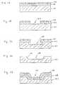
- FIGS. 2A through 2Dshow an example in the prior art for creating a plurality of openings in a receiving substrate which is designed to receive a plurality of separately fabricated elements which are deposited into the openings through fluidic self assembly.
- the method shown in FIGS. 2A through 2Dbegins by, in one example, thermally growing a silicon dioxide layer on a silicon substrate 20 .
- the resulting structureis shown in FIG. 2A with the silicon dioxide layer disposed over the silicon substrate 20 .
- a photoresist materialmay be applied, and exposed through a lithographic mask and then developed to produce a patterned mask formed from the developed photoresist.
- an etching solutionis applied to etch through the patterned mask to create an opening 24 in the silicon dioxide layer 22 .
- the resulting structureis shown in FIG. 2B.
- the silicon dioxide layer 22 with its opening 24is then used as a patterned mask to etch the silicon layer 22 to create the opening 26 in the silicon layer 20 as shown in FIG. 2C.
- This etching of the silicon layer 20may be performed with a KOH etchant or with an EDP etchant as described in U.S. Pat. No. 5,545,291.
- the silicon dioxide layer 22is removed, for example, by an etch in a hydrofluoric acid solution. This results in the structure shown in FIG.
- FIG. 2Dwhere the opening 26 is now ready to receive a separately fabricated element through an assembly process, such as for example, fluidic self assembly or perhaps a pick and place procedure.
- the structure shown in FIG. 2Dhas the drawback that a monocrystalline silicon layer is required in order to use the KOH etch to form the hole.
- the present inventionprovides various methods for creating an opening in a substrate and also provides apparatuses resulting from these methods.
- a method according to the present inventionan opening which has a predetermined cross-sectional shape is created in a substrate.
- the openingis designed to receive an element which is separately fabricated and which typically includes at least one functional component and which is placed into the opening in a process such as pick and place or fluidic self assembly.
- the methodinvolves etching the substrate through a first patterned mask for a first portion of an etch time and etching the substrate through a second patterned mask for a second portion of the etch time.
- the first and second patterned masksare different.
- an opening which has a predetermined cross-sectional shape in a substrate and which is designed to receive an element which is placed into the openingis created by applying a patterned mask over a material which is sensitive to electromagnetic radiation and exposing the material and the patterned mask to electromagnetic radiation which is project obliquely to a surface of the material such that some of the electromagnetic radiation impinges into a first portion of the material which is under the patterned mask.
- the patterned maskis removed and a second portion of the material which was under the patterned mask is also removed.
- a methodfor forming an opening in a first layer which includes silicon dioxide.
- a second layeris deposited over the first layer which includes silicon dioxide, and a metal adhesion layer, such as a tungsten layer is deposited over the second layer.
- the metal adhesion layeris patterned and the second is patterned to expose a portion of the first layer which is then etched.
- the present inventionalso provides a substrate having at least one opening which is designed to receive an element having a predetermined shape.
- the elementis fabricated separately and assembled into the opening.
- the openingincludes in a region near its top edge a beveled surface which in one exemplary embodiment is designed to decrease the frequency of inverted elements from being wedged into the top of the opening.
- a method for creating an opening in a layeris described.
- the openingis for receiving an element which is placed into the opening.
- the methodincludes forming a first layer on a substrate, depositing a second layer over the first layer, and ablating selectively the second layer at at least one desired region to create an opening in the second layer at the at least one desired region, wherein the ablating stops automatically at the first layer.
- the openingis for receiving an element which is fabricated on another substrate and is placed in the opening.
- the methodincludes forming an organic layer on a glass substrate and forming an opening in the organic layer.
- a method for etching glass in an etching solutionis described.
- the etching solutionhas certain described concentrations of hydrofluoric acid, a counter acid (e.g. HCl, HBr, HI, HNO 3 , or H 2 SO 4 ) and water and the etching of the glass with the etching solution is performed at a reduced temperature in the range of about 0° C. to about 10° C.
- a counter acide.g. HCl, HBr, HI, HNO 3 , or H 2 SO 4
- FIGS. 1A and 1Bshow examples of how a block can mate with an opening in a receiving substrate, which opening is designed to receive a separately fabricated element which includes at least one functional component.
- FIGS. 2A through 2Dshow another method in the prior art for forming openings in a receiving substrate.
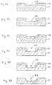
- FIGS. 3A through 3Gshow cross-sectional views of one method according to the present invention of forming an opening in a receiving substrate
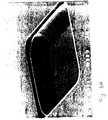
- FIG. 3His a perspective electron micrograph image of an opening formed according to this method.
- FIG. 3Ishows an example of a block in a hole.
- FIGS. 4A through 4Fshow in cross sectional views another method according to the present invention for forming openings in a receiving substrate.
- FIGS. 5A through 5Fshow in cross sectional views another method according to the present invention of forming openings in a receiving substrate.
- FIGS. 6A through 6Fillustrate in cross sectional views another example of the present invention for forming openings in a receiving substrate.
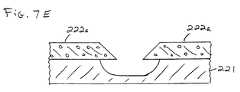
- FIGS. 7A through 7Eshow in cross sectional views another method according to the present invention for forming openings in a receiving substrate.
- FIGS. 8A through 8Fshow another method for forming openings in a receiving substrate according to the present invention.
- FIGS. 8A, 8B, 8 D, 8 E, and 8 Fare cross sectional views
- FIG. 8Cis a top plan view.
- FIG. 9Ais a flowchart which illustrates a general process for forming an assembly by placing elements into the openings in the receiving substrate.
- FIGS. 9B, 9C and 9 Dshow a cross-sectional view of one example of an assembly according to the present invention in which silicon blocks which include electrical functional components are assembled into the openings in a receiving substrate which in this case is a glass substrate.
- FIGS. 9E, 9F, 9 G, and 9 Hshow cross-sectional views of another example of an assembly according to the present invention in which silicon blocks, which include functional components, are assembled into the openings in a receiving substrate.
- the openings shown in FIGS. 9E, 9F, 9 G and 9 Hmay be formed with the method illustrated in FIGS. 3 A- 3 G.
- FIG. 9Iis a perspective electron micrograph image of a silicon block which has been placed into an opening in a substrate, and electrical interconnects have been formed to the silicon block.
- FIG. 10shows a flowchart which indicates a method for creating an assembly of blocks and a receiving substrate which receives the blocks into openings on the receiving substrate.
- FIGS. 11A and 11Bshow two examples of nozzles which may be used to dispense a slurry of blocks onto a receiving substrate.
- FIGS. 12A and 12Bare cross-sectional views of a substrate in which an opening is created according to another method of the present invention.
- FIGS. 13A and 13Bare cross-sectional views of a substrate in which an opening is created according to another method of the present invention.
- the present inventionrelates to methods and apparatuses for forming openings in a receiving substrate.
- the following description and drawingsare illustrative of the invention and are not to be construed as limiting the invention. Numerous specific details are described to provide a thorough understanding of the present invention. However, in certain instances, well known or conventional details are not described in order to not unnecessarily obscure the present invention in detail.
- the present inventionrelates generally to the field of creating openings in a receiving substrate and to apparatuses having these openings.
- the present inventionmay be used to fabricate openings for various different types of arrays.
- each element in the arrayincludes a functional component which may be an electrical component, a chemical component, or an electromechanical structural element or a micro electromechanical structural element or a micro-mechanical structural element.
- a functional componentwhich may be an electrical component, a chemical component, or an electromechanical structural element or a micro electromechanical structural element or a micro-mechanical structural element.
- the inventionmay be applied to the fabrication of an electronic array which can be used to deliver precise voltages for the control of liquid crystal cells to create a liquid crystal display or may be used for other types of displays such as electro-luminescent displays or light emitting diode displays or displays using electrophoretic ink display pixels, such as microencapsulated electrophoretic ink display pixels, and also for other applications requiring sampling or producing electrical signals over a large array of electrodes, such as memories and imaging arrays and photo diode arrays.
- the present inventionmay be used with electromagnetic signal detectors (e.g. antennas), or solar cells, or chemical sensors.
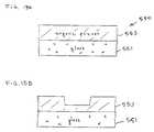
- an openinghas a predetermined size which is designed to receive an element also of the same predetermined size so that the element fits into the opening.
- each elementhas a trapezoidal cross-sectional shape which fits into a trapezoidal opening in which the top of the opening has a larger area than the bottom of the opening. Furthermore, it is desirable to form a deep opening without making the opening too wide.
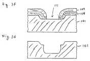
- FIGS. 3A through 3Gillustrate cross-sectional views after various processing operations according to one example of the present invention.
- the method shown by FIGS. 3A through 3Gbegins with the substrate 101 which is typically glass in the case of an active matrix liquid crystal display (of the transmissive type). It will be appreciated that this substrate may be a different material for other types of arrays.
- the glass substrate 101is covered by an amorphous silicon layer 102 which may be deposited by PECVD to a total thickness of approximately 500 Angstroms to three thousand Angstroms.
- An optional tungsten layer 103(or other metal adhesion layers such as, for example, titanium, tungsten, or chrome) may be deposited by sputtering; this optional tungsten layer 103 is deposited on top of the amorphous silicon layer 102 as shown in FIG. 3A.
- lithographyis used to provide a patterned mask layer with openings of the shape desired for the resulting hole in the substrate 101 .
- the size of the openings in the substrateare approximately 0.5 microns to 5 microns larger than the blocks to be assembled into the openings.
- a photoresistis used to create the patterned mask. This patterned mask may be created on top of the optional tungsten layer 103 by spinning photoresist onto the entire structure, exposing the photoresist through a lithographic mask and then developing the photoresist layer to create the pattern mask. Then the tungsten layer 103 is etched and the amorphous silicon layer 102 is etched to creating an opening 104 as shown in FIG. 3B.
- the optional tungsten layeris used to increase adhesion to photoresist to prevent pinholes in the underlying structure and results in an improved receiving substrate.
- This opening 104exposes the top surface of the substrate 102 so that it may be etched to create the opening 105 shown in FIG. 3C.
- the etch to create the opening 105is a wet etch.
- the preferred etch mixdepends on the type of glass used.
- the etch mixcontains dilute hydrofluoric acid and, preferably, an additional acid such as nitric acid, sulfuric acid, perchloric acid, or more preferably a halide acid such as hydrobromic acid or hydrochloric acid or hydriodic acid.
- the ratio of water to the second acid to hydrofluoric acidranges from 2:1:1 to 50:20:1, depending on the type of glass used for the substrate.
- the substrateis etched for roughly one quarter of the total etch time.
- the ratios of an etchant which includes water, hydrochloric acid and hydrofluoric acidis 4:1:1 (water:hydrochloric:hydrofluoric) and the total etch time is such that the total depth of the etchant produces an opening having a depth of 14.5 microns.
- the glasscan be etched with any hydrofluoric acid-based etch solution, with hydrofluoric acid concentration ranging from concentrated hydrofluoric acid to 1% concentrated hydrofluoric acid in water.
- the glassis soda lime glass, and is etched with a mixture of hydrofluoric acid:counter acid:water in which the water content ranges from 50% to 95%, the hydrofluoric acid content ranges from 25% to 1%, and the counter acid content ranges from 40% to 5%.
- the counter acidcould be nitric acid or sulfuric acid, or more preferably, hydriodic acid, or hydrobromic acid, or most preferably, hydrochloric acid.
- the temperature of the etching solutionis maintained at a temperature in the range of from ⁇ 10° C. to 40° C.
- the glassis borosilicate or aluminosilicate glass, such as Corning 7059 or Corning 1737, respectively, and is etched in an etch mix as above, in which the water content ranges from 60% to 95%, the hydrofluoric acid content ranges from 10% to 1%, and the counter acid, as described above, ranges from 30% to 5%.
- the temperature of the borosilicate or aluminosilicate glass etch described aboveis controlled to within 0.5 degrees C., at a specified temperature between ⁇ 5 and 5 degrees C.
- the etch solutionis 1 part HF to 10 parts HCl to 100 parts H 2 O.
- the tungsten layer 103 and the amorphous silicon layer 102are removed over the entire substrate, and then the entire substrate is blanket etched for an additional one quarter of the entire etch time.
- this blanket etchis the same etch mix used to create the initial opening 105 shown in FIG. 3C.
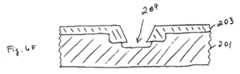
- the beveled edge 106 at the top of the opening 105tends to prevent an inverted element from lodging at the top of the opening 105 during the assembly of the element into the opening.
- the beveled edge 106creates an opening which has at least two slopes along the surface of the opening, where one of these slopes is an average of the slopes along the edge 106 and the other slope is substantially vertical as shown in FIG. 3G.
- amorphous silicon layer 108is deposited onto the entire top of the substrate.
- the amorphous siliconmay be deposited by a PECVD or CVD or a sputtering process to a total thickness of about a thousand Angstroms.
- An optional tungsten layer(which is preferably about 100 to 1000 Angstroms thick) may then be deposited (e.g. by sputtering) on the layer 108 .
- a photoresist layer 109is applied to the top of the amorphous silicon layer 108 (or on top of the optional tungsten layer if the tungsten layer is applied), and this photoresist layer 109 is patterned to create the opening 110 in the photoresist layer 109 (and in the optional tungsten layer if present) as shown in FIG. 3E.
- the patterned photoresist layer 109forms an opening 110 which is smaller than the original opening 104 in the patterned mask used to create the structure shown in FIG. 3B.
- the exposed surface of the amorphous silicon layer 108which is exposed at the opening 110 as shown in FIG. 3E, is then etched to create an opening 111 as shown in FIG. 3F.
- This opening 111exposes a top surface of the substrate 101 which is at the bottom of the opening 105 as it now exists in this sequence of processing operations.
- the substrate 101is now etched through the opening 111 with the same etch solution described above to create the opening shown in FIG. 3G.
- FIG. 3Gshows the opening after the amorphous silicon layer 108 and the photoresist layer 109 have been removed.
- the patterned photoresist layer 109is first stripped (and if present the optional tungsten layer is stripped) and then the amorphous silicon 108 is removed creating the structure shown in FIG. 3G.
- FIG. 3Hshows an electron micrograph image of an opening which may be formed with the method shown in FIGS. 3 A- 3 G.
- FIG. 9Eis a cross-sectional view of a similar opening. As can be seen from FIG. 3H and FIG. 9E, the opening has a bevel at its top edge. The rest of the opening is deep without having an upper cross-sectional area which is too large. If this upper cross-sectional area of the opening is too large, then inverted blocks will tend to get stuck in the opening.
- FIG. 3Iis a stick drawing of a block in an opening. The edge 115 A of the opening nearly abuts the edges 115 B and 115 D of the top of the block. The bottom edge 115 C of the block is shown through the body of the block which has been made, for purposes of illustration, to be transparent. An example of dimensions for a particular block and matching opening will now be provided.
- FIG. 9FBy means of an example, given a block 353 with the cross-section shape shown in FIG. 9F and dimensions: bottom width 131 microns, top width 182 microns and total thickness of 38 microns, circuit thickness 2 microns and angles of 54.7 degrees.
- the suitable holewould be etched with the following parameters. Opening 104 in layers 103 and 102 of FIG. 3B should be of width 145 microns. Then the glass should be etched (see previously mentioned etch conditions) a total of 14 microns. This forms opening 105 in the glass with a total width of 173 microns. Then the blanket etch (between 3 C and 3 D) should be for a depth of 7 microns.
- the opening 105to a width of 185 microns.
- the opening in the second mask material( 108 of 3 F) should be of a width 130 microns.
- the glassshould then be etched a total of 24 microns making the depth of the hole 38 microns.
- the cross-section of the block 353 and hole 351 combinationis shown in FIG. 9F.
- the total depth of the openingis 39 microns, and three etches are used to create the opening, where the total etch time is the total time for the three etches.
- the first and the third etchare through a first and second patterned mask respectively, and the second etch is without a patterned mask or at least uses a mask which allows the top edge of the openings to be exposed.
- the first etchis for a quarter of the total etch time
- the second etchis for a quarter of the total etch time
- the third and last etchis for one half of the entire etch time.
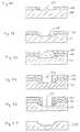
- FIGS. 4A through 4Fshow cross-sectional views through an opening fabricated according to another method of the present invention. Each of these figures shows the state of the opening after certain other process operations in this method.
- FIG. 4Ashows a patterned mask layer 132 which includes an opening 133 exposing a top surface of a substrate 131 which may be glass in one embodiment.
- the patterned mask layer 132may be, for example, chrome.
- the exposed areas of the substrate 131are etched using an appropriate etchant. In one example, this etch is a wet etch bath using hydrofluoric acid which creates the opening 134 in the substrate 131 as shown in FIG. 4B. This etch in one example is two-thirds of the total etch time used in the process shown in FIGS.
- FIG. 4Cshows an example when the blanket mask layer 135 has been deposited over the entire substrate and has filled the opening 134 .
- This second blanket mask layeris then patterned using, for example, photolithography, to pattern the photoresist layer 135 to create the opening 136 shown in FIG. 4D.
- This openingexposes the bottom surface of the opening 134 in the substrate 131 .
- the size of the opening 136is smaller than the size of the opening 134 as can be seen by comparing FIGS. 4B and 4 D.
- the substrate shown in FIG. 4Dis then etched again to etch the exposed surfaces of the substrate through the openings 136 to create the opening 137 shown in FIG.
- the patterned photoresist layer 135is removed by a conventional stripping operation and the chrome layer 132 is removed resulting in the structure shown in FIG. 4F in which the substrate 131 now includes an opening which has a staircased or beveled edge as shown in FIG. 4F.
- the etchant used to etch the substratewill depend upon the material of the substrate, and the masking layers will be designed to be resistant to those etchants.
- the second mask material, such as the photoresist layer 135is patterned with a vertical etch.
- the same lithographic mask which created the patterned layer 132may be used to create the pattern in the photoresist layer 135 (although this is not shown in FIGS. 4B and 4D).
- the etch which creates the opening 137may be a wet chemical etch (such as an etchant containing hydrofluoric acid) which is approximately two-thirds of the total etch time when the first etch to create the opening 134 was for one-third of the total etch time.
- a wet chemical etchsuch as an etchant containing hydrofluoric acid
- FIGS. 5A through 5Fshow another example of a method according to the present invention.
- the cross-sectional views through the substrate 151 shown in FIGS. 5A through 5Fillustrate the structure of an opening as it is created using this exemplary method. It will be appreciated that a plurality of such openings are formed in the substrate 151 which may be an array of openings designed to receive separately fabricated elements which are assembled into the opening in subsequent processing. This is also true for the opening which is created using the other examples of methods of the present invention.
- FIG. 5Ashows that a top region of the substrate 151 is exposed by an opening 152 in the patterned mask layer 153 .
- this patterned mask layermay be chrome or amorphous silicon formed by PECVD or CVD or sputtered amorphous silicon.
- the opening 152is created using standard lithography techniques. This opening matches the shape of the desired hole.
- the substrate with the patterned mask 153is then placed in a wet etch bath to create the opening 154 .
- a hydrofluoric acid etchetches the substrate 151 in its exposed regions to create the opening 154 as shown in FIG. 5B. In one example, this etch is for two-thirds of the total etch time, which total etch time includes the etching through the opening 157 to create the opening 158 as shown in FIGS. 5D and 5E.
- a second mask material 155is applied over the substrate 151 and into the hole 154 after the patterned mask layer 153 has been removed. This results in the structure shown in FIG. 5C. Then the second mask material 155 is patterned to create the opening 157 , typically using a vertical illumination. This results in the structure shown in FIG. 5D in which the opening 157 exposes a bottom portion of the opening 154 as shown in FIG. 5D. Then another etch is performed through the opening 157 to create the opening 158 shown in FIG. 5E. In one particular embodiment, a hydrofluoric acid etch for one-third of the total etch is used to create the opening 158 .
- the opening 158includes a beveled edge or a stairstep edge which provides for improved settling of elements into the hole and prevents lodging of inverted elements.
- a first mask materialis applied on top of the substrate 201 , and this first mask material is then patterned to create the first patterned mask 202 as shown in FIG. 6A. Then the substrate 201 is exposed to an etchant, which is typically a wet etch, which creates the opening 201 A as shown in FIG. 6B. Then the patterned first mask layer 202 is removed and a photo-polymerizable layer 203 is applied over the entire substrate, filling the holes as shown in FIG. 6C.
- an etchantwhich is typically a wet etch
- a second mask materialis applied over the photo-polymerizable material 203 , and this second mask material is patterned to create the opaque mask 204 which is shown aligned over the central region of the opening 201 A.
- the opaque mask 204is used to mask obliquely directed light 205 and 206 as shown in FIG. 6D.
- the obliquely directed lightobliquely directed from both sides of the opening as shown in FIG. 6D causes the light to pass partly under the mask 204 . Because the mask 204 is opaque, some of the region under the mask 204 will not be exposed and another portion near the edges of the mask 204 will be exposed.
- FIGS. 7A through 7Dshow an alternative embodiment in which the substrate 201 is not etched but the photo-polymerizable material 222 is etched after exposure to obliquely directed light as in the case of the method shown in FIGS. 6A through 6G.
- a patterned opaque mask 223(or alternatively a contact mask) is placed on a photo-polymerizable material 222 which has been placed over the substrate 221 .
- obliquely directed light 224 and 225exposes the area surrounding the desired opening and a portion of the area under the mask 223 thereby causing these exposed regions to by polymerized as region 222 A leaving the unpolymerized region that was not exposed as region 222 B.
- four sources of light obliquely angled relative to the surfacewill typically be necessary, however, two sources at either set of diagonally opposed corners of a rectangular mask is sufficient.
- FIG. 7Cshows the result of the exposure after the mask 223 has been removed. Then the unpolymerized material 222 B is removed using a conventional etchant which leaves the opening 227 as shown in FIG. 7D.
- the polymerized material 222 Amay be used as a mask to etch an opening in the substrate 221 .
- FIG. 7ESuch an alternative result is shown in FIG. 7E where the polymerized material 222 A is left to create a bevel around the top edge of the opening which now extends into the substrate 221 .
- FIGS. 8A through 8Fshow another example of a method according to the present invention.
- a mask materialis patterned over a substrate 251 to create openings which are thin slots.
- the mask materialmay be chrome which forms the patterned layer 252 with openings 253 A and 253 B.
- FIG. 8Cshows an example of such a mask where the openings form a rectangle with protrusions from the corners and openings 255 which resemble pin-hole openings next to these protrusions at the corners. It will be appreciated that FIG. 8C is a top view of the patterned mask layer 252 and that these openings in the patterned mask layer 252 expose portions of the top surface of the substrate 251 which, in one embodiment, may be glass.
- FIG. 8Ais indicated on FIG. 8C.
- a wet etchis applied to the substrate 251 to etch the substrate a small amount, such as 2 microns.
- the resulting etchis shown in FIG. 8B in which the small openings 254 A and 254 B are created in the substrate 251 .
- These openingssurround the chrome island 256 shown from top view in FIG. 8C and from side cross-sectional view in FIG. 8D.
- a photoresistis then applied and patterned over the chrome such that only the center square 256 is exposed as shown in FIG. 8D.
- the patterned photoresist layer 257is then used as a mask to etch the chrome island 256 resulting in the opening 258 as shown in FIG. 8E. Then the structure shown in FIG.
- a wet hydrofluoric acid etchis used to etch into the opening 258 of the substrate 251 . This creates the opening 259 shown in FIG. 8F. Then the patterned photoresist layer 257 and the chrome layer 252 are removed to produce the final hole.
- the various different methods of the present inventionwill typically create an array of openings on a receiving substrate. These openings are then filled with a plurality of elements, each of which typically include at least one function component, such as a pixel driving circuit for driving a liquid crystal cell in an active matrix liquid crystal display or other display driving elements for other types of displays.
- a function componentsuch as a pixel driving circuit for driving a liquid crystal cell in an active matrix liquid crystal display or other display driving elements for other types of displays.
- these elementsresemble tapered blocks having a trapezoidal cross-section where the top of the block is wider than the bottom of the block.
- An example of such a blockis shown as block 16 in FIG. 1D.
- Various improved methods for forming these blocksare described in co-pending U.S. patent application Ser. No. ______, which was filed concurrently herewith by John Stephen Smith, Mark Hadley and Jay Tu which is assigned to the same Assignee as the present invention and which is entitled “Methods for Creating Elements of Predetermined Shape and Apparatuses Using These Elements” and which is hereby incorporated herein by reference.
- the electrical circuitsare fabricated as described in U.S. patent application Ser. Nos.
- FIGS. 9A through 9Dwill now be referred to in describing one example of a method of assembling the blocks into the openings in order to create a completed assembly.
- FIG. 9Ashows a generalized flowchart indicating the various processing operations which are performed to create the completed assembly in which the blocks or elements are assembled into the openings in the receiving substrate.
- blocks having a predetermined shapeare prepared.
- an integrated circuitis fabricated into each block and each block is extracted from a first substrate which may be a single crystal semiconductor substrate, such as a monocrystalline silicon wafer.
- the openings for the blocksare prepared in a second substrate.
- Processing operation 303may employ any of the previously described methods of the present invention in order to form openings having a desired shape which is designed to match the predetermined shape of the blocks formed in processing operation 301 .
- the blocksare assembled into the openings.
- the blocksmay be assembled by a pick and place method as described above.
- fluidic self assemblyis used to assemble the blocks into the openings.
- Fluidic self assembly in one example of the present inventionmay use a slurry of the blocks which are carried in a fluid, such as acetone or water with a surfactant or other types of fluids, including gases or vapors. Agitation and fluid flow to move the blocks over the receiving surface may be used. When a block encounters an opening, it falls into it and is held there. Blocks that do not encounter an opening simply slide off the substrate. Eventually, the substrate contains only blocks that are in holes.
- a second dose of block slurrycan be deposited on the substrate to fill those holes.
- a binding agentmay be added and the slurry solvent, such as acetone, is evaporated.
- the assemblyis planarized.
- the substrate with the blocksis spin-coated with partially polymerized benzocyclobutene to a uniform thickness of greater than 2 microns.
- This planarization layeris then cured.
- FIG. 9Bshows an example of a block, referred to as silicon block 325 having an active device layer 327 at the top surface of the block 325 .
- the blocksits securely in the opening 323 in the glass substrate 321 .
- the planarization materialis shown in FIG. 9C as material 329 which fills the gaps in the opening 323 and also coats the upper surface of the glass substrate 321 and covers the block 325 and the active circuit layer 327 .
- Viasare then etched in the planarization layer and electrical connections are made to bonding pads on the integrated circuit in the active circuit layer 327 .
- Processing operation 309 as shown in FIG. 9Amay include other methods for interconnecting the various blocks in the various openings along the substrate.
- metallizationis applied into the vias 331 in order to make contact to bonding pads on the active device layer 327 of the block 325 .
- These patterned metal layerssuch as metal lines 333 A and 333 B, serve to interconnect the blocks electrically.
- these metal lines(or non-metal conductive lines) may represent a row line for a row of pixels or may represent a column line for a column of pixels as is well known in the art of fabricating active matrix liquid crystal displays.
- the Fluidic Self Assembly (FSA) processcan be performed in a variety of conditions, with a variety of fluids.
- Proper selection of the block and substrate surface chemistry as well as the fluid to be usedresults in faster, higher yielding assemblies with dramatically fewer excess blocks left on the surface prior to rinsing, inspection, and repair.
- the surface chemistry interaction with the fluideffectively reduces the amount of friction between the blocks and the substrate.
- the choice of block surface chemistry, substrate surface chemistry, and fluidare all usually interrelated. For example, hydrophobic surface chemistries work much better with organic fluids than with aqueous solutions.
- the treatment of the surfacesusually, but not necessarily, alters both sets of surfaces so that they are of the same type.
- both the elements and substratemay be treated to have a hydrophilic surface and the elements, so treated, may be dispersed in a polar solvent (e.g. H 2 O) and then dispensed over the so treated substrate in an FSA process.
- a polar solvente.g. H 2 O
- both the elements and the substratemay be treated to have a hydrophobic surface and the elements and substrate, so treated, may be combined in a solvent (e.g. hexane) which is non-polar in an FSA process.
- any surface treatment that cleans the surface of the blockresults in improved FSA's.
- a surface treatment fluidmay be in a liquid form, a gas form or a plasma form. The improvement is more significant if the surface treatment leaves a desired, uniform surface chemistry on all of the blocks for a given assembly.
- Hydrophilic surface chemistriescan be achieved by rinsing the blocks in any oxidizing solution, such as aqueous KMnO 4 , H 2 SO 4 with H 2 O 2 , NH 4 OH with H 2 O 2 , or ozonated deionized water or by exposing the blocks to an oxygen plasma.
- the surface chemistryis more uniform if the blocks can be agitated while being immersed in one of the preceding chemistries.
- the agitationcould be caused by a variety of systems, such as from a recirculating fluid flow, from a megasonic or ultrasonic bath, or by stirring.
- Hydrophilic surfaces with good uniformitycan be achieved by oxidizing the surfaces and reacting a functional, self-assembled monolayer onto the surface, and then oxidizing the functional group in the self-assembled monolayer.
- octenyltrimethoxysilanecould be reacted onto block surfaces cleaned by oxidation with H 2 SO 4 and H 2 O 2 .
- the alkene groupcan then be oxidized into a hydrophilic functional group by treatment with a mild, aqueous KMnO 4 solution.
- Hydrophobic surfaces on blockscan be created by cleaning and oxidizing the blocks as described above, and then reacting a self-assembled monolayer onto the surface, such that the hydrocarbon chains of the self-assembled monolayer are topmost at the surface.
- the contact angle of water on these hydrophobic surfacesis at least 90 degrees.
- Teflonwhich can be deposited or formed on the surfaces of the blocks, will also act to create hydrophobic surfaces on the blocks.
- Other types of coatings of a hydrophobic naturemay be used or a fluorine plasma may be used to create hydrophobic surfaces on the blocks.
- the substrate surface treatmentis analogous to the block surface treatment. It is possible to perform fluidic self-assemblies in which the block receives one surface treatment, and the substrate receives a different surface treatment.
- the substratemay be exposed to a surface treatment fluid which creates a metal coating (film) on the surface of the substrate (a hydrophilic surface normally) or a surface treatment fluid which is an oxygen plasma (to create a hydrophilic surface) or a surface treatment fluid which oxidizes a coating (or otherwise creates an oxidized coating) on the substrate while the blocks are exposed to a surface treatment fluid which is dissolved ozone in water.
- the same surface treatment fluide.g. an oxygen plasma
- the choice of fluid for any given FSAdepends on the surface chemistry of the blocks and the substrate. Assemblies processed with hydrophobic surface chemistries (e.g. the blocks and substrate have each been exposed to surface treatment fluid(s) which have created hydrophobic surfaces on the blocks and the substrates) proceed more rapidly if an organic solvent, such as toluene or hexane, is used as the slurry fluid in the FSA process.
- an organic solventsuch as toluene or hexane
- water or hydrophilic solventssuch as acetone (or other polar or water soluble solvents) are more appropriate as the slurry fluid in the FSA process.
- a preferred method of surface treatment for the block devicesis to oxidize the surface with a dilute aqueous solution containing 0.008% potassium permanganate, 0.025% sodium periodate, and 0.415% potassium carbonate.
- the block devicesare stirred in the oxidizing solution at 75° C. for 2 hours.
- the preferred method for stirring the block devices in the solutionis to separate the block devices from the stirrer by a stainless steel sieve material. After 2 hours of exposure to the oxidizing solution, the block devices are collected on the sieve, and rinsed in a 0.3M aqueous sodium bisulfite solution. Then the devices are rinsed in a 0.1M solution of acetic acid. Finally, they are rinsed in DI (deionized) water.
- the most preferred methodis to oxidize the block devices while they recirculate in a solution of 5 to 125 ppm dissolved ozone in DI water.
- the most preferred ozone concentrationis in the range of 50-125 ppm dissolved ozone.
- the block devicesare recirculated for 1 hour, rinsed in DI water, and then transferred to the slurry fluid prior to fluidic self assembly.
- the most preferred method for treating a glass or silicon substrateis to place the substrate in a mix of 95 parts concentrated sulfuric acid and 5 parts hydrogen peroxide for 10 minutes. The substrate is then rinsed in DI water prior to fluidic self assembly.
- a preferred treatment for treating plastic substratesis to expose them to gaseous ozone for 5 minutes.
- the most preferred method for treating a plastic substrateis to expose the substrate to an oxygen plasma for 1 minute prior to fluidic self assembly.
- the optimal fluids for FSAhave low viscosity and can be used safely. It is possible to add reagents to the fluid to improve the FSA process. For example, surfactants or certain water soluble polymers can be added to water to reduce the block-substrate interaction, thereby reducing the number of excess blocks left on the substrate at the end of an assembly. If a polymer is used, it is desirable that the polymer serve as a lubricant while dissolved. Preferred polymers would consist of water soluble polymers such as Union Carbide Polyox (polyethylene glycol) or DuPont Elvanol (polyvinyl alcohol).
- a surfactantit is preferable to use a non-ionic surfactant so that the circuitry is not damaged by counterions in the surfactant.
- the surfactantsnormally have a molecular form which includes a hydrophobic portion and a hydrophilic portion; often, the non-ionic surfactant will include a hydrophilic portion which is an ethylene oxide oligomer.
- a non-ionic surfactantsuch as Union Carbide MinFoam 1X or Triton 190 or DuPont Zonyl FS-300 is used in water to perform fluidic self assembly of blocks which have been surface treated with aqueous KMnO 4 (or ozonated water) on a glass substrate that was oxidized with H 2 SO 4 and H 2 O 2 .
- the water and surfactant and the blocksform the slurry for the FSA process, and the slurry is dispensed onto the pretreated substrate.
- the substrateis immersed in the FSA fluid (e.g.
- the substratemay be immersed in exactly the same fluid and a surfactant as the fluid and surfactant which make up the slurry.
- the blocks and the substrateare prepared in the desired manner (e.g. the desired surface treatments have been completed), and the appropriate carrier fluid is selected, the blocks can be deposited onto the substrate in a number of ways. They can flow down an inclined tube containing the fluid so that they fall through the FSA fluid and onto the substrate. One or a plurality of these tubes can be used to deposit the blocks onto the substrate. Also, the tube or tubes can be moved across the substrate such that the entire substrate can be covered with block slurry prior to or during assembly. In another embodiment, the blocks could be carried through a tube or a number of tubes by a fluid flow that is either laminar or turbulent. The flow(s) could effectively spray the block slurry over the substrate to cover a selected portion of or the entire substrate.
- the aforementioned tubescould be circular, fan-shaped, or have a multitude of ports.
- the fluidic self assembly processcan be accomplished in a variety of methods.
- the blockscan be moved across the substrate surface in a number of ways, including forced fluid flow, suction, gravity, magnetic fields if the blocks have magnetic characteristics, or any combination of these driving forces.
- Forced fluid flowcan drive the blocks across a tilted or horizontal substrate either by providing a uniform flow over the surface, or by using a very localized flow that can be directed in any desired manner.
- a magnetic field applied to magnetized blockscould draw the blocks into the receptor sites.
- Suctioncould be applied to holes located in the bottom of the receptor sites that go through the substrate to a vacuum source on the other side of the substrate. Gravity is used by tilting the substrate from horizontal to an angle not greater than 55 degrees.
- the tilted substrateis vibrated to drive the blocks down the substrate.
- the vibration frequencyranges from 50 Hz to 10,000 Hz, and can have a square, sine, sawtooth, or any other waveform.
- the direction of the vibrationis in one embodiment transverse to the direction of the block slurry flow down the tilted substrate. In some instances it may be desirable to have components of the vibration in the direction of the block flow down the substrate, and in the direction normal to the substrate.
- the fluidic self assemblycan proceed by either allowing all of the excess blocks (blocks that do not fill a receptor site) to move completely off of the substrate, or by forcing excess blocks to move off of the substrate.
- the excess blockscan be driven off of the substrate with fluid flow over the substrate, by altering the conditions of the vibration applied to the substrate during the assembly, by increasing the angle of inclination of the substrate, by suctioning off blocks, or by any combination of these methods.
- the fluidic self-assembly processcan be accelerated in a number of ways in addition to proper selection of the process parameters listed above.
- One method for speeding up the FSA processis to deposit blocks regularly or uniformly over the entire surface. This deposition process could result in a uniformly dense layer of blocks across the surface. This could be accomplished by spraying the block slurry across the substrate with one or more deposition nozzles. If desirable, the nozzle(s) could be designed to sweep across the surface to achieve more uniform coverage. Alternatively, the blocks could be deposited in selected areas of the substrate. These blocks could be placed by one or more fixed or movable deposition nozzles that deliver the blocks with the assistance of some combination of fluid flow, gravity, and vibrational impulse.
- FIGS. 11A and 11Bshow two examples of nozzle heads which include at least one nozzle.
- Nozzle head 450includes three nozzles 451 , 452 and 543 .
- Each nozzle 451 , 452 and 453may be coupled to receive the same fluid (e.g. a slurry with blocks) or different fluids (e.g. one nozzle ejects a slurry with blocks, one nozzle ejects “helper” blocks (described below) in a fluid, and another nozzle may create a vacuum to be used to remove excess blocks after depositing blocks and allowing them to settle/self-assemble into openings).
- Nozzle head 456includes many nozzles 457 disposed along a row; these many nozzles are designed to eject a fluid (e.g. a slurry with blocks and/or helper blocks) or to draw a vacuum.
- Several nozzle heads 456may be disposed above a substrate to uniformly and concurrently deposit blocks onto the substrate.
- the excess blockscan be removed from the substrate by the methods listed above.
- the excess block clearing processcan be accelerated with the addition of components designed to push blocks off of the substrate. Any combination of a number of different components could accomplish this task.
- One component that can increase clearingis a wiper blade that moves across the substrate. Blocks that are in receptor sitess will be unaffected, but blocks on the surface will be swept away by the wiper blade. Alternatively, a brush could be used in place of or in addition to the wiper blade.
- the components that clear excess blocks from the surfacecould be one or more large items, relative to the size of the blocks, that move down the substrate with the blocks, pushing blocks down and off the substrate as they move. These items may be referred to as helper blocks.
- these itemsare normally significantly larger than the blocks, gravity will drive them down the substrate faster than the blocks, and they will be able to push a large number of the blocks off of the substrate as they move down.
- These relatively large itemscould be glass, plastic, or metal balls, cylinders, or rectangular solids. More preferably, these items could have the same approximate shape as the blocks (but larger in size), or they could be shaped pieces of material that are designed to contact the substrate only where there are no receptor sites.
- these helper blockscould be rectangular pieces made of magnetic stainless steel. After removing the excess blocks from the surface, these items could be recovered and readily separated from the excess blocks by sieving or some other particle separation method or separated with a magnetic field in the case where the helper blocks are magnetic (e.g. the helper blocks are comprised of magnetic material).
- the substratecan be inspected for faults such as empty holes or blocks that have not seated properly in their receptor sites.
- Empty sitescan be filled by placing a small number of blocks in a slurry form and depositing this slurry on or above the empty site, and forcing or allowing the blocks to fill the empty site(s) by means analogous to those used to perform the assembly.
- Empty sitescan also be repaired by a pick-and-place process, in which an individual block is placed in an individual receptor site.
- a receptor site with an improperly seated blockcan be repaired by removing the block with either suction, fluid flow, or mechanical means, and then filling the now empty receptor site as described above.
- blocks that are tilted or rotated in their receptor sitecould be repaired after the assembly is complete with a hot press process.
- the blocksmay be bonded into their receptor sites with an organic or polymeric agent that serves as an adhesive in this application.
- the bonding agentcould be dissolved into the original FSA fluid prior to the start of the assembly, or it could be added any time later during the assembly, assuming that the bonding agent is compatible with the fluid used for the assembly. If the bonding agent is incompatible with the fluid used for the assembly, a fluid displacement process can be used at any time after the start of the assembly to replace the first fluid with a second fluid which is compatible with the bonding agent.
- acetoneis used as the FSA fluid
- a water soluble polymeris used as the bonding agent.
- the FSAis performed in toluene containing benzocyclobutene oligomers which serves as a bonding agent.
- the FSAis performed in basic water that contains surfactant and a water soluble polymer that serves as the bonding agent.
- the FSAcan be performed in water containing surfactant, and then a water soluble bonding agent dissolved in water can be added to the water/surfactant mixture.
- the completed assemblyis left immersed in the bonding solution for 5-30 minutes to allow the bonding agent to diffuse around the blocks in the receptor sites.
- the substratewere tilted it is preferable to reduce or eliminate the angle of inclination, and, in some cases, to apply a low amplitude vibration to the substrate while the angle of inclination of the substrate is being decreased.
- the substrateis either lifted out of the solution, or more preferably, the solution is drained away or evaporated from the substrate. Then the substrate is allowed to dry, either by free or forced convection. During the drying process, it is beneficial to tilt the substrate slightly, so that excess fluid does not pool and dry in the array of blocks.
- the fluidic self assembly processis complete.
- repair of blocks that are tilted in their receptor sitescan be accomplished with the use of heat and mechanical pressure in a number of different ways.
- the substratecan be heated to a temperature that softens the bonding agent, and then pressure can be applied either locally with a point source, more globally with a roller apparatus, or globally with weight or other form of applied pressure. In this step it is important that the surface pressed against the filled substrate will not stick to the blocks in the receptor sites or to the substrate.
- Solutia Scripset 550was used as the bonding agent, the substrate was heated to 120° C., and then pressed between perfluoroalkoxy polymer films with approximately 500 psi for 1 minute. The substrate is then cooled while under pressure. The pressure is released and the perfluoroalkoxy films were removed.
- a Teflon rollermade out of Teflon tubing placed over a steel rod, was rolled across the substrate after it was heated to 120° C. Both of these processes reduced the number of tilted blocks that remained after the completion of the FSA.
- the residual bonding agent that remains on the surface of the substratecan be removed with an oxygen plasma descum without damaging the bonding of the blocks in their receptor sites.
- the substrateis ready for planarization and the rest of the down stream processes required to electrically interconnect the blocks and construct an electrical apparatus.
- FIG. 10shows a flowchart of an exemplary method of the invention which includes the pretreatment of the blocks and the substrate and the bonding of blocks into openings as described above.
- This FIG. 10also optionally uses helper blocks to facilitate movement of the blocks across the substrate during the FSA process.
- Operations 401 and 403include the pretreatment of the surfaces of the blocks and the substrates.
- the fluid used in operation 405may be used to pretreat the blocks' surfaces.
- operations 407 and 409the FSA process occurs, and excess blocks (and helper blocks if used) are removed in operation 411 . Then the blocks are bonded into the openings (after use of a roller as described above) in operation 413 .
- a repair processmay be used as described above and then the substrate is processed in further down stream processes (e.g. planarization and electrical interconnection) in order to create a functional device, such as an active matrix flat panel display.
- FIGS. 9E, 9F, 9 G, 9 H and 9 Ishow the result of an FSA process which fills an opening created using a method according to the process illustrated in FIGS. 3 A- 3 G.
- FIG. 9Ebegins with the opening 351 in a glass substrate 350 .
- a block(shown in this case as a silicon Nanoblock 353 , where Nanoblock is a trademark of Alien Technology, Inc.) is assembled through an FSA process (e.g. the method of FIG. 10) into the opening 351 as shown in FIG. 9F.
- the top portion of block 353includes the functional component (in this case MOS circuitry, such as CMOS pixel drivers and electrode(s)) for the block.
- MOS circuitrysuch as CMOS pixel drivers and electrode(s)
- a planarizing layer 356is applied.
- the planarizing layermay be applied after a bonding solution is used to bond the block to the opening.
- a patterned metal (or other conductive material) layer 357is then created to electrically interconnect the block's functional component to other blocks or to other functional components.
- FIG. 9Ishows an electron micrograph of a block 353 in a substrate 350 after electrical interconnects 357 a and 357 b have been applied. Normally, many such blocks may be formed in a matrix to create, for example, the backplane of an active matrix flat panel display, such as an active matrix liquid crystal display.
- FIG. 12Ashows an assembly 501 of a substrate 503 with a reflective layer 507 and an ablatable layer 505 .
- the substrate 503may be a glass layer or a plastic layer which is flexible.
- the reflective layer 507may be an aluminum foil layer which is also flexible, and the ablatable layer 505 may be an organic polymer or other substances which may be removed (e.g. by evaporation through exposure to selectively located heat).
- the ablatable layer 505is exposed at desired locations to a laser beam 509 which removes the ablatable material at the exposed portions, thereby creating the opening shown in FIG. 12B.
- the openingis created to the point at which the reflective surface 510 of the foil is reached.
- the ablation processstops automatically at the reflective surface 510 .
- Thiswill produce uniformly deep openings when the ablatable layer has a uniform height across the surface of the foil.
- the openingmay then be used as described above in an FSA process.
- FIGS. 13A and 13BAn exemplary method according to another aspect of the invention will now be described in conjunction with FIGS. 13A and 13B.
- a completely different approach to making block receptor sites on a glass substrateis to form the holes in an organic layer coating a glass substrate. This offers many advantages over etching holes directly into the glass.
- the receptor site fabrication processmay be faster and easier on an organic layer than on glass. It will also yield receptor sites that are better in the sense that they more accurately match the size and shape of the nanoblocks.
- FIG. 13Ashows an assembly 550 having an organic layer 553 , which may be thin relative to the glass layer 551 . The opening is then formed to produce the structure shown in FIG. 13B.
- the choice of methoddepends in part on the material to be used as the organic layer on the glass. If the organic material is an amorphous or semicrystalline polymer, the receptor sites may be embossed into the polymer material with a mold that matches the block size and pitch for the device being produced (e.g. an active matrix LCD). In this case, it may be preferable to adjust the mold to take into account the differences in thermal coefficient of expansion between the polymer and the mold material.
- Embossingis just one method of forming the receptor sites in a polymeric coating on the glass.
- the coatingmay alternatively be injection molded onto the glass substrate during the coating process.
- the receptor sitescould be formed in the polymer by solvent casting a polymer solution onto a receptor site mold. The solvent cast sheet could then be laminated or transferred to the glass substrate.
- the receptor sitesare formed in a thin film of either thermoset plastic or crosslinkable organic material on the glass substrate.
- the receptor sitesare formed by placing the liquid organic starting material on the mold. It is preferable to treat the mold with a release coating, such as an oil, a fluorinated coating, or a low-surface energy self-assembled monolayer coating, or one of these materials combined with a metal layer that separates readily from these coatings, such as silver.
- the glass substrateis then pressed on top of the liquid organic material, such that the liquid flows around all of the features of the mold, and any bubbles in the liquid are removed.
- the glass/organic/mold stackis then exposed to sufficient heat or UV light, if necessary, for a sufficient time to cure the liquid organic material into a crosslinked solid material.
- the moldis then separated from the organic film on the glass.
- This methodis advantageous because it will work on a large class of organic materials, and does not require a photolithography step.
- This methodcan also be used on a plastic substrate on a metal foil.
- the processcan either be tuned to etch down to a particular depth in the plastic or a plastic-on-foil laminate structure can be used to create an etch stop.
- the plastic film thicknesscan be the same as the desired depth of the receptor site, such that in the laser ablation process the metal foil serves as an etch stop as described above.
Landscapes
- Engineering & Computer Science (AREA)
- Microelectronics & Electronic Packaging (AREA)
- Computer Hardware Design (AREA)
- Power Engineering (AREA)
- Physics & Mathematics (AREA)
- Manufacturing & Machinery (AREA)
- General Physics & Mathematics (AREA)
- Condensed Matter Physics & Semiconductors (AREA)
- Nonlinear Science (AREA)
- Mathematical Physics (AREA)
- Chemical & Material Sciences (AREA)
- Crystallography & Structural Chemistry (AREA)
- Plasma & Fusion (AREA)
- Optics & Photonics (AREA)
- Micromachines (AREA)
- Weting (AREA)
- Drying Of Semiconductors (AREA)
- Electrodes Of Semiconductors (AREA)
- Internal Circuitry In Semiconductor Integrated Circuit Devices (AREA)
Abstract
Description
- The present invention relates generally to the field of fabricating openings in a substrate and also to apparatuses with these openings. More particularly, the present invention relates to methods for forming openings in a substrate which openings are designed to receive an element which is later placed into the opening and which element includes at least one functional component, and the present invention relates to methods for creating assemblies with the openings.[0001]
- There are many examples of large arrays of functional components which can provide, produce or detect electromagnetic signals or chemicals or other characteristics. An example of such a large array is that of a display where many pixels or sub-pixels are formed on an array of electronic elements. For example, an active matrix liquid crystal display includes an array of many pixels or sub-pixels which are fabricated on amorphous silicon or polysilicon substrates which are large. As is well known in the art, it is difficult to produce a completely flawless active matrix liquid crystal display (LCD), when the display area is large, such as the LCD's on modern laptop computers. As the display area gets larger and larger, the yield of good displays decreases. This is due to the manner in which these display devices are fabricated.[0002]
- Silicon VLSI can be used to produce such an array over a silicon wafer's surface, but silicon wafers are limited in size, limited in conductivity, and not transparent. Further, processing of large areas on silicon wafers can be expensive. Displays which valve the light coming through them need to be transparent. Single crystal silicon can be bonded to a glass substrate and then etched to remove most of the area to achieve transparency, but this is intrinsically wasteful in that, for the sake of maximizing light transmission, the majority of the processed material is discarded and becomes chemical waste. The under-utilization of the precious die area wastes resources, causes greater amounts of chemical waste to be generated in the process, and is generally inefficient and expensive. Another example is photodiode arrays which may be used to collect solar energy. Large arrays of silicon photodiodes with concentrating lenses have been made by sawing wafers and using a pick and place assembly, but thermal dissipation is poor for large elements, and the small elements require too much assembly time.[0003]
- Alternative approaches to fabricating arrays such as displays include fabricating the desired circuitry in an amorphous or polycrystalline semiconductor layer which has been deposited on a substrate, such as glass or quartz. These approaches avoid the limitations of the size of the available single crystal silicon wafers, and avoid the cost of the single crystal wafers, but require expensive deposition of the semiconductor layer, and they still require processing of the entire large substrate to form the active elements in an array, still resulting in the production of much chemical waste and wasted resources. These processes also limit the choice of the substrate; for example, plastic substrates cannot be used due to the nature of the processes which deposit the semiconductor layers. Furthermore, amorphous or polycrystalline silicon semiconductor elements do not perform as well as those made from single crystal semiconductor material. For displays, as an example, it is often difficult or impossible to form some of the desired circuitry out of the amorphous or polycrystalline semiconductor materials. Thus, high frequency edge drivers may be impossible to form out of these materials. This results in the difficulty and expense of attaching an electrical lead for each and every row and column of an array, such as an active matrix liquid crystal display array.[0004]
- As noted above, another difficulty with the existing techniques is that the large number of elements in a large array results in a low probability that all of them will work properly and thus the yield of acceptably good arrays from the manufacturing process is low. Furthermore, there is no possibility of testing any of the elements until the assembly is complete, and then any imperfection in the array must be tolerated or the entire array could be discarded or special and expensive techniques must be used to repair it. These problems result from the fact that the various elements in the array are fabricated on the array rather than separately.[0005]
- It is possible to separately produce elements, such as pixel drivers and then place them where desired on a different and perhaps larger substrate. Prior techniques can be generally divided into two types: deterministic methods or random methods. Deterministic methods, such as pick and place, use a human or robot arm to pick each element and place it into its corresponding location in a different substrate. Pick and place methods place devices generally one at a time, and are generally not applicable to very small or numerous elements such as those needed for large arrays, such as an active matrix liquid crystal display. Random placement techniques are more effective and result in high yields if the elements to be placed have the right shape. U.S. Pat. No. 5,545,291 describes a method which uses random placement. In this method, microstructures are assembled onto a different substrate through fluid transport. This is sometimes referred to as fluidic self assembly (FSA). Using this technique, various blocks, each containing a functional component, may be fabricated on one substrate and then separated from that substrate and assembled onto a separate substrate through the fluidic self assembly process. The process involves combining the blocks with a fluid and dispensing the fluid and blocks over the surface of a receiving substrate which has receptor regions (e.g. openings). The blocks flow in the fluid over the surface and randomly align onto receptor regions.[0006]
- Thus the process which uses fluidic self assembly typically requires forming openings in a substrate in order to receive the elements or blocks. Methods are known in the prior art for forming such openings and are described in U.S. Pat. No. 5,545,291. One issue in forming an opening is to create its sidewalls so that blocks will self-align into the opening and drop into the opening. The substrate having openings in the[0007]
glass layer 10 may be used as a receiving substrate to receive a plurality of elements by using a fluidic self assembly method. FIG. 1A shows an example where a separately fabricatedelement 16 has properly assembled into theopening 14. However, it has been discovered that at times, anelement 16 will not properly assemble into anopening 14 due to the fact that theelement 16 becomes turned upside down and then lodges in the top of theopening 14. An example of this situation is shown in FIG. 1B. Often times, the invertedelement 16 lodges into the opening14 so tightly that it remains in the opening and prevents non-inverted elements from falling into theopening 14. Thus, the opening at the end of the assembly process will typically not be filled with an element or perhaps worse, may still contain an inverted element lodged at the top of theopening 14. - FIGS. 2A through 2D show an example in the prior art for creating a plurality of openings in a receiving substrate which is designed to receive a plurality of separately fabricated elements which are deposited into the openings through fluidic self assembly. The method shown in FIGS. 2A through 2D begins by, in one example, thermally growing a silicon dioxide layer on a[0008]
silicon substrate 20. The resulting structure is shown in FIG. 2A with the silicon dioxide layer disposed over thesilicon substrate 20. Then, a photoresist material may be applied, and exposed through a lithographic mask and then developed to produce a patterned mask formed from the developed photoresist. Then an etching solution is applied to etch through the patterned mask to create anopening 24 in thesilicon dioxide layer 22. The resulting structure is shown in FIG. 2B. Then, thesilicon dioxide layer 22 with itsopening 24 is then used as a patterned mask to etch thesilicon layer 22 to create theopening 26 in thesilicon layer 20 as shown in FIG. 2C. This etching of thesilicon layer 20 may be performed with a KOH etchant or with an EDP etchant as described in U.S. Pat. No. 5,545,291. After etching theopening 26 in thesilicon layer 20, thesilicon dioxide layer 22 is removed, for example, by an etch in a hydrofluoric acid solution. This results in the structure shown in FIG. 2D where theopening 26 is now ready to receive a separately fabricated element through an assembly process, such as for example, fluidic self assembly or perhaps a pick and place procedure. The structure shown in FIG. 2D has the drawback that a monocrystalline silicon layer is required in order to use the KOH etch to form the hole. - Often, it will be desirable to obtain a deep enough opening without making the opening too wide. This, of course, will depend on the shape, which is typically predetermined, of the separately fabricated element or block which is to be deposited into the opening. Naturally, the shape of the opening is designed to fit substantially the shape of the separately fabricated element. Often times, it is necessary to obtain an angle in the opening which is steeper than a 45° angle. These various requirements and the problems associated with inverted elements which become lodged in openings have resulted in attempts to improve the methods for fabricating the openings in a receiving substrate.[0009]
- From the above, it is seen that it is desirable to provide methods for forming openings in a receiving substrate and to provide methods for creating assemblies with these openings.[0010]
- The present invention provides various methods for creating an opening in a substrate and also provides apparatuses resulting from these methods. In one example of a method according to the present invention, an opening which has a predetermined cross-sectional shape is created in a substrate. The opening is designed to receive an element which is separately fabricated and which typically includes at least one functional component and which is placed into the opening in a process such as pick and place or fluidic self assembly. In this example, the method involves etching the substrate through a first patterned mask for a first portion of an etch time and etching the substrate through a second patterned mask for a second portion of the etch time. In one particular example of this method, the first and second patterned masks are different.[0011]
- In another example of a method according to the present invention, an opening which has a predetermined cross-sectional shape in a substrate and which is designed to receive an element which is placed into the opening is created by applying a patterned mask over a material which is sensitive to electromagnetic radiation and exposing the material and the patterned mask to electromagnetic radiation which is project obliquely to a surface of the material such that some of the electromagnetic radiation impinges into a first portion of the material which is under the patterned mask. The patterned mask is removed and a second portion of the material which was under the patterned mask is also removed.[0012]
- According to another aspect of the present invention, a method is provided for forming an opening in a first layer which includes silicon dioxide. In this method, a second layer is deposited over the first layer which includes silicon dioxide, and a metal adhesion layer, such as a tungsten layer is deposited over the second layer. The metal adhesion layer is patterned and the second is patterned to expose a portion of the first layer which is then etched.[0013]
- The present invention also provides a substrate having at least one opening which is designed to receive an element having a predetermined shape. The element is fabricated separately and assembled into the opening. The opening includes in a region near its top edge a beveled surface which in one exemplary embodiment is designed to decrease the frequency of inverted elements from being wedged into the top of the opening.[0014]
- According to another aspect of the invention, a method for creating an opening in a layer is described. The opening is for receiving an element which is placed into the opening. The method includes forming a first layer on a substrate, depositing a second layer over the first layer, and ablating selectively the second layer at at least one desired region to create an opening in the second layer at the at least one desired region, wherein the ablating stops automatically at the first layer.[0015]
- According to another aspect of the invention, another method for creating an opening in a substrate is described. The opening is for receiving an element which is fabricated on another substrate and is placed in the opening. The method includes forming an organic layer on a glass substrate and forming an opening in the organic layer.[0016]
- According to another aspect of the invention, a method for etching glass in an etching solution is described. The etching solution has certain described concentrations of hydrofluoric acid, a counter acid (e.g. HCl, HBr, HI, HNO[0017]3, or H2SO4) and water and the etching of the glass with the etching solution is performed at a reduced temperature in the range of about 0° C. to about 10° C.
- These aspects as well as other features of the present invention will be described further below.[0018]
- The present invention is illustrated by way of example and not limitation in the figures of the accompanying drawings in which like references indicate similar elements.[0019]
- FIGS. 1A and 1B show examples of how a block can mate with an opening in a receiving substrate, which opening is designed to receive a separately fabricated element which includes at least one functional component.[0020]
- FIGS. 2A through 2D show another method in the prior art for forming openings in a receiving substrate.[0021]
- FIGS. 3A through 3G show cross-sectional views of one method according to the present invention of forming an opening in a receiving substrate, and FIG. 3H is a perspective electron micrograph image of an opening formed according to this method.[0022]
- FIG. 3I shows an example of a block in a hole.[0023]
- FIGS. 4A through 4F show in cross sectional views another method according to the present invention for forming openings in a receiving substrate.[0024]
- FIGS. 5A through 5F show in cross sectional views another method according to the present invention of forming openings in a receiving substrate.[0025]
- FIGS. 6A through 6F illustrate in cross sectional views another example of the present invention for forming openings in a receiving substrate.[0026]
- FIGS. 7A through 7E show in cross sectional views another method according to the present invention for forming openings in a receiving substrate.[0027]
- FIGS. 8A through 8F show another method for forming openings in a receiving substrate according to the present invention. FIGS. 8A, 8B,[0028]8D,8E, and8F are cross sectional views, and FIG. 8C is a top plan view.
- FIG. 9A is a flowchart which illustrates a general process for forming an assembly by placing elements into the openings in the receiving substrate.[0029]
- FIGS. 9B, 9C and[0030]9D show a cross-sectional view of one example of an assembly according to the present invention in which silicon blocks which include electrical functional components are assembled into the openings in a receiving substrate which in this case is a glass substrate.
- FIGS. 9E, 9F,[0031]9G, and9H show cross-sectional views of another example of an assembly according to the present invention in which silicon blocks, which include functional components, are assembled into the openings in a receiving substrate. The openings shown in FIGS. 9E, 9F,9G and9H may be formed with the method illustrated in FIGS.3A-3G.
- FIG. 9I is a perspective electron micrograph image of a silicon block which has been placed into an opening in a substrate, and electrical interconnects have been formed to the silicon block.[0032]
- FIG. 10 shows a flowchart which indicates a method for creating an assembly of blocks and a receiving substrate which receives the blocks into openings on the receiving substrate.[0033]
- FIGS. 11A and 11B show two examples of nozzles which may be used to dispense a slurry of blocks onto a receiving substrate.[0034]
- FIGS. 12A and 12B are cross-sectional views of a substrate in which an opening is created according to another method of the present invention.[0035]
- FIGS. 13A and 13B are cross-sectional views of a substrate in which an opening is created according to another method of the present invention.[0036]
- The present invention relates to methods and apparatuses for forming openings in a receiving substrate. The following description and drawings are illustrative of the invention and are not to be construed as limiting the invention. Numerous specific details are described to provide a thorough understanding of the present invention. However, in certain instances, well known or conventional details are not described in order to not unnecessarily obscure the present invention in detail.[0037]
- The present invention relates generally to the field of creating openings in a receiving substrate and to apparatuses having these openings. The present invention may be used to fabricate openings for various different types of arrays. Typically, each element in the array includes a functional component which may be an electrical component, a chemical component, or an electromechanical structural element or a micro electromechanical structural element or a micro-mechanical structural element. The various methods of the present invention are illustrated in certain detailed examples with regard to the manufacture of an active matrix liquid crystal display, but it will be recognized that the invention will have wider applicability. Merely by way of example, the invention may be applied to the fabrication of an electronic array which can be used to deliver precise voltages for the control of liquid crystal cells to create a liquid crystal display or may be used for other types of displays such as electro-luminescent displays or light emitting diode displays or displays using electrophoretic ink display pixels, such as microencapsulated electrophoretic ink display pixels, and also for other applications requiring sampling or producing electrical signals over a large array of electrodes, such as memories and imaging arrays and photo diode arrays. Further, the present invention may be used with electromagnetic signal detectors (e.g. antennas), or solar cells, or chemical sensors.[0038]
- In a preferred embodiment of the present invention, an opening has a predetermined size which is designed to receive an element also of the same predetermined size so that the element fits into the opening. By controlling the fit between the element and the opening, it is possible to have the elements self assemble into the openings. Accordingly, in a preferred embodiment of the present invention, each element has a trapezoidal cross-sectional shape which fits into a trapezoidal opening in which the top of the opening has a larger area than the bottom of the opening. Furthermore, it is desirable to form a deep opening without making the opening too wide. FIGS. 3A through 3G illustrate cross-sectional views after various processing operations according to one example of the present invention.[0039]
- The method shown by FIGS. 3A through 3G begins with the[0040]
substrate 101 which is typically glass in the case of an active matrix liquid crystal display (of the transmissive type). It will be appreciated that this substrate may be a different material for other types of arrays. Theglass substrate 101 is covered by anamorphous silicon layer 102 which may be deposited by PECVD to a total thickness of approximately 500 Angstroms to three thousand Angstroms. An optional tungsten layer103 (or other metal adhesion layers such as, for example, titanium, tungsten, or chrome) may be deposited by sputtering; thisoptional tungsten layer 103 is deposited on top of theamorphous silicon layer 102 as shown in FIG. 3A. Then lithography is used to provide a patterned mask layer with openings of the shape desired for the resulting hole in thesubstrate 101. In one case, the size of the openings in the substrate are approximately 0.5 microns to 5 microns larger than the blocks to be assembled into the openings. Typically, a photoresist is used to create the patterned mask. This patterned mask may be created on top of theoptional tungsten layer 103 by spinning photoresist onto the entire structure, exposing the photoresist through a lithographic mask and then developing the photoresist layer to create the pattern mask. Then thetungsten layer 103 is etched and theamorphous silicon layer 102 is etched to creating anopening 104 as shown in FIG. 3B. The optional tungsten layer is used to increase adhesion to photoresist to prevent pinholes in the underlying structure and results in an improved receiving substrate. Thisopening 104 exposes the top surface of thesubstrate 102 so that it may be etched to create theopening 105 shown in FIG. 3C. - In one example of the present invention, the etch to create the[0041]
opening 105 is a wet etch. The preferred etch mix depends on the type of glass used. The etch mix contains dilute hydrofluoric acid and, preferably, an additional acid such as nitric acid, sulfuric acid, perchloric acid, or more preferably a halide acid such as hydrobromic acid or hydrochloric acid or hydriodic acid. The ratio of water to the second acid to hydrofluoric acid ranges from 2:1:1 to 50:20:1, depending on the type of glass used for the substrate. The substrate is etched for roughly one quarter of the total etch time. In one particular embodiment, the ratios of an etchant which includes water, hydrochloric acid and hydrofluoric acid is 4:1:1 (water:hydrochloric:hydrofluoric) and the total etch time is such that the total depth of the etchant produces an opening having a depth of 14.5 microns. - The glass can be etched with any hydrofluoric acid-based etch solution, with hydrofluoric acid concentration ranging from concentrated hydrofluoric acid to 1% concentrated hydrofluoric acid in water. In a preferred embodiment, the glass is soda lime glass, and is etched with a mixture of hydrofluoric acid:counter acid:water in which the water content ranges from 50% to 95%, the hydrofluoric acid content ranges from 25% to 1%, and the counter acid content ranges from 40% to 5%. The counter acid could be nitric acid or sulfuric acid, or more preferably, hydriodic acid, or hydrobromic acid, or most preferably, hydrochloric acid. The temperature of the etching solution is maintained at a temperature in the range of from −10° C. to 40° C. In a more preferred embodiment, the glass is borosilicate or aluminosilicate glass, such as Corning 7059 or Corning 1737, respectively, and is etched in an etch mix as above, in which the water content ranges from 60% to 95%, the hydrofluoric acid content ranges from 10% to 1%, and the counter acid, as described above, ranges from 30% to 5%. In the most preferred embodiment, the temperature of the borosilicate or aluminosilicate glass etch described above is controlled to within 0.5 degrees C., at a specified temperature between −5 and 5 degrees C. In the most preferred embodiment, the etch solution is 1 part HF to 10 parts HCl to 100 parts H[0042]2O.
- After the[0043]
opening 105 has been formed in thesubstrate 101 as shown in FIG. 3C, thetungsten layer 103 and theamorphous silicon layer 102 are removed over the entire substrate, and then the entire substrate is blanket etched for an additional one quarter of the entire etch time. This produces the structure shown in the cross-sectional view of FIG. 3D in which theopening 105 is deepened and at the same time the top edge of the opening is widened to provide thebeveled edge 106 which is created by the removal of material from the top of the substrate and sides of the hole, thereby changing the shape of the sides of the hole. Typically, this blanket etch is the same etch mix used to create theinitial opening 105 shown in FIG. 3C. Thebeveled edge 106 at the top of theopening 105 tends to prevent an inverted element from lodging at the top of theopening 105 during the assembly of the element into the opening. As can be seen from FIG. 3G, thebeveled edge 106 creates an opening which has at least two slopes along the surface of the opening, where one of these slopes is an average of the slopes along theedge 106 and the other slope is substantially vertical as shown in FIG. 3G. - After the beveled edge is created at the top of the opening, another[0044]
amorphous silicon layer 108 is deposited onto the entire top of the substrate. The amorphous silicon may be deposited by a PECVD or CVD or a sputtering process to a total thickness of about a thousand Angstroms. An optional tungsten layer (which is preferably about 100 to 1000 Angstroms thick) may then be deposited (e.g. by sputtering) on thelayer 108. Then aphotoresist layer 109 is applied to the top of the amorphous silicon layer108 (or on top of the optional tungsten layer if the tungsten layer is applied), and thisphotoresist layer 109 is patterned to create theopening 110 in the photoresist layer109 (and in the optional tungsten layer if present) as shown in FIG. 3E. The patternedphotoresist layer 109 forms anopening 110 which is smaller than theoriginal opening 104 in the patterned mask used to create the structure shown in FIG. 3B. The exposed surface of theamorphous silicon layer 108, which is exposed at theopening 110 as shown in FIG. 3E, is then etched to create an opening111 as shown in FIG. 3F. This opening111 exposes a top surface of thesubstrate 101 which is at the bottom of theopening 105 as it now exists in this sequence of processing operations. Thesubstrate 101 is now etched through the opening111 with the same etch solution described above to create the opening shown in FIG. 3G. FIG. 3G shows the opening after theamorphous silicon layer 108 and thephotoresist layer 109 have been removed. Typically, the patternedphotoresist layer 109 is first stripped (and if present the optional tungsten layer is stripped) and then theamorphous silicon 108 is removed creating the structure shown in FIG. 3G. - FIG. 3H shows an electron micrograph image of an opening which may be formed with the method shown in FIGS.[0045]3A-3G. FIG. 9E is a cross-sectional view of a similar opening. As can be seen from FIG. 3H and FIG. 9E, the opening has a bevel at its top edge. The rest of the opening is deep without having an upper cross-sectional area which is too large. If this upper cross-sectional area of the opening is too large, then inverted blocks will tend to get stuck in the opening. FIG. 3I is a stick drawing of a block in an opening. The
edge 115A of the opening nearly abuts theedges 115B and115D of the top of the block. The bottom edge115C of the block is shown through the body of the block which has been made, for purposes of illustration, to be transparent. An example of dimensions for a particular block and matching opening will now be provided. - By means of an example, given a[0046]
block 353 with the cross-section shape shown in FIG. 9F and dimensions:bottom width 131 microns, top width 182 microns and total thickness of 38 microns, circuit thickness 2 microns and angles of 54.7 degrees. The suitable hole would be etched with the following parameters. Opening104 inlayers opening 105 to a width of 185 microns. The opening in the second mask material (108 of3F) should be of a width 130 microns. The glass should then be etched a total of 24 microns making the depth of the hole 38 microns. The cross-section of theblock 353 andhole 351 combination is shown in FIG. 9F. - The following parameters create a block and opening combination which produces good self-assembly.[0047]
Block Parameters Hole Parameters thickness = 38.0-38.0 depth = 38.0-38.0 top1 = 184.6-184.6 bottom_width = 131.0- etch1 = 14.0-14.0 top2 = 173.0-173.0 131.0 top_width = 18 1.9-181.9 etch2 = 7.0-7.0 Iength1 = 145.0-145.0 delta_thickness = 2.0 etch3 = 24.0-24.0 length2 = 130.0-130.0 delta_corner = 10.0 marker = 19.8 radius1 = 4.0 radius2 = 12.0 - In one example of the method shown in FIGS. 3A through 3G, the total depth of the opening is 39 microns, and three etches are used to create the opening, where the total etch time is the total time for the three etches. The first and the third etch are through a first and second patterned mask respectively, and the second etch is without a patterned mask or at least uses a mask which allows the top edge of the openings to be exposed. Typically, the first etch is for a quarter of the total etch time, the second etch is for a quarter of the total etch time, and the third and last etch is for one half of the entire etch time. Using the method shown in FIGS. 3A through 3G, it is possible to create a deep opening which is not too wide and which includes a beveled edge. This opening has improved characteristics for receiving separately fabricated elements which may be assembled by a self assembly process, such as fluidic self assembly.[0048]
- FIGS. 4A through 4F show cross-sectional views through an opening fabricated according to another method of the present invention. Each of these figures shows the state of the opening after certain other process operations in this method. FIG. 4A shows a[0049]
patterned mask layer 132 which includes anopening 133 exposing a top surface of asubstrate 131 which may be glass in one embodiment. The patternedmask layer 132 may be, for example, chrome. The exposed areas of thesubstrate 131 are etched using an appropriate etchant. In one example, this etch is a wet etch bath using hydrofluoric acid which creates theopening 134 in thesubstrate 131 as shown in FIG. 4B. This etch in one example is two-thirds of the total etch time used in the process shown in FIGS. 4A through 4F. A second blanket mask, such as a photoresist layer, is deposited over the entire substrate. FIG. 4C shows an example when theblanket mask layer 135 has been deposited over the entire substrate and has filled theopening 134. This second blanket mask layer is then patterned using, for example, photolithography, to pattern thephotoresist layer 135 to create theopening 136 shown in FIG. 4D. This opening exposes the bottom surface of theopening 134 in thesubstrate 131. The size of theopening 136 is smaller than the size of theopening 134 as can be seen by comparing FIGS. 4B and4D. The substrate shown in FIG. 4D is then etched again to etch the exposed surfaces of the substrate through theopenings 136 to create theopening 137 shown in FIG. 4E. Then the patternedphotoresist layer 135 is removed by a conventional stripping operation and thechrome layer 132 is removed resulting in the structure shown in FIG. 4F in which thesubstrate 131 now includes an opening which has a staircased or beveled edge as shown in FIG. 4F. - It will be appreciated for the process shown in FIGS. 4A through 4F, the etchant used to etch the substrate will depend upon the material of the substrate, and the masking layers will be designed to be resistant to those etchants. Typically, the second mask material, such as the[0050]
photoresist layer 135 is patterned with a vertical etch. In one embodiment, the same lithographic mask which created the patternedlayer 132 may be used to create the pattern in the photoresist layer135 (although this is not shown in FIGS. 4B and 4D). The etch which creates theopening 137 may be a wet chemical etch (such as an etchant containing hydrofluoric acid) which is approximately two-thirds of the total etch time when the first etch to create theopening 134 was for one-third of the total etch time. - FIGS. 5A through 5F show another example of a method according to the present invention. The cross-sectional views through the[0051]
substrate 151 shown in FIGS. 5A through 5F illustrate the structure of an opening as it is created using this exemplary method. It will be appreciated that a plurality of such openings are formed in thesubstrate 151 which may be an array of openings designed to receive separately fabricated elements which are assembled into the opening in subsequent processing. This is also true for the opening which is created using the other examples of methods of the present invention. FIG. 5A shows that a top region of thesubstrate 151 is exposed by anopening 152 in the patternedmask layer 153. In one embodiment, this patterned mask layer may be chrome or amorphous silicon formed by PECVD or CVD or sputtered amorphous silicon. Theopening 152 is created using standard lithography techniques. This opening matches the shape of the desired hole. The substrate with the patternedmask 153 is then placed in a wet etch bath to create theopening 154. In one exemplary embodiment, a hydrofluoric acid etch etches thesubstrate 151 in its exposed regions to create theopening 154 as shown in FIG. 5B. In one example, this etch is for two-thirds of the total etch time, which total etch time includes the etching through theopening 157 to create theopening 158 as shown in FIGS. 5D and 5E. - After the[0052]
opening 154 is created, asecond mask material 155 is applied over thesubstrate 151 and into thehole 154 after the patternedmask layer 153 has been removed. This results in the structure shown in FIG. 5C. Then thesecond mask material 155 is patterned to create theopening 157, typically using a vertical illumination. This results in the structure shown in FIG. 5D in which theopening 157 exposes a bottom portion of theopening 154 as shown in FIG. 5D. Then another etch is performed through theopening 157 to create theopening 158 shown in FIG. 5E. In one particular embodiment, a hydrofluoric acid etch for one-third of the total etch is used to create theopening 158. Then the patternedmask material layer 155 is removed, which results in the structure shown in FIG. 5F. As can be seen from FIG. 5F, theopening 158 includes a beveled edge or a stairstep edge which provides for improved settling of elements into the hole and prevents lodging of inverted elements. - Another example of a method according to the present invention will now be described in conjunction with FIGS. 6A through 6F. A first mask material is applied on top of the[0053]
substrate 201, and this first mask material is then patterned to create the firstpatterned mask 202 as shown in FIG. 6A. Then thesubstrate 201 is exposed to an etchant, which is typically a wet etch, which creates theopening 201A as shown in FIG. 6B. Then the patternedfirst mask layer 202 is removed and a photo-polymerizable layer 203 is applied over the entire substrate, filling the holes as shown in FIG. 6C. A second mask material is applied over the photo-polymerizable material 203, and this second mask material is patterned to create theopaque mask 204 which is shown aligned over the central region of theopening 201A. This can be seen from FIG. 6D. Also as shown in FIG. 6D, theopaque mask 204 is used to mask obliquely directed light205 and206 as shown in FIG. 6D. The obliquely directed light, obliquely directed from both sides of the opening as shown in FIG. 6D causes the light to pass partly under themask 204. Because themask 204 is opaque, some of the region under themask 204 will not be exposed and another portion near the edges of themask 204 will be exposed. It will be appreciated that four sources of light obliquely angled relative to thetop surface 203 will typically be necessary in order to create an opening having four sides. The light will polymerize the photo-polymerizable material in all places where the material is exposed. Thus, the material which remained unexposed under themask 204 will be etched away resulting in theopening 208 shown in FIG. 6E. The various materials and etchants which may be used will be apparent to those skilled in the art. For example, a photo-polymerizable polyimide may be used. The opening208 forms apatterned layer 203 which exposes a portion of the bottom of theopening 201A as shown in FIG. 6E. This opening is then etched with an etchant, such as an etchant containing hydrofluoric acid when thesubstrate 201 is a glass. This etch process creates theopening 209 as shown in FIG. 6F. - FIGS. 7A through 7D show an alternative embodiment in which the[0054]
substrate 201 is not etched but the photo-polymerizable material 222 is etched after exposure to obliquely directed light as in the case of the method shown in FIGS. 6A through 6G. In the example of the method shown in FIGS. 7A through 7D, a patterned opaque mask223 (or alternatively a contact mask) is placed on a photo-polymerizable material 222 which has been placed over thesubstrate 221. Then obliquely directed light224 and225 exposes the area surrounding the desired opening and a portion of the area under themask 223 thereby causing these exposed regions to by polymerized as region222A leaving the unpolymerized region that was not exposed as region222B. Again, as in FIG. 6D, four sources of light obliquely angled relative to the surface will typically be necessary, however, two sources at either set of diagonally opposed corners of a rectangular mask is sufficient. FIG. 7C shows the result of the exposure after themask 223 has been removed. Then the unpolymerized material222B is removed using a conventional etchant which leaves theopening 227 as shown in FIG. 7D. Theopening 227 in FIG. 7D may be directly used as the opening to receive separately fabricated blocks. Alternatively, the polymerized material222A may be used as a mask to etch an opening in thesubstrate 221. Such an alternative result is shown in FIG. 7E where the polymerized material222A is left to create a bevel around the top edge of the opening which now extends into thesubstrate 221. - FIGS. 8A through 8F show another example of a method according to the present invention. A mask material is patterned over a[0055]
substrate 251 to create openings which are thin slots. In one example, the mask material may be chrome which forms the patternedlayer 252 with openings253A and253B. FIG. 8C shows an example of such a mask where the openings form a rectangle with protrusions from the corners andopenings 255 which resemble pin-hole openings next to these protrusions at the corners. It will be appreciated that FIG. 8C is a top view of the patternedmask layer 252 and that these openings in the patternedmask layer 252 expose portions of the top surface of thesubstrate 251 which, in one embodiment, may be glass. The cross-sectional view of FIG. 8A is indicated on FIG. 8C. Through these openings, a wet etch is applied to thesubstrate 251 to etch the substrate a small amount, such as 2 microns. The resulting etch is shown in FIG. 8B in which the small openings254A and254B are created in thesubstrate 251. These openings surround thechrome island 256 shown from top view in FIG. 8C and from side cross-sectional view in FIG. 8D. A photoresist is then applied and patterned over the chrome such that only thecenter square 256 is exposed as shown in FIG. 8D. The patternedphotoresist layer 257 is then used as a mask to etch thechrome island 256 resulting in theopening 258 as shown in FIG. 8E. Then the structure shown in FIG. 8E is etched again. In one embodiment, a wet hydrofluoric acid etch is used to etch into theopening 258 of thesubstrate 251. This creates theopening 259 shown in FIG. 8F. Then the patternedphotoresist layer 257 and thechrome layer 252 are removed to produce the final hole. - The various different methods of the present invention will typically create an array of openings on a receiving substrate. These openings are then filled with a plurality of elements, each of which typically include at least one function component, such as a pixel driving circuit for driving a liquid crystal cell in an active matrix liquid crystal display or other display driving elements for other types of displays. Co-pending U.S. patent application Ser. Nos. 09/251,220 and 09/251,268 filed Feb. 16, 1999 by John Stephen Smith and assigned to the same Assignee of the present invention describe an example of the electrical circuitry disposed on each element which is to be assembled into an opening. These co-pending applications are hereby incorporated herein by reference. Generally, these elements resemble tapered blocks having a trapezoidal cross-section where the top of the block is wider than the bottom of the block. An example of such a block is shown as[0056]
block 16 in FIG. 1D. Various improved methods for forming these blocks are described in co-pending U.S. patent application Ser. No. ______, which was filed concurrently herewith by John Stephen Smith, Mark Hadley and Jay Tu which is assigned to the same Assignee as the present invention and which is entitled “Methods for Creating Elements of Predetermined Shape and Apparatuses Using These Elements” and which is hereby incorporated herein by reference. In one preferred embodiment, the electrical circuits are fabricated as described in U.S. patent application Ser. Nos. 09/251,220 and 09/251,268 in blocks which are fabricated as described by the U.S. patent application entitled “Methods for Creating Elements of Predetermined Shape and Apparatuses Using These Elements.” FIGS. 9A through 9D will now be referred to in describing one example of a method of assembling the blocks into the openings in order to create a completed assembly. - FIG. 9A shows a generalized flowchart indicating the various processing operations which are performed to create the completed assembly in which the blocks or elements are assembled into the openings in the receiving substrate. In processing operation[0057]301, blocks having a predetermined shape are prepared. In one particular example, an integrated circuit is fabricated into each block and each block is extracted from a first substrate which may be a single crystal semiconductor substrate, such as a monocrystalline silicon wafer. Separately, in
step 303, the openings for the blocks are prepared in a second substrate.Processing operation 303 may employ any of the previously described methods of the present invention in order to form openings having a desired shape which is designed to match the predetermined shape of the blocks formed in processing operation301. Instep 305, the blocks are assembled into the openings. In one example, the blocks may be assembled by a pick and place method as described above. In a preferred embodiment of the present invention, fluidic self assembly is used to assemble the blocks into the openings. Fluidic self assembly in one example of the present invention may use a slurry of the blocks which are carried in a fluid, such as acetone or water with a surfactant or other types of fluids, including gases or vapors. Agitation and fluid flow to move the blocks over the receiving surface may be used. When a block encounters an opening, it falls into it and is held there. Blocks that do not encounter an opening simply slide off the substrate. Eventually, the substrate contains only blocks that are in holes. If any empty holes remain on the substrate, a second dose of block slurry can be deposited on the substrate to fill those holes. Once the desired percentages of holes has been filled, a binding agent may be added and the slurry solvent, such as acetone, is evaporated. - In[0058]
processing operation 307, the assembly is planarized. In one example, the substrate with the blocks is spin-coated with partially polymerized benzocyclobutene to a uniform thickness of greater than 2 microns. This planarization layer is then cured. FIG. 9B shows an example of a block, referred to assilicon block 325 having anactive device layer 327 at the top surface of theblock 325. The block sits securely in theopening 323 in theglass substrate 321. The planarization material is shown in FIG. 9C asmaterial 329 which fills the gaps in theopening 323 and also coats the upper surface of theglass substrate 321 and covers theblock 325 and theactive circuit layer 327. - Vias are then etched in the planarization layer and electrical connections are made to bonding pads on the integrated circuit in the[0059]
active circuit layer 327.Processing operation 309 as shown in FIG. 9A may include other methods for interconnecting the various blocks in the various openings along the substrate. In the case of an array of display elements, metallization is applied into thevias 331 in order to make contact to bonding pads on theactive device layer 327 of theblock 325. These patterned metal layers, such as metal lines333A and333B, serve to interconnect the blocks electrically. For example, these metal lines (or non-metal conductive lines) may represent a row line for a row of pixels or may represent a column line for a column of pixels as is well known in the art of fabricating active matrix liquid crystal displays. - The Fluidic Self Assembly (FSA) process can be performed in a variety of conditions, with a variety of fluids. Proper selection of the block and substrate surface chemistry as well as the fluid to be used results in faster, higher yielding assemblies with dramatically fewer excess blocks left on the surface prior to rinsing, inspection, and repair. The surface chemistry interaction with the fluid effectively reduces the amount of friction between the blocks and the substrate. The choice of block surface chemistry, substrate surface chemistry, and fluid are all usually interrelated. For example, hydrophobic surface chemistries work much better with organic fluids than with aqueous solutions. The treatment of the surfaces usually, but not necessarily, alters both sets of surfaces so that they are of the same type. For example, both the elements and substrate may be treated to have a hydrophilic surface and the elements, so treated, may be dispersed in a polar solvent (e.g. H[0060]2O) and then dispensed over the so treated substrate in an FSA process. In an alternative example, both the elements and the substrate may be treated to have a hydrophobic surface and the elements and substrate, so treated, may be combined in a solvent (e.g. hexane) which is non-polar in an FSA process.
- In the case of the block surface chemistry, any surface treatment that cleans the surface of the block results in improved FSA's. A surface treatment fluid may be in a liquid form, a gas form or a plasma form. The improvement is more significant if the surface treatment leaves a desired, uniform surface chemistry on all of the blocks for a given assembly. Hydrophilic surface chemistries can be achieved by rinsing the blocks in any oxidizing solution, such as aqueous KMnO[0061]4, H2SO4with H2O2, NH4OH with H2O2, or ozonated deionized water or by exposing the blocks to an oxygen plasma. The surface chemistry is more uniform if the blocks can be agitated while being immersed in one of the preceding chemistries. The agitation could be caused by a variety of systems, such as from a recirculating fluid flow, from a megasonic or ultrasonic bath, or by stirring. Hydrophilic surfaces with good uniformity can be achieved by oxidizing the surfaces and reacting a functional, self-assembled monolayer onto the surface, and then oxidizing the functional group in the self-assembled monolayer. For example, octenyltrimethoxysilane could be reacted onto block surfaces cleaned by oxidation with H2SO4and H2O2. The alkene group can then be oxidized into a hydrophilic functional group by treatment with a mild, aqueous KMnO4solution.
- Hydrophobic surfaces on blocks can be created by cleaning and oxidizing the blocks as described above, and then reacting a self-assembled monolayer onto the surface, such that the hydrocarbon chains of the self-assembled monolayer are topmost at the surface. Typically the contact angle of water on these hydrophobic surfaces is at least 90 degrees. Teflon, which can be deposited or formed on the surfaces of the blocks, will also act to create hydrophobic surfaces on the blocks. Other types of coatings of a hydrophobic nature may be used or a fluorine plasma may be used to create hydrophobic surfaces on the blocks.[0062]
- The substrate surface treatment is analogous to the block surface treatment. It is possible to perform fluidic self-assemblies in which the block receives one surface treatment, and the substrate receives a different surface treatment. For example, the substrate may be exposed to a surface treatment fluid which creates a metal coating (film) on the surface of the substrate (a hydrophilic surface normally) or a surface treatment fluid which is an oxygen plasma (to create a hydrophilic surface) or a surface treatment fluid which oxidizes a coating (or otherwise creates an oxidized coating) on the substrate while the blocks are exposed to a surface treatment fluid which is dissolved ozone in water. Alternatively, the same surface treatment fluid (e.g. an oxygen plasma) may be used on both the blocks and the substrate. It is also possible to pattern the surface treatment on the substrate, such that the surfaces in the bottom of the receptor sites are hydrophilic, and the rest of the substrate is hydrophobic, for example.[0063]
- As mentioned above, the choice of fluid for any given FSA depends on the surface chemistry of the blocks and the substrate. Assemblies processed with hydrophobic surface chemistries (e.g. the blocks and substrate have each been exposed to surface treatment fluid(s) which have created hydrophobic surfaces on the blocks and the substrates) proceed more rapidly if an organic solvent, such as toluene or hexane, is used as the slurry fluid in the FSA process. Conversely, if the blocks and substrate are hydrophilic (because the blocks and substrate have been exposed to surface treatment fluid(s) which have created hydrophilic surfaces on the blocks and the substrate), water or hydrophilic solvents such as acetone (or other polar or water soluble solvents) are more appropriate as the slurry fluid in the FSA process.[0064]
- A preferred method of surface treatment for the block devices is to oxidize the surface with a dilute aqueous solution containing 0.008% potassium permanganate, 0.025% sodium periodate, and 0.415% potassium carbonate. The block devices are stirred in the oxidizing solution at 75° C. for 2 hours. The preferred method for stirring the block devices in the solution is to separate the block devices from the stirrer by a stainless steel sieve material. After 2 hours of exposure to the oxidizing solution, the block devices are collected on the sieve, and rinsed in a 0.3M aqueous sodium bisulfite solution. Then the devices are rinsed in a 0.1M solution of acetic acid. Finally, they are rinsed in DI (deionized) water.[0065]
- The most preferred method is to oxidize the block devices while they recirculate in a solution of 5 to 125 ppm dissolved ozone in DI water. The most preferred ozone concentration is in the range of 50-125 ppm dissolved ozone. The block devices are recirculated for 1 hour, rinsed in DI water, and then transferred to the slurry fluid prior to fluidic self assembly.[0066]
- The most preferred method for treating a glass or silicon substrate is to place the substrate in a mix of 95 parts concentrated sulfuric acid and 5 parts hydrogen peroxide for 10 minutes. The substrate is then rinsed in DI water prior to fluidic self assembly.[0067]
- A preferred treatment for treating plastic substrates (e.g. a flexible plastic substrate) is to expose them to gaseous ozone for 5 minutes. The most preferred method for treating a plastic substrate is to expose the substrate to an oxygen plasma for 1 minute prior to fluidic self assembly.[0068]
- Besides surface interaction, the optimal fluids for FSA have low viscosity and can be used safely. It is possible to add reagents to the fluid to improve the FSA process. For example, surfactants or certain water soluble polymers can be added to water to reduce the block-substrate interaction, thereby reducing the number of excess blocks left on the substrate at the end of an assembly. If a polymer is used, it is desirable that the polymer serve as a lubricant while dissolved. Preferred polymers would consist of water soluble polymers such as Union Carbide Polyox (polyethylene glycol) or DuPont Elvanol (polyvinyl alcohol). If a surfactant is used, it is preferable to use a non-ionic surfactant so that the circuitry is not damaged by counterions in the surfactant. The surfactants normally have a molecular form which includes a hydrophobic portion and a hydrophilic portion; often, the non-ionic surfactant will include a hydrophilic portion which is an ethylene oxide oligomer. In a preferred method, a non-ionic surfactant such as Union Carbide MinFoam 1X or Triton 190 or DuPont Zonyl FS-300 is used in water to perform fluidic self assembly of blocks which have been surface treated with aqueous KMnO[0069]4(or ozonated water) on a glass substrate that was oxidized with H2SO4and H2O2. In this case, the water and surfactant and the blocks form the slurry for the FSA process, and the slurry is dispensed onto the pretreated substrate. Typically, the substrate is immersed in the FSA fluid (e.g. water in the immediately preceding example) which is the same as the fluid used to create the slurry having the blocks, and the slurry is added to the substrate while it is immersed in the FSA fluid. The substrate may be immersed in exactly the same fluid and a surfactant as the fluid and surfactant which make up the slurry.
- Once the blocks and the substrate are prepared in the desired manner (e.g. the desired surface treatments have been completed), and the appropriate carrier fluid is selected, the blocks can be deposited onto the substrate in a number of ways. They can flow down an inclined tube containing the fluid so that they fall through the FSA fluid and onto the substrate. One or a plurality of these tubes can be used to deposit the blocks onto the substrate. Also, the tube or tubes can be moved across the substrate such that the entire substrate can be covered with block slurry prior to or during assembly. In another embodiment, the blocks could be carried through a tube or a number of tubes by a fluid flow that is either laminar or turbulent. The flow(s) could effectively spray the block slurry over the substrate to cover a selected portion of or the entire substrate. The aforementioned tubes could be circular, fan-shaped, or have a multitude of ports.[0070]
- The fluidic self assembly process can be accomplished in a variety of methods. The blocks can be moved across the substrate surface in a number of ways, including forced fluid flow, suction, gravity, magnetic fields if the blocks have magnetic characteristics, or any combination of these driving forces. Forced fluid flow can drive the blocks across a tilted or horizontal substrate either by providing a uniform flow over the surface, or by using a very localized flow that can be directed in any desired manner. A magnetic field applied to magnetized blocks could draw the blocks into the receptor sites. Suction could be applied to holes located in the bottom of the receptor sites that go through the substrate to a vacuum source on the other side of the substrate. Gravity is used by tilting the substrate from horizontal to an angle not greater than 55 degrees. The blocks then slide down the substrate under the force of gravity. In a preferred embodiment, the tilted substrate is vibrated to drive the blocks down the substrate. The vibration frequency ranges from 50 Hz to 10,000 Hz, and can have a square, sine, sawtooth, or any other waveform. The direction of the vibration is in one embodiment transverse to the direction of the block slurry flow down the tilted substrate. In some instances it may be desirable to have components of the vibration in the direction of the block flow down the substrate, and in the direction normal to the substrate.[0071]
- Once the blocks are moving across the substrate, the fluidic self assembly can proceed by either allowing all of the excess blocks (blocks that do not fill a receptor site) to move completely off of the substrate, or by forcing excess blocks to move off of the substrate. The excess blocks can be driven off of the substrate with fluid flow over the substrate, by altering the conditions of the vibration applied to the substrate during the assembly, by increasing the angle of inclination of the substrate, by suctioning off blocks, or by any combination of these methods.[0072]
- The fluidic self-assembly process can be accelerated in a number of ways in addition to proper selection of the process parameters listed above. One method for speeding up the FSA process is to deposit blocks regularly or uniformly over the entire surface. This deposition process could result in a uniformly dense layer of blocks across the surface. This could be accomplished by spraying the block slurry across the substrate with one or more deposition nozzles. If desirable, the nozzle(s) could be designed to sweep across the surface to achieve more uniform coverage. Alternatively, the blocks could be deposited in selected areas of the substrate. These blocks could be placed by one or more fixed or movable deposition nozzles that deliver the blocks with the assistance of some combination of fluid flow, gravity, and vibrational impulse. Placing the blocks uniformly or regularly over the substrate surface accelerates the overall FSA process because less time is required for the blocks to move over the entire substrate. For example, if 10 rows of blocks are deposited regularly over the substrate surface, the blocks will only have to move one-tenth the distance across the substrate as compared to the case in which just one row of blocks is placed at the top of the substrate. Once a sufficient number of blocks has covered the areas of the substrate containing the receptor sites, such that the desired number of the receptor sites are filled, the excess blocks can be forced off of the substrate. FIGS. 11A and 11B show two examples of nozzle heads which include at least one nozzle.[0073]
Nozzle head 450 includes threenozzles nozzle Nozzle head 456 includesmany nozzles 457 disposed along a row; these many nozzles are designed to eject a fluid (e.g. a slurry with blocks and/or helper blocks) or to draw a vacuum. Several nozzle heads456 may be disposed above a substrate to uniformly and concurrently deposit blocks onto the substrate. - The excess blocks can be removed from the substrate by the methods listed above. The excess block clearing process can be accelerated with the addition of components designed to push blocks off of the substrate. Any combination of a number of different components could accomplish this task. One component that can increase clearing is a wiper blade that moves across the substrate. Blocks that are in receptor sties will be unaffected, but blocks on the surface will be swept away by the wiper blade. Alternatively, a brush could be used in place of or in addition to the wiper blade. The components that clear excess blocks from the surface could be one or more large items, relative to the size of the blocks, that move down the substrate with the blocks, pushing blocks down and off the substrate as they move. These items may be referred to as helper blocks. Because these items are normally significantly larger than the blocks, gravity will drive them down the substrate faster than the blocks, and they will be able to push a large number of the blocks off of the substrate as they move down. These relatively large items could be glass, plastic, or metal balls, cylinders, or rectangular solids. More preferably, these items could have the same approximate shape as the blocks (but larger in size), or they could be shaped pieces of material that are designed to contact the substrate only where there are no receptor sites. Most preferably, these helper blocks could be rectangular pieces made of magnetic stainless steel. After removing the excess blocks from the surface, these items could be recovered and readily separated from the excess blocks by sieving or some other particle separation method or separated with a magnetic field in the case where the helper blocks are magnetic (e.g. the helper blocks are comprised of magnetic material).[0074]
- After the excess blocks have been removed, the substrate can be inspected for faults such as empty holes or blocks that have not seated properly in their receptor sites. Empty sites can be filled by placing a small number of blocks in a slurry form and depositing this slurry on or above the empty site, and forcing or allowing the blocks to fill the empty site(s) by means analogous to those used to perform the assembly. Empty sites can also be repaired by a pick-and-place process, in which an individual block is placed in an individual receptor site. A receptor site with an improperly seated block can be repaired by removing the block with either suction, fluid flow, or mechanical means, and then filling the now empty receptor site as described above. Alternatively, blocks that are tilted or rotated in their receptor site could be repaired after the assembly is complete with a hot press process.[0075]
- Once all desired repairs have been made, the blocks may be bonded into their receptor sites with an organic or polymeric agent that serves as an adhesive in this application. The bonding agent could be dissolved into the original FSA fluid prior to the start of the assembly, or it could be added any time later during the assembly, assuming that the bonding agent is compatible with the fluid used for the assembly. If the bonding agent is incompatible with the fluid used for the assembly, a fluid displacement process can be used at any time after the start of the assembly to replace the first fluid with a second fluid which is compatible with the bonding agent. In one example, acetone is used as the FSA fluid, and a water soluble polymer is used as the bonding agent. After completion of the inspection and repair process, water is added to the system and acetone is removed at approximately the same rate, until there is a sufficient percentage of water in the resulting water/acetone mix such that the bonding agent is soluble in the mix. In a different example, the FSA is performed in toluene containing benzocyclobutene oligomers which serves as a bonding agent. In another example, the FSA is performed in basic water that contains surfactant and a water soluble polymer that serves as the bonding agent. Alternatively, the FSA can be performed in water containing surfactant, and then a water soluble bonding agent dissolved in water can be added to the water/surfactant mixture. Typically the completed assembly is left immersed in the bonding solution for 5-30 minutes to allow the bonding agent to diffuse around the blocks in the receptor sites. At this time, if the substrate were tilted it is preferable to reduce or eliminate the angle of inclination, and, in some cases, to apply a low amplitude vibration to the substrate while the angle of inclination of the substrate is being decreased.[0076]
- After the filled substrate has remained immersed in the bonding solution for the desired length of time, the substrate is either lifted out of the solution, or more preferably, the solution is drained away or evaporated from the substrate. Then the substrate is allowed to dry, either by free or forced convection. During the drying process, it is beneficial to tilt the substrate slightly, so that excess fluid does not pool and dry in the array of blocks.[0077]
- Once the substrate is dry, the fluidic self assembly process is complete. At this time, if necessary, repair of blocks that are tilted in their receptor sites can be accomplished with the use of heat and mechanical pressure in a number of different ways. The substrate can be heated to a temperature that softens the bonding agent, and then pressure can be applied either locally with a point source, more globally with a roller apparatus, or globally with weight or other form of applied pressure. In this step it is important that the surface pressed against the filled substrate will not stick to the blocks in the receptor sites or to the substrate. In one example,[0078]
Solutia Scripset 550 was used as the bonding agent, the substrate was heated to 120° C., and then pressed between perfluoroalkoxy polymer films with approximately 500 psi for 1 minute. The substrate is then cooled while under pressure. The pressure is released and the perfluoroalkoxy films were removed. In another example with the same bonding agent, a Teflon roller, made out of Teflon tubing placed over a steel rod, was rolled across the substrate after it was heated to 120° C. Both of these processes reduced the number of tilted blocks that remained after the completion of the FSA. - After the completion of the FSA, and the press repair if desired, the residual bonding agent that remains on the surface of the substrate can be removed with an oxygen plasma descum without damaging the bonding of the blocks in their receptor sites. At this point, the substrate is ready for planarization and the rest of the down stream processes required to electrically interconnect the blocks and construct an electrical apparatus.[0079]
- FIG. 10 shows a flowchart of an exemplary method of the invention which includes the pretreatment of the blocks and the substrate and the bonding of blocks into openings as described above. This FIG. 10 also optionally uses helper blocks to facilitate movement of the blocks across the substrate during the FSA process.[0080]
Operations operation 405 may be used to pretreat the blocks' surfaces. Inoperations operation 411. Then the blocks are bonded into the openings (after use of a roller as described above) inoperation 413. A repair process may be used as described above and then the substrate is processed in further down stream processes (e.g. planarization and electrical interconnection) in order to create a functional device, such as an active matrix flat panel display. - FIGS. 9E, 9F,[0081]9G,9H and9I show the result of an FSA process which fills an opening created using a method according to the process illustrated in FIGS.3A-3G. FIG. 9E begins with the
opening 351 in aglass substrate 350. A block (shown in this case as asilicon Nanoblock 353, where Nanoblock is a trademark of Alien Technology, Inc.) is assembled through an FSA process (e.g. the method of FIG. 10) into theopening 351 as shown in FIG. 9F. The top portion ofblock 353 includes the functional component (in this case MOS circuitry, such as CMOS pixel drivers and electrode(s)) for the block. Then, as shown in FIG. 9G, aplanarizing layer 356 is applied. The planarizing layer may be applied after a bonding solution is used to bond the block to the opening. A patterned metal (or other conductive material)layer 357 is then created to electrically interconnect the block's functional component to other blocks or to other functional components. FIG. 9I shows an electron micrograph of ablock 353 in asubstrate 350 after electrical interconnects357aand357bhave been applied. Normally, many such blocks may be formed in a matrix to create, for example, the backplane of an active matrix flat panel display, such as an active matrix liquid crystal display. - An exemplary method according to another aspect of the invention will now be described in conjunction with FIGS. 12A and 12B. FIG. 12A shows an[0082]
assembly 501 of asubstrate 503 with areflective layer 507 and anablatable layer 505. Thesubstrate 503 may be a glass layer or a plastic layer which is flexible. Thereflective layer 507 may be an aluminum foil layer which is also flexible, and theablatable layer 505 may be an organic polymer or other substances which may be removed (e.g. by evaporation through exposure to selectively located heat). Theablatable layer 505 is exposed at desired locations to alaser beam 509 which removes the ablatable material at the exposed portions, thereby creating the opening shown in FIG. 12B. The opening is created to the point at which thereflective surface 510 of the foil is reached. Thus, the ablation process stops automatically at thereflective surface 510. This will produce uniformly deep openings when the ablatable layer has a uniform height across the surface of the foil. The opening may then be used as described above in an FSA process. - An exemplary method according to another aspect of the invention will now be described in conjunction with FIGS. 13A and 13B. A completely different approach to making block receptor sites on a glass substrate is to form the holes in an organic layer coating a glass substrate. This offers many advantages over etching holes directly into the glass. The receptor site fabrication process may be faster and easier on an organic layer than on glass. It will also yield receptor sites that are better in the sense that they more accurately match the size and shape of the nanoblocks. FIG. 13A shows an[0083]
assembly 550 having anorganic layer 553, which may be thin relative to theglass layer 551. The opening is then formed to produce the structure shown in FIG. 13B. - There are several methods that may be used to make block receptor sites. The choice of method depends in part on the material to be used as the organic layer on the glass. If the organic material is an amorphous or semicrystalline polymer, the receptor sites may be embossed into the polymer material with a mold that matches the block size and pitch for the device being produced (e.g. an active matrix LCD). In this case, it may be preferable to adjust the mold to take into account the differences in thermal coefficient of expansion between the polymer and the mold material.[0084]
- Embossing is just one method of forming the receptor sites in a polymeric coating on the glass. The coating may alternatively be injection molded onto the glass substrate during the coating process. Alternatively, the receptor sites could be formed in the polymer by solvent casting a polymer solution onto a receptor site mold. The solvent cast sheet could then be laminated or transferred to the glass substrate.[0085]
- It is also possible to form the receptor sites in a thin film of either thermoset plastic or crosslinkable organic material on the glass substrate. The receptor sites are formed by placing the liquid organic starting material on the mold. It is preferable to treat the mold with a release coating, such as an oil, a fluorinated coating, or a low-surface energy self-assembled monolayer coating, or one of these materials combined with a metal layer that separates readily from these coatings, such as silver. The glass substrate is then pressed on top of the liquid organic material, such that the liquid flows around all of the features of the mold, and any bubbles in the liquid are removed. The glass/organic/mold stack is then exposed to sufficient heat or UV light, if necessary, for a sufficient time to cure the liquid organic material into a crosslinked solid material. The mold is then separated from the organic film on the glass.[0086]
- It is also possible to pattern the material without a mechanical mold by using light energy. There are two techniques to accomplish this. First, standard photolithography techniques could be used on a photopatternable material to expose and develop away the volume of material in the receptor site. In this case, the photopatternable material serves as the substrate material. Alternatively, a mask layer could be used on top of the organic material, such that the organic material could be etched with a plasma etch system. This method would apply to a larger class of organic substrate materials because the organic material does not need to be photopatternable. It is also possible to form the receptor sites in the organic layer by using a laser drilling or laser ablation technique as described above in conjunction with FIGS. 12A and 12B. This method is advantageous because it will work on a large class of organic materials, and does not require a photolithography step. This method can also be used on a plastic substrate on a metal foil. The process can either be tuned to etch down to a particular depth in the plastic or a plastic-on-foil laminate structure can be used to create an etch stop. Preferably, the plastic film thickness can be the same as the desired depth of the receptor site, such that in the laser ablation process the metal foil serves as an etch stop as described above.[0087]
- While the foregoing description has provided examples of the present invention, it will be apparent that various modifications may be made within the spirit and scope of the invention which is limited only by the following claims. For example, the order of the processing operations may be modified and the same or similar result achieved in the resulting structure.[0088]
Claims (59)
Priority Applications (2)
| Application Number | Priority Date | Filing Date | Title |
|---|---|---|---|
| US10/154,899US7101502B2 (en) | 1999-11-02 | 2002-05-23 | Methods for forming openings in a substrate and apparatuses with these openings and methods for creating assemblies with openings |
| US11/485,687US20060249873A1 (en) | 1999-11-02 | 2006-07-12 | Methods for forming openings in a substrate and apparatuses with these openings and methods for creating assemblies with openings |
Applications Claiming Priority (2)
| Application Number | Priority Date | Filing Date | Title |
|---|---|---|---|
| US09/432,512US6479395B1 (en) | 1999-11-02 | 1999-11-02 | Methods for forming openings in a substrate and apparatuses with these openings and methods for creating assemblies with openings |
| US10/154,899US7101502B2 (en) | 1999-11-02 | 2002-05-23 | Methods for forming openings in a substrate and apparatuses with these openings and methods for creating assemblies with openings |
Related Parent Applications (2)
| Application Number | Title | Priority Date | Filing Date |
|---|---|---|---|
| US09/432,512DivisionUS6479395B1 (en) | 1999-11-02 | 1999-11-02 | Methods for forming openings in a substrate and apparatuses with these openings and methods for creating assemblies with openings |
| US09/432,512ContinuationUS6479395B1 (en) | 1999-11-02 | 1999-11-02 | Methods for forming openings in a substrate and apparatuses with these openings and methods for creating assemblies with openings |
Related Child Applications (1)
| Application Number | Title | Priority Date | Filing Date |
|---|---|---|---|
| US11/485,687DivisionUS20060249873A1 (en) | 1999-11-02 | 2006-07-12 | Methods for forming openings in a substrate and apparatuses with these openings and methods for creating assemblies with openings |
Publications (2)
| Publication Number | Publication Date |
|---|---|
| US20040004058A1true US20040004058A1 (en) | 2004-01-08 |
| US7101502B2 US7101502B2 (en) | 2006-09-05 |
Family
ID=23716470
Family Applications (3)
| Application Number | Title | Priority Date | Filing Date |
|---|---|---|---|
| US09/432,512Expired - LifetimeUS6479395B1 (en) | 1999-11-02 | 1999-11-02 | Methods for forming openings in a substrate and apparatuses with these openings and methods for creating assemblies with openings |
| US10/154,899Expired - LifetimeUS7101502B2 (en) | 1999-11-02 | 2002-05-23 | Methods for forming openings in a substrate and apparatuses with these openings and methods for creating assemblies with openings |
| US11/485,687AbandonedUS20060249873A1 (en) | 1999-11-02 | 2006-07-12 | Methods for forming openings in a substrate and apparatuses with these openings and methods for creating assemblies with openings |
Family Applications Before (1)
| Application Number | Title | Priority Date | Filing Date |
|---|---|---|---|
| US09/432,512Expired - LifetimeUS6479395B1 (en) | 1999-11-02 | 1999-11-02 | Methods for forming openings in a substrate and apparatuses with these openings and methods for creating assemblies with openings |
Family Applications After (1)
| Application Number | Title | Priority Date | Filing Date |
|---|---|---|---|
| US11/485,687AbandonedUS20060249873A1 (en) | 1999-11-02 | 2006-07-12 | Methods for forming openings in a substrate and apparatuses with these openings and methods for creating assemblies with openings |
Country Status (3)
| Country | Link |
|---|---|
| US (3) | US6479395B1 (en) |
| AU (1) | AU1818801A (en) |
| WO (1) | WO2001033621A2 (en) |
Cited By (9)
| Publication number | Priority date | Publication date | Assignee | Title |
|---|---|---|---|---|
| US20050170634A1 (en)* | 1998-12-21 | 2005-08-04 | Megic Corporation | High performance system-on-chip discrete components using post passivation process |
| US20070262420A1 (en)* | 2005-01-24 | 2007-11-15 | Kiyoshi Arita | Manufacturing Method for Semiconductor Chips, and Semiconductor Chip |
| US20100107717A1 (en)* | 2008-10-31 | 2010-05-06 | Matthias Lehr | Method and device for fabricating bonding wires on the basis of microelectronic manufacturing techniques |
| US20110179640A1 (en)* | 2010-01-25 | 2011-07-28 | University Of Florida Research Foundation, Inc. | Enhanced magnetic self-assembly using integrated micromagnets |
| US20110193491A1 (en)* | 2010-02-05 | 2011-08-11 | Luxera, Inc. | Integrated Electronic Device for Controlling Light Emitting Diodes |
| US20120003779A1 (en)* | 2007-08-31 | 2012-01-05 | Csg Solar Ag | Abrasion-etch texturing of glass |
| US9130361B2 (en) | 2009-10-21 | 2015-09-08 | Mechtrix Corporation | Cyclonic stripping blade |
| CN105261569A (en)* | 2015-09-02 | 2016-01-20 | 业成光电(深圳)有限公司 | Manufacturing method for blind hole of insulating substrate for electronic apparatus |
| US9898046B2 (en) | 2014-01-29 | 2018-02-20 | Corning Incorporated | Bendable glass stack assemblies, articles and methods of making the same |
Families Citing this family (178)
| Publication number | Priority date | Publication date | Assignee | Title |
|---|---|---|---|---|
| US6468638B2 (en) | 1999-03-16 | 2002-10-22 | Alien Technology Corporation | Web process interconnect in electronic assemblies |
| US6623579B1 (en)* | 1999-11-02 | 2003-09-23 | Alien Technology Corporation | Methods and apparatus for fluidic self assembly |
| US6479395B1 (en)* | 1999-11-02 | 2002-11-12 | Alien Technology Corporation | Methods for forming openings in a substrate and apparatuses with these openings and methods for creating assemblies with openings |
| US6420266B1 (en)* | 1999-11-02 | 2002-07-16 | Alien Technology Corporation | Methods for creating elements of predetermined shape and apparatuses using these elements |
| DE10053334B4 (en)* | 2000-10-27 | 2018-08-02 | Robert Bosch Gmbh | Method and device for controlling an actuating element in a vehicle |
| US20020149107A1 (en)* | 2001-02-02 | 2002-10-17 | Avery Dennison Corporation | Method of making a flexible substrate containing self-assembling microstructures |
| US6951596B2 (en) | 2002-01-18 | 2005-10-04 | Avery Dennison Corporation | RFID label technique |
| US6606247B2 (en)* | 2001-05-31 | 2003-08-12 | Alien Technology Corporation | Multi-feature-size electronic structures |
| US7351660B2 (en)* | 2001-09-28 | 2008-04-01 | Hrl Laboratories, Llc | Process for producing high performance interconnects |
| US6974604B2 (en)* | 2001-09-28 | 2005-12-13 | Hrl Laboratories, Llc | Method of self-latching for adhesion during self-assembly of electronic or optical components |
| US7018575B2 (en)* | 2001-09-28 | 2006-03-28 | Hrl Laboratories, Llc | Method for assembly of complementary-shaped receptacle site and device microstructures |
| US6885032B2 (en) | 2001-11-21 | 2005-04-26 | Visible Tech-Knowledgy, Inc. | Display assembly having flexible transistors on a flexible substrate |
| US6893578B1 (en)* | 2001-12-05 | 2005-05-17 | Sandia Corporation | Selective etchant for oxide sacrificial material in semiconductor device fabrication |
| US7214569B2 (en) | 2002-01-23 | 2007-05-08 | Alien Technology Corporation | Apparatus incorporating small-feature-size and large-feature-size components and method for making same |
| US6867983B2 (en)* | 2002-08-07 | 2005-03-15 | Avery Dennison Corporation | Radio frequency identification device and method |
| US6897155B2 (en)* | 2002-08-14 | 2005-05-24 | Applied Materials, Inc. | Method for etching high-aspect-ratio features |
| US7224280B2 (en) | 2002-12-31 | 2007-05-29 | Avery Dennison Corporation | RFID device and method of forming |
| US6940408B2 (en) | 2002-12-31 | 2005-09-06 | Avery Dennison Corporation | RFID device and method of forming |
| US20040175843A1 (en)* | 2003-03-04 | 2004-09-09 | Roitman Daniel B. | Near-field and far-field encoding and shaping of microbeads for bioassays |
| US20040175842A1 (en)* | 2003-03-04 | 2004-09-09 | Roitman Daniel B. | Near-field and far-field encoding of microbeads for bioassays |
| US7253735B2 (en) | 2003-03-24 | 2007-08-07 | Alien Technology Corporation | RFID tags and processes for producing RFID tags |
| US7223635B1 (en) | 2003-07-25 | 2007-05-29 | Hrl Laboratories, Llc | Oriented self-location of microstructures with alignment structures |
| CN101427182B (en)* | 2004-04-27 | 2011-10-19 | 伊利诺伊大学评议会 | Composite patterning equipment for soft lithography |
| US20080055581A1 (en)* | 2004-04-27 | 2008-03-06 | Rogers John A | Devices and methods for pattern generation by ink lithography |
| US7521292B2 (en) | 2004-06-04 | 2009-04-21 | The Board Of Trustees Of The University Of Illinois | Stretchable form of single crystal silicon for high performance electronics on rubber substrates |
| CN103646848B (en) | 2004-06-04 | 2018-06-05 | 伊利诺伊大学评议会 | The method of assembling printable semiconductor elements and manufacture electronic device |
| US8217381B2 (en)* | 2004-06-04 | 2012-07-10 | The Board Of Trustees Of The University Of Illinois | Controlled buckling structures in semiconductor interconnects and nanomembranes for stretchable electronics |
| US7943491B2 (en) | 2004-06-04 | 2011-05-17 | The Board Of Trustees Of The University Of Illinois | Pattern transfer printing by kinetic control of adhesion to an elastomeric stamp |
| US7799699B2 (en) | 2004-06-04 | 2010-09-21 | The Board Of Trustees Of The University Of Illinois | Printable semiconductor structures and related methods of making and assembling |
| WO2005124371A1 (en) | 2004-06-21 | 2005-12-29 | Capres A/S | A method for providing alignment of a probe |
| EP2463668A2 (en) | 2004-06-21 | 2012-06-13 | Capres A/S | A method and an apparatus for testing electrical properties |
| JP2006066726A (en)* | 2004-08-27 | 2006-03-09 | Toshiba Corp | Semiconductor device manufacturing method and semiconductor substrate |
| US20060051517A1 (en)* | 2004-09-03 | 2006-03-09 | Eastman Kodak Company | Thermally controlled fluidic self-assembly method and support |
| US7251882B2 (en) | 2004-09-03 | 2007-08-07 | Eastman Kodak Company | Method for assembling micro-components to binding sites |
| US7629026B2 (en) | 2004-09-03 | 2009-12-08 | Eastman Kodak Company | Thermally controlled fluidic self-assembly |
| US7452748B1 (en) | 2004-11-08 | 2008-11-18 | Alien Technology Corporation | Strap assembly comprising functional block deposited therein and method of making same |
| US7551141B1 (en) | 2004-11-08 | 2009-06-23 | Alien Technology Corporation | RFID strap capacitively coupled and method of making same |
| US7688206B2 (en) | 2004-11-22 | 2010-03-30 | Alien Technology Corporation | Radio frequency identification (RFID) tag for an item having a conductive layer included or attached |
| US7385284B2 (en) | 2004-11-22 | 2008-06-10 | Alien Technology Corporation | Transponder incorporated into an electronic device |
| US7687277B2 (en) | 2004-12-22 | 2010-03-30 | Eastman Kodak Company | Thermally controlled fluidic self-assembly |
| AU2005322072A1 (en)* | 2004-12-27 | 2006-07-06 | Quantum Paper, Inc. | Addressable and printable emissive display |
| US20060274439A1 (en)* | 2005-02-10 | 2006-12-07 | Gordon Jeffrey M | Optical system using tailored imaging designs |
| US8334819B2 (en)* | 2005-03-11 | 2012-12-18 | The Invention Science Fund I, Llc | Superimposed displays |
| US20060202944A1 (en)* | 2005-03-11 | 2006-09-14 | Searete Llc, A Limited Liability Corporation Of The State Of Delaware | Elements for self assembling displays |
| US8300007B2 (en)* | 2005-03-11 | 2012-10-30 | The Invention Science Fund I, Llc | Self assembling display with substrate |
| US8711063B2 (en) | 2005-03-11 | 2014-04-29 | The Invention Science Fund I, Llc | Self assembly of elements for displays |
| US7977130B2 (en)* | 2006-08-03 | 2011-07-12 | The Invention Science Fund I, Llc | Method of assembling displays on substrates |
| US7662008B2 (en)* | 2005-04-04 | 2010-02-16 | Searete Llc | Method of assembling displays on substrates |
| US9153163B2 (en) | 2005-03-11 | 2015-10-06 | The Invention Science Fund I, Llc | Self assembly of elements for displays |
| US8860635B2 (en)* | 2005-04-04 | 2014-10-14 | The Invention Science Fund I, Llc | Self assembling display with substrate |
| US7990349B2 (en)* | 2005-04-22 | 2011-08-02 | The Invention Science Fund I, Llc | Superimposed displays |
| US8390537B2 (en)* | 2005-03-11 | 2013-03-05 | The Invention Science Fund I, Llc | Method of assembling displays on substrates |
| US7906722B2 (en) | 2005-04-19 | 2011-03-15 | Palo Alto Research Center Incorporated | Concentrating solar collector with solid optical element |
| TWM281293U (en)* | 2005-05-06 | 2005-11-21 | Harvatek Corp | Optoelectronic chip array package structure |
| US8063300B2 (en)* | 2005-05-26 | 2011-11-22 | Solfocus, Inc. | Concentrator solar photovoltaic array with compact tailored imaging power units |
| US7542301B1 (en) | 2005-06-22 | 2009-06-02 | Alien Technology Corporation | Creating recessed regions in a substrate and assemblies having such recessed regions |
| US20070031992A1 (en)* | 2005-08-05 | 2007-02-08 | Schatz Kenneth D | Apparatuses and methods facilitating functional block deposition |
| US20070107773A1 (en) | 2005-11-17 | 2007-05-17 | Palo Alto Research Center Incorporated | Bifacial cell with extruded gridline metallization |
| US7799371B2 (en) | 2005-11-17 | 2010-09-21 | Palo Alto Research Center Incorporated | Extruding/dispensing multiple materials to form high-aspect ratio extruded structures |
| US7765949B2 (en) | 2005-11-17 | 2010-08-03 | Palo Alto Research Center Incorporated | Extrusion/dispensing systems and methods |
| US20070169806A1 (en)* | 2006-01-20 | 2007-07-26 | Palo Alto Research Center Incorporated | Solar cell production using non-contact patterning and direct-write metallization |
| US7555826B2 (en) | 2005-12-22 | 2009-07-07 | Avery Dennison Corporation | Method of manufacturing RFID devices |
| US20070158804A1 (en)* | 2006-01-10 | 2007-07-12 | Semiconductor Energy Laboratory Co., Ltd. | Semiconductor device, manufacturing method of semiconductor device, and RFID tag |
| US7368394B2 (en)* | 2006-02-27 | 2008-05-06 | Applied Materials, Inc. | Etch methods to form anisotropic features for high aspect ratio applications |
| US20070202700A1 (en)* | 2006-02-27 | 2007-08-30 | Applied Materials, Inc. | Etch methods to form anisotropic features for high aspect ratio applications |
| EP1991723A2 (en) | 2006-03-03 | 2008-11-19 | The Board Of Trustees Of The University Of Illinois | Methods of making spatially aligned nanotubes and nanotube arrays |
| US7855335B2 (en) | 2006-04-26 | 2010-12-21 | Palo Alto Research Center Incorporated | Beam integration for concentrating solar collector |
| US7638708B2 (en) | 2006-05-05 | 2009-12-29 | Palo Alto Research Center Incorporated | Laminated solar concentrating photovoltaic device |
| US7851693B2 (en)* | 2006-05-05 | 2010-12-14 | Palo Alto Research Center Incorporated | Passively cooled solar concentrating photovoltaic device |
| US20070256725A1 (en)* | 2006-05-05 | 2007-11-08 | Palo Alto Research Center Incorporated | Solar Concentrating Photovoltaic Device With Resilient Cell Package Assembly |
| US7780812B2 (en) | 2006-11-01 | 2010-08-24 | Palo Alto Research Center Incorporated | Extrusion head with planarized edge surface |
| US7922471B2 (en) | 2006-11-01 | 2011-04-12 | Palo Alto Research Center Incorporated | Extruded structure with equilibrium shape |
| US8226391B2 (en) | 2006-11-01 | 2012-07-24 | Solarworld Innovations Gmbh | Micro-extrusion printhead nozzle with tapered cross-section |
| US8322025B2 (en) | 2006-11-01 | 2012-12-04 | Solarworld Innovations Gmbh | Apparatus for forming a plurality of high-aspect ratio gridline structures |
| US7928015B2 (en) | 2006-12-12 | 2011-04-19 | Palo Alto Research Center Incorporated | Solar cell fabrication using extruded dopant-bearing materials |
| US7638438B2 (en) | 2006-12-12 | 2009-12-29 | Palo Alto Research Center Incorporated | Solar cell fabrication using extrusion mask |
| EP2104954B1 (en) | 2007-01-17 | 2022-03-16 | The Board of Trustees of the University of Illinois | Optical systems fabricated by printing-based assembly |
| US20090025784A1 (en) | 2007-02-02 | 2009-01-29 | Sol Focus, Inc. | Thermal spray for solar concentrator fabrication |
| US20080203056A1 (en)* | 2007-02-26 | 2008-08-28 | Judy Wang | Methods for etching high aspect ratio features |
| US7954449B2 (en) | 2007-05-08 | 2011-06-07 | Palo Alto Research Center Incorporated | Wiring-free, plumbing-free, cooled, vacuum chuck |
| US9018833B2 (en) | 2007-05-31 | 2015-04-28 | Nthdegree Technologies Worldwide Inc | Apparatus with light emitting or absorbing diodes |
| US8877101B2 (en) | 2007-05-31 | 2014-11-04 | Nthdegree Technologies Worldwide Inc | Method of manufacturing a light emitting, power generating or other electronic apparatus |
| US8852467B2 (en) | 2007-05-31 | 2014-10-07 | Nthdegree Technologies Worldwide Inc | Method of manufacturing a printable composition of a liquid or gel suspension of diodes |
| US8846457B2 (en) | 2007-05-31 | 2014-09-30 | Nthdegree Technologies Worldwide Inc | Printable composition of a liquid or gel suspension of diodes |
| US9425357B2 (en) | 2007-05-31 | 2016-08-23 | Nthdegree Technologies Worldwide Inc. | Diode for a printable composition |
| US9534772B2 (en) | 2007-05-31 | 2017-01-03 | Nthdegree Technologies Worldwide Inc | Apparatus with light emitting diodes |
| US9343593B2 (en) | 2007-05-31 | 2016-05-17 | Nthdegree Technologies Worldwide Inc | Printable composition of a liquid or gel suspension of diodes |
| US8809126B2 (en) | 2007-05-31 | 2014-08-19 | Nthdegree Technologies Worldwide Inc | Printable composition of a liquid or gel suspension of diodes |
| US8133768B2 (en)* | 2007-05-31 | 2012-03-13 | Nthdegree Technologies Worldwide Inc | Method of manufacturing a light emitting, photovoltaic or other electronic apparatus and system |
| US8889216B2 (en)* | 2007-05-31 | 2014-11-18 | Nthdegree Technologies Worldwide Inc | Method of manufacturing addressable and static electronic displays |
| US8384630B2 (en) | 2007-05-31 | 2013-02-26 | Nthdegree Technologies Worldwide Inc | Light emitting, photovoltaic or other electronic apparatus and system |
| US8674593B2 (en) | 2007-05-31 | 2014-03-18 | Nthdegree Technologies Worldwide Inc | Diode for a printable composition |
| US8415879B2 (en) | 2007-05-31 | 2013-04-09 | Nthdegree Technologies Worldwide Inc | Diode for a printable composition |
| US9419179B2 (en) | 2007-05-31 | 2016-08-16 | Nthdegree Technologies Worldwide Inc | Diode for a printable composition |
| GB2451909B (en) | 2007-08-17 | 2012-07-11 | Wolfson Microelectronics Plc | Mems process and device |
| US20100330805A1 (en)* | 2007-11-02 | 2010-12-30 | Kenny Linh Doan | Methods for forming high aspect ratio features on a substrate |
| JPWO2009066624A1 (en)* | 2007-11-19 | 2011-04-07 | 旭硝子株式会社 | Method for etching glass substrate |
| US8674212B2 (en)* | 2008-01-15 | 2014-03-18 | General Electric Company | Solar cell and magnetically self-assembled solar cell assembly |
| TWI723953B (en) | 2008-03-05 | 2021-04-11 | 美國伊利諾大學理事會 | Stretchable and foldable electronic devices |
| US8470701B2 (en) | 2008-04-03 | 2013-06-25 | Advanced Diamond Technologies, Inc. | Printable, flexible and stretchable diamond for thermal management |
| US8127477B2 (en) | 2008-05-13 | 2012-03-06 | Nthdegree Technologies Worldwide Inc | Illuminating display systems |
| US7992332B2 (en) | 2008-05-13 | 2011-08-09 | Nthdegree Technologies Worldwide Inc. | Apparatuses for providing power for illumination of a display object |
| US8946683B2 (en) | 2008-06-16 | 2015-02-03 | The Board Of Trustees Of The University Of Illinois | Medium scale carbon nanotube thin film integrated circuits on flexible plastic substrates |
| WO2009157378A1 (en)* | 2008-06-25 | 2009-12-30 | 旭硝子株式会社 | Method for etching alkali-free glass substrate and display device |
| US7999175B2 (en) | 2008-09-09 | 2011-08-16 | Palo Alto Research Center Incorporated | Interdigitated back contact silicon solar cells with laser ablated grooves |
| US20100073166A1 (en)* | 2008-09-24 | 2010-03-25 | Kerr Roger S | Laser ablation to create pocket for die placement |
| US8389862B2 (en) | 2008-10-07 | 2013-03-05 | Mc10, Inc. | Extremely stretchable electronics |
| US8886334B2 (en) | 2008-10-07 | 2014-11-11 | Mc10, Inc. | Systems, methods, and devices using stretchable or flexible electronics for medical applications |
| JP5646492B2 (en) | 2008-10-07 | 2014-12-24 | エムシー10 インコーポレイテッドMc10,Inc. | Stretchable integrated circuit and device with sensor array |
| US8372726B2 (en) | 2008-10-07 | 2013-02-12 | Mc10, Inc. | Methods and applications of non-planar imaging arrays |
| US8097926B2 (en) | 2008-10-07 | 2012-01-17 | Mc10, Inc. | Systems, methods, and devices having stretchable integrated circuitry for sensing and delivering therapy |
| US8117983B2 (en) | 2008-11-07 | 2012-02-21 | Solarworld Innovations Gmbh | Directional extruded bead control |
| US8080729B2 (en) | 2008-11-24 | 2011-12-20 | Palo Alto Research Center Incorporated | Melt planarization of solar cell bus bars |
| US8960120B2 (en) | 2008-12-09 | 2015-02-24 | Palo Alto Research Center Incorporated | Micro-extrusion printhead with nozzle valves |
| EP2430652B1 (en) | 2009-05-12 | 2019-11-20 | The Board of Trustees of the University of Illionis | Printed assemblies of ultrathin, microscale inorganic light emitting diodes for deformable and semitransparent displays |
| WO2011041727A1 (en) | 2009-10-01 | 2011-04-07 | Mc10, Inc. | Protective cases with integrated electronics |
| US8084280B2 (en)* | 2009-10-05 | 2011-12-27 | Akrion Systems, Llc | Method of manufacturing a solar cell using a pre-cleaning step that contributes to homogeneous texture morphology |
| US20110100418A1 (en)* | 2009-11-03 | 2011-05-05 | Palo Alto Research Center Incorporated | Solid Linear Solar Concentrator Optical System With Micro-Faceted Mirror Array |
| US10918298B2 (en) | 2009-12-16 | 2021-02-16 | The Board Of Trustees Of The University Of Illinois | High-speed, high-resolution electrophysiology in-vivo using conformal electronics |
| US10441185B2 (en) | 2009-12-16 | 2019-10-15 | The Board Of Trustees Of The University Of Illinois | Flexible and stretchable electronic systems for epidermal electronics |
| US9936574B2 (en) | 2009-12-16 | 2018-04-03 | The Board Of Trustees Of The University Of Illinois | Waterproof stretchable optoelectronics |
| EP2547258B1 (en) | 2010-03-17 | 2015-08-05 | The Board of Trustees of the University of Illionis | Implantable biomedical devices on bioresorbable substrates |
| US10672748B1 (en) | 2010-06-02 | 2020-06-02 | Maxim Integrated Products, Inc. | Use of device assembly for a generalization of three-dimensional heterogeneous technologies integration |
| US8349653B2 (en) | 2010-06-02 | 2013-01-08 | Maxim Integrated Products, Inc. | Use of device assembly for a generalization of three-dimensional metal interconnect technologies |
| US8884156B2 (en) | 2010-11-29 | 2014-11-11 | Palo Alto Research Center Incorporated | Solar energy harvesting device using stimuli-responsive material |
| US8040609B1 (en) | 2010-11-29 | 2011-10-18 | Palo Alto Research Center Incorporated | Self-adjusting solar light transmission apparatus |
| US9442285B2 (en) | 2011-01-14 | 2016-09-13 | The Board Of Trustees Of The University Of Illinois | Optical component array having adjustable curvature |
| US9765934B2 (en) | 2011-05-16 | 2017-09-19 | The Board Of Trustees Of The University Of Illinois | Thermally managed LED arrays assembled by printing |
| JP2014523633A (en) | 2011-05-27 | 2014-09-11 | エムシー10 インコーポレイテッド | Electronic, optical and / or mechanical devices and systems and methods of manufacturing these devices and systems |
| WO2012167096A2 (en) | 2011-06-03 | 2012-12-06 | The Board Of Trustees Of The University Of Illinois | Conformable actively multiplexed high-density surface electrode array for brain interfacing |
| KR101979354B1 (en) | 2011-12-01 | 2019-08-29 | 더 보오드 오브 트러스티스 오브 더 유니버시티 오브 일리노이즈 | Transient devices designed to undergo programmable transformations |
| JP2015521303A (en) | 2012-03-30 | 2015-07-27 | ザ ボード オブ トラスティーズ オブ ザ ユニヴァーシ | An electronic device that can be attached to the surface and can be attached to an accessory |
| US9938186B2 (en) | 2012-04-13 | 2018-04-10 | Corning Incorporated | Strengthened glass articles having etched features and methods of forming the same |
| US8752380B2 (en) | 2012-05-22 | 2014-06-17 | Palo Alto Research Center Incorporated | Collapsible solar-thermal concentrator for renewable, sustainable expeditionary power generator system |
| WO2014028022A1 (en)* | 2012-08-16 | 2014-02-20 | Hewlett-Packard Development Company, L.P. | Diagonal openings in photodefinable glass |
| US9288898B2 (en)* | 2012-09-18 | 2016-03-15 | Palo Alto Research Center Incorporated | Reconfigurable stretchable connector substrate |
| US9171794B2 (en) | 2012-10-09 | 2015-10-27 | Mc10, Inc. | Embedding thin chips in polymer |
| CN105228788A (en) | 2012-11-29 | 2016-01-06 | 康宁股份有限公司 | For sacrifice cover layer and the method thereof of laser drill base material |
| CN105246850B (en) | 2012-11-29 | 2018-01-30 | 康宁股份有限公司 | Pass through the method for laser damage and etching manufacture glassware |
| US10312731B2 (en) | 2014-04-24 | 2019-06-04 | Westrock Shared Services, Llc | Powered shelf system for inductively powering electrical components of consumer product packages |
| US10319878B2 (en) | 2014-10-31 | 2019-06-11 | eLux, Inc. | Stratified quantum dot phosphor structure |
| US10543486B2 (en) | 2014-10-31 | 2020-01-28 | eLux Inc. | Microperturbation assembly system and method |
| US9892944B2 (en)* | 2016-06-23 | 2018-02-13 | Sharp Kabushiki Kaisha | Diodes offering asymmetric stability during fluidic assembly |
| US9825202B2 (en) | 2014-10-31 | 2017-11-21 | eLux, Inc. | Display with surface mount emissive elements |
| US10381332B2 (en) | 2014-10-31 | 2019-08-13 | eLux Inc. | Fabrication method for emissive display with light management system |
| US10381335B2 (en) | 2014-10-31 | 2019-08-13 | ehux, Inc. | Hybrid display using inorganic micro light emitting diodes (uLEDs) and organic LEDs (OLEDs) |
| US10418527B2 (en) | 2014-10-31 | 2019-09-17 | eLux, Inc. | System and method for the fluidic assembly of emissive displays |
| US10242977B2 (en) | 2014-10-31 | 2019-03-26 | eLux, Inc. | Fluid-suspended microcomponent harvest, distribution, and reclamation |
| US10236279B2 (en) | 2014-10-31 | 2019-03-19 | eLux, Inc. | Emissive display with light management system |
| US10535640B2 (en) | 2014-10-31 | 2020-01-14 | eLux Inc. | System and method for the fluidic assembly of micro-LEDs utilizing negative pressure |
| US10520769B2 (en) | 2014-10-31 | 2019-12-31 | eLux, Inc. | Emissive display with printed light modification structures |
| US10446728B2 (en) | 2014-10-31 | 2019-10-15 | eLux, Inc. | Pick-and remove system and method for emissive display repair |
| WO2016134306A1 (en) | 2015-02-20 | 2016-08-25 | Mc10, Inc. | Automated detection and configuration of wearable devices based on on-body status, location, and/or orientation |
| US10090241B2 (en)* | 2015-05-29 | 2018-10-02 | Taiwan Semiconductor Manufacturing Co., Ltd. | Device, package structure and method of forming the same |
| MX2017015587A (en) | 2015-06-01 | 2018-08-23 | Univ Illinois | Alternative approach to uv sensing. |
| AU2016270807A1 (en) | 2015-06-01 | 2017-12-14 | The Board Of Trustees Of The University Of Illinois | Miniaturized electronic systems with wireless power and near-field communication capabilities |
| US10925543B2 (en) | 2015-11-11 | 2021-02-23 | The Board Of Trustees Of The University Of Illinois | Bioresorbable silicon electronics for transient implants |
| US10277386B2 (en) | 2016-02-22 | 2019-04-30 | Mc10, Inc. | System, devices, and method for on-body data and power transmission |
| DE102016004592B4 (en) | 2016-04-14 | 2017-11-02 | Mühlbauer Gmbh & Co. Kg | System and method for aligning electronic components |
| CN109310340A (en) | 2016-04-19 | 2019-02-05 | Mc10股份有限公司 | Method and system for measuring sweat |
| US10410883B2 (en) | 2016-06-01 | 2019-09-10 | Corning Incorporated | Articles and methods of forming vias in substrates |
| US10794679B2 (en) | 2016-06-29 | 2020-10-06 | Corning Incorporated | Method and system for measuring geometric parameters of through holes |
| US10134657B2 (en) | 2016-06-29 | 2018-11-20 | Corning Incorporated | Inorganic wafer having through-holes attached to semiconductor wafer |
| KR102007428B1 (en) | 2017-03-09 | 2019-08-05 | 코닝 인코포레이티드 | Method of fabricating a metal thin film supported by a glass support |
| US11078112B2 (en) | 2017-05-25 | 2021-08-03 | Corning Incorporated | Silica-containing substrates with vias having an axially variable sidewall taper and methods for forming the same |
| US10580725B2 (en) | 2017-05-25 | 2020-03-03 | Corning Incorporated | Articles having vias with geometry attributes and methods for fabricating the same |
| US12180108B2 (en) | 2017-12-19 | 2024-12-31 | Corning Incorporated | Methods for etching vias in glass-based articles employing positive charge organic molecules |
| US11554984B2 (en) | 2018-02-22 | 2023-01-17 | Corning Incorporated | Alkali-free borosilicate glasses with low post-HF etch roughness |
| DE102018009472A1 (en) | 2018-12-03 | 2020-06-04 | Giesecke+Devrient Currency Technology Gmbh | Application and attachment of a certain number of individual elements on a substrate web |
| DE102018009475A1 (en) | 2018-12-03 | 2020-06-04 | Giesecke+Devrient Currency Technology Gmbh | Application and fastening of individual elements on a substrate web |
| US11562984B1 (en) | 2020-10-14 | 2023-01-24 | Hrl Laboratories, Llc | Integrated mechanical aids for high accuracy alignable-electrical contacts |
| KR102860620B1 (en)* | 2020-12-11 | 2025-09-15 | 삼성전자주식회사 | Micro semiconductor chip wetting align apparatus |
| EP4012755A1 (en) | 2020-12-11 | 2022-06-15 | Samsung Electronics Co., Ltd. | Micro-semiconductor chip wetting align apparatus |
| CN113328021B (en)* | 2021-05-10 | 2023-10-03 | 厦门三安光电有限公司 | Micro light emitting diode, micro light emitting element and display |
| US12057429B1 (en) | 2021-06-23 | 2024-08-06 | Hrl Laboratories, Llc | Temporary bonding structures for die-to-die and wafer-to-wafer bonding |
| KR20230030105A (en)* | 2021-08-24 | 2023-03-06 | 삼성디스플레이 주식회사 | display device including substrate including patterns and patterning method of substrate |
| WO2025163555A1 (en) | 2024-02-01 | 2025-08-07 | Avery Dennison Retail Information Services Llc | Self-adhesive straps for rfid devices |
| WO2025163552A1 (en) | 2024-02-01 | 2025-08-07 | Avery Dennison Retail Information Services Llc | Wet strap attach process |
Citations (14)
| Publication number | Priority date | Publication date | Assignee | Title |
|---|---|---|---|---|
| US4472240A (en)* | 1981-08-21 | 1984-09-18 | Tokyo Shibaura Denki Kabushiki Kaisha | Method for manufacturing semiconductor device |
| US4496418A (en)* | 1982-06-30 | 1985-01-29 | Rca Corporation | Process for forming an improved silicon-on-sapphire device |
| US5228926A (en)* | 1990-09-20 | 1993-07-20 | United Solar Systems Corporation | Photovoltaic device with increased light absorption and method for its manufacture |
| US5316618A (en)* | 1990-03-16 | 1994-05-31 | Westonbridge International Limited | Etching method for obtaining at least one cavity in a substrate |
| US5389198A (en)* | 1990-09-26 | 1995-02-14 | Hitachi, Ltd. | Structure and method of manufacturing the same |
| US5470693A (en)* | 1992-02-18 | 1995-11-28 | International Business Machines Corporation | Method of forming patterned polyimide films |
| US5545291A (en)* | 1993-12-17 | 1996-08-13 | The Regents Of The University Of California | Method for fabricating self-assembling microstructures |
| US5714038A (en)* | 1995-05-24 | 1998-02-03 | Samsung Electronics Co., Ltd. | Method for forming contact hole of semiconductor device |
| US5842186A (en)* | 1996-03-04 | 1998-11-24 | Pitney Bowes Inc. | Custom class selection in automated mail processing |
| US5904545A (en)* | 1993-12-17 | 1999-05-18 | The Regents Of The University Of California | Apparatus for fabricating self-assembling microstructures |
| US6281038B1 (en)* | 1999-02-05 | 2001-08-28 | Alien Technology Corporation | Methods for forming assemblies |
| US6507989B1 (en)* | 1997-03-13 | 2003-01-21 | President And Fellows Of Harvard College | Self-assembly of mesoscale objects |
| US6527964B1 (en)* | 1999-11-02 | 2003-03-04 | Alien Technology Corporation | Methods and apparatuses for improved flow in performing fluidic self assembly |
| US6623579B1 (en)* | 1999-11-02 | 2003-09-23 | Alien Technology Corporation | Methods and apparatus for fluidic self assembly |
Family Cites Families (31)
| Publication number | Priority date | Publication date | Assignee | Title |
|---|---|---|---|---|
| US3453045A (en)* | 1967-03-23 | 1969-07-01 | Xerox Corp | Xerographic development apparatus |
| US3967004A (en)* | 1972-08-28 | 1976-06-29 | Kouzou Oda | Method for the production of fiber-reinforced resin compounds |
| DE2656019C3 (en)* | 1976-12-10 | 1980-07-17 | Brown, Boveri & Cie Ag, 6800 Mannheim | Device for aligning and soldering pedestals or discs with respect to or on the solderable ohmic contacts) of semiconductor components |
| US4394325A (en)* | 1981-11-27 | 1983-07-19 | Carstab Corporation | Elemental sulfur-stablized organic antimony compound composition |
| US4484978A (en)* | 1983-09-23 | 1984-11-27 | Fairchild Camera & Instrument Corp. | Etching method |
| US4542397A (en)* | 1984-04-12 | 1985-09-17 | Xerox Corporation | Self aligning small scale integrated circuit semiconductor chips to form large area arrays |
| US4741839A (en)* | 1986-07-16 | 1988-05-03 | Heritage Industries Inc. | Ultrasonic vibrator tray processes and apparatus |
| US4849099A (en)* | 1986-12-22 | 1989-07-18 | Carpco, Inc. | Particle feeding apparatus |
| DE3736391C1 (en)* | 1987-10-28 | 1989-02-16 | Du Pont Deutschland | Process for coating surface areas previously made tacky |
| JPH069195B2 (en)* | 1989-05-06 | 1994-02-02 | 大日本スクリーン製造株式会社 | Substrate surface treatment method |
| US5078083A (en)* | 1989-10-17 | 1992-01-07 | Nylok Fastener Corporation | Method and apparatus for coating fasteners |
| KR960006714B1 (en)* | 1990-05-28 | 1996-05-22 | 가부시끼가이샤 도시바 | Manufacturing Method of Semiconductor Device |
| US5355577A (en)* | 1992-06-23 | 1994-10-18 | Cohn Michael B | Method and apparatus for the assembly of microfabricated devices |
| JP3236360B2 (en)* | 1992-09-04 | 2001-12-10 | シーシーエイ株式会社 | Apparatus for supplying and removing powder and granular material, and method for producing molded body with pattern using supply and removing apparatus for supplying and removing powder and granular material |
| JP3205103B2 (en) | 1993-01-07 | 2001-09-04 | 松下電器産業株式会社 | Method for manufacturing semiconductor device |
| US5629237A (en)* | 1994-10-24 | 1997-05-13 | Taiwan Semiconductor Manufacturing Company Ltd. | Taper etching without re-entrance profile |
| KR100215759B1 (en)* | 1994-12-19 | 1999-08-16 | 모리시타 요이치 | Semiconductor device and manufacturing method thereof |
| US5958794A (en)* | 1995-09-22 | 1999-09-28 | Minnesota Mining And Manufacturing Company | Method of modifying an exposed surface of a semiconductor wafer |
| JP3224731B2 (en)* | 1996-02-05 | 2001-11-05 | インターナショナル・ビジネス・マシーンズ・コーポレーション | Method of forming layer having high density pattern |
| US6033596A (en)* | 1996-09-24 | 2000-03-07 | Cabot Corporation | Multi-oxidizer slurry for chemical mechanical polishing |
| US6054340A (en)* | 1997-06-06 | 2000-04-25 | Motorola, Inc. | Method for forming a cavity capable of accessing deep fuse structures and device containing the same |
| WO2000046854A1 (en)* | 1999-02-05 | 2000-08-10 | Alien Technology Corporation | Apparatuses and methods for forming assemblies |
| US6850312B2 (en)* | 1999-03-16 | 2005-02-01 | Alien Technology Corporation | Apparatuses and methods for flexible displays |
| US6261947B1 (en)* | 1999-02-18 | 2001-07-17 | Micron Technology, Inc. | Formation of electrical contacts to conductive elements in the fabrication of semiconductor integrated circuits |
| US6468638B2 (en)* | 1999-03-16 | 2002-10-22 | Alien Technology Corporation | Web process interconnect in electronic assemblies |
| US6479395B1 (en)* | 1999-11-02 | 2002-11-12 | Alien Technology Corporation | Methods for forming openings in a substrate and apparatuses with these openings and methods for creating assemblies with openings |
| EP1280101B1 (en)* | 2000-04-04 | 2005-05-18 | Toray Engineering Co., Ltd. | Method of manufacturing cof package |
| US20020149107A1 (en)* | 2001-02-02 | 2002-10-17 | Avery Dennison Corporation | Method of making a flexible substrate containing self-assembling microstructures |
| US6657289B1 (en)* | 2001-07-13 | 2003-12-02 | Alien Technology Corporation | Apparatus relating to block configurations and fluidic self-assembly processes |
| US7214569B2 (en)* | 2002-01-23 | 2007-05-08 | Alien Technology Corporation | Apparatus incorporating small-feature-size and large-feature-size components and method for making same |
| US7253735B2 (en)* | 2003-03-24 | 2007-08-07 | Alien Technology Corporation | RFID tags and processes for producing RFID tags |
- 1999
- 1999-11-02USUS09/432,512patent/US6479395B1/ennot_activeExpired - Lifetime
- 2000
- 2000-09-26AUAU18188/01Apatent/AU1818801A/ennot_activeAbandoned
- 2000-09-26WOPCT/US2000/041003patent/WO2001033621A2/enactiveApplication Filing
- 2002
- 2002-05-23USUS10/154,899patent/US7101502B2/ennot_activeExpired - Lifetime
- 2006
- 2006-07-12USUS11/485,687patent/US20060249873A1/ennot_activeAbandoned
Patent Citations (14)
| Publication number | Priority date | Publication date | Assignee | Title |
|---|---|---|---|---|
| US4472240A (en)* | 1981-08-21 | 1984-09-18 | Tokyo Shibaura Denki Kabushiki Kaisha | Method for manufacturing semiconductor device |
| US4496418A (en)* | 1982-06-30 | 1985-01-29 | Rca Corporation | Process for forming an improved silicon-on-sapphire device |
| US5316618A (en)* | 1990-03-16 | 1994-05-31 | Westonbridge International Limited | Etching method for obtaining at least one cavity in a substrate |
| US5228926A (en)* | 1990-09-20 | 1993-07-20 | United Solar Systems Corporation | Photovoltaic device with increased light absorption and method for its manufacture |
| US5389198A (en)* | 1990-09-26 | 1995-02-14 | Hitachi, Ltd. | Structure and method of manufacturing the same |
| US5470693A (en)* | 1992-02-18 | 1995-11-28 | International Business Machines Corporation | Method of forming patterned polyimide films |
| US5545291A (en)* | 1993-12-17 | 1996-08-13 | The Regents Of The University Of California | Method for fabricating self-assembling microstructures |
| US5904545A (en)* | 1993-12-17 | 1999-05-18 | The Regents Of The University Of California | Apparatus for fabricating self-assembling microstructures |
| US5714038A (en)* | 1995-05-24 | 1998-02-03 | Samsung Electronics Co., Ltd. | Method for forming contact hole of semiconductor device |
| US5842186A (en)* | 1996-03-04 | 1998-11-24 | Pitney Bowes Inc. | Custom class selection in automated mail processing |
| US6507989B1 (en)* | 1997-03-13 | 2003-01-21 | President And Fellows Of Harvard College | Self-assembly of mesoscale objects |
| US6281038B1 (en)* | 1999-02-05 | 2001-08-28 | Alien Technology Corporation | Methods for forming assemblies |
| US6527964B1 (en)* | 1999-11-02 | 2003-03-04 | Alien Technology Corporation | Methods and apparatuses for improved flow in performing fluidic self assembly |
| US6623579B1 (en)* | 1999-11-02 | 2003-09-23 | Alien Technology Corporation | Methods and apparatus for fluidic self assembly |
Cited By (17)
| Publication number | Priority date | Publication date | Assignee | Title |
|---|---|---|---|---|
| US20050170634A1 (en)* | 1998-12-21 | 2005-08-04 | Megic Corporation | High performance system-on-chip discrete components using post passivation process |
| US20070262420A1 (en)* | 2005-01-24 | 2007-11-15 | Kiyoshi Arita | Manufacturing Method for Semiconductor Chips, and Semiconductor Chip |
| US8383436B2 (en)* | 2005-01-24 | 2013-02-26 | Panasonic Corporation | Manufacturing method for semiconductor chips, and semiconductor chip |
| US20120003779A1 (en)* | 2007-08-31 | 2012-01-05 | Csg Solar Ag | Abrasion-etch texturing of glass |
| US20100107717A1 (en)* | 2008-10-31 | 2010-05-06 | Matthias Lehr | Method and device for fabricating bonding wires on the basis of microelectronic manufacturing techniques |
| US8561446B2 (en)* | 2008-10-31 | 2013-10-22 | Globalfoundries Inc. | Method and device for fabricating bonding wires on the basis of microelectronic manufacturing techniques |
| US9130361B2 (en) | 2009-10-21 | 2015-09-08 | Mechtrix Corporation | Cyclonic stripping blade |
| US20110179640A1 (en)* | 2010-01-25 | 2011-07-28 | University Of Florida Research Foundation, Inc. | Enhanced magnetic self-assembly using integrated micromagnets |
| US8586410B2 (en)* | 2010-01-25 | 2013-11-19 | University Of Florida Research Foundation, Inc. | Enhanced magnetic self-assembly using integrated micromagnets |
| US20110193491A1 (en)* | 2010-02-05 | 2011-08-11 | Luxera, Inc. | Integrated Electronic Device for Controlling Light Emitting Diodes |
| US8587956B2 (en)* | 2010-02-05 | 2013-11-19 | Luxera, Inc. | Integrated electronic device for controlling light emitting diodes |
| US9898046B2 (en) | 2014-01-29 | 2018-02-20 | Corning Incorporated | Bendable glass stack assemblies, articles and methods of making the same |
| US10809766B2 (en) | 2014-01-29 | 2020-10-20 | Corning Incorporated | Bendable glass stack assemblies, articles and methods of making the same |
| US10824200B2 (en) | 2014-01-29 | 2020-11-03 | Corning Incorporated | Bendable glass stack assemblies, articles and methods of making the same |
| US11358372B2 (en) | 2014-01-29 | 2022-06-14 | Corning Incorporated | Bendable glass stack assemblies, articles and methods of making the same |
| US11745471B2 (en) | 2014-01-29 | 2023-09-05 | Corning Incorporated | Bendable glass stack assemblies, articles and methods of making the same |
| CN105261569A (en)* | 2015-09-02 | 2016-01-20 | 业成光电(深圳)有限公司 | Manufacturing method for blind hole of insulating substrate for electronic apparatus |
Also Published As
| Publication number | Publication date |
|---|---|
| US6479395B1 (en) | 2002-11-12 |
| WO2001033621A3 (en) | 2001-12-13 |
| WO2001033621A2 (en) | 2001-05-10 |
| AU1818801A (en) | 2001-05-14 |
| US7101502B2 (en) | 2006-09-05 |
| US20060249873A1 (en) | 2006-11-09 |
Similar Documents
| Publication | Publication Date | Title |
|---|---|---|
| US7101502B2 (en) | Methods for forming openings in a substrate and apparatuses with these openings and methods for creating assemblies with openings | |
| US7172789B2 (en) | Methods and apparatus for fluidic self assembly | |
| US7141176B1 (en) | Methods and apparatuses for assembling elements onto a substrate | |
| US7727804B2 (en) | Method and apparatus for fabricating self-assembling microstructures | |
| US5904545A (en) | Apparatus for fabricating self-assembling microstructures | |
| US8054444B2 (en) | Lens cleaning module for immersion lithography apparatus | |
| US6731353B1 (en) | Method and apparatus for transferring blocks | |
| US5824186A (en) | Method and apparatus for fabricating self-assembling microstructures | |
| US7179695B2 (en) | Method of forming wiring | |
| US20080176398A1 (en) | High throughput, low cost dual-mode patterning method for large area substrates | |
| US20120021563A1 (en) | Method and apparatus for manufacturing three-dimensional integrated circuit | |
| JP2003133708A (en) | Electronic component and transfer method thereof, circuit board and manufacturing method thereof, and display and manufacturing method thereof | |
| WO2004110117A1 (en) | Substrate and process for producing the same | |
| CN1527960A (en) | Method for manufacturing microstructure | |
| US20230093573A1 (en) | Printed devices in cavities | |
| KR20070053452A (en) | Solder ball bumping tools for ball grid arrays and wafer-level semiconductor packages and manufacturing methods thereof | |
| JP2002353261A (en) | Method of designing and forming bump | |
| KR20240065822A (en) | Chemical supplying unit and substrate treating apparatus | |
| CN115394738A (en) | Method for making bonding solder joints | |
| AU9735201A (en) | Method and apparatus for fabricating self-assembling microstructures | |
| AU2690099A (en) | Method and apparatus for fabricating self-assembling microstructures | |
| AU2689999A (en) | Method and apparatus for fabricating self-assembling microstructures |
Legal Events
| Date | Code | Title | Description |
|---|---|---|---|
| STCF | Information on status: patent grant | Free format text:PATENTED CASE | |
| AS | Assignment | Owner name:EAST WEST BANK, CALIFORNIA Free format text:SECURITY AGREEMENT;ASSIGNOR:ALIEN TECHNOLOGY CORPORATION;REEL/FRAME:022440/0755 Effective date:20070830 Owner name:EAST WEST BANK,CALIFORNIA Free format text:SECURITY AGREEMENT;ASSIGNOR:ALIEN TECHNOLOGY CORPORATION;REEL/FRAME:022440/0755 Effective date:20070830 | |
| FPAY | Fee payment | Year of fee payment:4 | |
| FPAY | Fee payment | Year of fee payment:8 | |
| AS | Assignment | Owner name:ALIEN TECHNOLOGY, LLC, CALIFORNIA Free format text:CHANGE OF NAME;ASSIGNOR:ALIEN TECHNOLOGY CORPORATION;REEL/FRAME:033888/0976 Effective date:20140917 | |
| AS | Assignment | Owner name:QUATROTEC, INC., DELAWARE Free format text:RELEASE BY SECURED PARTY;ASSIGNOR:EAST WEST BANK;REEL/FRAME:035122/0207 Effective date:20150303 Owner name:ALIEN TECHNOLOGY, LLC, FORMERLY KNOWN AS ALIEN TEC Free format text:RELEASE BY SECURED PARTY;ASSIGNOR:EAST WEST BANK;REEL/FRAME:035122/0207 Effective date:20150303 | |
| AS | Assignment | Owner name:RUIZHANG TECHNOLOGY LIMITED COMPANY, CHINA Free format text:ASSIGNMENT OF ASSIGNORS INTEREST;ASSIGNOR:ALIEN TECHNOLOGY, LLC;REEL/FRAME:035258/0817 Effective date:20150306 | |
| MAFP | Maintenance fee payment | Free format text:PAYMENT OF MAINTENANCE FEE, 12TH YEAR, LARGE ENTITY (ORIGINAL EVENT CODE: M1553) Year of fee payment:12 |