US20040000707A1 - Modularized die stacking system and method - Google Patents
Modularized die stacking system and methodDownload PDFInfo
- Publication number
- US20040000707A1 US20040000707A1US10/435,192US43519203AUS2004000707A1US 20040000707 A1US20040000707 A1US 20040000707A1US 43519203 AUS43519203 AUS 43519203AUS 2004000707 A1US2004000707 A1US 2004000707A1
- Authority
- US
- United States
- Prior art keywords
- flex
- contacts
- circuit
- die
- integrated
- Prior art date
- Legal status (The legal status is an assumption and is not a legal conclusion. Google has not performed a legal analysis and makes no representation as to the accuracy of the status listed.)
- Granted
Links
Images


Classifications
- H—ELECTRICITY
- H05—ELECTRIC TECHNIQUES NOT OTHERWISE PROVIDED FOR
- H05K—PRINTED CIRCUITS; CASINGS OR CONSTRUCTIONAL DETAILS OF ELECTRIC APPARATUS; MANUFACTURE OF ASSEMBLAGES OF ELECTRICAL COMPONENTS
- H05K1/00—Printed circuits
- H05K1/02—Details
- H05K1/14—Structural association of two or more printed circuits
- H05K1/147—Structural association of two or more printed circuits at least one of the printed circuits being bent or folded, e.g. by using a flexible printed circuit
- H—ELECTRICITY
- H01—ELECTRIC ELEMENTS
- H01L—SEMICONDUCTOR DEVICES NOT COVERED BY CLASS H10
- H01L23/00—Details of semiconductor or other solid state devices
- H01L23/28—Encapsulations, e.g. encapsulating layers, coatings, e.g. for protection
- H01L23/31—Encapsulations, e.g. encapsulating layers, coatings, e.g. for protection characterised by the arrangement or shape
- H01L23/3107—Encapsulations, e.g. encapsulating layers, coatings, e.g. for protection characterised by the arrangement or shape the device being completely enclosed
- H01L23/3114—Encapsulations, e.g. encapsulating layers, coatings, e.g. for protection characterised by the arrangement or shape the device being completely enclosed the device being a chip scale package, e.g. CSP
- H—ELECTRICITY
- H01—ELECTRIC ELEMENTS
- H01L—SEMICONDUCTOR DEVICES NOT COVERED BY CLASS H10
- H01L23/00—Details of semiconductor or other solid state devices
- H01L23/28—Encapsulations, e.g. encapsulating layers, coatings, e.g. for protection
- H01L23/31—Encapsulations, e.g. encapsulating layers, coatings, e.g. for protection characterised by the arrangement or shape
- H01L23/3107—Encapsulations, e.g. encapsulating layers, coatings, e.g. for protection characterised by the arrangement or shape the device being completely enclosed
- H01L23/3121—Encapsulations, e.g. encapsulating layers, coatings, e.g. for protection characterised by the arrangement or shape the device being completely enclosed a substrate forming part of the encapsulation
- H01L23/3128—Encapsulations, e.g. encapsulating layers, coatings, e.g. for protection characterised by the arrangement or shape the device being completely enclosed a substrate forming part of the encapsulation the substrate having spherical bumps for external connection
- H—ELECTRICITY
- H01—ELECTRIC ELEMENTS
- H01L—SEMICONDUCTOR DEVICES NOT COVERED BY CLASS H10
- H01L23/00—Details of semiconductor or other solid state devices
- H01L23/48—Arrangements for conducting electric current to or from the solid state body in operation, e.g. leads, terminal arrangements ; Selection of materials therefor
- H01L23/488—Arrangements for conducting electric current to or from the solid state body in operation, e.g. leads, terminal arrangements ; Selection of materials therefor consisting of soldered or bonded constructions
- H01L23/498—Leads, i.e. metallisations or lead-frames on insulating substrates, e.g. chip carriers
- H01L23/49811—Additional leads joined to the metallisation on the insulating substrate, e.g. pins, bumps, wires, flat leads
- H01L23/49816—Spherical bumps on the substrate for external connection, e.g. ball grid arrays [BGA]
- H—ELECTRICITY
- H01—ELECTRIC ELEMENTS
- H01L—SEMICONDUCTOR DEVICES NOT COVERED BY CLASS H10
- H01L23/00—Details of semiconductor or other solid state devices
- H01L23/48—Arrangements for conducting electric current to or from the solid state body in operation, e.g. leads, terminal arrangements ; Selection of materials therefor
- H01L23/488—Arrangements for conducting electric current to or from the solid state body in operation, e.g. leads, terminal arrangements ; Selection of materials therefor consisting of soldered or bonded constructions
- H01L23/498—Leads, i.e. metallisations or lead-frames on insulating substrates, e.g. chip carriers
- H01L23/49827—Via connections through the substrates, e.g. pins going through the substrate, coaxial cables
- H—ELECTRICITY
- H01—ELECTRIC ELEMENTS
- H01L—SEMICONDUCTOR DEVICES NOT COVERED BY CLASS H10
- H01L23/00—Details of semiconductor or other solid state devices
- H01L23/48—Arrangements for conducting electric current to or from the solid state body in operation, e.g. leads, terminal arrangements ; Selection of materials therefor
- H01L23/488—Arrangements for conducting electric current to or from the solid state body in operation, e.g. leads, terminal arrangements ; Selection of materials therefor consisting of soldered or bonded constructions
- H01L23/498—Leads, i.e. metallisations or lead-frames on insulating substrates, e.g. chip carriers
- H01L23/4985—Flexible insulating substrates
- H—ELECTRICITY
- H01—ELECTRIC ELEMENTS
- H01L—SEMICONDUCTOR DEVICES NOT COVERED BY CLASS H10
- H01L23/00—Details of semiconductor or other solid state devices
- H01L23/52—Arrangements for conducting electric current within the device in operation from one component to another, i.e. interconnections, e.g. wires, lead frames
- H01L23/538—Arrangements for conducting electric current within the device in operation from one component to another, i.e. interconnections, e.g. wires, lead frames the interconnection structure between a plurality of semiconductor chips being formed on, or in, insulating substrates
- H01L23/5387—Flexible insulating substrates
- H—ELECTRICITY
- H01—ELECTRIC ELEMENTS
- H01L—SEMICONDUCTOR DEVICES NOT COVERED BY CLASS H10
- H01L25/00—Assemblies consisting of a plurality of semiconductor or other solid state devices
- H01L25/03—Assemblies consisting of a plurality of semiconductor or other solid state devices all the devices being of a type provided for in a single subclass of subclasses H10B, H10D, H10F, H10H, H10K or H10N, e.g. assemblies of rectifier diodes
- H01L25/10—Assemblies consisting of a plurality of semiconductor or other solid state devices all the devices being of a type provided for in a single subclass of subclasses H10B, H10D, H10F, H10H, H10K or H10N, e.g. assemblies of rectifier diodes the devices having separate containers
- H01L25/105—Assemblies consisting of a plurality of semiconductor or other solid state devices all the devices being of a type provided for in a single subclass of subclasses H10B, H10D, H10F, H10H, H10K or H10N, e.g. assemblies of rectifier diodes the devices having separate containers the devices being integrated devices of class H10
- H—ELECTRICITY
- H05—ELECTRIC TECHNIQUES NOT OTHERWISE PROVIDED FOR
- H05K—PRINTED CIRCUITS; CASINGS OR CONSTRUCTIONAL DETAILS OF ELECTRIC APPARATUS; MANUFACTURE OF ASSEMBLAGES OF ELECTRICAL COMPONENTS
- H05K1/00—Printed circuits
- H05K1/02—Details
- H05K1/14—Structural association of two or more printed circuits
- H05K1/141—One or more single auxiliary printed circuits mounted on a main printed circuit, e.g. modules, adapters
- H—ELECTRICITY
- H01—ELECTRIC ELEMENTS
- H01L—SEMICONDUCTOR DEVICES NOT COVERED BY CLASS H10
- H01L2224/00—Indexing scheme for arrangements for connecting or disconnecting semiconductor or solid-state bodies and methods related thereto as covered by H01L24/00
- H01L2224/01—Means for bonding being attached to, or being formed on, the surface to be connected, e.g. chip-to-package, die-attach, "first-level" interconnects; Manufacturing methods related thereto
- H01L2224/02—Bonding areas; Manufacturing methods related thereto
- H01L2224/04—Structure, shape, material or disposition of the bonding areas prior to the connecting process
- H01L2224/05—Structure, shape, material or disposition of the bonding areas prior to the connecting process of an individual bonding area
- H01L2224/0554—External layer
- H01L2224/05599—Material
- H—ELECTRICITY
- H01—ELECTRIC ELEMENTS
- H01L—SEMICONDUCTOR DEVICES NOT COVERED BY CLASS H10
- H01L2224/00—Indexing scheme for arrangements for connecting or disconnecting semiconductor or solid-state bodies and methods related thereto as covered by H01L24/00
- H01L2224/01—Means for bonding being attached to, or being formed on, the surface to be connected, e.g. chip-to-package, die-attach, "first-level" interconnects; Manufacturing methods related thereto
- H01L2224/10—Bump connectors; Manufacturing methods related thereto
- H01L2224/15—Structure, shape, material or disposition of the bump connectors after the connecting process
- H01L2224/16—Structure, shape, material or disposition of the bump connectors after the connecting process of an individual bump connector
- H01L2224/161—Disposition
- H01L2224/16151—Disposition the bump connector connecting between a semiconductor or solid-state body and an item not being a semiconductor or solid-state body, e.g. chip-to-substrate, chip-to-passive
- H01L2224/16221—Disposition the bump connector connecting between a semiconductor or solid-state body and an item not being a semiconductor or solid-state body, e.g. chip-to-substrate, chip-to-passive the body and the item being stacked
- H01L2224/16225—Disposition the bump connector connecting between a semiconductor or solid-state body and an item not being a semiconductor or solid-state body, e.g. chip-to-substrate, chip-to-passive the body and the item being stacked the item being non-metallic, e.g. insulating substrate with or without metallisation
- H01L2224/16237—Disposition the bump connector connecting between a semiconductor or solid-state body and an item not being a semiconductor or solid-state body, e.g. chip-to-substrate, chip-to-passive the body and the item being stacked the item being non-metallic, e.g. insulating substrate with or without metallisation the bump connector connecting to a bonding area disposed in a recess of the surface of the item
- H—ELECTRICITY
- H01—ELECTRIC ELEMENTS
- H01L—SEMICONDUCTOR DEVICES NOT COVERED BY CLASS H10
- H01L2224/00—Indexing scheme for arrangements for connecting or disconnecting semiconductor or solid-state bodies and methods related thereto as covered by H01L24/00
- H01L2224/01—Means for bonding being attached to, or being formed on, the surface to be connected, e.g. chip-to-package, die-attach, "first-level" interconnects; Manufacturing methods related thereto
- H01L2224/26—Layer connectors, e.g. plate connectors, solder or adhesive layers; Manufacturing methods related thereto
- H01L2224/31—Structure, shape, material or disposition of the layer connectors after the connecting process
- H01L2224/32—Structure, shape, material or disposition of the layer connectors after the connecting process of an individual layer connector
- H01L2224/321—Disposition
- H01L2224/32151—Disposition the layer connector connecting between a semiconductor or solid-state body and an item not being a semiconductor or solid-state body, e.g. chip-to-substrate, chip-to-passive
- H01L2224/32221—Disposition the layer connector connecting between a semiconductor or solid-state body and an item not being a semiconductor or solid-state body, e.g. chip-to-substrate, chip-to-passive the body and the item being stacked
- H01L2224/32225—Disposition the layer connector connecting between a semiconductor or solid-state body and an item not being a semiconductor or solid-state body, e.g. chip-to-substrate, chip-to-passive the body and the item being stacked the item being non-metallic, e.g. insulating substrate with or without metallisation
- H—ELECTRICITY
- H01—ELECTRIC ELEMENTS
- H01L—SEMICONDUCTOR DEVICES NOT COVERED BY CLASS H10
- H01L2224/00—Indexing scheme for arrangements for connecting or disconnecting semiconductor or solid-state bodies and methods related thereto as covered by H01L24/00
- H01L2224/01—Means for bonding being attached to, or being formed on, the surface to be connected, e.g. chip-to-package, die-attach, "first-level" interconnects; Manufacturing methods related thereto
- H01L2224/42—Wire connectors; Manufacturing methods related thereto
- H01L2224/44—Structure, shape, material or disposition of the wire connectors prior to the connecting process
- H01L2224/45—Structure, shape, material or disposition of the wire connectors prior to the connecting process of an individual wire connector
- H01L2224/45001—Core members of the connector
- H01L2224/45099—Material
- H—ELECTRICITY
- H01—ELECTRIC ELEMENTS
- H01L—SEMICONDUCTOR DEVICES NOT COVERED BY CLASS H10
- H01L2224/00—Indexing scheme for arrangements for connecting or disconnecting semiconductor or solid-state bodies and methods related thereto as covered by H01L24/00
- H01L2224/01—Means for bonding being attached to, or being formed on, the surface to be connected, e.g. chip-to-package, die-attach, "first-level" interconnects; Manufacturing methods related thereto
- H01L2224/42—Wire connectors; Manufacturing methods related thereto
- H01L2224/47—Structure, shape, material or disposition of the wire connectors after the connecting process
- H01L2224/48—Structure, shape, material or disposition of the wire connectors after the connecting process of an individual wire connector
- H01L2224/481—Disposition
- H01L2224/48151—Connecting between a semiconductor or solid-state body and an item not being a semiconductor or solid-state body, e.g. chip-to-substrate, chip-to-passive
- H01L2224/48221—Connecting between a semiconductor or solid-state body and an item not being a semiconductor or solid-state body, e.g. chip-to-substrate, chip-to-passive the body and the item being stacked
- H01L2224/48225—Connecting between a semiconductor or solid-state body and an item not being a semiconductor or solid-state body, e.g. chip-to-substrate, chip-to-passive the body and the item being stacked the item being non-metallic, e.g. insulating substrate with or without metallisation
- H01L2224/48227—Connecting between a semiconductor or solid-state body and an item not being a semiconductor or solid-state body, e.g. chip-to-substrate, chip-to-passive the body and the item being stacked the item being non-metallic, e.g. insulating substrate with or without metallisation connecting the wire to a bond pad of the item
- H01L2224/48228—Connecting between a semiconductor or solid-state body and an item not being a semiconductor or solid-state body, e.g. chip-to-substrate, chip-to-passive the body and the item being stacked the item being non-metallic, e.g. insulating substrate with or without metallisation connecting the wire to a bond pad of the item the bond pad being disposed in a recess of the surface of the item
- H—ELECTRICITY
- H01—ELECTRIC ELEMENTS
- H01L—SEMICONDUCTOR DEVICES NOT COVERED BY CLASS H10
- H01L2224/00—Indexing scheme for arrangements for connecting or disconnecting semiconductor or solid-state bodies and methods related thereto as covered by H01L24/00
- H01L2224/01—Means for bonding being attached to, or being formed on, the surface to be connected, e.g. chip-to-package, die-attach, "first-level" interconnects; Manufacturing methods related thereto
- H01L2224/42—Wire connectors; Manufacturing methods related thereto
- H01L2224/47—Structure, shape, material or disposition of the wire connectors after the connecting process
- H01L2224/48—Structure, shape, material or disposition of the wire connectors after the connecting process of an individual wire connector
- H01L2224/481—Disposition
- H01L2224/48151—Connecting between a semiconductor or solid-state body and an item not being a semiconductor or solid-state body, e.g. chip-to-substrate, chip-to-passive
- H01L2224/48221—Connecting between a semiconductor or solid-state body and an item not being a semiconductor or solid-state body, e.g. chip-to-substrate, chip-to-passive the body and the item being stacked
- H01L2224/48225—Connecting between a semiconductor or solid-state body and an item not being a semiconductor or solid-state body, e.g. chip-to-substrate, chip-to-passive the body and the item being stacked the item being non-metallic, e.g. insulating substrate with or without metallisation
- H01L2224/4824—Connecting between the body and an opposite side of the item with respect to the body
- H—ELECTRICITY
- H01—ELECTRIC ELEMENTS
- H01L—SEMICONDUCTOR DEVICES NOT COVERED BY CLASS H10
- H01L2224/00—Indexing scheme for arrangements for connecting or disconnecting semiconductor or solid-state bodies and methods related thereto as covered by H01L24/00
- H01L2224/73—Means for bonding being of different types provided for in two or more of groups H01L2224/10, H01L2224/18, H01L2224/26, H01L2224/34, H01L2224/42, H01L2224/50, H01L2224/63, H01L2224/71
- H01L2224/732—Location after the connecting process
- H01L2224/73201—Location after the connecting process on the same surface
- H01L2224/73215—Layer and wire connectors
- H—ELECTRICITY
- H01—ELECTRIC ELEMENTS
- H01L—SEMICONDUCTOR DEVICES NOT COVERED BY CLASS H10
- H01L2224/00—Indexing scheme for arrangements for connecting or disconnecting semiconductor or solid-state bodies and methods related thereto as covered by H01L24/00
- H01L2224/80—Methods for connecting semiconductor or other solid state bodies using means for bonding being attached to, or being formed on, the surface to be connected
- H01L2224/85—Methods for connecting semiconductor or other solid state bodies using means for bonding being attached to, or being formed on, the surface to be connected using a wire connector
- H01L2224/8538—Bonding interfaces outside the semiconductor or solid-state body
- H01L2224/85399—Material
- H—ELECTRICITY
- H01—ELECTRIC ELEMENTS
- H01L—SEMICONDUCTOR DEVICES NOT COVERED BY CLASS H10
- H01L2225/00—Details relating to assemblies covered by the group H01L25/00 but not provided for in its subgroups
- H01L2225/03—All the devices being of a type provided for in the same main group of the same subclass of class H10, e.g. assemblies of rectifier diodes
- H01L2225/10—All the devices being of a type provided for in the same main group of the same subclass of class H10, e.g. assemblies of rectifier diodes the devices having separate containers
- H01L2225/1005—All the devices being of a type provided for in the same main group of the same subclass of class H10, e.g. assemblies of rectifier diodes the devices having separate containers the devices being integrated devices of class H10
- H01L2225/1011—All the devices being of a type provided for in the same main group of the same subclass of class H10, e.g. assemblies of rectifier diodes the devices having separate containers the devices being integrated devices of class H10 the containers being in a stacked arrangement
- H01L2225/1047—Details of electrical connections between containers
- H01L2225/1058—Bump or bump-like electrical connections, e.g. balls, pillars, posts
- H—ELECTRICITY
- H01—ELECTRIC ELEMENTS
- H01L—SEMICONDUCTOR DEVICES NOT COVERED BY CLASS H10
- H01L24/00—Arrangements for connecting or disconnecting semiconductor or solid-state bodies; Methods or apparatus related thereto
- H01L24/01—Means for bonding being attached to, or being formed on, the surface to be connected, e.g. chip-to-package, die-attach, "first-level" interconnects; Manufacturing methods related thereto
- H01L24/42—Wire connectors; Manufacturing methods related thereto
- H01L24/47—Structure, shape, material or disposition of the wire connectors after the connecting process
- H01L24/48—Structure, shape, material or disposition of the wire connectors after the connecting process of an individual wire connector
- H—ELECTRICITY
- H01—ELECTRIC ELEMENTS
- H01L—SEMICONDUCTOR DEVICES NOT COVERED BY CLASS H10
- H01L2924/00—Indexing scheme for arrangements or methods for connecting or disconnecting semiconductor or solid-state bodies as covered by H01L24/00
- H01L2924/0001—Technical content checked by a classifier
- H01L2924/00014—Technical content checked by a classifier the subject-matter covered by the group, the symbol of which is combined with the symbol of this group, being disclosed without further technical details
- H—ELECTRICITY
- H01—ELECTRIC ELEMENTS
- H01L—SEMICONDUCTOR DEVICES NOT COVERED BY CLASS H10
- H01L2924/00—Indexing scheme for arrangements or methods for connecting or disconnecting semiconductor or solid-state bodies as covered by H01L24/00
- H01L2924/013—Alloys
- H01L2924/0132—Binary Alloys
- H01L2924/01322—Eutectic Alloys, i.e. obtained by a liquid transforming into two solid phases
- H—ELECTRICITY
- H01—ELECTRIC ELEMENTS
- H01L—SEMICONDUCTOR DEVICES NOT COVERED BY CLASS H10
- H01L2924/00—Indexing scheme for arrangements or methods for connecting or disconnecting semiconductor or solid-state bodies as covered by H01L24/00
- H01L2924/10—Details of semiconductor or other solid state devices to be connected
- H01L2924/11—Device type
- H01L2924/14—Integrated circuits
- H—ELECTRICITY
- H01—ELECTRIC ELEMENTS
- H01L—SEMICONDUCTOR DEVICES NOT COVERED BY CLASS H10
- H01L2924/00—Indexing scheme for arrangements or methods for connecting or disconnecting semiconductor or solid-state bodies as covered by H01L24/00
- H01L2924/15—Details of package parts other than the semiconductor or other solid state devices to be connected
- H01L2924/151—Die mounting substrate
- H01L2924/153—Connection portion
- H01L2924/1531—Connection portion the connection portion being formed only on the surface of the substrate opposite to the die mounting surface
- H01L2924/15311—Connection portion the connection portion being formed only on the surface of the substrate opposite to the die mounting surface being a ball array, e.g. BGA
- H—ELECTRICITY
- H01—ELECTRIC ELEMENTS
- H01L—SEMICONDUCTOR DEVICES NOT COVERED BY CLASS H10
- H01L2924/00—Indexing scheme for arrangements or methods for connecting or disconnecting semiconductor or solid-state bodies as covered by H01L24/00
- H01L2924/15—Details of package parts other than the semiconductor or other solid state devices to be connected
- H01L2924/181—Encapsulation
- H—ELECTRICITY
- H01—ELECTRIC ELEMENTS
- H01L—SEMICONDUCTOR DEVICES NOT COVERED BY CLASS H10
- H01L2924/00—Indexing scheme for arrangements or methods for connecting or disconnecting semiconductor or solid-state bodies as covered by H01L24/00
- H01L2924/19—Details of hybrid assemblies other than the semiconductor or other solid state devices to be connected
- H01L2924/1901—Structure
- H01L2924/1904—Component type
- H01L2924/19041—Component type being a capacitor
- H—ELECTRICITY
- H01—ELECTRIC ELEMENTS
- H01L—SEMICONDUCTOR DEVICES NOT COVERED BY CLASS H10
- H01L2924/00—Indexing scheme for arrangements or methods for connecting or disconnecting semiconductor or solid-state bodies as covered by H01L24/00
- H01L2924/19—Details of hybrid assemblies other than the semiconductor or other solid state devices to be connected
- H01L2924/191—Disposition
- H01L2924/19101—Disposition of discrete passive components
- H01L2924/19107—Disposition of discrete passive components off-chip wires
- H—ELECTRICITY
- H01—ELECTRIC ELEMENTS
- H01L—SEMICONDUCTOR DEVICES NOT COVERED BY CLASS H10
- H01L2924/00—Indexing scheme for arrangements or methods for connecting or disconnecting semiconductor or solid-state bodies as covered by H01L24/00
- H01L2924/30—Technical effects
- H01L2924/301—Electrical effects
- H01L2924/3011—Impedance
- H—ELECTRICITY
- H05—ELECTRIC TECHNIQUES NOT OTHERWISE PROVIDED FOR
- H05K—PRINTED CIRCUITS; CASINGS OR CONSTRUCTIONAL DETAILS OF ELECTRIC APPARATUS; MANUFACTURE OF ASSEMBLAGES OF ELECTRICAL COMPONENTS
- H05K1/00—Printed circuits
- H05K1/18—Printed circuits structurally associated with non-printed electric components
- H05K1/189—Printed circuits structurally associated with non-printed electric components characterised by the use of a flexible or folded printed circuit
- H—ELECTRICITY
- H05—ELECTRIC TECHNIQUES NOT OTHERWISE PROVIDED FOR
- H05K—PRINTED CIRCUITS; CASINGS OR CONSTRUCTIONAL DETAILS OF ELECTRIC APPARATUS; MANUFACTURE OF ASSEMBLAGES OF ELECTRICAL COMPONENTS
- H05K2201/00—Indexing scheme relating to printed circuits covered by H05K1/00
- H05K2201/05—Flexible printed circuits [FPCs]
- H05K2201/056—Folded around rigid support or component
- H—ELECTRICITY
- H05—ELECTRIC TECHNIQUES NOT OTHERWISE PROVIDED FOR
- H05K—PRINTED CIRCUITS; CASINGS OR CONSTRUCTIONAL DETAILS OF ELECTRIC APPARATUS; MANUFACTURE OF ASSEMBLAGES OF ELECTRICAL COMPONENTS
- H05K2201/00—Indexing scheme relating to printed circuits covered by H05K1/00
- H05K2201/10—Details of components or other objects attached to or integrated in a printed circuit board
- H05K2201/10613—Details of electrical connections of non-printed components, e.g. special leads
- H05K2201/10621—Components characterised by their electrical contacts
- H05K2201/10689—Leaded Integrated Circuit [IC] package, e.g. dual-in-line [DIL]
- H—ELECTRICITY
- H05—ELECTRIC TECHNIQUES NOT OTHERWISE PROVIDED FOR
- H05K—PRINTED CIRCUITS; CASINGS OR CONSTRUCTIONAL DETAILS OF ELECTRIC APPARATUS; MANUFACTURE OF ASSEMBLAGES OF ELECTRICAL COMPONENTS
- H05K2201/00—Indexing scheme relating to printed circuits covered by H05K1/00
- H05K2201/10—Details of components or other objects attached to or integrated in a printed circuit board
- H05K2201/10613—Details of electrical connections of non-printed components, e.g. special leads
- H05K2201/10621—Components characterised by their electrical contacts
- H05K2201/10734—Ball grid array [BGA]; Bump grid array
- H—ELECTRICITY
- H05—ELECTRIC TECHNIQUES NOT OTHERWISE PROVIDED FOR
- H05K—PRINTED CIRCUITS; CASINGS OR CONSTRUCTIONAL DETAILS OF ELECTRIC APPARATUS; MANUFACTURE OF ASSEMBLAGES OF ELECTRICAL COMPONENTS
- H05K3/00—Apparatus or processes for manufacturing printed circuits
- H05K3/36—Assembling printed circuits with other printed circuits
- H05K3/361—Assembling flexible printed circuits with other printed circuits
- H05K3/363—Assembling flexible printed circuits with other printed circuits by soldering
Definitions
- the present inventionrelates to aggregating integrated circuits and, in particular, to stacking integrated circuits.
- a variety of techniquesare used to stack integrated circuits. Some methods require special packages, while other techniques stack conventional packages and still others stack multiple die within a single package. In some stacks, the leads of the packaged integrated circuits are used to create a stack, while in other systems, added structures such as rails provide all or part of the interconnection between packages. In still other techniques, flexible conductors with certain characteristics are used to selectively interconnect packaged integrated circuits. In yet other methods, one IC is connected to another within a single plastic body from which leads or contacts emerge.
- the predominant package configuration employed during the past decadehas encapsulated an integrated circuit (IC) in a plastic surround typically having a rectangular configuration.
- ICintegrated circuit
- the enveloped integrated circuitis connected to the application environment through leads emergent from the edge periphery of the plastic encapsulation.
- Such “leaded packages”have been the constituent elements most commonly employed by techniques for stacking packaged integrated circuits.
- Leaded packagesplay an important role in electronics, but efforts to miniaturize electronic components and assemblies have driven development of technologies that preserve circuit board surface area. Because leaded packages have leads emergent from peripheral sides of the package, leaded packages occupy more than a minimal amount of circuit board surface area. Consequently, alternatives to leaded packages have recently gained market share.
- CSPchip scale packaging
- CSPCSP leads or contacts do not typically extend beyond the outline perimeter of the package.
- the absence of “leads” on package sidesrenders most stacking techniques devised for leaded packages inapplicable for CSP stacking.
- CSPhas enabled reductions in size and weight parameters for many applications.
- micro ball grid array for flash and SRAM and wirebond on tape or rigid laminate CSPs for SRAM or EEPROMhave been employed in a variety of applications.
- CSPis a broad category including a variety of packages from near chip scale to die-sized packages such as the die sized ball grid array (DSBGA) recently described in proposed JEDEC standard 95-1 for DSBGA.
- DSBGAdie sized ball grid array
- CSP technologies that aggregate integrated circuits in CSP technologyhave recently been developed. For example, Sharp, Hitachi, Mitsubishi and Intel support what are called the S-CSP specifications for flash and SRAM applications.
- U.S. Pat. No. 6,262,895 B1 to Forthun(the “Forthun patent”) purports to disclose a technique for stacking chip scale packaged ICs.
- the Forthun patentdiscloses a “package” that exhibits a flex circuit wrapped partially about a CSP.
- the flex circuitis said to have pad arrays on upper and lower surfaces of the flex.
- the flex circuit of the Forthun “package”has a pad array on its upper surface and a pad array centrally located upon its lower surface. On the lower surface of the flex there are third and fourth arrays on opposite sides from the central lower surface pad array.
- a CSPcontacts the pad array located on the upper surface of the flex circuit. As described in the Forthun patent, the contacts on the lower surface of the CSP are pushed through “slits” in the upper surface pads and advanced through the flex to protrude from the pads of the lower surface array and, therefore, the bottom surface of the package. Thus, the contacts of the CSP serve as the contacts for the package.
- the sides of the flexare partially wrapped about the CSP to adjacently place the third and fourth pad arrays above the upper major surface of the CSP to create from the combination of the third and fourth pad arrays, a fifth pad array for connection to another such package.
- a stacked module of CSPs created with the described packageswill exhibit a flex circuit wrapped about each CSP in the module.
- the bad die problemis significant.
- Native as well as processing-acquired defectscan lead to unacceptably high failure rates for stacks created by aggregating IC elements before testing the constituent members of the assembly.
- stacking techniquesemploy one or more unpackaged die, there is typically not an opportunity for adequate preassembly test before the constituent ICs of the assembly are aggregated. Then, testing typically reveals bad stacks, it does not prevent their assembly and consequent waste of resources.
- the present inventionintegrates an IC die and a flexible circuit structure into an integrated lower stack element that can be stacked with either further integrated lower stack element iterations or with pre-packaged ICs in any of a variety of package types.
- the present inventioncan be used to advantage where size minimization, thermal efficiency and or test before stacking are significant concerns.
- the present inventionmay be employed to stack similar or dissimilar integrated circuits and may be used to create modularized systems.
- an IC dieis integrated with flex circuitry to create an integrated lower stack element.
- a dieis positioned above the surface of portions of a pair of flex circuits. Connection is made between the die and the flex circuitry.
- a protective layersuch as a molded plastic, for example, is formed to create a body that protects the flex-connected die and its connection to the flex.
- Connective elementsare placed along the flex circuits to create an array of module contacts along the second side of the flex circuitry. Portions of the pair of flex circuits are positioned above the body to create an integrated lower stack element.
- the integrated lower stack elementmay be stacked either with further iterations of the integrated lower stack element or with pre-packaged ICS to create a multi-element stacked circuit module.
- the present inventionmay be employed to advantage in numerous configurations and combinations in modules provided for high-density memories or high capacity computing.
- FIG. 1is an elevation view of module 10 devised in accordance with a preferred embodiment of the present invention.
- FIG. 2depicts an exemplar connection of an integrated circuit die to one of two flex circuits in a preferred embodiment of the present invention.
- FIG. 3depicts an elevation view of an integrated lower stack element in accordance with a preferred embodiment of the present invention.
- FIG. 4depicts an exemplar integration of a die in a flip-chip configuration with flex circuitry in accordance with a preferred embodiment of the present invention.
- FIG. 5depicts an exemplar construction details of an integrated lower stack element in accordance with a preferred embodiment of the present invention.
- FIG. 6depicts an exemplar construction details of an integrated lower stack element in accordance with another preferred embodiment of the present invention.
- FIG. 7depicts an exemplar conductive layer in a preferred flex circuitry employed in a preferred embodiment of the present invention.
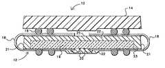
- FIG. 1is an elevation view of module 10 devised in accordance with a preferred embodiment of the present invention.
- Module 10is comprised of integrated lower stack element 12 and upper IC element 14 .
- Upper IC element 14 that is depicted in FIG. 1may be any of a variety of types and configurations of CSP such as, for example, those that are die-sized, as well those that are near chip-scale as well as the variety of ball grid array packages known in the art.
- Typical CSPssuch as, for example, ball-grid-array (“BGA”), micro-ball-grid array (“ ⁇ BGA”), and fine-pitch ball grid array (“FBGA”) packages have an array of connective contacts embodied, for example, as leads, bumps, solder balls, or balls that extend from a lower surface of a plastic casing in any of several patterns and pitches. An external portion of the connective contacts is often finished with a ball of solder.
- upper IC element 14is depicted as a CSP of a particular profile known to those in the art, but it should be understood that the figures are exemplary only.
- Upper IC element 14need not be limited to traditional CSP packaging and as those of skill recognize the opportunity, the present invention is adaptable to future package configurations.
- the present inventionis advantageously employed with memory circuits but may be employed to advantage with logic and computing circuits even where the constituent elements of module 10 are dissimilar.
- Upper IC element 14is shown with upper IC contacts 19 .
- Integrated lower stack element 12is shown with die 16 and connections 20 that connect die 16 to flex circuits 18 .
- Protective surround 22is disposed to protect connections 20 and die 16 .
- protective surround 22is a plastic surround.
- a body 23is formed having lateral sides 21 and an upper surface 25 .
- Protective body 23will, in a preferred embodiment, surround portions of die 16 that would otherwise be exposed to potential environmental damage.
- FIG. 2depicts an exemplar connection of an integrated circuit die 16 to one of two flex circuits 18 in a preferred embodiment of the present invention to create a die-flex combination.
- a die-flex combination in accordance with the present inventionmay be devised in a variety of particular manners including using one or two flex circuits to provide connection to die 16 , as well as using flex circuitry having one or more conductive layers.
- the flex circuitrywill articulate connective structures such as flex contacts and traces that will later be described.
- die pads 24 on die 16are connected to flex attachments 26 of flex 18 by connections 20 which, in the illustrated exemplar, are wire bonding connections.
- Die pads 24are just one type of die connective site that may be employed in the present invention. Other die connective sites such as flip-chip, tab and connective rings, balls, or pads may be employed. Die connective sites may also be construed to include combinations of such structures to provide a connective site for the die. Wire bonding is well known in the art and those of skill will appreciate that many other methods may be used to provide connections 20 between die 16 and the flex circuitry employed for the invention. For example, tab or flip-chip or other attachment techniques known in the art can be profitably used to implement connections 20 .
- die pads 24 of die 16can be arranged in a variety of configurations across the IC. As is known in the art, through die pads 24 , die 16 expresses data and instructions as well as ground and voltage connections.
- Flex 18may be configured to interconnect to die 16 with other connective configurations.
- flex attachments 26may be placed on the side of flex circuits 18 opposite that shown in FIG. 2 to place the flex attachments 26 immediately adjacent to the surface of die 16 to provide direct connection between die 16 and flex circuitry 18 .
- two flex circuits 18are employed but implementations of the invention can be devised using one flex circuit 18 .
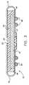
- FIG. 3depicts an elevation view of an integrated lower stack element 12 before its assembly into a module 10 .
- Die 16is placed adjacent to flex circuits 18 and fixed in place with adhesive 28 .
- adhesive 28A variety of adhesive methods are known in the art and, in a preferred embodiment, an adhesive is used that has thermally conductive properties.
- portions of flex circuits 18 A and 18 Bare fixed to die 16 by adhesive 28 which may be a liquid or tape adhesive or may be placed in discrete locations across the package.
- adhesive 28is thermally conductive.
- Adhesives that include a fluxare used to advantage in some steps of assembly of module 10 .
- Layer 28may also be a thermally conductive medium or body to encourage heat flow.
- module contacts 30are fixed along flex circuits 18 A and 18 B opposite the side of the flex circuits nearest to which die 16 is adjacent.
- the shown preferred module contacts 30are familiar to those in the art and may be comprised of eutectic, lead-free, solid copper, or other conductive materials.
- Other contact implementing structuresmay be used to create module contacts 30 as long as the conductive layer or layers of the flex circuitry can be connected to module contacts 30 to allow conveyance of the signals conducted in flex circuits 18 to be transmitted to an environment external to integrated lower stack element 12 .
- Ballsare well understood, but other techniques and structures such as connective rings, built-up pads, or even leads may be placed along flex circuits 18 to create module contacts 30 to convey signals from module 10 to an external environment. Any of the standard JEDEC patterns may be implemented with module contacts 30 as well as custom arrays of module contacts for specialized applications.
- FIG. 4depicts the integration of die 16 devised in a flip-chip configuration with two flex circuits 18 A and 18 B in accordance with a preferred embodiment of the present invention. Those of skill will understand that the depiction of FIG. 4 is not drawn to scale. Die 16 exhibits die pads 24 along a lower surface of the die. Attached to die pads 24 are die connectors 32 which, in the depicted embodiment, are flip-chip balls or connectors. As shown, flex circuits 18 A and 18 B have module contacts 30 .
- Any flexible or conformable substrate with a conductive patternmay be used as a flex circuit in the invention.
- the preferred flex circuitrywill employ more than one conductive layer, but the invention may be implemented with flex circuitry that has only a single conductive layer.
- flex circuit 18is preferably a multi-layer flexible circuit structure that has at least two conductive layers. This is particularly appropriate where frequencies to be encountered are higher.
- the conductive layersare metal such as copper alloy 110 although any conductive material may be employed in this role.
- the use of plural conductive layersprovides advantages such as the creation of a distributed capacitance across module 10 intended to reduce noise or bounce effects that can, particularly at higher frequencies, degrade signal integrity, as those of skill in the art will recognize.
- the entire flex circuitmay be flexible or, as those of skill in the art will recognize, a PCB structure made flexible in certain areas to allow conformability around body 23 and rigid in other areas for planarity along surfaces may be employed as an alternative flex circuitry in the present invention.
- structures known as rigid-flexmay be employed.
- Flex circuits 18 A and 18 B shown in FIG. 4are comprised of multiple layers. Depicted flex circuits 18 A and 18 B have a first outer surface 36 and a second outer surface 38 . The depicted preferred flex circuits 18 A and 18 B have two conductive layers interior to first and second outer surfaces 36 and 38 . In the depicted preferred embodiment, first conductive layer 40 and second conductive layer 42 are interior to first and second outer surfaces 36 and 38 , respectively. Intermediate support layer 44 lies between first conductive layer 40 and second conductive layer 42 . There may be more than one intermediate layer, but an intermediate layer of polyimide is preferred. Preferably, the intermediate layer provides mechanical support for the flex circuitry.
- a flex circuit 18may be devised for use in the present invention that lacks first outer surface 36 and/or second outer surface 38 .
- first conductive layer 40will be on the surface of the particular flex circuit 18 .
- first outer surfaceto make contact with first conductive layer 40 as shown in FIG. 4, die connectors 32 pass through windows 46 to reach first conductive layer 40 .
- module contacts 30pass through windows 48 in second outer surface 38 to reach second conductive layer 42 .
- first conductive layer 40is employed as a ground plane, while second conductive layer 42 provides the functions of being a signal conduction layer and a voltage conduction layer.
- second conductive layer 42is employed to implement signal connections between integrated lower stack element 12 and upper IC element 14
- first conductive layer 40is employed to implement ground connections between integrated lower stack element 12 and upper IC element 14 .
- first and second conductive layersmay be reversed. This may be implemented by flex layer design or by attendant use of interconnections.
- thermal managementis typically related to conductive layer materials and mass as well as the proximity between the die and the conductive layer.
- first and second conductive layers 40 and 42may be implemented with vias such as the via indicated in FIG. 4 by reference 50 .
- viassuch as the via indicated in FIG. 4 by reference 50 .
- appropriate connectionsmay be implemented by any of several well-known techniques such as plated holes or solid lines or wires.
- the connectionsneed not literally be implemented with vias.
- tracesare delineated in conductive layers to convey, where needed, signals between selected module contacts 30 and particular die connectors 32 in the case of flip-chip style die 16 or between module contacts 30 and flex connectors 26 in the case where wire-bond connections 20 are implemented or between upper and lower flex contacts as will be described herein.
- tracescan be implemented in a variety of configurations and manners and where die connectors are positioned coincident with module contact placement, trace use is minimized.
- a via 50may be used to directly connect a selected die connector 32 to a selected module contact 30 without intermediate lateral conveyance between the two through a trace.
- a single conductive layer flex circuitryis employed in an embodiment, there will be no need for a via if a die connector 32 is positioned coincident with a module contact 30 to implement connection through a lower flex contact 62 such as is depicted in FIG. 5.
- FIG. 5illustrates an exemplar construction of an integrated lower stack element 12 in accordance with an alternative preferred embodiment of the present invention that employs flex circuitry having a single conductive layer.
- die 16is appended to flex circuits 18 A and 18 B with adhesive 28 .
- the depicted embodimentalso exhibits optional inter-flex connective 51 that passes through the part of protective surround 22 that lies between flex circuit 18 A and flex circuit 18 B.
- the inter-flex connectivemay consist of one or more wires or other connective structures such as may be implemented in wire bond, lead frame or other form.
- die 16is connected to flex circuits 18 A and 18 B through die pads 24 and die connectors 32 .
- Flex circuits 18 A and 18 Bare depicted with first and second outer layers 36 and 38 , respectively.
- Support layer 54provides structure for flex circuits 18 A and 18 B and conductive layer 52 provides conductivity between die connectors 32 and module contacts 30 .
- Conductive layer 52also provides conductivity between integrated lower stack element 12 and added elements such as another integrated lower stack element 12 or upper IC element 14 that may be aggregated to create module 10 .
- conductive layer 52is disposed closer to module contacts 30 than is support layer 54 . This relative placement is preferred but not required.
- support layer 54provides a support function similar to that provided by intermediate layer 44 in multi-layer flex circuitry embodiments such as those earlier described herein.
- Demarcation gap 56 depicted in FIG. 5provides selective isolation of lower flex contact 62 of conductive layer 52 from areas of conductive layer 52 that may provide other functions or other interconnections between different ones of die connectors 32 and module contacts 30 or other interconnections to other elements of module 10 .
- flex circuits 18 A and 18 Bare shown as having one conductive layer (i.e., layer 52 ). Therefore, in the depicted alternative embodiment, that one conductive layer 52 is intended to provide interconnectivity functions for module 10 . Consequently, particular interconnection features should be isolated from each other to allow rational connections to be implemented in module 10 where conductive layer structures are used.
- demarcation gap 56is merely exemplary and assorted gaps and traces may be used in conductive layer 52 just as they may (but need not necessarily) be used in conductive layers in multi-conductive layer flex embodiments to provide rational interconnectivity features for module 10 .
- the present inventionmay be implemented with a flex circuitry that exhibits a dedicated connective network of individual traces and/or interconnections.
- a signalmay be conveyed from die 16 through die pad 24 though die connector 32 through lower flex contact 62 at conductive layer 52 to module contact 30 .
- Such connection pathsmay convey voltage, ground or data or instruction signal connections in and out of die 16 .
- lower flex contacts 62provide connection between die 16 and module contacts 30 as well as participating in selected connections between die 16 and the circuit of upper IC element 14 .
- a set of flex contactssuch as those identified in later FIG. 7 as upper flex contacts with respect to a second conductive layer 42 shown in FIG. 7, may, in the single conductive layer embodiment of FIG. 5, participate in the connection between the circuit of upper IC element 14 and the flex circuitry employed in the particular embodiment.
- FIG. 6depicts an alternative preferred embodiment of the present invention.
- die 16is disposed above first outer surface 36 while die connective sites which, in this instance, are die pads 24 are connected to lower flex contacts 62 at the level of conductive layer 52 with wire bond connections 20 through windows 46 .
- Body 23is formed about the depicted die-flex combination and, in the preferred embodiment, is formed employing protective surround 22 .
- Module contacts 30are connected to the lower flex contacts 62 to express the appropriate set of signals emanating from die 16 .
- FIG. 6depicts an alternative preferred embodiment of the present invention.
- a set of upper contactsare articulated in the conductive layer 52 to provide connective facility for an upper IC element 14 or another integrated lower stack element 12 .
- traces 64may be employed to provide connections between those upper flex contacts and the lower flex contacts and appropriate module contacts 30 .
- module contacts 30may be connected only to an upper element in a particular module 10 .
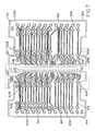
- FIG. 7illustrates an exemplar second conductive layer 42 as may be implemented in flex circuits 18 A and 18 B of a preferred embodiment. Also shown is a depiction of die 16 and its underside 17 . Identified in FIG. 7 are upper flex contacts 60 and lower flex contacts 62 that are at the level of second conductive layer 42 of flex circuits 18 A and 18 B. Upper flex contacts 60 and lower flex contacts 62 are conductive material and, preferably, are solid metal. Only some of upper flex contacts 60 and lower flex contacts 62 are identified with reference numerals in FIG. 7 to preserve clarity of the view.
- Each of flex circuits 18 A and 18 B in the depicted preferred embodimenthave both upper flex contacts 60 and lower flex contacts 62 .
- some embodimentsmay exhibit only lower or only upper flex contacts in flex circuits 18 A or 18 B.
- lower flex contacts 62are employed with module contacts 30 to provide connective facility for integrated lower stack element 12 in module 10 .
- module contacts 30are connected to lower flex contacts 62 as shown in exemplar fashion in FIG. 4 and in FIG. 5 in which figure a trace 64 is shown in the connective path between via 50 and lower flex contact 62 .
- traces between selected upper and lower flex contactsprovide a connective path between upper IC element 14 and integrated lower stack element 12 and/or directly to module contacts 30 .
- interconnection of respective contacts of upper IC element 14 and integrated lower stack element 12will also preferably provide a thermal path between the two elements 12 and 14 to assist in moderation of thermal gradients through module 10 .
- intermediate layer 44that, in a preferred embodiment, is a polyimide. Placement of such an intermediate layer between ground-conductive first conductive layer 40 and signal/voltage conductive second conductive layer 42 provides, in the combination, a distributed capacitance that assists in mitigation of ground bounce phenomena to improve high frequency performance of module 10 .
- FIG. 7depicted are various types of upper flex contacts 60 , various types of lower flex contacts 62 , and traces 64 .
- Lower flex contacts 62 Aare connected to corresponding selected upper flex contacts 60 A with signal traces 64 .
- signal traces 64To enhance the clarity of the view, only exemplar individual flex contacts 62 A and 60 A and traces 64 are literally identified in FIG. 7.
- signal traces 64may be devised to exhibit path routes determined to provide substantially equal signal lengths between corresponding flex contacts 60 A and 62 A.
- path routesdetermined to provide substantially equal signal lengths between corresponding flex contacts 60 A and 62 A.
- such relatively equal length tracesare illustrated in U.S. patent application Ser. No. 10/005,581 which is incorporated by reference into this application.
- VDD plane 66may be in one or more delineated sections but, preferably is contiguous per flex circuit 18 . Further, other embodiments may lack VDD plane 66 .
- Lower flex contacts 62 B and upper flex contacts 60 Bprovide connection to VDD plane 66 .
- upper flex contacts 60 B and lower flex contacts 62 Bselectively connect upper IC element 14 and integrated lower stack element 12 , respectively, to VDD plane 66 .
- Lower flex contacts 62 that are connected to first conductive layer 40 by vias 50are identified as lower flex contacts 62 C. To enhance the clarity of the view, only exemplar individual lower flex contacts 62 C are literally identified in FIG. 7. Upper flex contacts 60 that are connected to first conductive layer 40 by vias 50 are identified as upper flex contacts 60 C.
- module 10will exhibit an array of module contacts 30 that has a greater number of contacts than the constituent elements of module 10 individually exhibit.
- some of the module contacts 30may contact lower flex contacts 62 that do not make contact with one of the die contacts 24 of integrated lower stack element 12 but are connected to upper IC contacts 19 of upper IC element 14 . This allows module 10 to express a wider datapath than that expressed by constituent integrated lower stack element 12 or upper IC element 14 .
- a module contact 30may also be in contact with a lower flex contact 62 to provide a location through which different levels of constituent elements of the module may be enabled when no unused contacts are available or convenient for that purpose.
- first conductive layer 40becomes, on the part of flex 18 disposed above upper surface 23 of integrated lower stack element 12 , the lower-most conductive layer of flex 18 from the perspective of upper IC element 14 .
- those upper IC element contacts 19 of upper IC element 14 that provide ground (VSS) connectionsare connected to the first conductive layer 40 .
- First conductive layer 40lies beneath, however, second conductive layer 42 in that part of flex 18 that is wrapped above lower stack element 12 .
- those upper flex contacts 60 that are in contact with ground-conveying upper IC element contacts 25 of upper IC element 14have vias that route through intermediate layer 44 to reach first conductive layer 40 .
- These viasmay preferably be “on-pad” or coincident with the flex contact 60 to which they are connected.
- module 10expresses a datapath that is wider than that of the constituent circuits of either integrated lower stack element 12 or upper IC element 14 or where differential enablement of the respective elements of module 10 is desired as those skilled in the field will understand.
Landscapes
- Engineering & Computer Science (AREA)
- Microelectronics & Electronic Packaging (AREA)
- Power Engineering (AREA)
- Physics & Mathematics (AREA)
- Condensed Matter Physics & Semiconductors (AREA)
- General Physics & Mathematics (AREA)
- Computer Hardware Design (AREA)
- Semiconductor Integrated Circuits (AREA)
- Design And Manufacture Of Integrated Circuits (AREA)
Abstract
Description
- This application is a continuation-in-part of U.S. application Ser. No. 10/005,581, filed Oct. 26, 2001, pending, which is hereby incorporated by reference for all purposes.[0001]
- The present invention relates to aggregating integrated circuits and, in particular, to stacking integrated circuits.[0002]
- A variety of techniques are used to stack integrated circuits. Some methods require special packages, while other techniques stack conventional packages and still others stack multiple die within a single package. In some stacks, the leads of the packaged integrated circuits are used to create a stack, while in other systems, added structures such as rails provide all or part of the interconnection between packages. In still other techniques, flexible conductors with certain characteristics are used to selectively interconnect packaged integrated circuits. In yet other methods, one IC is connected to another within a single plastic body from which leads or contacts emerge.[0003]
- The predominant package configuration employed during the past decade has encapsulated an integrated circuit (IC) in a plastic surround typically having a rectangular configuration. The enveloped integrated circuit is connected to the application environment through leads emergent from the edge periphery of the plastic encapsulation. Such “leaded packages” have been the constituent elements most commonly employed by techniques for stacking packaged integrated circuits.[0004]
- Leaded packages play an important role in electronics, but efforts to miniaturize electronic components and assemblies have driven development of technologies that preserve circuit board surface area. Because leaded packages have leads emergent from peripheral sides of the package, leaded packages occupy more than a minimal amount of circuit board surface area. Consequently, alternatives to leaded packages have recently gained market share.[0005]
- One family of alternative packages is identified generally by the term “chip scale packaging” or CSP. CSP refers generally to packages that provide connection to an integrated circuit through a set of contacts (often embodied as “bumps” or “balls”) arrayed across a major surface of the package. Instead of leads emergent from a peripheral side of the package, contacts are placed on a major surface and typically emerge from the planar bottom surface of the package.[0006]
- The goal of CSP is to occupy as little area as possible and, preferably, approximately the area of the encapsulated IC. Therefore, CSP leads or contacts do not typically extend beyond the outline perimeter of the package. The absence of “leads” on package sides renders most stacking techniques devised for leaded packages inapplicable for CSP stacking.[0007]
- CSP has enabled reductions in size and weight parameters for many applications. For example, micro ball grid array for flash and SRAM and wirebond on tape or rigid laminate CSPs for SRAM or EEPROM have been employed in a variety of applications. CSP is a broad category including a variety of packages from near chip scale to die-sized packages such as the die sized ball grid array (DSBGA) recently described in proposed JEDEC standard 95-1 for DSBGA. To meet the continuing demands for cost and form factor reduction with increasing memory capacities, CSP technologies that aggregate integrated circuits in CSP technology have recently been developed. For example, Sharp, Hitachi, Mitsubishi and Intel support what are called the S-CSP specifications for flash and SRAM applications. Those S-CSP specifications describe, however, stacking multiple die within a single chip scale package and do not describe stacking integrated circuits that are individually modularized in plastic, either as BGA's or other common CSP packages. Stacking integrated circuits within a single package requires specialized technology that includes reformulation of package internals and significant expense with possible supply chain vulnerabilities.[0008]
- There are several known techniques for stacking packages articulated in chip scale technology. For example, the assignee of the present invention has developed previous systems for aggregating micro-BGA packages in space saving topologies. The assignee of the present invention has systems for stacking BGA packages on a DIMM in a RAMBUS environment.[0009]
- In U.S. Pat. No. 6,205,654 B1 owned by the assignee of the present invention, a system for stacking ball grid array packages that employs lead carriers to extend connectable points out from the packages is described. Other known techniques add structures to a stack of BGA-packaged ICs. Still others aggregate CSPs on a DIMM with angular placement of the packages. Such techniques provide alternatives, but require topologies of added cost and complexity.[0010]
- U.S. Pat. No. 6,262,895 B1 to Forthun (the “Forthun patent”) purports to disclose a technique for stacking chip scale packaged ICs. The Forthun patent discloses a “package” that exhibits a flex circuit wrapped partially about a CSP. The flex circuit is said to have pad arrays on upper and lower surfaces of the flex.[0011]
- The flex circuit of the Forthun “package” has a pad array on its upper surface and a pad array centrally located upon its lower surface. On the lower surface of the flex there are third and fourth arrays on opposite sides from the central lower surface pad array. To create the package of Forthun, a CSP contacts the pad array located on the upper surface of the flex circuit. As described in the Forthun patent, the contacts on the lower surface of the CSP are pushed through “slits” in the upper surface pads and advanced through the flex to protrude from the pads of the lower surface array and, therefore, the bottom surface of the package. Thus, the contacts of the CSP serve as the contacts for the package. The sides of the flex are partially wrapped about the CSP to adjacently place the third and fourth pad arrays above the upper major surface of the CSP to create from the combination of the third and fourth pad arrays, a fifth pad array for connection to another such package. Thus, as described in the Forthun disclosure, a stacked module of CSPs created with the described packages will exhibit a flex circuit wrapped about each CSP in the module.[0012]
- The previous known methods for stacking CSPs apparently have various deficiencies including complex structural arrangements and thermal or high frequency performance issues. To increase dissipation of heat generated by constituent CSPs, the thermal gradient between the lower CSP and upper CSP in a CSP stack or module should be minimized. Prior art solutions to CSP stacking do not, however, address thermal gradient minimization in disclosed constructions.[0013]
- In other applications, module height concerns impact the utility of known solutions in integrated circuit aggregation. In some stacking solutions, the bad die problem is significant. Indigenous as well as processing-acquired defects can lead to unacceptably high failure rates for stacks created by aggregating IC elements before testing the constituent members of the assembly. For example, where stacking techniques employ one or more unpackaged die, there is typically not an opportunity for adequate preassembly test before the constituent ICs of the assembly are aggregated. Then, testing typically reveals bad stacks, it does not prevent their assembly and consequent waste of resources.[0014]
- What is needed, therefore, is a technique and system for stacking integrated circuits using a technology that provides a thermally efficient, reliable structure that performs well at higher frequencies, but does not add excessive height to the stack yet allows pre-stacking test of constituent stack elements with production at reasonable cost with readily understood and managed materials and methods.[0015]
- The present invention integrates an IC die and a flexible circuit structure into an integrated lower stack element that can be stacked with either further integrated lower stack element iterations or with pre-packaged ICs in any of a variety of package types. The present invention can be used to advantage where size minimization, thermal efficiency and or test before stacking are significant concerns. The present invention may be employed to stack similar or dissimilar integrated circuits and may be used to create modularized systems.[0016]
- In the present invention, an IC die is integrated with flex circuitry to create an integrated lower stack element. In a preferred embodiment, a die is positioned above the surface of portions of a pair of flex circuits. Connection is made between the die and the flex circuitry. A protective layer such as a molded plastic, for example, is formed to create a body that protects the flex-connected die and its connection to the flex. Connective elements are placed along the flex circuits to create an array of module contacts along the second side of the flex circuitry. Portions of the pair of flex circuits are positioned above the body to create an integrated lower stack element. The integrated lower stack element may be stacked either with further iterations of the integrated lower stack element or with pre-packaged ICS to create a multi-element stacked circuit module. The present invention may be employed to advantage in numerous configurations and combinations in modules provided for high-density memories or high capacity computing.[0017]
- FIG. 1 is an elevation view of[0018]
module 10 devised in accordance with a preferred embodiment of the present invention. - FIG. 2 depicts an exemplar connection of an integrated circuit die to one of two flex circuits in a preferred embodiment of the present invention.[0019]
- FIG. 3 depicts an elevation view of an integrated lower stack element in accordance with a preferred embodiment of the present invention.[0020]
- FIG. 4 depicts an exemplar integration of a die in a flip-chip configuration with flex circuitry in accordance with a preferred embodiment of the present invention.[0021]
- FIG. 5 depicts an exemplar construction details of an integrated lower stack element in accordance with a preferred embodiment of the present invention.[0022]
- FIG. 6 depicts an exemplar construction details of an integrated lower stack element in accordance with another preferred embodiment of the present invention.[0023]
- FIG. 7 depicts an exemplar conductive layer in a preferred flex circuitry employed in a preferred embodiment of the present invention.[0024]
- FIG. 1 is an elevation view of[0025]
module 10 devised in accordance with a preferred embodiment of the present invention.Module 10 is comprised of integratedlower stack element 12 andupper IC element 14. - [0026]
Upper IC element 14 that is depicted in FIG. 1 may be any of a variety of types and configurations of CSP such as, for example, those that are die-sized, as well those that are near chip-scale as well as the variety of ball grid array packages known in the art. Typical CSPs, such as, for example, ball-grid-array (“BGA”), micro-ball-grid array (“μBGA”), and fine-pitch ball grid array (“FBGA”) packages have an array of connective contacts embodied, for example, as leads, bumps, solder balls, or balls that extend from a lower surface of a plastic casing in any of several patterns and pitches. An external portion of the connective contacts is often finished with a ball of solder. Collectively, these will be known herein as chip scale packaged integrated circuits (CSPs) and preferred embodiments will be described in terms of CSPs, but the particular configurations used in the explanatory figures are not, however, to be construed as limiting. For example, in the elevation view of FIG. 1,upper IC element 14 is depicted as a CSP of a particular profile known to those in the art, but it should be understood that the figures are exemplary only.Upper IC element 14 need not be limited to traditional CSP packaging and as those of skill recognize the opportunity, the present invention is adaptable to future package configurations. The present invention is advantageously employed with memory circuits but may be employed to advantage with logic and computing circuits even where the constituent elements ofmodule 10 are dissimilar.Upper IC element 14 is shown withupper IC contacts 19. - Integrated[0027]
lower stack element 12 is shown withdie 16 andconnections 20 that connect die16 to flexcircuits 18.Protective surround 22 is disposed to protectconnections 20 and die16. In a preferred embodiment,protective surround 22 is a plastic surround. As aprotective surround 22 is formed aboutdie 16, abody 23 is formed havinglateral sides 21 and anupper surface 25.Protective body 23 will, in a preferred embodiment, surround portions of die16 that would otherwise be exposed to potential environmental damage. - FIG. 2 depicts an exemplar connection of an integrated circuit die[0028]16 to one of two
flex circuits 18 in a preferred embodiment of the present invention to create a die-flex combination. As the present description continues, those of skill will recognize that a die-flex combination in accordance with the present invention may be devised in a variety of particular manners including using one or two flex circuits to provide connection to die16, as well as using flex circuitry having one or more conductive layers. Preferably, the flex circuitry will articulate connective structures such as flex contacts and traces that will later be described. - As shown in FIG. 2, die[0029]
pads 24 on die16 are connected to flexattachments 26 offlex 18 byconnections 20 which, in the illustrated exemplar, are wire bonding connections. Diepads 24 are just one type of die connective site that may be employed in the present invention. Other die connective sites such as flip-chip, tab and connective rings, balls, or pads may be employed. Die connective sites may also be construed to include combinations of such structures to provide a connective site for the die. Wire bonding is well known in the art and those of skill will appreciate that many other methods may be used to provideconnections 20 betweendie 16 and the flex circuitry employed for the invention. For example, tab or flip-chip or other attachment techniques known in the art can be profitably used to implementconnections 20. Those of skill will also appreciate that diepads 24 ofdie 16 can be arranged in a variety of configurations across the IC. As is known in the art, through diepads 24, die16 expresses data and instructions as well as ground and voltage connections. - [0030]
Flex 18 may be configured to interconnect to die16 with other connective configurations. For example, as a variant on the flip-chip connectivity scheme,flex attachments 26 may be placed on the side offlex circuits 18 opposite that shown in FIG. 2 to place theflex attachments 26 immediately adjacent to the surface ofdie 16 to provide direct connection betweendie 16 andflex circuitry 18. It should also be understood that in the preferred embodiment shown in FIG. 1, twoflex circuits 18 are employed but implementations of the invention can be devised using oneflex circuit 18. - FIG. 3 depicts an elevation view of an integrated[0031]
lower stack element 12 before its assembly into amodule 10.Die 16 is placed adjacent to flexcircuits 18 and fixed in place withadhesive 28. A variety of adhesive methods are known in the art and, in a preferred embodiment, an adhesive is used that has thermally conductive properties. - With reference to FIG. 4, in a preferred embodiment, portions of[0032]
flex circuits module 10.Layer 28 may also be a thermally conductive medium or body to encourage heat flow. - As shown in this preferred embodiment,[0033]
module contacts 30 are fixed alongflex circuits preferred module contacts 30 are familiar to those in the art and may be comprised of eutectic, lead-free, solid copper, or other conductive materials. Other contact implementing structures may be used to createmodule contacts 30 as long as the conductive layer or layers of the flex circuitry can be connected tomodule contacts 30 to allow conveyance of the signals conducted inflex circuits 18 to be transmitted to an environment external to integratedlower stack element 12. Balls are well understood, but other techniques and structures such as connective rings, built-up pads, or even leads may be placed alongflex circuits 18 to createmodule contacts 30 to convey signals frommodule 10 to an external environment. Any of the standard JEDEC patterns may be implemented withmodule contacts 30 as well as custom arrays of module contacts for specialized applications. - FIG. 4 depicts the integration of[0034]
die 16 devised in a flip-chip configuration with twoflex circuits pads 24 along a lower surface of the die. Attached to diepads 24 aredie connectors 32 which, in the depicted embodiment, are flip-chip balls or connectors. As shown,flex circuits module contacts 30. - Any flexible or conformable substrate with a conductive pattern may be used as a flex circuit in the invention. The preferred flex circuitry will employ more than one conductive layer, but the invention may be implemented with flex circuitry that has only a single conductive layer.[0035]
- Even though single conductive layer flex circuitry may readily be used in the invention,[0036]
flex circuit 18 is preferably a multi-layer flexible circuit structure that has at least two conductive layers. This is particularly appropriate where frequencies to be encountered are higher. Preferably, the conductive layers are metal such as copper alloy110 although any conductive material may be employed in this role. The use of plural conductive layers provides advantages such as the creation of a distributed capacitance acrossmodule 10 intended to reduce noise or bounce effects that can, particularly at higher frequencies, degrade signal integrity, as those of skill in the art will recognize. - The entire flex circuit may be flexible or, as those of skill in the art will recognize, a PCB structure made flexible in certain areas to allow conformability around[0037]
body 23 and rigid in other areas for planarity along surfaces may be employed as an alternative flex circuitry in the present invention. For example, structures known as rigid-flex may be employed. - [0038]
Flex circuits flex circuits outer surface 36 and a secondouter surface 38. The depictedpreferred flex circuits outer surfaces conductive layer 40 and secondconductive layer 42 are interior to first and secondouter surfaces Intermediate support layer 44 lies between firstconductive layer 40 and secondconductive layer 42. There may be more than one intermediate layer, but an intermediate layer of polyimide is preferred. Preferably, the intermediate layer provides mechanical support for the flex circuitry. - It should be understood that in some embodiments of the invention, there will be fewer layers employed in[0039]
flex circuit 18. For example, aflex circuit 18 may be devised for use in the present invention that lacks firstouter surface 36 and/or secondouter surface 38. In such a case, firstconductive layer 40 will be on the surface of theparticular flex circuit 18. Where there is a first outer surface, to make contact with firstconductive layer 40 as shown in FIG. 4, dieconnectors 32 pass throughwindows 46 to reach firstconductive layer 40. Similarly, where there is a secondouter surface 38,module contacts 30 pass throughwindows 48 in secondouter surface 38 to reach secondconductive layer 42. - In a preferred embodiment, first[0040]
conductive layer 40 is employed as a ground plane, while secondconductive layer 42 provides the functions of being a signal conduction layer and a voltage conduction layer. Thus, secondconductive layer 42 is employed to implement signal connections between integratedlower stack element 12 andupper IC element 14, while firstconductive layer 40 is employed to implement ground connections between integratedlower stack element 12 andupper IC element 14. Those of skill will note that roles of the first and second conductive layers may be reversed. This may be implemented by flex layer design or by attendant use of interconnections. As is understood, thermal management is typically related to conductive layer materials and mass as well as the proximity between the die and the conductive layer. - Selective connections between first and second[0041]
conductive layers reference 50. There are, however, many other alternative methods to provide any needed connections between the conductive layers. For example, appropriate connections may be implemented by any of several well-known techniques such as plated holes or solid lines or wires. Thus, the connections need not literally be implemented with vias. - As will be illustrated in later figures, traces are delineated in conductive layers to convey, where needed, signals between selected[0042]
module contacts 30 andparticular die connectors 32 in the case of flip-chip style die16 or betweenmodule contacts 30 andflex connectors 26 in the case where wire-bond connections 20 are implemented or between upper and lower flex contacts as will be described herein. Those of skill will recognize that traces can be implemented in a variety of configurations and manners and where die connectors are positioned coincident with module contact placement, trace use is minimized. For example, in some cases, if the die connectors32 (illustrated as flip-chip connectors) are placed appropriately on die16, a via50 may be used to directly connect a selecteddie connector 32 to a selectedmodule contact 30 without intermediate lateral conveyance between the two through a trace. Where a single conductive layer flex circuitry is employed in an embodiment, there will be no need for a via if adie connector 32 is positioned coincident with amodule contact 30 to implement connection through alower flex contact 62 such as is depicted in FIG. 5. - FIG. 5 illustrates an exemplar construction of an integrated[0043]
lower stack element 12 in accordance with an alternative preferred embodiment of the present invention that employs flex circuitry having a single conductive layer. As shown, die16 is appended to flexcircuits protective surround 22 that lies betweenflex circuit 18A andflex circuit 18B. The inter-flex connective may consist of one or more wires or other connective structures such as may be implemented in wire bond, lead frame or other form. - As those of skill will recognize, die[0044]16 is connected to flex
circuits die pads 24 and dieconnectors 32.Flex circuits outer layers Support layer 54 provides structure forflex circuits conductive layer 52 provides conductivity betweendie connectors 32 andmodule contacts 30.Conductive layer 52 also provides conductivity between integratedlower stack element 12 and added elements such as another integratedlower stack element 12 orupper IC element 14 that may be aggregated to createmodule 10. - Those of skill will recognize that in the depicted embodiment,[0045]
conductive layer 52 is disposed closer tomodule contacts 30 than issupport layer 54. This relative placement is preferred but not required. Such persons will also recognize thatsupport layer 54 provides a support function similar to that provided byintermediate layer 44 in multi-layer flex circuitry embodiments such as those earlier described herein. - [0046]
Demarcation gap 56 depicted in FIG. 5 provides selective isolation oflower flex contact 62 ofconductive layer 52 from areas ofconductive layer 52 that may provide other functions or other interconnections between different ones ofdie connectors 32 andmodule contacts 30 or other interconnections to other elements ofmodule 10. For example, in the embodiment of FIG. 5,flex circuits conductive layer 52 is intended to provide interconnectivity functions formodule 10. Consequently, particular interconnection features should be isolated from each other to allow rational connections to be implemented inmodule 10 where conductive layer structures are used. This is depicted bydemarcation gap 56, but those of skill will understand thatdemarcation gap 56 is merely exemplary and assorted gaps and traces may be used inconductive layer 52 just as they may (but need not necessarily) be used in conductive layers in multi-conductive layer flex embodiments to provide rational interconnectivity features formodule 10. However, as those of skill will recognize, the present invention may be implemented with a flex circuitry that exhibits a dedicated connective network of individual traces and/or interconnections. - With continuing reference to FIG. 5, a signal may be conveyed from die[0047]16 through
die pad 24 thoughdie connector 32 throughlower flex contact 62 atconductive layer 52 tomodule contact 30. Such connection paths may convey voltage, ground or data or instruction signal connections in and out ofdie 16. - In the depicted embodiment of FIG. 5,[0048]
lower flex contacts 62 provide connection betweendie 16 andmodule contacts 30 as well as participating in selected connections betweendie 16 and the circuit ofupper IC element 14. However, in addition, a set of flex contacts such as those identified in later FIG. 7 as upper flex contacts with respect to a secondconductive layer 42 shown in FIG. 7, may, in the single conductive layer embodiment of FIG. 5, participate in the connection between the circuit ofupper IC element 14 and the flex circuitry employed in the particular embodiment. - FIG. 6 depicts an alternative preferred embodiment of the present invention. In the embodiment as depicted in FIG. 6, die[0049]16 is disposed above first
outer surface 36 while die connective sites which, in this instance, aredie pads 24 are connected tolower flex contacts 62 at the level ofconductive layer 52 withwire bond connections 20 throughwindows 46.Body 23 is formed about the depicted die-flex combination and, in the preferred embodiment, is formed employingprotective surround 22.Module contacts 30 are connected to thelower flex contacts 62 to express the appropriate set of signals emanating fromdie 16. As those of skill will understand as to the preferred embodiment of FIG. 6, when integratedlower stack element 12 is incorporated into amodule 10, a set of upper contacts are articulated in theconductive layer 52 to provide connective facility for anupper IC element 14 or another integratedlower stack element 12. Further, traces64 may be employed to provide connections between those upper flex contacts and the lower flex contacts andappropriate module contacts 30. Those of skill will recognize that in some instances, there may bemodule contacts 30 that are connected only to an upper element in aparticular module 10. - FIG. 7 illustrates an exemplar second[0050]
conductive layer 42 as may be implemented inflex circuits die 16 and itsunderside 17. Identified in FIG. 7 areupper flex contacts 60 andlower flex contacts 62 that are at the level of secondconductive layer 42 offlex circuits Upper flex contacts 60 andlower flex contacts 62 are conductive material and, preferably, are solid metal. Only some ofupper flex contacts 60 andlower flex contacts 62 are identified with reference numerals in FIG. 7 to preserve clarity of the view. - Each of[0051]
flex circuits upper flex contacts 60 andlower flex contacts 62. Depending upon the contact pattern ofdie 16 andupper IC element 14, some embodiments may exhibit only lower or only upper flex contacts inflex circuits - In the preferred embodiment depicted in FIG. 7,[0052]
lower flex contacts 62 are employed withmodule contacts 30 to provide connective facility for integratedlower stack element 12 inmodule 10. Thus, in a preferred embodiment,module contacts 30 are connected tolower flex contacts 62 as shown in exemplar fashion in FIG. 4 and in FIG. 5 in which figure atrace 64 is shown in the connective path between via50 andlower flex contact 62. However, as those of skill will recognize, traces between selected upper and lower flex contacts provide a connective path betweenupper IC element 14 and integratedlower stack element 12 and/or directly tomodule contacts 30. - As those of skill will recognize, interconnection of respective contacts of[0053]
upper IC element 14 and integratedlower stack element 12 will also preferably provide a thermal path between the twoelements module 10. Those of skill will notice that between first and secondconductive layers intermediate layer 44 that, in a preferred embodiment, is a polyimide. Placement of such an intermediate layer between ground-conductive firstconductive layer 40 and signal/voltage conductive secondconductive layer 42 provides, in the combination, a distributed capacitance that assists in mitigation of ground bounce phenomena to improve high frequency performance ofmodule 10. - With continuing reference to FIG. 7, depicted are various types of[0054]
upper flex contacts 60, various types oflower flex contacts 62, and traces64.Lower flex contacts 62A are connected to corresponding selectedupper flex contacts 60A with signal traces64. To enhance the clarity of the view, only exemplarindividual flex contacts - To improve high frequency performance, signal traces[0055]64 may be devised to exhibit path routes determined to provide substantially equal signal lengths between
corresponding flex contacts - As shown in the depicted preferred embodiment of FIG. 7, traces[0056]64 are separated from the larger surface area of second
conductive layer 42 that is identified asVDD plane 66.VDD plane 66 may be in one or more delineated sections but, preferably is contiguous perflex circuit 18. Further, other embodiments may lackVDD plane 66. - [0057]
Lower flex contacts 62B andupper flex contacts 60B provide connection toVDD plane 66. In a preferred embodiment,upper flex contacts 60B andlower flex contacts 62B selectively connectupper IC element 14 and integratedlower stack element 12, respectively, toVDD plane 66. - [0058]
Lower flex contacts 62 that are connected to firstconductive layer 40 byvias 50 are identified aslower flex contacts 62C. To enhance the clarity of the view, only exemplar individuallower flex contacts 62C are literally identified in FIG. 7.Upper flex contacts 60 that are connected to firstconductive layer 40 byvias 50 are identified asupper flex contacts 60C. - In some embodiments, as shown in incorporated U.S. patent application Ser. No. 10/005,581,[0059]
module 10 will exhibit an array ofmodule contacts 30 that has a greater number of contacts than the constituent elements ofmodule 10 individually exhibit. In such embodiments, some of themodule contacts 30 may contactlower flex contacts 62 that do not make contact with one of thedie contacts 24 of integratedlower stack element 12 but are connected toupper IC contacts 19 ofupper IC element 14. This allowsmodule 10 to express a wider datapath than that expressed by constituent integratedlower stack element 12 orupper IC element 14. - A[0060]
module contact 30 may also be in contact with alower flex contact 62 to provide a location through which different levels of constituent elements of the module may be enabled when no unused contacts are available or convenient for that purpose. - Those of skill will recognize that as[0061]
flex circuitry 18 is partially wrapped aboutlateral side 21 of integratedlower stack element 12, firstconductive layer 40 becomes, on the part offlex 18 disposed aboveupper surface 23 of integratedlower stack element 12, the lower-most conductive layer offlex 18 from the perspective ofupper IC element 14. In the depicted embodiment, those upperIC element contacts 19 ofupper IC element 14 that provide ground (VSS) connections are connected to the firstconductive layer 40. Firstconductive layer 40 lies beneath, however, secondconductive layer 42 in that part offlex 18 that is wrapped abovelower stack element 12. Consequently, in the depicted preferred embodiment, thoseupper flex contacts 60 that are in contact with ground-conveying upperIC element contacts 25 ofupper IC element 14 have vias that route throughintermediate layer 44 to reach firstconductive layer 40. These vias may preferably be “on-pad” or coincident with theflex contact 60 to which they are connected. - As those of skill will recognize, there may be embodiments of the present invention that may profitably employ off-pad vias such as are described in previously cited U.S. application Ser. No. 10/005,581, filed Oct. 26, 2001, (the “'581 application) pending, which is incorporated by reference herein.[0062]
- Those of skill who refer to the '581 application will note that the figures in that application will be instructive in teaching details concerning a flex circuitry construction for preferred embodiments of the present invention. Further, as those of skill will recognize, the details on location and relationships between upper and lower flex contacts as described in the '581 application are useful to preferred embodiments of the present invention as modified to fit the particulars of the considered embodiment. Further, alternative embodiments depicted in the '581 application are instructive in understanding alternatives available for embodiments of the present invention. For example, the '581 application provides teachings that are descriptive of features that may be employed to advantage in preferred embodiments in accordance with the present invention where[0063]
module 10 expresses a datapath that is wider than that of the constituent circuits of either integratedlower stack element 12 orupper IC element 14 or where differential enablement of the respective elements ofmodule 10 is desired as those skilled in the field will understand. - Although the present invention has been described in detail, it will be apparent to those skilled in the art that the invention may be embodied in a variety of specific forms and that various changes, substitutions and alterations can be made without departing from the spirit and scope of the invention. The described embodiments are only illustrative and not restrictive and the scope of the invention is, therefore, indicated by the following claims.[0064]
Claims (40)
Priority Applications (2)
| Application Number | Priority Date | Filing Date | Title |
|---|---|---|---|
| US10/435,192US7485951B2 (en) | 2001-10-26 | 2003-05-09 | Modularized die stacking system and method |
| US11/941,718US20080067662A1 (en) | 2001-10-26 | 2007-11-16 | Modularized Die Stacking System and Method |
Applications Claiming Priority (2)
| Application Number | Priority Date | Filing Date | Title |
|---|---|---|---|
| US10/005,581US6576992B1 (en) | 2001-10-26 | 2001-10-26 | Chip scale stacking system and method |
| US10/435,192US7485951B2 (en) | 2001-10-26 | 2003-05-09 | Modularized die stacking system and method |
Related Parent Applications (1)
| Application Number | Title | Priority Date | Filing Date |
|---|---|---|---|
| US10/005,581Continuation-In-PartUS6576992B1 (en) | 2001-10-26 | 2001-10-26 | Chip scale stacking system and method |
Related Child Applications (1)
| Application Number | Title | Priority Date | Filing Date |
|---|---|---|---|
| US11/941,718ContinuationUS20080067662A1 (en) | 2001-10-26 | 2007-11-16 | Modularized Die Stacking System and Method |
Publications (2)
| Publication Number | Publication Date |
|---|---|
| US20040000707A1true US20040000707A1 (en) | 2004-01-01 |
| US7485951B2 US7485951B2 (en) | 2009-02-03 |
Family
ID=39187728
Family Applications (2)
| Application Number | Title | Priority Date | Filing Date |
|---|---|---|---|
| US10/435,192Expired - LifetimeUS7485951B2 (en) | 2001-10-26 | 2003-05-09 | Modularized die stacking system and method |
| US11/941,718AbandonedUS20080067662A1 (en) | 2001-10-26 | 2007-11-16 | Modularized Die Stacking System and Method |
Family Applications After (1)
| Application Number | Title | Priority Date | Filing Date |
|---|---|---|---|
| US11/941,718AbandonedUS20080067662A1 (en) | 2001-10-26 | 2007-11-16 | Modularized Die Stacking System and Method |
Country Status (1)
| Country | Link |
|---|---|
| US (2) | US7485951B2 (en) |
Cited By (14)
| Publication number | Priority date | Publication date | Assignee | Title |
|---|---|---|---|---|
| US20010018225A1 (en)* | 2000-02-22 | 2001-08-30 | Hideki Tanaka | Tape carrier type semiconductor device, method for manufacturing the same, and flexible substrate |
| US20050040504A1 (en)* | 2003-08-05 | 2005-02-24 | Sa-Yoon Kang | Low-cost flexible film package module and method of manufacturing the same |
| US20060076690A1 (en)* | 2004-09-27 | 2006-04-13 | Formfactor, Inc. | Stacked Die Module |
| US20060278968A1 (en)* | 2005-06-13 | 2006-12-14 | Shinko Electric Industries Co., Ltd. | Laminated semiconductor package |
| US20070158811A1 (en)* | 2006-01-11 | 2007-07-12 | James Douglas Wehrly | Low profile managed memory component |
| US20070159545A1 (en)* | 2006-01-11 | 2007-07-12 | Wehrly James D Jr | Managed memory component |
| US20070164416A1 (en)* | 2006-01-17 | 2007-07-19 | James Douglas Wehrly | Managed memory component |
| US20070170561A1 (en)* | 2006-01-11 | 2007-07-26 | Staktek Group L.P. | Leaded package integrated circuit stacking |
| US20080048309A1 (en)* | 2006-08-28 | 2008-02-28 | Corisis David J | Metal core foldover package structures, systems including same and methods of fabrication |
| US20080122113A1 (en)* | 2006-08-17 | 2008-05-29 | Corisis David J | Semiconductor device assemblies and systems including at least one conductive pathway extending around a side of at least one semiconductor device and methods for forming the same |
| US20080203552A1 (en)* | 2005-02-15 | 2008-08-28 | Unisemicon Co., Ltd. | Stacked Package and Method of Fabricating the Same |
| US20120068340A1 (en)* | 2010-09-22 | 2012-03-22 | Noriyuki Kimura | Ball grid array semiconductor package and method of manufacturing the same |
| US20120240095A1 (en)* | 2006-10-11 | 2012-09-20 | Satoshi Nakamura | Electric information processing method in cad system, device thereof, program, and computer-readable storage medium |
| US8525322B1 (en)* | 2004-10-25 | 2013-09-03 | Yong Woo Kim | Semiconductor package having a plurality of input/output members |
Families Citing this family (5)
| Publication number | Priority date | Publication date | Assignee | Title |
|---|---|---|---|---|
| US8050047B2 (en)* | 2007-07-12 | 2011-11-01 | Stats Chippac Ltd. | Integrated circuit package system with flexible substrate and recessed package |
| US8004093B2 (en)* | 2008-08-01 | 2011-08-23 | Stats Chippac Ltd. | Integrated circuit package stacking system |
| KR101796116B1 (en) | 2010-10-20 | 2017-11-10 | 삼성전자 주식회사 | Semiconductor device, memory module and memory system having the same and operating method thereof |
| US20120326304A1 (en)* | 2011-06-24 | 2012-12-27 | Warren Robert W | Externally Wire Bondable Chip Scale Package in a System-in-Package Module |
| US12107037B2 (en)* | 2021-11-03 | 2024-10-01 | Amkor Technology Singapore Holding Pte. Ltd. | Semiconductor devices and methods of manufacturing electronic devices |
Citations (95)
| Publication number | Priority date | Publication date | Assignee | Title |
|---|---|---|---|---|
| US3654394A (en)* | 1969-07-08 | 1972-04-04 | Gordon Eng Co | Field effect transistor switch, particularly for multiplexing |
| US3806767A (en)* | 1973-03-15 | 1974-04-23 | Tek Wave Inc | Interboard connector |
| US4079511A (en)* | 1976-07-30 | 1978-03-21 | Amp Incorporated | Method for packaging hermetically sealed integrated circuit chips on lead frames |
| US4381421A (en)* | 1980-07-01 | 1983-04-26 | Tektronix, Inc. | Electromagnetic shield for electronic equipment |
| US4513368A (en)* | 1981-05-22 | 1985-04-23 | Data General Corporation | Digital data processing system having object-based logical memory addressing and self-structuring modular memory |
| US4587596A (en)* | 1984-04-09 | 1986-05-06 | Amp Incorporated | High density mother/daughter circuit board connector |
| US4645944A (en)* | 1983-09-05 | 1987-02-24 | Matsushita Electric Industrial Co., Ltd. | MOS register for selecting among various data inputs |
| US4722691A (en)* | 1986-02-03 | 1988-02-02 | General Motors Corporation | Header assembly for a printed circuit board |
| US4903169A (en)* | 1986-04-03 | 1990-02-20 | Matsushita Electric Industrial Co., Ltd. | Shielded high frequency apparatus having partitioned shield case, and method of manufacture thereof |
| US4985703A (en)* | 1988-02-03 | 1991-01-15 | Nec Corporation | Analog multiplexer |
| US5081067A (en)* | 1989-02-10 | 1992-01-14 | Fujitsu Limited | Ceramic package type semiconductor device and method of assembling the same |
| US5117282A (en)* | 1990-10-29 | 1992-05-26 | Harris Corporation | Stacked configuration for integrated circuit devices |
| US5198965A (en)* | 1991-12-18 | 1993-03-30 | International Business Machines Corporation | Free form packaging of specific functions within a computer system |
| US5214307A (en)* | 1991-07-08 | 1993-05-25 | Micron Technology, Inc. | Lead frame for semiconductor devices having improved adhesive bond line control |
| US5276418A (en)* | 1988-11-16 | 1994-01-04 | Motorola, Inc. | Flexible substrate electronic assembly |
| US5289062A (en)* | 1991-03-18 | 1994-02-22 | Quality Semiconductor, Inc. | Fast transmission gate switch |
| US5289346A (en)* | 1991-02-26 | 1994-02-22 | Microelectronics And Computer Technology Corporation | Peripheral to area adapter with protective bumper for an integrated circuit chip |
| US5384690A (en)* | 1993-07-27 | 1995-01-24 | International Business Machines Corporation | Flex laminate package for a parallel processor |
| US5386341A (en)* | 1993-11-01 | 1995-01-31 | Motorola, Inc. | Flexible substrate folded in a U-shape with a rigidizer plate located in the notch of the U-shape |
| US5394303A (en)* | 1992-09-11 | 1995-02-28 | Kabushiki Kaisha Toshiba | Semiconductor device |
| US5396573A (en)* | 1993-08-03 | 1995-03-07 | International Business Machines Corporation | Pluggable connectors for connecting large numbers of electrical and/or optical cables to a module through a seal |
| US5397916A (en)* | 1991-12-10 | 1995-03-14 | Normington; Peter J. C. | Semiconductor device including stacked die |
| US5502333A (en)* | 1994-03-30 | 1996-03-26 | International Business Machines Corporation | Semiconductor stack structures and fabrication/sparing methods utilizing programmable spare circuit |
| US5509197A (en)* | 1994-06-10 | 1996-04-23 | Xetel Corporation | Method of making substrate edge connector |
| US5516989A (en)* | 1994-05-16 | 1996-05-14 | Nippon Mektron, Ltd. | Structure of the flexing section of a multilayer flexible circuit board |
| US5594275A (en)* | 1993-11-18 | 1997-01-14 | Samsung Electronics Co., Ltd. | J-leaded semiconductor package having a plurality of stacked ball grid array packages |
| US5610833A (en)* | 1992-06-02 | 1997-03-11 | Hewlett-Packard Company | Computer-aided design methods and apparatus for multilevel interconnect technologies |
| US5615089A (en)* | 1994-07-26 | 1997-03-25 | Fujitsu Limited | BGA semiconductor device including a plurality of semiconductor chips located on upper and lower surfaces of a first substrate |
| US5717556A (en)* | 1995-04-26 | 1998-02-10 | Nec Corporation | Printed-wiring board having plural parallel-connected interconnections |
| US5729894A (en)* | 1992-07-21 | 1998-03-24 | Lsi Logic Corporation | Method of assembling ball bump grid array semiconductor packages |
| US5744827A (en)* | 1995-11-28 | 1998-04-28 | Samsung Electronics Co., Ltd. | Three dimensional stack package device having exposed coupling lead portions and vertical interconnection elements |
| US5751553A (en)* | 1992-09-16 | 1998-05-12 | Clayton; James E. | Thin multichip module including a connector frame socket having first and second apertures |
| US5895970A (en)* | 1997-05-02 | 1999-04-20 | Nec Corporation | Semiconductor package having semiconductor element, mounting structure of semiconductor package mounted on circuit board, and method of assembling semiconductor package |
| US5895969A (en)* | 1992-05-25 | 1999-04-20 | Hitachi, Ltd. And Hitachi Vlsi Engineering Corp. | Thin type semiconductor device, module structure using the device and method of mounting the device on board |
| US6013948A (en)* | 1995-11-27 | 2000-01-11 | Micron Technology, Inc. | Stackable chip scale semiconductor package with mating contacts on opposed surfaces |
| US6014316A (en)* | 1997-06-13 | 2000-01-11 | Irvine Sensors Corporation | IC stack utilizing BGA contacts |
| US6028365A (en)* | 1998-03-30 | 2000-02-22 | Micron Technology, Inc. | Integrated circuit package and method of fabrication |
| US6034878A (en)* | 1996-12-16 | 2000-03-07 | Hitachi, Ltd. | Source-clock-synchronized memory system and memory unit |
| US6040624A (en)* | 1997-10-02 | 2000-03-21 | Motorola, Inc. | Semiconductor device package and method |
| US6178093B1 (en)* | 1996-06-28 | 2001-01-23 | International Business Machines Corporation | Information handling system with circuit assembly having holes filled with filler material |
| US6186106B1 (en)* | 1997-12-29 | 2001-02-13 | Visteon Global Technologies, Inc. | Apparatus for routing electrical signals in an engine |
| US6187652B1 (en)* | 1998-09-14 | 2001-02-13 | Fujitsu Limited | Method of fabrication of multiple-layer high density substrate |
| US6208521B1 (en)* | 1997-05-19 | 2001-03-27 | Nitto Denko Corporation | Film carrier and laminate type mounting structure using same |
| US6218731B1 (en)* | 1999-05-21 | 2001-04-17 | Siliconware Precision Industries Co., Ltd. | Tiny ball grid array package |
| US6222737B1 (en)* | 1999-04-23 | 2001-04-24 | Dense-Pac Microsystems, Inc. | Universal package and method of forming the same |
| US6336262B1 (en)* | 1996-10-31 | 2002-01-08 | International Business Machines Corporation | Process of forming a capacitor with multi-level interconnection technology |
| US20020006032A1 (en)* | 2000-05-23 | 2002-01-17 | Chris Karabatsos | Low-profile registered DIMM |
| US6351029B1 (en)* | 1999-05-05 | 2002-02-26 | Harlan R. Isaak | Stackable flex circuit chip package and method of making same |
| US20020030995A1 (en)* | 2000-08-07 | 2002-03-14 | Masao Shoji | Headlight |
| US6360935B1 (en)* | 1999-01-26 | 2002-03-26 | Board Of Regents Of The University Of Texas System | Apparatus and method for assessing solderability |
| US6368896B2 (en)* | 1997-10-31 | 2002-04-09 | Micron Technology, Inc. | Method of wafer level chip scale packaging |
| US20020044423A1 (en)* | 1999-05-14 | 2002-04-18 | Primavera Anthony A. | Method and apparatus for mounting and packaging electronic components |
| US6376769B1 (en)* | 1999-05-18 | 2002-04-23 | Amerasia International Technology, Inc. | High-density electronic package, and method for making same |
| US20020048849A1 (en)* | 1999-05-05 | 2002-04-25 | Isaak Harlan R. | Stackable flex circuit IC package and method of making same |
| US6504104B2 (en)* | 1997-12-10 | 2003-01-07 | Siemens Aktiengesellschaft | Flexible wiring for the transformation of a substrate with edge contacts into a ball grid array |
| US6509639B1 (en)* | 2001-07-27 | 2003-01-21 | Charles W. C. Lin | Three-dimensional stacked semiconductor package |
| US20030016710A1 (en)* | 2001-07-19 | 2003-01-23 | Satoshi Komoto | Semiconductor laser device including light receiving element for receiving monitoring laser beam |
| US6522018B1 (en)* | 2000-05-16 | 2003-02-18 | Micron Technology, Inc. | Ball grid array chip packages having improved testing and stacking characteristics |
| US6528870B2 (en)* | 2000-01-28 | 2003-03-04 | Kabushiki Kaisha Toshiba | Semiconductor device having a plurality of stacked wiring boards |
| US20030045025A1 (en)* | 2000-01-26 | 2003-03-06 | Coyle Anthony L. | Method of fabricating a molded package for micromechanical devices |
| US6532162B2 (en)* | 2001-05-26 | 2003-03-11 | Intel Corporation | Reference plane of integrated circuit packages |
| US20030049886A1 (en)* | 2001-09-07 | 2003-03-13 | Salmon Peter C. | Electronic system modules and method of fabrication |
| US6538895B2 (en)* | 1999-07-15 | 2003-03-25 | Infineon Technologies Ag | TSOP memory chip housing configuration |
| US20030067064A1 (en)* | 2001-10-10 | 2003-04-10 | Shin Kim | Stack package using flexible double wiring substrate |
| US6549413B2 (en)* | 2001-02-27 | 2003-04-15 | Chippac, Inc. | Tape ball grid array semiconductor package structure and assembly process |
| US6552910B1 (en)* | 2000-06-28 | 2003-04-22 | Micron Technology, Inc. | Stacked-die assemblies with a plurality of microelectronic devices and methods of manufacture |
| US20040000708A1 (en)* | 2001-10-26 | 2004-01-01 | Staktek Group, L.P. | Memory expansion and chip scale stacking system and method |
| US6673651B2 (en)* | 1999-07-01 | 2004-01-06 | Oki Electric Industry Co., Ltd. | Method of manufacturing semiconductor device including semiconductor elements mounted on base plate |
| US20040004281A1 (en)* | 2002-07-03 | 2004-01-08 | Jin-Chuan Bai | Semiconductor package with heat sink |
| US6677670B2 (en)* | 2000-04-25 | 2004-01-13 | Seiko Epson Corporation | Semiconductor device |
| US6683377B1 (en)* | 2000-05-30 | 2004-01-27 | Amkor Technology, Inc. | Multi-stacked memory package |
| US20040021211A1 (en)* | 2002-08-05 | 2004-02-05 | Tessera, Inc. | Microelectronic adaptors, assemblies and methods |
| US6689634B1 (en)* | 1999-09-22 | 2004-02-10 | Texas Instruments Incorporated | Modeling technique for selectively depopulating electrical contacts from a foot print of a grid array (BGA or LGA) package to increase device reliability |
| US6690584B2 (en)* | 2000-08-14 | 2004-02-10 | Fujitsu Limited | Information-processing device having a crossbar-board connected to back panels on different sides |
| US20040028936A1 (en)* | 2001-03-08 | 2004-02-12 | Masaki Kogiso | Metalic nanowire and process for producing the same |
| US20040031972A1 (en)* | 2001-10-09 | 2004-02-19 | Tessera, Inc. | Stacked packages |
| US6699730B2 (en)* | 1996-12-13 | 2004-03-02 | Tessers, Inc. | Stacked microelectronic assembly and method therefor |
| US20040045159A1 (en)* | 1996-12-13 | 2004-03-11 | Tessera, Inc. | Electrical connection with inwardly deformable contacts |
| US6707684B1 (en)* | 2001-04-02 | 2004-03-16 | Advanced Micro Devices, Inc. | Method and apparatus for direct connection between two integrated circuits via a connector |
| US6707148B1 (en)* | 2002-05-21 | 2004-03-16 | National Semiconductor Corporation | Bumped integrated circuits for optical applications |
| US6709893B2 (en)* | 1998-05-11 | 2004-03-23 | Micron Technology, Inc. | Interconnections for a semiconductor device and method for forming same |
| US20040065963A1 (en)* | 2002-09-17 | 2004-04-08 | Chippac, Inc. | Semiconductor multi-package module having wire bond interconnect between stacked packages and having electrical shield |
| US6724076B1 (en)* | 1999-11-15 | 2004-04-20 | Infineon Technologies Ag | Package for a semiconductor chip |
| US20040075991A1 (en)* | 1999-08-11 | 2004-04-22 | Tessera. Inc. | Vapor phase connection techniques |
| US6841855B2 (en)* | 2003-04-28 | 2005-01-11 | Intel Corporation | Electronic package having a flexible substrate with ends connected to one another |
| US20050018495A1 (en)* | 2004-01-29 | 2005-01-27 | Netlist, Inc. | Arrangement of integrated circuits in a memory module |
| US6849949B1 (en)* | 1999-09-27 | 2005-02-01 | Samsung Electronics Co., Ltd. | Thin stacked package |
| US20050035440A1 (en)* | 2001-08-22 | 2005-02-17 | Tessera, Inc. | Stacked chip assembly with stiffening layer |
| US20050040508A1 (en)* | 2003-08-22 | 2005-02-24 | Jong-Joo Lee | Area array type package stack and manufacturing method thereof |
| US6867496B1 (en)* | 1999-10-01 | 2005-03-15 | Seiko Epson Corporation | Interconnect substrate, semiconductor device, methods of fabricating, inspecting, and mounting the semiconductor device, circuit board, and electronic instrument |
| US6869825B2 (en)* | 2002-12-31 | 2005-03-22 | Intel Corporation | Folded BGA package design with shortened communication paths and more electrical routing flexibility |
| US6879047B1 (en)* | 2003-02-19 | 2005-04-12 | Amkor Technology, Inc. | Stacking structure for semiconductor devices using a folded over flexible substrate and method therefor |
| US6884653B2 (en)* | 2001-03-21 | 2005-04-26 | Micron Technology, Inc. | Folded interposer |
| US6998704B2 (en)* | 2002-08-30 | 2006-02-14 | Nec Corporation | Semiconductor device and method for manufacturing the same, circuit board, electronic apparatus, and semiconductor device manufacturing apparatus |
| US7023701B2 (en)* | 2003-05-05 | 2006-04-04 | Infineon Technologies, Ag | Device for cooling memory modules |
Family Cites Families (300)
| Publication number | Priority date | Publication date | Assignee | Title |
|---|---|---|---|---|
| US3372310A (en)* | 1965-04-30 | 1968-03-05 | Radiation Inc | Universal modular packages for integrated circuits |
| US3411122A (en) | 1966-01-13 | 1968-11-12 | Ibm | Electrical resistance element and method of fabricating |
| US3436604A (en) | 1966-04-25 | 1969-04-01 | Texas Instruments Inc | Complex integrated circuit array and method for fabricating same |
| US3772776A (en) | 1969-12-03 | 1973-11-20 | Thomas & Betts Corp | Method of interconnecting memory plane boards |
| US3727064A (en) | 1971-03-17 | 1973-04-10 | Monsanto Co | Opto-isolator devices and method for the fabrication thereof |
| US3746934A (en) | 1971-05-06 | 1973-07-17 | Siemens Ag | Stack arrangement of semiconductor chips |
| US3766439A (en) | 1972-01-12 | 1973-10-16 | Gen Electric | Electronic module using flexible printed circuit board with heat sink means |
| US3718842A (en)* | 1972-04-21 | 1973-02-27 | Texas Instruments Inc | Liquid crystal display mounting structure |
| CH591418A5 (en) | 1973-02-20 | 1977-09-15 | Sandoz Ag | |
| US3983547A (en) | 1974-06-27 | 1976-09-28 | International Business Machines - Ibm | Three-dimensional bubble device |
| US4103318A (en) | 1977-05-06 | 1978-07-25 | Ford Motor Company | Electronic multichip module |
| SU834957A1 (en) | 1979-03-12 | 1981-05-30 | Предприятие П/Я А-7438 | Device for feeding printed circuit boards |
| US4288841A (en) | 1979-09-20 | 1981-09-08 | Bell Telephone Laboratories, Incorporated | Double cavity semiconductor chip carrier |
| JPS5731166A (en) | 1980-07-31 | 1982-02-19 | Fujitsu Ltd | Semiconductor device |
| US4398235A (en) | 1980-09-11 | 1983-08-09 | General Motors Corporation | Vertical integrated circuit package integration |
| US4429349A (en)* | 1980-09-30 | 1984-01-31 | Burroughs Corporation | Coil connector |
| US4437235A (en) | 1980-12-29 | 1984-03-20 | Honeywell Information Systems Inc. | Integrated circuit package |
| JPS57181146A (en) | 1981-04-30 | 1982-11-08 | Hitachi Ltd | Resin-sealed semiconductor device |
| US4406508A (en) | 1981-07-02 | 1983-09-27 | Thomas & Betts Corporation | Dual-in-line package assembly |
| US4420794A (en) | 1981-09-10 | 1983-12-13 | Research, Incorporated | Integrated circuit switch |
| JPS5896756A (en) | 1981-12-04 | 1983-06-08 | Toshiba Corp | multi-chip package |
| JPS58112348A (en) | 1981-12-25 | 1983-07-04 | Fujitsu Ltd | semiconductor equipment |
| US4466183A (en)* | 1982-05-03 | 1984-08-21 | National Semiconductor Corporation | Integrated circuit packaging process |
| US4567543A (en)* | 1983-02-15 | 1986-01-28 | Motorola, Inc. | Double-sided flexible electronic circuit module |
| US4727513A (en)* | 1983-09-02 | 1988-02-23 | Wang Laboratories, Inc. | Signal in-line memory module |
| US4712129A (en) | 1983-12-12 | 1987-12-08 | Texas Instruments Incorporated | Integrated circuit device with textured bar cover |
| KR890004820B1 (en) | 1984-03-28 | 1989-11-27 | 인터내셔널 비지네스 머신즈 코포레이션 | Memory module and board with double storage density and method of forming the same |
| JPS60254762A (en) | 1984-05-31 | 1985-12-16 | Fujitsu Ltd | Semiconductor device package |
| EP0213205B1 (en) | 1984-12-28 | 1992-12-09 | Micro Co., Ltd. | Method of stacking printed circuit boards |
| EP0218796B1 (en) | 1985-08-16 | 1990-10-31 | Dai-Ichi Seiko Co. Ltd. | Semiconductor device comprising a plug-in-type package |
| US4724611A (en)* | 1985-08-23 | 1988-02-16 | Nec Corporation | Method for producing semiconductor module |
| US4696525A (en) | 1985-12-13 | 1987-09-29 | Amp Incorporated | Socket for stacking integrated circuit packages |
| JPS62230027A (en) | 1986-03-31 | 1987-10-08 | Matsushita Electric Ind Co Ltd | Manufacture of semiconductor device |
| US4763188A (en)* | 1986-08-08 | 1988-08-09 | Thomas Johnson | Packaging system for multiple semiconductor devices |
| JPS63153849A (en) | 1986-12-17 | 1988-06-27 | Nec Corp | Semiconductor device |
| US4839717A (en) | 1986-12-19 | 1989-06-13 | Fairchild Semiconductor Corporation | Ceramic package for high frequency semiconductor devices |
| US4821007A (en) | 1987-02-06 | 1989-04-11 | Tektronix, Inc. | Strip line circuit component and method of manufacture |
| US5159535A (en) | 1987-03-11 | 1992-10-27 | International Business Machines Corporation | Method and apparatus for mounting a flexible film semiconductor chip carrier on a circuitized substrate |
| US4862249A (en) | 1987-04-17 | 1989-08-29 | Xoc Devices, Inc. | Packaging system for stacking integrated circuits |
| KR970003915B1 (en)* | 1987-06-24 | 1997-03-22 | 미다 가쓰시게 | Semiconductor memory device and semiconductor memory module using same |
| IT1214254B (en) | 1987-09-23 | 1990-01-10 | Sgs Microelettonica S P A | SEMICONDUCTOR DEVICE IN PLASTIC OR CERAMIC CONTAINER WITH "CHIPS" FIXED ON BOTH SIDES OF THE CENTRAL ISLAND OF THE "FRAME". |
| US5016138A (en) | 1987-10-27 | 1991-05-14 | Woodman John K | Three dimensional integrated circuit package |
| US4983533A (en) | 1987-10-28 | 1991-01-08 | Irvine Sensors Corporation | High-density electronic modules - process and product |
| US5198888A (en) | 1987-12-28 | 1993-03-30 | Hitachi, Ltd. | Semiconductor stacked device |
| US4833568A (en) | 1988-01-29 | 1989-05-23 | Berhold G Mark | Three-dimensional circuit component assembly and method corresponding thereto |
| US4891789A (en) | 1988-03-03 | 1990-01-02 | Bull Hn Information Systems, Inc. | Surface mounted multilayer memory printed circuit board |
| US5138434A (en) | 1991-01-22 | 1992-08-11 | Micron Technology, Inc. | Packaging for semiconductor logic devices |
| US4992850A (en)* | 1989-02-15 | 1991-02-12 | Micron Technology, Inc. | Directly bonded simm module |
| US4911643A (en) | 1988-10-11 | 1990-03-27 | Beta Phase, Inc. | High density and high signal integrity connector |
| US4956694A (en) | 1988-11-04 | 1990-09-11 | Dense-Pac Microsystems, Inc. | Integrated circuit chip stacking |
| US4992849A (en)* | 1989-02-15 | 1991-02-12 | Micron Technology, Inc. | Directly bonded board multiple integrated circuit module |
| DE69006609T2 (en) | 1989-03-15 | 1994-06-30 | Ngk Insulators Ltd | Ceramic lid for closing a semiconductor element and method for closing a semiconductor element in a ceramic package. |
| JP2647194B2 (en) | 1989-04-17 | 1997-08-27 | 住友電気工業株式会社 | Semiconductor package sealing method |
| US4953060A (en) | 1989-05-05 | 1990-08-28 | Ncr Corporation | Stackable integrated circuit chip package with improved heat removal |
| US5104820A (en) | 1989-07-07 | 1992-04-14 | Irvine Sensors Corporation | Method of fabricating electronic circuitry unit containing stacked IC layers having lead rerouting |
| US5057903A (en) | 1989-07-17 | 1991-10-15 | Microelectronics And Computer Technology Corporation | Thermal heat sink encapsulated integrated circuit |
| US5200362A (en)* | 1989-09-06 | 1993-04-06 | Motorola, Inc. | Method of attaching conductive traces to an encapsulated semiconductor die using a removable transfer film |
| US5068708A (en) | 1989-10-02 | 1991-11-26 | Advanced Micro Devices, Inc. | Ground plane for plastic encapsulated integrated circuit die packages |
| US4967950A (en) | 1989-10-31 | 1990-11-06 | International Business Machines Corporation | Soldering method |
| US5012323A (en) | 1989-11-20 | 1991-04-30 | Micron Technology, Inc. | Double-die semiconductor package having a back-bonded die and a face-bonded die interconnected on a single leadframe |
| US5229641A (en) | 1989-11-25 | 1993-07-20 | Hitachi Maxell, Ltd. | Semiconductor card and manufacturing method therefor |
| US5041902A (en) | 1989-12-14 | 1991-08-20 | Motorola, Inc. | Molded electronic package with compression structures |
| US5191404A (en)* | 1989-12-20 | 1993-03-02 | Digital Equipment Corporation | High density memory array packaging |
| JPH03227541A (en) | 1990-02-01 | 1991-10-08 | Hitachi Ltd | Semiconductor device |
| US5083697A (en) | 1990-02-14 | 1992-01-28 | Difrancesco Louis | Particle-enhanced joining of metal surfaces |
| US5041015A (en) | 1990-03-30 | 1991-08-20 | Cal Flex, Inc. | Electrical jumper assembly |
| US5345205A (en) | 1990-04-05 | 1994-09-06 | General Electric Company | Compact high density interconnected microwave system |
| US5261068A (en) | 1990-05-25 | 1993-11-09 | Dell Usa L.P. | Dual path memory retrieval system for an interleaved dynamic RAM memory unit |
| US5050039A (en) | 1990-06-26 | 1991-09-17 | Digital Equipment Corporation | Multiple circuit chip mounting and cooling arrangement |
| US5475920A (en) | 1990-08-01 | 1995-12-19 | Burns; Carmen D. | Method of assembling ultra high density integrated circuit packages |
| EP0509065A1 (en) | 1990-08-01 | 1992-10-21 | Staktek Corporation | Ultra high density integrated circuit packages, method and apparatus |
| US5499160A (en) | 1990-08-01 | 1996-03-12 | Staktek Corporation | High density integrated circuit module with snap-on rail assemblies |
| US5446620A (en) | 1990-08-01 | 1995-08-29 | Staktek Corporation | Ultra high density integrated circuit packages |
| US5377077A (en) | 1990-08-01 | 1994-12-27 | Staktek Corporation | Ultra high density integrated circuit packages method and apparatus |
| US5852326A (en) | 1990-09-24 | 1998-12-22 | Tessera, Inc. | Face-up semiconductor chip assembly |
| US5148265A (en)* | 1990-09-24 | 1992-09-15 | Ist Associates, Inc. | Semiconductor chip assemblies with fan-in leads |
| JP3242101B2 (en) | 1990-10-05 | 2001-12-25 | 三菱電機株式会社 | Semiconductor integrated circuit |
| JPH04162556A (en) | 1990-10-25 | 1992-06-08 | Mitsubishi Electric Corp | Lead frame and its manufacturing method |
| JPH04209562A (en) | 1990-12-06 | 1992-07-30 | Fujitsu Ltd | Module structure of semiconductor package |
| JPH04284661A (en) | 1991-03-13 | 1992-10-09 | Toshiba Corp | Semiconductor device |
| US5219794A (en) | 1991-03-14 | 1993-06-15 | Hitachi, Ltd. | Semiconductor integrated circuit device and method of fabricating same |
| US5099393A (en) | 1991-03-25 | 1992-03-24 | International Business Machines Corporation | Electronic package for high density applications |
| US5158912A (en) | 1991-04-09 | 1992-10-27 | Digital Equipment Corporation | Integral heatsink semiconductor package |
| US5138430A (en) | 1991-06-06 | 1992-08-11 | International Business Machines Corporation | High performance versatile thermally enhanced IC chip mounting |
| US5714802A (en)* | 1991-06-18 | 1998-02-03 | Micron Technology, Inc. | High-density electronic module |
| JPH0513666A (en) | 1991-06-29 | 1993-01-22 | Sony Corp | Complex semiconductor device |
| US5311401A (en) | 1991-07-09 | 1994-05-10 | Hughes Aircraft Company | Stacked chip assembly and manufacturing method therefor |
| JP3014176B2 (en) | 1991-07-10 | 2000-02-28 | 新光電気工業株式会社 | Lead frame and semiconductor device |
| US5252857A (en) | 1991-08-05 | 1993-10-12 | International Business Machines Corporation | Stacked DCA memory chips |
| US5448450A (en) | 1991-08-15 | 1995-09-05 | Staktek Corporation | Lead-on-chip integrated circuit apparatus |
| JP2967621B2 (en) | 1991-08-27 | 1999-10-25 | 日本電気株式会社 | Method of manufacturing package for semiconductor device |
| US5168926A (en) | 1991-09-25 | 1992-12-08 | Intel Corporation | Heat sink design integrating interface material |
| IT1252136B (en) | 1991-11-29 | 1995-06-05 | St Microelectronics Srl | SEMICONDUCTOR DEVICE STRUCTURE WITH METALLIC DISSIPATOR AND PLASTIC BODY, WITH MEANS FOR AN ELECTRICAL CONNECTION TO THE HIGH RELIABILITY DISSIPATOR |
| US5281852A (en) | 1991-12-10 | 1994-01-25 | Normington Peter J C | Semiconductor device including stacked die |
| US5919231A (en) | 1992-01-10 | 1999-07-06 | Hansa Medical Products, Inc. | Delivery system for voice prosthesis |
| US5241454A (en) | 1992-01-22 | 1993-08-31 | International Business Machines Corporation | Mutlilayered flexible circuit package |
| US5262927A (en) | 1992-02-07 | 1993-11-16 | Lsi Logic Corporation | Partially-molded, PCB chip carrier package |
| US5224023A (en) | 1992-02-10 | 1993-06-29 | Smith Gary W | Foldable electronic assembly module |
| US5243133A (en) | 1992-02-18 | 1993-09-07 | International Business Machines, Inc. | Ceramic chip carrier with lead frame or edge clip |
| US5222014A (en) | 1992-03-02 | 1993-06-22 | Motorola, Inc. | Three-dimensional multi-chip pad array carrier |
| US5229916A (en) | 1992-03-04 | 1993-07-20 | International Business Machines Corporation | Chip edge interconnect overlay element |
| US5259770A (en) | 1992-03-19 | 1993-11-09 | Amp Incorporated | Impedance controlled elastomeric connector |
| US5438224A (en) | 1992-04-23 | 1995-08-01 | Motorola, Inc. | Integrated circuit package having a face-to-face IC chip arrangement |
| US5361228A (en) | 1992-04-30 | 1994-11-01 | Fuji Photo Film Co., Ltd. | IC memory card system having a common data and address bus |
| US5247423A (en) | 1992-05-26 | 1993-09-21 | Motorola, Inc. | Stacking three dimensional leadless multi-chip module and method for making the same |
| US5343366A (en) | 1992-06-24 | 1994-08-30 | International Business Machines Corporation | Packages for stacked integrated circuit chip cubes |
| US5702985A (en) | 1992-06-26 | 1997-12-30 | Staktek Corporation | Hermetically sealed ceramic integrated circuit heat dissipating package fabrication method |
| US5804870A (en) | 1992-06-26 | 1998-09-08 | Staktek Corporation | Hermetically sealed integrated circuit lead-on package configuration |
| US5854534A (en) | 1992-08-05 | 1998-12-29 | Fujitsu Limited | Controlled impedence interposer substrate |
| JPH0679990A (en)* | 1992-09-04 | 1994-03-22 | Mitsubishi Electric Corp | Ic memory card |
| US5432630A (en) | 1992-09-11 | 1995-07-11 | Motorola, Inc. | Optical bus with optical transceiver modules and method of manufacture |
| US5402006A (en) | 1992-11-10 | 1995-03-28 | Texas Instruments Incorporated | Semiconductor device with enhanced adhesion between heat spreader and leads and plastic mold compound |
| US5313097A (en) | 1992-11-16 | 1994-05-17 | International Business Machines, Corp. | High density memory module |
| US5375041A (en) | 1992-12-02 | 1994-12-20 | Intel Corporation | Ra-tab array bump tab tape based I.C. package |
| US5347428A (en) | 1992-12-03 | 1994-09-13 | Irvine Sensors Corporation | Module comprising IC memory stack dedicated to and structurally combined with an IC microprocessor chip |
| US6205654B1 (en) | 1992-12-11 | 2001-03-27 | Staktek Group L.P. | Method of manufacturing a surface mount package |
| US5484959A (en) | 1992-12-11 | 1996-01-16 | Staktek Corporation | High density lead-on-package fabrication method and apparatus |
| US5644161A (en) | 1993-03-29 | 1997-07-01 | Staktek Corporation | Ultra-high density warp-resistant memory module |
| US5801437A (en) | 1993-03-29 | 1998-09-01 | Staktek Corporation | Three-dimensional warp-resistant integrated circuit module method and apparatus |
| US5455740A (en) | 1994-03-07 | 1995-10-03 | Staktek Corporation | Bus communication system for stacked high density integrated circuit packages |
| US5541812A (en) | 1995-05-22 | 1996-07-30 | Burns; Carmen D. | Bus communication system for stacked high density integrated circuit packages having an intermediate lead frame |
| US5428190A (en) | 1993-07-02 | 1995-06-27 | Sheldahl, Inc. | Rigid-flex board with anisotropic interconnect and method of manufacture |
| US5337388A (en) | 1993-08-03 | 1994-08-09 | International Business Machines Corporation | Matrix of pluggable connectors for connecting large numbers of clustered electrical and/or opticcal cables to a module |
| US5413970A (en)* | 1993-10-08 | 1995-05-09 | Texas Instruments Incorporated | Process for manufacturing a semiconductor package having two rows of interdigitated leads |
| US5523619A (en) | 1993-11-03 | 1996-06-04 | International Business Machines Corporation | High density memory structure |
| US5477082A (en) | 1994-01-11 | 1995-12-19 | Exponential Technology, Inc. | Bi-planar multi-chip module |
| JPH088389A (en)* | 1994-04-20 | 1996-01-12 | Fujitsu Ltd | Semiconductor device and semiconductor device unit |
| US5448511A (en) | 1994-06-01 | 1995-09-05 | Storage Technology Corporation | Memory stack with an integrated interconnect and mounting structure |
| US5644839A (en) | 1994-06-10 | 1997-07-08 | Xetel Corporation | Surface mountable substrate edge terminal |
| US5523695A (en) | 1994-08-26 | 1996-06-04 | Vlsi Technology, Inc. | Universal test socket for exposing the active surface of an integrated circuit in a die-down package |
| KR970005644B1 (en) | 1994-09-03 | 1997-04-18 | 삼성전자 주식회사 | Multi-block erase and verify device and method of non-volatile semiconductor memory device |
| JP2570628B2 (en) | 1994-09-21 | 1997-01-08 | 日本電気株式会社 | Semiconductor package and manufacturing method thereof |
| KR0147259B1 (en) | 1994-10-27 | 1998-08-01 | 김광호 | Stack type semiconductor package and method for manufacturing the same |
| US5588205A (en) | 1995-01-24 | 1996-12-31 | Staktek Corporation | Method of manufacturing a high density integrated circuit module having complex electrical interconnect rails |
| US5592364A (en) | 1995-01-24 | 1997-01-07 | Staktek Corporation | High density integrated circuit module with complex electrical interconnect rails |
| US5491612A (en)* | 1995-02-21 | 1996-02-13 | Fairchild Space And Defense Corporation | Three-dimensional modular assembly of integrated circuits |
| US5514907A (en) | 1995-03-21 | 1996-05-07 | Simple Technology Incorporated | Apparatus for stacking semiconductor chips |
| US5612570A (en) | 1995-04-13 | 1997-03-18 | Dense-Pac Microsystems, Inc. | Chip stack and method of making same |
| US5657537A (en) | 1995-05-30 | 1997-08-19 | General Electric Company | Method for fabricating a stack of two dimensional circuit modules |
| US5872051A (en)* | 1995-08-02 | 1999-02-16 | International Business Machines Corporation | Process for transferring material to semiconductor chip conductive pads using a transfer substrate |
| US6025642A (en) | 1995-08-17 | 2000-02-15 | Staktek Corporation | Ultra high density integrated circuit packages |
| US5922061A (en)* | 1995-10-20 | 1999-07-13 | Iq Systems | Methods and apparatus for implementing high speed data communications |
| US6002167A (en)* | 1995-09-22 | 1999-12-14 | Hitachi Cable, Ltd. | Semiconductor device having lead on chip structure |
| SG45122A1 (en) | 1995-10-28 | 1998-01-16 | Inst Of Microelectronics | Low cost and highly reliable chip-sized package |
| JPH09139559A (en) | 1995-11-13 | 1997-05-27 | Minolta Co Ltd | Connection structure of circuit board |
| US5719440A (en) | 1995-12-19 | 1998-02-17 | Micron Technology, Inc. | Flip chip adaptor package for bare die |
| US5646446A (en) | 1995-12-22 | 1997-07-08 | Fairchild Space And Defense Corporation | Three-dimensional flexible assembly of integrated circuits |
| JP3718008B2 (en)* | 1996-02-26 | 2005-11-16 | 株式会社日立製作所 | Memory module and manufacturing method thereof |
| JPH09260568A (en) | 1996-03-27 | 1997-10-03 | Mitsubishi Electric Corp | Semiconductor device and manufacturing method thereof |
| US5789815A (en) | 1996-04-23 | 1998-08-04 | Motorola, Inc. | Three dimensional semiconductor package having flexible appendages |
| JP2810647B2 (en)* | 1996-04-30 | 1998-10-15 | 山一電機株式会社 | IC package |
| AU5866596A (en) | 1996-05-20 | 1997-12-09 | Morris Anschel | High-density, integrated circuit chip package |
| US5778522A (en) | 1996-05-20 | 1998-07-14 | Staktek Corporation | Method of manufacturing a high density integrated circuit module with complex electrical interconnect rails having electrical interconnect strain relief |
| DE19626126C2 (en) | 1996-06-28 | 1998-04-16 | Fraunhofer Ges Forschung | Method for forming a spatial chip arrangement and spatial chip arrangement |
| US6008538A (en)* | 1996-10-08 | 1999-12-28 | Micron Technology, Inc. | Method and apparatus providing redundancy for fabricating highly reliable memory modules |
| US5729896A (en) | 1996-10-31 | 1998-03-24 | International Business Machines Corporation | Method for attaching a flip chip on flexible circuit carrier using chip with metallic cap on solder |
| JP3695893B2 (en)* | 1996-12-03 | 2005-09-14 | 沖電気工業株式会社 | Semiconductor device, manufacturing method and mounting method thereof |
| US6121676A (en) | 1996-12-13 | 2000-09-19 | Tessera, Inc. | Stacked microelectronic assembly and method therefor |
| US7149095B2 (en)* | 1996-12-13 | 2006-12-12 | Tessera, Inc. | Stacked microelectronic assemblies |
| US5959839A (en) | 1997-01-02 | 1999-09-28 | At&T Corp | Apparatus for heat removal using a flexible backplane |
| US5933712A (en) | 1997-03-19 | 1999-08-03 | The Regents Of The University Of California | Attachment method for stacked integrated circuit (IC) chips |
| US6084778A (en) | 1997-04-29 | 2000-07-04 | Texas Instruments Incorporated | Three dimensional assembly using flexible wiring board |
| US6114763A (en) | 1997-05-30 | 2000-09-05 | Tessera, Inc. | Semiconductor package with translator for connection to an external substrate |
| US6028352A (en) | 1997-06-13 | 2000-02-22 | Irvine Sensors Corporation | IC stack utilizing secondary leadframes |
| US5917709A (en) | 1997-06-16 | 1999-06-29 | Eastman Kodak Company | Multiple circuit board assembly having an interconnect mechanism that includes a flex connector |
| US5986209A (en)* | 1997-07-09 | 1999-11-16 | Micron Technology, Inc. | Package stack via bottom leaded plastic (BLP) packaging |
| US6002589A (en) | 1997-07-21 | 1999-12-14 | Rambus Inc. | Integrated circuit package for coupling to a printed circuit board |
| US6234820B1 (en) | 1997-07-21 | 2001-05-22 | Rambus Inc. | Method and apparatus for joining printed circuit boards |
| JPH1197619A (en)* | 1997-07-25 | 1999-04-09 | Oki Electric Ind Co Ltd | Semiconductor device, manufacture thereof and mounting thereof |
| JP3294785B2 (en) | 1997-09-01 | 2002-06-24 | シャープ株式会社 | Heat dissipation structure of circuit element |
| US6313402B1 (en) | 1997-10-29 | 2001-11-06 | Packard Hughes Interconnect Company | Stress relief bend useful in an integrated circuit redistribution patch |
| US5869353A (en) | 1997-11-17 | 1999-02-09 | Dense-Pac Microsystems, Inc. | Modular panel stacking process |
| US5899705A (en) | 1997-11-20 | 1999-05-04 | Akram; Salman | Stacked leads-over chip multi-chip module |
| US5953215A (en) | 1997-12-01 | 1999-09-14 | Karabatsos; Chris | Apparatus and method for improving computer memory speed and capacity |
| US6266252B1 (en) | 1997-12-01 | 2001-07-24 | Chris Karabatsos | Apparatus and method for terminating a computer memory bus |
| US5949657A (en) | 1997-12-01 | 1999-09-07 | Karabatsos; Chris | Bottom or top jumpered foldable electronic assembly |
| US5963427A (en) | 1997-12-11 | 1999-10-05 | Sun Microsystems, Inc. | Multi-chip module with flexible circuit board |
| DE19758197C2 (en) | 1997-12-30 | 2002-11-07 | Infineon Technologies Ag | Stack arrangement for two semiconductor memory chips and printed circuit board, which is equipped with a plurality of such stack arrangements |
| JP3097644B2 (en) | 1998-01-06 | 2000-10-10 | 日本電気株式会社 | Semiconductor device connection structure and connection method |
| US5926369A (en) | 1998-01-22 | 1999-07-20 | International Business Machines Corporation | Vertically integrated multi-chip circuit package with heat-sink support |
| US6021048A (en)* | 1998-02-17 | 2000-02-01 | Smith; Gary W. | High speed memory module |
| US6233650B1 (en) | 1998-04-01 | 2001-05-15 | Intel Corporation | Using FET switches for large memory arrays |
| US6172874B1 (en) | 1998-04-06 | 2001-01-09 | Silicon Graphics, Inc. | System for stacking of integrated circuit packages |
| US6226862B1 (en) | 1998-04-30 | 2001-05-08 | Sheldahl, Inc. | Method for manufacturing printed circuit board assembly |
| JP3055619B2 (en) | 1998-04-30 | 2000-06-26 | 日本電気株式会社 | Semiconductor device and manufacturing method thereof |
| US6180881B1 (en)* | 1998-05-05 | 2001-01-30 | Harlan Ruben Isaak | Chip stack and method of making same |
| KR100285664B1 (en) | 1998-05-15 | 2001-06-01 | 박종섭 | Stack Package and Manufacturing Method |
| US6329705B1 (en) | 1998-05-20 | 2001-12-11 | Micron Technology, Inc. | Leadframes including offsets extending from a major plane thereof, packaged semiconductor devices including same, and method of designing and fabricating such leadframes |
| US6300679B1 (en)* | 1998-06-01 | 2001-10-09 | Semiconductor Components Industries, Llc | Flexible substrate for packaging a semiconductor component |
| US6300687B1 (en) | 1998-06-26 | 2001-10-09 | International Business Machines Corporation | Micro-flex technology in semiconductor packages |
| US6272741B1 (en) | 1998-07-24 | 2001-08-14 | Autosplice, Inc. | Hybrid solder ball and pin grid array circuit board interconnect system and method |
| JP3842444B2 (en)* | 1998-07-24 | 2006-11-08 | 富士通株式会社 | Manufacturing method of semiconductor device |
| DE19833713C1 (en) | 1998-07-27 | 2000-05-04 | Siemens Ag | Laminate or stacked package arrangement based on at least two integrated circuits |
| JP2000068444A (en)* | 1998-08-26 | 2000-03-03 | Mitsubishi Electric Corp | Semiconductor device |
| JP2000088921A (en) | 1998-09-08 | 2000-03-31 | Sony Corp | Semiconductor device |
| WO2000014802A1 (en)* | 1998-09-09 | 2000-03-16 | Seiko Epson Corporation | Semiconductor device, method of manufacture thereof, circuit board, and electronic device |
| US6347394B1 (en)* | 1998-11-04 | 2002-02-12 | Micron Technology, Inc. | Buffering circuit embedded in an integrated circuit device module used for buffering clocks and other input signals |
| US6239485B1 (en) | 1998-11-13 | 2001-05-29 | Fujitsu Limited | Reduced cross-talk noise high density signal interposer with power and ground wrap |
| US6310392B1 (en) | 1998-12-28 | 2001-10-30 | Staktek Group, L.P. | Stacked micro ball grid array packages |
| TW511723U (en)* | 1998-12-28 | 2002-11-21 | Foxconn Prec Components Co Ltd | Memory bus module |
| GB9900396D0 (en) | 1999-01-08 | 1999-02-24 | Danionics As | Arrangements of electrochemical cells |
| US6965166B2 (en) | 1999-02-24 | 2005-11-15 | Rohm Co., Ltd. | Semiconductor device of chip-on-chip structure |
| US6130477A (en) | 1999-03-17 | 2000-10-10 | Chen; Tsung-Chieh | Thin enhanced TAB BGA package having improved heat dissipation |
| US6313998B1 (en) | 1999-04-02 | 2001-11-06 | Legacy Electronics, Inc. | Circuit board assembly having a three dimensional array of integrated circuit packages |
| JP3602000B2 (en) | 1999-04-26 | 2004-12-15 | 沖電気工業株式会社 | Semiconductor device and semiconductor module |
| US6446158B1 (en) | 1999-05-17 | 2002-09-03 | Chris Karabatsos | Memory system using FET switches to select memory banks |
| DE19923523B4 (en) | 1999-05-21 | 2004-09-30 | Infineon Technologies Ag | Semiconductor module with semiconductor chips arranged one above the other and connected to one another |
| US6370668B1 (en)* | 1999-07-23 | 2002-04-09 | Rambus Inc | High speed memory system capable of selectively operating in non-chip-kill and chip-kill modes |
| JP2001053243A (en) | 1999-08-06 | 2001-02-23 | Hitachi Ltd | Semiconductor storage device and memory module |
| US6670700B1 (en) | 1999-08-19 | 2003-12-30 | Seiko Epson Corporation | Interconnect substrate and semiconductor device electronic instrument |
| US6111761A (en) | 1999-08-23 | 2000-08-29 | Motorola, Inc. | Electronic assembly |
| US6303981B1 (en) | 1999-09-01 | 2001-10-16 | Micron Technology, Inc. | Semiconductor package having stacked dice and leadframes and method of fabrication |
| JP2001077294A (en) | 1999-09-02 | 2001-03-23 | Nec Corp | Semiconductor device |
| JP2001085592A (en) | 1999-09-17 | 2001-03-30 | Seiko Epson Corp | Semiconductor device and its manufacturing method, circuit board, and electronic equipment |
| US6285560B1 (en) | 1999-09-20 | 2001-09-04 | Texas Instruments Incorporated | Method for increasing device reliability by selectively depopulating solder balls from a foot print of a ball grid array (BGA) package, and device so modified |
| US6572387B2 (en)* | 1999-09-24 | 2003-06-03 | Staktek Group, L.P. | Flexible circuit connector for stacked chip module |
| JP3633559B2 (en) | 1999-10-01 | 2005-03-30 | セイコーエプソン株式会社 | Semiconductor device and manufacturing method thereof, circuit board, and electronic apparatus |
| US6441476B1 (en)* | 2000-10-18 | 2002-08-27 | Seiko Epson Corporation | Flexible tape carrier with external terminals formed on interposers |
| JP2001177051A (en) | 1999-12-20 | 2001-06-29 | Toshiba Corp | Semiconductor device and system device |
| TW434664B (en) | 1999-12-29 | 2001-05-16 | Advanced Semiconductor Eng | Lead-bond type chip package and method for making the same |
| US6262895B1 (en)* | 2000-01-13 | 2001-07-17 | John A. Forthun | Stackable chip package with flex carrier |
| JP2001203319A (en)* | 2000-01-18 | 2001-07-27 | Sony Corp | Laminated semiconductor device |
| JP2001217388A (en)* | 2000-02-01 | 2001-08-10 | Sony Corp | Electronic device and method for manufacturing the same |
| US6444921B1 (en)* | 2000-02-03 | 2002-09-03 | Fujitsu Limited | Reduced stress and zero stress interposers for integrated-circuit chips, multichip substrates, and the like |
| JP2001223323A (en)* | 2000-02-10 | 2001-08-17 | Mitsubishi Electric Corp | Semiconductor device |
| US6487078B2 (en) | 2000-03-13 | 2002-11-26 | Legacy Electronics, Inc. | Electronic module having a three dimensional array of carrier-mounted integrated circuit packages |
| US6437990B1 (en) | 2000-03-20 | 2002-08-20 | Agere Systems Guardian Corp. | Multi-chip ball grid array IC packages |
| US6320137B1 (en) | 2000-04-11 | 2001-11-20 | 3M Innovative Properties Company | Flexible circuit with coverplate layer and overlapping protective layer |
| US6833984B1 (en) | 2000-05-03 | 2004-12-21 | Rambus, Inc. | Semiconductor module with serial bus connection to multiple dies |
| US6449159B1 (en) | 2000-05-03 | 2002-09-10 | Rambus Inc. | Semiconductor module with imbedded heat spreader |
| US6624507B1 (en) | 2000-05-09 | 2003-09-23 | National Semiconductor Corporation | Miniature semiconductor package for opto-electronic devices |
| JP2001332683A (en) | 2000-05-19 | 2001-11-30 | Nec Corp | Laminated semiconductor device and manufacturing method thereof |
| US6778404B1 (en) | 2000-06-02 | 2004-08-17 | Micron Technology Inc | Stackable ball grid array |
| US6660561B2 (en) | 2000-06-15 | 2003-12-09 | Dpac Technologies Corp. | Method of assembling a stackable integrated circuit chip |
| US6236565B1 (en) | 2000-06-15 | 2001-05-22 | Mark G. Gordon | Chip stack with active cooling system |
| US6560117B2 (en)* | 2000-06-28 | 2003-05-06 | Micron Technology, Inc. | Packaged microelectronic die assemblies and methods of manufacture |
| US7104804B2 (en) | 2000-07-03 | 2006-09-12 | Advanced Interconnect Solutions | Method and apparatus for memory module circuit interconnection |
| US6462423B1 (en) | 2000-08-31 | 2002-10-08 | Micron Technology, Inc. | Flip-chip with matched lines and ground plane |
| US6717241B1 (en) | 2000-08-31 | 2004-04-06 | Micron Technology, Inc. | Magnetic shielding for integrated circuits |
| US6526549B1 (en)* | 2000-09-14 | 2003-02-25 | Sun Microsystems, Inc. | Hierarchical parasitic capacitance extraction for ultra large scale integrated circuits |
| US6608763B1 (en) | 2000-09-15 | 2003-08-19 | Staktek Group L.P. | Stacking system and method |
| US6349050B1 (en)* | 2000-10-10 | 2002-02-19 | Rambus, Inc. | Methods and systems for reducing heat flux in memory systems |
| KR100340285B1 (en) | 2000-10-24 | 2002-06-15 | 윤종용 | Memory module having series-connected printed circuit boards |
| KR100402391B1 (en) | 2000-10-26 | 2003-10-22 | 삼성전자주식회사 | Memory card system |
| US6392162B1 (en) | 2000-11-10 | 2002-05-21 | Chris Karabatsos | Double-sided flexible jumper assembly and method of manufacture |
| KR100400765B1 (en) | 2000-11-13 | 2003-10-08 | 엘지.필립스 엘시디 주식회사 | Method for forming thin-film and liquid crystal display device fabricated by the same method |
| US6414384B1 (en) | 2000-12-22 | 2002-07-02 | Silicon Precision Industries Co., Ltd. | Package structure stacking chips on front surface and back surface of substrate |
| EP1306900A3 (en) | 2000-12-28 | 2005-07-06 | Texas Instruments Incorporated | Chip-scale packages stacked on folded interconnector for vertical assembly on substrates |
| KR100355032B1 (en) | 2001-01-08 | 2002-10-05 | 삼성전자 주식회사 | High density package memory device, memory module using this device, and control method of this module |
| US6737891B2 (en) | 2001-02-01 | 2004-05-18 | Chris Karabatsos | Tri-directional, high-speed bus switch |
| US6410857B1 (en) | 2001-03-01 | 2002-06-25 | Lockheed Martin Corporation | Signal cross-over interconnect for a double-sided circuit card assembly |
| US20020126951A1 (en) | 2001-03-12 | 2002-09-12 | Sutherland Robert A. | Optical converter flex assemblies |
| US6462408B1 (en) | 2001-03-27 | 2002-10-08 | Staktek Group, L.P. | Contact member stacking system and method |
| US6910268B2 (en)* | 2001-03-27 | 2005-06-28 | Formfactor, Inc. | Method for fabricating an IC interconnect system including an in-street integrated circuit wafer via |
| SG108245A1 (en) | 2001-03-30 | 2005-01-28 | Micron Technology Inc | Ball grid array interposer, packages and methods |
| US6588095B2 (en) | 2001-04-27 | 2003-07-08 | Hewlett-Packard Development Company, Lp. | Method of processing a device by electrophoresis coating |
| US7115986B2 (en)* | 2001-05-02 | 2006-10-03 | Micron Technology, Inc. | Flexible ball grid array chip scale packages |
| KR100415279B1 (en) | 2001-06-26 | 2004-01-16 | 삼성전자주식회사 | Chip stack package and manufacturing method thereof |
| DE10131939B4 (en)* | 2001-07-02 | 2014-12-11 | Qimonda Ag | Electronic circuit board with a plurality of housing-type housing semiconductor memories |
| US6627984B2 (en) | 2001-07-24 | 2003-09-30 | Dense-Pac Microsystems, Inc. | Chip stack with differing chip package types |
| JP2003045179A (en)* | 2001-08-01 | 2003-02-14 | Mitsubishi Electric Corp | Semiconductor element and semiconductor memory module using the same |
| JP2003059297A (en)* | 2001-08-08 | 2003-02-28 | Mitsubishi Electric Corp | Semiconductor storage device and semiconductor module using the same |
| KR100429878B1 (en) | 2001-09-10 | 2004-05-03 | 삼성전자주식회사 | Memory module and printed circuit board for the same |
| JP2003086760A (en) | 2001-09-12 | 2003-03-20 | Hitachi Ltd | Semiconductor device and method of manufacturing the same |
| JP3892259B2 (en) | 2001-09-14 | 2007-03-14 | カシオ計算機株式会社 | Manufacturing method of semiconductor device |
| WO2003032370A2 (en) | 2001-10-09 | 2003-04-17 | Tessera, Inc. | Stacked packages |
| US6620651B2 (en)* | 2001-10-23 | 2003-09-16 | National Starch And Chemical Investment Holding Corporation | Adhesive wafers for die attach application |
| US6576992B1 (en) | 2001-10-26 | 2003-06-10 | Staktek Group L.P. | Chip scale stacking system and method |
| US6940729B2 (en) | 2001-10-26 | 2005-09-06 | Staktek Group L.P. | Integrated circuit stacking system and method |
| US20030234443A1 (en)* | 2001-10-26 | 2003-12-25 | Staktek Group, L.P. | Low profile stacking system and method |
| US6657134B2 (en) | 2001-11-30 | 2003-12-02 | Honeywell International Inc. | Stacked ball grid array |
| US7081373B2 (en) | 2001-12-14 | 2006-07-25 | Staktek Group, L.P. | CSP chip stack with flex circuit |
| US20030113998A1 (en) | 2001-12-17 | 2003-06-19 | Ross Andrew C. | Flex tab for use in stacking packaged integrated circuit chips |
| US6891276B1 (en) | 2002-01-09 | 2005-05-10 | Bridge Semiconductor Corporation | Semiconductor package device |
| US6762769B2 (en) | 2002-01-23 | 2004-07-13 | Microsoft Corporation | System and method for real-time texture synthesis using patch-based sampling |
| SG121707A1 (en)* | 2002-03-04 | 2006-05-26 | Micron Technology Inc | Method and apparatus for flip-chip packaging providing testing capability |
| US6590282B1 (en)* | 2002-04-12 | 2003-07-08 | Industrial Technology Research Institute | Stacked semiconductor package formed on a substrate and method for fabrication |
| JP2003037246A (en) | 2002-05-29 | 2003-02-07 | Hitachi Ltd | Electronic components and electronic component modules |
| JP2003347503A (en) | 2002-05-30 | 2003-12-05 | Hitachi Ltd | Semiconductor device and method of manufacturing the same, and semiconductor mounting structure |
| US6600222B1 (en)* | 2002-07-17 | 2003-07-29 | Intel Corporation | Stacked microelectronic packages |
| JP2004055009A (en)* | 2002-07-18 | 2004-02-19 | Renesas Technology Corp | Semiconductor memory module |
| WO2004017399A1 (en) | 2002-08-16 | 2004-02-26 | Tessera, Inc. | Microelectronic packages with self-aligning features |
| US7246431B2 (en)* | 2002-09-06 | 2007-07-24 | Tessera, Inc. | Methods of making microelectronic packages including folded substrates |
| US6821029B1 (en) | 2002-09-10 | 2004-11-23 | Xilinx, Inc. | High speed serial I/O technology using an optical link |
| US7071547B2 (en) | 2002-09-11 | 2006-07-04 | Tessera, Inc. | Assemblies having stacked semiconductor chips and methods of making same |
| US6737742B2 (en) | 2002-09-11 | 2004-05-18 | International Business Machines Corporation | Stacked package for integrated circuits |
| KR100616435B1 (en) | 2002-11-28 | 2006-08-29 | 삼성전자주식회사 | Semiconductor Package and Laminated Package |
| TWI236077B (en) | 2002-12-31 | 2005-07-11 | Unisemicon Co Ltd | Stack package and fabricating method thereof |
| US6762495B1 (en) | 2003-01-30 | 2004-07-13 | Qualcomm Incorporated | Area array package with non-electrically connected solder balls |
| US20040217471A1 (en) | 2003-02-27 | 2004-11-04 | Tessera, Inc. | Component and assemblies with ends offset downwardly |
| KR20040078807A (en) | 2003-03-05 | 2004-09-13 | 삼성전자주식회사 | Ball Grid Array Stack Package |
| US20040245617A1 (en) | 2003-05-06 | 2004-12-09 | Tessera, Inc. | Dense multichip module |
| JP3893363B2 (en) | 2003-05-12 | 2007-03-14 | 沖電気工業株式会社 | Semiconductor module |
| JP3836811B2 (en) | 2003-05-12 | 2006-10-25 | 沖電気工業株式会社 | Semiconductor module |
| JP3859618B2 (en) | 2003-05-12 | 2006-12-20 | 沖電気工業株式会社 | Semiconductor device |
| US6940158B2 (en) | 2003-05-30 | 2005-09-06 | Tessera, Inc. | Assemblies having stacked semiconductor chips and methods of making same |
| US7269481B2 (en) | 2003-06-25 | 2007-09-11 | Intel Corporation | Method and apparatus for memory bandwidth thermal budgetting |
| US7078793B2 (en) | 2003-08-29 | 2006-07-18 | Infineon Technologies Ag | Semiconductor memory module |
| KR100535181B1 (en) | 2003-11-18 | 2005-12-09 | 삼성전자주식회사 | Semiconductor chip package having decoupling capacitor and manufacturing method thereof |
| KR100575590B1 (en) | 2003-12-17 | 2006-05-03 | 삼성전자주식회사 | Heat-Resistant Stacking Packages and Modules with They |
- 2003
- 2003-05-09USUS10/435,192patent/US7485951B2/ennot_activeExpired - Lifetime
- 2007
- 2007-11-16USUS11/941,718patent/US20080067662A1/ennot_activeAbandoned
Patent Citations (99)
| Publication number | Priority date | Publication date | Assignee | Title |
|---|---|---|---|---|
| US3654394A (en)* | 1969-07-08 | 1972-04-04 | Gordon Eng Co | Field effect transistor switch, particularly for multiplexing |
| US3806767A (en)* | 1973-03-15 | 1974-04-23 | Tek Wave Inc | Interboard connector |
| US4079511A (en)* | 1976-07-30 | 1978-03-21 | Amp Incorporated | Method for packaging hermetically sealed integrated circuit chips on lead frames |
| US4381421A (en)* | 1980-07-01 | 1983-04-26 | Tektronix, Inc. | Electromagnetic shield for electronic equipment |
| US4513368A (en)* | 1981-05-22 | 1985-04-23 | Data General Corporation | Digital data processing system having object-based logical memory addressing and self-structuring modular memory |
| US4645944A (en)* | 1983-09-05 | 1987-02-24 | Matsushita Electric Industrial Co., Ltd. | MOS register for selecting among various data inputs |
| US4587596A (en)* | 1984-04-09 | 1986-05-06 | Amp Incorporated | High density mother/daughter circuit board connector |
| US4722691A (en)* | 1986-02-03 | 1988-02-02 | General Motors Corporation | Header assembly for a printed circuit board |
| US4903169A (en)* | 1986-04-03 | 1990-02-20 | Matsushita Electric Industrial Co., Ltd. | Shielded high frequency apparatus having partitioned shield case, and method of manufacture thereof |
| US4985703A (en)* | 1988-02-03 | 1991-01-15 | Nec Corporation | Analog multiplexer |
| US5276418A (en)* | 1988-11-16 | 1994-01-04 | Motorola, Inc. | Flexible substrate electronic assembly |
| US5081067A (en)* | 1989-02-10 | 1992-01-14 | Fujitsu Limited | Ceramic package type semiconductor device and method of assembling the same |
| US5117282A (en)* | 1990-10-29 | 1992-05-26 | Harris Corporation | Stacked configuration for integrated circuit devices |
| US5289346A (en)* | 1991-02-26 | 1994-02-22 | Microelectronics And Computer Technology Corporation | Peripheral to area adapter with protective bumper for an integrated circuit chip |
| US5289062A (en)* | 1991-03-18 | 1994-02-22 | Quality Semiconductor, Inc. | Fast transmission gate switch |
| US5214307A (en)* | 1991-07-08 | 1993-05-25 | Micron Technology, Inc. | Lead frame for semiconductor devices having improved adhesive bond line control |
| US5397916A (en)* | 1991-12-10 | 1995-03-14 | Normington; Peter J. C. | Semiconductor device including stacked die |
| US5198965A (en)* | 1991-12-18 | 1993-03-30 | International Business Machines Corporation | Free form packaging of specific functions within a computer system |
| US5895969A (en)* | 1992-05-25 | 1999-04-20 | Hitachi, Ltd. And Hitachi Vlsi Engineering Corp. | Thin type semiconductor device, module structure using the device and method of mounting the device on board |
| US5610833A (en)* | 1992-06-02 | 1997-03-11 | Hewlett-Packard Company | Computer-aided design methods and apparatus for multilevel interconnect technologies |
| US5729894A (en)* | 1992-07-21 | 1998-03-24 | Lsi Logic Corporation | Method of assembling ball bump grid array semiconductor packages |
| US5394303A (en)* | 1992-09-11 | 1995-02-28 | Kabushiki Kaisha Toshiba | Semiconductor device |
| US5751553A (en)* | 1992-09-16 | 1998-05-12 | Clayton; James E. | Thin multichip module including a connector frame socket having first and second apertures |
| US5384690A (en)* | 1993-07-27 | 1995-01-24 | International Business Machines Corporation | Flex laminate package for a parallel processor |
| US5620782A (en)* | 1993-07-27 | 1997-04-15 | International Business Machines Corporation | Method of fabricating a flex laminate package |
| US5396573A (en)* | 1993-08-03 | 1995-03-07 | International Business Machines Corporation | Pluggable connectors for connecting large numbers of electrical and/or optical cables to a module through a seal |
| US5386341A (en)* | 1993-11-01 | 1995-01-31 | Motorola, Inc. | Flexible substrate folded in a U-shape with a rigidizer plate located in the notch of the U-shape |
| US5594275A (en)* | 1993-11-18 | 1997-01-14 | Samsung Electronics Co., Ltd. | J-leaded semiconductor package having a plurality of stacked ball grid array packages |
| US5502333A (en)* | 1994-03-30 | 1996-03-26 | International Business Machines Corporation | Semiconductor stack structures and fabrication/sparing methods utilizing programmable spare circuit |
| US5516989A (en)* | 1994-05-16 | 1996-05-14 | Nippon Mektron, Ltd. | Structure of the flexing section of a multilayer flexible circuit board |
| US5509197A (en)* | 1994-06-10 | 1996-04-23 | Xetel Corporation | Method of making substrate edge connector |
| US5615089A (en)* | 1994-07-26 | 1997-03-25 | Fujitsu Limited | BGA semiconductor device including a plurality of semiconductor chips located on upper and lower surfaces of a first substrate |
| US5717556A (en)* | 1995-04-26 | 1998-02-10 | Nec Corporation | Printed-wiring board having plural parallel-connected interconnections |
| US6013948A (en)* | 1995-11-27 | 2000-01-11 | Micron Technology, Inc. | Stackable chip scale semiconductor package with mating contacts on opposed surfaces |
| US5744827A (en)* | 1995-11-28 | 1998-04-28 | Samsung Electronics Co., Ltd. | Three dimensional stack package device having exposed coupling lead portions and vertical interconnection elements |
| US6178093B1 (en)* | 1996-06-28 | 2001-01-23 | International Business Machines Corporation | Information handling system with circuit assembly having holes filled with filler material |
| US6336262B1 (en)* | 1996-10-31 | 2002-01-08 | International Business Machines Corporation | Process of forming a capacitor with multi-level interconnection technology |
| US6699730B2 (en)* | 1996-12-13 | 2004-03-02 | Tessers, Inc. | Stacked microelectronic assembly and method therefor |
| US20040045159A1 (en)* | 1996-12-13 | 2004-03-11 | Tessera, Inc. | Electrical connection with inwardly deformable contacts |
| US6034878A (en)* | 1996-12-16 | 2000-03-07 | Hitachi, Ltd. | Source-clock-synchronized memory system and memory unit |
| US5895970A (en)* | 1997-05-02 | 1999-04-20 | Nec Corporation | Semiconductor package having semiconductor element, mounting structure of semiconductor package mounted on circuit board, and method of assembling semiconductor package |
| US6208521B1 (en)* | 1997-05-19 | 2001-03-27 | Nitto Denko Corporation | Film carrier and laminate type mounting structure using same |
| US6014316A (en)* | 1997-06-13 | 2000-01-11 | Irvine Sensors Corporation | IC stack utilizing BGA contacts |
| US6040624A (en)* | 1997-10-02 | 2000-03-21 | Motorola, Inc. | Semiconductor device package and method |
| US6368896B2 (en)* | 1997-10-31 | 2002-04-09 | Micron Technology, Inc. | Method of wafer level chip scale packaging |
| US6504104B2 (en)* | 1997-12-10 | 2003-01-07 | Siemens Aktiengesellschaft | Flexible wiring for the transformation of a substrate with edge contacts into a ball grid array |
| US6186106B1 (en)* | 1997-12-29 | 2001-02-13 | Visteon Global Technologies, Inc. | Apparatus for routing electrical signals in an engine |
| US6028365A (en)* | 1998-03-30 | 2000-02-22 | Micron Technology, Inc. | Integrated circuit package and method of fabrication |
| US6709893B2 (en)* | 1998-05-11 | 2004-03-23 | Micron Technology, Inc. | Interconnections for a semiconductor device and method for forming same |
| US6187652B1 (en)* | 1998-09-14 | 2001-02-13 | Fujitsu Limited | Method of fabrication of multiple-layer high density substrate |
| US6360935B1 (en)* | 1999-01-26 | 2002-03-26 | Board Of Regents Of The University Of Texas System | Apparatus and method for assessing solderability |
| US6360433B1 (en)* | 1999-04-23 | 2002-03-26 | Andrew C. Ross | Universal package and method of forming the same |
| US6222737B1 (en)* | 1999-04-23 | 2001-04-24 | Dense-Pac Microsystems, Inc. | Universal package and method of forming the same |
| US6351029B1 (en)* | 1999-05-05 | 2002-02-26 | Harlan R. Isaak | Stackable flex circuit chip package and method of making same |
| US6514793B2 (en)* | 1999-05-05 | 2003-02-04 | Dpac Technologies Corp. | Stackable flex circuit IC package and method of making same |
| US20020048849A1 (en)* | 1999-05-05 | 2002-04-25 | Isaak Harlan R. | Stackable flex circuit IC package and method of making same |
| US20020044423A1 (en)* | 1999-05-14 | 2002-04-18 | Primavera Anthony A. | Method and apparatus for mounting and packaging electronic components |
| US6376769B1 (en)* | 1999-05-18 | 2002-04-23 | Amerasia International Technology, Inc. | High-density electronic package, and method for making same |
| US6218731B1 (en)* | 1999-05-21 | 2001-04-17 | Siliconware Precision Industries Co., Ltd. | Tiny ball grid array package |
| US6673651B2 (en)* | 1999-07-01 | 2004-01-06 | Oki Electric Industry Co., Ltd. | Method of manufacturing semiconductor device including semiconductor elements mounted on base plate |
| US6538895B2 (en)* | 1999-07-15 | 2003-03-25 | Infineon Technologies Ag | TSOP memory chip housing configuration |
| US20040075991A1 (en)* | 1999-08-11 | 2004-04-22 | Tessera. Inc. | Vapor phase connection techniques |
| US6689634B1 (en)* | 1999-09-22 | 2004-02-10 | Texas Instruments Incorporated | Modeling technique for selectively depopulating electrical contacts from a foot print of a grid array (BGA or LGA) package to increase device reliability |
| US6849949B1 (en)* | 1999-09-27 | 2005-02-01 | Samsung Electronics Co., Ltd. | Thin stacked package |
| US6867496B1 (en)* | 1999-10-01 | 2005-03-15 | Seiko Epson Corporation | Interconnect substrate, semiconductor device, methods of fabricating, inspecting, and mounting the semiconductor device, circuit board, and electronic instrument |
| US6724076B1 (en)* | 1999-11-15 | 2004-04-20 | Infineon Technologies Ag | Package for a semiconductor chip |
| US20030045025A1 (en)* | 2000-01-26 | 2003-03-06 | Coyle Anthony L. | Method of fabricating a molded package for micromechanical devices |
| US6528870B2 (en)* | 2000-01-28 | 2003-03-04 | Kabushiki Kaisha Toshiba | Semiconductor device having a plurality of stacked wiring boards |
| US6677670B2 (en)* | 2000-04-25 | 2004-01-13 | Seiko Epson Corporation | Semiconductor device |
| US6522018B1 (en)* | 2000-05-16 | 2003-02-18 | Micron Technology, Inc. | Ball grid array chip packages having improved testing and stacking characteristics |
| US20020006032A1 (en)* | 2000-05-23 | 2002-01-17 | Chris Karabatsos | Low-profile registered DIMM |
| US6683377B1 (en)* | 2000-05-30 | 2004-01-27 | Amkor Technology, Inc. | Multi-stacked memory package |
| US6552910B1 (en)* | 2000-06-28 | 2003-04-22 | Micron Technology, Inc. | Stacked-die assemblies with a plurality of microelectronic devices and methods of manufacture |
| US20020030995A1 (en)* | 2000-08-07 | 2002-03-14 | Masao Shoji | Headlight |
| US6690584B2 (en)* | 2000-08-14 | 2004-02-10 | Fujitsu Limited | Information-processing device having a crossbar-board connected to back panels on different sides |
| US6549413B2 (en)* | 2001-02-27 | 2003-04-15 | Chippac, Inc. | Tape ball grid array semiconductor package structure and assembly process |
| US20040028936A1 (en)* | 2001-03-08 | 2004-02-12 | Masaki Kogiso | Metalic nanowire and process for producing the same |
| US6884653B2 (en)* | 2001-03-21 | 2005-04-26 | Micron Technology, Inc. | Folded interposer |
| US6707684B1 (en)* | 2001-04-02 | 2004-03-16 | Advanced Micro Devices, Inc. | Method and apparatus for direct connection between two integrated circuits via a connector |
| US6532162B2 (en)* | 2001-05-26 | 2003-03-11 | Intel Corporation | Reference plane of integrated circuit packages |
| US20030016710A1 (en)* | 2001-07-19 | 2003-01-23 | Satoshi Komoto | Semiconductor laser device including light receiving element for receiving monitoring laser beam |
| US6509639B1 (en)* | 2001-07-27 | 2003-01-21 | Charles W. C. Lin | Three-dimensional stacked semiconductor package |
| US20050035440A1 (en)* | 2001-08-22 | 2005-02-17 | Tessera, Inc. | Stacked chip assembly with stiffening layer |
| US20030049886A1 (en)* | 2001-09-07 | 2003-03-13 | Salmon Peter C. | Electronic system modules and method of fabrication |
| US20040031972A1 (en)* | 2001-10-09 | 2004-02-19 | Tessera, Inc. | Stacked packages |
| US20030067064A1 (en)* | 2001-10-10 | 2003-04-10 | Shin Kim | Stack package using flexible double wiring substrate |
| US6876074B2 (en)* | 2001-10-10 | 2005-04-05 | Samsung Electronics Co., Ltd. | Stack package using flexible double wiring substrate |
| US20040000708A1 (en)* | 2001-10-26 | 2004-01-01 | Staktek Group, L.P. | Memory expansion and chip scale stacking system and method |
| US6707148B1 (en)* | 2002-05-21 | 2004-03-16 | National Semiconductor Corporation | Bumped integrated circuits for optical applications |
| US20040004281A1 (en)* | 2002-07-03 | 2004-01-08 | Jin-Chuan Bai | Semiconductor package with heat sink |
| US20040021211A1 (en)* | 2002-08-05 | 2004-02-05 | Tessera, Inc. | Microelectronic adaptors, assemblies and methods |
| US6998704B2 (en)* | 2002-08-30 | 2006-02-14 | Nec Corporation | Semiconductor device and method for manufacturing the same, circuit board, electronic apparatus, and semiconductor device manufacturing apparatus |
| US20040065963A1 (en)* | 2002-09-17 | 2004-04-08 | Chippac, Inc. | Semiconductor multi-package module having wire bond interconnect between stacked packages and having electrical shield |
| US6869825B2 (en)* | 2002-12-31 | 2005-03-22 | Intel Corporation | Folded BGA package design with shortened communication paths and more electrical routing flexibility |
| US6879047B1 (en)* | 2003-02-19 | 2005-04-12 | Amkor Technology, Inc. | Stacking structure for semiconductor devices using a folded over flexible substrate and method therefor |
| US6841855B2 (en)* | 2003-04-28 | 2005-01-11 | Intel Corporation | Electronic package having a flexible substrate with ends connected to one another |
| US7023701B2 (en)* | 2003-05-05 | 2006-04-04 | Infineon Technologies, Ag | Device for cooling memory modules |
| US20050040508A1 (en)* | 2003-08-22 | 2005-02-24 | Jong-Joo Lee | Area array type package stack and manufacturing method thereof |
| US20050018495A1 (en)* | 2004-01-29 | 2005-01-27 | Netlist, Inc. | Arrangement of integrated circuits in a memory module |
Cited By (34)
| Publication number | Priority date | Publication date | Assignee | Title |
|---|---|---|---|---|
| US6867482B2 (en)* | 2000-02-22 | 2005-03-15 | Nec Lcd Technologies, Ltd. | Tape carrier type semiconductor device, method for manufacturing the same, and flexible substrate |
| US20010018225A1 (en)* | 2000-02-22 | 2001-08-30 | Hideki Tanaka | Tape carrier type semiconductor device, method for manufacturing the same, and flexible substrate |
| US20050040504A1 (en)* | 2003-08-05 | 2005-02-24 | Sa-Yoon Kang | Low-cost flexible film package module and method of manufacturing the same |
| US7109575B2 (en)* | 2003-08-05 | 2006-09-19 | Samsung Electronics Co., Ltd. | Low-cost flexible film package module and method of manufacturing the same |
| US20060268213A1 (en)* | 2003-08-05 | 2006-11-30 | Sa-Yoon Kang | Low-cost flexible film package module and method of manufacturing the same |
| US20060076690A1 (en)* | 2004-09-27 | 2006-04-13 | Formfactor, Inc. | Stacked Die Module |
| US8324725B2 (en) | 2004-09-27 | 2012-12-04 | Formfactor, Inc. | Stacked die module |
| US8525322B1 (en)* | 2004-10-25 | 2013-09-03 | Yong Woo Kim | Semiconductor package having a plurality of input/output members |
| US20080203552A1 (en)* | 2005-02-15 | 2008-08-28 | Unisemicon Co., Ltd. | Stacked Package and Method of Fabricating the Same |
| US7288841B2 (en) | 2005-06-13 | 2007-10-30 | Shinko Electric Industries, Co., Ltd. | Laminated semiconductor package |
| EP1734581A1 (en)* | 2005-06-13 | 2006-12-20 | Shinko Electric Industries Co., Ltd. | Laminated semiconductor package |
| US20060278968A1 (en)* | 2005-06-13 | 2006-12-14 | Shinko Electric Industries Co., Ltd. | Laminated semiconductor package |
| US20070170561A1 (en)* | 2006-01-11 | 2007-07-26 | Staktek Group L.P. | Leaded package integrated circuit stacking |
| US7508058B2 (en) | 2006-01-11 | 2009-03-24 | Entorian Technologies, Lp | Stacked integrated circuit module |
| US20070159545A1 (en)* | 2006-01-11 | 2007-07-12 | Wehrly James D Jr | Managed memory component |
| US20070158811A1 (en)* | 2006-01-11 | 2007-07-12 | James Douglas Wehrly | Low profile managed memory component |
| US7508069B2 (en) | 2006-01-11 | 2009-03-24 | Entorian Technologies, Lp | Managed memory component |
| US20070164416A1 (en)* | 2006-01-17 | 2007-07-19 | James Douglas Wehrly | Managed memory component |
| US20090160042A1 (en)* | 2006-01-17 | 2009-06-25 | Entorian Technologies, Lp | Managed Memory Component |
| WO2007136917A3 (en)* | 2006-05-18 | 2008-06-19 | Staktek Group Lp | Managed memory component |
| WO2007136928A3 (en)* | 2006-05-18 | 2008-05-02 | Staktek Group Lp | Low profile managed memory component |
| US20080122113A1 (en)* | 2006-08-17 | 2008-05-29 | Corisis David J | Semiconductor device assemblies and systems including at least one conductive pathway extending around a side of at least one semiconductor device and methods for forming the same |
| US7888185B2 (en)* | 2006-08-17 | 2011-02-15 | Micron Technology, Inc. | Semiconductor device assemblies and systems including at least one conductive pathway extending around a side of at least one semiconductor device |
| US7425758B2 (en) | 2006-08-28 | 2008-09-16 | Micron Technology, Inc. | Metal core foldover package structures |
| US20080316728A1 (en)* | 2006-08-28 | 2008-12-25 | Micron Technology, Inc. | Metal core foldover package structures |
| US7915077B2 (en) | 2006-08-28 | 2011-03-29 | Micron Technology, Inc. | Methods of making metal core foldover package structures |
| US8115112B2 (en) | 2006-08-28 | 2012-02-14 | Micron Technology, Inc. | Interposer substrates and semiconductor device assemblies and electronic systems including such interposer substrates |
| US20080299709A1 (en)* | 2006-08-28 | 2008-12-04 | Micron Technology, Inc. | Metal core foldover package structures |
| US20080048309A1 (en)* | 2006-08-28 | 2008-02-28 | Corisis David J | Metal core foldover package structures, systems including same and methods of fabrication |
| US20120240095A1 (en)* | 2006-10-11 | 2012-09-20 | Satoshi Nakamura | Electric information processing method in cad system, device thereof, program, and computer-readable storage medium |
| US8650528B2 (en)* | 2006-10-11 | 2014-02-11 | Zuken Inc. | Electric information processing method in CAD system, device thereof, program, and computer-readable storage medium |
| US20120068340A1 (en)* | 2010-09-22 | 2012-03-22 | Noriyuki Kimura | Ball grid array semiconductor package and method of manufacturing the same |
| US8940629B2 (en)* | 2010-09-22 | 2015-01-27 | Seiko Instruments Inc. | Ball grid array semiconductor package and method of manufacturing the same |
| US9245864B2 (en) | 2010-09-22 | 2016-01-26 | Seiko Instruments Inc. | Ball grid array semiconductor package and method of manufacturing the same |
Also Published As
| Publication number | Publication date |
|---|---|
| US20080067662A1 (en) | 2008-03-20 |
| US7485951B2 (en) | 2009-02-03 |
Similar Documents
| Publication | Publication Date | Title |
|---|---|---|
| US20080067662A1 (en) | Modularized Die Stacking System and Method | |
| US6576992B1 (en) | Chip scale stacking system and method | |
| US7335975B2 (en) | Integrated circuit stacking system and method | |
| US7495334B2 (en) | Stacking system and method | |
| US7026708B2 (en) | Low profile chip scale stacking system and method | |
| US6956284B2 (en) | Integrated circuit stacking system and method | |
| KR100281813B1 (en) | Thermally and electrically enhanced ball grid package | |
| US5895230A (en) | Integrated circuit chip package having configurable contacts and method for making the same | |
| EP0638931B1 (en) | Multi-chip module | |
| US8299594B2 (en) | Stacked ball grid array package module utilizing one or more interposer layers | |
| US20080079132A1 (en) | Inverted CSP Stacking System and Method | |
| US5473190A (en) | Tab tape | |
| US20060055024A1 (en) | Adapted leaded integrated circuit module | |
| US7057116B2 (en) | Selective reference plane bridge(s) on folded package | |
| US20050057911A1 (en) | Memory expansion and integrated circuit stacking system and method | |
| KR100276858B1 (en) | Electronic package with enhanced pad design | |
| US8835218B2 (en) | Stackable layer containing ball grid array package | |
| US7105926B2 (en) | Routing scheme for differential pairs in flip chip substrates | |
| US7679201B2 (en) | Device package |
Legal Events
| Date | Code | Title | Description |
|---|---|---|---|
| AS | Assignment | Owner name:STAKTEK GROUP L.P., TEXAS Free format text:ASSIGNMENT OF ASSIGNORS INTEREST;ASSIGNOR:BRADLEY, PHILL;REEL/FRAME:014061/0269 Effective date:20030508 Owner name:STAKTEK GROUP L.P., TEXAS Free format text:ASSIGNMENT OF ASSIGNORS INTEREST;ASSIGNOR:HART, CURTIS;REEL/FRAME:014062/0514 Effective date:20030423 Owner name:STAKTEK GROUP L.P., TEXAS Free format text:ASSIGNMENT OF ASSIGNORS INTEREST;ASSIGNORS:ROPER, DAVID L.;WILDER, JAMES;CADY, JAMES W.;AND OTHERS;REEL/FRAME:014061/0291 Effective date:20030508 Owner name:STAKTEK GROUP L.P., TEXAS Free format text:ASSIGNMENT OF ASSIGNORS INTEREST;ASSIGNOR:XETEL CORPORATION;REEL/FRAME:014061/0333 Effective date:20030509 | |
| AS | Assignment | Owner name:COMERICA BANK, AS AGENT, MICHIGAN Free format text:SECURITY AGREEMENT;ASSIGNOR:STAKTEK GROUP L.P.;REEL/FRAME:014546/0001 Effective date:20030819 | |
| FEPP | Fee payment procedure | Free format text:PAYOR NUMBER ASSIGNED (ORIGINAL EVENT CODE: ASPN); ENTITY STATUS OF PATENT OWNER: LARGE ENTITY Free format text:PAYER NUMBER DE-ASSIGNED (ORIGINAL EVENT CODE: RMPN); ENTITY STATUS OF PATENT OWNER: LARGE ENTITY | |
| STCF | Information on status: patent grant | Free format text:PATENTED CASE | |
| CC | Certificate of correction | ||
| AS | Assignment | Owner name:ENTORIAN TECHNOLOGIES L.P., TEXAS Free format text:CHANGE OF NAME;ASSIGNOR:STAKTEK GROUP, L.P.;REEL/FRAME:023848/0062 Effective date:20080229 | |
| AS | Assignment | Owner name:STAKTEK GROUP L.P. NOW KNOWN AS ENTORIAN TECHNOLOG Free format text:RELEASE BY SECURED PARTY;ASSIGNOR:COMERICA BANK, AS AGENT;REEL/FRAME:023985/0954 Effective date:20040219 | |
| FPAY | Fee payment | Year of fee payment:4 | |
| AS | Assignment | Owner name:ENTORIAN GP LLC, TEXAS Free format text:MERGER;ASSIGNOR:ENTORIAN TECHNOLOGIES L.P.;REEL/FRAME:029195/0048 Effective date:20100714 Owner name:ENTORIAN TECHNOLOGIES INC., TEXAS Free format text:MERGER;ASSIGNOR:ENTORIAN GP LLC;REEL/FRAME:029195/0114 Effective date:20100714 | |
| FEPP | Fee payment procedure | Free format text:PAYER NUMBER DE-ASSIGNED (ORIGINAL EVENT CODE: RMPN); ENTITY STATUS OF PATENT OWNER: LARGE ENTITY Free format text:PAYOR NUMBER ASSIGNED (ORIGINAL EVENT CODE: ASPN); ENTITY STATUS OF PATENT OWNER: LARGE ENTITY | |
| AS | Assignment | Owner name:OVID DATA CO. LLC, DELAWARE Free format text:ASSIGNMENT OF ASSIGNORS INTEREST;ASSIGNOR:ENTORIAN TECHNOLOGIES INC.;REEL/FRAME:029389/0672 Effective date:20121031 | |
| AS | Assignment | Owner name:TAMIRAS PER PTE. LTD., LLC, DELAWARE Free format text:MERGER;ASSIGNOR:OVID DATA CO. LLC;REEL/FRAME:037373/0481 Effective date:20150903 | |
| FPAY | Fee payment | Year of fee payment:8 | |
| MAFP | Maintenance fee payment | Free format text:PAYMENT OF MAINTENANCE FEE, 12TH YEAR, LARGE ENTITY (ORIGINAL EVENT CODE: M1553); ENTITY STATUS OF PATENT OWNER: LARGE ENTITY Year of fee payment:12 |