US20030235787A1 - Low viscosity high resolution patterning material - Google Patents
Low viscosity high resolution patterning materialDownload PDFInfo
- Publication number
- US20030235787A1 US20030235787A1US10/178,947US17894702AUS2003235787A1US 20030235787 A1US20030235787 A1US 20030235787A1US 17894702 AUS17894702 AUS 17894702AUS 2003235787 A1US2003235787 A1US 2003235787A1
- Authority
- US
- United States
- Prior art keywords
- component
- composition
- functional
- molecules
- poly
- Prior art date
- Legal status (The legal status is an assumption and is not a legal conclusion. Google has not performed a legal analysis and makes no representation as to the accuracy of the status listed.)
- Abandoned
Links
- 239000000463materialSubstances0.000titleabstractdescription70
- 238000000059patterningMethods0.000titledescription7
- 239000000203mixtureSubstances0.000claimsabstractdescription65
- 239000000758substrateSubstances0.000claimsabstractdescription37
- NIXOWILDQLNWCW-UHFFFAOYSA-MAcrylateChemical compound[O-]C(=O)C=CNIXOWILDQLNWCW-UHFFFAOYSA-M0.000claimsabstractdescription34
- 230000005855radiationEffects0.000claimsabstractdescription30
- 239000003999initiatorSubstances0.000claimsabstractdescription27
- 238000000034methodMethods0.000claimsabstractdescription23
- 229920006037cross link polymerPolymers0.000claimsabstractdescription15
- 238000009736wettingMethods0.000claimsabstractdescription9
- 238000007348radical reactionMethods0.000claimsabstractdescription7
- 150000003254radicalsChemical class0.000claimsabstractdescription7
- 239000010703siliconSubstances0.000claimsdescription12
- 229910052710siliconInorganic materials0.000claimsdescription12
- 150000001252acrylic acid derivativesChemical class0.000claimsdescription7
- ZIFLDVXQTMSDJE-UHFFFAOYSA-N3-[[dimethyl-[3-(2-methylprop-2-enoyloxy)propyl]silyl]oxy-dimethylsilyl]propyl 2-methylprop-2-enoateChemical compoundCC(=C)C(=O)OCCC[Si](C)(C)O[Si](C)(C)CCCOC(=O)C(C)=CZIFLDVXQTMSDJE-UHFFFAOYSA-N0.000claimsdescription6
- 239000005977EthyleneSubstances0.000claimsdescription5
- CQEYYJKEWSMYFG-UHFFFAOYSA-Nbutyl acrylateChemical compoundCCCCOC(=O)C=CCQEYYJKEWSMYFG-UHFFFAOYSA-N0.000claimsdescription5
- 229920000620organic polymerPolymers0.000claimsdescription5
- 2390000129561-hydroxycyclohexylphenyl-ketoneSubstances0.000claimsdescription4
- NWBTXZPDTSKZJU-UHFFFAOYSA-N3-[dimethyl(trimethylsilyloxy)silyl]propyl 2-methylprop-2-enoateChemical compoundCC(=C)C(=O)OCCC[Si](C)(C)O[Si](C)(C)CNWBTXZPDTSKZJU-UHFFFAOYSA-N0.000claimsdescription4
- VVQNEPGJFQJSBK-UHFFFAOYSA-NMethyl methacrylateChemical compoundCOC(=O)C(C)=CVVQNEPGJFQJSBK-UHFFFAOYSA-N0.000claimsdescription4
- GUCYFKSBFREPBC-UHFFFAOYSA-N[phenyl-(2,4,6-trimethylbenzoyl)phosphoryl]-(2,4,6-trimethylphenyl)methanoneChemical compoundCC1=CC(C)=CC(C)=C1C(=O)P(=O)(C=1C=CC=CC=1)C(=O)C1=C(C)C=C(C)C=C1CGUCYFKSBFREPBC-UHFFFAOYSA-N0.000claimsdescription4
- MQDJYUACMFCOFT-UHFFFAOYSA-Nbis[2-(1-hydroxycyclohexyl)phenyl]methanoneChemical compoundC=1C=CC=C(C(=O)C=2C(=CC=CC=2)C2(O)CCCCC2)C=1C1(O)CCCCC1MQDJYUACMFCOFT-UHFFFAOYSA-N0.000claimsdescription4
- 230000003287optical effectEffects0.000claimsdescription4
- 230000006335response to radiationEffects0.000claimsdescription4
- ISXSCDLOGDJUNJ-UHFFFAOYSA-Ntert-butyl prop-2-enoateChemical compoundCC(C)(C)OC(=O)C=CISXSCDLOGDJUNJ-UHFFFAOYSA-N0.000claimsdescription4
- QVGXLLKOCUKJST-UHFFFAOYSA-Natomic oxygenChemical compound[O]QVGXLLKOCUKJST-UHFFFAOYSA-N0.000claimsdescription3
- 239000001301oxygenSubstances0.000claimsdescription3
- 229910052760oxygenInorganic materials0.000claimsdescription3
- XUIMIQQOPSSXEZ-UHFFFAOYSA-NSiliconChemical compound[Si]XUIMIQQOPSSXEZ-UHFFFAOYSA-N0.000claims10
- PPBAWVJOPQUAMY-UHFFFAOYSA-N3-tris(trimethylsilyloxy)silylpropyl prop-2-enoateChemical compoundC[Si](C)(C)O[Si](O[Si](C)(C)C)(O[Si](C)(C)C)CCCOC(=O)C=CPPBAWVJOPQUAMY-UHFFFAOYSA-N0.000claims3
- VGGSQFUCUMXWEO-UHFFFAOYSA-NEtheneChemical compoundC=CVGGSQFUCUMXWEO-UHFFFAOYSA-N0.000claims2
- 125000004386diacrylate groupChemical group0.000claims2
- 239000011324beadSubstances0.000abstractdescription6
- 230000015572biosynthetic processEffects0.000abstractdescription6
- 239000000178monomerSubstances0.000description13
- 238000004519manufacturing processMethods0.000description10
- -1but not limited toSubstances0.000description7
- 239000003431cross linking reagentSubstances0.000description7
- 238000012546transferMethods0.000description7
- 238000012545processingMethods0.000description6
- 239000002861polymer materialSubstances0.000description5
- 239000003795chemical substances by applicationSubstances0.000description4
- 230000001419dependent effectEffects0.000description4
- 239000012530fluidSubstances0.000description4
- 238000001459lithographyMethods0.000description4
- 230000008569processEffects0.000description4
- 239000000470constituentSubstances0.000description3
- 238000004132cross linkingMethods0.000description3
- KPUWHANPEXNPJT-UHFFFAOYSA-NdisiloxaneChemical class[SiH3]O[SiH3]KPUWHANPEXNPJT-UHFFFAOYSA-N0.000description3
- 230000007246mechanismEffects0.000description3
- 238000001020plasma etchingMethods0.000description3
- 238000006116polymerization reactionMethods0.000description3
- 239000007787solidSubstances0.000description3
- 238000013519translationMethods0.000description3
- XKRFYHLGVUSROY-UHFFFAOYSA-NArgonChemical compound[Ar]XKRFYHLGVUSROY-UHFFFAOYSA-N0.000description2
- BAPJBEWLBFYGME-UHFFFAOYSA-NMethyl acrylateChemical compoundCOC(=O)C=CBAPJBEWLBFYGME-UHFFFAOYSA-N0.000description2
- BLRPTPMANUNPDV-UHFFFAOYSA-NSilaneChemical compound[SiH4]BLRPTPMANUNPDV-UHFFFAOYSA-N0.000description2
- 238000005137deposition processMethods0.000description2
- 238000005530etchingMethods0.000description2
- 229910052751metalInorganic materials0.000description2
- 239000002184metalSubstances0.000description2
- 239000004065semiconductorSubstances0.000description2
- 229910000077silaneInorganic materials0.000description2
- 238000003892spreadingMethods0.000description2
- 230000007480spreadingEffects0.000description2
- 239000000126substanceSubstances0.000description2
- XLYOFNOQVPJJNP-UHFFFAOYSA-NwaterSubstancesOXLYOFNOQVPJJNP-UHFFFAOYSA-N0.000description2
- ILPKEDJQVQQQRM-UHFFFAOYSA-N3-tris(trimethoxysilyloxy)silylpropyl prop-2-enoateChemical compoundCO[Si](OC)(OC)O[Si](O[Si](OC)(OC)OC)(O[Si](OC)(OC)OC)CCCOC(=O)C=CILPKEDJQVQQQRM-UHFFFAOYSA-N0.000description1
- BESKSSIEODQWBP-UHFFFAOYSA-N3-tris(trimethylsilyloxy)silylpropyl 2-methylprop-2-enoateChemical compoundCC(=C)C(=O)OCCC[Si](O[Si](C)(C)C)(O[Si](C)(C)C)O[Si](C)(C)CBESKSSIEODQWBP-UHFFFAOYSA-N0.000description1
- JBRZTFJDHDCESZ-UHFFFAOYSA-NAsGaChemical compound[As]#[Ga]JBRZTFJDHDCESZ-UHFFFAOYSA-N0.000description1
- 206010073306Exposure to radiationDiseases0.000description1
- 229910001218Gallium arsenideInorganic materials0.000description1
- 239000004952PolyamideSubstances0.000description1
- 238000010521absorption reactionMethods0.000description1
- 230000003466anti-cipated effectEffects0.000description1
- 229910052786argonInorganic materials0.000description1
- 238000000231atomic layer depositionMethods0.000description1
- 230000003190augmentative effectEffects0.000description1
- 239000005388borosilicate glassSubstances0.000description1
- 238000005219brazingMethods0.000description1
- 238000005229chemical vapour depositionMethods0.000description1
- 239000002131composite materialSubstances0.000description1
- 229920001577copolymerPolymers0.000description1
- 239000011243crosslinked materialSubstances0.000description1
- 238000011161developmentMethods0.000description1
- 238000005516engineering processMethods0.000description1
- NBVXSUQYWXRMNV-UHFFFAOYSA-NfluoromethaneChemical compoundFCNBVXSUQYWXRMNV-UHFFFAOYSA-N0.000description1
- 229920002313fluoropolymerPolymers0.000description1
- 238000012886linear functionMethods0.000description1
- 239000007788liquidSubstances0.000description1
- VCEXCCILEWFFBG-UHFFFAOYSA-Nmercury tellurideChemical compound[Hg]=[Te]VCEXCCILEWFFBG-UHFFFAOYSA-N0.000description1
- 125000005641methacryl groupChemical group0.000description1
- 238000012986modificationMethods0.000description1
- 230000004048modificationEffects0.000description1
- 238000005240physical vapour depositionMethods0.000description1
- 239000004033plasticSubstances0.000description1
- 229920003023plasticPolymers0.000description1
- 229920002647polyamidePolymers0.000description1
- 229920000515polycarbonatePolymers0.000description1
- 239000004417polycarbonateSubstances0.000description1
- 229920000728polyesterPolymers0.000description1
- 229920000642polymerPolymers0.000description1
- 229920002635polyurethanePolymers0.000description1
- 239000004814polyurethaneSubstances0.000description1
- 238000004886process controlMethods0.000description1
- 239000010453quartzSubstances0.000description1
- 230000009467reductionEffects0.000description1
- VYPSYNLAJGMNEJ-UHFFFAOYSA-Nsilicon dioxideInorganic materialsO=[Si]=OVYPSYNLAJGMNEJ-UHFFFAOYSA-N0.000description1
- 238000000992sputter etchingMethods0.000description1
- 239000003381stabilizerSubstances0.000description1
- 229920001169thermoplasticPolymers0.000description1
- 229920001187thermosetting polymerPolymers0.000description1
Images


Classifications
- G—PHYSICS
- G03—PHOTOGRAPHY; CINEMATOGRAPHY; ANALOGOUS TECHNIQUES USING WAVES OTHER THAN OPTICAL WAVES; ELECTROGRAPHY; HOLOGRAPHY
- G03F—PHOTOMECHANICAL PRODUCTION OF TEXTURED OR PATTERNED SURFACES, e.g. FOR PRINTING, FOR PROCESSING OF SEMICONDUCTOR DEVICES; MATERIALS THEREFOR; ORIGINALS THEREFOR; APPARATUS SPECIALLY ADAPTED THEREFOR
- G03F7/00—Photomechanical, e.g. photolithographic, production of textured or patterned surfaces, e.g. printing surfaces; Materials therefor, e.g. comprising photoresists; Apparatus specially adapted therefor
- G03F7/0002—Lithographic processes using patterning methods other than those involving the exposure to radiation, e.g. by stamping
- B—PERFORMING OPERATIONS; TRANSPORTING
- B82—NANOTECHNOLOGY
- B82Y—SPECIFIC USES OR APPLICATIONS OF NANOSTRUCTURES; MEASUREMENT OR ANALYSIS OF NANOSTRUCTURES; MANUFACTURE OR TREATMENT OF NANOSTRUCTURES
- B82Y10/00—Nanotechnology for information processing, storage or transmission, e.g. quantum computing or single electron logic
- B—PERFORMING OPERATIONS; TRANSPORTING
- B82—NANOTECHNOLOGY
- B82Y—SPECIFIC USES OR APPLICATIONS OF NANOSTRUCTURES; MEASUREMENT OR ANALYSIS OF NANOSTRUCTURES; MANUFACTURE OR TREATMENT OF NANOSTRUCTURES
- B82Y40/00—Manufacture or treatment of nanostructures
- G—PHYSICS
- G03—PHOTOGRAPHY; CINEMATOGRAPHY; ANALOGOUS TECHNIQUES USING WAVES OTHER THAN OPTICAL WAVES; ELECTROGRAPHY; HOLOGRAPHY
- G03F—PHOTOMECHANICAL PRODUCTION OF TEXTURED OR PATTERNED SURFACES, e.g. FOR PRINTING, FOR PROCESSING OF SEMICONDUCTOR DEVICES; MATERIALS THEREFOR; ORIGINALS THEREFOR; APPARATUS SPECIALLY ADAPTED THEREFOR
- G03F7/00—Photomechanical, e.g. photolithographic, production of textured or patterned surfaces, e.g. printing surfaces; Materials therefor, e.g. comprising photoresists; Apparatus specially adapted therefor
- G03F7/004—Photosensitive materials
- G03F7/027—Non-macromolecular photopolymerisable compounds having carbon-to-carbon double bonds, e.g. ethylenic compounds
- G—PHYSICS
- G03—PHOTOGRAPHY; CINEMATOGRAPHY; ANALOGOUS TECHNIQUES USING WAVES OTHER THAN OPTICAL WAVES; ELECTROGRAPHY; HOLOGRAPHY
- G03F—PHOTOMECHANICAL PRODUCTION OF TEXTURED OR PATTERNED SURFACES, e.g. FOR PRINTING, FOR PROCESSING OF SEMICONDUCTOR DEVICES; MATERIALS THEREFOR; ORIGINALS THEREFOR; APPARATUS SPECIALLY ADAPTED THEREFOR
- G03F7/00—Photomechanical, e.g. photolithographic, production of textured or patterned surfaces, e.g. printing surfaces; Materials therefor, e.g. comprising photoresists; Apparatus specially adapted therefor
- G03F7/004—Photosensitive materials
- G03F7/075—Silicon-containing compounds
- G03F7/0755—Non-macromolecular compounds containing Si-O, Si-C or Si-N bonds
Definitions
- the field of inventionrelates generally to micro-fabrication of structures. More particularly, the present invention is directed to patterning substrates in furtherance of the formation of structures.
- Micro-fabricationinvolves the fabrication of very small structures, e.g., having features on the order of micro-meters or smaller.
- One area in which micro-fabrication has had a sizeable impactis in the processing of integrated circuits.
- micro-fabricationbecomes increasingly important.
- Micro-fabricationprovides greater process control while allowing increased reduction of the minimum feature dimension of the structures formed.
- Other areas of development in which micro-fabrication has been employedinclude biotechnology, optical technology, mechanical systems and the like.
- Willson et al.disclose a method of forming a relief image in a structure.
- the methodincludes providing a substrate having a transfer layer.
- the transfer layeris covered with a polymerizable fluid composition.
- a moldmakes mechanical contact with the polymerizable fluid.
- the moldincludes a relief structure, and the polymerizable fluid composition fills the relief structure.
- the polymerizable fluid compositionis then subjected to conditions to solidify and polymerize the same, forming a solidified polymeric material on the transfer layer that contains a relief structure complimentary to that of the mold.
- the moldis then separated from the solid polymeric material such that a replica of the relief structure in the mold is formed in the solidified polymeric material.
- the transfer layer and the solidified polymeric materialare subjected to an environment to selectively etch the transfer layer relative to the solidified polymeric material such that a relief image is formed in the transfer layer.
- the time required and the minimum feature dimension provided by this techniqueis dependent upon, inter alia, the composition of the polymerizable material.
- the present inventionincludes a composition and a method for forming a pattern on a substrate with the composition by forming a cross-linked polymer from the composition upon exposing the same to radiation.
- the compositionincludes a mono-functional acrylate component, a poly-functional molecule component, and an initiator component responsive to the radiation to initiate a free radical reaction to cause the mono-functional acrylate component and the poly-functional acrylate component to polymerize and cross-link.
- This compositionfacilitates imprint lithography by satisfying numerous desirable characteristics.
- the compositionhas a viscosity in a range of 1 to 2 centepoise (cps).
- the compositionpreferentially wets an adjacent surface forming a contact angle of less than 75°.
- the compositionis formulated to minimize dissolving more than 500 nm of the adjacent surface upon being removed one minute after wetting the same.
- the compositionminimizes wetting of an adjacent silylating containing surface, forming a contact angle therewith that is greater than 75°.
- the initiator componentis responsive to a pulse of ultraviolet radiation, containing less than 5 J cm-2,causing the mono-functional component and the poly-functional component to polymerize and cross-link, defining a cross-linked polymer layer.
- the compositionalso provides a cross-linked polymer layer with relative thermal stability so that heated to a temperature of 75° C. the variation in an angle, measured between a nadir of a recess and a sidewall formed therein, is no more than 10%.
- FIG. 1is a simplified elevation view of a lithographic system in accordance with the present invention
- FIG. 2is a simplified representation of material from which an imprinting layer, shown in FIG. 1, is comprised before being polymerized and cross-linked;
- FIG. 3is a simplified representation of cross-linked polymer material into which the material shown in FIG. 2 is transformed after being subjected to radiation;
- FIG. 4is a simplified elevation view of an imprint device, shown in FIG. 1, in mechanical contact with an imprint layer disposed on a substrate, in accordance with one embodiment of the present invention
- FIG. 5is a simplified elevation view of the imprint device spaced-apart from the imprint layer, shown in FIG. 4, after patterning of the imprint layer;
- FIG. 6is a simplified elevation view of the imprint device and imprint layer shown in FIG. 5, with residue remaining in the pattern;
- FIG. 7is a simplified elevation view of material in an imprint device and substrate employed with the present invention in accordance with an alternate embodiment.
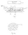
- a lithographic systemin accordance with an embodiment of the present invention includes a substrate 10 , having a substantially planar region shown as surface 12 . Disposed opposite substrate 10 is an imprint device 14 having a plurality of features thereon, forming a plurality of spaced-apart recesses 16 and protrusions 18 .
- the recesses 16are a plurality of grooves extending along a direction parallel to protrusions 18 that provide a cross-section of imprint device 14 with a shape of a battlement.
- the recesses 16may correspond to virtually any feature required to create an integrated circuit.
- a translation mechanism 20is connected between imprint device 14 and substrate 10 to vary a distance “d” between imprint device 14 and substrate 10 .
- a radiation source 22is located so that imprint device 14 is positioned between radiation source 22 and substrate 10 . Radiation source 22 is configured to impinge radiation on substrate 10 . To realize this, imprint device 14 is fabricated from material that allow it to be substantially transparent to the radiation produced by radiation source 22 .
- an imprinting layer 24is disposed adjacent to surface 12 , between substrate 10 and imprint device 14 .
- imprinting layer 24may be deposited using any known technique, in the present embodiment, imprinting layer 24 is deposited as a plurality of spaced-apart discrete beads 25 of material 25 a on substrate 10 , discussed more fully below.
- Imprinting layer 24is formed from a material 25 a that may be selectively polymerized and cross-linked to record a desired pattern. Material 25 a is shown in FIG. 3 as being cross-linked at points 25 b, forming cross-linked polymer material 25 c.
- the pattern recorded by imprinting layer 24is produced, in part, by mechanical contact with imprint device 14 .
- translation mechanism 20reduces the distance “d” to allow imprinting layer 24 to come into mechanical contact with imprint device 14 , spreading beads 25 so as to form imprinting layer 24 with a contiguous formation of material 25 a over surface 12 .
- distance “d”is reduced to allow sub-portions 24 a of imprinting layer 24 to ingress into and fill recesses 16 .
- material 25 ais provided with the requisite viscosity to completely fill recesses 16 in a timely manner, while covering surface with a contiguous formation of material 25 a, on the order of a few milliseconds to a few seconds.
- sub-portions 24 b of imprinting layer 24 in superimposition with protrusions 18remain after the desired, usually minimum distance “d” has reached a minimum distance, leaving sub-portions 24 a with a thickness to, and sub-portions 24 b with a thickness, t 2 .
- Thicknesses “t 1 ” and “t 2 ”may be any thickness desired, dependent upon the application.
- sub-portions 24 bmay be abrogated entirely whereby the only remaining material from imprinting layer 24 are sub-portions 24 a, after distance, “d” has reached a minimum value.
- radiation source 22produces actinic radiation that polymerizes and cross-links material 25 a, forming cross-link polymer material 25 c.
- the composition of imprinting layer 24transforms from material 25 a to material 25 c, which is a solid.
- material 25 cis solidified to provide surface 24 c of imprinting layer 24 with a shape conforming to a shape of a surface 14 a of imprint device 14 , shown more clearly in FIG. 5.
- an exemplary radiation source 22may produce ultraviolet radiation.
- Other radiation sourcesmay be employed, such as thermal, electromagnetic and the like.
- the selection of radiation employed to initiate the polymerization of the material in imprinting layer 24is known to one skilled in the art and typically depends on the specific application which is desired.
- translation mechanism 20increases the distance “d” so that imprint device 14 and imprinting layer 24 are spaced-apart.
- substrate 10 and imprinting layer 24may be selectively etched to increase the aspect ratio of recesses 30 in imprinting layer 24 .
- the material from which imprinting layer 24 is formedmay be varied to define a relative etch rate with respect to substrate 10 , as desired.
- the relative etch rate of imprinting layer 24 to substrate 10may be in a range of about 1.5:1 to about 100:1.
- imprinting layer 24may be provided with an etch differential with respect to photo-resist material (not shown) selectively disposed on surface 24 c.
- the photo-resist material(not shown) may be provided to further pattern imprinting layer 24 , using known techniques. Any etch process may be employed, dependent upon the etch rate desired and the underlying constituents that form substrate 10 and imprinting layer 24 . Exemplary etch processes may include plasma etching, reactive ion etching and the like.
- residual material 26may be present on imprinting layer 24 after patterning has been completed.
- Residual material 26may consist of un-polymerized material 25 a, solid polymerized and cross-linked material 25 c, substrate 10 or a combination thereof.
- Further processingmay be included to remove residual material 26 using well known techniques, e.g., argon ion milling, a plasma etch, reactive ion etching or a combination thereof. Further, removal of residual material 26 may be accomplished during any stage of the patterning. For example, removal of residual material 26 may be carried out before etching the polymerized and cross-linked imprinting layer 24 .
- the aspect ratio of recesses 30 formed from the aforementioned patterning techniquemay be as great as 30:1.
- one embodiment of imprint device 14has recesses 16 defining an aspect ratio in a range of 1:1 to 10:1.
- protrusions 18have a width W 1 in a range of about 10 nm to about 5000 ⁇ m
- recesses 16have a width W 2 in a range of 10 nm to about 5000 ⁇ m.
- imprint device 14may be formed from various conventional materials, such as, but not limited to, quartz, silicon, organic polymers, siloxane polymers, borosilicate glass, fluorocarbon polymers, metal, and combinations of the above.
- material 25 ais important to efficiently pattern substrate 10 in light of the unique deposition process employed.
- material 25 ais deposited on substrate 10 as a plurality of discrete and spaced-apart beads 25 .
- the combined volume of beads 25is such that the material 25 a is distributed appropriately over area of surface 12 where imprint layer 24 is to be formed.
- imprint layer 24is spread and patterned concurrently, with the pattern being subsequently set by exposure to radiation, such as ultraviolet radiation.
- material 25 ahave certain characteristics to facilitate rapid and even spreading of material 25 a in beads 25 over surface 12 so that the all thicknesses t 1 are substantially uniform and all thickness t 2 are substantially uniform.
- the desirable characteristicsinclude having a viscosity approximately that of water, (H 2 O), 1 to 2 centepoise (csp), or less, as well as the ability to wet surface of substrate 10 to avoid subsequent pit or hole formation after polymerization.
- the wettability of imprinting layer 24should be such that the angle, ⁇ 1 , is defined as follows:
- imprinting layer 24may be made sufficiently thin while avoiding formation of pits or holes in the thinner regions, such as regions 24 b.
- thermal stabilitysuch that the variation in an angle ⁇ , measured between a nadir 30 a of a recess 30 and a sidewall 30 b thereof, does not vary more than 10% after being heated to 75° C. for thirty (30) minutes.
- material 25 ashould transform to material 25 c, i.e., polymerize and cross-link, when subjected to a pulse of radiation containing less than 5 J cm-2.
- polymerization and cross-linkingwas determined by analyzing the infrared absorption of the “C ⁇ C” bond contained in material 25 a.
- substrate surface 12be relatively inert toward material 25 a, such that less than 500 nm of surface 12 be dissolved as a result sixty seconds of contact with material 25 a. It is further desired that the wetting of imprint device 14 by imprinting layer 24 be minimized. To that end, the wetting angle, ⁇ 2 , should be greater than 75°. Finally, should it be desired to vary an etch rate differential between imprinting layer 24 and substrate 10 , an exemplary embodiment of the present invention would demonstrate an etch rate that is 20% less than the etch rate of an optical photo-resist (not shown) exposed to an oxygen plasma.
- substrate 10may be formed from a number of different materials.
- the chemical composition of surface 12varies dependent upon the material from which substrate 10 is formed.
- substrate 10may be formed from silicon, plastics, gallium arsenide, mercury telluride, and composites thereof.
- substratemay include one or more layers in region, e.g., dielectric layer, metal layers, semiconductor layer and the like.
- the constituent components of material 25 aconsist of acrylated monomers or methacrylated monomers that are not silyated, a cross-linking agent, and an initiator.
- the non-silyated acryl or methacryl monomersare selected to provide material 25 a with a minimal viscosity, e.g., viscosity approximating the viscosity of water (1-2 cps) or less.
- the cross-linking agentis included, even though the size of these molecules increases the viscosity of material 25 a, to cross-link the molecules of the non-silyated monomers, providing material 25 a with the properties to record a pattern thereon having very small feature sizes, on the order of a few nanometers and to provide the aforementioned thermal stability for further processing.
- the initiatoris provided to produce a free radical reaction in response to radiation, causing the non-silyated monomers and the cross-linking agent to polymerize and cross-link, forming a cross-linked polymer material 25 c.
- a photo-initiator responsive to ultraviolet radiationis employed.
- a silyated monomermay also be included in material 25 a to control the etch rate of the result cross-linked polymer material 25 c, without substantially affecting the viscosity of material 25 a.
- non-silyated monomersinclude, but are not limited to, butyl acrylate, methyl acrylate, methyl methacrylate, or mixtures thereof.
- the non-silyated monomermay make up approximately 25 to 60% by weight of material 25 a. It is believed that the monomer provides adhesion to an underlying organic transfer layer, discussed more fully below.
- the cross-linking agentis a monomer that includes two or more polymerizable groups.
- polyfunctional siloxane derivativesmay be used as a crosslinking agent.
- An example of a polyfunctional siloxane derivativeis 1,3-bis(3-methacryloxypropyl)-tetramethyl disiloxane.
- Another suitable cross-linking agentconsists of ethylene diol diacrylate.
- the cross-linking agentmay be present in material 25 a in amounts of up to 20% by weight, but is more typically present in an amount of 5-15% by weight.
- the initiatormay be any component that initiates a free radical reaction in response to radiation, produced by radiation source 22 , impinging thereupon and being absorbed thereby.
- Suitable initiatorsmay include, but are not limited to, photo-initiators such as 1-hydroxycyclohexyl phenyl ketone or phenylbis(2,4,6-trimethyl benzoyl) phosphine oxide.
- the initiatormay be present in material 25 a in amounts of up to 5% by weight, but is typically present in an amount of 1-4% by weight.
- suitable silylated monomersmay include, but are not limited to, silyl-acryloxy and silyl methacryloxy derivatives. Specific examples are methacryloxypropyl tris(tri-methylsiloxy)silane and (3-acryloxypropyl)tris(tri-methoxysiloxy)-silane. Silylated monomers may be present in material 25 a amounts from 25 to 50% by weight.
- the curable liquidmay also include a dimethyl siloxane derivative. Examples of dimethyl siloxane derivatives include, but are not limited to, (acryloxypropyl) methylsiloxane dimethylsiloxane copolymer.
- exemplary compositions for material 25 aare as follows:
- compositionsalso include stabilizers that are well known in the chemical art to increase the operational life, as well as initiators.
- compositions described aboveprovide suitable viscosity and cross-linking required to efficiently pattern using imprint lithography and are based upon the realization that the poly-functional molecules increases viscosity less than experimentally anticipated.
- a dearth of informationexists relating to viscosity of materials as a function of the viscosity of the underlying components that form the material.
- an approximately linear function of compositionwas obtained by comparing 1/viscosity vs. the weight fraction of a molecule component in a material.
- a theoretical model of all components in a materialwas obtained by calculating 1/viscosity, based upon the weight percentage of the composition in the material 25 a. The theoretical viscosity was then compared with the measure viscosity.
- planarization layer 32may be formed from a number of differing materials, such as, for example, thermoset polymers, thermoplastic polymers, polyepoxies, polyamides, polyurethanes, polycarbonates, polyesters, and combinations thereof. Planarization layer 32 is fabricated in such a manner so as to possess a continuous, smooth, relatively defect-free surface that may exhibit excellent adhesion to the imprinting layer 24 .
- surface 14 amay be treated with a modifying agent.
- a modifying agentis a release layer 34 formed from a fluorocarbon silylating agent.
- Release layer 34 and other surface modifying agentsmay be applied using any know process. For example, processing techniques that may include chemical vapor deposition method, physical vapor deposition, atomic layer deposition or various other techniques, brazing and the like. In this configuration, imprinting layer 24 is located between planarization layer 32 and release layer 34 , during imprint lithography processes.
Landscapes
- Physics & Mathematics (AREA)
- Engineering & Computer Science (AREA)
- General Physics & Mathematics (AREA)
- Chemical & Material Sciences (AREA)
- Nanotechnology (AREA)
- Crystallography & Structural Chemistry (AREA)
- Spectroscopy & Molecular Physics (AREA)
- Mathematical Physics (AREA)
- Theoretical Computer Science (AREA)
- Condensed Matter Physics & Semiconductors (AREA)
- Manufacturing & Machinery (AREA)
- Polymerisation Methods In General (AREA)
Abstract
Description
- The field of invention relates generally to micro-fabrication of structures. More particularly, the present invention is directed to patterning substrates in furtherance of the formation of structures.[0001]
- Micro-fabrication involves the fabrication of very small structures, e.g., having features on the order of micro-meters or smaller. One area in which micro-fabrication has had a sizeable impact is in the processing of integrated circuits. As the semiconductor processing industry continues to strive for larger production yields while increasing the circuits per unit area formed on a substrate, micro-fabrication becomes increasingly important. Micro-fabrication provides greater process control while allowing increased reduction of the minimum feature dimension of the structures formed. Other areas of development in which micro-fabrication has been employed include biotechnology, optical technology, mechanical systems and the like.[0002]
- An exemplary micro-fabrication technique is shown in U.S. Pat. No. 6,334,960 to Willson et al. Willson et al. disclose a method of forming a relief image in a structure. The method includes providing a substrate having a transfer layer. The transfer layer is covered with a polymerizable fluid composition. A mold makes mechanical contact with the polymerizable fluid. The mold includes a relief structure, and the polymerizable fluid composition fills the relief structure. The polymerizable fluid composition is then subjected to conditions to solidify and polymerize the same, forming a solidified polymeric material on the transfer layer that contains a relief structure complimentary to that of the mold. The mold is then separated from the solid polymeric material such that a replica of the relief structure in the mold is formed in the solidified polymeric material. The transfer layer and the solidified polymeric material are subjected to an environment to selectively etch the transfer layer relative to the solidified polymeric material such that a relief image is formed in the transfer layer. The time required and the minimum feature dimension provided by this technique is dependent upon, inter alia, the composition of the polymerizable material.[0003]
- It is desired, therefore, to provide an improved composition for polymerizable material used in micro-fabrication.[0004]
- The present invention includes a composition and a method for forming a pattern on a substrate with the composition by forming a cross-linked polymer from the composition upon exposing the same to radiation. To that end, in one embodiment of the present invention the composition includes a mono-functional acrylate component, a poly-functional molecule component, and an initiator component responsive to the radiation to initiate a free radical reaction to cause the mono-functional acrylate component and the poly-functional acrylate component to polymerize and cross-link. This composition facilitates imprint lithography by satisfying numerous desirable characteristics. Specifically, the composition has a viscosity in a range of 1 to 2 centepoise (cps). The composition preferentially wets an adjacent surface forming a contact angle of less than 75°. In other embodiments, the composition is formulated to minimize dissolving more than 500 nm of the adjacent surface upon being removed one minute after wetting the same. In still other embodiments, the composition minimizes wetting of an adjacent silylating containing surface, forming a contact angle therewith that is greater than 75°. In one exemplary embodiment, the initiator component is responsive to a pulse of ultraviolet radiation, containing less than 5 J cm-2,causing the mono-functional component and the poly-functional component to polymerize and cross-link, defining a cross-linked polymer layer. In yet another embodiment, the composition also provides a cross-linked polymer layer with relative thermal stability so that heated to a temperature of 75° C. the variation in an angle, measured between a nadir of a recess and a sidewall formed therein, is no more than 10%. These and other embodiments are described herein.[0005]
- FIG. 1 is a simplified elevation view of a lithographic system in accordance with the present invention;[0006]
- FIG. 2 is a simplified representation of material from which an imprinting layer, shown in FIG. 1, is comprised before being polymerized and cross-linked;[0007]
- FIG. 3 is a simplified representation of cross-linked polymer material into which the material shown in FIG. 2 is transformed after being subjected to radiation;[0008]
- FIG. 4 is a simplified elevation view of an imprint device, shown in FIG. 1, in mechanical contact with an imprint layer disposed on a substrate, in accordance with one embodiment of the present invention;[0009]
- FIG. 5 is a simplified elevation view of the imprint device spaced-apart from the imprint layer, shown in FIG. 4, after patterning of the imprint layer;[0010]
- FIG. 6 is a simplified elevation view of the imprint device and imprint layer shown in FIG. 5, with residue remaining in the pattern; and[0011]
- FIG. 7 is a simplified elevation view of material in an imprint device and substrate employed with the present invention in accordance with an alternate embodiment.[0012]
- Referring to FIG. 1, a lithographic system in accordance with an embodiment of the present invention includes a[0013]
substrate 10, having a substantially planar region shown as surface12. Disposedopposite substrate 10 is animprint device 14 having a plurality of features thereon, forming a plurality of spaced-apart recesses 16 andprotrusions 18. In the present embodiment, therecesses 16 are a plurality of grooves extending along a direction parallel toprotrusions 18 that provide a cross-section ofimprint device 14 with a shape of a battlement. However, therecesses 16 may correspond to virtually any feature required to create an integrated circuit. Atranslation mechanism 20 is connected betweenimprint device 14 andsubstrate 10 to vary a distance “d” betweenimprint device 14 andsubstrate 10. Aradiation source 22 is located so thatimprint device 14 is positioned betweenradiation source 22 andsubstrate 10.Radiation source 22 is configured to impinge radiation onsubstrate 10. To realize this,imprint device 14 is fabricated from material that allow it to be substantially transparent to the radiation produced byradiation source 22. - Referring to both FIGS. 1 and 2, an[0014]
imprinting layer 24 is disposed adjacent to surface12, betweensubstrate 10 andimprint device 14. Althoughimprinting layer 24 may be deposited using any known technique, in the present embodiment,imprinting layer 24 is deposited as a plurality of spaced-apartdiscrete beads 25 of material25aonsubstrate 10, discussed more fully below.Imprinting layer 24 is formed from a material25athat may be selectively polymerized and cross-linked to record a desired pattern. Material25ais shown in FIG. 3 as being cross-linked atpoints 25b,formingcross-linked polymer material 25c. - Referring to both FIGS. 1 and 4, the pattern recorded by[0015]
imprinting layer 24 is produced, in part, by mechanical contact withimprint device 14. To that end,translation mechanism 20 reduces the distance “d” to allowimprinting layer 24 to come into mechanical contact withimprint device 14, spreadingbeads 25 so as to formimprinting layer 24 with a contiguous formation of material25aover surface12. In one embodiment, distance “d” is reduced to allow sub-portions24aofimprinting layer 24 to ingress into and fillrecesses 16. - Referring to FIGS. 1, 2 and[0016]4, to facilitate filling of
recesses 16, material25ais provided with the requisite viscosity to completely fillrecesses 16 in a timely manner, while covering surface with a contiguous formation of material25a,on the order of a few milliseconds to a few seconds. In the present embodiment,sub-portions 24bofimprinting layer 24 in superimposition withprotrusions 18 remain after the desired, usually minimum distance “d” has reached a minimum distance, leaving sub-portions24awith a thickness to, andsub-portions 24bwith a thickness, t2. Thicknesses “t1” and “t2” may be any thickness desired, dependent upon the application. Further, in another embodiment,sub-portions 24bmay be abrogated entirely whereby the only remaining material fromimprinting layer 24 are sub-portions24a,after distance, “d” has reached a minimum value. - Referring to FIGS. 1, 2 and[0017]3, after a desired distance “d” has been reached,
radiation source 22 produces actinic radiation that polymerizes and cross-links material25a,formingcross-link polymer material 25c.As a result, the composition ofimprinting layer 24 transforms from material25atomaterial 25c,which is a solid. Specifically,material 25cis solidified to provide surface24cofimprinting layer 24 with a shape conforming to a shape of a surface14aofimprint device 14, shown more clearly in FIG. 5. - Referring to FIGS. 1, 2 and[0018]3 an
exemplary radiation source 22 may produce ultraviolet radiation. Other radiation sources may be employed, such as thermal, electromagnetic and the like. The selection of radiation employed to initiate the polymerization of the material inimprinting layer 24 is known to one skilled in the art and typically depends on the specific application which is desired. Afterimprinting layer 24 is transformed to consist ofmaterial 25c,translation mechanism 20 increases the distance “d” so thatimprint device 14 andimprinting layer 24 are spaced-apart. - Referring to FIG. 5, additional processing may be employed to complete the patterning of[0019]
substrate 10. For example,substrate 10 andimprinting layer 24 may be selectively etched to increase the aspect ratio ofrecesses 30 inimprinting layer 24. To facilitate etching, the material from whichimprinting layer 24 is formed may be varied to define a relative etch rate with respect tosubstrate 10, as desired. The relative etch rate ofimprinting layer 24 tosubstrate 10 may be in a range of about 1.5:1 to about 100:1. Alternatively, or in addition to,imprinting layer 24 may be provided with an etch differential with respect to photo-resist material (not shown) selectively disposed on surface24c.The photo-resist material (not shown) may be provided to furtherpattern imprinting layer 24, using known techniques. Any etch process may be employed, dependent upon the etch rate desired and the underlying constituents that formsubstrate 10 andimprinting layer 24. Exemplary etch processes may include plasma etching, reactive ion etching and the like. - Referring to FIGS. 2, 3 and[0020]6, residual material26 may be present on
imprinting layer 24 after patterning has been completed. Residual material26 may consist of un-polymerized material25a,solid polymerized andcross-linked material 25c,substrate 10 or a combination thereof. Further processing may be included to remove residual material26 using well known techniques, e.g., argon ion milling, a plasma etch, reactive ion etching or a combination thereof. Further, removal of residual material26 may be accomplished during any stage of the patterning. For example, removal of residual material26 may be carried out before etching the polymerized andcross-linked imprinting layer 24. - Referring to FIGS. 1 and 5, the aspect ratio of[0021]
recesses 30 formed from the aforementioned patterning technique may be as great as 30:1. To that end, one embodiment ofimprint device 14 hasrecesses 16 defining an aspect ratio in a range of 1:1 to 10:1. Specifically,protrusions 18 have a width W1in a range of about 10 nm to about 5000 μm, and recesses16 have a width W2in a range of 10 nm to about 5000 μm. As a result,imprint device 14 may be formed from various conventional materials, such as, but not limited to, quartz, silicon, organic polymers, siloxane polymers, borosilicate glass, fluorocarbon polymers, metal, and combinations of the above. - Referring to FIGS. 1 and 2, the characteristics of material[0022]25aare important to efficiently
pattern substrate 10 in light of the unique deposition process employed. As mentioned above, material25ais deposited onsubstrate 10 as a plurality of discrete and spaced-apartbeads 25. The combined volume ofbeads 25 is such that the material25ais distributed appropriately over area of surface12 whereimprint layer 24 is to be formed. As a result,imprint layer 24 is spread and patterned concurrently, with the pattern being subsequently set by exposure to radiation, such as ultraviolet radiation. As a result of the deposition process it is desired that material25ahave certain characteristics to facilitate rapid and even spreading of material25ainbeads 25 over surface12 so that the all thicknesses t1are substantially uniform and all thickness t2are substantially uniform. The desirable characteristics include having a viscosity approximately that of water, (H2O), 1 to 2 centepoise (csp), or less, as well as the ability to wet surface ofsubstrate 10 to avoid subsequent pit or hole formation after polymerization. To that end, in one example, the wettability ofimprinting layer 24, as defined by the contact angle method, should be such that the angle, θ1, is defined as follows: - 0>θ1<75°
- With these two characteristics being satisfied, imprinting[0023]
layer 24 may be made sufficiently thin while avoiding formation of pits or holes in the thinner regions, such asregions 24b. - Referring to FIGS. 2, 3 and[0024]5, another desireable characteristic that it is desired for material25ato possess is thermal stability such that the variation in an angle Φ, measured between a nadir30aof a
recess 30 and a sidewall30bthereof, does not vary more than 10% after being heated to 75° C. for thirty (30) minutes. Additionally, material25ashould transform tomaterial 25c,i.e., polymerize and cross-link, when subjected to a pulse of radiation containing less than 5 J cm-2. In the present example, polymerization and cross-linking was determined by analyzing the infrared absorption of the “C═C” bond contained in material25a.Additionally, it is desired that substrate surface12 be relatively inert toward material25a,such that less than 500 nm of surface12 be dissolved as a result sixty seconds of contact with material25a.It is further desired that the wetting ofimprint device 14 by imprintinglayer 24 be minimized. To that end, the wetting angle, θ2, should be greater than 75°. Finally, should it be desired to vary an etch rate differential betweenimprinting layer 24 andsubstrate 10, an exemplary embodiment of the present invention would demonstrate an etch rate that is 20% less than the etch rate of an optical photo-resist (not shown) exposed to an oxygen plasma. - The constituent components that form material[0025]25ato provide the aforementioned characteristics may differ. This results from
substrate 10 being formed from a number of different materials. As a result, the chemical composition of surface12 varies dependent upon the material from whichsubstrate 10 is formed. For example,substrate 10 may be formed from silicon, plastics, gallium arsenide, mercury telluride, and composites thereof. Additionally, substrate may include one or more layers in region, e.g., dielectric layer, metal layers, semiconductor layer and the like. - Referring to FIGS. 2 and 3, in one embodiment of the present invention the constituent components of material[0026]25aconsist of acrylated monomers or methacrylated monomers that are not silyated, a cross-linking agent, and an initiator. The non-silyated acryl or methacryl monomers are selected to provide material25awith a minimal viscosity, e.g., viscosity approximating the viscosity of water (1-2 cps) or less. The cross-linking agent is included, even though the size of these molecules increases the viscosity of material25a,to cross-link the molecules of the non-silyated monomers, providing material25awith the properties to record a pattern thereon having very small feature sizes, on the order of a few nanometers and to provide the aforementioned thermal stability for further processing. To that end, the initiator is provided to produce a free radical reaction in response to radiation, causing the non-silyated monomers and the cross-linking agent to polymerize and cross-link, forming a
cross-linked polymer material 25c.In the present example, a photo-initiator responsive to ultraviolet radiation is employed. In addition, if desired, a silyated monomer may also be included in material25ato control the etch rate of the result cross-linkedpolymer material 25c,without substantially affecting the viscosity of material25a. - Examples of non-silyated monomers include, but are not limited to, butyl acrylate, methyl acrylate, methyl methacrylate, or mixtures thereof. The non-silyated monomer may make up approximately 25 to 60% by weight of material[0027]25a.It is believed that the monomer provides adhesion to an underlying organic transfer layer, discussed more fully below.
- The cross-linking agent is a monomer that includes two or more polymerizable groups. In one embodiment, polyfunctional siloxane derivatives may be used as a crosslinking agent. An example of a polyfunctional siloxane derivative is 1,3-bis(3-methacryloxypropyl)-tetramethyl disiloxane. Another suitable cross-linking agent consists of ethylene diol diacrylate. The cross-linking agent may be present in material[0028]25ain amounts of up to 20% by weight, but is more typically present in an amount of 5-15% by weight.
- The initiator may be any component that initiates a free radical reaction in response to radiation, produced by[0029]
radiation source 22, impinging thereupon and being absorbed thereby. Suitable initiators may include, but are not limited to, photo-initiators such as 1-hydroxycyclohexyl phenyl ketone or phenylbis(2,4,6-trimethyl benzoyl) phosphine oxide. The initiator may be present in material25ain amounts of up to 5% by weight, but is typically present in an amount of 1-4% by weight. - Were it desired to include silylated monomers in material[0030]25a,suitable silylated monomers may include, but are not limited to, silyl-acryloxy and silyl methacryloxy derivatives. Specific examples are methacryloxypropyl tris(tri-methylsiloxy)silane and (3-acryloxypropyl)tris(tri-methoxysiloxy)-silane. Silylated monomers may be present in material25aamounts from 25 to 50% by weight. The curable liquid may also include a dimethyl siloxane derivative. Examples of dimethyl siloxane derivatives include, but are not limited to, (acryloxypropyl) methylsiloxane dimethylsiloxane copolymer.
- Referring to both FIGS. 1 and 2, exemplary compositions for material[0031]25aare as follows:
- [0032]
Composition 1 - n-butyl acrylate+(3-acryloxypropyltristrimethylsiloxy)[0033]
silane+ 1,3-bis(3-methacryloxypropyl)tetramethyldisiloxane - Composition 2[0034]
- t-n-butyl acrylate+(3-acryloxypropyltristrimethylsiloxy)silane+Ethylene diol diacrylate[0035]
- Composition 3[0036]
- t-butyl acrylate+methacryloxypropylpentamethyldisiloxane+1,3-bis(3-methacryloxypropyl)tetramethyldisiloxane[0037]
- The above-identified compositions also include stabilizers that are well known in the chemical art to increase the operational life, as well as initiators.[0038]
- The compositions described above provide suitable viscosity and cross-linking required to efficiently pattern using imprint lithography and are based upon the realization that the poly-functional molecules increases viscosity less than experimentally anticipated. Specifically, a dearth of information exists relating to viscosity of materials as a function of the viscosity of the underlying components that form the material. As a result, an approximately linear function of composition was obtained by comparing 1/viscosity vs. the weight fraction of a molecule component in a material. A theoretical model of all components in a material was obtained by calculating 1/viscosity, based upon the weight percentage of the composition in the material[0039]25a.The theoretical viscosity was then compared with the measure viscosity. It was found that certain di-functional acrylates had a measured viscosity that was less than the theoretical viscosity, defining a viscosity differential. Similarly, the viscosity differential of the mono-functional molecules was such that the theoretical viscosity was greater than the measured viscosity. However, it was found that the viscosity differential of the di-functional molecules was nearly twice that of the mono-functional molecules. As a result, it was determined that cross-linking of material25amay be augmented without increasing the viscosity of the same too greatly.
- Referring to FIGS. 2 and 7, employing the compositions described above in material[0040]25ato facilitate imprint lithography was achieved by defining a
surface 112 of substrate110 with a planarization layer32 disposed adjacent to awafer 33. The primary function of planarization layer32 is to ensuresurface 112 is planar. To that end, planarization layer32 may be formed from a number of differing materials, such as, for example, thermoset polymers, thermoplastic polymers, polyepoxies, polyamides, polyurethanes, polycarbonates, polyesters, and combinations thereof. Planarization layer32 is fabricated in such a manner so as to possess a continuous, smooth, relatively defect-free surface that may exhibit excellent adhesion to theimprinting layer 24. - Additionally, to ensure that[0041]
imprinting layer 24 does not adhere toimprint device 14, surface14amay be treated with a modifying agent. One such modifying agent is arelease layer 34 formed from a fluorocarbon silylating agent.Release layer 34 and other surface modifying agents, may be applied using any know process. For example, processing techniques that may include chemical vapor deposition method, physical vapor deposition, atomic layer deposition or various other techniques, brazing and the like. In this configuration,imprinting layer 24 is located between planarization layer32 andrelease layer 34, during imprint lithography processes. - The embodiments of the present invention described above are exemplary. Many changes and modifications may be made to the disclosure recited above, while remaining within the scope of the invention. The scope of the invention should, therefore, be determined not with reference to the above description, but instead should be determined with reference to the appended claims along with their full scope of equivalents.[0042]
Claims (21)
Priority Applications (1)
| Application Number | Priority Date | Filing Date | Title |
|---|---|---|---|
| US10/178,947US20030235787A1 (en) | 2002-06-24 | 2002-06-24 | Low viscosity high resolution patterning material |
Applications Claiming Priority (1)
| Application Number | Priority Date | Filing Date | Title |
|---|---|---|---|
| US10/178,947US20030235787A1 (en) | 2002-06-24 | 2002-06-24 | Low viscosity high resolution patterning material |
Publications (1)
| Publication Number | Publication Date |
|---|---|
| US20030235787A1true US20030235787A1 (en) | 2003-12-25 |
Family
ID=29734822
Family Applications (1)
| Application Number | Title | Priority Date | Filing Date |
|---|---|---|---|
| US10/178,947AbandonedUS20030235787A1 (en) | 2002-06-24 | 2002-06-24 | Low viscosity high resolution patterning material |
Country Status (1)
| Country | Link |
|---|---|
| US (1) | US20030235787A1 (en) |
Cited By (36)
| Publication number | Priority date | Publication date | Assignee | Title |
|---|---|---|---|---|
| US20040116548A1 (en)* | 2002-12-12 | 2004-06-17 | Molecular Imprints, Inc. | Compositions for dark-field polymerization and method of using the same for imprint lithography processes |
| US6929762B2 (en) | 2002-11-13 | 2005-08-16 | Molecular Imprints, Inc. | Method of reducing pattern distortions during imprint lithography processes |
| US6990870B2 (en) | 2002-12-12 | 2006-01-31 | Molecular Imprints, Inc. | System for determining characteristics of substrates employing fluid geometries |
| US20060036051A1 (en)* | 2004-08-16 | 2006-02-16 | Molecular Imprints, Inc. | Composition to provide a layer with uniform etch characteristics |
| US20060076717A1 (en)* | 2002-07-11 | 2006-04-13 | Molecular Imprints, Inc. | Step and repeat imprint lithography processes |
| US7122482B2 (en) | 2003-10-27 | 2006-10-17 | Molecular Imprints, Inc. | Methods for fabricating patterned features utilizing imprint lithography |
| US7122079B2 (en) | 2004-02-27 | 2006-10-17 | Molecular Imprints, Inc. | Composition for an etching mask comprising a silicon-containing material |
| US7136150B2 (en) | 2003-09-25 | 2006-11-14 | Molecular Imprints, Inc. | Imprint lithography template having opaque alignment marks |
| US7157036B2 (en) | 2003-06-17 | 2007-01-02 | Molecular Imprints, Inc | Method to reduce adhesion between a conformable region and a pattern of a mold |
| WO2007002965A1 (en)* | 2005-06-30 | 2007-01-11 | Technische Universität Wien | Rapid-prototyping method and radiation-hardenable composition of application thereto |
| US20070034600A1 (en)* | 2002-12-12 | 2007-02-15 | Board Of Regents, The University Of Texas System | Planarization Method of Patterning a Substratte |
| US20070264591A1 (en)* | 2006-05-15 | 2007-11-15 | Asml Netherlands B.V. | Imprint lithography |
| US7307118B2 (en) | 2004-11-24 | 2007-12-11 | Molecular Imprints, Inc. | Composition to reduce adhesion between a conformable region and a mold |
| EP1800186A4 (en)* | 2004-09-15 | 2008-01-23 | Agency Science Tech & Res | PRINTED POLYMER CARRIER |
| US20080085465A1 (en)* | 2004-09-23 | 2008-04-10 | Molecular Imprints, Inc. | Polymerization Technique to Attenuate Oxygen Inhibition of Solidification of Liquids and Composition Therefor |
| US20080174046A1 (en)* | 2002-07-11 | 2008-07-24 | Molecular Imprints Inc. | Capillary Imprinting Technique |
| US7452574B2 (en) | 2003-02-27 | 2008-11-18 | Molecular Imprints, Inc. | Method to reduce adhesion between a polymerizable layer and a substrate employing a fluorine-containing layer |
| US20090136654A1 (en)* | 2005-10-05 | 2009-05-28 | Molecular Imprints, Inc. | Contact Angle Attenuations on Multiple Surfaces |
| US20090155583A1 (en)* | 2005-07-22 | 2009-06-18 | Molecular Imprints, Inc. | Ultra-thin Polymeric Adhesion Layer |
| US20090197057A1 (en)* | 2008-02-05 | 2009-08-06 | Molecular Imprints, Inc. | Controlling Template Surface Composition in Nano-Imprint Lithography |
| US7691313B2 (en) | 2002-11-13 | 2010-04-06 | Molecular Imprints, Inc. | Method for expelling gas positioned between a substrate and a mold |
| US20100098940A1 (en)* | 2008-10-20 | 2010-04-22 | Molecular Imprints, Inc. | Nano-Imprint Lithography Stack with Enhanced Adhesion Between Silicon-Containing and Non-Silicon Containing Layers |
| US20100112236A1 (en)* | 2008-10-30 | 2010-05-06 | Molecular Imprints, Inc. | Facilitating Adhesion Between Substrate and Patterned Layer |
| US7759407B2 (en) | 2005-07-22 | 2010-07-20 | Molecular Imprints, Inc. | Composition for adhering materials together |
| EP2221664A1 (en)* | 2009-02-19 | 2010-08-25 | Solvay Solexis S.p.A. | Nanolithography process |
| US7906180B2 (en) | 2004-02-27 | 2011-03-15 | Molecular Imprints, Inc. | Composition for an etching mask comprising a silicon-containing material |
| US20110081501A1 (en)* | 2006-03-06 | 2011-04-07 | Asahi Glass Company, Limted | Treated substrate having hydrophilic region and water repellent region, and process for producing it |
| US7939131B2 (en) | 2004-08-16 | 2011-05-10 | Molecular Imprints, Inc. | Method to provide a layer with uniform etch characteristics |
| US20110165412A1 (en)* | 2009-11-24 | 2011-07-07 | Molecular Imprints, Inc. | Adhesion layers in nanoimprint lithograhy |
| US8076386B2 (en) | 2004-02-23 | 2011-12-13 | Molecular Imprints, Inc. | Materials for imprint lithography |
| US8349241B2 (en) | 2002-10-04 | 2013-01-08 | Molecular Imprints, Inc. | Method to arrange features on a substrate to replicate features having minimal dimensional variability |
| CN103309162A (en)* | 2012-03-06 | 2013-09-18 | 第一毛织株式会社 | Photocurable composition, and encapsulated apparatus including a barrier layer including the same |
| US8557351B2 (en) | 2005-07-22 | 2013-10-15 | Molecular Imprints, Inc. | Method for adhering materials together |
| US8808808B2 (en) | 2005-07-22 | 2014-08-19 | Molecular Imprints, Inc. | Method for imprint lithography utilizing an adhesion primer layer |
| US20200024661A1 (en)* | 2018-07-20 | 2020-01-23 | Illumina, Inc. | Resin composition and flow cells incorporating the same |
| US12442039B2 (en) | 2023-12-29 | 2025-10-14 | Illumina, Inc. | Resin composition and flow cells incorporating the same |
Citations (93)
| Publication number | Priority date | Publication date | Assignee | Title |
|---|---|---|---|---|
| US3783520A (en)* | 1970-09-28 | 1974-01-08 | Bell Telephone Labor Inc | High accuracy alignment procedure utilizing moire patterns |
| US4070116A (en)* | 1975-06-23 | 1978-01-24 | International Business Machines Corporation | Gap measuring device for defining the distance between two or more surfaces |
| US4201800A (en)* | 1978-04-28 | 1980-05-06 | International Business Machines Corp. | Hardened photoresist master image mask process |
| US4426247A (en)* | 1982-04-12 | 1984-01-17 | Nippon Telegraph & Telephone Public Corporation | Method for forming micropattern |
| US4507331A (en)* | 1983-12-12 | 1985-03-26 | International Business Machines Corporation | Dry process for forming positive tone micro patterns |
| US4512848A (en)* | 1984-02-06 | 1985-04-23 | Exxon Research And Engineering Co. | Procedure for fabrication of microstructures over large areas using physical replication |
| US4600309A (en)* | 1982-12-30 | 1986-07-15 | Thomson-Csf | Process and apparatus for theoptical alignment of patterns in two close-up planes in an exposure means incorporating a divergent radiation source |
| US4657845A (en)* | 1986-01-14 | 1987-04-14 | International Business Machines Corporation | Positive tone oxygen plasma developable photoresist |
| US4731155A (en)* | 1987-04-15 | 1988-03-15 | General Electric Company | Process for forming a lithographic mask |
| US4737425A (en)* | 1986-06-10 | 1988-04-12 | International Business Machines Corporation | Patterned resist and process |
| US4808511A (en)* | 1987-05-19 | 1989-02-28 | International Business Machines Corporation | Vapor phase photoresist silylation process |
| US4826943A (en)* | 1986-07-25 | 1989-05-02 | Oki Electric Industry Co., Ltd. | Negative resist material |
| US4848911A (en)* | 1986-06-11 | 1989-07-18 | Kabushiki Kaisha Toshiba | Method for aligning first and second objects, relative to each other, and apparatus for practicing this method |
| US4857477A (en)* | 1986-09-18 | 1989-08-15 | Oki Electric Industry Co., Ltd. | Process for fabricating a semiconductor device |
| US4891303A (en)* | 1988-05-26 | 1990-01-02 | Texas Instruments Incorporated | Trilayer microlithographic process using a silicon-based resist as the middle layer |
| US4908298A (en)* | 1985-03-19 | 1990-03-13 | International Business Machines Corporation | Method of creating patterned multilayer films for use in production of semiconductor circuits and systems |
| US4919748A (en)* | 1989-06-30 | 1990-04-24 | At&T Bell Laboratories | Method for tapered etching |
| US4921778A (en)* | 1988-07-29 | 1990-05-01 | Shipley Company Inc. | Photoresist pattern fabrication employing chemically amplified metalized material |
| US4931351A (en)* | 1987-01-12 | 1990-06-05 | Eastman Kodak Company | Bilayer lithographic process |
| US4999280A (en)* | 1989-03-17 | 1991-03-12 | International Business Machines Corporation | Spray silylation of photoresist images |
| US5028366A (en)* | 1988-01-12 | 1991-07-02 | Air Products And Chemicals, Inc. | Water based mold release compositions for making molded polyurethane foam |
| US5108875A (en)* | 1988-07-29 | 1992-04-28 | Shipley Company Inc. | Photoresist pattern fabrication employing chemically amplified metalized material |
| US5110514A (en)* | 1989-05-01 | 1992-05-05 | Soane Technologies, Inc. | Controlled casting of a shrinkable material |
| US5126006A (en)* | 1990-10-30 | 1992-06-30 | International Business Machines Corp. | Plural level chip masking |
| US5179863A (en)* | 1990-03-05 | 1993-01-19 | Kabushiki Kaisha Toshiba | Method and apparatus for setting the gap distance between a mask and a wafer at a predetermined distance |
| US5198326A (en)* | 1990-05-24 | 1993-03-30 | Matsushita Electric Industrial Co., Ltd. | Process for forming fine pattern |
| US5212147A (en)* | 1991-05-15 | 1993-05-18 | Hewlett-Packard Company | Method of forming a patterned in-situ high Tc superconductive film |
| US5314772A (en)* | 1990-10-09 | 1994-05-24 | Arizona Board Of Regents | High resolution, multi-layer resist for microlithography and method therefor |
| US5318870A (en)* | 1989-10-18 | 1994-06-07 | Massachusetts Institute Of Technology | Method of patterning a phenolic polymer film without photoactive additive through exposure to high energy radiation below 225 nm with subsequent organometallic treatment and the associated imaged article |
| US5324683A (en)* | 1993-06-02 | 1994-06-28 | Motorola, Inc. | Method of forming a semiconductor structure having an air region |
| US5328810A (en)* | 1990-05-07 | 1994-07-12 | Micron Technology, Inc. | Method for reducing, by a factor or 2-N, the minimum masking pitch of a photolithographic process |
| US5330881A (en)* | 1989-06-02 | 1994-07-19 | Digital Equipment Corp. | Microlithographic method for producing thick, vertically-walled photoresist patterns |
| US5380474A (en)* | 1993-05-20 | 1995-01-10 | Sandia Corporation | Methods for patterned deposition on a substrate |
| US5417802A (en)* | 1994-03-18 | 1995-05-23 | At&T Corp. | Integrated circuit manufacturing |
| US5422295A (en)* | 1992-12-10 | 1995-06-06 | Samsung Electronics Co., Ltd. | Method for forming a semiconductor memory device having a vertical multi-layered storage electrode |
| US5421981A (en)* | 1991-06-26 | 1995-06-06 | Ppg Industries, Inc. | Electrochemical sensor storage device |
| US5424549A (en)* | 1991-12-20 | 1995-06-13 | Board Of Supervisors Of Louisiana State University And Agricultural And Mechanical College | Scanning systems for high resolution e-beam and X-ray lithography |
| US5425848A (en)* | 1993-03-16 | 1995-06-20 | U.S. Philips Corporation | Method of providing a patterned relief of cured photoresist on a flat substrate surface and device for carrying out such a method |
| US5431777A (en)* | 1992-09-17 | 1995-07-11 | International Business Machines Corporation | Methods and compositions for the selective etching of silicon |
| US5480047A (en)* | 1993-06-04 | 1996-01-02 | Sharp Kabushiki Kaisha | Method for forming a fine resist pattern |
| US5601641A (en)* | 1992-07-21 | 1997-02-11 | Tse Industries, Inc. | Mold release composition with polybutadiene and method of coating a mold core |
| US5736424A (en)* | 1987-02-27 | 1998-04-07 | Lucent Technologies Inc. | Device fabrication involving planarization |
| US5743998A (en)* | 1995-04-19 | 1998-04-28 | Park Scientific Instruments | Process for transferring microminiature patterns using spin-on glass resist media |
| US5772905A (en)* | 1995-11-15 | 1998-06-30 | Regents Of The University Of Minnesota | Nanoimprint lithography |
| US5855686A (en)* | 1994-05-24 | 1999-01-05 | Depositech, Inc. | Method and apparatus for vacuum deposition of highly ionized media in an electromagnetic controlled environment |
| US5888650A (en)* | 1996-06-03 | 1999-03-30 | Minnesota Mining And Manufacturing Company | Temperature-responsive adhesive article |
| US5895263A (en)* | 1996-12-19 | 1999-04-20 | International Business Machines Corporation | Process for manufacture of integrated circuit device |
| US5907782A (en)* | 1998-08-15 | 1999-05-25 | Acer Semiconductor Manufacturing Inc. | Method of forming a multiple fin-pillar capacitor for a high density dram cell |
| US5926690A (en)* | 1997-05-28 | 1999-07-20 | Advanced Micro Devices, Inc. | Run-to-run control process for controlling critical dimensions |
| US6033977A (en)* | 1997-06-30 | 2000-03-07 | Siemens Aktiengesellschaft | Dual damascene structure |
| US6039897A (en)* | 1996-08-28 | 2000-03-21 | University Of Washington | Multiple patterned structures on a single substrate fabricated by elastomeric micro-molding techniques |
| US6046056A (en)* | 1996-06-28 | 2000-04-04 | Caliper Technologies Corporation | High throughput screening assay systems in microscale fluidic devices |
| US6074827A (en)* | 1996-07-30 | 2000-06-13 | Aclara Biosciences, Inc. | Microfluidic method for nucleic acid purification and processing |
| US6168845B1 (en)* | 1999-01-19 | 2001-01-02 | International Business Machines Corporation | Patterned magnetic media and method of making the same using selective oxidation |
| US6174931B1 (en)* | 1991-02-28 | 2001-01-16 | 3M Innovative Properties Company | Multi-stage irradiation process for production of acrylic based compositions and compositions made thereby |
| US6245581B1 (en)* | 2000-04-19 | 2001-06-12 | Advanced Micro Devices, Inc. | Method and apparatus for control of critical dimension using feedback etch control |
| US6334960B1 (en)* | 1999-03-11 | 2002-01-01 | Board Of Regents, The University Of Texas System | Step and flash imprint lithography |
| US20020042027A1 (en)* | 1998-10-09 | 2002-04-11 | Chou Stephen Y. | Microscale patterning and articles formed thereby |
| US6383928B1 (en)* | 1999-09-02 | 2002-05-07 | Texas Instruments Incorporated | Post copper CMP clean |
| US6388253B1 (en)* | 1999-06-29 | 2002-05-14 | Applied Materials, Inc. | Integrated critical dimension control for semiconductor device manufacturing |
| US6387783B1 (en)* | 1999-04-26 | 2002-05-14 | International Business Machines Corporation | Methods of T-gate fabrication using a hybrid resist |
| US6391217B2 (en)* | 1999-12-23 | 2002-05-21 | University Of Massachusetts | Methods and apparatus for forming submicron patterns on films |
| US6391798B1 (en)* | 1987-02-27 | 2002-05-21 | Agere Systems Guardian Corp. | Process for planarization a semiconductor substrate |
| US20030011368A1 (en)* | 2000-02-07 | 2003-01-16 | Takayuki Abe | Magnetic resonance imaging device |
| US6514672B2 (en)* | 1999-06-17 | 2003-02-04 | Taiwan Semiconductor Manufacturing Company | Dry development process for a bi-layer resist system |
| US6518189B1 (en)* | 1995-11-15 | 2003-02-11 | Regents Of The University Of Minnesota | Method and apparatus for high density nanostructures |
| US6517995B1 (en)* | 1999-09-14 | 2003-02-11 | Massachusetts Institute Of Technology | Fabrication of finely featured devices by liquid embossing |
| US20030034329A1 (en)* | 1998-06-30 | 2003-02-20 | Chou Stephen Y. | Lithographic method for molding pattern with nanoscale depth |
| US6534418B1 (en)* | 2001-04-30 | 2003-03-18 | Advanced Micro Devices, Inc. | Use of silicon containing imaging layer to define sub-resolution gate structures |
| US6541360B1 (en)* | 2001-04-30 | 2003-04-01 | Advanced Micro Devices, Inc. | Bi-layer trim etch process to form integrated circuit gate structures |
| US20030080472A1 (en)* | 2001-10-29 | 2003-05-01 | Chou Stephen Y. | Lithographic method with bonded release layer for molding small patterns |
| US20030081193A1 (en)* | 2001-06-01 | 2003-05-01 | White Donald L. | Holder, system, and process for improving overlay in lithography |
| US6561706B2 (en)* | 2001-06-28 | 2003-05-13 | Advanced Micro Devices, Inc. | Critical dimension monitoring from latent image |
| US6565928B2 (en)* | 1999-03-08 | 2003-05-20 | Tokyo Electron Limited | Film forming method and film forming apparatus |
| US6580172B2 (en)* | 2001-03-02 | 2003-06-17 | Motorola, Inc. | Lithographic template and method of formation and use |
| US20030129542A1 (en)* | 2001-10-31 | 2003-07-10 | Brewer Science, Inc. | Contact planarization materials that generate no volatile byproducts or residue during curing |
| US6677252B2 (en)* | 1998-10-22 | 2004-01-13 | Micron Technology, Inc. | Methods for planarization of non-planar surfaces in device fabrication |
| US6676983B2 (en)* | 1999-03-29 | 2004-01-13 | The Quaker Oats Company | Puffed food starch product |
| US20040029041A1 (en)* | 2002-02-27 | 2004-02-12 | Brewer Science, Inc. | Novel planarization method for multi-layer lithography processing |
| US6696220B2 (en)* | 2000-10-12 | 2004-02-24 | Board Of Regents, The University Of Texas System | Template for room temperature, low pressure micro-and nano-imprint lithography |
| US20040036201A1 (en)* | 2000-07-18 | 2004-02-26 | Princeton University | Methods and apparatus of field-induced pressure imprint lithography |
| US6703190B2 (en)* | 1999-12-07 | 2004-03-09 | Infineon Technologies Ag | Method for producing resist structures |
| US20040046271A1 (en)* | 2002-09-05 | 2004-03-11 | Watts Michael P.C. | Functional patterning material for imprint lithography processes |
| US20040046288A1 (en)* | 2000-07-18 | 2004-03-11 | Chou Stephen Y. | Laset assisted direct imprint lithography |
| US20040065252A1 (en)* | 2002-10-04 | 2004-04-08 | Sreenivasan Sidlgata V. | Method of forming a layer on a substrate to facilitate fabrication of metrology standards |
| US6730256B1 (en)* | 2000-08-04 | 2004-05-04 | Massachusetts Institute Of Technology | Stereolithographic patterning with interlayer surface modifications |
| US6737202B2 (en)* | 2002-02-22 | 2004-05-18 | Motorola, Inc. | Method of fabricating a tiered structure using a multi-layered resist stack and use |
| US6743713B2 (en)* | 2002-05-15 | 2004-06-01 | Institute Of Microelectronics | Method of forming dual damascene pattern using dual bottom anti-reflective coatings (BARC) |
| US20040110856A1 (en)* | 2002-12-04 | 2004-06-10 | Young Jung Gun | Polymer solution for nanoimprint lithography to reduce imprint temperature and pressure |
| US20040116548A1 (en)* | 2002-12-12 | 2004-06-17 | Molecular Imprints, Inc. | Compositions for dark-field polymerization and method of using the same for imprint lithography processes |
| US20040112862A1 (en)* | 2002-12-12 | 2004-06-17 | Molecular Imprints, Inc. | Planarization composition and method of patterning a substrate using the same |
| US20040131718A1 (en)* | 2000-07-18 | 2004-07-08 | Princeton University | Lithographic apparatus for fluid pressure imprint lithography |
| US20040137734A1 (en)* | 1995-11-15 | 2004-07-15 | Princeton University | Compositions and processes for nanoimprinting |
- 2002
- 2002-06-24USUS10/178,947patent/US20030235787A1/ennot_activeAbandoned
Patent Citations (99)
| Publication number | Priority date | Publication date | Assignee | Title |
|---|---|---|---|---|
| US3783520A (en)* | 1970-09-28 | 1974-01-08 | Bell Telephone Labor Inc | High accuracy alignment procedure utilizing moire patterns |
| US4070116A (en)* | 1975-06-23 | 1978-01-24 | International Business Machines Corporation | Gap measuring device for defining the distance between two or more surfaces |
| US4201800A (en)* | 1978-04-28 | 1980-05-06 | International Business Machines Corp. | Hardened photoresist master image mask process |
| US4426247A (en)* | 1982-04-12 | 1984-01-17 | Nippon Telegraph & Telephone Public Corporation | Method for forming micropattern |
| US4600309A (en)* | 1982-12-30 | 1986-07-15 | Thomson-Csf | Process and apparatus for theoptical alignment of patterns in two close-up planes in an exposure means incorporating a divergent radiation source |
| US4507331A (en)* | 1983-12-12 | 1985-03-26 | International Business Machines Corporation | Dry process for forming positive tone micro patterns |
| US4512848A (en)* | 1984-02-06 | 1985-04-23 | Exxon Research And Engineering Co. | Procedure for fabrication of microstructures over large areas using physical replication |
| US4908298A (en)* | 1985-03-19 | 1990-03-13 | International Business Machines Corporation | Method of creating patterned multilayer films for use in production of semiconductor circuits and systems |
| US4657845A (en)* | 1986-01-14 | 1987-04-14 | International Business Machines Corporation | Positive tone oxygen plasma developable photoresist |
| US4737425A (en)* | 1986-06-10 | 1988-04-12 | International Business Machines Corporation | Patterned resist and process |
| US4848911A (en)* | 1986-06-11 | 1989-07-18 | Kabushiki Kaisha Toshiba | Method for aligning first and second objects, relative to each other, and apparatus for practicing this method |
| US4826943A (en)* | 1986-07-25 | 1989-05-02 | Oki Electric Industry Co., Ltd. | Negative resist material |
| US4857477A (en)* | 1986-09-18 | 1989-08-15 | Oki Electric Industry Co., Ltd. | Process for fabricating a semiconductor device |
| US4931351A (en)* | 1987-01-12 | 1990-06-05 | Eastman Kodak Company | Bilayer lithographic process |
| US5736424A (en)* | 1987-02-27 | 1998-04-07 | Lucent Technologies Inc. | Device fabrication involving planarization |
| US6391798B1 (en)* | 1987-02-27 | 2002-05-21 | Agere Systems Guardian Corp. | Process for planarization a semiconductor substrate |
| US4731155A (en)* | 1987-04-15 | 1988-03-15 | General Electric Company | Process for forming a lithographic mask |
| US4808511A (en)* | 1987-05-19 | 1989-02-28 | International Business Machines Corporation | Vapor phase photoresist silylation process |
| US5028366A (en)* | 1988-01-12 | 1991-07-02 | Air Products And Chemicals, Inc. | Water based mold release compositions for making molded polyurethane foam |
| US4891303A (en)* | 1988-05-26 | 1990-01-02 | Texas Instruments Incorporated | Trilayer microlithographic process using a silicon-based resist as the middle layer |
| US5108875A (en)* | 1988-07-29 | 1992-04-28 | Shipley Company Inc. | Photoresist pattern fabrication employing chemically amplified metalized material |
| US4921778A (en)* | 1988-07-29 | 1990-05-01 | Shipley Company Inc. | Photoresist pattern fabrication employing chemically amplified metalized material |
| US4999280A (en)* | 1989-03-17 | 1991-03-12 | International Business Machines Corporation | Spray silylation of photoresist images |
| US5110514A (en)* | 1989-05-01 | 1992-05-05 | Soane Technologies, Inc. | Controlled casting of a shrinkable material |
| US5330881A (en)* | 1989-06-02 | 1994-07-19 | Digital Equipment Corp. | Microlithographic method for producing thick, vertically-walled photoresist patterns |
| US4919748A (en)* | 1989-06-30 | 1990-04-24 | At&T Bell Laboratories | Method for tapered etching |
| US5318870A (en)* | 1989-10-18 | 1994-06-07 | Massachusetts Institute Of Technology | Method of patterning a phenolic polymer film without photoactive additive through exposure to high energy radiation below 225 nm with subsequent organometallic treatment and the associated imaged article |
| US5179863A (en)* | 1990-03-05 | 1993-01-19 | Kabushiki Kaisha Toshiba | Method and apparatus for setting the gap distance between a mask and a wafer at a predetermined distance |
| US5328810A (en)* | 1990-05-07 | 1994-07-12 | Micron Technology, Inc. | Method for reducing, by a factor or 2-N, the minimum masking pitch of a photolithographic process |
| US5198326A (en)* | 1990-05-24 | 1993-03-30 | Matsushita Electric Industrial Co., Ltd. | Process for forming fine pattern |
| US5527662A (en)* | 1990-05-24 | 1996-06-18 | Matsushita Electric Industrial Co., Ltd. | Process for forming fine pattern |
| US5314772A (en)* | 1990-10-09 | 1994-05-24 | Arizona Board Of Regents | High resolution, multi-layer resist for microlithography and method therefor |
| US5126006A (en)* | 1990-10-30 | 1992-06-30 | International Business Machines Corp. | Plural level chip masking |
| US6174931B1 (en)* | 1991-02-28 | 2001-01-16 | 3M Innovative Properties Company | Multi-stage irradiation process for production of acrylic based compositions and compositions made thereby |
| US5212147A (en)* | 1991-05-15 | 1993-05-18 | Hewlett-Packard Company | Method of forming a patterned in-situ high Tc superconductive film |
| US5421981A (en)* | 1991-06-26 | 1995-06-06 | Ppg Industries, Inc. | Electrochemical sensor storage device |
| US5424549A (en)* | 1991-12-20 | 1995-06-13 | Board Of Supervisors Of Louisiana State University And Agricultural And Mechanical College | Scanning systems for high resolution e-beam and X-ray lithography |
| US5601641A (en)* | 1992-07-21 | 1997-02-11 | Tse Industries, Inc. | Mold release composition with polybutadiene and method of coating a mold core |
| US5431777A (en)* | 1992-09-17 | 1995-07-11 | International Business Machines Corporation | Methods and compositions for the selective etching of silicon |
| US5422295A (en)* | 1992-12-10 | 1995-06-06 | Samsung Electronics Co., Ltd. | Method for forming a semiconductor memory device having a vertical multi-layered storage electrode |
| US5425848A (en)* | 1993-03-16 | 1995-06-20 | U.S. Philips Corporation | Method of providing a patterned relief of cured photoresist on a flat substrate surface and device for carrying out such a method |
| US5380474A (en)* | 1993-05-20 | 1995-01-10 | Sandia Corporation | Methods for patterned deposition on a substrate |
| US5324683A (en)* | 1993-06-02 | 1994-06-28 | Motorola, Inc. | Method of forming a semiconductor structure having an air region |
| US5480047A (en)* | 1993-06-04 | 1996-01-02 | Sharp Kabushiki Kaisha | Method for forming a fine resist pattern |
| US5417802A (en)* | 1994-03-18 | 1995-05-23 | At&T Corp. | Integrated circuit manufacturing |
| US5855686A (en)* | 1994-05-24 | 1999-01-05 | Depositech, Inc. | Method and apparatus for vacuum deposition of highly ionized media in an electromagnetic controlled environment |
| US6035805A (en)* | 1994-05-24 | 2000-03-14 | Depositech, Inc. | Method and apparatus for vacuum deposition of highly ionized media in an electromagnetic controlled environment |
| US5743998A (en)* | 1995-04-19 | 1998-04-28 | Park Scientific Instruments | Process for transferring microminiature patterns using spin-on glass resist media |
| US5772905A (en)* | 1995-11-15 | 1998-06-30 | Regents Of The University Of Minnesota | Nanoimprint lithography |
| US20040137734A1 (en)* | 1995-11-15 | 2004-07-15 | Princeton University | Compositions and processes for nanoimprinting |
| US6518189B1 (en)* | 1995-11-15 | 2003-02-11 | Regents Of The University Of Minnesota | Method and apparatus for high density nanostructures |
| US5888650A (en)* | 1996-06-03 | 1999-03-30 | Minnesota Mining And Manufacturing Company | Temperature-responsive adhesive article |
| US6046056A (en)* | 1996-06-28 | 2000-04-04 | Caliper Technologies Corporation | High throughput screening assay systems in microscale fluidic devices |
| US6074827A (en)* | 1996-07-30 | 2000-06-13 | Aclara Biosciences, Inc. | Microfluidic method for nucleic acid purification and processing |
| US6039897A (en)* | 1996-08-28 | 2000-03-21 | University Of Washington | Multiple patterned structures on a single substrate fabricated by elastomeric micro-molding techniques |
| US5895263A (en)* | 1996-12-19 | 1999-04-20 | International Business Machines Corporation | Process for manufacture of integrated circuit device |
| US5926690A (en)* | 1997-05-28 | 1999-07-20 | Advanced Micro Devices, Inc. | Run-to-run control process for controlling critical dimensions |
| US6033977A (en)* | 1997-06-30 | 2000-03-07 | Siemens Aktiengesellschaft | Dual damascene structure |
| US20030034329A1 (en)* | 1998-06-30 | 2003-02-20 | Chou Stephen Y. | Lithographic method for molding pattern with nanoscale depth |
| US5907782A (en)* | 1998-08-15 | 1999-05-25 | Acer Semiconductor Manufacturing Inc. | Method of forming a multiple fin-pillar capacitor for a high density dram cell |
| US6713238B1 (en)* | 1998-10-09 | 2004-03-30 | Stephen Y. Chou | Microscale patterning and articles formed thereby |
| US20020042027A1 (en)* | 1998-10-09 | 2002-04-11 | Chou Stephen Y. | Microscale patterning and articles formed thereby |
| US20040118809A1 (en)* | 1998-10-09 | 2004-06-24 | Chou Stephen Y. | Microscale patterning and articles formed thereby |
| US6677252B2 (en)* | 1998-10-22 | 2004-01-13 | Micron Technology, Inc. | Methods for planarization of non-planar surfaces in device fabrication |
| US6168845B1 (en)* | 1999-01-19 | 2001-01-02 | International Business Machines Corporation | Patterned magnetic media and method of making the same using selective oxidation |
| US6565928B2 (en)* | 1999-03-08 | 2003-05-20 | Tokyo Electron Limited | Film forming method and film forming apparatus |
| US6334960B1 (en)* | 1999-03-11 | 2002-01-01 | Board Of Regents, The University Of Texas System | Step and flash imprint lithography |
| US6676983B2 (en)* | 1999-03-29 | 2004-01-13 | The Quaker Oats Company | Puffed food starch product |
| US6387783B1 (en)* | 1999-04-26 | 2002-05-14 | International Business Machines Corporation | Methods of T-gate fabrication using a hybrid resist |
| US6514672B2 (en)* | 1999-06-17 | 2003-02-04 | Taiwan Semiconductor Manufacturing Company | Dry development process for a bi-layer resist system |
| US6388253B1 (en)* | 1999-06-29 | 2002-05-14 | Applied Materials, Inc. | Integrated critical dimension control for semiconductor device manufacturing |
| US6383928B1 (en)* | 1999-09-02 | 2002-05-07 | Texas Instruments Incorporated | Post copper CMP clean |
| US6517995B1 (en)* | 1999-09-14 | 2003-02-11 | Massachusetts Institute Of Technology | Fabrication of finely featured devices by liquid embossing |
| US6703190B2 (en)* | 1999-12-07 | 2004-03-09 | Infineon Technologies Ag | Method for producing resist structures |
| US6391217B2 (en)* | 1999-12-23 | 2002-05-21 | University Of Massachusetts | Methods and apparatus for forming submicron patterns on films |
| US20030011368A1 (en)* | 2000-02-07 | 2003-01-16 | Takayuki Abe | Magnetic resonance imaging device |
| US6245581B1 (en)* | 2000-04-19 | 2001-06-12 | Advanced Micro Devices, Inc. | Method and apparatus for control of critical dimension using feedback etch control |
| US20040046288A1 (en)* | 2000-07-18 | 2004-03-11 | Chou Stephen Y. | Laset assisted direct imprint lithography |
| US20040036201A1 (en)* | 2000-07-18 | 2004-02-26 | Princeton University | Methods and apparatus of field-induced pressure imprint lithography |
| US20040131718A1 (en)* | 2000-07-18 | 2004-07-08 | Princeton University | Lithographic apparatus for fluid pressure imprint lithography |
| US6730256B1 (en)* | 2000-08-04 | 2004-05-04 | Massachusetts Institute Of Technology | Stereolithographic patterning with interlayer surface modifications |
| US6696220B2 (en)* | 2000-10-12 | 2004-02-24 | Board Of Regents, The University Of Texas System | Template for room temperature, low pressure micro-and nano-imprint lithography |
| US6580172B2 (en)* | 2001-03-02 | 2003-06-17 | Motorola, Inc. | Lithographic template and method of formation and use |
| US6534418B1 (en)* | 2001-04-30 | 2003-03-18 | Advanced Micro Devices, Inc. | Use of silicon containing imaging layer to define sub-resolution gate structures |
| US6541360B1 (en)* | 2001-04-30 | 2003-04-01 | Advanced Micro Devices, Inc. | Bi-layer trim etch process to form integrated circuit gate structures |
| US20030081193A1 (en)* | 2001-06-01 | 2003-05-01 | White Donald L. | Holder, system, and process for improving overlay in lithography |
| US6561706B2 (en)* | 2001-06-28 | 2003-05-13 | Advanced Micro Devices, Inc. | Critical dimension monitoring from latent image |
| US20030080471A1 (en)* | 2001-10-29 | 2003-05-01 | Chou Stephen Y. | Lithographic method for molding pattern with nanoscale features |
| US20030080472A1 (en)* | 2001-10-29 | 2003-05-01 | Chou Stephen Y. | Lithographic method with bonded release layer for molding small patterns |
| US6716767B2 (en)* | 2001-10-31 | 2004-04-06 | Brewer Science, Inc. | Contact planarization materials that generate no volatile byproducts or residue during curing |
| US20030129542A1 (en)* | 2001-10-31 | 2003-07-10 | Brewer Science, Inc. | Contact planarization materials that generate no volatile byproducts or residue during curing |
| US6737202B2 (en)* | 2002-02-22 | 2004-05-18 | Motorola, Inc. | Method of fabricating a tiered structure using a multi-layered resist stack and use |
| US20040029041A1 (en)* | 2002-02-27 | 2004-02-12 | Brewer Science, Inc. | Novel planarization method for multi-layer lithography processing |
| US6743713B2 (en)* | 2002-05-15 | 2004-06-01 | Institute Of Microelectronics | Method of forming dual damascene pattern using dual bottom anti-reflective coatings (BARC) |
| US20040046271A1 (en)* | 2002-09-05 | 2004-03-11 | Watts Michael P.C. | Functional patterning material for imprint lithography processes |
| US20040065252A1 (en)* | 2002-10-04 | 2004-04-08 | Sreenivasan Sidlgata V. | Method of forming a layer on a substrate to facilitate fabrication of metrology standards |
| US20040110856A1 (en)* | 2002-12-04 | 2004-06-10 | Young Jung Gun | Polymer solution for nanoimprint lithography to reduce imprint temperature and pressure |
| US20040116548A1 (en)* | 2002-12-12 | 2004-06-17 | Molecular Imprints, Inc. | Compositions for dark-field polymerization and method of using the same for imprint lithography processes |
| US20040112862A1 (en)* | 2002-12-12 | 2004-06-17 | Molecular Imprints, Inc. | Planarization composition and method of patterning a substrate using the same |
Cited By (62)
| Publication number | Priority date | Publication date | Assignee | Title |
|---|---|---|---|---|
| US7077992B2 (en) | 2002-07-11 | 2006-07-18 | Molecular Imprints, Inc. | Step and repeat imprint lithography processes |
| US20080174046A1 (en)* | 2002-07-11 | 2008-07-24 | Molecular Imprints Inc. | Capillary Imprinting Technique |
| US7727453B2 (en) | 2002-07-11 | 2010-06-01 | Molecular Imprints, Inc. | Step and repeat imprint lithography processes |
| US7708926B2 (en) | 2002-07-11 | 2010-05-04 | Molecular Imprints, Inc. | Capillary imprinting technique |
| US20060076717A1 (en)* | 2002-07-11 | 2006-04-13 | Molecular Imprints, Inc. | Step and repeat imprint lithography processes |
| US8349241B2 (en) | 2002-10-04 | 2013-01-08 | Molecular Imprints, Inc. | Method to arrange features on a substrate to replicate features having minimal dimensional variability |
| US7691313B2 (en) | 2002-11-13 | 2010-04-06 | Molecular Imprints, Inc. | Method for expelling gas positioned between a substrate and a mold |
| US8282383B2 (en)* | 2002-11-13 | 2012-10-09 | Molecular Imprints, Inc. | Method for expelling gas positioned between a substrate and a mold |
| US6929762B2 (en) | 2002-11-13 | 2005-08-16 | Molecular Imprints, Inc. | Method of reducing pattern distortions during imprint lithography processes |
| US20040116548A1 (en)* | 2002-12-12 | 2004-06-17 | Molecular Imprints, Inc. | Compositions for dark-field polymerization and method of using the same for imprint lithography processes |
| US7906060B2 (en)* | 2002-12-12 | 2011-03-15 | Board Of Regents, The University Of Texas System | Compositions for dark-field polymerization and method of using the same for imprint lithography processes |
| US20080230959A1 (en)* | 2002-12-12 | 2008-09-25 | Board Of Regents, University Of Texas System | Compositions for Dark-Field Polymerization and Method of Using the Same for Imprint Lithography Processes |
| US6990870B2 (en) | 2002-12-12 | 2006-01-31 | Molecular Imprints, Inc. | System for determining characteristics of substrates employing fluid geometries |
| US20070034600A1 (en)* | 2002-12-12 | 2007-02-15 | Board Of Regents, The University Of Texas System | Planarization Method of Patterning a Substratte |
| US7365103B2 (en) | 2002-12-12 | 2008-04-29 | Board Of Regents, The University Of Texas System | Compositions for dark-field polymerization and method of using the same for imprint lithography processes |
| US7452574B2 (en) | 2003-02-27 | 2008-11-18 | Molecular Imprints, Inc. | Method to reduce adhesion between a polymerizable layer and a substrate employing a fluorine-containing layer |
| US7157036B2 (en) | 2003-06-17 | 2007-01-02 | Molecular Imprints, Inc | Method to reduce adhesion between a conformable region and a pattern of a mold |
| US20090272875A1 (en)* | 2003-06-17 | 2009-11-05 | Molecular Imprints, Inc. | Composition to Reduce Adhesion Between a Conformable Region and a Mold |
| US8152511B2 (en) | 2003-06-17 | 2012-04-10 | Molecular Imprints, Inc. | Composition to reduce adhesion between a conformable region and a mold |
| US7136150B2 (en) | 2003-09-25 | 2006-11-14 | Molecular Imprints, Inc. | Imprint lithography template having opaque alignment marks |
| US7122482B2 (en) | 2003-10-27 | 2006-10-17 | Molecular Imprints, Inc. | Methods for fabricating patterned features utilizing imprint lithography |
| US8076386B2 (en) | 2004-02-23 | 2011-12-13 | Molecular Imprints, Inc. | Materials for imprint lithography |
| US20110140306A1 (en)* | 2004-02-27 | 2011-06-16 | Molecular Imprints, Inc. | Composition for an Etching Mask Comprising a Silicon-Containing Material |
| US7906180B2 (en) | 2004-02-27 | 2011-03-15 | Molecular Imprints, Inc. | Composition for an etching mask comprising a silicon-containing material |
| US7122079B2 (en) | 2004-02-27 | 2006-10-17 | Molecular Imprints, Inc. | Composition for an etching mask comprising a silicon-containing material |
| US7939131B2 (en) | 2004-08-16 | 2011-05-10 | Molecular Imprints, Inc. | Method to provide a layer with uniform etch characteristics |
| US7282550B2 (en) | 2004-08-16 | 2007-10-16 | Molecular Imprints, Inc. | Composition to provide a layer with uniform etch characteristics |
| US20060036051A1 (en)* | 2004-08-16 | 2006-02-16 | Molecular Imprints, Inc. | Composition to provide a layer with uniform etch characteristics |
| AU2004323367B2 (en)* | 2004-09-15 | 2011-09-08 | Agency For Science, Technology And Research | An imprinted polymer support |
| EP1800186A4 (en)* | 2004-09-15 | 2008-01-23 | Agency Science Tech & Res | PRINTED POLYMER CARRIER |
| US20080085465A1 (en)* | 2004-09-23 | 2008-04-10 | Molecular Imprints, Inc. | Polymerization Technique to Attenuate Oxygen Inhibition of Solidification of Liquids and Composition Therefor |
| US7845931B2 (en) | 2004-09-23 | 2010-12-07 | Molecular Imprints, Inc. | Polymerization technique to attenuate oxygen inhibition of solidification of liquids and composition therefor |
| US7981481B2 (en) | 2004-09-23 | 2011-07-19 | Molecular Imprints, Inc. | Method for controlling distribution of fluid components on a body |
| US7307118B2 (en) | 2004-11-24 | 2007-12-11 | Molecular Imprints, Inc. | Composition to reduce adhesion between a conformable region and a mold |
| US7815835B2 (en) | 2005-06-30 | 2010-10-19 | Technische Universitat Wien | Rapid prototyping method and radiation-curable composition for use therein |
| WO2007002965A1 (en)* | 2005-06-30 | 2007-01-11 | Technische Universität Wien | Rapid-prototyping method and radiation-hardenable composition of application thereto |
| US20090224438A1 (en)* | 2005-06-30 | 2009-09-10 | Technische Universitat Wien | Rapid Prototyping Method and Radiation-Curable Composition for Use Therein |
| US20090155583A1 (en)* | 2005-07-22 | 2009-06-18 | Molecular Imprints, Inc. | Ultra-thin Polymeric Adhesion Layer |
| US8557351B2 (en) | 2005-07-22 | 2013-10-15 | Molecular Imprints, Inc. | Method for adhering materials together |
| US7759407B2 (en) | 2005-07-22 | 2010-07-20 | Molecular Imprints, Inc. | Composition for adhering materials together |
| US8808808B2 (en) | 2005-07-22 | 2014-08-19 | Molecular Imprints, Inc. | Method for imprint lithography utilizing an adhesion primer layer |
| US8846195B2 (en) | 2005-07-22 | 2014-09-30 | Canon Nanotechnologies, Inc. | Ultra-thin polymeric adhesion layer |
| US8142703B2 (en) | 2005-10-05 | 2012-03-27 | Molecular Imprints, Inc. | Imprint lithography method |
| US20090136654A1 (en)* | 2005-10-05 | 2009-05-28 | Molecular Imprints, Inc. | Contact Angle Attenuations on Multiple Surfaces |
| US20110081501A1 (en)* | 2006-03-06 | 2011-04-07 | Asahi Glass Company, Limted | Treated substrate having hydrophilic region and water repellent region, and process for producing it |
| US20070264591A1 (en)* | 2006-05-15 | 2007-11-15 | Asml Netherlands B.V. | Imprint lithography |
| US7998651B2 (en)* | 2006-05-15 | 2011-08-16 | Asml Netherlands B.V. | Imprint lithography |
| US8329052B2 (en) | 2006-05-15 | 2012-12-11 | Asml Netherlands B.V. | Imprint lithography |
| US9323143B2 (en) | 2008-02-05 | 2016-04-26 | Canon Nanotechnologies, Inc. | Controlling template surface composition in nano-imprint lithography |
| US20090197057A1 (en)* | 2008-02-05 | 2009-08-06 | Molecular Imprints, Inc. | Controlling Template Surface Composition in Nano-Imprint Lithography |
| US20100098940A1 (en)* | 2008-10-20 | 2010-04-22 | Molecular Imprints, Inc. | Nano-Imprint Lithography Stack with Enhanced Adhesion Between Silicon-Containing and Non-Silicon Containing Layers |
| US8415010B2 (en) | 2008-10-20 | 2013-04-09 | Molecular Imprints, Inc. | Nano-imprint lithography stack with enhanced adhesion between silicon-containing and non-silicon containing layers |
| US20100112236A1 (en)* | 2008-10-30 | 2010-05-06 | Molecular Imprints, Inc. | Facilitating Adhesion Between Substrate and Patterned Layer |
| US8361546B2 (en) | 2008-10-30 | 2013-01-29 | Molecular Imprints, Inc. | Facilitating adhesion between substrate and patterned layer |
| WO2010094661A1 (en)* | 2009-02-19 | 2010-08-26 | Solvay Solexis S.P.A. | Nanolithography process |
| EP2221664A1 (en)* | 2009-02-19 | 2010-08-25 | Solvay Solexis S.p.A. | Nanolithography process |
| US20110165412A1 (en)* | 2009-11-24 | 2011-07-07 | Molecular Imprints, Inc. | Adhesion layers in nanoimprint lithograhy |
| CN103309162A (en)* | 2012-03-06 | 2013-09-18 | 第一毛织株式会社 | Photocurable composition, and encapsulated apparatus including a barrier layer including the same |
| US10815391B2 (en) | 2012-03-06 | 2020-10-27 | Cheil Industries, Inc. | Apparatus comprising an encapsulated member |
| US20200024661A1 (en)* | 2018-07-20 | 2020-01-23 | Illumina, Inc. | Resin composition and flow cells incorporating the same |
| US11884976B2 (en)* | 2018-07-20 | 2024-01-30 | Illumina, Inc. | Resin composition and flow cells incorporating the same |
| US12442039B2 (en) | 2023-12-29 | 2025-10-14 | Illumina, Inc. | Resin composition and flow cells incorporating the same |
Similar Documents
| Publication | Publication Date | Title |
|---|---|---|
| US7365103B2 (en) | Compositions for dark-field polymerization and method of using the same for imprint lithography processes | |
| US20030235787A1 (en) | Low viscosity high resolution patterning material | |
| US20040112862A1 (en) | Planarization composition and method of patterning a substrate using the same | |
| US7452574B2 (en) | Method to reduce adhesion between a polymerizable layer and a substrate employing a fluorine-containing layer | |
| US7071088B2 (en) | Method for fabricating bulbous-shaped vias | |
| US8066930B2 (en) | Forming a layer on a substrate | |
| US20040168613A1 (en) | Composition and method to form a release layer | |
| US8021594B2 (en) | Preserving filled features when vacuum wiping | |
| US7179079B2 (en) | Conforming template for patterning liquids disposed on substrates | |
| EP1633545B1 (en) | Method to reduce adhesion between a conformable region and a pattern of a mold | |
| US8349241B2 (en) | Method to arrange features on a substrate to replicate features having minimal dimensional variability | |
| US7442336B2 (en) | Capillary imprinting technique | |
| KR101219354B1 (en) | Polymerization technique to attenuate oxygen inhibition of solidification of liquids and composition therefor | |
| US20060035029A1 (en) | Method to provide a layer with uniform etch characteristics | |
| US20060036051A1 (en) | Composition to provide a layer with uniform etch characteristics | |
| Stacey et al. | Compositions for dark-field polymerization and method of using the same for imprint lithography processes |
Legal Events
| Date | Code | Title | Description |
|---|---|---|---|
| AS | Assignment | Owner name:BOARD OF REGENTS, THE UNIVERSITY OF TEXAS SYSTEM, Free format text:ASSIGNMENT OF ASSIGNORS INTEREST;ASSIGNORS:WILLSON, CARLTON GRANT;BAILEY, TODD;JOHNSON, STEPHEN C.;AND OTHERS;REEL/FRAME:013702/0691 Effective date:20021111 Owner name:MOLECULAR IMPRINTS, INC., TEXAS Free format text:ASSIGNMENT OF ASSIGNORS INTEREST;ASSIGNOR:WATTS, MICHAEL P.C.;REEL/FRAME:013702/0680 Effective date:20030121 | |
| AS | Assignment | Owner name:VENTURE LENDING & LEASING IV, INC., CALIFORNIA Free format text:SECURITY INTEREST;ASSIGNOR:MOLECULAR IMPRINTS, INC.;REEL/FRAME:016133/0369 Effective date:20040928 Owner name:VENTURE LENDING & LEASING IV, INC.,CALIFORNIA Free format text:SECURITY INTEREST;ASSIGNOR:MOLECULAR IMPRINTS, INC.;REEL/FRAME:016133/0369 Effective date:20040928 | |
| STCB | Information on status: application discontinuation | Free format text:ABANDONED -- FAILURE TO RESPOND TO AN OFFICE ACTION | |
| AS | Assignment | Owner name:MOLECULAR IMPRINTS, INC.,TEXAS Free format text:RELEASE BY SECURED PARTY;ASSIGNOR:VENTURE LENDING & LEASING IV, INC.;REEL/FRAME:019072/0882 Effective date:20070326 Owner name:MOLECULAR IMPRINTS, INC., TEXAS Free format text:RELEASE BY SECURED PARTY;ASSIGNOR:VENTURE LENDING & LEASING IV, INC.;REEL/FRAME:019072/0882 Effective date:20070326 |