US20030235710A1 - Structures with improved adhesion to Si and C containing dielectrics and method for preparing the same - Google Patents
Structures with improved adhesion to Si and C containing dielectrics and method for preparing the sameDownload PDFInfo
- Publication number
- US20030235710A1 US20030235710A1US10/174,748US17474802AUS2003235710A1US 20030235710 A1US20030235710 A1US 20030235710A1US 17474802 AUS17474802 AUS 17474802AUS 2003235710 A1US2003235710 A1US 2003235710A1
- Authority
- US
- United States
- Prior art keywords
- layer
- insulating material
- dielectric
- electronic device
- region
- Prior art date
- Legal status (The legal status is an assumption and is not a legal conclusion. Google has not performed a legal analysis and makes no representation as to the accuracy of the status listed.)
- Granted
Links
- 239000003989dielectric materialSubstances0.000titleclaimsabstractdescription48
- 238000000034methodMethods0.000titleclaimsabstractdescription38
- 229910052710siliconInorganic materials0.000titleclaimsdescription24
- 229910052799carbonInorganic materials0.000titleclaimsdescription16
- 229910021417amorphous siliconInorganic materials0.000claimsabstractdescription155
- 239000011810insulating materialSubstances0.000claimsabstractdescription122
- 229910045601alloyInorganic materials0.000claimsabstractdescription78
- 239000000956alloySubstances0.000claimsabstractdescription78
- 229910017817a-GeInorganic materials0.000claimsabstractdescription77
- 239000004020conductorSubstances0.000claimsabstractdescription59
- 239000000463materialSubstances0.000claimsabstractdescription41
- 239000004065semiconductorSubstances0.000claimsabstractdescription32
- 239000000758substrateSubstances0.000claimsabstractdescription22
- 229910052751metalInorganic materials0.000claimsdescription49
- 239000002184metalSubstances0.000claimsdescription49
- 230000004888barrier functionEffects0.000claimsdescription40
- 238000009792diffusion processMethods0.000claimsdescription30
- VYPSYNLAJGMNEJ-UHFFFAOYSA-NSilicium dioxideChemical compoundO=[Si]=OVYPSYNLAJGMNEJ-UHFFFAOYSA-N0.000claimsdescription28
- 229910052581Si3N4Inorganic materials0.000claimsdescription19
- 238000000151depositionMethods0.000claimsdescription19
- HQVNEWCFYHHQES-UHFFFAOYSA-Nsilicon nitrideChemical compoundN12[Si]34N5[Si]62N3[Si]51N64HQVNEWCFYHHQES-UHFFFAOYSA-N0.000claimsdescription19
- XUIMIQQOPSSXEZ-UHFFFAOYSA-NSiliconChemical compound[Si]XUIMIQQOPSSXEZ-UHFFFAOYSA-N0.000claimsdescription18
- 239000010703siliconSubstances0.000claimsdescription18
- 239000003870refractory metalSubstances0.000claimsdescription16
- 238000000623plasma-assisted chemical vapour depositionMethods0.000claimsdescription15
- 238000004891communicationMethods0.000claimsdescription14
- HBMJWWWQQXIZIP-UHFFFAOYSA-Nsilicon carbideChemical compound[Si+]#[C-]HBMJWWWQQXIZIP-UHFFFAOYSA-N0.000claimsdescription13
- 229910010271silicon carbideInorganic materials0.000claimsdescription13
- 229910052814silicon oxideInorganic materials0.000claimsdescription12
- 229910052715tantalumInorganic materials0.000claimsdescription12
- OKTJSMMVPCPJKN-UHFFFAOYSA-NCarbonChemical compound[C]OKTJSMMVPCPJKN-UHFFFAOYSA-N0.000claimsdescription10
- 150000004767nitridesChemical class0.000claimsdescription10
- 229910052719titaniumInorganic materials0.000claimsdescription10
- 229910052721tungstenInorganic materials0.000claimsdescription10
- 229910052681coesiteInorganic materials0.000claimsdescription8
- 229910052906cristobaliteInorganic materials0.000claimsdescription8
- 230000008021depositionEffects0.000claimsdescription8
- 239000000377silicon dioxideSubstances0.000claimsdescription8
- 229910052682stishoviteInorganic materials0.000claimsdescription8
- 229910052905tridymiteInorganic materials0.000claimsdescription8
- 239000005380borophosphosilicate glassSubstances0.000claimsdescription6
- 150000001875compoundsChemical class0.000claimsdescription6
- 230000002708enhancing effectEffects0.000claimsdescription6
- 229910052735hafniumInorganic materials0.000claimsdescription6
- 229910052726zirconiumInorganic materials0.000claimsdescription6
- 239000011521glassSubstances0.000claimsdescription5
- 229910052739hydrogenInorganic materials0.000claimsdescription4
- 150000002500ionsChemical class0.000claimsdescription4
- 239000005360phosphosilicate glassSubstances0.000claimsdescription4
- 238000004544sputter depositionMethods0.000claimsdescription4
- 239000010949copperSubstances0.000claimsdescription3
- 238000007737ion beam depositionMethods0.000claimsdescription3
- 238000001659ion-beam spectroscopyMethods0.000claimsdescription3
- RYGMFSIKBFXOCR-UHFFFAOYSA-NCopperChemical compound[Cu]RYGMFSIKBFXOCR-UHFFFAOYSA-N0.000claimsdescription2
- 229910052802copperInorganic materials0.000claimsdescription2
- 230000005855radiationEffects0.000claimsdescription2
- 238000001020plasma etchingMethods0.000claims24
- UFHFLCQGNIYNRP-UHFFFAOYSA-NHydrogenChemical compound[H][H]UFHFLCQGNIYNRP-UHFFFAOYSA-N0.000claims3
- 239000001257hydrogenSubstances0.000claims3
- 238000004519manufacturing processMethods0.000abstractdescription8
- 239000010410layerSubstances0.000description296
- BLRPTPMANUNPDV-UHFFFAOYSA-NSilaneChemical compound[SiH4]BLRPTPMANUNPDV-UHFFFAOYSA-N0.000description11
- QUZPNFFHZPRKJD-UHFFFAOYSA-NgermaneChemical compound[GeH4]QUZPNFFHZPRKJD-UHFFFAOYSA-N0.000description8
- 229910052986germanium hydrideInorganic materials0.000description8
- 230000008569processEffects0.000description8
- 230000008901benefitEffects0.000description6
- 229910021332silicideInorganic materials0.000description6
- 239000011261inert gasSubstances0.000description5
- 238000001465metallisationMethods0.000description5
- 229920000642polymerPolymers0.000description5
- 229910052760oxygenInorganic materials0.000description4
- 239000005368silicate glassSubstances0.000description4
- QVGXLLKOCUKJST-UHFFFAOYSA-Natomic oxygenChemical compound[O]QVGXLLKOCUKJST-UHFFFAOYSA-N0.000description3
- 230000032798delaminationEffects0.000description3
- 230000001965increasing effectEffects0.000description3
- 239000012212insulatorSubstances0.000description3
- 239000011229interlayerSubstances0.000description3
- 239000007769metal materialSubstances0.000description3
- 238000012986modificationMethods0.000description3
- 230000004048modificationEffects0.000description3
- 229920000620organic polymerPolymers0.000description3
- 239000001301oxygenSubstances0.000description3
- 238000005498polishingMethods0.000description3
- 239000002243precursorSubstances0.000description3
- OAICVXFJPJFONN-UHFFFAOYSA-NPhosphorusChemical compound[P]OAICVXFJPJFONN-UHFFFAOYSA-N0.000description2
- GDFCWFBWQUEQIJ-UHFFFAOYSA-N[B].[P]Chemical compound[B].[P]GDFCWFBWQUEQIJ-UHFFFAOYSA-N0.000description2
- 229910052732germaniumInorganic materials0.000description2
- GNPVGFCGXDBREM-UHFFFAOYSA-Ngermanium atomChemical compound[Ge]GNPVGFCGXDBREM-UHFFFAOYSA-N0.000description2
- 150000002739metalsChemical class0.000description2
- -1methylsiloxaneChemical class0.000description2
- 239000000203mixtureSubstances0.000description2
- 229910052698phosphorusInorganic materials0.000description2
- 239000011574phosphorusSubstances0.000description2
- FVBUAEGBCNSCDD-UHFFFAOYSA-Nsilicide(4-)Chemical compound[Si-4]FVBUAEGBCNSCDD-UHFFFAOYSA-N0.000description2
- 238000012360testing methodMethods0.000description2
- MYMOFIZGZYHOMD-UHFFFAOYSA-NDioxygenChemical compoundO=OMYMOFIZGZYHOMD-UHFFFAOYSA-N0.000description1
- 229910052782aluminiumInorganic materials0.000description1
- XAGFODPZIPBFFR-UHFFFAOYSA-NaluminiumChemical compound[Al]XAGFODPZIPBFFR-UHFFFAOYSA-N0.000description1
- 230000015572biosynthetic processEffects0.000description1
- 150000001721carbonChemical class0.000description1
- 238000005229chemical vapour depositionMethods0.000description1
- 238000000576coating methodMethods0.000description1
- 230000002301combined effectEffects0.000description1
- 230000001934delayEffects0.000description1
- 229910001882dioxygenInorganic materials0.000description1
- 230000008030eliminationEffects0.000description1
- 238000003379elimination reactionMethods0.000description1
- 239000007789gasSubstances0.000description1
- 238000010348incorporationMethods0.000description1
- 229920000592inorganic polymerPolymers0.000description1
- 238000000206photolithographyMethods0.000description1
- 238000013001point bendingMethods0.000description1
- 229910021420polycrystalline siliconInorganic materials0.000description1
- 229920005591polysiliconPolymers0.000description1
- 238000012545processingMethods0.000description1
- 239000000126substanceSubstances0.000description1
Images


Classifications
- H—ELECTRICITY
- H01—ELECTRIC ELEMENTS
- H01L—SEMICONDUCTOR DEVICES NOT COVERED BY CLASS H10
- H01L23/00—Details of semiconductor or other solid state devices
- H01L23/52—Arrangements for conducting electric current within the device in operation from one component to another, i.e. interconnections, e.g. wires, lead frames
- H01L23/522—Arrangements for conducting electric current within the device in operation from one component to another, i.e. interconnections, e.g. wires, lead frames including external interconnections consisting of a multilayer structure of conductive and insulating layers inseparably formed on the semiconductor body
- H01L23/532—Arrangements for conducting electric current within the device in operation from one component to another, i.e. interconnections, e.g. wires, lead frames including external interconnections consisting of a multilayer structure of conductive and insulating layers inseparably formed on the semiconductor body characterised by the materials
- H01L23/5329—Insulating materials
- H01L23/53295—Stacked insulating layers
- H—ELECTRICITY
- H01—ELECTRIC ELEMENTS
- H01L—SEMICONDUCTOR DEVICES NOT COVERED BY CLASS H10
- H01L21/00—Processes or apparatus adapted for the manufacture or treatment of semiconductor or solid state devices or of parts thereof
- H01L21/70—Manufacture or treatment of devices consisting of a plurality of solid state components formed in or on a common substrate or of parts thereof; Manufacture of integrated circuit devices or of parts thereof
- H01L21/71—Manufacture of specific parts of devices defined in group H01L21/70
- H01L21/768—Applying interconnections to be used for carrying current between separate components within a device comprising conductors and dielectrics
- H01L21/76801—Applying interconnections to be used for carrying current between separate components within a device comprising conductors and dielectrics characterised by the formation and the after-treatment of the dielectrics, e.g. smoothing
- H01L21/76829—Applying interconnections to be used for carrying current between separate components within a device comprising conductors and dielectrics characterised by the formation and the after-treatment of the dielectrics, e.g. smoothing characterised by the formation of thin functional dielectric layers, e.g. dielectric etch-stop, barrier, capping or liner layers
- H01L21/76832—Multiple layers
- H—ELECTRICITY
- H01—ELECTRIC ELEMENTS
- H01L—SEMICONDUCTOR DEVICES NOT COVERED BY CLASS H10
- H01L21/00—Processes or apparatus adapted for the manufacture or treatment of semiconductor or solid state devices or of parts thereof
- H01L21/70—Manufacture or treatment of devices consisting of a plurality of solid state components formed in or on a common substrate or of parts thereof; Manufacture of integrated circuit devices or of parts thereof
- H01L21/71—Manufacture of specific parts of devices defined in group H01L21/70
- H01L21/768—Applying interconnections to be used for carrying current between separate components within a device comprising conductors and dielectrics
- H01L21/76801—Applying interconnections to be used for carrying current between separate components within a device comprising conductors and dielectrics characterised by the formation and the after-treatment of the dielectrics, e.g. smoothing
- H01L21/76829—Applying interconnections to be used for carrying current between separate components within a device comprising conductors and dielectrics characterised by the formation and the after-treatment of the dielectrics, e.g. smoothing characterised by the formation of thin functional dielectric layers, e.g. dielectric etch-stop, barrier, capping or liner layers
- H01L21/76834—Applying interconnections to be used for carrying current between separate components within a device comprising conductors and dielectrics characterised by the formation and the after-treatment of the dielectrics, e.g. smoothing characterised by the formation of thin functional dielectric layers, e.g. dielectric etch-stop, barrier, capping or liner layers formation of thin insulating films on the sidewalls or on top of conductors
- H—ELECTRICITY
- H01—ELECTRIC ELEMENTS
- H01L—SEMICONDUCTOR DEVICES NOT COVERED BY CLASS H10
- H01L23/00—Details of semiconductor or other solid state devices
- H01L23/52—Arrangements for conducting electric current within the device in operation from one component to another, i.e. interconnections, e.g. wires, lead frames
- H01L23/522—Arrangements for conducting electric current within the device in operation from one component to another, i.e. interconnections, e.g. wires, lead frames including external interconnections consisting of a multilayer structure of conductive and insulating layers inseparably formed on the semiconductor body
- H01L23/532—Arrangements for conducting electric current within the device in operation from one component to another, i.e. interconnections, e.g. wires, lead frames including external interconnections consisting of a multilayer structure of conductive and insulating layers inseparably formed on the semiconductor body characterised by the materials
- H01L23/5329—Insulating materials
- H—ELECTRICITY
- H01—ELECTRIC ELEMENTS
- H01L—SEMICONDUCTOR DEVICES NOT COVERED BY CLASS H10
- H01L23/00—Details of semiconductor or other solid state devices
- H01L23/52—Arrangements for conducting electric current within the device in operation from one component to another, i.e. interconnections, e.g. wires, lead frames
- H01L23/522—Arrangements for conducting electric current within the device in operation from one component to another, i.e. interconnections, e.g. wires, lead frames including external interconnections consisting of a multilayer structure of conductive and insulating layers inseparably formed on the semiconductor body
- H01L23/532—Arrangements for conducting electric current within the device in operation from one component to another, i.e. interconnections, e.g. wires, lead frames including external interconnections consisting of a multilayer structure of conductive and insulating layers inseparably formed on the semiconductor body characterised by the materials
- H01L23/53204—Conductive materials
- H01L23/53209—Conductive materials based on metals, e.g. alloys, metal silicides
- H01L23/53214—Conductive materials based on metals, e.g. alloys, metal silicides the principal metal being aluminium
- H01L23/53223—Additional layers associated with aluminium layers, e.g. adhesion, barrier, cladding layers
- H—ELECTRICITY
- H01—ELECTRIC ELEMENTS
- H01L—SEMICONDUCTOR DEVICES NOT COVERED BY CLASS H10
- H01L23/00—Details of semiconductor or other solid state devices
- H01L23/52—Arrangements for conducting electric current within the device in operation from one component to another, i.e. interconnections, e.g. wires, lead frames
- H01L23/522—Arrangements for conducting electric current within the device in operation from one component to another, i.e. interconnections, e.g. wires, lead frames including external interconnections consisting of a multilayer structure of conductive and insulating layers inseparably formed on the semiconductor body
- H01L23/532—Arrangements for conducting electric current within the device in operation from one component to another, i.e. interconnections, e.g. wires, lead frames including external interconnections consisting of a multilayer structure of conductive and insulating layers inseparably formed on the semiconductor body characterised by the materials
- H01L23/53204—Conductive materials
- H01L23/53209—Conductive materials based on metals, e.g. alloys, metal silicides
- H01L23/53228—Conductive materials based on metals, e.g. alloys, metal silicides the principal metal being copper
- H01L23/53238—Additional layers associated with copper layers, e.g. adhesion, barrier, cladding layers
- H—ELECTRICITY
- H01—ELECTRIC ELEMENTS
- H01L—SEMICONDUCTOR DEVICES NOT COVERED BY CLASS H10
- H01L2924/00—Indexing scheme for arrangements or methods for connecting or disconnecting semiconductor or solid-state bodies as covered by H01L24/00
- H01L2924/0001—Technical content checked by a classifier
- H01L2924/0002—Not covered by any one of groups H01L24/00, H01L24/00 and H01L2224/00
- Y—GENERAL TAGGING OF NEW TECHNOLOGICAL DEVELOPMENTS; GENERAL TAGGING OF CROSS-SECTIONAL TECHNOLOGIES SPANNING OVER SEVERAL SECTIONS OF THE IPC; TECHNICAL SUBJECTS COVERED BY FORMER USPC CROSS-REFERENCE ART COLLECTIONS [XRACs] AND DIGESTS
- Y10—TECHNICAL SUBJECTS COVERED BY FORMER USPC
- Y10T—TECHNICAL SUBJECTS COVERED BY FORMER US CLASSIFICATION
- Y10T428/00—Stock material or miscellaneous articles
- Y10T428/12—All metal or with adjacent metals
- Y10T428/12493—Composite; i.e., plural, adjacent, spatially distinct metal components [e.g., layers, joint, etc.]
- Y10T428/12528—Semiconductor component
- Y—GENERAL TAGGING OF NEW TECHNOLOGICAL DEVELOPMENTS; GENERAL TAGGING OF CROSS-SECTIONAL TECHNOLOGIES SPANNING OVER SEVERAL SECTIONS OF THE IPC; TECHNICAL SUBJECTS COVERED BY FORMER USPC CROSS-REFERENCE ART COLLECTIONS [XRACs] AND DIGESTS
- Y10—TECHNICAL SUBJECTS COVERED BY FORMER USPC
- Y10T—TECHNICAL SUBJECTS COVERED BY FORMER US CLASSIFICATION
- Y10T428/00—Stock material or miscellaneous articles
- Y10T428/12—All metal or with adjacent metals
- Y10T428/12493—Composite; i.e., plural, adjacent, spatially distinct metal components [e.g., layers, joint, etc.]
- Y10T428/12674—Ge- or Si-base component
- Y—GENERAL TAGGING OF NEW TECHNOLOGICAL DEVELOPMENTS; GENERAL TAGGING OF CROSS-SECTIONAL TECHNOLOGIES SPANNING OVER SEVERAL SECTIONS OF THE IPC; TECHNICAL SUBJECTS COVERED BY FORMER USPC CROSS-REFERENCE ART COLLECTIONS [XRACs] AND DIGESTS
- Y10—TECHNICAL SUBJECTS COVERED BY FORMER USPC
- Y10T—TECHNICAL SUBJECTS COVERED BY FORMER US CLASSIFICATION
- Y10T428/00—Stock material or miscellaneous articles
- Y10T428/24—Structurally defined web or sheet [e.g., overall dimension, etc.]
- Y10T428/24802—Discontinuous or differential coating, impregnation or bond [e.g., artwork, printing, retouched photograph, etc.]
- Y10T428/24926—Discontinuous or differential coating, impregnation or bond [e.g., artwork, printing, retouched photograph, etc.] including ceramic, glass, porcelain or quartz layer
Definitions
- the present inventiongenerally relates to a semiconductor electronic device structure comprising dielectric layers having improved adhesion to other dielectric or conducting layers. More particularly, the present invention relates to using a layer of amorphous silicon (a-Si) or amorphous Germanium (a-Ge) (or alloys thereof) as an adhesion enhancing interfacial layer. Furthermore, the present invention relates to a method for improving the adhesion between different dielectric or conductive layers including those that include Si or C.
- a-Siamorphous silicon
- a-Geamorphous Germanium
- the low-k materials that have been considered for applications in ULSI devicesinclude polymers containing Si, C, O and H, such as methylsiloxane, methylsilsesquioxanes, and other organic and inorganic polymers which are fabricated by spin-on techniques or, Si, C, 0 and H containing materials (SiCOH, SiOCH, carbon-doped oxides (CDO), silicon-oxicarbides, organosilicate glasses (OSG)) deposited by plasma enhanced chemical vapor deposition (CVD) techniques.
- SiCOH, SiOCHsilicon-doped oxides
- CDOcarbon-doped oxides
- OSGorganosilicate glasses
- the incorporation of the low-k dielectrics in the interconnect structures of integrated circuits (IC)often requires the use of other dielectric materials as diffusion barrier caps or etch-stop and chemo-mechanical polishing (CMP) hardmasks.
- CMPchemo-mechanical polishing
- the adhesion between the different layers in the complex structures of an IC deviceis often too low, resulting in delaminations during the processing of the device. This is especially true for adhesion of dielectric or metallic layers to SiO 2 .
- an intermediate layer of refractory metal nitrideis generally needed to provide suitable adhesion between the metallic Cu-diffusion barrier and the dielectric insulator of the interconnect structure.
- the conductive nitride layertypically of lower conductivity than the metallization layers occupies a significant thickness of the shrinking metallization and increases its resistivity.
- the elimination of this conductive nitride layer by substituting it with a very thin adhesion layercan improve the performance of ULSI devices.
- amorphous Silicon (a-Si) of tens of Angstroms thickhas been recognized for improving adhesion of wear resistant carbon coatings to metallic magnetic recording layers in recording tapes and disks. That is, in U.S. Pat. No. 4,647,494, a-Si is described as improving adhesion between amorphous hydrogenated carbon (or diamondlike carbon) and silicide forming metals.
- the use of thin a-Si bonding layerhas not been utilized in semiconductor ULSI manufacturing processes to enhance adhesion between dielectric layers of a semiconductor BEOL wiring structure.
- an oxide layere.g., from the group comprising SiO 2 , phosphorus silicate glass (“PSG”) or boron phosphorus silicate glass (“BPSG”)
- PSGphosphorus silicate glass
- BPSGboron phosphorus silicate glass
- BEOLback-end-of-the-line
- PECVDparallel plate plasma enhanced chemical vapor deposition
- a-Sithin amorphous Si
- a method for fabricating a BEOL interconnect structure with improved adhesion between the layers of the structurefurther provides an electronic device structure that incorporates a-Si layers (or layers of a-Ge or alloys thereof) between dissimilar layers in the structure to improve the adhesion between them.
- a thin a-Si layer1-100 nm, preferably 2-6 nm thick, is interposed between a silicon oxide layer and a SiCOH layer, enhancing the adhesion between the two layers.
- the 1-100 nm, preferably 2-6 nm thick a-Si layeris interposed between a SiCOH dielectric layer and a layer of SiN, SiC, SiCH, or SiCHN, to enhance the adhesion between the layers.
- the 1-100 nm, preferably 2-6 nm thick a-Si layeris interposed between a dielectric layer and a Ta layer, to enhance the adhesion between the two layers.
- the a-Si layer(or a layer of a-Ge or alloys thereof) is incorporated between any two layers from the group comprising SiO 2 , PSG, BPSG, SiN, SiC, SiCH, SiCHN, or SiCOH, Ta, Ti, and any other silicide forming metal, to improve the adhesion between the layers.
- the a-Si layer(or a layer of a-Ge or alloys thereof) is deposited after the hardmask layer which may be comprised of SiO 2 , PSG, BPSG, SiN, SiC, SiCH or SiCHN which is then followed by the liner material such as Ta, Ti, W or their nitrides or silicides.
- the a-Si layerallows for the pure form of the metal to be deposited without concern for delamination on the metal/hardmask interface during CMP. The further benefit of depositing the pure metal is found at the via/line interface where pure metallic bonding is created which guarantees good adhesion and improves device reliability especially for thermal excursions and also has the added benefit of reducing contact resistance.
- a method for fabricating a multilayered structure with strong adhesion between the different layerscomprising the steps of: providing a plasma enhanced chemical vapor deposition (“PECVD”) reactor: positioning an electronic device structure (i.e., substrate) having an upper layer of first dielectric in the reactor; flowing SiH 4 or SiH 4 diluted in an inert gas into the reactor; depositing a layer of a-Si on top of said substrate; flowing precursors into the reactor for depositing a second dielectric or conductive layer on top of the a-Si bonding layer.
- PECVDplasma enhanced chemical vapor deposition
- the second dielectric layeris preferably a SiCOH type dielectric of low dielectric constant (k ⁇ 3.2) or ultralow dielectric constant (k ⁇ 2.4) or a metal such as Ta, Ti, W, combinations of the previous, their silicides and/or nitrides.
- the step of depositing the a-Si adhesion layeris repeated after the deposition of said second layer.
- the a-Si layer(or a layer of a-Ge or alloys thereof) is at least partially oxidized by exposing it to an oxygen plasma after its deposition.
- the substrateis removed from the PECVD reactor after the deposition of the a-Si layer and a said second dielectric layer from the group comprising organic polymers, silicon based polymers, organic glasses, hybrid Si and C containing polymers, oxides, or porous modifications of same materials is deposited by a spin-on method.
- the substrateis removed from the PECVD reactor after the deposition of the a-Si layer and after exposing the a-Si layer to an oxygen plasma and a second dielectric layer from the group comprising organic polymers, silicon based polymers, organic glasses, hybrid Si and C containing polymers, oxides, is deposited by a spin-on method.
- Dielectric layerssuch as ones aforementioned, or layers of metals that form silicides have good adhesion to the a-Si interlayer, therefore the a-Si intermediate layer enhances the adhesion between such layers.
- the a-Sican be deposited by any radiation assisted techniques, such as PECVD, high density plasma, sputtering, ion beam sputtering, ion beam deposition.
- the adhesion enhancing a-Si layercan be used in the back end of the line (BEOL) structure of a CMOS device to improve the adhesion between a low-k dielectric, e.g. SiCOH, and SiO 2 or between a metal layer, e.g. Ta, and a dielectric.
- a low-k dielectrice.g. SiCOH, and SiO 2
- a metal layere.g. Ta
- the present inventionis further directed to an electronic device structure which has layers of insulating materials as intralevel or interlevel dielectrics in a back-end-of-the-line (“BEOL”) interconnect structure which includes a pre-processed semiconducting substrate that has a first region of metal embedded in a first layer of insulating material, a first region of conductor embedded in a second layer of insulating material, an adhesion layer of a-Si (or a layer of a-Ge or alloys thereof) between the second layer of insulating material and first layer of insulating material, the first region of conductor being in electrical contact with the first region of metal, and a second region of conductor being in electrical contact with the first region of conductor and being embedded in a third layer of insulating material, the third layer of insulating material contacting with the second layer of insulating material.
- the electronic device structuremay further comprise a dielectric cap layer situated in between the second layer of insulating material and the third layer of insulating material and including
- the dielectric cap materialcan be selected from silicon oxide, silicon nitride, silicon oxynitride, a refractory metal silicon nitride (wherein the refractory metal is selected from the group consisting of Ta, Zr, Hf and W) silicon carbide, carbon doped oxide or SiCOH and their hydrogenated compounds.
- the first and the second dielectric cap layersmay be selected from the same group of dielectric materials.
- the first layer of insulating materialmay be silicon oxide or silicon nitride or doped varieties of these materials, such as phosphorus silicate glass (“PSG”) or boron phosphorus silicate glass (“BPSG”), SiC, SiCN, SiCH, or SiCNH.
- the second and subsequent dielectric layersmay be PECVD deposited SiCOH or spin-on deposited dielectrics.
- the electronic device structuremay further include a diffusion barrier layer of a dielectric material deposited on at least one of the second and third layers of insulating material with an a-Si intermediate adhesion layer (or an adhesion layer of a-Ge or alloys thereof).
- the electronic device structuremay further comprise a dielectric on top of the second layer of insulating material, which acts as a reactive ion etch (“RIE”) hard mask and polish stop layer and a dielectric diffusion barrier layer on top of the dielectric RIE hard mask and polish stop layer, with an a-Si intermediate adhesion layer between said top dielectric and said second layer of insulating material.
- RIEreactive ion etch
- the method for improving the adhesion between the different layers of an electronic device structure using the a-Si adhesion layeris implemented in a back-end-of-the-line (“BEOL”) wiring process.
- the electronic device structurecomprises at least one a-Si bonding layer between the dielectric and conductive layers of a back-end-of-the-line (“BEOL”) wiring structure.
- FIG. 1depicts an enlarged, cross-sectional view of an electronic device having two layers of metallization in the BEOL according to the current state of the art.
- FIG. 2depicts the structure of FIG. 1 with an additional a-Si adhesion layers between the dielectrics of the two mettalization levels according to the present invention.
- FIG. 3depicts an enlarged, cross-sectional view of the electronic device structure of
- FIG. 2having an additional diffusion barrier dielectric cap layer on top of the intralevel dielectric and a-Si adhesion layers between the diffusion barrier and the intralevel and interlevel dielectrics according to the present invention.
- FIG. 4depicts an enlarged, cross-sectional view of the electronic device structure of FIG. 3 having an additional RIE hard mask/polish-stop dielectric cap layer and dielectric cap diffusion barrier on top of the polish-stop layer with a-Si adhesion layers between the different dielectric layers according to the present invention.
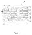
- FIG. 5depicts an enlarged, cross-sectional view of the electronic device structure of FIG. 4 having additional RIE hard mask/polish-stop dielectric layers on top of the interlevel dielectric material film with a-Si adhesion layers between the different dielectric layers according to the present invention.
- FIG. 6depicts an enlarged, cross-sectional view an electronic device structure having a-Si adhesion layers between the hard mask/polish-stop and barrier metal layer according to the present invention.
- the present inventiondiscloses a structure with improved adhesion between different layers of insulating or conductive materials, with thin a-Si adhesion layers disposed between the different layers, or alternately thin layers of amorphous Germanium (a-Ge) or alloys thereof.
- a-Geamorphous Germanium
- the adhesion layer materialmay comprise a-Si, a-Ge or alloys thereof.
- the present inventionprovides a method for improving the adhesion between different layers of insulating or conductive materials using thin a-Si bonding layers between each of the different layers.
- the thin amorphous Si (a-Si) bonding layermay be used to improve the adhesion between an organic dielectric and a Si-based dielectric such as silicon oxide, silicon nitride, SiCOH, SiCH, SiCNH, or between any two dielectric layers from the group comprising the aforementioned organic and Si based dielectrics.
- the dielectric layersmay be the main interconnect dielectric, a cap, or a hard mask layer in the back end of the line interconnect structure of an integrated circuit. While a-Si is not a low-k material, it is formed as a very thin layer as compared to the thickness of the dielectric layers, therefore its contribution to the effective dielctric constant is negligible.
- a-Si bonding layermay also be used to improve the adhesion between a metal or metal nitride and any dielectric layer from the aforementioned group.
- FIGS. 2 - 6The electronic devices formed according to the present invention are shown in FIGS. 2 - 6 . It should be noted that the devices shown in FIGS. 2 - 6 , are merely illustrated as examples according to the present invention, while countless other devices can also be formed according to the present invention.
- FIG. 1depicts electronic device 30 that is built on a silicon substrate 32 according to the current state of the art.
- insulating material layer 34is formed with a first region of metal 36 embedded therein.
- CMPchemical mechanical polishing
- a film such as a dielectric film 38having preferably a dielectric constant smaller than SiO 2 , is deposited on top of first layer of insulating material 34 and first region of metal 36 .
- First layer of insulating material 34may be suitably formed of silicon oxide, silicon nitride, doped varieties of these materials, or any other suitable insulating materials.
- Dielectric film 38is patterned by a photolithography process and conductor layer 40 is deposited therein. After a CMP process on first conductor layer 40 is carried out, second layer of dielectric film 44 is formed overlying first dielectric film 38 and first conductor layer 40 .
- Conductor layer 40may be deposited of a metallic conductive material or a non-metallic conductive material. For instance, a metallic conductive material of aluminum or copper, or a non-metallic material such as nitride or polysilicon may be utilized.
- the first conductor 40is in electrical communication with the first region of metal 36 .
- a second region of conductor 50is formed after a photolithographic process in the second dielectric film layer 44 , followed by a process for depositing the second conductor material.
- Second conductor 50may also be deposited of either a metallic material or a non-metallic material, similar to that used in depositing the first conductor layer 40 .
- the second region of conductor 50is in electrical communication with the first region of conductor 40 and is embedded in the second layer of dielectric insulator 44 .
- the second layer of dielectric film 44is in intimate contact with the first layer of insulating material 38 .
- the first layer of insulating material 38which is a dielectric material according to the present invention, serves as an intralevel dielectric material
- the second layer of insulating material, i.e., the dielectric film 44serves as both an intralevel and an interlevel dielectric. Based on the low dielectric constant of the dielectric film, superior insulating property can be achieved by first insulating layer 38 and second insulating layer 44 .
- FIG. 2depicts electronic device 130 that is built on a silicon substrate 32 according to the present invention.
- insulating material layer 34 with the embedded first region of metal 36a thin layer 100 of a-Si, 1-100 nm thick, preferably 2-6 nm thick, is formed on top of layers 34 and 36 . The process then continues as described with reference to FIG. 1.
- FIG. 3depicts electronic device 60 according to the present invention, similar to that of electronic device 130 shown in FIG. 2, but with additional dielectric cap layer 62 deposited between first insulating material layer 38 and second insulating material layer 44 .
- Dielectric cap layer 62can be suitably formed of a material such as silicon oxide, silicon nitride, silicon oxynitride, silicon carbide, silicon carbo-oxide (SiCO), modified SiCOH and their hydrogenated compounds, as well as refractory metal silicon nitride, wherein the refractory metal is selected the group consisting of: Ta, Zr, Hf, and W.
- Additional dielectric cap layer 62functions as a diffusion barrier layer for preventing diffusion of first conductor layer 40 into second insulating material layer 44 .
- the adhesion between cap layer 62 and dielectric layer 38is enhanced by the a-Si layer 102 .
- the adhesion between dielectric layer 44 and cap layer 62is enhanced by the a-Si layer 104 .
- the adhesion between cap layer 62 and dielectric layer 38is enhanced by the a-Si layer 102 and the adhesion between dielectric layer 44 and cap layer 62 is enhanced by the a-Si layer 104 .
- FIG. 4depicts another alternate embodiment of electronic device 70 according to the present invention.
- two additional dielectric cap layers 72 and 74that act as an RIE mask and CMP (chemical-mechanical polishing) polish stop layer are used.
- First dielectric cap layer 72is deposited on top of first insulating material layer 38 .
- the function of dielectric layer 72is to provide an end point for the CMP process utilized in planarizing first conductor layer 40 .
- Polish stop layer 72can be deposited of a suitable dielectric material such as silicon oxide, silicon nitride, silicon oxynitride, silicon carbide, silicon carbo-oxide (SiCO), modified SiCOH and their hydrogenated compounds, as well as refractory metal silicon nitride, wherein the refractory metal is selected from the group consisting of: Ta, Zr, Hf, Ti and W.
- the top surface of dielectric layer 72is at the same level as first conductor layer 40 .
- the adhesion between cap layer 72 and dielectric layer 38is enhanced by the a-Si layer 106 .
- the adhesion between dielectric layer 62 and cap layer 72is enhanced by the a-Si layer 102 .
- the adhesion between cap layer 72 and dielectric layer 38is enhanced by the a-Si layer 106 and the adhesion between dielectric layer 62 and layer 72 is enhanced by the a-Si layer 102 .
- a second dielectric layer 74can be added on top of second insulating material layer 44 for the same purposes.
- the adhesion between layer 74 and dielectric layer 44is enhanced by the a-Si layer 108 .
- FIG. 5depicts still another alternate embodiment of electronic device 80 according to the present invention.
- an additional layer of dielectric 82is deposited and thus divides second insulating material layer 44 into two separate layers 84 and 86 .
- Intralevel and interlevel dielectric layer 44is therefore divided into interlayer dielectric layer 84 and intralevel dielectric layer 86 at the boundary between interconnect 92 and interconnect 94 , as depicted in FIG. 5.
- An additional diffusion barrier layer 96is further deposited on top of the upper dielectric layer 74 .
- the additional benefits provided by this alternate embodiment of the electronic structure 80is that the dielectric layer 82 acts as a RIE etch stop providing superior interconnect depth control.
- the adhesion between layer 82 and dielectric layer 84is enhanced by the a-Si layer 110 .
- the adhesion between layer 86 and layer 82is enhanced by the a-Si layer 112 .
- the adhesion between cap layer 82 and dielectric layer 84is enhanced by the a-Si layer 110 and the adhesion between dielectric layer 86 and layer 82 is enhanced by the a-Si layer 112 .
- the adhesion between the diffusion layer 96 and dielectric layer 74is enhanced by the a-Si layer 114 .
- the adhesion between dielectric 74 and intralevel dielectric 86is enhanced by the a-Si layer 108 .
- FIG. 6depicts still another alternate embodiment of electronic device 90 according to the present invention.
- an a-Si layer 240is deposited and thus separates dielectric layer 44 from metal barrier layer 206 .
- the barrier layer 206may be a pure metal such as Ta, W or Ti rather than a nitrided form of the metal. This allows for reduced contact resistance between the via 225 and underlying line 210 at the contact area 245 and provides increased adhesion between dielectric layer 34 and metal cap layer 220 via the remaining a-Si layer 215 present after CMP of the metal barrier layer 216 .
- a preferred methodcomprises the steps of: providing a plasma enhanced chemical vapor deposition (“PECVD”) reactor: positioning an electronic structure (e.g., semiconductor substrate) having an upper layer of first dielectric in the reactor; flowing SiH 4 or SiH 4 diluted in an inert gas into the reactor; depositing a layer of a-Si on top of said substrate; flowing precursors into the reactor for depositing a second dielectric or conductive layer on top of the a-Si bonding layer.
- PECVDplasma enhanced chemical vapor deposition
- the second dielectric layeris preferably a SiCOH type dielectric of low dielectric constant (k ⁇ 3.2) or ultralow dielectric constant (k ⁇ 2.4), or a metal such as Ta, Ti, W, and combinations of the aforementioned, their nitrides and silicides.
- a wafer containing an electronic structure (i.e., substrate) having an upper layer of first dielectric with metal structures embedded in itis inserted in a plasma enhanced chemical vapor deposition (“PECVD”) reactor.
- PECVDplasma enhanced chemical vapor deposition
- the waferis then heated to a temperature between room temperature and 450° C. In typical conditions, the wafer is heated to 180° C.
- SiH 4 or SiH 4 diluted in inert gasis then flown into the reactor. In one example SiH 4 diluted to 2% in Ar is flown into the reactor at a rate of 30 sccm to achieve a pressure of 100 mtorr.
- GeH 4 or GeH 4 diluted in an inert gasmay be alternately flown into the reactor, or alternatively, mixtures of SiH 4 or diluted SiH 4 with GeH 4 or diluted GeH 4 may be flown into the reactor.
- An RF power sourceis then turned on to about 60.0 W for 0.5 to 2 minutes.
- the RF power generatedis operated under bias control and the a-Si layer (a-Ge or alloy thereof) is deposited at the same conditions as mentioned above but at ⁇ 200 V instead of 60 W.
- the RF power and the gas floware then turned off.
- the substrate temperaturemay optionally be adjusted, and the precursors used for the deposition of the next dielectric layer flown into the reactor so that the next film may be deposited.
- the waferis removed from the reactor after the deposition of the a-Si layer and the wafer is further processed by depositing a spin-on dielectric layer.
- oxygen gasis flown into the reactor and the RF power is turned on for 3 to 15 seconds to oxidize the a-Si layer at least partially.
- the adhesion provided by the thin a-Si bonding layeris strong enough to prevent delamination of the interconnect structure during fabrication and reliability testing.
- adhesion between two layershas been demonstrated to increase by a factor of three (3), from about 6.0 joule/m 2 to about 20.0 joule/m 2 .
- FIGS. 1 - 6The method and electronic structures formed according to the present invention have therefore been thoroughly demonstrated in the above descriptions and in the drawings of FIGS. 1 - 6 . It should be emphasized that the examples of the electronic structures shown in FIGS. 1 - 6 are merely used to illustrate the inventive method that can be applied in the fabrication of countless electronic devices.
Landscapes
- Engineering & Computer Science (AREA)
- Physics & Mathematics (AREA)
- Condensed Matter Physics & Semiconductors (AREA)
- General Physics & Mathematics (AREA)
- Computer Hardware Design (AREA)
- Microelectronics & Electronic Packaging (AREA)
- Power Engineering (AREA)
- Manufacturing & Machinery (AREA)
- Internal Circuitry In Semiconductor Integrated Circuit Devices (AREA)
Abstract
Description
- 1. Field of the Invention[0001]
- The present invention generally relates to a semiconductor electronic device structure comprising dielectric layers having improved adhesion to other dielectric or conducting layers. More particularly, the present invention relates to using a layer of amorphous silicon (a-Si) or amorphous Germanium (a-Ge) (or alloys thereof) as an adhesion enhancing interfacial layer. Furthermore, the present invention relates to a method for improving the adhesion between different dielectric or conductive layers including those that include Si or C.[0002]
- 2. Description of the Prior Art[0003]
- The continuous shrinking in dimensions of electronic devices utilized in ULSI circuits in recent years has resulted in increasing the resistance of the BEOL metallization as well as increasing the capacitance of the intralayer and interlayer dielectric. This combined effect increases signal delays in ULSI electronic devices. In order to improve the switching performance of future ULSI circuits, low dielectric constant (k) insulators and particularly those with k significantly lower than silicon oxide are being introduced to reduce the capacitances.[0004]
- The low-k materials that have been considered for applications in ULSI devices include polymers containing Si, C, O and H, such as methylsiloxane, methylsilsesquioxanes, and other organic and inorganic polymers which are fabricated by spin-on techniques or, Si, C,[0005]0 and H containing materials (SiCOH, SiOCH, carbon-doped oxides (CDO), silicon-oxicarbides, organosilicate glasses (OSG)) deposited by plasma enhanced chemical vapor deposition (CVD) techniques. The incorporation of the low-k dielectrics in the interconnect structures of integrated circuits (IC) often requires the use of other dielectric materials as diffusion barrier caps or etch-stop and chemo-mechanical polishing (CMP) hardmasks. The adhesion between the different layers in the complex structures of an IC device is often too low, resulting in delaminations during the processing of the device. This is especially true for adhesion of dielectric or metallic layers to SiO2. Furthermore, an intermediate layer of refractory metal nitride is generally needed to provide suitable adhesion between the metallic Cu-diffusion barrier and the dielectric insulator of the interconnect structure. The conductive nitride layer, typically of lower conductivity than the metallization layers occupies a significant thickness of the shrinking metallization and increases its resistivity. The elimination of this conductive nitride layer by substituting it with a very thin adhesion layer can improve the performance of ULSI devices.
- It would thus be highly desirable to provide a semiconductor device comprising an insulating structure including comprising a multitude of dielectric and conductive layers with good adhesion between the different layers, and a method for manufacturing said semiconductor device.[0006]
- As described in U.S. Pat. No. 4,647,494, amorphous Silicon (a-Si) of tens of Angstroms thick has been recognized for improving adhesion of wear resistant carbon coatings to metallic magnetic recording layers in recording tapes and disks. That is, in U.S. Pat. No. 4,647,494, a-Si is described as improving adhesion between amorphous hydrogenated carbon (or diamondlike carbon) and silicide forming metals. The use of thin a-Si bonding layer has not been utilized in semiconductor ULSI manufacturing processes to enhance adhesion between dielectric layers of a semiconductor BEOL wiring structure.[0007]
- It would thus be further highly desirable to provide a semiconductor device structure and method for manufacturing an insulating structure comprising a multitude of dielectric and conductive layers that includes thin a-Si, a-Ge or alloys thereof, bonding layers used to enhance adhesion between the different layers.[0008]
- It is therefore an object of the present invention to provide an insulating structure comprising a multitude of dielectric and conductive layers with good adhesion between the different layers.[0009]
- It is a further object of the present invention to provide an insulating structure comprising a multitude of dielectric and conductive layers wherein the adhesion between different layers is enhanced by a thin bonding layer comprising amorphous Si (a-Si), amorphous Ge (a-Ge) or alloys thereof, wherein the thin a-Si (a-Ge or alloys thereof) may be hydrogenated or non-hydrogenated.[0010]
- It is another object of the present invention to provide an insulating structure comprising a multitude of dielectric and conductive layers wherein the adhesion between different layers is enhanced by a thin amorphous bonding layer comprising amorphous Si (a-Si), amorphous Ge (a-Ge) or alloys thereof, wherein the thin a-Si (a-Ge or alloys thereof) may be at least partially oxidized.[0011]
- It is another object of the present invention to provide an insulating structure including a thin intermediate a-Si (a-Ge or alloys thereof) bonding layer adhesion layer for enhancing adhesion between an oxide layer, e.g., from the group comprising SiO[0012]2, phosphorus silicate glass (“PSG”) or boron phosphorus silicate glass (“BPSG”), and a layer from the group comprising SiCOH, SiC, SiCN, SiCH, or SiCNH.
- It is yet another object of the present invention to provide an electronic device structure incorporating layers of insulating and conductive materials as intralevel or interlevel dielectrics in a back-end-of-the-line (“BEOL”) wiring structure in which the adhesion between different dielectrics is enhanced by a thin intermediate a-Si bonding layer, or a bonding layer of a-Ge or alloys thereof.[0013]
- It is still another object of the present invention to provide an electronic device structure incorporating layers of insulating and conductive materials as intralevel or interlevel dielectrics in a BEOL wiring structure in which the adhesion between the conductive layers and the different dielectric layers is enhanced by a thin intermediate a-Si bonding layer, or a bonding layer of a-Ge or alloys thereof.[0014]
- It is still yet a further object of the present invention to provide a method for fabricating an a-Si adhesion layer (or a layer of a-Ge or alloys thereof) either in a parallel plate plasma enhanced chemical vapor deposition (“PECVD”) reactor or, in a sputtering reactor.[0015]
- It is yet another object of the present invention to provide an electronic device structure, which comprises at least one a-Si bonding layer (or a layer of a-Ge or alloys thereof) between a dielectric layer and a liner/barrier layer for a Cu metallization structure.[0016]
- It is another object of the present invention to provide an insulating semiconductor structure comprising a multitude of dielectric and conductive layers wherein the adhesion between different layers is enhanced by a thin amorphous Si (a-Si) bonding layer (or a layer of a-Ge or alloys thereof) which may be at least partially oxidized.[0017]
- According to the principles of the invention, there is provided a method for fabricating a BEOL interconnect structure with improved adhesion between the layers of the structure. The present invention further provides an electronic device structure that incorporates a-Si layers (or layers of a-Ge or alloys thereof) between dissimilar layers in the structure to improve the adhesion between them. In one embodiment, a thin a-Si layer, 1-100 nm, preferably 2-6 nm thick, is interposed between a silicon oxide layer and a SiCOH layer, enhancing the adhesion between the two layers. In another preferred embodiment, the 1-100 nm, preferably 2-6 nm thick a-Si layer is interposed between a SiCOH dielectric layer and a layer of SiN, SiC, SiCH, or SiCHN, to enhance the adhesion between the layers. In yet another embodiment, the 1-100 nm, preferably 2-6 nm thick a-Si layer is interposed between a dielectric layer and a Ta layer, to enhance the adhesion between the two layers.[0018]
- In yet another embodiment, the a-Si layer (or a layer of a-Ge or alloys thereof) is incorporated between any two layers from the group comprising SiO[0019]2, PSG, BPSG, SiN, SiC, SiCH, SiCHN, or SiCOH, Ta, Ti, and any other silicide forming metal, to improve the adhesion between the layers.
- In an embodiment, the a-Si layer (or a layer of a-Ge or alloys thereof) is deposited after the hardmask layer which may be comprised of SiO[0020]2, PSG, BPSG, SiN, SiC, SiCH or SiCHN which is then followed by the liner material such as Ta, Ti, W or their nitrides or silicides. The a-Si layer allows for the pure form of the metal to be deposited without concern for delamination on the metal/hardmask interface during CMP. The further benefit of depositing the pure metal is found at the via/line interface where pure metallic bonding is created which guarantees good adhesion and improves device reliability especially for thermal excursions and also has the added benefit of reducing contact resistance.
- In another aspect of the invention, there is provided a method for fabricating a multilayered structure with strong adhesion between the different layers comprising the steps of: providing a plasma enhanced chemical vapor deposition (“PECVD”) reactor: positioning an electronic device structure (i.e., substrate) having an upper layer of first dielectric in the reactor; flowing SiH[0021]4or SiH4diluted in an inert gas into the reactor; depositing a layer of a-Si on top of said substrate; flowing precursors into the reactor for depositing a second dielectric or conductive layer on top of the a-Si bonding layer. The second dielectric layer is preferably a SiCOH type dielectric of low dielectric constant (k<3.2) or ultralow dielectric constant (k<2.4) or a metal such as Ta, Ti, W, combinations of the previous, their silicides and/or nitrides.
- In another embodiment, the step of depositing the a-Si adhesion layer (or a layer of a-Ge or alloys thereof) is repeated after the deposition of said second layer.[0022]
- In yet another embodiment the a-Si layer (or a layer of a-Ge or alloys thereof) is at least partially oxidized by exposing it to an oxygen plasma after its deposition.[0023]
- In a different embodiment, the substrate is removed from the PECVD reactor after the deposition of the a-Si layer and a said second dielectric layer from the group comprising organic polymers, silicon based polymers, organic glasses, hybrid Si and C containing polymers, oxides, or porous modifications of same materials is deposited by a spin-on method.[0024]
- In yet a different embodiment, the substrate is removed from the PECVD reactor after the deposition of the a-Si layer and after exposing the a-Si layer to an oxygen plasma and a second dielectric layer from the group comprising organic polymers, silicon based polymers, organic glasses, hybrid Si and C containing polymers, oxides, is deposited by a spin-on method.[0025]
- Dielectric layers such as ones aforementioned, or layers of metals that form silicides have good adhesion to the a-Si interlayer, therefore the a-Si intermediate layer enhances the adhesion between such layers. The a-Si can be deposited by any radiation assisted techniques, such as PECVD, high density plasma, sputtering, ion beam sputtering, ion beam deposition.[0026]
- The adhesion enhancing a-Si layer can be used in the back end of the line (BEOL) structure of a CMOS device to improve the adhesion between a low-k dielectric, e.g. SiCOH, and SiO[0027]2or between a metal layer, e.g. Ta, and a dielectric.
- The present invention is further directed to an electronic device structure which has layers of insulating materials as intralevel or interlevel dielectrics in a back-end-of-the-line (“BEOL”) interconnect structure which includes a pre-processed semiconducting substrate that has a first region of metal embedded in a first layer of insulating material, a first region of conductor embedded in a second layer of insulating material, an adhesion layer of a-Si (or a layer of a-Ge or alloys thereof) between the second layer of insulating material and first layer of insulating material, the first region of conductor being in electrical contact with the first region of metal, and a second region of conductor being in electrical contact with the first region of conductor and being embedded in a third layer of insulating material, the third layer of insulating material contacting with the second layer of insulating material. The electronic device structure may further comprise a dielectric cap layer situated in between the second layer of insulating material and the third layer of insulating material and including a-Si adhesion layers between the cap layer and the second and optionally the third insulating layers.[0028]
- The electronic device structure may further comprise a first dielectric cap layer between the second layer of insulating material and the third layer of insulating material, and a second dielectric cap layer on top of the third layer of insulating material and containing a-Si adhesion layers between the cap layers and the insulating layers.[0029]
- The dielectric cap material can be selected from silicon oxide, silicon nitride, silicon oxynitride, a refractory metal silicon nitride (wherein the refractory metal is selected from the group consisting of Ta, Zr, Hf and W) silicon carbide, carbon doped oxide or SiCOH and their hydrogenated compounds. The first and the second dielectric cap layers may be selected from the same group of dielectric materials. The first layer of insulating material may be silicon oxide or silicon nitride or doped varieties of these materials, such as phosphorus silicate glass (“PSG”) or boron phosphorus silicate glass (“BPSG”), SiC, SiCN, SiCH, or SiCNH. The second and subsequent dielectric layers may be PECVD deposited SiCOH or spin-on deposited dielectrics.[0030]
- The electronic device structure may further include a diffusion barrier layer of a dielectric material deposited on at least one of the second and third layers of insulating material with an a-Si intermediate adhesion layer (or an adhesion layer of a-Ge or alloys thereof). The electronic device structure may further comprise a dielectric on top of the second layer of insulating material, which acts as a reactive ion etch (“RIE”) hard mask and polish stop layer and a dielectric diffusion barrier layer on top of the dielectric RIE hard mask and polish stop layer, with an a-Si intermediate adhesion layer between said top dielectric and said second layer of insulating material. The electronic device structure may further comprise a first dielectric RIE hard mask/polish-stop layer on top of the second layer of insulating material, a first dielectric RIE hard mask/diffusion barrier layer on top of the first dielectric polish-stop layer, a second dielectric RIE hard mask/polish-stop layer on top of the third layer of insulating material, and a second dielectric diffusion barrier layer on top of the second dielectric polish-stop layer with a-Si adhesion layers between two layers of different materials. The electronic device structure may further comprise a dielectric cap layer of same materials as mentioned above, between an interlevel dielectric and an intralevel dielectric.[0031]
- Advantageously, the method for improving the adhesion between the different layers of an electronic device structure using the a-Si adhesion layer is implemented in a back-end-of-the-line (“BEOL”) wiring process. Thus, the electronic device structure comprises at least one a-Si bonding layer between the dielectric and conductive layers of a back-end-of-the-line (“BEOL”) wiring structure.[0032]
- The foregoing and other objects, features, and advantages of the invention will be apparent from the following detailed description of the invention, as illustrated in the accompanying drawings, in which:[0033]
- FIG. 1 depicts an enlarged, cross-sectional view of an electronic device having two layers of metallization in the BEOL according to the current state of the art.[0034]
- FIG. 2 depicts the structure of FIG. 1 with an additional a-Si adhesion layers between the dielectrics of the two mettalization levels according to the present invention.[0035]
- FIG. 3 depicts an enlarged, cross-sectional view of the electronic device structure of[0036]
- FIG. 2 having an additional diffusion barrier dielectric cap layer on top of the intralevel dielectric and a-Si adhesion layers between the diffusion barrier and the intralevel and interlevel dielectrics according to the present invention.[0037]
- FIG. 4 depicts an enlarged, cross-sectional view of the electronic device structure of FIG. 3 having an additional RIE hard mask/polish-stop dielectric cap layer and dielectric cap diffusion barrier on top of the polish-stop layer with a-Si adhesion layers between the different dielectric layers according to the present invention.[0038]
- FIG. 5 depicts an enlarged, cross-sectional view of the electronic device structure of FIG. 4 having additional RIE hard mask/polish-stop dielectric layers on top of the interlevel dielectric material film with a-Si adhesion layers between the different dielectric layers according to the present invention.[0039]
- FIG. 6 depicts an enlarged, cross-sectional view an electronic device structure having a-Si adhesion layers between the hard mask/polish-stop and barrier metal layer according to the present invention.[0040]
- The present invention discloses a structure with improved adhesion between different layers of insulating or conductive materials, with thin a-Si adhesion layers disposed between the different layers, or alternately thin layers of amorphous Germanium (a-Ge) or alloys thereof. For purposes of discussion, a-Si will be described, however it is understood that the adhesion layer material may comprise a-Si, a-Ge or alloys thereof.[0041]
- The present invention provides a method for improving the adhesion between different layers of insulating or conductive materials using thin a-Si bonding layers between each of the different layers.[0042]
- The thin amorphous Si (a-Si) bonding layer may be used to improve the adhesion between an organic dielectric and a Si-based dielectric such as silicon oxide, silicon nitride, SiCOH, SiCH, SiCNH, or between any two dielectric layers from the group comprising the aforementioned organic and Si based dielectrics. The dielectric layers may be the main interconnect dielectric, a cap, or a hard mask layer in the back end of the line interconnect structure of an integrated circuit. While a-Si is not a low-k material, it is formed as a very thin layer as compared to the thickness of the dielectric layers, therefore its contribution to the effective dielctric constant is negligible. Furthermore, a large fraction of the a-Si layer is intermixed with the layers which it is bonding and thus converted into layers of dielectric constants smaller than a-Si. The a-Si bonding layer may also be used to improve the adhesion between a metal or metal nitride and any dielectric layer from the aforementioned group.[0043]
- The electronic devices formed according to the present invention are shown in FIGS.[0044]2-6. It should be noted that the devices shown in FIGS.2-6, are merely illustrated as examples according to the present invention, while countless other devices can also be formed according to the present invention.
- FIG. 1 depicts[0045]
electronic device 30 that is built on asilicon substrate 32 according to the current state of the art. On top ofsilicon substrate 32, insulatingmaterial layer 34 is formed with a first region ofmetal 36 embedded therein. After a chemical mechanical polishing (“CMP”) process is conducted on first region ofmetal 36, a film such as adielectric film 38, having preferably a dielectric constant smaller than SiO2, is deposited on top of first layer of insulatingmaterial 34 and first region ofmetal 36. - First layer of insulating[0046]
material 34 may be suitably formed of silicon oxide, silicon nitride, doped varieties of these materials, or any other suitable insulating materials.Dielectric film 38 is patterned by a photolithography process andconductor layer 40 is deposited therein. After a CMP process onfirst conductor layer 40 is carried out, second layer ofdielectric film 44 is formed overlyingfirst dielectric film 38 andfirst conductor layer 40.Conductor layer 40 may be deposited of a metallic conductive material or a non-metallic conductive material. For instance, a metallic conductive material of aluminum or copper, or a non-metallic material such as nitride or polysilicon may be utilized. Thefirst conductor 40 is in electrical communication with the first region ofmetal 36. - As further depicted in FIG. 1, a second region of[0047]
conductor 50 is formed after a photolithographic process in the seconddielectric film layer 44, followed by a process for depositing the second conductor material.Second conductor 50 may also be deposited of either a metallic material or a non-metallic material, similar to that used in depositing thefirst conductor layer 40. The second region ofconductor 50 is in electrical communication with the first region ofconductor 40 and is embedded in the second layer ofdielectric insulator 44. The second layer ofdielectric film 44 is in intimate contact with the first layer of insulatingmaterial 38. In this specific example, the first layer of insulatingmaterial 38, which is a dielectric material according to the present invention, serves as an intralevel dielectric material, while the second layer of insulating material, i.e., thedielectric film 44, serves as both an intralevel and an interlevel dielectric. Based on the low dielectric constant of the dielectric film, superior insulating property can be achieved by first insulatinglayer 38 and second insulatinglayer 44. - FIG. 2 depicts[0048]
electronic device 130 that is built on asilicon substrate 32 according to the present invention. After the formation of insulatingmaterial layer 34 with the embedded first region ofmetal 36, athin layer 100 of a-Si, 1-100 nm thick, preferably 2-6 nm thick, is formed on top oflayers - FIG. 3 depicts[0049]
electronic device 60 according to the present invention, similar to that ofelectronic device 130 shown in FIG. 2, but with additionaldielectric cap layer 62 deposited between first insulatingmaterial layer 38 and second insulatingmaterial layer 44.Dielectric cap layer 62 can be suitably formed of a material such as silicon oxide, silicon nitride, silicon oxynitride, silicon carbide, silicon carbo-oxide (SiCO), modified SiCOH and their hydrogenated compounds, as well as refractory metal silicon nitride, wherein the refractory metal is selected the group consisting of: Ta, Zr, Hf, and W. Additionaldielectric cap layer 62 functions as a diffusion barrier layer for preventing diffusion offirst conductor layer 40 into second insulatingmaterial layer 44. In one embodiment of the present invention, the adhesion betweencap layer 62 anddielectric layer 38 is enhanced by thea-Si layer 102. In another embodiment, the adhesion betweendielectric layer 44 andcap layer 62 is enhanced by thea-Si layer 104. In yet another embodiment the adhesion betweencap layer 62 anddielectric layer 38 is enhanced by thea-Si layer 102 and the adhesion betweendielectric layer 44 andcap layer 62 is enhanced by thea-Si layer 104. - FIG. 4 depicts another alternate embodiment of[0050]
electronic device 70 according to the present invention. Inelectronic device 70, two additional dielectric cap layers72 and74 that act as an RIE mask and CMP (chemical-mechanical polishing) polish stop layer are used. Firstdielectric cap layer 72 is deposited on top of first insulatingmaterial layer 38. The function ofdielectric layer 72 is to provide an end point for the CMP process utilized in planarizingfirst conductor layer 40.Polish stop layer 72 can be deposited of a suitable dielectric material such as silicon oxide, silicon nitride, silicon oxynitride, silicon carbide, silicon carbo-oxide (SiCO), modified SiCOH and their hydrogenated compounds, as well as refractory metal silicon nitride, wherein the refractory metal is selected from the group consisting of: Ta, Zr, Hf, Ti and W. The top surface ofdielectric layer 72 is at the same level asfirst conductor layer 40. In one embodiment, the adhesion betweencap layer 72 anddielectric layer 38 is enhanced by thea-Si layer 106. In another embodiment, the adhesion betweendielectric layer 62 andcap layer 72 is enhanced by thea-Si layer 102. In yet another embodiment the adhesion betweencap layer 72 anddielectric layer 38 is enhanced by thea-Si layer 106 and the adhesion betweendielectric layer 62 andlayer 72 is enhanced by thea-Si layer 102. - A[0051]
second dielectric layer 74 can be added on top of second insulatingmaterial layer 44 for the same purposes. In one embodiment, the adhesion betweenlayer 74 anddielectric layer 44 is enhanced by thea-Si layer 108. - FIG. 5 depicts still another alternate embodiment of[0052]
electronic device 80 according to the present invention. In this alternate embodiment, an additional layer ofdielectric 82 is deposited and thus divides second insulatingmaterial layer 44 into twoseparate layers dielectric layer 44, as depicted in FIG. 3, is therefore divided intointerlayer dielectric layer 84 andintralevel dielectric layer 86 at the boundary betweeninterconnect 92 andinterconnect 94, as depicted in FIG. 5. An additionaldiffusion barrier layer 96 is further deposited on top of theupper dielectric layer 74. The additional benefits provided by this alternate embodiment of theelectronic structure 80 is that thedielectric layer 82 acts as a RIE etch stop providing superior interconnect depth control. In one embodiment, the adhesion betweenlayer 82 anddielectric layer 84 is enhanced by thea-Si layer 110. In another embodiment, the adhesion betweenlayer 86 andlayer 82 is enhanced by thea-Si layer 112. In yet another embodiment the adhesion betweencap layer 82 anddielectric layer 84 is enhanced by thea-Si layer 110 and the adhesion betweendielectric layer 86 andlayer 82 is enhanced by thea-Si layer 112. In another embodiment the adhesion between thediffusion layer 96 anddielectric layer 74 is enhanced by thea-Si layer 114. In yet another embodiment the adhesion betweendielectric 74 andintralevel dielectric 86 is enhanced by thea-Si layer 108. - FIG. 6 depicts still another alternate embodiment of[0053]
electronic device 90 according to the present invention. In this alternate embodiment, ana-Si layer 240 is deposited and thus separatesdielectric layer 44 frommetal barrier layer 206. The additional benefits provided by this alternate embodiment of theelectronic structure 90 is that thebarrier layer 206 may be a pure metal such as Ta, W or Ti rather than a nitrided form of the metal. This allows for reduced contact resistance between the via225 andunderlying line 210 at thecontact area 245 and provides increased adhesion betweendielectric layer 34 andmetal cap layer 220 via the remaininga-Si layer 215 present after CMP of themetal barrier layer 216. - In any of said embodiments the a-Si layer may be at least partially oxidized, for example by a short exposure to an oxygen plasma.[0054]
- According to the invention, there is provided a method for fabricating the multilayered structures with strong adhesion between the different layers such as shown and described with respect to FIGS.[0055]2-6. A preferred method comprises the steps of: providing a plasma enhanced chemical vapor deposition (“PECVD”) reactor: positioning an electronic structure (e.g., semiconductor substrate) having an upper layer of first dielectric in the reactor; flowing SiH4or SiH4diluted in an inert gas into the reactor; depositing a layer of a-Si on top of said substrate; flowing precursors into the reactor for depositing a second dielectric or conductive layer on top of the a-Si bonding layer. It is understood that GeH4or GeH4diluted in an inert gas may be flown into the reactor, or alternatively, mixtures of SiH4or diluted SiH4with GeH4or diluted GeH4may be flown into the reactor. The second dielectric layer is preferably a SiCOH type dielectric of low dielectric constant (k<3.2) or ultralow dielectric constant (k<2.4), or a metal such as Ta, Ti, W, and combinations of the aforementioned, their nitrides and silicides.
- The following examples are presented to illustrate the fabrication of the dielectric film including the a-Si bonding layer in accordance with the present invention as well as to demonstrate advantages that can be obtained therefrom:[0056]
- In this example, a wafer containing an electronic structure (i.e., substrate) having an upper layer of first dielectric with metal structures embedded in it is inserted in a plasma enhanced chemical vapor deposition (“PECVD”) reactor. The wafer is then heated to a temperature between room temperature and 450° C. In typical conditions, the wafer is heated to 180° C. SiH[0057]4or SiH4diluted in inert gas is then flown into the reactor. In one example SiH4diluted to 2% in Ar is flown into the reactor at a rate of 30 sccm to achieve a pressure of 100 mtorr. It is understood that GeH4or GeH4diluted in an inert gas may be alternately flown into the reactor, or alternatively, mixtures of SiH4or diluted SiH4with GeH4or diluted GeH4may be flown into the reactor. An RF power source is then turned on to about 60.0 W for 0.5 to 2 minutes. In a different example, the RF power generated is operated under bias control and the a-Si layer (a-Ge or alloy thereof) is deposited at the same conditions as mentioned above but at −200 V instead of 60 W. The RF power and the gas flow are then turned off. The substrate temperature may optionally be adjusted, and the precursors used for the deposition of the next dielectric layer flown into the reactor so that the next film may be deposited.
- In a different example, the wafer is removed from the reactor after the deposition of the a-Si layer and the wafer is further processed by depositing a spin-on dielectric layer.[0058]
- In yet another example, after the deposition of the a-Si layer, oxygen gas is flown into the reactor and the RF power is turned on for 3 to 15 seconds to oxidize the a-Si layer at least partially.[0059]
- Qualitatively, the adhesion provided by the thin a-Si bonding layer is strong enough to prevent delamination of the interconnect structure during fabrication and reliability testing. In one example, as determined in a four-point bending test known amongst skilled artisans, adhesion between two layers has been demonstrated to increase by a factor of three (3), from about 6.0 joule/m[0060]2to about 20.0 joule/m2.
- The method and electronic structures formed according to the present invention have therefore been thoroughly demonstrated in the above descriptions and in the drawings of FIGS.[0061]1-6. It should be emphasized that the examples of the electronic structures shown in FIGS.1-6 are merely used to illustrate the inventive method that can be applied in the fabrication of countless electronic devices.
- While several embodiments of the invention, together with modifications thereof, have been described in detail herein and illustrated in the accompanying drawings, it will be evident that various further modifications are possible without departing from the scope of the invention. Nothing in the above specification is intended to limit the invention more narrowly than the appended claims. The examples given are intended only to be illustrative rather than exclusive.[0062]
Claims (63)
Priority Applications (1)
| Application Number | Priority Date | Filing Date | Title |
|---|---|---|---|
| US10/174,748US6764774B2 (en) | 2002-06-19 | 2002-06-19 | Structures with improved adhesion to Si and C containing dielectrics and method for preparing the same |
Applications Claiming Priority (1)
| Application Number | Priority Date | Filing Date | Title |
|---|---|---|---|
| US10/174,748US6764774B2 (en) | 2002-06-19 | 2002-06-19 | Structures with improved adhesion to Si and C containing dielectrics and method for preparing the same |
Publications (2)
| Publication Number | Publication Date |
|---|---|
| US20030235710A1true US20030235710A1 (en) | 2003-12-25 |
| US6764774B2 US6764774B2 (en) | 2004-07-20 |
Family
ID=29733673
Family Applications (1)
| Application Number | Title | Priority Date | Filing Date |
|---|---|---|---|
| US10/174,748Expired - LifetimeUS6764774B2 (en) | 2002-06-19 | 2002-06-19 | Structures with improved adhesion to Si and C containing dielectrics and method for preparing the same |
Country Status (1)
| Country | Link |
|---|---|
| US (1) | US6764774B2 (en) |
Cited By (15)
| Publication number | Priority date | Publication date | Assignee | Title |
|---|---|---|---|---|
| US20040152334A1 (en)* | 2003-01-14 | 2004-08-05 | Nec Electonics Corporation | Organic insulating film, manufacturing method thereof, semiconductor device using such organic insulating film and manufacturing method thereof |
| US20060189153A1 (en)* | 2003-09-12 | 2006-08-24 | International Business Machines Corporation | Structures with improved interfacial strength of SiCOH dielectrics and method for preparing the same |
| US20100272932A1 (en)* | 2008-03-07 | 2010-10-28 | Mitsubishi Electric Corporation | Decorative component |
| US20110079876A1 (en)* | 2006-12-29 | 2011-04-07 | Sallie Hose | Method of Manufacturing a Semiconductor Component and Structure |
| US20110215436A1 (en)* | 2010-03-02 | 2011-09-08 | Micron Technology, Inc. | Semiconductor devices including a diode structure over a conductive strap and methods of forming such semiconductor devices |
| CN103107158A (en)* | 2011-11-11 | 2013-05-15 | 中芯国际集成电路制造(上海)有限公司 | Semiconductor device and forming method thereof |
| US20140191376A1 (en)* | 2013-01-08 | 2014-07-10 | Siliconware Precision Industries Co., Ltd. | Semiconductor package and fabrication method thereof |
| EP2543069A4 (en)* | 2010-03-02 | 2015-04-08 | Micron Technology Inc | SEMICONDUCTOR AND METALLIC INSULATOR STRUCTURES, METHODS OF MAKING SUCH STRUCTURES, AND SEMICONDUCTOR DEVICES COMPRISING SUCH STRUCTURES |
| US9129983B2 (en) | 2011-02-11 | 2015-09-08 | Micron Technology, Inc. | Memory cells, memory arrays, methods of forming memory cells, and methods of forming a shared doped semiconductor region of a vertically oriented thyristor and a vertically oriented access transistor |
| US9269795B2 (en) | 2011-07-26 | 2016-02-23 | Micron Technology, Inc. | Circuit structures, memory circuitry, and methods |
| US9343462B2 (en) | 2010-03-02 | 2016-05-17 | Micron Technology, Inc. | Thyristor-based memory cells, devices and systems including the same and methods for forming the same |
| US9361966B2 (en) | 2011-03-08 | 2016-06-07 | Micron Technology, Inc. | Thyristors |
| US10157769B2 (en) | 2010-03-02 | 2018-12-18 | Micron Technology, Inc. | Semiconductor devices including a diode structure over a conductive strap and methods of forming such semiconductor devices |
| US10373956B2 (en) | 2011-03-01 | 2019-08-06 | Micron Technology, Inc. | Gated bipolar junction transistors, memory arrays, and methods of forming gated bipolar junction transistors |
| CN112435958A (en)* | 2019-08-26 | 2021-03-02 | 台湾积体电路制造股份有限公司 | Integrated circuit structure and forming method thereof |
Families Citing this family (10)
| Publication number | Priority date | Publication date | Assignee | Title |
|---|---|---|---|---|
| DE69838619T2 (en)* | 1997-11-20 | 2008-03-06 | Bristol-Myers Squibb Co. | MULTIPLE ATTACHABLE BAG WITH A MOVING ANZONE |
| JP2004014841A (en)* | 2002-06-07 | 2004-01-15 | Fujitsu Ltd | Semiconductor device and manufacturing method thereof |
| US20050181604A1 (en)* | 2002-07-11 | 2005-08-18 | Hans-Peter Sperlich | Method for structuring metal by means of a carbon mask |
| US6803313B2 (en)* | 2002-09-27 | 2004-10-12 | Advanced Micro Devices, Inc. | Method for forming a hardmask employing multiple independently formed layers of a pecvd material to reduce pinholes |
| US6917108B2 (en)* | 2002-11-14 | 2005-07-12 | International Business Machines Corporation | Reliable low-k interconnect structure with hybrid dielectric |
| JP2004253791A (en)* | 2003-01-29 | 2004-09-09 | Nec Electronics Corp | Insulating film and semiconductor device using the same |
| US6992003B2 (en)* | 2003-09-11 | 2006-01-31 | Freescale Semiconductor, Inc. | Integration of ultra low K dielectric in a semiconductor fabrication process |
| US7030468B2 (en)* | 2004-01-16 | 2006-04-18 | International Business Machines Corporation | Low k and ultra low k SiCOH dielectric films and methods to form the same |
| US7253522B2 (en)* | 2004-06-02 | 2007-08-07 | Avx Israel, Ltd. | Integrated capacitor for RF applications with Ta adhesion layer |
| US11217481B2 (en)* | 2019-11-08 | 2022-01-04 | International Business Machines Corporation | Fully aligned top vias |
Family Cites Families (3)
| Publication number | Priority date | Publication date | Assignee | Title |
|---|---|---|---|---|
| US4647494A (en) | 1985-10-31 | 1987-03-03 | International Business Machines Corporation | Silicon/carbon protection of metallic magnetic structures |
| US6265779B1 (en)* | 1998-08-11 | 2001-07-24 | International Business Machines Corporation | Method and material for integration of fuorine-containing low-k dielectrics |
| US6184123B1 (en)* | 1999-08-02 | 2001-02-06 | Taiwan Semiconductor Manufacturing Company | Method to prevent delamination of spin-on-glass and plasma nitride layers using ion implantation |
- 2002
- 2002-06-19USUS10/174,748patent/US6764774B2/ennot_activeExpired - Lifetime
Cited By (26)
| Publication number | Priority date | Publication date | Assignee | Title |
|---|---|---|---|---|
| US7763979B2 (en) | 2003-01-14 | 2010-07-27 | Nec Electronics Corporation | Organic insulating film, manufacturing method thereof, semiconductor device using such organic insulating film and manufacturing method thereof |
| US20040152334A1 (en)* | 2003-01-14 | 2004-08-05 | Nec Electonics Corporation | Organic insulating film, manufacturing method thereof, semiconductor device using such organic insulating film and manufacturing method thereof |
| US20060189153A1 (en)* | 2003-09-12 | 2006-08-24 | International Business Machines Corporation | Structures with improved interfacial strength of SiCOH dielectrics and method for preparing the same |
| US7888741B2 (en)* | 2003-09-12 | 2011-02-15 | International Business Machines Corporation | Structures with improved interfacial strength of SiCOH dielectrics and method for preparing the same |
| US8410578B2 (en)* | 2006-12-29 | 2013-04-02 | Semiconductor Components Industries, Llc | Method of manufacturing a semiconductor component and structure |
| US20110079876A1 (en)* | 2006-12-29 | 2011-04-07 | Sallie Hose | Method of Manufacturing a Semiconductor Component and Structure |
| US20100272932A1 (en)* | 2008-03-07 | 2010-10-28 | Mitsubishi Electric Corporation | Decorative component |
| US10157769B2 (en) | 2010-03-02 | 2018-12-18 | Micron Technology, Inc. | Semiconductor devices including a diode structure over a conductive strap and methods of forming such semiconductor devices |
| US10325926B2 (en) | 2010-03-02 | 2019-06-18 | Micron Technology, Inc. | Semiconductor-metal-on-insulator structures, methods of forming such structures, and semiconductor devices including such structures |
| US20110215436A1 (en)* | 2010-03-02 | 2011-09-08 | Micron Technology, Inc. | Semiconductor devices including a diode structure over a conductive strap and methods of forming such semiconductor devices |
| EP2543069A4 (en)* | 2010-03-02 | 2015-04-08 | Micron Technology Inc | SEMICONDUCTOR AND METALLIC INSULATOR STRUCTURES, METHODS OF MAKING SUCH STRUCTURES, AND SEMICONDUCTOR DEVICES COMPRISING SUCH STRUCTURES |
| US9646869B2 (en)* | 2010-03-02 | 2017-05-09 | Micron Technology, Inc. | Semiconductor devices including a diode structure over a conductive strap and methods of forming such semiconductor devices |
| US9608119B2 (en) | 2010-03-02 | 2017-03-28 | Micron Technology, Inc. | Semiconductor-metal-on-insulator structures, methods of forming such structures, and semiconductor devices including such structures |
| US9343462B2 (en) | 2010-03-02 | 2016-05-17 | Micron Technology, Inc. | Thyristor-based memory cells, devices and systems including the same and methods for forming the same |
| US9129983B2 (en) | 2011-02-11 | 2015-09-08 | Micron Technology, Inc. | Memory cells, memory arrays, methods of forming memory cells, and methods of forming a shared doped semiconductor region of a vertically oriented thyristor and a vertically oriented access transistor |
| US10373956B2 (en) | 2011-03-01 | 2019-08-06 | Micron Technology, Inc. | Gated bipolar junction transistors, memory arrays, and methods of forming gated bipolar junction transistors |
| US10886273B2 (en) | 2011-03-01 | 2021-01-05 | Micron Technology, Inc. | Gated bipolar junction transistors, memory arrays, and methods of forming gated bipolar junction transistors |
| US9361966B2 (en) | 2011-03-08 | 2016-06-07 | Micron Technology, Inc. | Thyristors |
| US9691465B2 (en) | 2011-03-08 | 2017-06-27 | Micron Technology, Inc. | Thyristors, methods of programming thyristors, and methods of forming thyristors |
| US9269795B2 (en) | 2011-07-26 | 2016-02-23 | Micron Technology, Inc. | Circuit structures, memory circuitry, and methods |
| CN103107158A (en)* | 2011-11-11 | 2013-05-15 | 中芯国际集成电路制造(上海)有限公司 | Semiconductor device and forming method thereof |
| US20140191376A1 (en)* | 2013-01-08 | 2014-07-10 | Siliconware Precision Industries Co., Ltd. | Semiconductor package and fabrication method thereof |
| US10192834B2 (en) | 2013-01-08 | 2019-01-29 | Siliconware Precision Industries Co., Ltd. | Semiconductor package and fabrication method thereof |
| CN112435958A (en)* | 2019-08-26 | 2021-03-02 | 台湾积体电路制造股份有限公司 | Integrated circuit structure and forming method thereof |
| US11967522B2 (en) | 2019-08-26 | 2024-04-23 | Taiwan Semiconductor Manufacturing Co., Ltd. | Amorphous layers for reducing copper diffusion and method forming same |
| US12354908B2 (en) | 2019-08-26 | 2025-07-08 | Taiwan Semiconductor Manufacturing Co., Ltd. | Amorphous layers for reducing copper diffusion and method forming same |
Also Published As
| Publication number | Publication date |
|---|---|
| US6764774B2 (en) | 2004-07-20 |
Similar Documents
| Publication | Publication Date | Title |
|---|---|---|
| US6764774B2 (en) | Structures with improved adhesion to Si and C containing dielectrics and method for preparing the same | |
| US7888741B2 (en) | Structures with improved interfacial strength of SiCOH dielectrics and method for preparing the same | |
| US8445377B2 (en) | Mechanically robust metal/low-k interconnects | |
| US6917108B2 (en) | Reliable low-k interconnect structure with hybrid dielectric | |
| US6331481B1 (en) | Damascene etchback for low ε dielectric | |
| US6566283B1 (en) | Silane treatment of low dielectric constant materials in semiconductor device manufacturing | |
| US7514354B2 (en) | Methods for forming damascene wiring structures having line and plug conductors formed from different materials | |
| US6943451B2 (en) | Semiconductor devices containing a discontinuous cap layer and methods for forming same | |
| US9059259B2 (en) | Hard mask for back-end-of-line (BEOL) interconnect structure | |
| US20210098292A1 (en) | Metallic interconnect structure | |
| US20110059607A1 (en) | Semiconductor device manufacturing method | |
| US10665541B2 (en) | Biconvex low resistance metal wire | |
| US9870944B2 (en) | Back-end-of-line (BEOL) interconnect structure | |
| US6927113B1 (en) | Semiconductor component and method of manufacture | |
| CN100378953C (en) | Method for Forming Low Resistance and Reliable Vias in Interlayer Dielectric Interconnects | |
| US6424038B1 (en) | Low dielectric constant microelectronic conductor structure with enhanced adhesion and attenuated electrical leakage | |
| US6548901B1 (en) | Cu/low-k BEOL with nonconcurrent hybrid dielectric interface | |
| US6455426B1 (en) | Method for making a semiconductor device having copper conductive layers | |
| US6753607B1 (en) | Structure for improving interlevel conductor connections |
Legal Events
| Date | Code | Title | Description |
|---|---|---|---|
| AS | Assignment | Owner name:INTERNATIONAL BUSINESS MACHINES CORPORATION, NEW Y Free format text:ASSIGNMENT OF ASSIGNORS INTEREST;ASSIGNORS:GRILL, ALFRED;LANE, MICHAEL;PATEL, VISHNUBHAL V.;REEL/FRAME:013034/0167 Effective date:20020619 | |
| FEPP | Fee payment procedure | Free format text:PAYOR NUMBER ASSIGNED (ORIGINAL EVENT CODE: ASPN); ENTITY STATUS OF PATENT OWNER: LARGE ENTITY | |
| STCF | Information on status: patent grant | Free format text:PATENTED CASE | |
| FPAY | Fee payment | Year of fee payment:4 | |
| REMI | Maintenance fee reminder mailed | ||
| FPAY | Fee payment | Year of fee payment:8 | |
| SULP | Surcharge for late payment | Year of fee payment:7 | |
| AS | Assignment | Owner name:GLOBALFOUNDRIES U.S. 2 LLC, NEW YORK Free format text:ASSIGNMENT OF ASSIGNORS INTEREST;ASSIGNOR:INTERNATIONAL BUSINESS MACHINES CORPORATION;REEL/FRAME:036550/0001 Effective date:20150629 | |
| AS | Assignment | Owner name:GLOBALFOUNDRIES INC., CAYMAN ISLANDS Free format text:ASSIGNMENT OF ASSIGNORS INTEREST;ASSIGNORS:GLOBALFOUNDRIES U.S. 2 LLC;GLOBALFOUNDRIES U.S. INC.;REEL/FRAME:036779/0001 Effective date:20150910 | |
| FPAY | Fee payment | Year of fee payment:12 | |
| AS | Assignment | Owner name:WILMINGTON TRUST, NATIONAL ASSOCIATION, DELAWARE Free format text:SECURITY AGREEMENT;ASSIGNOR:GLOBALFOUNDRIES INC.;REEL/FRAME:049490/0001 Effective date:20181127 | |
| AS | Assignment | Owner name:GLOBALFOUNDRIES U.S. INC., CALIFORNIA Free format text:ASSIGNMENT OF ASSIGNORS INTEREST;ASSIGNOR:GLOBALFOUNDRIES INC.;REEL/FRAME:054633/0001 Effective date:20201022 | |
| AS | Assignment | Owner name:GLOBALFOUNDRIES INC., CAYMAN ISLANDS Free format text:RELEASE BY SECURED PARTY;ASSIGNOR:WILMINGTON TRUST, NATIONAL ASSOCIATION;REEL/FRAME:054636/0001 Effective date:20201117 | |
| AS | Assignment | Owner name:GLOBALFOUNDRIES U.S. INC., NEW YORK Free format text:RELEASE BY SECURED PARTY;ASSIGNOR:WILMINGTON TRUST, NATIONAL ASSOCIATION;REEL/FRAME:056987/0001 Effective date:20201117 |