US20030235079A1 - Nor flash memory cell with high storage density - Google Patents
Nor flash memory cell with high storage densityDownload PDFInfo
- Publication number
- US20030235079A1 US20030235079A1US10/177,483US17748302AUS2003235079A1US 20030235079 A1US20030235079 A1US 20030235079A1US 17748302 AUS17748302 AUS 17748302AUS 2003235079 A1US2003235079 A1US 2003235079A1
- Authority
- US
- United States
- Prior art keywords
- floating gate
- gate
- source
- flash
- trench
- Prior art date
- Legal status (The legal status is an assumption and is not a legal conclusion. Google has not performed a legal analysis and makes no representation as to the accuracy of the status listed.)
- Granted
Links
- 230000015654memoryEffects0.000titleclaimsabstractdescription146
- 238000007667floatingMethods0.000claimsabstractdescription229
- 239000012212insulatorSubstances0.000claimsabstractdescription45
- 238000000034methodMethods0.000claimsabstractdescription40
- 239000000758substrateSubstances0.000claimsabstractdescription23
- 230000005540biological transmissionEffects0.000claimsabstractdescription6
- VYPSYNLAJGMNEJ-UHFFFAOYSA-NSilicium dioxideChemical compoundO=[Si]=OVYPSYNLAJGMNEJ-UHFFFAOYSA-N0.000claimsdescription12
- 238000002347injectionMethods0.000claimsdescription10
- 239000007924injectionSubstances0.000claimsdescription10
- 239000002784hot electronSubstances0.000claimsdescription9
- 239000000377silicon dioxideSubstances0.000claimsdescription6
- 230000008569processEffects0.000claimsdescription3
- 235000012239silicon dioxideNutrition0.000claimsdescription3
- 230000003321amplificationEffects0.000claimsdescription2
- 238000004519manufacturing processMethods0.000claimsdescription2
- 238000003199nucleic acid amplification methodMethods0.000claimsdescription2
- 238000003491arrayMethods0.000abstractdescription5
- 239000004065semiconductorSubstances0.000description14
- 239000002800charge carrierSubstances0.000description10
- 238000010586diagramMethods0.000description8
- 230000008859changeEffects0.000description6
- 238000005516engineering processMethods0.000description6
- 210000000746body regionAnatomy0.000description5
- 230000015556catabolic processEffects0.000description5
- 238000006731degradation reactionMethods0.000description5
- 239000003990capacitorSubstances0.000description4
- 230000000694effectsEffects0.000description4
- 238000012545processingMethods0.000description4
- XUIMIQQOPSSXEZ-UHFFFAOYSA-NSiliconChemical compound[Si]XUIMIQQOPSSXEZ-UHFFFAOYSA-N0.000description3
- 230000006399behaviorEffects0.000description3
- 238000012937correctionMethods0.000description3
- 230000005669field effectEffects0.000description3
- 229910044991metal oxideInorganic materials0.000description3
- 150000004706metal oxidesChemical class0.000description3
- 239000013642negative controlSubstances0.000description3
- TWNQGVIAIRXVLR-UHFFFAOYSA-Noxo(oxoalumanyloxy)alumaneChemical compoundO=[Al]O[Al]=OTWNQGVIAIRXVLR-UHFFFAOYSA-N0.000description3
- 229910052710siliconInorganic materials0.000description3
- 239000010703siliconSubstances0.000description3
- 235000012431wafersNutrition0.000description3
- 229910052581Si3N4Inorganic materials0.000description2
- 238000004891communicationMethods0.000description2
- 239000004020conductorSubstances0.000description2
- 238000011982device technologyMethods0.000description2
- 230000006870functionEffects0.000description2
- 239000000463materialSubstances0.000description2
- 230000007246mechanismEffects0.000description2
- 238000012986modificationMethods0.000description2
- 230000004048modificationEffects0.000description2
- HQVNEWCFYHHQES-UHFFFAOYSA-Nsilicon nitrideChemical compoundN12[Si]34N5[Si]62N3[Si]51N64HQVNEWCFYHHQES-UHFFFAOYSA-N0.000description2
- 102100037807GATOR complex protein MIOSHuman genes0.000description1
- 101000950705Homo sapiens GATOR complex protein MIOSProteins0.000description1
- 101150022794IDS2 geneProteins0.000description1
- 101100491259Oryza sativa subsp. japonica AP2-2 geneProteins0.000description1
- 230000003213activating effectEffects0.000description1
- 230000015572biosynthetic processEffects0.000description1
- 238000012512characterization methodMethods0.000description1
- 230000000295complement effectEffects0.000description1
- 230000007547defectEffects0.000description1
- 238000010893electron trapMethods0.000description1
- 239000002159nanocrystalSubstances0.000description1
- 238000013386optimize processMethods0.000description1
- 230000002093peripheral effectEffects0.000description1
- 238000004886process controlMethods0.000description1
- 239000000243solutionSubstances0.000description1
- 238000001228spectrumMethods0.000description1
- 238000012546transferMethods0.000description1
- 238000009279wet oxidation reactionMethods0.000description1
Images


Classifications
- H—ELECTRICITY
- H10—SEMICONDUCTOR DEVICES; ELECTRIC SOLID-STATE DEVICES NOT OTHERWISE PROVIDED FOR
- H10B—ELECTRONIC MEMORY DEVICES
- H10B69/00—Erasable-and-programmable ROM [EPROM] devices not provided for in groups H10B41/00 - H10B63/00, e.g. ultraviolet erasable-and-programmable ROM [UVEPROM] devices
- G—PHYSICS
- G11—INFORMATION STORAGE
- G11C—STATIC STORES
- G11C16/00—Erasable programmable read-only memories
- G11C16/02—Erasable programmable read-only memories electrically programmable
- G11C16/04—Erasable programmable read-only memories electrically programmable using variable threshold transistors, e.g. FAMOS
- G11C16/0408—Erasable programmable read-only memories electrically programmable using variable threshold transistors, e.g. FAMOS comprising cells containing floating gate transistors
- G11C16/0416—Erasable programmable read-only memories electrically programmable using variable threshold transistors, e.g. FAMOS comprising cells containing floating gate transistors comprising cells containing a single floating gate transistor and no select transistor, e.g. UV EPROM
- H—ELECTRICITY
- H10—SEMICONDUCTOR DEVICES; ELECTRIC SOLID-STATE DEVICES NOT OTHERWISE PROVIDED FOR
- H10B—ELECTRONIC MEMORY DEVICES
- H10B41/00—Electrically erasable-and-programmable ROM [EEPROM] devices comprising floating gates
- H10B41/20—Electrically erasable-and-programmable ROM [EEPROM] devices comprising floating gates characterised by three-dimensional arrangements, e.g. with cells on different height levels
- H10B41/23—Electrically erasable-and-programmable ROM [EEPROM] devices comprising floating gates characterised by three-dimensional arrangements, e.g. with cells on different height levels with source and drain on different levels, e.g. with sloping channels
- H10B41/27—Electrically erasable-and-programmable ROM [EEPROM] devices comprising floating gates characterised by three-dimensional arrangements, e.g. with cells on different height levels with source and drain on different levels, e.g. with sloping channels the channels comprising vertical portions, e.g. U-shaped channels
- H—ELECTRICITY
- H10—SEMICONDUCTOR DEVICES; ELECTRIC SOLID-STATE DEVICES NOT OTHERWISE PROVIDED FOR
- H10B—ELECTRONIC MEMORY DEVICES
- H10B41/00—Electrically erasable-and-programmable ROM [EEPROM] devices comprising floating gates
- H10B41/30—Electrically erasable-and-programmable ROM [EEPROM] devices comprising floating gates characterised by the memory core region
- H—ELECTRICITY
- H10—SEMICONDUCTOR DEVICES; ELECTRIC SOLID-STATE DEVICES NOT OTHERWISE PROVIDED FOR
- H10D—INORGANIC ELECTRIC SEMICONDUCTOR DEVICES
- H10D30/00—Field-effect transistors [FET]
- H10D30/01—Manufacture or treatment
- H10D30/021—Manufacture or treatment of FETs having insulated gates [IGFET]
- H10D30/0411—Manufacture or treatment of FETs having insulated gates [IGFET] of FETs having floating gates
- H—ELECTRICITY
- H10—SEMICONDUCTOR DEVICES; ELECTRIC SOLID-STATE DEVICES NOT OTHERWISE PROVIDED FOR
- H10D—INORGANIC ELECTRIC SEMICONDUCTOR DEVICES
- H10D30/00—Field-effect transistors [FET]
- H10D30/60—Insulated-gate field-effect transistors [IGFET]
- H10D30/68—Floating-gate IGFETs
- H10D30/681—Floating-gate IGFETs having only two programming levels
- H10D30/684—Floating-gate IGFETs having only two programming levels programmed by hot carrier injection
- H10D30/685—Floating-gate IGFETs having only two programming levels programmed by hot carrier injection from the channel
- H—ELECTRICITY
- H10—SEMICONDUCTOR DEVICES; ELECTRIC SOLID-STATE DEVICES NOT OTHERWISE PROVIDED FOR
- H10D—INORGANIC ELECTRIC SEMICONDUCTOR DEVICES
- H10D30/00—Field-effect transistors [FET]
- H10D30/60—Insulated-gate field-effect transistors [IGFET]
- H10D30/68—Floating-gate IGFETs
- H10D30/681—Floating-gate IGFETs having only two programming levels
- H10D30/684—Floating-gate IGFETs having only two programming levels programmed by hot carrier injection
- H10D30/686—Floating-gate IGFETs having only two programming levels programmed by hot carrier injection using hot carriers produced by avalanche breakdown of PN junctions, e.g. floating gate avalanche injection MOS [FAMOS]
- G—PHYSICS
- G11—INFORMATION STORAGE
- G11C—STATIC STORES
- G11C2216/00—Indexing scheme relating to G11C16/00 and subgroups, for features not directly covered by these groups
- G11C2216/12—Reading and writing aspects of erasable programmable read-only memories
- G11C2216/28—Floating gate memory programmed by reverse programming, e.g. programmed with negative gate voltage and erased with positive gate voltage or programmed with high source or drain voltage and erased with high gate voltage
Definitions
- the present inventionrelates generally to semiconductor integrated circuits and, more particularly, to NOR flash memory cells with high storage density.
- DRAMdynamic random access memory
- MOSFETmetal oxide semiconducting field effect transistor
- a conventional horizontal floating gate transistor structureincludes a source region and a drain region separated by a channel region in a horizontal substrate.
- a floating gateis separated by a thin tunnel gate oxide.
- the structureis programmed by storing a charge on the floating gate.
- a control gateis separated from the floating gate by an intergate dielectric.
- a charge stored on the floating gateeffects the conductivity of the cell when a read voltage potential is applied to the control gate. The state of cell can thus be determined by sensing a change in the device conductivity between the programmed and un-programmed states.
- Flash memories based on electron trappingare well known and commonly used electronic components.
- B. Dipert and L. Hebert“Flash Memory goes Mainstream,” IEEE Spectrum, No. 10, pp. 48-52, (October 1993); R. Goodwins, “New Memory Technologies on the Way,” http://zdnet.com.com/2100-1103-846950.html.
- Recently NAND flash memory cellshave become common in applications requiring high storage density while NOR flash memory cells are used in applications requiring high access and read speeds.
- C.-G. Hwang“Semiconductor Memories for the IT Era,” Abst. IEEE Int. Solid-State Circuits Conf., San Francisco, 2002, pp. 24-27).
- NAND flash memorieshave a higher density because 16 or more devices are placed in series, this increases density at the expense of speed. (See generally; R. Shirota et al., “A 2.3 mu 2 memory cell structure for 16 Mb NAND EEPROMs,” Digest of IEEE Int. Electron Device Meeting, San Francisco, 1990, pp. 103-106)
- This disclosuredescribes a high speed NOR type flash memory cell and arrays with high density. Two transistors occupy an area of 4F squared when viewed from above, or each memory cell consisting of one transistor has an area of 2F squared. NAND flash memories are ideally as small as 4F squared in conventional planar device technology, with practical devices having a cell area of SF squared.
- the vertical NOR flash memory cells described herehave a higher density than conventional planar NAND cells but they would operate at speeds higher than or comparable to conventional planar NOR flash memories.
- the NOR flash memories described herethen have both high density and high speed.
- an embodiment of the present inventionincludes a NOR flash cell.
- the NOR flash memory cellincludes a floating gate transistor extending outwardly from a substrate.
- the floating gate transistorhas a first source/drain region, a second source/drain region, a channel region between the first and the second source/drain regions, a floating gate separated from the channel region by a gate insulator, and a control gate separated from the floating gate by a gate dielectric.
- a sourcelineis formed buried in a trench adjacent to the vertical floating gate transistor and coupled to the first source/drain region.
- a transmission linecoupled to the second source/drain region.
- a wordlineis coupled to the control gate perpendicular to the sourceline.
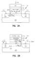
- FIG. 1Ais a block diagram of a metal oxide semiconductor field effect transistor (MOSFET) in a substrate according to the teachings of the prior art.
- MOSFETmetal oxide semiconductor field effect transistor
- FIG. 1Billustrates the MOSFET of FIG. 1A operated in the forward direction showing some degree of device degradation due to electrons being trapped in the gate oxide near the drain region over gradual use.
- FIG. 1Cis a graph showing the square root of the current signal (Ids) taken at the drain region of the conventional MOSFET versus the voltage potential (VGS) established between the gate and the source region.
- FIG. 2Ais a diagram of a programmed MOSFET which can be used as a NOR flash cell according to the teachings of the present invention.
- FIG. 2Bis a diagram suitable for explaining the method by which the MOSFET of the NOR flash cell of the present invention can be programmed to achieve the embodiments of the present invention.
- FIG. 2Cis a graph plotting the current signal (Ids) detected at the drain region versus a voltage potential, or drain voltage, (VDS) set up between the drain region and the source region (Ids vs. VDS).
- FIG. 3illustrates a portion of a memory array according to the teachings of the present invention.
- FIG. 4illustrates an electrical equivalent circuit for the portion of the memory array shown in FIG. 3.
- FIGS. 5 A- 5 Eare cross sectional views of various embodiments of the invention from the same vantage point illustrated in FIG. 3.
- FIGS. 6 A- 6 Billustrates the operation of the novel NOR flash cell formed according to the teachings of the present invention.
- FIG. 7illustrates the operation of a conventional DRAM cell.
- FIG. 8illustrates a memory device according to the teachings of the present invention.
- FIG. 9is a block diagram of an electrical system, or processor-based system, utilizing write once read only memory constructed in accordance with the present invention.
- wafer and substrate used in the following descriptioninclude any structure having an exposed surface with which to form the integrated circuit (IC) structure of the invention.
- substrateis understood to include semiconductor wafers.
- substrateis also used to refer to semiconductor structures during processing, and may include other layers that have been fabricated thereupon. Both wafer and substrate include doped and undoped semiconductors, epitaxial semiconductor layers supported by a base semiconductor or insulator, as well as other semiconductor structures well known to one skilled in the art.
- conductoris understood to include semiconductors, and the term insulator is defined to include any material that is less electrically conductive than the materials referred to as conductors.
- FIG. 1Ais useful in illustrating the conventional operation of a MOSFET such as can be used in a DRAM array.
- FIG. 1Aillustrates the normal hot electron injection and degradation of devices operated in the forward direction. As is explained below, since the electrons are trapped near the drain they are not very effective in changing the device characteristics.
- FIG. 1Ais a block diagram of a metal oxide semiconductor field effect transistor (MOSFET) 101 in a substrate 100 .
- the MOSFET 101includes a source region 102 , a drain region 104 , a channel region 106 in the substrate 100 between the source region 102 and the drain region 104 .
- a gate 108is separated from the channel region 108 by a gate oxide 110 .
- a sourceline 112is coupled to the source region 102 .
- a bitline 114is coupled to the drain region 104 .
- a wordline 116is coupled to the gate 108 .
- a drain to source voltage potential(Vds) is set up between the drain region 104 and the source region 102 .
- a voltage potentialis then applied to the gate 108 via a wordline 116 .
- Vtcharacteristic voltage threshold
- a channel 106forms in the substrate 100 between the drain region 104 and the source region 102 . Formation of the channel 106 permits conduction between the drain region 104 and the source region 102 , and a current signal (Ids) can be detected at the drain region 104 .
- FIG. 1Cillustrates this point.
- FIG. 1Cis a graph showing the square root of the current signal (Ids) taken at the drain region versus the voltage potential (VGS) established between the gate 108 and the source region 102 .
- the change in the slope of the plot of ⁇ square root ⁇ square root over (Ids) ⁇ versus VGSrepresents the change in the charge carrier mobility in the channel 106 .
- ⁇ VTrepresents the minimal change in the MOSFET's threshold voltage resulting from electrons gradually being trapped in the gate oxide 110 near the drain region 104 , under normal operation, due to device degradation. This results in a fixed trapped charge in the gate oxide 110 near the drain region 104 .
- Slope 1represents the charge carrier mobility in the channel 106 for FIG. 1A having no electrons trapped in the gate oxide 110 .
- Slope 2represents the charge mobility in the channel 106 for the conventional MOSFET of FIG. 1B having electrons 117 trapped in the gate oxide 110 near the drain region 104 .
- slope 1 and slope 2 in FIG. 1Cthe electrons 117 trapped in the gate oxide 110 near the drain region 104 of the conventional MOSFET do not significantly change the charge mobility in the channel 106 .
- One componentincludes a threshold voltage shift due to the trapped electrons and a second component includes mobility degradation due to additional scattering of carrier electrons caused by this trapped charge and additional surface states.
- a conventional MOSFETdegrades, or is “stressed,” over operation in the forward direction, electrons do gradually get injected and become trapped in the gate oxide near the drain. In this portion of the conventional MOSFET there is virtually no channel underneath the gate oxide. Thus the trapped charge modulates the threshold voltage and charge mobility only slightly.
- the inventorshave previously described programmable memory devices and functions based on the reverse stressing of MOSFET's in a conventional CMOS process and technology in order to form programmable address decode and correction. (See generally, L. Forbes, W. P. Noble and E. H. Cloud, “MOSFET technology for programmable address decode and correction,” application Ser. No. 09/383,804). That disclosure, however, did not describe write once read only memory solutions, but rather address decode and correction issues. The inventors also describe write once read only memory cells employing charge trapping in gate insulators for conventional MOSFETs and write once read only memory employing floating gates. The same are described in co-pending, commonly assigned U.S.
- normal flash memory cellscan be programmed by operation in the reverse direction and utilizing avalanche hot electron injection to trap electrons on the floating gate of the floating gate transistor.
- the programmed floating gate transistorWhen the programmed floating gate transistor is subsequently operated in the forward direction the electrons trapped on the floating gate cause the channel to have a different threshold voltage.
- the novel programmed floating gate transistors of the present inventionconduct significantly less current than conventional flash cells which have not been programmed. These electrons will remain trapped on the floating gate unless negative control gate voltages are applied. The electrons will not be removed from the floating gate when positive or zero control gate voltages are applied. Erasure can be accomplished by applying negative control gate voltages and/or increasing the temperature with negative control gate bias applied to cause the trapped electrons on the floating gate to be re-emitted back into the silicon channel of the MOSFET.
- FIG. 2Ais a diagram of a programmed floating gate transistor which can be used as a NOR flash cell according to the teachings of the present invention.
- the NOR flash cell 201includes a floating gate transistor in a substrate 200 which has a first source/drain region 202 , a second source/drain region 204 , and a channel region 206 between the first and second source/drain regions, 202 and 204 .
- the first source/drain region 202includes a source region 202 for the floating gate transistor and the second source/drain region 204 includes a drain region 204 for the floating gate transistor.
- FIG. 1is a diagram of a programmed floating gate transistor which can be used as a NOR flash cell according to the teachings of the present invention.
- the NOR flash cell 201includes a floating gate transistor in a substrate 200 which has a first source/drain region 202 , a second source/drain region 204 , and a channel region 206 between the first and second source/drain
- FIG. 2Afurther illustrates a floating gate 208 separated from the channel region 206 by a floating gate insulator 210 .
- An array plate 212is coupled to the first source/drain region 202 and a transmission line 214 is coupled to the second source/drain region 204 .
- the transmission line 214includes a bit line 214 .
- a control gate 216is separated from the floating gate 208 by a gate dielectric 218 .
- NOR flash cell 201is comprised of a programmed floating gate transistor.
- This programmed floating gate transistorhas a charge 217 trapped on the floating gate 208 .
- the charge 217 trapped on the floating gate 208includes a trapped electron charge 217 .
- FIG. 2Bis a diagram suitable for explaining the method by which the floating gate of the NOR flash cell 201 of the present invention can be programmed to achieve the embodiments of the present invention.
- the methodincludes programming the floating gate transistor.
- Programming the floating gate transistorincludes applying a first voltage potential V1 to a drain region 204 of the floating gate transistor and a second voltage potential V2 to the source region 202 .
- applying a first voltage potential V1 to the drain region 204 of the floating gate transistorincludes grounding the drain region 204 of the floating gate transistor as shown in FIG. 2B.
- applying a second voltage potential V2 to the source region 202includes biasing the array plate 212 to a voltage higher than VDD, as shown in FIG. 2B.
- a gate potential VGSis applied to the control gate 216 of the floating gate transistor.
- the gate potential VGSincludes a voltage potential which is less than the second voltage potential V2, but which is sufficient to establish conduction in the channel 206 of the floating gate transistor between the drain region 204 and the source region 202 . As shown in FIG.
- applying the first, second and gate potentials (V1, V2, and VGS respectively) to the floating gate transistorcreates a hot electron injection into the floating gate 208 of the floating gate transistor adjacent to the source region 202 .
- applying the first, second and gate potentials (V1, V2, and VGS respectively)provides enough energy to the charge carriers, e.g. electrons, being conducted across the channel 206 that, once the charge carriers are near the source region 202 , a number of the charge carriers get excited into the floating gate 208 adjacent to the source region 202 . Here the charge carriers become trapped.
- applying a first voltage potential V1 to the drain region 204 of the floating gate transistorincludes biasing the drain region 204 of the floating gate transistor to a voltage higher than VDD.
- applying a second voltage potential V2 to the source region 202includes grounding the array plate 212 .
- a gate potential VGSis applied to the control gate 216 of the floating gate transistor.
- the gate potential VGSincludes a voltage potential which is less than the first voltage potential V1, but which is sufficient to establish conduction in the channel 206 of the floating gate transistor between the drain region 204 and the source region 202 .
- Applying the first, second and gate potentials (V1, V2, and VGS respectively) to the floating gate transistorcreates a hot electron injection into the floating gate 208 of the floating gate transistor adjacent to the drain region 204 .
- applying the first, second and gate potentials (V1, V2, and VGS respectively)provides enough energy to the charge carriers, e.g. electrons, being conducted across the channel 206 that, once the charge carriers are near the drain region 204 , a number of the charge carriers get excited into the floating gate 208 adjacent to the drain region 204 .
- the charge carriersbecome trapped as shown in FIG. 2A.
- the methodis continued by subsequently operating the floating gate transistor in the forward direction in its programmed state during a read operation.
- the read operationincludes grounding the source region 202 and precharging the drain region a fractional voltage of VDD. If the device is addressed by a wordline coupled to the gate, then its conductivity will be determined by the presence or absence of stored charge in the floating gate. That is, a gate potential can be applied to the control gate 216 by a wordline 220 in an effort to form a conduction channel between the source and the drain regions as done with addressing and reading conventional DRAM cells.
- the conduction channel 206 of the floating gate transistorwill have a higher voltage threshold and will not conduct.
- FIG. 2Cis a graph plotting a current signal (IDS) detected at the second source/drain region 204 versus a voltage potential, or drain voltage, (VDS) set up between the second source/drain region 204 and the first source/drain region 202 (IDS vs. VDS).
- VDSrepresents the voltage potential set up between the drain region 204 and the source region 202 .
- the curve plotted as D1represents the conduction behavior of a conventional floating gate transistor which is not programmed according to the teachings of the present invention.
- the curve D2represents the conduction behavior of the programmed floating gate transistor, described above in connection with FIG. 2A, according to the teachings of the present invention. As shown in FIG.
- the current signal (IDS2) detected at the second source/drain region 204 for the programmed floating gate transistor (curve D2)is significantly lower than the current signal (IDS1) detected at the second source/drain region 204 for the conventional floating gate cell which is not programmed according to the teachings of the present invention. Again, this is attributed to the fact that the channel 206 in the programmed floating gate transistor of the present invention has a different voltage threshold.
- NROMNonvolatile Memory Cell
- B. Eitan et al.“Characterization of Channel Hot Electron Injection by the Subthreshold Slope of NROM device,” IEEE Electron Device Lett., Vol. 22, No. 11, pp. 556-558, (November 2001); B. Etian et al., “NROM: A novel localized Trapping, 2-Bit Nonvolatile Memory Cell,” IEEE Electron Device Lett., Vol. 21, No. 11, pp.
- the present inventiondiscloses programming a floating gate transistor to trap charge and reading the device to form a NOR flash memory cell with high density.
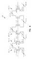
- FIG. 3illustrates a portion of a memory array 300 according to the teachings of the present invention.
- the memory in FIG. 3is shown illustrating a number of vertical pillars, or NOR flash cells, 301 - 1 , 301 - 2 , . . . , 301 -N, formed according to the teachings of the present invention.
- the number of vertical pillarare formed in rows and columns extending outwardly from a substrate 303 .
- the number of vertical pillars, 301 - 1 , 301 - 2 , . . . , 301 -Nare separated by a number of trenches 340 .
- the number of vertical pillars, 301 - 1 , 301 - 2 , . . . , 301 -Nserve as NOR floating gate transistors including a first source/drain region, e.g. 302 - 1 and 302 - 2 respectively.
- the first source/drain region, 302 - 1 and 302 - 2is coupled to a sourceline 304 .
- the sourceline 304is formed in a bottom of the trenches 340 between rows of the vertical pillars, 301 - 1 , 301 - 2 , . . . , 301 -N.
- the sourceline 304is formed from a doped region implanted in the bottom of the trenches 340 .
- a second source/drain regione.g. 306 - 1 and 306 - 2 respectively, is coupled to a bitline (not shown).
- a channel region 305is located between the first and the second source/drain regions.
- a floating gateshown generally as 309 , is separated from the channel region 305 by a first gate insulator 307 in the trenches 340 along rows of the vertical pillars, 301 - 1 , 301 - 2 , . . . , 301 -N.
- the first gate insulator 307includes a gate insulator 307 selected from the group of silicon dioxide (SiO 2 ) formed by wet oxidation, silicon oxynitride (SON), silicon rich oxide (SRO), and aluminum oxide (Al 2 O 3 ).
- the gate insulator 307includes an oxide-nitride-oxide (ONO) gate insulator 307 .
- ONOoxide-nitride-oxide
- a control line 313is formed across the number of pillars and in the trenches 340 between the floating gates. The control line 313 is separated from the pillars and the floating gates by a second gate insulator 317 .
- FIG. 4illustrates an electrical equivalent circuit 400 for the portion of the memory array shown in FIG. 3.
- a number of vertical NOR flash cells401 - 1 , 401 - 2 , . . . , 401 -N, are provided.
- Each vertical NOR flash cell, 401 - 1 , 401 - 2 , . . . , 401 -Nincludes a first source/drain region, e.g. 402 - 1 and 402 - 2 , a second source/drain region, e.g. 406 - 1 and 406 - 2 , a channel region 405 between the first and the second source/drain regions, and a floating gate, shown generally as 409 , separated from the channel region by a first gate insulator.
- FIG. 4further illustrates a number of bit lines, e.g. 411 - 1 and 411 - 2 .
- a single bit line, e.g. 411 - 1is coupled to the second source/drain regions, e.g. 406 - 1 and 406 - 2 , for a pair of NOR flash cells 401 - 1 and 401 - 2 since, as shown in FIG. 3, each pillar contains two NOR flash cells.
- the number of bit lines, 411 - 1 and 411 - 2are coupled to the second source/drain regions, e.g.
- a number of word linessuch as wordline 413 in FIG. 4, are coupled to a control gate 412 of each NOR flash cell along columns of the memory array.
- a number of sourcelines, 415 - 1 , 415 - 2 , . . . , 415 -Nare formed in a bottom of the trenches between rows of the vertical pillars, described in connection with FIG. 3, such that first source/drain regions, e.g. 402 - 2 and 402 - 3 , in column adjacent NOR flash cells, e.g.
- NOR flash cellse.g. 401 - 2 and 401 - 3 , separated by a trench, share a common sourceline, e.g. 415 - 1 .
- the number of sourcelines, 415 - 1 , 415 - 2 , . . . , 415 -Nare shared by column adjacent NOR flash cells, e.g. 401 - 2 and 401 - 3 , separated by a trench, along rows of the memory array 400 .
- column adjacent NOR flash cellse.g. 401 - 2 and 401 - 3 , separated by a trench
- when one column adjacent NOR flash cell, e.g. 401 - 2is being read its complement column adjacent NOR flash cell, e.g. 401 - 3 , can operate as a reference cell.
- FIGS. 5 A- 5 Eare cross sectional views of various embodiments of the invention from the same vantage point illustrated in FIG. 3.
- FIGS. 5 A- 5 Eare intended to illustrate the numerous floating gate and control gate configurations which are intended within the scope of the present invention.
- a wordline(not shown for sake of clarity) will couple to the various control gate configurations along columns of an array, and the sourcelines and bitlines will run along rows of the array (here shown running into the plane of the drawing sheet), in the same fashion as wordline 413 , sourcelines 415 - 1 , 415 - 2 , . . .
- FIGS. 5 A- 5 Ea number of vertical pillars, e.g. 500 - 1 and 500 - 2 , are illustrated with each pillar containing a pair of NOR flash cells.
- a single second source/drain region 503is shared at the top of each pillar.
- Each of the pillarsare separated by rows of trenches 530 .
- a buried sourcelineis located at the bottom of each trench 530 , e.g. a doped region implanted in the bottom of trenches 530 .
- a portion of the buried sourcelineundercuts the pillars, e.g. 500 - 1 and 500 - 2 , on opposing sides to serve as the respective first source/drain region for the pair of NOR flash cells.
- a conduction channel 505can be created in the body 507 of the pillar between the second source/drain region 503 and the respective sourcelines in each neighboring trench.
- the NOR flash cellsare programmed by grounding the source line and applying a gate voltage and a voltage to the second source/drain region, e.g. drain region. To read this state the drain and ground or source have the normal connections and the conductivity of the transistor determined.
- the devicescan be erased by applying a large negative voltage to the gate and positive voltage to the source.
- the coincidence and of gate and source bias at the same locationcan erase a transistor at this location, but the gate bias alone or source bias alone is not sufficient to disturb or erase the charge storage state of other transistors in the array.
- FIG. 5Aillustrates one embodiment of the present invention's floating gate and control gate configuration.
- a pair of floating gates 509 - 1 and 509 - 2are formed in each trench 530 between adjacent pillars which form memory cells 500 - 1 and 500 - 2 .
- Each one of the pair of floating gates, 509 - 1 and 509 - 2respectively opposes the body regions 507 - 1 and 507 - 2 in column adjacent pillars 500 - 1 and 500 - 2 on opposing sides of the trench 530 .
- a single control gate 513is shared by the pair of floating gates 509 - 1 and 509 - 2 on opposing sides of the trench 530 .
- the single control gate 513is formed in the trench, such as trench 530 , below the top surface of the pillars 500 - 1 and 500 - 2 and between the pair of floating gates 509 - 1 and 509 - 2 .
- each floating gatee.g. 509 - 1 and 509 - 2 , includes a vertically oriented floating gate having a vertical length of less than 100 nanometers.
- FIG. 5Billustrates another embodiment of the present invention's floating gate and control gate configuration.
- a pair of floating gates 509 - 1 and 509 - 2are formed in each trench 530 between column adjacent pillars 500 - 1 and 500 - 2 .
- Each one of the pair of floating gates, 509 - 1 and 509 - 2respectively opposes the body regions 507 - 1 and 507 - 2 in column adjacent pillars 500 - 1 and 500 - 2 on opposing sides of the trench 530 .
- a pair of control gatesshown as 513 - 1 and 513 - 2 , are formed in trenches, e.g. trench 530 , below the top surface of the pillars, 500 - 1 and 500 - 2 , and between the pair of floating gates 509 - 1 and 509 - 2 .
- Each one of the pair of control gates, 513 - 1 and 513 - 2addresses the floating gates, 509 - 1 and 509 - 2 respectively, on opposing sides of the trench 530 .
- the pair of control gates 513 - 1 and 513 - 2are separated by an insulator layer.
- FIG. 5Cillustrates another embodiment of the present invention's floating gate and control gate configuration.
- a pair of floating gates 509 - 1 and 509 - 2are again formed in each trench 530 between adjacent pillars which form memory cells 500 - 1 and 500 - 2 .
- Each one of the pair of floating gates, 509 - 1 and 509 - 2respectively opposes the body regions 507 - 1 and 507 - 2 in adjacent pillars 500 - 1 and 500 - 2 on opposing sides of the trench 530 .
- control gates 513are disposed vertically above the floating gates. That is, in this embodiment, the control gates 513 are located above the pair of floating gates 509 - 1 and 509 - 2 and not fully beneath the top surface of the pillars 500 - 1 and 500 - 2 . In the embodiment of FIG. 5C, each pair of floating gates, e.g. 509 - 1 and 509 - 2 , in a given trench shares a single control gate 513 .
- FIG. 5Dillustrates another embodiment of the present invention's floating gate and control gate configuration.
- a pair of floating gates 509 - 1 and 509 - 2are formed in each trench 530 between adjacent pillars which form memory cells 500 - 1 and 500 - 2 .
- Each one of the pair of floating gates, 509 - 1 and 509 - 2respectively opposes the body regions 507 - 1 and 507 - 2 in adjacent pillars 500 - 1 and 500 - 2 on opposing sides of the trench 530 .
- a pair of individual control gates 513 - 1 and 513 - 2are disposed vertically above each individual one of the pair of floating gates 509 - 1 and 509 - 2 . That is, the pair of individual control gates 513 - 1 and 513 - 2 are located above the pair of floating gates 509 - 1 and 509 - 2 and not fully beneath the top surface of the pillars 500 - 1 and 500 - 2 .
- FIG. 5Eillustrates another embodiment of the present invention's floating gate and control gate configuration.
- a single floating gate 509is formed in each trench 530 between adjacent pillars which form memory cells 500 - 1 and 500 - 2 .
- the single floating gate 509can be either a vertically oriented floating gate 509 or a horizontally oriented floating gate 509 formed by conventional processing techniques, or can be a horizontally oriented floating gate 509 formed by a replacement gate technique such as described in a copending application, entitled “Flash Memory with Ultrathin Vertical Body Transistors,” by Leonard Forbes and Kie Y. Ahn, application Ser. No. 09/780,169.
- the floating gate 509has a vertical length facing the channel regions 505 - 1 and 505 - 2 of less than 100 nm. In another embodiment, the floating gate 509 has a vertical length facing the channel regions 505 - 1 and 505 - 2 of less than 50 nm. In one embodiment, as shown in FIG. 5E, the floating gate 509 is shared, respectively, with the body regions 507 - 1 and 507 - 2 , including channel regions 505 - 1 and 505 - 2 , in adjacent pillars 500 - 1 and 500 - 2 located on opposing sides of the trench 530 .
- control gates 513are disposed vertically above the floating gates. That is, in this embodiment, the control gates 513 are located above the floating gate 509 and not fully beneath the top surface of the pillars 500 - 1 and 500 - 2 .
- FIGS. 6 A-B and 7are useful in illustrating the use of charge storage in the floating gate to modulate the conductivity of the NOR flash memory cell according to the teachings of the present invention. That is, FIGS. 6 A- 6 B illustrates the operation of the novel NOR flash memory cell 601 formed according to the teachings of the present invention. And, FIG. 7 illustrates the operation of a conventional DRAM cell 501 . As shown in FIG. 7, the gate insulator 702 is made thicker than in a conventional DRAM cell, e.g. 701 and is equal to or greater than 10 nm or 100 ⁇ ( 10 ⁇ 6 cm). In the embodiment shown in FIG.
- NOR flash memory cellhaving dimensions of 0.1 ⁇ m (10 ⁇ 5 cm) by 0.1 ⁇ m.
- FIG. 6Baids to further illustrate the conduction behavior of the novel NOR flash memory cell of the present invention.
- Vcontrol gate voltage
- the nominal threshold voltage without the floating gate chargedis 1 ⁇ 2 V
- the floating gate transistors in the arrayare utilized not just as passive on or off switches as transfer devices in DRAM arrays but rather as active devices providing gain.
- to program the floating gate transistor “off,”requires only a stored charge in the floating gate of about 100 electrons if the area is 0.1 ⁇ m by 0.1 ⁇ m.
- the NOR flash memory cellis un-programmed, e.g. no stored charge trapped in the floating gate, and if the floating gate transistor is addressed over 10 nS a of current of 12.5 ⁇ A is provided.
- the integrated drain currentthen has a charge of 125 fC or 800,000 electrons.
- FIG. 8a memory device is illustrated according to the teachings of the present invention.
- the memory device 840contains a memory array 842 , row and column decoders 844 , 848 and a sense amplifier circuit 846 .
- the memory array 842consists of a plurality of NOR flash memory cells 800 , formed according to the teachings of the present invention whose word lines 880 and bit lines 860 are commonly arranged into rows and columns, respectively.
- the bit lines 860 of the memory array 842are connected to the sense amplifier circuit 846 , while its word lines 880 are connected to the row decoder 844 .
- Address and control signalsare input on address/control lines 861 into the memory device 840 and connected to the column decoder 848 , sense amplifier circuit 846 and row decoder 844 and are used to gain read and write access, among other things, to the memory array 842 .
- the column decoder 848is connected to the sense amplifier circuit 846 via control and column select signals on column select lines 862 .
- the sense amplifier circuit 846receives input data destined for the memory array 842 and outputs data read from the memory array 842 over input/output (I/O) data lines 863 .
- Datais read from the cells of the memory array 842 by activating a word line 880 (via the row decoder 844 ), which couples all of the memory cells corresponding to that word line to respective bit lines 860 , which define the columns of the array.
- One or more bit lines 860are also activated.
- the sense amplifier circuit 846 connected to a bit line columndetects and amplifies the conduction sensed through a given NOR flash memory cell and transferred to its bit line 860 by measuring the potential difference between the activated bit line 860 and a reference line which may be an inactive bit line. Again, in the read operation the source region of a given cell is couple to a grounded array plate (not shown).
- the operation of Memory device sense amplifiersis described, for example, in U.S. Pat. Nos. 5,627,785; 5,280,205; and 5,042,011, all assigned to Micron Technology Inc., and incorporated by reference herein.
- FIG. 9is a block diagram of an electrical system, or processor-based system, 900 utilizing NOR flash memory 912 constructed in accordance with the present invention. That is, the NOR flash memory 912 utilizes the modified NOR flash cell architecture as explained and described in detail in connection with FIGS. 2 - 6 .
- the processor-based system 900may be a computer system, a process control system or any other system employing a processor and associated memory.
- the system 900includes a central processing unit (CPU) 902 , e.g., a microprocessor, that communicates with the NOR flash memory 912 and an I/O device 908 over a bus 920 .
- CPUcentral processing unit
- bus 920may be a series of buses and bridges commonly used in a processor-based system, but for convenience purposes only, the bus 920 has been illustrated as a single bus.
- a second I/O device 910is illustrated, but is not necessary to practice the invention.
- the processor-based system 900can also includes read-only memory (ROM) 914 and may include peripheral devices such as a floppy disk drive 904 and a compact disk (CD) ROM drive 906 that also communicates with the CPU 902 over the bus 920 as is well known in the art.
- ROMread-only memory
- CDcompact disk
- At least one of the NOR flash memory cell in NOR flash memory 912includes a programmed flash cell.
- FIG. 9illustrates an embodiment for electronic system circuitry in which the novel memory cells of the present invention are used.
- the illustration of system 900is intended to provide a general understanding of one application for the structure and circuitry of the present invention, and is not intended to serve as a complete description of all the elements and features of an electronic system using the novel memory cell structures.
- the inventionis equally applicable to any size and type of memory device 900 using the novel memory cells of the present invention and is not intended to be limited to that described above.
- such an electronic systemcan be fabricated in single-package processing units, or even on a single semiconductor chip, in order to reduce the communication time between the processor and the memory device.
- Applications containing the novel memory cell of the present invention as described in this disclosureinclude electronic systems for use in memory modules, device drivers, power modules, communication modems, processor modules, and application-specific modules, and may include multilayer, multichip modules.
- Such circuitrycan further be a subcomponent of a variety of electronic systems, such as a clock, a television, a cell phone, a personal computer, an automobile, an industrial control system, an aircraft, and others.
- NAND flash memoriesare ideally as small as 4F squared in conventional planar device technology, with practical devices having a cell area of 5F squared.
- the vertical NOR flash memory cells described herehave a higher density than conventional planar NAND cells but they would operate at speeds higher than or comparable to conventional planar NOR flash memories.
- the NOR flash memories described herethen have both high density and high speed.
Landscapes
- Engineering & Computer Science (AREA)
- Microelectronics & Electronic Packaging (AREA)
- Non-Volatile Memory (AREA)
- Semiconductor Memories (AREA)
Abstract
Description
- This application is related to the following co-pending, commonly assigned U.S. patent applications: “Write Once Read Only Memory Employing Floating Gates,” attorney docket no. 1303.051US1, Ser. No. ______, “Write Once Read Only Memory Employing Charge Trapping in Insulators,” attorney docket no. 1303.052US1, Ser. No. ______, “Ferroelectric Write Once Read Only Memory for Archival Storage,” attorney docket no. 1303.058US1, Ser. No. ______, “Nanocrystal Write Once Read Only Memory for Archival Storage,” attorney docket no. 1303.054US1, Ser. No. ______, “Write Once Read Only Memory with Large Work Function Floating Gates,” attorney docket no. 1303.055US1, Ser. No.______, “Vertical NROM Having a Storage Density of 1 Bit per 1F[0001]2,” attorney docket no. 1303.057US1, Ser. No. ______, and “Multistate NROM Having a Storage Density Much Greater than 1 Bit per 1F2,” attorney docket no. 1303.053US1, Ser. No. ______,each of which disclosure is herein incorporated by reference.
- The present invention relates generally to semiconductor integrated circuits and, more particularly, to NOR flash memory cells with high storage density.[0002]
- Many electronic products need various amounts of memory to store information, e.g. data. One common type of high speed, low cost memory includes dynamic random access memory (DRAM) comprised of individual DRAM cells arranged in arrays. DRAM cells include an access transistor, e.g a metal oxide semiconducting field effect transistor (MOSFET), coupled to a capacitor cell.[0003]
- Another type of high speed, low cost memory includes floating gate memory cells. A conventional horizontal floating gate transistor structure includes a source region and a drain region separated by a channel region in a horizontal substrate. A floating gate is separated by a thin tunnel gate oxide. The structure is programmed by storing a charge on the floating gate. A control gate is separated from the floating gate by an intergate dielectric. A charge stored on the floating gate effects the conductivity of the cell when a read voltage potential is applied to the control gate. The state of cell can thus be determined by sensing a change in the device conductivity between the programmed and un-programmed states.[0004]
- With successive generations of DRAM chips, an emphasis continues to be placed on increasing array density and maximizing chip real estate while minimizing the cost of manufacture. It is further desirable to increase array density with little or no modification of the DRAM optimized process flow.[0005]
- Flash memories based on electron trapping are well known and commonly used electronic components. (See generally; B. Dipert and L. Hebert, “Flash Memory goes Mainstream,” IEEE Spectrum, No. 10, pp. 48-52, (October 1993); R. Goodwins, “New Memory Technologies on the Way,” http://zdnet.com.com/2100-1103-846950.html). Recently NAND flash memory cells have become common in applications requiring high storage density while NOR flash memory cells are used in applications requiring high access and read speeds. (See generally, C.-G. Hwang, “Semiconductor Memories for the IT Era,” Abst. IEEE Int. Solid-State Circuits Conf., San Francisco, 2002, pp. 24-27). NAND flash memories have a higher density because 16 or more devices are placed in series, this increases density at the expense of speed. (See generally; R. Shirota et al., “A 2.3 mu[0006]2memory cell structure for 16 Mb NAND EEPROMs,” Digest of IEEE Int. Electron Device Meeting, San Francisco, 1990, pp. 103-106)
- Thus, there is an ongoing need for improved DRAM technology compatible flash memory cells. It is desirable that such flash memory cells be fabricated on a DRAM chip with little or no modification of the DRAM process flow. It is further desirable that such flash cells provide increased density and high access and read speeds.[0007]
- The above mentioned problems for creating DRAM technology compatible flash memory cells as well as other problems are addressed by the present invention and will be understood by reading and studying the following specification. This disclosure describes a high speed NOR type flash memory cell and arrays with high density. Two transistors occupy an area of 4F squared when viewed from above, or each memory cell consisting of one transistor has an area of 2F squared. NAND flash memories are ideally as small as 4F squared in conventional planar device technology, with practical devices having a cell area of SF squared. The vertical NOR flash memory cells described here have a higher density than conventional planar NAND cells but they would operate at speeds higher than or comparable to conventional planar NOR flash memories. The NOR flash memories described here then have both high density and high speed.[0008]
- In particular, an embodiment of the present invention includes a NOR flash cell. The NOR flash memory cell includes a floating gate transistor extending outwardly from a substrate. The floating gate transistor has a first source/drain region, a second source/drain region, a channel region between the first and the second source/drain regions, a floating gate separated from the channel region by a gate insulator, and a control gate separated from the floating gate by a gate dielectric. A sourceline is formed buried in a trench adjacent to the vertical floating gate transistor and coupled to the first source/drain region. A transmission line coupled to the second source/drain region. And, a wordline is coupled to the control gate perpendicular to the sourceline.[0009]
- These and other embodiments, aspects, advantages, and features of the present invention will be set forth in part in the description which follows, and in part will become apparent to those skilled in the art by reference to the following description of the invention and referenced drawings or by practice of the invention. The aspects, advantages, and features of the invention are realized and attained by means of the instrumentalities, procedures, and combinations particularly pointed out in the appended claims.[0010]
- FIG. 1A is a block diagram of a metal oxide semiconductor field effect transistor (MOSFET) in a substrate according to the teachings of the prior art.[0011]
- FIG. 1B illustrates the MOSFET of FIG. 1A operated in the forward direction showing some degree of device degradation due to electrons being trapped in the gate oxide near the drain region over gradual use.[0012]
- FIG. 1C is a graph showing the square root of the current signal (Ids) taken at the drain region of the conventional MOSFET versus the voltage potential (VGS) established between the gate and the source region.[0013]
- FIG. 2A is a diagram of a programmed MOSFET which can be used as a NOR flash cell according to the teachings of the present invention.[0014]
- FIG. 2B is a diagram suitable for explaining the method by which the MOSFET of the NOR flash cell of the present invention can be programmed to achieve the embodiments of the present invention.[0015]
- FIG. 2C is a graph plotting the current signal (Ids) detected at the drain region versus a voltage potential, or drain voltage, (VDS) set up between the drain region and the source region (Ids vs. VDS).[0016]
- FIG. 3 illustrates a portion of a memory array according to the teachings of the present invention.[0017]
- FIG. 4 illustrates an electrical equivalent circuit for the portion of the memory array shown in FIG. 3. FIGS.[0018]5A-5E are cross sectional views of various embodiments of the invention from the same vantage point illustrated in FIG. 3.
- FIGS.[0019]6A-6B illustrates the operation of the novel NOR flash cell formed according to the teachings of the present invention.
- FIG. 7 illustrates the operation of a conventional DRAM cell.[0020]
- FIG. 8 illustrates a memory device according to the teachings of the present invention.[0021]
- FIG. 9 is a block diagram of an electrical system, or processor-based system, utilizing write once read only memory constructed in accordance with the present invention.[0022]
- In the following detailed description of the invention, reference is made to the accompanying drawings which form a part hereof, and in which is shown, by way of illustration, specific embodiments in which the invention may be practiced. In the drawings, like numerals describe substantially similar components throughout the several views. These embodiments are described in sufficient detail to enable those skilled in the art to practice the invention. Other embodiments may be utilized and structural, logical, and electrical changes may be made without departing from the scope of the present invention.[0023]
- The terms wafer and substrate used in the following description include any structure having an exposed surface with which to form the integrated circuit (IC) structure of the invention. The term substrate is understood to include semiconductor wafers. The term substrate is also used to refer to semiconductor structures during processing, and may include other layers that have been fabricated thereupon. Both wafer and substrate include doped and undoped semiconductors, epitaxial semiconductor layers supported by a base semiconductor or insulator, as well as other semiconductor structures well known to one skilled in the art. The term conductor is understood to include semiconductors, and the term insulator is defined to include any material that is less electrically conductive than the materials referred to as conductors. The following detailed description is, therefore, not to be taken in a limiting sense, and the scope of the present invention is defined only by the appended claims, along with the full scope of equivalents to which such claims are entitled.[0024]
- FIG. 1A is useful in illustrating the conventional operation of a MOSFET such as can be used in a DRAM array. FIG. 1A illustrates the normal hot electron injection and degradation of devices operated in the forward direction. As is explained below, since the electrons are trapped near the drain they are not very effective in changing the device characteristics.[0025]
- FIG. 1A is a block diagram of a metal oxide semiconductor field effect transistor (MOSFET)[0026]101 in a
substrate 100. TheMOSFET 101 includes asource region 102, adrain region 104, achannel region 106 in thesubstrate 100 between thesource region 102 and thedrain region 104. Agate 108 is separated from thechannel region 108 by agate oxide 110. Asourceline 112 is coupled to thesource region 102. Abitline 114 is coupled to thedrain region 104. Awordline 116 is coupled to thegate 108. - In conventional operation, a drain to source voltage potential (Vds) is set up between the[0027]
drain region 104 and thesource region 102. A voltage potential is then applied to thegate 108 via awordline 116. Once the voltage potential applied to thegate 108 surpasses the characteristic voltage threshold (Vt) of the MOSFET achannel 106 forms in thesubstrate 100 between thedrain region 104 and thesource region 102. Formation of thechannel 106 permits conduction between thedrain region 104 and thesource region 102, and a current signal (Ids) can be detected at thedrain region 104. - In operation of the conventional MOSFET of FIG. 1A, some degree of device degradation does gradually occur for MOSFETs operated in the forward direction by[0028]
electrons 117 becoming trapped in thegate oxide 110 near thedrain region 104. This effect is illustrated in FIG. 1B. However, since theelectrons 117 are trapped near thedrain region 104 they are not very effective in changing the MOSFET characteristics. - FIG. 1C illustrates this point. FIG. 1C is a graph showing the square root of the current signal (Ids) taken at the drain region versus the voltage potential (VGS) established between the[0029]
gate 108 and thesource region 102. The change in the slope of the plot of {square root}{square root over (Ids)} versus VGS represents the change in the charge carrier mobility in thechannel 106. - In FIG. 1C, ΔVT represents the minimal change in the MOSFET's threshold voltage resulting from electrons gradually being trapped in the[0030]
gate oxide 110 near thedrain region 104, under normal operation, due to device degradation. This results in a fixed trapped charge in thegate oxide 110 near thedrain region 104.Slope 1 represents the charge carrier mobility in thechannel 106 for FIG. 1A having no electrons trapped in thegate oxide 110.Slope 2 represents the charge mobility in thechannel 106 for the conventional MOSFET of FIG.1B having electrons 117 trapped in thegate oxide 110 near thedrain region 104. As shown by a comparison ofslope 1 andslope 2 in FIG. 1C, theelectrons 117 trapped in thegate oxide 110 near thedrain region 104 of the conventional MOSFET do not significantly change the charge mobility in thechannel 106. - There are two components to the effects of stress and hot electron injection. One component includes a threshold voltage shift due to the trapped electrons and a second component includes mobility degradation due to additional scattering of carrier electrons caused by this trapped charge and additional surface states. When a conventional MOSFET degrades, or is “stressed,” over operation in the forward direction, electrons do gradually get injected and become trapped in the gate oxide near the drain. In this portion of the conventional MOSFET there is virtually no channel underneath the gate oxide. Thus the trapped charge modulates the threshold voltage and charge mobility only slightly.[0031]
- The inventors have previously described programmable memory devices and functions based on the reverse stressing of MOSFET's in a conventional CMOS process and technology in order to form programmable address decode and correction. (See generally, L. Forbes, W. P. Noble and E. H. Cloud, “MOSFET technology for programmable address decode and correction,” application Ser. No. 09/383,804). That disclosure, however, did not describe write once read only memory solutions, but rather address decode and correction issues. The inventors also describe write once read only memory cells employing charge trapping in gate insulators for conventional MOSFETs and write once read only memory employing floating gates. The same are described in co-pending, commonly assigned U.S. patent applications, entitled “Write Once Read Only Memory Employing Charge Trapping in Insulators,” attorney docket no. 1303.052US1, Ser. No. ______, and “Write Once Read Only Memory Employing Floating Gates,” attorney docket no. 1303.051US1, Ser. No. ______. The present application, however, describes NOR flash cells formed from conventional flash memory device structures.[0032]
- According to the teachings of the present invention, normal flash memory cells can be programmed by operation in the reverse direction and utilizing avalanche hot electron injection to trap electrons on the floating gate of the floating gate transistor. When the programmed floating gate transistor is subsequently operated in the forward direction the electrons trapped on the floating gate cause the channel to have a different threshold voltage. The novel programmed floating gate transistors of the present invention conduct significantly less current than conventional flash cells which have not been programmed. These electrons will remain trapped on the floating gate unless negative control gate voltages are applied. The electrons will not be removed from the floating gate when positive or zero control gate voltages are applied. Erasure can be accomplished by applying negative control gate voltages and/or increasing the temperature with negative control gate bias applied to cause the trapped electrons on the floating gate to be re-emitted back into the silicon channel of the MOSFET.[0033]
- FIG. 2A is a diagram of a programmed floating gate transistor which can be used as a NOR flash cell according to the teachings of the present invention. As shown in FIG. 2A the NOR[0034]
flash cell 201 includes a floating gate transistor in asubstrate 200 which has a first source/drain region 202, a second source/drain region 204, and achannel region 206 between the first and second source/drain regions,202 and204. In one embodiment, the first source/drain region 202 includes asource region 202 for the floating gate transistor and the second source/drain region 204 includes adrain region 204 for the floating gate transistor. FIG. 2A further illustrates a floatinggate 208 separated from thechannel region 206 by a floatinggate insulator 210. Anarray plate 212 is coupled to the first source/drain region 202 and atransmission line 214 is coupled to the second source/drain region 204. In one embodiment, thetransmission line 214 includes abit line 214. Further as shown in FIG. 2A, acontrol gate 216 is separated from the floatinggate 208 by agate dielectric 218. - As stated above, NOR[0035]
flash cell 201 is comprised of a programmed floating gate transistor. This programmed floating gate transistor has acharge 217 trapped on the floatinggate 208. In one embodiment, thecharge 217 trapped on the floatinggate 208 includes a trappedelectron charge 217. - FIG. 2B is a diagram suitable for explaining the method by which the floating gate of the NOR[0036]
flash cell 201 of the present invention can be programmed to achieve the embodiments of the present invention. As shown in FIG. 2B the method includes programming the floating gate transistor. Programming the floating gate transistor includes applying a first voltage potential V1 to adrain region 204 of the floating gate transistor and a second voltage potential V2 to thesource region 202. - In one embodiment, applying a first voltage potential V1 to the[0037]
drain region 204 of the floating gate transistor includes grounding thedrain region 204 of the floating gate transistor as shown in FIG. 2B. In this embodiment, applying a second voltage potential V2 to thesource region 202 includes biasing thearray plate 212 to a voltage higher than VDD, as shown in FIG. 2B. A gate potential VGS is applied to thecontrol gate 216 of the floating gate transistor. In one embodiment, the gate potential VGS includes a voltage potential which is less than the second voltage potential V2, but which is sufficient to establish conduction in thechannel 206 of the floating gate transistor between thedrain region 204 and thesource region 202. As shown in FIG. 2B, applying the first, second and gate potentials (V1, V2, and VGS respectively) to the floating gate transistor creates a hot electron injection into the floatinggate 208 of the floating gate transistor adjacent to thesource region 202. In other words, applying the first, second and gate potentials (V1, V2, and VGS respectively) provides enough energy to the charge carriers, e.g. electrons, being conducted across thechannel 206 that, once the charge carriers are near thesource region 202, a number of the charge carriers get excited into the floatinggate 208 adjacent to thesource region 202. Here the charge carriers become trapped. - In an alternative embodiment, applying a first voltage potential V1 to the[0038]
drain region 204 of the floating gate transistor includes biasing thedrain region 204 of the floating gate transistor to a voltage higher than VDD. In this embodiment, applying a second voltage potential V2 to thesource region 202 includes grounding thearray plate 212. A gate potential VGS is applied to thecontrol gate 216 of the floating gate transistor. In one embodiment, the gate potential VGS includes a voltage potential which is less than the first voltage potential V1, but which is sufficient to establish conduction in thechannel 206 of the floating gate transistor between thedrain region 204 and thesource region 202. Applying the first, second and gate potentials (V1, V2, and VGS respectively) to the floating gate transistor creates a hot electron injection into the floatinggate 208 of the floating gate transistor adjacent to thedrain region 204. In other words, applying the first, second and gate potentials (V1, V2, and VGS respectively) provides enough energy to the charge carriers, e.g. electrons, being conducted across thechannel 206 that, once the charge carriers are near thedrain region 204, a number of the charge carriers get excited into the floatinggate 208 adjacent to thedrain region 204. Here the charge carriers become trapped as shown in FIG. 2A. - In one embodiment of the present invention, the method is continued by subsequently operating the floating gate transistor in the forward direction in its programmed state during a read operation. Accordingly, the read operation includes grounding the[0039]
source region 202 and precharging the drain region a fractional voltage of VDD. If the device is addressed by a wordline coupled to the gate, then its conductivity will be determined by the presence or absence of stored charge in the floating gate. That is, a gate potential can be applied to thecontrol gate 216 by awordline 220 in an effort to form a conduction channel between the source and the drain regions as done with addressing and reading conventional DRAM cells. - However, now in its programmed state, the[0040]
conduction channel 206 of the floating gate transistor will have a higher voltage threshold and will not conduct. - FIG. 2C is a graph plotting a current signal (IDS) detected at the second source/[0041]
drain region 204 versus a voltage potential, or drain voltage, (VDS) set up between the second source/drain region 204 and the first source/drain region202 (IDS vs. VDS). In one embodiment, VDS represents the voltage potential set up between thedrain region 204 and thesource region 202. In FIG. 2C, the curve plotted as D1 represents the conduction behavior of a conventional floating gate transistor which is not programmed according to the teachings of the present invention. The curve D2 represents the conduction behavior of the programmed floating gate transistor, described above in connection with FIG. 2A, according to the teachings of the present invention. As shown in FIG. 2C, for a particular drain voltage, VDS, the current signal (IDS2) detected at the second source/drain region 204 for the programmed floating gate transistor (curve D2) is significantly lower than the current signal (IDS1) detected at the second source/drain region 204 for the conventional floating gate cell which is not programmed according to the teachings of the present invention. Again, this is attributed to the fact that thechannel 206 in the programmed floating gate transistor of the present invention has a different voltage threshold. - Some of these effects have recently been described for use in a different device structure, called an NROM, for flash memories. This latter work in Israel and Germany is based on employing charge trapping in a silicon nitride layer in a non-conventional flash memory device structure. (See generally, B. Eitan et al., “Characterization of Channel Hot Electron Injection by the Subthreshold Slope of NROM device,” IEEE Electron Device Lett., Vol. 22, No. 11, pp. 556-558, (November 2001); B. Etian et al., “NROM: A novel localized Trapping, 2-Bit Nonvolatile Memory Cell,” IEEE Electron Device Lett., Vol. 21, No. 11, pp. 543-545, (November 2000)). Charge trapping in silicon nitride gate insulators was the basic mechanism used in MNOS memory devices (see generally, S. Sze, Physics of Semiconductor Devices, Wiley, N.Y., 1981, pp. 504-506), charge trapping in aluminum oxide gates was the mechanism used in MIOS memory devices (see generally, S. Sze, Physics of Semiconductor Devices, Wiley, N.Y., 1981, pp. 504-506), and the present inventors have previously disclosed charge trapping at isolated point defects in gate insulators (see generally, L. Forbes and J. Geusic, “Memory using insulator traps,” U.S. Pat. No. 6,140,181, issued Oct. 31, 2000). However, none of the above described references addressed forming NOR flash memory cells.[0042]
- That is, in contrast to the above work, the present invention discloses programming a floating gate transistor to trap charge and reading the device to form a NOR flash memory cell with high density.[0043]
- FIG. 3 illustrates a portion of a[0044]
memory array 300 according to the teachings of the present invention. The memory in FIG. 3, is shown illustrating a number of vertical pillars, or NOR flash cells,301-1,301-2, . . . ,301-N, formed according to the teachings of the present invention. As one of ordinary skill in the art will appreciate upon reading this disclosure, the number of vertical pillar are formed in rows and columns extending outwardly from asubstrate 303. As shown in FIG. 3, the number of vertical pillars,301-1,301-2, . . . ,301-N, are separated by a number oftrenches 340. According to the teachings of the present invention, the number of vertical pillars,301-1,301-2, . . . ,301-N, serve as NOR floating gate transistors including a first source/drain region, e.g.302-1 and302-2 respectively. The first source/drain region,302-1 and302-2, is coupled to asourceline 304. As shown in FIG. 3, thesourceline 304 is formed in a bottom of thetrenches 340 between rows of the vertical pillars,301-1,301-2, . . . ,301-N. According to the teachings of the present invention, thesourceline 304 is formed from a doped region implanted in the bottom of thetrenches 340. A second source/drain region, e.g.306-1 and306-2 respectively, is coupled to a bitline (not shown). Achannel region 305 is located between the first and the second source/drain regions. - As shown in FIG. 3, a floating gate, shown generally as[0045]309, is separated from the
channel region 305 by afirst gate insulator 307 in thetrenches 340 along rows of the vertical pillars,301-1,301-2, . . . ,301-N. In one embodiment, according to the teachings of the present invention, thefirst gate insulator 307 includes agate insulator 307 selected from the group of silicon dioxide (SiO2) formed by wet oxidation, silicon oxynitride (SON), silicon rich oxide (SRO), and aluminum oxide (Al2O3). In another embodiment, according to the teachings of the present invention, thegate insulator 307 includes an oxide-nitride-oxide (ONO)gate insulator 307. In the embodiment shown in FIG. 3, acontrol line 313 is formed across the number of pillars and in thetrenches 340 between the floating gates. Thecontrol line 313 is separated from the pillars and the floating gates by asecond gate insulator 317. - FIG. 4 illustrates an electrical[0046]
equivalent circuit 400 for the portion of the memory array shown in FIG. 3. As shown in FIG. 4, a number of vertical NOR flash cells,401-1,401-2, . . . ,401-N, are provided. Each vertical NOR flash cell,401-1,401-2, . . . ,401-N, includes a first source/drain region, e.g.402-1 and402-2, a second source/drain region, e.g.406-1 and406-2, achannel region 405 between the first and the second source/drain regions, and a floating gate, shown generally as409, separated from the channel region by a first gate insulator. - FIG. 4 further illustrates a number of bit lines, e.g.[0047]411-1 and411-2. According to the teachings of the present invention as shown in the embodiment of FIG. 4, a single bit line, e.g.411-1 is coupled to the second source/drain regions, e.g.406-1 and406-2, for a pair of NOR flash cells401-1 and401-2 since, as shown in FIG. 3, each pillar contains two NOR flash cells. As shown in FIG. 4, the number of bit lines,411-1 and411-2, are coupled to the second source/drain regions, e.g.406-1 and406-2, along rows of the memory array. A number of word lines, such as
wordline 413 in FIG. 4, are coupled to acontrol gate 412 of each NOR flash cell along columns of the memory array. According to the teachings of the present invention, a number of sourcelines,415-1,415-2, . . . ,415-N, are formed in a bottom of the trenches between rows of the vertical pillars, described in connection with FIG. 3, such that first source/drain regions, e.g.402-2 and402-3, in column adjacent NOR flash cells, e.g.401-2 and401-3, separated by a trench, share a common sourceline, e.g.415-1. And additionally, the number of sourcelines,415-1,415-2, . . . ,415-N, are shared by column adjacent NOR flash cells, e.g.401-2 and401-3, separated by a trench, along rows of thememory array 400. In this manner, by way of example and not by way of limitation referring to column adjacent NOR flash cells, e.g.401-2 and401-3, separated by a trench, when one column adjacent NOR flash cell, e.g.401-2, is being read its complement column adjacent NOR flash cell, e.g.401-3, can operate as a reference cell. - FIGS.[0048]5A-5E are cross sectional views of various embodiments of the invention from the same vantage point illustrated in FIG. 3. However, FIGS.5A-5E are intended to illustrate the numerous floating gate and control gate configurations which are intended within the scope of the present invention. For each of the embodiments illustrated in FIGS.5A-5E, a wordline (not shown for sake of clarity) will couple to the various control gate configurations along columns of an array, and the sourcelines and bitlines will run along rows of the array (here shown running into the plane of the drawing sheet), in the same fashion as
wordline 413, sourcelines415-1,415-2, . . . ,415-N, and bitlines411-1,411-2, . . . ,411-N are arranged in FIG. 4. For each of the embodiments illustrated in FIGS.5A-5E, a number of vertical pillars, e.g.500-1 and500-2, are illustrated with each pillar containing a pair of NOR flash cells. In these embodiments, a single second source/drain region 503 is shared at the top of each pillar. Each of the pillars are separated by rows oftrenches 530. A buried sourceline is located at the bottom of eachtrench 530, e.g. a doped region implanted in the bottom oftrenches 530. In these embodiments, a portion of the buried sourceline undercuts the pillars, e.g.500-1 and500-2, on opposing sides to serve as the respective first source/drain region for the pair of NOR flash cells. Thus, on each side of a pillar, a conduction channel505 can be created in the body507 of the pillar between the second source/drain region 503 and the respective sourcelines in each neighboring trench. - As one of ordinary skill in the art will understand upon reading this disclosure, the NOR flash cells are programmed by grounding the source line and applying a gate voltage and a voltage to the second source/drain region, e.g. drain region. To read this state the drain and ground or source have the normal connections and the conductivity of the transistor determined. The devices can be erased by applying a large negative voltage to the gate and positive voltage to the source. The coincidence and of gate and source bias at the same location can erase a transistor at this location, but the gate bias alone or source bias alone is not sufficient to disturb or erase the charge storage state of other transistors in the array.[0049]
- FIG. 5A illustrates one embodiment of the present invention's floating gate and control gate configuration. As shown in the embodiment of FIG. 5A, a pair of floating gates[0050]509-1 and509-2 are formed in each
trench 530 between adjacent pillars which form memory cells500-1 and500-2. Each one of the pair of floating gates,509-1 and509-2, respectively opposes the body regions507-1 and507-2 in column adjacent pillars500-1 and500-2 on opposing sides of thetrench 530. - In the embodiment of FIG. 5A, a[0051]
single control gate 513 is shared by the pair of floating gates509-1 and509-2 on opposing sides of thetrench 530. As shown in FIG. 5A, thesingle control gate 513 is formed in the trench, such astrench 530, below the top surface of the pillars500-1 and500-2 and between the pair of floating gates509-1 and509-2. In one embodiment, according to the teachings of the present invention, each floating gate, e.g.509-1 and509-2, includes a vertically oriented floating gate having a vertical length of less than 100 nanometers. - FIG. 5B illustrates another embodiment of the present invention's floating gate and control gate configuration. As shown in the embodiment of FIG. 5B, a pair of floating gates[0052]509-1 and509-2 are formed in each
trench 530 between column adjacent pillars500-1 and500-2. Each one of the pair of floating gates,509-1 and509-2, respectively opposes the body regions507-1 and507-2 in column adjacent pillars500-1 and500-2 on opposing sides of thetrench 530. - In the embodiment of FIG. 5B, a pair of control gates, shown as[0053]513-1 and513-2, are formed in trenches,
e.g. trench 530, below the top surface of the pillars,500-1 and500-2, and between the pair of floating gates509-1 and509-2. Each one of the pair of control gates,513-1 and513-2, addresses the floating gates,509-1 and509-2 respectively, on opposing sides of thetrench 530. In this embodiment, the pair of control gates513-1 and513-2 are separated by an insulator layer. - FIG. 5C illustrates another embodiment of the present invention's floating gate and control gate configuration. As shown in the embodiment of FIG. 5C, a pair of floating gates[0054]509-1 and509-2 are again formed in each
trench 530 between adjacent pillars which form memory cells500-1 and500-2. Each one of the pair of floating gates,509-1 and509-2, respectively opposes the body regions507-1 and507-2 in adjacent pillars500-1 and500-2 on opposing sides of thetrench 530. - In the embodiment of FIG. 5C, the[0055]
control gates 513 are disposed vertically above the floating gates. That is, in this embodiment, thecontrol gates 513 are located above the pair of floating gates509-1 and509-2 and not fully beneath the top surface of the pillars500-1 and500-2. In the embodiment of FIG. 5C, each pair of floating gates, e.g.509-1 and509-2, in a given trench shares asingle control gate 513. - FIG. 5D illustrates another embodiment of the present invention's floating gate and control gate configuration. As shown in the embodiment of FIG. 5D, a pair of floating gates[0056]509-1 and509-2 are formed in each
trench 530 between adjacent pillars which form memory cells500-1 and500-2. Each one of the pair of floating gates,509-1 and509-2, respectively opposes the body regions507-1 and507-2 in adjacent pillars500-1 and500-2 on opposing sides of thetrench 530. - In the embodiment of FIG. 5D, a pair of individual control gates[0057]513-1 and513-2 are disposed vertically above each individual one of the pair of floating gates509-1 and509-2. That is, the pair of individual control gates513-1 and513-2 are located above the pair of floating gates509-1 and509-2 and not fully beneath the top surface of the pillars500-1 and500-2.
- FIG. 5E illustrates another embodiment of the present invention's floating gate and control gate configuration. As shown in the embodiment of FIG. 5E, a single floating[0058]
gate 509 is formed in eachtrench 530 between adjacent pillars which form memory cells500-1 and500-2. According to the teachings of the present invention, the single floatinggate 509 can be either a vertically oriented floatinggate 509 or a horizontally oriented floatinggate 509 formed by conventional processing techniques, or can be a horizontally oriented floatinggate 509 formed by a replacement gate technique such as described in a copending application, entitled “Flash Memory with Ultrathin Vertical Body Transistors,” by Leonard Forbes and Kie Y. Ahn, application Ser. No. 09/780,169. The same is incorporated herein in full. In one embodiment of the present invention, the floatinggate 509 has a vertical length facing the channel regions505-1 and505-2 of less than 100 nm. In another embodiment, the floatinggate 509 has a vertical length facing the channel regions505-1 and505-2 of less than 50 nm. In one embodiment, as shown in FIG. 5E, the floatinggate 509 is shared, respectively, with the body regions507-1 and507-2, including channel regions505-1 and505-2, in adjacent pillars500-1 and500-2 located on opposing sides of thetrench 530. - In the embodiment of FIG. 5E, the[0059]
control gates 513 are disposed vertically above the floating gates. That is, in this embodiment, thecontrol gates 513 are located above the floatinggate 509 and not fully beneath the top surface of the pillars500-1 and500-2. - FIGS.[0060]6A-B and7 are useful in illustrating the use of charge storage in the floating gate to modulate the conductivity of the NOR flash memory cell according to the teachings of the present invention. That is, FIGS.6A-6B illustrates the operation of the novel NOR flash memory cell601 formed according to the teachings of the present invention. And, FIG. 7 illustrates the operation of a conventional DRAM cell501. As shown in FIG. 7, the gate insulator702 is made thicker than in a conventional DRAM cell, e.g.701 and is equal to or greater than 10 nm or 100 Å (10−6cm). In the embodiment shown in FIG. 7A a NOR flash memory cell is illustrated having dimensions of 0.1 μm (10−5cm) by 0.1 μm. The capacitance, Ci, of the structure depends on the dielectric constant, εi, (given here as 0.3×10⁻¹²F/cm), and the thickness of the insulating layers, t, (given here as 10−6cm), such that Ci=εi/t, Farads/cm2or 3×10⁻⁷F/cm2. In one embodiment, a charge of1012electrons/cm2is programmed into the floating gate of the NOR flash memory cell. This produces a stored charge Δ Q=1012electrons/cm2×1.6×10−19Coulombs. In this embodiment, the resulting change in the threshold voltage (Δ Vt) of the NOR flash memory cell will be approximately 0.5 Volts (Δ Vt=Δ Q/Ci or 1.6×10⁻⁷/3×10−7=½ Volt). For Δ Q=1012electrons/cm3in the dimensions given above, this embodiment of the present invention involves trapping a charge of approximately 100 electrons in the floating gate of the NOR flash memory cell.
- FIG. 6B aids to further illustrate the conduction behavior of the novel NOR flash memory cell of the present invention. As one of ordinary skill in the art will understand upon reading this disclosure, if the NOR flash memory cell is being driven with a control gate voltage of 1.0 Volt (V) and the nominal threshold voltage without the floating gate charged is ½ V, then if the floating gate is charged the floating gate transistor of the present invention will be off and not conduct. That is, by trapping a charge of approximately 100 electrons in the floating gate of the NOR flash memory cell, having dimensions of 0.1 μm (10[0061]−5cm) by 0.1 μm, will raise the threshold voltage of the NOR flash memory cell to 1.0 Volt and a 1.0 Volt control gate potential will not be sufficient to turn the device on, e.g. Vt=1.0 V, I=0.
- Conversely, if the nominal threshold voltage without the floating gate charged is ½ V, then I=μC[0062]OXx (W/L)×((Vgs−Vt)2/2), or 12.5 μA, with μCOX=μCi=100 μA/V2and W/L=1. That is, the NOR flash memory cell of the present invention, having the dimensions describe above will produce a current I=100 μA/V2×(¼)×(½)=12.5 μA. Thus, in the present invention an un-written, or un-programmed NOR flash memory cell can conduct a current of the order 12.5 μA, whereas if the floating gate is charged then the NOR flash memory cell will not conduct. As one of ordinary skill in the art will understand upon reading this disclosure, the sense amplifiers used in DRAM arrays, and as describe above, can easily detect such differences in current on the bit lines.
- By way of comparison, in a conventional DRAM with 30 femtoFarad (fF) storage capacitors charged to 50 femtoColumbs (fC), if these are read over 5 nS then the average current on the bit line is only 10 μA. This is illustrated in connection with FIG. 7. As shown in FIG. 7, storing a 50 fC charge on the storage capacitor equates to storing 300,000 electrons.[0063]
- According to the teachings of the present invention, the floating gate transistors in the array are utilized not just as passive on or off switches as transfer devices in DRAM arrays but rather as active devices providing gain. In the present invention, to program the floating gate transistor “off,” requires only a stored charge in the floating gate of about 100 electrons if the area is 0.1 μm by 0.1 μm. And, if the NOR flash memory cell is un-programmed, e.g. no stored charge trapped in the floating gate, and if the floating gate transistor is addressed over 10 nS a of current of 12.5 μA is provided. The integrated drain current then has a charge of 125 fC or 800,000 electrons. This is in comparison to the charge on a DRAM capacitor of 50 fC which is only about 300,000 electrons. Hence, the use of the floating gate transistors in the array as active devices with gain, rather than just switches, provides an amplification of the stored charge, in the floating gate, from 100 to 800,000 electrons over a read address period of 10 nS.[0064]
- In FIG. 8 a memory device is illustrated according to the teachings of the present invention. The[0065]
memory device 840 contains amemory array 842, row andcolumn decoders sense amplifier circuit 846. Thememory array 842 consists of a plurality of NOR flash memory cells800, formed according to the teachings of the present invention whose word lines880 andbit lines 860 are commonly arranged into rows and columns, respectively. The bit lines860 of thememory array 842 are connected to thesense amplifier circuit 846, while itsword lines 880 are connected to therow decoder 844. Address and control signals are input on address/control lines 861 into thememory device 840 and connected to thecolumn decoder 848,sense amplifier circuit 846 androw decoder 844 and are used to gain read and write access, among other things, to thememory array 842. - The[0066]
column decoder 848 is connected to thesense amplifier circuit 846 via control and column select signals on columnselect lines 862. Thesense amplifier circuit 846 receives input data destined for thememory array 842 and outputs data read from thememory array 842 over input/output (I/O) data lines863. Data is read from the cells of thememory array 842 by activating a word line880 (via the row decoder844), which couples all of the memory cells corresponding to that word line torespective bit lines 860, which define the columns of the array. One ormore bit lines 860 are also activated. When aparticular word line 880 andbit lines 860 are activated, thesense amplifier circuit 846 connected to a bit line column detects and amplifies the conduction sensed through a given NOR flash memory cell and transferred to itsbit line 860 by measuring the potential difference between the activatedbit line 860 and a reference line which may be an inactive bit line. Again, in the read operation the source region of a given cell is couple to a grounded array plate (not shown). The operation of Memory device sense amplifiers is described, for example, in U.S. Pat. Nos. 5,627,785; 5,280,205; and 5,042,011, all assigned to Micron Technology Inc., and incorporated by reference herein. - FIG. 9 is a block diagram of an electrical system, or processor-based system,[0067]900 utilizing NOR flash memory912 constructed in accordance with the present invention. That is, the NOR flash memory912 utilizes the modified NOR flash cell architecture as explained and described in detail in connection with FIGS.2-6. The processor-based
system 900 may be a computer system, a process control system or any other system employing a processor and associated memory. Thesystem 900 includes a central processing unit (CPU)902, e.g., a microprocessor, that communicates with the NOR flash memory912 and an I/O device 908 over abus 920. It must be noted that thebus 920 may be a series of buses and bridges commonly used in a processor-based system, but for convenience purposes only, thebus 920 has been illustrated as a single bus. A second I/O device 910 is illustrated, but is not necessary to practice the invention. The processor-basedsystem 900 can also includes read-only memory (ROM)914 and may include peripheral devices such as afloppy disk drive 904 and a compact disk (CD)ROM drive 906 that also communicates with theCPU 902 over thebus 920 as is well known in the art. - It will be appreciated by those skilled in the art that additional circuitry and control signals can be provided, and that the[0068]
memory device 900 has been simplified to help focus on the invention. At least one of the NOR flash memory cell in NOR flash memory912 includes a programmed flash cell. - It will be understood that the embodiment shown in FIG. 9 illustrates an embodiment for electronic system circuitry in which the novel memory cells of the present invention are used. The illustration of[0069]
system 900, as shown in FIG. 9, is intended to provide a general understanding of one application for the structure and circuitry of the present invention, and is not intended to serve as a complete description of all the elements and features of an electronic system using the novel memory cell structures. Further, the invention is equally applicable to any size and type ofmemory device 900 using the novel memory cells of the present invention and is not intended to be limited to that described above. As one of ordinary skill in the art will understand, such an electronic system can be fabricated in single-package processing units, or even on a single semiconductor chip, in order to reduce the communication time between the processor and the memory device. - Applications containing the novel memory cell of the present invention as described in this disclosure include electronic systems for use in memory modules, device drivers, power modules, communication modems, processor modules, and application-specific modules, and may include multilayer, multichip modules. Such circuitry can further be a subcomponent of a variety of electronic systems, such as a clock, a television, a cell phone, a personal computer, an automobile, an industrial control system, an aircraft, and others.[0070]
- Two transistors occupy an area of 4F squared when viewed from above, or each memory cell consisting of one transistor has an area of 2F squared. NAND flash memories are ideally as small as 4F squared in conventional planar device technology, with practical devices having a cell area of 5F squared. The vertical NOR flash memory cells described here have a higher density than conventional planar NAND cells but they would operate at speeds higher than or comparable to conventional planar NOR flash memories. The NOR flash memories described here then have both high density and high speed.[0071]
- It is to be understood that the above description is intended to be illustrative, and not restrictive. Many other embodiments will be apparent to those of skill in the art upon reviewing the above description. The scope of the invention should, therefore, be determined with reference to the appended claims, along with the full scope of equivalents to which such claims are entitled.[0072]
Claims (51)
Priority Applications (4)
| Application Number | Priority Date | Filing Date | Title |
|---|---|---|---|
| US10/177,483US6996009B2 (en) | 2002-06-21 | 2002-06-21 | NOR flash memory cell with high storage density |
| US11/005,909US7348237B2 (en) | 2002-06-21 | 2004-12-06 | NOR flash memory cell with high storage density |
| US11/006,312US7113429B2 (en) | 2002-06-21 | 2004-12-06 | Nor flash memory cell with high storage density |
| US11/458,847US7476586B2 (en) | 2002-06-21 | 2006-07-20 | NOR flash memory cell with high storage density |
Applications Claiming Priority (1)
| Application Number | Priority Date | Filing Date | Title |
|---|---|---|---|
| US10/177,483US6996009B2 (en) | 2002-06-21 | 2002-06-21 | NOR flash memory cell with high storage density |
Related Child Applications (2)
| Application Number | Title | Priority Date | Filing Date |
|---|---|---|---|
| US11/005,909DivisionUS7348237B2 (en) | 2002-06-21 | 2004-12-06 | NOR flash memory cell with high storage density |
| US11/006,312DivisionUS7113429B2 (en) | 2002-06-21 | 2004-12-06 | Nor flash memory cell with high storage density |
Publications (2)
| Publication Number | Publication Date |
|---|---|
| US20030235079A1true US20030235079A1 (en) | 2003-12-25 |
| US6996009B2 US6996009B2 (en) | 2006-02-07 |
Family
ID=29734408
Family Applications (4)
| Application Number | Title | Priority Date | Filing Date |
|---|---|---|---|
| US10/177,483Expired - Fee RelatedUS6996009B2 (en) | 2002-06-21 | 2002-06-21 | NOR flash memory cell with high storage density |
| US11/006,312Expired - LifetimeUS7113429B2 (en) | 2002-06-21 | 2004-12-06 | Nor flash memory cell with high storage density |
| US11/005,909Expired - LifetimeUS7348237B2 (en) | 2002-06-21 | 2004-12-06 | NOR flash memory cell with high storage density |
| US11/458,847Expired - LifetimeUS7476586B2 (en) | 2002-06-21 | 2006-07-20 | NOR flash memory cell with high storage density |
Family Applications After (3)
| Application Number | Title | Priority Date | Filing Date |
|---|---|---|---|
| US11/006,312Expired - LifetimeUS7113429B2 (en) | 2002-06-21 | 2004-12-06 | Nor flash memory cell with high storage density |
| US11/005,909Expired - LifetimeUS7348237B2 (en) | 2002-06-21 | 2004-12-06 | NOR flash memory cell with high storage density |
| US11/458,847Expired - LifetimeUS7476586B2 (en) | 2002-06-21 | 2006-07-20 | NOR flash memory cell with high storage density |
Country Status (1)
| Country | Link |
|---|---|
| US (4) | US6996009B2 (en) |
Cited By (17)
| Publication number | Priority date | Publication date | Assignee | Title |
|---|---|---|---|---|
| US20040004245A1 (en)* | 2002-07-08 | 2004-01-08 | Micron Technology, Inc. | Memory utilizing oxide-conductor nanolaminates |
| US20040151029A1 (en)* | 1999-08-26 | 2004-08-05 | Micron Technology, Inc. | Programmable memory cell using charge trapping in a gate oxide |
| US20050032308A1 (en)* | 2003-08-08 | 2005-02-10 | Ching-Nan Hsiao | Multi-bit vertical memory cell and method of fabricating the same |
| US6878991B1 (en) | 2004-01-30 | 2005-04-12 | Micron Technology, Inc. | Vertical device 4F2 EEPROM memory |
| US20050133851A1 (en)* | 2003-12-17 | 2005-06-23 | Micron Technology, Inc. | Vertical NAND flash memory array |
| US6956772B2 (en) | 2001-02-13 | 2005-10-18 | Micron Technology, Inc. | Programmable fuse and antifuse and method thereof |
| US20060001074A1 (en)* | 2002-07-26 | 2006-01-05 | Micron Technology, Inc. | Three dimensional flash cell |
| US7075146B2 (en) | 2004-02-24 | 2006-07-11 | Micron Technology, Inc. | 4F2 EEPROM NROM memory arrays with vertical devices |
| US7095075B2 (en) | 2003-07-01 | 2006-08-22 | Micron Technology, Inc. | Apparatus and method for split transistor memory having improved endurance |
| US7241654B2 (en) | 2003-12-17 | 2007-07-10 | Micron Technology, Inc. | Vertical NROM NAND flash memory array |
| US20080037331A1 (en)* | 2004-12-01 | 2008-02-14 | Samsung Electronics Co., Ltd. | Non-volatile memory device and associated method of erasure |
| US7494873B2 (en) | 2002-07-08 | 2009-02-24 | Micron Technology, Inc. | Memory utilizing oxide-nitride nanolaminates |
| US7709402B2 (en) | 2006-02-16 | 2010-05-04 | Micron Technology, Inc. | Conductive layers for hafnium silicon oxynitride films |
| US7728626B2 (en) | 2002-07-08 | 2010-06-01 | Micron Technology, Inc. | Memory utilizing oxide nanolaminates |
| US20170194336A1 (en)* | 2016-01-05 | 2017-07-06 | Taiwan Semiconductor Manufacturing Co., Ltd. | Flash memory device having high coupling ratio |
| CN113597676A (en)* | 2019-03-20 | 2021-11-02 | 格林莱恩特Ip有限责任公司 | Manufacturing process of NOR memory cell with vertical floating gate |
| CN115020229A (en)* | 2022-05-30 | 2022-09-06 | 上海华力集成电路制造有限公司 | A process method for improving continuity of metal floating gate |
Families Citing this family (37)
| Publication number | Priority date | Publication date | Assignee | Title |
|---|---|---|---|---|
| CZ2003214A3 (en)* | 2000-06-29 | 2003-08-13 | Merck Patent Gmbh | Enhancement of antibody-cytokine fusion protein-mediated response by combined treatment with immunocytokine uptake enhancers |
| WO2002079415A2 (en)* | 2001-03-30 | 2002-10-10 | Lexigen Pharmaceuticals Corp. | Reducing the immunogenicity of fusion proteins |
| US6888739B2 (en)* | 2002-06-21 | 2005-05-03 | Micron Technology Inc. | Nanocrystal write once read only memory for archival storage |
| US6996009B2 (en)* | 2002-06-21 | 2006-02-07 | Micron Technology, Inc. | NOR flash memory cell with high storage density |
| US7193893B2 (en)* | 2002-06-21 | 2007-03-20 | Micron Technology, Inc. | Write once read only memory employing floating gates |
| US7154140B2 (en)* | 2002-06-21 | 2006-12-26 | Micron Technology, Inc. | Write once read only memory with large work function floating gates |
| US6804136B2 (en)* | 2002-06-21 | 2004-10-12 | Micron Technology, Inc. | Write once read only memory employing charge trapping in insulators |
| RU2366664C2 (en)* | 2002-12-17 | 2009-09-10 | Мерк Патент Гмбх | Humanised antibody (h14,18) based on mouse antibody 14,18, contacting gd2, and its fusion with il-2 |
| JP2004241503A (en)* | 2003-02-04 | 2004-08-26 | Fujitsu Ltd | Semiconductor storage device and method of manufacturing the same |
| US7301804B2 (en)* | 2003-12-16 | 2007-11-27 | Micro Technology, Inc. | NROM memory cell, memory array, related devices and methods |
| US7190616B2 (en)* | 2004-07-19 | 2007-03-13 | Micron Technology, Inc. | In-service reconfigurable DRAM and flash memory device |
| US7271052B1 (en)* | 2004-09-02 | 2007-09-18 | Micron Technology, Inc. | Long retention time single transistor vertical memory gain cell |
| US8094493B2 (en)* | 2004-11-12 | 2012-01-10 | Macronix International Co., Ltd. | Memory devices and methods using improved reference cell trimming algorithms for accurate read operation window control |
| US7927948B2 (en) | 2005-07-20 | 2011-04-19 | Micron Technology, Inc. | Devices with nanocrystals and methods of formation |
| CN100470808C (en)* | 2006-02-09 | 2009-03-18 | 茂德科技股份有限公司 | Dynamic random access memory structure and preparation method thereof |
| KR100807221B1 (en)* | 2006-08-22 | 2008-02-28 | 삼성전자주식회사 | Nonvolatile Memory Device and Manufacturing Method Thereof |
| US7696044B2 (en)* | 2006-09-19 | 2010-04-13 | Sandisk Corporation | Method of making an array of non-volatile memory cells with floating gates formed of spacers in substrate trenches |
| US7646054B2 (en)* | 2006-09-19 | 2010-01-12 | Sandisk Corporation | Array of non-volatile memory cells with floating gates formed of spacers in substrate trenches |
| US7838920B2 (en)* | 2006-12-04 | 2010-11-23 | Micron Technology, Inc. | Trench memory structures and operation |
| US20080150004A1 (en)* | 2006-12-20 | 2008-06-26 | Nanosys, Inc. | Electron Blocking Layers for Electronic Devices |
| US20080150003A1 (en)* | 2006-12-20 | 2008-06-26 | Jian Chen | Electron blocking layers for electronic devices |
| US7847341B2 (en) | 2006-12-20 | 2010-12-07 | Nanosys, Inc. | Electron blocking layers for electronic devices |
| US8686490B2 (en) | 2006-12-20 | 2014-04-01 | Sandisk Corporation | Electron blocking layers for electronic devices |
| US20080150009A1 (en)* | 2006-12-20 | 2008-06-26 | Nanosys, Inc. | Electron Blocking Layers for Electronic Devices |
| US7800161B2 (en)* | 2006-12-21 | 2010-09-21 | Sandisk Corporation | Flash NAND memory cell array with charge storage elements positioned in trenches |
| US7642160B2 (en)* | 2006-12-21 | 2010-01-05 | Sandisk Corporation | Method of forming a flash NAND memory cell array with charge storage elements positioned in trenches |
| US8686487B2 (en) | 2007-06-14 | 2014-04-01 | Micron Technology, Inc. | Semiconductor devices and electronic systems comprising floating gate transistors |
| US8180029B2 (en)* | 2007-06-28 | 2012-05-15 | Voxer Ip Llc | Telecommunication and multimedia management method and apparatus |
| US8320191B2 (en) | 2007-08-30 | 2012-11-27 | Infineon Technologies Ag | Memory cell arrangement, method for controlling a memory cell, memory array and electronic device |
| US8885407B1 (en)* | 2010-01-19 | 2014-11-11 | Perumal Ratnam | Vertical memory cells and methods, architectures and devices for the same |
| US8149610B2 (en) | 2010-05-12 | 2012-04-03 | Macronix International Co., Ltd. | Nonvolatile memory device |
| CN102263122B (en)* | 2010-05-28 | 2012-12-12 | 旺宏电子股份有限公司 | non-volatile storage device |
| US9029822B2 (en)* | 2012-11-17 | 2015-05-12 | Avalanche Technology, Inc. | High density resistive memory having a vertical dual channel transistor |
| CN103247626A (en)* | 2013-05-02 | 2013-08-14 | 复旦大学 | Semi-floating gate device and manufacturing method thereof |
| CN103745742A (en)* | 2013-12-25 | 2014-04-23 | 苏州宽温电子科技有限公司 | Differential floating gate DRAM (dynamic random access memory) storage unit |
| CN103745749A (en)* | 2013-12-25 | 2014-04-23 | 苏州宽温电子科技有限公司 | Improved differential-architecture ETOX flash storage unit |
| CN111863814B (en)* | 2019-04-24 | 2025-05-13 | 王振志 | Dynamic random access memory device and manufacturing method thereof |
Citations (89)
| Publication number | Priority date | Publication date | Assignee | Title |
|---|---|---|---|---|
| US3641516A (en)* | 1969-09-15 | 1972-02-08 | Ibm | Write once read only store semiconductor memory |
| US3665423A (en)* | 1969-03-15 | 1972-05-23 | Nippon Electric Co | Memory matrix using mis semiconductor element |
| US3877054A (en)* | 1973-03-01 | 1975-04-08 | Bell Telephone Labor Inc | Semiconductor memory apparatus with a multilayer insulator contacting the semiconductor |
| US3964085A (en)* | 1975-08-18 | 1976-06-15 | Bell Telephone Laboratories, Incorporated | Method for fabricating multilayer insulator-semiconductor memory apparatus |
| US4152627A (en)* | 1977-06-10 | 1979-05-01 | Monolithic Memories Inc. | Low power write-once, read-only memory array |
| US4217601A (en)* | 1979-02-15 | 1980-08-12 | International Business Machines Corporation | Non-volatile memory devices fabricated from graded or stepped energy band gap insulator MIM or MIS structure |
| US4507673A (en)* | 1979-10-13 | 1985-03-26 | Tokyo Shibaura Denki Kabushiki Kaisha | Semiconductor memory device |
| US4661833A (en)* | 1984-10-30 | 1987-04-28 | Kabushiki Kaisha Toshiba | Electrically erasable and programmable read only memory |
| US4939559A (en)* | 1981-12-14 | 1990-07-03 | International Business Machines Corporation | Dual electron injector structures using a conductive oxide between injectors |
| US5021999A (en)* | 1987-12-17 | 1991-06-04 | Mitsubishi Denki Kabushiki Kaisha | Non-volatile semiconductor memory device with facility of storing tri-level data |
| US5027171A (en)* | 1989-08-28 | 1991-06-25 | The United States Of America As Represented By The Secretary Of The Navy | Dual polarity floating gate MOS analog memory device |
| US5042011A (en)* | 1989-05-22 | 1991-08-20 | Micron Technology, Inc. | Sense amplifier pulldown device with tailored edge input |
| US5111430A (en)* | 1989-06-22 | 1992-05-05 | Nippon Telegraph And Telephone Corporation | Non-volatile memory with hot carriers transmitted to floating gate through control gate |
| US5253196A (en)* | 1991-01-09 | 1993-10-12 | The United States Of America As Represented By The Secretary Of The Navy | MOS analog memory with injection capacitors |
| US5280205A (en)* | 1992-04-16 | 1994-01-18 | Micron Technology, Inc. | Fast sense amplifier |
| US5293560A (en)* | 1988-06-08 | 1994-03-08 | Eliyahou Harari | Multi-state flash EEPROM system using incremental programing and erasing methods |
| US5298447A (en)* | 1993-07-22 | 1994-03-29 | United Microelectronics Corporation | Method of fabricating a flash memory cell |
| US5317535A (en)* | 1992-06-19 | 1994-05-31 | Intel Corporation | Gate/source disturb protection for sixteen-bit flash EEPROM memory arrays |
| US5388069A (en)* | 1992-03-19 | 1995-02-07 | Fujitsu Limited | Nonvolatile semiconductor memory device for preventing erroneous operation caused by over-erase phenomenon |
| US5399516A (en)* | 1992-03-12 | 1995-03-21 | International Business Machines Corporation | Method of making shadow RAM cell having a shallow trench EEPROM |
| US5410504A (en)* | 1994-05-03 | 1995-04-25 | Ward; Calvin B. | Memory based on arrays of capacitors |
| US5424993A (en)* | 1993-11-15 | 1995-06-13 | Micron Technology, Inc. | Programming method for the selective healing of over-erased cells on a flash erasable programmable read-only memory device |
| US5430670A (en)* | 1993-11-08 | 1995-07-04 | Elantec, Inc. | Differential analog memory cell and method for adjusting same |
| US5434815A (en)* | 1994-01-19 | 1995-07-18 | Atmel Corporation | Stress reduction for non-volatile memory cell |
| US5438544A (en)* | 1993-03-19 | 1995-08-01 | Fujitsu Limited | Non-volatile semiconductor memory device with function of bringing memory cell transistors to overerased state, and method of writing data in the device |
| US5449941A (en)* | 1991-10-29 | 1995-09-12 | Semiconductor Energy Laboratory Co., Ltd. | Semiconductor memory device |
| US5457649A (en)* | 1994-08-26 | 1995-10-10 | Microchip Technology, Inc. | Semiconductor memory device and write-once, read-only semiconductor memory array using amorphous-silicon and method therefor |
| US5467306A (en)* | 1993-10-04 | 1995-11-14 | Texas Instruments Incorporated | Method of using source bias to increase threshold voltages and/or to correct for over-erasure of flash eproms |
| US5485422A (en)* | 1994-06-02 | 1996-01-16 | Intel Corporation | Drain bias multiplexing for multiple bit flash cell |
| US5493140A (en)* | 1993-07-05 | 1996-02-20 | Sharp Kabushiki Kaisha | Nonvolatile memory cell and method of producing the same |
| US5508543A (en)* | 1994-04-29 | 1996-04-16 | International Business Machines Corporation | Low voltage memory |
| US5530668A (en)* | 1995-04-12 | 1996-06-25 | Ramtron International Corporation | Ferroelectric memory sensing scheme using bit lines precharged to a logic one voltage |
| US5530581A (en)* | 1995-05-31 | 1996-06-25 | Eic Laboratories, Inc. | Protective overlayer material and electro-optical coating using same |
| US5539279A (en)* | 1993-06-23 | 1996-07-23 | Hitachi, Ltd. | Ferroelectric memory |
| US5541871A (en)* | 1994-01-18 | 1996-07-30 | Rohm Co., Ltd. | Nonvolatile ferroelectric-semiconductor memory |
| US5541872A (en)* | 1993-12-30 | 1996-07-30 | Micron Technology, Inc. | Folded bit line ferroelectric memory device |
| US5550770A (en)* | 1992-08-27 | 1996-08-27 | Hitachi, Ltd. | Semiconductor memory device having ferroelectric capacitor memory cells with reading, writing and forced refreshing functions and a method of operating the same |
| US5600587A (en)* | 1995-01-27 | 1997-02-04 | Nec Corporation | Ferroelectric random-access memory |
| US5627781A (en)* | 1994-11-11 | 1997-05-06 | Sony Corporation | Nonvolatile semiconductor memory |
| US5627785A (en)* | 1996-03-15 | 1997-05-06 | Micron Technology, Inc. | Memory device with a sense amplifier |
| US5670790A (en)* | 1995-09-21 | 1997-09-23 | Kabushikik Kaisha Toshiba | Electronic device |
| US5714766A (en)* | 1995-09-29 | 1998-02-03 | International Business Machines Corporation | Nano-structure memory device |
| US5740104A (en)* | 1997-01-29 | 1998-04-14 | Micron Technology, Inc. | Multi-state flash memory cell and method for programming single electron differences |
| US5754477A (en)* | 1997-01-29 | 1998-05-19 | Micron Technology, Inc. | Differential flash memory cell and method for programming |
| US5768192A (en)* | 1996-07-23 | 1998-06-16 | Saifun Semiconductors, Ltd. | Non-volatile semiconductor memory cell utilizing asymmetrical charge trapping |
| US5801401A (en)* | 1997-01-29 | 1998-09-01 | Micron Technology, Inc. | Flash memory with microcrystalline silicon carbide film floating gate |
| US5828605A (en)* | 1997-10-14 | 1998-10-27 | Taiwan Semiconductor Manufacturing Company Ltd. | Snapback reduces the electron and hole trapping in the tunneling oxide of flash EEPROM |
| US5856688A (en)* | 1997-05-09 | 1999-01-05 | Samsung Electronics Co., Ltd. | Integrated circuit memory devices having nonvolatile single transistor unit cells therein |
| US5886368A (en)* | 1997-07-29 | 1999-03-23 | Micron Technology, Inc. | Transistor with silicon oxycarbide gate and methods of fabrication and use |
| US5912488A (en)* | 1996-07-30 | 1999-06-15 | Samsung Electronics Co., Ltd | Stacked-gate flash EEPROM memory devices having mid-channel injection characteristics for high speed programming |
| US5916365A (en)* | 1996-08-16 | 1999-06-29 | Sherman; Arthur | Sequential chemical vapor deposition |
| US5936274A (en)* | 1997-07-08 | 1999-08-10 | Micron Technology, Inc. | High density flash memory |
| US5943262A (en)* | 1997-12-31 | 1999-08-24 | Samsung Electronics Co., Ltd. | Non-volatile memory device and method for operating and fabricating the same |
| US5973356A (en)* | 1997-07-08 | 1999-10-26 | Micron Technology, Inc. | Ultra high density flash memory |
| US6031263A (en)* | 1997-07-29 | 2000-02-29 | Micron Technology, Inc. | DEAPROM and transistor with gallium nitride or gallium aluminum nitride gate |
| US6034882A (en)* | 1998-11-16 | 2000-03-07 | Matrix Semiconductor, Inc. | Vertically stacked field programmable nonvolatile memory and method of fabrication |
| US6072209A (en)* | 1997-07-08 | 2000-06-06 | Micro Technology, Inc. | Four F2 folded bit line DRAM cell structure having buried bit and word lines |
| US6115281A (en)* | 1997-06-09 | 2000-09-05 | Telcordia Technologies, Inc. | Methods and structures to cure the effects of hydrogen annealing on ferroelectric capacitors |
| US6125062A (en)* | 1998-08-26 | 2000-09-26 | Micron Technology, Inc. | Single electron MOSFET memory device and method |
| US6124729A (en)* | 1998-02-27 | 2000-09-26 | Micron Technology, Inc. | Field programmable logic arrays with vertical transistors |
| US6141237A (en)* | 1999-07-12 | 2000-10-31 | Ramtron International Corporation | Ferroelectric non-volatile latch circuits |
| US6141260A (en)* | 1998-08-27 | 2000-10-31 | Micron Technology, Inc. | Single electron resistor memory device and method for use thereof |
| US6140181A (en)* | 1997-11-13 | 2000-10-31 | Micron Technology, Inc. | Memory using insulator traps |
| US6141238A (en)* | 1999-08-30 | 2000-10-31 | Micron Technology, Inc. | Dynamic random access memory (DRAM) cells with repressed ferroelectric memory methods of reading same, and apparatuses including same |
| US6212103B1 (en)* | 1999-07-28 | 2001-04-03 | Xilinx, Inc. | Method for operating flash memory |
| US6243300B1 (en)* | 2000-02-16 | 2001-06-05 | Advanced Micro Devices, Inc. | Substrate hole injection for neutralizing spillover charge generated during programming of a non-volatile memory cell |
| US6252793B1 (en)* | 1997-11-14 | 2001-06-26 | Ramtron International Corporation | Reference cell configuration for a 1T/1C ferroelectric memory |
| US6269023B1 (en)* | 2000-05-19 | 2001-07-31 | Advanced Micro Devices, Inc. | Method of programming a non-volatile memory cell using a current limiter |
| US6294813B1 (en)* | 1998-05-29 | 2001-09-25 | Micron Technology, Inc. | Information handling system having improved floating gate tunneling devices |
| US6337805B1 (en)* | 1999-08-30 | 2002-01-08 | Micron Technology, Inc. | Discrete devices including EAPROM transistor and NVRAM memory cell with edge defined ferroelectric capacitance, methods for operating same, and apparatuses including same |
| US20020027264A1 (en)* | 1999-08-26 | 2002-03-07 | Micron Technology, Inc. | MOSFET technology for programmable address decode and correction |
| US6407435B1 (en)* | 2000-02-11 | 2002-06-18 | Sharp Laboratories Of America, Inc. | Multilayer dielectric stack and method |
| US20020074565A1 (en)* | 2000-06-29 | 2002-06-20 | Flagan Richard C. | Aerosol silicon nanoparticles for use in semiconductor device fabrication |
| US6438031B1 (en)* | 2000-02-16 | 2002-08-20 | Advanced Micro Devices, Inc. | Method of programming a non-volatile memory cell using a substrate bias |
| US6445030B1 (en)* | 2001-01-30 | 2002-09-03 | Advanced Micro Devices, Inc. | Flash memory erase speed by fluorine implant or fluorination |
| US6449188B1 (en)* | 2001-06-19 | 2002-09-10 | Advanced Micro Devices, Inc. | Low column leakage nor flash array-double cell implementation |
| US6456531B1 (en)* | 2000-06-23 | 2002-09-24 | Advanced Micro Devices, Inc. | Method of drain avalanche programming of a non-volatile memory cell |
| US6456536B1 (en)* | 2000-06-23 | 2002-09-24 | Advanced Micro Devices, Inc. | Method of programming a non-volatile memory cell using a substrate bias |
| US6459618B1 (en)* | 2000-08-25 | 2002-10-01 | Advanced Micro Devices, Inc. | Method of programming a non-volatile memory cell using a drain bias |
| US6504755B1 (en)* | 1999-05-14 | 2003-01-07 | Hitachi, Ltd. | Semiconductor memory device |
| US6514828B2 (en)* | 2001-04-20 | 2003-02-04 | Micron Technology, Inc. | Method of fabricating a highly reliable gate oxide |
| US6521911B2 (en)* | 2000-07-20 | 2003-02-18 | North Carolina State University | High dielectric constant metal silicates formed by controlled metal-surface reactions |
| US6521950B1 (en)* | 1993-06-30 | 2003-02-18 | The United States Of America As Represented By The Secretary Of The Navy | Ultra-high resolution liquid crystal display on silicon-on-sapphire |
| US6552387B1 (en)* | 1997-07-30 | 2003-04-22 | Saifun Semiconductors Ltd. | Non-volatile electrically erasable and programmable semiconductor memory cell utilizing asymmetrical charge trapping |
| US6559014B1 (en)* | 2001-10-15 | 2003-05-06 | Advanced Micro Devices, Inc. | Preparation of composite high-K / standard-K dielectrics for semiconductor devices |
| US6567312B1 (en)* | 2000-05-15 | 2003-05-20 | Fujitsu Limited | Non-volatile semiconductor memory device having a charge storing insulation film and data holding method therefor |
| US6567303B1 (en)* | 2001-01-31 | 2003-05-20 | Advanced Micro Devices, Inc. | Charge injection |
| US6570787B1 (en)* | 2002-04-19 | 2003-05-27 | Advanced Micro Devices, Inc. | Programming with floating source for low power, low leakage and high density flash memory devices |
| US6580124B1 (en)* | 2000-08-14 | 2003-06-17 | Matrix Semiconductor Inc. | Multigate semiconductor device with vertical channel current and method of fabrication |
Family Cites Families (40)
| Publication number | Priority date | Publication date | Assignee | Title |
|---|---|---|---|---|
| US4888733A (en) | 1988-09-12 | 1989-12-19 | Ramtron Corporation | Non-volatile memory cell and sensing method |
| JPH03222367A (en) | 1990-01-26 | 1991-10-01 | Fujitsu Ltd | Insulated gate type field effect transistor |
| US5323022A (en) | 1992-09-10 | 1994-06-21 | North Carolina State University | Platinum ohmic contact to p-type silicon carbide |
| US5379255A (en) | 1992-12-14 | 1995-01-03 | Texas Instruments Incorporated | Three dimensional famos memory devices and methods of fabricating |
| JPH06224431A (en) | 1993-01-26 | 1994-08-12 | Sharp Corp | Thin-film transistor and liquid crystal display panel |
| JPH06302828A (en) | 1993-04-14 | 1994-10-28 | Matsushita Electric Ind Co Ltd | Nonvolatile semiconductor memory device |
| US5572459A (en) | 1994-09-16 | 1996-11-05 | Ramtron International Corporation | Voltage reference for a ferroelectric 1T/1C based memory |
| JP3160160B2 (en)* | 1994-09-28 | 2001-04-23 | シャープ株式会社 | Semiconductor storage device |
| US5477485A (en) | 1995-02-22 | 1995-12-19 | National Semiconductor Corporation | Method for programming a single EPROM or FLASH memory cell to store multiple levels of data that utilizes a floating substrate |
| US6353554B1 (en)* | 1995-02-27 | 2002-03-05 | Btg International Inc. | Memory apparatus including programmable non-volatile multi-bit memory cell, and apparatus and method for demarcating memory states of the cell |
| JP2692639B2 (en)* | 1995-03-10 | 1997-12-17 | 日本電気株式会社 | Manufacturing method of nonvolatile semiconductor memory device |
| JPH08255878A (en) | 1995-03-16 | 1996-10-01 | Fujitsu Ltd | Floating gate transistor and manufacturing method thereof |
| US5852306A (en) | 1997-01-29 | 1998-12-22 | Micron Technology, Inc. | Flash memory with nanocrystalline silicon film floating gate |
| US6150687A (en) | 1997-07-08 | 2000-11-21 | Micron Technology, Inc. | Memory cell having a vertical transistor with buried source/drain and dual gates |
| US6768165B1 (en) | 1997-08-01 | 2004-07-27 | Saifun Semiconductors Ltd. | Two bit non-volatile electrically erasable and programmable semiconductor memory cell utilizing asymmetrical charge trapping |
| US6350704B1 (en) | 1997-10-14 | 2002-02-26 | Micron Technology Inc. | Porous silicon oxycarbide integrated circuit insulator |
| US5991225A (en) | 1998-02-27 | 1999-11-23 | Micron Technology, Inc. | Programmable memory address decode array with vertical transistors |
| US20020003252A1 (en) | 1998-09-03 | 2002-01-10 | Ravi Iyer | Flash memory circuit with with resistance to disturb effect |
| US6005790A (en)* | 1998-12-22 | 1999-12-21 | Stmicroelectronics, Inc. | Floating gate content addressable memory |
| US6160739A (en)* | 1999-04-16 | 2000-12-12 | Sandisk Corporation | Non-volatile memories with improved endurance and extended lifetime |
| US6498362B1 (en) | 1999-08-26 | 2002-12-24 | Micron Technology, Inc. | Weak ferroelectric transistor |
| US6867097B1 (en) | 1999-10-28 | 2005-03-15 | Advanced Micro Devices, Inc. | Method of making a memory cell with polished insulator layer |
| US6490205B1 (en) | 2000-02-16 | 2002-12-03 | Advanced Micro Devices, Inc. | Method of erasing a non-volatile memory cell using a substrate bias |
| US6596617B1 (en) | 2000-06-22 | 2003-07-22 | Progressant Technologies, Inc. | CMOS compatible process for making a tunable negative differential resistance (NDR) device |
| US6618290B1 (en) | 2000-06-23 | 2003-09-09 | Advanced Micro Devices, Inc. | Method of programming a non-volatile memory cell using a baking process |
| US6487121B1 (en) | 2000-08-25 | 2002-11-26 | Advanced Micro Devices, Inc. | Method of programming a non-volatile memory cell using a vertical electric field |
| US6660660B2 (en) | 2000-10-10 | 2003-12-09 | Asm International, Nv. | Methods for making a dielectric stack in an integrated circuit |
| US6465306B1 (en) | 2000-11-28 | 2002-10-15 | Advanced Micro Devices, Inc. | Simultaneous formation of charge storage and bitline to wordline isolation |
| US6683337B2 (en) | 2001-02-09 | 2004-01-27 | Micron Technology, Inc. | Dynamic memory based on single electron storage |
| FR2826056B1 (en) | 2001-06-14 | 2003-12-19 | Snecma Moteurs | VARIABLE CYCLE PROPULSION DEVICE BY MECHANICAL TRANSMISSION FOR SUPERSONIC AIRCRAFT |
| TWI230392B (en)* | 2001-06-18 | 2005-04-01 | Innovative Silicon Sa | Semiconductor device |
| TW520514B (en) | 2001-08-02 | 2003-02-11 | Macronix Int Co Ltd | Circuit and method of qualification test for non-volatile memory |
| US6525969B1 (en)* | 2001-08-10 | 2003-02-25 | Advanced Micro Devices, Inc. | Decoder apparatus and methods for pre-charging bit lines |
| US6778441B2 (en)* | 2001-08-30 | 2004-08-17 | Micron Technology, Inc. | Integrated circuit memory device and method |
| US6804136B2 (en) | 2002-06-21 | 2004-10-12 | Micron Technology, Inc. | Write once read only memory employing charge trapping in insulators |
| US6888739B2 (en) | 2002-06-21 | 2005-05-03 | Micron Technology Inc. | Nanocrystal write once read only memory for archival storage |
| US6996009B2 (en)* | 2002-06-21 | 2006-02-07 | Micron Technology, Inc. | NOR flash memory cell with high storage density |
| US7193893B2 (en) | 2002-06-21 | 2007-03-20 | Micron Technology, Inc. | Write once read only memory employing floating gates |
| US7847344B2 (en) | 2002-07-08 | 2010-12-07 | Micron Technology, Inc. | Memory utilizing oxide-nitride nanolaminates |
| US7221017B2 (en) | 2002-07-08 | 2007-05-22 | Micron Technology, Inc. | Memory utilizing oxide-conductor nanolaminates |
- 2002
- 2002-06-21USUS10/177,483patent/US6996009B2/ennot_activeExpired - Fee Related
- 2004
- 2004-12-06USUS11/006,312patent/US7113429B2/ennot_activeExpired - Lifetime
- 2004-12-06USUS11/005,909patent/US7348237B2/ennot_activeExpired - Lifetime
- 2006
- 2006-07-20USUS11/458,847patent/US7476586B2/ennot_activeExpired - Lifetime
Patent Citations (99)
| Publication number | Priority date | Publication date | Assignee | Title |
|---|---|---|---|---|
| US3665423A (en)* | 1969-03-15 | 1972-05-23 | Nippon Electric Co | Memory matrix using mis semiconductor element |
| US3641516A (en)* | 1969-09-15 | 1972-02-08 | Ibm | Write once read only store semiconductor memory |
| US3877054A (en)* | 1973-03-01 | 1975-04-08 | Bell Telephone Labor Inc | Semiconductor memory apparatus with a multilayer insulator contacting the semiconductor |
| US3964085A (en)* | 1975-08-18 | 1976-06-15 | Bell Telephone Laboratories, Incorporated | Method for fabricating multilayer insulator-semiconductor memory apparatus |
| US4152627A (en)* | 1977-06-10 | 1979-05-01 | Monolithic Memories Inc. | Low power write-once, read-only memory array |
| US4217601A (en)* | 1979-02-15 | 1980-08-12 | International Business Machines Corporation | Non-volatile memory devices fabricated from graded or stepped energy band gap insulator MIM or MIS structure |
| US4507673A (en)* | 1979-10-13 | 1985-03-26 | Tokyo Shibaura Denki Kabushiki Kaisha | Semiconductor memory device |
| US4939559A (en)* | 1981-12-14 | 1990-07-03 | International Business Machines Corporation | Dual electron injector structures using a conductive oxide between injectors |
| US4661833A (en)* | 1984-10-30 | 1987-04-28 | Kabushiki Kaisha Toshiba | Electrically erasable and programmable read only memory |
| US5021999A (en)* | 1987-12-17 | 1991-06-04 | Mitsubishi Denki Kabushiki Kaisha | Non-volatile semiconductor memory device with facility of storing tri-level data |
| US5293560A (en)* | 1988-06-08 | 1994-03-08 | Eliyahou Harari | Multi-state flash EEPROM system using incremental programing and erasing methods |
| US5042011A (en)* | 1989-05-22 | 1991-08-20 | Micron Technology, Inc. | Sense amplifier pulldown device with tailored edge input |
| US5111430A (en)* | 1989-06-22 | 1992-05-05 | Nippon Telegraph And Telephone Corporation | Non-volatile memory with hot carriers transmitted to floating gate through control gate |
| US5027171A (en)* | 1989-08-28 | 1991-06-25 | The United States Of America As Represented By The Secretary Of The Navy | Dual polarity floating gate MOS analog memory device |
| US5253196A (en)* | 1991-01-09 | 1993-10-12 | The United States Of America As Represented By The Secretary Of The Navy | MOS analog memory with injection capacitors |
| US5449941A (en)* | 1991-10-29 | 1995-09-12 | Semiconductor Energy Laboratory Co., Ltd. | Semiconductor memory device |
| US5399516A (en)* | 1992-03-12 | 1995-03-21 | International Business Machines Corporation | Method of making shadow RAM cell having a shallow trench EEPROM |
| US5388069A (en)* | 1992-03-19 | 1995-02-07 | Fujitsu Limited | Nonvolatile semiconductor memory device for preventing erroneous operation caused by over-erase phenomenon |
| US5280205A (en)* | 1992-04-16 | 1994-01-18 | Micron Technology, Inc. | Fast sense amplifier |
| US5317535A (en)* | 1992-06-19 | 1994-05-31 | Intel Corporation | Gate/source disturb protection for sixteen-bit flash EEPROM memory arrays |
| US5550770A (en)* | 1992-08-27 | 1996-08-27 | Hitachi, Ltd. | Semiconductor memory device having ferroelectric capacitor memory cells with reading, writing and forced refreshing functions and a method of operating the same |
| US5438544A (en)* | 1993-03-19 | 1995-08-01 | Fujitsu Limited | Non-volatile semiconductor memory device with function of bringing memory cell transistors to overerased state, and method of writing data in the device |
| US5539279A (en)* | 1993-06-23 | 1996-07-23 | Hitachi, Ltd. | Ferroelectric memory |
| US6521950B1 (en)* | 1993-06-30 | 2003-02-18 | The United States Of America As Represented By The Secretary Of The Navy | Ultra-high resolution liquid crystal display on silicon-on-sapphire |
| US5493140A (en)* | 1993-07-05 | 1996-02-20 | Sharp Kabushiki Kaisha | Nonvolatile memory cell and method of producing the same |
| US5298447A (en)* | 1993-07-22 | 1994-03-29 | United Microelectronics Corporation | Method of fabricating a flash memory cell |
| US5467306A (en)* | 1993-10-04 | 1995-11-14 | Texas Instruments Incorporated | Method of using source bias to increase threshold voltages and/or to correct for over-erasure of flash eproms |
| US5430670A (en)* | 1993-11-08 | 1995-07-04 | Elantec, Inc. | Differential analog memory cell and method for adjusting same |
| US5424993A (en)* | 1993-11-15 | 1995-06-13 | Micron Technology, Inc. | Programming method for the selective healing of over-erased cells on a flash erasable programmable read-only memory device |
| US5541872A (en)* | 1993-12-30 | 1996-07-30 | Micron Technology, Inc. | Folded bit line ferroelectric memory device |
| US5541871A (en)* | 1994-01-18 | 1996-07-30 | Rohm Co., Ltd. | Nonvolatile ferroelectric-semiconductor memory |
| US5434815A (en)* | 1994-01-19 | 1995-07-18 | Atmel Corporation | Stress reduction for non-volatile memory cell |
| US5508543A (en)* | 1994-04-29 | 1996-04-16 | International Business Machines Corporation | Low voltage memory |
| US5410504A (en)* | 1994-05-03 | 1995-04-25 | Ward; Calvin B. | Memory based on arrays of capacitors |
| US5485422A (en)* | 1994-06-02 | 1996-01-16 | Intel Corporation | Drain bias multiplexing for multiple bit flash cell |
| US5457649A (en)* | 1994-08-26 | 1995-10-10 | Microchip Technology, Inc. | Semiconductor memory device and write-once, read-only semiconductor memory array using amorphous-silicon and method therefor |
| US5627781A (en)* | 1994-11-11 | 1997-05-06 | Sony Corporation | Nonvolatile semiconductor memory |
| US5600587A (en)* | 1995-01-27 | 1997-02-04 | Nec Corporation | Ferroelectric random-access memory |
| US5530668A (en)* | 1995-04-12 | 1996-06-25 | Ramtron International Corporation | Ferroelectric memory sensing scheme using bit lines precharged to a logic one voltage |
| US5530581A (en)* | 1995-05-31 | 1996-06-25 | Eic Laboratories, Inc. | Protective overlayer material and electro-optical coating using same |
| US5670790A (en)* | 1995-09-21 | 1997-09-23 | Kabushikik Kaisha Toshiba | Electronic device |
| US5714766A (en)* | 1995-09-29 | 1998-02-03 | International Business Machines Corporation | Nano-structure memory device |
| US5627785A (en)* | 1996-03-15 | 1997-05-06 | Micron Technology, Inc. | Memory device with a sense amplifier |
| US5768192A (en)* | 1996-07-23 | 1998-06-16 | Saifun Semiconductors, Ltd. | Non-volatile semiconductor memory cell utilizing asymmetrical charge trapping |
| US5912488A (en)* | 1996-07-30 | 1999-06-15 | Samsung Electronics Co., Ltd | Stacked-gate flash EEPROM memory devices having mid-channel injection characteristics for high speed programming |
| US5916365A (en)* | 1996-08-16 | 1999-06-29 | Sherman; Arthur | Sequential chemical vapor deposition |
| US5740104A (en)* | 1997-01-29 | 1998-04-14 | Micron Technology, Inc. | Multi-state flash memory cell and method for programming single electron differences |
| US5754477A (en)* | 1997-01-29 | 1998-05-19 | Micron Technology, Inc. | Differential flash memory cell and method for programming |
| US5801401A (en)* | 1997-01-29 | 1998-09-01 | Micron Technology, Inc. | Flash memory with microcrystalline silicon carbide film floating gate |
| US5959896A (en)* | 1997-01-29 | 1999-09-28 | Micron Technology Inc. | Multi-state flash memory cell and method for programming single electron differences |
| US5856688A (en)* | 1997-05-09 | 1999-01-05 | Samsung Electronics Co., Ltd. | Integrated circuit memory devices having nonvolatile single transistor unit cells therein |
| US6115281A (en)* | 1997-06-09 | 2000-09-05 | Telcordia Technologies, Inc. | Methods and structures to cure the effects of hydrogen annealing on ferroelectric capacitors |
| US6072209A (en)* | 1997-07-08 | 2000-06-06 | Micro Technology, Inc. | Four F2 folded bit line DRAM cell structure having buried bit and word lines |
| US5973356A (en)* | 1997-07-08 | 1999-10-26 | Micron Technology, Inc. | Ultra high density flash memory |
| US5936274A (en)* | 1997-07-08 | 1999-08-10 | Micron Technology, Inc. | High density flash memory |
| US6238976B1 (en)* | 1997-07-08 | 2001-05-29 | Micron Technology, Inc. | Method for forming high density flash memory |
| US6249020B1 (en)* | 1997-07-29 | 2001-06-19 | Micron Technology, Inc. | DEAPROM and transistor with gallium nitride or gallium aluminum nitride gate |
| US6031263A (en)* | 1997-07-29 | 2000-02-29 | Micron Technology, Inc. | DEAPROM and transistor with gallium nitride or gallium aluminum nitride gate |
| US5886368A (en)* | 1997-07-29 | 1999-03-23 | Micron Technology, Inc. | Transistor with silicon oxycarbide gate and methods of fabrication and use |
| US6552387B1 (en)* | 1997-07-30 | 2003-04-22 | Saifun Semiconductors Ltd. | Non-volatile electrically erasable and programmable semiconductor memory cell utilizing asymmetrical charge trapping |
| US5828605A (en)* | 1997-10-14 | 1998-10-27 | Taiwan Semiconductor Manufacturing Company Ltd. | Snapback reduces the electron and hole trapping in the tunneling oxide of flash EEPROM |
| US6246606B1 (en)* | 1997-11-13 | 2001-06-12 | Micron Technology, Inc. | Memory using insulator traps |
| US6545314B2 (en)* | 1997-11-13 | 2003-04-08 | Micron Technology, Inc. | Memory using insulator traps |
| US6140181A (en)* | 1997-11-13 | 2000-10-31 | Micron Technology, Inc. | Memory using insulator traps |
| US6351411B2 (en)* | 1997-11-13 | 2002-02-26 | Micron Technology, Inc. | Memory using insulator traps |
| US6232643B1 (en)* | 1997-11-13 | 2001-05-15 | Micron Technology, Inc. | Memory using insulator traps |
| US6252793B1 (en)* | 1997-11-14 | 2001-06-26 | Ramtron International Corporation | Reference cell configuration for a 1T/1C ferroelectric memory |
| US5943262A (en)* | 1997-12-31 | 1999-08-24 | Samsung Electronics Co., Ltd. | Non-volatile memory device and method for operating and fabricating the same |
| US6124729A (en)* | 1998-02-27 | 2000-09-26 | Micron Technology, Inc. | Field programmable logic arrays with vertical transistors |
| US6294813B1 (en)* | 1998-05-29 | 2001-09-25 | Micron Technology, Inc. | Information handling system having improved floating gate tunneling devices |
| US6125062A (en)* | 1998-08-26 | 2000-09-26 | Micron Technology, Inc. | Single electron MOSFET memory device and method |
| US6141260A (en)* | 1998-08-27 | 2000-10-31 | Micron Technology, Inc. | Single electron resistor memory device and method for use thereof |
| US6185122B1 (en)* | 1998-11-16 | 2001-02-06 | Matrix Semiconductor, Inc. | Vertically stacked field programmable nonvolatile memory and method of fabrication |
| US6034882A (en)* | 1998-11-16 | 2000-03-07 | Matrix Semiconductor, Inc. | Vertically stacked field programmable nonvolatile memory and method of fabrication |
| US6504755B1 (en)* | 1999-05-14 | 2003-01-07 | Hitachi, Ltd. | Semiconductor memory device |
| US6141237A (en)* | 1999-07-12 | 2000-10-31 | Ramtron International Corporation | Ferroelectric non-volatile latch circuits |
| US6212103B1 (en)* | 1999-07-28 | 2001-04-03 | Xilinx, Inc. | Method for operating flash memory |
| US20020027264A1 (en)* | 1999-08-26 | 2002-03-07 | Micron Technology, Inc. | MOSFET technology for programmable address decode and correction |
| US6521958B1 (en)* | 1999-08-26 | 2003-02-18 | Micron Technology, Inc. | MOSFET technology for programmable address decode and correction |
| US6337805B1 (en)* | 1999-08-30 | 2002-01-08 | Micron Technology, Inc. | Discrete devices including EAPROM transistor and NVRAM memory cell with edge defined ferroelectric capacitance, methods for operating same, and apparatuses including same |
| US6141238A (en)* | 1999-08-30 | 2000-10-31 | Micron Technology, Inc. | Dynamic random access memory (DRAM) cells with repressed ferroelectric memory methods of reading same, and apparatuses including same |
| US6407435B1 (en)* | 2000-02-11 | 2002-06-18 | Sharp Laboratories Of America, Inc. | Multilayer dielectric stack and method |
| US6438031B1 (en)* | 2000-02-16 | 2002-08-20 | Advanced Micro Devices, Inc. | Method of programming a non-volatile memory cell using a substrate bias |
| US6243300B1 (en)* | 2000-02-16 | 2001-06-05 | Advanced Micro Devices, Inc. | Substrate hole injection for neutralizing spillover charge generated during programming of a non-volatile memory cell |
| US6567312B1 (en)* | 2000-05-15 | 2003-05-20 | Fujitsu Limited | Non-volatile semiconductor memory device having a charge storing insulation film and data holding method therefor |
| US6269023B1 (en)* | 2000-05-19 | 2001-07-31 | Advanced Micro Devices, Inc. | Method of programming a non-volatile memory cell using a current limiter |
| US6456536B1 (en)* | 2000-06-23 | 2002-09-24 | Advanced Micro Devices, Inc. | Method of programming a non-volatile memory cell using a substrate bias |
| US6456531B1 (en)* | 2000-06-23 | 2002-09-24 | Advanced Micro Devices, Inc. | Method of drain avalanche programming of a non-volatile memory cell |
| US20020074565A1 (en)* | 2000-06-29 | 2002-06-20 | Flagan Richard C. | Aerosol silicon nanoparticles for use in semiconductor device fabrication |
| US6586785B2 (en)* | 2000-06-29 | 2003-07-01 | California Institute Of Technology | Aerosol silicon nanoparticles for use in semiconductor device fabrication |
| US6521911B2 (en)* | 2000-07-20 | 2003-02-18 | North Carolina State University | High dielectric constant metal silicates formed by controlled metal-surface reactions |
| US6580124B1 (en)* | 2000-08-14 | 2003-06-17 | Matrix Semiconductor Inc. | Multigate semiconductor device with vertical channel current and method of fabrication |
| US6459618B1 (en)* | 2000-08-25 | 2002-10-01 | Advanced Micro Devices, Inc. | Method of programming a non-volatile memory cell using a drain bias |
| US6445030B1 (en)* | 2001-01-30 | 2002-09-03 | Advanced Micro Devices, Inc. | Flash memory erase speed by fluorine implant or fluorination |
| US6567303B1 (en)* | 2001-01-31 | 2003-05-20 | Advanced Micro Devices, Inc. | Charge injection |
| US6514828B2 (en)* | 2001-04-20 | 2003-02-04 | Micron Technology, Inc. | Method of fabricating a highly reliable gate oxide |
| US6449188B1 (en)* | 2001-06-19 | 2002-09-10 | Advanced Micro Devices, Inc. | Low column leakage nor flash array-double cell implementation |
| US6559014B1 (en)* | 2001-10-15 | 2003-05-06 | Advanced Micro Devices, Inc. | Preparation of composite high-K / standard-K dielectrics for semiconductor devices |
| US6570787B1 (en)* | 2002-04-19 | 2003-05-27 | Advanced Micro Devices, Inc. | Programming with floating source for low power, low leakage and high density flash memory devices |
Cited By (38)
| Publication number | Priority date | Publication date | Assignee | Title |
|---|---|---|---|---|
| US20040151029A1 (en)* | 1999-08-26 | 2004-08-05 | Micron Technology, Inc. | Programmable memory cell using charge trapping in a gate oxide |
| US6909635B2 (en) | 1999-08-26 | 2005-06-21 | Micron Technology, Inc. | Programmable memory cell using charge trapping in a gate oxide |
| US6956772B2 (en) | 2001-02-13 | 2005-10-18 | Micron Technology, Inc. | Programmable fuse and antifuse and method thereof |
| US7177193B2 (en) | 2001-02-13 | 2007-02-13 | Micron Technology, Inc. | Programmable fuse and antifuse and method therefor |
| US20060002187A1 (en)* | 2001-02-13 | 2006-01-05 | Micron Technology, Inc. | Programmable fuse and antifuse and method therefor |
| US7687848B2 (en) | 2002-07-08 | 2010-03-30 | Micron Technology, Inc. | Memory utilizing oxide-conductor nanolaminates |
| US7494873B2 (en) | 2002-07-08 | 2009-02-24 | Micron Technology, Inc. | Memory utilizing oxide-nitride nanolaminates |
| US8228725B2 (en) | 2002-07-08 | 2012-07-24 | Micron Technology, Inc. | Memory utilizing oxide nanolaminates |
| US7728626B2 (en) | 2002-07-08 | 2010-06-01 | Micron Technology, Inc. | Memory utilizing oxide nanolaminates |
| US20040004245A1 (en)* | 2002-07-08 | 2004-01-08 | Micron Technology, Inc. | Memory utilizing oxide-conductor nanolaminates |
| US7583534B2 (en) | 2002-07-08 | 2009-09-01 | Micron Technolgy, Inc. | Memory utilizing oxide-conductor nanolaminates |
| US7221017B2 (en) | 2002-07-08 | 2007-05-22 | Micron Technology, Inc. | Memory utilizing oxide-conductor nanolaminates |
| US20060001074A1 (en)* | 2002-07-26 | 2006-01-05 | Micron Technology, Inc. | Three dimensional flash cell |
| US7508024B2 (en)* | 2002-07-26 | 2009-03-24 | Micron Technology, Inc. | Three dimensional flash cell |
| US7719046B2 (en) | 2003-07-01 | 2010-05-18 | Micron Technology, Inc. | Apparatus and method for trench transistor memory having different gate dielectric thickness |
| US7095075B2 (en) | 2003-07-01 | 2006-08-22 | Micron Technology, Inc. | Apparatus and method for split transistor memory having improved endurance |
| US20050032308A1 (en)* | 2003-08-08 | 2005-02-10 | Ching-Nan Hsiao | Multi-bit vertical memory cell and method of fabricating the same |
| US7369436B2 (en) | 2003-12-17 | 2008-05-06 | Micron Technology, Inc. | Vertical NAND flash memory device |
| US7241654B2 (en) | 2003-12-17 | 2007-07-10 | Micron Technology, Inc. | Vertical NROM NAND flash memory array |
| US20050269626A1 (en)* | 2003-12-17 | 2005-12-08 | Micron Technology, Inc. | Vertical NAND flash memory device |
| US7148538B2 (en) | 2003-12-17 | 2006-12-12 | Micron Technology, Inc. | Vertical NAND flash memory array |
| US7339239B2 (en) | 2003-12-17 | 2008-03-04 | Micron Technology, Inc. | Vertical NROM NAND flash memory array |
| US20050133851A1 (en)* | 2003-12-17 | 2005-06-23 | Micron Technology, Inc. | Vertical NAND flash memory array |
| US20050265076A1 (en)* | 2003-12-17 | 2005-12-01 | Micron Technology, Inc. | Method of forming a vertical NAND flash memory array |
| US7157771B2 (en) | 2004-01-30 | 2007-01-02 | Micron Technology, Inc. | Vertical device 4F2 EEPROM memory |
| US7332773B2 (en) | 2004-01-30 | 2008-02-19 | Micron Technology, Inc. | Vertical device 4F2 EEPROM memory |
| US6878991B1 (en) | 2004-01-30 | 2005-04-12 | Micron Technology, Inc. | Vertical device 4F2 EEPROM memory |
| US7075146B2 (en) | 2004-02-24 | 2006-07-11 | Micron Technology, Inc. | 4F2 EEPROM NROM memory arrays with vertical devices |
| US7282762B2 (en) | 2004-02-24 | 2007-10-16 | Micron Technology, Inc. | 4F2 EEPROM NROM memory arrays with vertical devices |
| US7457168B2 (en)* | 2004-12-01 | 2008-11-25 | Samsung Electronics Co., Ltd. | Non-volatile memory device and associated method of erasure |
| US20080037331A1 (en)* | 2004-12-01 | 2008-02-14 | Samsung Electronics Co., Ltd. | Non-volatile memory device and associated method of erasure |
| US7709402B2 (en) | 2006-02-16 | 2010-05-04 | Micron Technology, Inc. | Conductive layers for hafnium silicon oxynitride films |
| US8067794B2 (en) | 2006-02-16 | 2011-11-29 | Micron Technology, Inc. | Conductive layers for hafnium silicon oxynitride films |
| US8785312B2 (en) | 2006-02-16 | 2014-07-22 | Micron Technology, Inc. | Conductive layers for hafnium silicon oxynitride |
| US20170194336A1 (en)* | 2016-01-05 | 2017-07-06 | Taiwan Semiconductor Manufacturing Co., Ltd. | Flash memory device having high coupling ratio |
| US9825046B2 (en)* | 2016-01-05 | 2017-11-21 | Taiwan Semiconductor Manufacturing Co., Ltd. | Flash memory device having high coupling ratio |
| CN113597676A (en)* | 2019-03-20 | 2021-11-02 | 格林莱恩特Ip有限责任公司 | Manufacturing process of NOR memory cell with vertical floating gate |
| CN115020229A (en)* | 2022-05-30 | 2022-09-06 | 上海华力集成电路制造有限公司 | A process method for improving continuity of metal floating gate |
Also Published As
| Publication number | Publication date |
|---|---|
| US20070015331A1 (en) | 2007-01-18 |
| US7476586B2 (en) | 2009-01-13 |
| US7348237B2 (en) | 2008-03-25 |
| US20050085040A1 (en) | 2005-04-21 |
| US6996009B2 (en) | 2006-02-07 |
| US20050082599A1 (en) | 2005-04-21 |
| US7113429B2 (en) | 2006-09-26 |
Similar Documents
| Publication | Publication Date | Title |
|---|---|---|
| US6996009B2 (en) | NOR flash memory cell with high storage density | |
| US6853587B2 (en) | Vertical NROM having a storage density of 1 bit per 1F2 | |
| US7112494B2 (en) | Write once read only memory employing charge trapping in insulators | |
| US7369435B2 (en) | Write once read only memory employing floating gates | |
| US7257022B2 (en) | Nanocrystal write once read only memory for archival storage | |
| US7154140B2 (en) | Write once read only memory with large work function floating gates | |
| US7050330B2 (en) | Multi-state NROM device | |
| US20030235076A1 (en) | Multistate NROM having a storage density much greater than 1 Bit per 1F2 |
Legal Events
| Date | Code | Title | Description |
|---|---|---|---|
| AS | Assignment | Owner name:MICRON TECHNOLOGY, INC., IDAHO Free format text:ASSIGNMENT OF ASSIGNORS INTEREST;ASSIGNOR:FORBES, LEONARD;REEL/FRAME:013049/0514 Effective date:20020531 | |
| FEPP | Fee payment procedure | Free format text:PAYOR NUMBER ASSIGNED (ORIGINAL EVENT CODE: ASPN); ENTITY STATUS OF PATENT OWNER: LARGE ENTITY | |
| CC | Certificate of correction | ||
| FPAY | Fee payment | Year of fee payment:4 | |
| FPAY | Fee payment | Year of fee payment:8 | |
| AS | Assignment | Owner name:U.S. BANK NATIONAL ASSOCIATION, AS COLLATERAL AGENT, CALIFORNIA Free format text:SECURITY INTEREST;ASSIGNOR:MICRON TECHNOLOGY, INC.;REEL/FRAME:038669/0001 Effective date:20160426 Owner name:U.S. BANK NATIONAL ASSOCIATION, AS COLLATERAL AGEN Free format text:SECURITY INTEREST;ASSIGNOR:MICRON TECHNOLOGY, INC.;REEL/FRAME:038669/0001 Effective date:20160426 | |
| AS | Assignment | Owner name:MORGAN STANLEY SENIOR FUNDING, INC., AS COLLATERAL AGENT, MARYLAND Free format text:PATENT SECURITY AGREEMENT;ASSIGNOR:MICRON TECHNOLOGY, INC.;REEL/FRAME:038954/0001 Effective date:20160426 Owner name:MORGAN STANLEY SENIOR FUNDING, INC., AS COLLATERAL Free format text:PATENT SECURITY AGREEMENT;ASSIGNOR:MICRON TECHNOLOGY, INC.;REEL/FRAME:038954/0001 Effective date:20160426 | |
| AS | Assignment | Owner name:U.S. BANK NATIONAL ASSOCIATION, AS COLLATERAL AGENT, CALIFORNIA Free format text:CORRECTIVE ASSIGNMENT TO CORRECT THE REPLACE ERRONEOUSLY FILED PATENT #7358718 WITH THE CORRECT PATENT #7358178 PREVIOUSLY RECORDED ON REEL 038669 FRAME 0001. ASSIGNOR(S) HEREBY CONFIRMS THE SECURITY INTEREST;ASSIGNOR:MICRON TECHNOLOGY, INC.;REEL/FRAME:043079/0001 Effective date:20160426 Owner name:U.S. BANK NATIONAL ASSOCIATION, AS COLLATERAL AGEN Free format text:CORRECTIVE ASSIGNMENT TO CORRECT THE REPLACE ERRONEOUSLY FILED PATENT #7358718 WITH THE CORRECT PATENT #7358178 PREVIOUSLY RECORDED ON REEL 038669 FRAME 0001. ASSIGNOR(S) HEREBY CONFIRMS THE SECURITY INTEREST;ASSIGNOR:MICRON TECHNOLOGY, INC.;REEL/FRAME:043079/0001 Effective date:20160426 | |
| FEPP | Fee payment procedure | Free format text:MAINTENANCE FEE REMINDER MAILED (ORIGINAL EVENT CODE: REM.) | |
| LAPS | Lapse for failure to pay maintenance fees | Free format text:PATENT EXPIRED FOR FAILURE TO PAY MAINTENANCE FEES (ORIGINAL EVENT CODE: EXP.) | |
| STCH | Information on status: patent discontinuation | Free format text:PATENT EXPIRED DUE TO NONPAYMENT OF MAINTENANCE FEES UNDER 37 CFR 1.362 | |
| FP | Lapsed due to failure to pay maintenance fee | Effective date:20180207 | |
| AS | Assignment | Owner name:MICRON TECHNOLOGY, INC., IDAHO Free format text:RELEASE BY SECURED PARTY;ASSIGNOR:U.S. BANK NATIONAL ASSOCIATION, AS COLLATERAL AGENT;REEL/FRAME:047243/0001 Effective date:20180629 | |
| AS | Assignment | Owner name:MICRON TECHNOLOGY, INC., IDAHO Free format text:RELEASE BY SECURED PARTY;ASSIGNOR:MORGAN STANLEY SENIOR FUNDING, INC., AS COLLATERAL AGENT;REEL/FRAME:050937/0001 Effective date:20190731 |