US20030235077A1 - Write once read only memory employing floating gates - Google Patents
Write once read only memory employing floating gatesDownload PDFInfo
- Publication number
- US20030235077A1 US20030235077A1US10/177,083US17708302AUS2003235077A1US 20030235077 A1US20030235077 A1US 20030235077A1US 17708302 AUS17708302 AUS 17708302AUS 2003235077 A1US2003235077 A1US 2003235077A1
- Authority
- US
- United States
- Prior art keywords
- floating gate
- source
- memory
- write once
- gate
- Prior art date
- Legal status (The legal status is an assumption and is not a legal conclusion. Google has not performed a legal analysis and makes no representation as to the accuracy of the status listed.)
- Granted
Links
- 238000007667floatingMethods0.000titleclaimsabstractdescription237
- 230000015654memoryEffects0.000titleclaimsabstractdescription146
- 238000000034methodMethods0.000claimsabstractdescription36
- 239000012212insulatorSubstances0.000claimsabstractdescription30
- 230000008569processEffects0.000claimsabstractdescription9
- 238000004519manufacturing processMethods0.000claimsabstractdescription8
- 239000002784hot electronSubstances0.000claimsdescription14
- 238000002347injectionMethods0.000claimsdescription14
- 239000007924injectionSubstances0.000claimsdescription14
- 239000000758substrateSubstances0.000claimsdescription11
- VYPSYNLAJGMNEJ-UHFFFAOYSA-NSilicium dioxideChemical compoundO=[Si]=OVYPSYNLAJGMNEJ-UHFFFAOYSA-N0.000claimsdescription9
- 230000005540biological transmissionEffects0.000claimsdescription4
- 230000008878couplingEffects0.000claimsdescription4
- 238000010168coupling processMethods0.000claimsdescription4
- 238000005859coupling reactionMethods0.000claimsdescription4
- 230000003321amplificationEffects0.000claimsdescription2
- 238000003199nucleic acid amplification methodMethods0.000claimsdescription2
- 239000000377silicon dioxideSubstances0.000claims4
- 235000012239silicon dioxideNutrition0.000claims2
- 239000004065semiconductorSubstances0.000description13
- 239000002800charge carrierSubstances0.000description10
- 238000005516engineering processMethods0.000description10
- 238000003491arrayMethods0.000description8
- 238000010586diagramMethods0.000description8
- 230000008859changeEffects0.000description6
- 239000003990capacitorSubstances0.000description5
- 230000015556catabolic processEffects0.000description5
- 238000006731degradation reactionMethods0.000description5
- 230000000694effectsEffects0.000description5
- 230000004048modificationEffects0.000description5
- 238000012986modificationMethods0.000description5
- 230000006399behaviorEffects0.000description3
- 238000012937correctionMethods0.000description3
- 230000005669field effectEffects0.000description3
- 229910044991metal oxideInorganic materials0.000description3
- 150000004706metal oxidesChemical class0.000description3
- 239000013642negative controlSubstances0.000description3
- 238000012545processingMethods0.000description3
- 235000012431wafersNutrition0.000description3
- 229910052581Si3N4Inorganic materials0.000description2
- 238000004891communicationMethods0.000description2
- 239000004020conductorSubstances0.000description2
- 230000006870functionEffects0.000description2
- 239000000463materialSubstances0.000description2
- 230000007246mechanismEffects0.000description2
- HQVNEWCFYHHQES-UHFFFAOYSA-Nsilicon nitrideChemical compoundN12[Si]34N5[Si]62N3[Si]51N64HQVNEWCFYHHQES-UHFFFAOYSA-N0.000description2
- 238000012546transferMethods0.000description2
- 102100037807GATOR complex protein MIOSHuman genes0.000description1
- 101000950705Homo sapiens GATOR complex protein MIOSProteins0.000description1
- 101150022794IDS2 geneProteins0.000description1
- 101100491259Oryza sativa subsp. japonica AP2-2 geneProteins0.000description1
- XUIMIQQOPSSXEZ-UHFFFAOYSA-NSiliconChemical compound[Si]XUIMIQQOPSSXEZ-UHFFFAOYSA-N0.000description1
- 230000003213activating effectEffects0.000description1
- 230000015572biosynthetic processEffects0.000description1
- 238000012512characterization methodMethods0.000description1
- 230000007547defectEffects0.000description1
- 238000013386optimize processMethods0.000description1
- TWNQGVIAIRXVLR-UHFFFAOYSA-Noxo(oxoalumanyloxy)alumaneChemical compoundO=[Al]O[Al]=OTWNQGVIAIRXVLR-UHFFFAOYSA-N0.000description1
- 230000003071parasitic effectEffects0.000description1
- 230000002093peripheral effectEffects0.000description1
- 238000004886process controlMethods0.000description1
- 229910052710siliconInorganic materials0.000description1
- 239000010703siliconSubstances0.000description1
- 229910052814silicon oxideInorganic materials0.000description1
- 239000000243solutionSubstances0.000description1
- 238000012360testing methodMethods0.000description1
Images


Classifications
- G—PHYSICS
- G11—INFORMATION STORAGE
- G11C—STATIC STORES
- G11C16/00—Erasable programmable read-only memories
- G11C16/02—Erasable programmable read-only memories electrically programmable
- G11C16/04—Erasable programmable read-only memories electrically programmable using variable threshold transistors, e.g. FAMOS
- G11C16/0408—Erasable programmable read-only memories electrically programmable using variable threshold transistors, e.g. FAMOS comprising cells containing floating gate transistors
- G11C16/0441—Erasable programmable read-only memories electrically programmable using variable threshold transistors, e.g. FAMOS comprising cells containing floating gate transistors comprising cells containing multiple floating gate devices, e.g. separate read-and-write FAMOS transistors with connected floating gates
- G—PHYSICS
- G11—INFORMATION STORAGE
- G11C—STATIC STORES
- G11C16/00—Erasable programmable read-only memories
- G11C16/02—Erasable programmable read-only memories electrically programmable
- G11C16/06—Auxiliary circuits, e.g. for writing into memory
- G11C16/26—Sensing or reading circuits; Data output circuits
- G11C16/28—Sensing or reading circuits; Data output circuits using differential sensing or reference cells, e.g. dummy cells
Definitions
- the present inventionrelates generally to semiconductor integrated circuits and, more particularly, to write once read only memory employing floating gates.
- DRAMdynamic random access memory
- DRAM cellsinclude an access transistor, e.g a metal oxide semiconducting field effect transistor (MOSFET), coupled to a capacitor cell.
- MOSFETmetal oxide semiconducting field effect transistor
- Another type of high speed, low cost memoryincludes floating gate memory cells.
- a conventional horizontal floating gate transistor structureincludes a source region and a drain region separated by a channel region in a horizontal substrate.
- a floating gateis separated by a thin tunnel gate oxide.
- the structureis programmed by storing a charge on the floating gate.
- a control gateis separated from the floating gate by an intergate dielectric.
- a charge stored on the floating gateeffects the conductivity of the cell when a read voltage potential is applied to the control gate.
- the state of cellcan thus be determined by sensing a change in the device conductivity between the programmed and un-programmed states.
- an illustrative embodiment of the present inventionincludes a write once read only memory cell.
- the write once read only memory cellincludes a floating gate transistor.
- the floating gate transistorhas a first source/drain region, a second source/drain region, a channel region between the first and the second source/drain regions, a floating gate separated from the channel region by a gate insulator, and a control gate separated from the floating gate by a gate dielectric.
- a plugcouples the first source/drain region to an array plate.
- a bitlineis coupled to the second source/drain region.
- the floating gate transistorcan be programmed by operation in a reverse direction trapping charge on the floating gate adjacent to the first source/drain region such that the programmed floating gate transistor operates at reduced drain source current when read in a forward direction.
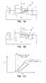
- FIG. 1Ais a block diagram of a metal oxide semiconductor field effect transistor (MOSFET) in a substrate according to the teachings of the prior art.
- MOSFETmetal oxide semiconductor field effect transistor
- FIG. 1Billustrates the MOSFET of FIG. 1A operated in the forward direction showing some degree of device degradation due to electrons being trapped in the gate oxide near the drain region over gradual use.
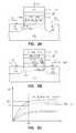
- FIG. 1Cis a graph showing the square root of the current signal (Ids) taken at the drain region of the conventional MOSFET versus the voltage potential (VGS) established between the gate and the source region.
- FIG. 2Ais a diagram of a programmed MOSFET which can be used as a write once read only memory cell according to the teachings of the present invention.
- FIG. 2Bis a diagram suitable for explaining the method by which the MOSFET of the write once read only memory cell of the present invention can be programmed to achieve the embodiments of the present invention.
- FIG. 2Cis a graph plotting the current signal (Ids) detected at the drain region versus a voltage potential, or drain voltage, (VDS) set up between the drain region and the source region (Ids vs. VDS).
- FIG. 3illustrates a portion of a memory array according to the teachings of the present invention.
- FIGS. 4 A- 4 Billustrates the operation of the novel write once read only memory cell formed according to the teachings of the present invention.
- FIG. 5illustrates the operation of a conventional DRAM cell.
- FIG. 6illustrates a memory device according to the teachings of the present invention.
- FIG. 7is a block diagram of an electrical system, or processor-based system, utilizing write once read only memory constructed in accordance with the present invention.
- wafer and substrate used in the following descriptioninclude any structure having an exposed surface with which to form the integrated circuit (IC) structure of the invention.
- substrateis understood to include semiconductor wafers.
- substrateis also used to refer to semiconductor structures during processing, and may include other layers that have been fabricated thereupon. Both wafer and substrate include doped and undoped semiconductors, epitaxial semiconductor layers supported by a base semiconductor or insulator, as well as other semiconductor structures well known to one skilled in the art.
- conductoris understood to include semiconductors, and the term insulator is defined to include any material that is less electrically conductive than the materials referred to as conductors.
- FIG. 1Ais useful in illustrating the conventional operation of a MOSFET such as can be used in a DRAM array.
- FIG. 1Aillustrates the normal hot electron injection and degradation of devices operated in the forward direction. As is explained below, since the electrons are trapped near the drain they are not very effective in changing the device characteristics.
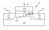
- FIG. 1Ais a block diagram of a metal oxide semiconductor field effect transistor (MOSFET) 101 in a substrate 100 .
- the MOSFET 101includes a source region 102 , a drain region 104 , a channel region 106 in the substrate 100 between the source region 102 and the drain region 104 .
- a gate 108is separated from the channel region 108 by a gate oxide 110 .
- a sourceline 112is coupled to the source region 102 .
- a bitline 114is coupled to the drain region 104 .
- a wordline 116is coupled to the gate 108 .
- a drain to source voltage potential(Vds) is set up between the drain region 104 and the source region 102 .
- a voltage potentialis then applied to the gate 108 via a wordline 116 .
- Vtcharacteristic voltage threshold
- a channel 106forms in the substrate 100 between the drain region 104 and the source region 102 . Formation of the channel 106 permits conduction between the drain region 104 and the source region 102 , and a current signal (Ids) can be detected at the drain region 104 .
- FIG. 1Cillustrates this point.
- FIG. 1Cis a graph showing the square root of the current signal (Ids) taken at the drain region versus the voltage potential (VGS) established between the gate 108 and the source region 102 .
- the change in the slope of the plot of ⁇ square root ⁇ square root over (Ids) ⁇ versus VGSrepresents the change in the charge carrier mobility in the channel 106 .
- AVTrepresents the minimal change in the MOSFET's threshold voltage resulting from electrons gradually being trapped in the gate oxide 110 near the drain region 104 , under normal operation, due to device degradation. This results in a fixed trapped charge in the gate oxide 110 near the drain region 104 .
- Slope 1represents the charge carrier mobility in the channel 106 for FIG. 1A having no electrons trapped in the gate oxide 110 .
- Slope 2represents the charge mobility in the channel 106 for the conventional MOSFET of FIG. 1B having electrons 117 trapped in the gate oxide 110 near the drain region 104 .
- slope 1 and slope 2 in FIG. 1Cthe electrons 117 trapped in the gate oxide 110 near the drain region 104 of the conventional MOSFET do not significantly change the charge mobility in the channel 106 .
- One componentincludes a threshold voltage shift due to the trapped electrons and a second component includes mobility degradation due to additional scattering of carrier electrons caused by this trapped charge and additional surface states.
- a conventional MOSFETdegrades, or is “stressed,” over operation in the forward direction, electrons do gradually get injected and become trapped in the gate oxide near the drain. In this portion of the conventional MOSFET there is virtually no channel underneath the gate oxide. Thus the trapped charge modulates the threshold voltage and charge mobility only slightly.
- the inventorshave previously described programmable memory devices and functions based on the reverse stressing of MOSFET's in a conventional CMOS process and technology in order to form programmable address decode and correction. (See generally, L. Forbes, W. P. Noble and E. H. Cloud, “MOSFET technology for programmable address-decode and correction,” application Ser. No. 09/383804). That disclosure, however, did not describe write once read only memory solutions, but rather address decode and correction issues. The inventors also describe write once read only memory cells employing charge trapping in gate insulators for conventional MOSFETs. The same is described in co-pending, commonly assigned U.S. patent application, entitled “Write Once Read Only Memory Employing Charge Trapping in Insulators,” attorney docket no. 1303.052US1, Ser. No. ______. The present application, however, describes write once read only memory cells formed from conventional flash memory device structures.
- normal flash memory cellscan be programmed by operation in the reverse direction and utilizing avalanche hot electron injection to trap electrons on the floating gate of the floating gate transistor.
- the programmed floating gate transistorWhen the programmed floating gate transistor is subsequently operated in the forward direction the electrons trapped on the floating gate cause the channel to have a different threshold voltage.
- the novel programmed floating gate transistors of the present inventionconduct significantly less current than conventional flash cells which have not been programmed. These electrons will remain trapped on the floating gate unless negative control gate voltages are applied. The electrons will not be removed from the floating gate when positive or zero control gate voltages are applied. Erasure can be accomplished by applying negative control gate voltages and/or increasing the temperature with negative control gate bias applied to cause the trapped electrons on the floating gate to be re-emitted back into the silicon channel of the MOSFET.
- FIG. 2Ais a diagram of a programmed floating gate transistor which can be used as a write once read only memory cell according to the teachings of the present invention.
- the write once read only memory cell 201includes a floating gate transistor in a substrate 200 which has a first source/drain region 202 , a second source/drain region 204 , and a channel region 206 between the first and second source/drain regions, 202 and 204 .
- the first source/drain region 202includes a source region 202 for the floating gate transistor and the second source/drain region 204 includes a drain region 204 for the floating gate transistor.
- FIG. 2Afurther illustrates a floating gate 208 separated from the channel region 206 by a floating gate insulator 210 .
- An array plate 212is coupled to the first source/drain region 202 and a transmission line 214 is coupled to the second source/drain region 204 .
- the transmission line 214includes a bit line 214 .
- a control gate 216is separated from the floating gate 208 by a gate dielectric 218 .
- write once read only memory cell 201is comprised of a programmed floating gate transistor.
- This programmed floating gate transistorhas a charge 217 trapped on the floating gate 208 .
- the charge 217 trapped on the floating gate 208includes a trapped electron charge 217 .
- FIG. 2Bis a diagram suitable for explaining the method by which the floating gate of the write once read only memory cell 201 of the present invention can be programmed to achieve the embodiments of the present invention.
- the methodincludes programming the floating gate transistor.
- Programming the floating gate transistorincludes applying a first voltage potential V1 to a drain region 204 of the floating gate transistor and a second voltage potential V2 to the source region 202 .
- applying a first voltage potential V1 to the drain region 204 of the floating gate transistorincludes grounding the drain region 204 of the floating gate transistor as shown in FIG. 2B.
- applying a second voltage potential V2 to the source region 202includes biasing the array plate 212 to a voltage higher than VDD, as shown in FIG. 2B.
- a gate potential VGSis applied to the control gate 216 of the floating gate transistor.
- the gate potential VGSincludes a voltage potential which is less than the second voltage potential V2, but which is sufficient to establish conduction in the channel 206 of the floating gate transistor between the drain region 204 and the source region 202 . As shown in FIG.
- applying the first, second and gate potentials (V1, V2, and VGS respectively) to the floating gate transistorcreates a hot electron injection into the floating gate 208 of the floating gate transistor adjacent to the source region 202 .
- applying the first, second and gate potentials (V1, V2, and VGS respectively)provides enough energy to the charge carriers, e.g. electrons, being conducted across the channel 206 that, once the charge carriers are near the source region 202 , a number of the charge carriers get excited into the floating gate 208 adjacent to the source region 202 . Here the charge carriers become trapped.
- applying a first voltage potential V1 to the drain region 204 of the floating gate transistorincludes biasing the drain region 204 of the floating gate transistor to a voltage higher than VDD.
- applying a second voltage potential V2 to the source region 202includes grounding the array plate 212 .
- a gate potential VGSis applied to the control gate 216 of the floating gate transistor.
- the gate potential VGSincludes a voltage potential which is less than the first voltage potential V1, but which is sufficient to establish conduction in the channel 206 of the floating gate transistor between the drain region 204 and the source region 202 .
- Applying the first, second and gate potentials (V1, V2, and VGS respectively) to the floating gate transistorcreates a hot electron injection into the floating gate 208 of the floating gate transistor adjacent to the drain region 204 .
- applying the first, second and gate potentials (V1, V2, and VGS respectively)provides enough energy to the charge carriers, e.g. electrons, being conducted across the channel 206 that, once the charge carriers are near the drain region 204 , a number of the charge carriers get excited into the floating gate 208 adjacent to the drain region 204 .
- the charge carriersbecome trapped as shown in FIG. 2A.
- the methodis continued by subsequently operating the floating gate transistor in the forward direction in its programmed state during a read operation.
- the read operationincludes grounding the source region 202 and precharging the drain region a fractional voltage of VDD. If the device is addressed by a wordline coupled to the gate, then its conductivity will be determined by the presence or absence of stored charge in the floating gate. That is, a gate potential can be applied to the control gate 216 by a wordline 220 in an effort to form a conduction channel between the source and the drain regions as done with addressing and reading conventional DRAM cells.
- FIG. 2Cis a graph plotting a current signal (IDS) detected at the second source/drain region 204 versus a voltage potential, or drain voltage, (VDS) set up between the second source/drain region 204 and the first source/drain region 202 (IDS vs. VDS).
- VDSrepresents the voltage potential set up between the drain region 204 and the source region 202 .
- the curve plotted as D 1represents the conduction behavior of a conventional floating gate transistor which is not programmed according to the teachings of the present invention.
- the curve D2represents the conduction behavior of the programmed floating gate transistor, described above in connection with FIG. 2A, according to the teachings of the present invention. As shown in FIG.
- the current signal (IDS 2 ) detected at the second source/drain region 204 for the programmed floating gate transistor (curve D2)is significantly lower than the current signal (IDS 1 ) detected at the second source/drain region 204 for the conventional floating gate cell which is not programmed according to the teachings of the present invention. Again, this is attributed to the fact that the channel 206 in the programmed floating gate transistor of the present invention has a different voltage threshold.
- NROMNonvolatile Memory Cell
- B. Eitan et al.“Characterization of Channel Hot Electron Injection by the Subthreshold Slope of NROM device,” IEEE Electron Device Lett., Vol. 22, No. 11, pp. 556-558, (Nov. 2001); B. Etian et al., “NROM: A novel localized Trapping, 2-Bit Nonvolatile Memory Cell,” IEEE Electron Device Lett., Vol. 21, No. 11, pp.
- the present inventiondisclosures programming a floating gate transistor to trap charge and reading the device to form a write once read only memory (WOROM) based on a modification of DRAM technology.
- WOROMwrite once read only memory
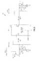
- FIG. 3illustrates a portion of a memory array 300 according to the teachings of the present invention.
- the memory in FIG. 3is shown illustrating a pair of write once read only floating gate memory cells 301 - 1 and 301 - 2 formed according to the teachings of the present invention.
- any number of write once and read only floating gate memory cellscan be organized in an array, but for ease of illustration only two are displayed in FIG. 3.
- a first source/drain region, 302 - 1 and 302 - 2 respectively,is coupled to an array plate 304 .
- a second source/drain region, 306 - 1 and 306 - 2 respectively,is coupled to a bitline, 308 - 1 and 308 - 2 respectively.
- Each of the bitlines, 308 - 1 and 308 - 2couple to a sense amplifier, shown generally at 310 .
- a wordline, 312 - 1 and 312 - 2 respectively,is couple to a control gate, 318 - 1 and 318 - 2 respectively, for each of the write once read only floating gate memory cells, 301 - 1 and 301 - 2 .
- a floating gate, 320 - 1 and 320 - 2 respectively,is separated from a channel region, 322 - 1 and 322 - 2 , in the write once read only floating gate memory cells, 301 - 1 and 301 - 2 , beneath the control gate, 318 - 1 and 318 - 2 .
- a write data/precharge circuitis shown at 324 for coupling a first or a second potential to bitline 308 - 1 .
- the write data/precharge circuit 324is adapted to couple either a ground to the bitline 308 - 1 during a write operation in the reverse direction, or alternatively to precharge the bitline 308 - 1 to fractional voltage of VDD during a read operation in the forward direction.
- the array plate 304can be biased to a voltage higher than VDD during a write operation in the reverse direction, or alternatively grounded during a read operation in the forward direction.
- the array structure 300has no capacitors. Instead, according to the teachings of the present invention, the first source/drain region or source region, 302 - 1 and 302 - 2 , are coupled via a conductive plug directly to the array plate 304 . In order to write, the array plate 304 is biased to voltage higher than VDD and the devices stressed in the reverse direction by grounding the data or bit line, 308 - 1 or 308 - 2 .
- the write once read only memory cell, 301 - 1 or 301 - 2is selected by a word line address, 312 - 1 or 312 - 2 , then the write once read only memory cell, 301 - 1 or 301 - 2 , will conduct and be stressed with accompanying hot electron injection into the cells floating gate, 320 - 1 or 320 - 2 , adjacent to the source region, 302 - 1 or 302 - 2 .
- the array plate 304can be grounded and the data or bit line, 308 - 1 or 308 - 2 driven to some voltage higher than VDD.
- the write once read only memory cell, 301 - 1 or 301 - 2is selected by a word line address, 312 - 1 or 312 - 2 , then the write once read only memory cell, 301 - 1 or 301 - 2 , will conduct and be stressed with accompanying hot electron injection into the cells floating gate, 320 - 1 or 320 - 2 , adjacent to the drain region, 306 - 1 or 306 - 2 .
- the write once read only floating gate memory cell, 301 - 1 or 301 - 2is operated in the forward direction with the array plate 304 grounded and the bit line, 308 - 1 or 308 - 2 , and respective second source/drain region or drain region, 306 - 1 and 306 - 2 , of the cells precharged to some fractional voltage of VDD. If the device is addressed by the word line, 312 - 1 or 312 - 2 , then its conductivity will be determined by the presence or absence of stored charge on the cells floating gate, 320 - 1 or 320 - 2 , and so detected using the sense amplifier 310 .
- DRAM sense amplifiersis described, for example, in U.S. Pat. Nos.
- the devicescan be subjected to hot electron stress in the reverse direction by biasing the array plate 304 , and read while grounding the array plate 304 to compare a stressed write once read only memory cell, e.g. cell 301 - 1 , to an unstressed dummy device/cell, e.g. 301 - 2 , as shown in FIG. 3.
- the write and possible erase featurecould be used during manufacture and test to initially program all cells or devices to have similar or matching conductivity before use in the field.
- the sense amplifier 310can then detect small differences in cell or device characteristics due to stress induced changes in device characteristics during the write operation.
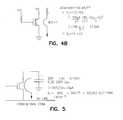
- FIGS. 4 A-B and 5are useful in illustrating the use of charge storage in the floating gate to modulate the conductivity of the write once read only floating gate memory cell according to the teachings of the present invention. That is, FIGS. 4 A- 4 B illustrates the operation of the novel write once read only floating gate memory cell 401 formed according to the teachings of the present invention. And, FIG. 5 illustrates the operation of a conventional DRAM cell 501 . As shown in FIG. 4A, the gate insulator 402 is made thicker than in a conventional DRAM cell, e.g. 501 and is equal to or greater than 10 nm or 100 ⁇ (10 ⁇ 6 cm). In the embodiment shown in FIG.
- a write once read only floating gate memory cellhaving dimensions of 0.1 ⁇ m (10 ⁇ 5 cm) by 0.1 ⁇ m.
- a charge of 10 12 electrons/cm 2is programmed into the floating gate of the write once read only floating gate memory cell.
- ⁇ Q10 12 electrons/cm 2 ⁇ 1.6 ⁇ 10 ⁇ 19 Coulombs.
- FIG. 4Baids to further illustrate the conduction behavior of the novel write once read only floating gate memory cell of the present invention.
- Vthe write once read only floating gate memory cell
- the nominal threshold voltage without the floating gate chargedis 1/2 V
- an un-written, or un-programmed write once read only floating gate memory cellcan conduct a current of the order 12.5 ⁇ A, whereas if the floating gate is charged then the write once read only floating gate memory cell will not conduct.
- the sense amplifiers used in DRAM arrayscan easily detect such differences in current on the bit lines.
- the floating gate transistors in the arrayare utilized not just as passive on or off switches as transfer devices in DRAM arrays but rather as active devices providing gain.
- to program the floating gate transistor “off,”requires only a stored charge in the floating gate of about 100 electrons if the area is 0.1 ⁇ m by 0.1 ⁇ m.
- the write once read only floating gate memory cellis un-programmed, e.g. no stored charge trapped in the floating gate, and if the floating gate transistor is addressed over 10 nS a of current of 12.5 ⁇ A is provided.
- the integrated drain currentthen has a charge of 125 fC or 800,000 electrons.
- FIG. 6a memory device is illustrated according to the teachings of the present invention.
- the memory device 640contains a memory array 642 , row and column decoders 644 , 648 and a sense amplifier circuit 646 .
- the memory array 642consists of a plurality of write once read only floating gate memory cells 600 , formed according to the teachings of the present invention whose word lines 680 and bit lines 660 are commonly arranged into rows and columns, respectively.
- the bit lines 660 of the memory array 642are connected to the sense amplifier circuit 646 , while its word lines 680 are connected to the row decoder 644 .
- Address and control signalsare input on address/control lines 661 into the memory device 640 and connected to the column decoder 648 , sense amplifier circuit 646 and row decoder 644 and are used to gain read and write access, among other things, to the memory array 642 .
- the column decoder 648is connected to the sense amplifier circuit 646 via control and column select signals on column select lines 662 .
- the sense amplifier circuit 646receives input data destined for the memory array 642 and outputs data read from the memory array 642 over input/output (I/O) data lines 663 .
- Datais read from the cells of the memory array 642 by activating a word line 680 (via the row decoder 644 ), which couples all of the memory cells corresponding to that word line to respective bit lines 660 , which define the columns of the array.
- One or more bit lines 660are also activated.
- the sense amplifier circuit 646 connected to a bit line columndetects and amplifies the conduction sensed through a given write once read only floating gate memory cell and transferred to its bit line 660 by measuring the potential difference between the activated bit line 660 and a reference line which may be an inactive bit line. Again, in the read operation the source region of a given cell is couple to a grounded array plate (not shown).
- the operation of Memory device sense amplifiersis described, for example, in U.S. Pat. Nos. 5,627,785; 5,280,205; and 5,042,011, all assigned to Micron Technology Inc., and incorporated by reference herein.
- FIG. 7is a block diagram of an electrical system, or processor-based system, 700 utilizing write once read only floating gate memory 712 constructed in accordance with the present invention. That is, the write once read only memory (WOROM) 712 utilizes the modified flash cell as explained and described in detail in connection with FIGS. 2 - 4 .
- the processor-based system 700may be a computer system, a process control system or any other system employing a processor and associated memory.
- the system 700includes a central processing unit (CPU) 702 , e.g., a microprocessor, that communicates with the write once read only floating gate memory 712 and an I/O device 708 over a bus 720 .
- CPUcentral processing unit
- bus 720may be a series of buses and bridges commonly used in a processor-based system, but for convenience purposes only, the bus 720 has been illustrated as a single bus.
- a second I/O device 710is illustrated, but is not necessary to practice the invention.
- the processor-based system 700can also includes read-only memory (ROM) 714 and may include peripheral devices such as a floppy disk drive 704 and a compact disk (CD) ROM drive 706 that also communicates with the CPU 702 over the bus 720 as is well known in the art.
- ROMread-only memory
- CDcompact disk
- At least one of the write once read only floating gate memory cell in WOROM 712includes a programmed flash cell.
- FIG. 7illustrates an embodiment for electronic system circuitry in which the novel memory cells of the present invention are used.
- the illustration of system 700is intended to provide a general understanding of one application for the structure and circuitry of the present invention, and is not intended to serve as a complete description of all the elements and features of an electronic system using the novel memory cell structures.
- the inventionis equally applicable to any size and type of memory device 700 using the novel memory cells of the present invention and is not intended to be limited to that described above.
- such an electronic systemcan be fabricated in single-package processing units, or even on a single semiconductor chip, in order to reduce the communication time between the processor and the memory device.
- Applications containing the novel memory cell of the present invention as described in this disclosureinclude electronic systems for use in memory modules, device drivers, power modules, communication modems, processor modules, and application-specific modules, and may include multilayer, multichip modules.
- Such circuitrycan further be a subcomponent of a variety of electronic systems, such as a clock, a television, a cell phone, a personal computer, an automobile, an industrial control system, an aircraft, and others.
Landscapes
- Engineering & Computer Science (AREA)
- Microelectronics & Electronic Packaging (AREA)
- Non-Volatile Memory (AREA)
- Semiconductor Memories (AREA)
Abstract
Description
- This application is related to the following co-pending, commonly assigned U.S. patent applications: “Write Once Read Only Memory Employing Charge Trapping in Insulators,” attorney docket no. 1303.052US1, Ser. No. ______, which are filed on even date herewith and each of which disclosure is herein incorporated by reference.[0001]
- The present invention relates generally to semiconductor integrated circuits and, more particularly, to write once read only memory employing floating gates.[0002]
- Many electronic products need various amounts of memory to store information, e.g. data. One common type of high speed, low cost memory includes dynamic random access memory (DRAM) comprised of individual DRAM cells arranged in arrays. DRAM cells include an access transistor, e.g a metal oxide semiconducting field effect transistor (MOSFET), coupled to a capacitor cell. Another type of high speed, low cost memory includes floating gate memory cells. A conventional horizontal floating gate transistor structure includes a source region and a drain region separated by a channel region in a horizontal substrate. A floating gate is separated by a thin tunnel gate oxide. The structure is programmed by storing a charge on the floating gate. A control gate is separated from the floating gate by an intergate dielectric. A charge stored on the floating gate effects the conductivity of the cell when a read voltage potential is applied to the control gate. The state of cell can thus be determined by sensing a change in the device conductivity between the programmed and un-programmed states.[0003]
- With successive generations of DRAM chips, an emphasis continues to be placed on increasing array density and maximizing chip real estate while minimizing the cost of manufacture. It is further desirable to increase array density with little or no modification of the DRAM optimized process flow.[0004]
- A requirement exists for memory devices which need only be programmed once, as for instance to function as an electronic film in a camera. If the memory arrays have a very high density then they can store a large number of very high resolution images in a digital camera. If the memory is inexpensive then it can for instance replace the light sensitive films which are used to store images in conventional cameras.[0005]
- Thus, there is a need for improved DRAM technology compatible write once read only memory. It is desirable that such write once read only memory be fabricated on a DRAM chip with little or no modification of the DRAM process flow. It is further desirable that such write once read only memory operate with lower programming voltages than that used by conventional DRAM cells, yet still hold sufficient charge to withstand the effects of parasitic capacitances and noise due to circuit operation.[0006]
- The above mentioned problems for creating DRAM technology compatible write once read only memory cells as well as other problems are addressed by the present invention and will be understood by reading and studying the following specification. This disclosure teaches structures and methods using floating gate devices as write once read only memory in a DRAM integrated circuit. The structures and methods use the existing process sequence for MOSFET's in DRAM technology.[0007]
- In particular, an illustrative embodiment of the present invention includes a write once read only memory cell. The write once read only memory cell includes a floating gate transistor. The floating gate transistor has a first source/drain region, a second source/drain region, a channel region between the first and the second source/drain regions, a floating gate separated from the channel region by a gate insulator, and a control gate separated from the floating gate by a gate dielectric. A plug couples the first source/drain region to an array plate. A bitline is coupled to the second source/drain region. The floating gate transistor can be programmed by operation in a reverse direction trapping charge on the floating gate adjacent to the first source/drain region such that the programmed floating gate transistor operates at reduced drain source current when read in a forward direction.[0008]
- These and other embodiments, aspects, advantages, and features of the present invention will be set forth in part in the description which follows, and in part will become apparent to those skilled in the art by reference to the following description of the invention and referenced drawings or by practice of the invention. The aspects, advantages, and features of the invention are realized and attained by means of the instrumentalities, procedures, and combinations particularly pointed out in the appended claims.[0009]
- FIG. 1A is a block diagram of a metal oxide semiconductor field effect transistor (MOSFET) in a substrate according to the teachings of the prior art.[0010]
- FIG. 1B illustrates the MOSFET of FIG. 1A operated in the forward direction showing some degree of device degradation due to electrons being trapped in the gate oxide near the drain region over gradual use.[0011]
- FIG. 1C is a graph showing the square root of the current signal (Ids) taken at the drain region of the conventional MOSFET versus the voltage potential (VGS) established between the gate and the source region.[0012]
- FIG. 2A is a diagram of a programmed MOSFET which can be used as a write once read only memory cell according to the teachings of the present invention.[0013]
- FIG. 2B is a diagram suitable for explaining the method by which the MOSFET of the write once read only memory cell of the present invention can be programmed to achieve the embodiments of the present invention.[0014]
- FIG. 2C is a graph plotting the current signal (Ids) detected at the drain region versus a voltage potential, or drain voltage, (VDS) set up between the drain region and the source region (Ids vs. VDS).[0015]
- FIG. 3 illustrates a portion of a memory array according to the teachings of the present invention.[0016]
- FIGS.[0017]4A-4B illustrates the operation of the novel write once read only memory cell formed according to the teachings of the present invention.
- FIG. 5 illustrates the operation of a conventional DRAM cell.[0018]
- FIG. 6 illustrates a memory device according to the teachings of the present invention.[0019]
- FIG. 7 is a block diagram of an electrical system, or processor-based system, utilizing write once read only memory constructed in accordance with the present invention.[0020]
- In the following detailed description of the Invention, reference is made to the accompanying drawings which form a part hereof, and in which is shown, by way of illustration, specific embodiments in which the invention may be practiced. In the drawings, like numerals describe substantially similar components throughout the several views. These embodiments are described in sufficient detail to enable those skilled in the art to practice the invention. Other embodiments may be utilized and structural, logical, and electrical changes may be made without departing from the scope of the present invention.[0021]
- The terms wafer and substrate used in the following description include any structure having an exposed surface with which to form the integrated circuit (IC) structure of the invention. The term substrate is understood to include semiconductor wafers. The term substrate is also used to refer to semiconductor structures during processing, and may include other layers that have been fabricated thereupon. Both wafer and substrate include doped and undoped semiconductors, epitaxial semiconductor layers supported by a base semiconductor or insulator, as well as other semiconductor structures well known to one skilled in the art. The term conductor is understood to include semiconductors, and the term insulator is defined to include any material that is less electrically conductive than the materials referred to as conductors. The following detailed description is, therefore, not to be taken in a limiting sense, and the scope of the present invention is defined only by the appended claims, along with the full scope of equivalents to which such claims are entitled.[0022]
- FIG. 1A is useful in illustrating the conventional operation of a MOSFET such as can be used in a DRAM array. FIG. 1A illustrates the normal hot electron injection and degradation of devices operated in the forward direction. As is explained below, since the electrons are trapped near the drain they are not very effective in changing the device characteristics.[0023]
- FIG. 1A is a block diagram of a metal oxide semiconductor field effect transistor (MOSFET)[0024]101 in a
substrate 100. TheMOSFET 101 includes asource region 102, adrain region 104, achannel region 106 in thesubstrate 100 between thesource region 102 and thedrain region 104. Agate 108 is separated from thechannel region 108 by agate oxide 110. Asourceline 112 is coupled to thesource region 102. Abitline 114 is coupled to thedrain region 104. Awordline 116 is coupled to thegate 108. - In conventional operation, a drain to source voltage potential (Vds) is set up between the[0025]
drain region 104 and thesource region 102. A voltage potential is then applied to thegate 108 via awordline 116. Once the voltage potential applied to thegate 108 surpasses the characteristic voltage threshold (Vt) of the MOSFET achannel 106 forms in thesubstrate 100 between thedrain region 104 and thesource region 102. Formation of thechannel 106 permits conduction between thedrain region 104 and thesource region 102, and a current signal (Ids) can be detected at thedrain region 104. - In operation of the conventional MOSFET of FIG. 1A, some degree of device degradation does gradually occur for MOSFETs operated in the forward direction by[0026]
electrons 117 becoming trapped in thegate oxide 110 near thedrain region 104. This effect is illustrated in FIG. 1B. However, since theelectrons 117 are trapped near thedrain region 104 they are not very effective in changing the MOSFET characteristics. - FIG. 1C illustrates this point. FIG. 1C is a graph showing the square root of the current signal (Ids) taken at the drain region versus the voltage potential (VGS) established between the[0027]
gate 108 and thesource region 102. The change in the slope of the plot of {square root}{square root over (Ids)} versus VGS represents the change in the charge carrier mobility in thechannel 106. - In FIG. 1C, AVT represents the minimal change in the MOSFET's threshold voltage resulting from electrons gradually being trapped in the[0028]
gate oxide 110 near thedrain region 104, under normal operation, due to device degradation. This results in a fixed trapped charge in thegate oxide 110 near thedrain region 104.Slope 1 represents the charge carrier mobility in thechannel 106 for FIG. 1A having no electrons trapped in thegate oxide 110.Slope 2 represents the charge mobility in thechannel 106 for the conventional MOSFET of FIG.1B having electrons 117 trapped in thegate oxide 110 near thedrain region 104. As shown by a comparison ofslope 1 andslope 2 in FIG. 1C, theelectrons 117 trapped in thegate oxide 110 near thedrain region 104 of the conventional MOSFET do not significantly change the charge mobility in thechannel 106. - There are two components to the effects of stress and hot electron injection. One component includes a threshold voltage shift due to the trapped electrons and a second component includes mobility degradation due to additional scattering of carrier electrons caused by this trapped charge and additional surface states. When a conventional MOSFET degrades, or is “stressed,” over operation in the forward direction, electrons do gradually get injected and become trapped in the gate oxide near the drain. In this portion of the conventional MOSFET there is virtually no channel underneath the gate oxide. Thus the trapped charge modulates the threshold voltage and charge mobility only slightly.[0029]
- The inventors have previously described programmable memory devices and functions based on the reverse stressing of MOSFET's in a conventional CMOS process and technology in order to form programmable address decode and correction. (See generally, L. Forbes, W. P. Noble and E. H. Cloud, “MOSFET technology for programmable address-decode and correction,” application Ser. No. 09/383804). That disclosure, however, did not describe write once read only memory solutions, but rather address decode and correction issues. The inventors also describe write once read only memory cells employing charge trapping in gate insulators for conventional MOSFETs. The same is described in co-pending, commonly assigned U.S. patent application, entitled “Write Once Read Only Memory Employing Charge Trapping in Insulators,” attorney docket no. 1303.052US1, Ser. No. ______. The present application, however, describes write once read only memory cells formed from conventional flash memory device structures.[0030]
- According to the teachings of the present invention, normal flash memory cells can be programmed by operation in the reverse direction and utilizing avalanche hot electron injection to trap electrons on the floating gate of the floating gate transistor. When the programmed floating gate transistor is subsequently operated in the forward direction the electrons trapped on the floating gate cause the channel to have a different threshold voltage. The novel programmed floating gate transistors of the present invention conduct significantly less current than conventional flash cells which have not been programmed. These electrons will remain trapped on the floating gate unless negative control gate voltages are applied. The electrons will not be removed from the floating gate when positive or zero control gate voltages are applied. Erasure can be accomplished by applying negative control gate voltages and/or increasing the temperature with negative control gate bias applied to cause the trapped electrons on the floating gate to be re-emitted back into the silicon channel of the MOSFET.[0031]
- FIG. 2A is a diagram of a programmed floating gate transistor which can be used as a write once read only memory cell according to the teachings of the present invention. As shown in FIG. 2A the write once read only[0032]
memory cell 201 includes a floating gate transistor in asubstrate 200 which has a first source/drain region 202, a second source/drain region 204, and achannel region 206 between the first and second source/drain regions,202 and204. In one embodiment, the first source/drain region 202 includes asource region 202 for the floating gate transistor and the second source/drain region 204 includes adrain region 204 for the floating gate transistor. FIG. 2A further illustrates a floatinggate 208 separated from thechannel region 206 by a floatinggate insulator 210. Anarray plate 212 is coupled to the first source/drain region 202 and atransmission line 214 is coupled to the second source/drain region 204. In one embodiment, thetransmission line 214 includes abit line 214. Further as shown in FIG. 2A, acontrol gate 216 is separated from the floatinggate 208 by agate dielectric 218. - As stated above, write once read only[0033]
memory cell 201 is comprised of a programmed floating gate transistor. This programmed floating gate transistor has acharge 217 trapped on the floatinggate 208. In one embodiment, thecharge 217 trapped on the floatinggate 208 includes a trappedelectron charge 217. - FIG. 2B is a diagram suitable for explaining the method by which the floating gate of the write once read only[0034]
memory cell 201 of the present invention can be programmed to achieve the embodiments of the present invention. As shown in FIG. 2B the method includes programming the floating gate transistor. Programming the floating gate transistor includes applying a first voltage potential V1 to adrain region 204 of the floating gate transistor and a second voltage potential V2 to thesource region 202. - In one embodiment, applying a first voltage potential V1 to the[0035]
drain region 204 of the floating gate transistor includes grounding thedrain region 204 of the floating gate transistor as shown in FIG. 2B. In this embodiment, applying a second voltage potential V2 to thesource region 202 includes biasing thearray plate 212 to a voltage higher than VDD, as shown in FIG. 2B. A gate potential VGS is applied to thecontrol gate 216 of the floating gate transistor. In one embodiment, the gate potential VGS includes a voltage potential which is less than the second voltage potential V2, but which is sufficient to establish conduction in thechannel 206 of the floating gate transistor between thedrain region 204 and thesource region 202. As shown in FIG. 2B, applying the first, second and gate potentials (V1, V2, and VGS respectively) to the floating gate transistor creates a hot electron injection into the floatinggate 208 of the floating gate transistor adjacent to thesource region 202. In other words, applying the first, second and gate potentials (V1, V2, and VGS respectively) provides enough energy to the charge carriers, e.g. electrons, being conducted across thechannel 206 that, once the charge carriers are near thesource region 202, a number of the charge carriers get excited into the floatinggate 208 adjacent to thesource region 202. Here the charge carriers become trapped. - In an alternative embodiment, applying a first voltage potential V1 to the[0036]
drain region 204 of the floating gate transistor includes biasing thedrain region 204 of the floating gate transistor to a voltage higher than VDD. In this embodiment, applying a second voltage potential V2 to thesource region 202 includes grounding thearray plate 212. A gate potential VGS is applied to thecontrol gate 216 of the floating gate transistor. In one embodiment, the gate potential VGS includes a voltage potential which is less than the first voltage potential V1, but which is sufficient to establish conduction in thechannel 206 of the floating gate transistor between thedrain region 204 and thesource region 202. Applying the first, second and gate potentials (V1, V2, and VGS respectively) to the floating gate transistor creates a hot electron injection into the floatinggate 208 of the floating gate transistor adjacent to thedrain region 204. In other words, applying the first, second and gate potentials (V1, V2, and VGS respectively) provides enough energy to the charge carriers, e.g. electrons, being conducted across thechannel 206 that, once the charge carriers are near thedrain region 204, a number of the charge carriers get excited into the floatinggate 208 adjacent to thedrain region 204. Here the charge carriers become trapped as shown in FIG. 2A. - In one embodiment of the present invention, the method is continued by subsequently operating the floating gate transistor in the forward direction in its programmed state during a read operation. Accordingly, the read operation includes grounding the[0037]
source region 202 and precharging the drain region a fractional voltage of VDD. If the device is addressed by a wordline coupled to the gate, then its conductivity will be determined by the presence or absence of stored charge in the floating gate. That is, a gate potential can be applied to thecontrol gate 216 by awordline 220 in an effort to form a conduction channel between the source and the drain regions as done with addressing and reading conventional DRAM cells. - However, now in its programmed state, the[0038]
conduction channel 206 of the floating gate transistor will have a higher voltage threshold - FIG. 2C is a graph plotting a current signal (IDS) detected at the second source/[0039]
drain region 204 versus a voltage potential, or drain voltage, (VDS) set up between the second source/drain region 204 and the first source/drain region202 (IDS vs. VDS). In one embodiment, VDS represents the voltage potential set up between thedrain region 204 and thesource region 202. In FIG. 2C, the curve plotted as D1 represents the conduction behavior of a conventional floating gate transistor which is not programmed according to the teachings of the present invention. The curve D2 represents the conduction behavior of the programmed floating gate transistor, described above in connection with FIG. 2A, according to the teachings of the present invention. As shown in FIG. 2C, for a particular drain voltage, VDS, the current signal (IDS2) detected at the second source/drain region 204 for the programmed floating gate transistor (curve D2) is significantly lower than the current signal (IDS1) detected at the second source/drain region 204 for the conventional floating gate cell which is not programmed according to the teachings of the present invention. Again, this is attributed to the fact that thechannel 206 in the programmed floating gate transistor of the present invention has a different voltage threshold. - Some of these effects have recently been described for use in a different device structure, called an NROM, for flash memories. This latter work in Israel and Germany is based on employing charge trapping in a silicon nitride layer in a non-conventional flash memory device structure. (See generally, B. Eitan et al., “Characterization of Channel Hot Electron Injection by the Subthreshold Slope of NROM device,” IEEE Electron Device Lett., Vol. 22, No. 11, pp. 556-558, (Nov. 2001); B. Etian et al., “NROM: A novel localized Trapping, 2-Bit Nonvolatile Memory Cell,” IEEE Electron Device Lett., Vol. 21, No. 11, pp. 543-545, (Nov. 2000)). Charge trapping in silicon nitride gate insulators was the basic mechanism used in MNOS memory devices (see generally, S. Sze, Physics of Semiconductor Devices, Wiley, N.Y., 1981, pp. 504-506), charge trapping in aluminum oxide gates was the mechanism used in MIOS memory devices (see generally, S. Sze, Physics of Semiconductor Devices, Wiley, N.Y., 1981, pp. 504-506), and the present inventors have previously disclosed charge trapping at isolated point defects in gate insulators (see generally, L. Forbes and J. Geusic, “Memory using insulator traps,” U.S. Pat. No. 6,140,181, issued Oct. 31, 2000). However, none of the above described references addressed forming write once read only memory cells in conventional flash memory cell device structures.[0040]
- That is, in contrast to the above work, the present invention disclosures programming a floating gate transistor to trap charge and reading the device to form a write once read only memory (WOROM) based on a modification of DRAM technology.[0041]
- FIG. 3 illustrates a portion of a[0042]
memory array 300 according to the teachings of the present invention. The memory in FIG. 3, is shown illustrating a pair of write once read only floating gate memory cells301-1 and301-2 formed according to the teachings of the present invention. As one of ordinary skill in the art will understand upon reading this disclosure, any number of write once and read only floating gate memory cells can be organized in an array, but for ease of illustration only two are displayed in FIG. 3. As shown in FIG. 3, a first source/drain region,302-1 and302-2 respectively, is coupled to anarray plate 304. A second source/drain region,306-1 and306-2 respectively, is coupled to a bitline,308-1 and308-2 respectively. Each of the bitlines,308-1 and308-2, couple to a sense amplifier, shown generally at310. A wordline,312-1 and312-2 respectively, is couple to a control gate,318-1 and318-2 respectively, for each of the write once read only floating gate memory cells,301-1 and301-2. A floating gate,320-1 and320-2 respectively, is separated from a channel region,322-1 and322-2, in the write once read only floating gate memory cells,301-1 and301-2, beneath the control gate,318-1 and318-2. Finally, a write data/precharge circuit is shown at324 for coupling a first or a second potential to bitline308-1. As one of ordinary skill in the art will understand upon reading this disclosure, the write data/precharge circuit 324 is adapted to couple either a ground to the bitline308-1 during a write operation in the reverse direction, or alternatively to precharge the bitline308-1 to fractional voltage of VDD during a read operation in the forward direction. As one of ordinary skill in the art will understand upon reading this disclosure, thearray plate 304 can be biased to a voltage higher than VDD during a write operation in the reverse direction, or alternatively grounded during a read operation in the forward direction. - As shown in FIG. 3, the[0043]
array structure 300 has no capacitors. Instead, according to the teachings of the present invention, the first source/drain region or source region,302-1 and302-2, are coupled via a conductive plug directly to thearray plate 304. In order to write, thearray plate 304 is biased to voltage higher than VDD and the devices stressed in the reverse direction by grounding the data or bit line,308-1 or308-2. If the write once read only memory cell,301-1 or301-2, is selected by a word line address,312-1 or312-2, then the write once read only memory cell,301-1 or301-2, will conduct and be stressed with accompanying hot electron injection into the cells floating gate,320-1 or320-2, adjacent to the source region,302-1 or302-2. Alternatively, thearray plate 304 can be grounded and the data or bit line,308-1 or308-2 driven to some voltage higher than VDD. Again, if the write once read only memory cell,301-1 or301-2, is selected by a word line address,312-1 or312-2, then the write once read only memory cell,301-1 or301-2, will conduct and be stressed with accompanying hot electron injection into the cells floating gate,320-1 or320-2, adjacent to the drain region,306-1 or306-2. During read, the write once read only floating gate memory cell,301-1 or301-2, is operated in the forward direction with thearray plate 304 grounded and the bit line,308-1 or308-2, and respective second source/drain region or drain region,306-1 and306-2, of the cells precharged to some fractional voltage of VDD. If the device is addressed by the word line,312-1 or312-2, then its conductivity will be determined by the presence or absence of stored charge on the cells floating gate,320-1 or320-2, and so detected using thesense amplifier 310. The operation of DRAM sense amplifiers is described, for example, in U.S. Pat. Nos. 5,627,785; 5,280,205; and 5,042,011, all assigned to Micron Technology Inc., and incorporated by reference herein. The array would thus be addressed and read in the conventional manner used in DRAM's, but programmed as write once read only memory cells in a novel fashion. - In operation the devices can be subjected to hot electron stress in the reverse direction by biasing the[0044]
array plate 304, and read while grounding thearray plate 304 to compare a stressed write once read only memory cell, e.g. cell301-1, to an unstressed dummy device/cell, e.g.301-2, as shown in FIG. 3. The write and possible erase feature could be used during manufacture and test to initially program all cells or devices to have similar or matching conductivity before use in the field. Thesense amplifier 310 can then detect small differences in cell or device characteristics due to stress induced changes in device characteristics during the write operation. - As one of ordinary skill in the art will understand upon reading this disclosure such arrays of write once read only memory cells are conveniently realized by a modification of DRAM technology. That is, the transfer devices in the DRAM arrays are replaced by flash memory type devices with floating gates. Conventional transistors for address decode and sense amplifiers can be fabricated after this step with normal thin gate insulators of silicon oxide. Because the devices in the array have a floating gate they can be erased by biasing the control or address gate with a large negative potential.[0045]
- FIGS.[0046]4A-B and5 are useful in illustrating the use of charge storage in the floating gate to modulate the conductivity of the write once read only floating gate memory cell according to the teachings of the present invention. That is, FIGS.4A-4B illustrates the operation of the novel write once read only floating gate memory cell401 formed according to the teachings of the present invention. And, FIG. 5 illustrates the operation of a conventional DRAM cell501. As shown in FIG. 4A, the
gate insulator 402 is made thicker than in a conventional DRAM cell, e.g.501 and is equal to or greater than 10 nm or 100 Å (10−6cm). In the embodiment shown in FIG. 4A a write once read only floating gate memory cell is illustrated having dimensions of 0.1 μm (10−5cm) by 0.1 μm. The capacitance, Ci, of the structure depends on the dielectric constant, ε1, (given here as 0.3×10⁻¹²F/cm), and the thickness of the insulating layers, t, (given here as 10−6cm), such that Ci=εi/t, Farads/cm2or 3×10⁻⁷F/cm2. In one embodiment, a charge of 1012electrons/cm2is programmed into the floating gate of the write once read only floating gate memory cell. This produces a stored charge ΔQ=1012electrons/cm2×1.6×10−19Coulombs. In this embodiment, the resulting change in the threshold voltage (ΔVt) of the write once read only floating gate memory cell will be approximately 0.5 Volts (ΔVt=ΔQ/Ci or 1.6×10⁻⁷/3×10−7=1/2 Volt). For ΔQ=1012electrons/cm3in the dimensions given above, this embodiment of the present invention involves trapping a charge of approximately 100 electrons in the floating gate of the write once read only floating gate memory cell. - FIG. 4B aids to further illustrate the conduction behavior of the novel write once read only floating gate memory cell of the present invention. As one of ordinary skill in the art will understand upon reading this disclosure, if the write once read only floating gate memory cell is being driven with a control gate voltage of 1.0 Volt (V) and the nominal threshold voltage without the floating gate charged is 1/2 V, then if the floating gate is charged the floating gate transistor of the present invention will be off and not conduct. That is, by trapping a charge of approximately 100 electrons in the floating gate of the write once read only floating gate memory cell, having dimensions of 0.1 μm (10[0047]−5cm) by 0.1 μm, will raise the threshold voltage of the write once read only floating gate memory cell to 1.0 Volt and a 1.0 Volt control gate potential will not be sufficient to turn the device on, e.g. Vt=1.0V, I=0.
- Conversely, if the nominal threshold voltage without the floating gate charged is 1/2, then I=μC[0048]OX×(W/L)×((Vgs−Vt)2/2), or 12.5 μA, with μCOX=μC1=100 μA/V2and W/L=1. That is, the write once read only floating gate memory cell of the present invention, having the dimensions describe above will produce a current I=100 μA/V2×(1/4)×(1/2)=12.5 μA. Thus, in the present invention an un-written, or un-programmed write once read only floating gate memory cell can conduct a current of the order 12.5 μA, whereas if the floating gate is charged then the write once read only floating gate memory cell will not conduct. As one of ordinary skill in the art will understand upon reading this disclosure, the sense amplifiers used in DRAM arrays, and as describe above, can easily detect such differences in current on the bit lines.
- By way of comparison, in a conventional DRAM with 30 femtoFarad (fF) storage capacitors charged to 50 femtoColumbs (fC), if these are read over 5 nS then the average current on the bit line is only 10 μA. This is illustrated in connection with FIG. 5. As shown in FIG. 5, storing a 50 fC charge on the storage capacitor equates to storing 300,000 electrons.[0049]
- According to the teachings of the present invention, the floating gate transistors in the array are utilized not just as passive on or off switches as transfer devices in DRAM arrays but rather as active devices providing gain. In the present invention, to program the floating gate transistor “off,” requires only a stored charge in the floating gate of about 100 electrons if the area is 0.1 μm by 0.1 μm. And, if the write once read only floating gate memory cell is un-programmed, e.g. no stored charge trapped in the floating gate, and if the floating gate transistor is addressed over 10 nS a of current of 12.5 μA is provided. The integrated drain current then has a charge of 125 fC or 800,000 electrons. This is in comparison to the charge on a DRAM capacitor of 50 fC which is only about 300,000 electrons. Hence, the use of the floating gate transistors in the array as active devices with gain, rather than just switches, provides an amplification of the stored charge, in the floating gate, from 100 to 800,000 electrons over a read address period of 10 nS.[0050]
- In FIG. 6 a memory device is illustrated according to the teachings of the present invention. The[0051]
memory device 640 contains amemory array 642, row andcolumn decoders sense amplifier circuit 646. Thememory array 642 consists of a plurality of write once read only floating gate memory cells600, formed according to the teachings of the present invention whose word lines680 andbit lines 660 are commonly arranged into rows and columns, respectively. The bit lines660 of thememory array 642 are connected to thesense amplifier circuit 646, while itsword lines 680 are connected to therow decoder 644. Address and control signals are input on address/control lines 661 into thememory device 640 and connected to thecolumn decoder 648,sense amplifier circuit 646 androw decoder 644 and are used to gain read and write access, among other things, to thememory array 642. - The[0052]
column decoder 648 is connected to thesense amplifier circuit 646 via control and column select signals on columnselect lines 662. Thesense amplifier circuit 646 receives input data destined for thememory array 642 and outputs data read from thememory array 642 over input/output (I/O) data lines663. Data is read from the cells of thememory array 642 by activating a word line680 (via the row decoder644), which couples all of the memory cells corresponding to that word line torespective bit lines 660, which define the columns of the array. One ormore bit lines 660 are also activated. When aparticular word line 680 andbit lines 660 are activated, thesense amplifier circuit 646 connected to a bit line column detects and amplifies the conduction sensed through a given write once read only floating gate memory cell and transferred to itsbit line 660 by measuring the potential difference between the activatedbit line 660 and a reference line which may be an inactive bit line. Again, in the read operation the source region of a given cell is couple to a grounded array plate (not shown). The operation of Memory device sense amplifiers is described, for example, in U.S. Pat. Nos. 5,627,785; 5,280,205; and 5,042,011, all assigned to Micron Technology Inc., and incorporated by reference herein. - FIG. 7 is a block diagram of an electrical system, or processor-based system,[0053]700 utilizing write once read only floating gate memory712 constructed in accordance with the present invention. That is, the write once read only memory (WOROM)712 utilizes the modified flash cell as explained and described in detail in connection with FIGS.2-4. The processor-based
system 700 may be a computer system, a process control system or any other system employing a processor and associated memory. Thesystem 700 includes a central processing unit (CPU)702, e.g., a microprocessor, that communicates with the write once read only floating gate memory712 and an I/O device 708 over abus 720. It must be noted that thebus 720 may be a series of buses and bridges commonly used in a processor-based system, but for convenience purposes only, thebus 720 has been illustrated as a single bus. A second I/O device710 is illustrated, but is not necessary to practice the invention. The processor-basedsystem 700 can also includes read-only memory (ROM)714 and may include peripheral devices such as afloppy disk drive 704 and a compact disk (CD)ROM drive 706 that also communicates with theCPU 702 over thebus 720 as is well known in the art. - It will be appreciated by those skilled in the art that additional circuitry and control signals can be provided, and that the[0054]
memory device 700 has been simplified to help focus on the invention. At least one of the write once read only floating gate memory cell in WOROM712 includes a programmed flash cell. - It will be understood that the embodiment shown in FIG. 7 illustrates an embodiment for electronic system circuitry in which the novel memory cells of the present invention are used. The illustration of[0055]
system 700, as shown in FIG. 7, is intended to provide a general understanding of one application for the structure and circuitry of the present invention, and is not intended to serve as a complete description of all the elements and features of an electronic system using the novel memory cell structures. Further, the invention is equally applicable to any size and type ofmemory device 700 using the novel memory cells of the present invention and is not intended to be limited to that described above. As one of ordinary skill in the art will understand, such an electronic system can be fabricated in single-package processing units, or even on a single semiconductor chip, in order to reduce the communication time between the processor and the memory device. - Applications containing the novel memory cell of the present invention as described in this disclosure include electronic systems for use in memory modules, device drivers, power modules, communication modems, processor modules, and application-specific modules, and may include multilayer, multichip modules. Such circuitry can further be a subcomponent of a variety of electronic systems, such as a clock, a television, a cell phone, a personal computer, an automobile, an industrial control system, an aircraft, and others.[0056]
- Conclusion[0057]
- Utilization of a modification of well established DRAM technology and arrays will serve to afford an inexpensive memory device which can be regarded as disposable if the information is later transferred to another medium, for instance CDROM's. The high density of DRAM array structures will afford the storage of a large volume of digital data or images at a very low cost per bit. There are many applications where the data need only be written once, the low cost of these memories will make it more efficient to just utilize a new memory array, and dispose of the old memory array, rather than trying to erase and reuse these arrays as is done with current flash memories.[0058]
- It is to be understood that the above description is intended to be illustrative, and not restrictive. Many other embodiments will be apparent to those of skill in the art upon reviewing the above description. The scope of the invention should, therefore, be determined with reference to the appended claims, along with the full scope of equivalents to which such claims are entitled.[0059]
Claims (39)
Priority Applications (3)
| Application Number | Priority Date | Filing Date | Title |
|---|---|---|---|
| US10/177,083US7193893B2 (en) | 2002-06-21 | 2002-06-21 | Write once read only memory employing floating gates |
| US11/215,496US7130220B2 (en) | 2002-06-21 | 2005-08-30 | Write once read only memory employing floating gates |
| US11/215,618US7369435B2 (en) | 2002-06-21 | 2005-08-30 | Write once read only memory employing floating gates |
Applications Claiming Priority (1)
| Application Number | Priority Date | Filing Date | Title |
|---|---|---|---|
| US10/177,083US7193893B2 (en) | 2002-06-21 | 2002-06-21 | Write once read only memory employing floating gates |
Related Child Applications (2)
| Application Number | Title | Priority Date | Filing Date |
|---|---|---|---|
| US11/215,618DivisionUS7369435B2 (en) | 2002-06-21 | 2005-08-30 | Write once read only memory employing floating gates |
| US11/215,496DivisionUS7130220B2 (en) | 2002-06-21 | 2005-08-30 | Write once read only memory employing floating gates |
Publications (2)
| Publication Number | Publication Date |
|---|---|
| US20030235077A1true US20030235077A1 (en) | 2003-12-25 |
| US7193893B2 US7193893B2 (en) | 2007-03-20 |
Family
ID=29734289
Family Applications (3)
| Application Number | Title | Priority Date | Filing Date |
|---|---|---|---|
| US10/177,083Expired - LifetimeUS7193893B2 (en) | 2002-06-21 | 2002-06-21 | Write once read only memory employing floating gates |
| US11/215,496Expired - LifetimeUS7130220B2 (en) | 2002-06-21 | 2005-08-30 | Write once read only memory employing floating gates |
| US11/215,618Expired - LifetimeUS7369435B2 (en) | 2002-06-21 | 2005-08-30 | Write once read only memory employing floating gates |
Family Applications After (2)
| Application Number | Title | Priority Date | Filing Date |
|---|---|---|---|
| US11/215,496Expired - LifetimeUS7130220B2 (en) | 2002-06-21 | 2005-08-30 | Write once read only memory employing floating gates |
| US11/215,618Expired - LifetimeUS7369435B2 (en) | 2002-06-21 | 2005-08-30 | Write once read only memory employing floating gates |
Country Status (1)
| Country | Link |
|---|---|
| US (3) | US7193893B2 (en) |
Cited By (10)
| Publication number | Priority date | Publication date | Assignee | Title |
|---|---|---|---|---|
| US20040004245A1 (en)* | 2002-07-08 | 2004-01-08 | Micron Technology, Inc. | Memory utilizing oxide-conductor nanolaminates |
| US20040114433A1 (en)* | 2001-02-13 | 2004-06-17 | Micron Technology, Inc. | Programmable fuse and antifuse and method therefor |
| US20040151029A1 (en)* | 1999-08-26 | 2004-08-05 | Micron Technology, Inc. | Programmable memory cell using charge trapping in a gate oxide |
| US7112494B2 (en) | 2002-06-21 | 2006-09-26 | Micron Technology, Inc. | Write once read only memory employing charge trapping in insulators |
| US7154140B2 (en)* | 2002-06-21 | 2006-12-26 | Micron Technology, Inc. | Write once read only memory with large work function floating gates |
| US7221586B2 (en) | 2002-07-08 | 2007-05-22 | Micron Technology, Inc. | Memory utilizing oxide nanolaminates |
| US7348237B2 (en) | 2002-06-21 | 2008-03-25 | Micron Technology, Inc. | NOR flash memory cell with high storage density |
| US7369435B2 (en) | 2002-06-21 | 2008-05-06 | Micron Technology, Inc. | Write once read only memory employing floating gates |
| US7489545B2 (en) | 2002-07-08 | 2009-02-10 | Micron Technology, Inc. | Memory utilizing oxide-nitride nanolaminates |
| US7709402B2 (en) | 2006-02-16 | 2010-05-04 | Micron Technology, Inc. | Conductive layers for hafnium silicon oxynitride films |
Families Citing this family (251)
| Publication number | Priority date | Publication date | Assignee | Title |
|---|---|---|---|---|
| US6958302B2 (en)* | 2002-12-04 | 2005-10-25 | Micron Technology, Inc. | Atomic layer deposited Zr-Sn-Ti-O films using TiI4 |
| US7101813B2 (en) | 2002-12-04 | 2006-09-05 | Micron Technology Inc. | Atomic layer deposited Zr-Sn-Ti-O films |
| US7588988B2 (en) | 2004-08-31 | 2009-09-15 | Micron Technology, Inc. | Method of forming apparatus having oxide films formed using atomic layer deposition |
| KR100689211B1 (en)* | 2004-12-11 | 2007-03-08 | 경북대학교 산학협력단 | Saddle-type OS element |
| US7972974B2 (en) | 2006-01-10 | 2011-07-05 | Micron Technology, Inc. | Gallium lanthanide oxide films |
| JP4997882B2 (en)* | 2006-09-05 | 2012-08-08 | ソニー株式会社 | Nonvolatile semiconductor memory device and writing method thereof |
| US20090016118A1 (en)* | 2007-07-12 | 2009-01-15 | Silicon Storage Technology, Inc. | Non-volatile dram with floating gate and method of operation |
| US8373439B2 (en) | 2009-04-14 | 2013-02-12 | Monolithic 3D Inc. | 3D semiconductor device |
| US9711407B2 (en) | 2009-04-14 | 2017-07-18 | Monolithic 3D Inc. | Method of manufacturing a three dimensional integrated circuit by transfer of a mono-crystalline layer |
| US8405420B2 (en) | 2009-04-14 | 2013-03-26 | Monolithic 3D Inc. | System comprising a semiconductor device and structure |
| US9577642B2 (en) | 2009-04-14 | 2017-02-21 | Monolithic 3D Inc. | Method to form a 3D semiconductor device |
| US8362482B2 (en) | 2009-04-14 | 2013-01-29 | Monolithic 3D Inc. | Semiconductor device and structure |
| US8058137B1 (en) | 2009-04-14 | 2011-11-15 | Monolithic 3D Inc. | Method for fabrication of a semiconductor device and structure |
| US8754533B2 (en) | 2009-04-14 | 2014-06-17 | Monolithic 3D Inc. | Monolithic three-dimensional semiconductor device and structure |
| US8378715B2 (en) | 2009-04-14 | 2013-02-19 | Monolithic 3D Inc. | Method to construct systems |
| US8258810B2 (en) | 2010-09-30 | 2012-09-04 | Monolithic 3D Inc. | 3D semiconductor device |
| US8362800B2 (en) | 2010-10-13 | 2013-01-29 | Monolithic 3D Inc. | 3D semiconductor device including field repairable logics |
| US7986042B2 (en) | 2009-04-14 | 2011-07-26 | Monolithic 3D Inc. | Method for fabrication of a semiconductor device and structure |
| US8384426B2 (en) | 2009-04-14 | 2013-02-26 | Monolithic 3D Inc. | Semiconductor device and structure |
| US9509313B2 (en) | 2009-04-14 | 2016-11-29 | Monolithic 3D Inc. | 3D semiconductor device |
| US8395191B2 (en) | 2009-10-12 | 2013-03-12 | Monolithic 3D Inc. | Semiconductor device and structure |
| US8427200B2 (en) | 2009-04-14 | 2013-04-23 | Monolithic 3D Inc. | 3D semiconductor device |
| US8669778B1 (en) | 2009-04-14 | 2014-03-11 | Monolithic 3D Inc. | Method for design and manufacturing of a 3D semiconductor device |
| US8581349B1 (en) | 2011-05-02 | 2013-11-12 | Monolithic 3D Inc. | 3D memory semiconductor device and structure |
| US10354995B2 (en) | 2009-10-12 | 2019-07-16 | Monolithic 3D Inc. | Semiconductor memory device and structure |
| US8536023B2 (en) | 2010-11-22 | 2013-09-17 | Monolithic 3D Inc. | Method of manufacturing a semiconductor device and structure |
| US11018133B2 (en) | 2009-10-12 | 2021-05-25 | Monolithic 3D Inc. | 3D integrated circuit |
| US10157909B2 (en) | 2009-10-12 | 2018-12-18 | Monolithic 3D Inc. | 3D semiconductor device and structure |
| US10366970B2 (en) | 2009-10-12 | 2019-07-30 | Monolithic 3D Inc. | 3D semiconductor device and structure |
| US8450804B2 (en) | 2011-03-06 | 2013-05-28 | Monolithic 3D Inc. | Semiconductor device and structure for heat removal |
| US8148728B2 (en) | 2009-10-12 | 2012-04-03 | Monolithic 3D, Inc. | Method for fabrication of a semiconductor device and structure |
| US9099424B1 (en) | 2012-08-10 | 2015-08-04 | Monolithic 3D Inc. | Semiconductor system, device and structure with heat removal |
| US11984445B2 (en) | 2009-10-12 | 2024-05-14 | Monolithic 3D Inc. | 3D semiconductor devices and structures with metal layers |
| US10043781B2 (en) | 2009-10-12 | 2018-08-07 | Monolithic 3D Inc. | 3D semiconductor device and structure |
| US10910364B2 (en) | 2009-10-12 | 2021-02-02 | Monolitaic 3D Inc. | 3D semiconductor device |
| US10388863B2 (en) | 2009-10-12 | 2019-08-20 | Monolithic 3D Inc. | 3D memory device and structure |
| US11374118B2 (en) | 2009-10-12 | 2022-06-28 | Monolithic 3D Inc. | Method to form a 3D integrated circuit |
| US12027518B1 (en) | 2009-10-12 | 2024-07-02 | Monolithic 3D Inc. | 3D semiconductor devices and structures with metal layers |
| US8476145B2 (en) | 2010-10-13 | 2013-07-02 | Monolithic 3D Inc. | Method of fabricating a semiconductor device and structure |
| US8742476B1 (en) | 2012-11-27 | 2014-06-03 | Monolithic 3D Inc. | Semiconductor device and structure |
| US8026521B1 (en) | 2010-10-11 | 2011-09-27 | Monolithic 3D Inc. | Semiconductor device and structure |
| US8492886B2 (en) | 2010-02-16 | 2013-07-23 | Monolithic 3D Inc | 3D integrated circuit with logic |
| US9099526B2 (en) | 2010-02-16 | 2015-08-04 | Monolithic 3D Inc. | Integrated circuit device and structure |
| US8541819B1 (en) | 2010-12-09 | 2013-09-24 | Monolithic 3D Inc. | Semiconductor device and structure |
| US8373230B1 (en) | 2010-10-13 | 2013-02-12 | Monolithic 3D Inc. | Method for fabrication of a semiconductor device and structure |
| US8298875B1 (en) | 2011-03-06 | 2012-10-30 | Monolithic 3D Inc. | Method for fabrication of a semiconductor device and structure |
| US8461035B1 (en) | 2010-09-30 | 2013-06-11 | Monolithic 3D Inc. | Method for fabrication of a semiconductor device and structure |
| US9219005B2 (en) | 2011-06-28 | 2015-12-22 | Monolithic 3D Inc. | Semiconductor system and device |
| US8642416B2 (en) | 2010-07-30 | 2014-02-04 | Monolithic 3D Inc. | Method of forming three dimensional integrated circuit devices using layer transfer technique |
| US9953925B2 (en) | 2011-06-28 | 2018-04-24 | Monolithic 3D Inc. | Semiconductor system and device |
| US10217667B2 (en) | 2011-06-28 | 2019-02-26 | Monolithic 3D Inc. | 3D semiconductor device, fabrication method and system |
| US8901613B2 (en) | 2011-03-06 | 2014-12-02 | Monolithic 3D Inc. | Semiconductor device and structure for heat removal |
| US10497713B2 (en) | 2010-11-18 | 2019-12-03 | Monolithic 3D Inc. | 3D semiconductor memory device and structure |
| US8273610B2 (en) | 2010-11-18 | 2012-09-25 | Monolithic 3D Inc. | Method of constructing a semiconductor device and structure |
| US8163581B1 (en) | 2010-10-13 | 2012-04-24 | Monolith IC 3D | Semiconductor and optoelectronic devices |
| US11482440B2 (en) | 2010-12-16 | 2022-10-25 | Monolithic 3D Inc. | 3D semiconductor device and structure with a built-in test circuit for repairing faulty circuits |
| US12362219B2 (en) | 2010-11-18 | 2025-07-15 | Monolithic 3D Inc. | 3D semiconductor memory device and structure |
| US11227897B2 (en) | 2010-10-11 | 2022-01-18 | Monolithic 3D Inc. | Method for producing a 3D semiconductor memory device and structure |
| US11469271B2 (en) | 2010-10-11 | 2022-10-11 | Monolithic 3D Inc. | Method to produce 3D semiconductor devices and structures with memory |
| US11158674B2 (en) | 2010-10-11 | 2021-10-26 | Monolithic 3D Inc. | Method to produce a 3D semiconductor device and structure |
| US11018191B1 (en) | 2010-10-11 | 2021-05-25 | Monolithic 3D Inc. | 3D semiconductor device and structure |
| US11600667B1 (en) | 2010-10-11 | 2023-03-07 | Monolithic 3D Inc. | Method to produce 3D semiconductor devices and structures with memory |
| US11024673B1 (en) | 2010-10-11 | 2021-06-01 | Monolithic 3D Inc. | 3D semiconductor device and structure |
| US10290682B2 (en) | 2010-10-11 | 2019-05-14 | Monolithic 3D Inc. | 3D IC semiconductor device and structure with stacked memory |
| US11315980B1 (en) | 2010-10-11 | 2022-04-26 | Monolithic 3D Inc. | 3D semiconductor device and structure with transistors |
| US8114757B1 (en) | 2010-10-11 | 2012-02-14 | Monolithic 3D Inc. | Semiconductor device and structure |
| US10896931B1 (en) | 2010-10-11 | 2021-01-19 | Monolithic 3D Inc. | 3D semiconductor device and structure |
| US11257867B1 (en) | 2010-10-11 | 2022-02-22 | Monolithic 3D Inc. | 3D semiconductor device and structure with oxide bonds |
| US11869915B2 (en) | 2010-10-13 | 2024-01-09 | Monolithic 3D Inc. | Multilevel semiconductor device and structure with image sensors and wafer bonding |
| US11984438B2 (en) | 2010-10-13 | 2024-05-14 | Monolithic 3D Inc. | Multilevel semiconductor device and structure with oxide bonding |
| US11404466B2 (en) | 2010-10-13 | 2022-08-02 | Monolithic 3D Inc. | Multilevel semiconductor device and structure with image sensors |
| US11855114B2 (en) | 2010-10-13 | 2023-12-26 | Monolithic 3D Inc. | Multilevel semiconductor device and structure with image sensors and wafer bonding |
| US12080743B2 (en) | 2010-10-13 | 2024-09-03 | Monolithic 3D Inc. | Multilevel semiconductor device and structure with image sensors and wafer bonding |
| US11043523B1 (en) | 2010-10-13 | 2021-06-22 | Monolithic 3D Inc. | Multilevel semiconductor device and structure with image sensors |
| US11694922B2 (en) | 2010-10-13 | 2023-07-04 | Monolithic 3D Inc. | Multilevel semiconductor device and structure with oxide bonding |
| US12360310B2 (en) | 2010-10-13 | 2025-07-15 | Monolithic 3D Inc. | Multilevel semiconductor device and structure with oxide bonding |
| US12094892B2 (en) | 2010-10-13 | 2024-09-17 | Monolithic 3D Inc. | 3D micro display device and structure |
| US11164898B2 (en) | 2010-10-13 | 2021-11-02 | Monolithic 3D Inc. | Multilevel semiconductor device and structure |
| US11163112B2 (en) | 2010-10-13 | 2021-11-02 | Monolithic 3D Inc. | Multilevel semiconductor device and structure with electromagnetic modulators |
| US8379458B1 (en) | 2010-10-13 | 2013-02-19 | Monolithic 3D Inc. | Semiconductor device and structure |
| US10943934B2 (en) | 2010-10-13 | 2021-03-09 | Monolithic 3D Inc. | Multilevel semiconductor device and structure |
| US9197804B1 (en) | 2011-10-14 | 2015-11-24 | Monolithic 3D Inc. | Semiconductor and optoelectronic devices |
| US10978501B1 (en) | 2010-10-13 | 2021-04-13 | Monolithic 3D Inc. | Multilevel semiconductor device and structure with waveguides |
| US11929372B2 (en) | 2010-10-13 | 2024-03-12 | Monolithic 3D Inc. | Multilevel semiconductor device and structure with image sensors and wafer bonding |
| US10998374B1 (en) | 2010-10-13 | 2021-05-04 | Monolithic 3D Inc. | Multilevel semiconductor device and structure |
| US8283215B2 (en) | 2010-10-13 | 2012-10-09 | Monolithic 3D Inc. | Semiconductor and optoelectronic devices |
| US11855100B2 (en) | 2010-10-13 | 2023-12-26 | Monolithic 3D Inc. | Multilevel semiconductor device and structure with oxide bonding |
| US11327227B2 (en) | 2010-10-13 | 2022-05-10 | Monolithic 3D Inc. | Multilevel semiconductor device and structure with electromagnetic modulators |
| US11133344B2 (en) | 2010-10-13 | 2021-09-28 | Monolithic 3D Inc. | Multilevel semiconductor device and structure with image sensors |
| US10833108B2 (en) | 2010-10-13 | 2020-11-10 | Monolithic 3D Inc. | 3D microdisplay device and structure |
| US10679977B2 (en) | 2010-10-13 | 2020-06-09 | Monolithic 3D Inc. | 3D microdisplay device and structure |
| US11063071B1 (en) | 2010-10-13 | 2021-07-13 | Monolithic 3D Inc. | Multilevel semiconductor device and structure with waveguides |
| US11437368B2 (en) | 2010-10-13 | 2022-09-06 | Monolithic 3D Inc. | Multilevel semiconductor device and structure with oxide bonding |
| US11605663B2 (en) | 2010-10-13 | 2023-03-14 | Monolithic 3D Inc. | Multilevel semiconductor device and structure with image sensors and wafer bonding |
| US11508605B2 (en) | 2010-11-18 | 2022-11-22 | Monolithic 3D Inc. | 3D semiconductor memory device and structure |
| US11735462B2 (en) | 2010-11-18 | 2023-08-22 | Monolithic 3D Inc. | 3D semiconductor device and structure with single-crystal layers |
| US11615977B2 (en) | 2010-11-18 | 2023-03-28 | Monolithic 3D Inc. | 3D semiconductor memory device and structure |
| US11610802B2 (en) | 2010-11-18 | 2023-03-21 | Monolithic 3D Inc. | Method for producing a 3D semiconductor device and structure with single crystal transistors and metal gate electrodes |
| US11784082B2 (en) | 2010-11-18 | 2023-10-10 | Monolithic 3D Inc. | 3D semiconductor device and structure with bonding |
| US11355381B2 (en) | 2010-11-18 | 2022-06-07 | Monolithic 3D Inc. | 3D semiconductor memory device and structure |
| US11355380B2 (en) | 2010-11-18 | 2022-06-07 | Monolithic 3D Inc. | Methods for producing 3D semiconductor memory device and structure utilizing alignment marks |
| US11121021B2 (en) | 2010-11-18 | 2021-09-14 | Monolithic 3D Inc. | 3D semiconductor device and structure |
| US11004719B1 (en) | 2010-11-18 | 2021-05-11 | Monolithic 3D Inc. | Methods for producing a 3D semiconductor memory device and structure |
| US11495484B2 (en) | 2010-11-18 | 2022-11-08 | Monolithic 3D Inc. | 3D semiconductor devices and structures with at least two single-crystal layers |
| US12144190B2 (en) | 2010-11-18 | 2024-11-12 | Monolithic 3D Inc. | 3D semiconductor device and structure with bonding and memory cells preliminary class |
| US11107721B2 (en) | 2010-11-18 | 2021-08-31 | Monolithic 3D Inc. | 3D semiconductor device and structure with NAND logic |
| US11482439B2 (en) | 2010-11-18 | 2022-10-25 | Monolithic 3D Inc. | Methods for producing a 3D semiconductor memory device comprising charge trap junction-less transistors |
| US11901210B2 (en) | 2010-11-18 | 2024-02-13 | Monolithic 3D Inc. | 3D semiconductor device and structure with memory |
| US11923230B1 (en) | 2010-11-18 | 2024-03-05 | Monolithic 3D Inc. | 3D semiconductor device and structure with bonding |
| US11804396B2 (en) | 2010-11-18 | 2023-10-31 | Monolithic 3D Inc. | Methods for producing a 3D semiconductor device and structure with memory cells and multiple metal layers |
| US11854857B1 (en) | 2010-11-18 | 2023-12-26 | Monolithic 3D Inc. | Methods for producing a 3D semiconductor device and structure with memory cells and multiple metal layers |
| US11018042B1 (en) | 2010-11-18 | 2021-05-25 | Monolithic 3D Inc. | 3D semiconductor memory device and structure |
| US11482438B2 (en) | 2010-11-18 | 2022-10-25 | Monolithic 3D Inc. | Methods for producing a 3D semiconductor memory device and structure |
| US12272586B2 (en) | 2010-11-18 | 2025-04-08 | Monolithic 3D Inc. | 3D semiconductor memory device and structure with memory and metal layers |
| US11862503B2 (en) | 2010-11-18 | 2024-01-02 | Monolithic 3D Inc. | Method for producing a 3D semiconductor device and structure with memory cells and multiple metal layers |
| US11443971B2 (en) | 2010-11-18 | 2022-09-13 | Monolithic 3D Inc. | 3D semiconductor device and structure with memory |
| US11094576B1 (en) | 2010-11-18 | 2021-08-17 | Monolithic 3D Inc. | Methods for producing a 3D semiconductor memory device and structure |
| US11521888B2 (en) | 2010-11-18 | 2022-12-06 | Monolithic 3D Inc. | 3D semiconductor device and structure with high-k metal gate transistors |
| US11211279B2 (en) | 2010-11-18 | 2021-12-28 | Monolithic 3D Inc. | Method for processing a 3D integrated circuit and structure |
| US12125737B1 (en) | 2010-11-18 | 2024-10-22 | Monolithic 3D Inc. | 3D semiconductor device and structure with metal layers and memory cells |
| US11031275B2 (en) | 2010-11-18 | 2021-06-08 | Monolithic 3D Inc. | 3D semiconductor device and structure with memory |
| US12243765B2 (en) | 2010-11-18 | 2025-03-04 | Monolithic 3D Inc. | 3D semiconductor device and structure with metal layers and memory cells |
| US12033884B2 (en) | 2010-11-18 | 2024-07-09 | Monolithic 3D Inc. | Methods for producing a 3D semiconductor device and structure with memory cells and multiple metal layers |
| US12154817B1 (en) | 2010-11-18 | 2024-11-26 | Monolithic 3D Inc. | Methods for producing a 3D semiconductor memory device and structure |
| US11569117B2 (en) | 2010-11-18 | 2023-01-31 | Monolithic 3D Inc. | 3D semiconductor device and structure with single-crystal layers |
| US12068187B2 (en) | 2010-11-18 | 2024-08-20 | Monolithic 3D Inc. | 3D semiconductor device and structure with bonding and DRAM memory cells |
| US11164770B1 (en) | 2010-11-18 | 2021-11-02 | Monolithic 3D Inc. | Method for producing a 3D semiconductor memory device and structure |
| US12100611B2 (en) | 2010-11-18 | 2024-09-24 | Monolithic 3D Inc. | Methods for producing a 3D semiconductor device and structure with memory cells and multiple metal layers |
| US12136562B2 (en) | 2010-11-18 | 2024-11-05 | Monolithic 3D Inc. | 3D semiconductor device and structure with single-crystal layers |
| US8975670B2 (en) | 2011-03-06 | 2015-03-10 | Monolithic 3D Inc. | Semiconductor device and structure for heat removal |
| US9384962B2 (en) | 2011-04-07 | 2016-07-05 | United Microelectronics Corp. | Oxygen treatment of replacement work-function metals in CMOS transistor gates |
| US8673758B2 (en) | 2011-06-16 | 2014-03-18 | United Microelectronics Corp. | Structure of metal gate and fabrication method thereof |
| US8536038B2 (en) | 2011-06-21 | 2013-09-17 | United Microelectronics Corp. | Manufacturing method for metal gate using ion implantation |
| US10388568B2 (en) | 2011-06-28 | 2019-08-20 | Monolithic 3D Inc. | 3D semiconductor device and system |
| US8486790B2 (en) | 2011-07-18 | 2013-07-16 | United Microelectronics Corp. | Manufacturing method for metal gate |
| US8551876B2 (en) | 2011-08-18 | 2013-10-08 | United Microelectronics Corp. | Manufacturing method for semiconductor device having metal gate |
| US8872286B2 (en) | 2011-08-22 | 2014-10-28 | United Microelectronics Corp. | Metal gate structure and fabrication method thereof |
| KR101884824B1 (en) | 2011-09-07 | 2018-08-03 | 삼성디스플레이 주식회사 | Thin film transistor and manufacturing method thereof |
| US8687399B2 (en) | 2011-10-02 | 2014-04-01 | Monolithic 3D Inc. | Semiconductor device and structure |
| US9029173B2 (en) | 2011-10-18 | 2015-05-12 | Monolithic 3D Inc. | Method for fabrication of a semiconductor device and structure |
| US8691681B2 (en) | 2012-01-04 | 2014-04-08 | United Microelectronics Corp. | Semiconductor device having a metal gate and fabricating method thereof |
| US8860181B2 (en) | 2012-03-07 | 2014-10-14 | United Microelectronics Corp. | Thin film resistor structure |
| US9000557B2 (en) | 2012-03-17 | 2015-04-07 | Zvi Or-Bach | Semiconductor device and structure |
| US8557632B1 (en) | 2012-04-09 | 2013-10-15 | Monolithic 3D Inc. | Method for fabrication of a semiconductor device and structure |
| US11088050B2 (en) | 2012-04-09 | 2021-08-10 | Monolithic 3D Inc. | 3D semiconductor device with isolation layers |
| US11735501B1 (en) | 2012-04-09 | 2023-08-22 | Monolithic 3D Inc. | 3D semiconductor device and structure with metal layers and a connective path |
| US11410912B2 (en) | 2012-04-09 | 2022-08-09 | Monolithic 3D Inc. | 3D semiconductor device with vias and isolation layers |
| US11594473B2 (en) | 2012-04-09 | 2023-02-28 | Monolithic 3D Inc. | 3D semiconductor device and structure with metal layers and a connective path |
| US11164811B2 (en) | 2012-04-09 | 2021-11-02 | Monolithic 3D Inc. | 3D semiconductor device with isolation layers and oxide-to-oxide bonding |
| US10600888B2 (en) | 2012-04-09 | 2020-03-24 | Monolithic 3D Inc. | 3D semiconductor device |
| US11694944B1 (en) | 2012-04-09 | 2023-07-04 | Monolithic 3D Inc. | 3D semiconductor device and structure with metal layers and a connective path |
| US11881443B2 (en) | 2012-04-09 | 2024-01-23 | Monolithic 3D Inc. | 3D semiconductor device and structure with metal layers and a connective path |
| US11616004B1 (en) | 2012-04-09 | 2023-03-28 | Monolithic 3D Inc. | 3D semiconductor device and structure with metal layers and a connective path |
| US11476181B1 (en) | 2012-04-09 | 2022-10-18 | Monolithic 3D Inc. | 3D semiconductor device and structure with metal layers |
| US9105623B2 (en) | 2012-05-25 | 2015-08-11 | United Microelectronics Corp. | Semiconductor device having metal gate and manufacturing method thereof |
| US8975666B2 (en) | 2012-08-22 | 2015-03-10 | United Microelectronics Corp. | MOS transistor and process thereof |
| US8925098B2 (en) | 2012-11-15 | 2014-12-30 | Elwha Llc | Data security and access tracking in memory |
| US8686428B1 (en) | 2012-11-16 | 2014-04-01 | Monolithic 3D Inc. | Semiconductor device and structure |
| US8574929B1 (en) | 2012-11-16 | 2013-11-05 | Monolithic 3D Inc. | Method to form a 3D semiconductor device and structure |
| US9054172B2 (en) | 2012-12-05 | 2015-06-09 | United Microelectrnics Corp. | Semiconductor structure having contact plug and method of making the same |
| US12051674B2 (en) | 2012-12-22 | 2024-07-30 | Monolithic 3D Inc. | 3D semiconductor device and structure with metal layers |
| US11217565B2 (en) | 2012-12-22 | 2022-01-04 | Monolithic 3D Inc. | Method to form a 3D semiconductor device and structure |
| US8674470B1 (en) | 2012-12-22 | 2014-03-18 | Monolithic 3D Inc. | Semiconductor device and structure |
| US11916045B2 (en) | 2012-12-22 | 2024-02-27 | Monolithic 3D Inc. | 3D semiconductor device and structure with metal layers |
| US11063024B1 (en) | 2012-12-22 | 2021-07-13 | Monlithic 3D Inc. | Method to form a 3D semiconductor device and structure |
| US11961827B1 (en) | 2012-12-22 | 2024-04-16 | Monolithic 3D Inc. | 3D semiconductor device and structure with metal layers |
| US11967583B2 (en) | 2012-12-22 | 2024-04-23 | Monolithic 3D Inc. | 3D semiconductor device and structure with metal layers |
| US11784169B2 (en) | 2012-12-22 | 2023-10-10 | Monolithic 3D Inc. | 3D semiconductor device and structure with metal layers |
| US11309292B2 (en) | 2012-12-22 | 2022-04-19 | Monolithic 3D Inc. | 3D semiconductor device and structure with metal layers |
| US11018116B2 (en) | 2012-12-22 | 2021-05-25 | Monolithic 3D Inc. | Method to form a 3D semiconductor device and structure |
| US11004694B1 (en) | 2012-12-29 | 2021-05-11 | Monolithic 3D Inc. | 3D semiconductor device and structure |
| US9385058B1 (en) | 2012-12-29 | 2016-07-05 | Monolithic 3D Inc. | Semiconductor device and structure |
| US10651054B2 (en) | 2012-12-29 | 2020-05-12 | Monolithic 3D Inc. | 3D semiconductor device and structure |
| US11430667B2 (en) | 2012-12-29 | 2022-08-30 | Monolithic 3D Inc. | 3D semiconductor device and structure with bonding |
| US10600657B2 (en) | 2012-12-29 | 2020-03-24 | Monolithic 3D Inc | 3D semiconductor device and structure |
| US10892169B2 (en) | 2012-12-29 | 2021-01-12 | Monolithic 3D Inc. | 3D semiconductor device and structure |
| US10903089B1 (en) | 2012-12-29 | 2021-01-26 | Monolithic 3D Inc. | 3D semiconductor device and structure |
| US11430668B2 (en) | 2012-12-29 | 2022-08-30 | Monolithic 3D Inc. | 3D semiconductor device and structure with bonding |
| US11087995B1 (en) | 2012-12-29 | 2021-08-10 | Monolithic 3D Inc. | 3D semiconductor device and structure |
| US12249538B2 (en) | 2012-12-29 | 2025-03-11 | Monolithic 3D Inc. | 3D semiconductor device and structure including power distribution grids |
| US10115663B2 (en) | 2012-12-29 | 2018-10-30 | Monolithic 3D Inc. | 3D semiconductor device and structure |
| US11177140B2 (en) | 2012-12-29 | 2021-11-16 | Monolithic 3D Inc. | 3D semiconductor device and structure |
| US9871034B1 (en) | 2012-12-29 | 2018-01-16 | Monolithic 3D Inc. | Semiconductor device and structure |
| US8735269B1 (en) | 2013-01-15 | 2014-05-27 | United Microelectronics Corp. | Method for forming semiconductor structure having TiN layer |
| US12094965B2 (en) | 2013-03-11 | 2024-09-17 | Monolithic 3D Inc. | 3D semiconductor device and structure with metal layers and memory cells |
| US8902663B1 (en) | 2013-03-11 | 2014-12-02 | Monolithic 3D Inc. | Method of maintaining a memory state |
| US10325651B2 (en) | 2013-03-11 | 2019-06-18 | Monolithic 3D Inc. | 3D semiconductor device with stacked memory |
| US11935949B1 (en) | 2013-03-11 | 2024-03-19 | Monolithic 3D Inc. | 3D semiconductor device and structure with metal layers and memory cells |
| US11869965B2 (en) | 2013-03-11 | 2024-01-09 | Monolithic 3D Inc. | 3D semiconductor device and structure with metal layers and memory cells |
| US10840239B2 (en) | 2014-08-26 | 2020-11-17 | Monolithic 3D Inc. | 3D semiconductor device and structure |
| US11923374B2 (en) | 2013-03-12 | 2024-03-05 | Monolithic 3D Inc. | 3D semiconductor device and structure with metal layers |
| US12100646B2 (en) | 2013-03-12 | 2024-09-24 | Monolithic 3D Inc. | 3D semiconductor device and structure with metal layers |
| US8994404B1 (en) | 2013-03-12 | 2015-03-31 | Monolithic 3D Inc. | Semiconductor device and structure |
| US11088130B2 (en) | 2014-01-28 | 2021-08-10 | Monolithic 3D Inc. | 3D semiconductor device and structure |
| US11398569B2 (en) | 2013-03-12 | 2022-07-26 | Monolithic 3D Inc. | 3D semiconductor device and structure |
| US9117749B1 (en) | 2013-03-15 | 2015-08-25 | Monolithic 3D Inc. | Semiconductor device and structure |
| US10224279B2 (en) | 2013-03-15 | 2019-03-05 | Monolithic 3D Inc. | Semiconductor device and structure |
| US11341309B1 (en) | 2013-04-15 | 2022-05-24 | Monolithic 3D Inc. | Automation for monolithic 3D devices |
| US11030371B2 (en) | 2013-04-15 | 2021-06-08 | Monolithic 3D Inc. | Automation for monolithic 3D devices |
| US11487928B2 (en) | 2013-04-15 | 2022-11-01 | Monolithic 3D Inc. | Automation for monolithic 3D devices |
| US11574109B1 (en) | 2013-04-15 | 2023-02-07 | Monolithic 3D Inc | Automation methods for 3D integrated circuits and devices |
| US11270055B1 (en) | 2013-04-15 | 2022-03-08 | Monolithic 3D Inc. | Automation for monolithic 3D devices |
| US11720736B2 (en) | 2013-04-15 | 2023-08-08 | Monolithic 3D Inc. | Automation methods for 3D integrated circuits and devices |
| US9021414B1 (en) | 2013-04-15 | 2015-04-28 | Monolithic 3D Inc. | Automation for monolithic 3D devices |
| US9653300B2 (en) | 2013-04-16 | 2017-05-16 | United Microelectronics Corp. | Structure of metal gate structure and manufacturing method of the same |
| US9159798B2 (en) | 2013-05-03 | 2015-10-13 | United Microelectronics Corp. | Replacement gate process and device manufactured using the same |
| US9196542B2 (en) | 2013-05-22 | 2015-11-24 | United Microelectronics Corp. | Method for manufacturing semiconductor devices |
| US8921947B1 (en) | 2013-06-10 | 2014-12-30 | United Microelectronics Corp. | Multi-metal gate semiconductor device having triple diameter metal opening |
| US9105720B2 (en) | 2013-09-11 | 2015-08-11 | United Microelectronics Corp. | Semiconductor device having metal gate and manufacturing method thereof |
| US20150069534A1 (en) | 2013-09-11 | 2015-03-12 | United Microelectronics Corp. | Semiconductor device and method for fabricating the same |
| US9196546B2 (en) | 2013-09-13 | 2015-11-24 | United Microelectronics Corp. | Metal gate transistor |
| US11031394B1 (en) | 2014-01-28 | 2021-06-08 | Monolithic 3D Inc. | 3D semiconductor device and structure |
| US11107808B1 (en) | 2014-01-28 | 2021-08-31 | Monolithic 3D Inc. | 3D semiconductor device and structure |
| US10297586B2 (en) | 2015-03-09 | 2019-05-21 | Monolithic 3D Inc. | Methods for processing a 3D semiconductor device |
| US12094829B2 (en) | 2014-01-28 | 2024-09-17 | Monolithic 3D Inc. | 3D semiconductor device and structure |
| US9231071B2 (en) | 2014-02-24 | 2016-01-05 | United Microelectronics Corp. | Semiconductor structure and manufacturing method of the same |
| US10400262B2 (en)* | 2015-04-01 | 2019-09-03 | The Board Of Trustees Of The University Of Illinois | Analyte sensing for eye injuries and conditions |
| US11056468B1 (en) | 2015-04-19 | 2021-07-06 | Monolithic 3D Inc. | 3D semiconductor device and structure |
| US10825779B2 (en) | 2015-04-19 | 2020-11-03 | Monolithic 3D Inc. | 3D semiconductor device and structure |
| US10381328B2 (en) | 2015-04-19 | 2019-08-13 | Monolithic 3D Inc. | Semiconductor device and structure |
| US11011507B1 (en) | 2015-04-19 | 2021-05-18 | Monolithic 3D Inc. | 3D semiconductor device and structure |
| US11956952B2 (en) | 2015-08-23 | 2024-04-09 | Monolithic 3D Inc. | Semiconductor memory device and structure |
| US12178055B2 (en) | 2015-09-21 | 2024-12-24 | Monolithic 3D Inc. | 3D semiconductor memory devices and structures |
| US12250830B2 (en) | 2015-09-21 | 2025-03-11 | Monolithic 3D Inc. | 3D semiconductor memory devices and structures |
| US12100658B2 (en) | 2015-09-21 | 2024-09-24 | Monolithic 3D Inc. | Method to produce a 3D multilayer semiconductor device and structure |
| US11114427B2 (en) | 2015-11-07 | 2021-09-07 | Monolithic 3D Inc. | 3D semiconductor processor and memory device and structure |
| US11937422B2 (en) | 2015-11-07 | 2024-03-19 | Monolithic 3D Inc. | Semiconductor memory device and structure |
| US11978731B2 (en) | 2015-09-21 | 2024-05-07 | Monolithic 3D Inc. | Method to produce a multi-level semiconductor memory device and structure |
| CN108401468A (en) | 2015-09-21 | 2018-08-14 | 莫诺利特斯3D有限公司 | 3D semiconductor devices and structures |
| US10522225B1 (en) | 2015-10-02 | 2019-12-31 | Monolithic 3D Inc. | Semiconductor device with non-volatile memory |
| US12035531B2 (en) | 2015-10-24 | 2024-07-09 | Monolithic 3D Inc. | 3D semiconductor device and structure with logic and memory |
| US11296115B1 (en) | 2015-10-24 | 2022-04-05 | Monolithic 3D Inc. | 3D semiconductor device and structure |
| US11991884B1 (en) | 2015-10-24 | 2024-05-21 | Monolithic 3D Inc. | 3D semiconductor device and structure with logic and memory |
| US11114464B2 (en) | 2015-10-24 | 2021-09-07 | Monolithic 3D Inc. | 3D semiconductor device and structure |
| US12120880B1 (en) | 2015-10-24 | 2024-10-15 | Monolithic 3D Inc. | 3D semiconductor device and structure with logic and memory |
| US10847540B2 (en) | 2015-10-24 | 2020-11-24 | Monolithic 3D Inc. | 3D semiconductor memory device and structure |
| US12219769B2 (en) | 2015-10-24 | 2025-02-04 | Monolithic 3D Inc. | 3D semiconductor device and structure with logic and memory |
| US12016181B2 (en) | 2015-10-24 | 2024-06-18 | Monolithic 3D Inc. | 3D semiconductor device and structure with logic and memory |
| US10418369B2 (en) | 2015-10-24 | 2019-09-17 | Monolithic 3D Inc. | Multi-level semiconductor memory device and structure |
| US11711928B2 (en) | 2016-10-10 | 2023-07-25 | Monolithic 3D Inc. | 3D memory devices and structures with control circuits |
| US11251149B2 (en) | 2016-10-10 | 2022-02-15 | Monolithic 3D Inc. | 3D memory device and structure |
| US11869591B2 (en) | 2016-10-10 | 2024-01-09 | Monolithic 3D Inc. | 3D memory devices and structures with control circuits |
| US11329059B1 (en) | 2016-10-10 | 2022-05-10 | Monolithic 3D Inc. | 3D memory devices and structures with thinned single crystal substrates |
| US11812620B2 (en) | 2016-10-10 | 2023-11-07 | Monolithic 3D Inc. | 3D DRAM memory devices and structures with control circuits |
| US11930648B1 (en) | 2016-10-10 | 2024-03-12 | Monolithic 3D Inc. | 3D memory devices and structures with metal layers |
| US12225704B2 (en) | 2016-10-10 | 2025-02-11 | Monolithic 3D Inc. | 3D memory devices and structures with memory arrays and metal layers |
| US10892016B1 (en) | 2019-04-08 | 2021-01-12 | Monolithic 3D Inc. | 3D memory semiconductor devices and structures |
| US11158652B1 (en) | 2019-04-08 | 2021-10-26 | Monolithic 3D Inc. | 3D memory semiconductor devices and structures |
| US11018156B2 (en) | 2019-04-08 | 2021-05-25 | Monolithic 3D Inc. | 3D memory semiconductor devices and structures |
| US11763864B2 (en) | 2019-04-08 | 2023-09-19 | Monolithic 3D Inc. | 3D memory semiconductor devices and structures with bit-line pillars |
| US11296106B2 (en) | 2019-04-08 | 2022-04-05 | Monolithic 3D Inc. | 3D memory semiconductor devices and structures |
Citations (20)
| Publication number | Priority date | Publication date | Assignee | Title |
|---|---|---|---|---|
| US5409859A (en)* | 1992-09-10 | 1995-04-25 | Cree Research, Inc. | Method of forming platinum ohmic contact to p-type silicon carbide |
| US6222768B1 (en)* | 2000-01-28 | 2001-04-24 | Advanced Micro Devices, Inc. | Auto adjusting window placement scheme for an NROM virtual ground array |
| US6294813B1 (en)* | 1998-05-29 | 2001-09-25 | Micron Technology, Inc. | Information handling system having improved floating gate tunneling devices |
| US6320786B1 (en)* | 2000-12-22 | 2001-11-20 | Macronix International Co., Ltd. | Method of controlling multi-state NROM |
| US6320784B1 (en)* | 2000-03-14 | 2001-11-20 | Motorola, Inc. | Memory cell and method for programming thereof |
| US6429063B1 (en)* | 1999-10-26 | 2002-08-06 | Saifun Semiconductors Ltd. | NROM cell with generally decoupled primary and secondary injection |
| US6465306B1 (en)* | 2000-11-28 | 2002-10-15 | Advanced Micro Devices, Inc. | Simultaneous formation of charge storage and bitline to wordline isolation |
| US6490204B2 (en)* | 2000-05-04 | 2002-12-03 | Saifun Semiconductors Ltd. | Programming and erasing methods for a reference cell of an NROM array |
| US6490205B1 (en)* | 2000-02-16 | 2002-12-03 | Advanced Micro Devices, Inc. | Method of erasing a non-volatile memory cell using a substrate bias |
| US6514816B2 (en)* | 2001-03-01 | 2003-02-04 | United Microelectronics Corp. | Method of fabricating a self-aligned shallow trench isolation |
| US6566699B2 (en)* | 1997-07-30 | 2003-05-20 | Saifun Semiconductors Ltd. | Non-volatile electrically erasable and programmable semiconductor memory cell utilizing asymmetrical charge trapping |
| US6567303B1 (en)* | 2001-01-31 | 2003-05-20 | Advanced Micro Devices, Inc. | Charge injection |
| US6580118B2 (en)* | 1999-06-08 | 2003-06-17 | Infineon Technologies Ag | Non-volatile semiconductor memory cell having a metal oxide dielectric, and method for fabricating the memory cell |
| US6618290B1 (en)* | 2000-06-23 | 2003-09-09 | Advanced Micro Devices, Inc. | Method of programming a non-volatile memory cell using a baking process |
| US6674138B1 (en)* | 2001-12-31 | 2004-01-06 | Advanced Micro Devices, Inc. | Use of high-k dielectric materials in modified ONO structure for semiconductor devices |
| US20040063276A1 (en)* | 2001-03-12 | 2004-04-01 | Naoki Yamamoto | Process for producing semiconductor integated circuit device |
| US6867097B1 (en)* | 1999-10-28 | 2005-03-15 | Advanced Micro Devices, Inc. | Method of making a memory cell with polished insulator layer |
| US20060001080A1 (en)* | 2002-06-21 | 2006-01-05 | Micron Technology, Inc. | Write once read only memory employing floating gates |
| US20060008966A1 (en)* | 2002-07-08 | 2006-01-12 | Micron Technology, Inc. | Memory utilizing oxide-conductor nanolaminates |
| US6996009B2 (en)* | 2002-06-21 | 2006-02-07 | Micron Technology, Inc. | NOR flash memory cell with high storage density |
Family Cites Families (186)
| Publication number | Priority date | Publication date | Assignee | Title |
|---|---|---|---|---|
| US623613A (en)* | 1899-04-25 | Frederic s | ||
| US3381114A (en) | 1963-12-28 | 1968-04-30 | Nippon Electric Co | Device for manufacturing epitaxial crystals |
| JPS4844581B1 (en) | 1969-03-15 | 1973-12-25 | ||
| BE755039A (en) | 1969-09-15 | 1971-02-01 | Ibm | PERMANENT SEMI-CONDUCTOR MEMORY |
| US3877054A (en) | 1973-03-01 | 1975-04-08 | Bell Telephone Labor Inc | Semiconductor memory apparatus with a multilayer insulator contacting the semiconductor |
| JPS5538022Y2 (en) | 1973-12-19 | 1980-09-05 | ||
| US3964085A (en) | 1975-08-18 | 1976-06-15 | Bell Telephone Laboratories, Incorporated | Method for fabricating multilayer insulator-semiconductor memory apparatus |
| US4152627A (en) | 1977-06-10 | 1979-05-01 | Monolithic Memories Inc. | Low power write-once, read-only memory array |
| US4215156A (en) | 1977-08-26 | 1980-07-29 | International Business Machines Corporation | Method for fabricating tantalum semiconductor contacts |
| US4217601A (en) | 1979-02-15 | 1980-08-12 | International Business Machines Corporation | Non-volatile memory devices fabricated from graded or stepped energy band gap insulator MIM or MIS structure |
| FI57975C (en) | 1979-02-28 | 1980-11-10 | Lohja Ab Oy | OVER ANCHORING VIDEO UPDATE FOR AVAILABILITY |
| JPS5656677A (en) | 1979-10-13 | 1981-05-18 | Toshiba Corp | Semiconductor memory device |
| US4333808A (en) | 1979-10-30 | 1982-06-08 | International Business Machines Corporation | Method for manufacture of ultra-thin film capacitor |
| GB2085166A (en) | 1980-10-07 | 1982-04-21 | Itt Ind Ltd | Semiconductor gas sensor |
| US4939559A (en) | 1981-12-14 | 1990-07-03 | International Business Machines Corporation | Dual electron injector structures using a conductive oxide between injectors |
| DE3364607D1 (en) | 1982-03-15 | 1986-08-28 | Toshiba Kk | Optical type information recording medium |
| JPS61105862A (en) | 1984-10-30 | 1986-05-23 | Toshiba Corp | semiconductor equipment |
| US4590042A (en) | 1984-12-24 | 1986-05-20 | Tegal Corporation | Plasma reactor having slotted manifold |
| US4920071A (en) | 1985-03-15 | 1990-04-24 | Fairchild Camera And Instrument Corporation | High temperature interconnect system for an integrated circuit |
| DE3606959A1 (en) | 1986-03-04 | 1987-09-10 | Leybold Heraeus Gmbh & Co Kg | DEVICE FOR PLASMA TREATMENT OF SUBSTRATES IN A PLASMA DISCHARGE EXCITED BY HIGH FREQUENCY |
| JPH0231076Y2 (en) | 1986-06-09 | 1990-08-22 | ||
| US5016215A (en) | 1987-09-30 | 1991-05-14 | Texas Instruments Incorporated | High speed EPROM with reverse polarity voltages applied to source and drain regions during reading and writing |
| JPH07120720B2 (en) | 1987-12-17 | 1995-12-20 | 三菱電機株式会社 | Nonvolatile semiconductor memory device |
| US5677867A (en)* | 1991-06-12 | 1997-10-14 | Hazani; Emanuel | Memory with isolatable expandable bit lines |
| US5293560A (en) | 1988-06-08 | 1994-03-08 | Eliyahou Harari | Multi-state flash EEPROM system using incremental programing and erasing methods |
| JPH029115A (en) | 1988-06-28 | 1990-01-12 | Mitsubishi Electric Corp | semiconductor manufacturing equipment |
| US4888733A (en) | 1988-09-12 | 1989-12-19 | Ramtron Corporation | Non-volatile memory cell and sensing method |
| US5042011A (en) | 1989-05-22 | 1991-08-20 | Micron Technology, Inc. | Sense amplifier pulldown device with tailored edge input |
| DE4020007C2 (en) | 1989-06-22 | 1994-09-29 | Nippon Telegraph & Telephone | Non-volatile memory |
| US4993358A (en) | 1989-07-28 | 1991-02-19 | Watkins-Johnson Company | Chemical vapor deposition reactor and method of operation |
| US5198029A (en) | 1989-08-01 | 1993-03-30 | Gte Products Corporation | Apparatus for coating small solids |
| US5027171A (en) | 1989-08-28 | 1991-06-25 | The United States Of America As Represented By The Secretary Of The Navy | Dual polarity floating gate MOS analog memory device |
| EP0435765B1 (en) | 1989-12-22 | 1997-04-02 | Sumitomo Electric Industries, Ltd. | Method of fabricating a superconductive microwave component |
| JPH03222367A (en) | 1990-01-26 | 1991-10-01 | Fujitsu Ltd | Insulated gate type field effect transistor |
| US6110529A (en) | 1990-07-06 | 2000-08-29 | Advanced Tech Materials | Method of forming metal films on a substrate by chemical vapor deposition |
| US5840897A (en) | 1990-07-06 | 1998-11-24 | Advanced Technology Materials, Inc. | Metal complex source reagents for chemical vapor deposition |
| US5080928A (en) | 1990-10-05 | 1992-01-14 | Gte Laboratories Incorporated | Method for making moisture insensitive zinc sulfide based luminescent materials |
| US5253196A (en) | 1991-01-09 | 1993-10-12 | The United States Of America As Represented By The Secretary Of The Navy | MOS analog memory with injection capacitors |
| US5141260A (en) | 1991-02-04 | 1992-08-25 | Fluid Controls, Inc. | Force-transferring double-containment plastic pipe assembly |
| US5449941A (en) | 1991-10-29 | 1995-09-12 | Semiconductor Energy Laboratory Co., Ltd. | Semiconductor memory device |
| US5303182A (en) | 1991-11-08 | 1994-04-12 | Rohm Co., Ltd. | Nonvolatile semiconductor memory utilizing a ferroelectric film |
| US5274249A (en) | 1991-12-20 | 1993-12-28 | University Of Maryland | Superconducting field effect devices with thin channel layer |
| US5399516A (en) | 1992-03-12 | 1995-03-21 | International Business Machines Corporation | Method of making shadow RAM cell having a shallow trench EEPROM |
| US5388069A (en) | 1992-03-19 | 1995-02-07 | Fujitsu Limited | Nonvolatile semiconductor memory device for preventing erroneous operation caused by over-erase phenomenon |
| US5280205A (en) | 1992-04-16 | 1994-01-18 | Micron Technology, Inc. | Fast sense amplifier |
| US5317535A (en) | 1992-06-19 | 1994-05-31 | Intel Corporation | Gate/source disturb protection for sixteen-bit flash EEPROM memory arrays |
| JPH0677434A (en) | 1992-08-27 | 1994-03-18 | Hitachi Ltd | Semiconductor memory device |
| US5379255A (en) | 1992-12-14 | 1995-01-03 | Texas Instruments Incorporated | Three dimensional famos memory devices and methods of fabricating |
| JPH06224431A (en) | 1993-01-26 | 1994-08-12 | Sharp Corp | Thin-film transistor and liquid crystal display panel |
| JPH06275087A (en) | 1993-03-19 | 1994-09-30 | Fujitsu Ltd | Nonvolatile semiconductor memory device |
| JPH06302828A (en) | 1993-04-14 | 1994-10-28 | Matsushita Electric Ind Co Ltd | Nonvolatile semiconductor memory device |
| US5539279A (en) | 1993-06-23 | 1996-07-23 | Hitachi, Ltd. | Ferroelectric memory |
| US6521950B1 (en) | 1993-06-30 | 2003-02-18 | The United States Of America As Represented By The Secretary Of The Navy | Ultra-high resolution liquid crystal display on silicon-on-sapphire |
| US5493140A (en) | 1993-07-05 | 1996-02-20 | Sharp Kabushiki Kaisha | Nonvolatile memory cell and method of producing the same |
| US5298447A (en) | 1993-07-22 | 1994-03-29 | United Microelectronics Corporation | Method of fabricating a flash memory cell |
| US5467306A (en) | 1993-10-04 | 1995-11-14 | Texas Instruments Incorporated | Method of using source bias to increase threshold voltages and/or to correct for over-erasure of flash eproms |
| US5430670A (en) | 1993-11-08 | 1995-07-04 | Elantec, Inc. | Differential analog memory cell and method for adjusting same |
| US5424993A (en) | 1993-11-15 | 1995-06-13 | Micron Technology, Inc. | Programming method for the selective healing of over-erased cells on a flash erasable programmable read-only memory device |
| US5424975A (en) | 1993-12-30 | 1995-06-13 | Micron Technology, Inc. | Reference circuit for a non-volatile ferroelectric memory |
| JP3710507B2 (en) | 1994-01-18 | 2005-10-26 | ローム株式会社 | Non-volatile memory |
| US5434815A (en) | 1994-01-19 | 1995-07-18 | Atmel Corporation | Stress reduction for non-volatile memory cell |
| US5508543A (en) | 1994-04-29 | 1996-04-16 | International Business Machines Corporation | Low voltage memory |
| US5410504A (en) | 1994-05-03 | 1995-04-25 | Ward; Calvin B. | Memory based on arrays of capacitors |
| US5485422A (en) | 1994-06-02 | 1996-01-16 | Intel Corporation | Drain bias multiplexing for multiple bit flash cell |
| US5828080A (en) | 1994-08-17 | 1998-10-27 | Tdk Corporation | Oxide thin film, electronic device substrate and electronic device |
| US5457649A (en) | 1994-08-26 | 1995-10-10 | Microchip Technology, Inc. | Semiconductor memory device and write-once, read-only semiconductor memory array using amorphous-silicon and method therefor |
| US5822256A (en) | 1994-09-06 | 1998-10-13 | Intel Corporation | Method and circuitry for usage of partially functional nonvolatile memory |
| US5572459A (en) | 1994-09-16 | 1996-11-05 | Ramtron International Corporation | Voltage reference for a ferroelectric 1T/1C based memory |
| JP3160160B2 (en) | 1994-09-28 | 2001-04-23 | シャープ株式会社 | Semiconductor storage device |
| JP3610621B2 (en) | 1994-11-11 | 2005-01-19 | ソニー株式会社 | Nonvolatile semiconductor memory device |
| JPH08203266A (en) | 1995-01-27 | 1996-08-09 | Nec Corp | Ferroelectric memory device |
| US5477485A (en) | 1995-02-22 | 1995-12-19 | National Semiconductor Corporation | Method for programming a single EPROM or FLASH memory cell to store multiple levels of data that utilizes a floating substrate |
| US6353554B1 (en) | 1995-02-27 | 2002-03-05 | Btg International Inc. | Memory apparatus including programmable non-volatile multi-bit memory cell, and apparatus and method for demarcating memory states of the cell |
| JP2692639B2 (en) | 1995-03-10 | 1997-12-17 | 日本電気株式会社 | Manufacturing method of nonvolatile semiconductor memory device |
| JPH08255878A (en) | 1995-03-16 | 1996-10-01 | Fujitsu Ltd | Floating gate transistor and manufacturing method thereof |
| US5530668A (en) | 1995-04-12 | 1996-06-25 | Ramtron International Corporation | Ferroelectric memory sensing scheme using bit lines precharged to a logic one voltage |
| JP3360098B2 (en) | 1995-04-20 | 2002-12-24 | 東京エレクトロン株式会社 | Shower head structure of processing equipment |
| US5530581A (en) | 1995-05-31 | 1996-06-25 | Eic Laboratories, Inc. | Protective overlayer material and electro-optical coating using same |
| US5753934A (en) | 1995-08-04 | 1998-05-19 | Tok Corporation | Multilayer thin film, substrate for electronic device, electronic device, and preparation of multilayer oxide thin film |
| JP3745015B2 (en) | 1995-09-21 | 2006-02-15 | 株式会社東芝 | Electronic devices |
| US5714766A (en) | 1995-09-29 | 1998-02-03 | International Business Machines Corporation | Nano-structure memory device |
| KR0164072B1 (en) | 1995-11-13 | 1999-02-01 | 김주용 | Method of forming shallow junction in a semiconductor device |
| US5627785A (en) | 1996-03-15 | 1997-05-06 | Micron Technology, Inc. | Memory device with a sense amplifier |
| US5735960A (en) | 1996-04-02 | 1998-04-07 | Micron Technology, Inc. | Apparatus and method to increase gas residence time in a reactor |
| JP3193302B2 (en) | 1996-06-26 | 2001-07-30 | ティーディーケイ株式会社 | Film structure, electronic device, recording medium, and method of manufacturing ferroelectric thin film |
| US5768192A (en) | 1996-07-23 | 1998-06-16 | Saifun Semiconductors, Ltd. | Non-volatile semiconductor memory cell utilizing asymmetrical charge trapping |
| KR100238199B1 (en) | 1996-07-30 | 2000-01-15 | 윤종용 | Flash eeprom device and manufacturing method thereof |
| US5698022A (en) | 1996-08-14 | 1997-12-16 | Advanced Technology Materials, Inc. | Lanthanide/phosphorus precursor compositions for MOCVD of lanthanide/phosphorus oxide films |
| US5916365A (en) | 1996-08-16 | 1999-06-29 | Sherman; Arthur | Sequential chemical vapor deposition |
| KR100492258B1 (en) | 1996-10-11 | 2005-09-02 | 가부시키가이샤 에바라 세이사꾸쇼 | Reaction gas ejection head |
| EP0854210B1 (en) | 1996-12-19 | 2002-03-27 | Toshiba Ceramics Co., Ltd. | Vapor deposition apparatus for forming thin film |
| US5801401A (en) | 1997-01-29 | 1998-09-01 | Micron Technology, Inc. | Flash memory with microcrystalline silicon carbide film floating gate |
| US5852306A (en) | 1997-01-29 | 1998-12-22 | Micron Technology, Inc. | Flash memory with nanocrystalline silicon film floating gate |
| US5754477A (en) | 1997-01-29 | 1998-05-19 | Micron Technology, Inc. | Differential flash memory cell and method for programming |
| US5740104A (en) | 1997-01-29 | 1998-04-14 | Micron Technology, Inc. | Multi-state flash memory cell and method for programming single electron differences |
| KR100218275B1 (en) | 1997-05-09 | 1999-09-01 | 윤종용 | Ferroelectric memory device with bulk type 1 transistor structure |
| US6115281A (en) | 1997-06-09 | 2000-09-05 | Telcordia Technologies, Inc. | Methods and structures to cure the effects of hydrogen annealing on ferroelectric capacitors |
| US6150687A (en) | 1997-07-08 | 2000-11-21 | Micron Technology, Inc. | Memory cell having a vertical transistor with buried source/drain and dual gates |
| US6072209A (en) | 1997-07-08 | 2000-06-06 | Micro Technology, Inc. | Four F2 folded bit line DRAM cell structure having buried bit and word lines |
| US5936274A (en) | 1997-07-08 | 1999-08-10 | Micron Technology, Inc. | High density flash memory |
| US5973356A (en) | 1997-07-08 | 1999-10-26 | Micron Technology, Inc. | Ultra high density flash memory |
| US6013553A (en) | 1997-07-24 | 2000-01-11 | Texas Instruments Incorporated | Zirconium and/or hafnium oxynitride gate dielectric |
| US5886368A (en) | 1997-07-29 | 1999-03-23 | Micron Technology, Inc. | Transistor with silicon oxycarbide gate and methods of fabrication and use |
| US6031263A (en) | 1997-07-29 | 2000-02-29 | Micron Technology, Inc. | DEAPROM and transistor with gallium nitride or gallium aluminum nitride gate |
| US6768165B1 (en) | 1997-08-01 | 2004-07-27 | Saifun Semiconductors Ltd. | Two bit non-volatile electrically erasable and programmable semiconductor memory cell utilizing asymmetrical charge trapping |
| US6020024A (en) | 1997-08-04 | 2000-02-01 | Motorola, Inc. | Method for forming high dielectric constant metal oxides |
| TW432636B (en) | 1997-09-26 | 2001-05-01 | Thunderbird Tech Inc | Metal gate fermi-threshold field effect transistor |
| US6063202A (en) | 1997-09-26 | 2000-05-16 | Novellus Systems, Inc. | Apparatus for backside and edge exclusion of polymer film during chemical vapor deposition |
| US6161500A (en) | 1997-09-30 | 2000-12-19 | Tokyo Electron Limited | Apparatus and method for preventing the premature mixture of reactant gases in CVD and PECVD reactions |
| JP3495889B2 (en) | 1997-10-03 | 2004-02-09 | シャープ株式会社 | Semiconductor storage element |
| US6350704B1 (en) | 1997-10-14 | 2002-02-26 | Micron Technology Inc. | Porous silicon oxycarbide integrated circuit insulator |
| US5828605A (en) | 1997-10-14 | 1998-10-27 | Taiwan Semiconductor Manufacturing Company Ltd. | Snapback reduces the electron and hole trapping in the tunneling oxide of flash EEPROM |
| JPH11195768A (en)* | 1997-10-22 | 1999-07-21 | Fujitsu Ltd | Electronic device including perovskite oxide film, method of manufacturing the same, and ferroelectric capacitor |
| US6232643B1 (en) | 1997-11-13 | 2001-05-15 | Micron Technology, Inc. | Memory using insulator traps |
| US6028783A (en) | 1997-11-14 | 2000-02-22 | Ramtron International Corporation | Memory cell configuration for a 1T/1C ferroelectric memory |
| KR100295150B1 (en) | 1997-12-31 | 2001-07-12 | 윤종용 | Operation method of a nonvolatile memory device, a device capable of implementing the above operation, and a manufacturing method thereof |
| US5991225A (en) | 1998-02-27 | 1999-11-23 | Micron Technology, Inc. | Programmable memory address decode array with vertical transistors |
| US6124729A (en) | 1998-02-27 | 2000-09-26 | Micron Technology, Inc. | Field programmable logic arrays with vertical transistors |
| US6225168B1 (en) | 1998-06-04 | 2001-05-01 | Advanced Micro Devices, Inc. | Semiconductor device having metal gate electrode and titanium or tantalum nitride gate dielectric barrier layer and process of fabrication thereof |
| US6302964B1 (en) | 1998-06-16 | 2001-10-16 | Applied Materials, Inc. | One-piece dual gas faceplate for a showerhead in a semiconductor wafer processing system |
| US6027961A (en) | 1998-06-30 | 2000-02-22 | Motorola, Inc. | CMOS semiconductor devices and method of formation |
| US6391769B1 (en) | 1998-08-19 | 2002-05-21 | Samsung Electronics Co., Ltd. | Method for forming metal interconnection in semiconductor device and interconnection structure fabricated thereby |
| US6125062A (en) | 1998-08-26 | 2000-09-26 | Micron Technology, Inc. | Single electron MOSFET memory device and method |
| US6141260A (en) | 1998-08-27 | 2000-10-31 | Micron Technology, Inc. | Single electron resistor memory device and method for use thereof |
| US20020003252A1 (en) | 1998-09-03 | 2002-01-10 | Ravi Iyer | Flash memory circuit with with resistance to disturb effect |
| EP1001459B1 (en) | 1998-09-09 | 2011-11-09 | Texas Instruments Incorporated | Integrated circuit comprising a capacitor and method |
| US6444895B1 (en) | 1998-09-28 | 2002-09-03 | Nec Corporation | Device and method for nondestructive inspection on semiconductor device |
| US6034882A (en) | 1998-11-16 | 2000-03-07 | Matrix Semiconductor, Inc. | Vertically stacked field programmable nonvolatile memory and method of fabrication |
| US6005790A (en) | 1998-12-22 | 1999-12-21 | Stmicroelectronics, Inc. | Floating gate content addressable memory |
| US6445023B1 (en) | 1999-03-16 | 2002-09-03 | Micron Technology, Inc. | Mixed metal nitride and boride barrier layers |
| KR100319884B1 (en) | 1999-04-12 | 2002-01-10 | 윤종용 | Capacitor of semiconductor device and method for fabricating the same |
| US6171900B1 (en) | 1999-04-15 | 2001-01-09 | Taiwan Semiconductor Manufacturing Company | CVD Ta2O5/oxynitride stacked gate insulator with TiN gate electrode for sub-quarter micron MOSFET |
| US6160739A (en) | 1999-04-16 | 2000-12-12 | Sandisk Corporation | Non-volatile memories with improved endurance and extended lifetime |
| WO2000070675A1 (en) | 1999-05-14 | 2000-11-23 | Hitachi, Ltd. | Semiconductor memory device |
| US6206972B1 (en) | 1999-07-08 | 2001-03-27 | Genus, Inc. | Method and apparatus for providing uniform gas delivery to substrates in CVD and PECVD processes |
| US6141237A (en) | 1999-07-12 | 2000-10-31 | Ramtron International Corporation | Ferroelectric non-volatile latch circuits |
| US6297539B1 (en) | 1999-07-19 | 2001-10-02 | Sharp Laboratories Of America, Inc. | Doped zirconia, or zirconia-like, dielectric film transistor structure and deposition method for same |
| US6212103B1 (en) | 1999-07-28 | 2001-04-03 | Xilinx, Inc. | Method for operating flash memory |
| US6498362B1 (en) | 1999-08-26 | 2002-12-24 | Micron Technology, Inc. | Weak ferroelectric transistor |
| US6521958B1 (en) | 1999-08-26 | 2003-02-18 | Micron Technology, Inc. | MOSFET technology for programmable address decode and correction |
| US6141238A (en) | 1999-08-30 | 2000-10-31 | Micron Technology, Inc. | Dynamic random access memory (DRAM) cells with repressed ferroelectric memory methods of reading same, and apparatuses including same |
| US6337805B1 (en) | 1999-08-30 | 2002-01-08 | Micron Technology, Inc. | Discrete devices including EAPROM transistor and NVRAM memory cell with edge defined ferroelectric capacitance, methods for operating same, and apparatuses including same |
| US6049479A (en)* | 1999-09-23 | 2000-04-11 | Advanced Micro Devices, Inc. | Operational approach for the suppression of bi-directional tunnel oxide stress of a flash cell |
| US6203613B1 (en) | 1999-10-19 | 2001-03-20 | International Business Machines Corporation | Atomic layer deposition with nitrate containing precursors |
| US6122201A (en) | 1999-10-20 | 2000-09-19 | Taiwan Semiconductor Manufacturing Company | Clipped sine wave channel erase method to reduce oxide trapping charge generation rate of flash EEPROM |
| KR100304714B1 (en) | 1999-10-20 | 2001-11-02 | 윤종용 | Method for fabricating metal layer of semiconductor device using metal-halide gas |
| US20030032270A1 (en) | 2001-08-10 | 2003-02-13 | John Snyder | Fabrication method for a device for regulating flow of electric current with high dielectric constant gate insulating layer and source/drain forming schottky contact or schottky-like region with substrate |
| KR100313091B1 (en) | 1999-12-29 | 2001-11-07 | 박종섭 | Method of forming gate dielectric layer with TaON |
| US6407435B1 (en) | 2000-02-11 | 2002-06-18 | Sharp Laboratories Of America, Inc. | Multilayer dielectric stack and method |
| US6438031B1 (en) | 2000-02-16 | 2002-08-20 | Advanced Micro Devices, Inc. | Method of programming a non-volatile memory cell using a substrate bias |
| US6243300B1 (en) | 2000-02-16 | 2001-06-05 | Advanced Micro Devices, Inc. | Substrate hole injection for neutralizing spillover charge generated during programming of a non-volatile memory cell |
| US6444039B1 (en) | 2000-03-07 | 2002-09-03 | Simplus Systems Corporation | Three-dimensional showerhead apparatus |
| JP4002712B2 (en) | 2000-05-15 | 2007-11-07 | スパンション エルエルシー | Nonvolatile semiconductor memory device and data holding method of nonvolatile semiconductor memory device |
| US6432779B1 (en) | 2000-05-18 | 2002-08-13 | Motorola, Inc. | Selective removal of a metal oxide dielectric |
| US6269023B1 (en) | 2000-05-19 | 2001-07-31 | Advanced Micro Devices, Inc. | Method of programming a non-volatile memory cell using a current limiter |
| JP2001332546A (en) | 2000-05-24 | 2001-11-30 | Rohm Co Ltd | Oxidizing method, manufacturing method of silicon oxide film, and oxidizing device |
| US6456531B1 (en) | 2000-06-23 | 2002-09-24 | Advanced Micro Devices, Inc. | Method of drain avalanche programming of a non-volatile memory cell |
| US6456536B1 (en) | 2000-06-23 | 2002-09-24 | Advanced Micro Devices, Inc. | Method of programming a non-volatile memory cell using a substrate bias |
| WO2002003430A2 (en) | 2000-06-29 | 2002-01-10 | California Institute Of Technology | Aerosol process for fabricating discontinuous floating gate microelectronic devices |
| WO2002009167A2 (en) | 2000-07-20 | 2002-01-31 | North Carolina State University | High dielectric constant metal silicates formed by controlled metal-surface reactions |
| US6580124B1 (en) | 2000-08-14 | 2003-06-17 | Matrix Semiconductor Inc. | Multigate semiconductor device with vertical channel current and method of fabrication |
| JP2002141503A (en) | 2000-08-24 | 2002-05-17 | National Institute Of Advanced Industrial & Technology | Manufacturing method of self-aligned transistor |
| US6459618B1 (en) | 2000-08-25 | 2002-10-01 | Advanced Micro Devices, Inc. | Method of programming a non-volatile memory cell using a drain bias |
| US6487121B1 (en) | 2000-08-25 | 2002-11-26 | Advanced Micro Devices, Inc. | Method of programming a non-volatile memory cell using a vertical electric field |
| US6465334B1 (en) | 2000-10-05 | 2002-10-15 | Advanced Micro Devices, Inc. | Enhanced electroless deposition of dielectric precursor materials for use in in-laid gate MOS transistors |
| US6660660B2 (en) | 2000-10-10 | 2003-12-09 | Asm International, Nv. | Methods for making a dielectric stack in an integrated circuit |
| US6368941B1 (en) | 2000-11-08 | 2002-04-09 | United Microelectronics Corp. | Fabrication of a shallow trench isolation by plasma oxidation |
| US20020089023A1 (en) | 2001-01-05 | 2002-07-11 | Motorola, Inc. | Low leakage current metal oxide-nitrides and method of fabricating same |
| US6445030B1 (en) | 2001-01-30 | 2002-09-03 | Advanced Micro Devices, Inc. | Flash memory erase speed by fluorine implant or fluorination |
| US6683337B2 (en) | 2001-02-09 | 2004-01-27 | Micron Technology, Inc. | Dynamic memory based on single electron storage |
| US6495436B2 (en) | 2001-02-09 | 2002-12-17 | Micron Technology, Inc. | Formation of metal oxide gate dielectric |
| US6514828B2 (en) | 2001-04-20 | 2003-02-04 | Micron Technology, Inc. | Method of fabricating a highly reliable gate oxide |
| US7037862B2 (en) | 2001-06-13 | 2006-05-02 | Micron Technology, Inc. | Dielectric layer forming method and devices formed therewith |
| TWI230392B (en) | 2001-06-18 | 2005-04-01 | Innovative Silicon Sa | Semiconductor device |
| US6449188B1 (en) | 2001-06-19 | 2002-09-10 | Advanced Micro Devices, Inc. | Low column leakage nor flash array-double cell implementation |
| US6534420B2 (en) | 2001-07-18 | 2003-03-18 | Micron Technology, Inc. | Methods for forming dielectric materials and methods for forming semiconductor devices |
| TW520514B (en) | 2001-08-02 | 2003-02-11 | Macronix Int Co Ltd | Circuit and method of qualification test for non-volatile memory |
| US6778441B2 (en) | 2001-08-30 | 2004-08-17 | Micron Technology, Inc. | Integrated circuit memory device and method |
| US6559014B1 (en) | 2001-10-15 | 2003-05-06 | Advanced Micro Devices, Inc. | Preparation of composite high-K / standard-K dielectrics for semiconductor devices |
| US6642573B1 (en) | 2002-03-13 | 2003-11-04 | Advanced Micro Devices, Inc. | Use of high-K dielectric material in modified ONO structure for semiconductor devices |
| US6570787B1 (en) | 2002-04-19 | 2003-05-27 | Advanced Micro Devices, Inc. | Programming with floating source for low power, low leakage and high density flash memory devices |
| US7045430B2 (en) | 2002-05-02 | 2006-05-16 | Micron Technology Inc. | Atomic layer-deposited LaAlO3 films for gate dielectrics |
| US6888739B2 (en) | 2002-06-21 | 2005-05-03 | Micron Technology Inc. | Nanocrystal write once read only memory for archival storage |
| US7154140B2 (en) | 2002-06-21 | 2006-12-26 | Micron Technology, Inc. | Write once read only memory with large work function floating gates |
| US6804136B2 (en) | 2002-06-21 | 2004-10-12 | Micron Technology, Inc. | Write once read only memory employing charge trapping in insulators |
| US7847344B2 (en) | 2002-07-08 | 2010-12-07 | Micron Technology, Inc. | Memory utilizing oxide-nitride nanolaminates |
- 2002
- 2002-06-21USUS10/177,083patent/US7193893B2/ennot_activeExpired - Lifetime
- 2005
- 2005-08-30USUS11/215,496patent/US7130220B2/ennot_activeExpired - Lifetime
- 2005-08-30USUS11/215,618patent/US7369435B2/ennot_activeExpired - Lifetime
Patent Citations (21)
| Publication number | Priority date | Publication date | Assignee | Title |
|---|---|---|---|---|
| US5409859A (en)* | 1992-09-10 | 1995-04-25 | Cree Research, Inc. | Method of forming platinum ohmic contact to p-type silicon carbide |
| US6566699B2 (en)* | 1997-07-30 | 2003-05-20 | Saifun Semiconductors Ltd. | Non-volatile electrically erasable and programmable semiconductor memory cell utilizing asymmetrical charge trapping |
| US6294813B1 (en)* | 1998-05-29 | 2001-09-25 | Micron Technology, Inc. | Information handling system having improved floating gate tunneling devices |
| US6580118B2 (en)* | 1999-06-08 | 2003-06-17 | Infineon Technologies Ag | Non-volatile semiconductor memory cell having a metal oxide dielectric, and method for fabricating the memory cell |
| US6429063B1 (en)* | 1999-10-26 | 2002-08-06 | Saifun Semiconductors Ltd. | NROM cell with generally decoupled primary and secondary injection |
| US6867097B1 (en)* | 1999-10-28 | 2005-03-15 | Advanced Micro Devices, Inc. | Method of making a memory cell with polished insulator layer |
| US6222768B1 (en)* | 2000-01-28 | 2001-04-24 | Advanced Micro Devices, Inc. | Auto adjusting window placement scheme for an NROM virtual ground array |
| US6490205B1 (en)* | 2000-02-16 | 2002-12-03 | Advanced Micro Devices, Inc. | Method of erasing a non-volatile memory cell using a substrate bias |
| US6320784B1 (en)* | 2000-03-14 | 2001-11-20 | Motorola, Inc. | Memory cell and method for programming thereof |
| US6490204B2 (en)* | 2000-05-04 | 2002-12-03 | Saifun Semiconductors Ltd. | Programming and erasing methods for a reference cell of an NROM array |
| US6618290B1 (en)* | 2000-06-23 | 2003-09-09 | Advanced Micro Devices, Inc. | Method of programming a non-volatile memory cell using a baking process |
| US6465306B1 (en)* | 2000-11-28 | 2002-10-15 | Advanced Micro Devices, Inc. | Simultaneous formation of charge storage and bitline to wordline isolation |
| US6320786B1 (en)* | 2000-12-22 | 2001-11-20 | Macronix International Co., Ltd. | Method of controlling multi-state NROM |
| US6567303B1 (en)* | 2001-01-31 | 2003-05-20 | Advanced Micro Devices, Inc. | Charge injection |
| US6514816B2 (en)* | 2001-03-01 | 2003-02-04 | United Microelectronics Corp. | Method of fabricating a self-aligned shallow trench isolation |
| US20040063276A1 (en)* | 2001-03-12 | 2004-04-01 | Naoki Yamamoto | Process for producing semiconductor integated circuit device |
| US6674138B1 (en)* | 2001-12-31 | 2004-01-06 | Advanced Micro Devices, Inc. | Use of high-k dielectric materials in modified ONO structure for semiconductor devices |
| US20060001080A1 (en)* | 2002-06-21 | 2006-01-05 | Micron Technology, Inc. | Write once read only memory employing floating gates |
| US20060002188A1 (en)* | 2002-06-21 | 2006-01-05 | Micron Technology, Inc. | Write once read only memory employing floating gates |
| US6996009B2 (en)* | 2002-06-21 | 2006-02-07 | Micron Technology, Inc. | NOR flash memory cell with high storage density |
| US20060008966A1 (en)* | 2002-07-08 | 2006-01-12 | Micron Technology, Inc. | Memory utilizing oxide-conductor nanolaminates |
Cited By (27)
| Publication number | Priority date | Publication date | Assignee | Title |
|---|---|---|---|---|
| US20040151029A1 (en)* | 1999-08-26 | 2004-08-05 | Micron Technology, Inc. | Programmable memory cell using charge trapping in a gate oxide |
| US6909635B2 (en) | 1999-08-26 | 2005-06-21 | Micron Technology, Inc. | Programmable memory cell using charge trapping in a gate oxide |
| US7177193B2 (en) | 2001-02-13 | 2007-02-13 | Micron Technology, Inc. | Programmable fuse and antifuse and method therefor |
| US20040114433A1 (en)* | 2001-02-13 | 2004-06-17 | Micron Technology, Inc. | Programmable fuse and antifuse and method therefor |
| US6956772B2 (en)* | 2001-02-13 | 2005-10-18 | Micron Technology, Inc. | Programmable fuse and antifuse and method thereof |
| US20060002187A1 (en)* | 2001-02-13 | 2006-01-05 | Micron Technology, Inc. | Programmable fuse and antifuse and method therefor |
| US7112494B2 (en) | 2002-06-21 | 2006-09-26 | Micron Technology, Inc. | Write once read only memory employing charge trapping in insulators |
| US7133315B2 (en) | 2002-06-21 | 2006-11-07 | Micron Technology, Inc. | Write once read only memory employing charge trapping in insulators |
| US7154140B2 (en)* | 2002-06-21 | 2006-12-26 | Micron Technology, Inc. | Write once read only memory with large work function floating gates |
| US7166509B2 (en) | 2002-06-21 | 2007-01-23 | Micron Technology, Inc. | Write once read only memory with large work function floating gates |
| US7348237B2 (en) | 2002-06-21 | 2008-03-25 | Micron Technology, Inc. | NOR flash memory cell with high storage density |
| US7476586B2 (en) | 2002-06-21 | 2009-01-13 | Micron Technology, Inc. | NOR flash memory cell with high storage density |
| US7369435B2 (en) | 2002-06-21 | 2008-05-06 | Micron Technology, Inc. | Write once read only memory employing floating gates |
| US7221017B2 (en) | 2002-07-08 | 2007-05-22 | Micron Technology, Inc. | Memory utilizing oxide-conductor nanolaminates |
| US7687848B2 (en) | 2002-07-08 | 2010-03-30 | Micron Technology, Inc. | Memory utilizing oxide-conductor nanolaminates |
| US7433237B2 (en) | 2002-07-08 | 2008-10-07 | Micron Technology, Inc. | Memory utilizing oxide nanolaminates |
| US7221586B2 (en) | 2002-07-08 | 2007-05-22 | Micron Technology, Inc. | Memory utilizing oxide nanolaminates |
| US7489545B2 (en) | 2002-07-08 | 2009-02-10 | Micron Technology, Inc. | Memory utilizing oxide-nitride nanolaminates |
| US7494873B2 (en) | 2002-07-08 | 2009-02-24 | Micron Technology, Inc. | Memory utilizing oxide-nitride nanolaminates |
| US7583534B2 (en) | 2002-07-08 | 2009-09-01 | Micron Technolgy, Inc. | Memory utilizing oxide-conductor nanolaminates |
| US20040004245A1 (en)* | 2002-07-08 | 2004-01-08 | Micron Technology, Inc. | Memory utilizing oxide-conductor nanolaminates |
| US8228725B2 (en) | 2002-07-08 | 2012-07-24 | Micron Technology, Inc. | Memory utilizing oxide nanolaminates |
| US7728626B2 (en) | 2002-07-08 | 2010-06-01 | Micron Technology, Inc. | Memory utilizing oxide nanolaminates |
| US7847344B2 (en) | 2002-07-08 | 2010-12-07 | Micron Technology, Inc. | Memory utilizing oxide-nitride nanolaminates |
| US8067794B2 (en) | 2006-02-16 | 2011-11-29 | Micron Technology, Inc. | Conductive layers for hafnium silicon oxynitride films |
| US7709402B2 (en) | 2006-02-16 | 2010-05-04 | Micron Technology, Inc. | Conductive layers for hafnium silicon oxynitride films |
| US8785312B2 (en) | 2006-02-16 | 2014-07-22 | Micron Technology, Inc. | Conductive layers for hafnium silicon oxynitride |
Also Published As
| Publication number | Publication date |
|---|---|
| US7369435B2 (en) | 2008-05-06 |
| US7193893B2 (en) | 2007-03-20 |
| US20060001080A1 (en) | 2006-01-05 |
| US7130220B2 (en) | 2006-10-31 |
| US20060002188A1 (en) | 2006-01-05 |
Similar Documents
| Publication | Publication Date | Title |
|---|---|---|
| US7369435B2 (en) | Write once read only memory employing floating gates | |
| US7133315B2 (en) | Write once read only memory employing charge trapping in insulators | |
| US7154778B2 (en) | Nanocrystal write once read only memory for archival storage | |
| US7154140B2 (en) | Write once read only memory with large work function floating gates | |
| US7230848B2 (en) | Vertical NROM having a storage density of 1 bit per 1F2 | |
| US7348237B2 (en) | NOR flash memory cell with high storage density | |
| US20030235076A1 (en) | Multistate NROM having a storage density much greater than 1 Bit per 1F2 |
Legal Events
| Date | Code | Title | Description |
|---|---|---|---|
| AS | Assignment | Owner name:MICRON TECHNOLOGY, INC., IDAHO Free format text:ASSIGNMENT OF ASSIGNORS INTEREST;ASSIGNOR:FORBES, LEONARD;REEL/FRAME:013032/0280 Effective date:20020329 | |
| FEPP | Fee payment procedure | Free format text:PAYOR NUMBER ASSIGNED (ORIGINAL EVENT CODE: ASPN); ENTITY STATUS OF PATENT OWNER: LARGE ENTITY | |
| STCF | Information on status: patent grant | Free format text:PATENTED CASE | |
| CC | Certificate of correction | ||
| FPAY | Fee payment | Year of fee payment:4 | |
| FPAY | Fee payment | Year of fee payment:8 | |
| AS | Assignment | Owner name:U.S. BANK NATIONAL ASSOCIATION, AS COLLATERAL AGENT, CALIFORNIA Free format text:SECURITY INTEREST;ASSIGNOR:MICRON TECHNOLOGY, INC.;REEL/FRAME:038669/0001 Effective date:20160426 Owner name:U.S. BANK NATIONAL ASSOCIATION, AS COLLATERAL AGEN Free format text:SECURITY INTEREST;ASSIGNOR:MICRON TECHNOLOGY, INC.;REEL/FRAME:038669/0001 Effective date:20160426 | |
| AS | Assignment | Owner name:MORGAN STANLEY SENIOR FUNDING, INC., AS COLLATERAL AGENT, MARYLAND Free format text:PATENT SECURITY AGREEMENT;ASSIGNOR:MICRON TECHNOLOGY, INC.;REEL/FRAME:038954/0001 Effective date:20160426 Owner name:MORGAN STANLEY SENIOR FUNDING, INC., AS COLLATERAL Free format text:PATENT SECURITY AGREEMENT;ASSIGNOR:MICRON TECHNOLOGY, INC.;REEL/FRAME:038954/0001 Effective date:20160426 | |
| AS | Assignment | Owner name:U.S. BANK NATIONAL ASSOCIATION, AS COLLATERAL AGENT, CALIFORNIA Free format text:CORRECTIVE ASSIGNMENT TO CORRECT THE REPLACE ERRONEOUSLY FILED PATENT #7358718 WITH THE CORRECT PATENT #7358178 PREVIOUSLY RECORDED ON REEL 038669 FRAME 0001. ASSIGNOR(S) HEREBY CONFIRMS THE SECURITY INTEREST;ASSIGNOR:MICRON TECHNOLOGY, INC.;REEL/FRAME:043079/0001 Effective date:20160426 Owner name:U.S. BANK NATIONAL ASSOCIATION, AS COLLATERAL AGEN Free format text:CORRECTIVE ASSIGNMENT TO CORRECT THE REPLACE ERRONEOUSLY FILED PATENT #7358718 WITH THE CORRECT PATENT #7358178 PREVIOUSLY RECORDED ON REEL 038669 FRAME 0001. ASSIGNOR(S) HEREBY CONFIRMS THE SECURITY INTEREST;ASSIGNOR:MICRON TECHNOLOGY, INC.;REEL/FRAME:043079/0001 Effective date:20160426 | |
| AS | Assignment | Owner name:JPMORGAN CHASE BANK, N.A., AS COLLATERAL AGENT, ILLINOIS Free format text:SECURITY INTEREST;ASSIGNORS:MICRON TECHNOLOGY, INC.;MICRON SEMICONDUCTOR PRODUCTS, INC.;REEL/FRAME:047540/0001 Effective date:20180703 Owner name:JPMORGAN CHASE BANK, N.A., AS COLLATERAL AGENT, IL Free format text:SECURITY INTEREST;ASSIGNORS:MICRON TECHNOLOGY, INC.;MICRON SEMICONDUCTOR PRODUCTS, INC.;REEL/FRAME:047540/0001 Effective date:20180703 | |
| AS | Assignment | Owner name:MICRON TECHNOLOGY, INC., IDAHO Free format text:RELEASE BY SECURED PARTY;ASSIGNOR:U.S. BANK NATIONAL ASSOCIATION, AS COLLATERAL AGENT;REEL/FRAME:047243/0001 Effective date:20180629 | |
| MAFP | Maintenance fee payment | Free format text:PAYMENT OF MAINTENANCE FEE, 12TH YEAR, LARGE ENTITY (ORIGINAL EVENT CODE: M1553); ENTITY STATUS OF PATENT OWNER: LARGE ENTITY Year of fee payment:12 | |
| AS | Assignment | Owner name:MICRON TECHNOLOGY, INC., IDAHO Free format text:RELEASE BY SECURED PARTY;ASSIGNOR:MORGAN STANLEY SENIOR FUNDING, INC., AS COLLATERAL AGENT;REEL/FRAME:050937/0001 Effective date:20190731 | |
| AS | Assignment | Owner name:MICRON TECHNOLOGY, INC., IDAHO Free format text:RELEASE BY SECURED PARTY;ASSIGNOR:JPMORGAN CHASE BANK, N.A., AS COLLATERAL AGENT;REEL/FRAME:051028/0001 Effective date:20190731 Owner name:MICRON SEMICONDUCTOR PRODUCTS, INC., IDAHO Free format text:RELEASE BY SECURED PARTY;ASSIGNOR:JPMORGAN CHASE BANK, N.A., AS COLLATERAL AGENT;REEL/FRAME:051028/0001 Effective date:20190731 |