US20030232488A1 - Wafer level packaging - Google Patents
Wafer level packagingDownload PDFInfo
- Publication number
- US20030232488A1 US20030232488A1US10/232,267US23226702AUS2003232488A1US 20030232488 A1US20030232488 A1US 20030232488A1US 23226702 AUS23226702 AUS 23226702AUS 2003232488 A1US2003232488 A1US 2003232488A1
- Authority
- US
- United States
- Prior art keywords
- substrate
- forming
- trenches
- integrated circuit
- trench
- Prior art date
- Legal status (The legal status is an assumption and is not a legal conclusion. Google has not performed a legal analysis and makes no representation as to the accuracy of the status listed.)
- Granted
Links
- 238000004806packaging method and processMethods0.000titledescription5
- 239000000758substrateSubstances0.000claimsabstractdescription338
- 239000004020conductorSubstances0.000claimsabstractdescription64
- 238000000034methodMethods0.000claimsdescription114
- 238000004519manufacturing processMethods0.000claimsdescription31
- 238000005520cutting processMethods0.000claimsdescription21
- XLYOFNOQVPJJNP-UHFFFAOYSA-NwaterSubstancesOXLYOFNOQVPJJNP-UHFFFAOYSA-N0.000claimsdescription2
- 238000009413insulationMethods0.000claims2
- 238000005304joiningMethods0.000claims1
- 238000003698laser cuttingMethods0.000claims1
- 235000012431wafersNutrition0.000description58
- 230000015654memoryEffects0.000description35
- 238000004891communicationMethods0.000description9
- 239000004065semiconductorSubstances0.000description8
- 239000000463materialSubstances0.000description7
- 230000006870functionEffects0.000description6
- 230000001681protective effectEffects0.000description4
- 241001133184Colletotrichum agavesSpecies0.000description3
- 238000000151depositionMethods0.000description3
- 238000005530etchingMethods0.000description3
- 239000012811non-conductive materialSubstances0.000description3
- 230000001360synchronised effectEffects0.000description3
- 230000002146bilateral effectEffects0.000description2
- 239000012212insulatorSubstances0.000description2
- 230000006386memory functionEffects0.000description2
- 238000001465metallisationMethods0.000description2
- 229910000679solderInorganic materials0.000description2
- 238000003860storageMethods0.000description2
- UMIVXZPTRXBADB-UHFFFAOYSA-NbenzocyclobuteneChemical classC1=CC=C2CCC2=C1UMIVXZPTRXBADB-UHFFFAOYSA-N0.000description1
- 230000002457bidirectional effectEffects0.000description1
- 230000008021depositionEffects0.000description1
- 229910003460diamondInorganic materials0.000description1
- 239000010432diamondSubstances0.000description1
- 238000005553drillingMethods0.000description1
- 239000008393encapsulating agentSubstances0.000description1
- 238000005516engineering processMethods0.000description1
- 238000001459lithographyMethods0.000description1
- 239000002184metalSubstances0.000description1
- 238000012858packaging processMethods0.000description1
- 230000003068static effectEffects0.000description1
Images


Classifications
- H—ELECTRICITY
- H01—ELECTRIC ELEMENTS
- H01L—SEMICONDUCTOR DEVICES NOT COVERED BY CLASS H10
- H01L21/00—Processes or apparatus adapted for the manufacture or treatment of semiconductor or solid state devices or of parts thereof
- H01L21/70—Manufacture or treatment of devices consisting of a plurality of solid state components formed in or on a common substrate or of parts thereof; Manufacture of integrated circuit devices or of parts thereof
- H01L21/71—Manufacture of specific parts of devices defined in group H01L21/70
- H01L21/768—Applying interconnections to be used for carrying current between separate components within a device comprising conductors and dielectrics
- H01L21/76898—Applying interconnections to be used for carrying current between separate components within a device comprising conductors and dielectrics formed through a semiconductor substrate
- H—ELECTRICITY
- H01—ELECTRIC ELEMENTS
- H01L—SEMICONDUCTOR DEVICES NOT COVERED BY CLASS H10
- H01L23/00—Details of semiconductor or other solid state devices
- H01L23/48—Arrangements for conducting electric current to or from the solid state body in operation, e.g. leads, terminal arrangements ; Selection of materials therefor
- H01L23/481—Internal lead connections, e.g. via connections, feedthrough structures
- H—ELECTRICITY
- H01—ELECTRIC ELEMENTS
- H01L—SEMICONDUCTOR DEVICES NOT COVERED BY CLASS H10
- H01L2224/00—Indexing scheme for arrangements for connecting or disconnecting semiconductor or solid-state bodies and methods related thereto as covered by H01L24/00
- H01L2224/01—Means for bonding being attached to, or being formed on, the surface to be connected, e.g. chip-to-package, die-attach, "first-level" interconnects; Manufacturing methods related thereto
- H01L2224/02—Bonding areas; Manufacturing methods related thereto
- H01L2224/023—Redistribution layers [RDL] for bonding areas
- H01L2224/0237—Disposition of the redistribution layers
- H01L2224/02371—Disposition of the redistribution layers connecting the bonding area on a surface of the semiconductor or solid-state body with another surface of the semiconductor or solid-state body
- H—ELECTRICITY
- H01—ELECTRIC ELEMENTS
- H01L—SEMICONDUCTOR DEVICES NOT COVERED BY CLASS H10
- H01L2224/00—Indexing scheme for arrangements for connecting or disconnecting semiconductor or solid-state bodies and methods related thereto as covered by H01L24/00
- H01L2224/01—Means for bonding being attached to, or being formed on, the surface to be connected, e.g. chip-to-package, die-attach, "first-level" interconnects; Manufacturing methods related thereto
- H01L2224/02—Bonding areas; Manufacturing methods related thereto
- H01L2224/04—Structure, shape, material or disposition of the bonding areas prior to the connecting process
- H01L2224/0401—Bonding areas specifically adapted for bump connectors, e.g. under bump metallisation [UBM]
- H—ELECTRICITY
- H01—ELECTRIC ELEMENTS
- H01L—SEMICONDUCTOR DEVICES NOT COVERED BY CLASS H10
- H01L2224/00—Indexing scheme for arrangements for connecting or disconnecting semiconductor or solid-state bodies and methods related thereto as covered by H01L24/00
- H01L2224/01—Means for bonding being attached to, or being formed on, the surface to be connected, e.g. chip-to-package, die-attach, "first-level" interconnects; Manufacturing methods related thereto
- H01L2224/02—Bonding areas; Manufacturing methods related thereto
- H01L2224/04—Structure, shape, material or disposition of the bonding areas prior to the connecting process
- H01L2224/05—Structure, shape, material or disposition of the bonding areas prior to the connecting process of an individual bonding area
- H01L2224/0554—External layer
- H01L2224/05541—Structure
- H01L2224/05548—Bonding area integrally formed with a redistribution layer on the semiconductor or solid-state body
- H—ELECTRICITY
- H01—ELECTRIC ELEMENTS
- H01L—SEMICONDUCTOR DEVICES NOT COVERED BY CLASS H10
- H01L2224/00—Indexing scheme for arrangements for connecting or disconnecting semiconductor or solid-state bodies and methods related thereto as covered by H01L24/00
- H01L2224/01—Means for bonding being attached to, or being formed on, the surface to be connected, e.g. chip-to-package, die-attach, "first-level" interconnects; Manufacturing methods related thereto
- H01L2224/10—Bump connectors; Manufacturing methods related thereto
- H01L2224/12—Structure, shape, material or disposition of the bump connectors prior to the connecting process
- H01L2224/13—Structure, shape, material or disposition of the bump connectors prior to the connecting process of an individual bump connector
- H01L2224/13001—Core members of the bump connector
- H01L2224/1302—Disposition
- H01L2224/13024—Disposition the bump connector being disposed on a redistribution layer on the semiconductor or solid-state body
- H—ELECTRICITY
- H01—ELECTRIC ELEMENTS
- H01L—SEMICONDUCTOR DEVICES NOT COVERED BY CLASS H10
- H01L2224/00—Indexing scheme for arrangements for connecting or disconnecting semiconductor or solid-state bodies and methods related thereto as covered by H01L24/00
- H01L2224/01—Means for bonding being attached to, or being formed on, the surface to be connected, e.g. chip-to-package, die-attach, "first-level" interconnects; Manufacturing methods related thereto
- H01L2224/10—Bump connectors; Manufacturing methods related thereto
- H01L2224/15—Structure, shape, material or disposition of the bump connectors after the connecting process
- H01L2224/16—Structure, shape, material or disposition of the bump connectors after the connecting process of an individual bump connector
- H01L2224/161—Disposition
- H01L2224/16135—Disposition the bump connector connecting between different semiconductor or solid-state bodies, i.e. chip-to-chip
- H01L2224/16145—Disposition the bump connector connecting between different semiconductor or solid-state bodies, i.e. chip-to-chip the bodies being stacked
- H—ELECTRICITY
- H01—ELECTRIC ELEMENTS
- H01L—SEMICONDUCTOR DEVICES NOT COVERED BY CLASS H10
- H01L2224/00—Indexing scheme for arrangements for connecting or disconnecting semiconductor or solid-state bodies and methods related thereto as covered by H01L24/00
- H01L2224/91—Methods for connecting semiconductor or solid state bodies including different methods provided for in two or more of groups H01L2224/80 - H01L2224/90
- H01L2224/92—Specific sequence of method steps
- H01L2224/9202—Forming additional connectors after the connecting process
Definitions
- the present inventionrelates to wafer level packaging techniques and structures. More particularly, the present invention relates to forming vias in a wafer level package.
- Wafer level packagingprovides a complete electronic device package at the wafer level. This provides a package having a high density of integrated circuits in a small or ultra-thin profile package. Electronic devices and associated software applications continue to demand more memory and processing power from chip packages. However, electronic devices that use such chip packages have continued to shrink. Thus, the demand for integrated circuit packages having a high density in a smaller package has also increased. While it is desirable to design a new die that meets all of the needs of the market, such a design may not be feasible or ready for market. Thus, dies or chips are connected together, e.g., stacked, to achieve the desired density and electronic capacity. Wafer level packaging is used to meet these demands. However, most wafer level packaging processes have not had industrial success as such processes require a significant amount of wafer thinning followed by etching or laser drilling processes to create through holes in the wafer level package.
- the present inventionincludes methods for creating a through via in a substrate and the resulting structures. Trenches are mechanically formed in the two sides of a substrate. Where the trenches cross through vias or holes are formed.
- the methodincludes sawing into a fabrication side of a substrate and sawing into a backside of the substrate so that the sawing on the fabrication side and sawing on the backside cross each other to form the via. The depths of the sawing into the two sides of the substrate are at least equal to the height of the substrate.
- the substrateis a wafer that includes a plurality of dies each containing integrated circuits.
- the integrated circuitsin various embodiments, form memory devices, logic circuits and/or processor circuits.
- the method of the present inventionincludes forming trenches on a first side of the substrate and forming trenches on a second side of the substrate to form the through vias at the intersection of the trenches.
- Formingincludes mechanically forming the trenches.
- the trenches on one sideare orthogonal to the trenches on the other side.
- trenches on a fabrication side of the substrateare formed in saw streets.
- the trenches formed on the back or non-active side of the substrateare formed beneath the dies or integrated circuits. Thus, the intersections of the trenches that form the through vias are in the saw streets.
- the dimensions of the through viasare determined by the widths of the trenches formed on each side of the substrate.
- the widths of the trenchesare determined by the widths of the mechanical cutter used to create the respective trench.
- the through viasinclude a conductor material to form a contact or communication line from the top side of the substrate to the back side.
- contactsare formed in the back side trenches, which contacts are connected to the conductor material in the through vias.
- Methods and structures of the present inventionfurther include the number of trenches formed in the back side of the substrate and how the back side trenches relate to the die components.
- the number of trenches formed in the back side of the substrateare equal to or less than the number of bond pads on the dies.
- the number of trenches formed in the back side of the substrateare equal to half the number of bond pads.
- the bond padsare connected to one through via that is positioned adjacent the respective die. Traces connect the bond pads to the through vias.
- the tracesare formed so that they alternate which sides of the die they extend to and thus, adjacent bond pads are connected to conductors in through vias on opposite sides of the die.
- some tracesare parallel to trenches in the back side of the substrate.
- some of the tracesare skew to trenches in the back side of the substrate.
- the method of creating a via through a waferincludes providing a substrate with at least one integrated circuit, forming a first trench in the top side of the substrate, and forming a second trench in the back side of the substrate so that the second trench crosses the first trench to form a through via.
- a conductoris inserted in the through via to extend from the top side to the back side. This forms an edge contact and provides a connection from the fabrication side of the substrate to a contact on the back side of the substrate.
- bond padsare on the substrate fabrication side. The bond pads are connected to the conductor.
- a back side contactis formed at one end of the second trench and connected to the conductor.
- back side contactsare formed at each end of the back side trench.
- the methodfurther includes backgrinding the back side of the substrate so that the back side is essentially coplanar to the back side contact.
- An embodiment of the present inventionprovides a method for stacking integrated circuit devices.
- the methodincludes providing a first substrate including a plurality of first integrated circuit devices separated by streets, forming first trenches in the streets on a top side of the first substrate, and forming second trenches on the backside of the first substrate so that the second trenches and first trenches intersect to form through vias from the top side to the backside of the first substrate.
- the methodfurther includes inserting a conductor into the through vias to form contacts on the top side and the backside, connecting the conductor to at least one of the plurality of first integrated circuit devices.
- a second substratewhich includes a plurality of second individual integrated circuit devices separated by streets, is connected to the first substrate.
- the plurality of second integrated circuit devicesare connected to the first plurality of integrated circuit devices. Connected pairs of the connected first integrated circuit devices and second integrated circuit devices are separated from the other pairs of connected first integrated circuit devices and second integrated circuit devices.
- the methodincludes forming third trenches in the streets on a top side of the second substrate, forming fourth trenches on the backside of the second substrate so that the third and fourth trenches intersect to form through vias from the top side to the backside of the second substrate, and inserting a conductor into the through vias to form contacts on the top side and the backside.
- the methodincludes connecting the conductor to at least one of the plurality of second integrated circuit devices.
- the fourth trenchesare formed beneath at least one of the second integrated circuit devices.
- the fourth trenchesare linear. In an embodiment, the trenches and saw streets of the first and second substrates are aligned prior to dicing.
- An embodiment of the present inventionis directed to a method of forming a substrate level package of two integrated circuit devices.
- the methodincludes providing a first substrate including a plurality of first dies separated by streets, the first dies including bond pads on an active side of the substrate and traces connected to the bond pads, forming first trenches in the streets on a top side of the first substrate, forming second trenches on the backside of the first substrate so that the second trenches and first trenches intersect to form through vias from the top side to the backside of the first substrate, and inserting a conductor into the through vias to form contacts on the top side and the backside.
- the first substrateis connected to a second substrate. In an embodiment, the first and second substrate are formed the same.
- the first and second substratesare mirror images of each other.
- the methodfurther includes connecting the conductor to at least one of the bond pads using one of the traces.
- the second substrateincludes a plurality of second individual integrated circuit devices separated by streets.
- the methodfurther includes, in an embodiment, connecting the plurality of second integrated circuit devices to the first plurality of integrated circuit devices and separating connected pairs of the connected first integrated circuit devices and second integrated circuit devices from the other pairs of connected first integrated circuit devices and second integrated circuit devices.
- the method of the present inventionincludes encapsulating a pair of the connected first integrated circuit device and second integrated circuit device.
- the contacts to the pair of the connected first integrated circuit device and second integrated circuit deviceare at the backside of one of the first and second integrated circuit devices of the pair.
- the active device fabrication side of the substratesare connected together and aligned.
- the bond pads of the first and second integrated circuit devicesare connected to provide communication between the devices.
- the traces of the first and second integrated circuit devicesare connected to provide communication between the devices.
- the conductors in the through vias of the second substrateare connected to the conductors in the through vias of the first substrate.
- FIG. 1shows a substrate having a plurality of die.
- FIG. 2is an elevational view of a partial wafer during a processing step according to the present invention.
- FIG. 3is a view of the FIG. 2 partial wafer taken generally along line 3 - 3 during a processing step according to the present invention.
- FIG. 4is a plan view of a wafer during processing thereof according to the teachings of the present invention.
- FIG. 5is a top perspective view of a wafer according to the teachings of the present invention.
- FIG. 6is a bottom perspective view of a wafer according to the teachings of the present invention.
- FIG. 7Ais a top view of a partial substrate according to a further embodiment of the present invention.
- FIG. 7Bis a top view of a partial substrate according to a further embodiment of the present invention.
- FIG. 8Ais a partial top perspective view of a FIG. 7A die.
- FIG. 8Bis a partial top perspective view of a FIG. 7B die.
- FIG. 9is a partial bottom perspective view of a die according to the present invention.
- FIG. 10is a partial view of the FIG. 9 die.
- FIG. 11is a partial view of the FIG. 10 die after a processing step.
- FIG. 12is a partial view of the FIG. 11 die after a processing step. top view of a die according to the further embodiment of the present invention.
- FIG. 13Ais a top view of an embodiment of a die after a processing step.
- FIG. 13Bis a top view of an embodiment of a die after a processing step.
- FIG. 14is a bottom view of a die according to an embodiment of the present invention.
- FIG. 15is a stacked assembly of a plurality of dies according to the teachings of the present invention.
- FIG. 16is perspective view of a wafer stack according to an embodiment of the present invention.
- FIG. 17Ais a cross sectional view of a partial wafer stack of the present invention.
- FIG. 17Bis a cross sectional view taken generally along line 17 B- 17 B of FIG. 17A.
- FIG. 18is a perspective view of a singulated die stack of the present invention.
- FIG. 19is a plan view of a package according to an embodiment of the present invention.
- wafer and substrate used hereininclude any structure having an exposed surface onto which a layer is deposited according to the present invention, for example, to form the integrated circuit (IC) structure.
- substrateis understood to include semiconductor wafers.
- substrateis also used to refer to semiconductor structures during processing, and may include other layers that have been fabricated thereupon.
- Both wafer and substrateinclude doped and undoped semiconductors, epitaxial semiconductor layers supported by a base semiconductor or insulator, as well as other semiconductor structures well known to one skilled in the art.
- the term conductoris understood to include semiconductors, and the term insulator is defined to include any material that is less electrically conductive than the materials referred to as conductors.
- the present descriptionemploys a number convention where the first (leftmost), most significant digit(s) are the same as the figure number on which the numbers appear. Accordingly, like or similar elements will have the same least significant digits.
- the substrate, wafer, or base layeris designated by the convention X00, where “X” is the figure number, e.g., 100, 200, 300, etc.
- toprefers to the surface on which the layers that form an active integrated circuit structure are formed.
- backrefers to the region of the substrate beneath the surface on which active circuit structures are formed.
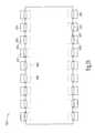
- FIG. 1shows a wafer 100 that includes a plurality of die 105 each separated from adjacent die by saw streets 108 .
- the die 105each include integrated circuits and contacts that provide communication between the integrated circuits and circuits outside the substrate and die.
- the die 105in an embodiment, includes a memory circuit.
- the memory circuitincludes a dynamic random access memory (DRAM). In other embodiments the memory circuit includes at least one of SRAM (Static Random Access Memory) or Flash memories.
- DRAMdynamic random access memory
- SRAMStatic Random Access Memory
- the DRAMcould be a synchronous memory device such as SGRAM (Synchronous Graphics Random Access Memory), SDRAM (Synchronous Dynamic Random Access Memory), SDRAM II, and DDR SDRAM (Double Data Rate SDRAM), as well as Synchlink or Rambus DRAMs and other emerging memory technologies as known in the art.
- the integrated circuits of the die 105define logic circuits. Die 105 may further include a processor.
- the die 105in an embodiment, include a system on a chip, which has a plurality of different integrated circuit structures, e.g., logic circuits and memory circuits.
- the saw streets 108do not contain integrated circuits. The saw streets 108 define non-active areas of the substrate whereat the substrate is divided into individual dies 105 .
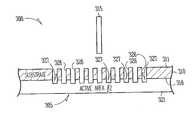
- FIG. 2shows a side view of a partial substrate, e.g., a wafer, 200 that includes a plurality of dies 205 .
- the dies 205include integrated circuits (not shown) that are fabricated using techniques known in the art, such as etching, lithography, deposition, doping, etc.
- a portion 210 of the substrate 200herein defined as the back, does not contain integrated circuits.
- the back portion 210acts as base for supporting the active area that contains integrated circuits.
- the back portionincludes a back surface 211 that comes into contact with substrate handling equipment (not shown) during fabrication.
- a saw street 208is formed intermediate the dies 205 .
- a mechanical cutter 215is aligned with the saw street 208 and forms a recessed, closed bottom trench 216 in the saw street 208 .
- the recessed trench 216in an embodiment, is formed by cutting a kerf in the substrate 200 along the saw streets.
- the trenches 216in an embodiment, extend the length of the dies 205 .
- the trenches 216in an embodiment, extend from one side of the substrate 200 to the other side of the substrate 200 .
- the trenches 216are linear.
- the width of the mechanical cutter 215defines the width of the trenches 216 .
- the mechanical cutter 215is a saw blade.
- the saw bladeis a circular saw blade that is mounted to a rotational drive such as an electric motor (not shown).
- the saw bladealong its outer cutting circumference includes a diamond material.
- the mechanical cutter 215is aligned with a saw street 208 outside the outer boundary of the substrate 200 .
- the cutter 215is first brought into contact with the outer boundary of the substrate 200 at the saw street 208 .
- Mechanical cutter 215 and the substrate 200relatively and linearly move such that the cutter forms the trench 216 in the substrate.
- the cutter 215is stationary and the substrate 200 moves relative to the cutter 215 .
- the substrate 200is stationary and the cutter 215 moves relative to the substrate.
- the cutter 215is positioned so that it cuts through a top surface 221 into the body of the substrate 200 .
- the top surface 221is the surface of the substrate 200 wherein and whereon active integrated circuits are fabricated.
- the cutter 215does not cut completely through the base portion 210 of the substrate. That is, the cutter 215 when creating the trenches 216 does not cut through back surface 211 .
- the cuttercuts into the base portion 210 of the substrate. This results in the trenches 216 being open at the substrate top surface 221 and being closed at the bottom of the trench, which is spaced upwardly from the substrate back surface 211 . Accordingly, the cutter 215 forms the trenches 216 to about half the thickness of the substrate 200 .
- the cutter 215forms the trenches to over half the thickness of the substrate 200 . In an embodiment, the cutter 215 forms the trenches to about two-thirds the thickness of the substrate 200 . In an embodiment, the cutting process described herein is repeated for each of the saw streets. In an embodiment, the cutting process described herein is repeated for only those saw streets 208 that extend in a same direction or that are parallel. In this embodiment, the saw streets that are transverse to the same direction saw streets 208 that include trenches 216 are not cut.
- FIG. 3shows a substrate 300 after further processing of the FIG. 2 substrate 200 .
- a mechanical cutter 315is positioned adjacent the nonactive substrate back portion 310 containing back side 311 of the substrate 300 .
- the substrate 200is flipped after the top trenches 216 are formed.
- the substrate 300is in the same orientation as the FIG. 2 substrate 200 and the mechanical cutter 315 is positioned beneath the substrate.
- the mechanical cutter 315includes the same embodiments as described herein for mechanical cutter 215 .
- Cutter 315is aligned with the outer boundary of substrate 300 and first contacts and begins cutting at the outer edge of the substrate 300 .
- the cutter 315cuts at least one back trench or kerf 326 , which is shown on the top of FIG. 3.
- the term “back”refers to a back or base area of a wafer or substrate on which integrated circuit layers are formed and that supports the active area and does not contain active integrated circuit components.
- the back trench 326is at least to half the thickness of the substrate 300 .
- the back trench 326is about half the thickness of the substrate 300 .
- the back trench 326is less than about half the thickness of the substrate 300 .
- the back trench 326is about one-third the thickness of the substrate 300 .
- a plurality of back trenches 326are formed beneath an active area of a die 205 .
- the back trenches 326are cut at a different angle than the top trenches 316 .
- the directions of the IC fabrication side trenches 316 and the back trenches 326are transverse to each other.
- the directions of the trenches 316 and 326are orthogonal.
- the directions of the trenches 316 and 326are at about 90 degrees with respect to each other.
- directions of the trenches 316 and 326are at about 45 degrees with respect to each other.
- directions of the trenches 316 and 326are at an angle of greater than about 45 degrees with respect to each other.
- directions of the trenches 316 and 326are at an angle greater than about 10 degrees with respect to each other.
- the trench(es) 326are formed at a depth that causes them to physically cross at least one of the top trench(es) 316 at intersections 327 . These intersections 327 form through holes (apertures) that extend from the substrate first, top side 311 to the substrate second, back side 321 .
- the substrate 300remains in a large scale form factor, e.g., wafer. That is, a plurality of dies 305 remain connected to each other through the non-cut back region 310 of substrate 300 .
- the back trenches 326are parallel to some of the top trenches 316 formed in saw streets.
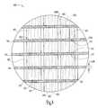
- FIG. 4shows a substrate 400 according to the present invention.
- Substrate 400includes a plurality of die 405 separated by saw streets 408 A and 408 B.
- Saw streets 408 Aextend in a first direction.
- Saw streets 408 Bextend in a second direction generally perpendicular to saw streets 408 A.
- Top trenches 416are formed in saw streets 408 A.
- a plurality of back trenches 426are formed in the back portion of substrate 400 . Each of the back trenches 426 extend under a plurality of dies 405 that are linearly aligned in the second direction.
- a plurality of back trenches 426extend under each aligned die 405 and intersect each of the top trenches 416 that extend transverse to the direction of the back trenches 426 .
- Through vias 427are formed at the intersections of the top and back trenches 416 , 426 .
- the back trenches 426in the illustrated embodiment, extend parallel to the second direction saw streets 408 B. Accordingly, back trenches 426 do not form intersections or through vias with any trench or kerf formed in the saw streets 408 B. In the illustrated embodiment, no trenches are formed in the saw streets 408 B.
- FIG. 5shows a top perspective view of a substrate 500 according to an embodiment of the present invention.
- Substrate 500includes a plurality dies 505 bound on two parallel sides by saw streets 508 B and on the other two parallel sides by trenches 516 .
- the trenches 516are top kerfs formed by mechanical cutting.
- the back, nonactive device portion of substrate 500is mechanically cut to form back trenches 526 .
- the back trenches 526are kerfs as described herein.
- the top trenches 516 and back trenches 526intersect at 527 to form through vias extending completely through substrate 500 , i.e. from the top side to the back side.
- Each of the dies 505further includes bond pads 530 .
- Bond pads 530are conductive contacts that are electrically connected to the integrated circuits of die 505 .
- the bond pads 530form connectors to circuits external to the die 505 .
- the bond pads 530are connected to leads in a package (not shown).
- Bond pads 530are formed by metalization of a nonmasked area of the wafer 500 .
- Bond pads 530are formed inwardly from the edges of die 505 , the edges being defined by saw streets 508 B and top trenches 516 .
- the bond pads 530are formed in a line essentially centered on die. That is, each bond pad 530 is equal distant from the two trenches 516 that bound the two opposite sides of the generally rectangular die. Further, the bond pads 530 are positioned inwardly on the die 505 from the saw streets 508 B, which as shown in FIG. 5 are not cut or trenched.
- FIG. 6shows a back perspective view of a substrate 600 , which is the same as substrate 500 .
- Substrate 600includes a plurality of active circuit side trenches or kerfs 616 and a plurality of non-active circuit side trenches or kerfs 626 .
- the trenches 616 and 626extend transverse to each other, essentially perpendicular as shown in FIG. 6, and intersect at 627 to form the through vias.
- the width of the top trenches 216 , 316 , 416 , 516are formed by using a mechanical cutter 215 or 315 .
- the width of the top trenches (kerfs)are equal to the width of the mechanical cutter. Accordingly, the mechanical cutter only makes a single pass on the substrate 200 , 300 , 400 , 500 or 600 to form one kerf.
- the kerf width 416W, 516W, in an embodiment,is about 200 micrometers.
- the kerf width 416W, 516W, in an embodiment,is greater than about 200 micrometers.
- the width of the back trenches 326 , 426 , 526are equal to the widths of the top trenches. In an embodiment, the width of the top trenches are greater than the width of the back trenches.
- FIG. 7Ashows a partial substrate 700 that includes a full die 705 bound between two top trenches 716 , which in turn abut two outer dies 705 that are partially shown.
- Dies 705each include bonding pads 730 that are positioned in a line along the center of the die in its longitudinal dimension. Bonding pads 730 are positioned on the substrate top surface 721 . In an embodiment, bonding pads 730 are not positioned on the back substrate surface as the integrated circuits in the die do not extend into the non-active back portion of the substrate. Bonding pads 730 are positioned longitudinally from top to bottom in the FIG. 7A embodiment. The bonding pads are equal distance from the sides of the die 705 as defined by the trenches 716 .
- Traces 731extend from the bonding pads 730 to edge contacts 732 .
- Traces 731are formed by third metallization processes.
- the edge contacts 732are formed by depositing a conductive material in the through vias 727 . Accordingly, edge contacts 732 extend from the substrate top surface 721 to the substrate back surface (not shown in FIG. 7A).
- the edge contacts 732thus are formed in the substrate top surface trenches 716 and in the substrate back surface trenches (not shown in FIG. 7A). Accordingly, electrically communication to the integrated circuits in dies 705 are made from either side of the substrate 700 through the edge contacts 732 formed in the through vias 727 , and through the traces 731 and bond pads on the substrate top surface 721 .
- the substrate 700is coated with a non-conductive material except on the bonding pads 730 , the area whereat the traces 731 are formed and the through vias 727 .
- the traces 731are formed on top of the non-conductive material layer.
- the non-conductive materialinclude polymides, organic encapsulant, and benzocyclobutenes.
- the traces 731 and through vias 727are formed in the areas free of the non-conducting material.
- the individual dies 705are separated from the adjacent dies by dicing along saw street 708 B and completing the cut through the substrate at top trench 716 .
- the dicing of the die 705is performed by mechanically cutting.
- dicingis performed by laser.
- dicingis performed by water jet.
- FIG. 7Bshows an embodiment of the substrate 700 , which is similar to the substrate shown in FIG. 7A except some traces 731 B are angled with respect to corresponding traces 731 shown in FIG. 7A. As described herein, edge contacts 732 are formed in intersections 727 . The intersections 727 are through holes in the substrate 700 where the top trench 716 crosses a back trench. In the FIG. 7B embodiment, some bond pads 730 B are not positioned directly over a back trench. Thus, the trace 731 B that connects such bond pads 730 B are angled so that the bond pads connects to an edge contact 732 formed at the same back trench as an edge contact 732 connected to an adjacent bond pad 730 .
- the substrate 700to be formed with fewer back trenches than the number of bond pads 730 , 730 B.
- the contacts 732are formed at each end of one back trench at through vias 727 .
- the minimum number of back trenches or through vias 727is half the number of bond pads 730 .
- all of the traces 731 B that extend to one side of the die 705are formed at an angle. The traces 731 B are not perpendicular to the top trench 716 or side of the die.
- FIG. 8Ashows a top perspective view of a single die 805 that is separated from a substrate, such as substrate 700 shown in FIG. 7.
- the die 805is diced from the adjacent dies along both the saw streets in which a top trench was formed and the saw streets in which a trench was not formed.
- Die 805has a corrugated back surface 811 due to the plurality of back side trenches 826 formed in the non-active portion of the substrate.
- Each of the edge contacts 832are aligned with one of the back surface trenches 826 .
- the die 805in an embodiment, is packaged using the edge contacts 832 that are accessible from the top, side or back of the die.
- the back surface 811which does not contain active circuits, is ground until it is essentially planar. In an embodiment, the back surface 811 is ground to the back of the edge contacts 832 . After the back surface 811 is ground, the die 805 is packaged. In an embodiment, the die 805 is surface mounted to a further substrate. In an embodiment, the number of back trenches 826 is at least equal to the number of bond pads 830 if the only one contact is formed in each back trench. In this embodiment, one back trench 826 is cut so that it passes directly under one bond pad 830 . One contact 832 is formed at one end of each back trench 826 at the edge of the die.
- FIG. 8Bshows a top perspective view of another embodiment of the present invention.
- Traces 831 Bextend from bond pads 830 B to contacts 832 .
- the bond contacts 830 Bare not positioned directly above the back trench 826 .
- traces 831 Bextend at an angle to connect the bond pads 830 B to the contacts 832 .
- One contact 832is formed at each end of one trench 826 .
- the traces 831 Bare at an angle relative to the edges of the die 805 .
- the traces 831 Bare at an angle with respect to traces 831 and the back trenches 826 .
- a back trench 826is cut so that it passes directly beneath one bond pad 830 .
- One edge contact 832is formed at each end of the back trench at both edges of the die 805 .
- the traces 831are parallel to the back trench 826 and connect bond pad 830 to one edge contact at one edge of the die.
- the traces 831 Bare nonparallel to the back trench 826 and connect bond pad 830 B to an edge contact at the other edge of the die.
- the traces 831 Bare parallel to each other.
- the number of back trenches 826is equal to half the number of bond pads 830 .
- the number of back trenches 826 that extend under a single die 805is in the range of equal to the number of bond pads 830 , 830 B to half the number of bond pads 830 , 830 B.
- FIG. 9shows a die 905 that is similar to the die 805 shown in FIG. 8 but in a back perspective view.
- Non-active region (back) surface 911 of die 905includes a plurality of substrate back trenches 926 that are formed according to the present invention. Accordingly, the back surface 911 has a corrugated appearance. Aligned with the back trenches 926 are edge contacts 932 .
- the die 905is representative of one of the plurality of dies that form a substrate or wafer during fabrication. However, for scale of illustration only a single die 905 is shown in FIG. 9. Additional dies would be connected along the sides of die 905 , for example, substrates and wafers as described above.
- FIG. 10shows a portion 1035 of die 905 including one back side trench 1026 and a region of the substrate adjacent the back side trench, which region has not been cut to form the back side trench 1026 . It will be recognized that this portion 1035 repeats itself to form a complete die, for example, die 905 as shown in FIG. 9.
- Trench 1026is a recess that has a closed interior surface 1036 defined by the removed, e.g., cut, volume of the substrate and sides 1037 defined by the uncut region of the substrate.
- Edge contacts 1032are formed at each end of the substrate portion 1035 aligned with and at the ends of the back side trench 1026 . The edge contacts 1032 do not extend into the trench 1026 but include enough area to form a side contact.
- the back surface 1039 of the edge contact 1032is essentially coplanar with the trench interior surface 1036 .
- FIG. 11shows the FIG. 10 die portion 1035 after further processing.
- Die portion 1135includes a back contact pad 1140 in the recessed trench 1126 in physical and electrical contact with a back surface of the edge contact 1132 .
- one contact pad 1140is formed at each end of the trench 1126 .
- the contact pad 1140is on a portion of the recessed trench interior surface 1136 .
- the back contact pad 1140provides back contacts that electrically connect to the bond pads (not shown in FIG. 11) of the integrated circuit through edge contacts 1132 and traces (not shown in FIG. 11).
- the back contacts 1140are formed by depositing a conductor in the trench.
- the back surface of the substrateis masked then the conductor material is deposited in the unmasked portions in the trench 1126 which correspond to the contact pads areas at the end of the trench.
- the substrate back surfaceis covered by a dielectric except at the edge contacts 1132 .
- the conductor materialis then deposited in an area at the edge contacts 1132 and in physical and electrical contact with the edge contact to form back contacts 1140 .
- back contactsare formed by third metal redistribution.
- the conductive materialcovers the substrate back surface and is then etched away except for the back contacts 1140 .
- FIG. 12shows a back view of a portion 1245 of the substrate after a further processing of the substrate portion 1135 as shown in FIG. 11.
- the portion 1245includes both substrate regions that are adjacent and upraised relative to the back trench 1226 .
- the substrate portion 1245includes the trench 1226 with one edge contact 1232 aligned with each end of the trench.
- One back contact 1240is formed in each end of the trench 1226 .
- the upraised substrate back surface 1242which is upraised relative to both the trench 1226 and the back contacts 1240 is subjected to back grinding to bring the back contacts 1240 into generally planar relationship to the substrate back surface 1242 . That is, the substrate regions adjacent the trench 1226 that were not cut are removed so that the die has a back surface that is essentially flush with the back contacts 1240 .
- FIG. 13Ashows a top view of a finished die 1305 according to the present invention.
- Die 1305includes a plurality of bond pads 1330 that are I/O pads, which connect the integrated circuits internal to the die to external circuits (not shown).
- a trace 1331connects each bond pad 1330 to an edge contact 1332 .
- the edge contacts 1332include a portion on the top surface of the die and a portion on the side of the die extending from the die top surface to the die back surface.
- the die 1305includes at least one upstanding, conductive contact 1350 on at least one of the edge contacts 1332 .
- the contact 1350is a ball contact.
- the ball contactis a solder ball.
- each of the edge contacts 1332is connected to a contact 1350 .
- Die 1305has a plurality of traces that are generally parallel to each other and perpendicular to the sides of the die. Accordingly, die 1305 has back trenches (not shown) that only have one edge contact 1332 formed in alignment therewith. Thus, the number of back trenches is equal to the number of bond pads and traces in this embodiment.
- FIG. 13Bshows a top perspective view of a finished die 1305 .
- the dieincludes pairs of contacts 1332 that are aligned with each other and positioned at opposite edges of the die 1305 .
- One of the pair of contactsis connected to a bond pad 1330 through a trace 1331 that is also aligned with the pair of edge contacts 1332 .
- the other of the pair of contactsis connected by a trace 1331 B to a bond pad 1330 B that is not aligned with the pair of contacts.
- the trace 1331 Bextends at an angle with respect to the edge of the die 1305 and with respect to the trace 1331 .
- the number of contacts 1332are equal on both edges of the die 1305 .
- the number of back trenches(not shown in FIG.
- each back trenchincludes one contact 1332 at each end of the trench. Accordingly, the number of back trenches formed in die 1305 is equal to half the number of bond pads 1330 .
- FIG. 14shows a back view of a finished die 1405 according to the present invention.
- Die 1405includes a plurality of edge contacts 1432 that extend from the die top surface to the die back surface.
- a plurality of back contacts 1440are connected to the plurality of edge contacts 1432 .
- Each edge contact 1432is connected to one back contact 1440 .
- the die 1405includes contacts on the die top surface, die edge surface and the die back surface.
- One back contact 1440is formed at each end of back trench 1426 .
- a contact 1450is positioned on at least one back contact 1440 .
- contact 1450is a solder ball.
- each back contact 1440has a contact 1450 thereon.
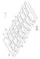
- FIG. 15shows a die stack 1555 that includes a plurality of dies 1505 electrically connected together.
- a die stack 1555expands the functional capacity of the dies 1505 .
- each of the dies 1505include memory devices.
- the die stack 1555expands the memory capacity over a single die 1505 .
- the contacts 1550connect an upper die's substrate active surface contacts (not shown, but designated above as X32, where X is the figure number) to a lower dies non-active circuit side contacts 1540 .
- the top most die 1505 as shown in FIG. 15has its non-active, back substrate surface contacts 1540 free from other contacts. These contacts 1540 , in an embodiment, are used to connect the die stack 1555 to an external circuit (not shown).
- the lower most die 1505 shown in FIG. 15has its contacts 1550 free from contacting another die 1505 .
- these contacts 1550connect the wafer stack to an external circuit (not shown).
- the dies 1505 having contacts on the top and back surfaceallow the dies to connected to adjacent dies such that the die stack 1555 has a profile that is essentially equal to the profile of the dies constituting the stack 1555 and the contacts 1550 intermediate adjacent dies.
- contacts 1555are controlled collapse connections that have a low profile, i.e., height. This provides a small stack height that is essentially the sum of the thicknesses of the dies 1505 .
- the back contacts 1550connect the die stack to a BGA or other chip connect structure.
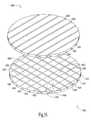
- FIG. 16shows two wafers 1600 , the top wafer being inverted relative to the bottom wafer such that the active device side or surface of the wafers 1600 face each other.
- the active device regions of dies 1605 of both wafers 1600face each other.
- each die 1605includes bonding pads and traces that interconnect the bonding pads to edge contacts formed in through vias according to the teachings of the present invention.
- the top portions of edge contacts on one of the wafers 1600include connectors (not shown) that provide a direct connect to the top portions of the edge contacts on the other wafer 1600 . Accordingly, each die 1605 of one wafer is electrically and physically connected to one die of the other wafer.
- Each wafer 1600includes a plurality of through vias that are filled with a conductive material, thus the integrated circuits of each die 1605 is electrically accessible through the conductive material in the through vias.
- the trough via connectionsform a portion of the edge contact.
- back contacts as described hereinare connected to the edge contacts.
- the back surface of at least one of the wafers 1600is adapted to connected to an external circuit. Accordingly, the present invention provides contacts and connections to the dies through the vias formed according to the present invention such that external connections are made through the backside of at least one of the wafers 1600 .
- At least one of the wafers 1600is subjected to back grinding to further thin the wafer according to the teachings of the present invention. This causes the contacts formed by conductive material in the through vias or back contacts formed in the trenches 1626 to be at the back surface of the at least one wafer 1600 . Thus, the wafer 1600 can be mounted in its non-singulated state.
- the stacked and connected wafers 1600are singulated or diced such that the interconnected, facing dies remain joined togther.
- the individual unitseach include two dies, one die from each of the two wafers.
- the external circuitis connected to these individual units at the edge contacts in an embodiment. In an embodiment, the external circuit is connected to these individual units at the back contacts.
- FIG. 17Ashows a cross-sectional, partial view of substrate stack that has two substrates 1700 .
- the cross-sectionis taken generally along vertically-aligned, back side trenches 1726 of the two stacked substrate 1700 .
- Each substrate 1700includes at least two die 1705 .
- the two die of the top substrateare positioned directly above the two die of the bottom substrate.
- Bond pads 1730are formed on the active circuit side of the dies 1705 .
- the bond pads 1730 of the bottom dieare aligned with bond pads of the die that is positioned above the bottom die.
- Traces 1731extend from the bond pads 1730 outwardly to the side of the die 1705 .
- Edge contacts 1732are formed aligned with the non-active side trench intermediate the dies 1705 that are formed on the same substrate.
- the dies at the bottomare formed on the same substrate and the dies at the top are formed on the same substrate.
- the non-active side trenchescross the active side trenches 1716 at intersections to form through holes 1727 that extend from the top to the back of the respective substrate and die.
- the through holes 1727are filled with conductive material and connect to non-active side contacts 1740 .
- the dies 1705thus are interconnected at the vertically aligned bond pads 1730 and vertically aligned traces 1731 .
- Contacts 1740 at non-active sides of the connected, vertically aligned dies 1705provide connections to external circuits (not shown).
- FIG. 17Bshows a cross-sectional, partial view of substrate 1700 generally along line 17 B- 17 B of FIG. 17A.
- the line 17 B- 17 Bgenerally follows active circuit side trenches 1716 of both substrates, which trenches 1716 are vertically aligned.
- FIG. 18shows a die stack that includes two die 1805 that are stacked top side to top side. That is, the active areas of the two die are adjacent one another.
- the two die 1805are joined together as discussed above in a wafer form in an embodiment.
- the top die 1805is from a different substrate or wafer than the bottom die 1805 .
- the joined wafersare diced to separate pairs of dies 1805 from adjacent pairs of dies.
- the through vias 1827are aligned between the dies 1805 and are separated when the joined dies are separated from the adjacent dies.
- the vias 1827are filed with a conductive material such that the vias with conductive material for interconnection between the two, joined die 1805 .
- the vias 1827 filled with conductive materialfurther define edge contacts and back contacts that connect the stacked dies 1805 to external circuits (not shown).
- FIG. 19shows a top view of a package 1970 according to the present invention.
- the package 1970includes one of a die, die stack, or wafer stack that includes back contacts 1940 .
- the dieis encapsualted in a protective case that seals the active area from the environment.
- Connectors 1972extend through the protective case and electrically contact the back contacts 1940 .
- Connectors 1972further connect to leads 1974 that allow the package 1970 to connect to external circuits, which include address and data buses and control circuits.
- a method for fabricating a wafer level packageincludes fabricating an active area on a substrate.
- the active areaincludes integrated circuits.
- the integrated circuitsform memory devices.
- the integrated circuitsperform logic functions or processor tasks.
- the active areais a system on a chip device that includes logic functions and memory functions.
- the saw streets intermediate the integrated circuitsare partially cut in a first direction to form trenches or kerfs.
- the non-active regions of the substrate, generally beneath the integrated circuits or diesare partially cut to form non-active side or back trenches or kerfs.
- a plurality of cuts in the non-active regions of the substrateare made to form a plurality of non-active side trenches. Where the active side trenches and non-active side trenches intersect there are formed through vias in the substrate. These through vias provide holes, which when filled with a conductive material provide contacts on both the active (top) surface of the substrate and the non-active (back) surface of the substrate.
- Numerous devicesare adaptable for use with a wafer level package as described herein.
- Such devicesinclude individual IC packages, sometimes referred to as chips, circuit modules, memory modules, and computers and electronic systems.
- Individual IC packagesinclude a die having an individual pattern, typically rectangular, on a substrate that contains circuitry, or integrated circuit devices, to perform a specific function, such as memory functions, logic functions, and address functions.
- a semiconductor waferwill typically contain a repeated pattern of such dies containing the same functionality.
- the individual IC packageincludes structures of the present invention or is manufactured according to the methods of the present invention.
- the individual IC packagein an embodiment, further contains additional circuitry to extend to such complex devices as a monolithic processor with multiple functionality and/or a processor and memory module in a single IC package.
- Individual IC packagestypically include a protective casing (not shown) with leads extending therefrom (not shown) providing access to the circuitry of the IC package for unilateral or bilateral communication and control.
- the leadsare connected to the edge contacts, ball contacts or other contacts as described herein.
- Circuit modulesinclude two or more dies that are combined, with or without protective casing. Such a combination enhances or extends the functionality of an individual die.
- the circuit moduleincludes a combination of dies representing a variety of functions, or a combination of dies containing the same functionality.
- One or more dies of circuit modulecontain structures according to the present invention or are formed by methods of the present invention.
- Some examples of a circuit moduleinclude memory modules, device drivers, power modules, communication modems, processor modules and application-specific (ASIC) modules, and may include multilayer, multichip modules.
- the circuit moduleis, in an embodiment, a subcomponent of a variety of electronic systems, such as a clock, a television, a cell phone, a personal computer, personal data assistant, an automobile, an industrial control system, an aircraft and others.
- the circuit modulehas a variety of leads extending therefrom and coupled to the dies providing unilateral or bilateral communication and control.
- One form of a circuit moduleis a memory module.
- the memory modulecontains multiple memory IC devices on support, the number of IC devices generally depending upon the desired bus width and the desire for parity.
- the memory moduleaccepts a command signal from an external controller (not shown) on a command link and provides for data input and data output on data links.
- the command link and data linksare connected to leads extending from the support.
- the memory module and/or the dies that constitute at least part of the memory moduleinclude structures of the present invention or are formed according to methods of the present invention.
- Electronic systemsinclude one or more circuit modules.
- An electronic systemgenerally contains a user interface that communicates with an electronic unit, that processes or stores electrical information.
- the user interfaceprovides a user of the electronic system with some form of control or observation of the results of the electronic unit.
- Some examples of user interfaceinclude the keyboard, pointing device, monitor or printer of a personal computer; the tuning dial, display or speakers of a radio; the ignition switch, gauges or gas pedal of an automobile; and the card reader, keypad, display or currency dispenser of an automated teller machine.
- the user interfacein an embodiment, provides access ports provided to electronic unit. Access ports are used to connect an electronic unit to the more tangible user interface components previously exemplified.
- One or more of the circuit modulesinclude a processor providing some form of manipulation, control or direction of inputs from or outputs to user interface, or of other information either preprogrammed into, or otherwise provided to, the electronic unit.
- electronic systemis, in an embodiment, associated with certain mechanical components (not shown) in addition to the circuit modules and the user interface. It will be appreciated that the one or more circuit modules in the electronic system are replaced by a single integrated circuit in an embodiment. In an embodiment, the electronic system is a subcomponent of a larger electronic system. It will also be appreciated that at least one of the memory modules includes structures according to the present invention or is formed according to methods according to the present invention.
- the memory systemincludes one or more memory modules and a memory controller.
- the memory moduleseach contain one or more memory IC devices.
- at least one of memory devicesincludes structures according to the present invention or is fabricated according to the present invention.
- the memory controllerprovides and controls a bidirectional interface between memory system and an external system bus.
- the memory systemaccepts a command signal from the external bus and relays it to the one or more memory modules on a command link.
- the memory systemprovides for data input and data output between the one or more memory modules and external system bus on data links.
- the computer systemincludes a processor and a memory system housed in a computer unit.
- the computer systemis but one example of an electronic system containing another electronic system, i.e., the memory system, as a subcomponent.
- the computer systemoptionally contains user interface components.
- User interface componentsinclude, but are not limited to a keyboard, a pointing device, a monitor, a printer and a bulk storage device. It will be appreciated that other components are often associated with computer system such as modems, device driver cards, additional storage devices, etc.
- the processor and the memory system of the computer systemin an embodiment, are incorporated on a single die or IC package. Such single package processing units reduce the communication time between the processor and the memory circuit. It will be appreciated that at least one of the processor and the memory system contain an IC package according to the present invention
- FIG. 4The above description refers to numerous views of substrates that illustrate embodiments of the present invention. These views are, at times, drawn to an enlarges, simplified scale to illustrate the present invention. For example, the saw streets and dies shown in FIG. 4 are shown in a greater enlarges scale. Hundreds of die are formed on a single substrate. The saw streets are formed as small as possible to allow more dies to be formed on a single substrate.
- the forming of the through vias or apertures as described hereinprovides a true wafer level package, e.g., a chip profile. That is, a significant space savings is achieved by producing a small package size.
- the dimensions of the through viasare determined by the size of the mechanical cutters used to form the partial cuts in the substrate. That is, with a saw blade, the width of the blade making the cut in the substrate top surface determines one dimension (e.g., length). The width of a blade making the cut in the substrate back surface determines another dimension (e.g., width). Accordingly, the dimensions of the via can be made as small as the width of saw blades. In an embodiment, a dimension of the via is about 0.2 mm.
- the techniques described hereinprovide a low cost and an industrial acceptable method to produce through vias compared to conventional etching and laser drill techniques. As a result, space savings are achieved in packaging a substrate according to the present invention.
Landscapes
- Engineering & Computer Science (AREA)
- Physics & Mathematics (AREA)
- Condensed Matter Physics & Semiconductors (AREA)
- General Physics & Mathematics (AREA)
- Computer Hardware Design (AREA)
- Microelectronics & Electronic Packaging (AREA)
- Power Engineering (AREA)
- Manufacturing & Machinery (AREA)
- Semiconductor Integrated Circuits (AREA)
- Internal Circuitry In Semiconductor Integrated Circuit Devices (AREA)
- Dicing (AREA)
Abstract
Description
- This application claims priority under 35 U.S.C. 119 from Singapore Application No. 200203615-0, filed Jun. 14, 2002, which application is incorporated herein by reference.[0001]
- The present invention relates to wafer level packaging techniques and structures. More particularly, the present invention relates to forming vias in a wafer level package.[0002]
- Wafer level packaging provides a complete electronic device package at the wafer level. This provides a package having a high density of integrated circuits in a small or ultra-thin profile package. Electronic devices and associated software applications continue to demand more memory and processing power from chip packages. However, electronic devices that use such chip packages have continued to shrink. Thus, the demand for integrated circuit packages having a high density in a smaller package has also increased. While it is desirable to design a new die that meets all of the needs of the market, such a design may not be feasible or ready for market. Thus, dies or chips are connected together, e.g., stacked, to achieve the desired density and electronic capacity. Wafer level packaging is used to meet these demands. However, most wafer level packaging processes have not had industrial success as such processes require a significant amount of wafer thinning followed by etching or laser drilling processes to create through holes in the wafer level package.[0003]
- The present invention includes methods for creating a through via in a substrate and the resulting structures. Trenches are mechanically formed in the two sides of a substrate. Where the trenches cross through vias or holes are formed. In an embodiment, the method includes sawing into a fabrication side of a substrate and sawing into a backside of the substrate so that the sawing on the fabrication side and sawing on the backside cross each other to form the via. The depths of the sawing into the two sides of the substrate are at least equal to the height of the substrate. In an embodiment, the substrate is a wafer that includes a plurality of dies each containing integrated circuits. The integrated circuits, in various embodiments, form memory devices, logic circuits and/or processor circuits.[0004]
- In an embodiment, the method of the present invention includes forming trenches on a first side of the substrate and forming trenches on a second side of the substrate to form the through vias at the intersection of the trenches. Forming includes mechanically forming the trenches. In an embodiment, the trenches on one side are orthogonal to the trenches on the other side. In an embodiment, trenches on a fabrication side of the substrate are formed in saw streets. In an embodiment, the trenches formed on the back or non-active side of the substrate are formed beneath the dies or integrated circuits. Thus, the intersections of the trenches that form the through vias are in the saw streets. The dimensions of the through vias are determined by the widths of the trenches formed on each side of the substrate. The widths of the trenches are determined by the widths of the mechanical cutter used to create the respective trench. The through vias include a conductor material to form a contact or communication line from the top side of the substrate to the back side. In an embodiment, contacts are formed in the back side trenches, which contacts are connected to the conductor material in the through vias.[0005]
- Methods and structures of the present invention further include the number of trenches formed in the back side of the substrate and how the back side trenches relate to the die components. In an embodiment, the number of trenches formed in the back side of the substrate are equal to or less than the number of bond pads on the dies. In an embodiment, the number of trenches formed in the back side of the substrate are equal to half the number of bond pads. The bond pads are connected to one through via that is positioned adjacent the respective die. Traces connect the bond pads to the through vias. In an embodiment, the traces are formed so that they alternate which sides of the die they extend to and thus, adjacent bond pads are connected to conductors in through vias on opposite sides of the die. In an embodiment, some traces are parallel to trenches in the back side of the substrate. In an embodiment, some of the traces are skew to trenches in the back side of the substrate.[0006]
- In an embodiment, the method of creating a via through a wafer includes providing a substrate with at least one integrated circuit, forming a first trench in the top side of the substrate, and forming a second trench in the back side of the substrate so that the second trench crosses the first trench to form a through via. In an embodiment, a conductor is inserted in the through via to extend from the top side to the back side. This forms an edge contact and provides a connection from the fabrication side of the substrate to a contact on the back side of the substrate. In an embodiment, bond pads are on the substrate fabrication side. The bond pads are connected to the conductor. In an embodiment, a back side contact is formed at one end of the second trench and connected to the conductor. In an embodiment, back side contacts are formed at each end of the back side trench. In an embodiment, the method further includes backgrinding the back side of the substrate so that the back side is essentially coplanar to the back side contact.[0007]
- An embodiment of the present invention provides a method for stacking integrated circuit devices. The method includes providing a first substrate including a plurality of first integrated circuit devices separated by streets, forming first trenches in the streets on a top side of the first substrate, and forming second trenches on the backside of the first substrate so that the second trenches and first trenches intersect to form through vias from the top side to the backside of the first substrate. In an embodiment, the method further includes inserting a conductor into the through vias to form contacts on the top side and the backside, connecting the conductor to at least one of the plurality of first integrated circuit devices. A second substrate, which includes a plurality of second individual integrated circuit devices separated by streets, is connected to the first substrate. In an embodiment, the plurality of second integrated circuit devices are connected to the first plurality of integrated circuit devices. Connected pairs of the connected first integrated circuit devices and second integrated circuit devices are separated from the other pairs of connected first integrated circuit devices and second integrated circuit devices. In an embodiment, the method includes forming third trenches in the streets on a top side of the second substrate, forming fourth trenches on the backside of the second substrate so that the third and fourth trenches intersect to form through vias from the top side to the backside of the second substrate, and inserting a conductor into the through vias to form contacts on the top side and the backside. In an embodiment, the method includes connecting the conductor to at least one of the plurality of second integrated circuit devices. In an embodiment, the fourth trenches are formed beneath at least one of the second integrated circuit devices. In an embodiment, the fourth trenches are linear. In an embodiment, the trenches and saw streets of the first and second substrates are aligned prior to dicing.[0008]
- An embodiment of the present invention is directed to a method of forming a substrate level package of two integrated circuit devices. The method includes providing a first substrate including a plurality of first dies separated by streets, the first dies including bond pads on an active side of the substrate and traces connected to the bond pads, forming first trenches in the streets on a top side of the first substrate, forming second trenches on the backside of the first substrate so that the second trenches and first trenches intersect to form through vias from the top side to the backside of the first substrate, and inserting a conductor into the through vias to form contacts on the top side and the backside. The first substrate is connected to a second substrate. In an embodiment, the first and second substrate are formed the same. In an embodiment, the first and second substrates are mirror images of each other. The method further includes connecting the conductor to at least one of the bond pads using one of the traces. In an embodiment, the second substrate includes a plurality of second individual integrated circuit devices separated by streets. The method further includes, in an embodiment, connecting the plurality of second integrated circuit devices to the first plurality of integrated circuit devices and separating connected pairs of the connected first integrated circuit devices and second integrated circuit devices from the other pairs of connected first integrated circuit devices and second integrated circuit devices. In an embodiment, the method of the present invention includes encapsulating a pair of the connected first integrated circuit device and second integrated circuit device. In an embodiment, the contacts to the pair of the connected first integrated circuit device and second integrated circuit device are at the backside of one of the first and second integrated circuit devices of the pair. Thus, the active device fabrication side of the substrates are connected together and aligned. In an embodiment, the bond pads of the first and second integrated circuit devices are connected to provide communication between the devices. In an embodiment, the traces of the first and second integrated circuit devices are connected to provide communication between the devices. In an embodiment, the conductors in the through vias of the second substrate are connected to the conductors in the through vias of the first substrate.[0009]
- Further features and advantages of the present invention, as well as the structure and operation of various embodiments of the present invention, are described in detail below with reference to the accompanying drawings.[0010]
- FIG. 1 shows a substrate having a plurality of die.[0011]
- FIG. 2 is an elevational view of a partial wafer during a processing step according to the present invention.[0012]
- FIG. 3 is a view of the FIG. 2 partial wafer taken generally along line[0013]3-3 during a processing step according to the present invention.
- FIG. 4 is a plan view of a wafer during processing thereof according to the teachings of the present invention.[0014]
- FIG. 5 is a top perspective view of a wafer according to the teachings of the present invention.[0015]
- FIG. 6 is a bottom perspective view of a wafer according to the teachings of the present invention.[0016]
- FIG. 7A is a top view of a partial substrate according to a further embodiment of the present invention.[0017]
- FIG. 7B is a top view of a partial substrate according to a further embodiment of the present invention.[0018]
- FIG. 8A is a partial top perspective view of a FIG. 7A die.[0019]
- FIG. 8B is a partial top perspective view of a FIG. 7B die.[0020]
- FIG. 9 is a partial bottom perspective view of a die according to the present invention.[0021]
- FIG. 10 is a partial view of the FIG. 9 die.[0022]
- FIG. 11 is a partial view of the FIG. 10 die after a processing step.[0023]
- FIG. 12 is a partial view of the FIG. 11 die after a processing step. top view of a die according to the further embodiment of the present invention.[0024]
- FIG. 13A is a top view of an embodiment of a die after a processing step.[0025]
- FIG. 13B is a top view of an embodiment of a die after a processing step.[0026]
- FIG. 14 is a bottom view of a die according to an embodiment of the present invention.[0027]
- FIG. 15 is a stacked assembly of a plurality of dies according to the teachings of the present invention.[0028]
- FIG. 16 is perspective view of a wafer stack according to an embodiment of the present invention.[0029]
- FIG. 17A is a cross sectional view of a partial wafer stack of the present invention.[0030]
- FIG. 17B is a cross sectional view taken generally along[0031]
line 17B-17B of FIG. 17A. - FIG. 18 is a perspective view of a singulated die stack of the present invention.[0032]
- FIG. 19 is a plan view of a package according to an embodiment of the present invention.[0033]
- In the following detailed description of the invention, reference is made to the accompanying drawings which form a part hereof, and in which is shown, by way of illustration, specific embodiments in which the invention may be practiced. These embodiments are described in sufficient detail to enable those skilled in the art to practice the invention. Other embodiments may be utilized and structural, logical, and electrical changes may be made without departing from the scope of the present invention. The terms wafer and substrate used herein include any structure having an exposed surface onto which a layer is deposited according to the present invention, for example, to form the integrated circuit (IC) structure. The term substrate is understood to include semiconductor wafers. The term substrate is also used to refer to semiconductor structures during processing, and may include other layers that have been fabricated thereupon. Both wafer and substrate include doped and undoped semiconductors, epitaxial semiconductor layers supported by a base semiconductor or insulator, as well as other semiconductor structures well known to one skilled in the art. The term conductor is understood to include semiconductors, and the term insulator is defined to include any material that is less electrically conductive than the materials referred to as conductors. The following detailed description is, therefore, not to be taken in a limiting sense, and the scope of the present invention is defined only by the appended claims, along with the full scope of equivalents to which such claims are entitled.[0034]
- The present description employs a number convention where the first (leftmost), most significant digit(s) are the same as the figure number on which the numbers appear. Accordingly, like or similar elements will have the same least significant digits. For example, the substrate, wafer, or base layer is designated by the convention X00, where “X” is the figure number, e.g., 100, 200, 300, etc.[0035]
- The present description uses the terms “top” and “back” when referring to the substrate on which integrated circuits are formed. The term “top” refers to the surface on which the layers that form an active integrated circuit structure are formed. The term “back” refers to the region of the substrate beneath the surface on which active circuit structures are formed.[0036]
- FIG. 1 shows a[0037]
wafer 100 that includes a plurality ofdie 105 each separated from adjacent die bysaw streets 108. The die105 each include integrated circuits and contacts that provide communication between the integrated circuits and circuits outside the substrate and die. Thedie 105, in an embodiment, includes a memory circuit. The memory circuit includes a dynamic random access memory (DRAM). In other embodiments the memory circuit includes at least one of SRAM (Static Random Access Memory) or Flash memories. Additionally, the DRAM could be a synchronous memory device such as SGRAM (Synchronous Graphics Random Access Memory), SDRAM (Synchronous Dynamic Random Access Memory), SDRAM II, and DDR SDRAM (Double Data Rate SDRAM), as well as Synchlink or Rambus DRAMs and other emerging memory technologies as known in the art. The integrated circuits of thedie 105, in an embodiment, define logic circuits.Die 105 may further include a processor. Thedie 105, in an embodiment, include a system on a chip, which has a plurality of different integrated circuit structures, e.g., logic circuits and memory circuits. Thesaw streets 108 do not contain integrated circuits. Thesaw streets 108 define non-active areas of the substrate whereat the substrate is divided into individual dies105. - FIG. 2 shows a side view of a partial substrate, e.g., a wafer,[0038]200 that includes a plurality of dies205. The dies205 include integrated circuits (not shown) that are fabricated using techniques known in the art, such as etching, lithography, deposition, doping, etc. A
portion 210 of thesubstrate 200, herein defined as the back, does not contain integrated circuits. Theback portion 210 acts as base for supporting the active area that contains integrated circuits. The back portion includes aback surface 211 that comes into contact with substrate handling equipment (not shown) during fabrication. Asaw street 208 is formed intermediate the dies205. Amechanical cutter 215 is aligned with thesaw street 208 and forms a recessed, closedbottom trench 216 in thesaw street 208. The recessedtrench 216, in an embodiment, is formed by cutting a kerf in thesubstrate 200 along the saw streets. Thetrenches 216, in an embodiment, extend the length of the dies205. Thetrenches 216, in an embodiment, extend from one side of thesubstrate 200 to the other side of thesubstrate 200. Thetrenches 216 are linear. The width of themechanical cutter 215 defines the width of thetrenches 216. In an embodiment, themechanical cutter 215 is a saw blade. In an embodiment, the saw blade is a circular saw blade that is mounted to a rotational drive such as an electric motor (not shown). The saw blade along its outer cutting circumference includes a diamond material. In operation, themechanical cutter 215 is aligned with asaw street 208 outside the outer boundary of thesubstrate 200. Thecutter 215 is first brought into contact with the outer boundary of thesubstrate 200 at thesaw street 208.Mechanical cutter 215 and thesubstrate 200 relatively and linearly move such that the cutter forms thetrench 216 in the substrate. In an embodiment, thecutter 215 is stationary and thesubstrate 200 moves relative to thecutter 215. In an embodiment, thesubstrate 200 is stationary and thecutter 215 moves relative to the substrate. Thecutter 215 is positioned so that it cuts through atop surface 221 into the body of thesubstrate 200. Thetop surface 221 is the surface of thesubstrate 200 wherein and whereon active integrated circuits are fabricated. However, thecutter 215 does not cut completely through thebase portion 210 of the substrate. That is, thecutter 215 when creating thetrenches 216 does not cut throughback surface 211. In an embodiment, the cutter cuts into thebase portion 210 of the substrate. This results in thetrenches 216 being open at thesubstrate top surface 221 and being closed at the bottom of the trench, which is spaced upwardly from the substrate backsurface 211. Accordingly, thecutter 215 forms thetrenches 216 to about half the thickness of thesubstrate 200. In an embodiment, thecutter 215 forms the trenches to over half the thickness of thesubstrate 200. In an embodiment, thecutter 215 forms the trenches to about two-thirds the thickness of thesubstrate 200. In an embodiment, the cutting process described herein is repeated for each of the saw streets. In an embodiment, the cutting process described herein is repeated for only those sawstreets 208 that extend in a same direction or that are parallel. In this embodiment, the saw streets that are transverse to the same direction sawstreets 208 that includetrenches 216 are not cut. - FIG. 3 shows a[0039]
substrate 300 after further processing of the FIG. 2substrate 200. Amechanical cutter 315 is positioned adjacent the nonactive substrate backportion 310 containing backside 311 of thesubstrate 300. In an embodiment, thesubstrate 200 is flipped after thetop trenches 216 are formed. In an embodiment, thesubstrate 300 is in the same orientation as the FIG. 2substrate 200 and themechanical cutter 315 is positioned beneath the substrate. Themechanical cutter 315 includes the same embodiments as described herein formechanical cutter 215.Cutter 315 is aligned with the outer boundary ofsubstrate 300 and first contacts and begins cutting at the outer edge of thesubstrate 300. Thecutter 315 cuts at least one back trench orkerf 326, which is shown on the top of FIG. 3. The term “back” refers to a back or base area of a wafer or substrate on which integrated circuit layers are formed and that supports the active area and does not contain active integrated circuit components. Theback trench 326 is at least to half the thickness of thesubstrate 300. Theback trench 326 is about half the thickness of thesubstrate 300. Theback trench 326 is less than about half the thickness of thesubstrate 300. In an embodiment, theback trench 326 is about one-third the thickness of thesubstrate 300. In an embodiment, a plurality ofback trenches 326 are formed beneath an active area of adie 205. Theback trenches 326 are cut at a different angle than thetop trenches 316. Specifically, the directions of the ICfabrication side trenches 316 and theback trenches 326 are transverse to each other. In an embodiment, the directions of thetrenches trenches trenches trenches trenches intersections 327. Theseintersections 327 form through holes (apertures) that extend from the substrate first,top side 311 to the substrate second, backside 321. However, thesubstrate 300 remains in a large scale form factor, e.g., wafer. That is, a plurality of dies305 remain connected to each other through the non-cutback region 310 ofsubstrate 300. In an embodiment, theback trenches 326 are parallel to some of thetop trenches 316 formed in saw streets. - FIG. 4 shows a[0040]
substrate 400 according to the present invention.Substrate 400 includes a plurality ofdie 405 separated by sawstreets Saw streets 408A extend in a first direction. Sawstreets 408B extend in a second direction generally perpendicular to sawstreets 408A.Top trenches 416 are formed insaw streets 408A. A plurality ofback trenches 426 are formed in the back portion ofsubstrate 400. Each of theback trenches 426 extend under a plurality of dies405 that are linearly aligned in the second direction. A plurality ofback trenches 426 extend under each aligned die405 and intersect each of thetop trenches 416 that extend transverse to the direction of theback trenches 426. Throughvias 427 are formed at the intersections of the top and backtrenches back trenches 426, in the illustrated embodiment, extend parallel to the second direction sawstreets 408B. Accordingly, backtrenches 426 do not form intersections or through vias with any trench or kerf formed in thesaw streets 408B. In the illustrated embodiment, no trenches are formed in thesaw streets 408B. - FIG. 5 shows a top perspective view of a[0041]
substrate 500 according to an embodiment of the present invention.Substrate 500 includes a plurality dies505 bound on two parallel sides by sawstreets 508B and on the other two parallel sides bytrenches 516. In an embodiment, thetrenches 516 are top kerfs formed by mechanical cutting. The back, nonactive device portion ofsubstrate 500 is mechanically cut to form backtrenches 526. In an embodiment, theback trenches 526 are kerfs as described herein. Thetop trenches 516 andback trenches 526 intersect at527 to form through vias extending completely throughsubstrate 500, i.e. from the top side to the back side. Each of the dies505 further includesbond pads 530.Bond pads 530 are conductive contacts that are electrically connected to the integrated circuits ofdie 505. Thebond pads 530 form connectors to circuits external to thedie 505. In an embodiment, thebond pads 530 are connected to leads in a package (not shown).Bond pads 530 are formed by metalization of a nonmasked area of thewafer 500.Bond pads 530 are formed inwardly from the edges ofdie 505, the edges being defined bysaw streets 508B andtop trenches 516. Thebond pads 530 are formed in a line essentially centered on die. That is, eachbond pad 530 is equal distant from the twotrenches 516 that bound the two opposite sides of the generally rectangular die. Further, thebond pads 530 are positioned inwardly on the die505 from thesaw streets 508B, which as shown in FIG. 5 are not cut or trenched. - FIG. 6 shows a back perspective view of a[0042]
substrate 600, which is the same assubstrate 500.Substrate 600 includes a plurality of active circuit side trenches orkerfs 616 and a plurality of non-active circuit side trenches orkerfs 626. Thetrenches - The width of the[0043]
top trenches mechanical cutter substrate kerf width kerf width back trenches - FIG. 7A shows a[0044]
partial substrate 700 that includes afull die 705 bound between twotop trenches 716, which in turn abut two outer dies705 that are partially shown. Dies705 each includebonding pads 730 that are positioned in a line along the center of the die in its longitudinal dimension.Bonding pads 730 are positioned on thesubstrate top surface 721. In an embodiment,bonding pads 730 are not positioned on the back substrate surface as the integrated circuits in the die do not extend into the non-active back portion of the substrate.Bonding pads 730 are positioned longitudinally from top to bottom in the FIG. 7A embodiment. The bonding pads are equal distance from the sides of the die705 as defined by thetrenches 716.Traces 731 extend from thebonding pads 730 to edgecontacts 732.Traces 731, in an embodiment, are formed by third metallization processes. Theedge contacts 732 are formed by depositing a conductive material in the throughvias 727. Accordingly,edge contacts 732 extend from thesubstrate top surface 721 to the substrate back surface (not shown in FIG. 7A). Theedge contacts 732 thus are formed in the substratetop surface trenches 716 and in the substrate back surface trenches (not shown in FIG. 7A). Accordingly, electrically communication to the integrated circuits in dies705 are made from either side of thesubstrate 700 through theedge contacts 732 formed in the throughvias 727, and through thetraces 731 and bond pads on thesubstrate top surface 721. - In an embodiment, the[0045]
substrate 700 is coated with a non-conductive material except on thebonding pads 730, the area whereat thetraces 731 are formed and the throughvias 727. In an embodiment, thetraces 731 are formed on top of the non-conductive material layer. Examples of the non-conductive material include polymides, organic encapsulant, and benzocyclobutenes. Thetraces 731 and throughvias 727 are formed in the areas free of the non-conducting material. The individual dies705 are separated from the adjacent dies by dicing alongsaw street 708B and completing the cut through the substrate attop trench 716. In an embodiment, the dicing of thedie 705 is performed by mechanically cutting. In an embodiment, dicing is performed by laser. In an embodiment, dicing is performed by water jet. - FIG. 7B shows an embodiment of the[0046]
substrate 700, which is similar to the substrate shown in FIG. 7A except sometraces 731B are angled with respect to correspondingtraces 731 shown in FIG. 7A. As described herein,edge contacts 732 are formed inintersections 727. Theintersections 727 are through holes in thesubstrate 700 where thetop trench 716 crosses a back trench. In the FIG. 7B embodiment, somebond pads 730B are not positioned directly over a back trench. Thus, thetrace 731B that connectssuch bond pads 730B are angled so that the bond pads connects to anedge contact 732 formed at the same back trench as anedge contact 732 connected to anadjacent bond pad 730. This allows thesubstrate 700 to be formed with fewer back trenches than the number ofbond pads contacts 732 are formed at each end of one back trench at throughvias 727. Thus, the minimum number of back trenches or throughvias 727 is half the number ofbond pads 730. In an embodiment, all of thetraces 731B that extend to one side of thedie 705 are formed at an angle. Thetraces 731B are not perpendicular to thetop trench 716 or side of the die. - FIG. 8A shows a top perspective view of a[0047]
single die 805 that is separated from a substrate, such assubstrate 700 shown in FIG. 7. Thedie 805 is diced from the adjacent dies along both the saw streets in which a top trench was formed and the saw streets in which a trench was not formed.Die 805 has a corrugated backsurface 811 due to the plurality ofback side trenches 826 formed in the non-active portion of the substrate. Each of theedge contacts 832 are aligned with one of theback surface trenches 826. Thedie 805, in an embodiment, is packaged using theedge contacts 832 that are accessible from the top, side or back of the die. In an embodiment, theback surface 811, which does not contain active circuits, is ground until it is essentially planar. In an embodiment, theback surface 811 is ground to the back of theedge contacts 832. After theback surface 811 is ground, thedie 805 is packaged. In an embodiment, thedie 805 is surface mounted to a further substrate. In an embodiment, the number ofback trenches 826 is at least equal to the number ofbond pads 830 if the only one contact is formed in each back trench. In this embodiment, oneback trench 826 is cut so that it passes directly under onebond pad 830. Onecontact 832 is formed at one end of eachback trench 826 at the edge of the die. - FIG. 8B shows a top perspective view of another embodiment of the present invention.[0048]
Traces 831B extend frombond pads 830B tocontacts 832. Thebond contacts 830B are not positioned directly above theback trench 826. Accordingly, traces831B extend at an angle to connect thebond pads 830B to thecontacts 832. Onecontact 832 is formed at each end of onetrench 826. Thetraces 831B are at an angle relative to the edges of thedie 805. Thetraces 831B are at an angle with respect totraces 831 and theback trenches 826. In this embodiment, aback trench 826 is cut so that it passes directly beneath onebond pad 830. Oneedge contact 832 is formed at each end of the back trench at both edges of thedie 805. Thetraces 831 are parallel to theback trench 826 and connectbond pad 830 to one edge contact at one edge of the die. Thetraces 831B are nonparallel to theback trench 826 and connectbond pad 830B to an edge contact at the other edge of the die. Thetraces 831B are parallel to each other. In this embodiment, the number ofback trenches 826 is equal to half the number ofbond pads 830. Thus, the number ofback trenches 826 that extend under asingle die 805, in an embodiment according to the present invention, is in the range of equal to the number ofbond pads bond pads - FIG. 9 shows a[0049]
die 905 that is similar to the die805 shown in FIG. 8 but in a back perspective view. Non-active region (back)surface 911 ofdie 905 includes a plurality of substrate backtrenches 926 that are formed according to the present invention. Accordingly, theback surface 911 has a corrugated appearance. Aligned with theback trenches 926 areedge contacts 932. Thedie 905 is representative of one of the plurality of dies that form a substrate or wafer during fabrication. However, for scale of illustration only asingle die 905 is shown in FIG. 9. Additional dies would be connected along the sides ofdie 905, for example, substrates and wafers as described above. - FIG. 10 shows a[0050]
portion 1035 ofdie 905 including one backside trench 1026 and a region of the substrate adjacent the back side trench, which region has not been cut to form theback side trench 1026. It will be recognized that thisportion 1035 repeats itself to form a complete die, for example, die905 as shown in FIG. 9.Trench 1026 is a recess that has a closedinterior surface 1036 defined by the removed, e.g., cut, volume of the substrate andsides 1037 defined by the uncut region of the substrate.Edge contacts 1032 are formed at each end of thesubstrate portion 1035 aligned with and at the ends of theback side trench 1026. Theedge contacts 1032 do not extend into thetrench 1026 but include enough area to form a side contact. Theback surface 1039 of theedge contact 1032 is essentially coplanar with the trenchinterior surface 1036. - FIG. 11 shows the FIG. 10[0051]
die portion 1035 after further processing.Die portion 1135 includes aback contact pad 1140 in the recessedtrench 1126 in physical and electrical contact with a back surface of theedge contact 1132. In an embodiment, onecontact pad 1140 is formed at each end of thetrench 1126. Thecontact pad 1140 is on a portion of the recessed trenchinterior surface 1136. Theback contact pad 1140 provides back contacts that electrically connect to the bond pads (not shown in FIG. 11) of the integrated circuit throughedge contacts 1132 and traces (not shown in FIG. 11). Theback contacts 1140 are formed by depositing a conductor in the trench. In an embodiment, the back surface of the substrate is masked then the conductor material is deposited in the unmasked portions in thetrench 1126 which correspond to the contact pads areas at the end of the trench. In an embodiment, the substrate back surface is covered by a dielectric except at theedge contacts 1132. The conductor material is then deposited in an area at theedge contacts 1132 and in physical and electrical contact with the edge contact to form backcontacts 1140. In an embodiment, back contacts are formed by third metal redistribution. In an embodiment, the conductive material covers the substrate back surface and is then etched away except for theback contacts 1140. - FIG. 12 shows a back view of a[0052]
portion 1245 of the substrate after a further processing of thesubstrate portion 1135 as shown in FIG. 11. Theportion 1245 includes both substrate regions that are adjacent and upraised relative to theback trench 1226. Thesubstrate portion 1245 includes thetrench 1226 with oneedge contact 1232 aligned with each end of the trench. Oneback contact 1240 is formed in each end of thetrench 1226. The upraised substrate backsurface 1242, which is upraised relative to both thetrench 1226 and theback contacts 1240 is subjected to back grinding to bring theback contacts 1240 into generally planar relationship to the substrate backsurface 1242. That is, the substrate regions adjacent thetrench 1226 that were not cut are removed so that the die has a back surface that is essentially flush with theback contacts 1240. - FIG. 13A shows a top view of a[0053]
finished die 1305 according to the present invention.Die 1305 includes a plurality ofbond pads 1330 that are I/O pads, which connect the integrated circuits internal to the die to external circuits (not shown). Atrace 1331 connects eachbond pad 1330 to anedge contact 1332. Theedge contacts 1332 include a portion on the top surface of the die and a portion on the side of the die extending from the die top surface to the die back surface. In an embodiment, thedie 1305 includes at least one upstanding,conductive contact 1350 on at least one of theedge contacts 1332. In an embodiment, thecontact 1350 is a ball contact. In an embodiment, the ball contact is a solder ball. In an embodiment, each of theedge contacts 1332 is connected to acontact 1350.Die 1305 has a plurality of traces that are generally parallel to each other and perpendicular to the sides of the die. Accordingly, die1305 has back trenches (not shown) that only have oneedge contact 1332 formed in alignment therewith. Thus, the number of back trenches is equal to the number of bond pads and traces in this embodiment. - FIG. 13B shows a top perspective view of a[0054]
finished die 1305. The die includes pairs ofcontacts 1332 that are aligned with each other and positioned at opposite edges of thedie 1305. One of the pair of contacts is connected to abond pad 1330 through atrace 1331 that is also aligned with the pair ofedge contacts 1332. The other of the pair of contacts is connected by atrace 1331B to abond pad 1330B that is not aligned with the pair of contacts. Thetrace 1331B extends at an angle with respect to the edge of thedie 1305 and with respect to thetrace 1331. In an embodiment, the number ofcontacts 1332 are equal on both edges of thedie 1305. The number of back trenches (not shown in FIG. 13B) is less than the number ofbond pads 1330 asside contacts 1332 are formed at both ends of at least one trench. In an embodiment, each back trench includes onecontact 1332 at each end of the trench. Accordingly, the number of back trenches formed indie 1305 is equal to half the number ofbond pads 1330. - FIG. 14 shows a back view of a[0055]
finished die 1405 according to the present invention.Die 1405 includes a plurality ofedge contacts 1432 that extend from the die top surface to the die back surface. A plurality ofback contacts 1440 are connected to the plurality ofedge contacts 1432. Eachedge contact 1432 is connected to oneback contact 1440. Thus, thedie 1405 includes contacts on the die top surface, die edge surface and the die back surface. Oneback contact 1440 is formed at each end ofback trench 1426. In an embodiment, acontact 1450 is positioned on at least oneback contact 1440. In an embodiment,contact 1450 is a solder ball. In an embodiment, eachback contact 1440 has acontact 1450 thereon. - FIG. 15 shows a[0056]
die stack 1555 that includes a plurality of dies1505 electrically connected together. Adie stack 1555 expands the functional capacity of the dies1505. In an embodiment, each of the dies1505 include memory devices. Thus, thedie stack 1555 expands the memory capacity over asingle die 1505. Thecontacts 1550 connect an upper die's substrate active surface contacts (not shown, but designated above as X32, where X is the figure number) to a lower dies non-activecircuit side contacts 1540. The top most die1505 as shown in FIG. 15 has its non-active, backsubstrate surface contacts 1540 free from other contacts. Thesecontacts 1540, in an embodiment, are used to connect thedie stack 1555 to an external circuit (not shown). The lower most die1505 shown in FIG. 15 has itscontacts 1550 free from contacting anotherdie 1505. In an embodiment, thesecontacts 1550 connect the wafer stack to an external circuit (not shown). Thus, the dies1505 having contacts on the top and back surface allow the dies to connected to adjacent dies such that thedie stack 1555 has a profile that is essentially equal to the profile of the dies constituting thestack 1555 and thecontacts 1550 intermediate adjacent dies. In an embodiment,contacts 1555 are controlled collapse connections that have a low profile, i.e., height. This provides a small stack height that is essentially the sum of the thicknesses of the dies1505. In an embodiment, theback contacts 1550 connect the die stack to a BGA or other chip connect structure. - FIG. 16 shows two[0057]
wafers 1600, the top wafer being inverted relative to the bottom wafer such that the active device side or surface of thewafers 1600 face each other. Thus, the active device regions of dies1605 of bothwafers 1600 face each other. While not shown in FIG. 16 for reasons of clarity, each die1605 includes bonding pads and traces that interconnect the bonding pads to edge contacts formed in through vias according to the teachings of the present invention. In an embodiment, the top portions of edge contacts on one of thewafers 1600 include connectors (not shown) that provide a direct connect to the top portions of the edge contacts on theother wafer 1600. Accordingly, each die1605 of one wafer is electrically and physically connected to one die of the other wafer. Eachwafer 1600 includes a plurality of through vias that are filled with a conductive material, thus the integrated circuits of each die1605 is electrically accessible through the conductive material in the through vias. In an embodiment, the trough via connections form a portion of the edge contact. In an embodiment, back contacts as described herein are connected to the edge contacts. Thus, the back surface of at least one of thewafers 1600 is adapted to connected to an external circuit. Accordingly, the present invention provides contacts and connections to the dies through the vias formed according to the present invention such that external connections are made through the backside of at least one of thewafers 1600. - It will be recognized that it is with the scope of the present invention to connect the two[0058]
wafers 1600 together by other methods known to one of skill in the art. For example, thewafers 1600, and the dies on each wafer, are connected by an anisotropic conductive film. - In an embodiment, at least one of the[0059]
wafers 1600 is subjected to back grinding to further thin the wafer according to the teachings of the present invention. This causes the contacts formed by conductive material in the through vias or back contacts formed in thetrenches 1626 to be at the back surface of the at least onewafer 1600. Thus, thewafer 1600 can be mounted in its non-singulated state. - In an embodiment, the stacked and[0060]
connected wafers 1600 are singulated or diced such that the interconnected, facing dies remain joined togther. Thus, the individual units each include two dies, one die from each of the two wafers. The external circuit is connected to these individual units at the edge contacts in an embodiment. In an embodiment, the external circuit is connected to these individual units at the back contacts. - FIG. 17A shows a cross-sectional, partial view of substrate stack that has two[0061]
substrates 1700. The cross-section is taken generally along vertically-aligned, backside trenches 1726 of the twostacked substrate 1700. Eachsubstrate 1700 includes at least two die1705. The two die of the top substrate are positioned directly above the two die of the bottom substrate.Bond pads 1730 are formed on the active circuit side of the dies1705. Thebond pads 1730 of the bottom die are aligned with bond pads of the die that is positioned above the bottom die.Traces 1731 extend from thebond pads 1730 outwardly to the side of thedie 1705.Edge contacts 1732 are formed aligned with the non-active side trench intermediate the dies1705 that are formed on the same substrate. In the embodiment shown, the dies at the bottom are formed on the same substrate and the dies at the top are formed on the same substrate. The non-active side trenches cross theactive side trenches 1716 at intersections to form throughholes 1727 that extend from the top to the back of the respective substrate and die. The throughholes 1727 are filled with conductive material and connect tonon-active side contacts 1740. The dies1705 thus are interconnected at the vertically alignedbond pads 1730 and vertically aligned traces1731.Contacts 1740 at non-active sides of the connected, vertically aligned dies1705 provide connections to external circuits (not shown). - FIG. 17B shows a cross-sectional, partial view of[0062]
substrate 1700 generally alongline 17B-17B of FIG. 17A. Theline 17B-17B generally follows activecircuit side trenches 1716 of both substrates, whichtrenches 1716 are vertically aligned. - FIG. 18 shows a die stack that includes two die[0063]1805 that are stacked top side to top side. That is, the active areas of the two die are adjacent one another. The two die1805 are joined together as discussed above in a wafer form in an embodiment. Thus, the top die1805 is from a different substrate or wafer than the bottom die1805. Then, the joined wafers are diced to separate pairs of dies1805 from adjacent pairs of dies. The through
vias 1827 are aligned between the dies1805 and are separated when the joined dies are separated from the adjacent dies. Thevias 1827 are filed with a conductive material such that the vias with conductive material for interconnection between the two, joineddie 1805. Thevias 1827 filled with conductive material further define edge contacts and back contacts that connect the stacked dies1805 to external circuits (not shown). - FIG. 19 shows a top view of a[0064]
package 1970 according to the present invention. Thepackage 1970 includes one of a die, die stack, or wafer stack that includes backcontacts 1940. The die is encapsualted in a protective case that seals the active area from the environment.Connectors 1972 extend through the protective case and electrically contact theback contacts 1940.Connectors 1972 further connect toleads 1974 that allow thepackage 1970 to connect to external circuits, which include address and data buses and control circuits. - A method for fabricating a wafer level package according to an embodiment of the present invention includes fabricating an active area on a substrate. The active area includes integrated circuits. In an embodiment, the integrated circuits form memory devices. In an embodiment, the integrated circuits perform logic functions or processor tasks. In an embodiment, the active area is a system on a chip device that includes logic functions and memory functions. The saw streets intermediate the integrated circuits are partially cut in a first direction to form trenches or kerfs. The non-active regions of the substrate, generally beneath the integrated circuits or dies are partially cut to form non-active side or back trenches or kerfs. In an embodiment, a plurality of cuts in the non-active regions of the substrate are made to form a plurality of non-active side trenches. Where the active side trenches and non-active side trenches intersect there are formed through vias in the substrate. These through vias provide holes, which when filled with a conductive material provide contacts on both the active (top) surface of the substrate and the non-active (back) surface of the substrate.[0065]
- Numerous devices are adaptable for use with a wafer level package as described herein. Such devices include individual IC packages, sometimes referred to as chips, circuit modules, memory modules, and computers and electronic systems. Individual IC packages include a die having an individual pattern, typically rectangular, on a substrate that contains circuitry, or integrated circuit devices, to perform a specific function, such as memory functions, logic functions, and address functions. A semiconductor wafer will typically contain a repeated pattern of such dies containing the same functionality. The individual IC package includes structures of the present invention or is manufactured according to the methods of the present invention. The individual IC package, in an embodiment, further contains additional circuitry to extend to such complex devices as a monolithic processor with multiple functionality and/or a processor and memory module in a single IC package. Individual IC packages typically include a protective casing (not shown) with leads extending therefrom (not shown) providing access to the circuitry of the IC package for unilateral or bilateral communication and control. In an embodiment, the leads are connected to the edge contacts, ball contacts or other contacts as described herein.[0066]
- Circuit modules include two or more dies that are combined, with or without protective casing. Such a combination enhances or extends the functionality of an individual die. The circuit module includes a combination of dies representing a variety of functions, or a combination of dies containing the same functionality. One or more dies of circuit module contain structures according to the present invention or are formed by methods of the present invention. Some examples of a circuit module include memory modules, device drivers, power modules, communication modems, processor modules and application-specific (ASIC) modules, and may include multilayer, multichip modules. The circuit module is, in an embodiment, a subcomponent of a variety of electronic systems, such as a clock, a television, a cell phone, a personal computer, personal data assistant, an automobile, an industrial control system, an aircraft and others. The circuit module has a variety of leads extending therefrom and coupled to the dies providing unilateral or bilateral communication and control.[0067]
- One form of a circuit module is a memory module. The memory module contains multiple memory IC devices on support, the number of IC devices generally depending upon the desired bus width and the desire for parity. The memory module accepts a command signal from an external controller (not shown) on a command link and provides for data input and data output on data links. The command link and data links are connected to leads extending from the support. The memory module and/or the dies that constitute at least part of the memory module include structures of the present invention or are formed according to methods of the present invention.[0068]
- Electronic systems include one or more circuit modules. An electronic system generally contains a user interface that communicates with an electronic unit, that processes or stores electrical information. The user interface provides a user of the electronic system with some form of control or observation of the results of the electronic unit. Some examples of user interface include the keyboard, pointing device, monitor or printer of a personal computer; the tuning dial, display or speakers of a radio; the ignition switch, gauges or gas pedal of an automobile; and the card reader, keypad, display or currency dispenser of an automated teller machine. The user interface, in an embodiment, provides access ports provided to electronic unit. Access ports are used to connect an electronic unit to the more tangible user interface components previously exemplified. One or more of the circuit modules include a processor providing some form of manipulation, control or direction of inputs from or outputs to user interface, or of other information either preprogrammed into, or otherwise provided to, the electronic unit. As will be apparent from the lists of examples previously given, electronic system is, in an embodiment, associated with certain mechanical components (not shown) in addition to the circuit modules and the user interface. It will be appreciated that the one or more circuit modules in the electronic system are replaced by a single integrated circuit in an embodiment. In an embodiment, the electronic system is a subcomponent of a larger electronic system. It will also be appreciated that at least one of the memory modules includes structures according to the present invention or is formed according to methods according to the present invention.[0069]
- A specific embodiment of an electronic system as a memory system. The memory system includes one or more memory modules and a memory controller. The memory modules each contain one or more memory IC devices. In an embodiment, at least one of memory devices includes structures according to the present invention or is fabricated according to the present invention. The memory controller provides and controls a bidirectional interface between memory system and an external system bus. The memory system accepts a command signal from the external bus and relays it to the one or more memory modules on a command link. The memory system provides for data input and data output between the one or more memory modules and external system bus on data links.[0070]
- Another specific embodiment of an electronic system as a computer system. The computer system includes a processor and a memory system housed in a computer unit. The computer system is but one example of an electronic system containing another electronic system, i.e., the memory system, as a subcomponent. The computer system optionally contains user interface components. User interface components include, but are not limited to a keyboard, a pointing device, a monitor, a printer and a bulk storage device. It will be appreciated that other components are often associated with computer system such as modems, device driver cards, additional storage devices, etc. It will further be appreciated that the processor and the memory system of the computer system, in an embodiment, are incorporated on a single die or IC package. Such single package processing units reduce the communication time between the processor and the memory circuit. It will be appreciated that at least one of the processor and the memory system contain an IC package according to the present invention[0071]
- The above description refers to numerous views of substrates that illustrate embodiments of the present invention. These views are, at times, drawn to an enlarges, simplified scale to illustrate the present invention. For example, the saw streets and dies shown in FIG. 4 are shown in a greater enlarges scale. Hundreds of die are formed on a single substrate. The saw streets are formed as small as possible to allow more dies to be formed on a single substrate.[0072]
- The forming of the through vias or apertures as described herein provides a true wafer level package, e.g., a chip profile. That is, a significant space savings is achieved by producing a small package size. The dimensions of the through vias are determined by the size of the mechanical cutters used to form the partial cuts in the substrate. That is, with a saw blade, the width of the blade making the cut in the substrate top surface determines one dimension (e.g., length). The width of a blade making the cut in the substrate back surface determines another dimension (e.g., width). Accordingly, the dimensions of the via can be made as small as the width of saw blades. In an embodiment, a dimension of the via is about 0.2 mm. The techniques described herein provide a low cost and an industrial acceptable method to produce through vias compared to conventional etching and laser drill techniques. As a result, space savings are achieved in packaging a substrate according to the present invention.[0073]
Claims (103)
Priority Applications (3)
| Application Number | Priority Date | Filing Date | Title |
|---|---|---|---|
| US12/120,044US7820484B2 (en) | 2002-06-14 | 2008-05-13 | Wafer level packaging |
| US12/898,896US8106488B2 (en) | 2002-06-14 | 2010-10-06 | Wafer level packaging |
| US13/360,044US8564106B2 (en) | 2002-06-14 | 2012-01-27 | Wafer level packaging |
Applications Claiming Priority (2)
| Application Number | Priority Date | Filing Date | Title |
|---|---|---|---|
| SG200203615-0 | 2002-06-14 | ||
| SG200203615-0ASG142115A1 (en) | 2002-06-14 | 2002-06-14 | Wafer level packaging |
Related Child Applications (1)
| Application Number | Title | Priority Date | Filing Date |
|---|---|---|---|
| US12/120,044DivisionUS7820484B2 (en) | 2002-06-14 | 2008-05-13 | Wafer level packaging |
Publications (2)
| Publication Number | Publication Date |
|---|---|
| US20030232488A1true US20030232488A1 (en) | 2003-12-18 |
| US7375009B2 US7375009B2 (en) | 2008-05-20 |
Family
ID=29729283
Family Applications (4)
| Application Number | Title | Priority Date | Filing Date |
|---|---|---|---|
| US10/232,267Expired - LifetimeUS7375009B2 (en) | 2002-06-14 | 2002-08-28 | Method of forming a conductive via through a wafer |
| US12/120,044Expired - LifetimeUS7820484B2 (en) | 2002-06-14 | 2008-05-13 | Wafer level packaging |
| US12/898,896Expired - Fee RelatedUS8106488B2 (en) | 2002-06-14 | 2010-10-06 | Wafer level packaging |
| US13/360,044Expired - LifetimeUS8564106B2 (en) | 2002-06-14 | 2012-01-27 | Wafer level packaging |
Family Applications After (3)
| Application Number | Title | Priority Date | Filing Date |
|---|---|---|---|
| US12/120,044Expired - LifetimeUS7820484B2 (en) | 2002-06-14 | 2008-05-13 | Wafer level packaging |
| US12/898,896Expired - Fee RelatedUS8106488B2 (en) | 2002-06-14 | 2010-10-06 | Wafer level packaging |
| US13/360,044Expired - LifetimeUS8564106B2 (en) | 2002-06-14 | 2012-01-27 | Wafer level packaging |
Country Status (2)
| Country | Link |
|---|---|
| US (4) | US7375009B2 (en) |
| SG (1) | SG142115A1 (en) |
Cited By (22)
| Publication number | Priority date | Publication date | Assignee | Title |
|---|---|---|---|---|
| US20050153522A1 (en)* | 2004-01-09 | 2005-07-14 | Hyeon Hwang | Wafer level chip stack method |
| US20050233549A1 (en)* | 2004-04-19 | 2005-10-20 | Hana Microdisplay Technologies, Inc. | Multi-elevation singulation of device laminates in wafer scale and substrate processing |
| US20060043533A1 (en)* | 2004-08-24 | 2006-03-02 | Lake Rickie C | Wafer backside removal to complete through-holes and provide wafer singulation during the formation of a semiconductor device |
| US20070065653A1 (en)* | 2002-11-26 | 2007-03-22 | Fujitsu Limited | Substrate sheet material for a semiconductor device and a manufacturing method thereof, a molding method using a substrate sheet material, a manufacturing method of semiconductor devices |
| US20080090413A1 (en)* | 2006-10-17 | 2008-04-17 | John Trezza | Wafer via formation |
| CN100383939C (en)* | 2005-08-31 | 2008-04-23 | 日月光半导体制造股份有限公司 | Wafer-level stacked multi-chip packaging method |
| US20080296776A1 (en)* | 2007-05-31 | 2008-12-04 | Infineon Technologies Sensonor As | Method of Manufacturing Electrical Conductors for a Semiconductor Device |
| US20090001598A1 (en)* | 2007-06-27 | 2009-01-01 | Wen-Chih Chiou | Formation of Through Via before Contact Processing |
| US20090057843A1 (en)* | 2007-08-28 | 2009-03-05 | Micron Technology, Inc. | Semiconductor assemblies and methods of manufacturing such assemblies |
| US20090081828A1 (en)* | 2007-09-26 | 2009-03-26 | Northrop Grumman Systems Corporation | MEMS Fabrication Method |
| US20090224371A1 (en)* | 2008-03-05 | 2009-09-10 | Chen-Hua Yu | Protection for Bonding Pads and Methods of Formation |
| US20090283871A1 (en)* | 2008-05-14 | 2009-11-19 | Hung-Pin Chang | System, Structure, and Method of Manufacturing a Semiconductor Substrate Stack |
| US20100096737A1 (en)* | 2008-10-20 | 2010-04-22 | Micron Technology, Inc. | Stackable semiconductor assemblies and methods of manufacturing such assemblies |
| US20100267217A1 (en)* | 2009-04-20 | 2010-10-21 | Taiwan Semiconductor Manufacturing Company, Ltd. | Backside Process for a Substrate |
| US20140263585A1 (en)* | 2013-03-15 | 2014-09-18 | Sanmina Corporation | Method for forming interposers and stacked memory devices |
| US8847360B2 (en) | 2008-09-09 | 2014-09-30 | Qualcomm Incorporated | Systems and methods for enabling ESD protection on 3-D stacked devices |
| CN111261605A (en)* | 2018-12-03 | 2020-06-09 | 爱思开海力士有限公司 | semiconductor package |
| CN111276458A (en)* | 2018-12-04 | 2020-06-12 | 爱思开海力士有限公司 | semiconductor package |
| US11152345B2 (en)* | 2019-09-13 | 2021-10-19 | Kioxia Corporation | Method for manufacturing semiconductor device |
| US20220344270A1 (en)* | 2021-04-22 | 2022-10-27 | Micron Technology, Inc. | Semiconductor devices with recessed pads for die stack interconnections |
| US20220352077A1 (en)* | 2021-04-28 | 2022-11-03 | Micron Technology, Inc. | Recessed semiconductor devices, and associated systems and methods |
| US20230116208A1 (en)* | 2021-10-11 | 2023-04-13 | Denso Corporation | Manufacturing method of semiconductor device |
Families Citing this family (65)
| Publication number | Priority date | Publication date | Assignee | Title |
|---|---|---|---|---|
| SG102639A1 (en)* | 2001-10-08 | 2004-03-26 | Micron Technology Inc | Apparatus and method for packing circuits |
| SG142115A1 (en)* | 2002-06-14 | 2008-05-28 | Micron Technology Inc | Wafer level packaging |
| SG119185A1 (en) | 2003-05-06 | 2006-02-28 | Micron Technology Inc | Method for packaging circuits and packaged circuits |
| US7612443B1 (en)* | 2003-09-04 | 2009-11-03 | University Of Notre Dame Du Lac | Inter-chip communication |
| WO2008014633A1 (en) | 2006-06-29 | 2008-02-07 | Intel Corporation | Apparatus, system, and method for wireless connection in integrated circuit packages |
| US8278563B1 (en)* | 2007-03-29 | 2012-10-02 | Marvell International Ltd. | Via to plating bus |
| US7585750B2 (en)* | 2007-05-04 | 2009-09-08 | Stats Chippac, Ltd. | Semiconductor package having through-hole via on saw streets formed with partial saw |
| TW200917391A (en)* | 2007-06-20 | 2009-04-16 | Vertical Circuits Inc | Three-dimensional circuitry formed on integrated circuit device using two-dimensional fabrication |
| CN101681848B (en)* | 2008-05-21 | 2011-11-02 | 精材科技股份有限公司 | Electronic component package |
| US8528886B2 (en)* | 2009-02-02 | 2013-09-10 | Corning Incorporated | Material sheet handling system and processing methods |
| US8486723B1 (en) | 2010-08-19 | 2013-07-16 | MCube Inc. | Three axis magnetic sensor device and method |
| US8928602B1 (en) | 2009-03-03 | 2015-01-06 | MCube Inc. | Methods and apparatus for object tracking on a hand-held device |
| US8797279B2 (en) | 2010-05-25 | 2014-08-05 | MCube Inc. | Analog touchscreen methods and apparatus |
| US8421082B1 (en) | 2010-01-19 | 2013-04-16 | Mcube, Inc. | Integrated CMOS and MEMS with air dielectric method and system |
| US8553389B1 (en) | 2010-08-19 | 2013-10-08 | MCube Inc. | Anchor design and method for MEMS transducer apparatuses |
| US8477473B1 (en) | 2010-08-19 | 2013-07-02 | MCube Inc. | Transducer structure and method for MEMS devices |
| US8476129B1 (en) | 2010-05-24 | 2013-07-02 | MCube Inc. | Method and structure of sensors and MEMS devices using vertical mounting with interconnections |
| US8823007B2 (en) | 2009-10-28 | 2014-09-02 | MCube Inc. | Integrated system on chip using multiple MEMS and CMOS devices |
| US8710597B1 (en) | 2010-04-21 | 2014-04-29 | MCube Inc. | Method and structure for adding mass with stress isolation to MEMS structures |
| US8395252B1 (en) | 2009-11-13 | 2013-03-12 | MCube Inc. | Integrated MEMS and CMOS package and method |
| US9709509B1 (en) | 2009-11-13 | 2017-07-18 | MCube Inc. | System configured for integrated communication, MEMS, Processor, and applications using a foundry compatible semiconductor process |
| US8263876B2 (en)* | 2009-12-30 | 2012-09-11 | Harvatek Corporation | Conductive substrate structure with conductive channels formed by using a two-sided cut approach and a method for manufacturing the same |
| US8637943B1 (en) | 2010-01-04 | 2014-01-28 | MCube Inc. | Multi-axis integrated MEMS devices with CMOS circuits and method therefor |
| US8794065B1 (en) | 2010-02-27 | 2014-08-05 | MCube Inc. | Integrated inertial sensing apparatus using MEMS and quartz configured on crystallographic planes |
| US8936959B1 (en) | 2010-02-27 | 2015-01-20 | MCube Inc. | Integrated rf MEMS, control systems and methods |
| US8367522B1 (en) | 2010-04-08 | 2013-02-05 | MCube Inc. | Method and structure of integrated micro electro-mechanical systems and electronic devices using edge bond pads |
| US8928696B1 (en) | 2010-05-25 | 2015-01-06 | MCube Inc. | Methods and apparatus for operating hysteresis on a hand held device |
| US8652961B1 (en) | 2010-06-18 | 2014-02-18 | MCube Inc. | Methods and structure for adapting MEMS structures to form electrical interconnections for integrated circuits |
| US8869616B1 (en) | 2010-06-18 | 2014-10-28 | MCube Inc. | Method and structure of an inertial sensor using tilt conversion |
| US8993362B1 (en) | 2010-07-23 | 2015-03-31 | MCube Inc. | Oxide retainer method for MEMS devices |
| US8541262B2 (en) | 2010-09-02 | 2013-09-24 | Taiwan Semiconductor Manufacturing Company, Ltd. | Die edge contacts for semiconductor devices |
| US8692366B2 (en) | 2010-09-30 | 2014-04-08 | Analog Device, Inc. | Apparatus and method for microelectromechanical systems device packaging |
| US8319326B2 (en)* | 2010-09-30 | 2012-11-27 | Apple Inc. | Stacked die with vertically-aligned conductors and methods for making the same |
| US8723986B1 (en) | 2010-11-04 | 2014-05-13 | MCube Inc. | Methods and apparatus for initiating image capture on a hand-held device |
| US8748206B2 (en) | 2010-11-23 | 2014-06-10 | Honeywell International Inc. | Systems and methods for a four-layer chip-scale MEMS device |
| US9171964B2 (en) | 2010-11-23 | 2015-10-27 | Honeywell International Inc. | Systems and methods for a three-layer chip-scale MEMS device |
| US8298943B1 (en) | 2011-05-27 | 2012-10-30 | International Business Machines Corporation | Self aligning via patterning |
| KR20120135626A (en)* | 2011-06-07 | 2012-12-17 | 삼성전자주식회사 | Method for manufacturing semiconductor chip package |
| US9464362B2 (en) | 2012-07-18 | 2016-10-11 | Deca Technologies Inc. | Magnetically sealed wafer plating jig system and method |
| US8932443B2 (en) | 2011-06-07 | 2015-01-13 | Deca Technologies Inc. | Adjustable wafer plating shield and method |
| US8969101B1 (en) | 2011-08-17 | 2015-03-03 | MCube Inc. | Three axis magnetic sensor device and method using flex cables |
| USD692896S1 (en)* | 2011-11-15 | 2013-11-05 | Connectblue Ab | Module |
| USD689053S1 (en)* | 2011-11-15 | 2013-09-03 | Connectblue Ab | Module |
| USD680545S1 (en)* | 2011-11-15 | 2013-04-23 | Connectblue Ab | Module |
| USD668658S1 (en)* | 2011-11-15 | 2012-10-09 | Connectblue Ab | Module |
| USD680119S1 (en)* | 2011-11-15 | 2013-04-16 | Connectblue Ab | Module |
| USD668659S1 (en)* | 2011-11-15 | 2012-10-09 | Connectblue Ab | Module |
| US8519513B2 (en)* | 2012-01-04 | 2013-08-27 | Freescale Semiconductor, Inc. | Semiconductor wafer plating bus |
| US8836132B2 (en) | 2012-04-03 | 2014-09-16 | Analog Devices, Inc. | Vertical mount package and wafer level packaging therefor |
| US9475694B2 (en) | 2013-01-14 | 2016-10-25 | Analog Devices Global | Two-axis vertical mount package assembly |
| US9130016B2 (en)* | 2013-04-15 | 2015-09-08 | Schott Corporation | Method of manufacturing through-glass vias |
| US20140326856A1 (en)* | 2013-05-06 | 2014-11-06 | Omnivision Technologies, Inc. | Integrated circuit stack with low profile contacts |
| US9859162B2 (en)* | 2014-09-11 | 2018-01-02 | Alta Devices, Inc. | Perforation of films for separation |
| US9824774B2 (en)* | 2015-03-16 | 2017-11-21 | Nxp Usa, Inc. | Magnetic field programming of electronic devices on a wafer |
| US9607911B2 (en) | 2015-03-16 | 2017-03-28 | Nxp Usa, Inc. | Optical programming of electronic devices on a wafer |
| CN106298631B (en)* | 2015-05-12 | 2020-07-14 | 联华电子股份有限公司 | Semiconductor element and manufacturing method thereof |
| EP3125284A1 (en)* | 2015-07-27 | 2017-02-01 | Nexperia B.V. | A method of making a plurality of semiconductor devices |
| US9425110B1 (en) | 2015-08-27 | 2016-08-23 | Northrop Grumman Systems Corporation | Yield enhancing vertical redundancy method for 3D wafer level packaged (WLP) integrated circuit systems |
| US10304802B2 (en)* | 2016-05-02 | 2019-05-28 | International Business Machines Corporation | Integrated wafer-level processing system |
| US11647678B2 (en) | 2016-08-23 | 2023-05-09 | Analog Devices International Unlimited Company | Compact integrated device packages |
| US10964682B2 (en) | 2016-09-30 | 2021-03-30 | Intel Corporation | Data storage system using wafer-level packaging |
| US10629574B2 (en) | 2016-10-27 | 2020-04-21 | Analog Devices, Inc. | Compact integrated device packages |
| US10697800B2 (en) | 2016-11-04 | 2020-06-30 | Analog Devices Global | Multi-dimensional measurement using magnetic sensors and related systems, methods, and integrated circuits |
| EP3520695A3 (en) | 2018-01-31 | 2019-11-06 | Analog Devices, Inc. | Electronic devices |
| KR20220081036A (en) | 2020-12-08 | 2022-06-15 | 삼성전자주식회사 | Semiconductor package and method of manufacturing the semiconductor package |
Citations (75)
| Publication number | Priority date | Publication date | Assignee | Title |
|---|---|---|---|---|
| US3735214A (en)* | 1972-01-27 | 1973-05-22 | Coilcraft Inc | A header for mounting circuit elements for incorporation in an electric circuit |
| US4141456A (en)* | 1976-08-30 | 1979-02-27 | Rca Corp. | Apparatus and method for aligning wafers |
| US4355457A (en)* | 1980-10-29 | 1982-10-26 | Rca Corporation | Method of forming a mesa in a semiconductor device with subsequent separation into individual devices |
| US4610079A (en)* | 1980-01-22 | 1986-09-09 | Tokyo Shibaura Denki Kabushiki Kaisha | Method of dicing a semiconductor wafer |
| US4764846A (en)* | 1987-01-05 | 1988-08-16 | Irvine Sensors Corporation | High density electronic package comprising stacked sub-modules |
| US4786960A (en)* | 1984-08-07 | 1988-11-22 | Commissariat A L'energie Atomique | CMOS integrated circuit and process for producing an electric isolation zones in said integrated circuit |
| US4790894A (en)* | 1987-02-19 | 1988-12-13 | Hitachi Condenser Co., Ltd. | Process for producing printed wiring board |
| US4871418A (en)* | 1987-03-27 | 1989-10-03 | International Business Machines Corporation | Process for fabricating arbitrarily shaped through holes in a component |
| US4896459A (en)* | 1986-04-18 | 1990-01-30 | Gmn Georg Muller Nurnberg A.G. | Apparatus for manufacturing thin wafers of hard, non-metallic material such as for use as semiconductor substrates |
| US4930216A (en)* | 1989-03-10 | 1990-06-05 | Microelectronics And Computer Technology Corporation | Process for preparing integrated circuit dies for mounting |
| US4961821A (en)* | 1989-11-22 | 1990-10-09 | Xerox Corporation | Ode through holes and butt edges without edge dicing |
| US4983251A (en)* | 1985-06-20 | 1991-01-08 | U.S. Philips Corporation | Method of manufacturing semiconductor devices |
| US5091331A (en)* | 1990-04-16 | 1992-02-25 | Harris Corporation | Ultra-thin circuit fabrication by controlled wafer debonding |
| US5126286A (en)* | 1990-10-05 | 1992-06-30 | Micron Technology, Inc. | Method of manufacturing edge connected semiconductor die |
| US5146308A (en)* | 1990-10-05 | 1992-09-08 | Micron Technology, Inc. | Semiconductor package utilizing edge connected semiconductor dice |
| US5166097A (en)* | 1990-11-26 | 1992-11-24 | The Boeing Company | Silicon wafers containing conductive feedthroughs |
| US5272114A (en)* | 1990-12-10 | 1993-12-21 | Amoco Corporation | Method for cleaving a semiconductor crystal body |
| US5302849A (en)* | 1993-03-01 | 1994-04-12 | Motorola, Inc. | Plastic and grid array semiconductor device and method for making the same |
| US5302554A (en)* | 1992-02-06 | 1994-04-12 | Mitsubishi Denki Kabushiki Kaisha | Method for producing semiconductor device |
| US5356081A (en)* | 1993-02-24 | 1994-10-18 | Electric Power Research Institute, Inc. | Apparatus and process for employing synergistic destructive powers of a water stream and a laser beam |
| US5543365A (en)* | 1994-12-02 | 1996-08-06 | Texas Instruments Incorporated | Wafer scribe technique using laser by forming polysilicon |
| US5552345A (en)* | 1993-09-22 | 1996-09-03 | Harris Corporation | Die separation method for silicon on diamond circuit structures |
| US5606198A (en)* | 1993-10-13 | 1997-02-25 | Yamaha Corporation | Semiconductor chip with electrodes on side surface |
| US5648684A (en)* | 1995-07-26 | 1997-07-15 | International Business Machines Corporation | Endcap chip with conductive, monolithic L-connect for multichip stack |
| US5661901A (en)* | 1995-07-10 | 1997-09-02 | Micron Technology, Inc. | Method for mounting and electrically interconnecting semiconductor dice |
| US5663105A (en)* | 1994-05-02 | 1997-09-02 | Texas Instruments Incorporated | Semiconductor device package side-by-side stacking and mounting system |
| US5729437A (en)* | 1994-06-22 | 1998-03-17 | Seiko Epson Corporation | Electronic part including a thin body of molding resin |
| US5825076A (en)* | 1996-07-25 | 1998-10-20 | Northrop Grumman Corporation | Integrated circuit non-etch technique for forming vias in a semiconductor wafer and a semiconductor wafer having vias formed therein using non-etch technique |
| US5879964A (en)* | 1997-07-07 | 1999-03-09 | Korea Advanced Institute Of Science And Technology | Method for fabricating chip size packages using lamination process |
| US5888884A (en)* | 1998-01-02 | 1999-03-30 | General Electric Company | Electronic device pad relocation, precision placement, and packaging in arrays |
| US5900582A (en)* | 1992-06-05 | 1999-05-04 | Mitsubishi Denki Kabushiki Kaisha | Lead frame including frame-cutting slit for lead-on-chip (LOC) semiconductor device and semiconductor device incorporating the lead frame |
| US5902499A (en)* | 1994-05-30 | 1999-05-11 | Richerzhagen; Bernold | Method and apparatus for machining material with a liquid-guided laser beam |
| US5904548A (en)* | 1996-11-21 | 1999-05-18 | Texas Instruments Incorporated | Trench scribe line for decreased chip spacing |
| US5904546A (en)* | 1996-02-12 | 1999-05-18 | Micron Technology, Inc. | Method and apparatus for dicing semiconductor wafers |
| US5925934A (en)* | 1995-10-28 | 1999-07-20 | Institute Of Microelectronics | Low cost and highly reliable chip-sized package |
| US5952611A (en)* | 1997-12-19 | 1999-09-14 | Texas Instruments Incorporated | Flexible pin location integrated circuit package |
| US5990566A (en)* | 1998-05-20 | 1999-11-23 | Micron Technology, Inc. | High density semiconductor package |
| US6004188A (en)* | 1998-09-10 | 1999-12-21 | Chartered Semiconductor Manufacturing Ltd. | Method for forming copper damascene structures by using a dual CMP barrier layer |
| US6040618A (en)* | 1997-03-06 | 2000-03-21 | Micron Technology, Inc. | Multi-chip module employing a carrier substrate with micromachined alignment structures and method of forming |
| US6054760A (en)* | 1996-12-23 | 2000-04-25 | Scb Technologies Inc. | Surface-connectable semiconductor bridge elements and devices including the same |
| US6072236A (en)* | 1996-03-07 | 2000-06-06 | Micron Technology, Inc. | Micromachined chip scale package |
| US6087203A (en)* | 1997-12-19 | 2000-07-11 | Texas Instruments Incorporated | Method for adhering and sealing a silicon chip in an integrated circuit package |
| US6096635A (en)* | 1997-10-21 | 2000-08-01 | Microjet Technology Co., Ltd. | Method for creating via hole in chip |
| US6137164A (en)* | 1998-03-16 | 2000-10-24 | Texas Instruments Incorporated | Thin stacked integrated circuit device |
| US6204186B1 (en)* | 1999-01-13 | 2001-03-20 | Lucent Technologies Inc. | Method of making integrated circuit capacitor including tapered plug |
| US6228687B1 (en)* | 1999-06-28 | 2001-05-08 | Micron Technology, Inc. | Wafer-level package and methods of fabricating |
| US6236107B1 (en)* | 1994-04-29 | 2001-05-22 | Texas Instruments Incorporated | Encapsulate resin LOC package and method of fabrication |
| US6268642B1 (en)* | 1999-04-26 | 2001-07-31 | United Microelectronics Corp. | Wafer level package |
| US6271060B1 (en)* | 1999-09-13 | 2001-08-07 | Vishay Intertechnology, Inc. | Process of fabricating a chip scale surface mount package for semiconductor device |
| US6294837B1 (en)* | 1997-12-18 | 2001-09-25 | Micron Technology, Inc. | Semiconductor interconnect having laser machined contacts |
| US6295978B1 (en)* | 1996-11-26 | 2001-10-02 | Micron Technology, Inc. | Method for reducing damage to wafer cutting blades during wafer dicing |
| US20010030357A1 (en)* | 1998-02-17 | 2001-10-18 | Akihiro Murata | Semiconductor apparatus substrate, semiconductor apparatus, and method of manufacturing thereof and electronic apparatus |
| US6319354B1 (en)* | 1998-07-06 | 2001-11-20 | Micron Technology, Inc. | System and method for dicing semiconductor components |
| US6326689B1 (en)* | 1999-07-26 | 2001-12-04 | Stmicroelectronics, Inc. | Backside contact for touchchip |
| US20020019069A1 (en)* | 2000-07-11 | 2002-02-14 | Seiko Epson Corporation | Optical element and method of manufacturing the same, and electronic instrument |
| US20020030245A1 (en)* | 2000-06-02 | 2002-03-14 | Seiko Epson Corporation | Semiconductor device, method of fabricating the same, stack-type semiconductor device, circuit board and electronic instrument |
| US20020031864A1 (en)* | 1996-05-20 | 2002-03-14 | Ball Michael B. | Method of fabrication of stacked semiconductor devices |
| US6379999B1 (en)* | 1999-09-10 | 2002-04-30 | Oki Electric Industry Co., Ltd. | Semiconductor device and method of manufacturing the same |
| US6383835B1 (en)* | 1995-09-01 | 2002-05-07 | Canon Kabushiki Kaisha | IC package having a conductive material at least partially filling a recess |
| US6414374B2 (en)* | 1997-12-31 | 2002-07-02 | Micron Technology, Inc. | Semiconductor device including edge bond pads and methods |
| US20020094607A1 (en)* | 2001-01-16 | 2002-07-18 | Uta Gebauer | Electronic component with stacked semiconductor chips and method of producing the component |
| US6427676B2 (en)* | 1996-11-12 | 2002-08-06 | Micron Technology, Inc. | Method for sawing wafers employing multiple indexing techniques for multiple die dimensions |
| US20020139577A1 (en)* | 2001-03-27 | 2002-10-03 | Miller Charles A. | In-street integrated circuit wafer via |
| US20020164838A1 (en)* | 2001-05-02 | 2002-11-07 | Moon Ow Chee | Flexible ball grid array chip scale packages and methods of fabrication |
| US6534382B1 (en)* | 1996-12-18 | 2003-03-18 | Canon Kabushiki Kaisha | Process for producing semiconductor article |
| US20030060034A1 (en)* | 1999-04-02 | 2003-03-27 | Imec Vzw, A Research Center In The Country Of Belgium | Method of transferring ultra-thin substrates and application of the method to the manufacture of a multi-layer thin film device |
| US20030071341A1 (en)* | 2001-10-16 | 2003-04-17 | Jeung Boon Suan | Apparatus and method for leadless packaging of semiconductor devices |
| US6555294B1 (en)* | 1998-07-28 | 2003-04-29 | Commissariat A L'energie Atomique | Method for collective production of magnetic heads with rounded bearing surface |
| US6656765B1 (en)* | 2000-02-02 | 2003-12-02 | Amkor Technology, Inc. | Fabricating very thin chip size semiconductor packages |
| US6677675B2 (en)* | 2000-06-16 | 2004-01-13 | Micron Technology, Inc. | Microelectronic devices and microelectronic die packages |
| US6733711B2 (en)* | 2000-09-01 | 2004-05-11 | General Electric Company | Plastic packaging of LED arrays |
| US6750547B2 (en)* | 2001-12-26 | 2004-06-15 | Micron Technology, Inc. | Multi-substrate microelectronic packages and methods for manufacture |
| US6836009B2 (en)* | 2002-08-08 | 2004-12-28 | Micron Technology, Inc. | Packaged microelectronic components |
| US6930382B2 (en)* | 2001-12-27 | 2005-08-16 | Kabushiki Kaisha Toshiba | Semiconductor device and method of manufacturing the same |
| US6946324B1 (en)* | 1998-06-10 | 2005-09-20 | Asat Ltd. | Process for fabricating a leadless plastic chip carrier |
Family Cites Families (83)
| Publication number | Priority date | Publication date | Assignee | Title |
|---|---|---|---|---|
| US3691707A (en) | 1969-11-12 | 1972-09-19 | Sola Basic Ind | Semiconductor material cutting apparatus and method of making the same |
| US3617938A (en) | 1970-05-04 | 1971-11-02 | United Aircraft Corp | Polarizing laser mirror |
| JPS5157283A (en) | 1974-11-15 | 1976-05-19 | Nippon Electric Co | Handotaikibanno bunkatsuhoho |
| US4085038A (en) | 1976-12-15 | 1978-04-18 | Western Electric Co., Inc. | Methods of and apparatus for sorting parts of a separated article |
| JPS5836939A (en) | 1981-08-26 | 1983-03-04 | Toshiba Corp | Cutting method for glass wafer |
| US4668032A (en) | 1982-04-08 | 1987-05-26 | Harris Corporation | Flexible solder socket for connecting leadless integrated circuit packages to a printed circuit board |
| JPS6164176A (en) | 1984-09-05 | 1986-04-02 | Sanyo Electric Co Ltd | How to divide light emitting diodes |
| JPS63235084A (en) | 1987-03-20 | 1988-09-30 | Fanuc Ltd | Laser oscillation control device |
| DE3718947A1 (en) | 1987-06-05 | 1988-12-15 | Wacker Chemitronic | METHOD FOR SHARPENING SEPARATING TOOLS FOR SEPARATING DISKS FROM BAR OR BLOCK-SHAPED WORKPIECES AND SEPARATING METHOD |
| US5079222A (en) | 1987-08-31 | 1992-01-07 | Semiconductor Energy Laboratory Co., Ltd. | Superconducting ceramic circuits and manufacturing method for the same |
| US5081049A (en) | 1988-07-18 | 1992-01-14 | Unisearch Limited | Sculpted solar cell surfaces |
| US5107586A (en) | 1988-09-27 | 1992-04-28 | General Electric Company | Method for interconnecting a stack of integrated circuits at a very high density |
| JPH07120646B2 (en) | 1990-05-16 | 1995-12-20 | 株式会社東芝 | Method for manufacturing mesa type semiconductor pellets |
| US7198969B1 (en) | 1990-09-24 | 2007-04-03 | Tessera, Inc. | Semiconductor chip assemblies, methods of making same and components for same |
| JP3028660B2 (en) | 1991-10-21 | 2000-04-04 | 住友電気工業株式会社 | Manufacturing method of diamond heat sink |
| US5218229A (en) | 1991-08-30 | 1993-06-08 | Micron Technology, Inc. | Inset die lead frame configuration lead frame for a semiconductor device having means for improved busing and die-lead frame attachment |
| US5219796A (en) | 1991-11-04 | 1993-06-15 | Xerox Corporation | Method of fabricating image sensor dies and the like for use in assembling arrays |
| US6084175A (en) | 1993-05-20 | 2000-07-04 | Amoco/Enron Solar | Front contact trenches for polycrystalline photovoltaic devices and semi-conductor devices with buried contacts |
| US5804314A (en) | 1994-03-22 | 1998-09-08 | Hewlett-Packard Company | Silicon microstructures and process for their fabrication |
| US5500503A (en) | 1994-08-04 | 1996-03-19 | Midwest Research Institute | Simultaneous laser cutting and welding of metal foil to edge of a plate |
| MY114888A (en) | 1994-08-22 | 2003-02-28 | Ibm | Method for forming a monolithic electronic module by stacking planar arrays of integrated circuit chips |
| CN101398871B (en)* | 1995-02-13 | 2011-05-18 | 英特特拉斯特技术公司 | Systems and methods for secure transaction management and electronic rights protection |
| JP3732551B2 (en) | 1995-05-15 | 2006-01-05 | 株式会社東芝 | Manufacturing method of semiconductor device |
| US5780806A (en) | 1995-07-25 | 1998-07-14 | Lockheed Idaho Technologies Company | Laser ablation system, and method of decontaminating surfaces |
| US6163010A (en) | 1996-10-25 | 2000-12-19 | E. I. Du Pont De Nemours And Company | Method and apparatus for laser cutting materials |
| US6211572B1 (en) | 1995-10-31 | 2001-04-03 | Tessera, Inc. | Semiconductor chip package with fan-in leads |
| US5844317A (en) | 1995-12-21 | 1998-12-01 | International Business Machines Corporation | Consolidated chip design for wire bond and flip-chip package technologies |
| JP2939726B2 (en) | 1996-04-19 | 1999-08-25 | 株式会社エスアイアイ・アールディセンター | Manufacturing method of semiconductor acceleration sensor |
| US6083218A (en) | 1996-07-10 | 2000-07-04 | Trw Inc. | Method and apparatus for removing dental caries by using laser radiation |
| JPH1027971A (en) | 1996-07-10 | 1998-01-27 | Nec Corp | Dicing method for organic thin film multilayer wiring board |
| US5846375A (en) | 1996-09-26 | 1998-12-08 | Micron Technology, Inc. | Area specific temperature control for electrode plates and chucks used in semiconductor processing equipment |
| US6034438A (en) | 1996-10-18 | 2000-03-07 | The Regents Of The University Of California | L-connect routing of die surface pads to the die edge for stacking in a 3D array |
| US6008069A (en) | 1996-10-18 | 1999-12-28 | Fujitsu Limited | Fabrication process of a semiconductor device including a dicing process of a semiconductor wafer |
| US5841686A (en) | 1996-11-22 | 1998-11-24 | Ma Laboratories, Inc. | Dual-bank memory module with shared capacitors and R-C elements integrated into the module substrate |
| US5910687A (en) | 1997-01-24 | 1999-06-08 | Chipscale, Inc. | Wafer fabrication of die-bottom contacts for electronic devices |
| JPH10226589A (en) | 1997-02-14 | 1998-08-25 | Sumitomo Electric Ind Ltd | Manufacturing method of diamond heat sink |
| JPH10305420A (en) | 1997-03-04 | 1998-11-17 | Ngk Insulators Ltd | Processing method of base material composed of oxide single crystal and method of manufacturing functional device |
| US6156030A (en) | 1997-06-04 | 2000-12-05 | Y-Beam Technologies, Inc. | Method and apparatus for high precision variable rate material removal and modification |
| US6393685B1 (en) | 1997-06-10 | 2002-05-28 | The Regents Of The University Of California | Microjoinery methods and devices |
| US5961852A (en) | 1997-09-09 | 1999-10-05 | Optical Coating Laboratory, Inc. | Laser scribe and break process |
| US6624505B2 (en) | 1998-02-06 | 2003-09-23 | Shellcase, Ltd. | Packaged integrated circuits and methods of producing thereof |
| US6075710A (en) | 1998-02-11 | 2000-06-13 | Express Packaging Systems, Inc. | Low-cost surface-mount compatible land-grid array (LGA) chip scale package (CSP) for packaging solder-bumped flip chips |
| CN1134322C (en) | 1998-04-30 | 2004-01-14 | 辛诺瓦有限公司 | Material shaping device with laser beam which is injected into stream of liquid |
| KR100283415B1 (en) | 1998-07-29 | 2001-06-01 | 구자홍 | Method and apparatus of machining a transparent medium by laser |
| US6291894B1 (en) | 1998-08-31 | 2001-09-18 | Micron Technology, Inc. | Method and apparatus for a semiconductor package for vertical surface mounting |
| US6211488B1 (en) | 1998-12-01 | 2001-04-03 | Accudyne Display And Semiconductor Systems, Inc. | Method and apparatus for separating non-metallic substrates utilizing a laser initiated scribe |
| KR100315030B1 (en) | 1998-12-29 | 2002-04-24 | 박종섭 | Manufacturing method of semiconductor package |
| US6214703B1 (en) | 1999-04-15 | 2001-04-10 | Taiwan Semiconductor Manufacturing Company | Method to increase wafer utility by implementing deep trench in scribe line |
| FR2794570B1 (en) | 1999-06-04 | 2003-07-18 | Gemplus Card Int | METHOD FOR MANUFACTURING PORTABLE DEVICE WITH INTEGRATED CIRCUIT WITH ELECTRICAL CONDUCTION PATHS |
| US6420245B1 (en) | 1999-06-08 | 2002-07-16 | Kulicke & Soffa Investments, Inc. | Method for singulating semiconductor wafers |
| WO2000075983A1 (en) | 1999-06-08 | 2000-12-14 | Kulicke & Soffa Investments, Inc. | A method for dicing wafers with laser scribing |
| US6555447B2 (en) | 1999-06-08 | 2003-04-29 | Kulicke & Soffa Investments, Inc. | Method for laser scribing of wafers |
| US6562698B2 (en) | 1999-06-08 | 2003-05-13 | Kulicke & Soffa Investments, Inc. | Dual laser cutting of wafers |
| JP4298072B2 (en) | 1999-07-14 | 2009-07-15 | 中村留精密工業株式会社 | Cleaving method of hard brittle plate |
| US6228675B1 (en) | 1999-07-23 | 2001-05-08 | Agilent Technologies, Inc. | Microcap wafer-level package with vias |
| US6611540B1 (en) | 1999-07-29 | 2003-08-26 | Otward Maria Mueller | Diode-laser system for hyperpolarized He-3 and Xe-129 gas generation and other applications |
| US20030082845A1 (en) | 2000-01-14 | 2003-05-01 | Amkor Technology, Inc. | Package for multiple integrated circuits and method of making |
| JP2001274528A (en) | 2000-01-21 | 2001-10-05 | Fujitsu Ltd | Method of transferring thin film devices between substrates |
| US6468891B2 (en) | 2000-02-24 | 2002-10-22 | Micron Technology, Inc. | Stereolithographically fabricated conductive elements, semiconductor device components and assemblies including such conductive elements, and methods |
| EP1269535B1 (en) | 2000-04-04 | 2007-10-10 | Synova S.A. | Method for cutting an object and for further processing the cut material and a carrier for holding the object or the cut material |
| US6804086B2 (en) | 2000-04-27 | 2004-10-12 | Seagate Technology Llc | Unitary crystalline slider with edges rounded by laser ablation |
| JP3484396B2 (en) | 2000-05-09 | 2004-01-06 | 新光電気工業株式会社 | Wafer cutting method |
| US6717245B1 (en) | 2000-06-02 | 2004-04-06 | Micron Technology, Inc. | Chip scale packages performed by wafer level processing |
| US6562640B1 (en) | 2000-08-23 | 2003-05-13 | Taiwan Micro Display Corporation | Method of manufacturing micro-display |
| JP3616872B2 (en) | 2000-09-14 | 2005-02-02 | 住友電気工業株式会社 | Diamond wafer chip making method |
| US6676878B2 (en) | 2001-01-31 | 2004-01-13 | Electro Scientific Industries, Inc. | Laser segmented cutting |
| KR100673073B1 (en) | 2000-10-21 | 2007-01-22 | 삼성전자주식회사 | Method and apparatus for cutting nonmetallic substrate using laser beam |
| JP2002151786A (en) | 2000-11-10 | 2002-05-24 | Sharp Corp | Semiconductor laser device |
| JP4522574B2 (en) | 2000-12-04 | 2010-08-11 | 大日本印刷株式会社 | Method for manufacturing semiconductor device |
| US6291317B1 (en) | 2000-12-06 | 2001-09-18 | Xerox Corporation | Method for dicing of micro devices |
| US20020086137A1 (en) | 2000-12-28 | 2002-07-04 | International Business Machines Corporation | Method of reducing wafer stress by laser ablation of streets |
| JP2002217258A (en) | 2001-01-22 | 2002-08-02 | Hitachi Ltd | Semiconductor device, method of measuring the same, and method of manufacturing semiconductor device |
| JP4678805B2 (en) | 2001-02-14 | 2011-04-27 | シャープ株式会社 | Semiconductor light emitting device and manufacturing method thereof |
| DE10120408B4 (en) | 2001-04-25 | 2006-02-02 | Infineon Technologies Ag | Electronic component with a semiconductor chip, electronic assembly of stacked semiconductor chips and method for their production |
| KR100701013B1 (en) | 2001-05-21 | 2007-03-29 | 삼성전자주식회사 | Method and apparatus for cutting non-metallic substrate using laser beam |
| KR100676249B1 (en) | 2001-05-23 | 2007-01-30 | 삼성전자주식회사 | Refrigerant for cutting substrate, substrate cutting method using same and apparatus for performing same |
| GB0114896D0 (en) | 2001-06-19 | 2001-08-08 | Bp Solar Ltd | Process for manufacturing a solar cell |
| US6734370B2 (en) | 2001-09-07 | 2004-05-11 | Irvine Sensors Corporation | Multilayer modules with flexible substrates |
| SG139508A1 (en) | 2001-09-10 | 2008-02-29 | Micron Technology Inc | Wafer dicing device and method |
| SG102639A1 (en) | 2001-10-08 | 2004-03-26 | Micron Technology Inc | Apparatus and method for packing circuits |
| US6611052B2 (en) | 2001-11-16 | 2003-08-26 | Micron Technology, Inc. | Wafer level stackable semiconductor package |
| SG142115A1 (en) | 2002-06-14 | 2008-05-28 | Micron Technology Inc | Wafer level packaging |
| SG119185A1 (en) | 2003-05-06 | 2006-02-28 | Micron Technology Inc | Method for packaging circuits and packaged circuits |
- 2002
- 2002-06-14SGSG200203615-0Apatent/SG142115A1/enunknown
- 2002-08-28USUS10/232,267patent/US7375009B2/ennot_activeExpired - Lifetime
- 2008
- 2008-05-13USUS12/120,044patent/US7820484B2/ennot_activeExpired - Lifetime
- 2010
- 2010-10-06USUS12/898,896patent/US8106488B2/ennot_activeExpired - Fee Related
- 2012
- 2012-01-27USUS13/360,044patent/US8564106B2/ennot_activeExpired - Lifetime
Patent Citations (84)
| Publication number | Priority date | Publication date | Assignee | Title |
|---|---|---|---|---|
| US3735214A (en)* | 1972-01-27 | 1973-05-22 | Coilcraft Inc | A header for mounting circuit elements for incorporation in an electric circuit |
| US4141456A (en)* | 1976-08-30 | 1979-02-27 | Rca Corp. | Apparatus and method for aligning wafers |
| US4610079A (en)* | 1980-01-22 | 1986-09-09 | Tokyo Shibaura Denki Kabushiki Kaisha | Method of dicing a semiconductor wafer |
| US4355457A (en)* | 1980-10-29 | 1982-10-26 | Rca Corporation | Method of forming a mesa in a semiconductor device with subsequent separation into individual devices |
| US4786960A (en)* | 1984-08-07 | 1988-11-22 | Commissariat A L'energie Atomique | CMOS integrated circuit and process for producing an electric isolation zones in said integrated circuit |
| US4983251A (en)* | 1985-06-20 | 1991-01-08 | U.S. Philips Corporation | Method of manufacturing semiconductor devices |
| US4896459A (en)* | 1986-04-18 | 1990-01-30 | Gmn Georg Muller Nurnberg A.G. | Apparatus for manufacturing thin wafers of hard, non-metallic material such as for use as semiconductor substrates |
| US4764846A (en)* | 1987-01-05 | 1988-08-16 | Irvine Sensors Corporation | High density electronic package comprising stacked sub-modules |
| US4790894A (en)* | 1987-02-19 | 1988-12-13 | Hitachi Condenser Co., Ltd. | Process for producing printed wiring board |
| US4871418A (en)* | 1987-03-27 | 1989-10-03 | International Business Machines Corporation | Process for fabricating arbitrarily shaped through holes in a component |
| US4930216A (en)* | 1989-03-10 | 1990-06-05 | Microelectronics And Computer Technology Corporation | Process for preparing integrated circuit dies for mounting |
| US4961821A (en)* | 1989-11-22 | 1990-10-09 | Xerox Corporation | Ode through holes and butt edges without edge dicing |
| US5091331A (en)* | 1990-04-16 | 1992-02-25 | Harris Corporation | Ultra-thin circuit fabrication by controlled wafer debonding |
| US5126286A (en)* | 1990-10-05 | 1992-06-30 | Micron Technology, Inc. | Method of manufacturing edge connected semiconductor die |
| US5146308A (en)* | 1990-10-05 | 1992-09-08 | Micron Technology, Inc. | Semiconductor package utilizing edge connected semiconductor dice |
| US5166097A (en)* | 1990-11-26 | 1992-11-24 | The Boeing Company | Silicon wafers containing conductive feedthroughs |
| US5272114A (en)* | 1990-12-10 | 1993-12-21 | Amoco Corporation | Method for cleaving a semiconductor crystal body |
| US5302554A (en)* | 1992-02-06 | 1994-04-12 | Mitsubishi Denki Kabushiki Kaisha | Method for producing semiconductor device |
| US5900582A (en)* | 1992-06-05 | 1999-05-04 | Mitsubishi Denki Kabushiki Kaisha | Lead frame including frame-cutting slit for lead-on-chip (LOC) semiconductor device and semiconductor device incorporating the lead frame |
| US5356081A (en)* | 1993-02-24 | 1994-10-18 | Electric Power Research Institute, Inc. | Apparatus and process for employing synergistic destructive powers of a water stream and a laser beam |
| US5302849A (en)* | 1993-03-01 | 1994-04-12 | Motorola, Inc. | Plastic and grid array semiconductor device and method for making the same |
| US5552345A (en)* | 1993-09-22 | 1996-09-03 | Harris Corporation | Die separation method for silicon on diamond circuit structures |
| US5606198A (en)* | 1993-10-13 | 1997-02-25 | Yamaha Corporation | Semiconductor chip with electrodes on side surface |
| US6236107B1 (en)* | 1994-04-29 | 2001-05-22 | Texas Instruments Incorporated | Encapsulate resin LOC package and method of fabrication |
| US5663105A (en)* | 1994-05-02 | 1997-09-02 | Texas Instruments Incorporated | Semiconductor device package side-by-side stacking and mounting system |
| US5902499A (en)* | 1994-05-30 | 1999-05-11 | Richerzhagen; Bernold | Method and apparatus for machining material with a liquid-guided laser beam |
| US5729437A (en)* | 1994-06-22 | 1998-03-17 | Seiko Epson Corporation | Electronic part including a thin body of molding resin |
| US5543365A (en)* | 1994-12-02 | 1996-08-06 | Texas Instruments Incorporated | Wafer scribe technique using laser by forming polysilicon |
| US5661901A (en)* | 1995-07-10 | 1997-09-02 | Micron Technology, Inc. | Method for mounting and electrically interconnecting semiconductor dice |
| US5648684A (en)* | 1995-07-26 | 1997-07-15 | International Business Machines Corporation | Endcap chip with conductive, monolithic L-connect for multichip stack |
| US6383835B1 (en)* | 1995-09-01 | 2002-05-07 | Canon Kabushiki Kaisha | IC package having a conductive material at least partially filling a recess |
| US5925934A (en)* | 1995-10-28 | 1999-07-20 | Institute Of Microelectronics | Low cost and highly reliable chip-sized package |
| US5904546A (en)* | 1996-02-12 | 1999-05-18 | Micron Technology, Inc. | Method and apparatus for dicing semiconductor wafers |
| US6072236A (en)* | 1996-03-07 | 2000-06-06 | Micron Technology, Inc. | Micromachined chip scale package |
| US20020031864A1 (en)* | 1996-05-20 | 2002-03-14 | Ball Michael B. | Method of fabrication of stacked semiconductor devices |
| US5825076A (en)* | 1996-07-25 | 1998-10-20 | Northrop Grumman Corporation | Integrated circuit non-etch technique for forming vias in a semiconductor wafer and a semiconductor wafer having vias formed therein using non-etch technique |
| US6427676B2 (en)* | 1996-11-12 | 2002-08-06 | Micron Technology, Inc. | Method for sawing wafers employing multiple indexing techniques for multiple die dimensions |
| US5904548A (en)* | 1996-11-21 | 1999-05-18 | Texas Instruments Incorporated | Trench scribe line for decreased chip spacing |
| US6295978B1 (en)* | 1996-11-26 | 2001-10-02 | Micron Technology, Inc. | Method for reducing damage to wafer cutting blades during wafer dicing |
| US6534382B1 (en)* | 1996-12-18 | 2003-03-18 | Canon Kabushiki Kaisha | Process for producing semiconductor article |
| US6054760A (en)* | 1996-12-23 | 2000-04-25 | Scb Technologies Inc. | Surface-connectable semiconductor bridge elements and devices including the same |
| US6040618A (en)* | 1997-03-06 | 2000-03-21 | Micron Technology, Inc. | Multi-chip module employing a carrier substrate with micromachined alignment structures and method of forming |
| US6462399B1 (en)* | 1997-03-06 | 2002-10-08 | Micron Technology, Inc. | Multi-chip module employing a carrier substrate with micromachined alignment structures and method of forming |
| US6133065A (en)* | 1997-03-06 | 2000-10-17 | Micron Technology, Inc. | Multi-chip module employing carrier substrate with micromachined alignment structures and method of forming |
| US5879964A (en)* | 1997-07-07 | 1999-03-09 | Korea Advanced Institute Of Science And Technology | Method for fabricating chip size packages using lamination process |
| US6096635A (en)* | 1997-10-21 | 2000-08-01 | Microjet Technology Co., Ltd. | Method for creating via hole in chip |
| US6294837B1 (en)* | 1997-12-18 | 2001-09-25 | Micron Technology, Inc. | Semiconductor interconnect having laser machined contacts |
| US20020001882A1 (en)* | 1997-12-19 | 2002-01-03 | Eng Kian Teng | Method for adhering and sealing a silicon chip in an integrated circuit package |
| US5952611A (en)* | 1997-12-19 | 1999-09-14 | Texas Instruments Incorporated | Flexible pin location integrated circuit package |
| US6387729B2 (en)* | 1997-12-19 | 2002-05-14 | Texas Instruments Incorporated | Method for adhering and sealing a silicon chip in an integrated circuit package |
| US6365833B1 (en)* | 1997-12-19 | 2002-04-02 | Texas Instruments Incorporated | Integrated circuit package |
| US6087203A (en)* | 1997-12-19 | 2000-07-11 | Texas Instruments Incorporated | Method for adhering and sealing a silicon chip in an integrated circuit package |
| US6414374B2 (en)* | 1997-12-31 | 2002-07-02 | Micron Technology, Inc. | Semiconductor device including edge bond pads and methods |
| US5888884A (en)* | 1998-01-02 | 1999-03-30 | General Electric Company | Electronic device pad relocation, precision placement, and packaging in arrays |
| US20010030357A1 (en)* | 1998-02-17 | 2001-10-18 | Akihiro Murata | Semiconductor apparatus substrate, semiconductor apparatus, and method of manufacturing thereof and electronic apparatus |
| US6137164A (en)* | 1998-03-16 | 2000-10-24 | Texas Instruments Incorporated | Thin stacked integrated circuit device |
| US5990566A (en)* | 1998-05-20 | 1999-11-23 | Micron Technology, Inc. | High density semiconductor package |
| US6946324B1 (en)* | 1998-06-10 | 2005-09-20 | Asat Ltd. | Process for fabricating a leadless plastic chip carrier |
| US6319354B1 (en)* | 1998-07-06 | 2001-11-20 | Micron Technology, Inc. | System and method for dicing semiconductor components |
| US6555294B1 (en)* | 1998-07-28 | 2003-04-29 | Commissariat A L'energie Atomique | Method for collective production of magnetic heads with rounded bearing surface |
| US6004188A (en)* | 1998-09-10 | 1999-12-21 | Chartered Semiconductor Manufacturing Ltd. | Method for forming copper damascene structures by using a dual CMP barrier layer |
| US6204186B1 (en)* | 1999-01-13 | 2001-03-20 | Lucent Technologies Inc. | Method of making integrated circuit capacitor including tapered plug |
| US20030060034A1 (en)* | 1999-04-02 | 2003-03-27 | Imec Vzw, A Research Center In The Country Of Belgium | Method of transferring ultra-thin substrates and application of the method to the manufacture of a multi-layer thin film device |
| US6268642B1 (en)* | 1999-04-26 | 2001-07-31 | United Microelectronics Corp. | Wafer level package |
| US6228687B1 (en)* | 1999-06-28 | 2001-05-08 | Micron Technology, Inc. | Wafer-level package and methods of fabricating |
| US20010021541A1 (en)* | 1999-06-28 | 2001-09-13 | Salman Akram | Wafer-level package and methods of fabricating |
| US6521995B1 (en)* | 1999-06-28 | 2003-02-18 | Micron Technology, Inc. | Wafer-level package |
| US6326689B1 (en)* | 1999-07-26 | 2001-12-04 | Stmicroelectronics, Inc. | Backside contact for touchchip |
| US6379999B1 (en)* | 1999-09-10 | 2002-04-30 | Oki Electric Industry Co., Ltd. | Semiconductor device and method of manufacturing the same |
| US6271060B1 (en)* | 1999-09-13 | 2001-08-07 | Vishay Intertechnology, Inc. | Process of fabricating a chip scale surface mount package for semiconductor device |
| US6656765B1 (en)* | 2000-02-02 | 2003-12-02 | Amkor Technology, Inc. | Fabricating very thin chip size semiconductor packages |
| US20020030245A1 (en)* | 2000-06-02 | 2002-03-14 | Seiko Epson Corporation | Semiconductor device, method of fabricating the same, stack-type semiconductor device, circuit board and electronic instrument |
| US6677675B2 (en)* | 2000-06-16 | 2004-01-13 | Micron Technology, Inc. | Microelectronic devices and microelectronic die packages |
| US20020019069A1 (en)* | 2000-07-11 | 2002-02-14 | Seiko Epson Corporation | Optical element and method of manufacturing the same, and electronic instrument |
| US6733711B2 (en)* | 2000-09-01 | 2004-05-11 | General Electric Company | Plastic packaging of LED arrays |
| US20020094607A1 (en)* | 2001-01-16 | 2002-07-18 | Uta Gebauer | Electronic component with stacked semiconductor chips and method of producing the component |
| US20020139577A1 (en)* | 2001-03-27 | 2002-10-03 | Miller Charles A. | In-street integrated circuit wafer via |
| US20020164838A1 (en)* | 2001-05-02 | 2002-11-07 | Moon Ow Chee | Flexible ball grid array chip scale packages and methods of fabrication |
| US20030071341A1 (en)* | 2001-10-16 | 2003-04-17 | Jeung Boon Suan | Apparatus and method for leadless packaging of semiconductor devices |
| US20030071335A1 (en)* | 2001-10-16 | 2003-04-17 | Jeung Boon Suan | Apparatus and method for leadless packaging of semiconductor devices |
| US6743696B2 (en)* | 2001-10-16 | 2004-06-01 | Micron Technology, Inc. | Apparatus and method for leadless packaging of semiconductor devices |
| US6750547B2 (en)* | 2001-12-26 | 2004-06-15 | Micron Technology, Inc. | Multi-substrate microelectronic packages and methods for manufacture |
| US6930382B2 (en)* | 2001-12-27 | 2005-08-16 | Kabushiki Kaisha Toshiba | Semiconductor device and method of manufacturing the same |
| US6836009B2 (en)* | 2002-08-08 | 2004-12-28 | Micron Technology, Inc. | Packaged microelectronic components |
Cited By (52)
| Publication number | Priority date | Publication date | Assignee | Title |
|---|---|---|---|---|
| US20070065653A1 (en)* | 2002-11-26 | 2007-03-22 | Fujitsu Limited | Substrate sheet material for a semiconductor device and a manufacturing method thereof, a molding method using a substrate sheet material, a manufacturing method of semiconductor devices |
| US7294531B2 (en)* | 2004-01-09 | 2007-11-13 | Samsung Electronics Co., Ltd. | Wafer level chip stack method |
| US20050153522A1 (en)* | 2004-01-09 | 2005-07-14 | Hyeon Hwang | Wafer level chip stack method |
| US20050233549A1 (en)* | 2004-04-19 | 2005-10-20 | Hana Microdisplay Technologies, Inc. | Multi-elevation singulation of device laminates in wafer scale and substrate processing |
| US7320930B2 (en)* | 2004-04-19 | 2008-01-22 | Hana Microdisplay Technologies, Inc. | Multi-elevation singulation of device laminates in wafer scale and substrate processing |
| US20060043533A1 (en)* | 2004-08-24 | 2006-03-02 | Lake Rickie C | Wafer backside removal to complete through-holes and provide wafer singulation during the formation of a semiconductor device |
| US7199449B2 (en)* | 2004-08-24 | 2007-04-03 | Micron Technology, Inc. | Wafer backside removal to complete through-holes and provide wafer singulation during the formation of a semiconductor device |
| CN100383939C (en)* | 2005-08-31 | 2008-04-23 | 日月光半导体制造股份有限公司 | Wafer-level stacked multi-chip packaging method |
| US7871927B2 (en)* | 2006-10-17 | 2011-01-18 | Cufer Asset Ltd. L.L.C. | Wafer via formation |
| US20080090413A1 (en)* | 2006-10-17 | 2008-04-17 | John Trezza | Wafer via formation |
| US20080296776A1 (en)* | 2007-05-31 | 2008-12-04 | Infineon Technologies Sensonor As | Method of Manufacturing Electrical Conductors for a Semiconductor Device |
| US9793192B2 (en) | 2007-06-27 | 2017-10-17 | Taiwan Semiconductor Manufacturing Company, Ltd. | Formation of through via before contact processing |
| US7939941B2 (en)* | 2007-06-27 | 2011-05-10 | Taiwan Semiconductor Manufacturing Company, Ltd. | Formation of through via before contact processing |
| US20110177655A1 (en)* | 2007-06-27 | 2011-07-21 | Taiwan Semiconductor Manufacturing Company, Ltd. | Formation of Through Via before Contact Processing |
| US20090001598A1 (en)* | 2007-06-27 | 2009-01-01 | Wen-Chih Chiou | Formation of Through Via before Contact Processing |
| US9209157B2 (en) | 2007-06-27 | 2015-12-08 | Taiwan Semiconductor Manufacturing Company, Ltd. | Formation of through via before contact processing |
| US20100133662A1 (en)* | 2007-08-28 | 2010-06-03 | Micron Technology, Inc. | Semiconductor assemblies and methods of manufacturing such assemblies |
| US8362594B2 (en) | 2007-08-28 | 2013-01-29 | Micron Technology, Inc. | Semiconductor assemblies and methods of manufacturing such assemblies including trench and channel intersects with through-hole in the mold material |
| US7674655B2 (en)* | 2007-08-28 | 2010-03-09 | Micron Technology, Inc. | Semiconductor assemblies and methods of manufacturing such assemblies including forming trenches in a first side of the molding material |
| TWI387021B (en)* | 2007-08-28 | 2013-02-21 | Micron Technology Inc | Semiconductor assemblies and methods of manufacturing such assemblies |
| US20090057843A1 (en)* | 2007-08-28 | 2009-03-05 | Micron Technology, Inc. | Semiconductor assemblies and methods of manufacturing such assemblies |
| US20110175206A1 (en)* | 2007-08-28 | 2011-07-21 | Micron Technology, Inc. | Semiconductor assemblies and methods of manufacturing such assemblies |
| US7915711B2 (en) | 2007-08-28 | 2011-03-29 | Micron Technology, Inc. | Semiconductor assemblies and methods of manufacturing such assemblies including trenches in a molding material between semiconductor die |
| WO2009032539A3 (en)* | 2007-08-28 | 2009-06-04 | Micron Technology Inc | Semiconductor assemblies and methods of manufacturing such assemblies |
| US20090081828A1 (en)* | 2007-09-26 | 2009-03-26 | Northrop Grumman Systems Corporation | MEMS Fabrication Method |
| US7872357B2 (en) | 2008-03-05 | 2011-01-18 | Taiwan Semiconductor Manufacturing Company, Ltd. | Protection for bonding pads and methods of formation |
| US20090224371A1 (en)* | 2008-03-05 | 2009-09-10 | Chen-Hua Yu | Protection for Bonding Pads and Methods of Formation |
| US9728457B2 (en) | 2008-05-14 | 2017-08-08 | Taiwan Semiconductor Manufacturing Company, Ltd. | System, structure, and method of manufacturing a semiconductor substrate stack |
| US10515933B2 (en) | 2008-05-14 | 2019-12-24 | Taiwan Semiconductor Manufacturing Company, Ltd. | System, structure, and method of manufacturing a semiconductor substrate stack |
| US11004832B2 (en) | 2008-05-14 | 2021-05-11 | Taiwan Semiconductor Manufacturing Company, Ltd. | System, structure, and method of manufacturing a semiconductor substrate stack |
| US20090283871A1 (en)* | 2008-05-14 | 2009-11-19 | Hung-Pin Chang | System, Structure, and Method of Manufacturing a Semiconductor Substrate Stack |
| US8853830B2 (en) | 2008-05-14 | 2014-10-07 | Taiwan Semiconductor Manufacturing Company, Ltd. | System, structure, and method of manufacturing a semiconductor substrate stack |
| US8847360B2 (en) | 2008-09-09 | 2014-09-30 | Qualcomm Incorporated | Systems and methods for enabling ESD protection on 3-D stacked devices |
| US8669657B2 (en)* | 2008-10-20 | 2014-03-11 | Micron Technology, Inc. | Stackable semiconductor assemblies and methods of manufacturing such assemblies |
| US20100096737A1 (en)* | 2008-10-20 | 2010-04-22 | Micron Technology, Inc. | Stackable semiconductor assemblies and methods of manufacturing such assemblies |
| US8518747B2 (en) | 2008-10-20 | 2013-08-27 | Micron Technology, Inc. | Stackable semiconductor assemblies and methods of manufacturing such assemblies |
| US8288874B2 (en) | 2008-10-20 | 2012-10-16 | Micron Technology, Inc. | Stackable semiconductor assemblies and methods of manufacturing such assemblies |
| US20110095407A1 (en)* | 2008-10-20 | 2011-04-28 | Micron Technology, Inc. | Stackable semiconductor assemblies and methods of manufacturing such assemblies |
| US7863722B2 (en) | 2008-10-20 | 2011-01-04 | Micron Technology, Inc. | Stackable semiconductor assemblies and methods of manufacturing such assemblies |
| US8691664B2 (en) | 2009-04-20 | 2014-04-08 | Taiwan Semiconductor Manufacturing Company, Ltd. | Backside process for a substrate |
| US20100267217A1 (en)* | 2009-04-20 | 2010-10-21 | Taiwan Semiconductor Manufacturing Company, Ltd. | Backside Process for a Substrate |
| US9016552B2 (en)* | 2013-03-15 | 2015-04-28 | Sanmina Corporation | Method for forming interposers and stacked memory devices |
| US20140263585A1 (en)* | 2013-03-15 | 2014-09-18 | Sanmina Corporation | Method for forming interposers and stacked memory devices |
| CN111261605A (en)* | 2018-12-03 | 2020-06-09 | 爱思开海力士有限公司 | semiconductor package |
| CN111276458A (en)* | 2018-12-04 | 2020-06-12 | 爱思开海力士有限公司 | semiconductor package |
| US11152345B2 (en)* | 2019-09-13 | 2021-10-19 | Kioxia Corporation | Method for manufacturing semiconductor device |
| US20220344270A1 (en)* | 2021-04-22 | 2022-10-27 | Micron Technology, Inc. | Semiconductor devices with recessed pads for die stack interconnections |
| US11715696B2 (en)* | 2021-04-22 | 2023-08-01 | Micron Technology, Inc. | Semiconductor devices with recessed pads for die stack interconnections |
| US12087697B2 (en) | 2021-04-22 | 2024-09-10 | Micron Technology, Inc. | Semiconductor devices with recessed pads for die stack interconnections |
| US20220352077A1 (en)* | 2021-04-28 | 2022-11-03 | Micron Technology, Inc. | Recessed semiconductor devices, and associated systems and methods |
| US11646269B2 (en)* | 2021-04-28 | 2023-05-09 | Micron Technology, Inc. | Recessed semiconductor devices, and associated systems and methods |
| US20230116208A1 (en)* | 2021-10-11 | 2023-04-13 | Denso Corporation | Manufacturing method of semiconductor device |
Also Published As
| Publication number | Publication date |
|---|---|
| SG142115A1 (en) | 2008-05-28 |
| US8106488B2 (en) | 2012-01-31 |
| US20080211113A1 (en) | 2008-09-04 |
| US20120119263A1 (en) | 2012-05-17 |
| US7820484B2 (en) | 2010-10-26 |
| US20110018143A1 (en) | 2011-01-27 |
| US7375009B2 (en) | 2008-05-20 |
| US8564106B2 (en) | 2013-10-22 |
Similar Documents
| Publication | Publication Date | Title |
|---|---|---|
| US7375009B2 (en) | Method of forming a conductive via through a wafer | |
| US10811278B2 (en) | Method for packaging circuits | |
| US7358154B2 (en) | Method for fabricating packaged die | |
| US11114401B2 (en) | Bonding structure and method for manufacturing the same | |
| US10128224B2 (en) | Circuit boards and semiconductor packages including protruding pattern on substrate | |
| KR20140042090A (en) | Semiconductor package and method for manufacturing the same | |
| US7199449B2 (en) | Wafer backside removal to complete through-holes and provide wafer singulation during the formation of a semiconductor device | |
| US20250087531A1 (en) | Semiconductor chip structure | |
| US11756935B2 (en) | Chip-stacked semiconductor package with increased package reliability | |
| TW201701368A (en) | Semiconductor packages including interposer and methods of manufacturing the same | |
| US8039306B2 (en) | 3D integration of vertical components in reconstituted substrates | |
| CN118489153A (en) | Chip stacking packaging structure and preparation method thereof, and electronic device | |
| KR20240029425A (en) | Semiconductor package | |
| KR20170086210A (en) | Stacked package and method for fabricating the same | |
| CN119697995A (en) | Semiconductor structure, storage system and method for preparing semiconductor structure |
Legal Events
| Date | Code | Title | Description |
|---|---|---|---|
| AS | Assignment | Owner name:MICRON TECHNOLOGY, INC., IDAHO Free format text:ASSIGNMENT OF ASSIGNORS INTEREST;ASSIGNORS:KWANG, CHUA S.;JEUNG, BOON S.;POO, CHIA Y.;AND OTHERS;REEL/FRAME:014703/0593 Effective date:20040603 | |
| STCF | Information on status: patent grant | Free format text:PATENTED CASE | |
| CC | Certificate of correction | ||
| FEPP | Fee payment procedure | Free format text:PAYOR NUMBER ASSIGNED (ORIGINAL EVENT CODE: ASPN); ENTITY STATUS OF PATENT OWNER: LARGE ENTITY | |
| FPAY | Fee payment | Year of fee payment:4 | |
| FPAY | Fee payment | Year of fee payment:8 | |
| AS | Assignment | Owner name:U.S. BANK NATIONAL ASSOCIATION, AS COLLATERAL AGENT, CALIFORNIA Free format text:SECURITY INTEREST;ASSIGNOR:MICRON TECHNOLOGY, INC.;REEL/FRAME:038669/0001 Effective date:20160426 Owner name:U.S. BANK NATIONAL ASSOCIATION, AS COLLATERAL AGEN Free format text:SECURITY INTEREST;ASSIGNOR:MICRON TECHNOLOGY, INC.;REEL/FRAME:038669/0001 Effective date:20160426 | |
| AS | Assignment | Owner name:MORGAN STANLEY SENIOR FUNDING, INC., AS COLLATERAL AGENT, MARYLAND Free format text:PATENT SECURITY AGREEMENT;ASSIGNOR:MICRON TECHNOLOGY, INC.;REEL/FRAME:038954/0001 Effective date:20160426 Owner name:MORGAN STANLEY SENIOR FUNDING, INC., AS COLLATERAL Free format text:PATENT SECURITY AGREEMENT;ASSIGNOR:MICRON TECHNOLOGY, INC.;REEL/FRAME:038954/0001 Effective date:20160426 | |
| AS | Assignment | Owner name:U.S. BANK NATIONAL ASSOCIATION, AS COLLATERAL AGENT, CALIFORNIA Free format text:CORRECTIVE ASSIGNMENT TO CORRECT THE REPLACE ERRONEOUSLY FILED PATENT #7358718 WITH THE CORRECT PATENT #7358178 PREVIOUSLY RECORDED ON REEL 038669 FRAME 0001. ASSIGNOR(S) HEREBY CONFIRMS THE SECURITY INTEREST;ASSIGNOR:MICRON TECHNOLOGY, INC.;REEL/FRAME:043079/0001 Effective date:20160426 Owner name:U.S. BANK NATIONAL ASSOCIATION, AS COLLATERAL AGEN Free format text:CORRECTIVE ASSIGNMENT TO CORRECT THE REPLACE ERRONEOUSLY FILED PATENT #7358718 WITH THE CORRECT PATENT #7358178 PREVIOUSLY RECORDED ON REEL 038669 FRAME 0001. ASSIGNOR(S) HEREBY CONFIRMS THE SECURITY INTEREST;ASSIGNOR:MICRON TECHNOLOGY, INC.;REEL/FRAME:043079/0001 Effective date:20160426 | |
| AS | Assignment | Owner name:JPMORGAN CHASE BANK, N.A., AS COLLATERAL AGENT, ILLINOIS Free format text:SECURITY INTEREST;ASSIGNORS:MICRON TECHNOLOGY, INC.;MICRON SEMICONDUCTOR PRODUCTS, INC.;REEL/FRAME:047540/0001 Effective date:20180703 Owner name:JPMORGAN CHASE BANK, N.A., AS COLLATERAL AGENT, IL Free format text:SECURITY INTEREST;ASSIGNORS:MICRON TECHNOLOGY, INC.;MICRON SEMICONDUCTOR PRODUCTS, INC.;REEL/FRAME:047540/0001 Effective date:20180703 | |
| AS | Assignment | Owner name:MICRON TECHNOLOGY, INC., IDAHO Free format text:RELEASE BY SECURED PARTY;ASSIGNOR:U.S. BANK NATIONAL ASSOCIATION, AS COLLATERAL AGENT;REEL/FRAME:047243/0001 Effective date:20180629 | |
| AS | Assignment | Owner name:MICRON TECHNOLOGY, INC., IDAHO Free format text:RELEASE BY SECURED PARTY;ASSIGNOR:MORGAN STANLEY SENIOR FUNDING, INC., AS COLLATERAL AGENT;REEL/FRAME:050937/0001 Effective date:20190731 | |
| AS | Assignment | Owner name:MICRON SEMICONDUCTOR PRODUCTS, INC., IDAHO Free format text:RELEASE BY SECURED PARTY;ASSIGNOR:JPMORGAN CHASE BANK, N.A., AS COLLATERAL AGENT;REEL/FRAME:051028/0001 Effective date:20190731 Owner name:MICRON TECHNOLOGY, INC., IDAHO Free format text:RELEASE BY SECURED PARTY;ASSIGNOR:JPMORGAN CHASE BANK, N.A., AS COLLATERAL AGENT;REEL/FRAME:051028/0001 Effective date:20190731 | |
| MAFP | Maintenance fee payment | Free format text:PAYMENT OF MAINTENANCE FEE, 12TH YEAR, LARGE ENTITY (ORIGINAL EVENT CODE: M1553); ENTITY STATUS OF PATENT OWNER: LARGE ENTITY Year of fee payment:12 |