US20030228747A1 - Pr2O3-based la-oxide gate dielectrics - Google Patents
Pr2O3-based la-oxide gate dielectricsDownload PDFInfo
- Publication number
- US20030228747A1 US20030228747A1US10/163,686US16368602AUS2003228747A1US 20030228747 A1US20030228747 A1US 20030228747A1US 16368602 AUS16368602 AUS 16368602AUS 2003228747 A1US2003228747 A1US 2003228747A1
- Authority
- US
- United States
- Prior art keywords
- layer
- lanthanide oxide
- forming
- film
- dielectric constant
- Prior art date
- Legal status (The legal status is an assumption and is not a legal conclusion. Google has not performed a legal analysis and makes no representation as to the accuracy of the status listed.)
- Granted
Links
Images

Classifications
- H—ELECTRICITY
- H01—ELECTRIC ELEMENTS
- H01L—SEMICONDUCTOR DEVICES NOT COVERED BY CLASS H10
- H01L21/00—Processes or apparatus adapted for the manufacture or treatment of semiconductor or solid state devices or of parts thereof
- H01L21/02—Manufacture or treatment of semiconductor devices or of parts thereof
- H01L21/04—Manufacture or treatment of semiconductor devices or of parts thereof the devices having potential barriers, e.g. a PN junction, depletion layer or carrier concentration layer
- H01L21/18—Manufacture or treatment of semiconductor devices or of parts thereof the devices having potential barriers, e.g. a PN junction, depletion layer or carrier concentration layer the devices having semiconductor bodies comprising elements of Group IV of the Periodic Table or AIIIBV compounds with or without impurities, e.g. doping materials
- H01L21/28—Manufacture of electrodes on semiconductor bodies using processes or apparatus not provided for in groups H01L21/20 - H01L21/268
- H01L21/28008—Making conductor-insulator-semiconductor electrodes
- H01L21/28017—Making conductor-insulator-semiconductor electrodes the insulator being formed after the semiconductor body, the semiconductor being silicon
- H01L21/28158—Making the insulator
- H01L21/28167—Making the insulator on single crystalline silicon, e.g. using a liquid, i.e. chemical oxidation
- H01L21/28185—Making the insulator on single crystalline silicon, e.g. using a liquid, i.e. chemical oxidation with a treatment, e.g. annealing, after the formation of the gate insulator and before the formation of the definitive gate conductor
- C—CHEMISTRY; METALLURGY
- C23—COATING METALLIC MATERIAL; COATING MATERIAL WITH METALLIC MATERIAL; CHEMICAL SURFACE TREATMENT; DIFFUSION TREATMENT OF METALLIC MATERIAL; COATING BY VACUUM EVAPORATION, BY SPUTTERING, BY ION IMPLANTATION OR BY CHEMICAL VAPOUR DEPOSITION, IN GENERAL; INHIBITING CORROSION OF METALLIC MATERIAL OR INCRUSTATION IN GENERAL
- C23C—COATING METALLIC MATERIAL; COATING MATERIAL WITH METALLIC MATERIAL; SURFACE TREATMENT OF METALLIC MATERIAL BY DIFFUSION INTO THE SURFACE, BY CHEMICAL CONVERSION OR SUBSTITUTION; COATING BY VACUUM EVAPORATION, BY SPUTTERING, BY ION IMPLANTATION OR BY CHEMICAL VAPOUR DEPOSITION, IN GENERAL
- C23C14/00—Coating by vacuum evaporation, by sputtering or by ion implantation of the coating forming material
- C23C14/06—Coating by vacuum evaporation, by sputtering or by ion implantation of the coating forming material characterised by the coating material
- C23C14/08—Oxides
- C—CHEMISTRY; METALLURGY
- C23—COATING METALLIC MATERIAL; COATING MATERIAL WITH METALLIC MATERIAL; CHEMICAL SURFACE TREATMENT; DIFFUSION TREATMENT OF METALLIC MATERIAL; COATING BY VACUUM EVAPORATION, BY SPUTTERING, BY ION IMPLANTATION OR BY CHEMICAL VAPOUR DEPOSITION, IN GENERAL; INHIBITING CORROSION OF METALLIC MATERIAL OR INCRUSTATION IN GENERAL
- C23C—COATING METALLIC MATERIAL; COATING MATERIAL WITH METALLIC MATERIAL; SURFACE TREATMENT OF METALLIC MATERIAL BY DIFFUSION INTO THE SURFACE, BY CHEMICAL CONVERSION OR SUBSTITUTION; COATING BY VACUUM EVAPORATION, BY SPUTTERING, BY ION IMPLANTATION OR BY CHEMICAL VAPOUR DEPOSITION, IN GENERAL
- C23C14/00—Coating by vacuum evaporation, by sputtering or by ion implantation of the coating forming material
- C23C14/22—Coating by vacuum evaporation, by sputtering or by ion implantation of the coating forming material characterised by the process of coating
- C23C14/24—Vacuum evaporation
- C23C14/28—Vacuum evaporation by wave energy or particle radiation
- C23C14/30—Vacuum evaporation by wave energy or particle radiation by electron bombardment
- H—ELECTRICITY
- H01—ELECTRIC ELEMENTS
- H01L—SEMICONDUCTOR DEVICES NOT COVERED BY CLASS H10
- H01L21/00—Processes or apparatus adapted for the manufacture or treatment of semiconductor or solid state devices or of parts thereof
- H01L21/02—Manufacture or treatment of semiconductor devices or of parts thereof
- H01L21/02104—Forming layers
- H01L21/02107—Forming insulating materials on a substrate
- H01L21/02225—Forming insulating materials on a substrate characterised by the process for the formation of the insulating layer
- H01L21/0226—Forming insulating materials on a substrate characterised by the process for the formation of the insulating layer formation by a deposition process
- H01L21/02263—Forming insulating materials on a substrate characterised by the process for the formation of the insulating layer formation by a deposition process deposition from the gas or vapour phase
- H01L21/02266—Forming insulating materials on a substrate characterised by the process for the formation of the insulating layer formation by a deposition process deposition from the gas or vapour phase deposition by physical ablation of a target, e.g. sputtering, reactive sputtering, physical vapour deposition or pulsed laser deposition
- H—ELECTRICITY
- H01—ELECTRIC ELEMENTS
- H01L—SEMICONDUCTOR DEVICES NOT COVERED BY CLASS H10
- H01L21/00—Processes or apparatus adapted for the manufacture or treatment of semiconductor or solid state devices or of parts thereof
- H01L21/02—Manufacture or treatment of semiconductor devices or of parts thereof
- H01L21/02104—Forming layers
- H01L21/02107—Forming insulating materials on a substrate
- H01L21/02296—Forming insulating materials on a substrate characterised by the treatment performed before or after the formation of the layer
- H01L21/02299—Forming insulating materials on a substrate characterised by the treatment performed before or after the formation of the layer pre-treatment
- H01L21/02304—Forming insulating materials on a substrate characterised by the treatment performed before or after the formation of the layer pre-treatment formation of intermediate layers, e.g. buffer layers, layers to improve adhesion, lattice match or diffusion barriers
- H—ELECTRICITY
- H01—ELECTRIC ELEMENTS
- H01L—SEMICONDUCTOR DEVICES NOT COVERED BY CLASS H10
- H01L21/00—Processes or apparatus adapted for the manufacture or treatment of semiconductor or solid state devices or of parts thereof
- H01L21/02—Manufacture or treatment of semiconductor devices or of parts thereof
- H01L21/04—Manufacture or treatment of semiconductor devices or of parts thereof the devices having potential barriers, e.g. a PN junction, depletion layer or carrier concentration layer
- H01L21/18—Manufacture or treatment of semiconductor devices or of parts thereof the devices having potential barriers, e.g. a PN junction, depletion layer or carrier concentration layer the devices having semiconductor bodies comprising elements of Group IV of the Periodic Table or AIIIBV compounds with or without impurities, e.g. doping materials
- H01L21/28—Manufacture of electrodes on semiconductor bodies using processes or apparatus not provided for in groups H01L21/20 - H01L21/268
- H01L21/28008—Making conductor-insulator-semiconductor electrodes
- H01L21/28017—Making conductor-insulator-semiconductor electrodes the insulator being formed after the semiconductor body, the semiconductor being silicon
- H01L21/28158—Making the insulator
- H01L21/28167—Making the insulator on single crystalline silicon, e.g. using a liquid, i.e. chemical oxidation
- H01L21/28194—Making the insulator on single crystalline silicon, e.g. using a liquid, i.e. chemical oxidation by deposition, e.g. evaporation, ALD, CVD, sputtering, laser deposition
- H—ELECTRICITY
- H10—SEMICONDUCTOR DEVICES; ELECTRIC SOLID-STATE DEVICES NOT OTHERWISE PROVIDED FOR
- H10D—INORGANIC ELECTRIC SEMICONDUCTOR DEVICES
- H10D64/00—Electrodes of devices having potential barriers
- H10D64/01—Manufacture or treatment
- H10D64/031—Manufacture or treatment of data-storage electrodes
- H10D64/035—Manufacture or treatment of data-storage electrodes comprising conductor-insulator-conductor-insulator-semiconductor structures
- H—ELECTRICITY
- H10—SEMICONDUCTOR DEVICES; ELECTRIC SOLID-STATE DEVICES NOT OTHERWISE PROVIDED FOR
- H10D—INORGANIC ELECTRIC SEMICONDUCTOR DEVICES
- H10D64/00—Electrodes of devices having potential barriers
- H10D64/60—Electrodes characterised by their materials
- H10D64/66—Electrodes having a conductor capacitively coupled to a semiconductor by an insulator, e.g. MIS electrodes
- H10D64/68—Electrodes having a conductor capacitively coupled to a semiconductor by an insulator, e.g. MIS electrodes characterised by the insulator, e.g. by the gate insulator
- H10D64/681—Electrodes having a conductor capacitively coupled to a semiconductor by an insulator, e.g. MIS electrodes characterised by the insulator, e.g. by the gate insulator having a compositional variation, e.g. multilayered
- H10D64/685—Electrodes having a conductor capacitively coupled to a semiconductor by an insulator, e.g. MIS electrodes characterised by the insulator, e.g. by the gate insulator having a compositional variation, e.g. multilayered being perpendicular to the channel plane
- H—ELECTRICITY
- H10—SEMICONDUCTOR DEVICES; ELECTRIC SOLID-STATE DEVICES NOT OTHERWISE PROVIDED FOR
- H10D—INORGANIC ELECTRIC SEMICONDUCTOR DEVICES
- H10D64/00—Electrodes of devices having potential barriers
- H10D64/60—Electrodes characterised by their materials
- H10D64/66—Electrodes having a conductor capacitively coupled to a semiconductor by an insulator, e.g. MIS electrodes
- H10D64/68—Electrodes having a conductor capacitively coupled to a semiconductor by an insulator, e.g. MIS electrodes characterised by the insulator, e.g. by the gate insulator
- H10D64/691—Electrodes having a conductor capacitively coupled to a semiconductor by an insulator, e.g. MIS electrodes characterised by the insulator, e.g. by the gate insulator comprising metallic compounds, e.g. metal oxides or metal silicates
- H—ELECTRICITY
- H01—ELECTRIC ELEMENTS
- H01L—SEMICONDUCTOR DEVICES NOT COVERED BY CLASS H10
- H01L21/00—Processes or apparatus adapted for the manufacture or treatment of semiconductor or solid state devices or of parts thereof
- H01L21/02—Manufacture or treatment of semiconductor devices or of parts thereof
- H01L21/02104—Forming layers
- H01L21/02107—Forming insulating materials on a substrate
- H01L21/02109—Forming insulating materials on a substrate characterised by the type of layer, e.g. type of material, porous/non-porous, pre-cursors, mixtures or laminates
- H01L21/02112—Forming insulating materials on a substrate characterised by the type of layer, e.g. type of material, porous/non-porous, pre-cursors, mixtures or laminates characterised by the material of the layer
- H01L21/02172—Forming insulating materials on a substrate characterised by the type of layer, e.g. type of material, porous/non-porous, pre-cursors, mixtures or laminates characterised by the material of the layer the material containing at least one metal element, e.g. metal oxides, metal nitrides, metal oxynitrides or metal carbides
- H01L21/02175—Forming insulating materials on a substrate characterised by the type of layer, e.g. type of material, porous/non-porous, pre-cursors, mixtures or laminates characterised by the material of the layer the material containing at least one metal element, e.g. metal oxides, metal nitrides, metal oxynitrides or metal carbides characterised by the metal
- H01L21/02178—Forming insulating materials on a substrate characterised by the type of layer, e.g. type of material, porous/non-porous, pre-cursors, mixtures or laminates characterised by the material of the layer the material containing at least one metal element, e.g. metal oxides, metal nitrides, metal oxynitrides or metal carbides characterised by the metal the material containing aluminium, e.g. Al2O3
- H—ELECTRICITY
- H01—ELECTRIC ELEMENTS
- H01L—SEMICONDUCTOR DEVICES NOT COVERED BY CLASS H10
- H01L21/00—Processes or apparatus adapted for the manufacture or treatment of semiconductor or solid state devices or of parts thereof
- H01L21/02—Manufacture or treatment of semiconductor devices or of parts thereof
- H01L21/02104—Forming layers
- H01L21/02107—Forming insulating materials on a substrate
- H01L21/02109—Forming insulating materials on a substrate characterised by the type of layer, e.g. type of material, porous/non-porous, pre-cursors, mixtures or laminates
- H01L21/02112—Forming insulating materials on a substrate characterised by the type of layer, e.g. type of material, porous/non-porous, pre-cursors, mixtures or laminates characterised by the material of the layer
- H01L21/02172—Forming insulating materials on a substrate characterised by the type of layer, e.g. type of material, porous/non-porous, pre-cursors, mixtures or laminates characterised by the material of the layer the material containing at least one metal element, e.g. metal oxides, metal nitrides, metal oxynitrides or metal carbides
- H01L21/02175—Forming insulating materials on a substrate characterised by the type of layer, e.g. type of material, porous/non-porous, pre-cursors, mixtures or laminates characterised by the material of the layer the material containing at least one metal element, e.g. metal oxides, metal nitrides, metal oxynitrides or metal carbides characterised by the metal
- H01L21/02192—Forming insulating materials on a substrate characterised by the type of layer, e.g. type of material, porous/non-porous, pre-cursors, mixtures or laminates characterised by the material of the layer the material containing at least one metal element, e.g. metal oxides, metal nitrides, metal oxynitrides or metal carbides characterised by the metal the material containing at least one rare earth metal element, e.g. oxides of lanthanides, scandium or yttrium
- H—ELECTRICITY
- H01—ELECTRIC ELEMENTS
- H01L—SEMICONDUCTOR DEVICES NOT COVERED BY CLASS H10
- H01L21/00—Processes or apparatus adapted for the manufacture or treatment of semiconductor or solid state devices or of parts thereof
- H01L21/02—Manufacture or treatment of semiconductor devices or of parts thereof
- H01L21/02104—Forming layers
- H01L21/02107—Forming insulating materials on a substrate
- H01L21/02109—Forming insulating materials on a substrate characterised by the type of layer, e.g. type of material, porous/non-porous, pre-cursors, mixtures or laminates
- H01L21/02112—Forming insulating materials on a substrate characterised by the type of layer, e.g. type of material, porous/non-porous, pre-cursors, mixtures or laminates characterised by the material of the layer
- H01L21/02172—Forming insulating materials on a substrate characterised by the type of layer, e.g. type of material, porous/non-porous, pre-cursors, mixtures or laminates characterised by the material of the layer the material containing at least one metal element, e.g. metal oxides, metal nitrides, metal oxynitrides or metal carbides
- H01L21/02175—Forming insulating materials on a substrate characterised by the type of layer, e.g. type of material, porous/non-porous, pre-cursors, mixtures or laminates characterised by the material of the layer the material containing at least one metal element, e.g. metal oxides, metal nitrides, metal oxynitrides or metal carbides characterised by the metal
- H01L21/02194—Forming insulating materials on a substrate characterised by the type of layer, e.g. type of material, porous/non-porous, pre-cursors, mixtures or laminates characterised by the material of the layer the material containing at least one metal element, e.g. metal oxides, metal nitrides, metal oxynitrides or metal carbides characterised by the metal the material containing more than one metal element
- H—ELECTRICITY
- H01—ELECTRIC ELEMENTS
- H01L—SEMICONDUCTOR DEVICES NOT COVERED BY CLASS H10
- H01L21/00—Processes or apparatus adapted for the manufacture or treatment of semiconductor or solid state devices or of parts thereof
- H01L21/02—Manufacture or treatment of semiconductor devices or of parts thereof
- H01L21/02104—Forming layers
- H01L21/02107—Forming insulating materials on a substrate
- H01L21/02109—Forming insulating materials on a substrate characterised by the type of layer, e.g. type of material, porous/non-porous, pre-cursors, mixtures or laminates
- H01L21/022—Forming insulating materials on a substrate characterised by the type of layer, e.g. type of material, porous/non-porous, pre-cursors, mixtures or laminates the layer being a laminate, i.e. composed of sublayers, e.g. stacks of alternating high-k metal oxides
- H—ELECTRICITY
- H01—ELECTRIC ELEMENTS
- H01L—SEMICONDUCTOR DEVICES NOT COVERED BY CLASS H10
- H01L21/00—Processes or apparatus adapted for the manufacture or treatment of semiconductor or solid state devices or of parts thereof
- H01L21/02—Manufacture or treatment of semiconductor devices or of parts thereof
- H01L21/02104—Forming layers
- H01L21/02107—Forming insulating materials on a substrate
- H01L21/02225—Forming insulating materials on a substrate characterised by the process for the formation of the insulating layer
- H01L21/0226—Forming insulating materials on a substrate characterised by the process for the formation of the insulating layer formation by a deposition process
- H01L21/02263—Forming insulating materials on a substrate characterised by the process for the formation of the insulating layer formation by a deposition process deposition from the gas or vapour phase
- H01L21/02269—Forming insulating materials on a substrate characterised by the process for the formation of the insulating layer formation by a deposition process deposition from the gas or vapour phase deposition by thermal evaporation
- H—ELECTRICITY
- H01—ELECTRIC ELEMENTS
- H01L—SEMICONDUCTOR DEVICES NOT COVERED BY CLASS H10
- H01L2924/00—Indexing scheme for arrangements or methods for connecting or disconnecting semiconductor or solid-state bodies as covered by H01L24/00
- H01L2924/0001—Technical content checked by a classifier
- H01L2924/0002—Not covered by any one of groups H01L24/00, H01L24/00 and H01L2224/00
- H—ELECTRICITY
- H10—SEMICONDUCTOR DEVICES; ELECTRIC SOLID-STATE DEVICES NOT OTHERWISE PROVIDED FOR
- H10D—INORGANIC ELECTRIC SEMICONDUCTOR DEVICES
- H10D30/00—Field-effect transistors [FET]
- H10D30/60—Insulated-gate field-effect transistors [IGFET]
Definitions
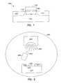
- the inventionrelates to semiconductor devices and device fabrication. Specifically, the invention relates to gate dielectric layers of transistor devices and their method of fabrication.
- FIG. 1A common configuration of such a transistor is shown in FIG. 1. While the following discussion uses FIG. 1 to illustrate a transistor from the prior art, one skilled in the art will recognize that the present invention could be incorporated into the transistor shown in FIG. 1 to form a novel transistor according to the invention.
- the transistor 100is fabricated in a substrate 110 that is typically silicon, but could be fabricated from other semiconductor materials as well.
- the transistor 100has a first source/drain region 120 and a second source/drain region 130 .
- a body region 132is located between the first source/drain region and the second source/drain region, where the body region 132 defines a channel of the transistor with a channel length 134 .
- a gate dielectric, or gate oxide 140is located on the body region 132 with a gate 150 located over the gate dielectric.
- the gate dielectriccan be formed from materials other than oxides, the gate dielectric is typically an oxide, and is commonly referred to as a gate oxide.
- the gatemay be fabricated from polycrystalline silicon (polysilicon), or other conducting materials such as metal may be used.
- the gate dielectric 140In fabricating transistors to be smaller in size and reliably operating on lower power supplies, one important design criteria is the gate dielectric 140 .
- the mainstay for forming the gate dielectrichas been silicon dioxide, SiO 2 .
- a thermally grown amorphous SiO 2 layerprovides an electrically and thermodynamically stable material, where the interface of the SiO 2 layer with underlying Si provides a high quality interface as well as superior electrical isolation properties.
- use of SiO 2 on Sihas provided defect charge densities on the order of 10 10 /cm 2 , midgap interface state densities of approximately 10 10 /cm 2 eV, and breakdown voltages in the range of 15 MV/cm. With such qualities, there would be no apparent need to use a material other than SiO 2 , but increased scaling and other requirements for gate dielectrics create the need to find other dielectric materials to be used for a gate dielectric.
- a method of forming a gate dielectricincludes forming a layer of Pr 2 O 3 on a substrate and forming a layer of another lanthanide oxide onto the layer of Pr 2 O 3 .
- This second layeris formed of a lanthanide oxide selected from the group consisting of Nd 2 O 3 , Sm 2 O 3 , Gd 2 O 3 , and Dy 2 O 3 .
- the layer of Pr 2 O 3 and the layer of the lanthanide oxidecan be formed as a nanolaminate.
- a gate dielectric formed as a combination of layers of Pr 2 O 3 and another lanthanide oxidehas a larger dielectric constant than silicon dioxide, a relatively small leakage current, and good stability with respect to a silicon based substrate.
- Embodiments according to the teachings of the present inventioninclude forming transistors, memory devices, and electronic systems.
- Other embodimentsinclude structures for transistors, memory devices, and electronic systems with dielectric gates of layers of Pr 2 O 3 and another lanthanide oxide. Such dielectric gates provide a significantly thinner equivalent oxide thickness compared with a silicon oxide gate having the same physical thickness. Alternatively, such dielectric gates provide a significantly thicker physical thickness than a silicon oxide gate having the same equivalent oxide thickness.
- FIG. 1depicts a common configuration of a transistor.
- FIG. 2depicts an embodiment of a deposition process for forming a gate dielectric using electron beam evaporation according to the teachings of the present invention.
- FIG. 3depicts an embodiment of another configuration of a transistor capable of being fabricated according to the teachings of the present invention.
- FIG. 4illustrates a perspective view of an embodiment of a personal computer incorporating devices made according to the teachings of the present invention.
- FIG. 5illustrates a schematic view of an embodiment of a processing unit incorporating devices made according to the teachings of the present invention.
- FIG. 6illustrates a schematic view of an embodiment of a DRAM memory device according to the teachings of the present invention.
- the term “horizontal” as used in this applicationis defined as a plane parallel to the conventional plane or surface of a wafer or substrate, regardless of the orientation of the wafer or substrate.
- the term “vertical”refers to a direction perpendicular to the horizontal as defined above. Prepositions, such as “on”, “side” (as in “sidewall”), “higher”, “lower”, “over” and “under” are defined with respect to the conventional plane or surface being on the top surface of the wafer or substrate, regardless of the orientation of the wafer or substrate.
- a gate dielectric 140 of FIG. 1when operating in a transistor, has both a physical gate dielectric thickness and an equivalent oxide thickness (t eq )
- the equivalent oxide thicknessquantifies the electrical properties, such as capacitance, of a gate dielectric 140 in terms of a representative physical thickness.
- t eqis defined as the thickness of a theoretical SiO 2 layer that would be required to have the same capacitance density as a given dielectric, ignoring leakage current and reliability considerations.
- a SiO 2 layer of thickness, t, deposited on a Si surface as a gate dielectricwill also have a t eq larger than its thickness, t.
- This t eqresults from the capacitance in the surface channel on which the SiO 2 is deposited due to the formation of a depletion/inversion region.
- This depletion/inversion regioncan result in t eq being from 3 to 6 Angstroms ( ⁇ ) larger than the SiO 2 thickness, t.
- the gate dielectric equivalent oxide thickness, t eqto under 10 ⁇
- the physical thickness requirement for a SiO 2 layer used for a gate dielectricwould be need to be approximately 4 to 7 ⁇ .
- a thin SiO 2 layer of only one or two monolayerswill not form a full band gap.
- the lack of a full band gap in a SiO 2 gate dielectricwould cause an effective short between an underlying Si channel and an overlying polysilicon gate.
- This undesirable propertysets a limit on the physical thickness to which a SiO 2 layer can be scaled.
- the minimum thickness due to this monolayer effectis thought to be about 7-8 ⁇ . Therefore, for future devices to have a t eq less than about 10 ⁇ , other dielectrics than SiO 2 need to be considered for use as a gate dielectric.
- the resulting capacitancewould be that of two dielectrics in series.
- the t eq of the dielectric layerwould be the sum of the SiO 2 thickness and a multiplicative factor of the thickness, t, of the dielectric being formed, written as
- the t eqis again limited by a SiO 2 layer.
- the t eqwould be limited by the layer with the lowest dielectric constant.
- the layer interfacing with the silicon layermust provide a high quality interface to maintain a high channel carrier mobility.
- Pr 2 O 3One candidate for forming gate dielectrics is Pr 2 O 3 .
- crystalline praseodymium oxide on siliconwas reported to have outstanding dielectric properties.
- forming a layer of Pr 2 O 3 on a substrate and forming a layer of another lanthanide oxide onto the layer of Pr 2 O 3is controlled to form a thin layer of each material with the combination of the two alternating layers of insulators forming a nanolaminate.
- the other lanthanide oxide used to form the nanolaminateis selected from a group consisting of Nd 2 O 3 , Sm 2 O 3 , Gd 2 O 3 , and Dy 2 O 3 .
- the nanolaminate formed as the dielectric layercan be formed from multiple alternating thin layers of lanthanide oxides with the initial layer deposited being a layer of Pr 2 O 3 .
- using Pr 2 O 3 for the initial layerprovides a thin amorphous layer or region at the surface of a silicon based substrate.
- a nanolaminateis grown by forming a layer of Pr 2 O 3 on a substrate by electron beam evaporation. Subsequently, a layer of another lanthanide oxide is formed onto the layer of Pr 2 O 3 also by electron beam evaporation. The resulting nanolaminate has a total thickness which is about the same as the thickness of the initial layer of Pr 2 O 3 formed on the substrate. Thus, each layer in the nanolaminate is reduced to one-half the original thickness deposited.
- Such filmsare uniformly produced with a t eq less than 20 ⁇ , typically with about a t eq of about 14 ⁇ .
- FIG. 2depicts an embodiment of a deposition process for forming a gate dielectric using electron beam evaporation according to the teachings of the present invention.
- This processcan be used to deposit a material forming a film containing a layer of Pr 2 O 3 and a layer of another lanthanide oxide on a surface such as a body region of a transistor.
- a substrate 210is placed inside a deposition chamber 260 .
- the substrate in this embodimentis masked by a first masking structure 270 and a second masking structure 271 .
- the unmasked region 233includes a body region of a transistor, however one skilled in the art will recognize that other semiconductor device structures may utilize this process.
- the electron gun 263generates an electron beam 264 that hits target 261 .
- target 261contains a ceramic Pr 6 O 11 source, which is evaporated due to the impact of the electron beam 264 .
- the evaporated material 268is then distributed throughout the chamber 260 .
- a dielectric layer of Pr 2 O 3is grown forming a film 240 on the surface of the exposed body region 233 that it contacts.
- the growth ratecan vary with a typical rate of 0.1 ⁇ /s.
- the resultant Pr 2 O 3 layerincludes a thin amorphous interfacial layer of about 0.5 nm thickness separating a crystalline layer of Pr 2 O 3 from the substrate on which it is grown. This thin amorphous layer is beneficial in reducing the number of interface charges and eliminating any grain boundary paths for conductance from the substrate.
- Other source materialscan be used for forming the Pr 2 O 3 layer, as are known to those skilled in the art.
- the structureis annealed briefly at 600° C. As a result of this brief anneal, there is no significant hysteresis in capacitance-voltage (C-V) measurements. Further, the nanolaminates can be annealed up to 1000° C. for 15 seconds with no degradation in electrical properties.
- such filmshave a t eq of 14 ⁇ with a leakage current of approximately 5 ⁇ 10 ⁇ 9 ⁇ /cm 2 at a gate voltages of ⁇ 1 V, with a dielectric constant ranging from the dielectric constant of a Pr 2 O 3 film on silicon, 31, to the dielectric constant of the other selected lanthanide oxide.
- this leakage currentis at least 10 4 times lower that the best published value of HfO 2 or ZrO 2 films with the same t eq and a 3 nm thick SiO 2 layer.
- alternating layers of Pr 2 O 3 and another selected lanthanide oxideare formed by controlled electron beam evaporation providing layers of material of predetermined thickness.
- This controlallows the engineering of a dielectric with a predetermined thickness, and composition.
- a dielectric layer with a predetermined t eq in a narrow range of valuescan be grown.
- additional layers of additional lanthanide oxidescan be formed.
- the dielectric layer formed having an interfacial layer between the substrate on which it is grown and a lanthanide oxide nanolaminatecan have an effective dielectric constant considerably less than a dielectric constant associated with a nanolaminate of lanthanide oxides. This is dependent upon the dielectric constant of the interfacial material being considerably less than the dielectric constant of the lanthanide oxides used to form the nanolaminate.
- a Pr 2 O 3 layercan be formed on a silicon based substrate having a dielectric constant of about 31 with an interfacial layer of about 0.5 nm (5 ⁇ ).
- an effective dielectric constant for a thin layer of Pr 2 O 3 on siliconis about 15.
- Similar effective dielectric constantsare associated with thin layers of Nd 2 O 3 , Sm 2 O 3 , Gd 2 O 3 , and Dy 2 O 3 oxides on silicon.
- a thin layer of Nd 2 O 3has an effective dielectric constant of about 12.9 with an interfacial layer of about 8.2 ⁇
- a thin layer of Sm 2 O 3has an effective dielectric constant of about 11.4 with an interfacial layer of about 5.5 ⁇
- a thin layer of Gd 2 O 3has an effective dielectric constant of about 13.9 with an interfacial layer of about 10 ⁇
- a thin layer of Dy 2 O 3has an effective dielectric constant of about 14.3 with an interfacial layer of about 12 ⁇ .
- Lanthanide oxides grown on silicon with these reduced effective dielectric constants and corresponding interfacial layerscan be attained with a t eq equal to about 13 ⁇ for Pr 2 O 3 , about 12.4 ⁇ for Nd 2 O 3 , about 12.2 ⁇ for Sm 2 O 3 , about 13 ⁇ for Gd 2 O 3 , and about 13.3 ⁇ for Dy 2 O 3 . Consequently, nanolaminates of these lanthanide oxides can be formed with an effective dielectric constants in the range of 11 to 15 and a t eq in the range of about 12 ⁇ to about 14 ⁇ .
- the formation of the interfacial layeris one factor in determining how thin a layer can be grown.
- An interfacial layercan be SiO 2 for many processes forming a non-SiO 2 dielectric on a silicon substrate.
- a thin amorphous interfacial layeris formed that is not a SiO 2 layer.
- this interfacial layeris either an amorphous layer primarily of Pr 2 O 3 formed between the silicon substrate and a crystalline form of Pr 2 O 3 , or a layer of Pr—Si—O silicate.
- the dielectric constant for Pr—Si—O silicateis significantly greater than SiO 2 , but not as high as Pr 2 O 3 .
- Another factor setting a lower limit for the scaling of a dielectric layeris the number of monolayers of the dielectric structure necessary to develop a full band gap such that good insulation is maintained between an underlying silicon layer and an overlying conductive layer on the dielectric layer or film. This requirement is necessary to avoid possible short circuit effects between the underlying silicon layer and the overlying conductive layer used. In one embodiment, for a 0.5 nm interfacial layer and several monolayers of lanthanide grown, an expected lower limit for the physical thickness of a dielectric layer grown by forming a lanthanide oxide nanolaminate is anticipated to be in about the 2-4 nm range.
- typical dielectric layers or filmscan be grown by forming lanthanide oxide nanolaminates having physical thickness in the range of 4 to 10 nm.
- the number of layers used, the thickness of each layer, and the lanthanide oxide used for each layercan be engineered to provide the desired electrical characteristics.
- Pr 2 O 3 used as the initial layeris expected to provide excellent overall results with respect to reliability, current leakage, and ultra-thin t eq .
- Alternate embodimentsinclude forming lanthanide oxide nanolaminates by electron beam evaporation with target material to form Pr 2 O 3 other than Pr 6 O 11 , forming lanthanide oxide nanolaminates by atomic layer deposition, and electron beam evaporation forming lanthanide oxide nanolaminates with initial layers of a lanthanide oxide other than Pr 2 O 3 .
- the physical thicknessescan range from about 2 nm to about 10 nm with typical thickness ranging from about 4 nm to about 10 nm.
- Such layershave an effective dielectric constant ranging from 11 to 31, where a layer with a typical interfacial layer has an effective dielectric constant in the range 11 to 16 and a layer with a significantly thin interfacial layer can attain an effective dielectric constant in the range 25 to 31. Consequently, a range for the equivalent oxide thickness of a dielectric layer formed as a lanthanide oxide nanolaminate can be engineered over a significant range.
- the novel process described aboveprovides significant advantages by providing a straight forward method of forming dielectric layers having ultra-thin equivalent oxide thicknesses by electron beam evaporation.
- Praseodymium oxide-based nanolaminatesprovide excellent reliability characteristics, based on measurements of current density as a function of gate voltage and stress induced leakage currents for the lanthanide oxides which form the nanolaminates.
- the dielectric breakdownoccurs a least above 43 MEV/cm.
- the lanthanide oxides forming the nanolaminatesretain excellent J-V characteristics even after stress-induced electrical breakdown.
- the praseodymium oxide forming the first layer of the nanolaminateis epitaxially oriented with respect to a substrate on which it is formed, the praseodymium layer is separated from the substrate surface by a thin amorphous layer. Additionally, the novel process and novel dielectric layer structure can be implemented to form transistors, memory devices, and electronic systems including information handling devices.
- a transistor 100 as depicted in FIG. 1can be formed by forming a source/drain region 120 and another source/drain region 130 in a silicon based substrate 110 where the two source/drain regions 120 , 130 are separated by a body region 132 .
- the body region 132 separated by the source/drain 120 and the source/drain 130defines a channel having a channel length 134 .
- Pr 2 O 3is formed on the body region 132 by evaporation using a electron gun at a controlled rate.
- lanthanide oxideselected from the group consisting of Nd 2 O 3 , Sm 2 O 3 , Gd 2 O 3 , and Dy 2 O 3 is formed on the Pr 2 O 3 layer by controlling a rate of electron beam evaporation.
- This controlled processforms a film 140 containing a nanolaminate of Pr 2 O 3 and another lanthanide oxide on the body region 132 .
- a gate 150is formed over the gate dielectric 140 .
- forming the gate 150includes forming a polysilicon layer, though a metal gate can be formed in an alternative process. Forming the substrate, source/region regions, and the gate is performed using standard processes known to those skilled in the art. Additionally, the sequencing of the various elements of the process for forming a transistor is conducted with standard fabrication processes, also as known to those skilled in the art.
- FIG. 3depicts a transistor 300 having a silicon based substrate 310 with two source/drain regions 320 , 330 separated by a body region 332 .
- the body region 332 between the two source/drain regions 320 , 330defines a channel region having a channel length 334 .
- a stack 355including a gate dielectric 340 , a floating gate 352 , a floating gate dielectric 342 , and a control gate 350 .
- the gate dielectric 340can be formed as described above with the remaining elements of the transistor 300 formed using processes known to those skilled in the art. Alternately, both the gate dielectric 340 and the floating gate dielectric 342 can be formed by various embodiments in accordance with the present invention as described above.
- Transistors created by the methods described abovemay be implemented into memory devices and electronic systems including information handling devices.
- Information handling devices having a dielectric layer containing a lanthanide oxide nanolaminatecan be constructed using various embodiments of the methods described above. Such information devices include wireless systems, telecommunication systems, and computers.
- An embodiment of a computer having a dielectric layer containing a lanthanide oxide nanolaminateis shown in FIGS. 4 - 6 and described below. While specific types of memory devices and computing devices are shown below, it will be recognized by one skilled in the art that several types of memory devices and information handling devices utilize the invention.
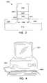
- a personal computeras shown in FIGS. 4 and 5, include a monitor 400 , keyboard input 402 and a processing unit 404 .
- the processor unit 404typically includes microprocessor 506 , memory bus circuit 508 having a plurality of memory slots 512 ( a - n ), and other peripheral circuitry 510 .
- Peripheral circuitry 510permits various peripheral devices 524 to interface processor-memory bus 520 over input/output (I/O) bus 522 .
- the personal computer shown in FIGS. 4 and 5also includes at least one transistor having a gate dielectric containing a lanthanide oxide nanolaminate in an embodiment according to the teachings of the present invention.
- Microprocessor 506produces control and address signals to control the exchange of data between memory bus circuit 508 and microprocessor 506 and between memory bus circuit 508 and peripheral circuitry 510 . This exchange of data is accomplished over high speed memory bus 520 and over high speed I/O bus 522 .
- Coupled to memory bus 520are a plurality of memory slots 512 ( a - n ) which receive memory devices well known to those skilled in the art.
- memory slots 512a - n
- SIMMssingle in-line memory modules
- DIMMsdual in-line memory modules
- Page mode operations in a DRAMare defined by the method of accessing a row of a memory cell arrays and randomly accessing different columns of the array. Data stored at the row and column intersection can be read and output while that column is accessed. Page mode DRAMs require access steps which limit the communication speed of memory circuit 508 .
- An alternate type of deviceis the extended data output (EDO) memory which allows data stored at a memory array address to be available as output after the addressed column has been closed. This memory can increase some communication speeds by allowing shorter access signals without reducing the time in which memory output data is available on memory bus 520 .
- EDOextended data output
- Other alternative types of devicesinclude SDRAM, DDR SDRAM, SLDRAM and Direct RDRAM as well as others such as SRAM or Flash memories.
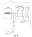
- FIG. 6is a block diagram of an illustrative DRAM device 600 compatible with memory slots 512 ( a - n ).
- the description of DRAM 600has been simplified for purposes of illustrating a DRAM memory device and is not intended to be a complete description of all the features of a DRAM. Those skilled in the art will recognize that a wide variety of memory devices may be used in the implementation of the present invention.
- the example of a DRAM memory device shown in FIG. 6includes at least one transistor having a gate dielectric containing a lanthanide oxide nanolaminate in an embodiment according to the teachings of the present invention.
- Control, address and data information provided over memory bus 520is further represented by individual inputs to DRAM 600 , as shown in FIG. 6. These individual representations are illustrated by data lines 602 , address lines 604 and various discrete lines directed to control logic 606 .
- DRAM 600includes memory array 610 which in turn comprises rows and columns of addressable memory cells. Each memory cell in a row is coupled to a common word line. The word line is coupled to gates of individual transistors, where at least one transistor has a gate coupled to a gate dielectric containing a layer Pr 2 O 3 and a layer another lanthanide oxide in accordance with the method and structure previously described above. Additionally, each memory cell in a column is coupled to a common bit line. Each cell in memory array 610 includes a storage capacitor and an access transistor as is conventional in the art.
- DRAM 600interfaces with, for example, microprocessor 606 through address lines 604 and data lines 602 .
- DRAM 600may interface with a DRAM controller, a micro-controller, a chip set or other electronic system.
- Microprocessor 506also provides a number of control signals to DRAM 600 , including but not limited to, row and column address strobe signals RAS and CAS, write enable signal WE, an output enable signal OE and other conventional control signals.
- Row address buffer 612 and row decoder 614receive and decode row addresses from row address signals provided on address lines 604 by microprocessor 506 . Each unique row address corresponds to a row of cells in memory array 610 .
- Row decoder 614includes a word line driver, an address decoder tree, and circuitry which translates a given row address received from row address buffers 612 and selectively activates the appropriate word line of memory array 610 via the word line drivers.
- Column address buffer 616 and column decoder 618receive and decode column address signals provided on address lines 604 . Column decoder 618 also determines when a column is defective and the address of a replacement column. Column decoder 618 is coupled to sense amplifiers 620 . Sense amplifiers 620 are coupled to complementary pairs of bit lines of memory array 610 .
- Sense amplifiers 620are coupled to data-in buffer 622 and data-out buffer 624 .
- Data-in buffers 622 and data-out buffers 624are coupled to data lines 602 .
- data lines 602provide data to data-in buffer 622 .
- Sense amplifier 620receives data from data-in buffer 622 and stores the data in memory array 610 as a charge on a capacitor of a cell at an address specified on address lines 604 .
- DRAM 600transfers data to microprocessor 506 from memory array 610 .
- Complementary bit lines for the accessed cellare equilibrated during a precharge operation to a reference voltage provided by an equilibration circuit and a reference voltage supply.
- the charge stored in the accessed cellis then shared with the associated bit lines.
- a sense amplifier of sense amplifiers 620detects and amplifies a difference in voltage between the complementary bit lines.
- the sense amplifierpasses the amplified voltage to data-out buffer 624 .
- Control logic 606is used to control the many available functions of DRAM 600 .
- various control circuits and signals not detailed hereininitiate and synchronize DRAM 600 operation as known to those skilled in the art.
- the description of DRAM 600has been simplified for purposes of illustrating the present invention and is not intended to be a complete description of all the features of a DRAM.
- memory devicesincluding but not limited to, SDRAMs, SLDRAMs, RDRAMs and other DRAMs and SRAMs, VRAMs and EEPROMs, may be used in the implementation of embodiments of the present invention.
- the DRAM implementation described hereinis illustrative only and not intended to be exclusive or limiting.
- a gate dielectric containing a layer of Pr 2 O 3 and a layer of another lanthanide oxide, and a method of fabricating such a gate dielectricare provided that produces a reliable gate dielectric having an equivalent oxide thickness thinner than attainable using SiO 2 .
- Gate dielectric structures that are formed using the methods described hereininclude nanolaminates of Pr 2 O 3 and another lanthanide oxide selected from the group consisting of Nd 2 O 3 , Sm 2 O 3 , Gd 2 O 3 , and Dy 2 O 3 . These gate dielectric structures are thermodynamically stable such that the gate dielectrics formed will have minimal reactions with a silicon substrate or other structures during processing.
- Transistors, higher level ICs, devices, and electronic systemsare provided utilizing the novel gate dielectric and process of formation.
- Gate dielectric layers of lanthanide oxide nanolaminatesare formed having a high dielectric constant ( ⁇ ), where the gate dielectrics are capable of a t eq of 14 ⁇ or thinner, providing suitable substitutes for SiO 2 gate dielectrics.
- the physical thickness of the Pr 2 O 3 layeris much larger than the SiO 2 thickness associated with the t eq limit of SiO 2 . Forming the larger thickness provides advantages in processing the gate dielectric.
- a dielectric layer or film containing a lanthanide oxide nanolaminateallows the engineering or selection of a dielectric constant ranging from that of Pr 2 O 3 to a dielectric constant of another lanthanide oxide that is comprised in the nanolaminate.
Landscapes
- Engineering & Computer Science (AREA)
- Chemical & Material Sciences (AREA)
- Physics & Mathematics (AREA)
- Chemical Kinetics & Catalysis (AREA)
- Condensed Matter Physics & Semiconductors (AREA)
- Computer Hardware Design (AREA)
- Microelectronics & Electronic Packaging (AREA)
- Power Engineering (AREA)
- Manufacturing & Machinery (AREA)
- General Physics & Mathematics (AREA)
- General Chemical & Material Sciences (AREA)
- Materials Engineering (AREA)
- Mechanical Engineering (AREA)
- Metallurgy (AREA)
- Organic Chemistry (AREA)
- Crystallography & Structural Chemistry (AREA)
- Optics & Photonics (AREA)
- Health & Medical Sciences (AREA)
- Toxicology (AREA)
- Semiconductor Memories (AREA)
- Insulated Gate Type Field-Effect Transistor (AREA)
- Thin Film Transistor (AREA)
Abstract
Description
- This application is related to the following, co-pending, commonly assigned applications, incorporated herein by reference:[0001]
- U.S. application Ser. No. 10/027,315, attorney docket no. 1303.033US1 entitled: “Low-Temperature Grown High-Quality Ultra-Thin Praseodymium Gate Dielectrics.”[0002]
- The invention relates to semiconductor devices and device fabrication. Specifically, the invention relates to gate dielectric layers of transistor devices and their method of fabrication.[0003]
- The semiconductor device industry has a market driven need to improve speed performance, improve its low static (off-state) power requirements, and adapt to a wide range of power supply and output voltage requirements for it silicon based microelectronic products. In particular, in the fabrication of transistors, there is continuous pressure to reduce the size of devices such as transistors. The ultimate goal is to fabricate increasingly smaller and more reliable integrated circuits (ICs) for use in products such as processor chips, mobile telephones, or memory devices such as DRAMs. The smaller devices are frequently powered by batteries, where there is also pressure to reduce the size of the batteries, and to extend the time between battery charges. This forces the industry to not only design smaller transistors, but to design them to operate reliably with lower power supplies.[0004]
- Currently, the semiconductor industry relies on the ability to reduce or scale the dimensions of its basic devices, primarily, the silicon based metal-oxide-semiconductor field effect transistor (MOSFET). A common configuration of such a transistor is shown in FIG. 1. While the following discussion uses FIG. 1 to illustrate a transistor from the prior art, one skilled in the art will recognize that the present invention could be incorporated into the transistor shown in FIG. 1 to form a novel transistor according to the invention. The[0005]
transistor 100 is fabricated in asubstrate 110 that is typically silicon, but could be fabricated from other semiconductor materials as well. Thetransistor 100 has a first source/drain region 120 and a second source/drain region 130. Abody region 132 is located between the first source/drain region and the second source/drain region, where thebody region 132 defines a channel of the transistor with achannel length 134. A gate dielectric, orgate oxide 140 is located on thebody region 132 with agate 150 located over the gate dielectric. Although the gate dielectric can be formed from materials other than oxides, the gate dielectric is typically an oxide, and is commonly referred to as a gate oxide. The gate may be fabricated from polycrystalline silicon (polysilicon), or other conducting materials such as metal may be used. - In fabricating transistors to be smaller in size and reliably operating on lower power supplies, one important design criteria is the gate dielectric[0006]140. The mainstay for forming the gate dielectric has been silicon dioxide, SiO2. A thermally grown amorphous SiO2layer provides an electrically and thermodynamically stable material, where the interface of the SiO2layer with underlying Si provides a high quality interface as well as superior electrical isolation properties. In typical processing, use of SiO2on Si has provided defect charge densities on the order of 1010/cm2, midgap interface state densities of approximately 1010/cm2eV, and breakdown voltages in the range of 15 MV/cm. With such qualities, there would be no apparent need to use a material other than SiO2, but increased scaling and other requirements for gate dielectrics create the need to find other dielectric materials to be used for a gate dielectric.
- What is needed is an alternate dielectric material for forming a gate dielectric that has a high dielectric constant relative to SiO[0007]2, and is thermodynamically stable with respect to silicon such that forming the dielectric on a silicon layer will not result in SiO2formation, or diffusion of material, such as dopants, into the gate dielectric from the underlying silicon layer.
- A solution to the problems as discussed above is addressed in embodiments according to the teachings of the present invention. In one embodiment, a method of forming a gate dielectric includes forming a layer of Pr[0008]2O3on a substrate and forming a layer of another lanthanide oxide onto the layer of Pr2O3. This second layer is formed of a lanthanide oxide selected from the group consisting of Nd2O3, Sm2O3, Gd2O3, and Dy2O3. Further, the layer of Pr2O3and the layer of the lanthanide oxide can be formed as a nanolaminate. Advantageously, a gate dielectric formed as a combination of layers of Pr2O3and another lanthanide oxide has a larger dielectric constant than silicon dioxide, a relatively small leakage current, and good stability with respect to a silicon based substrate. Embodiments according to the teachings of the present invention include forming transistors, memory devices, and electronic systems.
- Other embodiments include structures for transistors, memory devices, and electronic systems with dielectric gates of layers of Pr[0009]2O3and another lanthanide oxide. Such dielectric gates provide a significantly thinner equivalent oxide thickness compared with a silicon oxide gate having the same physical thickness. Alternatively, such dielectric gates provide a significantly thicker physical thickness than a silicon oxide gate having the same equivalent oxide thickness.
- These and other embodiments, aspects, advantages, and features of the present invention will be set forth in part in the description which follows, and in part will become apparent to those skilled in the art by reference to the following description of the invention and referenced drawings or by practice of the invention. The aspects, advantages, and features of the invention are realized and attained by means of the instrumentalities, procedures, and combinations particularly pointed out in the appended claims.[0010]
- FIG. 1 depicts a common configuration of a transistor.[0011]
- FIG. 2 depicts an embodiment of a deposition process for forming a gate dielectric using electron beam evaporation according to the teachings of the present invention.[0012]
- FIG. 3 depicts an embodiment of another configuration of a transistor capable of being fabricated according to the teachings of the present invention.[0013]
- FIG. 4 illustrates a perspective view of an embodiment of a personal computer incorporating devices made according to the teachings of the present invention.[0014]
- FIG. 5 illustrates a schematic view of an embodiment of a processing unit incorporating devices made according to the teachings of the present invention.[0015]
- FIG. 6 illustrates a schematic view of an embodiment of a DRAM memory device according to the teachings of the present invention.[0016]
- In the following detailed description of the invention, reference is made to the accompanying drawings which form a part hereof, and in which is shown, by way of illustration, specific embodiments in which the invention may be practiced. In the drawings, like numerals describe substantially similar components throughout the several views. These embodiments are described in sufficient detail to enable those skilled in the art to practice the invention. Other embodiments may be utilized and structural, logical, and electrical changes may be made without departing from the scope of the present invention.[0017]
- The terms wafer and substrate used in the following description include any structure having an exposed surface with which to form the integrated circuit (IC) structure of the invention. The term substrate is understood to include semiconductor wafers. The term substrate is also used to refer to semiconductor structures during processing, and may include other layers that have been fabricated thereupon. Both wafer and substrate include doped and undoped semiconductors, epitaxial semiconductor layers supported by a base semiconductor or insulator, as well as other semiconductor structures well known to one skilled in the art. The term conductor is understood to include semiconductors, and the term insulator or dielectric is defined to include any material that is less electrically conductive than the materials referred to as conductors.[0018]
- The term “horizontal” as used in this application is defined as a plane parallel to the conventional plane or surface of a wafer or substrate, regardless of the orientation of the wafer or substrate. The term “vertical” refers to a direction perpendicular to the horizontal as defined above. Prepositions, such as “on”, “side” (as in “sidewall”), “higher”, “lower”, “over” and “under” are defined with respect to the conventional plane or surface being on the top surface of the wafer or substrate, regardless of the orientation of the wafer or substrate. The following detailed description is, therefore, not to be taken in a limiting sense, and the scope of the present invention is defined only by the appended claims, along with the full scope of equivalents to which such claims are entitled.[0019]
- A gate dielectric[0020]140 of FIG. 1, when operating in a transistor, has both a physical gate dielectric thickness and an equivalent oxide thickness (teq) The equivalent oxide thickness quantifies the electrical properties, such as capacitance, of a gate dielectric140 in terms of a representative physical thickness. teqis defined as the thickness of a theoretical SiO2layer that would be required to have the same capacitance density as a given dielectric, ignoring leakage current and reliability considerations.
- A SiO[0021]2layer of thickness, t, deposited on a Si surface as a gate dielectric will also have a teqlarger than its thickness, t. This teqresults from the capacitance in the surface channel on which the SiO2is deposited due to the formation of a depletion/inversion region. This depletion/inversion region can result in teqbeing from 3 to 6 Angstroms (Å) larger than the SiO2thickness, t. Thus, with the semiconductor industry driving to someday scale the gate dielectric equivalent oxide thickness, teq, to under 10 Å, the physical thickness requirement for a SiO2layer used for a gate dielectric would be need to be approximately 4 to 7 Å.
- Additional requirements on a SiO[0022]2layer would depend on the gate electrode used in conjunction with the SiO2gate dielectric. Using a conventional polysilicon gate would result in an additional increase in teqfor the SiO2layer. This additional thickness could be eliminated by using a metal gate electrode, though metal gates are not currently used in complementary metal-oxide-semiconductor field effect transistor (CMOS) technology. Thus, future devices would be designed towards a physical SiO2gate dielectric layer of about 5 Å or less. Such a small thickness requirement for a SiO2oxide layer creates additional problems.
- Silicon dioxide is used as a gate dielectric, in part, due to its electrical isolation properties in a SiO[0023]2—Si based structure. This electrical isolation is due to the relatively large band gap of SiO2(8.9 eV) making it a good insulator from electrical conduction. Signification reductions in its band gap would eliminate it as a material for a gate dielectric. As the thickness of a SiO2layer decreases, the number of atomic layers, or monolayers of the material in the thickness decreases. At a certain thickness, the number of monolayers will be sufficiently small that the SiO2layer will not have a complete arrangement of atoms as in a larger or bulk layer. As a result of incomplete formation relative to a bulk structure, a thin SiO2layer of only one or two monolayers will not form a full band gap. The lack of a full band gap in a SiO2gate dielectric would cause an effective short between an underlying Si channel and an overlying polysilicon gate. This undesirable property sets a limit on the physical thickness to which a SiO2layer can be scaled. The minimum thickness due to this monolayer effect is thought to be about 7-8 Å. Therefore, for future devices to have a teqless than about 10 Å, other dielectrics than SiO2need to be considered for use as a gate dielectric.
- For a typical dielectric layer used as a gate dielectric, the capacitance is determined as one for a parallel plate capacitance: C=κε[0024]0A/t, where κ is the dielectric constant, ε0is the permittivity of free space, A is the area of the capacitor, and t is the thickness of the dielectric. The thickness, t, of a material is related to teqfor a given capacitance with the dielectric constant of SiO2, κox=3.9, associated with teq, as
- t=(κ/κox)teq=(κ/3.9)teq.
- Thus, materials with a dielectric constant greater than that of SiO[0025]2, 3.9, will have a physical thickness that can be considerably larger than a desired teq, while providing the desired equivalent oxide thickness. For example, an alternate dielectric material with a dielectric constant of 10 could have a thickness of about 25.6 Å to provide a teqof 10 Å, not including any depletion/inversion layer effects. Thus, the reduced equivalent oxide thickness of transistors can be realized by using dielectric materials with higher dielectric constants than SiO2.
- The thinner equivalent oxide thickness, t[0026]eq, required for lower transistor operating voltages and smaller transistor dimensions may be realized by a significant number of materials, but additional fabricating requirements makes determining a suitable replacement for SiO2difficult. The current view for the microelectronics industry is still for Si based devices. This requires that the gate dielectric employed be grown on a silicon substrate or silicon layer, which places significant restraints on the substitute dielectric material. During the formation of the dielectric on the silicon layer, there exists the possibility that a small layer of SiO2could be formed in addition to the desired dielectric. The result would effectively be a dielectric layer consisting of two sublayers in parallel with each other and the silicon layer on which the dielectric is formed. In such a case, the resulting capacitance would be that of two dielectrics in series. As a result, the teqof the dielectric layer would be the sum of the SiO2thickness and a multiplicative factor of the thickness, t, of the dielectric being formed, written as
- teq=tSiO2+(κox/κ)t.
- Thus, if a SiO[0027]2layer is formed in the process, the teqis again limited by a SiO2layer. In the event that a barrier layer is formed between the silicon layer and the desired dielectric in which the barrier layer prevents the formation of a SiO2layer, the teqwould be limited by the layer with the lowest dielectric constant. However, whether a single dielectric layer with a high dielectric constant or a barrier layer with a higher dielectric constant than SiO2is employed, the layer interfacing with the silicon layer must provide a high quality interface to maintain a high channel carrier mobility.
- One of the advantages using SiO[0028]2as a gate dielectric has been that the formation of the SiO2layer results is an amorphous gate dielectric. Having an amorphous structure for a gate dielectric is advantageous because grain boundaries in polycrystalline gate dielectrics provide high leakage paths. Additionally, grain size and orientation changes throughout a polycrystalline gate dielectric can cause variations in the film's dielectric constant. The abovementioned material properties, including structure, are for the materials in a bulk form. Many materials having the advantage of a high dielectric constant relative to SiO2also have the disadvantage of a crystalline form, at least in a bulk configuration. The best candidates for replacing SiO2as a gate dielectric are those with high dielectric constant, which can be fabricated as a thin layer with an amorphous form.
- One candidate for forming gate dielectrics is Pr[0029]2O3. In co-pending, commonly assigned U.S. patent applications: entitled “Low-Temperature Grown High-Quality Ultra-Thin Praseodymium Gate Dielectrics,” attorney docket no. 1303.033US1, Ser. No. 10/027,315, Pr2O3is disclosed as a replacement for SiO2in forming gate dielectrics and other dielectric films in electronic devices such as MOS transistors. Additionally, in a recent article by H. J. Osten et al.,Technical Digest of IEDM, pp. 653-656 (2000), crystalline praseodymium oxide on silicon was reported to have outstanding dielectric properties.
- However, in a recent article by H. Zhang et al.,[0030]Journal of the Electrochemical Society,148 (4) pp. F63-F66 (2001), it was noted that dielectric layers using high-κ materials tend to have a narrower bandgap. The article reported investigating the use of nanolaminates of ZrO2/HfO2, ZrO2/Ta2O5, and Ta2O5/HfO2, instead of a single layer of either Ta2O5, ZrO2, or HfO2. Each nanolaminate, that is, a composite of thin alternating layers of insulators, was grown using Atomic Layer Deposition. The dielectric layers formed of these nanolaminates were reported to have a dielectric constant in the range of 9 to 16, providing a teqreduction factor of about 3 relative to SiO2.
- Embodiments according to the teachings of the present invention provide a novel set of dielectric structures for replacing SiO[0031]2as a gate dielectric and as other dielectrics requiring an ultra-thin equivalent oxide thicknesses, teq. Dielectric layers containing layers of Pr2O3and another lanthanide oxide for use as the replacement dielectric are formed in various embodiments. In one embodiment, a dielectric layer is grown by forming a layer of Pr2O3on a substrate and forming a layer of another lanthanide oxide onto the layer of Pr2O3. In another embodiment, forming a layer of Pr2O3on a substrate and forming a layer of another lanthanide oxide onto the layer of Pr2O3is controlled to form a thin layer of each material with the combination of the two alternating layers of insulators forming a nanolaminate. The other lanthanide oxide used to form the nanolaminate is selected from a group consisting of Nd2O3, Sm2O3, Gd2O3, and Dy2O3. Alternately, the nanolaminate formed as the dielectric layer can be formed from multiple alternating thin layers of lanthanide oxides with the initial layer deposited being a layer of Pr2O3. Advantageously, using Pr2O3for the initial layer provides a thin amorphous layer or region at the surface of a silicon based substrate.
- By forming the dielectric layer as a nanolaminate, the dielectric layer can be grown as a composite whose insulating properties can be adjusted. The engineering of the nanolaminate allows the formation of a dielectric layer with a dielectric constant ranging between the values of the dielectric constants of the lanthanide oxides which form the dielectric layer. However, in many cases the dielectric layer will have an effective dielectric constant less than the dielectric constant of the lanthanide oxides used to form the dielectric layer. This reduction in the effective dielectric constant is due to interfacial layers formed between the silicon substrate surface and the first lanthanide oxide layer of the nanolaminate.[0032]
- In one embodiment, a nanolaminate is grown by forming a layer of Pr[0033]2O3on a substrate by electron beam evaporation. Subsequently, a layer of another lanthanide oxide is formed onto the layer of Pr2O3also by electron beam evaporation. The resulting nanolaminate has a total thickness which is about the same as the thickness of the initial layer of Pr2O3formed on the substrate. Thus, each layer in the nanolaminate is reduced to one-half the original thickness deposited. Such films are uniformly produced with a teqless than 20 Å, typically with about a teqof about 14 Å.
- FIG. 2 depicts an embodiment of a deposition process for forming a gate dielectric using electron beam evaporation according to the teachings of the present invention. This process can be used to deposit a material forming a film containing a layer of Pr[0034]2O3and a layer of another lanthanide oxide on a surface such as a body region of a transistor. In FIG. 2, a
substrate 210 is placed inside adeposition chamber 260. The substrate in this embodiment is masked by afirst masking structure 270 and asecond masking structure 271. In this embodiment, theunmasked region 233 includes a body region of a transistor, however one skilled in the art will recognize that other semiconductor device structures may utilize this process. Also located within thedeposition chamber 260 is anelectron gun 263 and atarget 261. Theelectron gun 263 provides anelectron beam 264 directed attarget 261 containing a source material for forming Pr2O3and other lanthanide oxides on theunmasked region 233 of thesubstrate 210. Theelectron gun 263 includes a rate monitor for controlling the rate of evaporation of the material in thetarget 261 at which theelectron beam 264 is directed. For convenience, control displays and necessary electrical connections as are known to those skilled in the art are not shown in FIG. 2. Alternatively, a chamber can be used with multiple electron guns, where each electron gun is directed to different targets containing sources to form selected lanthanide oxides to be used at different times in the process. - During the evaporation process, the[0035]
electron gun 263 generates anelectron beam 264 that hitstarget 261. In one embodiment,target 261 contains a ceramic Pr6O11source, which is evaporated due to the impact of theelectron beam 264. The evaporatedmaterial 268 is then distributed throughout thechamber 260. A dielectric layer of Pr2O3is grown forming afilm 240 on the surface of the exposedbody region 233 that it contacts. The growth rate can vary with a typical rate of 0.1 Å/s. The resultant Pr2O3layer includes a thin amorphous interfacial layer of about 0.5 nm thickness separating a crystalline layer of Pr2O3from the substrate on which it is grown. This thin amorphous layer is beneficial in reducing the number of interface charges and eliminating any grain boundary paths for conductance from the substrate. Other source materials can be used for forming the Pr2O3layer, as are known to those skilled in the art. - Subsequent to the formation of the Pr[0036]2O3layer, another lanthanide oxide is deposited on the
film 240 converting thefilm 240 from a Pr2O3layer to a nanolaminate of Pr2O3and the other lanthanide oxide. The other lanthanide oxide is selected from the group consisting of Nd2O3, Sm2O3, Gd2O3, and Dy2O3. Depending on the lanthanide oxide selected to form the nanolaminate, a corresponding source material is used in thetarget 261 for electron beam evaporation. The source material for the particular lanthanide oxide is chosen from commercial materials for forming the lanthanide oxide by electron bean evaporation, as is known by those skilled in the art. - After forming the nanolaminate, the structure is annealed briefly at 600° C. As a result of this brief anneal, there is no significant hysteresis in capacitance-voltage (C-V) measurements. Further, the nanolaminates can be annealed up to 1000° C. for 15 seconds with no degradation in electrical properties. In one embodiment, such films have a t[0037]eqof 14 Å with a leakage current of approximately 5×10⁻⁹Å/cm2at a gate voltages of ±1 V, with a dielectric constant ranging from the dielectric constant of a Pr2O3film on silicon, 31, to the dielectric constant of the other selected lanthanide oxide. Advantageously, this leakage current is at least 104times lower that the best published value of HfO2or ZrO2films with the same teqand a 3 nm thick SiO2layer.
- In one embodiment alternating layers of Pr[0038]2O3and another selected lanthanide oxide are formed by controlled electron beam evaporation providing layers of material of predetermined thickness. This control allows the engineering of a dielectric with a predetermined thickness, and composition. Through evaluation of different lanthanide oxides at various thicknesses and number of layers, a dielectric layer with a predetermined teqin a narrow range of values can be grown. Alternately, after forming a Pr2O3layer and a layer of another lanthanide oxide, additional layers of additional lanthanide oxides can be formed. Each layer of an additional lanthanide oxide selected from a group consisting of Pr2O3, Nd2O3, Sm2O3, Gd2O3, and Dy2O3. Consequently, a dielectric layer can be engineered with electrical characteristics suited for a given application. These electrical characteristics include teqand leakage current. A teqof less than 20 Å can be obtained with typically sizes about of about 14 Å to 8.5 Å.
- In another embodiment, nanolaminates of lanthanide oxides are formed by electron beam evaporation. The lanthanide oxides used in these nanolaminates are chosen from the group consisting of Pr[0039]2O3, Nd2O3, Sm2O3, Gd2O3, and Dy2O3. The structure of the nanolaminates can be varied with any one of the group used as the initial layer formed on a substrate. Typically, the substrate is silicon based, since these lanthanide oxides are thermodynamically stable with respect to formation on a silicon surface. In an alternate embodiment, lanthanide oxide nanolaminates are formed by atomic layer deposition.
- The Pr[0040]2O3film formed on a silicon has a dielectric constant of about 31 when formed with little or no interfacial layer between the Pr2O3film and the substrate. The dielectric constants for the other lanthanide oxides are also in the range of 25-30. As a result, a dielectric layer grown by forming a nanolaminate of lanthanide oxides has a dielectric constant in the range of about 25 to about 31. However, with an interfacial layer formed between the surface of the substrate and the first lanthanide oxide, the teqof the dielectric layer is the teqof the interfacial layer in parallel with the lanthanide oxide nanolaminate. Thus, the dielectric layer formed having an interfacial layer between the substrate on which it is grown and a lanthanide oxide nanolaminate can have an effective dielectric constant considerably less than a dielectric constant associated with a nanolaminate of lanthanide oxides. This is dependent upon the dielectric constant of the interfacial material being considerably less than the dielectric constant of the lanthanide oxides used to form the nanolaminate.
- As previously noted above, a Pr[0041]2O3layer can be formed on a silicon based substrate having a dielectric constant of about 31 with an interfacial layer of about 0.5 nm (5 Å). In another embodiment, for an interfacial layer of about 10.7 Å, an effective dielectric constant for a thin layer of Pr2O3on silicon is about 15. Similar effective dielectric constants are associated with thin layers of Nd2O3, Sm2O3, Gd2O3, and Dy2O3oxides on silicon. For example, a thin layer of Nd2O3has an effective dielectric constant of about 12.9 with an interfacial layer of about 8.2 Å, a thin layer of Sm2O3has an effective dielectric constant of about 11.4 with an interfacial layer of about 5.5 Å, a thin layer of Gd2O3has an effective dielectric constant of about 13.9 with an interfacial layer of about 10 Å, and a thin layer of Dy2O3has an effective dielectric constant of about 14.3 with an interfacial layer of about 12 Å. Lanthanide oxides grown on silicon with these reduced effective dielectric constants and corresponding interfacial layers can be attained with a teqequal to about 13 Å for Pr2O3, about 12.4 Å for Nd2O3, about 12.2 Å for Sm2O3, about 13 Å for Gd2O3, and about 13.3 Å for Dy2O3. Consequently, nanolaminates of these lanthanide oxides can be formed with an effective dielectric constants in the range of 11 to 15 and a teqin the range of about 12 Å to about 14 Å.
- The formation of the interfacial layer is one factor in determining how thin a layer can be grown. An interfacial layer can be SiO[0042]2for many processes forming a non-SiO2dielectric on a silicon substrate. However, advantageously, in an embodiment forming a lanthanide oxide nanolaminate with an initial layer of Pr2O3, a thin amorphous interfacial layer is formed that is not a SiO2layer. Typically, this interfacial layer is either an amorphous layer primarily of Pr2O3formed between the silicon substrate and a crystalline form of Pr2O3, or a layer of Pr—Si—O silicate. The dielectric constant for Pr—Si—O silicate is significantly greater than SiO2, but not as high as Pr2O3.
- Another factor setting a lower limit for the scaling of a dielectric layer is the number of monolayers of the dielectric structure necessary to develop a full band gap such that good insulation is maintained between an underlying silicon layer and an overlying conductive layer on the dielectric layer or film. This requirement is necessary to avoid possible short circuit effects between the underlying silicon layer and the overlying conductive layer used. In one embodiment, for a 0.5 nm interfacial layer and several monolayers of lanthanide grown, an expected lower limit for the physical thickness of a dielectric layer grown by forming a lanthanide oxide nanolaminate is anticipated to be in about the 2-4 nm range. Consequently, typical dielectric layers or films can be grown by forming lanthanide oxide nanolaminates having physical thickness in the range of 4 to 10 nm. The number of layers used, the thickness of each layer, and the lanthanide oxide used for each layer can be engineered to provide the desired electrical characteristics. Pr[0043]2O3used as the initial layer is expected to provide excellent overall results with respect to reliability, current leakage, and ultra-thin teq.
- Alternate embodiments include forming lanthanide oxide nanolaminates by electron beam evaporation with target material to form Pr[0044]2O3other than Pr6O11, forming lanthanide oxide nanolaminates by atomic layer deposition, and electron beam evaporation forming lanthanide oxide nanolaminates with initial layers of a lanthanide oxide other than Pr2O3. The physical thicknesses can range from about 2 nm to about 10 nm with typical thickness ranging from about 4 nm to about 10 nm. Such layers have an effective dielectric constant ranging from 11 to 31, where a layer with a typical interfacial layer has an effective dielectric constant in the range 11 to 16 and a layer with a significantly thin interfacial layer can attain an effective dielectric constant in the range 25 to 31. Consequently, a range for the equivalent oxide thickness of a dielectric layer formed as a lanthanide oxide nanolaminate can be engineered over a significant range. The expected teqranges for various effective dielectric constants are shown in the following
Physical Physical Physical Physical Thickness Thickness Thickness Thickness t = 0.5 nm t = 1.0 nm t = 2.0 nm t = 10 nm (5Å) (10 Å) (20 Å) (100 Å) κ teq(Å) teq(Å) teq(Å) teq(Å) 11 1.77 3.55 7.09 35.45 12 1.63 3.25 6.50 32.50 13 1.50 3.00 6.00 30.00 14 1.39 2.79 5.57 27.86 15 1.30 2.60 5.20 26.00 16 1.22 2.44 4.88 24.38 20 0.98 1.95 3.90 19.50 25 0.78 1.56 3.12 15.60 31 0.63 1.26 2.52 12.58 - As noted previously, various embodiments provide a typical t[0045]eqof about 14 Å. With careful preparation and engineering of the lanthanide oxide nanolaminate limiting the size of interfacial regions, a teq down to 2.5 Å or lower is anticipated.
- The novel process described above provides significant advantages by providing a straight forward method of forming dielectric layers having ultra-thin equivalent oxide thicknesses by electron beam evaporation. Praseodymium oxide-based nanolaminates provide excellent reliability characteristics, based on measurements of current density as a function of gate voltage and stress induced leakage currents for the lanthanide oxides which form the nanolaminates. The dielectric breakdown occurs a least above 43 MEV/cm. The lanthanide oxides forming the nanolaminates retain excellent J-V characteristics even after stress-induced electrical breakdown. Though the praseodymium oxide forming the first layer of the nanolaminate is epitaxially oriented with respect to a substrate on which it is formed, the praseodymium layer is separated from the substrate surface by a thin amorphous layer. Additionally, the novel process and novel dielectric layer structure can be implemented to form transistors, memory devices, and electronic systems including information handling devices.[0046]
- A[0047]
transistor 100 as depicted in FIG. 1 can be formed by forming a source/drain region 120 and another source/drain region 130 in a silicon basedsubstrate 110 where the two source/drain regions body region 132. Thebody region 132 separated by the source/drain 120 and the source/drain 130 defines a channel having achannel length 134. Pr2O3is formed on thebody region 132 by evaporation using a electron gun at a controlled rate. Subsequently, another lanthanide oxide selected from the group consisting of Nd2O3, Sm2O3, Gd2O3, and Dy2O3is formed on the Pr2O3layer by controlling a rate of electron beam evaporation. This controlled process forms afilm 140 containing a nanolaminate of Pr2O3and another lanthanide oxide on thebody region 132. Agate 150 is formed over thegate dielectric 140. Typically, forming thegate 150 includes forming a polysilicon layer, though a metal gate can be formed in an alternative process. Forming the substrate, source/region regions, and the gate is performed using standard processes known to those skilled in the art. Additionally, the sequencing of the various elements of the process for forming a transistor is conducted with standard fabrication processes, also as known to those skilled in the art. - The method of forming lanthanide oxide nanolaminates for a gate dielectric is applied to other transistor structures having dielectric layers in various embodiments according to the teachings of the present invention. For example, the structure of FIG. 3 depicts a[0048]
transistor 300 having a silicon basedsubstrate 310 with two source/drain regions body region 332. Thebody region 332 between the two source/drain regions channel length 334. Located above thebody region 332 is astack 355 including agate dielectric 340, a floatinggate 352, a floatinggate dielectric 342, and acontrol gate 350. Thegate dielectric 340 can be formed as described above with the remaining elements of thetransistor 300 formed using processes known to those skilled in the art. Alternately, both thegate dielectric 340 and the floatinggate dielectric 342 can be formed by various embodiments in accordance with the present invention as described above. - Transistors created by the methods described above may be implemented into memory devices and electronic systems including information handling devices. Information handling devices having a dielectric layer containing a lanthanide oxide nanolaminate can be constructed using various embodiments of the methods described above. Such information devices include wireless systems, telecommunication systems, and computers. An embodiment of a computer having a dielectric layer containing a lanthanide oxide nanolaminate is shown in FIGS.[0049]4-6 and described below. While specific types of memory devices and computing devices are shown below, it will be recognized by one skilled in the art that several types of memory devices and information handling devices utilize the invention.
- A personal computer, as shown in FIGS. 4 and 5, include a[0050]
monitor 400,keyboard input 402 and aprocessing unit 404. Theprocessor unit 404 typically includesmicroprocessor 506,memory bus circuit 508 having a plurality of memory slots512(a-n), and otherperipheral circuitry 510.Peripheral circuitry 510 permits variousperipheral devices 524 to interface processor-memory bus 520 over input/output (I/O)bus 522. The personal computer shown in FIGS. 4 and 5 also includes at least one transistor having a gate dielectric containing a lanthanide oxide nanolaminate in an embodiment according to the teachings of the present invention. - [0051]
Microprocessor 506 produces control and address signals to control the exchange of data betweenmemory bus circuit 508 andmicroprocessor 506 and betweenmemory bus circuit 508 andperipheral circuitry 510. This exchange of data is accomplished over highspeed memory bus 520 and over high speed I/O bus 522. - Coupled to[0052]
memory bus 520 are a plurality of memory slots512(a-n) which receive memory devices well known to those skilled in the art. For example, single in-line memory modules (SIMMs) and dual in-line memory modules (DIMMs) may be used in the implementation of the present invention. - These memory devices can be produced in a variety of designs which provide different methods of reading from and writing to the dynamic memory cells of[0053]
memory slots 512. One such method is the page mode operation. Page mode operations in a DRAM are defined by the method of accessing a row of a memory cell arrays and randomly accessing different columns of the array. Data stored at the row and column intersection can be read and output while that column is accessed. Page mode DRAMs require access steps which limit the communication speed ofmemory circuit 508. - An alternate type of device is the extended data output (EDO) memory which allows data stored at a memory array address to be available as output after the addressed column has been closed. This memory can increase some communication speeds by allowing shorter access signals without reducing the time in which memory output data is available on[0054]
memory bus 520. Other alternative types of devices include SDRAM, DDR SDRAM, SLDRAM and Direct RDRAM as well as others such as SRAM or Flash memories. - FIG. 6 is a block diagram of an[0055]
illustrative DRAM device 600 compatible with memory slots512(a-n). The description ofDRAM 600 has been simplified for purposes of illustrating a DRAM memory device and is not intended to be a complete description of all the features of a DRAM. Those skilled in the art will recognize that a wide variety of memory devices may be used in the implementation of the present invention. The example of a DRAM memory device shown in FIG. 6 includes at least one transistor having a gate dielectric containing a lanthanide oxide nanolaminate in an embodiment according to the teachings of the present invention. - Control, address and data information provided over[0056]
memory bus 520 is further represented by individual inputs toDRAM 600, as shown in FIG. 6. These individual representations are illustrated bydata lines 602,address lines 604 and various discrete lines directed to controllogic 606. - As is well known in the art,[0057]
DRAM 600 includesmemory array 610 which in turn comprises rows and columns of addressable memory cells. Each memory cell in a row is coupled to a common word line. The word line is coupled to gates of individual transistors, where at least one transistor has a gate coupled to a gate dielectric containing a layer Pr2O3and a layer another lanthanide oxide in accordance with the method and structure previously described above. Additionally, each memory cell in a column is coupled to a common bit line. Each cell inmemory array 610 includes a storage capacitor and an access transistor as is conventional in the art. - [0058]
DRAM 600 interfaces with, for example,microprocessor 606 throughaddress lines 604 anddata lines 602. Alternatively,DRAM 600 may interface with a DRAM controller, a micro-controller, a chip set or other electronic system.Microprocessor 506 also provides a number of control signals toDRAM 600, including but not limited to, row and column address strobe signals RAS and CAS, write enable signal WE, an output enable signal OE and other conventional control signals. - [0059]
Row address buffer 612 androw decoder 614 receive and decode row addresses from row address signals provided onaddress lines 604 bymicroprocessor 506. Each unique row address corresponds to a row of cells inmemory array 610.Row decoder 614 includes a word line driver, an address decoder tree, and circuitry which translates a given row address received from row address buffers612 and selectively activates the appropriate word line ofmemory array 610 via the word line drivers. - [0060]
Column address buffer 616 andcolumn decoder 618 receive and decode column address signals provided onaddress lines 604.Column decoder 618 also determines when a column is defective and the address of a replacement column.Column decoder 618 is coupled to senseamplifiers 620.Sense amplifiers 620 are coupled to complementary pairs of bit lines ofmemory array 610. - [0061]
Sense amplifiers 620 are coupled to data-inbuffer 622 and data-outbuffer 624. Data-inbuffers 622 and data-outbuffers 624 are coupled todata lines 602. During a write operation,data lines 602 provide data to data-inbuffer 622.Sense amplifier 620 receives data from data-inbuffer 622 and stores the data inmemory array 610 as a charge on a capacitor of a cell at an address specified onaddress lines 604. - During a read operation,[0062]
DRAM 600 transfers data tomicroprocessor 506 frommemory array 610. Complementary bit lines for the accessed cell are equilibrated during a precharge operation to a reference voltage provided by an equilibration circuit and a reference voltage supply. The charge stored in the accessed cell is then shared with the associated bit lines. A sense amplifier ofsense amplifiers 620 detects and amplifies a difference in voltage between the complementary bit lines. The sense amplifier passes the amplified voltage to data-outbuffer 624. - [0063]
Control logic 606 is used to control the many available functions ofDRAM 600. In addition, various control circuits and signals not detailed herein initiate and synchronizeDRAM 600 operation as known to those skilled in the art. As stated above, the description ofDRAM 600 has been simplified for purposes of illustrating the present invention and is not intended to be a complete description of all the features of a DRAM. Those skilled in the art will recognize that a wide variety of memory devices, including but not limited to, SDRAMs, SLDRAMs, RDRAMs and other DRAMs and SRAMs, VRAMs and EEPROMs, may be used in the implementation of embodiments of the present invention. The DRAM implementation described herein is illustrative only and not intended to be exclusive or limiting. - Conclusion[0064]
- A gate dielectric containing a layer of Pr[0065]2O3and a layer of another lanthanide oxide, and a method of fabricating such a gate dielectric are provided that produces a reliable gate dielectric having an equivalent oxide thickness thinner than attainable using SiO2. Gate dielectric structures that are formed using the methods described herein include nanolaminates of Pr2O3and another lanthanide oxide selected from the group consisting of Nd2O3, Sm2O3, Gd2O3, and Dy2O3. These gate dielectric structures are thermodynamically stable such that the gate dielectrics formed will have minimal reactions with a silicon substrate or other structures during processing.
- Transistors, higher level ICs, devices, and electronic systems are provided utilizing the novel gate dielectric and process of formation. Gate dielectric layers of lanthanide oxide nanolaminates are formed having a high dielectric constant (κ), where the gate dielectrics are capable of a t[0066]eqof 14 Å or thinner, providing suitable substitutes for SiO2gate dielectrics. At the same time, the physical thickness of the Pr2O3layer is much larger than the SiO2thickness associated with the teqlimit of SiO2. Forming the larger thickness provides advantages in processing the gate dielectric. In addition forming a dielectric layer or film containing a lanthanide oxide nanolaminate allows the engineering or selection of a dielectric constant ranging from that of Pr2O3to a dielectric constant of another lanthanide oxide that is comprised in the nanolaminate.
- Although specific embodiments have been illustrated and described herein, it will be appreciated by those of ordinary skill in the art that any arrangement which is calculated to achieve the same purpose may be substituted for the specific embodiment shown. This application is intended to cover any adaptations or variations of the present invention. It is to be understood that the above description is intended to be illustrative, and not restrictive. Combinations of the above embodiments, and other embodiments will be apparent to those of skill in the art upon reviewing the above description. The scope of the invention includes any other applications in which the above structures and fabrication methods are used. The scope of the invention should be determined with reference to the appended claims, along with the full scope of equivalents to which such claims are entitled.[0067]
Claims (72)
Priority Applications (3)
| Application Number | Priority Date | Filing Date | Title |
|---|---|---|---|
| US10/163,686US7205218B2 (en) | 2002-06-05 | 2002-06-05 | Method including forming gate dielectrics having multiple lanthanide oxide layers |
| US10/931,365US20050023594A1 (en) | 2002-06-05 | 2004-08-31 | Pr2O3-based la-oxide gate dielectrics |
| US11/621,401US8093638B2 (en) | 2002-06-05 | 2007-01-09 | Systems with a gate dielectric having multiple lanthanide oxide layers |
Applications Claiming Priority (1)
| Application Number | Priority Date | Filing Date | Title |
|---|---|---|---|
| US10/163,686US7205218B2 (en) | 2002-06-05 | 2002-06-05 | Method including forming gate dielectrics having multiple lanthanide oxide layers |
Related Child Applications (1)
| Application Number | Title | Priority Date | Filing Date |
|---|---|---|---|
| US10/931,365DivisionUS20050023594A1 (en) | 2002-06-05 | 2004-08-31 | Pr2O3-based la-oxide gate dielectrics |
Publications (2)
| Publication Number | Publication Date |
|---|---|
| US20030228747A1true US20030228747A1 (en) | 2003-12-11 |
| US7205218B2 US7205218B2 (en) | 2007-04-17 |
Family
ID=29710030
Family Applications (3)
| Application Number | Title | Priority Date | Filing Date |
|---|---|---|---|
| US10/163,686Expired - Fee RelatedUS7205218B2 (en) | 2002-06-05 | 2002-06-05 | Method including forming gate dielectrics having multiple lanthanide oxide layers |
| US10/931,365AbandonedUS20050023594A1 (en) | 2002-06-05 | 2004-08-31 | Pr2O3-based la-oxide gate dielectrics |
| US11/621,401Expired - LifetimeUS8093638B2 (en) | 2002-06-05 | 2007-01-09 | Systems with a gate dielectric having multiple lanthanide oxide layers |
Family Applications After (2)
| Application Number | Title | Priority Date | Filing Date |
|---|---|---|---|
| US10/931,365AbandonedUS20050023594A1 (en) | 2002-06-05 | 2004-08-31 | Pr2O3-based la-oxide gate dielectrics |
| US11/621,401Expired - LifetimeUS8093638B2 (en) | 2002-06-05 | 2007-01-09 | Systems with a gate dielectric having multiple lanthanide oxide layers |
Country Status (1)
| Country | Link |
|---|---|
| US (3) | US7205218B2 (en) |
Cited By (75)
| Publication number | Priority date | Publication date | Assignee | Title |
|---|---|---|---|---|
| US20030045060A1 (en)* | 2001-08-30 | 2003-03-06 | Micron Technology, Inc. | Crystalline or amorphous medium-k gate oxides, Y2O3 and Gd2O3 |
| US20030043637A1 (en)* | 2001-08-30 | 2003-03-06 | Micron Technology, Inc | Flash memory with low tunnel barrier interpoly insulators |
| US20030193061A1 (en)* | 2000-08-03 | 2003-10-16 | Hans-Joerg Osten | Electronic component and method for producing an electronic component |
| US20030207540A1 (en)* | 2002-05-02 | 2003-11-06 | Micron Technology, Inc. | Atomic layer-deposited laaio3 films for gate dielectrics |
| US20040033681A1 (en)* | 2002-08-15 | 2004-02-19 | Micron Technology, Inc. | Lanthanide doped TiOx dielectric films by plasma oxidation |
| US20040183108A1 (en)* | 2001-12-20 | 2004-09-23 | Micron Technology, Inc. | Low-temperature grown high-quality ultra-thin praseodymium gate dielectrics |
| US6852167B2 (en) | 2001-03-01 | 2005-02-08 | Micron Technology, Inc. | Methods, systems, and apparatus for uniform chemical-vapor depositions |
| US20050168915A1 (en)* | 2002-04-23 | 2005-08-04 | Hans-Joachim Mussig | Semiconductor capacitor with praseodymium oxide as dielectric |
| US20050212030A1 (en)* | 2002-07-04 | 2005-09-29 | Hans-Joachim Mussig | Semiconductor capacitor and mosfet fitted therewith |
| US6953730B2 (en) | 2001-12-20 | 2005-10-11 | Micron Technology, Inc. | Low-temperature grown high quality ultra-thin CoTiO3 gate dielectrics |
| US6958302B2 (en) | 2002-12-04 | 2005-10-25 | Micron Technology, Inc. | Atomic layer deposited Zr-Sn-Ti-O films using TiI4 |
| US20060059215A1 (en)* | 2001-12-20 | 2006-03-16 | Koushik Maharatna | Cordic unit |
| DE102005005229A1 (en)* | 2004-10-04 | 2006-04-06 | IHP GmbH - Innovations for High Performance Microelectronics/Institut für innovative Mikroelektronik | Electronic component e.g. CMOS-transistor, producing process, involves isolating dielectric layer from another layer on basis of oxide-containing material and etching former layer with etching solution from aqueous sulfuric acid |
| US7049192B2 (en) | 2003-06-24 | 2006-05-23 | Micron Technology, Inc. | Lanthanide oxide / hafnium oxide dielectrics |
| US20060138501A1 (en)* | 2002-09-26 | 2006-06-29 | Hans-Joachim Mussig | Semi-conductor dielectric component with a praseodymium oxide dielectric |
| US20060157733A1 (en)* | 2003-06-13 | 2006-07-20 | Gerald Lucovsky | Complex oxides for use in semiconductor devices and related methods |
| US7081421B2 (en) | 2004-08-26 | 2006-07-25 | Micron Technology, Inc. | Lanthanide oxide dielectric layer |
| US20060165187A1 (en)* | 2002-10-11 | 2006-07-27 | Ihp Gmbh - Innovations For High Performance Microe | Multiplex signal error correction method and device |
| US7084078B2 (en) | 2002-08-29 | 2006-08-01 | Micron Technology, Inc. | Atomic layer deposited lanthanide doped TiOx dielectric films |
| US7101813B2 (en) | 2002-12-04 | 2006-09-05 | Micron Technology Inc. | Atomic layer deposited Zr-Sn-Ti-O films |
| US20060228868A1 (en)* | 2005-03-29 | 2006-10-12 | Micron Technology, Inc. | ALD of amorphous lanthanide doped TiOx films |
| US20060244100A1 (en)* | 2005-04-28 | 2006-11-02 | Micron Technology, Inc. | Atomic layer deposited zirconium silicon oxide films |
| US7135369B2 (en) | 2003-03-31 | 2006-11-14 | Micron Technology, Inc. | Atomic layer deposited ZrAlxOy dielectric layers including Zr4AlO9 |
| US20060286734A1 (en)* | 2005-06-17 | 2006-12-21 | Ihp Gmbh - Innovations For High Performance | MIM/MIS structure with praseodymium titanate or praseodymium oxide as insulator material |
| US20070007560A1 (en)* | 2005-07-07 | 2007-01-11 | Micron Technology, Inc. | Metal-substituted transistor gates |
| US7183186B2 (en) | 2003-04-22 | 2007-02-27 | Micro Technology, Inc. | Atomic layer deposited ZrTiO4 films |
| US20070045752A1 (en)* | 2005-08-31 | 2007-03-01 | Leonard Forbes | Self aligned metal gates on high-K dielectrics |
| US7192892B2 (en) | 2003-03-04 | 2007-03-20 | Micron Technology, Inc. | Atomic layer deposited dielectric layers |
| US7192824B2 (en) | 2003-06-24 | 2007-03-20 | Micron Technology, Inc. | Lanthanide oxide / hafnium oxide dielectric layers |
| US7205620B2 (en) | 2002-01-17 | 2007-04-17 | Micron Technology, Inc. | Highly reliable amorphous high-k gate dielectric ZrOxNy |
| US20070138519A1 (en)* | 2003-08-28 | 2007-06-21 | Hans-Joachim Mussig | Production process for a semiconductor component with a praseodymium oxide dielectric |
| US7235501B2 (en) | 2004-12-13 | 2007-06-26 | Micron Technology, Inc. | Lanthanum hafnium oxide dielectrics |
| US7235854B2 (en) | 2002-08-15 | 2007-06-26 | Micron Technology, Inc. | Lanthanide doped TiOx dielectric films |
| US7259434B2 (en) | 2001-08-30 | 2007-08-21 | Micron Technology, Inc. | Highly reliable amorphous high-k gate oxide ZrO2 |
| US7326980B2 (en) | 2002-08-28 | 2008-02-05 | Micron Technology, Inc. | Devices with HfSiON dielectric films which are Hf-O rich |
| US20080032424A1 (en)* | 2006-08-03 | 2008-02-07 | Micron Technology, Inc. | ALD of Zr-substituted BaTiO3 films as gate dielectrics |
| US20080029790A1 (en)* | 2006-08-03 | 2008-02-07 | Micron Technology, Inc. | ALD of silicon films on germanium |
| US20080087890A1 (en)* | 2006-10-16 | 2008-04-17 | Micron Technology, Inc. | Methods to form dielectric structures in semiconductor devices and resulting devices |
| US7374964B2 (en) | 2005-02-10 | 2008-05-20 | Micron Technology, Inc. | Atomic layer deposition of CeO2/Al2O3 films as gate dielectrics |
| US7393736B2 (en) | 2005-08-29 | 2008-07-01 | Micron Technology, Inc. | Atomic layer deposition of Zrx Hfy Sn1-x-y O2 films as high k gate dielectrics |
| US7399666B2 (en) | 2005-02-15 | 2008-07-15 | Micron Technology, Inc. | Atomic layer deposition of Zr3N4/ZrO2 films as gate dielectrics |
| US7410910B2 (en) | 2005-08-31 | 2008-08-12 | Micron Technology, Inc. | Lanthanum aluminum oxynitride dielectric films |
| US7432548B2 (en) | 2006-08-31 | 2008-10-07 | Micron Technology, Inc. | Silicon lanthanide oxynitride films |
| US7494939B2 (en) | 2004-08-31 | 2009-02-24 | Micron Technology, Inc. | Methods for forming a lanthanum-metal oxide dielectric layer |
| US7498247B2 (en) | 2005-02-23 | 2009-03-03 | Micron Technology, Inc. | Atomic layer deposition of Hf3N4/HfO2 films as gate dielectrics |
| US7508648B2 (en) | 2005-02-08 | 2009-03-24 | Micron Technology, Inc. | Atomic layer deposition of Dy doped HfO2 films as gate dielectrics |
| US7510983B2 (en) | 2005-06-14 | 2009-03-31 | Micron Technology, Inc. | Iridium/zirconium oxide structure |
| US7544596B2 (en) | 2005-08-30 | 2009-06-09 | Micron Technology, Inc. | Atomic layer deposition of GdScO3 films as gate dielectrics |
| US7544604B2 (en) | 2006-08-31 | 2009-06-09 | Micron Technology, Inc. | Tantalum lanthanide oxynitride films |
| US7554161B2 (en) | 2002-06-05 | 2009-06-30 | Micron Technology, Inc. | HfAlO3 films for gate dielectrics |
| US7560793B2 (en) | 2002-05-02 | 2009-07-14 | Micron Technology, Inc. | Atomic layer deposition and conversion |
| US7560395B2 (en) | 2005-01-05 | 2009-07-14 | Micron Technology, Inc. | Atomic layer deposited hafnium tantalum oxide dielectrics |
| US7563730B2 (en) | 2006-08-31 | 2009-07-21 | Micron Technology, Inc. | Hafnium lanthanide oxynitride films |
| US7572695B2 (en) | 2005-05-27 | 2009-08-11 | Micron Technology, Inc. | Hafnium titanium oxide films |
| US7582161B2 (en) | 2006-04-07 | 2009-09-01 | Micron Technology, Inc. | Atomic layer deposited titanium-doped indium oxide films |
| US7582549B2 (en) | 2006-08-25 | 2009-09-01 | Micron Technology, Inc. | Atomic layer deposited barium strontium titanium oxide films |
| US7588988B2 (en) | 2004-08-31 | 2009-09-15 | Micron Technology, Inc. | Method of forming apparatus having oxide films formed using atomic layer deposition |
| US7601649B2 (en) | 2004-08-02 | 2009-10-13 | Micron Technology, Inc. | Zirconium-doped tantalum oxide films |
| US7605030B2 (en) | 2006-08-31 | 2009-10-20 | Micron Technology, Inc. | Hafnium tantalum oxynitride high-k dielectric and metal gates |
| US7662729B2 (en) | 2005-04-28 | 2010-02-16 | Micron Technology, Inc. | Atomic layer deposition of a ruthenium layer to a lanthanide oxide dielectric layer |
| US7670646B2 (en) | 2002-05-02 | 2010-03-02 | Micron Technology, Inc. | Methods for atomic-layer deposition |
| US7687409B2 (en) | 2005-03-29 | 2010-03-30 | Micron Technology, Inc. | Atomic layer deposited titanium silicon oxide films |
| US7709402B2 (en) | 2006-02-16 | 2010-05-04 | Micron Technology, Inc. | Conductive layers for hafnium silicon oxynitride films |
| US7727908B2 (en) | 2006-08-03 | 2010-06-01 | Micron Technology, Inc. | Deposition of ZrA1ON films |
| US7728626B2 (en) | 2002-07-08 | 2010-06-01 | Micron Technology, Inc. | Memory utilizing oxide nanolaminates |
| US7759747B2 (en) | 2006-08-31 | 2010-07-20 | Micron Technology, Inc. | Tantalum aluminum oxynitride high-κ dielectric |
| US7776765B2 (en) | 2006-08-31 | 2010-08-17 | Micron Technology, Inc. | Tantalum silicon oxynitride high-k dielectrics and metal gates |
| US7972974B2 (en) | 2006-01-10 | 2011-07-05 | Micron Technology, Inc. | Gallium lanthanide oxide films |
| US8071476B2 (en) | 2005-08-31 | 2011-12-06 | Micron Technology, Inc. | Cobalt titanium oxide dielectric films |
| US8110469B2 (en) | 2005-08-30 | 2012-02-07 | Micron Technology, Inc. | Graded dielectric layers |
| US8125038B2 (en) | 2002-07-30 | 2012-02-28 | Micron Technology, Inc. | Nanolaminates of hafnium oxide and zirconium oxide |
| US8367506B2 (en) | 2007-06-04 | 2013-02-05 | Micron Technology, Inc. | High-k dielectrics with gold nano-particles |
| US8501563B2 (en) | 2005-07-20 | 2013-08-06 | Micron Technology, Inc. | Devices with nanocrystals and methods of formation |
| US20150035119A1 (en)* | 2007-04-27 | 2015-02-05 | Micron Technology, Inc. | Capacitors and methods with praseodymium oxide insulators |
| WO2017149205A1 (en)* | 2016-03-04 | 2017-09-08 | Beneq Oy | A plasma etch-resistant film and a method for its fabrication |
Families Citing this family (13)
| Publication number | Priority date | Publication date | Assignee | Title |
|---|---|---|---|---|
| US7476925B2 (en)* | 2001-08-30 | 2009-01-13 | Micron Technology, Inc. | Atomic layer deposition of metal oxide and/or low asymmetrical tunnel barrier interploy insulators |
| US6893984B2 (en)* | 2002-02-20 | 2005-05-17 | Micron Technology Inc. | Evaporated LaA1O3 films for gate dielectrics |
| US7205218B2 (en)* | 2002-06-05 | 2007-04-17 | Micron Technology, Inc. | Method including forming gate dielectrics having multiple lanthanide oxide layers |
| US7037863B2 (en)* | 2002-09-10 | 2006-05-02 | Samsung Electronics Co., Ltd. | Post thermal treatment methods of forming high dielectric layers over interfacial layers in integrated circuit devices |
| US7202562B2 (en)* | 2004-12-02 | 2007-04-10 | Micron Technology, Inc. | Integrated circuit cooling system and method |
| US20060125030A1 (en)* | 2004-12-13 | 2006-06-15 | Micron Technology, Inc. | Hybrid ALD-CVD of PrxOy/ZrO2 films as gate dielectrics |
| US7575978B2 (en) | 2005-08-04 | 2009-08-18 | Micron Technology, Inc. | Method for making conductive nanoparticle charge storage element |
| US7989290B2 (en) | 2005-08-04 | 2011-08-02 | Micron Technology, Inc. | Methods for forming rhodium-based charge traps and apparatus including rhodium-based charge traps |
| US20070049023A1 (en)* | 2005-08-29 | 2007-03-01 | Micron Technology, Inc. | Zirconium-doped gadolinium oxide films |
| US7440354B2 (en)* | 2006-05-15 | 2008-10-21 | Freescale Semiconductor, Inc. | Memory with level shifting word line driver and method thereof |
| US20080057659A1 (en)* | 2006-08-31 | 2008-03-06 | Micron Technology, Inc. | Hafnium aluminium oxynitride high-K dielectric and metal gates |
| US7662693B2 (en)* | 2007-09-26 | 2010-02-16 | Micron Technology, Inc. | Lanthanide dielectric with controlled interfaces |
| KR20210033346A (en)* | 2019-09-18 | 2021-03-26 | 삼성전자주식회사 | Electronic device and method of manufacturing the same |
Citations (94)
| Publication number | Priority date | Publication date | Assignee | Title |
|---|---|---|---|---|
| US3381114A (en)* | 1963-12-28 | 1968-04-30 | Nippon Electric Co | Device for manufacturing epitaxial crystals |
| US4215156A (en)* | 1977-08-26 | 1980-07-29 | International Business Machines Corporation | Method for fabricating tantalum semiconductor contacts |
| US4333808A (en)* | 1979-10-30 | 1982-06-08 | International Business Machines Corporation | Method for manufacture of ultra-thin film capacitor |
| US4394673A (en)* | 1980-09-29 | 1983-07-19 | International Business Machines Corporation | Rare earth silicide Schottky barriers |
| US4399424A (en)* | 1980-10-07 | 1983-08-16 | Itt Industries, Inc. | Gas sensor |
| US4590042A (en)* | 1984-12-24 | 1986-05-20 | Tegal Corporation | Plasma reactor having slotted manifold |
| US4647947A (en)* | 1982-03-15 | 1987-03-03 | Tokyo Shibaura Denki Kabushiki Kaisha | Optical protuberant bubble recording medium |
| US4695436A (en)* | 1985-01-16 | 1987-09-22 | Toth Aluminum Corporation | Process for manufacturing high purity metal chlorides |
| US4767641A (en)* | 1986-03-04 | 1988-08-30 | Leybold-Heraeus Gmbh | Plasma treatment apparatus |
| US4920071A (en)* | 1985-03-15 | 1990-04-24 | Fairchild Camera And Instrument Corporation | High temperature interconnect system for an integrated circuit |
| US4993358A (en)* | 1989-07-28 | 1991-02-19 | Watkins-Johnson Company | Chemical vapor deposition reactor and method of operation |
| US5006192A (en)* | 1988-06-28 | 1991-04-09 | Mitsubishi Denki Kabushiki Kaisha | Apparatus for producing semiconductor devices |
| US5595606A (en)* | 1995-04-20 | 1997-01-21 | Tokyo Electron Limited | Shower head and film forming apparatus using the same |
| US5735960A (en)* | 1996-04-02 | 1998-04-07 | Micron Technology, Inc. | Apparatus and method to increase gas residence time in a reactor |
| US5795808A (en)* | 1995-11-13 | 1998-08-18 | Hyundai Electronics Industries C., Ltd. | Method for forming shallow junction for semiconductor device |
| US5801105A (en)* | 1995-08-04 | 1998-09-01 | Tdk Corporation | Multilayer thin film, substrate for electronic device, electronic device, and preparation of multilayer oxide thin film |
| US5810923A (en)* | 1994-08-17 | 1998-09-22 | Tdk Corporation | Method for forming oxide thin film and the treatment of silicon substrate |
| US5950925A (en)* | 1996-10-11 | 1999-09-14 | Ebara Corporation | Reactant gas ejector head |
| US6013553A (en)* | 1997-07-24 | 2000-01-11 | Texas Instruments Incorporated | Zirconium and/or hafnium oxynitride gate dielectric |
| US6020024A (en)* | 1997-08-04 | 2000-02-01 | Motorola, Inc. | Method for forming high dielectric constant metal oxides |
| US6027961A (en)* | 1998-06-30 | 2000-02-22 | Motorola, Inc. | CMOS semiconductor devices and method of formation |
| US6057271A (en)* | 1989-12-22 | 2000-05-02 | Sumitomo Electric Industries, Ltd. | Method of making a superconducting microwave component by off-axis sputtering |
| US6059885A (en)* | 1996-12-19 | 2000-05-09 | Toshiba Ceramics Co., Ltd. | Vapor deposition apparatus and method for forming thin film |
| US6093944A (en)* | 1998-06-04 | 2000-07-25 | Lucent Technologies Inc. | Dielectric materials of amorphous compositions of TI-O2 doped with rare earth elements and devices employing same |
| US6110529A (en)* | 1990-07-06 | 2000-08-29 | Advanced Tech Materials | Method of forming metal films on a substrate by chemical vapor deposition |
| US6171900B1 (en)* | 1999-04-15 | 2001-01-09 | Taiwan Semiconductor Manufacturing Company | CVD Ta2O5/oxynitride stacked gate insulator with TiN gate electrode for sub-quarter micron MOSFET |
| US6203613B1 (en)* | 1999-10-19 | 2001-03-20 | International Business Machines Corporation | Atomic layer deposition with nitrate containing precursors |
| US6207589B1 (en)* | 1999-07-19 | 2001-03-27 | Sharp Laboratories Of America, Inc. | Method of forming a doped metal oxide dielectric film |
| US6206972B1 (en)* | 1999-07-08 | 2001-03-27 | Genus, Inc. | Method and apparatus for providing uniform gas delivery to substrates in CVD and PECVD processes |
| US6211035B1 (en)* | 1998-09-09 | 2001-04-03 | Texas Instruments Incorporated | Integrated circuit and method |
| US6225168B1 (en)* | 1998-06-04 | 2001-05-01 | Advanced Micro Devices, Inc. | Semiconductor device having metal gate electrode and titanium or tantalum nitride gate dielectric barrier layer and process of fabrication thereof |
| US6258637B1 (en)* | 1996-08-05 | 2001-07-10 | Texas Instruments Incorporated | Method for thin film deposition on single-crystal semiconductor substrates |
| US6281144B1 (en)* | 1997-09-26 | 2001-08-28 | Novellus Systems, Inc. | Exclusion of polymer film from semiconductor wafer edge and backside during film (CVD) deposition |
| US6368941B1 (en)* | 2000-11-08 | 2002-04-09 | United Microelectronics Corp. | Fabrication of a shallow trench isolation by plasma oxidation |
| US6380579B1 (en)* | 1999-04-12 | 2002-04-30 | Samsung Electronics Co., Ltd. | Capacitor of semiconductor device |
| US6387712B1 (en)* | 1996-06-26 | 2002-05-14 | Tdk Corporation | Process for preparing ferroelectric thin films |
| US6391769B1 (en)* | 1998-08-19 | 2002-05-21 | Samsung Electronics Co., Ltd. | Method for forming metal interconnection in semiconductor device and interconnection structure fabricated thereby |
| US20020068466A1 (en)* | 2000-12-06 | 2002-06-06 | Seung-Hwan Lee | Methods of forming thin films by atomic layer deposition |
| US6404027B1 (en)* | 2000-02-07 | 2002-06-11 | Agere Systems Guardian Corp. | High dielectric constant gate oxides for silicon-based devices |
| US20020089023A1 (en)* | 2001-01-05 | 2002-07-11 | Motorola, Inc. | Low leakage current metal oxide-nitrides and method of fabricating same |
| US20020094632A1 (en)* | 2000-08-31 | 2002-07-18 | Agarwal Vishnu K. | Capacitor fabrication methods and capacitor constructions |
| US6432779B1 (en)* | 2000-05-18 | 2002-08-13 | Motorola, Inc. | Selective removal of a metal oxide dielectric |
| US6441417B1 (en)* | 2001-03-28 | 2002-08-27 | Sharp Laboratories Of America, Inc. | Single c-axis PGO thin film on ZrO2 for non-volatile memory applications and methods of making the same |
| US6444039B1 (en)* | 2000-03-07 | 2002-09-03 | Simplus Systems Corporation | Three-dimensional showerhead apparatus |
| US6444592B1 (en)* | 2000-06-20 | 2002-09-03 | International Business Machines Corporation | Interfacial oxidation process for high-k gate dielectric process integration |
| US20020122885A1 (en)* | 2001-03-01 | 2002-09-05 | Micron Technology, Inc. | Methods, systems, and apparatus for uniform chemical-vapor depositions |
| US20030003635A1 (en)* | 2001-05-23 | 2003-01-02 | Paranjpe Ajit P. | Atomic layer deposition for fabricating thin films |
| US20030017717A1 (en)* | 2001-07-18 | 2003-01-23 | Ahn Kie Y. | Methods for forming dielectric materials and methods for forming semiconductor devices |
| US6514828B2 (en)* | 2001-04-20 | 2003-02-04 | Micron Technology, Inc. | Method of fabricating a highly reliable gate oxide |
| US20030032270A1 (en)* | 2001-08-10 | 2003-02-13 | John Snyder | Fabrication method for a device for regulating flow of electric current with high dielectric constant gate insulating layer and source/drain forming schottky contact or schottky-like region with substrate |
| US6521911B2 (en)* | 2000-07-20 | 2003-02-18 | North Carolina State University | High dielectric constant metal silicates formed by controlled metal-surface reactions |
| US20030043637A1 (en)* | 2001-08-30 | 2003-03-06 | Micron Technology, Inc | Flash memory with low tunnel barrier interpoly insulators |
| US6531354B2 (en)* | 2000-01-19 | 2003-03-11 | North Carolina State University | Lanthanum oxide-based gate dielectrics for integrated circuit field effect transistors |
| US20030049942A1 (en)* | 2001-08-31 | 2003-03-13 | Suvi Haukka | Low temperature gate stack |
| US6551929B1 (en)* | 2000-06-28 | 2003-04-22 | Applied Materials, Inc. | Bifurcated deposition process for depositing refractory metal layers employing atomic layer deposition and chemical vapor deposition techniques |
| US20030104666A1 (en)* | 2001-02-05 | 2003-06-05 | International Business Machines Corporation | Method for forming dielectric stack without interfacial layer |
| US6586349B1 (en)* | 2002-02-21 | 2003-07-01 | Advanced Micro Devices, Inc. | Integrated process for fabrication of graded composite dielectric material layers for semiconductor devices |
| US6590252B2 (en)* | 2000-11-06 | 2003-07-08 | Matsushita Electric Industrial Co., Ltd. | Semiconductor device with oxygen diffusion barrier layer termed from composite nitride |
| US6592942B1 (en)* | 2000-07-07 | 2003-07-15 | Asm International N.V. | Method for vapour deposition of a film onto a substrate |
| US6674138B1 (en)* | 2001-12-31 | 2004-01-06 | Advanced Micro Devices, Inc. | Use of high-k dielectric materials in modified ONO structure for semiconductor devices |
| US20040007171A1 (en)* | 1999-10-14 | 2004-01-15 | Mikko Ritala | Method for growing thin oxide films |
| US20040009679A1 (en)* | 2001-01-19 | 2004-01-15 | Yeo Jae-Hyun | Method of forming material using atomic layer deposition and method of forming capacitor of semiconductor device using the same |
| US20040033701A1 (en)* | 2002-08-15 | 2004-02-19 | Micron Technology, Inc. | Lanthanide doped tiox dielectric films |
| US6696332B2 (en)* | 2001-12-26 | 2004-02-24 | Texas Instruments Incorporated | Bilayer deposition to avoid unwanted interfacial reactions during high K gate dielectric processing |
| US6699747B2 (en)* | 2000-02-29 | 2004-03-02 | Infineon Technologies Ag | Method for increasing the capacitance in a storage trench |
| US20040043635A1 (en)* | 2002-08-28 | 2004-03-04 | Micron Technology, Inc. | Systems and methods for forming metal oxides using metal diketonates and/or ketoimines |
| US6709989B2 (en)* | 2001-06-21 | 2004-03-23 | Motorola, Inc. | Method for fabricating a semiconductor structure including a metal oxide interface with silicon |
| US6713846B1 (en)* | 2001-01-26 | 2004-03-30 | Aviza Technology, Inc. | Multilayer high κ dielectric films |
| US6730575B2 (en)* | 2001-08-30 | 2004-05-04 | Micron Technology, Inc. | Methods of forming perovskite-type material and capacitor dielectric having perovskite-type crystalline structure |
| US20040110391A1 (en)* | 2002-12-04 | 2004-06-10 | Micron Technology, Inc. | Atomic layer deposited Zr-Sn-Ti-O films |
| US6750066B1 (en)* | 2002-04-08 | 2004-06-15 | Advanced Micro Devices, Inc. | Precision high-K intergate dielectric layer |
| US6767795B2 (en)* | 2002-01-17 | 2004-07-27 | Micron Technology, Inc. | Highly reliable amorphous high-k gate dielectric ZrOXNY |
| US6777353B2 (en)* | 2000-04-14 | 2004-08-17 | Asm Microchemistry Oy | Process for producing oxide thin films |
| US6780704B1 (en)* | 1999-12-03 | 2004-08-24 | Asm International Nv | Conformal thin films over textured capacitor electrodes |
| US6844203B2 (en)* | 2001-08-30 | 2005-01-18 | Micron Technology, Inc. | Gate oxides, and methods of forming |
| US20050020017A1 (en)* | 2003-06-24 | 2005-01-27 | Micron Technology, Inc. | Lanthanide oxide / hafnium oxide dielectric layers |
| US20050023624A1 (en)* | 2002-06-05 | 2005-02-03 | Micron Technology, Inc. | Atomic layer-deposited HfAlO3 films for gate dielectrics |
| US20050023626A1 (en)* | 2003-06-24 | 2005-02-03 | Micron Technology, Inc. | Lanthanide oxide / hafnium oxide dielectrics |
| US20050023625A1 (en)* | 2002-08-28 | 2005-02-03 | Micron Technology, Inc. | Atomic layer deposited HfSiON dielectric films |
| US20050026374A1 (en)* | 2002-03-13 | 2005-02-03 | Micron Technology, Inc. | Evaporation of Y-Si-O films for medium-K dielectrics |
| US20050023627A1 (en)* | 2002-08-15 | 2005-02-03 | Micron Technology, Inc. | Lanthanide doped TiOx dielectric films by plasma oxidation |
| US20050023594A1 (en)* | 2002-06-05 | 2005-02-03 | Micron Technology, Inc. | Pr2O3-based la-oxide gate dielectrics |
| US20050029604A1 (en)* | 2002-12-04 | 2005-02-10 | Micron Technology, Inc. | Atomic layer deposited Zr-Sn-Ti-O films using TiI4 |
| US20050029605A1 (en)* | 2001-08-30 | 2005-02-10 | Micron Technology, Inc. | Highly reliable amorphous high-k gate oxide ZrO2 |
| US20050054165A1 (en)* | 2003-03-31 | 2005-03-10 | Micron Technology, Inc. | Atomic layer deposited ZrAlxOy dielectric layers |
| US20050124175A1 (en)* | 2003-10-10 | 2005-06-09 | Kie Ahn | Lanthanide oxide/zirconium oxide atomic layer deposited nanolaminate gate dielectrics |
| US20060001151A1 (en)* | 2003-03-04 | 2006-01-05 | Micron Technology, Inc. | Atomic layer deposited dielectric layers |
| US20060000412A1 (en)* | 2002-05-02 | 2006-01-05 | Micron Technology, Inc. | Systems and apparatus for atomic-layer deposition |
| US20060024975A1 (en)* | 2004-08-02 | 2006-02-02 | Micron Technology, Inc. | Atomic layer deposition of zirconium-doped tantalum oxide films |
| US20060026716A1 (en)* | 2004-04-26 | 2006-02-02 | Pioneer Hi-Bred International, Inc. | Transcriptional activators involved in abiotic stress tolerance |
| US20060043504A1 (en)* | 2004-08-31 | 2006-03-02 | Micron Technology, Inc. | Atomic layer deposited titanium aluminum oxide films |
| US20060043492A1 (en)* | 2004-08-26 | 2006-03-02 | Micron Technology, Inc. | Ruthenium gate for a lanthanide oxide dielectric layer |
| US20060046522A1 (en)* | 2004-08-31 | 2006-03-02 | Micron Technology, Inc. | Atomic layer deposited lanthanum aluminum oxide dielectric layer |
| US7045430B2 (en)* | 2002-05-02 | 2006-05-16 | Micron Technology Inc. | Atomic layer-deposited LaAlO3 films for gate dielectrics |
Family Cites Families (138)
| Publication number | Priority date | Publication date | Assignee | Title |
|---|---|---|---|---|
| US621099A (en)* | 1899-03-14 | Machine for making braid of variable widths | ||
| SE393967B (en) | 1974-11-29 | 1977-05-31 | Sateko Oy | PROCEDURE AND PERFORMANCE OF LAYING BETWEEN THE STORAGE IN A LABOR PACKAGE |
| FI57975C (en) | 1979-02-28 | 1980-11-10 | Lohja Ab Oy | OVER ANCHORING VIDEO UPDATE FOR AVAILABILITY |
| GB2164519A (en) | 1984-09-14 | 1986-03-19 | Philips Electronic Associated | Processing video signals |
| US4725877A (en) | 1986-04-11 | 1988-02-16 | American Telephone And Telegraph Company, At&T Bell Laboratories | Metallized semiconductor device including an interface layer |
| JPH0231076Y2 (en) | 1986-06-09 | 1990-08-22 | ||
| US6120531A (en) | 1987-05-20 | 2000-09-19 | Micron, Technology | Physiotherapy fiber, shoes, fabric, and clothes utilizing electromagnetic energy |
| US5840897A (en) | 1990-07-06 | 1998-11-24 | Advanced Technology Materials, Inc. | Metal complex source reagents for chemical vapor deposition |
| US5032545A (en) | 1990-10-30 | 1991-07-16 | Micron Technology, Inc. | Process for preventing a native oxide from forming on the surface of a semiconductor material and integrated circuit capacitors produced thereby |
| US5089084A (en) | 1990-12-03 | 1992-02-18 | Micron Technology, Inc. | Hydrofluoric acid etcher and cascade rinser |
| EP0540993A1 (en)* | 1991-11-06 | 1993-05-12 | Ramtron International Corporation | Structure and fabrication of high transconductance MOS field effect transistor using a buffer layer/ferroelectric/buffer layer stack as the gate dielectric |
| TW235363B (en) | 1993-01-25 | 1994-12-01 | Hitachi Seisakusyo Kk | |
| JP3328389B2 (en) | 1993-09-14 | 2002-09-24 | 康夫 垂井 | Manufacturing method of ferroelectric thin film |
| US6296943B1 (en) | 1994-03-05 | 2001-10-02 | Nissan Chemical Industries, Ltd. | Method for producing composite sol, coating composition, and optical element |
| US5455489A (en) | 1994-04-11 | 1995-10-03 | Bhargava; Rameshwar N. | Displays comprising doped nanocrystal phosphors |
| US6544357B1 (en) | 1994-08-01 | 2003-04-08 | Franz Hehmann | Selected processing for non-equilibrium light alloys and products |
| US5822256A (en) | 1994-09-06 | 1998-10-13 | Intel Corporation | Method and circuitry for usage of partially functional nonvolatile memory |
| US6013199A (en) | 1997-03-04 | 2000-01-11 | Symyx Technologies | Phosphor materials |
| US5756404A (en) | 1995-12-07 | 1998-05-26 | Micron Technologies, Inc. | Two-step nitride deposition |
| US5789030A (en) | 1996-03-18 | 1998-08-04 | Micron Technology, Inc. | Method for depositing doped amorphous or polycrystalline silicon on a substrate |
| US5674574A (en) | 1996-05-20 | 1997-10-07 | Micron Technology, Inc. | Vapor delivery system for solid precursors and method regarding same |
| US5939333A (en) | 1996-05-30 | 1999-08-17 | Micron Technology, Inc. | Silicon nitride deposition method |
| US6313035B1 (en) | 1996-05-31 | 2001-11-06 | Micron Technology, Inc. | Chemical vapor deposition using organometallic precursors |
| US6342277B1 (en) | 1996-08-16 | 2002-01-29 | Licensee For Microelectronics: Asm America, Inc. | Sequential chemical vapor deposition |
| US5963833A (en) | 1996-07-03 | 1999-10-05 | Micron Technology, Inc. | Method for cleaning semiconductor wafers and |
| US5698022A (en) | 1996-08-14 | 1997-12-16 | Advanced Technology Materials, Inc. | Lanthanide/phosphorus precursor compositions for MOCVD of lanthanide/phosphorus oxide films |
| US6010969A (en) | 1996-10-02 | 2000-01-04 | Micron Technology, Inc. | Method of depositing films on semiconductor devices by using carboxylate complexes |
| US5926730A (en) | 1997-02-19 | 1999-07-20 | Micron Technology, Inc. | Conductor layer nitridation |
| US5879459A (en)* | 1997-08-29 | 1999-03-09 | Genus, Inc. | Vertically-stacked process reactor and cluster tool system for atomic layer deposition |
| US6072209A (en) | 1997-07-08 | 2000-06-06 | Micro Technology, Inc. | Four F2 folded bit line DRAM cell structure having buried bit and word lines |
| US6161500A (en) | 1997-09-30 | 2000-12-19 | Tokyo Electron Limited | Apparatus and method for preventing the premature mixture of reactant gases in CVD and PECVD reactions |
| KR100269328B1 (en) | 1997-12-31 | 2000-10-16 | 윤종용 | Method for forming conductive layer using atomic layer deposition process |
| US6592661B1 (en) | 1998-02-25 | 2003-07-15 | Micron Technology, Inc. | Method for processing wafers in a semiconductor fabrication system |
| US6025627A (en) | 1998-05-29 | 2000-02-15 | Micron Technology, Inc. | Alternate method and structure for improved floating gate tunneling devices |
| US6461970B1 (en) | 1998-06-10 | 2002-10-08 | Micron Technology, Inc. | Method of reducing defects in anti-reflective coatings and semiconductor structures fabricated thereby |
| US6302964B1 (en) | 1998-06-16 | 2001-10-16 | Applied Materials, Inc. | One-piece dual gas faceplate for a showerhead in a semiconductor wafer processing system |
| US6141260A (en) | 1998-08-27 | 2000-10-31 | Micron Technology, Inc. | Single electron resistor memory device and method for use thereof |
| US6074953A (en) | 1998-08-28 | 2000-06-13 | Micron Technology, Inc. | Dual-source plasma etchers, dual-source plasma etching methods, and methods of forming planar coil dual-source plasma etchers |
| US6225237B1 (en) | 1998-09-01 | 2001-05-01 | Micron Technology, Inc. | Method for forming metal-containing films using metal complexes with chelating O- and/or N-donor ligands |
| US6218293B1 (en) | 1998-11-13 | 2001-04-17 | Micron Technology, Inc. | Batch processing for semiconductor wafers to form aluminum nitride and titanium aluminum nitride |
| US6210999B1 (en) | 1998-12-04 | 2001-04-03 | Advanced Micro Devices, Inc. | Method and test structure for low-temperature integration of high dielectric constant gate dielectrics into self-aligned semiconductor devices |
| JP2000208508A (en) | 1999-01-13 | 2000-07-28 | Texas Instr Inc <Ti> | Vacuum deposition of silicate high dielectric constant materials |
| US6291341B1 (en) | 1999-02-12 | 2001-09-18 | Micron Technology, Inc. | Method for PECVD deposition of selected material films |
| US6303500B1 (en) | 1999-02-24 | 2001-10-16 | Micron Technology, Inc. | Method and apparatus for electroless plating a contact pad |
| US6445023B1 (en) | 1999-03-16 | 2002-09-03 | Micron Technology, Inc. | Mixed metal nitride and boride barrier layers |
| US6273951B1 (en) | 1999-06-16 | 2001-08-14 | Micron Technology, Inc. | Precursor mixtures for use in preparing layers on substrates |
| US6812157B1 (en) | 1999-06-24 | 2004-11-02 | Prasad Narhar Gadgil | Apparatus for atomic layer chemical vapor deposition |
| US6297539B1 (en) | 1999-07-19 | 2001-10-02 | Sharp Laboratories Of America, Inc. | Doped zirconia, or zirconia-like, dielectric film transistor structure and deposition method for same |
| US6368518B1 (en) | 1999-08-25 | 2002-04-09 | Micron Technology, Inc. | Methods for removing rhodium- and iridium-containing films |
| US6187484B1 (en) | 1999-08-31 | 2001-02-13 | Micron Technology, Inc. | Irradiation mask |
| KR100304714B1 (en) | 1999-10-20 | 2001-11-02 | 윤종용 | Method for fabricating metal layer of semiconductor device using metal-halide gas |
| SG99871A1 (en) | 1999-10-25 | 2003-11-27 | Motorola Inc | Method for fabricating a semiconductor structure including a metal oxide interface with silicon |
| US6503330B1 (en) | 1999-12-22 | 2003-01-07 | Genus, Inc. | Apparatus and method to achieve continuous interface and ultrathin film during atomic layer deposition |
| KR100313091B1 (en) | 1999-12-29 | 2001-11-07 | 박종섭 | Method of forming gate dielectric layer with TaON |
| US6527866B1 (en) | 2000-02-09 | 2003-03-04 | Conductus, Inc. | Apparatus and method for deposition of thin films |
| US6407435B1 (en) | 2000-02-11 | 2002-06-18 | Sharp Laboratories Of America, Inc. | Multilayer dielectric stack and method |
| US6537613B1 (en) | 2000-04-10 | 2003-03-25 | Air Products And Chemicals, Inc. | Process for metal metalloid oxides and nitrides with compositional gradients |
| JP2001332546A (en) | 2000-05-24 | 2001-11-30 | Rohm Co Ltd | Oxidizing method, manufacturing method of silicon oxide film, and oxidizing device |
| KR100351056B1 (en) | 2000-06-27 | 2002-09-05 | 삼성전자 주식회사 | Method of manufacturing semiconductor device including step of selectively forming metal oxide layer |
| DE10039327A1 (en) | 2000-08-03 | 2002-02-14 | Ihp Gmbh | Electronic component and manufacturing method for electronic component |
| US6365515B1 (en) | 2000-08-28 | 2002-04-02 | Micron Technology, Inc. | Chemical vapor deposition process |
| EP1329526B1 (en) | 2000-10-02 | 2007-09-12 | Nippon Mining & Metals Co., Ltd. | Method for producing high-purity zirconium and hafnium for sputtering targets |
| US6465334B1 (en) | 2000-10-05 | 2002-10-15 | Advanced Micro Devices, Inc. | Enhanced electroless deposition of dielectric precursor materials for use in in-laid gate MOS transistors |
| US6300203B1 (en) | 2000-10-05 | 2001-10-09 | Advanced Micro Devices, Inc. | Electrolytic deposition of dielectric precursor materials for use in in-laid gate MOS transistors |
| US6660660B2 (en)* | 2000-10-10 | 2003-12-09 | Asm International, Nv. | Methods for making a dielectric stack in an integrated circuit |
| US6395650B1 (en) | 2000-10-23 | 2002-05-28 | International Business Machines Corporation | Methods for forming metal oxide layers with enhanced purity |
| US20020083464A1 (en) | 2000-11-07 | 2002-06-27 | Mai-Ian Tomsen | System and method for unprompted, context-sensitive querying during a televison broadcast |
| US6828045B1 (en) | 2003-06-13 | 2004-12-07 | Idemitsu Kosan Co., Ltd. | Organic electroluminescence element and production method thereof |
| US6524867B2 (en) | 2000-12-28 | 2003-02-25 | Micron Technology, Inc. | Method for forming platinum-rhodium stack as an oxygen barrier |
| KR20020056260A (en) | 2000-12-29 | 2002-07-10 | 박종섭 | Method for forming metal gate of semiconductor devoie |
| US7112543B2 (en) | 2001-01-04 | 2006-09-26 | Micron Technology, Inc. | Methods of forming assemblies comprising silicon-doped aluminum oxide |
| US20020089063A1 (en) | 2001-01-08 | 2002-07-11 | Ahn Kie Y. | Copper dual damascene interconnect technology |
| US6566147B2 (en) | 2001-02-02 | 2003-05-20 | Micron Technology, Inc. | Method for controlling deposition of dielectric films |
| US6495436B2 (en) | 2001-02-09 | 2002-12-17 | Micron Technology, Inc. | Formation of metal oxide gate dielectric |
| US6613656B2 (en) | 2001-02-13 | 2003-09-02 | Micron Technology, Inc. | Sequential pulse deposition |
| US6518610B2 (en) | 2001-02-20 | 2003-02-11 | Micron Technology, Inc. | Rhodium-rich oxygen barriers |
| KR100384558B1 (en) | 2001-02-22 | 2003-05-22 | 삼성전자주식회사 | Method for forming dielectric layer and capacitor using thereof |
| US6454912B1 (en) | 2001-03-15 | 2002-09-24 | Micron Technology, Inc. | Method and apparatus for the fabrication of ferroelectric films |
| US6586792B2 (en) | 2001-03-15 | 2003-07-01 | Micron Technology, Inc. | Structures, methods, and systems for ferroelectric memory transistors |
| US20050145959A1 (en) | 2001-03-15 | 2005-07-07 | Leonard Forbes | Technique to mitigate short channel effects with vertical gate transistor with different gate materials |
| JP3792589B2 (en) | 2001-03-29 | 2006-07-05 | 富士通株式会社 | Manufacturing method of semiconductor device |
| EP1251530A3 (en) | 2001-04-16 | 2004-12-29 | Shipley Company LLC | Dielectric laminate for a capacitor |
| US20020167089A1 (en) | 2001-05-14 | 2002-11-14 | Micron Technology, Inc. | Copper dual damascene interconnect technology |
| KR100426219B1 (en) | 2001-05-18 | 2004-04-06 | 홍국선 | Dielectric Ceramic Compositions and Manufacturing Method of Multilayer components thereof |
| KR100363332B1 (en) | 2001-05-23 | 2002-12-05 | Samsung Electronics Co Ltd | Method for forming semiconductor device having gate all-around type transistor |
| US7037862B2 (en) | 2001-06-13 | 2006-05-02 | Micron Technology, Inc. | Dielectric layer forming method and devices formed therewith |
| US6656835B2 (en) | 2001-06-21 | 2003-12-02 | Micron Technology, Inc. | Process for low temperature atomic layer deposition of Rh |
| US20030008243A1 (en) | 2001-07-09 | 2003-01-09 | Micron Technology, Inc. | Copper electroless deposition technology for ULSI metalization |
| US6919266B2 (en) | 2001-07-24 | 2005-07-19 | Micron Technology, Inc. | Copper technology for ULSI metallization |
| US6677250B2 (en) | 2001-08-17 | 2004-01-13 | Micron Technology, Inc. | CVD apparatuses and methods of forming a layer over a semiconductor substrate |
| US7129128B2 (en) | 2001-08-29 | 2006-10-31 | Micron Technology, Inc. | Method of improved high K dielectric-polysilicon interface for CMOS devices |
| US6754108B2 (en) | 2001-08-30 | 2004-06-22 | Micron Technology, Inc. | DRAM cells with repressed floating gate memory, low tunnel barrier interpoly insulators |
| US7476925B2 (en) | 2001-08-30 | 2009-01-13 | Micron Technology, Inc. | Atomic layer deposition of metal oxide and/or low asymmetrical tunnel barrier interploy insulators |
| US7132711B2 (en) | 2001-08-30 | 2006-11-07 | Micron Technology, Inc. | Programmable array logic or memory with p-channel devices and asymmetrical tunnel barriers |
| US7042043B2 (en) | 2001-08-30 | 2006-05-09 | Micron Technology, Inc. | Programmable array logic or memory devices with asymmetrical tunnel barriers |
| US7135734B2 (en) | 2001-08-30 | 2006-11-14 | Micron Technology, Inc. | Graded composition metal oxide tunnel barrier interpoly insulators |
| US6573199B2 (en) | 2001-08-30 | 2003-06-03 | Micron Technology, Inc. | Methods of treating dielectric materials with oxygen, and methods of forming capacitor constructions |
| US20030059535A1 (en) | 2001-09-25 | 2003-03-27 | Lee Luo | Cycling deposition of low temperature films in a cold wall single wafer process chamber |
| US6656371B2 (en) | 2001-09-27 | 2003-12-02 | Micron Technology, Inc. | Methods of forming magnetoresisitive devices |
| US6498063B1 (en) | 2001-10-12 | 2002-12-24 | Micron Technology, Inc. | Even nucleation between silicon and oxide surfaces for thin silicon nitride film growth |
| JP3682920B2 (en)* | 2001-10-30 | 2005-08-17 | 富士通株式会社 | Manufacturing method of semiconductor device |
| US6593610B2 (en) | 2001-12-13 | 2003-07-15 | Micron Technology, Inc. | Memory cell arrays |
| US6953730B2 (en) | 2001-12-20 | 2005-10-11 | Micron Technology, Inc. | Low-temperature grown high quality ultra-thin CoTiO3 gate dielectrics |
| US6900122B2 (en) | 2001-12-20 | 2005-05-31 | Micron Technology, Inc. | Low-temperature grown high-quality ultra-thin praseodymium gate dielectrics |
| US6821873B2 (en) | 2002-01-10 | 2004-11-23 | Texas Instruments Incorporated | Anneal sequence for high-κ film property optimization |
| US6645882B1 (en) | 2002-01-17 | 2003-11-11 | Advanced Micro Devices, Inc. | Preparation of composite high-K/standard-K dielectrics for semiconductor devices |
| US6893984B2 (en) | 2002-02-20 | 2005-05-17 | Micron Technology Inc. | Evaporated LaA1O3 films for gate dielectrics |
| US6451641B1 (en) | 2002-02-27 | 2002-09-17 | Advanced Micro Devices, Inc. | Non-reducing process for deposition of polysilicon gate electrode over high-K gate dielectric material |
| US6900106B2 (en) | 2002-03-06 | 2005-05-31 | Micron Technology, Inc. | Methods of forming capacitor constructions |
| US6642573B1 (en) | 2002-03-13 | 2003-11-04 | Advanced Micro Devices, Inc. | Use of high-K dielectric material in modified ONO structure for semiconductor devices |
| US20030235961A1 (en) | 2002-04-17 | 2003-12-25 | Applied Materials, Inc. | Cyclical sequential deposition of multicomponent films |
| US7589029B2 (en) | 2002-05-02 | 2009-09-15 | Micron Technology, Inc. | Atomic layer deposition and conversion |
| US6524901B1 (en) | 2002-06-20 | 2003-02-25 | Micron Technology, Inc. | Method for forming a notched damascene planar poly/metal gate |
| US7847344B2 (en) | 2002-07-08 | 2010-12-07 | Micron Technology, Inc. | Memory utilizing oxide-nitride nanolaminates |
| US7221017B2 (en) | 2002-07-08 | 2007-05-22 | Micron Technology, Inc. | Memory utilizing oxide-conductor nanolaminates |
| US7221586B2 (en) | 2002-07-08 | 2007-05-22 | Micron Technology, Inc. | Memory utilizing oxide nanolaminates |
| US6921702B2 (en) | 2002-07-30 | 2005-07-26 | Micron Technology Inc. | Atomic layer deposited nanolaminates of HfO2/ZrO2 films as gate dielectrics |
| US6960538B2 (en) | 2002-08-21 | 2005-11-01 | Micron Technology, Inc. | Composite dielectric forming methods and composite dielectrics |
| US20040036129A1 (en) | 2002-08-22 | 2004-02-26 | Micron Technology, Inc. | Atomic layer deposition of CMOS gates with variable work functions |
| US6673701B1 (en) | 2002-08-27 | 2004-01-06 | Micron Technology, Inc. | Atomic layer deposition methods |
| US7084078B2 (en) | 2002-08-29 | 2006-08-01 | Micron Technology, Inc. | Atomic layer deposited lanthanide doped TiOx dielectric films |
| JP4290421B2 (en) | 2002-12-27 | 2009-07-08 | Necエレクトロニクス株式会社 | Semiconductor device and manufacturing method thereof |
| US20040144980A1 (en) | 2003-01-27 | 2004-07-29 | Ahn Kie Y. | Atomic layer deposition of metal oxynitride layers as gate dielectrics and semiconductor device structures utilizing metal oxynitride layers |
| US20040198069A1 (en) | 2003-04-04 | 2004-10-07 | Applied Materials, Inc. | Method for hafnium nitride deposition |
| US7183186B2 (en) | 2003-04-22 | 2007-02-27 | Micro Technology, Inc. | Atomic layer deposited ZrTiO4 films |
| US7157769B2 (en) | 2003-12-18 | 2007-01-02 | Micron Technology, Inc. | Flash memory having a high-permittivity tunnel dielectric |
| US7138681B2 (en)* | 2004-07-27 | 2006-11-21 | Micron Technology, Inc. | High density stepped, non-planar nitride read only memory |
| US7151294B2 (en)* | 2004-08-03 | 2006-12-19 | Micron Technology, Inc. | High density stepped, non-planar flash memory |
| US7164168B2 (en)* | 2004-08-03 | 2007-01-16 | Micron Technology, Inc. | Non-planar flash memory having shielding between floating gates |
| US7235501B2 (en) | 2004-12-13 | 2007-06-26 | Micron Technology, Inc. | Lanthanum hafnium oxide dielectrics |
| US20060125030A1 (en) | 2004-12-13 | 2006-06-15 | Micron Technology, Inc. | Hybrid ALD-CVD of PrxOy/ZrO2 films as gate dielectrics |
| US7560395B2 (en) | 2005-01-05 | 2009-07-14 | Micron Technology, Inc. | Atomic layer deposited hafnium tantalum oxide dielectrics |
| US7365027B2 (en) | 2005-03-29 | 2008-04-29 | Micron Technology, Inc. | ALD of amorphous lanthanide doped TiOx films |
| US7195999B2 (en) | 2005-07-07 | 2007-03-27 | Micron Technology, Inc. | Metal-substituted transistor gates |
| US20070049023A1 (en) | 2005-08-29 | 2007-03-01 | Micron Technology, Inc. | Zirconium-doped gadolinium oxide films |
| US7544596B2 (en) | 2005-08-30 | 2009-06-09 | Micron Technology, Inc. | Atomic layer deposition of GdScO3 films as gate dielectrics |
| US7214994B2 (en) | 2005-08-31 | 2007-05-08 | Micron Technology, Inc. | Self aligned metal gates on high-k dielectrics |
| US7432548B2 (en) | 2006-08-31 | 2008-10-07 | Micron Technology, Inc. | Silicon lanthanide oxynitride films |
- 2002
- 2002-06-05USUS10/163,686patent/US7205218B2/ennot_activeExpired - Fee Related
- 2004
- 2004-08-31USUS10/931,365patent/US20050023594A1/ennot_activeAbandoned
- 2007
- 2007-01-09USUS11/621,401patent/US8093638B2/ennot_activeExpired - Lifetime
Patent Citations (99)
| Publication number | Priority date | Publication date | Assignee | Title |
|---|---|---|---|---|
| US3381114A (en)* | 1963-12-28 | 1968-04-30 | Nippon Electric Co | Device for manufacturing epitaxial crystals |
| US4215156A (en)* | 1977-08-26 | 1980-07-29 | International Business Machines Corporation | Method for fabricating tantalum semiconductor contacts |
| US4333808A (en)* | 1979-10-30 | 1982-06-08 | International Business Machines Corporation | Method for manufacture of ultra-thin film capacitor |
| US4394673A (en)* | 1980-09-29 | 1983-07-19 | International Business Machines Corporation | Rare earth silicide Schottky barriers |
| US4399424A (en)* | 1980-10-07 | 1983-08-16 | Itt Industries, Inc. | Gas sensor |
| US4647947A (en)* | 1982-03-15 | 1987-03-03 | Tokyo Shibaura Denki Kabushiki Kaisha | Optical protuberant bubble recording medium |
| US4590042A (en)* | 1984-12-24 | 1986-05-20 | Tegal Corporation | Plasma reactor having slotted manifold |
| US4695436A (en)* | 1985-01-16 | 1987-09-22 | Toth Aluminum Corporation | Process for manufacturing high purity metal chlorides |
| US4920071A (en)* | 1985-03-15 | 1990-04-24 | Fairchild Camera And Instrument Corporation | High temperature interconnect system for an integrated circuit |
| US4767641A (en)* | 1986-03-04 | 1988-08-30 | Leybold-Heraeus Gmbh | Plasma treatment apparatus |
| US5006192A (en)* | 1988-06-28 | 1991-04-09 | Mitsubishi Denki Kabushiki Kaisha | Apparatus for producing semiconductor devices |
| US4993358A (en)* | 1989-07-28 | 1991-02-19 | Watkins-Johnson Company | Chemical vapor deposition reactor and method of operation |
| US6057271A (en)* | 1989-12-22 | 2000-05-02 | Sumitomo Electric Industries, Ltd. | Method of making a superconducting microwave component by off-axis sputtering |
| US6110529A (en)* | 1990-07-06 | 2000-08-29 | Advanced Tech Materials | Method of forming metal films on a substrate by chemical vapor deposition |
| US5810923A (en)* | 1994-08-17 | 1998-09-22 | Tdk Corporation | Method for forming oxide thin film and the treatment of silicon substrate |
| US5595606A (en)* | 1995-04-20 | 1997-01-21 | Tokyo Electron Limited | Shower head and film forming apparatus using the same |
| US5801105A (en)* | 1995-08-04 | 1998-09-01 | Tdk Corporation | Multilayer thin film, substrate for electronic device, electronic device, and preparation of multilayer oxide thin film |
| US5795808A (en)* | 1995-11-13 | 1998-08-18 | Hyundai Electronics Industries C., Ltd. | Method for forming shallow junction for semiconductor device |
| US5735960A (en)* | 1996-04-02 | 1998-04-07 | Micron Technology, Inc. | Apparatus and method to increase gas residence time in a reactor |
| US6387712B1 (en)* | 1996-06-26 | 2002-05-14 | Tdk Corporation | Process for preparing ferroelectric thin films |
| US6258637B1 (en)* | 1996-08-05 | 2001-07-10 | Texas Instruments Incorporated | Method for thin film deposition on single-crystal semiconductor substrates |
| US5950925A (en)* | 1996-10-11 | 1999-09-14 | Ebara Corporation | Reactant gas ejector head |
| US6059885A (en)* | 1996-12-19 | 2000-05-09 | Toshiba Ceramics Co., Ltd. | Vapor deposition apparatus and method for forming thin film |
| US6013553A (en)* | 1997-07-24 | 2000-01-11 | Texas Instruments Incorporated | Zirconium and/or hafnium oxynitride gate dielectric |
| US6020024A (en)* | 1997-08-04 | 2000-02-01 | Motorola, Inc. | Method for forming high dielectric constant metal oxides |
| US6281144B1 (en)* | 1997-09-26 | 2001-08-28 | Novellus Systems, Inc. | Exclusion of polymer film from semiconductor wafer edge and backside during film (CVD) deposition |
| US6225168B1 (en)* | 1998-06-04 | 2001-05-01 | Advanced Micro Devices, Inc. | Semiconductor device having metal gate electrode and titanium or tantalum nitride gate dielectric barrier layer and process of fabrication thereof |
| US6093944A (en)* | 1998-06-04 | 2000-07-25 | Lucent Technologies Inc. | Dielectric materials of amorphous compositions of TI-O2 doped with rare earth elements and devices employing same |
| US6027961A (en)* | 1998-06-30 | 2000-02-22 | Motorola, Inc. | CMOS semiconductor devices and method of formation |
| US6391769B1 (en)* | 1998-08-19 | 2002-05-21 | Samsung Electronics Co., Ltd. | Method for forming metal interconnection in semiconductor device and interconnection structure fabricated thereby |
| US6211035B1 (en)* | 1998-09-09 | 2001-04-03 | Texas Instruments Incorporated | Integrated circuit and method |
| US6380579B1 (en)* | 1999-04-12 | 2002-04-30 | Samsung Electronics Co., Ltd. | Capacitor of semiconductor device |
| US6171900B1 (en)* | 1999-04-15 | 2001-01-09 | Taiwan Semiconductor Manufacturing Company | CVD Ta2O5/oxynitride stacked gate insulator with TiN gate electrode for sub-quarter micron MOSFET |
| US6206972B1 (en)* | 1999-07-08 | 2001-03-27 | Genus, Inc. | Method and apparatus for providing uniform gas delivery to substrates in CVD and PECVD processes |
| US6207589B1 (en)* | 1999-07-19 | 2001-03-27 | Sharp Laboratories Of America, Inc. | Method of forming a doped metal oxide dielectric film |
| US20040007171A1 (en)* | 1999-10-14 | 2004-01-15 | Mikko Ritala | Method for growing thin oxide films |
| US6203613B1 (en)* | 1999-10-19 | 2001-03-20 | International Business Machines Corporation | Atomic layer deposition with nitrate containing precursors |
| US6780704B1 (en)* | 1999-12-03 | 2004-08-24 | Asm International Nv | Conformal thin films over textured capacitor electrodes |
| US6531354B2 (en)* | 2000-01-19 | 2003-03-11 | North Carolina State University | Lanthanum oxide-based gate dielectrics for integrated circuit field effect transistors |
| US6404027B1 (en)* | 2000-02-07 | 2002-06-11 | Agere Systems Guardian Corp. | High dielectric constant gate oxides for silicon-based devices |
| US6699747B2 (en)* | 2000-02-29 | 2004-03-02 | Infineon Technologies Ag | Method for increasing the capacitance in a storage trench |
| US6444039B1 (en)* | 2000-03-07 | 2002-09-03 | Simplus Systems Corporation | Three-dimensional showerhead apparatus |
| US6777353B2 (en)* | 2000-04-14 | 2004-08-17 | Asm Microchemistry Oy | Process for producing oxide thin films |
| US6432779B1 (en)* | 2000-05-18 | 2002-08-13 | Motorola, Inc. | Selective removal of a metal oxide dielectric |
| US6444592B1 (en)* | 2000-06-20 | 2002-09-03 | International Business Machines Corporation | Interfacial oxidation process for high-k gate dielectric process integration |
| US6551929B1 (en)* | 2000-06-28 | 2003-04-22 | Applied Materials, Inc. | Bifurcated deposition process for depositing refractory metal layers employing atomic layer deposition and chemical vapor deposition techniques |
| US6592942B1 (en)* | 2000-07-07 | 2003-07-15 | Asm International N.V. | Method for vapour deposition of a film onto a substrate |
| US6521911B2 (en)* | 2000-07-20 | 2003-02-18 | North Carolina State University | High dielectric constant metal silicates formed by controlled metal-surface reactions |
| US20020094632A1 (en)* | 2000-08-31 | 2002-07-18 | Agarwal Vishnu K. | Capacitor fabrication methods and capacitor constructions |
| US6590252B2 (en)* | 2000-11-06 | 2003-07-08 | Matsushita Electric Industrial Co., Ltd. | Semiconductor device with oxygen diffusion barrier layer termed from composite nitride |
| US6368941B1 (en)* | 2000-11-08 | 2002-04-09 | United Microelectronics Corp. | Fabrication of a shallow trench isolation by plasma oxidation |
| US20020068466A1 (en)* | 2000-12-06 | 2002-06-06 | Seung-Hwan Lee | Methods of forming thin films by atomic layer deposition |
| US20020089023A1 (en)* | 2001-01-05 | 2002-07-11 | Motorola, Inc. | Low leakage current metal oxide-nitrides and method of fabricating same |
| US20040009679A1 (en)* | 2001-01-19 | 2004-01-15 | Yeo Jae-Hyun | Method of forming material using atomic layer deposition and method of forming capacitor of semiconductor device using the same |
| US6713846B1 (en)* | 2001-01-26 | 2004-03-30 | Aviza Technology, Inc. | Multilayer high κ dielectric films |
| US20030104666A1 (en)* | 2001-02-05 | 2003-06-05 | International Business Machines Corporation | Method for forming dielectric stack without interfacial layer |
| US20020122885A1 (en)* | 2001-03-01 | 2002-09-05 | Micron Technology, Inc. | Methods, systems, and apparatus for uniform chemical-vapor depositions |
| US6441417B1 (en)* | 2001-03-28 | 2002-08-27 | Sharp Laboratories Of America, Inc. | Single c-axis PGO thin film on ZrO2 for non-volatile memory applications and methods of making the same |
| US6514828B2 (en)* | 2001-04-20 | 2003-02-04 | Micron Technology, Inc. | Method of fabricating a highly reliable gate oxide |
| US20030003635A1 (en)* | 2001-05-23 | 2003-01-02 | Paranjpe Ajit P. | Atomic layer deposition for fabricating thin films |
| US6709989B2 (en)* | 2001-06-21 | 2004-03-23 | Motorola, Inc. | Method for fabricating a semiconductor structure including a metal oxide interface with silicon |
| US20030017717A1 (en)* | 2001-07-18 | 2003-01-23 | Ahn Kie Y. | Methods for forming dielectric materials and methods for forming semiconductor devices |
| US6534420B2 (en)* | 2001-07-18 | 2003-03-18 | Micron Technology, Inc. | Methods for forming dielectric materials and methods for forming semiconductor devices |
| US20030032270A1 (en)* | 2001-08-10 | 2003-02-13 | John Snyder | Fabrication method for a device for regulating flow of electric current with high dielectric constant gate insulating layer and source/drain forming schottky contact or schottky-like region with substrate |
| US6844203B2 (en)* | 2001-08-30 | 2005-01-18 | Micron Technology, Inc. | Gate oxides, and methods of forming |
| US20050032292A1 (en)* | 2001-08-30 | 2005-02-10 | Micron Technology, Inc. | Crystalline or amorphous medium-K gate oxides, Y2O3 and Gd2O3 |
| US20050029605A1 (en)* | 2001-08-30 | 2005-02-10 | Micron Technology, Inc. | Highly reliable amorphous high-k gate oxide ZrO2 |
| US6730575B2 (en)* | 2001-08-30 | 2004-05-04 | Micron Technology, Inc. | Methods of forming perovskite-type material and capacitor dielectric having perovskite-type crystalline structure |
| US20030043637A1 (en)* | 2001-08-30 | 2003-03-06 | Micron Technology, Inc | Flash memory with low tunnel barrier interpoly insulators |
| US20030049942A1 (en)* | 2001-08-31 | 2003-03-13 | Suvi Haukka | Low temperature gate stack |
| US6696332B2 (en)* | 2001-12-26 | 2004-02-24 | Texas Instruments Incorporated | Bilayer deposition to avoid unwanted interfacial reactions during high K gate dielectric processing |
| US6674138B1 (en)* | 2001-12-31 | 2004-01-06 | Advanced Micro Devices, Inc. | Use of high-k dielectric materials in modified ONO structure for semiconductor devices |
| US6767795B2 (en)* | 2002-01-17 | 2004-07-27 | Micron Technology, Inc. | Highly reliable amorphous high-k gate dielectric ZrOXNY |
| US6586349B1 (en)* | 2002-02-21 | 2003-07-01 | Advanced Micro Devices, Inc. | Integrated process for fabrication of graded composite dielectric material layers for semiconductor devices |
| US20050026374A1 (en)* | 2002-03-13 | 2005-02-03 | Micron Technology, Inc. | Evaporation of Y-Si-O films for medium-K dielectrics |
| US6750066B1 (en)* | 2002-04-08 | 2004-06-15 | Advanced Micro Devices, Inc. | Precision high-K intergate dielectric layer |
| US7045430B2 (en)* | 2002-05-02 | 2006-05-16 | Micron Technology Inc. | Atomic layer-deposited LaAlO3 films for gate dielectrics |
| US20060000412A1 (en)* | 2002-05-02 | 2006-01-05 | Micron Technology, Inc. | Systems and apparatus for atomic-layer deposition |
| US20050023594A1 (en)* | 2002-06-05 | 2005-02-03 | Micron Technology, Inc. | Pr2O3-based la-oxide gate dielectrics |
| US20050023624A1 (en)* | 2002-06-05 | 2005-02-03 | Micron Technology, Inc. | Atomic layer-deposited HfAlO3 films for gate dielectrics |
| US20040033701A1 (en)* | 2002-08-15 | 2004-02-19 | Micron Technology, Inc. | Lanthanide doped tiox dielectric films |
| US20050023627A1 (en)* | 2002-08-15 | 2005-02-03 | Micron Technology, Inc. | Lanthanide doped TiOx dielectric films by plasma oxidation |
| US20040043635A1 (en)* | 2002-08-28 | 2004-03-04 | Micron Technology, Inc. | Systems and methods for forming metal oxides using metal diketonates and/or ketoimines |
| US20050023625A1 (en)* | 2002-08-28 | 2005-02-03 | Micron Technology, Inc. | Atomic layer deposited HfSiON dielectric films |
| US20040110391A1 (en)* | 2002-12-04 | 2004-06-10 | Micron Technology, Inc. | Atomic layer deposited Zr-Sn-Ti-O films |
| US20050029604A1 (en)* | 2002-12-04 | 2005-02-10 | Micron Technology, Inc. | Atomic layer deposited Zr-Sn-Ti-O films using TiI4 |
| US20060001151A1 (en)* | 2003-03-04 | 2006-01-05 | Micron Technology, Inc. | Atomic layer deposited dielectric layers |
| US20050054165A1 (en)* | 2003-03-31 | 2005-03-10 | Micron Technology, Inc. | Atomic layer deposited ZrAlxOy dielectric layers |
| US20050029547A1 (en)* | 2003-06-24 | 2005-02-10 | Micron Technology, Inc. | Lanthanide oxide / hafnium oxide dielectric layers |
| US20050020017A1 (en)* | 2003-06-24 | 2005-01-27 | Micron Technology, Inc. | Lanthanide oxide / hafnium oxide dielectric layers |
| US20050023626A1 (en)* | 2003-06-24 | 2005-02-03 | Micron Technology, Inc. | Lanthanide oxide / hafnium oxide dielectrics |
| US20050124175A1 (en)* | 2003-10-10 | 2005-06-09 | Kie Ahn | Lanthanide oxide/zirconium oxide atomic layer deposited nanolaminate gate dielectrics |
| US6989573B2 (en)* | 2003-10-10 | 2006-01-24 | Micron Technology, Inc. | Lanthanide oxide/zirconium oxide atomic layer deposited nanolaminate gate dielectrics |
| US20060026716A1 (en)* | 2004-04-26 | 2006-02-02 | Pioneer Hi-Bred International, Inc. | Transcriptional activators involved in abiotic stress tolerance |
| US20060024975A1 (en)* | 2004-08-02 | 2006-02-02 | Micron Technology, Inc. | Atomic layer deposition of zirconium-doped tantalum oxide films |
| US20060043492A1 (en)* | 2004-08-26 | 2006-03-02 | Micron Technology, Inc. | Ruthenium gate for a lanthanide oxide dielectric layer |
| US20060046505A1 (en)* | 2004-08-26 | 2006-03-02 | Micron Technology, Inc. | Ruthenium gate for a lanthanide oxide dielectric layer |
| US20060043504A1 (en)* | 2004-08-31 | 2006-03-02 | Micron Technology, Inc. | Atomic layer deposited titanium aluminum oxide films |
| US20060046522A1 (en)* | 2004-08-31 | 2006-03-02 | Micron Technology, Inc. | Atomic layer deposited lanthanum aluminum oxide dielectric layer |
Cited By (195)
| Publication number | Priority date | Publication date | Assignee | Title |
|---|---|---|---|---|
| US7129551B2 (en) | 2000-08-03 | 2006-10-31 | Ihp Gmbh-Innovations For High Performance Electronics | Electronic component having a praseodymium oxide layer and process for fabricating same |
| US20030193061A1 (en)* | 2000-08-03 | 2003-10-16 | Hans-Joerg Osten | Electronic component and method for producing an electronic component |
| US6852167B2 (en) | 2001-03-01 | 2005-02-08 | Micron Technology, Inc. | Methods, systems, and apparatus for uniform chemical-vapor depositions |
| US7410668B2 (en) | 2001-03-01 | 2008-08-12 | Micron Technology, Inc. | Methods, systems, and apparatus for uniform chemical-vapor depositions |
| US7259434B2 (en) | 2001-08-30 | 2007-08-21 | Micron Technology, Inc. | Highly reliable amorphous high-k gate oxide ZrO2 |
| US8652957B2 (en) | 2001-08-30 | 2014-02-18 | Micron Technology, Inc. | High-K gate dielectric oxide |
| US6844203B2 (en) | 2001-08-30 | 2005-01-18 | Micron Technology, Inc. | Gate oxides, and methods of forming |
| US20030043637A1 (en)* | 2001-08-30 | 2003-03-06 | Micron Technology, Inc | Flash memory with low tunnel barrier interpoly insulators |
| US7545674B2 (en) | 2001-08-30 | 2009-06-09 | Micron Technology, Inc. | Flash memory with low tunnel barrier interpoly insulators |
| US8026161B2 (en) | 2001-08-30 | 2011-09-27 | Micron Technology, Inc. | Highly reliable amorphous high-K gate oxide ZrO2 |
| US7068544B2 (en) | 2001-08-30 | 2006-06-27 | Micron Technology, Inc. | Flash memory with low tunnel barrier interpoly insulators |
| US7208804B2 (en) | 2001-08-30 | 2007-04-24 | Micron Technology, Inc. | Crystalline or amorphous medium-K gate oxides, Y203 and Gd203 |
| US20030045060A1 (en)* | 2001-08-30 | 2003-03-06 | Micron Technology, Inc. | Crystalline or amorphous medium-k gate oxides, Y2O3 and Gd2O3 |
| US7606852B2 (en) | 2001-12-20 | 2009-10-20 | IHP-GmbH-Innovations for High Performance Microelectronics/Institut fur Innovative Mikroelectronik | CORDIC unit |
| US20060059215A1 (en)* | 2001-12-20 | 2006-03-16 | Koushik Maharatna | Cordic unit |
| US6979855B2 (en) | 2001-12-20 | 2005-12-27 | Micron Technology, Inc. | High-quality praseodymium gate dielectrics |
| US6953730B2 (en) | 2001-12-20 | 2005-10-11 | Micron Technology, Inc. | Low-temperature grown high quality ultra-thin CoTiO3 gate dielectrics |
| US7804144B2 (en) | 2001-12-20 | 2010-09-28 | Micron Technology, Inc. | Low-temperature grown high quality ultra-thin CoTiO3 gate dielectrics |
| US7064058B2 (en) | 2001-12-20 | 2006-06-20 | Micron Technology, Inc. | Low-temperature growth high-quality ultra-thin praseodymium gate dieletrics |
| US20040183108A1 (en)* | 2001-12-20 | 2004-09-23 | Micron Technology, Inc. | Low-temperature grown high-quality ultra-thin praseodymium gate dielectrics |
| US8178413B2 (en) | 2001-12-20 | 2012-05-15 | Micron Technology, Inc. | Low-temperature grown high quality ultra-thin CoTiO3 gate dielectrics |
| US7429515B2 (en) | 2001-12-20 | 2008-09-30 | Micron Technology, Inc. | Low-temperature grown high quality ultra-thin CoTiO3 gate dielectrics |
| US7205620B2 (en) | 2002-01-17 | 2007-04-17 | Micron Technology, Inc. | Highly reliable amorphous high-k gate dielectric ZrOxNy |
| US7113388B2 (en) | 2002-04-23 | 2006-09-26 | IHP GmbH- Innovations for High Performance | Semiconductor capacitor with praseodymium oxide as dielectric |
| US20050168915A1 (en)* | 2002-04-23 | 2005-08-04 | Hans-Joachim Mussig | Semiconductor capacitor with praseodymium oxide as dielectric |
| US7045430B2 (en) | 2002-05-02 | 2006-05-16 | Micron Technology Inc. | Atomic layer-deposited LaAlO3 films for gate dielectrics |
| US7560793B2 (en) | 2002-05-02 | 2009-07-14 | Micron Technology, Inc. | Atomic layer deposition and conversion |
| US20030207540A1 (en)* | 2002-05-02 | 2003-11-06 | Micron Technology, Inc. | Atomic layer-deposited laaio3 films for gate dielectrics |
| US7589029B2 (en) | 2002-05-02 | 2009-09-15 | Micron Technology, Inc. | Atomic layer deposition and conversion |
| US7670646B2 (en) | 2002-05-02 | 2010-03-02 | Micron Technology, Inc. | Methods for atomic-layer deposition |
| US7554161B2 (en) | 2002-06-05 | 2009-06-30 | Micron Technology, Inc. | HfAlO3 films for gate dielectrics |
| US7060600B2 (en) | 2002-07-04 | 2006-06-13 | Ihp Gmbh - Innovations For High Performance Microelectronics/Instut Fur Innovative Mikroelektronik | Semiconductor capacitor and MOSFET fitted therewith |
| US20050212030A1 (en)* | 2002-07-04 | 2005-09-29 | Hans-Joachim Mussig | Semiconductor capacitor and mosfet fitted therewith |
| US7728626B2 (en) | 2002-07-08 | 2010-06-01 | Micron Technology, Inc. | Memory utilizing oxide nanolaminates |
| US8228725B2 (en) | 2002-07-08 | 2012-07-24 | Micron Technology, Inc. | Memory utilizing oxide nanolaminates |
| US8125038B2 (en) | 2002-07-30 | 2012-02-28 | Micron Technology, Inc. | Nanolaminates of hafnium oxide and zirconium oxide |
| US6884739B2 (en) | 2002-08-15 | 2005-04-26 | Micron Technology Inc. | Lanthanide doped TiOx dielectric films by plasma oxidation |
| US7439194B2 (en) | 2002-08-15 | 2008-10-21 | Micron Technology, Inc. | Lanthanide doped TiOx dielectric films by plasma oxidation |
| US7235854B2 (en) | 2002-08-15 | 2007-06-26 | Micron Technology, Inc. | Lanthanide doped TiOx dielectric films |
| US20040033681A1 (en)* | 2002-08-15 | 2004-02-19 | Micron Technology, Inc. | Lanthanide doped TiOx dielectric films by plasma oxidation |
| US7026694B2 (en) | 2002-08-15 | 2006-04-11 | Micron Technology, Inc. | Lanthanide doped TiOx dielectric films by plasma oxidation |
| US7326980B2 (en) | 2002-08-28 | 2008-02-05 | Micron Technology, Inc. | Devices with HfSiON dielectric films which are Hf-O rich |
| US7084078B2 (en) | 2002-08-29 | 2006-08-01 | Micron Technology, Inc. | Atomic layer deposited lanthanide doped TiOx dielectric films |
| US7388246B2 (en) | 2002-08-29 | 2008-06-17 | Micron Technology, Inc. | Lanthanide doped TiOx dielectric films |
| US20060138501A1 (en)* | 2002-09-26 | 2006-06-29 | Hans-Joachim Mussig | Semi-conductor dielectric component with a praseodymium oxide dielectric |
| US7583770B2 (en) | 2002-10-11 | 2009-09-01 | Ihp Gmbh-Innovations For High Performance Microelectronics/Institut Fur Innovative Mikroelektronik | Multiplex signal error correction method and device |
| US20060165187A1 (en)* | 2002-10-11 | 2006-07-27 | Ihp Gmbh - Innovations For High Performance Microe | Multiplex signal error correction method and device |
| US6958302B2 (en) | 2002-12-04 | 2005-10-25 | Micron Technology, Inc. | Atomic layer deposited Zr-Sn-Ti-O films using TiI4 |
| US7923381B2 (en) | 2002-12-04 | 2011-04-12 | Micron Technology, Inc. | Methods of forming electronic devices containing Zr-Sn-Ti-O films |
| US7101813B2 (en) | 2002-12-04 | 2006-09-05 | Micron Technology Inc. | Atomic layer deposited Zr-Sn-Ti-O films |
| US7410917B2 (en) | 2002-12-04 | 2008-08-12 | Micron Technology, Inc. | Atomic layer deposited Zr-Sn-Ti-O films using TiI4 |
| US7402876B2 (en) | 2002-12-04 | 2008-07-22 | Micron Technology, Inc. | Zr— Sn—Ti—O films |
| US7611959B2 (en) | 2002-12-04 | 2009-11-03 | Micron Technology, Inc. | Zr-Sn-Ti-O films |
| US8445952B2 (en) | 2002-12-04 | 2013-05-21 | Micron Technology, Inc. | Zr-Sn-Ti-O films |
| US7192892B2 (en) | 2003-03-04 | 2007-03-20 | Micron Technology, Inc. | Atomic layer deposited dielectric layers |
| US7405454B2 (en) | 2003-03-04 | 2008-07-29 | Micron Technology, Inc. | Electronic apparatus with deposited dielectric layers |
| US7135369B2 (en) | 2003-03-31 | 2006-11-14 | Micron Technology, Inc. | Atomic layer deposited ZrAlxOy dielectric layers including Zr4AlO9 |
| US7625794B2 (en) | 2003-03-31 | 2009-12-01 | Micron Technology, Inc. | Methods of forming zirconium aluminum oxide |
| US7863667B2 (en) | 2003-04-22 | 2011-01-04 | Micron Technology, Inc. | Zirconium titanium oxide films |
| US7183186B2 (en) | 2003-04-22 | 2007-02-27 | Micro Technology, Inc. | Atomic layer deposited ZrTiO4 films |
| US20060157733A1 (en)* | 2003-06-13 | 2006-07-20 | Gerald Lucovsky | Complex oxides for use in semiconductor devices and related methods |
| US7049192B2 (en) | 2003-06-24 | 2006-05-23 | Micron Technology, Inc. | Lanthanide oxide / hafnium oxide dielectrics |
| US7129553B2 (en) | 2003-06-24 | 2006-10-31 | Micron Technology, Inc. | Lanthanide oxide/hafnium oxide dielectrics |
| US7312494B2 (en)* | 2003-06-24 | 2007-12-25 | Micron Technology, Inc. | Lanthanide oxide / hafnium oxide dielectric layers |
| US7192824B2 (en) | 2003-06-24 | 2007-03-20 | Micron Technology, Inc. | Lanthanide oxide / hafnium oxide dielectric layers |
| US20070138519A1 (en)* | 2003-08-28 | 2007-06-21 | Hans-Joachim Mussig | Production process for a semiconductor component with a praseodymium oxide dielectric |
| US7528434B2 (en) | 2003-08-28 | 2009-05-05 | Ihp Gmbh - Innovations For High Performance | Production process for a semiconductor component with a praseodymium oxide dielectric |
| US7776762B2 (en) | 2004-08-02 | 2010-08-17 | Micron Technology, Inc. | Zirconium-doped tantalum oxide films |
| US7727905B2 (en) | 2004-08-02 | 2010-06-01 | Micron Technology, Inc. | Zirconium-doped tantalum oxide films |
| US8288809B2 (en) | 2004-08-02 | 2012-10-16 | Micron Technology, Inc. | Zirconium-doped tantalum oxide films |
| US7601649B2 (en) | 2004-08-02 | 2009-10-13 | Micron Technology, Inc. | Zirconium-doped tantalum oxide films |
| US8765616B2 (en) | 2004-08-02 | 2014-07-01 | Micron Technology, Inc. | Zirconium-doped tantalum oxide films |
| US20100224944A1 (en)* | 2004-08-26 | 2010-09-09 | Ahn Kie Y | Ruthenium for a dielectric containing a lanthanide |
| US7719065B2 (en) | 2004-08-26 | 2010-05-18 | Micron Technology, Inc. | Ruthenium layer for a dielectric layer containing a lanthanide oxide |
| US7081421B2 (en) | 2004-08-26 | 2006-07-25 | Micron Technology, Inc. | Lanthanide oxide dielectric layer |
| US8558325B2 (en)* | 2004-08-26 | 2013-10-15 | Micron Technology, Inc. | Ruthenium for a dielectric containing a lanthanide |
| US8907486B2 (en) | 2004-08-26 | 2014-12-09 | Micron Technology, Inc. | Ruthenium for a dielectric containing a lanthanide |
| US8154066B2 (en) | 2004-08-31 | 2012-04-10 | Micron Technology, Inc. | Titanium aluminum oxide films |
| US8541276B2 (en) | 2004-08-31 | 2013-09-24 | Micron Technology, Inc. | Methods of forming an insulating metal oxide |
| US8237216B2 (en) | 2004-08-31 | 2012-08-07 | Micron Technology, Inc. | Apparatus having a lanthanum-metal oxide semiconductor device |
| US7494939B2 (en) | 2004-08-31 | 2009-02-24 | Micron Technology, Inc. | Methods for forming a lanthanum-metal oxide dielectric layer |
| US7588988B2 (en) | 2004-08-31 | 2009-09-15 | Micron Technology, Inc. | Method of forming apparatus having oxide films formed using atomic layer deposition |
| US7867919B2 (en) | 2004-08-31 | 2011-01-11 | Micron Technology, Inc. | Method of fabricating an apparatus having a lanthanum-metal oxide dielectric layer |
| DE102005005229B4 (en)* | 2004-10-04 | 2009-11-05 | IHP GmbH - Innovations for High Performance Microelectronics/Institut für innovative Mikroelektronik | Wet-chemical etching process for MOS layer structures with praseodymium oxide-containing dielectric |
| DE102005005229A1 (en)* | 2004-10-04 | 2006-04-06 | IHP GmbH - Innovations for High Performance Microelectronics/Institut für innovative Mikroelektronik | Electronic component e.g. CMOS-transistor, producing process, involves isolating dielectric layer from another layer on basis of oxide-containing material and etching former layer with etching solution from aqueous sulfuric acid |
| US7411237B2 (en) | 2004-12-13 | 2008-08-12 | Micron Technology, Inc. | Lanthanum hafnium oxide dielectrics |
| US7915174B2 (en) | 2004-12-13 | 2011-03-29 | Micron Technology, Inc. | Dielectric stack containing lanthanum and hafnium |
| US7235501B2 (en) | 2004-12-13 | 2007-06-26 | Micron Technology, Inc. | Lanthanum hafnium oxide dielectrics |
| US7602030B2 (en) | 2005-01-05 | 2009-10-13 | Micron Technology, Inc. | Hafnium tantalum oxide dielectrics |
| US8278225B2 (en) | 2005-01-05 | 2012-10-02 | Micron Technology, Inc. | Hafnium tantalum oxide dielectrics |
| US8524618B2 (en) | 2005-01-05 | 2013-09-03 | Micron Technology, Inc. | Hafnium tantalum oxide dielectrics |
| US7560395B2 (en) | 2005-01-05 | 2009-07-14 | Micron Technology, Inc. | Atomic layer deposited hafnium tantalum oxide dielectrics |
| US7508648B2 (en) | 2005-02-08 | 2009-03-24 | Micron Technology, Inc. | Atomic layer deposition of Dy doped HfO2 films as gate dielectrics |
| US7374964B2 (en) | 2005-02-10 | 2008-05-20 | Micron Technology, Inc. | Atomic layer deposition of CeO2/Al2O3 films as gate dielectrics |
| US7754618B2 (en) | 2005-02-10 | 2010-07-13 | Micron Technology, Inc. | Method of forming an apparatus having a dielectric containing cerium oxide and aluminum oxide |
| US7518246B2 (en) | 2005-02-10 | 2009-04-14 | Micron Technology, Inc. | Atomic layer deposition of CeO2/Al2O3 films as gate dielectrics |
| US7399666B2 (en) | 2005-02-15 | 2008-07-15 | Micron Technology, Inc. | Atomic layer deposition of Zr3N4/ZrO2 films as gate dielectrics |
| US7423311B2 (en) | 2005-02-15 | 2008-09-09 | Micron Technology, Inc. | Atomic layer deposition of Zr3N4/ZrO2 films as gate dielectrics |
| US7498247B2 (en) | 2005-02-23 | 2009-03-03 | Micron Technology, Inc. | Atomic layer deposition of Hf3N4/HfO2 films as gate dielectrics |
| US8102013B2 (en) | 2005-03-29 | 2012-01-24 | Micron Technology, Inc. | Lanthanide doped TiOx films |
| US20060228868A1 (en)* | 2005-03-29 | 2006-10-12 | Micron Technology, Inc. | ALD of amorphous lanthanide doped TiOx films |
| US7365027B2 (en) | 2005-03-29 | 2008-04-29 | Micron Technology, Inc. | ALD of amorphous lanthanide doped TiOx films |
| US8399365B2 (en) | 2005-03-29 | 2013-03-19 | Micron Technology, Inc. | Methods of forming titanium silicon oxide |
| US7511326B2 (en) | 2005-03-29 | 2009-03-31 | Micron Technology, Inc. | ALD of amorphous lanthanide doped TiOx films |
| US8076249B2 (en) | 2005-03-29 | 2011-12-13 | Micron Technology, Inc. | Structures containing titanium silicon oxide |
| US7687409B2 (en) | 2005-03-29 | 2010-03-30 | Micron Technology, Inc. | Atomic layer deposited titanium silicon oxide films |
| US7662729B2 (en) | 2005-04-28 | 2010-02-16 | Micron Technology, Inc. | Atomic layer deposition of a ruthenium layer to a lanthanide oxide dielectric layer |
| US20060244100A1 (en)* | 2005-04-28 | 2006-11-02 | Micron Technology, Inc. | Atomic layer deposited zirconium silicon oxide films |
| US7390756B2 (en) | 2005-04-28 | 2008-06-24 | Micron Technology, Inc. | Atomic layer deposited zirconium silicon oxide films |
| US8084808B2 (en) | 2005-04-28 | 2011-12-27 | Micron Technology, Inc. | Zirconium silicon oxide films |
| US7700989B2 (en) | 2005-05-27 | 2010-04-20 | Micron Technology, Inc. | Hafnium titanium oxide films |
| US7572695B2 (en) | 2005-05-27 | 2009-08-11 | Micron Technology, Inc. | Hafnium titanium oxide films |
| US7510983B2 (en) | 2005-06-14 | 2009-03-31 | Micron Technology, Inc. | Iridium/zirconium oxide structure |
| US20060286734A1 (en)* | 2005-06-17 | 2006-12-21 | Ihp Gmbh - Innovations For High Performance | MIM/MIS structure with praseodymium titanate or praseodymium oxide as insulator material |
| US7211492B2 (en) | 2005-07-07 | 2007-05-01 | Micron Technology, Inc. | Self aligned metal gates on high-k dielectrics |
| US7750379B2 (en) | 2005-07-07 | 2010-07-06 | Micron Technology, Inc. | Metal-substituted transistor gates |
| US20070010060A1 (en)* | 2005-07-07 | 2007-01-11 | Micron Technology, Inc. | Metal-substituted transistor gates |
| US7674698B2 (en) | 2005-07-07 | 2010-03-09 | Micron Technology, Inc. | Metal-substituted transistor gates |
| US20070007635A1 (en)* | 2005-07-07 | 2007-01-11 | Micron Technology, Inc. | Self aligned metal gates on high-k dielectrics |
| US7195999B2 (en)* | 2005-07-07 | 2007-03-27 | Micron Technology, Inc. | Metal-substituted transistor gates |
| US20070007560A1 (en)* | 2005-07-07 | 2007-01-11 | Micron Technology, Inc. | Metal-substituted transistor gates |
| US8501563B2 (en) | 2005-07-20 | 2013-08-06 | Micron Technology, Inc. | Devices with nanocrystals and methods of formation |
| US8921914B2 (en) | 2005-07-20 | 2014-12-30 | Micron Technology, Inc. | Devices with nanocrystals and methods of formation |
| US7393736B2 (en) | 2005-08-29 | 2008-07-01 | Micron Technology, Inc. | Atomic layer deposition of Zrx Hfy Sn1-x-y O2 films as high k gate dielectrics |
| US8497542B2 (en) | 2005-08-29 | 2013-07-30 | Micron Technology, Inc. | ZrXHfYSn1-X-YO2 films as high K gate dielectrics |
| US7875912B2 (en) | 2005-08-29 | 2011-01-25 | Micron Technology, Inc. | Zrx Hfy Sn1-x-y O2 films as high k gate dielectrics |
| US8003985B2 (en) | 2005-08-30 | 2011-08-23 | Micron Technology, Inc. | Apparatus having a dielectric containing scandium and gadolinium |
| US8933449B2 (en) | 2005-08-30 | 2015-01-13 | Micron Technology, Inc. | Apparatus having a dielectric containing scandium and gadolinium |
| US8603907B2 (en) | 2005-08-30 | 2013-12-10 | Micron Technology, Inc. | Apparatus having a dielectric containing scandium and gadolinium |
| US9627501B2 (en) | 2005-08-30 | 2017-04-18 | Micron Technology, Inc. | Graded dielectric structures |
| US7544596B2 (en) | 2005-08-30 | 2009-06-09 | Micron Technology, Inc. | Atomic layer deposition of GdScO3 films as gate dielectrics |
| US8951903B2 (en) | 2005-08-30 | 2015-02-10 | Micron Technology, Inc. | Graded dielectric structures |
| US8110469B2 (en) | 2005-08-30 | 2012-02-07 | Micron Technology, Inc. | Graded dielectric layers |
| US20090152620A1 (en)* | 2005-08-30 | 2009-06-18 | Micron Technology, Inc. | ATOMIC LAYER DEPOSITION OF GdScO3 FILMS AS GATE DIELECTRICS |
| US7410910B2 (en) | 2005-08-31 | 2008-08-12 | Micron Technology, Inc. | Lanthanum aluminum oxynitride dielectric films |
| US20070045752A1 (en)* | 2005-08-31 | 2007-03-01 | Leonard Forbes | Self aligned metal gates on high-K dielectrics |
| US8071476B2 (en) | 2005-08-31 | 2011-12-06 | Micron Technology, Inc. | Cobalt titanium oxide dielectric films |
| US7214994B2 (en) | 2005-08-31 | 2007-05-08 | Micron Technology, Inc. | Self aligned metal gates on high-k dielectrics |
| US8455959B2 (en) | 2005-08-31 | 2013-06-04 | Micron Technology, Inc. | Apparatus containing cobalt titanium oxide |
| US8895442B2 (en) | 2005-08-31 | 2014-11-25 | Micron Technology, Inc. | Cobalt titanium oxide dielectric films |
| US7531869B2 (en) | 2005-08-31 | 2009-05-12 | Micron Technology, Inc. | Lanthanum aluminum oxynitride dielectric films |
| US9129961B2 (en) | 2006-01-10 | 2015-09-08 | Micron Technology, Inc. | Gallium lathanide oxide films |
| US7972974B2 (en) | 2006-01-10 | 2011-07-05 | Micron Technology, Inc. | Gallium lanthanide oxide films |
| US9583334B2 (en) | 2006-01-10 | 2017-02-28 | Micron Technology, Inc. | Gallium lanthanide oxide films |
| US8785312B2 (en) | 2006-02-16 | 2014-07-22 | Micron Technology, Inc. | Conductive layers for hafnium silicon oxynitride |
| US7709402B2 (en) | 2006-02-16 | 2010-05-04 | Micron Technology, Inc. | Conductive layers for hafnium silicon oxynitride films |
| US8067794B2 (en) | 2006-02-16 | 2011-11-29 | Micron Technology, Inc. | Conductive layers for hafnium silicon oxynitride films |
| US7582161B2 (en) | 2006-04-07 | 2009-09-01 | Micron Technology, Inc. | Atomic layer deposited titanium-doped indium oxide films |
| US20090314345A1 (en)* | 2006-04-07 | 2009-12-24 | Ahn Kie Y | Atomic layer deposited titanium-doped indium oxide films |
| US8273177B2 (en) | 2006-04-07 | 2012-09-25 | Micron Technology, Inc. | Titanium-doped indium oxide films |
| US8628615B2 (en) | 2006-04-07 | 2014-01-14 | Micron Technology, Inc. | Titanium-doped indium oxide films |
| US8741746B2 (en) | 2006-08-03 | 2014-06-03 | Micron Technology, Inc. | Silicon on germanium |
| US20080032424A1 (en)* | 2006-08-03 | 2008-02-07 | Micron Technology, Inc. | ALD of Zr-substituted BaTiO3 films as gate dielectrics |
| US20080029790A1 (en)* | 2006-08-03 | 2008-02-07 | Micron Technology, Inc. | ALD of silicon films on germanium |
| US8993455B2 (en) | 2006-08-03 | 2015-03-31 | Micron Technology, Inc. | ZrAlON films |
| US7727908B2 (en) | 2006-08-03 | 2010-06-01 | Micron Technology, Inc. | Deposition of ZrA1ON films |
| US8323988B2 (en) | 2006-08-03 | 2012-12-04 | Micron Technology, Inc. | Zr-substituted BaTiO3 films |
| US7749879B2 (en) | 2006-08-03 | 2010-07-06 | Micron Technology, Inc. | ALD of silicon films on germanium |
| US8269254B2 (en) | 2006-08-03 | 2012-09-18 | Micron Technology, Inc. | Silicon on germanium |
| US9236245B2 (en) | 2006-08-03 | 2016-01-12 | Micron Technology, Inc. | ZrA1ON films |
| US9252281B2 (en) | 2006-08-03 | 2016-02-02 | Micron Technology, Inc. | Silicon on germanium |
| US9502256B2 (en) | 2006-08-03 | 2016-11-22 | Micron Technology, Inc. | ZrAION films |
| US20100270590A1 (en)* | 2006-08-03 | 2010-10-28 | Ahn Kie Y | Ald of silicon films on germanium |
| US8772050B2 (en) | 2006-08-03 | 2014-07-08 | Micron Technology, Inc. | Zr-substituted BaTiO3 films |
| US7985995B2 (en) | 2006-08-03 | 2011-07-26 | Micron Technology, Inc. | Zr-substituted BaTiO3 films |
| US9202686B2 (en) | 2006-08-25 | 2015-12-01 | Micron Technology, Inc. | Electronic devices including barium strontium titanium oxide films |
| US8581352B2 (en) | 2006-08-25 | 2013-11-12 | Micron Technology, Inc. | Electronic devices including barium strontium titanium oxide films |
| US7582549B2 (en) | 2006-08-25 | 2009-09-01 | Micron Technology, Inc. | Atomic layer deposited barium strontium titanium oxide films |
| US7563730B2 (en) | 2006-08-31 | 2009-07-21 | Micron Technology, Inc. | Hafnium lanthanide oxynitride films |
| US8084370B2 (en) | 2006-08-31 | 2011-12-27 | Micron Technology, Inc. | Hafnium tantalum oxynitride dielectric |
| US7544604B2 (en) | 2006-08-31 | 2009-06-09 | Micron Technology, Inc. | Tantalum lanthanide oxynitride films |
| US8772851B2 (en) | 2006-08-31 | 2014-07-08 | Micron Technology, Inc. | Dielectrics containing at least one of a refractory metal or a non-refractory metal |
| US8557672B2 (en) | 2006-08-31 | 2013-10-15 | Micron Technology, Inc. | Dielectrics containing at least one of a refractory metal or a non-refractory metal |
| US7989362B2 (en) | 2006-08-31 | 2011-08-02 | Micron Technology, Inc. | Hafnium lanthanide oxynitride films |
| US8519466B2 (en) | 2006-08-31 | 2013-08-27 | Micron Technology, Inc. | Tantalum silicon oxynitride high-K dielectrics and metal gates |
| US7432548B2 (en) | 2006-08-31 | 2008-10-07 | Micron Technology, Inc. | Silicon lanthanide oxynitride films |
| US8466016B2 (en) | 2006-08-31 | 2013-06-18 | Micron Technolgy, Inc. | Hafnium tantalum oxynitride dielectric |
| US7902582B2 (en) | 2006-08-31 | 2011-03-08 | Micron Technology, Inc. | Tantalum lanthanide oxynitride films |
| US7605030B2 (en) | 2006-08-31 | 2009-10-20 | Micron Technology, Inc. | Hafnium tantalum oxynitride high-k dielectric and metal gates |
| US8951880B2 (en) | 2006-08-31 | 2015-02-10 | Micron Technology, Inc. | Dielectrics containing at least one of a refractory metal or a non-refractory metal |
| US8759170B2 (en) | 2006-08-31 | 2014-06-24 | Micron Technology, Inc. | Hafnium tantalum oxynitride dielectric |
| US7776765B2 (en) | 2006-08-31 | 2010-08-17 | Micron Technology, Inc. | Tantalum silicon oxynitride high-k dielectrics and metal gates |
| US8168502B2 (en) | 2006-08-31 | 2012-05-01 | Micron Technology, Inc. | Tantalum silicon oxynitride high-K dielectrics and metal gates |
| US7759747B2 (en) | 2006-08-31 | 2010-07-20 | Micron Technology, Inc. | Tantalum aluminum oxynitride high-κ dielectric |
| US8114763B2 (en) | 2006-08-31 | 2012-02-14 | Micron Technology, Inc. | Tantalum aluminum oxynitride high-K dielectric |
| US20080087890A1 (en)* | 2006-10-16 | 2008-04-17 | Micron Technology, Inc. | Methods to form dielectric structures in semiconductor devices and resulting devices |
| US9231047B2 (en)* | 2007-04-27 | 2016-01-05 | Micron Technology, Inc. | Capacitors and methods with praseodymium oxide insulators |
| US20150035119A1 (en)* | 2007-04-27 | 2015-02-05 | Micron Technology, Inc. | Capacitors and methods with praseodymium oxide insulators |
| US9064866B2 (en) | 2007-06-04 | 2015-06-23 | Micro Technology, Inc. | High-k dielectrics with gold nano-particles |
| US8367506B2 (en) | 2007-06-04 | 2013-02-05 | Micron Technology, Inc. | High-k dielectrics with gold nano-particles |
| WO2017149205A1 (en)* | 2016-03-04 | 2017-09-08 | Beneq Oy | A plasma etch-resistant film and a method for its fabrication |
| CN109072432A (en)* | 2016-03-04 | 2018-12-21 | Beneq有限公司 | Plasma resistant etching-film and its manufacturing method |
| EP3423610A4 (en)* | 2016-03-04 | 2019-12-04 | Beneq OY | PLASMA ETCH RESISTANT FILM AND METHOD FOR MANUFACTURING THE SAME |
| US10961620B2 (en) | 2016-03-04 | 2021-03-30 | Beneq Oy | Plasma etch-resistant film and a method for its fabrication |
| US11421319B2 (en)* | 2016-03-04 | 2022-08-23 | Beneq Oy | Plasma etch-resistant film and a method for its fabrication |
Also Published As
| Publication number | Publication date |
|---|---|
| US7205218B2 (en) | 2007-04-17 |
| US20070111544A1 (en) | 2007-05-17 |
| US8093638B2 (en) | 2012-01-10 |
| US20050023594A1 (en) | 2005-02-03 |
Similar Documents
| Publication | Publication Date | Title |
|---|---|---|
| US7205218B2 (en) | Method including forming gate dielectrics having multiple lanthanide oxide layers | |
| US6893984B2 (en) | Evaporated LaA1O3 films for gate dielectrics | |
| US6812100B2 (en) | Evaporation of Y-Si-O films for medium-k dielectrics | |
| US6900122B2 (en) | Low-temperature grown high-quality ultra-thin praseodymium gate dielectrics | |
| US7259434B2 (en) | Highly reliable amorphous high-k gate oxide ZrO2 | |
| US7326980B2 (en) | Devices with HfSiON dielectric films which are Hf-O rich | |
| US6767795B2 (en) | Highly reliable amorphous high-k gate dielectric ZrOXNY | |
| US7192892B2 (en) | Atomic layer deposited dielectric layers | |
| US6844203B2 (en) | Gate oxides, and methods of forming | |
| US7235854B2 (en) | Lanthanide doped TiOx dielectric films | |
| US8786006B2 (en) | Flash memory device having a graded composition, high dielectric constant gate insulator |
Legal Events
| Date | Code | Title | Description |
|---|---|---|---|
| AS | Assignment | Owner name:MICRON TECHNOLOGY, INC., IDAHO Free format text:ASSIGNMENT OF ASSIGNORS INTEREST;ASSIGNORS:AHN, KIE Y.;FORBES, LEONARD;REEL/FRAME:012980/0910;SIGNING DATES FROM 20020517 TO 20020518 | |
| FEPP | Fee payment procedure | Free format text:PAYOR NUMBER ASSIGNED (ORIGINAL EVENT CODE: ASPN); ENTITY STATUS OF PATENT OWNER: LARGE ENTITY | |
| STCF | Information on status: patent grant | Free format text:PATENTED CASE | |
| CC | Certificate of correction | ||
| FPAY | Fee payment | Year of fee payment:4 | |
| FPAY | Fee payment | Year of fee payment:8 | |
| AS | Assignment | Owner name:U.S. BANK NATIONAL ASSOCIATION, AS COLLATERAL AGENT, CALIFORNIA Free format text:SECURITY INTEREST;ASSIGNOR:MICRON TECHNOLOGY, INC.;REEL/FRAME:038669/0001 Effective date:20160426 Owner name:U.S. BANK NATIONAL ASSOCIATION, AS COLLATERAL AGEN Free format text:SECURITY INTEREST;ASSIGNOR:MICRON TECHNOLOGY, INC.;REEL/FRAME:038669/0001 Effective date:20160426 | |
| AS | Assignment | Owner name:MORGAN STANLEY SENIOR FUNDING, INC., AS COLLATERAL AGENT, MARYLAND Free format text:PATENT SECURITY AGREEMENT;ASSIGNOR:MICRON TECHNOLOGY, INC.;REEL/FRAME:038954/0001 Effective date:20160426 Owner name:MORGAN STANLEY SENIOR FUNDING, INC., AS COLLATERAL Free format text:PATENT SECURITY AGREEMENT;ASSIGNOR:MICRON TECHNOLOGY, INC.;REEL/FRAME:038954/0001 Effective date:20160426 | |
| AS | Assignment | Owner name:U.S. BANK NATIONAL ASSOCIATION, AS COLLATERAL AGENT, CALIFORNIA Free format text:CORRECTIVE ASSIGNMENT TO CORRECT THE REPLACE ERRONEOUSLY FILED PATENT #7358718 WITH THE CORRECT PATENT #7358178 PREVIOUSLY RECORDED ON REEL 038669 FRAME 0001. ASSIGNOR(S) HEREBY CONFIRMS THE SECURITY INTEREST;ASSIGNOR:MICRON TECHNOLOGY, INC.;REEL/FRAME:043079/0001 Effective date:20160426 Owner name:U.S. BANK NATIONAL ASSOCIATION, AS COLLATERAL AGEN Free format text:CORRECTIVE ASSIGNMENT TO CORRECT THE REPLACE ERRONEOUSLY FILED PATENT #7358718 WITH THE CORRECT PATENT #7358178 PREVIOUSLY RECORDED ON REEL 038669 FRAME 0001. ASSIGNOR(S) HEREBY CONFIRMS THE SECURITY INTEREST;ASSIGNOR:MICRON TECHNOLOGY, INC.;REEL/FRAME:043079/0001 Effective date:20160426 | |
| AS | Assignment | Owner name:JPMORGAN CHASE BANK, N.A., AS COLLATERAL AGENT, ILLINOIS Free format text:SECURITY INTEREST;ASSIGNORS:MICRON TECHNOLOGY, INC.;MICRON SEMICONDUCTOR PRODUCTS, INC.;REEL/FRAME:047540/0001 Effective date:20180703 Owner name:JPMORGAN CHASE BANK, N.A., AS COLLATERAL AGENT, IL Free format text:SECURITY INTEREST;ASSIGNORS:MICRON TECHNOLOGY, INC.;MICRON SEMICONDUCTOR PRODUCTS, INC.;REEL/FRAME:047540/0001 Effective date:20180703 | |
| AS | Assignment | Owner name:MICRON TECHNOLOGY, INC., IDAHO Free format text:RELEASE BY SECURED PARTY;ASSIGNOR:U.S. BANK NATIONAL ASSOCIATION, AS COLLATERAL AGENT;REEL/FRAME:047243/0001 Effective date:20180629 | |
| FEPP | Fee payment procedure | Free format text:MAINTENANCE FEE REMINDER MAILED (ORIGINAL EVENT CODE: REM.); ENTITY STATUS OF PATENT OWNER: LARGE ENTITY | |
| LAPS | Lapse for failure to pay maintenance fees | Free format text:PATENT EXPIRED FOR FAILURE TO PAY MAINTENANCE FEES (ORIGINAL EVENT CODE: EXP.); ENTITY STATUS OF PATENT OWNER: LARGE ENTITY | |
| STCH | Information on status: patent discontinuation | Free format text:PATENT EXPIRED DUE TO NONPAYMENT OF MAINTENANCE FEES UNDER 37 CFR 1.362 | |
| FP | Lapsed due to failure to pay maintenance fee | Effective date:20190417 | |
| AS | Assignment | Owner name:MICRON TECHNOLOGY, INC., IDAHO Free format text:RELEASE BY SECURED PARTY;ASSIGNOR:MORGAN STANLEY SENIOR FUNDING, INC., AS COLLATERAL AGENT;REEL/FRAME:050937/0001 Effective date:20190731 | |
| AS | Assignment | Owner name:MICRON TECHNOLOGY, INC., IDAHO Free format text:RELEASE BY SECURED PARTY;ASSIGNOR:JPMORGAN CHASE BANK, N.A., AS COLLATERAL AGENT;REEL/FRAME:051028/0001 Effective date:20190731 Owner name:MICRON SEMICONDUCTOR PRODUCTS, INC., IDAHO Free format text:RELEASE BY SECURED PARTY;ASSIGNOR:JPMORGAN CHASE BANK, N.A., AS COLLATERAL AGENT;REEL/FRAME:051028/0001 Effective date:20190731 |