US20030223296A1 - Self-aligned method of forming a semiconductor memory array of floating gate memory cells with buried source line and floating gate, and a memory array made thereby - Google Patents
Self-aligned method of forming a semiconductor memory array of floating gate memory cells with buried source line and floating gate, and a memory array made therebyDownload PDFInfo
- Publication number
- US20030223296A1 US20030223296A1US10/358,623US35862303AUS2003223296A1US 20030223296 A1US20030223296 A1US 20030223296A1US 35862303 AUS35862303 AUS 35862303AUS 2003223296 A1US2003223296 A1US 2003223296A1
- Authority
- US
- United States
- Prior art keywords
- substrate
- forming
- conductive material
- regions
- floating gate
- Prior art date
- Legal status (The legal status is an assumption and is not a legal conclusion. Google has not performed a legal analysis and makes no representation as to the accuracy of the status listed.)
- Granted
Links
- 238000007667floatingMethods0.000titleclaimsabstractdescription137
- 238000000034methodMethods0.000titleclaimsabstractdescription86
- 239000004065semiconductorSubstances0.000titleclaimsabstractdescription37
- 239000000758substrateSubstances0.000claimsabstractdescription122
- 239000004020conductorSubstances0.000claimsabstractdescription50
- 125000006850spacer groupChemical group0.000claimsdescription55
- 238000002955isolationMethods0.000claimsdescription52
- 230000008569processEffects0.000claimsdescription45
- 230000015572biosynthetic processEffects0.000claimsdescription31
- 239000000463materialSubstances0.000claimsdescription31
- 239000012774insulation materialSubstances0.000claimsdescription17
- 230000005689Fowler Nordheim tunnelingEffects0.000claimsdescription11
- 239000011810insulating materialSubstances0.000claimsdescription9
- 238000005530etchingMethods0.000claimsdescription6
- 239000010410layerSubstances0.000description121
- 150000004767nitridesChemical class0.000description50
- 238000000151depositionMethods0.000description25
- 230000008021depositionEffects0.000description21
- 229920002120photoresistant polymerPolymers0.000description21
- 230000003647oxidationEffects0.000description13
- 238000007254oxidation reactionMethods0.000description13
- 230000000873masking effectEffects0.000description12
- 229910052751metalInorganic materials0.000description12
- 239000002184metalSubstances0.000description12
- 229910021420polycrystalline siliconInorganic materials0.000description10
- 229920005591polysiliconPolymers0.000description10
- VYPSYNLAJGMNEJ-UHFFFAOYSA-NSilicium dioxideChemical compoundO=[Si]=OVYPSYNLAJGMNEJ-UHFFFAOYSA-N0.000description8
- XUIMIQQOPSSXEZ-UHFFFAOYSA-NSiliconChemical compound[Si]XUIMIQQOPSSXEZ-UHFFFAOYSA-N0.000description8
- 230000008878couplingEffects0.000description8
- 238000010168coupling processMethods0.000description8
- 238000005859coupling reactionMethods0.000description8
- 238000005468ion implantationMethods0.000description8
- 229910052710siliconInorganic materials0.000description8
- 239000010703siliconSubstances0.000description8
- 238000009413insulationMethods0.000description7
- 239000007943implantSubstances0.000description6
- IJGRMHOSHXDMSA-UHFFFAOYSA-NAtomic nitrogenChemical compoundN#NIJGRMHOSHXDMSA-UHFFFAOYSA-N0.000description4
- PXHVJJICTQNCMI-UHFFFAOYSA-NNickelChemical compound[Ni]PXHVJJICTQNCMI-UHFFFAOYSA-N0.000description4
- 238000005516engineering processMethods0.000description4
- 150000002500ionsChemical class0.000description4
- 238000001459lithographyMethods0.000description4
- BASFCYQUMIYNBI-UHFFFAOYSA-NplatinumChemical compound[Pt]BASFCYQUMIYNBI-UHFFFAOYSA-N0.000description4
- 235000012239silicon dioxideNutrition0.000description4
- 239000000377silicon dioxideSubstances0.000description4
- 230000005641tunnelingEffects0.000description4
- 229910052581Si3N4Inorganic materials0.000description3
- 238000003491arrayMethods0.000description3
- 230000008901benefitEffects0.000description3
- 238000004519manufacturing processMethods0.000description3
- 229910052757nitrogenInorganic materials0.000description3
- HQVNEWCFYHHQES-UHFFFAOYSA-Nsilicon nitrideChemical compoundN12[Si]34N5[Si]62N3[Si]51N64HQVNEWCFYHHQES-UHFFFAOYSA-N0.000description3
- WFKWXMTUELFFGS-UHFFFAOYSA-NtungstenChemical compound[W]WFKWXMTUELFFGS-UHFFFAOYSA-N0.000description3
- 229910052721tungstenInorganic materials0.000description3
- 239000010937tungstenSubstances0.000description3
- ZOKXTWBITQBERF-UHFFFAOYSA-NMolybdenumChemical compound[Mo]ZOKXTWBITQBERF-UHFFFAOYSA-N0.000description2
- RTAQQCXQSZGOHL-UHFFFAOYSA-NTitaniumChemical compound[Ti]RTAQQCXQSZGOHL-UHFFFAOYSA-N0.000description2
- 229910017052cobaltInorganic materials0.000description2
- 239000010941cobaltSubstances0.000description2
- GUTLYIVDDKVIGB-UHFFFAOYSA-Ncobalt atomChemical compound[Co]GUTLYIVDDKVIGB-UHFFFAOYSA-N0.000description2
- 230000007423decreaseEffects0.000description2
- 239000003989dielectric materialSubstances0.000description2
- 230000000694effectsEffects0.000description2
- 239000002784hot electronSubstances0.000description2
- 238000002513implantationMethods0.000description2
- 238000011065in-situ storageMethods0.000description2
- 239000012212insulatorSubstances0.000description2
- 238000001465metallisationMethods0.000description2
- 229910052750molybdenumInorganic materials0.000description2
- 239000011733molybdenumSubstances0.000description2
- 229910052759nickelInorganic materials0.000description2
- 238000005457optimizationMethods0.000description2
- 230000002093peripheral effectEffects0.000description2
- 229910052697platinumInorganic materials0.000description2
- 239000010936titaniumSubstances0.000description2
- 229910052719titaniumInorganic materials0.000description2
- 238000012876topographyMethods0.000description2
- ZOXJGFHDIHLPTG-UHFFFAOYSA-NBoronChemical compound[B]ZOXJGFHDIHLPTG-UHFFFAOYSA-N0.000description1
- RYGMFSIKBFXOCR-UHFFFAOYSA-NCopperChemical compound[Cu]RYGMFSIKBFXOCR-UHFFFAOYSA-N0.000description1
- 229910052782aluminiumInorganic materials0.000description1
- XAGFODPZIPBFFR-UHFFFAOYSA-NaluminiumChemical compound[Al]XAGFODPZIPBFFR-UHFFFAOYSA-N0.000description1
- 229910052787antimonyInorganic materials0.000description1
- WATWJIUSRGPENY-UHFFFAOYSA-Nantimony atomChemical compound[Sb]WATWJIUSRGPENY-UHFFFAOYSA-N0.000description1
- 229910052785arsenicInorganic materials0.000description1
- RQNWIZPPADIBDY-UHFFFAOYSA-Narsenic atomChemical compound[As]RQNWIZPPADIBDY-UHFFFAOYSA-N0.000description1
- 229910052796boronInorganic materials0.000description1
- 239000005380borophosphosilicate glassSubstances0.000description1
- 238000005229chemical vapour depositionMethods0.000description1
- 229910052802copperInorganic materials0.000description1
- 239000010949copperSubstances0.000description1
- 230000002950deficientEffects0.000description1
- 230000002349favourable effectEffects0.000description1
- BHEPBYXIRTUNPN-UHFFFAOYSA-Nhydridophosphorus(.) (triplet)Chemical compound[PH]BHEPBYXIRTUNPN-UHFFFAOYSA-N0.000description1
- 238000007373indentationMethods0.000description1
- 238000002347injectionMethods0.000description1
- 239000007924injectionSubstances0.000description1
- 230000010354integrationEffects0.000description1
- 230000007246mechanismEffects0.000description1
- 230000001590oxidative effectEffects0.000description1
- 229910052698phosphorusInorganic materials0.000description1
- 238000000623plasma-assisted chemical vapour depositionMethods0.000description1
- 238000005498polishingMethods0.000description1
- 230000001681protective effectEffects0.000description1
- 230000009467reductionEffects0.000description1
- 239000002356single layerSubstances0.000description1
- 238000005549size reductionMethods0.000description1
- 238000009751slip formingMethods0.000description1
- 239000007787solidSubstances0.000description1
- 230000008719thickeningEffects0.000description1
Images


Classifications
- H—ELECTRICITY
- H10—SEMICONDUCTOR DEVICES; ELECTRIC SOLID-STATE DEVICES NOT OTHERWISE PROVIDED FOR
- H10B—ELECTRONIC MEMORY DEVICES
- H10B69/00—Erasable-and-programmable ROM [EPROM] devices not provided for in groups H10B41/00 - H10B63/00, e.g. ultraviolet erasable-and-programmable ROM [UVEPROM] devices
- H—ELECTRICITY
- H10—SEMICONDUCTOR DEVICES; ELECTRIC SOLID-STATE DEVICES NOT OTHERWISE PROVIDED FOR
- H10B—ELECTRONIC MEMORY DEVICES
- H10B41/00—Electrically erasable-and-programmable ROM [EEPROM] devices comprising floating gates
- H10B41/20—Electrically erasable-and-programmable ROM [EEPROM] devices comprising floating gates characterised by three-dimensional arrangements, e.g. with cells on different height levels
- H10B41/23—Electrically erasable-and-programmable ROM [EEPROM] devices comprising floating gates characterised by three-dimensional arrangements, e.g. with cells on different height levels with source and drain on different levels, e.g. with sloping channels
Definitions
- the present inventionrelates to a self-aligned method of forming a semiconductor memory array of floating gate memory cells.
- the present inventionalso relates to a semiconductor memory array of floating gate memory cells of the foregoing type.
- Non-volatile semiconductor memory cells using a floating gate to store charges thereon and memory arrays of such non-volatile memory cells formed in a semiconductor substrateare well known in the art.
- floating gate memory cellshave been of the split gate type, or stacked gate type.
- Self-alignmentis well known in the art. Self-alignment refers to the act of processing one or more steps involving one or more materials such that the features are automatically aligned with respect to one another in that step processing. Accordingly, the present invention uses the technique of self-alignment to achieve the manufacturing of a semiconductor memory array of the floating gate memory cell type.
- floating gatesare formed with a sharp edge facing a control gate to enhance Fowler-Nordheim tunneling, which is used to move electrons off of the floating gate during an erase operation.
- the sharp edgeis typically formed by oxidizing or partially etching the top surface of the floating gate poly in an uneven manner. However, as the dimensions of the floating gate get smaller, this sharp edge can be more difficult to form in this manner.
- the present inventionsolves the above-mentioned problems by providing a self-aligned method of forming memory cells with reduced size and novel structure, and a memory cell array formed thereby.
- the present inventionis an electrically programmable and erasable memory device that includes a substrate of semiconductor material having a first conductivity type and a horizontal surface, a trench formed into the surface of the substrate, first and second spaced-apart regions formed in the substrate and having a second conductivity type, with a channel region formed in the substrate therebetween, wherein the first region is formed underneath the trench, and the channel region includes a first portion that extends substantially along a sidewall of the trench and a second portion that extends substantially along the surface of the substrate, an electrically conductive floating gate having at least a lower portion thereof disposed in the trench adjacent to and insulated from the channel region first portion for controlling a conductivity of the channel region first portion, and an electrically conductive control gate disposed over and insulated from the channel region second portion for controlling a conductivity of the channel region second portion, wherein there is at most only a partial vertical overlap between the control gate and the floating gate.
- an array of electrically programmable and erasable memory devicesincludes a substrate of semiconductor material having a first conductivity type and a surface, spaced apart isolation regions formed on the substrate which are substantially parallel to one another and extend in a first direction, with an active region between each pair of adjacent isolation regions, and each of the active regions including a plurality of pairs of memory cells.
- Each of the memory cell pairsincludes a trench formed into the surface of the substrate and including a pair of opposing sidewalls, a first region formed in the substrate underneath the trench, a pair of second regions formed in the substrate, with a pair of channel regions each formed in the substrate between the first region and one of the second regions, wherein the first and second regions have a second conductivity type, and wherein each of the channel regions includes a first portion that extends substantially along one of the opposing trench sidewalls and a second portion that extends substantially along the substrate surface, a pair of electrically conductive floating gates each having at least a lower portion thereof disposed in the trench adjacent to and insulated from one of the channel region first portions for controlling a conductivity of the one channel region first portion, and a pair of electrically conductive control gates each disposed over and insulated from one of the channel region second portions for controlling a conductivity of the one channel region second portion, wherein there is at most only a partial vertical overlap between the control gates and the floating gates.
- a method of forming a semiconductor memory cellincludes forming a trench into a surface of a semiconductor substrate, wherein the substrate has a first conductivity type, forming first and second spaced-apart regions of a second conductivity type in the substrate with the first region formed underneath the trench, wherein a channel region is defined in the substrate between the first and second regions such that the channel region includes a first portion that extends substantially along a sidewall of the trench and a second portion that extends substantially along the surface of the substrate, forming an electrically conductive floating gate having at least a lower portion thereof disposed in the trench adjacent to and insulated from the channel region first portion for controlling a conductivity of the channel region first portion, and forming an electrically conductive control gate disposed over and insulated from the channel region second portion for controlling a conductivity of the channel region second portion, wherein there is at most only a partial vertical overlap between the control gate and the floating gate.
- a method of forming an array of electrically programmable and erasable memory devicesincludes forming spaced apart isolation regions on a semiconductor substrate that are substantially parallel to one another and extend in a first direction, with an active region between each pair of adjacent isolation regions, wherein the substrate has a surface and a first conductivity type, forming a plurality of pairs of memory cells in each of the active regions.
- each of the memory cell pairsincludes forming a trench into the surface of the substrate having a pair of opposing sidewalls, forming a first region in the substrate and underneath the trench, forming a pair of second regions in the substrate, with a pair of channel regions each defined in the substrate between the first region and one of the second regions, wherein the first and second regions have a second conductivity type, and wherein each of the channel regions includes a first portion that extends substantially along one of the opposing trench sidewalls and a second portion that extends substantially along the surface of the substrate, forming a pair of electrically conductive floating gates each having at least a lower portion thereof disposed in the trench adjacent to and insulated from one of the channel region first portions for controlling a conductivity of the one channel region first portion, and forming a pair of electrically conductive control gates each disposed over and insulated from one of the channel region second portions for controlling a conductivity of the one channel region second portion, wherein there is at most only a partial vertical overlap between the control gates and the floating gates.
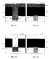
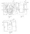
- FIG. 1Ais a top view of a semiconductor substrate used in the first step of the method of present invention to form isolation regions.
- FIG. 1Bis a cross sectional view of the structure taken along the line 1 B- 1 B showing the initial processing steps of the present invention.
- FIG. 1Cis a top view of the structure showing the next step in the processing of the structure of FIG. 1B, in which isolation regions are defined.
- FIG. 1Dis a cross sectional view of the structure in FIG. 1C taken along the line 1 D- 1 D showing the isolation trenches formed in the structure.
- FIG. 1Eis a cross sectional view of the structure in FIG. 1D showing the formation of isolation blocks of material in the isolation trenches.
- FIG. 1Fis a cross sectional view of the structure in FIG. 1E showing the final structure of the isolation regions.
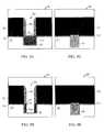
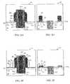
- FIGS. 2 A- 2 Qare cross sectional views of the semiconductor structure in FIG. 1F taken along the line 2 A- 2 A showing in sequence the steps in the processing of the semiconductor structure in the formation of a non-volatile memory array of floating gate memory cells of the present invention.
- FIGS. 3 A- 3 Qarc cross sectional views of a periphery region of the semiconductor structure showing in sequence the steps in the processing of the semiconductor structure in the formation of the non-volatile memory array of floating gate memory cells of the present invention.
- FIG. 4is a top plan view of the memory cell array of the present invention.
- FIGS. 5 A- 5 Jare cross sectional views of the semiconductor structure in FIG. 1F taken along the line 2 A- 2 A showing in sequence the steps in a first alternate processing embodiment of the semiconductor structure of the present invention.
- FIGS. 6A to 6 Dare cross sectional views of a semiconductor structure showing in sequence the steps in a second alternate processing embodiment of the semiconductor structure shown in FIG. 2B.
- FIGS. 7 A- 7 Dare cross sectional views of the isolation region of the semiconductor structure showing in sequence the steps in the second alternate processing embodiment of the structure shown in FIG. 3B.
- FIGS. 8A to 8 Dare cross sectional views of a semiconductor structure showing in sequence the steps in a third alternate processing embodiment of the semiconductor structure shown in FIG. 2B.
- FIGS. 9 A- 9 Dare cross sectional views of the isolation region of the semiconductor structure showing in sequence the steps in the third alternate processing embodiment of the structure shown in FIG. 3B.
- FIGS. 1A to 1 F and 2 A to 2 Qwhich show the processing steps in making the memory cell array of the present invention
- FIGS. 3 A- 3 Qwhich show the processing steps in making the periphery region(s) of the semiconductor structure.
- the methodbegins with a semiconductor substrate 10 , which is preferably of P type and is well known in the art.
- the thicknesses of the layers described belowwill depend upon the design rules and the process technology generation. What is described herein is for the 0.10 micron process. However, it will be understood by those skilled in the art that the present invention is not limited to any specific process technology generation, nor to any specific value in any of the process parameters described hereinafter.
- FIG. 1Athere is shown a top plan view of a semiconductor substrate 10 (or a semiconductor well), which is preferably of P type and is well known in the art.
- First and second layers of material 12 and 14are formed (e.g. grown or deposited) on the substrate.
- first layer 12can be silicon dioxide (hereinafter “oxide”), which is formed on the substrate 10 by any well known technique such as oxidation or oxide deposition (e.g. chemical vapor deposition or CVD) to a thickness of approximately 50-150 ⁇ .
- Nitrogen doped oxide or other insulation dielectricscan also be used.
- Second layer 14can be silicon nitride (hereinafter “nitride”), which is formed over oxide layer 12 preferably by CVD or PECVD to a thickness of approximately 1000-5000 ⁇ .
- FIG. 1Billustrates a cross-section of the resulting structure.
- suitable photo resist material 16is applied on the nitride layer 14 and a masking step is performed to selectively remove the photo resist material from certain regions (stripes 18 ) that extend in the Y or column direction, as shown in FIG. 1C.
- the exposed nitride layer 14 and oxide layer 12are etched away in stripes 18 using standard etching techniques (i.e. anisotropic nitride and oxide/dielectric etch processes) to form trenches 20 in the structure.
- the distance W between adjacent stripes 18can be as small as the smallest lithographic feature of the process used.
- a silicon etch processis then used to extend trenches 20 down into the silicon substrate 10 (e.g. to a depth of approximately 500 ⁇ to several microns), as shown in FIG. 1D. Where the photo resist 16 is not removed, the nitride layer 14 and oxide layer 12 are maintained. The resulting structure illustrated in FIG. 1D now defines active regions 22 interlaced with isolation regions 24 .
- the structureis further processed to remove the remaining photo resist 16 .
- an isolation materialsuch as silicon dioxide is formed in trenches 20 by depositing a thick oxide layer, followed by a Chemical-Mechanical-Polishing or CMP etch (using nitride layer 14 as an etch stop) to remove the oxide layer except for oxide blocks 26 in trenches 20 , as shown in FIG. 1E.
- CMP etchusing nitride layer 14 as an etch stop
- the remaining nitride and oxide layers 14 / 12are then removed using nitride/oxide etch processes, leaving STI oxide blocks 26 extending along isolation regions 24 , as shown in FIG. 1F.
- FIGS. 1A to 1 Fillustrate the memory cell array region of the substrate, in which columns of memory cells will be formed in the active regions 22 which are separated by the isolation regions 24 .
- the substrate 10also includes at least one periphery region 28 in which control circuitry is formed that will be used to operate the memory cells formed in the memory cell array region.
- isolation blocks 26are also formed in the periphery region 28 during the same STI or LOCOS process described above.
- FIGS. 2A to 2 Qshow the cross sections of the structure in the active regions 22 from a view orthogonal to that of FIG. 1F (along line 2 A- 2 A as shown in FIGS. 1C and 1F), and FIGS. 3A to 3 Q show the cross sections of the structure in the periphery region(s) 28 , as the next steps in the process of the present invention are performed concurrently in both regions.
- An insulation layer 30(preferably oxide or nitrogen doped oxide) is first formed over the substrate 10 , as shown in FIGS. 2A and 3A.
- the active region portions of the substrate 10can be doped at this time for better independent control of the cell array portion of the memory device relative to the periphery region 28 .
- Such dopingis often referred to as a V t implant or cell well implant, and is well known in the art.
- the periphery regionis protected by a photo resist layer, which is deposited over the entire structure and removed from just the memory cell array region of the substrate.
- a thick layer of hard mask material 32such as nitride is formed over oxide layer 30 (e.g. ⁇ 3500 ⁇ thick).
- a plurality of parallel second trenches 34are formed in the nitride layer 32 by applying a photo resist (masking) material on the nitride layer 32 , and then performing a masking step to remove the photo resist material from selected parallel stripe regions.
- An anisotropic nitride etchis used to remove the exposed portions of nitride layer 32 in the stripe regions, leaving second trenches 34 that extend down to and expose oxide layer 30 .
- an anisotropic oxide etchis used to remove the exposed portions of oxide layer 30 and extend second trenches 34 down to the substrate 10 .
- a silicon anisotropic etch processis then used to extend second trenches 34 down into the substrate 10 in each of the active regions 22 (for example, down to a depth of approximately one feature size deep, e.g. about 500 ⁇ to several microns with 0.15 um technology).
- the photo resistcan be removed after trenches 34 are formed into the substrate 10 .
- the resulting active/periphery regions 22 / 28are shown in FIGS. 2 B/ 3 B.
- a layer of insulation material 36is next formed (preferably using a thermal oxidation or CVD oxide process) along the exposed silicon in second trenches 34 that forms the bottom and lower sidewalls of the second trenches 34 (e.g. ⁇ 60 ⁇ to 150 ⁇ thick).
- a thick layer of polysilicon 38(hereinafter “poly”) is then formed over the structure, which fills second trenches 34 .
- Poly layer 38can be doped (e.g. n+) by ion implant, or by an in-situ doped poly process.
- the resulting active/periphery regions 22 / 28are shown in FIGS. 2 C/ 3 C.
- a poly etch process(e.g. a CMP process using nitride layer 32 as an etch stop) is used to remove poly layer 38 except for blocks 40 of the polysilicon 38 left remaining in second trenches 34 .
- a controlled poly etchis then used to lower the height of poly blocks 40 , where the tops of poly blocks 40 are disposed above the surface of the substrate, but below the tops of STI blocks 26 in the isolation regions 24 , as shown in FIGS. 2 D/ 3 D.
- Another optional poly etchis then performed to create sloped portions 42 on the tops of poly blocks 40 (adjacent the second trench sidewalls), as shown in FIG. 2E.
- a thermal oxidation processis then performed to form or enhance the tips of sloped portions 42 , which oxidizes the exposed top surfaces of the poly blocks 40 (forming oxide layer 46 thereon), as shown in FIG. 2F.
- Oxide spacers 48are then formed along the sidewalls of the second trenches 34 .
- Spacers 48are formed by depositing oxide over the structure (e.g. approximately 300 to 1000 ⁇ thickness) followed by an anisotropic oxide etch. The oxide etch also removes the center portion of oxide layer 46 in each of the second trenches 34 . The periphery region 28 is left unaffected. The resulting active/periphery regions 22 / 28 are shown in FIGS. 2 G/ 3 G.
- An anisotropic poly etch in combination with some oxide etch (for adjustment of STI oxide height, along the trench 34 )is next performed, which removes the center portions of the poly blocks 40 that are not protected by oxide spacers 48 , leaving a pair of opposing poly blocks 40 a in each of the second trenches 34 , as shown in FIG. 2H.
- An insulation deposition and anisotropic etch-back processis then used to form an insulation layer 50 along the exposed sides of poly blocks 40 a inside second trenches 34 .
- the insulation materialcould be any insulation material (e.g. ONO—oxide/nitride/oxide, or other high dielectric materials).
- the insulation materialis oxide, so that the oxide deposition/etch process also thickens the oxide spacers 48 and results in the removal of the exposed portions of oxide layer 36 at the bottom of each second trench 34 to expose the substrate, as shown in FIGS. 2 I/ 3 I.
- Suitable ion implantationthat, depending upon if the substrate is P or N type, may include arsenic, phosphorous, boron and/or antimony (and possible anneal) is then made across the surface of the structure to form first (source) regions 52 in the exposed substrate portions at the bottom of second trenches 34 .
- the source regions 52are self-aligned to the second trenches 34 , and have a second conductivity type (e.g. N type) that is different from a first conductivity type of the substrate (e.g. P type).
- the ionshave no significant effect on the nitride layer 32 .
- the resulting active/periphery regions 22 / 28are shown in FIGS. 2 J/ 3 J.
- a poly deposition step, followed by a poly CMP etchare used to fill second trenches 34 with poly blocks 54 , as shown in FIG. 2K.
- a nitride etchfollows, which removes nitride layer 32 , and exposes upper edges of the poly blocks 40 a.
- a tunnel oxide layer 56is next formed on the exposed upper edges of poly blocks 40 a, either by thermal oxidation, oxide deposition, or both.
- This oxide formation stepalso forms an oxide layer 58 on the exposed top surfaces of poly blocks 54 , as well as possibly thickening oxide layer 30 over substrate 10 .
- Optional V t implantation in the periphery region 28can be performed at this time by masking off the active regions 22 .
- the resulting active/periphery regions 22 / 28are shown in FIGS. 2 L/ 3 L.
- the oxide layer 30serves as the gate oxide for both the memory cells in the active regions, and the control circuitry in the periphery region.
- the thickness of the gate oxidedictate's its maximum operating voltage.
- photo resist 60is formed over the structure, followed by a masking step for selectively removing portions of the photo resist in the periphery region to expose portions of oxide layer 30 .
- the exposed portions of oxide layer 30can be thinned (e.g. by using a controlled etch) or replaced (e.g. by an oxide etch and oxide deposition) with oxide layer 30 a having the desired thickness, as illustrated in FIGS. 2 M/ 3 M.
- a poly deposition stepis used to form a poly layer 62 over the structure (e.g. approximately 500-3000 ⁇ thick). Photo resist deposition and masking steps follow to form blocks of photo resist 64 on the poly layer in the periphery region 28 , as shown in FIGS. 2 N/ 3 N. An anisotropic poly etch is then used to remove poly layer 62 except for poly blocks 66 under photo resist blocks 64 (in periphery region 28 ), and poly spacers 68 adjacent oxide spacers 48 (in active regions 22 ).
- Suitable ion implantationis used to form second (drain) regions 70 in the substrate active regions and source/drain regions 72 / 74 in the substrate periphery region 28 for the devices therein.
- the resulting active/periphery regions 22 / 28are shown in FIGS. 2 O/ 3 O.
- insulation spacers 76are formed by insulation material deposition and anisotropic etch (e.g. nitride or oxide), and are disposed against poly spacers 68 , oxide spacers 48 and poly blocks 66 .
- a metal deposition stepis then performed, to deposit a metal such as tungsten, cobalt, titanium, nickel, platinum, or molybdenum over the active and periphery regions 22 / 28 .
- the structuresare then annealed, permitting the hot metal to flow and to seep into the exposed top portions of poly spacers 68 and poly blocks 66 to form a conductive layer of metalized polysilicon 78 (polycide) thereon.
- the metal deposited on the remaining structureis removed by a metal etch process.
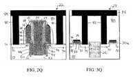
- the resulting active/periphery regions 22 / 28are shown in FIGS. 2 P/ 3 P.
- Insulation material 80such as BPSG or oxide, is then formed over the entire structure.
- a masking stepis performed to define etching areas over the drain regions 70 / 74 .
- the insulation material 80is selectively etched in the masked regions to create contact openings that extend down to drain regions 70 / 74 .
- the contact openingsare then filled with a conductor metal (e.g. tungsten) to form metal contacts 82 that are electrically connected to drain regions 70 / 74 .
- Drain line contacts 84 / 86e.g.
- the process of the present inventionforms pairs of memory cells that mirror each other, with a memory cell formed on each side of the poly block 54 .
- first and second regions 52 / 70form the source and drain regions respectively (although those skilled in the art know that source and drain can be switched during operation).
- Poly block 40 aconstitutes the floating gate
- poly spacer 68constitutes the control gate.
- Channel regions 90 for each memory cellare defined in the surface portion of the substrate that is in-between the source and drain 52 / 70 .
- Each channel region 90includes two portions joined together at an approximate right angle, with a first (vertical) portion 92 extending along the vertical wall of filled second trench 34 and a second (horizontal) portion 94 extending between the sidewall of filled second trench 34 and the drain region 70 .
- Each pair of memory cellsshare a common source region 52 that is disposed underneath filled second trench 34 and is in electrical contact with poly block 54 .
- each drain region 70is shared between adjacent memory cells from different mirror sets of memory cells.
- FIG. 4is a top view of the resulting structure showing the interconnection between bit lines 84 and drain regions 70 , as well as control gates 68 which are continuously formed as control (word) lines that extend across both the active and isolation regions 22 / 24 .
- the above-described processdoes not produce source regions 52 that extend across the isolation regions 24 (which can easily be done by a deep implant, or by removing the STI insulation material from the isolation region portions of second trenches 34 before ion implantation).
- poly blocks 54(which are in electrical contact with source regions 52 ) are formed continuously across the isolation regions to adjacent active regions, and form source lines each of which electrically connects together all the source regions 52 for, each row of paired memory cells.
- the floating gates 40 aare disposed in second trenches 34 , with each floating gate facing and insulated from one of the channel region vertical portions 92 , one of the source regions 52 and one of the poly blocks 54 .
- Each floating gate 40 aincludes an upper portion that extends above the substrate surface and terminates in an edge 96 that faces and is insulated from one of the control gates 68 , thus providing a path for Fowler-Nordheim tunneling through oxide layer 56 .
- Poly blocks 54each extend along and are insulated (by oxide layer 50 ) from floating gates 44 a, for enhanced voltage coupling therebetween.
- a ground potentialis applied to both its source 52 and drain 70 .
- a high-positive voltage(e.g. +7 to +15 volts) is applied to the control gate 68 . Electrons on the floating gate 40 a are induced through the Fowler-Nordheim tunneling mechanism to tunnel from the upper end of the floating gate 40 a (primarily from edge 96 ), through the oxide layer 56 , and onto the control gate 68 , leaving the floating gate 40 a positively charged. Tunneling is enhanced by the sharpness of edge 96 . It should be noted that since each of the control gates 68 extends across the active and isolation regions as continuous control (word) lines, one memory cell in each active region is ‘erased’ at the same time.
- a small voltage(e.g. 0.5 to 2.0 V) is applied to its drain region 70 .
- a positive voltage level in the vicinity of the threshold voltage of the MOS structure(on the order of approximately +0.2 to 1 volt) is applied to its control gate 68 .
- a positive high voltage(e.g. on the order of 5 to 12 volts) is applied to its source region 52 . Electrons generated by the drain region 70 will flow from the drain region 70 towards the source region 52 through the deeply depleted horizontal portion 94 of the channel region 90 .
- the electronsAs the electrons reach the vertical portion 92 of the channel region 90 , they will see the high potential of floating gate 40 a (because the floating gate 40 a is strongly voltage-coupled to the positively charged source region 52 and poly block 54 ). The electrons will accelerate and become heated, with most of them being injected into and through the insulating layer 36 and onto the floating gate 40 a. Low or ground potential is applied to the source/drain regions 52 / 70 and control gates 68 for memory cell rows/columns not containing the selected memory cell. Thus, only the memory cell in the selected row and column is programmed.
- ground potentialis applied to its source region 52 .
- a read voltage(e.g. ⁇ 0.5 to 2 volts) is applied to its drain region 70 and approximately 1 to 4 volts (depending upon the power supply voltage of the device) is applied to its control gate 68 . If the floating gate 40 a is positively charged (i.e. the floating gate is discharged of electrons), then the vertical channel region portion 92 (directly adjacent to the floating gate 40 a ) is turned on. When the control gate 68 is raised to the read potential, the horizontal channel region portion 94 (directly adjacent the control gate 68 ) is also turned on. Thus, the entire channel region 90 will be turned on, causing electrons to flow from the source region 52 to the drain region 70 . This sensed electrical current would be the “1” state.
- the vertical channel region portion 92is either weakly turned on or is entirely shut off. Even when the control gate 68 and the drain region 70 are raised to the read potential, little or no current will flow through vertical channel region portion 92 . In this case, either the current is very small compared to that of the “1” state or there is no current at all. In this manner, the memory cell is sensed to be programmed at the “0” state. Ground potential is applied to the source/drain regions 52 / 70 and control gates 68 for non-selected columns and rows so only the selected memory cell is read.
- the memory cell arrayincludes peripheral circuitry including conventional row address decoding circuitry, column address decoding circuitry, sense amplifier circuitry, output buffer circuitry and input buffer circuitry, which are well known in the art.
- the present inventionprovides a memory cell array with reduced size and superior program efficiency. Memory cell size is reduced significantly because the source regions 52 are buried inside the substrate 10 , and are self-aligned to the second trenches 34 , where space is not wasted due to limitations in the lithography generation, contact alignment and contact integrity.
- Each floating gate 40 ahas a lower portion disposed in second trench 34 formed in the substrate for receiving the tunneling electrons during the program operation and for turning on the vertical channel region portion 92 during the read operation.
- Each floating gate 40 aalso has an upper portion that extends out of the second trench formed in the substrate and terminates in an edge facing the control gate for Fowler Nordheim tunneling thereto during the erase operation.
- Program efficiencyis greatly enhanced by “aiming” the horizontal portion 94 of the channel region 90 at the floating gate 40 a.
- the electrons in the channel regionflow in a path parallel to the floating gate, where a relatively small number of the heated electrons are injected onto the floating gate.
- the estimated program efficiency (number of electrons injected compared to total number of electrons) in such conventional programming schemesis estimated at about 1/1000.
- the program efficiency of the present inventionis improved by 10 fold or even 100 fold, where almost all the electrons are injected onto the floating gate.
- each floating gate 40 athere is also an enhanced voltage coupling between each floating gate 40 a and the corresponding source region 52 via the poly block 54 (electrically connected with the source region 52 ).
- having source region 52 and drain region 70 separated vertically as well as horizontallyallows easier optimization of reliability parameters without affecting cell size.
- FIGS. 5A to 5 Jshow the cross sections of the structure in the active regions 22 for an alternate method for making the memory cell array of the present invention. This first alternate process starts with the structure shown in FIG. 2A. For simplicity, elements in common with the first embodiment described above are designated using the same element numbers.
- the thick nitride layer 32(e.g. ⁇ 1000 to 10,000 ⁇ in thickness) is formed over oxide layer 30 .
- Parallel second trenches 34are formed in the nitride layer 32 by applying a photo resist (masking) material on the nitride layer 32 , and then performing a masking step to remove the photo resist material from selected parallel stripe regions.
- An anisotropic nitride etchis used to remove the exposed portions of nitride layer 32 in the stripe regions, leaving second trenches 34 that extend down to and expose oxide layer 30 .
- oxide spacers 102are formed in second trenches 34 by an oxide deposition step, followed by an oxide anisotropic etch step.
- the portions of oxide layer 30 in the bottom center of the second trenchesare also removed during this oxide etch step, exposing the underlying substrate 10 .
- the resulting structureis shown in FIG. 5A.
- a silicon anisotropic etch processis used to extend second trenches 34 down into the substrate 10 in each of the active regions 22 (for example, down to a depth of approximately 500 ⁇ to several microns with 0.15 um technology).
- the width of the second trenches 34 in substrate 10is essentially the spacing between the oxide spacers 102 .
- Suitable ion implantation (and possible anneal)is then made across the surface of the structure to form the first (source) regions 52 in the exposed substrate portions at the bottom of second trenches 34 .
- the source regions 52are self-aligned to the second trenches 34 , and have a second conductivity type (e.g. N type) that is different from a first conductivity type of the substrate (e.g. P type).
- the ionshave no significant effect on the nitride layer 32 .
- the resulting structureis shown in FIG. 5B.
- Oxide layer 100is next formed on the exposed silicon substrate 10 (forming the bottom and lower sidewalls of the second trenches 34 ), preferably by thermal oxidation (e.g. ⁇ 70 to 150 ⁇ thick).
- a thick poly layeris then formed over the structure, which fills second trenches 34 .
- a poly CMP etch processusing nitride layer 32 as an etch stop, is used to remove poly layer except for poly blocks 54 left remaining in second trenches 34 .
- a controlled poly etchis then used to lower the height of poly blocks 54 below the top of nitride layer 32 .
- An optional oxide layer 104is then formed on the poly blocks 54 (e.g. by thermal oxidation).
- a thin nitride layer 106is then deposited over the structure, followed by masking step and nitride etch to remove the nitride layer 106 except for those portions over oxide layer 104 and poly blocks 54 . This can be accomplished by depositing photo resist over the structure, followed by a controlled exposure so that only the photo resist in the second trench 34 is left covering the deposited nitride. The resulting structure is shown in FIG. 5C.
- a dry and/or wet oxide etchis used to remove the oxide spacers 102 .
- a thermal oxidation processfollows, which forms oxide layer 108 on exposed side portions of poly blocks 54 and on exposed portions of the substrate.
- An anisotropic oxide etchis used to removed the oxide layer 108 just formed on the substrate. The resulting structure is shown in FIG. 5D.
- nitride layers 32 and 106are used as masks to etch away the exposed silicon substrate in second trenches 34 down to a depth even with the bottoms of poly blocks 54 .
- Additional ion implantation(and possible anneal) is used to expand source regions 52 underneath second trenches 34 , as shown in FIG. 5E.
- An insulation layer 110is then formed on the second trench sidewalls, preferably by CVD deposition of oxide (e.g. ⁇ 70-150 ⁇ thick).
- a thick poly layeris formed over the structure which fills second trenches 34 , followed by a CMP poly etch (using nitride layer 32 as an etch stop) and additional poly etch to form poly blocks 40 a having tops that are below that of the STI oxide blocks 26 in the isolation regions 24 . Sloped etching or oxidation is then used to sharpen edges 96 on the tops of poly blocks 40 a.
- An oxide deposition and etch back processis then used to fill the top portions of second trenches 34 with oxide 112 , which seals poly blocks 40 a and creates oxide spacers at the tops of second trenches 34 .
- the resulting structureis shown in FIG. 5F, and includes three poly blocks in each second trench, surrounded and sealed by oxide.
- Poly block 54is in electrical contact with source region 52 and disposed between the pair of poly blocks 40 a (which are insulated from source region 52 ).
- An optional extension of poly block 54can be performed by removing nitride layer 106 and oxide layer 104 via controlled nitride and oxide etches, followed by a poly deposition and poly CMP etch back.
- An optional poly etchcan be used to lower the new tops of poly blocks 54 before an oxidation process is used to form a protective oxide layer 114 over poly blocks 54 , as shown in FIG. 5G.
- a nitride etchis next used to remove nitride layer 32 .
- a controlled oxide etchis then used to recess the exposed oxide by about 10 to several hundred angstroms, followed by a thermal oxidation process that reforms oxide layers 30 and 114 and results in an indentation in the oxide surrounding the tops of poly blocks 40 a ).
- the resulting structureis shown in FIG. 5H.
- a poly deposition and anisotropic poly etchis used to form poly spacers 68 adjacent oxide spacers 112 .
- Suitable ion implantation (and anneal)is used to form second (drain) regions 70 in the substrate.
- Insulation spacers 76are then formed by insulation material deposition and anisotropic etch (e.g. nitride or oxide), and are disposed against poly spacers 68 .
- a metal deposition stepis then performed, to deposit a metal such as tungsten, cobalt, titanium, nickel, platinum, or molybdenum over the structure, which is then annealed to permit the hot metal to flow and to seep into the exposed top portions of poly spacers 68 to form polycide 78 thereon.
- the remaining metal deposited on the remaining structureis removed by a metal etch process.
- the resulting structureis shown in FIG. 5I.
- Insulation material 80 , metal contacts 82 , and drain line contact 84are formed as described above with respect to FIG. 2Q to result in the final structure shown in FIG. 5J.
- the advantage of this embodimentis the ease with which the solid source line poly blocks 54 are formed, and their electrical contact with source regions 52 .
- using the poly block 54 to separate the later formed floating gate poly blocks 40 amakes it easier to prevent shorts between the floating gates.
- FIGS. 6A to 6 G and 7 A to 7 Gillustrate a second alternate method for making the memory cell array of the present invention.
- This second alternate processbegins with the structures shown in FIGS. 2B and 3B, but without the formation of oxide layer 30 underneath nitride layer 32 , as oxide layer 30 is optional for this embodiment.
- the ion implantation (and possible anneal) processis used to form the first (source) regions 52 in the exposed substrate portions at the bottom of second trenches 34 .
- a thin poly layer 118is then formed over the structures, as shown in FIGS. 6A and 7A.
- Poly layer 118can be doped (e.g. n+) by ion implant, or by an in-situ process.
- the thickness of poly layer 118is preferably 50-500 ⁇ , and dictates the eventual thickness of the floating gates for the final memory cell device.
- Oxideis formed over the structure, followed by a planarizing oxide etch (e.g. CMP etch using portions of poly layer 118 over nitride layer 32 as an etch stop) which fills second trenches 34 with oxide blocks 120 .
- a poly etchfollows that removes the exposed portions of poly layer 118 (i.e. those portions over nitride layer 32 ).
- An oxide etchis next used to recess the oxide blocks 120 down even with those portions of poly layer 118 left disposed over the STI blocks 26 in the isolation regions 24 (e.g. using portions of poly layer 118 in the inactive regions over STI blocks 26 as an oxide etch stop).
- the resulting active/peripheral region structuresare shown in FIGS. 6B and 7B.
- poly layer 118has first portions 119 a formed over the nitride layer 32 outside the trench 34 .
- FIG. 6His the same view of the second trench 34 as shown in FIG. 6A, but in the isolation regions 24 instead of the active regions 22 .
- poly layer 118has second portions 119 b formed over STI blocks 26 .
- poly layer portions 119 aare disposed at a higher topography level than that of poly layer portions 119 b.
- the first oxide etchis performed using poly layer portions 119 a as an etch stop to evenly fill second trenches 34 in both the active and isolation regions 22 / 24 .
- the subsequent oxide etchuses poly layer portions 119 b as an etch stop to set the proper level of oxide block 120 in the active region and to fully expose poly layer 118 in the isolation region 24 .
- a poly etchis next used to remove exposed portions of poly layer 118 (i.e. along upper portions of second trenches 34 in the active regions, and over STI blocks 26 in the isolation regions 24 ).
- An oxidation processfollows, to form oxide blocks 122 on the exposed end portions of poly layer 118 .
- Dielectric spacers 124such as oxide, are then formed, inside second trenches 34 over oxide blocks 122 and partially over oxide blocks 120 , via oxide deposition and etch back, as shown in FIG. 6C.
- Another oxide etchis then used to remove the exposed center portion of oxide blocks 120 (between spacers 124 , which are reduced in height by the oxide etch), exposing poly layer 118 at the center of second trenches 34 .
- a poly etch and an oxide etchfollow to remove the exposed portions of poly layer 118 and oxide layer 36 at the bottom center of second trenches 34 , exposing portions of the substrate. The resulting structures are shown in FIGS. 6 D/ 7 D.
- Dielectric spacers 125are next formed inside second trenches 34 by depositing nitride (or oxide) over the structure, followed by an anisotropic nitride etch. Second trenches 34 are then filled with poly blocks 54 using a poly deposition and CMP etch back-process (using nitride layer 32 as an etch stop), as shown in FIG. 6E. Nitride layer 32 is removed from the active and isolation regions 22 / 24 and periphery region 28 using a nitride etch. The tunnel oxide layer 56 is next formed on the exposed upper edges of poly layer 118 , either by thermal oxidation, oxide deposition, or both.
- oxide layer 32Since oxide layer 32 was not formed earlier in this process, the oxide layer 56 also extends over the exposed portions of substrate 10 . This oxide formation step also forms oxide layer 58 on the exposed top surfaces of poly blocks 54 .
- Optional V t implantation in the periphery region 28can be performed at this time by masking off the active regions 22 . The resulting active/periphery regions 22 / 28 are shown in FIGS. 6 F/ 7 F.
- L-shaped poly layer 118constitutes the floating gate for each of the memory cells.
- Each floating gate 118includes a pair of orthogonally oriented elongated portions 118 a/ 118 b joined together at their proximal ends.
- Floating gate portion 118 aextends along and is insulated from the substrate sidewall of second trench 34 , with an upper segment 118 c extending above the substrate surface.
- Floating gate portion 118 bextends along and is insulated from a bottom substrate wall of second trench 34 (i.e. disposed over and insulated from source region 52 ).
- the control gate spacer 68has a first portion laterally adjacent to and insulated from the floating gate upper segment 118 c, and a second portion disposed over and insulated from the upper segment 118 c.
- the floating gate segment 118 chas a distal end that terminates in a thin tip portion having an edge 96 that directly faces and is insulated from the control gate 68 , thus providing a path for Fowler-Nordheim tunneling between the floating gate 118 and the control gate 68 .
- the second alternate embodiment of the present inventionprovides a memory cell array with reduced size and superior program efficiency.
- Memory cell sizeis reduced significantly because the source regions 52 are buried inside the substrate 10 , and are self-aligned to the trenches 34 , where space is not wasted due to limitations in the lithography generation, contact alignment and contact integrity.
- Program efficiencyis greatly enhanced by “aiming” the horizontal portion 94 of the channel region 90 at the floating gate 118 .
- the L-shaped floating gate configuration of the present inventionprovides many advantages. Because the floating gate portions 118 a/ 118 b are made from a thin layer of poly material, the upper tip thereof is narrow and enhances Fowler-Nordheim tunneling to the control gate 68 .
- each floating gate 118 and the corresponding source region 52there is no need for extensive thermal oxidation steps to form sharp edges for enhanced tunneling.
- each poly block 54needs to be insulated from the substrate as it crosses the isolation regions, so that it does not short to the substrate. This is accomplished by making the depth of STI blocks 26 in the isolation regions deeper than the bottom of second trench 34 , or by ensuring the material for STI blocks 26 etches slower than the material used to form oxide blocks 120 .
- FIGS. 8A to 8 D and 9 A to 9 Dillustrate a third alternate method for making the memory cell array of the present invention.
- This third alternate processbegins with the structures shown in FIGS. 2B and 3B.
- the ion implantation (and possible anneal) processis used to form the first (source) regions 52 in the exposed substrate portions at the bottom of second trenches 34 .
- Poly spacers 126are then formed in second trenches 34 by forming a layer of polysilicon over the structure, followed by an anisotropic poly etch that removes the poly layer except for the poly spacers 126 , as shown in FIGS. 8A and 9A.
- the poly spacerspreferably have a height no greater than the STI blocks 26 in the isolation regions 24 (e.g. use STI blocks 26 in the inactive regions as an etch stop), which ensures all the polysilicon is removed from the isolation regions.
- Oxideis formed over the structures of FIGS. 8 A/ 9 A, followed by a planarizing oxide etch (e.g. CMP etch using nitride layer 32 as an etch stop), which fills second trenches 34 with oxide blocks 128 .
- An oxide etchis next used to recess the oxide blocks 128 down even with the tops of poly spacers 126 (e.g. use poly spacers 126 as an oxide etch stop).
- Dielectric spacers 130such as oxide, are then formed inside second trenches 34 and over poly spacers 126 , via oxide deposition and etch back, as shown in FIG. 8B.
- FIGS. 8 C/ 9 CAnother oxide etch is then used to remove the exposed center portions of oxide blocks 128 and oxide layer 36 (between spacers 130 , which are reduced in height by the oxide etch), exposing portions of the substrate.
- the resulting structuresare shown in FIGS. 8 C/ 9 C.
- poly spacers 126constitute the floating gates, which are insulated from the control gates 68 via oxide 56 .
- the floating gate spacers 126each terminate in a sharp edge 96 that directly faces and is insulated from the control gate 68 , thus providing a path for Fowler-Nordheim tunneling between the floating gate 126 and the control gate 68 .
- trenches 20 / 34can end up having any shape that extends into the substrate, not just the elongated rectangular shape shown in the figures.
- polysiliconrefers to any appropriate conductive material that can be used to form the elements of non-volatile memory cells.
- any appropriate insulatorcan be used in place of silicon dioxide or silicon nitride.
- any appropriate material who's etch propertydiffers from that of silicon dioxide (or any insulator) and from polysilicon (or any conductor) can be used in place of silicon nitride.
- the above described inventionis shown to be formed in a substrate which is shown to be uniformly doped, but it is well known and contemplated by the present invention that memory cell elements can be formed in well regions of the substrate, which are regions that are doped to have a different conductivity type compared to other portions of the substrate. Lastly, single layers of insulating or conductive material could be formed as multiple layers of such materials, and vice versa.
Landscapes
- Semiconductor Memories (AREA)
- Non-Volatile Memory (AREA)
Abstract
Description
- This application claims the benefit of U.S. Provisional Application No. 60/370,888, filed Apr. 5, 2002, and entitled High Coupling Non-Volatile Trench Memory Cell; U.S. Provisional Application No. 60/393,696, filed Jul. 2, 2002, and entitled Non-Volatile Memory Trench Cell and Method of Making Same; and U.S. Provisional Application No. 60/398,146, filed Jul. 23, 2002, and entitled Non-Volatile Memory Trench Cell With Buried Floating Gate, all of which are incorporated herein in their entirety by reference.[0001]
- The present invention relates to a self-aligned method of forming a semiconductor memory array of floating gate memory cells. The present invention also relates to a semiconductor memory array of floating gate memory cells of the foregoing type.[0002]
- Non-volatile semiconductor memory cells using a floating gate to store charges thereon and memory arrays of such non-volatile memory cells formed in a semiconductor substrate are well known in the art. Typically, such floating gate memory cells have been of the split gate type, or stacked gate type.[0003]
- One of the problems facing the manufacturability of semiconductor floating gate memory cell arrays has been the alignment of the various components such as source, drain, control gate, and floating gate. As the design rule of integration of semiconductor processing decreases, reducing the smallest lithographic feature, the need for precise alignment becomes more critical. Alignment of various parts also determines the yield of the manufacturing of the semiconductor products.[0004]
- Self-alignment is well known in the art. Self-alignment refers to the act of processing one or more steps involving one or more materials such that the features are automatically aligned with respect to one another in that step processing. Accordingly, the present invention uses the technique of self-alignment to achieve the manufacturing of a semiconductor memory array of the floating gate memory cell type.[0005]
- There is a constant need to shrink the size of the memory cell arrays in order to maximize the number of memory cells on a single wafer. It is well known that forming memory cells in pairs, with each pair sharing a single source region, and with adjacent pairs of cells sharing a common drain region, reduces the size of the memory cell array. However, a large area of the array is typically reserved for the bit-line connection to the drain regions. The bit-line area is often occupied by the contact openings between memory cell pairs, and the contact to wordline spacing, which strongly depends upon lithography generation, contact alignment and contact integrity. In addition, significant space is reserved for the word-line transistor, the size of which is set by lithography generation and junction scaling.[0006]
- Traditionally, floating gates are formed with a sharp edge facing a control gate to enhance Fowler-Nordheim tunneling, which is used to move electrons off of the floating gate during an erase operation. The sharp edge is typically formed by oxidizing or partially etching the top surface of the floating gate poly in an uneven manner. However, as the dimensions of the floating gate get smaller, this sharp edge can be more difficult to form in this manner.[0007]
- There is also a need to improve the programming efficiency of memory cell array. In conventional programming schemes, the electrons in the channel region flow in a path parallel to the floating gate, where a relatively small number of the heated electrons are injected onto the floating gate. The estimated program efficiency (number of electrons injected compared to total number of electrons) is estimated at about 1/1000.[0008]
- It is known to form memory cell elements over non-planar portions of the substrate. For example, U.S. Pat. No. 5,780,341 (Ogura) discloses a number of memory device configurations that includes a step channel formed in the substrate surface. While the purpose of the step channel is to inject hot electrons more efficiently onto the floating gate, these memory device designs are still deficient in that it is difficult to optimize the size and formation of the memory cell elements as well the necessary operational parameters needed for efficient and reliable operation.[0009]
- There is a need for a non-volatile, floating gate type memory cell array with significant cell size reduction while providing enhanced programming efficiency.[0010]
- The present invention solves the above-mentioned problems by providing a self-aligned method of forming memory cells with reduced size and novel structure, and a memory cell array formed thereby.[0011]
- The present invention is an electrically programmable and erasable memory device that includes a substrate of semiconductor material having a first conductivity type and a horizontal surface, a trench formed into the surface of the substrate, first and second spaced-apart regions formed in the substrate and having a second conductivity type, with a channel region formed in the substrate therebetween, wherein the first region is formed underneath the trench, and the channel region includes a first portion that extends substantially along a sidewall of the trench and a second portion that extends substantially along the surface of the substrate, an electrically conductive floating gate having at least a lower portion thereof disposed in the trench adjacent to and insulated from the channel region first portion for controlling a conductivity of the channel region first portion, and an electrically conductive control gate disposed over and insulated from the channel region second portion for controlling a conductivity of the channel region second portion, wherein there is at most only a partial vertical overlap between the control gate and the floating gate.[0012]
- In another aspect of the present invention, an array of electrically programmable and erasable memory devices includes a substrate of semiconductor material having a first conductivity type and a surface, spaced apart isolation regions formed on the substrate which are substantially parallel to one another and extend in a first direction, with an active region between each pair of adjacent isolation regions, and each of the active regions including a plurality of pairs of memory cells. Each of the memory cell pairs includes a trench formed into the surface of the substrate and including a pair of opposing sidewalls, a first region formed in the substrate underneath the trench, a pair of second regions formed in the substrate, with a pair of channel regions each formed in the substrate between the first region and one of the second regions, wherein the first and second regions have a second conductivity type, and wherein each of the channel regions includes a first portion that extends substantially along one of the opposing trench sidewalls and a second portion that extends substantially along the substrate surface, a pair of electrically conductive floating gates each having at least a lower portion thereof disposed in the trench adjacent to and insulated from one of the channel region first portions for controlling a conductivity of the one channel region first portion, and a pair of electrically conductive control gates each disposed over and insulated from one of the channel region second portions for controlling a conductivity of the one channel region second portion, wherein there is at most only a partial vertical overlap between the control gates and the floating gates.[0013]
- In yet another aspect of the present invention, a method of forming a semiconductor memory cell includes forming a trench into a surface of a semiconductor substrate, wherein the substrate has a first conductivity type, forming first and second spaced-apart regions of a second conductivity type in the substrate with the first region formed underneath the trench, wherein a channel region is defined in the substrate between the first and second regions such that the channel region includes a first portion that extends substantially along a sidewall of the trench and a second portion that extends substantially along the surface of the substrate, forming an electrically conductive floating gate having at least a lower portion thereof disposed in the trench adjacent to and insulated from the channel region first portion for controlling a conductivity of the channel region first portion, and forming an electrically conductive control gate disposed over and insulated from the channel region second portion for controlling a conductivity of the channel region second portion, wherein there is at most only a partial vertical overlap between the control gate and the floating gate.[0014]
- In yet one more aspect of the present invention, a method of forming an array of electrically programmable and erasable memory devices includes forming spaced apart isolation regions on a semiconductor substrate that are substantially parallel to one another and extend in a first direction, with an active region between each pair of adjacent isolation regions, wherein the substrate has a surface and a first conductivity type, forming a plurality of pairs of memory cells in each of the active regions. The formation of each of the memory cell pairs includes forming a trench into the surface of the substrate having a pair of opposing sidewalls, forming a first region in the substrate and underneath the trench, forming a pair of second regions in the substrate, with a pair of channel regions each defined in the substrate between the first region and one of the second regions, wherein the first and second regions have a second conductivity type, and wherein each of the channel regions includes a first portion that extends substantially along one of the opposing trench sidewalls and a second portion that extends substantially along the surface of the substrate, forming a pair of electrically conductive floating gates each having at least a lower portion thereof disposed in the trench adjacent to and insulated from one of the channel region first portions for controlling a conductivity of the one channel region first portion, and forming a pair of electrically conductive control gates each disposed over and insulated from one of the channel region second portions for controlling a conductivity of the one channel region second portion, wherein there is at most only a partial vertical overlap between the control gates and the floating gates.[0015]
- Other objects and features of the present invention will become apparent by a review of the specification, claims and appended figures.[0016]
- FIG. 1A is a top view of a semiconductor substrate used in the first step of the method of present invention to form isolation regions.[0017]
- FIG. 1B is a cross sectional view of the structure taken along the line[0018]1B-1B showing the initial processing steps of the present invention.
- FIG. 1C is a top view of the structure showing the next step in the processing of the structure of FIG. 1B, in which isolation regions are defined.[0019]
- FIG. 1D is a cross sectional view of the structure in FIG. 1C taken along the line[0020]1D-1D showing the isolation trenches formed in the structure.
- FIG. 1E is a cross sectional view of the structure in FIG. 1D showing the formation of isolation blocks of material in the isolation trenches.[0021]
- FIG. 1F is a cross sectional view of the structure in FIG. 1E showing the final structure of the isolation regions.[0022]
- FIGS.[0023]2A-2Q are cross sectional views of the semiconductor structure in FIG. 1F taken along the line2A-2A showing in sequence the steps in the processing of the semiconductor structure in the formation of a non-volatile memory array of floating gate memory cells of the present invention.
- FIGS.[0024]3A-3Q arc cross sectional views of a periphery region of the semiconductor structure showing in sequence the steps in the processing of the semiconductor structure in the formation of the non-volatile memory array of floating gate memory cells of the present invention.
- FIG. 4 is a top plan view of the memory cell array of the present invention.[0025]
- FIGS.[0026]5A-5J are cross sectional views of the semiconductor structure in FIG. 1F taken along the line2A-2A showing in sequence the steps in a first alternate processing embodiment of the semiconductor structure of the present invention.
- FIGS. 6A to[0027]6D are cross sectional views of a semiconductor structure showing in sequence the steps in a second alternate processing embodiment of the semiconductor structure shown in FIG. 2B.
- FIGS.[0028]7A-7D are cross sectional views of the isolation region of the semiconductor structure showing in sequence the steps in the second alternate processing embodiment of the structure shown in FIG. 3B.
- FIGS. 8A to[0029]8D are cross sectional views of a semiconductor structure showing in sequence the steps in a third alternate processing embodiment of the semiconductor structure shown in FIG. 2B.
- FIGS.[0030]9A-9D are cross sectional views of the isolation region of the semiconductor structure showing in sequence the steps in the third alternate processing embodiment of the structure shown in FIG. 3B.
- The method of the present invention is illustrated in FIGS. 1A to[0031]1F and2A to2Q (which show the processing steps in making the memory cell array of the present invention), and FIGS.3A-3Q (which show the processing steps in making the periphery region(s) of the semiconductor structure). The method begins with a
semiconductor substrate 10, which is preferably of P type and is well known in the art. The thicknesses of the layers described below will depend upon the design rules and the process technology generation. What is described herein is for the 0.10 micron process. However, it will be understood by those skilled in the art that the present invention is not limited to any specific process technology generation, nor to any specific value in any of the process parameters described hereinafter. - Isolation Region Formation[0032]
- FIGS. 1A to[0033]1F illustrate the well known STI method of forming isolation regions on a substrate. Referring to FIG. 1A there is shown a top plan view of a semiconductor substrate10 (or a semiconductor well), which is preferably of P type and is well known in the art. First and second layers of
material first layer 12 can be silicon dioxide (hereinafter “oxide”), which is formed on thesubstrate 10 by any well known technique such as oxidation or oxide deposition (e.g. chemical vapor deposition or CVD) to a thickness of approximately 50-150 Å. Nitrogen doped oxide or other insulation dielectrics can also be used.Second layer 14 can be silicon nitride (hereinafter “nitride”), which is formed overoxide layer 12 preferably by CVD or PECVD to a thickness of approximately 1000-5000 Å. FIG. 1B illustrates a cross-section of the resulting structure. - Once the first and[0034]
second layers 12/14 have been formed, suitable photo resistmaterial 16 is applied on thenitride layer 14 and a masking step is performed to selectively remove the photo resist material from certain regions (stripes18) that extend in the Y or column direction, as shown in FIG. 1C. Where the photo-resistmaterial 16 is removed, the exposednitride layer 14 andoxide layer 12 are etched away instripes 18 using standard etching techniques (i.e. anisotropic nitride and oxide/dielectric etch processes) to formtrenches 20 in the structure. The distance W betweenadjacent stripes 18 can be as small as the smallest lithographic feature of the process used. A silicon etch process is then used to extendtrenches 20 down into the silicon substrate10 (e.g. to a depth of approximately 500 Å to several microns), as shown in FIG. 1D. Where the photo resist16 is not removed, thenitride layer 14 andoxide layer 12 are maintained. The resulting structure illustrated in FIG. 1D now definesactive regions 22 interlaced withisolation regions 24. - The structure is further processed to remove the remaining photo resist[0035]16. Then, an isolation material such as silicon dioxide is formed in
trenches 20 by depositing a thick oxide layer, followed by a Chemical-Mechanical-Polishing or CMP etch (usingnitride layer 14 as an etch stop) to remove the oxide layer except for oxide blocks26 intrenches 20, as shown in FIG. 1E. The remaining nitride andoxide layers 14/12 are then removed using nitride/oxide etch processes, leaving STI oxide blocks26 extending alongisolation regions 24, as shown in FIG. 1F. - The STI isolation method described above is the preferred method of forming[0036]
isolation regions 24. However, the well known LOCOS isolation method (e.g. recessed LOCOS, poly buffered LOCOS, etc.) could alternately be used, where thetrenches 20 may not extend into the substrate, and isolation material may be formed on the substrate surface instripe regions 18. FIGS. 1A to1F illustrate the memory cell array region of the substrate, in which columns of memory cells will be formed in theactive regions 22 which are separated by theisolation regions 24. It should be noted that thesubstrate 10 also includes at least oneperiphery region 28 in which control circuitry is formed that will be used to operate the memory cells formed in the memory cell array region. Preferably, isolation blocks26 are also formed in theperiphery region 28 during the same STI or LOCOS process described above. - Memory Cell Formation[0037]
- The structure shown in FIG. 1F is further processed as follows. FIGS. 2A to[0038]2Q show the cross sections of the structure in the
active regions 22 from a view orthogonal to that of FIG. 1F (along line2A-2A as shown in FIGS. 1C and 1F), and FIGS. 3A to3Q show the cross sections of the structure in the periphery region(s)28, as the next steps in the process of the present invention are performed concurrently in both regions. - An insulation layer[0039]30 (preferably oxide or nitrogen doped oxide) is first formed over the
substrate 10, as shown in FIGS. 2A and 3A. The active region portions of thesubstrate 10 can be doped at this time for better independent control of the cell array portion of the memory device relative to theperiphery region 28. Such doping is often referred to as a Vtimplant or cell well implant, and is well known in the art. During this implant, the periphery region is protected by a photo resist layer, which is deposited over the entire structure and removed from just the memory cell array region of the substrate. - Next, a thick layer of[0040]
hard mask material 32 such as nitride is formed over oxide layer30 (e.g. ˜3500 Å thick). A plurality of parallelsecond trenches 34 are formed in thenitride layer 32 by applying a photo resist (masking) material on thenitride layer 32, and then performing a masking step to remove the photo resist material from selected parallel stripe regions. An anisotropic nitride etch is used to remove the exposed portions ofnitride layer 32 in the stripe regions, leavingsecond trenches 34 that extend down to and exposeoxide layer 30. After the photo resist is removed, an anisotropic oxide etch is used to remove the exposed portions ofoxide layer 30 and extendsecond trenches 34 down to thesubstrate 10. A silicon anisotropic etch process is then used to extendsecond trenches 34 down into thesubstrate 10 in each of the active regions22 (for example, down to a depth of approximately one feature size deep, e.g. about 500 Å to several microns with 0.15 um technology). Alternately, the photo resist can be removed aftertrenches 34 are formed into thesubstrate 10. The resulting active/periphery regions 22/28 are shown in FIGS.2B/3B. - A layer of[0041]
insulation material 36 is next formed (preferably using a thermal oxidation or CVD oxide process) along the exposed silicon insecond trenches 34 that forms the bottom and lower sidewalls of the second trenches34 (e.g. ˜60 Å to 150 Å thick). A thick layer of polysilicon38 (hereinafter “poly”) is then formed over the structure, which fillssecond trenches 34.Poly layer 38 can be doped (e.g. n+) by ion implant, or by an in-situ doped poly process. The resulting active/periphery regions 22/28 are shown in FIGS.2C/3C. - A poly etch process (e.g. a CMP process using[0042]
nitride layer 32 as an etch stop) is used to removepoly layer 38 except forblocks 40 of thepolysilicon 38 left remaining insecond trenches 34. A controlled poly etch is then used to lower the height of poly blocks40, where the tops of poly blocks40 are disposed above the surface of the substrate, but below the tops of STI blocks26 in theisolation regions 24, as shown in FIGS.2D/3D. - Another optional poly etch is then performed to create sloped[0043]
portions 42 on the tops of poly blocks40 (adjacent the second trench sidewalls), as shown in FIG. 2E. A thermal oxidation process is then performed to form or enhance the tips of slopedportions 42, which oxidizes the exposed top surfaces of the poly blocks40 (formingoxide layer 46 thereon), as shown in FIG. 2F.Oxide spacers 48 are then formed along the sidewalls of thesecond trenches 34. Formation of spacers is well known in the art, and involves the deposition of a material over the contour of a structure, followed by an anisotropic etch process, whereby the material is removed from horizontal surfaces of the structure, while the material remains largely intact on vertically oriented surfaces of the structure (with a rounded upper surface).Spacers 48 are formed by depositing oxide over the structure (e.g. approximately 300 to 1000 Å thickness) followed by an anisotropic oxide etch. The oxide etch also removes the center portion ofoxide layer 46 in each of thesecond trenches 34. Theperiphery region 28 is left unaffected. The resulting active/periphery regions 22/28 are shown in FIGS.2G/3G. - An anisotropic poly etch in combination with some oxide etch (for adjustment of STI oxide height, along the trench[0044]34) is next performed, which removes the center portions of the poly blocks40 that are not protected by
oxide spacers 48, leaving a pair of opposing poly blocks40ain each of thesecond trenches 34, as shown in FIG. 2H. An insulation deposition and anisotropic etch-back process is then used to form aninsulation layer 50 along the exposed sides of poly blocks40ainsidesecond trenches 34. The insulation material could be any insulation material (e.g. ONO—oxide/nitride/oxide, or other high dielectric materials). Preferably, the insulation material is oxide, so that the oxide deposition/etch process also thickens theoxide spacers 48 and results in the removal of the exposed portions ofoxide layer 36 at the bottom of eachsecond trench 34 to expose the substrate, as shown in FIGS.2I/3I. - Suitable ion implantation that, depending upon if the substrate is P or N type, may include arsenic, phosphorous, boron and/or antimony (and possible anneal) is then made across the surface of the structure to form first (source)[0045]
regions 52 in the exposed substrate portions at the bottom ofsecond trenches 34. Thesource regions 52 are self-aligned to thesecond trenches 34, and have a second conductivity type (e.g. N type) that is different from a first conductivity type of the substrate (e.g. P type). The ions have no significant effect on thenitride layer 32. The resulting active/periphery regions 22/28 are shown in FIGS.2J/3J. - A poly deposition step, followed by a poly CMP etch (using the[0046]
nitride layer 32 as an etch stop) are used to fillsecond trenches 34 with poly blocks54, as shown in FIG. 2K. A nitride etch follows, which removesnitride layer 32, and exposes upper edges of the poly blocks40a.Atunnel oxide layer 56 is next formed on the exposed upper edges of poly blocks40a,either by thermal oxidation, oxide deposition, or both. This oxide formation step also forms anoxide layer 58 on the exposed top surfaces of poly blocks54, as well as possibly thickeningoxide layer 30 oversubstrate 10. Optional Vtimplantation in theperiphery region 28 can be performed at this time by masking off theactive regions 22. The resulting active/periphery regions 22/28 are shown in FIGS.2L/3L. - The[0047]
oxide layer 30 serves as the gate oxide for both the memory cells in the active regions, and the control circuitry in the periphery region. For each device, the thickness of the gate oxide dictate's its maximum operating voltage. Thus, if it is desired that some of the control circuitry operate at a different voltage than the memory cells or other devices of the control circuitry, then the thickness of thegate oxide 32 can be modified at this point in the process. In way of example but not limitation, photo resist60 is formed over the structure, followed by a masking step for selectively removing portions of the photo resist in the periphery region to expose portions ofoxide layer 30. The exposed portions ofoxide layer 30 can be thinned (e.g. by using a controlled etch) or replaced (e.g. by an oxide etch and oxide deposition) withoxide layer 30ahaving the desired thickness, as illustrated in FIGS.2M/3M. - After removal of photo resist[0048]60, a poly deposition step is used to form a
poly layer 62 over the structure (e.g. approximately 500-3000 Å thick). Photo resist deposition and masking steps follow to form blocks of photo resist64 on the poly layer in theperiphery region 28, as shown in FIGS.2N/3N. An anisotropic poly etch is then used to removepoly layer 62 except for poly blocks66 under photo resist blocks64 (in periphery region28), andpoly spacers 68 adjacent oxide spacers48 (in active regions22). Suitable ion implantation (and anneal) is used to form second (drain)regions 70 in the substrate active regions and source/drain regions 72/74 in thesubstrate periphery region 28 for the devices therein. The resulting active/periphery regions 22/28 are shown in FIGS.2O/3O. - After the photo resist[0049]
blocks 64 are then removed,insulation spacers 76 are formed by insulation material deposition and anisotropic etch (e.g. nitride or oxide), and are disposed againstpoly spacers 68,oxide spacers 48 and poly blocks66. A metal deposition step is then performed, to deposit a metal such as tungsten, cobalt, titanium, nickel, platinum, or molybdenum over the active andperiphery regions 22/28. The structures are then annealed, permitting the hot metal to flow and to seep into the exposed top portions ofpoly spacers 68 and poly blocks66 to form a conductive layer of metalized polysilicon78 (polycide) thereon. The metal deposited on the remaining structure is removed by a metal etch process. The resulting active/periphery regions 22/28 are shown in FIGS.2P/3P. - [0050]
Insulation material 80, such as BPSG or oxide, is then formed over the entire structure. A masking step is performed to define etching areas over thedrain regions 70/74. Theinsulation material 80 is selectively etched in the masked regions to create contact openings that extend down to drainregions 70/74. The contact openings are then filled with a conductor metal (e.g. tungsten) to formmetal contacts 82 that are electrically connected to drainregions 70/74.Drain line contacts 84/86 (e.g. aluminum, copper, etc.) are added to the active andperiphery 22/28 regions respectively by metal masking over theinsulation material 80, to connect together all the contacts82 (and thus all the drain regions70) in eachactive region 22, and to connect together a plurality ofdrain regions 74 in theperiphery region 28. The final active region memory cell structure is illustrated in FIG. 2Q, and the final periphery region control circuitry structure is illustrated in FIG. 3Q. - As shown in FIG. 2Q, the process of the present invention forms pairs of memory cells that mirror each other, with a memory cell formed on each side of the[0051]
poly block 54. For each memory cell, first andsecond regions 52/70 form the source and drain regions respectively (although those skilled in the art know that source and drain can be switched during operation).Poly block 40aconstitutes the floating gate, andpoly spacer 68 constitutes the control gate.Channel regions 90 for each memory cell are defined in the surface portion of the substrate that is in-between the source and drain52/70. Eachchannel region 90 includes two portions joined together at an approximate right angle, with a first (vertical)portion 92 extending along the vertical wall of filledsecond trench 34 and a second (horizontal)portion 94 extending between the sidewall of filledsecond trench 34 and thedrain region 70. Each pair of memory cells share acommon source region 52 that is disposed underneath filledsecond trench 34 and is in electrical contact withpoly block 54. Similarly, eachdrain region 70 is shared between adjacent memory cells from different mirror sets of memory cells. - FIG. 4 is a top view of the resulting structure showing the interconnection between[0052]
bit lines 84 anddrain regions 70, as well ascontrol gates 68 which are continuously formed as control (word) lines that extend across both the active andisolation regions 22/24. The above-described process does not producesource regions 52 that extend across the isolation regions24 (which can easily be done by a deep implant, or by removing the STI insulation material from the isolation region portions ofsecond trenches 34 before ion implantation). However, poly blocks54 (which are in electrical contact with source regions52) are formed continuously across the isolation regions to adjacent active regions, and form source lines each of which electrically connects together all thesource regions 52 for, each row of paired memory cells. - The floating[0053]
gates 40aare disposed insecond trenches 34, with each floating gate facing and insulated from one of the channel regionvertical portions 92, one of thesource regions 52 and one of the poly blocks54. Each floatinggate 40aincludes an upper portion that extends above the substrate surface and terminates in anedge 96 that faces and is insulated from one of thecontrol gates 68, thus providing a path for Fowler-Nordheim tunneling throughoxide layer 56. Poly blocks54 each extend along and are insulated (by oxide layer50) from floating gates44a,for enhanced voltage coupling therebetween. It is important that there is at most only a partial vertical overlap between any control gate and any floating gate, so that excessive capacitive coupling therebetween does not hinder the operation of the memory cell described below. This means that if there is any vertical overlap between the control gate and the floating gate, that the control gate does not extend over (in the horizontal direction) enough to completely overlap (in the vertical direction) the floating gate. - Memory Cell Operation[0054]
- The operation of the memory cells will now be described. The operation and theory of operation of such memory cells are also described in U.S. Pat. No 5,572,054, whose disclosure is incorporated herein by reference with regard to the operation and theory of operation of a non-volatile memory cell having a floating gate and a control gate, floating gate to control gate tunneling, and an array of memory cells formed thereby.[0055]
- To initially erase a selected memory cell in any given[0056]
active region 22, a ground potential is applied to both itssource 52 anddrain 70. A high-positive voltage (e.g. +7 to +15 volts) is applied to thecontrol gate 68. Electrons on the floatinggate 40aare induced through the Fowler-Nordheim tunneling mechanism to tunnel from the upper end of the floatinggate 40a(primarily from edge96), through theoxide layer 56, and onto thecontrol gate 68, leaving the floatinggate 40apositively charged. Tunneling is enhanced by the sharpness ofedge 96. It should be noted that since each of thecontrol gates 68 extends across the active and isolation regions as continuous control (word) lines, one memory cell in each active region is ‘erased’ at the same time. - When a selected memory cell is desired to be programmed, a small voltage (e.g. 0.5 to 2.0 V) is applied to its[0057]
drain region 70. A positive voltage level in the vicinity of the threshold voltage of the MOS structure (on the order of approximately +0.2 to 1 volt) is applied to itscontrol gate 68. A positive high voltage (e.g. on the order of 5 to 12 volts) is applied to itssource region 52. Electrons generated by thedrain region 70 will flow from thedrain region 70 towards thesource region 52 through the deeply depletedhorizontal portion 94 of thechannel region 90. As the electrons reach thevertical portion 92 of thechannel region 90, they will see the high potential of floatinggate 40a(because the floatinggate 40ais strongly voltage-coupled to the positively chargedsource region 52 and poly block54). The electrons will accelerate and become heated, with most of them being injected into and through the insulatinglayer 36 and onto the floatinggate 40a.Low or ground potential is applied to the source/drain regions 52/70 andcontrol gates 68 for memory cell rows/columns not containing the selected memory cell. Thus, only the memory cell in the selected row and column is programmed. - The injection of electrons onto the floating[0058]
gate 40awill continue until the reduction of the charge on the floatinggate 40acan no longer sustain a high surface potential along the verticalchannel region portion 92 to generate hot electrons. At that point, the electrons or the negative charges in the floatinggate 40awill decrease the electron flow from thedrain region 70 onto the floatinggate 40a. - Finally, to read a selected memory cell, ground potential is applied to its[0059]
source region 52. A read voltage (e.g. ˜0.5 to 2 volts) is applied to itsdrain region 70 and approximately 1 to 4 volts (depending upon the power supply voltage of the device) is applied to itscontrol gate 68. If the floatinggate 40ais positively charged (i.e. the floating gate is discharged of electrons), then the vertical channel region portion92 (directly adjacent to the floatinggate 40a) is turned on. When thecontrol gate 68 is raised to the read potential, the horizontal channel region portion94 (directly adjacent the control gate68) is also turned on. Thus, theentire channel region 90 will be turned on, causing electrons to flow from thesource region 52 to thedrain region 70. This sensed electrical current would be the “1” state. - On the other hand, if the floating[0060]
gate 40ais negatively charged, the verticalchannel region portion 92 is either weakly turned on or is entirely shut off. Even when thecontrol gate 68 and thedrain region 70 are raised to the read potential, little or no current will flow through verticalchannel region portion 92. In this case, either the current is very small compared to that of the “1” state or there is no current at all. In this manner, the memory cell is sensed to be programmed at the “0” state. Ground potential is applied to the source/drain regions 52/70 andcontrol gates 68 for non-selected columns and rows so only the selected memory cell is read. - The memory cell array includes peripheral circuitry including conventional row address decoding circuitry, column address decoding circuitry, sense amplifier circuitry, output buffer circuitry and input buffer circuitry, which are well known in the art.[0061]
- The present invention provides a memory cell array with reduced size and superior program efficiency. Memory cell size is reduced significantly because the[0062]
source regions 52 are buried inside thesubstrate 10, and are self-aligned to thesecond trenches 34, where space is not wasted due to limitations in the lithography generation, contact alignment and contact integrity. Each floatinggate 40ahas a lower portion disposed insecond trench 34 formed in the substrate for receiving the tunneling electrons during the program operation and for turning on the verticalchannel region portion 92 during the read operation. Each floatinggate 40aalso has an upper portion that extends out of the second trench formed in the substrate and terminates in an edge facing the control gate for Fowler Nordheim tunneling thereto during the erase operation. - Program efficiency is greatly enhanced by “aiming” the[0063]
horizontal portion 94 of thechannel region 90 at the floatinggate 40a.In conventional programming schemes, the electrons in the channel region flow in a path parallel to the floating gate, where a relatively small number of the heated electrons are injected onto the floating gate. The estimated program efficiency (number of electrons injected compared to total number of electrons) in such conventional programming schemes is estimated at about 1/1000. However, because the horizontal portion of the channel region defines an electron path that is ‘aimed’ directly at the floating gate, the program efficiency of the present invention is improved by 10 fold or even 100 fold, where almost all the electrons are injected onto the floating gate. - Also with the present invention, there is also an enhanced voltage coupling between each floating[0064]
gate 40aand thecorresponding source region 52 via the poly block54 (electrically connected with the source region52). At the same time, there is relatively low voltage coupling between the floatinggate 40aand thecontrol gate 68. Furthermore, havingsource region 52 and drainregion 70 separated vertically as well as horizontally allows easier optimization of reliability parameters without affecting cell size. - First Alternate Embodiment[0065]
- FIGS. 5A to[0066]5J show the cross sections of the structure in the
active regions 22 for an alternate method for making the memory cell array of the present invention. This first alternate process starts with the structure shown in FIG. 2A. For simplicity, elements in common with the first embodiment described above are designated using the same element numbers. - The thick nitride layer[0067]32.(e.g. ˜1000 to 10,000 Å in thickness) is formed over
oxide layer 30. Parallelsecond trenches 34 are formed in thenitride layer 32 by applying a photo resist (masking) material on thenitride layer 32, and then performing a masking step to remove the photo resist material from selected parallel stripe regions. An anisotropic nitride etch is used to remove the exposed portions ofnitride layer 32 in the stripe regions, leavingsecond trenches 34 that extend down to and exposeoxide layer 30. After the photo resist is removed,oxide spacers 102 are formed insecond trenches 34 by an oxide deposition step, followed by an oxide anisotropic etch step. The portions ofoxide layer 30 in the bottom center of the second trenches are also removed during this oxide etch step, exposing theunderlying substrate 10. The resulting structure is shown in FIG. 5A. - A silicon anisotropic etch process is used to extend[0068]
second trenches 34 down into thesubstrate 10 in each of the active regions22 (for example, down to a depth of approximately 500 Å to several microns with 0.15 um technology). The width of thesecond trenches 34 insubstrate 10 is essentially the spacing between theoxide spacers 102. Suitable ion implantation (and possible anneal) is then made across the surface of the structure to form the first (source)regions 52 in the exposed substrate portions at the bottom ofsecond trenches 34. Thesource regions 52 are self-aligned to thesecond trenches 34, and have a second conductivity type (e.g. N type) that is different from a first conductivity type of the substrate (e.g. P type). The ions have no significant effect on thenitride layer 32. The resulting structure is shown in FIG. 5B. - [0069]
Oxide layer 100 is next formed on the exposed silicon substrate10 (forming the bottom and lower sidewalls of the second trenches34), preferably by thermal oxidation (e.g. ˜70 to 150 Å thick). A thick poly layer is then formed over the structure, which fillssecond trenches 34. A poly CMP etch process, usingnitride layer 32 as an etch stop, is used to remove poly layer except for poly blocks54 left remaining insecond trenches 34. A controlled poly etch is then used to lower the height of poly blocks54 below the top ofnitride layer 32. Anoptional oxide layer 104 is then formed on the poly blocks54 (e.g. by thermal oxidation). Athin nitride layer 106 is then deposited over the structure, followed by masking step and nitride etch to remove thenitride layer 106 except for those portions overoxide layer 104 and poly blocks54. This can be accomplished by depositing photo resist over the structure, followed by a controlled exposure so that only the photo resist in thesecond trench 34 is left covering the deposited nitride. The resulting structure is shown in FIG. 5C. - Using the[0070]
nitride layer 106 as a mask, a dry and/or wet oxide etch is used to remove theoxide spacers 102. A thermal oxidation process follows, which forms oxide layer108 on exposed side portions of poly blocks54 and on exposed portions of the substrate. An anisotropic oxide etch is used to removed the oxide layer108 just formed on the substrate. The resulting structure is shown in FIG. 5D. - Using nitride layers[0071]32 and106 as masks, a silicon etch is used to etch away the exposed silicon substrate in
second trenches 34 down to a depth even with the bottoms of poly blocks54. Additional ion implantation (and possible anneal) is used to expandsource regions 52 underneathsecond trenches 34, as shown in FIG. 5E. - An[0072]
insulation layer 110 is then formed on the second trench sidewalls, preferably by CVD deposition of oxide (e.g. ˜70-150 Å thick). A thick poly layer is formed over the structure which fillssecond trenches 34, followed by a CMP poly etch (usingnitride layer 32 as an etch stop) and additional poly etch to form poly blocks40ahaving tops that are below that of the STI oxide blocks26 in theisolation regions 24. Sloped etching or oxidation is then used to sharpenedges 96 on the tops of poly blocks40a.An oxide deposition and etch back process is then used to fill the top portions ofsecond trenches 34 withoxide 112, which seals poly blocks40aand creates oxide spacers at the tops ofsecond trenches 34. The resulting structure is shown in FIG. 5F, and includes three poly blocks in each second trench, surrounded and sealed by oxide.Poly block 54 is in electrical contact withsource region 52 and disposed between the pair of poly blocks40a(which are insulated from source region52). - An optional extension of[0073]
poly block 54 can be performed by removingnitride layer 106 andoxide layer 104 via controlled nitride and oxide etches, followed by a poly deposition and poly CMP etch back. An optional poly etch can be used to lower the new tops of poly blocks54 before an oxidation process is used to form aprotective oxide layer 114 over poly blocks54, as shown in FIG. 5G. A nitride etch is next used to removenitride layer 32. A controlled oxide etch is then used to recess the exposed oxide by about 10 to several hundred angstroms, followed by a thermal oxidation process that reforms oxide layers30 and114 and results in an indentation in the oxide surrounding the tops of poly blocks40a). The resulting structure is shown in FIG. 5H. - A poly deposition and anisotropic poly etch is used to form[0074]
poly spacers 68adjacent oxide spacers 112. Suitable ion implantation (and anneal) is used to form second (drain)regions 70 in the substrate.Insulation spacers 76 are then formed by insulation material deposition and anisotropic etch (e.g. nitride or oxide), and are disposed againstpoly spacers 68. A metal deposition step is then performed, to deposit a metal such as tungsten, cobalt, titanium, nickel, platinum, or molybdenum over the structure, which is then annealed to permit the hot metal to flow and to seep into the exposed top portions ofpoly spacers 68 to formpolycide 78 thereon. The remaining metal deposited on the remaining structure is removed by a metal etch process. The resulting structure is shown in FIG. 5I. - [0075]
Insulation material 80,metal contacts 82, and drainline contact 84 are formed as described above with respect to FIG. 2Q to result in the final structure shown in FIG. 5J. The advantage of this embodiment is the ease with which the solid source line poly blocks54 are formed, and their electrical contact withsource regions 52. Moreover, using thepoly block 54 to separate the later formed floating gate poly blocks40amakes it easier to prevent shorts between the floating gates. - Second Alternate Embodiment[0076]
- FIGS. 6A to[0077]6G and7A to7G illustrate a second alternate method for making the memory cell array of the present invention. This second alternate process begins with the structures shown in FIGS. 2B and 3B, but without the formation of
oxide layer 30 underneathnitride layer 32, asoxide layer 30 is optional for this embodiment. After the formation ofinsulation material 36 as described above with respect to FIG. 2C, the ion implantation (and possible anneal) process is used to form the first (source)regions 52 in the exposed substrate portions at the bottom ofsecond trenches 34. Athin poly layer 118 is then formed over the structures, as shown in FIGS. 6A and 7A.Poly layer 118 can be doped (e.g. n+) by ion implant, or by an in-situ process. The thickness ofpoly layer 118 is preferably 50-500 Å, and dictates the eventual thickness of the floating gates for the final memory cell device. - Oxide is formed over the structure, followed by a planarizing oxide etch (e.g. CMP etch using portions of[0078]
poly layer 118 overnitride layer 32 as an etch stop) which fillssecond trenches 34 with oxide blocks120. A poly etch follows that removes the exposed portions of poly layer118 (i.e. those portions over nitride layer32). An oxide etch is next used to recess the oxide blocks120 down even with those portions ofpoly layer 118 left disposed over the STI blocks26 in the isolation regions24 (e.g. using portions ofpoly layer 118 in the inactive regions over STI blocks26 as an oxide etch stop). The resulting active/peripheral region structures are shown in FIGS. 6B and 7B. - It should be noted that two different portions of[0079]
poly layer 118, disposed at two different topography levels, are used as an etch stop in the oxide etch, poly etch, oxide etch process just described. Specifically, as shown in FIG. 6A,poly layer 118 hasfirst portions 119aformed over thenitride layer 32 outside thetrench 34. FIG. 6H is the same view of thesecond trench 34 as shown in FIG. 6A, but in theisolation regions 24 instead of theactive regions 22. As shown in FIG. 6H,poly layer 118 has second portions119bformed over STI blocks26. Thus,poly layer portions 119aare disposed at a higher topography level than that of poly layer portions119b.In order to formoxide block 120 in the active regions, the first oxide etch is performed usingpoly layer portions 119aas an etch stop to evenly fillsecond trenches 34 in both the active andisolation regions 22/24. The subsequent oxide etch uses poly layer portions119bas an etch stop to set the proper level ofoxide block 120 in the active region and to fully exposepoly layer 118 in theisolation region 24. - A poly etch is next used to remove exposed portions of poly layer[0080]118 (i.e. along upper portions of
second trenches 34 in the active regions, and over STI blocks26 in the isolation regions24). An oxidation process follows, to form oxide blocks122 on the exposed end portions ofpoly layer 118.Dielectric spacers 124, such as oxide, are then formed, insidesecond trenches 34 overoxide blocks 122 and partially over oxide blocks120, via oxide deposition and etch back, as shown in FIG. 6C. Another oxide etch is then used to remove the exposed center portion of oxide blocks120 (betweenspacers 124, which are reduced in height by the oxide etch), exposingpoly layer 118 at the center ofsecond trenches 34. A poly etch and an oxide etch follow to remove the exposed portions ofpoly layer 118 andoxide layer 36 at the bottom center ofsecond trenches 34, exposing portions of the substrate. The resulting structures are shown in FIGS.6D/7D. - [0081]
Dielectric spacers 125 are next formed insidesecond trenches 34 by depositing nitride (or oxide) over the structure, followed by an anisotropic nitride etch.Second trenches 34 are then filled withpoly blocks 54 using a poly deposition and CMP etch back-process (usingnitride layer 32 as an etch stop), as shown in FIG. 6E.Nitride layer 32 is removed from the active andisolation regions 22/24 andperiphery region 28 using a nitride etch. Thetunnel oxide layer 56 is next formed on the exposed upper edges ofpoly layer 118, either by thermal oxidation, oxide deposition, or both. Sinceoxide layer 32 was not formed earlier in this process, theoxide layer 56 also extends over the exposed portions ofsubstrate 10. This oxide formation step also formsoxide layer 58 on the exposed top surfaces of poly blocks54. Optional Vtimplantation in theperiphery region 28 can be performed at this time by masking off theactive regions 22. The resulting active/periphery regions 22/28 are shown in FIGS.6F/7F. - The remaining processing steps described above with respect to FIGS. 2M through 2Q are next performed on the structures shown in FIGS. 6F and 7F, resulting in a final active region memory cell structure illustrated in FIG. 6G, and the final periphery region control circuitry structure illustrated in FIG. 7G.[0082]
- As shown in FIG. 6G, L-shaped[0083]
poly layer 118 constitutes the floating gate for each of the memory cells. Each floatinggate 118 includes a pair of orthogonally oriented elongated portions118a/118bjoined together at their proximal ends. Floating gate portion118aextends along and is insulated from the substrate sidewall ofsecond trench 34, with an upper segment118cextending above the substrate surface. Floating gate portion118bextends along and is insulated from a bottom substrate wall of second trench34 (i.e. disposed over and insulated from source region52). Thecontrol gate spacer 68 has a first portion laterally adjacent to and insulated from the floating gate upper segment118c,and a second portion disposed over and insulated from the upper segment118c.The floating gate segment118chas a distal end that terminates in a thin tip portion having anedge 96 that directly faces and is insulated from thecontrol gate 68, thus providing a path for Fowler-Nordheim tunneling between the floatinggate 118 and thecontrol gate 68. - The second alternate embodiment of the present invention provides a memory cell array with reduced size and superior program efficiency. Memory cell size is reduced significantly because the[0084]
source regions 52 are buried inside thesubstrate 10, and are self-aligned to thetrenches 34, where space is not wasted due to limitations in the lithography generation, contact alignment and contact integrity. Program efficiency is greatly enhanced by “aiming” thehorizontal portion 94 of thechannel region 90 at the floatinggate 118. The L-shaped floating gate configuration of the present invention provides many advantages. Because the floating gate portions118a/118bare made from a thin layer of poly material, the upper tip thereof is narrow and enhances Fowler-Nordheim tunneling to thecontrol gate 68. There is no need for extensive thermal oxidation steps to form sharp edges for enhanced tunneling. There is also an enhanced voltage coupling ratio between each floatinggate 118 and thecorresponding source region 52 given the proximity of the horizontal floating gate portion118band the source region52 (separated only by thin oxide layer36). Since the upper tip of floating gate upper segment118cof floating gate portion118ais not formed using an oxide process, but instead is formed by the deposition of a thin layer of polysilicon, more heavily doped polysilicon can be used to prevent poly depletion problems during operation. Moreover, havingsource region 52 and drainregion 70 separated vertically as well as horizontally allows easier optimization of reliability parameters without affecting cell size. - It should be noted that for this embodiment, voltage coupling between floating[0085]
gates 118 andsource regions 52 are sufficient, so that additional voltage coupling with poly blocks54, while favorable, is not necessary. Poly blocks54 for this embodiment serve mainly to electrically connect all thesource regions 52 in each row of paired memory cells together. Therefore, poly blocks54 can be omitted from this embodiment, so long as an electrical contact similar to contact82 is formed down to eachsource region 52. It should also be noted that eachpoly block 54 needs to be insulated from the substrate as it crosses the isolation regions, so that it does not short to the substrate. This is accomplished by making the depth of STI blocks26 in the isolation regions deeper than the bottom ofsecond trench 34, or by ensuring the material for STI blocks26 etches slower than the material used to form oxide blocks120. - Third Alternate Embodiment[0086]
- FIGS. 8A to[0087]8D and9A to9D illustrate a third alternate method for making the memory cell array of the present invention. This third alternate process begins with the structures shown in FIGS. 2B and 3B. After the formation of
insulation material 36 as described above with respect to FIG. 2C, the ion implantation (and possible anneal) process is used to form the first (source)regions 52 in the exposed substrate portions at the bottom ofsecond trenches 34.Poly spacers 126 are then formed insecond trenches 34 by forming a layer of polysilicon over the structure, followed by an anisotropic poly etch that removes the poly layer except for thepoly spacers 126, as shown in FIGS. 8A and 9A. The poly spacers preferably have a height no greater than the STI blocks26 in the isolation regions24 (e.g. use STI blocks26 in the inactive regions as an etch stop), which ensures all the polysilicon is removed from the isolation regions. - Oxide is formed over the structures of FIGS.[0088]8A/9A, followed by a planarizing oxide etch (e.g. CMP etch using
nitride layer 32 as an etch stop), which fillssecond trenches 34 with oxide blocks128. An oxide etch is next used to recess the oxide blocks128 down even with the tops of poly spacers126 (e.g. usepoly spacers 126 as an oxide etch stop).Dielectric spacers 130, such as oxide, are then formed insidesecond trenches 34 and overpoly spacers 126, via oxide deposition and etch back, as shown in FIG. 8B. Another oxide etch is then used to remove the exposed center portions ofoxide blocks 128 and oxide layer36 (betweenspacers 130, which are reduced in height by the oxide etch), exposing portions of the substrate. The resulting structures are shown in FIGS.8C/9C. - The remaining processing steps described above with respect to FIGS. 2K through 2Q are next performed on the structures shown in FIGS. 8C and 9C, resulting in a final active region memory cell structure illustrated in FIG. 8D, and the final periphery region control circuitry structure illustrated in FIG. 9D. In this embodiment,[0089]
poly spacers 126 constitute the floating gates, which are insulated from thecontrol gates 68 viaoxide 56. By forming the floating gates as spacers, the number and/or complexity of processing steps are reduced. The floatinggate spacers 126 each terminate in asharp edge 96 that directly faces and is insulated from thecontrol gate 68, thus providing a path for Fowler-Nordheim tunneling between the floatinggate 126 and thecontrol gate 68. - It is to be understood that the present invention is not limited to the embodiment(s) described above and illustrated herein, but encompasses any and all variations falling within the scope of the appended claims. For example,[0090]
trenches 20/34 can end up having any shape that extends into the substrate, not just the elongated rectangular shape shown in the figures. Also, although the foregoing method describes the use of appropriately doped polysilicon as the conductive material used to form the memory cells, it should be clear to those having ordinary skill in the art that in the context of this disclosure and the appended claims, “polysilicon” refers to any appropriate conductive material that can be used to form the elements of non-volatile memory cells. In addition, any appropriate insulator can be used in place of silicon dioxide or silicon nitride. Moreover, any appropriate material who's etch property differs from that of silicon dioxide (or any insulator) and from polysilicon (or any conductor) can be used in place of silicon nitride. Further, as is apparent from the claims, not all method steps need be performed in the exact order illustrated or claimed, but rather in any order that allows the proper formation of the memory cell of the present invention. Additionally, the above described invention is shown to be formed in a substrate which is shown to be uniformly doped, but it is well known and contemplated by the present invention that memory cell elements can be formed in well regions of the substrate, which are regions that are doped to have a different conductivity type compared to other portions of the substrate. Lastly, single layers of insulating or conductive material could be formed as multiple layers of such materials, and vice versa.
Claims (43)
Priority Applications (7)
| Application Number | Priority Date | Filing Date | Title |
|---|---|---|---|
| US10/358,623US6952034B2 (en) | 2002-04-05 | 2003-02-04 | Semiconductor memory array of floating gate memory cells with buried source line and floating gate |
| TW092105958ATWI223895B (en) | 2002-04-05 | 2003-03-18 | Self-aligned method of forming a semiconductor memory array of floating gate memory cells with buried source ling and floating gate, and a memory array made thereby |
| JP2003087103AJP4065414B2 (en) | 2002-04-05 | 2003-03-27 | Self-aligned method for forming a semiconductor memory array of floating gate memory cells with buried source lines and floating gates and memory array made thereby |
| CNB031102123ACN1271719C (en) | 2002-04-05 | 2003-04-04 | Method for forming semiconductor memory array and memory array produced thereby |
| KR10-2003-0021748AKR100472163B1 (en) | 2002-04-05 | 2003-04-07 | Self-aligned method of forming a semiconductor memory array of floating gate memory cells with buried source line and floating gate, and a memory array made thereby |
| US10/757,830US6891220B2 (en) | 2002-04-05 | 2004-01-13 | Method of programming electrons onto a floating gate of a non-volatile memory cell |
| US11/166,882US7537996B2 (en) | 2002-04-05 | 2005-06-24 | Self-aligned method of forming a semiconductor memory array of floating gate memory cells with buried source line and floating gate |
Applications Claiming Priority (4)
| Application Number | Priority Date | Filing Date | Title |
|---|---|---|---|
| US37088802P | 2002-04-05 | 2002-04-05 | |
| US39369602P | 2002-07-02 | 2002-07-02 | |
| US39814602P | 2002-07-23 | 2002-07-23 | |
| US10/358,623US6952034B2 (en) | 2002-04-05 | 2003-02-04 | Semiconductor memory array of floating gate memory cells with buried source line and floating gate |
Related Child Applications (2)
| Application Number | Title | Priority Date | Filing Date |
|---|---|---|---|
| US10/757,830Continuation-In-PartUS6891220B2 (en) | 2002-04-05 | 2004-01-13 | Method of programming electrons onto a floating gate of a non-volatile memory cell |
| US11/166,882DivisionUS7537996B2 (en) | 2002-04-05 | 2005-06-24 | Self-aligned method of forming a semiconductor memory array of floating gate memory cells with buried source line and floating gate |
Publications (2)
| Publication Number | Publication Date |
|---|---|
| US20030223296A1true US20030223296A1 (en) | 2003-12-04 |
| US6952034B2 US6952034B2 (en) | 2005-10-04 |
Family
ID=46204722
Family Applications (2)
| Application Number | Title | Priority Date | Filing Date |
|---|---|---|---|
| US10/358,623Expired - LifetimeUS6952034B2 (en) | 2002-04-05 | 2003-02-04 | Semiconductor memory array of floating gate memory cells with buried source line and floating gate |
| US11/166,882Expired - LifetimeUS7537996B2 (en) | 2002-04-05 | 2005-06-24 | Self-aligned method of forming a semiconductor memory array of floating gate memory cells with buried source line and floating gate |
Family Applications After (1)
| Application Number | Title | Priority Date | Filing Date |
|---|---|---|---|
| US11/166,882Expired - LifetimeUS7537996B2 (en) | 2002-04-05 | 2005-06-24 | Self-aligned method of forming a semiconductor memory array of floating gate memory cells with buried source line and floating gate |
Country Status (5)
| Country | Link |
|---|---|
| US (2) | US6952034B2 (en) |
| JP (1) | JP4065414B2 (en) |
| KR (1) | KR100472163B1 (en) |
| CN (1) | CN1271719C (en) |
| TW (1) | TWI223895B (en) |
Cited By (5)
| Publication number | Priority date | Publication date | Assignee | Title |
|---|---|---|---|---|
| US6822287B1 (en)* | 2003-05-30 | 2004-11-23 | Silicon Storage Technology, Inc. | Array of integrated circuit units with strapping lines to prevent punch through |
| US20050104115A1 (en)* | 2002-04-01 | 2005-05-19 | Sohrab Kianian | Self aligned method of forming a semiconductor memory array of floating gate memory cells with buried bit-line and raised source line, and a memory array made thereby |
| JP2005260235A (en)* | 2004-03-09 | 2005-09-22 | Silicon Storage Technology Inc | Embedded bit line type nonvolatile floating gate memory cell having independently controllable control gate in trench, array thereof, and manufacturing method thereof |
| US20060202284A1 (en)* | 2005-03-11 | 2006-09-14 | Takashi Yuda | Nonvolatile memory |
| US9793280B2 (en) | 2015-03-04 | 2017-10-17 | Silicon Storage Technology, Inc. | Integration of split gate flash memory array and logic devices |
Families Citing this family (53)
| Publication number | Priority date | Publication date | Assignee | Title |
|---|---|---|---|---|
| US6952034B2 (en)* | 2002-04-05 | 2005-10-04 | Silicon Storage Technology, Inc. | Semiconductor memory array of floating gate memory cells with buried source line and floating gate |
| WO2004032243A1 (en)* | 2002-10-04 | 2004-04-15 | Koninklijke Philips Electronics N.V. | Power semiconductor devices |
| TW569435B (en)* | 2002-12-17 | 2004-01-01 | Nanya Technology Corp | A stacked gate flash memory and the method of fabricating the same |
| US7307308B2 (en)* | 2003-04-07 | 2007-12-11 | Silicon Storage Technology, Inc. | Buried bit line non-volatile floating gate memory cell with independent controllable control gate in a trench, and array thereof, and method of formation |
| US7190018B2 (en)* | 2003-04-07 | 2007-03-13 | Silicon Storage Technology, Inc. | Bi-directional read/program non-volatile floating gate memory cell with independent controllable control gates, and array thereof, and method of formation |
| US6936883B2 (en)* | 2003-04-07 | 2005-08-30 | Silicon Storage Technology, Inc. | Bi-directional read/program non-volatile floating gate memory cell and array thereof, and method of formation |
| JP4472633B2 (en)* | 2003-06-10 | 2010-06-02 | 富士通マイクロエレクトロニクス株式会社 | Semiconductor integrated circuit device and method for manufacturing semiconductor integrated circuit device |
| US20050012137A1 (en)* | 2003-07-18 | 2005-01-20 | Amitay Levi | Nonvolatile memory cell having floating gate, control gate and separate erase gate, an array of such memory cells, and method of manufacturing |
| US7285466B2 (en) | 2003-08-05 | 2007-10-23 | Samsung Electronics Co., Ltd. | Methods of forming metal oxide semiconductor (MOS) transistors having three dimensional channels |
| US7242050B2 (en)* | 2003-11-13 | 2007-07-10 | Silicon Storage Technology, Inc. | Stacked gate memory cell with erase to gate, array, and method of manufacturing |
| DE10356285A1 (en) | 2003-11-28 | 2005-06-30 | Infineon Technologies Ag | Integrated semiconductor memory and method for manufacturing an integrated semiconductor memory |
| KR100526478B1 (en)* | 2003-12-31 | 2005-11-08 | 동부아남반도체 주식회사 | Semiconductor device and fabricating method thereof |
| CN100362664C (en)* | 2004-03-26 | 2008-01-16 | 力晶半导体股份有限公司 | non-volatile memory unit and its manufacturing method |
| CN1307710C (en)* | 2004-03-26 | 2007-03-28 | 力晶半导体股份有限公司 | Manufacturing method of flash storage unit |
| JP2006054283A (en)* | 2004-08-11 | 2006-02-23 | Nec Electronics Corp | Nonvolatile semiconductor memory device and its manufacturing method |
| US7518179B2 (en)* | 2004-10-08 | 2009-04-14 | Freescale Semiconductor, Inc. | Virtual ground memory array and method therefor |
| US7262997B2 (en) | 2005-07-25 | 2007-08-28 | Freescale Semiconductor, Inc. | Process for operating an electronic device including a memory array and conductive lines |
| US7394686B2 (en)* | 2005-07-25 | 2008-07-01 | Freescale Semiconductor, Inc. | Programmable structure including discontinuous storage elements and spacer control gates in a trench |
| US7582929B2 (en)* | 2005-07-25 | 2009-09-01 | Freescale Semiconductor, Inc | Electronic device including discontinuous storage elements |
| US7642594B2 (en) | 2005-07-25 | 2010-01-05 | Freescale Semiconductor, Inc | Electronic device including gate lines, bit lines, or a combination thereof |
| US7619270B2 (en)* | 2005-07-25 | 2009-11-17 | Freescale Semiconductor, Inc. | Electronic device including discontinuous storage elements |
| US7619275B2 (en)* | 2005-07-25 | 2009-11-17 | Freescale Semiconductor, Inc. | Process for forming an electronic device including discontinuous storage elements |
| US7112490B1 (en)* | 2005-07-25 | 2006-09-26 | Freescale Semiconductor, Inc. | Hot carrier injection programmable structure including discontinuous storage elements and spacer control gates in a trench |
| EP1961010B1 (en)* | 2005-12-07 | 2013-05-15 | Nxp B.V. | An electronic circuit with a memory matrix |
| US7592224B2 (en) | 2006-03-30 | 2009-09-22 | Freescale Semiconductor, Inc | Method of fabricating a storage device including decontinuous storage elements within and between trenches |
| US7622389B1 (en)* | 2006-04-25 | 2009-11-24 | Spansion Llc | Selective contact formation using masking and resist patterning techniques |
| US7696044B2 (en)* | 2006-09-19 | 2010-04-13 | Sandisk Corporation | Method of making an array of non-volatile memory cells with floating gates formed of spacers in substrate trenches |
| WO2008036552A2 (en)* | 2006-09-19 | 2008-03-27 | Sandisk Corporation | Array of non-volatile memory cells with floating gates formed of spacers in substrate trenches |
| US7646054B2 (en)* | 2006-09-19 | 2010-01-12 | Sandisk Corporation | Array of non-volatile memory cells with floating gates formed of spacers in substrate trenches |
| US20080108212A1 (en)* | 2006-10-19 | 2008-05-08 | Atmel Corporation | High voltage vertically oriented eeprom device |
| KR100881015B1 (en)* | 2006-11-30 | 2009-01-30 | 동부일렉트로닉스 주식회사 | Semiconductor device and manufacturing method |
| US7642160B2 (en)* | 2006-12-21 | 2010-01-05 | Sandisk Corporation | Method of forming a flash NAND memory cell array with charge storage elements positioned in trenches |
| US7800161B2 (en)* | 2006-12-21 | 2010-09-21 | Sandisk Corporation | Flash NAND memory cell array with charge storage elements positioned in trenches |
| US7651916B2 (en)* | 2007-01-24 | 2010-01-26 | Freescale Semiconductor, Inc | Electronic device including trenches and discontinuous storage elements and processes of forming and using the same |
| US7838922B2 (en)* | 2007-01-24 | 2010-11-23 | Freescale Semiconductor, Inc. | Electronic device including trenches and discontinuous storage elements |
| US7572699B2 (en)* | 2007-01-24 | 2009-08-11 | Freescale Semiconductor, Inc | Process of forming an electronic device including fins and discontinuous storage elements |
| US7732848B2 (en)* | 2007-05-31 | 2010-06-08 | Infineon Technologies Ag | Power semiconductor device with improved heat dissipation |
| TWI355046B (en)* | 2007-07-10 | 2011-12-21 | Nanya Technology Corp | Two bit memory structure and method of making the |
| WO2010043068A1 (en)* | 2008-10-13 | 2010-04-22 | 上海宏力半导体制造有限公司 | Electrically erasable programmable memory and its manufacture method |
| US8148768B2 (en)* | 2008-11-26 | 2012-04-03 | Silicon Storage Technology, Inc. | Non-volatile memory cell with self aligned floating and erase gates, and method of making same |
| US7851846B2 (en)* | 2008-12-03 | 2010-12-14 | Silicon Storage Technology, Inc. | Non-volatile memory cell with buried select gate, and method of making same |
| US20150179749A1 (en)* | 2013-12-19 | 2015-06-25 | Silicon Storage Technology, Inc | Non-volatile Memory Cell With Self Aligned Floating And Erase Gates, And Method Of Making Same |
| TWI742299B (en) | 2017-09-15 | 2021-10-11 | 美商綠芯智慧財產有限責任公司 | Electrically erasable programmable nonvolatile memory cell and method of operating memory cell |
| CN110010606B (en) | 2018-01-05 | 2023-04-07 | 硅存储技术公司 | Dual bit non-volatile memory cell with floating gate in substrate trench |
| CN110021602B (en) | 2018-01-05 | 2023-04-07 | 硅存储技术公司 | Non-volatile memory cell with floating gate in dedicated trench |
| CN108447866B (en)* | 2018-03-06 | 2019-03-26 | 武汉新芯集成电路制造有限公司 | Floating-gate device and preparation method thereof |
| US10418451B1 (en)* | 2018-05-09 | 2019-09-17 | Silicon Storage Technology, Inc. | Split-gate flash memory cell with varying insulation gate oxides, and method of forming same |
| CN113348561A (en)* | 2018-11-26 | 2021-09-03 | 康宁股份有限公司 | Methods of forming patterned insulating layers on conductive layers and articles made using the same |
| US11101277B2 (en)* | 2019-03-20 | 2021-08-24 | Greenliant Ip, Llc. | Process for manufacturing NOR memory cell with vertical floating gate |
| CN112185970B (en)* | 2019-07-02 | 2024-05-28 | 硅存储技术公司 | Method of forming a split gate memory cell |
| CN112185815B (en) | 2019-07-04 | 2024-07-23 | 硅存储技术公司 | Method for forming split gate flash memory cell |
| CN113496896B (en)* | 2020-04-08 | 2024-04-16 | 北方集成电路技术创新中心(北京)有限公司 | Semiconductor structure and method of forming the same |
| US12225723B2 (en) | 2022-03-30 | 2025-02-11 | Iotmemory Technology Inc. | Non-volatile memory device |
Citations (40)
| Publication number | Priority date | Publication date | Assignee | Title |
|---|---|---|---|---|
| US73275A (en)* | 1868-01-14 | Improvement in fbigtion-matches | ||
| US4757360A (en)* | 1983-07-06 | 1988-07-12 | Rca Corporation | Floating gate memory device with facing asperities on floating and control gates |
| US4794565A (en)* | 1986-09-15 | 1988-12-27 | The Regents Of The University Of California | Electrically programmable memory device employing source side injection |
| US4882707A (en)* | 1986-10-27 | 1989-11-21 | Kabushiki Kaisha Toshiba | Non-volatile semi-conductor memory device with double gate structure |
| US4905062A (en)* | 1987-11-19 | 1990-02-27 | Texas Instruments Incorporated | Planar famos transistor with trench isolation |
| US4931847A (en)* | 1986-06-27 | 1990-06-05 | Sgs-Thomson Microelectronics S.P.A. | Floating gate memory with sidewall tunnelling area |
| US4947221A (en)* | 1985-11-29 | 1990-08-07 | General Electric Company | Memory cell for a dense EPROM |
| US5021848A (en)* | 1990-03-13 | 1991-06-04 | Chiu Te Long | Electrically-erasable and electrically-programmable memory storage devices with self aligned tunnel dielectric area and the method of fabricating thereof |
| US5029130A (en)* | 1990-01-22 | 1991-07-02 | Silicon Storage Technology, Inc. | Single transistor non-valatile electrically alterable semiconductor memory device |
| US5041886A (en)* | 1989-08-17 | 1991-08-20 | Samsung Electronics Co., Ltd. | Nonvolatile semiconductor memory device and manufacturing method thereof |
| US5049515A (en)* | 1990-03-09 | 1991-09-17 | Intel Corporation, Inc. | Method of making a three-dimensional memory cell with integral select transistor |
| US5101250A (en)* | 1988-06-28 | 1992-03-31 | Mitsubishi Denki Kabushiki Kaisha | Electrically programmable non-volatile memory device and manufacturing method thereof |
| US5268319A (en)* | 1988-06-08 | 1993-12-07 | Eliyahou Harari | Highly compact EPROM and flash EEPROM devices |
| US5338953A (en)* | 1991-06-20 | 1994-08-16 | Mitsubishi Denki Kabushiki Kaisha | Electrically erasable and programmable semiconductor memory device with trench memory transistor and manufacturing method of the same |
| US5381028A (en)* | 1993-01-21 | 1995-01-10 | Nippon Steel Corporation | Nonvolatile semiconductor memory with raised source and drain |
| US5429965A (en)* | 1991-07-08 | 1995-07-04 | Shimoji; Noriyuki | Method for manufacturing a semiconductor memory |
| US5495441A (en)* | 1994-05-18 | 1996-02-27 | United Microelectronics Corporation | Split-gate flash memory cell |
| US5544103A (en)* | 1992-03-03 | 1996-08-06 | Xicor, Inc. | Compact page-erasable eeprom non-volatile memory |
| US5572054A (en)* | 1990-01-22 | 1996-11-05 | Silicon Storage Technology, Inc. | Method of operating a single transistor non-volatile electrically alterable semiconductor memory device |
| US5638320A (en)* | 1994-11-02 | 1997-06-10 | Invoice Technology, Inc. | High resolution analog storage EPROM and flash EPROM |
| US5780341A (en)* | 1996-12-06 | 1998-07-14 | Halo Lsi Design & Device Technology, Inc. | Low voltage EEPROM/NVRAM transistors and making method |
| US5780892A (en)* | 1995-03-21 | 1998-07-14 | Winbond Electronics Corporation | Flash E2 PROM cell structure with poly floating and control gates |
| US5789293A (en)* | 1995-03-31 | 1998-08-04 | Samsung Electronics Co., Ltd. | Nonvolatile memory device and manufacturing method thereof |
| US5796139A (en)* | 1995-02-23 | 1998-08-18 | Sanyo Electric Co., Ltd. | Semiconductor device |
| US5808328A (en)* | 1977-02-21 | 1998-09-15 | Zaidan Hojin Handotai Kenkyu Shinkokai | High-speed and high-density semiconductor memory |
| US5811853A (en)* | 1995-12-20 | 1998-09-22 | Winbond Electronics Corp. | Single-side oxide sealed salicide for EPROMS |
| US5814853A (en)* | 1996-01-22 | 1998-09-29 | Advanced Micro Devices, Inc. | Sourceless floating gate memory device and method of storing data |
| US5943830A (en)* | 1997-05-30 | 1999-08-31 | Dayton Superior Corporation | Knee brace bracket for tilt-up construction |
| US6091104A (en)* | 1999-03-24 | 2000-07-18 | Chen; Chiou-Feng | Flash memory cell with self-aligned gates and fabrication process |
| US6103573A (en)* | 1999-06-30 | 2000-08-15 | Sandisk Corporation | Processing techniques for making a dual floating gate EEPROM cell array |
| US6140182A (en)* | 1999-02-23 | 2000-10-31 | Actrans System Inc. | Nonvolatile memory with self-aligned floating gate and fabrication process |
| US6180458B1 (en)* | 1996-02-02 | 2001-01-30 | Infineon Technologies Ag | Method of producing a memory cell configuration |
| US6222227B1 (en)* | 1999-08-09 | 2001-04-24 | Actrans System Inc. | Memory cell with self-aligned floating gate and separate select gate, and fabrication process |
| US6262917B1 (en)* | 1999-10-22 | 2001-07-17 | United Microelectronics Corp. | Structure of a flash memory device |
| US6316315B1 (en)* | 1998-02-20 | 2001-11-13 | Infineon Technologies Ag | Method for fabricating a memory cell having a MOS transistor |
| US6521944B1 (en)* | 2001-08-09 | 2003-02-18 | National Semiconductor Corporation | Split gate memory cell with a floating gate in the corner of a trench |
| US6538275B2 (en)* | 2000-07-12 | 2003-03-25 | Matsushita Electric Industrial Co., Ltd. | Nonvolatile semiconductor memory device and method for fabricating the same |
| US6541815B1 (en)* | 2001-10-11 | 2003-04-01 | International Business Machines Corporation | High-density dual-cell flash memory structure |
| US20030073275A1 (en)* | 2001-10-17 | 2003-04-17 | Sohrab Kianian | Self aligned method of forming a semiconductor memory array of floating gate memory cells with buried bitline and vertical word line transistor, and a memory array made thereby |
| US6756633B2 (en)* | 2001-12-27 | 2004-06-29 | Silicon Storage Technology, Inc. | Semiconductor memory array of floating gate memory cells with horizontally oriented floating gate edges |
Family Cites Families (20)
| Publication number | Priority date | Publication date | Assignee | Title |
|---|---|---|---|---|
| US5051793A (en) | 1989-03-27 | 1991-09-24 | Ict International Cmos Technology, Inc. | Coplanar flash EPROM cell and method of making same |
| JP2798990B2 (en) | 1989-08-09 | 1998-09-17 | 株式会社東芝 | Non-volatile memory device |
| US5488244A (en)* | 1995-02-27 | 1996-01-30 | Chartered Simiconductor Manufacturing Pte Ltd. | Electrically erasable and programmable read only memory cell |
| DE19525070C2 (en) | 1995-07-10 | 2001-12-06 | Infineon Technologies Ag | Electrically writable and erasable read-only memory cell arrangement and method for the production thereof |
| DE19732870C2 (en)* | 1997-07-30 | 1999-10-07 | Siemens Ag | Non-volatile memory cell with high coupling capacity and process for its production |
| US6803273B1 (en)* | 1997-12-23 | 2004-10-12 | Texas Instruments Incorporated | Method to salicide source-line in flash memory with STI |
| US6051860A (en) | 1998-01-16 | 2000-04-18 | Matsushita Electric Industrial Co., Ltd. | Nonvolatile semiconductor memory device and method for fabricating the same and semiconductor integrated circuit |
| JP4367979B2 (en) | 1998-01-27 | 2009-11-18 | 正気 小椋 | Method for manufacturing nonvolatile semiconductor memory device |
| JP2001085544A (en) | 1999-09-14 | 2001-03-30 | Sanyo Electric Co Ltd | Split gate type memory cell |
| US6248633B1 (en)* | 1999-10-25 | 2001-06-19 | Halo Lsi Design & Device Technology, Inc. | Process for making and programming and operating a dual-bit multi-level ballistic MONOS memory |
| JP2001217326A (en) | 2000-02-01 | 2001-08-10 | Matsushita Electric Ind Co Ltd | Semiconductor memory device and method of manufacturing the same |
| JP2001284473A (en) | 2000-03-28 | 2001-10-12 | Sanyo Electric Co Ltd | Nonvolatile semiconductor memory |
| JP3993754B2 (en) | 2000-07-03 | 2007-10-17 | 松下電器産業株式会社 | Method for manufacturing nonvolatile semiconductor memory device |
| US20020055228A1 (en)* | 2000-09-21 | 2002-05-09 | Ambrose Thomas M. | Sidewall process to improve the flash memory cell performance |
| KR100364803B1 (en)* | 2000-11-15 | 2002-12-16 | 주식회사 하이닉스반도체 | Method for manufacturing Nonvolatile Memory |
| US6759707B2 (en)* | 2001-03-08 | 2004-07-06 | Micron Technology, Inc. | 2F2 memory device system |
| TW480680B (en)* | 2001-04-03 | 2002-03-21 | Nanya Technology Corp | Method for producing self-aligned separated gate-type flash memory cell |
| TW530416B (en)* | 2002-03-26 | 2003-05-01 | Nanya Technology Corp | Structure and manufacturing method of split gate flash memory |
| US6952034B2 (en)* | 2002-04-05 | 2005-10-04 | Silicon Storage Technology, Inc. | Semiconductor memory array of floating gate memory cells with buried source line and floating gate |
| US6746920B1 (en)* | 2003-01-07 | 2004-06-08 | Megawin Technology Co., Ltd. | Fabrication method of flash memory device with L-shaped floating gate |
- 2003
- 2003-02-04USUS10/358,623patent/US6952034B2/ennot_activeExpired - Lifetime
- 2003-03-18TWTW092105958Apatent/TWI223895B/ennot_activeIP Right Cessation
- 2003-03-27JPJP2003087103Apatent/JP4065414B2/ennot_activeExpired - Lifetime
- 2003-04-04CNCNB031102123Apatent/CN1271719C/ennot_activeExpired - Lifetime
- 2003-04-07KRKR10-2003-0021748Apatent/KR100472163B1/ennot_activeExpired - Lifetime
- 2005
- 2005-06-24USUS11/166,882patent/US7537996B2/ennot_activeExpired - Lifetime
Patent Citations (42)
| Publication number | Priority date | Publication date | Assignee | Title |
|---|---|---|---|---|
| US73275A (en)* | 1868-01-14 | Improvement in fbigtion-matches | ||
| US5808328A (en)* | 1977-02-21 | 1998-09-15 | Zaidan Hojin Handotai Kenkyu Shinkokai | High-speed and high-density semiconductor memory |
| US4757360A (en)* | 1983-07-06 | 1988-07-12 | Rca Corporation | Floating gate memory device with facing asperities on floating and control gates |
| US4947221A (en)* | 1985-11-29 | 1990-08-07 | General Electric Company | Memory cell for a dense EPROM |
| US4931847A (en)* | 1986-06-27 | 1990-06-05 | Sgs-Thomson Microelectronics S.P.A. | Floating gate memory with sidewall tunnelling area |
| US4794565A (en)* | 1986-09-15 | 1988-12-27 | The Regents Of The University Of California | Electrically programmable memory device employing source side injection |
| US4882707A (en)* | 1986-10-27 | 1989-11-21 | Kabushiki Kaisha Toshiba | Non-volatile semi-conductor memory device with double gate structure |
| US4905062A (en)* | 1987-11-19 | 1990-02-27 | Texas Instruments Incorporated | Planar famos transistor with trench isolation |
| US5268319A (en)* | 1988-06-08 | 1993-12-07 | Eliyahou Harari | Highly compact EPROM and flash EEPROM devices |
| US5101250A (en)* | 1988-06-28 | 1992-03-31 | Mitsubishi Denki Kabushiki Kaisha | Electrically programmable non-volatile memory device and manufacturing method thereof |
| US5041886A (en)* | 1989-08-17 | 1991-08-20 | Samsung Electronics Co., Ltd. | Nonvolatile semiconductor memory device and manufacturing method thereof |
| US5029130A (en)* | 1990-01-22 | 1991-07-02 | Silicon Storage Technology, Inc. | Single transistor non-valatile electrically alterable semiconductor memory device |
| US5572054A (en)* | 1990-01-22 | 1996-11-05 | Silicon Storage Technology, Inc. | Method of operating a single transistor non-volatile electrically alterable semiconductor memory device |
| US5049515A (en)* | 1990-03-09 | 1991-09-17 | Intel Corporation, Inc. | Method of making a three-dimensional memory cell with integral select transistor |
| US5021848A (en)* | 1990-03-13 | 1991-06-04 | Chiu Te Long | Electrically-erasable and electrically-programmable memory storage devices with self aligned tunnel dielectric area and the method of fabricating thereof |
| US5338953A (en)* | 1991-06-20 | 1994-08-16 | Mitsubishi Denki Kabushiki Kaisha | Electrically erasable and programmable semiconductor memory device with trench memory transistor and manufacturing method of the same |
| US5429965A (en)* | 1991-07-08 | 1995-07-04 | Shimoji; Noriyuki | Method for manufacturing a semiconductor memory |
| US5544103A (en)* | 1992-03-03 | 1996-08-06 | Xicor, Inc. | Compact page-erasable eeprom non-volatile memory |
| US5381028A (en)* | 1993-01-21 | 1995-01-10 | Nippon Steel Corporation | Nonvolatile semiconductor memory with raised source and drain |
| US5495441A (en)* | 1994-05-18 | 1996-02-27 | United Microelectronics Corporation | Split-gate flash memory cell |
| US5638320A (en)* | 1994-11-02 | 1997-06-10 | Invoice Technology, Inc. | High resolution analog storage EPROM and flash EPROM |
| US5796139A (en)* | 1995-02-23 | 1998-08-18 | Sanyo Electric Co., Ltd. | Semiconductor device |
| US5780892A (en)* | 1995-03-21 | 1998-07-14 | Winbond Electronics Corporation | Flash E2 PROM cell structure with poly floating and control gates |
| US5789293A (en)* | 1995-03-31 | 1998-08-04 | Samsung Electronics Co., Ltd. | Nonvolatile memory device and manufacturing method thereof |
| US5811853A (en)* | 1995-12-20 | 1998-09-22 | Winbond Electronics Corp. | Single-side oxide sealed salicide for EPROMS |
| US5814853A (en)* | 1996-01-22 | 1998-09-29 | Advanced Micro Devices, Inc. | Sourceless floating gate memory device and method of storing data |
| US6180458B1 (en)* | 1996-02-02 | 2001-01-30 | Infineon Technologies Ag | Method of producing a memory cell configuration |
| US5780341A (en)* | 1996-12-06 | 1998-07-14 | Halo Lsi Design & Device Technology, Inc. | Low voltage EEPROM/NVRAM transistors and making method |
| US6157058A (en)* | 1996-12-06 | 2000-12-05 | Halo Lsi Design Device Technology, Inc. | Low voltage EEPROM/NVRAM transistors and making method |
| US5943830A (en)* | 1997-05-30 | 1999-08-31 | Dayton Superior Corporation | Knee brace bracket for tilt-up construction |
| US6316315B1 (en)* | 1998-02-20 | 2001-11-13 | Infineon Technologies Ag | Method for fabricating a memory cell having a MOS transistor |
| US6140182A (en)* | 1999-02-23 | 2000-10-31 | Actrans System Inc. | Nonvolatile memory with self-aligned floating gate and fabrication process |
| US6091104A (en)* | 1999-03-24 | 2000-07-18 | Chen; Chiou-Feng | Flash memory cell with self-aligned gates and fabrication process |
| US6103573A (en)* | 1999-06-30 | 2000-08-15 | Sandisk Corporation | Processing techniques for making a dual floating gate EEPROM cell array |
| US6222227B1 (en)* | 1999-08-09 | 2001-04-24 | Actrans System Inc. | Memory cell with self-aligned floating gate and separate select gate, and fabrication process |
| US6262917B1 (en)* | 1999-10-22 | 2001-07-17 | United Microelectronics Corp. | Structure of a flash memory device |
| US6316298B1 (en)* | 1999-10-22 | 2001-11-13 | United Microelectronics Corp. | Fabrication method for a flash memory device |
| US6538275B2 (en)* | 2000-07-12 | 2003-03-25 | Matsushita Electric Industrial Co., Ltd. | Nonvolatile semiconductor memory device and method for fabricating the same |
| US6521944B1 (en)* | 2001-08-09 | 2003-02-18 | National Semiconductor Corporation | Split gate memory cell with a floating gate in the corner of a trench |
| US6541815B1 (en)* | 2001-10-11 | 2003-04-01 | International Business Machines Corporation | High-density dual-cell flash memory structure |
| US20030073275A1 (en)* | 2001-10-17 | 2003-04-17 | Sohrab Kianian | Self aligned method of forming a semiconductor memory array of floating gate memory cells with buried bitline and vertical word line transistor, and a memory array made thereby |
| US6756633B2 (en)* | 2001-12-27 | 2004-06-29 | Silicon Storage Technology, Inc. | Semiconductor memory array of floating gate memory cells with horizontally oriented floating gate edges |
Cited By (7)
| Publication number | Priority date | Publication date | Assignee | Title |
|---|---|---|---|---|
| US20050104115A1 (en)* | 2002-04-01 | 2005-05-19 | Sohrab Kianian | Self aligned method of forming a semiconductor memory array of floating gate memory cells with buried bit-line and raised source line, and a memory array made thereby |
| US6822287B1 (en)* | 2003-05-30 | 2004-11-23 | Silicon Storage Technology, Inc. | Array of integrated circuit units with strapping lines to prevent punch through |
| US20040238852A1 (en)* | 2003-05-30 | 2004-12-02 | Dana Lee | Array of integrated circuit units with strapping lines to prevent punch through |
| JP2005260235A (en)* | 2004-03-09 | 2005-09-22 | Silicon Storage Technology Inc | Embedded bit line type nonvolatile floating gate memory cell having independently controllable control gate in trench, array thereof, and manufacturing method thereof |
| US20060202284A1 (en)* | 2005-03-11 | 2006-09-14 | Takashi Yuda | Nonvolatile memory |
| US7388253B2 (en)* | 2005-03-11 | 2008-06-17 | Oki Electric Industry Co., Ltd. | Nonvolatile memory |
| US9793280B2 (en) | 2015-03-04 | 2017-10-17 | Silicon Storage Technology, Inc. | Integration of split gate flash memory array and logic devices |
Also Published As
| Publication number | Publication date |
|---|---|
| TW200306001A (en) | 2003-11-01 |
| US7537996B2 (en) | 2009-05-26 |
| CN1453878A (en) | 2003-11-05 |
| KR100472163B1 (en) | 2005-03-10 |
| US20050269624A1 (en) | 2005-12-08 |
| CN1271719C (en) | 2006-08-23 |
| US6952034B2 (en) | 2005-10-04 |
| TWI223895B (en) | 2004-11-11 |
| JP2003303908A (en) | 2003-10-24 |
| KR20030079811A (en) | 2003-10-10 |
| JP4065414B2 (en) | 2008-03-26 |
Similar Documents
| Publication | Publication Date | Title |
|---|---|---|
| US7537996B2 (en) | Self-aligned method of forming a semiconductor memory array of floating gate memory cells with buried source line and floating gate | |
| US6906379B2 (en) | Semiconductor memory array of floating gate memory cells with buried floating gate | |
| US6756633B2 (en) | Semiconductor memory array of floating gate memory cells with horizontally oriented floating gate edges | |
| US6891220B2 (en) | Method of programming electrons onto a floating gate of a non-volatile memory cell | |
| US7326614B2 (en) | Self aligned method of forming a semiconductor memory array of floating gate memory cells with buried bit-line and raised source line, and a memory array made thereby | |
| US7307308B2 (en) | Buried bit line non-volatile floating gate memory cell with independent controllable control gate in a trench, and array thereof, and method of formation | |
| US7180127B2 (en) | Semiconductor memory array of floating gate memory cells with buried floating gate, pointed floating gate and pointed channel region | |
| US7208376B2 (en) | Self aligned method of forming a semiconductor memory array of floating gate memory cells with buried floating gate and pointed channel region | |
| US6917069B2 (en) | Semiconductor memory array of floating gate memory cells with buried bit-line and vertical word line transistor | |
| US8148768B2 (en) | Non-volatile memory cell with self aligned floating and erase gates, and method of making same | |
| US8138524B2 (en) | Self-aligned method of forming a semiconductor memory array of floating memory cells with source side erase, and a memory array made thereby | |
| US7144778B2 (en) | Self aligned method of forming a semiconductor memory array of floating gate memory cells with buried bit-line and raised source line | |
| US6822287B1 (en) | Array of integrated circuit units with strapping lines to prevent punch through | |
| KR20050074336A (en) | An improved method of programming electrons onto a floating gate of a non-volatile memory cell |
Legal Events
| Date | Code | Title | Description |
|---|---|---|---|
| AS | Assignment | Owner name:SILICON STORAGE TECHNOLOGY INC., CALIFORNIA Free format text:ASSIGNMENT OF ASSIGNORS INTEREST;ASSIGNORS:HU, YAW WEN;KIANIAN, SOHRAB;REEL/FRAME:014117/0770;SIGNING DATES FROM 20030508 TO 20030512 | |
| STCF | Information on status: patent grant | Free format text:PATENTED CASE | |
| FPAY | Fee payment | Year of fee payment:4 | |
| FPAY | Fee payment | Year of fee payment:8 | |
| AS | Assignment | Owner name:JPMORGAN CHASE BANK, N.A., AS ADMINISTRATIVE AGENT, ILLINOIS Free format text:SECURITY INTEREST;ASSIGNOR:SILICON STORAGE TECHNOLOGY, INC.;REEL/FRAME:041675/0316 Effective date:20170208 Owner name:JPMORGAN CHASE BANK, N.A., AS ADMINISTRATIVE AGENT Free format text:SECURITY INTEREST;ASSIGNOR:SILICON STORAGE TECHNOLOGY, INC.;REEL/FRAME:041675/0316 Effective date:20170208 | |
| FPAY | Fee payment | Year of fee payment:12 | |
| AS | Assignment | Owner name:JPMORGAN CHASE BANK, N.A., AS ADMINISTRATIVE AGENT, ILLINOIS Free format text:SECURITY INTEREST;ASSIGNORS:MICROCHIP TECHNOLOGY INCORPORATED;SILICON STORAGE TECHNOLOGY, INC.;ATMEL CORPORATION;AND OTHERS;REEL/FRAME:046426/0001 Effective date:20180529 Owner name:JPMORGAN CHASE BANK, N.A., AS ADMINISTRATIVE AGENT Free format text:SECURITY INTEREST;ASSIGNORS:MICROCHIP TECHNOLOGY INCORPORATED;SILICON STORAGE TECHNOLOGY, INC.;ATMEL CORPORATION;AND OTHERS;REEL/FRAME:046426/0001 Effective date:20180529 | |
| AS | Assignment | Owner name:WELLS FARGO BANK, NATIONAL ASSOCIATION, AS NOTES COLLATERAL AGENT, CALIFORNIA Free format text:SECURITY INTEREST;ASSIGNORS:MICROCHIP TECHNOLOGY INCORPORATED;SILICON STORAGE TECHNOLOGY, INC.;ATMEL CORPORATION;AND OTHERS;REEL/FRAME:047103/0206 Effective date:20180914 Owner name:WELLS FARGO BANK, NATIONAL ASSOCIATION, AS NOTES C Free format text:SECURITY INTEREST;ASSIGNORS:MICROCHIP TECHNOLOGY INCORPORATED;SILICON STORAGE TECHNOLOGY, INC.;ATMEL CORPORATION;AND OTHERS;REEL/FRAME:047103/0206 Effective date:20180914 | |
| AS | Assignment | Owner name:JPMORGAN CHASE BANK, N.A., AS ADMINISTRATIVE AGENT, DELAWARE Free format text:SECURITY INTEREST;ASSIGNORS:MICROCHIP TECHNOLOGY INC.;SILICON STORAGE TECHNOLOGY, INC.;ATMEL CORPORATION;AND OTHERS;REEL/FRAME:053311/0305 Effective date:20200327 | |
| AS | Assignment | Owner name:ATMEL CORPORATION, ARIZONA Free format text:RELEASE BY SECURED PARTY;ASSIGNOR:JPMORGAN CHASE BANK, N.A, AS ADMINISTRATIVE AGENT;REEL/FRAME:053466/0011 Effective date:20200529 Owner name:MICROCHIP TECHNOLOGY INC., ARIZONA Free format text:RELEASE BY SECURED PARTY;ASSIGNOR:JPMORGAN CHASE BANK, N.A, AS ADMINISTRATIVE AGENT;REEL/FRAME:053466/0011 Effective date:20200529 Owner name:MICROSEMI CORPORATION, CALIFORNIA Free format text:RELEASE BY SECURED PARTY;ASSIGNOR:JPMORGAN CHASE BANK, N.A, AS ADMINISTRATIVE AGENT;REEL/FRAME:053466/0011 Effective date:20200529 Owner name:SILICON STORAGE TECHNOLOGY, INC., ARIZONA Free format text:RELEASE BY SECURED PARTY;ASSIGNOR:JPMORGAN CHASE BANK, N.A, AS ADMINISTRATIVE AGENT;REEL/FRAME:053466/0011 Effective date:20200529 Owner name:MICROSEMI STORAGE SOLUTIONS, INC., ARIZONA Free format text:RELEASE BY SECURED PARTY;ASSIGNOR:JPMORGAN CHASE BANK, N.A, AS ADMINISTRATIVE AGENT;REEL/FRAME:053466/0011 Effective date:20200529 | |
| AS | Assignment | Owner name:WELLS FARGO BANK, NATIONAL ASSOCIATION, MINNESOTA Free format text:SECURITY INTEREST;ASSIGNORS:MICROCHIP TECHNOLOGY INC.;SILICON STORAGE TECHNOLOGY, INC.;ATMEL CORPORATION;AND OTHERS;REEL/FRAME:053468/0705 Effective date:20200529 | |
| AS | Assignment | Owner name:WELLS FARGO BANK, NATIONAL ASSOCIATION, AS COLLATERAL AGENT, MINNESOTA Free format text:SECURITY INTEREST;ASSIGNORS:MICROCHIP TECHNOLOGY INCORPORATED;SILICON STORAGE TECHNOLOGY, INC.;ATMEL CORPORATION;AND OTHERS;REEL/FRAME:055671/0612 Effective date:20201217 | |
| AS | Assignment | Owner name:WELLS FARGO BANK, NATIONAL ASSOCIATION, AS NOTES COLLATERAL AGENT, MINNESOTA Free format text:SECURITY INTEREST;ASSIGNORS:MICROCHIP TECHNOLOGY INCORPORATED;SILICON STORAGE TECHNOLOGY, INC.;ATMEL CORPORATION;AND OTHERS;REEL/FRAME:057935/0474 Effective date:20210528 | |
| AS | Assignment | Owner name:MICROSEMI STORAGE SOLUTIONS, INC., ARIZONA Free format text:RELEASE BY SECURED PARTY;ASSIGNOR:JPMORGAN CHASE BANK, N.A., AS ADMINISTRATIVE AGENT;REEL/FRAME:059333/0222 Effective date:20220218 Owner name:MICROSEMI CORPORATION, ARIZONA Free format text:RELEASE BY SECURED PARTY;ASSIGNOR:JPMORGAN CHASE BANK, N.A., AS ADMINISTRATIVE AGENT;REEL/FRAME:059333/0222 Effective date:20220218 Owner name:ATMEL CORPORATION, ARIZONA Free format text:RELEASE BY SECURED PARTY;ASSIGNOR:JPMORGAN CHASE BANK, N.A., AS ADMINISTRATIVE AGENT;REEL/FRAME:059333/0222 Effective date:20220218 Owner name:SILICON STORAGE TECHNOLOGY, INC., ARIZONA Free format text:RELEASE BY SECURED PARTY;ASSIGNOR:JPMORGAN CHASE BANK, N.A., AS ADMINISTRATIVE AGENT;REEL/FRAME:059333/0222 Effective date:20220218 Owner name:MICROCHIP TECHNOLOGY INCORPORATED, ARIZONA Free format text:RELEASE BY SECURED PARTY;ASSIGNOR:JPMORGAN CHASE BANK, N.A., AS ADMINISTRATIVE AGENT;REEL/FRAME:059333/0222 Effective date:20220218 | |
| AS | Assignment | Owner name:SILICON STORAGE TECHNOLOGY, INC., ARIZONA Free format text:RELEASE BY SECURED PARTY;ASSIGNOR:JPMORGAN CHASE BANK, N.A., AS ADMINISTRATIVE AGENT;REEL/FRAME:059687/0344 Effective date:20220218 | |
| AS | Assignment | Owner name:MICROSEMI STORAGE SOLUTIONS, INC., ARIZONA Free format text:RELEASE BY SECURED PARTY;ASSIGNOR:WELLS FARGO BANK, NATIONAL ASSOCIATION, AS NOTES COLLATERAL AGENT;REEL/FRAME:059358/0001 Effective date:20220228 Owner name:MICROSEMI CORPORATION, ARIZONA Free format text:RELEASE BY SECURED PARTY;ASSIGNOR:WELLS FARGO BANK, NATIONAL ASSOCIATION, AS NOTES COLLATERAL AGENT;REEL/FRAME:059358/0001 Effective date:20220228 Owner name:ATMEL CORPORATION, ARIZONA Free format text:RELEASE BY SECURED PARTY;ASSIGNOR:WELLS FARGO BANK, NATIONAL ASSOCIATION, AS NOTES COLLATERAL AGENT;REEL/FRAME:059358/0001 Effective date:20220228 Owner name:SILICON STORAGE TECHNOLOGY, INC., ARIZONA Free format text:RELEASE BY SECURED PARTY;ASSIGNOR:WELLS FARGO BANK, NATIONAL ASSOCIATION, AS NOTES COLLATERAL AGENT;REEL/FRAME:059358/0001 Effective date:20220228 Owner name:MICROCHIP TECHNOLOGY INCORPORATED, ARIZONA Free format text:RELEASE BY SECURED PARTY;ASSIGNOR:WELLS FARGO BANK, NATIONAL ASSOCIATION, AS NOTES COLLATERAL AGENT;REEL/FRAME:059358/0001 Effective date:20220228 | |
| AS | Assignment | Owner name:MICROSEMI STORAGE SOLUTIONS, INC., ARIZONA Free format text:RELEASE BY SECURED PARTY;ASSIGNOR:WELLS FARGO BANK, NATIONAL ASSOCIATION, AS NOTES COLLATERAL AGENT;REEL/FRAME:059863/0400 Effective date:20220228 Owner name:MICROSEMI CORPORATION, ARIZONA Free format text:RELEASE BY SECURED PARTY;ASSIGNOR:WELLS FARGO BANK, NATIONAL ASSOCIATION, AS NOTES COLLATERAL AGENT;REEL/FRAME:059863/0400 Effective date:20220228 Owner name:ATMEL CORPORATION, ARIZONA Free format text:RELEASE BY SECURED PARTY;ASSIGNOR:WELLS FARGO BANK, NATIONAL ASSOCIATION, AS NOTES COLLATERAL AGENT;REEL/FRAME:059863/0400 Effective date:20220228 Owner name:SILICON STORAGE TECHNOLOGY, INC., ARIZONA Free format text:RELEASE BY SECURED PARTY;ASSIGNOR:WELLS FARGO BANK, NATIONAL ASSOCIATION, AS NOTES COLLATERAL AGENT;REEL/FRAME:059863/0400 Effective date:20220228 Owner name:MICROCHIP TECHNOLOGY INCORPORATED, ARIZONA Free format text:RELEASE BY SECURED PARTY;ASSIGNOR:WELLS FARGO BANK, NATIONAL ASSOCIATION, AS NOTES COLLATERAL AGENT;REEL/FRAME:059863/0400 Effective date:20220228 | |
| AS | Assignment | Owner name:MICROSEMI STORAGE SOLUTIONS, INC., ARIZONA Free format text:RELEASE BY SECURED PARTY;ASSIGNOR:WELLS FARGO BANK, NATIONAL ASSOCIATION, AS NOTES COLLATERAL AGENT;REEL/FRAME:059363/0001 Effective date:20220228 Owner name:MICROSEMI CORPORATION, ARIZONA Free format text:RELEASE BY SECURED PARTY;ASSIGNOR:WELLS FARGO BANK, NATIONAL ASSOCIATION, AS NOTES COLLATERAL AGENT;REEL/FRAME:059363/0001 Effective date:20220228 Owner name:ATMEL CORPORATION, ARIZONA Free format text:RELEASE BY SECURED PARTY;ASSIGNOR:WELLS FARGO BANK, NATIONAL ASSOCIATION, AS NOTES COLLATERAL AGENT;REEL/FRAME:059363/0001 Effective date:20220228 Owner name:SILICON STORAGE TECHNOLOGY, INC., ARIZONA Free format text:RELEASE BY SECURED PARTY;ASSIGNOR:WELLS FARGO BANK, NATIONAL ASSOCIATION, AS NOTES COLLATERAL AGENT;REEL/FRAME:059363/0001 Effective date:20220228 Owner name:MICROCHIP TECHNOLOGY INCORPORATED, ARIZONA Free format text:RELEASE BY SECURED PARTY;ASSIGNOR:WELLS FARGO BANK, NATIONAL ASSOCIATION, AS NOTES COLLATERAL AGENT;REEL/FRAME:059363/0001 Effective date:20220228 | |
| AS | Assignment | Owner name:MICROSEMI STORAGE SOLUTIONS, INC., ARIZONA Free format text:RELEASE BY SECURED PARTY;ASSIGNOR:WELLS FARGO BANK, NATIONAL ASSOCIATION, AS NOTES COLLATERAL AGENT;REEL/FRAME:060894/0437 Effective date:20220228 Owner name:MICROSEMI CORPORATION, ARIZONA Free format text:RELEASE BY SECURED PARTY;ASSIGNOR:WELLS FARGO BANK, NATIONAL ASSOCIATION, AS NOTES COLLATERAL AGENT;REEL/FRAME:060894/0437 Effective date:20220228 Owner name:ATMEL CORPORATION, ARIZONA Free format text:RELEASE BY SECURED PARTY;ASSIGNOR:WELLS FARGO BANK, NATIONAL ASSOCIATION, AS NOTES COLLATERAL AGENT;REEL/FRAME:060894/0437 Effective date:20220228 Owner name:SILICON STORAGE TECHNOLOGY, INC., ARIZONA Free format text:RELEASE BY SECURED PARTY;ASSIGNOR:WELLS FARGO BANK, NATIONAL ASSOCIATION, AS NOTES COLLATERAL AGENT;REEL/FRAME:060894/0437 Effective date:20220228 Owner name:MICROCHIP TECHNOLOGY INCORPORATED, ARIZONA Free format text:RELEASE BY SECURED PARTY;ASSIGNOR:WELLS FARGO BANK, NATIONAL ASSOCIATION, AS NOTES COLLATERAL AGENT;REEL/FRAME:060894/0437 Effective date:20220228 |