US20030222295A1 - High performance system-on-chip inductor using post passivation process - Google Patents
High performance system-on-chip inductor using post passivation processDownload PDFInfo
- Publication number
- US20030222295A1 US20030222295A1US10/445,558US44555803AUS2003222295A1US 20030222295 A1US20030222295 A1US 20030222295A1US 44555803 AUS44555803 AUS 44555803AUS 2003222295 A1US2003222295 A1US 2003222295A1
- Authority
- US
- United States
- Prior art keywords
- layer
- inductor
- polymer
- passivation
- over
- Prior art date
- Legal status (The legal status is an assumption and is not a legal conclusion. Google has not performed a legal analysis and makes no representation as to the accuracy of the status listed.)
- Granted
Links
- 238000002161passivationMethods0.000titleclaimsabstractdescription108
- 238000000034methodMethods0.000titleclaimsabstractdescription69
- 230000008569processEffects0.000titledescription15
- 229920000642polymerPolymers0.000claimsabstractdescription118
- 239000010410layerSubstances0.000claimsdescription259
- 229910052751metalInorganic materials0.000claimsdescription126
- 239000002184metalSubstances0.000claimsdescription126
- 239000000758substrateSubstances0.000claimsdescription77
- 239000004065semiconductorSubstances0.000claimsdescription29
- 229910000679solderInorganic materials0.000claimsdescription25
- 229920001721polyimidePolymers0.000claimsdescription22
- 239000004642PolyimideSubstances0.000claimsdescription21
- 230000004888barrier functionEffects0.000claimsdescription20
- 239000003292glueSubstances0.000claimsdescription19
- 239000000463materialSubstances0.000claimsdescription19
- 238000001465metallisationMethods0.000claimsdescription13
- 239000011241protective layerSubstances0.000claimsdescription12
- 238000009713electroplatingMethods0.000claimsdescription10
- UMIVXZPTRXBADB-UHFFFAOYSA-NbenzocyclobuteneChemical compoundC1=CC=C2CCC2=C1UMIVXZPTRXBADB-UHFFFAOYSA-N0.000claimsdescription8
- 239000004020conductorSubstances0.000claimsdescription6
- 229910052804chromiumInorganic materials0.000claimsdescription5
- 238000004544sputter depositionMethods0.000claimsdescription5
- 239000004593EpoxySubstances0.000claimsdescription4
- 229920000052poly(p-xylylene)Polymers0.000claimsdescription4
- 238000007667floatingMethods0.000claimsdescription3
- 238000007650screen-printingMethods0.000claimsdescription3
- 238000010030laminatingMethods0.000claims1
- 238000004528spin coatingMethods0.000claims1
- 239000003990capacitorSubstances0.000description34
- XUIMIQQOPSSXEZ-UHFFFAOYSA-NSiliconChemical compound[Si]XUIMIQQOPSSXEZ-UHFFFAOYSA-N0.000description31
- 229910052710siliconInorganic materials0.000description31
- 239000010703siliconSubstances0.000description31
- 239000010931goldSubstances0.000description19
- 230000003071parasitic effectEffects0.000description18
- 239000010949copperSubstances0.000description17
- 238000013459approachMethods0.000description15
- 229910052737goldInorganic materials0.000description14
- 238000013461designMethods0.000description13
- PCHJSUWPFVWCPO-UHFFFAOYSA-NgoldChemical compound[Au]PCHJSUWPFVWCPO-UHFFFAOYSA-N0.000description12
- 238000012545processingMethods0.000description9
- 229910001218Gallium arsenideInorganic materials0.000description8
- 230000001965increasing effectEffects0.000description8
- 229920002120photoresistant polymerPolymers0.000description8
- 230000008901benefitEffects0.000description7
- 229910052802copperInorganic materials0.000description7
- RYGMFSIKBFXOCR-UHFFFAOYSA-NCopperChemical compound[Cu]RYGMFSIKBFXOCR-UHFFFAOYSA-N0.000description6
- 230000015572biosynthetic processEffects0.000description5
- 230000001419dependent effectEffects0.000description5
- 238000000151depositionMethods0.000description5
- 238000005516engineering processMethods0.000description5
- GWEVSGVZZGPLCZ-UHFFFAOYSA-NTitan oxideChemical compoundO=[Ti]=OGWEVSGVZZGPLCZ-UHFFFAOYSA-N0.000description4
- 230000008021depositionEffects0.000description4
- 230000005672electromagnetic fieldEffects0.000description4
- 238000005530etchingMethods0.000description4
- 230000001939inductive effectEffects0.000description4
- 238000004519manufacturing processMethods0.000description4
- 229910052581Si3N4Inorganic materials0.000description3
- VYPSYNLAJGMNEJ-UHFFFAOYSA-NSilicium dioxideChemical compoundO=[Si]=OVYPSYNLAJGMNEJ-UHFFFAOYSA-N0.000description3
- 229910052782aluminiumInorganic materials0.000description3
- 238000009826distributionMethods0.000description3
- 230000000694effectsEffects0.000description3
- 230000009467reductionEffects0.000description3
- BQCADISMDOOEFD-UHFFFAOYSA-NSilverChemical compound[Ag]BQCADISMDOOEFD-UHFFFAOYSA-N0.000description2
- XAGFODPZIPBFFR-UHFFFAOYSA-NaluminiumChemical compound[Al]XAGFODPZIPBFFR-UHFFFAOYSA-N0.000description2
- 238000005229chemical vapour depositionMethods0.000description2
- VNNRSPGTAMTISX-UHFFFAOYSA-Nchromium nickelChemical compound[Cr].[Ni]VNNRSPGTAMTISX-UHFFFAOYSA-N0.000description2
- 238000007796conventional methodMethods0.000description2
- 238000013500data storageMethods0.000description2
- 230000003247decreasing effectEffects0.000description2
- 239000010408filmSubstances0.000description2
- 230000010354integrationEffects0.000description2
- 238000001459lithographyMethods0.000description2
- 238000010295mobile communicationMethods0.000description2
- 229910001120nichromeInorganic materials0.000description2
- 238000000059patterningMethods0.000description2
- 229910052814silicon oxideInorganic materials0.000description2
- 229910052709silverInorganic materials0.000description2
- 239000004332silverSubstances0.000description2
- -1sodium ions)Chemical class0.000description2
- PBCFLUZVCVVTBY-UHFFFAOYSA-Ntantalum pentoxideInorganic materialsO=[Ta](=O)O[Ta](=O)=OPBCFLUZVCVVTBY-UHFFFAOYSA-N0.000description2
- 229910001111Fine metalInorganic materials0.000description1
- 229910005887NiSnInorganic materials0.000description1
- 229910002370SrTiO3Inorganic materials0.000description1
- 229910004166TaNInorganic materials0.000description1
- BOTDANWDWHJENH-UHFFFAOYSA-NTetraethyl orthosilicateChemical compoundCCO[Si](OCC)(OCC)OCCBOTDANWDWHJENH-UHFFFAOYSA-N0.000description1
- ATJFFYVFTNAWJD-UHFFFAOYSA-NTinChemical compound[Sn]ATJFFYVFTNAWJD-UHFFFAOYSA-N0.000description1
- 238000005352clarificationMethods0.000description1
- 229910052681coesiteInorganic materials0.000description1
- 238000004891communicationMethods0.000description1
- 230000002860competitive effectEffects0.000description1
- 239000002131composite materialSubstances0.000description1
- 239000012141concentrateSubstances0.000description1
- 238000010276constructionMethods0.000description1
- 238000011109contaminationMethods0.000description1
- 230000008878couplingEffects0.000description1
- 238000010168coupling processMethods0.000description1
- 238000005859coupling reactionMethods0.000description1
- 229910052906cristobaliteInorganic materials0.000description1
- 239000003989dielectric materialSubstances0.000description1
- 230000004907fluxEffects0.000description1
- 239000011810insulating materialSubstances0.000description1
- 150000002500ionsChemical class0.000description1
- 238000003475laminationMethods0.000description1
- 150000002739metalsChemical class0.000description1
- 238000005459micromachiningMethods0.000description1
- 238000012986modificationMethods0.000description1
- 230000004048modificationEffects0.000description1
- 229910052759nickelInorganic materials0.000description1
- 238000004806packaging method and processMethods0.000description1
- 230000035515penetrationEffects0.000description1
- 238000007747platingMethods0.000description1
- 229910021420polycrystalline siliconInorganic materials0.000description1
- 229920006254polymer filmPolymers0.000description1
- 229920005591polysiliconPolymers0.000description1
- 230000002250progressing effectEffects0.000description1
- 230000001681protective effectEffects0.000description1
- 229910052594sapphireInorganic materials0.000description1
- 239000010980sapphireSubstances0.000description1
- 239000000377silicon dioxideSubstances0.000description1
- HQVNEWCFYHHQES-UHFFFAOYSA-Nsilicon nitrideChemical compoundN12[Si]34N5[Si]62N3[Si]51N64HQVNEWCFYHHQES-UHFFFAOYSA-N0.000description1
- 229910001415sodium ionInorganic materials0.000description1
- 229910052682stishoviteInorganic materials0.000description1
- 239000010409thin filmSubstances0.000description1
- 229910052723transition metalInorganic materials0.000description1
- 150000003624transition metalsChemical class0.000description1
- 229910052905tridymiteInorganic materials0.000description1
- WFKWXMTUELFFGS-UHFFFAOYSA-NtungstenChemical compound[W]WFKWXMTUELFFGS-UHFFFAOYSA-N0.000description1
- 229910052721tungstenInorganic materials0.000description1
- 239000010937tungstenSubstances0.000description1
Images


Classifications
- H—ELECTRICITY
- H01—ELECTRIC ELEMENTS
- H01L—SEMICONDUCTOR DEVICES NOT COVERED BY CLASS H10
- H01L23/00—Details of semiconductor or other solid state devices
- H01L23/52—Arrangements for conducting electric current within the device in operation from one component to another, i.e. interconnections, e.g. wires, lead frames
- H01L23/522—Arrangements for conducting electric current within the device in operation from one component to another, i.e. interconnections, e.g. wires, lead frames including external interconnections consisting of a multilayer structure of conductive and insulating layers inseparably formed on the semiconductor body
- H01L23/5222—Capacitive arrangements or effects of, or between wiring layers
- H01L23/5223—Capacitor integral with wiring layers
- H—ELECTRICITY
- H01—ELECTRIC ELEMENTS
- H01L—SEMICONDUCTOR DEVICES NOT COVERED BY CLASS H10
- H01L23/00—Details of semiconductor or other solid state devices
- H01L23/52—Arrangements for conducting electric current within the device in operation from one component to another, i.e. interconnections, e.g. wires, lead frames
- H01L23/522—Arrangements for conducting electric current within the device in operation from one component to another, i.e. interconnections, e.g. wires, lead frames including external interconnections consisting of a multilayer structure of conductive and insulating layers inseparably formed on the semiconductor body
- H01L23/5227—Inductive arrangements or effects of, or between, wiring layers
- H—ELECTRICITY
- H01—ELECTRIC ELEMENTS
- H01L—SEMICONDUCTOR DEVICES NOT COVERED BY CLASS H10
- H01L23/00—Details of semiconductor or other solid state devices
- H01L23/52—Arrangements for conducting electric current within the device in operation from one component to another, i.e. interconnections, e.g. wires, lead frames
- H01L23/522—Arrangements for conducting electric current within the device in operation from one component to another, i.e. interconnections, e.g. wires, lead frames including external interconnections consisting of a multilayer structure of conductive and insulating layers inseparably formed on the semiconductor body
- H01L23/5228—Resistive arrangements or effects of, or between, wiring layers
- H—ELECTRICITY
- H01—ELECTRIC ELEMENTS
- H01L—SEMICONDUCTOR DEVICES NOT COVERED BY CLASS H10
- H01L23/00—Details of semiconductor or other solid state devices
- H01L23/52—Arrangements for conducting electric current within the device in operation from one component to another, i.e. interconnections, e.g. wires, lead frames
- H01L23/522—Arrangements for conducting electric current within the device in operation from one component to another, i.e. interconnections, e.g. wires, lead frames including external interconnections consisting of a multilayer structure of conductive and insulating layers inseparably formed on the semiconductor body
- H01L23/528—Layout of the interconnection structure
- H01L23/5286—Arrangements of power or ground buses
- H—ELECTRICITY
- H01—ELECTRIC ELEMENTS
- H01L—SEMICONDUCTOR DEVICES NOT COVERED BY CLASS H10
- H01L23/00—Details of semiconductor or other solid state devices
- H01L23/52—Arrangements for conducting electric current within the device in operation from one component to another, i.e. interconnections, e.g. wires, lead frames
- H01L23/522—Arrangements for conducting electric current within the device in operation from one component to another, i.e. interconnections, e.g. wires, lead frames including external interconnections consisting of a multilayer structure of conductive and insulating layers inseparably formed on the semiconductor body
- H01L23/532—Arrangements for conducting electric current within the device in operation from one component to another, i.e. interconnections, e.g. wires, lead frames including external interconnections consisting of a multilayer structure of conductive and insulating layers inseparably formed on the semiconductor body characterised by the materials
- H01L23/5329—Insulating materials
- H—ELECTRICITY
- H01—ELECTRIC ELEMENTS
- H01L—SEMICONDUCTOR DEVICES NOT COVERED BY CLASS H10
- H01L23/00—Details of semiconductor or other solid state devices
- H01L23/58—Structural electrical arrangements for semiconductor devices not otherwise provided for, e.g. in combination with batteries
- H01L23/60—Protection against electrostatic charges or discharges, e.g. Faraday shields
- H—ELECTRICITY
- H01—ELECTRIC ELEMENTS
- H01L—SEMICONDUCTOR DEVICES NOT COVERED BY CLASS H10
- H01L23/00—Details of semiconductor or other solid state devices
- H01L23/58—Structural electrical arrangements for semiconductor devices not otherwise provided for, e.g. in combination with batteries
- H01L23/64—Impedance arrangements
- H01L23/642—Capacitive arrangements
- H—ELECTRICITY
- H01—ELECTRIC ELEMENTS
- H01L—SEMICONDUCTOR DEVICES NOT COVERED BY CLASS H10
- H01L23/00—Details of semiconductor or other solid state devices
- H01L23/58—Structural electrical arrangements for semiconductor devices not otherwise provided for, e.g. in combination with batteries
- H01L23/64—Impedance arrangements
- H01L23/645—Inductive arrangements
- H—ELECTRICITY
- H01—ELECTRIC ELEMENTS
- H01L—SEMICONDUCTOR DEVICES NOT COVERED BY CLASS H10
- H01L23/00—Details of semiconductor or other solid state devices
- H01L23/58—Structural electrical arrangements for semiconductor devices not otherwise provided for, e.g. in combination with batteries
- H01L23/64—Impedance arrangements
- H01L23/647—Resistive arrangements
- H—ELECTRICITY
- H01—ELECTRIC ELEMENTS
- H01L—SEMICONDUCTOR DEVICES NOT COVERED BY CLASS H10
- H01L24/00—Arrangements for connecting or disconnecting semiconductor or solid-state bodies; Methods or apparatus related thereto
- H01L24/01—Means for bonding being attached to, or being formed on, the surface to be connected, e.g. chip-to-package, die-attach, "first-level" interconnects; Manufacturing methods related thereto
- H01L24/02—Bonding areas ; Manufacturing methods related thereto
- H01L24/03—Manufacturing methods
- H—ELECTRICITY
- H01—ELECTRIC ELEMENTS
- H01L—SEMICONDUCTOR DEVICES NOT COVERED BY CLASS H10
- H01L24/00—Arrangements for connecting or disconnecting semiconductor or solid-state bodies; Methods or apparatus related thereto
- H01L24/01—Means for bonding being attached to, or being formed on, the surface to be connected, e.g. chip-to-package, die-attach, "first-level" interconnects; Manufacturing methods related thereto
- H01L24/02—Bonding areas ; Manufacturing methods related thereto
- H01L24/04—Structure, shape, material or disposition of the bonding areas prior to the connecting process
- H01L24/05—Structure, shape, material or disposition of the bonding areas prior to the connecting process of an individual bonding area
- H—ELECTRICITY
- H10—SEMICONDUCTOR DEVICES; ELECTRIC SOLID-STATE DEVICES NOT OTHERWISE PROVIDED FOR
- H10D—INORGANIC ELECTRIC SEMICONDUCTOR DEVICES
- H10D1/00—Resistors, capacitors or inductors
- H10D1/20—Inductors
- H—ELECTRICITY
- H10—SEMICONDUCTOR DEVICES; ELECTRIC SOLID-STATE DEVICES NOT OTHERWISE PROVIDED FOR
- H10D—INORGANIC ELECTRIC SEMICONDUCTOR DEVICES
- H10D1/00—Resistors, capacitors or inductors
- H10D1/40—Resistors
- H10D1/47—Resistors having no potential barriers
- H—ELECTRICITY
- H10—SEMICONDUCTOR DEVICES; ELECTRIC SOLID-STATE DEVICES NOT OTHERWISE PROVIDED FOR
- H10D—INORGANIC ELECTRIC SEMICONDUCTOR DEVICES
- H10D84/00—Integrated devices formed in or on semiconductor substrates that comprise only semiconducting layers, e.g. on Si wafers or on GaAs-on-Si wafers
- H10D84/201—Integrated devices formed in or on semiconductor substrates that comprise only semiconducting layers, e.g. on Si wafers or on GaAs-on-Si wafers characterised by the integration of only components covered by H10D1/00 or H10D8/00, e.g. RLC circuits
- H10D84/204—Integrated devices formed in or on semiconductor substrates that comprise only semiconducting layers, e.g. on Si wafers or on GaAs-on-Si wafers characterised by the integration of only components covered by H10D1/00 or H10D8/00, e.g. RLC circuits of combinations of diodes or capacitors or resistors
- H—ELECTRICITY
- H01—ELECTRIC ELEMENTS
- H01L—SEMICONDUCTOR DEVICES NOT COVERED BY CLASS H10
- H01L2224/00—Indexing scheme for arrangements for connecting or disconnecting semiconductor or solid-state bodies and methods related thereto as covered by H01L24/00
- H01L2224/01—Means for bonding being attached to, or being formed on, the surface to be connected, e.g. chip-to-package, die-attach, "first-level" interconnects; Manufacturing methods related thereto
- H01L2224/02—Bonding areas; Manufacturing methods related thereto
- H01L2224/04—Structure, shape, material or disposition of the bonding areas prior to the connecting process
- H01L2224/0401—Bonding areas specifically adapted for bump connectors, e.g. under bump metallisation [UBM]
- H—ELECTRICITY
- H01—ELECTRIC ELEMENTS
- H01L—SEMICONDUCTOR DEVICES NOT COVERED BY CLASS H10
- H01L2224/00—Indexing scheme for arrangements for connecting or disconnecting semiconductor or solid-state bodies and methods related thereto as covered by H01L24/00
- H01L2224/01—Means for bonding being attached to, or being formed on, the surface to be connected, e.g. chip-to-package, die-attach, "first-level" interconnects; Manufacturing methods related thereto
- H01L2224/02—Bonding areas; Manufacturing methods related thereto
- H01L2224/04—Structure, shape, material or disposition of the bonding areas prior to the connecting process
- H01L2224/04042—Bonding areas specifically adapted for wire connectors, e.g. wirebond pads
- H—ELECTRICITY
- H01—ELECTRIC ELEMENTS
- H01L—SEMICONDUCTOR DEVICES NOT COVERED BY CLASS H10
- H01L2224/00—Indexing scheme for arrangements for connecting or disconnecting semiconductor or solid-state bodies and methods related thereto as covered by H01L24/00
- H01L2224/01—Means for bonding being attached to, or being formed on, the surface to be connected, e.g. chip-to-package, die-attach, "first-level" interconnects; Manufacturing methods related thereto
- H01L2224/02—Bonding areas; Manufacturing methods related thereto
- H01L2224/04—Structure, shape, material or disposition of the bonding areas prior to the connecting process
- H01L2224/05—Structure, shape, material or disposition of the bonding areas prior to the connecting process of an individual bonding area
- H—ELECTRICITY
- H01—ELECTRIC ELEMENTS
- H01L—SEMICONDUCTOR DEVICES NOT COVERED BY CLASS H10
- H01L2224/00—Indexing scheme for arrangements for connecting or disconnecting semiconductor or solid-state bodies and methods related thereto as covered by H01L24/00
- H01L2224/01—Means for bonding being attached to, or being formed on, the surface to be connected, e.g. chip-to-package, die-attach, "first-level" interconnects; Manufacturing methods related thereto
- H01L2224/10—Bump connectors; Manufacturing methods related thereto
- H01L2224/12—Structure, shape, material or disposition of the bump connectors prior to the connecting process
- H01L2224/13—Structure, shape, material or disposition of the bump connectors prior to the connecting process of an individual bump connector
- H01L2224/13001—Core members of the bump connector
- H01L2224/1302—Disposition
- H01L2224/13022—Disposition the bump connector being at least partially embedded in the surface
- H—ELECTRICITY
- H01—ELECTRIC ELEMENTS
- H01L—SEMICONDUCTOR DEVICES NOT COVERED BY CLASS H10
- H01L23/00—Details of semiconductor or other solid state devices
- H01L23/28—Encapsulations, e.g. encapsulating layers, coatings, e.g. for protection
- H01L23/31—Encapsulations, e.g. encapsulating layers, coatings, e.g. for protection characterised by the arrangement or shape
- H01L23/3157—Partial encapsulation or coating
- H01L23/3192—Multilayer coating
- H—ELECTRICITY
- H01—ELECTRIC ELEMENTS
- H01L—SEMICONDUCTOR DEVICES NOT COVERED BY CLASS H10
- H01L2924/00—Indexing scheme for arrangements or methods for connecting or disconnecting semiconductor or solid-state bodies as covered by H01L24/00
- H01L2924/01—Chemical elements
- H01L2924/01006—Carbon [C]
- H—ELECTRICITY
- H01—ELECTRIC ELEMENTS
- H01L—SEMICONDUCTOR DEVICES NOT COVERED BY CLASS H10
- H01L2924/00—Indexing scheme for arrangements or methods for connecting or disconnecting semiconductor or solid-state bodies as covered by H01L24/00
- H01L2924/01—Chemical elements
- H01L2924/01011—Sodium [Na]
- H—ELECTRICITY
- H01—ELECTRIC ELEMENTS
- H01L—SEMICONDUCTOR DEVICES NOT COVERED BY CLASS H10
- H01L2924/00—Indexing scheme for arrangements or methods for connecting or disconnecting semiconductor or solid-state bodies as covered by H01L24/00
- H01L2924/01—Chemical elements
- H01L2924/01013—Aluminum [Al]
- H—ELECTRICITY
- H01—ELECTRIC ELEMENTS
- H01L—SEMICONDUCTOR DEVICES NOT COVERED BY CLASS H10
- H01L2924/00—Indexing scheme for arrangements or methods for connecting or disconnecting semiconductor or solid-state bodies as covered by H01L24/00
- H01L2924/01—Chemical elements
- H01L2924/01014—Silicon [Si]
- H—ELECTRICITY
- H01—ELECTRIC ELEMENTS
- H01L—SEMICONDUCTOR DEVICES NOT COVERED BY CLASS H10
- H01L2924/00—Indexing scheme for arrangements or methods for connecting or disconnecting semiconductor or solid-state bodies as covered by H01L24/00
- H01L2924/01—Chemical elements
- H01L2924/01019—Potassium [K]
- H—ELECTRICITY
- H01—ELECTRIC ELEMENTS
- H01L—SEMICONDUCTOR DEVICES NOT COVERED BY CLASS H10
- H01L2924/00—Indexing scheme for arrangements or methods for connecting or disconnecting semiconductor or solid-state bodies as covered by H01L24/00
- H01L2924/01—Chemical elements
- H01L2924/01022—Titanium [Ti]
- H—ELECTRICITY
- H01—ELECTRIC ELEMENTS
- H01L—SEMICONDUCTOR DEVICES NOT COVERED BY CLASS H10
- H01L2924/00—Indexing scheme for arrangements or methods for connecting or disconnecting semiconductor or solid-state bodies as covered by H01L24/00
- H01L2924/01—Chemical elements
- H01L2924/01024—Chromium [Cr]
- H—ELECTRICITY
- H01—ELECTRIC ELEMENTS
- H01L—SEMICONDUCTOR DEVICES NOT COVERED BY CLASS H10
- H01L2924/00—Indexing scheme for arrangements or methods for connecting or disconnecting semiconductor or solid-state bodies as covered by H01L24/00
- H01L2924/01—Chemical elements
- H01L2924/01028—Nickel [Ni]
- H—ELECTRICITY
- H01—ELECTRIC ELEMENTS
- H01L—SEMICONDUCTOR DEVICES NOT COVERED BY CLASS H10
- H01L2924/00—Indexing scheme for arrangements or methods for connecting or disconnecting semiconductor or solid-state bodies as covered by H01L24/00
- H01L2924/01—Chemical elements
- H01L2924/01029—Copper [Cu]
- H—ELECTRICITY
- H01—ELECTRIC ELEMENTS
- H01L—SEMICONDUCTOR DEVICES NOT COVERED BY CLASS H10
- H01L2924/00—Indexing scheme for arrangements or methods for connecting or disconnecting semiconductor or solid-state bodies as covered by H01L24/00
- H01L2924/01—Chemical elements
- H01L2924/01033—Arsenic [As]
- H—ELECTRICITY
- H01—ELECTRIC ELEMENTS
- H01L—SEMICONDUCTOR DEVICES NOT COVERED BY CLASS H10
- H01L2924/00—Indexing scheme for arrangements or methods for connecting or disconnecting semiconductor or solid-state bodies as covered by H01L24/00
- H01L2924/01—Chemical elements
- H01L2924/01038—Strontium [Sr]
- H—ELECTRICITY
- H01—ELECTRIC ELEMENTS
- H01L—SEMICONDUCTOR DEVICES NOT COVERED BY CLASS H10
- H01L2924/00—Indexing scheme for arrangements or methods for connecting or disconnecting semiconductor or solid-state bodies as covered by H01L24/00
- H01L2924/01—Chemical elements
- H01L2924/01042—Molybdenum [Mo]
- H—ELECTRICITY
- H01—ELECTRIC ELEMENTS
- H01L—SEMICONDUCTOR DEVICES NOT COVERED BY CLASS H10
- H01L2924/00—Indexing scheme for arrangements or methods for connecting or disconnecting semiconductor or solid-state bodies as covered by H01L24/00
- H01L2924/01—Chemical elements
- H01L2924/01047—Silver [Ag]
- H—ELECTRICITY
- H01—ELECTRIC ELEMENTS
- H01L—SEMICONDUCTOR DEVICES NOT COVERED BY CLASS H10
- H01L2924/00—Indexing scheme for arrangements or methods for connecting or disconnecting semiconductor or solid-state bodies as covered by H01L24/00
- H01L2924/01—Chemical elements
- H01L2924/0105—Tin [Sn]
- H—ELECTRICITY
- H01—ELECTRIC ELEMENTS
- H01L—SEMICONDUCTOR DEVICES NOT COVERED BY CLASS H10
- H01L2924/00—Indexing scheme for arrangements or methods for connecting or disconnecting semiconductor or solid-state bodies as covered by H01L24/00
- H01L2924/01—Chemical elements
- H01L2924/01073—Tantalum [Ta]
- H—ELECTRICITY
- H01—ELECTRIC ELEMENTS
- H01L—SEMICONDUCTOR DEVICES NOT COVERED BY CLASS H10
- H01L2924/00—Indexing scheme for arrangements or methods for connecting or disconnecting semiconductor or solid-state bodies as covered by H01L24/00
- H01L2924/01—Chemical elements
- H01L2924/01074—Tungsten [W]
- H—ELECTRICITY
- H01—ELECTRIC ELEMENTS
- H01L—SEMICONDUCTOR DEVICES NOT COVERED BY CLASS H10
- H01L2924/00—Indexing scheme for arrangements or methods for connecting or disconnecting semiconductor or solid-state bodies as covered by H01L24/00
- H01L2924/01—Chemical elements
- H01L2924/01075—Rhenium [Re]
- H—ELECTRICITY
- H01—ELECTRIC ELEMENTS
- H01L—SEMICONDUCTOR DEVICES NOT COVERED BY CLASS H10
- H01L2924/00—Indexing scheme for arrangements or methods for connecting or disconnecting semiconductor or solid-state bodies as covered by H01L24/00
- H01L2924/01—Chemical elements
- H01L2924/01078—Platinum [Pt]
- H—ELECTRICITY
- H01—ELECTRIC ELEMENTS
- H01L—SEMICONDUCTOR DEVICES NOT COVERED BY CLASS H10
- H01L2924/00—Indexing scheme for arrangements or methods for connecting or disconnecting semiconductor or solid-state bodies as covered by H01L24/00
- H01L2924/01—Chemical elements
- H01L2924/01079—Gold [Au]
- H—ELECTRICITY
- H01—ELECTRIC ELEMENTS
- H01L—SEMICONDUCTOR DEVICES NOT COVERED BY CLASS H10
- H01L2924/00—Indexing scheme for arrangements or methods for connecting or disconnecting semiconductor or solid-state bodies as covered by H01L24/00
- H01L2924/01—Chemical elements
- H01L2924/01082—Lead [Pb]
- H—ELECTRICITY
- H01—ELECTRIC ELEMENTS
- H01L—SEMICONDUCTOR DEVICES NOT COVERED BY CLASS H10
- H01L2924/00—Indexing scheme for arrangements or methods for connecting or disconnecting semiconductor or solid-state bodies as covered by H01L24/00
- H01L2924/013—Alloys
- H01L2924/014—Solder alloys
- H—ELECTRICITY
- H01—ELECTRIC ELEMENTS
- H01L—SEMICONDUCTOR DEVICES NOT COVERED BY CLASS H10
- H01L2924/00—Indexing scheme for arrangements or methods for connecting or disconnecting semiconductor or solid-state bodies as covered by H01L24/00
- H01L2924/049—Nitrides composed of metals from groups of the periodic table
- H01L2924/0494—4th Group
- H01L2924/04941—TiN
- H—ELECTRICITY
- H01—ELECTRIC ELEMENTS
- H01L—SEMICONDUCTOR DEVICES NOT COVERED BY CLASS H10
- H01L2924/00—Indexing scheme for arrangements or methods for connecting or disconnecting semiconductor or solid-state bodies as covered by H01L24/00
- H01L2924/049—Nitrides composed of metals from groups of the periodic table
- H01L2924/0495—5th Group
- H01L2924/04953—TaN
- H—ELECTRICITY
- H01—ELECTRIC ELEMENTS
- H01L—SEMICONDUCTOR DEVICES NOT COVERED BY CLASS H10
- H01L2924/00—Indexing scheme for arrangements or methods for connecting or disconnecting semiconductor or solid-state bodies as covered by H01L24/00
- H01L2924/049—Nitrides composed of metals from groups of the periodic table
- H01L2924/0504—14th Group
- H01L2924/05042—Si3N4
- H—ELECTRICITY
- H01—ELECTRIC ELEMENTS
- H01L—SEMICONDUCTOR DEVICES NOT COVERED BY CLASS H10
- H01L2924/00—Indexing scheme for arrangements or methods for connecting or disconnecting semiconductor or solid-state bodies as covered by H01L24/00
- H01L2924/10—Details of semiconductor or other solid state devices to be connected
- H01L2924/102—Material of the semiconductor or solid state bodies
- H01L2924/1025—Semiconducting materials
- H01L2924/10251—Elemental semiconductors, i.e. Group IV
- H01L2924/10253—Silicon [Si]
- H—ELECTRICITY
- H01—ELECTRIC ELEMENTS
- H01L—SEMICONDUCTOR DEVICES NOT COVERED BY CLASS H10
- H01L2924/00—Indexing scheme for arrangements or methods for connecting or disconnecting semiconductor or solid-state bodies as covered by H01L24/00
- H01L2924/10—Details of semiconductor or other solid state devices to be connected
- H01L2924/102—Material of the semiconductor or solid state bodies
- H01L2924/1025—Semiconducting materials
- H01L2924/1026—Compound semiconductors
- H01L2924/1032—III-V
- H01L2924/10329—Gallium arsenide [GaAs]
- H—ELECTRICITY
- H01—ELECTRIC ELEMENTS
- H01L—SEMICONDUCTOR DEVICES NOT COVERED BY CLASS H10
- H01L2924/00—Indexing scheme for arrangements or methods for connecting or disconnecting semiconductor or solid-state bodies as covered by H01L24/00
- H01L2924/10—Details of semiconductor or other solid state devices to be connected
- H01L2924/11—Device type
- H01L2924/14—Integrated circuits
- H01L2924/141—Analog devices
- H01L2924/1423—Monolithic Microwave Integrated Circuit [MMIC]
- H—ELECTRICITY
- H01—ELECTRIC ELEMENTS
- H01L—SEMICONDUCTOR DEVICES NOT COVERED BY CLASS H10
- H01L2924/00—Indexing scheme for arrangements or methods for connecting or disconnecting semiconductor or solid-state bodies as covered by H01L24/00
- H01L2924/19—Details of hybrid assemblies other than the semiconductor or other solid state devices to be connected
- H01L2924/1901—Structure
- H01L2924/19015—Structure including thin film passive components
- H—ELECTRICITY
- H01—ELECTRIC ELEMENTS
- H01L—SEMICONDUCTOR DEVICES NOT COVERED BY CLASS H10
- H01L2924/00—Indexing scheme for arrangements or methods for connecting or disconnecting semiconductor or solid-state bodies as covered by H01L24/00
- H01L2924/19—Details of hybrid assemblies other than the semiconductor or other solid state devices to be connected
- H01L2924/1901—Structure
- H01L2924/1904—Component type
- H01L2924/19041—Component type being a capacitor
- H—ELECTRICITY
- H01—ELECTRIC ELEMENTS
- H01L—SEMICONDUCTOR DEVICES NOT COVERED BY CLASS H10
- H01L2924/00—Indexing scheme for arrangements or methods for connecting or disconnecting semiconductor or solid-state bodies as covered by H01L24/00
- H01L2924/19—Details of hybrid assemblies other than the semiconductor or other solid state devices to be connected
- H01L2924/1901—Structure
- H01L2924/1904—Component type
- H01L2924/19042—Component type being an inductor
- H—ELECTRICITY
- H01—ELECTRIC ELEMENTS
- H01L—SEMICONDUCTOR DEVICES NOT COVERED BY CLASS H10
- H01L2924/00—Indexing scheme for arrangements or methods for connecting or disconnecting semiconductor or solid-state bodies as covered by H01L24/00
- H01L2924/19—Details of hybrid assemblies other than the semiconductor or other solid state devices to be connected
- H01L2924/1901—Structure
- H01L2924/1904—Component type
- H01L2924/19043—Component type being a resistor
- H—ELECTRICITY
- H01—ELECTRIC ELEMENTS
- H01L—SEMICONDUCTOR DEVICES NOT COVERED BY CLASS H10
- H01L2924/00—Indexing scheme for arrangements or methods for connecting or disconnecting semiconductor or solid-state bodies as covered by H01L24/00
- H01L2924/19—Details of hybrid assemblies other than the semiconductor or other solid state devices to be connected
- H01L2924/191—Disposition
- H01L2924/19101—Disposition of discrete passive components
- H01L2924/19102—Disposition of discrete passive components in a stacked assembly with the semiconductor or solid state device
- H01L2924/19104—Disposition of discrete passive components in a stacked assembly with the semiconductor or solid state device on the semiconductor or solid-state device, i.e. passive-on-chip
- H—ELECTRICITY
- H01—ELECTRIC ELEMENTS
- H01L—SEMICONDUCTOR DEVICES NOT COVERED BY CLASS H10
- H01L2924/00—Indexing scheme for arrangements or methods for connecting or disconnecting semiconductor or solid-state bodies as covered by H01L24/00
- H01L2924/30—Technical effects
- H01L2924/301—Electrical effects
- H01L2924/30105—Capacitance
- H—ELECTRICITY
- H01—ELECTRIC ELEMENTS
- H01L—SEMICONDUCTOR DEVICES NOT COVERED BY CLASS H10
- H01L2924/00—Indexing scheme for arrangements or methods for connecting or disconnecting semiconductor or solid-state bodies as covered by H01L24/00
- H01L2924/30—Technical effects
- H01L2924/301—Electrical effects
- H01L2924/3011—Impedance
- H—ELECTRICITY
- H01—ELECTRIC ELEMENTS
- H01L—SEMICONDUCTOR DEVICES NOT COVERED BY CLASS H10
- H01L2924/00—Indexing scheme for arrangements or methods for connecting or disconnecting semiconductor or solid-state bodies as covered by H01L24/00
- H01L2924/30—Technical effects
- H01L2924/301—Electrical effects
- H01L2924/3025—Electromagnetic shielding
Definitions
- the inventionrelates to the manufacturing of high performance Integrated Circuit (IC's), and, more specifically, to methods of creating high performance electrical components (such as an inductor) on the surface of a semiconductor substrate by reducing the electromagnetic losses that are typically incurred in the surface of the substrate.
- ICIntegrated Circuit
- a typical application for inductors of the inventionis in the field of modern mobile communication applications.
- One of the main applications of semiconductor devices in the field of mobile communicationis the creation of Radio Frequency (RF) amplifiers.
- RF amplifierscontain a number of standard components, a major component of a typical RF amplifier is a tuned circuit that contains inductive and capacitive components. Tuned circuits form, dependent on and determined by the values of their inductive and capacitive components, an impedance that is frequency dependent, enabling the tuned circuit to either present a high or a low impedance for signals of a certain frequency.
- the tuned circuitcan therefore either reject or pass and further amplify components of an analog signal, based on the frequency of that component.
- the tuned circuitcan in this manner be used as a filter to filter out or remove signals of certain frequencies or to remove noise from a circuit configuration that is aimed at processing analog signals.
- the tuned circuitcan also be used to form a high electrical impedance by using the LC resonance of the circuit and to thereby counteract the effects of parasitic capacitances that are part of a circuit.
- One of the problems that is encountered when creating an inductor on the surface of a semiconductor substrateis that the self-resonance that is caused by the parasitic capacitance between the (spiral) inductor and the underlying substrate will limit the use of the inductor at high frequencies. As part of the design of such an inductor it is therefore of importance to reduce the capacitive coupling between the created inductor and the underlying substrate.
- the electromagnetic field that is generated by the inductorinduces eddy currents in the underlying silicon substrate. Since the silicon substrate is a resistive conductor, the eddy currents will consume electromagnetic energy resulting in significant energy loss, resulting in a low Q inductor. This is one of the main reasons for a low Q value of a inductor, whereby the resonant frequency of 1/ ⁇ square root ⁇ (LC) limits the upper boundary of the frequency. In addition, the eddy currents that are induced by the inductor will interfere with the performance of circuitry that is in close physical proximity to the inductor. Furthermore, the fine metal lines used to form the inductor also consume energy, due to the metal's resistance, and result in low Q inductors.
- inductorthat forms part of an LC resonance circuit.
- the creation of the inductormust incorporate the minimization of the surface area that is required for the inductor, while at the same time maintaining a high Q value for the inductor.
- inductors that are created on the surface of a substrateare of a spiral shape whereby the spiral is created in a plane that is parallel with the plane of the surface of the substrate.
- Conventional methods that are used to create the inductor on the surface of a substratesuffer several limitations.
- MMICMonolithic Microwave Integrated Circuits
- the spiral form of the inductor that is created on the surface of a semiconductor substrateresults, due to the physical size of the inductor, in parasitic capacitances between the inductor wiring and the underlying substrate and causes electromagnetic energy losses in the underlying resistive silicon substrate. These parasitic capacitances have a serious negative effect on the functionality of the created LC circuit by sharply reducing the frequency of resonance of the tuned circuit of the application.
- the inductor-generated electromagnetic fieldwill induce eddy currents in the underlying resistive silicon substrate, causing a significant energy loss that results in low Q inductors.
- the performance parameter of an inductoris typically indicated is the Quality (Q) factor of the inductor.
- Esis the energy that is stored in the reactive portion of the component
- Elis the energy that is lost in the reactive portion of the component.
- the higher the quality of the componentthe closer the resistive value of the component approaches zero while the Q factor of the component approaches infinity.
- the electromagnetic energy that is created by the inductorwill primarily be lost in the resistive silicon of the underlying substrate and in the metal lines that are created to form the inductor.
- the quality factorserves as a measure of the purity of the reactance (or the susceptance) of the component, which can be degraded due to the resistive silicon substrate, the resistance of the metal lines and dielectric losses. In an actual configuration, there are always some physical resistors that will dissipate power, thereby decreasing the power that can be recovered.
- the quality factor Qis dimensionless. A Q value of greater than 100 is considered very high for discrete inductors that are mounted on the surface of Printed Circuit Boards. For inductors that form part of an integrated circuit, the Q value is typically in the range between about 3 and 10.
- the parasitic capacitances that occur as part of this creationlimit the upper bound of the cut-off frequency that can be achieved for the inductor using conventional silicon processes. This limitation is, for many applications, not acceptable. Dependent on the frequency at which the LC circuit is designed to resonate, significantly larger values of quality factor, such as for instance 50 or more, must be available. Prior Art has in this been limited to creating values of higher quality factors as separate units, and in integrating these separate units with the surrounding device functions. This negates the advantages that can be obtained when using the monolithic construction of creating both the inductor and the surrounding devices on one and the same semiconductor substrate.
- the non-monolithic approachalso has the disadvantage that additional wiring is required to interconnect the sub-components of the assembly, thereby again introducing additional parasitic capacitances and resistive losses over the interconnecting wiring network.
- additional wiringis required to interconnect the sub-components of the assembly, thereby again introducing additional parasitic capacitances and resistive losses over the interconnecting wiring network.
- power consumptionis at a premium and must therefore be as low as possible.
- the effects of parasitic capacitances and resistive power losscan be partially compensated, but there are limitations to even this approach.
- These problemstake on even greater urgency with the rapid expansion of wireless applications, such as portable telephones and the like.
- Wireless communicationis a rapidly expanding market, where the integration of RF integrated circuits is one of the most important challenges.
- One of the approachesis to significantly increase the frequency of operation to for instance the range of 10 to 100 GHz. For such high frequencies, the value of the quality factor obtained from silicon-based inductors is significantly degraded.
- monolithic inductorshave been researched using other than silicon as the base for the creation of the inductors.
- Such monolithic inductorshave for instance been created using sapphire or GaAs as a base.
- These inductorshave considerably lower substrate losses than their silicon counterparts (no eddy current, hence no loss of electromagnetic energy) and therefore provide much higher Q inductors.
- theyhave lower parasitic capacitance and therefore provide higher frequency operation capabilities. Where however more complex applications are required, the need still exists to create inductors using silicon as a substrate.
- GaAsis a semi-insulating material at high frequencies, reducing the electromagnetic losses that are incurred in the surface of the GaAs substrate, thereby increasing the Q value of the inductor created on the GaAs surface.
- GaAs RF chipshowever are expensive, a process that can avoid the use of GaAs RF chips therefore offers the benefit of cost advantage.
- a number of different approacheshave been used to incorporate inductors into a semiconductor environment without sacrificing device performance due to substrate losses.
- One of these approacheshas been to selectively remove (by etching) the silicon underneath the inductor (using methods of micro machining), thereby removing substrate resistive energy losses and parasitic effects.
- Another methodhas been to use multiple layers of metal (such as aluminum) interconnects or of copper damascene interconnects.
- U.S. Pat. No. 5,212,403shows a method of forming wiring connections both inside and outside (in a wiring substrate over the chip) for a logic circuit depending on the length of the wire connections.
- U.S. Pat. No. 5,501,006shows a structure with an insulating layer between the integrated circuit (IC) and the wiring substrate.
- a distribution leadconnects the bonding pads of the IC to the bonding pads of the substrate.
- U.S. Pat. No. 5,055,907discloses an extended integration semiconductor structure that allows manufacturers to integrate circuitry beyond the chip boundaries by forming a thin film multi-layer wiring decal on the support substrate and over the chip.
- this referencediffers from the invention.
- U.S. Pat. No. 5,106,461(Volfson et al.) teaches a multi layer interconnect structure of alternating polyimide (dielectric) and metal layers over an IC in a TAB structure.
- U.S. Pat. No. 5,635,767(Wenzel et al.) teaches a method for reducing RC delay by a PBGA that separates multiple metal layers.
- U.S. Pat. No. 5,686,764shows a flip chip substrate that reduces RC delay by separating the power and I/O traces.
- U.S. Pat. No. 6,008,102shows a helix inductor using two metal layers connected by vias.
- Another objective of the inventionis to provide a method for the creation of a high-Q inductor.
- Another objective of the inventionis to replace the GaAs chip with a silicon chip as a base on which a high-Q inductor is created.
- Yet another objective of the inventionis to extend the frequency range of the inductor that is created on the surface of a silicon substrate.
- the above referenced U.S. Pat. No. 6,383,916adds, in a post passivation processing sequence, a thick layer of dielectric over a layer of passivation and layers of wide and thick metal lines on top of the thick layer of dielectric.
- the present inventionextends referenced U.S. Pat. No. 6,383,916 by in addition creating high quality electrical components, such as an inductor, a capacitor or a resistor, on a layer of passivation or on the surface of a thick layer of dielectric.
- the process of the inventionprovides a method for mounting discrete passive electrical components on the surface of Integrated Circuit chips.
- FIG. 1is a cross sectional representation of the interconnection scheme shown in U.S. Pat. No. 6,383,916.
- FIG. 2is a cross sectional representation of an inductor of the invention, created on a thick layer of polyimide.
- FIG. 3is a top view of an inductor created following the process of the invention.
- FIG. 4is a cross sectional representation of a substrate and overlying layers, an inductor has been created on the surface of a thick layer of polyimide, a layer of conductive material has been added to further insulate the inductor from the underlying silicon substrate.
- FIG. 5 ashows an inductor of the invention above a layer of passivation.
- FIGS. 5 b - 5 care a cross-sectional representation, and top view, respectively, of inductors of the invention formed on an isolated section of polymer.
- FIG. 6 ais a cross sectional representation of a transformer according to the invention, formed over a polymer layer, over a layer of passivation.
- FIG. 6 bis a cross sectional representation of a transformer according to the invention, with the bottom coil formed on a layer of passivation.
- FIG. 6 cis a three dimensional view of another embodiment of a solenoidal inductor of the invention, over a passivation layer.
- FIG. 6 dis a three-dimensional view of a solenoidal inductor of the invention, formed over a polymer layer, over a passivation layer.
- FIG. 6 eis a top view of the inductors of FIGS. 6 c and 6 d.
- FIG. 6 fis a cross sectional representation of the structure of FIG. 6 e , taken along the line 6 f - 6 f ′ of FIG. 6 e.
- FIG. 6 gis a three dimensional view of an inductor of the invention, in the shape of a toroid.
- FIG. 6 his a top view of the toroidal inductor of FIG. 6 g.
- FIGS. 7 a - 7 cis a cross sectional representation of a capacitor of the invention, formed over a polymer layer over passivation.
- FIG. 8is a cross sectional representation of a resistor of the invention, formed over a passivation layer.
- FIGS. 9 a - 9 bare cross sectional representations of a resistor of the invention, formed over a thick polymer layer, over a passivation layer.
- FIG. 10is a cross sectional representation of a silicon substrate over which a discrete electrical component has been mounted, on the top of a thick polymer layer, using surface mount technology.
- FIG. 11is a cross sectional representation of a silicon substrate, having a passivation layer on the surface of which a discrete electrical component has been mounted, using surface mount technology.
- FIGS. 12 - 18depict, in cross-sectional form, the creation of gold metal structures of the invention, through a layer of polymer.
- FIGS. 19 - 23depict the creation of copper metal structures of the invention, through a layer of polymer.
- FIGS. 24 a - 24 cshow alternate methods of connecting to the inductor of the invention.
- FIGS. 25 and 26show extended methods of connecting a capacitor and a resistor under the invention.
- U.S. Pat. No. 6,383,916assigned to a common assignee as the current invention, teaches an Integrated Circuit structure where re-distribution and interconnect metal layers are created in layers of dielectric over the passivation layer of a conventional Integrated Circuit (IC).
- ICIntegrated Circuit
- a layer of passivationis deposited over the IC, a thick layer of polymer is alternately deposited over the surface of the layer of passivation, and thick, wide metal lines are formed over the passivation.
- U.S. Pat. No. 6,303,423also assigned to a common assignee as the current invention, addresses, among other objectives, the creation of an inductor whereby the emphasis is on creating an inductor of high Q value above the passivation layer of a semiconductor substrate.
- the high quality of the inductor of the inventionallows for the use of this inductor in high frequency applications while incurring minimum loss of power.
- the inventionfurther addresses the creation of a capacitor and a resistor on the surface of a silicon substrate whereby the main objective (of the process of creating a capacitor and resistor) is to reduce parasitics that are typically incurred by these components in the underlying silicon substrate.
- FIG. 1there is shown a cross section of one implementation of U.S. Pat. No. 6,383,916.
- the surface of silicon substrate 10has been provided with transistors 11 and other devices (not shown in FIG. 1).
- the surface of substrate 10is covered by a interlevel dielectric (ILD) layer 12 , formed over the devices.
- ILDinterlevel dielectric
- Layers 14represent metal and dielectric layers that are typically created over ILD 12 .
- Layers 14contain one or more layers of dielectric, interspersed with one or more metal interconnect lines 13 that make up a network of electrical connections.
- At a top metal layerare points 16 of electrical contact. These points 16 of electrical contact can establish electrical interconnects to the transistors and other devices 11 that have been provided in and on the surface of the substrate 10 .
- a passivation layer 18formed of, for example, a composite layer of silicon oxide and silicon nitride, is deposited over the surface of layers 14 , and function to prevent the penetration of mobile ions (such as sodium ions), moisture, transition metal (such as gold, copper, silver), and other contamination.
- the passivation layeris used to protect the underlying devices (such as transistors, polysilicon resistors, poly-to-poly capacitors, etc.) and the fine-line metal interconnection.
- Layer 20is a polymer, and is preferably polyimide.
- Polymer 20may optionally be photosensitive. Examples of other polymers that can be used include benzocyclobutene (BCB), parylene or epoxy-based material such as photoepoxy SU-8 (available from Sotec Microsystems, Renens, Switzerland).
- BCBbenzocyclobutene
- paryleneparylene
- epoxy-based materialsuch as photoepoxy SU-8 (available from Sotec Microsystems, Renens, Switzerland).
- metallizationis performed to create patterned wide metal layers 26 and 28 , and to connect to contact points 16 .
- Lines 26 and 28can be of any design in width and thickness to accommodate specific circuit design requirements, which can be used for power distribution, or as a ground or signal bus.
- metal 26may be connected off-chip through wire bonds or solder bumps.
- Contact points 16are located on top of a thin dielectric (layers 14 , FIG. 1), and the pad size must be kept small to minimize capacitance with underlying metal layers. In addition, a large pad size will interfere with the routing capability of the layer of metal.
- Layer 20is a thick polymer dielectric layer (for example, polyimide) having a thickness in excess of 2 ⁇ m (after curing).
- the range of the polymer thicknesscan vary from 2 ⁇ m to 150 ⁇ m, dependent on electrical design requirements.
- the polyimide filmcan be multiple coated and cured.
- U.S. Pat. No. 6,383,916 B1allows for the interconnection of circuit elements at various distances, over the path 30 / 32 / 34 shown in FIG. 1, using the thick, wide (as compared to the underlying “fine line” metallization in layers 14 ) metal of 28 .
- Thick, wide metal 28has smaller resistance and capacitance than the fine line metal 14 and is also easier and more cost effective to manufacture.
- FIG. 2shows how the interconnect aspect of U.S. Pat. No. 6,383,916, can be modified to form an inductor on the surface of the thick layer 20 of polyimide.
- the inductoris created in a plane that is parallel with the surface of the substrate 10 whereby this plane however is separated from the surface of the substrate 10 by the combined heights of layers 12 , 14 , 18 , and 20 .
- FIG. 2shows a cross section 40 of the inductor taken in a plane that is perpendicular to the surface of substrate 10 .
- the wide and thick metalwill also contribute to a reduction of the resistive energy losses.
- the low resistivity metalsuch as gold, silver and copper, can be applied using electroplating, the thickness can be about 20 ⁇ m.
- the electromagnetic field in the silicon substratewill be reduced as the distance is increased, and the Q value of the inductor can be increased.
- the inductoroverlies the layer of passivation and by, in addition, creating the inductor on the surface of a thick layer of dielectric (such as a polymer) formed over the passivation layer.
- a thick layer of dielectricsuch as a polymer
- the openings 19 in passivation layer 18may be as small as 0.1 um wide.
- contact pads 16may also be nearly as small, which allows for greater routing capability in the top fine-line metallization layer, and lower capacitance.
- the openings 22 / 36 / 38 in polymer 20are larger than the passivation openings 19 .
- the polymer openings 22 / 36 / 38are aligned with passivation openings 19 .
- the larger polymer openingsallow for relaxed design rules, simpler opening formation, and the use of a thick metal layer for the post-passivation metallization of the invention.
- FIG. 2illustrates interconnect structure 26 as well as inductor 40 , wherein the inductor includes two contacts 41 and 43 , through polymer layer 20 to contact pads 16 .
- FIG. 2 structuremay be covered by an additional layer of polymer (not shown).
- FIGS. 24 a and 24 billustrate another feature of the invention, in which contacts to the inductor are formed in a different manner than the 2 downward contacts of FIG. 2.
- a layer 35 of dielectric, preferably polyimide or the like,is deposited over interconnection 26 and inductor 40 .
- An opening 36 ′ to one end of the inductoris then formed to expose one terminal of the inductor 40 .
- Inductor 40 in FIG. 24 athus can have one contact extending upward, and a second contact 40 ′ extending downward, in a “one-up, one-down” configuration.
- FIG. 24 billustrates another alternative, in which 2 upward contact openings 36 ′ and 38 ′ are formed from inductor 40 , in a “two-up” configuration.
- the upward contactsmay be used for connection to external devices or packaging, by way of wire bonding, solder bumps, or the like.
- wire bondingan upper surface of inductor 40 must be formed of a wire-bondable material such as Au or Al.
- solder bump connectionunder bump metallization (UBM) would be formed in the upward contact opening, followed by solder bump formation.
- UBMunder bump metallization
- interconnections to other contact pads on the same diemay be made through openings 36 ′ and/or 38 ′, using similar metallization (but as an additional layer) as used for structure 26 and inductor 40 .
- extension 89connected to inductor 40 , is used to relocate an inductor contact opening 36 ′′ to another location on the die, such as at the die edge. This may be useful for ease of wire bonding, for example. Opening 38 ′′ is formed as earlier described. Extension 89 is formed at the same time and of the same metallization as structure 26 and inductor 40 .
- extension 89could be used to interconnect inductor 40 to another contact point on the same die, by making a downward contact (not shown, but described earlier) instead of upward contact 36 ′′.
- FIG. 3shows a top view 42 of the spiral structure of the inductor 40 that has been created on the surface of layer 20 of dielectric.
- the inductor 40 cross section that is shown in FIG. 2is taken along line 2 - 2 of FIG. 3.
- FIG. 4shows a cross section of inductor 40 whereby the inductor has been further isolated from the surface of the substrate 10 by the addition of a conductive plate 44 ′, of conducting material, formed under substantially all of the inductor, and preferably formed of Cu (copper) or Au (gold).
- the surface area of the conductive plate 44 ′typically extends over the surface of passivation layer 18 such that the inductor 40 aligns with and overlays the conductive plate 44 ′, the surface area of conductive plate 44 ′ can be extended slightly beyond these boundaries to further improve shielding the surface of substrate 10 from the electromagnetic field of inductor 40 .
- Conductive plate 44 ′can be connected to one of the inductor terminals (as shown in FIG. 4, in which it is connected to the rightmost inductor terminal 43 ), or may be left at a floating voltage level, or may be connected to another voltage level, deciding on the system's electrical design.
- Conductive plate 44 ′is formed using the methods and material of the invention, as later described with regard to the metal layer used to form metal interconnect 26 and inductor 40 . Conductive plate 44 ′ is formed at the same time as connectors 44 , which serve to connect the next level metal to contact points 16 , as shown in FIG. 4.
- a second polymer layer 47may be deposited over inductor 40 and interconnect structure 26 , to provide additional protection of the metal structures.
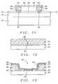
- a substrate 80is shown, which could be an underlying dielectric layer, and a metal contact point 81 , preferably comprising aluminum.
- a layer 84 of passivationhas been patterned creating an opening 82 through layer 84 that exposes the contact pad 81 .
- Layer 86is a layer of polymer, preferably polyimide, as earlier described, deposited over the layer 84 of passivation, including the exposed surface of the contact pad.
- Polymer layer 86such as polyimide, is typically spun on. For some thick layers of polymer, the polymer can be screen printed. Alternately, a laminated dry film polymer may be used.
- FIG. 13illustrates forming an opening 87 in polymer 86 , wherein the polymer opening 87 is larger than passivation opening 82 .
- Opening 87is depicted having sloped sides 85 .
- Polymer layer 86is exposed and developed to form opening 87 , which initially has vertical sidewalls. However, the subsequent curing process causes the sidewalls to have a slope 85 , and a opening 87 to have a resultant partially conical shape.
- the sidewall slope 85may have an angle of 45 degrees or more, and is typically between about 50 and 60 degrees. It may be possible to form the sidewalls with an angle as small as 20 degrees.
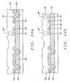
- a glue/barrier layer 88preferably comprising TiW, is deposited, preferably by sputtering to a thickness of between about 500 and 5,000 Angstroms.
- a gold seed layer 90is next sputter deposited over the glue/barrier 88 , to a thickness of between about 300 and 3,000 Angstroms.
- a bulk layer 92 of gold (Au)is next formed by electroplating, to a thickness of between about 1 and 20 ⁇ m. Electroplating is preceded by deposition of a thick photoresist 94 (to a thickness greater than the desired bulk metal thickness), and conventional lithography to expose the gold seed layer 90 in those areas where electroplating thick metallization is desired.
- polymer opening 87may be only partially filled, as shown in FIGS. 17 - 18 , which provides tight design rules for fine-pitch inductors.
- the design rule of polymer opening 87is typically about 15 um, while the metal traces of inductor are as tight as a 4 um pitch. Therefore, patterning metal inside the polyimide opening is a very important feature of this technology.
- Glue/barrier layer 88 and Au seed layer 90are sputtered as previously described, and photoresist 95 formed as shown in FIG. 17, followed by electroplating gold bulk layer 92 . Photoresist 95 is then stripped, and the seed layer and glue/barrier etched as previously described, and as shown in FIG. 18.
- coppermay be used as the bulk metal in the post-passivation metallization scheme.
- the FIG. 13 structureis a starting point.
- a glue/barrier layer 100 of Cr or Tiis sputter deposited to a thickness of between about 200 and 2000 Angstroms.
- a Cu seed layer 102is sputter deposited to a thickness of between about 2,000 and 10,000 Angstroms.
- Bulk layer 104 of Cuis next electroplated to a thickness of between about 3 and 20 ⁇ m, also using a photoresist 94 ′ and conventional lithography to define the areas to be electroplated.
- an optional cap layer 106 comprising Nimay also be formed, also by electroplating, to a thickness of between about 0.1 and 3 um.
- photoresist 94 ′is stripped, exposing Cu seed layer 104 .
- Clue/barrier layer 100 and Cu seed layer 102are now removed, as shown in FIG. 21, by etching.
- the bulk Cu layer 104is used as a mask for this etch.
- Ni cap layer 106acts as an etch stop during the etching of glue/barrier 100 and seed layer 102 .
- a faster Cu etch recipecan be used for removing the seed layer since there is no loss of Cu bulk in this configuration.
- polymer opening 87may be only partially filled, as shown in FIGS. 22 - 23 .
- Glue/barrier layer 100 and Cu seed layer 102are sputtered as previously described, and photoresist 95 ′ formed as shown in FIG. 22, followed by electroplating Cu bulk layer 104 and Ni 106 .
- Photoresist 95 ′is then stripped, and the seed layer and glue/barrier etched as previously described, and as shown in FIG. 23.
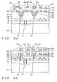
- FIG. 5 alayers similar to earlier descriptions are shown whereby in this case no layer of polyimide has been deposited over the layer of passivation.
- An inductor 19has been created on the surface of layer 18 of passivation.
- the ohmic resistivity of the metal that is used for inductor 19must be as low as possible. For this reason, the use of a thick layer of, for instance, gold is preferred for the formation of inductor 19 . It has been shown that a thick layer of gold increased the Q value of inductor 19 from about 5 to about 20 for 2.4 GHz applications.
- FIG. 5 a inductormay be connected to other elements in various configurations, as earlier described. These include both terminals being connected to lower levels, as shown in FIG. 4, one up and one down as shown in FIG. 24 a , or both up as in FIG. 24 b.
- An additional layer of polymermay optionally be formed over inductor 19 .
- polymer islandsmay be formed only under the inductor coils, and not elsewhere over the passivation layer, in order to reduce the stress caused by a larger sheet of polymer.
- FIGS. 5 b - 5 care a cross-sectional representation, and top view, respectively, of inductors of the invention formed on polymer islands.
- Each islandmay contain one or more than one inductor, such as on the right-most island of FIG. 5 c having a first inductor 40 ′ and second inductor 40 ′′′.
- isolated islands of polymer 20 ′are formed, by depositing a polymer layer and then patterning the polymer layer to form the polymer islands.
- the polymer islandsmay also be formed by screen printing, or by dry film lamination.
- the islands of polymer 20 ′are formed only at the location of inductors 40 ′ and 40 ′′, which are formed subsequent to polymer island formation.
- inductors 40 ′ and 40 ′′ of FIG. 5 bare formed as earlier described.
- inductor 40 ′′is shown with downward contacts 41 ′ and 43 ′ connecting to metal contact points 16 .
- Inductors 40 ′are shown without contacts but could be connected upward for connection to external circuits, as described elsewhere.
- FIG. 5 cis a top view of the inductors of the invention shown in FIG. 5 b , in which the FIG. 5 b cross-section is taken along line 5 b - 5 b in FIG. 5 c . It can be seen in FIG. 5 c that polymer islands 20 ′ are isolated from one another, and polymer is only located under inductor locations—passivation layer 18 is exposed in all other areas of the substrate.
- An additional protective layer of polymermay optionally be formed over inductors 40 ′ and 40 ′′.
- polymer islandsmay be formed under other devices of the invention, including passive devices such as resistors and capacitors.
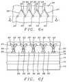
- FIGS. 6 a - 6 bdepict a transformer made according to the invention.
- the transformerconsists of bottom coil 60 , and top coil 62 , isolated by a dielectric layer 47 .
- Polymer layers 20 , 47 and 64are formed, and comprise materials, previously described. Openings 66 are provided in top polymer layer 64 for connections to the top coil 62 .
- FIG. 6 bis a cross-sectional representation of a transformer of the invention, in which the bottom coil 60 is formed directly on passivation layer 18 .
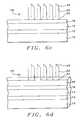
- FIG. 6 cis a three-dimensional view of a solenoid structure of an inductor 19 that has been created on passivation layer 18 , according to the invention. Further highlighted in FIG. 6 c are:
- top and bottom metal segments 25 , 27are connected, as shown, by the substantially vertical metal segments formed in vias 23 , to form a continuous solenoid.
- FIG. 6 dis a three dimensional view of a solenoid that has been created on a first layer 29 of polymer, having vias 23 created in a second layer of polymer.
- FIG. 6 fis a cross section of the structure of FIGS. 6 c - e , taken along line 6 f - 6 f ′ of FIG. 6 e.
- FIGS. 6 g - 6 ha toroidal inductor 68 is shown, also formed according to the method and structure of the invention.
- FIG. 6 ga three-dimensional view is shown, including top metal wires 27 ′, with vias 23 ′ connecting the top metal wires to the bottom metal wires 25 ′.
- FIG. 6 hshows, for further clarification, a top view of the toroidal inductor 68 of FIG. 6 g .
- the highlighted features of this figurehave previously been explained and therefore do not need to be further discussed at this time.
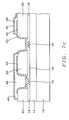
- FIG. 7 ais a cross section of a capacitor that has been created over a substrate 10 .
- a layer (or layers) 14 of conductive interconnect lines and contact points 16have been created over substrate 10 .
- a layer 18 of passivationhas been deposited over layer 14 , with openings created in layer 18 of passivation through which contact pads 16 can be accessed.
- a capacitorcontains, as is well known, a lower plate, an upper plate and a layer of dielectric that separates the upper plate from the lower plate.
- FIG. 7 aincludes lower plate 42 , upper plate 45 , and dielectric layer 46 .
- the upper and lower platesare formed as earlier described, using electroplated Au or Cu for the bulk metals.
- An optional protective polymer, preferably polyimide,may be formed over the capacitor. Contacts to the capacitor may be made as described earlier for inductor terminals (both down, one up and one down, or both up).
- Lower plate 42is formed to a thickness of between about 0.5 and 20 ⁇ m.
- Layer 46 of dielectricis between about 500 and 50,000 Angstroms.
- Upper plate 45is between about 0.5 and 20 ⁇ m thick.
- the post-passivation capacitor shown in cross section in FIG. 7 ahas:
- [0125]can use high-dielectric-constant material such as TiO 2 or Ta 2 O 5 , in addition to polymer, Si 3 N 4 or SiO 2 , for the dielectric between the upper and the lower plate of the capacitor, resulting in a higher capacitive value of the capacitor.
- high-dielectric-constant materialsuch as TiO 2 or Ta 2 O 5
- Si 3 N 4 or SiO 2in addition to polymer, Si 3 N 4 or SiO 2
- the capacitor of FIG. 7 amay alternately be formed above a polymer layer (deposited over passivation 18 ), similar to the inductor of FIG. 4.
- Dielectric layer 46is formed of a high-K dielectric material such as Si 3 N 4 , TEOS, Ta 2 O 5 , TiO 2 , SrTiO 3 , or SiON, which are typically deposited by CVD (Chemical Vapor Deposition).
- CVDChemical Vapor Deposition
- the dielectric layer 46can be a polymer film, including polyimide, benzocyclobutene (BCB), parylene or an epoxy-based material such as photoepoxy SU-8.
- a polymer filmincluding polyimide, benzocyclobutene (BCB), parylene or an epoxy-based material such as photoepoxy SU-8.
- FIGS. 7 b - 7 cshow a cross section where, as in FIG. 7 a , a capacitor is created.
- a thick layer 20 of polymerhas been deposited over the surface of the passivation layer 18 and has been patterned in order to make the contact pads 16 accessible though the thick layer 20 of polymer.
- FIG. 7 bshows the polymer vias having a smaller via diameter than the vias created through the layer of passivation. It is however preferred, as shown in FIG. 7 c , that larger vias be used in conjunction with smaller passivation vias.
- the thick layer 20 of polymermoves most of the capacitor, that is the lower plate 42 , the upper plate 45 and the dielectric 46 , further from the surface of substrate 10 by a distance equal to the thickness of layer 20 .
- the range of polyimide thicknesscan vary from 2 ⁇ m to 150 ⁇ m, depending on electrical design requirements. This leads to a significant increase in distance between the capacitor and underlying structures, including metal lines and/or the silicon substrate, so that parasitic capacitance is significantly reduced.
- FIGS. 7 a - 7 cdepict both capacitor terminals being connected down to a lower layer.
- the capacitormay also be contacted in one-up-one-down configuration—as shown in FIG. 25—or a two-up technique, as previously described with reference to FIG. 24 b.
- the upper capacitor plate 45can be connected in an upward manner through a layer of dielectric that has been deposited over the second capacitor plate 45 of FIGS. 7 a - 7 c . This is further highlighted in the cross section of FIG. 25, wherein a layer 35 of dielectric has been deposited over the capacitor upper plate 45 , with an opening 37 created through the layer 35 of dielectric to expose the capacitor upper plate 45 , for further connection to external circuits.
- the capacitor of FIGS. 7 a - 7 cmay optionally be covered with a protective layer of polymer, as previously described.
- FIG. 8shows a cross section of a substrate 10 over which has been deposited a layer 18 of passivation, with a resistor 48 formed over passivation layer 18 .
- a resistoras is well known, is created by connecting two points with a material that offers electrical resistance to the passage of current through the material.
- a resistive materialsuch as TaN, NiCr, NiSn, tungsten (W), TiW, TiN, Cr, Ti, TaSi or Ni.
- NiCrprovides the best TCR (Temperature Coefficient of Resistance), which can be as small as 5 ppm/° C.
- Resistor dimensionssuch as thickness, length and width of deposition of high resistive material 48 are application dependent.
- the resistor that is shown in cross section in FIG. 8is, as are the capacitors of FIGS. 7 a - 7 c , created in a post-passivation process on the surface of layer 18 of passivation.
- FIGS. 9 a - 9 bshows the resistor of the invention formed over a thick layer of polymer 20 , connected to contact pads 16 .
- FIGS. 8, 9 a and 9 bshow a “two-down” system for contacting the terminals of the resistor 48 .
- the resistormay also be contacted in one-up-one-down configuration, as shown in FIG. 26, or a two-up technique, as previously described with reference to the inductor of FIG. 24 b.
- An additional layer of polymer, to protect the resistor,may optionally be formed over the resistor of FIGS. 8, 9 a and 9 b.
- FIGS. 10 and 11Further applications of the post-passivation processing of the invention are shown in FIGS. 10 and 11, which concentrate on making contact points between contact pads 16 and an overlying electric component, such as a discrete inductor, capacitor, resistor or other passive device.
- Interconnect metal 50 of the inventionis formed in polymer openings, as previously described, which are aligned with smaller passivation openings, to connect to pads 16 , and serves as an under-bump metal (UBM). Solder contact bumps are formed over UBM 50 using conventional methods of selective solder deposition (plating, ball mounting, or screen printing on the surface of contacts 50 ), the application of a flux on the deposited solder and flowing the solder.
- UBMunder-bump metal
- a discrete device 54is connected to solder balls 52 and has solder 53 to facilitate the connection. This is similar to the surface mount technology used in the assembly of printed circuit boards.
- the discrete electrical componentmay be, but is not limited to, devices such as inductors, capacitors or resistors.
- FIG. 11illustrates mounting of discrete device 54 , using solder bumps 56 , and UBM 50 , directly over passivation layer 18 .
- FIGS. 10 and 11have the advantages of performance and cost savings since the discrete component does not have to be mounted on a Printed Circuit Board as is the common practice in the art.
- UBM 50is formed using the metallization scheme of the invention (as shown and described with respect to FIGS. 12 - 23 ), except that when Au is used as the bulk layer, its thickness is in the range of between about 0.1 and 20 um, the thinner range being preferable to avoid a high gold concentration in the solder near the UBM/solder interface, after processing.
- the discrete componentsprovide optimized parameters and can be mounted close to the circuits, which offer true system-on-chip performance
- the post-passivation process of the inventionallows for the selection of discrete component design parameters that result in reduced resistance of the discrete capacitor and the discrete inductor, this is further clear from the following comparison between prior art processes and the processes of the invention.
- the present inventionby contrast, can use easily formed thick metal layers, the thickness reducing resistance.
- Use of polymer 20further separates the components formed from underlying structures, reducing capacitance. With the reduced capacitance, a higher frequency of operation results due to a higher resonant frequency.
Landscapes
- Engineering & Computer Science (AREA)
- Power Engineering (AREA)
- Computer Hardware Design (AREA)
- Microelectronics & Electronic Packaging (AREA)
- Physics & Mathematics (AREA)
- Condensed Matter Physics & Semiconductors (AREA)
- General Physics & Mathematics (AREA)
- Manufacturing & Machinery (AREA)
- Geometry (AREA)
- Semiconductor Integrated Circuits (AREA)
- Internal Circuitry In Semiconductor Integrated Circuit Devices (AREA)
Abstract
Description
- This application is a Continuation-In-Part of attorney docket MEG00-008CBBC, Ser. No. 10/303,451, filing date Nov. 25, 2002, which is a continuation of attorney docket MEG00-008CBB, Ser. No. 10/156,590, filed on May 28, 2002, now issued as U.S. Pat. No. 6,489,647, which is a Divisional Application of MEG00-008CB, Ser. No. 09/970,005, filing date Oct. 3, 2001, now U.S. Pat. No. 6,455,885, which is a Divisional Application of MEG00-008C, Ser. No. 09/721,722, filing date Nov. 27, 2000, now U.S. Pat. No. 6,303,423, which is a continuation-in-part of attorney docket MEG00-008, Ser. No. 09/637,926, filing date Aug. 14, 2000, now abandoned, which is a continuation-in-part of attorney docket MSLIN98-002C, Ser. No. 09/251,183, filing date Feb. 17, 1999, now issued as U.S. Pat. No. 6,383,916 B1, which is a continuation-in-part of attorney docket MSLIN98-002, Ser. No. 09/216,791, filing date Dec. 21, 1998, now abandoned, assigned to common assignee.[0001]
- This application is related to attorney docket number MEG02-017, Ser. No. ______, filed on ______, and assigned to a common assignee.[0002]
- This application is related to attorney docket number MEG02-018, Ser. No. ______, filed on ______, and assigned to a common assignee.[0003]
- (1) Field of the Invention[0004]
- The invention relates to the manufacturing of high performance Integrated Circuit (IC's), and, more specifically, to methods of creating high performance electrical components (such as an inductor) on the surface of a semiconductor substrate by reducing the electromagnetic losses that are typically incurred in the surface of the substrate.[0005]
- (2) Description of the Related Art[0006]
- The continued emphasis in the semiconductor technology is to create improved performance semiconductor devices at competitive prices. This emphasis over the years has resulted in extreme miniaturization of semiconductor devices, made possible by continued advances of semiconductor processes and materials in combination with new and sophisticated device designs. Most of the semiconductor devices that are at this time being created are aimed at processing digital data. There are however also numerous semiconductor designs that are aimed at incorporating analog functions into devices that simultaneously process digital and analog data, or devices that can be used for the processing of only analog data. One of the major challenges in the creation of analog processing circuitry (using digital processing procedures and equipment) is that a number of the components that are used for analog circuitry are large in size and are therefore not readily integrated into devices that typically have feature sizes that approach the sub-micron range. The main components that offer a challenge in this respect are capacitors and inductors, since both these components are, for typical analog processing circuits, of considerable size.[0007]
- A typical application for inductors of the invention is in the field of modern mobile communication applications. One of the main applications of semiconductor devices in the field of mobile communication is the creation of Radio Frequency (RF) amplifiers. RF amplifiers contain a number of standard components, a major component of a typical RF amplifier is a tuned circuit that contains inductive and capacitive components. Tuned circuits form, dependent on and determined by the values of their inductive and capacitive components, an impedance that is frequency dependent, enabling the tuned circuit to either present a high or a low impedance for signals of a certain frequency. The tuned circuit can therefore either reject or pass and further amplify components of an analog signal, based on the frequency of that component. The tuned circuit can in this manner be used as a filter to filter out or remove signals of certain frequencies or to remove noise from a circuit configuration that is aimed at processing analog signals. The tuned circuit can also be used to form a high electrical impedance by using the LC resonance of the circuit and to thereby counteract the effects of parasitic capacitances that are part of a circuit. One of the problems that is encountered when creating an inductor on the surface of a semiconductor substrate is that the self-resonance that is caused by the parasitic capacitance between the (spiral) inductor and the underlying substrate will limit the use of the inductor at high frequencies. As part of the design of such an inductor it is therefore of importance to reduce the capacitive coupling between the created inductor and the underlying substrate.[0008]
- At high frequencies, the electromagnetic field that is generated by the inductor induces eddy currents in the underlying silicon substrate. Since the silicon substrate is a resistive conductor, the eddy currents will consume electromagnetic energy resulting in significant energy loss, resulting in a low Q inductor. This is one of the main reasons for a low Q value of a inductor, whereby the resonant frequency of 1/{square root}(LC) limits the upper boundary of the frequency. In addition, the eddy currents that are induced by the inductor will interfere with the performance of circuitry that is in close physical proximity to the inductor. Furthermore, the fine metal lines used to form the inductor also consume energy, due to the metal's resistance, and result in low Q inductors.[0009]
- It has already been pointed out that one of the key components used in creating high frequency analog semiconductor devices is the inductor that forms part of an LC resonance circuit. In view of the high device density that is typically encountered in semiconductor devices and the subsequent intense use of the substrate surface area, the creation of the inductor must incorporate the minimization of the surface area that is required for the inductor, while at the same time maintaining a high Q value for the inductor. Typically, inductors that are created on the surface of a substrate are of a spiral shape whereby the spiral is created in a plane that is parallel with the plane of the surface of the substrate. Conventional methods that are used to create the inductor on the surface of a substrate suffer several limitations. Most high Q inductors form part of a hybrid device configuration or of Monolithic Microwave Integrated Circuits (MMIC's) or are created as discrete components, the creation of which is not readily integratable into a typical process of Integrated Circuit manufacturing. It is clear that, by combining the creation on one semiconductor monolithic substrate of circuitry that is aimed at the functions of analog data manipulation and analog data storage with the functions of digital data manipulation and digital data storage, a number of significant advantages can be achieved. Such advantages include the reduction of manufacturing costs and the reduction of power consumption by the combined functions. The spiral form of the inductor that is created on the surface of a semiconductor substrate however results, due to the physical size of the inductor, in parasitic capacitances between the inductor wiring and the underlying substrate and causes electromagnetic energy losses in the underlying resistive silicon substrate. These parasitic capacitances have a serious negative effect on the functionality of the created LC circuit by sharply reducing the frequency of resonance of the tuned circuit of the application.[0010]
- More seriously, the inductor-generated electromagnetic field will induce eddy currents in the underlying resistive silicon substrate, causing a significant energy loss that results in low Q inductors.[0011]
- The performance parameter of an inductor is typically indicated is the Quality (Q) factor of the inductor. The quality factor Q of an inductor is defined as Q=Es/El, wherein Es is the energy that is stored in the reactive portion of the component while El is the energy that is lost in the reactive portion of the component. The higher the quality of the component, the closer the resistive value of the component approaches zero while the Q factor of the component approaches infinity. For inductors that are created overlying a silicon substrate, the electromagnetic energy that is created by the inductor will primarily be lost in the resistive silicon of the underlying substrate and in the metal lines that are created to form the inductor. For components, the quality factor serves as a measure of the purity of the reactance (or the susceptance) of the component, which can be degraded due to the resistive silicon substrate, the resistance of the metal lines and dielectric losses. In an actual configuration, there are always some physical resistors that will dissipate power, thereby decreasing the power that can be recovered. The quality factor Q is dimensionless. A Q value of greater than 100 is considered very high for discrete inductors that are mounted on the surface of Printed Circuit Boards. For inductors that form part of an integrated circuit, the Q value is typically in the range between about 3 and 10.[0012]
- In creating an inductor on a monolithic substrate on which additional semiconductor devices are created, the parasitic capacitances that occur as part of this creation limit the upper bound of the cut-off frequency that can be achieved for the inductor using conventional silicon processes. This limitation is, for many applications, not acceptable. Dependent on the frequency at which the LC circuit is designed to resonate, significantly larger values of quality factor, such as for[0013]
instance 50 or more, must be available. Prior Art has in this been limited to creating values of higher quality factors as separate units, and in integrating these separate units with the surrounding device functions. This negates the advantages that can be obtained when using the monolithic construction of creating both the inductor and the surrounding devices on one and the same semiconductor substrate. The non-monolithic approach also has the disadvantage that additional wiring is required to interconnect the sub-components of the assembly, thereby again introducing additional parasitic capacitances and resistive losses over the interconnecting wiring network. For many of the applications of a RF amplifier, such as portable battery powered applications, power consumption is at a premium and must therefore be as low as possible. By raising the power consumption, the effects of parasitic capacitances and resistive power loss can be partially compensated, but there are limitations to even this approach. These problems take on even greater urgency with the rapid expansion of wireless applications, such as portable telephones and the like. Wireless communication is a rapidly expanding market, where the integration of RF integrated circuits is one of the most important challenges. One of the approaches is to significantly increase the frequency of operation to for instance the range of 10 to 100 GHz. For such high frequencies, the value of the quality factor obtained from silicon-based inductors is significantly degraded. For applications in this frequency range, monolithic inductors have been researched using other than silicon as the base for the creation of the inductors. Such monolithic inductors have for instance been created using sapphire or GaAs as a base. These inductors have considerably lower substrate losses than their silicon counterparts (no eddy current, hence no loss of electromagnetic energy) and therefore provide much higher Q inductors. Furthermore, they have lower parasitic capacitance and therefore provide higher frequency operation capabilities. Where however more complex applications are required, the need still exists to create inductors using silicon as a substrate. For those applications, the approach of using a base material other than silicon has proven to be too cumbersome while for instance GaAs as a medium for the creation of semiconductor devices is as yet a technical challenge that needs to be addressed. It is known that GaAs is a semi-insulating material at high frequencies, reducing the electromagnetic losses that are incurred in the surface of the GaAs substrate, thereby increasing the Q value of the inductor created on the GaAs surface. GaAs RF chips however are expensive, a process that can avoid the use of GaAs RF chips therefore offers the benefit of cost advantage. - A number of different approaches have been used to incorporate inductors into a semiconductor environment without sacrificing device performance due to substrate losses. One of these approaches has been to selectively remove (by etching) the silicon underneath the inductor (using methods of micro machining), thereby removing substrate resistive energy losses and parasitic effects. Another method has been to use multiple layers of metal (such as aluminum) interconnects or of copper damascene interconnects.[0014]
- Other approaches have used a high resistivity silicon substrate thereby reducing resistive losses in the silicon substrate. Resistive substrate losses in the surface of the underlying substrate form a dominant factor in determining the Q value of silicon inductors. Further, biased wells have been proposed underneath a spiral conductor, this again aimed at reducing inductive losses in the surface of the substrate. A more complex approach has been to create an active inductive component that simulates the electrical properties of an inductor as it is applied in active circuitry. This latter approach however results in high power consumption by the simulated inductor and in noise performance that is unacceptable for low power, high frequency applications. All of these approaches have as common objectives to enhance the quality (Q) value of the inductor and to reduce the surface area that is required for the creation of the inductor. The most important consideration in this respect is the electromagnetic energy losses due to the electromagnetic induced eddy currents in the silicon substrate.[0015]
- When the dimensions of Integrated Circuits are scaled down, the cost per die is decreased while some aspects of performance are improved. The metal connections which connect the Integrated Circuit to other circuit or system components become of relative more importance and have, with the further miniaturization of the IC, an increasingly negative impact on circuit performance. The parasitic capacitance and resistance of the metal interconnections increase, which degrades the chip performance significantly. Of most concern in this respect is the voltage drop along the power and ground buses and the RC delay of the critical signal paths. Attempts to reduce the resistance by using wider metal lines result in higher capacitance of these wires.[0016]
- Current techniques for building an inductor on the surface of a semiconductor substrate use fine-line techniques whereby the inductor is created under a layer of passivation. This however implies close physical proximity between the created inductor and the surface of the substrate over which the inductor has been created (typically less than 10 μm), resulting in high electromagnetic losses in the silicon substrate which in turn results in reducing the Q value of the inductor.[0017]
- U.S. Pat. No. 5,212,403 (Nakanishi) shows a method of forming wiring connections both inside and outside (in a wiring substrate over the chip) for a logic circuit depending on the length of the wire connections.[0018]
- U.S. Pat. No. 5,501,006 (Gehman, Jr. et al.) shows a structure with an insulating layer between the integrated circuit (IC) and the wiring substrate. A distribution lead connects the bonding pads of the IC to the bonding pads of the substrate.[0019]
- U.S. Pat. No. 5,055,907 (Jacobs) discloses an extended integration semiconductor structure that allows manufacturers to integrate circuitry beyond the chip boundaries by forming a thin film multi-layer wiring decal on the support substrate and over the chip. However, this reference differs from the invention.[0020]
- U.S. Pat. No. 5,106,461 (Volfson et al.) teaches a multi layer interconnect structure of alternating polyimide (dielectric) and metal layers over an IC in a TAB structure.[0021]
- U.S. Pat. No. 5,635,767 (Wenzel et al.) teaches a method for reducing RC delay by a PBGA that separates multiple metal layers.[0022]
- U.S. Pat. No. 5,686,764 (Fulcher) shows a flip chip substrate that reduces RC delay by separating the power and I/O traces.[0023]
- U.S. Pat. No. 6,008,102 (Alford et al.) shows a helix inductor using two metal layers connected by vias.[0024]
- U.S. Pat. No. 5,372,967 (Sundaram et al.) discloses a helix inductor.[0025]
- U.S. Pat. No. 5,576,680 (Ling) and U.S. Pat. No. 5,884,990 (Burghartz et al.) show other helix inductor designs.[0026]
- It is the primary objective of the invention to improve the RF performance of High Performance Integrated Circuits.[0027]
- Another objective of the invention is to provide a method for the creation of a high-Q inductor.[0028]
- Another objective of the invention is to replace the GaAs chip with a silicon chip as a base on which a high-Q inductor is created.[0029]
- Yet another objective of the invention is to extend the frequency range of the inductor that is created on the surface of a silicon substrate.[0030]
- It is yet another objective of the invention to create high quality passive electrical components overlying the surface of a silicon substrate.[0031]
- The above referenced U.S. Pat. No. 6,383,916 adds, in a post passivation processing sequence, a thick layer of dielectric over a layer of passivation and layers of wide and thick metal lines on top of the thick layer of dielectric. The present invention extends referenced U.S. Pat. No. 6,383,916 by in addition creating high quality electrical components, such as an inductor, a capacitor or a resistor, on a layer of passivation or on the surface of a thick layer of dielectric. In addition, the process of the invention provides a method for mounting discrete passive electrical components on the surface of Integrated Circuit chips.[0032]
- FIG. 1 is a cross sectional representation of the interconnection scheme shown in U.S. Pat. No. 6,383,916.[0033]
- FIG. 2 is a cross sectional representation of an inductor of the invention, created on a thick layer of polyimide.[0034]
- FIG. 3 is a top view of an inductor created following the process of the invention.[0035]
- FIG. 4 is a cross sectional representation of a substrate and overlying layers, an inductor has been created on the surface of a thick layer of polyimide, a layer of conductive material has been added to further insulate the inductor from the underlying silicon substrate.[0036]
- FIG. 5[0037]ashows an inductor of the invention above a layer of passivation.
- FIGS. 5[0038]b-5care a cross-sectional representation, and top view, respectively, of inductors of the invention formed on an isolated section of polymer.
- FIG. 6[0039]ais a cross sectional representation of a transformer according to the invention, formed over a polymer layer, over a layer of passivation.
- FIG. 6[0040]bis a cross sectional representation of a transformer according to the invention, with the bottom coil formed on a layer of passivation.
- FIG. 6[0041]cis a three dimensional view of another embodiment of a solenoidal inductor of the invention, over a passivation layer.
- FIG. 6[0042]dis a three-dimensional view of a solenoidal inductor of the invention, formed over a polymer layer, over a passivation layer.
- FIG. 6[0043]eis a top view of the inductors of FIGS. 6cand6d.
- FIG. 6[0044]fis a cross sectional representation of the structure of FIG. 6e, taken along the
line 6f-6f′ of FIG. 6e. - FIG. 6[0045]gis a three dimensional view of an inductor of the invention, in the shape of a toroid.
- FIG. 6[0046]his a top view of the toroidal inductor of FIG. 6g.
- FIGS. 7[0047]a-7cis a cross sectional representation of a capacitor of the invention, formed over a polymer layer over passivation.
- FIG. 8 is a cross sectional representation of a resistor of the invention, formed over a passivation layer.[0048]
- FIGS. 9[0049]a-9bare cross sectional representations of a resistor of the invention, formed over a thick polymer layer, over a passivation layer.
- FIG. 10 is a cross sectional representation of a silicon substrate over which a discrete electrical component has been mounted, on the top of a thick polymer layer, using surface mount technology.[0050]
- FIG. 11 is a cross sectional representation of a silicon substrate, having a passivation layer on the surface of which a discrete electrical component has been mounted, using surface mount technology.[0051]
- FIGS.[0052]12-18 depict, in cross-sectional form, the creation of gold metal structures of the invention, through a layer of polymer.
- FIGS.[0053]19-23 depict the creation of copper metal structures of the invention, through a layer of polymer.
- FIGS. 24[0054]a-24cshow alternate methods of connecting to the inductor of the invention.
- FIGS. 25 and 26 show extended methods of connecting a capacitor and a resistor under the invention.[0055]
- U.S. Pat. No. 6,383,916, assigned to a common assignee as the current invention, teaches an Integrated Circuit structure where re-distribution and interconnect metal layers are created in layers of dielectric over the passivation layer of a conventional Integrated Circuit (IC). A layer of passivation is deposited over the IC, a thick layer of polymer is alternately deposited over the surface of the layer of passivation, and thick, wide metal lines are formed over the passivation.[0056]
- U.S. Pat. No. 6,303,423, also assigned to a common assignee as the current invention, addresses, among other objectives, the creation of an inductor whereby the emphasis is on creating an inductor of high Q value above the passivation layer of a semiconductor substrate. The high quality of the inductor of the invention allows for the use of this inductor in high frequency applications while incurring minimum loss of power. The invention further addresses the creation of a capacitor and a resistor on the surface of a silicon substrate whereby the main objective (of the process of creating a capacitor and resistor) is to reduce parasitics that are typically incurred by these components in the underlying silicon substrate.[0057]
- Referring now more specifically to FIG. 1, there is shown a cross section of one implementation of U.S. Pat. No. 6,383,916. The surface of[0058]
silicon substrate 10 has been provided withtransistors 11 and other devices (not shown in FIG. 1). The surface ofsubstrate 10 is covered by a interlevel dielectric (ILD)layer 12, formed over the devices. - Layers[0059]14 represent metal and dielectric layers that are typically created over
ILD 12.Layers 14 contain one or more layers of dielectric, interspersed with one or moremetal interconnect lines 13 that make up a network of electrical connections. At a top metal layer arepoints 16 of electrical contact. Thesepoints 16 of electrical contact can establish electrical interconnects to the transistors andother devices 11 that have been provided in and on the surface of thesubstrate 10. Apassivation layer 18, formed of, for example, a composite layer of silicon oxide and silicon nitride, is deposited over the surface oflayers 14, and function to prevent the penetration of mobile ions (such as sodium ions), moisture, transition metal (such as gold, copper, silver), and other contamination. The passivation layer is used to protect the underlying devices (such as transistors, polysilicon resistors, poly-to-poly capacitors, etc.) and the fine-line metal interconnection. - The key steps of U.S. Pat. No. 6,383,916, begin with the deposition of a[0060]
thick layer 20 of polyimide that is deposited over the surface ofpassivation layer 18. Access must be provided to points ofelectrical contact 16, for this reason a pattern ofopenings polyimide layer 20 and thepassivation layer 18, the pattern ofopenings openings 22/36/38 that are created in thelayer 20 of polyimide, electrically extended to the surface oflayer 20. - [0061]
Layer 20 is a polymer, and is preferably polyimide.Polymer 20 may optionally be photosensitive. Examples of other polymers that can be used include benzocyclobutene (BCB), parylene or epoxy-based material such as photoepoxy SU-8 (available from Sotec Microsystems, Renens, Switzerland). - After formation of[0062]
openings 22/36/38, metallization is performed to create patternedwide metal layers Lines metal 26 may be connected off-chip through wire bonds or solder bumps. - Contact points[0063]16 are located on top of a thin dielectric (layers14, FIG. 1), and the pad size must be kept small to minimize capacitance with underlying metal layers. In addition, a large pad size will interfere with the routing capability of the layer of metal.
- [0064]
Layer 20 is a thick polymer dielectric layer (for example, polyimide) having a thickness in excess of 2 μm (after curing). The range of the polymer thickness can vary from 2 μm to 150 μm, dependent on electrical design requirements. For a thicker layer of polyimide, the polyimide film can be multiple coated and cured. - U.S. Pat. No. 6,383,916 B1 allows for the interconnection of circuit elements at various distances, over the[0065]
path 30/32/34 shown in FIG. 1, using the thick, wide (as compared to the underlying “fine line” metallization in layers14) metal of28. Thick,wide metal 28 has smaller resistance and capacitance than thefine line metal 14 and is also easier and more cost effective to manufacture. - FIG. 2 shows how the interconnect aspect of U.S. Pat. No. 6,383,916, can be modified to form an inductor on the surface of the[0066]
thick layer 20 of polyimide. The inductor is created in a plane that is parallel with the surface of thesubstrate 10 whereby this plane however is separated from the surface of thesubstrate 10 by the combined heights oflayers cross section 40 of the inductor taken in a plane that is perpendicular to the surface ofsubstrate 10. The wide and thick metal will also contribute to a reduction of the resistive energy losses. Furthermore, the low resistivity metal, such as gold, silver and copper, can be applied using electroplating, the thickness can be about 20 μm. - By increasing the distance between the inductor and the semiconductor surface, as compared to prior art approaches in which the inductor is formed under the passivation, the electromagnetic field in the silicon substrate will be reduced as the distance is increased, and the Q value of the inductor can be increased. The inductor overlies the layer of passivation and by, in addition, creating the inductor on the surface of a thick layer of dielectric (such as a polymer) formed over the passivation layer. In addition, by using wide and thick metal for the creation of the inductor, the parasitic resistance is reduced.[0067]
- In an important feature of the invention, the[0068]
openings 19 inpassivation layer 18 may be as small as 0.1 um wide. Thus,contact pads 16 may also be nearly as small, which allows for greater routing capability in the top fine-line metallization layer, and lower capacitance. - In another important feature of the invention, the[0069]
openings 22/36/38 inpolymer 20 are larger than thepassivation openings 19. Thepolymer openings 22/36/38 are aligned withpassivation openings 19. The larger polymer openings allow for relaxed design rules, simpler opening formation, and the use of a thick metal layer for the post-passivation metallization of the invention. - FIG. 2 illustrates[0070]
interconnect structure 26 as well asinductor 40, wherein the inductor includes twocontacts polymer layer 20 to contactpads 16. - In another feature of the invention, the FIG. 2 structure may be covered by an additional layer of polymer (not shown).[0071]
- FIGS. 24[0072]aand24billustrate another feature of the invention, in which contacts to the inductor are formed in a different manner than the 2 downward contacts of FIG. 2. Specifically, in FIG. 24a, a
layer 35 of dielectric, preferably polyimide or the like, is deposited overinterconnection 26 andinductor 40. Anopening 36′ to one end of the inductor is then formed to expose one terminal of theinductor 40.Inductor 40 in FIG. 24athus can have one contact extending upward, and asecond contact 40′ extending downward, in a “one-up, one-down” configuration. - FIG. 24[0073]billustrates another alternative, in which2
upward contact openings 36′ and38′ are formed frominductor 40, in a “two-up” configuration. - In both FIGS. 24[0074]aand24b, the upward contacts may be used for connection to external devices or packaging, by way of wire bonding, solder bumps, or the like. For wire bonding, an upper surface of
inductor 40 must be formed of a wire-bondable material such as Au or Al. For solder bump connection, under bump metallization (UBM) would be formed in the upward contact opening, followed by solder bump formation. - In either of the FIG. 24[0075]aor24bconfigurations, interconnections to other contact pads on the same die (as opposed to connections to external devices, as described in the previous paragraph) may be made through
openings 36′ and/or38′, using similar metallization (but as an additional layer) as used forstructure 26 andinductor 40. - Referring now to FIG. 24[0076]c, another feature of the invention is shown in which
extension 89, connected toinductor 40, is used to relocate aninductor contact opening 36″ to another location on the die, such as at the die edge. This may be useful for ease of wire bonding, for example.Opening 38″ is formed as earlier described.Extension 89 is formed at the same time and of the same metallization asstructure 26 andinductor 40. - Similarly,[0077]
extension 89 could be used to interconnectinductor 40 to another contact point on the same die, by making a downward contact (not shown, but described earlier) instead ofupward contact 36″. - If a contact to a center point of the inductor, such as that shown under opening[0078]38″ in FIG. 24c, is desired, then such contact cannot of course be made by an extension such as40′, but instead must be either upward or downward.
- FIG. 3 shows a[0079]
top view 42 of the spiral structure of theinductor 40 that has been created on the surface oflayer 20 of dielectric. Theinductor 40 cross section that is shown in FIG. 2 is taken along line2-2 of FIG. 3. - FIG. 4 shows a cross section of[0080]
inductor 40 whereby the inductor has been further isolated from the surface of thesubstrate 10 by the addition of aconductive plate 44′, of conducting material, formed under substantially all of the inductor, and preferably formed of Cu (copper) or Au (gold). The surface area of theconductive plate 44′ typically extends over the surface ofpassivation layer 18 such that theinductor 40 aligns with and overlays theconductive plate 44′, the surface area ofconductive plate 44′ can be extended slightly beyond these boundaries to further improve shielding the surface ofsubstrate 10 from the electromagnetic field ofinductor 40. - [0081]
Conductive plate 44′ can be connected to one of the inductor terminals (as shown in FIG. 4, in which it is connected to the rightmost inductor terminal43), or may be left at a floating voltage level, or may be connected to another voltage level, deciding on the system's electrical design. - [0082]
Conductive plate 44′ is formed using the methods and material of the invention, as later described with regard to the metal layer used to formmetal interconnect 26 andinductor 40.Conductive plate 44′ is formed at the same time asconnectors 44, which serve to connect the next level metal to contactpoints 16, as shown in FIG. 4. - Optionally, a[0083]
second polymer layer 47 may be deposited overinductor 40 andinterconnect structure 26, to provide additional protection of the metal structures. - Referring now to FIGS.[0084]12-23, further details are provided for forming the post passivation inductor (and other passive devices) of the invention. In FIG. 12, a
substrate 80 is shown, which could be an underlying dielectric layer, and ametal contact point 81, preferably comprising aluminum. Alayer 84 of passivation has been patterned creating anopening 82 throughlayer 84 that exposes thecontact pad 81.Layer 86 is a layer of polymer, preferably polyimide, as earlier described, deposited over thelayer 84 of passivation, including the exposed surface of the contact pad.Polymer layer 86, such as polyimide, is typically spun on. For some thick layers of polymer, the polymer can be screen printed. Alternately, a laminated dry film polymer may be used. - FIG. 13 illustrates forming an[0085]
opening 87 inpolymer 86, wherein thepolymer opening 87 is larger thanpassivation opening 82.Opening 87 is depicted having sloped sides85.Polymer layer 86 is exposed and developed to form opening87, which initially has vertical sidewalls. However, the subsequent curing process causes the sidewalls to have aslope 85, and aopening 87 to have a resultant partially conical shape. Thesidewall slope 85 may have an angle of 45 degrees or more, and is typically between about 50 and 60 degrees. It may be possible to form the sidewalls with an angle as small as 20 degrees. - By creating relatively large vias through the layer of polyimide or polymer, aligned with smaller vias created through the underlying layer of passivation, aligned with underlying sub-micron metal layer, it is clear that the sub-micron metal vias can effectively be enlarged when progressing from the sub-micron metal layer to the level of the wide metal.[0086]
- Continuing to refer to FIG. 13, one metallization system and process for forming the post passivation interconnect and inductor of the invention is depicted. First, a glue/[0087]
barrier layer 88, preferably comprising TiW, is deposited, preferably by sputtering to a thickness of between about 500 and 5,000 Angstroms. Agold seed layer 90, is next sputter deposited over the glue/barrier 88, to a thickness of between about 300 and 3,000 Angstroms. - Referring now to FIG. 14, a[0088]
bulk layer 92 of gold (Au) is next formed by electroplating, to a thickness of between about 1 and 20 μm. Electroplating is preceded by deposition of a thick photoresist94 (to a thickness greater than the desired bulk metal thickness), and conventional lithography to expose thegold seed layer 90 in those areas where electroplating thick metallization is desired. - After electroplating,[0089]
photoresist 94 is removed, as shown in FIG. 15. Glue/barrier Layer 88 andgold seed layer 90 are now removed, as shown in FIG. 16, by etching, usingbulk Au layer 92 as a mask. One coil ofinductor 40 is shown, but it would be understood that the complete inductor would be formed at the same time. - In another feature of the invention,[0090]
polymer opening 87 may be only partially filled, as shown in FIGS.17-18, which provides tight design rules for fine-pitch inductors. The design rule ofpolymer opening 87 is typically about 15 um, while the metal traces of inductor are as tight as a 4 um pitch. Therefore, patterning metal inside the polyimide opening is a very important feature of this technology. - Glue/[0091]
barrier layer 88 andAu seed layer 90 are sputtered as previously described, andphotoresist 95 formed as shown in FIG. 17, followed by electroplatinggold bulk layer 92.Photoresist 95 is then stripped, and the seed layer and glue/barrier etched as previously described, and as shown in FIG. 18. - In another embodiment of the invention, copper may be used as the bulk metal in the post-passivation metallization scheme. The FIG. 13 structure is a starting point. Next, as shown in FIG. 19, a glue/[0092]
barrier layer 100 of Cr or Ti is sputter deposited to a thickness of between about 200 and 2000 Angstroms. Next, aCu seed layer 102 is sputter deposited to a thickness of between about 2,000 and 10,000 Angstroms.Bulk layer 104 of Cu is next electroplated to a thickness of between about 3 and 20 μm, also using aphotoresist 94′ and conventional lithography to define the areas to be electroplated. Finally, anoptional cap layer 106 comprising Ni may also be formed, also by electroplating, to a thickness of between about 0.1 and 3 um. - Referring to FIG. 20,[0093]
photoresist 94′ is stripped, exposingCu seed layer 104. Clue/barrier layer 100 andCu seed layer 102 are now removed, as shown in FIG. 21, by etching. Thebulk Cu layer 104 is used as a mask for this etch. - If optional[0094]
Ni cap layer 106 is used, it acts as an etch stop during the etching of glue/barrier 100 andseed layer 102. With the Ni cap, a faster Cu etch recipe can be used for removing the seed layer since there is no loss of Cu bulk in this configuration. - One coil of[0095]
inductor 40 is shown, but it would be understood that the complete inductor would be formed at the same time. - In another feature of the invention and as earlier described,[0096]
polymer opening 87 may be only partially filled, as shown in FIGS.22-23. Glue/barrier layer 100 andCu seed layer 102 are sputtered as previously described, andphotoresist 95′ formed as shown in FIG. 22, followed by electroplatingCu bulk layer 104 andNi 106.Photoresist 95′ is then stripped, and the seed layer and glue/barrier etched as previously described, and as shown in FIG. 23. - Referring now to FIG. 5[0097]a, layers similar to earlier descriptions are shown whereby in this case no layer of polyimide has been deposited over the layer of passivation. An
inductor 19 has been created on the surface oflayer 18 of passivation. The ohmic resistivity of the metal that is used forinductor 19 must be as low as possible. For this reason, the use of a thick layer of, for instance, gold is preferred for the formation ofinductor 19. It has been shown that a thick layer of gold increased the Q value ofinductor 19 from about 5 to about 20 for 2.4 GHz applications. - The FIG. 5[0098]ainductor may be connected to other elements in various configurations, as earlier described. These include both terminals being connected to lower levels, as shown in FIG. 4, one up and one down as shown in FIG. 24a, or both up as in FIG. 24b.
- An additional layer of polymer (not shown) may optionally be formed over[0099]
inductor 19. - In another feature of the invention, polymer islands may be formed only under the inductor coils, and not elsewhere over the passivation layer, in order to reduce the stress caused by a larger sheet of polymer. This is depicted in FIGS. 5[0100]b-5c, which are a cross-sectional representation, and top view, respectively, of inductors of the invention formed on polymer islands. Each island may contain one or more than one inductor, such as on the right-most island of FIG. 5chaving a
first inductor 40′ andsecond inductor 40′″. - Referring first to FIG. 5[0101]b, isolated islands of
polymer 20′ are formed, by depositing a polymer layer and then patterning the polymer layer to form the polymer islands. The polymer islands may also be formed by screen printing, or by dry film lamination. The islands ofpolymer 20′ are formed only at the location ofinductors 40′ and40″, which are formed subsequent to polymer island formation. - The[0102]
inductors 40′ and40″ of FIG. 5bare formed as earlier described. For illustrative purposes,inductor 40″ is shown withdownward contacts 41′ and43′ connecting to metal contact points16.Inductors 40′ are shown without contacts but could be connected upward for connection to external circuits, as described elsewhere. - FIG. 5[0103]cis a top view of the inductors of the invention shown in FIG. 5b, in which the FIG. 5bcross-section is taken along line5b-5bin FIG. 5c. It can be seen in FIG. 5cthat
polymer islands 20′ are isolated from one another, and polymer is only located under inductor locations—passivation layer 18 is exposed in all other areas of the substrate. - An additional protective layer of polymer (not shown) may optionally be formed over[0104]
inductors 40′ and40″. - In a similar fashion to that shown in FIGS. 5[0105]b-5cfor inductors, polymer islands may be formed under other devices of the invention, including passive devices such as resistors and capacitors.
- FIGS. 6[0106]a-6bdepict a transformer made according to the invention. The transformer consists of
bottom coil 60, andtop coil 62, isolated by adielectric layer 47. Polymer layers20,47 and64 are formed, and comprise materials, previously described.Openings 66 are provided intop polymer layer 64 for connections to thetop coil 62. - FIG. 6[0107]bis a cross-sectional representation of a transformer of the invention, in which the
bottom coil 60 is formed directly onpassivation layer 18. - FIG. 6[0108]cis a three-dimensional view of a solenoid structure of an
inductor 19 that has been created onpassivation layer 18, according to the invention. Further highlighted in FIG. 6care: - [0109]23, vias that are created in the thick layer of
polymer 20, having substantially vertical metal segments - [0110]25, the bottom metal segments of the solenoid
- [0111]27, the top metal segments of the solenoid.
- The top and[0112]
bottom metal segments vias 23, to form a continuous solenoid. - FIG. 6[0113]dis a three dimensional view of a solenoid that has been created on a
first layer 29 of polymer, havingvias 23 created in a second layer of polymer. - FIG. 6[0114]eis a top view of the solenoid of FIGS. 6cand6d.
Vias 23 are shown, connectingtop metal segments 27 tobottom metal segments 25. - FIG. 6[0115]fis a cross section of the structure of FIGS. 6c-e, taken along
line 6f-6f′ of FIG. 6e. - Referring now to FIGS. 6[0116]g-6h, a
toroidal inductor 68 is shown, also formed according to the method and structure of the invention. In FIG. 6g, a three-dimensional view is shown, includingtop metal wires 27′, withvias 23′ connecting the top metal wires to thebottom metal wires 25′. - FIG. 6[0117]hshows, for further clarification, a top view of the
toroidal inductor 68 of FIG. 6g. The highlighted features of this figure have previously been explained and therefore do not need to be further discussed at this time. - Besides inductors, it is very useful to form other passive devices, such as capacitors and resistors, using the method and structure of the invention.[0118]
- FIG. 7[0119]ais a cross section of a capacitor that has been created over a
substrate 10. A layer (or layers)14 of conductive interconnect lines and contact points16 have been created oversubstrate 10. Alayer 18 of passivation has been deposited overlayer 14, with openings created inlayer 18 of passivation through whichcontact pads 16 can be accessed. - A capacitor contains, as is well known, a lower plate, an upper plate and a layer of dielectric that separates the upper plate from the lower plate. FIG. 7[0120]aincludes
lower plate 42,upper plate 45, anddielectric layer 46. The upper and lower plates are formed as earlier described, using electroplated Au or Cu for the bulk metals. An optional protective polymer, preferably polyimide, may be formed over the capacitor. Contacts to the capacitor may be made as described earlier for inductor terminals (both down, one up and one down, or both up). - [0121]
Lower plate 42 is formed to a thickness of between about 0.5 and 20 μm.Layer 46 of dielectric is between about 500 and 50,000 Angstroms.Upper plate 45 is between about 0.5 and 20 μm thick. - The post-passivation capacitor shown in cross section in FIG. 7[0122]ahas:
- reduced parasitic capacitance between the capacitor and the underlying silicon substrate[0123]
- allowed for the use of a thick layer of conductive material for the capacitor plates, reducing the resistance of the capacitor; this is particularly important for wireless applications[0124]
- can use high-dielectric-constant material such as TiO[0125]2or Ta2O5, in addition to polymer, Si3N4or SiO2, for the dielectric between the upper and the lower plate of the capacitor, resulting in a higher capacitive value of the capacitor.
- The capacitor of FIG. 7[0126]amay alternately be formed above a polymer layer (deposited over passivation18), similar to the inductor of FIG. 4.
- [0127]
Dielectric layer 46 is formed of a high-K dielectric material such as Si3N4, TEOS, Ta2O5, TiO2, SrTiO3, or SiON, which are typically deposited by CVD (Chemical Vapor Deposition). - Alternately, the[0128]
dielectric layer 46 can be a polymer film, including polyimide, benzocyclobutene (BCB), parylene or an epoxy-based material such as photoepoxy SU-8. - FIGS. 7[0129]b-7cshow a cross section where, as in FIG. 7a, a capacitor is created. In the cross section that is shown in FIG. 7ba
thick layer 20 of polymer has been deposited over the surface of thepassivation layer 18 and has been patterned in order to make thecontact pads 16 accessible though thethick layer 20 of polymer. FIG. 7bshows the polymer vias having a smaller via diameter than the vias created through the layer of passivation. It is however preferred, as shown in FIG. 7c, that larger vias be used in conjunction with smaller passivation vias. Thethick layer 20 of polymer moves most of the capacitor, that is thelower plate 42, theupper plate 45 and the dielectric46, further from the surface ofsubstrate 10 by a distance equal to the thickness oflayer 20. It has previously been stated that the range of polyimide thickness can vary from 2 μm to 150 μm, depending on electrical design requirements. This leads to a significant increase in distance between the capacitor and underlying structures, including metal lines and/or the silicon substrate, so that parasitic capacitance is significantly reduced. - FIGS. 7[0130]a-7cdepict both capacitor terminals being connected down to a lower layer. The capacitor may also be contacted in one-up-one-down configuration—as shown in FIG. 25—or a two-up technique, as previously described with reference to FIG. 24b.
- Specifically relating to the cross section of FIGS. 7[0131]a-7c, the
upper capacitor plate 45 can be connected in an upward manner through a layer of dielectric that has been deposited over thesecond capacitor plate 45 of FIGS. 7a-7c. This is further highlighted in the cross section of FIG. 25, wherein alayer 35 of dielectric has been deposited over the capacitorupper plate 45, with anopening 37 created through thelayer 35 of dielectric to expose the capacitorupper plate 45, for further connection to external circuits. - The capacitor of FIGS. 7[0132]a-7cmay optionally be covered with a protective layer of polymer, as previously described.
- FIG. 8 shows a cross section of a[0133]
substrate 10 over which has been deposited alayer 18 of passivation, with aresistor 48 formed overpassivation layer 18. A resistor, as is well known, is created by connecting two points with a material that offers electrical resistance to the passage of current through the material. For the creation of layer48 a resistive material is used, such as TaN, NiCr, NiSn, tungsten (W), TiW, TiN, Cr, Ti, TaSi or Ni. Among these resistive materials, NiCr provides the best TCR (Temperature Coefficient of Resistance), which can be as small as 5 ppm/° C. Resistor dimensions such as thickness, length and width of deposition of highresistive material 48 are application dependent. The resistor that is shown in cross section in FIG. 8 is, as are the capacitors of FIGS. 7a-7c, created in a post-passivation process on the surface oflayer 18 of passivation. - FIGS. 9[0134]a-9bshows the resistor of the invention formed over a thick layer of
polymer 20, connected to contactpads 16. By increasing the distance between the body of the resistor and the substrate (by the thickness of thepolymer layer 20 and other intervening layers) the parasitic capacitance between the body of the resistor and the substrate is reduced, resulting in an improved resistive component (reduced parasitic capacitive loss, improved high frequency performance). - FIGS. 8, 9[0135]aand9bshow a “two-down” system for contacting the terminals of the
resistor 48. The resistor may also be contacted in one-up-one-down configuration, as shown in FIG. 26, or a two-up technique, as previously described with reference to the inductor of FIG. 24b. - An additional layer of polymer, to protect the resistor, may optionally be formed over the resistor of FIGS. 8, 9[0136]aand9b.
- Further applications of the post-passivation processing of the invention are shown in FIGS. 10 and 11, which concentrate on making contact points between[0137]
contact pads 16 and an overlying electric component, such as a discrete inductor, capacitor, resistor or other passive device.Interconnect metal 50 of the invention is formed in polymer openings, as previously described, which are aligned with smaller passivation openings, to connect topads 16, and serves as an under-bump metal (UBM). Solder contact bumps are formed overUBM 50 using conventional methods of selective solder deposition (plating, ball mounting, or screen printing on the surface of contacts50), the application of a flux on the deposited solder and flowing the solder. Adiscrete device 54 is connected to solderballs 52 and hassolder 53 to facilitate the connection. This is similar to the surface mount technology used in the assembly of printed circuit boards. The discrete electrical component may be, but is not limited to, devices such as inductors, capacitors or resistors. - FIG. 11 illustrates mounting of[0138]
discrete device 54, using solder bumps56, andUBM 50, directly overpassivation layer 18. - The discrete components of FIGS. 10 and 11 have the advantages of performance and cost savings since the discrete component does not have to be mounted on a Printed Circuit Board as is the common practice in the art.[0139]
- [0140]
UBM 50 is formed using the metallization scheme of the invention (as shown and described with respect to FIGS.12-23), except that when Au is used as the bulk layer, its thickness is in the range of between about 0.1 and 20 um, the thinner range being preferable to avoid a high gold concentration in the solder near the UBM/solder interface, after processing. - The invention and its various features provide the advantages of:[0141]
- the discrete components provide optimized parameters and can be mounted close to the circuits, which offer true system-on-chip performance[0142]
- the discrete components mounting close to the circuits also minimizes parasitics[0143]
- the post-passivation process of the invention allows for the selection of discrete component design parameters that result in reduced resistance of the discrete capacitor and the discrete inductor, this is further clear from the following comparison between prior art processes and the processes of the invention.[0144]
- Prior approaches in the art uses thinner metal for inductors, requiring wider coils (to minimize resistance), resulting in increased surface area, increasing the parasitic capacitance of the inductor and causing eddy current losses in the surface of the substrate.[0145]
- The present invention by contrast, can use easily formed thick metal layers, the thickness reducing resistance. Use of[0146]
polymer 20 further separates the components formed from underlying structures, reducing capacitance. With the reduced capacitance, a higher frequency of operation results due to a higher resonant frequency. - Although the preferred embodiment of the present invention has been illustrated, and that form has been described in detail, it will be readily understood by those skilled in the art that various modifications may be made therein without departing from the spirit of the invention or from the scope of the appended claims.[0147]
Claims (77)
Priority Applications (10)
| Application Number | Priority Date | Filing Date | Title |
|---|---|---|---|
| US10/445,558US8178435B2 (en) | 1998-12-21 | 2003-05-27 | High performance system-on-chip inductor using post passivation process |
| TW93111711ATWI236763B (en) | 2003-05-27 | 2004-04-27 | High performance system-on-chip inductor using post passivation process |
| US10/710,596US8421158B2 (en) | 1998-12-21 | 2004-07-23 | Chip structure with a passive device and method for forming the same |
| US11/183,658US7592205B2 (en) | 1998-12-21 | 2005-07-18 | Over-passivation process of forming polymer layer over IC chip |
| US11/653,171US20070108551A1 (en) | 2003-05-27 | 2007-01-12 | High performance system-on-chip inductor using post passivation process |
| US11/668,481US20070182521A1 (en) | 2003-05-27 | 2007-01-30 | High performance system-on-chip inductor using post passivation process |
| US11/668,484US20070202685A1 (en) | 2003-05-27 | 2007-01-30 | High performance system-on-chip inductor using post passivation process |
| US11/668,482US20130193553A9 (en) | 1998-12-21 | 2007-01-30 | High performance system-on-chip inductor using post passivation process |
| US11/668,483US20070202684A1 (en) | 2003-05-27 | 2007-01-30 | High performance system-on-chip inductor using post passivation process |
| US13/851,050US20130214387A1 (en) | 1998-12-21 | 2013-03-26 | Chip structure with a passive device and method for forming the same |
Applications Claiming Priority (8)
| Application Number | Priority Date | Filing Date | Title |
|---|---|---|---|
| US21679198A | 1998-12-21 | 1998-12-21 | |
| US09/251,183US6383916B1 (en) | 1998-12-21 | 1999-02-17 | Top layers of metal for high performance IC's |
| US63792600A | 2000-08-14 | 2000-08-14 | |
| US09/721,722US6303423B1 (en) | 1998-12-21 | 2000-11-27 | Method for forming high performance system-on-chip using post passivation process |
| US09/970,005US6455885B1 (en) | 1998-12-21 | 2001-10-03 | Inductor structure for high performance system-on-chip using post passivation process |
| US10/156,590US6489647B1 (en) | 1998-12-21 | 2002-05-28 | Capacitor for high performance system-on-chip using post passivation process structure |
| US10/303,451US6897507B2 (en) | 1998-12-21 | 2002-11-25 | Capacitor for high performance system-on-chip using post passivation device |
| US10/445,558US8178435B2 (en) | 1998-12-21 | 2003-05-27 | High performance system-on-chip inductor using post passivation process |
Related Parent Applications (1)
| Application Number | Title | Priority Date | Filing Date |
|---|---|---|---|
| US10/303,451Continuation-In-PartUS6897507B2 (en) | 1998-12-21 | 2002-11-25 | Capacitor for high performance system-on-chip using post passivation device |
Related Child Applications (6)
| Application Number | Title | Priority Date | Filing Date |
|---|---|---|---|
| US10/710,596Continuation-In-PartUS8421158B2 (en) | 1998-12-21 | 2004-07-23 | Chip structure with a passive device and method for forming the same |
| US11/653,171ContinuationUS20070108551A1 (en) | 2003-05-27 | 2007-01-12 | High performance system-on-chip inductor using post passivation process |
| US11/668,484ContinuationUS20070202685A1 (en) | 2003-05-27 | 2007-01-30 | High performance system-on-chip inductor using post passivation process |
| US11/668,483ContinuationUS20070202684A1 (en) | 2003-05-27 | 2007-01-30 | High performance system-on-chip inductor using post passivation process |
| US11/668,482ContinuationUS20130193553A9 (en) | 1998-12-21 | 2007-01-30 | High performance system-on-chip inductor using post passivation process |
| US11/668,481ContinuationUS20070182521A1 (en) | 2003-05-27 | 2007-01-30 | High performance system-on-chip inductor using post passivation process |
Publications (2)
| Publication Number | Publication Date |
|---|---|
| US20030222295A1true US20030222295A1 (en) | 2003-12-04 |
| US8178435B2 US8178435B2 (en) | 2012-05-15 |
Family
ID=46204845
Family Applications (1)
| Application Number | Title | Priority Date | Filing Date |
|---|---|---|---|
| US10/445,558Expired - Fee RelatedUS8178435B2 (en) | 1998-12-21 | 2003-05-27 | High performance system-on-chip inductor using post passivation process |
Country Status (1)
| Country | Link |
|---|---|
| US (1) | US8178435B2 (en) |
Cited By (43)
| Publication number | Priority date | Publication date | Assignee | Title |
|---|---|---|---|---|
| US20030127750A1 (en)* | 2000-07-17 | 2003-07-10 | Hans-Jurgen Hacke | Electronic chip component with an integrated circuit and fabrication method |
| US20060049525A1 (en)* | 2004-09-09 | 2006-03-09 | Megic Corporation | Post passivation interconnection process and structures |
| US20060205200A1 (en)* | 2005-03-08 | 2006-09-14 | Dominick Richiuso | Low capacitance solder bump interface structure |
| US20070023919A1 (en)* | 2005-07-29 | 2007-02-01 | Mou-Shiung Lin | Bonding pad on ic substrate and method for making the same |
| US20070026631A1 (en)* | 2005-07-29 | 2007-02-01 | Mou-Shiung Lin | Metal pad or metal bump over pad exposed by passivation layer |
| US7230340B2 (en) | 2000-10-18 | 2007-06-12 | Megica Corporation | Post passivation interconnection schemes on top of the IC chips |
| US20070200244A1 (en)* | 2003-10-15 | 2007-08-30 | Mou-Shiung Lin | Post passivation interconnection schemes on top of the IC chips |
| KR100763224B1 (en) | 2006-02-08 | 2007-10-04 | 삼성전자주식회사 | Semiconductor device and manufacturing method thereof |
| US7319277B2 (en) | 2003-05-08 | 2008-01-15 | Megica Corporation | Chip structure with redistribution traces |
| US20080035974A1 (en)* | 1998-12-21 | 2008-02-14 | Megica Corporation | High performance system-on-chip using post passivation process |
| US20080128910A1 (en)* | 2004-09-09 | 2008-06-05 | Megica Corporation | Post Passivation Interconnection Process And Structures |
| US20080150623A1 (en)* | 2006-12-26 | 2008-06-26 | Megica Corporation | Voltage Regulator Integrated with Semiconductor Chip |
| US20080157273A1 (en)* | 2007-01-03 | 2008-07-03 | Stmicroelectronics Sa | Integrated electronic circuit chip comprising an inductor |
| US20080251925A1 (en)* | 2004-09-23 | 2008-10-16 | Megica Corporation | Top layers of metal for integrated circuits |
| CN100438030C (en)* | 2005-05-18 | 2008-11-26 | 米辑电子股份有限公司 | Circuitry component |
| US20080290520A1 (en)* | 2004-09-09 | 2008-11-27 | Megica Corporation | Reliable metal bumps on top of I/O pads after removal of test probe marks |
| US20090053887A1 (en)* | 2003-07-23 | 2009-02-26 | Megica Corporation | Wirebond pad for semiconductor chip or wafer |
| US7521705B2 (en) | 2005-08-15 | 2009-04-21 | Micron Technology, Inc. | Reproducible resistance variable insulating memory devices having a shaped bottom electrode |
| US20090294970A1 (en)* | 2008-05-30 | 2009-12-03 | Stockinger Michael A | High frequency interconnect pad structure |
| US7932172B2 (en) | 2005-09-23 | 2011-04-26 | Megica Corporation | Semiconductor chip and process for forming the same |
| US7960825B2 (en) | 2006-09-06 | 2011-06-14 | Megica Corporation | Chip package and method for fabricating the same |
| US7960269B2 (en) | 2005-07-22 | 2011-06-14 | Megica Corporation | Method for forming a double embossing structure |
| US7964973B2 (en) | 2004-08-12 | 2011-06-21 | Megica Corporation | Chip structure |
| US7973629B2 (en) | 2001-09-04 | 2011-07-05 | Megica Corporation | Method for making high-performance RF integrated circuits |
| US8013449B2 (en) | 2003-10-15 | 2011-09-06 | Megica Corporation | Post passivation interconnection schemes on top of the IC chips |
| US20110291741A1 (en)* | 2010-05-28 | 2011-12-01 | Alexander Mayer | Current Control Using Thermally Matched Resistors |
| US8129265B2 (en)* | 1998-12-21 | 2012-03-06 | Megica Corporation | High performance system-on-chip discrete components using post passivation process |
| US8178435B2 (en) | 1998-12-21 | 2012-05-15 | Megica Corporation | High performance system-on-chip inductor using post passivation process |
| US8193636B2 (en) | 2007-03-13 | 2012-06-05 | Megica Corporation | Chip assembly with interconnection by metal bump |
| US8212155B1 (en)* | 2007-06-26 | 2012-07-03 | Wright Peter V | Integrated passive device |
| US8304907B2 (en) | 1998-12-21 | 2012-11-06 | Megica Corporation | Top layers of metal for integrated circuits |
| US8384189B2 (en) | 2005-03-29 | 2013-02-26 | Megica Corporation | High performance system-on-chip using post passivation process |
| US8421158B2 (en) | 1998-12-21 | 2013-04-16 | Megica Corporation | Chip structure with a passive device and method for forming the same |
| US8421227B2 (en) | 2006-06-28 | 2013-04-16 | Megica Corporation | Semiconductor chip structure |
| WO2014022099A1 (en)* | 2012-07-30 | 2014-02-06 | Qualcomm Mems Technologies, Inc. | Complex passive design with special via implementation |
| US9893008B2 (en)* | 2013-08-06 | 2018-02-13 | Texas Instruments Incorporated | High voltage polymer dielectric capacitor isolation device |
| EP3146538A4 (en)* | 2014-05-23 | 2018-02-28 | Texas Instruments Incorporated | Method of manufacturing a micro-fabricated wafer level integrated inductor or transformer for high frequency switch mode power supplies |
| CN110233147A (en)* | 2019-05-08 | 2019-09-13 | 福建省福联集成电路有限公司 | A kind of stacked inductance and production method |
| WO2020123793A1 (en) | 2018-12-14 | 2020-06-18 | General Electric Company | Methods of fabricating high voltage semiconductor devices having improved electric field suppression |
| US11201600B1 (en) | 2020-10-05 | 2021-12-14 | Analog Devices, Inc. | Apparatus and methods for control and calibration of tunable filters |
| US11201602B1 (en) | 2020-09-17 | 2021-12-14 | Analog Devices, Inc. | Apparatus and methods for tunable filtering |
| EP3895208A4 (en)* | 2018-12-14 | 2022-09-07 | General Electric Company | HIGH VOLTAGE SEMICONDUCTOR DEVICES WITH ENHANCED ELECTRIC FIELD SUPPRESSION |
| US20240030276A1 (en)* | 2021-03-29 | 2024-01-25 | Rohm Co., Ltd. | Isolator, insulating module, and gate driver |
Families Citing this family (7)
| Publication number | Priority date | Publication date | Assignee | Title |
|---|---|---|---|---|
| DE10349749B3 (en)* | 2003-10-23 | 2005-05-25 | Infineon Technologies Ag | Anti-fuse connection for integrated circuits and method for producing anti-fuse connections |
| US8829676B2 (en)* | 2011-06-28 | 2014-09-09 | Taiwan Semiconductor Manufacturing Company, Ltd. | Interconnect structure for wafer level package |
| US20130146345A1 (en)* | 2011-12-12 | 2013-06-13 | Kazuki KAJIHARA | Printed wiring board and method for manufacturing the same |
| US9035194B2 (en)* | 2012-10-30 | 2015-05-19 | Intel Corporation | Circuit board with integrated passive devices |
| US20140167900A1 (en) | 2012-12-14 | 2014-06-19 | Gregorio R. Murtagian | Surface-mount inductor structures for forming one or more inductors with substrate traces |
| US9368460B2 (en) | 2013-03-15 | 2016-06-14 | Taiwan Semiconductor Manufacturing Company, Ltd. | Fan-out interconnect structure and method for forming same |
| KR102047595B1 (en)* | 2017-12-11 | 2019-11-21 | 삼성전기주식회사 | Inductor and method for manufacturing the same |
Citations (64)
| Publication number | Priority date | Publication date | Assignee | Title |
|---|---|---|---|---|
| US4733289A (en)* | 1980-04-25 | 1988-03-22 | Hitachi, Ltd. | Resin-molded semiconductor device using polyimide and nitride films for the passivation film |
| US5055907A (en)* | 1989-01-25 | 1991-10-08 | Mosaic, Inc. | Extended integration semiconductor structure with wiring layers |
| US5095357A (en)* | 1989-08-18 | 1992-03-10 | Mitsubishi Denki Kabushiki Kaisha | Inductive structures for semiconductor integrated circuits |
| US5106461A (en)* | 1989-04-04 | 1992-04-21 | Massachusetts Institute Of Technology | High-density, multi-level interconnects, flex circuits, and tape for tab |
| US5108950A (en)* | 1987-11-18 | 1992-04-28 | Casio Computer Co., Ltd. | Method for forming a bump electrode for a semiconductor device |
| US5212403A (en)* | 1990-09-10 | 1993-05-18 | Hitachi, Ltd. | Integrated circuit device having an ic chip mounted on the wiring substrate and having suitable mutual connections between internal circuits |
| US5227012A (en)* | 1990-04-24 | 1993-07-13 | Hightec Mg Ag | Method of manufacturing multi-layer thin film circuits containing integrated thin film resistors |
| US5372967A (en)* | 1992-01-27 | 1994-12-13 | Motorola, Inc. | Method for fabricating a vertical trench inductor |
| US5384274A (en)* | 1992-04-06 | 1995-01-24 | Nippon Precision Circuits Inc. | Method of making a combined semiconductor device and inductor |
| US5416356A (en)* | 1993-09-03 | 1995-05-16 | Motorola, Inc. | Integrated circuit having passive circuit elements |
| US5478773A (en)* | 1994-04-28 | 1995-12-26 | Motorola, Inc. | Method of making an electronic device having an integrated inductor |
| US5501006A (en)* | 1993-09-22 | 1996-03-26 | Motorola, Inc. | Method for connection of signals to an integrated circuit |
| US5504354A (en)* | 1990-10-15 | 1996-04-02 | Aptix Corporation | Interconnect substrate with circuits for field-programmability and testing of multichip modules and hybrid circuits |
| US5576680A (en)* | 1994-03-01 | 1996-11-19 | Amer-Soi | Structure and fabrication process of inductors on semiconductor chip |
| US5635767A (en)* | 1995-06-02 | 1997-06-03 | Motorola, Inc. | Semiconductor device having built-in high frequency bypass capacitor |
| US5686764A (en)* | 1996-03-20 | 1997-11-11 | Lsi Logic Corporation | Flip chip package with reduced number of package layers |
| US5789303A (en)* | 1994-11-28 | 1998-08-04 | Northern Telecom Limited | Method of adding on chip capacitors to an integrated circuit |
| US5929508A (en)* | 1998-05-21 | 1999-07-27 | Harris Corp | Defect gettering by induced stress |
| US5930637A (en)* | 1997-10-31 | 1999-07-27 | Taiwan Semiconductor Manufacturing Co., Ltd. | Method of fabricating a microwave inductor |
| US6008102A (en)* | 1998-04-09 | 1999-12-28 | Motorola, Inc. | Method of forming a three-dimensional integrated inductor |
| US6030877A (en)* | 1997-10-06 | 2000-02-29 | Industrial Technology Research Institute | Electroless gold plating method for forming inductor structures |
| US6051489A (en)* | 1997-05-13 | 2000-04-18 | Chipscale, Inc. | Electronic component package with posts on the active side of the substrate |
| US6100103A (en)* | 1998-05-21 | 2000-08-08 | Electronics And Telecommunications Research Institute | Highly integrated multicolor light emitting device and a method for manufacturing the same |
| US6114938A (en)* | 1997-11-11 | 2000-09-05 | Murata Manufacturing Co., Ltd. | Variable inductor device |
| US6121065A (en)* | 1997-09-26 | 2000-09-19 | Institute Of Microelectronics | Wafer scale burn-in testing |
| US6140197A (en)* | 1999-08-30 | 2000-10-31 | Chartered Semiconductor Manufacturing Ltd. | Method of making spiral-type RF inductors having a high quality factor (Q) |
| US6146958A (en)* | 1996-10-02 | 2000-11-14 | National Semiconductor Corporation | Methods for making VLSI capacitors and high Q VLSI inductors using metal-filled via plugs |
| US6180445B1 (en)* | 2000-04-24 | 2001-01-30 | Taiwan Semiconductor Manufacturing Company | Method to fabricate high Q inductor by redistribution layer when flip-chip package is employed |
| US6184143B1 (en)* | 1997-09-08 | 2001-02-06 | Hitachi, Ltd. | Semiconductor integrated circuit device and fabrication process thereof |
| US6184159B1 (en)* | 1998-06-12 | 2001-02-06 | Taiwan Semiconductor Manufacturing Corporation | Interlayer dielectric planarization process |
| US6236101B1 (en)* | 1997-11-05 | 2001-05-22 | Texas Instruments Incorporated | Metallization outside protective overcoat for improved capacitors and inductors |
| US6255714B1 (en)* | 1999-06-22 | 2001-07-03 | Agere Systems Guardian Corporation | Integrated circuit having a micromagnetic device including a ferromagnetic core and method of manufacture therefor |
| US6272736B1 (en)* | 1998-11-13 | 2001-08-14 | United Microelectronics Corp. | Method for forming a thin-film resistor |
| US20010016410A1 (en)* | 1996-12-13 | 2001-08-23 | Peng Cheng | Method of forming contacts |
| US6287931B1 (en)* | 1998-12-04 | 2001-09-11 | Winbond Electronics Corp. | Method of fabricating on-chip inductor |
| US6294834B1 (en)* | 2000-01-21 | 2001-09-25 | United Microelectronics Corp. | Structure of combined passive elements and logic circuit on a silicon on insulator wafer |
| US6303423B1 (en)* | 1998-12-21 | 2001-10-16 | Megic Corporation | Method for forming high performance system-on-chip using post passivation process |
| US6329715B1 (en)* | 1996-09-20 | 2001-12-11 | Tdk Corporation | Passive electronic parts, IC parts, and wafer |
| US20020000665A1 (en)* | 1999-04-05 | 2002-01-03 | Alexander L. Barr | Semiconductor device conductive bump and interconnect barrier |
| US20020008301A1 (en)* | 1998-07-13 | 2002-01-24 | Ping Liou | Monolithic high-q inductance device and process for fabricating the same |
| US20020017730A1 (en)* | 2000-08-11 | 2002-02-14 | Integrated Electronics & Packaging | Semiconductor device |
| US20020089062A1 (en)* | 1998-05-18 | 2002-07-11 | Mukul Saran | Fine pitch system and method for reinforcing bond pads in semiconductor devices |
| US6445271B1 (en)* | 1999-05-28 | 2002-09-03 | Honeywell International Inc. | Three-dimensional micro-coils in planar substrates |
| US6452274B1 (en)* | 1997-11-17 | 2002-09-17 | Sony Corporation | Semiconductor device having a low dielectric layer as an interlayer insulating layer |
| US6456183B1 (en)* | 1999-02-26 | 2002-09-24 | Memscap And Planhead-Silmag Phs | Inductor for integrated circuit |
| US6459135B1 (en)* | 1999-03-23 | 2002-10-01 | Memscap S.A. | Monolithic integrated circuit incorporating an inductive component and process for fabricating such an integrated circuit |
| US6465879B1 (en)* | 1999-10-19 | 2002-10-15 | Citizen Watch Co., Ltd. | Structure for mounting semiconductor device, method of mounting same, semiconductor device, and method of fabricating same |
| US6495442B1 (en)* | 2000-10-18 | 2002-12-17 | Magic Corporation | Post passivation interconnection schemes on top of the IC chips |
| US6501169B1 (en)* | 1999-11-29 | 2002-12-31 | Casio Computer Co., Ltd. | Semiconductor device which prevents leakage of noise generated in a circuit element forming area and which shields against external electromagnetic noise |
| US6504227B1 (en)* | 1999-06-30 | 2003-01-07 | Kabushiki Kaisha Toshiba | Passive semiconductor device mounted as daughter chip on active semiconductor device |
| US6518165B1 (en)* | 1998-07-28 | 2003-02-11 | Korea Advanced Institute Of Science And Technology | Method for manufacturing a semiconductor device having a metal layer floating over a substrate |
| US6544880B1 (en)* | 1999-06-14 | 2003-04-08 | Micron Technology, Inc. | Method of improving copper interconnects of semiconductor devices for bonding |
| US6545354B1 (en)* | 1999-02-15 | 2003-04-08 | Casio Computer Co., Ltd. | Semiconductor device having a barrier layer |
| US6566731B2 (en)* | 1999-02-26 | 2003-05-20 | Micron Technology, Inc. | Open pattern inductor |
| US20030102551A1 (en)* | 2000-07-13 | 2003-06-05 | Hidekazu Kikuchi | Semiconductor device and method for manufacturing |
| US20030124835A1 (en)* | 2001-12-31 | 2003-07-03 | Mou-Shiung Lin | Integrated chip package structure using silicon substrate and method of manufacturing the same |
| US6636139B2 (en)* | 2001-09-10 | 2003-10-21 | Taiwan Semiconductor Manufacturing Company | Structure to reduce the degradation of the Q value of an inductor caused by via resistance |
| US6638844B1 (en)* | 2002-07-29 | 2003-10-28 | Chartered Semiconductor Manufacturing Ltd. | Method of reducing substrate coupling/noise for radio frequency CMOS (RFCMOS) components in semiconductor technology by backside trench and fill |
| US6657304B1 (en)* | 2002-06-06 | 2003-12-02 | Advanced Micro Devices, Inc. | Conformal barrier liner in an integrated circuit interconnect |
| US6716693B1 (en)* | 2003-03-27 | 2004-04-06 | Chartered Semiconductor Manufacturing Ltd. | Method of forming a surface coating layer within an opening within a body by atomic layer deposition |
| US6720659B1 (en)* | 1998-05-07 | 2004-04-13 | Tokyo Electron Limited | Semiconductor device having an adhesion layer |
| US20040121606A1 (en)* | 2002-12-23 | 2004-06-24 | Motorola, Inc. | Flip-chip structure and method for high quality inductors and transformers |
| US6759275B1 (en)* | 2001-09-04 | 2004-07-06 | Megic Corporation | Method for making high-performance RF integrated circuits |
| US6800534B2 (en)* | 2002-12-09 | 2004-10-05 | Taiwan Semiconductor Manufacturing Company | Method of forming embedded MIM capacitor and zigzag inductor scheme |
Family Cites Families (138)
| Publication number | Priority date | Publication date | Assignee | Title |
|---|---|---|---|---|
| GB1487945A (en) | 1974-11-20 | 1977-10-05 | Ibm | Semiconductor integrated circuit devices |
| US4685998A (en) | 1984-03-22 | 1987-08-11 | Thomson Components - Mostek Corp. | Process of forming integrated circuits with contact pads in a standard array |
| US4992847A (en) | 1988-06-06 | 1991-02-12 | Regents Of The University Of California | Thin-film chip-to-substrate interconnect and methods for making same |
| US4885841A (en) | 1989-02-21 | 1989-12-12 | Micron Technology, Inc. | Vibrational method of aligning the leads of surface-mount electronic components with the mounting pads of printed circuit boards during the molten solder mounting process |
| US5226232A (en) | 1990-05-18 | 1993-07-13 | Hewlett-Packard Company | Method for forming a conductive pattern on an integrated circuit |
| US5047830A (en) | 1990-05-22 | 1991-09-10 | Amp Incorporated | Field emitter array integrated circuit chip interconnection |
| WO1992004449A1 (en) | 1990-08-31 | 1992-03-19 | Monsanto Company | Glyphosate tolerant 5-enolpyruvylshikimate-3-phosphate synthases |
| US5095402A (en) | 1990-10-02 | 1992-03-10 | Rogers Corporation | Internally decoupled integrated circuit package |
| US6979840B1 (en) | 1991-09-25 | 2005-12-27 | Semiconductor Energy Laboratory Co., Ltd. | Thin film transistors having anodized metal film between the gate wiring and drain wiring |
| JP3063422B2 (en) | 1992-10-05 | 2000-07-12 | 富士電機株式会社 | Coil for magnetic induction element |
| WO1994017558A1 (en) | 1993-01-29 | 1994-08-04 | The Regents Of The University Of California | Monolithic passive component |
| US5328553A (en) | 1993-02-02 | 1994-07-12 | Motorola Inc. | Method for fabricating a semiconductor device having a planar surface |
| US5557180A (en) | 1993-06-30 | 1996-09-17 | Sgs-Thomson Microelectronics, Inc. | Circuit and method for operating a 3-phase motor with a uni-coil phase commutation scheme |
| US5485038A (en) | 1993-07-15 | 1996-01-16 | Hughes Aircraft Company | Microelectronic circuit substrate structure including photoimageable epoxy dielectric layers |
| US5370766A (en) | 1993-08-16 | 1994-12-06 | California Micro Devices | Methods for fabrication of thin film inductors, inductor networks and integration with other passive and active devices |
| US5767564A (en) | 1993-10-19 | 1998-06-16 | Kyocera Corporation | Semiconductor device with a decoupling capacitor mounted thereon having a thermal expansion coefficient matched to the device |
| US5527998A (en) | 1993-10-22 | 1996-06-18 | Sheldahl, Inc. | Flexible multilayer printed circuit boards and methods of manufacture |
| US5455064A (en) | 1993-11-12 | 1995-10-03 | Fujitsu Limited | Process for fabricating a substrate with thin film capacitor and insulating plug |
| US5465879A (en) | 1994-01-27 | 1995-11-14 | Asymptotic Technologies, Inc. | Disposable nozzle assembly for high speed viscous material droplet dispenser |
| US5752182A (en) | 1994-05-09 | 1998-05-12 | Matsushita Electric Industrial Co., Ltd. | Hybrid IC |
| US5446311A (en) | 1994-09-16 | 1995-08-29 | International Business Machines Corporation | High-Q inductors in silicon technology without expensive metalization |
| US5629240A (en) | 1994-12-09 | 1997-05-13 | Sun Microsystems, Inc. | Method for direct attachment of an on-chip bypass capacitor in an integrated circuit |
| FR2728104A1 (en) | 1994-12-09 | 1996-06-14 | Sgs Thomson Microelectronics | METHOD OF MARKING CIRCUITS INTEGRATED WITH A LASER, AND MARKING APPARATUS THEREFOR |
| US5608262A (en) | 1995-02-24 | 1997-03-04 | Lucent Technologies Inc. | Packaging multi-chip modules without wire-bond interconnection |
| EP0734059B1 (en) | 1995-03-24 | 2005-11-09 | Shinko Electric Industries Co., Ltd. | Chip sized semiconductor device and a process for making it |
| US5742100A (en) | 1995-03-27 | 1998-04-21 | Motorola, Inc. | Structure having flip-chip connected substrates |
| US5842626A (en) | 1995-03-31 | 1998-12-01 | Intel Corporation | Method for coupling surface mounted capacitors to semiconductor packages |
| US5656849A (en) | 1995-09-22 | 1997-08-12 | International Business Machines Corporation | Two-level spiral inductor structure having a high inductance to area ratio |
| JP2953404B2 (en) | 1995-12-08 | 1999-09-27 | ソニー株式会社 | Semiconductor device and manufacturing method thereof |
| KR0182073B1 (en) | 1995-12-22 | 1999-03-20 | 황인길 | Semiconductor chip scale semiconductor package and manufacturing method thereof |
| JP2904086B2 (en) | 1995-12-27 | 1999-06-14 | 日本電気株式会社 | Semiconductor device and manufacturing method thereof |
| KR100367069B1 (en) | 1996-04-24 | 2003-03-29 | 이케다 타케시 | Semiconductor Device |
| US5883422A (en) | 1996-06-28 | 1999-03-16 | The Whitaker Corporation | Reduced parasitic capacitance semiconductor devices |
| US5949654A (en) | 1996-07-03 | 1999-09-07 | Kabushiki Kaisha Toshiba | Multi-chip module, an electronic device, and production method thereof |
| WO1998003994A1 (en) | 1996-07-18 | 1998-01-29 | Advanced Micro Devices, Inc. | Integrated circuit which uses an etch stop for producing staggered interconnect lines |
| US5793272A (en) | 1996-08-23 | 1998-08-11 | International Business Machines Corporation | Integrated circuit toroidal inductor |
| US5874770A (en) | 1996-10-10 | 1999-02-23 | General Electric Company | Flexible interconnect film including resistor and capacitor layers |
| US5888630A (en) | 1996-11-08 | 1999-03-30 | W. L. Gore & Associates, Inc. | Apparatus and method for unit area composition control to minimize warp in an integrated circuit chip package assembly |
| GB9626754D0 (en) | 1996-12-23 | 1997-02-12 | Northern Telecom Ltd | A pseudo duplex scheme |
| US5763108A (en) | 1997-03-05 | 1998-06-09 | Headway Technologies, Inc. | High saturtion magnetization material and magnetic head fabricated therefrom |
| AU735548B2 (en) | 1997-03-06 | 2001-07-12 | Teijin Limited | Polyethylene-2,6-naphthalene dicarboxylate resin and preform and bottle molded thereof |
| KR100214561B1 (en) | 1997-03-14 | 1999-08-02 | 구본준 | Rip Lead Package |
| US5969424A (en) | 1997-03-19 | 1999-10-19 | Fujitsu Limited | Semiconductor device with pad structure |
| US5969422A (en) | 1997-05-15 | 1999-10-19 | Advanced Micro Devices, Inc. | Plated copper interconnect structure |
| US6040226A (en) | 1997-05-27 | 2000-03-21 | General Electric Company | Method for fabricating a thin film inductor |
| US6118351A (en) | 1997-06-10 | 2000-09-12 | Lucent Technologies Inc. | Micromagnetic device for power processing applications and method of manufacture therefor |
| US6440750B1 (en) | 1997-06-10 | 2002-08-27 | Agere Systems Guardian Corporation | Method of making integrated circuit having a micromagnetic device |
| US6245594B1 (en) | 1997-08-05 | 2001-06-12 | Micron Technology, Inc. | Methods for forming conductive micro-bumps and recessed contacts for flip-chip technology and method of flip-chip assembly |
| US5972734A (en) | 1997-09-17 | 1999-10-26 | Lsi Logic Corporation | Interposer for ball grid array (BGA) package |
| JP3152180B2 (en) | 1997-10-03 | 2001-04-03 | 日本電気株式会社 | Semiconductor device and manufacturing method thereof |
| US6147857A (en) | 1997-10-07 | 2000-11-14 | E. R. W. | Optional on chip power supply bypass capacitor |
| TW565728B (en) | 1997-10-15 | 2003-12-11 | Sharp Kk | Tape-carrier-package semiconductor device and a liquid crystal panel display using such a device as well as a method for testing the disconnection thereof |
| US5886393A (en) | 1997-11-07 | 1999-03-23 | National Semiconductor Corporation | Bonding wire inductor for use in an integrated circuit package and method |
| FR2771843B1 (en) | 1997-11-28 | 2000-02-11 | Sgs Thomson Microelectronics | INTEGRATED CIRCUIT TRANSFORMER |
| US6570247B1 (en) | 1997-12-30 | 2003-05-27 | Intel Corporation | Integrated circuit device having an embedded heat slug |
| US6169030B1 (en) | 1998-01-14 | 2001-01-02 | Applied Materials, Inc. | Metallization process and method |
| US6023407A (en) | 1998-02-26 | 2000-02-08 | International Business Machines Corporation | Structure for a thin film multilayer capacitor |
| JP4197195B2 (en) | 1998-02-27 | 2008-12-17 | ヒューレット・パッカード・カンパニー | Providing audio information |
| US6479341B1 (en) | 1998-03-02 | 2002-11-12 | Vanguard International Semiconductor Corporation | Capacitor over metal DRAM structure |
| US6025261A (en) | 1998-04-29 | 2000-02-15 | Micron Technology, Inc. | Method for making high-Q inductive elements |
| JP2000022085A (en) | 1998-06-29 | 2000-01-21 | Toshiba Corp | Semiconductor device and manufacturing method thereof |
| UA46173C2 (en) | 1998-07-09 | 2002-05-15 | Інфінеон Текнолоджіз Аг | SEMICONDUCTOR CONSTRUCTIVE ELEMENT |
| US6399178B1 (en) | 1998-07-20 | 2002-06-04 | Amerasia International Technology, Inc. | Rigid adhesive underfill preform, as for a flip-chip device |
| TW386279B (en) | 1998-08-07 | 2000-04-01 | Winbond Electronics Corp | Inductor structure with air gap and method of manufacturing thereof |
| US6424034B1 (en) | 1998-08-31 | 2002-07-23 | Micron Technology, Inc. | High performance packaging for microprocessors and DRAM chips which minimizes timing skews |
| US6478773B1 (en) | 1998-12-21 | 2002-11-12 | Micrus Corporation | Apparatus for deployment of micro-coil using a catheter |
| US6101371A (en) | 1998-09-12 | 2000-08-08 | Lucent Technologies, Inc. | Article comprising an inductor |
| US6261994B1 (en) | 1998-09-17 | 2001-07-17 | Eastman Kodak Company | Reflective imaging display material with biaxially oriented polyolefin sheet |
| DE69936175T2 (en) | 1998-11-04 | 2008-01-24 | Lucent Technologies Inc. | Inductance or low-loss trace in an integrated circuit |
| US6475904B2 (en) | 1998-12-03 | 2002-11-05 | Advanced Micro Devices, Inc. | Interconnect structure with silicon containing alicyclic polymers and low-k dielectric materials and method of making same with single and dual damascene techniques |
| JP2000174206A (en) | 1998-12-10 | 2000-06-23 | Sony Corp | Semiconductor device and its manufacture |
| JP3477692B2 (en) | 1998-12-18 | 2003-12-10 | 株式会社村田製作所 | Electronic components |
| US7405149B1 (en) | 1998-12-21 | 2008-07-29 | Megica Corporation | Post passivation method for semiconductor chip or wafer |
| US6756295B2 (en) | 1998-12-21 | 2004-06-29 | Megic Corporation | Chip structure and process for forming the same |
| US6869870B2 (en) | 1998-12-21 | 2005-03-22 | Megic Corporation | High performance system-on-chip discrete components using post passivation process |
| US8178435B2 (en) | 1998-12-21 | 2012-05-15 | Megica Corporation | High performance system-on-chip inductor using post passivation process |
| US7531417B2 (en) | 1998-12-21 | 2009-05-12 | Megica Corporation | High performance system-on-chip passive device using post passivation process |
| US8421158B2 (en) | 1998-12-21 | 2013-04-16 | Megica Corporation | Chip structure with a passive device and method for forming the same |
| US6383916B1 (en) | 1998-12-21 | 2002-05-07 | M. S. Lin | Top layers of metal for high performance IC's |
| US7592205B2 (en) | 1998-12-21 | 2009-09-22 | Megica Corporation | Over-passivation process of forming polymer layer over IC chip |
| US6479900B1 (en) | 1998-12-22 | 2002-11-12 | Sanyo Electric Co., Ltd. | Semiconductor device and method of manufacturing the same |
| JP2000216264A (en) | 1999-01-22 | 2000-08-04 | Mitsubishi Electric Corp | CMOS logic circuit element, semiconductor device, method of manufacturing the same, and semiconductor circuit design method used in the method of manufacturing the same |
| US6191468B1 (en) | 1999-02-03 | 2001-02-20 | Micron Technology, Inc. | Inductor with magnetic material layers |
| US6441715B1 (en) | 1999-02-17 | 2002-08-27 | Texas Instruments Incorporated | Method of fabricating a miniaturized integrated circuit inductor and transformer fabrication |
| EP1146555B1 (en) | 1999-03-09 | 2007-12-12 | Tokyo Electron Limited | Production method for a semiconductor device |
| US6236103B1 (en) | 1999-03-31 | 2001-05-22 | International Business Machines Corp. | Integrated high-performance decoupling capacitor and heat sink |
| FR2793943B1 (en) | 1999-05-18 | 2001-07-13 | Memscap | MICRO-COMPONENTS OF THE MICRO-INDUCTANCE OR MICRO-TRANSFORMER TYPE, AND METHOD FOR MANUFACTURING SUCH MICRO-COMPONENTS |
| US6498557B2 (en) | 1999-05-28 | 2002-12-24 | Honeywell International Inc. | Three-dimensional micro-coils in planar substrates |
| US6291305B1 (en) | 1999-06-11 | 2001-09-18 | S3 Graphics Co., Ltd. | Method for implementing resistance, capacitance and/or inductance in an integrated circuit |
| US6426686B1 (en) | 1999-06-16 | 2002-07-30 | Microsubstrates Corporation | Microwave circuit packages having a reduced number of vias in the substrate |
| US6133079A (en) | 1999-07-22 | 2000-10-17 | Chartered Semiconductor Manufacturing Ltd. | Method for reducing substrate capacitive coupling of a thin film inductor by reverse P/N junctions |
| GB2353139B (en) | 1999-08-12 | 2001-08-29 | United Microelectronics Corp | Inductor and method of manufacturing the same |
| US6168965B1 (en) | 1999-08-12 | 2001-01-02 | Tower Semiconductor Ltd. | Method for making backside illuminated image sensor |
| US6221727B1 (en) | 1999-08-30 | 2001-04-24 | Chartered Semiconductor Manufacturing Ltd. | Method to trap air at the silicon substrate for improving the quality factor of RF inductors in CMOS technology |
| US6410435B1 (en) | 1999-10-01 | 2002-06-25 | Agere Systems Guardian Corp. | Process for fabricating copper interconnect for ULSI integrated circuits |
| US6365498B1 (en) | 1999-10-15 | 2002-04-02 | Industrial Technology Research Institute | Integrated process for I/O redistribution and passive components fabrication and devices formed |
| US6528349B1 (en) | 1999-10-26 | 2003-03-04 | Georgia Tech Research Corporation | Monolithically-fabricated compliant wafer-level package with wafer level reliability and functionality testability |
| JP2003518743A (en) | 1999-12-21 | 2003-06-10 | アドバンスト・マイクロ・ディバイシズ・インコーポレイテッド | Organic packages with solder for reliable flip-chip connection |
| KR100319813B1 (en) | 2000-01-03 | 2002-01-09 | 윤종용 | method of forming solder bumps with reduced UBM undercut |
| KR100386081B1 (en) | 2000-01-05 | 2003-06-09 | 주식회사 하이닉스반도체 | Semiconductor package and fabricating method thereof |
| US6278264B1 (en) | 2000-02-04 | 2001-08-21 | Volterra Semiconductor Corporation | Flip-chip switching regulator |
| US6404615B1 (en) | 2000-02-16 | 2002-06-11 | Intarsia Corporation | Thin film capacitors |
| JP3996315B2 (en) | 2000-02-21 | 2007-10-24 | 松下電器産業株式会社 | Semiconductor device and manufacturing method thereof |
| US6586309B1 (en) | 2000-04-24 | 2003-07-01 | Chartered Semiconductor Manufacturing Ltd. | High performance RF inductors and transformers using bonding technique |
| US6673690B2 (en) | 2000-04-27 | 2004-01-06 | Siliconware Precision Industries Co., Ltd. | Method of mounting a passive component over an integrated circuit package substrate |
| US6455915B1 (en) | 2000-05-30 | 2002-09-24 | Programmable Silicon Solutions | Integrated inductive circuits |
| US6416356B1 (en) | 2000-06-02 | 2002-07-09 | Astec International Limited | AC interface for electrical equipment racks |
| TW457624B (en) | 2000-07-07 | 2001-10-01 | Aoba Technology Co Ltd | Manufacturing method of etching-type single-layer and stacked-layer chip inductor |
| JP2002043520A (en) | 2000-07-19 | 2002-02-08 | Sony Corp | Semiconductor device and manufacturing method thereof |
| US6399997B1 (en) | 2000-08-01 | 2002-06-04 | Megic Corporation | High performance system-on-chip using post passivation process and glass substrates |
| US6500724B1 (en) | 2000-08-21 | 2002-12-31 | Motorola, Inc. | Method of making semiconductor device having passive elements including forming capacitor electrode and resistor from same layer of material |
| US6420773B1 (en) | 2000-10-04 | 2002-07-16 | Winbond Electronics Corp. | Multi-level spiral inductor structure having high inductance (L) and high quality factor (Q) |
| US6486530B1 (en) | 2000-10-16 | 2002-11-26 | Intarsia Corporation | Integration of anodized metal capacitors and high temperature deposition capacitors |
| US6710433B2 (en) | 2000-11-15 | 2004-03-23 | Skyworks Solutions, Inc. | Leadless chip carrier with embedded inductor |
| US6365480B1 (en) | 2000-11-27 | 2002-04-02 | Analog Devices, Inc. | IC resistor and capacitor fabrication method |
| JP3526548B2 (en) | 2000-11-29 | 2004-05-17 | 松下電器産業株式会社 | Semiconductor device and manufacturing method thereof |
| TW466764B (en) | 2000-12-01 | 2001-12-01 | Tecstar Technology Co Ltd | Manufacturing method of multi-segment circuit printing for multi-layered chip inductor |
| JP3888854B2 (en) | 2001-02-16 | 2007-03-07 | シャープ株式会社 | Manufacturing method of semiconductor integrated circuit |
| US6818545B2 (en) | 2001-03-05 | 2004-11-16 | Megic Corporation | Low fabrication cost, fine pitch and high reliability solder bump |
| US6903459B2 (en) | 2001-05-17 | 2005-06-07 | Matsushita Electric Industrial Co., Ltd. | High frequency semiconductor device |
| TW531873B (en) | 2001-06-12 | 2003-05-11 | Advanced Interconnect Tech Ltd | Barrier cap for under bump metal |
| US20030042587A1 (en) | 2001-08-31 | 2003-03-06 | Tsung-Jen Lee | IC packaging and manufacturing methods |
| US6974765B2 (en) | 2001-09-27 | 2005-12-13 | Intel Corporation | Encapsulation of pin solder for maintaining accuracy in pin position |
| US6644536B2 (en) | 2001-12-28 | 2003-11-11 | Intel Corporation | Solder reflow with microwave energy |
| US6620635B2 (en) | 2002-02-20 | 2003-09-16 | International Business Machines Corporation | Damascene resistor and method for measuring the width of same |
| US6621140B1 (en) | 2002-02-25 | 2003-09-16 | Rf Micro Devices, Inc. | Leadframe inductors |
| US20030183332A1 (en) | 2002-03-26 | 2003-10-02 | Simila Charles E. | Screen printed thermal expansion standoff |
| KR100460062B1 (en) | 2002-04-23 | 2004-12-04 | 주식회사 하이닉스반도체 | Multi chip package and manufacturing method thereof |
| JP3871609B2 (en) | 2002-05-27 | 2007-01-24 | 松下電器産業株式会社 | Semiconductor device and manufacturing method thereof |
| US6803323B2 (en) | 2002-05-30 | 2004-10-12 | Freescale Semiconductor, Inc. | Method of forming a component overlying a semiconductor substrate |
| AU2002343595A1 (en) | 2002-08-02 | 2004-02-23 | Bae Systems Information And Electronic Systems Integration Inc. | High-density interconnection of temperature sensitive electronic devices |
| US7285867B2 (en) | 2002-11-08 | 2007-10-23 | Casio Computer Co., Ltd. | Wiring structure on semiconductor substrate and method of fabricating the same |
| TW578292B (en) | 2002-11-22 | 2004-03-01 | Via Tech Inc | Chip to eliminate noise and manufacturing method thereof |
| JP3808030B2 (en) | 2002-11-28 | 2006-08-09 | 沖電気工業株式会社 | Semiconductor device and manufacturing method thereof |
| US7008867B2 (en) | 2003-02-21 | 2006-03-07 | Aptos Corporation | Method for forming copper bump antioxidation surface |
| US8368150B2 (en) | 2003-03-17 | 2013-02-05 | Megica Corporation | High performance IC chip having discrete decoupling capacitors attached to its IC surface |
| TWI236763B (en) | 2003-05-27 | 2005-07-21 | Megic Corp | High performance system-on-chip inductor using post passivation process |
| US7087927B1 (en) | 2003-07-22 | 2006-08-08 | National Semiconductor Corporation | Semiconductor die with an editing structure |
- 2003
- 2003-05-27USUS10/445,558patent/US8178435B2/ennot_activeExpired - Fee Related
Patent Citations (69)
| Publication number | Priority date | Publication date | Assignee | Title |
|---|---|---|---|---|
| US4733289A (en)* | 1980-04-25 | 1988-03-22 | Hitachi, Ltd. | Resin-molded semiconductor device using polyimide and nitride films for the passivation film |
| US5108950A (en)* | 1987-11-18 | 1992-04-28 | Casio Computer Co., Ltd. | Method for forming a bump electrode for a semiconductor device |
| US5055907A (en)* | 1989-01-25 | 1991-10-08 | Mosaic, Inc. | Extended integration semiconductor structure with wiring layers |
| US5106461A (en)* | 1989-04-04 | 1992-04-21 | Massachusetts Institute Of Technology | High-density, multi-level interconnects, flex circuits, and tape for tab |
| US5095357A (en)* | 1989-08-18 | 1992-03-10 | Mitsubishi Denki Kabushiki Kaisha | Inductive structures for semiconductor integrated circuits |
| US5227012A (en)* | 1990-04-24 | 1993-07-13 | Hightec Mg Ag | Method of manufacturing multi-layer thin film circuits containing integrated thin film resistors |
| US5212403A (en)* | 1990-09-10 | 1993-05-18 | Hitachi, Ltd. | Integrated circuit device having an ic chip mounted on the wiring substrate and having suitable mutual connections between internal circuits |
| US5504354A (en)* | 1990-10-15 | 1996-04-02 | Aptix Corporation | Interconnect substrate with circuits for field-programmability and testing of multichip modules and hybrid circuits |
| US5372967A (en)* | 1992-01-27 | 1994-12-13 | Motorola, Inc. | Method for fabricating a vertical trench inductor |
| US5384274A (en)* | 1992-04-06 | 1995-01-24 | Nippon Precision Circuits Inc. | Method of making a combined semiconductor device and inductor |
| US5416356A (en)* | 1993-09-03 | 1995-05-16 | Motorola, Inc. | Integrated circuit having passive circuit elements |
| US5501006A (en)* | 1993-09-22 | 1996-03-26 | Motorola, Inc. | Method for connection of signals to an integrated circuit |
| US5576680A (en)* | 1994-03-01 | 1996-11-19 | Amer-Soi | Structure and fabrication process of inductors on semiconductor chip |
| US5478773A (en)* | 1994-04-28 | 1995-12-26 | Motorola, Inc. | Method of making an electronic device having an integrated inductor |
| US5789303A (en)* | 1994-11-28 | 1998-08-04 | Northern Telecom Limited | Method of adding on chip capacitors to an integrated circuit |
| US5635767A (en)* | 1995-06-02 | 1997-06-03 | Motorola, Inc. | Semiconductor device having built-in high frequency bypass capacitor |
| US5686764A (en)* | 1996-03-20 | 1997-11-11 | Lsi Logic Corporation | Flip chip package with reduced number of package layers |
| US6329715B1 (en)* | 1996-09-20 | 2001-12-11 | Tdk Corporation | Passive electronic parts, IC parts, and wafer |
| US6146958A (en)* | 1996-10-02 | 2000-11-14 | National Semiconductor Corporation | Methods for making VLSI capacitors and high Q VLSI inductors using metal-filled via plugs |
| US20010016410A1 (en)* | 1996-12-13 | 2001-08-23 | Peng Cheng | Method of forming contacts |
| US6051489A (en)* | 1997-05-13 | 2000-04-18 | Chipscale, Inc. | Electronic component package with posts on the active side of the substrate |
| US6184143B1 (en)* | 1997-09-08 | 2001-02-06 | Hitachi, Ltd. | Semiconductor integrated circuit device and fabrication process thereof |
| US6121065A (en)* | 1997-09-26 | 2000-09-19 | Institute Of Microelectronics | Wafer scale burn-in testing |
| US6030877A (en)* | 1997-10-06 | 2000-02-29 | Industrial Technology Research Institute | Electroless gold plating method for forming inductor structures |
| US5930637A (en)* | 1997-10-31 | 1999-07-27 | Taiwan Semiconductor Manufacturing Co., Ltd. | Method of fabricating a microwave inductor |
| US6236101B1 (en)* | 1997-11-05 | 2001-05-22 | Texas Instruments Incorporated | Metallization outside protective overcoat for improved capacitors and inductors |
| US6114938A (en)* | 1997-11-11 | 2000-09-05 | Murata Manufacturing Co., Ltd. | Variable inductor device |
| US6452274B1 (en)* | 1997-11-17 | 2002-09-17 | Sony Corporation | Semiconductor device having a low dielectric layer as an interlayer insulating layer |
| US6008102A (en)* | 1998-04-09 | 1999-12-28 | Motorola, Inc. | Method of forming a three-dimensional integrated inductor |
| US6720659B1 (en)* | 1998-05-07 | 2004-04-13 | Tokyo Electron Limited | Semiconductor device having an adhesion layer |
| US20020089062A1 (en)* | 1998-05-18 | 2002-07-11 | Mukul Saran | Fine pitch system and method for reinforcing bond pads in semiconductor devices |
| US6100103A (en)* | 1998-05-21 | 2000-08-08 | Electronics And Telecommunications Research Institute | Highly integrated multicolor light emitting device and a method for manufacturing the same |
| US5929508A (en)* | 1998-05-21 | 1999-07-27 | Harris Corp | Defect gettering by induced stress |
| US6184159B1 (en)* | 1998-06-12 | 2001-02-06 | Taiwan Semiconductor Manufacturing Corporation | Interlayer dielectric planarization process |
| US20020008301A1 (en)* | 1998-07-13 | 2002-01-24 | Ping Liou | Monolithic high-q inductance device and process for fabricating the same |
| US6518165B1 (en)* | 1998-07-28 | 2003-02-11 | Korea Advanced Institute Of Science And Technology | Method for manufacturing a semiconductor device having a metal layer floating over a substrate |
| US6272736B1 (en)* | 1998-11-13 | 2001-08-14 | United Microelectronics Corp. | Method for forming a thin-film resistor |
| US6287931B1 (en)* | 1998-12-04 | 2001-09-11 | Winbond Electronics Corp. | Method of fabricating on-chip inductor |
| US6489647B1 (en)* | 1998-12-21 | 2002-12-03 | Megic Corporation | Capacitor for high performance system-on-chip using post passivation process structure |
| US6303423B1 (en)* | 1998-12-21 | 2001-10-16 | Megic Corporation | Method for forming high performance system-on-chip using post passivation process |
| US6455885B1 (en)* | 1998-12-21 | 2002-09-24 | Megic Corporation | Inductor structure for high performance system-on-chip using post passivation process |
| US6870256B2 (en)* | 1999-02-15 | 2005-03-22 | Casio Computer Co., Ltd. | Semiconductor device having a thin-film circuit element provided above an integrated circuit |
| US6545354B1 (en)* | 1999-02-15 | 2003-04-08 | Casio Computer Co., Ltd. | Semiconductor device having a barrier layer |
| US6566731B2 (en)* | 1999-02-26 | 2003-05-20 | Micron Technology, Inc. | Open pattern inductor |
| US6456183B1 (en)* | 1999-02-26 | 2002-09-24 | Memscap And Planhead-Silmag Phs | Inductor for integrated circuit |
| US6459135B1 (en)* | 1999-03-23 | 2002-10-01 | Memscap S.A. | Monolithic integrated circuit incorporating an inductive component and process for fabricating such an integrated circuit |
| US20020000665A1 (en)* | 1999-04-05 | 2002-01-03 | Alexander L. Barr | Semiconductor device conductive bump and interconnect barrier |
| US6445271B1 (en)* | 1999-05-28 | 2002-09-03 | Honeywell International Inc. | Three-dimensional micro-coils in planar substrates |
| US6544880B1 (en)* | 1999-06-14 | 2003-04-08 | Micron Technology, Inc. | Method of improving copper interconnects of semiconductor devices for bonding |
| US6255714B1 (en)* | 1999-06-22 | 2001-07-03 | Agere Systems Guardian Corporation | Integrated circuit having a micromagnetic device including a ferromagnetic core and method of manufacture therefor |
| US6504227B1 (en)* | 1999-06-30 | 2003-01-07 | Kabushiki Kaisha Toshiba | Passive semiconductor device mounted as daughter chip on active semiconductor device |
| US6140197A (en)* | 1999-08-30 | 2000-10-31 | Chartered Semiconductor Manufacturing Ltd. | Method of making spiral-type RF inductors having a high quality factor (Q) |
| US6465879B1 (en)* | 1999-10-19 | 2002-10-15 | Citizen Watch Co., Ltd. | Structure for mounting semiconductor device, method of mounting same, semiconductor device, and method of fabricating same |
| US6501169B1 (en)* | 1999-11-29 | 2002-12-31 | Casio Computer Co., Ltd. | Semiconductor device which prevents leakage of noise generated in a circuit element forming area and which shields against external electromagnetic noise |
| US6294834B1 (en)* | 2000-01-21 | 2001-09-25 | United Microelectronics Corp. | Structure of combined passive elements and logic circuit on a silicon on insulator wafer |
| US6180445B1 (en)* | 2000-04-24 | 2001-01-30 | Taiwan Semiconductor Manufacturing Company | Method to fabricate high Q inductor by redistribution layer when flip-chip package is employed |
| US20030102551A1 (en)* | 2000-07-13 | 2003-06-05 | Hidekazu Kikuchi | Semiconductor device and method for manufacturing |
| US20020017730A1 (en)* | 2000-08-11 | 2002-02-14 | Integrated Electronics & Packaging | Semiconductor device |
| US6495442B1 (en)* | 2000-10-18 | 2002-12-17 | Magic Corporation | Post passivation interconnection schemes on top of the IC chips |
| US6734563B2 (en)* | 2000-10-18 | 2004-05-11 | Megic Corporation | Post passivation interconnection schemes on top of the IC chips |
| US6759275B1 (en)* | 2001-09-04 | 2004-07-06 | Megic Corporation | Method for making high-performance RF integrated circuits |
| US6636139B2 (en)* | 2001-09-10 | 2003-10-21 | Taiwan Semiconductor Manufacturing Company | Structure to reduce the degradation of the Q value of an inductor caused by via resistance |
| US20030124835A1 (en)* | 2001-12-31 | 2003-07-03 | Mou-Shiung Lin | Integrated chip package structure using silicon substrate and method of manufacturing the same |
| US6746898B2 (en)* | 2001-12-31 | 2004-06-08 | Megic Corporation | Integrated chip package structure using silicon substrate and method of manufacturing the same |
| US6657304B1 (en)* | 2002-06-06 | 2003-12-02 | Advanced Micro Devices, Inc. | Conformal barrier liner in an integrated circuit interconnect |
| US6638844B1 (en)* | 2002-07-29 | 2003-10-28 | Chartered Semiconductor Manufacturing Ltd. | Method of reducing substrate coupling/noise for radio frequency CMOS (RFCMOS) components in semiconductor technology by backside trench and fill |
| US6800534B2 (en)* | 2002-12-09 | 2004-10-05 | Taiwan Semiconductor Manufacturing Company | Method of forming embedded MIM capacitor and zigzag inductor scheme |
| US20040121606A1 (en)* | 2002-12-23 | 2004-06-24 | Motorola, Inc. | Flip-chip structure and method for high quality inductors and transformers |
| US6716693B1 (en)* | 2003-03-27 | 2004-04-06 | Chartered Semiconductor Manufacturing Ltd. | Method of forming a surface coating layer within an opening within a body by atomic layer deposition |
Cited By (81)
| Publication number | Priority date | Publication date | Assignee | Title |
|---|---|---|---|---|
| US8129265B2 (en)* | 1998-12-21 | 2012-03-06 | Megica Corporation | High performance system-on-chip discrete components using post passivation process |
| US8487400B2 (en) | 1998-12-21 | 2013-07-16 | Megica Corporation | High performance system-on-chip using post passivation process |
| US8421158B2 (en) | 1998-12-21 | 2013-04-16 | Megica Corporation | Chip structure with a passive device and method for forming the same |
| US8178435B2 (en) | 1998-12-21 | 2012-05-15 | Megica Corporation | High performance system-on-chip inductor using post passivation process |
| US20080035974A1 (en)* | 1998-12-21 | 2008-02-14 | Megica Corporation | High performance system-on-chip using post passivation process |
| US8304907B2 (en) | 1998-12-21 | 2012-11-06 | Megica Corporation | Top layers of metal for integrated circuits |
| US6969917B2 (en)* | 2000-07-17 | 2005-11-29 | Infineon Technologies Ag | Electronic chip component with an integrated circuit and fabrication method |
| US20030127750A1 (en)* | 2000-07-17 | 2003-07-10 | Hans-Jurgen Hacke | Electronic chip component with an integrated circuit and fabrication method |
| US7230340B2 (en) | 2000-10-18 | 2007-06-12 | Megica Corporation | Post passivation interconnection schemes on top of the IC chips |
| US7973629B2 (en) | 2001-09-04 | 2011-07-05 | Megica Corporation | Method for making high-performance RF integrated circuits |
| US8384508B2 (en) | 2001-09-04 | 2013-02-26 | Megica Corporation | Method for making high-performance RF integrated circuits |
| US7319277B2 (en) | 2003-05-08 | 2008-01-15 | Megica Corporation | Chip structure with redistribution traces |
| US8187965B2 (en) | 2003-07-23 | 2012-05-29 | Megica Corporation | Wirebond pad for semiconductor chip or wafer |
| US20090053887A1 (en)* | 2003-07-23 | 2009-02-26 | Megica Corporation | Wirebond pad for semiconductor chip or wafer |
| US20070200244A1 (en)* | 2003-10-15 | 2007-08-30 | Mou-Shiung Lin | Post passivation interconnection schemes on top of the IC chips |
| US7498255B2 (en) | 2003-10-15 | 2009-03-03 | Megica Corporation | Post passivation interconnection schemes on top of the IC chips |
| US8013449B2 (en) | 2003-10-15 | 2011-09-06 | Megica Corporation | Post passivation interconnection schemes on top of the IC chips |
| US8456013B2 (en) | 2003-10-15 | 2013-06-04 | Megica Corporation | Post passivation interconnection schemes on top of the IC chips |
| US7459790B2 (en) | 2003-10-15 | 2008-12-02 | Megica Corporation | Post passivation interconnection schemes on top of the IC chips |
| US7928576B2 (en) | 2003-10-15 | 2011-04-19 | Megica Corporation | Post passivation interconnection schemes on top of the IC chips |
| US20080138978A1 (en)* | 2003-10-15 | 2008-06-12 | Megica Corporation | Post passivation interconnection schemes on top of the ic chips |
| US8159074B2 (en) | 2004-08-12 | 2012-04-17 | Megica Corporation | Chip structure |
| US7964973B2 (en) | 2004-08-12 | 2011-06-21 | Megica Corporation | Chip structure |
| US8008775B2 (en)* | 2004-09-09 | 2011-08-30 | Megica Corporation | Post passivation interconnection structures |
| US20080290520A1 (en)* | 2004-09-09 | 2008-11-27 | Megica Corporation | Reliable metal bumps on top of I/O pads after removal of test probe marks |
| US8018060B2 (en) | 2004-09-09 | 2011-09-13 | Megica Corporation | Post passivation interconnection process and structures |
| US20060049525A1 (en)* | 2004-09-09 | 2006-03-09 | Megic Corporation | Post passivation interconnection process and structures |
| US20080128910A1 (en)* | 2004-09-09 | 2008-06-05 | Megica Corporation | Post Passivation Interconnection Process And Structures |
| US8120181B2 (en)* | 2004-09-09 | 2012-02-21 | Megica Corporation | Post passivation interconnection process and structures |
| US20080251925A1 (en)* | 2004-09-23 | 2008-10-16 | Megica Corporation | Top layers of metal for integrated circuits |
| US20060205200A1 (en)* | 2005-03-08 | 2006-09-14 | Dominick Richiuso | Low capacitance solder bump interface structure |
| US8384189B2 (en) | 2005-03-29 | 2013-02-26 | Megica Corporation | High performance system-on-chip using post passivation process |
| CN100438030C (en)* | 2005-05-18 | 2008-11-26 | 米辑电子股份有限公司 | Circuitry component |
| US8362588B2 (en) | 2005-05-18 | 2013-01-29 | Megica Corporation | Semiconductor chip with coil element over passivation layer |
| CN100454484C (en)* | 2005-05-18 | 2009-01-21 | 米辑电子股份有限公司 | Circuitry component fabricating method |
| CN100438029C (en)* | 2005-05-18 | 2008-11-26 | 米辑电子股份有限公司 | Circuitry component |
| US7985653B2 (en) | 2005-05-18 | 2011-07-26 | Megica Corporation | Semiconductor chip with coil element over passivation layer |
| CN100521087C (en)* | 2005-05-18 | 2009-07-29 | 米辑电子股份有限公司 | Method for manufacturing circuit element |
| US20090104769A1 (en)* | 2005-05-18 | 2009-04-23 | Megica Corporation | Semiconductor chip with coil element over passivation layer |
| US20110233776A1 (en)* | 2005-05-18 | 2011-09-29 | Megica Corporation | Semiconductor chip with coil element over passivation layer |
| US7960269B2 (en) | 2005-07-22 | 2011-06-14 | Megica Corporation | Method for forming a double embossing structure |
| US20070026631A1 (en)* | 2005-07-29 | 2007-02-01 | Mou-Shiung Lin | Metal pad or metal bump over pad exposed by passivation layer |
| US8399989B2 (en) | 2005-07-29 | 2013-03-19 | Megica Corporation | Metal pad or metal bump over pad exposed by passivation layer |
| US20070023919A1 (en)* | 2005-07-29 | 2007-02-01 | Mou-Shiung Lin | Bonding pad on ic substrate and method for making the same |
| US8148822B2 (en) | 2005-07-29 | 2012-04-03 | Megica Corporation | Bonding pad on IC substrate and method for making the same |
| US8476613B2 (en) | 2005-08-15 | 2013-07-02 | Micron Technology, Inc. | Reproducible resistance variable insulating memory devices and methods for forming same |
| US20090179188A1 (en)* | 2005-08-15 | 2009-07-16 | Jun Liu | Reproducible resistance variable insulating memory devices having a shaped bottom electrode |
| US7863595B2 (en) | 2005-08-15 | 2011-01-04 | Micron Technology, Inc. | Reproducible resistance variable insulating memory devices having a shaped bottom electrode |
| US20110070714A1 (en)* | 2005-08-15 | 2011-03-24 | Jun Liu | Reproducible resistnance variable insulating memory devices and methods for forming same |
| US8039300B2 (en) | 2005-08-15 | 2011-10-18 | Micron Technology, Inc. | Reproducible resistance variable insulating memory devices and methods for forming same |
| US7521705B2 (en) | 2005-08-15 | 2009-04-21 | Micron Technology, Inc. | Reproducible resistance variable insulating memory devices having a shaped bottom electrode |
| US7932172B2 (en) | 2005-09-23 | 2011-04-26 | Megica Corporation | Semiconductor chip and process for forming the same |
| KR100763224B1 (en) | 2006-02-08 | 2007-10-04 | 삼성전자주식회사 | Semiconductor device and manufacturing method thereof |
| US7569908B2 (en) | 2006-02-08 | 2009-08-04 | Samsung Electronics Co., Ltd. | Semiconductor device and method of manufacturing the same |
| US8421227B2 (en) | 2006-06-28 | 2013-04-16 | Megica Corporation | Semiconductor chip structure |
| US20110215446A1 (en)* | 2006-09-06 | 2011-09-08 | Megica Corporation | Chip package and method for fabricating the same |
| US7960825B2 (en) | 2006-09-06 | 2011-06-14 | Megica Corporation | Chip package and method for fabricating the same |
| US8436449B2 (en) | 2006-09-06 | 2013-05-07 | Megica Corporation | Chip package and method for fabricating the same |
| US20080150623A1 (en)* | 2006-12-26 | 2008-06-26 | Megica Corporation | Voltage Regulator Integrated with Semiconductor Chip |
| US8749021B2 (en) | 2006-12-26 | 2014-06-10 | Megit Acquisition Corp. | Voltage regulator integrated with semiconductor chip |
| US20080157273A1 (en)* | 2007-01-03 | 2008-07-03 | Stmicroelectronics Sa | Integrated electronic circuit chip comprising an inductor |
| FR2911006A1 (en)* | 2007-01-03 | 2008-07-04 | St Microelectronics Sa | Integrated electronic circuit chip for electronic circuit assembly e.g. filter, has inductor arranged above protective layer, where thickness of inductor is extended from and beyond upper surface of protective layer |
| US8193636B2 (en) | 2007-03-13 | 2012-06-05 | Megica Corporation | Chip assembly with interconnection by metal bump |
| US8212155B1 (en)* | 2007-06-26 | 2012-07-03 | Wright Peter V | Integrated passive device |
| US20090294970A1 (en)* | 2008-05-30 | 2009-12-03 | Stockinger Michael A | High frequency interconnect pad structure |
| US8274146B2 (en)* | 2008-05-30 | 2012-09-25 | Freescale Semiconductor, Inc. | High frequency interconnect pad structure |
| US20110291741A1 (en)* | 2010-05-28 | 2011-12-01 | Alexander Mayer | Current Control Using Thermally Matched Resistors |
| US8129789B2 (en)* | 2010-05-28 | 2012-03-06 | Infineon Technologies Ag | Current control using thermally matched resistors |
| WO2014022099A1 (en)* | 2012-07-30 | 2014-02-06 | Qualcomm Mems Technologies, Inc. | Complex passive design with special via implementation |
| US9001031B2 (en) | 2012-07-30 | 2015-04-07 | Qualcomm Mems Technologies, Inc. | Complex passive design with special via implementation |
| CN104508766A (en)* | 2012-07-30 | 2015-04-08 | 高通Mems科技公司 | Complex passive designs with special via implementations |
| US9893008B2 (en)* | 2013-08-06 | 2018-02-13 | Texas Instruments Incorporated | High voltage polymer dielectric capacitor isolation device |
| EP3146538A4 (en)* | 2014-05-23 | 2018-02-28 | Texas Instruments Incorporated | Method of manufacturing a micro-fabricated wafer level integrated inductor or transformer for high frequency switch mode power supplies |
| WO2020123793A1 (en) | 2018-12-14 | 2020-06-18 | General Electric Company | Methods of fabricating high voltage semiconductor devices having improved electric field suppression |
| EP3895208A4 (en)* | 2018-12-14 | 2022-09-07 | General Electric Company | HIGH VOLTAGE SEMICONDUCTOR DEVICES WITH ENHANCED ELECTRIC FIELD SUPPRESSION |
| EP3895207A4 (en)* | 2018-12-14 | 2022-10-12 | General Electric Company | Methods of fabricating high voltage semiconductor devices having improved electric field suppression |
| US11538769B2 (en) | 2018-12-14 | 2022-12-27 | General Electric Company | High voltage semiconductor devices having improved electric field suppression |
| CN110233147A (en)* | 2019-05-08 | 2019-09-13 | 福建省福联集成电路有限公司 | A kind of stacked inductance and production method |
| US11201602B1 (en) | 2020-09-17 | 2021-12-14 | Analog Devices, Inc. | Apparatus and methods for tunable filtering |
| US11201600B1 (en) | 2020-10-05 | 2021-12-14 | Analog Devices, Inc. | Apparatus and methods for control and calibration of tunable filters |
| US20240030276A1 (en)* | 2021-03-29 | 2024-01-25 | Rohm Co., Ltd. | Isolator, insulating module, and gate driver |
Also Published As
| Publication number | Publication date |
|---|---|
| US8178435B2 (en) | 2012-05-15 |
Similar Documents
| Publication | Publication Date | Title |
|---|---|---|
| US8178435B2 (en) | High performance system-on-chip inductor using post passivation process | |
| US6869870B2 (en) | High performance system-on-chip discrete components using post passivation process | |
| US7531417B2 (en) | High performance system-on-chip passive device using post passivation process | |
| US20070181970A1 (en) | High performance system-on-chip inductor using post passivation process | |
| US6303423B1 (en) | Method for forming high performance system-on-chip using post passivation process | |
| US6489656B1 (en) | Resistor for high performance system-on-chip using post passivation process | |
| US8018060B2 (en) | Post passivation interconnection process and structures | |
| US8384189B2 (en) | High performance system-on-chip using post passivation process |
Legal Events
| Date | Code | Title | Description |
|---|---|---|---|
| AS | Assignment | Owner name:MEGIC CORPORATION, TAIWAN Free format text:ASSIGNMENT OF ASSIGNORS INTEREST;ASSIGNOR:LIN, MOU-SHIUNG;REEL/FRAME:014124/0327 Effective date:20030523 | |
| AS | Assignment | Owner name:MEGICA CORPORATION, TAIWAN Free format text:ASSIGNMENT OF ASSIGNORS INTEREST;ASSIGNOR:MEGIC CORPORATION;REEL/FRAME:017566/0028 Effective date:20060428 | |
| ZAAA | Notice of allowance and fees due | Free format text:ORIGINAL CODE: NOA | |
| ZAAB | Notice of allowance mailed | Free format text:ORIGINAL CODE: MN/=. | |
| ZAAA | Notice of allowance and fees due | Free format text:ORIGINAL CODE: NOA | |
| ZAAB | Notice of allowance mailed | Free format text:ORIGINAL CODE: MN/=. | |
| ZAAA | Notice of allowance and fees due | Free format text:ORIGINAL CODE: NOA | |
| ZAAB | Notice of allowance mailed | Free format text:ORIGINAL CODE: MN/=. | |
| FEPP | Fee payment procedure | Free format text:PAYER NUMBER DE-ASSIGNED (ORIGINAL EVENT CODE: RMPN); ENTITY STATUS OF PATENT OWNER: LARGE ENTITY Free format text:PAYOR NUMBER ASSIGNED (ORIGINAL EVENT CODE: ASPN); ENTITY STATUS OF PATENT OWNER: LARGE ENTITY | |
| ZAAA | Notice of allowance and fees due | Free format text:ORIGINAL CODE: NOA | |
| ZAAB | Notice of allowance mailed | Free format text:ORIGINAL CODE: MN/=. | |
| STCF | Information on status: patent grant | Free format text:PATENTED CASE | |
| AS | Assignment | Owner name:MEGIT ACQUISITION CORP., CALIFORNIA Free format text:MERGER;ASSIGNOR:MEGICA CORPORATION;REEL/FRAME:031283/0198 Effective date:20130611 | |
| AS | Assignment | Owner name:QUALCOMM INCORPORATED, CALIFORNIA Free format text:ASSIGNMENT OF ASSIGNORS INTEREST;ASSIGNOR:MEGIT ACQUISITION CORP.;REEL/FRAME:033303/0124 Effective date:20140709 | |
| FPAY | Fee payment | Year of fee payment:4 | |
| MAFP | Maintenance fee payment | Free format text:PAYMENT OF MAINTENANCE FEE, 8TH YEAR, LARGE ENTITY (ORIGINAL EVENT CODE: M1552); ENTITY STATUS OF PATENT OWNER: LARGE ENTITY Year of fee payment:8 | |
| FEPP | Fee payment procedure | Free format text:MAINTENANCE FEE REMINDER MAILED (ORIGINAL EVENT CODE: REM.); ENTITY STATUS OF PATENT OWNER: LARGE ENTITY | |
| LAPS | Lapse for failure to pay maintenance fees | Free format text:PATENT EXPIRED FOR FAILURE TO PAY MAINTENANCE FEES (ORIGINAL EVENT CODE: EXP.); ENTITY STATUS OF PATENT OWNER: LARGE ENTITY | |
| STCH | Information on status: patent discontinuation | Free format text:PATENT EXPIRED DUE TO NONPAYMENT OF MAINTENANCE FEES UNDER 37 CFR 1.362 | |
| FP | Lapsed due to failure to pay maintenance fee | Effective date:20240515 |