US20030221313A1 - Method for making stacked integrated circuits (ICs) using prepackaged parts - Google Patents
Method for making stacked integrated circuits (ICs) using prepackaged partsDownload PDFInfo
- Publication number
- US20030221313A1 US20030221313A1US10/339,023US33902303AUS2003221313A1US 20030221313 A1US20030221313 A1US 20030221313A1US 33902303 AUS33902303 AUS 33902303AUS 2003221313 A1US2003221313 A1US 2003221313A1
- Authority
- US
- United States
- Prior art keywords
- pcb
- prepackaged
- layer
- semiconductor chip
- assembly
- Prior art date
- Legal status (The legal status is an assumption and is not a legal conclusion. Google has not performed a legal analysis and makes no representation as to the accuracy of the status listed.)
- Abandoned
Links
Images


Classifications
- H—ELECTRICITY
- H01—ELECTRIC ELEMENTS
- H01L—SEMICONDUCTOR DEVICES NOT COVERED BY CLASS H10
- H01L24/00—Arrangements for connecting or disconnecting semiconductor or solid-state bodies; Methods or apparatus related thereto
- H01L24/93—Batch processes
- H01L24/95—Batch processes at chip-level, i.e. with connecting carried out on a plurality of singulated devices, i.e. on diced chips
- H01L24/97—Batch processes at chip-level, i.e. with connecting carried out on a plurality of singulated devices, i.e. on diced chips the devices being connected to a common substrate, e.g. interposer, said common substrate being separable into individual assemblies after connecting
- H—ELECTRICITY
- H01—ELECTRIC ELEMENTS
- H01L—SEMICONDUCTOR DEVICES NOT COVERED BY CLASS H10
- H01L23/00—Details of semiconductor or other solid state devices
- H01L23/28—Encapsulations, e.g. encapsulating layers, coatings, e.g. for protection
- H01L23/31—Encapsulations, e.g. encapsulating layers, coatings, e.g. for protection characterised by the arrangement or shape
- H01L23/3107—Encapsulations, e.g. encapsulating layers, coatings, e.g. for protection characterised by the arrangement or shape the device being completely enclosed
- H01L23/3114—Encapsulations, e.g. encapsulating layers, coatings, e.g. for protection characterised by the arrangement or shape the device being completely enclosed the device being a chip scale package, e.g. CSP
- H—ELECTRICITY
- H01—ELECTRIC ELEMENTS
- H01L—SEMICONDUCTOR DEVICES NOT COVERED BY CLASS H10
- H01L23/00—Details of semiconductor or other solid state devices
- H01L23/48—Arrangements for conducting electric current to or from the solid state body in operation, e.g. leads, terminal arrangements ; Selection of materials therefor
- H01L23/488—Arrangements for conducting electric current to or from the solid state body in operation, e.g. leads, terminal arrangements ; Selection of materials therefor consisting of soldered or bonded constructions
- H01L23/498—Leads, i.e. metallisations or lead-frames on insulating substrates, e.g. chip carriers
- H01L23/49833—Leads, i.e. metallisations or lead-frames on insulating substrates, e.g. chip carriers the chip support structure consisting of a plurality of insulating substrates
- H—ELECTRICITY
- H01—ELECTRIC ELEMENTS
- H01L—SEMICONDUCTOR DEVICES NOT COVERED BY CLASS H10
- H01L24/00—Arrangements for connecting or disconnecting semiconductor or solid-state bodies; Methods or apparatus related thereto
- H01L24/01—Means for bonding being attached to, or being formed on, the surface to be connected, e.g. chip-to-package, die-attach, "first-level" interconnects; Manufacturing methods related thereto
- H01L24/18—High density interconnect [HDI] connectors; Manufacturing methods related thereto
- H01L24/23—Structure, shape, material or disposition of the high density interconnect connectors after the connecting process
- H01L24/24—Structure, shape, material or disposition of the high density interconnect connectors after the connecting process of an individual high density interconnect connector
- H—ELECTRICITY
- H01—ELECTRIC ELEMENTS
- H01L—SEMICONDUCTOR DEVICES NOT COVERED BY CLASS H10
- H01L24/00—Arrangements for connecting or disconnecting semiconductor or solid-state bodies; Methods or apparatus related thereto
- H01L24/01—Means for bonding being attached to, or being formed on, the surface to be connected, e.g. chip-to-package, die-attach, "first-level" interconnects; Manufacturing methods related thereto
- H01L24/42—Wire connectors; Manufacturing methods related thereto
- H01L24/47—Structure, shape, material or disposition of the wire connectors after the connecting process
- H01L24/48—Structure, shape, material or disposition of the wire connectors after the connecting process of an individual wire connector
- H—ELECTRICITY
- H01—ELECTRIC ELEMENTS
- H01L—SEMICONDUCTOR DEVICES NOT COVERED BY CLASS H10
- H01L24/00—Arrangements for connecting or disconnecting semiconductor or solid-state bodies; Methods or apparatus related thereto
- H01L24/80—Methods for connecting semiconductor or other solid state bodies using means for bonding being attached to, or being formed on, the surface to be connected
- H01L24/82—Methods for connecting semiconductor or other solid state bodies using means for bonding being attached to, or being formed on, the surface to be connected by forming build-up interconnects at chip-level, e.g. for high density interconnects [HDI]
- H—ELECTRICITY
- H01—ELECTRIC ELEMENTS
- H01L—SEMICONDUCTOR DEVICES NOT COVERED BY CLASS H10
- H01L24/00—Arrangements for connecting or disconnecting semiconductor or solid-state bodies; Methods or apparatus related thereto
- H01L24/80—Methods for connecting semiconductor or other solid state bodies using means for bonding being attached to, or being formed on, the surface to be connected
- H01L24/86—Methods for connecting semiconductor or other solid state bodies using means for bonding being attached to, or being formed on, the surface to be connected using tape automated bonding [TAB]
- H—ELECTRICITY
- H01—ELECTRIC ELEMENTS
- H01L—SEMICONDUCTOR DEVICES NOT COVERED BY CLASS H10
- H01L24/00—Arrangements for connecting or disconnecting semiconductor or solid-state bodies; Methods or apparatus related thereto
- H01L24/98—Methods for disconnecting semiconductor or solid-state bodies
- H—ELECTRICITY
- H01—ELECTRIC ELEMENTS
- H01L—SEMICONDUCTOR DEVICES NOT COVERED BY CLASS H10
- H01L25/00—Assemblies consisting of a plurality of semiconductor or other solid state devices
- H01L25/03—Assemblies consisting of a plurality of semiconductor or other solid state devices all the devices being of a type provided for in a single subclass of subclasses H10B, H10D, H10F, H10H, H10K or H10N, e.g. assemblies of rectifier diodes
- H01L25/10—Assemblies consisting of a plurality of semiconductor or other solid state devices all the devices being of a type provided for in a single subclass of subclasses H10B, H10D, H10F, H10H, H10K or H10N, e.g. assemblies of rectifier diodes the devices having separate containers
- H01L25/105—Assemblies consisting of a plurality of semiconductor or other solid state devices all the devices being of a type provided for in a single subclass of subclasses H10B, H10D, H10F, H10H, H10K or H10N, e.g. assemblies of rectifier diodes the devices having separate containers the devices being integrated devices of class H10
- H—ELECTRICITY
- H01—ELECTRIC ELEMENTS
- H01L—SEMICONDUCTOR DEVICES NOT COVERED BY CLASS H10
- H01L25/00—Assemblies consisting of a plurality of semiconductor or other solid state devices
- H01L25/16—Assemblies consisting of a plurality of semiconductor or other solid state devices the devices being of types provided for in two or more different subclasses of H10B, H10D, H10F, H10H, H10K or H10N, e.g. forming hybrid circuits
- H—ELECTRICITY
- H05—ELECTRIC TECHNIQUES NOT OTHERWISE PROVIDED FOR
- H05K—PRINTED CIRCUITS; CASINGS OR CONSTRUCTIONAL DETAILS OF ELECTRIC APPARATUS; MANUFACTURE OF ASSEMBLAGES OF ELECTRICAL COMPONENTS
- H05K1/00—Printed circuits
- H05K1/18—Printed circuits structurally associated with non-printed electric components
- H05K1/182—Printed circuits structurally associated with non-printed electric components associated with components mounted in the printed circuit board, e.g. insert mounted components [IMC]
- H05K1/185—Components encapsulated in the insulating substrate of the printed circuit or incorporated in internal layers of a multilayer circuit
- H05K1/186—Components encapsulated in the insulating substrate of the printed circuit or incorporated in internal layers of a multilayer circuit manufactured by mounting on or connecting to patterned circuits before or during embedding
- H—ELECTRICITY
- H01—ELECTRIC ELEMENTS
- H01L—SEMICONDUCTOR DEVICES NOT COVERED BY CLASS H10
- H01L2224/00—Indexing scheme for arrangements for connecting or disconnecting semiconductor or solid-state bodies and methods related thereto as covered by H01L24/00
- H01L2224/01—Means for bonding being attached to, or being formed on, the surface to be connected, e.g. chip-to-package, die-attach, "first-level" interconnects; Manufacturing methods related thereto
- H01L2224/02—Bonding areas; Manufacturing methods related thereto
- H01L2224/023—Redistribution layers [RDL] for bonding areas
- H—ELECTRICITY
- H01—ELECTRIC ELEMENTS
- H01L—SEMICONDUCTOR DEVICES NOT COVERED BY CLASS H10
- H01L2224/00—Indexing scheme for arrangements for connecting or disconnecting semiconductor or solid-state bodies and methods related thereto as covered by H01L24/00
- H01L2224/01—Means for bonding being attached to, or being formed on, the surface to be connected, e.g. chip-to-package, die-attach, "first-level" interconnects; Manufacturing methods related thereto
- H01L2224/10—Bump connectors; Manufacturing methods related thereto
- H01L2224/15—Structure, shape, material or disposition of the bump connectors after the connecting process
- H01L2224/16—Structure, shape, material or disposition of the bump connectors after the connecting process of an individual bump connector
- H—ELECTRICITY
- H01—ELECTRIC ELEMENTS
- H01L—SEMICONDUCTOR DEVICES NOT COVERED BY CLASS H10
- H01L2224/00—Indexing scheme for arrangements for connecting or disconnecting semiconductor or solid-state bodies and methods related thereto as covered by H01L24/00
- H01L2224/01—Means for bonding being attached to, or being formed on, the surface to be connected, e.g. chip-to-package, die-attach, "first-level" interconnects; Manufacturing methods related thereto
- H01L2224/18—High density interconnect [HDI] connectors; Manufacturing methods related thereto
- H01L2224/23—Structure, shape, material or disposition of the high density interconnect connectors after the connecting process
- H01L2224/24—Structure, shape, material or disposition of the high density interconnect connectors after the connecting process of an individual high density interconnect connector
- H01L2224/2401—Structure
- H01L2224/2402—Laminated, e.g. MCM-L type
- H—ELECTRICITY
- H01—ELECTRIC ELEMENTS
- H01L—SEMICONDUCTOR DEVICES NOT COVERED BY CLASS H10
- H01L2224/00—Indexing scheme for arrangements for connecting or disconnecting semiconductor or solid-state bodies and methods related thereto as covered by H01L24/00
- H01L2224/01—Means for bonding being attached to, or being formed on, the surface to be connected, e.g. chip-to-package, die-attach, "first-level" interconnects; Manufacturing methods related thereto
- H01L2224/26—Layer connectors, e.g. plate connectors, solder or adhesive layers; Manufacturing methods related thereto
- H01L2224/31—Structure, shape, material or disposition of the layer connectors after the connecting process
- H01L2224/32—Structure, shape, material or disposition of the layer connectors after the connecting process of an individual layer connector
- H01L2224/3201—Structure
- H01L2224/32012—Structure relative to the bonding area, e.g. bond pad
- H01L2224/32014—Structure relative to the bonding area, e.g. bond pad the layer connector being smaller than the bonding area, e.g. bond pad
- H—ELECTRICITY
- H01—ELECTRIC ELEMENTS
- H01L—SEMICONDUCTOR DEVICES NOT COVERED BY CLASS H10
- H01L2224/00—Indexing scheme for arrangements for connecting or disconnecting semiconductor or solid-state bodies and methods related thereto as covered by H01L24/00
- H01L2224/01—Means for bonding being attached to, or being formed on, the surface to be connected, e.g. chip-to-package, die-attach, "first-level" interconnects; Manufacturing methods related thereto
- H01L2224/42—Wire connectors; Manufacturing methods related thereto
- H01L2224/44—Structure, shape, material or disposition of the wire connectors prior to the connecting process
- H01L2224/45—Structure, shape, material or disposition of the wire connectors prior to the connecting process of an individual wire connector
- H01L2224/45001—Core members of the connector
- H01L2224/45099—Material
- H01L2224/451—Material with a principal constituent of the material being a metal or a metalloid, e.g. boron (B), silicon (Si), germanium (Ge), arsenic (As), antimony (Sb), tellurium (Te) and polonium (Po), and alloys thereof
- H01L2224/45138—Material with a principal constituent of the material being a metal or a metalloid, e.g. boron (B), silicon (Si), germanium (Ge), arsenic (As), antimony (Sb), tellurium (Te) and polonium (Po), and alloys thereof the principal constituent melting at a temperature of greater than or equal to 950°C and less than 1550°C
- H01L2224/45144—Gold (Au) as principal constituent
- H—ELECTRICITY
- H01—ELECTRIC ELEMENTS
- H01L—SEMICONDUCTOR DEVICES NOT COVERED BY CLASS H10
- H01L2224/00—Indexing scheme for arrangements for connecting or disconnecting semiconductor or solid-state bodies and methods related thereto as covered by H01L24/00
- H01L2224/01—Means for bonding being attached to, or being formed on, the surface to be connected, e.g. chip-to-package, die-attach, "first-level" interconnects; Manufacturing methods related thereto
- H01L2224/42—Wire connectors; Manufacturing methods related thereto
- H01L2224/47—Structure, shape, material or disposition of the wire connectors after the connecting process
- H01L2224/48—Structure, shape, material or disposition of the wire connectors after the connecting process of an individual wire connector
- H01L2224/4805—Shape
- H01L2224/4809—Loop shape
- H01L2224/48091—Arched
- H—ELECTRICITY
- H01—ELECTRIC ELEMENTS
- H01L—SEMICONDUCTOR DEVICES NOT COVERED BY CLASS H10
- H01L2224/00—Indexing scheme for arrangements for connecting or disconnecting semiconductor or solid-state bodies and methods related thereto as covered by H01L24/00
- H01L2224/01—Means for bonding being attached to, or being formed on, the surface to be connected, e.g. chip-to-package, die-attach, "first-level" interconnects; Manufacturing methods related thereto
- H01L2224/42—Wire connectors; Manufacturing methods related thereto
- H01L2224/47—Structure, shape, material or disposition of the wire connectors after the connecting process
- H01L2224/48—Structure, shape, material or disposition of the wire connectors after the connecting process of an individual wire connector
- H01L2224/481—Disposition
- H01L2224/48151—Connecting between a semiconductor or solid-state body and an item not being a semiconductor or solid-state body, e.g. chip-to-substrate, chip-to-passive
- H01L2224/48221—Connecting between a semiconductor or solid-state body and an item not being a semiconductor or solid-state body, e.g. chip-to-substrate, chip-to-passive the body and the item being stacked
- H01L2224/48225—Connecting between a semiconductor or solid-state body and an item not being a semiconductor or solid-state body, e.g. chip-to-substrate, chip-to-passive the body and the item being stacked the item being non-metallic, e.g. insulating substrate with or without metallisation
- H01L2224/48227—Connecting between a semiconductor or solid-state body and an item not being a semiconductor or solid-state body, e.g. chip-to-substrate, chip-to-passive the body and the item being stacked the item being non-metallic, e.g. insulating substrate with or without metallisation connecting the wire to a bond pad of the item
- H—ELECTRICITY
- H01—ELECTRIC ELEMENTS
- H01L—SEMICONDUCTOR DEVICES NOT COVERED BY CLASS H10
- H01L2224/00—Indexing scheme for arrangements for connecting or disconnecting semiconductor or solid-state bodies and methods related thereto as covered by H01L24/00
- H01L2224/01—Means for bonding being attached to, or being formed on, the surface to be connected, e.g. chip-to-package, die-attach, "first-level" interconnects; Manufacturing methods related thereto
- H01L2224/42—Wire connectors; Manufacturing methods related thereto
- H01L2224/47—Structure, shape, material or disposition of the wire connectors after the connecting process
- H01L2224/48—Structure, shape, material or disposition of the wire connectors after the connecting process of an individual wire connector
- H01L2224/481—Disposition
- H01L2224/48151—Connecting between a semiconductor or solid-state body and an item not being a semiconductor or solid-state body, e.g. chip-to-substrate, chip-to-passive
- H01L2224/48221—Connecting between a semiconductor or solid-state body and an item not being a semiconductor or solid-state body, e.g. chip-to-substrate, chip-to-passive the body and the item being stacked
- H01L2224/48245—Connecting between a semiconductor or solid-state body and an item not being a semiconductor or solid-state body, e.g. chip-to-substrate, chip-to-passive the body and the item being stacked the item being metallic
- H01L2224/48247—Connecting between a semiconductor or solid-state body and an item not being a semiconductor or solid-state body, e.g. chip-to-substrate, chip-to-passive the body and the item being stacked the item being metallic connecting the wire to a bond pad of the item
- H—ELECTRICITY
- H01—ELECTRIC ELEMENTS
- H01L—SEMICONDUCTOR DEVICES NOT COVERED BY CLASS H10
- H01L2224/00—Indexing scheme for arrangements for connecting or disconnecting semiconductor or solid-state bodies and methods related thereto as covered by H01L24/00
- H01L2224/01—Means for bonding being attached to, or being formed on, the surface to be connected, e.g. chip-to-package, die-attach, "first-level" interconnects; Manufacturing methods related thereto
- H01L2224/42—Wire connectors; Manufacturing methods related thereto
- H01L2224/47—Structure, shape, material or disposition of the wire connectors after the connecting process
- H01L2224/48—Structure, shape, material or disposition of the wire connectors after the connecting process of an individual wire connector
- H01L2224/481—Disposition
- H01L2224/48151—Connecting between a semiconductor or solid-state body and an item not being a semiconductor or solid-state body, e.g. chip-to-substrate, chip-to-passive
- H01L2224/48221—Connecting between a semiconductor or solid-state body and an item not being a semiconductor or solid-state body, e.g. chip-to-substrate, chip-to-passive the body and the item being stacked
- H01L2224/48245—Connecting between a semiconductor or solid-state body and an item not being a semiconductor or solid-state body, e.g. chip-to-substrate, chip-to-passive the body and the item being stacked the item being metallic
- H01L2224/4826—Connecting between the body and an opposite side of the item with respect to the body
- H—ELECTRICITY
- H01—ELECTRIC ELEMENTS
- H01L—SEMICONDUCTOR DEVICES NOT COVERED BY CLASS H10
- H01L2224/00—Indexing scheme for arrangements for connecting or disconnecting semiconductor or solid-state bodies and methods related thereto as covered by H01L24/00
- H01L2224/01—Means for bonding being attached to, or being formed on, the surface to be connected, e.g. chip-to-package, die-attach, "first-level" interconnects; Manufacturing methods related thereto
- H01L2224/42—Wire connectors; Manufacturing methods related thereto
- H01L2224/47—Structure, shape, material or disposition of the wire connectors after the connecting process
- H01L2224/48—Structure, shape, material or disposition of the wire connectors after the connecting process of an individual wire connector
- H01L2224/484—Connecting portions
- H01L2224/48463—Connecting portions the connecting portion on the bonding area of the semiconductor or solid-state body being a ball bond
- H01L2224/48465—Connecting portions the connecting portion on the bonding area of the semiconductor or solid-state body being a ball bond the other connecting portion not on the bonding area being a wedge bond, i.e. ball-to-wedge, regular stitch
- H—ELECTRICITY
- H01—ELECTRIC ELEMENTS
- H01L—SEMICONDUCTOR DEVICES NOT COVERED BY CLASS H10
- H01L2224/00—Indexing scheme for arrangements for connecting or disconnecting semiconductor or solid-state bodies and methods related thereto as covered by H01L24/00
- H01L2224/01—Means for bonding being attached to, or being formed on, the surface to be connected, e.g. chip-to-package, die-attach, "first-level" interconnects; Manufacturing methods related thereto
- H01L2224/42—Wire connectors; Manufacturing methods related thereto
- H01L2224/47—Structure, shape, material or disposition of the wire connectors after the connecting process
- H01L2224/48—Structure, shape, material or disposition of the wire connectors after the connecting process of an individual wire connector
- H01L2224/485—Material
- H01L2224/48505—Material at the bonding interface
- H01L2224/48599—Principal constituent of the connecting portion of the wire connector being Gold (Au)
- H—ELECTRICITY
- H01—ELECTRIC ELEMENTS
- H01L—SEMICONDUCTOR DEVICES NOT COVERED BY CLASS H10
- H01L2224/00—Indexing scheme for arrangements for connecting or disconnecting semiconductor or solid-state bodies and methods related thereto as covered by H01L24/00
- H01L2224/73—Means for bonding being of different types provided for in two or more of groups H01L2224/10, H01L2224/18, H01L2224/26, H01L2224/34, H01L2224/42, H01L2224/50, H01L2224/63, H01L2224/71
- H01L2224/732—Location after the connecting process
- H01L2224/73251—Location after the connecting process on different surfaces
- H01L2224/73253—Bump and layer connectors
- H—ELECTRICITY
- H01—ELECTRIC ELEMENTS
- H01L—SEMICONDUCTOR DEVICES NOT COVERED BY CLASS H10
- H01L2224/00—Indexing scheme for arrangements for connecting or disconnecting semiconductor or solid-state bodies and methods related thereto as covered by H01L24/00
- H01L2224/80—Methods for connecting semiconductor or other solid state bodies using means for bonding being attached to, or being formed on, the surface to be connected
- H01L2224/81—Methods for connecting semiconductor or other solid state bodies using means for bonding being attached to, or being formed on, the surface to be connected using a bump connector
- H01L2224/81052—Detaching bump connectors, e.g. after testing
- H—ELECTRICITY
- H01—ELECTRIC ELEMENTS
- H01L—SEMICONDUCTOR DEVICES NOT COVERED BY CLASS H10
- H01L2224/00—Indexing scheme for arrangements for connecting or disconnecting semiconductor or solid-state bodies and methods related thereto as covered by H01L24/00
- H01L2224/80—Methods for connecting semiconductor or other solid state bodies using means for bonding being attached to, or being formed on, the surface to be connected
- H01L2224/81—Methods for connecting semiconductor or other solid state bodies using means for bonding being attached to, or being formed on, the surface to be connected using a bump connector
- H01L2224/818—Bonding techniques
- H01L2224/81801—Soldering or alloying
- H—ELECTRICITY
- H01—ELECTRIC ELEMENTS
- H01L—SEMICONDUCTOR DEVICES NOT COVERED BY CLASS H10
- H01L2224/00—Indexing scheme for arrangements for connecting or disconnecting semiconductor or solid-state bodies and methods related thereto as covered by H01L24/00
- H01L2224/80—Methods for connecting semiconductor or other solid state bodies using means for bonding being attached to, or being formed on, the surface to be connected
- H01L2224/82—Methods for connecting semiconductor or other solid state bodies using means for bonding being attached to, or being formed on, the surface to be connected by forming build-up interconnects at chip-level, e.g. for high density interconnects [HDI]
- H—ELECTRICITY
- H01—ELECTRIC ELEMENTS
- H01L—SEMICONDUCTOR DEVICES NOT COVERED BY CLASS H10
- H01L2224/00—Indexing scheme for arrangements for connecting or disconnecting semiconductor or solid-state bodies and methods related thereto as covered by H01L24/00
- H01L2224/80—Methods for connecting semiconductor or other solid state bodies using means for bonding being attached to, or being formed on, the surface to be connected
- H01L2224/85—Methods for connecting semiconductor or other solid state bodies using means for bonding being attached to, or being formed on, the surface to be connected using a wire connector
- H01L2224/852—Applying energy for connecting
- H01L2224/85201—Compression bonding
- H01L2224/85205—Ultrasonic bonding
- H—ELECTRICITY
- H01—ELECTRIC ELEMENTS
- H01L—SEMICONDUCTOR DEVICES NOT COVERED BY CLASS H10
- H01L2224/00—Indexing scheme for arrangements for connecting or disconnecting semiconductor or solid-state bodies and methods related thereto as covered by H01L24/00
- H01L2224/80—Methods for connecting semiconductor or other solid state bodies using means for bonding being attached to, or being formed on, the surface to be connected
- H01L2224/86—Methods for connecting semiconductor or other solid state bodies using means for bonding being attached to, or being formed on, the surface to be connected using tape automated bonding [TAB]
- H—ELECTRICITY
- H01—ELECTRIC ELEMENTS
- H01L—SEMICONDUCTOR DEVICES NOT COVERED BY CLASS H10
- H01L2224/00—Indexing scheme for arrangements for connecting or disconnecting semiconductor or solid-state bodies and methods related thereto as covered by H01L24/00
- H01L2224/93—Batch processes
- H01L2224/95—Batch processes at chip-level, i.e. with connecting carried out on a plurality of singulated devices, i.e. on diced chips
- H01L2224/97—Batch processes at chip-level, i.e. with connecting carried out on a plurality of singulated devices, i.e. on diced chips the devices being connected to a common substrate, e.g. interposer, said common substrate being separable into individual assemblies after connecting
- H—ELECTRICITY
- H01—ELECTRIC ELEMENTS
- H01L—SEMICONDUCTOR DEVICES NOT COVERED BY CLASS H10
- H01L2225/00—Details relating to assemblies covered by the group H01L25/00 but not provided for in its subgroups
- H01L2225/03—All the devices being of a type provided for in the same main group of the same subclass of class H10, e.g. assemblies of rectifier diodes
- H01L2225/10—All the devices being of a type provided for in the same main group of the same subclass of class H10, e.g. assemblies of rectifier diodes the devices having separate containers
- H01L2225/1005—All the devices being of a type provided for in the same main group of the same subclass of class H10, e.g. assemblies of rectifier diodes the devices having separate containers the devices being integrated devices of class H10
- H01L2225/1011—All the devices being of a type provided for in the same main group of the same subclass of class H10, e.g. assemblies of rectifier diodes the devices having separate containers the devices being integrated devices of class H10 the containers being in a stacked arrangement
- H01L2225/1017—All the devices being of a type provided for in the same main group of the same subclass of class H10, e.g. assemblies of rectifier diodes the devices having separate containers the devices being integrated devices of class H10 the containers being in a stacked arrangement the lowermost container comprising a device support
- H01L2225/1029—All the devices being of a type provided for in the same main group of the same subclass of class H10, e.g. assemblies of rectifier diodes the devices having separate containers the devices being integrated devices of class H10 the containers being in a stacked arrangement the lowermost container comprising a device support the support being a lead frame
- H—ELECTRICITY
- H01—ELECTRIC ELEMENTS
- H01L—SEMICONDUCTOR DEVICES NOT COVERED BY CLASS H10
- H01L2225/00—Details relating to assemblies covered by the group H01L25/00 but not provided for in its subgroups
- H01L2225/03—All the devices being of a type provided for in the same main group of the same subclass of class H10, e.g. assemblies of rectifier diodes
- H01L2225/10—All the devices being of a type provided for in the same main group of the same subclass of class H10, e.g. assemblies of rectifier diodes the devices having separate containers
- H01L2225/1005—All the devices being of a type provided for in the same main group of the same subclass of class H10, e.g. assemblies of rectifier diodes the devices having separate containers the devices being integrated devices of class H10
- H01L2225/1011—All the devices being of a type provided for in the same main group of the same subclass of class H10, e.g. assemblies of rectifier diodes the devices having separate containers the devices being integrated devices of class H10 the containers being in a stacked arrangement
- H01L2225/1047—Details of electrical connections between containers
- H01L2225/1064—Electrical connections provided on a side surface of one or more of the containers
- H—ELECTRICITY
- H01—ELECTRIC ELEMENTS
- H01L—SEMICONDUCTOR DEVICES NOT COVERED BY CLASS H10
- H01L2225/00—Details relating to assemblies covered by the group H01L25/00 but not provided for in its subgroups
- H01L2225/03—All the devices being of a type provided for in the same main group of the same subclass of class H10, e.g. assemblies of rectifier diodes
- H01L2225/10—All the devices being of a type provided for in the same main group of the same subclass of class H10, e.g. assemblies of rectifier diodes the devices having separate containers
- H01L2225/1005—All the devices being of a type provided for in the same main group of the same subclass of class H10, e.g. assemblies of rectifier diodes the devices having separate containers the devices being integrated devices of class H10
- H01L2225/1011—All the devices being of a type provided for in the same main group of the same subclass of class H10, e.g. assemblies of rectifier diodes the devices having separate containers the devices being integrated devices of class H10 the containers being in a stacked arrangement
- H01L2225/1047—Details of electrical connections between containers
- H01L2225/107—Indirect electrical connections, e.g. via an interposer, a flexible substrate, using TAB
- H—ELECTRICITY
- H01—ELECTRIC ELEMENTS
- H01L—SEMICONDUCTOR DEVICES NOT COVERED BY CLASS H10
- H01L24/00—Arrangements for connecting or disconnecting semiconductor or solid-state bodies; Methods or apparatus related thereto
- H01L24/01—Means for bonding being attached to, or being formed on, the surface to be connected, e.g. chip-to-package, die-attach, "first-level" interconnects; Manufacturing methods related thereto
- H01L24/26—Layer connectors, e.g. plate connectors, solder or adhesive layers; Manufacturing methods related thereto
- H01L24/28—Structure, shape, material or disposition of the layer connectors prior to the connecting process
- H01L24/29—Structure, shape, material or disposition of the layer connectors prior to the connecting process of an individual layer connector
- H—ELECTRICITY
- H01—ELECTRIC ELEMENTS
- H01L—SEMICONDUCTOR DEVICES NOT COVERED BY CLASS H10
- H01L24/00—Arrangements for connecting or disconnecting semiconductor or solid-state bodies; Methods or apparatus related thereto
- H01L24/01—Means for bonding being attached to, or being formed on, the surface to be connected, e.g. chip-to-package, die-attach, "first-level" interconnects; Manufacturing methods related thereto
- H01L24/26—Layer connectors, e.g. plate connectors, solder or adhesive layers; Manufacturing methods related thereto
- H01L24/31—Structure, shape, material or disposition of the layer connectors after the connecting process
- H01L24/32—Structure, shape, material or disposition of the layer connectors after the connecting process of an individual layer connector
- H—ELECTRICITY
- H01—ELECTRIC ELEMENTS
- H01L—SEMICONDUCTOR DEVICES NOT COVERED BY CLASS H10
- H01L24/00—Arrangements for connecting or disconnecting semiconductor or solid-state bodies; Methods or apparatus related thereto
- H01L24/01—Means for bonding being attached to, or being formed on, the surface to be connected, e.g. chip-to-package, die-attach, "first-level" interconnects; Manufacturing methods related thereto
- H01L24/42—Wire connectors; Manufacturing methods related thereto
- H01L24/44—Structure, shape, material or disposition of the wire connectors prior to the connecting process
- H01L24/45—Structure, shape, material or disposition of the wire connectors prior to the connecting process of an individual wire connector
- H—ELECTRICITY
- H01—ELECTRIC ELEMENTS
- H01L—SEMICONDUCTOR DEVICES NOT COVERED BY CLASS H10
- H01L24/00—Arrangements for connecting or disconnecting semiconductor or solid-state bodies; Methods or apparatus related thereto
- H01L24/01—Means for bonding being attached to, or being formed on, the surface to be connected, e.g. chip-to-package, die-attach, "first-level" interconnects; Manufacturing methods related thereto
- H01L24/50—Tape automated bonding [TAB] connectors, i.e. film carriers; Manufacturing methods related thereto
- H—ELECTRICITY
- H01—ELECTRIC ELEMENTS
- H01L—SEMICONDUCTOR DEVICES NOT COVERED BY CLASS H10
- H01L24/00—Arrangements for connecting or disconnecting semiconductor or solid-state bodies; Methods or apparatus related thereto
- H01L24/80—Methods for connecting semiconductor or other solid state bodies using means for bonding being attached to, or being formed on, the surface to be connected
- H01L24/81—Methods for connecting semiconductor or other solid state bodies using means for bonding being attached to, or being formed on, the surface to be connected using a bump connector
- H—ELECTRICITY
- H01—ELECTRIC ELEMENTS
- H01L—SEMICONDUCTOR DEVICES NOT COVERED BY CLASS H10
- H01L25/00—Assemblies consisting of a plurality of semiconductor or other solid state devices
- H01L25/18—Assemblies consisting of a plurality of semiconductor or other solid state devices the devices being of the types provided for in two or more different main groups of the same subclass of H10B, H10D, H10F, H10H, H10K or H10N
- H—ELECTRICITY
- H01—ELECTRIC ELEMENTS
- H01L—SEMICONDUCTOR DEVICES NOT COVERED BY CLASS H10
- H01L2924/00—Indexing scheme for arrangements or methods for connecting or disconnecting semiconductor or solid-state bodies as covered by H01L24/00
- H01L2924/0001—Technical content checked by a classifier
- H01L2924/00014—Technical content checked by a classifier the subject-matter covered by the group, the symbol of which is combined with the symbol of this group, being disclosed without further technical details
- H—ELECTRICITY
- H01—ELECTRIC ELEMENTS
- H01L—SEMICONDUCTOR DEVICES NOT COVERED BY CLASS H10
- H01L2924/00—Indexing scheme for arrangements or methods for connecting or disconnecting semiconductor or solid-state bodies as covered by H01L24/00
- H01L2924/01—Chemical elements
- H01L2924/01005—Boron [B]
- H—ELECTRICITY
- H01—ELECTRIC ELEMENTS
- H01L—SEMICONDUCTOR DEVICES NOT COVERED BY CLASS H10
- H01L2924/00—Indexing scheme for arrangements or methods for connecting or disconnecting semiconductor or solid-state bodies as covered by H01L24/00
- H01L2924/01—Chemical elements
- H01L2924/01006—Carbon [C]
- H—ELECTRICITY
- H01—ELECTRIC ELEMENTS
- H01L—SEMICONDUCTOR DEVICES NOT COVERED BY CLASS H10
- H01L2924/00—Indexing scheme for arrangements or methods for connecting or disconnecting semiconductor or solid-state bodies as covered by H01L24/00
- H01L2924/01—Chemical elements
- H01L2924/01013—Aluminum [Al]
- H—ELECTRICITY
- H01—ELECTRIC ELEMENTS
- H01L—SEMICONDUCTOR DEVICES NOT COVERED BY CLASS H10
- H01L2924/00—Indexing scheme for arrangements or methods for connecting or disconnecting semiconductor or solid-state bodies as covered by H01L24/00
- H01L2924/01—Chemical elements
- H01L2924/01014—Silicon [Si]
- H—ELECTRICITY
- H01—ELECTRIC ELEMENTS
- H01L—SEMICONDUCTOR DEVICES NOT COVERED BY CLASS H10
- H01L2924/00—Indexing scheme for arrangements or methods for connecting or disconnecting semiconductor or solid-state bodies as covered by H01L24/00
- H01L2924/01—Chemical elements
- H01L2924/01023—Vanadium [V]
- H—ELECTRICITY
- H01—ELECTRIC ELEMENTS
- H01L—SEMICONDUCTOR DEVICES NOT COVERED BY CLASS H10
- H01L2924/00—Indexing scheme for arrangements or methods for connecting or disconnecting semiconductor or solid-state bodies as covered by H01L24/00
- H01L2924/01—Chemical elements
- H01L2924/01029—Copper [Cu]
- H—ELECTRICITY
- H01—ELECTRIC ELEMENTS
- H01L—SEMICONDUCTOR DEVICES NOT COVERED BY CLASS H10
- H01L2924/00—Indexing scheme for arrangements or methods for connecting or disconnecting semiconductor or solid-state bodies as covered by H01L24/00
- H01L2924/01—Chemical elements
- H01L2924/01079—Gold [Au]
- H—ELECTRICITY
- H01—ELECTRIC ELEMENTS
- H01L—SEMICONDUCTOR DEVICES NOT COVERED BY CLASS H10
- H01L2924/00—Indexing scheme for arrangements or methods for connecting or disconnecting semiconductor or solid-state bodies as covered by H01L24/00
- H01L2924/013—Alloys
- H01L2924/014—Solder alloys
- H—ELECTRICITY
- H01—ELECTRIC ELEMENTS
- H01L—SEMICONDUCTOR DEVICES NOT COVERED BY CLASS H10
- H01L2924/00—Indexing scheme for arrangements or methods for connecting or disconnecting semiconductor or solid-state bodies as covered by H01L24/00
- H01L2924/06—Polymers
- H01L2924/078—Adhesive characteristics other than chemical
- H—ELECTRICITY
- H01—ELECTRIC ELEMENTS
- H01L—SEMICONDUCTOR DEVICES NOT COVERED BY CLASS H10
- H01L2924/00—Indexing scheme for arrangements or methods for connecting or disconnecting semiconductor or solid-state bodies as covered by H01L24/00
- H01L2924/10—Details of semiconductor or other solid state devices to be connected
- H01L2924/102—Material of the semiconductor or solid state bodies
- H01L2924/1025—Semiconducting materials
- H01L2924/10251—Elemental semiconductors, i.e. Group IV
- H01L2924/10253—Silicon [Si]
- H—ELECTRICITY
- H01—ELECTRIC ELEMENTS
- H01L—SEMICONDUCTOR DEVICES NOT COVERED BY CLASS H10
- H01L2924/00—Indexing scheme for arrangements or methods for connecting or disconnecting semiconductor or solid-state bodies as covered by H01L24/00
- H01L2924/10—Details of semiconductor or other solid state devices to be connected
- H01L2924/11—Device type
- H01L2924/14—Integrated circuits
- H—ELECTRICITY
- H01—ELECTRIC ELEMENTS
- H01L—SEMICONDUCTOR DEVICES NOT COVERED BY CLASS H10
- H01L2924/00—Indexing scheme for arrangements or methods for connecting or disconnecting semiconductor or solid-state bodies as covered by H01L24/00
- H01L2924/15—Details of package parts other than the semiconductor or other solid state devices to be connected
- H01L2924/151—Die mounting substrate
- H01L2924/153—Connection portion
- H01L2924/1531—Connection portion the connection portion being formed only on the surface of the substrate opposite to the die mounting surface
- H01L2924/15311—Connection portion the connection portion being formed only on the surface of the substrate opposite to the die mounting surface being a ball array, e.g. BGA
- H—ELECTRICITY
- H01—ELECTRIC ELEMENTS
- H01L—SEMICONDUCTOR DEVICES NOT COVERED BY CLASS H10
- H01L2924/00—Indexing scheme for arrangements or methods for connecting or disconnecting semiconductor or solid-state bodies as covered by H01L24/00
- H01L2924/15—Details of package parts other than the semiconductor or other solid state devices to be connected
- H01L2924/181—Encapsulation
- H01L2924/1815—Shape
- H01L2924/1816—Exposing the passive side of the semiconductor or solid-state body
- H01L2924/18165—Exposing the passive side of the semiconductor or solid-state body of a wire bonded chip
- H—ELECTRICITY
- H01—ELECTRIC ELEMENTS
- H01L—SEMICONDUCTOR DEVICES NOT COVERED BY CLASS H10
- H01L2924/00—Indexing scheme for arrangements or methods for connecting or disconnecting semiconductor or solid-state bodies as covered by H01L24/00
- H01L2924/19—Details of hybrid assemblies other than the semiconductor or other solid state devices to be connected
- H01L2924/1901—Structure
- H01L2924/1904—Component type
- H01L2924/19041—Component type being a capacitor
- H—ELECTRICITY
- H01—ELECTRIC ELEMENTS
- H01L—SEMICONDUCTOR DEVICES NOT COVERED BY CLASS H10
- H01L2924/00—Indexing scheme for arrangements or methods for connecting or disconnecting semiconductor or solid-state bodies as covered by H01L24/00
- H01L2924/19—Details of hybrid assemblies other than the semiconductor or other solid state devices to be connected
- H01L2924/1901—Structure
- H01L2924/1904—Component type
- H01L2924/19043—Component type being a resistor
- H—ELECTRICITY
- H05—ELECTRIC TECHNIQUES NOT OTHERWISE PROVIDED FOR
- H05K—PRINTED CIRCUITS; CASINGS OR CONSTRUCTIONAL DETAILS OF ELECTRIC APPARATUS; MANUFACTURE OF ASSEMBLAGES OF ELECTRICAL COMPONENTS
- H05K1/00—Printed circuits
- H05K1/02—Details
- H05K1/0201—Thermal arrangements, e.g. for cooling, heating or preventing overheating
- H05K1/0203—Cooling of mounted components
- H05K1/0207—Cooling of mounted components using internal conductor planes parallel to the surface for thermal conduction, e.g. power planes
- H—ELECTRICITY
- H05—ELECTRIC TECHNIQUES NOT OTHERWISE PROVIDED FOR
- H05K—PRINTED CIRCUITS; CASINGS OR CONSTRUCTIONAL DETAILS OF ELECTRIC APPARATUS; MANUFACTURE OF ASSEMBLAGES OF ELECTRICAL COMPONENTS
- H05K1/00—Printed circuits
- H05K1/02—Details
- H05K1/14—Structural association of two or more printed circuits
- H05K1/144—Stacked arrangements of planar printed circuit boards
- H—ELECTRICITY
- H05—ELECTRIC TECHNIQUES NOT OTHERWISE PROVIDED FOR
- H05K—PRINTED CIRCUITS; CASINGS OR CONSTRUCTIONAL DETAILS OF ELECTRIC APPARATUS; MANUFACTURE OF ASSEMBLAGES OF ELECTRICAL COMPONENTS
- H05K3/00—Apparatus or processes for manufacturing printed circuits
- H05K3/40—Forming printed elements for providing electric connections to or between printed circuits
- H05K3/403—Edge contacts; Windows or holes in the substrate having plural connections on the walls thereof
- H—ELECTRICITY
- H05—ELECTRIC TECHNIQUES NOT OTHERWISE PROVIDED FOR
- H05K—PRINTED CIRCUITS; CASINGS OR CONSTRUCTIONAL DETAILS OF ELECTRIC APPARATUS; MANUFACTURE OF ASSEMBLAGES OF ELECTRICAL COMPONENTS
- H05K3/00—Apparatus or processes for manufacturing printed circuits
- H05K3/40—Forming printed elements for providing electric connections to or between printed circuits
- H05K3/42—Plated through-holes or plated via connections
- H05K3/429—Plated through-holes specially for multilayer circuits, e.g. having connections to inner circuit layers
- H—ELECTRICITY
- H05—ELECTRIC TECHNIQUES NOT OTHERWISE PROVIDED FOR
- H05K—PRINTED CIRCUITS; CASINGS OR CONSTRUCTIONAL DETAILS OF ELECTRIC APPARATUS; MANUFACTURE OF ASSEMBLAGES OF ELECTRICAL COMPONENTS
- H05K3/00—Apparatus or processes for manufacturing printed circuits
- H05K3/46—Manufacturing multilayer circuits
- H05K3/4611—Manufacturing multilayer circuits by laminating two or more circuit boards
- H05K3/4641—Manufacturing multilayer circuits by laminating two or more circuit boards having integrally laminated metal sheets or special power cores
- Y—GENERAL TAGGING OF NEW TECHNOLOGICAL DEVELOPMENTS; GENERAL TAGGING OF CROSS-SECTIONAL TECHNOLOGIES SPANNING OVER SEVERAL SECTIONS OF THE IPC; TECHNICAL SUBJECTS COVERED BY FORMER USPC CROSS-REFERENCE ART COLLECTIONS [XRACs] AND DIGESTS
- Y10—TECHNICAL SUBJECTS COVERED BY FORMER USPC
- Y10T—TECHNICAL SUBJECTS COVERED BY FORMER US CLASSIFICATION
- Y10T29/00—Metal working
- Y10T29/49—Method of mechanical manufacture
- Y10T29/49002—Electrical device making
- Y10T29/49004—Electrical device making including measuring or testing of device or component part
- Y—GENERAL TAGGING OF NEW TECHNOLOGICAL DEVELOPMENTS; GENERAL TAGGING OF CROSS-SECTIONAL TECHNOLOGIES SPANNING OVER SEVERAL SECTIONS OF THE IPC; TECHNICAL SUBJECTS COVERED BY FORMER USPC CROSS-REFERENCE ART COLLECTIONS [XRACs] AND DIGESTS
- Y10—TECHNICAL SUBJECTS COVERED BY FORMER USPC
- Y10T—TECHNICAL SUBJECTS COVERED BY FORMER US CLASSIFICATION
- Y10T29/00—Metal working
- Y10T29/49—Method of mechanical manufacture
- Y10T29/49002—Electrical device making
- Y10T29/49117—Conductor or circuit manufacturing
- Y10T29/49121—Beam lead frame or beam lead device
- Y—GENERAL TAGGING OF NEW TECHNOLOGICAL DEVELOPMENTS; GENERAL TAGGING OF CROSS-SECTIONAL TECHNOLOGIES SPANNING OVER SEVERAL SECTIONS OF THE IPC; TECHNICAL SUBJECTS COVERED BY FORMER USPC CROSS-REFERENCE ART COLLECTIONS [XRACs] AND DIGESTS
- Y10—TECHNICAL SUBJECTS COVERED BY FORMER USPC
- Y10T—TECHNICAL SUBJECTS COVERED BY FORMER US CLASSIFICATION
- Y10T29/00—Metal working
- Y10T29/49—Method of mechanical manufacture
- Y10T29/49002—Electrical device making
- Y10T29/49117—Conductor or circuit manufacturing
- Y10T29/49124—On flat or curved insulated base, e.g., printed circuit, etc.
- Y10T29/4913—Assembling to base an electrical component, e.g., capacitor, etc.
- Y10T29/49144—Assembling to base an electrical component, e.g., capacitor, etc. by metal fusion
- Y—GENERAL TAGGING OF NEW TECHNOLOGICAL DEVELOPMENTS; GENERAL TAGGING OF CROSS-SECTIONAL TECHNOLOGIES SPANNING OVER SEVERAL SECTIONS OF THE IPC; TECHNICAL SUBJECTS COVERED BY FORMER USPC CROSS-REFERENCE ART COLLECTIONS [XRACs] AND DIGESTS
- Y10—TECHNICAL SUBJECTS COVERED BY FORMER USPC
- Y10T—TECHNICAL SUBJECTS COVERED BY FORMER US CLASSIFICATION
- Y10T29/00—Metal working
- Y10T29/49—Method of mechanical manufacture
- Y10T29/49002—Electrical device making
- Y10T29/49117—Conductor or circuit manufacturing
- Y10T29/49124—On flat or curved insulated base, e.g., printed circuit, etc.
- Y10T29/4913—Assembling to base an electrical component, e.g., capacitor, etc.
- Y10T29/49146—Assembling to base an electrical component, e.g., capacitor, etc. with encapsulating, e.g., potting, etc.
- Y—GENERAL TAGGING OF NEW TECHNOLOGICAL DEVELOPMENTS; GENERAL TAGGING OF CROSS-SECTIONAL TECHNOLOGIES SPANNING OVER SEVERAL SECTIONS OF THE IPC; TECHNICAL SUBJECTS COVERED BY FORMER USPC CROSS-REFERENCE ART COLLECTIONS [XRACs] AND DIGESTS
- Y10—TECHNICAL SUBJECTS COVERED BY FORMER USPC
- Y10T—TECHNICAL SUBJECTS COVERED BY FORMER US CLASSIFICATION
- Y10T29/00—Metal working
- Y10T29/49—Method of mechanical manufacture
- Y10T29/49002—Electrical device making
- Y10T29/49117—Conductor or circuit manufacturing
- Y10T29/49124—On flat or curved insulated base, e.g., printed circuit, etc.
- Y10T29/49147—Assembling terminal to base
- Y10T29/49149—Assembling terminal to base by metal fusion bonding
- Y—GENERAL TAGGING OF NEW TECHNOLOGICAL DEVELOPMENTS; GENERAL TAGGING OF CROSS-SECTIONAL TECHNOLOGIES SPANNING OVER SEVERAL SECTIONS OF THE IPC; TECHNICAL SUBJECTS COVERED BY FORMER USPC CROSS-REFERENCE ART COLLECTIONS [XRACs] AND DIGESTS
- Y10—TECHNICAL SUBJECTS COVERED BY FORMER USPC
- Y10T—TECHNICAL SUBJECTS COVERED BY FORMER US CLASSIFICATION
- Y10T29/00—Metal working
- Y10T29/49—Method of mechanical manufacture
- Y10T29/49002—Electrical device making
- Y10T29/49117—Conductor or circuit manufacturing
- Y10T29/49169—Assembling electrical component directly to terminal or elongated conductor
- Y10T29/49171—Assembling electrical component directly to terminal or elongated conductor with encapsulating
Definitions
- This inventionrelates generally to the dense packaging of electronic circuitry through the stacking of printed circuit boards (PCB) populated with components, and through the stacking of integrated circuit (IC) chips (aka microcircuits or die). More specifically, the present invention relates to a method making a stack of integrated circuits (ICs) from prepackaged ICs.
- PCBprinted circuit boards
- ICintegrated circuit
- Integrated circuit manufacturesmake readily available prepackaged encapsulated silicon chips that are pre-tested and therefore known good die.
- Prepackaged chipsalso referred to as Plastic Encapsulated Microcircuits (PEMs)
- PEMsPlastic Encapsulated Microcircuits
- stacking prepackaged silicon chipsis impractical because they cannot be configured densely enough to meet the requirements of today's applications.
- Irvine Sensor's Corp.developed further technology which combined old and new methods to reprocess, stack and interconnect pre-packaged silicon chips.
- Irvine Sensor'shas disclosed some of this technology in the published U.S. patent application Ser. No. 09/770,864 entitled “A Stackable Microcircuit Layer Formed From a Plastic Encapsulated Microcircuit and Method of Making the Same.” The content of this published patent application is hereby incorporated by reference in its entirety.
- the PEMis more specifically a memory chip readily available in a plastic encapsulated thin small outline package (TSOP).
- TSOPplastic encapsulated thin small outline package
- the processuses wafer grinding equipment to remove most of the encapsulant material from the top surface of the TSOP, down to the cross section of a gold ball used for electrical connection of the bare silicon. This step leaves a thin layer of encapsulant on the silicon surface, which serves as the insulating surface for metal trace deposition. Grinding is further performed to remove encapsulant from the bottom of the TSOP and to thin the die itself. During this backside grinding step, the leads are also removed.
- a final dicing stepminimizes the layer footprint, while leaving enough of the original TSOP encapsulant around the die edges to provide and insulating surface for bus metalization.
- the processyields a “stackable layer” that may be stacked with “neo-layers” that are created from bare die.
- the inventionmay be regarded as a method of making a stacked assembly of integrated circuits (ICs) comprising the steps of: providing a first encapsulated prepackaged semiconductor chip having internal wire bonds, an encapsulant, and lead material extending from the sides of the chip, removing the lead material and at least part of the encapsulant from the sides, exposing the wire bonds, providing a second encapsulated prepackaged semiconductor chip, one or more internal wire bonds and an encapsulant, exposing the wire bonds of the second encapsulated prepackaged semiconductor chip, stacking the second prepackaged semiconductor chip and subsequent chips onto the first prepackaged semiconductor chip, interconnecting the wire bonds of the stacked semiconductor chips to form electrical connections between all of the stacked chips; and metalizing the electrical connections between the stacked chips to form electrical buses to complete a stacked assembly of ICs.
- ICsintegrated circuits
- Additional steps according to this method of the inventioninclude: applying solder balls to the IC stack, mounting the IC stack to a printed circuit board (PCB) with the solder balls, and underfilling the IC stack and PCB to structurally stabilize the IC stack and the PCB.
- the first and second prepackaged semiconductor chipseach have two bare semiconductor chips within each package, the bare semiconductor chips separated by an interposer layer and each bare semiconductor chip has one or more wire bonds.
- the interposer layeris used to dissipate heat from the stacked IC assembly.
- the inventionmay be regarded as a method of making a stacked integrated circuit (IC) assembly comprising the steps of: providing a first encapsulated prepackaged semiconductor chip, soldering the first encapsulated prepackaged semiconductor chip to a intermediate PCB, providing a second encapsulated prepackaged semiconductor chip, soldering the second encapsulated prepackaged semiconductor chip to a large PCB, soldering the second encapsulated prepackaged semiconductor chip to the intermediate PCB, attaching a plurality of lead frames to the large PCB.
- ICstacked integrated circuit
- Additional steps to this aspect of the inventioninclude: providing subsequent encapsulated prepackaged semiconductor chips, and soldering the chips to the stacked IC assembly to make the assembly the desired size.
- the inventionmay be regarded as a high-density stacked printed circuit board (PCB) assembly comprising: a plurality of PCBs having one or more through holes extending from the topside to the bottom side, a plurality of discrete components mounted to each PCB on one or more sides, one or more metal conductors extending through the through holes to electrically connect each PCB, one or more encapsulants to occupy the volume between each PCB and each discrete components, and one or more interposer layers arranged within the assembly to dissipate heat generated within the assembly.
- PCBprinted circuit board
- PCBprinted circuit board
- the inventionmay be regarded as a method of making a stacked assembly of integrated circuits (ICs) from a plurality of encapsulated prepackaged semiconductor chips wherein the resultant assembly has the same footprint as the original plurality of encapsulated prepackaged semiconductor chips comprising the steps of: providing a first encapsulated prepackaged semiconductor chip that conducts electrical signals having one or more lateral edges, soldering the first encapsulated prepackaged semiconductor chip to a PCB interposer layer to form a first subassembly having solder connections, routing the signals to the one or more lateral edges using the PCB interposer layer, providing a second prepackaged semiconductor chip that conducts electrical signals to one or more lateral edges, the chip having a top side and a bottom side, soldering the second prepackaged semiconductor chip to a second PCB interposer layer to form a second subassembly having solder connections, soldering a ball grid array pattern to the bottom side of the second prepack
- ICsintegrated circuits
- the inventionmay be regarded as a compact low cost mini-computer comprising a memory stack having one or more lateral edges that includes (a) one or more bus bars extending down the lateral edges of the memory stack, (b) a plurality of prepackaged semiconductor chips each having leads and wire bonds for electrical conductivity wherein the leads are removed, and wherein the wire bonds are connected directly to the one or more bus bars, (c) a top PCB layer connected to the plurality of prepackaged semiconductor chips and connected to the one or more bus bars, (d) a bottom PCB layer connected to the plurality of prepackaged semiconductor chips and connected to the one or more bus bars, and (e) a transceiver layer having one or more transceiver chips mounted to the top PCB layer.
- the mini-computercomprises a processor stack having one or more lateral edges and including: (a) a programmable logic device (PLD) layer mounted to a printed circuit board (PCB) layer, (b) a processor layer mounted to the PLD layer, (c) a synchronous dynamic random access memory (SDRAM) layer mounted to the processor layer, (d) a boot flash layer mounted to the SDRAM layer, (e) a discrete component layer having a plurality of crystals, capacitors, and resistors, the discrete component layer mounted to the boot flash layer, and (f) a large PCB board electrically connecting the flash stack and the processor stack to form the minicomputer.
- PLDprogrammable logic device
- PCBprinted circuit board
- SDRAMsynchronous dynamic random access memory
- the inventionmay be regarded as a method of manufacturing a memory stack (static random access memory, SRAM type, for example) array comprising the steps of: fabricating and testing a predetermined quantity of printed circuit boards (PCBs) having two sides for a predetermined quantity of memory layers for a predetermined quantity of memory stack subassemblies for the memory stack array of a predetermined size, soldering one or more interdigitated capacitors to each side of each PCB, soldering a memory to each side of each PCB using a ball grid array (BGA) pattern, attaching copper shims to each memory, attaching copper sheets to each copper shim to dissipate heat forming a memory layer, stacking multiple memory layers side-by-side to form one memory stack subassembly, the subassembly having voided spaces, encapsulating the voided spaces with epoxy resin, metalizing the memory stack subassembly for electrical interconnection between multiple memory layers, and stacking
- PCBsprinted circuit boards
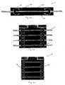
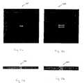
- FIG. 1 ais a sectional view of an encapsulated prepackaged semiconductor chip 11 with leads 17 exiting on two sides;
- FIG. 1 bis a sectional view of an intermediate step of a method embodied by the present invention wherein encapsulated prepackaged semiconductor chips 11 are stacked on top of one another;
- FIG. 1 cis a sectional view of a stacked assembly of integrated circuits (ICs) wherein the sides of the assembly are metalized to form an electrical bus.
- ICsintegrated circuits
- FIG. 2 ais a sectional view of an encapsulated prepackaged semiconductor chip 11 that contains two bare semiconductor chips 22 separated by an interposer layer 24 ;
- FIG. 2 bis a sectional view of an intermediate step of a method embodied by the present invention wherein encapsulated prepackaged semiconductor chips 11 , each containing two bare semiconductor chips, are stacked on top of one another;
- FIG. 2 cis a sectional view of the stacked encapsulated prepackaged semiconductor chips of FIG. 2 b wherein the electrical leads 17 are removed and the sides are metalized to form an electrical bus 18 to complete the stacked assembly of integrated circuits 10 ;
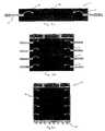
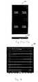
- FIG. 3is a sectional view of a high-density stacked printed circuit board assembly 30 with plated through-holes 38 ;
- FIG. 4is a sectional view of a high-density stacked printed circuit board assembly 40 of the present invention that employs metalized bus bars 48 for electrical interconnection;
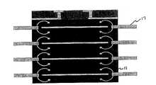
- FIG. 5is a perspective view of a stacked integrated circuit assembly 50 that employs electrical lead frames 58 for electrical interconnection.
- FIG. 6is a sectioned perspective view of a stacked integrated circuit assembly 50 of FIG. 5;
- FIG. 7is a cross-sectional view of the stacked integrated circuit assembly 50 taken along section line 7 - 7 ;
- FIG. 8shows another stacked integrated circuit assembly 80 embodied by the present invention, wherein the stacked assembly 80 has the same footprint as the prepackaged semiconductor chips 86 from which the assembly was made.
- FIG. 9is a block diagram of a low-cost, compact mini-computer embodied by the present invention.
- FIG. 10 ais a top view of the low-cost, compact mini-computer 900 of the present invention.
- FIG. 10 bis a profile of the minicomputer 900 with viewable interior of a processor stack 950 and a memory stack 910 ;
- FIG. 11 ais a top view of a PLD layer 951 of the present invention.
- FIG. 11 bis a profile of the PLD layer 951 ;
- FIG. 12 ais a top view of a processor layer 953 of the present invention.
- FIG. 12 bis a profile of the processor layer 953 ;
- FIG. 13 ais a top view of a SDRAM layer 954 of the present invention.
- FIG. 13 bis a profile of the SDRAM layer 954 ;
- FIG. 14 ais a top view of a boot flash layer 955 of the present invention.
- FIG. 14 bis a profile of the boot flash layer 955 :
- FIGS. 15 a and 15 bare top and profile views of a discrete component layer 956 of the present invention, respectively;
- FIG. 16is a profile of the processor stack 950 with viewable interior
- FIGS. 17 a and 17 bare top and profile views of a discrete component layer 915 of the present invention.
- FIG. 18is a profile of the processor stack 950 with viewable interior
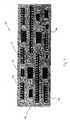
- FIGS. 19 a through care a side view (end plate cut away), an end view, and a bottom view, respectively, of a SRAM stack subassemblies of the present invention.
- FIG. 20 ais top view of a SRAM stack subassemblies
- FIG. 20 bis an exploded top view of SRAM stack subassemblies
- FIG. 21is a block diagram of the process for making a SRAM stack array of the present invention.
- FIG. 22 a through eare illustrations of SRAM subassembly during selected stages of the process of FIG. 21;
- FIG. 23 a through cis an illustration of the SRAM stack array of the present invention.
- an encapsulated prepackaged semiconductor chip 11and more specifically a flash memory thin small outline package (TSOP) is shown with leads 17 exiting both sides.
- the TSOPsare stacked as shown in FIG. 1 b .
- the sides of the stack with the TSOP leads 17are ground to the point that the lead material is removed and the ends of the internal bonded wires are exposed.
- metalizationis then applied to form busses 18 to interconnect the wires and the top and bottom layers which may be a separate transceiver layer or a PCB layer, for example.
- Solder balls 19are included as a final step, to provide means to connect the stack to a primary PCB (not shown) such as that of a computer.
- the finished structurehas the memory capacity of an individual TSOP times the number layers in the stack.
- FIGS. 2 a through 2 cshows the same process as in FIGS. 1 a through 1 c , however TSOP 11 contains more than one bare semiconductor chip 22 internally. Specifically, two separate bare semiconductor chips 22 are contained within the TSOP 11 in a back-to-back configuration and separated by interposer layer 24 .
- the processes of FIGS. 1 and 2do not employ “thinning” the TSOP from the top and bottom and subsequent connecting layers electrically via metal film traces as in the prior art. Instead the wire bonds 14 are exposed from the sides and not the top of the TSOP 11 . While not providing the increased density advantages of thinning, exposing the wire bonds 14 from the sides, efficiently balances size and manufacturing cost requirements.
- FIG. 3illustrates a high density packaging technique using primarily standard printed circuit board (PCB) fabrication manufacturing technology.
- PCBprinted circuit board
- Large PCBscan contain repeated patterns of a portion of a circuit for manufacturing multiple assemblies 30 , and some PCBs 32 contain components 34 on both sides.
- the PCBs 32are populated with components 34 , on one or two sides, using surface mount soldering and a high-temperature solder.
- Several PCBs of different designs, each containing part of the entire circuit,are stacked together, and all of the space between PCBs is filled with an encapsulant material 36 .
- the assembly 30is further processed to add plated through holes 38 between PCBs 32 and to form a final metal pattern on the exterior boards.
- the through hole 38 diametershould be approximately equal to about 10% of the board thickness.
- the assembly 30may then be cut into individual stacked circuits. Additionally, further components and connectors can be soldered to the exterior boards using standard solder. The final step in the method is testing.
- FIG. 4illustrates an alternative embodiment to the invention illustrated in FIG. 3.
- a high-density stacked printed circuit board assembly 40 of the present inventionalternatively employs metalized bus bars, instead of plated through holes 48 , for electrical interconnection.
- the processes of the two embodimentsare identical.
- FIGS. 5 through 7illustrate stacking encapsulated prepackaged semiconductor chips 52 with leadered parts as in other embodiments, however this alternate method uses additional PCB material and lead frames 58 to achieve the desired configuration. This method is particularly suitable for dual-port static random access memory (DPSRAM) and SRAM.
- the encapsulated prepackaged chipsare soldered to intermediate PCBs 54 to form layers.
- the final layeris soldered to a large PCB.
- the large PCB 56may be 0.02 inches thick and the intermediate PCBs 54 may be 0.01 inches thick.
- a plurality of lead frames 58are employed to attach the large PCB to a prospective customer's board.
- FIG. 8illustrates a method of the present invention as applied to encapsulated prepackaged chips 82 that contain fine ball grid array FBGA configurations 86 .
- a significant advantage to this configurationis that the final stacked assembly with have the same footprint as the original FBGA packages 82 . This allows anticipation of newer technology because an obsolete stack can be replaced with higher capability components with the same footprint as they become available.
- a first encapsulated prepackages chip 82(FBGA type, for example) is soldered 86 to a PCB interposer layer 84 that routes signals to two edges.
- FIG. 9is a block diagram of the compact, low-cost minicomputer embodied by the present invention.
- the computerconsists of two stacks, a processor stack 950 , and flash memory storage stack 910 .
- the flash memory storage stack 910is a 0.5 GB solid-state hard drive
- the processor stack 950implements a 32-bit Intel® StrongARM® computer system running Linux operating system. Support for the LCD, mouse, keyboard, and external I/O is provided.
- the processor stack 951 constructionis shown in FIG. 16 and the individual layers are shown in FIGS. 11 a through 15 b .
- All of the processor component layersare available in ball grid array (BGA) packages.
- BGAball grid array
- the typical BGA package constructionhas the bare semiconductor chip flip-chip mounted to a carrier (i.e. PCB), encapsulated, and then solder balls 945 are attached to the PCB for interconnection to the next layer. This internal construction allows thinning the package and removing much of the backside of the semiconductor from the chip without disturbing the chip interconnect surface.
- PLDProgrammable Logic Device
- the basic processis to perform a BGA solder mounting of many PLDs onto a large PCB (for mass production) and then underfill and pot the connection for insulation and stability.
- the resulting large panelis then cut into sections, thinned, and then diced into individual layers.
- the finished PLD layeris shown in FIGS. 11 a and 11 b.
- the processor layer 953 shown in FIGS. 12 a and 12 bcontains, by way of example, the StrongARM processor (SA-1110) and the StrongARM companion chip (SA-1111).
- the construction of the process layer 953is similar to that of the PLD layer 951 , except that the two components are mounted on either side of the PCB and the mounting, underfill, pot, and thinning steps are accomplished for both sides the PCB.
- SDRAM 954 and Boot Flash 955 layersare shown in FIGS. 13 a and 13 b , and 14 a and 14 b , respectively. These layers are two-sided like the process layer. Additionally, the SDRAM layer has two chips on each side of the PCB.
- the final layer in the processor stackis the discrete component layer 956 as shown in FIGS. 15 a and 15 b . It contains seven semiconductor, discrete surface-mount components (two crystals, three capacitors, and two resistors), by way of example.
- the constructionis similar to the one-sided PLD layer 951 except thinning of the discrete layer 956 leaves potting material above the components.
- the five layersare laminated together and interconnected using stacking technology. Metalization is added to the two sides of the stack to complete the interconnection between layers, bringing all input/output signals to the PLD PCB, to which PLD PCB solder balls are subsequently added. The exposed metal on the busses is coated for protection at the next level of assembly.
- the flash memory stackcontains eight large-capacity flash memory chips 911 and four transceiver chips 916 .
- the layer for the transceivers 915is similar to the PLD layer 951 in the processor stack 950 .
- the flash memoryis stacked using a method of the present invention as detailed in FIGS. 1 and 2.
- the flash chipscome in TSOPs with leads exiting on two sides.
- the bare semiconductor insidemay be a single chip (as in FIG. 1) or two separate chips in a back-to-back configuration (as in FIG. 2).
- the TSOPs 911are laminated directly with the transceiver layer and a top PCB layer 914 a .
- the sides of the stack with the TSOP leadsare ground to the point where the lead material is removed and the ends of the internal bonded wire are exposed.
- the metalizationis then applied to the busses to interconnect the wires, the traces of the transceiver layer 915 , and the bottom PCB 914 b .
- the bussesare coated and solder balls added as a final step.
- the manufacturing process for the stacksare optimized for mass production. For all but the flash memory chips 911 , the PCB fabrication, and encapsulation processes are performed in large area panels. The panels are quartered for thinning, then cut into individual layers or strips of layers for stacking. Layers are laminated into cubes of multiple stacks, which are separated into individual stacks after metalizing the busses. This approach to layer and stack fabrication largely avoids the processing of individual components/layers and lends itself to automation. The technique of stacking flash memory avoids layer fabrication altogether.
- the intentis for the user to interconnect the two stacks as part of integration into the application platform.
- the user PCB 960would supply the required power (1.75 V, 3.3 V, and ground) and interconnection to the import/export hardware.
- an extremely compact, highly capable, and low cost computercan be constructed using standard parts and mostly standard assembly processes.
- the stacked constructionis inherently rugged and the assembly and interconnection processes used have been demonstrated to be highly reliable, making the product suitable for a wide range of applications.
- FIGS. 19 through 23 cillustrate the process used to fabricate a large capacity memory (SRAM type for example) stack array 200 .
- the complete array 200is illustrated in FIG. 23.
- the array 200is made from twenty four memory stack subassemblies 210 .
- a subassembly 210is illustrated more specifically as a Micron SRAM S-Neo Stack, however the integrated circuit function is unimportant to the invention.
- Each subassembly 210contains ten memory chips 214 .
- the copper shims 216 and copper sheets 217provide excellent heat transfer characteristics without shorting circuitry.
- the copper sheets 217are physically located between layers and thermal management is accomplished by drawing the heat from the top of each chip. Heat from one side of the memory chip 214 will go directly into the copper sheets 217 , while on the other side, heat from the leads or BGA 215 is dissipated into ground planes in the PCB 211 . These dual paths quickly spread the heat away from chips being exercised. Since only portions of the full array are exercised at one time, spreading the heat into the whole array and away from hot spots is essential. This makes managing the dissipation from the module relatively simple while keeping the junctions relatively cool. Once laminated (FIG.
- the subassembly 210is encapsulated with an epoxy material that is chemically similar to the compound used to encapsulate the memory chips.
- the encapsulantmakes the module rugged, and the combination of materials used result in a composite thermal expansion coefficient very close to a typical host PCB. This means that the BGA used to attach the module to the host PCB will undergo a minimum of stress.
Landscapes
- Engineering & Computer Science (AREA)
- Microelectronics & Electronic Packaging (AREA)
- Power Engineering (AREA)
- Computer Hardware Design (AREA)
- Physics & Mathematics (AREA)
- Condensed Matter Physics & Semiconductors (AREA)
- General Physics & Mathematics (AREA)
- Manufacturing & Machinery (AREA)
- Wire Bonding (AREA)
Abstract
Description
- The present application is related to U.S. Provisional Patent Application serial No. 60/346,494, filed on Jan. 9, 2002, which is incorporated herein by reference and to which priority is claimed pursuant to 35 USC 119, and is a continuation-in-part of U.S. patent application Ser. No. 09/770,864, filed on Jan. 26, 2001, which application is pending and herein incorporated by reference.[0001]
- 1. Field of the Invention[0002]
- This invention relates generally to the dense packaging of electronic circuitry through the stacking of printed circuit boards (PCB) populated with components, and through the stacking of integrated circuit (IC) chips (aka microcircuits or die). More specifically, the present invention relates to a method making a stack of integrated circuits (ICs) from prepackaged ICs.[0003]
- 2. Description of The Related Art[0004]
- Of particular interest in the electronic design and manufacturing art, is the high-density packaging of electronic circuitry to yield designs of increased capability. Existing methods for “stacking” electronic circuitry are continuously evolving and improving for better efficiency and reliability.[0005]
- An early effort to provide a 3-D electronics stack combining different functions, different area electronic chips is illustrated by Kravitz et al., U.S. Pat. No. 3,370,203. That patent shows stacked “frames” having dimensions “such that integrated circuits which have slightly different dimensions can by mounted thereon”, explaining that “integrated circuits from different sources of supply are often advantageously incorporated in a single module.”[0006]
- Over the last decade and longer, Irvine Sensors Corporation, the assignee of the present invention, has been developing high-density electronic stacking methods. An early process was termed “Silicon Die Stacking,” That method stacked ICs as “bare die” in the form of whole wafers. The wafer stacks were subsequently metalized for electrical interconnection, and the wafer stacks were diced to form connectable die-stacks.[0007]
- The bare Silicon Die Stacking techniques were problematic for several reasons. Primarily troublesome, is that whole wafers are difficult to obtain because the manufacturers do not want to reveal their yield or expose their built-in test structures that could facilitate reverse engineering of their circuitry. Additionally, a wafer may contain a quantity of defective die, and comprehensive testing procedures are expensive making it even more difficult to purchase pre-tested wafers or bare die. This problem in the field is referred to as obtaining Known Good Die (KGD). Irvine Sensors Corp. developed an improved technology termed “Neo-Die Stacking,” however this method involved stacking bare die, which did not alleviate the problem of obtaining KGD.[0008]
- Integrated circuit manufactures make readily available prepackaged encapsulated silicon chips that are pre-tested and therefore known good die. Prepackaged chips, also referred to as Plastic Encapsulated Microcircuits (PEMs), can inexpensively be further tested under temperature ranges and sorted. However, stacking prepackaged silicon chips is impractical because they cannot be configured densely enough to meet the requirements of today's applications. Accordingly, Irvine Sensor's Corp. developed further technology which combined old and new methods to reprocess, stack and interconnect pre-packaged silicon chips. Irvine Sensor's has disclosed some of this technology in the published U.S. patent application Ser. No. 09/770,864 entitled “A Stackable Microcircuit Layer Formed From a Plastic Encapsulated Microcircuit and Method of Making the Same.” The content of this published patent application is hereby incorporated by reference in its entirety.[0009]
- The foregoing patent application details modification and reprocessing of PEMs to form smaller, very thin stackable layers. In one particular embodiment, the PEM is more specifically a memory chip readily available in a plastic encapsulated thin small outline package (TSOP). In brief, the process uses wafer grinding equipment to remove most of the encapsulant material from the top surface of the TSOP, down to the cross section of a gold ball used for electrical connection of the bare silicon. This step leaves a thin layer of encapsulant on the silicon surface, which serves as the insulating surface for metal trace deposition. Grinding is further performed to remove encapsulant from the bottom of the TSOP and to thin the die itself. During this backside grinding step, the leads are also removed. A final dicing step minimizes the layer footprint, while leaving enough of the original TSOP encapsulant around the die edges to provide and insulating surface for bus metalization. The process yields a “stackable layer” that may be stacked with “neo-layers” that are created from bare die.[0010]
- Although the abovementioned process is largely effective, further methods are needed, as described in the present invention, to balance size and density with manufacturing cost and component availability which can be optimally employed to create a compact, low cost mini-computer.[0011]
- In the first aspect, the invention may be regarded as a method of making a stacked assembly of integrated circuits (ICs) comprising the steps of: providing a first encapsulated prepackaged semiconductor chip having internal wire bonds, an encapsulant, and lead material extending from the sides of the chip, removing the lead material and at least part of the encapsulant from the sides, exposing the wire bonds, providing a second encapsulated prepackaged semiconductor chip, one or more internal wire bonds and an encapsulant, exposing the wire bonds of the second encapsulated prepackaged semiconductor chip, stacking the second prepackaged semiconductor chip and subsequent chips onto the first prepackaged semiconductor chip, interconnecting the wire bonds of the stacked semiconductor chips to form electrical connections between all of the stacked chips; and metalizing the electrical connections between the stacked chips to form electrical buses to complete a stacked assembly of ICs.[0012]
- Additional steps according to this method of the invention include: applying solder balls to the IC stack, mounting the IC stack to a printed circuit board (PCB) with the solder balls, and underfilling the IC stack and PCB to structurally stabilize the IC stack and the PCB. In a separate embodiment, the first and second prepackaged semiconductor chips each have two bare semiconductor chips within each package, the bare semiconductor chips separated by an interposer layer and each bare semiconductor chip has one or more wire bonds. The interposer layer is used to dissipate heat from the stacked IC assembly.[0013]
- In a second aspect, the invention may be regarded as a method of making a stacked integrated circuit (IC) assembly comprising the steps of: providing a first encapsulated prepackaged semiconductor chip, soldering the first encapsulated prepackaged semiconductor chip to a intermediate PCB, providing a second encapsulated prepackaged semiconductor chip, soldering the second encapsulated prepackaged semiconductor chip to a large PCB, soldering the second encapsulated prepackaged semiconductor chip to the intermediate PCB, attaching a plurality of lead frames to the large PCB.[0014]
- Additional steps to this aspect of the invention include: providing subsequent encapsulated prepackaged semiconductor chips, and soldering the chips to the stacked IC assembly to make the assembly the desired size.[0015]
- In a third aspect of the invention, the invention may be regarded as a high-density stacked printed circuit board (PCB) assembly comprising: a plurality of PCBs having one or more through holes extending from the topside to the bottom side, a plurality of discrete components mounted to each PCB on one or more sides, one or more metal conductors extending through the through holes to electrically connect each PCB, one or more encapsulants to occupy the volume between each PCB and each discrete components, and one or more interposer layers arranged within the assembly to dissipate heat generated within the assembly.[0016]
- In a forth aspect of the invention, another high-density stacked printed circuit board (PCB) assembly is disclosed and claimed. It comprises: a plurality of PCBs having one or more sides, a plurality of discrete components mounted to each PCB on one or more sides, one or more encapsulants to occupy the volume between each PCB and each discrete components, one or more bus bars extending down one or more sides of the plurality of PCBs to electrically connect each PCB, and one or more interposer layers arranged within the assembly to dissipate heat generated within the assembly.[0017]
- In a fifth aspect, the invention may be regarded as a method of making a stacked assembly of integrated circuits (ICs) from a plurality of encapsulated prepackaged semiconductor chips wherein the resultant assembly has the same footprint as the original plurality of encapsulated prepackaged semiconductor chips comprising the steps of: providing a first encapsulated prepackaged semiconductor chip that conducts electrical signals having one or more lateral edges, soldering the first encapsulated prepackaged semiconductor chip to a PCB interposer layer to form a first subassembly having solder connections, routing the signals to the one or more lateral edges using the PCB interposer layer, providing a second prepackaged semiconductor chip that conducts electrical signals to one or more lateral edges, the chip having a top side and a bottom side, soldering the second prepackaged semiconductor chip to a second PCB interposer layer to form a second subassembly having solder connections, soldering a ball grid array pattern to the bottom side of the second prepackaged semiconductor chip, stacking the first and second subassemblies, and routing electrical signals from the first and second subassemblies to the ball grid array pattern to form the stacked assembly of integrated circuits wherein the assembly has the same footprint as the plurality of encapsulated prepackaged chips. An additional step includes underfilling the solder connections of the first and second subassemblies with epoxy material.[0018]
- In a sixth aspect, the invention may be regarded as a compact low cost mini-computer comprising a memory stack having one or more lateral edges that includes (a) one or more bus bars extending down the lateral edges of the memory stack, (b) a plurality of prepackaged semiconductor chips each having leads and wire bonds for electrical conductivity wherein the leads are removed, and wherein the wire bonds are connected directly to the one or more bus bars, (c) a top PCB layer connected to the plurality of prepackaged semiconductor chips and connected to the one or more bus bars, (d) a bottom PCB layer connected to the plurality of prepackaged semiconductor chips and connected to the one or more bus bars, and (e) a transceiver layer having one or more transceiver chips mounted to the top PCB layer. In addition to the memory stack, the mini-computer comprises a processor stack having one or more lateral edges and including: (a) a programmable logic device (PLD) layer mounted to a printed circuit board (PCB) layer, (b) a processor layer mounted to the PLD layer, (c) a synchronous dynamic random access memory (SDRAM) layer mounted to the processor layer, (d) a boot flash layer mounted to the SDRAM layer, (e) a discrete component layer having a plurality of crystals, capacitors, and resistors, the discrete component layer mounted to the boot flash layer, and (f) a large PCB board electrically connecting the flash stack and the processor stack to form the minicomputer.[0019]
- Finally, in a seventh aspect, the invention may be regarded as a method of manufacturing a memory stack (static random access memory, SRAM type, for example) array comprising the steps of: fabricating and testing a predetermined quantity of printed circuit boards (PCBs) having two sides for a predetermined quantity of memory layers for a predetermined quantity of memory stack subassemblies for the memory stack array of a predetermined size, soldering one or more interdigitated capacitors to each side of each PCB, soldering a memory to each side of each PCB using a ball grid array (BGA) pattern, attaching copper shims to each memory, attaching copper sheets to each copper shim to dissipate heat forming a memory layer, stacking multiple memory layers side-by-side to form one memory stack subassembly, the subassembly having voided spaces, encapsulating the voided spaces with epoxy resin, metalizing the memory stack subassembly for electrical interconnection between multiple memory layers, and stacking multiple memory stack subassemblies to form the memory stack array[0020]
- The objects, advantages and features of the present invention will become more apparent to those skilled in the art from the following detailed description, when read in conjunction with the accompanying drawings, wherein:[0021]
- FIG. 1[0022]ais a sectional view of an encapsulated prepackaged semiconductor chip11 with leads17 exiting on two sides;
- FIG. 1[0023]bis a sectional view of an intermediate step of a method embodied by the present invention wherein encapsulated prepackaged semiconductor chips11 are stacked on top of one another;
- FIG. 1[0024]cis a sectional view of a stacked assembly of integrated circuits (ICs) wherein the sides of the assembly are metalized to form an electrical bus.
- FIG. 2[0025]ais a sectional view of an encapsulated prepackaged semiconductor chip11 that contains two
bare semiconductor chips 22 separated by aninterposer layer 24; - FIG. 2[0026]bis a sectional view of an intermediate step of a method embodied by the present invention wherein encapsulated prepackaged semiconductor chips11, each containing two bare semiconductor chips, are stacked on top of one another;
- FIG. 2[0027]cis a sectional view of the stacked encapsulated prepackaged semiconductor chips of FIG. 2bwherein the electrical leads17 are removed and the sides are metalized to form an
electrical bus 18 to complete the stacked assembly ofintegrated circuits 10; - FIG. 3 is a sectional view of a high-density stacked printed[0028]
circuit board assembly 30 with plated through-holes 38; - FIG. 4 is a sectional view of a high-density stacked printed[0029]
circuit board assembly 40 of the present invention that employs metalized bus bars48 for electrical interconnection; - FIG. 5 is a perspective view of a stacked[0030]
integrated circuit assembly 50 that employs electrical lead frames58 for electrical interconnection. - FIG. 6 is a sectioned perspective view of a stacked[0031]
integrated circuit assembly 50 of FIG. 5; - FIG. 7 is a cross-sectional view of the stacked[0032]
integrated circuit assembly 50 taken along section line7-7; - FIG. 8 shows another stacked[0033]
integrated circuit assembly 80 embodied by the present invention, wherein the stackedassembly 80 has the same footprint as theprepackaged semiconductor chips 86 from which the assembly was made. - FIG. 9 is a block diagram of a low-cost, compact mini-computer embodied by the present invention;[0034]
- FIG. 10[0035]ais a top view of the low-cost,
compact mini-computer 900 of the present invention; - FIG. 10[0036]bis a profile of the
minicomputer 900 with viewable interior of aprocessor stack 950 and amemory stack 910; - FIG. 11[0037]ais a top view of a
PLD layer 951 of the present invention; - FIG. 11[0038]bis a profile of the
PLD layer 951; - FIG. 12[0039]ais a top view of a
processor layer 953 of the present invention; - FIG. 12[0040]bis a profile of the
processor layer 953; - FIG. 13[0041]ais a top view of a
SDRAM layer 954 of the present invention; - FIG. 13[0042]bis a profile of the
SDRAM layer 954; - FIG. 14[0043]ais a top view of a
boot flash layer 955 of the present invention; - FIG. 14[0044]bis a profile of the boot flash layer955:
- FIGS. 15[0045]aand15bare top and profile views of a
discrete component layer 956 of the present invention, respectively; - FIG. 16 is a profile of the[0046]
processor stack 950 with viewable interior; - FIGS. 17[0047]aand17bare top and profile views of a
discrete component layer 915 of the present invention; - FIG. 18 is a profile of the[0048]
processor stack 950 with viewable interior; - FIGS. 19[0049]athroughcare a side view (end plate cut away), an end view, and a bottom view, respectively, of a SRAM stack subassemblies of the present invention;
- FIG. 20[0050]ais top view of a SRAM stack subassemblies;
- FIG. 20[0051]bis an exploded top view of SRAM stack subassemblies;
- FIG. 21 is a block diagram of the process for making a SRAM stack array of the present invention;[0052]
- FIG. 22 a through e are illustrations of SRAM subassembly during selected stages of the process of FIG. 21;[0053]
- FIG. 23 a through c is an illustration of the SRAM stack array of the present invention.[0054]
- Referring initially to FIG. 1[0055]athroughc, an encapsulated prepackaged semiconductor chip11, and more specifically a flash memory thin small outline package (TSOP) is shown with
leads 17 exiting both sides. In a method of the invention, the TSOPs are stacked as shown in FIG. 1b. The sides of the stack with the TSOP leads17 are ground to the point that the lead material is removed and the ends of the internal bonded wires are exposed. As illustrated in FIG. 1c, metalization is then applied to formbusses 18 to interconnect the wires and the top and bottom layers which may be a separate transceiver layer or a PCB layer, for example.Solder balls 19 are included as a final step, to provide means to connect the stack to a primary PCB (not shown) such as that of a computer. The finished structure has the memory capacity of an individual TSOP times the number layers in the stack. - FIGS. 2[0056]athrough2cshows the same process as in FIGS. 1athrough1c, however TSOP11 contains more than one
bare semiconductor chip 22 internally. Specifically, two separatebare semiconductor chips 22 are contained within the TSOP11 in a back-to-back configuration and separated byinterposer layer 24. The processes of FIGS. 1 and 2 do not employ “thinning” the TSOP from the top and bottom and subsequent connecting layers electrically via metal film traces as in the prior art. Instead thewire bonds 14 are exposed from the sides and not the top of the TSOP11. While not providing the increased density advantages of thinning, exposing thewire bonds 14 from the sides, efficiently balances size and manufacturing cost requirements. - FIG. 3 illustrates a high density packaging technique using primarily standard printed circuit board (PCB) fabrication manufacturing technology. Large PCBs can contain repeated patterns of a portion of a circuit for manufacturing[0057]
multiple assemblies 30, and somePCBs 32 containcomponents 34 on both sides. In a method of the invention, thePCBs 32 are populated withcomponents 34, on one or two sides, using surface mount soldering and a high-temperature solder. Several PCBs of different designs, each containing part of the entire circuit, are stacked together, and all of the space between PCBs is filled with anencapsulant material 36. Theassembly 30 is further processed to add plated throughholes 38 betweenPCBs 32 and to form a final metal pattern on the exterior boards. As a general design parameter, the throughhole 38 diameter should be approximately equal to about 10% of the board thickness. Theassembly 30 may then be cut into individual stacked circuits. Additionally, further components and connectors can be soldered to the exterior boards using standard solder. The final step in the method is testing. - FIG. 4 illustrates an alternative embodiment to the invention illustrated in FIG. 3. A high-density stacked printed[0058]
circuit board assembly 40 of the present invention alternatively employs metalized bus bars, instead of plated throughholes 48, for electrical interconnection. Other than this difference, the processes of the two embodiments are identical. - FIGS. 5 through 7 illustrate stacking encapsulated[0059]
prepackaged semiconductor chips 52 with leadered parts as in other embodiments, however this alternate method uses additional PCB material and leadframes 58 to achieve the desired configuration. This method is particularly suitable for dual-port static random access memory (DPSRAM) and SRAM. The encapsulated prepackaged chips are soldered tointermediate PCBs 54 to form layers. The final layer is soldered to a large PCB. By way of example only, thelarge PCB 56 may be 0.02 inches thick and theintermediate PCBs 54 may be 0.01 inches thick. A plurality of lead frames58 are employed to attach the large PCB to a prospective customer's board. - FIG. 8 illustrates a method of the present invention as applied to encapsulated[0060]
prepackaged chips 82 that contain fine ball gridarray FBGA configurations 86. A significant advantage to this configuration is that the final stacked assembly with have the same footprint as the original FBGA packages82. This allows anticipation of newer technology because an obsolete stack can be replaced with higher capability components with the same footprint as they become available. In this method, a first encapsulated prepackages chip82 (FBGA type, for example) is soldered86 to aPCB interposer layer 84 that routes signals to two edges. Next, separately solder86 asecond FBGA 84 to a secondPCB interposer layer 84 that routs signals from two edges to a ballgrid array pattern 88. The aforementionedPCB solder connections 86 are finally underfilled with epoxy resin for insulation and stability. - FIGS. 9 through 18 collectively illustrate a compact, low-cost minicomputer where various method and structure of the present invention are employed. FIG. 9 is a block diagram of the compact, low-cost minicomputer embodied by the present invention. The computer consists of two stacks, a[0061]
processor stack 950, and flashmemory storage stack 910. By way of example only, the flashmemory storage stack 910 is a 0.5 GB solid-state hard drive, and theprocessor stack 950 implements a 32-bit Intel® StrongARM® computer system running Linux operating system. Support for the LCD, mouse, keyboard, and external I/O is provided. - The[0062]
processor stack 951 construction is shown in FIG. 16 and the individual layers are shown in FIGS. 11athrough15b. Other than the two crystals, three capacitors, and two resistors, all of the processor component layers are available in ball grid array (BGA) packages. The typical BGA package construction has the bare semiconductor chip flip-chip mounted to a carrier (i.e. PCB), encapsulated, and then solderballs 945 are attached to the PCB for interconnection to the next layer. This internal construction allows thinning the package and removing much of the backside of the semiconductor from the chip without disturbing the chip interconnect surface. - For the Programmable Logic Device (PLD)[0063]
layer 951, the basic process is to perform a BGA solder mounting of many PLDs onto a large PCB (for mass production) and then underfill and pot the connection for insulation and stability. The resulting large panel is then cut into sections, thinned, and then diced into individual layers. The finished PLD layer is shown in FIGS. 11aand11b. - The[0064]
processor layer 953 shown in FIGS. 12aand12bcontains, by way of example, the StrongARM processor (SA-1110) and the StrongARM companion chip (SA-1111). The construction of theprocess layer 953 is similar to that of thePLD layer 951, except that the two components are mounted on either side of the PCB and the mounting, underfill, pot, and thinning steps are accomplished for both sides the PCB. - The synchronous dynamic random access memory (SDRAM)[0065]954 and
Boot Flash 955 layers are shown in FIGS. 13aand13b, and14aand14b, respectively. These layers are two-sided like the process layer. Additionally, the SDRAM layer has two chips on each side of the PCB. - The final layer in the processor stack is the[0066]
discrete component layer 956 as shown in FIGS. 15aand15b. It contains seven semiconductor, discrete surface-mount components (two crystals, three capacitors, and two resistors), by way of example. The construction is similar to the one-sided PLD layer 951 except thinning of thediscrete layer 956 leaves potting material above the components. - For the[0067]
processor stack 950, again illustrated in FIG. 16, the five layers are laminated together and interconnected using stacking technology. Metalization is added to the two sides of the stack to complete the interconnection between layers, bringing all input/output signals to the PLD PCB, to which PLD PCB solder balls are subsequently added. The exposed metal on the busses is coated for protection at the next level of assembly. - Now referring to FIG. 18, the flash memory stack contains eight large-capacity[0068]
flash memory chips 911 and fourtransceiver chips 916. The layer for thetransceivers 915, as shown in FIGS. 17aand17b, is similar to thePLD layer 951 in theprocessor stack 950. The flash memory is stacked using a method of the present invention as detailed in FIGS. 1 and 2. The flash chips come in TSOPs with leads exiting on two sides. The bare semiconductor inside may be a single chip (as in FIG. 1) or two separate chips in a back-to-back configuration (as in FIG. 2). TheTSOPs 911 are laminated directly with the transceiver layer and a top PCB layer914a. The sides of the stack with the TSOP leads are ground to the point where the lead material is removed and the ends of the internal bonded wire are exposed. The metalization is then applied to the busses to interconnect the wires, the traces of thetransceiver layer 915, and the bottom PCB914b. As with the processor stack, the busses are coated and solder balls added as a final step. - The manufacturing process for the stacks are optimized for mass production. For all but the[0069]
flash memory chips 911, the PCB fabrication, and encapsulation processes are performed in large area panels. The panels are quartered for thinning, then cut into individual layers or strips of layers for stacking. Layers are laminated into cubes of multiple stacks, which are separated into individual stacks after metalizing the busses. This approach to layer and stack fabrication largely avoids the processing of individual components/layers and lends itself to automation. The technique of stacking flash memory avoids layer fabrication altogether. - Most of the manufacturing can be easily transitioned to contract manufacturers because many of the processes are standard (e.g., PCB fabrication, surface-mount soldering, underfill, and thin film deposition). This results in flexibility, lower cost and a rapid ramping to high volume without a large capital investment. For the reasons stated above, the design approach provides for a cost effective and producible product.[0070]
- As shown in FIGS. 10[0071]aand10b, the intent is for the user to interconnect the two stacks as part of integration into the application platform. The
user PCB 960 would supply the required power (1.75 V, 3.3 V, and ground) and interconnection to the import/export hardware. In sum, an extremely compact, highly capable, and low cost computer can be constructed using standard parts and mostly standard assembly processes. The stacked construction is inherently rugged and the assembly and interconnection processes used have been demonstrated to be highly reliable, making the product suitable for a wide range of applications. - FIGS. 19 through 23[0072]cillustrate the process used to fabricate a large capacity memory (SRAM type for example)
stack array 200. Thecomplete array 200 is illustrated in FIG. 23. Thearray 200 is made from twenty fourmemory stack subassemblies 210. Asubassembly 210, is illustrated more specifically as a Micron SRAM S-Neo Stack, however the integrated circuit function is unimportant to the invention. Eachsubassembly 210 contains ten memory chips214. - In this design, the copper shims[0073]216 and copper sheets217 provide excellent heat transfer characteristics without shorting circuitry. The copper sheets217 are physically located between layers and thermal management is accomplished by drawing the heat from the top of each chip. Heat from one side of the memory chip214 will go directly into the copper sheets217, while on the other side, heat from the leads or
BGA 215 is dissipated into ground planes in thePCB 211. These dual paths quickly spread the heat away from chips being exercised. Since only portions of the full array are exercised at one time, spreading the heat into the whole array and away from hot spots is essential. This makes managing the dissipation from the module relatively simple while keeping the junctions relatively cool. Once laminated (FIG. 22c), thesubassembly 210 is encapsulated with an epoxy material that is chemically similar to the compound used to encapsulate the memory chips. The encapsulant makes the module rugged, and the combination of materials used result in a composite thermal expansion coefficient very close to a typical host PCB. This means that the BGA used to attach the module to the host PCB will undergo a minimum of stress. - While the invention has been illustrated and described by means of specific embodiments, it is to be understood that numerous changes and modifications may be made therein without departing from the intent and scope of the invention as defined in the appended claims.[0074]
Claims (20)
Priority Applications (2)
| Application Number | Priority Date | Filing Date | Title |
|---|---|---|---|
| US10/339,023US20030221313A1 (en) | 2001-01-26 | 2003-01-09 | Method for making stacked integrated circuits (ICs) using prepackaged parts |
| US11/644,438US20070102803A1 (en) | 2001-01-26 | 2006-12-22 | Method for making stacked integrated circuits (ICs) using prepackaged parts |
Applications Claiming Priority (3)
| Application Number | Priority Date | Filing Date | Title |
|---|---|---|---|
| US09/770,864US20020100600A1 (en) | 2001-01-26 | 2001-01-26 | Stackable microcircuit layer formed from a plastic encapsulated microcircuit and method of making the same |
| US34649402P | 2002-01-09 | 2002-01-09 | |
| US10/339,023US20030221313A1 (en) | 2001-01-26 | 2003-01-09 | Method for making stacked integrated circuits (ICs) using prepackaged parts |
Related Parent Applications (1)
| Application Number | Title | Priority Date | Filing Date |
|---|---|---|---|
| US09/770,864Continuation-In-PartUS20020100600A1 (en) | 2001-01-26 | 2001-01-26 | Stackable microcircuit layer formed from a plastic encapsulated microcircuit and method of making the same |
Related Child Applications (1)
| Application Number | Title | Priority Date | Filing Date |
|---|---|---|---|
| US11/644,438DivisionUS20070102803A1 (en) | 2001-01-26 | 2006-12-22 | Method for making stacked integrated circuits (ICs) using prepackaged parts |
Publications (1)
| Publication Number | Publication Date |
|---|---|
| US20030221313A1true US20030221313A1 (en) | 2003-12-04 |
Family
ID=38002913
Family Applications (2)
| Application Number | Title | Priority Date | Filing Date |
|---|---|---|---|
| US10/339,023AbandonedUS20030221313A1 (en) | 2001-01-26 | 2003-01-09 | Method for making stacked integrated circuits (ICs) using prepackaged parts |
| US11/644,438AbandonedUS20070102803A1 (en) | 2001-01-26 | 2006-12-22 | Method for making stacked integrated circuits (ICs) using prepackaged parts |
Family Applications After (1)
| Application Number | Title | Priority Date | Filing Date |
|---|---|---|---|
| US11/644,438AbandonedUS20070102803A1 (en) | 2001-01-26 | 2006-12-22 | Method for making stacked integrated circuits (ICs) using prepackaged parts |
Country Status (1)
| Country | Link |
|---|---|
| US (2) | US20030221313A1 (en) |
Cited By (12)
| Publication number | Priority date | Publication date | Assignee | Title |
|---|---|---|---|---|
| US20060001068A1 (en)* | 2004-06-30 | 2006-01-05 | Mosley Larry E | Multi-layer capacitor using dielectric layers having differing compositions |
| WO2005091365A3 (en)* | 2004-03-16 | 2006-03-16 | Infineon Technologies Ag | Coupling substrate for semiconductor components and method for the production thereof |
| EP1724835A1 (en) | 2005-05-17 | 2006-11-22 | Irvine Sensors Corporation | Electronic module comprising a layer containing integrated circuit die and a method for making the same |
| US20070052084A1 (en)* | 2005-08-26 | 2007-03-08 | Kennedy John V | High density interconnect assembly comprising stacked electronic module |
| US7309906B1 (en)* | 2004-04-01 | 2007-12-18 | Altera Corporation | Apparatus and methods for providing highly effective and area efficient decoupling capacitance in programmable logic devices |
| US20080070330A1 (en)* | 2003-12-22 | 2008-03-20 | Yuji Wada | Fabrication method of semiconductor integrated circuit device |
| US20080074144A1 (en)* | 2002-01-17 | 2008-03-27 | Volkan Ozguz | Field programmable gate array utilizing dedicated memory stacks in a vertical layer format |
| US20120020040A1 (en)* | 2010-07-26 | 2012-01-26 | Lin Paul T | Package-to-package stacking by using interposer with traces, and or standoffs and solder balls |
| US8198576B2 (en) | 2003-03-28 | 2012-06-12 | Aprolase Development Co., Llc | Three-dimensional LADAR module with alignment reference insert circuitry comprising high density interconnect structure |
| USRE43722E1 (en) | 2003-03-28 | 2012-10-09 | Aprolase Development Co., Llc | Three-dimensional ladar module with alignment reference insert circuitry |
| US20160286657A1 (en)* | 2015-03-24 | 2016-09-29 | Oclaro Japan, Inc. | Optical module |
| CN110383473A (en)* | 2016-12-19 | 2019-10-25 | 维迪科研究所 | Power electronic circuit equipped with bus bars forming a heat sink and method of integration |
Families Citing this family (14)
| Publication number | Priority date | Publication date | Assignee | Title |
|---|---|---|---|---|
| US7911053B2 (en)* | 2007-04-19 | 2011-03-22 | Marvell World Trade Ltd. | Semiconductor packaging with internal wiring bus |
| US9894771B2 (en) | 2007-05-08 | 2018-02-13 | Joseph Charles Fjelstad | Occam process for components having variations in part dimensions |
| US8510935B2 (en)* | 2007-07-10 | 2013-08-20 | Joseph C Fjelstad | Electronic assemblies without solder and methods for their manufacture |
| US7926173B2 (en)* | 2007-07-05 | 2011-04-19 | Occam Portfolio Llc | Method of making a circuit assembly |
| KR20100017408A (en)* | 2007-05-29 | 2010-02-16 | 오컴 포트폴리오 엘엘씨 | Electronic assemblies without solder and methods for their manufacture |
| US7981703B2 (en)* | 2007-05-29 | 2011-07-19 | Occam Portfolio Llc | Electronic assemblies without solder and methods for their manufacture |
| SG149724A1 (en)* | 2007-07-24 | 2009-02-27 | Micron Technology Inc | Semicoductor dies with recesses, associated leadframes, and associated systems and methods |
| SG149725A1 (en)* | 2007-07-24 | 2009-02-27 | Micron Technology Inc | Thin semiconductor die packages and associated systems and methods |
| US8300425B2 (en)* | 2007-07-31 | 2012-10-30 | Occam Portfolio Llc | Electronic assemblies without solder having overlapping components |
| US9681550B2 (en)* | 2007-08-28 | 2017-06-13 | Joseph C. Fjelstad | Method of making a circuit subassembly |
| US8358013B1 (en)* | 2007-08-29 | 2013-01-22 | Marvell International Ltd. | Leadless multi-chip module structure |
| WO2010045594A2 (en)* | 2008-10-17 | 2010-04-22 | Occam Portfolio Llc | Flexible circuit assemblies without solder and methods for their manufacture |
| CN102944709A (en)* | 2011-08-16 | 2013-02-27 | 北京天中磊智能科技有限公司 | Electric meter module structure realized by adopting multi-chip system-level packaging technology and packaging method thereof |
| DE112012006070B4 (en) | 2012-03-20 | 2024-03-14 | Tahoe Research, Ltd. | Storage device that responds to device commands for operational control |
Citations (40)
| Publication number | Priority date | Publication date | Assignee | Title |
|---|---|---|---|---|
| US4028722A (en)* | 1970-10-13 | 1977-06-07 | Motorola, Inc. | Contact bonded packaged integrated circuit |
| US4889612A (en)* | 1987-05-22 | 1989-12-26 | Abbott Laboratories | Ion-selective electrode having a non-metal sensing element |
| US4989063A (en)* | 1988-12-09 | 1991-01-29 | The United States Of America As Represented By The Secretary Of The Air Force | Hybrid wafer scale microcircuit integration |
| US4994215A (en)* | 1980-08-04 | 1991-02-19 | Fine Particle Technology Corp. | Method of fabricating complex microcircuit boards, substrates and microcircuits and the substrates and microcircuits |
| US5008213A (en)* | 1988-12-09 | 1991-04-16 | The United States Of America As Represented By The Secretary Of The Air Force | Hybrid wafer scale microcircuit integration |
| US5086018A (en)* | 1991-05-02 | 1992-02-04 | International Business Machines Corporation | Method of making a planarized thin film covered wire bonded semiconductor package |
| US5111278A (en)* | 1991-03-27 | 1992-05-05 | Eichelberger Charles W | Three-dimensional multichip module systems |
| US5270673A (en)* | 1992-07-24 | 1993-12-14 | Hewlett-Packard Company | Surface mount microcircuit hybrid |
| US5280192A (en)* | 1990-04-30 | 1994-01-18 | International Business Machines Corporation | Three-dimensional memory card structure with internal direct chip attachment |
| US5291061A (en)* | 1993-04-06 | 1994-03-01 | Micron Semiconductor, Inc. | Multi-chip stacked devices |
| US5454160A (en)* | 1993-12-03 | 1995-10-03 | Ncr Corporation | Apparatus and method for stacking integrated circuit devices |
| US5466634A (en)* | 1994-12-20 | 1995-11-14 | International Business Machines Corporation | Electronic modules with interconnected surface metallization layers and fabrication methods therefore |
| US5502667A (en)* | 1993-09-13 | 1996-03-26 | International Business Machines Corporation | Integrated multichip memory module structure |
| US5502621A (en)* | 1994-03-31 | 1996-03-26 | Hewlett-Packard Company | Mirrored pin assignment for two sided multi-chip layout |
| US5530292A (en)* | 1990-03-15 | 1996-06-25 | Fujitsu Limited | Semiconductor device having a plurality of chips |
| US5585668A (en)* | 1995-01-30 | 1996-12-17 | Staktek Corporation | Integrated circuit package with overlapped die on a common lead frame |
| US5585600A (en)* | 1993-09-02 | 1996-12-17 | International Business Machines Corporation | Encapsulated semiconductor chip module and method of forming the same |
| US5699234A (en)* | 1995-05-30 | 1997-12-16 | General Electric Company | Stacking of three dimensional high density interconnect modules with metal edge contacts |
| US5701233A (en)* | 1995-01-23 | 1997-12-23 | Irvine Sensors Corporation | Stackable modules and multimodular assemblies |
| US5700697A (en)* | 1993-02-01 | 1997-12-23 | Silicon Packaging Technology | Method for packaging an integrated circuit using a reconstructed package |
| US5703400A (en)* | 1995-12-04 | 1997-12-30 | General Electric Company | Fabrication and structures of two-sided molded circuit modules with flexible interconnect layers |
| US5739581A (en)* | 1995-11-17 | 1998-04-14 | National Semiconductor Corporation | High density integrated circuit package assembly with a heatsink between stacked dies |
| US5778520A (en)* | 1996-07-03 | 1998-07-14 | Kim; Jong Tae | Method of making an assembly package in an air tight cavity and a product made by the method |
| US5836071A (en)* | 1996-12-26 | 1998-11-17 | Texas Instrument Incorporated | Method to produce known good die using temporary wire bond, die attach and packaging |
| US6028352A (en)* | 1997-06-13 | 2000-02-22 | Irvine Sensors Corporation | IC stack utilizing secondary leadframes |
| US6060373A (en)* | 1998-07-10 | 2000-05-09 | Citizen Watch Co., Ltd. | Method for manufacturing a flip chip semiconductor device |
| US6080262A (en)* | 1997-10-21 | 2000-06-27 | Hon Hai Precision Ind. Co., Ltd. | Method for forming an enclosure on a ferrous core |
| US6103553A (en)* | 1996-12-11 | 2000-08-15 | Hyundai Electronics Industries Co., Ltd. | Method of manufacturing a known good die utilizing a substrate |
| US6140695A (en)* | 1997-05-15 | 2000-10-31 | Micron Technology, Inc. | Compression layer on the leadframe to reduce stress defects |
| US6147400A (en)* | 1995-09-22 | 2000-11-14 | Tessera, Inc. | Connecting multiple microelectronic elements with lead deformation |
| US6307256B1 (en)* | 1998-10-26 | 2001-10-23 | Apack Technologies Inc. | Semiconductor package with a stacked chip on a leadframe |
| US6342398B1 (en)* | 1998-12-17 | 2002-01-29 | Taiwan Semiconductor Manufacturing Company | Method of backside emission analysis for BGA packaged IC's |
| US6368886B1 (en)* | 2000-09-15 | 2002-04-09 | The Charles Stark Draper Laboratory, Inc. | Method of recovering encapsulated die |
| US20020100600A1 (en)* | 2001-01-26 | 2002-08-01 | Albert Douglas M. | Stackable microcircuit layer formed from a plastic encapsulated microcircuit and method of making the same |
| US6429028B1 (en)* | 2000-08-29 | 2002-08-06 | Dpa Labs, Incorporated | Process to remove semiconductor chips from a plastic package |
| US6440835B1 (en)* | 2000-10-13 | 2002-08-27 | Charles W. C. Lin | Method of connecting a conductive trace to a semiconductor chip |
| US20030094704A1 (en)* | 2001-01-26 | 2003-05-22 | Gann Keith D. | Method of fabricating known good dies from packaged integrated circuits |
| US6630369B2 (en)* | 2001-07-17 | 2003-10-07 | Ultra Tec Manufacturing, Inc. | Sample preparation apparatus and method |
| US6818980B1 (en)* | 2003-05-07 | 2004-11-16 | Asat Ltd. | Stacked semiconductor package and method of manufacturing the same |
| US6858926B2 (en)* | 1998-06-30 | 2005-02-22 | Micron Technology, Inc. | Stackable ceramic FBGA for high thermal applications |
- 2003
- 2003-01-09USUS10/339,023patent/US20030221313A1/ennot_activeAbandoned
- 2006
- 2006-12-22USUS11/644,438patent/US20070102803A1/ennot_activeAbandoned
Patent Citations (41)
| Publication number | Priority date | Publication date | Assignee | Title |
|---|---|---|---|---|
| US4028722A (en)* | 1970-10-13 | 1977-06-07 | Motorola, Inc. | Contact bonded packaged integrated circuit |
| US4994215A (en)* | 1980-08-04 | 1991-02-19 | Fine Particle Technology Corp. | Method of fabricating complex microcircuit boards, substrates and microcircuits and the substrates and microcircuits |
| US4889612A (en)* | 1987-05-22 | 1989-12-26 | Abbott Laboratories | Ion-selective electrode having a non-metal sensing element |
| US4989063A (en)* | 1988-12-09 | 1991-01-29 | The United States Of America As Represented By The Secretary Of The Air Force | Hybrid wafer scale microcircuit integration |
| US5008213A (en)* | 1988-12-09 | 1991-04-16 | The United States Of America As Represented By The Secretary Of The Air Force | Hybrid wafer scale microcircuit integration |
| US5530292A (en)* | 1990-03-15 | 1996-06-25 | Fujitsu Limited | Semiconductor device having a plurality of chips |
| US5280192A (en)* | 1990-04-30 | 1994-01-18 | International Business Machines Corporation | Three-dimensional memory card structure with internal direct chip attachment |
| US5111278A (en)* | 1991-03-27 | 1992-05-05 | Eichelberger Charles W | Three-dimensional multichip module systems |
| US5086018A (en)* | 1991-05-02 | 1992-02-04 | International Business Machines Corporation | Method of making a planarized thin film covered wire bonded semiconductor package |
| US5270673A (en)* | 1992-07-24 | 1993-12-14 | Hewlett-Packard Company | Surface mount microcircuit hybrid |
| US5700697A (en)* | 1993-02-01 | 1997-12-23 | Silicon Packaging Technology | Method for packaging an integrated circuit using a reconstructed package |
| US5291061A (en)* | 1993-04-06 | 1994-03-01 | Micron Semiconductor, Inc. | Multi-chip stacked devices |
| US5585600A (en)* | 1993-09-02 | 1996-12-17 | International Business Machines Corporation | Encapsulated semiconductor chip module and method of forming the same |
| US5502667A (en)* | 1993-09-13 | 1996-03-26 | International Business Machines Corporation | Integrated multichip memory module structure |
| US5454160A (en)* | 1993-12-03 | 1995-10-03 | Ncr Corporation | Apparatus and method for stacking integrated circuit devices |
| US5502621A (en)* | 1994-03-31 | 1996-03-26 | Hewlett-Packard Company | Mirrored pin assignment for two sided multi-chip layout |
| US5466634A (en)* | 1994-12-20 | 1995-11-14 | International Business Machines Corporation | Electronic modules with interconnected surface metallization layers and fabrication methods therefore |
| US5701233A (en)* | 1995-01-23 | 1997-12-23 | Irvine Sensors Corporation | Stackable modules and multimodular assemblies |
| US5585668A (en)* | 1995-01-30 | 1996-12-17 | Staktek Corporation | Integrated circuit package with overlapped die on a common lead frame |
| US5699234A (en)* | 1995-05-30 | 1997-12-16 | General Electric Company | Stacking of three dimensional high density interconnect modules with metal edge contacts |
| US6147400A (en)* | 1995-09-22 | 2000-11-14 | Tessera, Inc. | Connecting multiple microelectronic elements with lead deformation |
| US5739581A (en)* | 1995-11-17 | 1998-04-14 | National Semiconductor Corporation | High density integrated circuit package assembly with a heatsink between stacked dies |
| US5703400A (en)* | 1995-12-04 | 1997-12-30 | General Electric Company | Fabrication and structures of two-sided molded circuit modules with flexible interconnect layers |
| US5778520A (en)* | 1996-07-03 | 1998-07-14 | Kim; Jong Tae | Method of making an assembly package in an air tight cavity and a product made by the method |
| US6103553A (en)* | 1996-12-11 | 2000-08-15 | Hyundai Electronics Industries Co., Ltd. | Method of manufacturing a known good die utilizing a substrate |
| US5836071A (en)* | 1996-12-26 | 1998-11-17 | Texas Instrument Incorporated | Method to produce known good die using temporary wire bond, die attach and packaging |
| US6140695A (en)* | 1997-05-15 | 2000-10-31 | Micron Technology, Inc. | Compression layer on the leadframe to reduce stress defects |
| US6028352A (en)* | 1997-06-13 | 2000-02-22 | Irvine Sensors Corporation | IC stack utilizing secondary leadframes |
| US6080262A (en)* | 1997-10-21 | 2000-06-27 | Hon Hai Precision Ind. Co., Ltd. | Method for forming an enclosure on a ferrous core |
| US6858926B2 (en)* | 1998-06-30 | 2005-02-22 | Micron Technology, Inc. | Stackable ceramic FBGA for high thermal applications |
| US6060373A (en)* | 1998-07-10 | 2000-05-09 | Citizen Watch Co., Ltd. | Method for manufacturing a flip chip semiconductor device |
| US6307256B1 (en)* | 1998-10-26 | 2001-10-23 | Apack Technologies Inc. | Semiconductor package with a stacked chip on a leadframe |
| US6342398B1 (en)* | 1998-12-17 | 2002-01-29 | Taiwan Semiconductor Manufacturing Company | Method of backside emission analysis for BGA packaged IC's |
| US6429028B1 (en)* | 2000-08-29 | 2002-08-06 | Dpa Labs, Incorporated | Process to remove semiconductor chips from a plastic package |
| US6368886B1 (en)* | 2000-09-15 | 2002-04-09 | The Charles Stark Draper Laboratory, Inc. | Method of recovering encapsulated die |
| US6440835B1 (en)* | 2000-10-13 | 2002-08-27 | Charles W. C. Lin | Method of connecting a conductive trace to a semiconductor chip |
| US20020100600A1 (en)* | 2001-01-26 | 2002-08-01 | Albert Douglas M. | Stackable microcircuit layer formed from a plastic encapsulated microcircuit and method of making the same |
| US20030094704A1 (en)* | 2001-01-26 | 2003-05-22 | Gann Keith D. | Method of fabricating known good dies from packaged integrated circuits |
| US6706971B2 (en)* | 2001-01-26 | 2004-03-16 | Irvine Sensors Corporation | Stackable microcircuit layer formed from a plastic encapsulated microcircuit |
| US6630369B2 (en)* | 2001-07-17 | 2003-10-07 | Ultra Tec Manufacturing, Inc. | Sample preparation apparatus and method |
| US6818980B1 (en)* | 2003-05-07 | 2004-11-16 | Asat Ltd. | Stacked semiconductor package and method of manufacturing the same |
Cited By (19)
| Publication number | Priority date | Publication date | Assignee | Title |
|---|---|---|---|---|
| US20080074144A1 (en)* | 2002-01-17 | 2008-03-27 | Volkan Ozguz | Field programmable gate array utilizing dedicated memory stacks in a vertical layer format |
| US7902879B2 (en) | 2002-01-17 | 2011-03-08 | Aprolase Development Co., Llc | Field programmable gate array utilizing dedicated memory stacks in a vertical layer format |
| US7649386B2 (en) | 2002-01-17 | 2010-01-19 | Ozguz Volkan H | Field programmable gate array utilizing dedicated memory stacks in a vertical layer format |
| USRE43722E1 (en) | 2003-03-28 | 2012-10-09 | Aprolase Development Co., Llc | Three-dimensional ladar module with alignment reference insert circuitry |
| US8198576B2 (en) | 2003-03-28 | 2012-06-12 | Aprolase Development Co., Llc | Three-dimensional LADAR module with alignment reference insert circuitry comprising high density interconnect structure |
| US7422914B2 (en)* | 2003-12-22 | 2008-09-09 | Renesas Technology Corp. | Fabrication method of semiconductor integrated circuit device |
| US20080293167A1 (en)* | 2003-12-22 | 2008-11-27 | Yuji Wada | Fabrication method of semiconductor integrated circuit device |
| US20080070330A1 (en)* | 2003-12-22 | 2008-03-20 | Yuji Wada | Fabrication method of semiconductor integrated circuit device |
| WO2005091365A3 (en)* | 2004-03-16 | 2006-03-16 | Infineon Technologies Ag | Coupling substrate for semiconductor components and method for the production thereof |
| US20070102807A1 (en)* | 2004-03-16 | 2007-05-10 | Jens Pohl | Coupling substrate for semiconductor components and method for producing the same |
| US7663223B2 (en) | 2004-03-16 | 2010-02-16 | Infineon Technologies Ag | Coupling substrate for semiconductor components and method for producing the same |
| US7309906B1 (en)* | 2004-04-01 | 2007-12-18 | Altera Corporation | Apparatus and methods for providing highly effective and area efficient decoupling capacitance in programmable logic devices |
| US20060001068A1 (en)* | 2004-06-30 | 2006-01-05 | Mosley Larry E | Multi-layer capacitor using dielectric layers having differing compositions |
| EP1724835A1 (en) | 2005-05-17 | 2006-11-22 | Irvine Sensors Corporation | Electronic module comprising a layer containing integrated circuit die and a method for making the same |
| US20070052084A1 (en)* | 2005-08-26 | 2007-03-08 | Kennedy John V | High density interconnect assembly comprising stacked electronic module |
| US20120020040A1 (en)* | 2010-07-26 | 2012-01-26 | Lin Paul T | Package-to-package stacking by using interposer with traces, and or standoffs and solder balls |
| US20160286657A1 (en)* | 2015-03-24 | 2016-09-29 | Oclaro Japan, Inc. | Optical module |
| US9891396B2 (en)* | 2015-03-24 | 2018-02-13 | Oclaro Japan, Inc. | Optical module |
| CN110383473A (en)* | 2016-12-19 | 2019-10-25 | 维迪科研究所 | Power electronic circuit equipped with bus bars forming a heat sink and method of integration |
Also Published As
| Publication number | Publication date |
|---|---|
| US20070102803A1 (en) | 2007-05-10 |
Similar Documents
| Publication | Publication Date | Title |
|---|---|---|
| US20070102803A1 (en) | Method for making stacked integrated circuits (ICs) using prepackaged parts | |
| US5222014A (en) | Three-dimensional multi-chip pad array carrier | |
| US6420789B1 (en) | Ball grid array chip packages having improved testing and stacking characteristics | |
| US5313366A (en) | Direct chip attach module (DCAM) | |
| US7528007B2 (en) | Methods for assembling semiconductor devices and interposers | |
| US6890798B2 (en) | Stacked chip packaging | |
| US5838060A (en) | Stacked assemblies of semiconductor packages containing programmable interconnect | |
| US5943213A (en) | Three-dimensional electronic module | |
| US7145225B2 (en) | Interposer configured to reduce the profiles of semiconductor device assemblies and packages including the same and methods | |
| US5434745A (en) | Stacked silicon die carrier assembly | |
| US6249052B1 (en) | Substrate on chip (SOC) multiple-chip module (MCM) with chip-size-package (CSP) ready configuration | |
| US5448511A (en) | Memory stack with an integrated interconnect and mounting structure | |
| US7476963B2 (en) | Three-dimensional stack manufacture for integrated circuit devices and method of manufacture | |
| HK1004352B (en) | Stackable three-dimensional multiple chip semiconductor device and method for making the same | |
| US6127726A (en) | Cavity down plastic ball grid array multi-chip module | |
| JPH0758276A (en) | Multi-chip module | |
| WO1999044401A1 (en) | Stacking layers containing enclosed ic chips | |
| US20020081755A1 (en) | Method of testing and constructing monolithic multi-chip modules | |
| JPH09232503A (en) | Three-dimensional laminated module | |
| US8835218B2 (en) | Stackable layer containing ball grid array package |
Legal Events
| Date | Code | Title | Description |
|---|---|---|---|
| AS | Assignment | Owner name:IRVINE SENSORS CORPORATION, CALIFORNIA Free format text:ASSIGNMENT OF ASSIGNORS INTEREST;ASSIGNOR:GANN, KEITH D.;REEL/FRAME:016666/0642 Effective date:20050601 | |
| AS | Assignment | Owner name:LONGVIEW FUND, L.P.,CALIFORNIA Free format text:SECURITY INTEREST;ASSIGNOR:IRVINE SENSORS CORP.;REEL/FRAME:018746/0842 Effective date:20061229 Owner name:ALPHA CAPITAL ANSTALT,LIECHTENSTEIN Free format text:SECURITY INTEREST;ASSIGNOR:IRVINE SENSORS CORP.;REEL/FRAME:018746/0842 Effective date:20061229 Owner name:LONGVIEW FUND, L.P., CALIFORNIA Free format text:SECURITY INTEREST;ASSIGNOR:IRVINE SENSORS CORP.;REEL/FRAME:018746/0842 Effective date:20061229 Owner name:ALPHA CAPITAL ANSTALT, LIECHTENSTEIN Free format text:SECURITY INTEREST;ASSIGNOR:IRVINE SENSORS CORP.;REEL/FRAME:018746/0842 Effective date:20061229 | |
| STCB | Information on status: application discontinuation | Free format text:ABANDONED -- FAILURE TO RESPOND TO AN OFFICE ACTION | |
| AS | Assignment | Owner name:APROLASE DEVELOPMENT CO., LLC, DELAWARE Free format text:ASSIGNMENT OF ASSIGNORS INTEREST;ASSIGNOR:IRVINE SENSORS CORPORATION;REEL/FRAME:022766/0211 Effective date:20090316 | |
| AS | Assignment | Owner name:IRVINE SENSORS CORPORATION, CALIFORNIA Free format text:RELEASE BY SECURED PARTY;ASSIGNORS:LONGVIEW FUND, L.P.;ALPHA CAPITAL ANSTALT;REEL/FRAME:026632/0405 Effective date:20090227 |