US20030218221A1 - Transistor structures and methods for making the same - Google Patents
Transistor structures and methods for making the sameDownload PDFInfo
- Publication number
- US20030218221A1 US20030218221A1US10/307,162US30716202AUS2003218221A1US 20030218221 A1US20030218221 A1US 20030218221A1US 30716202 AUS30716202 AUS 30716202AUS 2003218221 A1US2003218221 A1US 2003218221A1
- Authority
- US
- United States
- Prior art keywords
- channel layer
- transistor according
- zno
- drain
- gate insulator
- Prior art date
- Legal status (The legal status is an assumption and is not a legal conclusion. Google has not performed a legal analysis and makes no representation as to the accuracy of the status listed.)
- Granted
Links
- 238000000034methodMethods0.000titleclaimsabstractdescription28
- XOLBLPGZBRYERU-UHFFFAOYSA-Ntin dioxideChemical compoundO=[Sn]=OXOLBLPGZBRYERU-UHFFFAOYSA-N0.000claimsabstractdescription76
- 239000012212insulatorSubstances0.000claimsabstractdescription64
- 239000000463materialSubstances0.000claimsabstractdescription44
- 230000005669field effectEffects0.000claimsabstractdescription22
- 239000012780transparent materialSubstances0.000claimsabstractdescription21
- 238000000137annealingMethods0.000claimsabstractdescription15
- 239000000758substrateSubstances0.000claimsdescription30
- 239000003990capacitorSubstances0.000claimsdescription14
- 238000000151depositionMethods0.000claimsdescription14
- 239000010408filmSubstances0.000claimsdescription12
- 230000005540biological transmissionEffects0.000claimsdescription11
- 230000005693optoelectronicsEffects0.000claimsdescription11
- GWEVSGVZZGPLCZ-UHFFFAOYSA-NTitan oxideChemical compoundO=[Ti]=OGWEVSGVZZGPLCZ-UHFFFAOYSA-N0.000claimsdescription10
- QVGXLLKOCUKJST-UHFFFAOYSA-Natomic oxygenChemical compound[O]QVGXLLKOCUKJST-UHFFFAOYSA-N0.000claimsdescription10
- 230000003287optical effectEffects0.000claimsdescription10
- 239000001301oxygenSubstances0.000claimsdescription10
- 229910052760oxygenInorganic materials0.000claimsdescription10
- PNEYBMLMFCGWSK-UHFFFAOYSA-Naluminium oxideInorganic materials[O-2].[O-2].[O-2].[Al+3].[Al+3]PNEYBMLMFCGWSK-UHFFFAOYSA-N0.000claimsdescription9
- 229910052593corundumInorganic materials0.000claimsdescription9
- AMGQUBHHOARCQH-UHFFFAOYSA-Nindium;oxotinChemical compound[In].[Sn]=OAMGQUBHHOARCQH-UHFFFAOYSA-N0.000claimsdescription9
- 238000001228spectrumMethods0.000claimsdescription9
- 229910001845yogo sapphireInorganic materials0.000claimsdescription9
- 239000011521glassSubstances0.000claimsdescription8
- 239000011810insulating materialSubstances0.000claimsdescription8
- 238000004377microelectronicMethods0.000claimsdescription8
- 239000010409thin filmSubstances0.000claimsdescription8
- XLOMVQKBTHCTTD-UHFFFAOYSA-Nzinc oxideInorganic materials[Zn]=OXLOMVQKBTHCTTD-UHFFFAOYSA-N0.000claimsdescription7
- 239000004973liquid crystal related substanceSubstances0.000claimsdescription6
- 230000001590oxidative effectEffects0.000claimsdescription6
- 239000011159matrix materialSubstances0.000claimsdescription5
- 229910025794LaB6Inorganic materials0.000claimsdescription3
- 238000009825accumulationMethods0.000claimsdescription3
- 239000002019doping agentSubstances0.000claimsdescription3
- 239000000284extractSubstances0.000claimsdescription3
- 238000009792diffusion processMethods0.000claimsdescription2
- 238000010884ion-beam techniqueMethods0.000claimsdescription2
- 230000000694effectsEffects0.000claims1
- 239000004020conductorSubstances0.000description8
- 238000004151rapid thermal annealingMethods0.000description7
- 230000008021depositionEffects0.000description6
- 229910052782aluminiumInorganic materials0.000description5
- 238000005229chemical vapour depositionMethods0.000description5
- 239000010949copperSubstances0.000description5
- 229910052751metalInorganic materials0.000description5
- 239000002184metalSubstances0.000description5
- 238000004544sputter depositionMethods0.000description5
- XKRFYHLGVUSROY-UHFFFAOYSA-NArgonChemical compound[Ar]XKRFYHLGVUSROY-UHFFFAOYSA-N0.000description4
- VYPSYNLAJGMNEJ-UHFFFAOYSA-NSilicium dioxideChemical compoundO=[Si]=OVYPSYNLAJGMNEJ-UHFFFAOYSA-N0.000description4
- 229910052802copperInorganic materials0.000description4
- 230000008569processEffects0.000description4
- XUIMIQQOPSSXEZ-UHFFFAOYSA-NSiliconChemical compound[Si]XUIMIQQOPSSXEZ-UHFFFAOYSA-N0.000description3
- 229910052786argonInorganic materials0.000description3
- 238000001704evaporationMethods0.000description3
- 230000008020evaporationEffects0.000description3
- 230000006870functionEffects0.000description3
- 230000006872improvementEffects0.000description3
- CNRZQDQNVUKEJG-UHFFFAOYSA-Noxo-bis(oxoalumanyloxy)titaniumChemical compoundO=[Al]O[Ti](=O)O[Al]=OCNRZQDQNVUKEJG-UHFFFAOYSA-N0.000description3
- 238000012545processingMethods0.000description3
- 239000010703siliconSubstances0.000description3
- 229910052710siliconInorganic materials0.000description3
- 238000012546transferMethods0.000description3
- CPLXHLVBOLITMK-UHFFFAOYSA-NMagnesium oxideChemical compound[Mg]=OCPLXHLVBOLITMK-UHFFFAOYSA-N0.000description2
- 238000000231atomic layer depositionMethods0.000description2
- 229910052681coesiteInorganic materials0.000description2
- 229910052906cristobaliteInorganic materials0.000description2
- 239000007772electrode materialSubstances0.000description2
- 229910052737goldInorganic materials0.000description2
- 238000010348incorporationMethods0.000description2
- PJXISJQVUVHSOJ-UHFFFAOYSA-Nindium(III) oxideInorganic materials[O-2].[O-2].[O-2].[In+3].[In+3]PJXISJQVUVHSOJ-UHFFFAOYSA-N0.000description2
- 238000002347injectionMethods0.000description2
- 239000007924injectionSubstances0.000description2
- 238000002955isolationMethods0.000description2
- 150000002739metalsChemical class0.000description2
- 229910052759nickelInorganic materials0.000description2
- 238000005457optimizationMethods0.000description2
- 229910052697platinumInorganic materials0.000description2
- 239000004065semiconductorSubstances0.000description2
- 239000000377silicon dioxideSubstances0.000description2
- 229910052682stishoviteInorganic materials0.000description2
- 239000010936titaniumSubstances0.000description2
- 229910052905tridymiteInorganic materials0.000description2
- 229910052721tungstenInorganic materials0.000description2
- 235000012431wafersNutrition0.000description2
- RYGMFSIKBFXOCR-UHFFFAOYSA-NCopperChemical compound[Cu]RYGMFSIKBFXOCR-UHFFFAOYSA-N0.000description1
- 229910052689HolmiumInorganic materials0.000description1
- 229910052581Si3N4Inorganic materials0.000description1
- 239000000956alloySubstances0.000description1
- 229910045601alloyInorganic materials0.000description1
- XAGFODPZIPBFFR-UHFFFAOYSA-NaluminiumChemical compound[Al]XAGFODPZIPBFFR-UHFFFAOYSA-N0.000description1
- 238000013459approachMethods0.000description1
- 230000006399behaviorEffects0.000description1
- 230000008901benefitEffects0.000description1
- 230000015572biosynthetic processEffects0.000description1
- 229910052796boronInorganic materials0.000description1
- 230000008859changeEffects0.000description1
- 239000002131composite materialSubstances0.000description1
- 239000000470constituentSubstances0.000description1
- 239000000356contaminantSubstances0.000description1
- 230000008878couplingEffects0.000description1
- 238000010168coupling processMethods0.000description1
- 238000005859coupling reactionMethods0.000description1
- 238000013461designMethods0.000description1
- 230000005684electric fieldEffects0.000description1
- 230000001747exhibiting effectEffects0.000description1
- 238000000605extractionMethods0.000description1
- 229910052738indiumInorganic materials0.000description1
- 238000007689inspectionMethods0.000description1
- 238000005468ion implantationMethods0.000description1
- 238000001659ion-beam spectroscopyMethods0.000description1
- 150000002500ionsChemical class0.000description1
- 229910052746lanthanumInorganic materials0.000description1
- 239000000395magnesium oxideSubstances0.000description1
- 239000000203mixtureSubstances0.000description1
- 238000000059patterningMethods0.000description1
- 238000011112process operationMethods0.000description1
- 230000009467reductionEffects0.000description1
- 238000011160researchMethods0.000description1
- 229910052706scandiumInorganic materials0.000description1
- 230000011664signalingEffects0.000description1
- HQVNEWCFYHHQES-UHFFFAOYSA-Nsilicon nitrideChemical compoundN12[Si]34N5[Si]62N3[Si]51N64HQVNEWCFYHHQES-UHFFFAOYSA-N0.000description1
- 229910052727yttriumInorganic materials0.000description1
Images


Classifications
- H—ELECTRICITY
- H10—SEMICONDUCTOR DEVICES; ELECTRIC SOLID-STATE DEVICES NOT OTHERWISE PROVIDED FOR
- H10D—INORGANIC ELECTRIC SEMICONDUCTOR DEVICES
- H10D62/00—Semiconductor bodies, or regions thereof, of devices having potential barriers
- H—ELECTRICITY
- H10—SEMICONDUCTOR DEVICES; ELECTRIC SOLID-STATE DEVICES NOT OTHERWISE PROVIDED FOR
- H10D—INORGANIC ELECTRIC SEMICONDUCTOR DEVICES
- H10D30/00—Field-effect transistors [FET]
- H10D30/60—Insulated-gate field-effect transistors [IGFET]
- H10D30/67—Thin-film transistors [TFT]
- H10D30/6729—Thin-film transistors [TFT] characterised by the electrodes
- H10D30/6737—Thin-film transistors [TFT] characterised by the electrodes characterised by the electrode materials
- H10D30/6739—Conductor-insulator-semiconductor electrodes
- H—ELECTRICITY
- H10—SEMICONDUCTOR DEVICES; ELECTRIC SOLID-STATE DEVICES NOT OTHERWISE PROVIDED FOR
- H10D—INORGANIC ELECTRIC SEMICONDUCTOR DEVICES
- H10D30/00—Field-effect transistors [FET]
- H10D30/60—Insulated-gate field-effect transistors [IGFET]
- H10D30/67—Thin-film transistors [TFT]
- H10D30/674—Thin-film transistors [TFT] characterised by the active materials
- H10D30/6755—Oxide semiconductors, e.g. zinc oxide, copper aluminium oxide or cadmium stannate
- H—ELECTRICITY
- H10—SEMICONDUCTOR DEVICES; ELECTRIC SOLID-STATE DEVICES NOT OTHERWISE PROVIDED FOR
- H10D—INORGANIC ELECTRIC SEMICONDUCTOR DEVICES
- H10D64/00—Electrodes of devices having potential barriers
- H10D64/60—Electrodes characterised by their materials
- H10D64/62—Electrodes ohmically coupled to a semiconductor
- H—ELECTRICITY
- H10—SEMICONDUCTOR DEVICES; ELECTRIC SOLID-STATE DEVICES NOT OTHERWISE PROVIDED FOR
- H10D—INORGANIC ELECTRIC SEMICONDUCTOR DEVICES
- H10D99/00—Subject matter not provided for in other groups of this subclass
Definitions
- the present disclosurerelates to transistor structures such as, for example, transparent transistors.
- AMLCDactive-matrix liquid crystal displays
- TFTthin-film transistor
- AMLCD displaysemploy transistor materials that may be deposited onto glass substrates but are not transparent (usually amorphous, polycrystalline, or continuous-grain silicon are the materials used to fabricate TFTs on glass).
- the portion of the display glass occupied by the addressing electronicsis not available for transmission of light through the display. Therefore, the availability of transparent transistors for AMLCD addressing would improve display performance by allowing more light to be transmitted through the display.
- FIG. 1is a sectional view of a first embodiment of a presently disclosed transistor structure
- FIG. 2is a sectional view of a second embodiment of a presently disclosed transistor structure
- FIG. 3is a sectional view of a third embodiment of a presently disclosed transistor structure
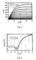
- FIG. 4is a graph showing drain-source current (I DS ) versus drain-source voltage (V DS ), as a function of gate-source voltage (V GS ), for the transistor structure depicted in FIG. 1 (the gate-source voltage varies from +40V (top curve) to +2 V in 2 V steps);
- FIG. 5is a graph showing the I DS vs. V GS characteristics for the transistor structure depicted in FIG. 1 at three different drain-source voltages;
- FIG. 7is a graph showing the optical transmission characteristics through the source or drain portion of the transistor structure depicted in FIG. 1.
- Enhancement-mode transistormeans a transistor in which there is negligible current flow (i.e., there is no conducting channel) between a source and a drain at zero gate voltage. In other words, the transistor device is “normally off.” In contrast, a depletion-mode transistor is “normally on” meaning that a current flows between a source and a drain at zero gate voltage.
- Gategenerally refers to the insulated gate terminal of a three terminal FET when used in the context of a transistor circuit configuration.
- substantially insulatingcan include insulating materials (e.g., materials having a resistivity of greater than about 10 10 ⁇ -cm) and semi-insulating materials (e.g., materials having a resistivity of about 10 3 ⁇ -cm to about 10 10 ⁇ -cm).
- substantially transparentgenerally denotes a material or construct that does not absorb a substantial amount of light in the visible portion (and/or infrared portion in certain variants) of the electromagnetic spectrum.
- “Vertical”means substantially perpendicular to the surface of a substrate.
- enhancement mode, field effect transistorswherein at least a portion of the transistor structure may be substantially transparent.
- Devices that include the transistors and methods for making the transistorsare also disclosed.
- One variant of the transistorincludes a channel layer comprising a substantially insulating, substantially transparent, material selected from ZnO or SnO 2 .
- a gate insulator layer comprising a substantially transparent materialis located adjacent to the channel layer so as to define a channel layer/gate insulator layer interface.
- the transistoralso includes a source that can inject electrons into the channel layer for accumulation at the channel layer/gate insulator layer interface and a drain that can extract electrons from the channel layer.
- a second variant of the transistorincludes a channel layer comprising a substantially transparent material selected from substantially insulating ZnO or substantially insulating SnO 2 , the substantially insulating ZnO or substantially insulating SnO 2 being produced by annealing.
- a gate insulator layeris located adjacent to the channel layer and comprises a substantially transparent material.
- the transistoralso includes a source, a drain, and a gate electrode.
- a method for making the transistorsincludes providing a gate insulating layer, depositing ZnO or SnO 2 onto at least a portion of a surface of the gate insulating layer, and annealing the ZnO or SnO 2 for about 1 to about 5 minutes at a temperature of about 300 to about 1000° C. in an oxidative atmosphere.
- the transistorsmay be included in optoelectronic display devices as switches coupled to at least one display element.
- Another disclosed deviceis a substantially transparent, dynamic random-access memory cell, comprising a substantially transparent capacitor coupled to the transistor.
- a further application of the transistorsis in substantially transparent inverters wherein the transistor is coupled to a load device.
- the transistor structureincludes a substrate, a gate electrode, a gate insulator layer, a channel layer, a source and a drain.
- the channel layermay be positioned adjacent to the gate insulator layer so that a surface of the channel layer is contiguous with a surface of the gate insulator layer.
- the contact region of the channel layer surface and the gate insulator layer surfaceis referred to herein as the channel layer/gate insulator layer interface.
- the channel layer insulating materialis different than the gate insulator layer material and the channel layer/gate insulator layer interface defines a discrete material boundary.
- the channel layer/gate insulator layer interfacemay define a conducting channel for the flow of electrons from the source to the drain.
- the transistormay be classified as a “surface-channel” or “interface-channel” device.
- the applied gate voltagefacilitates electron accumulation in the channel layer/gate insulator layer interface region.
- the applied voltageenhances electron injection from the source to the channel layer/gate insulator layer interface and electron extraction therefrom by the drain.
- the transistor structuremay exhibit an optical transmission of at least about 90%, more particularly at least about 95%, across the visible portion (and/or infrared portion in certain variants) of the electromagnetic spectrum.
- Each of the additional components of the structurei.e., substrate, gate electrode, source/drain terminals
- the transistor structure as a whole (and/or individual components of the transistor)may exhibit an optical transmission of at least about 50%, more particularly at least about 70%, and most particularly at least about 90%, across the visible portion (and/or infrared portion in certain variants) of the electromagnetic spectrum.
- a further feature of the FET disclosed hereinis that it may easily be fabricated as a thin film transistor (TFT).
- TFTthin film transistor
- relatively low processing temperaturese.g., not exceeding about 800° C.
- ion implantingto set the channel threshold voltage and define the source and drain contacts in certain variants of the FET structure.
- Such TFTstypically are very useful in association with optoelectronic device as explained below in more detail.
- the channel layertypically is made from a substantially insulating material that is also substantially transparent. A negligible amount of electrons is inherently available in the bulk portion of the channel layer since the channel layer is made from a substantially insulating material.
- the substantially insulating channel layermay provide inherent electrical isolation for multiple devices sharing a continuous channel layer film (with patterned gate, source, and drain electrodes defining each device). Such inherent device isolation means that patterning of the channel layer film is not necessary since conductivity at the channel layer/gate insulator layer is exhibited only beneath the patterned gate electrodes.
- Illustrative materials for the channel layerinclude ZnO and SnO 2 .
- Insulating ZnO and SnO 2may be made by an annealing process, particularly rapid thermal annealing (RTA).
- RTArapid thermal annealing
- Such insulating ZnO and SnO 2typically exhibit a bandgap of less than about 5 eV.
- a layer of ZnOmay be deposited (e.g., by sputtering or chemical vapor deposition) and subsequently undergo annealing for about 1 to about 5 minutes at a temperature of about 300 to about 1000° C., particularly about 700 to about 800° C., in a substantially oxidative atmosphere.
- a temperature of about 300 to about 1000° C., particularly about 700 to about 800° C.in a substantially oxidative atmosphere.
- Oxygen vacancies in ZnOcan render it n-type and conductive.
- High temperature (i.e., at least about 700° C.) annealing in inert atmospheres such as argonmay also produce insulating ZnO.
- such higher temperature annealsmay improve the ZnO crystallinity, thus improving the electron transport properties.
- Such insulating ZnOtypically is not doped.
- a layer of SnO 2may be deposited (e.g., by sputtering or chemical vapor deposition) and subsequently undergo annealing for about 1 to about 5 minutes at a temperature of about 300 to about 1000° C., particularly about 700 to about 900° C., in a substantially oxidative atmosphere.
- a temperature of about 300 to about 1000° C.particularly about 700 to about 900° C.
- Oxygen vacancies in SnO 2can render it n-type and conductive.
- High temperature (i.e., greater than about 700° C.) annealing in inert atmospheres such as argonmay also produce insulating SnO 2 .
- Such higher temperature annealsmay improve the SnO 2 crystallinity, thus improving the electron transport properties.
- the resistivity of the SnO 2may also be enhanced by substitutional doping with an acceptor dopant such as, for example, Al, In, Ga, Bi, B, La, Sc, Y, Lu, Er, Ho, and mixtures thereof.
- the thickness of the channel layermay vary, and according to particular examples it can range from about 10 to about 500 nm.
- the channel lengthalso may vary, and according to particular examples it can range from about 1,000 to about 100,000 nm.
- the gate insulator layermay be made from any material exhibiting insulating properties required for gate insulators, particularly a substantially transparent material.
- Gate insulator materialstypically exhibit a bandgap of greater than about 5 eV.
- Illustrative materialsinclude substantially transparent materials such as aluminum-titanium oxide (Al 2 O 3 /TiO 2 ), Al 2 O 3 , MgO, SiO 2 , silicon nitride, and silicon oxynitride.
- a substantially transparent materialis aluminum-titanium oxide grown by atomic layer deposition.
- the thickness of the gate insulator layermay vary, and according to particular examples it can range from about 10 to about 300 nm.
- the gate insulator layermay be introduced into the structure by techniques such as chemical vapor deposition, sputtering, atomic layer deposition, or evaporation.
- Source/drain terminalsrefer to the terminals of a FET, between which conduction occurs under the influence of an electric field. Designers often designate a particular source/drain terminal to be a “source” or a “drain” on the basis of the voltage to be applied to that terminal when the FET is operated in a circuit.
- the source and drainmay be made from any suitable conductive material such as an n-type material.
- the source and drain materialsare optionally opaque materials or substantially transparent materials.
- Illustrative materialsinclude transparent, n-type conductors such as indium-tin oxide (ITO), ZnO, SnO 2 , or In 2 O 3 or opaque metals such as Al, Cu, Au, Pt, W, Ni, or Ti.
- Especially useful materials for the source and drainare those that can inject (and extract) electrons into the channel layer insulating material. Examples of such electron injection materials include indium-tin oxide, LaB 6 , and ZnO:Al.
- the source and drainmay be introduced into the structure by techniques such as chemical vapor deposition, sputtering, evaporation, and/or doping of the channel layer material via diffusion or ion implantation.
- the source and drain terminalsmay be fabricated such that they are geometrically symmetrical or non-symmetrical.
- the gate electrodemay be made from any suitable conductive material.
- the gate electrode materialis optionally an opaque material or a substantially transparent material.
- Illustrative gate electrode materialsinclude transparent, n-type conductors such as indium-tin oxide (ITO), ZnO, SnO 2 , or In 2 O 3 , or opaque metals such as Al, Cu, Au, Pt, W, Ni, or Ti.
- the thickness of the gate electrodemay vary, and according to particular examples it can range from about 50 to about 1000 nm.
- the gate electrodemay be introduced into the structure by chemical vapor deposition, sputtering, evaporation and/or doping.
- Substraterefers to the physical object that is the basic workpiece that is transformed by various process operations into the desired microelectronic configuration.
- a substratemay also be referred to as a wafer.
- Wafersmay be made of semiconducting, non-semiconducting, or combinations of semiconducting and non-semiconducting materials.
- the substratemay be made from any suitable material.
- the substrate materialis optionally an opaque material or a substantially transparent material.
- Illustrative substrate materialsinclude glass and silicon.
- the thickness of the substratemay vary, and according to particular examples it can range from about 100 ⁇ m to about 1 cm.
- Metal lines, traces, wires, interconnects, conductors, signal paths and signaling mediumsmay be used for providing the desired electrical connections.
- the related terms listed above,are generally interchangeable, and appear in order from specific to general.
- Metal linesgenerally aluminum (Al), copper (Cu) or an alloy of Al and Cu, are conductors that provide signal paths for coupling or interconnecting, electrical circuitry. Conductors other than metal may also be utilized.
- An illustrative n-channel operation of the transistorinvolves applying a positive voltage to the gate electrode, grounding the source, and applying a positive voltage to the drain.
- a voltage of about 5 to about 40 Vmay be applied to the gate electrode and the drain during operation.
- the threshold voltagemay range from about 1 to about 20 V.
- Electronsflow from the source, along the conducting channel created at the channel layer/gate insulator layer interface, and out of the transistor through the drain.
- the effective mobility of the electrons at the interfacemay vary depending upon the specific structure, but could range, for example, from about 0.05 to about 20 cm 2 V ⁇ 1 s ⁇ 1 . Simply removing the positive voltage applied to the gate electrode turns the transistor off since the transistor is an enhancement-mode transistor.
- the transistor structures disclosed hereinmay be used for fabricating chips, integrated circuits, monolithic devices, semiconductor devices, and microelectronic devices.
- a microelectronic deviceis an optoelectronic device.
- An illustrative optoelectronic deviceis an active-matrix liquid-crystal display (AMLCD).
- One exemplar deviceis an optoelectronic display device that includes elements having electrodes and an electro-optical material disposed between the electrodes.
- a connection electrode of the transparent transistormay be connected to an electrode of the display element, while the switching element and the display element overlap one another at least partly.
- An optoelectronic display elementis here understood to be a display element whose optical properties change under the influence of an electrical quantity such as current or voltage such as, for example, an element usually referred to as liquid crystal display (LCD).
- LCDliquid crystal display
- the presently detailed transparent transistoris sufficiently fast for switching the display element at such a high frequency that the use of the transparent transistor as a switching element in a liquid crystal display is possible.
- the display elementacts in electrical terms as a capacitor that is charged or discharged by the accompanying transparent transistor.
- the optoelectronic display devicemay include many display elements each with its own transparent transistor, for example, arranged in a matrix.
- the transparent transistorsmay be arrayed for LCD devices as described, for example, in Kim, “Thin-Film-Transistor Device Design”, Information Display 2/02, p. 26 (2002).
- microelectronic devicesthat could employ the transistor structure shown herein include inverters, analog amplifiers and single-transistor dynamic random-access memory (DRAM) cells, and like devices.
- DRAMsingle-transistor dynamic random-access memory
- a transparent enhancement-mode transistorwhose source is connected to one terminal of a transparent capacitor, while the other terminal of the capacitor is grounded, constitutes a transparent single-transistor dynamic random-access memory (DRAM) cell.
- DRAMtransparent single-transistor dynamic random-access memory
- the enhancement-mode transistorserving as an access transistor that controls the capacitor charge state.
- a logic 0is represented by negligible capacitor charge and a concomitantly small capacitor voltage.
- a logic 1is obtained by charging the capacitor, thus increasing the capacitor voltage until it approaches the power supply voltage.
- a transparent capacitormay be constructed by sandwiching a transparent insulator layer, using materials such as Al 2 O3 or SiO 2 , between two transparent conductors, using materials such as indium-tin oxide, ZnO, or SnO 2 .
- FIGS. 1 - 3Illustrative examples of specific transistor structures are shown in FIGS. 1 - 3 .
- the specific examples described beloware for illustrative purposes and should not be considered as limiting the scope of the appended claims.
- like reference numeralsrefer to like elements unless otherwise indicated.
- FIG. 1A first figure.
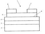
- a TFT structure 1is illustrated that was fabricated on a one-inch by one-inch thick composite substrate.
- the platformincludes a glass substrate 2 , a 200 nm thick, indium-tin oxide (ITO) gate electrode 3 coated on the substrate 2 , and a 200 nm thick, aluminum-titanium oxide gate insulator layer 4 .
- ITOindium-tin oxide
- a ZnO channel and an ITO source/drain electrode filmwas deposited via ion beam sputtering in 10 ⁇ 4 Torr of Ar/O 2 (80%/20%); the substrate was unheated during deposition.
- the ZnO channel layer 5(100 nm thick), an ITO source electrode 6 (300 nm thick) and, an ITO drain electrode 7 (300 nm thick) were defined using a shadow mask.
- the resulting structuredefines a channel layer/gate insulator layer interface 8 .
- a 300° C. rapid thermal anneal (RTA) in Ar immediately prior to both the ZnO and ITO depositionsserved to remove adsorbed contaminants from the exposed surface, yielding a noticeable improvement in film quality (particularly for ITO films).
- a RTAtypically in O 2 or Ar, at 600 to 800° C.
- a 300° C. RTA in O 2was used to improve the transparency of the ITO layer.
- the source/drain electrodes 6 and 7are disposed on the top surface of the channel layer 5 (from a vertical perspective) and the gate electrode 3 and channel layer 5 are disposed, respectively, on opposing surfaces of the gate insulator layer 4 .
- structure 1allows for high temperature processing of the ZnO channel layer 5 prior to deposition and processing of the ITO source/drain electrodes 6 and 7 .
- Certain electrical and physical characteristics of the TFT structure 1were evaluated as described below and illustrated in FIGS. 4 - 7 .
- n-channel, enhancement-mode behavioris obtained as demonstrated by the fact that a positive gate voltage in excess of ⁇ 15 V (the threshold) is required to obtain appreciable drain-source current.
- IDS-VDS curvesexhibit prototypical FET characteristics; of particular significance is the flatness of these curves at large drain voltages (i.e. they exhibit ‘hard’ saturation).
- the drain and gate voltages employedare rather large compared to conventional FETs; gate and drain voltages can be reduced to the range expected for typical FET operation (i.e. ⁇ 5-10 V), by simply reducing the gate insulator thickness.
- the insulator thicknessis ⁇ 200 nm, as optimized for electroluminescent display applications; if an otherwise identical insulator is rescaled to a thickness of 20 nm, the gate and drain voltages will be reduced by a factor of approximately 10.
- the IDS of structure 1is currently rather small (i.e., I DS (max) is about 6 ⁇ A in FIG. 4). A larger I DS may be desirable for most applications.
- the magnitude of I DSis determined by two factors. One is the effective mobility of the channel electrons, ⁇ eff (about 0.05-0.2 cm 2 V ⁇ 1 s ⁇ 1 for the TFT structure 1 ). Process/device optimization should result in an improvement in ⁇ eff by a factor of about 2 to 100 which will lead to a corresponding increase in I DS .
- the second factoris the aspect ratio.
- FIG. 5illustrates the I DS -V GS characteristics of the TFT structure 1 at three different drain voltages. This figure shows that there is a factor of 10 5 -10 6 difference between the ‘on’ and ‘off’ currents when the transistor is used as a switch.
- FIG. 6shows the transfer characteristics of the TFT structure 1 when it is employed as an inverter.
- V DDpower supply voltage
- a logic swing of about 15 V between 15 and 30 Vis clearly evident from this curve.
- a logic inverteris comprised of two constituents: a transistor coupled to a load device.
- the load devicemay be a resistor, as employed in this example.
- a depletion- or enhancement-mode transistormay also be used as load devices, typically offering superior performance.
- the fundamental property of a logic inverteris that it performs a logical not operation, in which a logic 0 (1) input produces a logic 1 (0) output.
- Successful achievement of a transparent logic inverter, as described herein,is significant since the inverter is the most basic building block for achieving transparent digital electronics. Optimization of the transparent thin film transistor via reducing the insulator thickness, reducing physical dimensions, and increasing the current drive capability (increased aspect ratio and effective mobility) will lead to a significant reduction in the required power supply voltage for inverter operation.
- Transparent transistorsmay also be employed in amplifier applications.
- the inverter structures described abovecan also function as simple analog inverting amplifiers. With the appropriate DC bias at the input, a small input signal (superimposed upon the DC bias) is amplified by the inverter transfer characteristic.
- these transistorscould be directly applied in arbitrary amplifier configurations, with the limitation that the maximum operating frequency will be relatively low due to the low mobility of these devices.
- FIG. 7shows the optical transmission of the TFT structure 1 through the source 6 or drain 7 (optical transmission through the channel, not shown here, is higher than through the source or drain).
- the average transmission in the visible portion of the electromagnetic spectrum(450-700 nm) is about 90% (about 95% through the channel).
- the transparent TFT structureis essentially invisible; a slight tinting of the glass substrate is apparent upon close inspection.
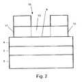
- a source electrode 11(100 nm thick) and a drain electrode 12 (100 nm thick) were made by selectively doping the ends of a ZnO channel layer 13 (100 nm thick) with In (or any other suitable n-type dopant). This was accomplished by ion beam sputter depositing a thin (about 5 nm) ITO layer using the source/drain shadow mask before depositing the ZnO channel film. A subsequent high-temperature ( ⁇ 600-800° C.) annealing step was performed to diffusion-dope the ZnO, thus forming n-type doped source/drain regions 11 and 12 .
- the diffusion-doping RTAmay also function as the oxidizing RTA for the ZnO.
- ITO contactsmay be placed over the source and drain regions to provide better electrical contact.
- the substrate 2 , gate electrode 3 , gate insulator layer 4 , and channel layer/gate insulator layer interface 8are the same as in FIG. 1.
- an ITO source electrode 21(300 nm thick) and ITO drain electrode 22 (300 nm thick) are deposited prior to formation of a ZnO channel layer 23 (100 nm thick).
- the ZnO channel layer 23is subsequently deposited conformally over the ITO source/drain electrodes 21 and 22 .
- a 700° C. Ar annealwas performed, followed by a 300° C. oxygen anneal.
- the substrate 2 , gate electrode 3 , gate insulator layer 4 , and channel layer/gate insulator layer interface 8are the same as in FIG. 1.
Landscapes
- Thin Film Transistor (AREA)
Abstract
Description
- This application claims benefit of U.S. Provisional Application No. 60/382,696, filed May 21, 2002.[0001]
- The present disclosure relates to transistor structures such as, for example, transparent transistors.[0002]
- The microelectronics industry and research community is undertaking efforts to fabricate electronic devices (e.g., diodes and transistors) that are transparent to the portion of the electromagnetic spectrum that is visible to the human eye. Circuits made of such devices would offer unique opportunities for innovation or improvement of consumer-, automotive-, and military-electronics systems.[0003]
- For example, active-matrix liquid crystal displays (AMLCD) are employed extensively in laptop computers and other information display products. The operation of an AMLCD display requires that each picture or display element (pixel) have a corresponding thin-film transistor (TFT) associated with it for selecting or addressing the pixel to be on or off. Currently, AMLCD displays employ transistor materials that may be deposited onto glass substrates but are not transparent (usually amorphous, polycrystalline, or continuous-grain silicon are the materials used to fabricate TFTs on glass). Thus, the portion of the display glass occupied by the addressing electronics is not available for transmission of light through the display. Therefore, the availability of transparent transistors for AMLCD addressing would improve display performance by allowing more light to be transmitted through the display.[0004]
- Certain embodiments will be described in more detail with reference to the following drawings:[0005]
- FIG. 1 is a sectional view of a first embodiment of a presently disclosed transistor structure;[0006]
- FIG. 2 is a sectional view of a second embodiment of a presently disclosed transistor structure;[0007]
- FIG. 3 is a sectional view of a third embodiment of a presently disclosed transistor structure;[0008]
- FIG. 4 is a graph showing drain-source current (I[0009]DS) versus drain-source voltage (VDS), as a function of gate-source voltage (VGS), for the transistor structure depicted in FIG. 1 (the gate-source voltage varies from +40V (top curve) to +2 V in 2 V steps);
- FIG. 5 is a graph showing the I[0010]DSvs. VGScharacteristics for the transistor structure depicted in FIG. 1 at three different drain-source voltages;
- FIG. 6 is a graph showing inverter transfer characteristics for the transistor structure depicted in FIG. 1 using a transparent thin-film resistor load (R=70 MΩ) and a power supply voltage, V[0011]DD=40 V; and
- FIG. 7 is a graph showing the optical transmission characteristics through the source or drain portion of the transistor structure depicted in FIG. 1.[0012]
- For ease of understanding, the following terms used herein are described below in more detail:[0013]
- “Enhancement-mode transistor” means a transistor in which there is negligible current flow (i.e., there is no conducting channel) between a source and a drain at zero gate voltage. In other words, the transistor device is “normally off.” In contrast, a depletion-mode transistor is “normally on” meaning that a current flows between a source and a drain at zero gate voltage.[0014]
- “Gate” generally refers to the insulated gate terminal of a three terminal FET when used in the context of a transistor circuit configuration.[0015]
- “Substantially insulating” can include insulating materials (e.g., materials having a resistivity of greater than about 10[0016]10Ω-cm) and semi-insulating materials (e.g., materials having a resistivity of about 103Ω-cm to about 1010Ω-cm).
- “Substantially transparent” generally denotes a material or construct that does not absorb a substantial amount of light in the visible portion (and/or infrared portion in certain variants) of the electromagnetic spectrum.[0017]
- “Vertical” means substantially perpendicular to the surface of a substrate.[0018]
- The preceding term descriptions are provided solely to aid the reader, and should not be construed to have a scope less than that understood by a person of ordinary skill in the art or as limiting the scope of the appended claims.[0019]
- Disclosed herein are enhancement mode, field effect transistors wherein at least a portion of the transistor structure may be substantially transparent. Devices that include the transistors and methods for making the transistors are also disclosed.[0020]
- One variant of the transistor includes a channel layer comprising a substantially insulating, substantially transparent, material selected from ZnO or SnO[0021]2. A gate insulator layer comprising a substantially transparent material is located adjacent to the channel layer so as to define a channel layer/gate insulator layer interface. The transistor also includes a source that can inject electrons into the channel layer for accumulation at the channel layer/gate insulator layer interface and a drain that can extract electrons from the channel layer.
- A second variant of the transistor includes a channel layer comprising a substantially transparent material selected from substantially insulating ZnO or substantially insulating SnO[0022]2, the substantially insulating ZnO or substantially insulating SnO2being produced by annealing. A gate insulator layer is located adjacent to the channel layer and comprises a substantially transparent material. The transistor also includes a source, a drain, and a gate electrode.
- A method for making the transistors includes providing a gate insulating layer, depositing ZnO or SnO[0023]2onto at least a portion of a surface of the gate insulating layer, and annealing the ZnO or SnO2for about 1 to about 5 minutes at a temperature of about 300 to about 1000° C. in an oxidative atmosphere.
- The transistors may be included in optoelectronic display devices as switches coupled to at least one display element. Another disclosed device is a substantially transparent, dynamic random-access memory cell, comprising a substantially transparent capacitor coupled to the transistor. A further application of the transistors is in substantially transparent inverters wherein the transistor is coupled to a load device.[0024]
- In general, the transistor structure includes a substrate, a gate electrode, a gate insulator layer, a channel layer, a source and a drain. The channel layer may be positioned adjacent to the gate insulator layer so that a surface of the channel layer is contiguous with a surface of the gate insulator layer. The contact region of the channel layer surface and the gate insulator layer surface is referred to herein as the channel layer/gate insulator layer interface. In exemplary constructs, the channel layer insulating material is different than the gate insulator layer material and the channel layer/gate insulator layer interface defines a discrete material boundary.[0025]
- A feature of an embodiment of the transistor structure is that the channel layer/gate insulator layer interface may define a conducting channel for the flow of electrons from the source to the drain. In other words, the transistor may be classified as a “surface-channel” or “interface-channel” device. The applied gate voltage facilitates electron accumulation in the channel layer/gate insulator layer interface region. In addition, the applied voltage enhances electron injection from the source to the channel layer/gate insulator layer interface and electron extraction therefrom by the drain.[0026]
- Another characteristic of the transistor structure is that selected embodiments of the construct or combination of the channel layer and the gate insulator layer may exhibit an optical transmission of at least about 90%, more particularly at least about 95%, across the visible portion (and/or infrared portion in certain variants) of the electromagnetic spectrum. Each of the additional components of the structure (i.e., substrate, gate electrode, source/drain terminals) may be optionally opaque or substantially transparent depending upon the desired end use of the transistor. In certain embodiments, the transistor structure as a whole (and/or individual components of the transistor) may exhibit an optical transmission of at least about 50%, more particularly at least about 70%, and most particularly at least about 90%, across the visible portion (and/or infrared portion in certain variants) of the electromagnetic spectrum.[0027]
- A further feature of the FET disclosed herein is that it may easily be fabricated as a thin film transistor (TFT). For example, relatively low processing temperatures (e.g., not exceeding about 800° C.) may be used and there is no need for ion implanting to set the channel threshold voltage and define the source and drain contacts in certain variants of the FET structure. Such TFTs typically are very useful in association with optoelectronic device as explained below in more detail.[0028]
- The channel layer typically is made from a substantially insulating material that is also substantially transparent. A negligible amount of electrons is inherently available in the bulk portion of the channel layer since the channel layer is made from a substantially insulating material. In addition, the substantially insulating channel layer may provide inherent electrical isolation for multiple devices sharing a continuous channel layer film (with patterned gate, source, and drain electrodes defining each device). Such inherent device isolation means that patterning of the channel layer film is not necessary since conductivity at the channel layer/gate insulator layer is exhibited only beneath the patterned gate electrodes.[0029]
- Illustrative materials for the channel layer include ZnO and SnO[0030]2. Insulating ZnO and SnO2may be made by an annealing process, particularly rapid thermal annealing (RTA). Such insulating ZnO and SnO2typically exhibit a bandgap of less than about 5 eV.
- For example, a layer of ZnO may be deposited (e.g., by sputtering or chemical vapor deposition) and subsequently undergo annealing for about 1 to about 5 minutes at a temperature of about 300 to about 1000° C., particularly about 700 to about 800° C., in a substantially oxidative atmosphere. Although not bound by any theory, it is believed that such a process should result in the incorporation of more oxygen into the ZnO layer, thus reducing the oxygen vacancy concentration. Oxygen vacancies in ZnO can render it n-type and conductive. High temperature (i.e., at least about 700° C.) annealing in inert atmospheres such as argon may also produce insulating ZnO. Although not bound by any theory, such higher temperature anneals may improve the ZnO crystallinity, thus improving the electron transport properties. Such insulating ZnO typically is not doped.[0031]
- Similarly, a layer of SnO[0032]2may be deposited (e.g., by sputtering or chemical vapor deposition) and subsequently undergo annealing for about 1 to about 5 minutes at a temperature of about 300 to about 1000° C., particularly about 700 to about 900° C., in a substantially oxidative atmosphere. Although not bound by any theory, it is believed that such a process should result in the incorporation of more oxygen into the SnO2layer, thus reducing the oxygen vacancy concentration. Oxygen vacancies in SnO2can render it n-type and conductive. High temperature (i.e., greater than about 700° C.) annealing in inert atmospheres such as argon may also produce insulating SnO2. Although not bound by any theory, such higher temperature anneals may improve the SnO2crystallinity, thus improving the electron transport properties. The resistivity of the SnO2may also be enhanced by substitutional doping with an acceptor dopant such as, for example, Al, In, Ga, Bi, B, La, Sc, Y, Lu, Er, Ho, and mixtures thereof.
- The thickness of the channel layer may vary, and according to particular examples it can range from about 10 to about 500 nm. The channel length also may vary, and according to particular examples it can range from about 1,000 to about 100,000 nm.[0033]
- The gate insulator layer may be made from any material exhibiting insulating properties required for gate insulators, particularly a substantially transparent material. Gate insulator materials typically exhibit a bandgap of greater than about 5 eV. Illustrative materials include substantially transparent materials such as aluminum-titanium oxide (Al[0034]2O3/TiO2), Al2O3, MgO, SiO2, silicon nitride, and silicon oxynitride. One distinctive example of a substantially transparent material is aluminum-titanium oxide grown by atomic layer deposition. The thickness of the gate insulator layer may vary, and according to particular examples it can range from about 10 to about 300 nm. The gate insulator layer may be introduced into the structure by techniques such as chemical vapor deposition, sputtering, atomic layer deposition, or evaporation.
- Source/drain terminals refer to the terminals of a FET, between which conduction occurs under the influence of an electric field. Designers often designate a particular source/drain terminal to be a “source” or a “drain” on the basis of the voltage to be applied to that terminal when the FET is operated in a circuit. The source and drain may be made from any suitable conductive material such as an n-type material. The source and drain materials are optionally opaque materials or substantially transparent materials. Illustrative materials include transparent, n-type conductors such as indium-tin oxide (ITO), ZnO, SnO[0035]2, or In2O3or opaque metals such as Al, Cu, Au, Pt, W, Ni, or Ti. Especially useful materials for the source and drain are those that can inject (and extract) electrons into the channel layer insulating material. Examples of such electron injection materials include indium-tin oxide, LaB6, and ZnO:Al.
- The source and drain may be introduced into the structure by techniques such as chemical vapor deposition, sputtering, evaporation, and/or doping of the channel layer material via diffusion or ion implantation. The source and drain terminals may be fabricated such that they are geometrically symmetrical or non-symmetrical.[0036]
- The gate electrode may be made from any suitable conductive material. The gate electrode material is optionally an opaque material or a substantially transparent material. Illustrative gate electrode materials include transparent, n-type conductors such as indium-tin oxide (ITO), ZnO, SnO[0037]2, or In2O3, or opaque metals such as Al, Cu, Au, Pt, W, Ni, or Ti. The thickness of the gate electrode may vary, and according to particular examples it can range from about 50 to about 1000 nm. The gate electrode may be introduced into the structure by chemical vapor deposition, sputtering, evaporation and/or doping.
- “Substrate”, as used herein, refers to the physical object that is the basic workpiece that is transformed by various process operations into the desired microelectronic configuration. A substrate may also be referred to as a wafer. Wafers may be made of semiconducting, non-semiconducting, or combinations of semiconducting and non-semiconducting materials. The substrate may be made from any suitable material. The substrate material is optionally an opaque material or a substantially transparent material. Illustrative substrate materials include glass and silicon. The thickness of the substrate may vary, and according to particular examples it can range from about 100 μm to about 1 cm.[0038]
- Electrical contact to the gate electrode, source, drain and substrate may be provided in any manner. For example, metal lines, traces, wires, interconnects, conductors, signal paths and signaling mediums may be used for providing the desired electrical connections. The related terms listed above, are generally interchangeable, and appear in order from specific to general. Metal lines, generally aluminum (Al), copper (Cu) or an alloy of Al and Cu, are conductors that provide signal paths for coupling or interconnecting, electrical circuitry. Conductors other than metal may also be utilized.[0039]
- An illustrative n-channel operation of the transistor involves applying a positive voltage to the gate electrode, grounding the source, and applying a positive voltage to the drain. For example, a voltage of about 5 to about 40 V may be applied to the gate electrode and the drain during operation. The threshold voltage may range from about 1 to about 20 V. Electrons flow from the source, along the conducting channel created at the channel layer/gate insulator layer interface, and out of the transistor through the drain. The effective mobility of the electrons at the interface may vary depending upon the specific structure, but could range, for example, from about 0.05 to about 20 cm[0040]2V−1s−1. Simply removing the positive voltage applied to the gate electrode turns the transistor off since the transistor is an enhancement-mode transistor.
- The transistor structures disclosed herein may be used for fabricating chips, integrated circuits, monolithic devices, semiconductor devices, and microelectronic devices. One example of a microelectronic device is an optoelectronic device. An illustrative optoelectronic device is an active-matrix liquid-crystal display (AMLCD).[0041]
- One exemplar device is an optoelectronic display device that includes elements having electrodes and an electro-optical material disposed between the electrodes. A connection electrode of the transparent transistor may be connected to an electrode of the display element, while the switching element and the display element overlap one another at least partly. An optoelectronic display element is here understood to be a display element whose optical properties change under the influence of an electrical quantity such as current or voltage such as, for example, an element usually referred to as liquid crystal display (LCD). The presently detailed transparent transistor is sufficiently fast for switching the display element at such a high frequency that the use of the transparent transistor as a switching element in a liquid crystal display is possible. The display element acts in electrical terms as a capacitor that is charged or discharged by the accompanying transparent transistor. The optoelectronic display device may include many display elements each with its own transparent transistor, for example, arranged in a matrix. The transparent transistors may be arrayed for LCD devices as described, for example, in Kim, “Thin-Film-Transistor Device Design”,[0042]
Information Display 2/02, p. 26 (2002). - Other examples of microelectronic devices that could employ the transistor structure shown herein include inverters, analog amplifiers and single-transistor dynamic random-access memory (DRAM) cells, and like devices.[0043]
- For instance, a transparent enhancement-mode transistor whose source is connected to one terminal of a transparent capacitor, while the other terminal of the capacitor is grounded, constitutes a transparent single-transistor dynamic random-access memory (DRAM) cell. In such a DRAM cell, information is stored as charge on a capacitor, with the enhancement-mode transistor serving as an access transistor that controls the capacitor charge state. Usually in such a DRAM cell, a[0044]
logic 0 is represented by negligible capacitor charge and a concomitantly small capacitor voltage. In contrast, alogic 1 is obtained by charging the capacitor, thus increasing the capacitor voltage until it approaches the power supply voltage. - The entire DRAM cell described herein, or a portion thereof, is transparent. Fabricating transparent capacitors and connecting them to a transparent transistor to realize a DRAM cell can be accomplished using various techniques. Specifically, a transparent capacitor may be constructed by sandwiching a transparent insulator layer, using materials such as Al[0045]2O3 or SiO2, between two transparent conductors, using materials such as indium-tin oxide, ZnO, or SnO2.
- Illustrative examples of specific transistor structures are shown in FIGS.[0046]1-3. The specific examples described below are for illustrative purposes and should not be considered as limiting the scope of the appended claims. In FIGS.1-3 like reference numerals refer to like elements unless otherwise indicated.
- A[0047]
TFT structure 1 is illustrated that was fabricated on a one-inch by one-inch thick composite substrate. The platform includes aglass substrate 2, a 200 nm thick, indium-tin oxide (ITO)gate electrode 3 coated on thesubstrate 2, and a 200 nm thick, aluminum-titanium oxidegate insulator layer 4. - A ZnO channel and an ITO source/drain electrode film was deposited via ion beam sputtering in 10[0048]−4Torr of Ar/O2(80%/20%); the substrate was unheated during deposition. The ZnO channel layer5 (100 nm thick), an ITO source electrode6 (300 nm thick) and, an ITO drain electrode7 (300 nm thick) were defined using a shadow mask. The resulting structure defines a channel layer/gate
insulator layer interface 8. A 300° C. rapid thermal anneal (RTA) in Ar immediately prior to both the ZnO and ITO depositions served to remove adsorbed contaminants from the exposed surface, yielding a noticeable improvement in film quality (particularly for ITO films). After deposition of the ZnO layer, a RTA (typically in O2or Ar, at 600 to 800° C.) was employed to increase the ZnO channel resistivity and to improve the electrical quality of the channel layer/gate insulatinglayer interface 8. Following deposition of the ITO source/drain electrodes, a 300° C. RTA in O2was used to improve the transparency of the ITO layer. In thetransistor structure 1 the source/drain electrodes gate electrode 3 andchannel layer 5 are disposed, respectively, on opposing surfaces of thegate insulator layer 4. Consequently,structure 1 allows for high temperature processing of theZnO channel layer 5 prior to deposition and processing of the ITO source/drain electrodes TFT structure 1 were evaluated as described below and illustrated in FIGS.4-7. - With reference to FIG. 4, n-channel, enhancement-mode behavior is obtained as demonstrated by the fact that a positive gate voltage in excess of ˜15 V (the threshold) is required to obtain appreciable drain-source current. These IDS-VDS curves exhibit prototypical FET characteristics; of particular significance is the flatness of these curves at large drain voltages (i.e. they exhibit ‘hard’ saturation). The drain and gate voltages employed are rather large compared to conventional FETs; gate and drain voltages can be reduced to the range expected for typical FET operation (i.e. ˜5-10 V), by simply reducing the gate insulator thickness. In the[0049]
TFT structure 1 the insulator thickness is ˜200 nm, as optimized for electroluminescent display applications; if an otherwise identical insulator is rescaled to a thickness of 20 nm, the gate and drain voltages will be reduced by a factor of approximately 10. - The IDS of[0050]
structure 1 is currently rather small (i.e., IDS(max) is about 6 μA in FIG. 4). A larger IDSmay be desirable for most applications. The magnitude of IDSis determined by two factors. One is the effective mobility of the channel electrons, μeff(about 0.05-0.2 cm2V−1s−1for the TFT structure1). Process/device optimization should result in an improvement in μeffby a factor of about 2 to 100 which will lead to a corresponding increase in IDS. The second factor is the aspect ratio. The aspect ratio of the TFT structure1 (the physical width of the gate, Z, divided by the length of the gate, L) is about 2 (with Z=2L=6000 μm). A larger aspect ratio will lead to a larger IDS. - FIG. 5 illustrates the I[0051]DS-VGScharacteristics of the
TFT structure 1 at three different drain voltages. This figure shows that there is a factor of105-106difference between the ‘on’ and ‘off’ currents when the transistor is used as a switch. - FIG. 6 shows the transfer characteristics of the[0052]
TFT structure 1 when it is employed as an inverter. A ZnO transparent thin-film resistor (R=70 MΩ) is used as the inverter passive load with a power supply voltage VDD=40 V. A logic swing of about 15 V between 15 and 30 V is clearly evident from this curve. This constitutes a demonstration of the use of the presently described transparent TFT as a transparent inverter. In its simplest implementation, a logic inverter is comprised of two constituents: a transistor coupled to a load device. The load device may be a resistor, as employed in this example. Alternatively, a depletion- or enhancement-mode transistor may also be used as load devices, typically offering superior performance. The fundamental property of a logic inverter is that it performs a logical not operation, in which a logic 0 (1) input produces a logic 1 (0) output. Successful achievement of a transparent logic inverter, as described herein, is significant since the inverter is the most basic building block for achieving transparent digital electronics. Optimization of the transparent thin film transistor via reducing the insulator thickness, reducing physical dimensions, and increasing the current drive capability (increased aspect ratio and effective mobility) will lead to a significant reduction in the required power supply voltage for inverter operation. - Transparent transistors may also be employed in amplifier applications. For example, the inverter structures described above can also function as simple analog inverting amplifiers. With the appropriate DC bias at the input, a small input signal (superimposed upon the DC bias) is amplified by the inverter transfer characteristic. In addition to such simple amplifier configurations, these transistors could be directly applied in arbitrary amplifier configurations, with the limitation that the maximum operating frequency will be relatively low due to the low mobility of these devices.[0053]
- FIG. 7 shows the optical transmission of the[0054]
TFT structure 1 through thesource 6 or drain7 (optical transmission through the channel, not shown here, is higher than through the source or drain). The average transmission in the visible portion of the electromagnetic spectrum (450-700 nm) is about 90% (about 95% through the channel). Visually, the transparent TFT structure is essentially invisible; a slight tinting of the glass substrate is apparent upon close inspection. - In another[0055]
transparent TFT structure 10 version shown in FIG. 2, a source electrode11 (100 nm thick) and a drain electrode12 (100 nm thick) were made by selectively doping the ends of a ZnO channel layer13 (100 nm thick) with In (or any other suitable n-type dopant). This was accomplished by ion beam sputter depositing a thin (about 5 nm) ITO layer using the source/drain shadow mask before depositing the ZnO channel film. A subsequent high-temperature (˜600-800° C.) annealing step was performed to diffusion-dope the ZnO, thus forming n-type doped source/drain regions substrate 2,gate electrode 3,gate insulator layer 4, and channel layer/gateinsulator layer interface 8 are the same as in FIG. 1. - In a third variation of a[0056]
TFT structure 20, an ITO source electrode21 (300 nm thick) and ITO drain electrode22 (300 nm thick) are deposited prior to formation of a ZnO channel layer23 (100 nm thick). TheZnO channel layer 23 is subsequently deposited conformally over the ITO source/drain electrodes substrate 2,gate electrode 3,gate insulator layer 4, and channel layer/gateinsulator layer interface 8 are the same as in FIG. 1. - Having illustrated and described the principles of the disclosed devices and methods with reference to several embodiments, it should be apparent that these devices and methods may be modified in arrangement and detail without departing from such principles.[0057]
- What is claimed is:[0058]
Claims (64)
Priority Applications (11)
| Application Number | Priority Date | Filing Date | Title |
|---|---|---|---|
| US10/307,162US7189992B2 (en) | 2002-05-21 | 2002-11-27 | Transistor structures having a transparent channel |
| US10/350,819US7339187B2 (en) | 2002-05-21 | 2003-01-24 | Transistor structures |
| TW092112416ATWI278113B (en) | 2002-05-21 | 2003-05-07 | Transistor structures and methods for making the same |
| KR1020047018750AKR101023491B1 (en) | 2002-05-21 | 2003-05-15 | Transistor Structure and Manufacturing Method Thereof |
| PCT/US2003/015527WO2004038757A2 (en) | 2002-05-21 | 2003-05-15 | Transistor structures and methods for making the same |
| AU2003299510AAU2003299510A1 (en) | 2002-05-21 | 2003-05-15 | Transistor structures and methods for making the same |
| JP2005501592AJP2006502597A (en) | 2002-05-21 | 2003-05-15 | Transistor structure and manufacturing method thereof |
| CNB038116782ACN100440540C (en) | 2002-05-21 | 2003-05-15 | Transistor structure, method of manufacturing the same, and method of operating the same |
| EP03799797AEP1508172A2 (en) | 2002-05-21 | 2003-05-15 | Transistor structures and methods for making the same |
| US11/702,834US7888207B2 (en) | 2002-05-21 | 2007-02-05 | Transistor structures and methods for making the same |
| US12/006,738US20080108198A1 (en) | 2002-05-21 | 2008-01-03 | Transistor structures and methods for making the same |
Applications Claiming Priority (2)
| Application Number | Priority Date | Filing Date | Title |
|---|---|---|---|
| US38269602P | 2002-05-21 | 2002-05-21 | |
| US10/307,162US7189992B2 (en) | 2002-05-21 | 2002-11-27 | Transistor structures having a transparent channel |
Related Child Applications (2)
| Application Number | Title | Priority Date | Filing Date |
|---|---|---|---|
| US10/350,819Continuation-In-PartUS7339187B2 (en) | 2002-05-21 | 2003-01-24 | Transistor structures |
| US11/702,834DivisionUS7888207B2 (en) | 2002-05-21 | 2007-02-05 | Transistor structures and methods for making the same |
Publications (2)
| Publication Number | Publication Date |
|---|---|
| US20030218221A1true US20030218221A1 (en) | 2003-11-27 |
| US7189992B2 US7189992B2 (en) | 2007-03-13 |
Family
ID=46150238
Family Applications (2)
| Application Number | Title | Priority Date | Filing Date |
|---|---|---|---|
| US10/307,162Expired - LifetimeUS7189992B2 (en) | 2002-05-21 | 2002-11-27 | Transistor structures having a transparent channel |
| US11/702,834Expired - Fee RelatedUS7888207B2 (en) | 2002-05-21 | 2007-02-05 | Transistor structures and methods for making the same |
Family Applications After (1)
| Application Number | Title | Priority Date | Filing Date |
|---|---|---|---|
| US11/702,834Expired - Fee RelatedUS7888207B2 (en) | 2002-05-21 | 2007-02-05 | Transistor structures and methods for making the same |
Country Status (1)
| Country | Link |
|---|---|
| US (2) | US7189992B2 (en) |
Cited By (66)
| Publication number | Priority date | Publication date | Assignee | Title |
|---|---|---|---|---|
| US20030218222A1 (en)* | 2002-05-21 | 2003-11-27 | The State Of Oregon Acting And Through The Oregon State Board Of Higher Education On Behalf Of | Transistor structures and methods for making the same |
| US20040056273A1 (en)* | 2002-06-24 | 2004-03-25 | Cermet, Inc. | High-electron mobility transistor with zinc oxide |
| US20050199959A1 (en)* | 2004-03-12 | 2005-09-15 | Chiang Hai Q. | Semiconductor device |
| US20050199881A1 (en)* | 2004-03-12 | 2005-09-15 | Hoffman Randy L. | Semiconductor device |
| US20050199880A1 (en)* | 2004-03-12 | 2005-09-15 | Hoffman Randy L. | Semiconductor device |
| US20050199879A1 (en)* | 2004-03-12 | 2005-09-15 | Hoffman Randy L. | Semiconductor device |
| US20050199961A1 (en)* | 2004-03-12 | 2005-09-15 | Hoffman Randy L. | Semiconductor device |
| US20060003485A1 (en)* | 2004-06-30 | 2006-01-05 | Hoffman Randy L | Devices and methods of making the same |
| US20060091793A1 (en)* | 2004-11-02 | 2006-05-04 | 3M Innovative Properties Company | Methods and displays utilizing integrated zinc oxide row and column drivers in conjunction with organic light emitting diodes |
| US20060194500A1 (en)* | 2005-02-28 | 2006-08-31 | Casio Computer Co., Ltd. | Thin film transistor panel |
| US20060192204A1 (en)* | 2005-02-28 | 2006-08-31 | Casio Computer Co., Ltd. | Thin film transistor panel |
| US20060251813A1 (en)* | 2004-04-08 | 2006-11-09 | Carlson Chris M | Methods of forming material over substrates |
| US20070093004A1 (en)* | 2005-10-25 | 2007-04-26 | Park Sang H | Method of manufacturing thin film transistor including ZnO thin layer |
| US7250627B2 (en) | 2004-03-12 | 2007-07-31 | Hewlett-Packard Development Company, L.P. | Semiconductor device |
| US20070194379A1 (en)* | 2004-03-12 | 2007-08-23 | Japan Science And Technology Agency | Amorphous Oxide And Thin Film Transistor |
| US7262463B2 (en) | 2003-07-25 | 2007-08-28 | Hewlett-Packard Development Company, L.P. | Transistor including a deposited channel region having a doped portion |
| WO2007108293A1 (en)* | 2006-03-17 | 2007-09-27 | Canon Kabushiki Kaisha | Thin-film transistor and display device oxide semiconductor and gate dielectric having an oxygen concentration gradient |
| US20070224739A1 (en)* | 2006-02-23 | 2007-09-27 | Faulkner Carl M | Method for making semiconductor insulated-gate field-effect transistor having multilayer deposited metal source(s) and/or drain(s) |
| US20070252147A1 (en)* | 2006-04-17 | 2007-11-01 | Chang-Jung Kim | Semiconductor device and method of manufacturing the same |
| KR100777109B1 (en) | 2005-10-25 | 2007-11-19 | 한국전자통신연구원 | Manufacture method of Thin Film Transistor Comprising ZnO Semiconductor |
| US7297977B2 (en) | 2004-03-12 | 2007-11-20 | Hewlett-Packard Development Company, L.P. | Semiconductor device |
| US20080258140A1 (en)* | 2007-04-20 | 2008-10-23 | Samsung Electronics Co., Ltd. | Thin film transistor including selectively crystallized channel layer and method of manufacturing the thin film transistor |
| WO2008128821A1 (en)* | 2007-04-19 | 2008-10-30 | Evonik Degussa Gmbh | Layers composite comprising a pyrogenic zinc oxide layer and field-effect transistor comprising this composite |
| EP1995787A2 (en)* | 2005-09-29 | 2008-11-26 | Semiconductor Energy Laboratory Co, Ltd. | Semiconductor device having oxide semiconductor layer and manufacturing method therof |
| US20080296569A1 (en)* | 2003-09-18 | 2008-12-04 | Industrial Technology Research Institute | Compound semiconductor material and method for forming an active layer of a thin film transistor device |
| US20080315200A1 (en)* | 2007-06-19 | 2008-12-25 | Samsung Electronics Co., Ltd. | Oxide semiconductors and thin film transistors comprising the same |
| US20080315194A1 (en)* | 2007-06-19 | 2008-12-25 | Samsung Electronics Co., Ltd. | Oxide semiconductors and thin film transistors comprising the same |
| US20090134401A1 (en)* | 2004-05-28 | 2009-05-28 | Semiconductor Energy Laboratory Co., Ltd. | Thin Film Transistor and Display Device, Method for Manufacturing the Same, and Television System |
| US20090261389A1 (en)* | 2008-04-16 | 2009-10-22 | Electronics And Telecommunications Research Institute | Composition for oxide semiconductor thin film, field effect transistor using the composition, and method of fabricating the transistor |
| US20090283763A1 (en)* | 2008-05-15 | 2009-11-19 | Samsung Electronics Co., Ltd. | Transistors, semiconductor devices and methods of manufacturing the same |
| US20090294764A1 (en)* | 2008-05-29 | 2009-12-03 | Samsung Electronics Co., Ltd. | Oxide semiconductors and thin film transistors comprising the same |
| US20100006837A1 (en)* | 2008-07-09 | 2010-01-14 | Electronics And Telecommunications Research Institute | Composition for oxide semiconductor thin film, field effect transistor using the composition and method of fabricating the transistor |
| US20100025680A1 (en)* | 2007-02-02 | 2010-02-04 | Bridgestone Corporation | Thin-film transistor and method of manufacturing the same |
| US20100048298A1 (en)* | 2006-11-09 | 2010-02-25 | Wms Gaming Inc. | Substantially transparent electrical components within a wagering game machine |
| US20100117071A1 (en)* | 2007-04-05 | 2010-05-13 | Kazuyoshi Inoue | Field-effect transistor, and process for producing field-effect transistor |
| EP2202802A1 (en)* | 2008-12-24 | 2010-06-30 | Semiconductor Energy Laboratory Co., Ltd. | Driver circuit and semiconductor device |
| WO2010100885A1 (en)* | 2009-03-06 | 2010-09-10 | Canon Kabushiki Kaisha | Method for forming semiconductor film, method for forming semiconductor device and semiconductor device |
| US20110050733A1 (en)* | 2007-02-09 | 2011-03-03 | Idemitsu Kosan Co., Ltd | Thin film transistor manufacturing method, thin film transistor, thin film transistor substrate and image display apparatus, image display apparatus and semiconductor device |
| US20110216571A1 (en)* | 2010-03-04 | 2011-09-08 | Semiconductor Energy Laboratory Co., Ltd. | Semiconductor memory device and semiconductor device |
| WO2011125036A1 (en) | 2010-04-06 | 2011-10-13 | Faculdade De Ciências E Tecnologia Da Universidade Nova De Lisboa | P-type oxide alloys based on copper oxides, tin oxides, tin-copper alloy oxides and metal alloy thereof, and nickel oxide, with embedded metals thereof, fabrication process and use thereof |
| JP2011228622A (en)* | 2010-03-30 | 2011-11-10 | Sony Corp | Thin film transistor, manufacturing method thereof, and display device |
| US8158974B2 (en) | 2007-03-23 | 2012-04-17 | Idemitsu Kosan Co., Ltd. | Semiconductor device, polycrystalline semiconductor thin film, process for producing polycrystalline semiconductor thin film, field effect transistor, and process for producing field effect transistor |
| US8268194B2 (en) | 2007-02-16 | 2012-09-18 | Samsung Electronics Co., Ltd. | Oxide semiconductor target |
| US8400187B2 (en) | 2009-10-16 | 2013-03-19 | Semiconductor Energy Laboratory Co., Ltd. | Logic circuit and semiconductor device |
| US20130092933A1 (en)* | 2010-06-21 | 2013-04-18 | Murata Manufacturing Co., Ltd. | Ultraviolet sensor and method for manufacturing the same |
| US20130292668A1 (en)* | 2012-05-07 | 2013-11-07 | Korea Institute Of Science And Technology | P-type transparent oxide semiconductor, transistor having the same, and manufacture method of the same |
| US8759829B2 (en) | 2009-03-27 | 2014-06-24 | Semiconductor Energy Laboratory Co., Ltd. | Semiconductor device comprising oxide semiconductor layer as channel formation layer |
| JP2015008302A (en)* | 2009-12-25 | 2015-01-15 | 株式会社半導体エネルギー研究所 | Semiconductor device |
| US8981374B2 (en) | 2013-01-30 | 2015-03-17 | Semiconductor Energy Laboratory Co., Ltd. | Semiconductor device |
| US9042161B2 (en) | 2010-09-13 | 2015-05-26 | Semiconductor Energy Laboratory Co., Ltd. | Memory device |
| JP2015111678A (en)* | 2010-02-05 | 2015-06-18 | 株式会社半導体エネルギー研究所 | Semiconductor device |
| TWI493722B (en)* | 2008-12-26 | 2015-07-21 | Semiconductor Energy Lab | Semiconductor device, method of manufacturing the same, and electronic device having the same |
| US9112048B2 (en) | 2011-08-17 | 2015-08-18 | Ramgoss Inc. | Vertical field effect transistor on oxide semiconductor substrate |
| US9379319B2 (en) | 2013-07-29 | 2016-06-28 | Samsung Electronics Co., Ltd. | Nonvolatile memory transistor and device including the same |
| US9494830B2 (en) | 2013-06-05 | 2016-11-15 | Semiconductor Energy Laboratory Co., Ltd. | Sequential circuit and semiconductor device |
| US20170236949A1 (en)* | 2016-02-12 | 2017-08-17 | Semiconductor Energy Laboratory Co., Ltd. | Semiconductor device |
| US9911755B2 (en) | 2012-12-25 | 2018-03-06 | Semiconductor Energy Laboratory Co., Ltd. | Semiconductor device including transistor and capacitor |
| RU2654960C1 (en)* | 2017-04-26 | 2018-05-23 | Федеральное государственное бюджетное образовательное учреждение высшего образования "Чеченский государственный университет" | Method for making semiconductor device |
| US9990965B2 (en) | 2011-12-15 | 2018-06-05 | Semiconductor Energy Laboratory Co., Ltd. | Storage device |
| KR20190035665A (en)* | 2010-09-14 | 2019-04-03 | 가부시키가이샤 한도오따이 에네루기 켄큐쇼 | Memory device and semiconductor device |
| KR20190058429A (en)* | 2010-10-05 | 2019-05-29 | 가부시키가이샤 한도오따이 에네루기 켄큐쇼 | Semiconductor memory device and driving method thereof |
| US10373983B2 (en) | 2016-08-03 | 2019-08-06 | Semiconductor Energy Laboratory Co., Ltd. | Display device and electronic device |
| US10431672B1 (en) | 2018-04-20 | 2019-10-01 | International Business Machines Corporation | Method of forming a III-V and Zn based finFET structure using low temperature deposition techniques |
| CN110783412A (en)* | 2019-10-21 | 2020-02-11 | 华南理工大学 | Tin oxide-based thin film transistor based on plasma enhanced atomic layer deposition gate insulating layer and preparation method |
| JP2023086833A (en)* | 2010-04-23 | 2023-06-22 | 株式会社半導体エネルギー研究所 | Semiconductor device |
| JP2023129746A (en)* | 2008-09-12 | 2023-09-15 | 株式会社半導体エネルギー研究所 | display device |
Families Citing this family (114)
| Publication number | Priority date | Publication date | Assignee | Title |
|---|---|---|---|---|
| US7589029B2 (en) | 2002-05-02 | 2009-09-15 | Micron Technology, Inc. | Atomic layer deposition and conversion |
| US7135421B2 (en) | 2002-06-05 | 2006-11-14 | Micron Technology, Inc. | Atomic layer-deposited hafnium aluminum oxide |
| US7135369B2 (en) | 2003-03-31 | 2006-11-14 | Micron Technology, Inc. | Atomic layer deposited ZrAlxOy dielectric layers including Zr4AlO9 |
| US7444197B2 (en)* | 2004-05-06 | 2008-10-28 | Smp Logic Systems Llc | Methods, systems, and software program for validation and monitoring of pharmaceutical manufacturing processes |
| US7588988B2 (en)* | 2004-08-31 | 2009-09-15 | Micron Technology, Inc. | Method of forming apparatus having oxide films formed using atomic layer deposition |
| JP4615276B2 (en)* | 2004-09-21 | 2011-01-19 | シャープ株式会社 | Content data distribution apparatus and content data distribution system |
| KR100953596B1 (en)* | 2004-11-10 | 2010-04-21 | 캐논 가부시끼가이샤 | Light emitting device |
| EP2453481B1 (en) | 2004-11-10 | 2017-01-11 | Canon Kabushiki Kaisha | Field effect transistor with amorphous oxide |
| US7863611B2 (en)* | 2004-11-10 | 2011-01-04 | Canon Kabushiki Kaisha | Integrated circuits utilizing amorphous oxides |
| US7829444B2 (en)* | 2004-11-10 | 2010-11-09 | Canon Kabushiki Kaisha | Field effect transistor manufacturing method |
| US7791072B2 (en)* | 2004-11-10 | 2010-09-07 | Canon Kabushiki Kaisha | Display |
| US7453065B2 (en)* | 2004-11-10 | 2008-11-18 | Canon Kabushiki Kaisha | Sensor and image pickup device |
| US7927948B2 (en) | 2005-07-20 | 2011-04-19 | Micron Technology, Inc. | Devices with nanocrystals and methods of formation |
| JP5116225B2 (en) | 2005-09-06 | 2013-01-09 | キヤノン株式会社 | Manufacturing method of oxide semiconductor device |
| JP4560502B2 (en)* | 2005-09-06 | 2010-10-13 | キヤノン株式会社 | Field effect transistor |
| JP2007073705A (en)* | 2005-09-06 | 2007-03-22 | Canon Inc | Oxide semiconductor channel thin film transistor and method for manufacturing the same |
| CN101577231B (en)* | 2005-11-15 | 2013-01-02 | 株式会社半导体能源研究所 | Semiconductor device and method of manufacturing the same |
| KR101150142B1 (en)* | 2006-04-06 | 2012-06-11 | 어플라이드 머티어리얼스, 인코포레이티드 | Reactive sputtering zinc oxide transparent conductive oxides onto large area substrates |
| GB2437768A (en)* | 2006-05-03 | 2007-11-07 | Seiko Epson Corp | Photosensing TFT |
| JP4609797B2 (en)* | 2006-08-09 | 2011-01-12 | Nec液晶テクノロジー株式会社 | Thin film device and manufacturing method thereof |
| US7651896B2 (en) | 2006-08-30 | 2010-01-26 | Semiconductor Energy Laboratory Co., Ltd. | Method for manufacturing semiconductor device |
| JP5164357B2 (en)* | 2006-09-27 | 2013-03-21 | キヤノン株式会社 | Semiconductor device and manufacturing method of semiconductor device |
| US20080164145A1 (en)* | 2006-11-20 | 2008-07-10 | Frederick Vosburgh | Devices and Methods for Antifouling |
| JP5305630B2 (en) | 2006-12-05 | 2013-10-02 | キヤノン株式会社 | Manufacturing method of bottom gate type thin film transistor and manufacturing method of display device |
| JP4934599B2 (en)* | 2007-01-29 | 2012-05-16 | キヤノン株式会社 | Active matrix display device |
| US8436349B2 (en)* | 2007-02-20 | 2013-05-07 | Canon Kabushiki Kaisha | Thin-film transistor fabrication process and display device |
| JP5196870B2 (en)* | 2007-05-23 | 2013-05-15 | キヤノン株式会社 | Electronic device using oxide semiconductor and method for manufacturing the same |
| JP5121254B2 (en)* | 2007-02-28 | 2013-01-16 | キヤノン株式会社 | Thin film transistor and display device |
| KR101257851B1 (en)* | 2007-03-13 | 2013-04-24 | 삼성전자주식회사 | Thin film transistor for display and Manufacturing method for the Same |
| JP5244331B2 (en)* | 2007-03-26 | 2013-07-24 | 出光興産株式会社 | Amorphous oxide semiconductor thin film, manufacturing method thereof, thin film transistor manufacturing method, field effect transistor, light emitting device, display device, and sputtering target |
| US7927713B2 (en) | 2007-04-27 | 2011-04-19 | Applied Materials, Inc. | Thin film semiconductor material produced through reactive sputtering of zinc target using nitrogen gases |
| EP2183780A4 (en) | 2007-08-02 | 2010-07-28 | Applied Materials Inc | THIN FILM TRANSISTORS USING THIN FILM SEMICONDUCTOR MATERIALS |
| JP4759598B2 (en)* | 2007-09-28 | 2011-08-31 | キヤノン株式会社 | THIN FILM TRANSISTOR, MANUFACTURING METHOD THEREOF, AND DISPLAY DEVICE USING THE SAME |
| JP5213421B2 (en)* | 2007-12-04 | 2013-06-19 | キヤノン株式会社 | Oxide semiconductor thin film transistor |
| JP5213429B2 (en)* | 2007-12-13 | 2013-06-19 | キヤノン株式会社 | Field effect transistor |
| JP5213458B2 (en) | 2008-01-08 | 2013-06-19 | キヤノン株式会社 | Amorphous oxide and field effect transistor |
| JP5219529B2 (en)* | 2008-01-23 | 2013-06-26 | キヤノン株式会社 | Field effect transistor and display device including the field effect transistor |
| JP5264197B2 (en) | 2008-01-23 | 2013-08-14 | キヤノン株式会社 | Thin film transistor |
| JP5121478B2 (en)* | 2008-01-31 | 2013-01-16 | 株式会社ジャパンディスプレイウェスト | Optical sensor element, imaging device, electronic device, and memory element |
| JP2009206508A (en)* | 2008-01-31 | 2009-09-10 | Canon Inc | Thin film transistor and display |
| US8980066B2 (en)* | 2008-03-14 | 2015-03-17 | Applied Materials, Inc. | Thin film metal oxynitride semiconductors |
| US8143093B2 (en)* | 2008-03-20 | 2012-03-27 | Applied Materials, Inc. | Process to make metal oxide thin film transistor array with etch stopping layer |
| US7879698B2 (en)* | 2008-03-24 | 2011-02-01 | Applied Materials, Inc. | Integrated process system and process sequence for production of thin film transistor arrays using doped or compounded metal oxide semiconductor |
| JP5704790B2 (en)* | 2008-05-07 | 2015-04-22 | キヤノン株式会社 | Thin film transistor and display device |
| JP5202094B2 (en)* | 2008-05-12 | 2013-06-05 | キヤノン株式会社 | Semiconductor device |
| JP5305731B2 (en)* | 2008-05-12 | 2013-10-02 | キヤノン株式会社 | Method for controlling threshold voltage of semiconductor device |
| US8258511B2 (en)* | 2008-07-02 | 2012-09-04 | Applied Materials, Inc. | Thin film transistors using multiple active channel layers |
| JP5511157B2 (en)* | 2008-07-03 | 2014-06-04 | キヤノン株式会社 | Luminescent display device |
| KR101516050B1 (en) | 2008-08-27 | 2015-05-04 | 이데미쓰 고산 가부시키가이샤 | Field-effect transistor, method for manufacturing same, and sputtering target |
| KR101681483B1 (en)* | 2008-09-12 | 2016-12-02 | 삼성디스플레이 주식회사 | Thin film transistor array substrate and method of manufacturing the same |
| KR101435501B1 (en) | 2008-10-03 | 2014-08-29 | 가부시키가이샤 한도오따이 에네루기 켄큐쇼 | Display device |
| US8247276B2 (en) | 2009-02-20 | 2012-08-21 | Semiconductor Energy Laboratory Co., Ltd. | Thin film transistor, method for manufacturing the same, and semiconductor device |
| US20100244017A1 (en)* | 2009-03-31 | 2010-09-30 | Randy Hoffman | Thin-film transistor (tft) with an extended oxide channel |
| TW201103090A (en)* | 2009-07-01 | 2011-01-16 | Univ Nat Chiao Tung | Method for manufacturing a self-aligned thin film transistor and a structure of the same |
| KR101476817B1 (en) | 2009-07-03 | 2014-12-26 | 가부시키가이샤 한도오따이 에네루기 켄큐쇼 | Display device including transistor and manufacturing method thereof |
| KR102798889B1 (en) | 2009-07-10 | 2025-04-23 | 가부시키가이샤 한도오따이 에네루기 켄큐쇼 | Method for manufacturing liquid crystal display device |
| KR102219095B1 (en) | 2009-09-24 | 2021-02-23 | 가부시키가이샤 한도오따이 에네루기 켄큐쇼 | Semiconductor device and method for manufacturing the same |
| CN102640294B (en)* | 2009-09-24 | 2014-12-17 | 应用材料公司 | Methods of fabricating metal oxide or metal oxynitride TFTs using wet process for source-drain metal etch |
| US8840763B2 (en)* | 2009-09-28 | 2014-09-23 | Applied Materials, Inc. | Methods for stable process in a reactive sputtering process using zinc or doped zinc target |
| WO2011043194A1 (en) | 2009-10-09 | 2011-04-14 | Semiconductor Energy Laboratory Co., Ltd. | Semiconductor device and method for manufacturing the same |
| KR101772639B1 (en) | 2009-10-16 | 2017-08-29 | 가부시키가이샤 한도오따이 에네루기 켄큐쇼 | Semiconductor device |
| KR101490726B1 (en)* | 2009-10-21 | 2015-02-09 | 가부시키가이샤 한도오따이 에네루기 켄큐쇼 | Semiconductor device |
| KR102019239B1 (en) | 2009-10-30 | 2019-09-06 | 가부시키가이샤 한도오따이 에네루기 켄큐쇼 | Semiconductor device |
| WO2011055660A1 (en) | 2009-11-06 | 2011-05-12 | Semiconductor Energy Laboratory Co., Ltd. | Semiconductor device |
| KR101893332B1 (en) | 2009-11-13 | 2018-08-31 | 가부시키가이샤 한도오따이 에네루기 켄큐쇼 | Semiconductor device and driving method thereof |
| KR102393447B1 (en) | 2009-11-13 | 2022-05-03 | 가부시키가이샤 한도오따이 에네루기 켄큐쇼 | Semiconductor device and manufacturing method thereof |
| KR101370301B1 (en) | 2009-11-20 | 2014-03-05 | 가부시키가이샤 한도오따이 에네루기 켄큐쇼 | Method for manufacturing semiconductor device |
| KR102250803B1 (en) | 2009-12-04 | 2021-05-11 | 가부시키가이샤 한도오따이 에네루기 켄큐쇼 | Semiconductor device |
| KR101720072B1 (en) | 2009-12-11 | 2017-03-27 | 가부시키가이샤 한도오따이 에네루기 켄큐쇼 | Nonvolatile latch circuit and logic circuit, and semiconductor device using the same |
| KR102352590B1 (en) | 2009-12-18 | 2022-01-17 | 가부시키가이샤 한도오따이 에네루기 켄큐쇼 | Liquid crystal display device and electronic device |
| KR101768433B1 (en) | 2009-12-18 | 2017-08-16 | 가부시키가이샤 한도오따이 에네루기 켄큐쇼 | Method for manufacturing semiconductor device |
| KR20250048807A (en) | 2009-12-25 | 2025-04-10 | 가부시키가이샤 한도오따이 에네루기 켄큐쇼 | Semiconductor device |
| KR101861991B1 (en) | 2010-01-20 | 2018-05-30 | 가부시키가이샤 한도오따이 에네루기 켄큐쇼 | Signal processing circuit and method for driving the same |
| KR20180043383A (en) | 2010-01-22 | 2018-04-27 | 가부시키가이샤 한도오따이 에네루기 켄큐쇼 | Method for manufacturing semiconductor device |
| KR101878206B1 (en)* | 2010-03-05 | 2018-07-16 | 가부시키가이샤 한도오따이 에네루기 켄큐쇼 | Manufacturing method of oxide semiconductor film and manufacturing method of transistor |
| DE112011100841B4 (en) | 2010-03-08 | 2021-11-25 | Semiconductor Energy Laboratory Co., Ltd. | Semiconductor device and method for manufacturing the semiconductor device |
| WO2011114905A1 (en) | 2010-03-19 | 2011-09-22 | Semiconductor Energy Laboratory Co., Ltd. | Semiconductor memory device |
| WO2011122299A1 (en) | 2010-03-31 | 2011-10-06 | Semiconductor Energy Laboratory Co., Ltd. | Driving method of liquid crystal display device |
| TWI511236B (en) | 2010-05-14 | 2015-12-01 | Semiconductor Energy Lab | Semiconductor device |
| JP5718072B2 (en) | 2010-07-30 | 2015-05-13 | 三星ディスプレイ株式會社Samsung Display Co.,Ltd. | Thin film transistor oxide for semiconductor layer and sputtering target, and thin film transistor |
| US8634228B2 (en) | 2010-09-02 | 2014-01-21 | Semiconductor Energy Laboratory Co., Ltd. | Driving method of semiconductor device |
| WO2012029638A1 (en) | 2010-09-03 | 2012-03-08 | Semiconductor Energy Laboratory Co., Ltd. | Semiconductor device |
| KR101952456B1 (en)* | 2010-10-29 | 2019-02-26 | 가부시키가이샤 한도오따이 에네루기 켄큐쇼 | Storage device |
| JP2012142562A (en) | 2010-12-17 | 2012-07-26 | Semiconductor Energy Lab Co Ltd | Semiconductor memory device |
| TWI535032B (en) | 2011-01-12 | 2016-05-21 | 半導體能源研究所股份有限公司 | Semiconductor device manufacturing method |
| TWI564890B (en) | 2011-01-26 | 2017-01-01 | 半導體能源研究所股份有限公司 | Memory device and semiconductor device |
| US9431400B2 (en) | 2011-02-08 | 2016-08-30 | Semiconductor Energy Laboratory Co., Ltd. | Semiconductor memory device and method for manufacturing the same |
| JP5827145B2 (en) | 2011-03-08 | 2015-12-02 | 株式会社半導体エネルギー研究所 | Signal processing circuit |
| JP5933897B2 (en) | 2011-03-18 | 2016-06-15 | 株式会社半導体エネルギー研究所 | Semiconductor device |
| US9111795B2 (en) | 2011-04-29 | 2015-08-18 | Semiconductor Energy Laboratory Co., Ltd. | Semiconductor device with capacitor connected to memory element through oxide semiconductor film |
| KR101963457B1 (en) | 2011-04-29 | 2019-03-28 | 가부시키가이샤 한도오따이 에네루기 켄큐쇼 | Semiconductor device and driving method thereof |
| KR101891650B1 (en) | 2011-09-22 | 2018-08-27 | 삼성디스플레이 주식회사 | OXIDE SEMICONDUCTOR, THIN FILM TRANSISTOR INCLUDING THE SAME AND THIN FILM TRANSISTOR array PANEL INCLUDING THE SAME |
| US8728861B2 (en) | 2011-10-12 | 2014-05-20 | The United States Of America As Represented By The Secretary Of The Air Force | Fabrication method for ZnO thin film transistors using etch-stop layer |
| KR20130049620A (en) | 2011-11-04 | 2013-05-14 | 삼성디스플레이 주식회사 | Display device |
| US9076505B2 (en) | 2011-12-09 | 2015-07-07 | Semiconductor Energy Laboratory Co., Ltd. | Memory device |
| CN102593063B (en)* | 2012-02-22 | 2014-04-23 | 中国科学院宁波材料技术与工程研究所 | A kind of preparation method of bipolar stannous oxide inverter |
| KR20130111874A (en) | 2012-04-02 | 2013-10-11 | 삼성디스플레이 주식회사 | Thin film transistor, thin film transistor array panel and display device including the same, and manufacturing method of thin film transistor |
| US9553201B2 (en) | 2012-04-02 | 2017-01-24 | Samsung Display Co., Ltd. | Thin film transistor, thin film transistor array panel, and manufacturing method of thin film transistor |
| KR20130111873A (en) | 2012-04-02 | 2013-10-11 | 단국대학교 산학협력단 | Manufacturing method for a thin film transistor array panel |
| KR20130129674A (en) | 2012-05-21 | 2013-11-29 | 삼성디스플레이 주식회사 | Thin film transistor and thin film transistor array panel including the same |
| KR102004398B1 (en) | 2012-07-24 | 2019-07-29 | 삼성디스플레이 주식회사 | Display device and method of manufacturing the same |
| KR102046996B1 (en) | 2012-10-16 | 2019-11-21 | 삼성디스플레이 주식회사 | Thin film transistor array |
| JP2014142986A (en) | 2012-12-26 | 2014-08-07 | Semiconductor Energy Lab Co Ltd | Semiconductor device |
| KR102235595B1 (en) | 2013-07-08 | 2021-04-05 | 삼성디스플레이 주식회사 | Composition for tin oxide semiconductor and method for formation of tin oxide semiconductor thin film |
| JP6560508B2 (en) | 2014-03-13 | 2019-08-14 | 株式会社半導体エネルギー研究所 | Semiconductor device |
| KR20150138026A (en) | 2014-05-29 | 2015-12-09 | 가부시키가이샤 한도오따이 에네루기 켄큐쇼 | Semiconductor device |
| US9985139B2 (en) | 2014-11-12 | 2018-05-29 | Qualcomm Incorporated | Hydrogenated p-channel metal oxide semiconductor thin film transistors |
| US9685542B2 (en) | 2014-12-30 | 2017-06-20 | Qualcomm Incorporated | Atomic layer deposition of P-type oxide semiconductor thin films |
| US9647135B2 (en) | 2015-01-22 | 2017-05-09 | Snaptrack, Inc. | Tin based p-type oxide semiconductor and thin film transistor applications |
| WO2016147529A1 (en)* | 2015-03-16 | 2016-09-22 | 富士電機株式会社 | Semiconductor device manufacturing method |
| US9786856B2 (en) | 2015-08-20 | 2017-10-10 | Dpix, Llc | Method of manufacturing an image sensor device |
| US9680030B1 (en) | 2015-12-02 | 2017-06-13 | Advanced Device Research Inc. | Enhancement-mode field effect transistor having metal oxide channel layer |
| US9929215B2 (en) | 2016-07-12 | 2018-03-27 | Dpix, Llc | Method of optimizing an interface for processing of an organic semiconductor |
| US10868191B2 (en)* | 2018-12-07 | 2020-12-15 | Cornell University | Patterning electronic devices using reactive-ion etching of tin oxides |
Citations (13)
| Publication number | Priority date | Publication date | Assignee | Title |
|---|---|---|---|---|
| US3385731A (en)* | 1961-08-17 | 1968-05-28 | Rca Corp | Method of fabricating thin film device having close spaced electrodes |
| US4582395A (en)* | 1980-07-31 | 1986-04-15 | Kabushiki Kaisha Suwa Seikosha | Active matrix assembly for a liquid crystal display device including an insulated-gate-transistor |
| US4823803A (en)* | 1987-07-31 | 1989-04-25 | Winners Japan Company Limited | Halitosis detector device |
| US5625199A (en)* | 1996-01-16 | 1997-04-29 | Lucent Technologies Inc. | Article comprising complementary circuit with inorganic n-channel and organic p-channel thin film transistors |
| US5744864A (en)* | 1995-08-03 | 1998-04-28 | U.S. Philips Corporation | Semiconductor device having a transparent switching element |
| US6281552B1 (en)* | 1999-03-23 | 2001-08-28 | Semiconductor Energy Laboratory Co., Ltd. | Thin film transistors having ldd regions |
| US6291837B1 (en)* | 1997-03-18 | 2001-09-18 | Semiconductor Energy Laboratory Co., Ltd. | Substrate of semiconductor device and fabrication method thereof as well as semiconductor device and fabrication method thereof |
| US6351428B2 (en)* | 2000-02-29 | 2002-02-26 | Micron Technology, Inc. | Programmable low voltage decode circuits with ultra-thin tunnel oxides |
| US6384448B1 (en)* | 2000-02-28 | 2002-05-07 | Micron Technology, Inc. | P-channel dynamic flash memory cells with ultrathin tunnel oxides |
| US20020056838A1 (en)* | 2000-11-15 | 2002-05-16 | Matsushita Electric Industrial Co., Ltd. | Thin film transistor array, method of producing the same, and display panel using the same |
| US6563174B2 (en)* | 2001-09-10 | 2003-05-13 | Sharp Kabushiki Kaisha | Thin film transistor and matrix display device |
| US6617209B1 (en)* | 2002-02-22 | 2003-09-09 | Intel Corporation | Method for making a semiconductor device having a high-k gate dielectric |
| US20040023432A1 (en)* | 2000-08-18 | 2004-02-05 | Koichi Haga | Semiconductor polysilicon component and method of manufacture thereof |
Family Cites Families (39)
| Publication number | Priority date | Publication date | Assignee | Title |
|---|---|---|---|---|
| US3385371A (en)* | 1966-03-09 | 1968-05-28 | Schlumberger Technology Corp | Sleeve valve for well tools |
| JPS55104013A (en) | 1979-02-05 | 1980-08-09 | Nitto Electric Ind Co | Method of fabricating transparent conductive membrane |
| JPS56125868A (en) | 1980-03-07 | 1981-10-02 | Chiyou Lsi Gijutsu Kenkyu Kumiai | Thin-film semiconductor device |
| US4770498A (en)* | 1982-07-12 | 1988-09-13 | Hosiden Electronics Co., Ltd. | Dot-matrix liquid crystal display |
| JPH01218539A (en)* | 1988-02-26 | 1989-08-31 | Shikishima Seipan Kk | Freezing of frozen dough for breads and the like |
| JPH0824191B2 (en) | 1989-03-17 | 1996-03-06 | 富士通株式会社 | Thin film transistor |
| US5324365A (en)* | 1991-09-24 | 1994-06-28 | Canon Kabushiki Kaisha | Solar cell |
| US5254480A (en)* | 1992-02-20 | 1993-10-19 | Minnesota Mining And Manufacturing Company | Process for producing a large area solid state radiation detector |
| US5268586A (en)* | 1992-02-25 | 1993-12-07 | North American Philips Corporation | Vertical power MOS device with increased ruggedness and method of fabrication |
| JPH05251705A (en) | 1992-03-04 | 1993-09-28 | Fuji Xerox Co Ltd | Thin-film transistor |
| JPH0667187A (en) | 1992-08-19 | 1994-03-11 | Seiko Epson Corp | Active matrix liquid crystal display device |
| JP2613719B2 (en)* | 1992-09-01 | 1997-05-28 | キヤノン株式会社 | Method of manufacturing solar cell module |
| JPH0710693A (en)* | 1993-06-29 | 1995-01-13 | Lion Corp | Method and device for manufacturing zinc oxide thin film |
| JPH07114351A (en) | 1993-10-14 | 1995-05-02 | Casio Comput Co Ltd | Light emitting display device and method of manufacturing the same |
| JP2674496B2 (en)* | 1993-12-28 | 1997-11-12 | 日本電気株式会社 | Transparent insulating substrate and thin film transistor |
| US5397920A (en) | 1994-03-24 | 1995-03-14 | Minnesota Mining And Manufacturing Company | Light transmissive, electrically-conductive, oxide film and methods of production |
| JP3479375B2 (en) | 1995-03-27 | 2003-12-15 | 科学技術振興事業団 | Metal oxide semiconductor device in which a pn junction is formed with a thin film transistor made of a metal oxide semiconductor such as cuprous oxide, and methods for manufacturing the same |
| US5741580A (en) | 1995-08-25 | 1998-04-21 | Minolta Co, Ltd. | Crystalline thin film and producing method thereof, and acoustooptic deflection element |
| JPH1041477A (en)* | 1996-07-23 | 1998-02-13 | Sanyo Electric Co Ltd | Ferroelectric memory |
| JP3276930B2 (en) | 1998-11-17 | 2002-04-22 | 科学技術振興事業団 | Transistor and semiconductor device |
| US6218208B1 (en)* | 1999-07-02 | 2001-04-17 | National Science Council | Fabrication of a multi-structure ion sensitive field effect transistor with a pH sensing layer of a tin oxide thin film |
| JP2001183648A (en)* | 1999-12-24 | 2001-07-06 | Nec Corp | Color liquid crystal display device and method of producing the same |
| JP4434411B2 (en)* | 2000-02-16 | 2010-03-17 | 出光興産株式会社 | Active drive type organic EL light emitting device and manufacturing method thereof |
| JP2001244464A (en)* | 2000-03-02 | 2001-09-07 | Sanyo Electric Works Ltd | Method for manufacturing metal oxide transistor |
| US6838696B2 (en)* | 2000-03-15 | 2005-01-04 | Advanced Display Inc. | Liquid crystal display |
| US6566685B2 (en)* | 2000-04-12 | 2003-05-20 | Casio Computer Co., Ltd. | Double gate photo sensor array |
| US6891237B1 (en)* | 2000-06-27 | 2005-05-10 | Lucent Technologies Inc. | Organic semiconductor device having an active dielectric layer comprising silsesquioxanes |
| JP2002012100A (en) | 2000-06-29 | 2002-01-15 | Jatco Transtechnology Ltd | Vehicle control device |
| TW449929B (en)* | 2000-08-02 | 2001-08-11 | Ind Tech Res Inst | Structure and manufacturing method of amorphous-silicon thin film transistor array |
| JP4089858B2 (en) | 2000-09-01 | 2008-05-28 | 国立大学法人東北大学 | Semiconductor device |
| US6632993B2 (en)* | 2000-10-05 | 2003-10-14 | Kaneka Corporation | Photovoltaic module |
| TW541723B (en)* | 2001-04-27 | 2003-07-11 | Shinetsu Handotai Kk | Method for manufacturing light-emitting element |
| JP2002348680A (en)* | 2001-05-22 | 2002-12-04 | Sharp Corp | Metal film pattern and method of manufacturing the same |
| WO2003040441A1 (en)* | 2001-11-05 | 2003-05-15 | Japan Science And Technology Agency | Natural superlattice homologous single crystal thin film, method for preparation thereof, and device using said single crystal thin film |
| JP3864413B2 (en)* | 2002-04-22 | 2006-12-27 | セイコーエプソン株式会社 | Method for manufacturing transistor |
| US7339187B2 (en) | 2002-05-21 | 2008-03-04 | State Of Oregon Acting By And Through The Oregon State Board Of Higher Education On Behalf Of Oregon State University | Transistor structures |
| US7105868B2 (en)* | 2002-06-24 | 2006-09-12 | Cermet, Inc. | High-electron mobility transistor with zinc oxide |
| US7067843B2 (en) | 2002-10-11 | 2006-06-27 | E. I. Du Pont De Nemours And Company | Transparent oxide semiconductor thin film transistors |
| US20060197092A1 (en)* | 2005-03-03 | 2006-09-07 | Randy Hoffman | System and method for forming conductive material on a substrate |
- 2002
- 2002-11-27USUS10/307,162patent/US7189992B2/ennot_activeExpired - Lifetime
- 2007
- 2007-02-05USUS11/702,834patent/US7888207B2/ennot_activeExpired - Fee Related
Patent Citations (13)
| Publication number | Priority date | Publication date | Assignee | Title |
|---|---|---|---|---|
| US3385731A (en)* | 1961-08-17 | 1968-05-28 | Rca Corp | Method of fabricating thin film device having close spaced electrodes |
| US4582395A (en)* | 1980-07-31 | 1986-04-15 | Kabushiki Kaisha Suwa Seikosha | Active matrix assembly for a liquid crystal display device including an insulated-gate-transistor |
| US4823803A (en)* | 1987-07-31 | 1989-04-25 | Winners Japan Company Limited | Halitosis detector device |
| US5744864A (en)* | 1995-08-03 | 1998-04-28 | U.S. Philips Corporation | Semiconductor device having a transparent switching element |
| US5625199A (en)* | 1996-01-16 | 1997-04-29 | Lucent Technologies Inc. | Article comprising complementary circuit with inorganic n-channel and organic p-channel thin film transistors |
| US6291837B1 (en)* | 1997-03-18 | 2001-09-18 | Semiconductor Energy Laboratory Co., Ltd. | Substrate of semiconductor device and fabrication method thereof as well as semiconductor device and fabrication method thereof |
| US6281552B1 (en)* | 1999-03-23 | 2001-08-28 | Semiconductor Energy Laboratory Co., Ltd. | Thin film transistors having ldd regions |
| US6384448B1 (en)* | 2000-02-28 | 2002-05-07 | Micron Technology, Inc. | P-channel dynamic flash memory cells with ultrathin tunnel oxides |
| US6351428B2 (en)* | 2000-02-29 | 2002-02-26 | Micron Technology, Inc. | Programmable low voltage decode circuits with ultra-thin tunnel oxides |
| US20040023432A1 (en)* | 2000-08-18 | 2004-02-05 | Koichi Haga | Semiconductor polysilicon component and method of manufacture thereof |
| US20020056838A1 (en)* | 2000-11-15 | 2002-05-16 | Matsushita Electric Industrial Co., Ltd. | Thin film transistor array, method of producing the same, and display panel using the same |
| US6563174B2 (en)* | 2001-09-10 | 2003-05-13 | Sharp Kabushiki Kaisha | Thin film transistor and matrix display device |
| US6617209B1 (en)* | 2002-02-22 | 2003-09-09 | Intel Corporation | Method for making a semiconductor device having a high-k gate dielectric |
Cited By (182)
| Publication number | Priority date | Publication date | Assignee | Title |
|---|---|---|---|---|
| US20080108198A1 (en)* | 2002-05-21 | 2008-05-08 | State of Oregon acting by & through the Oregon State Board of Higher Education on behalf of | Transistor structures and methods for making the same |
| US7339187B2 (en) | 2002-05-21 | 2008-03-04 | State Of Oregon Acting By And Through The Oregon State Board Of Higher Education On Behalf Of Oregon State University | Transistor structures |
| US20030218222A1 (en)* | 2002-05-21 | 2003-11-27 | The State Of Oregon Acting And Through The Oregon State Board Of Higher Education On Behalf Of | Transistor structures and methods for making the same |
| US7105868B2 (en)* | 2002-06-24 | 2006-09-12 | Cermet, Inc. | High-electron mobility transistor with zinc oxide |
| US20040056273A1 (en)* | 2002-06-24 | 2004-03-25 | Cermet, Inc. | High-electron mobility transistor with zinc oxide |
| US7564055B2 (en) | 2003-07-25 | 2009-07-21 | Hewlett-Packard Development Company, L.P. | Transistor including a deposited channel region having a doped portion |
| US20070267699A1 (en)* | 2003-07-25 | 2007-11-22 | Randy Hoffman | Transistor Including a Deposited Channel Region Having a Doped Portion |
| US7262463B2 (en) | 2003-07-25 | 2007-08-28 | Hewlett-Packard Development Company, L.P. | Transistor including a deposited channel region having a doped portion |
| US20080296569A1 (en)* | 2003-09-18 | 2008-12-04 | Industrial Technology Research Institute | Compound semiconductor material and method for forming an active layer of a thin film transistor device |
| US20110101352A1 (en)* | 2004-03-12 | 2011-05-05 | Japan Science And Technology Agency | Amorphous oxide and thin film transistor |
| US7297977B2 (en) | 2004-03-12 | 2007-11-20 | Hewlett-Packard Development Company, L.P. | Semiconductor device |
| US8647031B2 (en) | 2004-03-12 | 2014-02-11 | Hewlett-Packard Development Company, L.P. | Method of making a semiconductor device having a multicomponent oxide |
| US7642573B2 (en) | 2004-03-12 | 2010-01-05 | Hewlett-Packard Development Company, L.P. | Semiconductor device |
| US20050199959A1 (en)* | 2004-03-12 | 2005-09-15 | Chiang Hai Q. | Semiconductor device |
| US7145174B2 (en) | 2004-03-12 | 2006-12-05 | Hewlett-Packard Development Company, Lp. | Semiconductor device |
| US8314420B2 (en) | 2004-03-12 | 2012-11-20 | Hewlett-Packard Development Company, L.P. | Semiconductor device with multiple component oxide channel |
| US7242039B2 (en) | 2004-03-12 | 2007-07-10 | Hewlett-Packard Development Company, L.P. | Semiconductor device |
| US7250627B2 (en) | 2004-03-12 | 2007-07-31 | Hewlett-Packard Development Company, L.P. | Semiconductor device |
| US20070194379A1 (en)* | 2004-03-12 | 2007-08-23 | Japan Science And Technology Agency | Amorphous Oxide And Thin Film Transistor |
| US20060043377A1 (en)* | 2004-03-12 | 2006-03-02 | Hewlett-Packard Development Company, L.P. | Semiconductor device |
| US7732251B2 (en) | 2004-03-12 | 2010-06-08 | Hewlett-Packard Development Company, L.P. | Method of making a semiconductor device having a multicomponent oxide |
| US10032931B2 (en) | 2004-03-12 | 2018-07-24 | Japan Science And Technology Agency | Switching element |
| US7282782B2 (en) | 2004-03-12 | 2007-10-16 | Hewlett-Packard Development Company, L.P. | Combined binary oxide semiconductor device |
| US10032930B2 (en) | 2004-03-12 | 2018-07-24 | Japan Science And Technology Agency | Amorphous oxide and thin film transistor |
| EP2413366A1 (en)* | 2004-03-12 | 2012-02-01 | Japan Science And Technology Agency | A switching element of LCDs or organic EL displays |
| US20090278122A1 (en)* | 2004-03-12 | 2009-11-12 | Japan Science And Technology Agency | Amorphous oxide and thin film transistor |
| EP1737044A4 (en)* | 2004-03-12 | 2009-10-21 | Japan Science & Tech Agency | AMORPH OXIDE AND THIN FILM TRANSISTOR |
| US20050199961A1 (en)* | 2004-03-12 | 2005-09-15 | Hoffman Randy L. | Semiconductor device |
| US20050199879A1 (en)* | 2004-03-12 | 2005-09-15 | Hoffman Randy L. | Semiconductor device |
| US20050199880A1 (en)* | 2004-03-12 | 2005-09-15 | Hoffman Randy L. | Semiconductor device |
| US20080254569A1 (en)* | 2004-03-12 | 2008-10-16 | Hoffman Randy L | Semiconductor Device |
| US9947803B2 (en) | 2004-03-12 | 2018-04-17 | Japan Science And Technology Agency | Amorphous oxide and thin film transistor |
| US9269826B2 (en) | 2004-03-12 | 2016-02-23 | Japan Science And Technology Agency | Amorphous oxide and thin film transistor |
| US20110201162A1 (en)* | 2004-03-12 | 2011-08-18 | Japan Science And Technology Agency | Amorphous oxide and thin film transistor |
| US20050199881A1 (en)* | 2004-03-12 | 2005-09-15 | Hoffman Randy L. | Semiconductor device |
| US7462862B2 (en) | 2004-03-12 | 2008-12-09 | Hewlett-Packard Development Company, L.P. | Transistor using an isovalent semiconductor oxide as the active channel layer |
| US20100078634A1 (en)* | 2004-03-12 | 2010-04-01 | Hewlett-Packard Development Company, L.P. | Semiconductor device |
| US20090280600A1 (en)* | 2004-03-12 | 2009-11-12 | Japan Science And Technology Agency | Amorphous oxide and thin film transistor |
| EP2226847A3 (en)* | 2004-03-12 | 2010-09-29 | Japan Science And Technology Agency | Amorphous oxide and thin film transistor |
| US7838348B2 (en) | 2004-03-12 | 2010-11-23 | Hewlett-Packard Development Company, L.P. | Semiconductor device |
| US8481122B2 (en)* | 2004-04-08 | 2013-07-09 | Micron Technology, Inc. | Methods of forming material over substrates |
| US20060251813A1 (en)* | 2004-04-08 | 2006-11-09 | Carlson Chris M | Methods of forming material over substrates |
| US20090134401A1 (en)* | 2004-05-28 | 2009-05-28 | Semiconductor Energy Laboratory Co., Ltd. | Thin Film Transistor and Display Device, Method for Manufacturing the Same, and Television System |
| US8912546B2 (en)* | 2004-05-28 | 2014-12-16 | Semiconductor Energy Laboratory Co., Ltd. | Thin film transistor and display device |
| US20060003485A1 (en)* | 2004-06-30 | 2006-01-05 | Hoffman Randy L | Devices and methods of making the same |
| US7298084B2 (en) | 2004-11-02 | 2007-11-20 | 3M Innovative Properties Company | Methods and displays utilizing integrated zinc oxide row and column drivers in conjunction with organic light emitting diodes |
| US20060091793A1 (en)* | 2004-11-02 | 2006-05-04 | 3M Innovative Properties Company | Methods and displays utilizing integrated zinc oxide row and column drivers in conjunction with organic light emitting diodes |
| US20060194500A1 (en)* | 2005-02-28 | 2006-08-31 | Casio Computer Co., Ltd. | Thin film transistor panel |
| US7795621B2 (en) | 2005-02-28 | 2010-09-14 | Casio Computer Co., Ltd. | Thin film transistor panel |
| US7633090B2 (en) | 2005-02-28 | 2009-12-15 | Casio Computer Co., Ltd. | Thin film transistor panel |
| US20060192204A1 (en)* | 2005-02-28 | 2006-08-31 | Casio Computer Co., Ltd. | Thin film transistor panel |
| US8629069B2 (en)* | 2005-09-29 | 2014-01-14 | Semiconductor Energy Laboratory Co., Ltd. | Semiconductor device and manufacturing method thereof |
| US7932521B2 (en) | 2005-09-29 | 2011-04-26 | Semiconductor Energy Laboratory Co., Ltd. | Semiconductor device and manufacturing method thereof |
| US10304962B2 (en)* | 2005-09-29 | 2019-05-28 | Semiconductor Energy Laboratory Co., Ltd. | Semiconductor device and manufacturing method thereof |
| EP1770788A3 (en)* | 2005-09-29 | 2011-09-21 | Semiconductor Energy Laboratory Co., Ltd. | Semiconductor device having oxide semiconductor layer and manufacturing method thereof |
| US8669550B2 (en) | 2005-09-29 | 2014-03-11 | Semiconductor Energy Laboratory Co., Ltd. | Semiconductor device and manufacturing method thereof |
| US9099562B2 (en) | 2005-09-29 | 2015-08-04 | Semiconductor Energy Laboratory Co., Ltd. | Semiconductor device and manufacturing method thereof |
| US8466463B2 (en) | 2005-09-29 | 2013-06-18 | Semiconductor Energy Laboratory Co., Ltd. | Semiconductor device and manufacturing method thereof |
| US12183832B2 (en) | 2005-09-29 | 2024-12-31 | Semiconductor Energy Laboratory Co., Ltd. | Semiconductor device and manufacturing method thereof |
| CN105428418A (en)* | 2005-09-29 | 2016-03-23 | 株式会社半导体能源研究所 | Semiconductor device having oxide semiconductor layer and manufacturing method thereof |
| US8790959B2 (en) | 2005-09-29 | 2014-07-29 | Semiconductor Energy Laboratory Co., Ltd. | Semiconductor device and manufacturing method thereof |
| EP1995787A2 (en)* | 2005-09-29 | 2008-11-26 | Semiconductor Energy Laboratory Co, Ltd. | Semiconductor device having oxide semiconductor layer and manufacturing method therof |
| US8274077B2 (en) | 2005-09-29 | 2012-09-25 | Semiconductor Energy Laboratory Co., Ltd. | Semiconductor device and manufacturing method thereof |
| US20080308797A1 (en)* | 2005-09-29 | 2008-12-18 | Semiconductor Energy Laboratory Co., Ltd. | Semiconductor Device and Manufacturing Method Thereof |
| US8796069B2 (en)* | 2005-09-29 | 2014-08-05 | Semiconductor Energy Laboratory Co., Ltd. | Semiconductor device and manufacturing method thereof |
| US20070093004A1 (en)* | 2005-10-25 | 2007-04-26 | Park Sang H | Method of manufacturing thin film transistor including ZnO thin layer |
| KR100777109B1 (en) | 2005-10-25 | 2007-11-19 | 한국전자통신연구원 | Manufacture method of Thin Film Transistor Comprising ZnO Semiconductor |
| US7816240B2 (en)* | 2006-02-23 | 2010-10-19 | Acorn Technologies, Inc. | Method for making semiconductor insulated-gate field-effect transistor having multilayer deposited metal source(s) and/or drain(s) |
| US20070224739A1 (en)* | 2006-02-23 | 2007-09-27 | Faulkner Carl M | Method for making semiconductor insulated-gate field-effect transistor having multilayer deposited metal source(s) and/or drain(s) |
| US20110008953A1 (en)* | 2006-02-23 | 2011-01-13 | Faulkner Carl M | Method for making semiconductor insulated-gate field-effect transistor having multilayer deposited metal source(s) and/or drain(s) |
| US8658523B2 (en) | 2006-02-23 | 2014-02-25 | Acorn Technologies, Inc. | Method for making semiconductor insulated-gate field-effect transistor having multilayer deposited metal source(s) and/or drain(s) |
| US20090072232A1 (en)* | 2006-03-17 | 2009-03-19 | Canon Kabushiki Kaisha | Thin-Film Transistor and Display Device using Oxide Semiconductor |
| US7923723B2 (en) | 2006-03-17 | 2011-04-12 | Canon Kabushiki Kaisha | Thin-film transistor and display device using oxide semiconductor |
| WO2007108293A1 (en)* | 2006-03-17 | 2007-09-27 | Canon Kabushiki Kaisha | Thin-film transistor and display device oxide semiconductor and gate dielectric having an oxygen concentration gradient |
| US8421070B2 (en) | 2006-04-17 | 2013-04-16 | Samsung Electronics Co., Ltd. | ZnO based semiconductor devices and methods of manufacturing the same |
| US8735882B2 (en) | 2006-04-17 | 2014-05-27 | Samsung Electronics Co., Ltd. | ZnO based semiconductor devices and methods of manufacturing the same |
| US7893431B2 (en) | 2006-04-17 | 2011-02-22 | Samsung Electronics Co., Ltd. | ZnO based semiconductor devices and methods of manufacturing the same |
| US20110101342A1 (en)* | 2006-04-17 | 2011-05-05 | Chang-Jung Kim | ZnO based semiconductor devices and methods of manufacturing the same |
| US20070252147A1 (en)* | 2006-04-17 | 2007-11-01 | Chang-Jung Kim | Semiconductor device and method of manufacturing the same |
| US20110101343A1 (en)* | 2006-04-17 | 2011-05-05 | Chang-Jung Kim | ZnO based semiconductor devices and methods of manufacturing the same |
| US20100048298A1 (en)* | 2006-11-09 | 2010-02-25 | Wms Gaming Inc. | Substantially transparent electrical components within a wagering game machine |
| US8026506B2 (en) | 2007-02-02 | 2011-09-27 | Bridgestone Corporation | Thin-film transistor with channel layer formed by metal oxide film including indium, and method of manufacturing the same |
| US20100025680A1 (en)* | 2007-02-02 | 2010-02-04 | Bridgestone Corporation | Thin-film transistor and method of manufacturing the same |
| US8642402B2 (en) | 2007-02-09 | 2014-02-04 | Idemitsu Kosan Co., Ltd. | Thin film transistor manufacturing method, thin film transistor, thin film transistor substrate and image display apparatus, image display apparatus and semiconductor device |
| US20110050733A1 (en)* | 2007-02-09 | 2011-03-03 | Idemitsu Kosan Co., Ltd | Thin film transistor manufacturing method, thin film transistor, thin film transistor substrate and image display apparatus, image display apparatus and semiconductor device |
| US8268194B2 (en) | 2007-02-16 | 2012-09-18 | Samsung Electronics Co., Ltd. | Oxide semiconductor target |
| US8158974B2 (en) | 2007-03-23 | 2012-04-17 | Idemitsu Kosan Co., Ltd. | Semiconductor device, polycrystalline semiconductor thin film, process for producing polycrystalline semiconductor thin film, field effect transistor, and process for producing field effect transistor |
| US8779419B2 (en) | 2007-03-23 | 2014-07-15 | Idemitsu Kosan Co., Ltd. | Semiconductor device, polycrystalline semiconductor thin film, process for producing polycrystalline semiconductor thin film, field effect transistor, and process for producing field effect transistor |
| US8530891B2 (en) | 2007-04-05 | 2013-09-10 | Idemitsu Kosan Co., Ltd | Field-effect transistor, and process for producing field-effect transistor |
| US20100117071A1 (en)* | 2007-04-05 | 2010-05-13 | Kazuyoshi Inoue | Field-effect transistor, and process for producing field-effect transistor |
| KR101156280B1 (en) | 2007-04-19 | 2012-06-13 | 포르슝스젠트룸 카를스루에 게엠베하 | Layers Composite Comprising a Pyrogenic Zinc Oxide Layer and Field-Effect Transistor Comprising This Composite |
| WO2008128821A1 (en)* | 2007-04-19 | 2008-10-30 | Evonik Degussa Gmbh | Layers composite comprising a pyrogenic zinc oxide layer and field-effect transistor comprising this composite |
| US20100132788A1 (en)* | 2007-04-19 | 2010-06-03 | Evonik Degussa Gmbh | Pyrogenic zinc oxide-comprising composite of layers and field-effect transistor comprising this composite |
| US8907333B2 (en) | 2007-04-19 | 2014-12-09 | Evonik Degussa Gmbh | Pyrogenic zinc oxide-comprising composite of layers and field-effect transistor comprising this composite |
| US20080258140A1 (en)* | 2007-04-20 | 2008-10-23 | Samsung Electronics Co., Ltd. | Thin film transistor including selectively crystallized channel layer and method of manufacturing the thin film transistor |
| US8618543B2 (en) | 2007-04-20 | 2013-12-31 | Samsung Electronics Co., Ltd. | Thin film transistor including selectively crystallized channel layer and method of manufacturing the thin film transistor |
| US8450732B2 (en) | 2007-06-19 | 2013-05-28 | Samsung Electronics Co., Ltd. | Oxide semiconductors and thin film transistors comprising the same |
| US7935964B2 (en) | 2007-06-19 | 2011-05-03 | Samsung Electronics Co., Ltd. | Oxide semiconductors and thin film transistors comprising the same |
| US20080315194A1 (en)* | 2007-06-19 | 2008-12-25 | Samsung Electronics Co., Ltd. | Oxide semiconductors and thin film transistors comprising the same |
| US20080315200A1 (en)* | 2007-06-19 | 2008-12-25 | Samsung Electronics Co., Ltd. | Oxide semiconductors and thin film transistors comprising the same |
| US20090261389A1 (en)* | 2008-04-16 | 2009-10-22 | Electronics And Telecommunications Research Institute | Composition for oxide semiconductor thin film, field effect transistor using the composition, and method of fabricating the transistor |
| US8017045B2 (en) | 2008-04-16 | 2011-09-13 | Electronics And Telecommunications Research Institute | Composition for oxide semiconductor thin film and field effect transistor using the composition |
| US20090283763A1 (en)* | 2008-05-15 | 2009-11-19 | Samsung Electronics Co., Ltd. | Transistors, semiconductor devices and methods of manufacturing the same |
| US8384076B2 (en) | 2008-05-15 | 2013-02-26 | Samsung Electronics Co., Ltd. | Transistors, semiconductor devices and methods of manufacturing the same |
| US7816680B2 (en) | 2008-05-29 | 2010-10-19 | Samsung Electronics Co., Ltd. | Oxide semiconductors and thin film transistors comprising the same |
| US20090294764A1 (en)* | 2008-05-29 | 2009-12-03 | Samsung Electronics Co., Ltd. | Oxide semiconductors and thin film transistors comprising the same |
| US20100006837A1 (en)* | 2008-07-09 | 2010-01-14 | Electronics And Telecommunications Research Institute | Composition for oxide semiconductor thin film, field effect transistor using the composition and method of fabricating the transistor |
| JP7547556B2 (en) | 2008-09-12 | 2024-09-09 | 株式会社半導体エネルギー研究所 | Display device |
| JP2023129746A (en)* | 2008-09-12 | 2023-09-15 | 株式会社半導体エネルギー研究所 | display device |
| EP2202802A1 (en)* | 2008-12-24 | 2010-06-30 | Semiconductor Energy Laboratory Co., Ltd. | Driver circuit and semiconductor device |
| EP2515337A1 (en)* | 2008-12-24 | 2012-10-24 | Semiconductor Energy Laboratory Co., Ltd. | Driver circuit and semiconductor device |
| US9443888B2 (en) | 2008-12-24 | 2016-09-13 | Semiconductor Energy Laboratory Co., Ltd. | Method of manufacturing semiconductor device including transistor and resistor incorporating hydrogen in oxide semiconductor |
| US9941310B2 (en) | 2008-12-24 | 2018-04-10 | Semiconductor Energy Laboratory Co., Ltd. | Driver circuit with oxide semiconductor layers having varying hydrogen concentrations |
| US9202827B2 (en) | 2008-12-24 | 2015-12-01 | Semiconductor Energy Laboratory Co., Ltd. | Driver circuit and semiconductor device |
| TWI493722B (en)* | 2008-12-26 | 2015-07-21 | Semiconductor Energy Lab | Semiconductor device, method of manufacturing the same, and electronic device having the same |
| US8389996B2 (en) | 2009-03-06 | 2013-03-05 | Canon Kabushiki Kaisha | Method for forming semiconductor film, method for forming semiconductor device and semiconductor device |
| WO2010100885A1 (en)* | 2009-03-06 | 2010-09-10 | Canon Kabushiki Kaisha | Method for forming semiconductor film, method for forming semiconductor device and semiconductor device |
| CN102341912A (en)* | 2009-03-06 | 2012-02-01 | 佳能株式会社 | Method for forming semiconductor film, method for forming semiconductor device, and semiconductor device |
| US9184189B2 (en) | 2009-03-27 | 2015-11-10 | Semiconductor Energy Laboratory Co., Ltd. | Semiconductor device, display device, and electronic appliance |
| US8759829B2 (en) | 2009-03-27 | 2014-06-24 | Semiconductor Energy Laboratory Co., Ltd. | Semiconductor device comprising oxide semiconductor layer as channel formation layer |
| US8400187B2 (en) | 2009-10-16 | 2013-03-19 | Semiconductor Energy Laboratory Co., Ltd. | Logic circuit and semiconductor device |
| US11302824B2 (en) | 2009-10-16 | 2022-04-12 | Semiconductor Energy Laboratory Co., Ltd. | Logic circuit and semiconductor device |
| US10211344B2 (en) | 2009-10-16 | 2019-02-19 | Semiconductor Energy Laboratory Co., Ltd. | Logic circuit and semiconductor device |
| US10593810B2 (en) | 2009-10-16 | 2020-03-17 | Semiconductor Energy Laboratory Co., Ltd. | Logic circuit and semiconductor device |
| US11742432B2 (en) | 2009-10-16 | 2023-08-29 | Semiconductor Energy Laboratory Co., Ltd. | Logic circuit and semiconductor device |
| US12170338B2 (en) | 2009-10-16 | 2024-12-17 | Semiconductor Energy Laboratory Co., Ltd. | Logic circuit and semiconductor device |
| US10490671B2 (en) | 2009-10-16 | 2019-11-26 | Semiconductor Energy Laboratory Co., Ltd. | Logic circuit and semiconductor device |
| US10770597B2 (en) | 2009-10-16 | 2020-09-08 | Semiconductor Energy Laboratory Co., Ltd. | Logic circuit and semiconductor device |
| JP2015008302A (en)* | 2009-12-25 | 2015-01-15 | 株式会社半導体エネルギー研究所 | Semiconductor device |
| US9349735B2 (en) | 2009-12-25 | 2016-05-24 | Semiconductor Energy Laboratory Co., Ltd. | Semiconductor device |
| US11825665B2 (en) | 2009-12-25 | 2023-11-21 | Semiconductor Energy Laboratory Co., Ltd. | Semiconductor device |
| US9991265B2 (en) | 2009-12-25 | 2018-06-05 | Semiconductor Energy Laboratory Co., Ltd. | Semiconductor device |
| US10553589B2 (en) | 2009-12-25 | 2020-02-04 | Semiconductor Energy Laboratory Co., Ltd. | Semiconductor device |
| US11456296B2 (en) | 2009-12-25 | 2022-09-27 | Semiconductor Energy Laboratory Co., Ltd. | Semiconductor device |
| US12283599B2 (en) | 2009-12-25 | 2025-04-22 | Semiconductor Energy Laboratory Co., Ltd. | Semiconductor device |
| US9190413B2 (en) | 2010-02-05 | 2015-11-17 | Semiconductor Energy Laboratory Co., Ltd. | Semiconductor device |
| US9793276B2 (en) | 2010-02-05 | 2017-10-17 | Semiconductor Energy Laboratory Co., Ltd. | Semiconductor device having transistor and capacitor |
| JP2015111678A (en)* | 2010-02-05 | 2015-06-18 | 株式会社半導体エネルギー研究所 | Semiconductor device |
| US20110216571A1 (en)* | 2010-03-04 | 2011-09-08 | Semiconductor Energy Laboratory Co., Ltd. | Semiconductor memory device and semiconductor device |
| US8437165B2 (en) | 2010-03-04 | 2013-05-07 | Semiconductor Energy Laboratory Co., Ltd. | Semiconductor memory device and semiconductor device |
| US10763371B2 (en) | 2010-03-30 | 2020-09-01 | Joled Inc. | Thin-film transistor, method of manufacturing the same, and display device |
| US9859437B2 (en) | 2010-03-30 | 2018-01-02 | Joled Inc. | Thin-film transistor, method of manufacturing the same, and display device |
| JP2011228622A (en)* | 2010-03-30 | 2011-11-10 | Sony Corp | Thin film transistor, manufacturing method thereof, and display device |
| WO2011125036A1 (en) | 2010-04-06 | 2011-10-13 | Faculdade De Ciências E Tecnologia Da Universidade Nova De Lisboa | P-type oxide alloys based on copper oxides, tin oxides, tin-copper alloy oxides and metal alloy thereof, and nickel oxide, with embedded metals thereof, fabrication process and use thereof |
| JP2023086833A (en)* | 2010-04-23 | 2023-06-22 | 株式会社半導体エネルギー研究所 | Semiconductor device |
| JP7524394B2 (en) | 2010-04-23 | 2024-07-29 | 株式会社半導体エネルギー研究所 | Semiconductor Device |
| US20130092933A1 (en)* | 2010-06-21 | 2013-04-18 | Murata Manufacturing Co., Ltd. | Ultraviolet sensor and method for manufacturing the same |
| US9064990B2 (en)* | 2010-06-21 | 2015-06-23 | Murato Manufacturing Co., Ltd. | Ultraviolet sensor and method for manufacturing the same |
| US9263116B2 (en) | 2010-09-13 | 2016-02-16 | Semiconductor Energy Laboratory Co., Ltd. | Memory device |
| US9042161B2 (en) | 2010-09-13 | 2015-05-26 | Semiconductor Energy Laboratory Co., Ltd. | Memory device |
| KR20190035665A (en)* | 2010-09-14 | 2019-04-03 | 가부시키가이샤 한도오따이 에네루기 켄큐쇼 | Memory device and semiconductor device |
| US12040042B2 (en) | 2010-09-14 | 2024-07-16 | Semiconductor Energy Laboratory Co., Ltd. | Semiconductor device including transistor |
| US11568902B2 (en) | 2010-09-14 | 2023-01-31 | Semiconductor Energy Laboratory Co., Ltd. | Semiconductor device including transistors with different channel-formation materials |
| KR102104421B1 (en)* | 2010-09-14 | 2020-04-24 | 가부시키가이샤 한도오따이 에네루기 켄큐쇼 | Memory device and semiconductor device |
| US10665270B2 (en) | 2010-09-14 | 2020-05-26 | Semiconductor Energy Laboratory Co., Ltd. | Memory device comprising stacked memory cell |
| KR20190058429A (en)* | 2010-10-05 | 2019-05-29 | 가부시키가이샤 한도오따이 에네루기 켄큐쇼 | Semiconductor memory device and driving method thereof |
| KR102109600B1 (en)* | 2010-10-05 | 2020-05-12 | 가부시키가이샤 한도오따이 에네루기 켄큐쇼 | Semiconductor memory device and driving method thereof |
| US9112048B2 (en) | 2011-08-17 | 2015-08-18 | Ramgoss Inc. | Vertical field effect transistor on oxide semiconductor substrate |
| US9990965B2 (en) | 2011-12-15 | 2018-06-05 | Semiconductor Energy Laboratory Co., Ltd. | Storage device |
| US20130292668A1 (en)* | 2012-05-07 | 2013-11-07 | Korea Institute Of Science And Technology | P-type transparent oxide semiconductor, transistor having the same, and manufacture method of the same |
| US9236493B2 (en)* | 2012-05-17 | 2016-01-12 | Korea Institute Of Science And Technology | P-type transparent oxide semiconductor, transistor having the same, and manufacture method of the same |
| US9911755B2 (en) | 2012-12-25 | 2018-03-06 | Semiconductor Energy Laboratory Co., Ltd. | Semiconductor device including transistor and capacitor |
| US9177969B2 (en) | 2013-01-30 | 2015-11-03 | Semiconductor Energy Laboratory Co., Ltd. | Semiconductor device |
| US9659977B2 (en) | 2013-01-30 | 2017-05-23 | Semiconductor Energy Laboratory Co., Ltd. | Semiconductor device |
| US9917116B2 (en) | 2013-01-30 | 2018-03-13 | Semiconductor Energy Laboratory Co., Ltd. | Semiconductor device |
| US8981374B2 (en) | 2013-01-30 | 2015-03-17 | Semiconductor Energy Laboratory Co., Ltd. | Semiconductor device |
| US9331108B2 (en) | 2013-01-30 | 2016-05-03 | Semiconductor Energy Laboratory Co., Ltd. | Semiconductor device |
| US9494830B2 (en) | 2013-06-05 | 2016-11-15 | Semiconductor Energy Laboratory Co., Ltd. | Sequential circuit and semiconductor device |
| US9939692B2 (en) | 2013-06-05 | 2018-04-10 | Semiconductor Energy Laboratory Co., Ltd. | Sequential circuit and semiconductor device |
| US9379319B2 (en) | 2013-07-29 | 2016-06-28 | Samsung Electronics Co., Ltd. | Nonvolatile memory transistor and device including the same |
| US10038100B2 (en)* | 2016-02-12 | 2018-07-31 | Semiconductor Energy Laboratory Co., Ltd. | Semiconductor device |
| US20170236949A1 (en)* | 2016-02-12 | 2017-08-17 | Semiconductor Energy Laboratory Co., Ltd. | Semiconductor device |
| US10439074B2 (en) | 2016-02-12 | 2019-10-08 | Semiconductor Energy Laboratory Co., Ltd. | Semiconductor device |
| US11676971B2 (en) | 2016-08-03 | 2023-06-13 | Semiconductor Energy Laboratory Co., Ltd. | Display device and electronic device |
| US11404447B2 (en) | 2016-08-03 | 2022-08-02 | Semiconductor Energy Laboratory Co., Ltd. | Display device and electronic device |
| US12027528B2 (en) | 2016-08-03 | 2024-07-02 | Semiconductor Energy Laboratory Co., Ltd. | Display device and electronic device |
| US10373983B2 (en) | 2016-08-03 | 2019-08-06 | Semiconductor Energy Laboratory Co., Ltd. | Display device and electronic device |
| US10700098B2 (en) | 2016-08-03 | 2020-06-30 | Semiconductor Energy Laboratory Co., Ltd. | Display device and electronic device |
| RU2654960C1 (en)* | 2017-04-26 | 2018-05-23 | Федеральное государственное бюджетное образовательное учреждение высшего образования "Чеченский государственный университет" | Method for making semiconductor device |
| US10777665B2 (en) | 2018-04-20 | 2020-09-15 | International Business Machines Corporation | III-V and Zn based finFET structure formed using low temperature deposition techniques |
| US10431672B1 (en) | 2018-04-20 | 2019-10-01 | International Business Machines Corporation | Method of forming a III-V and Zn based finFET structure using low temperature deposition techniques |
| CN110783412A (en)* | 2019-10-21 | 2020-02-11 | 华南理工大学 | Tin oxide-based thin film transistor based on plasma enhanced atomic layer deposition gate insulating layer and preparation method |
Also Published As
| Publication number | Publication date |
|---|---|
| US7888207B2 (en) | 2011-02-15 |
| US7189992B2 (en) | 2007-03-13 |
| US20070141784A1 (en) | 2007-06-21 |
Similar Documents
| Publication | Publication Date | Title |
|---|---|---|
| US7888207B2 (en) | Transistor structures and methods for making the same | |
| US7339187B2 (en) | Transistor structures | |
| KR101603775B1 (en) | Channel layer and transistor comprising the same | |
| KR100360965B1 (en) | Method of Manufacturing Semiconductor Device | |
| JP6096233B2 (en) | Manufacturing method of semiconductor device and semiconductor device | |
| KR101035357B1 (en) | An oxide semiconductor thin film transistor, a method of manufacturing the same, and an organic light emitting device having an oxide semiconductor thin film transistor | |
| JP5294651B2 (en) | Inverter manufacturing method and inverter | |
| CN101621076B (en) | Thin film transistor, method of manufacturing the same and flat panel display device having the same | |
| US7915651B2 (en) | Transparent double-injection field-effect transistor | |
| TWI234030B (en) | Liquid crystal display device integrated with driving circuit and method for fabrication the same | |
| Nag et al. | Characteristics improvement of top‐gate self‐aligned amorphous indium gallium zinc oxide thin‐film transistors using a dual‐gate control | |
| KR101023491B1 (en) | Transistor Structure and Manufacturing Method Thereof | |
| KR20100135544A (en) | Transistors, manufacturing methods thereof, and electronic devices including the transistors | |
| KR20110080118A (en) | A thin film transistor having a multilayer etch stop layer and a method of manufacturing the same | |
| JPH04290467A (en) | active matrix substrate | |
| Wong et al. | Monolithic Integration of Fluorinated Metal-Oxide Thin-Film Transistor and Hydrogenated Amorphous Silicon Photo-Diode | |
| Pancha | using Y, O, gate insulator | |
| Kim | Organic-inorganic hybrid thin film transistors and electronic circuits |
Legal Events
| Date | Code | Title | Description |
|---|---|---|---|
| AS | Assignment | Owner name:STATE OF OREGON ACTING BY AND THROUGH THE OREGON S Free format text:ASSIGNMENT OF ASSIGNORS INTEREST;ASSIGNORS:WAGER, JOHN F., III;HOFFMAN, RANDY L.;REEL/FRAME:013988/0690;SIGNING DATES FROM 20030319 TO 20030401 | |
| STCF | Information on status: patent grant | Free format text:PATENTED CASE | |
| CC | Certificate of correction | ||
| AS | Assignment | Owner name:NATIONAL INSTITUTES OF HEALTH (NIH), U.S. DEPT. OF Free format text:CONFIRMATORY LICENSE;ASSIGNOR:OREGON STATE UNIVERSITY;REEL/FRAME:023668/0152 Effective date:20091214 | |
| FPAY | Fee payment | Year of fee payment:4 | |
| AS | Assignment | Owner name:NATIONAL SCIENCE FOUNDATION, VIRGINIA Free format text:CONFIRMATORY LICENSE;ASSIGNOR:OREGON STATE UNIVERSITY;REEL/FRAME:026776/0138 Effective date:20091214 | |
| AS | Assignment | Owner name:NATIONAL SCIENCE FOUNDATION, VIRGINIA Free format text:CONFIRMATORY LICENSE;ASSIGNOR:OREGON STATE UNIVERSITY;REEL/FRAME:028222/0005 Effective date:20120504 | |
| FPAY | Fee payment | Year of fee payment:8 | |
| MAFP | Maintenance fee payment | Free format text:PAYMENT OF MAINTENANCE FEE, 12TH YEAR, LARGE ENTITY (ORIGINAL EVENT CODE: M1553); ENTITY STATUS OF PATENT OWNER: LARGE ENTITY Year of fee payment:12 |