US20030209784A1 - Package for integrated circuit with internal matching - Google Patents
Package for integrated circuit with internal matchingDownload PDFInfo
- Publication number
- US20030209784A1 US20030209784A1US10/142,250US14225002AUS2003209784A1US 20030209784 A1US20030209784 A1US 20030209784A1US 14225002 AUS14225002 AUS 14225002AUS 2003209784 A1US2003209784 A1US 2003209784A1
- Authority
- US
- United States
- Prior art keywords
- transmission line
- integrated circuit
- die
- lead
- impedance matching
- Prior art date
- Legal status (The legal status is an assumption and is not a legal conclusion. Google has not performed a legal analysis and makes no representation as to the accuracy of the status listed.)
- Granted
Links
- 230000005540biological transmissionEffects0.000claimsabstractdescription76
- 239000003990capacitorSubstances0.000claimsabstractdescription28
- 150000001875compoundsChemical class0.000claimsabstract2
- RYGMFSIKBFXOCR-UHFFFAOYSA-NCopperChemical compound[Cu]RYGMFSIKBFXOCR-UHFFFAOYSA-N0.000claimsdescription4
- 229910001218Gallium arsenideInorganic materials0.000claimsdescription4
- 229910052802copperInorganic materials0.000claimsdescription4
- 239000010949copperSubstances0.000claimsdescription4
- 229910052710siliconInorganic materials0.000claimsdescription2
- 239000010703siliconSubstances0.000claimsdescription2
- XUIMIQQOPSSXEZ-UHFFFAOYSA-NSiliconChemical compound[Si]XUIMIQQOPSSXEZ-UHFFFAOYSA-N0.000claims1
- 238000005530etchingMethods0.000abstractdescription2
- 238000010586diagramMethods0.000description6
- 230000009466transformationEffects0.000description5
- 230000001413cellular effectEffects0.000description2
- 238000001914filtrationMethods0.000description2
- 230000003071parasitic effectEffects0.000description2
- 239000004065semiconductorSubstances0.000description2
- 238000007792additionMethods0.000description1
- 238000000034methodMethods0.000description1
- 230000001131transforming effectEffects0.000description1
Images


Classifications
- H—ELECTRICITY
- H01—ELECTRIC ELEMENTS
- H01L—SEMICONDUCTOR DEVICES NOT COVERED BY CLASS H10
- H01L24/00—Arrangements for connecting or disconnecting semiconductor or solid-state bodies; Methods or apparatus related thereto
- H01L24/01—Means for bonding being attached to, or being formed on, the surface to be connected, e.g. chip-to-package, die-attach, "first-level" interconnects; Manufacturing methods related thereto
- H01L24/02—Bonding areas ; Manufacturing methods related thereto
- H01L24/04—Structure, shape, material or disposition of the bonding areas prior to the connecting process
- H01L24/06—Structure, shape, material or disposition of the bonding areas prior to the connecting process of a plurality of bonding areas
- H—ELECTRICITY
- H01—ELECTRIC ELEMENTS
- H01L—SEMICONDUCTOR DEVICES NOT COVERED BY CLASS H10
- H01L23/00—Details of semiconductor or other solid state devices
- H01L23/48—Arrangements for conducting electric current to or from the solid state body in operation, e.g. leads, terminal arrangements ; Selection of materials therefor
- H01L23/488—Arrangements for conducting electric current to or from the solid state body in operation, e.g. leads, terminal arrangements ; Selection of materials therefor consisting of soldered or bonded constructions
- H01L23/495—Lead-frames or other flat leads
- H01L23/49517—Additional leads
- H01L23/49524—Additional leads the additional leads being a tape carrier or flat leads
- H—ELECTRICITY
- H01—ELECTRIC ELEMENTS
- H01L—SEMICONDUCTOR DEVICES NOT COVERED BY CLASS H10
- H01L23/00—Details of semiconductor or other solid state devices
- H01L23/48—Arrangements for conducting electric current to or from the solid state body in operation, e.g. leads, terminal arrangements ; Selection of materials therefor
- H01L23/488—Arrangements for conducting electric current to or from the solid state body in operation, e.g. leads, terminal arrangements ; Selection of materials therefor consisting of soldered or bonded constructions
- H01L23/495—Lead-frames or other flat leads
- H01L23/49589—Capacitor integral with or on the leadframe
- H—ELECTRICITY
- H01—ELECTRIC ELEMENTS
- H01L—SEMICONDUCTOR DEVICES NOT COVERED BY CLASS H10
- H01L23/00—Details of semiconductor or other solid state devices
- H01L23/58—Structural electrical arrangements for semiconductor devices not otherwise provided for, e.g. in combination with batteries
- H01L23/64—Impedance arrangements
- H01L23/66—High-frequency adaptations
- H—ELECTRICITY
- H01—ELECTRIC ELEMENTS
- H01L—SEMICONDUCTOR DEVICES NOT COVERED BY CLASS H10
- H01L24/00—Arrangements for connecting or disconnecting semiconductor or solid-state bodies; Methods or apparatus related thereto
- H01L24/01—Means for bonding being attached to, or being formed on, the surface to be connected, e.g. chip-to-package, die-attach, "first-level" interconnects; Manufacturing methods related thereto
- H01L24/42—Wire connectors; Manufacturing methods related thereto
- H01L24/47—Structure, shape, material or disposition of the wire connectors after the connecting process
- H01L24/49—Structure, shape, material or disposition of the wire connectors after the connecting process of a plurality of wire connectors
- H—ELECTRICITY
- H01—ELECTRIC ELEMENTS
- H01L—SEMICONDUCTOR DEVICES NOT COVERED BY CLASS H10
- H01L2224/00—Indexing scheme for arrangements for connecting or disconnecting semiconductor or solid-state bodies and methods related thereto as covered by H01L24/00
- H01L2224/01—Means for bonding being attached to, or being formed on, the surface to be connected, e.g. chip-to-package, die-attach, "first-level" interconnects; Manufacturing methods related thereto
- H01L2224/02—Bonding areas; Manufacturing methods related thereto
- H01L2224/023—Redistribution layers [RDL] for bonding areas
- H—ELECTRICITY
- H01—ELECTRIC ELEMENTS
- H01L—SEMICONDUCTOR DEVICES NOT COVERED BY CLASS H10
- H01L2224/00—Indexing scheme for arrangements for connecting or disconnecting semiconductor or solid-state bodies and methods related thereto as covered by H01L24/00
- H01L2224/01—Means for bonding being attached to, or being formed on, the surface to be connected, e.g. chip-to-package, die-attach, "first-level" interconnects; Manufacturing methods related thereto
- H01L2224/02—Bonding areas; Manufacturing methods related thereto
- H01L2224/04—Structure, shape, material or disposition of the bonding areas prior to the connecting process
- H01L2224/05—Structure, shape, material or disposition of the bonding areas prior to the connecting process of an individual bonding area
- H01L2224/0554—External layer
- H01L2224/0555—Shape
- H01L2224/05552—Shape in top view
- H01L2224/05553—Shape in top view being rectangular
- H—ELECTRICITY
- H01—ELECTRIC ELEMENTS
- H01L—SEMICONDUCTOR DEVICES NOT COVERED BY CLASS H10
- H01L2224/00—Indexing scheme for arrangements for connecting or disconnecting semiconductor or solid-state bodies and methods related thereto as covered by H01L24/00
- H01L2224/01—Means for bonding being attached to, or being formed on, the surface to be connected, e.g. chip-to-package, die-attach, "first-level" interconnects; Manufacturing methods related thereto
- H01L2224/02—Bonding areas; Manufacturing methods related thereto
- H01L2224/04—Structure, shape, material or disposition of the bonding areas prior to the connecting process
- H01L2224/05—Structure, shape, material or disposition of the bonding areas prior to the connecting process of an individual bonding area
- H01L2224/0554—External layer
- H01L2224/05599—Material
- H—ELECTRICITY
- H01—ELECTRIC ELEMENTS
- H01L—SEMICONDUCTOR DEVICES NOT COVERED BY CLASS H10
- H01L2224/00—Indexing scheme for arrangements for connecting or disconnecting semiconductor or solid-state bodies and methods related thereto as covered by H01L24/00
- H01L2224/01—Means for bonding being attached to, or being formed on, the surface to be connected, e.g. chip-to-package, die-attach, "first-level" interconnects; Manufacturing methods related thereto
- H01L2224/02—Bonding areas; Manufacturing methods related thereto
- H01L2224/04—Structure, shape, material or disposition of the bonding areas prior to the connecting process
- H01L2224/06—Structure, shape, material or disposition of the bonding areas prior to the connecting process of a plurality of bonding areas
- H01L2224/0601—Structure
- H01L2224/0603—Bonding areas having different sizes, e.g. different heights or widths
- H—ELECTRICITY
- H01—ELECTRIC ELEMENTS
- H01L—SEMICONDUCTOR DEVICES NOT COVERED BY CLASS H10
- H01L2224/00—Indexing scheme for arrangements for connecting or disconnecting semiconductor or solid-state bodies and methods related thereto as covered by H01L24/00
- H01L2224/01—Means for bonding being attached to, or being formed on, the surface to be connected, e.g. chip-to-package, die-attach, "first-level" interconnects; Manufacturing methods related thereto
- H01L2224/26—Layer connectors, e.g. plate connectors, solder or adhesive layers; Manufacturing methods related thereto
- H01L2224/31—Structure, shape, material or disposition of the layer connectors after the connecting process
- H01L2224/32—Structure, shape, material or disposition of the layer connectors after the connecting process of an individual layer connector
- H01L2224/321—Disposition
- H01L2224/32151—Disposition the layer connector connecting between a semiconductor or solid-state body and an item not being a semiconductor or solid-state body, e.g. chip-to-substrate, chip-to-passive
- H01L2224/32221—Disposition the layer connector connecting between a semiconductor or solid-state body and an item not being a semiconductor or solid-state body, e.g. chip-to-substrate, chip-to-passive the body and the item being stacked
- H01L2224/32245—Disposition the layer connector connecting between a semiconductor or solid-state body and an item not being a semiconductor or solid-state body, e.g. chip-to-substrate, chip-to-passive the body and the item being stacked the item being metallic
- H—ELECTRICITY
- H01—ELECTRIC ELEMENTS
- H01L—SEMICONDUCTOR DEVICES NOT COVERED BY CLASS H10
- H01L2224/00—Indexing scheme for arrangements for connecting or disconnecting semiconductor or solid-state bodies and methods related thereto as covered by H01L24/00
- H01L2224/01—Means for bonding being attached to, or being formed on, the surface to be connected, e.g. chip-to-package, die-attach, "first-level" interconnects; Manufacturing methods related thereto
- H01L2224/42—Wire connectors; Manufacturing methods related thereto
- H01L2224/47—Structure, shape, material or disposition of the wire connectors after the connecting process
- H01L2224/48—Structure, shape, material or disposition of the wire connectors after the connecting process of an individual wire connector
- H01L2224/4805—Shape
- H01L2224/4809—Loop shape
- H01L2224/48091—Arched
- H—ELECTRICITY
- H01—ELECTRIC ELEMENTS
- H01L—SEMICONDUCTOR DEVICES NOT COVERED BY CLASS H10
- H01L2224/00—Indexing scheme for arrangements for connecting or disconnecting semiconductor or solid-state bodies and methods related thereto as covered by H01L24/00
- H01L2224/01—Means for bonding being attached to, or being formed on, the surface to be connected, e.g. chip-to-package, die-attach, "first-level" interconnects; Manufacturing methods related thereto
- H01L2224/42—Wire connectors; Manufacturing methods related thereto
- H01L2224/47—Structure, shape, material or disposition of the wire connectors after the connecting process
- H01L2224/48—Structure, shape, material or disposition of the wire connectors after the connecting process of an individual wire connector
- H01L2224/481—Disposition
- H01L2224/48151—Connecting between a semiconductor or solid-state body and an item not being a semiconductor or solid-state body, e.g. chip-to-substrate, chip-to-passive
- H01L2224/48221—Connecting between a semiconductor or solid-state body and an item not being a semiconductor or solid-state body, e.g. chip-to-substrate, chip-to-passive the body and the item being stacked
- H01L2224/48245—Connecting between a semiconductor or solid-state body and an item not being a semiconductor or solid-state body, e.g. chip-to-substrate, chip-to-passive the body and the item being stacked the item being metallic
- H01L2224/48247—Connecting between a semiconductor or solid-state body and an item not being a semiconductor or solid-state body, e.g. chip-to-substrate, chip-to-passive the body and the item being stacked the item being metallic connecting the wire to a bond pad of the item
- H—ELECTRICITY
- H01—ELECTRIC ELEMENTS
- H01L—SEMICONDUCTOR DEVICES NOT COVERED BY CLASS H10
- H01L2224/00—Indexing scheme for arrangements for connecting or disconnecting semiconductor or solid-state bodies and methods related thereto as covered by H01L24/00
- H01L2224/01—Means for bonding being attached to, or being formed on, the surface to be connected, e.g. chip-to-package, die-attach, "first-level" interconnects; Manufacturing methods related thereto
- H01L2224/42—Wire connectors; Manufacturing methods related thereto
- H01L2224/47—Structure, shape, material or disposition of the wire connectors after the connecting process
- H01L2224/48—Structure, shape, material or disposition of the wire connectors after the connecting process of an individual wire connector
- H01L2224/481—Disposition
- H01L2224/48151—Connecting between a semiconductor or solid-state body and an item not being a semiconductor or solid-state body, e.g. chip-to-substrate, chip-to-passive
- H01L2224/48221—Connecting between a semiconductor or solid-state body and an item not being a semiconductor or solid-state body, e.g. chip-to-substrate, chip-to-passive the body and the item being stacked
- H01L2224/48245—Connecting between a semiconductor or solid-state body and an item not being a semiconductor or solid-state body, e.g. chip-to-substrate, chip-to-passive the body and the item being stacked the item being metallic
- H01L2224/48253—Connecting between a semiconductor or solid-state body and an item not being a semiconductor or solid-state body, e.g. chip-to-substrate, chip-to-passive the body and the item being stacked the item being metallic connecting the wire to a potential ring of the item
- H—ELECTRICITY
- H01—ELECTRIC ELEMENTS
- H01L—SEMICONDUCTOR DEVICES NOT COVERED BY CLASS H10
- H01L2224/00—Indexing scheme for arrangements for connecting or disconnecting semiconductor or solid-state bodies and methods related thereto as covered by H01L24/00
- H01L2224/01—Means for bonding being attached to, or being formed on, the surface to be connected, e.g. chip-to-package, die-attach, "first-level" interconnects; Manufacturing methods related thereto
- H01L2224/42—Wire connectors; Manufacturing methods related thereto
- H01L2224/47—Structure, shape, material or disposition of the wire connectors after the connecting process
- H01L2224/48—Structure, shape, material or disposition of the wire connectors after the connecting process of an individual wire connector
- H01L2224/481—Disposition
- H01L2224/48151—Connecting between a semiconductor or solid-state body and an item not being a semiconductor or solid-state body, e.g. chip-to-substrate, chip-to-passive
- H01L2224/48221—Connecting between a semiconductor or solid-state body and an item not being a semiconductor or solid-state body, e.g. chip-to-substrate, chip-to-passive the body and the item being stacked
- H01L2224/48245—Connecting between a semiconductor or solid-state body and an item not being a semiconductor or solid-state body, e.g. chip-to-substrate, chip-to-passive the body and the item being stacked the item being metallic
- H01L2224/48257—Connecting between a semiconductor or solid-state body and an item not being a semiconductor or solid-state body, e.g. chip-to-substrate, chip-to-passive the body and the item being stacked the item being metallic connecting the wire to a die pad of the item
- H—ELECTRICITY
- H01—ELECTRIC ELEMENTS
- H01L—SEMICONDUCTOR DEVICES NOT COVERED BY CLASS H10
- H01L2224/00—Indexing scheme for arrangements for connecting or disconnecting semiconductor or solid-state bodies and methods related thereto as covered by H01L24/00
- H01L2224/01—Means for bonding being attached to, or being formed on, the surface to be connected, e.g. chip-to-package, die-attach, "first-level" interconnects; Manufacturing methods related thereto
- H01L2224/42—Wire connectors; Manufacturing methods related thereto
- H01L2224/47—Structure, shape, material or disposition of the wire connectors after the connecting process
- H01L2224/49—Structure, shape, material or disposition of the wire connectors after the connecting process of a plurality of wire connectors
- H01L2224/491—Disposition
- H01L2224/4911—Disposition the connectors being bonded to at least one common bonding area, e.g. daisy chain
- H01L2224/49111—Disposition the connectors being bonded to at least one common bonding area, e.g. daisy chain the connectors connecting two common bonding areas, e.g. Litz or braid wires
- H—ELECTRICITY
- H01—ELECTRIC ELEMENTS
- H01L—SEMICONDUCTOR DEVICES NOT COVERED BY CLASS H10
- H01L2224/00—Indexing scheme for arrangements for connecting or disconnecting semiconductor or solid-state bodies and methods related thereto as covered by H01L24/00
- H01L2224/01—Means for bonding being attached to, or being formed on, the surface to be connected, e.g. chip-to-package, die-attach, "first-level" interconnects; Manufacturing methods related thereto
- H01L2224/42—Wire connectors; Manufacturing methods related thereto
- H01L2224/47—Structure, shape, material or disposition of the wire connectors after the connecting process
- H01L2224/49—Structure, shape, material or disposition of the wire connectors after the connecting process of a plurality of wire connectors
- H01L2224/491—Disposition
- H01L2224/4912—Layout
- H01L2224/49171—Fan-out arrangements
- H—ELECTRICITY
- H01—ELECTRIC ELEMENTS
- H01L—SEMICONDUCTOR DEVICES NOT COVERED BY CLASS H10
- H01L2224/00—Indexing scheme for arrangements for connecting or disconnecting semiconductor or solid-state bodies and methods related thereto as covered by H01L24/00
- H01L2224/73—Means for bonding being of different types provided for in two or more of groups H01L2224/10, H01L2224/18, H01L2224/26, H01L2224/34, H01L2224/42, H01L2224/50, H01L2224/63, H01L2224/71
- H01L2224/732—Location after the connecting process
- H01L2224/73251—Location after the connecting process on different surfaces
- H01L2224/73265—Layer and wire connectors
- H—ELECTRICITY
- H01—ELECTRIC ELEMENTS
- H01L—SEMICONDUCTOR DEVICES NOT COVERED BY CLASS H10
- H01L2224/00—Indexing scheme for arrangements for connecting or disconnecting semiconductor or solid-state bodies and methods related thereto as covered by H01L24/00
- H01L2224/80—Methods for connecting semiconductor or other solid state bodies using means for bonding being attached to, or being formed on, the surface to be connected
- H01L2224/85—Methods for connecting semiconductor or other solid state bodies using means for bonding being attached to, or being formed on, the surface to be connected using a wire connector
- H01L2224/8538—Bonding interfaces outside the semiconductor or solid-state body
- H01L2224/85399—Material
- H—ELECTRICITY
- H01—ELECTRIC ELEMENTS
- H01L—SEMICONDUCTOR DEVICES NOT COVERED BY CLASS H10
- H01L23/00—Details of semiconductor or other solid state devices
- H01L23/48—Arrangements for conducting electric current to or from the solid state body in operation, e.g. leads, terminal arrangements ; Selection of materials therefor
- H01L23/488—Arrangements for conducting electric current to or from the solid state body in operation, e.g. leads, terminal arrangements ; Selection of materials therefor consisting of soldered or bonded constructions
- H01L23/495—Lead-frames or other flat leads
- H01L23/49575—Assemblies of semiconductor devices on lead frames
- H—ELECTRICITY
- H01—ELECTRIC ELEMENTS
- H01L—SEMICONDUCTOR DEVICES NOT COVERED BY CLASS H10
- H01L24/00—Arrangements for connecting or disconnecting semiconductor or solid-state bodies; Methods or apparatus related thereto
- H01L24/01—Means for bonding being attached to, or being formed on, the surface to be connected, e.g. chip-to-package, die-attach, "first-level" interconnects; Manufacturing methods related thereto
- H01L24/42—Wire connectors; Manufacturing methods related thereto
- H01L24/47—Structure, shape, material or disposition of the wire connectors after the connecting process
- H01L24/48—Structure, shape, material or disposition of the wire connectors after the connecting process of an individual wire connector
- H—ELECTRICITY
- H01—ELECTRIC ELEMENTS
- H01L—SEMICONDUCTOR DEVICES NOT COVERED BY CLASS H10
- H01L2924/00—Indexing scheme for arrangements or methods for connecting or disconnecting semiconductor or solid-state bodies as covered by H01L24/00
- H01L2924/0001—Technical content checked by a classifier
- H01L2924/00014—Technical content checked by a classifier the subject-matter covered by the group, the symbol of which is combined with the symbol of this group, being disclosed without further technical details
- H—ELECTRICITY
- H01—ELECTRIC ELEMENTS
- H01L—SEMICONDUCTOR DEVICES NOT COVERED BY CLASS H10
- H01L2924/00—Indexing scheme for arrangements or methods for connecting or disconnecting semiconductor or solid-state bodies as covered by H01L24/00
- H01L2924/01—Chemical elements
- H01L2924/01014—Silicon [Si]
- H—ELECTRICITY
- H01—ELECTRIC ELEMENTS
- H01L—SEMICONDUCTOR DEVICES NOT COVERED BY CLASS H10
- H01L2924/00—Indexing scheme for arrangements or methods for connecting or disconnecting semiconductor or solid-state bodies as covered by H01L24/00
- H01L2924/01—Chemical elements
- H01L2924/01029—Copper [Cu]
- H—ELECTRICITY
- H01—ELECTRIC ELEMENTS
- H01L—SEMICONDUCTOR DEVICES NOT COVERED BY CLASS H10
- H01L2924/00—Indexing scheme for arrangements or methods for connecting or disconnecting semiconductor or solid-state bodies as covered by H01L24/00
- H01L2924/10—Details of semiconductor or other solid state devices to be connected
- H01L2924/102—Material of the semiconductor or solid state bodies
- H01L2924/1025—Semiconducting materials
- H01L2924/10251—Elemental semiconductors, i.e. Group IV
- H01L2924/10253—Silicon [Si]
- H—ELECTRICITY
- H01—ELECTRIC ELEMENTS
- H01L—SEMICONDUCTOR DEVICES NOT COVERED BY CLASS H10
- H01L2924/00—Indexing scheme for arrangements or methods for connecting or disconnecting semiconductor or solid-state bodies as covered by H01L24/00
- H01L2924/10—Details of semiconductor or other solid state devices to be connected
- H01L2924/102—Material of the semiconductor or solid state bodies
- H01L2924/1025—Semiconducting materials
- H01L2924/1026—Compound semiconductors
- H01L2924/1032—III-V
- H01L2924/10329—Gallium arsenide [GaAs]
- H—ELECTRICITY
- H01—ELECTRIC ELEMENTS
- H01L—SEMICONDUCTOR DEVICES NOT COVERED BY CLASS H10
- H01L2924/00—Indexing scheme for arrangements or methods for connecting or disconnecting semiconductor or solid-state bodies as covered by H01L24/00
- H01L2924/10—Details of semiconductor or other solid state devices to be connected
- H01L2924/11—Device type
- H01L2924/14—Integrated circuits
- H—ELECTRICITY
- H01—ELECTRIC ELEMENTS
- H01L—SEMICONDUCTOR DEVICES NOT COVERED BY CLASS H10
- H01L2924/00—Indexing scheme for arrangements or methods for connecting or disconnecting semiconductor or solid-state bodies as covered by H01L24/00
- H01L2924/15—Details of package parts other than the semiconductor or other solid state devices to be connected
- H01L2924/181—Encapsulation
- H—ELECTRICITY
- H01—ELECTRIC ELEMENTS
- H01L—SEMICONDUCTOR DEVICES NOT COVERED BY CLASS H10
- H01L2924/00—Indexing scheme for arrangements or methods for connecting or disconnecting semiconductor or solid-state bodies as covered by H01L24/00
- H01L2924/19—Details of hybrid assemblies other than the semiconductor or other solid state devices to be connected
- H01L2924/1901—Structure
- H01L2924/1904—Component type
- H01L2924/19041—Component type being a capacitor
- H—ELECTRICITY
- H01—ELECTRIC ELEMENTS
- H01L—SEMICONDUCTOR DEVICES NOT COVERED BY CLASS H10
- H01L2924/00—Indexing scheme for arrangements or methods for connecting or disconnecting semiconductor or solid-state bodies as covered by H01L24/00
- H01L2924/19—Details of hybrid assemblies other than the semiconductor or other solid state devices to be connected
- H01L2924/1901—Structure
- H01L2924/1904—Component type
- H01L2924/19042—Component type being an inductor
- H—ELECTRICITY
- H01—ELECTRIC ELEMENTS
- H01L—SEMICONDUCTOR DEVICES NOT COVERED BY CLASS H10
- H01L2924/00—Indexing scheme for arrangements or methods for connecting or disconnecting semiconductor or solid-state bodies as covered by H01L24/00
- H01L2924/19—Details of hybrid assemblies other than the semiconductor or other solid state devices to be connected
- H01L2924/191—Disposition
- H01L2924/19101—Disposition of discrete passive components
- H01L2924/19105—Disposition of discrete passive components in a side-by-side arrangement on a common die mounting substrate
- H—ELECTRICITY
- H01—ELECTRIC ELEMENTS
- H01L—SEMICONDUCTOR DEVICES NOT COVERED BY CLASS H10
- H01L2924/00—Indexing scheme for arrangements or methods for connecting or disconnecting semiconductor or solid-state bodies as covered by H01L24/00
- H01L2924/30—Technical effects
- H01L2924/301—Electrical effects
- H01L2924/30105—Capacitance
- H—ELECTRICITY
- H01—ELECTRIC ELEMENTS
- H01L—SEMICONDUCTOR DEVICES NOT COVERED BY CLASS H10
- H01L2924/00—Indexing scheme for arrangements or methods for connecting or disconnecting semiconductor or solid-state bodies as covered by H01L24/00
- H01L2924/30—Technical effects
- H01L2924/301—Electrical effects
- H01L2924/3011—Impedance
- H01L2924/30111—Impedance matching
Definitions
- the present inventionrelates to the field of semiconductor devices, and in particular to an integrated circuit with internal impedance matching
- radio frequency (RF) power amplifiersare built using a semiconductor device (e.g., silicon or GaAs) that has a low output impedance (e.g., less two ohms). This impedance needs to be transformed to a higher impedance value (e.g., fifty ohms) to connect to filters, switches, diplexers and antennas in the rest of the radio.
- This impedance transformation networkis typically referred to as the “output match.”
- the output matchis typically tuned at the harmonic frequencies to increase efficiency and battery life (e.g., talk time) of the cellular telephone.
- These harmonic frequenciesextend up to 6 GHz.
- the distance between the capacitors and other passive components used to construct the output matchis critical, for example a distance of 0.001′′ is significant.
- a vendormay specify distances of 0.062′′ and 0.416′′ in one one-thousandth of an inch of precision between the capacitors and other passive components of the output matching network.
- the harmonic frequenciespresent a second problem.
- the capacitorshave parasitic values that become significant at the harmonic frequencies. Since the parasitic values differ from one manufacturer to another, changing vendors for the same value component will yield different results.
- an integrated circuitincludes a die that is electrically connected to and housed within a plastic package.
- the packageincludes a lead frame comprising a transmission line, at least one input signal lead, and at least one output signal lead that is connected to the transmission line.
- the dieprovides an output signal onto the transmission line. At least one select location along the transmission line is connected to a first electrical node through an impedance matching circuit within the integrated circuit.
- an integrated circuit packageincludes a lead frame comprising at least one transmission line, at least one input signal lead, and at least one output signal lead. At least one select location along the transmission line is connected to a first electrical node through an impedance matching circuit within the integrated circuit package, wherein the impedance matching circuit is associated with the output signal lead.
- the impedance matching circuitis located within the integrated circuit.
- the impedance matching circuitmay be connected between the at least one select location along the transmission line and a die paddle of the lead frame.
- the impedance matching circuitmay be located within the die, and electrically connected (e.g., by bond wires) to the at least one select location along the transmission line.
- At least one select location along the transmission lineis wire bonded to a capacitor.
- the capacitance value of the capacitor and the dimensions of the transmission lineare selected to provide the desired matching circuit (i.e., output impedance).
- Incorporating the transmission line into the lead frameavoids having to place the matching network outside of the integrated circuit. For example, etching the lead frame to provide the transmission line, and placing components (e.g., capacitors, inductors, etc.) of the impedance transform matching circuit on a die and connecting these components on the die between select locations on the transmission line and the first electrical node (e.g., ground) is relatively inexpensive. A second embodiment of placing the impedance matching circuit between the at least one select location along the transmission line and the die paddle is also relatively inexpensive.
- FIG. 1illustrates a functional block diagram of a prior art matching circuit configuration for an RF output signal
- FIG. 2is a cut-a-way top view of a first integrated circuit that includes a first die, and a second die within a first plastic package;
- FIG. 3is a functional block diagram illustration of the internal matching network associated with the first die illustrated in FIG. 2;
- FIG. 4is a cut-a-way top view of a lead frame of a second integrated circuit that provides at least one output signal
- FIG. 5illustrates a section taken along line A-A in FIG. 4;
- FIG. 6illustrates a bottom view of the second plastic package of FIG. 4
- FIG. 7illustrates a side view of the package of FIG. 6
- FIG. 8is a cut-a-way top view of a lead frame of a third integrated circuit that includes an internal matching circuit located within a die;
- FIG. 9is a top view of the lead frame of FIG. 8 shown in cross hatch;
- FIG. 10is a bottom view of the lead frame of FIG. 8 with exposed sections of the lead frame shown in cross hatch;
- FIG. 11is a cut-a-way top view of a lead frame of a fourth integrated circuit that includes an internal matching network located between the die paddle and a first select location on the transmission line;
- FIG. 12is a cut-a-way top view of a lead frame of a fifth integrated circuit that includes a first internal matching network component located between the die and a first select location on the transmission line, and a second internal matching network component located between the die paddle and a second select location on the transmission line; and
- FIG. 13is a functional block diagram illustration of the internal matching network associated with the integrated circuit of FIG. 12.
- FIG. 1illustrates a functional block diagram of a prior art matching circuit configuration 100 that provides an output signal on a line 102 .
- the output signal on the line 102is from an RF power amplifier (PA) within an integrated circuit 104 .
- the integrated circuit 104provides the output signal on the line 102 to an impedance transformation network 106 (also referred to herein as a “matching network”), which provides an impedance matched output signal on a line 108 .
- the impedance matched output signal on the line 108may for example have an output impedance of fifty ohms, whereas the impedance of the signal on the line 102 may for example be two ohms.
- the impedance matching network 106includes a plurality of capacitors C 1 110 and C 2 112 that are precisely positioned to provide the required impedance transformation and harmonic filtering.
- the capacitor C 1 110is precisely positioned (e.g., to a 0.001′′ tolerance) from edge 114 of the integrated circuit 104 , while the distance between capacitors C 1 110 and C 2 112 is also precisely controlled. As set forth above, these positioning constraints lead to a problematic and relatively costly matching network that is external to the integrated circuit 104 .
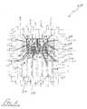
- FIG. 2is a cut-a-way top view of a first integrated circuit 200 that includes a first die 202 , and a second die 204 within a plastic package.
- the first die 202provides an output signal via bond wires 206 , 208 to a first transmission line 210 located on a lead frame (e.g., etched copper).
- the second die 204provides an output signal via bond wires 212 , 214 to a second transmission line 216 located on the lead frame.
- the lead framealso includes a plurality of input/output (I/O) leads (e.g., 218 - 222 ). Bond wires interconnect bonding pads on the dies and the I/O leads.
- I/Oinput/output
- the lead framealso includes at least one transmission line (e.g., 0.1 mm thick in non-exposed areas, and 0.2 mm thick in exposed areas) that cooperates with circuit components within the integrated circuit to provide an integrated circuit with internal matching.
- transmission linee.g., 0.1 mm thick in non-exposed areas, and 0.2 mm thick in exposed areas
- matching circuit componentssuch as capacitors and/or inductors (not shown) located on the first die 202 are connected to the first transmission line 210 .
- a first capacitor located on the first die 202is connected to a first selected location on the transmission line 210 by bond wires 230 , 231 . Two bond wires are shown in this embodiment for current handling.
- a skilled personwill recognize of course that more or less bond wires may be used to connect the matching circuit component on the die to the transmission line, depending upon the current handling required.
- a second capacitor(now shown) may be located on the die 202 and connected to a second location (e.g., location 240 ) on the transmission line 210 by bond wires (not shown) to provide a matching circuit that is functionally similar to the circuit 106 illustrated in FIG. 1.
- the matching networkis located within the integrated circuit. That is, the integrated circuit of FIG. 2 includes internal matching.
- the second die 204may also include an internal matching network that is established by connecting a matching circuit component(s) within the second die 204 , to the transmission line 216 for example via bond wires 242 , 244 .
- FIG. 3is a functional block diagram illustration of the internal matching network associated with the first die 202 illustrated in FIG. 2.
- an output amplifier 246 located on the die 202provides an output signal that is conducted by the transmission line 210 to an I/O lead 248 .
- a first lead of a capacitor 252 located on the die 202is connected to a first select location 254 on the transmission line 210 via the bond wires 230 , 231 .
- a second lead of the capacitor 252is connected to a first electrical potential, for example ground.
- thisprovides an impedance matching circuit 258 that is located within the integrated circuit 200 .
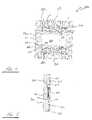
- FIG. 4is a cut-a-way top view of a second integrated circuit 300 that includes a die (not shown in FIG. 4), that is placed onto a die paddle 302 of a lead frame 306 (e.g., etched copper) that includes plurality of I/O leads (e.g., 308 - 314 ). Interconnect bonding pads located on the die are connected for example via bond wires to the I/O leads.
- the lead frame 306also includes a first transmission line 320 shown in cross hatch.
- the packagealso includes a second transmission line 322 that is also not exposed on the exterior of the package.
- the first transmission line 320is associated with a first output signal from the package, while the second transmission line is associated with a second output signal from the package.
- Matching circuit componentssuch as capacitors and/or inductors (not shown) located on the die and associated with the first output signal, are connected between a first electrical potential (e.g., ground) and at least one select location on the first transmission line 320 .
- FIG. 5illustrates a section taken along line A-A in FIG. 4.
- a die 402is located on the paddle 302 , and at least one bond wire 404 connects lead 313 and a bond pad (not shown) on the die 402 .
- FIG. 6illustrates a bottom view of the second integrated circuit.
- the lead frameincludes the paddle 302 and the plurality of I/O leads, for example 308 - 314 .
- the packagealso includes a plurality of exposed wire bond support structures 510 - 517 that represent select locations along the transmission lines at which the matching circuit components may be connected.
- these support structuresare connection points for bond wires between the matching components on the die, and the transmission lines within the lead frame of the package.
- bonding wire 430(FIG. 5) runs between a matching component (e.g., a capacitor) on the die 402 and the support structure 511 (i.e., a select location on the transmission line 320 ).
- FIG. 7is a side view of the package of FIG. 5.
- FIG. 8is a cut-a-way top view of a third integrated circuit 800 that includes a die 802 , and a lead frame 804 of a third plastic package.
- FIG. 9is a top view of the lead frame 804 of FIG. 8 shown in cross hatch.
- the lead frame 804includes a die paddle 806 and a plurality of I/O leads 808 - 823 .
- the lead framealso includes a transmission line 826 that connects an output 828 on the die 802 to selected I/O leads 808 - 812 .
- the die output 828is connected to the transmission line 826 by a plurality of bond wires 831 .
- the die 802includes at least one component (e.g., a capacitor, inductor, etc) of an impedance matching/transformation network.
- the network matching component within the dieis connected to a first select location 830 along the transmission line 826 .
- a circuit configuration as shown in FIG. 3is provided.
- the matching circuit component within the die 802may be connected to the transmission line 826 at one of a plurality of select locations 832 - 836 along the transmission line, rather than at the selected location 830 .
- the integrated circuit 800is 4 mm ⁇ 4 mm (i.e., L 850 is equal to 4 cm).
- the path length of the transmission line 826will vary pending upon the select location (e.g., 830 ) along the transmission line that the matching circuit component is connected to.
- FIG. 10is a bottom view of the lead frame of FIG. 8 shown in cross hatch. In this view, support structures associated with the select locations 830 , 836 along the transmission line 826 (FIG. 9) are exposed on the underside of the integrated circuit 800 .
- FIG. 11is a cut-a-way top view of a fourth integrated circuit 1100 that includes a die 1102 , and a lead frame 1104 of a fourth plastic package.
- This embodimentis substantially the same as the embodiment illustrated in FIGS. 8 - 10 , with the principal exception that an internal matching network component 1106 (e.g., a capacitor) is located between die paddle 1108 and a first select location 1110 on the transmission line 826 . That is, the internal matching circuit component is not located on the die. However, the internal matching circuit is still resident within the integrated circuit to provide the internal matching.
- an internal matching network component 1106e.g., a capacitor
- FIG. 12is a cut-a-way top view of a fifth integrated circuit 1200 that includes a die 1202 , and a lead frame 1204 of a fifth plastic package.
- This embodimentis substantially the same as the embodiments illustrated in FIGS. 8 - 10 , and FIG. 11, with the principal exception that a first internal matching network component 1206 (e.g., a capacitor) is located between a die paddle 1208 and a first select location 1210 on the transmission line 826 , and second internal matching network component (not shown) is located within the die 1202 and connected to a second select location 1212 on the transmission line.
- a first internal matching network component 1206e.g., a capacitor
- second internal matching network component(not shown) is located within the die 1202 and connected to a second select location 1212 on the transmission line.
- FIG. 13is a functional block diagram illustration of the internal matching network associated with the integrated circuit of FIG. 12.
- an output amplifier 1302 located on the die 1202provides an output signal that is conducted by the transmission line 826 to the I/O lead 808 .
- a first lead of a capacitor 1306 located on the die 1202is connected to the second select location 1212 on the transmission line 826 via bond wires 1314 .
- a second lead of the capacitor 1306 on the dieis connected to a first electrical potential, for example ground.
- a first lead of the capacitor 1206is connected to the first selected location 1210 on the transmission line 826 , while a second lead of the capacitor 1206 is connected to the die paddle (i.e., ground).
- the integrated circuit and package of the present inventionprovide internal impedance matching, thus for example freeing a handset manufacturer (or board manufacturer) from having to provide room on the board for the impedance transformation matching circuitry.
Landscapes
- Engineering & Computer Science (AREA)
- Power Engineering (AREA)
- Computer Hardware Design (AREA)
- Microelectronics & Electronic Packaging (AREA)
- Physics & Mathematics (AREA)
- Condensed Matter Physics & Semiconductors (AREA)
- General Physics & Mathematics (AREA)
- Lead Frames For Integrated Circuits (AREA)
Abstract
Description
- The present invention relates to the field of semiconductor devices, and in particular to an integrated circuit with internal impedance matching[0001]
- In cellular telephones, radio frequency (RF) power amplifiers (PA) are built using a semiconductor device (e.g., silicon or GaAs) that has a low output impedance (e.g., less two ohms). This impedance needs to be transformed to a higher impedance value (e.g., fifty ohms) to connect to filters, switches, diplexers and antennas in the rest of the radio. This impedance transformation network is typically referred to as the “output match.”[0002]
- In addition to transforming a two-ohm impedance to fifty ohms, the output match is typically tuned at the harmonic frequencies to increase efficiency and battery life (e.g., talk time) of the cellular telephone. These harmonic frequencies extend up to 6 GHz. At these frequencies, the distance between the capacitors and other passive components used to construct the output match is critical, for example a distance of 0.001″ is significant. For example, a vendor may specify distances of 0.062″ and 0.416″ in one one-thousandth of an inch of precision between the capacitors and other passive components of the output matching network.[0003]
- The harmonic frequencies present a second problem. The capacitors have parasitic values that become significant at the harmonic frequencies. Since the parasitic values differ from one manufacturer to another, changing vendors for the same value component will yield different results.[0004]
- In producing high volumes (e.g., 30,000,000 per year) these dependencies on a single vendor and tolerances of 0.001″ are costly to manage. Therefore, there is a need for an improved technique for providing an impedance matching network.[0005]
- Briefly, according to an aspect of the present invention, an integrated circuit includes a die that is electrically connected to and housed within a plastic package. The package includes a lead frame comprising a transmission line, at least one input signal lead, and at least one output signal lead that is connected to the transmission line. The die provides an output signal onto the transmission line. At least one select location along the transmission line is connected to a first electrical node through an impedance matching circuit within the integrated circuit.[0006]
- According to another aspect of the present invention, an integrated circuit package includes a lead frame comprising at least one transmission line, at least one input signal lead, and at least one output signal lead. At least one select location along the transmission line is connected to a first electrical node through an impedance matching circuit within the integrated circuit package, wherein the impedance matching circuit is associated with the output signal lead.[0007]
- The impedance matching circuit is located within the integrated circuit. For example, in one embodiment, the impedance matching circuit may be connected between the at least one select location along the transmission line and a die paddle of the lead frame. In another embodiment, the impedance matching circuit may be located within the die, and electrically connected (e.g., by bond wires) to the at least one select location along the transmission line.[0008]
- In one embodiment, at least one select location along the transmission line is wire bonded to a capacitor. The capacitance value of the capacitor and the dimensions of the transmission line are selected to provide the desired matching circuit (i.e., output impedance).[0009]
- Incorporating the transmission line into the lead frame avoids having to place the matching network outside of the integrated circuit. For example, etching the lead frame to provide the transmission line, and placing components (e.g., capacitors, inductors, etc.) of the impedance transform matching circuit on a die and connecting these components on the die between select locations on the transmission line and the first electrical node (e.g., ground) is relatively inexpensive. A second embodiment of placing the impedance matching circuit between the at least one select location along the transmission line and the die paddle is also relatively inexpensive.[0010]
- These and other objects, features and advantages of the present invention will become more apparent in light of the following detailed description of preferred embodiments thereof, as illustrated in the accompanying drawings.[0011]
- FIG. 1 illustrates a functional block diagram of a prior art matching circuit configuration for an RF output signal;[0012]
- FIG. 2 is a cut-a-way top view of a first integrated circuit that includes a first die, and a second die within a first plastic package;[0013]
- FIG. 3 is a functional block diagram illustration of the internal matching network associated with the first die illustrated in FIG. 2;[0014]
- FIG. 4 is a cut-a-way top view of a lead frame of a second integrated circuit that provides at least one output signal;[0015]
- FIG. 5 illustrates a section taken along line A-A in FIG. 4;[0016]
- FIG. 6 illustrates a bottom view of the second plastic package of FIG. 4;[0017]
- FIG. 7 illustrates a side view of the package of FIG. 6;[0018]
- FIG. 8 is a cut-a-way top view of a lead frame of a third integrated circuit that includes an internal matching circuit located within a die;[0019]
- FIG. 9 is a top view of the lead frame of FIG. 8 shown in cross hatch;[0020]
- FIG. 10 is a bottom view of the lead frame of FIG. 8 with exposed sections of the lead frame shown in cross hatch;[0021]
- FIG. 11 is a cut-a-way top view of a lead frame of a fourth integrated circuit that includes an internal matching network located between the die paddle and a first select location on the transmission line;[0022]
- FIG. 12 is a cut-a-way top view of a lead frame of a fifth integrated circuit that includes a first internal matching network component located between the die and a first select location on the transmission line, and a second internal matching network component located between the die paddle and a second select location on the transmission line; and[0023]
- FIG. 13 is a functional block diagram illustration of the internal matching network associated with the integrated circuit of FIG. 12.[0024]
- FIG. 1 illustrates a functional block diagram of a prior art matching circuit configuration[0025]100 that provides an output signal on a
line 102. In one embodiment, the output signal on theline 102 is from an RF power amplifier (PA) within an integratedcircuit 104. Theintegrated circuit 104 provides the output signal on theline 102 to an impedance transformation network106 (also referred to herein as a “matching network”), which provides an impedance matched output signal on aline 108. For example, the impedance matched output signal on theline 108 may for example have an output impedance of fifty ohms, whereas the impedance of the signal on theline 102 may for example be two ohms. The impedance matchingnetwork 106 includes a plurality ofcapacitors C 1110 and C2112 that are precisely positioned to provide the required impedance transformation and harmonic filtering. For example, thecapacitor C 1110 is precisely positioned (e.g., to a 0.001″ tolerance) fromedge 114 of the integratedcircuit 104, while the distance betweencapacitors C 1110 andC 2112 is also precisely controlled. As set forth above, these positioning constraints lead to a problematic and relatively costly matching network that is external to the integratedcircuit 104. - FIG. 2 is a cut-a-way top view of a first integrated[0026]
circuit 200 that includes afirst die 202, and a second die204 within a plastic package. Thefirst die 202 provides an output signal via bond wires206,208 to afirst transmission line 210 located on a lead frame (e.g., etched copper). The second die204 provides an output signal viabond wires second transmission line 216 located on the lead frame. The lead frame also includes a plurality of input/output (I/O) leads (e.g.,218-222). Bond wires interconnect bonding pads on the dies and the I/O leads. According to an aspect of the present invention, the lead frame also includes at least one transmission line (e.g., 0.1 mm thick in non-exposed areas, and 0.2 mm thick in exposed areas) that cooperates with circuit components within the integrated circuit to provide an integrated circuit with internal matching. Specifically, in this embodiment matching circuit components such as capacitors and/or inductors (not shown) located on thefirst die 202 are connected to thefirst transmission line 210. For example, a first capacitor located on thefirst die 202 is connected to a first selected location on thetransmission line 210 bybond wires die 202 and connected to a second location (e.g., location240) on thetransmission line 210 by bond wires (not shown) to provide a matching circuit that is functionally similar to thecircuit 106 illustrated in FIG. 1. However, in the embodiment of FIG. 2, the matching network is located within the integrated circuit. That is, the integrated circuit of FIG. 2 includes internal matching. - The second die[0027]204 may also include an internal matching network that is established by connecting a matching circuit component(s) within the second die204, to the
transmission line 216 for example via bond wires242,244. - FIG. 3 is a functional block diagram illustration of the internal matching network associated with the[0028]
first die 202 illustrated in FIG. 2. For example anoutput amplifier 246 located on thedie 202 provides an output signal that is conducted by thetransmission line 210 to an I/O lead 248. A first lead of a capacitor252 located on thedie 202 is connected to a firstselect location 254 on thetransmission line 210 via thebond wires impedance matching circuit 258 that is located within theintegrated circuit 200. - FIG. 4 is a cut-a-way top view of a second[0029]
integrated circuit 300 that includes a die (not shown in FIG. 4), that is placed onto adie paddle 302 of a lead frame306 (e.g., etched copper) that includes plurality of I/O leads (e.g.,308-314). Interconnect bonding pads located on the die are connected for example via bond wires to the I/O leads. Thelead frame 306 also includes afirst transmission line 320 shown in cross hatch. In this embodiment, the package also includes asecond transmission line 322 that is also not exposed on the exterior of the package. Thefirst transmission line 320 is associated with a first output signal from the package, while the second transmission line is associated with a second output signal from the package. Matching circuit components such as capacitors and/or inductors (not shown) located on the die and associated with the first output signal, are connected between a first electrical potential (e.g., ground) and at least one select location on thefirst transmission line 320. - FIG. 5 illustrates a section taken along line A-A in FIG. 4. A[0030]
die 402 is located on thepaddle 302, and at least onebond wire 404 connects lead313 and a bond pad (not shown) on thedie 402. FIG. 6 illustrates a bottom view of the second integrated circuit. As shown, the lead frame includes thepaddle 302 and the plurality of I/O leads, for example308-314. Referring to FIGS. 5 and 6, the package also includes a plurality of exposed wire bond support structures510-517 that represent select locations along the transmission lines at which the matching circuit components may be connected. For example, in one embodiment, these support structures (e.g., etched copper) are connection points for bond wires between the matching components on the die, and the transmission lines within the lead frame of the package. For example, bonding wire430 (FIG. 5) runs between a matching component (e.g., a capacitor) on thedie 402 and the support structure511 (i.e., a select location on the transmission line320). - FIG. 7 is a side view of the package of FIG. 5.[0031]
- FIG. 8 is a cut-a-way top view of a third[0032]
integrated circuit 800 that includes adie 802, and alead frame 804 of a third plastic package. FIG. 9 is a top view of thelead frame 804 of FIG. 8 shown in cross hatch. Thelead frame 804 includes adie paddle 806 and a plurality of I/O leads808-823. The lead frame also includes atransmission line 826 that connects anoutput 828 on thedie 802 to selected I/O leads808-812. In this embodiment, thedie output 828 is connected to thetransmission line 826 by a plurality ofbond wires 831. Thedie 802 includes at least one component (e.g., a capacitor, inductor, etc) of an impedance matching/transformation network. The network matching component within the die is connected to a firstselect location 830 along thetransmission line 826. As a result, a circuit configuration as shown in FIG. 3 is provided. Depending upon the impedance matching and filtering requirements, the matching circuit component within thedie 802 may be connected to thetransmission line 826 at one of a plurality of select locations832-836 along the transmission line, rather than at the selectedlocation 830. In the embodiment of FIG. 8, theintegrated circuit 800 is 4 mm×4 mm (i.e.,L 850 is equal to 4 cm). As shown in FIG. 8, the path length of thetransmission line 826 will vary pending upon the select location (e.g.,830) along the transmission line that the matching circuit component is connected to. - FIG. 10 is a bottom view of the lead frame of FIG. 8 shown in cross hatch. In this view, support structures associated with the[0033]
select locations integrated circuit 800. - FIG. 11 is a cut-a-way top view of a fourth[0034]
integrated circuit 1100 that includes adie 1102, and alead frame 1104 of a fourth plastic package. This embodiment is substantially the same as the embodiment illustrated in FIGS.8-10, with the principal exception that an internal matching network component1106 (e.g., a capacitor) is located betweendie paddle 1108 and a firstselect location 1110 on thetransmission line 826. That is, the internal matching circuit component is not located on the die. However, the internal matching circuit is still resident within the integrated circuit to provide the internal matching. - FIG. 12 is a cut-a-way top view of a fifth[0035]
integrated circuit 1200 that includes adie 1202, and alead frame 1204 of a fifth plastic package. This embodiment is substantially the same as the embodiments illustrated in FIGS.8-10, and FIG. 11, with the principal exception that a first internal matching network component1206 (e.g., a capacitor) is located between a die paddle1208 and a firstselect location 1210 on thetransmission line 826, and second internal matching network component (not shown) is located within thedie 1202 and connected to a secondselect location 1212 on the transmission line. - FIG. 13 is a functional block diagram illustration of the internal matching network associated with the integrated circuit of FIG. 12. For example, an[0036]
output amplifier 1302 located on thedie 1202 provides an output signal that is conducted by thetransmission line 826 to the I/O lead 808. A first lead of acapacitor 1306 located on thedie 1202 is connected to the secondselect location 1212 on thetransmission line 826 viabond wires 1314. A second lead of thecapacitor 1306 on the die is connected to a first electrical potential, for example ground. A first lead of thecapacitor 1206 is connected to the first selectedlocation 1210 on thetransmission line 826, while a second lead of thecapacitor 1206 is connected to the die paddle (i.e., ground). - Advantageously, the integrated circuit and package of the present invention provide internal impedance matching, thus for example freeing a handset manufacturer (or board manufacturer) from having to provide room on the board for the impedance transformation matching circuitry.[0037]
- Although the present invention has been discussed in the context of a package for power amplifiers for wireless handsets, it is contemplated that the many other applications will find it desirable to replace applications that require impedance matching, conventionally performed on a circuit board or as lumped element components, with matching circuitry contained within the integrated circuit. Advantageously, this obviates many of the manufacturability problems associated with having to precisely position the components of the matching circuit. In addition, although the matching network components have been connected between the transmission line and ground, the first electrical potential does not necessarily have to be ground.[0038]
- Although the present invention has been shown and described with respect to several preferred embodiments thereof, various changes, omissions and additions to the form and detail thereof, may be made therein, without departing from the spirit and scope of the invention.[0039]
Claims (18)
Priority Applications (7)
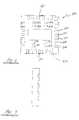
| Application Number | Priority Date | Filing Date | Title |
|---|---|---|---|
| US10/142,250US6828658B2 (en) | 2002-05-09 | 2002-05-09 | Package for integrated circuit with internal matching |
| US10/427,330US6903447B2 (en) | 2002-05-09 | 2003-05-01 | Apparatus, methods and articles of manufacture for packaging an integrated circuit with internal matching |
| EP03750119AEP1502309A4 (en) | 2002-05-09 | 2003-05-08 | INTEGRATED CIRCUIT WITH INTERNAL IMPEDANCE ADAPTATION CIRCUIT |
| JP2004504309AJP2005524995A (en) | 2002-05-09 | 2003-05-08 | Integrated circuit having internal impedance matching circuit |
| AU2003267226AAU2003267226A1 (en) | 2002-05-09 | 2003-05-08 | Integrated circuit with internal impedance matching circuit |
| PCT/US2003/014893WO2003096439A1 (en) | 2002-05-09 | 2003-05-08 | Integrated circuit with internal impedance matching circuit |
| KR10-2004-7018046AKR20050006241A (en) | 2002-05-09 | 2003-05-08 | Integrated circuit with internal impedance matching circuit |
Applications Claiming Priority (1)
| Application Number | Priority Date | Filing Date | Title |
|---|---|---|---|
| US10/142,250US6828658B2 (en) | 2002-05-09 | 2002-05-09 | Package for integrated circuit with internal matching |
Related Child Applications (1)
| Application Number | Title | Priority Date | Filing Date |
|---|---|---|---|
| US10/427,330Continuation-In-PartUS6903447B2 (en) | 2002-05-09 | 2003-05-01 | Apparatus, methods and articles of manufacture for packaging an integrated circuit with internal matching |
Publications (2)
| Publication Number | Publication Date |
|---|---|
| US20030209784A1true US20030209784A1 (en) | 2003-11-13 |
| US6828658B2 US6828658B2 (en) | 2004-12-07 |
Family
ID=29399844
Family Applications (1)
| Application Number | Title | Priority Date | Filing Date |
|---|---|---|---|
| US10/142,250Expired - LifetimeUS6828658B2 (en) | 2002-05-09 | 2002-05-09 | Package for integrated circuit with internal matching |
Country Status (1)
| Country | Link |
|---|---|
| US (1) | US6828658B2 (en) |
Cited By (20)
| Publication number | Priority date | Publication date | Assignee | Title |
|---|---|---|---|---|
| US20060197198A1 (en)* | 2004-02-05 | 2006-09-07 | St Assembly Test Services Ltd. | Semiconductor package with passive device integration |
| US20070241423A1 (en)* | 2006-04-14 | 2007-10-18 | Taylor William P | Methods and apparatus for integrated circuit having multiple dies with at least one on chip capacitor |
| US20070268094A1 (en)* | 2006-05-19 | 2007-11-22 | Sony Corporation | Semiconductor device interconnecting unit, semiconductor device, high-frequency module, and semiconductor device interconnecting method |
| US20070285187A1 (en)* | 2006-05-19 | 2007-12-13 | Sony Corporation | Semiconductor device interconnecting unit, semiconductor device and high-frequency module |
| US20080013298A1 (en)* | 2006-07-14 | 2008-01-17 | Nirmal Sharma | Methods and apparatus for passive attachment of components for integrated circuits |
| US20080034582A1 (en)* | 2006-04-14 | 2008-02-14 | Taylor William P | Methods for sensor having capacitor on chip |
| EP1675178A3 (en)* | 2004-11-30 | 2008-05-28 | M/A-Com, Inc. | Connection arrangement for micro lead frame plastic packages |
| US20080142935A1 (en)* | 2005-02-24 | 2008-06-19 | Freescale Semicondutor, Inc. | Lead-Frame Circuit Package |
| US20100052424A1 (en)* | 2008-08-26 | 2010-03-04 | Taylor William P | Methods and apparatus for integrated circuit having integrated energy storage device |
| US8093670B2 (en) | 2008-07-24 | 2012-01-10 | Allegro Microsystems, Inc. | Methods and apparatus for integrated circuit having on chip capacitor with eddy current reductions |
| US8629539B2 (en) | 2012-01-16 | 2014-01-14 | Allegro Microsystems, Llc | Methods and apparatus for magnetic sensor having non-conductive die paddle |
| US9411025B2 (en) | 2013-04-26 | 2016-08-09 | Allegro Microsystems, Llc | Integrated circuit package having a split lead frame and a magnet |
| US9494660B2 (en) | 2012-03-20 | 2016-11-15 | Allegro Microsystems, Llc | Integrated circuit package having a split lead frame |
| US9666788B2 (en) | 2012-03-20 | 2017-05-30 | Allegro Microsystems, Llc | Integrated circuit package having a split lead frame |
| US9812588B2 (en) | 2012-03-20 | 2017-11-07 | Allegro Microsystems, Llc | Magnetic field sensor integrated circuit with integral ferromagnetic material |
| US10234513B2 (en) | 2012-03-20 | 2019-03-19 | Allegro Microsystems, Llc | Magnetic field sensor integrated circuit with integral ferromagnetic material |
| US10411498B2 (en) | 2015-10-21 | 2019-09-10 | Allegro Microsystems, Llc | Apparatus and methods for extending sensor integrated circuit operation through a power disturbance |
| US10978897B2 (en) | 2018-04-02 | 2021-04-13 | Allegro Microsystems, Llc | Systems and methods for suppressing undesirable voltage supply artifacts |
| US10991644B2 (en) | 2019-08-22 | 2021-04-27 | Allegro Microsystems, Llc | Integrated circuit package having a low profile |
| US12341138B2 (en)* | 2021-10-01 | 2025-06-24 | TDK—Micronas GmbH | Dual die integrated circuit system in an integrated circuit package with two separate supply domains |
Families Citing this family (5)
| Publication number | Priority date | Publication date | Assignee | Title |
|---|---|---|---|---|
| US7002238B2 (en)* | 2003-10-23 | 2006-02-21 | Broadcom Corporation | Use of a down-bond as a controlled inductor in integrated circuit applications |
| TWI245378B (en)* | 2003-11-05 | 2005-12-11 | Advanced Semiconductor Eng | Substrate for use in forming electronic package |
| US7999364B2 (en)* | 2006-08-24 | 2011-08-16 | Monolithic Power Systems, Inc. | Method and flip chip structure for power devices |
| US7882482B2 (en)* | 2007-10-12 | 2011-02-01 | Monolithic Power Systems, Inc. | Layout schemes and apparatus for high performance DC-DC output stage |
| US9515032B1 (en) | 2015-08-13 | 2016-12-06 | Win Semiconductors Corp. | High-frequency package |
Citations (12)
| Publication number | Priority date | Publication date | Assignee | Title |
|---|---|---|---|---|
| US4353047A (en)* | 1979-01-29 | 1982-10-05 | Nippon Electric Co., Ltd. | (1-x)BaO.xTiO2 System dielectric material for use in a microwave device |
| US5557144A (en)* | 1993-01-29 | 1996-09-17 | Anadigics, Inc. | Plastic packages for microwave frequency applications |
| US5696466A (en)* | 1995-12-08 | 1997-12-09 | The Whitaker Corporation | Heterolithic microwave integrated impedance matching circuitry and method of manufacture |
| US5963089A (en)* | 1996-09-12 | 1999-10-05 | Sony Corporation | Semiconductor amplifying apparatus and communication terminal apparatus |
| US6016084A (en)* | 1996-12-27 | 2000-01-18 | Canon Kabushiki Kaisha | Method for connecting printed circuit board with housing, and electronic instrument having connection structure according to the connecting method |
| US6049126A (en)* | 1995-12-14 | 2000-04-11 | Nec Corporation | Semiconductor package and amplifier employing the same |
| US6084300A (en)* | 1997-04-21 | 2000-07-04 | Oki Electric Industry Co., Ltd. | Compact resin-sealed semiconductor device |
| US6188237B1 (en)* | 1998-05-25 | 2001-02-13 | Kabushiki Kaisha Toshiba | Impedance matching circuit, high speed semiconductor integrated circuit employing the same and computer system employing the integrated circuit |
| US6289204B1 (en)* | 1998-07-09 | 2001-09-11 | Motorola, Inc. | Integration of a receiver front-end in multilayer ceramic integrated circuit technology |
| US6392298B1 (en)* | 2000-02-28 | 2002-05-21 | Ericsson Inc. | Functional lid for RF power package |
| US6456125B1 (en)* | 2000-09-29 | 2002-09-24 | Fujitsu Quantum Devices Limited | Distributed high frequency circuit equipped with bias bypass line to reduce chip area |
| US6528879B2 (en)* | 2000-09-20 | 2003-03-04 | Sanyo Electric Co., Ltd. | Semiconductor device and semiconductor module |
- 2002
- 2002-05-09USUS10/142,250patent/US6828658B2/ennot_activeExpired - Lifetime
Patent Citations (12)
| Publication number | Priority date | Publication date | Assignee | Title |
|---|---|---|---|---|
| US4353047A (en)* | 1979-01-29 | 1982-10-05 | Nippon Electric Co., Ltd. | (1-x)BaO.xTiO2 System dielectric material for use in a microwave device |
| US5557144A (en)* | 1993-01-29 | 1996-09-17 | Anadigics, Inc. | Plastic packages for microwave frequency applications |
| US5696466A (en)* | 1995-12-08 | 1997-12-09 | The Whitaker Corporation | Heterolithic microwave integrated impedance matching circuitry and method of manufacture |
| US6049126A (en)* | 1995-12-14 | 2000-04-11 | Nec Corporation | Semiconductor package and amplifier employing the same |
| US5963089A (en)* | 1996-09-12 | 1999-10-05 | Sony Corporation | Semiconductor amplifying apparatus and communication terminal apparatus |
| US6016084A (en)* | 1996-12-27 | 2000-01-18 | Canon Kabushiki Kaisha | Method for connecting printed circuit board with housing, and electronic instrument having connection structure according to the connecting method |
| US6084300A (en)* | 1997-04-21 | 2000-07-04 | Oki Electric Industry Co., Ltd. | Compact resin-sealed semiconductor device |
| US6188237B1 (en)* | 1998-05-25 | 2001-02-13 | Kabushiki Kaisha Toshiba | Impedance matching circuit, high speed semiconductor integrated circuit employing the same and computer system employing the integrated circuit |
| US6289204B1 (en)* | 1998-07-09 | 2001-09-11 | Motorola, Inc. | Integration of a receiver front-end in multilayer ceramic integrated circuit technology |
| US6392298B1 (en)* | 2000-02-28 | 2002-05-21 | Ericsson Inc. | Functional lid for RF power package |
| US6528879B2 (en)* | 2000-09-20 | 2003-03-04 | Sanyo Electric Co., Ltd. | Semiconductor device and semiconductor module |
| US6456125B1 (en)* | 2000-09-29 | 2002-09-24 | Fujitsu Quantum Devices Limited | Distributed high frequency circuit equipped with bias bypass line to reduce chip area |
Cited By (36)
| Publication number | Priority date | Publication date | Assignee | Title |
|---|---|---|---|---|
| US7960816B2 (en)* | 2004-02-05 | 2011-06-14 | St Assembly Test Services Ltd. | Semiconductor package with passive device integration |
| US20060197198A1 (en)* | 2004-02-05 | 2006-09-07 | St Assembly Test Services Ltd. | Semiconductor package with passive device integration |
| EP1675178A3 (en)* | 2004-11-30 | 2008-05-28 | M/A-Com, Inc. | Connection arrangement for micro lead frame plastic packages |
| US20080142935A1 (en)* | 2005-02-24 | 2008-06-19 | Freescale Semicondutor, Inc. | Lead-Frame Circuit Package |
| US8736034B2 (en) | 2005-02-24 | 2014-05-27 | Freescale Semiconductor, Inc. | Lead-frame circuit package |
| US7676914B2 (en)* | 2006-04-14 | 2010-03-16 | Allegro Microsystems, Inc. | Methods for sensor having capacitor on chip |
| US20080034582A1 (en)* | 2006-04-14 | 2008-02-14 | Taylor William P | Methods for sensor having capacitor on chip |
| US20070241423A1 (en)* | 2006-04-14 | 2007-10-18 | Taylor William P | Methods and apparatus for integrated circuit having multiple dies with at least one on chip capacitor |
| US7687882B2 (en) | 2006-04-14 | 2010-03-30 | Allegro Microsystems, Inc. | Methods and apparatus for integrated circuit having multiple dies with at least one on chip capacitor |
| US20070285187A1 (en)* | 2006-05-19 | 2007-12-13 | Sony Corporation | Semiconductor device interconnecting unit, semiconductor device and high-frequency module |
| US20070268094A1 (en)* | 2006-05-19 | 2007-11-22 | Sony Corporation | Semiconductor device interconnecting unit, semiconductor device, high-frequency module, and semiconductor device interconnecting method |
| US7760045B2 (en) | 2006-05-19 | 2010-07-20 | Sony Corporation | Semiconductor device interconnecting unit, semiconductor device, high-frequency module, and semiconductor device interconnecting method |
| US7907924B2 (en) | 2006-05-19 | 2011-03-15 | Sony Corporation | Semiconductor device interconnecting unit, semiconductor device and high-frequency module having a millimeter wave band |
| US20080013298A1 (en)* | 2006-07-14 | 2008-01-17 | Nirmal Sharma | Methods and apparatus for passive attachment of components for integrated circuits |
| US9228860B2 (en) | 2006-07-14 | 2016-01-05 | Allegro Microsystems, Llc | Sensor and method of providing a sensor |
| US8093670B2 (en) | 2008-07-24 | 2012-01-10 | Allegro Microsystems, Inc. | Methods and apparatus for integrated circuit having on chip capacitor with eddy current reductions |
| US20100052424A1 (en)* | 2008-08-26 | 2010-03-04 | Taylor William P | Methods and apparatus for integrated circuit having integrated energy storage device |
| US9299915B2 (en) | 2012-01-16 | 2016-03-29 | Allegro Microsystems, Llc | Methods and apparatus for magnetic sensor having non-conductive die paddle |
| US9620705B2 (en) | 2012-01-16 | 2017-04-11 | Allegro Microsystems, Llc | Methods and apparatus for magnetic sensor having non-conductive die paddle |
| US10333055B2 (en) | 2012-01-16 | 2019-06-25 | Allegro Microsystems, Llc | Methods for magnetic sensor having non-conductive die paddle |
| US8629539B2 (en) | 2012-01-16 | 2014-01-14 | Allegro Microsystems, Llc | Methods and apparatus for magnetic sensor having non-conductive die paddle |
| US9666788B2 (en) | 2012-03-20 | 2017-05-30 | Allegro Microsystems, Llc | Integrated circuit package having a split lead frame |
| US10916665B2 (en) | 2012-03-20 | 2021-02-09 | Allegro Microsystems, Llc | Magnetic field sensor integrated circuit with an integrated coil |
| US9812588B2 (en) | 2012-03-20 | 2017-11-07 | Allegro Microsystems, Llc | Magnetic field sensor integrated circuit with integral ferromagnetic material |
| US10230006B2 (en) | 2012-03-20 | 2019-03-12 | Allegro Microsystems, Llc | Magnetic field sensor integrated circuit with an electromagnetic suppressor |
| US10234513B2 (en) | 2012-03-20 | 2019-03-19 | Allegro Microsystems, Llc | Magnetic field sensor integrated circuit with integral ferromagnetic material |
| US11961920B2 (en) | 2012-03-20 | 2024-04-16 | Allegro Microsystems, Llc | Integrated circuit package with magnet having a channel |
| US11828819B2 (en) | 2012-03-20 | 2023-11-28 | Allegro Microsystems, Llc | Magnetic field sensor integrated circuit with integral ferromagnetic material |
| US9494660B2 (en) | 2012-03-20 | 2016-11-15 | Allegro Microsystems, Llc | Integrated circuit package having a split lead frame |
| US11677032B2 (en) | 2012-03-20 | 2023-06-13 | Allegro Microsystems, Llc | Sensor integrated circuit with integrated coil and element in central region of mold material |
| US11444209B2 (en) | 2012-03-20 | 2022-09-13 | Allegro Microsystems, Llc | Magnetic field sensor integrated circuit with an integrated coil enclosed with a semiconductor die by a mold material |
| US9411025B2 (en) | 2013-04-26 | 2016-08-09 | Allegro Microsystems, Llc | Integrated circuit package having a split lead frame and a magnet |
| US10411498B2 (en) | 2015-10-21 | 2019-09-10 | Allegro Microsystems, Llc | Apparatus and methods for extending sensor integrated circuit operation through a power disturbance |
| US10978897B2 (en) | 2018-04-02 | 2021-04-13 | Allegro Microsystems, Llc | Systems and methods for suppressing undesirable voltage supply artifacts |
| US10991644B2 (en) | 2019-08-22 | 2021-04-27 | Allegro Microsystems, Llc | Integrated circuit package having a low profile |
| US12341138B2 (en)* | 2021-10-01 | 2025-06-24 | TDK—Micronas GmbH | Dual die integrated circuit system in an integrated circuit package with two separate supply domains |
Also Published As
| Publication number | Publication date |
|---|---|
| US6828658B2 (en) | 2004-12-07 |
Similar Documents
| Publication | Publication Date | Title |
|---|---|---|
| US6828658B2 (en) | Package for integrated circuit with internal matching | |
| US7795728B2 (en) | Electronic component | |
| US6424223B1 (en) | MMIC power amplifier with wirebond output matching circuit | |
| US7149496B2 (en) | High-frequency module and radio communication apparatus | |
| KR100839067B1 (en) | Electronic circuit module and its manufacturing method | |
| US7119623B2 (en) | Output circuit for a semiconductor amplifier element | |
| US5438305A (en) | High frequency module including a flexible substrate | |
| US20030060172A1 (en) | Radio frequency module | |
| EP1094538A2 (en) | Multilayered ceramic RF device | |
| EP0979559A1 (en) | Amplifier module with two power amplifiers for dual band cellular phones | |
| US6903447B2 (en) | Apparatus, methods and articles of manufacture for packaging an integrated circuit with internal matching | |
| US6414387B1 (en) | Semiconductor device including a chip having high-frequency circuit blocks | |
| JPH10242377A (en) | High frequency power amplifier module | |
| JPH05167302A (en) | High frequency power amplifier circuit device and high frequency module including said circuit device | |
| US6049126A (en) | Semiconductor package and amplifier employing the same | |
| US5917233A (en) | Integrated circuit having a parasitic resonance filter | |
| JP2006528854A (en) | Small impedance conversion circuit | |
| US6642617B2 (en) | Semiconductor device | |
| JP2011176061A (en) | Semiconductor device | |
| EP1502309A1 (en) | Integrated circuit with internal impedance matching circuit | |
| JP2006080662A (en) | Semiconductor transistor with built-in matching circuit, monolithic amplifier and multistage amplifier | |
| WO2004112241A1 (en) | High-frequency power amplifier module | |
| US6624703B1 (en) | Terminal arrangement for an electrical device | |
| JP2002171144A (en) | High frequency amplifier | |
| JP2006148268A (en) | Power amplification module |
Legal Events
| Date | Code | Title | Description |
|---|---|---|---|
| AS | Assignment | Owner name:M/A COM, INC., MASSACHUSETTS Free format text:ASSIGNMENT OF ASSIGNORS INTEREST;ASSIGNORS:SCHMITZ, NORBERT A.;GIACCHINO, RICHARD J.;STRUBLE, WAYNE M.;REEL/FRAME:013171/0081;SIGNING DATES FROM 20020603 TO 20020801 | |
| STCF | Information on status: patent grant | Free format text:PATENTED CASE | |
| FPAY | Fee payment | Year of fee payment:4 | |
| REMI | Maintenance fee reminder mailed | ||
| AS | Assignment | Owner name:COBHAM DEFENSE ELECTRONIC SYSTEMS CORPORATION, MAS Free format text:ASSIGNMENT OF ASSIGNORS INTEREST;ASSIGNORS:M/A COM, INC.;RAYCHEM INTERNATIONAL;TYCO ELECTRONICS CORPORATION;AND OTHERS;REEL/FRAME:022266/0400;SIGNING DATES FROM 20080108 TO 20090113 Owner name:COBHAM DEFENSE ELECTRONIC SYSTEMS CORPORATION,MASS Free format text:ASSIGNMENT OF ASSIGNORS INTEREST;ASSIGNORS:M/A COM, INC.;RAYCHEM INTERNATIONAL;TYCO ELECTRONICS CORPORATION;AND OTHERS;SIGNING DATES FROM 20080108 TO 20090113;REEL/FRAME:022266/0400 Owner name:COBHAM DEFENSE ELECTRONIC SYSTEMS CORPORATION, MAS Free format text:ASSIGNMENT OF ASSIGNORS INTEREST;ASSIGNORS:M/A COM, INC.;RAYCHEM INTERNATIONAL;TYCO ELECTRONICS CORPORATION;AND OTHERS;SIGNING DATES FROM 20080108 TO 20090113;REEL/FRAME:022266/0400 | |
| AS | Assignment | Owner name:COBHAM DEFENSE ELECTRONIC SYSTEMS CORPORATION, MAS Free format text:SECURITY AGREEMENT;ASSIGNOR:KIWI STONE ACQUISITION CORP.;REEL/FRAME:022482/0016 Effective date:20090330 Owner name:COBHAM DEFENSE ELECTRONIC SYSTEMS CORPORATION,MASS Free format text:SECURITY AGREEMENT;ASSIGNOR:KIWI STONE ACQUISITION CORP.;REEL/FRAME:022482/0016 Effective date:20090330 | |
| AS | Assignment | Owner name:KIWI STONE ACQUISITION CORPORATION, CALIFORNIA Free format text:ASSIGNMENT OF ASSIGNORS INTEREST;ASSIGNOR:COBHAM DEFENSE ELECTRONIC SYSTEMS CORPORATION;REEL/FRAME:022714/0890 Effective date:20090521 Owner name:KIWI STONE ACQUISITION CORPORATION,CALIFORNIA Free format text:ASSIGNMENT OF ASSIGNORS INTEREST;ASSIGNOR:COBHAM DEFENSE ELECTRONIC SYSTEMS CORPORATION;REEL/FRAME:022714/0890 Effective date:20090521 | |
| AS | Assignment | Owner name:M/A-COM TECHNOLOGY SOLUTIONS HOLDINGS, INC., MASSA Free format text:CHANGE OF NAME;ASSIGNOR:KIWI STONE ACQUISITION CORP.;REEL/FRAME:023476/0069 Effective date:20090526 Owner name:M/A-COM TECHNOLOGY SOLUTIONS HOLDINGS, INC.,MASSAC Free format text:CHANGE OF NAME;ASSIGNOR:KIWI STONE ACQUISITION CORP.;REEL/FRAME:023476/0069 Effective date:20090526 | |
| AS | Assignment | Owner name:RBS BUSINESS CAPITAL, A DIVISION OF RBS ASSET FINA Free format text:SECURITY AGREEMENT;ASSIGNORS:MIMIX BROADBAND, INC.;M/A-COM TECHNOLOGY SOLUTIONS HOLDINGS, INC.;REEL/FRAME:025444/0920 Effective date:20101203 | |
| AS | Assignment | Owner name:M/A-COM TECHNOLOGY SOLUTIONS HOLDINGS, INC., MASSA Free format text:RELEASE BY SECURED PARTY;ASSIGNOR:COBHAM DEFENSE ELECTRONIC SYSTEMS CORPORATION;REEL/FRAME:025445/0947 Effective date:20101203 | |
| AS | Assignment | Owner name:JPMORGAN CHASE BANK, N.A., AS ADMINISTRATIVE AGENT Free format text:SECURITY AGREEMENT;ASSIGNOR:M/A-COM TECHNOLOGY SOLUTIONS HOLDINGS, INC.;REEL/FRAME:027015/0444 Effective date:20110930 | |
| AS | Assignment | Owner name:M/A-COM TECHNOLOGY SOLUTIONS HOLDINGS, INC., MASSA Free format text:RELEASE OF SECURITY INTEREST RECORDED AT REEL/FRAME 25444/920;ASSIGNOR:RBS BUSINESS CAPITAL, A DIVISION OF RBS ASSET FINANCE, INC., AS ADMINISTRATIVE AGENT;REEL/FRAME:027028/0021 Effective date:20110930 Owner name:MIMIX BROADBAND, INC., MASSACHUSETTS Free format text:RELEASE OF SECURITY INTEREST RECORDED AT REEL/FRAME 25444/920;ASSIGNOR:RBS BUSINESS CAPITAL, A DIVISION OF RBS ASSET FINANCE, INC., AS ADMINISTRATIVE AGENT;REEL/FRAME:027028/0021 Effective date:20110930 | |
| FPAY | Fee payment | Year of fee payment:8 | |
| AS | Assignment | Owner name:JPMORGAN CHASE BANK, N.A., AS ADMINISTRATIVE AGENT Free format text:SECURITY AGREEMENT;ASSIGNOR:M/A-COM TECHNOLOGY SOLUTIONS HOLDINGS, INC.;REEL/FRAME:031314/0183 Effective date:20130926 | |
| FEPP | Fee payment procedure | Free format text:PAYOR NUMBER ASSIGNED (ORIGINAL EVENT CODE: ASPN); ENTITY STATUS OF PATENT OWNER: LARGE ENTITY | |
| AS | Assignment | Owner name:M/A-COM TECHNOLOGY SOLUTIONS HOLDINGS, INC., MASSA Free format text:RELEASE BY SECURED PARTY;ASSIGNOR:JPMORGAN CHASE BANK, N.A.;REEL/FRAME:032857/0032 Effective date:20140508 | |
| AS | Assignment | Owner name:GOLDMAN SACHS BANK USA, NEW YORK Free format text:SECURITY INTEREST;ASSIGNORS:M/A-COM TECHNOLOGY SOLUTIONS HOLDINGS, INC.;MINDSPEED TECHNOLOGIES, INC.;BROOKTREE CORPORATION;REEL/FRAME:032859/0374 Effective date:20140508 | |
| FPAY | Fee payment | Year of fee payment:12 | |
| AS | Assignment | Owner name:MACOM TECHNOLOGY SOLUTIONS HOLDINGS, INC., MASSACH Free format text:CHANGE OF NAME;ASSIGNOR:M/A-COM TECHNOLOGY SOLUTIONS HOLDINGS, INC.;REEL/FRAME:039139/0826 Effective date:20160601 |