US20030207540A1 - Atomic layer-deposited laaio3 films for gate dielectrics - Google Patents
Atomic layer-deposited laaio3 films for gate dielectricsDownload PDFInfo
- Publication number
- US20030207540A1 US20030207540A1US10/137,499US13749902AUS2003207540A1US 20030207540 A1US20030207540 A1US 20030207540A1US 13749902 AUS13749902 AUS 13749902AUS 2003207540 A1US2003207540 A1US 2003207540A1
- Authority
- US
- United States
- Prior art keywords
- pulsing
- reaction chamber
- source gas
- source
- substrate
- Prior art date
- Legal status (The legal status is an assumption and is not a legal conclusion. Google has not performed a legal analysis and makes no representation as to the accuracy of the status listed.)
- Granted
Links
Images


Classifications
- H—ELECTRICITY
- H01—ELECTRIC ELEMENTS
- H01L—SEMICONDUCTOR DEVICES NOT COVERED BY CLASS H10
- H01L21/00—Processes or apparatus adapted for the manufacture or treatment of semiconductor or solid state devices or of parts thereof
- H01L21/02—Manufacture or treatment of semiconductor devices or of parts thereof
- H01L21/04—Manufacture or treatment of semiconductor devices or of parts thereof the devices having potential barriers, e.g. a PN junction, depletion layer or carrier concentration layer
- H01L21/18—Manufacture or treatment of semiconductor devices or of parts thereof the devices having potential barriers, e.g. a PN junction, depletion layer or carrier concentration layer the devices having semiconductor bodies comprising elements of Group IV of the Periodic Table or AIIIBV compounds with or without impurities, e.g. doping materials
- H01L21/28—Manufacture of electrodes on semiconductor bodies using processes or apparatus not provided for in groups H01L21/20 - H01L21/268
- H01L21/28008—Making conductor-insulator-semiconductor electrodes
- H01L21/28017—Making conductor-insulator-semiconductor electrodes the insulator being formed after the semiconductor body, the semiconductor being silicon
- H01L21/28158—Making the insulator
- H01L21/28167—Making the insulator on single crystalline silicon, e.g. using a liquid, i.e. chemical oxidation
- H01L21/28185—Making the insulator on single crystalline silicon, e.g. using a liquid, i.e. chemical oxidation with a treatment, e.g. annealing, after the formation of the gate insulator and before the formation of the definitive gate conductor
- H—ELECTRICITY
- H01—ELECTRIC ELEMENTS
- H01L—SEMICONDUCTOR DEVICES NOT COVERED BY CLASS H10
- H01L21/00—Processes or apparatus adapted for the manufacture or treatment of semiconductor or solid state devices or of parts thereof
- H01L21/02—Manufacture or treatment of semiconductor devices or of parts thereof
- H01L21/04—Manufacture or treatment of semiconductor devices or of parts thereof the devices having potential barriers, e.g. a PN junction, depletion layer or carrier concentration layer
- H01L21/18—Manufacture or treatment of semiconductor devices or of parts thereof the devices having potential barriers, e.g. a PN junction, depletion layer or carrier concentration layer the devices having semiconductor bodies comprising elements of Group IV of the Periodic Table or AIIIBV compounds with or without impurities, e.g. doping materials
- H01L21/28—Manufacture of electrodes on semiconductor bodies using processes or apparatus not provided for in groups H01L21/20 - H01L21/268
- H01L21/28008—Making conductor-insulator-semiconductor electrodes
- H01L21/28017—Making conductor-insulator-semiconductor electrodes the insulator being formed after the semiconductor body, the semiconductor being silicon
- H01L21/28158—Making the insulator
- H01L21/28167—Making the insulator on single crystalline silicon, e.g. using a liquid, i.e. chemical oxidation
- H01L21/28194—Making the insulator on single crystalline silicon, e.g. using a liquid, i.e. chemical oxidation by deposition, e.g. evaporation, ALD, CVD, sputtering, laser deposition
- H—ELECTRICITY
- H10—SEMICONDUCTOR DEVICES; ELECTRIC SOLID-STATE DEVICES NOT OTHERWISE PROVIDED FOR
- H10D—INORGANIC ELECTRIC SEMICONDUCTOR DEVICES
- H10D64/00—Electrodes of devices having potential barriers
- H10D64/60—Electrodes characterised by their materials
- H10D64/66—Electrodes having a conductor capacitively coupled to a semiconductor by an insulator, e.g. MIS electrodes
- H10D64/68—Electrodes having a conductor capacitively coupled to a semiconductor by an insulator, e.g. MIS electrodes characterised by the insulator, e.g. by the gate insulator
- H10D64/681—Electrodes having a conductor capacitively coupled to a semiconductor by an insulator, e.g. MIS electrodes characterised by the insulator, e.g. by the gate insulator having a compositional variation, e.g. multilayered
- H10D64/685—Electrodes having a conductor capacitively coupled to a semiconductor by an insulator, e.g. MIS electrodes characterised by the insulator, e.g. by the gate insulator having a compositional variation, e.g. multilayered being perpendicular to the channel plane
- H—ELECTRICITY
- H10—SEMICONDUCTOR DEVICES; ELECTRIC SOLID-STATE DEVICES NOT OTHERWISE PROVIDED FOR
- H10D—INORGANIC ELECTRIC SEMICONDUCTOR DEVICES
- H10D64/00—Electrodes of devices having potential barriers
- H10D64/60—Electrodes characterised by their materials
- H10D64/66—Electrodes having a conductor capacitively coupled to a semiconductor by an insulator, e.g. MIS electrodes
- H10D64/68—Electrodes having a conductor capacitively coupled to a semiconductor by an insulator, e.g. MIS electrodes characterised by the insulator, e.g. by the gate insulator
- H10D64/691—Electrodes having a conductor capacitively coupled to a semiconductor by an insulator, e.g. MIS electrodes characterised by the insulator, e.g. by the gate insulator comprising metallic compounds, e.g. metal oxides or metal silicates
- H—ELECTRICITY
- H01—ELECTRIC ELEMENTS
- H01L—SEMICONDUCTOR DEVICES NOT COVERED BY CLASS H10
- H01L21/00—Processes or apparatus adapted for the manufacture or treatment of semiconductor or solid state devices or of parts thereof
- H01L21/02—Manufacture or treatment of semiconductor devices or of parts thereof
- H01L21/02104—Forming layers
- H01L21/02107—Forming insulating materials on a substrate
- H01L21/02109—Forming insulating materials on a substrate characterised by the type of layer, e.g. type of material, porous/non-porous, pre-cursors, mixtures or laminates
- H01L21/02112—Forming insulating materials on a substrate characterised by the type of layer, e.g. type of material, porous/non-porous, pre-cursors, mixtures or laminates characterised by the material of the layer
- H01L21/02172—Forming insulating materials on a substrate characterised by the type of layer, e.g. type of material, porous/non-porous, pre-cursors, mixtures or laminates characterised by the material of the layer the material containing at least one metal element, e.g. metal oxides, metal nitrides, metal oxynitrides or metal carbides
- H01L21/02175—Forming insulating materials on a substrate characterised by the type of layer, e.g. type of material, porous/non-porous, pre-cursors, mixtures or laminates characterised by the material of the layer the material containing at least one metal element, e.g. metal oxides, metal nitrides, metal oxynitrides or metal carbides characterised by the metal
- H01L21/02178—Forming insulating materials on a substrate characterised by the type of layer, e.g. type of material, porous/non-porous, pre-cursors, mixtures or laminates characterised by the material of the layer the material containing at least one metal element, e.g. metal oxides, metal nitrides, metal oxynitrides or metal carbides characterised by the metal the material containing aluminium, e.g. Al2O3
- H—ELECTRICITY
- H01—ELECTRIC ELEMENTS
- H01L—SEMICONDUCTOR DEVICES NOT COVERED BY CLASS H10
- H01L21/00—Processes or apparatus adapted for the manufacture or treatment of semiconductor or solid state devices or of parts thereof
- H01L21/02—Manufacture or treatment of semiconductor devices or of parts thereof
- H01L21/02104—Forming layers
- H01L21/02107—Forming insulating materials on a substrate
- H01L21/02109—Forming insulating materials on a substrate characterised by the type of layer, e.g. type of material, porous/non-porous, pre-cursors, mixtures or laminates
- H01L21/02112—Forming insulating materials on a substrate characterised by the type of layer, e.g. type of material, porous/non-porous, pre-cursors, mixtures or laminates characterised by the material of the layer
- H01L21/02172—Forming insulating materials on a substrate characterised by the type of layer, e.g. type of material, porous/non-porous, pre-cursors, mixtures or laminates characterised by the material of the layer the material containing at least one metal element, e.g. metal oxides, metal nitrides, metal oxynitrides or metal carbides
- H01L21/02175—Forming insulating materials on a substrate characterised by the type of layer, e.g. type of material, porous/non-porous, pre-cursors, mixtures or laminates characterised by the material of the layer the material containing at least one metal element, e.g. metal oxides, metal nitrides, metal oxynitrides or metal carbides characterised by the metal
- H01L21/02192—Forming insulating materials on a substrate characterised by the type of layer, e.g. type of material, porous/non-porous, pre-cursors, mixtures or laminates characterised by the material of the layer the material containing at least one metal element, e.g. metal oxides, metal nitrides, metal oxynitrides or metal carbides characterised by the metal the material containing at least one rare earth metal element, e.g. oxides of lanthanides, scandium or yttrium
- H—ELECTRICITY
- H01—ELECTRIC ELEMENTS
- H01L—SEMICONDUCTOR DEVICES NOT COVERED BY CLASS H10
- H01L21/00—Processes or apparatus adapted for the manufacture or treatment of semiconductor or solid state devices or of parts thereof
- H01L21/02—Manufacture or treatment of semiconductor devices or of parts thereof
- H01L21/02104—Forming layers
- H01L21/02107—Forming insulating materials on a substrate
- H01L21/02109—Forming insulating materials on a substrate characterised by the type of layer, e.g. type of material, porous/non-porous, pre-cursors, mixtures or laminates
- H01L21/02112—Forming insulating materials on a substrate characterised by the type of layer, e.g. type of material, porous/non-porous, pre-cursors, mixtures or laminates characterised by the material of the layer
- H01L21/02172—Forming insulating materials on a substrate characterised by the type of layer, e.g. type of material, porous/non-porous, pre-cursors, mixtures or laminates characterised by the material of the layer the material containing at least one metal element, e.g. metal oxides, metal nitrides, metal oxynitrides or metal carbides
- H01L21/02175—Forming insulating materials on a substrate characterised by the type of layer, e.g. type of material, porous/non-porous, pre-cursors, mixtures or laminates characterised by the material of the layer the material containing at least one metal element, e.g. metal oxides, metal nitrides, metal oxynitrides or metal carbides characterised by the metal
- H01L21/02194—Forming insulating materials on a substrate characterised by the type of layer, e.g. type of material, porous/non-porous, pre-cursors, mixtures or laminates characterised by the material of the layer the material containing at least one metal element, e.g. metal oxides, metal nitrides, metal oxynitrides or metal carbides characterised by the metal the material containing more than one metal element
- H—ELECTRICITY
- H01—ELECTRIC ELEMENTS
- H01L—SEMICONDUCTOR DEVICES NOT COVERED BY CLASS H10
- H01L21/00—Processes or apparatus adapted for the manufacture or treatment of semiconductor or solid state devices or of parts thereof
- H01L21/02—Manufacture or treatment of semiconductor devices or of parts thereof
- H01L21/02104—Forming layers
- H01L21/02107—Forming insulating materials on a substrate
- H01L21/02225—Forming insulating materials on a substrate characterised by the process for the formation of the insulating layer
- H01L21/0226—Forming insulating materials on a substrate characterised by the process for the formation of the insulating layer formation by a deposition process
- H01L21/02263—Forming insulating materials on a substrate characterised by the process for the formation of the insulating layer formation by a deposition process deposition from the gas or vapour phase
- H01L21/02271—Forming insulating materials on a substrate characterised by the process for the formation of the insulating layer formation by a deposition process deposition from the gas or vapour phase deposition by decomposition or reaction of gaseous or vapour phase compounds, i.e. chemical vapour deposition
- H01L21/0228—Forming insulating materials on a substrate characterised by the process for the formation of the insulating layer formation by a deposition process deposition from the gas or vapour phase deposition by decomposition or reaction of gaseous or vapour phase compounds, i.e. chemical vapour deposition deposition by cyclic CVD, e.g. ALD, ALE, pulsed CVD
- H—ELECTRICITY
- H01—ELECTRIC ELEMENTS
- H01L—SEMICONDUCTOR DEVICES NOT COVERED BY CLASS H10
- H01L21/00—Processes or apparatus adapted for the manufacture or treatment of semiconductor or solid state devices or of parts thereof
- H01L21/02—Manufacture or treatment of semiconductor devices or of parts thereof
- H01L21/04—Manufacture or treatment of semiconductor devices or of parts thereof the devices having potential barriers, e.g. a PN junction, depletion layer or carrier concentration layer
- H01L21/18—Manufacture or treatment of semiconductor devices or of parts thereof the devices having potential barriers, e.g. a PN junction, depletion layer or carrier concentration layer the devices having semiconductor bodies comprising elements of Group IV of the Periodic Table or AIIIBV compounds with or without impurities, e.g. doping materials
- H01L21/28—Manufacture of electrodes on semiconductor bodies using processes or apparatus not provided for in groups H01L21/20 - H01L21/268
- H01L21/28008—Making conductor-insulator-semiconductor electrodes
- H01L21/28017—Making conductor-insulator-semiconductor electrodes the insulator being formed after the semiconductor body, the semiconductor being silicon
- H01L21/28158—Making the insulator
- H01L21/28167—Making the insulator on single crystalline silicon, e.g. using a liquid, i.e. chemical oxidation
- H01L21/28202—Making the insulator on single crystalline silicon, e.g. using a liquid, i.e. chemical oxidation in a nitrogen-containing ambient, e.g. nitride deposition, growth, oxynitridation, NH3 nitridation, N2O oxidation, thermal nitridation, RTN, plasma nitridation, RPN
- H—ELECTRICITY
- H10—SEMICONDUCTOR DEVICES; ELECTRIC SOLID-STATE DEVICES NOT OTHERWISE PROVIDED FOR
- H10D—INORGANIC ELECTRIC SEMICONDUCTOR DEVICES
- H10D64/00—Electrodes of devices having potential barriers
- H10D64/60—Electrodes characterised by their materials
- H10D64/66—Electrodes having a conductor capacitively coupled to a semiconductor by an insulator, e.g. MIS electrodes
- H10D64/68—Electrodes having a conductor capacitively coupled to a semiconductor by an insulator, e.g. MIS electrodes characterised by the insulator, e.g. by the gate insulator
- H10D64/693—Electrodes having a conductor capacitively coupled to a semiconductor by an insulator, e.g. MIS electrodes characterised by the insulator, e.g. by the gate insulator the insulator comprising nitrogen, e.g. nitrides, oxynitrides or nitrogen-doped materials
Definitions
- the inventionrelates to semiconductor devices and device fabrication. Specifically, the invention relates to gate dielectric layers of transistor devices and their method of fabrication.
- the semiconductor device industryhas a market driven need to improve speed performance, improve its low static (off-state) power requirements, and adapt to a wide range of power supply and output voltage requirements for it silicon based microelectronic products.
- transistorsthere is continuous pressure to reduce the size of devices such as transistors.
- the ultimate goalis to fabricate increasingly smaller and more reliable integrated circuits (ICs) for use in products such as processor chips, mobile telephones, or memory devices such as DRAMs.
- ICsintegrated circuits
- the smaller devicesare frequently powered by batteries, where there is also pressure to reduce the size of the batteries, and to extend the time between battery charges. This forces the industry to not only design smaller transistors, but to design them to operate reliably with lower power supplies.
- FIG. 1A common configuration of such a transistor is shown in FIG. 1. While the following discussion uses FIG. 1 to illustrate a transistor from the prior art, one skilled in the art will recognize that the present invention could be incorporated into the transistor shown in FIG. 1 to form a novel transistor according to the invention.
- the transistor 100is fabricated in a substrate 110 that is typically silicon, but could be fabricated from other semiconductor materials as well.
- the transistor 100has a first source/drain region 120 and a second source/drain region 130 .
- a body region 132is located between the first source/drain region and the second source/drain region, where the body region 132 defines a channel of the transistor with a channel length 134 .
- a gate dielectric, or gate oxide 140is located on the body region 132 with a gate 150 located over the gate dielectric.
- the gate dielectriccan be formed from materials other than oxides, the gate dielectric is typically an oxide, and is commonly referred to as a gate oxide.
- the gatemay be fabricated from polycrystalline silicon (polysilicon), or other conducting materials such as metal may be used.
- the gate dielectric 140In fabricating transistors to be smaller in size and reliably operating on lower power supplies, one important design criteria is the gate dielectric 140 .
- the mainstay for forming the gate dielectrichas been silicon dioxide, SiO 2 .
- a thermally grown amorphous SiO 2 layerprovides an electrically and thermodynamically stable material, where the interface of the SiO 2 layer with underlying Si provides a high quality interface as well as superior electrical isolation properties.
- use of SiO 2 on Sihas provided defect charge densities on the order of 10 10 /cm 2 , midgap interface state densities of approximately 10 10 /cm 2 eV, and breakdown voltages in the range of 15 MV/cm. With such qualities, there would be no apparent need to use a material other than SiO 2 , but with increased scaling, other requirements for gate dielectrics create the need to find other dielectric materials to be used for a gate dielectric.
- a method of forming a gate dielectric on a transistor body regionincludes the atomic layer deposition of an amorphous film containing LaAlO 3 on the transistor body region.
- the ALD formation of the LaAlO 3 filmis performed by pulsing a lanthanum containing precursor into a reaction chamber containing a substrate, pulsing a first oxygen containing precursor into the reaction chamber, pulsing an aluminum containing precursor into the reaction chamber, and pulsing a second oxygen containing precursor into the reaction chamber.
- Each precursoris pulsed into the reaction chamber for a selected time period. A length of time for pulsing each precursor is selected according to the precursor used.
- the LaAlO 3 film thicknessis controlled by repeating for a number of cycles the pulsing of the lanthanum containing precursor, the first oxygen containing precursor, the aluminum containing precursor, and the second oxygen containing precursor until the desired thickness is formed.
- a DMEAA, an adduct of alane (AlH 3 ) and dimethylehtylamine [N(CH 3 ) 2 (C 2 H 5 )], source gascan be used in place of the trimethylaluminium source gas.
- these methodscan be used to further form a memory array where the process of forming the memory array is adapted to form gate dielectrics in accordance with the present invention.
- an information handling systemcan be formed using the methods of the present invention, wherein a memory array fabricated in conjunction with fabricating a processor is formed to include transistors having gate dielectrics containing LaAlO 3 .
- These gate dielectricsare formed by the ALD processing of a lanthanum sequence and a aluminum sequence for a number of cycles to provide a film containing LaAlO 3 .
- a transistor having two source/drain regions separated by a body regionincludes an amorphous gate dielectric containing LaAlO 3 located above the body region between the two source/drain regions.
- the gate dielectricmay be essentially composed of LaAlO 3 or it may also contain Al 2 O 3 , and La 2 O 3 .
- the dielectric constant of the gate dielectriccan range from about 9 to about 30.
- the gate dielectriccan have a thickness corresponding to an equivalent oxide thickness (t eq ) in the range from about 1.5 Angstroms to about 5 Angstroms, in addition to larger t eq values.
- a memory arrayincludes a number of transistors having two source/drain regions separated by a body region with an amorphous gate dielectric containing LaAlO 3 located above the body region between the two source/drain regions. These transistors provide the memory array with an array of transistors having gate dielectrics with equivalent oxide thickness (t eq ) in the range from about 1.5 Angstroms to about 5 Angstroms, providing transistors operable at reduced voltage levels.
- an information handling devicesuch as a computer, includes a processor and a memory array having a number of transistors with two source/drain regions separated by a body region that includes an amorphous gate dielectric containing LaAlO 3 located above the body region between the two source/drain regions.
- FIG. 1depicts a common configuration of a transistor.
- FIG. 2Adepicts an atomic layer deposition system for processing a LaAlO 3 film in accordance with the present invention.
- FIG. 2Bdepicts a gas-distribution fixture of an atomic layer deposition chamber for processing a LaAlO 3 film in accordance with the present invention.
- FIG. 3depicts a flow diagram of elements of a method to process a LaAlO 3 film in accordance with the present invention.
- FIG. 4depicts a configuration of a transistor capable of being fabricated in accordance with the present invention.
- FIG. 5depicts a perspective view of a personal computer incorporating devices made in accordance with the present invention.
- FIG. 6depicts a schematic view of a central processing unit incorporating devices made in accordance with the present invention.
- FIG. 7shows a schematic view of a DRAM memory device in accordance with the present invention.
- wafer and substrate used in the following descriptioninclude any structure having an exposed surface with which to form the integrated circuit (IC) structure of the invention.
- substrateis understood to include semiconductor wafers.
- substrateis also used to refer to semiconductor structures during processing, and may include other layers that have been fabricated thereupon. Both wafer and substrate include doped and undoped semiconductors, epitaxial semiconductor layers supported by a base semiconductor or insulator, as well as other semiconductor structures well known to one skilled in the art.
- conductoris understood to include semiconductors, and the term insulator or dielectric is defined to include any material that is less electrically conductive than the materials referred to as conductors.
- the term “horizontal” as used in this applicationis defined as a plane parallel to the conventional plane or surface of a wafer or substrate, regardless of the orientation of the wafer or substrate.
- the term “vertical”refers to a direction perpendicular to the horizontal as defined above. Prepositions, such as “on”, “side” (as in “sidewall”), “higher”, “lower”, “over” and “under” are defined with respect to the conventional plane or surface being on the top surface of the wafer or substrate, regardless of the orientation of the wafer or substrate.
- a gate dielectric 140 of FIG. 1when operating in a transistor, has both a physical gate dielectric thickness and an equivalent oxide thickness (t eq ).
- the equivalent oxide thicknessquantifies the electrical properties, such as capacitance, of a gate dielectric 140 in terms of a representative physical thickness.
- t eqis defined as the thickness of a theoretical SiO 2 layer that would be required to have the same capacitance density as a given dielectric, ignoring leakage current and reliability considerations.
- a SiO 2 layer of thickness, t, deposited on a Si surface as a gate dielectricwill also have a t eq larger than its thickness, t.
- This t eqresults from the capacitance in the surface channel on which the SiO 2 is deposited due to the formation of a depletion/inversion region.
- This depletion/inversion regioncan result in t eq being from 3 to 6 Angstroms ( ⁇ ) larger than the SiO 2 thickness, t.
- the gate dielectric equivalent oxide thickness, t eqto under 10 ⁇
- the physical thickness requirement for a SiO 2 layer used for a gate dielectricwould be need to be approximately 4 to 7 ⁇ .
- SiO 2 layerAdditional requirements on a SiO 2 layer would depend on the gate electrode used in conjunction with the SiO 2 gate dielectric. Using a conventional polysilicon gate would result in an additional increase in t eq for the SiO 2 layer. This additional thickness could be eliminated by using a metal gate electrode, though metal gates are not currently used in complementary metal-oxide-semiconductor field effect transistor (CMOS) technology. Thus, future devices would be designed towards a physical SiO 2 gate dielectric layer of about 5 ⁇ or less. Such a small thickness requirement for a SiO 2 oxide layer creates additional problems.
- CMOScomplementary metal-oxide-semiconductor field effect transistor
- Silicon dioxideis used as a gate dielectric, in part, due to its electrical isolation properties in a SiO 2 —Si based structure. This electrical isolation is due to the relatively large band gap of SiO 2 (8.9 eV) making it a good insulator from electrical conduction. Signification reductions in its band gap would eliminate it as a material for a gate dielectric. As the thickness of a SiO 2 layer decreases, the number of atomic layers, or monolayers of the material in the thickness decreases. At a certain thickness, the number of monolayers will be sufficiently small that the SiO 2 layer will not have a complete arrangement of atoms as in a larger or bulk layer.
- a thin SiO 2 layer of only one or two monolayerswill not form a full band gap.
- the lack of a full band gap in a SiO 2 gate dielectricwould cause an effective short between an underlying Si channel and an overlying polysilicon gate.
- This undesirable propertysets a limit on the physical thickness to which a SiO 2 layer can be scaled.
- the minimum thickness due to this monolayer effectis thought to be about 7-8 ⁇ . Therefore, for future devices to have a t eq less than about 10 ⁇ , other dielectrics than SiO 2 need to be considered for use as a gate dielectric.
- materials with a dielectric constant greater than that of SiO 2 , 3.9will have a physical thickness that can be considerably larger than a desired t eq , while providing the desired equivalent oxide thickness.
- an alternate dielectric material with a dielectric constant of 10could have a thickness of about 25.6 ⁇ to provide a t eq of 10 ⁇ , not including any depletion/inversion layer effects.
- the reduced equivalent oxide thickness of transistorscan be realized by using dielectric materials with higher dielectric constants than SiO 2 .
- the thinner equivalent oxide thickness, t eq, required for lower transistor operating voltages and smaller transistor dimensionsmay be realized by a significant number of materials, but additional fabricating requirements makes determining a suitable replacement for SiO 2 difficult.
- the current view for the microelectronics industryis still for Si based devices. This requires that the gate dielectric employed be grown on a silicon substrate or silicon layer, which places significant restraints on the substitute dielectric material. During the formation of the dielectric on the silicon layer, there exists the possibility that a small layer of SiO 2 could be formed in addition to the desired dielectric. The result would effectively be a dielectric layer consisting of two sublayers in parallel with each other and the silicon layer on which the dielectric is formed.
- the resulting capacitancewould be that of two dielectrics in series.
- the t eq of the dielectric layerwould be the sum of the SiO 2 thickness and a multiplicative factor of the thickness of the dielectric being formed.
- the t eqis again limited by a SiO 2 layer.
- the t eqwould be limited by the layer with the lowest dielectric constant.
- the layer interfacing with the silicon layermust provide a high quality interface to maintain a high channel carrier mobility.
- SiO 2As a gate dielectric, One of the advantages using SiO 2 as a gate dielectric has been that the formation of the SiO 2 layer results is an amorphous gate dielectric. Having an amorphous structure for a gate dielectric is advantageous because grain boundaries in polycrystalline gate dielectrics provide high leakage paths. Additionally, grain size and orientation changes throughout a polycrystalline gate dielectric can cause variations in the film's dielectric constant.
- the abovementioned material properties including structureare for the materials in a bulk form.
- the materials having the advantage of a high dielectric constants relative to SiO 2also have the disadvantage of a crystalline form, at least in a bulk configuration.
- the best candidates for replacing SiO 2 as a gate dielectricare those with high dielectric constant, which can be fabricated as a thin layer with an amorphous form.
- LaAlO 3is disclosed as a replacement for SiO 2 as material for forming gate dielectrics and other dielectric films in electronic devices such as MOS transistors.
- This applicationdisclosed, among other things, forming layers of LaAlO 3 on silicon by electron beam evaporation of dry pellets of Al 2 O 3 and La 2 O 3 using two electron guns controlled by two rate monitors. Controlling the rates for evaporating the dry pellets of Al 2 O 3 and La 2 O 3 allows for the formation of a gate dielectric having a composition with a predetermined dielectric constant.
- the predetermined dielectric constantwill range from the dielectric constant of Al 2 O 3 to the dielectric constant of La 2 O 3 , depending on the composition of the film. Films substantially consisting of LaAlO 3 film could be obtained on silicon providing an amorphous dielectric layer with a dielectric constant between 21 and 24. Other reports indicate that LaAlO 3 film can be grown by metal-organic chemical-vapor-deposition method, volatile surfactant-assisted metal-organic chemical-vapor-deposition method, pulsed-laser depositions method, and rf magnetron sputtering method.
- layers of LaAlO 3can be deposited on silicon using atomic layer deposition (ALD), also known as atomic layer epitaxy (ALE).
- ALDatomic layer deposition
- ALEatomic layer epitaxy
- ALDwas developed in the early 1970's as a modification of chemical vapor deposition (CVD) and is also called “alternatively pulsed-CVD.”
- CVDchemical vapor deposition
- ALEatomic layer epitaxy
- ALD cyclecan be preformed in less than one second in properly designed flow type reaction chambers.
- precursor pulse timesrange from about 0.5 sec to about 2 to 3 seconds.
- ALDin ALD, the saturation of all the reaction and purging phases or steps makes the growth self-limiting.
- This self-limiting growthresults in large area uniformity and conformality, which has important applications for such cases as planar substrates, deep trenches, and in the processing of porous silicon and high surface area silica and alumina powders.
- ALDprovides for controlling film thickness in a straightforward, simple manner by controlling the number of growth cycles.
- ALDwas originally developed to manufacture luminescent and dielectric films needed in electroluminescent displays. Significant efforts have been made to apply ALD to the growth of doped zinc sulfide and alkaline earth metal sulfide films. Additionally, ALD has been studied for the growth of different epitaxial II-V and II-VI films, nonepitaxial crystalline or amorphous oxide and nitride films and multilayer structures of these. There also has been considerable interest towards the ALD growth of silicon and germanium films, but due to the difficult precursor chemistry, this has not been very successful.
- the precursorsmay be gaseous, liquid or solid. However, liquid or solid precursors must be volatile. The vapor pressure must be high enough for effective mass transportation. Also, solid and some liquid precursors need to be heated inside the reaction chamber and introduced through heated tubes to the substrates. The necessary vapor pressure must be reached at a temperature below the substrate temperature to avoid the condensation of the precursors on the substrate. Due to the self-limiting growth mechanisms of ALD, relatively low vapor pressure solid precursors can be used though evaporation rates may somewhat vary during the process because of changes in their surface area.
- precursors used in ALDthere are several requirements for precursors used in ALD.
- the precursorsmust be thermally stable at the substrate temperature because their decomposition would destroy the surface control and accordingly the advantages of the ALD method which relies on the reactant of the precursor at the substrate surface. Of course, a slight decomposition, if slow compared to the ALD growth, can be tolerated.
- the precursorshave to chemisorb on or react with the surface, though the interaction between the precursor and the surface as well as the mechanism for the adsorption is different for different precursors.
- the molecules at the substrate surfacemust react aggressively with the second precursor to form the desired solid film. Additionally, precursors should not react with the film to cause etching, and precursors should not dissolve in the film. Using highly reactive precursors in ALD contrasts with the selection of precursors for conventional CVD.
- the by-products in the reactionmust be gaseous in order to allow their easy removal from the reaction chamber. Further, the by-products should not react or adsorb on the surface.
- a LaAlO 3 filmis formed on a substrate mounted in a reaction chamber by pulsing a lanthanum containing precursor into the reaction chamber followed by pulsing a first oxygen containing precursor, and by pulsing an aluminum containing precursor into the reaction chamber followed by pulsing a second oxygen containing precursor into the reaction chamber. Between each pulsing, a purging gas is introduced into the reaction chamber. Pulsing a lanthanum containing precursor into the reaction chamber followed by pulsing a first oxygen containing precursor with subsequent purging after each pulsing constitutes a lanthanum sequence.
- pulsing an aluminum containing precursor into the reaction chamber followed by pulsing a second oxygen containing precursor into the reaction chamber with subsequent purging after each pulsingconstitutes an aluminum sequence.
- the selection of the first oxygen containing precursordepends upon the lanthanum containing precursor pulsed into the chamber, and likewise, the second oxygen containing precursor depends upon the aluminum precursor pulsed into the chamber. Additionally, different purging gases can be employed for the lanthanum sequence and the aluminum sequence.
- pulsing each precursor into the reaction chamberis individually controlled for a predetermined period, where the predetermined period for each precursor differs according to the nature of the precursor.
- the precursorsare selected such that performing one lanthanum sequence followed by an aluminum sequence completes one cycle of ALD deposition of a LaAlO 3 layer.
- the thickness of this LaAlO 3 layerwill depend on the precursors used, the period of the pluses, and the processing temperature.
- a LaAlO 3 film with a predetermined thicknessis formed by repeating for a number of cycles the lanthanum sequence and the aluminum sequence. Once a LaAlO 3 film with the desired thickness is formed, the LaAlO 3 film is annealed.
- precursor gasesare used to form LaAlO 3 films as a gate dielectric on a transistor body.
- solid or liquid precursorscan be used in an appropriately designed reaction chamber.
- ALD formation of other materialsis disclosed in co-pending, commonly assigned U.S. patent applications: entitled “Atomic Layer Deposition and Conversion,” attorney docket no. 303.802US1, Ser. No. ______, and “Atomic Layer of AlO x for ULSI Gate Atomic Layer Deposition for Gate Dielectric Layer,” attorney docket no. 1303.048US 1, Ser. No. ______.
- FIG. 2Adepicts elements of an atomic layer deposition system for processing a LaAlO 3 film in accordance with the present invention.
- the elements depictedare those elements necessary for discussion of the present invention such that those skilled in the art may practice the present invention without undue experimentation.
- a further discussion of the ALD reaction chambercan be found in co-pending, commonly assigned U.S. patent applications: entitled “Methods, Systems, and Apparatus for Uniform Chemical-Vapor Depositions,” attorney docket no. 303.717US1, Ser. No. 09/797,324, incorporated herein by reference.
- a substrate 210is placed inside a reaction chamber 220 of ALD system 200 .
- a heating element 230which is thermally coupled to substrate 210 to control the substrate temperature.
- a gas-distribution fixture 240introduces precursor gases to the substrate 210 .
- Each precursor gasoriginates from individual gas sources 251 , 252 , 253 , 254 whose flow is controlled by mass-flow controllers 256 , 257 , 258 , 259 , respectively.
- the gas sources 251 - 254provide a precursor gas either by storing the precursor as a gas or by providing a location and apparatus for evaporating a solid or liquid material to form the selected precursor gas.
- purging gas sources 261 , 262are also included in the ALD system, each of which is coupled to mass-flow controllers 266 , 267 , respectively.
- the gas sources 251 - 254 and the purging gas sources 261 - 262are coupled by their associated mass-flow controllers to a common gas line or conduit 270 which is coupled to the gas-distribution fixture 240 inside the reaction chamber 220 .
- Gas conduit 270is also coupled to vacuum pump, or exhaust pump, 281 by mass-flow controller 286 to remove excess precursor gases, purging gases, and by-product gases at the end of a purging sequence from the gas conduit.
- Vacuum pump, or exhaust pump, 282is coupled by mass-flow controller 287 to remove excess precursor gases, purging gases, and by-product gases at the end of a purging sequence from the reaction chamber 220 .
- mass-flow controller 287to remove excess precursor gases, purging gases, and by-product gases at the end of a purging sequence from the reaction chamber 220 .
- control displays, mounting apparatus, temperature sensing devices, substrate maneuvering apparatus, and necessary electrical connections as are known to those skilled in the artare not shown in FIG. 2A.
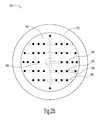
- FIG. 2Bdepicts a gas-distribution fixture of an atomic layer deposition chamber for processing a LaAlO 3 film.
- Gas-distribution fixture 240includes a gas-distribution member 242 , and a gas inlet 244 .
- Gas inlet 244couples the gas-distribution member 242 to the gas conduit 270 of FIG. 2A.
- Gas-distribution member 242includes gas-distribution holes, or orifices, 246 and gas-distribution channels 248 .
- holes 246are substantially circular with a common diameter in the range of 15-20 microns; gas-distribution channels 248 have a common width in the range of 20-45 microns.
- the surface 249 of the gas distribution member having gas-distribution holes 246is substantially planar and parallel to the substrate 210 of FIG. 2A.
- other embodimentsuse other surface forms as well as shapes and sizes of holes and channels.
- the distribution and size of holesmay also affect deposition thickness and thus might be used to assist thickness control.
- Holes 246are coupled through gas-distribution channels 248 to gas inlet 244 .
- the ALD system 200is well suited for practicing the present invention, other ALD systems commercially available can be used.
- reaction chambersfor deposition of films are understood by those of ordinary skill in the art of semiconductor fabrication.
- the present inventionman be practiced on a variety of such reaction chambers without undue experimentation.
- one of ordinary skill in the artwill comprehend the necessary detection, measurement, and control techniques in the art of semiconductor fabrication upon reading the disclosure.
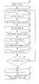
- FIG. 3depicts a flow diagram of elements of a method to process a LaAlO 3 film.
- the methodcan be implemented with the atomic layer deposition system of FIGS. 2A,B.
- a substrateis prepared.
- the substrate used for forming a transistoris typically a silicon or silicon containing material.
- This preparation processincludes cleaning of the substrate 210 and forming layers and regions of the substrate, such as drains and sources of a metal oxide semiconductor (MOS) transistor, prior to forming a gate dielectric.
- MOSmetal oxide semiconductor
- the sequencing of the formation of the regions of the transistor being processedfollows typical sequencing that is generally performed in the fabrication of a MOS transistor as is well known to those skilled in the art.
- the processing prior to forming a gate dielectricis the masking of substrate regions to be protected during the gate dielectric formation, as is typically performed in MOS fabrication.
- the unmasked regionincludes a body region of a transistor, however one skilled in the art will recognize that other semiconductor device structures may utilize this process.
- the substrate 210 in its ready for processing formis conveyed into a position in reaction chamber 220 for ALD processing.
- a precursor containing lanthanumis pulsed into reaction chamber 220 .
- the La(thd) 3is pulsed into reaction chamber 220 through the gas-distribution fixture 240 onto substrate 210 .
- the flow of the La(thd) 3is controlled by mass-flow controller 256 from gas source 251 .
- the La(thd) 3 gascan be formed from evaporation from an open crucible held at about 170° C. and provided to the gas source 251 .
- the La(thd) 3reacts with the surface of the substrate 210 in the desired region defined by the unmasked areas of the substrate 210 .
- a first purging gasis pulsed into the reaction chamber 220 .
- nitrogenwith a purity greater than 99.99% is used as a purging gas and a carrier gas for La(thd) 3 .
- the nitrogen flowis controlled by mass-flow controller 266 from the purging gas source 261 into the gas conduit 270 .
- a first oxygen containing precursoris pulsed into the reaction chamber 220 .
- ozone gasis selected as the precursor acting as an oxidizing reactant to form a lanthanum oxide on the substrate 210 .
- the ozone gasis pulsed into the reaction chamber 220 through gas conduit 270 from gas source 252 by mass-flow controller 257 .
- the ozoneaggressively reacts at the surface of substrate 210 .
- the first purging gasis injected into the reaction chamber 220 .
- nitrogen gasis used to purge the reaction chamber after pulsing each precursor gas. Excess precursor gas, and reaction by-products are removed from the system by the purge gas in conjunction with the exhausting of the reaction chamber 220 using vacuum pump 282 through mass-flow controller 287 , and exhausting of the gas conduit 270 by the vacuum pump 281 through mass-flow controller 286 .
- the substrateis held between about 180° C. and about 425° C. by the heating element 230 with the reaction chamber having a reduced pressure near the substrate of 2-3 mbar (1.5-2.25 Torr).
- the La(thd) 3 pulse timeranges from about 0.5 sec to about 1.5 sec.
- One embodimentuses a La(thd) 3 pulse time of 0.8 sec, while another embodiment uses a La(thd) 3 pulse time of 1.0 sec.
- the purge pulsesrange from about 0.8 sec to about 3 sec.
- the ozone pulse timesrange from about 1 sec to about 3 sec, with one embodiment employing a 2 sec ozone pulse time.
- a precursor containing aluminumis pulsed into the reaction chamber 220 .
- trimethylaluminium (TMA), Al(CH 3 ) 3is used as the aluminum containing precursor following the La(thd) 3 /ozone sequence.
- TMAtrimethylaluminium
- the TMAis pulsed to the surface of the substrate 210 through gas-distribution fixture 240 from gas source 253 by mass-flow controller 258 .
- the TMAis introduced onto the lanthanum oxide film formed during the La(thd) 3 /ozone sequence.
- a second purging gasis introduced into the system.
- purified argonis used as a purging and carrier gas.
- the argon flowis controlled by mass-flow controller 267 from the purging gas source 262 into the gas conduit 270 and subsequently into the reaction chamber 220 .
- a second oxygen containing precursoris pulsed into the reaction chamber 220 .
- distilled water vaporis selected as the precursor acting as an oxidizing reactant to interact with the TMA on the substrate 210 .
- the distilled water vaporis pulsed into the reaction chamber 220 through gas conduit 270 from gas source 254 by mass-flow controller 259 .
- the distilled water vaporaggressively reacts at the surface of substrate 210 to form a LaAlO 3 film.
- the second purging gasis injected into the reaction chamber 200 .
- argon gasis used to purge the reaction chamber after pulsing each precursor gas. Excess precursor gas, and reaction by-products are removed from the system by the purge gas in conjunction with the exhausting of the reaction chamber 220 using vacuum pump 282 through mass-flow controller 287 , and exhausting of the gas conduit 270 by the vacuum pump 281 through mass-flow controller 286 .
- the substrateis held between about 350° C. and about 450° C. by the heating element 230 .
- the reaction chamberis maintained at about 150° C. to minimize reactant condensation.
- the process pressureis maintained at about 230 mTorr during the pulsing of the precursor gases and at about 200 mTorr for the purging gases. Pulse times for the TMA and the distilled water vapor were about 1 sec for both precursors, with purging pulse times of about 15 secs.
- the substrate temperatureis maintained at about 350° C. for the complete La(thd) 3 /ozone/TMA/distilled water vapor cycle. In another embodiment, the substrate temperature is maintained at about 425° C. for the complete La(thd) 3 /ozone/TMA/distilled water vapor cycle.
- a DMEAA/oxygen sequencecan be employed rather than the TMA/distilled water vapor sequence.
- the aluminum containing precursor DMEAAis an adduct of alane (AlH 3 ) and dimethylehtylamine [N(CH 3 ) 2 (C 2 H 5 )].
- the DMEAAis pulsed to the substrate 210 surface form gas source 253 .
- the DMEAA gascan be provided to gas source 253 through a bubbler-type evaporation controlled at 25° C.
- the purging and carrier gas associated with DMEAA, at 335is hydrogen from purging gas source 262 .
- oxygen as the second oxygen containing precursoris pulsed into the reaction chamber 220 from gas source 254 .
- hydrogen purging gasis again flowed through the reaction chamber 220 from purging gas source 262 .
- the substrateis held between about 100° C. and about 125° C. by the heating element 230 .
- the process pressure during the DMEAA/oxygen sequenceis maintained at about 30 mTorr.
- a DMEAA/distilled water vapor sequencecan be used under the same temperature and pressure ranges as the TMA/distilled water sequence.
- the substrate temperatureis maintained at about 350° C. for the complete La(thd) 3 /ozone/DMEAA/distilled water vapor cycle.
- the complete La(thd) 3 /ozone/DMEAA/distilled water vapor cyclecan be performed with the substrate temperature maintained at about 425° C.
- the thickness of a LaAlO 3 film after one cycleis determined by the pulsing periods used in the lanthanum sequence and the aluminum sequence at a given temperature.
- the pulsing periods of the ALD processdepend upon the characteristics of the reaction system 200 employed and the precursor and purging sources. Typically, at a given temperature, the pulsing periods can vary over a significant range above some minimum pulse time for the precursors, without substantially altering the growth rate.
- the growth rate for the LaAlO 3 filmwill be set at a value such as N nm/cycle.
- tin an application such as forming a gate dielectric of a MOS transistor, the ALD process should be repeated for t/N cycles.
- the LaAlO 3 filmis of the desired thickness, t. As mentioned, the desired thickness should be completed after t/N cycles. If less than t/N cycles have been completed, the process starts over at 310 with the pulsing of the precursor containing lanthanum, which in the embodiment discussed above is a La(thd) 3 gas. If t/N cycles have completed, no further ALD processing is requires and the LaAlO 3 film, at 355 , is annealed. The annealing is a final heating cycle for producing the LaAlO 3 film and is performed at a temperature between about 850° C. and about 950° C. to produce optimum performance as a dielectric insulator. The annealing can be performed in an oxygen or nitrogen atmosphere.
- processing the device containing the LaAlO 3 filmis completed.
- completing the deviceincludes completing the formation of a transistor.
- completing the processincludes completing the formation of a memory device having a array with access transistors formed with LaAlO 3 film gate dielectrics.
- completing the processincludes the formation of an information handling device that uses electronic devices with transistors formed with LaAlO 3 film gate dielectrics.
- information handling devicesinclude many memory devices, having many access transistors.
- a LaAlO 3 film for use as a gate dielectricforms on body region of a transistor by the ALD process using a lanthanum/ozone/aluminum/water cycle.
- This cycleis the combination of a lanthanum/ozone sequence and an aluminum/water sequence. Terminating the cycle at the end of a lanthanum/ozone sequence would result in a La 2 O 3 film. Performing just an aluminum/water sequence would result in an Al 2 O 3 film.
- the film thicknessis linear with respect to the number of deposition cycles at a fixed processing temperature.
- a LaAlO 3 dielectric filmwill have a dielectric constant in the range of about 21 to about 25. However, a dielectric film containing LaAlO 3 , Al 2 O 3 , and La 2 O 3 will have a dielectric constant ranging from the dielectric constant of Al 2 O 3 , 9, to the dielectric constant of La 2 O 3 , 30.
- the amount of lanthanum and aluminum deposited on the surface region of a substratecan be controlled.
- a dielectric film formed by ALD using a lanthanum sequence and a aluminum sequencecan be formed with a composition containing selected or predetermined percentages of LaAlO 3 , Al 2 O 3 , and La 2 O 3 , in which case the effective dielectric constant of the film will be selected or predetermined in the range from 9 to 30.
- a dielectric film formed in accordance with the present invention containing almost entirely LaAlO 3will have a dielectric constant in the range of about 21 to about 25.
- the resulting dielectric containing LaAlO 3should be amorphous.
- a dielectric film containing LaAlO 3can be engineered with selected characteristics by also controlling precursor materials for each sequence, processing temperatures and pressures for each sequence, individual precursor pulsing times, and heat treatment at the end of the process, at the end of each cycle, and at the end of each sequence.
- the heat treatmentmay include in situ annealing in various atmospheres including argon, nitrogen, and oxygen.
- the pulsing times for precursorsrange from about 0.5 sec to about 2 to 3 sec, though longer pulses can be employed.
- pulsing times for purging gaseswill range from a time equal to its associated precursor pulse time to an order of magnitude larger than the associated precursor pulse time in order than all excess material and by-products be purged from the reaction system.
- the pulsing times for purging gaseswill range from about one sec to about 30 seconds.
- the growth rates for an engineered LaAlO 3 containing filmwill be controlled by the growth rates of the individual sequences and typically can be from about 0.72 ⁇ per cycle to about 25 ⁇ per cycle. Other growth rates may also be attained.
- a range of equivalent oxide thickness, t eq , attainable in accordance with the present inventionis associated with the capability to provide a composition having a dielectric constant in the range form about 9 to about 30, and the capability to attain physical film thickness in the range of from about 0.5 to about 50 mm and above.
- LaAlO 3 in a bulk form at room temperaturehas a nearly cubic perovskite crystal structure with a lattice constant of 0.536 nm. Fortunately, the films grown by ALD have an amorphous form, though it is expected that a dimension for a monolayer of LaAlO 3 is related to its lattice constant in bulk form. At a physical thickness about 0.5 ⁇ m, t eq would be expected to range from about 2.2 ⁇ to about 0.65 ⁇ for the dielectric constant ranging from 9 to 30. For a layer of essentially LaAlO 3 , t eq would be expected to range from about 0.93 ⁇ to about 0.78 ⁇ for a physical layer of 0.5 nm.
- t eqFor a substantially LaAlO 3 film having a thickness of approximately 2 nm, t eq would range from about 3 ⁇ to about 3.7 ⁇ . From above, it is apparent that a film containing LaAlO 3 can be attained with a t eq ranging from 1.5 ⁇ to 5 ⁇ . Further, such a film can provide a t eq significantly less than 2 or 3 ⁇ , even less than 1.5 ⁇ .
- novel process described aboveprovides significant advantages by performing atomic layer deposition with a lanthanum sequence/aluminum sequence deposition cycle. Further, by independently controlling the various parameters for each sequence a gate dielectric with a selected dielectric constant can be formed. Additionally, the novel process can be implemented to form transistors, memory devices, and information handling devices.
- a transistor 100 as depicted in FIG. 1can be formed by forming a source/drain region 120 and another source/drain region 130 in a silicon based substrate 110 where the two source/drain regions 120 , 130 are separated by a body region 132 .
- the body region 132 separated by the source/drain 120 and the source/drain 130defines a channel having a channel length 134 .
- a LaAlO 3 filmis formed by ALD by pulsing a lanthanum containing precursor into a reaction chamber containing the substrate 110 , pulsing a first oxygen containing precursor into the reaction chamber, pulsing an aluminum containing precursor into the reaction chamber, and pulsing a second oxygen containing precursor into the reaction chamber.
- Each precursoris pulsed into the reaction chamber for a selected time period. A length of time for pulsing each precursor is selected according to the precursor used. Between each precursor pulsing, precursor excess and reaction by-products are removed from the reaction.
- the LaAlO 3 film thicknessis controlled by repeating for a number of cycles the pulsing of the lanthanum containing precursor, the first oxygen containing precursor, the aluminum containing precursor, and the second oxygen containing precursor until the desired thickness for film 140 containing LaAlO 3 is formed on the body region.
- a gateis formed over the gate dielectric 140 . Typically, forming the gate includes forming a polysilicon layer, though a metal gate can be formed in an alternative process. Forming the substrate, source/region regions, and the gate is performed using standard processes known to those skilled in the art. Additionally, the sequencing of the various elements of the process for forming a transistor is conducted with standard fabrication processes, also as known to those skilled in the art.
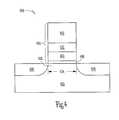
- FIG. 4depicts a transistor 400 having a silicon based substrate 410 with two source/drain regions 420 , 430 separated by a body region 432 .
- the body region 432 between the two source/drain regions 420 , 430defines a channel region having a channel length 434 .
- a stack 455including a gate dielectric 440 , a floating gate 452 , a floating gate dielectric 442 , and control gate 450 .
- the gate dielectric 440is formed in an ALD process according to the teachings of the present invention as described above with the remaining elements of the transistor 400 formed using processes known to those skilled in the art. Alternately, both the gate dielectric 440 and the floating gate dielectric 442 can be formed by ALD in accordance with the present invention as described above.
- Transistors created by the methods described abovemay be implemented into memory devices and information handling devices as shown in FIGS. 5 - 7 and described below. While specific types of memory devices and computing devices are shown below, it will be recognized by one skilled in the art that several types of memory devices and information handling devices could utilize the invention.
- a personal computeras shown in FIGS. 5 and 6, include a monitor 500 , keyboard input 502 and a central processing unit 504 .
- the processor unit 504typically includes microprocessor 606 , memory bus circuit 608 having a plurality of memory slots 612 ( a - n ), and other peripheral circuitry 610 .
- Peripheral circuitry 610permits various peripheral devices 624 to interface processor-memory bus 620 over input/output (I/O) bus 622 .
- the personal computer shown in FIGS. 5 and 6also includes at least one transistor having a gate dielectric according to the teachings of the present invention.
- Microprocessor 606produces control and address signals to control the exchange of data between memory bus circuit 608 and microprocessor 606 and between memory bus circuit 608 and peripheral circuitry 610 . This exchange of data is accomplished over high speed memory bus 620 and over high speed I/O bus 622 .
- Coupled to memory bus 620are a plurality of memory slots 612 ( a - n ) which receive memory devices well known to those skilled in the art.
- memory slots 612For example, single in-line memory modules (SIMMs) and dual in-line memory modules (DIMMs) may be used in the implementation of the present invention.
- Page mode operations in a DRAMare defined by the method of accessing a row of a memory cell arrays and randomly accessing different columns of the array. Data stored at the row and column intersection can be read and output while that column is accessed. Page mode DRAMs require access steps which limit the communication speed of memory circuit 608 . A typical communication speed for a DRAM device using page mode is approximately 33 MHZ.
- An alternate type of deviceis the extended data output (EDO) memory which allows data stored at a memory array address to be available as output after the addressed column has been closed.
- EDOextended data output
- This memorycan increase some communication speeds by allowing shorter access signals without reducing the time in which memory output data is available on memory bus 620 .
- Other alternative types of devicesinclude SDRAM, DDR SDRAM, SLDRAM and Direct RDRAM as well as others such as SRAM or Flash memories.
- FIG. 7is a block diagram of an illustrative DRAM device 700 compatible with memory slots 612 ( a - n ).
- the description of DRAM 700has been simplified for purposes of illustrating a DRAM memory device and is not intended to be a complete description of all the features of a DRAM.
- Those skilled in the artwill recognize that a wide variety of memory devices may be used in the implementation of the present invention.
- the example of a DRAM memory device shown in FIG. 6includes at least one transistor having a gate dielectric according to the teachings of the present invention.
- Control, address and data information provided over memory bus 620is further represented by individual inputs to DRAM 700 , as shown in FIG. 7. These individual representations are illustrated by data lines 702 , address lines 704 and various discrete lines directed to control logic 706 .
- DRAM 700includes memory array 710 which in turn comprises rows and columns of addressable memory cells. Each memory cell in a row is coupled to a common word line. The word line is coupled to gates of individual transistors, where at least one transistor has a gate coupled to a gate dielectric containing LaAlO 3 in accordance with the method and structure previously described above. Additionally, each memory cell in a column is coupled to a common bit line. Each cell in memory array 710 includes a storage capacitor and an access transistor as is conventional in the art.
- DRAM 700interfaces with, for example, microprocessor 606 through address lines 704 and data lines 702 .
- DRAM 700may interface with a DRAM controller, a micro-controller, a chip set or other electronic system.
- Microprocessor 606also provides a number of control signals to DRAM 700 , including but not limited to, row and column address strobe signals RAS and CAS, write enable signal WE, an output enable signal OE and other conventional control signals.
- Row address buffer 712 and row decoder 714receive and decode row addresses from row address signals provided on address lines 704 by microprocessor 606 . Each unique row address corresponds to a row of cells in memory array 710 .
- Row decoder 714includes a word line driver, an address decoder tree, and circuitry which translates a given row address received from row address buffers 712 and selectively activates the appropriate word line of memory array 710 via the word line drivers.
- Column address buffer 716 and column decoder 718receive and decode column address signals provided on address lines 704 .
- Column decoder 718also determines when a column is defective and the address of a replacement column.
- Column decoder 718is coupled to sense amplifiers 720 .
- Sense amplifiers 720are coupled to complementary pairs of bit lines of memory array 710 .
- Sense amplifiers 720are coupled to data-in buffer 722 and data-out buffer 724 .
- Data-in buffers 722 and data-out buffers 724are coupled to data lines 702 .
- data lines 702provide data to data-in buffer 722 .
- Sense amplifier 720receives data from data-in buffer 722 and stores the data in memory array 710 as a charge on a capacitor of a cell at an address specified on address lines 704 .
- DRAM 700transfers data to microprocessor 606 from memory array 710 .
- Complementary bit lines for the accessed cellare equilibrated during a precharge operation to a reference voltage provided by an equilibration circuit and a reference voltage supply.
- the charge stored in the accessed cellis then shared with the associated bit lines.
- a sense amplifier of sense amplifiers 720detects and amplifies a difference in voltage between the complementary bit lines.
- the sense amplifierpasses the amplified voltage to data-out buffer 724 .
- Control logic 706is used to control the many available functions of DRAM 700 .
- various control circuits and signals not detailed hereininitiate and synchronize DRAM 700 operation as known to those skilled in the art.
- the description of DRAM 700has been simplified for purposes of illustrating the present invention and is not intended to be a complete description of all the features of a DRAM.
- memory devicesincluding but not limited to, SDRAMs, SLDRAMs, RDRAMs and other DRAMs and SRAMs, VRAMs and EEPROMs, may be used in the implementation of the present invention.
- the DRAM implementation described hereinis illustrative only and not intended to be exclusive or limiting.
- a gate dielectric containing LaAlO 3 and method of fabricating a gate dielectric contained LaAlO 3are provided that produces a reliable gate dielectric having a thinner equivalent oxide thickness than attainable using SiO 2 .
- LaAlO 3 gate dielectrics formed using the methods described hereinare thermodynamically stable such that the gate dielectrics formed will have minimal reactions with a silicon substrate or other structures during processing.
- Transistors and higher level ICs or devicesare provided utilizing the novel gate dielectric and process of formation.
- Gate dielectric layers containing LaAlO 3are formed having a high dielectric constant ( ⁇ ), where the gate dielectrics are capable of a t eq thinner than 5 ⁇ , thinner than the expected limit for SiO 2 gate dielectrics.
- the physical thickness of the LaAlO 3 layeris much larger than the SiO 2 thickness associated with the t eq limit of SiO 2 . Forming the larger thickness provides advantages in processing the gate dielectric.
- a dielectric containing LaAlO 3 , Al 2 O 3 , and La 2 O 3through controlling a lanthanum sequence and a aluminum sequence in an ALD processing of a substrate allows the selection of a dielectric constant ranging from that of Al 2 O 3 to the dielectric constant of La 2 O 3 .
Landscapes
- Engineering & Computer Science (AREA)
- Condensed Matter Physics & Semiconductors (AREA)
- Manufacturing & Machinery (AREA)
- General Chemical & Material Sciences (AREA)
- Physics & Mathematics (AREA)
- Chemical Kinetics & Catalysis (AREA)
- Chemical & Material Sciences (AREA)
- General Physics & Mathematics (AREA)
- Crystallography & Structural Chemistry (AREA)
- Computer Hardware Design (AREA)
- Microelectronics & Electronic Packaging (AREA)
- Power Engineering (AREA)
- Semiconductor Memories (AREA)
- Insulated Gate Type Field-Effect Transistor (AREA)
- Chemical Vapour Deposition (AREA)
Abstract
Description
- This application is related to the following, co-pending, commonly assigned applications, incorporated herein by reference:[0001]
- U.S. application Ser. No. ______, attorney docket no. 1303.046US1 entitled: “Evaporated LaAlO[0002]3Films for Gate Dielectrics,”
- U.S. application Ser. No. ______, attorney docket no. 303.802US1 entitled: “Atomic Layer Deposition and Conversion,”[0003]
- U.S. application Ser. No. ______, attorney docket no. 1303.048US1 entitled: “Atomic Layer of AlO[0004]xfor ULSI Gate Atomic Layer Deposition for Gate Dielectric Layer,” and
- U.S. application Ser. No. 09/797,324, attorney docket no. 303.717US 1 entitled: “Methods, Systems, and Apparatus for Uniform Chemical-Vapor Depositions.”[0005]
- The invention relates to semiconductor devices and device fabrication. Specifically, the invention relates to gate dielectric layers of transistor devices and their method of fabrication.[0006]
- The semiconductor device industry has a market driven need to improve speed performance, improve its low static (off-state) power requirements, and adapt to a wide range of power supply and output voltage requirements for it silicon based microelectronic products. In particular, in the fabrication of transistors, there is continuous pressure to reduce the size of devices such as transistors. The ultimate goal is to fabricate increasingly smaller and more reliable integrated circuits (ICs) for use in products such as processor chips, mobile telephones, or memory devices such as DRAMs. The smaller devices are frequently powered by batteries, where there is also pressure to reduce the size of the batteries, and to extend the time between battery charges. This forces the industry to not only design smaller transistors, but to design them to operate reliably with lower power supplies.[0007]
- Currently, the semiconductor industry relies on the ability to reduce or scale the dimensions of its basic devices, primarily, the silicon based metal-oxide-semiconductor field effect transistor (MOSFET). A common configuration of such a transistor is shown in FIG. 1. While the following discussion uses FIG. 1 to illustrate a transistor from the prior art, one skilled in the art will recognize that the present invention could be incorporated into the transistor shown in FIG. 1 to form a novel transistor according to the invention. The[0008]
transistor 100 is fabricated in asubstrate 110 that is typically silicon, but could be fabricated from other semiconductor materials as well. Thetransistor 100 has a first source/drain region 120 and a second source/drain region 130. Abody region 132 is located between the first source/drain region and the second source/drain region, where thebody region 132 defines a channel of the transistor with achannel length 134. A gate dielectric, orgate oxide 140 is located on thebody region 132 with agate 150 located over the gate dielectric. Although the gate dielectric can be formed from materials other than oxides, the gate dielectric is typically an oxide, and is commonly referred to as a gate oxide. The gate may be fabricated from polycrystalline silicon (polysilicon), or other conducting materials such as metal may be used. - In fabricating transistors to be smaller in size and reliably operating on lower power supplies, one important design criteria is the gate dielectric[0009]140. The mainstay for forming the gate dielectric has been silicon dioxide, SiO2. A thermally grown amorphous SiO2layer provides an electrically and thermodynamically stable material, where the interface of the SiO2layer with underlying Si provides a high quality interface as well as superior electrical isolation properties. In typical processing, use of SiO2on Si has provided defect charge densities on the order of 1010/cm2, midgap interface state densities of approximately 1010/cm2eV, and breakdown voltages in the range of 15 MV/cm. With such qualities, there would be no apparent need to use a material other than SiO2, but with increased scaling, other requirements for gate dielectrics create the need to find other dielectric materials to be used for a gate dielectric.
- What is needed is an alternate dielectric material for forming a gate dielectric that has a high dielectric constant relative to SiO[0010]2, and is thermodynamically stable with respect to silicon such that forming the dielectric on a silicon layer will not result in SiO2formation, or diffusion of material, such as dopants, into the gate dielectric from the underlying silicon layer.
- A solution to the problems as discussed above is addressed in the present invention. In accordance with the present invention, a method of forming a gate dielectric on a transistor body region includes the atomic layer deposition of an amorphous film containing LaAlO[0011]3on the transistor body region. The ALD formation of the LaAlO3film is performed by pulsing a lanthanum containing precursor into a reaction chamber containing a substrate, pulsing a first oxygen containing precursor into the reaction chamber, pulsing an aluminum containing precursor into the reaction chamber, and pulsing a second oxygen containing precursor into the reaction chamber. Each precursor is pulsed into the reaction chamber for a selected time period. A length of time for pulsing each precursor is selected according to the precursor used. Between each precursor pulsing, precursor excess and reaction by-products are removed from the reaction. The LaAlO3film thickness is controlled by repeating for a number of cycles the pulsing of the lanthanum containing precursor, the first oxygen containing precursor, the aluminum containing precursor, and the second oxygen containing precursor until the desired thickness is formed.
- A transistor is fabricated on a substrate by forming two source/drain regions separated by a body region, pulsing a La(thd)[0012]3(thd=2,2,6,6-tetramethyl-3,5-heptanedione) source gas into a reaction chamber containing the substrate, pulsing ozone into the reaction chamber, pulsing a trimethylaluminium, Al(CH3)3, source gas into the reaction chamber, and pulsing water vapor into the reaction chamber. Controlling the processing temperatures, and the number of cycles of the lanthanum precursor and the number of cycles of the aluminum precursor provides the capability to form a film composition having a predetermined dielectric constant. A DMEAA, an adduct of alane (AlH3) and dimethylehtylamine [N(CH3)2(C2H5)], source gas can be used in place of the trimethylaluminium source gas.
- Advantageously, these methods can be used to further form a memory array where the process of forming the memory array is adapted to form gate dielectrics in accordance with the present invention. Additionally, an information handling system can be formed using the methods of the present invention, wherein a memory array fabricated in conjunction with fabricating a processor is formed to include transistors having gate dielectrics containing LaAlO[0013]3. These gate dielectrics are formed by the ALD processing of a lanthanum sequence and a aluminum sequence for a number of cycles to provide a film containing LaAlO3.
- In accordance with the present invention, a transistor having two source/drain regions separated by a body region includes an amorphous gate dielectric containing LaAlO[0014]3located above the body region between the two source/drain regions. The gate dielectric may be essentially composed of LaAlO3or it may also contain Al2O3, and La2O3. Depending on its composition, the dielectric constant of the gate dielectric can range from about 9 to about 30. Depending on its composition, the gate dielectric can have a thickness corresponding to an equivalent oxide thickness (teq) in the range from about 1.5 Angstroms to about 5 Angstroms, in addition to larger teqvalues.
- Advantageously, a memory array includes a number of transistors having two source/drain regions separated by a body region with an amorphous gate dielectric containing LaAlO[0015]3located above the body region between the two source/drain regions. These transistors provide the memory array with an array of transistors having gate dielectrics with equivalent oxide thickness (teq) in the range from about 1.5 Angstroms to about 5 Angstroms, providing transistors operable at reduced voltage levels. Additionally, an information handling device, such as a computer, includes a processor and a memory array having a number of transistors with two source/drain regions separated by a body region that includes an amorphous gate dielectric containing LaAlO3located above the body region between the two source/drain regions.
- These and other embodiments, aspects, advantages, and features of the present invention will be set forth in part in the description which follows, and in part will become apparent to those skilled in the art by reference to the following description of the invention and referenced drawings or by practice of the invention. The aspects, advantages, and features of the invention are realized and attained by means of the instrumentalities, procedures, and combinations particularly pointed out in the appended claims.[0016]
- FIG. 1 depicts a common configuration of a transistor.[0017]
- FIG. 2A depicts an atomic layer deposition system for processing a LaAlO[0018]3film in accordance with the present invention.
- FIG. 2B depicts a gas-distribution fixture of an atomic layer deposition chamber for processing a LaAlO[0019]3film in accordance with the present invention.
- FIG. 3 depicts a flow diagram of elements of a method to process a LaAlO[0020]3film in accordance with the present invention.
- FIG. 4 depicts a configuration of a transistor capable of being fabricated in accordance with the present invention.[0021]
- FIG. 5 depicts a perspective view of a personal computer incorporating devices made in accordance with the present invention.[0022]
- FIG. 6 depicts a schematic view of a central processing unit incorporating devices made in accordance with the present invention.[0023]
- FIG. 7 shows a schematic view of a DRAM memory device in accordance with the present invention.[0024]
- In the following detailed description of the invention, reference is made to the accompanying drawings which form a part hereof, and in which is shown, by way of illustration, specific embodiments in which the invention may be practiced. In the drawings, like numerals describe substantially similar components throughout the several views. These embodiments are described in sufficient detail to enable those skilled in the art to practice the invention. Other embodiments may be utilized and structural, logical, and electrical changes may be made without departing from the scope of the present invention.[0025]
- The terms wafer and substrate used in the following description include any structure having an exposed surface with which to form the integrated circuit (IC) structure of the invention. The term substrate is understood to include semiconductor wafers. The term substrate is also used to refer to semiconductor structures during processing, and may include other layers that have been fabricated thereupon. Both wafer and substrate include doped and undoped semiconductors, epitaxial semiconductor layers supported by a base semiconductor or insulator, as well as other semiconductor structures well known to one skilled in the art. The term conductor is understood to include semiconductors, and the term insulator or dielectric is defined to include any material that is less electrically conductive than the materials referred to as conductors.[0026]
- The term “horizontal” as used in this application is defined as a plane parallel to the conventional plane or surface of a wafer or substrate, regardless of the orientation of the wafer or substrate. The term “vertical” refers to a direction perpendicular to the horizontal as defined above. Prepositions, such as “on”, “side” (as in “sidewall”), “higher”, “lower”, “over” and “under” are defined with respect to the conventional plane or surface being on the top surface of the wafer or substrate, regardless of the orientation of the wafer or substrate. The following detailed description is, therefore, not to be taken in a limiting sense, and the scope of the present invention is defined only by the appended claims, along with the full scope of equivalents to which such claims are entitled.[0027]
- A[0028]
gate dielectric 140 of FIG. 1, when operating in a transistor, has both a physical gate dielectric thickness and an equivalent oxide thickness (teq). The equivalent oxide thickness quantifies the electrical properties, such as capacitance, of agate dielectric 140 in terms of a representative physical thickness. teqis defined as the thickness of a theoretical SiO2layer that would be required to have the same capacitance density as a given dielectric, ignoring leakage current and reliability considerations. - A SiO[0029]2layer of thickness, t, deposited on a Si surface as a gate dielectric will also have a teqlarger than its thickness, t. This teqresults from the capacitance in the surface channel on which the SiO2is deposited due to the formation of a depletion/inversion region. This depletion/inversion region can result in teqbeing from 3 to 6 Angstroms (Å) larger than the SiO2thickness, t. Thus, with the semiconductor industry driving to someday scale the gate dielectric equivalent oxide thickness, teq, to under 10 Å, the physical thickness requirement for a SiO2layer used for a gate dielectric would be need to be approximately 4 to 7 Å.
- Additional requirements on a SiO[0030]2layer would depend on the gate electrode used in conjunction with the SiO2gate dielectric. Using a conventional polysilicon gate would result in an additional increase in teqfor the SiO2layer. This additional thickness could be eliminated by using a metal gate electrode, though metal gates are not currently used in complementary metal-oxide-semiconductor field effect transistor (CMOS) technology. Thus, future devices would be designed towards a physical SiO2gate dielectric layer of about 5 Å or less. Such a small thickness requirement for a SiO2oxide layer creates additional problems.
- Silicon dioxide is used as a gate dielectric, in part, due to its electrical isolation properties in a SiO[0031]2—Si based structure. This electrical isolation is due to the relatively large band gap of SiO2(8.9 eV) making it a good insulator from electrical conduction. Signification reductions in its band gap would eliminate it as a material for a gate dielectric. As the thickness of a SiO2layer decreases, the number of atomic layers, or monolayers of the material in the thickness decreases. At a certain thickness, the number of monolayers will be sufficiently small that the SiO2layer will not have a complete arrangement of atoms as in a larger or bulk layer. As a result of incomplete formation relative to a bulk structure, a thin SiO2layer of only one or two monolayers will not form a full band gap. The lack of a full band gap in a SiO2gate dielectric would cause an effective short between an underlying Si channel and an overlying polysilicon gate. This undesirable property sets a limit on the physical thickness to which a SiO2layer can be scaled. The minimum thickness due to this monolayer effect is thought to be about 7-8 Å. Therefore, for future devices to have a teqless than about 10 Å, other dielectrics than SiO2need to be considered for use as a gate dielectric.
- For a typical dielectric layer used as a gate dielectric, the capacitance is determined as one for a parallel plate capacitance: C=κε[0032]0A/t, where κ is the dielectric constant, ε0is the permittivity of free space, A is the area of the capacitor, and t is the thickness of the dielectric. The thickness, t, of a material is related to teqfor a given capacitance with the dielectric constant of SiO2, κox=3.9, associated with teq, as
- t=(κ/κox)teq=(κ/3.9)teq.
- Thus, materials with a dielectric constant greater than that of SiO[0033]2, 3.9, will have a physical thickness that can be considerably larger than a desired teq, while providing the desired equivalent oxide thickness. For example, an alternate dielectric material with a dielectric constant of 10 could have a thickness of about 25.6 Å to provide a teqof 10 Å, not including any depletion/inversion layer effects. Thus, the reduced equivalent oxide thickness of transistors can be realized by using dielectric materials with higher dielectric constants than SiO2.
- The thinner equivalent oxide thickness, t[0034]eq,required for lower transistor operating voltages and smaller transistor dimensions may be realized by a significant number of materials, but additional fabricating requirements makes determining a suitable replacement for SiO2difficult. The current view for the microelectronics industry is still for Si based devices. This requires that the gate dielectric employed be grown on a silicon substrate or silicon layer, which places significant restraints on the substitute dielectric material. During the formation of the dielectric on the silicon layer, there exists the possibility that a small layer of SiO2could be formed in addition to the desired dielectric. The result would effectively be a dielectric layer consisting of two sublayers in parallel with each other and the silicon layer on which the dielectric is formed. In such a case, the resulting capacitance would be that of two dielectrics in series. As a result, the teqof the dielectric layer would be the sum of the SiO2thickness and a multiplicative factor of the thickness of the dielectric being formed. Thus, if a SiO2layer is formed in the process, the teqis again limited by a SiO2layer. In the event, that a barrier layer is formed between the silicon layer and the desired dielectric in which the barrier layer prevents the formation of a SiO2layer, the teqwould be limited by the layer with the lowest dielectric constant. However, whether a single dielectric layer with a high dielectric constant or a barrier layer with a higher dielectric constant than SiO2is employed, the layer interfacing with the silicon layer must provide a high quality interface to maintain a high channel carrier mobility.
- In a recent article by G. D. Wilk et al.,[0035]Journal of Applied Physics,vol. 89: no. 10, pp. 5243-5275 (2001), material properties of high dielectric materials for gate dielectrics were discussed. Among the information disclosed was the viability of Al2O3as a substitute for SiO2. Al2O3was disclosed has having favourable properties for use as a gate dielectric such as high band gap, thermodynamic stability on Si up to high temperatures, and an amorphous structure. In addition, Wilk disclosed that forming a layer of Al2O3on silicon does not result in a SiO2interfacial layer. However, the dielectric constant of Al2O3is only 9, where thin layers may have a dielectric constant of about 8 to about 10. Though the dielectric constant of Al2O3is in an improvement over SiO2, a higher dielectric constant for a gate dielectric is desirable. Other dielectrics and their properties discussed by Wilk include
Dielectric Band gap Crystal Material Constant (κ) Eg(eV) Structure(s) SiO2 3.9 8.9 Amorphous Si3N4 7 5.1 Amorphous Al2O3 9 8.7 Amorphous Y2O3 15 5.6 Cubic La2O3 30 4.3 Hexagonal, Cubic Ta2O3 26 4.5 Orthorhombic TiO2 80 3.5 Tetrag. (rutile, anatase) HfO2 25 5.7 Mono., Tetrag., Cubic ZrO2 25 7.8 Mono., Tetrag., Cubic - One of the advantages using SiO[0036]2as a gate dielectric has been that the formation of the SiO2layer results is an amorphous gate dielectric. Having an amorphous structure for a gate dielectric is advantageous because grain boundaries in polycrystalline gate dielectrics provide high leakage paths. Additionally, grain size and orientation changes throughout a polycrystalline gate dielectric can cause variations in the film's dielectric constant. The abovementioned material properties including structure are for the materials in a bulk form. The materials having the advantage of a high dielectric constants relative to SiO2also have the disadvantage of a crystalline form, at least in a bulk configuration. The best candidates for replacing SiO2as a gate dielectric are those with high dielectric constant, which can be fabricated as a thin layer with an amorphous form.
- In co-pending, commonly assigned U.S. patent applications: entitled “Evaporated LaAlO[0037]3Films for Gate Dielectrics,” attorney docket no. 1303.046US1, Ser. No. ______, LaAlO3is disclosed as a replacement for SiO2as material for forming gate dielectrics and other dielectric films in electronic devices such as MOS transistors. This application disclosed, among other things, forming layers of LaAlO3on silicon by electron beam evaporation of dry pellets of Al2O3and La2O3using two electron guns controlled by two rate monitors. Controlling the rates for evaporating the dry pellets of Al2O3and La2O3allows for the formation of a gate dielectric having a composition with a predetermined dielectric constant. The predetermined dielectric constant will range from the dielectric constant of Al2O3to the dielectric constant of La2O3, depending on the composition of the film. Films substantially consisting of LaAlO3film could be obtained on silicon providing an amorphous dielectric layer with a dielectric constant between 21 and 24. Other reports indicate that LaAlO3film can be grown by metal-organic chemical-vapor-deposition method, volatile surfactant-assisted metal-organic chemical-vapor-deposition method, pulsed-laser depositions method, and rf magnetron sputtering method.
- In accordance with the present invention, layers of LaAlO[0038]3can be deposited on silicon using atomic layer deposition (ALD), also known as atomic layer epitaxy (ALE). ALD was developed in the early 1970's as a modification of chemical vapor deposition (CVD) and is also called “alternatively pulsed-CVD.” In ALD, gaseous precursors are introduced one at a time to the substrate surface mounted within a reaction chamber (or reactor). This introduction of the gaseous precursors takes the form of pulses of each gaseous precursor. Between the pulses, the reaction chamber is purged with an inert gas or evacuated. In the first pulsing phase, reaction with the substrate occurs with the precursor saturatively chemisorbed at the substrate surface. Subsequent purging removes precursor excess from the reaction chamber. The second pulsing phase introduces another precursor on the substrate where the growth reaction of the desired film takes place. Subsequent to the film growth reaction, reaction byproducts and precursor excess are purged from the reaction chamber. For favourable precursor chemistry where the precursors adsorb and react with each other on the substrate aggressively, one ALD cycle can be preformed in less than one second in properly designed flow type reaction chambers. Typically, precursor pulse times range from about 0.5 sec to about 2 to 3 seconds.
- Advantageously, in ALD, the saturation of all the reaction and purging phases or steps makes the growth self-limiting. This self-limiting growth results in large area uniformity and conformality, which has important applications for such cases as planar substrates, deep trenches, and in the processing of porous silicon and high surface area silica and alumina powders. Significantly, ALD provides for controlling film thickness in a straightforward, simple manner by controlling the number of growth cycles.[0039]
- ALD was originally developed to manufacture luminescent and dielectric films needed in electroluminescent displays. Significant efforts have been made to apply ALD to the growth of doped zinc sulfide and alkaline earth metal sulfide films. Additionally, ALD has been studied for the growth of different epitaxial II-V and II-VI films, nonepitaxial crystalline or amorphous oxide and nitride films and multilayer structures of these. There also has been considerable interest towards the ALD growth of silicon and germanium films, but due to the difficult precursor chemistry, this has not been very successful.[0040]
- The precursors may be gaseous, liquid or solid. However, liquid or solid precursors must be volatile. The vapor pressure must be high enough for effective mass transportation. Also, solid and some liquid precursors need to be heated inside the reaction chamber and introduced through heated tubes to the substrates. The necessary vapor pressure must be reached at a temperature below the substrate temperature to avoid the condensation of the precursors on the substrate. Due to the self-limiting growth mechanisms of ALD, relatively low vapor pressure solid precursors can be used though evaporation rates may somewhat vary during the process because of changes in their surface area.[0041]
- There are several requirements for precursors used in ALD. The precursors must be thermally stable at the substrate temperature because their decomposition would destroy the surface control and accordingly the advantages of the ALD method which relies on the reactant of the precursor at the substrate surface. Of course, a slight decomposition, if slow compared to the ALD growth, can be tolerated.[0042]
- The precursors have to chemisorb on or react with the surface, though the interaction between the precursor and the surface as well as the mechanism for the adsorption is different for different precursors. The molecules at the substrate surface must react aggressively with the second precursor to form the desired solid film. Additionally, precursors should not react with the film to cause etching, and precursors should not dissolve in the film. Using highly reactive precursors in ALD contrasts with the selection of precursors for conventional CVD.[0043]
- The by-products in the reaction must be gaseous in order to allow their easy removal from the reaction chamber. Further, the by-products should not react or adsorb on the surface.[0044]
- In accordance with the present invention, a LaAlO[0045]3film is formed on a substrate mounted in a reaction chamber by pulsing a lanthanum containing precursor into the reaction chamber followed by pulsing a first oxygen containing precursor, and by pulsing an aluminum containing precursor into the reaction chamber followed by pulsing a second oxygen containing precursor into the reaction chamber. Between each pulsing, a purging gas is introduced into the reaction chamber. Pulsing a lanthanum containing precursor into the reaction chamber followed by pulsing a first oxygen containing precursor with subsequent purging after each pulsing constitutes a lanthanum sequence. Similarly, pulsing an aluminum containing precursor into the reaction chamber followed by pulsing a second oxygen containing precursor into the reaction chamber with subsequent purging after each pulsing constitutes an aluminum sequence. The selection of the first oxygen containing precursor depends upon the lanthanum containing precursor pulsed into the chamber, and likewise, the second oxygen containing precursor depends upon the aluminum precursor pulsed into the chamber. Additionally, different purging gases can be employed for the lanthanum sequence and the aluminum sequence. Furthermore, pulsing each precursor into the reaction chamber is individually controlled for a predetermined period, where the predetermined period for each precursor differs according to the nature of the precursor.
- The precursors are selected such that performing one lanthanum sequence followed by an aluminum sequence completes one cycle of ALD deposition of a LaAlO[0046]3layer. The thickness of this LaAlO3layer will depend on the precursors used, the period of the pluses, and the processing temperature. A LaAlO3film with a predetermined thickness is formed by repeating for a number of cycles the lanthanum sequence and the aluminum sequence. Once a LaAlO3film with the desired thickness is formed, the LaAlO3film is annealed.
- In an embodiment of the present invention, precursor gases are used to form LaAlO[0047]3films as a gate dielectric on a transistor body. Alternately, solid or liquid precursors can be used in an appropriately designed reaction chamber. ALD formation of other materials is disclosed in co-pending, commonly assigned U.S. patent applications: entitled “Atomic Layer Deposition and Conversion,” attorney docket no. 303.802US1, Ser. No. ______, and “Atomic Layer of AlOxfor ULSI Gate Atomic Layer Deposition for Gate Dielectric Layer,” attorney docket no. 1303.048
US 1, Ser. No. ______. - FIG. 2A depicts elements of an atomic layer deposition system for processing a LaAlO[0048]3film in accordance with the present invention. The elements depicted are those elements necessary for discussion of the present invention such that those skilled in the art may practice the present invention without undue experimentation. A further discussion of the ALD reaction chamber can be found in co-pending, commonly assigned U.S. patent applications: entitled “Methods, Systems, and Apparatus for Uniform Chemical-Vapor Depositions,” attorney docket no. 303.717US1, Ser. No. 09/797,324, incorporated herein by reference. In FIG. 2A, a
substrate 210 is placed inside areaction chamber 220 ofALD system 200. Also located within thereaction chamber 220 is aheating element 230 which is thermally coupled tosubstrate 210 to control the substrate temperature. A gas-distribution fixture 240 introduces precursor gases to thesubstrate 210. Each precursor gas originates fromindividual gas sources flow controllers - Also included in the ALD system are purging[0049]
gas sources flow controllers conduit 270 which is coupled to the gas-distribution fixture 240 inside thereaction chamber 220.Gas conduit 270 is also coupled to vacuum pump, or exhaust pump,281 by mass-flow controller 286 to remove excess precursor gases, purging gases, and by-product gases at the end of a purging sequence from the gas conduit. - Vacuum pump, or exhaust pump,[0050]282 is coupled by mass-
flow controller 287 to remove excess precursor gases, purging gases, and by-product gases at the end of a purging sequence from thereaction chamber 220. For convenience, control displays, mounting apparatus, temperature sensing devices, substrate maneuvering apparatus, and necessary electrical connections as are known to those skilled in the art are not shown in FIG. 2A. - FIG. 2B depicts a gas-distribution fixture of an atomic layer deposition chamber for processing a LaAlO[0051]3film. Gas-
distribution fixture 240 includes a gas-distribution member 242, and agas inlet 244.Gas inlet 244 couples the gas-distribution member 242 to thegas conduit 270 of FIG. 2A. Gas-distribution member 242 includes gas-distribution holes, or orifices,246 and gas-distribution channels 248. In the exemplary embodiment, holes246 are substantially circular with a common diameter in the range of 15-20 microns; gas-distribution channels 248 have a common width in the range of 20-45 microns. Thesurface 249 of the gas distribution member having gas-distribution holes 246 is substantially planar and parallel to thesubstrate 210 of FIG. 2A. However, other embodiments use other surface forms as well as shapes and sizes of holes and channels. The distribution and size of holes may also affect deposition thickness and thus might be used to assist thickness control.Holes 246 are coupled through gas-distribution channels 248 togas inlet 244. Though theALD system 200 is well suited for practicing the present invention, other ALD systems commercially available can be used. - The use, construction and fundamental operation of reaction chambers for deposition of films are understood by those of ordinary skill in the art of semiconductor fabrication. The present invention man be practiced on a variety of such reaction chambers without undue experimentation. Furthermore, one of ordinary skill in the art will comprehend the necessary detection, measurement, and control techniques in the art of semiconductor fabrication upon reading the disclosure.[0052]
- FIG. 3 depicts a flow diagram of elements of a method to process a LaAlO[0053]3film. The method can be implemented with the atomic layer deposition system of FIGS. 2A,B. At305, a substrate is prepared. The substrate used for forming a transistor is typically a silicon or silicon containing material. This preparation process includes cleaning of the
substrate 210 and forming layers and regions of the substrate, such as drains and sources of a metal oxide semiconductor (MOS) transistor, prior to forming a gate dielectric. The sequencing of the formation of the regions of the transistor being processed follows typical sequencing that is generally performed in the fabrication of a MOS transistor as is well known to those skilled in the art. Included in the processing prior to forming a gate dielectric is the masking of substrate regions to be protected during the gate dielectric formation, as is typically performed in MOS fabrication. In this embodiment, the unmasked region includes a body region of a transistor, however one skilled in the art will recognize that other semiconductor device structures may utilize this process. Additionally, thesubstrate 210 in its ready for processing form is conveyed into a position inreaction chamber 220 for ALD processing. - At[0054]310, a precursor containing lanthanum is pulsed into
reaction chamber 220. In particular, La(thd)3(thd=2,2,6,6-tetramethl-3,5-heptanedione) is used as a source material. The La(thd)3is pulsed intoreaction chamber 220 through the gas-distribution fixture 240 ontosubstrate 210. The flow of the La(thd)3is controlled by mass-flow controller 256 fromgas source 251. The La(thd)3gas can be formed from evaporation from an open crucible held at about 170° C. and provided to thegas source 251. The La(thd)3reacts with the surface of thesubstrate 210 in the desired region defined by the unmasked areas of thesubstrate 210. - At[0055]315, a first purging gas is pulsed into the
reaction chamber 220. In particular, nitrogen with a purity greater than 99.99% is used as a purging gas and a carrier gas for La(thd)3. The nitrogen flow is controlled by mass-flow controller 266 from the purginggas source 261 into thegas conduit 270. Following the purge, at320, a first oxygen containing precursor is pulsed into thereaction chamber 220. For the lanthanum sequence using La(thd)3as the precursor, ozone gas is selected as the precursor acting as an oxidizing reactant to form a lanthanum oxide on thesubstrate 210. The ozone gas is pulsed into thereaction chamber 220 throughgas conduit 270 fromgas source 252 by mass-flow controller 257. The ozone aggressively reacts at the surface ofsubstrate 210. - Following the pulsing of oxidizing reactant ozone, at[0056]325, the first purging gas is injected into the
reaction chamber 220. In the La(thd)3/ozone sequence, nitrogen gas is used to purge the reaction chamber after pulsing each precursor gas. Excess precursor gas, and reaction by-products are removed from the system by the purge gas in conjunction with the exhausting of thereaction chamber 220 usingvacuum pump 282 through mass-flow controller 287, and exhausting of thegas conduit 270 by thevacuum pump 281 through mass-flow controller 286. - During the La(thd)[0057]3/ozone sequence, the substrate is held between about 180° C. and about 425° C. by the
heating element 230 with the reaction chamber having a reduced pressure near the substrate of 2-3 mbar (1.5-2.25 Torr). The La(thd)3pulse time ranges from about 0.5 sec to about 1.5 sec. One embodiment uses a La(thd)3pulse time of 0.8 sec, while another embodiment uses a La(thd)3pulse time of 1.0 sec. The purge pulses range from about 0.8 sec to about 3 sec. The ozone pulse times range from about 1 sec to about 3 sec, with one embodiment employing a 2 sec ozone pulse time. - At[0058]330, a precursor containing aluminum is pulsed into the
reaction chamber 220. In one embodiment of the present invention, trimethylaluminium (TMA), Al(CH3)3, is used as the aluminum containing precursor following the La(thd)3/ozone sequence. The TMA is pulsed to the surface of thesubstrate 210 through gas-distribution fixture 240 fromgas source 253 by mass-flow controller 258. The TMA is introduced onto the lanthanum oxide film formed during the La(thd)3/ozone sequence. - At[0059]335, a second purging gas is introduced into the system. For a TMA precursor, purified argon is used as a purging and carrier gas. The argon flow is controlled by mass-
flow controller 267 from the purginggas source 262 into thegas conduit 270 and subsequently into thereaction chamber 220. Following the argon purge, at340, a second oxygen containing precursor is pulsed into thereaction chamber 220. For the aluminum sequence using TMA as the precursor, distilled water vapor is selected as the precursor acting as an oxidizing reactant to interact with the TMA on thesubstrate 210. The distilled water vapor is pulsed into thereaction chamber 220 throughgas conduit 270 fromgas source 254 by mass-flow controller 259. The distilled water vapor aggressively reacts at the surface ofsubstrate 210 to form a LaAlO3film. - Following the pulsing of the distilled water vapor acting as an oxidizing reactant, at[0060]345, the second purging gas is injected into the
reaction chamber 200. In the TMA/distilled water vapor sequence, argon gas is used to purge the reaction chamber after pulsing each precursor gas. Excess precursor gas, and reaction by-products are removed from the system by the purge gas in conjunction with the exhausting of thereaction chamber 220 usingvacuum pump 282 through mass-flow controller 287, and exhausting of thegas conduit 270 by thevacuum pump 281 through mass-flow controller 286. This completes not only the TMA/distilled water vapor sequence, but it also completes a lanthanum sequence/aluminum sequence cycle forming a LaAlO3layer having a set thickness associated with one ALD cycle. - During the TMA/distilled water vapor sequence, the substrate is held between about 350° C. and about 450° C. by the[0061]
heating element 230. The reaction chamber is maintained at about 150° C. to minimize reactant condensation. The process pressure is maintained at about 230 mTorr during the pulsing of the precursor gases and at about 200 mTorr for the purging gases. Pulse times for the TMA and the distilled water vapor were about 1 sec for both precursors, with purging pulse times of about 15 secs. In one embodiment, the substrate temperature is maintained at about 350° C. for the complete La(thd)3/ozone/TMA/distilled water vapor cycle. In another embodiment, the substrate temperature is maintained at about 425° C. for the complete La(thd)3/ozone/TMA/distilled water vapor cycle. - As an alternate aluminum sequence, a DMEAA/oxygen sequence can be employed rather than the TMA/distilled water vapor sequence. The aluminum containing precursor DMEAA is an adduct of alane (AlH[0062]3) and dimethylehtylamine [N(CH3)2(C2H5)]. At330, the DMEAA is pulsed to the
substrate 210 surfaceform gas source 253. The DMEAA gas can be provided togas source 253 through a bubbler-type evaporation controlled at 25° C. The purging and carrier gas associated with DMEAA, at335, is hydrogen from purginggas source 262. At340, to provide the necessary reaction at thesubstrate 210, oxygen as the second oxygen containing precursor is pulsed into thereaction chamber 220 fromgas source 254. At345, hydrogen purging gas is again flowed through thereaction chamber 220 from purginggas source 262. - During the DMEAA/oxygen sequence, the substrate is held between about 100° C. and about 125° C. by the[0063]
heating element 230. The process pressure during the DMEAA/oxygen sequence is maintained at about 30 mTorr. - In an alternate aluminum sequence using DMEAA, a DMEAA/distilled water vapor sequence can used under the same temperature and pressure ranges as the TMA/distilled water sequence. In an embodiment of the present invention, the substrate temperature is maintained at about 350° C. for the complete La(thd)[0064]3/ozone/DMEAA/distilled water vapor cycle. Alternately, the complete La(thd)3/ozone/DMEAA/distilled water vapor cycle can be performed with the substrate temperature maintained at about 425° C.
- The thickness of a LaAlO[0065]3film after one cycle is determined by the pulsing periods used in the lanthanum sequence and the aluminum sequence at a given temperature. The pulsing periods of the ALD process depend upon the characteristics of the
reaction system 200 employed and the precursor and purging sources. Typically, at a given temperature, the pulsing periods can vary over a significant range above some minimum pulse time for the precursors, without substantially altering the growth rate. Once a set of periods for one cycle is determined, the growth rate for the LaAlO3film will be set at a value such as N nm/cycle. For a desired LaAlO3film thickness, t, in an application such as forming a gate dielectric of a MOS transistor, the ALD process should be repeated for t/N cycles. - At[0066]350, it is determined whether the LaAlO3film is of the desired thickness, t. As mentioned, the desired thickness should be completed after t/N cycles. If less than t/N cycles have been completed, the process starts over at310 with the pulsing of the precursor containing lanthanum, which in the embodiment discussed above is a La(thd)3gas. If t/N cycles have completed, no further ALD processing is requires and the LaAlO3film, at355, is annealed. The annealing is a final heating cycle for producing the LaAlO3film and is performed at a temperature between about 850° C. and about 950° C. to produce optimum performance as a dielectric insulator. The annealing can be performed in an oxygen or nitrogen atmosphere.
- At[0067]360, after forming the LaAlO3film, processing the device containing the LaAlO3film is completed. In one embodiment, completing the device includes completing the formation of a transistor. Alternately, completing the process includes completing the formation of a memory device having a array with access transistors formed with LaAlO3film gate dielectrics. Further, in another embodiment, completing the process includes the formation of an information handling device that uses electronic devices with transistors formed with LaAlO3film gate dielectrics. Typically, information handling devices include many memory devices, having many access transistors.
- In accordance with the present invention, a LaAlO[0068]3film for use as a gate dielectric forms on body region of a transistor by the ALD process using a lanthanum/ozone/aluminum/water cycle. This cycle is the combination of a lanthanum/ozone sequence and an aluminum/water sequence. Terminating the cycle at the end of a lanthanum/ozone sequence would result in a La2O3film. Performing just an aluminum/water sequence would result in an Al2O3film.
- In a recent article by M. Nieminen et al.,[0069]Applied Surface Science,vol. 174, pp. 155-165 (2001), growth of La2O3films by ALD using a La(thd)3/ozone sequence was reported. The best results for growing La2O3films occurred for substrate temperatures above 300° C. to 400° C. However, after processing, the films were found to be relatively unstable in ambient air. The study also found that at a processing temperature of about 250° C., the growth rate was relatively stable at 0.36 Å per cycle as the pulse time of the La(thd)3varied from 0.5 to 1.5 seconds. However, the growth rate at a processing temperature of about 250° C. was significantly less if the pulse time for the ozone was less than one second. At a ozone pulse rate of 1 sec or greater, the growth rate saturated at 0.36 Å per cycle. Though the growth rate remained relatively constant at 0.36 Å per cycle over the temperature range of about 225° C. to about 275° C., the growth rate was found to increase with deposition temperature. At about 350° C., the growth rate was interpolated to be about 0.65 Å per cycle, while at about 425° C., the growth was interpolated to be about 1.48 Å per cycle. However, as noted above, the film thickness is linear with respect to the number of deposition cycles at a fixed processing temperature.
- In a recent article by Y. Kim et al.,[0070]Applied Physics Letters,vol. 71 (25), pp. 3604-3606 (1997), growth of Al2O3films by ALD using a TMA/distilled water vapor sequence was reported. With the substrate temperature maintained at 370° C., and the pulsing time for the TMA and the distilled water vapor set each at 1 second, the growth rate for the Al2O3films was determined to be about 0.19 μm per cycle. This growth rate was determined to be the same for TiN, Si, and SiO2substrates. An Al2O3growth rate of 24.4 Å per cycle at 100° C. by ALD using DMEAA and oxygen as precursors was reported in a recent article by C. Jeong et al.,Japanese Journal of Applied Physics,vol. 40
part 1 no. 1, pp. 285-289 (2001). Typically, Al2O3films formed by ALD are amorphous. - A LaAlO[0071]3dielectric film will have a dielectric constant in the range of about 21 to about 25. However, a dielectric film containing LaAlO3, Al2O3, and La2O3will have a dielectric constant ranging from the dielectric constant of Al2O3, 9, to the dielectric constant of La2O3, 30. By controlling the number of cycles of the lanthanum sequence and the number of cycles of the aluminum sequence, the amount of lanthanum and aluminum deposited on the surface region of a substrate can be controlled. Thus, a dielectric film formed by ALD using a lanthanum sequence and a aluminum sequence can be formed with a composition containing selected or predetermined percentages of LaAlO3, Al2O3, and La2O3, in which case the effective dielectric constant of the film will be selected or predetermined in the range from 9 to 30. A dielectric film formed in accordance with the present invention containing almost entirely LaAlO3will have a dielectric constant in the range of about 21 to about 25. Furthermore, using an aluminum sequence subsequent to a lanthanum sequence, the resulting dielectric containing LaAlO3should be amorphous.
- In addition to separately controlling the number of cycles of the lanthanum sequence and the aluminum sequence in the ALD process, a dielectric film containing LaAlO[0072]3can be engineered with selected characteristics by also controlling precursor materials for each sequence, processing temperatures and pressures for each sequence, individual precursor pulsing times, and heat treatment at the end of the process, at the end of each cycle, and at the end of each sequence. The heat treatment may include in situ annealing in various atmospheres including argon, nitrogen, and oxygen. The pulsing times for precursors range from about 0.5 sec to about 2 to 3 sec, though longer pulses can be employed. Typically, pulsing times for purging gases will range from a time equal to its associated precursor pulse time to an order of magnitude larger than the associated precursor pulse time in order than all excess material and by-products be purged from the reaction system. Generally, the pulsing times for purging gases will range from about one sec to about 30 seconds. The growth rates for an engineered LaAlO3containing film will be controlled by the growth rates of the individual sequences and typically can be from about 0.72 Å per cycle to about 25 Å per cycle. Other growth rates may also be attained.
- A range of equivalent oxide thickness, t[0073]eq, attainable in accordance with the present invention is associated with the capability to provide a composition having a dielectric constant in the range form about 9 to about 30, and the capability to attain physical film thickness in the range of from about 0.5 to about 50 mm and above. The teqrange in accordance with the present invention are shown in the following
Physical Thickness Physical Thickness Physical Thickness t = 0.5 nm (5 Å) t = 1.0 nm (10 Å) t = 50 nm (500 Å) κ teq(Å) teq(Å) teq (A) 9 2.17 4.33 216.67 21 .93 1.86 92.86 25 .78 1.56 78 30 .65 1.3 65 - LaAlO[0074]3in a bulk form at room temperature has a nearly cubic perovskite crystal structure with a lattice constant of 0.536 nm. Fortunately, the films grown by ALD have an amorphous form, though it is expected that a dimension for a monolayer of LaAlO3is related to its lattice constant in bulk form. At a physical thickness about 0.5 μm, teqwould be expected to range from about 2.2 Å to about 0.65 Å for the dielectric constant ranging from 9 to 30. For a layer of essentially LaAlO3, teqwould be expected to range from about 0.93 Å to about 0.78 Å for a physical layer of 0.5 nm. The lower limit on the scaling of a layer containing LaAlO3would depend on the monolayers of the film necessary to develop a full band gap such that good insulation is maintained between an underlying silicon layer and an overlying conductive layer to the LaAlO3film. This requirement is necessary to avoid possible short circuit effects between the underlying silicon layer and the overlying conductive layer. For a substantially LaAlO3film having a thickness of approximately 2 nm, teqwould range from about 3 Å to about 3.7 Å. From above, it is apparent that a film containing LaAlO3can be attained with a teqranging from 1.5 Å to 5 Å. Further, such a film can provide a teqsignificantly less than 2 or 3 Å, even less than 1.5 Å.
- The novel process described above provides significant advantages by performing atomic layer deposition with a lanthanum sequence/aluminum sequence deposition cycle. Further, by independently controlling the various parameters for each sequence a gate dielectric with a selected dielectric constant can be formed. Additionally, the novel process can be implemented to form transistors, memory devices, and information handling devices.[0075]
- A[0076]
transistor 100 as depicted in FIG. 1 can be formed by forming a source/drain region 120 and another source/drain region 130 in a silicon basedsubstrate 110 where the two source/drain regions body region 132. Thebody region 132 separated by the source/drain 120 and the source/drain 130 defines a channel having achannel length 134. A LaAlO3film is formed by ALD by pulsing a lanthanum containing precursor into a reaction chamber containing thesubstrate 110, pulsing a first oxygen containing precursor into the reaction chamber, pulsing an aluminum containing precursor into the reaction chamber, and pulsing a second oxygen containing precursor into the reaction chamber. Each precursor is pulsed into the reaction chamber for a selected time period. A length of time for pulsing each precursor is selected according to the precursor used. Between each precursor pulsing, precursor excess and reaction by-products are removed from the reaction. The LaAlO3film thickness is controlled by repeating for a number of cycles the pulsing of the lanthanum containing precursor, the first oxygen containing precursor, the aluminum containing precursor, and the second oxygen containing precursor until the desired thickness forfilm 140 containing LaAlO3is formed on the body region. A gate is formed over thegate dielectric 140. Typically, forming the gate includes forming a polysilicon layer, though a metal gate can be formed in an alternative process. Forming the substrate, source/region regions, and the gate is performed using standard processes known to those skilled in the art. Additionally, the sequencing of the various elements of the process for forming a transistor is conducted with standard fabrication processes, also as known to those skilled in the art. - The method of forming a LaAlO[0077]3film by ALD as a gate dielectric in accordance with the present invention can be applied to other transistor structures having dielectric layers. For example, the structure of FIG. 4 depicts a
transistor 400 having a silicon basedsubstrate 410 with two source/drain regions body region 432. Thebody region 432 between the two source/drain regions channel length 434. Located above thebody region 432 is astack 455 including agate dielectric 440, a floatinggate 452, a floatinggate dielectric 442, andcontrol gate 450. Thegate dielectric 440 is formed in an ALD process according to the teachings of the present invention as described above with the remaining elements of thetransistor 400 formed using processes known to those skilled in the art. Alternately, both thegate dielectric 440 and the floatinggate dielectric 442 can be formed by ALD in accordance with the present invention as described above. - Transistors created by the methods described above may be implemented into memory devices and information handling devices as shown in FIGS.[0078]5-7 and described below. While specific types of memory devices and computing devices are shown below, it will be recognized by one skilled in the art that several types of memory devices and information handling devices could utilize the invention.
- A personal computer, as shown in FIGS. 5 and 6, include a[0079]
monitor 500,keyboard input 502 and acentral processing unit 504. Theprocessor unit 504 typically includesmicroprocessor 606,memory bus circuit 608 having a plurality of memory slots612(a-n), and otherperipheral circuitry 610.Peripheral circuitry 610 permits variousperipheral devices 624 to interface processor-memory bus 620 over input/output (I/O)bus 622. The personal computer shown in FIGS. 5 and 6 also includes at least one transistor having a gate dielectric according to the teachings of the present invention. - [0080]
Microprocessor 606 produces control and address signals to control the exchange of data betweenmemory bus circuit 608 andmicroprocessor 606 and betweenmemory bus circuit 608 andperipheral circuitry 610. This exchange of data is accomplished over highspeed memory bus 620 and over high speed I/O bus 622. - Coupled to[0081]
memory bus 620 are a plurality of memory slots612(a-n) which receive memory devices well known to those skilled in the art. For example, single in-line memory modules (SIMMs) and dual in-line memory modules (DIMMs) may be used in the implementation of the present invention. - These memory devices can be produced in a variety of designs which provide different methods of reading from and writing to the dynamic memory cells of[0082]
memory slots 612. One such method is the page mode operation. Page mode operations in a DRAM are defined by the method of accessing a row of a memory cell arrays and randomly accessing different columns of the array. Data stored at the row and column intersection can be read and output while that column is accessed. Page mode DRAMs require access steps which limit the communication speed ofmemory circuit 608. A typical communication speed for a DRAM device using page mode is approximately 33 MHZ. - An alternate type of device is the extended data output (EDO) memory which allows data stored at a memory array address to be available as output after the addressed column has been closed. This memory can increase some communication speeds by allowing shorter access signals without reducing the time in which memory output data is available on[0083]
memory bus 620. Other alternative types of devices include SDRAM, DDR SDRAM, SLDRAM and Direct RDRAM as well as others such as SRAM or Flash memories. - FIG. 7 is a block diagram of an[0084]
illustrative DRAM device 700 compatible with memory slots612(a-n). The description ofDRAM 700 has been simplified for purposes of illustrating a DRAM memory device and is not intended to be a complete description of all the features of a DRAM. Those skilled in the art will recognize that a wide variety of memory devices may be used in the implementation of the present invention. The example of a DRAM memory device shown in FIG. 6 includes at least one transistor having a gate dielectric according to the teachings of the present invention. - Control, address and data information provided over[0085]
memory bus 620 is further represented by individual inputs toDRAM 700, as shown in FIG. 7. These individual representations are illustrated bydata lines 702,address lines 704 and various discrete lines directed to controllogic 706. - As is well known in the art,[0086]
DRAM 700 includesmemory array 710 which in turn comprises rows and columns of addressable memory cells. Each memory cell in a row is coupled to a common word line. The word line is coupled to gates of individual transistors, where at least one transistor has a gate coupled to a gate dielectric containing LaAlO3in accordance with the method and structure previously described above. Additionally, each memory cell in a column is coupled to a common bit line. Each cell inmemory array 710 includes a storage capacitor and an access transistor as is conventional in the art. - [0087]
DRAM 700 interfaces with, for example,microprocessor 606 throughaddress lines 704 anddata lines 702. Alternatively,DRAM 700 may interface with a DRAM controller, a micro-controller, a chip set or other electronic system.Microprocessor 606 also provides a number of control signals toDRAM 700, including but not limited to, row and column address strobe signals RAS and CAS, write enable signal WE, an output enable signal OE and other conventional control signals. - [0088]
Row address buffer 712 androw decoder 714 receive and decode row addresses from row address signals provided onaddress lines 704 bymicroprocessor 606. Each unique row address corresponds to a row of cells inmemory array 710.Row decoder 714 includes a word line driver, an address decoder tree, and circuitry which translates a given row address received from row address buffers712 and selectively activates the appropriate word line ofmemory array 710 via the word line drivers. - [0089]
Column address buffer 716 andcolumn decoder 718 receive and decode column address signals provided onaddress lines 704.Column decoder 718 also determines when a column is defective and the address of a replacement column.Column decoder 718 is coupled to senseamplifiers 720.Sense amplifiers 720 are coupled to complementary pairs of bit lines ofmemory array 710. - [0090]
Sense amplifiers 720 are coupled to data-inbuffer 722 and data-outbuffer 724. Data-inbuffers 722 and data-outbuffers 724 are coupled todata lines 702. During a write operation,data lines 702 provide data to data-inbuffer 722.Sense amplifier 720 receives data from data-inbuffer 722 and stores the data inmemory array 710 as a charge on a capacitor of a cell at an address specified onaddress lines 704. - During a read operation,[0091]
DRAM 700 transfers data tomicroprocessor 606 frommemory array 710. Complementary bit lines for the accessed cell are equilibrated during a precharge operation to a reference voltage provided by an equilibration circuit and a reference voltage supply. The charge stored in the accessed cell is then shared with the associated bit lines. A sense amplifier ofsense amplifiers 720 detects and amplifies a difference in voltage between the complementary bit lines. The sense amplifier passes the amplified voltage to data-outbuffer 724. - [0092]
Control logic 706 is used to control the many available functions ofDRAM 700. In addition, various control circuits and signals not detailed herein initiate and synchronizeDRAM 700 operation as known to those skilled in the art. As stated above, the description ofDRAM 700 has been simplified for purposes of illustrating the present invention and is not intended to be a complete description of all the features of a DRAM. Those skilled in the art will recognize that a wide variety of memory devices, including but not limited to, SDRAMs, SLDRAMs, RDRAMs and other DRAMs and SRAMs, VRAMs and EEPROMs, may be used in the implementation of the present invention. The DRAM implementation described herein is illustrative only and not intended to be exclusive or limiting. - A gate dielectric containing LaAlO[0093]3and method of fabricating a gate dielectric contained LaAlO3are provided that produces a reliable gate dielectric having a thinner equivalent oxide thickness than attainable using SiO2. LaAlO3gate dielectrics formed using the methods described herein are thermodynamically stable such that the gate dielectrics formed will have minimal reactions with a silicon substrate or other structures during processing.
- Transistors and higher level ICs or devices are provided utilizing the novel gate dielectric and process of formation. Gate dielectric layers containing LaAlO[0094]3are formed having a high dielectric constant (κ), where the gate dielectrics are capable of a teqthinner than 5 Å, thinner than the expected limit for SiO2gate dielectrics. At the same time, the physical thickness of the LaAlO3layer is much larger than the SiO2thickness associated with the teqlimit of SiO2. Forming the larger thickness provides advantages in processing the gate dielectric. In addition forming a dielectric containing LaAlO3, Al2O3, and La2O3through controlling a lanthanum sequence and a aluminum sequence in an ALD processing of a substrate allows the selection of a dielectric constant ranging from that of Al2O3to the dielectric constant of La2O3.
- Although specific embodiments have been illustrated and described herein, it will be appreciated by those of ordinary skill in the art that any arrangement which is calculated to achieve the same purpose may be substituted for the specific embodiment shown. This application is intended to cover any adaptations or variations of the present invention. It is to be understood that the above description is intended to be illustrative, and not restrictive. Combinations of the above embodiments, and other embodiments will be apparent to those of skill in the art upon reviewing the above description. The scope of the invention includes any other applications in which the above structures and fabrication methods are used. The scope of the invention should be determined with reference to the appended claims, along with the full scope of equivalents to which such claims are entitled.[0095]
Claims (74)
Priority Applications (2)
| Application Number | Priority Date | Filing Date | Title |
|---|---|---|---|
| US10/137,499US7045430B2 (en) | 2002-05-02 | 2002-05-02 | Atomic layer-deposited LaAlO3 films for gate dielectrics |
| US10/789,042US20040164357A1 (en) | 2002-05-02 | 2004-02-27 | Atomic layer-deposited LaAIO3 films for gate dielectrics |
Applications Claiming Priority (1)
| Application Number | Priority Date | Filing Date | Title |
|---|---|---|---|
| US10/137,499US7045430B2 (en) | 2002-05-02 | 2002-05-02 | Atomic layer-deposited LaAlO3 films for gate dielectrics |
Related Child Applications (1)
| Application Number | Title | Priority Date | Filing Date |
|---|---|---|---|
| US10/789,042DivisionUS20040164357A1 (en) | 2002-05-02 | 2004-02-27 | Atomic layer-deposited LaAIO3 films for gate dielectrics |
Publications (2)
| Publication Number | Publication Date |
|---|---|
| US20030207540A1true US20030207540A1 (en) | 2003-11-06 |
| US7045430B2 US7045430B2 (en) | 2006-05-16 |
Family
ID=29269093
Family Applications (2)
| Application Number | Title | Priority Date | Filing Date |
|---|---|---|---|
| US10/137,499Expired - LifetimeUS7045430B2 (en) | 2002-05-02 | 2002-05-02 | Atomic layer-deposited LaAlO3 films for gate dielectrics |
| US10/789,042AbandonedUS20040164357A1 (en) | 2002-05-02 | 2004-02-27 | Atomic layer-deposited LaAIO3 films for gate dielectrics |
Family Applications After (1)
| Application Number | Title | Priority Date | Filing Date |
|---|---|---|---|
| US10/789,042AbandonedUS20040164357A1 (en) | 2002-05-02 | 2004-02-27 | Atomic layer-deposited LaAIO3 films for gate dielectrics |
Country Status (1)
| Country | Link |
|---|---|
| US (2) | US7045430B2 (en) |
Cited By (84)
| Publication number | Priority date | Publication date | Assignee | Title |
|---|---|---|---|---|
| US20030043633A1 (en)* | 2001-08-30 | 2003-03-06 | Micron Technology, Inc. | Programmable array logic or memory with p-channel devices and asymmetrical tunnel barriers |
| US20030048666A1 (en)* | 2001-08-30 | 2003-03-13 | Micron Technology, Inc. | Graded composition metal oxide tunnel barrier interpoly insulators |
| US20040110348A1 (en)* | 2002-12-04 | 2004-06-10 | Micron Technology, Inc. | Atomic layer deposited Zr-Sn-Ti-O films using TiI4 |
| US20040168145A1 (en)* | 2001-08-30 | 2004-08-26 | Micron Technology, Inc. | Service programmable logic arrays with low tunnel barrier interpoly insulators |
| US20040164342A1 (en)* | 2001-08-30 | 2004-08-26 | Micron Technology, Inc. | Integrated circuit memory device and method |
| US20040216670A1 (en)* | 2003-04-30 | 2004-11-04 | Infineon Technologies Ag | Process for the ALD coating of substrates and apparatus suitable for carrying out the process |
| US20040233010A1 (en)* | 2003-05-22 | 2004-11-25 | Salman Akram | Atomic layer deposition (ALD) high permeability layered magnetic films to reduce noise in high speed interconnection |
| US20050023595A1 (en)* | 2001-08-30 | 2005-02-03 | Micron Technology, Inc. | Programmable array logic or memory devices with asymmetrical tunnel barriers |
| US6852167B2 (en) | 2001-03-01 | 2005-02-08 | Micron Technology, Inc. | Methods, systems, and apparatus for uniform chemical-vapor depositions |
| US20050186731A1 (en)* | 2004-02-19 | 2005-08-25 | Derderian Garo J. | Atomic layer deposition method of forming an oxide comprising layer on a substrate |
| US20050242387A1 (en)* | 2004-04-29 | 2005-11-03 | Micron Technology, Inc. | Flash memory device having a graded composition, high dielectric constant gate insulator |
| US6979855B2 (en) | 2001-12-20 | 2005-12-27 | Micron Technology, Inc. | High-quality praseodymium gate dielectrics |
| US7026694B2 (en) | 2002-08-15 | 2006-04-11 | Micron Technology, Inc. | Lanthanide doped TiOx dielectric films by plasma oxidation |
| US7049192B2 (en) | 2003-06-24 | 2006-05-23 | Micron Technology, Inc. | Lanthanide oxide / hafnium oxide dielectrics |
| US7068544B2 (en) | 2001-08-30 | 2006-06-27 | Micron Technology, Inc. | Flash memory with low tunnel barrier interpoly insulators |
| US7081421B2 (en) | 2004-08-26 | 2006-07-25 | Micron Technology, Inc. | Lanthanide oxide dielectric layer |
| US7084078B2 (en) | 2002-08-29 | 2006-08-01 | Micron Technology, Inc. | Atomic layer deposited lanthanide doped TiOx dielectric films |
| US20060183272A1 (en)* | 2005-02-15 | 2006-08-17 | Micron Technology, Inc. | Atomic layer deposition of Zr3N4/ZrO2 films as gate dielectrics |
| US20060186458A1 (en)* | 2005-02-23 | 2006-08-24 | Micron Technology,Inc. | Germanium-silicon-carbide floating gates in memories |
| US7101813B2 (en) | 2002-12-04 | 2006-09-05 | Micron Technology Inc. | Atomic layer deposited Zr-Sn-Ti-O films |
| US20060228868A1 (en)* | 2005-03-29 | 2006-10-12 | Micron Technology, Inc. | ALD of amorphous lanthanide doped TiOx films |
| US20060244100A1 (en)* | 2005-04-28 | 2006-11-02 | Micron Technology, Inc. | Atomic layer deposited zirconium silicon oxide films |
| US7135421B2 (en) | 2002-06-05 | 2006-11-14 | Micron Technology, Inc. | Atomic layer-deposited hafnium aluminum oxide |
| US7135369B2 (en) | 2003-03-31 | 2006-11-14 | Micron Technology, Inc. | Atomic layer deposited ZrAlxOy dielectric layers including Zr4AlO9 |
| US7160577B2 (en) | 2002-05-02 | 2007-01-09 | Micron Technology, Inc. | Methods for atomic-layer deposition of aluminum oxides in integrated circuits |
| US20070010060A1 (en)* | 2005-07-07 | 2007-01-11 | Micron Technology, Inc. | Metal-substituted transistor gates |
| US7183186B2 (en) | 2003-04-22 | 2007-02-27 | Micro Technology, Inc. | Atomic layer deposited ZrTiO4 films |
| US20070045752A1 (en)* | 2005-08-31 | 2007-03-01 | Leonard Forbes | Self aligned metal gates on high-K dielectrics |
| US7187587B2 (en) | 2001-08-30 | 2007-03-06 | Micron Technology, Inc. | Programmable memory address and decode circuits with low tunnel barrier interpoly insulators |
| US7192892B2 (en) | 2003-03-04 | 2007-03-20 | Micron Technology, Inc. | Atomic layer deposited dielectric layers |
| US7192824B2 (en) | 2003-06-24 | 2007-03-20 | Micron Technology, Inc. | Lanthanide oxide / hafnium oxide dielectric layers |
| US7199023B2 (en) | 2002-08-28 | 2007-04-03 | Micron Technology, Inc. | Atomic layer deposited HfSiON dielectric films wherein each precursor is independendently pulsed |
| US7205218B2 (en) | 2002-06-05 | 2007-04-17 | Micron Technology, Inc. | Method including forming gate dielectrics having multiple lanthanide oxide layers |
| US20070134931A1 (en)* | 2005-12-08 | 2007-06-14 | Micron Technology, Inc. | Lanthanide yttrium aluminum oxide dielectric films |
| US7235501B2 (en) | 2004-12-13 | 2007-06-26 | Micron Technology, Inc. | Lanthanum hafnium oxide dielectrics |
| US7235854B2 (en) | 2002-08-15 | 2007-06-26 | Micron Technology, Inc. | Lanthanide doped TiOx dielectric films |
| US7259434B2 (en) | 2001-08-30 | 2007-08-21 | Micron Technology, Inc. | Highly reliable amorphous high-k gate oxide ZrO2 |
| US20080032062A1 (en)* | 2006-07-06 | 2008-02-07 | Meiere Scott H | Organometallic compounds having sterically hindered amides |
| US20080029790A1 (en)* | 2006-08-03 | 2008-02-07 | Micron Technology, Inc. | ALD of silicon films on germanium |
| US20080032424A1 (en)* | 2006-08-03 | 2008-02-07 | Micron Technology, Inc. | ALD of Zr-substituted BaTiO3 films as gate dielectrics |
| US20080087890A1 (en)* | 2006-10-16 | 2008-04-17 | Micron Technology, Inc. | Methods to form dielectric structures in semiconductor devices and resulting devices |
| US20080102205A1 (en)* | 2006-10-27 | 2008-05-01 | Barry Sean T | ALD of metal-containing films using cyclopentadienyl compounds |
| US7374964B2 (en) | 2005-02-10 | 2008-05-20 | Micron Technology, Inc. | Atomic layer deposition of CeO2/Al2O3 films as gate dielectrics |
| US20080121979A1 (en)* | 2006-11-27 | 2008-05-29 | Kabushiki Kaisha Toshiba | Nonvolatile semiconductor memory device and method for manufacturing the same |
| US7393736B2 (en) | 2005-08-29 | 2008-07-01 | Micron Technology, Inc. | Atomic layer deposition of Zrx Hfy Sn1-x-y O2 films as high k gate dielectrics |
| US7410910B2 (en) | 2005-08-31 | 2008-08-12 | Micron Technology, Inc. | Lanthanum aluminum oxynitride dielectric films |
| US7429515B2 (en) | 2001-12-20 | 2008-09-30 | Micron Technology, Inc. | Low-temperature grown high quality ultra-thin CoTiO3 gate dielectrics |
| US7432548B2 (en) | 2006-08-31 | 2008-10-07 | Micron Technology, Inc. | Silicon lanthanide oxynitride films |
| US7446368B2 (en) | 2001-08-30 | 2008-11-04 | Micron Technology, Inc. | Deposition of metal oxide and/or low asymmetrical tunnel barrier interpoly insulators |
| US20090004801A1 (en)* | 2007-06-28 | 2009-01-01 | Micron Technology, Inc. | Method of forming lutetium and lanthanum dielectric structures |
| US7494939B2 (en) | 2004-08-31 | 2009-02-24 | Micron Technology, Inc. | Methods for forming a lanthanum-metal oxide dielectric layer |
| US7498247B2 (en) | 2005-02-23 | 2009-03-03 | Micron Technology, Inc. | Atomic layer deposition of Hf3N4/HfO2 films as gate dielectrics |
| US7508648B2 (en) | 2005-02-08 | 2009-03-24 | Micron Technology, Inc. | Atomic layer deposition of Dy doped HfO2 films as gate dielectrics |
| US7510983B2 (en) | 2005-06-14 | 2009-03-31 | Micron Technology, Inc. | Iridium/zirconium oxide structure |
| US7544596B2 (en) | 2005-08-30 | 2009-06-09 | Micron Technology, Inc. | Atomic layer deposition of GdScO3 films as gate dielectrics |
| US7544604B2 (en) | 2006-08-31 | 2009-06-09 | Micron Technology, Inc. | Tantalum lanthanide oxynitride films |
| US7554829B2 (en) | 1999-07-30 | 2009-06-30 | Micron Technology, Inc. | Transmission lines for CMOS integrated circuits |
| US7560395B2 (en) | 2005-01-05 | 2009-07-14 | Micron Technology, Inc. | Atomic layer deposited hafnium tantalum oxide dielectrics |
| US7560793B2 (en) | 2002-05-02 | 2009-07-14 | Micron Technology, Inc. | Atomic layer deposition and conversion |
| US7563730B2 (en) | 2006-08-31 | 2009-07-21 | Micron Technology, Inc. | Hafnium lanthanide oxynitride films |
| US7572695B2 (en) | 2005-05-27 | 2009-08-11 | Micron Technology, Inc. | Hafnium titanium oxide films |
| US7582549B2 (en) | 2006-08-25 | 2009-09-01 | Micron Technology, Inc. | Atomic layer deposited barium strontium titanium oxide films |
| US7582161B2 (en) | 2006-04-07 | 2009-09-01 | Micron Technology, Inc. | Atomic layer deposited titanium-doped indium oxide films |
| US7588988B2 (en) | 2004-08-31 | 2009-09-15 | Micron Technology, Inc. | Method of forming apparatus having oxide films formed using atomic layer deposition |
| US7601649B2 (en) | 2004-08-02 | 2009-10-13 | Micron Technology, Inc. | Zirconium-doped tantalum oxide films |
| US7605030B2 (en) | 2006-08-31 | 2009-10-20 | Micron Technology, Inc. | Hafnium tantalum oxynitride high-k dielectric and metal gates |
| US7662729B2 (en) | 2005-04-28 | 2010-02-16 | Micron Technology, Inc. | Atomic layer deposition of a ruthenium layer to a lanthanide oxide dielectric layer |
| US7687409B2 (en) | 2005-03-29 | 2010-03-30 | Micron Technology, Inc. | Atomic layer deposited titanium silicon oxide films |
| US7709402B2 (en) | 2006-02-16 | 2010-05-04 | Micron Technology, Inc. | Conductive layers for hafnium silicon oxynitride films |
| US7728626B2 (en) | 2002-07-08 | 2010-06-01 | Micron Technology, Inc. | Memory utilizing oxide nanolaminates |
| US7727908B2 (en) | 2006-08-03 | 2010-06-01 | Micron Technology, Inc. | Deposition of ZrA1ON films |
| US7759747B2 (en) | 2006-08-31 | 2010-07-20 | Micron Technology, Inc. | Tantalum aluminum oxynitride high-κ dielectric |
| US7776765B2 (en)* | 2006-08-31 | 2010-08-17 | Micron Technology, Inc. | Tantalum silicon oxynitride high-k dielectrics and metal gates |
| US7972974B2 (en) | 2006-01-10 | 2011-07-05 | Micron Technology, Inc. | Gallium lanthanide oxide films |
| US20110165780A1 (en)* | 2008-05-30 | 2011-07-07 | Sigma-Aldrich Co. | Methods of forming ruthenium-containing films by atomic layer deposition |
| US8071476B2 (en) | 2005-08-31 | 2011-12-06 | Micron Technology, Inc. | Cobalt titanium oxide dielectric films |
| US8125038B2 (en) | 2002-07-30 | 2012-02-28 | Micron Technology, Inc. | Nanolaminates of hafnium oxide and zirconium oxide |
| US8501563B2 (en) | 2005-07-20 | 2013-08-06 | Micron Technology, Inc. | Devices with nanocrystals and methods of formation |
| JP2014187393A (en)* | 2009-11-20 | 2014-10-02 | Hitachi Kokusai Electric Inc | Method for manufacturing semiconductor device, substrate processing method, and substrate processing device |
| US20150243493A1 (en)* | 2008-06-20 | 2015-08-27 | Hitachi Kokusai Electric Inc. | Method for processing substrate and substrate processing apparatus |
| US9938151B2 (en) | 2011-09-16 | 2018-04-10 | Empire Technology Development Llc | Alteration of graphene defects |
| US11538944B2 (en)* | 2009-09-18 | 2022-12-27 | Shin-Etsu Chemical Co., Ltd. | Solar cell, method for manufacturing solar cell, and solar cell module |
| KR20230084326A (en)* | 2016-07-28 | 2023-06-12 | 에이에스엠 아이피 홀딩 비.브이. | Method and apparatus for filling a gap |
| US11976352B2 (en) | 2018-02-12 | 2024-05-07 | Merck Patent Gmbh | Methods of vapor deposition of ruthenium using an oxygen-free co-reactant |
Families Citing this family (429)
| Publication number | Priority date | Publication date | Assignee | Title |
|---|---|---|---|---|
| FI118804B (en)* | 1999-12-03 | 2008-03-31 | Asm Int | Process for making oxide films |
| US6844203B2 (en)* | 2001-08-30 | 2005-01-18 | Micron Technology, Inc. | Gate oxides, and methods of forming |
| US7193893B2 (en) | 2002-06-21 | 2007-03-20 | Micron Technology, Inc. | Write once read only memory employing floating gates |
| US7221017B2 (en) | 2002-07-08 | 2007-05-22 | Micron Technology, Inc. | Memory utilizing oxide-conductor nanolaminates |
| US7847344B2 (en)* | 2002-07-08 | 2010-12-07 | Micron Technology, Inc. | Memory utilizing oxide-nitride nanolaminates |
| US7037863B2 (en)* | 2002-09-10 | 2006-05-02 | Samsung Electronics Co., Ltd. | Post thermal treatment methods of forming high dielectric layers over interfacial layers in integrated circuit devices |
| US7618681B2 (en) | 2003-10-28 | 2009-11-17 | Asm International N.V. | Process for producing bismuth-containing oxide films |
| US7372098B2 (en)* | 2005-06-16 | 2008-05-13 | Micron Technology, Inc. | Low power flash memory devices |
| US8110469B2 (en) | 2005-08-30 | 2012-02-07 | Micron Technology, Inc. | Graded dielectric layers |
| US20070054048A1 (en)* | 2005-09-07 | 2007-03-08 | Suvi Haukka | Extended deposition range by hot spots |
| US7795160B2 (en)* | 2006-07-21 | 2010-09-14 | Asm America Inc. | ALD of metal silicate films |
| US7678838B2 (en)* | 2006-08-04 | 2010-03-16 | University Of Memphis Research Foundation | Nanothin polymer films with selective pores and method of use thereof |
| US8986456B2 (en) | 2006-10-10 | 2015-03-24 | Asm America, Inc. | Precursor delivery system |
| US8076200B2 (en) | 2006-10-30 | 2011-12-13 | Micron Technology, Inc. | Charge trapping dielectric structures with variable band-gaps |
| US7829155B1 (en) | 2006-11-22 | 2010-11-09 | The University Of Memphis Research Foundation | Nanothin polymer coatings containing thiol and methods of use thereof |
| US8367506B2 (en) | 2007-06-04 | 2013-02-05 | Micron Technology, Inc. | High-k dielectrics with gold nano-particles |
| JP5221065B2 (en)* | 2007-06-22 | 2013-06-26 | 株式会社東芝 | Nonvolatile semiconductor memory device |
| US8501637B2 (en)* | 2007-12-21 | 2013-08-06 | Asm International N.V. | Silicon dioxide thin films by ALD |
| US7728392B2 (en)* | 2008-01-03 | 2010-06-01 | International Business Machines Corporation | SRAM device structure including same band gap transistors having gate stacks with high-K dielectrics and same work function |
| CN102076882B (en) | 2008-04-25 | 2013-12-25 | Asm国际公司 | Synthesis and use of precursors for ALD of tellurium and selenium thin films |
| US10566169B1 (en) | 2008-06-30 | 2020-02-18 | Nexgen Semi Holding, Inc. | Method and device for spatial charged particle bunching |
| US10378106B2 (en) | 2008-11-14 | 2019-08-13 | Asm Ip Holding B.V. | Method of forming insulation film by modified PEALD |
| US9394608B2 (en) | 2009-04-06 | 2016-07-19 | Asm America, Inc. | Semiconductor processing reactor and components thereof |
| US8071452B2 (en)* | 2009-04-27 | 2011-12-06 | Asm America, Inc. | Atomic layer deposition of hafnium lanthanum oxides |
| WO2010144730A2 (en)* | 2009-06-10 | 2010-12-16 | Nexgen Semi Holding, Inc. | Apparatus and method for manufacturing multi-component oxide heterostructures |
| US8877655B2 (en) | 2010-05-07 | 2014-11-04 | Asm America, Inc. | Systems and methods for thin-film deposition of metal oxides using excited nitrogen-oxygen species |
| US8883270B2 (en) | 2009-08-14 | 2014-11-11 | Asm America, Inc. | Systems and methods for thin-film deposition of metal oxides using excited nitrogen—oxygen species |
| US8802201B2 (en) | 2009-08-14 | 2014-08-12 | Asm America, Inc. | Systems and methods for thin-film deposition of metal oxides using excited nitrogen-oxygen species |
| WO2011056519A2 (en) | 2009-10-26 | 2011-05-12 | Asm International N.V. | Synthesis and use of precursors for ald of group va element containing thin films |
| US9312155B2 (en) | 2011-06-06 | 2016-04-12 | Asm Japan K.K. | High-throughput semiconductor-processing apparatus equipped with multiple dual-chamber modules |
| US9793148B2 (en) | 2011-06-22 | 2017-10-17 | Asm Japan K.K. | Method for positioning wafers in multiple wafer transport |
| US10364496B2 (en) | 2011-06-27 | 2019-07-30 | Asm Ip Holding B.V. | Dual section module having shared and unshared mass flow controllers |
| US10854498B2 (en) | 2011-07-15 | 2020-12-01 | Asm Ip Holding B.V. | Wafer-supporting device and method for producing same |
| US20130023129A1 (en) | 2011-07-20 | 2013-01-24 | Asm America, Inc. | Pressure transmitter for a semiconductor processing environment |
| US9096931B2 (en) | 2011-10-27 | 2015-08-04 | Asm America, Inc | Deposition valve assembly and method of heating the same |
| US9341296B2 (en) | 2011-10-27 | 2016-05-17 | Asm America, Inc. | Heater jacket for a fluid line |
| US9017481B1 (en) | 2011-10-28 | 2015-04-28 | Asm America, Inc. | Process feed management for semiconductor substrate processing |
| US9167625B2 (en) | 2011-11-23 | 2015-10-20 | Asm Ip Holding B.V. | Radiation shielding for a substrate holder |
| US9005539B2 (en) | 2011-11-23 | 2015-04-14 | Asm Ip Holding B.V. | Chamber sealing member |
| US9202727B2 (en) | 2012-03-02 | 2015-12-01 | ASM IP Holding | Susceptor heater shim |
| US8946830B2 (en) | 2012-04-04 | 2015-02-03 | Asm Ip Holdings B.V. | Metal oxide protective layer for a semiconductor device |
| TWI622664B (en) | 2012-05-02 | 2018-05-01 | Asm智慧財產控股公司 | Phase stable film, structure and device comprising the same, and method of forming same |
| US8728832B2 (en) | 2012-05-07 | 2014-05-20 | Asm Ip Holdings B.V. | Semiconductor device dielectric interface layer |
| US8933375B2 (en) | 2012-06-27 | 2015-01-13 | Asm Ip Holding B.V. | Susceptor heater and method of heating a substrate |
| US9558931B2 (en) | 2012-07-27 | 2017-01-31 | Asm Ip Holding B.V. | System and method for gas-phase sulfur passivation of a semiconductor surface |
| US9117866B2 (en) | 2012-07-31 | 2015-08-25 | Asm Ip Holding B.V. | Apparatus and method for calculating a wafer position in a processing chamber under process conditions |
| US9169975B2 (en) | 2012-08-28 | 2015-10-27 | Asm Ip Holding B.V. | Systems and methods for mass flow controller verification |
| US9659799B2 (en) | 2012-08-28 | 2017-05-23 | Asm Ip Holding B.V. | Systems and methods for dynamic semiconductor process scheduling |
| US9021985B2 (en) | 2012-09-12 | 2015-05-05 | Asm Ip Holdings B.V. | Process gas management for an inductively-coupled plasma deposition reactor |
| US9324811B2 (en) | 2012-09-26 | 2016-04-26 | Asm Ip Holding B.V. | Structures and devices including a tensile-stressed silicon arsenic layer and methods of forming same |
| US10714315B2 (en) | 2012-10-12 | 2020-07-14 | Asm Ip Holdings B.V. | Semiconductor reaction chamber showerhead |
| US9640416B2 (en) | 2012-12-26 | 2017-05-02 | Asm Ip Holding B.V. | Single-and dual-chamber module-attachable wafer-handling chamber |
| US20160376700A1 (en) | 2013-02-01 | 2016-12-29 | Asm Ip Holding B.V. | System for treatment of deposition reactor |
| US8894870B2 (en) | 2013-02-01 | 2014-11-25 | Asm Ip Holding B.V. | Multi-step method and apparatus for etching compounds containing a metal |
| US9589770B2 (en) | 2013-03-08 | 2017-03-07 | Asm Ip Holding B.V. | Method and systems for in-situ formation of intermediate reactive species |
| US9484191B2 (en) | 2013-03-08 | 2016-11-01 | Asm Ip Holding B.V. | Pulsed remote plasma method and system |
| US8993054B2 (en) | 2013-07-12 | 2015-03-31 | Asm Ip Holding B.V. | Method and system to reduce outgassing in a reaction chamber |
| US9018111B2 (en) | 2013-07-22 | 2015-04-28 | Asm Ip Holding B.V. | Semiconductor reaction chamber with plasma capabilities |
| US9396934B2 (en) | 2013-08-14 | 2016-07-19 | Asm Ip Holding B.V. | Methods of forming films including germanium tin and structures and devices including the films |
| US9793115B2 (en) | 2013-08-14 | 2017-10-17 | Asm Ip Holding B.V. | Structures and devices including germanium-tin films and methods of forming same |
| US9240412B2 (en) | 2013-09-27 | 2016-01-19 | Asm Ip Holding B.V. | Semiconductor structure and device and methods of forming same using selective epitaxial process |
| US9556516B2 (en) | 2013-10-09 | 2017-01-31 | ASM IP Holding B.V | Method for forming Ti-containing film by PEALD using TDMAT or TDEAT |
| US9605343B2 (en) | 2013-11-13 | 2017-03-28 | Asm Ip Holding B.V. | Method for forming conformal carbon films, structures conformal carbon film, and system of forming same |
| US10179947B2 (en) | 2013-11-26 | 2019-01-15 | Asm Ip Holding B.V. | Method for forming conformal nitrided, oxidized, or carbonized dielectric film by atomic layer deposition |
| US10683571B2 (en) | 2014-02-25 | 2020-06-16 | Asm Ip Holding B.V. | Gas supply manifold and method of supplying gases to chamber using same |
| US9447498B2 (en) | 2014-03-18 | 2016-09-20 | Asm Ip Holding B.V. | Method for performing uniform processing in gas system-sharing multiple reaction chambers |
| US10167557B2 (en) | 2014-03-18 | 2019-01-01 | Asm Ip Holding B.V. | Gas distribution system, reactor including the system, and methods of using the same |
| US11015245B2 (en) | 2014-03-19 | 2021-05-25 | Asm Ip Holding B.V. | Gas-phase reactor and system having exhaust plenum and components thereof |
| US9404587B2 (en) | 2014-04-24 | 2016-08-02 | ASM IP Holding B.V | Lockout tagout for semiconductor vacuum valve |
| US10858737B2 (en) | 2014-07-28 | 2020-12-08 | Asm Ip Holding B.V. | Showerhead assembly and components thereof |
| US9543180B2 (en) | 2014-08-01 | 2017-01-10 | Asm Ip Holding B.V. | Apparatus and method for transporting wafers between wafer carrier and process tool under vacuum |
| US9890456B2 (en) | 2014-08-21 | 2018-02-13 | Asm Ip Holding B.V. | Method and system for in situ formation of gas-phase compounds |
| US10941490B2 (en) | 2014-10-07 | 2021-03-09 | Asm Ip Holding B.V. | Multiple temperature range susceptor, assembly, reactor and system including the susceptor, and methods of using the same |
| US9657845B2 (en) | 2014-10-07 | 2017-05-23 | Asm Ip Holding B.V. | Variable conductance gas distribution apparatus and method |
| KR102300403B1 (en) | 2014-11-19 | 2021-09-09 | 에이에스엠 아이피 홀딩 비.브이. | Method of depositing thin film |
| KR102263121B1 (en) | 2014-12-22 | 2021-06-09 | 에이에스엠 아이피 홀딩 비.브이. | Semiconductor device and manufacuring method thereof |
| US9478415B2 (en) | 2015-02-13 | 2016-10-25 | Asm Ip Holding B.V. | Method for forming film having low resistance and shallow junction depth |
| US10529542B2 (en) | 2015-03-11 | 2020-01-07 | Asm Ip Holdings B.V. | Cross-flow reactor and method |
| US10276355B2 (en) | 2015-03-12 | 2019-04-30 | Asm Ip Holding B.V. | Multi-zone reactor, system including the reactor, and method of using the same |
| US10458018B2 (en) | 2015-06-26 | 2019-10-29 | Asm Ip Holding B.V. | Structures including metal carbide material, devices including the structures, and methods of forming same |
| US10600673B2 (en) | 2015-07-07 | 2020-03-24 | Asm Ip Holding B.V. | Magnetic susceptor to baseplate seal |
| US10913754B2 (en) | 2015-07-07 | 2021-02-09 | Samsung Electronics Co., Ltd. | Lanthanum compound and methods of forming thin film and integrated circuit device using the lanthanum compound |
| KR102424961B1 (en) | 2015-07-07 | 2022-07-25 | 삼성전자주식회사 | Lanthanum compound, method of synthesis of lanthanum compound, lanthanum precursor composition, and methods of forming thin film and integrated circuit device |
| US9899291B2 (en) | 2015-07-13 | 2018-02-20 | Asm Ip Holding B.V. | Method for protecting layer by forming hydrocarbon-based extremely thin film |
| US10043661B2 (en) | 2015-07-13 | 2018-08-07 | Asm Ip Holding B.V. | Method for protecting layer by forming hydrocarbon-based extremely thin film |
| US10083836B2 (en) | 2015-07-24 | 2018-09-25 | Asm Ip Holding B.V. | Formation of boron-doped titanium metal films with high work function |
| US10087525B2 (en) | 2015-08-04 | 2018-10-02 | Asm Ip Holding B.V. | Variable gap hard stop design |
| US9647114B2 (en) | 2015-08-14 | 2017-05-09 | Asm Ip Holding B.V. | Methods of forming highly p-type doped germanium tin films and structures and devices including the films |
| US9711345B2 (en) | 2015-08-25 | 2017-07-18 | Asm Ip Holding B.V. | Method for forming aluminum nitride-based film by PEALD |
| US9960072B2 (en) | 2015-09-29 | 2018-05-01 | Asm Ip Holding B.V. | Variable adjustment for precise matching of multiple chamber cavity housings |
| US9607842B1 (en) | 2015-10-02 | 2017-03-28 | Asm Ip Holding B.V. | Methods of forming metal silicides |
| US9909214B2 (en) | 2015-10-15 | 2018-03-06 | Asm Ip Holding B.V. | Method for depositing dielectric film in trenches by PEALD |
| US10211308B2 (en) | 2015-10-21 | 2019-02-19 | Asm Ip Holding B.V. | NbMC layers |
| US10322384B2 (en) | 2015-11-09 | 2019-06-18 | Asm Ip Holding B.V. | Counter flow mixer for process chamber |
| US9455138B1 (en) | 2015-11-10 | 2016-09-27 | Asm Ip Holding B.V. | Method for forming dielectric film in trenches by PEALD using H-containing gas |
| US9905420B2 (en) | 2015-12-01 | 2018-02-27 | Asm Ip Holding B.V. | Methods of forming silicon germanium tin films and structures and devices including the films |
| US9607837B1 (en) | 2015-12-21 | 2017-03-28 | Asm Ip Holding B.V. | Method for forming silicon oxide cap layer for solid state diffusion process |
| US9735024B2 (en) | 2015-12-28 | 2017-08-15 | Asm Ip Holding B.V. | Method of atomic layer etching using functional group-containing fluorocarbon |
| US9627221B1 (en) | 2015-12-28 | 2017-04-18 | Asm Ip Holding B.V. | Continuous process incorporating atomic layer etching |
| US11139308B2 (en) | 2015-12-29 | 2021-10-05 | Asm Ip Holding B.V. | Atomic layer deposition of III-V compounds to form V-NAND devices |
| US10468251B2 (en) | 2016-02-19 | 2019-11-05 | Asm Ip Holding B.V. | Method for forming spacers using silicon nitride film for spacer-defined multiple patterning |
| US10529554B2 (en) | 2016-02-19 | 2020-01-07 | Asm Ip Holding B.V. | Method for forming silicon nitride film selectively on sidewalls or flat surfaces of trenches |
| US9754779B1 (en) | 2016-02-19 | 2017-09-05 | Asm Ip Holding B.V. | Method for forming silicon nitride film selectively on sidewalls or flat surfaces of trenches |
| US10501866B2 (en) | 2016-03-09 | 2019-12-10 | Asm Ip Holding B.V. | Gas distribution apparatus for improved film uniformity in an epitaxial system |
| US10343920B2 (en) | 2016-03-18 | 2019-07-09 | Asm Ip Holding B.V. | Aligned carbon nanotubes |
| US9892913B2 (en) | 2016-03-24 | 2018-02-13 | Asm Ip Holding B.V. | Radial and thickness control via biased multi-port injection settings |
| US10190213B2 (en) | 2016-04-21 | 2019-01-29 | Asm Ip Holding B.V. | Deposition of metal borides |
| US10865475B2 (en) | 2016-04-21 | 2020-12-15 | Asm Ip Holding B.V. | Deposition of metal borides and silicides |
| US10087522B2 (en) | 2016-04-21 | 2018-10-02 | Asm Ip Holding B.V. | Deposition of metal borides |
| US10032628B2 (en) | 2016-05-02 | 2018-07-24 | Asm Ip Holding B.V. | Source/drain performance through conformal solid state doping |
| US10367080B2 (en) | 2016-05-02 | 2019-07-30 | Asm Ip Holding B.V. | Method of forming a germanium oxynitride film |
| KR102592471B1 (en) | 2016-05-17 | 2023-10-20 | 에이에스엠 아이피 홀딩 비.브이. | Method of forming metal interconnection and method of fabricating semiconductor device using the same |
| US11453943B2 (en) | 2016-05-25 | 2022-09-27 | Asm Ip Holding B.V. | Method for forming carbon-containing silicon/metal oxide or nitride film by ALD using silicon precursor and hydrocarbon precursor |
| US10388509B2 (en) | 2016-06-28 | 2019-08-20 | Asm Ip Holding B.V. | Formation of epitaxial layers via dislocation filtering |
| US9859151B1 (en) | 2016-07-08 | 2018-01-02 | Asm Ip Holding B.V. | Selective film deposition method to form air gaps |
| US10612137B2 (en) | 2016-07-08 | 2020-04-07 | Asm Ip Holdings B.V. | Organic reactants for atomic layer deposition |
| US9793135B1 (en) | 2016-07-14 | 2017-10-17 | ASM IP Holding B.V | Method of cyclic dry etching using etchant film |
| US10714385B2 (en) | 2016-07-19 | 2020-07-14 | Asm Ip Holding B.V. | Selective deposition of tungsten |
| KR102354490B1 (en) | 2016-07-27 | 2022-01-21 | 에이에스엠 아이피 홀딩 비.브이. | Method of processing a substrate |
| US10177025B2 (en) | 2016-07-28 | 2019-01-08 | Asm Ip Holding B.V. | Method and apparatus for filling a gap |
| US10395919B2 (en) | 2016-07-28 | 2019-08-27 | Asm Ip Holding B.V. | Method and apparatus for filling a gap |
| US9812320B1 (en) | 2016-07-28 | 2017-11-07 | Asm Ip Holding B.V. | Method and apparatus for filling a gap |
| KR102532607B1 (en) | 2016-07-28 | 2023-05-15 | 에이에스엠 아이피 홀딩 비.브이. | Substrate processing apparatus and method of operating the same |
| US10090316B2 (en) | 2016-09-01 | 2018-10-02 | Asm Ip Holding B.V. | 3D stacked multilayer semiconductor memory using doped select transistor channel |
| US10410943B2 (en) | 2016-10-13 | 2019-09-10 | Asm Ip Holding B.V. | Method for passivating a surface of a semiconductor and related systems |
| US10643826B2 (en) | 2016-10-26 | 2020-05-05 | Asm Ip Holdings B.V. | Methods for thermally calibrating reaction chambers |
| US11532757B2 (en) | 2016-10-27 | 2022-12-20 | Asm Ip Holding B.V. | Deposition of charge trapping layers |
| US10714350B2 (en) | 2016-11-01 | 2020-07-14 | ASM IP Holdings, B.V. | Methods for forming a transition metal niobium nitride film on a substrate by atomic layer deposition and related semiconductor device structures |
| US10435790B2 (en) | 2016-11-01 | 2019-10-08 | Asm Ip Holding B.V. | Method of subatmospheric plasma-enhanced ALD using capacitively coupled electrodes with narrow gap |
| US10229833B2 (en) | 2016-11-01 | 2019-03-12 | Asm Ip Holding B.V. | Methods for forming a transition metal nitride film on a substrate by atomic layer deposition and related semiconductor device structures |
| US10643904B2 (en) | 2016-11-01 | 2020-05-05 | Asm Ip Holdings B.V. | Methods for forming a semiconductor device and related semiconductor device structures |
| US10134757B2 (en) | 2016-11-07 | 2018-11-20 | Asm Ip Holding B.V. | Method of processing a substrate and a device manufactured by using the method |
| KR102546317B1 (en) | 2016-11-15 | 2023-06-21 | 에이에스엠 아이피 홀딩 비.브이. | Gas supply unit and substrate processing apparatus including the same |
| US10340135B2 (en) | 2016-11-28 | 2019-07-02 | Asm Ip Holding B.V. | Method of topologically restricted plasma-enhanced cyclic deposition of silicon or metal nitride |
| KR102762543B1 (en) | 2016-12-14 | 2025-02-05 | 에이에스엠 아이피 홀딩 비.브이. | Substrate processing apparatus |
| US11581186B2 (en) | 2016-12-15 | 2023-02-14 | Asm Ip Holding B.V. | Sequential infiltration synthesis apparatus |
| US9916980B1 (en) | 2016-12-15 | 2018-03-13 | Asm Ip Holding B.V. | Method of forming a structure on a substrate |
| US11447861B2 (en) | 2016-12-15 | 2022-09-20 | Asm Ip Holding B.V. | Sequential infiltration synthesis apparatus and a method of forming a patterned structure |
| KR102700194B1 (en) | 2016-12-19 | 2024-08-28 | 에이에스엠 아이피 홀딩 비.브이. | Substrate processing apparatus |
| US10269558B2 (en) | 2016-12-22 | 2019-04-23 | Asm Ip Holding B.V. | Method of forming a structure on a substrate |
| US10867788B2 (en) | 2016-12-28 | 2020-12-15 | Asm Ip Holding B.V. | Method of forming a structure on a substrate |
| US11390950B2 (en) | 2017-01-10 | 2022-07-19 | Asm Ip Holding B.V. | Reactor system and method to reduce residue buildup during a film deposition process |
| US10655221B2 (en) | 2017-02-09 | 2020-05-19 | Asm Ip Holding B.V. | Method for depositing oxide film by thermal ALD and PEALD |
| US10468261B2 (en) | 2017-02-15 | 2019-11-05 | Asm Ip Holding B.V. | Methods for forming a metallic film on a substrate by cyclical deposition and related semiconductor device structures |
| US10283353B2 (en) | 2017-03-29 | 2019-05-07 | Asm Ip Holding B.V. | Method of reforming insulating film deposited on substrate with recess pattern |
| US10529563B2 (en) | 2017-03-29 | 2020-01-07 | Asm Ip Holdings B.V. | Method for forming doped metal oxide films on a substrate by cyclical deposition and related semiconductor device structures |
| US10103040B1 (en) | 2017-03-31 | 2018-10-16 | Asm Ip Holding B.V. | Apparatus and method for manufacturing a semiconductor device |
| USD830981S1 (en) | 2017-04-07 | 2018-10-16 | Asm Ip Holding B.V. | Susceptor for semiconductor substrate processing apparatus |
| KR102457289B1 (en) | 2017-04-25 | 2022-10-21 | 에이에스엠 아이피 홀딩 비.브이. | Method for depositing a thin film and manufacturing a semiconductor device |
| US10892156B2 (en) | 2017-05-08 | 2021-01-12 | Asm Ip Holding B.V. | Methods for forming a silicon nitride film on a substrate and related semiconductor device structures |
| US10770286B2 (en) | 2017-05-08 | 2020-09-08 | Asm Ip Holdings B.V. | Methods for selectively forming a silicon nitride film on a substrate and related semiconductor device structures |
| US10446393B2 (en) | 2017-05-08 | 2019-10-15 | Asm Ip Holding B.V. | Methods for forming silicon-containing epitaxial layers and related semiconductor device structures |
| US10504742B2 (en) | 2017-05-31 | 2019-12-10 | Asm Ip Holding B.V. | Method of atomic layer etching using hydrogen plasma |
| US10886123B2 (en) | 2017-06-02 | 2021-01-05 | Asm Ip Holding B.V. | Methods for forming low temperature semiconductor layers and related semiconductor device structures |
| US12040200B2 (en) | 2017-06-20 | 2024-07-16 | Asm Ip Holding B.V. | Semiconductor processing apparatus and methods for calibrating a semiconductor processing apparatus |
| US11306395B2 (en) | 2017-06-28 | 2022-04-19 | Asm Ip Holding B.V. | Methods for depositing a transition metal nitride film on a substrate by atomic layer deposition and related deposition apparatus |
| US10685834B2 (en) | 2017-07-05 | 2020-06-16 | Asm Ip Holdings B.V. | Methods for forming a silicon germanium tin layer and related semiconductor device structures |
| KR20190009245A (en) | 2017-07-18 | 2019-01-28 | 에이에스엠 아이피 홀딩 비.브이. | Methods for forming a semiconductor device structure and related semiconductor device structures |
| US11374112B2 (en) | 2017-07-19 | 2022-06-28 | Asm Ip Holding B.V. | Method for depositing a group IV semiconductor and related semiconductor device structures |
| US11018002B2 (en) | 2017-07-19 | 2021-05-25 | Asm Ip Holding B.V. | Method for selectively depositing a Group IV semiconductor and related semiconductor device structures |
| US10541333B2 (en) | 2017-07-19 | 2020-01-21 | Asm Ip Holding B.V. | Method for depositing a group IV semiconductor and related semiconductor device structures |
| US10605530B2 (en) | 2017-07-26 | 2020-03-31 | Asm Ip Holding B.V. | Assembly of a liner and a flange for a vertical furnace as well as the liner and the vertical furnace |
| US10590535B2 (en) | 2017-07-26 | 2020-03-17 | Asm Ip Holdings B.V. | Chemical treatment, deposition and/or infiltration apparatus and method for using the same |
| US10312055B2 (en) | 2017-07-26 | 2019-06-04 | Asm Ip Holding B.V. | Method of depositing film by PEALD using negative bias |
| TWI815813B (en) | 2017-08-04 | 2023-09-21 | 荷蘭商Asm智慧財產控股公司 | Showerhead assembly for distributing a gas within a reaction chamber |
| US10692741B2 (en) | 2017-08-08 | 2020-06-23 | Asm Ip Holdings B.V. | Radiation shield |
| US10770336B2 (en) | 2017-08-08 | 2020-09-08 | Asm Ip Holding B.V. | Substrate lift mechanism and reactor including same |
| US11139191B2 (en) | 2017-08-09 | 2021-10-05 | Asm Ip Holding B.V. | Storage apparatus for storing cassettes for substrates and processing apparatus equipped therewith |
| US10249524B2 (en) | 2017-08-09 | 2019-04-02 | Asm Ip Holding B.V. | Cassette holder assembly for a substrate cassette and holding member for use in such assembly |
| US11769682B2 (en) | 2017-08-09 | 2023-09-26 | Asm Ip Holding B.V. | Storage apparatus for storing cassettes for substrates and processing apparatus equipped therewith |
| US10236177B1 (en) | 2017-08-22 | 2019-03-19 | ASM IP Holding B.V.. | Methods for depositing a doped germanium tin semiconductor and related semiconductor device structures |
| USD900036S1 (en) | 2017-08-24 | 2020-10-27 | Asm Ip Holding B.V. | Heater electrical connector and adapter |
| US11830730B2 (en) | 2017-08-29 | 2023-11-28 | Asm Ip Holding B.V. | Layer forming method and apparatus |
| KR102491945B1 (en) | 2017-08-30 | 2023-01-26 | 에이에스엠 아이피 홀딩 비.브이. | Substrate processing apparatus |
| US11295980B2 (en) | 2017-08-30 | 2022-04-05 | Asm Ip Holding B.V. | Methods for depositing a molybdenum metal film over a dielectric surface of a substrate by a cyclical deposition process and related semiconductor device structures |
| US11056344B2 (en) | 2017-08-30 | 2021-07-06 | Asm Ip Holding B.V. | Layer forming method |
| KR102401446B1 (en) | 2017-08-31 | 2022-05-24 | 에이에스엠 아이피 홀딩 비.브이. | Substrate processing apparatus |
| US10607895B2 (en) | 2017-09-18 | 2020-03-31 | Asm Ip Holdings B.V. | Method for forming a semiconductor device structure comprising a gate fill metal |
| KR102630301B1 (en) | 2017-09-21 | 2024-01-29 | 에이에스엠 아이피 홀딩 비.브이. | Method of sequential infiltration synthesis treatment of infiltrateable material and structures and devices formed using same |
| US10844484B2 (en) | 2017-09-22 | 2020-11-24 | Asm Ip Holding B.V. | Apparatus for dispensing a vapor phase reactant to a reaction chamber and related methods |
| US10658205B2 (en) | 2017-09-28 | 2020-05-19 | Asm Ip Holdings B.V. | Chemical dispensing apparatus and methods for dispensing a chemical to a reaction chamber |
| US10403504B2 (en) | 2017-10-05 | 2019-09-03 | Asm Ip Holding B.V. | Method for selectively depositing a metallic film on a substrate |
| US10319588B2 (en) | 2017-10-10 | 2019-06-11 | Asm Ip Holding B.V. | Method for depositing a metal chalcogenide on a substrate by cyclical deposition |
| US10923344B2 (en) | 2017-10-30 | 2021-02-16 | Asm Ip Holding B.V. | Methods for forming a semiconductor structure and related semiconductor structures |
| KR102443047B1 (en) | 2017-11-16 | 2022-09-14 | 에이에스엠 아이피 홀딩 비.브이. | Method of processing a substrate and a device manufactured by the same |
| US10910262B2 (en) | 2017-11-16 | 2021-02-02 | Asm Ip Holding B.V. | Method of selectively depositing a capping layer structure on a semiconductor device structure |
| US11022879B2 (en) | 2017-11-24 | 2021-06-01 | Asm Ip Holding B.V. | Method of forming an enhanced unexposed photoresist layer |
| WO2019103613A1 (en) | 2017-11-27 | 2019-05-31 | Asm Ip Holding B.V. | A storage device for storing wafer cassettes for use with a batch furnace |
| CN111344522B (en) | 2017-11-27 | 2022-04-12 | 阿斯莫Ip控股公司 | Including clean mini-environment device |
| US10290508B1 (en) | 2017-12-05 | 2019-05-14 | Asm Ip Holding B.V. | Method for forming vertical spacers for spacer-defined patterning |
| US10872771B2 (en) | 2018-01-16 | 2020-12-22 | Asm Ip Holding B. V. | Method for depositing a material film on a substrate within a reaction chamber by a cyclical deposition process and related device structures |
| KR102695659B1 (en) | 2018-01-19 | 2024-08-14 | 에이에스엠 아이피 홀딩 비.브이. | Method for depositing a gap filling layer by plasma assisted deposition |
| TWI799494B (en) | 2018-01-19 | 2023-04-21 | 荷蘭商Asm 智慧財產控股公司 | Deposition method |
| USD903477S1 (en) | 2018-01-24 | 2020-12-01 | Asm Ip Holdings B.V. | Metal clamp |
| US11018047B2 (en) | 2018-01-25 | 2021-05-25 | Asm Ip Holding B.V. | Hybrid lift pin |
| USD880437S1 (en) | 2018-02-01 | 2020-04-07 | Asm Ip Holding B.V. | Gas supply plate for semiconductor manufacturing apparatus |
| US10535516B2 (en) | 2018-02-01 | 2020-01-14 | Asm Ip Holdings B.V. | Method for depositing a semiconductor structure on a surface of a substrate and related semiconductor structures |
| US11081345B2 (en) | 2018-02-06 | 2021-08-03 | Asm Ip Holding B.V. | Method of post-deposition treatment for silicon oxide film |
| WO2019158960A1 (en) | 2018-02-14 | 2019-08-22 | Asm Ip Holding B.V. | A method for depositing a ruthenium-containing film on a substrate by a cyclical deposition process |
| US10896820B2 (en) | 2018-02-14 | 2021-01-19 | Asm Ip Holding B.V. | Method for depositing a ruthenium-containing film on a substrate by a cyclical deposition process |
| US10731249B2 (en) | 2018-02-15 | 2020-08-04 | Asm Ip Holding B.V. | Method of forming a transition metal containing film on a substrate by a cyclical deposition process, a method for supplying a transition metal halide compound to a reaction chamber, and related vapor deposition apparatus |
| US10658181B2 (en) | 2018-02-20 | 2020-05-19 | Asm Ip Holding B.V. | Method of spacer-defined direct patterning in semiconductor fabrication |
| KR102636427B1 (en) | 2018-02-20 | 2024-02-13 | 에이에스엠 아이피 홀딩 비.브이. | Substrate processing method and apparatus |
| US10975470B2 (en) | 2018-02-23 | 2021-04-13 | Asm Ip Holding B.V. | Apparatus for detecting or monitoring for a chemical precursor in a high temperature environment |
| US11473195B2 (en) | 2018-03-01 | 2022-10-18 | Asm Ip Holding B.V. | Semiconductor processing apparatus and a method for processing a substrate |
| US11629406B2 (en) | 2018-03-09 | 2023-04-18 | Asm Ip Holding B.V. | Semiconductor processing apparatus comprising one or more pyrometers for measuring a temperature of a substrate during transfer of the substrate |
| US11114283B2 (en) | 2018-03-16 | 2021-09-07 | Asm Ip Holding B.V. | Reactor, system including the reactor, and methods of manufacturing and using same |
| KR102646467B1 (en) | 2018-03-27 | 2024-03-11 | 에이에스엠 아이피 홀딩 비.브이. | Method of forming an electrode on a substrate and a semiconductor device structure including an electrode |
| US11230766B2 (en) | 2018-03-29 | 2022-01-25 | Asm Ip Holding B.V. | Substrate processing apparatus and method |
| US11088002B2 (en) | 2018-03-29 | 2021-08-10 | Asm Ip Holding B.V. | Substrate rack and a substrate processing system and method |
| US10510536B2 (en) | 2018-03-29 | 2019-12-17 | Asm Ip Holding B.V. | Method of depositing a co-doped polysilicon film on a surface of a substrate within a reaction chamber |
| KR102501472B1 (en) | 2018-03-30 | 2023-02-20 | 에이에스엠 아이피 홀딩 비.브이. | Substrate processing method |
| KR102600229B1 (en) | 2018-04-09 | 2023-11-10 | 에이에스엠 아이피 홀딩 비.브이. | Substrate supporting device, substrate processing apparatus including the same and substrate processing method |
| US12025484B2 (en) | 2018-05-08 | 2024-07-02 | Asm Ip Holding B.V. | Thin film forming method |
| TWI811348B (en) | 2018-05-08 | 2023-08-11 | 荷蘭商Asm 智慧財產控股公司 | Methods for depositing an oxide film on a substrate by a cyclical deposition process and related device structures |
| US12272527B2 (en) | 2018-05-09 | 2025-04-08 | Asm Ip Holding B.V. | Apparatus for use with hydrogen radicals and method of using same |
| KR20190129718A (en) | 2018-05-11 | 2019-11-20 | 에이에스엠 아이피 홀딩 비.브이. | Methods for forming a doped metal carbide film on a substrate and related semiconductor device structures |
| KR102596988B1 (en) | 2018-05-28 | 2023-10-31 | 에이에스엠 아이피 홀딩 비.브이. | Method of processing a substrate and a device manufactured by the same |
| US11718913B2 (en) | 2018-06-04 | 2023-08-08 | Asm Ip Holding B.V. | Gas distribution system and reactor system including same |
| TWI840362B (en) | 2018-06-04 | 2024-05-01 | 荷蘭商Asm Ip私人控股有限公司 | Wafer handling chamber with moisture reduction |
| US11286562B2 (en) | 2018-06-08 | 2022-03-29 | Asm Ip Holding B.V. | Gas-phase chemical reactor and method of using same |
| KR102568797B1 (en) | 2018-06-21 | 2023-08-21 | 에이에스엠 아이피 홀딩 비.브이. | Substrate processing system |
| US10797133B2 (en) | 2018-06-21 | 2020-10-06 | Asm Ip Holding B.V. | Method for depositing a phosphorus doped silicon arsenide film and related semiconductor device structures |
| TWI873894B (en) | 2018-06-27 | 2025-02-21 | 荷蘭商Asm Ip私人控股有限公司 | Cyclic deposition methods for forming metal-containing material and films and structures including the metal-containing material |
| KR102854019B1 (en) | 2018-06-27 | 2025-09-02 | 에이에스엠 아이피 홀딩 비.브이. | Periodic deposition method for forming a metal-containing material and films and structures comprising the metal-containing material |
| KR102686758B1 (en) | 2018-06-29 | 2024-07-18 | 에이에스엠 아이피 홀딩 비.브이. | Method for depositing a thin film and manufacturing a semiconductor device |
| US10612136B2 (en) | 2018-06-29 | 2020-04-07 | ASM IP Holding, B.V. | Temperature-controlled flange and reactor system including same |
| US10755922B2 (en) | 2018-07-03 | 2020-08-25 | Asm Ip Holding B.V. | Method for depositing silicon-free carbon-containing film as gap-fill layer by pulse plasma-assisted deposition |
| US10388513B1 (en) | 2018-07-03 | 2019-08-20 | Asm Ip Holding B.V. | Method for depositing silicon-free carbon-containing film as gap-fill layer by pulse plasma-assisted deposition |
| US10767789B2 (en) | 2018-07-16 | 2020-09-08 | Asm Ip Holding B.V. | Diaphragm valves, valve components, and methods for forming valve components |
| US10483099B1 (en) | 2018-07-26 | 2019-11-19 | Asm Ip Holding B.V. | Method for forming thermally stable organosilicon polymer film |
| US11053591B2 (en) | 2018-08-06 | 2021-07-06 | Asm Ip Holding B.V. | Multi-port gas injection system and reactor system including same |
| US10883175B2 (en) | 2018-08-09 | 2021-01-05 | Asm Ip Holding B.V. | Vertical furnace for processing substrates and a liner for use therein |
| US10829852B2 (en) | 2018-08-16 | 2020-11-10 | Asm Ip Holding B.V. | Gas distribution device for a wafer processing apparatus |
| US11430674B2 (en) | 2018-08-22 | 2022-08-30 | Asm Ip Holding B.V. | Sensor array, apparatus for dispensing a vapor phase reactant to a reaction chamber and related methods |
| KR102707956B1 (en) | 2018-09-11 | 2024-09-19 | 에이에스엠 아이피 홀딩 비.브이. | Method for deposition of a thin film |
| US11024523B2 (en) | 2018-09-11 | 2021-06-01 | Asm Ip Holding B.V. | Substrate processing apparatus and method |
| US11049751B2 (en) | 2018-09-14 | 2021-06-29 | Asm Ip Holding B.V. | Cassette supply system to store and handle cassettes and processing apparatus equipped therewith |
| CN110970344B (en) | 2018-10-01 | 2024-10-25 | Asmip控股有限公司 | Substrate holding apparatus, system comprising the same and method of using the same |
| US11232963B2 (en) | 2018-10-03 | 2022-01-25 | Asm Ip Holding B.V. | Substrate processing apparatus and method |
| KR102592699B1 (en) | 2018-10-08 | 2023-10-23 | 에이에스엠 아이피 홀딩 비.브이. | Substrate support unit and apparatuses for depositing thin film and processing the substrate including the same |
| US10847365B2 (en) | 2018-10-11 | 2020-11-24 | Asm Ip Holding B.V. | Method of forming conformal silicon carbide film by cyclic CVD |
| US10811256B2 (en) | 2018-10-16 | 2020-10-20 | Asm Ip Holding B.V. | Method for etching a carbon-containing feature |
| KR102546322B1 (en) | 2018-10-19 | 2023-06-21 | 에이에스엠 아이피 홀딩 비.브이. | Substrate processing apparatus and substrate processing method |
| KR102605121B1 (en) | 2018-10-19 | 2023-11-23 | 에이에스엠 아이피 홀딩 비.브이. | Substrate processing apparatus and substrate processing method |
| USD948463S1 (en) | 2018-10-24 | 2022-04-12 | Asm Ip Holding B.V. | Susceptor for semiconductor substrate supporting apparatus |
| US10381219B1 (en) | 2018-10-25 | 2019-08-13 | Asm Ip Holding B.V. | Methods for forming a silicon nitride film |
| US12378665B2 (en) | 2018-10-26 | 2025-08-05 | Asm Ip Holding B.V. | High temperature coatings for a preclean and etch apparatus and related methods |
| US11087997B2 (en) | 2018-10-31 | 2021-08-10 | Asm Ip Holding B.V. | Substrate processing apparatus for processing substrates |
| KR102748291B1 (en) | 2018-11-02 | 2024-12-31 | 에이에스엠 아이피 홀딩 비.브이. | Substrate support unit and substrate processing apparatus including the same |
| US11572620B2 (en) | 2018-11-06 | 2023-02-07 | Asm Ip Holding B.V. | Methods for selectively depositing an amorphous silicon film on a substrate |
| US11031242B2 (en) | 2018-11-07 | 2021-06-08 | Asm Ip Holding B.V. | Methods for depositing a boron doped silicon germanium film |
| US10847366B2 (en) | 2018-11-16 | 2020-11-24 | Asm Ip Holding B.V. | Methods for depositing a transition metal chalcogenide film on a substrate by a cyclical deposition process |
| US10818758B2 (en) | 2018-11-16 | 2020-10-27 | Asm Ip Holding B.V. | Methods for forming a metal silicate film on a substrate in a reaction chamber and related semiconductor device structures |
| US10559458B1 (en) | 2018-11-26 | 2020-02-11 | Asm Ip Holding B.V. | Method of forming oxynitride film |
| US12040199B2 (en) | 2018-11-28 | 2024-07-16 | Asm Ip Holding B.V. | Substrate processing apparatus for processing substrates |
| US11217444B2 (en) | 2018-11-30 | 2022-01-04 | Asm Ip Holding B.V. | Method for forming an ultraviolet radiation responsive metal oxide-containing film |
| KR102636428B1 (en) | 2018-12-04 | 2024-02-13 | 에이에스엠 아이피 홀딩 비.브이. | A method for cleaning a substrate processing apparatus |
| US11158513B2 (en) | 2018-12-13 | 2021-10-26 | Asm Ip Holding B.V. | Methods for forming a rhenium-containing film on a substrate by a cyclical deposition process and related semiconductor device structures |
| TWI874340B (en) | 2018-12-14 | 2025-03-01 | 荷蘭商Asm Ip私人控股有限公司 | Method of forming device structure, structure formed by the method and system for performing the method |
| TWI866480B (en) | 2019-01-17 | 2024-12-11 | 荷蘭商Asm Ip 私人控股有限公司 | Methods of forming a transition metal containing film on a substrate by a cyclical deposition process |
| KR102727227B1 (en) | 2019-01-22 | 2024-11-07 | 에이에스엠 아이피 홀딩 비.브이. | Semiconductor processing device |
| CN111524788B (en) | 2019-02-01 | 2023-11-24 | Asm Ip私人控股有限公司 | Method for forming topologically selective films of silicon oxide |
| KR102626263B1 (en) | 2019-02-20 | 2024-01-16 | 에이에스엠 아이피 홀딩 비.브이. | Cyclical deposition method including treatment step and apparatus for same |
| TWI845607B (en) | 2019-02-20 | 2024-06-21 | 荷蘭商Asm Ip私人控股有限公司 | Cyclical deposition method and apparatus for filling a recess formed within a substrate surface |
| TWI838458B (en) | 2019-02-20 | 2024-04-11 | 荷蘭商Asm Ip私人控股有限公司 | Apparatus and methods for plug fill deposition in 3-d nand applications |
| TWI873122B (en) | 2019-02-20 | 2025-02-21 | 荷蘭商Asm Ip私人控股有限公司 | Method of filling a recess formed within a surface of a substrate, semiconductor structure formed according to the method, and semiconductor processing apparatus |
| TWI842826B (en) | 2019-02-22 | 2024-05-21 | 荷蘭商Asm Ip私人控股有限公司 | Substrate processing apparatus and method for processing substrate |
| US11742198B2 (en) | 2019-03-08 | 2023-08-29 | Asm Ip Holding B.V. | Structure including SiOCN layer and method of forming same |
| KR102782593B1 (en) | 2019-03-08 | 2025-03-14 | 에이에스엠 아이피 홀딩 비.브이. | Structure Including SiOC Layer and Method of Forming Same |
| KR102858005B1 (en) | 2019-03-08 | 2025-09-09 | 에이에스엠 아이피 홀딩 비.브이. | Method for Selective Deposition of Silicon Nitride Layer and Structure Including Selectively-Deposited Silicon Nitride Layer |
| JP2020167398A (en) | 2019-03-28 | 2020-10-08 | エーエスエム・アイピー・ホールディング・ベー・フェー | Door openers and substrate processing equipment provided with door openers |
| KR102809999B1 (en) | 2019-04-01 | 2025-05-19 | 에이에스엠 아이피 홀딩 비.브이. | Method of manufacturing semiconductor device |
| KR20200123380A (en) | 2019-04-19 | 2020-10-29 | 에이에스엠 아이피 홀딩 비.브이. | Layer forming method and apparatus |
| KR20200125453A (en) | 2019-04-24 | 2020-11-04 | 에이에스엠 아이피 홀딩 비.브이. | Gas-phase reactor system and method of using same |
| US11289326B2 (en) | 2019-05-07 | 2022-03-29 | Asm Ip Holding B.V. | Method for reforming amorphous carbon polymer film |
| KR20200130121A (en) | 2019-05-07 | 2020-11-18 | 에이에스엠 아이피 홀딩 비.브이. | Chemical source vessel with dip tube |
| KR20200130652A (en) | 2019-05-10 | 2020-11-19 | 에이에스엠 아이피 홀딩 비.브이. | Method of depositing material onto a surface and structure formed according to the method |
| JP7612342B2 (en) | 2019-05-16 | 2025-01-14 | エーエスエム・アイピー・ホールディング・ベー・フェー | Wafer boat handling apparatus, vertical batch furnace and method |
| JP7598201B2 (en) | 2019-05-16 | 2024-12-11 | エーエスエム・アイピー・ホールディング・ベー・フェー | Wafer boat handling apparatus, vertical batch furnace and method |
| USD947913S1 (en) | 2019-05-17 | 2022-04-05 | Asm Ip Holding B.V. | Susceptor shaft |
| USD975665S1 (en) | 2019-05-17 | 2023-01-17 | Asm Ip Holding B.V. | Susceptor shaft |
| USD935572S1 (en) | 2019-05-24 | 2021-11-09 | Asm Ip Holding B.V. | Gas channel plate |
| USD922229S1 (en) | 2019-06-05 | 2021-06-15 | Asm Ip Holding B.V. | Device for controlling a temperature of a gas supply unit |
| KR20200141002A (en) | 2019-06-06 | 2020-12-17 | 에이에스엠 아이피 홀딩 비.브이. | Method of using a gas-phase reactor system including analyzing exhausted gas |
| KR20200141931A (en) | 2019-06-10 | 2020-12-21 | 에이에스엠 아이피 홀딩 비.브이. | Method for cleaning quartz epitaxial chambers |
| KR20200143254A (en) | 2019-06-11 | 2020-12-23 | 에이에스엠 아이피 홀딩 비.브이. | Method of forming an electronic structure using an reforming gas, system for performing the method, and structure formed using the method |
| USD944946S1 (en) | 2019-06-14 | 2022-03-01 | Asm Ip Holding B.V. | Shower plate |
| USD931978S1 (en) | 2019-06-27 | 2021-09-28 | Asm Ip Holding B.V. | Showerhead vacuum transport |
| TWI807195B (en)* | 2019-06-28 | 2023-07-01 | 美商應用材料股份有限公司 | Fluorine-doped nitride films for improved high-k reliability |
| KR20210005515A (en) | 2019-07-03 | 2021-01-14 | 에이에스엠 아이피 홀딩 비.브이. | Temperature control assembly for substrate processing apparatus and method of using same |
| JP7499079B2 (en) | 2019-07-09 | 2024-06-13 | エーエスエム・アイピー・ホールディング・ベー・フェー | Plasma device using coaxial waveguide and substrate processing method |
| CN112216646A (en) | 2019-07-10 | 2021-01-12 | Asm Ip私人控股有限公司 | Substrate supporting assembly and substrate processing device comprising same |
| KR20210010307A (en) | 2019-07-16 | 2021-01-27 | 에이에스엠 아이피 홀딩 비.브이. | Substrate processing apparatus |
| KR20210010816A (en) | 2019-07-17 | 2021-01-28 | 에이에스엠 아이피 홀딩 비.브이. | Radical assist ignition plasma system and method |
| KR102860110B1 (en) | 2019-07-17 | 2025-09-16 | 에이에스엠 아이피 홀딩 비.브이. | Methods of forming silicon germanium structures |
| US11643724B2 (en) | 2019-07-18 | 2023-05-09 | Asm Ip Holding B.V. | Method of forming structures using a neutral beam |
| KR20210010817A (en) | 2019-07-19 | 2021-01-28 | 에이에스엠 아이피 홀딩 비.브이. | Method of Forming Topology-Controlled Amorphous Carbon Polymer Film |
| TWI839544B (en) | 2019-07-19 | 2024-04-21 | 荷蘭商Asm Ip私人控股有限公司 | Method of forming topology-controlled amorphous carbon polymer film |
| TWI851767B (en) | 2019-07-29 | 2024-08-11 | 荷蘭商Asm Ip私人控股有限公司 | Methods for selective deposition utilizing n-type dopants and/or alternative dopants to achieve high dopant incorporation |
| US12169361B2 (en) | 2019-07-30 | 2024-12-17 | Asm Ip Holding B.V. | Substrate processing apparatus and method |
| CN112309900A (en) | 2019-07-30 | 2021-02-02 | Asm Ip私人控股有限公司 | Substrate processing apparatus |
| CN112309899A (en) | 2019-07-30 | 2021-02-02 | Asm Ip私人控股有限公司 | Substrate processing apparatus |
| US11587814B2 (en) | 2019-07-31 | 2023-02-21 | Asm Ip Holding B.V. | Vertical batch furnace assembly |
| US11587815B2 (en) | 2019-07-31 | 2023-02-21 | Asm Ip Holding B.V. | Vertical batch furnace assembly |
| US11227782B2 (en) | 2019-07-31 | 2022-01-18 | Asm Ip Holding B.V. | Vertical batch furnace assembly |
| CN112323048B (en) | 2019-08-05 | 2024-02-09 | Asm Ip私人控股有限公司 | Liquid level sensor for chemical source container |
| CN112342526A (en) | 2019-08-09 | 2021-02-09 | Asm Ip私人控股有限公司 | Heater assembly including cooling device and method of using same |
| USD965524S1 (en) | 2019-08-19 | 2022-10-04 | Asm Ip Holding B.V. | Susceptor support |
| USD965044S1 (en) | 2019-08-19 | 2022-09-27 | Asm Ip Holding B.V. | Susceptor shaft |
| JP2021031769A (en) | 2019-08-21 | 2021-03-01 | エーエスエム アイピー ホールディング ビー.ブイ. | Production apparatus of mixed gas of film deposition raw material and film deposition apparatus |
| USD940837S1 (en) | 2019-08-22 | 2022-01-11 | Asm Ip Holding B.V. | Electrode |
| KR20210024423A (en) | 2019-08-22 | 2021-03-05 | 에이에스엠 아이피 홀딩 비.브이. | Method for forming a structure with a hole |
| USD979506S1 (en) | 2019-08-22 | 2023-02-28 | Asm Ip Holding B.V. | Insulator |
| USD930782S1 (en) | 2019-08-22 | 2021-09-14 | Asm Ip Holding B.V. | Gas distributor |
| USD949319S1 (en) | 2019-08-22 | 2022-04-19 | Asm Ip Holding B.V. | Exhaust duct |
| KR20210024420A (en) | 2019-08-23 | 2021-03-05 | 에이에스엠 아이피 홀딩 비.브이. | Method for depositing silicon oxide film having improved quality by peald using bis(diethylamino)silane |
| US11286558B2 (en) | 2019-08-23 | 2022-03-29 | Asm Ip Holding B.V. | Methods for depositing a molybdenum nitride film on a surface of a substrate by a cyclical deposition process and related semiconductor device structures including a molybdenum nitride film |
| KR102806450B1 (en) | 2019-09-04 | 2025-05-12 | 에이에스엠 아이피 홀딩 비.브이. | Methods for selective deposition using a sacrificial capping layer |
| KR102733104B1 (en) | 2019-09-05 | 2024-11-22 | 에이에스엠 아이피 홀딩 비.브이. | Substrate processing apparatus |
| US11562901B2 (en) | 2019-09-25 | 2023-01-24 | Asm Ip Holding B.V. | Substrate processing method |
| CN112593212B (en) | 2019-10-02 | 2023-12-22 | Asm Ip私人控股有限公司 | Method for forming topologically selective silicon oxide film by cyclic plasma enhanced deposition process |
| KR20210042810A (en) | 2019-10-08 | 2021-04-20 | 에이에스엠 아이피 홀딩 비.브이. | Reactor system including a gas distribution assembly for use with activated species and method of using same |
| TW202128273A (en) | 2019-10-08 | 2021-08-01 | 荷蘭商Asm Ip私人控股有限公司 | Gas injection system, reactor system, and method of depositing material on surface of substratewithin reaction chamber |
| TWI846953B (en) | 2019-10-08 | 2024-07-01 | 荷蘭商Asm Ip私人控股有限公司 | Substrate processing device |
| TWI846966B (en) | 2019-10-10 | 2024-07-01 | 荷蘭商Asm Ip私人控股有限公司 | Method of forming a photoresist underlayer and structure including same |
| US12009241B2 (en) | 2019-10-14 | 2024-06-11 | Asm Ip Holding B.V. | Vertical batch furnace assembly with detector to detect cassette |
| TWI834919B (en) | 2019-10-16 | 2024-03-11 | 荷蘭商Asm Ip私人控股有限公司 | Method of topology-selective film formation of silicon oxide |
| US11637014B2 (en) | 2019-10-17 | 2023-04-25 | Asm Ip Holding B.V. | Methods for selective deposition of doped semiconductor material |
| KR102845724B1 (en) | 2019-10-21 | 2025-08-13 | 에이에스엠 아이피 홀딩 비.브이. | Apparatus and methods for selectively etching films |
| KR20210050453A (en) | 2019-10-25 | 2021-05-07 | 에이에스엠 아이피 홀딩 비.브이. | Methods for filling a gap feature on a substrate surface and related semiconductor structures |
| US11646205B2 (en) | 2019-10-29 | 2023-05-09 | Asm Ip Holding B.V. | Methods of selectively forming n-type doped material on a surface, systems for selectively forming n-type doped material, and structures formed using same |
| KR20210054983A (en) | 2019-11-05 | 2021-05-14 | 에이에스엠 아이피 홀딩 비.브이. | Structures with doped semiconductor layers and methods and systems for forming same |
| US11501968B2 (en) | 2019-11-15 | 2022-11-15 | Asm Ip Holding B.V. | Method for providing a semiconductor device with silicon filled gaps |
| KR102861314B1 (en) | 2019-11-20 | 2025-09-17 | 에이에스엠 아이피 홀딩 비.브이. | Method of depositing carbon-containing material on a surface of a substrate, structure formed using the method, and system for forming the structure |
| CN112951697B (en) | 2019-11-26 | 2025-07-29 | Asmip私人控股有限公司 | Substrate processing apparatus |
| US11450529B2 (en) | 2019-11-26 | 2022-09-20 | Asm Ip Holding B.V. | Methods for selectively forming a target film on a substrate comprising a first dielectric surface and a second metallic surface |
| CN120432376A (en) | 2019-11-29 | 2025-08-05 | Asm Ip私人控股有限公司 | Substrate processing apparatus |
| CN112885692B (en) | 2019-11-29 | 2025-08-15 | Asmip私人控股有限公司 | Substrate processing apparatus |
| JP7527928B2 (en) | 2019-12-02 | 2024-08-05 | エーエスエム・アイピー・ホールディング・ベー・フェー | Substrate processing apparatus and substrate processing method |
| KR20210070898A (en) | 2019-12-04 | 2021-06-15 | 에이에스엠 아이피 홀딩 비.브이. | Substrate processing apparatus |
| KR20210078405A (en) | 2019-12-17 | 2021-06-28 | 에이에스엠 아이피 홀딩 비.브이. | Method of forming vanadium nitride layer and structure including the vanadium nitride layer |
| KR20210080214A (en) | 2019-12-19 | 2021-06-30 | 에이에스엠 아이피 홀딩 비.브이. | Methods for filling a gap feature on a substrate and related semiconductor structures |
| JP7730637B2 (en) | 2020-01-06 | 2025-08-28 | エーエスエム・アイピー・ホールディング・ベー・フェー | Gas delivery assembly, components thereof, and reactor system including same |
| JP7636892B2 (en) | 2020-01-06 | 2025-02-27 | エーエスエム・アイピー・ホールディング・ベー・フェー | Channeled Lift Pins |
| US11993847B2 (en) | 2020-01-08 | 2024-05-28 | Asm Ip Holding B.V. | Injector |
| KR20210093163A (en) | 2020-01-16 | 2021-07-27 | 에이에스엠 아이피 홀딩 비.브이. | Method of forming high aspect ratio features |
| US11211244B2 (en) | 2020-01-17 | 2021-12-28 | Taiwan Semiconductor Manufacturing, Co., Ltd. | Ultraviolet radiation activated atomic layer deposition |
| KR102675856B1 (en) | 2020-01-20 | 2024-06-17 | 에이에스엠 아이피 홀딩 비.브이. | Method of forming thin film and method of modifying surface of thin film |
| TWI889744B (en) | 2020-01-29 | 2025-07-11 | 荷蘭商Asm Ip私人控股有限公司 | Contaminant trap system, and baffle plate stack |
| TW202513845A (en) | 2020-02-03 | 2025-04-01 | 荷蘭商Asm Ip私人控股有限公司 | Semiconductor structures and methods for forming the same |
| KR20210100010A (en) | 2020-02-04 | 2021-08-13 | 에이에스엠 아이피 홀딩 비.브이. | Method and apparatus for transmittance measurements of large articles |
| US11776846B2 (en) | 2020-02-07 | 2023-10-03 | Asm Ip Holding B.V. | Methods for depositing gap filling fluids and related systems and devices |
| TW202146691A (en) | 2020-02-13 | 2021-12-16 | 荷蘭商Asm Ip私人控股有限公司 | Gas distribution assembly, shower plate assembly, and method of adjusting conductance of gas to reaction chamber |
| KR20210103956A (en) | 2020-02-13 | 2021-08-24 | 에이에스엠 아이피 홀딩 비.브이. | Substrate processing apparatus including light receiving device and calibration method of light receiving device |
| TWI855223B (en) | 2020-02-17 | 2024-09-11 | 荷蘭商Asm Ip私人控股有限公司 | Method for growing phosphorous-doped silicon layer |
| CN113410160A (en) | 2020-02-28 | 2021-09-17 | Asm Ip私人控股有限公司 | System specially used for cleaning parts |
| KR20210113043A (en) | 2020-03-04 | 2021-09-15 | 에이에스엠 아이피 홀딩 비.브이. | Alignment fixture for a reactor system |
| KR20210116240A (en) | 2020-03-11 | 2021-09-27 | 에이에스엠 아이피 홀딩 비.브이. | Substrate handling device with adjustable joints |
| US11876356B2 (en) | 2020-03-11 | 2024-01-16 | Asm Ip Holding B.V. | Lockout tagout assembly and system and method of using same |
| KR102775390B1 (en) | 2020-03-12 | 2025-02-28 | 에이에스엠 아이피 홀딩 비.브이. | Method for Fabricating Layer Structure Having Target Topological Profile |
| US12173404B2 (en) | 2020-03-17 | 2024-12-24 | Asm Ip Holding B.V. | Method of depositing epitaxial material, structure formed using the method, and system for performing the method |
| KR102755229B1 (en) | 2020-04-02 | 2025-01-14 | 에이에스엠 아이피 홀딩 비.브이. | Thin film forming method |
| TWI887376B (en) | 2020-04-03 | 2025-06-21 | 荷蘭商Asm Ip私人控股有限公司 | Method for manufacturing semiconductor device |
| TWI888525B (en) | 2020-04-08 | 2025-07-01 | 荷蘭商Asm Ip私人控股有限公司 | Apparatus and methods for selectively etching silcon oxide films |
| KR20210128343A (en) | 2020-04-15 | 2021-10-26 | 에이에스엠 아이피 홀딩 비.브이. | Method of forming chromium nitride layer and structure including the chromium nitride layer |
| US11821078B2 (en) | 2020-04-15 | 2023-11-21 | Asm Ip Holding B.V. | Method for forming precoat film and method for forming silicon-containing film |
| US11996289B2 (en) | 2020-04-16 | 2024-05-28 | Asm Ip Holding B.V. | Methods of forming structures including silicon germanium and silicon layers, devices formed using the methods, and systems for performing the methods |
| KR20210130646A (en) | 2020-04-21 | 2021-11-01 | 에이에스엠 아이피 홀딩 비.브이. | Method for processing a substrate |
| CN113555279A (en) | 2020-04-24 | 2021-10-26 | Asm Ip私人控股有限公司 | Methods of forming vanadium nitride-containing layers and structures comprising the same |
| KR20210132612A (en) | 2020-04-24 | 2021-11-04 | 에이에스엠 아이피 홀딩 비.브이. | Methods and apparatus for stabilizing vanadium compounds |
| KR20210132600A (en) | 2020-04-24 | 2021-11-04 | 에이에스엠 아이피 홀딩 비.브이. | Methods and systems for depositing a layer comprising vanadium, nitrogen, and a further element |
| KR102866804B1 (en) | 2020-04-24 | 2025-09-30 | 에이에스엠 아이피 홀딩 비.브이. | Vertical batch furnace assembly comprising a cooling gas supply |
| TW202208671A (en) | 2020-04-24 | 2022-03-01 | 荷蘭商Asm Ip私人控股有限公司 | Methods of forming structures including vanadium boride and vanadium phosphide layers |
| KR102783898B1 (en) | 2020-04-29 | 2025-03-18 | 에이에스엠 아이피 홀딩 비.브이. | Solid source precursor vessel |
| KR20210134869A (en) | 2020-05-01 | 2021-11-11 | 에이에스엠 아이피 홀딩 비.브이. | Fast FOUP swapping with a FOUP handler |
| JP7726664B2 (en) | 2020-05-04 | 2025-08-20 | エーエスエム・アイピー・ホールディング・ベー・フェー | Substrate processing system for processing a substrate |
| KR102788543B1 (en) | 2020-05-13 | 2025-03-27 | 에이에스엠 아이피 홀딩 비.브이. | Laser alignment fixture for a reactor system |
| TW202146699A (en) | 2020-05-15 | 2021-12-16 | 荷蘭商Asm Ip私人控股有限公司 | Method of forming a silicon germanium layer, semiconductor structure, semiconductor device, method of forming a deposition layer, and deposition system |
| KR20210143653A (en) | 2020-05-19 | 2021-11-29 | 에이에스엠 아이피 홀딩 비.브이. | Substrate processing apparatus |
| KR20210145079A (en) | 2020-05-21 | 2021-12-01 | 에이에스엠 아이피 홀딩 비.브이. | Flange and apparatus for processing substrates |
| KR102795476B1 (en) | 2020-05-21 | 2025-04-11 | 에이에스엠 아이피 홀딩 비.브이. | Structures including multiple carbon layers and methods of forming and using same |
| TWI873343B (en) | 2020-05-22 | 2025-02-21 | 荷蘭商Asm Ip私人控股有限公司 | Reaction system for forming thin film on substrate |
| KR20210146802A (en) | 2020-05-26 | 2021-12-06 | 에이에스엠 아이피 홀딩 비.브이. | Method for depositing boron and gallium containing silicon germanium layers |
| TWI876048B (en) | 2020-05-29 | 2025-03-11 | 荷蘭商Asm Ip私人控股有限公司 | Substrate processing device |
| TW202212620A (en) | 2020-06-02 | 2022-04-01 | 荷蘭商Asm Ip私人控股有限公司 | Apparatus for processing substrate, method of forming film, and method of controlling apparatus for processing substrate |
| TW202208659A (en) | 2020-06-16 | 2022-03-01 | 荷蘭商Asm Ip私人控股有限公司 | Method for depositing boron containing silicon germanium layers |
| TW202218133A (en) | 2020-06-24 | 2022-05-01 | 荷蘭商Asm Ip私人控股有限公司 | Method for forming a layer provided with silicon |
| TWI873359B (en) | 2020-06-30 | 2025-02-21 | 荷蘭商Asm Ip私人控股有限公司 | Substrate processing method |
| US12431354B2 (en) | 2020-07-01 | 2025-09-30 | Asm Ip Holding B.V. | Silicon nitride and silicon oxide deposition methods using fluorine inhibitor |
| TW202202649A (en) | 2020-07-08 | 2022-01-16 | 荷蘭商Asm Ip私人控股有限公司 | Substrate processing method |
| KR20220010438A (en) | 2020-07-17 | 2022-01-25 | 에이에스엠 아이피 홀딩 비.브이. | Structures and methods for use in photolithography |
| KR20220011092A (en) | 2020-07-20 | 2022-01-27 | 에이에스엠 아이피 홀딩 비.브이. | Method and system for forming structures including transition metal layers |
| TWI878570B (en) | 2020-07-20 | 2025-04-01 | 荷蘭商Asm Ip私人控股有限公司 | Method and system for depositing molybdenum layers |
| US12322591B2 (en) | 2020-07-27 | 2025-06-03 | Asm Ip Holding B.V. | Thin film deposition process |
| KR20220021863A (en) | 2020-08-14 | 2022-02-22 | 에이에스엠 아이피 홀딩 비.브이. | Method for processing a substrate |
| US12040177B2 (en) | 2020-08-18 | 2024-07-16 | Asm Ip Holding B.V. | Methods for forming a laminate film by cyclical plasma-enhanced deposition processes |
| TW202228863A (en) | 2020-08-25 | 2022-08-01 | 荷蘭商Asm Ip私人控股有限公司 | Method for cleaning a substrate, method for selectively depositing, and reaction system |
| US11725280B2 (en) | 2020-08-26 | 2023-08-15 | Asm Ip Holding B.V. | Method for forming metal silicon oxide and metal silicon oxynitride layers |
| TW202229601A (en) | 2020-08-27 | 2022-08-01 | 荷蘭商Asm Ip私人控股有限公司 | Method of forming patterned structures, method of manipulating mechanical property, device structure, and substrate processing system |
| TW202217045A (en) | 2020-09-10 | 2022-05-01 | 荷蘭商Asm Ip私人控股有限公司 | Methods for depositing gap filing fluids and related systems and devices |
| USD990534S1 (en) | 2020-09-11 | 2023-06-27 | Asm Ip Holding B.V. | Weighted lift pin |
| KR20220036866A (en) | 2020-09-16 | 2022-03-23 | 에이에스엠 아이피 홀딩 비.브이. | Silicon oxide deposition method |
| USD1012873S1 (en) | 2020-09-24 | 2024-01-30 | Asm Ip Holding B.V. | Electrode for semiconductor processing apparatus |
| TWI889903B (en) | 2020-09-25 | 2025-07-11 | 荷蘭商Asm Ip私人控股有限公司 | Semiconductor processing method |
| US12009224B2 (en) | 2020-09-29 | 2024-06-11 | Asm Ip Holding B.V. | Apparatus and method for etching metal nitrides |
| KR20220045900A (en) | 2020-10-06 | 2022-04-13 | 에이에스엠 아이피 홀딩 비.브이. | Deposition method and an apparatus for depositing a silicon-containing material |
| CN114293174A (en) | 2020-10-07 | 2022-04-08 | Asm Ip私人控股有限公司 | Gas supply unit and substrate processing apparatus including the same |
| TW202229613A (en) | 2020-10-14 | 2022-08-01 | 荷蘭商Asm Ip私人控股有限公司 | Method of depositing material on stepped structure |
| TW202232565A (en) | 2020-10-15 | 2022-08-16 | 荷蘭商Asm Ip私人控股有限公司 | Method of manufacturing semiconductor device, and substrate treatment apparatus using ether-cat |
| TW202217037A (en) | 2020-10-22 | 2022-05-01 | 荷蘭商Asm Ip私人控股有限公司 | Method of depositing vanadium metal, structure, device and a deposition assembly |
| TW202223136A (en) | 2020-10-28 | 2022-06-16 | 荷蘭商Asm Ip私人控股有限公司 | Method for forming layer on substrate, and semiconductor processing system |
| TW202229620A (en) | 2020-11-12 | 2022-08-01 | 特文特大學 | Deposition system, method for controlling reaction condition, method for depositing |
| TW202229795A (en) | 2020-11-23 | 2022-08-01 | 荷蘭商Asm Ip私人控股有限公司 | A substrate processing apparatus with an injector |
| TW202235649A (en) | 2020-11-24 | 2022-09-16 | 荷蘭商Asm Ip私人控股有限公司 | Methods for filling a gap and related systems and devices |
| TW202235675A (en) | 2020-11-30 | 2022-09-16 | 荷蘭商Asm Ip私人控股有限公司 | Injector, and substrate processing apparatus |
| US12255053B2 (en) | 2020-12-10 | 2025-03-18 | Asm Ip Holding B.V. | Methods and systems for depositing a layer |
| TW202233884A (en) | 2020-12-14 | 2022-09-01 | 荷蘭商Asm Ip私人控股有限公司 | Method of forming structures for threshold voltage control |
| US11946137B2 (en) | 2020-12-16 | 2024-04-02 | Asm Ip Holding B.V. | Runout and wobble measurement fixtures |
| TW202232639A (en) | 2020-12-18 | 2022-08-16 | 荷蘭商Asm Ip私人控股有限公司 | Wafer processing apparatus with a rotatable table |
| TW202231903A (en) | 2020-12-22 | 2022-08-16 | 荷蘭商Asm Ip私人控股有限公司 | Transition metal deposition method, transition metal layer, and deposition assembly for depositing transition metal on substrate |
| TW202226899A (en) | 2020-12-22 | 2022-07-01 | 荷蘭商Asm Ip私人控股有限公司 | Plasma treatment device having matching box |
| TW202242184A (en) | 2020-12-22 | 2022-11-01 | 荷蘭商Asm Ip私人控股有限公司 | Precursor capsule, precursor vessel, vapor deposition assembly, and method of loading solid precursor into precursor vessel |
| USD981973S1 (en) | 2021-05-11 | 2023-03-28 | Asm Ip Holding B.V. | Reactor wall for substrate processing apparatus |
| USD1023959S1 (en) | 2021-05-11 | 2024-04-23 | Asm Ip Holding B.V. | Electrode for substrate processing apparatus |
| USD980814S1 (en) | 2021-05-11 | 2023-03-14 | Asm Ip Holding B.V. | Gas distributor for substrate processing apparatus |
| USD980813S1 (en) | 2021-05-11 | 2023-03-14 | Asm Ip Holding B.V. | Gas flow control plate for substrate processing apparatus |
| USD990441S1 (en) | 2021-09-07 | 2023-06-27 | Asm Ip Holding B.V. | Gas flow control plate |
| USD1060598S1 (en) | 2021-12-03 | 2025-02-04 | Asm Ip Holding B.V. | Split showerhead cover |
Citations (39)
| Publication number | Priority date | Publication date | Assignee | Title |
|---|---|---|---|---|
| US4058430A (en)* | 1974-11-29 | 1977-11-15 | Tuomo Suntola | Method for producing compound thin films |
| US4725877A (en)* | 1986-04-11 | 1988-02-16 | American Telephone And Telegraph Company, At&T Bell Laboratories | Metallized semiconductor device including an interface layer |
| US5496597A (en)* | 1993-07-20 | 1996-03-05 | Planar International Ltd. | Method for preparing a multilayer structure for electroluminescent components |
| US6010969A (en)* | 1996-10-02 | 2000-01-04 | Micron Technology, Inc. | Method of depositing films on semiconductor devices by using carboxylate complexes |
| US6203726B1 (en)* | 1997-03-04 | 2001-03-20 | Symyx Technologies, Inc. | Phosphor Materials |
| US6225237B1 (en)* | 1998-09-01 | 2001-05-01 | Micron Technology, Inc. | Method for forming metal-containing films using metal complexes with chelating O- and/or N-donor ligands |
| US6273951B1 (en)* | 1999-06-16 | 2001-08-14 | Micron Technology, Inc. | Precursor mixtures for use in preparing layers on substrates |
| US20020024108A1 (en)* | 2000-06-26 | 2002-02-28 | Gerald Lucovsky | Novel non-crystalline oxides for use in microelectronic, optical, and other applications |
| US6395650B1 (en)* | 2000-10-23 | 2002-05-28 | International Business Machines Corporation | Methods for forming metal oxide layers with enhanced purity |
| US20020111001A1 (en)* | 2001-02-09 | 2002-08-15 | Micron Technology, Inc. | Formation of metal oxide gate dielectric |
| US6441417B1 (en)* | 2001-03-28 | 2002-08-27 | Sharp Laboratories Of America, Inc. | Single c-axis PGO thin film on ZrO2 for non-volatile memory applications and methods of making the same |
| US20020122885A1 (en)* | 2001-03-01 | 2002-09-05 | Micron Technology, Inc. | Methods, systems, and apparatus for uniform chemical-vapor depositions |
| US6451641B1 (en)* | 2002-02-27 | 2002-09-17 | Advanced Micro Devices, Inc. | Non-reducing process for deposition of polysilicon gate electrode over high-K gate dielectric material |
| US6452229B1 (en)* | 2002-02-21 | 2002-09-17 | Advanced Micro Devices, Inc. | Ultra-thin fully depleted SOI device with T-shaped gate and method of fabrication |
| US6531324B2 (en)* | 2001-03-28 | 2003-03-11 | Sharp Laboratories Of America, Inc. | MFOS memory transistor & method of fabricating same |
| US6531354B2 (en)* | 2000-01-19 | 2003-03-11 | North Carolina State University | Lanthanum oxide-based gate dielectrics for integrated circuit field effect transistors |
| US6537613B1 (en)* | 2000-04-10 | 2003-03-25 | Air Products And Chemicals, Inc. | Process for metal metalloid oxides and nitrides with compositional gradients |
| US20030072882A1 (en)* | 2001-08-03 | 2003-04-17 | Jaakko Niinisto | Method of depositing rare earth oxide thin films |
| US6555879B1 (en)* | 2002-01-11 | 2003-04-29 | Advanced Micro Devices, Inc. | SOI device with metal source/drain and method of fabrication |
| US20030119291A1 (en)* | 2001-12-20 | 2003-06-26 | Micron Technology, Inc. | Low-temperature grown high-quality ultra-thin praseodymium gate dielectrics |
| US6586349B1 (en)* | 2002-02-21 | 2003-07-01 | Advanced Micro Devices, Inc. | Integrated process for fabrication of graded composite dielectric material layers for semiconductor devices |
| US6602720B2 (en)* | 2001-03-28 | 2003-08-05 | Sharp Laboratories Of America, Inc. | Single transistor ferroelectric transistor structure with high-K insulator and method of fabricating same |
| US20030157764A1 (en)* | 2002-02-20 | 2003-08-21 | Micron Technology, Inc. | Evaporated LaA1O3 films for gate dielectrics |
| US6620670B2 (en)* | 2002-01-18 | 2003-09-16 | Applied Materials, Inc. | Process conditions and precursors for atomic layer deposition (ALD) of AL2O3 |
| US20030207032A1 (en)* | 2002-05-02 | 2003-11-06 | Micron Technology, Inc. | Methods, systems, and apparatus for atomic-layer deposition of aluminum oxides in integrated circuits |
| US6645882B1 (en)* | 2002-01-17 | 2003-11-11 | Advanced Micro Devices, Inc. | Preparation of composite high-K/standard-K dielectrics for semiconductor devices |
| US20030209324A1 (en)* | 2000-10-16 | 2003-11-13 | Fink Steven T. | Plasma reactor with reduced reaction chamber |
| US6660660B2 (en)* | 2000-10-10 | 2003-12-09 | Asm International, Nv. | Methods for making a dielectric stack in an integrated circuit |
| US20030227033A1 (en)* | 2002-06-05 | 2003-12-11 | Micron Technology, Inc. | Atomic layer-deposited HfA1O3 films for gate dielectrics |
| US20030228747A1 (en)* | 2002-06-05 | 2003-12-11 | Micron Technology, Inc. | Pr2O3-based la-oxide gate dielectrics |
| US20040004245A1 (en)* | 2002-07-08 | 2004-01-08 | Micron Technology, Inc. | Memory utilizing oxide-conductor nanolaminates |
| US20040004247A1 (en)* | 2002-07-08 | 2004-01-08 | Micron Technology, Inc. | Memory utilizing oxide-nitride nanolaminates |
| US20040033681A1 (en)* | 2002-08-15 | 2004-02-19 | Micron Technology, Inc. | Lanthanide doped TiOx dielectric films by plasma oxidation |
| US20040033701A1 (en)* | 2002-08-15 | 2004-02-19 | Micron Technology, Inc. | Lanthanide doped tiox dielectric films |
| US20040038525A1 (en)* | 2002-08-26 | 2004-02-26 | Shuang Meng | Enhanced atomic layer deposition |
| US6713846B1 (en)* | 2001-01-26 | 2004-03-30 | Aviza Technology, Inc. | Multilayer high κ dielectric films |
| US6730575B2 (en)* | 2001-08-30 | 2004-05-04 | Micron Technology, Inc. | Methods of forming perovskite-type material and capacitor dielectric having perovskite-type crystalline structure |
| US6750066B1 (en)* | 2002-04-08 | 2004-06-15 | Advanced Micro Devices, Inc. | Precision high-K intergate dielectric layer |
| US20050138262A1 (en)* | 2003-12-18 | 2005-06-23 | Micron Technology, Inc. | Flash memory having a high-permittivity tunnel dielectric |
Family Cites Families (115)
| Publication number | Priority date | Publication date | Assignee | Title |
|---|---|---|---|---|
| US4215156A (en) | 1977-08-26 | 1980-07-29 | International Business Machines Corporation | Method for fabricating tantalum semiconductor contacts |
| FI57975C (en) | 1979-02-28 | 1980-11-10 | Lohja Ab Oy | OVER ANCHORING VIDEO UPDATE FOR AVAILABILITY |
| US4333808A (en) | 1979-10-30 | 1982-06-08 | International Business Machines Corporation | Method for manufacture of ultra-thin film capacitor |
| US4394673A (en) | 1980-09-29 | 1983-07-19 | International Business Machines Corporation | Rare earth silicide Schottky barriers |
| GB2085166A (en) | 1980-10-07 | 1982-04-21 | Itt Ind Ltd | Semiconductor gas sensor |
| DE3364607D1 (en) | 1982-03-15 | 1986-08-28 | Toshiba Kk | Optical type information recording medium |
| US4920071A (en) | 1985-03-15 | 1990-04-24 | Fairchild Camera And Instrument Corporation | High temperature interconnect system for an integrated circuit |
| US5198029A (en) | 1989-08-01 | 1993-03-30 | Gte Products Corporation | Apparatus for coating small solids |
| EP0435765B1 (en) | 1989-12-22 | 1997-04-02 | Sumitomo Electric Industries, Ltd. | Method of fabricating a superconductive microwave component |
| US5055319A (en) | 1990-04-02 | 1991-10-08 | The Regents Of The University Of California | Controlled high rate deposition of metal oxide films |
| US6110529A (en) | 1990-07-06 | 2000-08-29 | Advanced Tech Materials | Method of forming metal films on a substrate by chemical vapor deposition |
| US5840897A (en) | 1990-07-06 | 1998-11-24 | Advanced Technology Materials, Inc. | Metal complex source reagents for chemical vapor deposition |
| US5080928A (en) | 1990-10-05 | 1992-01-14 | Gte Laboratories Incorporated | Method for making moisture insensitive zinc sulfide based luminescent materials |
| US5828080A (en) | 1994-08-17 | 1998-10-27 | Tdk Corporation | Oxide thin film, electronic device substrate and electronic device |
| US5822256A (en) | 1994-09-06 | 1998-10-13 | Intel Corporation | Method and circuitry for usage of partially functional nonvolatile memory |
| JP3360098B2 (en) | 1995-04-20 | 2002-12-24 | 東京エレクトロン株式会社 | Shower head structure of processing equipment |
| US5753934A (en) | 1995-08-04 | 1998-05-19 | Tok Corporation | Multilayer thin film, substrate for electronic device, electronic device, and preparation of multilayer oxide thin film |
| KR0164072B1 (en) | 1995-11-13 | 1999-02-01 | 김주용 | Method of forming shallow junction in a semiconductor device |
| US6313035B1 (en)* | 1996-05-31 | 2001-11-06 | Micron Technology, Inc. | Chemical vapor deposition using organometallic precursors |
| JP3193302B2 (en) | 1996-06-26 | 2001-07-30 | ティーディーケイ株式会社 | Film structure, electronic device, recording medium, and method of manufacturing ferroelectric thin film |
| US5698022A (en) | 1996-08-14 | 1997-12-16 | Advanced Technology Materials, Inc. | Lanthanide/phosphorus precursor compositions for MOCVD of lanthanide/phosphorus oxide films |
| US5916365A (en) | 1996-08-16 | 1999-06-29 | Sherman; Arthur | Sequential chemical vapor deposition |
| JPH10308166A (en)* | 1997-03-04 | 1998-11-17 | Pioneer Electron Corp | Electron emission element and display device using the same |
| JPH10312739A (en)* | 1997-03-10 | 1998-11-24 | Pioneer Electron Corp | Electron emitting element and display device with it |
| US6089184A (en) | 1997-06-11 | 2000-07-18 | Tokyo Electron Limited | CVD apparatus and CVD method |
| US6013553A (en) | 1997-07-24 | 2000-01-11 | Texas Instruments Incorporated | Zirconium and/or hafnium oxynitride gate dielectric |
| US6020024A (en) | 1997-08-04 | 2000-02-01 | Motorola, Inc. | Method for forming high dielectric constant metal oxides |
| JP3570864B2 (en)* | 1997-08-08 | 2004-09-29 | パイオニア株式会社 | Electron emitting element and display device using the same |
| US6333556B1 (en)* | 1997-10-09 | 2001-12-25 | Micron Technology, Inc. | Insulating materials |
| US6350704B1 (en)* | 1997-10-14 | 2002-02-26 | Micron Technology Inc. | Porous silicon oxycarbide integrated circuit insulator |
| US5972847A (en) | 1998-01-28 | 1999-10-26 | Lockheed Martin Energy | Method for making high-critical-current-density YBa2 Cu3 O7 superconducting layers on metallic substrates |
| JPH11335849A (en) | 1998-05-27 | 1999-12-07 | Ebara Corp | Film forming device |
| US6225168B1 (en) | 1998-06-04 | 2001-05-01 | Advanced Micro Devices, Inc. | Semiconductor device having metal gate electrode and titanium or tantalum nitride gate dielectric barrier layer and process of fabrication thereof |
| US6093944A (en) | 1998-06-04 | 2000-07-25 | Lucent Technologies Inc. | Dielectric materials of amorphous compositions of TI-O2 doped with rare earth elements and devices employing same |
| US6027961A (en) | 1998-06-30 | 2000-02-22 | Motorola, Inc. | CMOS semiconductor devices and method of formation |
| US6391769B1 (en) | 1998-08-19 | 2002-05-21 | Samsung Electronics Co., Ltd. | Method for forming metal interconnection in semiconductor device and interconnection structure fabricated thereby |
| US6141260A (en)* | 1998-08-27 | 2000-10-31 | Micron Technology, Inc. | Single electron resistor memory device and method for use thereof |
| EP1001459B1 (en) | 1998-09-09 | 2011-11-09 | Texas Instruments Incorporated | Integrated circuit comprising a capacitor and method |
| US6200893B1 (en)* | 1999-03-11 | 2001-03-13 | Genus, Inc | Radical-assisted sequential CVD |
| US6445023B1 (en) | 1999-03-16 | 2002-09-03 | Micron Technology, Inc. | Mixed metal nitride and boride barrier layers |
| KR100319884B1 (en) | 1999-04-12 | 2002-01-10 | 윤종용 | Capacitor of semiconductor device and method for fabricating the same |
| US6171900B1 (en) | 1999-04-15 | 2001-01-09 | Taiwan Semiconductor Manufacturing Company | CVD Ta2O5/oxynitride stacked gate insulator with TiN gate electrode for sub-quarter micron MOSFET |
| US6297539B1 (en) | 1999-07-19 | 2001-10-02 | Sharp Laboratories Of America, Inc. | Doped zirconia, or zirconia-like, dielectric film transistor structure and deposition method for same |
| US6060755A (en) | 1999-07-19 | 2000-05-09 | Sharp Laboratories Of America, Inc. | Aluminum-doped zirconium dielectric film transistor structure and deposition method for same |
| US6709968B1 (en)* | 2000-08-16 | 2004-03-23 | Micron Technology, Inc. | Microelectronic device with package with conductive elements and associated method of manufacture |
| FI117942B (en)* | 1999-10-14 | 2007-04-30 | Asm Int | Process for making oxide thin films |
| US6203613B1 (en) | 1999-10-19 | 2001-03-20 | International Business Machines Corporation | Atomic layer deposition with nitrate containing precursors |
| KR100304714B1 (en) | 1999-10-20 | 2001-11-02 | 윤종용 | Method for fabricating metal layer of semiconductor device using metal-halide gas |
| SG99871A1 (en) | 1999-10-25 | 2003-11-27 | Motorola Inc | Method for fabricating a semiconductor structure including a metal oxide interface with silicon |
| US20030032270A1 (en)* | 2001-08-10 | 2003-02-13 | John Snyder | Fabrication method for a device for regulating flow of electric current with high dielectric constant gate insulating layer and source/drain forming schottky contact or schottky-like region with substrate |
| KR100313091B1 (en) | 1999-12-29 | 2001-11-07 | 박종섭 | Method of forming gate dielectric layer with TaON |
| US6404027B1 (en) | 2000-02-07 | 2002-06-11 | Agere Systems Guardian Corp. | High dielectric constant gate oxides for silicon-based devices |
| US6407435B1 (en) | 2000-02-11 | 2002-06-18 | Sharp Laboratories Of America, Inc. | Multilayer dielectric stack and method |
| US6297103B1 (en)* | 2000-02-28 | 2001-10-02 | Micron Technology, Inc. | Structure and method for dual gate oxide thicknesses |
| JP5173101B2 (en) | 2000-05-15 | 2013-03-27 | エイエスエム インターナショナル エヌ.ヴェー. | Integrated circuit manufacturing method |
| US6432779B1 (en) | 2000-05-18 | 2002-08-13 | Motorola, Inc. | Selective removal of a metal oxide dielectric |
| JP2001332546A (en) | 2000-05-24 | 2001-11-30 | Rohm Co Ltd | Oxidizing method, manufacturing method of silicon oxide film, and oxidizing device |
| KR100351056B1 (en) | 2000-06-27 | 2002-09-05 | 삼성전자 주식회사 | Method of manufacturing semiconductor device including step of selectively forming metal oxide layer |
| JP3786566B2 (en)* | 2000-06-27 | 2006-06-14 | 株式会社東芝 | Semiconductor device and manufacturing method thereof |
| US6458416B1 (en) | 2000-07-19 | 2002-10-01 | Micron Technology, Inc. | Deposition methods |
| WO2002009167A2 (en) | 2000-07-20 | 2002-01-31 | North Carolina State University | High dielectric constant metal silicates formed by controlled metal-surface reactions |
| KR100821456B1 (en)* | 2000-08-14 | 2008-04-11 | 샌디스크 쓰리디 엘엘씨 | Dense array and charge storage device and manufacturing method thereof |
| US6420230B1 (en) | 2000-08-31 | 2002-07-16 | Micron Technology, Inc. | Capacitor fabrication methods and capacitor constructions |
| US6465334B1 (en) | 2000-10-05 | 2002-10-15 | Advanced Micro Devices, Inc. | Enhanced electroless deposition of dielectric precursor materials for use in in-laid gate MOS transistors |
| US6368941B1 (en) | 2000-11-08 | 2002-04-09 | United Microelectronics Corp. | Fabrication of a shallow trench isolation by plasma oxidation |
| US6613695B2 (en) | 2000-11-24 | 2003-09-02 | Asm America, Inc. | Surface preparation prior to deposition |
| US20020089023A1 (en) | 2001-01-05 | 2002-07-11 | Motorola, Inc. | Low leakage current metal oxide-nitrides and method of fabricating same |
| US7087482B2 (en)* | 2001-01-19 | 2006-08-08 | Samsung Electronics Co., Ltd. | Method of forming material using atomic layer deposition and method of forming capacitor of semiconductor device using the same |
| KR100384558B1 (en)* | 2001-02-22 | 2003-05-22 | 삼성전자주식회사 | Method for forming dielectric layer and capacitor using thereof |
| US6858865B2 (en)* | 2001-02-23 | 2005-02-22 | Micron Technology, Inc. | Doped aluminum oxide dielectrics |
| US6586792B2 (en)* | 2001-03-15 | 2003-07-01 | Micron Technology, Inc. | Structures, methods, and systems for ferroelectric memory transistors |
| US6448192B1 (en) | 2001-04-16 | 2002-09-10 | Motorola, Inc. | Method for forming a high dielectric constant material |
| US6514828B2 (en) | 2001-04-20 | 2003-02-04 | Micron Technology, Inc. | Method of fabricating a highly reliable gate oxide |
| US6552383B2 (en)* | 2001-05-11 | 2003-04-22 | Micron Technology, Inc. | Integrated decoupling capacitors |
| KR100426219B1 (en)* | 2001-05-18 | 2004-04-06 | 홍국선 | Dielectric Ceramic Compositions and Manufacturing Method of Multilayer components thereof |
| US7037574B2 (en)* | 2001-05-23 | 2006-05-02 | Veeco Instruments, Inc. | Atomic layer deposition for fabricating thin films |
| US7037862B2 (en)* | 2001-06-13 | 2006-05-02 | Micron Technology, Inc. | Dielectric layer forming method and devices formed therewith |
| US20030008243A1 (en)* | 2001-07-09 | 2003-01-09 | Micron Technology, Inc. | Copper electroless deposition technology for ULSI metalization |
| US6534420B2 (en) | 2001-07-18 | 2003-03-18 | Micron Technology, Inc. | Methods for forming dielectric materials and methods for forming semiconductor devices |
| US6602053B2 (en)* | 2001-08-02 | 2003-08-05 | Siemens Westinghouse Power Corporation | Cooling structure and method of manufacturing the same |
| US8026161B2 (en)* | 2001-08-30 | 2011-09-27 | Micron Technology, Inc. | Highly reliable amorphous high-K gate oxide ZrO2 |
| US6844203B2 (en)* | 2001-08-30 | 2005-01-18 | Micron Technology, Inc. | Gate oxides, and methods of forming |
| US7068544B2 (en)* | 2001-08-30 | 2006-06-27 | Micron Technology, Inc. | Flash memory with low tunnel barrier interpoly insulators |
| US7042043B2 (en) | 2001-08-30 | 2006-05-09 | Micron Technology, Inc. | Programmable array logic or memory devices with asymmetrical tunnel barriers |
| US7476925B2 (en) | 2001-08-30 | 2009-01-13 | Micron Technology, Inc. | Atomic layer deposition of metal oxide and/or low asymmetrical tunnel barrier interploy insulators |
| US7160817B2 (en)* | 2001-08-30 | 2007-01-09 | Micron Technology, Inc. | Dielectric material forming methods |
| US6514808B1 (en)* | 2001-11-30 | 2003-02-04 | Motorola, Inc. | Transistor having a high K dielectric and short gate length and method therefor |
| US6674138B1 (en)* | 2001-12-31 | 2004-01-06 | Advanced Micro Devices, Inc. | Use of high-k dielectric materials in modified ONO structure for semiconductor devices |
| US6838404B2 (en)* | 2002-01-09 | 2005-01-04 | Board Of Trustees Of University Of Illinois | Metal alkoxides and methods of making same |
| US6784480B2 (en) | 2002-02-12 | 2004-08-31 | Micron Technology, Inc. | Asymmetric band-gap engineered nonvolatile memory device |
| US6787185B2 (en) | 2002-02-25 | 2004-09-07 | Micron Technology, Inc. | Deposition methods for improved delivery of metastable species |
| US6812100B2 (en)* | 2002-03-13 | 2004-11-02 | Micron Technology, Inc. | Evaporation of Y-Si-O films for medium-k dielectrics |
| US7220312B2 (en)* | 2002-03-13 | 2007-05-22 | Micron Technology, Inc. | Methods for treating semiconductor substrates |
| US7589029B2 (en) | 2002-05-02 | 2009-09-15 | Micron Technology, Inc. | Atomic layer deposition and conversion |
| US6921702B2 (en)* | 2002-07-30 | 2005-07-26 | Micron Technology Inc. | Atomic layer deposited nanolaminates of HfO2/ZrO2 films as gate dielectrics |
| US6960538B2 (en)* | 2002-08-21 | 2005-11-01 | Micron Technology, Inc. | Composite dielectric forming methods and composite dielectrics |
| US20040036129A1 (en)* | 2002-08-22 | 2004-02-26 | Micron Technology, Inc. | Atomic layer deposition of CMOS gates with variable work functions |
| US7199023B2 (en)* | 2002-08-28 | 2007-04-03 | Micron Technology, Inc. | Atomic layer deposited HfSiON dielectric films wherein each precursor is independendently pulsed |
| US6958302B2 (en)* | 2002-12-04 | 2005-10-25 | Micron Technology, Inc. | Atomic layer deposited Zr-Sn-Ti-O films using TiI4 |
| US7192892B2 (en)* | 2003-03-04 | 2007-03-20 | Micron Technology, Inc. | Atomic layer deposited dielectric layers |
| US7183186B2 (en) | 2003-04-22 | 2007-02-27 | Micro Technology, Inc. | Atomic layer deposited ZrTiO4 films |
| US7192824B2 (en)* | 2003-06-24 | 2007-03-20 | Micron Technology, Inc. | Lanthanide oxide / hafnium oxide dielectric layers |
| US7049192B2 (en)* | 2003-06-24 | 2006-05-23 | Micron Technology, Inc. | Lanthanide oxide / hafnium oxide dielectrics |
| US6989573B2 (en)* | 2003-10-10 | 2006-01-24 | Micron Technology, Inc. | Lanthanide oxide/zirconium oxide atomic layer deposited nanolaminate gate dielectrics |
| US7138681B2 (en)* | 2004-07-27 | 2006-11-21 | Micron Technology, Inc. | High density stepped, non-planar nitride read only memory |
| US7601649B2 (en)* | 2004-08-02 | 2009-10-13 | Micron Technology, Inc. | Zirconium-doped tantalum oxide films |
| US7151294B2 (en)* | 2004-08-03 | 2006-12-19 | Micron Technology, Inc. | High density stepped, non-planar flash memory |
| US7164168B2 (en)* | 2004-08-03 | 2007-01-16 | Micron Technology, Inc. | Non-planar flash memory having shielding between floating gates |
| US7374964B2 (en)* | 2005-02-10 | 2008-05-20 | Micron Technology, Inc. | Atomic layer deposition of CeO2/Al2O3 films as gate dielectrics |
| US7195999B2 (en)* | 2005-07-07 | 2007-03-27 | Micron Technology, Inc. | Metal-substituted transistor gates |
| US20070018214A1 (en)* | 2005-07-25 | 2007-01-25 | Micron Technology, Inc. | Magnesium titanium oxide films |
| US7985995B2 (en)* | 2006-08-03 | 2011-07-26 | Micron Technology, Inc. | Zr-substituted BaTiO3 films |
| US7727908B2 (en)* | 2006-08-03 | 2010-06-01 | Micron Technology, Inc. | Deposition of ZrA1ON films |
| US7749879B2 (en)* | 2006-08-03 | 2010-07-06 | Micron Technology, Inc. | ALD of silicon films on germanium |
| US7582549B2 (en)* | 2006-08-25 | 2009-09-01 | Micron Technology, Inc. | Atomic layer deposited barium strontium titanium oxide films |
- 2002
- 2002-05-02USUS10/137,499patent/US7045430B2/ennot_activeExpired - Lifetime
- 2004
- 2004-02-27USUS10/789,042patent/US20040164357A1/ennot_activeAbandoned
Patent Citations (41)
| Publication number | Priority date | Publication date | Assignee | Title |
|---|---|---|---|---|
| US4058430A (en)* | 1974-11-29 | 1977-11-15 | Tuomo Suntola | Method for producing compound thin films |
| US4725877A (en)* | 1986-04-11 | 1988-02-16 | American Telephone And Telegraph Company, At&T Bell Laboratories | Metallized semiconductor device including an interface layer |
| US5496597A (en)* | 1993-07-20 | 1996-03-05 | Planar International Ltd. | Method for preparing a multilayer structure for electroluminescent components |
| US6010969A (en)* | 1996-10-02 | 2000-01-04 | Micron Technology, Inc. | Method of depositing films on semiconductor devices by using carboxylate complexes |
| US6368398B2 (en)* | 1996-10-02 | 2002-04-09 | Micron Technology, Inc. | Method of depositing films by using carboxylate complexes |
| US6203726B1 (en)* | 1997-03-04 | 2001-03-20 | Symyx Technologies, Inc. | Phosphor Materials |
| US20030003722A1 (en)* | 1998-09-01 | 2003-01-02 | Micron Technology, Inc. | Chemical vapor deposition systems including metal complexes with chelating O- and/or N-donor ligands |
| US6225237B1 (en)* | 1998-09-01 | 2001-05-01 | Micron Technology, Inc. | Method for forming metal-containing films using metal complexes with chelating O- and/or N-donor ligands |
| US6273951B1 (en)* | 1999-06-16 | 2001-08-14 | Micron Technology, Inc. | Precursor mixtures for use in preparing layers on substrates |
| US6531354B2 (en)* | 2000-01-19 | 2003-03-11 | North Carolina State University | Lanthanum oxide-based gate dielectrics for integrated circuit field effect transistors |
| US6537613B1 (en)* | 2000-04-10 | 2003-03-25 | Air Products And Chemicals, Inc. | Process for metal metalloid oxides and nitrides with compositional gradients |
| US20020024108A1 (en)* | 2000-06-26 | 2002-02-28 | Gerald Lucovsky | Novel non-crystalline oxides for use in microelectronic, optical, and other applications |
| US6660660B2 (en)* | 2000-10-10 | 2003-12-09 | Asm International, Nv. | Methods for making a dielectric stack in an integrated circuit |
| US20030209324A1 (en)* | 2000-10-16 | 2003-11-13 | Fink Steven T. | Plasma reactor with reduced reaction chamber |
| US6395650B1 (en)* | 2000-10-23 | 2002-05-28 | International Business Machines Corporation | Methods for forming metal oxide layers with enhanced purity |
| US6713846B1 (en)* | 2001-01-26 | 2004-03-30 | Aviza Technology, Inc. | Multilayer high κ dielectric films |
| US20020111001A1 (en)* | 2001-02-09 | 2002-08-15 | Micron Technology, Inc. | Formation of metal oxide gate dielectric |
| US20020122885A1 (en)* | 2001-03-01 | 2002-09-05 | Micron Technology, Inc. | Methods, systems, and apparatus for uniform chemical-vapor depositions |
| US6531324B2 (en)* | 2001-03-28 | 2003-03-11 | Sharp Laboratories Of America, Inc. | MFOS memory transistor & method of fabricating same |
| US6441417B1 (en)* | 2001-03-28 | 2002-08-27 | Sharp Laboratories Of America, Inc. | Single c-axis PGO thin film on ZrO2 for non-volatile memory applications and methods of making the same |
| US6602720B2 (en)* | 2001-03-28 | 2003-08-05 | Sharp Laboratories Of America, Inc. | Single transistor ferroelectric transistor structure with high-K insulator and method of fabricating same |
| US20030072882A1 (en)* | 2001-08-03 | 2003-04-17 | Jaakko Niinisto | Method of depositing rare earth oxide thin films |
| US6730575B2 (en)* | 2001-08-30 | 2004-05-04 | Micron Technology, Inc. | Methods of forming perovskite-type material and capacitor dielectric having perovskite-type crystalline structure |
| US20030119291A1 (en)* | 2001-12-20 | 2003-06-26 | Micron Technology, Inc. | Low-temperature grown high-quality ultra-thin praseodymium gate dielectrics |
| US6555879B1 (en)* | 2002-01-11 | 2003-04-29 | Advanced Micro Devices, Inc. | SOI device with metal source/drain and method of fabrication |
| US6645882B1 (en)* | 2002-01-17 | 2003-11-11 | Advanced Micro Devices, Inc. | Preparation of composite high-K/standard-K dielectrics for semiconductor devices |
| US6620670B2 (en)* | 2002-01-18 | 2003-09-16 | Applied Materials, Inc. | Process conditions and precursors for atomic layer deposition (ALD) of AL2O3 |
| US20030157764A1 (en)* | 2002-02-20 | 2003-08-21 | Micron Technology, Inc. | Evaporated LaA1O3 films for gate dielectrics |
| US6452229B1 (en)* | 2002-02-21 | 2002-09-17 | Advanced Micro Devices, Inc. | Ultra-thin fully depleted SOI device with T-shaped gate and method of fabrication |
| US6586349B1 (en)* | 2002-02-21 | 2003-07-01 | Advanced Micro Devices, Inc. | Integrated process for fabrication of graded composite dielectric material layers for semiconductor devices |
| US6451641B1 (en)* | 2002-02-27 | 2002-09-17 | Advanced Micro Devices, Inc. | Non-reducing process for deposition of polysilicon gate electrode over high-K gate dielectric material |
| US6750066B1 (en)* | 2002-04-08 | 2004-06-15 | Advanced Micro Devices, Inc. | Precision high-K intergate dielectric layer |
| US20030207032A1 (en)* | 2002-05-02 | 2003-11-06 | Micron Technology, Inc. | Methods, systems, and apparatus for atomic-layer deposition of aluminum oxides in integrated circuits |
| US20030227033A1 (en)* | 2002-06-05 | 2003-12-11 | Micron Technology, Inc. | Atomic layer-deposited HfA1O3 films for gate dielectrics |
| US20030228747A1 (en)* | 2002-06-05 | 2003-12-11 | Micron Technology, Inc. | Pr2O3-based la-oxide gate dielectrics |
| US20040004245A1 (en)* | 2002-07-08 | 2004-01-08 | Micron Technology, Inc. | Memory utilizing oxide-conductor nanolaminates |
| US20040004247A1 (en)* | 2002-07-08 | 2004-01-08 | Micron Technology, Inc. | Memory utilizing oxide-nitride nanolaminates |
| US20040033681A1 (en)* | 2002-08-15 | 2004-02-19 | Micron Technology, Inc. | Lanthanide doped TiOx dielectric films by plasma oxidation |
| US20040033701A1 (en)* | 2002-08-15 | 2004-02-19 | Micron Technology, Inc. | Lanthanide doped tiox dielectric films |
| US20040038525A1 (en)* | 2002-08-26 | 2004-02-26 | Shuang Meng | Enhanced atomic layer deposition |
| US20050138262A1 (en)* | 2003-12-18 | 2005-06-23 | Micron Technology, Inc. | Flash memory having a high-permittivity tunnel dielectric |
Cited By (238)
| Publication number | Priority date | Publication date | Assignee | Title |
|---|---|---|---|---|
| US7554829B2 (en) | 1999-07-30 | 2009-06-30 | Micron Technology, Inc. | Transmission lines for CMOS integrated circuits |
| US6852167B2 (en) | 2001-03-01 | 2005-02-08 | Micron Technology, Inc. | Methods, systems, and apparatus for uniform chemical-vapor depositions |
| US7410668B2 (en) | 2001-03-01 | 2008-08-12 | Micron Technology, Inc. | Methods, systems, and apparatus for uniform chemical-vapor depositions |
| US20060002192A1 (en)* | 2001-08-30 | 2006-01-05 | Micron Technology | Integrated circuit memory device and method |
| US20040164342A1 (en)* | 2001-08-30 | 2004-08-26 | Micron Technology, Inc. | Integrated circuit memory device and method |
| US8026161B2 (en) | 2001-08-30 | 2011-09-27 | Micron Technology, Inc. | Highly reliable amorphous high-K gate oxide ZrO2 |
| US7135734B2 (en) | 2001-08-30 | 2006-11-14 | Micron Technology, Inc. | Graded composition metal oxide tunnel barrier interpoly insulators |
| US20050023602A1 (en)* | 2001-08-30 | 2005-02-03 | Micron Technology, Inc. | Programmable array logic or memory with p-channel devices and asymmetrical tunnel barriers |
| US20050023595A1 (en)* | 2001-08-30 | 2005-02-03 | Micron Technology, Inc. | Programmable array logic or memory devices with asymmetrical tunnel barriers |
| US20040168145A1 (en)* | 2001-08-30 | 2004-08-26 | Micron Technology, Inc. | Service programmable logic arrays with low tunnel barrier interpoly insulators |
| US7136302B2 (en) | 2001-08-30 | 2006-11-14 | Micron Technology, Inc. | Integrated circuit memory device and method |
| US7545674B2 (en) | 2001-08-30 | 2009-06-09 | Micron Technology, Inc. | Flash memory with low tunnel barrier interpoly insulators |
| US6952032B2 (en) | 2001-08-30 | 2005-10-04 | Micron Technology, Inc. | Programmable array logic or memory devices with asymmetrical tunnel barriers |
| US7508025B2 (en) | 2001-08-30 | 2009-03-24 | Micron Technology, Inc. | Atomic layer deposition of metal oxide and/or low asymmetrical tunnel barrier interpoly insulators |
| US7504687B2 (en) | 2001-08-30 | 2009-03-17 | Micron Technology, Inc. | Atomic layer deposition of metal oxide and/or low asymmetrical tunnel barrier interpoly insulators |
| US7476925B2 (en) | 2001-08-30 | 2009-01-13 | Micron Technology, Inc. | Atomic layer deposition of metal oxide and/or low asymmetrical tunnel barrier interploy insulators |
| US7473956B2 (en) | 2001-08-30 | 2009-01-06 | Micron Technology, Inc. | Atomic layer deposition of metal oxide and/or low assymmetrical tunnel barrier interpoly insulators |
| US7126183B2 (en) | 2001-08-30 | 2006-10-24 | Micron Technology, Inc. | Programmable array logic or memory with p-channel devices and asymmetrical tunnel barriers |
| US7132711B2 (en) | 2001-08-30 | 2006-11-07 | Micron Technology, Inc. | Programmable array logic or memory with p-channel devices and asymmetrical tunnel barriers |
| US7446368B2 (en) | 2001-08-30 | 2008-11-04 | Micron Technology, Inc. | Deposition of metal oxide and/or low asymmetrical tunnel barrier interpoly insulators |
| US7465983B2 (en) | 2001-08-30 | 2008-12-16 | Micron Technology, Inc. | Low tunnel barrier insulators |
| US7274067B2 (en) | 2001-08-30 | 2007-09-25 | Micron Technology, Inc. | Service programmable logic arrays with low tunnel barrier interpoly insulators |
| US7187587B2 (en) | 2001-08-30 | 2007-03-06 | Micron Technology, Inc. | Programmable memory address and decode circuits with low tunnel barrier interpoly insulators |
| US20030048666A1 (en)* | 2001-08-30 | 2003-03-13 | Micron Technology, Inc. | Graded composition metal oxide tunnel barrier interpoly insulators |
| US20030043633A1 (en)* | 2001-08-30 | 2003-03-06 | Micron Technology, Inc. | Programmable array logic or memory with p-channel devices and asymmetrical tunnel barriers |
| US7068544B2 (en) | 2001-08-30 | 2006-06-27 | Micron Technology, Inc. | Flash memory with low tunnel barrier interpoly insulators |
| US7391072B2 (en) | 2001-08-30 | 2008-06-24 | Micron Technology, Inc. | Programmable array logic or memory with p-channel devices and asymmetrical tunnel barriers |
| US7074673B2 (en) | 2001-08-30 | 2006-07-11 | Micron Technology, Inc. | Service programmable logic arrays with low tunnel barrier interpoly insulators |
| US7372097B2 (en) | 2001-08-30 | 2008-05-13 | Micron Technology, Inc. | Programmable array logic or memory with p-channel devices and asymmetrical tunnel barriers |
| US7372096B2 (en) | 2001-08-30 | 2008-05-13 | Micron Technology, Inc. | Programmable array logic or memory with p-channel devices and asymmetrical tunnel barriers |
| US8652957B2 (en) | 2001-08-30 | 2014-02-18 | Micron Technology, Inc. | High-K gate dielectric oxide |
| US7027328B2 (en) | 2001-08-30 | 2006-04-11 | Micron Technology, Inc. | Integrated circuit memory device and method |
| US7259434B2 (en) | 2001-08-30 | 2007-08-21 | Micron Technology, Inc. | Highly reliable amorphous high-k gate oxide ZrO2 |
| US7112841B2 (en) | 2001-08-30 | 2006-09-26 | Micron Technology, Inc. | Graded composition metal oxide tunnel barrier interpoly insulators |
| US7064058B2 (en) | 2001-12-20 | 2006-06-20 | Micron Technology, Inc. | Low-temperature growth high-quality ultra-thin praseodymium gate dieletrics |
| US7429515B2 (en) | 2001-12-20 | 2008-09-30 | Micron Technology, Inc. | Low-temperature grown high quality ultra-thin CoTiO3 gate dielectrics |
| US6979855B2 (en) | 2001-12-20 | 2005-12-27 | Micron Technology, Inc. | High-quality praseodymium gate dielectrics |
| US7804144B2 (en) | 2001-12-20 | 2010-09-28 | Micron Technology, Inc. | Low-temperature grown high quality ultra-thin CoTiO3 gate dielectrics |
| US8178413B2 (en) | 2001-12-20 | 2012-05-15 | Micron Technology, Inc. | Low-temperature grown high quality ultra-thin CoTiO3 gate dielectrics |
| US7560793B2 (en) | 2002-05-02 | 2009-07-14 | Micron Technology, Inc. | Atomic layer deposition and conversion |
| US7670646B2 (en) | 2002-05-02 | 2010-03-02 | Micron Technology, Inc. | Methods for atomic-layer deposition |
| US7589029B2 (en) | 2002-05-02 | 2009-09-15 | Micron Technology, Inc. | Atomic layer deposition and conversion |
| US7160577B2 (en) | 2002-05-02 | 2007-01-09 | Micron Technology, Inc. | Methods for atomic-layer deposition of aluminum oxides in integrated circuits |
| US7135421B2 (en) | 2002-06-05 | 2006-11-14 | Micron Technology, Inc. | Atomic layer-deposited hafnium aluminum oxide |
| US8093638B2 (en) | 2002-06-05 | 2012-01-10 | Micron Technology, Inc. | Systems with a gate dielectric having multiple lanthanide oxide layers |
| US7205218B2 (en) | 2002-06-05 | 2007-04-17 | Micron Technology, Inc. | Method including forming gate dielectrics having multiple lanthanide oxide layers |
| US7554161B2 (en) | 2002-06-05 | 2009-06-30 | Micron Technology, Inc. | HfAlO3 films for gate dielectrics |
| US8228725B2 (en) | 2002-07-08 | 2012-07-24 | Micron Technology, Inc. | Memory utilizing oxide nanolaminates |
| US7728626B2 (en) | 2002-07-08 | 2010-06-01 | Micron Technology, Inc. | Memory utilizing oxide nanolaminates |
| US8125038B2 (en) | 2002-07-30 | 2012-02-28 | Micron Technology, Inc. | Nanolaminates of hafnium oxide and zirconium oxide |
| US7439194B2 (en) | 2002-08-15 | 2008-10-21 | Micron Technology, Inc. | Lanthanide doped TiOx dielectric films by plasma oxidation |
| US7235854B2 (en) | 2002-08-15 | 2007-06-26 | Micron Technology, Inc. | Lanthanide doped TiOx dielectric films |
| US7026694B2 (en) | 2002-08-15 | 2006-04-11 | Micron Technology, Inc. | Lanthanide doped TiOx dielectric films by plasma oxidation |
| US7326980B2 (en) | 2002-08-28 | 2008-02-05 | Micron Technology, Inc. | Devices with HfSiON dielectric films which are Hf-O rich |
| US7199023B2 (en) | 2002-08-28 | 2007-04-03 | Micron Technology, Inc. | Atomic layer deposited HfSiON dielectric films wherein each precursor is independendently pulsed |
| US7388246B2 (en) | 2002-08-29 | 2008-06-17 | Micron Technology, Inc. | Lanthanide doped TiOx dielectric films |
| US7084078B2 (en) | 2002-08-29 | 2006-08-01 | Micron Technology, Inc. | Atomic layer deposited lanthanide doped TiOx dielectric films |
| US7611959B2 (en) | 2002-12-04 | 2009-11-03 | Micron Technology, Inc. | Zr-Sn-Ti-O films |
| US20040110348A1 (en)* | 2002-12-04 | 2004-06-10 | Micron Technology, Inc. | Atomic layer deposited Zr-Sn-Ti-O films using TiI4 |
| US6958302B2 (en) | 2002-12-04 | 2005-10-25 | Micron Technology, Inc. | Atomic layer deposited Zr-Sn-Ti-O films using TiI4 |
| US8445952B2 (en) | 2002-12-04 | 2013-05-21 | Micron Technology, Inc. | Zr-Sn-Ti-O films |
| US7410917B2 (en) | 2002-12-04 | 2008-08-12 | Micron Technology, Inc. | Atomic layer deposited Zr-Sn-Ti-O films using TiI4 |
| US7101813B2 (en) | 2002-12-04 | 2006-09-05 | Micron Technology Inc. | Atomic layer deposited Zr-Sn-Ti-O films |
| US7402876B2 (en) | 2002-12-04 | 2008-07-22 | Micron Technology, Inc. | Zr— Sn—Ti—O films |
| US7405454B2 (en) | 2003-03-04 | 2008-07-29 | Micron Technology, Inc. | Electronic apparatus with deposited dielectric layers |
| US7192892B2 (en) | 2003-03-04 | 2007-03-20 | Micron Technology, Inc. | Atomic layer deposited dielectric layers |
| US7135369B2 (en) | 2003-03-31 | 2006-11-14 | Micron Technology, Inc. | Atomic layer deposited ZrAlxOy dielectric layers including Zr4AlO9 |
| US7625794B2 (en) | 2003-03-31 | 2009-12-01 | Micron Technology, Inc. | Methods of forming zirconium aluminum oxide |
| US7183186B2 (en) | 2003-04-22 | 2007-02-27 | Micro Technology, Inc. | Atomic layer deposited ZrTiO4 films |
| US7863667B2 (en) | 2003-04-22 | 2011-01-04 | Micron Technology, Inc. | Zirconium titanium oxide films |
| US20040216670A1 (en)* | 2003-04-30 | 2004-11-04 | Infineon Technologies Ag | Process for the ALD coating of substrates and apparatus suitable for carrying out the process |
| US20050140462A1 (en)* | 2003-05-22 | 2005-06-30 | Micron Technology, Inc. | High permeability layered magnetic films to reduce noise in high speed interconnection |
| US7154354B2 (en) | 2003-05-22 | 2006-12-26 | Micron Technology, Inc. | High permeability layered magnetic films to reduce noise in high speed interconnection |
| US6970053B2 (en) | 2003-05-22 | 2005-11-29 | Micron Technology, Inc. | Atomic layer deposition (ALD) high permeability layered magnetic films to reduce noise in high speed interconnection |
| US20040233010A1 (en)* | 2003-05-22 | 2004-11-25 | Salman Akram | Atomic layer deposition (ALD) high permeability layered magnetic films to reduce noise in high speed interconnection |
| US7192824B2 (en) | 2003-06-24 | 2007-03-20 | Micron Technology, Inc. | Lanthanide oxide / hafnium oxide dielectric layers |
| US7312494B2 (en) | 2003-06-24 | 2007-12-25 | Micron Technology, Inc. | Lanthanide oxide / hafnium oxide dielectric layers |
| US7129553B2 (en) | 2003-06-24 | 2006-10-31 | Micron Technology, Inc. | Lanthanide oxide/hafnium oxide dielectrics |
| US7049192B2 (en) | 2003-06-24 | 2006-05-23 | Micron Technology, Inc. | Lanthanide oxide / hafnium oxide dielectrics |
| US20050186731A1 (en)* | 2004-02-19 | 2005-08-25 | Derderian Garo J. | Atomic layer deposition method of forming an oxide comprising layer on a substrate |
| US7329615B2 (en) | 2004-02-19 | 2008-02-12 | Micron Technology, Inc. | Atomic layer deposition method of forming an oxide comprising layer on a substrate |
| US7067438B2 (en) | 2004-02-19 | 2006-06-27 | Micron Technology, Inc. | Atomic layer deposition method of forming an oxide comprising layer on a substrate |
| US20060003102A1 (en)* | 2004-02-19 | 2006-01-05 | Derderian Garo J | Atomic layer deposition method of forming an oxide comprising layer on a substrate |
| US20060029737A1 (en)* | 2004-02-19 | 2006-02-09 | Micron Technology, Inc. | Atomic layer deposition method of forming an oxide comprising layer on a substrate |
| US7119034B2 (en)* | 2004-02-19 | 2006-10-10 | Micron Technology, Inc. | Atomic layer deposition method of forming an oxide comprising layer on a substrate |
| US20050242387A1 (en)* | 2004-04-29 | 2005-11-03 | Micron Technology, Inc. | Flash memory device having a graded composition, high dielectric constant gate insulator |
| US20050282327A1 (en)* | 2004-04-29 | 2005-12-22 | Micron Technology, Inc. | Flash memory device having a graded composition, high dielectric constant gate insulator |
| US7198999B2 (en) | 2004-04-29 | 2007-04-03 | Micron Technology, Inc. | Flash memory device having a graded composition, high dielectric constant gate insulator |
| US8765616B2 (en) | 2004-08-02 | 2014-07-01 | Micron Technology, Inc. | Zirconium-doped tantalum oxide films |
| US7601649B2 (en) | 2004-08-02 | 2009-10-13 | Micron Technology, Inc. | Zirconium-doped tantalum oxide films |
| US8288809B2 (en) | 2004-08-02 | 2012-10-16 | Micron Technology, Inc. | Zirconium-doped tantalum oxide films |
| US7776762B2 (en) | 2004-08-02 | 2010-08-17 | Micron Technology, Inc. | Zirconium-doped tantalum oxide films |
| US7727905B2 (en) | 2004-08-02 | 2010-06-01 | Micron Technology, Inc. | Zirconium-doped tantalum oxide films |
| US7081421B2 (en) | 2004-08-26 | 2006-07-25 | Micron Technology, Inc. | Lanthanide oxide dielectric layer |
| US7719065B2 (en) | 2004-08-26 | 2010-05-18 | Micron Technology, Inc. | Ruthenium layer for a dielectric layer containing a lanthanide oxide |
| US8907486B2 (en) | 2004-08-26 | 2014-12-09 | Micron Technology, Inc. | Ruthenium for a dielectric containing a lanthanide |
| US8558325B2 (en) | 2004-08-26 | 2013-10-15 | Micron Technology, Inc. | Ruthenium for a dielectric containing a lanthanide |
| US8154066B2 (en) | 2004-08-31 | 2012-04-10 | Micron Technology, Inc. | Titanium aluminum oxide films |
| US8237216B2 (en) | 2004-08-31 | 2012-08-07 | Micron Technology, Inc. | Apparatus having a lanthanum-metal oxide semiconductor device |
| US8541276B2 (en) | 2004-08-31 | 2013-09-24 | Micron Technology, Inc. | Methods of forming an insulating metal oxide |
| US7494939B2 (en) | 2004-08-31 | 2009-02-24 | Micron Technology, Inc. | Methods for forming a lanthanum-metal oxide dielectric layer |
| US7588988B2 (en) | 2004-08-31 | 2009-09-15 | Micron Technology, Inc. | Method of forming apparatus having oxide films formed using atomic layer deposition |
| US7867919B2 (en) | 2004-08-31 | 2011-01-11 | Micron Technology, Inc. | Method of fabricating an apparatus having a lanthanum-metal oxide dielectric layer |
| US7235501B2 (en) | 2004-12-13 | 2007-06-26 | Micron Technology, Inc. | Lanthanum hafnium oxide dielectrics |
| US7411237B2 (en) | 2004-12-13 | 2008-08-12 | Micron Technology, Inc. | Lanthanum hafnium oxide dielectrics |
| US7915174B2 (en) | 2004-12-13 | 2011-03-29 | Micron Technology, Inc. | Dielectric stack containing lanthanum and hafnium |
| US7602030B2 (en) | 2005-01-05 | 2009-10-13 | Micron Technology, Inc. | Hafnium tantalum oxide dielectrics |
| US8524618B2 (en) | 2005-01-05 | 2013-09-03 | Micron Technology, Inc. | Hafnium tantalum oxide dielectrics |
| US8278225B2 (en) | 2005-01-05 | 2012-10-02 | Micron Technology, Inc. | Hafnium tantalum oxide dielectrics |
| US7560395B2 (en) | 2005-01-05 | 2009-07-14 | Micron Technology, Inc. | Atomic layer deposited hafnium tantalum oxide dielectrics |
| US7508648B2 (en) | 2005-02-08 | 2009-03-24 | Micron Technology, Inc. | Atomic layer deposition of Dy doped HfO2 films as gate dielectrics |
| US7518246B2 (en) | 2005-02-10 | 2009-04-14 | Micron Technology, Inc. | Atomic layer deposition of CeO2/Al2O3 films as gate dielectrics |
| US7754618B2 (en) | 2005-02-10 | 2010-07-13 | Micron Technology, Inc. | Method of forming an apparatus having a dielectric containing cerium oxide and aluminum oxide |
| US7374964B2 (en) | 2005-02-10 | 2008-05-20 | Micron Technology, Inc. | Atomic layer deposition of CeO2/Al2O3 films as gate dielectrics |
| US7423311B2 (en) | 2005-02-15 | 2008-09-09 | Micron Technology, Inc. | Atomic layer deposition of Zr3N4/ZrO2 films as gate dielectrics |
| US20060183272A1 (en)* | 2005-02-15 | 2006-08-17 | Micron Technology, Inc. | Atomic layer deposition of Zr3N4/ZrO2 films as gate dielectrics |
| US7399666B2 (en) | 2005-02-15 | 2008-07-15 | Micron Technology, Inc. | Atomic layer deposition of Zr3N4/ZrO2 films as gate dielectrics |
| US7498247B2 (en) | 2005-02-23 | 2009-03-03 | Micron Technology, Inc. | Atomic layer deposition of Hf3N4/HfO2 films as gate dielectrics |
| US20070195608A1 (en)* | 2005-02-23 | 2007-08-23 | Micron Technology, Inc. | Germanium-silicon-carbide floating gates in memories |
| US7960803B2 (en) | 2005-02-23 | 2011-06-14 | Micron Technology, Inc. | Electronic device having a hafnium nitride and hafnium oxide film |
| US7879674B2 (en) | 2005-02-23 | 2011-02-01 | Micron Technology, Inc. | Germanium-silicon-carbide floating gates in memories |
| US20060186458A1 (en)* | 2005-02-23 | 2006-08-24 | Micron Technology,Inc. | Germanium-silicon-carbide floating gates in memories |
| US20070170492A1 (en)* | 2005-02-23 | 2007-07-26 | Micron Technology, Inc. | Germanium-silicon-carbide floating gates in memories |
| US8330202B2 (en) | 2005-02-23 | 2012-12-11 | Micron Technology, Inc. | Germanium-silicon-carbide floating gates in memories |
| US8399365B2 (en) | 2005-03-29 | 2013-03-19 | Micron Technology, Inc. | Methods of forming titanium silicon oxide |
| US7365027B2 (en) | 2005-03-29 | 2008-04-29 | Micron Technology, Inc. | ALD of amorphous lanthanide doped TiOx films |
| US20060228868A1 (en)* | 2005-03-29 | 2006-10-12 | Micron Technology, Inc. | ALD of amorphous lanthanide doped TiOx films |
| US8076249B2 (en) | 2005-03-29 | 2011-12-13 | Micron Technology, Inc. | Structures containing titanium silicon oxide |
| US7511326B2 (en) | 2005-03-29 | 2009-03-31 | Micron Technology, Inc. | ALD of amorphous lanthanide doped TiOx films |
| US7687409B2 (en) | 2005-03-29 | 2010-03-30 | Micron Technology, Inc. | Atomic layer deposited titanium silicon oxide films |
| US8102013B2 (en) | 2005-03-29 | 2012-01-24 | Micron Technology, Inc. | Lanthanide doped TiOx films |
| US20060244100A1 (en)* | 2005-04-28 | 2006-11-02 | Micron Technology, Inc. | Atomic layer deposited zirconium silicon oxide films |
| US7390756B2 (en) | 2005-04-28 | 2008-06-24 | Micron Technology, Inc. | Atomic layer deposited zirconium silicon oxide films |
| US7662729B2 (en) | 2005-04-28 | 2010-02-16 | Micron Technology, Inc. | Atomic layer deposition of a ruthenium layer to a lanthanide oxide dielectric layer |
| US8084808B2 (en) | 2005-04-28 | 2011-12-27 | Micron Technology, Inc. | Zirconium silicon oxide films |
| US7700989B2 (en) | 2005-05-27 | 2010-04-20 | Micron Technology, Inc. | Hafnium titanium oxide films |
| US7572695B2 (en) | 2005-05-27 | 2009-08-11 | Micron Technology, Inc. | Hafnium titanium oxide films |
| US7510983B2 (en) | 2005-06-14 | 2009-03-31 | Micron Technology, Inc. | Iridium/zirconium oxide structure |
| US7211492B2 (en) | 2005-07-07 | 2007-05-01 | Micron Technology, Inc. | Self aligned metal gates on high-k dielectrics |
| US7195999B2 (en) | 2005-07-07 | 2007-03-27 | Micron Technology, Inc. | Metal-substituted transistor gates |
| US20070010060A1 (en)* | 2005-07-07 | 2007-01-11 | Micron Technology, Inc. | Metal-substituted transistor gates |
| US7750379B2 (en) | 2005-07-07 | 2010-07-06 | Micron Technology, Inc. | Metal-substituted transistor gates |
| US7674698B2 (en) | 2005-07-07 | 2010-03-09 | Micron Technology, Inc. | Metal-substituted transistor gates |
| US20070007560A1 (en)* | 2005-07-07 | 2007-01-11 | Micron Technology, Inc. | Metal-substituted transistor gates |
| US8921914B2 (en) | 2005-07-20 | 2014-12-30 | Micron Technology, Inc. | Devices with nanocrystals and methods of formation |
| US8501563B2 (en) | 2005-07-20 | 2013-08-06 | Micron Technology, Inc. | Devices with nanocrystals and methods of formation |
| US7393736B2 (en) | 2005-08-29 | 2008-07-01 | Micron Technology, Inc. | Atomic layer deposition of Zrx Hfy Sn1-x-y O2 films as high k gate dielectrics |
| US8497542B2 (en) | 2005-08-29 | 2013-07-30 | Micron Technology, Inc. | ZrXHfYSn1-X-YO2 films as high K gate dielectrics |
| US7875912B2 (en) | 2005-08-29 | 2011-01-25 | Micron Technology, Inc. | Zrx Hfy Sn1-x-y O2 films as high k gate dielectrics |
| US8933449B2 (en) | 2005-08-30 | 2015-01-13 | Micron Technology, Inc. | Apparatus having a dielectric containing scandium and gadolinium |
| US20090152620A1 (en)* | 2005-08-30 | 2009-06-18 | Micron Technology, Inc. | ATOMIC LAYER DEPOSITION OF GdScO3 FILMS AS GATE DIELECTRICS |
| US8603907B2 (en) | 2005-08-30 | 2013-12-10 | Micron Technology, Inc. | Apparatus having a dielectric containing scandium and gadolinium |
| US8003985B2 (en) | 2005-08-30 | 2011-08-23 | Micron Technology, Inc. | Apparatus having a dielectric containing scandium and gadolinium |
| US7544596B2 (en) | 2005-08-30 | 2009-06-09 | Micron Technology, Inc. | Atomic layer deposition of GdScO3 films as gate dielectrics |
| US7214994B2 (en) | 2005-08-31 | 2007-05-08 | Micron Technology, Inc. | Self aligned metal gates on high-k dielectrics |
| US8071476B2 (en) | 2005-08-31 | 2011-12-06 | Micron Technology, Inc. | Cobalt titanium oxide dielectric films |
| US8455959B2 (en) | 2005-08-31 | 2013-06-04 | Micron Technology, Inc. | Apparatus containing cobalt titanium oxide |
| US7410910B2 (en) | 2005-08-31 | 2008-08-12 | Micron Technology, Inc. | Lanthanum aluminum oxynitride dielectric films |
| US7531869B2 (en) | 2005-08-31 | 2009-05-12 | Micron Technology, Inc. | Lanthanum aluminum oxynitride dielectric films |
| US8895442B2 (en) | 2005-08-31 | 2014-11-25 | Micron Technology, Inc. | Cobalt titanium oxide dielectric films |
| US20070045752A1 (en)* | 2005-08-31 | 2007-03-01 | Leonard Forbes | Self aligned metal gates on high-K dielectrics |
| US20070134931A1 (en)* | 2005-12-08 | 2007-06-14 | Micron Technology, Inc. | Lanthanide yttrium aluminum oxide dielectric films |
| US20120108052A1 (en)* | 2005-12-08 | 2012-05-03 | Ahn Kie Y | Electronic apparatus containing lanthanide yttrium aluminum oxide |
| US20100052033A1 (en)* | 2005-12-08 | 2010-03-04 | Ahn Kie Y | Lanthanide yttrium aluminum oxide dielectric films |
| US8093666B2 (en)* | 2005-12-08 | 2012-01-10 | Micron Technology, Inc. | Lanthanide yttrium aluminum oxide dielectric films |
| US7615438B2 (en)* | 2005-12-08 | 2009-11-10 | Micron Technology, Inc. | Lanthanide yttrium aluminum oxide dielectric films |
| US8399320B2 (en)* | 2005-12-08 | 2013-03-19 | Micron Technology, Inc. | Electronic apparatus containing lanthanide yttrium aluminum oxide |
| US9129961B2 (en) | 2006-01-10 | 2015-09-08 | Micron Technology, Inc. | Gallium lathanide oxide films |
| US7972974B2 (en) | 2006-01-10 | 2011-07-05 | Micron Technology, Inc. | Gallium lanthanide oxide films |
| US9583334B2 (en) | 2006-01-10 | 2017-02-28 | Micron Technology, Inc. | Gallium lanthanide oxide films |
| US7709402B2 (en) | 2006-02-16 | 2010-05-04 | Micron Technology, Inc. | Conductive layers for hafnium silicon oxynitride films |
| US8785312B2 (en) | 2006-02-16 | 2014-07-22 | Micron Technology, Inc. | Conductive layers for hafnium silicon oxynitride |
| US8067794B2 (en) | 2006-02-16 | 2011-11-29 | Micron Technology, Inc. | Conductive layers for hafnium silicon oxynitride films |
| US8628615B2 (en) | 2006-04-07 | 2014-01-14 | Micron Technology, Inc. | Titanium-doped indium oxide films |
| US8273177B2 (en) | 2006-04-07 | 2012-09-25 | Micron Technology, Inc. | Titanium-doped indium oxide films |
| US7582161B2 (en) | 2006-04-07 | 2009-09-01 | Micron Technology, Inc. | Atomic layer deposited titanium-doped indium oxide films |
| US20090314345A1 (en)* | 2006-04-07 | 2009-12-24 | Ahn Kie Y | Atomic layer deposited titanium-doped indium oxide films |
| US20080032062A1 (en)* | 2006-07-06 | 2008-02-07 | Meiere Scott H | Organometallic compounds having sterically hindered amides |
| US7956168B2 (en) | 2006-07-06 | 2011-06-07 | Praxair Technology, Inc. | Organometallic compounds having sterically hindered amides |
| US8993455B2 (en) | 2006-08-03 | 2015-03-31 | Micron Technology, Inc. | ZrAlON films |
| US8741746B2 (en) | 2006-08-03 | 2014-06-03 | Micron Technology, Inc. | Silicon on germanium |
| US9502256B2 (en) | 2006-08-03 | 2016-11-22 | Micron Technology, Inc. | ZrAION films |
| US9252281B2 (en) | 2006-08-03 | 2016-02-02 | Micron Technology, Inc. | Silicon on germanium |
| US8269254B2 (en) | 2006-08-03 | 2012-09-18 | Micron Technology, Inc. | Silicon on germanium |
| US8323988B2 (en) | 2006-08-03 | 2012-12-04 | Micron Technology, Inc. | Zr-substituted BaTiO3 films |
| US9236245B2 (en) | 2006-08-03 | 2016-01-12 | Micron Technology, Inc. | ZrA1ON films |
| US20080032424A1 (en)* | 2006-08-03 | 2008-02-07 | Micron Technology, Inc. | ALD of Zr-substituted BaTiO3 films as gate dielectrics |
| US7985995B2 (en) | 2006-08-03 | 2011-07-26 | Micron Technology, Inc. | Zr-substituted BaTiO3 films |
| US7727908B2 (en) | 2006-08-03 | 2010-06-01 | Micron Technology, Inc. | Deposition of ZrA1ON films |
| US7749879B2 (en) | 2006-08-03 | 2010-07-06 | Micron Technology, Inc. | ALD of silicon films on germanium |
| US8772050B2 (en) | 2006-08-03 | 2014-07-08 | Micron Technology, Inc. | Zr-substituted BaTiO3 films |
| US20080029790A1 (en)* | 2006-08-03 | 2008-02-07 | Micron Technology, Inc. | ALD of silicon films on germanium |
| US7582549B2 (en) | 2006-08-25 | 2009-09-01 | Micron Technology, Inc. | Atomic layer deposited barium strontium titanium oxide films |
| US9202686B2 (en) | 2006-08-25 | 2015-12-01 | Micron Technology, Inc. | Electronic devices including barium strontium titanium oxide films |
| US8581352B2 (en) | 2006-08-25 | 2013-11-12 | Micron Technology, Inc. | Electronic devices including barium strontium titanium oxide films |
| US7759747B2 (en) | 2006-08-31 | 2010-07-20 | Micron Technology, Inc. | Tantalum aluminum oxynitride high-κ dielectric |
| US7544604B2 (en) | 2006-08-31 | 2009-06-09 | Micron Technology, Inc. | Tantalum lanthanide oxynitride films |
| US8557672B2 (en) | 2006-08-31 | 2013-10-15 | Micron Technology, Inc. | Dielectrics containing at least one of a refractory metal or a non-refractory metal |
| US7902582B2 (en) | 2006-08-31 | 2011-03-08 | Micron Technology, Inc. | Tantalum lanthanide oxynitride films |
| US7605030B2 (en) | 2006-08-31 | 2009-10-20 | Micron Technology, Inc. | Hafnium tantalum oxynitride high-k dielectric and metal gates |
| US8084370B2 (en) | 2006-08-31 | 2011-12-27 | Micron Technology, Inc. | Hafnium tantalum oxynitride dielectric |
| US8519466B2 (en) | 2006-08-31 | 2013-08-27 | Micron Technology, Inc. | Tantalum silicon oxynitride high-K dielectrics and metal gates |
| US7432548B2 (en) | 2006-08-31 | 2008-10-07 | Micron Technology, Inc. | Silicon lanthanide oxynitride films |
| US8759170B2 (en) | 2006-08-31 | 2014-06-24 | Micron Technology, Inc. | Hafnium tantalum oxynitride dielectric |
| US8168502B2 (en) | 2006-08-31 | 2012-05-01 | Micron Technology, Inc. | Tantalum silicon oxynitride high-K dielectrics and metal gates |
| US8466016B2 (en) | 2006-08-31 | 2013-06-18 | Micron Technolgy, Inc. | Hafnium tantalum oxynitride dielectric |
| US8772851B2 (en) | 2006-08-31 | 2014-07-08 | Micron Technology, Inc. | Dielectrics containing at least one of a refractory metal or a non-refractory metal |
| US7563730B2 (en) | 2006-08-31 | 2009-07-21 | Micron Technology, Inc. | Hafnium lanthanide oxynitride films |
| US8114763B2 (en) | 2006-08-31 | 2012-02-14 | Micron Technology, Inc. | Tantalum aluminum oxynitride high-K dielectric |
| US8951880B2 (en) | 2006-08-31 | 2015-02-10 | Micron Technology, Inc. | Dielectrics containing at least one of a refractory metal or a non-refractory metal |
| US7989362B2 (en) | 2006-08-31 | 2011-08-02 | Micron Technology, Inc. | Hafnium lanthanide oxynitride films |
| US7776765B2 (en)* | 2006-08-31 | 2010-08-17 | Micron Technology, Inc. | Tantalum silicon oxynitride high-k dielectrics and metal gates |
| US20080087890A1 (en)* | 2006-10-16 | 2008-04-17 | Micron Technology, Inc. | Methods to form dielectric structures in semiconductor devices and resulting devices |
| US9273391B2 (en) | 2006-10-27 | 2016-03-01 | Asm Ip Holding B.V. | ALD of zirconium-containing films using cyclopentadienyl compounds |
| US11155919B2 (en) | 2006-10-27 | 2021-10-26 | Asm Ip Holding B.V. | ALD of metal-containing films using cyclopentadienyl compounds |
| US10294563B2 (en) | 2006-10-27 | 2019-05-21 | Asm Ip Holding B.V. | ALD of hafnium-containing films using cyclopentadienyl compounds |
| US9850575B1 (en) | 2006-10-27 | 2017-12-26 | Asm Ip Holding B.V. | ALD of metal-containing films using cyclopentadienly compounds |
| US20080102205A1 (en)* | 2006-10-27 | 2008-05-01 | Barry Sean T | ALD of metal-containing films using cyclopentadienyl compounds |
| US9677175B2 (en) | 2006-10-27 | 2017-06-13 | ASM IP Holding, B.V. | ALD of metal-containing films using cyclopentadienyl compounds |
| US9670582B2 (en) | 2006-10-27 | 2017-06-06 | Asm Ip Holding B.V. | ALD of metal-containing films using cyclopentadienyl compounds |
| US8795771B2 (en)* | 2006-10-27 | 2014-08-05 | Sean T. Barry | ALD of metal-containing films using cyclopentadienyl compounds |
| US20080121979A1 (en)* | 2006-11-27 | 2008-05-29 | Kabushiki Kaisha Toshiba | Nonvolatile semiconductor memory device and method for manufacturing the same |
| US7902588B2 (en) | 2006-11-27 | 2011-03-08 | Kabushiki Kaisha Toshiba | Nonvolatile semiconductor memory device and method for manufacturing the same |
| US7759237B2 (en) | 2007-06-28 | 2010-07-20 | Micron Technology, Inc. | Method of forming lutetium and lanthanum dielectric structures |
| US8071443B2 (en) | 2007-06-28 | 2011-12-06 | Micron Technology, Inc. | Method of forming lutetium and lanthanum dielectric structures |
| US8847334B2 (en) | 2007-06-28 | 2014-09-30 | Micron Technology, Inc. | Method of forming lutetium and lanthanum dielectric structures |
| US20090004801A1 (en)* | 2007-06-28 | 2009-01-01 | Micron Technology, Inc. | Method of forming lutetium and lanthanum dielectric structures |
| US20110165780A1 (en)* | 2008-05-30 | 2011-07-07 | Sigma-Aldrich Co. | Methods of forming ruthenium-containing films by atomic layer deposition |
| US20150243493A1 (en)* | 2008-06-20 | 2015-08-27 | Hitachi Kokusai Electric Inc. | Method for processing substrate and substrate processing apparatus |
| US9768012B2 (en)* | 2008-06-20 | 2017-09-19 | Hitachi Kokusai Electric Inc. | Method for processing substrate and substrate processing apparatus |
| US11545588B2 (en)* | 2009-09-18 | 2023-01-03 | Shin-Etsu Chemical Co., Ltd. | Solar cell, method for manufacturing solar cell, and solar cell module |
| US12191406B2 (en) | 2009-09-18 | 2025-01-07 | Shin-Etsu Chemical Co., Ltd. | Solar cell, method for manufacturing solar cell, and solar cell module |
| US11538944B2 (en)* | 2009-09-18 | 2022-12-27 | Shin-Etsu Chemical Co., Ltd. | Solar cell, method for manufacturing solar cell, and solar cell module |
| JP2014187393A (en)* | 2009-11-20 | 2014-10-02 | Hitachi Kokusai Electric Inc | Method for manufacturing semiconductor device, substrate processing method, and substrate processing device |
| US9938151B2 (en) | 2011-09-16 | 2018-04-10 | Empire Technology Development Llc | Alteration of graphene defects |
| KR20230084326A (en)* | 2016-07-28 | 2023-06-12 | 에이에스엠 아이피 홀딩 비.브이. | Method and apparatus for filling a gap |
| KR102676010B1 (en) | 2016-07-28 | 2024-06-17 | 에이에스엠 아이피 홀딩 비.브이. | Method and apparatus for filling a gap |
| US11976352B2 (en) | 2018-02-12 | 2024-05-07 | Merck Patent Gmbh | Methods of vapor deposition of ruthenium using an oxygen-free co-reactant |
Also Published As
| Publication number | Publication date |
|---|---|
| US7045430B2 (en) | 2006-05-16 |
| US20040164357A1 (en) | 2004-08-26 |
Similar Documents
| Publication | Publication Date | Title |
|---|---|---|
| US7045430B2 (en) | Atomic layer-deposited LaAlO3 films for gate dielectrics | |
| US7135421B2 (en) | Atomic layer-deposited hafnium aluminum oxide | |
| US7199023B2 (en) | Atomic layer deposited HfSiON dielectric films wherein each precursor is independendently pulsed | |
| US8125038B2 (en) | Nanolaminates of hafnium oxide and zirconium oxide | |
| US7192892B2 (en) | Atomic layer deposited dielectric layers | |
| US7135369B2 (en) | Atomic layer deposited ZrAlxOy dielectric layers including Zr4AlO9 | |
| US7388246B2 (en) | Lanthanide doped TiOx dielectric films | |
| US7101813B2 (en) | Atomic layer deposited Zr-Sn-Ti-O films | |
| US7923381B2 (en) | Methods of forming electronic devices containing Zr-Sn-Ti-O films |
Legal Events
| Date | Code | Title | Description |
|---|---|---|---|
| AS | Assignment | Owner name:MICRON TECHNOLOGY, INC., IDAHO Free format text:ASSIGNMENT OF ASSIGNORS INTEREST;ASSIGNORS:AHN, KIE Y.;FORBES, LEONARD;REEL/FRAME:012869/0906;SIGNING DATES FROM 20020220 TO 20020221 | |
| FEPP | Fee payment procedure | Free format text:PAYOR NUMBER ASSIGNED (ORIGINAL EVENT CODE: ASPN); ENTITY STATUS OF PATENT OWNER: LARGE ENTITY | |
| STCF | Information on status: patent grant | Free format text:PATENTED CASE | |
| CC | Certificate of correction | ||
| FPAY | Fee payment | Year of fee payment:4 | |
| FPAY | Fee payment | Year of fee payment:8 | |
| AS | Assignment | Owner name:U.S. BANK NATIONAL ASSOCIATION, AS COLLATERAL AGENT, CALIFORNIA Free format text:SECURITY INTEREST;ASSIGNOR:MICRON TECHNOLOGY, INC.;REEL/FRAME:038669/0001 Effective date:20160426 Owner name:U.S. BANK NATIONAL ASSOCIATION, AS COLLATERAL AGEN Free format text:SECURITY INTEREST;ASSIGNOR:MICRON TECHNOLOGY, INC.;REEL/FRAME:038669/0001 Effective date:20160426 | |
| AS | Assignment | Owner name:MORGAN STANLEY SENIOR FUNDING, INC., AS COLLATERAL AGENT, MARYLAND Free format text:PATENT SECURITY AGREEMENT;ASSIGNOR:MICRON TECHNOLOGY, INC.;REEL/FRAME:038954/0001 Effective date:20160426 Owner name:MORGAN STANLEY SENIOR FUNDING, INC., AS COLLATERAL Free format text:PATENT SECURITY AGREEMENT;ASSIGNOR:MICRON TECHNOLOGY, INC.;REEL/FRAME:038954/0001 Effective date:20160426 | |
| AS | Assignment | Owner name:U.S. BANK NATIONAL ASSOCIATION, AS COLLATERAL AGENT, CALIFORNIA Free format text:CORRECTIVE ASSIGNMENT TO CORRECT THE REPLACE ERRONEOUSLY FILED PATENT #7358718 WITH THE CORRECT PATENT #7358178 PREVIOUSLY RECORDED ON REEL 038669 FRAME 0001. ASSIGNOR(S) HEREBY CONFIRMS THE SECURITY INTEREST;ASSIGNOR:MICRON TECHNOLOGY, INC.;REEL/FRAME:043079/0001 Effective date:20160426 Owner name:U.S. BANK NATIONAL ASSOCIATION, AS COLLATERAL AGEN Free format text:CORRECTIVE ASSIGNMENT TO CORRECT THE REPLACE ERRONEOUSLY FILED PATENT #7358718 WITH THE CORRECT PATENT #7358178 PREVIOUSLY RECORDED ON REEL 038669 FRAME 0001. ASSIGNOR(S) HEREBY CONFIRMS THE SECURITY INTEREST;ASSIGNOR:MICRON TECHNOLOGY, INC.;REEL/FRAME:043079/0001 Effective date:20160426 | |
| MAFP | Maintenance fee payment | Free format text:PAYMENT OF MAINTENANCE FEE, 12TH YEAR, LARGE ENTITY (ORIGINAL EVENT CODE: M1553) Year of fee payment:12 | |
| AS | Assignment | Owner name:JPMORGAN CHASE BANK, N.A., AS COLLATERAL AGENT, ILLINOIS Free format text:SECURITY INTEREST;ASSIGNORS:MICRON TECHNOLOGY, INC.;MICRON SEMICONDUCTOR PRODUCTS, INC.;REEL/FRAME:047540/0001 Effective date:20180703 Owner name:JPMORGAN CHASE BANK, N.A., AS COLLATERAL AGENT, IL Free format text:SECURITY INTEREST;ASSIGNORS:MICRON TECHNOLOGY, INC.;MICRON SEMICONDUCTOR PRODUCTS, INC.;REEL/FRAME:047540/0001 Effective date:20180703 | |
| AS | Assignment | Owner name:MICRON TECHNOLOGY, INC., IDAHO Free format text:RELEASE BY SECURED PARTY;ASSIGNOR:U.S. BANK NATIONAL ASSOCIATION, AS COLLATERAL AGENT;REEL/FRAME:047243/0001 Effective date:20180629 | |
| AS | Assignment | Owner name:MICRON TECHNOLOGY, INC., IDAHO Free format text:RELEASE BY SECURED PARTY;ASSIGNOR:MORGAN STANLEY SENIOR FUNDING, INC., AS COLLATERAL AGENT;REEL/FRAME:050937/0001 Effective date:20190731 | |
| AS | Assignment | Owner name:MICRON TECHNOLOGY, INC., IDAHO Free format text:RELEASE BY SECURED PARTY;ASSIGNOR:JPMORGAN CHASE BANK, N.A., AS COLLATERAL AGENT;REEL/FRAME:051028/0001 Effective date:20190731 Owner name:MICRON SEMICONDUCTOR PRODUCTS, INC., IDAHO Free format text:RELEASE BY SECURED PARTY;ASSIGNOR:JPMORGAN CHASE BANK, N.A., AS COLLATERAL AGENT;REEL/FRAME:051028/0001 Effective date:20190731 |