US20030205802A1 - Method of bonding a semiconductor die without an ESD circuit and a separate ESD circuit to an external lead, and a semiconductor device made thereby - Google Patents
Method of bonding a semiconductor die without an ESD circuit and a separate ESD circuit to an external lead, and a semiconductor device made therebyDownload PDFInfo
- Publication number
- US20030205802A1 US20030205802A1US10/370,422US37042203AUS2003205802A1US 20030205802 A1US20030205802 A1US 20030205802A1US 37042203 AUS37042203 AUS 37042203AUS 2003205802 A1US2003205802 A1US 2003205802A1
- Authority
- US
- United States
- Prior art keywords
- die
- mounting
- esd
- circuit
- semiconductor die
- Prior art date
- Legal status (The legal status is an assumption and is not a legal conclusion. Google has not performed a legal analysis and makes no representation as to the accuracy of the status listed.)
- Granted
Links
Images


Classifications
- H—ELECTRICITY
- H01—ELECTRIC ELEMENTS
- H01L—SEMICONDUCTOR DEVICES NOT COVERED BY CLASS H10
- H01L24/00—Arrangements for connecting or disconnecting semiconductor or solid-state bodies; Methods or apparatus related thereto
- H01L24/01—Means for bonding being attached to, or being formed on, the surface to be connected, e.g. chip-to-package, die-attach, "first-level" interconnects; Manufacturing methods related thereto
- H01L24/42—Wire connectors; Manufacturing methods related thereto
- H01L24/47—Structure, shape, material or disposition of the wire connectors after the connecting process
- H01L24/48—Structure, shape, material or disposition of the wire connectors after the connecting process of an individual wire connector
- H—ELECTRICITY
- H01—ELECTRIC ELEMENTS
- H01L—SEMICONDUCTOR DEVICES NOT COVERED BY CLASS H10
- H01L23/00—Details of semiconductor or other solid state devices
- H01L23/58—Structural electrical arrangements for semiconductor devices not otherwise provided for, e.g. in combination with batteries
- H01L23/60—Protection against electrostatic charges or discharges, e.g. Faraday shields
- H—ELECTRICITY
- H01—ELECTRIC ELEMENTS
- H01L—SEMICONDUCTOR DEVICES NOT COVERED BY CLASS H10
- H01L24/00—Arrangements for connecting or disconnecting semiconductor or solid-state bodies; Methods or apparatus related thereto
- H01L24/01—Means for bonding being attached to, or being formed on, the surface to be connected, e.g. chip-to-package, die-attach, "first-level" interconnects; Manufacturing methods related thereto
- H01L24/42—Wire connectors; Manufacturing methods related thereto
- H01L24/47—Structure, shape, material or disposition of the wire connectors after the connecting process
- H01L24/49—Structure, shape, material or disposition of the wire connectors after the connecting process of a plurality of wire connectors
- H—ELECTRICITY
- H01—ELECTRIC ELEMENTS
- H01L—SEMICONDUCTOR DEVICES NOT COVERED BY CLASS H10
- H01L24/00—Arrangements for connecting or disconnecting semiconductor or solid-state bodies; Methods or apparatus related thereto
- H01L24/01—Means for bonding being attached to, or being formed on, the surface to be connected, e.g. chip-to-package, die-attach, "first-level" interconnects; Manufacturing methods related thereto
- H01L24/50—Tape automated bonding [TAB] connectors, i.e. film carriers; Manufacturing methods related thereto
- H—ELECTRICITY
- H01—ELECTRIC ELEMENTS
- H01L—SEMICONDUCTOR DEVICES NOT COVERED BY CLASS H10
- H01L24/00—Arrangements for connecting or disconnecting semiconductor or solid-state bodies; Methods or apparatus related thereto
- H01L24/80—Methods for connecting semiconductor or other solid state bodies using means for bonding being attached to, or being formed on, the surface to be connected
- H01L24/86—Methods for connecting semiconductor or other solid state bodies using means for bonding being attached to, or being formed on, the surface to be connected using tape automated bonding [TAB]
- H—ELECTRICITY
- H01—ELECTRIC ELEMENTS
- H01L—SEMICONDUCTOR DEVICES NOT COVERED BY CLASS H10
- H01L2224/00—Indexing scheme for arrangements for connecting or disconnecting semiconductor or solid-state bodies and methods related thereto as covered by H01L24/00
- H01L2224/01—Means for bonding being attached to, or being formed on, the surface to be connected, e.g. chip-to-package, die-attach, "first-level" interconnects; Manufacturing methods related thereto
- H01L2224/02—Bonding areas; Manufacturing methods related thereto
- H01L2224/04—Structure, shape, material or disposition of the bonding areas prior to the connecting process
- H01L2224/0401—Bonding areas specifically adapted for bump connectors, e.g. under bump metallisation [UBM]
- H—ELECTRICITY
- H01—ELECTRIC ELEMENTS
- H01L—SEMICONDUCTOR DEVICES NOT COVERED BY CLASS H10
- H01L2224/00—Indexing scheme for arrangements for connecting or disconnecting semiconductor or solid-state bodies and methods related thereto as covered by H01L24/00
- H01L2224/01—Means for bonding being attached to, or being formed on, the surface to be connected, e.g. chip-to-package, die-attach, "first-level" interconnects; Manufacturing methods related thereto
- H01L2224/02—Bonding areas; Manufacturing methods related thereto
- H01L2224/04—Structure, shape, material or disposition of the bonding areas prior to the connecting process
- H01L2224/05—Structure, shape, material or disposition of the bonding areas prior to the connecting process of an individual bonding area
- H01L2224/0554—External layer
- H01L2224/0555—Shape
- H01L2224/05552—Shape in top view
- H01L2224/05554—Shape in top view being square
- H—ELECTRICITY
- H01—ELECTRIC ELEMENTS
- H01L—SEMICONDUCTOR DEVICES NOT COVERED BY CLASS H10
- H01L2224/00—Indexing scheme for arrangements for connecting or disconnecting semiconductor or solid-state bodies and methods related thereto as covered by H01L24/00
- H01L2224/01—Means for bonding being attached to, or being formed on, the surface to be connected, e.g. chip-to-package, die-attach, "first-level" interconnects; Manufacturing methods related thereto
- H01L2224/02—Bonding areas; Manufacturing methods related thereto
- H01L2224/04—Structure, shape, material or disposition of the bonding areas prior to the connecting process
- H01L2224/05—Structure, shape, material or disposition of the bonding areas prior to the connecting process of an individual bonding area
- H01L2224/0554—External layer
- H01L2224/05599—Material
- H—ELECTRICITY
- H01—ELECTRIC ELEMENTS
- H01L—SEMICONDUCTOR DEVICES NOT COVERED BY CLASS H10
- H01L2224/00—Indexing scheme for arrangements for connecting or disconnecting semiconductor or solid-state bodies and methods related thereto as covered by H01L24/00
- H01L2224/01—Means for bonding being attached to, or being formed on, the surface to be connected, e.g. chip-to-package, die-attach, "first-level" interconnects; Manufacturing methods related thereto
- H01L2224/10—Bump connectors; Manufacturing methods related thereto
- H01L2224/15—Structure, shape, material or disposition of the bump connectors after the connecting process
- H01L2224/16—Structure, shape, material or disposition of the bump connectors after the connecting process of an individual bump connector
- H01L2224/161—Disposition
- H01L2224/16135—Disposition the bump connector connecting between different semiconductor or solid-state bodies, i.e. chip-to-chip
- H01L2224/16145—Disposition the bump connector connecting between different semiconductor or solid-state bodies, i.e. chip-to-chip the bodies being stacked
- H—ELECTRICITY
- H01—ELECTRIC ELEMENTS
- H01L—SEMICONDUCTOR DEVICES NOT COVERED BY CLASS H10
- H01L2224/00—Indexing scheme for arrangements for connecting or disconnecting semiconductor or solid-state bodies and methods related thereto as covered by H01L24/00
- H01L2224/01—Means for bonding being attached to, or being formed on, the surface to be connected, e.g. chip-to-package, die-attach, "first-level" interconnects; Manufacturing methods related thereto
- H01L2224/42—Wire connectors; Manufacturing methods related thereto
- H01L2224/47—Structure, shape, material or disposition of the wire connectors after the connecting process
- H01L2224/48—Structure, shape, material or disposition of the wire connectors after the connecting process of an individual wire connector
- H01L2224/4805—Shape
- H01L2224/4809—Loop shape
- H01L2224/48091—Arched
- H—ELECTRICITY
- H01—ELECTRIC ELEMENTS
- H01L—SEMICONDUCTOR DEVICES NOT COVERED BY CLASS H10
- H01L2224/00—Indexing scheme for arrangements for connecting or disconnecting semiconductor or solid-state bodies and methods related thereto as covered by H01L24/00
- H01L2224/01—Means for bonding being attached to, or being formed on, the surface to be connected, e.g. chip-to-package, die-attach, "first-level" interconnects; Manufacturing methods related thereto
- H01L2224/42—Wire connectors; Manufacturing methods related thereto
- H01L2224/47—Structure, shape, material or disposition of the wire connectors after the connecting process
- H01L2224/48—Structure, shape, material or disposition of the wire connectors after the connecting process of an individual wire connector
- H01L2224/481—Disposition
- H01L2224/48135—Connecting between different semiconductor or solid-state bodies, i.e. chip-to-chip
- H01L2224/48145—Connecting between different semiconductor or solid-state bodies, i.e. chip-to-chip the bodies being stacked
- H01L2224/48147—Connecting between different semiconductor or solid-state bodies, i.e. chip-to-chip the bodies being stacked with an intermediate bond, e.g. continuous wire daisy chain
- H—ELECTRICITY
- H01—ELECTRIC ELEMENTS
- H01L—SEMICONDUCTOR DEVICES NOT COVERED BY CLASS H10
- H01L2224/00—Indexing scheme for arrangements for connecting or disconnecting semiconductor or solid-state bodies and methods related thereto as covered by H01L24/00
- H01L2224/01—Means for bonding being attached to, or being formed on, the surface to be connected, e.g. chip-to-package, die-attach, "first-level" interconnects; Manufacturing methods related thereto
- H01L2224/42—Wire connectors; Manufacturing methods related thereto
- H01L2224/47—Structure, shape, material or disposition of the wire connectors after the connecting process
- H01L2224/48—Structure, shape, material or disposition of the wire connectors after the connecting process of an individual wire connector
- H01L2224/481—Disposition
- H01L2224/48151—Connecting between a semiconductor or solid-state body and an item not being a semiconductor or solid-state body, e.g. chip-to-substrate, chip-to-passive
- H01L2224/48221—Connecting between a semiconductor or solid-state body and an item not being a semiconductor or solid-state body, e.g. chip-to-substrate, chip-to-passive the body and the item being stacked
- H01L2224/48225—Connecting between a semiconductor or solid-state body and an item not being a semiconductor or solid-state body, e.g. chip-to-substrate, chip-to-passive the body and the item being stacked the item being non-metallic, e.g. insulating substrate with or without metallisation
- H01L2224/48237—Connecting between a semiconductor or solid-state body and an item not being a semiconductor or solid-state body, e.g. chip-to-substrate, chip-to-passive the body and the item being stacked the item being non-metallic, e.g. insulating substrate with or without metallisation connecting the wire to a die pad of the item
- H—ELECTRICITY
- H01—ELECTRIC ELEMENTS
- H01L—SEMICONDUCTOR DEVICES NOT COVERED BY CLASS H10
- H01L2224/00—Indexing scheme for arrangements for connecting or disconnecting semiconductor or solid-state bodies and methods related thereto as covered by H01L24/00
- H01L2224/01—Means for bonding being attached to, or being formed on, the surface to be connected, e.g. chip-to-package, die-attach, "first-level" interconnects; Manufacturing methods related thereto
- H01L2224/42—Wire connectors; Manufacturing methods related thereto
- H01L2224/47—Structure, shape, material or disposition of the wire connectors after the connecting process
- H01L2224/48—Structure, shape, material or disposition of the wire connectors after the connecting process of an individual wire connector
- H01L2224/484—Connecting portions
- H01L2224/4847—Connecting portions the connecting portion on the bonding area of the semiconductor or solid-state body being a wedge bond
- H01L2224/48471—Connecting portions the connecting portion on the bonding area of the semiconductor or solid-state body being a wedge bond the other connecting portion not on the bonding area being a ball bond, i.e. wedge-to-ball, reverse stitch
- H—ELECTRICITY
- H01—ELECTRIC ELEMENTS
- H01L—SEMICONDUCTOR DEVICES NOT COVERED BY CLASS H10
- H01L2224/00—Indexing scheme for arrangements for connecting or disconnecting semiconductor or solid-state bodies and methods related thereto as covered by H01L24/00
- H01L2224/01—Means for bonding being attached to, or being formed on, the surface to be connected, e.g. chip-to-package, die-attach, "first-level" interconnects; Manufacturing methods related thereto
- H01L2224/42—Wire connectors; Manufacturing methods related thereto
- H01L2224/47—Structure, shape, material or disposition of the wire connectors after the connecting process
- H01L2224/49—Structure, shape, material or disposition of the wire connectors after the connecting process of a plurality of wire connectors
- H01L2224/491—Disposition
- H01L2224/4911—Disposition the connectors being bonded to at least one common bonding area, e.g. daisy chain
- H—ELECTRICITY
- H01—ELECTRIC ELEMENTS
- H01L—SEMICONDUCTOR DEVICES NOT COVERED BY CLASS H10
- H01L2224/00—Indexing scheme for arrangements for connecting or disconnecting semiconductor or solid-state bodies and methods related thereto as covered by H01L24/00
- H01L2224/73—Means for bonding being of different types provided for in two or more of groups H01L2224/10, H01L2224/18, H01L2224/26, H01L2224/34, H01L2224/42, H01L2224/50, H01L2224/63, H01L2224/71
- H01L2224/732—Location after the connecting process
- H01L2224/73251—Location after the connecting process on different surfaces
- H01L2224/73265—Layer and wire connectors
- H—ELECTRICITY
- H01—ELECTRIC ELEMENTS
- H01L—SEMICONDUCTOR DEVICES NOT COVERED BY CLASS H10
- H01L2224/00—Indexing scheme for arrangements for connecting or disconnecting semiconductor or solid-state bodies and methods related thereto as covered by H01L24/00
- H01L2224/80—Methods for connecting semiconductor or other solid state bodies using means for bonding being attached to, or being formed on, the surface to be connected
- H01L2224/85—Methods for connecting semiconductor or other solid state bodies using means for bonding being attached to, or being formed on, the surface to be connected using a wire connector
- H01L2224/8538—Bonding interfaces outside the semiconductor or solid-state body
- H01L2224/85399—Material
- H—ELECTRICITY
- H01—ELECTRIC ELEMENTS
- H01L—SEMICONDUCTOR DEVICES NOT COVERED BY CLASS H10
- H01L2924/00—Indexing scheme for arrangements or methods for connecting or disconnecting semiconductor or solid-state bodies as covered by H01L24/00
- H01L2924/0001—Technical content checked by a classifier
- H01L2924/00014—Technical content checked by a classifier the subject-matter covered by the group, the symbol of which is combined with the symbol of this group, being disclosed without further technical details
- H—ELECTRICITY
- H01—ELECTRIC ELEMENTS
- H01L—SEMICONDUCTOR DEVICES NOT COVERED BY CLASS H10
- H01L2924/00—Indexing scheme for arrangements or methods for connecting or disconnecting semiconductor or solid-state bodies as covered by H01L24/00
- H01L2924/01—Chemical elements
- H01L2924/01006—Carbon [C]
- H—ELECTRICITY
- H01—ELECTRIC ELEMENTS
- H01L—SEMICONDUCTOR DEVICES NOT COVERED BY CLASS H10
- H01L2924/00—Indexing scheme for arrangements or methods for connecting or disconnecting semiconductor or solid-state bodies as covered by H01L24/00
- H01L2924/01—Chemical elements
- H01L2924/01014—Silicon [Si]
- H—ELECTRICITY
- H01—ELECTRIC ELEMENTS
- H01L—SEMICONDUCTOR DEVICES NOT COVERED BY CLASS H10
- H01L2924/00—Indexing scheme for arrangements or methods for connecting or disconnecting semiconductor or solid-state bodies as covered by H01L24/00
- H01L2924/013—Alloys
- H01L2924/014—Solder alloys
- H—ELECTRICITY
- H01—ELECTRIC ELEMENTS
- H01L—SEMICONDUCTOR DEVICES NOT COVERED BY CLASS H10
- H01L2924/00—Indexing scheme for arrangements or methods for connecting or disconnecting semiconductor or solid-state bodies as covered by H01L24/00
- H01L2924/10—Details of semiconductor or other solid state devices to be connected
- H01L2924/11—Device type
- H01L2924/14—Integrated circuits
- H—ELECTRICITY
- H01—ELECTRIC ELEMENTS
- H01L—SEMICONDUCTOR DEVICES NOT COVERED BY CLASS H10
- H01L2924/00—Indexing scheme for arrangements or methods for connecting or disconnecting semiconductor or solid-state bodies as covered by H01L24/00
- H01L2924/30—Technical effects
- H01L2924/301—Electrical effects
- H01L2924/3011—Impedance
- H01L2924/30111—Impedance matching
Definitions
- the present inventionrelates to a method of bonding a semiconductor die without an ESD circuit and a separate ESD circuit to an external lead, and more particularly to a semiconductor device made thereby.
- referencesdo not disclose particular structures of chip carriers and semiconductor dies that may be connected to the separate ESD circuit advantageously. In particular, such a structure would be useful for packaging a semiconductor die with the integrated circuit as memory circuits. Finally, the references do not disclose the use of separate ESD circuits with terminating resistors outside of the semiconductor die but part of the package of the semiconductor device.
- a method for bonding a semiconductor die without an ESD circuit and a separate ESD circuit to an external leadis disclosed.
- the external leadis first bonded to the separate ESD circuit.
- the separate ESD circuit with the external lead bonded theretois then bonded to the semiconductor die.
- the present inventionalso relates to a semiconductor device which has a chip carrier, a semiconductor die, and an ESD circuit.
- the chip carrierhas a first surface with a plurality of leads and a second surface opposite to the first surface, and an aperture between the first surface and the second surface.
- the semiconductor diehas a mounting surface with a mounting pad thereon facing the second surface with the mounting pad in the aperture.
- the ESD circuitis on the mounting surface in the aperture.
- a first electrical connectorconnects one of the plurality of leads to the ESD circuit and a second electrical connector connects the ESD circuit to the mounting pad.
- the present inventionrelates to a method of assembling a semiconductor device wherein a strip containing a plurality of ESD circuits are mounted on the mounting surface of the semiconductor die with the strip of plurality of ESD circuits mounted substantially adjacent to a plurality rows of mounting pads of the semiconductor die.
- the present inventionrelates to a semiconductor device which has a semiconductor die with an input pad, an ESD circuit electrically connected to the input pad, and a terminating resistor switchably connected to the input pad.
- the ESD circuit and the resistorare external to the die, but packaged in the same package.
- An external leadis connected to the input pad.
- FIG. 1Ais a top view of a first embodiment of an unpackaged semiconductor device manufactured by the method of the present invention, with FIG. 1B being a cross-sectional view of the device shown in FIG. 1A.
- FIG. 2Ais a top view of a second embodiment of an unpackaged semiconductor device manufactured by the method of the present invention, with FIG. 2B being a cross-sectional view of the device shown in FIG. 2A.
- FIG. 3Ais a top view of a third embodiment of an unpackaged semiconductor device manufactured by the method of the present invention, with FIG. 3B being a cross-sectional view of the device shown in FIG. 3A.
- FIG. 4Ais a top view of a fourth embodiment of an unpackaged semiconductor device manufactured by the method of the present invention, with FIG. 4B being a cross-sectional view of the device shown in FIG. 4A.
- FIG. 5Ais a top view of a fifth embodiment of an unpackaged semiconductor device manufactured by the method of the present invention, with FIG. 5B being a cross-sectional view of the device shown in FIG. 5A.
- FIG. 6Ais a top view of a sixth embodiment of an unpackaged semiconductor device of the present invention, also made by the method of the present invention, with FIG. 6B being a cross-sectional view shown in FIG. 6A.
- FIG. 7 a & 7 bare schematic circuit diagrams of a plurality of semiconductor devices of the present invention each packaged with a terminating resistor switchably connectable by a control signal.
- FIG. 8 a & 8 bare schematic circuit diagrams of a plurality of semiconductor devices of the present invention, each packaged with a series resistor switchably connectable by a first control signal and a second control signal.
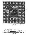
- FIG. 1Athere is shown a top view of an unpackaged semiconductor device 10 made in accordance with the method of the present invention.
- the device 10comprises a semiconductor die or an integrated circuit chip 16 .
- the chip 16is typically substantially rectangular in shape having I/O pads 24 around the periphery or the perimeter thereof.
- the chip 16can be any type of integrated circuit, such as memory, logic, processor, or analog. However, the chip or semiconductor die 16 does not have any ESD circuit associated with the input/output pads 24 .
- the signals both input and output are supplied to the die 16are supplied along these I/O pads 24 .
- the die 16is mounted on a glass substrate 14 which has a plurality of schottkey diodes 22 around its perimeter.
- each of the schottkey diodesis well known in the art and provides the function of ESD protection.
- the glass substrate 14 with the schottkey diodes thereonis mounted on a chip carrier 12 .
- the chip carrier 12has a plurality of leads 20 which are electrical connections to various pins from which the packaged device 10 would supply signals and/or power to or from the device 10 .
- the die 16is mounted on the glass 14 by a die adhesive with the glass substrate 14 attached to the chip carrier 12 also by die adhesive.
- wire bondsare provided to electrically connect the external leads 20 to the schottkey diode 22 on the glass substrate 14 and to the bonding pads 24 on the semiconductor die 16 .
- a first wire bond having a first end and a second endis first used to connect the external lead 20 to the schottkey diode 22 . More particularly, the first end of the wire bond is first attached to the external lead 20 . The second end of the first wire bond is then attached to the schottkey diode 22 . Then a second wire bond having a first end is attached to the schottkey diode 22 . The second end of the second wire bond is then attached to the bonding pad 24 of the semiconductor die 16 .
- any ESD disturbance caused by the act of soldering the wire from the schottkey diode 22 to the bonding pad 24 of the semiconductor die 16can be absorbed by the schottkey diode 22 .
- FIGS. 1A and 1Bany type of IC packaging may be used. Further, after the wire bonds have been attached, the device 10 is then packaged by having epoxy resin or ceramic either surround the sides or encapsulate the wire bonds or surround and encapsulate the entire structure. All of such packaging technique is well known in the art. Further, although the chip 16 is shown as being attached to the carrier 12 in a so-called “face up” configuration, i.e. the first and second bonding wires run along the side of the chip 16 and the side of the substrate 14 , as will be seen, the method of the present invention is not so limited.
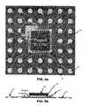
- FIGS. 2A and 2Bthere is shown a top and cross-sectional view, respectively, of a second embodiment of an unpackaged semiconductor device 110 made by the method of the present invention.
- the device 110shown in FIG. 2A, the device 110 comprises a chip carrier 12 , with a plurality of external leads 20 .
- the chip carrier 12again, can be a BGA-type carrier, but the method of the present invention may be used with any type of carrier 12 .
- a substrate 14 with discrete schottkey diodes 22 mounted thereonis mounted onto the chip carrier 12 .
- the schottkey diodes 22are discrete devices bonded to the substrate as an assembly.
- the chip carrier 12may be attached to the substrate 14 by die adhesive or the like.
- a semiconductor die 16 of integrated circuitis mounted on the substrate 14 .
- the semiconductor die 16can be of any type of integrated circuit, but without any ESD circuit thereon.
- the semiconductor die 16can be attached to the substrate 14 by die adhesive.
- a first bonding wireis used to bond the external lead 20 to the schottkey diode 22 on the substrate 14 .
- a second bonding wireis provided with one end of the second bonding wire first attached to the schottkey diode 22 on the substrate 14 , with the other end of the second wire then attached to the bonding pad 24 of the semiconductor die 16 .
- the wiring of the external lead 20 to the bonding pad 24is done in reverse of the normal order, such that by the time the bonding wire is wired to the bonding pad 24 of the semiconductor die 16 , the ESD circuit 22 will have already been electrically attached to the wire and can absorb any ESD disturbance caused during the bonding process.
- the device 110can be packaged by encapsulating just the bonding wires or encapsulating the entire structure, all in a manner well known in the art.
- FIGS. 3A and 3Bthere is shown respectively the top and cross-sectional view of a third embodiment of a semiconductor device 210 made by the method of the present invention.
- this device 210again there is a chip carrier 12 having plurality of leads 20 .
- the carrier 12again, can be a BGA-type carrier or can be any type of carrier.
- a semiconductor die 16 having integrated circuits thereon but without any ESD circuit,is mounted directly on the chip carrier 12 substantially at the central portion thereof. This again can be done by using die adhesive to attach the semiconductor die 16 to the chip carrier 12 .
- One or more strips 14 of glass or semiconductor substrate having schottkey diodes 22 fabricated or mounted thereonare placed adjacent to the semiconductor die 16 and on the chip carrier 12 .
- the semiconductor die 16is not mounted directly on a glass or substrate 14 containing the schottkey diodes 22 . Instead, the semiconductor die 16 is mounted directly on the chip carrier 12 and the glass or silicon substrate 14 with the schottkey diodes 22 are mounted on the chip carrier 12 along the periphery and spaced apart from the semiconductor die 16 .
- a first bonding wireis used to attach the external lead 20 to the schottkey diode 22 .
- a first end of the first bonding wireis first attached to the external lead 20 .
- the other end of the bonding wireis attached to the schottkey diode 22 .
- a second bonding wirehas a first end that is then connected to the schottkey diode 22 .
- the other end of the second wireis then used to bond to the bonding pad 24 of the semiconductor die 16 .
- any ESD disturbance that occurs during the bonding processcan be absorbed by the ESD circuit or the schottkey diode 22 .
- the device 210can be packaged in the usual or well known manner of packaging.
- FIGS. 4A and 4Bthere is shown a fourth embodiment of an unpackaged semiconductor device 310 made in accordance with the present invention.
- the device 310comprises a chip carrier 12 having a plurality of external leads 20 thereon.
- a semiconductor die 16 without any ESD circuitis mounted on the chip carrier 12 by, e.g., die adhesive attaching the die 16 directly to the carrier 12 .
- a ring-shaped polymer having a plurality of schottkey diodes 22 mounted thereon,is also mounted directly on the chip carrier 12 by, e.g., die adhesive attaching the polymer ring 14 to the carrier 12 .
- a first bonding wireis first attached to the external lead 20 . Thereafter it is attached to the schottkey diode 22 which is on the polymer ring 14 .
- a second bonding wireis first attached to the schottkey diode 22 and thereafter is attached to the bonding pad 24 on the semiconductor die 16 .
- the device 310can then be packaged in the usual or well known manner.
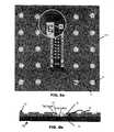
- FIGS. 5A and 5Bthere is shown a top and a cross-sectional view, respectively, of a fifth embodiment of an unpackaged semiconductor device 410 made by the method of the present invention.
- the device 410is similar to the device 10 and 110 shown in FIGS. 1 and 2, respectively.
- the semiconductor die 16is a so-called “flipped IC chip” 16 .
- the bonding pads 24 of the die 16are on a mounting surface which directly faces the substrate 14 .
- the bonding pads 24mount directly onto the substrate 14 which has interconnections through the substrate 14 to the schottkey diode 22 .
- a first bonding wireis used to bond the external lead 20 to the schottkey diode 22 on the substrate 12 .
- the entire flip chip 16is then mounted with its bonding pads 24 connected to the substrate 14 . In that manner, electrical connection is then made between the schottkey diode 22 and the integrated circuit on the die 16 .
- well known packaging techniquesare used to package the device 410 .
- a chip carrier 12has a plurality of external leads 20 on a first surface thereof.
- the chip carrier 12also has a second surface opposite the first surface on which are mounted the external leads 20 .
- the semiconductor die 16has a mounting surface having the bonding pads 24 thereon. The mounting surface is mated to the second surface of the chip carrier 12 . This is a well known “face down” structure. Between the first surface and the second surface of the chip carrier 12 is an aperture 15 .
- the input/output bonding pads 24 of the semiconductor die 16are substantially located in the middle of the rectangularly-shaped die 16 and the die 16 is positioned with respect to the chip carrier 12 such that the bonding pads 24 are positioned within the aperture 15 .
- a strip of glass or silicon substrate containing a plurality of schottkey diodes 22are mounted on the mounting surface of the die 16 and are also positioned within the aperture 15 . Alternatively, the diodes 22 could be mounted and pre-attached to bond leads of the package substrate.
- the die 16is typically a memory circuit, such as a DDR DRAM memory circuit, but without ESD circuit integrated therewith.
- a leadis then used to bond the external lead 20 to the schottkey diode 22 and to the bonding pad 24 of the semiconductor die 16 .
- a first bondis created between the external lead 20 and the schottkey diode 22 .
- the same external leadis extended and is used to connect between the external lead 20 and the bonding pad 24 on the semiconductor die 16 .
- packagingcan be completed by simply encapsulating the aperture 15 and/or additionally encapsulating the chip carrier 12 and the die 16 together.
- FIG. 7 athere is shown a schematic diagram of a plurality of packaged integrated circuit semiconductor devices 610 ( a - i ) of the present invention.
- the nine devices 610 ( a - i )are arranged in a plurality of rows and columns.
- a plurality of control signals 60 ( a - c )access each device 610 in the same column.
- Each device 610comprises a semiconductor die 16 without an ESD circuit integrated therewith.
- the integrated circuit die 16is a DDR (DRAM) memory device.
- DRAMDDR
- the present inventionis not so limited and can be any type of device that requires operation at a high transmission rate.
- the die 16is packaged along with a separate ESD circuit 22 , such as a schottkey diode 22 , in a package 30 , in the manner described heretofore.
- the package 30receives an external lead 20 and is connected to the schottkey diode 22 and to the bonding pad 24 of the die 16 .
- the device 610also comprises a terminating resistor 36 which is switchably connected by switch 32 to the external lead 20 and to the bonding pad 24 .
- the terminating resistor 36can be made of a thin film resistor and can be very precise. In a preferred embodiment, the terminating resistor 36 has 50 ⁇ resistance (or any other amount of resistance).
- the switch 32can be controlled by the control signal 60 supplied along the column line.
- the switch 32can be a transistor which can be electrically activated.
- the switch 32can be a fuse which can be blown or not blown and thereby “permanently” connect or disconnect the resistor 36 to the external lead 20 .
- the external leads 20 to each device 610 in the same roware all connected to the same row signal line 62 .
- the control signal 60is selected to activate the switch 32 connecting the terminating resistor 36 to the external lead 20 .
- signals supplied along the external lead 20will have a 50 ⁇ terminating resistance (or any other amount of resistance) which is typically the matched impedance for high frequency operation. This would be in the event the integrated circuit within the die 16 can be operated at such high frequency.
- the schottkey diode 22performs the function of ESD protection for the circuit of the die 16 .
- the control signal 40may be used to deactivate the switch 32 thereby disconnecting the terminating resistor 36 from the external lead 20 .
- the same circuit on the die 16may be fabricated through the same fabrication line and only during the wafer sort can the “high/low” performance dies be selected. Thus, there need not be separate inventories kept for different performance IC dies 16 .
- FIG. 7 bthere is shown a schematic circuit drawing of another embodiment of a plurality of packaged devices 610 of the present invention. Similar to the devices 610 shown in FIG. 7 a, the devices 610 shown in FIG. 7 b are arranged in a plurality of rows and columns. The only difference between the embodiment shown in FIG. 7 b and that shown in FIG. 7 a is that the external lead 20 for each device 610 is individually supplied with the signal supplied on signal line 62 ( a - i ), and is not supplied in common to the same row.
- FIG. 8 athere is shown a schematic circuit drawing of a plurality of packaged integrated circuit semiconductor devices 710 ( a - i ) of the present invention.
- the nine devices 710 ( a - i )are arranged in a plurality of rows and columns.
- a plurality of control signals 60 ( a - c )access each device 710 in the same column.
- Each device 710comprises a semiconductor die 16 without an ESD circuit integrated therewith.
- the integrated circuit die 16is a DDR (DRAM) memory device.
- DRAMDDR
- the present inventionis not so limited and can be any type of device that requires operation at a high transmission rate.
- the die 16is packaged along with a separate ESD circuit 22 , such as a schottkey diode 22 , in a package 30 , in the manner described heretofore.
- the package 30receives an external lead 20 and is connected to the schottkey diode 22 and to the bonding pad 24 of the die 16 .
- the device 710also comprises a resistor 36 , connected in series with the external lead 20 , and which is switchably connected by switch 32 b to the bonding pad 24 .
- the resistor 36can be made of a thin film resistor and can be very precise. In a preferred embodiment, the resistor 36 has 50 ⁇ resistance.
- the switch 32 bcan be controlled by the control signal 60 c supplied along the column line.
- the switch 32 bcan be a transistor which can be electrically activated.
- the external lead 20is supplied along a parallel path to a second switch 32 a, which is activated by a signal from the control line 64 c. If the switch 32 a is activated, the signal from the external lead 20 is supplied directly to the bonding pad 24 .
- the external leads 20 to each device 710 in the same roware all connected to the same row signal line 62 .
- FIG. 8 bthere is shown a schematic circuit drawing of another embodiment of a plurality of packaged devices 710 of the present invention. Similar to the devices 710 shown in FIG. 8 a, the devices 710 shown in FIG. 8 b are arranged in a plurality of rows and columns. The only difference between the embodiment shown in FIG. 8 b and that shown in FIG. 8 a is that the external lead 20 for each device 710 is individually supplied with the signal supplied on signal line 62 ( a - i ), and is not supplied in common to the same row.
Landscapes
- Engineering & Computer Science (AREA)
- Power Engineering (AREA)
- Computer Hardware Design (AREA)
- Microelectronics & Electronic Packaging (AREA)
- Physics & Mathematics (AREA)
- Condensed Matter Physics & Semiconductors (AREA)
- General Physics & Mathematics (AREA)
- Semiconductor Integrated Circuits (AREA)
Abstract
Description
- This non-provisional application claims the priority of a Provisional Application Serial No. 60/358,17 filed on Feb. 20, 2002 and a Provisional Application Serial No. 60/380,033 filed on May 6, 2002, whose disclosures are incorporated herein in their entirety by reference.[0001]
- The present invention relates to a method of bonding a semiconductor die without an ESD circuit and a separate ESD circuit to an external lead, and more particularly to a semiconductor device made thereby.[0002]
- In a semiconductor device, which has a semiconductor die having an integrated circuit thereon, it is well known to have an ESD circuit to protect the input/output signal of the integrated circuit from electrostatic discharge. Typically, the ESD circuit is integrated with the integrated circuit onto the same single semiconductor die.[0003]
- In U.S. Pat. Nos. 6,198,16 and 6,066,890, the references disclose the ESD circuit being a separate circuit apart from a semiconductor die and packaged together in a single package to protect and enhance the performance of the integrated circuit die. See, for example, FIGS.[0004]3-5 and column 3, lines 29-50 of U.S. Pat. No. 6,066,890. However, one of the shortcomings of these references is that the particular order by which the external leads are bonded or connected to the various circuits is not disclosed. This is important in that since the ESD circuit is removed from the integrated circuit die, the die is “exposed” to the harmful effects of ESD, during the bonding process.
- Further, the references do not disclose particular structures of chip carriers and semiconductor dies that may be connected to the separate ESD circuit advantageously. In particular, such a structure would be useful for packaging a semiconductor die with the integrated circuit as memory circuits. Finally, the references do not disclose the use of separate ESD circuits with terminating resistors outside of the semiconductor die but part of the package of the semiconductor device. These and other shortcomings are overcome by the present invention.[0005]
- Other relevant art includes U.S. Pat. Nos. 5,771,140; 6,385,021; and 5,859,758.[0006]
- In the present invention, a method for bonding a semiconductor die without an ESD circuit and a separate ESD circuit to an external lead is disclosed. In the method of the present invention, the external lead is first bonded to the separate ESD circuit. Thereafter, the separate ESD circuit with the external lead bonded thereto is then bonded to the semiconductor die.[0007]
- The present invention also relates to a semiconductor device which has a chip carrier, a semiconductor die, and an ESD circuit. The chip carrier has a first surface with a plurality of leads and a second surface opposite to the first surface, and an aperture between the first surface and the second surface. The semiconductor die has a mounting surface with a mounting pad thereon facing the second surface with the mounting pad in the aperture. The ESD circuit is on the mounting surface in the aperture. A first electrical connector connects one of the plurality of leads to the ESD circuit and a second electrical connector connects the ESD circuit to the mounting pad.[0008]
- In addition, the present invention relates to a method of assembling a semiconductor device wherein a strip containing a plurality of ESD circuits are mounted on the mounting surface of the semiconductor die with the strip of plurality of ESD circuits mounted substantially adjacent to a plurality rows of mounting pads of the semiconductor die.[0009]
- Finally, the present invention relates to a semiconductor device which has a semiconductor die with an input pad, an ESD circuit electrically connected to the input pad, and a terminating resistor switchably connected to the input pad. The ESD circuit and the resistor are external to the die, but packaged in the same package. An external lead is connected to the input pad.[0010]
- FIG. 1A is a top view of a first embodiment of an unpackaged semiconductor device manufactured by the method of the present invention, with FIG. 1B being a cross-sectional view of the device shown in FIG. 1A.[0011]
- FIG. 2A is a top view of a second embodiment of an unpackaged semiconductor device manufactured by the method of the present invention, with FIG. 2B being a cross-sectional view of the device shown in FIG. 2A.[0012]
- FIG. 3A is a top view of a third embodiment of an unpackaged semiconductor device manufactured by the method of the present invention, with FIG. 3B being a cross-sectional view of the device shown in FIG. 3A.[0013]
- FIG. 4A is a top view of a fourth embodiment of an unpackaged semiconductor device manufactured by the method of the present invention, with FIG. 4B being a cross-sectional view of the device shown in FIG. 4A.[0014]
- FIG. 5A is a top view of a fifth embodiment of an unpackaged semiconductor device manufactured by the method of the present invention, with FIG. 5B being a cross-sectional view of the device shown in FIG. 5A.[0015]
- FIG. 6A is a top view of a sixth embodiment of an unpackaged semiconductor device of the present invention, also made by the method of the present invention, with FIG. 6B being a cross-sectional view shown in FIG. 6A.[0016]
- FIG. 7[0017]a&7bare schematic circuit diagrams of a plurality of semiconductor devices of the present invention each packaged with a terminating resistor switchably connectable by a control signal.
- FIG. 8[0018]a&8bare schematic circuit diagrams of a plurality of semiconductor devices of the present invention, each packaged with a series resistor switchably connectable by a first control signal and a second control signal.
- Referring to FIG. 1A there is shown a top view of an[0019]
unpackaged semiconductor device 10 made in accordance with the method of the present invention. Thedevice 10 comprises a semiconductor die or anintegrated circuit chip 16. Thechip 16 is typically substantially rectangular in shape having I/O pads 24 around the periphery or the perimeter thereof. Thechip 16 can be any type of integrated circuit, such as memory, logic, processor, or analog. However, the chip or semiconductor die16 does not have any ESD circuit associated with the input/output pads 24. The signals both input and output are supplied to the die16 are supplied along these I/O pads 24. Thedie 16 is mounted on aglass substrate 14 which has a plurality ofschottkey diodes 22 around its perimeter. Each of the schottkey diodes is well known in the art and provides the function of ESD protection. Finally, theglass substrate 14 with the schottkey diodes thereon is mounted on achip carrier 12. Thechip carrier 12 has a plurality ofleads 20 which are electrical connections to various pins from which the packageddevice 10 would supply signals and/or power to or from thedevice 10. Typically, thedie 16 is mounted on theglass 14 by a die adhesive with theglass substrate 14 attached to thechip carrier 12 also by die adhesive. - In the method of the present invention, wire bonds are provided to electrically connect the external leads[0020]20 to the
schottkey diode 22 on theglass substrate 14 and to thebonding pads 24 on the semiconductor die16. In particular, a first wire bond having a first end and a second end is first used to connect theexternal lead 20 to theschottkey diode 22. More particularly, the first end of the wire bond is first attached to theexternal lead 20. The second end of the first wire bond is then attached to theschottkey diode 22. Then a second wire bond having a first end is attached to theschottkey diode 22. The second end of the second wire bond is then attached to thebonding pad 24 of the semiconductor die16. - It should be noted that this order of first attaching the wire bond from the[0021]
external lead 20 to theschottkey diode 22 and then to thebonding pad 24 of the semiconductor die16 is in reverse of the normal order. In the prior art, when a wire bond is used to attach thebonding pad 24 from the die16 to theexternal lead 20, bond wires are first attached to thebonding pad 24 and then to theexternal lead 20. This is undesirable and can have a deleterious effect where the semiconductor die16 does not have an ESD circuit designed therein. With the method of the present invention, the external lead is first attached to theschottkey diode 22. Then the connection from theschottkey diode 22 to thebonding pad 24 of the semiconductor die16 is made. In so doing, any ESD disturbance caused by the act of soldering the wire from theschottkey diode 22 to thebonding pad 24 of the semiconductor die16 can be absorbed by theschottkey diode 22. - Although a BGA-type package is disclosed in FIGS. 1A and 1B, any type of IC packaging may be used. Further, after the wire bonds have been attached, the[0022]
device 10 is then packaged by having epoxy resin or ceramic either surround the sides or encapsulate the wire bonds or surround and encapsulate the entire structure. All of such packaging technique is well known in the art. Further, although thechip 16 is shown as being attached to thecarrier 12 in a so-called “face up” configuration, i.e. the first and second bonding wires run along the side of thechip 16 and the side of thesubstrate 14, as will be seen, the method of the present invention is not so limited. - Referring to FIGS. 2A and 2B, there is shown a top and cross-sectional view, respectively, of a second embodiment of an[0023]
unpackaged semiconductor device 110 made by the method of the present invention. In thedevice 110, shown in FIG. 2A, thedevice 110 comprises achip carrier 12, with a plurality of external leads20. Thechip carrier 12, again, can be a BGA-type carrier, but the method of the present invention may be used with any type ofcarrier 12. Asubstrate 14 withdiscrete schottkey diodes 22 mounted thereon is mounted onto thechip carrier 12. In this embodiment, theschottkey diodes 22 are discrete devices bonded to the substrate as an assembly. Thechip carrier 12 may be attached to thesubstrate 14 by die adhesive or the like. A semiconductor die16 of integrated circuit is mounted on thesubstrate 14. Again, the semiconductor die16 can be of any type of integrated circuit, but without any ESD circuit thereon. The semiconductor die16 can be attached to thesubstrate 14 by die adhesive. - Again, in the method of the present invention, a first bonding wire is used to bond the[0024]
external lead 20 to theschottkey diode 22 on thesubstrate 14. A second bonding wire is provided with one end of the second bonding wire first attached to theschottkey diode 22 on thesubstrate 14, with the other end of the second wire then attached to thebonding pad 24 of the semiconductor die16. Again, the wiring of theexternal lead 20 to thebonding pad 24 is done in reverse of the normal order, such that by the time the bonding wire is wired to thebonding pad 24 of the semiconductor die16, theESD circuit 22 will have already been electrically attached to the wire and can absorb any ESD disturbance caused during the bonding process. - Finally, after the[0025]
device 110 has been bonded, it can be packaged by encapsulating just the bonding wires or encapsulating the entire structure, all in a manner well known in the art. - Referring to FIGS. 3A and 3B there is shown respectively the top and cross-sectional view of a third embodiment of a[0026]
semiconductor device 210 made by the method of the present invention. In thisdevice 210, again there is achip carrier 12 having plurality of leads20. Thecarrier 12, again, can be a BGA-type carrier or can be any type of carrier. A semiconductor die16 having integrated circuits thereon but without any ESD circuit, is mounted directly on thechip carrier 12 substantially at the central portion thereof. This again can be done by using die adhesive to attach the semiconductor die16 to thechip carrier 12. One ormore strips 14 of glass or semiconductor substrate havingschottkey diodes 22 fabricated or mounted thereon are placed adjacent to the semiconductor die16 and on thechip carrier 12. Thus, unlike the embodiments shown in FIGS. 1 and 2, in thedevice 210, the semiconductor die16 is not mounted directly on a glass orsubstrate 14 containing theschottkey diodes 22. Instead, the semiconductor die16 is mounted directly on thechip carrier 12 and the glass orsilicon substrate 14 with theschottkey diodes 22 are mounted on thechip carrier 12 along the periphery and spaced apart from the semiconductor die16. - Again, the method of bonding the wires to the various components is as follows. A first bonding wire is used to attach the[0027]
external lead 20 to theschottkey diode 22. A first end of the first bonding wire is first attached to theexternal lead 20. The other end of the bonding wire is attached to theschottkey diode 22. A second bonding wire has a first end that is then connected to theschottkey diode 22. The other end of the second wire is then used to bond to thebonding pad 24 of the semiconductor die16. - Again, with the method of the present invention, any ESD disturbance that occurs during the bonding process can be absorbed by the ESD circuit or the[0028]
schottkey diode 22. Finally, thedevice 210 can be packaged in the usual or well known manner of packaging. - Referring to FIGS. 4A and 4B, there is shown a fourth embodiment of an[0029]
unpackaged semiconductor device 310 made in accordance with the present invention. Thedevice 310 comprises achip carrier 12 having a plurality ofexternal leads 20 thereon. A semiconductor die16 without any ESD circuit, is mounted on thechip carrier 12 by, e.g., die adhesive attaching the die16 directly to thecarrier 12. A ring-shaped polymer having a plurality ofschottkey diodes 22 mounted thereon, is also mounted directly on thechip carrier 12 by, e.g., die adhesive attaching thepolymer ring 14 to thecarrier 12. Similar to the aforementioned methods, in the method of bonding thedevice 310, a first bonding wire is first attached to theexternal lead 20. Thereafter it is attached to theschottkey diode 22 which is on thepolymer ring 14. A second bonding wire is first attached to theschottkey diode 22 and thereafter is attached to thebonding pad 24 on the semiconductor die16. Thedevice 310 can then be packaged in the usual or well known manner. - Referring to FIGS. 5A and 5B, there is shown a top and a cross-sectional view, respectively, of a fifth embodiment of an[0030]
unpackaged semiconductor device 410 made by the method of the present invention. Thedevice 410 is similar to thedevice devices bonding pads 24 of the die16 are on a mounting surface which directly faces thesubstrate 14. Thus, thebonding pads 24 mount directly onto thesubstrate 14 which has interconnections through thesubstrate 14 to theschottkey diode 22. - In the method of the present invention, a first bonding wire is used to bond the[0031]
external lead 20 to theschottkey diode 22 on thesubstrate 12. Once all the bonding wires have been attached from the external leads20 to theschottkey diodes 22, theentire flip chip 16 is then mounted with itsbonding pads 24 connected to thesubstrate 14. In that manner, electrical connection is then made between theschottkey diode 22 and the integrated circuit on thedie 16. Finally, well known packaging techniques are used to package thedevice 410. - Referring to FIG. 6A there is shown a sixth embodiment of an[0032]
unpackaged semiconductor device 510 of the present invention, made by the method of the present invention. Indevice 510, achip carrier 12 has a plurality ofexternal leads 20 on a first surface thereof. Thechip carrier 12 also has a second surface opposite the first surface on which are mounted the external leads20. The semiconductor die16 has a mounting surface having thebonding pads 24 thereon. The mounting surface is mated to the second surface of thechip carrier 12. This is a well known “face down” structure. Between the first surface and the second surface of thechip carrier 12 is anaperture 15. The input/output bonding pads 24 of the semiconductor die16 are substantially located in the middle of the rectangularly-shapeddie 16 and thedie 16 is positioned with respect to thechip carrier 12 such that thebonding pads 24 are positioned within theaperture 15. A strip of glass or silicon substrate containing a plurality ofschottkey diodes 22 are mounted on the mounting surface of thedie 16 and are also positioned within theaperture 15. Alternatively, thediodes 22 could be mounted and pre-attached to bond leads of the package substrate. Thedie 16 is typically a memory circuit, such as a DDR DRAM memory circuit, but without ESD circuit integrated therewith. A lead is then used to bond theexternal lead 20 to theschottkey diode 22 and to thebonding pad 24 of the semiconductor die16. Thus, in the method of the present invention, a first bond is created between theexternal lead 20 and theschottkey diode 22. Thereafter, the same external lead is extended and is used to connect between theexternal lead 20 and thebonding pad 24 on the semiconductor die16. - Thereafter, packaging can be completed by simply encapsulating the[0033]
aperture 15 and/or additionally encapsulating thechip carrier 12 and the die16 together. - Referring to FIG. 7[0034]athere is shown a schematic diagram of a plurality of packaged integrated circuit semiconductor devices610(a-i) of the present invention. The nine devices610(a-i) are arranged in a plurality of rows and columns. A plurality of control signals60(a-c) access each device610 in the same column. Each device610 comprises a
semiconductor die 16 without an ESD circuit integrated therewith. In the preferred embodiment, the integrated circuit die16 is a DDR (DRAM) memory device. However, the present invention is not so limited and can be any type of device that requires operation at a high transmission rate. Thedie 16 is packaged along with aseparate ESD circuit 22, such as aschottkey diode 22, in a package30, in the manner described heretofore. The package30 receives anexternal lead 20 and is connected to theschottkey diode 22 and to thebonding pad 24 of thedie 16. In addition, however, the device610 also comprises a terminatingresistor 36 which is switchably connected byswitch 32 to theexternal lead 20 and to thebonding pad 24. The terminatingresistor 36 can be made of a thin film resistor and can be very precise. In a preferred embodiment, the terminatingresistor 36 has 50Ω resistance (or any other amount of resistance). Theswitch 32 can be controlled by the control signal60 supplied along the column line. Therefore, theswitch 32 can be a transistor which can be electrically activated. Alternatively, theswitch 32 can be a fuse which can be blown or not blown and thereby “permanently” connect or disconnect theresistor 36 to theexternal lead 20. The external leads20 to each device610 in the same row are all connected to the same row signal line62. - With the device[0035]610 of the present invention, if it is desired to operate the device610 in a high performance mode, i.e., at a high frequency, the control signal60 is selected to activate the
switch 32 connecting the terminatingresistor 36 to theexternal lead 20. In that event, signals supplied along theexternal lead 20 will have a 50Ω terminating resistance (or any other amount of resistance) which is typically the matched impedance for high frequency operation. This would be in the event the integrated circuit within the die16 can be operated at such high frequency. At the same time, theschottkey diode 22 performs the function of ESD protection for the circuit of thedie 16. - Alternatively, if the IC in the[0036]
die 16 is deemed to be of “low quality” and is not able to perform at high frequency, then the control signal40 may be used to deactivate theswitch 32 thereby disconnecting the terminatingresistor 36 from theexternal lead 20. Thus, with the device610 of the present invention, the same circuit on the die16 may be fabricated through the same fabrication line and only during the wafer sort can the “high/low” performance dies be selected. Thus, there need not be separate inventories kept for different performance IC dies16. - Referring to FIG. 7[0037]b,there is shown a schematic circuit drawing of another embodiment of a plurality of packaged devices610 of the present invention. Similar to the devices610 shown in FIG. 7a,the devices610 shown in FIG. 7bare arranged in a plurality of rows and columns. The only difference between the embodiment shown in FIG. 7band that shown in FIG. 7ais that the
external lead 20 for each device610 is individually supplied with the signal supplied on signal line62(a-i), and is not supplied in common to the same row. - Referring to FIG. 8[0038]athere is shown a schematic circuit drawing of a plurality of packaged integrated circuit semiconductor devices710(a-i) of the present invention. The nine devices710(a-i) are arranged in a plurality of rows and columns. A plurality of control signals60(a-c) access each device710 in the same column. Each device710 comprises a
semiconductor die 16 without an ESD circuit integrated therewith. In the preferred embodiment, the integrated circuit die16 is a DDR (DRAM) memory device. However, the present invention is not so limited and can be any type of device that requires operation at a high transmission rate. Thedie 16 is packaged along with aseparate ESD circuit 22, such as aschottkey diode 22, in a package30, in the manner described heretofore. The package30 receives anexternal lead 20 and is connected to theschottkey diode 22 and to thebonding pad 24 of thedie 16. In addition, however, the device710 also comprises aresistor 36, connected in series with theexternal lead 20, and which is switchably connected byswitch 32bto thebonding pad 24. Theresistor 36 can be made of a thin film resistor and can be very precise. In a preferred embodiment, theresistor 36 has 50Ω resistance. Theswitch 32bcan be controlled by thecontrol signal 60csupplied along the column line. Therefore, theswitch 32bcan be a transistor which can be electrically activated. In addition, theexternal lead 20 is supplied along a parallel path to asecond switch 32a,which is activated by a signal from thecontrol line 64c.If theswitch 32ais activated, the signal from theexternal lead 20 is supplied directly to thebonding pad 24. The external leads20 to each device710 in the same row are all connected to the same row signal line62. - Referring to FIG. 8[0039]b,there is shown a schematic circuit drawing of another embodiment of a plurality of packaged devices710 of the present invention. Similar to the devices710 shown in FIG. 8a,the devices710 shown in FIG. 8bare arranged in a plurality of rows and columns. The only difference between the embodiment shown in FIG. 8band that shown in FIG. 8ais that the
external lead 20 for each device710 is individually supplied with the signal supplied on signal line62(a-i), and is not supplied in common to the same row.
Claims (26)
Priority Applications (1)
| Application Number | Priority Date | Filing Date | Title |
|---|---|---|---|
| US10/370,422US6933610B2 (en) | 2002-02-20 | 2003-02-19 | Method of bonding a semiconductor die without an ESD circuit and a separate ESD circuit to an external lead, and a semiconductor device made thereby |
Applications Claiming Priority (3)
| Application Number | Priority Date | Filing Date | Title |
|---|---|---|---|
| US35811702P | 2002-02-20 | 2002-02-20 | |
| US38003302P | 2002-05-06 | 2002-05-06 | |
| US10/370,422US6933610B2 (en) | 2002-02-20 | 2003-02-19 | Method of bonding a semiconductor die without an ESD circuit and a separate ESD circuit to an external lead, and a semiconductor device made thereby |
Publications (2)
| Publication Number | Publication Date |
|---|---|
| US20030205802A1true US20030205802A1 (en) | 2003-11-06 |
| US6933610B2 US6933610B2 (en) | 2005-08-23 |
Family
ID=34865123
Family Applications (1)
| Application Number | Title | Priority Date | Filing Date |
|---|---|---|---|
| US10/370,422Expired - LifetimeUS6933610B2 (en) | 2002-02-20 | 2003-02-19 | Method of bonding a semiconductor die without an ESD circuit and a separate ESD circuit to an external lead, and a semiconductor device made thereby |
Country Status (1)
| Country | Link |
|---|---|
| US (1) | US6933610B2 (en) |
Cited By (35)
| Publication number | Priority date | Publication date | Assignee | Title |
|---|---|---|---|---|
| US20040227226A1 (en)* | 2003-05-16 | 2004-11-18 | Via Technologies, Inc. | Structure of multi-tier wire bonding for high frequency integrated circuits and method of layout for the same |
| US20060180902A1 (en)* | 2005-02-11 | 2006-08-17 | Rambus, Inc. | Semiconductor package with low and high-speed signal paths |
| US7379316B2 (en) | 2005-09-02 | 2008-05-27 | Metaram, Inc. | Methods and apparatus of stacking DRAMs |
| US7515453B2 (en) | 2005-06-24 | 2009-04-07 | Metaram, Inc. | Integrated memory core and memory interface circuit |
| US8019589B2 (en) | 2006-07-31 | 2011-09-13 | Google Inc. | Memory apparatus operable to perform a power-saving operation |
| US8055833B2 (en) | 2006-10-05 | 2011-11-08 | Google Inc. | System and method for increasing capacity, performance, and flexibility of flash storage |
| US8060774B2 (en) | 2005-06-24 | 2011-11-15 | Google Inc. | Memory systems and memory modules |
| US8081474B1 (en) | 2007-12-18 | 2011-12-20 | Google Inc. | Embossed heat spreader |
| US8080874B1 (en) | 2007-09-14 | 2011-12-20 | Google Inc. | Providing additional space between an integrated circuit and a circuit board for positioning a component therebetween |
| US8090897B2 (en) | 2006-07-31 | 2012-01-03 | Google Inc. | System and method for simulating an aspect of a memory circuit |
| US8089795B2 (en) | 2006-02-09 | 2012-01-03 | Google Inc. | Memory module with memory stack and interface with enhanced capabilities |
| US8111566B1 (en) | 2007-11-16 | 2012-02-07 | Google, Inc. | Optimal channel design for memory devices for providing a high-speed memory interface |
| US8130560B1 (en) | 2006-11-13 | 2012-03-06 | Google Inc. | Multi-rank partial width memory modules |
| US8154935B2 (en) | 2006-07-31 | 2012-04-10 | Google Inc. | Delaying a signal communicated from a system to at least one of a plurality of memory circuits |
| US8169233B2 (en) | 2009-06-09 | 2012-05-01 | Google Inc. | Programming of DIMM termination resistance values |
| US8181048B2 (en) | 2006-07-31 | 2012-05-15 | Google Inc. | Performing power management operations |
| US8209479B2 (en) | 2007-07-18 | 2012-06-26 | Google Inc. | Memory circuit system and method |
| US8244971B2 (en) | 2006-07-31 | 2012-08-14 | Google Inc. | Memory circuit system and method |
| US8280714B2 (en) | 2006-07-31 | 2012-10-02 | Google Inc. | Memory circuit simulation system and method with refresh capabilities |
| US8327104B2 (en) | 2006-07-31 | 2012-12-04 | Google Inc. | Adjusting the timing of signals associated with a memory system |
| US8335894B1 (en) | 2008-07-25 | 2012-12-18 | Google Inc. | Configurable memory system with interface circuit |
| US8386722B1 (en) | 2008-06-23 | 2013-02-26 | Google Inc. | Stacked DIMM memory interface |
| US8397013B1 (en) | 2006-10-05 | 2013-03-12 | Google Inc. | Hybrid memory module |
| US8438328B2 (en) | 2008-02-21 | 2013-05-07 | Google Inc. | Emulation of abstracted DIMMs using abstracted DRAMs |
| US8566516B2 (en) | 2006-07-31 | 2013-10-22 | Google Inc. | Refresh management of memory modules |
| US8773937B2 (en) | 2005-06-24 | 2014-07-08 | Google Inc. | Memory refresh apparatus and method |
| US8796830B1 (en) | 2006-09-01 | 2014-08-05 | Google Inc. | Stackable low-profile lead frame package |
| US20140353847A1 (en)* | 2013-06-03 | 2014-12-04 | SK Hynix Inc. | Semiconductor package |
| US8949519B2 (en) | 2005-06-24 | 2015-02-03 | Google Inc. | Simulating a memory circuit |
| US8972673B2 (en) | 2006-07-31 | 2015-03-03 | Google Inc. | Power management of memory circuits by virtual memory simulation |
| US9171585B2 (en) | 2005-06-24 | 2015-10-27 | Google Inc. | Configurable memory circuit system and method |
| US9507739B2 (en) | 2005-06-24 | 2016-11-29 | Google Inc. | Configurable memory circuit system and method |
| US9542353B2 (en) | 2006-02-09 | 2017-01-10 | Google Inc. | System and method for reducing command scheduling constraints of memory circuits |
| US9632929B2 (en) | 2006-02-09 | 2017-04-25 | Google Inc. | Translating an address associated with a command communicated between a system and memory circuits |
| US10013371B2 (en) | 2005-06-24 | 2018-07-03 | Google Llc | Configurable memory circuit system and method |
Families Citing this family (1)
| Publication number | Priority date | Publication date | Assignee | Title |
|---|---|---|---|---|
| US8053898B2 (en)* | 2009-10-05 | 2011-11-08 | Samsung Electronics Co., Ltd. | Connection for off-chip electrostatic discharge protection |
Citations (12)
| Publication number | Priority date | Publication date | Assignee | Title |
|---|---|---|---|---|
| US5568346A (en)* | 1994-02-08 | 1996-10-22 | Mitel Corporation | ESD protection circuit |
| US5644167A (en)* | 1996-03-01 | 1997-07-01 | National Semiconductor Corporation | Integrated circuit package assemblies including an electrostatic discharge interposer |
| US5771140A (en)* | 1995-11-28 | 1998-06-23 | Lg Semicon Co., Ltd. | Electro-static discharge and latch-up prevention circuit |
| US5859758A (en)* | 1996-11-20 | 1999-01-12 | Lg Semicon Co., Ltd. | Electro-static discharge protection circuit |
| US5862031A (en)* | 1997-11-26 | 1999-01-19 | Analog Devices, Inc. | ESD protection circuit for integrated circuits having a bipolar differential input |
| US5978197A (en)* | 1997-11-18 | 1999-11-02 | Lsi Corporation | Testing ESD protection schemes in semiconductor integrated circuits |
| US6066890A (en)* | 1995-11-13 | 2000-05-23 | Siliconix Incorporated | Separate circuit devices in an intra-package configuration and assembly techniques |
| US6198136B1 (en)* | 1996-03-19 | 2001-03-06 | International Business Machines Corporation | Support chips for buffer circuits |
| US6385021B1 (en)* | 2000-04-10 | 2002-05-07 | Motorola, Inc. | Electrostatic discharge (ESD) protection circuit |
| US6458869B1 (en)* | 2000-03-30 | 2002-10-01 | National Institute Of Standards Of Technology | Etchant/primer composition, etchant/primer/adhesive monomer composition, kits and methods using the same for improved bonding to dental structures |
| US6489672B2 (en)* | 1998-02-09 | 2002-12-03 | Winbond Electronics Corp. | Integrated circuit package architecture with improved electrostatic discharge protection |
| US20040041168A1 (en)* | 2002-08-29 | 2004-03-04 | Hembree David R | Test insert with electrostatic discharge structures and associated methods |
Family Cites Families (1)
| Publication number | Priority date | Publication date | Assignee | Title |
|---|---|---|---|---|
| JP2655768B2 (en)* | 1991-08-05 | 1997-09-24 | ローム株式会社 | Adhesive and mounting structure using the same |
- 2003
- 2003-02-19USUS10/370,422patent/US6933610B2/ennot_activeExpired - Lifetime
Patent Citations (12)
| Publication number | Priority date | Publication date | Assignee | Title |
|---|---|---|---|---|
| US5568346A (en)* | 1994-02-08 | 1996-10-22 | Mitel Corporation | ESD protection circuit |
| US6066890A (en)* | 1995-11-13 | 2000-05-23 | Siliconix Incorporated | Separate circuit devices in an intra-package configuration and assembly techniques |
| US5771140A (en)* | 1995-11-28 | 1998-06-23 | Lg Semicon Co., Ltd. | Electro-static discharge and latch-up prevention circuit |
| US5644167A (en)* | 1996-03-01 | 1997-07-01 | National Semiconductor Corporation | Integrated circuit package assemblies including an electrostatic discharge interposer |
| US6198136B1 (en)* | 1996-03-19 | 2001-03-06 | International Business Machines Corporation | Support chips for buffer circuits |
| US5859758A (en)* | 1996-11-20 | 1999-01-12 | Lg Semicon Co., Ltd. | Electro-static discharge protection circuit |
| US5978197A (en)* | 1997-11-18 | 1999-11-02 | Lsi Corporation | Testing ESD protection schemes in semiconductor integrated circuits |
| US5862031A (en)* | 1997-11-26 | 1999-01-19 | Analog Devices, Inc. | ESD protection circuit for integrated circuits having a bipolar differential input |
| US6489672B2 (en)* | 1998-02-09 | 2002-12-03 | Winbond Electronics Corp. | Integrated circuit package architecture with improved electrostatic discharge protection |
| US6458869B1 (en)* | 2000-03-30 | 2002-10-01 | National Institute Of Standards Of Technology | Etchant/primer composition, etchant/primer/adhesive monomer composition, kits and methods using the same for improved bonding to dental structures |
| US6385021B1 (en)* | 2000-04-10 | 2002-05-07 | Motorola, Inc. | Electrostatic discharge (ESD) protection circuit |
| US20040041168A1 (en)* | 2002-08-29 | 2004-03-04 | Hembree David R | Test insert with electrostatic discharge structures and associated methods |
Cited By (70)
| Publication number | Priority date | Publication date | Assignee | Title |
|---|---|---|---|---|
| US20040227226A1 (en)* | 2003-05-16 | 2004-11-18 | Via Technologies, Inc. | Structure of multi-tier wire bonding for high frequency integrated circuits and method of layout for the same |
| US7705445B2 (en) | 2005-02-11 | 2010-04-27 | Rambus Inc. | Semiconductor package with low and high-speed signal paths |
| US20060180902A1 (en)* | 2005-02-11 | 2006-08-17 | Rambus, Inc. | Semiconductor package with low and high-speed signal paths |
| US20080150123A1 (en)* | 2005-02-11 | 2008-06-26 | Ming Li | Semiconductor Package With Rigid And Flexible Circuits |
| US7515453B2 (en) | 2005-06-24 | 2009-04-07 | Metaram, Inc. | Integrated memory core and memory interface circuit |
| US8615679B2 (en) | 2005-06-24 | 2013-12-24 | Google Inc. | Memory modules with reliability and serviceability functions |
| US10013371B2 (en) | 2005-06-24 | 2018-07-03 | Google Llc | Configurable memory circuit system and method |
| US9507739B2 (en) | 2005-06-24 | 2016-11-29 | Google Inc. | Configurable memory circuit system and method |
| US9171585B2 (en) | 2005-06-24 | 2015-10-27 | Google Inc. | Configurable memory circuit system and method |
| US8060774B2 (en) | 2005-06-24 | 2011-11-15 | Google Inc. | Memory systems and memory modules |
| US8949519B2 (en) | 2005-06-24 | 2015-02-03 | Google Inc. | Simulating a memory circuit |
| US8359187B2 (en) | 2005-06-24 | 2013-01-22 | Google Inc. | Simulating a different number of memory circuit devices |
| US8386833B2 (en) | 2005-06-24 | 2013-02-26 | Google Inc. | Memory systems and memory modules |
| US8773937B2 (en) | 2005-06-24 | 2014-07-08 | Google Inc. | Memory refresh apparatus and method |
| US8811065B2 (en) | 2005-09-02 | 2014-08-19 | Google Inc. | Performing error detection on DRAMs |
| US8619452B2 (en) | 2005-09-02 | 2013-12-31 | Google Inc. | Methods and apparatus of stacking DRAMs |
| US8582339B2 (en) | 2005-09-02 | 2013-11-12 | Google Inc. | System including memory stacks |
| US7379316B2 (en) | 2005-09-02 | 2008-05-27 | Metaram, Inc. | Methods and apparatus of stacking DRAMs |
| US8797779B2 (en) | 2006-02-09 | 2014-08-05 | Google Inc. | Memory module with memory stack and interface with enhanced capabilites |
| US9632929B2 (en) | 2006-02-09 | 2017-04-25 | Google Inc. | Translating an address associated with a command communicated between a system and memory circuits |
| US8089795B2 (en) | 2006-02-09 | 2012-01-03 | Google Inc. | Memory module with memory stack and interface with enhanced capabilities |
| US8566556B2 (en) | 2006-02-09 | 2013-10-22 | Google Inc. | Memory module with memory stack and interface with enhanced capabilities |
| US9542353B2 (en) | 2006-02-09 | 2017-01-10 | Google Inc. | System and method for reducing command scheduling constraints of memory circuits |
| US9542352B2 (en) | 2006-02-09 | 2017-01-10 | Google Inc. | System and method for reducing command scheduling constraints of memory circuits |
| US9727458B2 (en) | 2006-02-09 | 2017-08-08 | Google Inc. | Translating an address associated with a command communicated between a system and memory circuits |
| US8671244B2 (en) | 2006-07-31 | 2014-03-11 | Google Inc. | Simulating a memory standard |
| US8112266B2 (en) | 2006-07-31 | 2012-02-07 | Google Inc. | Apparatus for simulating an aspect of a memory circuit |
| US8090897B2 (en) | 2006-07-31 | 2012-01-03 | Google Inc. | System and method for simulating an aspect of a memory circuit |
| US8327104B2 (en) | 2006-07-31 | 2012-12-04 | Google Inc. | Adjusting the timing of signals associated with a memory system |
| US8154935B2 (en) | 2006-07-31 | 2012-04-10 | Google Inc. | Delaying a signal communicated from a system to at least one of a plurality of memory circuits |
| US8745321B2 (en) | 2006-07-31 | 2014-06-03 | Google Inc. | Simulating a memory standard |
| US8280714B2 (en) | 2006-07-31 | 2012-10-02 | Google Inc. | Memory circuit simulation system and method with refresh capabilities |
| US8181048B2 (en) | 2006-07-31 | 2012-05-15 | Google Inc. | Performing power management operations |
| US8566516B2 (en) | 2006-07-31 | 2013-10-22 | Google Inc. | Refresh management of memory modules |
| US8244971B2 (en) | 2006-07-31 | 2012-08-14 | Google Inc. | Memory circuit system and method |
| US8041881B2 (en) | 2006-07-31 | 2011-10-18 | Google Inc. | Memory device with emulated characteristics |
| US8595419B2 (en) | 2006-07-31 | 2013-11-26 | Google Inc. | Memory apparatus operable to perform a power-saving operation |
| US8601204B2 (en) | 2006-07-31 | 2013-12-03 | Google Inc. | Simulating a refresh operation latency |
| US8340953B2 (en) | 2006-07-31 | 2012-12-25 | Google, Inc. | Memory circuit simulation with power saving capabilities |
| US8868829B2 (en) | 2006-07-31 | 2014-10-21 | Google Inc. | Memory circuit system and method |
| US9047976B2 (en) | 2006-07-31 | 2015-06-02 | Google Inc. | Combined signal delay and power saving for use with a plurality of memory circuits |
| US8631220B2 (en) | 2006-07-31 | 2014-01-14 | Google Inc. | Adjusting the timing of signals associated with a memory system |
| US8667312B2 (en) | 2006-07-31 | 2014-03-04 | Google Inc. | Performing power management operations |
| US8019589B2 (en) | 2006-07-31 | 2011-09-13 | Google Inc. | Memory apparatus operable to perform a power-saving operation |
| US8972673B2 (en) | 2006-07-31 | 2015-03-03 | Google Inc. | Power management of memory circuits by virtual memory simulation |
| US8796830B1 (en) | 2006-09-01 | 2014-08-05 | Google Inc. | Stackable low-profile lead frame package |
| US8977806B1 (en) | 2006-10-05 | 2015-03-10 | Google Inc. | Hybrid memory module |
| US8055833B2 (en) | 2006-10-05 | 2011-11-08 | Google Inc. | System and method for increasing capacity, performance, and flexibility of flash storage |
| US8397013B1 (en) | 2006-10-05 | 2013-03-12 | Google Inc. | Hybrid memory module |
| US8751732B2 (en) | 2006-10-05 | 2014-06-10 | Google Inc. | System and method for increasing capacity, performance, and flexibility of flash storage |
| US8370566B2 (en) | 2006-10-05 | 2013-02-05 | Google Inc. | System and method for increasing capacity, performance, and flexibility of flash storage |
| US8446781B1 (en) | 2006-11-13 | 2013-05-21 | Google Inc. | Multi-rank partial width memory modules |
| US8130560B1 (en) | 2006-11-13 | 2012-03-06 | Google Inc. | Multi-rank partial width memory modules |
| US8760936B1 (en) | 2006-11-13 | 2014-06-24 | Google Inc. | Multi-rank partial width memory modules |
| US8209479B2 (en) | 2007-07-18 | 2012-06-26 | Google Inc. | Memory circuit system and method |
| US8080874B1 (en) | 2007-09-14 | 2011-12-20 | Google Inc. | Providing additional space between an integrated circuit and a circuit board for positioning a component therebetween |
| US8675429B1 (en) | 2007-11-16 | 2014-03-18 | Google Inc. | Optimal channel design for memory devices for providing a high-speed memory interface |
| US8111566B1 (en) | 2007-11-16 | 2012-02-07 | Google, Inc. | Optimal channel design for memory devices for providing a high-speed memory interface |
| US8730670B1 (en) | 2007-12-18 | 2014-05-20 | Google Inc. | Embossed heat spreader |
| US8081474B1 (en) | 2007-12-18 | 2011-12-20 | Google Inc. | Embossed heat spreader |
| US8705240B1 (en) | 2007-12-18 | 2014-04-22 | Google Inc. | Embossed heat spreader |
| US8438328B2 (en) | 2008-02-21 | 2013-05-07 | Google Inc. | Emulation of abstracted DIMMs using abstracted DRAMs |
| US8631193B2 (en) | 2008-02-21 | 2014-01-14 | Google Inc. | Emulation of abstracted DIMMS using abstracted DRAMS |
| US8386722B1 (en) | 2008-06-23 | 2013-02-26 | Google Inc. | Stacked DIMM memory interface |
| US8762675B2 (en) | 2008-06-23 | 2014-06-24 | Google Inc. | Memory system for synchronous data transmission |
| US8335894B1 (en) | 2008-07-25 | 2012-12-18 | Google Inc. | Configurable memory system with interface circuit |
| US8819356B2 (en) | 2008-07-25 | 2014-08-26 | Google Inc. | Configurable multirank memory system with interface circuit |
| US8169233B2 (en) | 2009-06-09 | 2012-05-01 | Google Inc. | Programming of DIMM termination resistance values |
| US9184155B2 (en)* | 2013-06-03 | 2015-11-10 | SK Hynix Inc. | Semiconductor package |
| US20140353847A1 (en)* | 2013-06-03 | 2014-12-04 | SK Hynix Inc. | Semiconductor package |
Also Published As
| Publication number | Publication date |
|---|---|
| US6933610B2 (en) | 2005-08-23 |
Similar Documents
| Publication | Publication Date | Title |
|---|---|---|
| US6933610B2 (en) | Method of bonding a semiconductor die without an ESD circuit and a separate ESD circuit to an external lead, and a semiconductor device made thereby | |
| US6781240B2 (en) | Semiconductor package with semiconductor chips stacked therein and method of making the package | |
| US6635560B2 (en) | Method for implementing selected functionality on an integrated circuit device | |
| US6208018B1 (en) | Piggyback multiple dice assembly | |
| US6291881B1 (en) | Dual silicon chip package | |
| CN1574323B (en) | Semiconductor device with a plurality of transistors | |
| US20090121221A1 (en) | High performance sub-system design and assembly | |
| US8525329B2 (en) | Component stacking for integrated circuit electronic package | |
| KR20020055603A (en) | Dual-die integrated circuit package | |
| JPH0834283B2 (en) | Multilayer chip assembly and manufacturing method thereof | |
| US5117280A (en) | Plastic package semiconductor device with thermal stress resistant structure | |
| US6469395B1 (en) | Semiconductor device | |
| US6476472B1 (en) | Integrated circuit package with improved ESD protection for no-connect pins | |
| US20030116834A1 (en) | High density direct connect LOC assembly | |
| US6856027B2 (en) | Multi-chips stacked package | |
| TWI715234B (en) | Chip package module | |
| US6682954B1 (en) | Method for employing piggyback multiple die #3 | |
| US7173328B2 (en) | Integrated circuit package and method having wire-bonded intra-die electrical connections | |
| US6495910B1 (en) | Package structure for accommodating thicker semiconductor unit | |
| JP2780355B2 (en) | Semiconductor integrated circuit device | |
| KR100207902B1 (en) | Multi chip package using lead frame | |
| US20040128830A1 (en) | Mapable tape apply for LOC and BOC packages | |
| JPH05121632A (en) | Semiconductor device | |
| JPH0382066A (en) | Semiconductor device | |
| JP2524967Y2 (en) | Wire bonding mount |
Legal Events
| Date | Code | Title | Description |
|---|---|---|---|
| AS | Assignment | Owner name:SILICON PIPE, CALIFORNIA Free format text:ASSIGNMENT OF ASSIGNORS INTEREST;ASSIGNORS:SEGARAM, PARA KANAGASABAI;FJELSTAD, JOSEPH;HABA, BELGACEM;REEL/FRAME:014179/0765 Effective date:20030527 | |
| STCF | Information on status: patent grant | Free format text:PATENTED CASE | |
| CC | Certificate of correction | ||
| AS | Assignment | Owner name:SECURE NOTE HOLDERS: DAN ANDERSON, JOSEPH FJELSTAD Free format text:FORECLOSURE BY SECURE NOTE HOLDERS;ASSIGNOR:SILICON PIPE, INC.;REEL/FRAME:021380/0276 Effective date:20080107 | |
| AS | Assignment | Owner name:NOVIAS, LLC, CALIFORNIA Free format text:ASSIGNMENT OF ASSIGNORS INTEREST;ASSIGNORS:HOLDERS, SECURE NOTE;ANDERSON, DAN;FJELSTAD, JOE;AND OTHERS;REEL/FRAME:021744/0512 Effective date:20080301 Owner name:NOVIAS, LLC,CALIFORNIA Free format text:ASSIGNMENT OF ASSIGNORS INTEREST;ASSIGNORS:HOLDERS, SECURE NOTE;ANDERSON, DAN;FJELSTAD, JOE;AND OTHERS;REEL/FRAME:021744/0512 Effective date:20080301 | |
| FPAY | Fee payment | Year of fee payment:4 | |
| AS | Assignment | Owner name:INTERCONNECT PORTFOLIO, LLC, CALIFORNIA Free format text:ASSIGNMENT OF ASSIGNORS INTEREST;ASSIGNOR:NOVIAS LLC;REEL/FRAME:021861/0127 Effective date:20080314 Owner name:INTERCONNECT PORTFOLIO, LLC,CALIFORNIA Free format text:ASSIGNMENT OF ASSIGNORS INTEREST;ASSIGNOR:NOVIAS LLC;REEL/FRAME:021861/0127 Effective date:20080314 | |
| AS | Assignment | Owner name:TECHNOLOGY PROPERTIES LIMITED LLC, CALIFORNIA Free format text:LICENSE;ASSIGNOR:INTERCONNECT PORTFOLIO LLC;REEL/FRAME:022343/0351 Effective date:20080315 Owner name:TECHNOLOGY PROPERTIES LIMITED LLC,CALIFORNIA Free format text:LICENSE;ASSIGNOR:INTERCONNECT PORTFOLIO LLC;REEL/FRAME:022343/0351 Effective date:20080315 | |
| FEPP | Fee payment procedure | Free format text:PAT HOLDER NO LONGER CLAIMS SMALL ENTITY STATUS, ENTITY STATUS SET TO UNDISCOUNTED (ORIGINAL EVENT CODE: STOL); ENTITY STATUS OF PATENT OWNER: LARGE ENTITY | |
| AS | Assignment | Owner name:SAMSUNG ELECTRONICS CO., LTD., KOREA, REPUBLIC OF Free format text:ASSIGNMENT OF ASSIGNORS INTEREST;ASSIGNOR:TECHNOLOGY PROPERTIES LIMITED;REEL/FRAME:025105/0596 Effective date:20100610 Owner name:SAMSUNG ELECTRONICS CO., LTD., KOREA, REPUBLIC OF Free format text:ASSIGNMENT OF ASSIGNORS INTEREST;ASSIGNORS:INTERCONNECT PORTFOLIO, LLC;INTELLASYS BEC LIMITED;TECHNOLOGY PROPERTIES LIMITED;REEL/FRAME:025105/0634 Effective date:20100914 | |
| FPAY | Fee payment | Year of fee payment:8 | |
| FPAY | Fee payment | Year of fee payment:12 |