US20030205662A1 - Image sensor with photosensitive thin film transistors and dark current compensation - Google Patents
Image sensor with photosensitive thin film transistors and dark current compensationDownload PDFInfo
- Publication number
- US20030205662A1 US20030205662A1US10/457,931US45793103AUS2003205662A1US 20030205662 A1US20030205662 A1US 20030205662A1US 45793103 AUS45793103 AUS 45793103AUS 2003205662 A1US2003205662 A1US 2003205662A1
- Authority
- US
- United States
- Prior art keywords
- tft
- coupled
- image sensor
- photo
- electrode
- Prior art date
- Legal status (The legal status is an assumption and is not a legal conclusion. Google has not performed a legal analysis and makes no representation as to the accuracy of the status listed.)
- Granted
Links
- 239000010409thin filmSubstances0.000titledescription4
- 239000003990capacitorSubstances0.000claimsabstractdescription47
- 238000003860storageMethods0.000claimsabstractdescription40
- 230000004044responseEffects0.000claimsabstractdescription7
- 239000004065semiconductorSubstances0.000claimsdescription34
- 239000000758substrateSubstances0.000claimsdescription28
- 229910021417amorphous siliconInorganic materials0.000claimsdescription17
- 238000002161passivationMethods0.000claimsdescription15
- VYPSYNLAJGMNEJ-UHFFFAOYSA-NSilicium dioxideChemical compoundO=[Si]=OVYPSYNLAJGMNEJ-UHFFFAOYSA-N0.000claimsdescription6
- 229910052581Si3N4Inorganic materials0.000claimsdescription5
- HQVNEWCFYHHQES-UHFFFAOYSA-Nsilicon nitrideChemical groupN12[Si]34N5[Si]62N3[Si]51N64HQVNEWCFYHHQES-UHFFFAOYSA-N0.000claimsdescription5
- 229910052814silicon oxideInorganic materials0.000claimsdescription5
- BPUBBGLMJRNUCC-UHFFFAOYSA-Noxygen(2-);tantalum(5+)Chemical compound[O-2].[O-2].[O-2].[O-2].[O-2].[Ta+5].[Ta+5]BPUBBGLMJRNUCC-UHFFFAOYSA-N0.000claimsdescription2
- 229910001936tantalum oxideInorganic materials0.000claimsdescription2
- 239000000463materialSubstances0.000description19
- 238000000034methodMethods0.000description17
- 239000012212insulatorSubstances0.000description11
- 238000004519manufacturing processMethods0.000description10
- 230000008569processEffects0.000description8
- 238000000151depositionMethods0.000description5
- 238000010586diagramMethods0.000description5
- 239000011521glassSubstances0.000description4
- 239000011159matrix materialSubstances0.000description4
- 229910052782aluminiumInorganic materials0.000description3
- 230000008901benefitEffects0.000description3
- XQPRBTXUXXVTKB-UHFFFAOYSA-Mcaesium iodideChemical compound[I-].[Cs+]XQPRBTXUXXVTKB-UHFFFAOYSA-M0.000description3
- 229910052804chromiumInorganic materials0.000description3
- 229910052751metalInorganic materials0.000description3
- 239000002184metalSubstances0.000description3
- 150000002739metalsChemical class0.000description3
- 229910052719titaniumInorganic materials0.000description3
- WUPHOULIZUERAE-UHFFFAOYSA-N3-(oxolan-2-yl)propanoic acidChemical compoundOC(=O)CCC1CCCO1WUPHOULIZUERAE-UHFFFAOYSA-N0.000description2
- 206010034972Photosensitivity reactionDiseases0.000description2
- AQCDIIAORKRFCD-UHFFFAOYSA-Ncadmium selenideChemical compound[Cd]=[Se]AQCDIIAORKRFCD-UHFFFAOYSA-N0.000description2
- 229910052980cadmium sulfideInorganic materials0.000description2
- 238000004891communicationMethods0.000description2
- 229910052802copperInorganic materials0.000description2
- 230000008021depositionEffects0.000description2
- 230000006870functionEffects0.000description2
- -1p-SiInorganic materials0.000description2
- 238000000059patterningMethods0.000description2
- 230000036211photosensitivityEffects0.000description2
- 239000011669seleniumSubstances0.000description2
- 238000004544sputter depositionMethods0.000description2
- 229910052715tantalumInorganic materials0.000description2
- 238000004846x-ray emissionMethods0.000description2
- OAICVXFJPJFONN-UHFFFAOYSA-NPhosphorusChemical compound[P]OAICVXFJPJFONN-UHFFFAOYSA-N0.000description1
- BUGBHKTXTAQXES-UHFFFAOYSA-NSeleniumChemical compound[Se]BUGBHKTXTAQXES-UHFFFAOYSA-N0.000description1
- 239000006096absorbing agentSubstances0.000description1
- 238000010521absorption reactionMethods0.000description1
- 239000012190activatorSubstances0.000description1
- 238000003491arrayMethods0.000description1
- 239000011230binding agentSubstances0.000description1
- 230000000903blocking effectEffects0.000description1
- 229910052792caesiumInorganic materials0.000description1
- TVFDJXOCXUVLDH-UHFFFAOYSA-Ncaesium atomChemical compound[Cs]TVFDJXOCXUVLDH-UHFFFAOYSA-N0.000description1
- 230000008859changeEffects0.000description1
- 239000002800charge carrierSubstances0.000description1
- 238000006243chemical reactionMethods0.000description1
- 238000007796conventional methodMethods0.000description1
- 230000008878couplingEffects0.000description1
- 238000010168coupling processMethods0.000description1
- 238000005859coupling reactionMethods0.000description1
- 239000003989dielectric materialSubstances0.000description1
- 230000000694effectsEffects0.000description1
- 230000005684electric fieldEffects0.000description1
- 230000005670electromagnetic radiationEffects0.000description1
- 239000010408filmSubstances0.000description1
- RZILCCPWPBTYDO-UHFFFAOYSA-NfluometuronChemical compoundCN(C)C(=O)NC1=CC=CC(C(F)(F)F)=C1RZILCCPWPBTYDO-UHFFFAOYSA-N0.000description1
- 238000002594fluoroscopyMethods0.000description1
- 239000003292glueSubstances0.000description1
- 238000002347injectionMethods0.000description1
- 239000007924injectionSubstances0.000description1
- 239000004973liquid crystal related substanceSubstances0.000description1
- 239000000203mixtureSubstances0.000description1
- 229910052750molybdenumInorganic materials0.000description1
- 238000000206photolithographyMethods0.000description1
- 238000000623plasma-assisted chemical vapour depositionMethods0.000description1
- 239000002985plastic filmSubstances0.000description1
- 229920001296polysiloxanePolymers0.000description1
- 239000010453quartzSubstances0.000description1
- 238000002601radiographyMethods0.000description1
- 229910052594sapphireInorganic materials0.000description1
- 239000010980sapphireSubstances0.000description1
- 229910052711seleniumInorganic materials0.000description1
- HBMJWWWQQXIZIP-UHFFFAOYSA-Nsilicon carbideChemical compound[Si+]#[C-]HBMJWWWQQXIZIP-UHFFFAOYSA-N0.000description1
- 238000001228spectrumMethods0.000description1
- 239000000126substanceSubstances0.000description1
- 229910052714telluriumInorganic materials0.000description1
- PORWMNRCUJJQNO-UHFFFAOYSA-Ntellurium atomChemical compound[Te]PORWMNRCUJJQNO-UHFFFAOYSA-N0.000description1
- 230000007704transitionEffects0.000description1
- 238000007740vapor depositionMethods0.000description1
Images


Classifications
- H—ELECTRICITY
- H10—SEMICONDUCTOR DEVICES; ELECTRIC SOLID-STATE DEVICES NOT OTHERWISE PROVIDED FOR
- H10F—INORGANIC SEMICONDUCTOR DEVICES SENSITIVE TO INFRARED RADIATION, LIGHT, ELECTROMAGNETIC RADIATION OF SHORTER WAVELENGTH OR CORPUSCULAR RADIATION
- H10F39/00—Integrated devices, or assemblies of multiple devices, comprising at least one element covered by group H10F30/00, e.g. radiation detectors comprising photodiode arrays
- H10F39/80—Constructional details of image sensors
- H10F39/803—Pixels having integrated switching, control, storage or amplification elements
- H—ELECTRICITY
- H10—SEMICONDUCTOR DEVICES; ELECTRIC SOLID-STATE DEVICES NOT OTHERWISE PROVIDED FOR
- H10F—INORGANIC SEMICONDUCTOR DEVICES SENSITIVE TO INFRARED RADIATION, LIGHT, ELECTROMAGNETIC RADIATION OF SHORTER WAVELENGTH OR CORPUSCULAR RADIATION
- H10F39/00—Integrated devices, or assemblies of multiple devices, comprising at least one element covered by group H10F30/00, e.g. radiation detectors comprising photodiode arrays
- H10F39/10—Integrated devices
- H10F39/12—Image sensors
- H10F39/18—Complementary metal-oxide-semiconductor [CMOS] image sensors; Photodiode array image sensors
Definitions
- the present inventionrelates to image sensors and, more specifically, to flat panel image sensors employing photosensitive thin film transistors.
- Flat panel image sensorsare commercially successful products that are able to effectively detect electromagnetic radiation in and near the visible light spectrum.
- Flat panel image sensorsare fabricated by depositing and patterning various metals, insulators, and semiconductors on glass substrates as is done in flat panel displays.
- Such sensorscommonly employ photosensitive elements, such as amorphous silicon (a-Si) PIN diodes.
- the photosensitive elementis coupled to a readout switch, such as thin film transistor (TFT), that provides data indicative of received light.
- TFTthin film transistor
- the image sensorincludes a phosphorescent screen that overlays an array of image sensing elements.
- the phosphorescent screenconverts received X-rays to visible light.
- the arrayreceives the visible light and generates a photocurrent responsive to the light.
- the photocurrentis read out as data indicative of the sensed light.
- the arraysare difficult to manufacture since separate process steps are required to construct the PIN diodes and the TFTs.
- the total mask countmay be 8 or more which is burdensome while the yields are low.
- a-Si PIN diodesare not a standard device in flat panel display processing which increases manufacturing expense. It would therefore be advantageous to use a standard process to greatly reduce the cost of flat panel image sensors.
- TFTsfor flat panel applications is a common process.
- a common use for TFTsis in active matrix liquid crystal displays (AMLCDs).
- Each TFTfunctions as a switch for a pixel in a matrix display. The voltage across each pixel is controlled independently and at a high contrast ratio.
- TFTsmay be fabricated by depositing and patterning metals, insulators, and semiconductors on substrates through methods well known in the art.
- TFTstypically employ a-Si, polycrystalline silicone, or CdSe film as the semiconductor material.
- A-Siis typically used in flat panel applications as it is easily deposited on large area glass substrates at temperatures below 350 centigrade.
- TFTsare more economical to fabricate than a-Si PIN diodes and are well suited for flat panel applications.
- the present inventorshave recognized that if both the image sensing element and the readout switch of an image sensor array were incorporated as TFTs, fewer photomasks would be required and manufacturing costs would be greatly reduced.
- TFTshave not commonly been used as photosensitive elements.
- United States Patent Application Publication Nos. 2001/0055008 and 2001/0052597, both to Young et al.disclose the use of TFTs as light sensing elements for a display device. The light sensing elements provide feedback to progressively adjust the current flow through display elements to control light output.
- the use of TFTs exclusively for an image sensoris not disclosed. Since a TFT is more economical to manufacture and has already been successfully incorporated into flat panel applications, the present inventors have recognized that it would be advantageous to employ TFTs in image sensors.
- An image sensor arrayincludes image sensors disposed on a substrate and arranged to receive and sense an image. Each image sensor represents a pixel for a received image.
- the image sensorseach include a photo TFT that generates a photocurrent in response to the image.
- the photo TFTmay be manufactured using common processes for TFTs in flat panel applications.
- the photo TFThas a gate electrode which is shorted to its source electrode to obtain a photocurrent that is substantially independent of source-drain bias.
- the photo TFTmay also be configured with interdigitated source and drain electrodes to increase the photosensitivity.
- Each photo TFTis coupled to a bias line to enable operation and a storage capacitor to store a charge and discharge upon generation of a photocurrent.
- the storage capacitoris coupled to a readout TFT that is also manufactured using known processes.
- the readout TFTpasses a charge from the storage capacitor to a data line. Operation of the readout TFT is enabled by a select line which is coupled to the gate electrode of the readout TFT.
- a light shieldmay be disposed over the channel of the readout TFT to prevent a charge leaking through the readout TFT.
- Each photo TFTmay further be coupled to a reference TFT.
- a reference TFTis similar in structure to a corresponding photo TFT and provides an equivalent dark current to compensate for dark current in the photo TFT.
- the reference TFTincludes a light shield so as to not generate a photocurrent in response to received light.
- the photo TFTscan provide an effective and economical alternative to conventional photodiodes.
- Photo TFTsmay be manufactured with corresponding readout TFTs using conventional methods thereby reducing mask counts and costs. Photo TFTs may further yield photocurrents greater than that of photodiodes.
- FIG. 1Ais a schematic diagram of an embodiment of a sensor element
- FIG. 1Bis a schematic diagram of an alternative embodiment of a sensor element
- FIG. 2is a schematic diagram of an array of sensor elements
- FIG. 3is a plan view of an embodiment of sensor elements for use in an image sensor array
- FIG. 4is a cross-sectional view of one embodiment of a photo TFT
- FIG. 5is a cross-sectional view of one embodiment of a readout TFT and a storage capacitor
- FIG. 6is a graph comparing the photocurrent for a PIN photodiode with the photocurrent for a photo TFT
- FIG. 7is a schematic diagram of an alternative embodiment of a sensor element
- FIG. 8is a schematic diagram of an alternative embodiment of an array of sensor elements
- FIG. 9is a plan view of an embodiment of sensor elements for use in an image sensor array.
- FIG. 10is a cross-sectional view of an embodiment of a compensation TFT.
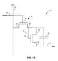
- FIG. 1Aan embodiment of a sensor element 10 is shown suitable for use in an image sensor matrix array.
- the sensor element 10includes a photo TFT 12 that generates a photocurrent in response to received light.
- the photo TFT 12is easily fabricated using common thin film layers.
- the photo TFT 12is a gated device having similarly doped contact regions and an intrinsic semiconductor region disposed between.
- the photo TFT 12has a gate electrode 14 that is coupled directly to the source electrode 16 . The coupling of the gate and source electrodes 14 , 16 creates a generated photocurrent that, for short channel lengths, exceeds that of an a-Si PIN photodiode.
- the photocurrentis a secondary photocurrent and has a potential gain of more than one whereas an a-Si PIN photodiode typically has a gain of less than one.
- the source electrode 16is coupled to a bias line 17 which is common to all photosensitive elements in an array. In operation, the bias line 17 may be coupled to a negative voltage.
- the source and drain electrodes 16 , 18 of the photo TFT 12are coupled to a storage capacitor 20 which is discharged when the photo TFT 12 is exposed to light.
- the storage capacitor 20is coupled to the source electrode 22 of a readout TFT 24 .
- the charge on the storage capacitor 20is read out periodically through the readout TFT 24 and a data line 26 .
- the gate electrode 28 of the readout TFT 24is coupled to a select line 30 to enable the readout TFT 24 .
- a drain electrode 32is coupled to the data line 26 to readout a charge.
- the photo TFT 12 and the readout TFT 24may be manufactured using common TFT manufacturing methods, such as in AMLCD applications.
- the TFTs 12 , 24generally include substantially co-planar source and drain electrodes, a semiconductor layer between the source and drain electrodes, and a gate electrode in proximity to the semiconductor layer but electrically insulated by a gate insulator. Current flow between the source and drain electrodes is controlled by the application of a voltage to the gate electrode. The voltage to the gate electrode produces an electric field which accumulates a charged region near the semiconductor-gate insulator interface. This charged region forms a current conducting channel in the semiconductor layer through which the device current is conducted.
- FIG. 1Ban alternative embodiment of a sensor element 33 is shown.
- the sensor element 33differs from the previously shown embodiment in that the gate electrode 14 is coupled directly to the drain electrode 18 .
- the bias line 17has a positive voltage bias. Operation of the sensor element 33 is similar to that of sensor element 10 .
- the storage capacitor 20is discharged when the photo TFT 12 is exposed to light. The charge on the storage capacitor 20 is read out periodically through the readout TFT 24 and the data line 26 .
- FIG. 2a schematic is shown of an image sensor array 34 that includes regularly-spaced sensor elements 10 of FIG. 1A. Although elements 10 of FIG. 1A are shown, sensor elements of FIG. 1B may be used as well.
- the sensor elements 10are arranged at intersections between rows and columns with each element corresponding to an individual pixels. The rows are designated by the select lines 30 and the columns are designated by the data lines 26 . Individual sensor elements respond to received light and generate a data signal that is transmitted on an associated data line 26 . As data signals pass through the data lines 26 to a control circuit, an image sensor array 34 determines the location of a received image on the array 34 .
- the array 34is for illustrative purposes only as an image sensor would have far more sensor elements.
- the select lines 30may be in communication with an address circuit to address individual readout TFTs.
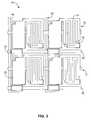
- FIG. 3a plan view of four sensor elements 10 is shown.
- the photo and readout TFTs 12 , 24may be embodied as various structures which may be manufactured using processes similar to that for TFTs in an AMLCD.
- the plan viewprovides a view of components relative to one another.
- the photo TFT 12has a source electrode 16 and drain electrode 18 configured with extending members. The extending members are disposed relative to one another to form an interdigitated pattern.
- FIG. 4a cross-sectional view of one embodiment of a photo TFT 12 of FIG. 3 is shown.
- the photo TFT 12may be used in either sensor elements 10 , 33 of FIG. 1A or 1 B.
- the photo TFT 12includes a gate electrode 14 deposited and patterned on an insulating transparent substrate 40 , such as glass, quartz, sapphire, or the like.
- the gate electrode 14may include metals such as Cr, Cu, Al, Ta, Ti or the like.
- a gate insulator 42insulates the gate electrode 14 from a semiconductor layer 44 .
- the gate insulator 42may include various materials well known in the art, such as silicon nitride, silicon oxide, or the like.
- a semiconductor layer 44is stacked on the gate insulator 42 above the gate electrode 14 and may include a-Si, p-Si, amorphous silicon carbide (SiC), tellurium (Te), selenium (Se), cadmium sulfide (CdS), cadmium selenide (CdSe), or the like.
- a-Siis well suited to large area fabrication on glass substrates at temperatures below 350 centigrade and exhibits a very high, dark resistivity.
- the semiconductor layer 44may be deposited in accordance with methods known in the art including sputtering or deposition, such as plasma-enhanced chemical vapor deposition.
- the semiconductor layer 44may be patterned through known methods, such as by use of a mask and photolithographic processing.
- the semiconductor layer 44may include an n+layer that contacts the source and drain electrodes 16 , 18 .
- the n+layermay be deposited on opposing ends of the semiconductor layer 44 where contact exists with the source and drain electrodes 16 , 18 .
- the n+layerprovides a low resistance contact for the source and drain electrodes 16 , 18 , and suppresses hole injection at negative gate voltage.
- the source and drain electrodes 16 , 18are patterned at a certain distance from one another so that the electrodes 16 , 18 are separated by a co-planar region of semiconductor material 44 in order to form a gate controlled current channel.
- the semiconductor layer 44may be configured as shown in FIG. 4, to provide contact between alternating source and drain electrode extending members 16 , 18 .
- the semiconductor layer 44 and source and drain electrode extending members 16 , 18are patterned and etched to form multiple channels 46 .
- the interdigitated patternincreases the photosensitivity of the photo TFT 12 , although one of skill in the art will appreciate that the photo TFT 12 may have an alternative configuration such as a simple inverted staggered structure, trilayer type inverted staggered structure, or other known structures.
- a passivation layer 48is formed on an upper surface of the photo TFT 12 to cover and protect the channels 46 .
- the passivation layer 48may include silicon nitride, silicon oxide, and combinations thereof.
- the passivation layer 48may extend and cover the electrodes 16 , 18 as well.
- the present inventionhas particular application in detecting x-ray emissions in the industrial and medical industries.
- the photo TFT 12may be used to detect x-ray emissions by covering the TFT 12 with a screen 50 to convert x-rays to light.
- the screen 50includes scintillator material that absorbs x-rays and converts the energy to visible light. Scintillator material may yield many light photons for each received x-ray photon.
- the scintillator materialusually consists of a high-atomic number material, which has high x-ray absorption, and a low-concentration activator that provides direct band transitions to facilitate visible photon emission.
- Acceptable scintillator materialsinclude granular like phosphors or crystalline like cesium iodide (CsI). Phosphors glow when exposed to x-rays. Various grain sizes and chemical mixtures may be used to produce a variety of resolution and brightness varieties. CsI provides a better combination of resolution and brightness. Because cesium has a high atomic number, it is an excellent x-ray absorber and is very efficient at converting x-ray to visible light.
- the scintillator materialmay be mixed with a glue binder and coated onto plastic sheets to form the screen 50 . In one embodiment the scintillator material includes relatively low cost external phosphor such as Kodake LANEX, which has a Gd 2 O 2 S:Tb layer to convert X-rays to green light with a wavelength of 544 nm.
- the dark current of the photo TFT 12may be significant and create noise in an image.
- the dark imagemay be stored in a memory and subtracted from the light image.
- the dark currentmay also exhibit some drift over time, which affects the gray scale accuracy and image quality. This may be minimized by periodically, e.g. every minute, interrupting the light exposure and retaking the dark reference image.
- the storage capacitor 20may be embodied as a stacked capacitor having multiple layers and is deposited on a substrate 40 .
- a stacked capacitorincreases the dynamic range of the sensor element 10 and requires less space thereby increasing the space available for the photo TFT 12 .
- the capacitor 20has a top electrode 52 , bottom electrode 54 , and a center electrode 56 .
- the center electrode 56is separated from the top and bottom electrodes 52 , 54 by first and second dielectric layers 58 , 60 .
- the center electrode 56may include Al, Cr, Ti, Mo and the like and, in the embodiment shown, couples to the source electrode 22 of the readout TFT 24 .
- the readout TFT 24may have a conventional structure and a manufacturing process similar to that of a TFT in an array for an AMLCD.
- the TFT 24includes a gate electrode 28 deposited on the upper surface of the insulating substrate 40 .
- the gate electrode 28may include Cu, Cr, Al, Ta, Ti, or combinations thereof and is deposited through known methods such as sputtering or vapor deposition. The gate electrode may then be patterned by photolithography or other known methods.
- a gate insulator 62covers the gate electrode 28 and may include silicon nitride, silicon oxide, tantalum oxide, or combinations thereof.
- the gate insulator 62may be the same layer that serves as a dielectric layer 60 for the storage capacitor 20 .
- a semiconductor layer 64is deposited on the gate insulator 62 above the gate electrode 28 using known deposition methods.
- the semiconductor layer 64may include a-Si, p-Si, or the like and further include a doping layer, such as a n+layer, that contacts the source and drain electrodes 22 , 32 .
- the source and drain electrodes 22 , 32are deposited and patterned using known methods and, with the semiconductor layer 64 , form a channel 66 .
- a passivation layer 68which may also be the same layer as passivation layer 48 , covers and protects the channel 66 .
- the passivation layer 68may include silicon nitride, silicon oxide, or other suitable dielectric material and may also extend and serve as a dielectric layer 58 for the storage capacitor 20 .
- a light shield 70may be disposed on the upper surface of the passivation layer 68 to cover the channel 66 .
- the readout TFT 24may be exposed to the same light level as the photo TFT 12 . Shielding prevents a charge from leaking from the storage capacitor 20 through the readout TFT 24 .
- the light shield 70is opaque and may include Cr or other suitable material.
- the light shield 70may also extend and serve as the top electrode 52 or as an additional electrode for the storage capacitor 20 . An additional electrode increases the value of the storage capacitor 20 .
- FIG. 6a graph is shown illustrating the relative photocurrents of an a-Si photodiode and an a-Si photo TFT as an inverse function of channel length (L).
- the photo TFTis configured with its gate electrode 14 coupled to its source electrode 16 as taught by the present invention.
- the resulting photocurrent of the photo TFTexceeds that of the photodiode for certain values of L.
- the photocurrent 72is proportional to L
- the photocurrent 74is proportional to 1/L.
- the conversion efficiency of photons into currentbecomes equal for the two devices.
- the photo TFTbecomes more efficient. This is because the photocurrent 72 in the photo diode is a primary photocurrent with a gain that cannot exceed unity.
- One photongenerates not more than one electron-hole pair, since the photo diode has blocking contacts for electrons and holes when reverse biased. Therefore, only one charge carrier can contribute to the photocurrent per absorbed photon.
- the source and drain contactsmay be embodied as n+ layers so that electrons can be injected from the contacts and replenish the photocurrent.
- a secondary electron photocurrentoccurs which can have a gain more than 1 when the electron lifetime exceeds the transit time from source to drain.
- an image sensor arrayhaving a substrate with addressable pixels.
- Each pixeldefined by a sensor element 10 that has a photo TFT 12 , storage capacitor 20 , and a readout TFT.
- Each sensor element 10is in electrical communication with a control circuit (not shown) to operate the sensor elements.
- the photo TFT 12includes a doped semiconductor material that generates a current channel in response to receive light and effectively discharges the storage capacitor 20 .
- TFT manufacturing for flat panel applicationsis a standard process which reduces the cost of the image sensor of the present invention.
- PIN diodes and TFTsrequire separate processes to manufacture and can require 8 or more photomasks
- an image sensor of the present inventioncan be constructed with 3 to 5 photomasks.
- a photo TFTcan yield photocurrents that exceed that of a PIN diode.
- the photocurrent of a photo TFTcan be an order of magnitude greater than a PIN diode
- the dark current of a photo TFTcan also be much greater than that of a PIN diode. Even when a photo TFT is operated in complete darkness a small current is still present which is referred to as a dark current. A relatively small amount of energy is sufficient to overcome the relatively low threshold of a photo TFT and create a dark current. A dark current may result from thermal activity, screen scintillation, filed emission, and other forms of noise. A high dark current limits the dynamic range of a sensor and can potentially increase the noise at the low light levels used in X-ray radiography and fluoroscopy.
- FIG. 7an embodiment of a sensor element 100 for use in an image sensor matrix array is shown.
- the sensor element 100includes elements of the embodiment of FIG. 1A such as a photo TFT 102 coupled to a storage capacitor 104 and a readout TFT 106 . Structure and operation of the capacitor 104 and TFTs 102 , 106 is similar to that previously described above.
- the sensor element 100is coupled to a bias line 108 , data line 110 , and select line 112 as shown.
- the sensor element 100further includes a dark current reference TFT 114 that is coupled to the photo TFT 102 at a pixel node 116 .
- the photo TFT 102 and the reference TFT 114are coupled to one another at their drain electrodes 118 , 120 .
- the pixel node 116has a voltage, referred to herein as the signal voltage, which is held by the storage capacitor 104 and is read out through the readout TFT 106 once per frame.
- the reference TFT 114cancels dark current resulting from the photo TFT 102 and is coupled at its source electrode 122 to a second bias line 124 .
- a gate electrode 126 of the reference TFT 114is coupled to the pixel node 116 but may also be coupled to the second bias line 124 in an alternative implementation.
- the reference TFT 114may be shielded with an opaque light shield similar to the readout TFT 24 of the previous embodiments.
- the readout TFT 106may also be so shielded to prevent a charge from leaking from the storage capacitor 104 through the readout TFT 106 .
- the reference TFT 114 and the photo TFT 102have substantially identical dimensions other than the aforementioned light shield. Because the reference TFT 114 and the photo TFT 102 are very similar and in close proximity, process variations across the sensor element 100 are not an issue. The TFTs 102 , 114 will generate the same or very similar dark current.
- the first and second bias lines 108 , 124have separate bias voltages.
- the voltage at node 116is reset to the charge amplifier reference voltage, V ref , during each readout.
- V refcharge amplifier reference voltage
- the voltage on line 108is typically 5 to 10 V lower than V ref and the voltage on line 124 is higher by substantially the same amount.
- the bias voltage across both the reference TFT 114 and the photo TFT 102will remain approximately the same in the dark.
- the first bias voltagemay be 0 V and the second bias voltage may be 10 V.
- the first and second bias lines 108 , 124have separate bias voltages. Although any number of bias voltages may be suitable, the first bias voltage is typically greater than the second bias voltage. In one implementation, the first bias voltage may be 20 V and the second bias voltage may be 10 V.
- the signal voltage at the pixel node 116does not change. This is because the dark currents of the photo TFT 102 and reference TFT 114 are approximately equal to one another and effectively cancel out.
- the signal voltage at the pixel node 116holds the differential voltage between the photocurrent and the dark current. Thus, the dark current is subtracted at the pixel node 116 .
- the photo TFT 102When the sensor element 100 is exposed to light, the photo TFT 102 will have a larger photocurrent than the reference TFT 114 which is shielded from the light.
- the storage capacitor 104will discharge and provide a read out.
- the dynamic range of the sensor elementwill increase by a factor of ten. Similarly, when the dark currents vary by less than 1 percent, the dynamic range will increase by about a factor of 100.
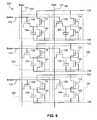
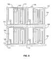
- FIG. 8a schematic is shown of an image sensor array 200 that includes six regularly-spaced sensor elements 100 of FIG. 7.
- the sensor elements 100are arranged at intersections between rows and columns with each element corresponding to an individual pixel.
- the rowsare designated by the select lines 112 and the columns are designated by the data lines 110 .
- Individual sensor elements 100respond to received light and generate a data signal that is transmitted on an associated data line 110 .
- the voltage bias lines 108 , 124are coupled to their respective TFTs 102 , 114 .
- FIG. 9a plan view of four sensor elements 100 is shown.
- the sensor elements 100are shown coupled to the first and second bias lines 108 , 124 , select lines 112 , and data lines 110 .
- the photo TFT 102has source and drain electrodes disposed in an interdigitated pattern. Since the reference TFT 114 has similar dimensions to the photo TFT 102 , the reference TFT 114 is likewise configured in an interdigitated pattern. To prevent an increase in the footprint of the sensor element 100 , the photo TFT 102 and the reference TFT 114 may be smaller than the photo TFT 12 of the previous embodiments. As such, the photo TFT 102 and the reference TFT 114 includes fewer extending members of the source and drain electrodes.
- FIG. 10a cross-sectional view of one embodiment of a reference TFT 114 is shown.
- the source and drain electrodes 122 , 118are formed in an interdigitated pattern with a semiconductor material 300 disposed between to form a gate controlled current channel.
- the semiconductor material 300may be formed of amorphous silicon or any other common material. Deposition of the electrodes 122 , 118 and the semiconductor material 300 may be achieved through methods commonly known in the art.
- the reference TFT 114further includes a substrate 302 , an insulator layer 304 disposed over a gate electrode 126 , and a passivation layer 306 to cover and protect channels 308 .
- the reference TFT 114further includes an opaque light shield 310 to cover and shield the channels 308 from light.
- the light shield 310prevents the reference TFT 114 from generating a photocurrent in response to light.
- a suitable material for the shield layer 310is Cr.
- a photo TFT 102 used in the same sensor element 100would be similarly embodied but without the light shield 310 .
- One of skill in the artwill appreciate that the structure of the reference TFT 114 may vary to reflect the structure of the photo TFT 102 .
- the embodiment shown in FIG. 9is for illustrative purposes only and should not be considered limiting of the present invention.
Landscapes
- Solid State Image Pick-Up Elements (AREA)
Abstract
Description
- This application is a continuation-in-part of and claims the benefit under 35 U.S.C. §120 of U.S. patent application Ser. No. 10/347,149, filed Jan. 17, 2003, which is a continuation-in-part of U.S. patent application Ser. No. 10/217,798, filed Aug. 12, 2002, and Ser. No. 10/307,106, filed Nov. 27, 2002, all of which claim the benefit under 35 U.S.C. §119(e) of U.S. Provisional Patent Application No. 60/359,263, filed Feb. 20, 2002.[0001]
- The present invention relates to image sensors and, more specifically, to flat panel image sensors employing photosensitive thin film transistors.[0002]
- Flat panel image sensors are commercially successful products that are able to effectively detect electromagnetic radiation in and near the visible light spectrum. Flat panel image sensors are fabricated by depositing and patterning various metals, insulators, and semiconductors on glass substrates as is done in flat panel displays. Such sensors commonly employ photosensitive elements, such as amorphous silicon (a-Si) PIN diodes. The photosensitive element is coupled to a readout switch, such as thin film transistor (TFT), that provides data indicative of received light.[0003]
- A common use for flat panel image sensors is for medical and industrial applications to detect X-rays. The image sensor includes a phosphorescent screen that overlays an array of image sensing elements. The phosphorescent screen converts received X-rays to visible light. The array receives the visible light and generates a photocurrent responsive to the light. The photocurrent is read out as data indicative of the sensed light.[0004]
- The arrays are difficult to manufacture since separate process steps are required to construct the PIN diodes and the TFTs. The total mask count may be 8 or more which is burdensome while the yields are low. Furthermore, a-Si PIN diodes are not a standard device in flat panel display processing which increases manufacturing expense. It would therefore be advantageous to use a standard process to greatly reduce the cost of flat panel image sensors.[0005]
- Manufacturing TFTs for flat panel applications is a common process. A common use for TFTs is in active matrix liquid crystal displays (AMLCDs). Each TFT functions as a switch for a pixel in a matrix display. The voltage across each pixel is controlled independently and at a high contrast ratio. TFTs may be fabricated by depositing and patterning metals, insulators, and semiconductors on substrates through methods well known in the art. TFTs typically employ a-Si, polycrystalline silicone, or CdSe film as the semiconductor material. A-Si is typically used in flat panel applications as it is easily deposited on large area glass substrates at temperatures below 350 centigrade.[0006]
- TFTs are more economical to fabricate than a-Si PIN diodes and are well suited for flat panel applications. The present inventors have recognized that if both the image sensing element and the readout switch of an image sensor array were incorporated as TFTs, fewer photomasks would be required and manufacturing costs would be greatly reduced.[0007]
- TFTs have not commonly been used as photosensitive elements. United States Patent Application Publication Nos. 2001/0055008 and 2001/0052597, both to Young et al. (hereinafter the “Young applications”), disclose the use of TFTs as light sensing elements for a display device. The light sensing elements provide feedback to progressively adjust the current flow through display elements to control light output. However, the use of TFTs exclusively for an image sensor is not disclosed. Since a TFT is more economical to manufacture and has already been successfully incorporated into flat panel applications, the present inventors have recognized that it would be advantageous to employ TFTs in image sensors.[0008]
- An image sensor array includes image sensors disposed on a substrate and arranged to receive and sense an image. Each image sensor represents a pixel for a received image. The image sensors each include a photo TFT that generates a photocurrent in response to the image. The photo TFT may be manufactured using common processes for TFTs in flat panel applications. The photo TFT has a gate electrode which is shorted to its source electrode to obtain a photocurrent that is substantially independent of source-drain bias. The photo TFT may also be configured with interdigitated source and drain electrodes to increase the photosensitivity.[0009]
- Each photo TFT is coupled to a bias line to enable operation and a storage capacitor to store a charge and discharge upon generation of a photocurrent. The storage capacitor is coupled to a readout TFT that is also manufactured using known processes. The readout TFT passes a charge from the storage capacitor to a data line. Operation of the readout TFT is enabled by a select line which is coupled to the gate electrode of the readout TFT. A light shield may be disposed over the channel of the readout TFT to prevent a charge leaking through the readout TFT.[0010]
- Each photo TFT may further be coupled to a reference TFT. A reference TFT is similar in structure to a corresponding photo TFT and provides an equivalent dark current to compensate for dark current in the photo TFT. The reference TFT includes a light shield so as to not generate a photocurrent in response to received light.[0011]
- The photo TFTs can provide an effective and economical alternative to conventional photodiodes. Photo TFTs may be manufactured with corresponding readout TFTs using conventional methods thereby reducing mask counts and costs. Photo TFTs may further yield photocurrents greater than that of photodiodes.[0012]
- Additional aspects and advantages of this invention will be apparent from the following detailed description of preferred embodiments thereof, which proceeds with reference to the accompanying drawings.[0013]
- Non-exhaustive embodiments of the invention are described with reference to the figures in which:[0014]
- FIG. 1A is a schematic diagram of an embodiment of a sensor element;[0015]
- FIG. 1B is a schematic diagram of an alternative embodiment of a sensor element;[0016]
- FIG. 2 is a schematic diagram of an array of sensor elements;[0017]
- FIG. 3 is a plan view of an embodiment of sensor elements for use in an image sensor array;[0018]
- FIG. 4 is a cross-sectional view of one embodiment of a photo TFT;[0019]
- FIG. 5 is a cross-sectional view of one embodiment of a readout TFT and a storage capacitor;[0020]
- FIG. 6 is a graph comparing the photocurrent for a PIN photodiode with the photocurrent for a photo TFT;[0021]
- FIG. 7 is a schematic diagram of an alternative embodiment of a sensor element;[0022]
- FIG. 8 is a schematic diagram of an alternative embodiment of an array of sensor elements;[0023]
- FIG. 9 is a plan view of an embodiment of sensor elements for use in an image sensor array; and[0024]
- FIG. 10 is a cross-sectional view of an embodiment of a compensation TFT.[0025]
- Reference is now made to the figures in which like reference numerals refer to like elements. For clarity, the first digit or digits of a reference numeral indicates the figure number in which the corresponding element is first used.[0026]
- Throughout the specification, reference to “one embodiment” or “an embodiment” means that a particular described feature, structure, or characteristic is included in at least one embodiment of the present invention. Thus, appearances of the phrases “in one embodiment” or “in an embodiment” in various places throughout this specification are not necessarily all referring to the same embodiment.[0027]
- Furthermore, the described features, structures, or characteristics may be combined in any suitable manner in one or more embodiments. Those skilled in the art will recognize that the invention can be practiced without one or more of the specific details, or with other methods, components, materials, etc. In other instances, well-known structures, materials, or operations are not shown or not described in detail to avoid obscuring aspects of the invention.[0028]
- Referring to FIG. 1A, an embodiment of a[0029]
sensor element 10 is shown suitable for use in an image sensor matrix array. Thesensor element 10 includes aphoto TFT 12 that generates a photocurrent in response to received light. Thephoto TFT 12 is easily fabricated using common thin film layers. In the embodiment shown, thephoto TFT 12 is a gated device having similarly doped contact regions and an intrinsic semiconductor region disposed between. Thephoto TFT 12 has agate electrode 14 that is coupled directly to thesource electrode 16. The coupling of the gate andsource electrodes source electrode 16 is coupled to abias line 17 which is common to all photosensitive elements in an array. In operation, thebias line 17 may be coupled to a negative voltage. - The source and drain[0030]
electrodes photo TFT 12 are coupled to astorage capacitor 20 which is discharged when thephoto TFT 12 is exposed to light. Thestorage capacitor 20 is coupled to thesource electrode 22 of areadout TFT 24. The charge on thestorage capacitor 20 is read out periodically through thereadout TFT 24 and adata line 26. As shown, thegate electrode 28 of thereadout TFT 24 is coupled to aselect line 30 to enable thereadout TFT 24. Adrain electrode 32 is coupled to thedata line 26 to readout a charge. - The[0031]
photo TFT 12 and thereadout TFT 24 may be manufactured using common TFT manufacturing methods, such as in AMLCD applications. TheTFTs - Referring to FIG. 1B an alternative embodiment of a[0032]
sensor element 33 is shown. Thesensor element 33 differs from the previously shown embodiment in that thegate electrode 14 is coupled directly to thedrain electrode 18. In operation, thebias line 17 has a positive voltage bias. Operation of thesensor element 33 is similar to that ofsensor element 10. Thestorage capacitor 20 is discharged when thephoto TFT 12 is exposed to light. The charge on thestorage capacitor 20 is read out periodically through thereadout TFT 24 and thedata line 26. - Referring to FIG. 2, a schematic is shown of an[0033]
image sensor array 34 that includes regularly-spacedsensor elements 10 of FIG. 1A. Althoughelements 10 of FIG. 1A are shown, sensor elements of FIG. 1B may be used as well. Thesensor elements 10 are arranged at intersections between rows and columns with each element corresponding to an individual pixels. The rows are designated by theselect lines 30 and the columns are designated by the data lines26. Individual sensor elements respond to received light and generate a data signal that is transmitted on an associateddata line 26. As data signals pass through the data lines26 to a control circuit, animage sensor array 34 determines the location of a received image on thearray 34. - The[0034]
array 34 is for illustrative purposes only as an image sensor would have far more sensor elements. Theselect lines 30 may be in communication with an address circuit to address individual readout TFTs. - Referring to FIG. 3, a plan view of four[0035]
sensor elements 10 is shown. The photo andreadout TFTs photo TFT 12 has asource electrode 16 anddrain electrode 18 configured with extending members. The extending members are disposed relative to one another to form an interdigitated pattern. - Referring to FIG. 4, a cross-sectional view of one embodiment of a[0036]
photo TFT 12 of FIG. 3 is shown. Thephoto TFT 12 may be used in eithersensor elements photo TFT 12 includes agate electrode 14 deposited and patterned on an insulatingtransparent substrate 40, such as glass, quartz, sapphire, or the like. Thegate electrode 14 may include metals such as Cr, Cu, Al, Ta, Ti or the like. Agate insulator 42 insulates thegate electrode 14 from asemiconductor layer 44. Thegate insulator 42 may include various materials well known in the art, such as silicon nitride, silicon oxide, or the like. - A[0037]
semiconductor layer 44 is stacked on thegate insulator 42 above thegate electrode 14 and may include a-Si, p-Si, amorphous silicon carbide (SiC), tellurium (Te), selenium (Se), cadmium sulfide (CdS), cadmium selenide (CdSe), or the like. However, a-Si is well suited to large area fabrication on glass substrates at temperatures below 350 centigrade and exhibits a very high, dark resistivity. Thesemiconductor layer 44 may be deposited in accordance with methods known in the art including sputtering or deposition, such as plasma-enhanced chemical vapor deposition. Thesemiconductor layer 44 may be patterned through known methods, such as by use of a mask and photolithographic processing. - The[0038]
semiconductor layer 44 may include an n+layer that contacts the source and drainelectrodes semiconductor layer 44 where contact exists with the source and drainelectrodes electrodes - The source and drain[0039]
electrodes electrodes semiconductor material 44 in order to form a gate controlled current channel. Thesemiconductor layer 44 may be configured as shown in FIG. 4, to provide contact between alternating source and drainelectrode extending members semiconductor layer 44 and source and drainelectrode extending members multiple channels 46. The interdigitated pattern increases the photosensitivity of thephoto TFT 12, although one of skill in the art will appreciate that thephoto TFT 12 may have an alternative configuration such as a simple inverted staggered structure, trilayer type inverted staggered structure, or other known structures. - In one embodiment, a[0040]
passivation layer 48 is formed on an upper surface of thephoto TFT 12 to cover and protect thechannels 46. Thepassivation layer 48 may include silicon nitride, silicon oxide, and combinations thereof. Thepassivation layer 48 may extend and cover theelectrodes - The present invention has particular application in detecting x-ray emissions in the industrial and medical industries. The[0041]
photo TFT 12 may be used to detect x-ray emissions by covering theTFT 12 with ascreen 50 to convert x-rays to light. Thescreen 50 includes scintillator material that absorbs x-rays and converts the energy to visible light. Scintillator material may yield many light photons for each received x-ray photon. The scintillator material usually consists of a high-atomic number material, which has high x-ray absorption, and a low-concentration activator that provides direct band transitions to facilitate visible photon emission. - Acceptable scintillator materials include granular like phosphors or crystalline like cesium iodide (CsI). Phosphors glow when exposed to x-rays. Various grain sizes and chemical mixtures may be used to produce a variety of resolution and brightness varieties. CsI provides a better combination of resolution and brightness. Because cesium has a high atomic number, it is an excellent x-ray absorber and is very efficient at converting x-ray to visible light. The scintillator material may be mixed with a glue binder and coated onto plastic sheets to form the[0042]
screen 50. In one embodiment the scintillator material includes relatively low cost external phosphor such as Kodake LANEX, which has a Gd2O2S:Tb layer to convert X-rays to green light with a wavelength of 544 nm. - In operation, the dark current of the[0043]
photo TFT 12 may be significant and create noise in an image. In order to compensate, the dark image may be stored in a memory and subtracted from the light image. The dark current may also exhibit some drift over time, which affects the gray scale accuracy and image quality. This may be minimized by periodically, e.g. every minute, interrupting the light exposure and retaking the dark reference image. - Referring to FIG. 5, a cross-sectional view of an embodiment of a[0044]
storage capacitor 20 and areadout TFT 24 coupled to one another is show. Thestorage capacitor 20 may be embodied as a stacked capacitor having multiple layers and is deposited on asubstrate 40. A stacked capacitor increases the dynamic range of thesensor element 10 and requires less space thereby increasing the space available for thephoto TFT 12. In one embodiment, thecapacitor 20 has atop electrode 52,bottom electrode 54, and acenter electrode 56. Thecenter electrode 56 is separated from the top andbottom electrodes center electrode 56 may include Al, Cr, Ti, Mo and the like and, in the embodiment shown, couples to thesource electrode 22 of thereadout TFT 24. - The[0045]
readout TFT 24 may have a conventional structure and a manufacturing process similar to that of a TFT in an array for an AMLCD. TheTFT 24 includes agate electrode 28 deposited on the upper surface of the insulatingsubstrate 40. Thegate electrode 28 may include Cu, Cr, Al, Ta, Ti, or combinations thereof and is deposited through known methods such as sputtering or vapor deposition. The gate electrode may then be patterned by photolithography or other known methods. Agate insulator 62 covers thegate electrode 28 and may include silicon nitride, silicon oxide, tantalum oxide, or combinations thereof. Thegate insulator 62 may be the same layer that serves as adielectric layer 60 for thestorage capacitor 20. - A[0046]
semiconductor layer 64 is deposited on thegate insulator 62 above thegate electrode 28 using known deposition methods. Thesemiconductor layer 64 may include a-Si, p-Si, or the like and further include a doping layer, such as a n+layer, that contacts the source and drainelectrodes electrodes semiconductor layer 64, form achannel 66. - A[0047]
passivation layer 68, which may also be the same layer aspassivation layer 48, covers and protects thechannel 66. Thepassivation layer 68 may include silicon nitride, silicon oxide, or other suitable dielectric material and may also extend and serve as adielectric layer 58 for thestorage capacitor 20. - In one embodiment, which departs from conventional TFT structures, a[0048]
light shield 70 may be disposed on the upper surface of thepassivation layer 68 to cover thechannel 66. Thereadout TFT 24 may be exposed to the same light level as thephoto TFT 12. Shielding prevents a charge from leaking from thestorage capacitor 20 through thereadout TFT 24. Thelight shield 70 is opaque and may include Cr or other suitable material. In an alternative embodiment, thelight shield 70 may also extend and serve as thetop electrode 52 or as an additional electrode for thestorage capacitor 20. An additional electrode increases the value of thestorage capacitor 20. - Referring to FIG. 6, a graph is shown illustrating the relative photocurrents of an a-Si photodiode and an a-Si photo TFT as an inverse function of channel length (L). The photo TFT is configured with its[0049]
gate electrode 14 coupled to itssource electrode 16 as taught by the present invention. As illustrated, the resulting photocurrent of the photo TFT exceeds that of the photodiode for certain values of L. In the photodiode, thephotocurrent 72 is proportional to L, whereas, in the photo TFT, thephotocurrent 74 is proportional to 1/L. - At a certain value of L, which is approximately 10 to 20 μm, the conversion efficiency of photons into current becomes equal for the two devices. For smaller values of L, the photo TFT becomes more efficient. This is because the[0050]
photocurrent 72 in the photo diode is a primary photocurrent with a gain that cannot exceed unity. One photon generates not more than one electron-hole pair, since the photo diode has blocking contacts for electrons and holes when reverse biased. Therefore, only one charge carrier can contribute to the photocurrent per absorbed photon. In the photo TFT, the source and drain contacts may be embodied as n+ layers so that electrons can be injected from the contacts and replenish the photocurrent. Thus, a secondary electron photocurrent occurs which can have a gain more than 1 when the electron lifetime exceeds the transit time from source to drain. - According to the present invention, there is provided an image sensor array having a substrate with addressable pixels. Each pixel defined by a[0051]
sensor element 10 that has aphoto TFT 12,storage capacitor 20, and a readout TFT. Eachsensor element 10 is in electrical communication with a control circuit (not shown) to operate the sensor elements. Thephoto TFT 12 includes a doped semiconductor material that generates a current channel in response to receive light and effectively discharges thestorage capacitor 20. - TFT manufacturing for flat panel applications is a standard process which reduces the cost of the image sensor of the present invention. Whereas PIN diodes and TFTs require separate processes to manufacture and can require 8 or more photomasks, an image sensor of the present invention can be constructed with 3 to 5 photomasks. A photo TFT can yield photocurrents that exceed that of a PIN diode.[0052]
- Although the photocurrent of a photo TFT can be an order of magnitude greater than a PIN diode, the dark current of a photo TFT can also be much greater than that of a PIN diode. Even when a photo TFT is operated in complete darkness a small current is still present which is referred to as a dark current. A relatively small amount of energy is sufficient to overcome the relatively low threshold of a photo TFT and create a dark current. A dark current may result from thermal activity, screen scintillation, filed emission, and other forms of noise. A high dark current limits the dynamic range of a sensor and can potentially increase the noise at the low light levels used in X-ray radiography and fluoroscopy.[0053]
- Referring to FIG. 7, an embodiment of a[0054]
sensor element 100 for use in an image sensor matrix array is shown. Thesensor element 100 includes elements of the embodiment of FIG. 1A such as aphoto TFT 102 coupled to astorage capacitor 104 and areadout TFT 106. Structure and operation of thecapacitor 104 andTFTs sensor element 100 is coupled to abias line 108,data line 110, andselect line 112 as shown. - The[0055]
sensor element 100 further includes a darkcurrent reference TFT 114 that is coupled to thephoto TFT 102 at apixel node 116. Thephoto TFT 102 and thereference TFT 114 are coupled to one another at theirdrain electrodes pixel node 116 has a voltage, referred to herein as the signal voltage, which is held by thestorage capacitor 104 and is read out through thereadout TFT 106 once per frame. - The[0056]
reference TFT 114 cancels dark current resulting from thephoto TFT 102 and is coupled at itssource electrode 122 to asecond bias line 124. Agate electrode 126 of thereference TFT 114 is coupled to thepixel node 116 but may also be coupled to thesecond bias line 124 in an alternative implementation. Thereference TFT 114 may be shielded with an opaque light shield similar to thereadout TFT 24 of the previous embodiments. Thereadout TFT 106 may also be so shielded to prevent a charge from leaking from thestorage capacitor 104 through thereadout TFT 106. - The[0057]
reference TFT 114 and thephoto TFT 102 have substantially identical dimensions other than the aforementioned light shield. Because thereference TFT 114 and thephoto TFT 102 are very similar and in close proximity, process variations across thesensor element 100 are not an issue. TheTFTs - The first and[0058]
second bias lines node 116 is reset to the charge amplifier reference voltage, Vref, during each readout. Thus, the voltage online 108 is typically 5 to 10 V lower than Vrefand the voltage online 124 is higher by substantially the same amount. Hence, the bias voltage across both thereference TFT 114 and thephoto TFT 102 will remain approximately the same in the dark. In one implementation, when a charge amplifier reference voltage is 5V, the first bias voltage may be 0 V and the second bias voltage may be 10 V. - The first and[0059]
second bias lines - When the[0060]
sensor element 100 is not exposed to light, the signal voltage at thepixel node 116 does not change. This is because the dark currents of thephoto TFT 102 andreference TFT 114 are approximately equal to one another and effectively cancel out. The signal voltage at thepixel node 116 holds the differential voltage between the photocurrent and the dark current. Thus, the dark current is subtracted at thepixel node 116. - When the[0061]
sensor element 100 is exposed to light, thephoto TFT 102 will have a larger photocurrent than thereference TFT 114 which is shielded from the light. Thestorage capacitor 104 will discharge and provide a read out. - When the dark currents of the[0062]
photo TFT 102 and thereference TFT 114 are within ten percent, the dynamic range of the sensor element will increase by a factor of ten. Similarly, when the dark currents vary by less than 1 percent, the dynamic range will increase by about a factor of 100. - Referring to FIG. 8, a schematic is shown of an[0063]
image sensor array 200 that includes six regularly-spacedsensor elements 100 of FIG. 7. Thesensor elements 100 are arranged at intersections between rows and columns with each element corresponding to an individual pixel. The rows are designated by theselect lines 112 and the columns are designated by the data lines110.Individual sensor elements 100 respond to received light and generate a data signal that is transmitted on an associateddata line 110. The voltage biaslines respective TFTs - Referring to FIG. 9, a plan view of four[0064]
sensor elements 100 is shown. Thesensor elements 100 are shown coupled to the first andsecond bias lines select lines 112, anddata lines 110. Thephoto TFT 102 has source and drain electrodes disposed in an interdigitated pattern. Since thereference TFT 114 has similar dimensions to thephoto TFT 102, thereference TFT 114 is likewise configured in an interdigitated pattern. To prevent an increase in the footprint of thesensor element 100, thephoto TFT 102 and thereference TFT 114 may be smaller than thephoto TFT 12 of the previous embodiments. As such, thephoto TFT 102 and thereference TFT 114 includes fewer extending members of the source and drain electrodes. - Referring to FIG. 10, a cross-sectional view of one embodiment of a[0065]
reference TFT 114 is shown. The source and drainelectrodes semiconductor material 300 disposed between to form a gate controlled current channel. Thesemiconductor material 300 may be formed of amorphous silicon or any other common material. Deposition of theelectrodes semiconductor material 300 may be achieved through methods commonly known in the art. - The[0066]
reference TFT 114 further includes asubstrate 302, aninsulator layer 304 disposed over agate electrode 126, and apassivation layer 306 to cover and protectchannels 308. Thereference TFT 114 further includes an opaquelight shield 310 to cover and shield thechannels 308 from light. Thelight shield 310 prevents thereference TFT 114 from generating a photocurrent in response to light. A suitable material for theshield layer 310 is Cr. - A[0067]
photo TFT 102 used in thesame sensor element 100 would be similarly embodied but without thelight shield 310. One of skill in the art will appreciate that the structure of thereference TFT 114 may vary to reflect the structure of thephoto TFT 102. The embodiment shown in FIG. 9 is for illustrative purposes only and should not be considered limiting of the present invention. - It will be obvious to those having skill in the art that many changes may be made to the details of the above-described embodiments of this invention without departing from the underlying principles thereof. The scope of the present invention should, therefore, be determined only by the following claims.[0068]
Claims (28)
Priority Applications (1)
| Application Number | Priority Date | Filing Date | Title |
|---|---|---|---|
| US10/457,931US6831710B2 (en) | 2002-02-20 | 2003-06-09 | Image sensor with photosensitive thin film transistors and dark current compensation |
Applications Claiming Priority (5)
| Application Number | Priority Date | Filing Date | Title |
|---|---|---|---|
| US35926302P | 2002-02-20 | 2002-02-20 | |
| US10/217,798US7408598B2 (en) | 2002-02-20 | 2002-08-12 | Light sensitive display with selected interval of light sensitive elements |
| US10/307,106US6995743B2 (en) | 2002-02-20 | 2002-11-27 | Light sensitive display |
| US10/347,149US7023503B2 (en) | 2002-02-20 | 2003-01-17 | Image sensor with photosensitive thin film transistors |
| US10/457,931US6831710B2 (en) | 2002-02-20 | 2003-06-09 | Image sensor with photosensitive thin film transistors and dark current compensation |
Related Parent Applications (1)
| Application Number | Title | Priority Date | Filing Date |
|---|---|---|---|
| US10/347,149Continuation-In-PartUS7023503B2 (en) | 2002-02-20 | 2003-01-17 | Image sensor with photosensitive thin film transistors |
Publications (2)
| Publication Number | Publication Date |
|---|---|
| US20030205662A1true US20030205662A1 (en) | 2003-11-06 |
| US6831710B2 US6831710B2 (en) | 2004-12-14 |
Family
ID=27767916
Family Applications (2)
| Application Number | Title | Priority Date | Filing Date |
|---|---|---|---|
| US10/347,149Expired - Fee RelatedUS7023503B2 (en) | 2002-02-20 | 2003-01-17 | Image sensor with photosensitive thin film transistors |
| US10/457,931Expired - Fee RelatedUS6831710B2 (en) | 2002-02-20 | 2003-06-09 | Image sensor with photosensitive thin film transistors and dark current compensation |
Family Applications Before (1)
| Application Number | Title | Priority Date | Filing Date |
|---|---|---|---|
| US10/347,149Expired - Fee RelatedUS7023503B2 (en) | 2002-02-20 | 2003-01-17 | Image sensor with photosensitive thin film transistors |
Country Status (3)
| Country | Link |
|---|---|
| US (2) | US7023503B2 (en) |
| AU (1) | AU2003208975A1 (en) |
| WO (1) | WO2003073507A2 (en) |
Cited By (28)
| Publication number | Priority date | Publication date | Assignee | Title |
|---|---|---|---|---|
| US20030156230A1 (en)* | 2002-02-20 | 2003-08-21 | Boer Willem Den | Light sensitive display |
| US20040113877A1 (en)* | 2002-05-23 | 2004-06-17 | Adiel Abileah | Light sensitive display |
| US20060034492A1 (en)* | 2002-10-30 | 2006-02-16 | Roy Siegel | Hand recognition system |
| US7009663B2 (en) | 2003-12-17 | 2006-03-07 | Planar Systems, Inc. | Integrated optical light sensitive active matrix liquid crystal display |
| US7023503B2 (en) | 2002-02-20 | 2006-04-04 | Planar Systems, Inc. | Image sensor with photosensitive thin film transistors |
| US20080266045A1 (en)* | 2007-04-25 | 2008-10-30 | Scanvue Technologies, Llc | Thin film varistor array |
| US20100066703A1 (en)* | 2008-09-16 | 2010-03-18 | Po-Yang Chen | Embedded optical induction input device and method of implementing the same |
| US7773139B2 (en) | 2004-04-16 | 2010-08-10 | Apple Inc. | Image sensor with photosensitive thin film transistors |
| US20110187954A1 (en)* | 2005-12-28 | 2011-08-04 | Hee Kwang Kang | Liquid crystal display device and fabricating and driving method thereof |
| US20110284722A1 (en)* | 2010-05-20 | 2011-11-24 | Samsung Electronics Co., Ltd. | Light-sensing circuit, method of operating the light-sensing circuit, and light-sensing apparatus employing the light-sensing circuit |
| US8079904B2 (en) | 2004-08-20 | 2011-12-20 | Igt | Gaming access card with display |
| US8207946B2 (en) | 2003-02-20 | 2012-06-26 | Apple Inc. | Light sensitive display |
| US20120228505A1 (en)* | 2011-03-09 | 2012-09-13 | Samsung Electronics Co., Ltd. | Optical sensor |
| US8529341B2 (en) | 2004-07-27 | 2013-09-10 | Igt | Optically sensitive display for a gaming apparatus |
| US8638320B2 (en) | 2011-06-22 | 2014-01-28 | Apple Inc. | Stylus orientation detection |
| US8928635B2 (en) | 2011-06-22 | 2015-01-06 | Apple Inc. | Active stylus |
| US9176604B2 (en) | 2012-07-27 | 2015-11-03 | Apple Inc. | Stylus device |
| US9310923B2 (en) | 2010-12-03 | 2016-04-12 | Apple Inc. | Input device for touch sensitive devices |
| US9329703B2 (en) | 2011-06-22 | 2016-05-03 | Apple Inc. | Intelligent stylus |
| US9557845B2 (en) | 2012-07-27 | 2017-01-31 | Apple Inc. | Input device for and method of communication with capacitive devices through frequency variation |
| US9652090B2 (en) | 2012-07-27 | 2017-05-16 | Apple Inc. | Device for digital communication through capacitive coupling |
| US9939935B2 (en) | 2013-07-31 | 2018-04-10 | Apple Inc. | Scan engine for touch controller architecture |
| US10048775B2 (en) | 2013-03-14 | 2018-08-14 | Apple Inc. | Stylus detection and demodulation |
| US10061450B2 (en) | 2014-12-04 | 2018-08-28 | Apple Inc. | Coarse scan and targeted active mode scan for touch |
| US20190123209A1 (en)* | 2017-05-19 | 2019-04-25 | Shenzhen China Star Optoelectronics Technology Co., Ltd. | Thin film transistor and method for manufacturing the same |
| US10474277B2 (en) | 2016-05-31 | 2019-11-12 | Apple Inc. | Position-based stylus communication |
| CN111785745A (en)* | 2020-06-11 | 2020-10-16 | 上海交通大学 | Optical sensor, optical sensor device and preparation method thereof |
| US12153764B1 (en) | 2020-09-25 | 2024-11-26 | Apple Inc. | Stylus with receive architecture for position determination |
Families Citing this family (38)
| Publication number | Priority date | Publication date | Assignee | Title |
|---|---|---|---|---|
| DE10057696A1 (en)* | 2000-11-21 | 2002-05-16 | Siemens Ag | LCD display with background lighting provided by a controlled light source |
| TWI363206B (en)* | 2003-02-28 | 2012-05-01 | Samsung Electronics Co Ltd | Liquid crystal display device |
| JP4108633B2 (en)* | 2003-06-20 | 2008-06-25 | シャープ株式会社 | THIN FILM TRANSISTOR, MANUFACTURING METHOD THEREOF, AND ELECTRONIC DEVICE |
| CA2535490A1 (en) | 2003-08-12 | 2005-02-17 | Simon Fraser University | Multi-mode digital imaging apparatus and system |
| CN100397652C (en)* | 2004-05-10 | 2008-06-25 | 凌阳科技股份有限公司 | Circuit layout structure of photosensitive chip and semiconductor substrate of photosensitive chip |
| US7329186B2 (en)* | 2004-08-20 | 2008-02-12 | Igt | Gaming system with rewritable display card and LCD input display for reading same |
| CA2494602A1 (en) | 2005-01-08 | 2006-07-08 | Karim S. Karim | Digital imaging apparatus and system |
| DE102004052452B4 (en)* | 2004-10-28 | 2008-05-29 | Siemens Ag | Radiation detector for detecting radiation |
| GB0426563D0 (en)* | 2004-12-03 | 2005-01-05 | Plastic Logic Ltd | Alignment tolerant patterning on flexible substrates |
| US7276748B2 (en)* | 2005-02-28 | 2007-10-02 | International Business Machines Corporation | Body potential imager cell |
| JP2007065243A (en)* | 2005-08-31 | 2007-03-15 | Sanyo Epson Imaging Devices Corp | Display device |
| US9064772B2 (en)* | 2005-10-07 | 2015-06-23 | Integrated Digital Technologies, Inc. | Touch screen system having dual touch sensing function |
| US8748796B2 (en)* | 2005-10-07 | 2014-06-10 | Integrated Digital Technologies, Inc. | Interactive display panel having touch-sensing functions |
| US8575536B2 (en)* | 2005-10-07 | 2013-11-05 | Integrated Digital Technologies Inc. | Pixel array and touch sensing display panel having the same |
| TWI291237B (en)* | 2005-10-07 | 2007-12-11 | Integrated Digital Technologie | Photo detector array |
| US8480484B2 (en) | 2005-11-09 | 2013-07-09 | Igt | Secure identification devices and methods for detecting and monitoring access thereof |
| DE102005060795A1 (en) | 2005-12-16 | 2007-07-12 | Siemens Ag | Flat panel detector |
| US20070159561A1 (en)* | 2006-01-10 | 2007-07-12 | Trendon Touch Technology Corp. | Display panel having touching circuit |
| US8144115B2 (en)* | 2006-03-17 | 2012-03-27 | Konicek Jeffrey C | Flat panel display screen operable for touch position determination system and methods |
| US7859526B2 (en)* | 2006-05-01 | 2010-12-28 | Konicek Jeffrey C | Active matrix emissive display and optical scanner system, methods and applications |
| GB2437768A (en)* | 2006-05-03 | 2007-11-07 | Seiko Epson Corp | Photosensing TFT |
| KR101003170B1 (en) | 2006-09-25 | 2010-12-22 | 인테그레이티드 디지털 테크놀로지스, 인코포레이티드 | Photo detector array |
| US7787081B2 (en)* | 2006-12-15 | 2010-08-31 | Hannstar Display Corporation | Photo-sensitive element and liquid crystal display with the same |
| WO2008126873A1 (en)* | 2007-04-09 | 2008-10-23 | Sharp Kabushiki Kaisha | Display device |
| US8199236B2 (en) | 2007-09-11 | 2012-06-12 | Simon Fraser University/Industry Liason Office | Device and pixel architecture for high resolution digital |
| KR20090028884A (en)* | 2007-09-17 | 2009-03-20 | 삼성전자주식회사 | X-ray detection method and x-ray detection apparatus for performing the same |
| US8232960B2 (en)* | 2007-11-01 | 2012-07-31 | Hewlett-Packard Development Company, L.P. | Displaying electrophoretic particles |
| TWI380260B (en)* | 2007-12-06 | 2012-12-21 | Au Optronics Corp | Ambient light detection system and related method |
| US9367998B2 (en) | 2008-02-21 | 2016-06-14 | Bally Gaming, Inc. | Gaming system having displays with integrated image capture capabilities |
| US7955890B2 (en)* | 2008-06-24 | 2011-06-07 | Applied Materials, Inc. | Methods for forming an amorphous silicon film in display devices |
| TWI415283B (en)* | 2009-02-18 | 2013-11-11 | Au Optronics Corp | X-ray sensor and manufacturing method thereof |
| TWI381298B (en)* | 2009-03-20 | 2013-01-01 | Hannstar Display Corp | Photo element and driving method thereof and liquid crystal display |
| US8446392B2 (en)* | 2009-11-16 | 2013-05-21 | Smart Technologies Ulc | Method for determining the location of a pointer in a pointer input region, and interactive input system executing the method |
| KR101848063B1 (en)* | 2010-11-17 | 2018-04-12 | 삼성디스플레이 주식회사 | Liquid crystal display device and method of fabricating the same |
| KR101795744B1 (en)* | 2011-04-06 | 2017-11-09 | 삼성디스플레이 주식회사 | Display device and noise reduction method using the same |
| KR20140047494A (en) | 2012-10-12 | 2014-04-22 | 삼성전자주식회사 | Subpixel, image sensor having the same and image sensing system |
| US9368059B2 (en)* | 2013-03-01 | 2016-06-14 | Semiconductor Energy Laboratory Co., Ltd. | Semiconductor device and driving method thereof |
| CN107680548B (en)* | 2017-10-23 | 2020-03-31 | 京东方科技集团股份有限公司 | Pixel unit and driving method thereof, pixel circuit, liquid crystal panel and display device |
Citations (16)
| Publication number | Priority date | Publication date | Assignee | Title |
|---|---|---|---|---|
| US5003356A (en)* | 1987-09-09 | 1991-03-26 | Casio Computer Co., Ltd. | Thin film transistor array |
| US5349174A (en)* | 1992-05-06 | 1994-09-20 | U.S. Philips Corporation | Image sensor with transparent capacitive regions |
| US5414283A (en)* | 1993-11-19 | 1995-05-09 | Ois Optical Imaging Systems, Inc. | TFT with reduced parasitic capacitance |
| US5525813A (en)* | 1991-04-19 | 1996-06-11 | Fuji Xerox Co., Ltd. | Image sensor having TFT gate electrode surrounding the photoelectric conversion element |
| US5598004A (en)* | 1994-07-20 | 1997-01-28 | U.S. Philips Corporation | Image detector |
| US5930591A (en)* | 1997-04-23 | 1999-07-27 | Litton Systems Canada Limited | High resolution, low voltage flat-panel radiation imaging sensors |
| US5962856A (en)* | 1995-04-28 | 1999-10-05 | Sunnybrook Hospital | Active matrix X-ray imaging array |
| US6020590A (en)* | 1998-01-22 | 2000-02-01 | Ois Optical Imaging Systems, Inc. | Large area imager with UV blocking layer |
| US6236063B1 (en)* | 1998-05-15 | 2001-05-22 | Semiconductor Energy Laboratory Co., Ltd. | Semiconductor device |
| US20010052597A1 (en)* | 2000-06-20 | 2001-12-20 | U.S. Philips Corporation | Light-emitting matrix array display devices with light sensing elements |
| US20010055008A1 (en)* | 2000-06-20 | 2001-12-27 | U.S. Philips Corporation | Matrix array display devices with light sensing elements and associated storage capacitors |
| US6392254B1 (en)* | 1997-01-17 | 2002-05-21 | General Electric Company | Corrosion resistant imager |
| US20020074549A1 (en)* | 1999-06-03 | 2002-06-20 | Woon-Yong Park | Method for fabricating thin film transistor array substrate for liquid crystal display |
| US6465824B1 (en)* | 2000-03-09 | 2002-10-15 | General Electric Company | Imager structure |
| US20030156087A1 (en)* | 2002-02-20 | 2003-08-21 | Boer Willem Den | Light sensitive display |
| US20030218116A1 (en)* | 2002-02-20 | 2003-11-27 | Boer Willem Den | Image sensor with photosensitive thin film transistors |
Family Cites Families (120)
| Publication number | Priority date | Publication date | Assignee | Title |
|---|---|---|---|---|
| US4220815B1 (en) | 1978-12-04 | 1996-09-03 | Elographics Inc | Nonplanar transparent electrographic sensor |
| US4320292A (en) | 1979-08-22 | 1982-03-16 | Nippon Telegraph And Telephone Public Corporation | Coordinate input apparatus |
| JPS5685792A (en)* | 1979-12-14 | 1981-07-13 | Citizen Watch Co Ltd | Liquid crystal display unit |
| FR2496949B1 (en) | 1980-12-23 | 1987-05-15 | Thomson Csf | ELECTRO-OPTICAL SWITCHING DEVICE |
| JPS57141177A (en)* | 1981-02-26 | 1982-09-01 | Matsushita Electric Ind Co Ltd | Video camera with monitor |
| US4476463A (en) | 1981-08-24 | 1984-10-09 | Interaction Systems, Inc. | Display device having unpatterned touch detection |
| EP0097384B1 (en) | 1982-06-18 | 1987-01-28 | Koninklijke Philips Electronics N.V. | Liquid-crystal display device |
| JPS5910988A (en) | 1982-07-12 | 1984-01-20 | ホシデン株式会社 | Color liquid crystal display |
| US4785564A (en) | 1982-12-20 | 1988-11-22 | Motorola Inc. | Electronic notepad |
| JPS6045219A (en)* | 1983-08-23 | 1985-03-11 | Toshiba Corp | Active matrix type display device |
| JPH0654960B2 (en) | 1983-10-20 | 1994-07-20 | シチズン時計株式会社 | Driving method for liquid crystal display device |
| US4655552A (en)* | 1984-03-17 | 1987-04-07 | Citizen Watch Co., Ltd. | Flat panel display device having on-screen data input function |
| US4603356A (en) | 1984-03-19 | 1986-07-29 | Energy Conversion Devices, Inc. | Imaging system with light valve and photodetector |
| JPS616729A (en) | 1984-06-20 | 1986-01-13 | Sharp Corp | Input/output device of information |
| US4917474A (en) | 1984-09-10 | 1990-04-17 | Semiconductor Energy Laboratory Co., Ltd. | Optoelectronic panel and method of making the same |
| JPS6182466A (en)* | 1984-09-29 | 1986-04-26 | Toshiba Corp | light sensor |
| US4814760A (en) | 1984-12-28 | 1989-03-21 | Wang Laboratories, Inc. | Information display and entry device |
| US4782327A (en) | 1985-01-02 | 1988-11-01 | Victor B. Kley | Computer control |
| US4794634A (en) | 1985-12-24 | 1988-12-27 | Kabushiki Kaisha Komatsu Seisakusho | Position-sensitive photodetector and light transmissive tablet and light-emitting pen |
| DE3602796A1 (en) | 1986-01-30 | 1987-08-06 | Messerschmitt Boelkow Blohm | SENSOR ELEMENT WITH A MEMORY FOR ABNORMAL CHANGES IN THE INCIDENT LIGHT INTENSITY |
| US4720869A (en) | 1986-02-18 | 1988-01-19 | International Business Machines Corporation | Hand dimension verification |
| EP0252646B1 (en) | 1986-07-07 | 1993-09-29 | Semiconductor Energy Laboratory Co., Ltd. | Paperless portable book |
| US4698460A (en) | 1986-08-26 | 1987-10-06 | Tektronix, Inc. | Touch panel system |
| US4782328A (en) | 1986-10-02 | 1988-11-01 | Product Development Services, Incorporated | Ambient-light-responsive touch screen data input method and system |
| US4767192A (en) | 1986-10-31 | 1988-08-30 | International Business Machines Corporation | Light activated light valve with a silicon control element |
| US4772101A (en) | 1986-11-07 | 1988-09-20 | The United States Of America As Represented By The Administrator Of The National Aeronautics And Space Administration | Remotely controllable real-time optical processor |
| US6069393A (en)* | 1987-06-26 | 2000-05-30 | Canon Kabushiki Kaisha | Photoelectric converter |
| JPS6440004U (en) | 1987-09-07 | 1989-03-09 | ||
| JPH02123626A (en) | 1988-11-01 | 1990-05-11 | Mitsubishi Electric Corp | optical switch device |
| US5051570A (en) | 1989-01-20 | 1991-09-24 | Nec Corporation | Liquid crystal light valve showing an improved display contrast |
| JP2816979B2 (en) | 1989-02-13 | 1998-10-27 | 日本フィリップス株式会社 | Display device with input function |
| FI85543C (en) | 1989-11-03 | 1992-04-27 | Marttila Heikki Oy | Connection circuit for contact display panel |
| JPH02278326A (en)* | 1989-04-19 | 1990-11-14 | Sharp Corp | Information input/output device |
| US5339090A (en) | 1989-06-23 | 1994-08-16 | Northern Telecom Limited | Spatial light modulators |
| FI85544C (en) | 1989-11-03 | 1992-04-27 | Marttila Heikki Oy | Coupling for compensating the effect of external light on infrared-sensitive phototransistors in contact display panels |
| US5105186A (en) | 1990-05-25 | 1992-04-14 | Hewlett-Packard Company | Lcd touch screen |
| GB2245708A (en) | 1990-06-29 | 1992-01-08 | Philips Electronic Associated | Touch sensor array systems |
| US6067062A (en) | 1990-09-05 | 2000-05-23 | Seiko Instruments Inc. | Light valve device |
| JPH04133313A (en) | 1990-09-25 | 1992-05-07 | Semiconductor Energy Lab Co Ltd | Manufacture of semiconductor |
| US5445871A (en) | 1990-10-30 | 1995-08-29 | Kansai Paint Co., Ltd. | Surface-modified plastic plate |
| TW237562B (en) | 1990-11-09 | 1995-01-01 | Semiconductor Energy Res Co Ltd | |
| US5153420A (en)* | 1990-11-28 | 1992-10-06 | Xerox Corporation | Timing independent pixel-scale light sensing apparatus |
| GB9026040D0 (en) | 1990-11-30 | 1991-01-16 | Philips Electronic Associated | Addressable matrix device |
| IT1244552B (en)* | 1990-12-12 | 1994-07-15 | Solari Udine Spa | AGGREGABLE ELEMENTARY CELL FOR THE PRODUCTION OF POINT-MATRIX DISPLAYS |
| US5204661A (en)* | 1990-12-13 | 1993-04-20 | Xerox Corporation | Input/output pixel circuit and array of such circuits |
| GB9027481D0 (en) | 1990-12-19 | 1991-02-06 | Philips Electronic Associated | Matrix display device with write-in facility |
| GB9108226D0 (en)* | 1991-04-17 | 1991-06-05 | Philips Electronic Associated | Optical touch input device |
| DE69221018T2 (en) | 1991-05-01 | 1998-01-22 | Matsushita Electric Ind Co Ltd | Solid state imaging device |
| US5243332A (en) | 1991-10-31 | 1993-09-07 | Massachusetts Institute Of Technology | Information entry and display |
| US5751453A (en)* | 1991-12-06 | 1998-05-12 | Ncr Corporation | Liquid crystal display with pen-input capability |
| US5610629A (en)* | 1991-12-06 | 1997-03-11 | Ncr Corporation | Pen input to liquid crystal display |
| US5243452A (en) | 1991-12-06 | 1993-09-07 | Ncr Corporation | Liquid crystal display with pen-input capability |
| JP2863363B2 (en) | 1992-01-24 | 1999-03-03 | シャープ株式会社 | Display device |
| US5381251A (en)* | 1992-04-07 | 1995-01-10 | Sharp Kabushiki Kaisha | Optical switch element and a liquid crystal light directional coupler used in the optical switch element |
| JPH0688968A (en)* | 1992-04-07 | 1994-03-29 | Sharp Corp | Optical waveguide, optical input device using same, display device using same and manufacture thereof |
| JP2837578B2 (en) | 1992-05-20 | 1998-12-16 | シャープ株式会社 | Image input / output device and method |
| US5355149A (en) | 1992-05-27 | 1994-10-11 | Spacelabs Medical, Inc. | Scanning system for touch screen keyboards |
| JP3140837B2 (en) | 1992-05-29 | 2001-03-05 | シャープ株式会社 | Input integrated display |
| GB9220104D0 (en) | 1992-09-07 | 1992-11-04 | Philips Electronics Uk Ltd | Matrix display device with light sensing function |
| KR950004378B1 (en)* | 1992-09-09 | 1995-04-28 | 주식회사금성사 | Lcd cell and manufacturing method of situation sensing |
| JP2774424B2 (en) | 1992-12-07 | 1998-07-09 | シャープ株式会社 | Image input integrated display device |
| US5581378A (en) | 1993-02-01 | 1996-12-03 | University Of Alabama At Huntsville | Electro-optical holographic display |
| US6133906A (en) | 1993-03-15 | 2000-10-17 | Microtouch Systems, Inc. | Display-integrated stylus detection system |
| JPH0772823A (en) | 1993-03-29 | 1995-03-17 | At & T Global Inf Solutions Internatl Inc | Pen input mechanism of liquid- crystal display and its input method |
| JP3358744B2 (en)* | 1993-05-06 | 2002-12-24 | シャープ株式会社 | Liquid crystal display |
| GB9313841D0 (en) | 1993-07-05 | 1993-08-18 | Philips Electronics Uk Ltd | An electro-optic device |
| US5635982A (en) | 1994-06-27 | 1997-06-03 | Zhang; Hong J. | System for automatic video segmentation and key frame extraction for video sequences having both sharp and gradual transitions |
| TW293225B (en) | 1994-08-23 | 1996-12-11 | Canon Kk | |
| US5917464A (en) | 1994-10-18 | 1999-06-29 | Xerox Corporation | Combination of 2-D detector array with display for image processing |
| US5652600A (en) | 1994-11-17 | 1997-07-29 | Planar Systems, Inc. | Time multiplexed gray scale approach |
| US5818553A (en)* | 1995-04-10 | 1998-10-06 | Norand Corporation | Contrast control for a backlit LCD |
| TW327707B (en) | 1995-05-18 | 1998-03-01 | Motorola Inc | Method for producing power consumption in a portable electronic device with a liquid crystal display screen |
| US5877735A (en) | 1995-06-23 | 1999-03-02 | Planar Systems, Inc. | Substrate carriers for electroluminescent displays |
| US5990988A (en)* | 1995-09-01 | 1999-11-23 | Pioneer Electric Corporation | Reflection liquid crystal display and a semiconductor device for the display |
| US5767623A (en) | 1995-09-11 | 1998-06-16 | Planar Systems, Inc. | Interconnection between an active matrix electroluminescent display and an electrical cable |
| US5793342A (en) | 1995-10-03 | 1998-08-11 | Planar Systems, Inc. | Resonant mode active matrix TFEL display excitation driver with sinusoidal low power illumination input |
| US5712528A (en) | 1995-10-05 | 1998-01-27 | Planar Systems, Inc. | Dual substrate full color TFEL panel with insulator bridge structure |
| US5847690A (en) | 1995-10-24 | 1998-12-08 | Lucent Technologies Inc. | Integrated liquid crystal display and digitizer having a black matrix layer adapted for sensing screen touch location |
| JPH09203890A (en) | 1996-01-25 | 1997-08-05 | Sharp Corp | LIQUID CRYSTAL DISPLAY DEVICE WITH INPUT FUNCTION, REFLECTION TYPE LIQUID CRYSTAL DISPLAY DEVICE WITH INPUT FUNCTION, AND METHODS OF MANUFACTURING THE SAME |
| CN1103984C (en) | 1996-03-18 | 2003-03-26 | 皇家菲利浦电子有限公司 | Display device |
| DE19720925B4 (en) | 1996-05-29 | 2004-08-26 | Nawotec Gmbh | Device for entering information by means of an object approaching the device |
| US5778108A (en) | 1996-06-07 | 1998-07-07 | Electronic Data Systems Corporation | Method and system for detecting transitional markers such as uniform fields in a video signal |
| US5920360A (en) | 1996-06-07 | 1999-07-06 | Electronic Data Systems Corporation | Method and system for detecting fade transitions in a video signal |
| US5959697A (en) | 1996-06-07 | 1999-09-28 | Electronic Data Systems Corporation | Method and system for detecting dissolve transitions in a video signal |
| JPH1027068A (en) | 1996-07-12 | 1998-01-27 | Sumitomo Bakelite Co Ltd | Transparent touch panel and film for the panel |
| JPH1040004A (en) | 1996-07-22 | 1998-02-13 | Ricoh Co Ltd | Liquid crystal display with input touch panel |
| JPH10133819A (en) | 1996-11-01 | 1998-05-22 | Matsushita Electric Ind Co Ltd | Touch panel and method of manufacturing the same |
| JPH10133817A (en) | 1996-11-01 | 1998-05-22 | Techno Print Kk | Glass touch panel |
| US6020945A (en) | 1996-11-11 | 2000-02-01 | Dowa Mining Co., Ltd. | Display device with a transparent optical filter |
| KR100393039B1 (en)* | 1996-11-20 | 2003-10-17 | 삼성에스디아이 주식회사 | Liquid crystal display |
| JPH10198515A (en) | 1997-01-08 | 1998-07-31 | Nippon Avionics Co Ltd | Display device with touch input function |
| JPH11110110A (en) | 1997-09-29 | 1999-04-23 | Mitsui Chem Inc | Transparent conductive film for touch panel |
| JP4044187B2 (en)* | 1997-10-20 | 2008-02-06 | 株式会社半導体エネルギー研究所 | Active matrix display device and manufacturing method thereof |
| US6028581A (en) | 1997-10-21 | 2000-02-22 | Sony Corporation | Method and apparatus for a liquid crystal display (LCD) having an input function |
| US6087599A (en) | 1997-11-24 | 2000-07-11 | The Whitaker Corporation | Touch panels having plastic substrates |
| GB9725571D0 (en) | 1997-12-04 | 1998-02-04 | Philips Electronics Nv | Electronic apparatus comprising fingerprint sensing devices |
| US6163313A (en) | 1997-12-12 | 2000-12-19 | Aroyan; James L. | Touch sensitive screen and method |
| US5990980A (en) | 1997-12-23 | 1999-11-23 | Sarnoff Corporation | Detection of transitions in video sequences |
| JP3649907B2 (en)* | 1998-01-20 | 2005-05-18 | シャープ株式会社 | Two-dimensional image detector and manufacturing method thereof |
| JP4577734B2 (en) | 1998-02-24 | 2010-11-10 | Dowaホールディングス株式会社 | Low reflective resistive touch panel and method for manufacturing the same |
| JP3549039B2 (en)* | 1998-03-23 | 2004-08-04 | シャープ株式会社 | 2D image detector |
| JP2000002041A (en) | 1998-06-12 | 2000-01-07 | Daiken Co Ltd | Automatic closing device for sliding door |
| KR100394023B1 (en)* | 1998-08-06 | 2003-10-17 | 엘지.필립스 엘시디 주식회사 | Transflective Liquid Crystal Display |
| US6278444B1 (en) | 1998-08-21 | 2001-08-21 | Geoffrey D. Wilson | Low current four-wire interface for five-wire resistive touch-screen |
| JP4016526B2 (en) | 1998-09-08 | 2007-12-05 | 富士ゼロックス株式会社 | 3D object identification device |
| JP3732956B2 (en)* | 1998-09-16 | 2006-01-11 | 三洋電機株式会社 | Reflective liquid crystal display |
| US6184863B1 (en) | 1998-10-13 | 2001-02-06 | The George Washington University | Direct pointing apparatus and method therefor |
| US6278423B1 (en) | 1998-11-24 | 2001-08-21 | Planar Systems, Inc | Active matrix electroluminescent grey scale display |
| JP2000162624A (en) | 1998-11-26 | 2000-06-16 | Sanyo Electric Co Ltd | Reflection type liquid crystal display device |
| US6295113B1 (en)* | 1998-12-16 | 2001-09-25 | Picvue Electronics, Ltd. | Twisted nematic color liquid crystal display |
| US6181394B1 (en) | 1999-01-22 | 2001-01-30 | White Electronic Designs, Corp. | Super bright low reflection liquid crystal display |
| US20020030768A1 (en) | 1999-03-15 | 2002-03-14 | I-Wei Wu | Integrated high resolution image sensor and display on an active matrix array with micro-lens |
| US6681034B1 (en) | 1999-07-15 | 2004-01-20 | Precise Biometrics | Method and system for fingerprint template matching |
| US6351076B1 (en) | 1999-10-06 | 2002-02-26 | Tohoku Pioneer Corporation | Luminescent display panel drive unit and drive method thereof |
| US6184394B1 (en)* | 2000-01-27 | 2001-02-06 | Eastman Chemical Company | Process for the preparation of 3-furoate esters and novel intermediate compounds |
| KR100771258B1 (en) | 2000-05-09 | 2007-10-29 | 가부시키가이샤 한도오따이 에네루기 켄큐쇼 | Identity verification system, identity verification method and mobile phone device |
| WO2002021426A1 (en) | 2000-09-07 | 2002-03-14 | Healthetech, Inc. | Portable computing apparatus particularly useful in a weight management program |
| KR100453088B1 (en)* | 2001-01-15 | 2004-10-15 | 가부시끼가이샤 도시바 | Liquid crystal display |
| TWI222029B (en) | 2001-12-04 | 2004-10-11 | Desun Technology Co Ltd | Two-in-one image display/image capture apparatus and the method thereof and identification system using the same |
| US7053967B2 (en) | 2002-05-23 | 2006-05-30 | Planar Systems, Inc. | Light sensitive display |
- 2003
- 2003-01-17USUS10/347,149patent/US7023503B2/ennot_activeExpired - Fee Related
- 2003-02-04WOPCT/US2003/003277patent/WO2003073507A2/enactiveSearch and Examination
- 2003-02-04AUAU2003208975Apatent/AU2003208975A1/ennot_activeAbandoned
- 2003-06-09USUS10/457,931patent/US6831710B2/ennot_activeExpired - Fee Related
Patent Citations (19)
| Publication number | Priority date | Publication date | Assignee | Title |
|---|---|---|---|---|
| US5003356A (en)* | 1987-09-09 | 1991-03-26 | Casio Computer Co., Ltd. | Thin film transistor array |
| US5525813A (en)* | 1991-04-19 | 1996-06-11 | Fuji Xerox Co., Ltd. | Image sensor having TFT gate electrode surrounding the photoelectric conversion element |
| US5349174A (en)* | 1992-05-06 | 1994-09-20 | U.S. Philips Corporation | Image sensor with transparent capacitive regions |
| US5414283A (en)* | 1993-11-19 | 1995-05-09 | Ois Optical Imaging Systems, Inc. | TFT with reduced parasitic capacitance |
| US5598004A (en)* | 1994-07-20 | 1997-01-28 | U.S. Philips Corporation | Image detector |
| US5962856A (en)* | 1995-04-28 | 1999-10-05 | Sunnybrook Hospital | Active matrix X-ray imaging array |
| US6392254B1 (en)* | 1997-01-17 | 2002-05-21 | General Electric Company | Corrosion resistant imager |
| US5930591A (en)* | 1997-04-23 | 1999-07-27 | Litton Systems Canada Limited | High resolution, low voltage flat-panel radiation imaging sensors |
| US6020590A (en)* | 1998-01-22 | 2000-02-01 | Ois Optical Imaging Systems, Inc. | Large area imager with UV blocking layer |
| US6236063B1 (en)* | 1998-05-15 | 2001-05-22 | Semiconductor Energy Laboratory Co., Ltd. | Semiconductor device |
| US20020074549A1 (en)* | 1999-06-03 | 2002-06-20 | Woon-Yong Park | Method for fabricating thin film transistor array substrate for liquid crystal display |
| US6465824B1 (en)* | 2000-03-09 | 2002-10-15 | General Electric Company | Imager structure |
| US20010055008A1 (en)* | 2000-06-20 | 2001-12-27 | U.S. Philips Corporation | Matrix array display devices with light sensing elements and associated storage capacitors |
| US20010052597A1 (en)* | 2000-06-20 | 2001-12-20 | U.S. Philips Corporation | Light-emitting matrix array display devices with light sensing elements |
| US20030156087A1 (en)* | 2002-02-20 | 2003-08-21 | Boer Willem Den | Light sensitive display |
| US20030156230A1 (en)* | 2002-02-20 | 2003-08-21 | Boer Willem Den | Light sensitive display |
| US20030179323A1 (en)* | 2002-02-20 | 2003-09-25 | Adiel Abileah | Light sensitive display |
| US20030218116A1 (en)* | 2002-02-20 | 2003-11-27 | Boer Willem Den | Image sensor with photosensitive thin film transistors |
| US20040046900A1 (en)* | 2002-02-20 | 2004-03-11 | Boer Willem Den | Light sensitive display |
Cited By (62)
| Publication number | Priority date | Publication date | Assignee | Title |
|---|---|---|---|---|
| US9971456B2 (en) | 2002-02-20 | 2018-05-15 | Apple Inc. | Light sensitive display with switchable detection modes for detecting a fingerprint |
| US20030156230A1 (en)* | 2002-02-20 | 2003-08-21 | Boer Willem Den | Light sensitive display |
| US8441422B2 (en) | 2002-02-20 | 2013-05-14 | Apple Inc. | Light sensitive display with object detection calibration |
| US6995743B2 (en) | 2002-02-20 | 2006-02-07 | Planar Systems, Inc. | Light sensitive display |
| US11073926B2 (en) | 2002-02-20 | 2021-07-27 | Apple Inc. | Light sensitive display |
| US8570449B2 (en) | 2002-02-20 | 2013-10-29 | Apple Inc. | Light sensitive display with pressure sensor |
| US7023503B2 (en) | 2002-02-20 | 2006-04-04 | Planar Systems, Inc. | Image sensor with photosensitive thin film transistors |
| US7280102B2 (en) | 2002-02-20 | 2007-10-09 | Planar Systems, Inc. | Light sensitive display |
| US7408598B2 (en) | 2002-02-20 | 2008-08-05 | Planar Systems, Inc. | Light sensitive display with selected interval of light sensitive elements |
| US9411470B2 (en) | 2002-02-20 | 2016-08-09 | Apple Inc. | Light sensitive display with multiple data set object detection |
| US9134851B2 (en) | 2002-02-20 | 2015-09-15 | Apple Inc. | Light sensitive display |
| US7872641B2 (en) | 2002-02-20 | 2011-01-18 | Apple Inc. | Light sensitive display |
| US20030179323A1 (en)* | 2002-02-20 | 2003-09-25 | Adiel Abileah | Light sensitive display |
| US8044930B2 (en) | 2002-05-23 | 2011-10-25 | Apple Inc. | Light sensitive display |
| US7880819B2 (en) | 2002-05-23 | 2011-02-01 | Apple Inc. | Light sensitive display |
| US7880733B2 (en) | 2002-05-23 | 2011-02-01 | Apple Inc. | Light sensitive display |
| US20040113877A1 (en)* | 2002-05-23 | 2004-06-17 | Adiel Abileah | Light sensitive display |
| US9354735B2 (en) | 2002-05-23 | 2016-05-31 | Apple Inc. | Light sensitive display |
| US7830461B2 (en) | 2002-05-23 | 2010-11-09 | Apple Inc. | Light sensitive display |
| US7852417B2 (en) | 2002-05-23 | 2010-12-14 | Apple Inc. | Light sensitive display |
| US20060034492A1 (en)* | 2002-10-30 | 2006-02-16 | Roy Siegel | Hand recognition system |
| US8207946B2 (en) | 2003-02-20 | 2012-06-26 | Apple Inc. | Light sensitive display |
| US7009663B2 (en) | 2003-12-17 | 2006-03-07 | Planar Systems, Inc. | Integrated optical light sensitive active matrix liquid crystal display |
| US7773139B2 (en) | 2004-04-16 | 2010-08-10 | Apple Inc. | Image sensor with photosensitive thin film transistors |
| US8289429B2 (en) | 2004-04-16 | 2012-10-16 | Apple Inc. | Image sensor with photosensitive thin film transistors and dark current compensation |
| US8529341B2 (en) | 2004-07-27 | 2013-09-10 | Igt | Optically sensitive display for a gaming apparatus |
| US8079904B2 (en) | 2004-08-20 | 2011-12-20 | Igt | Gaming access card with display |
| US8524516B2 (en)* | 2005-12-28 | 2013-09-03 | Lg Display Co., Ltd. | Liquid crystal display device and fabricating and driving method thereof |
| US20110187954A1 (en)* | 2005-12-28 | 2011-08-04 | Hee Kwang Kang | Liquid crystal display device and fabricating and driving method thereof |
| US7969276B2 (en)* | 2007-04-25 | 2011-06-28 | Scanvue Technologies, Llc | Thin film varistor array |
| US20080266045A1 (en)* | 2007-04-25 | 2008-10-30 | Scanvue Technologies, Llc | Thin film varistor array |
| US8477117B2 (en)* | 2008-09-16 | 2013-07-02 | Hannstar Display Corporation | Embedded optical induction input device and method of implementing the same |
| US20100066703A1 (en)* | 2008-09-16 | 2010-03-18 | Po-Yang Chen | Embedded optical induction input device and method of implementing the same |
| US20110284722A1 (en)* | 2010-05-20 | 2011-11-24 | Samsung Electronics Co., Ltd. | Light-sensing circuit, method of operating the light-sensing circuit, and light-sensing apparatus employing the light-sensing circuit |
| US9419610B2 (en)* | 2010-05-20 | 2016-08-16 | Samsung Electronics Co., Ltd. | Light-sensing circuit, method of operating the light-sensing circuit, and light-sensing apparatus employing the light-sensing circuit |
| US9310923B2 (en) | 2010-12-03 | 2016-04-12 | Apple Inc. | Input device for touch sensitive devices |
| US8796626B2 (en)* | 2011-03-09 | 2014-08-05 | Samsung Display Co., Ltd. | Optical sensor |
| US20120228505A1 (en)* | 2011-03-09 | 2012-09-13 | Samsung Electronics Co., Ltd. | Optical sensor |
| US9921684B2 (en) | 2011-06-22 | 2018-03-20 | Apple Inc. | Intelligent stylus |
| US8928635B2 (en) | 2011-06-22 | 2015-01-06 | Apple Inc. | Active stylus |
| US9519361B2 (en) | 2011-06-22 | 2016-12-13 | Apple Inc. | Active stylus |
| US9329703B2 (en) | 2011-06-22 | 2016-05-03 | Apple Inc. | Intelligent stylus |
| US8638320B2 (en) | 2011-06-22 | 2014-01-28 | Apple Inc. | Stylus orientation detection |
| US9557845B2 (en) | 2012-07-27 | 2017-01-31 | Apple Inc. | Input device for and method of communication with capacitive devices through frequency variation |
| US9652090B2 (en) | 2012-07-27 | 2017-05-16 | Apple Inc. | Device for digital communication through capacitive coupling |
| US9582105B2 (en) | 2012-07-27 | 2017-02-28 | Apple Inc. | Input device for touch sensitive devices |
| US9176604B2 (en) | 2012-07-27 | 2015-11-03 | Apple Inc. | Stylus device |
| US10048775B2 (en) | 2013-03-14 | 2018-08-14 | Apple Inc. | Stylus detection and demodulation |
| US9939935B2 (en) | 2013-07-31 | 2018-04-10 | Apple Inc. | Scan engine for touch controller architecture |
| US12340048B2 (en) | 2013-07-31 | 2025-06-24 | Apple Inc. | Touch controller architecture |
| US10845901B2 (en) | 2013-07-31 | 2020-11-24 | Apple Inc. | Touch controller architecture |
| US11687192B2 (en) | 2013-07-31 | 2023-06-27 | Apple Inc. | Touch controller architecture |
| US10067580B2 (en) | 2013-07-31 | 2018-09-04 | Apple Inc. | Active stylus for use with touch controller architecture |
| US10061449B2 (en) | 2014-12-04 | 2018-08-28 | Apple Inc. | Coarse scan and targeted active mode scan for touch and stylus |
| US10664113B2 (en) | 2014-12-04 | 2020-05-26 | Apple Inc. | Coarse scan and targeted active mode scan for touch and stylus |
| US10067618B2 (en) | 2014-12-04 | 2018-09-04 | Apple Inc. | Coarse scan and targeted active mode scan for touch |
| US10061450B2 (en) | 2014-12-04 | 2018-08-28 | Apple Inc. | Coarse scan and targeted active mode scan for touch |
| US10474277B2 (en) | 2016-05-31 | 2019-11-12 | Apple Inc. | Position-based stylus communication |
| US10403755B2 (en)* | 2017-05-19 | 2019-09-03 | Shenzhen China Star Optoelectronics Technology Co., Ltd. | Thin film transistor and method for manufacturing the same |
| US20190123209A1 (en)* | 2017-05-19 | 2019-04-25 | Shenzhen China Star Optoelectronics Technology Co., Ltd. | Thin film transistor and method for manufacturing the same |
| CN111785745A (en)* | 2020-06-11 | 2020-10-16 | 上海交通大学 | Optical sensor, optical sensor device and preparation method thereof |
| US12153764B1 (en) | 2020-09-25 | 2024-11-26 | Apple Inc. | Stylus with receive architecture for position determination |
Also Published As
| Publication number | Publication date |
|---|---|
| AU2003208975A8 (en) | 2003-09-09 |
| WO2003073507A3 (en) | 2004-04-08 |
| AU2003208975A1 (en) | 2003-09-09 |
| US20030218116A1 (en) | 2003-11-27 |
| US7023503B2 (en) | 2006-04-04 |
| WO2003073507A2 (en) | 2003-09-04 |
| US6831710B2 (en) | 2004-12-14 |
Similar Documents
| Publication | Publication Date | Title |
|---|---|---|
| US6831710B2 (en) | Image sensor with photosensitive thin film transistors and dark current compensation | |
| US7773139B2 (en) | Image sensor with photosensitive thin film transistors | |
| US5420452A (en) | Solid state radiation detector | |
| US7902512B1 (en) | Coplanar high fill factor pixel architecture | |
| US5942756A (en) | Radiation detector and fabrication method | |
| EP0543951B1 (en) | Solid state electromagnetic radiation detector | |
| US8253212B2 (en) | Photodetector/imaging device with avalanche gain | |
| US6982425B1 (en) | Indirect x-ray image detector for radiology | |
| EP0165764A2 (en) | Depletion mode thin film semiconductor photodetectors | |
| US20050206764A1 (en) | Photoelectric converter and radiation reader | |
| CA2233816A1 (en) | High resolution, low voltage flat-panel radiation imaging sensors | |
| US11646330B2 (en) | Unit cell of display panel including integrated TFT photodetector | |
| US11515354B2 (en) | Thin film transistor array substrate for digital X-ray detector device and digital X-ray detector device including the same | |
| US11698468B2 (en) | Radiation detector, method of operating radiation detector, and method of fabricating radiation detector | |
| US7112778B2 (en) | Active-matrix substrate and electromagnetic wave detector | |
| JP4376350B2 (en) | Pixel amplifier circuit | |
| US6252215B1 (en) | Hybrid sensor pixel architecture with gate line and drive line synchronization | |
| US6005238A (en) | Hybrid sensor pixel architecture with linearization circuit | |
| US6051827A (en) | Hybrid sensor pixel architecture with threshold response | |
| KR102619971B1 (en) | Digital x-ray detector and method of fabricating thereof | |
| US7432578B1 (en) | CMOS image sensor with enhanced photosensitivity | |
| KR100575033B1 (en) | Thin film transistor type optical sensor and manufacturing method | |
| KR20190075728A (en) | Digital x-ray detector panel and the manufacturing method thereof |
Legal Events
| Date | Code | Title | Description |
|---|---|---|---|
| AS | Assignment | Owner name:PLANAR SYSTEMS INC., OREGON Free format text:ASSIGNMENT OF ASSIGNORS INTEREST;ASSIGNOR:DEN BOER, WILLEM;REEL/FRAME:014164/0877 Effective date:20030605 | |
| AS | Assignment | Owner name:BANK OF AMERICA, N.A., CALIFORNIA Free format text:SECURITY AGREEMENT;ASSIGNOR:PLANAR SYSTEMS, INC.;REEL/FRAME:019892/0957 Effective date:20070629 | |
| FEPP | Fee payment procedure | Free format text:PAT HOLDER NO LONGER CLAIMS SMALL ENTITY STATUS, ENTITY STATUS SET TO UNDISCOUNTED (ORIGINAL EVENT CODE: STOL); ENTITY STATUS OF PATENT OWNER: LARGE ENTITY | |
| REFU | Refund | Free format text:REFUND - SURCHARGE, PETITION TO ACCEPT PYMT AFTER EXP, UNINTENTIONAL (ORIGINAL EVENT CODE: R2551); ENTITY STATUS OF PATENT OWNER: LARGE ENTITY | |
| FPAY | Fee payment | Year of fee payment:4 | |
| SULP | Surcharge for late payment | ||
| AS | Assignment | Owner name:APPLE INC., CALIFORNIA Free format text:ASSIGNMENT OF ASSIGNORS INTEREST;ASSIGNOR:PLANAR SYSTEMS, INC.;REEL/FRAME:022856/0450 Effective date:20090616 Owner name:APPLE INC.,CALIFORNIA Free format text:ASSIGNMENT OF ASSIGNORS INTEREST;ASSIGNOR:PLANAR SYSTEMS, INC.;REEL/FRAME:022856/0450 Effective date:20090616 | |
| AS | Assignment | Owner name:PLANAR SYSTEMS, INC., OREGON Free format text:RELEASE BY SECURED PARTY;ASSIGNOR:BANK OF AMERICA, N.A.;REEL/FRAME:023639/0220 Effective date:20090226 Owner name:PLANAR SYSTEMS, INC.,OREGON Free format text:RELEASE BY SECURED PARTY;ASSIGNOR:BANK OF AMERICA, N.A.;REEL/FRAME:023639/0220 Effective date:20090226 | |
| FPAY | Fee payment | Year of fee payment:8 | |
| REMI | Maintenance fee reminder mailed | ||
| LAPS | Lapse for failure to pay maintenance fees | ||
| STCH | Information on status: patent discontinuation | Free format text:PATENT EXPIRED DUE TO NONPAYMENT OF MAINTENANCE FEES UNDER 37 CFR 1.362 | |
| FP | Lapsed due to failure to pay maintenance fee | Effective date:20161214 |