US20030203539A1 - Partially patterned lead frames and methods of making and using the same in semiconductor packaging - Google Patents
Partially patterned lead frames and methods of making and using the same in semiconductor packagingDownload PDFInfo
- Publication number
- US20030203539A1 US20030203539A1US10/134,882US13488202AUS2003203539A1US 20030203539 A1US20030203539 A1US 20030203539A1US 13488202 AUS13488202 AUS 13488202AUS 2003203539 A1US2003203539 A1US 2003203539A1
- Authority
- US
- United States
- Prior art keywords
- chip
- lead frame
- film
- partially patterned
- region
- Prior art date
- Legal status (The legal status is an assumption and is not a legal conclusion. Google has not performed a legal analysis and makes no representation as to the accuracy of the status listed.)
- Granted
Links
- 238000000034methodMethods0.000titleclaimsabstractdescription78
- 239000004065semiconductorSubstances0.000titleclaimsdescription7
- 238000004806packaging method and processMethods0.000titleabstractdescription21
- 238000004519manufacturing processMethods0.000claimsabstractdescription19
- 239000008393encapsulating agentSubstances0.000claimsabstractdescription18
- 238000005530etchingMethods0.000claimsdescription29
- 239000000463materialSubstances0.000claimsdescription22
- 238000000059patterningMethods0.000claimsdescription22
- 229910000679solderInorganic materials0.000claimsdescription19
- 238000007747platingMethods0.000claimsdescription13
- 238000005304joiningMethods0.000claimsdescription11
- RYGMFSIKBFXOCR-UHFFFAOYSA-NCopperChemical compound[Cu]RYGMFSIKBFXOCR-UHFFFAOYSA-N0.000claimsdescription8
- 229910052802copperInorganic materials0.000claimsdescription8
- 239000010949copperSubstances0.000claimsdescription8
- PXHVJJICTQNCMI-UHFFFAOYSA-NnickelSubstances[Ni]PXHVJJICTQNCMI-UHFFFAOYSA-N0.000claimsdescription8
- 239000011159matrix materialSubstances0.000claimsdescription7
- 229910052759nickelInorganic materials0.000claimsdescription5
- 229920005989resinPolymers0.000claimsdescription4
- 239000011347resinSubstances0.000claimsdescription4
- 238000007598dipping methodMethods0.000claimsdescription3
- 229910000881Cu alloyInorganic materials0.000claims1
- 229910045601alloyInorganic materials0.000claims1
- 239000000956alloySubstances0.000claims1
- 239000003822epoxy resinSubstances0.000claims1
- 229910052737goldInorganic materials0.000claims1
- 230000001788irregularEffects0.000claims1
- 229920000647polyepoxidePolymers0.000claims1
- 229910052709silverInorganic materials0.000claims1
- 239000002184metalSubstances0.000abstractdescription52
- 229910052751metalInorganic materials0.000abstractdescription52
- 230000008569processEffects0.000abstractdescription15
- 239000007787solidSubstances0.000abstractdescription9
- 238000002507cathodic stripping potentiometryMethods0.000abstractdescription7
- 238000012360testing methodMethods0.000abstractdescription5
- 239000012778molding materialSubstances0.000description18
- 238000012545processingMethods0.000description7
- 230000008901benefitEffects0.000description6
- 230000032798delaminationEffects0.000description6
- 230000002093peripheral effectEffects0.000description6
- 238000005520cutting processMethods0.000description5
- 238000010586diagramMethods0.000description5
- 238000005538encapsulationMethods0.000description5
- 239000004033plasticSubstances0.000description5
- 229920003023plasticPolymers0.000description5
- 239000004593EpoxySubstances0.000description4
- 239000007795chemical reaction productSubstances0.000description4
- 238000004873anchoringMethods0.000description3
- 238000010276constructionMethods0.000description3
- 238000001816coolingMethods0.000description3
- 238000005516engineering processMethods0.000description3
- 238000002955isolationMethods0.000description3
- 230000035882stressEffects0.000description3
- 239000000758substrateSubstances0.000description3
- 238000013459approachMethods0.000description2
- 238000007796conventional methodMethods0.000description2
- 238000013461designMethods0.000description2
- 230000009977dual effectEffects0.000description2
- 230000008030eliminationEffects0.000description2
- 238000003379elimination reactionMethods0.000description2
- 238000012858packaging processMethods0.000description2
- 238000007789sealingMethods0.000description2
- 238000012546transferMethods0.000description2
- 239000000919ceramicSubstances0.000description1
- 230000008859changeEffects0.000description1
- 238000006243chemical reactionMethods0.000description1
- 239000012141concentrateSubstances0.000description1
- 238000009760electrical discharge machiningMethods0.000description1
- 238000004100electronic packagingMethods0.000description1
- 230000010354integrationEffects0.000description1
- 230000013011matingEffects0.000description1
- 230000007246mechanismEffects0.000description1
- 238000003801millingMethods0.000description1
- 239000002245particleSubstances0.000description1
- 229920002120photoresistant polymerPolymers0.000description1
- 230000002265preventionEffects0.000description1
- 230000001902propagating effectEffects0.000description1
- 238000000926separation methodMethods0.000description1
- 239000000126substanceSubstances0.000description1
- 230000008646thermal stressEffects0.000description1
Images


Classifications
- H—ELECTRICITY
- H01—ELECTRIC ELEMENTS
- H01L—SEMICONDUCTOR DEVICES NOT COVERED BY CLASS H10
- H01L21/00—Processes or apparatus adapted for the manufacture or treatment of semiconductor or solid state devices or of parts thereof
- H01L21/02—Manufacture or treatment of semiconductor devices or of parts thereof
- H01L21/04—Manufacture or treatment of semiconductor devices or of parts thereof the devices having potential barriers, e.g. a PN junction, depletion layer or carrier concentration layer
- H01L21/50—Assembly of semiconductor devices using processes or apparatus not provided for in a single one of the groups H01L21/18 - H01L21/326 or H10D48/04 - H10D48/07 e.g. sealing of a cap to a base of a container
- H01L21/56—Encapsulations, e.g. encapsulation layers, coatings
- H—ELECTRICITY
- H01—ELECTRIC ELEMENTS
- H01L—SEMICONDUCTOR DEVICES NOT COVERED BY CLASS H10
- H01L21/00—Processes or apparatus adapted for the manufacture or treatment of semiconductor or solid state devices or of parts thereof
- H01L21/02—Manufacture or treatment of semiconductor devices or of parts thereof
- H01L21/04—Manufacture or treatment of semiconductor devices or of parts thereof the devices having potential barriers, e.g. a PN junction, depletion layer or carrier concentration layer
- H01L21/48—Manufacture or treatment of parts, e.g. containers, prior to assembly of the devices, using processes not provided for in a single one of the groups H01L21/18 - H01L21/326 or H10D48/04 - H10D48/07
- H01L21/4814—Conductive parts
- H01L21/4821—Flat leads, e.g. lead frames with or without insulating supports
- H01L21/4828—Etching
- H01L21/4832—Etching a temporary substrate after encapsulation process to form leads
- H—ELECTRICITY
- H01—ELECTRIC ELEMENTS
- H01L—SEMICONDUCTOR DEVICES NOT COVERED BY CLASS H10
- H01L21/00—Processes or apparatus adapted for the manufacture or treatment of semiconductor or solid state devices or of parts thereof
- H01L21/02—Manufacture or treatment of semiconductor devices or of parts thereof
- H01L21/04—Manufacture or treatment of semiconductor devices or of parts thereof the devices having potential barriers, e.g. a PN junction, depletion layer or carrier concentration layer
- H01L21/48—Manufacture or treatment of parts, e.g. containers, prior to assembly of the devices, using processes not provided for in a single one of the groups H01L21/18 - H01L21/326 or H10D48/04 - H10D48/07
- H01L21/4814—Conductive parts
- H01L21/4821—Flat leads, e.g. lead frames with or without insulating supports
- H01L21/4842—Mechanical treatment, e.g. punching, cutting, deforming, cold welding
- H—ELECTRICITY
- H01—ELECTRIC ELEMENTS
- H01L—SEMICONDUCTOR DEVICES NOT COVERED BY CLASS H10
- H01L21/00—Processes or apparatus adapted for the manufacture or treatment of semiconductor or solid state devices or of parts thereof
- H01L21/02—Manufacture or treatment of semiconductor devices or of parts thereof
- H01L21/04—Manufacture or treatment of semiconductor devices or of parts thereof the devices having potential barriers, e.g. a PN junction, depletion layer or carrier concentration layer
- H01L21/50—Assembly of semiconductor devices using processes or apparatus not provided for in a single one of the groups H01L21/18 - H01L21/326 or H10D48/04 - H10D48/07 e.g. sealing of a cap to a base of a container
- H01L21/56—Encapsulations, e.g. encapsulation layers, coatings
- H01L21/561—Batch processing
- H—ELECTRICITY
- H01—ELECTRIC ELEMENTS
- H01L—SEMICONDUCTOR DEVICES NOT COVERED BY CLASS H10
- H01L23/00—Details of semiconductor or other solid state devices
- H01L23/28—Encapsulations, e.g. encapsulating layers, coatings, e.g. for protection
- H01L23/31—Encapsulations, e.g. encapsulating layers, coatings, e.g. for protection characterised by the arrangement or shape
- H01L23/3107—Encapsulations, e.g. encapsulating layers, coatings, e.g. for protection characterised by the arrangement or shape the device being completely enclosed
- H01L23/3114—Encapsulations, e.g. encapsulating layers, coatings, e.g. for protection characterised by the arrangement or shape the device being completely enclosed the device being a chip scale package, e.g. CSP
- H—ELECTRICITY
- H01—ELECTRIC ELEMENTS
- H01L—SEMICONDUCTOR DEVICES NOT COVERED BY CLASS H10
- H01L24/00—Arrangements for connecting or disconnecting semiconductor or solid-state bodies; Methods or apparatus related thereto
- H01L24/93—Batch processes
- H01L24/95—Batch processes at chip-level, i.e. with connecting carried out on a plurality of singulated devices, i.e. on diced chips
- H01L24/97—Batch processes at chip-level, i.e. with connecting carried out on a plurality of singulated devices, i.e. on diced chips the devices being connected to a common substrate, e.g. interposer, said common substrate being separable into individual assemblies after connecting
- H—ELECTRICITY
- H01—ELECTRIC ELEMENTS
- H01L—SEMICONDUCTOR DEVICES NOT COVERED BY CLASS H10
- H01L2224/00—Indexing scheme for arrangements for connecting or disconnecting semiconductor or solid-state bodies and methods related thereto as covered by H01L24/00
- H01L2224/01—Means for bonding being attached to, or being formed on, the surface to be connected, e.g. chip-to-package, die-attach, "first-level" interconnects; Manufacturing methods related thereto
- H01L2224/02—Bonding areas; Manufacturing methods related thereto
- H01L2224/04—Structure, shape, material or disposition of the bonding areas prior to the connecting process
- H01L2224/05—Structure, shape, material or disposition of the bonding areas prior to the connecting process of an individual bonding area
- H01L2224/0554—External layer
- H01L2224/0555—Shape
- H01L2224/05552—Shape in top view
- H01L2224/05554—Shape in top view being square
- H—ELECTRICITY
- H01—ELECTRIC ELEMENTS
- H01L—SEMICONDUCTOR DEVICES NOT COVERED BY CLASS H10
- H01L2224/00—Indexing scheme for arrangements for connecting or disconnecting semiconductor or solid-state bodies and methods related thereto as covered by H01L24/00
- H01L2224/01—Means for bonding being attached to, or being formed on, the surface to be connected, e.g. chip-to-package, die-attach, "first-level" interconnects; Manufacturing methods related thereto
- H01L2224/10—Bump connectors; Manufacturing methods related thereto
- H01L2224/15—Structure, shape, material or disposition of the bump connectors after the connecting process
- H01L2224/16—Structure, shape, material or disposition of the bump connectors after the connecting process of an individual bump connector
- H01L2224/161—Disposition
- H01L2224/16151—Disposition the bump connector connecting between a semiconductor or solid-state body and an item not being a semiconductor or solid-state body, e.g. chip-to-substrate, chip-to-passive
- H01L2224/16221—Disposition the bump connector connecting between a semiconductor or solid-state body and an item not being a semiconductor or solid-state body, e.g. chip-to-substrate, chip-to-passive the body and the item being stacked
- H01L2224/16245—Disposition the bump connector connecting between a semiconductor or solid-state body and an item not being a semiconductor or solid-state body, e.g. chip-to-substrate, chip-to-passive the body and the item being stacked the item being metallic
- H—ELECTRICITY
- H01—ELECTRIC ELEMENTS
- H01L—SEMICONDUCTOR DEVICES NOT COVERED BY CLASS H10
- H01L2224/00—Indexing scheme for arrangements for connecting or disconnecting semiconductor or solid-state bodies and methods related thereto as covered by H01L24/00
- H01L2224/01—Means for bonding being attached to, or being formed on, the surface to be connected, e.g. chip-to-package, die-attach, "first-level" interconnects; Manufacturing methods related thereto
- H01L2224/26—Layer connectors, e.g. plate connectors, solder or adhesive layers; Manufacturing methods related thereto
- H01L2224/31—Structure, shape, material or disposition of the layer connectors after the connecting process
- H01L2224/32—Structure, shape, material or disposition of the layer connectors after the connecting process of an individual layer connector
- H01L2224/321—Disposition
- H01L2224/32151—Disposition the layer connector connecting between a semiconductor or solid-state body and an item not being a semiconductor or solid-state body, e.g. chip-to-substrate, chip-to-passive
- H01L2224/32221—Disposition the layer connector connecting between a semiconductor or solid-state body and an item not being a semiconductor or solid-state body, e.g. chip-to-substrate, chip-to-passive the body and the item being stacked
- H01L2224/32245—Disposition the layer connector connecting between a semiconductor or solid-state body and an item not being a semiconductor or solid-state body, e.g. chip-to-substrate, chip-to-passive the body and the item being stacked the item being metallic
- H—ELECTRICITY
- H01—ELECTRIC ELEMENTS
- H01L—SEMICONDUCTOR DEVICES NOT COVERED BY CLASS H10
- H01L2224/00—Indexing scheme for arrangements for connecting or disconnecting semiconductor or solid-state bodies and methods related thereto as covered by H01L24/00
- H01L2224/01—Means for bonding being attached to, or being formed on, the surface to be connected, e.g. chip-to-package, die-attach, "first-level" interconnects; Manufacturing methods related thereto
- H01L2224/42—Wire connectors; Manufacturing methods related thereto
- H01L2224/44—Structure, shape, material or disposition of the wire connectors prior to the connecting process
- H01L2224/45—Structure, shape, material or disposition of the wire connectors prior to the connecting process of an individual wire connector
- H01L2224/45001—Core members of the connector
- H01L2224/4501—Shape
- H01L2224/45012—Cross-sectional shape
- H01L2224/45015—Cross-sectional shape being circular
- H—ELECTRICITY
- H01—ELECTRIC ELEMENTS
- H01L—SEMICONDUCTOR DEVICES NOT COVERED BY CLASS H10
- H01L2224/00—Indexing scheme for arrangements for connecting or disconnecting semiconductor or solid-state bodies and methods related thereto as covered by H01L24/00
- H01L2224/01—Means for bonding being attached to, or being formed on, the surface to be connected, e.g. chip-to-package, die-attach, "first-level" interconnects; Manufacturing methods related thereto
- H01L2224/42—Wire connectors; Manufacturing methods related thereto
- H01L2224/44—Structure, shape, material or disposition of the wire connectors prior to the connecting process
- H01L2224/45—Structure, shape, material or disposition of the wire connectors prior to the connecting process of an individual wire connector
- H01L2224/45001—Core members of the connector
- H01L2224/45099—Material
- H01L2224/451—Material with a principal constituent of the material being a metal or a metalloid, e.g. boron (B), silicon (Si), germanium (Ge), arsenic (As), antimony (Sb), tellurium (Te) and polonium (Po), and alloys thereof
- H01L2224/45117—Material with a principal constituent of the material being a metal or a metalloid, e.g. boron (B), silicon (Si), germanium (Ge), arsenic (As), antimony (Sb), tellurium (Te) and polonium (Po), and alloys thereof the principal constituent melting at a temperature of greater than or equal to 400°C and less than 950°C
- H01L2224/45124—Aluminium (Al) as principal constituent
- H—ELECTRICITY
- H01—ELECTRIC ELEMENTS
- H01L—SEMICONDUCTOR DEVICES NOT COVERED BY CLASS H10
- H01L2224/00—Indexing scheme for arrangements for connecting or disconnecting semiconductor or solid-state bodies and methods related thereto as covered by H01L24/00
- H01L2224/01—Means for bonding being attached to, or being formed on, the surface to be connected, e.g. chip-to-package, die-attach, "first-level" interconnects; Manufacturing methods related thereto
- H01L2224/42—Wire connectors; Manufacturing methods related thereto
- H01L2224/44—Structure, shape, material or disposition of the wire connectors prior to the connecting process
- H01L2224/45—Structure, shape, material or disposition of the wire connectors prior to the connecting process of an individual wire connector
- H01L2224/45001—Core members of the connector
- H01L2224/45099—Material
- H01L2224/451—Material with a principal constituent of the material being a metal or a metalloid, e.g. boron (B), silicon (Si), germanium (Ge), arsenic (As), antimony (Sb), tellurium (Te) and polonium (Po), and alloys thereof
- H01L2224/45138—Material with a principal constituent of the material being a metal or a metalloid, e.g. boron (B), silicon (Si), germanium (Ge), arsenic (As), antimony (Sb), tellurium (Te) and polonium (Po), and alloys thereof the principal constituent melting at a temperature of greater than or equal to 950°C and less than 1550°C
- H01L2224/45147—Copper (Cu) as principal constituent
- H—ELECTRICITY
- H01—ELECTRIC ELEMENTS
- H01L—SEMICONDUCTOR DEVICES NOT COVERED BY CLASS H10
- H01L2224/00—Indexing scheme for arrangements for connecting or disconnecting semiconductor or solid-state bodies and methods related thereto as covered by H01L24/00
- H01L2224/01—Means for bonding being attached to, or being formed on, the surface to be connected, e.g. chip-to-package, die-attach, "first-level" interconnects; Manufacturing methods related thereto
- H01L2224/42—Wire connectors; Manufacturing methods related thereto
- H01L2224/47—Structure, shape, material or disposition of the wire connectors after the connecting process
- H01L2224/48—Structure, shape, material or disposition of the wire connectors after the connecting process of an individual wire connector
- H01L2224/4805—Shape
- H01L2224/4809—Loop shape
- H01L2224/48091—Arched
- H—ELECTRICITY
- H01—ELECTRIC ELEMENTS
- H01L—SEMICONDUCTOR DEVICES NOT COVERED BY CLASS H10
- H01L2224/00—Indexing scheme for arrangements for connecting or disconnecting semiconductor or solid-state bodies and methods related thereto as covered by H01L24/00
- H01L2224/01—Means for bonding being attached to, or being formed on, the surface to be connected, e.g. chip-to-package, die-attach, "first-level" interconnects; Manufacturing methods related thereto
- H01L2224/42—Wire connectors; Manufacturing methods related thereto
- H01L2224/47—Structure, shape, material or disposition of the wire connectors after the connecting process
- H01L2224/48—Structure, shape, material or disposition of the wire connectors after the connecting process of an individual wire connector
- H01L2224/481—Disposition
- H01L2224/48151—Connecting between a semiconductor or solid-state body and an item not being a semiconductor or solid-state body, e.g. chip-to-substrate, chip-to-passive
- H01L2224/48221—Connecting between a semiconductor or solid-state body and an item not being a semiconductor or solid-state body, e.g. chip-to-substrate, chip-to-passive the body and the item being stacked
- H01L2224/48245—Connecting between a semiconductor or solid-state body and an item not being a semiconductor or solid-state body, e.g. chip-to-substrate, chip-to-passive the body and the item being stacked the item being metallic
- H01L2224/48247—Connecting between a semiconductor or solid-state body and an item not being a semiconductor or solid-state body, e.g. chip-to-substrate, chip-to-passive the body and the item being stacked the item being metallic connecting the wire to a bond pad of the item
- H—ELECTRICITY
- H01—ELECTRIC ELEMENTS
- H01L—SEMICONDUCTOR DEVICES NOT COVERED BY CLASS H10
- H01L2224/00—Indexing scheme for arrangements for connecting or disconnecting semiconductor or solid-state bodies and methods related thereto as covered by H01L24/00
- H01L2224/01—Means for bonding being attached to, or being formed on, the surface to be connected, e.g. chip-to-package, die-attach, "first-level" interconnects; Manufacturing methods related thereto
- H01L2224/42—Wire connectors; Manufacturing methods related thereto
- H01L2224/47—Structure, shape, material or disposition of the wire connectors after the connecting process
- H01L2224/48—Structure, shape, material or disposition of the wire connectors after the connecting process of an individual wire connector
- H01L2224/484—Connecting portions
- H01L2224/48463—Connecting portions the connecting portion on the bonding area of the semiconductor or solid-state body being a ball bond
- H01L2224/48465—Connecting portions the connecting portion on the bonding area of the semiconductor or solid-state body being a ball bond the other connecting portion not on the bonding area being a wedge bond, i.e. ball-to-wedge, regular stitch
- H—ELECTRICITY
- H01—ELECTRIC ELEMENTS
- H01L—SEMICONDUCTOR DEVICES NOT COVERED BY CLASS H10
- H01L2224/00—Indexing scheme for arrangements for connecting or disconnecting semiconductor or solid-state bodies and methods related thereto as covered by H01L24/00
- H01L2224/01—Means for bonding being attached to, or being formed on, the surface to be connected, e.g. chip-to-package, die-attach, "first-level" interconnects; Manufacturing methods related thereto
- H01L2224/42—Wire connectors; Manufacturing methods related thereto
- H01L2224/47—Structure, shape, material or disposition of the wire connectors after the connecting process
- H01L2224/49—Structure, shape, material or disposition of the wire connectors after the connecting process of a plurality of wire connectors
- H01L2224/491—Disposition
- H01L2224/4912—Layout
- H01L2224/49171—Fan-out arrangements
- H—ELECTRICITY
- H01—ELECTRIC ELEMENTS
- H01L—SEMICONDUCTOR DEVICES NOT COVERED BY CLASS H10
- H01L2224/00—Indexing scheme for arrangements for connecting or disconnecting semiconductor or solid-state bodies and methods related thereto as covered by H01L24/00
- H01L2224/73—Means for bonding being of different types provided for in two or more of groups H01L2224/10, H01L2224/18, H01L2224/26, H01L2224/34, H01L2224/42, H01L2224/50, H01L2224/63, H01L2224/71
- H01L2224/732—Location after the connecting process
- H01L2224/73251—Location after the connecting process on different surfaces
- H01L2224/73265—Layer and wire connectors
- H—ELECTRICITY
- H01—ELECTRIC ELEMENTS
- H01L—SEMICONDUCTOR DEVICES NOT COVERED BY CLASS H10
- H01L2224/00—Indexing scheme for arrangements for connecting or disconnecting semiconductor or solid-state bodies and methods related thereto as covered by H01L24/00
- H01L2224/80—Methods for connecting semiconductor or other solid state bodies using means for bonding being attached to, or being formed on, the surface to be connected
- H01L2224/85—Methods for connecting semiconductor or other solid state bodies using means for bonding being attached to, or being formed on, the surface to be connected using a wire connector
- H01L2224/852—Applying energy for connecting
- H01L2224/85201—Compression bonding
- H—ELECTRICITY
- H01—ELECTRIC ELEMENTS
- H01L—SEMICONDUCTOR DEVICES NOT COVERED BY CLASS H10
- H01L2224/00—Indexing scheme for arrangements for connecting or disconnecting semiconductor or solid-state bodies and methods related thereto as covered by H01L24/00
- H01L2224/91—Methods for connecting semiconductor or solid state bodies including different methods provided for in two or more of groups H01L2224/80 - H01L2224/90
- H01L2224/92—Specific sequence of method steps
- H01L2224/922—Connecting different surfaces of the semiconductor or solid-state body with connectors of different types
- H01L2224/9222—Sequential connecting processes
- H01L2224/92242—Sequential connecting processes the first connecting process involving a layer connector
- H01L2224/92247—Sequential connecting processes the first connecting process involving a layer connector the second connecting process involving a wire connector
- H—ELECTRICITY
- H01—ELECTRIC ELEMENTS
- H01L—SEMICONDUCTOR DEVICES NOT COVERED BY CLASS H10
- H01L2224/00—Indexing scheme for arrangements for connecting or disconnecting semiconductor or solid-state bodies and methods related thereto as covered by H01L24/00
- H01L2224/93—Batch processes
- H01L2224/95—Batch processes at chip-level, i.e. with connecting carried out on a plurality of singulated devices, i.e. on diced chips
- H01L2224/97—Batch processes at chip-level, i.e. with connecting carried out on a plurality of singulated devices, i.e. on diced chips the devices being connected to a common substrate, e.g. interposer, said common substrate being separable into individual assemblies after connecting
- H—ELECTRICITY
- H01—ELECTRIC ELEMENTS
- H01L—SEMICONDUCTOR DEVICES NOT COVERED BY CLASS H10
- H01L23/00—Details of semiconductor or other solid state devices
- H01L23/28—Encapsulations, e.g. encapsulating layers, coatings, e.g. for protection
- H01L23/31—Encapsulations, e.g. encapsulating layers, coatings, e.g. for protection characterised by the arrangement or shape
- H01L23/3107—Encapsulations, e.g. encapsulating layers, coatings, e.g. for protection characterised by the arrangement or shape the device being completely enclosed
- H—ELECTRICITY
- H01—ELECTRIC ELEMENTS
- H01L—SEMICONDUCTOR DEVICES NOT COVERED BY CLASS H10
- H01L23/00—Details of semiconductor or other solid state devices
- H01L23/48—Arrangements for conducting electric current to or from the solid state body in operation, e.g. leads, terminal arrangements ; Selection of materials therefor
- H01L23/488—Arrangements for conducting electric current to or from the solid state body in operation, e.g. leads, terminal arrangements ; Selection of materials therefor consisting of soldered or bonded constructions
- H01L23/495—Lead-frames or other flat leads
- H01L23/49579—Lead-frames or other flat leads characterised by the materials of the lead frames or layers thereon
- H01L23/49582—Metallic layers on lead frames
- H—ELECTRICITY
- H01—ELECTRIC ELEMENTS
- H01L—SEMICONDUCTOR DEVICES NOT COVERED BY CLASS H10
- H01L24/00—Arrangements for connecting or disconnecting semiconductor or solid-state bodies; Methods or apparatus related thereto
- H01L24/01—Means for bonding being attached to, or being formed on, the surface to be connected, e.g. chip-to-package, die-attach, "first-level" interconnects; Manufacturing methods related thereto
- H01L24/42—Wire connectors; Manufacturing methods related thereto
- H01L24/44—Structure, shape, material or disposition of the wire connectors prior to the connecting process
- H01L24/45—Structure, shape, material or disposition of the wire connectors prior to the connecting process of an individual wire connector
- H—ELECTRICITY
- H01—ELECTRIC ELEMENTS
- H01L—SEMICONDUCTOR DEVICES NOT COVERED BY CLASS H10
- H01L24/00—Arrangements for connecting or disconnecting semiconductor or solid-state bodies; Methods or apparatus related thereto
- H01L24/01—Means for bonding being attached to, or being formed on, the surface to be connected, e.g. chip-to-package, die-attach, "first-level" interconnects; Manufacturing methods related thereto
- H01L24/42—Wire connectors; Manufacturing methods related thereto
- H01L24/47—Structure, shape, material or disposition of the wire connectors after the connecting process
- H01L24/48—Structure, shape, material or disposition of the wire connectors after the connecting process of an individual wire connector
- H—ELECTRICITY
- H01—ELECTRIC ELEMENTS
- H01L—SEMICONDUCTOR DEVICES NOT COVERED BY CLASS H10
- H01L24/00—Arrangements for connecting or disconnecting semiconductor or solid-state bodies; Methods or apparatus related thereto
- H01L24/01—Means for bonding being attached to, or being formed on, the surface to be connected, e.g. chip-to-package, die-attach, "first-level" interconnects; Manufacturing methods related thereto
- H01L24/42—Wire connectors; Manufacturing methods related thereto
- H01L24/47—Structure, shape, material or disposition of the wire connectors after the connecting process
- H01L24/49—Structure, shape, material or disposition of the wire connectors after the connecting process of a plurality of wire connectors
- H—ELECTRICITY
- H01—ELECTRIC ELEMENTS
- H01L—SEMICONDUCTOR DEVICES NOT COVERED BY CLASS H10
- H01L2924/00—Indexing scheme for arrangements or methods for connecting or disconnecting semiconductor or solid-state bodies as covered by H01L24/00
- H01L2924/01—Chemical elements
- H01L2924/01005—Boron [B]
- H—ELECTRICITY
- H01—ELECTRIC ELEMENTS
- H01L—SEMICONDUCTOR DEVICES NOT COVERED BY CLASS H10
- H01L2924/00—Indexing scheme for arrangements or methods for connecting or disconnecting semiconductor or solid-state bodies as covered by H01L24/00
- H01L2924/01—Chemical elements
- H01L2924/01006—Carbon [C]
- H—ELECTRICITY
- H01—ELECTRIC ELEMENTS
- H01L—SEMICONDUCTOR DEVICES NOT COVERED BY CLASS H10
- H01L2924/00—Indexing scheme for arrangements or methods for connecting or disconnecting semiconductor or solid-state bodies as covered by H01L24/00
- H01L2924/01—Chemical elements
- H01L2924/01013—Aluminum [Al]
- H—ELECTRICITY
- H01—ELECTRIC ELEMENTS
- H01L—SEMICONDUCTOR DEVICES NOT COVERED BY CLASS H10
- H01L2924/00—Indexing scheme for arrangements or methods for connecting or disconnecting semiconductor or solid-state bodies as covered by H01L24/00
- H01L2924/01—Chemical elements
- H01L2924/01028—Nickel [Ni]
- H—ELECTRICITY
- H01—ELECTRIC ELEMENTS
- H01L—SEMICONDUCTOR DEVICES NOT COVERED BY CLASS H10
- H01L2924/00—Indexing scheme for arrangements or methods for connecting or disconnecting semiconductor or solid-state bodies as covered by H01L24/00
- H01L2924/01—Chemical elements
- H01L2924/01029—Copper [Cu]
- H—ELECTRICITY
- H01—ELECTRIC ELEMENTS
- H01L—SEMICONDUCTOR DEVICES NOT COVERED BY CLASS H10
- H01L2924/00—Indexing scheme for arrangements or methods for connecting or disconnecting semiconductor or solid-state bodies as covered by H01L24/00
- H01L2924/01—Chemical elements
- H01L2924/01033—Arsenic [As]
- H—ELECTRICITY
- H01—ELECTRIC ELEMENTS
- H01L—SEMICONDUCTOR DEVICES NOT COVERED BY CLASS H10
- H01L2924/00—Indexing scheme for arrangements or methods for connecting or disconnecting semiconductor or solid-state bodies as covered by H01L24/00
- H01L2924/01—Chemical elements
- H01L2924/01046—Palladium [Pd]
- H—ELECTRICITY
- H01—ELECTRIC ELEMENTS
- H01L—SEMICONDUCTOR DEVICES NOT COVERED BY CLASS H10
- H01L2924/00—Indexing scheme for arrangements or methods for connecting or disconnecting semiconductor or solid-state bodies as covered by H01L24/00
- H01L2924/01—Chemical elements
- H01L2924/01047—Silver [Ag]
- H—ELECTRICITY
- H01—ELECTRIC ELEMENTS
- H01L—SEMICONDUCTOR DEVICES NOT COVERED BY CLASS H10
- H01L2924/00—Indexing scheme for arrangements or methods for connecting or disconnecting semiconductor or solid-state bodies as covered by H01L24/00
- H01L2924/01—Chemical elements
- H01L2924/0105—Tin [Sn]
- H—ELECTRICITY
- H01—ELECTRIC ELEMENTS
- H01L—SEMICONDUCTOR DEVICES NOT COVERED BY CLASS H10
- H01L2924/00—Indexing scheme for arrangements or methods for connecting or disconnecting semiconductor or solid-state bodies as covered by H01L24/00
- H01L2924/01—Chemical elements
- H01L2924/01075—Rhenium [Re]
- H—ELECTRICITY
- H01—ELECTRIC ELEMENTS
- H01L—SEMICONDUCTOR DEVICES NOT COVERED BY CLASS H10
- H01L2924/00—Indexing scheme for arrangements or methods for connecting or disconnecting semiconductor or solid-state bodies as covered by H01L24/00
- H01L2924/01—Chemical elements
- H01L2924/01078—Platinum [Pt]
- H—ELECTRICITY
- H01—ELECTRIC ELEMENTS
- H01L—SEMICONDUCTOR DEVICES NOT COVERED BY CLASS H10
- H01L2924/00—Indexing scheme for arrangements or methods for connecting or disconnecting semiconductor or solid-state bodies as covered by H01L24/00
- H01L2924/01—Chemical elements
- H01L2924/01079—Gold [Au]
- H—ELECTRICITY
- H01—ELECTRIC ELEMENTS
- H01L—SEMICONDUCTOR DEVICES NOT COVERED BY CLASS H10
- H01L2924/00—Indexing scheme for arrangements or methods for connecting or disconnecting semiconductor or solid-state bodies as covered by H01L24/00
- H01L2924/01—Chemical elements
- H01L2924/01082—Lead [Pb]
- H—ELECTRICITY
- H01—ELECTRIC ELEMENTS
- H01L—SEMICONDUCTOR DEVICES NOT COVERED BY CLASS H10
- H01L2924/00—Indexing scheme for arrangements or methods for connecting or disconnecting semiconductor or solid-state bodies as covered by H01L24/00
- H01L2924/013—Alloys
- H01L2924/014—Solder alloys
- H—ELECTRICITY
- H01—ELECTRIC ELEMENTS
- H01L—SEMICONDUCTOR DEVICES NOT COVERED BY CLASS H10
- H01L2924/00—Indexing scheme for arrangements or methods for connecting or disconnecting semiconductor or solid-state bodies as covered by H01L24/00
- H01L2924/10—Details of semiconductor or other solid state devices to be connected
- H01L2924/1015—Shape
- H01L2924/1016—Shape being a cuboid
- H01L2924/10161—Shape being a cuboid with a rectangular active surface
- H—ELECTRICITY
- H01—ELECTRIC ELEMENTS
- H01L—SEMICONDUCTOR DEVICES NOT COVERED BY CLASS H10
- H01L2924/00—Indexing scheme for arrangements or methods for connecting or disconnecting semiconductor or solid-state bodies as covered by H01L24/00
- H01L2924/10—Details of semiconductor or other solid state devices to be connected
- H01L2924/1015—Shape
- H01L2924/1016—Shape being a cuboid
- H01L2924/10162—Shape being a cuboid with a square active surface
- H—ELECTRICITY
- H01—ELECTRIC ELEMENTS
- H01L—SEMICONDUCTOR DEVICES NOT COVERED BY CLASS H10
- H01L2924/00—Indexing scheme for arrangements or methods for connecting or disconnecting semiconductor or solid-state bodies as covered by H01L24/00
- H01L2924/10—Details of semiconductor or other solid state devices to be connected
- H01L2924/11—Device type
- H01L2924/12—Passive devices, e.g. 2 terminal devices
- H01L2924/1204—Optical Diode
- H01L2924/12042—LASER
- H—ELECTRICITY
- H01—ELECTRIC ELEMENTS
- H01L—SEMICONDUCTOR DEVICES NOT COVERED BY CLASS H10
- H01L2924/00—Indexing scheme for arrangements or methods for connecting or disconnecting semiconductor or solid-state bodies as covered by H01L24/00
- H01L2924/10—Details of semiconductor or other solid state devices to be connected
- H01L2924/11—Device type
- H01L2924/14—Integrated circuits
- H—ELECTRICITY
- H01—ELECTRIC ELEMENTS
- H01L—SEMICONDUCTOR DEVICES NOT COVERED BY CLASS H10
- H01L2924/00—Indexing scheme for arrangements or methods for connecting or disconnecting semiconductor or solid-state bodies as covered by H01L24/00
- H01L2924/15—Details of package parts other than the semiconductor or other solid state devices to be connected
- H01L2924/181—Encapsulation
- H01L2924/183—Connection portion, e.g. seal
- H01L2924/18301—Connection portion, e.g. seal being an anchoring portion, i.e. mechanical interlocking between the encapsulation resin and another package part
- H—ELECTRICITY
- H01—ELECTRIC ELEMENTS
- H01L—SEMICONDUCTOR DEVICES NOT COVERED BY CLASS H10
- H01L2924/00—Indexing scheme for arrangements or methods for connecting or disconnecting semiconductor or solid-state bodies as covered by H01L24/00
- H01L2924/30—Technical effects
- H01L2924/301—Electrical effects
- H01L2924/30105—Capacitance
- H—ELECTRICITY
- H01—ELECTRIC ELEMENTS
- H01L—SEMICONDUCTOR DEVICES NOT COVERED BY CLASS H10
- H01L2924/00—Indexing scheme for arrangements or methods for connecting or disconnecting semiconductor or solid-state bodies as covered by H01L24/00
- H01L2924/30—Technical effects
- H01L2924/35—Mechanical effects
- H01L2924/351—Thermal stress
- Y—GENERAL TAGGING OF NEW TECHNOLOGICAL DEVELOPMENTS; GENERAL TAGGING OF CROSS-SECTIONAL TECHNOLOGIES SPANNING OVER SEVERAL SECTIONS OF THE IPC; TECHNICAL SUBJECTS COVERED BY FORMER USPC CROSS-REFERENCE ART COLLECTIONS [XRACs] AND DIGESTS
- Y10—TECHNICAL SUBJECTS COVERED BY FORMER USPC
- Y10T—TECHNICAL SUBJECTS COVERED BY FORMER US CLASSIFICATION
- Y10T29/00—Metal working
- Y10T29/49—Method of mechanical manufacture
- Y10T29/49002—Electrical device making
- Y10T29/49117—Conductor or circuit manufacturing
- Y10T29/49121—Beam lead frame or beam lead device
Definitions
- the inventionrelates to electronic packaging in general, and more particularly, to a partially patterned lead frame and a method for making and using the same.
- the partially patterned lead frameis stronger and more stable than conventional lead frames.
- the sturdiness of the partially patterned lead frameimproves the process of manufacturing lead frame packages and enhances the overall reliability of the end product.
- the finger-like portions of a typical lead frameextend from a central portion, known as the chip receiving area, also known as a chip-pad.
- the chipis usually attached to the receiving area with the backside down, and the front side is positioned face up with terminals located peripherally on the perimeter of the chip, or over the surface of the chip in the form of an array.
- the receiving areatypically has dimensions of about 5 mm ⁇ 5 mm, and the leads extending outwardly from the chip-pad area have typical dimensions of about 10 mm long ⁇ 1 mm wide ⁇ 0.5 mm thick.
- the lead frameis typically held down by a vacuum chuck and mechanical clamps. The chuck and clamps must be refitted for lead frames of different sizes and shapes. The present invention alleviates this problem.
- the prior arthas not shown any lead frames that can withstand the stresses encountered in current semiconductor packaging processes and that can be manufactured in a cost effective manner.
- the present inventionachieves this objective by providing a partially patterned lead frame that not only improves the manufacturability of the lead frame itself, but also improves the integrity and reliability of the electronic packages that are formed therefrom.
- the present inventionprovides a partially patterned lead frame for use in semiconductor packaging.
- the lead frameis composed of a film having a top surface and a bottom surface.
- a first region of the filmis partially patterned from the top surface but not entirely through the film to the bottom surface.
- a second region of the film, not patterned from the top surfaceforms a chip receiving area for supporting an integrated circuit (IC) chip and a plurality of lead contacts for providing electrical connections to the IC chip.
- the first regionforms trenches in the film and creates a webbed structure that interconnects the second region that is not partially patterned from the top surface.
- the present inventionis also directed to a method of manufacturing partially patterned lead frames and to electronic packages made utilizing the lead frames.
- the lead frame of the inventionhas improved structural rigidity because of its web-like, or webbed structure.
- the top surface of a metal film, from which the lead frame is to be formedis first patterned using standard photolithographic techniques or similar techniques to outline the areas that will correspond to a chip receiving area and leads.
- etchingis performed in the first region of the film outside the outlined areas from the top surface of the film partially through the thickness of the underlying film to create a lead frame pattern in the film.
- the remaining areas not patterned from the top surfaceform a second region which will serve as a chip receiving area and leads along the top surface.
- the first regionforms a recessed webbed region below the top surface of the film. The webbed structure of the first region connects the lead portions to each other and to the chip receiving area.
- the partially patterned filmlooks similar to a webbed foot and retains its rigidity and strength so it can withstand the forces of subsequent manufacturing process steps.
- the partially patterned lead framecan withstand the forces encountered during wire bonding and encapsulation processes.
- the chip receiving area and electrical leadscan be formed from the same parts of the second region (e.g., in the case where the electrical leads support the integrated chip as well as provide electrical connection thereto).
- the present inventionalso provides a unique method of making a plurality of electronic packages using partially patterned lead frames.
- the methodinvolves a film having a top surface and a bottom surface. In the first region, the film is partially patterned from the top surface but not entirely through to the bottom surface. The remaining second region on the film not partially patterned from the top surface forms a plurality of partially patterned lead frames.
- Each of the lead frameshas a chip receiving area for supporting an integrated circuit (IC) chip and a plurality of electrical leads for providing electrical connections to the IC chip.
- ICintegrated circuit
- the first region of the filmforms a webbed structure that interconnects the chip receiving areas and electrical leads of each lead frame.
- the first regionalso connects the plurality of lead frames to one another in street portions of the film.
- a plurality of chipsis provided, each chip having a plurality of electrical terminals for attachment to a corresponding lead frame.
- Each chipis attached to the chip receiving area on a corresponding lead frame and an electrical connection is formed between at least one terminal of each chip and one of the electrical leads of the lead frame.
- an encapsulant materialis applied over the lead frames and the street portions of the film to completely cover the top of the film. Once the encapsulant material is dried, a back patterning process is performed from the bottom surface of the film in the first region to remove the webbed structure and the street portions of the film. The encapsulant material disposed over the street portions of the film is then singulated to form individual packages.
- the methodincludes forming the lead frames into the film in a matrix in a block/window pattern, and involves the production of chip scale packages.
- the flat and solid un-etched bottom surface of the lead frameserves as an excellent heat sink during the wire bonding process. This provides even heat transfer for better and more consistent bond quality. Additionally, the solid structure provides a continuous surface for a universal vacuum chuck to hold the lead frame down, thereby making the chip-attachment process more stable and the leads more secure during the subsequent process steps. Awkward clamping of outer edges of the lead frame is eliminated to allow an array-matrix lead frame design and processing without conversion needs. Because the bottom side of the partially patterned lead frame is a flat continuous surface, a universal vacuum chuck may be used to hold down many different sizes of frames.
- the present inventionis directed to a partially patterned lead frame that will accommodate not only wire-bonded chips but also solder bumped flip-chips.
- the inventionteaches methods of using the partially patterned lead frame for making etched lead frame packages (ELPs) that use wire-bonding, ELPs with flip-chips (ELPFs), and also ELPs or ELPFs with land grid array (LGA) pads to form etched land grid array (ELGA) packages, as further described in the embodiments of the present invention.
- ELPsetched lead frame packages
- LGAland grid array
- FC technologyis one more step towards fully automated joining of the electrical terminals on a chip to the next level of packaging, namely, to a ceramic or plastic substrate, or to a chip microcarrier that is later joined to the substrate.
- the microcarrierwhich is only slightly larger than the chip itself, is now called the chip scale package (CSP).
- FC technologyevolved from tape automated bonding (TAB) which in turn had its origins in wire bonding (WB). Whereas in WB and TAB the chip is positioned on its back surface and electrical connections are made to the terminals located around the perimeter on its top surface, in FC technology the orientation of the chip is reversed. The chip is placed face downward and the back side of the chip oriented upward. This flip-chip orientation has a significant advantage in that it concentrates the electrical functions on the underside of the chip, leaving the top side free for use in developing a highly efficient heat transfer design.
- the chip terminals or bond padsare sealed with different types of bumps over the surface of the chip, where the patterns may be deployed in an area array, peripheral patterns or other patterns.
- the chipmay be attached to the next level in the following ways: a) FC attachment to a lead frame; b) FC attachment of a layer/substrate, known as an interposer, for re-routing the connection spacing on a lead frame; c) FC attachment to a pre-attached interposer on a lead frame; or d) FC attachment to a printed circuit board using conventional techniques, including chip reflow methods.
- Chip attachment using conventional techniquesbecomes especially difficult when applied to QFN (Quad Flat No Lead) lead frames in making QFN packages and derivatives thereof, such as VFQPF-N.
- QFNQuad Flat No Lead
- conventional lead framesin general lack structural rigidity. Finger-like portions of lead frames can be quite flimsy and difficult to hold in one precise position. This lends to handling flaws, damage and distortion in assembly processes and complicated chip bonding situations.
- FC joining processesrequire precise alignment of bumped solder heads against the hanging and flimsy lead ends of the lead frame.
- the wetted solder endsmust retain their positions after placement through the solder reflow process. Consequently, reflow parameters have to be optimized to compensate for lead frame bouncing during chip joining, which, if not properly done, can result in poor joints, and hence poor quality and poor reliability of the end product.
- all the major process steps of forming a semiconductor packageare performed from one side of the film that is to become a lead frame.
- the other sidenamely, the bottom side
- the bottom surfaceis back-etched to remove selectively the webbed portions that connect the leads to each other and to the chip receiving area.
- the removal of embedded metal through the saw thickness, or streets, in the webbed portionshas several advantages, including the elimination of the saw forces propagating throughout the lead frame structure, and hence, the prevention of the delamination at the metal-plastic interfaces. Also, the electrical isolation through back-etching enables strip testing prior to any sawing or singulation, or for that matter, prior to any further processing steps. After the back patterning, the remaining and exposed metal portions on the bottom surface can then be flash finished with any number of solderable materials through immersion-tin dipping or electroless-nickel plating.
- the ELGA packageuses the FC of the ELPF package, however, with LGA pads for connection to the next level of packaging.
- the present inventionalso teaches how to form locking features on the exposed vertical walls of the recessed webbed portions of the partially etched lead frame, such as on the side walls of the leads, that will come in contact with the molding material, such as a resin.
- the molding materialsuch as a resin.
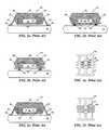
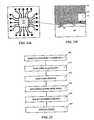
- FIG. 1 ais a diagram of a conventional lead frame with leads and a chip-pad area, according to prior art.
- FIG. 1 bis a diagram of the conventional lead frame of FIG. 1 a showing the attachment of a chip to the chip-pad, and the wire bonding of the terminals on the chip to the leads, according to prior art.
- FIG. 2 ais a cross-sectional view of a wire-bonded and leaded (with leads) near-chip scale package (CSP), showing connection to the next level of packaging by means of leads, according to prior art.
- CSPnear-chip scale package
- FIG. 2 bis a cross-sectional view of a wire-bonded and leadless (with no leads) near-CSP, showing connection to the next level of packaging by means of solder bumps or balls, according to prior art.
- FIG. 2 cis a cross-sectional view of a flip-chip and leaded near-CSP, showing connection to the next level of packaging by means of leads, according to prior art.
- FIG. 2 dis a cross-sectional view of a flip-chip and leadless near-CSP, showing connection to the next level of packaging by means of solder balls, according to prior art.
- FIG. 3 ais a top view of a stencil-like lead frame showing the wire bonded connection of a back-bonded chip to the leads of the lead frame, according to prior art.
- FIG. 3 bis a top view of a stencil-like lead frame showing the connection of a flipped chip to the leads of the lead frame through a solder reflow process, according to prior art.
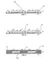
- FIG. 4is a cross-sectional view of a metal film of uniform thickness pre-plated on both sides with a bondable material, according to the present invention.
- FIG. 5is a cross-sectional view of a metal film of FIG. 4, where only the pre-plating on the top surface has been patterned corresponding to two chip sites with each site including a chip-pad and lead contacts surrounding each chip-pad, according to the present invention.
- FIG. 6is a cross-sectional view of the plated metal film of FIG. 4, which has been partially patterned, according to the present invention.
- FIG. 6 ais a top view showing a matrix of partially patterned lead frames according to the present invention.
- FIGS. 6 b and 6 cshow progressively enlarged top views of the lead frames in the matrix shown in 6 a.
- FIG. 7is a cross-sectional view of the partially patterned metal film of FIG. 6 where a chip has been attached to the chip-pad on each of the two chip sites, according to the present invention.
- FIG. 8is a cross-sectional view of the chip attached metal film of FIG. 7, where the terminals on each chip have been wire bonded to the lead portions of the lead frame so formed on each chip site, according to the present invention.
- FIG. 9is a cross-sectional view of the wire bonded lead frame of FIG. 8 where the top surface of the metal film, including the chips and the wire bonds have been hermetically sealed in an encapsulant, according to the present invention.
- FIG. 10is a cross-sectional view of the hermetically sealed package of FIG. 9 that has been etched from the backside to remove the first region of each lead frame and the street regions in the film) according to the present invention.
- FIG. 11is a cross-sectional view of two near chip size partially patterned packages wherein the encapsulant has been singulated in the street regions, according to the present invention to form two separate packages.
- FIG. 12 ais a top view of one of the singulated packages of FIG. 11 showing the chip, the contacts and the wires connecting the chip terminals to the lead contacts, and an enlarged cross section of one of the contacts with a wire bond, according to the present invention.
- FIG. 12 bis a cross-sectional view of the area between the chip-pad and one of the contacts showing the use of a “lip” on the vertical surfaces that come into contact with the molding material in order to provide anchoring and prevent delamination, according to the present invention.
- FIG. 12 cis a cross-sectional view of the area between the chip-pad and one of the contacts showing the use of different shapes of cavities on the vertical surfaces that come into contact with the molding material in order to provide anchoring and prevent delamination, according to the present invention.
- FIGS. 13 a - 13 fare diagrams of various cavities that can be used to provide anchoring means for molding material on the vertical surfaces shown in FIGS. 12 b and 12 c , according to the present invention.
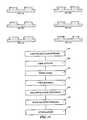
- FIG. 14is a flow chart summarizing the various process steps of forming a partially patterned package, according to the present invention.
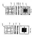
- FIG. 15 ais a diagram showing the top, side and bottom views of a package with a peripheral I/O configuration, according to the present invention.
- FIG. 15 bis a diagram showing the top, side and bottom views of a package with an array configuration of I/O pads, according to the present invention.
- FIG. 16is a cross-sectional view of a metal film of FIG. 4, where only the pre-plating on the top surface has been patterned corresponding to two flip-chip sites with each site including a chip receiving area and leads surrounding each chip receiving area, according to the present invention.
- FIG. 17is a cross-sectional view of the plated metal film of FIG. 16, which has been partially patterned to form a web-like lead frame (i.e., webbed structure), according to the present invention.
- FIG. 18is a cross-sectional view of a chip-joined lead frame (FCL) showing the flip-chip (FC) joining, according to the present invention.
- FIG. 19is a cross-sectional view of the FCL of FIG. 18 where the top surface of the metal film, including the chips, have been hermetically sealed in an encapsulant, according to the present invention.
- FIG. 20is a cross-sectional view of the hermetically sealed package of FIG. 19 that has been etched from the backside to remove selectively the webbed portions between the individual leads and between the recessed chip receiving areas, according to the present invention.
- FIG. 21is a cross-sectional view of two near chip size partially patterned packages that have been singulated from the package of FIG. 20, according to the present invention.
- FIG. 22 ais a top view of one of the singulated packages of FIG. 21 showing the chip and the leads connecting the chip terminals to the end portions of the leads, which are in turn connected to the next level of packaging, according to the present invention.
- FIG. 22 bis an enlarged cross-sectional view of the area between the flip chip and the connection to the next level packaging showing the two end connections of a lead, according to the present invention.
- FIG. 23is a flow chart summarizing the various process steps of forming a partially patterned package supporting a flip-chip, according to the present invention.
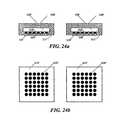
- FIGS. 24 a and 24 bshow a cross-sectional view and a bottom view of two near chip size partially patterned packages that have been singulated, and then provided with ball grid array connectors for connection to the next level of packaging to form an ELGA-type package, according to the present invention.
- FIGS. 4 - 15 b and FIGS. 16 - 24 bshow different embodiments of forming a partially patterned lead frame package with lead counts comparable to that of near-chip scale packages (CSPs).
- the method of the inventionimproves the automation of the manufacturing line and the quality and reliability of the packages made therefrom. This is accomplished by performing a major portion of the manufacturing process steps with a partially patterned metal film formed into a web-like lead frame on one side.
- the lead frame used in the inventionis partially patterned on one side and is solid and flat on the other side. This construction is improved both mechanically and thermally, and performs without distortion or deformation during the chip-attach, wire bond, and encapsulation processes.
- the bottom surfaceis etched entirely through the film to isolate the lead contacts from the chip-pad and each other. Subsequently, the resultant encapsulated package is singulated without having to cut into any additional metal.
- FIGS. 4 - 15 bshow the forming of a partially patterned lead frame for a wire-bonded chip and a method of using the same for forming an ELP-type electronic package.
- FIGS. 16 - 22show the forming of a partially patterned lead frame for a flip-chip and a method of using the same for forming an ELPF-type electronic package.
- a method of forming an ELGA-type of electronic package, using the instant partially patterned lead frame,is also described in connection with FIGS. 24 a and 24 b.
- FIG. 4is a cross-sectional view of a film, preferably a sheet of metal, preferably copper, that is not only to be formed into a lead frame, but also to serve as a stable carrier during the ensuing process steps of forming the lead frame.
- the thickness of the strip of metalis equal to or greater than about 0.05 mm. In another embodiment, the thickness can be in the range between about 0.05 to 0.5 mm.
- Forming a lead frametypically involves cutting through the strip of metal, like cutting a stencil, and then working with very fine finger-like leads.
- a vacuum chuckmay be used.
- Conventional vacuum chuckstypically are not adapted to provide suction for such delicate devices and the lead frame must usually be clamped down peripherally.
- Any rigging used for this purposemust be refitted from one type and size of lead frame to another. The instant invention, however, alleviates this refitting step. Because the bottom surface of the partially patterned lead frame is solid and continuous, a conventional vacuum chuck can easily hold the lead frame in place during processing.
- one size strip of metal that can accommodate the various industrial lead framescan be used universally in the manufacture of the lead frames.
- the subsequent process steps of chip attach and wire bondingcan be accomplished with much less stress and strain on the lead frame to be formed.
- Lead frames with much finer geometriescan easily be fabricated because the leads are held together by the web-like structures and are not separated from each other until the very final step.
- Forming of the various patterns on the lead framecan be accomplished in a number of ways.
- One approachcan be stamping the pattern into the metal.
- Other approachesmay include chemical or electrochemical milling and electrical discharge machining (EDM).
- EDMelectrical discharge machining
- photolithographic patterningwhich is a mainstay of semiconductor manufacturing, is preferred.
- metal strip ( 100 ) shown in FIG. 4is pre-plated on both the front (or top) side and the back (or bottom) side prior to the photolithographic patterning. Either or both the front surface and the back surface may be pre-plated with a material that enables bonding as well as solderability, respectively.
- the front surfaceis pre-plated with a bondable material, such as Ni/Pd/Au-strike or Ag.
- the back surfaceis pre-plated with a solderable material, such as Sn/Pb, lead-free solder, immersion-tin electroless-nickel or Au-strike. The pre-plating can be performed at a later step, if so desired.
- the pre-plated front side ( 110 )is photolithographically patterned to form areas corresponding to chip-pad ( 115 ) and electrical contacts ( 113 ) surrounding the chip-pad area.
- An electrical contact ( 113 )can be characterized as the end portion of a lead that is connected to the chip-pad area ( 115 ) through a first region of intermediate recessed portions that forms the web-like structure. These intermediate recessed web-like portions are removed at a later time when metal film ( 100 ) is etched from the back so that the end portions and the chip-pad portions will be isolated from each other.
- the areas comprising a chip-pad ( 115 ) and the surrounding contacts ( 113 )are sometimes referred to as chip sites.
- a plurality of chip sitescan be formed on a continuous roll of copper sheet sprocketed to a spool to easily automate the forming of lead frames comprising one or more chip sites.
- FIG. 5illustrates two chip sites, which will be formed into two corresponding lead frames, which in turn will be part of two packages that will be formed from them.
- the pattern shown for the two chip sites illustrated in FIG. 5is then transferred into film strip ( 100 ) by etching.
- a main feature of the present inventionis that the etching is performed only partially through the thickness of the metal, which is referred to herein as partial patterning.
- the partial patterningis performed in a first region of the film to form a webbed structure ( 130 ) that connects the chip pads ( 115 ) of lead contacts ( 113 ) of each lead frame.
- the first regionalso connects the lead frames to one another at street portions ( 136 ) of the film.
- a matrix or such lead framesmay be formed in a block/window film ( 138 ).
- FIGS. 6 b and 6 cshow that the first region includes the webbed structure ( 139 ) connecting the chip pad and lead contacts of each lead frame. The first region also connects the plurality of lead frames to one another at street portions ( 136 ) of the film.
- the partial patterningcan vary from 25% to 90% of the thickness of the film.
- the partial patterningmay be virtually any percentage of the thickness of the film and the amount of partial etching can be determined by considering various factors affecting the manufacturability parameters, including flexibility, rigidity, and thermal thickness (or thermal conductance).
- the lateral dimensions of lead contact areas ( 113 ) and chip-pad areas ( 115 )can be determined based on the degree of miniaturization desired for given chip sizes and wire bonds or other connecting media that may be used for interlevel or intralevel connections in a given package or between packages at the next level of packaging. It is especially noted that manufacturability concerns for fine features and dimensional stability of the lead frame are of lesser significance now by virtue of the web-like structure of the finger-like leads.
- chips ( 140 )are next attached to the chip-pad areas preferably using an epoxy ( 150 ).
- the epoxymay be filled with conductive particles to enhance the cooling of the chip.
- the epoxyis cured and, as shown in FIG. 8, wires ( 160 ) are bonded to terminals ( 145 ) and to corresponding lead contacts ( 113 ) using well-known wire bonding techniques.
- the lead frame formed according to the present inventionhas a solid, continuous back side that is firmly seated and held down on a flat surface such as by a vacuum chuck (not shown), the web-like structure of the leads do not flutter or bounce during wire bonding. This results in excellent bonds, which improves the reliability of the end product.
- both the lead contacts ( 113 ) and the chip-pads ( 115 )can now readily be isolated from one another to form their own islands by etching the webbed structure ( 135 ) of the first region through the back side of the package.
- the street portions ( 136 )are also back etched.
- the back etchingcontinues until the molding material is reached.
- the etch method for back etching the metalshould be the same as that used for the front side.
- the etch time for the back sidemay differ from that used for the front side, depending upon the degree of partial etching that was performed from the front side.
- the initial forming of the partial etch lead framecan be custom tailored to fit the manufacturing requirements for automation, quality, reliability and functionality of the final package.
- the encapsulant ( 170 ) over the street portions ( 136 ) between the lead framesis singulated to form two individual packages as shown in FIG. 11.
- Thisis accomplished in a number of ways, including saw slicing, water-jet-cut, laser-cut, or a combination thereof, or other techniques that are especially suitable for cutting plastics.
- this methodmay also be applied to produce a great number of packages from a matrix of lead frames.
- FIG. 12 aA top view of a singulated ELP is shown in FIG. 12 a , where contacts ( 120 ) and chip ( 140 ) are shown isolated from one another on their own islands, but only connected with each other through wires ( 160 ) that have been wire bonded.
- FIG. 12 bshows an enlarged view of a corner of the package between the chip and one of the contacts comprising a portion of the original metal strip ( 100 ), a top surface pre-plated to form bondable layer ( 113 ), and a bottom surface pre-plated to form solderable layer ( 123 ).
- a “lip”is shown both on the contact and the corner of the chip.
- the pre-plated surface ( 120 ) on the underside of the packagecan now be used for several purposes.
- Another aspect of the present inventionprovides a means for lessening the possibility of delamination between the molding material and the surfaces to which it should adhere. This is accomplished by half-etching the edges around the chip-pad and the contact areas to form a ledge or a “lip”, such as referenced by numeral ( 105 ) in FIG. 12 b . It is also possible to form irregularly shaped cavities ( 107 ) shown in FIG. 12 c to enhance the interlocking mechanism of the surfaces that come into contact with the molding material. Enlarged views of various other cavities are also shown in FIGS. 13 a - 13 f , and forming of these surface enhancements can readily be incorporated into the partial etching from the front side. This will not be necessary for etching from the backside inasmuch as the molding material encapsulates only the surfaces that are formed partially from the front side.
- FIG. 14summarizes the method of the present invention as commencing with the partial etching of a lead frame ( 200 ) into a metal strip from the front side and ending with the back pattern etching ( 250 ) of the same metal strip in such a way so as to form the desired chip-pad and the surrounding contacts.
- the intermediate steps of chip attach ( 210 ), epoxy cure ( 220 ), wire bonding ( 230 ), and encapsulation ( 240 )are all accomplished on a mechanically and thermally stable lead frame, because the leads are still connected through the first region of intermediate recessed portions on a partially etched web-like or webbed structure in the metal film.
- the method of the present inventionmay be used to form a wide variety of packages, such as an array type of a lead frame for an electronic package.
- a top view of an array type package ( 400 )is shown in FIG. 15 b next to the standard peripheral type package ( 300 ) shown in FIG. 15 a .
- numeral ( 305 )references a peripheral arrangement of chip terminals
- numeral ( 405 )references an array type arrangement of the terminals, which can be configured in-line or staggered.
- Both packagesare formed using the disclosed partial patterning invention as indicated by reference numerals ( 310 ) and ( 410 ).
- inner leads ( 440 ) and outer leads ( 445 )are shown in the array type ELP.
- Both packagesare encapsulated in molding material ( 320 ) or ( 420 ).
- Back pattern etching to isolate the contacts and the chipare indicated by ( 330 ) and ( 430 ).
- Numeral ( 450 )depicts a ground ring feature, which is etched to the same level as the mold.
- Numeral ( 460 )points to the array type input/output configuration on the bottom view of the ELP.
- the second embodiment shown in the drawings 16 - 24 bdiscloses a method of forming a partially patterned VFQFP-N type lead frame which is especially suitable for mass producing FC electronic packages.
- the lead frame made to accommodate the flip-chipwill, hereafter, be referred to as FCL to distinguish it from conventional lead frames. This is because, unlike conventional lead frames, FCLs are sturdier and much more adaptable to automated manufacturing lines, as described below.
- FCLsare also web-like structures in contrast to the conventional all-purpose punched through, stencil-like lead frames.
- the front side of a web-like FCLhas recessed sections, including partially patterned leads, while the back side is solid and flat. This provides mechanical rigidity to perform without distortion or deformation during the manufacturing processes.
- the backsideis etched to isolate the lead contacts from each other. Subsequently, the resultant encapsulated package is singulated without having to cut into any additional metal.
- FCLs with much finer geometriessuch as with VFQFP-N packages, can easily be fabricated inasmuch as the leads are held together by the web-like, or webbed structures and not totally separated from each other until the very final step of singulation.
- the FCL of the second embodimentis also formed from a sheet of metal, preferably copper film as shown in FIG. 4, where both the front surface and the back surface are pre-plated, or, as stated previously, the plating can be deferred to a later step.
- the reference numeralshave been kept the same as appropriate except for denoting those of the second embodiment with primes.
- the same reference numeral ( 100 )has been kept for consistency for the metal film used for both embodiments).
- the pre-plated front side ( 110 ′)is photolithographically patterned to form chip receiving areas ( 115 ′), lead portions ( 113 ′) surrounding the chip receiving areas, and other intermediate areas ( 117 ′).
- chip receiving areas115 ′
- lead portions113 ′
- other intermediate areas117 ′
- one end portion of the leadswill be connected to the terminals of an FC, while the other end portion will be connected to the next level of packaging.
- the areas comprising a chip receiving area and the surrounding leadsare sometimes referred to as a chip site, similar to the chip sites with wire-bonded chips.
- a plurality of lead frames comprising a plurality of chip sitescan be formed on a continuous roll of copper sheet sprocketed to a spool to easily automate the forming of lead frames comprising one or more chip sites.
- FIG. 16illustrates two chip sites, which will be formed into two corresponding lead frames, which in turn will be part of two packages that will be formed from them.
- the pattern shown for the two chip sites illustrated in FIG. 16is then transferred into metal film ( 100 ) by partial patterning through etching.
- the partial patterning shown in FIG. 17may be up to one-half, one-quarter, or for that matter, any ratio of the thickness of the strip of metal, and the amount of partial etching can be determined by considering various factors affecting the manufacturability parameters including flexibility, rigidity, and thermal thickness (or thermal conductance).
- the lateral dimensions of lead contact areas ( 113 ′) and chip areas ( 115 ′)can be determined based on the degree of miniaturization desired for given chip sites including the chip size and the leads that may be used for interlevel or intralevel connections in a given package or between packages at the next level of packaging. It is especially noted that manufacturability concerns for fine features and dimensional stability of the lead frame are of lesser significance now by virtue of the webbed structure of the finger-like leads.
- the lead frame formed according to the present inventionhas a solid, continuous back side that is firmly seated and held down on a flat surface, the web-like structure of the leads do not flutter or bounce around in the chip-joining furnace, thereby yielding excellent chip joining. Consequently, the disclosed method improves the reliability of the end product, namely, that of the VFQFP-N type packages.
- the chips, along with the partially patterned leads on the front side of the original metal film,are then hermetically encapsulated in a molding material, for example, by a resin, as shown in FIG. 19.
- Encapsulant ( 140 ′)is formed around all exposed surfaces, including that of leads ( 113 ′), around solder balls ( 135 ′), underneath the chips, along the vertical walls of recessed chip receiving areas, ( 115 ′) as well as that of the vertical walls of recessed areas ( 117 ′) except for the unetched, solid and flat back side of strip of metal ( 100 ) that is held down firmly onto a flat surface.
- the resultant molded packageis lifted up, the clean backside is now available for further processing.
- the commonly encountered problem of mold flashing to the footprint on the underside of the packageis eliminated in this embodiment as well.
- Leads ( 113 ′)can now readily be isolated from one another by patterning through the back side of the package in alignment with the pattern that was partially etched from the front side at the beginning of the process. The back etching continues until the molding material is reached. This is shown in FIG. 20 where web-like portions of the lead frames, namely areas ( 111 ′) and ( 119 ′), are removed to disconnect chip areas ( 115 ′) from each other, and leads ( 113 ′) from each other. It is preferred that the etch recipe for back patterning the metal be the same as the recipe that was used for partial etching from the front side.
- the etch time from the back sidemay differ from that used for the front side depending upon the degree of partial etching that was performed from the front side.
- the initial forming of the partial etch lead framecan be custom tailored to fit the manufacturing requirements for automation, quality, reliability and functionality of the final package.
- the package of FIG. 20, having two encapsulated chip sites for the purposes of illustrating the present inventionis next singulated into singular near-chip size packages (CSPs), which are more of the VFQFP-N type packages, as shown in FIG. 21.
- CSPssingular near-chip size packages
- FIG. 22 aA top view of a singulated partially patterned lead frame package is shown in FIG. 22 a , where leads ( 113 ′) are shown isolated from one another and connected to solder balls ( 135 ′) on the underside of chip ( 130 ′).
- FIG. 22 bshows an enlarged view of a corner of the package between the chip and one of the leads connected to an external contact ( 145 ′) that may be provided on a card or a board ( 150 ′).
- the pre-plated surface ( 120 ′)is already prepared to be joined to the next level of contact as shown in the same Figure.
- the underside ( 114 ′) of leads ( 113 ′)are exposed to the ambient environment, thus
- FIG. 23summarizes the method of the present embodiment as commencing with the partial patterning of a lead frame ( 200 ′) into a metal strip from the front side and ending with the back patterning ( 240 ′) of the same metal strip in such a way so as to form the desired chip receiving areas and the surrounding leads.
- the intermediate steps of FC placement ( 210 ′), FC chip joining ( 220 ′), and encapsulation ( 230 ′)are all accomplished on a mechanically and thermally stable FCL because the leads are still connected through the partially etched web-like structure in the metal film.
- the method of the inventionmay be used to form a wide variety of packages, such as an array type of a partially patterned lead frame where an area array of solder bumps can be chip joined simultaneously on to the lead frame with the chip flipped over, similar to the method disclosed herein with a peripheral set of solder bumps.
- an array of partially patterned lead frames themselvescan be formed simultaneously, and then FC joined also simultaneously, followed by singulation of the array into a multiplicity of separate VFQFP-N type packages.
- each resulting CSPcan then be provided with solder bumps, pads, or other electrical connections underneath the package for array type joining on to the next level of packaging to form an etched lead frame package with ball grid array, or ELGA-type package shown in FIGS.
- FIG. 24 aa cross-sectional view is shown where chip pads ( 135 ′) are formed over the leads ( 145 ′). Subsequent to the back-patterning, leads ( 145 ′) are electrically isolated from each other to be joined to the next level of packaging.
- the exposed bottom surfaces of ( 145 ′)can be flash finished with any number of solderable materials through immersion-tin dipping or electroless-nickel plating.
- the bottom surface ( 111 ′) of the ELGA packageis shown in FIG. 24 b with an array pattern for the electrical connections ( 145 ′).
- the inventionpromotes a number of advantages in the manufacturing process for electronic packages. For example, after the back etching and prior to singulation, a block of packages will inherently be ready for strip testing while the packages are still arranged in the block. This provides a significant advantage as compared to handling the packages as individual units. Strip testing the packages while they are arranged in a block improves the reliability of the test.
- the inventionalso enables a manufacturer to produce packages having dual or triple rows of staggered leads that can multiply I/O capacity of a given package.
- the flat continuous bottom surface of the lead framesenables the use of universal assembly equipment, which does not need refitting for each application, and which is completely flexible for automation. For example, processing between 2 ⁇ 2 through 12 ⁇ 12 package blocks does not require any mechanical change.
- the inventioneasily facilitates the construction of packages having a “stand off” for each foot (for example, at 2 mils between the bottom of the molded body at the surface of the foot). The stand off provides additional advantages when the chip packages are to be connected to the next level of packaging, such as a board.
Landscapes
- Engineering & Computer Science (AREA)
- Microelectronics & Electronic Packaging (AREA)
- Computer Hardware Design (AREA)
- Power Engineering (AREA)
- Physics & Mathematics (AREA)
- Condensed Matter Physics & Semiconductors (AREA)
- General Physics & Mathematics (AREA)
- Manufacturing & Machinery (AREA)
- Lead Frames For Integrated Circuits (AREA)
- Encapsulation Of And Coatings For Semiconductor Or Solid State Devices (AREA)
Abstract
Description
- The invention relates to electronic packaging in general, and more particularly, to a partially patterned lead frame and a method for making and using the same. The partially patterned lead frame is stronger and more stable than conventional lead frames. The sturdiness of the partially patterned lead frame improves the process of manufacturing lead frame packages and enhances the overall reliability of the end product.[0001]
- In making electronic packages that use lead frames, there are several process steps that subject the lead frames to mechanical and thermal stresses. The finer geometries of current lead frames and the ever-increasing integration of circuits on semiconductor chips have resulted in processing that places even greater stress on the lead frames. Finely configured lead frames often resemble very delicate embroidery, or stencil-like metal structures that tend to bend, break, disfigure and deform easily. (See FIGS. 1[0002]aand1b). Such conventional lead frames are used in the industry to create a variety of chip packages, including wire bonded and flip-chip (FC) packages. (See FIGS. 2a-2dand3a-3b).
- Conventional lead frames generally lack structural rigidity. The finger-like portions of lead frames can be quite flimsy and difficult to hold in position. This lends to handling flaws, damage and distortion in assembly processes and complicated wire bonding situations. Consequently, bond parameters have to be optimized to compensate for lead frame bouncing during the bonding process. A failure to optimize the bonding parameters to compensate for the mechanical instability of the lead frame can result in poor bond adhesion, and hence poor quality and poor reliability of the bond.[0003]
- The finger-like portions of a typical lead frame extend from a central portion, known as the chip receiving area, also known as a chip-pad. The chip is usually attached to the receiving area with the backside down, and the front side is positioned face up with terminals located peripherally on the perimeter of the chip, or over the surface of the chip in the form of an array. The receiving area typically has dimensions of about 5 mm×5 mm, and the leads extending outwardly from the chip-pad area have typical dimensions of about 10 mm long×1 mm wide×0.5 mm thick. The lead frame is typically held down by a vacuum chuck and mechanical clamps. The chuck and clamps must be refitted for lead frames of different sizes and shapes. The present invention alleviates this problem.[0004]
- The prior art has not shown any lead frames that can withstand the stresses encountered in current semiconductor packaging processes and that can be manufactured in a cost effective manner. The present invention achieves this objective by providing a partially patterned lead frame that not only improves the manufacturability of the lead frame itself, but also improves the integrity and reliability of the electronic packages that are formed therefrom.[0005]
- The present invention provides a partially patterned lead frame for use in semiconductor packaging. The lead frame is composed of a film having a top surface and a bottom surface. A first region of the film is partially patterned from the top surface but not entirely through the film to the bottom surface. A second region of the film, not patterned from the top surface, forms a chip receiving area for supporting an integrated circuit (IC) chip and a plurality of lead contacts for providing electrical connections to the IC chip. The first region forms trenches in the film and creates a webbed structure that interconnects the second region that is not partially patterned from the top surface. The present invention is also directed to a method of manufacturing partially patterned lead frames and to electronic packages made utilizing the lead frames. The lead frame of the invention has improved structural rigidity because of its web-like, or webbed structure.[0006]
- According to the invention, the top surface of a metal film, from which the lead frame is to be formed, is first patterned using standard photolithographic techniques or similar techniques to outline the areas that will correspond to a chip receiving area and leads. At the next step, etching is performed in the first region of the film outside the outlined areas from the top surface of the film partially through the thickness of the underlying film to create a lead frame pattern in the film. After the partial patterning, the remaining areas not patterned from the top surface form a second region which will serve as a chip receiving area and leads along the top surface. The first region forms a recessed webbed region below the top surface of the film. The webbed structure of the first region connects the lead portions to each other and to the chip receiving area. Thus, the partially patterned film looks similar to a webbed foot and retains its rigidity and strength so it can withstand the forces of subsequent manufacturing process steps. In particular, the partially patterned lead frame can withstand the forces encountered during wire bonding and encapsulation processes. In some embodiments, the chip receiving area and electrical leads can be formed from the same parts of the second region (e.g., in the case where the electrical leads support the integrated chip as well as provide electrical connection thereto).[0007]
- The present invention also provides a unique method of making a plurality of electronic packages using partially patterned lead frames. The method involves a film having a top surface and a bottom surface. In the first region, the film is partially patterned from the top surface but not entirely through to the bottom surface. The remaining second region on the film not partially patterned from the top surface forms a plurality of partially patterned lead frames. Each of the lead frames has a chip receiving area for supporting an integrated circuit (IC) chip and a plurality of electrical leads for providing electrical connections to the IC chip.[0008]
- The first region of the film forms a webbed structure that interconnects the chip receiving areas and electrical leads of each lead frame. The first region also connects the plurality of lead frames to one another in street portions of the film.[0009]
- A plurality of chips is provided, each chip having a plurality of electrical terminals for attachment to a corresponding lead frame. Each chip is attached to the chip receiving area on a corresponding lead frame and an electrical connection is formed between at least one terminal of each chip and one of the electrical leads of the lead frame. Thereafter, an encapsulant material is applied over the lead frames and the street portions of the film to completely cover the top of the film. Once the encapsulant material is dried, a back patterning process is performed from the bottom surface of the film in the first region to remove the webbed structure and the street portions of the film. The encapsulant material disposed over the street portions of the film is then singulated to form individual packages.[0010]
- In a preferred embodiment, the method includes forming the lead frames into the film in a matrix in a block/window pattern, and involves the production of chip scale packages.[0011]
- Several advantages arise from the partially patterned lead frame of the present invention. The flat and solid un-etched bottom surface of the lead frame serves as an excellent heat sink during the wire bonding process. This provides even heat transfer for better and more consistent bond quality. Additionally, the solid structure provides a continuous surface for a universal vacuum chuck to hold the lead frame down, thereby making the chip-attachment process more stable and the leads more secure during the subsequent process steps. Awkward clamping of outer edges of the lead frame is eliminated to allow an array-matrix lead frame design and processing without conversion needs. Because the bottom side of the partially patterned lead frame is a flat continuous surface, a universal vacuum chuck may be used to hold down many different sizes of frames. This removes the complication of having to refit the vacuum chuck each time a lead frame of different dimensions is being employed in the packaging process. Also, there is no further need for clamping. The use of a universal vacuum chuck and elimination of clamping enables construction of dual or triple rows of staggered leads on the second region for higher lead counts.[0012]
- The present invention is directed to a partially patterned lead frame that will accommodate not only wire-bonded chips but also solder bumped flip-chips. In addition, the invention teaches methods of using the partially patterned lead frame for making etched lead frame packages (ELPs) that use wire-bonding, ELPs with flip-chips (ELPFs), and also ELPs or ELPFs with land grid array (LGA) pads to form etched land grid array (ELGA) packages, as further described in the embodiments of the present invention.[0013]
- Flip Chip (FC) technology is one more step towards fully automated joining of the electrical terminals on a chip to the next level of packaging, namely, to a ceramic or plastic substrate, or to a chip microcarrier that is later joined to the substrate. The microcarrier, which is only slightly larger than the chip itself, is now called the chip scale package (CSP). FC technology evolved from tape automated bonding (TAB) which in turn had its origins in wire bonding (WB). Whereas in WB and TAB the chip is positioned on its back surface and electrical connections are made to the terminals located around the perimeter on its top surface, in FC technology the orientation of the chip is reversed. The chip is placed face downward and the back side of the chip oriented upward. This flip-chip orientation has a significant advantage in that it concentrates the electrical functions on the underside of the chip, leaving the top side free for use in developing a highly efficient heat transfer design.[0014]
- In the FC process, the chip terminals or bond pads are sealed with different types of bumps over the surface of the chip, where the patterns may be deployed in an area array, peripheral patterns or other patterns. The chip may be attached to the next level in the following ways: a) FC attachment to a lead frame; b) FC attachment of a layer/substrate, known as an interposer, for re-routing the connection spacing on a lead frame; c) FC attachment to a pre-attached interposer on a lead frame; or d) FC attachment to a printed circuit board using conventional techniques, including chip reflow methods.[0015]
- Chip attachment using conventional techniques becomes especially difficult when applied to QFN (Quad Flat No Lead) lead frames in making QFN packages and derivatives thereof, such as VFQPF-N. This is because conventional lead frames in general lack structural rigidity. Finger-like portions of lead frames can be quite flimsy and difficult to hold in one precise position. This lends to handling flaws, damage and distortion in assembly processes and complicated chip bonding situations. FC joining processes require precise alignment of bumped solder heads against the hanging and flimsy lead ends of the lead frame. Furthermore, the wetted solder ends must retain their positions after placement through the solder reflow process. Consequently, reflow parameters have to be optimized to compensate for lead frame bouncing during chip joining, which, if not properly done, can result in poor joints, and hence poor quality and poor reliability of the end product.[0016]
- It is common practice to form the conventional stencil-like lead frames by patterning a photoresist on a strip of metal, or metal film, and etching through the pattern to form the finger-like leads extending outwardly from the chip receiving area. It is also customary to use “tie-bars” between the fingers so that the fingers are kept apart during the various process steps, as was shown in FIGS. 3[0017]aand3b. The present invention alleviates the problem of the lack of structural rigidity of the lead frame by forming a web-like, partially patterned lead frame instead of a stencil-like lead frame.
- In accordance with a method of the present invention, all the major process steps of forming a semiconductor package are performed from one side of the film that is to become a lead frame. The other side, namely, the bottom side, remains flat and untouched on a surface, such as the surface of a vacuum chuck. This includes the step of encapsulating and hermetically sealing the partially formed front side of the package. Once the encapsulation is completed, the bottom surface is back-etched to remove selectively the webbed portions that connect the leads to each other and to the chip receiving area. In the ELP case, where the chip is back-bonded to a chip-pad at the chip receiving area and the electrical connection to the chip terminals is made by means of wire bonding, all intermediate webbed portions are severed through etching so that the chip-pad and the lead contacts at the wire bonded end are now isolated from each other by the molding material that surrounds the chip, the wires and the front surfaces of the wire-bonded contact areas. In the case of the ELPF package, however, only the webbed portions that connect the leads to each other are severed through etching, since leads themselves that are connected to the chip solder headed bumps provide the electrical connection to the next level of packaging.[0018]
- The removal of embedded metal through the saw thickness, or streets, in the webbed portions has several advantages, including the elimination of the saw forces propagating throughout the lead frame structure, and hence, the prevention of the delamination at the metal-plastic interfaces. Also, the electrical isolation through back-etching enables strip testing prior to any sawing or singulation, or for that matter, prior to any further processing steps. After the back patterning, the remaining and exposed metal portions on the bottom surface can then be flash finished with any number of solderable materials through immersion-tin dipping or electroless-nickel plating. The ELGA package uses the FC of the ELPF package, however, with LGA pads for connection to the next level of packaging.[0019]
- In order to prevent any separation between the molding material and other components of the package during manufacturing, the present invention also teaches how to form locking features on the exposed vertical walls of the recessed webbed portions of the partially etched lead frame, such as on the side walls of the leads, that will come in contact with the molding material, such as a resin. As an alternative, it is also taught to form “lips” on the edges of the chip-pad and lead contacts so as to capture the molding material under each lip, thereby making it difficult for the molding material to separate from the mating surfaces.[0020]
- FIG. 1[0021]ais a diagram of a conventional lead frame with leads and a chip-pad area, according to prior art.
- FIG. 1[0022]bis a diagram of the conventional lead frame of FIG. 1ashowing the attachment of a chip to the chip-pad, and the wire bonding of the terminals on the chip to the leads, according to prior art.
- FIG. 2[0023]ais a cross-sectional view of a wire-bonded and leaded (with leads) near-chip scale package (CSP), showing connection to the next level of packaging by means of leads, according to prior art.
- FIG. 2[0024]bis a cross-sectional view of a wire-bonded and leadless (with no leads) near-CSP, showing connection to the next level of packaging by means of solder bumps or balls, according to prior art.
- FIG. 2[0025]cis a cross-sectional view of a flip-chip and leaded near-CSP, showing connection to the next level of packaging by means of leads, according to prior art.
- FIG. 2[0026]dis a cross-sectional view of a flip-chip and leadless near-CSP, showing connection to the next level of packaging by means of solder balls, according to prior art.
- FIG. 3[0027]ais a top view of a stencil-like lead frame showing the wire bonded connection of a back-bonded chip to the leads of the lead frame, according to prior art.
- FIG. 3[0028]bis a top view of a stencil-like lead frame showing the connection of a flipped chip to the leads of the lead frame through a solder reflow process, according to prior art.
- FIG. 4 is a cross-sectional view of a metal film of uniform thickness pre-plated on both sides with a bondable material, according to the present invention.[0029]
- FIG. 5 is a cross-sectional view of a metal film of FIG. 4, where only the pre-plating on the top surface has been patterned corresponding to two chip sites with each site including a chip-pad and lead contacts surrounding each chip-pad, according to the present invention.[0030]
- FIG. 6 is a cross-sectional view of the plated metal film of FIG. 4, which has been partially patterned, according to the present invention.[0031]
- FIG. 6[0032]ais a top view showing a matrix of partially patterned lead frames according to the present invention.
- FIGS. 6[0033]band6cshow progressively enlarged top views of the lead frames in the matrix shown in6a.
- FIG. 7 is a cross-sectional view of the partially patterned metal film of FIG. 6 where a chip has been attached to the chip-pad on each of the two chip sites, according to the present invention.[0034]
- FIG. 8 is a cross-sectional view of the chip attached metal film of FIG. 7, where the terminals on each chip have been wire bonded to the lead portions of the lead frame so formed on each chip site, according to the present invention.[0035]
- FIG. 9 is a cross-sectional view of the wire bonded lead frame of FIG. 8 where the top surface of the metal film, including the chips and the wire bonds have been hermetically sealed in an encapsulant, according to the present invention.[0036]
- FIG. 10 is a cross-sectional view of the hermetically sealed package of FIG. 9 that has been etched from the backside to remove the first region of each lead frame and the street regions in the film) according to the present invention.[0037]
- FIG. 11 is a cross-sectional view of two near chip size partially patterned packages wherein the encapsulant has been singulated in the street regions, according to the present invention to form two separate packages.[0038]
- FIG. 12[0039]ais a top view of one of the singulated packages of FIG. 11 showing the chip, the contacts and the wires connecting the chip terminals to the lead contacts, and an enlarged cross section of one of the contacts with a wire bond, according to the present invention.
- FIG. 12[0040]bis a cross-sectional view of the area between the chip-pad and one of the contacts showing the use of a “lip” on the vertical surfaces that come into contact with the molding material in order to provide anchoring and prevent delamination, according to the present invention.
- FIG. 12[0041]cis a cross-sectional view of the area between the chip-pad and one of the contacts showing the use of different shapes of cavities on the vertical surfaces that come into contact with the molding material in order to provide anchoring and prevent delamination, according to the present invention.
- FIGS. 13[0042]a-13fare diagrams of various cavities that can be used to provide anchoring means for molding material on the vertical surfaces shown in FIGS. 12band12c, according to the present invention.
- FIG. 14 is a flow chart summarizing the various process steps of forming a partially patterned package, according to the present invention.[0043]
- FIG. 15[0044]ais a diagram showing the top, side and bottom views of a package with a peripheral I/O configuration, according to the present invention.
- FIG. 15[0045]bis a diagram showing the top, side and bottom views of a package with an array configuration of I/O pads, according to the present invention.
- FIG. 16 is a cross-sectional view of a metal film of FIG. 4, where only the pre-plating on the top surface has been patterned corresponding to two flip-chip sites with each site including a chip receiving area and leads surrounding each chip receiving area, according to the present invention.[0046]
- FIG. 17 is a cross-sectional view of the plated metal film of FIG. 16, which has been partially patterned to form a web-like lead frame (i.e., webbed structure), according to the present invention.[0047]
- FIG. 18 is a cross-sectional view of a chip-joined lead frame (FCL) showing the flip-chip (FC) joining, according to the present invention.[0048]
- FIG. 19 is a cross-sectional view of the FCL of FIG. 18 where the top surface of the metal film, including the chips, have been hermetically sealed in an encapsulant, according to the present invention.[0049]
- FIG. 20 is a cross-sectional view of the hermetically sealed package of FIG. 19 that has been etched from the backside to remove selectively the webbed portions between the individual leads and between the recessed chip receiving areas, according to the present invention.[0050]
- FIG. 21 is a cross-sectional view of two near chip size partially patterned packages that have been singulated from the package of FIG. 20, according to the present invention.[0051]
- FIG. 22[0052]ais a top view of one of the singulated packages of FIG. 21 showing the chip and the leads connecting the chip terminals to the end portions of the leads, which are in turn connected to the next level of packaging, according to the present invention.
- FIG. 22[0053]bis an enlarged cross-sectional view of the area between the flip chip and the connection to the next level packaging showing the two end connections of a lead, according to the present invention.
- FIG. 23 is a flow chart summarizing the various process steps of forming a partially patterned package supporting a flip-chip, according to the present invention.[0054]
- FIGS. 24[0055]aand24bshow a cross-sectional view and a bottom view of two near chip size partially patterned packages that have been singulated, and then provided with ball grid array connectors for connection to the next level of packaging to form an ELGA-type package, according to the present invention.
- FIGS.[0056]4-15band FIGS.16-24bshow different embodiments of forming a partially patterned lead frame package with lead counts comparable to that of near-chip scale packages (CSPs). The method of the invention improves the automation of the manufacturing line and the quality and reliability of the packages made therefrom. This is accomplished by performing a major portion of the manufacturing process steps with a partially patterned metal film formed into a web-like lead frame on one side. In contrast with conventionally punched through stencil-like lead frames, the lead frame used in the invention is partially patterned on one side and is solid and flat on the other side. This construction is improved both mechanically and thermally, and performs without distortion or deformation during the chip-attach, wire bond, and encapsulation processes. After the chip attach and wire bonding process steps are completed and the chip and wire bonds are affixed and hermetically encapsulated in a molding material, the bottom surface is etched entirely through the film to isolate the lead contacts from the chip-pad and each other. Subsequently, the resultant encapsulated package is singulated without having to cut into any additional metal.
- More specifically, FIGS.[0057]4-15bshow the forming of a partially patterned lead frame for a wire-bonded chip and a method of using the same for forming an ELP-type electronic package. FIGS.16-22, on the other hand, show the forming of a partially patterned lead frame for a flip-chip and a method of using the same for forming an ELPF-type electronic package. A method of forming an ELGA-type of electronic package, using the instant partially patterned lead frame, is also described in connection with FIGS. 24aand24b.
- FIG. 4 is a cross-sectional view of a film, preferably a sheet of metal, preferably copper, that is not only to be formed into a lead frame, but also to serve as a stable carrier during the ensuing process steps of forming the lead frame. The thickness of the strip of metal is equal to or greater than about 0.05 mm. In another embodiment, the thickness can be in the range between about 0.05 to 0.5 mm.[0058]
- Forming a lead frame typically involves cutting through the strip of metal, like cutting a stencil, and then working with very fine finger-like leads. In order to hold down such a delicate structure in place, a vacuum chuck may be used. Conventional vacuum chucks, however, typically are not adapted to provide suction for such delicate devices and the lead frame must usually be clamped down peripherally. Any rigging used for this purpose must be refitted from one type and size of lead frame to another. The instant invention, however, alleviates this refitting step. Because the bottom surface of the partially patterned lead frame is solid and continuous, a conventional vacuum chuck can easily hold the lead frame in place during processing. Furthermore, one size strip of metal that can accommodate the various industrial lead frames can be used universally in the manufacture of the lead frames. The subsequent process steps of chip attach and wire bonding can be accomplished with much less stress and strain on the lead frame to be formed. Lead frames with much finer geometries can easily be fabricated because the leads are held together by the web-like structures and are not separated from each other until the very final step.[0059]
- Forming of the various patterns on the lead frame can be accomplished in a number of ways. One approach can be stamping the pattern into the metal. Other approaches may include chemical or electrochemical milling and electrical discharge machining (EDM). On the other hand, photolithographic patterning, which is a mainstay of semiconductor manufacturing, is preferred. In the present invention, metal strip ([0060]100) shown in FIG. 4 is pre-plated on both the front (or top) side and the back (or bottom) side prior to the photolithographic patterning. Either or both the front surface and the back surface may be pre-plated with a material that enables bonding as well as solderability, respectively. In one embodiment, the front surface is pre-plated with a bondable material, such as Ni/Pd/Au-strike or Ag. In another embodiment, the back surface is pre-plated with a solderable material, such as Sn/Pb, lead-free solder, immersion-tin electroless-nickel or Au-strike. The pre-plating can be performed at a later step, if so desired.
- At the next step, the pre-plated front side ([0061]110) is photolithographically patterned to form areas corresponding to chip-pad (115) and electrical contacts (113) surrounding the chip-pad area. An electrical contact (113) can be characterized as the end portion of a lead that is connected to the chip-pad area (115) through a first region of intermediate recessed portions that forms the web-like structure. These intermediate recessed web-like portions are removed at a later time when metal film (100) is etched from the back so that the end portions and the chip-pad portions will be isolated from each other. The areas comprising a chip-pad (115) and the surrounding contacts (113) are sometimes referred to as chip sites. A plurality of chip sites can be formed on a continuous roll of copper sheet sprocketed to a spool to easily automate the forming of lead frames comprising one or more chip sites. FIG. 5 illustrates two chip sites, which will be formed into two corresponding lead frames, which in turn will be part of two packages that will be formed from them.
- The pattern shown for the two chip sites illustrated in FIG. 5 is then transferred into film strip ([0062]100) by etching. As shown in FIG. 6, a main feature of the present invention is that the etching is performed only partially through the thickness of the metal, which is referred to herein as partial patterning. The partial patterning is performed in a first region of the film to form a webbed structure (130) that connects the chip pads (115) of lead contacts (113) of each lead frame. The first region also connects the lead frames to one another at street portions (136) of the film.
- As shown in FIGS. 6[0063]a-c, a matrix or such lead frames (for example, 16×16) may be formed in a block/window film (138). FIGS. 6band6cshow that the first region includes the webbed structure (139) connecting the chip pad and lead contacts of each lead frame. The first region also connects the plurality of lead frames to one another at street portions (136) of the film.
- In one embodiment, the partial patterning can vary from 25% to 90% of the thickness of the film. The partial patterning, however, may be virtually any percentage of the thickness of the film and the amount of partial etching can be determined by considering various factors affecting the manufacturability parameters, including flexibility, rigidity, and thermal thickness (or thermal conductance). The lateral dimensions of lead contact areas ([0064]113) and chip-pad areas (115) can be determined based on the degree of miniaturization desired for given chip sizes and wire bonds or other connecting media that may be used for interlevel or intralevel connections in a given package or between packages at the next level of packaging. It is especially noted that manufacturability concerns for fine features and dimensional stability of the lead frame are of lesser significance now by virtue of the web-like structure of the finger-like leads.
- As shown in FIG. 7, chips ([0065]140) are next attached to the chip-pad areas preferably using an epoxy (150). The epoxy may be filled with conductive particles to enhance the cooling of the chip. The epoxy is cured and, as shown in FIG. 8, wires (160) are bonded to terminals (145) and to corresponding lead contacts (113) using well-known wire bonding techniques. Because the lead frame formed according to the present invention has a solid, continuous back side that is firmly seated and held down on a flat surface such as by a vacuum chuck (not shown), the web-like structure of the leads do not flutter or bounce during wire bonding. This results in excellent bonds, which improves the reliability of the end product.
- In FIG. 9, after connecting the chips and the corresponding contacts, all the components on the front side of the metal film are then hermetically encapsulated in a molding material, for example, by a resin. Encapsulant ([0066]170) is formed over the film and all exposed surfaces, including the lead frames and their associated wires (160), chips (140) and contacts (113) as well as the webbed structure (130) and street portions (136). When the resultant molded package is lifted up, the clean backside is now available for further processing. The commonly encountered problem of mold flashing to the footprint on the underside of the package is eliminated with this disclosed method.
- As shown in FIG. 10, both the lead contacts ([0067]113) and the chip-pads (115) can now readily be isolated from one another to form their own islands by etching the webbed structure (135) of the first region through the back side of the package. At this point, the street portions (136) are also back etched. The back etching continues until the molding material is reached. The etch method for back etching the metal should be the same as that used for the front side. The etch time for the back side, however, may differ from that used for the front side, depending upon the degree of partial etching that was performed from the front side. Thus, the initial forming of the partial etch lead frame can be custom tailored to fit the manufacturing requirements for automation, quality, reliability and functionality of the final package.
- As a final step, the encapsulant ([0068]170) over the street portions (136) between the lead frames is singulated to form two individual packages as shown in FIG. 11. This is accomplished in a number of ways, including saw slicing, water-jet-cut, laser-cut, or a combination thereof, or other techniques that are especially suitable for cutting plastics. In other words, there is no more metal to cut through and hence no delamination and other problems associated with cutting plastic and metal in combination. This is to be compared with conventional packages, where bridging metal between streets must be cut at the same time that the package is being singulated. Many times, when cutting both metal and plastic at the same time, some of the metal chips can short lines and contacts, causing unwanted and unpredictable wear on the saw blades. As shown in FIG. 6a, this method may also be applied to produce a great number of packages from a matrix of lead frames.
- A top view of a singulated ELP is shown in FIG. 12[0069]a, where contacts (120) and chip (140) are shown isolated from one another on their own islands, but only connected with each other through wires (160) that have been wire bonded. FIG. 12bshows an enlarged view of a corner of the package between the chip and one of the contacts comprising a portion of the original metal strip (100), a top surface pre-plated to form bondable layer (113), and a bottom surface pre-plated to form solderable layer (123). In FIG. 12b, a “lip” is shown both on the contact and the corner of the chip.
- The pre-plated surface ([0070]120) on the underside of the package can now be used for several purposes. First, direct external access to the back (125) of chip-pad (140) provides an additional heat path for cooling. Second, contacts (123) within the footprint of the near-chip size package (CSP) make it possible to mount tightly spaced packages at the next level of packaging, and hence increase performance for the same area.
- Another aspect of the present invention provides a means for lessening the possibility of delamination between the molding material and the surfaces to which it should adhere. This is accomplished by half-etching the edges around the chip-pad and the contact areas to form a ledge or a “lip”, such as referenced by numeral ([0071]105) in FIG. 12b. It is also possible to form irregularly shaped cavities (107) shown in FIG. 12cto enhance the interlocking mechanism of the surfaces that come into contact with the molding material. Enlarged views of various other cavities are also shown in FIGS. 13a-13f, and forming of these surface enhancements can readily be incorporated into the partial etching from the front side. This will not be necessary for etching from the backside inasmuch as the molding material encapsulates only the surfaces that are formed partially from the front side.
- FIG. 14 summarizes the method of the present invention as commencing with the partial etching of a lead frame ([0072]200) into a metal strip from the front side and ending with the back pattern etching (250) of the same metal strip in such a way so as to form the desired chip-pad and the surrounding contacts. The intermediate steps of chip attach (210), epoxy cure (220), wire bonding (230), and encapsulation (240) are all accomplished on a mechanically and thermally stable lead frame, because the leads are still connected through the first region of intermediate recessed portions on a partially etched web-like or webbed structure in the metal film. It is also important to note that it is only after all the components of the package have been secured in an encapsulant that the first region of intermediate recessed portions is removed through back pattern etching (250), and the peripheral contacts as well as the chip-pad are made to separate from each other for proper isolation. Consequently, there is no need to cut through any metal during singulation (260) into single near chip-size packages.
- The method of the present invention may be used to form a wide variety of packages, such as an array type of a lead frame for an electronic package. A top view of an array type package ([0073]400) is shown in FIG. 15bnext to the standard peripheral type package (300) shown in FIG. 15a. While numeral (305) references a peripheral arrangement of chip terminals, numeral (405) references an array type arrangement of the terminals, which can be configured in-line or staggered. Both packages are formed using the disclosed partial patterning invention as indicated by reference numerals (310) and (410). In the array type ELP, inner leads (440) and outer leads (445) are shown. Both packages are encapsulated in molding material (320) or (420). Back pattern etching to isolate the contacts and the chip are indicated by (330) and (430). Numeral (450) depicts a ground ring feature, which is etched to the same level as the mold. Numeral (460) points to the array type input/output configuration on the bottom view of the ELP.
- The second embodiment shown in the drawings[0074]16-24bdiscloses a method of forming a partially patterned VFQFP-N type lead frame which is especially suitable for mass producing FC electronic packages. The lead frame made to accommodate the flip-chip will, hereafter, be referred to as FCL to distinguish it from conventional lead frames. This is because, unlike conventional lead frames, FCLs are sturdier and much more adaptable to automated manufacturing lines, as described below.
- FCLs are also web-like structures in contrast to the conventional all-purpose punched through, stencil-like lead frames. The front side of a web-like FCL has recessed sections, including partially patterned leads, while the back side is solid and flat. This provides mechanical rigidity to perform without distortion or deformation during the manufacturing processes. After the completion of the chip attach and hermetic sealing of the package, the backside is etched to isolate the lead contacts from each other. Subsequently, the resultant encapsulated package is singulated without having to cut into any additional metal. Thus, it will be apparent that FCLs with much finer geometries, such as with VFQFP-N packages, can easily be fabricated inasmuch as the leads are held together by the web-like, or webbed structures and not totally separated from each other until the very final step of singulation.[0075]
- Like the already disclosed partially patterned lead frame of the first embodiment, the FCL of the second embodiment is also formed from a sheet of metal, preferably copper film as shown in FIG. 4, where both the front surface and the back surface are pre-plated, or, as stated previously, the plating can be deferred to a later step. (It is noted that, as the process steps for both embodiments are similar, the reference numerals have been kept the same as appropriate except for denoting those of the second embodiment with primes. The same reference numeral ([0076]100) has been kept for consistency for the metal film used for both embodiments). Then, the pre-plated front side (110′) is photolithographically patterned to form chip receiving areas (115′), lead portions (113′) surrounding the chip receiving areas, and other intermediate areas (117′). At a subsequent process step that is disclosed below, one end portion of the leads will be connected to the terminals of an FC, while the other end portion will be connected to the next level of packaging. The areas comprising a chip receiving area and the surrounding leads are sometimes referred to as a chip site, similar to the chip sites with wire-bonded chips. A plurality of lead frames comprising a plurality of chip sites can be formed on a continuous roll of copper sheet sprocketed to a spool to easily automate the forming of lead frames comprising one or more chip sites. FIG. 16 illustrates two chip sites, which will be formed into two corresponding lead frames, which in turn will be part of two packages that will be formed from them.
- The pattern shown for the two chip sites illustrated in FIG. 16 is then transferred into metal film ([0077]100) by partial patterning through etching. The partial patterning shown in FIG. 17 may be up to one-half, one-quarter, or for that matter, any ratio of the thickness of the strip of metal, and the amount of partial etching can be determined by considering various factors affecting the manufacturability parameters including flexibility, rigidity, and thermal thickness (or thermal conductance). The lateral dimensions of lead contact areas (113′) and chip areas (115′) can be determined based on the degree of miniaturization desired for given chip sites including the chip size and the leads that may be used for interlevel or intralevel connections in a given package or between packages at the next level of packaging. It is especially noted that manufacturability concerns for fine features and dimensional stability of the lead frame are of lesser significance now by virtue of the webbed structure of the finger-like leads.
- Flip-chip (FC) ([0078]130′) is then flipped over so that terminals (135′) on the front side of the chip rest on one end portion of the leads as shown in FIG. 18. At a later step, the opposite end of the leads will be formed into electrical contacts for connection to the next level of packaging, such as a card or a board. First, however, chips assembled on the web-like lead frame structure shown in FIG. 18 are sent through a chip joining furnace as is practiced in the art. The solder balls are reflowed so that the reflow is limited by the BLM, thus forming solder pillars. Since the lead frame formed according to the present invention has a solid, continuous back side that is firmly seated and held down on a flat surface, the web-like structure of the leads do not flutter or bounce around in the chip-joining furnace, thereby yielding excellent chip joining. Consequently, the disclosed method improves the reliability of the end product, namely, that of the VFQFP-N type packages.
- After chip joining, the chips, along with the partially patterned leads on the front side of the original metal film, are then hermetically encapsulated in a molding material, for example, by a resin, as shown in FIG. 19. Encapsulant ([0079]140′) is formed around all exposed surfaces, including that of leads (113′), around solder balls (135′), underneath the chips, along the vertical walls of recessed chip receiving areas, (115′) as well as that of the vertical walls of recessed areas (117′) except for the unetched, solid and flat back side of strip of metal (100) that is held down firmly onto a flat surface. When the resultant molded package is lifted up, the clean backside is now available for further processing. The commonly encountered problem of mold flashing to the footprint on the underside of the package is eliminated in this embodiment as well.
- Leads ([0080]113′) can now readily be isolated from one another by patterning through the back side of the package in alignment with the pattern that was partially etched from the front side at the beginning of the process. The back etching continues until the molding material is reached. This is shown in FIG. 20 where web-like portions of the lead frames, namely areas (111′) and (119′), are removed to disconnect chip areas (115′) from each other, and leads (113′) from each other. It is preferred that the etch recipe for back patterning the metal be the same as the recipe that was used for partial etching from the front side. However, the etch time from the back side may differ from that used for the front side depending upon the degree of partial etching that was performed from the front side. Thus, the initial forming of the partial etch lead frame can be custom tailored to fit the manufacturing requirements for automation, quality, reliability and functionality of the final package.
- As a final step, the package of FIG. 20, having two encapsulated chip sites for the purposes of illustrating the present invention, is next singulated into singular near-chip size packages (CSPs), which are more of the VFQFP-N type packages, as shown in FIG. 21. A top view of a singulated partially patterned lead frame package is shown in FIG. 22[0081]a, where leads (113′) are shown isolated from one another and connected to solder balls (135′) on the underside of chip (130′). FIG. 22bshows an enlarged view of a corner of the package between the chip and one of the leads connected to an external contact (145′) that may be provided on a card or a board (150′). The pre-plated surface (120′) is already prepared to be joined to the next level of contact as shown in the same Figure. Also, the underside (114′) of leads (113′) are exposed to the ambient environment, thus providing enhanced cooling.
- The same techniques as disclosed before may be used to prevent the delamination of the encapsulant from the surfaces of the FCL, namely, by incorporating the irregularly shaped cavities of FIGS. 13[0082]a-13fon the vertical walls of the recessed areas (115′) and (117′) of the webbed lead frame. The forming of these surface enhancements can readily be incorporated into the partial etching from the front side. This will not be necessary for etching from the backside inasmuch as the molding material encapsulates only the surfaces that are formed partially from the front side.
- FIG. 23 summarizes the method of the present embodiment as commencing with the partial patterning of a lead frame ([0083]200′) into a metal strip from the front side and ending with the back patterning (240′) of the same metal strip in such a way so as to form the desired chip receiving areas and the surrounding leads. The intermediate steps of FC placement (210′), FC chip joining (220′), and encapsulation (230′) are all accomplished on a mechanically and thermally stable FCL because the leads are still connected through the partially etched web-like structure in the metal film. It is also important to note that it is only after all the components of the package have been secured in an encapsulant that the web portions of the leads are removed selectively through back pattern etching (240′), and the leads are made to separate from each other for proper isolation. Consequently, there is no need to cut through any metal during singulation (250′) into single near chip-size package.
- The method of the invention may be used to form a wide variety of packages, such as an array type of a partially patterned lead frame where an area array of solder bumps can be chip joined simultaneously on to the lead frame with the chip flipped over, similar to the method disclosed herein with a peripheral set of solder bumps. Also, an array of partially patterned lead frames themselves can be formed simultaneously, and then FC joined also simultaneously, followed by singulation of the array into a multiplicity of separate VFQFP-N type packages. Also, each resulting CSP can then be provided with solder bumps, pads, or other electrical connections underneath the package for array type joining on to the next level of packaging to form an etched lead frame package with ball grid array, or ELGA-type package shown in FIGS. 24[0084]aand24b. In FIG. 24a, a cross-sectional view is shown where chip pads (135′) are formed over the leads (145′). Subsequent to the back-patterning, leads (145′) are electrically isolated from each other to be joined to the next level of packaging. The exposed bottom surfaces of (145′) can be flash finished with any number of solderable materials through immersion-tin dipping or electroless-nickel plating. The bottom surface (111′) of the ELGA package is shown in FIG. 24bwith an array pattern for the electrical connections (145′).
- The invention promotes a number of advantages in the manufacturing process for electronic packages. For example, after the back etching and prior to singulation, a block of packages will inherently be ready for strip testing while the packages are still arranged in the block. This provides a significant advantage as compared to handling the packages as individual units. Strip testing the packages while they are arranged in a block improves the reliability of the test.[0085]
- The invention also enables a manufacturer to produce packages having dual or triple rows of staggered leads that can multiply I/O capacity of a given package. The flat continuous bottom surface of the lead frames enables the use of universal assembly equipment, which does not need refitting for each application, and which is completely flexible for automation. For example, processing between 2×2 through 12×12 package blocks does not require any mechanical change. In addition, the invention easily facilitates the construction of packages having a “stand off” for each foot (for example, at 2 mils between the bottom of the molded body at the surface of the foot). The stand off provides additional advantages when the chip packages are to be connected to the next level of packaging, such as a board.[0086]
- While the invention has been particularly shown and described with reference to particular embodiments, those skilled in the art will understand that various changes in form and details may be made without departing from the spirit and scope of the invention.[0087]
Claims (36)
Priority Applications (16)
| Application Number | Priority Date | Filing Date | Title |
|---|---|---|---|
| US10/134,882US6812552B2 (en) | 2002-04-29 | 2002-04-29 | Partially patterned lead frames and methods of making and using the same in semiconductor packaging |
| US10/342,732US6777265B2 (en) | 2002-04-29 | 2003-01-15 | Partially patterned lead frames and methods of making and using the same in semiconductor packaging |
| PCT/US2003/013046WO2003103038A1 (en) | 2002-04-29 | 2003-04-28 | Partially patterned lead frames and methods of making and using the same in semiconductor packaging |
| JP2004510023AJP2005531137A (en) | 2002-04-29 | 2003-04-28 | Partially patterned leadframe and method for its manufacture and use in semiconductor packaging |
| CNB038093588ACN100380614C (en) | 2002-04-29 | 2003-04-28 | Partially patterned lead frames and methods of making and using the same in semiconductor packaging |
| KR1020047017388AKR100789348B1 (en) | 2002-04-29 | 2003-04-28 | Partially patterned lead frames and methods of making and using the same in semiconductor packaging |
| AU2003239183AAU2003239183A1 (en) | 2002-04-29 | 2003-04-28 | Partially patterned lead frames and methods of making and using the same in semiconductor packaging |
| EP03733901AEP1500130A1 (en) | 2002-04-29 | 2003-04-28 | Partially patterned lead frames and methods of making and using the same in semiconductor packaging |
| TW92110007ATWI239054B (en) | 2002-04-29 | 2003-04-29 | Partially patterned lead frames and methods of making and using the same in semiconductor packaging |
| US10/916,093US7129116B2 (en) | 2002-04-29 | 2004-08-10 | Partially patterned lead frames and methods of making and using the same in semiconductor packaging |
| US11/197,944US7622332B2 (en) | 2002-04-29 | 2005-08-04 | Partially patterned lead frames and methods of making and using the same in semiconductor packaging |
| US11/553,664US7799611B2 (en) | 2002-04-29 | 2006-10-27 | Partially patterned lead frames and methods of making and using the same in semiconductor packaging |
| US11/877,732US7790500B2 (en) | 2002-04-29 | 2007-10-24 | Partially patterned lead frames and methods of making and using the same in semiconductor packaging |
| JP2008027536AJP2008160148A (en) | 2002-04-29 | 2008-02-07 | Method for forming electronic package |
| US12/875,248US20110057298A1 (en) | 2002-04-29 | 2010-09-03 | Partially Patterned Lead Frames and Methods of Making and Using the Same in Semiconductor Packaging |
| US13/009,362US8236612B2 (en) | 2002-04-29 | 2011-01-19 | Partially patterned lead frames and methods of making and using the same in semiconductor packaging |
Applications Claiming Priority (1)
| Application Number | Priority Date | Filing Date | Title |
|---|---|---|---|
| US10/134,882US6812552B2 (en) | 2002-04-29 | 2002-04-29 | Partially patterned lead frames and methods of making and using the same in semiconductor packaging |
Related Child Applications (2)
| Application Number | Title | Priority Date | Filing Date |
|---|---|---|---|
| US10/342,732Continuation-In-PartUS6777265B2 (en) | 2002-04-29 | 2003-01-15 | Partially patterned lead frames and methods of making and using the same in semiconductor packaging |
| US10/916,093ContinuationUS7129116B2 (en) | 2002-04-29 | 2004-08-10 | Partially patterned lead frames and methods of making and using the same in semiconductor packaging |
Publications (2)
| Publication Number | Publication Date |
|---|---|
| US20030203539A1true US20030203539A1 (en) | 2003-10-30 |
| US6812552B2 US6812552B2 (en) | 2004-11-02 |
Family
ID=29249326
Family Applications (3)
| Application Number | Title | Priority Date | Filing Date |
|---|---|---|---|
| US10/134,882Expired - LifetimeUS6812552B2 (en) | 2002-04-29 | 2002-04-29 | Partially patterned lead frames and methods of making and using the same in semiconductor packaging |
| US10/916,093Expired - LifetimeUS7129116B2 (en) | 2002-04-29 | 2004-08-10 | Partially patterned lead frames and methods of making and using the same in semiconductor packaging |
| US11/197,944Expired - LifetimeUS7622332B2 (en) | 2002-04-29 | 2005-08-04 | Partially patterned lead frames and methods of making and using the same in semiconductor packaging |
Family Applications After (2)
| Application Number | Title | Priority Date | Filing Date |
|---|---|---|---|
| US10/916,093Expired - LifetimeUS7129116B2 (en) | 2002-04-29 | 2004-08-10 | Partially patterned lead frames and methods of making and using the same in semiconductor packaging |
| US11/197,944Expired - LifetimeUS7622332B2 (en) | 2002-04-29 | 2005-08-04 | Partially patterned lead frames and methods of making and using the same in semiconductor packaging |
Country Status (2)
| Country | Link |
|---|---|
| US (3) | US6812552B2 (en) |
| JP (1) | JP2008160148A (en) |
Cited By (26)
| Publication number | Priority date | Publication date | Assignee | Title |
|---|---|---|---|---|
| WO2004097896A3 (en)* | 2003-04-26 | 2005-05-06 | Freescale Semiconductor Inc | A packaged integrated circuit having a heat spreader and method therefor |
| US6894376B1 (en)* | 2003-06-09 | 2005-05-17 | National Semiconductor Corporation | Leadless microelectronic package and a method to maximize the die size in the package |
| US20060148231A1 (en)* | 2005-01-06 | 2006-07-06 | Kai-Kuang Ho | Integrated die bumping process |
| US20060151860A1 (en)* | 2003-06-25 | 2006-07-13 | Shafidul Islam | Lead frame routed chip pads for semiconductor packages |
| US20070108565A1 (en)* | 2005-08-09 | 2007-05-17 | Stats Chippac Ltd. | Etched leadframe flipchip package system |
| US20080211068A1 (en)* | 2006-12-27 | 2008-09-04 | Nan-Jang Chen | Method for manufacturing leadframe, packaging method for using the leadframe and semiconductor package product |
| US20080290486A1 (en)* | 2006-12-27 | 2008-11-27 | Nan-Jang Chen | Leadframe package |
| US20090230523A1 (en)* | 2008-03-14 | 2009-09-17 | Pao-Huei Chang Chien | Advanced quad flat no lead chip package having a cavity structure and manufacturing methods thereof |
| EP1994551A4 (en)* | 2006-03-14 | 2010-03-10 | Unisem Mauritius Holdings Ltd | Methods of making qfn package with power and ground rings |
| WO2010008673A3 (en)* | 2008-07-16 | 2010-03-11 | National Semiconductor Corporation | Methods and systems for packaging integrated circuits with thin metal contacts |
| US20100295161A1 (en)* | 2009-05-22 | 2010-11-25 | Texas Instruments Incorporated | Method for Semiconductor Leadframes in Low Volume and Rapid Turnaround |
| EP1942524A3 (en)* | 2006-12-21 | 2010-12-29 | Cobham Defense Electronic Systems Corporation | Flip Chip Shielded RF I/O Land Grid Array Package |
| US20110014747A1 (en)* | 2006-08-28 | 2011-01-20 | Atmel Corporation | Stackable packages for three-dimensional packaging of semiconductor dice |
| US20120146200A1 (en)* | 2010-12-09 | 2012-06-14 | Mcmillan John Robert | Pre-bonded substrate for integrated circuit package and method of making the same |
| US8237250B2 (en) | 2008-08-21 | 2012-08-07 | Advanced Semiconductor Engineering, Inc. | Advanced quad flat non-leaded package structure and manufacturing method thereof |
| WO2014007919A1 (en)* | 2012-07-02 | 2014-01-09 | Delphi Technologies, Inc. | Circuit assembly |
| DE102010060503B4 (en)* | 2009-12-01 | 2014-10-16 | Infineon Technologies Ag | Method for producing a laminate electronic component |
| CN104750587A (en)* | 2013-12-31 | 2015-07-01 | 中芯国际集成电路制造(上海)有限公司 | Method and device for testing interactions of package structures |
| US20150221526A1 (en)* | 2012-05-02 | 2015-08-06 | Texas Instruments Incorporated | Selective planishing method for making a semiconductor device |
| CN105720007A (en)* | 2014-11-17 | 2016-06-29 | 矽品精密工业股份有限公司 | Electronic package structure and method for fabricating the same |
| US20160240460A1 (en)* | 2010-08-31 | 2016-08-18 | Utac Thai Limited | Singulation method for semiconductor package with plating on side of connectors |
| CN107123602A (en)* | 2017-06-12 | 2017-09-01 | 江阴长电先进封装有限公司 | The encapsulating structure and its manufacture method of a kind of fingerprint recognition chip |
| CN111952191A (en)* | 2019-05-15 | 2020-11-17 | 英飞凌科技股份有限公司 | Batch manufacturing of packages by dividing the sheet into carriers after mounting the electronic components |
| CN112382616A (en)* | 2020-11-11 | 2021-02-19 | 合肥圣达电子科技实业有限公司 | Electronic packaging shell and preparation method thereof |
| CN112530895A (en)* | 2020-12-22 | 2021-03-19 | 宁波康强电子股份有限公司 | Lead frame for packaging, semiconductor packaging structure and packaging method |
| CN114649216A (en)* | 2020-12-18 | 2022-06-21 | 意法半导体股份有限公司 | Methods of manufacturing semiconductor devices, components used, and corresponding semiconductor devices |
Families Citing this family (186)
| Publication number | Priority date | Publication date | Assignee | Title |
|---|---|---|---|---|
| US8330270B1 (en)* | 1998-06-10 | 2012-12-11 | Utac Hong Kong Limited | Integrated circuit package having a plurality of spaced apart pad portions |
| US6229200B1 (en) | 1998-06-10 | 2001-05-08 | Asat Limited | Saw-singulated leadless plastic chip carrier |
| US7049177B1 (en)* | 2004-01-28 | 2006-05-23 | Asat Ltd. | Leadless plastic chip carrier with standoff contacts and die attach pad |
| US7332375B1 (en) | 1998-06-24 | 2008-02-19 | Amkor Technology, Inc. | Method of making an integrated circuit package |
| US6143981A (en) | 1998-06-24 | 2000-11-07 | Amkor Technology, Inc. | Plastic integrated circuit package and method and leadframe for making the package |
| JP4349541B2 (en)* | 2000-05-09 | 2009-10-21 | 大日本印刷株式会社 | Resin-encapsulated semiconductor device frame |
| US6734536B2 (en)* | 2001-01-12 | 2004-05-11 | Rohm Co., Ltd. | Surface-mounting semiconductor device and method of making the same |
| KR100369393B1 (en) | 2001-03-27 | 2003-02-05 | 앰코 테크놀로지 코리아 주식회사 | Lead frame and semiconductor package using it and its manufacturing method |
| JP4034073B2 (en)* | 2001-05-11 | 2008-01-16 | 株式会社ルネサステクノロジ | Manufacturing method of semiconductor device |
| SG120858A1 (en)* | 2001-08-06 | 2006-04-26 | Micron Technology Inc | Quad flat no-lead (qfn) grid array package, methodof making and memory module and computer system including same |
| US8236612B2 (en)* | 2002-04-29 | 2012-08-07 | Unisem (Mauritius) Holdings Limited | Partially patterned lead frames and methods of making and using the same in semiconductor packaging |
| JP3666594B2 (en)* | 2002-10-17 | 2005-06-29 | ローム株式会社 | Cutting method of lead terminals in package type electronic components |
| US6936929B1 (en)* | 2003-03-17 | 2005-08-30 | National Semiconductor Corporation | Multichip packages with exposed dice |
| US7153724B1 (en)* | 2003-08-08 | 2006-12-26 | Ns Electronics Bangkok (1993) Ltd. | Method of fabricating no-lead package for semiconductor die with half-etched leadframe |
| WO2005017968A2 (en) | 2003-08-14 | 2005-02-24 | Advanced Interconnect Technologies Limited | Semiconductor device package and method for manufacturing same |
| CN101587869B (en)* | 2003-08-26 | 2011-04-13 | 宇芯(毛里求斯)控股有限公司 | Reversible leadless package and methods of making and using same |
| JP3789443B2 (en)* | 2003-09-01 | 2006-06-21 | Necエレクトロニクス株式会社 | Resin-sealed semiconductor device |
| US7033517B1 (en)* | 2003-09-15 | 2006-04-25 | Asat Ltd. | Method of fabricating a leadless plastic chip carrier |
| US7060535B1 (en) | 2003-10-29 | 2006-06-13 | Ns Electronics Bangkok (1993) Ltd. | Flat no-lead semiconductor die package including stud terminals |
| US7144517B1 (en) | 2003-11-07 | 2006-12-05 | Amkor Technology, Inc. | Manufacturing method for leadframe and for semiconductor package using the leadframe |
| JP3910598B2 (en)* | 2004-03-04 | 2007-04-25 | 松下電器産業株式会社 | Resin-sealed semiconductor device and manufacturing method thereof |
| US7553700B2 (en)* | 2004-05-11 | 2009-06-30 | Gem Services, Inc. | Chemical-enhanced package singulation process |
| US7095096B1 (en)* | 2004-08-16 | 2006-08-22 | National Semiconductor Corporation | Microarray lead frame |
| TWI249214B (en)* | 2004-11-12 | 2006-02-11 | Advanced Semiconductor Eng | Assembly process |
| US20060170081A1 (en)* | 2005-02-03 | 2006-08-03 | Gerber Mark A | Method and apparatus for packaging an electronic chip |
| US7554179B2 (en)* | 2005-02-08 | 2009-06-30 | Stats Chippac Ltd. | Multi-leadframe semiconductor package and method of manufacture |
| JP4857594B2 (en)* | 2005-04-26 | 2012-01-18 | 大日本印刷株式会社 | Circuit member and method of manufacturing circuit member |
| US7498665B2 (en)* | 2005-05-05 | 2009-03-03 | Stats Chippac Ltd. | Integrated circuit leadless package system |
| US7846775B1 (en) | 2005-05-23 | 2010-12-07 | National Semiconductor Corporation | Universal lead frame for micro-array packages |
| US7777313B2 (en)* | 2005-06-07 | 2010-08-17 | Analog Devices, Inc. | Electronic package structures and methods |
| US7785928B2 (en)* | 2005-07-09 | 2010-08-31 | Gautham Viswanadam | Integrated circuit device and method of manufacturing thereof |
| US7439100B2 (en)* | 2005-08-18 | 2008-10-21 | Semiconductor Components Industries, L.L.C. | Encapsulated chip scale package having flip-chip on lead frame structure and method |
| US7410830B1 (en)* | 2005-09-26 | 2008-08-12 | Asat Ltd | Leadless plastic chip carrier and method of fabricating same |
| JP4086202B2 (en)* | 2005-10-25 | 2008-05-14 | 日本テキサス・インスツルメンツ株式会社 | Manufacturing method of semiconductor device |
| JP2007129068A (en)* | 2005-11-04 | 2007-05-24 | Toshiba Corp | Semiconductor device, manufacturing method thereof, and substrate used for manufacturing the same |
| US7507603B1 (en) | 2005-12-02 | 2009-03-24 | Amkor Technology, Inc. | Etch singulated semiconductor package |
| US7943431B2 (en)* | 2005-12-02 | 2011-05-17 | Unisem (Mauritius) Holdings Limited | Leadless semiconductor package and method of manufacture |
| JP4379413B2 (en)* | 2005-12-06 | 2009-12-09 | セイコーエプソン株式会社 | Electronic component, method for manufacturing electronic component, circuit board, and electronic device |
| US7981702B2 (en)* | 2006-03-08 | 2011-07-19 | Stats Chippac Ltd. | Integrated circuit package in package system |
| US8310060B1 (en) | 2006-04-28 | 2012-11-13 | Utac Thai Limited | Lead frame land grid array |
| US8487451B2 (en) | 2006-04-28 | 2013-07-16 | Utac Thai Limited | Lead frame land grid array with routing connector trace under unit |
| US8460970B1 (en) | 2006-04-28 | 2013-06-11 | Utac Thai Limited | Lead frame ball grid array with traces under die having interlocking features |
| US8461694B1 (en) | 2006-04-28 | 2013-06-11 | Utac Thai Limited | Lead frame ball grid array with traces under die having interlocking features |
| US8492906B2 (en) | 2006-04-28 | 2013-07-23 | Utac Thai Limited | Lead frame ball grid array with traces under die |
| JP4799385B2 (en)* | 2006-05-11 | 2011-10-26 | パナソニック株式会社 | Manufacturing method of resin-encapsulated semiconductor device and wiring board therefor |
| US7968998B1 (en) | 2006-06-21 | 2011-06-28 | Amkor Technology, Inc. | Side leaded, bottom exposed pad and bottom exposed lead fusion quad flat semiconductor package |
| US7537965B2 (en)* | 2006-06-21 | 2009-05-26 | Delphi Technologies, Inc. | Manufacturing method for a leadless multi-chip electronic module |
| US8030138B1 (en) | 2006-07-10 | 2011-10-04 | National Semiconductor Corporation | Methods and systems of packaging integrated circuits |
| US20080029855A1 (en)* | 2006-08-04 | 2008-02-07 | Yi-Ling Chang | Lead Frame and Fabrication Method thereof |
| US7936055B2 (en)* | 2006-08-23 | 2011-05-03 | Stats Chippac Ltd. | Integrated circuit package system with interlock |
| US7638863B2 (en)* | 2006-08-31 | 2009-12-29 | Semiconductor Components Industries, Llc | Semiconductor package and method therefor |
| US8067271B2 (en)* | 2006-09-15 | 2011-11-29 | Stats Chippac Ltd. | Integrated circuit package system with encapsulation lock |
| DE102006044690B4 (en)* | 2006-09-22 | 2010-07-29 | Infineon Technologies Ag | Electronic component and method for manufacturing |
| US8013437B1 (en) | 2006-09-26 | 2011-09-06 | Utac Thai Limited | Package with heat transfer |
| US8125077B2 (en) | 2006-09-26 | 2012-02-28 | Utac Thai Limited | Package with heat transfer |
| US20080079124A1 (en)* | 2006-10-03 | 2008-04-03 | Chris Edward Haga | Interdigitated leadfingers |
| CN101601133B (en) | 2006-10-27 | 2011-08-10 | 宇芯(毛里求斯)控股有限公司 | Partially patterned leadframe and methods of making and using same in semiconductor package |
| US7608484B2 (en)* | 2006-10-31 | 2009-10-27 | Texas Instruments Incorporated | Non-pull back pad package with an additional solder standoff |
| US9761435B1 (en) | 2006-12-14 | 2017-09-12 | Utac Thai Limited | Flip chip cavity package |
| US9082607B1 (en) | 2006-12-14 | 2015-07-14 | Utac Thai Limited | Molded leadframe substrate semiconductor package |
| US8178982B2 (en)* | 2006-12-30 | 2012-05-15 | Stats Chippac Ltd. | Dual molded multi-chip package system |
| KR101391924B1 (en)* | 2007-01-05 | 2014-05-07 | 페어차일드코리아반도체 주식회사 | Semiconductor package |
| CN100524676C (en)* | 2007-01-18 | 2009-08-05 | 南茂科技股份有限公司 | Blanking type packaging structure without outer pin and manufacturing method thereof |
| US7777310B2 (en)* | 2007-02-02 | 2010-08-17 | Stats Chippac Ltd. | Integrated circuit package system with integral inner lead and paddle |
| US8258609B2 (en)* | 2007-03-21 | 2012-09-04 | Stats Chippac Ltd. | Integrated circuit package system with lead support |
| US20080315376A1 (en)* | 2007-06-19 | 2008-12-25 | Jinbang Tang | Conformal EMI shielding with enhanced reliability |
| US7977774B2 (en) | 2007-07-10 | 2011-07-12 | Amkor Technology, Inc. | Fusion quad flat semiconductor package |
| US7687899B1 (en) | 2007-08-07 | 2010-03-30 | Amkor Technology, Inc. | Dual laminate package structure with embedded elements |
| US9806006B2 (en) | 2007-09-20 | 2017-10-31 | Utac Headquarters Ptd. Ltd. | Etch isolation LPCC/QFN strip |
| US7777351B1 (en) | 2007-10-01 | 2010-08-17 | Amkor Technology, Inc. | Thin stacked interposer package |
| US8089159B1 (en) | 2007-10-03 | 2012-01-03 | Amkor Technology, Inc. | Semiconductor package with increased I/O density and method of making the same |
| MY146344A (en)* | 2007-10-23 | 2012-08-15 | Semiconductor Components Ind | Method of manufacturing a semiconductor component with a low cost leadframe using a non-metallic base structure |
| US7847386B1 (en) | 2007-11-05 | 2010-12-07 | Amkor Technology, Inc. | Reduced size stacked semiconductor package and method of making the same |
| US7790512B1 (en) | 2007-11-06 | 2010-09-07 | Utac Thai Limited | Molded leadframe substrate semiconductor package |
| US7749809B2 (en)* | 2007-12-17 | 2010-07-06 | National Semiconductor Corporation | Methods and systems for packaging integrated circuits |
| US7956453B1 (en) | 2008-01-16 | 2011-06-07 | Amkor Technology, Inc. | Semiconductor package with patterning layer and method of making same |
| US7723852B1 (en) | 2008-01-21 | 2010-05-25 | Amkor Technology, Inc. | Stacked semiconductor package and method of making same |
| US8048781B2 (en)* | 2008-01-24 | 2011-11-01 | National Semiconductor Corporation | Methods and systems for packaging integrated circuits |
| US8084299B2 (en) | 2008-02-01 | 2011-12-27 | Infineon Technologies Ag | Semiconductor device package and method of making a semiconductor device package |
| US8063474B2 (en) | 2008-02-06 | 2011-11-22 | Fairchild Semiconductor Corporation | Embedded die package on package (POP) with pre-molded leadframe |
| US8110447B2 (en)* | 2008-03-21 | 2012-02-07 | Fairchild Semiconductor Corporation | Method of making and designing lead frames for semiconductor packages |
| US8067821B1 (en) | 2008-04-10 | 2011-11-29 | Amkor Technology, Inc. | Flat semiconductor package with half package molding |
| US7768135B1 (en) | 2008-04-17 | 2010-08-03 | Amkor Technology, Inc. | Semiconductor package with fast power-up cycle and method of making same |
| US7808084B1 (en) | 2008-05-06 | 2010-10-05 | Amkor Technology, Inc. | Semiconductor package with half-etched locking features |
| US8063470B1 (en) | 2008-05-22 | 2011-11-22 | Utac Thai Limited | Method and apparatus for no lead semiconductor package |
| JP2009302209A (en)* | 2008-06-11 | 2009-12-24 | Nec Electronics Corp | Lead frame, semiconductor device, manufacturing method of lead frame, and manufacturing method of semiconductor device |
| US8039303B2 (en) | 2008-06-11 | 2011-10-18 | Stats Chippac, Ltd. | Method of forming stress relief layer between die and interconnect structure |
| US7888184B2 (en)* | 2008-06-20 | 2011-02-15 | Stats Chippac Ltd. | Integrated circuit packaging system with embedded circuitry and post, and method of manufacture thereof |
| US9177898B2 (en)* | 2008-06-25 | 2015-11-03 | Stats Chippac Ltd. | Integrated circuit package system with locking terminal |
| US7944043B1 (en) | 2008-07-08 | 2011-05-17 | Amkor Technology, Inc. | Semiconductor device having improved contact interface reliability and method therefor |
| US8125064B1 (en) | 2008-07-28 | 2012-02-28 | Amkor Technology, Inc. | Increased I/O semiconductor package and method of making same |
| US8184453B1 (en) | 2008-07-31 | 2012-05-22 | Amkor Technology, Inc. | Increased capacity semiconductor package |
| US8022516B2 (en)* | 2008-08-13 | 2011-09-20 | Atmel Corporation | Metal leadframe package with secure feature |
| US7888781B2 (en) | 2008-08-27 | 2011-02-15 | Fairchild Semiconductor Corporation | Micro-layered lead frame semiconductor packages |
| US9947605B2 (en)* | 2008-09-04 | 2018-04-17 | UTAC Headquarters Pte. Ltd. | Flip chip cavity package |
| US7847392B1 (en) | 2008-09-30 | 2010-12-07 | Amkor Technology, Inc. | Semiconductor device including leadframe with increased I/O |
| US8008784B2 (en)* | 2008-10-02 | 2011-08-30 | Advanced Semiconductor Engineering, Inc. | Package including a lead frame, a chip and a sealant |
| US7989933B1 (en) | 2008-10-06 | 2011-08-02 | Amkor Technology, Inc. | Increased I/O leadframe and semiconductor device including same |
| KR101001874B1 (en)* | 2008-10-21 | 2010-12-17 | 엘지이노텍 주식회사 | Multi-layered leadless frame for semiconductor package and manufacturing method of semiconductor package using same |
| US8008758B1 (en) | 2008-10-27 | 2011-08-30 | Amkor Technology, Inc. | Semiconductor device with increased I/O leadframe |
| US8089145B1 (en) | 2008-11-17 | 2012-01-03 | Amkor Technology, Inc. | Semiconductor device including increased capacity leadframe |
| US8106502B2 (en)* | 2008-11-17 | 2012-01-31 | Stats Chippac Ltd. | Integrated circuit packaging system with plated pad and method of manufacture thereof |
| US8072050B1 (en) | 2008-11-18 | 2011-12-06 | Amkor Technology, Inc. | Semiconductor device with increased I/O leadframe including passive device |
| US7875963B1 (en) | 2008-11-21 | 2011-01-25 | Amkor Technology, Inc. | Semiconductor device including leadframe having power bars and increased I/O |
| US7982298B1 (en) | 2008-12-03 | 2011-07-19 | Amkor Technology, Inc. | Package in package semiconductor device |
| US8487420B1 (en) | 2008-12-08 | 2013-07-16 | Amkor Technology, Inc. | Package in package semiconductor device with film over wire |
| US20170117214A1 (en) | 2009-01-05 | 2017-04-27 | Amkor Technology, Inc. | Semiconductor device with through-mold via |
| US8680656B1 (en) | 2009-01-05 | 2014-03-25 | Amkor Technology, Inc. | Leadframe structure for concentrated photovoltaic receiver package |
| US8058715B1 (en) | 2009-01-09 | 2011-11-15 | Amkor Technology, Inc. | Package in package device for RF transceiver module |
| US8026589B1 (en) | 2009-02-23 | 2011-09-27 | Amkor Technology, Inc. | Reduced profile stackable semiconductor package |
| US7960818B1 (en) | 2009-03-04 | 2011-06-14 | Amkor Technology, Inc. | Conformal shield on punch QFN semiconductor package |
| MY163911A (en)* | 2009-03-06 | 2017-11-15 | Shenzhen Standarad Patent & Trademark Agent Ltd | Leadless integrated circuit package having high density contacts |
| US7858443B2 (en)* | 2009-03-09 | 2010-12-28 | Utac Hong Kong Limited | Leadless integrated circuit package having standoff contacts and die attach pad |
| US8569877B2 (en) | 2009-03-12 | 2013-10-29 | Utac Thai Limited | Metallic solderability preservation coating on metal part of semiconductor package to prevent oxide |
| US8785253B2 (en) | 2009-04-03 | 2014-07-22 | Kaixin, Inc. | Leadframe for IC package and method of manufacture |
| US8575742B1 (en) | 2009-04-06 | 2013-11-05 | Amkor Technology, Inc. | Semiconductor device with increased I/O leadframe including power bars |
| US8124447B2 (en) | 2009-04-10 | 2012-02-28 | Advanced Semiconductor Engineering, Inc. | Manufacturing method of advanced quad flat non-leaded package |
| US8133759B2 (en)* | 2009-04-28 | 2012-03-13 | Macronix International Co., Ltd. | Leadframe |
| TWI570820B (en)* | 2009-06-09 | 2017-02-11 | 史達晶片有限公司 | Semiconductor device and method of forming stress relief layer between die and interconnect structure |
| US20100314728A1 (en)* | 2009-06-16 | 2010-12-16 | Tung Lok Li | Ic package having an inductor etched into a leadframe thereof |
| US8334467B2 (en)* | 2009-06-17 | 2012-12-18 | Lsi Corporation | Lead frame design to improve reliability |
| US9449900B2 (en) | 2009-07-23 | 2016-09-20 | UTAC Headquarters Pte. Ltd. | Leadframe feature to minimize flip-chip semiconductor die collapse during flip-chip reflow |
| CN102576701B (en)* | 2009-09-02 | 2016-08-17 | 凯信公司 | IC package and method of manufacturing the same |
| US8502357B2 (en)* | 2009-10-01 | 2013-08-06 | Stats Chippac Ltd. | Integrated circuit packaging system with shaped lead and method of manufacture thereof |
| US8586414B2 (en)* | 2010-12-14 | 2013-11-19 | Alpha & Omega Semiconductor, Inc. | Top exposed package and assembly method |
| US8368189B2 (en) | 2009-12-04 | 2013-02-05 | Utac Thai Limited | Auxiliary leadframe member for stabilizing the bond wire process |
| US9355940B1 (en) | 2009-12-04 | 2016-05-31 | Utac Thai Limited | Auxiliary leadframe member for stabilizing the bond wire process |
| US20110163430A1 (en)* | 2010-01-06 | 2011-07-07 | Advanced Semiconductor Engineering, Inc. | Leadframe Structure, Advanced Quad Flat No Lead Package Structure Using the Same, and Manufacturing Methods Thereof |
| US8415205B2 (en)* | 2010-01-12 | 2013-04-09 | Stats Chippac Ltd. | Integrated circuit packaging system with lead interlocking mechanisms and method of manufacture thereof |
| US8575732B2 (en) | 2010-03-11 | 2013-11-05 | Utac Thai Limited | Leadframe based multi terminal IC package |
| US8420508B2 (en)* | 2010-03-17 | 2013-04-16 | Stats Chippac Ltd. | Integrated circuit packaging system with bump contact on package leads and method of manufacture thereof |
| US8871571B2 (en) | 2010-04-02 | 2014-10-28 | Utac Thai Limited | Apparatus for and methods of attaching heat slugs to package tops |
| US20110269269A1 (en)* | 2010-05-03 | 2011-11-03 | National Semiconductor Corporation | Laser ablation alternative to low cost leadframe process |
| US8349658B2 (en)* | 2010-05-26 | 2013-01-08 | Stats Chippac, Ltd. | Semiconductor device and method of forming conductive posts and heat sink over semiconductor die using leadframe |
| US9269691B2 (en) | 2010-05-26 | 2016-02-23 | Stats Chippac, Ltd. | Semiconductor device and method of making an embedded wafer level ball grid array (EWLB) package on package (POP) device with a slotted metal carrier interposer |
| US20130237055A1 (en)* | 2010-06-11 | 2013-09-12 | Imec | Method of redistributing functional element |
| JP5546363B2 (en)* | 2010-06-11 | 2014-07-09 | ローム株式会社 | Semiconductor device and manufacturing method of semiconductor device |
| US8716873B2 (en) | 2010-07-01 | 2014-05-06 | United Test And Assembly Center Ltd. | Semiconductor packages and methods of packaging semiconductor devices |
| TWI420630B (en)* | 2010-09-14 | 2013-12-21 | Advanced Semiconductor Eng | Semiconductor package structure and semiconductor package process |
| US8669649B2 (en) | 2010-09-24 | 2014-03-11 | Stats Chippac Ltd. | Integrated circuit packaging system with interlock and method of manufacture thereof |
| JP5910909B2 (en)* | 2011-03-29 | 2016-04-27 | 大日本印刷株式会社 | Semiconductor device and manufacturing method of semiconductor device |
| KR101796116B1 (en) | 2010-10-20 | 2017-11-10 | 삼성전자 주식회사 | Semiconductor device, memory module and memory system having the same and operating method thereof |
| TWI419290B (en) | 2010-10-29 | 2013-12-11 | Advanced Semiconductor Eng | Quad flat non-leaded package and manufacturing method thereof |
| US9029991B2 (en)* | 2010-11-16 | 2015-05-12 | Conexant Systems, Inc. | Semiconductor packages with reduced solder voiding |
| US8193037B1 (en) | 2010-12-06 | 2012-06-05 | Stats Chippac Ltd. | Integrated circuit packaging system with pad connection and method of manufacture thereof |
| US8723324B2 (en) | 2010-12-06 | 2014-05-13 | Stats Chippac Ltd. | Integrated circuit packaging system with pad connection and method of manufacture thereof |
| US8674485B1 (en) | 2010-12-08 | 2014-03-18 | Amkor Technology, Inc. | Semiconductor device including leadframe with downsets |
| CN102569099B (en)* | 2010-12-28 | 2014-12-10 | 万国半导体(开曼)股份有限公司 | Packaging method of flip chip |
| TWI557183B (en) | 2015-12-16 | 2016-11-11 | 財團法人工業技術研究院 | Oxane composition, and photovoltaic device comprising the same |
| US8648450B1 (en) | 2011-01-27 | 2014-02-11 | Amkor Technology, Inc. | Semiconductor device including leadframe with a combination of leads and lands |
| US8502363B2 (en) | 2011-07-06 | 2013-08-06 | Advanced Semiconductor Engineering, Inc. | Semiconductor device packages with solder joint enhancement element and related methods |
| CN102386165A (en)* | 2011-10-28 | 2012-03-21 | 三星半导体(中国)研究开发有限公司 | Chip package and manufacturing method thereof |
| US9704725B1 (en) | 2012-03-06 | 2017-07-11 | Amkor Technology, Inc. | Semiconductor device with leadframe configured to facilitate reduced burr formation |
| US8674487B2 (en) | 2012-03-15 | 2014-03-18 | Advanced Semiconductor Engineering, Inc. | Semiconductor packages with lead extensions and related methods |
| US9653656B2 (en) | 2012-03-16 | 2017-05-16 | Advanced Semiconductor Engineering, Inc. | LED packages and related methods |
| US9029198B2 (en) | 2012-05-10 | 2015-05-12 | Utac Thai Limited | Methods of manufacturing semiconductor devices including terminals with internal routing interconnections |
| US9449905B2 (en) | 2012-05-10 | 2016-09-20 | Utac Thai Limited | Plated terminals with routing interconnections semiconductor device |
| US9006034B1 (en) | 2012-06-11 | 2015-04-14 | Utac Thai Limited | Post-mold for semiconductor package having exposed traces |
| US9059379B2 (en) | 2012-10-29 | 2015-06-16 | Advanced Semiconductor Engineering, Inc. | Light-emitting semiconductor packages and related methods |
| US8877555B2 (en)* | 2012-11-16 | 2014-11-04 | Alpha & Omega Semiconductor, Inc. | Flip-chip semiconductor chip packing method |
| US9013028B2 (en)* | 2013-01-04 | 2015-04-21 | Texas Instruments Incorporated | Integrated circuit package and method of making |
| KR101486790B1 (en) | 2013-05-02 | 2015-01-28 | 앰코 테크놀로지 코리아 주식회사 | Micro Lead Frame for semiconductor package |
| US9012268B2 (en)* | 2013-06-28 | 2015-04-21 | Stmicroelectronics, Inc. | Leadless packages and method of manufacturing same |
| CN103456645B (en)* | 2013-08-06 | 2016-06-01 | 江阴芯智联电子科技有限公司 | First lose and seal three-dimensional systematic chip afterwards and just filling stack package structure and processing method |
| CN103400777B (en)* | 2013-08-06 | 2016-04-27 | 江苏长电科技股份有限公司 | First sealing chip formal dress salient point three-dimensional systematic metal circuit board and process after erosion |
| CN103400776B (en)* | 2013-08-06 | 2016-02-03 | 江苏长电科技股份有限公司 | First lose and seal three-dimensional systematic flip chip encapsulation structure and process afterwards |
| CN103400778B (en)* | 2013-08-06 | 2016-03-30 | 江苏长电科技股份有限公司 | First lose and seal passive device three-dimensional systematic metal circuit board structure &processes method afterwards |
| KR101563911B1 (en) | 2013-10-24 | 2015-10-28 | 앰코 테크놀로지 코리아 주식회사 | Semiconductor package |
| US10242953B1 (en) | 2015-05-27 | 2019-03-26 | Utac Headquarters PTE. Ltd | Semiconductor package with plated metal shielding and a method thereof |
| US9449876B2 (en)* | 2014-01-17 | 2016-09-20 | Infineon Technologies Ag | Singulation of semiconductor dies with contact metallization by electrical discharge machining |
| US9331003B1 (en) | 2014-03-28 | 2016-05-03 | Stats Chippac Ltd. | Integrated circuit packaging system with pre-molded leadframe and method of manufacture thereof |
| US9673122B2 (en) | 2014-05-02 | 2017-06-06 | Amkor Technology, Inc. | Micro lead frame structure having reinforcing portions and method |
| US10242934B1 (en) | 2014-05-07 | 2019-03-26 | Utac Headquarters Pte Ltd. | Semiconductor package with full plating on contact side surfaces and methods thereof |
| US9748187B2 (en)* | 2014-12-19 | 2017-08-29 | Taiwan Semiconductor Manufacturing Co., Ltd. | Wafer structure and method for wafer dicing |
| US9966326B2 (en) | 2015-03-16 | 2018-05-08 | Unisem (M) Berhad | Lead frames with wettable flanks |
| US9570381B2 (en) | 2015-04-02 | 2017-02-14 | Advanced Semiconductor Engineering, Inc. | Semiconductor packages and related manufacturing methods |
| US9917038B1 (en) | 2015-11-10 | 2018-03-13 | Utac Headquarters Pte Ltd | Semiconductor package with multiple molding routing layers and a method of manufacturing the same |
| US10276477B1 (en)* | 2016-05-20 | 2019-04-30 | UTAC Headquarters Pte. Ltd. | Semiconductor package with multiple stacked leadframes and a method of manufacturing the same |
| JP2018177301A (en)* | 2017-04-13 | 2018-11-15 | 株式会社吉野工業所 | Handled bottle |
| US10529672B2 (en) | 2017-08-31 | 2020-01-07 | Stmicroelectronics, Inc. | Package with interlocking leads and manufacturing the same |
| US10643860B2 (en) | 2018-03-26 | 2020-05-05 | Infineon Technologies Ag | Methods of thinning and structuring semiconductor wafers by electrical discharge machining |
| US10903148B2 (en)* | 2018-04-10 | 2021-01-26 | Microchip Technology Incorporated | High performance multi-component electronics power module |
| US10967450B2 (en) | 2018-05-04 | 2021-04-06 | Infineon Technologies Ag | Slicing SiC material by wire electrical discharge machining |
| JP7147501B2 (en)* | 2018-11-19 | 2022-10-05 | ローム株式会社 | Semiconductor device manufacturing method |
| JP7353794B2 (en) | 2019-05-13 | 2023-10-02 | ローム株式会社 | Semiconductor device, its manufacturing method, and module |
| US11791247B2 (en) | 2020-09-30 | 2023-10-17 | Semiconductor Components Industries, Llc | Concealed gate terminal semiconductor packages and related methods |
Citations (16)
| Publication number | Priority date | Publication date | Assignee | Title |
|---|---|---|---|---|
| US3925789A (en)* | 1971-12-16 | 1975-12-09 | Casio Computer Co Ltd | Ink jet recording apparatus |
| US4142905A (en)* | 1977-09-09 | 1979-03-06 | Burroughs Corporation | Waterless ink for non-impact jet printers |
| US4176361A (en)* | 1975-05-22 | 1979-11-27 | Konishiroku Photo Industry Co., Ltd. | Ink composition for ink jet printing |
| US4207577A (en)* | 1978-09-13 | 1980-06-10 | Whittaker Corporation | Opaque jet inks |
| US4255196A (en)* | 1979-02-23 | 1981-03-10 | Rohm And Haas Company | Lithographic ink of reduced volatile solvent content for reducing atmospheric pollution |
| US4266232A (en)* | 1979-06-29 | 1981-05-05 | International Business Machines Corporation | Voltage modulated drop-on-demand ink jet method and apparatus |
| US4290072A (en)* | 1980-01-28 | 1981-09-15 | American Can Company | Opaque jet ink printing method and composition |
| US4401470A (en)* | 1981-03-30 | 1983-08-30 | Mobil Oil Corporation | Intaglio printing ink and method of employing the same |
| US4459601A (en)* | 1981-01-30 | 1984-07-10 | Exxon Research And Engineering Co. | Ink jet method and apparatus |
| US4540997A (en)* | 1984-03-26 | 1985-09-10 | Tektronix, Inc. | Method and apparatus for avoiding the drying of ink in the ink jets of ink jet printers |
| US4646106A (en)* | 1982-01-04 | 1987-02-24 | Exxon Printing Systems, Inc. | Method of operating an ink jet |
| US5656550A (en)* | 1994-08-24 | 1997-08-12 | Fujitsu Limited | Method of producing a semicondutor device having a lead portion with outer connecting terminal |
| US5847458A (en)* | 1996-05-21 | 1998-12-08 | Shinko Electric Industries Co., Ltd. | Semiconductor package and device having heads coupled with insulating material |
| US6001671A (en)* | 1996-04-18 | 1999-12-14 | Tessera, Inc. | Methods for manufacturing a semiconductor package having a sacrificial layer |
| US6238952B1 (en)* | 2000-02-29 | 2001-05-29 | Advanced Semiconductor Engineering, Inc. | Low-pin-count chip package and manufacturing method thereof |
| US20010045625A1 (en)* | 2000-05-24 | 2001-11-29 | Noriaki Sakamoto | Board for manufacturing a BGA and method of manufacturing semiconductor device using thereof |
Family Cites Families (49)
| Publication number | Priority date | Publication date | Assignee | Title |
|---|---|---|---|---|
| US4038488A (en)* | 1975-05-12 | 1977-07-26 | Cambridge Memories, Inc. | Multilayer ceramic multi-chip, dual in-line packaging assembly |
| US4368168A (en)* | 1978-07-17 | 1983-01-11 | Dusan Slepcevic | Method for encapsulating electrical components |
| US6835898B2 (en) | 1993-11-16 | 2004-12-28 | Formfactor, Inc. | Electrical contact structures formed by configuring a flexible wire to have a springable shape and overcoating the wire with at least one layer of a resilient conductive material, methods of mounting the contact structures to electronic components, and applications for employing the contact structures |
| US5923538A (en)* | 1994-10-17 | 1999-07-13 | Lsi Logic Corporation | Support member for mounting a microelectronic circuit package |
| JPH08222681A (en)* | 1995-02-14 | 1996-08-30 | Toshiba Corp | Resin-sealed semiconductor device |
| KR0183645B1 (en)* | 1996-03-26 | 1999-03-20 | 이대원 | Semiconductor lead frame with multi-layer plated layer |
| US6821821B2 (en)* | 1996-04-18 | 2004-11-23 | Tessera, Inc. | Methods for manufacturing resistors using a sacrificial layer |
| JP2811170B2 (en)* | 1996-06-28 | 1998-10-15 | 株式会社後藤製作所 | Resin-sealed semiconductor device and method of manufacturing the same |
| CN1122304C (en)* | 1997-02-10 | 2003-09-24 | 松下电器产业株式会社 | Resin sealed semiconductor device and method for manufacturing the same |
| JPH1154658A (en) | 1997-07-30 | 1999-02-26 | Hitachi Ltd | Semiconductor device, method of manufacturing the same, and frame structure |
| JPH11186294A (en) | 1997-10-14 | 1999-07-09 | Sumitomo Metal Smi Electron Devices Inc | Semiconductor package and manufacture thereof |
| JPH11195742A (en) | 1998-01-05 | 1999-07-21 | Matsushita Electron Corp | Semiconductor device, manufacture thereof, and led frame therefor |
| JPH11312749A (en) | 1998-02-25 | 1999-11-09 | Fujitsu Ltd | Semiconductor device, method of manufacturing the same, and method of manufacturing a lead frame |
| US6635957B2 (en)* | 1998-06-10 | 2003-10-21 | Asat Ltd. | Leadless plastic chip carrier with etch back pad singulation and die attach pad array |
| US6872661B1 (en)* | 1998-06-10 | 2005-03-29 | Asat Ltd. | Leadless plastic chip carrier with etch back pad singulation and die attach pad array |
| US6989294B1 (en)* | 1998-06-10 | 2006-01-24 | Asat, Ltd. | Leadless plastic chip carrier with etch back pad singulation |
| US6498099B1 (en)* | 1998-06-10 | 2002-12-24 | Asat Ltd. | Leadless plastic chip carrier with etch back pad singulation |
| US6933594B2 (en)* | 1998-06-10 | 2005-08-23 | Asat Ltd. | Leadless plastic chip carrier with etch back pad singulation |
| US6585905B1 (en)* | 1998-06-10 | 2003-07-01 | Asat Ltd. | Leadless plastic chip carrier with partial etch die attach pad |
| US6143981A (en) | 1998-06-24 | 2000-11-07 | Amkor Technology, Inc. | Plastic integrated circuit package and method and leadframe for making the package |
| JP3436159B2 (en) | 1998-11-11 | 2003-08-11 | 松下電器産業株式会社 | Method for manufacturing resin-encapsulated semiconductor device |
| JP2000188309A (en) | 1998-12-22 | 2000-07-04 | Hitachi Cable Ltd | Stiffener and TAB tape with stiffener |
| US6355199B1 (en) | 1999-02-12 | 2002-03-12 | St. Assembly Test Services Pte Ltd | Method of molding flexible circuit with molded stiffener |
| KR100618541B1 (en) | 1999-07-06 | 2006-08-31 | 삼성전자주식회사 | Manufacturing method of multilayer semiconductor chip package |
| JP2001068586A (en) | 1999-08-25 | 2001-03-16 | Fujitsu Ltd | Semiconductor device |
| US20020100165A1 (en) | 2000-02-14 | 2002-08-01 | Amkor Technology, Inc. | Method of forming an integrated circuit device package using a temporary substrate |
| US6451627B1 (en) | 1999-09-07 | 2002-09-17 | Motorola, Inc. | Semiconductor device and process for manufacturing and packaging a semiconductor device |
| JP3371867B2 (en) | 1999-10-05 | 2003-01-27 | 日本電気株式会社 | Semiconductor device |
| US6316727B1 (en)* | 1999-10-07 | 2001-11-13 | United Microelectronics Corp. | Multi-chip semiconductor package |
| JP3460646B2 (en) | 1999-10-29 | 2003-10-27 | 松下電器産業株式会社 | Resin-sealed semiconductor device and method of manufacturing the same |
| TW569424B (en) | 2000-03-17 | 2004-01-01 | Matsushita Electric Industrial Co Ltd | Module with embedded electric elements and the manufacturing method thereof |
| TW506236B (en) | 2000-06-09 | 2002-10-11 | Sanyo Electric Co | Method for manufacturing an illumination device |
| TW507482B (en) | 2000-06-09 | 2002-10-21 | Sanyo Electric Co | Light emitting device, its manufacturing process, and lighting device using such a light-emitting device |
| US6348399B1 (en) | 2000-07-06 | 2002-02-19 | Advanced Semiconductor Engineering, Inc. | Method of making chip scale package |
| KR100414479B1 (en) | 2000-08-09 | 2004-01-07 | 주식회사 코스타트반도체 | Implantable circuit tapes for implanted semiconductor package and method for manufacturing thereof |
| KR100347706B1 (en)* | 2000-08-09 | 2002-08-09 | 주식회사 코스타트반도체 | New molded package having a implantable circuits and manufacturing method thereof |
| US6545364B2 (en)* | 2000-09-04 | 2003-04-08 | Sanyo Electric Co., Ltd. | Circuit device and method of manufacturing the same |
| JP3600131B2 (en) | 2000-09-04 | 2004-12-08 | 三洋電機株式会社 | Circuit device manufacturing method |
| JP3639514B2 (en) | 2000-09-04 | 2005-04-20 | 三洋電機株式会社 | Circuit device manufacturing method |
| US6762118B2 (en) | 2000-10-10 | 2004-07-13 | Walsin Advanced Electronics Ltd. | Package having array of metal pegs linked by printed circuit lines |
| US6576539B1 (en)* | 2000-10-13 | 2003-06-10 | Charles W.C. Lin | Semiconductor chip assembly with interlocked conductive trace |
| TW464053U (en) | 2000-12-29 | 2001-11-11 | Chipmos Technologies Inc | Tape bearing encapsulation structure |
| US6906423B1 (en)* | 2001-06-05 | 2005-06-14 | Kabushiki Kaisha Toshiba | Mask used for exposing a porous substrate |
| JP2003204027A (en) | 2002-01-09 | 2003-07-18 | Matsushita Electric Ind Co Ltd | Lead frame and method of manufacturing the same, resin-sealed semiconductor device and method of manufacturing the same |
| CN100380614C (en) | 2002-04-29 | 2008-04-09 | 先进互联技术有限公司 | Partially patterned lead frames and methods of making and using the same in semiconductor packaging |
| US6777265B2 (en) | 2002-04-29 | 2004-08-17 | Advanced Interconnect Technologies Limited | Partially patterned lead frames and methods of making and using the same in semiconductor packaging |
| US20040058478A1 (en) | 2002-09-25 | 2004-03-25 | Shafidul Islam | Taped lead frames and methods of making and using the same in semiconductor packaging |
| US6936929B1 (en)* | 2003-03-17 | 2005-08-30 | National Semiconductor Corporation | Multichip packages with exposed dice |
| CN101601133B (en) | 2006-10-27 | 2011-08-10 | 宇芯(毛里求斯)控股有限公司 | Partially patterned leadframe and methods of making and using same in semiconductor package |
- 2002
- 2002-04-29USUS10/134,882patent/US6812552B2/ennot_activeExpired - Lifetime
- 2004
- 2004-08-10USUS10/916,093patent/US7129116B2/ennot_activeExpired - Lifetime
- 2005
- 2005-08-04USUS11/197,944patent/US7622332B2/ennot_activeExpired - Lifetime
- 2008
- 2008-02-07JPJP2008027536Apatent/JP2008160148A/ennot_activeAbandoned
Patent Citations (16)
| Publication number | Priority date | Publication date | Assignee | Title |
|---|---|---|---|---|
| US3925789A (en)* | 1971-12-16 | 1975-12-09 | Casio Computer Co Ltd | Ink jet recording apparatus |
| US4176361A (en)* | 1975-05-22 | 1979-11-27 | Konishiroku Photo Industry Co., Ltd. | Ink composition for ink jet printing |
| US4142905A (en)* | 1977-09-09 | 1979-03-06 | Burroughs Corporation | Waterless ink for non-impact jet printers |
| US4207577A (en)* | 1978-09-13 | 1980-06-10 | Whittaker Corporation | Opaque jet inks |
| US4255196A (en)* | 1979-02-23 | 1981-03-10 | Rohm And Haas Company | Lithographic ink of reduced volatile solvent content for reducing atmospheric pollution |
| US4266232A (en)* | 1979-06-29 | 1981-05-05 | International Business Machines Corporation | Voltage modulated drop-on-demand ink jet method and apparatus |
| US4290072A (en)* | 1980-01-28 | 1981-09-15 | American Can Company | Opaque jet ink printing method and composition |
| US4459601A (en)* | 1981-01-30 | 1984-07-10 | Exxon Research And Engineering Co. | Ink jet method and apparatus |
| US4401470A (en)* | 1981-03-30 | 1983-08-30 | Mobil Oil Corporation | Intaglio printing ink and method of employing the same |
| US4646106A (en)* | 1982-01-04 | 1987-02-24 | Exxon Printing Systems, Inc. | Method of operating an ink jet |
| US4540997A (en)* | 1984-03-26 | 1985-09-10 | Tektronix, Inc. | Method and apparatus for avoiding the drying of ink in the ink jets of ink jet printers |
| US5656550A (en)* | 1994-08-24 | 1997-08-12 | Fujitsu Limited | Method of producing a semicondutor device having a lead portion with outer connecting terminal |
| US6001671A (en)* | 1996-04-18 | 1999-12-14 | Tessera, Inc. | Methods for manufacturing a semiconductor package having a sacrificial layer |
| US5847458A (en)* | 1996-05-21 | 1998-12-08 | Shinko Electric Industries Co., Ltd. | Semiconductor package and device having heads coupled with insulating material |
| US6238952B1 (en)* | 2000-02-29 | 2001-05-29 | Advanced Semiconductor Engineering, Inc. | Low-pin-count chip package and manufacturing method thereof |
| US20010045625A1 (en)* | 2000-05-24 | 2001-11-29 | Noriaki Sakamoto | Board for manufacturing a BGA and method of manufacturing semiconductor device using thereof |
Cited By (53)
| Publication number | Priority date | Publication date | Assignee | Title |
|---|---|---|---|---|
| WO2004097896A3 (en)* | 2003-04-26 | 2005-05-06 | Freescale Semiconductor Inc | A packaged integrated circuit having a heat spreader and method therefor |
| US20070031996A1 (en)* | 2003-04-26 | 2007-02-08 | Chopin Sheila F | Packaged integrated circuit having a heat spreader and method therefor |
| US6894376B1 (en)* | 2003-06-09 | 2005-05-17 | National Semiconductor Corporation | Leadless microelectronic package and a method to maximize the die size in the package |
| US7288439B1 (en) | 2003-06-09 | 2007-10-30 | National Semiconductor Corporation | Leadless microelectronic package and a method to maximize the die size in the package |
| US20080076206A1 (en)* | 2003-06-25 | 2008-03-27 | Shafidul Islam | Lead frame routed chip pads for semiconductor packages |
| US20060151860A1 (en)* | 2003-06-25 | 2006-07-13 | Shafidul Islam | Lead frame routed chip pads for semiconductor packages |
| US7795710B2 (en) | 2003-06-25 | 2010-09-14 | Unisem (Mauritius) Holdings Limited | Lead frame routed chip pads for semiconductor packages |
| US7820480B2 (en) | 2003-06-25 | 2010-10-26 | Unisem (Mauritius) Holdings Limited | Lead frame routed chip pads for semiconductor packages |
| US20060148231A1 (en)* | 2005-01-06 | 2006-07-06 | Kai-Kuang Ho | Integrated die bumping process |
| US20070054483A1 (en)* | 2005-01-06 | 2007-03-08 | Kai-Kuang Ho | Integrated Die Bumping Process |
| US7241678B2 (en)* | 2005-01-06 | 2007-07-10 | United Microelectronics Corp. | Integrated die bumping process |
| US7399695B2 (en) | 2005-01-06 | 2008-07-15 | United Microelectronics Corp. | Integrated die bumping process |
| US7250685B2 (en)* | 2005-08-09 | 2007-07-31 | Stats Chippac Ltd. | Etched leadframe flipchip package system |
| US7414318B2 (en) | 2005-08-09 | 2008-08-19 | Stats Chippac Ltd. | Etched leadframe flipchip package system |
| US20070241432A1 (en)* | 2005-08-09 | 2007-10-18 | Il Kwon Shim | Etched leadframe flipchip package system |
| US20070108565A1 (en)* | 2005-08-09 | 2007-05-17 | Stats Chippac Ltd. | Etched leadframe flipchip package system |
| EP1994551A4 (en)* | 2006-03-14 | 2010-03-10 | Unisem Mauritius Holdings Ltd | Methods of making qfn package with power and ground rings |
| US8278150B2 (en)* | 2006-08-28 | 2012-10-02 | Atmel Corporation | Stackable packages for three-dimensional packaging of semiconductor dice |
| US20110014747A1 (en)* | 2006-08-28 | 2011-01-20 | Atmel Corporation | Stackable packages for three-dimensional packaging of semiconductor dice |
| EP1942524A3 (en)* | 2006-12-21 | 2010-12-29 | Cobham Defense Electronic Systems Corporation | Flip Chip Shielded RF I/O Land Grid Array Package |
| US20080211068A1 (en)* | 2006-12-27 | 2008-09-04 | Nan-Jang Chen | Method for manufacturing leadframe, packaging method for using the leadframe and semiconductor package product |
| US7834435B2 (en) | 2006-12-27 | 2010-11-16 | Mediatek Inc. | Leadframe with extended pad segments between leads and die pad, and leadframe package using the same |
| US8124461B2 (en) | 2006-12-27 | 2012-02-28 | Mediatek Inc. | Method for manufacturing leadframe, packaging method for using the leadframe and semiconductor package product |
| US20080290486A1 (en)* | 2006-12-27 | 2008-11-27 | Nan-Jang Chen | Leadframe package |
| US8350380B2 (en) | 2006-12-27 | 2013-01-08 | Mediatek Inc. | Method for manufacturing leadframe, packaging method for using the leadframe and semiconductor package product |
| US8492883B2 (en) | 2008-03-14 | 2013-07-23 | Advanced Semiconductor Engineering, Inc. | Semiconductor package having a cavity structure |
| US20090230523A1 (en)* | 2008-03-14 | 2009-09-17 | Pao-Huei Chang Chien | Advanced quad flat no lead chip package having a cavity structure and manufacturing methods thereof |
| WO2010008673A3 (en)* | 2008-07-16 | 2010-03-11 | National Semiconductor Corporation | Methods and systems for packaging integrated circuits with thin metal contacts |
| US8237250B2 (en) | 2008-08-21 | 2012-08-07 | Advanced Semiconductor Engineering, Inc. | Advanced quad flat non-leaded package structure and manufacturing method thereof |
| US8133763B2 (en)* | 2009-05-22 | 2012-03-13 | Texas Instruments Incorporated | Method for semiconductor leadframes in low volume and rapid turnaround |
| US20120126385A1 (en)* | 2009-05-22 | 2012-05-24 | Texas Instruments Incorporated | Method for semiconductor leadframes in low volume and rapid turnaround |
| US20120126383A1 (en)* | 2009-05-22 | 2012-05-24 | Texas Instruments Incorporated | Method for semiconductor leadframes in low volume and rapid turnaround |
| US20100295161A1 (en)* | 2009-05-22 | 2010-11-25 | Texas Instruments Incorporated | Method for Semiconductor Leadframes in Low Volume and Rapid Turnaround |
| US8624363B2 (en)* | 2009-05-22 | 2014-01-07 | Texas Instruments Incorporated | Method for semiconductor leadframes in low volume and rapid turnaround |
| US8669647B2 (en)* | 2009-05-22 | 2014-03-11 | Texas Instruments Incorporated | Method for semiconductor leadframes in low volume and rapid turnaround |
| DE102010060503B4 (en)* | 2009-12-01 | 2014-10-16 | Infineon Technologies Ag | Method for producing a laminate electronic component |
| US20160240460A1 (en)* | 2010-08-31 | 2016-08-18 | Utac Thai Limited | Singulation method for semiconductor package with plating on side of connectors |
| US9818676B2 (en)* | 2010-08-31 | 2017-11-14 | Utac Thai Limited | Singulation method for semiconductor package with plating on side of connectors |
| US20120146200A1 (en)* | 2010-12-09 | 2012-06-14 | Mcmillan John Robert | Pre-bonded substrate for integrated circuit package and method of making the same |
| US8513786B2 (en)* | 2010-12-09 | 2013-08-20 | Qpl Limited | Pre-bonded substrate for integrated circuit package and method of making the same |
| US10438816B2 (en) | 2012-05-02 | 2019-10-08 | Texas Instruments Incorporated | Selective planishing method for making a semiconductor device |
| US9972506B2 (en)* | 2012-05-02 | 2018-05-15 | Texas Instruments Incorporated | Selective planishing method for making a semiconductor device |
| US20150221526A1 (en)* | 2012-05-02 | 2015-08-06 | Texas Instruments Incorporated | Selective planishing method for making a semiconductor device |
| KR101526834B1 (en)* | 2012-07-02 | 2015-06-05 | 델피 테크놀로지스 인코포레이티드 | Circuit assembly |
| US8884169B2 (en) | 2012-07-02 | 2014-11-11 | Delphi Technologies, Inc. | Circuit assembly |
| WO2014007919A1 (en)* | 2012-07-02 | 2014-01-09 | Delphi Technologies, Inc. | Circuit assembly |
| CN104750587A (en)* | 2013-12-31 | 2015-07-01 | 中芯国际集成电路制造(上海)有限公司 | Method and device for testing interactions of package structures |
| CN105720007A (en)* | 2014-11-17 | 2016-06-29 | 矽品精密工业股份有限公司 | Electronic package structure and method for fabricating the same |
| CN107123602A (en)* | 2017-06-12 | 2017-09-01 | 江阴长电先进封装有限公司 | The encapsulating structure and its manufacture method of a kind of fingerprint recognition chip |
| CN111952191A (en)* | 2019-05-15 | 2020-11-17 | 英飞凌科技股份有限公司 | Batch manufacturing of packages by dividing the sheet into carriers after mounting the electronic components |
| CN112382616A (en)* | 2020-11-11 | 2021-02-19 | 合肥圣达电子科技实业有限公司 | Electronic packaging shell and preparation method thereof |
| CN114649216A (en)* | 2020-12-18 | 2022-06-21 | 意法半导体股份有限公司 | Methods of manufacturing semiconductor devices, components used, and corresponding semiconductor devices |
| CN112530895A (en)* | 2020-12-22 | 2021-03-19 | 宁波康强电子股份有限公司 | Lead frame for packaging, semiconductor packaging structure and packaging method |
Also Published As
| Publication number | Publication date |
|---|---|
| US6812552B2 (en) | 2004-11-02 |
| JP2008160148A (en) | 2008-07-10 |
| US7622332B2 (en) | 2009-11-24 |
| US20050006737A1 (en) | 2005-01-13 |
| US20050263864A1 (en) | 2005-12-01 |
| US7129116B2 (en) | 2006-10-31 |
Similar Documents
| Publication | Publication Date | Title |
|---|---|---|
| US6812552B2 (en) | Partially patterned lead frames and methods of making and using the same in semiconductor packaging | |
| US6777265B2 (en) | Partially patterned lead frames and methods of making and using the same in semiconductor packaging | |
| US7799611B2 (en) | Partially patterned lead frames and methods of making and using the same in semiconductor packaging | |
| KR100789348B1 (en) | Partially patterned lead frames and methods of making and using the same in semiconductor packaging | |
| US7790500B2 (en) | Partially patterned lead frames and methods of making and using the same in semiconductor packaging | |
| US7439097B2 (en) | Taped lead frames and methods of making and using the same in semiconductor packaging | |
| US6867072B1 (en) | Flipchip QFN package and method therefor | |
| US8236612B2 (en) | Partially patterned lead frames and methods of making and using the same in semiconductor packaging | |
| US9966326B2 (en) | Lead frames with wettable flanks | |
| US20050037618A1 (en) | Singulation method used in leadless packaging process | |
| JP2003188332A (en) | Semiconductor device and method of manufacturing the same | |
| JP2000150761A (en) | Resin-sealed semiconductor device and method of manufacturing the same | |
| HK1087838B (en) | Partially patterned lead frames and methods of making and using the same in semiconductor packaging |
Legal Events
| Date | Code | Title | Description |
|---|---|---|---|
| AS | Assignment | Owner name:ADVANCED INTERCONNECT TECHNOLOGIES, INDONESIA Free format text:ASSIGNMENT OF ASSIGNORS INTEREST;ASSIGNORS:ISLAM, SHAFIDUL;SAN ANTONIO, ROMARICO SANTOS;REEL/FRAME:012857/0923 Effective date:20020415 | |
| AS | Assignment | Owner name:ADVANCED INTERCONNECT TECHNOLOGIES LIMITED, INDONE Free format text:ASSIGNMENT OF ASSIGNORS INTEREST;ASSIGNORS:ISLAM, SHAFIDUL;SAN ANTONIO, ROMARICO SANTOS;REEL/FRAME:014260/0954 Effective date:20020415 | |
| STCF | Information on status: patent grant | Free format text:PATENTED CASE | |
| AS | Assignment | Owner name:UNISEM (MAURITIUS) HOLDINGS LIMITED, MAURITIUS Free format text:CHANGE OF NAME;ASSIGNOR:ADVANCED INTERCONNECT TECHNOLOGIES LIMITED;REEL/FRAME:020574/0249 Effective date:20070806 | |
| FPAY | Fee payment | Year of fee payment:4 | |
| REMI | Maintenance fee reminder mailed | ||
| FPAY | Fee payment | Year of fee payment:8 | |
| REMI | Maintenance fee reminder mailed | ||
| FPAY | Fee payment | Year of fee payment:12 | |
| SULP | Surcharge for late payment | Year of fee payment:11 | |
| AS | Assignment | Owner name:UNISEM (M) BERHAD, MALAYSIA Free format text:ASSIGNMENT OF ASSIGNORS INTEREST;ASSIGNOR:UNISEM (MAURITIUS) HOLDINGS LIMITED;REEL/FRAME:050179/0630 Effective date:20190823 |