US20030201722A1 - Plasma processing apparatus - Google Patents
Plasma processing apparatusDownload PDFInfo
- Publication number
- US20030201722A1 US20030201722A1US10/419,113US41911303AUS2003201722A1US 20030201722 A1US20030201722 A1US 20030201722A1US 41911303 AUS41911303 AUS 41911303AUS 2003201722 A1US2003201722 A1US 2003201722A1
- Authority
- US
- United States
- Prior art keywords
- magnetic field
- chamber
- plasma generation
- plasma
- process chamber
- Prior art date
- Legal status (The legal status is an assumption and is not a legal conclusion. Google has not performed a legal analysis and makes no representation as to the accuracy of the status listed.)
- Granted
Links
- 238000012545processingMethods0.000titleclaimsabstractdescription17
- 238000000034methodMethods0.000claimsabstractdescription85
- 230000008569processEffects0.000claimsabstractdescription85
- 150000002500ionsChemical class0.000claimsdescription44
- 239000002245particleSubstances0.000claimsdescription20
- 238000011144upstream manufacturingMethods0.000claimsdescription17
- 230000007935neutral effectEffects0.000claimsdescription14
- 238000004891communicationMethods0.000claimsdescription9
- 230000000694effectsEffects0.000claimsdescription6
- 238000005086pumpingMethods0.000claimsdescription3
- 230000004907fluxEffects0.000claimsdescription2
- 230000003287optical effectEffects0.000claimsdescription2
- 230000005540biological transmissionEffects0.000claims1
- BSYNRYMUTXBXSQ-UHFFFAOYSA-NAspirinChemical compoundCC(=O)OC1=CC=CC=C1C(O)=OBSYNRYMUTXBXSQ-UHFFFAOYSA-N0.000abstractdescription9
- 238000009616inductively coupled plasmaMethods0.000abstractdescription3
- 210000002381plasmaAnatomy0.000description69
- 239000007789gasSubstances0.000description12
- 239000000758substrateSubstances0.000description10
- 230000008878couplingEffects0.000description8
- 238000010168coupling processMethods0.000description8
- 238000005859coupling reactionMethods0.000description8
- 230000033001locomotionEffects0.000description4
- 230000008901benefitEffects0.000description3
- 238000013461designMethods0.000description3
- 239000011261inert gasSubstances0.000description3
- 238000013459approachMethods0.000description2
- 230000009286beneficial effectEffects0.000description2
- 238000010586diagramMethods0.000description2
- 238000009792diffusion processMethods0.000description2
- 230000005684electric fieldEffects0.000description2
- 230000005284excitationEffects0.000description2
- 230000009467reductionEffects0.000description2
- 230000004044responseEffects0.000description2
- 238000010521absorption reactionMethods0.000description1
- XAGFODPZIPBFFR-UHFFFAOYSA-NaluminiumChemical compound[Al]XAGFODPZIPBFFR-UHFFFAOYSA-N0.000description1
- 229910052782aluminiumInorganic materials0.000description1
- 239000004411aluminiumSubstances0.000description1
- 230000015572biosynthetic processEffects0.000description1
- 230000008859changeEffects0.000description1
- 239000007795chemical reaction productSubstances0.000description1
- 238000010276constructionMethods0.000description1
- 230000001419dependent effectEffects0.000description1
- 238000005137deposition processMethods0.000description1
- 238000011161developmentMethods0.000description1
- 230000005685electric field effectEffects0.000description1
- 239000012777electrically insulating materialSubstances0.000description1
- 230000005672electromagnetic fieldEffects0.000description1
- 238000005530etchingMethods0.000description1
- 238000001914filtrationMethods0.000description1
- 239000012634fragmentSubstances0.000description1
- 238000010438heat treatmentMethods0.000description1
- 238000005286illuminationMethods0.000description1
- 230000006872improvementEffects0.000description1
- 239000011810insulating materialSubstances0.000description1
- 230000003993interactionEffects0.000description1
- 230000035699permeabilityEffects0.000description1
- 229910021420polycrystalline siliconInorganic materials0.000description1
- 229920005591polysiliconPolymers0.000description1
- 230000000630rising effectEffects0.000description1
- 239000004065semiconductorSubstances0.000description1
- 239000000126substanceSubstances0.000description1
- 238000012546transferMethods0.000description1
Images


Classifications
- H—ELECTRICITY
- H01—ELECTRIC ELEMENTS
- H01J—ELECTRIC DISCHARGE TUBES OR DISCHARGE LAMPS
- H01J37/00—Discharge tubes with provision for introducing objects or material to be exposed to the discharge, e.g. for the purpose of examination or processing thereof
- H01J37/32—Gas-filled discharge tubes
- H01J37/32009—Arrangements for generation of plasma specially adapted for examination or treatment of objects, e.g. plasma sources
- H01J37/32192—Microwave generated discharge
- H—ELECTRICITY
- H01—ELECTRIC ELEMENTS
- H01J—ELECTRIC DISCHARGE TUBES OR DISCHARGE LAMPS
- H01J37/00—Discharge tubes with provision for introducing objects or material to be exposed to the discharge, e.g. for the purpose of examination or processing thereof
- H01J37/32—Gas-filled discharge tubes
- H01J37/32009—Arrangements for generation of plasma specially adapted for examination or treatment of objects, e.g. plasma sources
- H01J37/32082—Radio frequency generated discharge
- H01J37/321—Radio frequency generated discharge the radio frequency energy being inductively coupled to the plasma
- H01J37/3211—Antennas, e.g. particular shapes of coils
- H—ELECTRICITY
- H01—ELECTRIC ELEMENTS
- H01J—ELECTRIC DISCHARGE TUBES OR DISCHARGE LAMPS
- H01J37/00—Discharge tubes with provision for introducing objects or material to be exposed to the discharge, e.g. for the purpose of examination or processing thereof
- H01J37/32—Gas-filled discharge tubes
- H01J37/32009—Arrangements for generation of plasma specially adapted for examination or treatment of objects, e.g. plasma sources
- H01J37/32357—Generation remote from the workpiece, e.g. down-stream
- H—ELECTRICITY
- H01—ELECTRIC ELEMENTS
- H01J—ELECTRIC DISCHARGE TUBES OR DISCHARGE LAMPS
- H01J37/00—Discharge tubes with provision for introducing objects or material to be exposed to the discharge, e.g. for the purpose of examination or processing thereof
- H01J37/32—Gas-filled discharge tubes
- H01J37/32431—Constructional details of the reactor
- H01J37/32623—Mechanical discharge control means
- H—ELECTRICITY
- H01—ELECTRIC ELEMENTS
- H01J—ELECTRIC DISCHARGE TUBES OR DISCHARGE LAMPS
- H01J37/00—Discharge tubes with provision for introducing objects or material to be exposed to the discharge, e.g. for the purpose of examination or processing thereof
- H01J37/32—Gas-filled discharge tubes
- H01J37/32431—Constructional details of the reactor
- H01J37/3266—Magnetic control means
- H01J37/32678—Electron cyclotron resonance
Definitions
- This inventionrelates to plasma processing apparatus and in particular, but not exclusively, to inductively coupled plasma helicon or electron cyclotron resonance apparatus.
- ECRelectron cyclotron resonance
- the inventionconsists in a plasma processing apparatus including:
- a plasma generation chamberhaving a plasma zone and being generally orientated about an axis; being proximate to and in electromagnetic communication with the antenna or source and being for feeding ions and/or neutral particles to the process chamber;
- a magnetic field generatorfor generating a magnetic field within the plasma generation chamber such that it extends generally parallel to the axis and passes from the chamber into the process chamber
- the magnetic field generator and/or a further magnetic field generatorconverges the magnetic field at a location upstream of the plasma zone whereby electrons travelling along the magnetic field lines from the plasma generation chamber will be reflected towards the plasma zone and in that there is no electrically conductive path extending around or through the upstream location.
- any charged particlewill be reflected at a converging field, but at the energies and field strengths, typical in many applications, the orbital radius of the ions will be about 4 cm, which is similar to the mean free path of the scattering gas and the distance to the walls. Hence collisions may cause some ions to pass through the convergent field at the upstream location.
- a reduction in ion loss ratesimplies that less source power is required to sustain a plasma with a given density.
- a reduction in ion loss rateallows a reduced ion creation rate, so a given plasma density can be produced at a lower electron temperature. This would mean that less power is used in electron heating, further increasing the power efficiency, and the number of species produced in low energy electron interactions (eg. negative ions, molecular fragments, reactive radicals) is increased changing the plasma chemistry in a way that may be beneficial for the plasma processing.
- species produced in low energy electron interactionseg. negative ions, molecular fragments, reactive radicals
- the ion temperatureis also reduced.
- a low ion temperatureis beneficial, if it is desired to produce a highly anisotropic ion velocity distribution, by accelerating the ions with an electric field in the direction of the substrate. This is often very desirable when processing high aspect ratio features.
- the plasma generation chamberhas two ends and the upstream location is adjacent to one end and the process chamber is at or is contiguous with the other end of the plasma generation chamber.
- the magnetic generatorgenerates within the plasma generation chamber a field which is substantially uniform and substantially parallel to the axis.
- the Lorentz forceencourages the electrons to move in cyclotron orbits. If the orbital radius is less than the electron mean free path, the diffusion of electrons perpendicular to the magnetic field is strongly suppressed. Thus, if the field is orientated parallel to the chamber walls, the charge loss is suppressed. A reduced flow of charges to the chamber walls leads to reduced gradients in the plasma density and, therefore, to a more uniform processing environment. This enhanced uniformity will, the Applicants have appreciated, lead to increased efficiency in the coupling of the RF Power.
- Electronswill be lost from the chamber, wherever the field has a component perpendicular to that chamber wall. Therefore, if the walls of the plasma generation chamber are not substantially parallel to the axis of the field then, the magnetic field generator may be arranged to provide an increased field strength as the non-parallel wall is approached.
- An additional independent magnetic field generatormay be provided for generating a field downstream of the plasma generation chamber.
- the magnetic field generator and the additional magnetic field generatormay be sized such that the latter has a substantially zero net effect in the plasma generation chamber.
- the magnetic field generatormay include a first coil for generating a magnetic field in the plasma generation chamber and a second coil for converging that field at the upstream location.
- the first and second coilsare preferably powered by a single power source, whereas the additional magnetic field generator may be powered by a separate source. It is possible to configure the first and second coil contiguously such that they appear as a single coil such that there is a first coil part and a second coil part.
- An advantage of having the additional magnetic generatoris that the magnetic field in the process chamber can be controlled in such a way as to control the way in which the ions spread out and thus allow adjustment of the process effect on a substrate and hence increase control of the centre-to-edge profile.
- the apparatusmay further include a second further magnetic field generator for converging the magnetic field at a downstream location between the plasma generation zone and the process chamber.
- the electron pathis via the chamber wall around the downstream location, then for the ions to impinge usefully upon the substrate then it must be in DC connection with the chamber walls or negatively biased e.g. via an RF supply, if not, then ions that flow from the plasmas chamber will travel to the process chamber wall to recombine with the electrons thereby equalising charge. (Prior art publications have not made this apparent).
- the plasma generation chamberthere is a gas feed into the plasma generation chamber which passes through the upstream location.
- the gascan either be withdrawn in the process chamber or, if it is desired that no neutral particles enter the process chamber, it can be withdrawn upstream of that chamber.
- the inventionconsists in a plasma processing apparatus including:
- a plasma generation chambergenerally orientated about an axis and being proximate to and in electromagnetic communication with the antenna and for feeding ions and/or neutral particles to the process chamber;
- a magnetic field generatorfor generating a magnetic field within the plasma generation chamber such that it extends generally parallel to the axis and passes from the chamber into the process chamber
- the magnetic field generatorgenerates a field which is substantially uniform within the plasma generation chamber and substantially parallel to the axis thereof.
- the inventionconsists in a plasma processing apparatus including:
- a plasma generation chamberhaving a plasma zone and being generally orientated about an axis being proximate to and in electromagnetic communication with the antenna and being for feeding particles to the process chamber;
- a magnetic field generatorfor generating a magnetic field within the plasma generation chamber such that it extends generally parallel to the axis and passes from the chamber into the process chamber
- the magnetic field generator and/or a further magnetic field generatorconverges the magnetic field at a location downstream of the plasma zone whereby electrons travelling along the magnetic field lines will be reflected towards the plasma zone and in that there is either no electrically conductive or a controllable conductive path extending around or through the downstream location.
- the inventionconsists in a plasma processing apparatus including:
- a plasma generation chamberhaving a plasma zone and being generally orientated about an axis; being proximate to and in electromagnetic communications with the antenna and being for feeding ions to the process chamber;
- a magnetic field generatorfor generating a magnetic field within the plasma generation chamber such that it extends generally parallel to the axis and passes from the chamber into the process chamber characterised in that there is a pumping outlet between the plasma generation and process chambers whereby neutral particles are removed and do not enter the process chamber.
- FIG. 1shows one of the Applicants' preferred magnetic fields plotted against the position within the plasma generation and process chambers and the manner in which such a field may be approximated using two coils;
- FIG. 2is a schematic representation of magnetic field lines generated by the two coil system
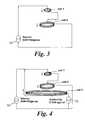
- FIG. 3is a circuit diagram illustrating the arrangement of the two coils
- FIG. 4is a circuit diagram illustrating the use of an additional coil
- FIG. 5is a schematic layout of helicon apparatus incorporating the FIG. 4 arrangement
- FIG. 6is a schematic ECR apparatus incorporating the FIG. 4 arrangement
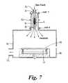
- FIG. 7is an alternative apparatus for providing a stream of neutral particles to the process chamber
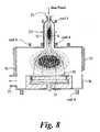
- FIG. 8is a corresponding arrangement for providing neutral particles, ions and electrons
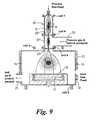
- FIG. 9is an arrangement which provides a source of ions and electrons.
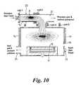
- FIG. 10illustrates an alternative arrangement for filtering ions and electrons.
- FIG. 1an idealised total field is indicated at 10 by plotting a magnetic field for the vertical position of an apparatus, of the type that will be described in more detail in connection with FIGS. 5 or 6 , in which there is a plasma generation chamber surmounting a process chamber.
- the Applicantshave determined that what is required is a highly uniform field in the source or plasma generation region, with a strong convergent field at the top of the plasma generation chamber and, in general, a reducing field in the process chamber. In some embodiments it may be desirable to have the field strength peak in the process chamber, before it reduces.
- the Applicantsare able to reflect the electrons, which would otherwise escape through the top of the plasma generation chamber, along the field lines and thereby trap electrons as previously described; to enhance the coupling in the source region and reduce the electron temperature; and to enhance uniformity of process in the process chamber.
- the trapping of the electronsis dependent on there being no conductive path around or through the strongly convergent field.
- FIG. 2is a schematic two dimensional representation of the magnetic field lines generated by the coils 1 and 2 with 50 turns in coil 1 and 43 turns in coil 2 , each coil carrying a current of 33 Amps.
- a uniform field of 100 gaussis generated in the source region rising to 400 gauss at the upstream end of the plasma generation chamber and dropping off downstream into the process chamber.
- FIG. 4an additional coil or coils can be added, at a larger radius, to control the magnetic field strength in the process chamber. Conveniently this has a separate current source 14 . With the circuit shown in FIG. 4, and with a suitable selection of the number of turns, the current which initially flows through coil 3 , will also flow through coil 2 whereby it produces an equal and opposite field, in the source region, so that the field produced in the source region by coil 3 is effectively cancelled out and does not interfere with the field strength or uniformity in the source region.
- the FIG. 4 arrangementis particularly convenient, because it now enables the operator to have separate control of the magnetic field in the plasma chamber and to make the appropriate adjustments to enhance process uniformity, in dependence on the specific process being performed, the dimensions of the workpiece etc.
- coil 1could be replaced by a permanent magnet or an independent high current flat coil.
- a single coilcould be used instead of coils 1 and 2 with a high permeability body adjacent the top of the plasma generation chamber.
- the plasma generation chambercould be configured with a permanent magnet at its upstream end.
- Coil 2could be constructed as a Helmholtz pair, being two flat coils positioned coaxially with a vertical offset.
- FIGS. 5 and 6illustrate the application of the three coil configuration to a helicon plasma source and an ECR apparatus respectively.
- the plasma generation chamberis indicated at 15 and the process chamber is indicated at 16 .
- a workpiece supportis provided at 17 and a workpiece 18 sits thereon.
- the plasma generation or source regionis indicated at 19 .
- the chamber 15is made of an electrically insulating material and this helps to ensure there is no electrically conductive path that bypasses the convergent field.
- an antenna 20is driven by a RF power supply 21
- microwave power 26is supplied to a wave guide 22 and enters the chamber 15 through a window 23 .
- FIG. 7shows a variation on the apparatus of FIG. 5.
- This apparatusis intended to provide a supply of purely neutral particles (e.g. free radicals) to the process chamber 16 .
- purely neutral particlese.g. free radicals
- Coil 2is omitted for clarity sake, but, as has already been indicated, particular magnetic field arrangements can be achieved with coils or permanent magnets working in combination.
- electronsare reflected at each end of the plasma generation chamber 15 at respective locations A and B.
- This chamberis of insulating material and so there is no path for the electrons to escape. Ions are therefore also trapped within the chamber 15 .
- a gas feed 24is provided at the top of the chamber 15 to pass through the convergent field and the gas is withdrawn from the process chamber 16 at 25 .
- Neutral particlesare therefore drawn into the process chamber 16 with the flow of gas to react with the substrate 18 such as in etch or resist stripping processes.
- the apparatusmay also be suitable for certain vapour deposition processes.
- This arrangementis desirable because it produces a reactive, purely chemical, environment with extremely good power efficiency.
- coil 3there is no need for coil 3 as substantially no electrons (or ions) flow into the process chamber, and the process chamber can almost certainly be made out of aluminium.
- the support 17As the particles flowing into the process chamber are neutral, no bias is required for the support 17 .
- This apparatusthus obviates the need for substrate (e.g. semiconductor wafer) bias, or a magnetic field in the process chamber, thus saving expense and complexity.
- the pumping speed and pressure in chamber 16should be such that the neutral particles diffuse to the substrate 18 . Too high a pressure in the plasma chamber may promote diffusion of electrons from the magnetic confinement in the plasma source.
- FIG. 8is similar to the arrangement of FIG. 7 except here it is intended that coil 4 should be powered to a lesser extent so that a controlled number of ions can escape, particularly at high pressures.
- Ion escapecan preferably occur by the formation of a window in the magnetic field which allows a controllable flux of electrons, and hence ions, to pass into the process chamber in the direction of the substrate.
- the ratios of ions to radicalscan be continuously varied from zero up to the position where the apparatus is essentially that of FIG. 2. If ion flow is required at low pressures, it may be necessary to have a high resistance, or variable resistance electrically conducting leakage path from the chamber 15 to the chamber 16 so as to reduce the electric field effect.
- a magnetic bucket 31may be provided around the process chamber 16 and an optional coil 5 is shown at the base of the chamber which may be provided to enhance uniformity across the substrate 18 .
- the support 17may be RF biased to further enhance the anisotropic velocity distribution of the ions, and/or change the ion energy.
- FIG. 9is a further development in which the process gas and radicals are pumped out of a buffer chamber 27 disposed between the plasma generation chamber 15 and the process chamber 16 , a further coil 6 , is located at the bottom end of the buffer chamber 27 to control the flow of ions and electrons.
- Baffles 28 , 29are provided at the upstream and downstream ends of the buffer chamber 27 to control the gas flow such that the process gas and radicals can be pumped out at 30 and it is probably desirable to have a flow of inert gas from an inlet 33 into the process chamber 16 to maintain higher pressure there.
- the ions entering the process chamberwould be extremely anisotropic and this arrangement may be particularly suitable for reactive ion processing, such as polysilicon etching, especially if anisotropy is at a premium and the etch rate is less important.
- FIG. 10shows an alternative arrangement for providing a flow of charged particles with no, or reduced radicals, into the process chamber 16 .
- the plasma generation chamber 15is turned through 90 degrees to avoid illumination of the substrate by e.g. ultraviolet light and coils 2 and 4 are arranged to guide the charged particles' into the process chamber 16 , whilst the process gas and neutral radicals are pumped out in a linear flow at 32 .
- An inert gas pressuremay be maintained in the process chamber to prevent the entrance of radicals into the process chamber.
- an inert gascan be introduced into the process chamber and pumped out at 25 , along with the process gas and reaction products.
Landscapes
- Physics & Mathematics (AREA)
- Engineering & Computer Science (AREA)
- Plasma & Fusion (AREA)
- Chemical & Material Sciences (AREA)
- Analytical Chemistry (AREA)
- Drying Of Semiconductors (AREA)
- Chemical Vapour Deposition (AREA)
Abstract
Description
- A claim to priority is made to U.S. Provisional Application Serial No.[0001]60/392,049 filed Jun. 28, 2002 and to British Patent Application No.0209291.4 filed Apr. 24th2002, the contents of both applications being incorporated herein by reference in their entireties.
- 1. Field of the Invention[0002]
- This invention relates to plasma processing apparatus and in particular, but not exclusively, to inductively coupled plasma helicon or electron cyclotron resonance apparatus.[0003]
- 2. Description of Related Art[0004]
- An early suggestion for the design of an inductively coupled plasma apparatus is described in U.S. Pat. No. 4,810,935, in which an antenna operates within an axial magnetic field upon a plasma source, which is coupled to a larger volume process chamber. This noted that, under these conditions, efficient coupling of the RF power could be achieved. This efficiency is due to the resonant response of the electrons' motions in the form of helicon plasma waves. The concept was further developed in U.S. Pat. No. 4,990,229, and other examples of helicon plasma source designs are contained in U.S. Pat. No. 5,449,433, U.S. Pat. No. 5,567,268 and U.S. Pat. No. 6,189,484.[0005]
- In an alternative approach, power is supplied radiatively to the plasma to generate an electron cyclotron resonance (ECR), as described in U.S. Pat. No. 3,418,206. Here, high power transfer efficiency results from the resonant response of the electrons motions in the form of cyclotron orbits around the magnetic field. Some examples of the use of ECR sources for plasma processing can be found in U.S. Pat. No. 4,401,054, U.S. Pat. No. 4,609,428 and U.S. Pat. No. 4,638,216.[0006]
- In both helicon and ECR designs, to optimise power absorption efficiency strong overlap, extending over a large volume of plasma, is required between the source electromagnetic fields and the electron motions at the excitation frequency.[0007]
- Many possible RF antennae geometries can be used to excite plasma waves in a helicon source. These include the single loop and two loop antenna of U.S. Pat. No. 4,990,229, which couple to axially symmetric (m=0) wave modes, as well as geometries that couple to m=+1 modes. Practical antennae are of finite length and are therefore able to produce a range of wave numbers along the antenna axis (which is also the magnetic field direction). The coupling efficiency at each wave number will be determined in part by the antenna geometry, but also by the geometry of the wave modes, which is influenced by the chamber walls, the magnetic field profile and the electron density profile in the vicinity of the antenna. Strong variations in field strength or electron density affect the wave propagation and cause strong spatial variations in the amplitude and wave number, making it difficult to couple efficiently using a simple antenna geometry. There will nevertheless be a characteristic wave mode for which the coupling is strongest, and this will determine the power coupling efficiency of the antenna. In the prior art this is not especially well controlled or understood, because the field and plasma density vary strongly along the field direction.[0008]
- In an electron cyclotron resonance (ECR) source, the microwave field geometry is determined by the launching wave guide. Power coupling is to the cyclotron motion of the electrons and efficient coupling requires that the cyclotron frequency closely matches the excitation frequency. If the D.C Magnetic field strength is strongly varying, this can only be achieved over a small volume of space. In both the helicon and ECR sources, therefore, there is a need for improved control and uniformity in the magnetic field in the source region.[0009]
- From a first aspect the invention consists in a plasma processing apparatus including:[0010]
- (a) a process chamber;[0011]
- (b) an antenna or microwave source for radiating electromagnetic waves;[0012]
- (c) a plasma generation chamber having a plasma zone and being generally orientated about an axis; being proximate to and in electromagnetic communication with the antenna or source and being for feeding ions and/or neutral particles to the process chamber; and[0013]
- (d) a magnetic field generator for generating a magnetic field within the plasma generation chamber such that it extends generally parallel to the axis and passes from the chamber into the process chamber[0014]
- characterised in that the magnetic field generator and/or a further magnetic field generator converges the magnetic field at a location upstream of the plasma zone whereby electrons travelling along the magnetic field lines from the plasma generation chamber will be reflected towards the plasma zone and in that there is no electrically conductive path extending around or through the upstream location.[0015]
- In principal any charged particle will be reflected at a converging field, but at the energies and field strengths, typical in many applications, the orbital radius of the ions will be about 4 cm, which is similar to the mean free path of the scattering gas and the distance to the walls. Hence collisions may cause some ions to pass through the convergent field at the upstream location.[0016]
- However, provided that there is not a conductive path, for instance a conductive chamber wall, around the upstream location then this will not matter. This is because if some ions are scattered through the convergent field, but electrons are reflected, then the region within the chamber will have a negative net charge, which in turn will set an axial electric field within the chamber that will prevent the ions escaping.[0017]
- This approach has a number of advantages. First a reduction in ion loss rates implies that less source power is required to sustain a plasma with a given density. Secondly, a reduction in ion loss rate allows a reduced ion creation rate, so a given plasma density can be produced at a lower electron temperature. This would mean that less power is used in electron heating, further increasing the power efficiency, and the number of species produced in low energy electron interactions (eg. negative ions, molecular fragments, reactive radicals) is increased changing the plasma chemistry in a way that may be beneficial for the plasma processing. Further there are fewer high energy electron collisions, such as those that heat the ions, so the ion temperature is also reduced. A low ion temperature is beneficial, if it is desired to produce a highly anisotropic ion velocity distribution, by accelerating the ions with an electric field in the direction of the substrate. This is often very desirable when processing high aspect ratio features.[0018]
- In a preferred arrangement, the plasma generation chamber has two ends and the upstream location is adjacent to one end and the process chamber is at or is contiguous with the other end of the plasma generation chamber.[0019]
- It is particularly preferred that the magnetic generator generates within the plasma generation chamber a field which is substantially uniform and substantially parallel to the axis. The Applicants have appreciated that the Lorentz force encourages the electrons to move in cyclotron orbits. If the orbital radius is less than the electron mean free path, the diffusion of electrons perpendicular to the magnetic field is strongly suppressed. Thus, if the field is orientated parallel to the chamber walls, the charge loss is suppressed. A reduced flow of charges to the chamber walls leads to reduced gradients in the plasma density and, therefore, to a more uniform processing environment. This enhanced uniformity will, the Applicants have appreciated, lead to increased efficiency in the coupling of the RF Power.[0020]
- Electrons will be lost from the chamber, wherever the field has a component perpendicular to that chamber wall. Therefore, if the walls of the plasma generation chamber are not substantially parallel to the axis of the field then, the magnetic field generator may be arranged to provide an increased field strength as the non-parallel wall is approached.[0021]
- An additional independent magnetic field generator may be provided for generating a field downstream of the plasma generation chamber. The magnetic field generator and the additional magnetic field generator may be sized such that the latter has a substantially zero net effect in the plasma generation chamber. The magnetic field generator may include a first coil for generating a magnetic field in the plasma generation chamber and a second coil for converging that field at the upstream location. The first and second coils are preferably powered by a single power source, whereas the additional magnetic field generator may be powered by a separate source. It is possible to configure the first and second coil contiguously such that they appear as a single coil such that there is a first coil part and a second coil part.[0022]
- An advantage of having the additional magnetic generator is that the magnetic field in the process chamber can be controlled in such a way as to control the way in which the ions spread out and thus allow adjustment of the process effect on a substrate and hence increase control of the centre-to-edge profile.[0023]
- The apparatus may further include a second further magnetic field generator for converging the magnetic field at a downstream location between the plasma generation zone and the process chamber.[0024]
- If it is desired to allow ions through the downstream location, then there may be an electrically i.e electron conductive path from the plasma generation chamber around, or through the downstream location. Alternatively there may be no electrically conductive path around or through the downstream location and in that way both electrons and ions can be trapped at either end of the plasma zone due to the principal of charge equalisation. Where there is an electrically conductive path, the conductance of that path may be variable so that the rate of ion flow can be adjusted by adjusting the rate of electron flow. Equally the strength of the convergent magnetic field can be varied so that a window of axial field lines is created so some electrons, and hence ions, may pass through if desired. An axial field can allow the ions to arrive at the substrate in a highly anisotropic manner.[0025]
- If the electron path is via the chamber wall around the downstream location, then for the ions to impinge usefully upon the substrate then it must be in DC connection with the chamber walls or negatively biased e.g. via an RF supply, if not, then ions that flow from the plasmas chamber will travel to the process chamber wall to recombine with the electrons thereby equalising charge. (Prior art publications have not made this apparent).[0026]
- It is particularly preferred that there is a gas feed into the plasma generation chamber which passes through the upstream location. The gas can either be withdrawn in the process chamber or, if it is desired that no neutral particles enter the process chamber, it can be withdrawn upstream of that chamber.[0027]
- From a further aspect the invention consists in a plasma processing apparatus including:[0028]
- (a) a process chamber,[0029]
- (b) an antenna for radiating electromagnetic waves,[0030]
- (c) a plasma generation chamber generally orientated about an axis and being proximate to and in electromagnetic communication with the antenna and for feeding ions and/or neutral particles to the process chamber; and[0031]
- (d) a magnetic field generator for generating a magnetic field within the plasma generation chamber such that it extends generally parallel to the axis and passes from the chamber into the process chamber[0032]
- characterised in that the magnetic field generator generates a field which is substantially uniform within the plasma generation chamber and substantially parallel to the axis thereof.[0033]
- From a still further aspect the invention consists in a plasma processing apparatus including:[0034]
- (a) a process chamber,[0035]
- (b) an antenna or a microwave source for radiating electromagnetic waves[0036]
- (c) a plasma generation chamber having a plasma zone and being generally orientated about an axis being proximate to and in electromagnetic communication with the antenna and being for feeding particles to the process chamber; and[0037]
- (d) a magnetic field generator for generating a magnetic field within the plasma generation chamber such that it extends generally parallel to the axis and passes from the chamber into the process chamber[0038]
- characterised in that the magnetic field generator and/or a further magnetic field generator converges the magnetic field at a location downstream of the plasma zone whereby electrons travelling along the magnetic field lines will be reflected towards the plasma zone and in that there is either no electrically conductive or a controllable conductive path extending around or through the downstream location.[0039]
- From yet another aspect the invention consists in a plasma processing apparatus including:[0040]
- (a) a process chamber,[0041]
- (b) an antenna or a microwave source for radiating electromagnetic waves[0042]
- (c) a plasma generation chamber having a plasma zone and being generally orientated about an axis; being proximate to and in electromagnetic communications with the antenna and being for feeding ions to the process chamber; and[0043]
- (d) a magnetic field generator for generating a magnetic field within the plasma generation chamber such that it extends generally parallel to the axis and passes from the chamber into the process chamber characterised in that there is a pumping outlet between the plasma generation and process chambers whereby neutral particles are removed and do not enter the process chamber.[0044]
- Although the invention has been defined above it is to be understood it includes any inventive combination of the features set out above or in the following description.[0045]
- The invention can be performed in various ways and specific embodiments will now be described with reference to the accompanying drawings, in which:[0046]
- FIG. 1 shows one of the Applicants' preferred magnetic fields plotted against the position within the plasma generation and process chambers and the manner in which such a field may be approximated using two coils;[0047]
- FIG. 2 is a schematic representation of magnetic field lines generated by the two coil system;[0048]
- FIG. 3 is a circuit diagram illustrating the arrangement of the two coils;[0049]
- FIG. 4 is a circuit diagram illustrating the use of an additional coil;[0050]
- FIG. 5 is a schematic layout of helicon apparatus incorporating the FIG. 4 arrangement;[0051]
- FIG. 6 is a schematic ECR apparatus incorporating the FIG. 4 arrangement;[0052]
- FIG. 7 is an alternative apparatus for providing a stream of neutral particles to the process chamber;[0053]
- FIG. 8 is a corresponding arrangement for providing neutral particles, ions and electrons;[0054]
- FIG. 9 is an arrangement which provides a source of ions and electrons; and[0055]
- FIG. 10 illustrates an alternative arrangement for filtering ions and electrons.[0056]
- In FIG. 1 an idealised total field is indicated at[0057]10 by plotting a magnetic field for the vertical position of an apparatus, of the type that will be described in more detail in connection with FIGS.5 or6, in which there is a plasma generation chamber surmounting a process chamber. As will be seen from the
graph 10 the Applicants have determined that what is required is a highly uniform field in the source or plasma generation region, with a strong convergent field at the top of the plasma generation chamber and, in general, a reducing field in the process chamber. In some embodiments it may be desirable to have the field strength peak in the process chamber, before it reduces. - As has been indicated above, by selecting such a magnetic field profile, the Applicants are able to reflect the electrons, which would otherwise escape through the top of the plasma generation chamber, along the field lines and thereby trap electrons as previously described; to enhance the coupling in the source region and reduce the electron temperature; and to enhance uniformity of process in the process chamber. The trapping of the electrons is dependent on there being no conductive path around or through the strongly convergent field.[0058]
- By way of illustration, broken lines[0059]11 and12 illustrate how two magnetic coils combine to approximate the
graph 10. For example one appropriate calculation, using two magnetic coils is forcoil 1 at 1,650 Amp turns of radius of 3 cms, and Z of −15 cms forcoil 2 to have 1,440 Amp turns of radius of 10 cms, and Z of −5 cms. FIG. 2 is a schematic two dimensional representation of the magnetic field lines generated by thecoils coil 1 and 43 turns incoil 2, each coil carrying a current of 33 Amps. A uniform field of 100 gauss is generated in the source region rising to 400 gauss at the upstream end of the plasma generation chamber and dropping off downstream into the process chamber. - For arrangements involving two or more current carrying coils, an appropriate choice of the ratio of the number of turns will allow them to be connected in series and operate from a single[0060]
current supply 13. By altering the current, the magnetic field strength in the source region can be varied easily, whilst its uniformity and the magnetic mirroring effect ofcoil 1 are maintained. - One of the benefits of the adoption of[0061]
coil 1 is that the plasma is to a great extent kept away from the top of the plasma generation chamber, allowing sensitive equipment such as optical and electrical diagnostics, electrical feed throughs, gas feed lines etc to be mounted there with a reduced risk that they will be attacked or interfered with by the plasma. - Turning to FIG. 4 an additional coil or coils can be added, at a larger radius, to control the magnetic field strength in the process chamber. Conveniently this has a separate[0062]
current source 14. With the circuit shown in FIG. 4, and with a suitable selection of the number of turns, the current which initially flows throughcoil 3, will also flow throughcoil 2 whereby it produces an equal and opposite field, in the source region, so that the field produced in the source region bycoil 3 is effectively cancelled out and does not interfere with the field strength or uniformity in the source region. The FIG. 4 arrangement is particularly convenient, because it now enables the operator to have separate control of the magnetic field in the plasma chamber and to make the appropriate adjustments to enhance process uniformity, in dependence on the specific process being performed, the dimensions of the workpiece etc. - It will be appreciated that there are a whole range of magnetic sources that could be used to achieve the principle set out above. For[0063]
example coil 1 could be replaced by a permanent magnet or an independent high current flat coil. A single coil could be used instead ofcoils - For further improvement in uniformity,[0064]
Coil 2 could be constructed as a Helmholtz pair, being two flat coils positioned coaxially with a vertical offset. FIGS. 5 and 6 illustrate the application of the three coil configuration to a helicon plasma source and an ECR apparatus respectively. In each the plasma generation chamber is indicated at15 and the process chamber is indicated at16. A workpiece support is provided at17 and aworkpiece 18 sits thereon. The plasma generation or source region is indicated at19. Conveniently thechamber 15 is made of an electrically insulating material and this helps to ensure there is no electrically conductive path that bypasses the convergent field. In FIG. 5 anantenna 20 is driven by aRF power supply 21, whilst in FIG. 6microwave power 26 is supplied to awave guide 22 and enters thechamber 15 through awindow 23. - The general construction and operation of such apparatus is well known in the art and further reference can be made to the earlier specifications mentioned above, which are incorporated for that purpose, by reference.[0065]
- FIG. 7 shows a variation on the apparatus of FIG. 5. This apparatus is intended to provide a supply of purely neutral particles (e.g. free radicals) to the[0066]
process chamber 16. In this arrangement there is also a convergent field at the downstream end of theplasma chamber 15, which in the schematically shown view is produced bycoil 4.Coil 2 is omitted for clarity sake, but, as has already been indicated, particular magnetic field arrangements can be achieved with coils or permanent magnets working in combination. With the arrangement shown in FIG. 7 electrons are reflected at each end of theplasma generation chamber 15 at respective locations A and B. This chamber is of insulating material and so there is no path for the electrons to escape. Ions are therefore also trapped within thechamber 15. - A[0067]
gas feed 24 is provided at the top of thechamber 15 to pass through the convergent field and the gas is withdrawn from theprocess chamber 16 at25. Neutral particles are therefore drawn into theprocess chamber 16 with the flow of gas to react with thesubstrate 18 such as in etch or resist stripping processes. The apparatus may also be suitable for certain vapour deposition processes. - This arrangement is desirable because it produces a reactive, purely chemical, environment with extremely good power efficiency. There is no need for[0068]
coil 3 as substantially no electrons (or ions) flow into the process chamber, and the process chamber can almost certainly be made out of aluminium. As the particles flowing into the process chamber are neutral, no bias is required for thesupport 17. This apparatus thus obviates the need for substrate (e.g. semiconductor wafer) bias, or a magnetic field in the process chamber, thus saving expense and complexity. - For best process uniformity, the pumping speed and pressure in[0069]
chamber 16 should be such that the neutral particles diffuse to thesubstrate 18. Too high a pressure in the plasma chamber may promote diffusion of electrons from the magnetic confinement in the plasma source. - The FIG. 8 is similar to the arrangement of FIG. 7 except here it is intended that[0070]
coil 4 should be powered to a lesser extent so that a controlled number of ions can escape, particularly at high pressures. Ion escape can preferably occur by the formation of a window in the magnetic field which allows a controllable flux of electrons, and hence ions, to pass into the process chamber in the direction of the substrate. Thus the ratios of ions to radicals can be continuously varied from zero up to the position where the apparatus is essentially that of FIG. 2. If ion flow is required at low pressures, it may be necessary to have a high resistance, or variable resistance electrically conducting leakage path from thechamber 15 to thechamber 16 so as to reduce the electric field effect. - As there is some flow of charged particles to the process chamber, a[0071]
magnetic bucket 31 may be provided around theprocess chamber 16 and anoptional coil 5 is shown at the base of the chamber which may be provided to enhance uniformity across thesubstrate 18. Thesupport 17 may be RF biased to further enhance the anisotropic velocity distribution of the ions, and/or change the ion energy. - FIG. 9 is a further development in which the process gas and radicals are pumped out of a[0072]
buffer chamber 27 disposed between theplasma generation chamber 15 and theprocess chamber 16, afurther coil 6, is located at the bottom end of thebuffer chamber 27 to control the flow of ions and electrons. Baffles28,29 are provided at the upstream and downstream ends of thebuffer chamber 27 to control the gas flow such that the process gas and radicals can be pumped out at30 and it is probably desirable to have a flow of inert gas from aninlet 33 into theprocess chamber 16 to maintain higher pressure there. - The ions entering the process chamber would be extremely anisotropic and this arrangement may be particularly suitable for reactive ion processing, such as polysilicon etching, especially if anisotropy is at a premium and the etch rate is less important.[0073]
- FIG. 10 shows an alternative arrangement for providing a flow of charged particles with no, or reduced radicals, into the[0074]
process chamber 16. Here theplasma generation chamber 15 is turned through 90 degrees to avoid illumination of the substrate by e.g. ultraviolet light and coils2 and4 are arranged to guide the charged particles' into theprocess chamber 16, whilst the process gas and neutral radicals are pumped out in a linear flow at32. An inert gas pressure may be maintained in the process chamber to prevent the entrance of radicals into the process chamber. Similarly, in each of the FIGS. 9 and 10 embodiments an inert gas can be introduced into the process chamber and pumped out at25, along with the process gas and reaction products.
Claims (39)
Priority Applications (1)
| Application Number | Priority Date | Filing Date | Title |
|---|---|---|---|
| US10/419,113US6876154B2 (en) | 2002-04-24 | 2003-04-21 | Plasma processing apparatus |
Applications Claiming Priority (4)
| Application Number | Priority Date | Filing Date | Title |
|---|---|---|---|
| GB0209291AGB0209291D0 (en) | 2002-04-24 | 2002-04-24 | Plasma processing apparatus |
| GB0209291.4 | 2002-04-24 | ||
| US39204902P | 2002-06-28 | 2002-06-28 | |
| US10/419,113US6876154B2 (en) | 2002-04-24 | 2003-04-21 | Plasma processing apparatus |
Publications (2)
| Publication Number | Publication Date |
|---|---|
| US20030201722A1true US20030201722A1 (en) | 2003-10-30 |
| US6876154B2 US6876154B2 (en) | 2005-04-05 |
Family
ID=29254915
Family Applications (1)
| Application Number | Title | Priority Date | Filing Date |
|---|---|---|---|
| US10/419,113Expired - LifetimeUS6876154B2 (en) | 2002-04-24 | 2003-04-21 | Plasma processing apparatus |
Country Status (1)
| Country | Link |
|---|---|
| US (1) | US6876154B2 (en) |
Cited By (10)
| Publication number | Priority date | Publication date | Assignee | Title |
|---|---|---|---|---|
| US20040223579A1 (en)* | 2001-07-30 | 2004-11-11 | Young-Kwan Lee | Antenna structure for inductively coupled plasma generator |
| US20050205212A1 (en)* | 2004-03-22 | 2005-09-22 | Varian Semiconductor Equipment | RF Plasma Source With Conductive Top Section |
| US20070170867A1 (en)* | 2006-01-24 | 2007-07-26 | Varian Semiconductor Equipment Associates, Inc. | Plasma Immersion Ion Source With Low Effective Antenna Voltage |
| US20080093506A1 (en)* | 2004-09-22 | 2008-04-24 | Elwing Llc | Spacecraft Thruster |
| US20080132046A1 (en)* | 2006-12-04 | 2008-06-05 | Varian Semiconductor Equipment Associates, Inc. | Plasma Doping With Electronically Controllable Implant Angle |
| US20080169183A1 (en)* | 2007-01-16 | 2008-07-17 | Varian Semiconductor Equipment Associates, Inc. | Plasma Source with Liner for Reducing Metal Contamination |
| US20080200015A1 (en)* | 2007-02-16 | 2008-08-21 | Varian Semiconductor Equipment Associates, Inc. | Multi-step plasma doping with improved dose control |
| CN103906338A (en)* | 2012-12-31 | 2014-07-02 | 北京北方微电子基地设备工艺研究中心有限责任公司 | Plasma device |
| US20140231669A1 (en)* | 2013-02-18 | 2014-08-21 | Sumitomo Heavy Industries, Ltd. | Microwave ion source and method for starting same |
| US20160225590A1 (en)* | 2015-01-30 | 2016-08-04 | Applied Materials, Inc. | Magnet configurations for radial uniformity tuning of icp plasmas |
Families Citing this family (22)
| Publication number | Priority date | Publication date | Assignee | Title |
|---|---|---|---|---|
| DE10325151B4 (en)* | 2003-05-30 | 2006-11-30 | Infineon Technologies Ag | Device for generating and / or influencing electromagnetic radiation of a plasma |
| CN1890175B (en)* | 2003-12-03 | 2010-04-07 | 理想星株式会社 | Apparatus and method for producing fullerene derivative |
| US8179050B2 (en)* | 2005-06-23 | 2012-05-15 | The Regents Of The University Of California | Helicon plasma source with permanent magnets |
| EP2251454B1 (en) | 2009-05-13 | 2014-07-23 | SiO2 Medical Products, Inc. | Vessel coating and inspection |
| WO2013170052A1 (en) | 2012-05-09 | 2013-11-14 | Sio2 Medical Products, Inc. | Saccharide protective coating for pharmaceutical package |
| US9458536B2 (en) | 2009-07-02 | 2016-10-04 | Sio2 Medical Products, Inc. | PECVD coating methods for capped syringes, cartridges and other articles |
| US11624115B2 (en) | 2010-05-12 | 2023-04-11 | Sio2 Medical Products, Inc. | Syringe with PECVD lubrication |
| US9878101B2 (en) | 2010-11-12 | 2018-01-30 | Sio2 Medical Products, Inc. | Cyclic olefin polymer vessels and vessel coating methods |
| US9272095B2 (en) | 2011-04-01 | 2016-03-01 | Sio2 Medical Products, Inc. | Vessels, contact surfaces, and coating and inspection apparatus and methods |
| US11116695B2 (en) | 2011-11-11 | 2021-09-14 | Sio2 Medical Products, Inc. | Blood sample collection tube |
| CA2855353C (en) | 2011-11-11 | 2021-01-19 | Sio2 Medical Products, Inc. | Passivation, ph protective or lubricity coating for pharmaceutical package, coating process and apparatus |
| US20150297800A1 (en) | 2012-07-03 | 2015-10-22 | Sio2 Medical Products, Inc. | SiOx BARRIER FOR PHARMACEUTICAL PACKAGE AND COATING PROCESS |
| US9664626B2 (en) | 2012-11-01 | 2017-05-30 | Sio2 Medical Products, Inc. | Coating inspection method |
| US9903782B2 (en) | 2012-11-16 | 2018-02-27 | Sio2 Medical Products, Inc. | Method and apparatus for detecting rapid barrier coating integrity characteristics |
| US9764093B2 (en) | 2012-11-30 | 2017-09-19 | Sio2 Medical Products, Inc. | Controlling the uniformity of PECVD deposition |
| AU2013352436B2 (en) | 2012-11-30 | 2018-10-25 | Sio2 Medical Products, Inc. | Controlling the uniformity of PECVD deposition on medical syringes, cartridges, and the like |
| US20160015898A1 (en) | 2013-03-01 | 2016-01-21 | Sio2 Medical Products, Inc. | Plasma or cvd pre-treatment for lubricated pharmaceutical package, coating process and apparatus |
| US9937099B2 (en) | 2013-03-11 | 2018-04-10 | Sio2 Medical Products, Inc. | Trilayer coated pharmaceutical packaging with low oxygen transmission rate |
| JP6453841B2 (en) | 2013-03-11 | 2019-01-16 | エスアイオーツー・メディカル・プロダクツ・インコーポレイテッド | Coated packaging |
| US20160017490A1 (en) | 2013-03-15 | 2016-01-21 | Sio2 Medical Products, Inc. | Coating method |
| EP3122917B1 (en) | 2014-03-28 | 2020-05-06 | SiO2 Medical Products, Inc. | Antistatic coatings for plastic vessels |
| KR102786617B1 (en) | 2015-08-18 | 2025-03-26 | 에스아이오2 메디컬 프로덕츠, 엘엘씨 | Packaging containers for pharmaceuticals and other products with low oxygen permeability |
Citations (16)
| Publication number | Priority date | Publication date | Assignee | Title |
|---|---|---|---|---|
| US3418206A (en)* | 1963-04-29 | 1968-12-24 | Boeing Co | Particle accelerator |
| US4401054A (en)* | 1980-05-02 | 1983-08-30 | Nippon Telegraph & Telephone Public Corporation | Plasma deposition apparatus |
| US4609428A (en)* | 1984-07-23 | 1986-09-02 | Fujitsu Limited | Method and apparatus for microwave plasma anisotropic dry etching |
| US4638216A (en)* | 1983-05-20 | 1987-01-20 | Commissariat A L'energie Atomique | Electron cyclotron resonance ion source |
| US4810935A (en)* | 1985-05-03 | 1989-03-07 | The Australian National University | Method and apparatus for producing large volume magnetoplasmas |
| US4990229A (en)* | 1989-06-13 | 1991-02-05 | Plasma & Materials Technologies, Inc. | High density plasma deposition and etching apparatus |
| US5189446A (en)* | 1991-05-17 | 1993-02-23 | International Business Machines Corporation | Plasma wafer processing tool having closed electron cyclotron resonance |
| US5346579A (en)* | 1991-10-17 | 1994-09-13 | Applied Materials, Inc. | Magnetic field enhanced plasma processing chamber |
| US5361016A (en)* | 1992-03-26 | 1994-11-01 | General Atomics | High density plasma formation using whistler mode excitation in a reduced cross-sectional area formation tube |
| US5421891A (en)* | 1989-06-13 | 1995-06-06 | Plasma & Materials Technologies, Inc. | High density plasma deposition and etching apparatus |
| US5429070A (en)* | 1989-06-13 | 1995-07-04 | Plasma & Materials Technologies, Inc. | High density plasma deposition and etching apparatus |
| US5449433A (en)* | 1994-02-14 | 1995-09-12 | Micron Semiconductor, Inc. | Use of a high density plasma source having an electrostatic shield for anisotropic polysilicon etching over topography |
| US5567268A (en)* | 1994-01-31 | 1996-10-22 | Sony Corporation | Plasma processing apparatus and method for carrying out plasma processing by using such plasma processing apparatus |
| US6110395A (en)* | 1997-08-26 | 2000-08-29 | Trikon Technologies, Inc. | Method and structure for controlling plasma uniformity |
| US6189484B1 (en)* | 1999-03-05 | 2001-02-20 | Applied Materials Inc. | Plasma reactor having a helicon wave high density plasma source |
| US6251792B1 (en)* | 1990-07-31 | 2001-06-26 | Applied Materials, Inc. | Plasma etch processes |
Family Cites Families (3)
| Publication number | Priority date | Publication date | Assignee | Title |
|---|---|---|---|---|
| JPS62216638A (en) | 1986-03-19 | 1987-09-24 | Anelva Corp | Device for treating surface |
| EP0283519B1 (en) | 1986-09-29 | 1994-04-13 | Nippon Telegraph And Telephone Corporation | Ion generation apparatus, thin film formation apparatus using the ion generation apparatus, and ion source |
| WO2000036631A1 (en) | 1998-12-11 | 2000-06-22 | Surface Technology Systems Limited | Plasma processing apparatus |
- 2003
- 2003-04-21USUS10/419,113patent/US6876154B2/ennot_activeExpired - Lifetime
Patent Citations (16)
| Publication number | Priority date | Publication date | Assignee | Title |
|---|---|---|---|---|
| US3418206A (en)* | 1963-04-29 | 1968-12-24 | Boeing Co | Particle accelerator |
| US4401054A (en)* | 1980-05-02 | 1983-08-30 | Nippon Telegraph & Telephone Public Corporation | Plasma deposition apparatus |
| US4638216A (en)* | 1983-05-20 | 1987-01-20 | Commissariat A L'energie Atomique | Electron cyclotron resonance ion source |
| US4609428A (en)* | 1984-07-23 | 1986-09-02 | Fujitsu Limited | Method and apparatus for microwave plasma anisotropic dry etching |
| US4810935A (en)* | 1985-05-03 | 1989-03-07 | The Australian National University | Method and apparatus for producing large volume magnetoplasmas |
| US4990229A (en)* | 1989-06-13 | 1991-02-05 | Plasma & Materials Technologies, Inc. | High density plasma deposition and etching apparatus |
| US5421891A (en)* | 1989-06-13 | 1995-06-06 | Plasma & Materials Technologies, Inc. | High density plasma deposition and etching apparatus |
| US5429070A (en)* | 1989-06-13 | 1995-07-04 | Plasma & Materials Technologies, Inc. | High density plasma deposition and etching apparatus |
| US6251792B1 (en)* | 1990-07-31 | 2001-06-26 | Applied Materials, Inc. | Plasma etch processes |
| US5189446A (en)* | 1991-05-17 | 1993-02-23 | International Business Machines Corporation | Plasma wafer processing tool having closed electron cyclotron resonance |
| US5346579A (en)* | 1991-10-17 | 1994-09-13 | Applied Materials, Inc. | Magnetic field enhanced plasma processing chamber |
| US5361016A (en)* | 1992-03-26 | 1994-11-01 | General Atomics | High density plasma formation using whistler mode excitation in a reduced cross-sectional area formation tube |
| US5567268A (en)* | 1994-01-31 | 1996-10-22 | Sony Corporation | Plasma processing apparatus and method for carrying out plasma processing by using such plasma processing apparatus |
| US5449433A (en)* | 1994-02-14 | 1995-09-12 | Micron Semiconductor, Inc. | Use of a high density plasma source having an electrostatic shield for anisotropic polysilicon etching over topography |
| US6110395A (en)* | 1997-08-26 | 2000-08-29 | Trikon Technologies, Inc. | Method and structure for controlling plasma uniformity |
| US6189484B1 (en)* | 1999-03-05 | 2001-02-20 | Applied Materials Inc. | Plasma reactor having a helicon wave high density plasma source |
Cited By (15)
| Publication number | Priority date | Publication date | Assignee | Title |
|---|---|---|---|---|
| US20040223579A1 (en)* | 2001-07-30 | 2004-11-11 | Young-Kwan Lee | Antenna structure for inductively coupled plasma generator |
| US7079085B2 (en)* | 2001-07-30 | 2006-07-18 | Plasmart Co. Ltd. | Antenna structure for inductively coupled plasma generator |
| US20050205212A1 (en)* | 2004-03-22 | 2005-09-22 | Varian Semiconductor Equipment | RF Plasma Source With Conductive Top Section |
| US20050205211A1 (en)* | 2004-03-22 | 2005-09-22 | Vikram Singh | Plasma immersion ion implantion apparatus and method |
| WO2005093780A3 (en)* | 2004-03-22 | 2006-06-08 | Varian Semiconductor Equipment | Rf plasma source with conductive top section |
| US20080093506A1 (en)* | 2004-09-22 | 2008-04-24 | Elwing Llc | Spacecraft Thruster |
| US20070170867A1 (en)* | 2006-01-24 | 2007-07-26 | Varian Semiconductor Equipment Associates, Inc. | Plasma Immersion Ion Source With Low Effective Antenna Voltage |
| US20080132046A1 (en)* | 2006-12-04 | 2008-06-05 | Varian Semiconductor Equipment Associates, Inc. | Plasma Doping With Electronically Controllable Implant Angle |
| US20080169183A1 (en)* | 2007-01-16 | 2008-07-17 | Varian Semiconductor Equipment Associates, Inc. | Plasma Source with Liner for Reducing Metal Contamination |
| US20080200015A1 (en)* | 2007-02-16 | 2008-08-21 | Varian Semiconductor Equipment Associates, Inc. | Multi-step plasma doping with improved dose control |
| US7820533B2 (en) | 2007-02-16 | 2010-10-26 | Varian Semiconductor Equipment Associates, Inc. | Multi-step plasma doping with improved dose control |
| CN103906338A (en)* | 2012-12-31 | 2014-07-02 | 北京北方微电子基地设备工艺研究中心有限责任公司 | Plasma device |
| US20140231669A1 (en)* | 2013-02-18 | 2014-08-21 | Sumitomo Heavy Industries, Ltd. | Microwave ion source and method for starting same |
| US20160225590A1 (en)* | 2015-01-30 | 2016-08-04 | Applied Materials, Inc. | Magnet configurations for radial uniformity tuning of icp plasmas |
| US10249479B2 (en)* | 2015-01-30 | 2019-04-02 | Applied Materials, Inc. | Magnet configurations for radial uniformity tuning of ICP plasmas |
Also Published As
| Publication number | Publication date |
|---|---|
| US6876154B2 (en) | 2005-04-05 |
Similar Documents
| Publication | Publication Date | Title |
|---|---|---|
| US6876154B2 (en) | Plasma processing apparatus | |
| GB2387964A (en) | Plasma processing apparatus | |
| EP0648069B1 (en) | RF induction plasma source for plasma processing | |
| CA1311214C (en) | Dual plasma microwave apparatus and method for treating a surface | |
| US5122251A (en) | High density plasma deposition and etching apparatus | |
| US20040219737A1 (en) | Method and apparatus for processing a workpiece with a plasma | |
| US6783629B2 (en) | Plasma treatment apparatus with improved uniformity of treatment and method for improving uniformity of plasma treatment | |
| EP1976346A1 (en) | Apparatus for generating a plasma | |
| EP1627413B1 (en) | A high density plasma reactor | |
| WO1991000679A1 (en) | Toroidal electron cyclotron resonance reactor | |
| US6087778A (en) | Scalable helicon wave plasma processing device with a non-cylindrical source chamber having a serpentine antenna | |
| WO1995015672A1 (en) | Method and apparatus for planar plasma processing | |
| Cluggish et al. | Density profile control in a large diameter, helicon plasma | |
| JP3881307B2 (en) | Plasma processing equipment | |
| WO2007002455A2 (en) | Helicon plasma source with permanent magnets | |
| US6225592B1 (en) | Method and apparatus for launching microwave energy into a plasma processing chamber | |
| JPH11135297A (en) | Plasma generator | |
| EP1006557B1 (en) | Apparatus for generating magnetically neutral line discharge type plasma | |
| TW201521070A (en) | Apparatus to provide electrons to substrate and ion implantation system | |
| Godyak et al. | Plasma and electrical characteristics of inductive discharge in a magnetic field | |
| RU2106716C1 (en) | Plant for microwave vacuum-plasma treatment of condensed media | |
| EP0871795B1 (en) | A scalable helicon wave plasma processing device with a non-cylindrical source chamber | |
| CN113133174A (en) | Helicon-ion cyclotron resonance coupling discharge system | |
| RU2223570C1 (en) | Device for microwave vacuum-plasma surface treatment with electron cyclotron resonance | |
| Menard et al. | Laboratory measurements and optimization of inductively coupled loop antenna plasma sources |
Legal Events
| Date | Code | Title | Description |
|---|---|---|---|
| AS | Assignment | Owner name:TRIKON HOLDINGS LIMITED, GREAT BRITAIN Free format text:ASSIGNMENT OF ASSIGNORS INTEREST;ASSIGNOR:APPLEYARD, NICHOLAS JOHN;REEL/FRAME:013990/0494 Effective date:20030417 | |
| STCF | Information on status: patent grant | Free format text:PATENTED CASE | |
| AS | Assignment | Owner name:AVIZA EUROPE LIMITED, UNITED KINGDOM Free format text:CHANGE OF NAME;ASSIGNOR:TRIKON HOLDINGS LIMITED;REEL/FRAME:018917/0079 Effective date:20051202 | |
| AS | Assignment | Owner name:UNITED COMMERCIAL BANK, CALIFORNIA Free format text:INTELLECTUAL PROPERTY SECURITY AGREEMENT;ASSIGNORS:AVIZA TECHNOLOGY, INC.;AVIZA, INC.;REEL/FRAME:019265/0381 Effective date:20070413 | |
| FPAY | Fee payment | Year of fee payment:4 | |
| FPAY | Fee payment | Year of fee payment:8 | |
| SULP | Surcharge for late payment | Year of fee payment:7 | |
| AS | Assignment | Owner name:SPP PROCESS TECHNOLOGY SYSTEMS UK LIMITED, GREAT B Free format text:ASSIGNMENT OF ASSIGNORS INTEREST;ASSIGNOR:AVIZA EUROPE LIMITED;REEL/FRAME:034855/0893 Effective date:20091016 | |
| AS | Assignment | Owner name:SPTS TECHNOLOGIES LIMITED, UNITED KINGDOM Free format text:CHANGE OF NAME;ASSIGNOR:SPP PROCESS TECHNOLOGY SYSTEMS UK LIMITED;REEL/FRAME:034876/0395 Effective date:20110803 | |
| AS | Assignment | Owner name:JPMORGAN CHASE BANK, N.A., AS ADMINISTRATIVE AGENT, ILLINOIS Free format text:SECURITY INTEREST;ASSIGNOR:SPTS TECHNOLOGIES LIMITED;REEL/FRAME:035364/0295 Effective date:20150401 Owner name:JPMORGAN CHASE BANK, N.A., AS ADMINISTRATIVE AGENT Free format text:SECURITY INTEREST;ASSIGNOR:SPTS TECHNOLOGIES LIMITED;REEL/FRAME:035364/0295 Effective date:20150401 | |
| AS | Assignment | Owner name:SPTS TECHNOLOGIES LIMITED, UNITED KINGDOM Free format text:RELEASE BY SECURED PARTY;ASSIGNOR:JPMORGAN CHASE BANK, N.A.;REEL/FRAME:039257/0026 Effective date:20160623 | |
| FPAY | Fee payment | Year of fee payment:12 |