US20030201519A1 - Semiconductor package with conductor impedance selected during assembly - Google Patents
Semiconductor package with conductor impedance selected during assemblyDownload PDFInfo
- Publication number
- US20030201519A1 US20030201519A1US10/411,531US41153103AUS2003201519A1US 20030201519 A1US20030201519 A1US 20030201519A1US 41153103 AUS41153103 AUS 41153103AUS 2003201519 A1US2003201519 A1US 2003201519A1
- Authority
- US
- United States
- Prior art keywords
- conductors
- primary
- array
- impedance
- auxiliary
- Prior art date
- Legal status (The legal status is an assumption and is not a legal conclusion. Google has not performed a legal analysis and makes no representation as to the accuracy of the status listed.)
- Granted
Links
- 239000004020conductorSubstances0.000titleclaimsabstractdescription205
- 239000004065semiconductorSubstances0.000titleclaimsabstractdescription26
- 238000000034methodMethods0.000claimsabstract5
- 230000005540biological transmissionEffects0.000claimsdescription32
- 239000000758substrateSubstances0.000claimsdescription26
- 238000004377microelectronicMethods0.000claimsdescription4
- 239000003989dielectric materialSubstances0.000claimsdescription3
- 238000005538encapsulationMethods0.000claims1
- 239000011159matrix materialSubstances0.000description15
- 239000000463materialSubstances0.000description10
- 229910000679solderInorganic materials0.000description10
- 238000004458analytical methodMethods0.000description4
- 230000008054signal transmissionEffects0.000description4
- 239000011347resinSubstances0.000description3
- 229920005989resinPolymers0.000description3
- RYGMFSIKBFXOCR-UHFFFAOYSA-NCopperChemical compound[Cu]RYGMFSIKBFXOCR-UHFFFAOYSA-N0.000description2
- 238000003491arrayMethods0.000description2
- 229910052802copperInorganic materials0.000description2
- 239000010949copperSubstances0.000description2
- 230000005573mixed-mode transmissionEffects0.000description2
- 230000035699permeabilityEffects0.000description2
- 239000002131composite materialSubstances0.000description1
- 238000005094computer simulationMethods0.000description1
- 238000010276constructionMethods0.000description1
- 238000010586diagramMethods0.000description1
- 239000010408filmSubstances0.000description1
- 239000012212insulatorSubstances0.000description1
- 238000004519manufacturing processMethods0.000description1
- 238000012986modificationMethods0.000description1
- 230000004048modificationEffects0.000description1
- 238000004806packaging method and processMethods0.000description1
- 239000004033plasticSubstances0.000description1
- 229920001721polyimidePolymers0.000description1
- 230000035755proliferationEffects0.000description1
- 238000000926separation methodMethods0.000description1
- 238000004088simulationMethods0.000description1
- 239000010409thin filmSubstances0.000description1
Images


Classifications
- H—ELECTRICITY
- H01—ELECTRIC ELEMENTS
- H01L—SEMICONDUCTOR DEVICES NOT COVERED BY CLASS H10
- H01L23/00—Details of semiconductor or other solid state devices
- H01L23/48—Arrangements for conducting electric current to or from the solid state body in operation, e.g. leads, terminal arrangements ; Selection of materials therefor
- H—ELECTRICITY
- H01—ELECTRIC ELEMENTS
- H01L—SEMICONDUCTOR DEVICES NOT COVERED BY CLASS H10
- H01L23/00—Details of semiconductor or other solid state devices
- H01L23/58—Structural electrical arrangements for semiconductor devices not otherwise provided for, e.g. in combination with batteries
- H01L23/64—Impedance arrangements
- H01L23/66—High-frequency adaptations
- H—ELECTRICITY
- H01—ELECTRIC ELEMENTS
- H01L—SEMICONDUCTOR DEVICES NOT COVERED BY CLASS H10
- H01L23/00—Details of semiconductor or other solid state devices
- H01L23/48—Arrangements for conducting electric current to or from the solid state body in operation, e.g. leads, terminal arrangements ; Selection of materials therefor
- H01L23/488—Arrangements for conducting electric current to or from the solid state body in operation, e.g. leads, terminal arrangements ; Selection of materials therefor consisting of soldered or bonded constructions
- H01L23/498—Leads, i.e. metallisations or lead-frames on insulating substrates, e.g. chip carriers
- H01L23/49811—Additional leads joined to the metallisation on the insulating substrate, e.g. pins, bumps, wires, flat leads
- H01L23/49816—Spherical bumps on the substrate for external connection, e.g. ball grid arrays [BGA]
- H—ELECTRICITY
- H01—ELECTRIC ELEMENTS
- H01L—SEMICONDUCTOR DEVICES NOT COVERED BY CLASS H10
- H01L23/00—Details of semiconductor or other solid state devices
- H01L23/52—Arrangements for conducting electric current within the device in operation from one component to another, i.e. interconnections, e.g. wires, lead frames
- H01L23/522—Arrangements for conducting electric current within the device in operation from one component to another, i.e. interconnections, e.g. wires, lead frames including external interconnections consisting of a multilayer structure of conductive and insulating layers inseparably formed on the semiconductor body
- H01L23/5222—Capacitive arrangements or effects of, or between wiring layers
- H—ELECTRICITY
- H01—ELECTRIC ELEMENTS
- H01L—SEMICONDUCTOR DEVICES NOT COVERED BY CLASS H10
- H01L23/00—Details of semiconductor or other solid state devices
- H01L23/52—Arrangements for conducting electric current within the device in operation from one component to another, i.e. interconnections, e.g. wires, lead frames
- H01L23/522—Arrangements for conducting electric current within the device in operation from one component to another, i.e. interconnections, e.g. wires, lead frames including external interconnections consisting of a multilayer structure of conductive and insulating layers inseparably formed on the semiconductor body
- H01L23/528—Layout of the interconnection structure
- H01L23/5286—Arrangements of power or ground buses
- H—ELECTRICITY
- H01—ELECTRIC ELEMENTS
- H01L—SEMICONDUCTOR DEVICES NOT COVERED BY CLASS H10
- H01L23/00—Details of semiconductor or other solid state devices
- H01L23/58—Structural electrical arrangements for semiconductor devices not otherwise provided for, e.g. in combination with batteries
- H01L23/64—Impedance arrangements
- H—ELECTRICITY
- H01—ELECTRIC ELEMENTS
- H01L—SEMICONDUCTOR DEVICES NOT COVERED BY CLASS H10
- H01L24/00—Arrangements for connecting or disconnecting semiconductor or solid-state bodies; Methods or apparatus related thereto
- H01L24/01—Means for bonding being attached to, or being formed on, the surface to be connected, e.g. chip-to-package, die-attach, "first-level" interconnects; Manufacturing methods related thereto
- H01L24/42—Wire connectors; Manufacturing methods related thereto
- H01L24/47—Structure, shape, material or disposition of the wire connectors after the connecting process
- H01L24/49—Structure, shape, material or disposition of the wire connectors after the connecting process of a plurality of wire connectors
- H—ELECTRICITY
- H01—ELECTRIC ELEMENTS
- H01L—SEMICONDUCTOR DEVICES NOT COVERED BY CLASS H10
- H01L2223/00—Details relating to semiconductor or other solid state devices covered by the group H01L23/00
- H01L2223/58—Structural electrical arrangements for semiconductor devices not otherwise provided for
- H01L2223/64—Impedance arrangements
- H01L2223/66—High-frequency adaptations
- H01L2223/6605—High-frequency electrical connections
- H01L2223/6627—Waveguides, e.g. microstrip line, strip line, coplanar line
- H—ELECTRICITY
- H01—ELECTRIC ELEMENTS
- H01L—SEMICONDUCTOR DEVICES NOT COVERED BY CLASS H10
- H01L2224/00—Indexing scheme for arrangements for connecting or disconnecting semiconductor or solid-state bodies and methods related thereto as covered by H01L24/00
- H01L2224/01—Means for bonding being attached to, or being formed on, the surface to be connected, e.g. chip-to-package, die-attach, "first-level" interconnects; Manufacturing methods related thereto
- H01L2224/02—Bonding areas; Manufacturing methods related thereto
- H01L2224/04—Structure, shape, material or disposition of the bonding areas prior to the connecting process
- H01L2224/05—Structure, shape, material or disposition of the bonding areas prior to the connecting process of an individual bonding area
- H01L2224/0554—External layer
- H01L2224/0555—Shape
- H01L2224/05552—Shape in top view
- H01L2224/05554—Shape in top view being square
- H—ELECTRICITY
- H01—ELECTRIC ELEMENTS
- H01L—SEMICONDUCTOR DEVICES NOT COVERED BY CLASS H10
- H01L2224/00—Indexing scheme for arrangements for connecting or disconnecting semiconductor or solid-state bodies and methods related thereto as covered by H01L24/00
- H01L2224/01—Means for bonding being attached to, or being formed on, the surface to be connected, e.g. chip-to-package, die-attach, "first-level" interconnects; Manufacturing methods related thereto
- H01L2224/10—Bump connectors; Manufacturing methods related thereto
- H01L2224/15—Structure, shape, material or disposition of the bump connectors after the connecting process
- H01L2224/16—Structure, shape, material or disposition of the bump connectors after the connecting process of an individual bump connector
- H—ELECTRICITY
- H01—ELECTRIC ELEMENTS
- H01L—SEMICONDUCTOR DEVICES NOT COVERED BY CLASS H10
- H01L2224/00—Indexing scheme for arrangements for connecting or disconnecting semiconductor or solid-state bodies and methods related thereto as covered by H01L24/00
- H01L2224/01—Means for bonding being attached to, or being formed on, the surface to be connected, e.g. chip-to-package, die-attach, "first-level" interconnects; Manufacturing methods related thereto
- H01L2224/42—Wire connectors; Manufacturing methods related thereto
- H01L2224/47—Structure, shape, material or disposition of the wire connectors after the connecting process
- H01L2224/48—Structure, shape, material or disposition of the wire connectors after the connecting process of an individual wire connector
- H01L2224/4805—Shape
- H01L2224/4809—Loop shape
- H01L2224/48091—Arched
- H—ELECTRICITY
- H01—ELECTRIC ELEMENTS
- H01L—SEMICONDUCTOR DEVICES NOT COVERED BY CLASS H10
- H01L2224/00—Indexing scheme for arrangements for connecting or disconnecting semiconductor or solid-state bodies and methods related thereto as covered by H01L24/00
- H01L2224/01—Means for bonding being attached to, or being formed on, the surface to be connected, e.g. chip-to-package, die-attach, "first-level" interconnects; Manufacturing methods related thereto
- H01L2224/42—Wire connectors; Manufacturing methods related thereto
- H01L2224/47—Structure, shape, material or disposition of the wire connectors after the connecting process
- H01L2224/48—Structure, shape, material or disposition of the wire connectors after the connecting process of an individual wire connector
- H01L2224/481—Disposition
- H01L2224/48151—Connecting between a semiconductor or solid-state body and an item not being a semiconductor or solid-state body, e.g. chip-to-substrate, chip-to-passive
- H01L2224/48221—Connecting between a semiconductor or solid-state body and an item not being a semiconductor or solid-state body, e.g. chip-to-substrate, chip-to-passive the body and the item being stacked
- H01L2224/48225—Connecting between a semiconductor or solid-state body and an item not being a semiconductor or solid-state body, e.g. chip-to-substrate, chip-to-passive the body and the item being stacked the item being non-metallic, e.g. insulating substrate with or without metallisation
- H01L2224/48227—Connecting between a semiconductor or solid-state body and an item not being a semiconductor or solid-state body, e.g. chip-to-substrate, chip-to-passive the body and the item being stacked the item being non-metallic, e.g. insulating substrate with or without metallisation connecting the wire to a bond pad of the item
- H—ELECTRICITY
- H01—ELECTRIC ELEMENTS
- H01L—SEMICONDUCTOR DEVICES NOT COVERED BY CLASS H10
- H01L2224/00—Indexing scheme for arrangements for connecting or disconnecting semiconductor or solid-state bodies and methods related thereto as covered by H01L24/00
- H01L2224/01—Means for bonding being attached to, or being formed on, the surface to be connected, e.g. chip-to-package, die-attach, "first-level" interconnects; Manufacturing methods related thereto
- H01L2224/42—Wire connectors; Manufacturing methods related thereto
- H01L2224/47—Structure, shape, material or disposition of the wire connectors after the connecting process
- H01L2224/49—Structure, shape, material or disposition of the wire connectors after the connecting process of a plurality of wire connectors
- H01L2224/491—Disposition
- H01L2224/4912—Layout
- H01L2224/49175—Parallel arrangements
- H—ELECTRICITY
- H01—ELECTRIC ELEMENTS
- H01L—SEMICONDUCTOR DEVICES NOT COVERED BY CLASS H10
- H01L2224/00—Indexing scheme for arrangements for connecting or disconnecting semiconductor or solid-state bodies and methods related thereto as covered by H01L24/00
- H01L2224/01—Means for bonding being attached to, or being formed on, the surface to be connected, e.g. chip-to-package, die-attach, "first-level" interconnects; Manufacturing methods related thereto
- H01L2224/42—Wire connectors; Manufacturing methods related thereto
- H01L2224/47—Structure, shape, material or disposition of the wire connectors after the connecting process
- H01L2224/49—Structure, shape, material or disposition of the wire connectors after the connecting process of a plurality of wire connectors
- H01L2224/494—Connecting portions
- H01L2224/4943—Connecting portions the connecting portions being staggered
- H01L2224/49433—Connecting portions the connecting portions being staggered outside the semiconductor or solid-state body
- H—ELECTRICITY
- H01—ELECTRIC ELEMENTS
- H01L—SEMICONDUCTOR DEVICES NOT COVERED BY CLASS H10
- H01L24/00—Arrangements for connecting or disconnecting semiconductor or solid-state bodies; Methods or apparatus related thereto
- H01L24/01—Means for bonding being attached to, or being formed on, the surface to be connected, e.g. chip-to-package, die-attach, "first-level" interconnects; Manufacturing methods related thereto
- H01L24/42—Wire connectors; Manufacturing methods related thereto
- H01L24/47—Structure, shape, material or disposition of the wire connectors after the connecting process
- H01L24/48—Structure, shape, material or disposition of the wire connectors after the connecting process of an individual wire connector
- H—ELECTRICITY
- H01—ELECTRIC ELEMENTS
- H01L—SEMICONDUCTOR DEVICES NOT COVERED BY CLASS H10
- H01L2924/00—Indexing scheme for arrangements or methods for connecting or disconnecting semiconductor or solid-state bodies as covered by H01L24/00
- H01L2924/0001—Technical content checked by a classifier
- H01L2924/00014—Technical content checked by a classifier the subject-matter covered by the group, the symbol of which is combined with the symbol of this group, being disclosed without further technical details
- H—ELECTRICITY
- H01—ELECTRIC ELEMENTS
- H01L—SEMICONDUCTOR DEVICES NOT COVERED BY CLASS H10
- H01L2924/00—Indexing scheme for arrangements or methods for connecting or disconnecting semiconductor or solid-state bodies as covered by H01L24/00
- H01L2924/01—Chemical elements
- H01L2924/01004—Beryllium [Be]
- H—ELECTRICITY
- H01—ELECTRIC ELEMENTS
- H01L—SEMICONDUCTOR DEVICES NOT COVERED BY CLASS H10
- H01L2924/00—Indexing scheme for arrangements or methods for connecting or disconnecting semiconductor or solid-state bodies as covered by H01L24/00
- H01L2924/01—Chemical elements
- H01L2924/01005—Boron [B]
- H—ELECTRICITY
- H01—ELECTRIC ELEMENTS
- H01L—SEMICONDUCTOR DEVICES NOT COVERED BY CLASS H10
- H01L2924/00—Indexing scheme for arrangements or methods for connecting or disconnecting semiconductor or solid-state bodies as covered by H01L24/00
- H01L2924/01—Chemical elements
- H01L2924/01006—Carbon [C]
- H—ELECTRICITY
- H01—ELECTRIC ELEMENTS
- H01L—SEMICONDUCTOR DEVICES NOT COVERED BY CLASS H10
- H01L2924/00—Indexing scheme for arrangements or methods for connecting or disconnecting semiconductor or solid-state bodies as covered by H01L24/00
- H01L2924/01—Chemical elements
- H01L2924/01013—Aluminum [Al]
- H—ELECTRICITY
- H01—ELECTRIC ELEMENTS
- H01L—SEMICONDUCTOR DEVICES NOT COVERED BY CLASS H10
- H01L2924/00—Indexing scheme for arrangements or methods for connecting or disconnecting semiconductor or solid-state bodies as covered by H01L24/00
- H01L2924/01—Chemical elements
- H01L2924/01029—Copper [Cu]
- H—ELECTRICITY
- H01—ELECTRIC ELEMENTS
- H01L—SEMICONDUCTOR DEVICES NOT COVERED BY CLASS H10
- H01L2924/00—Indexing scheme for arrangements or methods for connecting or disconnecting semiconductor or solid-state bodies as covered by H01L24/00
- H01L2924/01—Chemical elements
- H01L2924/01074—Tungsten [W]
- H—ELECTRICITY
- H01—ELECTRIC ELEMENTS
- H01L—SEMICONDUCTOR DEVICES NOT COVERED BY CLASS H10
- H01L2924/00—Indexing scheme for arrangements or methods for connecting or disconnecting semiconductor or solid-state bodies as covered by H01L24/00
- H01L2924/013—Alloys
- H01L2924/014—Solder alloys
- H—ELECTRICITY
- H01—ELECTRIC ELEMENTS
- H01L—SEMICONDUCTOR DEVICES NOT COVERED BY CLASS H10
- H01L2924/00—Indexing scheme for arrangements or methods for connecting or disconnecting semiconductor or solid-state bodies as covered by H01L24/00
- H01L2924/10—Details of semiconductor or other solid state devices to be connected
- H01L2924/1015—Shape
- H01L2924/1016—Shape being a cuboid
- H01L2924/10161—Shape being a cuboid with a rectangular active surface
- H—ELECTRICITY
- H01—ELECTRIC ELEMENTS
- H01L—SEMICONDUCTOR DEVICES NOT COVERED BY CLASS H10
- H01L2924/00—Indexing scheme for arrangements or methods for connecting or disconnecting semiconductor or solid-state bodies as covered by H01L24/00
- H01L2924/10—Details of semiconductor or other solid state devices to be connected
- H01L2924/11—Device type
- H01L2924/14—Integrated circuits
- H—ELECTRICITY
- H01—ELECTRIC ELEMENTS
- H01L—SEMICONDUCTOR DEVICES NOT COVERED BY CLASS H10
- H01L2924/00—Indexing scheme for arrangements or methods for connecting or disconnecting semiconductor or solid-state bodies as covered by H01L24/00
- H01L2924/19—Details of hybrid assemblies other than the semiconductor or other solid state devices to be connected
- H01L2924/1901—Structure
- H01L2924/1903—Structure including wave guides
- H—ELECTRICITY
- H01—ELECTRIC ELEMENTS
- H01L—SEMICONDUCTOR DEVICES NOT COVERED BY CLASS H10
- H01L2924/00—Indexing scheme for arrangements or methods for connecting or disconnecting semiconductor or solid-state bodies as covered by H01L24/00
- H01L2924/19—Details of hybrid assemblies other than the semiconductor or other solid state devices to be connected
- H01L2924/191—Disposition
- H01L2924/19101—Disposition of discrete passive components
- H01L2924/19107—Disposition of discrete passive components off-chip wires
- H—ELECTRICITY
- H01—ELECTRIC ELEMENTS
- H01L—SEMICONDUCTOR DEVICES NOT COVERED BY CLASS H10
- H01L2924/00—Indexing scheme for arrangements or methods for connecting or disconnecting semiconductor or solid-state bodies as covered by H01L24/00
- H01L2924/30—Technical effects
- H01L2924/301—Electrical effects
- H01L2924/30105—Capacitance
- H—ELECTRICITY
- H01—ELECTRIC ELEMENTS
- H01L—SEMICONDUCTOR DEVICES NOT COVERED BY CLASS H10
- H01L2924/00—Indexing scheme for arrangements or methods for connecting or disconnecting semiconductor or solid-state bodies as covered by H01L24/00
- H01L2924/30—Technical effects
- H01L2924/301—Electrical effects
- H01L2924/30107—Inductance
- H—ELECTRICITY
- H01—ELECTRIC ELEMENTS
- H01L—SEMICONDUCTOR DEVICES NOT COVERED BY CLASS H10
- H01L2924/00—Indexing scheme for arrangements or methods for connecting or disconnecting semiconductor or solid-state bodies as covered by H01L24/00
- H01L2924/30—Technical effects
- H01L2924/301—Electrical effects
- H01L2924/3011—Impedance
- H01L2924/30111—Impedance matching
Definitions
- This inventionrelates generally to a semiconductor package, and more particularly to the impedance of conductors in a semiconductor package.
- ICintegrated circuit
- clock circuit drivers of many high frequency circuitsare designed for 50 ohm matched impedance, and this in turn necessitates a specific geometric conductor design, and a predetermined output location for the conductor system in a package or substrate to match the circuit design.
- the conductor system within a substrate or package used for both single ended and differential signal transmissionhas different impedance levels for each mode, and thus a specific conductor design for individual devices.
- Arrays of conductorsprovide transmission lines in semiconductor packages or substrates; these arrays or systems include signal layer(s), and a ground conductor(s) which may be within the substrate, the printed wiring board or the semiconductor chip itself.
- the conductive layersare interspaced with dielectric materials. Characteristic impedance of the conductors is a function of conductor spacing, dielectric thickness, conductor width, the electrical properties of the materials, and the velocity of signal propagation on the line.
- Differential impedance between a pair of conductorsis either odd mode or even mode depending upon the direction of signal propagation, and for some circuits the need for both modes exists within the same device. This is particularly true of higher frequency and microwave devices designed for even mode impedance, often at 100 ohms.
- the primary object of the inventionis to provide a multiple use conductor system for interconnecting an integrated circuit chip to an external circuit wherein the impedance level of the conductors serving as transmission lines can be arbitrarily selected.
- Yet another objectiveis to provide a flexible conductor system which is usable with different types of packages or substrates.
- the inventionis a microelectronic device, and a method of fabricating the device, wherein the impedance of single ended or differential signal transmission lines is determined by the choice of which conductors are connected to ground during the assembly of the semiconductor device. Moreover, the device is applicable to pairs of conductors having odd or even mode impedance within the same conductor system.
- the deviceis a semiconductor package having a plurality of conductors arrayed in two (or more) parallel planes, and a ground conductor.
- Each of the primary conductorshas the same dimensions and spacing between conductors, and each of the auxiliary conductors has the same dimensions and spacing.
- Conductors in the auxiliary or second planesubstantially overlay the primary signal conductors in the first plane, and the impedance of any lead or lead pair is arbitrarily set by connecting the auxiliary conductors to ground or by leaving them floating. Differential pairs of signal conductors, either odd or even mode are set by connecting the auxiliary conductors to a ground contact.
- a conductor systemwherein single ended and differential impedance modes are mixed within the same package or substrate.
- Conductorsare arrayed in two (or more) parallel planes, with an available ground conductor, and the auxiliary conductors substantially overlay the primary conductors.
- Conductor dimensions and spacingare set to provide alternating impedance modes.
- FIG. 1is a cross sectional design of conductors of the current invention.
- FIG. 2shows the overlaying conductors from a top view.
- FIG. 3illustrates bond selection of the primary conductors for differential mode transmission
- FIG. 4illustrates bond selection of the primary and ground conductors for single ended signal transmission.
- FIG. 5is a cross sectional diagram of a conductor system applicable to mixed mode, to single ended, or to a differential pair of transmission lines.
- FIG. 6illustrates a mixed transmission mode conductor system in the same device.
- FIG. 7is a Ball Grid Array package with single ended transmission lines.
- FIG. 8is a flip chip bonded BGA package of the current invention.
- FIG. 9is a cross section of a device of the current invention using a flex circuit substrate.
- FIG. 1provides a cross section of the conductors of the current invention, wherein a ground plane 105 exists either in the package, the chip, or the next level of interconnection, typically a printed wiring board.
- a first level or primary conductors 101are positioned at a distance “h 1 ” above the ground plane 105 and have a defined width “w 1 ”, and a separation “d” from the adjacent primary conductor.
- An auxiliary or second level 102 of conductors having width “w 2 ”is positioned above the primary conductors 101 at a distance “h 2 ” above the ground plane, and substantially follow the path of the primary conductors throughout the conductor system.
- the conductors 101 and 102are of the same material and have thickness “t”. The conductors are interspaced with a dielectric material.
- FIG. 2provides a top view of the conductors 102 and 101 showing the position furthermost from the ground source. From this view it can be seen that an auxiliary conductor 102 lies directly above each of the primary conductors 101 . Contact pads 104 and 107 are located on the substrate 106 .
- impedance of a conductor or leadis a function of inductance and capacitance of the conductors, and is determined by the height above the ground plane, and the conductor width, and that for single ended transmission lines, impedance is a function of the spacing between the conductors. It is further recognized that the ratio of “h” and “w” is the same for each conductor in a given signal layer if the impedance of the conductors is to be substantially the same.
- FIG. 1all primary conductors 101 in the system are designed for a selected impedance level, taking into account the known geometric constraints discussed previously, the dielectric constant of the materials of construction and the resistivity of the conductors.
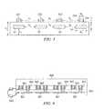
- FIG. 3shows the primary conductors 101 electrically connected to an output signal pin 104 of the package or substrate 106 . In this embodiment, the electrical connections are made by way of a wire bond.
- the auxiliary conductors 102are “floating” or unattached to any other conductor, and the impedance values of the auxiliary conductors are of no concern to the device performance.
- a dielectric layer 134separates the two conductor layers and the dielectric thickness is equal to the difference between “h 1 ” and “h 2 ” in FIG. 1.
- This transmission configurationprovides impedance results of the primary conductors which are have only slightly different from a device with a single level of conductors; i.e., the auxiliary conductors cause a minor change in the capacitance values which results in only minor changes in the impedance values.
- the bonding configuration, shown in FIG. 3is used with differential mode transmission lines.
- each of the primary conductors 401is connected to a signal output pin 404 , and each of the overlying auxiliary conductors 402 is electrically connected to a ground contact 407 .
- a dielectric layer 434separates the primary and auxiliary conductor levels. This configuration provides a connection for single ended transmission by the primary conductors. Connection of the auxiliary conductors 402 to ground essentially sandwiches the primary conductors between two ground levels; i.e., the ground plane within the package or board, and a second isolated ground plane formed by the auxiliary conductors when attached to a ground contact.
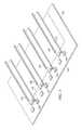
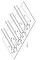
- modescan be mixed within a conductor system having an array of primary conductors 51 , 52 , 53 , and 54 , and a parallel array of auxiliary conductors 521 , 522 , 523 , and 524 substantially overlaying the primary conductors, and separated by a dielectric layer 534 .
- spacing of the primary and auxiliary conductorsare not uniform throughout the respective conductor planes, but are spaced at predetermined distances to allow mixed mode impedance, single ended impedance or differential impedance depending upon the connection of the auxiliary conductors to ground.
- the primary conductors 51 , 52 , 53 , 54are connected to signal output pins or pads.
- all auxiliary conductors 521 , 522 , 523 and 524are connected to ground 507 .
- the auxiliary conductorsare floating or not connected, and the center pair 52 and 53 are spaced and dimensioned to provide a differential pair of specified impedance.
- the conductors 52 and 53are made the differential transmission lines, and leads 51 and 54 are made single ended transmission lines by attaching auxiliary conductors 521 and 524 to ground 507 .
- Each primary conductoris electrically connected to an output pad 504 , and auxiliary conductors 521 and 524 are connected to ground contact 507 , thereby a device having a pair of differential transmission lines, 52 and 53 , and two single ended lines 51 and 54 .
- the single ended conductors of FIG. 4were designed for 50 ohm impedance, and the model data shows the values to be within 5%. By connecting the specific auxiliary conductors to ground, differential impedance of the odd and even modes are within 3%.
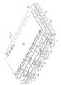
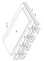
- FIG. 7illustrates a preferred embodiment of the invention as a BGA (Ball Grid Array) semiconductor package.
- the package substrate 706is comprised of a composite material, such as BT resin having a dielectric constant of 4.
- the deviceincludes a primary level of conductors 701 overlaid by a second level of auxiliary conductors 702 , and the conductors separated by a layer of dielectric 734 .
- Plated vias 711connect each primary conductor 701 to an external solder ball contact 721 .
- Plated vias 712connect each second level conductor 702 to a ground plane 732 embedded within the package substrate, to an array of external solder ball contacts 722 .
- An integrated circuit chip 700is adhered to a chip pad 715 on the package substrate 706 , and the chip 700 is connected by wire bonds 716 to selected conductors.
- the chip and conductor systemare encapsulated in a plastic material (not shown).
- an embodiment of the inventionincludes a flip chip interconnected integrated circuit chip 800 electrically connected by solder bumps 820 to a pattern of primary conductors 801 and auxiliary conductors 802 on the substrate 806 .
- the primary conductors 801 on the surface of the substrateinterconnect the solder bumps on the IC chip to the external signal leads or solder balls 821
- the auxiliary conductors 802interconnect the chip ground contacts to the ground plane 832 .
- External ground contactsare made through solder balls 822 by way of vias to the ground plane 832 . Ground contacts to be excluded, as in the case of differential mode transmission lines, are avoided by removing designated solder balls prior to assembly onto the substrate.
- Conductive viasprovide electrical connection between the primary 801 and secondary 802 conductors to external solder ball contacts 821 and 822 .
- the preferred embodiments, as demonstrated in FIGS. 7 and 8include a ground plane 732 , 832 within the package substrate.
- the ground planeoften exists within the printed circuit board, rather than in the package itself and the configuration is usable with the current invention. Ground contacts are made directly to the printed wiring board ground plane, avoiding the need for an additional layer within the package.
- the conductor system of the current inventionis applicable not only to rigid substrates, as illustrated in FIGS. 6, 7 and 8 wherein the conductors are supported on a rigid material and separated by a dielectric layer, but the system is also applicable to thin flex circuits.
- a cross section of a Flex Circuit device of the current inventionis provided having a level of primary conductors 901 on one surface and an overlaying array of auxiliary conductors 902 on the alternate surface on a thin film dielectric 903 , such as a polyimide film.
- the IC chip 900has solder bump connections 905 to said conductors on the film substrate. External contacts to conductors 901 and 902 are made a perimeter contact pads 910 .
- packages or substrates having a conductor system of this inventioninclude leaded devices, rather than those having solder ball connectors.
Landscapes
- Physics & Mathematics (AREA)
- Engineering & Computer Science (AREA)
- Computer Hardware Design (AREA)
- Microelectronics & Electronic Packaging (AREA)
- Power Engineering (AREA)
- Condensed Matter Physics & Semiconductors (AREA)
- General Physics & Mathematics (AREA)
- Geometry (AREA)
- Structure Of Printed Boards (AREA)
- Lead Frames For Integrated Circuits (AREA)
Abstract
Description
- This invention relates generally to a semiconductor package, and more particularly to the impedance of conductors in a semiconductor package.[0001]
- In order to maintain signal integrity, the design of high speed integrated circuit (IC) devices requires specific characteristic impedance of conductors which interconnect an IC chip to a printed wiring board or the next level of interconnection. For example, clock circuit drivers of many high frequency circuits are designed for 50 ohm matched impedance, and this in turn necessitates a specific geometric conductor design, and a predetermined output location for the conductor system in a package or substrate to match the circuit design. Moreover, the conductor system within a substrate or package used for both single ended and differential signal transmission has different impedance levels for each mode, and thus a specific conductor design for individual devices.[0002]
- Arrays of conductors provide transmission lines in semiconductor packages or substrates; these arrays or systems include signal layer(s), and a ground conductor(s) which may be within the substrate, the printed wiring board or the semiconductor chip itself. The conductive layers are interspaced with dielectric materials. Characteristic impedance of the conductors is a function of conductor spacing, dielectric thickness, conductor width, the electrical properties of the materials, and the velocity of signal propagation on the line.[0003]
- Differential impedance between a pair of conductors is either odd mode or even mode depending upon the direction of signal propagation, and for some circuits the need for both modes exists within the same device. This is particularly true of higher frequency and microwave devices designed for even mode impedance, often at 100 ohms.[0004]
- The ongoing proliferation of high speed circuits with specific conductor requirements places a difficult and costly demand for as many package or substrate designs. A need exists for more flexible conductor systems which accommodate a number of different circuit design requirements.[0005]
- The primary object of the invention is to provide a multiple use conductor system for interconnecting an integrated circuit chip to an external circuit wherein the impedance level of the conductors serving as transmission lines can be arbitrarily selected.[0006]
- It is an object of the invention to provide a semiconductor package having conductors wherein the impedance can be selected for individual leads or lead pairs.[0007]
- It is an object of the invention to provide a semiconductor package wherein the characteristic impedance of the conductors can be selected for single ended or differential pairs of transmission lines, as well as for odd and even mode differential transmission lines within the same package.[0008]
- It is an object of the invention to provide a semiconductor package wherein the impedance level of the conductors is established during the assembly of the circuit.[0009]
- It is an object of the invention to provide a semiconductor package which is usable for many chip designs, and thus reduces the costs associated with tooling, inventory, and package design.[0010]
- It is further an object that the interconnection of the conductors is compatible with either wire bond or flip chip interconnection.[0011]
- Yet another objective is to provide a flexible conductor system which is usable with different types of packages or substrates.[0012]
- It is an object of one embodiment of the invention to provide a conductor system wherein single ended and differential mode transmission can be mixed within the same conductor system.[0013]
- The invention is a microelectronic device, and a method of fabricating the device, wherein the impedance of single ended or differential signal transmission lines is determined by the choice of which conductors are connected to ground during the assembly of the semiconductor device. Moreover, the device is applicable to pairs of conductors having odd or even mode impedance within the same conductor system.[0014]
- In one embodiment, the device is a semiconductor package having a plurality of conductors arrayed in two (or more) parallel planes, and a ground conductor. Each of the primary conductors has the same dimensions and spacing between conductors, and each of the auxiliary conductors has the same dimensions and spacing. Conductors in the auxiliary or second plane substantially overlay the primary signal conductors in the first plane, and the impedance of any lead or lead pair is arbitrarily set by connecting the auxiliary conductors to ground or by leaving them floating. Differential pairs of signal conductors, either odd or even mode are set by connecting the auxiliary conductors to a ground contact.[0015]
- In an alternate embodiment, a conductor system is provided wherein single ended and differential impedance modes are mixed within the same package or substrate. Conductors are arrayed in two (or more) parallel planes, with an available ground conductor, and the auxiliary conductors substantially overlay the primary conductors. Conductor dimensions and spacing are set to provide alternating impedance modes.[0016]
- FIG. 1 is a cross sectional design of conductors of the current invention.[0017]
- FIG. 2 shows the overlaying conductors from a top view.[0018]
- FIG. 3 illustrates bond selection of the primary conductors for differential mode transmission[0019]
- FIG. 4 illustrates bond selection of the primary and ground conductors for single ended signal transmission.[0020]
- FIG. 5 is a cross sectional diagram of a conductor system applicable to mixed mode, to single ended, or to a differential pair of transmission lines.[0021]
- FIG. 6 illustrates a mixed transmission mode conductor system in the same device.[0022]
- FIG. 7 is a Ball Grid Array package with single ended transmission lines.[0023]
- FIG. 8 is a flip chip bonded BGA package of the current invention.[0024]
- FIG. 9 is a cross section of a device of the current invention using a flex circuit substrate.[0025]
- FIG. 1 provides a cross section of the conductors of the current invention, wherein a[0026]
ground plane 105 exists either in the package, the chip, or the next level of interconnection, typically a printed wiring board. A first level orprimary conductors 101 are positioned at a distance “h1” above theground plane 105 and have a defined width “w1”, and a separation “d” from the adjacent primary conductor. An auxiliary orsecond level 102 of conductors having width “w2” is positioned above theprimary conductors 101 at a distance “h2” above the ground plane, and substantially follow the path of the primary conductors throughout the conductor system. Theconductors - FIG. 2 provides a top view of the[0027]
conductors auxiliary conductor 102 lies directly above each of theprimary conductors 101. Contactpads substrate 106. - It is known by those skilled in the art that the impedance of a conductor or lead is a function of inductance and capacitance of the conductors, and is determined by the height above the ground plane, and the conductor width, and that for single ended transmission lines, impedance is a function of the spacing between the conductors. It is further recognized that the ratio of “h” and “w” is the same for each conductor in a given signal layer if the impedance of the conductors is to be substantially the same. The general equation for a impedance “Z” of a conductor is given by:[0028]

- In FIG. 1 all[0029]
primary conductors 101 in the system are designed for a selected impedance level, taking into account the known geometric constraints discussed previously, the dielectric constant of the materials of construction and the resistivity of the conductors. FIG. 3 shows theprimary conductors 101 electrically connected to anoutput signal pin 104 of the package orsubstrate 106. In this embodiment, the electrical connections are made by way of a wire bond. Theauxiliary conductors 102 are “floating” or unattached to any other conductor, and the impedance values of the auxiliary conductors are of no concern to the device performance. Adielectric layer 134 separates the two conductor layers and the dielectric thickness is equal to the difference between “h1” and “h2” in FIG. 1. - This transmission configuration provides impedance results of the primary conductors which are have only slightly different from a device with a single level of conductors; i.e., the auxiliary conductors cause a minor change in the capacitance values which results in only minor changes in the impedance values. The bonding configuration, shown in FIG. 3 is used with differential mode transmission lines.[0030]
- Turning now to FIG. 4, each of the[0031]
primary conductors 401 is connected to asignal output pin 404, and each of the overlyingauxiliary conductors 402 is electrically connected to aground contact 407. Adielectric layer 434 separates the primary and auxiliary conductor levels. This configuration provides a connection for single ended transmission by the primary conductors. Connection of theauxiliary conductors 402 to ground essentially sandwiches the primary conductors between two ground levels; i.e., the ground plane within the package or board, and a second isolated ground plane formed by the auxiliary conductors when attached to a ground contact. - From FIGS. 3 and 4, it is apparent that the impedance of the conductors of the current invention are arbitrarily selected as single ended or differential mode transmission lines depending on connection to ground.[0032]
- In an alternate embodiment, illustrated in FIGS. 5 and 6, it can be seen that modes can be mixed within a conductor system having an array of[0033]
primary conductors auxiliary conductors dielectric layer 534. In this embodiment, spacing of the primary and auxiliary conductors are not uniform throughout the respective conductor planes, but are spaced at predetermined distances to allow mixed mode impedance, single ended impedance or differential impedance depending upon the connection of the auxiliary conductors to ground. - In each application, the[0034]
primary conductors auxiliary conductors ground 507. In an application requiring a differential pair, the auxiliary conductors are floating or not connected, and thecenter pair - For the application of mixed modes, the[0035]
conductors auxiliary conductors ground 507. - The configuration of mixed mode is further illustrated in FIG. 6. Each primary conductor is electrically connected to an[0036]
output pad 504, andauxiliary conductors ground contact 507, thereby a device having a pair of differential transmission lines,52 and53, and two single endedlines - In order to insure proper signal transmission and timing, prediction and control of electrical parameters of a packaging system is analyzed using computer modeling and simulation program. Such electrical modeling programs are both commercially available, and have been developed by a number of university programs. The geometry and material properties of a series of conductors and insulators are input to the program, and the output includes capacitance, inductance of the conductors and the resulting impedance of the lead in question, and of the surrounding leads. The results of such analyses are then input to a simulation model to predict a circuit performance.[0037]
- Validity of the current invention is illustrated by results of an electrical model of the device in FIGS. 3 and 4 are given in Tables 1 and 2 respectively.[0038]
- Conductor material: Copper (resistivity=1.67 ohm cm) permeability (μr=1)[0039]
- Substrate material: BT resin (dielectric constant=4) (dielectric loss tangent δ=0[0040]
- Conductor design in mm[0041]
w2= 0.0625 w1= 0.125 t = 0.02 d1= 0.125 h1= 0.251 h2= 0.3615 - [0042]
TABLE 1 First Level Conductors With Differential Transmission Lines (Auxiliary Conductors Floating) Conductor # 1 2 3 4 CAPACITANCE MATRIX 1.32 1.39 1.39 1.32 (pf/cm) pico farads per centimeter INDUCTANCE MATRIX 5.00 5.00 5.07 5.07 (nh/cm) nanohenries/cm IMPEDANCE MATRIX (ohm) 76.22 75.19 75.19 76.22 adjacent lead 25 25 25 25 Differential mode Impedance 51.22 50.19 50.19 51.22 - [0043]
TABLE 2 First Level Conductors With Single Ended Transmission Lines (Auxiliary Conductors Grounded) Conductor # 1 2 3 4 CAPACITANCE MATRIX 1.32 1.39 1.39 1.32 (pf/cm) pico farads per centimeter INDUCTANCE MATRIX 3.44 3.33 3.35 3.44 (nh/cm) nanohenries/cm IMPEDANCE MATRIX (ohm) 51.59 50.02 50.02 51.59 - The single ended conductors of FIG. 4 were designed for 50 ohm impedance, and the model data shows the values to be within 5%. By connecting the specific auxiliary conductors to ground, differential impedance of the odd and even modes are within 3%.[0044]
- An analysis of the mixed mode device in FIGS. 5 and 6, provides the results given in Table 3.[0045]
- Conductor material: Copper (resistivity=1.67 ohm cm) (permeability μr=1)[0046]
- Substrate material: BT resin (dielectric constant=4) (dielectric loss tangent δ=0)[0047]
- Conductor design in mm[0048]
t = 0.02 w20.02 d3 = 0.52 d3 = 0.1 h1= 0.192 w1= 0.1 d2 = 0.18 d4 = 0.45 h2= 0.264 - [0049]
TABLE 3 Differential Transmission Lines 52, 53(Auxiliary Conductors Floating) Conductor # 51 52 53 54 CAPACITANCE MATRIX 1.33 1.42 1.42 1.33 (pf/cm) pico farads per centimeter INDUCTANCE MATRIX 5.00 4.93 4.93 5.00 (nh/cm) nanohenries/cm IMPEDANCE MATRIX (ohm) 75.27 74.21 74.22 75.26 adjacent lead 24.79 24.79 Differential mode Impedance 49.42 49.43 - [0050]
Conductors With Single Transmission Lines (All Auxiliary Conductors Grounded) Conductor # 52 52 53 54 CAPACITANCE MATRIX 1.33 1.42 1.42 1.33 (pf/cm) picofarads per centimeter INDUCTANCE MATRIX 3.33 3.22 3.21 3.33 (nh/cn) nanohenries/cm IMPEDANCE MATRIX (ohm) 50.02 48.27 48.22 50.01 - [0051]
Mixed Mode Transmission Lines Differential Pair Conductor # 51 52 53 54 CAPACITANCE MATRIX 1.33 1.42 1.42 1.33 (pf/cm) picofarads per centimeter INDUCTANCE MATRIX 3.34 4.88 4.88 3.34 (nh/cm) nanohenries/cm IMPEDANCE MATRIX (ohm) 50.13 73.44 73.44 50.13 adjacent lead 24.12 24.12 Differential mode Impedance 49.32 49.32 - Thus, in the preferred embodiment illustrated in FIGS. 3 and 4, and the analysis in Tables 1 and 2, a conductor system having overlaying conductors in a single device design is provided, and said design is compatible with various chip transmission requirements, thereby eliminating a need for specific package designs for various impedance matching conductors.[0052]
- In the alternate embodiment, given in FIGS. 5 and 6 and the analysis in Table 3, a conductor system is shown which allows both single ended and differential mode impedance transmission lines within the same package, or allows either single ended or for differential transmission modes to be selected arbitrarily by the bonding configuration.[0053]
- FIG. 7 illustrates a preferred embodiment of the invention as a BGA (Ball Grid Array) semiconductor package. In this embodiment, the[0054]
package substrate 706 is comprised of a composite material, such as BT resin having a dielectric constant of 4. The device includes a primary level ofconductors 701 overlaid by a second level ofauxiliary conductors 702, and the conductors separated by a layer ofdielectric 734. Plated vias711 connect eachprimary conductor 701 to an externalsolder ball contact 721. Plated vias712 connect eachsecond level conductor 702 to aground plane 732 embedded within the package substrate, to an array of externalsolder ball contacts 722. Anintegrated circuit chip 700 is adhered to achip pad 715 on thepackage substrate 706, and thechip 700 is connected bywire bonds 716 to selected conductors. The chip and conductor system are encapsulated in a plastic material (not shown). - In FIG. 8, an embodiment of the invention includes a flip chip interconnected integrated[0055]
circuit chip 800 electrically connected by solder bumps820 to a pattern ofprimary conductors 801 andauxiliary conductors 802 on thesubstrate 806. Theprimary conductors 801 on the surface of the substrate interconnect the solder bumps on the IC chip to the external signal leads orsolder balls 821, and theauxiliary conductors 802 interconnect the chip ground contacts to theground plane 832. External ground contacts are made throughsolder balls 822 by way of vias to theground plane 832. Ground contacts to be excluded, as in the case of differential mode transmission lines, are avoided by removing designated solder balls prior to assembly onto the substrate. Conductive vias provide electrical connection between the primary801 and secondary802 conductors to externalsolder ball contacts - The preferred embodiments, as demonstrated in FIGS. 7 and 8 include a[0056]
ground plane - The conductor system of the current invention is applicable not only to rigid substrates, as illustrated in FIGS. 6, 7 and[0057]8 wherein the conductors are supported on a rigid material and separated by a dielectric layer, but the system is also applicable to thin flex circuits. In FIG. 9, a cross section of a Flex Circuit device of the current invention is provided having a level of
primary conductors 901 on one surface and an overlaying array ofauxiliary conductors 902 on the alternate surface on athin film dielectric 903, such as a polyimide film. TheIC chip 900 hassolder bump connections 905 to said conductors on the film substrate. External contacts toconductors perimeter contact pads 910. - The invention has been illustrated and described as a single chip package, but the overlying conductor system of this invention is equally applicable to multichip devices require controlled impedance transmission lines.[0058]
- Further, packages or substrates having a conductor system of this invention include leaded devices, rather than those having solder ball connectors.[0059]
- While preferred embodiments and some alternative applications of the invention have been described above, they are not intended to be limited, but instead it should be understood that various modifications may be made from the specific details described herein without departing from the spirit and scope of the invention as set forth in the appended claims.[0060]

Claims (13)
1- An electrical conductor system for a microelectronic device wherein the impedance of individual leads is arbitrarily selected during assembly of said device, said system comprising;
a) an array of primary conductors in a plane,
b) an array of auxiliary conductors substantially overlaying said primary conductors,
c) a dielectric layer separating said conductor layers,
d) a ground plane separated from said conductors a by dielectric material, and
e) means for interconnecting said conductors and said ground plane.
2- A conductor system as inclaim 1 wherein the impedance is selected for either single ended or differential pairs of transmission lines, said system having primary conductors of the same size and equal spacing, and auxiliary conductors of the same size and equal spacing.
3- A conductor system as inclaim 1 wherein the impedance is selected for single ended, for differential pairs, or for both single ended and differential pairs of transmission lines within the same device; said system having each of the primary conductors the same size, and each of the auxiliary conductors the same size.
4- A method of assembling the conductor system for a microelectronic device wherein the impedance of primary conductors is selected to form differential mode input and output pairs including the following steps;
a) providing an array of primary conductors in a plane,
b) providing an array of auxiliary conductors substantially overlying said primary conductors,
c) separating said conductors by a dielectric layer,
d) providing a ground plane separated from said conductors by a dielectric layer, and
e) interconnecting said primary conductors to signal ports, and not connecting auxiliary conductors.
5- A method of assembling the conductor system for a microelectronic device having the impedance of primary conductors forming single ended transmission lines including the following steps;
a) providing an array of primary conductors in a plane,
b) providing an array of auxiliary conductors substantially overlying said primary conductors,
c) separating said conductors by a dielectric layer,
d) providing a ground plane separated from said conductors by a dielectric layer, and
e) interconnecting said primary conductors to signal ports, and said auxiliary conductors to ground.
6- A semiconductor device having the impedance of individual leads arbitrarily selected, said device comprising;
a) an integrated circuit chip,
b) a conductor system as inclaim 1 , and
c) a semiconductor package including a substrate, external leads and encapsulation.
7- A semiconductor device as inclaim 6 wherein said means or interconnection is by wire bonding.
8- A semiconductor device as inclaim 6 wherein said means of interconnection is by flip chip contacts.
9- A semiconductor device as inclaim 6 wherein said package is a Ball Grid Array.
10- A semiconductor device as inclaim 6 wherein said package includes a substrate for one or more semiconductor chips.
11- A method of assembling a semiconductor device wherein the impedance of primary conductors in the package or substrate forms differential mode input and output pairs including the following steps;
a) interconnecting a semiconductor chip to an array of primary conductors in said package,
b) providing an array of auxiliary conductors substantially overlying said primary conductors,
c) providing a dielectric layer separating said conductors,
d) providing a ground plane separated from said conductors by a dielectric layer, and
e) interconnecting said primary conductors to external signal ports on said package, and auxiliary conductors not connected.
12- A method of assembling a semiconductor device wherein the impedance of primary conductors in the package or substrate forms single ended transmission lines including the following steps;
a) interconnecting a semiconductor chip to an array of primary conductors in a plane,
b) interconnecting a semiconductor chip to an array of auxiliary conductors substantially overlying said primary conductors,
c) providing a dielectric layer separating said conductors,
d) providing a ground lane separated from said conductors by a dielectric layer, and
e) interconnecting said primary conductors to external signal ports, and auxiliary conductors to ground.
13- A flex circuit semiconductor device having the impedance of individual leads arbitrarily selected, said device comprising;
a) an integrated circuit chip having flip chip contacts,
b) a flexible dielectric film having an array of primary conductors on the first surface,
c) an array of auxiliary conductors on the second surface substantially overlaying said primary conductors,
d) an array of conductive vias,
e) an array of input/output contact pads on said film surfaces,
f) an available ground plane external to said device, and
g) a means to interconnect said conductors and said ground plane.
Priority Applications (1)
| Application Number | Priority Date | Filing Date | Title |
|---|---|---|---|
| US10/411,531US7132740B2 (en) | 1999-12-29 | 2003-04-10 | Semiconductor package with conductor impedance selected during assembly |
Applications Claiming Priority (3)
| Application Number | Priority Date | Filing Date | Title |
|---|---|---|---|
| US17345099P | 1999-12-29 | 1999-12-29 | |
| US09/750,393US6563208B2 (en) | 1999-12-29 | 2000-12-28 | Semiconductor package with conductor impedance selected during assembly |
| US10/411,531US7132740B2 (en) | 1999-12-29 | 2003-04-10 | Semiconductor package with conductor impedance selected during assembly |
Related Parent Applications (1)
| Application Number | Title | Priority Date | Filing Date |
|---|---|---|---|
| US09/750,393ContinuationUS6563208B2 (en) | 1999-12-29 | 2000-12-28 | Semiconductor package with conductor impedance selected during assembly |
Publications (2)
| Publication Number | Publication Date |
|---|---|
| US20030201519A1true US20030201519A1 (en) | 2003-10-30 |
| US7132740B2 US7132740B2 (en) | 2006-11-07 |
Family
ID=22632093
Family Applications (2)
| Application Number | Title | Priority Date | Filing Date |
|---|---|---|---|
| US09/750,393Expired - LifetimeUS6563208B2 (en) | 1999-12-29 | 2000-12-28 | Semiconductor package with conductor impedance selected during assembly |
| US10/411,531Expired - LifetimeUS7132740B2 (en) | 1999-12-29 | 2003-04-10 | Semiconductor package with conductor impedance selected during assembly |
Family Applications Before (1)
| Application Number | Title | Priority Date | Filing Date |
|---|---|---|---|
| US09/750,393Expired - LifetimeUS6563208B2 (en) | 1999-12-29 | 2000-12-28 | Semiconductor package with conductor impedance selected during assembly |
Country Status (4)
| Country | Link |
|---|---|
| US (2) | US6563208B2 (en) |
| EP (1) | EP1113497A3 (en) |
| JP (1) | JP2001196499A (en) |
| KR (1) | KR100686671B1 (en) |
Cited By (3)
| Publication number | Priority date | Publication date | Assignee | Title |
|---|---|---|---|---|
| US20030072130A1 (en)* | 2001-05-30 | 2003-04-17 | University Of Washington | Methods for modeling interactions between massively coupled multiple vias in multilayered electronic packaging structures |
| US20100003785A1 (en)* | 2007-01-25 | 2010-01-07 | Raytheon Company | Stacked integrated circuit assembly |
| WO2018125443A1 (en)* | 2016-12-27 | 2018-07-05 | Intel Corporation | Multi-conductor interconnect structure for a microelectronic device |
Families Citing this family (8)
| Publication number | Priority date | Publication date | Assignee | Title |
|---|---|---|---|---|
| EP1113497A3 (en)* | 1999-12-29 | 2006-01-25 | Texas Instruments Incorporated | Semiconductor package with conductor impedance selected during assembly |
| DE10031843A1 (en)* | 2000-06-30 | 2002-01-10 | Alcatel Sa | Electrical or opto-electrical component with a plastic packaging and method for varying the impedance of a connection line of such a component |
| JP3674780B2 (en)* | 2001-11-29 | 2005-07-20 | ユーディナデバイス株式会社 | High frequency semiconductor device |
| US20040012935A1 (en)* | 2002-07-16 | 2004-01-22 | Matsushita Electric Industrial Co., Ltd. | Printed wiring board |
| US7259968B2 (en)* | 2003-05-14 | 2007-08-21 | Hewlett-Packard Development Company, L.P. | Tailoring impedances of conductive traces in a circuit board |
| US7265443B2 (en)* | 2005-04-29 | 2007-09-04 | Texas Instruments Incorporated | Wire bonded semiconductor device having low inductance and noise |
| US8436450B2 (en)* | 2008-02-01 | 2013-05-07 | Viasat, Inc. | Differential internally matched wire-bond interface |
| KR20220019331A (en) | 2020-08-10 | 2022-02-17 | 삼성전자주식회사 | Package substrate and semiconductor package including the same |
Citations (82)
| Publication number | Priority date | Publication date | Assignee | Title |
|---|---|---|---|---|
| US4498122A (en)* | 1982-12-29 | 1985-02-05 | At&T Bell Laboratories | High-speed, high pin-out LSI chip package |
| US5173767A (en)* | 1990-05-28 | 1992-12-22 | Siemens Aktiengesellschaft | Integrated circuit housing composed of three coated, dielectric plates |
| US5228911A (en)* | 1991-04-18 | 1993-07-20 | Merck Patent Gesellschaft Mit Beschrankter Haftung | Oxidized graphite flaky particles and pigments based thereon |
| US5234437A (en)* | 1991-12-12 | 1993-08-10 | Target Therapeutics, Inc. | Detachable pusher-vasoocclusion coil assembly with threaded coupling |
| US5250071A (en)* | 1992-09-22 | 1993-10-05 | Target Therapeutics, Inc. | Detachable embolic coil assembly using interlocking clasps and method of use |
| US5261916A (en)* | 1991-12-12 | 1993-11-16 | Target Therapeutics | Detachable pusher-vasoocclusive coil assembly with interlocking ball and keyway coupling |
| US5266912A (en)* | 1992-08-19 | 1993-11-30 | Micron Technology, Inc. | Inherently impedance matched multiple integrated circuit module |
| US5312415A (en)* | 1992-09-22 | 1994-05-17 | Target Therapeutics, Inc. | Assembly for placement of embolic coils using frictional placement |
| US5331204A (en)* | 1991-10-17 | 1994-07-19 | Ngk Spark Plug Co., Ltd. | Integrated circuit package in which impendance between signal pads and signal lines is matched by reducing the size of a ground plane |
| US5332693A (en)* | 1989-07-20 | 1994-07-26 | Hyundai Electronics, Industries Co., Ltd. | Method for manufacturing aluminum wired layer for interconnecting device to device in a semiconductor device |
| US5350397A (en)* | 1992-11-13 | 1994-09-27 | Target Therapeutics, Inc. | Axially detachable embolic coil assembly |
| US5690671A (en)* | 1994-12-13 | 1997-11-25 | Micro Interventional Systems, Inc. | Embolic elements and methods and apparatus for their delivery |
| US5719725A (en)* | 1995-11-30 | 1998-02-17 | Sanyo Electric Co., Ltd. | Disk playback device |
| US6077214A (en)* | 1998-07-29 | 2000-06-20 | Myocor, Inc. | Stress reduction apparatus and method |
| US6143024A (en)* | 1998-06-04 | 2000-11-07 | Sulzer Carbomedics Inc. | Annuloplasty ring having flexible anterior portion |
| US6190408B1 (en)* | 1998-03-05 | 2001-02-20 | The University Of Cincinnati | Device and method for restructuring the heart chamber geometry |
| US6299637B1 (en)* | 1999-08-20 | 2001-10-09 | Samuel M. Shaolian | Transluminally implantable venous valve |
| US20020013571A1 (en)* | 1999-04-09 | 2002-01-31 | Evalve, Inc. | Methods and devices for capturing and fixing leaflets in valve repair |
| US20020035961A1 (en)* | 2000-06-21 | 2002-03-28 | Seiko Epson Corporation | Ceramic film and method of manufacturing the same, semiconductor device and piezoelectric device |
| US6402781B1 (en)* | 2000-01-31 | 2002-06-11 | Mitralife | Percutaneous mitral annuloplasty and cardiac reinforcement |
| US6406420B1 (en)* | 1997-01-02 | 2002-06-18 | Myocor, Inc. | Methods and devices for improving cardiac function in hearts |
| US20020156526A1 (en)* | 2001-04-24 | 2002-10-24 | Hlavka Edwin J. | Method and apparatus for catheter-based annuloplasty |
| US20020168360A1 (en)* | 2001-03-02 | 2002-11-14 | Christine Dingivan | Methods of preventing or treating inflammatory or autoimmune disorders by administering integrin alphanubeta3 antagonists in combination with other prophylactic or therapeutic agents |
| US20020183766A1 (en)* | 1997-09-12 | 2002-12-05 | Evalve, Inc. | Surgical device for connecting soft tissue |
| US20030050693A1 (en)* | 2001-09-10 | 2003-03-13 | Quijano Rodolfo C. | Minimally invasive delivery system for annuloplasty rings |
| US20030069635A1 (en)* | 2001-05-29 | 2003-04-10 | Cartledge Richard G. | Prosthetic heart valve |
| US20030069593A1 (en)* | 2001-08-31 | 2003-04-10 | Tremulis William S. | Method and apparatus for valve repair |
| US20030069570A1 (en)* | 1999-10-02 | 2003-04-10 | Witzel Thomas H. | Methods for repairing mitral valve annulus percutaneously |
| US20030074012A1 (en)* | 2000-10-10 | 2003-04-17 | Coalescent Surgical, Inc. | Minimally invasive annuloplasty procedure and apparatus |
| US20030078854A1 (en)* | 2000-03-06 | 2003-04-24 | Young-Up Shim | System and method for providing advertisement and technical skill premium by using network |
| US20030083742A1 (en)* | 2000-02-02 | 2003-05-01 | Paul A. Spence | Heart valve repair apparatus and methods |
| US6585781B1 (en)* | 1999-08-09 | 2003-07-01 | Aktiebolaget Electrolux | Laundry washing machine with steam drying |
| US20030130730A1 (en)* | 2001-10-26 | 2003-07-10 | Cohn William E. | Method and apparatus for reducing mitral regurgitation |
| US20030167071A1 (en)* | 2002-03-01 | 2003-09-04 | Evalve, Inc. | Suture fasteners and methods of use |
| US6626899B2 (en)* | 1999-06-25 | 2003-09-30 | Nidus Medical, Llc | Apparatus and methods for treating tissue |
| US6656221B2 (en)* | 2001-02-05 | 2003-12-02 | Viacor, Inc. | Method and apparatus for improving mitral valve function |
| US20030229395A1 (en)* | 1998-06-16 | 2003-12-11 | Cardiac Concepts, Inc. | Mitral valve annuloplasty ring |
| US20040003819A1 (en)* | 1999-04-09 | 2004-01-08 | Evalve, Inc. | Methods and apparatus for cardiac valve repair |
| US6689164B1 (en)* | 1999-10-12 | 2004-02-10 | Jacques Seguin | Annuloplasty device for use in minimally invasive procedure |
| US20040039443A1 (en)* | 1999-06-30 | 2004-02-26 | Solem Jan Otto | Method and device for treatment of mitral insufficiency |
| US20040044350A1 (en)* | 1999-04-09 | 2004-03-04 | Evalve, Inc. | Steerable access sheath and methods of use |
| US6702826B2 (en)* | 2000-06-23 | 2004-03-09 | Viacor, Inc. | Automated annular plication for mitral valve repair |
| US6701929B2 (en)* | 1999-03-03 | 2004-03-09 | Hany Hussein | Device and method for treatment of congestive heart failure |
| US20040049211A1 (en)* | 2002-06-12 | 2004-03-11 | Mitral Interventions, Inc. | Method and apparatus for tissue connection |
| US6709382B1 (en)* | 1999-05-04 | 2004-03-23 | Simon Marcus Horner | Cardiac assist method and apparatus |
| US20040073302A1 (en)* | 2002-02-05 | 2004-04-15 | Jonathan Rourke | Method and apparatus for improving mitral valve function |
| US6723036B2 (en)* | 2002-06-19 | 2004-04-20 | Contour Fabricators, Inc. | Methods and apparatus for folding sheet material |
| US6726716B2 (en)* | 2001-08-24 | 2004-04-27 | Edwards Lifesciences Corporation | Self-molding annuloplasty ring |
| US20040097979A1 (en)* | 2002-11-14 | 2004-05-20 | Oleg Svanidze | Aortic valve implantation device |
| US6740107B2 (en)* | 2001-12-19 | 2004-05-25 | Trimedyne, Inc. | Device for treatment of atrioventricular valve regurgitation |
| US20040105969A1 (en)* | 2002-12-03 | 2004-06-03 | Dai Huang | Manufacture of carbon composites by hot pressing |
| US20040122448A1 (en)* | 2002-08-13 | 2004-06-24 | The General Hospital Corporation | Cardiac devices and methods for percutaneous repair of atrioventricular valves |
| US6755777B2 (en)* | 1997-01-02 | 2004-06-29 | Myocor, Inc. | Heart wall tension reduction apparatus and method |
| US20040127982A1 (en)* | 2002-10-01 | 2004-07-01 | Ample Medical, Inc. | Devices, systems, and methods for reshaping a heart valve annulus |
| US20040127981A1 (en)* | 2000-09-20 | 2004-07-01 | Ample Medical, Inc. | Devices, systems, and methods for retaining a native heart valve leaflet |
| US20040127983A1 (en)* | 1997-12-17 | 2004-07-01 | Myocor, Inc. | Valve to myocardium tension members device and method |
| US20040133220A1 (en)* | 2000-01-31 | 2004-07-08 | Randall Lashinski | Adjustable transluminal annuloplasty system |
| US20040133240A1 (en)* | 2003-01-07 | 2004-07-08 | Cardiac Dimensions, Inc. | Electrotherapy system, device, and method for treatment of cardiac valve dysfunction |
| US20040133062A1 (en)* | 2002-10-11 | 2004-07-08 | Suresh Pai | Minimally invasive cardiac force transfer structures |
| US20040133279A1 (en)* | 2003-01-06 | 2004-07-08 | Krueger David J. | Surgical implants for use as spinal spacers |
| US20040138745A1 (en)* | 2001-10-01 | 2004-07-15 | Ample Medical, Inc. | Methods and devices for heart valve treatments |
| US20040148021A1 (en)* | 2002-08-29 | 2004-07-29 | Cartledge Richard G. | Implantable devices for controlling the internal circumference of an anatomic orifice or lumen |
| US6770063B2 (en)* | 2002-04-23 | 2004-08-03 | Uresil, L.P. | Thoracic vent kit |
| US20040152947A1 (en)* | 2000-10-06 | 2004-08-05 | Schroeder Richard F. | Methods and devices for improving mitral valve function |
| US20040156123A1 (en)* | 2003-02-05 | 2004-08-12 | Pentax Corporation | Structure of a lens barrel |
| US20040162510A1 (en)* | 2003-02-14 | 2004-08-19 | Medtronic Physio-Control Corp | Integrated external chest compression and defibrillation devices and methods of operation |
| US6784510B1 (en)* | 2003-04-16 | 2004-08-31 | Freescale Semiconductor, Inc. | Magnetoresistive random access memory device structures |
| US6797001B2 (en)* | 2002-03-11 | 2004-09-28 | Cardiac Dimensions, Inc. | Device, assembly and method for mitral valve repair |
| US20040187539A1 (en)* | 2003-03-31 | 2004-09-30 | Makoto Ishizuka | Method and apparatus for forming microchannels in a filament wire |
| US20040193191A1 (en)* | 2003-02-06 | 2004-09-30 | Guided Delivery Systems, Inc. | Devices and methods for heart valve repair |
| US20040215339A1 (en)* | 2002-10-24 | 2004-10-28 | Drasler William J. | Venous valve apparatus and method |
| US20040220657A1 (en)* | 2003-05-02 | 2004-11-04 | Cardiac Dimensions, Inc., A Washington Corporation | Tissue shaping device with conformable anchors |
| US20040243229A1 (en)* | 2002-01-09 | 2004-12-02 | Myocor, Inc. | Devices and methods for heart valve treatment |
| US20040249452A1 (en)* | 2001-11-01 | 2004-12-09 | Adams John M. | Focused compression mitral valve device and method |
| US20050004686A1 (en)* | 2001-10-09 | 2005-01-06 | Atsushi Imazu | Servo control apparatus control method |
| US20050021066A1 (en)* | 2001-08-29 | 2005-01-27 | Hans-Juergen Kuhr | Analytical device with lancet and test element |
| US20050149014A1 (en)* | 2001-11-15 | 2005-07-07 | Quantumcor, Inc. | Cardiac valve leaflet attachment device and methods thereof |
| US20050197694A1 (en)* | 2001-10-16 | 2005-09-08 | Extensia Medical, Inc. | Systems for heart treatment |
| US20050252984A1 (en)* | 2004-03-25 | 2005-11-17 | Osman Ahmed | Method and apparatus for graphically displaying a building system |
| US20050273160A1 (en)* | 2004-04-23 | 2005-12-08 | Lashinski Randall T | Pulmonary vein valve implant |
| US20060058871A1 (en)* | 2004-09-14 | 2006-03-16 | Edwards Lifesciences, Ag | Device and method for treatment of heart valve regurgitation |
| US7112207B2 (en)* | 1999-10-21 | 2006-09-26 | Edwards Lifesciences Corporation | Minimally invasive mitral valve repair method and apparatus |
Family Cites Families (7)
| Publication number | Priority date | Publication date | Assignee | Title |
|---|---|---|---|---|
| JPS60134440A (en)* | 1983-12-23 | 1985-07-17 | Hitachi Ltd | Semiconductor integrated circuit device |
| JPH08236654A (en)* | 1995-02-23 | 1996-09-13 | Matsushita Electric Ind Co Ltd | Chip carrier and manufacturing method thereof |
| FR2747235B1 (en)* | 1996-04-03 | 1998-07-10 | Bull Sa | INTEGRATED CIRCUIT BOX |
| JP3732927B2 (en)* | 1997-07-31 | 2006-01-11 | 京セラ株式会社 | Multilayer wiring board |
| JP3111938B2 (en)* | 1997-09-16 | 2000-11-27 | 日本電気株式会社 | Semiconductor device |
| US6064113A (en)* | 1998-01-13 | 2000-05-16 | Lsi Logic Corporation | Semiconductor device package including a substrate having bonding fingers within an electrically conductive ring surrounding a die area and a combined power and ground plane to stabilize signal path impedances |
| EP1113497A3 (en)* | 1999-12-29 | 2006-01-25 | Texas Instruments Incorporated | Semiconductor package with conductor impedance selected during assembly |
- 2000
- 2000-12-20EPEP00127906Apatent/EP1113497A3/ennot_activeWithdrawn
- 2000-12-26JPJP2000394486Apatent/JP2001196499A/ennot_activeAbandoned
- 2000-12-28USUS09/750,393patent/US6563208B2/ennot_activeExpired - Lifetime
- 2000-12-28KRKR1020000083615Apatent/KR100686671B1/ennot_activeExpired - Fee Related
- 2003
- 2003-04-10USUS10/411,531patent/US7132740B2/ennot_activeExpired - Lifetime
Patent Citations (97)
| Publication number | Priority date | Publication date | Assignee | Title |
|---|---|---|---|---|
| US4498122A (en)* | 1982-12-29 | 1985-02-05 | At&T Bell Laboratories | High-speed, high pin-out LSI chip package |
| US5332693A (en)* | 1989-07-20 | 1994-07-26 | Hyundai Electronics, Industries Co., Ltd. | Method for manufacturing aluminum wired layer for interconnecting device to device in a semiconductor device |
| US5173767A (en)* | 1990-05-28 | 1992-12-22 | Siemens Aktiengesellschaft | Integrated circuit housing composed of three coated, dielectric plates |
| US5228911A (en)* | 1991-04-18 | 1993-07-20 | Merck Patent Gesellschaft Mit Beschrankter Haftung | Oxidized graphite flaky particles and pigments based thereon |
| US5331204A (en)* | 1991-10-17 | 1994-07-19 | Ngk Spark Plug Co., Ltd. | Integrated circuit package in which impendance between signal pads and signal lines is matched by reducing the size of a ground plane |
| US5234437A (en)* | 1991-12-12 | 1993-08-10 | Target Therapeutics, Inc. | Detachable pusher-vasoocclusion coil assembly with threaded coupling |
| US5261916A (en)* | 1991-12-12 | 1993-11-16 | Target Therapeutics | Detachable pusher-vasoocclusive coil assembly with interlocking ball and keyway coupling |
| US5266912A (en)* | 1992-08-19 | 1993-11-30 | Micron Technology, Inc. | Inherently impedance matched multiple integrated circuit module |
| US5250071A (en)* | 1992-09-22 | 1993-10-05 | Target Therapeutics, Inc. | Detachable embolic coil assembly using interlocking clasps and method of use |
| US5312415A (en)* | 1992-09-22 | 1994-05-17 | Target Therapeutics, Inc. | Assembly for placement of embolic coils using frictional placement |
| US5350397A (en)* | 1992-11-13 | 1994-09-27 | Target Therapeutics, Inc. | Axially detachable embolic coil assembly |
| US5690671A (en)* | 1994-12-13 | 1997-11-25 | Micro Interventional Systems, Inc. | Embolic elements and methods and apparatus for their delivery |
| US5719725A (en)* | 1995-11-30 | 1998-02-17 | Sanyo Electric Co., Ltd. | Disk playback device |
| US20040133063A1 (en)* | 1997-01-02 | 2004-07-08 | Myocor | Methods and devices for improving cardiac function in hearts |
| US6755777B2 (en)* | 1997-01-02 | 2004-06-29 | Myocor, Inc. | Heart wall tension reduction apparatus and method |
| US6406420B1 (en)* | 1997-01-02 | 2002-06-18 | Myocor, Inc. | Methods and devices for improving cardiac function in hearts |
| US20020183766A1 (en)* | 1997-09-12 | 2002-12-05 | Evalve, Inc. | Surgical device for connecting soft tissue |
| US20040127983A1 (en)* | 1997-12-17 | 2004-07-01 | Myocor, Inc. | Valve to myocardium tension members device and method |
| US20060195012A1 (en)* | 1997-12-17 | 2006-08-31 | Myocor, Inc. | Valve to myocardium tension members device and method |
| US6190408B1 (en)* | 1998-03-05 | 2001-02-20 | The University Of Cincinnati | Device and method for restructuring the heart chamber geometry |
| US6143024A (en)* | 1998-06-04 | 2000-11-07 | Sulzer Carbomedics Inc. | Annuloplasty ring having flexible anterior portion |
| US20030229395A1 (en)* | 1998-06-16 | 2003-12-11 | Cardiac Concepts, Inc. | Mitral valve annuloplasty ring |
| US6077214A (en)* | 1998-07-29 | 2000-06-20 | Myocor, Inc. | Stress reduction apparatus and method |
| US6701929B2 (en)* | 1999-03-03 | 2004-03-09 | Hany Hussein | Device and method for treatment of congestive heart failure |
| US20050033446A1 (en)* | 1999-04-09 | 2005-02-10 | Evalve, Inc. A California Corporation | Methods and apparatus for cardiac valve repair |
| US20040039442A1 (en)* | 1999-04-09 | 2004-02-26 | Evalve, Inc. | Methods and apparatus for cardiac valve repair |
| US20050021057A1 (en)* | 1999-04-09 | 2005-01-27 | Evalve, Inc. | Leaflet structuring |
| US20040003819A1 (en)* | 1999-04-09 | 2004-01-08 | Evalve, Inc. | Methods and apparatus for cardiac valve repair |
| US20040030382A1 (en)* | 1999-04-09 | 2004-02-12 | Evalve, Inc. | Methods and apparatus for cardiac valve repair |
| US20040044350A1 (en)* | 1999-04-09 | 2004-03-04 | Evalve, Inc. | Steerable access sheath and methods of use |
| US20020013571A1 (en)* | 1999-04-09 | 2002-01-31 | Evalve, Inc. | Methods and devices for capturing and fixing leaflets in valve repair |
| US6709382B1 (en)* | 1999-05-04 | 2004-03-23 | Simon Marcus Horner | Cardiac assist method and apparatus |
| US6626899B2 (en)* | 1999-06-25 | 2003-09-30 | Nidus Medical, Llc | Apparatus and methods for treating tissue |
| US20040039443A1 (en)* | 1999-06-30 | 2004-02-26 | Solem Jan Otto | Method and device for treatment of mitral insufficiency |
| US6585781B1 (en)* | 1999-08-09 | 2003-07-01 | Aktiebolaget Electrolux | Laundry washing machine with steam drying |
| US6299637B1 (en)* | 1999-08-20 | 2001-10-09 | Samuel M. Shaolian | Transluminally implantable venous valve |
| US20030069570A1 (en)* | 1999-10-02 | 2003-04-10 | Witzel Thomas H. | Methods for repairing mitral valve annulus percutaneously |
| US6689164B1 (en)* | 1999-10-12 | 2004-02-10 | Jacques Seguin | Annuloplasty device for use in minimally invasive procedure |
| US20040153144A1 (en)* | 1999-10-12 | 2004-08-05 | Jacques Seguin | Annuloplasty device for use in minimally invasive procedure |
| US7112207B2 (en)* | 1999-10-21 | 2006-09-26 | Edwards Lifesciences Corporation | Minimally invasive mitral valve repair method and apparatus |
| US6402781B1 (en)* | 2000-01-31 | 2002-06-11 | Mitralife | Percutaneous mitral annuloplasty and cardiac reinforcement |
| US6709456B2 (en)* | 2000-01-31 | 2004-03-23 | Ev3 Santa Rosa, Inc. | Percutaneous mitral annuloplasty with hemodynamic monitoring |
| US6537314B2 (en)* | 2000-01-31 | 2003-03-25 | Ev3 Santa Rosa, Inc. | Percutaneous mitral annuloplasty and cardiac reinforcement |
| US20040133220A1 (en)* | 2000-01-31 | 2004-07-08 | Randall Lashinski | Adjustable transluminal annuloplasty system |
| US20040138744A1 (en)* | 2000-01-31 | 2004-07-15 | Randall Lashinski | Transluminal mitral annuloplasty with active anchoring |
| US20040088047A1 (en)* | 2000-02-02 | 2004-05-06 | Paul A. Spence | Heart valve repair apparatus and methods |
| US20030083742A1 (en)* | 2000-02-02 | 2003-05-01 | Paul A. Spence | Heart valve repair apparatus and methods |
| US20030078854A1 (en)* | 2000-03-06 | 2003-04-24 | Young-Up Shim | System and method for providing advertisement and technical skill premium by using network |
| US20020035961A1 (en)* | 2000-06-21 | 2002-03-28 | Seiko Epson Corporation | Ceramic film and method of manufacturing the same, semiconductor device and piezoelectric device |
| US6702826B2 (en)* | 2000-06-23 | 2004-03-09 | Viacor, Inc. | Automated annular plication for mitral valve repair |
| US20040127981A1 (en)* | 2000-09-20 | 2004-07-01 | Ample Medical, Inc. | Devices, systems, and methods for retaining a native heart valve leaflet |
| US20040152947A1 (en)* | 2000-10-06 | 2004-08-05 | Schroeder Richard F. | Methods and devices for improving mitral valve function |
| US20030074012A1 (en)* | 2000-10-10 | 2003-04-17 | Coalescent Surgical, Inc. | Minimally invasive annuloplasty procedure and apparatus |
| US6656221B2 (en)* | 2001-02-05 | 2003-12-02 | Viacor, Inc. | Method and apparatus for improving mitral valve function |
| US20020168360A1 (en)* | 2001-03-02 | 2002-11-14 | Christine Dingivan | Methods of preventing or treating inflammatory or autoimmune disorders by administering integrin alphanubeta3 antagonists in combination with other prophylactic or therapeutic agents |
| US20020156526A1 (en)* | 2001-04-24 | 2002-10-24 | Hlavka Edwin J. | Method and apparatus for catheter-based annuloplasty |
| US6619291B2 (en)* | 2001-04-24 | 2003-09-16 | Edwin J. Hlavka | Method and apparatus for catheter-based annuloplasty |
| US20040019378A1 (en)* | 2001-04-24 | 2004-01-29 | Hlavka Edwin J. | Method and apparatus for performing catheter-based annuloplasty |
| US20030069635A1 (en)* | 2001-05-29 | 2003-04-10 | Cartledge Richard G. | Prosthetic heart valve |
| US6726716B2 (en)* | 2001-08-24 | 2004-04-27 | Edwards Lifesciences Corporation | Self-molding annuloplasty ring |
| US20050021066A1 (en)* | 2001-08-29 | 2005-01-27 | Hans-Juergen Kuhr | Analytical device with lancet and test element |
| US20030069593A1 (en)* | 2001-08-31 | 2003-04-10 | Tremulis William S. | Method and apparatus for valve repair |
| US20030050693A1 (en)* | 2001-09-10 | 2003-03-13 | Quijano Rodolfo C. | Minimally invasive delivery system for annuloplasty rings |
| US20040138745A1 (en)* | 2001-10-01 | 2004-07-15 | Ample Medical, Inc. | Methods and devices for heart valve treatments |
| US20050004686A1 (en)* | 2001-10-09 | 2005-01-06 | Atsushi Imazu | Servo control apparatus control method |
| US20050197694A1 (en)* | 2001-10-16 | 2005-09-08 | Extensia Medical, Inc. | Systems for heart treatment |
| US20030130730A1 (en)* | 2001-10-26 | 2003-07-10 | Cohn William E. | Method and apparatus for reducing mitral regurgitation |
| US20040249452A1 (en)* | 2001-11-01 | 2004-12-09 | Adams John M. | Focused compression mitral valve device and method |
| US20050149014A1 (en)* | 2001-11-15 | 2005-07-07 | Quantumcor, Inc. | Cardiac valve leaflet attachment device and methods thereof |
| US6740107B2 (en)* | 2001-12-19 | 2004-05-25 | Trimedyne, Inc. | Device for treatment of atrioventricular valve regurgitation |
| US20040243229A1 (en)* | 2002-01-09 | 2004-12-02 | Myocor, Inc. | Devices and methods for heart valve treatment |
| US20040019377A1 (en)* | 2002-01-14 | 2004-01-29 | Taylor Daniel C. | Method and apparatus for reducing mitral regurgitation |
| US20040073302A1 (en)* | 2002-02-05 | 2004-04-15 | Jonathan Rourke | Method and apparatus for improving mitral valve function |
| US20030167071A1 (en)* | 2002-03-01 | 2003-09-04 | Evalve, Inc. | Suture fasteners and methods of use |
| US6797001B2 (en)* | 2002-03-11 | 2004-09-28 | Cardiac Dimensions, Inc. | Device, assembly and method for mitral valve repair |
| US6770063B2 (en)* | 2002-04-23 | 2004-08-03 | Uresil, L.P. | Thoracic vent kit |
| US20040049211A1 (en)* | 2002-06-12 | 2004-03-11 | Mitral Interventions, Inc. | Method and apparatus for tissue connection |
| US6723036B2 (en)* | 2002-06-19 | 2004-04-20 | Contour Fabricators, Inc. | Methods and apparatus for folding sheet material |
| US20040122448A1 (en)* | 2002-08-13 | 2004-06-24 | The General Hospital Corporation | Cardiac devices and methods for percutaneous repair of atrioventricular valves |
| US20040249453A1 (en)* | 2002-08-29 | 2004-12-09 | Cartledge Richard G. | Methods for controlling the internal circumference of an anatomic orifice or lumen |
| US20040148021A1 (en)* | 2002-08-29 | 2004-07-29 | Cartledge Richard G. | Implantable devices for controlling the internal circumference of an anatomic orifice or lumen |
| US20040127982A1 (en)* | 2002-10-01 | 2004-07-01 | Ample Medical, Inc. | Devices, systems, and methods for reshaping a heart valve annulus |
| US20040133062A1 (en)* | 2002-10-11 | 2004-07-08 | Suresh Pai | Minimally invasive cardiac force transfer structures |
| US20040215339A1 (en)* | 2002-10-24 | 2004-10-28 | Drasler William J. | Venous valve apparatus and method |
| US20040097979A1 (en)* | 2002-11-14 | 2004-05-20 | Oleg Svanidze | Aortic valve implantation device |
| US20040105969A1 (en)* | 2002-12-03 | 2004-06-03 | Dai Huang | Manufacture of carbon composites by hot pressing |
| US20040133279A1 (en)* | 2003-01-06 | 2004-07-08 | Krueger David J. | Surgical implants for use as spinal spacers |
| US20040133240A1 (en)* | 2003-01-07 | 2004-07-08 | Cardiac Dimensions, Inc. | Electrotherapy system, device, and method for treatment of cardiac valve dysfunction |
| US20040156123A1 (en)* | 2003-02-05 | 2004-08-12 | Pentax Corporation | Structure of a lens barrel |
| US20040193191A1 (en)* | 2003-02-06 | 2004-09-30 | Guided Delivery Systems, Inc. | Devices and methods for heart valve repair |
| US20040162510A1 (en)* | 2003-02-14 | 2004-08-19 | Medtronic Physio-Control Corp | Integrated external chest compression and defibrillation devices and methods of operation |
| US20040187539A1 (en)* | 2003-03-31 | 2004-09-30 | Makoto Ishizuka | Method and apparatus for forming microchannels in a filament wire |
| US6784510B1 (en)* | 2003-04-16 | 2004-08-31 | Freescale Semiconductor, Inc. | Magnetoresistive random access memory device structures |
| US20040220657A1 (en)* | 2003-05-02 | 2004-11-04 | Cardiac Dimensions, Inc., A Washington Corporation | Tissue shaping device with conformable anchors |
| US20050252984A1 (en)* | 2004-03-25 | 2005-11-17 | Osman Ahmed | Method and apparatus for graphically displaying a building system |
| US20050273160A1 (en)* | 2004-04-23 | 2005-12-08 | Lashinski Randall T | Pulmonary vein valve implant |
| US20060058871A1 (en)* | 2004-09-14 | 2006-03-16 | Edwards Lifesciences, Ag | Device and method for treatment of heart valve regurgitation |
Cited By (6)
| Publication number | Priority date | Publication date | Assignee | Title |
|---|---|---|---|---|
| US20030072130A1 (en)* | 2001-05-30 | 2003-04-17 | University Of Washington | Methods for modeling interactions between massively coupled multiple vias in multilayered electronic packaging structures |
| US7149666B2 (en)* | 2001-05-30 | 2006-12-12 | University Of Washington | Methods for modeling interactions between massively coupled multiple vias in multilayered electronic packaging structures |
| US20100003785A1 (en)* | 2007-01-25 | 2010-01-07 | Raytheon Company | Stacked integrated circuit assembly |
| US7888176B2 (en)* | 2007-01-25 | 2011-02-15 | Raytheon Company | Stacked integrated circuit assembly |
| WO2018125443A1 (en)* | 2016-12-27 | 2018-07-05 | Intel Corporation | Multi-conductor interconnect structure for a microelectronic device |
| US10980108B2 (en) | 2016-12-27 | 2021-04-13 | Intel Corporation | Multi-conductor interconnect structure for a microelectronic device |
Also Published As
| Publication number | Publication date |
|---|---|
| US6563208B2 (en) | 2003-05-13 |
| EP1113497A3 (en) | 2006-01-25 |
| KR20010062801A (en) | 2001-07-07 |
| JP2001196499A (en) | 2001-07-19 |
| EP1113497A2 (en) | 2001-07-04 |
| US7132740B2 (en) | 2006-11-07 |
| KR100686671B1 (en) | 2007-02-26 |
| US20020003291A1 (en) | 2002-01-10 |
Similar Documents
| Publication | Publication Date | Title |
|---|---|---|
| US7247932B1 (en) | Chip package with capacitor | |
| US7550842B2 (en) | Integrated circuit assembly | |
| US6501157B1 (en) | Substrate for accepting wire bonded or flip-chip components | |
| US20210098280A1 (en) | Process for Making a Semiconductor System | |
| US5093708A (en) | Multilayer integrated circuit module | |
| US5029325A (en) | TAB tape translator for use with semiconductor devices | |
| EP0782191A2 (en) | Multi-level stacked integrated-circuit-chip assembly | |
| US7611981B1 (en) | Optimized circuit design layout for high performance ball grid array packages | |
| US20140363924A1 (en) | Stacked multi-die packages with impedance control | |
| US20190069392A1 (en) | Stacked transmission line | |
| US7132740B2 (en) | Semiconductor package with conductor impedance selected during assembly | |
| US6642137B2 (en) | Method for manufacturing a package structure of integrated circuits | |
| JP2001024089A (en) | System semiconductor device and method for manufacturing thereof | |
| US20020096754A1 (en) | Stacked structure of integrated circuits | |
| US20040058477A1 (en) | Integrated circuit package and manufacturing method therefor | |
| US6586825B1 (en) | Dual chip in package with a wire bonded die mounted to a substrate | |
| US7948093B2 (en) | Memory IC package assembly having stair step metal layer and apertures | |
| US7022913B2 (en) | Electronic component, method of manufacturing the electronic component, and electronic apparatus | |
| US5434450A (en) | PGA package type semiconductor device having leads to be supplied with power source potential | |
| KR100219473B1 (en) | Semiconductor device the use for tab lead and method of mount of the same |
Legal Events
| Date | Code | Title | Description |
|---|---|---|---|
| STCF | Information on status: patent grant | Free format text:PATENTED CASE | |
| FPAY | Fee payment | Year of fee payment:4 | |
| FPAY | Fee payment | Year of fee payment:8 | |
| MAFP | Maintenance fee payment | Free format text:PAYMENT OF MAINTENANCE FEE, 12TH YEAR, LARGE ENTITY (ORIGINAL EVENT CODE: M1553) Year of fee payment:12 |