US20030201458A1 - Strained fin fets structure and method - Google Patents
Strained fin fets structure and methodDownload PDFInfo
- Publication number
- US20030201458A1 US20030201458A1US10/439,886US43988603AUS2003201458A1US 20030201458 A1US20030201458 A1US 20030201458A1US 43988603 AUS43988603 AUS 43988603AUS 2003201458 A1US2003201458 A1US 2003201458A1
- Authority
- US
- United States
- Prior art keywords
- gate
- silicon
- central portion
- transistor
- germanium
- Prior art date
- Legal status (The legal status is an assumption and is not a legal conclusion. Google has not performed a legal analysis and makes no representation as to the accuracy of the status listed.)
- Granted
Links
- 238000000034methodMethods0.000titleclaimsabstractdescription49
- XUIMIQQOPSSXEZ-UHFFFAOYSA-NSiliconChemical group[Si]XUIMIQQOPSSXEZ-UHFFFAOYSA-N0.000claimsabstractdescription121
- 239000012212insulatorSubstances0.000claimsabstractdescription38
- 229910052710siliconInorganic materials0.000claimsdescription62
- 239000010703siliconSubstances0.000claimsdescription62
- 229910000577Silicon-germaniumInorganic materials0.000claimsdescription40
- 239000004065semiconductorSubstances0.000claimsdescription22
- 230000005669field effectEffects0.000claimsdescription21
- LEVVHYCKPQWKOP-UHFFFAOYSA-N[Si].[Ge]Chemical compound[Si].[Ge]LEVVHYCKPQWKOP-UHFFFAOYSA-N0.000claimsdescription20
- 229910052732germaniumInorganic materials0.000claimsdescription19
- GNPVGFCGXDBREM-UHFFFAOYSA-Ngermanium atomChemical compound[Ge]GNPVGFCGXDBREM-UHFFFAOYSA-N0.000claimsdescription19
- 238000005530etchingMethods0.000claimsdescription16
- 239000004020conductorSubstances0.000claimsdescription15
- 238000000151depositionMethods0.000claimsdescription8
- 230000001939inductive effectEffects0.000claims3
- 229910021420polycrystalline siliconInorganic materials0.000description25
- 229920005591polysiliconPolymers0.000description25
- 239000000463materialSubstances0.000description13
- 239000007943implantSubstances0.000description10
- 238000004519manufacturing processMethods0.000description7
- 238000000059patterningMethods0.000description6
- 239000002019doping agentSubstances0.000description5
- 229910044991metal oxideInorganic materials0.000description5
- 150000004706metal oxidesChemical class0.000description5
- 239000000758substrateSubstances0.000description5
- 125000001475halogen functional groupChemical group0.000description4
- 125000006850spacer groupChemical group0.000description4
- 150000004767nitridesChemical class0.000description3
- 230000003647oxidationEffects0.000description3
- 238000007254oxidation reactionMethods0.000description3
- BOTDANWDWHJENH-UHFFFAOYSA-NTetraethyl orthosilicateChemical compoundCCO[Si](OCC)(OCC)OCCBOTDANWDWHJENH-UHFFFAOYSA-N0.000description2
- 230000009286beneficial effectEffects0.000description2
- 230000015572biosynthetic processEffects0.000description2
- 239000000969carrierSubstances0.000description2
- 230000008021depositionEffects0.000description2
- 238000005516engineering processMethods0.000description2
- 150000002500ionsChemical class0.000description2
- 238000002955isolationMethods0.000description2
- 229910021332silicideInorganic materials0.000description2
- FVBUAEGBCNSCDD-UHFFFAOYSA-Nsilicide(4-)Chemical compound[Si-4]FVBUAEGBCNSCDD-UHFFFAOYSA-N0.000description2
- 239000000126substanceSubstances0.000description2
- JBRZTFJDHDCESZ-UHFFFAOYSA-NAsGaChemical compound[As]#[Ga]JBRZTFJDHDCESZ-UHFFFAOYSA-N0.000description1
- 229910001218Gallium arsenideInorganic materials0.000description1
- 230000001154acute effectEffects0.000description1
- 230000015556catabolic processEffects0.000description1
- 230000002860competitive effectEffects0.000description1
- 230000000295complement effectEffects0.000description1
- 239000013078crystalSubstances0.000description1
- 238000006731degradation reactionMethods0.000description1
- 230000001419dependent effectEffects0.000description1
- 239000003989dielectric materialSubstances0.000description1
- 230000000694effectsEffects0.000description1
- 239000012535impuritySubstances0.000description1
- 229910052751metalInorganic materials0.000description1
- 239000002184metalSubstances0.000description1
- 239000000203mixtureSubstances0.000description1
- 238000012986modificationMethods0.000description1
- 230000004048modificationEffects0.000description1
- 238000005498polishingMethods0.000description1
- 238000010405reoxidation reactionMethods0.000description1
Images


Classifications
- H—ELECTRICITY
- H01—ELECTRIC ELEMENTS
- H01L—SEMICONDUCTOR DEVICES NOT COVERED BY CLASS H10
- H01L21/00—Processes or apparatus adapted for the manufacture or treatment of semiconductor or solid state devices or of parts thereof
- H01L21/02—Manufacture or treatment of semiconductor devices or of parts thereof
- H01L21/04—Manufacture or treatment of semiconductor devices or of parts thereof the devices having potential barriers, e.g. a PN junction, depletion layer or carrier concentration layer
- H01L21/18—Manufacture or treatment of semiconductor devices or of parts thereof the devices having potential barriers, e.g. a PN junction, depletion layer or carrier concentration layer the devices having semiconductor bodies comprising elements of Group IV of the Periodic Table or AIIIBV compounds with or without impurities, e.g. doping materials
- H—ELECTRICITY
- H10—SEMICONDUCTOR DEVICES; ELECTRIC SOLID-STATE DEVICES NOT OTHERWISE PROVIDED FOR
- H10D—INORGANIC ELECTRIC SEMICONDUCTOR DEVICES
- H10D30/00—Field-effect transistors [FET]
- H10D30/60—Insulated-gate field-effect transistors [IGFET]
- H10D30/62—Fin field-effect transistors [FinFET]
- H—ELECTRICITY
- H01—ELECTRIC ELEMENTS
- H01L—SEMICONDUCTOR DEVICES NOT COVERED BY CLASS H10
- H01L21/00—Processes or apparatus adapted for the manufacture or treatment of semiconductor or solid state devices or of parts thereof
- H01L21/02—Manufacture or treatment of semiconductor devices or of parts thereof
- H01L21/04—Manufacture or treatment of semiconductor devices or of parts thereof the devices having potential barriers, e.g. a PN junction, depletion layer or carrier concentration layer
- H01L21/18—Manufacture or treatment of semiconductor devices or of parts thereof the devices having potential barriers, e.g. a PN junction, depletion layer or carrier concentration layer the devices having semiconductor bodies comprising elements of Group IV of the Periodic Table or AIIIBV compounds with or without impurities, e.g. doping materials
- H01L21/22—Diffusion of impurity materials, e.g. doping materials, electrode materials, into or out of a semiconductor body, or between semiconductor regions; Interactions between two or more impurities; Redistribution of impurities
- H—ELECTRICITY
- H01—ELECTRIC ELEMENTS
- H01L—SEMICONDUCTOR DEVICES NOT COVERED BY CLASS H10
- H01L21/00—Processes or apparatus adapted for the manufacture or treatment of semiconductor or solid state devices or of parts thereof
- H01L21/02—Manufacture or treatment of semiconductor devices or of parts thereof
- H01L21/04—Manufacture or treatment of semiconductor devices or of parts thereof the devices having potential barriers, e.g. a PN junction, depletion layer or carrier concentration layer
- H01L21/18—Manufacture or treatment of semiconductor devices or of parts thereof the devices having potential barriers, e.g. a PN junction, depletion layer or carrier concentration layer the devices having semiconductor bodies comprising elements of Group IV of the Periodic Table or AIIIBV compounds with or without impurities, e.g. doping materials
- H01L21/28—Manufacture of electrodes on semiconductor bodies using processes or apparatus not provided for in groups H01L21/20 - H01L21/268
- H—ELECTRICITY
- H10—SEMICONDUCTOR DEVICES; ELECTRIC SOLID-STATE DEVICES NOT OTHERWISE PROVIDED FOR
- H10D—INORGANIC ELECTRIC SEMICONDUCTOR DEVICES
- H10D30/00—Field-effect transistors [FET]
- H10D30/01—Manufacture or treatment
- H10D30/021—Manufacture or treatment of FETs having insulated gates [IGFET]
- H10D30/024—Manufacture or treatment of FETs having insulated gates [IGFET] of fin field-effect transistors [FinFET]
- H—ELECTRICITY
- H10—SEMICONDUCTOR DEVICES; ELECTRIC SOLID-STATE DEVICES NOT OTHERWISE PROVIDED FOR
- H10D—INORGANIC ELECTRIC SEMICONDUCTOR DEVICES
- H10D30/00—Field-effect transistors [FET]
- H10D30/60—Insulated-gate field-effect transistors [IGFET]
- H10D30/67—Thin-film transistors [TFT]
- H10D30/674—Thin-film transistors [TFT] characterised by the active materials
- H10D30/6741—Group IV materials, e.g. germanium or silicon carbide
- H10D30/6748—Group IV materials, e.g. germanium or silicon carbide having a multilayer structure or superlattice structure
- H—ELECTRICITY
- H10—SEMICONDUCTOR DEVICES; ELECTRIC SOLID-STATE DEVICES NOT OTHERWISE PROVIDED FOR
- H10D—INORGANIC ELECTRIC SEMICONDUCTOR DEVICES
- H10D30/00—Field-effect transistors [FET]
- H10D30/60—Insulated-gate field-effect transistors [IGFET]
- H10D30/67—Thin-film transistors [TFT]
- H10D30/6758—Thin-film transistors [TFT] characterised by the insulating substrates
- H—ELECTRICITY
- H10—SEMICONDUCTOR DEVICES; ELECTRIC SOLID-STATE DEVICES NOT OTHERWISE PROVIDED FOR
- H10D—INORGANIC ELECTRIC SEMICONDUCTOR DEVICES
- H10D30/00—Field-effect transistors [FET]
- H10D30/60—Insulated-gate field-effect transistors [IGFET]
- H10D30/751—Insulated-gate field-effect transistors [IGFET] having composition variations in the channel regions
Definitions
- the present inventiongenerally relates to the field of semiconductor manufacturing and, more specifically, to a method for forming double-gated field effect transistors.
- CMOScomplementary metal oxide semiconductor
- FETsfield effect transistors
- Double gated FETsuse two gates, one on each side of the body to facilitate scaling of CMOS dimensions while maintaining acceptable performance.
- the use of the double gateincreases the gate area, which allows the transistor to have better current control without increasing the gate length of the device.
- the double gated FETis able to have the current control of a larger transistor without requiring the device space of the larger transistor.
- the threshold voltage of a double gated transistoris highly dependent upon the material used for the two gates.
- current fabrication techniqueshave generally resulted in a double gated transistor that has either too high a threshold voltage or too low a threshold voltage. For example, if the gates are doped the same polarity as the source, the threshold voltage will generally be near zero. Conversely, if the gates are doped the opposite polarity of the source, then the threshold voltage will be approximately one volt. Neither result is desirable in most CMOS applications.
- the asymmetric strained Fin Field effect transistorhas an insulator and a semiconductor structure on the insulator.
- the structureincludes a central portion and first and second ends extending from the central portion.
- a first gateis positioned on a first side of the central portion of the structure, a strain-producing layer between the first gate and the first side of the central portion of the structure, and a second gate on a second side of the central portion of the structure.
- the insulatoris a buried oxide layer and the central portion of the structure is silicon.
- the strain-producing layerhas a sufficient concentration of germanium to produce strain within the central portion to enhance carrier mobility without producing sufficient dislocations to reduce overall performance of the transistor.
- the first and second endsare source and drain regions, respectively. The concentration of germanium is between 10% and 40%.
- the different gatesmay be doped differently to adjust VT.
- the gatesmay also be doped similarly.
- the symmetric strained Fin field effect transistorhas an insulator and a semiconductor structure on the insulator.
- the structureis a Fin body having a central portion having silicon and silicon germanium and end portions comprising silicon.
- a first gateis positioned on a first side of the central portion of the silicon structure and a second gate is on a second side of the central portion of the structure.
- the first gate and the second gatemay again be doped similarly or differently (as with the asymmetric strained situation).
- the method of forming a transistorincludes forming a silicon layer on an insulator, etching a first portion of the silicon layer to create a first opening, depositing a first gate in the first opening and etching a second portion of the silicon layer to create a second opening opposite the first opening. After the etching of the second portion, the silicon layer has a silicon structure on the insulator having a central portion and Fins extending from ends of the central portion.
- the inventionforms a strain-producing layer upon a portion of the silicon structure facing the second opening which forms a second gate in the second opening, and removes the first gate and the second gate from all portions of the silicon structure except from the central portion.
- the method of forming an asymmetric strained Fin field effect transistorincludes forming a silicon layer on an insulator, etching a first portion of the silicon layer to create a first opening, depositing a first gate in the first opening, etching a second portion of the silicon layer to create a second opening opposite the first opening. After the etching of the second portion, the silicon layer has a silicon structure on the insulator having a central portion and Fins extending from ends of the central portion.
- the inventionforms a silicon germanium layer upon a portion of the silicon structure facing the second opening, forms a second gate doped differently or similarly to the first gate in the second opening and removes the first gate and the second gate from all portions of the silicon structure except the central portion.
- the method of forming strained Fin field effect transistorsincludes forming a silicon structure on an insulator, forming stress on one or both sides of the silicon structure, having a central portion and Fins extending from ends of the central portion, depositing a first gate and a second gate on sides of the silicon structure, and removing the first gate and the second gate from all portions of the silicon structure except the central portion.
- FIGS. 1 - 20 , 22 , 24 and 25are cross-sectional views of a first embodiment of a FET structure produced utilizing a method according to a first embodiment of the invention
- FIGS. 21, 23, and 26 - 28are perspective views of the first embodiment of FET structure produced utilizing the method according to the first embodiment of the invention.
- FIGS. 29 - 31are cross-sectional views of the second embodiment of a FET structure produced utilizing a method in accordance with a second embodiment of the invention.
- FIG. 32is a flowchart illustrating a sequence of steps in accordance with the first embodiment of the invention.
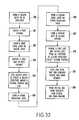
- FIG. 33is a flowchart illustrating a sequence of steps in accordance with the second embodiment of the invention.
- This inventionrelates to enhanced Fin FET devices and builds strain into such devices.
- the present inventionis implemented using a “Fin” type FET double gated structure.
- the double gatesare formed on each side of the body, with the body being disposed horizontally between the gates.
- the inventionproduces a Fin FET that has a channel body that is strained through the operation of a silicon germanium layer. Processing is started on a wafer that is built, potentially through wafer bonding, to include a silicon bulk wafer on the bottom, a relatively thick bottom oxide layer and a relaxed SiGe layer on top. A thin Fin is then etched out of the SiGe, stopping on the BOX layer. A thin layer of epitaxial silicon can then be grown onto the Fin. Due to the difference in the crystalline lattice constant of Silicon and SiGe, the epitaxial layer will grow under strained conditions.
- the inventioncan be included in symmetrical or asymmetrical gate workfunction Fin FET devices.
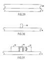
- FIGS. 29 - 31the processing necessary to create a strained symmetric strained Fin FET in accordance with a second embodiment of the invention starts with a SOI structure having a SiGe layer 300 above and insulator 10 (this is shown in FIG. 29).
- the SiGe layer 300is selectively patterned, as shown in FIG. 30.
- a silicon layer 315is grown on the SiGe layer 300 to create a strained structure.
- a thermal oxide 320is then grown on the silicon layer 315 .
- the gate conductors (e.g., polysilicon) 310are deposited, planarized, and patterned to form the gates surrounding the body structure 155 .
- the gate conductors 310have the same doping concentration and material makeup.
- the gate electrodes 310can be made asymmetric with, for example, an ion implant, to result in an asymmetric gate workfunction Fin FET with strain. More specifically, in the asymmetric gate arrangement, the gate conductors 310 would have different doping concentrations or utilize different dopants. Processing proceeds to complete the structure shown in FIGS. 18 - 28 , as discussed above.
- An important feature of the inventionis that it provides strain within many different forms of Fin FETs.
- One of the strained Fin FET embodiments shown in FIGS. 1 - 28utilizes an SOI arrangement to formed a strained Fin FET that has either symmetric or asymmetric gate conductors.
- a dynamic threshold Fin FETis formed.
- the embodiment shown in FIGS. 29 - 31utilizes a SiGe-OI (silicon germanium over insulator) in place of the SOI structure shown in FIGS. 1 - 28 .
- the SiGe-O structurecan be formed as an asymmetric gate or symmetric gate structure depending upon the doping of the gate conductors.
- the forgoing embodimentsare merely illustrative of the invention and the invention is not limited to these specific embodiments. Instead, the embodiments shown above are merely examples and one ordinarily skilled in the art would understand that many different types of Fin FETs would achieve beneficial results by including the inventive strain structure.
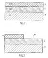
- FIGS. 1 - 28The formation of a Fin FET according to a first embodiment of the invention is shown in FIGS. 1 - 28 .
- Processingbegins as shown FIG. 1 where a silicon over an insulator (SOI) structure includes an insulator 10 such as a buried oxide layer with an overlying silicon layer 11 .
- a placeholder layer 12(such as a nitride, etc.) is deposited over the silicon layer 11 .
- This structureis then patterned using well-known conventional patterning processes, as shown in FIG. 2, to remove a portion 20 of the placeholder layer 12 .
- a subsequent etching stepremoves any corresponding portion 30 of the silicon layer 11 not protected by the placeholder 12 , as shown in FIG. 3.
- an oxidation processgrows a gate oxide layer 40 on the silicon 11 .
- polysilicon 50is deposited over the structure, as shown FIG. 5.
- the polysilicon 50is of one dopant type (e.g., N+ doped polysilicon, etc.).
- the structureis planarized using, for example, a chemical mechanical polishing (CMP) process to form planar layer 60 .
- CMPchemical mechanical polishing
- FIG. 7illustrates an oxidation process in which the doped polysilicon 50 oxidizes at a faster rate than the placeholder material 12 . Therefore, the oxide layer 70 over the polysilicon 50 is thicker than the oxide layer 71 over the placeholder layer 12 .
- the oxide layers 70 , 71are etched at a controlled rate, as shown in FIG. 8. Once the placeholder layer 12 is exposed, the etching process is stopped. This removes all the oxide from the upper surface of the placeholder layer 12 , while leaving some oxide 70 above the polysilicon layer 50 . Next, in FIG. 9, the placeholder layer 12 is removed using a selected etching process, leaving the upper portion 90 of the silicon 11 exposed.
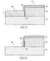
- a hard mask 100(such as TEOS, etc.) is conformally deposited over the upper layers of the structure. Then, as shown in FIG. 11, a directional anisotropic etch is used to remove the hard mask 100 from all horizontal surfaces 110 , yet allow the hard mask 100 to remain upon the vertical surfaces of the polysilicon 50 and the oxide 70 . In FIG. 12, the silicon 11 is patterned to remove the portion 120 . Only the portion beneath the hard mask 100 remains after the patterning process.
- a directional anisotropic etchis used to remove the hard mask 100 from all horizontal surfaces 110 , yet allow the hard mask 100 to remain upon the vertical surfaces of the polysilicon 50 and the oxide 70 .
- the silicon 11is patterned to remove the portion 120 . Only the portion beneath the hard mask 100 remains after the patterning process.
- FIG. 13illustrates the growth of selective SiGe 130 . While SiGe is used in this example, the invention is not limited to such material composition. Any substance which will present a lattice mismatch with the silicon will produce stress and would be useful with the invention. More specifically, the structure is heated in a complex having Ge, which causes the SiGe 130 to grow from the silicon 11 . This builds strain into the already-formed silicon channel 11 . The resulting Si layer is strained due to the lattice mismatch between the SiGe and the smaller lattice constant silicon layer. Physical strain on the channel material in an FET can improve carrier mobility. Strain induced on planar p-type metal oxide semiconductor field effect transistor (MOSFET) devices has been shown to increase hole mobility in excess of 30%. This is because the strain splits the conduction and valence bands and raises the energy of the low mobility ellipsoids, depopulating them of holes.
- MOSFETmetal oxide semiconductor field effect transistor
- the oxide 70is removed from the upper surface 141 of the polysilicon 50 . This also reduces the height 142 of the hard mask 100 and forms a step 140 in the insulator 10 . Another thermal oxidation step forms an oxide 150 over the SiGe 130 surface, as shown in FIG. 15. Alternatively, the formation of the oxide 150 could be omitted to form a dynamic threshold Fin FET. In the embodiment without the oxide 150 (the dynamic threshold (DT) Fin FET) the strained Fin FET DT CMOS devices are formed with body tied to gate. This structure, including the silicon 11 , gate oxide 40 , hard mask 100 , oxide 150 , and SiGe 130 , is referred to hereinafter as the “body” and is identified in the drawings as item 155 in order to simplify the description and illustration.
- bodyis identified in the drawings as item 155 in order to simplify the description and illustration.
- a second polysilicon 160that may be doped differently or similarly to the first polysilicon 50 , is deposited over the entire structure.
- the structureis again planarized, forming a planar upper surface 170 , as shown in FIG. 17.
- the first polysilicon 50was an N+ doped polysilicon
- the second polysilicon 160is preferably a P+ polysilicon.
- the first and second polysiliconcould be the same for symmetric gate devices.
- the two types of polysiliconcould be substituted for one another, or for other types of doping now known or developed in the future.
- the important pointis that the polysilicon regions 50 , 160 existing on opposite sides of the body 155 are doped differently for asymmetric structures.
- the polysilicon 50 , 160could be Germanium doped or any other conductor. Utilizing differently-doped polysilicon on opposite sides of the silicon channel structure 11 creates an asymmetric gate Fin FET.
- Various electrically conducting materialshave associated with them a built-in electrical potential, often referred to as a fermi level, which, along with externally applied voltage, determines the relative affinity of the conductor for electrons (or holes).
- the fermi levelis intrinsic to the material while in a semiconductor, such as silicon, this fermi level can be adjusted to values between the valence band and conduction band by introduction of impurities which supply excess holes or electrons.
- the two gate electrodes 50 , 160are doped with opposite polarity, with one gate being doped N-type and the other gate being doped P-type.
- the two gate electrodes 50 , 160have different fermi levels and, hence, one gate electrode (the strong gate, the n-gate for nFETs) has a greater affinity for the inversion carriers while the other electrode (the weak gate, the p-gate for nFETs) has a lesser affinity for the inversion carriers.
- the inversion channelwill form in the semiconductor body at a location nearer the “strong” gate.
- both gate electrodescontribute to the inversion potential, leading to a relatively low threshold voltage (e.g., between 0 and 0.5 volts).
- the structureis an asymmetric Fin FET device
- the silicon 11is only etched on one side 30
- the placeholder 12 above the remaining silicon 11is left in place.
- the inventiongrows selective single-crystal SiGe 130 on the exposed half of the Fin structure (on the side opposite the gate oxide).
- the inventionis also applicable to symmetric Fin FETs, as shown later.
- Processingproceeds, as shown in FIG. 18, with the deposition or growth of an intrinsic silicon layer 180 .
- another insulator hard mask 190(such as TEOS, etc.) is deposited over the intrinsic silicon 18 and patterned using conventional patterning techniques to remove portions 200 , as shown in FIG. 20.
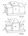
- the same structureis shown in perspective view in FIG. 21.
- the polysilicon electrodes 50 , 160 and intrinsic silicon 180are patterned using the hard mask 190 , as shown in FIG. 22 (and in perspective view in FIG. 23).
- the hard mask 190is then removed from area 220 , as shown in FIG. 24.
- the patterning of the gates 50 , 160preferably removes all the gate polysilicon down to the buried oxide layer 10 and is done using a directional etch that is selective to the nitride or oxide. Thus, the patterning does not remove the portions of the body 155 that are protected by the previously-formed hard mask 100 .
- the patterningleaves a portion of polysilicon 50 and polysilicon 160 , which defines the two gates of the double gated transistor.
- a buffered HF clean upis performed, followed by a thermal reoxidation designed to grow oxide on all the exposed silicon surfaces. This preferably forms a thin (50 angstrom) film of oxide that provides good interface when the gate meets the body.
- the inventionthen performs well-known, conventional source, drain, and halo implants in the transistor.
- these implantsare made into all four directions of the exposed portions (Fins 250 ) of the body 155 to ensure that a uniform implant is made into both sides of the body.
- both the source and drain implantsare made from both sides of the Fins 250 of the body 155 .
- another implantis made, with different implant energies and angles, to form the halo implants in the body 155 that improve short channel effects.
- the halo implantsare performed at higher energies and at angles more acute with respect to the Fin 250 in order to assure placement of the halo dopant further under the gate electrodes 50 , 160 than the source/drain dopants.
- the inventiondeposits a dielectric 240 of thickness greater than the height of the combined gate electrodes 50 , 160 and hardmask 232 , covering the entire gate electrodes 50 , 160 and exposed Fins 250 , as shown in FIG. 25.
- This dielectricis then planarized and partially recessed until a portion of the hardmask 232 and gate electrodes 50 , 160 , but not any of the source/drain Fin region, is exposed, as shown in FIG. 25.
- the dielectric 240is etched to cover only the sides of the gates 50 , 160 and sidewall spacers 242 are formed on the edges of the gates above the dielectric 240 .
- the sidewall spacers 242are preferably formed of a nitride.
- the dielectric 240 , sidewall spacers 242 , and hardmask 232are used to mask a directional etch and thereby remove the oxides 40 , 150 , except in areas adjacent the gates.
- the hardmask 232 , the sidewall spacers 242 , and the sidewall portions 240combine to effectively isolate the gate 50 , 160 from the source and drain 250 contacts 280 , as shown in FIG. 27.
- the source and drain contacts 280comprise a patterned conductive material.
- the intrinsic silicon layer 180is silicided using conventional, well-known silicide processes, forming silicide layer 230 .
- FIG. 32a flow chart summarizing this first embodiment of the invention is shown.
- the inventionforms a silicon layer 11 on an insulator 10 .
- the inventioncreates a first opening 30 .
- the inventiongrows a first oxide layer 40 on the silicon layer 11 .
- the inventiondeposits a first gate 50 in the first opening.
- the inventionetches the silicon layer 11 to create a silicon structure 155 having a central portion and Fins.
- the inventionforms a strain-producing layer 130 in item 325 .
- the inventiongrows a second oxide layer 150 on the strain-producing layer 130 .
- the inventionforms a second gate 160 in the second opening 140 . Then, in item 328 , the invention removes the first gate and second gate from all portions of the silicon structure except the central portion. In item 329 , the invention dopes the Fins 250 such that the Fins 250 comprise source and drain regions. Lastly, in item 330 , the invention forms source and drain contacts 280 over source and drain regions.
- a voltage within the gates 50 , 160changes the conductivity of the region of the semiconducting silicon 11 that is covered by the gates 50 , 160 .
- This operationeither makes or breaks an electrical connection between the source and drain Fins 250 . Therefore, the device can be used as an electrical switch to perform logical operations.
- one important feature of the inventionis the SiGe layer 130 that remains as a permanent part of the body 155 . More specifically, such a feature builds strain into the silicon channel 11 . Physical strain on the channel material in an FET can improve carrier mobility.
- FIGS. 29 - 31the processing necessary to create a strained symmetric strained Fin FET in accordance with a second embodiment of the invention starts with a SOI structure having a SiGe layer 300 above an insulator 10 (this is shown in FIG. 29).
- the SiGe layer 300is selectively patterned, as shown in FIG. 30.
- a silicon layer 315is grown on the SiGe layer 300 to create a strained structure.
- a thermal oxide 320is then grown on the silicon layer 315 .
- the gate conductors (e.g., polysilicon) 310are deposited, planarized, and patterned to form the gates surrounding the body structure 155 .
- the gate conductors 310have the same doping concentration and material makeup.
- the gate electrodes 310can be made asymmetric with, for example, an ion implant to result in an asymmetric gate workfunction Fin FET with strain. More specifically, in the asymmetric gate arrangement, the gate conductors 310 would have different doping concentrations or utilize different dopants. Processing proceeds to complete the structure shown in FIGS. 18 - 28 , as discussed above.
- An important feature of the inventionis that it provides strain within many different forms of Fin FETs.
- One of the strained Fin FET embodiments shown in FIGS. 1 - 28utilizes an SOI arrangement to form a strained Fin FET that has either symmetric or asymmetric gate conductors.
- a dynamic threshold Fin FETis formed.
- the embodiment shown in FIGS. 29 - 31utilizes a SiGe-OI (silicon germanium over insulator) in place of the SOI structure shown in FIGS. 1 - 28 .
- the SiGe-OI structurecan be formed as an asymmetric gate or symmetric gate structure, depending upon the doping of the gate conductors.
- the forgoing embodimentsare merely illustrative of the invention and the invention is not limited to these specific embodiments. Instead, the embodiments shown above are merely examples and one ordinarily skilled in the art would understand that many different types of FinFETs would achieve beneficial results by including the inventive strain structure.
- FIG. 33a flow chart for constructing a symmetric strained Fin field effect transistor, in accordance with a second embodiment of the invention, is shown.
- the methodforms a silicon germanium layer 300 on an insulator 10 .
- the methodetches a silicon germanium layer to create a silicon structure that has a central portion and Fins 250 .
- the methodgrows an oxide layer 320 on silicon structure 300 .
- the methoddeposits gates on sides of the silicon structure.
- the methodremoves the first gate and second gate from all portions of the silicon structure except the central portion.
- the methoddopes the Fins 250 such that the Fins 250 are source and drain regions.
- the methodforms source and drain contacts 280 over source and drain regions.
- the SiGe layer 130builds strain into the already-formed silicon channel 11 .
- Physical strain on the channel material in FETcan improve carrier mobility.
- Strain induced on planar p-type metal oxide semiconductor field effect transistor (MOSFET) deviceshas been shown to increase hole mobility up to 30%. This invention provides these advantages to thin semiconductor bodies that are vertically arranged on a substrate; and as such, the invention combines greater channel control with greater carrier mobility.
Landscapes
- Engineering & Computer Science (AREA)
- Physics & Mathematics (AREA)
- Condensed Matter Physics & Semiconductors (AREA)
- General Physics & Mathematics (AREA)
- Manufacturing & Machinery (AREA)
- Computer Hardware Design (AREA)
- Microelectronics & Electronic Packaging (AREA)
- Power Engineering (AREA)
- Thin Film Transistor (AREA)
- Insulated Gate Type Field-Effect Transistor (AREA)
- Microwave Amplifiers (AREA)
Abstract
Description
- 1. Field of the Invention[0001]
- The present invention generally relates to the field of semiconductor manufacturing and, more specifically, to a method for forming double-gated field effect transistors.[0002]
- 2. Description of the Related Art[0003]
- The need to remain cost and performance competitive in the production of semiconductor devices has caused continually increasing device density in integrated circuits. To facilitate the increase in device density, new technologies are constantly needed to allow the feature size of these semiconductor devices to be reduced.[0004]
- The push for ever-increasing device densities is particularly strong in complementary metal oxide semiconductor (CMOS) technologies, such as the in the design and fabrication of field effect transistors (FETs). FETs are used in almost all types of integrated circuit design (i.e., microprocessors, memory, etc.). Unfortunately, increased device density in CMOS FETs often results in degradation of performance and/or reliability.[0005]
- One type of FET that has been proposed to facilitate increased device density is a double gated field effect transistor. Double gated FETs use two gates, one on each side of the body to facilitate scaling of CMOS dimensions while maintaining acceptable performance. In particular, the use of the double gate increases the gate area, which allows the transistor to have better current control without increasing the gate length of the device. As such, the double gated FET is able to have the current control of a larger transistor without requiring the device space of the larger transistor.[0006]
- Unfortunately, several difficulties arise in the design and fabrication of double gated CMOS transistors. First, the relative dimensions of a double gated transistor are such that it is difficult to reliably fabricate one that has reliable performance and minimum feature size. Second, the threshold voltage of a double gated transistor is highly dependent upon the material used for the two gates. In particular, current fabrication techniques have generally resulted in a double gated transistor that has either too high a threshold voltage or too low a threshold voltage. For example, if the gates are doped the same polarity as the source, the threshold voltage will generally be near zero. Conversely, if the gates are doped the opposite polarity of the source, then the threshold voltage will be approximately one volt. Neither result is desirable in most CMOS applications.[0007]
- Thus, there is a need for improved device structures and methods of fabrication of double gated CMOS devices that provide improved threshold voltage of the resulting double gated CMOS without overly increasing fabrication complexity.[0008]
- Physical strain on the channel material in FET can improve carrier mobility. Strain induced on planar p-type metal oxide semiconductor field effect transistor (MOSFET) devices has been shown to increase hole mobility in excess of 30%. This invention provides these advantages to thin semiconductor bodies that are vertically arranged on a substrate; as such, the invention combines greater channel control with greater carrier mobility.[0009]
- The asymmetric strained Fin Field effect transistor has an insulator and a semiconductor structure on the insulator. The structure includes a central portion and first and second ends extending from the central portion. A first gate is positioned on a first side of the central portion of the structure, a strain-producing layer between the first gate and the first side of the central portion of the structure, and a second gate on a second side of the central portion of the structure. The insulator is a buried oxide layer and the central portion of the structure is silicon. The strain-producing layer has a sufficient concentration of germanium to produce strain within the central portion to enhance carrier mobility without producing sufficient dislocations to reduce overall performance of the transistor. The first and second ends are source and drain regions, respectively. The concentration of germanium is between 10% and 40%. The different gates may be doped differently to adjust VT. The gates may also be doped similarly.[0010]
- The symmetric strained Fin field effect transistor has an insulator and a semiconductor structure on the insulator. The structure is a Fin body having a central portion having silicon and silicon germanium and end portions comprising silicon. A first gate is positioned on a first side of the central portion of the silicon structure and a second gate is on a second side of the central portion of the structure. The first gate and the second gate may again be doped similarly or differently (as with the asymmetric strained situation).[0011]
- The method of forming a transistor includes forming a silicon layer on an insulator, etching a first portion of the silicon layer to create a first opening, depositing a first gate in the first opening and etching a second portion of the silicon layer to create a second opening opposite the first opening. After the etching of the second portion, the silicon layer has a silicon structure on the insulator having a central portion and Fins extending from ends of the central portion. The invention forms a strain-producing layer upon a portion of the silicon structure facing the second opening which forms a second gate in the second opening, and removes the first gate and the second gate from all portions of the silicon structure except from the central portion.[0012]
- The method of forming an asymmetric strained Fin field effect transistor includes forming a silicon layer on an insulator, etching a first portion of the silicon layer to create a first opening, depositing a first gate in the first opening, etching a second portion of the silicon layer to create a second opening opposite the first opening. After the etching of the second portion, the silicon layer has a silicon structure on the insulator having a central portion and Fins extending from ends of the central portion. The invention forms a silicon germanium layer upon a portion of the silicon structure facing the second opening, forms a second gate doped differently or similarly to the first gate in the second opening and removes the first gate and the second gate from all portions of the silicon structure except the central portion.[0013]
- The method of forming strained Fin field effect transistors includes forming a silicon structure on an insulator, forming stress on one or both sides of the silicon structure, having a central portion and Fins extending from ends of the central portion, depositing a first gate and a second gate on sides of the silicon structure, and removing the first gate and the second gate from all portions of the silicon structure except the central portion.[0014]
- Physical strain on the channel material in FETs can improve carrier mobility. Strain induced on planar p-type metal oxide semiconductor field effect transistor (MOSFET) devices has been shown to increase hole mobility in excess of 30%. This invention provides these advantages to thin semiconductor bodies that are vertically arranged on a substrate; and, as such, the invention combines greater channel control with greater carrier mobility.[0015]
- The foregoing and other objects, aspects and advantages will be better understood from the following detailed description of a preferred embodiment(s) of the invention with reference to the drawings, in which:[0016]
- FIGS.[0017]1-20,22,24 and25 are cross-sectional views of a first embodiment of a FET structure produced utilizing a method according to a first embodiment of the invention;
- FIGS. 21, 23, and[0018]26-28 are perspective views of the first embodiment of FET structure produced utilizing the method according to the first embodiment of the invention;
- FIGS.[0019]29-31 are cross-sectional views of the second embodiment of a FET structure produced utilizing a method in accordance with a second embodiment of the invention;
- FIG. 32 is a flowchart illustrating a sequence of steps in accordance with the first embodiment of the invention; and[0020]
- FIG. 33 is a flowchart illustrating a sequence of steps in accordance with the second embodiment of the invention.[0021]
- This invention relates to enhanced Fin FET devices and builds strain into such devices. The present invention is implemented using a “Fin” type FET double gated structure. In a Fin FET type structure, the double gates are formed on each side of the body, with the body being disposed horizontally between the gates. The invention produces a Fin FET that has a channel body that is strained through the operation of a silicon germanium layer. Processing is started on a wafer that is built, potentially through wafer bonding, to include a silicon bulk wafer on the bottom, a relatively thick bottom oxide layer and a relaxed SiGe layer on top. A thin Fin is then etched out of the SiGe, stopping on the BOX layer. A thin layer of epitaxial silicon can then be grown onto the Fin. Due to the difference in the crystalline lattice constant of Silicon and SiGe, the epitaxial layer will grow under strained conditions. The invention can be included in symmetrical or asymmetrical gate workfunction Fin FET devices.[0022]
- While the invention is described above with respect to an asymmetric strained Fin FET, it is equally applicable to a symmetric strained Fin FET. More specifically, as shown in FIGS.[0023]29-31, the processing necessary to create a strained symmetric strained Fin FET in accordance with a second embodiment of the invention starts with a SOI structure having a
SiGe layer 300 above and insulator10 (this is shown in FIG. 29). TheSiGe layer 300 is selectively patterned, as shown in FIG. 30. Then, asilicon layer 315 is grown on theSiGe layer 300 to create a strained structure. Athermal oxide 320 is then grown on thesilicon layer 315. Next, the gate conductors (e.g., polysilicon)310 are deposited, planarized, and patterned to form the gates surrounding thebody structure 155. In one embodiment, thegate conductors 310 have the same doping concentration and material makeup. However, in a different embodiment, thegate electrodes 310 can be made asymmetric with, for example, an ion implant, to result in an asymmetric gate workfunction Fin FET with strain. More specifically, in the asymmetric gate arrangement, thegate conductors 310 would have different doping concentrations or utilize different dopants. Processing proceeds to complete the structure shown in FIGS.18-28, as discussed above. - An important feature of the invention is that it provides strain within many different forms of Fin FETs. One of the strained Fin FET embodiments shown in FIGS.[0024]1-28 utilizes an SOI arrangement to formed a strained Fin FET that has either symmetric or asymmetric gate conductors. Alternatively, as explained with respect to FIG. 15, if the
oxide 150 is omitted, a dynamic threshold Fin FET is formed. To the contrary, the embodiment shown in FIGS.29-31 utilizes a SiGe-OI (silicon germanium over insulator) in place of the SOI structure shown in FIGS.1-28. In a similar manner, the SiGe-O structure can be formed as an asymmetric gate or symmetric gate structure depending upon the doping of the gate conductors. The forgoing embodiments are merely illustrative of the invention and the invention is not limited to these specific embodiments. Instead, the embodiments shown above are merely examples and one ordinarily skilled in the art would understand that many different types of Fin FETs would achieve beneficial results by including the inventive strain structure. - The formation of a Fin FET according to a first embodiment of the invention is shown in FIGS.[0025]1-28. Processing begins as shown FIG. 1 where a silicon over an insulator (SOI) structure includes an
insulator 10 such as a buried oxide layer with anoverlying silicon layer 11. A placeholder layer12 (such as a nitride, etc.) is deposited over thesilicon layer 11. This structure is then patterned using well-known conventional patterning processes, as shown in FIG. 2, to remove aportion 20 of theplaceholder layer 12. A subsequent etching step removes any correspondingportion 30 of thesilicon layer 11 not protected by theplaceholder 12, as shown in FIG. 3. - In FIG. 4, an oxidation process grows a[0026]
gate oxide layer 40 on thesilicon 11. Next,polysilicon 50 is deposited over the structure, as shown FIG. 5. Thepolysilicon 50 is of one dopant type (e.g., N+ doped polysilicon, etc.). In FIG. 6, the structure is planarized using, for example, a chemical mechanical polishing (CMP) process to formplanar layer 60. FIG. 7 illustrates an oxidation process in which the dopedpolysilicon 50 oxidizes at a faster rate than theplaceholder material 12. Therefore, theoxide layer 70 over thepolysilicon 50 is thicker than theoxide layer 71 over theplaceholder layer 12. - The oxide layers[0027]70,71 are etched at a controlled rate, as shown in FIG. 8. Once the
placeholder layer 12 is exposed, the etching process is stopped. This removes all the oxide from the upper surface of theplaceholder layer 12, while leaving someoxide 70 above thepolysilicon layer 50. Next, in FIG. 9, theplaceholder layer 12 is removed using a selected etching process, leaving theupper portion 90 of thesilicon 11 exposed. - In FIG. 10, a hard mask[0028]100 (such as TEOS, etc.) is conformally deposited over the upper layers of the structure. Then, as shown in FIG. 11, a directional anisotropic etch is used to remove the
hard mask 100 from allhorizontal surfaces 110, yet allow thehard mask 100 to remain upon the vertical surfaces of thepolysilicon 50 and theoxide 70. In FIG. 12, thesilicon 11 is patterned to remove theportion 120. Only the portion beneath thehard mask 100 remains after the patterning process. - FIG. 13 illustrates the growth of[0029]
selective SiGe 130. While SiGe is used in this example, the invention is not limited to such material composition. Any substance which will present a lattice mismatch with the silicon will produce stress and would be useful with the invention. More specifically, the structure is heated in a complex having Ge, which causes theSiGe 130 to grow from thesilicon 11. This builds strain into the already-formedsilicon channel 11. The resulting Si layer is strained due to the lattice mismatch between the SiGe and the smaller lattice constant silicon layer. Physical strain on the channel material in an FET can improve carrier mobility. Strain induced on planar p-type metal oxide semiconductor field effect transistor (MOSFET) devices has been shown to increase hole mobility in excess of 30%. This is because the strain splits the conduction and valence bands and raises the energy of the low mobility ellipsoids, depopulating them of holes. - At the same time, excessive amounts of germanium will produce misfit dislocations that will degrade device performance. The inventors have found the optimal range of the content to be 10% to 40% germanium.[0030]
- Strain is induced on conventional planar devices by use of Shallow Trench Isolation (STI) techniques. In a Fin FET, however, there is no process analogous to STI, as the buried insulator layer[0031]10 (BOX) provides the device isolation. The invention overcomes this problem by using Silicon Germanium (SiGe) and silicon sidewall films to generate this strain on the Fin FET channel.
- In FIG. 14, the[0032]
oxide 70 is removed from theupper surface 141 of thepolysilicon 50. This also reduces theheight 142 of thehard mask 100 and forms astep 140 in theinsulator 10. Another thermal oxidation step forms anoxide 150 over theSiGe 130 surface, as shown in FIG. 15. Alternatively, the formation of theoxide 150 could be omitted to form a dynamic threshold Fin FET. In the embodiment without the oxide150 (the dynamic threshold (DT) Fin FET) the strained Fin FET DT CMOS devices are formed with body tied to gate. This structure, including thesilicon 11,gate oxide 40,hard mask 100,oxide 150, andSiGe 130, is referred to hereinafter as the “body” and is identified in the drawings asitem 155 in order to simplify the description and illustration. - Next, in FIG. 16, a[0033]
second polysilicon 160, that may be doped differently or similarly to thefirst polysilicon 50, is deposited over the entire structure. The structure is again planarized, forming a planarupper surface 170, as shown in FIG. 17. Since thefirst polysilicon 50 was an N+ doped polysilicon, thesecond polysilicon 160 is preferably a P+ polysilicon. However, the first and second polysilicon could be the same for symmetric gate devices. The two types of polysilicon could be substituted for one another, or for other types of doping now known or developed in the future. The important point is that thepolysilicon regions body 155 are doped differently for asymmetric structures. Thepolysilicon silicon channel structure 11 creates an asymmetric gate Fin FET. - Various electrically conducting materials have associated with them a built-in electrical potential, often referred to as a fermi level, which, along with externally applied voltage, determines the relative affinity of the conductor for electrons (or holes). In a metal, the fermi level is intrinsic to the material while in a semiconductor, such as silicon, this fermi level can be adjusted to values between the valence band and conduction band by introduction of impurities which supply excess holes or electrons. In the asymmetric double gated Fin FET, the two[0034]
gate electrodes gate electrodes - In the embodiment being illustrated and discussed, the structure is an asymmetric Fin FET device, the[0035]
silicon 11 is only etched on oneside 30, and theplaceholder 12 above the remainingsilicon 11 is left in place. The invention grows selective single-crystal SiGe 130 on the exposed half of the Fin structure (on the side opposite the gate oxide). However, the invention is also applicable to symmetric Fin FETs, as shown later. - Processing proceeds, as shown in FIG. 18, with the deposition or growth of an[0036]
intrinsic silicon layer 180. Then, in FIG. 19, another insulator hard mask190 (such as TEOS, etc.) is deposited over the intrinsic silicon18 and patterned using conventional patterning techniques to removeportions 200, as shown in FIG. 20. The same structure is shown in perspective view in FIG. 21. Thepolysilicon electrodes intrinsic silicon 180 are patterned using thehard mask 190, as shown in FIG. 22 (and in perspective view in FIG. 23). Thehard mask 190 is then removed fromarea 220, as shown in FIG. 24. The patterning of thegates oxide layer 10 and is done using a directional etch that is selective to the nitride or oxide. Thus, the patterning does not remove the portions of thebody 155 that are protected by the previously-formedhard mask 100. The patterning leaves a portion ofpolysilicon 50 andpolysilicon 160, which defines the two gates of the double gated transistor. A buffered HF clean up is performed, followed by a thermal reoxidation designed to grow oxide on all the exposed silicon surfaces. This preferably forms a thin (50 angstrom) film of oxide that provides good interface when the gate meets the body. - The invention then performs well-known, conventional source, drain, and halo implants in the transistor. Preferably, these implants are made into all four directions of the exposed portions (Fins[0037]250) of the
body 155 to ensure that a uniform implant is made into both sides of the body. In particular, both the source and drain implants are made from both sides of theFins 250 of thebody 155. Then, another implant is made, with different implant energies and angles, to form the halo implants in thebody 155 that improve short channel effects. The halo implants are performed at higher energies and at angles more acute with respect to theFin 250 in order to assure placement of the halo dopant further under thegate electrodes - Next, the invention deposits a dielectric[0038]240 of thickness greater than the height of the combined
gate electrodes hardmask 232, covering theentire gate electrodes Fins 250, as shown in FIG. 25. This dielectric is then planarized and partially recessed until a portion of thehardmask 232 andgate electrodes gates sidewall spacers 242 are formed on the edges of the gates above the dielectric240. This is preferably done using a conformal deposition of a dielectric material, followed by a directional etch. The sidewall spacers242 are preferably formed of a nitride. The dielectric240,sidewall spacers 242, andhardmask 232 are used to mask a directional etch and thereby remove theoxides hardmask 232, thesidewall spacers 242, and thesidewall portions 240 combine to effectively isolate thegate contacts 280, as shown in FIG. 27. Preferably, the source anddrain contacts 280 comprise a patterned conductive material. Next, as shown in FIG. 28, theintrinsic silicon layer 180 is silicided using conventional, well-known silicide processes, formingsilicide layer 230. - In FIG. 32, a flow chart summarizing this first embodiment of the invention is shown. First, in[0039]
item 320, the invention forms asilicon layer 11 on aninsulator 10. Then, initem 321, the invention creates afirst opening 30. Initem 322, the invention grows afirst oxide layer 40 on thesilicon layer 11. Next, initem 323, the invention deposits afirst gate 50 in the first opening. Initem 324, the invention etches thesilicon layer 11 to create asilicon structure 155 having a central portion and Fins. The invention forms a strain-producinglayer 130 initem 325. Next, initem 326, the invention grows asecond oxide layer 150 on the strain-producinglayer 130. Initem 327, the invention forms asecond gate 160 in thesecond opening 140. Then, initem 328, the invention removes the first gate and second gate from all portions of the silicon structure except the central portion. Initem 329, the invention dopes theFins 250 such that theFins 250 comprise source and drain regions. Lastly, initem 330, the invention forms source anddrain contacts 280 over source and drain regions. - In operation, a voltage within the[0040]
gates semiconducting silicon 11 that is covered by thegates Fins 250. Therefore, the device can be used as an electrical switch to perform logical operations. - As mentioned above, one important feature of the invention is the[0041]
SiGe layer 130 that remains as a permanent part of thebody 155. More specifically, such a feature builds strain into thesilicon channel 11. Physical strain on the channel material in an FET can improve carrier mobility. - While the invention is described above with respect to an asymmetric strained Fin FET, it is equally applicable to a symmetric strained Fin FET. More specifically, as shown in FIGS.[0042]29-31, the processing necessary to create a strained symmetric strained Fin FET in accordance with a second embodiment of the invention starts with a SOI structure having a
SiGe layer 300 above an insulator10 (this is shown in FIG. 29). TheSiGe layer 300 is selectively patterned, as shown in FIG. 30. Then, asilicon layer 315 is grown on theSiGe layer 300 to create a strained structure. Athermal oxide 320 is then grown on thesilicon layer 315. Next, the gate conductors (e.g., polysilicon)310 are deposited, planarized, and patterned to form the gates surrounding thebody structure 155. In one embodiment, thegate conductors 310 have the same doping concentration and material makeup. However, in a different embodiment, thegate electrodes 310 can be made asymmetric with, for example, an ion implant to result in an asymmetric gate workfunction Fin FET with strain. More specifically, in the asymmetric gate arrangement, thegate conductors 310 would have different doping concentrations or utilize different dopants. Processing proceeds to complete the structure shown in FIGS.18-28, as discussed above. - An important feature of the invention is that it provides strain within many different forms of Fin FETs. One of the strained Fin FET embodiments shown in FIGS.[0043]1-28 utilizes an SOI arrangement to form a strained Fin FET that has either symmetric or asymmetric gate conductors. Alternatively, as explained with respect to FIG. 15, if the
oxide 150 is omitted, a dynamic threshold Fin FET is formed. To the contrary, the embodiment shown in FIGS.29-31 utilizes a SiGe-OI (silicon germanium over insulator) in place of the SOI structure shown in FIGS.1-28. In a similar manner, the SiGe-OI structure can be formed as an asymmetric gate or symmetric gate structure, depending upon the doping of the gate conductors. The forgoing embodiments are merely illustrative of the invention and the invention is not limited to these specific embodiments. Instead, the embodiments shown above are merely examples and one ordinarily skilled in the art would understand that many different types of FinFETs would achieve beneficial results by including the inventive strain structure. - In FIG. 33, a flow chart for constructing a symmetric strained Fin field effect transistor, in accordance with a second embodiment of the invention, is shown. First, in[0044]
item 331, the method forms asilicon germanium layer 300 on aninsulator 10. Next, initem 332, the method etches a silicon germanium layer to create a silicon structure that has a central portion andFins 250. Initem 333, the method grows anoxide layer 320 onsilicon structure 300. Initem 334, the method deposits gates on sides of the silicon structure. Next, initem 336, the method removes the first gate and second gate from all portions of the silicon structure except the central portion. Initem 337, the method dopes theFins 250 such that theFins 250 are source and drain regions. Lastly, initem 338, the method forms source anddrain contacts 280 over source and drain regions. - As mentioned above, the[0045]
SiGe layer 130 builds strain into the already-formedsilicon channel 11. Physical strain on the channel material in FET can improve carrier mobility. Strain induced on planar p-type metal oxide semiconductor field effect transistor (MOSFET) devices has been shown to increase hole mobility up to 30%. This invention provides these advantages to thin semiconductor bodies that are vertically arranged on a substrate; and as such, the invention combines greater channel control with greater carrier mobility. - While the invention has been described in terms of preferred embodiments, those skilled in the art will recognize that the invention can be practiced with modification within the spirit and scope of the appended claims. For example, while the invention has been taught with reference to a particular method of forming vertical semiconductor bodies, other methods of producing discrete semiconductor bodies on a substrate could be used (e.g., silicon islands on a SOI substrate). Moreover, while SiGe is taught as the primary material to induce the requisite strain in the channel region, other materials could be used. Finally, the invention is applicable to other semiconductors (e.g., Group III-IV semiconductors such as gallium arsenide).[0046]
Claims (37)
1. A transistor comprising:
an insulator;
a semiconductor structure on said insulator, wherein said structure includes a central portion and first and second ends extending from said central portion;
a first gate positioned on a first side of said central portion of said structure;
a strain-producing layer between said first gate and said first side of said central portion of said structure; and
a second gate on a second side of said central portion of said structure.
2. The transistor inclaim 1 , wherein said insulator comprises a buried oxide layer.
3. The transistor inclaim 1 , wherein said central portion of said structure comprises silicon.
4. The transistor inclaim 1 , wherein said strain-inducing layer has a sufficient concentration of germanium to produce strain within said central portion to enhance carrier mobility, without producing sufficient dislocations to reduce overall performance of said transistor.
5. The transistor inclaim 1 , wherein said first and second ends comprise source and drain regions, respectively.
6. The transistor inclaim 4 , wherein said concentration of germanium is between 10% and 40%.
7. The transistor inclaim 1 , wherein said first gate and said second gate are doped differently.
7. The transistor inclaim 1 , wherein said first gate and said second gate are doped similarly.
8. An asymmetric strained Fin field effect transistor comprising:
an insulator;
a semiconductor structure on said insulator, wherein said structure includes a central portion and Fins extending from ends of said central portion;
a first gate positioned on a first side of said central portion of said structure;
a strain-inducing layer between said first gate and said first side of said central portion of said silicon structure; and
a second gate on a second side of said central portion of said silicon structure,
wherein said first gate and said second gate are doped differently.
9. The transistor inclaim 8 , wherein said insulator comprises a buried oxide layer.
10. The transistor inclaim 8 , wherein said central portion of said silicon structure comprises silicon.
11. The transistor inclaim 8 , wherein said strain-inducing layer comprises silicon germanium.
12. The transistor inclaim 11 , wherein said silicon germanium has a sufficient concentration of germanium to produce strain within said central portion to enhance carrier mobility, without producing sufficient dislocations to reduce overall performance of said Fin field effect transistor.
13. The transistor inclaim 11 , wherein said concentration of germanium is between 10% and 40%.
14. The transistor inclaim 8 , wherein said Fins comprise source and drain regions.
15. A symmetric strained Fin field effect transistor comprising:
an insulator;
a semiconductor structure on said insulator, wherein said structure comprises a Fin body having a central portion comprising silicon and silicon germanium; and end portions comprising silicon;
a first gate positioned on a first side of said central portion of said silicon structure; and
a second gate on a second side of said central portion of said structure,
wherein said first gate and said second gate are doped similarly.
16. The transistor inclaim 15 , wherein said insulator comprises a buried oxide layer.
17. The transistor inclaim 15 , wherein said silicon germanium has a sufficient concentration of germanium to produce strain within said central portion to enhance carrier mobility, without producing sufficient dislocations to reduce overall performance of said Fin field effect transistor.
18. The transistor inclaim 17 , wherein said concentration of germanium is between 10% and 40%.
19. A method of forming a transistor comprising:
forming a silicon layer on an insulator;
etching a first portion of said silicon layer to create a first opening;
depositing a first gate in said first opening;
etching a second portion of said silicon layer to create a second opening opposite said first opening, wherein after said etching of said second portion, said silicon layer comprises a silicon structure on said insulator having a central portion and Fins extending from ends of said central portion;
forming a strain-producing layer upon a portion of opening;
forming a second gate in said second opening; and
removing said first gate and said second gate from all portions of said silicon structure except said central portion.
20. The method inclaim 19 , further comprising doping said Fins such that said Fins comprise source and drain regions.
21. The method inclaim 19 , wherein said silicon germanium has a sufficient concentration of germanium to produce strain within said central portion to enhance carrier mobility, without producing sufficient dislocations to reduce overall performance of said Fin field effect transistor.
22. The method inclaim 20 , wherein said concentration of germanium is between 10% and 40%.
23. A method of forming an asymmetric strained Fin field effect transistor comprising:
forming a silicon layer on an insulator;
etching a first portion of said silicon layer to create a first opening;
depositing a first gate in said first opening;
etching a second portion of said silicon layer to create a second opening opposite said first opening, wherein after said etching of said second portion, said silicon layer comprises a silicon structure on said insulator having a central portion and Fins extending from ends of said central portion;
forming a silicon germanium layer upon a portion of said silicon structure facing said second opening;
forming a second gate in said second opening, wherein said first gate and said second gate are doped differently; and
removing said first gate and said second gate from all portions of said silicon structure except said central portion.
24. The method inclaim 23 , further comprising doping said Fins such that said Fins comprise source and drain regions.
25. The method inclaim 23 , wherein said silicon germanium has a sufficient concentration of germanium to produce strain within said central portion to enhance carrier mobility, without producing sufficient dislocations to reduce overall performance of said Fin field effect transistor.
26. The method inclaim 24 , wherein said concentration of germanium is between 10% and 40%.
27. A method of forming strained Fin field effect transistor comprising:
forming a silicon structure on an insulator;
forming stress on one side of said silicon structure, having a central portion and Fins extending from ends of said central portion;
depositing a first gate and a second gate on sides of said silicon structure; and
removing said first gate and said second gate from all portions of said silicon structure except said central portion.
28. The method inclaim 27 , wherein said first gate and said second gate are doped similarly.
29. The method inclaim 27 , wherein said first gate and said second gate are doped differently.
30. The method inclaim 28 , further comprising doping said Fins such that said Fins comprise source and drain regions.
31. The method inclaim 27 , wherein said silicon germanium has a sufficient concentration of germanium to produce strain within said central portion to enhance carrier mobility, without producing sufficient dislocations to reduce overall performance of said Fin field effect transistor.
32. The method inclaim 31 , wherein said concentration of germanium is between 10% and 40%.
33. A method of forming a transistor comprising:
forming a silicon germanium layer on an insulator;
etching said silicon germanium layer to create a central portion and Fins Lending from ends of said central portion;
growing a strained silicon layer on said silicon germanium layer;
growing a thermal oxide on said strained silicon layer; and
growing gate conductors on said thermal oxide.
34. The method inclaim 33 , further comprising doping said Fins such that said Fins comprise source and drain regions.
35. The method inclaim 33 , wherein said silicon germanium has a sufficient concentration of germanium to produce strain within said strained silicon layer to enhance carrier mobility, without producing sufficient dislocations to reduce overall performance of said transistor.
36. The method inclaim 35 , wherein said concentration of germanium is between 10% and 40%.
Priority Applications (1)
| Application Number | Priority Date | Filing Date | Title |
|---|---|---|---|
| US10/439,886US6849884B2 (en) | 2002-03-19 | 2003-05-16 | Strained Fin FETs structure and method |
Applications Claiming Priority (2)
| Application Number | Priority Date | Filing Date | Title |
|---|---|---|---|
| US10/101,807US6635909B2 (en) | 2002-03-19 | 2002-03-19 | Strained fin FETs structure and method |
| US10/439,886US6849884B2 (en) | 2002-03-19 | 2003-05-16 | Strained Fin FETs structure and method |
Related Parent Applications (1)
| Application Number | Title | Priority Date | Filing Date |
|---|---|---|---|
| US10/101,807ContinuationUS6635909B2 (en) | 2002-03-19 | 2002-03-19 | Strained fin FETs structure and method |
Publications (2)
| Publication Number | Publication Date |
|---|---|
| US20030201458A1true US20030201458A1 (en) | 2003-10-30 |
| US6849884B2 US6849884B2 (en) | 2005-02-01 |
Family
ID=28040074
Family Applications (3)
| Application Number | Title | Priority Date | Filing Date |
|---|---|---|---|
| US10/101,807Expired - LifetimeUS6635909B2 (en) | 2002-03-19 | 2002-03-19 | Strained fin FETs structure and method |
| US10/405,844Expired - LifetimeUS6767793B2 (en) | 2002-03-19 | 2003-04-02 | Strained fin FETs structure and method |
| US10/439,886Expired - LifetimeUS6849884B2 (en) | 2002-03-19 | 2003-05-16 | Strained Fin FETs structure and method |
Family Applications Before (2)
| Application Number | Title | Priority Date | Filing Date |
|---|---|---|---|
| US10/101,807Expired - LifetimeUS6635909B2 (en) | 2002-03-19 | 2002-03-19 | Strained fin FETs structure and method |
| US10/405,844Expired - LifetimeUS6767793B2 (en) | 2002-03-19 | 2003-04-02 | Strained fin FETs structure and method |
Country Status (11)
| Country | Link |
|---|---|
| US (3) | US6635909B2 (en) |
| EP (1) | EP1488462B1 (en) |
| JP (1) | JP4493343B2 (en) |
| KR (1) | KR100694641B1 (en) |
| CN (1) | CN100334741C (en) |
| AT (1) | ATE498199T1 (en) |
| AU (1) | AU2003223306A1 (en) |
| DE (1) | DE60335981D1 (en) |
| IL (1) | IL164063A0 (en) |
| TW (1) | TW580771B (en) |
| WO (1) | WO2003081640A2 (en) |
Cited By (57)
| Publication number | Priority date | Publication date | Assignee | Title |
|---|---|---|---|---|
| US20030227072A1 (en)* | 2002-06-10 | 2003-12-11 | Leonard Forbes | Output prediction logic circuits with ultra-thin vertical transistors and methods of formation |
| US20040036126A1 (en)* | 2002-08-23 | 2004-02-26 | Chau Robert S. | Tri-gate devices and methods of fabrication |
| US20040097044A1 (en)* | 2002-11-15 | 2004-05-20 | Samsung Electronics Co., Ltd. | Silicon/oxide/nitride/oxide/silicon nonvolatile memory with vertical channels, fabricating method thereof, and programming method thereof |
| WO2004068585A1 (en)* | 2003-01-23 | 2004-08-12 | Advanced Micro Devices, Inc. | Strained channel finfet |
| US20040262698A1 (en)* | 2003-06-25 | 2004-12-30 | International Business Machines Corporation | High-density finfet integration scheme |
| US20050148137A1 (en)* | 2003-12-30 | 2005-07-07 | Brask Justin K. | Nonplanar transistors with metal gate electrodes |
| US20050153486A1 (en)* | 2004-01-12 | 2005-07-14 | Advanced Micro Devices, Inc. | Method of fabricating a strained silicon channel FinFET |
| US6921914B2 (en) | 2000-08-16 | 2005-07-26 | Massachusetts Institute Of Technology | Process for producing semiconductor article using graded epitaxial growth |
| US6940089B2 (en) | 2001-04-04 | 2005-09-06 | Massachusetts Institute Of Technology | Semiconductor device structure |
| US20050218438A1 (en)* | 2004-03-31 | 2005-10-06 | Nick Lindert | Bulk non-planar transistor having strained enhanced mobility and methods of fabrication |
| US20050242406A1 (en)* | 2003-06-27 | 2005-11-03 | Hareland Scott A | Nonplanar device with stress incorporation layer and method of fabrication |
| US20060022268A1 (en)* | 2004-07-27 | 2006-02-02 | Chang-Woo Oh | Semiconductor devices including stress inducing layers |
| US6995430B2 (en) | 2002-06-07 | 2006-02-07 | Amberwave Systems Corporation | Strained-semiconductor-on-insulator device structures |
| US20060033095A1 (en)* | 2004-08-10 | 2006-02-16 | Doyle Brian S | Non-planar pMOS structure with a strained channel region and an integrated strained CMOS flow |
| US20060063332A1 (en)* | 2004-09-23 | 2006-03-23 | Brian Doyle | U-gate transistors and methods of fabrication |
| US20060071275A1 (en)* | 2004-09-30 | 2006-04-06 | Brask Justin K | Nonplanar transistors with metal gate electrodes |
| US20060113603A1 (en)* | 2004-12-01 | 2006-06-01 | Amberwave Systems Corporation | Hybrid semiconductor-on-insulator structures and related methods |
| US7060632B2 (en) | 2002-03-14 | 2006-06-13 | Amberwave Systems Corporation | Methods for fabricating strained layers on semiconductor substrates |
| US7074623B2 (en) | 2002-06-07 | 2006-07-11 | Amberwave Systems Corporation | Methods of forming strained-semiconductor-on-insulator finFET device structures |
| US20060157794A1 (en)* | 2005-01-18 | 2006-07-20 | Doyle Brian S | Non-planar MOS structure with a strained channel region |
| US20060255415A1 (en)* | 2005-05-12 | 2006-11-16 | International Business Machines Corporation | Structure and method of making a field effect transistor having an asymmetrically stressed channel region |
| WO2006122956A1 (en)* | 2005-05-19 | 2006-11-23 | International Business Machines Corporation | Fin field effect transistors (finfets) and methods for making the same |
| US20060292772A1 (en)* | 2005-06-24 | 2006-12-28 | International Business Machines Corporation | Dense pitch bulk finfet process by selective epi and etch |
| US20070001219A1 (en)* | 2005-06-30 | 2007-01-04 | Marko Radosavljevic | Block contact architectures for nanoscale channel transistors |
| US20070040223A1 (en)* | 2005-08-17 | 2007-02-22 | Intel Corporation | Lateral undercut of metal gate in SOI device |
| US20070063230A1 (en)* | 2005-09-19 | 2007-03-22 | International Business Machines Corporation | Asymmetrically stressed cmos finfet |
| US20070090416A1 (en)* | 2005-09-28 | 2007-04-26 | Doyle Brian S | CMOS devices with a single work function gate electrode and method of fabrication |
| US20070099350A1 (en)* | 2005-10-27 | 2007-05-03 | International Business Machines Corporation | Structure and method of fabricating finfet with buried channel |
| US7227176B2 (en) | 1998-04-10 | 2007-06-05 | Massachusetts Institute Of Technology | Etch stop layer system |
| US7268058B2 (en) | 2004-01-16 | 2007-09-11 | Intel Corporation | Tri-gate transistors and methods to fabricate same |
| US7307273B2 (en) | 2002-06-07 | 2007-12-11 | Amberwave Systems Corporation | Control of strain in device layers by selective relaxation |
| US7335545B2 (en) | 2002-06-07 | 2008-02-26 | Amberwave Systems Corporation | Control of strain in device layers by prevention of relaxation |
| US7393733B2 (en) | 2004-12-01 | 2008-07-01 | Amberwave Systems Corporation | Methods of forming hybrid fin field-effect transistor structures |
| US7396711B2 (en) | 2005-12-27 | 2008-07-08 | Intel Corporation | Method of fabricating a multi-cornered film |
| US20080164535A1 (en)* | 2007-01-09 | 2008-07-10 | Dureseti Chidambarrao | Curved finfets |
| CN100413090C (en)* | 2004-06-11 | 2008-08-20 | 国际商业机器公司 | Method and structure for providing adjustable leakage current in a CMOS integrated circuit |
| US20080206934A1 (en)* | 2007-02-23 | 2008-08-28 | Jones Robert E | Forming semiconductor fins using a sacrificial fin |
| US20080230824A1 (en)* | 2005-09-28 | 2008-09-25 | Nxp B.V. | Double Gate Non-Volatile Memory Device and Method of Manufacturing |
| US7449373B2 (en) | 2006-03-31 | 2008-11-11 | Intel Corporation | Method of ion implanting for tri-gate devices |
| US7456476B2 (en) | 2003-06-27 | 2008-11-25 | Intel Corporation | Nonplanar semiconductor device with partially or fully wrapped around gate electrode and methods of fabrication |
| US20090014798A1 (en)* | 2007-07-11 | 2009-01-15 | International Business Machines Corporation | Finfet sram with asymmetric gate and method of manufacture thereof |
| US7479421B2 (en) | 2005-09-28 | 2009-01-20 | Intel Corporation | Process for integrating planar and non-planar CMOS transistors on a bulk substrate and article made thereby |
| US7547637B2 (en) | 2005-06-21 | 2009-06-16 | Intel Corporation | Methods for patterning a semiconductor film |
| US7550333B2 (en) | 2004-10-25 | 2009-06-23 | Intel Corporation | Nonplanar device with thinned lower body portion and method of fabrication |
| US7579280B2 (en) | 2004-06-01 | 2009-08-25 | Intel Corporation | Method of patterning a film |
| US7858481B2 (en) | 2005-06-15 | 2010-12-28 | Intel Corporation | Method for fabricating transistor with thinned channel |
| US7859053B2 (en) | 2004-09-29 | 2010-12-28 | Intel Corporation | Independently accessed double-gate and tri-gate transistors in same process flow |
| US7879675B2 (en) | 2005-03-14 | 2011-02-01 | Intel Corporation | Field effect transistor with metal source/drain regions |
| US7989280B2 (en) | 2005-11-30 | 2011-08-02 | Intel Corporation | Dielectric interface for group III-V semiconductor device |
| US8084818B2 (en) | 2004-06-30 | 2011-12-27 | Intel Corporation | High mobility tri-gate devices and methods of fabrication |
| US8183646B2 (en) | 2005-02-23 | 2012-05-22 | Intel Corporation | Field effect transistor with narrow bandgap source and drain regions and method of fabrication |
| US8362566B2 (en) | 2008-06-23 | 2013-01-29 | Intel Corporation | Stress in trigate devices using complimentary gate fill materials |
| US8617945B2 (en) | 2006-08-02 | 2013-12-31 | Intel Corporation | Stacking fault and twin blocking barrier for integrating III-V on Si |
| US8748292B2 (en) | 2002-06-07 | 2014-06-10 | Taiwan Semiconductor Manufacturing Company, Ltd. | Methods of forming strained-semiconductor-on-insulator device structures |
| CN103928330A (en)* | 2013-01-11 | 2014-07-16 | 中芯国际集成电路制造(上海)有限公司 | Semiconductor structure and forming method thereof |
| US20180012988A1 (en)* | 2006-11-20 | 2018-01-11 | Globalfoundries Inc. | Dual stress device and method |
| US10515801B2 (en) | 2007-06-04 | 2019-12-24 | Micron Technology, Inc. | Pitch multiplication using self-assembling materials |
Families Citing this family (137)
| Publication number | Priority date | Publication date | Assignee | Title |
|---|---|---|---|---|
| US6800910B2 (en)* | 2002-09-30 | 2004-10-05 | Advanced Micro Devices, Inc. | FinFET device incorporating strained silicon in the channel region |
| US6611029B1 (en)* | 2002-11-08 | 2003-08-26 | Advanced Micro Devices, Inc. | Double gate semiconductor device having separate gates |
| US6709982B1 (en) | 2002-11-26 | 2004-03-23 | Advanced Micro Devices, Inc. | Double spacer FinFET formation |
| US6855990B2 (en)* | 2002-11-26 | 2005-02-15 | Taiwan Semiconductor Manufacturing Co., Ltd | Strained-channel multiple-gate transistor |
| US7148526B1 (en) | 2003-01-23 | 2006-12-12 | Advanced Micro Devices, Inc. | Germanium MOSFET devices and methods for making same |
| US6855606B2 (en)* | 2003-02-20 | 2005-02-15 | Taiwan Semiconductor Manufacturing Company, Ltd. | Semiconductor nano-rod devices |
| US6800885B1 (en)* | 2003-03-12 | 2004-10-05 | Advance Micro Devices, Inc. | Asymmetrical double gate or all-around gate MOSFET devices and methods for making same |
| US6762448B1 (en) | 2003-04-03 | 2004-07-13 | Advanced Micro Devices, Inc. | FinFET device with multiple fin structures |
| TWI231994B (en)* | 2003-04-04 | 2005-05-01 | Univ Nat Taiwan | Strained Si FinFET |
| US7074656B2 (en)* | 2003-04-29 | 2006-07-11 | Taiwan Semiconductor Manufacturing Company, Ltd. | Doping of semiconductor fin devices |
| CN1799146A (en)* | 2003-05-30 | 2006-07-05 | 松下电器产业株式会社 | Semiconductor device and method for manufacturing same |
| US6992354B2 (en)* | 2003-06-25 | 2006-01-31 | International Business Machines Corporation | FinFET having suppressed parasitic device characteristics |
| US20040266115A1 (en)* | 2003-06-25 | 2004-12-30 | Bor-Wen Chan | Method of making a gate electrode on a semiconductor device |
| US7005330B2 (en)* | 2003-06-27 | 2006-02-28 | Taiwan Semiconductor Manufacturing Company, Ltd. | Structure and method for forming the gate electrode in a multiple-gate transistor |
| US7372147B2 (en)* | 2003-07-02 | 2008-05-13 | Hewlett-Packard Development Company, L.P. | Supporting a circuit package including a substrate having a solder column array |
| US6716686B1 (en) | 2003-07-08 | 2004-04-06 | Advanced Micro Devices, Inc. | Method for forming channels in a finfet device |
| US6921982B2 (en)* | 2003-07-21 | 2005-07-26 | International Business Machines Corporation | FET channel having a strained lattice structure along multiple surfaces |
| KR100487566B1 (en)* | 2003-07-23 | 2005-05-03 | 삼성전자주식회사 | Fin field effect transistors and methods of formiing the same |
| US7078742B2 (en) | 2003-07-25 | 2006-07-18 | Taiwan Semiconductor Manufacturing Co., Ltd. | Strained-channel semiconductor structure and method of fabricating the same |
| US7307467B2 (en)* | 2006-04-28 | 2007-12-11 | International Business Machines Corporation | Structure and method for implementing oxide leakage based voltage divider network for integrated circuit devices |
| US7301206B2 (en)* | 2003-08-01 | 2007-11-27 | Taiwan Semiconductor Manufacturing Company, Ltd. | Semiconductor-on-insulator SRAM configured using partially-depleted and fully-depleted transistors |
| US6787476B1 (en)* | 2003-08-04 | 2004-09-07 | Advanced Micro Devices, Inc. | Etch stop layer for etching FinFET gate over a large topography |
| US7172943B2 (en)* | 2003-08-13 | 2007-02-06 | Taiwan Semiconductor Manufacturing Company, Ltd. | Multiple-gate transistors formed on bulk substrates |
| US7355253B2 (en)* | 2003-08-22 | 2008-04-08 | International Business Machines Corporation | Strained-channel Fin field effect transistor (FET) with a uniform channel thickness and separate gates |
| US8008136B2 (en)* | 2003-09-03 | 2011-08-30 | Advanced Micro Devices, Inc. | Fully silicided gate structure for FinFET devices |
| US7015078B1 (en)* | 2003-09-09 | 2006-03-21 | Advanced Micro Devices, Inc. | Silicon on insulator substrate having improved thermal conductivity and method of its formation |
| JP2005086024A (en)* | 2003-09-09 | 2005-03-31 | Toshiba Corp | Semiconductor device and method for manufacturing same |
| US7863674B2 (en)* | 2003-09-24 | 2011-01-04 | Taiwan Semiconductor Manufacturing Company, Ltd. | Multiple-gate transistors formed on bulk substrates |
| US6970373B2 (en)* | 2003-10-02 | 2005-11-29 | Intel Corporation | Method and apparatus for improving stability of a 6T CMOS SRAM cell |
| US6951783B2 (en)* | 2003-10-28 | 2005-10-04 | Freescale Semiconductor, Inc. | Confined spacers for double gate transistor semiconductor fabrication process |
| US7888201B2 (en)* | 2003-11-04 | 2011-02-15 | Taiwan Semiconductor Manufacturing Company, Ltd. | Semiconductor-on-insulator SRAM configured using partially-depleted and fully-depleted transistors |
| US7498225B1 (en) | 2003-12-04 | 2009-03-03 | Advanced Micro Devices, Inc. | Systems and methods for forming multiple fin structures using metal-induced-crystallization |
| US6936516B1 (en)* | 2004-01-12 | 2005-08-30 | Advanced Micro Devices, Inc. | Replacement gate strained silicon finFET process |
| US8217450B1 (en) | 2004-02-03 | 2012-07-10 | GlobalFoundries, Inc. | Double-gate semiconductor device with gate contacts formed adjacent sidewalls of a fin |
| KR100577565B1 (en)* | 2004-02-23 | 2006-05-08 | 삼성전자주식회사 | Manufacturing Method of Fin Field Effect Transistor |
| KR100598099B1 (en)* | 2004-02-24 | 2006-07-07 | 삼성전자주식회사 | Vertical channel fin field effect transistor with damascene gate and method of manufacturing same |
| US7060539B2 (en)* | 2004-03-01 | 2006-06-13 | International Business Machines Corporation | Method of manufacture of FinFET devices with T-shaped fins and devices manufactured thereby |
| KR100620446B1 (en)* | 2004-03-09 | 2006-09-12 | 삼성전자주식회사 | Fin Field Effect Transistor and Method of Manufacturing the Same |
| JP4177775B2 (en)* | 2004-03-16 | 2008-11-05 | 株式会社東芝 | Semiconductor substrate, manufacturing method thereof, and semiconductor device |
| US7176092B2 (en)* | 2004-04-16 | 2007-02-13 | Taiwan Semiconductor Manufacturing Company | Gate electrode for a semiconductor fin device |
| US7098477B2 (en)* | 2004-04-23 | 2006-08-29 | International Business Machines Corporation | Structure and method of manufacturing a finFET device having stacked fins |
| US7056773B2 (en)* | 2004-04-28 | 2006-06-06 | International Business Machines Corporation | Backgated FinFET having different oxide thicknesses |
| DE102004027691B4 (en)* | 2004-06-07 | 2008-04-30 | Infineon Technologies Ag | Method for producing a web made of a semiconductor material |
| US7452778B2 (en)* | 2004-06-10 | 2008-11-18 | Taiwan Semiconductor Manufacturing Company, Ltd. | Semiconductor nano-wire devices and methods of fabrication |
| KR100541657B1 (en)* | 2004-06-29 | 2006-01-11 | 삼성전자주식회사 | Multi-gate transistor fabrication method and multi-gate transistor fabricated thereby |
| US6969659B1 (en) | 2004-08-12 | 2005-11-29 | International Business Machines Corporation | FinFETs (Fin Field Effect Transistors) |
| KR101140450B1 (en)* | 2004-08-18 | 2012-04-30 | 코닝 인코포레이티드 | Strained semiconductor-on-insulator structure and methods for making strained semiconductor-on-insulator structures |
| KR100674914B1 (en)* | 2004-09-25 | 2007-01-26 | 삼성전자주식회사 | Morse transistor having a modified channel layer and method of manufacturing same |
| DE102005045078B4 (en)* | 2004-09-25 | 2009-01-22 | Samsung Electronics Co., Ltd., Suwon | Field effect transistor with a strained channel layer on sidewalls of a structure on a semiconductor substrate |
| US7332439B2 (en)* | 2004-09-29 | 2008-02-19 | Intel Corporation | Metal gate transistors with epitaxial source and drain regions |
| JP2006128494A (en)* | 2004-10-29 | 2006-05-18 | Toshiba Corp | Semiconductor integrated circuit device and manufacturing method thereof |
| US7241649B2 (en)* | 2004-10-29 | 2007-07-10 | International Business Machines Corporation | FinFET body contact structure |
| US7288805B2 (en) | 2005-02-24 | 2007-10-30 | International Business Machines Corporation | Double gate isolation |
| US8324660B2 (en) | 2005-05-17 | 2012-12-04 | Taiwan Semiconductor Manufacturing Company, Ltd. | Lattice-mismatched semiconductor structures with reduced dislocation defect densities and related methods for device fabrication |
| US9153645B2 (en) | 2005-05-17 | 2015-10-06 | Taiwan Semiconductor Manufacturing Company, Ltd. | Lattice-mismatched semiconductor structures with reduced dislocation defect densities and related methods for device fabrication |
| US20070090408A1 (en)* | 2005-09-29 | 2007-04-26 | Amlan Majumdar | Narrow-body multiple-gate FET with dominant body transistor for high performance |
| JP5167816B2 (en)* | 2005-10-21 | 2013-03-21 | 富士通株式会社 | Fin-type semiconductor device and manufacturing method thereof |
| US7402856B2 (en)* | 2005-12-09 | 2008-07-22 | Intel Corporation | Non-planar microelectronic device having isolation element to mitigate fringe effects and method to fabricate same |
| US7439588B2 (en)* | 2005-12-13 | 2008-10-21 | Intel Corporation | Tri-gate integration with embedded floating body memory cell using a high-K dual metal gate |
| US7512017B2 (en)* | 2005-12-21 | 2009-03-31 | Intel Corporation | Integration of planar and tri-gate devices on the same substrate |
| US7525160B2 (en) | 2005-12-27 | 2009-04-28 | Intel Corporation | Multigate device with recessed strain regions |
| US20070148926A1 (en)* | 2005-12-28 | 2007-06-28 | Intel Corporation | Dual halo implant for improving short channel effect in three-dimensional tri-gate transistors |
| US7545008B2 (en)* | 2006-02-03 | 2009-06-09 | The Hong Kong University Of Science And Technology | Complementary metal-oxide-semiconductor transistor structure for high density and high performance integrated circuits |
| WO2007112066A2 (en) | 2006-03-24 | 2007-10-04 | Amberwave Systems Corporation | Lattice-mismatched semiconductor structures and related methods for device fabrication |
| US20070235763A1 (en)* | 2006-03-29 | 2007-10-11 | Doyle Brian S | Substrate band gap engineered multi-gate pMOS devices |
| US7425500B2 (en) | 2006-03-31 | 2008-09-16 | Intel Corporation | Uniform silicide metal on epitaxially grown source and drain regions of three-dimensional transistors |
| US7407847B2 (en)* | 2006-03-31 | 2008-08-05 | Intel Corporation | Stacked multi-gate transistor design and method of fabrication |
| US7579897B2 (en)* | 2006-04-28 | 2009-08-25 | International Business Machines Corporation | Design structure for implementing oxide leakage based voltage divider network for integrated circuit devices |
| JP2007299951A (en)* | 2006-04-28 | 2007-11-15 | Toshiba Corp | Semiconductor device and manufacturing method thereof |
| US7573108B2 (en)* | 2006-05-12 | 2009-08-11 | Micron Technology, Inc | Non-planar transistor and techniques for fabricating the same |
| US8227316B2 (en)* | 2006-06-29 | 2012-07-24 | International Business Machines Corporation | Method for manufacturing double gate finFET with asymmetric halo |
| US8946811B2 (en) | 2006-07-10 | 2015-02-03 | Taiwan Semiconductor Manufacturing Company, Ltd. | Body-tied, strained-channel multi-gate device and methods of manufacturing same |
| KR100748261B1 (en)* | 2006-09-01 | 2007-08-09 | 경북대학교 산학협력단 | FINE field effect transistor with low leakage current and its manufacturing method |
| US8173551B2 (en) | 2006-09-07 | 2012-05-08 | Taiwan Semiconductor Manufacturing Co., Ltd. | Defect reduction using aspect ratio trapping |
| US7435683B2 (en)* | 2006-09-15 | 2008-10-14 | Intel Corporation | Apparatus and method for selectively recessing spacers on multi-gate devices |
| US20080097346A1 (en)* | 2006-09-19 | 2008-04-24 | Alcon, Inc. | Trocar cannula |
| US7700470B2 (en) | 2006-09-22 | 2010-04-20 | Intel Corporation | Selective anisotropic wet etching of workfunction metal for semiconductor devices |
| WO2008039495A1 (en) | 2006-09-27 | 2008-04-03 | Amberwave Systems Corporation | Tri-gate field-effect transistors formed by aspect ratio trapping |
| WO2008039534A2 (en) | 2006-09-27 | 2008-04-03 | Amberwave Systems Corporation | Quantum tunneling devices and circuits with lattice- mismatched semiconductor structures |
| US8502263B2 (en) | 2006-10-19 | 2013-08-06 | Taiwan Semiconductor Manufacturing Company, Ltd. | Light-emitter-based devices with lattice-mismatched semiconductor structures |
| US20080111185A1 (en)* | 2006-11-13 | 2008-05-15 | International Business Machines Corporation | Asymmetric multi-gated transistor and method for forming |
| US8362561B2 (en)* | 2006-12-15 | 2013-01-29 | Nxp B.V. | Transistor device and method of manufacturing such a transistor device |
| US20080157225A1 (en)* | 2006-12-29 | 2008-07-03 | Suman Datta | SRAM and logic transistors with variable height multi-gate transistor architecture |
| US20080173950A1 (en)* | 2007-01-18 | 2008-07-24 | International Business Machines Corporation | Structure and Method of Fabricating Electrical Structure Having Improved Charge Mobility |
| US7825328B2 (en) | 2007-04-09 | 2010-11-02 | Taiwan Semiconductor Manufacturing Company, Ltd. | Nitride-based multi-junction solar cell modules and methods for making the same |
| US8304805B2 (en) | 2009-01-09 | 2012-11-06 | Taiwan Semiconductor Manufacturing Company, Ltd. | Semiconductor diodes fabricated by aspect ratio trapping with coalesced films |
| WO2008124154A2 (en) | 2007-04-09 | 2008-10-16 | Amberwave Systems Corporation | Photovoltaics on silicon |
| US8237151B2 (en) | 2009-01-09 | 2012-08-07 | Taiwan Semiconductor Manufacturing Company, Ltd. | Diode-based devices and methods for making the same |
| US8329541B2 (en) | 2007-06-15 | 2012-12-11 | Taiwan Semiconductor Manufacturing Company, Ltd. | InP-based transistor fabrication |
| JP2010538495A (en) | 2007-09-07 | 2010-12-09 | アンバーウェーブ・システムズ・コーポレーション | Multi-junction solar cell |
| WO2009072984A1 (en)* | 2007-12-07 | 2009-06-11 | Agency For Science, Technology And Research | A silicon-germanium nanowire structure and a method of forming the same |
| US8183667B2 (en) | 2008-06-03 | 2012-05-22 | Taiwan Semiconductor Manufacturing Co., Ltd. | Epitaxial growth of crystalline material |
| US8274097B2 (en) | 2008-07-01 | 2012-09-25 | Taiwan Semiconductor Manufacturing Company, Ltd. | Reduction of edge effects from aspect ratio trapping |
| US8981427B2 (en) | 2008-07-15 | 2015-03-17 | Taiwan Semiconductor Manufacturing Company, Ltd. | Polishing of small composite semiconductor materials |
| US7608495B1 (en)* | 2008-09-19 | 2009-10-27 | Micron Technology, Inc. | Transistor forming methods |
| US20100072515A1 (en)* | 2008-09-19 | 2010-03-25 | Amberwave Systems Corporation | Fabrication and structures of crystalline material |
| EP2335273A4 (en) | 2008-09-19 | 2012-01-25 | Taiwan Semiconductor Mfg | FORMATION OF DEVICES BY GROWTH OF EPITAXIAL LAYERS |
| US8253211B2 (en) | 2008-09-24 | 2012-08-28 | Taiwan Semiconductor Manufacturing Company, Ltd. | Semiconductor sensor structures with reduced dislocation defect densities |
| US20100155801A1 (en)* | 2008-12-22 | 2010-06-24 | Doyle Brian S | Integrated circuit, 1T-1C embedded memory cell containing same, and method of manufacturing 1T-1C memory cell for embedded memory application |
| US7999298B2 (en)* | 2008-12-30 | 2011-08-16 | Intel Corporation | Embedded memory cell and method of manufacturing same |
| US8816391B2 (en)* | 2009-04-01 | 2014-08-26 | Taiwan Semiconductor Manufacturing Company, Ltd. | Source/drain engineering of devices with high-mobility channels |
| CN101853882B (en) | 2009-04-01 | 2016-03-23 | 台湾积体电路制造股份有限公司 | There is the high-mobility multiple-gate transistor of the switch current ratio of improvement |
| US8629446B2 (en) | 2009-04-02 | 2014-01-14 | Taiwan Semiconductor Manufacturing Company, Ltd. | Devices formed from a non-polar plane of a crystalline material and method of making the same |
| US8455860B2 (en)* | 2009-04-30 | 2013-06-04 | Taiwan Semiconductor Manufacturing Company, Ltd. | Reducing source/drain resistance of III-V based transistors |
| US9768305B2 (en) | 2009-05-29 | 2017-09-19 | Taiwan Semiconductor Manufacturing Company, Ltd. | Gradient ternary or quaternary multiple-gate transistor |
| US8617976B2 (en) | 2009-06-01 | 2013-12-31 | Taiwan Semiconductor Manufacturing Company, Ltd. | Source/drain re-growth for manufacturing III-V based transistors |
| US8440517B2 (en)* | 2010-10-13 | 2013-05-14 | Taiwan Semiconductor Manufacturing Company, Ltd. | FinFET and method of fabricating the same |
| US8138030B2 (en)* | 2009-09-15 | 2012-03-20 | International Business Machines Corporation | Asymmetric finFET device with improved parasitic resistance and capacitance |
| US8158500B2 (en) | 2010-01-27 | 2012-04-17 | International Business Machines Corporation | Field effect transistors (FETS) and methods of manufacture |
| CN102263131B (en)* | 2010-05-25 | 2013-05-01 | 中国科学院微电子研究所 | Semiconductor device and forming method thereof |
| CN102315269B (en)* | 2010-07-01 | 2013-12-25 | 中国科学院微电子研究所 | Semiconductor device and forming method thereof |
| US8263446B2 (en) | 2010-09-13 | 2012-09-11 | International Business Machines Corporation | Asymmetric FinFET devices |
| US9484432B2 (en) | 2010-12-21 | 2016-11-01 | Intel Corporation | Contact resistance reduction employing germanium overlayer pre-contact metalization |
| US8901537B2 (en) | 2010-12-21 | 2014-12-02 | Intel Corporation | Transistors with high concentration of boron doped germanium |
| CN102569395B (en)* | 2010-12-31 | 2014-08-20 | 中国科学院微电子研究所 | Semiconductor device and method of forming the same |
| CN102412130A (en)* | 2011-03-30 | 2012-04-11 | 上海华力微电子有限公司 | Method for improving carrier mobility of transistor by utilizing gate polycrystalline silicon |
| CN102931061B (en)* | 2011-08-09 | 2015-01-28 | 中芯国际集成电路制造(上海)有限公司 | Method for manufacturing fin structure of FinFET (Fin Field-Effect Tube) |
| US8723236B2 (en)* | 2011-10-13 | 2014-05-13 | Taiwan Semiconductor Manufacturing Company, Ltd. | FinFET device and method of manufacturing same |
| KR101805634B1 (en)* | 2011-11-15 | 2017-12-08 | 삼성전자 주식회사 | Semiconductor device comprising III-V group barrier and method of manufacturing the same |
| CN103187290B (en)* | 2011-12-31 | 2015-10-21 | 中芯国际集成电路制造(北京)有限公司 | Fin type field-effect transistor and manufacture method thereof |
| US8587068B2 (en)* | 2012-01-26 | 2013-11-19 | International Business Machines Corporation | SRAM with hybrid FinFET and planar transistors |
| US8759916B2 (en) | 2012-01-27 | 2014-06-24 | International Business Machines Corporation | Field effect transistor and a method of forming the transistor |
| KR101835655B1 (en) | 2012-03-06 | 2018-03-07 | 삼성전자주식회사 | FinFET and method of fabricating the same |
| CN103811543B (en)* | 2012-11-05 | 2018-09-18 | 中国科学院微电子研究所 | Semiconductor device and method for manufacturing the same |
| US8872225B2 (en)* | 2012-12-20 | 2014-10-28 | Intel Corporation | Defect transferred and lattice mismatched epitaxial film |
| CN103915344B (en)* | 2013-01-08 | 2017-02-22 | 中芯国际集成电路制造(上海)有限公司 | Semiconductor device and forming method thereof |
| CN103985748B (en)* | 2013-02-08 | 2016-12-28 | 中国科学院微电子研究所 | Semiconductor arrangement and method for the production thereof |
| US9385234B2 (en) | 2013-02-27 | 2016-07-05 | Taiwan Semiconductor Manufacturing Company, Ltd. | FinFETs with strained well regions |
| US9087902B2 (en) | 2013-02-27 | 2015-07-21 | Taiwan Semiconductor Manufacturing Company, Ltd. | FinFETs with strained well regions |
| US9159824B2 (en)* | 2013-02-27 | 2015-10-13 | Taiwan Semiconductor Manufacturing Company, Ltd. | FinFETs with strained well regions |
| KR102045212B1 (en) | 2013-04-23 | 2019-11-15 | 삼성전자 주식회사 | Semiconductor device and fabricated method thereof |
| CN104576381B (en)* | 2013-10-14 | 2018-01-09 | 中国科学院微电子研究所 | Asymmetric ultrathin SOIMOS transistor structure and manufacturing method thereof |
| US20150187915A1 (en)* | 2013-12-26 | 2015-07-02 | Samsung Electronics Co., Ltd. | Method for fabricating fin type transistor |
| US9515181B2 (en) | 2014-08-06 | 2016-12-06 | Qualcomm Incorporated | Semiconductor device with self-aligned back side features |
| US9391204B1 (en) | 2015-03-12 | 2016-07-12 | International Business Machines Corporation | Asymmetric FET |
| US9722052B2 (en)* | 2015-10-27 | 2017-08-01 | International Business Machines Corporation | Fin cut without residual fin defects |
| US9735269B1 (en) | 2016-05-06 | 2017-08-15 | International Business Machines Corporation | Integrated strained stacked nanosheet FET |
Citations (5)
| Publication number | Priority date | Publication date | Assignee | Title |
|---|---|---|---|---|
| US6475869B1 (en)* | 2001-02-26 | 2002-11-05 | Advanced Micro Devices, Inc. | Method of forming a double gate transistor having an epitaxial silicon/germanium channel region |
| US20030151077A1 (en)* | 2002-02-13 | 2003-08-14 | Leo Mathew | Method of forming a vertical double gate semiconductor device and structure thereof |
| US20040031979A1 (en)* | 2002-06-07 | 2004-02-19 | Amberwave Systems Corporation | Strained-semiconductor-on-insulator device structures |
| US20040061178A1 (en)* | 2002-09-30 | 2004-04-01 | Advanced Micro Devices Inc. | Finfet having improved carrier mobility and method of its formation |
| US20040145019A1 (en)* | 2003-01-23 | 2004-07-29 | Srikanteswara Dakshina-Murthy | Strained channel finfet |
Family Cites Families (16)
| Publication number | Priority date | Publication date | Assignee | Title |
|---|---|---|---|---|
| JPH0521797A (en)* | 1991-07-11 | 1993-01-29 | Fujitsu Ltd | Semiconductor device and manufacturing method thereof |
| US5461250A (en)* | 1992-08-10 | 1995-10-24 | International Business Machines Corporation | SiGe thin film or SOI MOSFET and method for making the same |
| US5385853A (en)* | 1992-12-02 | 1995-01-31 | International Business Machines Corporation | Method of fabricating a metal oxide semiconductor heterojunction field effect transistor (MOSHFET) |
| JP3351691B2 (en)* | 1996-09-02 | 2002-12-03 | 株式会社東芝 | Semiconductor device |
| US6399970B2 (en)* | 1996-09-17 | 2002-06-04 | Matsushita Electric Industrial Co., Ltd. | FET having a Si/SiGeC heterojunction channel |
| JP3607431B2 (en)* | 1996-09-18 | 2005-01-05 | 株式会社東芝 | Semiconductor device and manufacturing method thereof |
| JP3443343B2 (en)* | 1997-12-03 | 2003-09-02 | 松下電器産業株式会社 | Semiconductor device |
| EP1672700A2 (en)* | 1999-11-15 | 2006-06-21 | Matsushita Electric Industrial Co., Ltd. | Field effect semiconductor device |
| JP4220665B2 (en)* | 1999-11-15 | 2009-02-04 | パナソニック株式会社 | Semiconductor device |
| US6252284B1 (en)* | 1999-12-09 | 2001-06-26 | International Business Machines Corporation | Planarized silicon fin device |
| JP2002057329A (en)* | 2000-08-09 | 2002-02-22 | Toshiba Corp | Vertical field effect transistor and method of manufacturing the same |
| US6413802B1 (en)* | 2000-10-23 | 2002-07-02 | The Regents Of The University Of California | Finfet transistor structures having a double gate channel extending vertically from a substrate and methods of manufacture |
| US6458662B1 (en)* | 2001-04-04 | 2002-10-01 | Advanced Micro Devices, Inc. | Method of fabricating a semiconductor device having an asymmetrical dual-gate silicon-germanium (SiGe) channel MOSFET and a device thereby formed |
| US6492212B1 (en)* | 2001-10-05 | 2002-12-10 | International Business Machines Corporation | Variable threshold voltage double gated transistors and method of fabrication |
| US6610576B2 (en)* | 2001-12-13 | 2003-08-26 | International Business Machines Corporation | Method for forming asymmetric dual gate transistor |
| JP3782021B2 (en)* | 2002-02-22 | 2006-06-07 | 株式会社東芝 | Semiconductor device, semiconductor device manufacturing method, and semiconductor substrate manufacturing method |
- 2002
- 2002-03-19USUS10/101,807patent/US6635909B2/ennot_activeExpired - Lifetime
- 2003
- 2003-02-26TWTW092104049Apatent/TW580771B/ennot_activeIP Right Cessation
- 2003-03-19WOPCT/US2003/008480patent/WO2003081640A2/enactiveApplication Filing
- 2003-03-19JPJP2003579263Apatent/JP4493343B2/ennot_activeExpired - Lifetime
- 2003-03-19ILIL16406303Apatent/IL164063A0/enunknown
- 2003-03-19KRKR1020047012876Apatent/KR100694641B1/ennot_activeExpired - Fee Related
- 2003-03-19ATAT03719421Tpatent/ATE498199T1/ennot_activeIP Right Cessation
- 2003-03-19DEDE60335981Tpatent/DE60335981D1/ennot_activeExpired - Lifetime
- 2003-03-19EPEP03719421Apatent/EP1488462B1/ennot_activeExpired - Lifetime
- 2003-03-19AUAU2003223306Apatent/AU2003223306A1/ennot_activeAbandoned
- 2003-03-19CNCNB038062879Apatent/CN100334741C/ennot_activeExpired - Fee Related
- 2003-04-02USUS10/405,844patent/US6767793B2/ennot_activeExpired - Lifetime
- 2003-05-16USUS10/439,886patent/US6849884B2/ennot_activeExpired - Lifetime
Patent Citations (5)
| Publication number | Priority date | Publication date | Assignee | Title |
|---|---|---|---|---|
| US6475869B1 (en)* | 2001-02-26 | 2002-11-05 | Advanced Micro Devices, Inc. | Method of forming a double gate transistor having an epitaxial silicon/germanium channel region |
| US20030151077A1 (en)* | 2002-02-13 | 2003-08-14 | Leo Mathew | Method of forming a vertical double gate semiconductor device and structure thereof |
| US20040031979A1 (en)* | 2002-06-07 | 2004-02-19 | Amberwave Systems Corporation | Strained-semiconductor-on-insulator device structures |
| US20040061178A1 (en)* | 2002-09-30 | 2004-04-01 | Advanced Micro Devices Inc. | Finfet having improved carrier mobility and method of its formation |
| US20040145019A1 (en)* | 2003-01-23 | 2004-07-29 | Srikanteswara Dakshina-Murthy | Strained channel finfet |
Cited By (169)
| Publication number | Priority date | Publication date | Assignee | Title |
|---|---|---|---|---|
| US7227176B2 (en) | 1998-04-10 | 2007-06-05 | Massachusetts Institute Of Technology | Etch stop layer system |
| US6921914B2 (en) | 2000-08-16 | 2005-07-26 | Massachusetts Institute Of Technology | Process for producing semiconductor article using graded epitaxial growth |
| US7348259B2 (en) | 2001-04-04 | 2008-03-25 | Massachusetts Institute Of Technology | Method of fabricating a semiconductor structure that includes transferring one or more material layers to a substrate and smoothing an exposed surface of at least one of the material layers |
| US6940089B2 (en) | 2001-04-04 | 2005-09-06 | Massachusetts Institute Of Technology | Semiconductor device structure |
| US7060632B2 (en) | 2002-03-14 | 2006-06-13 | Amberwave Systems Corporation | Methods for fabricating strained layers on semiconductor substrates |
| US7588994B2 (en) | 2002-06-07 | 2009-09-15 | Amberwave Systems Corporation | Methods for forming strained-semiconductor-on-insulator device structures by mechanically inducing strain |
| US7297612B2 (en) | 2002-06-07 | 2007-11-20 | Amberwave Systems Corporation | Methods for forming strained-semiconductor-on-insulator device structures by use of cleave planes |
| US6995430B2 (en) | 2002-06-07 | 2006-02-07 | Amberwave Systems Corporation | Strained-semiconductor-on-insulator device structures |
| US7335545B2 (en) | 2002-06-07 | 2008-02-26 | Amberwave Systems Corporation | Control of strain in device layers by prevention of relaxation |
| US7838392B2 (en) | 2002-06-07 | 2010-11-23 | Taiwan Semiconductor Manufacturing Company, Ltd. | Methods for forming III-V semiconductor device structures |
| US7420201B2 (en) | 2002-06-07 | 2008-09-02 | Amberwave Systems Corporation | Strained-semiconductor-on-insulator device structures with elevated source/drain regions |
| US7259388B2 (en) | 2002-06-07 | 2007-08-21 | Amberwave Systems Corporation | Strained-semiconductor-on-insulator device structures |
| US7414259B2 (en) | 2002-06-07 | 2008-08-19 | Amberwave Systems Corporation | Strained germanium-on-insulator device structures |
| US7109516B2 (en) | 2002-06-07 | 2006-09-19 | Amberwave Systems Corporation | Strained-semiconductor-on-insulator finFET device structures |
| US7074623B2 (en) | 2002-06-07 | 2006-07-11 | Amberwave Systems Corporation | Methods of forming strained-semiconductor-on-insulator finFET device structures |
| US8748292B2 (en) | 2002-06-07 | 2014-06-10 | Taiwan Semiconductor Manufacturing Company, Ltd. | Methods of forming strained-semiconductor-on-insulator device structures |
| US7307273B2 (en) | 2002-06-07 | 2007-12-11 | Amberwave Systems Corporation | Control of strain in device layers by selective relaxation |
| US20040147079A1 (en)* | 2002-06-10 | 2004-07-29 | Leonard Forbes | Output prediction logic circuits with ultra-thin vertical transistors and methods of formation |
| US6998311B2 (en) | 2002-06-10 | 2006-02-14 | Micron Technology, Inc. | Methods of forming output prediction logic circuits with ultra-thin vertical transistors |
| US20050156230A1 (en)* | 2002-06-10 | 2005-07-21 | Leonard Forbes | Output prediction logic circuits with ultra-thin vertical transistors and methods of formation |
| US6900521B2 (en)* | 2002-06-10 | 2005-05-31 | Micron Technology, Inc. | Vertical transistors and output prediction logic circuits containing same |
| US7217974B2 (en) | 2002-06-10 | 2007-05-15 | Micron Technology, Inc. | Output prediction logic circuits with ultra-thin vertical transistors and methods of formation |
| US20030227072A1 (en)* | 2002-06-10 | 2003-12-11 | Leonard Forbes | Output prediction logic circuits with ultra-thin vertical transistors and methods of formation |
| US7514346B2 (en) | 2002-08-23 | 2009-04-07 | Intel Corporation | Tri-gate devices and methods of fabrication |
| US20060228840A1 (en)* | 2002-08-23 | 2006-10-12 | Chau Robert S | Tri-gate devices and methods of fabrication |
| US7358121B2 (en) | 2002-08-23 | 2008-04-15 | Intel Corporation | Tri-gate devices and methods of fabrication |
| US7560756B2 (en) | 2002-08-23 | 2009-07-14 | Intel Corporation | Tri-gate devices and methods of fabrication |
| US20040094807A1 (en)* | 2002-08-23 | 2004-05-20 | Chau Robert S. | Tri-gate devices and methods of fabrication |
| US20070034972A1 (en)* | 2002-08-23 | 2007-02-15 | Chau Robert S | Tri-gate devices and methods of fabrication |
| US7504678B2 (en) | 2002-08-23 | 2009-03-17 | Intel Corporation | Tri-gate devices and methods of fabrication |
| US20040036126A1 (en)* | 2002-08-23 | 2004-02-26 | Chau Robert S. | Tri-gate devices and methods of fabrication |
| US7368791B2 (en) | 2002-08-23 | 2008-05-06 | Intel Corporation | Multi-gate carbon nano-tube transistors |
| US20050199950A1 (en)* | 2002-08-23 | 2005-09-15 | Chau Robert S. | Tri-gate devices and methods of fabrication |
| US20070281409A1 (en)* | 2002-08-23 | 2007-12-06 | Yuegang Zhang | Multi-gate carbon nano-tube transistors |
| US7427794B2 (en) | 2002-08-23 | 2008-09-23 | Intel Corporation | Tri-gate devices and methods of fabrication |
| US7439574B2 (en)* | 2002-11-15 | 2008-10-21 | Samsung Electronics Co., Ltd. | Silicon/oxide/nitride/silicon nonvolatile memory with vertical channels |
| US20040097044A1 (en)* | 2002-11-15 | 2004-05-20 | Samsung Electronics Co., Ltd. | Silicon/oxide/nitride/oxide/silicon nonvolatile memory with vertical channels, fabricating method thereof, and programming method thereof |
| WO2004068585A1 (en)* | 2003-01-23 | 2004-08-12 | Advanced Micro Devices, Inc. | Strained channel finfet |
| US6897527B2 (en) | 2003-01-23 | 2005-05-24 | Advanced Micro Devices, Inc. | Strained channel FinFET |
| US20040262698A1 (en)* | 2003-06-25 | 2004-12-30 | International Business Machines Corporation | High-density finfet integration scheme |
| US6987289B2 (en) | 2003-06-25 | 2006-01-17 | International Business Machines Corporation | High-density FinFET integration scheme |
| US6894326B2 (en)* | 2003-06-25 | 2005-05-17 | International Business Machines Corporation | High-density finFET integration scheme |
| US20050242406A1 (en)* | 2003-06-27 | 2005-11-03 | Hareland Scott A | Nonplanar device with stress incorporation layer and method of fabrication |
| US7241653B2 (en) | 2003-06-27 | 2007-07-10 | Intel Corporation | Nonplanar device with stress incorporation layer and method of fabrication |
| US7714397B2 (en) | 2003-06-27 | 2010-05-11 | Intel Corporation | Tri-gate transistor device with stress incorporation layer and method of fabrication |
| US7820513B2 (en) | 2003-06-27 | 2010-10-26 | Intel Corporation | Nonplanar semiconductor device with partially or fully wrapped around gate electrode and methods of fabrication |
| US8273626B2 (en) | 2003-06-27 | 2012-09-25 | Intel Corporationn | Nonplanar semiconductor device with partially or fully wrapped around gate electrode and methods of fabrication |
| US20110020987A1 (en)* | 2003-06-27 | 2011-01-27 | Hareland Scott A | Nonplanar semiconductor device with partially or fully wrapped around gate electrode and methods of fabrication |
| US8405164B2 (en) | 2003-06-27 | 2013-03-26 | Intel Corporation | Tri-gate transistor device with stress incorporation layer and method of fabrication |
| US7456476B2 (en) | 2003-06-27 | 2008-11-25 | Intel Corporation | Nonplanar semiconductor device with partially or fully wrapped around gate electrode and methods of fabrication |
| US7329913B2 (en) | 2003-12-30 | 2008-02-12 | Intel Corporation | Nonplanar transistors with metal gate electrodes |
| US20050148137A1 (en)* | 2003-12-30 | 2005-07-07 | Brask Justin K. | Nonplanar transistors with metal gate electrodes |
| US7105390B2 (en) | 2003-12-30 | 2006-09-12 | Intel Corporation | Nonplanar transistors with metal gate electrodes |
| WO2005071728A1 (en)* | 2004-01-12 | 2005-08-04 | Advanced Micro Devices, Inc. | Method of fabricating a strained finfet channel |
| US7138302B2 (en) | 2004-01-12 | 2006-11-21 | Advanced Micro Devices, Inc. | Method of fabricating an integrated circuit channel region |
| US20050153486A1 (en)* | 2004-01-12 | 2005-07-14 | Advanced Micro Devices, Inc. | Method of fabricating a strained silicon channel FinFET |
| KR101065049B1 (en) | 2004-01-12 | 2011-09-19 | 글로벌파운드리즈 인크. | Modified Pinpet Channel Manufacturing Method |
| US7268058B2 (en) | 2004-01-16 | 2007-09-11 | Intel Corporation | Tri-gate transistors and methods to fabricate same |
| US7326634B2 (en) | 2004-03-31 | 2008-02-05 | Intel Corporation | Bulk non-planar transistor having strained enhanced mobility and methods of fabrication |
| KR100845175B1 (en)* | 2004-03-31 | 2008-07-10 | 인텔 코포레이션 | A bulk non-planar transistor having a strained channel with enhanced mobility and methods of fabrication |
| US7781771B2 (en) | 2004-03-31 | 2010-08-24 | Intel Corporation | Bulk non-planar transistor having strained enhanced mobility and methods of fabrication |
| US20050218438A1 (en)* | 2004-03-31 | 2005-10-06 | Nick Lindert | Bulk non-planar transistor having strained enhanced mobility and methods of fabrication |
| WO2005098963A1 (en)* | 2004-03-31 | 2005-10-20 | Intel Corporation | A bulk non-planar transistor having a strained channel with enhanced mobility and methods of fabrication |
| US7579280B2 (en) | 2004-06-01 | 2009-08-25 | Intel Corporation | Method of patterning a film |
| CN100413090C (en)* | 2004-06-11 | 2008-08-20 | 国际商业机器公司 | Method and structure for providing adjustable leakage current in a CMOS integrated circuit |
| US8084818B2 (en) | 2004-06-30 | 2011-12-27 | Intel Corporation | High mobility tri-gate devices and methods of fabrication |
| US8461653B2 (en) | 2004-07-27 | 2013-06-11 | Samsung Electronics Co., Ltd. | Semiconductor devices including fin shaped semiconductor regions and stress inducing layers |
| US7271456B2 (en) | 2004-07-27 | 2007-09-18 | Samsung Electronics Co., Ltd. | Semiconductor devices including stress inducing layers |
| US7952151B2 (en) | 2004-07-27 | 2011-05-31 | Samsung Electronics Co., Ltd. | Semiconductor devices including fin shaped semiconductor regions and stress inducing layers |
| US7859064B1 (en) | 2004-07-27 | 2010-12-28 | Samsung Electronics Co., Ltd. | Semiconductor devices including channel and junction regions of different semiconductor materials |
| US20060022268A1 (en)* | 2004-07-27 | 2006-02-02 | Chang-Woo Oh | Semiconductor devices including stress inducing layers |
| US20110079859A1 (en)* | 2004-07-27 | 2011-04-07 | Chang-Woo Oh | Semiconductor devices including fin shaped semiconductor regions and stress inducing layers |
| US7960794B2 (en) | 2004-08-10 | 2011-06-14 | Intel Corporation | Non-planar pMOS structure with a strained channel region and an integrated strained CMOS flow |
| US7348284B2 (en) | 2004-08-10 | 2008-03-25 | Intel Corporation | Non-planar pMOS structure with a strained channel region and an integrated strained CMOS flow |
| US20060033095A1 (en)* | 2004-08-10 | 2006-02-16 | Doyle Brian S | Non-planar pMOS structure with a strained channel region and an integrated strained CMOS flow |
| US20060063332A1 (en)* | 2004-09-23 | 2006-03-23 | Brian Doyle | U-gate transistors and methods of fabrication |
| US8268709B2 (en) | 2004-09-29 | 2012-09-18 | Intel Corporation | Independently accessed double-gate and tri-gate transistors in same process flow |
| US7859053B2 (en) | 2004-09-29 | 2010-12-28 | Intel Corporation | Independently accessed double-gate and tri-gate transistors in same process flow |
| US8399922B2 (en) | 2004-09-29 | 2013-03-19 | Intel Corporation | Independently accessed double-gate and tri-gate transistors |
| US20060138552A1 (en)* | 2004-09-30 | 2006-06-29 | Brask Justin K | Nonplanar transistors with metal gate electrodes |
| US7361958B2 (en) | 2004-09-30 | 2008-04-22 | Intel Corporation | Nonplanar transistors with metal gate electrodes |
| US20060071275A1 (en)* | 2004-09-30 | 2006-04-06 | Brask Justin K | Nonplanar transistors with metal gate electrodes |
| US20060138553A1 (en)* | 2004-09-30 | 2006-06-29 | Brask Justin K | Nonplanar transistors with metal gate electrodes |
| US7326656B2 (en) | 2004-09-30 | 2008-02-05 | Intel Corporation | Method of forming a metal oxide dielectric |
| US7531437B2 (en) | 2004-09-30 | 2009-05-12 | Intel Corporation | Method of forming metal gate electrodes using sacrificial gate electrode material and sacrificial gate dielectric material |
| US10236356B2 (en) | 2004-10-25 | 2019-03-19 | Intel Corporation | Nonplanar device with thinned lower body portion and method of fabrication |
| US8502351B2 (en) | 2004-10-25 | 2013-08-06 | Intel Corporation | Nonplanar device with thinned lower body portion and method of fabrication |
| US9190518B2 (en) | 2004-10-25 | 2015-11-17 | Intel Corporation | Nonplanar device with thinned lower body portion and method of fabrication |
| US8749026B2 (en) | 2004-10-25 | 2014-06-10 | Intel Corporation | Nonplanar device with thinned lower body portion and method of fabrication |
| US9741809B2 (en) | 2004-10-25 | 2017-08-22 | Intel Corporation | Nonplanar device with thinned lower body portion and method of fabrication |
| US7550333B2 (en) | 2004-10-25 | 2009-06-23 | Intel Corporation | Nonplanar device with thinned lower body portion and method of fabrication |
| US8067818B2 (en) | 2004-10-25 | 2011-11-29 | Intel Corporation | Nonplanar device with thinned lower body portion and method of fabrication |
| US20060113603A1 (en)* | 2004-12-01 | 2006-06-01 | Amberwave Systems Corporation | Hybrid semiconductor-on-insulator structures and related methods |
| US7393733B2 (en) | 2004-12-01 | 2008-07-01 | Amberwave Systems Corporation | Methods of forming hybrid fin field-effect transistor structures |
| US8183627B2 (en) | 2004-12-01 | 2012-05-22 | Taiwan Semiconductor Manufacturing Company, Ltd. | Hybrid fin field-effect transistor structures and related methods |
| US7531393B2 (en) | 2005-01-18 | 2009-05-12 | Intel Corporation | Non-planar MOS structure with a strained channel region |
| US20060157794A1 (en)* | 2005-01-18 | 2006-07-20 | Doyle Brian S | Non-planar MOS structure with a strained channel region |
| US20060157687A1 (en)* | 2005-01-18 | 2006-07-20 | Doyle Brian S | Non-planar MOS structure with a strained channel region |
| US7193279B2 (en)* | 2005-01-18 | 2007-03-20 | Intel Corporation | Non-planar MOS structure with a strained channel region |
| US8183646B2 (en) | 2005-02-23 | 2012-05-22 | Intel Corporation | Field effect transistor with narrow bandgap source and drain regions and method of fabrication |
| US8664694B2 (en) | 2005-02-23 | 2014-03-04 | Intel Corporation | Field effect transistor with narrow bandgap source and drain regions and method of fabrication |
| US9614083B2 (en) | 2005-02-23 | 2017-04-04 | Intel Corporation | Field effect transistor with narrow bandgap source and drain regions and method of fabrication |
| US8816394B2 (en) | 2005-02-23 | 2014-08-26 | Intel Corporation | Field effect transistor with narrow bandgap source and drain regions and method of fabrication |
| US9748391B2 (en) | 2005-02-23 | 2017-08-29 | Intel Corporation | Field effect transistor with narrow bandgap source and drain regions and method of fabrication |
| US9368583B2 (en) | 2005-02-23 | 2016-06-14 | Intel Corporation | Field effect transistor with narrow bandgap source and drain regions and method of fabrication |
| US8368135B2 (en) | 2005-02-23 | 2013-02-05 | Intel Corporation | Field effect transistor with narrow bandgap source and drain regions and method of fabrication |
| US10121897B2 (en) | 2005-02-23 | 2018-11-06 | Intel Corporation | Field effect transistor with narrow bandgap source and drain regions and method of fabrication |
| US9048314B2 (en) | 2005-02-23 | 2015-06-02 | Intel Corporation | Field effect transistor with narrow bandgap source and drain regions and method of fabrication |
| US7879675B2 (en) | 2005-03-14 | 2011-02-01 | Intel Corporation | Field effect transistor with metal source/drain regions |
| US20060255415A1 (en)* | 2005-05-12 | 2006-11-16 | International Business Machines Corporation | Structure and method of making a field effect transistor having an asymmetrically stressed channel region |
| US7355221B2 (en) | 2005-05-12 | 2008-04-08 | International Business Machines Corporation | Field effect transistor having an asymmetrically stressed channel region |
| US20070010059A1 (en)* | 2005-05-19 | 2007-01-11 | Hovis William P | Fin field effect transistors (FinFETs) and methods for making the same |
| US7368787B2 (en)* | 2005-05-19 | 2008-05-06 | International Business Machines Corporation | Fin field effect transistors (FinFETs) and methods for making the same |
| US20060261414A1 (en)* | 2005-05-19 | 2006-11-23 | International Business Machines Corporation | Fin field effect transistors (FinFETs) and methods for making the same |
| WO2006122956A1 (en)* | 2005-05-19 | 2006-11-23 | International Business Machines Corporation | Fin field effect transistors (finfets) and methods for making the same |
| US7858481B2 (en) | 2005-06-15 | 2010-12-28 | Intel Corporation | Method for fabricating transistor with thinned channel |
| US9806195B2 (en) | 2005-06-15 | 2017-10-31 | Intel Corporation | Method for fabricating transistor with thinned channel |
| US9337307B2 (en) | 2005-06-15 | 2016-05-10 | Intel Corporation | Method for fabricating transistor with thinned channel |
| US11978799B2 (en) | 2005-06-15 | 2024-05-07 | Tahoe Research, Ltd. | Method for fabricating transistor with thinned channel |
| US7547637B2 (en) | 2005-06-21 | 2009-06-16 | Intel Corporation | Methods for patterning a semiconductor film |
| US8581258B2 (en) | 2005-06-21 | 2013-11-12 | Intel Corporation | Semiconductor device structures and methods of forming semiconductor structures |
| US9385180B2 (en) | 2005-06-21 | 2016-07-05 | Intel Corporation | Semiconductor device structures and methods of forming semiconductor structures |
| US8933458B2 (en) | 2005-06-21 | 2015-01-13 | Intel Corporation | Semiconductor device structures and methods of forming semiconductor structures |
| US9761724B2 (en) | 2005-06-21 | 2017-09-12 | Intel Corporation | Semiconductor device structures and methods of forming semiconductor structures |
| US8071983B2 (en) | 2005-06-21 | 2011-12-06 | Intel Corporation | Semiconductor device structures and methods of forming semiconductor structures |
| US20060292772A1 (en)* | 2005-06-24 | 2006-12-28 | International Business Machines Corporation | Dense pitch bulk finfet process by selective epi and etch |
| US7960791B2 (en) | 2005-06-24 | 2011-06-14 | International Business Machines Corporation | Dense pitch bulk FinFET process by selective EPI and etch |
| US20110207298A1 (en)* | 2005-06-24 | 2011-08-25 | International Business Machines Corporation | Dense pitch bulk finfet process by selective epi and etch |
| US8420471B2 (en) | 2005-06-24 | 2013-04-16 | International Business Machines Corporation | Dense pitch bulk FinFET process by selective EPI and etch |
| US7279375B2 (en) | 2005-06-30 | 2007-10-09 | Intel Corporation | Block contact architectures for nanoscale channel transistors |
| US7898041B2 (en) | 2005-06-30 | 2011-03-01 | Intel Corporation | Block contact architectures for nanoscale channel transistors |
| US20070001219A1 (en)* | 2005-06-30 | 2007-01-04 | Marko Radosavljevic | Block contact architectures for nanoscale channel transistors |
| US7402875B2 (en) | 2005-08-17 | 2008-07-22 | Intel Corporation | Lateral undercut of metal gate in SOI device |
| US7736956B2 (en) | 2005-08-17 | 2010-06-15 | Intel Corporation | Lateral undercut of metal gate in SOI device |
| US20070040223A1 (en)* | 2005-08-17 | 2007-02-22 | Intel Corporation | Lateral undercut of metal gate in SOI device |
| US20070063230A1 (en)* | 2005-09-19 | 2007-03-22 | International Business Machines Corporation | Asymmetrically stressed cmos finfet |
| US7400031B2 (en) | 2005-09-19 | 2008-07-15 | International Business Machines Corporation | Asymmetrically stressed CMOS FinFET |
| US20080217692A1 (en)* | 2005-09-19 | 2008-09-11 | International Business Machines Corporation | Asymmetrically stressed cmos finfet |
| US8039929B2 (en) | 2005-09-19 | 2011-10-18 | International Business Machines Corporation | Asymmetrically stressed CMOS FinFET |
| US8193567B2 (en) | 2005-09-28 | 2012-06-05 | Intel Corporation | Process for integrating planar and non-planar CMOS transistors on a bulk substrate and article made thereby |
| US7791128B2 (en)* | 2005-09-28 | 2010-09-07 | Nxp B.V. | Double gate non-volatile memory device and method of manufacturing |
| US20070090416A1 (en)* | 2005-09-28 | 2007-04-26 | Doyle Brian S | CMOS devices with a single work function gate electrode and method of fabrication |
| US7479421B2 (en) | 2005-09-28 | 2009-01-20 | Intel Corporation | Process for integrating planar and non-planar CMOS transistors on a bulk substrate and article made thereby |
| US7902014B2 (en) | 2005-09-28 | 2011-03-08 | Intel Corporation | CMOS devices with a single work function gate electrode and method of fabrication |
| US20080230824A1 (en)* | 2005-09-28 | 2008-09-25 | Nxp B.V. | Double Gate Non-Volatile Memory Device and Method of Manufacturing |
| US8294180B2 (en) | 2005-09-28 | 2012-10-23 | Intel Corporation | CMOS devices with a single work function gate electrode and method of fabrication |
| US20070099350A1 (en)* | 2005-10-27 | 2007-05-03 | International Business Machines Corporation | Structure and method of fabricating finfet with buried channel |
| US7348225B2 (en)* | 2005-10-27 | 2008-03-25 | International Business Machines Corporation | Structure and method of fabricating FINFET with buried channel |
| US20080105897A1 (en)* | 2005-10-27 | 2008-05-08 | International Business Machines Corporation | Structure and method of fabricating finfet with buried channel |
| US7910413B2 (en) | 2005-10-27 | 2011-03-22 | International Business Machines Corporation | Structure and method of fabricating FinFET with buried channel |
| US7989280B2 (en) | 2005-11-30 | 2011-08-02 | Intel Corporation | Dielectric interface for group III-V semiconductor device |
| US7396711B2 (en) | 2005-12-27 | 2008-07-08 | Intel Corporation | Method of fabricating a multi-cornered film |
| US7449373B2 (en) | 2006-03-31 | 2008-11-11 | Intel Corporation | Method of ion implanting for tri-gate devices |
| US8617945B2 (en) | 2006-08-02 | 2013-12-31 | Intel Corporation | Stacking fault and twin blocking barrier for integrating III-V on Si |
| US10714616B2 (en)* | 2006-11-20 | 2020-07-14 | Globalfoundries Inc. | FINFET having a gate structure in a trench feature in a bent fin |
| US20180012988A1 (en)* | 2006-11-20 | 2018-01-11 | Globalfoundries Inc. | Dual stress device and method |
| US20080164535A1 (en)* | 2007-01-09 | 2008-07-10 | Dureseti Chidambarrao | Curved finfets |
| US7538391B2 (en) | 2007-01-09 | 2009-05-26 | International Business Machines Corporation | Curved FINFETs |
| US7772048B2 (en)* | 2007-02-23 | 2010-08-10 | Freescale Semiconductor, Inc. | Forming semiconductor fins using a sacrificial fin |
| US20080206934A1 (en)* | 2007-02-23 | 2008-08-28 | Jones Robert E | Forming semiconductor fins using a sacrificial fin |
| US10515801B2 (en) | 2007-06-04 | 2019-12-24 | Micron Technology, Inc. | Pitch multiplication using self-assembling materials |
| US20090014798A1 (en)* | 2007-07-11 | 2009-01-15 | International Business Machines Corporation | Finfet sram with asymmetric gate and method of manufacture thereof |
| US7737501B2 (en)* | 2007-07-11 | 2010-06-15 | International Business Machines Corporation | FinFET SRAM with asymmetric gate and method of manufacture thereof |
| US8741733B2 (en) | 2008-06-23 | 2014-06-03 | Intel Corporation | Stress in trigate devices using complimentary gate fill materials |
| US9806193B2 (en) | 2008-06-23 | 2017-10-31 | Intel Corporation | Stress in trigate devices using complimentary gate fill materials |
| US9450092B2 (en) | 2008-06-23 | 2016-09-20 | Intel Corporation | Stress in trigate devices using complimentary gate fill materials |
| US9224754B2 (en) | 2008-06-23 | 2015-12-29 | Intel Corporation | Stress in trigate devices using complimentary gate fill materials |
| US8362566B2 (en) | 2008-06-23 | 2013-01-29 | Intel Corporation | Stress in trigate devices using complimentary gate fill materials |
| CN103928330A (en)* | 2013-01-11 | 2014-07-16 | 中芯国际集成电路制造(上海)有限公司 | Semiconductor structure and forming method thereof |
Also Published As
| Publication number | Publication date |
|---|---|
| DE60335981D1 (en) | 2011-03-24 |
| EP1488462A2 (en) | 2004-12-22 |
| US6767793B2 (en) | 2004-07-27 |
| TW580771B (en) | 2004-03-21 |
| US20030178681A1 (en) | 2003-09-25 |
| CN1643697A (en) | 2005-07-20 |
| US20030178677A1 (en) | 2003-09-25 |
| TW200304703A (en) | 2003-10-01 |
| US6635909B2 (en) | 2003-10-21 |
| IL164063A0 (en) | 2005-12-18 |
| AU2003223306A8 (en) | 2003-10-08 |
| KR100694641B1 (en) | 2007-03-13 |
| EP1488462A4 (en) | 2008-04-23 |
| US6849884B2 (en) | 2005-02-01 |
| CN100334741C (en) | 2007-08-29 |
| EP1488462B1 (en) | 2011-02-09 |
| JP2005521258A (en) | 2005-07-14 |
| WO2003081640A3 (en) | 2004-03-11 |
| AU2003223306A1 (en) | 2003-10-08 |
| JP4493343B2 (en) | 2010-06-30 |
| ATE498199T1 (en) | 2011-02-15 |
| KR20040094702A (en) | 2004-11-10 |
| WO2003081640A2 (en) | 2003-10-02 |
Similar Documents
| Publication | Publication Date | Title |
|---|---|---|
| US6635909B2 (en) | Strained fin FETs structure and method | |
| US10418488B2 (en) | Method to form strained channel in thin box SOI structures by elastic strain relaxation of the substrate | |
| US9793373B2 (en) | Field effect transistor structure with abrupt source/drain junctions | |
| US5998807A (en) | Integrated CMOS circuit arrangement and method for the manufacture thereof | |
| KR100810012B1 (en) | Structure and method of making strained channel cmos transistors having lattice-mismatched epitaxial extension and source and drain regions | |
| US7288445B2 (en) | Double gated transistor and method of fabrication | |
| CN100428497C (en) | Fabrication structure and method of strained semiconductor CMOS transistor | |
| US6492212B1 (en) | Variable threshold voltage double gated transistors and method of fabrication | |
| US11688741B2 (en) | Gate-all-around devices with isolated and non-isolated epitaxy regions for strain engineering | |
| US20050017377A1 (en) | FET channel having a strained lattice structure along multiple surfaces | |
| CN101023530A (en) | High Mobility Bulk Silicon P-Channel Field Effect Transistor | |
| US20190259673A1 (en) | Stacked short and long channel finfets | |
| US7648880B2 (en) | Nitride-encapsulated FET (NNCFET) |
Legal Events
| Date | Code | Title | Description |
|---|---|---|---|
| FEPP | Fee payment procedure | Free format text:PAYOR NUMBER ASSIGNED (ORIGINAL EVENT CODE: ASPN); ENTITY STATUS OF PATENT OWNER: LARGE ENTITY | |
| STCF | Information on status: patent grant | Free format text:PATENTED CASE | |
| FPAY | Fee payment | Year of fee payment:4 | |
| AS | Assignment | Owner name:MICROSOFT CORPORATION, WASHINGTON Free format text:ASSIGNMENT OF ASSIGNORS INTEREST;ASSIGNOR:INTERNATIONAL BUSINESS MACHINES CORPORATION;REEL/FRAME:027102/0539 Effective date:20110930 | |
| FPAY | Fee payment | Year of fee payment:8 | |
| AS | Assignment | Owner name:MICROSOFT TECHNOLOGY LICENSING, LLC, WASHINGTON Free format text:ASSIGNMENT OF ASSIGNORS INTEREST;ASSIGNOR:MICROSOFT CORPORATION;REEL/FRAME:034541/0477 Effective date:20141014 | |
| FPAY | Fee payment | Year of fee payment:12 |