US20030201309A1 - Masking flux for semiconductor components - Google Patents
Masking flux for semiconductor componentsDownload PDFInfo
- Publication number
- US20030201309A1 US20030201309A1US10/437,214US43721403AUS2003201309A1US 20030201309 A1US20030201309 A1US 20030201309A1US 43721403 AUS43721403 AUS 43721403AUS 2003201309 A1US2003201309 A1US 2003201309A1
- Authority
- US
- United States
- Prior art keywords
- flux
- polymer
- contact
- polymer resin
- contact pad
- Prior art date
- Legal status (The legal status is an assumption and is not a legal conclusion. Google has not performed a legal analysis and makes no representation as to the accuracy of the status listed.)
- Granted
Links
- 230000004907fluxEffects0.000titleclaimsabstractdescription126
- 239000004065semiconductorSubstances0.000titleclaimsabstractdescription49
- 230000000873masking effectEffects0.000titleabstractdescription24
- 229910000679solderInorganic materials0.000claimsabstractdescription109
- 229920000642polymerPolymers0.000claimsabstractdescription66
- 239000002952polymeric resinSubstances0.000claimsabstractdescription54
- 229920003002synthetic resinPolymers0.000claimsabstractdescription54
- 239000002245particleSubstances0.000claimsabstractdescription14
- 235000012489doughnutsNutrition0.000claimsabstractdescription4
- 239000003795chemical substances by applicationSubstances0.000claimsdescription52
- 230000008021depositionEffects0.000claimsdescription18
- 239000000463materialSubstances0.000claimsdescription17
- 239000002904solventSubstances0.000claimsdescription9
- 238000007650screen-printingMethods0.000claimsdescription7
- 239000000376reactantSubstances0.000claimsdescription6
- 150000001875compoundsChemical class0.000claimsdescription5
- 239000004593EpoxySubstances0.000claims6
- 239000002253acidSubstances0.000claims6
- 229920001296polysiloxanePolymers0.000claims6
- 238000000034methodMethods0.000abstractdescription20
- 238000004891communicationMethods0.000abstractdescription7
- 239000000758substrateSubstances0.000description22
- 235000012431wafersNutrition0.000description7
- PXHVJJICTQNCMI-UHFFFAOYSA-NNickelChemical compound[Ni]PXHVJJICTQNCMI-UHFFFAOYSA-N0.000description6
- 238000004140cleaningMethods0.000description6
- 238000006073displacement reactionMethods0.000description5
- 238000010438heat treatmentMethods0.000description5
- 239000011133leadSubstances0.000description5
- 238000004519manufacturing processMethods0.000description5
- 239000011135tinSubstances0.000description5
- 229910052718tinInorganic materials0.000description5
- 238000012546transferMethods0.000description5
- KDLHZDBZIXYQEI-UHFFFAOYSA-NPalladiumChemical compound[Pd]KDLHZDBZIXYQEI-UHFFFAOYSA-N0.000description4
- 229910052745leadInorganic materials0.000description4
- BASFCYQUMIYNBI-UHFFFAOYSA-NplatinumChemical compound[Pt]BASFCYQUMIYNBI-UHFFFAOYSA-N0.000description4
- RSWGJHLUYNHPMX-UHFFFAOYSA-NAbietic-SaeureNatural productsC12CCC(C(C)C)=CC2=CCC2C1(C)CCCC2(C)C(O)=ORSWGJHLUYNHPMX-UHFFFAOYSA-N0.000description3
- RTAQQCXQSZGOHL-UHFFFAOYSA-NTitaniumChemical compound[Ti]RTAQQCXQSZGOHL-UHFFFAOYSA-N0.000description3
- KRKNYBCHXYNGOX-UHFFFAOYSA-Ncitric acidChemical compoundOC(=O)CC(O)(C(O)=O)CC(O)=OKRKNYBCHXYNGOX-UHFFFAOYSA-N0.000description3
- 238000005137deposition processMethods0.000description3
- 229910052751metalInorganic materials0.000description3
- 239000002184metalSubstances0.000description3
- 229910052759nickelInorganic materials0.000description3
- 239000010936titaniumSubstances0.000description3
- 229910052719titaniumInorganic materials0.000description3
- XLYOFNOQVPJJNP-UHFFFAOYSA-NwaterSubstancesOXLYOFNOQVPJJNP-UHFFFAOYSA-N0.000description3
- GJYCVCVHRSWLNY-UHFFFAOYSA-N2-butylphenolChemical compoundCCCCC1=CC=CC=C1OGJYCVCVHRSWLNY-UHFFFAOYSA-N0.000description2
- SMNDYUVBFMFKNZ-UHFFFAOYSA-N2-furoic acidChemical compoundOC(=O)C1=CC=CO1SMNDYUVBFMFKNZ-UHFFFAOYSA-N0.000description2
- VYZAMTAEIAYCRO-UHFFFAOYSA-NChromiumChemical compound[Cr]VYZAMTAEIAYCRO-UHFFFAOYSA-N0.000description2
- RYGMFSIKBFXOCR-UHFFFAOYSA-NCopperChemical compound[Cu]RYGMFSIKBFXOCR-UHFFFAOYSA-N0.000description2
- 244000043261Hevea brasiliensisSpecies0.000description2
- KHPCPRHQVVSZAH-HUOMCSJISA-NRosinNatural productsO(C/C=C/c1ccccc1)[C@H]1[C@H](O)[C@@H](O)[C@@H](O)[C@@H](CO)O1KHPCPRHQVVSZAH-HUOMCSJISA-N0.000description2
- 230000001070adhesive effectEffects0.000description2
- 229910045601alloyInorganic materials0.000description2
- 239000000956alloySubstances0.000description2
- 229910052802copperInorganic materials0.000description2
- 239000010949copperSubstances0.000description2
- 239000012777electrically insulating materialSubstances0.000description2
- 239000003822epoxy resinSubstances0.000description2
- PCHJSUWPFVWCPO-UHFFFAOYSA-NgoldChemical compound[Au]PCHJSUWPFVWCPO-UHFFFAOYSA-N0.000description2
- 229910052737goldInorganic materials0.000description2
- 239000010931goldSubstances0.000description2
- 229920003052natural elastomerPolymers0.000description2
- 229920001194natural rubberPolymers0.000description2
- 150000007524organic acidsChemical class0.000description2
- 229910052763palladiumInorganic materials0.000description2
- 230000002093peripheral effectEffects0.000description2
- 239000004033plasticSubstances0.000description2
- 229920003023plasticPolymers0.000description2
- 229910052697platinumInorganic materials0.000description2
- 229920000647polyepoxidePolymers0.000description2
- 239000004848polyfunctional curativeSubstances0.000description2
- 229910052710siliconInorganic materials0.000description2
- 239000010703siliconSubstances0.000description2
- 229920002050silicone resinPolymers0.000description2
- 229910052709silverInorganic materials0.000description2
- 229920003051synthetic elastomerPolymers0.000description2
- 239000005061synthetic rubberSubstances0.000description2
- KHPCPRHQVVSZAH-UHFFFAOYSA-Ntrans-cinnamyl beta-D-glucopyranosideNatural productsOC1C(O)C(O)C(CO)OC1OCC=CC1=CC=CC=C1KHPCPRHQVVSZAH-UHFFFAOYSA-N0.000description2
- BJEPYKJPYRNKOW-REOHCLBHSA-N(S)-malic acidChemical compoundOC(=O)[C@@H](O)CC(O)=OBJEPYKJPYRNKOW-REOHCLBHSA-N0.000description1
- JYEUMXHLPRZUAT-UHFFFAOYSA-N1,2,3-triazineChemical compoundC1=CN=NN=C1JYEUMXHLPRZUAT-UHFFFAOYSA-N0.000description1
- XQUPVDVFXZDTLT-UHFFFAOYSA-N1-[4-[[4-(2,5-dioxopyrrol-1-yl)phenyl]methyl]phenyl]pyrrole-2,5-dioneChemical compoundO=C1C=CC(=O)N1C(C=C1)=CC=C1CC1=CC=C(N2C(C=CC2=O)=O)C=C1XQUPVDVFXZDTLT-UHFFFAOYSA-N0.000description1
- VXQBJTKSVGFQOL-UHFFFAOYSA-N2-(2-butoxyethoxy)ethyl acetateChemical compoundCCCCOCCOCCOC(C)=OVXQBJTKSVGFQOL-UHFFFAOYSA-N0.000description1
- BTXXTMOWISPQSJ-UHFFFAOYSA-N4,4,4-trifluorobutan-2-oneChemical compoundCC(=O)CC(F)(F)FBTXXTMOWISPQSJ-UHFFFAOYSA-N0.000description1
- BQACOLQNOUYJCE-FYZZASKESA-NAbietic acidNatural productsCC(C)C1=CC2=CC[C@]3(C)[C@](C)(CCC[C@@]3(C)C(=O)O)[C@H]2CC1BQACOLQNOUYJCE-FYZZASKESA-N0.000description1
- 239000004215Carbon black (E152)Substances0.000description1
- ZOKXTWBITQBERF-UHFFFAOYSA-NMolybdenumChemical compound[Mo]ZOKXTWBITQBERF-UHFFFAOYSA-N0.000description1
- BQCADISMDOOEFD-UHFFFAOYSA-NSilverChemical compound[Ag]BQCADISMDOOEFD-UHFFFAOYSA-N0.000description1
- 229920002125Sokalan®Polymers0.000description1
- ATJFFYVFTNAWJD-UHFFFAOYSA-NTinChemical compound[Sn]ATJFFYVFTNAWJD-UHFFFAOYSA-N0.000description1
- XTXRWKRVRITETP-UHFFFAOYSA-NVinyl acetateChemical compoundCC(=O)OC=CXTXRWKRVRITETP-UHFFFAOYSA-N0.000description1
- 239000000853adhesiveSubstances0.000description1
- 230000002411adverseEffects0.000description1
- BJEPYKJPYRNKOW-UHFFFAOYSA-Nalpha-hydroxysuccinic acidNatural productsOC(=O)C(O)CC(O)=OBJEPYKJPYRNKOW-UHFFFAOYSA-N0.000description1
- 229910052782aluminiumInorganic materials0.000description1
- XAGFODPZIPBFFR-UHFFFAOYSA-NaluminiumChemical compound[Al]XAGFODPZIPBFFR-UHFFFAOYSA-N0.000description1
- 150000001412aminesChemical class0.000description1
- 150000008064anhydridesChemical class0.000description1
- WHRVRSCEWKLAHX-LQDWTQKMSA-Nbenzylpenicillin procaineChemical compound[H+].CCN(CC)CCOC(=O)C1=CC=C(N)C=C1.N([C@H]1[C@H]2SC([C@@H](N2C1=O)C([O-])=O)(C)C)C(=O)CC1=CC=CC=C1WHRVRSCEWKLAHX-LQDWTQKMSA-N0.000description1
- 150000001732carboxylic acid derivativesChemical class0.000description1
- 229920002678cellulosePolymers0.000description1
- 239000001913celluloseSubstances0.000description1
- 239000000919ceramicSubstances0.000description1
- 239000004020conductorSubstances0.000description1
- 239000000470constituentSubstances0.000description1
- 238000007796conventional methodMethods0.000description1
- 229920001577copolymerPolymers0.000description1
- 125000004122cyclic groupChemical group0.000description1
- -1dibutyl isobutyl diphenolChemical compound0.000description1
- 238000009826distributionMethods0.000description1
- 239000013536elastomeric materialSubstances0.000description1
- 239000000839emulsionSubstances0.000description1
- 238000005516engineering processMethods0.000description1
- 230000007613environmental effectEffects0.000description1
- 229930195733hydrocarbonNatural products0.000description1
- 150000002430hydrocarbonsChemical class0.000description1
- 229910052741iridiumInorganic materials0.000description1
- GKOZUEZYRPOHIO-UHFFFAOYSA-Niridium atomChemical compound[Ir]GKOZUEZYRPOHIO-UHFFFAOYSA-N0.000description1
- 239000007788liquidSubstances0.000description1
- 239000001630malic acidSubstances0.000description1
- 235000011090malic acidNutrition0.000description1
- 150000002739metalsChemical class0.000description1
- 238000012986modificationMethods0.000description1
- 230000004048modificationEffects0.000description1
- 229910052750molybdenumInorganic materials0.000description1
- 239000011733molybdenumSubstances0.000description1
- 238000010943off-gassingMethods0.000description1
- 238000004806packaging method and processMethods0.000description1
- 229920003192poly(bis maleimide)Polymers0.000description1
- 239000004584polyacrylic acidSubstances0.000description1
- 229920000728polyesterPolymers0.000description1
- 229920001721polyimidePolymers0.000description1
- 239000009719polyimide resinSubstances0.000description1
- 230000000284resting effectEffects0.000description1
- 238000007789sealingMethods0.000description1
- 238000000926separation methodMethods0.000description1
- 239000004332silverSubstances0.000description1
- 239000010935stainless steelSubstances0.000description1
- 229910001220stainless steelInorganic materials0.000description1
- 239000004094surface-active agentSubstances0.000description1
- 229910052715tantalumInorganic materials0.000description1
- GUVRBAGPIYLISA-UHFFFAOYSA-Ntantalum atomChemical compound[Ta]GUVRBAGPIYLISA-UHFFFAOYSA-N0.000description1
- 238000012876topographyMethods0.000description1
- WFKWXMTUELFFGS-UHFFFAOYSA-NtungstenChemical compound[W]WFKWXMTUELFFGS-UHFFFAOYSA-N0.000description1
- 229910052721tungstenInorganic materials0.000description1
- 239000010937tungstenSubstances0.000description1
- 239000011345viscous materialSubstances0.000description1
Images


Classifications
- H—ELECTRICITY
- H01—ELECTRIC ELEMENTS
- H01L—SEMICONDUCTOR DEVICES NOT COVERED BY CLASS H10
- H01L24/00—Arrangements for connecting or disconnecting semiconductor or solid-state bodies; Methods or apparatus related thereto
- H01L24/01—Means for bonding being attached to, or being formed on, the surface to be connected, e.g. chip-to-package, die-attach, "first-level" interconnects; Manufacturing methods related thereto
- H01L24/10—Bump connectors ; Manufacturing methods related thereto
- H01L24/12—Structure, shape, material or disposition of the bump connectors prior to the connecting process
- B—PERFORMING OPERATIONS; TRANSPORTING
- B23—MACHINE TOOLS; METAL-WORKING NOT OTHERWISE PROVIDED FOR
- B23K—SOLDERING OR UNSOLDERING; WELDING; CLADDING OR PLATING BY SOLDERING OR WELDING; CUTTING BY APPLYING HEAT LOCALLY, e.g. FLAME CUTTING; WORKING BY LASER BEAM
- B23K1/00—Soldering, e.g. brazing, or unsoldering
- B23K1/20—Preliminary treatment of work or areas to be soldered, e.g. in respect of a galvanic coating
- B23K1/203—Fluxing, i.e. applying flux onto surfaces
- B—PERFORMING OPERATIONS; TRANSPORTING
- B23—MACHINE TOOLS; METAL-WORKING NOT OTHERWISE PROVIDED FOR
- B23K—SOLDERING OR UNSOLDERING; WELDING; CLADDING OR PLATING BY SOLDERING OR WELDING; CUTTING BY APPLYING HEAT LOCALLY, e.g. FLAME CUTTING; WORKING BY LASER BEAM
- B23K35/00—Rods, electrodes, materials, or media, for use in soldering, welding, or cutting
- B23K35/22—Rods, electrodes, materials, or media, for use in soldering, welding, or cutting characterised by the composition or nature of the material
- B23K35/36—Selection of non-metallic compositions, e.g. coatings, fluxes; Selection of soldering or welding materials, conjoint with selection of non-metallic compositions, both selections being of interest
- B23K35/3612—Selection of non-metallic compositions, e.g. coatings, fluxes; Selection of soldering or welding materials, conjoint with selection of non-metallic compositions, both selections being of interest with organic compounds as principal constituents
- B23K35/3613—Polymers, e.g. resins
- H—ELECTRICITY
- H01—ELECTRIC ELEMENTS
- H01L—SEMICONDUCTOR DEVICES NOT COVERED BY CLASS H10
- H01L24/00—Arrangements for connecting or disconnecting semiconductor or solid-state bodies; Methods or apparatus related thereto
- H01L24/01—Means for bonding being attached to, or being formed on, the surface to be connected, e.g. chip-to-package, die-attach, "first-level" interconnects; Manufacturing methods related thereto
- H01L24/10—Bump connectors ; Manufacturing methods related thereto
- H01L24/11—Manufacturing methods
- H—ELECTRICITY
- H01—ELECTRIC ELEMENTS
- H01L—SEMICONDUCTOR DEVICES NOT COVERED BY CLASS H10
- H01L24/00—Arrangements for connecting or disconnecting semiconductor or solid-state bodies; Methods or apparatus related thereto
- H01L24/80—Methods for connecting semiconductor or other solid state bodies using means for bonding being attached to, or being formed on, the surface to be connected
- H01L24/81—Methods for connecting semiconductor or other solid state bodies using means for bonding being attached to, or being formed on, the surface to be connected using a bump connector
- H—ELECTRICITY
- H05—ELECTRIC TECHNIQUES NOT OTHERWISE PROVIDED FOR
- H05K—PRINTED CIRCUITS; CASINGS OR CONSTRUCTIONAL DETAILS OF ELECTRIC APPARATUS; MANUFACTURE OF ASSEMBLAGES OF ELECTRICAL COMPONENTS
- H05K3/00—Apparatus or processes for manufacturing printed circuits
- H05K3/30—Assembling printed circuits with electric components, e.g. with resistor
- H05K3/32—Assembling printed circuits with electric components, e.g. with resistor electrically connecting electric components or wires to printed circuits
- H05K3/34—Assembling printed circuits with electric components, e.g. with resistor electrically connecting electric components or wires to printed circuits by soldering
- H05K3/3489—Composition of fluxes; Methods of application thereof; Other methods of activating the contact surfaces
- B—PERFORMING OPERATIONS; TRANSPORTING
- B23—MACHINE TOOLS; METAL-WORKING NOT OTHERWISE PROVIDED FOR
- B23K—SOLDERING OR UNSOLDERING; WELDING; CLADDING OR PLATING BY SOLDERING OR WELDING; CUTTING BY APPLYING HEAT LOCALLY, e.g. FLAME CUTTING; WORKING BY LASER BEAM
- B23K2101/00—Articles made by soldering, welding or cutting
- B23K2101/36—Electric or electronic devices
- B23K2101/40—Semiconductor devices
- B—PERFORMING OPERATIONS; TRANSPORTING
- B23—MACHINE TOOLS; METAL-WORKING NOT OTHERWISE PROVIDED FOR
- B23K—SOLDERING OR UNSOLDERING; WELDING; CLADDING OR PLATING BY SOLDERING OR WELDING; CUTTING BY APPLYING HEAT LOCALLY, e.g. FLAME CUTTING; WORKING BY LASER BEAM
- B23K35/00—Rods, electrodes, materials, or media, for use in soldering, welding, or cutting
- B23K35/22—Rods, electrodes, materials, or media, for use in soldering, welding, or cutting characterised by the composition or nature of the material
- B23K35/36—Selection of non-metallic compositions, e.g. coatings, fluxes; Selection of soldering or welding materials, conjoint with selection of non-metallic compositions, both selections being of interest
- B23K35/3612—Selection of non-metallic compositions, e.g. coatings, fluxes; Selection of soldering or welding materials, conjoint with selection of non-metallic compositions, both selections being of interest with organic compounds as principal constituents
- B23K35/3618—Carboxylic acids or salts
- H—ELECTRICITY
- H01—ELECTRIC ELEMENTS
- H01L—SEMICONDUCTOR DEVICES NOT COVERED BY CLASS H10
- H01L2224/00—Indexing scheme for arrangements for connecting or disconnecting semiconductor or solid-state bodies and methods related thereto as covered by H01L24/00
- H01L2224/01—Means for bonding being attached to, or being formed on, the surface to be connected, e.g. chip-to-package, die-attach, "first-level" interconnects; Manufacturing methods related thereto
- H01L2224/02—Bonding areas; Manufacturing methods related thereto
- H01L2224/04—Structure, shape, material or disposition of the bonding areas prior to the connecting process
- H01L2224/05—Structure, shape, material or disposition of the bonding areas prior to the connecting process of an individual bonding area
- H01L2224/0554—External layer
- H01L2224/0556—Disposition
- H01L2224/05568—Disposition the whole external layer protruding from the surface
- H—ELECTRICITY
- H01—ELECTRIC ELEMENTS
- H01L—SEMICONDUCTOR DEVICES NOT COVERED BY CLASS H10
- H01L2224/00—Indexing scheme for arrangements for connecting or disconnecting semiconductor or solid-state bodies and methods related thereto as covered by H01L24/00
- H01L2224/01—Means for bonding being attached to, or being formed on, the surface to be connected, e.g. chip-to-package, die-attach, "first-level" interconnects; Manufacturing methods related thereto
- H01L2224/02—Bonding areas; Manufacturing methods related thereto
- H01L2224/04—Structure, shape, material or disposition of the bonding areas prior to the connecting process
- H01L2224/05—Structure, shape, material or disposition of the bonding areas prior to the connecting process of an individual bonding area
- H01L2224/0554—External layer
- H01L2224/05573—Single external layer
- H—ELECTRICITY
- H01—ELECTRIC ELEMENTS
- H01L—SEMICONDUCTOR DEVICES NOT COVERED BY CLASS H10
- H01L2224/00—Indexing scheme for arrangements for connecting or disconnecting semiconductor or solid-state bodies and methods related thereto as covered by H01L24/00
- H01L2224/01—Means for bonding being attached to, or being formed on, the surface to be connected, e.g. chip-to-package, die-attach, "first-level" interconnects; Manufacturing methods related thereto
- H01L2224/02—Bonding areas; Manufacturing methods related thereto
- H01L2224/04—Structure, shape, material or disposition of the bonding areas prior to the connecting process
- H01L2224/05—Structure, shape, material or disposition of the bonding areas prior to the connecting process of an individual bonding area
- H01L2224/0554—External layer
- H01L2224/05599—Material
- H01L2224/056—Material with a principal constituent of the material being a metal or a metalloid, e.g. boron [B], silicon [Si], germanium [Ge], arsenic [As], antimony [Sb], tellurium [Te] and polonium [Po], and alloys thereof
- H01L2224/05601—Material with a principal constituent of the material being a metal or a metalloid, e.g. boron [B], silicon [Si], germanium [Ge], arsenic [As], antimony [Sb], tellurium [Te] and polonium [Po], and alloys thereof the principal constituent melting at a temperature of less than 400°C
- H01L2224/05611—Tin [Sn] as principal constituent
- H—ELECTRICITY
- H01—ELECTRIC ELEMENTS
- H01L—SEMICONDUCTOR DEVICES NOT COVERED BY CLASS H10
- H01L2224/00—Indexing scheme for arrangements for connecting or disconnecting semiconductor or solid-state bodies and methods related thereto as covered by H01L24/00
- H01L2224/01—Means for bonding being attached to, or being formed on, the surface to be connected, e.g. chip-to-package, die-attach, "first-level" interconnects; Manufacturing methods related thereto
- H01L2224/02—Bonding areas; Manufacturing methods related thereto
- H01L2224/04—Structure, shape, material or disposition of the bonding areas prior to the connecting process
- H01L2224/05—Structure, shape, material or disposition of the bonding areas prior to the connecting process of an individual bonding area
- H01L2224/0554—External layer
- H01L2224/05599—Material
- H01L2224/056—Material with a principal constituent of the material being a metal or a metalloid, e.g. boron [B], silicon [Si], germanium [Ge], arsenic [As], antimony [Sb], tellurium [Te] and polonium [Po], and alloys thereof
- H01L2224/05638—Material with a principal constituent of the material being a metal or a metalloid, e.g. boron [B], silicon [Si], germanium [Ge], arsenic [As], antimony [Sb], tellurium [Te] and polonium [Po], and alloys thereof the principal constituent melting at a temperature of greater than or equal to 950°C and less than 1550°C
- H01L2224/05644—Gold [Au] as principal constituent
- H—ELECTRICITY
- H01—ELECTRIC ELEMENTS
- H01L—SEMICONDUCTOR DEVICES NOT COVERED BY CLASS H10
- H01L2224/00—Indexing scheme for arrangements for connecting or disconnecting semiconductor or solid-state bodies and methods related thereto as covered by H01L24/00
- H01L2224/01—Means for bonding being attached to, or being formed on, the surface to be connected, e.g. chip-to-package, die-attach, "first-level" interconnects; Manufacturing methods related thereto
- H01L2224/02—Bonding areas; Manufacturing methods related thereto
- H01L2224/04—Structure, shape, material or disposition of the bonding areas prior to the connecting process
- H01L2224/05—Structure, shape, material or disposition of the bonding areas prior to the connecting process of an individual bonding area
- H01L2224/0554—External layer
- H01L2224/05599—Material
- H01L2224/056—Material with a principal constituent of the material being a metal or a metalloid, e.g. boron [B], silicon [Si], germanium [Ge], arsenic [As], antimony [Sb], tellurium [Te] and polonium [Po], and alloys thereof
- H01L2224/05638—Material with a principal constituent of the material being a metal or a metalloid, e.g. boron [B], silicon [Si], germanium [Ge], arsenic [As], antimony [Sb], tellurium [Te] and polonium [Po], and alloys thereof the principal constituent melting at a temperature of greater than or equal to 950°C and less than 1550°C
- H01L2224/05647—Copper [Cu] as principal constituent
- H—ELECTRICITY
- H01—ELECTRIC ELEMENTS
- H01L—SEMICONDUCTOR DEVICES NOT COVERED BY CLASS H10
- H01L2224/00—Indexing scheme for arrangements for connecting or disconnecting semiconductor or solid-state bodies and methods related thereto as covered by H01L24/00
- H01L2224/01—Means for bonding being attached to, or being formed on, the surface to be connected, e.g. chip-to-package, die-attach, "first-level" interconnects; Manufacturing methods related thereto
- H01L2224/02—Bonding areas; Manufacturing methods related thereto
- H01L2224/04—Structure, shape, material or disposition of the bonding areas prior to the connecting process
- H01L2224/05—Structure, shape, material or disposition of the bonding areas prior to the connecting process of an individual bonding area
- H01L2224/0554—External layer
- H01L2224/05599—Material
- H01L2224/056—Material with a principal constituent of the material being a metal or a metalloid, e.g. boron [B], silicon [Si], germanium [Ge], arsenic [As], antimony [Sb], tellurium [Te] and polonium [Po], and alloys thereof
- H01L2224/05638—Material with a principal constituent of the material being a metal or a metalloid, e.g. boron [B], silicon [Si], germanium [Ge], arsenic [As], antimony [Sb], tellurium [Te] and polonium [Po], and alloys thereof the principal constituent melting at a temperature of greater than or equal to 950°C and less than 1550°C
- H01L2224/05655—Nickel [Ni] as principal constituent
- H—ELECTRICITY
- H01—ELECTRIC ELEMENTS
- H01L—SEMICONDUCTOR DEVICES NOT COVERED BY CLASS H10
- H01L2224/00—Indexing scheme for arrangements for connecting or disconnecting semiconductor or solid-state bodies and methods related thereto as covered by H01L24/00
- H01L2224/01—Means for bonding being attached to, or being formed on, the surface to be connected, e.g. chip-to-package, die-attach, "first-level" interconnects; Manufacturing methods related thereto
- H01L2224/02—Bonding areas; Manufacturing methods related thereto
- H01L2224/04—Structure, shape, material or disposition of the bonding areas prior to the connecting process
- H01L2224/05—Structure, shape, material or disposition of the bonding areas prior to the connecting process of an individual bonding area
- H01L2224/0554—External layer
- H01L2224/05599—Material
- H01L2224/056—Material with a principal constituent of the material being a metal or a metalloid, e.g. boron [B], silicon [Si], germanium [Ge], arsenic [As], antimony [Sb], tellurium [Te] and polonium [Po], and alloys thereof
- H01L2224/05663—Material with a principal constituent of the material being a metal or a metalloid, e.g. boron [B], silicon [Si], germanium [Ge], arsenic [As], antimony [Sb], tellurium [Te] and polonium [Po], and alloys thereof the principal constituent melting at a temperature of greater than 1550°C
- H01L2224/05664—Palladium [Pd] as principal constituent
- H—ELECTRICITY
- H01—ELECTRIC ELEMENTS
- H01L—SEMICONDUCTOR DEVICES NOT COVERED BY CLASS H10
- H01L2224/00—Indexing scheme for arrangements for connecting or disconnecting semiconductor or solid-state bodies and methods related thereto as covered by H01L24/00
- H01L2224/01—Means for bonding being attached to, or being formed on, the surface to be connected, e.g. chip-to-package, die-attach, "first-level" interconnects; Manufacturing methods related thereto
- H01L2224/02—Bonding areas; Manufacturing methods related thereto
- H01L2224/04—Structure, shape, material or disposition of the bonding areas prior to the connecting process
- H01L2224/05—Structure, shape, material or disposition of the bonding areas prior to the connecting process of an individual bonding area
- H01L2224/0554—External layer
- H01L2224/05599—Material
- H01L2224/056—Material with a principal constituent of the material being a metal or a metalloid, e.g. boron [B], silicon [Si], germanium [Ge], arsenic [As], antimony [Sb], tellurium [Te] and polonium [Po], and alloys thereof
- H01L2224/05663—Material with a principal constituent of the material being a metal or a metalloid, e.g. boron [B], silicon [Si], germanium [Ge], arsenic [As], antimony [Sb], tellurium [Te] and polonium [Po], and alloys thereof the principal constituent melting at a temperature of greater than 1550°C
- H01L2224/05666—Titanium [Ti] as principal constituent
- H—ELECTRICITY
- H01—ELECTRIC ELEMENTS
- H01L—SEMICONDUCTOR DEVICES NOT COVERED BY CLASS H10
- H01L2224/00—Indexing scheme for arrangements for connecting or disconnecting semiconductor or solid-state bodies and methods related thereto as covered by H01L24/00
- H01L2224/01—Means for bonding being attached to, or being formed on, the surface to be connected, e.g. chip-to-package, die-attach, "first-level" interconnects; Manufacturing methods related thereto
- H01L2224/02—Bonding areas; Manufacturing methods related thereto
- H01L2224/04—Structure, shape, material or disposition of the bonding areas prior to the connecting process
- H01L2224/05—Structure, shape, material or disposition of the bonding areas prior to the connecting process of an individual bonding area
- H01L2224/0554—External layer
- H01L2224/05599—Material
- H01L2224/056—Material with a principal constituent of the material being a metal or a metalloid, e.g. boron [B], silicon [Si], germanium [Ge], arsenic [As], antimony [Sb], tellurium [Te] and polonium [Po], and alloys thereof
- H01L2224/05663—Material with a principal constituent of the material being a metal or a metalloid, e.g. boron [B], silicon [Si], germanium [Ge], arsenic [As], antimony [Sb], tellurium [Te] and polonium [Po], and alloys thereof the principal constituent melting at a temperature of greater than 1550°C
- H01L2224/05669—Platinum [Pt] as principal constituent
- H—ELECTRICITY
- H01—ELECTRIC ELEMENTS
- H01L—SEMICONDUCTOR DEVICES NOT COVERED BY CLASS H10
- H01L2224/00—Indexing scheme for arrangements for connecting or disconnecting semiconductor or solid-state bodies and methods related thereto as covered by H01L24/00
- H01L2224/01—Means for bonding being attached to, or being formed on, the surface to be connected, e.g. chip-to-package, die-attach, "first-level" interconnects; Manufacturing methods related thereto
- H01L2224/02—Bonding areas; Manufacturing methods related thereto
- H01L2224/04—Structure, shape, material or disposition of the bonding areas prior to the connecting process
- H01L2224/05—Structure, shape, material or disposition of the bonding areas prior to the connecting process of an individual bonding area
- H01L2224/0554—External layer
- H01L2224/05599—Material
- H01L2224/056—Material with a principal constituent of the material being a metal or a metalloid, e.g. boron [B], silicon [Si], germanium [Ge], arsenic [As], antimony [Sb], tellurium [Te] and polonium [Po], and alloys thereof
- H01L2224/05663—Material with a principal constituent of the material being a metal or a metalloid, e.g. boron [B], silicon [Si], germanium [Ge], arsenic [As], antimony [Sb], tellurium [Te] and polonium [Po], and alloys thereof the principal constituent melting at a temperature of greater than 1550°C
- H01L2224/05671—Chromium [Cr] as principal constituent
- H—ELECTRICITY
- H01—ELECTRIC ELEMENTS
- H01L—SEMICONDUCTOR DEVICES NOT COVERED BY CLASS H10
- H01L2224/00—Indexing scheme for arrangements for connecting or disconnecting semiconductor or solid-state bodies and methods related thereto as covered by H01L24/00
- H01L2224/01—Means for bonding being attached to, or being formed on, the surface to be connected, e.g. chip-to-package, die-attach, "first-level" interconnects; Manufacturing methods related thereto
- H01L2224/02—Bonding areas; Manufacturing methods related thereto
- H01L2224/04—Structure, shape, material or disposition of the bonding areas prior to the connecting process
- H01L2224/06—Structure, shape, material or disposition of the bonding areas prior to the connecting process of a plurality of bonding areas
- H01L2224/061—Disposition
- H01L2224/0612—Layout
- H01L2224/0613—Square or rectangular array
- H01L2224/06131—Square or rectangular array being uniform, i.e. having a uniform pitch across the array
- H—ELECTRICITY
- H01—ELECTRIC ELEMENTS
- H01L—SEMICONDUCTOR DEVICES NOT COVERED BY CLASS H10
- H01L2224/00—Indexing scheme for arrangements for connecting or disconnecting semiconductor or solid-state bodies and methods related thereto as covered by H01L24/00
- H01L2224/01—Means for bonding being attached to, or being formed on, the surface to be connected, e.g. chip-to-package, die-attach, "first-level" interconnects; Manufacturing methods related thereto
- H01L2224/10—Bump connectors; Manufacturing methods related thereto
- H01L2224/11—Manufacturing methods
- H01L2224/11001—Involving a temporary auxiliary member not forming part of the manufacturing apparatus, e.g. removable or sacrificial coating, film or substrate
- H01L2224/11003—Involving a temporary auxiliary member not forming part of the manufacturing apparatus, e.g. removable or sacrificial coating, film or substrate for holding or transferring the bump preform
- H—ELECTRICITY
- H01—ELECTRIC ELEMENTS
- H01L—SEMICONDUCTOR DEVICES NOT COVERED BY CLASS H10
- H01L2224/00—Indexing scheme for arrangements for connecting or disconnecting semiconductor or solid-state bodies and methods related thereto as covered by H01L24/00
- H01L2224/01—Means for bonding being attached to, or being formed on, the surface to be connected, e.g. chip-to-package, die-attach, "first-level" interconnects; Manufacturing methods related thereto
- H01L2224/10—Bump connectors; Manufacturing methods related thereto
- H01L2224/11—Manufacturing methods
- H01L2224/113—Manufacturing methods by local deposition of the material of the bump connector
- H01L2224/1131—Manufacturing methods by local deposition of the material of the bump connector in liquid form
- H01L2224/1132—Screen printing, i.e. using a stencil
- H—ELECTRICITY
- H01—ELECTRIC ELEMENTS
- H01L—SEMICONDUCTOR DEVICES NOT COVERED BY CLASS H10
- H01L2224/00—Indexing scheme for arrangements for connecting or disconnecting semiconductor or solid-state bodies and methods related thereto as covered by H01L24/00
- H01L2224/01—Means for bonding being attached to, or being formed on, the surface to be connected, e.g. chip-to-package, die-attach, "first-level" interconnects; Manufacturing methods related thereto
- H01L2224/10—Bump connectors; Manufacturing methods related thereto
- H01L2224/11—Manufacturing methods
- H01L2224/113—Manufacturing methods by local deposition of the material of the bump connector
- H01L2224/1133—Manufacturing methods by local deposition of the material of the bump connector in solid form
- H01L2224/11334—Manufacturing methods by local deposition of the material of the bump connector in solid form using preformed bumps
- H—ELECTRICITY
- H01—ELECTRIC ELEMENTS
- H01L—SEMICONDUCTOR DEVICES NOT COVERED BY CLASS H10
- H01L2224/00—Indexing scheme for arrangements for connecting or disconnecting semiconductor or solid-state bodies and methods related thereto as covered by H01L24/00
- H01L2224/01—Means for bonding being attached to, or being formed on, the surface to be connected, e.g. chip-to-package, die-attach, "first-level" interconnects; Manufacturing methods related thereto
- H01L2224/10—Bump connectors; Manufacturing methods related thereto
- H01L2224/12—Structure, shape, material or disposition of the bump connectors prior to the connecting process
- H01L2224/13—Structure, shape, material or disposition of the bump connectors prior to the connecting process of an individual bump connector
- H01L2224/13001—Core members of the bump connector
- H01L2224/1302—Disposition
- H01L2224/13023—Disposition the whole bump connector protruding from the surface
- H—ELECTRICITY
- H01—ELECTRIC ELEMENTS
- H01L—SEMICONDUCTOR DEVICES NOT COVERED BY CLASS H10
- H01L2224/00—Indexing scheme for arrangements for connecting or disconnecting semiconductor or solid-state bodies and methods related thereto as covered by H01L24/00
- H01L2224/01—Means for bonding being attached to, or being formed on, the surface to be connected, e.g. chip-to-package, die-attach, "first-level" interconnects; Manufacturing methods related thereto
- H01L2224/10—Bump connectors; Manufacturing methods related thereto
- H01L2224/12—Structure, shape, material or disposition of the bump connectors prior to the connecting process
- H01L2224/13—Structure, shape, material or disposition of the bump connectors prior to the connecting process of an individual bump connector
- H01L2224/13001—Core members of the bump connector
- H01L2224/13099—Material
- H—ELECTRICITY
- H01—ELECTRIC ELEMENTS
- H01L—SEMICONDUCTOR DEVICES NOT COVERED BY CLASS H10
- H01L2224/00—Indexing scheme for arrangements for connecting or disconnecting semiconductor or solid-state bodies and methods related thereto as covered by H01L24/00
- H01L2224/74—Apparatus for manufacturing arrangements for connecting or disconnecting semiconductor or solid-state bodies and for methods related thereto
- H01L2224/741—Apparatus for manufacturing means for bonding, e.g. connectors
- H01L2224/742—Apparatus for manufacturing bump connectors
- H—ELECTRICITY
- H01—ELECTRIC ELEMENTS
- H01L—SEMICONDUCTOR DEVICES NOT COVERED BY CLASS H10
- H01L2224/00—Indexing scheme for arrangements for connecting or disconnecting semiconductor or solid-state bodies and methods related thereto as covered by H01L24/00
- H01L2224/80—Methods for connecting semiconductor or other solid state bodies using means for bonding being attached to, or being formed on, the surface to be connected
- H01L2224/81—Methods for connecting semiconductor or other solid state bodies using means for bonding being attached to, or being formed on, the surface to be connected using a bump connector
- H01L2224/818—Bonding techniques
- H01L2224/81801—Soldering or alloying
- H—ELECTRICITY
- H01—ELECTRIC ELEMENTS
- H01L—SEMICONDUCTOR DEVICES NOT COVERED BY CLASS H10
- H01L24/00—Arrangements for connecting or disconnecting semiconductor or solid-state bodies; Methods or apparatus related thereto
- H01L24/01—Means for bonding being attached to, or being formed on, the surface to be connected, e.g. chip-to-package, die-attach, "first-level" interconnects; Manufacturing methods related thereto
- H01L24/02—Bonding areas ; Manufacturing methods related thereto
- H01L24/04—Structure, shape, material or disposition of the bonding areas prior to the connecting process
- H01L24/05—Structure, shape, material or disposition of the bonding areas prior to the connecting process of an individual bonding area
- H—ELECTRICITY
- H01—ELECTRIC ELEMENTS
- H01L—SEMICONDUCTOR DEVICES NOT COVERED BY CLASS H10
- H01L2924/00—Indexing scheme for arrangements or methods for connecting or disconnecting semiconductor or solid-state bodies as covered by H01L24/00
- H01L2924/01—Chemical elements
- H01L2924/01005—Boron [B]
- H—ELECTRICITY
- H01—ELECTRIC ELEMENTS
- H01L—SEMICONDUCTOR DEVICES NOT COVERED BY CLASS H10
- H01L2924/00—Indexing scheme for arrangements or methods for connecting or disconnecting semiconductor or solid-state bodies as covered by H01L24/00
- H01L2924/01—Chemical elements
- H01L2924/01006—Carbon [C]
- H—ELECTRICITY
- H01—ELECTRIC ELEMENTS
- H01L—SEMICONDUCTOR DEVICES NOT COVERED BY CLASS H10
- H01L2924/00—Indexing scheme for arrangements or methods for connecting or disconnecting semiconductor or solid-state bodies as covered by H01L24/00
- H01L2924/01—Chemical elements
- H01L2924/01013—Aluminum [Al]
- H—ELECTRICITY
- H01—ELECTRIC ELEMENTS
- H01L—SEMICONDUCTOR DEVICES NOT COVERED BY CLASS H10
- H01L2924/00—Indexing scheme for arrangements or methods for connecting or disconnecting semiconductor or solid-state bodies as covered by H01L24/00
- H01L2924/01—Chemical elements
- H01L2924/01022—Titanium [Ti]
- H—ELECTRICITY
- H01—ELECTRIC ELEMENTS
- H01L—SEMICONDUCTOR DEVICES NOT COVERED BY CLASS H10
- H01L2924/00—Indexing scheme for arrangements or methods for connecting or disconnecting semiconductor or solid-state bodies as covered by H01L24/00
- H01L2924/01—Chemical elements
- H01L2924/01029—Copper [Cu]
- H—ELECTRICITY
- H01—ELECTRIC ELEMENTS
- H01L—SEMICONDUCTOR DEVICES NOT COVERED BY CLASS H10
- H01L2924/00—Indexing scheme for arrangements or methods for connecting or disconnecting semiconductor or solid-state bodies as covered by H01L24/00
- H01L2924/01—Chemical elements
- H01L2924/01033—Arsenic [As]
- H—ELECTRICITY
- H01—ELECTRIC ELEMENTS
- H01L—SEMICONDUCTOR DEVICES NOT COVERED BY CLASS H10
- H01L2924/00—Indexing scheme for arrangements or methods for connecting or disconnecting semiconductor or solid-state bodies as covered by H01L24/00
- H01L2924/01—Chemical elements
- H01L2924/01039—Yttrium [Y]
- H—ELECTRICITY
- H01—ELECTRIC ELEMENTS
- H01L—SEMICONDUCTOR DEVICES NOT COVERED BY CLASS H10
- H01L2924/00—Indexing scheme for arrangements or methods for connecting or disconnecting semiconductor or solid-state bodies as covered by H01L24/00
- H01L2924/01—Chemical elements
- H01L2924/01042—Molybdenum [Mo]
- H—ELECTRICITY
- H01—ELECTRIC ELEMENTS
- H01L—SEMICONDUCTOR DEVICES NOT COVERED BY CLASS H10
- H01L2924/00—Indexing scheme for arrangements or methods for connecting or disconnecting semiconductor or solid-state bodies as covered by H01L24/00
- H01L2924/01—Chemical elements
- H01L2924/01046—Palladium [Pd]
- H—ELECTRICITY
- H01—ELECTRIC ELEMENTS
- H01L—SEMICONDUCTOR DEVICES NOT COVERED BY CLASS H10
- H01L2924/00—Indexing scheme for arrangements or methods for connecting or disconnecting semiconductor or solid-state bodies as covered by H01L24/00
- H01L2924/01—Chemical elements
- H01L2924/01047—Silver [Ag]
- H—ELECTRICITY
- H01—ELECTRIC ELEMENTS
- H01L—SEMICONDUCTOR DEVICES NOT COVERED BY CLASS H10
- H01L2924/00—Indexing scheme for arrangements or methods for connecting or disconnecting semiconductor or solid-state bodies as covered by H01L24/00
- H01L2924/01—Chemical elements
- H01L2924/0105—Tin [Sn]
- H—ELECTRICITY
- H01—ELECTRIC ELEMENTS
- H01L—SEMICONDUCTOR DEVICES NOT COVERED BY CLASS H10
- H01L2924/00—Indexing scheme for arrangements or methods for connecting or disconnecting semiconductor or solid-state bodies as covered by H01L24/00
- H01L2924/01—Chemical elements
- H01L2924/01073—Tantalum [Ta]
- H—ELECTRICITY
- H01—ELECTRIC ELEMENTS
- H01L—SEMICONDUCTOR DEVICES NOT COVERED BY CLASS H10
- H01L2924/00—Indexing scheme for arrangements or methods for connecting or disconnecting semiconductor or solid-state bodies as covered by H01L24/00
- H01L2924/01—Chemical elements
- H01L2924/01074—Tungsten [W]
- H—ELECTRICITY
- H01—ELECTRIC ELEMENTS
- H01L—SEMICONDUCTOR DEVICES NOT COVERED BY CLASS H10
- H01L2924/00—Indexing scheme for arrangements or methods for connecting or disconnecting semiconductor or solid-state bodies as covered by H01L24/00
- H01L2924/01—Chemical elements
- H01L2924/01077—Iridium [Ir]
- H—ELECTRICITY
- H01—ELECTRIC ELEMENTS
- H01L—SEMICONDUCTOR DEVICES NOT COVERED BY CLASS H10
- H01L2924/00—Indexing scheme for arrangements or methods for connecting or disconnecting semiconductor or solid-state bodies as covered by H01L24/00
- H01L2924/01—Chemical elements
- H01L2924/01078—Platinum [Pt]
- H—ELECTRICITY
- H01—ELECTRIC ELEMENTS
- H01L—SEMICONDUCTOR DEVICES NOT COVERED BY CLASS H10
- H01L2924/00—Indexing scheme for arrangements or methods for connecting or disconnecting semiconductor or solid-state bodies as covered by H01L24/00
- H01L2924/01—Chemical elements
- H01L2924/01079—Gold [Au]
- H—ELECTRICITY
- H01—ELECTRIC ELEMENTS
- H01L—SEMICONDUCTOR DEVICES NOT COVERED BY CLASS H10
- H01L2924/00—Indexing scheme for arrangements or methods for connecting or disconnecting semiconductor or solid-state bodies as covered by H01L24/00
- H01L2924/01—Chemical elements
- H01L2924/01082—Lead [Pb]
- H—ELECTRICITY
- H01—ELECTRIC ELEMENTS
- H01L—SEMICONDUCTOR DEVICES NOT COVERED BY CLASS H10
- H01L2924/00—Indexing scheme for arrangements or methods for connecting or disconnecting semiconductor or solid-state bodies as covered by H01L24/00
- H01L2924/01—Chemical elements
- H01L2924/01087—Francium [Fr]
- H—ELECTRICITY
- H01—ELECTRIC ELEMENTS
- H01L—SEMICONDUCTOR DEVICES NOT COVERED BY CLASS H10
- H01L2924/00—Indexing scheme for arrangements or methods for connecting or disconnecting semiconductor or solid-state bodies as covered by H01L24/00
- H01L2924/013—Alloys
- H01L2924/014—Solder alloys
- H—ELECTRICITY
- H01—ELECTRIC ELEMENTS
- H01L—SEMICONDUCTOR DEVICES NOT COVERED BY CLASS H10
- H01L2924/00—Indexing scheme for arrangements or methods for connecting or disconnecting semiconductor or solid-state bodies as covered by H01L24/00
- H01L2924/10—Details of semiconductor or other solid state devices to be connected
- H01L2924/11—Device type
- H01L2924/14—Integrated circuits
- H—ELECTRICITY
- H05—ELECTRIC TECHNIQUES NOT OTHERWISE PROVIDED FOR
- H05K—PRINTED CIRCUITS; CASINGS OR CONSTRUCTIONAL DETAILS OF ELECTRIC APPARATUS; MANUFACTURE OF ASSEMBLAGES OF ELECTRICAL COMPONENTS
- H05K2203/00—Indexing scheme relating to apparatus or processes for manufacturing printed circuits covered by H05K3/00
- H05K2203/04—Soldering or other types of metallurgic bonding
- H05K2203/041—Solder preforms in the shape of solder balls
- H—ELECTRICITY
- H05—ELECTRIC TECHNIQUES NOT OTHERWISE PROVIDED FOR
- H05K—PRINTED CIRCUITS; CASINGS OR CONSTRUCTIONAL DETAILS OF ELECTRIC APPARATUS; MANUFACTURE OF ASSEMBLAGES OF ELECTRICAL COMPONENTS
- H05K3/00—Apparatus or processes for manufacturing printed circuits
- H05K3/30—Assembling printed circuits with electric components, e.g. with resistor
- H05K3/32—Assembling printed circuits with electric components, e.g. with resistor electrically connecting electric components or wires to printed circuits
- H05K3/34—Assembling printed circuits with electric components, e.g. with resistor electrically connecting electric components or wires to printed circuits by soldering
- H05K3/3457—Solder materials or compositions; Methods of application thereof
- H05K3/3478—Applying solder preforms; Transferring prefabricated solder patterns
Definitions
- This inventionrelates generally to semiconductor packaging, and more particularly to a masking flux for fabricating external contacts, such as solder balls and solder bumps, on semiconductor components.
- Semiconductor componentssuch as packages, dice and wafers include external contacts which provide input/output paths to the integrated circuits contained on the components.
- the external contactstypically comprise solder balls, or solder bumps, bonded to contact pads on the component.
- the external contactscan be arranged in a dense grid array, such as a ball grid array (BGA), or a fine ball grid array (FBGA).
- BGAball grid array
- FBGAfine ball grid array
- FIGS. 1 A- 1 DA prior art solder reflow bonding process is illustrated in FIGS. 1 A- 1 D.
- a semiconductor component 10includes a pattern of contact pads 12 in electrical communication with the integrated circuits and semiconductor devices contained on the component 10 .
- the contact pads 12typically comprise a solder wettable metal such as chrome, titanium or nickel.
- the component 10also includes a pattern of conductive traces 14 in electrical communication with the contact pads 12 .
- the component 10includes an electrically insulating solder mask 16 having openings 22 aligned with the contact pads 12 .
- the solder mask 16substantially covers the conductive traces 14 , but as illustrated in FIG. 1A, the openings 22 sometimes expose portions of the conductive traces 14 that are in close proximity to the contact pads 12 .
- a layer of flux 18is deposited on the contact pads 12 using a suitable deposition process such as screen printing or pin transfer.
- the flux 18chemically attacks surface oxides, such that the molten solder can wet the surfaces to be bonded.
- the fluxcomprises has either a rosin based or a water soluble chemistry.
- solder balls 20can be placed on the contact pads 12 in physical contact with the flux 18 .
- the solder balls 20have the shape of a sphere, or a truncated sphere.
- the flux 18also performs a tacking function for holding the solder balls 20 on the contact pads 12 during the bonding process.
- the component 10can be placed in a furnace at a temperature sufficient to reflow and metallurgically bond the solder balls 20 to the contact pads 12 .
- the component 10can then be removed from the furnace and cooled.
- the component 10can then be surface mounted to a supporting substrate, such as a printed circuit board, by bonding the solder balls 20 to corresponding electrodes on the supporting substrate.
- the high temperatures encountered in the furnacecan cause most of the flux 18 to vaporize in the furnace.
- a flux cleaning stepis also required to remove any flux residue that remains on the contact pads 12 and component 10 .
- the flux cleaning processcan be performed using a hydrocarbon for a rosin based flux, or water with surfactants for a water soluble flux.
- One factor that can adversely affect the reliability of the component 10is shorting caused by distortion of the solder balls 20 . As shown in FIG. 1D, distortion of the solder balls 20 can cause portions of the solder balls 20 to touch exposed portions of the conductive traces 14 . It would be advantageous for a flux to be curable and electrically insulating, such that shorting between the solder balls 20 and the conductive traces 14 can be eliminated.
- Another factor that can affect the reliability of the component during normal operationis fatigue failure of the solder balls 20 , particularly at the interfaces with the contact pads 12 and the electrodes on the supporting substrate. Typically, fatigue failures are induced by thermal expansion mismatches between the component and the supporting substrate.
- the component 10comprises a first material, such as silicon having a first TCE (thermal coefficient of expansion)
- the supporting substratecomprises a second material, such as FR- 4 having a second TCE
- cyclic forcescan be placed on the solder balls 20 as the component 10 is thermally cycled during normal operation.
- These forcescan include tensile forces, moment forces and shear forces. If the forces are large enough, the solder balls 20 can separate from the contact pads 12 forming an electrical open. The separation can also compromise the physical bond between the component 10 and the supporting substrate. This problem is compounded because the area of interface between the solder balls 20 and the contact pads 12 is relatively small, such that the forces are concentrated over a relatively small area.
- a fluxit would be advantageous for a flux to have the capability to support and rigidify the solder balls 20 , or other external contacts, on a semiconductor component 10 , during normal operation of the component 10 .
- the present inventionis directed to an improved flux configured to form a rigidifying structure for the external contacts.
- the fluxis formulated to remove oxides from the components, is curable for reducing vapors during the fabrication process, and is electrically insulating for masking conductive traces for the external contacts.
- an improved polymer masking flux for fabricating external contacts on semiconductor componentsa bonding system that includes the flux, and improved components fabricated using the flux, are provided.
- the componentcomprises a semiconductor package, a semiconductor die, or a semiconductor wafer, and the external contacts comprise solder balls.
- the componentincludes a substrate, contact pads on the substrate and conductive traces in electrical communication with the contact pads.
- the componentalso includes a solder mask having openings aligned with the contact pads.
- the fluxis configured to clean surface oxides from the contact pads during reflow bonding of the solder balls to the contact pads. In addition, the flux masks exposed portions of the conductive traces, and prevents electrical shorting between the solder balls and the conductive traces.
- the fluxis also configured to cure, or polymerize, in a reflow furnace, and form polymer support members for the solder balls.
- the polymer support membersare donut shaped elements that rigidify, and absorb forces acting on the solder balls during subsequent use of the component. Each polymer support member surrounds a base portion of a solder ball, and has a thickness approximately equal to one tenth to one half the diameter of the solder balls.
- the fluxincludes an electrically insulating polymer resin such as an epoxy resin, a silicone resin, natural rubber or synthetic rubber.
- the polymer resinprovides a base material which cures or polymerizes into the polymer support members.
- the fluxincludes a fluxing agent, such as an organic acid, for cleaning and removing oxides from the surface of the contact pads and the solder balls.
- the fluxalso includes a curing agent or hardener, such as a reactant or a solvent, that reacts with and cures the polymer resin in the reflow furnace. Because the flux cures into the polymer support members, vapors in the reflow furnace are reduced, and there is no need to perform a flux cleaning step on the component following the reflow bonding process.
- the fluxis a relatively thick viscous material that has non-flowing characteristics over a selected temperature range. This allows an exact quantity of the flux to be deposited onto the contact pads as a droplet using pin transfer, nozzle deposition or screen printing processes. The droplet maintains it's shape, remains on the contact pads, and provides high adhesion for tacking the solder balls to the contact pads during the reflow bonding step.
- the fluxcan be used at the wafer level during the fabrication of multiple components at the same time (i.e., wafer level fabrication process), or can be employed on singulated components such as individual dice or packages (i.e., die level fabrication process).
- a system for bonding the solder balls to the semiconductor componentincludes the flux, and a flux dispensing mechanism configured to deposit the droplets of flux onto the contact pads.
- the systemalso includes a conveyor, a ball placement mechanism and a reflow furnace.
- the fluxcan also be used to fabricate external contacts in the form of solder bumps, rather than solder balls.
- the fluxagain includes the polymer resin, the fluxing agent, and the curing agent.
- the fluxalso includes micro solder particles configured to coalesce into the solder bumps.
- the fluxis initially deposited onto the contact pads using a deposition process, such as screen printing, or nozzle deposition.
- the polymer resinmasks exposed portions of the conductive traces, and the fluxing agent cleans surface oxides from the contact pads.
- the fluxis reflowed by heating the components in a reflow furnace. During the reflow step, the solder particles and the polymer resin separate, such that the solder particles form the solder bumps, and the polymer resin forms polymer support members for the solder bumps.
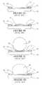
- FIGS. 1 A- 1 Dare schematic cross sectional views illustrating a prior art reflow bonding process for solder balls
- FIGS. 2 A- 2 Dare schematic cross sectional views illustrating a reflow bonding process performed using a preformed solder ball and a flux formulated in accordance with the invention
- FIG. 3Ais a cross sectional view taken along section line 3 A- 3 A of FIG. 2A;
- FIG. 3Bis a cross sectional view taken along section line 3 B- 3 B of FIG. 2B;
- FIG. 3Cis a cross sectional view taken along section line 3 C- 3 C of FIG. 2C;
- FIG. 3Dis a cross sectional view taken along section line 3 D- 3 D of FIG. 2D;
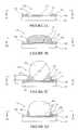
- FIGS. 4 A- 4 Care schematic cross sectional views illustrating a reflow bonding process performed using a polymer flux fabricated in accordance with an alternate embodiment of the invention
- FIG. 5Ais a schematic illustration of a system constructed in accordance with the invention for bonding external contacts to semiconductor components.
- FIG. 5Bis a plan view taken along line 5 B- 5 B of FIG. 5A illustrating the component prior to bonding of the external contacts.
- semiconductor componentmeans an electronic component that includes a semiconductor die.
- Exemplary semiconductor componentsinclude bare semiconductor dice, chip scale packages, ceramic or plastic semiconductor packages, BGA devices, semiconductor wafers, and panels and leadframes containing multiple dice or chip scale packages.
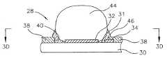
- FIGS. 2 A- 2 D, and FIGS. 3 A- 3 Da process for fabricating external contacts on a semiconductor component 28 using a polymer flux formulated in accordance with the invention is illustrated.
- the semiconductor component 28is provided, and includes a substrate 30 .
- the substrate 30can be provided as a wafer, a panel, or a leadframe, containing a plurality of components 28 that can be singulated following the fabrication process (i.e., wafer level process).
- the component 28 and the substrate 30can comprise a singulated element, such as an individual package or die.
- the substrate 30can comprise a semiconductor material, such as silicon, or a plastic material, such as bismaleimide triazine (BT), or a polyimide resin.
- BTbismaleimide triazine
- the substrate 30includes a surface 31 , and a contact pad 32 on the surface 31 .
- a contact pad 32on the surface 31 .
- the substrate 30includes a plurality of contact pads 32 arranged in a desired pattern such as a dense grid array.
- the contact pad 32comprises a solder wettable material such as copper, tin, lead, palladium, platinum, nickel, chrome, titanium or gold.
- the substrate 30also includes a conductive trace 36 (FIG. 3A) in electrical communication with the contact pad 32 .
- the conductive trace 36establishes electrical communication between the contact pad 32 and the integrated circuits contained on the component 28 .
- the substrate 30also includes a conductive trace 34 in electrical communication with another contact pad that is not illustrated.
- the conductive traces 34 , 36comprise a highly conductive material such as aluminum, titanium, nickel, iridium, copper, gold, tungsten, silver, platinum, palladium, tantalum, molybdenum or alloys of these metals.
- the substrate 30also includes a mask 38 having an opening 40 aligned with the contact pad 32 .
- the mask 38comprises an electrically insulating material, such as a photoimageable resist.
- the mask 38electrically insulates the conductive traces 34 , 36 and prevents shorting between the contact pad 32 and adjacent contact pads.
- the opening 40 in the mask 38also exposes portions of the conductive traces 34 , 36 .
- a flux deposition stepis performed in which a droplet 42 of polymer masking flux is deposited through the opening 40 in the mask 38 onto the contact pad 32 .
- a droplet 42 of polymer masking fluxis deposited through the opening 40 in the mask 38 onto the contact pad 32 .
- the component 28will include as many droplets as there are contact pads 32 , but only one droplet 42 per contact pad 32 .
- the droplet 42covers the contact pad 32 , completely fills the opening 40 , and covers the exposed portions of the conductive traces 34 , 36 .
- the size of the droplet 42will depend on the size of the contact pad 32 and the opening 40 .
- the droplet 42has a generally dome shaped topography with a convex surface.
- the droplet 42can be deposited on the contact pad 32 using a suitable deposition process, such as pin transfer, positive displacement through a nozzle, or screen printing.
- a suitable pin transfer mechanismis included in a ball placement system manufactured by Motorola of Phoenix, Ariz. as a model no. MS250PLUS.
- a suitable positive displacement mechanismis a “MICRO PEN” manufactured by Ohmcraft Inc. of Pittsford, N.Y.
- Another suitable positive displacement mechanismis a “2800” liquid dispensing system manufactured by Camelot Systems, Inc. of Haverhill, Mass.
- screen printinga stainless steel or monofilament polyester screen can be stretched and attached to a metal frame. A negative pattern can then be generated on the mesh using a photosensitive emulsion. The flux can then be forced through screen and onto the contact pad 32 .
- the polymer masking fluxis formulated to meet environmental standards recognized in the semiconductor industry.
- the polymer masking fluxis formulated with a viscosity that allows the droplet 42 to have non-flowing characteristics at a selected temperature range, such as room temperature (e.g., 60° F. to 100° F. or 15.5° C. to 37.8° C.).
- This viscosityallows the polymer masking flux to maintain a desired size and shape, and to remain in a desired area of the substrate 30 over the temperature range.
- the polymer masking fluxcan have a viscosity at a temperature of about 25° C. of about 100 to 1500 poise. In this case the viscosity can be measured using a spiral/Malcom viscometer at 25 rpm,
- the polymer masking fluxincludes an electrically insulating polymer resin such as an epoxy resin, a silicone resin, natural rubber, synthetic rubber, or similar elastomeric material having suitable non-flowing and curable properties.
- an electrically insulating polymer resinsuch as an epoxy resin, a silicone resin, natural rubber, synthetic rubber, or similar elastomeric material having suitable non-flowing and curable properties.
- specific polymer resinsinclude, but are not limited to: pthalate-actate acetate hydroxyl copolymer, dibutyl isobutyl diphenol cellulose copolymer, and butyl phenol ketyl vinyl acetate polymer.
- the polymer masking fluxalso includes a fluxing agent, such as an organic acid, for cleaning and removing oxides from the surface of the contact pads 42 and the solder balls 44 .
- a fluxing agentsuch as an organic acid
- Suitable fluxing agentsinclude carboxylic acid, abietic acid, citric acid, 2-furoic acid, malic acid and polyacrylic acid.
- a representative proportion of the fluxing agent as a volume percentage of the total volume of the droplet 42can be from about 0.1% to 16%.
- the polymer masking fluxalso includes a curing agent or hardener, such as a reactant or a solvent, that reacts with and cures the polymer resin over a selected temperature range and time period.
- Suitable curing agentsinclude amines, anhydrides, and butyl carbitol acetate.
- the fluxing agent and the curing agentcan also comprise a same chemical compound.
- the curing agentcan be included in the polymer resin in a quantity sufficient to cure the polymer resin at a temperature of between about 200° C. to 250° C. in about 1 to 2 minutes.
- the curing processcan be performed simultaneous with a reflow step using a reflow furnace to be hereinafter described. If required, a final cure can also be performed at a lower temperature for a longer time period. In this case a batch oven can be used to perform the final cure.
- a ball placement stepis performed in which a solder ball 44 is placed on the droplet 42 , and pushed into contact with the contact pad 32 .
- the ball placement stepis performed at room temperature such that the viscous properties of the droplet 42 are maintained. In this viscous condition, the droplet 42 also has adhesive properties that hold the solder ball 44 on the contact pad 32 with an adhesive force.
- the ball placement stepmust be performed with sufficient force to permit the solder ball 44 to displace the middle portion of the droplet 42 , and physically contact the contact pad 32 .
- the solder ball 44can be formed separately out of a suitable solder alloy, such as 95%Pb/5%Sn, 60%Pb/40%Sn, 63%Sn/37%Pb, or 62%Pb/36%Sn/2%Ag.
- a representative range for the outside diameter (OD) of the solder ball 44can be from about 0.002-in (0.050 mm) to 0.025-in (0.675 mm).
- a representative thickness T of the droplet 42 , with the solder ball 44 in contact with the contact pad 32can be from about one tenth to one half the outside diameter of the solder ball 44 .
- the solder ball 44can be pushed through the droplet 42 , and placed on the contact pad 32 using a suitable ball placement mechanism.
- a suitable ball placement mechanismis included in the previously identified ball placement system MS250PLUS manufactured by Motorola.
- Another ball placement mechanism suitableis disclosed in U.S. Pat. No. 6,100,175 to Wood et al. entitled “Method And Apparatus For Attaching Balls To A Substrate”.
- a heating or reflow stepis performed in which the component 28 is placed in a furnace, and the solder ball 44 is heated to a temperature sufficient to reflow the solder.
- the reflowed solder ball 44metallurgically bonds to the contact pad 32 .
- the droplet 42 of fluxpolymerizes, or cures, into a polymer support member 46 .
- the polymer support member 46is a donut shaped structure (torus) resting on the surface 31 of the substrate 30 , and encompassing the base portion of the solder ball 44 .
- the polymer support member 46helps to support and rigidify the solder ball 44 during subsequent operation of the component 28 .
- the polymer support member 46bonds to the solder ball 44 , bonds to the opening 40 in the mask 38 , and bonds to the surface of the mask 38 to provide a rigidifying structure anchored to the substrate 30 .
- the polymer support member 46In addition to performing a supporting and rigidifying function, the polymer support member 46 also performs a masking and electrical insulating function. Specifically, the polymer support member 46 masks the exposed portions of the conductive trace 34 , and prevents shorting between the solder ball 44 and the conductive trace 34 . In addition, the polymer support member 46 provides an electrically insulating material in the opening 40 , and between the solder ball 44 and the conductive trace 34 .
- FIGS. 4 A- 4 Ca process for fabricating solder bumps 48 (FIG. 4C) using the polymer masking flux are illustrated.
- the component 28is provided and includes the substrate 30 , the contact pad 32 , the conductive trace 34 , the mask 38 , and the opening 40 in the mask 38 , substantially as previously described.
- a deposition apparatus 52is provided.
- the deposition apparatusis configured to deposit a polymer masking flux 50 on the contact pad 32 .
- the polymer masking flux 50includes a polymer resin formulated with the previously described characteristics, a fluxing agent for cleaning the contact pad 32 and a curing agent for curing the polymer resin.
- the polymer masking flux 50also includes solder particles having a desired particle size distribution.
- the deposition apparatus 52comprises a screen printer comprising a screen 54 having an opening 58 , and a squeegee 56 configured to push the polymer flux 50 through the opening 58 onto the contact pad 32 .
- the deposition apparatuscan comprise a positive displacement mechanism as previously described, configured to dispense the polymer masking flux 50 under pressure through a nozzle.
- a flux deposition stepis performed.
- the squeegee 56is used to force the polymer masking flux 50 through the opening 58 in the screen 54 , and onto the contact pad 32 , to form a droplet 60 of flux.
- the polymer masking flux 50 , and the droplet 60are viscous, uncured, and non-flowing substantially as previously described.
- the droplet 60has a peripheral shape corresponding to the peripheral shape of the opening 58 (e.g., circular, square, rectangular).
- the droplet 60has a height corresponding to the height of the screen 54 above the contact pad 32 .
- a reflow bonding stepis performed in a furnace substantially as previously described.
- the droplet 60 of polymer masking flux 50is heated to a temperature sufficient to coalesce the solder particles therein into a generally hemispherically shaped solder bump 48 .
- the polymer resinseparates from the solder particles, moves outward, and polymerizes into the polymer support member 46 .
- the polymer resin in the droplet 60masks and electrically insulates the conductive trace 34 , substantially as previously described.
- the curing mechanismcan comprise outgassing of a solvent during heating as indicated by vapor trails 76 .
- curingcan be accomplished in a first stage at a relatively high temperature (e.g., 250° C.) for a relatively brief time (e.g., 1 minute), followed by a second stage at a lower temperature (e.g., 100° C. for a longer time (e.g., several minutes or more).
- the system 62includes a conveyor 64 for moving the component 28 through the different stages of the system 62 .
- the conveyor 28includes lugs 66 for engaging the component 28 .
- the component 28can be mounted to a leadframe or a panel having openings configured to engage the lugs 66 .
- the component 28includes the contact pads 32 formed substantially as previously described. In the illustrative embodiment, the contact pads 32 are generally circular in shape, and are arranged in a dense grid array of rows and columns.
- the system 62includes a flux dispensing mechanism 68 configured to dispense a viscous polymer masking flux 70 , formulated as previously described, onto the contact pads 32 to form the droplets 42 .
- the flux dispensing mechanism 68can comprise a pin transfer mechanism, a positive displacement mechanism having one or more nozzles, or a screen printing apparatus, all as previously described.
- the system 62includes a ball placement mechanism 72 configured to place the solder balls 44 on the droplets 42 in physical contact with the contact pads 32 substantially as previously described.
- the system 62also includes a two stage furnace 74 configured to reflow the solder balls 44 , and to cure the droplets 42 to form the polymer support members 46 substantially as previously described. Suitable furnaces are available from Scientific Sealing Technology of Downey, Calif., Vitronics of New Hampshire, and Accel of Texas.
- the inventionprovides an improved polymer masking flux for fabricating external contacts on semiconductor components, a system for fabricating external contacts that includes the polymer flux, and improved semiconductor components fabricated using the polymer flux.
Landscapes
- Engineering & Computer Science (AREA)
- Microelectronics & Electronic Packaging (AREA)
- Computer Hardware Design (AREA)
- Power Engineering (AREA)
- Manufacturing & Machinery (AREA)
- Mechanical Engineering (AREA)
- Electric Connection Of Electric Components To Printed Circuits (AREA)
Abstract
Description
- This invention relates generally to semiconductor packaging, and more particularly to a masking flux for fabricating external contacts, such as solder balls and solder bumps, on semiconductor components.[0001]
- Semiconductor components, such as packages, dice and wafers include external contacts which provide input/output paths to the integrated circuits contained on the components. For surface mount components, the external contacts typically comprise solder balls, or solder bumps, bonded to contact pads on the component. For some components, such as chip scale packages and BGA packages, the external contacts can be arranged in a dense grid array, such as a ball grid array (BGA), or a fine ball grid array (FBGA).[0002]
- One conventional method for forming external contacts uses pre-formed solder balls, and a solder reflow bonding process. A prior art solder reflow bonding process is illustrated in FIGS.[0003]1A-1D.
- As shown in FIG. 1A, a[0004]
semiconductor component 10 includes a pattern ofcontact pads 12 in electrical communication with the integrated circuits and semiconductor devices contained on thecomponent 10. Thecontact pads 12 typically comprise a solder wettable metal such as chrome, titanium or nickel. Thecomponent 10 also includes a pattern ofconductive traces 14 in electrical communication with thecontact pads 12. In addition, thecomponent 10 includes an electrically insulatingsolder mask 16 havingopenings 22 aligned with thecontact pads 12. Thesolder mask 16 substantially covers theconductive traces 14, but as illustrated in FIG. 1A, theopenings 22 sometimes expose portions of theconductive traces 14 that are in close proximity to thecontact pads 12. - As shown in FIG. 1B, during the bonding process, a layer of[0005]
flux 18 is deposited on thecontact pads 12 using a suitable deposition process such as screen printing or pin transfer. Theflux 18 chemically attacks surface oxides, such that the molten solder can wet the surfaces to be bonded. Typically, the flux comprises has either a rosin based or a water soluble chemistry. - As shown in FIG. 1C, following application of the[0006]
flux 18, pre-formedsolder balls 20 can be placed on thecontact pads 12 in physical contact with theflux 18. Typically, thesolder balls 20 have the shape of a sphere, or a truncated sphere. Although a fixture can be used to center and maintain thesolder balls 20 on thecontact pads 12, theflux 18 also performs a tacking function for holding thesolder balls 20 on thecontact pads 12 during the bonding process. - Following placement of the[0007]
solder balls 20 on thecontact pads 12, thecomponent 10 can be placed in a furnace at a temperature sufficient to reflow and metallurgically bond thesolder balls 20 to thecontact pads 12. Thecomponent 10 can then be removed from the furnace and cooled. Thecomponent 10 can then be surface mounted to a supporting substrate, such as a printed circuit board, by bonding thesolder balls 20 to corresponding electrodes on the supporting substrate. - In addition to reflowing the[0008]
solder balls 20, the high temperatures encountered in the furnace can cause most of theflux 18 to vaporize in the furnace. However, a flux cleaning step is also required to remove any flux residue that remains on thecontact pads 12 andcomponent 10. The flux cleaning process can be performed using a hydrocarbon for a rosin based flux, or water with surfactants for a water soluble flux. - One factor that can adversely affect the reliability of the[0009]
component 10 is shorting caused by distortion of thesolder balls 20. As shown in FIG. 1D, distortion of thesolder balls 20 can cause portions of thesolder balls 20 to touch exposed portions of theconductive traces 14. It would be advantageous for a flux to be curable and electrically insulating, such that shorting between thesolder balls 20 and theconductive traces 14 can be eliminated. Another factor that can affect the reliability of the component during normal operation is fatigue failure of thesolder balls 20, particularly at the interfaces with thecontact pads 12 and the electrodes on the supporting substrate. Typically, fatigue failures are induced by thermal expansion mismatches between the component and the supporting substrate. For example, if thecomponent 10 comprises a first material, such as silicon having a first TCE (thermal coefficient of expansion), and the supporting substrate comprises a second material, such as FR-4 having a second TCE, cyclic forces can be placed on thesolder balls 20 as thecomponent 10 is thermally cycled during normal operation. - These forces can include tensile forces, moment forces and shear forces. If the forces are large enough, the[0010]
solder balls 20 can separate from thecontact pads 12 forming an electrical open. The separation can also compromise the physical bond between thecomponent 10 and the supporting substrate. This problem is compounded because the area of interface between thesolder balls 20 and thecontact pads 12 is relatively small, such that the forces are concentrated over a relatively small area. - It would be advantageous for a flux to have the capability to support and rigidify the[0011]
solder balls 20, or other external contacts, on asemiconductor component 10, during normal operation of thecomponent 10. The present invention is directed to an improved flux configured to form a rigidifying structure for the external contacts. In addition, the flux is formulated to remove oxides from the components, is curable for reducing vapors during the fabrication process, and is electrically insulating for masking conductive traces for the external contacts. - In accordance with the present invention, an improved polymer masking flux for fabricating external contacts on semiconductor components, a bonding system that includes the flux, and improved components fabricated using the flux, are provided.[0012]
- In an illustrative embodiment the component comprises a semiconductor package, a semiconductor die, or a semiconductor wafer, and the external contacts comprise solder balls. The component includes a substrate, contact pads on the substrate and conductive traces in electrical communication with the contact pads. The component also includes a solder mask having openings aligned with the contact pads.[0013]
- The flux is configured to clean surface oxides from the contact pads during reflow bonding of the solder balls to the contact pads. In addition, the flux masks exposed portions of the conductive traces, and prevents electrical shorting between the solder balls and the conductive traces. The flux is also configured to cure, or polymerize, in a reflow furnace, and form polymer support members for the solder balls. The polymer support members are donut shaped elements that rigidify, and absorb forces acting on the solder balls during subsequent use of the component. Each polymer support member surrounds a base portion of a solder ball, and has a thickness approximately equal to one tenth to one half the diameter of the solder balls.[0014]
- The flux includes an electrically insulating polymer resin such as an epoxy resin, a silicone resin, natural rubber or synthetic rubber. The polymer resin provides a base material which cures or polymerizes into the polymer support members. In addition, the flux includes a fluxing agent, such as an organic acid, for cleaning and removing oxides from the surface of the contact pads and the solder balls. The flux also includes a curing agent or hardener, such as a reactant or a solvent, that reacts with and cures the polymer resin in the reflow furnace. Because the flux cures into the polymer support members, vapors in the reflow furnace are reduced, and there is no need to perform a flux cleaning step on the component following the reflow bonding process.[0015]
- The flux is a relatively thick viscous material that has non-flowing characteristics over a selected temperature range. This allows an exact quantity of the flux to be deposited onto the contact pads as a droplet using pin transfer, nozzle deposition or screen printing processes. The droplet maintains it's shape, remains on the contact pads, and provides high adhesion for tacking the solder balls to the contact pads during the reflow bonding step. The flux can be used at the wafer level during the fabrication of multiple components at the same time (i.e., wafer level fabrication process), or can be employed on singulated components such as individual dice or packages (i.e., die level fabrication process).[0016]
- A system for bonding the solder balls to the semiconductor component includes the flux, and a flux dispensing mechanism configured to deposit the droplets of flux onto the contact pads. The system also includes a conveyor, a ball placement mechanism and a reflow furnace.[0017]
- The flux can also be used to fabricate external contacts in the form of solder bumps, rather than solder balls. In this case the flux again includes the polymer resin, the fluxing agent, and the curing agent. The flux also includes micro solder particles configured to coalesce into the solder bumps. The flux is initially deposited onto the contact pads using a deposition process, such as screen printing, or nozzle deposition. The polymer resin masks exposed portions of the conductive traces, and the fluxing agent cleans surface oxides from the contact pads. Following deposition, the flux is reflowed by heating the components in a reflow furnace. During the reflow step, the solder particles and the polymer resin separate, such that the solder particles form the solder bumps, and the polymer resin forms polymer support members for the solder bumps.[0018]
- FIGS.[0019]1A-1D are schematic cross sectional views illustrating a prior art reflow bonding process for solder balls;
- FIGS.[0020]2A-2D are schematic cross sectional views illustrating a reflow bonding process performed using a preformed solder ball and a flux formulated in accordance with the invention;
- FIG. 3A is a cross sectional view taken along[0021]
section line 3A-3A of FIG. 2A; - FIG. 3B is a cross sectional view taken along[0022]
section line 3B-3B of FIG. 2B; - FIG. 3C is a cross sectional view taken along[0023]
section line 3C-3C of FIG. 2C; - FIG. 3D is a cross sectional view taken along[0024]
section line 3D-3D of FIG. 2D; - FIGS.[0025]4A-4C are schematic cross sectional views illustrating a reflow bonding process performed using a polymer flux fabricated in accordance with an alternate embodiment of the invention;
- FIG. 5A is a schematic illustration of a system constructed in accordance with the invention for bonding external contacts to semiconductor components; and[0026]
- FIG. 5B is a plan view taken along[0027]
line 5B-5B of FIG. 5A illustrating the component prior to bonding of the external contacts. - As used herein, the term “semiconductor component” means an electronic component that includes a semiconductor die. Exemplary semiconductor components include bare semiconductor dice, chip scale packages, ceramic or plastic semiconductor packages, BGA devices, semiconductor wafers, and panels and leadframes containing multiple dice or chip scale packages.[0028]
- Referring to FIGS.[0029]2A-2D, and FIGS.3A-3D, a process for fabricating external contacts on a
semiconductor component 28 using a polymer flux formulated in accordance with the invention is illustrated. - As shown in FIGS. 2A and 3A, the[0030]
semiconductor component 28 is provided, and includes asubstrate 30. Thesubstrate 30 can be provided as a wafer, a panel, or a leadframe, containing a plurality ofcomponents 28 that can be singulated following the fabrication process (i.e., wafer level process). Alternately, thecomponent 28 and thesubstrate 30 can comprise a singulated element, such as an individual package or die. Depending on thecomponent 28, thesubstrate 30 can comprise a semiconductor material, such as silicon, or a plastic material, such as bismaleimide triazine (BT), or a polyimide resin. - The[0031]
substrate 30 includes asurface 31, and acontact pad 32 on thesurface 31. For simplicity only onecontact pad 32 is shown. However, thesubstrate 30 includes a plurality ofcontact pads 32 arranged in a desired pattern such as a dense grid array. Thecontact pad 32 comprises a solder wettable material such as copper, tin, lead, palladium, platinum, nickel, chrome, titanium or gold. - The[0032]
substrate 30 also includes a conductive trace36 (FIG. 3A) in electrical communication with thecontact pad 32. Theconductive trace 36 establishes electrical communication between thecontact pad 32 and the integrated circuits contained on thecomponent 28. Thesubstrate 30 also includes aconductive trace 34 in electrical communication with another contact pad that is not illustrated. The conductive traces34,36 comprise a highly conductive material such as aluminum, titanium, nickel, iridium, copper, gold, tungsten, silver, platinum, palladium, tantalum, molybdenum or alloys of these metals. - The[0033]
substrate 30 also includes amask 38 having anopening 40 aligned with thecontact pad 32. Themask 38 comprises an electrically insulating material, such as a photoimageable resist. Themask 38 electrically insulates the conductive traces34,36 and prevents shorting between thecontact pad 32 and adjacent contact pads. As shown in FIG. 3A, in addition to exposing thecontact pad 32, theopening 40 in themask 38 also exposes portions of the conductive traces34,36. - Next, as shown in FIGS. 2B and 3B, a flux deposition step is performed in which a[0034]
droplet 42 of polymer masking flux is deposited through theopening 40 in themask 38 onto thecontact pad 32. Again, although only asingle droplet 42 of flux is illustrated, it is understood that thecomponent 28 will include as many droplets as there arecontact pads 32, but only onedroplet 42 percontact pad 32. In the illustrative embodiment, thedroplet 42 covers thecontact pad 32, completely fills theopening 40, and covers the exposed portions of the conductive traces34,36. The size of thedroplet 42 will depend on the size of thecontact pad 32 and theopening 40. In addition, thedroplet 42 has a generally dome shaped topography with a convex surface. Thedroplet 42 can be deposited on thecontact pad 32 using a suitable deposition process, such as pin transfer, positive displacement through a nozzle, or screen printing. A suitable pin transfer mechanism is included in a ball placement system manufactured by Motorola of Phoenix, Ariz. as a model no. MS250PLUS. A suitable positive displacement mechanism is a “MICRO PEN” manufactured by Ohmcraft Inc. of Pittsford, N.Y. Another suitable positive displacement mechanism is a “2800” liquid dispensing system manufactured by Camelot Systems, Inc. of Haverhill, Mass. With screen printing a stainless steel or monofilament polyester screen can be stretched and attached to a metal frame. A negative pattern can then be generated on the mesh using a photosensitive emulsion. The flux can then be forced through screen and onto thecontact pad 32. - The polymer masking flux is formulated to meet environmental standards recognized in the semiconductor industry. In addition, the polymer masking flux is formulated with a viscosity that allows the[0035]
droplet 42 to have non-flowing characteristics at a selected temperature range, such as room temperature (e.g., 60° F. to 100° F. or 15.5° C. to 37.8° C.). This viscosity allows the polymer masking flux to maintain a desired size and shape, and to remain in a desired area of thesubstrate 30 over the temperature range. By way of example, the polymer masking flux can have a viscosity at a temperature of about 25° C. of about 100 to 1500 poise. In this case the viscosity can be measured using a spiral/Malcom viscometer at 25 rpm, - As a primary constituent the polymer masking flux includes an electrically insulating polymer resin such as an epoxy resin, a silicone resin, natural rubber, synthetic rubber, or similar elastomeric material having suitable non-flowing and curable properties. By way of example, specific polymer resins include, but are not limited to: pthalate-actate acetate hydroxyl copolymer, dibutyl isobutyl diphenol cellulose copolymer, and butyl phenol ketyl vinyl acetate polymer.[0036]
- The polymer masking flux also includes a fluxing agent, such as an organic acid, for cleaning and removing oxides from the surface of the[0037]
contact pads 42 and thesolder balls 44. Suitable fluxing agents include carboxylic acid, abietic acid, citric acid, 2-furoic acid, malic acid and polyacrylic acid. A representative proportion of the fluxing agent as a volume percentage of the total volume of thedroplet 42 can be from about 0.1% to 16%. - The polymer masking flux also includes a curing agent or hardener, such as a reactant or a solvent, that reacts with and cures the polymer resin over a selected temperature range and time period. Suitable curing agents include amines, anhydrides, and butyl carbitol acetate. The fluxing agent and the curing agent can also comprise a same chemical compound. By way of example, the curing agent can be included in the polymer resin in a quantity sufficient to cure the polymer resin at a temperature of between about 200° C. to 250° C. in about 1 to 2 minutes. The curing process can be performed simultaneous with a reflow step using a reflow furnace to be hereinafter described. If required, a final cure can also be performed at a lower temperature for a longer time period. In this case a batch oven can be used to perform the final cure.[0038]
- As shown in FIG. 2C and FIG. 3C, following the droplet deposition step, a ball placement step is performed in which a[0039]
solder ball 44 is placed on thedroplet 42, and pushed into contact with thecontact pad 32. Preferably, the ball placement step is performed at room temperature such that the viscous properties of thedroplet 42 are maintained. In this viscous condition, thedroplet 42 also has adhesive properties that hold thesolder ball 44 on thecontact pad 32 with an adhesive force. The ball placement step must be performed with sufficient force to permit thesolder ball 44 to displace the middle portion of thedroplet 42, and physically contact thecontact pad 32. - The[0040]
solder ball 44 can be formed separately out of a suitable solder alloy, such as 95%Pb/5%Sn, 60%Pb/40%Sn, 63%Sn/37%Pb, or 62%Pb/36%Sn/2%Ag. A representative range for the outside diameter (OD) of thesolder ball 44 can be from about 0.002-in (0.050 mm) to 0.025-in (0.675 mm). A representative thickness T of thedroplet 42, with thesolder ball 44 in contact with thecontact pad 32, can be from about one tenth to one half the outside diameter of thesolder ball 44. - The[0041]
solder ball 44 can be pushed through thedroplet 42, and placed on thecontact pad 32 using a suitable ball placement mechanism. Such a ball placement mechanism is included in the previously identified ball placement system MS250PLUS manufactured by Motorola. Another ball placement mechanism suitable is disclosed in U.S. Pat. No. 6,100,175 to Wood et al. entitled “Method And Apparatus For Attaching Balls To A Substrate”. - Next, as shown in FIG. 2D and FIG. 3D, a heating or reflow step is performed in which the[0042]
component 28 is placed in a furnace, and thesolder ball 44 is heated to a temperature sufficient to reflow the solder. During the heating step, the reflowedsolder ball 44 metallurgically bonds to thecontact pad 32. Also during the heating step, thedroplet 42 of flux polymerizes, or cures, into apolymer support member 46. - As shown in FIG. 3D, the[0043]
polymer support member 46 is a donut shaped structure (torus) resting on thesurface 31 of thesubstrate 30, and encompassing the base portion of thesolder ball 44. Thepolymer support member 46 helps to support and rigidify thesolder ball 44 during subsequent operation of thecomponent 28. In this regard, thepolymer support member 46 bonds to thesolder ball 44, bonds to theopening 40 in themask 38, and bonds to the surface of themask 38 to provide a rigidifying structure anchored to thesubstrate 30. - In addition to performing a supporting and rigidifying function, the[0044]
polymer support member 46 also performs a masking and electrical insulating function. Specifically, thepolymer support member 46 masks the exposed portions of theconductive trace 34, and prevents shorting between thesolder ball 44 and theconductive trace 34. In addition, thepolymer support member 46 provides an electrically insulating material in theopening 40, and between thesolder ball 44 and theconductive trace 34. - Referring to FIGS.[0045]4A-4C, a process for fabricating solder bumps48 (FIG. 4C) using the polymer masking flux are illustrated. Initially, as shown in FIG. 4A, the
component 28 is provided and includes thesubstrate 30, thecontact pad 32, theconductive trace 34, themask 38, and theopening 40 in themask 38, substantially as previously described. - As also shown in FIG. 4A, a[0046]
deposition apparatus 52 is provided. The deposition apparatus is configured to deposit apolymer masking flux 50 on thecontact pad 32. Thepolymer masking flux 50 includes a polymer resin formulated with the previously described characteristics, a fluxing agent for cleaning thecontact pad 32 and a curing agent for curing the polymer resin. Thepolymer masking flux 50 also includes solder particles having a desired particle size distribution. - In the illustrative embodiment, the[0047]
deposition apparatus 52 comprises a screen printer comprising ascreen 54 having anopening 58, and asqueegee 56 configured to push thepolymer flux 50 through theopening 58 onto thecontact pad 32. Alternately, the deposition apparatus can comprise a positive displacement mechanism as previously described, configured to dispense thepolymer masking flux 50 under pressure through a nozzle. - Next, as shown in FIG. 4B, a flux deposition step is performed. During this step, the[0048]
squeegee 56 is used to force thepolymer masking flux 50 through theopening 58 in thescreen 54, and onto thecontact pad 32, to form adroplet 60 of flux. During the deposition step thepolymer masking flux 50, and thedroplet 60, are viscous, uncured, and non-flowing substantially as previously described. In addition, thedroplet 60 has a peripheral shape corresponding to the peripheral shape of the opening58 (e.g., circular, square, rectangular). Thedroplet 60 has a height corresponding to the height of thescreen 54 above thecontact pad 32. - Next, as shown in FIG. 4C, a reflow bonding step is performed in a furnace substantially as previously described. During the reflow bonding step the[0049]
droplet 60 ofpolymer masking flux 50 is heated to a temperature sufficient to coalesce the solder particles therein into a generally hemispherically shapedsolder bump 48. In addition, during the reflow bonding step the polymer resin separates from the solder particles, moves outward, and polymerizes into thepolymer support member 46. - Also during the reflow bonding step, the polymer resin in the[0050]
droplet 60 masks and electrically insulates theconductive trace 34, substantially as previously described. As before, the curing mechanism can comprise outgassing of a solvent during heating as indicated byvapor trails 76. As also previously described, curing can be accomplished in a first stage at a relatively high temperature (e.g., 250° C.) for a relatively brief time (e.g., 1 minute), followed by a second stage at a lower temperature (e.g., 100° C. for a longer time (e.g., several minutes or more). - Referring to FIGS. 5A and 5B, a[0051]
system 62 for bonding thesolder balls 44 to thecomponent 28 is illustrated schematically. Thesystem 62 includes aconveyor 64 for moving thecomponent 28 through the different stages of thesystem 62. Theconveyor 28 includeslugs 66 for engaging thecomponent 28. For example, thecomponent 28 can be mounted to a leadframe or a panel having openings configured to engage thelugs 66. As shown in FIG. 5B, thecomponent 28 includes thecontact pads 32 formed substantially as previously described. In the illustrative embodiment, thecontact pads 32 are generally circular in shape, and are arranged in a dense grid array of rows and columns. - As also shown in FIG. 5A, the[0052]
system 62 includes aflux dispensing mechanism 68 configured to dispense a viscouspolymer masking flux 70, formulated as previously described, onto thecontact pads 32 to form thedroplets 42. Theflux dispensing mechanism 68 can comprise a pin transfer mechanism, a positive displacement mechanism having one or more nozzles, or a screen printing apparatus, all as previously described. - As also shown in FIG. 5A, the[0053]
system 62 includes aball placement mechanism 72 configured to place thesolder balls 44 on thedroplets 42 in physical contact with thecontact pads 32 substantially as previously described. Thesystem 62 also includes a twostage furnace 74 configured to reflow thesolder balls 44, and to cure thedroplets 42 to form thepolymer support members 46 substantially as previously described. Suitable furnaces are available from Scientific Sealing Technology of Downey, Calif., Vitronics of New Hampshire, and Accel of Texas. - Thus the invention provides an improved polymer masking flux for fabricating external contacts on semiconductor components, a system for fabricating external contacts that includes the polymer flux, and improved semiconductor components fabricated using the polymer flux. While the invention has been described with reference to certain preferred embodiments, as will be apparent to those skilled in the art, certain changes and modifications can be made without departing from the scope of the invention as defined by the following claims.[0054]
Claims (52)
Priority Applications (1)
| Application Number | Priority Date | Filing Date | Title |
|---|---|---|---|
| US10/437,214US6926191B2 (en) | 2002-02-05 | 2003-05-13 | Process for fabricating external contacts on semiconductor components |
Applications Claiming Priority (2)
| Application Number | Priority Date | Filing Date | Title |
|---|---|---|---|
| US10/068,819US6854633B1 (en) | 2002-02-05 | 2002-02-05 | System with polymer masking flux for fabricating external contacts on semiconductor components |
| US10/437,214US6926191B2 (en) | 2002-02-05 | 2003-05-13 | Process for fabricating external contacts on semiconductor components |
Related Parent Applications (1)
| Application Number | Title | Priority Date | Filing Date |
|---|---|---|---|
| US10/068,819DivisionUS6854633B1 (en) | 2002-02-05 | 2002-02-05 | System with polymer masking flux for fabricating external contacts on semiconductor components |
Publications (2)
| Publication Number | Publication Date |
|---|---|
| US20030201309A1true US20030201309A1 (en) | 2003-10-30 |
| US6926191B2 US6926191B2 (en) | 2005-08-09 |
Family
ID=29248114
Family Applications (2)
| Application Number | Title | Priority Date | Filing Date |
|---|---|---|---|
| US10/068,819Expired - Fee RelatedUS6854633B1 (en) | 2002-02-05 | 2002-02-05 | System with polymer masking flux for fabricating external contacts on semiconductor components |
| US10/437,214Expired - LifetimeUS6926191B2 (en) | 2002-02-05 | 2003-05-13 | Process for fabricating external contacts on semiconductor components |
Family Applications Before (1)
| Application Number | Title | Priority Date | Filing Date |
|---|---|---|---|
| US10/068,819Expired - Fee RelatedUS6854633B1 (en) | 2002-02-05 | 2002-02-05 | System with polymer masking flux for fabricating external contacts on semiconductor components |
Country Status (1)
| Country | Link |
|---|---|
| US (2) | US6854633B1 (en) |
Cited By (16)
| Publication number | Priority date | Publication date | Assignee | Title |
|---|---|---|---|---|
| US6888255B2 (en)* | 2003-05-30 | 2005-05-03 | Texas Instruments Incorporated | Built-up bump pad structure and method for same |
| US20060086777A1 (en)* | 2003-03-10 | 2006-04-27 | Motoyuki Itoh | Method and apparatus for placing conductive balls |
| US20060160347A1 (en)* | 2005-01-19 | 2006-07-20 | Seiko Epson Corporation | Method of manufacturing semiconductor device and method of treating electrical connection section |
| US20070235844A1 (en)* | 2006-04-06 | 2007-10-11 | Alps Electric Co., Ltd. | Electronic device mounting structure and method of manufacturing the same |
| US20090218680A1 (en)* | 2008-02-28 | 2009-09-03 | Celik Zeki Z | Process of grounding heat spreader/stiffener to a flip chip package using solder and film adhesive |
| US20100055846A1 (en)* | 2007-06-12 | 2010-03-04 | Taiwan Semiconductor Manufacturing Co., Ltd. | Semiconductor package structures |
| US20140196940A1 (en)* | 2013-01-11 | 2014-07-17 | Qualcomm Incorporated | Through mold via relief gutter on molded laser package (mlp) packages |
| US20150258638A1 (en)* | 2014-03-14 | 2015-09-17 | Indium Corporation | Methods and compositions for forming solder bumps on a substrate with radiation curable or thermal curable solder flux |
| WO2017172237A1 (en)* | 2016-04-01 | 2017-10-05 | Intel Corporation | Water soluble flux with modified viscosity |
| US20180286793A1 (en)* | 2017-03-30 | 2018-10-04 | Taiwan Semiconductor Manufacturing Co., Ltd. | Package structure and method of forming thereof |
| US20190067036A1 (en)* | 2017-08-24 | 2019-02-28 | Advanced Semiconductor Engineering, Inc. | Semiconductor package and method of manufacturing the same |
| US20190109081A1 (en)* | 2017-10-11 | 2019-04-11 | Micron Technology, Inc. | Methods of processing semiconductor devices |
| US20190267346A1 (en)* | 2018-02-28 | 2019-08-29 | Powertech Technology Inc. | Flux transfer tool and flux transfer method |
| US11089685B2 (en)* | 2009-06-12 | 2021-08-10 | Amkor Technology Singapore Holding Pte. Ltd. | Stackable via package and method |
| CN114375494A (en)* | 2019-09-24 | 2022-04-19 | 松下知识产权经营株式会社 | Electronic component, method for manufacturing electronic component, mounted structure, and method for manufacturing mounted structure |
| US11478869B2 (en)* | 2020-06-10 | 2022-10-25 | Senju Metal Industry Co., Ltd. | Method for forming bump electrode substrate |
Families Citing this family (9)
| Publication number | Priority date | Publication date | Assignee | Title |
|---|---|---|---|---|
| TW546805B (en)* | 2002-07-18 | 2003-08-11 | Advanced Semiconductor Eng | Bumping process |
| TWI231555B (en)* | 2003-06-30 | 2005-04-21 | Advanced Semiconductor Eng | Wafer level package and fabrication process thereof |
| JP2005095977A (en)* | 2003-08-26 | 2005-04-14 | Sanyo Electric Co Ltd | Circuit device |
| US20050067468A1 (en)* | 2003-09-30 | 2005-03-31 | Daoqiang Lu | Fluxes for flip chip assembly using water soluble polymers |
| TWI235028B (en)* | 2004-04-30 | 2005-06-21 | Via Tech Inc | Pin grid array package carrier and process for mounting passive component thereon |
| US7187078B2 (en)* | 2004-09-13 | 2007-03-06 | Taiwan Semiconductor Manufacturing Co. Ltd. | Bump structure |
| TWI419242B (en)* | 2007-02-05 | 2013-12-11 | Chipmos Technologies Inc | Bump structure with reinforcement and manufacturing method thereof |
| US8987605B2 (en)* | 2011-09-28 | 2015-03-24 | Taiwan Semiconductor Manufacturing Company, Ltd. | Formation of connectors without UBM |
| US10074625B2 (en)* | 2015-09-20 | 2018-09-11 | Qualcomm Incorporated | Wafer level package (WLP) ball support using cavity structure |
Citations (14)
| Publication number | Priority date | Publication date | Assignee | Title |
|---|---|---|---|---|
| US5385636A (en)* | 1993-03-05 | 1995-01-31 | Alcatel N.V. | Method of forming a metal contact on a projection on a semiconductor substrate |
| US5482736A (en)* | 1994-08-04 | 1996-01-09 | Amkor Electronics, Inc. | Method for applying flux to ball grid array package |
| US5611476A (en)* | 1996-01-18 | 1997-03-18 | Btu International | Solder reflow convection furnace employing flux handling and gas densification systems |
| US6059173A (en)* | 1998-03-05 | 2000-05-09 | International Business Machines Corporation | Micro grid array solder interconnection structure for second level packaging joining a module and printed circuit board |
| US6063647A (en)* | 1997-12-08 | 2000-05-16 | 3M Innovative Properties Company | Method for making circuit elements for a z-axis interconnect |
| US6180504B1 (en)* | 1999-08-27 | 2001-01-30 | Micron Technology, Inc. | Method for fabricating a semiconductor component with external polymer support layer |
| US6204080B1 (en)* | 1997-10-31 | 2001-03-20 | Daewoo Electronics Co., Ltd. | Method for manufacturing thin film actuated mirror array in an optical projection system |
| US6263358B1 (en)* | 1997-07-25 | 2001-07-17 | British Telecommunications Public Limited Company | Scheduler for a software system having means for allocating tasks |
| US6276599B1 (en)* | 1998-04-10 | 2001-08-21 | Noda Screen Co., Ltd. | Method and apparatus for forming solder bumps |
| US6293456B1 (en)* | 1997-05-27 | 2001-09-25 | Spheretek, Llc | Methods for forming solder balls on substrates |
| US6297560B1 (en)* | 1996-10-31 | 2001-10-02 | Miguel Albert Capote | Semiconductor flip-chip assembly with pre-applied encapsulating layers |
| US6352881B1 (en)* | 1999-07-22 | 2002-03-05 | National Semiconductor Corporation | Method and apparatus for forming an underfill adhesive layer |
| US6402013B2 (en)* | 1999-12-03 | 2002-06-11 | Senju Metal Industry Co., Ltd | Thermosetting soldering flux and soldering process |
| US20030051770A1 (en)* | 2000-12-04 | 2003-03-20 | Tsutomu Nishina | Flux for soldering and solder composition |
Family Cites Families (16)
| Publication number | Priority date | Publication date | Assignee | Title |
|---|---|---|---|---|
| US5128746A (en) | 1990-09-27 | 1992-07-07 | Motorola, Inc. | Adhesive and encapsulant material with fluxing properties |
| JPH058085A (en)* | 1990-11-30 | 1993-01-19 | Nippondenso Co Ltd | Soldering flux |
| US5417771A (en)* | 1994-02-16 | 1995-05-23 | Takeda Chemical Industries, Ltd. | Soldering flux |
| US5539153A (en) | 1994-08-08 | 1996-07-23 | Hewlett-Packard Company | Method of bumping substrates by contained paste deposition |
| EP0831981B1 (en)* | 1995-05-24 | 2007-03-14 | Fry's Metals Inc. | Epoxy-based, voc-free soldering flux |
| US5851311A (en)* | 1996-03-29 | 1998-12-22 | Sophia Systems Co., Ltd. | Polymerizable flux composition for encapsulating the solder in situ |
| US6053398A (en) | 1996-12-06 | 2000-04-25 | The Furukawa Electric Co., Ltd. | Solder bump forming method, solder bump forming apparatus, head unit for use therein and soldering method using the head unit |
| US6441487B2 (en) | 1997-10-20 | 2002-08-27 | Flip Chip Technologies, L.L.C. | Chip scale package using large ductile solder balls |
| US6184581B1 (en) | 1997-11-24 | 2001-02-06 | Delco Electronics Corporation | Solder bump input/output pad for a surface mount circuit device |
| US6260264B1 (en) | 1997-12-08 | 2001-07-17 | 3M Innovative Properties Company | Methods for making z-axis electrical connections |
| US6059894A (en)* | 1998-04-08 | 2000-05-09 | Hewlett-Packard Company | High temperature flip chip joining flux that obviates the cleaning process |
| US6259036B1 (en) | 1998-04-13 | 2001-07-10 | Micron Technology, Inc. | Method for fabricating electronic assemblies using semi-cured conductive elastomeric bumps |
| US6100175A (en) | 1998-08-28 | 2000-08-08 | Micron Technology, Inc. | Method and apparatus for aligning and attaching balls to a substrate |
| US6168972B1 (en) | 1998-12-22 | 2001-01-02 | Fujitsu Limited | Flip chip pre-assembly underfill process |
| US6186392B1 (en) | 2000-01-21 | 2001-02-13 | Micron Technology, Inc. | Method and system for forming contacts on a semiconductor component by aligning and attaching ferromagnetic balls |
| US6234379B1 (en) | 2000-02-28 | 2001-05-22 | Nordson Corporation | No-flow flux and underfill dispensing methods |
- 2002
- 2002-02-05USUS10/068,819patent/US6854633B1/ennot_activeExpired - Fee Related
- 2003
- 2003-05-13USUS10/437,214patent/US6926191B2/ennot_activeExpired - Lifetime
Patent Citations (15)
| Publication number | Priority date | Publication date | Assignee | Title |
|---|---|---|---|---|
| US5385636A (en)* | 1993-03-05 | 1995-01-31 | Alcatel N.V. | Method of forming a metal contact on a projection on a semiconductor substrate |
| US5482736A (en)* | 1994-08-04 | 1996-01-09 | Amkor Electronics, Inc. | Method for applying flux to ball grid array package |
| US5611476A (en)* | 1996-01-18 | 1997-03-18 | Btu International | Solder reflow convection furnace employing flux handling and gas densification systems |
| US5611476C1 (en)* | 1996-01-18 | 2002-02-26 | Btu Int | Solder reflow convection furnace employing flux handling and gas densification systems |
| US6297560B1 (en)* | 1996-10-31 | 2001-10-02 | Miguel Albert Capote | Semiconductor flip-chip assembly with pre-applied encapsulating layers |
| US6293456B1 (en)* | 1997-05-27 | 2001-09-25 | Spheretek, Llc | Methods for forming solder balls on substrates |
| US6263358B1 (en)* | 1997-07-25 | 2001-07-17 | British Telecommunications Public Limited Company | Scheduler for a software system having means for allocating tasks |
| US6204080B1 (en)* | 1997-10-31 | 2001-03-20 | Daewoo Electronics Co., Ltd. | Method for manufacturing thin film actuated mirror array in an optical projection system |
| US6063647A (en)* | 1997-12-08 | 2000-05-16 | 3M Innovative Properties Company | Method for making circuit elements for a z-axis interconnect |
| US6059173A (en)* | 1998-03-05 | 2000-05-09 | International Business Machines Corporation | Micro grid array solder interconnection structure for second level packaging joining a module and printed circuit board |
| US6276599B1 (en)* | 1998-04-10 | 2001-08-21 | Noda Screen Co., Ltd. | Method and apparatus for forming solder bumps |
| US6352881B1 (en)* | 1999-07-22 | 2002-03-05 | National Semiconductor Corporation | Method and apparatus for forming an underfill adhesive layer |
| US6180504B1 (en)* | 1999-08-27 | 2001-01-30 | Micron Technology, Inc. | Method for fabricating a semiconductor component with external polymer support layer |
| US6402013B2 (en)* | 1999-12-03 | 2002-06-11 | Senju Metal Industry Co., Ltd | Thermosetting soldering flux and soldering process |
| US20030051770A1 (en)* | 2000-12-04 | 2003-03-20 | Tsutomu Nishina | Flux for soldering and solder composition |
Cited By (30)
| Publication number | Priority date | Publication date | Assignee | Title |
|---|---|---|---|---|
| US20060086777A1 (en)* | 2003-03-10 | 2006-04-27 | Motoyuki Itoh | Method and apparatus for placing conductive balls |
| US7431792B2 (en)* | 2003-03-10 | 2008-10-07 | Hitachi Metals, Ltd. | Method and apparatus for placing conductive balls |
| US6888255B2 (en)* | 2003-05-30 | 2005-05-03 | Texas Instruments Incorporated | Built-up bump pad structure and method for same |
| US20060160347A1 (en)* | 2005-01-19 | 2006-07-20 | Seiko Epson Corporation | Method of manufacturing semiconductor device and method of treating electrical connection section |
| EP1858070A3 (en)* | 2005-01-19 | 2008-08-06 | Seiko Epson Corporation | Method of manufacturing semiconductor device |
| US7608479B2 (en) | 2005-01-19 | 2009-10-27 | Seiko Epson Corporation | Method of manufacturing semiconductor device and method of treating electrical connection section |
| US20070235844A1 (en)* | 2006-04-06 | 2007-10-11 | Alps Electric Co., Ltd. | Electronic device mounting structure and method of manufacturing the same |
| US8524595B2 (en)* | 2007-06-12 | 2013-09-03 | Taiwan Semiconductor Manufacturing Co., Ltd. | Semiconductor package structures |
| US20100055846A1 (en)* | 2007-06-12 | 2010-03-04 | Taiwan Semiconductor Manufacturing Co., Ltd. | Semiconductor package structures |
| US20090218680A1 (en)* | 2008-02-28 | 2009-09-03 | Celik Zeki Z | Process of grounding heat spreader/stiffener to a flip chip package using solder and film adhesive |
| US7968999B2 (en)* | 2008-02-28 | 2011-06-28 | Lsi Corporation | Process of grounding heat spreader/stiffener to a flip chip package using solder and film adhesive |
| US12035472B2 (en) | 2009-06-12 | 2024-07-09 | Amkor Technology Singapore Holding Ptd. Ltd. | Stackable via package and method |
| US11700692B2 (en) | 2009-06-12 | 2023-07-11 | Amkor Technology Singapore Holding Pte. Ltd. | Stackable via package and method |
| US11089685B2 (en)* | 2009-06-12 | 2021-08-10 | Amkor Technology Singapore Holding Pte. Ltd. | Stackable via package and method |
| US9313881B2 (en)* | 2013-01-11 | 2016-04-12 | Qualcomm Incorporated | Through mold via relief gutter on molded laser package (MLP) packages |
| US20140196940A1 (en)* | 2013-01-11 | 2014-07-17 | Qualcomm Incorporated | Through mold via relief gutter on molded laser package (mlp) packages |
| CN106134300A (en)* | 2014-03-14 | 2016-11-16 | 铟泰公司 | Method and composition for forming solder bumps on a substrate with radiation curable or thermally curable flux |
| US20150258638A1 (en)* | 2014-03-14 | 2015-09-17 | Indium Corporation | Methods and compositions for forming solder bumps on a substrate with radiation curable or thermal curable solder flux |
| WO2015138905A1 (en)* | 2014-03-14 | 2015-09-17 | Indium Corporation | Methods and compositions for forming solder bumps on a substrate with radiation curable or thermal curable solder flux |
| WO2017172237A1 (en)* | 2016-04-01 | 2017-10-05 | Intel Corporation | Water soluble flux with modified viscosity |
| US10037898B2 (en)* | 2016-04-01 | 2018-07-31 | Intel Corporation | Water soluble flux with modified viscosity |
| US10872850B2 (en)* | 2017-03-30 | 2020-12-22 | Taiwan Semiconductor Manufacturing Co., Ltd. | Package structure and method of forming thereof |
| US20180286793A1 (en)* | 2017-03-30 | 2018-10-04 | Taiwan Semiconductor Manufacturing Co., Ltd. | Package structure and method of forming thereof |
| US10643863B2 (en)* | 2017-08-24 | 2020-05-05 | Advanced Semiconductor Engineering, Inc. | Semiconductor package and method of manufacturing the same |
| US20190067036A1 (en)* | 2017-08-24 | 2019-02-28 | Advanced Semiconductor Engineering, Inc. | Semiconductor package and method of manufacturing the same |
| US10825762B2 (en)* | 2017-10-11 | 2020-11-03 | Micron Technology, Inc. | Methods of processing semiconductor devices |
| US20190109081A1 (en)* | 2017-10-11 | 2019-04-11 | Micron Technology, Inc. | Methods of processing semiconductor devices |
| US20190267346A1 (en)* | 2018-02-28 | 2019-08-29 | Powertech Technology Inc. | Flux transfer tool and flux transfer method |
| CN114375494A (en)* | 2019-09-24 | 2022-04-19 | 松下知识产权经营株式会社 | Electronic component, method for manufacturing electronic component, mounted structure, and method for manufacturing mounted structure |
| US11478869B2 (en)* | 2020-06-10 | 2022-10-25 | Senju Metal Industry Co., Ltd. | Method for forming bump electrode substrate |
Also Published As
| Publication number | Publication date |
|---|---|
| US6854633B1 (en) | 2005-02-15 |
| US6926191B2 (en) | 2005-08-09 |
Similar Documents
| Publication | Publication Date | Title |
|---|---|---|
| US6926191B2 (en) | Process for fabricating external contacts on semiconductor components | |
| US6118179A (en) | Semiconductor component with external contact polymer support member and method of fabrication | |
| US6909194B2 (en) | Electronic assembly having semiconductor component with polymer support member and method of fabrication | |
| US7300865B2 (en) | Method for bonding IC chips to substrates incorporating dummy bumps and non-conductive adhesive | |
| US6107122A (en) | Direct die contact (DDC) semiconductor package | |
| US6586322B1 (en) | Method of making a bump on a substrate using multiple photoresist layers | |
| US6933221B1 (en) | Method for underfilling semiconductor components using no flow underfill | |
| US6136047A (en) | Solder bump transfer plate | |
| US6413862B1 (en) | Use of palladium in IC manufacturing | |
| US6190940B1 (en) | Flip chip assembly of semiconductor IC chips | |
| US6207475B1 (en) | Method for dispensing underfill and devices formed | |
| KR101411482B1 (en) | Microelectronic device having a compliant terminal mounting part and method of manufacturing the same | |
| US6696356B2 (en) | Method of making a bump on a substrate without ribbon residue | |
| US20080119038A1 (en) | Use of palladium in ic manufacturing with conductive polymer bump | |
| JP2000100851A (en) | Semiconductor substrate and manufacture thereof and structure and method for mounting semiconductor parts | |
| US7378333B2 (en) | Semiconductor device and manufacturing method thereof | |
| US6259036B1 (en) | Method for fabricating electronic assemblies using semi-cured conductive elastomeric bumps | |
| US6013713A (en) | Electrode modification using an unzippable polymer paste | |
| US6605491B1 (en) | Method for bonding IC chips to substrates with non-conductive adhesive | |
| US6281571B1 (en) | Semiconductor device having an external connection electrode extending through a through hole formed in a substrate | |
| US5505367A (en) | Method for bumping silicon devices | |
| KR101040157B1 (en) | Package using nano-spring or micro-spring and manufacturing method thereof | |
| JPH01161850A (en) | Manufacturing method of semiconductor device | |
| KR100221654B1 (en) | Method for manufacturing metal bump used screen printing |
Legal Events
| Date | Code | Title | Description |
|---|---|---|---|
| FEPP | Fee payment procedure | Free format text:PAYOR NUMBER ASSIGNED (ORIGINAL EVENT CODE: ASPN); ENTITY STATUS OF PATENT OWNER: LARGE ENTITY | |
| STCF | Information on status: patent grant | Free format text:PATENTED CASE | |
| CC | Certificate of correction | ||
| FPAY | Fee payment | Year of fee payment:4 | |
| FPAY | Fee payment | Year of fee payment:8 | |
| AS | Assignment | Owner name:U.S. BANK NATIONAL ASSOCIATION, AS COLLATERAL AGENT, CALIFORNIA Free format text:SECURITY INTEREST;ASSIGNOR:MICRON TECHNOLOGY, INC.;REEL/FRAME:038669/0001 Effective date:20160426 Owner name:U.S. BANK NATIONAL ASSOCIATION, AS COLLATERAL AGEN Free format text:SECURITY INTEREST;ASSIGNOR:MICRON TECHNOLOGY, INC.;REEL/FRAME:038669/0001 Effective date:20160426 | |
| AS | Assignment | Owner name:MORGAN STANLEY SENIOR FUNDING, INC., AS COLLATERAL AGENT, MARYLAND Free format text:PATENT SECURITY AGREEMENT;ASSIGNOR:MICRON TECHNOLOGY, INC.;REEL/FRAME:038954/0001 Effective date:20160426 Owner name:MORGAN STANLEY SENIOR FUNDING, INC., AS COLLATERAL Free format text:PATENT SECURITY AGREEMENT;ASSIGNOR:MICRON TECHNOLOGY, INC.;REEL/FRAME:038954/0001 Effective date:20160426 | |
| FPAY | Fee payment | Year of fee payment:12 | |
| AS | Assignment | Owner name:U.S. BANK NATIONAL ASSOCIATION, AS COLLATERAL AGENT, CALIFORNIA Free format text:CORRECTIVE ASSIGNMENT TO CORRECT THE REPLACE ERRONEOUSLY FILED PATENT #7358718 WITH THE CORRECT PATENT #7358178 PREVIOUSLY RECORDED ON REEL 038669 FRAME 0001. ASSIGNOR(S) HEREBY CONFIRMS THE SECURITY INTEREST;ASSIGNOR:MICRON TECHNOLOGY, INC.;REEL/FRAME:043079/0001 Effective date:20160426 Owner name:U.S. BANK NATIONAL ASSOCIATION, AS COLLATERAL AGEN Free format text:CORRECTIVE ASSIGNMENT TO CORRECT THE REPLACE ERRONEOUSLY FILED PATENT #7358718 WITH THE CORRECT PATENT #7358178 PREVIOUSLY RECORDED ON REEL 038669 FRAME 0001. ASSIGNOR(S) HEREBY CONFIRMS THE SECURITY INTEREST;ASSIGNOR:MICRON TECHNOLOGY, INC.;REEL/FRAME:043079/0001 Effective date:20160426 | |
| AS | Assignment | Owner name:JPMORGAN CHASE BANK, N.A., AS COLLATERAL AGENT, ILLINOIS Free format text:SECURITY INTEREST;ASSIGNORS:MICRON TECHNOLOGY, INC.;MICRON SEMICONDUCTOR PRODUCTS, INC.;REEL/FRAME:047540/0001 Effective date:20180703 Owner name:JPMORGAN CHASE BANK, N.A., AS COLLATERAL AGENT, IL Free format text:SECURITY INTEREST;ASSIGNORS:MICRON TECHNOLOGY, INC.;MICRON SEMICONDUCTOR PRODUCTS, INC.;REEL/FRAME:047540/0001 Effective date:20180703 | |
| AS | Assignment | Owner name:MICRON TECHNOLOGY, INC., IDAHO Free format text:RELEASE BY SECURED PARTY;ASSIGNOR:U.S. BANK NATIONAL ASSOCIATION, AS COLLATERAL AGENT;REEL/FRAME:047243/0001 Effective date:20180629 | |
| AS | Assignment | Owner name:MICRON TECHNOLOGY, INC., IDAHO Free format text:RELEASE BY SECURED PARTY;ASSIGNOR:MORGAN STANLEY SENIOR FUNDING, INC., AS COLLATERAL AGENT;REEL/FRAME:050937/0001 Effective date:20190731 | |
| AS | Assignment | Owner name:MICRON TECHNOLOGY, INC., IDAHO Free format text:RELEASE BY SECURED PARTY;ASSIGNOR:JPMORGAN CHASE BANK, N.A., AS COLLATERAL AGENT;REEL/FRAME:051028/0001 Effective date:20190731 Owner name:MICRON SEMICONDUCTOR PRODUCTS, INC., IDAHO Free format text:RELEASE BY SECURED PARTY;ASSIGNOR:JPMORGAN CHASE BANK, N.A., AS COLLATERAL AGENT;REEL/FRAME:051028/0001 Effective date:20190731 |