US20030198587A1 - Method for low-temperature organic chemical vapor deposition of tungsten nitride, tungsten nitride films and tungsten nitride diffusion barriers for computer interconnect metallization - Google Patents
Method for low-temperature organic chemical vapor deposition of tungsten nitride, tungsten nitride films and tungsten nitride diffusion barriers for computer interconnect metallizationDownload PDFInfo
- Publication number
- US20030198587A1 US20030198587A1US10/425,823US42582303AUS2003198587A1US 20030198587 A1US20030198587 A1US 20030198587A1US 42582303 AUS42582303 AUS 42582303AUS 2003198587 A1US2003198587 A1US 2003198587A1
- Authority
- US
- United States
- Prior art keywords
- tungsten
- tungsten nitride
- precursor
- substrate
- nitrogen
- Prior art date
- Legal status (The legal status is an assumption and is not a legal conclusion. Google has not performed a legal analysis and makes no representation as to the accuracy of the status listed.)
- Granted
Links
Images


Classifications
- B—PERFORMING OPERATIONS; TRANSPORTING
- B32—LAYERED PRODUCTS
- B32B—LAYERED PRODUCTS, i.e. PRODUCTS BUILT-UP OF STRATA OF FLAT OR NON-FLAT, e.g. CELLULAR OR HONEYCOMB, FORM
- B32B9/00—Layered products comprising a layer of a particular substance not covered by groups B32B11/00 - B32B29/00
- C—CHEMISTRY; METALLURGY
- C01—INORGANIC CHEMISTRY
- C01B—NON-METALLIC ELEMENTS; COMPOUNDS THEREOF; METALLOIDS OR COMPOUNDS THEREOF NOT COVERED BY SUBCLASS C01C
- C01B21/00—Nitrogen; Compounds thereof
- C01B21/06—Binary compounds of nitrogen with metals, with silicon, or with boron, or with carbon, i.e. nitrides; Compounds of nitrogen with more than one metal, silicon or boron
- C01B21/0615—Binary compounds of nitrogen with metals, with silicon, or with boron, or with carbon, i.e. nitrides; Compounds of nitrogen with more than one metal, silicon or boron with transition metals other than titanium, zirconium or hafnium
- C01B21/062—Binary compounds of nitrogen with metals, with silicon, or with boron, or with carbon, i.e. nitrides; Compounds of nitrogen with more than one metal, silicon or boron with transition metals other than titanium, zirconium or hafnium with chromium, molybdenum or tungsten
- C—CHEMISTRY; METALLURGY
- C23—COATING METALLIC MATERIAL; COATING MATERIAL WITH METALLIC MATERIAL; CHEMICAL SURFACE TREATMENT; DIFFUSION TREATMENT OF METALLIC MATERIAL; COATING BY VACUUM EVAPORATION, BY SPUTTERING, BY ION IMPLANTATION OR BY CHEMICAL VAPOUR DEPOSITION, IN GENERAL; INHIBITING CORROSION OF METALLIC MATERIAL OR INCRUSTATION IN GENERAL
- C23C—COATING METALLIC MATERIAL; COATING MATERIAL WITH METALLIC MATERIAL; SURFACE TREATMENT OF METALLIC MATERIAL BY DIFFUSION INTO THE SURFACE, BY CHEMICAL CONVERSION OR SUBSTITUTION; COATING BY VACUUM EVAPORATION, BY SPUTTERING, BY ION IMPLANTATION OR BY CHEMICAL VAPOUR DEPOSITION, IN GENERAL
- C23C16/00—Chemical coating by decomposition of gaseous compounds, without leaving reaction products of surface material in the coating, i.e. chemical vapour deposition [CVD] processes
- C23C16/22—Chemical coating by decomposition of gaseous compounds, without leaving reaction products of surface material in the coating, i.e. chemical vapour deposition [CVD] processes characterised by the deposition of inorganic material, other than metallic material
- C23C16/30—Deposition of compounds, mixtures or solid solutions, e.g. borides, carbides, nitrides
- C23C16/34—Nitrides
- C—CHEMISTRY; METALLURGY
- C01—INORGANIC CHEMISTRY
- C01P—INDEXING SCHEME RELATING TO STRUCTURAL AND PHYSICAL ASPECTS OF SOLID INORGANIC COMPOUNDS
- C01P2002/00—Crystal-structural characteristics
- C01P2002/70—Crystal-structural characteristics defined by measured X-ray, neutron or electron diffraction data
- C01P2002/72—Crystal-structural characteristics defined by measured X-ray, neutron or electron diffraction data by d-values or two theta-values, e.g. as X-ray diagram
- C—CHEMISTRY; METALLURGY
- C01—INORGANIC CHEMISTRY
- C01P—INDEXING SCHEME RELATING TO STRUCTURAL AND PHYSICAL ASPECTS OF SOLID INORGANIC COMPOUNDS
- C01P2002/00—Crystal-structural characteristics
- C01P2002/70—Crystal-structural characteristics defined by measured X-ray, neutron or electron diffraction data
- C01P2002/77—Crystal-structural characteristics defined by measured X-ray, neutron or electron diffraction data by unit-cell parameters, atom positions or structure diagrams
- C—CHEMISTRY; METALLURGY
- C01—INORGANIC CHEMISTRY
- C01P—INDEXING SCHEME RELATING TO STRUCTURAL AND PHYSICAL ASPECTS OF SOLID INORGANIC COMPOUNDS
- C01P2004/00—Particle morphology
- C01P2004/01—Particle morphology depicted by an image
- C01P2004/03—Particle morphology depicted by an image obtained by SEM
- C—CHEMISTRY; METALLURGY
- C01—INORGANIC CHEMISTRY
- C01P—INDEXING SCHEME RELATING TO STRUCTURAL AND PHYSICAL ASPECTS OF SOLID INORGANIC COMPOUNDS
- C01P2004/00—Particle morphology
- C01P2004/01—Particle morphology depicted by an image
- C01P2004/04—Particle morphology depicted by an image obtained by TEM, STEM, STM or AFM
- C—CHEMISTRY; METALLURGY
- C01—INORGANIC CHEMISTRY
- C01P—INDEXING SCHEME RELATING TO STRUCTURAL AND PHYSICAL ASPECTS OF SOLID INORGANIC COMPOUNDS
- C01P2006/00—Physical properties of inorganic compounds
- C01P2006/10—Solid density
- C—CHEMISTRY; METALLURGY
- C01—INORGANIC CHEMISTRY
- C01P—INDEXING SCHEME RELATING TO STRUCTURAL AND PHYSICAL ASPECTS OF SOLID INORGANIC COMPOUNDS
- C01P2006/00—Physical properties of inorganic compounds
- C01P2006/40—Electric properties
Definitions
- liner thicknessis predicted to decrease from 20 nm for the 0.15 ⁇ m device generation, to less than 6 nm for its 0.05 ⁇ m in counterpart as noted in the International Technology Roadman for Semiconductors, 1999 Edition, Santa Clara, Calif., pp. 165.
- Tungsten nitridesare refractory compounds with high densities and exceptional hardness and barrier properties. They are usually regarded as interstitial compounds, i.e., with a range of non-stoichiometric ratios of tungsten and nitrogen atoms. Even so, two simple stoichiometries are often represented, ditungsten nitride and tungsten nitride. Representative properties are as follows: TABLE A Compound Density (g/cm 3 ) Lattice Parameter W 2 N 12.0-17.7 0.412 WN same as above 0.289
- WN xpresents a potentially viable solution given its attractive properties as highly refractory material with excellent mechanical and chemical properties, there remains problems with achieving high conformality with low impurities. Since tungsten nitride can be deposited in amorphous form (see, B. Park et al., J. Electron. Mater., 26, pp. 1 (1997)), it is highly desirable for microelectronic applications, given that an amorphous film inherently has no grain boundaries. The lack of grain boundaries provides added stability towards metal migration by eliminating grain boundaries as a primary path for metal diffusion. Accordingly, prior work in the literature has successfully demonstrated the applicability of W 2 N as an effective barrier against copper diffusion at temperatures as high as 750° C. M. Uekubo et al., Thin Solid Films, 286, pp. 170 (1996).
- Tungsten nitridehas also been deposited by chemical vapor deposition (CVD) from tungsten tetrafluoride (WF 6 ) and ammonia (NH 3 ). S. Marcus et al., Thin Solid Films, 236, pp.330 (1993). While such CVD-based methods could provide viable step coverage in such aggressive topographies, thereby allowing the potential use of the same CVD liner technology in multiple generations of sub-100 nm microprocessor and memory products, inorganic CVD from WF 6 and NH 3 poses challenges.
- the difficultiesinclude: (a) transport and handling concerns attributed to the high reactivity of the fluorinated WF 6 source, (b) process concerns caused by potential gas phase particle generation in the reaction of WF 6 and NH 3 and (c) reliability issues pertaining to the possible inclusion of fluorine in the resulting WN x liner which is a fast diffuser in metals such as copper.
- MOCVDmetal-organic CVD
- tungsten sourcei.e., bis-(tert-butyl-imido)bis(tertbutylamido)tungsten having the formula ((t-BuN) 2 W(NHt-Bu) 2 ).
- MOCVD from such single source precursorstypically requires high processing temperatures, in excess of 450° C., with resulting film resistivities generally greater than 620 ⁇ /cm. Higher resistivities result from significant thermal sensitivity of such single source prior art tungsten precursors for MOCVD. At temperatures of about 450° C. and higher, the hydrocarbon-based ligands in such sources tend to decompose readily, leading to film contamination with carbon and, as a result, higher resistivity.
- tungsten nitride liner materialsmust provide the required performance at continuously reduced thicknesses in order to maximize space availability for the actual copper conductor.
- Predictions published in the International Technology Roadmap for Semiconductors-1998 Updateindicate the need for liners with thicknesses below 1 nm for the 50 nm node.
- the high chemical and thermal instability of many of the metal-organic tungsten source precursors used in the prior artcan cause premature decomposition of the source chemistry upon contact with the substrate surface.
- the net outcomeis the growth of highly contaminated films via a more conventional CVD-based thermolytic or pyrolytic approach, instead of the self-limiting, layer-by-layer, ALD approach.
- CVD-based thermolytic or pyrolytic approachinstead of the self-limiting, layer-by-layer, ALD approach.
- Even in the case of the inorganic tungsten hexafluoride source chemistrythere has not been a successful identification of an appropriate process window and/or intermediate precursor species that can successfully and reliably allow adsorption and decomposition in a layer-by-layer ALD mode.
- the inventionincludes a process for the production of tungsten nitride, comprising reacting a tungsten carbonyl compound with ammonia at a temperature below about 600° C.
- the tungsten carbonyl compoundis a compound according to formula (I):
- Xis a two-electron donor or a ligand selected from the group consisting of ammonia, amine, carbonyl and halogen and n is 0 or 1.
- the inventionfurther includes a process for the production of a tungsten nitride film comprising reacting a tungsten carbonyl compound with ammonia at a temperature below about 600° C.
- a process for the chemical vapor deposition of a tungsten nitride film onto a substrateis also within the invention.
- the methodcomprises introducing into a deposition chamber, a substrate, a tungsten carbonyl compound in a vapor state and at least one nitrogen-containing gas, and maintaining a substrate temperature of from about 200° C. to about 600° C. for a period of time sufficient to deposit a tungsten nitride film on the substrate.
- a tungsten nitride precursoris further included in the invention which precursor comprises a tungsten carbonyl compound, and the precursor is capable of forming a tungsten nitride film in the presence of a nitrogen-containing reactant gas at a temperature of less than about 600° C.
- the inventionalso includes a tungsten nitride film having an electrical resistance of less than about 600 ⁇ /cm, wherein the film is a reaction product of a tungsten carbonyl compound and a nitrogen-containing gas.
- a tungsten nitride coated substrateis also within the invention and it comprises a substrate coated on at least one side with a tungsten nitride film, wherein the tungsten nitride film has an electrical resistance of less than about 600 ⁇ /cm and is a reaction product of a tungsten carbonyl compound and a nitrogen-containing gas.
- a process for forming a film by atomic layer depositionincludes introducing into a deposition chamber a substrate having a surface and heating the substrate to a temperature sufficient to allow adsorption of a tungsten source precursor or an intermediate of a tungsten source precursor.
- a tungsten source precursoris introduced into the deposition chamber by pulsing the tungsten source precursor to expose the heated substrate surface to the tungsten source precursor for a period of time sufficient to form a self-limiting monolayer of the source precursor or an intermediate of the tungsten source precursor intermediate on the substrate surface.
- An inert gasis introduced into the deposition chamber by pulsing the inert gas to purge the deposition chamber with an inert gas for a period of time sufficient to remove the tungsten nitride precursor in the gas phase but without removing adsorbed precursor in the monolayer.
- a nitrogen-containing gasis introduced into the deposition chamber by pulsing the nitrogen-containing gas for a period of time sufficient to react with the adsorbed precursor monolayer on the substrate surface and to form a first tungsten nitride atomic layer on the substrate surface.
- the process for forming a film by atomic layer depositionfurther comprises introducing an inert gas by pulsing the inert gas into the deposition chamber to purge the deposition chamber of the nitrogen-containing reactant gas.
- the process for forming a film by atomic layer deposition as described aboveis repeated by pulsing in further precursor, then inert gas, then nitrogen-containing reactant gas in the manner noted above until a tungsten nitride film of a predetermined thickness is formed.
- FIG. 1is a representation of high resolution x-ray photoelectron spectroscopy (XPS) spectra of the W4f 7/2 elemental core peaks for (a) metal-organic chemical vapor deposition (MOCVD) W 2 N films formed in accordance with an embodiment of the process of the invention in Example 1 and (b) a sputtered pure W standard;
- XPSx-ray photoelectron spectroscopy
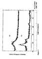
- FIG. 2is a representation of the x-ray diffraction (XRD) pattern of MOCVD-grown W 2 N films grown in Example 1 at substrate temperatures of: (a) 200° C. (film thickness of about 52 nm) and (b) 275° C. (film thickness of about 63 nm);
- FIG. 3is a representation of a bright field cross-section transmission electron microscopy (TEM) image of a representative 62 nm-thick MOCVD-grown W 2 N film formed in Example 1;
- TEMtransmission electron microscopy
- FIG. 4is a representation of Fast Fourier Transform (FFT) TEM images of the W 2 N samples of FIG. 3 from Example 1 showing an amorphous W 2 N phase.
- FFTFast Fourier Transform
- FIG. 5is a representation of Rutherford backscattering spectroscopy (RBS) spectra of MOCVD-grown W 2 N films formed in accordance with Example 1;
- FIG. 6is a representation of a cross-section scanning electron microscopy (CS-SEM) image of MOCVD-grown W 2 N films in nominal 0.25 ⁇ m trench structures;
- FIG. 7is a representation of XRD patterns of a W 2 N films produced using thermal CVD in accordance with an embodiment of the invention as set forth in Example 2;
- FIG. 8is a representation of XPS spectra of the tungsten nitride films of Example 2.
- FIG. 9is a representation of RBS spectra of the tungsten nitride films of Example 2.
- FIG. 10is a representation of a typical cross-section TEM-magnified view of a representative silicon substrate upon which oxide trench patterns, of nominal diameter 200 nm and 6:1 aspect ratio, are formed and upon which a conformal tungsten nitride coating of Example 3 has been deposited;
- FIG. 11is a representation of XPS spectra of the tungsten nitride films formed by the thermal CVD reaction in Example 3 according to an embodiment of the method;
- FIG. 12is a representation of Auger electron spectra of the tungsten nitride films of Example 3.
- FIG. 13is a representation of RBS spectra of the tungsten nitride films of Example 3.
- FIG. 14is a representation of a typical cross section TEM-magnified view of a representative silicon substrate upon which oxide trench patterns, of nominal diameter 180 nm and 5:1 aspect ratio, are formed and upon which a representative sample of a the conformal tungsten nitride coating in accordance with Example 3 has been deposited; and
- FIG. 15is a representation of a typical cross-section TEM-magnified view of a representative silicon substrate upon which oxide trench patterns, of nominal diameter 300 nm and 4:1 aspect ratio are formed and upon which are conformal tungsten nitride coatings of Example 4.
- tungsten nitride and tungsten nitride films of the present invention and the tungsten nitride precursors of the inventionmay be used on a wide variety of substrates and for a wide variety of applications. While they, of course, are highly applicable in the microelectronic field, deposited thin films of tungsten nitride in accordance with the invention also form hard coatings which may be used as protective coatings in various fields such as for providing hard coatings to aircraft or other engine parts or as a substitute for silicon nitride or tungsten carbide in many applications in which such coatings are used.
- tungsten nitride filmsmay be used for hard coatings on drill bits to protect the life of the drill bit in place of tungsten carbide and similar drill bit coating materials.
- other toolswhich are now provided with protective coatings, or materials which are formed of tungsten carbide, but are still vulnerable to oxidation can be coated with the tungsten nitride films of the invention to extend their life.
- the tungsten nitride of the inventionmay also be used s a cosmetic and/or protective coating for jewelry, in anti-reflective coatings for optical, optoelectronic, and lithography applications.
- light bulb filamentsmay be coated with the tungsten nitride films of the invention in order to extend filament life.
- the tungsten nitride films of the inventionare more advantageous than tungsten carbide for applications such as those mentioned above, because the tungsten nitride films of the invention can be formed as amorphous films with little or no polycrystallinity. As a result, such films do not oxidize as quickly as tungsten carbide. In addition, the tungsten nitride films emit light from a different part of the spectrum than materials such as tungsten carbide and appear more gold than black in appearance. As a result of the unique emission spectrum of the films, such films are more thermodynamically efficient and do not absorb heat as quickly from the environment.
- Such efficiencyis particularly advantageous in applications in which heat is detrimental and can lead to failure, such as in many microelectronic applications and in light bulb filaments where heat contributes to filament failure. While such intended applications clearly benefit from the tungsten nitride, tungsten nitride films and film forming processes of the present invention, it will be understood, based on this disclosure that such films have a wide range of potential uses and will provide significant advantages in many fields. As a result, while the tungsten nitride and tungsten nitride films and processes are generally described herein with respect to their potential use in microelectronics, such uses should not be considered limiting in any regard.
- the inventionincludes processes for producing tungsten nitride and tungsten nitride films as well as a process for the chemical vapor deposition of tungsten nitride films onto a substrate.
- the inventionfurther includes tungsten nitride precursors capable of forming a tungsten nitride film and a tungsten nitride coated substrate.
- Such tungsten nitride films, as well as other thin films,may further be produced in accordance with the process for producing a film by atomic layer deposition of the invention.
- tungsten nitrideis formed by reacting a tungsten carbonyl compound with a nitrogen-containing reactant gas such as preferably ammonia, and at a preferred temperature of less than about 600° C.
- the tungsten nitridecan have tungsten and nitrogen in varied stoichiometric ratios, but preferably includes tungsten nitride in the form of WN x , wherein x is preferably characterized by the relationship, 0.1 ⁇ x ⁇ 2.0.
- the ratio of gaseous flow of nitrogen containing reactant to the tungsten source precursorranges from about 1000:1 to about 1:1000, more preferably from about 100:1 to about 1:1 and most preferably from about 2:1 to about 1:1, however, it will be understood that the range of ratios for the precursors also is related to the desired W:N ratio desired in the resulting film for a given application.
- the tungsten carbonyl compound used in the inventionmay be any W 0 complex of carbonyl (CO) with tungsten (W) which is preferably free of fluorine, including most preferably tungsten hexacarbonyl also known as hexacarbonyl tungsten, i.e. (W(CO) 6 ). However, one or more of the carbonyl groups may also be substituted with electron pair donors or similar ligands.
- Tungsten hexacarbonylhas the following properties: a melting point of 169-170° C.; a vapor pressure at 35° C. of 2 torr; a ⁇ H form of ⁇ 227 kcal/mole; and a specific gravity of 2.65.
- Tungsten hexacarbonylis available as a white, odorless powder which is stable in air and which has a toxicity level (oral in rats) of LD50:>5000 mg/kg.
- one of the carbonyl groupsis readily substituted with groups or elements such as ammonia, amine, halogens and electron pair donors such as oxygen compounds and the like which may be used to assist in transport of the tungsten carbonyl compound to the deposition area as described further below.
- the carbonyl groupsare readily substituted by nitrogen in the processes of the present invention, particularly in the CVD processes of the invention.
- the tungsten carbonyl compoundhas the following formula (I):
- Xis a two-electron donor or a ligand such as ammonia, amine, carbonyl and halogens such as chlorine, bromine and iodine.
- Xmay be oxygen-containing organics such as tetrahydrofuran, trimethyphosphine and compounds of similar structure which can act as two-electron donor compounds While fluorine may be used, it is not preferred due to its high reactivity. Any other similar groups which may be easily displaced by nitrogen in the deposition process but which do not have a significant adverse affect on the formation of tungsten nitride may also be used as the ligand X.
- nis preferably 0 or 1.
- Tungsten nitride formed from reacting tungsten carbonyl compounds such as those described above with a nitrogen-containing gas such as nitrogen, ammonia, and hydrazine, most preferably ammonia at a temperature below 600° C.are within the scope of the invention.
- Tungsten nitride, preferably of the stoichiometry WN x with 0.1 ⁇ x ⁇ 2.0,are formed by reacting the tungsten carbonyl compound and nitrogen-containing gas, preferably ammonia, and more preferably, in the presence of hydrogen. Hydrogen when employed assists in the decomposition process of the tungsten nitride precursor, i.e., the tungsten carbonyl compound.
- the use of hydrogencan aid in removal of (CO) ligands from the tungsten carbonyl compound by bonding with the ligands once they are dissociated from the decomposing tungsten carbonyl compound.
- the hydrogencan aid in preventing their reincorporation in the resulting tungsten nitride film, thereby minimizing potential contaminants in the resulting film.
- a further example of a reaction in accordance with the present invention using a tungsten carbonyl compound and a nitrogen-containing reactant gas in the presence of hydrogen, such as tungsten hexacarbonyl and ammonia with hydrogen,proceeds as follows:
- CO, C and Omay range from 5 at % to more than 50% depending upon the substrate temperature, with higher substrate temperatures yielding lower CO, O, and C incorporation.
- the production of hydrogenated and nitride byproducts in formulas (III) and (II)are critical to the growth of pure tungsten nitride films without CO, C or O contamination.
- the temperaturebe kept within the range of from about 200° C. to about 350° C. in order to receive the most benefits of the low temperature advantages of the present invention. Further, the lower the temperature within this range, the lower the level of polycrystallinity, and, in accordance with one preferred embodiment of the invention, tungsten nitride formed using the specified reaction at temperatures of from about 200° C. to about 275° C. form a substantially completely, if not completely, amorphous phase tungsten nitride.
- the tungsten carbonyl compounds described abovewhich are capable of forming a tungsten nitride film in the presence of a nitrogen-containing reactant gas such as ammonia at the temperatures noted above further provide unique precursors for the formation of tungsten nitride and tungsten nitride films, particularly in accordance with various deposition processes as described further below.
- the tungsten nitride films formed in accordance with this inventiondemonstrate low resistivities of less than about 600 ⁇ /cm, preferably less than about 400 ⁇ /cm and most preferably less than 300 ⁇ /cm at temperatures below about 600° C.
- the tungsten nitride films of the inventionmay be formed in accordance with any suitable method, preferably a CVD method and using any of a wide number of commercially available or specially modified sputtering or other CVD apparatuses, as described further below.
- tungsten nitridegenerally for a wide variety of applications and for coatings and films can be formed using other suitable pathways, including sputtering, collimated sputtering, nitridation from the liquid phase, annealing of tungsten films in a nitrogen-containing ambient, ion-beam deposition, and laser ablation.
- Formation of tungsten nitride and deposition of tungsten nitride filmsoccurs generally in accordance with the invention by heating one or more tungsten carbonyl compounds to temperatures in the range of from about 85° C. to about 100° C. and transporting the tungsten carbonyl compound(s) preferably by a mass flow device into a deposition chamber which preferably has a substrate for receiving the tungsten nitride reactant product. If a transport gas is used, as described further below, such as hydrogen, the tungsten carbonyl compound(s) may be transported first to a mixing zone in which the hydrogen, or other gas, is mixed into the tungsten carbonyl compound(s) which act as a precursor(s).
- a transport gassuch as hydrogen
- the reaction chamberpreferably contains a substrate at a temperature of less than about 600° C., preferably from about 200° C. to about 350° C. and most preferably not greater than about 275° C.
- Ammonia, or another nitrogen-containing reactant gasis introduced into the deposition chamber. Molar equivalents of ammonia or other reactants are provided which would displace one of the carbonyl groups on the molecule of the tungsten carbonyl compound precursor(s), and can be introduced into the mixing zone before the reaction chamber in order to receive the benefit of prereaction and to increase deposition rate, however, caution must be taken as such benefits may be offset by vapor phase particle formation if mixing is poor.
- tungsten nitride source precursor of the inventionprovides a tungsten nitride growth process which is relatively independent of the type of substrate used. This is desirable because more selective tungsten nitride CVD processes available in the prior art are not feasible within the constraints imposed by prevailing manufacturing practices, particularly with respect to the need for ultra clean room sample preparation and associated processing conditions to ensure selectivity.
- the precursorsmay be used to provide conformal tungsten nitride films on various substrates, including blanket substrates (non-patterned) and patterned substrates which have sub-micron features and structures.
- the filmsare useful on such substrates as a result of their ability to completely fill the aggressive device features of emerging integrated circuitry technologies and for their ability to form a hard, protective coating.
- such filmsmay be used as resistant barrier layers and/or adhesion promotor layers for copper metallization schemes in which copper films act as signal-carrying conductors across each metallization level in a computer chip (interconnects) or as barrier materials and/or adhesion promoters in copper metallization schemes having signal-carrying conductors that connect two different levels in a computer chip (plug).
- the conformal filmsare also useful in applications involving the deposition of metals by plating techniques, including deposition of metals by electroless plating in which such protective or barrier coatings are desired to protect the metals coated on a surface, to protect a surface from an outer coating as a liner or barrier, or to provide interlayer protection between layers in multilayer coatings or multilayer plating.
- “conformal” coatingmeans a coating which evenly covers a substrate having a complex topography.
- the evenness of the coatingcan be measured by, for example, examining the thickness of the coating along the walls and bottom of the hole in the substrate, and determining the variation in the thickness of the coating.
- sub-quarter-micron substratesare conformally coated when the coating has a thickness, measured at any point normal to the surface of a wall or floor of a hole in the surface of the substrate, which is within 25% of the thickness at any other point in the hole.
- the variation of coating thickness of tungsten nitride films formed using the precursors of the inventionis within 10%, and more preferably within 5%, that is, at no point is the thickness of the coating either 10% or preferably 5% greater or smaller than the average coating thickness.
- step coveragerefers to the ratio of the coating thickness at the bottom of a feature such as a trench or via, to the thickness of the coating on the top surface of the substrate adjacent to the feature, where the ratio is multiplied by 100 to provide a percentage value.
- the processes of the invention and deposited tungsten nitride films formed from the precursors of the inventionhave conformal or complete filling of complex substrate topographies depending on the intended use of the substrate.
- substrates which may be coated with the tungsten nitride films of the present inventionare those which are intended to be used in an integrated circuit and which have complex topography including holes, trenches, vias and the like for providing the necessary connections between materials of various electrical conductivities that form a semiconductor device.
- Other substrates which may be used with the tungsten nitride filmsare those which are intended for ultra-large scale integration (ULSI) integrated circuit technologies and are also patterned with holes, trenches, and other features with diameters of less than 1.0 micron, and often less than 0.5 microns, and even 0.25 microns or less. Such substrates having such small features are known as “sub-quarter-micron” substrates.
- Sub-quarter-micron substrateswhich may have tungsten nitride barrier and/or adhesion promotor type films deposited on them in accordance with the present invention include those having features with high aspect ratios of from about 3:1 to about 6:1 or more, where the aspect ratio is defined as the ratio of the depth of a feature to its diameter as viewed in cross-section.
- “sub-quarter-micron substrates”have feature diameters less than about 0.25 microns and an aspect ratio of typically larger than about 3:1. Those of aspect ratios of about 4:1 and greater are associated with substrates for ULSI circuitry.
- Exemplary substrate types which may be coated with deposited tungsten nitride films of the present inventioninclude blanket and patterned semiconductor substrates, such as silicon and gallium arsenide; substrates already coated with single or multilayer metallic coatings; surfaces requiring a hard protective coating; and substrates which require an adhesion promotor or barrier layer or which may also be further coated with other tungsten nitride films formed using the invention.
- Suitable substrates for receiving the filmsinclude, for example, steel, tungsten carbide, silicon nitride, as well as typical microelectronic application metals such as copper (Cu), tungsten (W), tantalum (Ta), titanium (Ti) and their binary, ternary and quaternary phases, such as a further layer of tungsten nitride (WN x ) having the same or a different value of x, tantalum nitride (TaN x ), titanium nitride (TiN x ), titanium-nitride-silicide (TiN x Si y ) and tantalum nitride silicide (TaN x Si y ) where x and y may have values ranging from, respectively, 0 to 2 and 0 to 3, preferably with respect to tungsten nitride, x is from 0.1 to 2.0.
- WN xtungsten nitride
- substrates which may be coated with tungsten nitride deposited films of the invention and formed from the novel precursors of the inventioninclude silicon dioxide, silicon nitride, or doped versions and mixtures thereof; low dielectric constant (k) insulator materials having K ⁇ 4.0, which are potential substitutes for silicon dioxide in emerging ULSI circuitry; titanium-based and tantalum-based diffusion barriers or adhesion promoter liners as well as other tungsten-based diffusion barriers or adhesion promotor liners, including those of pure tantalum, tungsten and titanium and their binary, ternary and quaternary alloys; metals, such as aluminum, beryllium, cadmium, cerium, chromium, cobalt, tungsten, gallium, gold, lead, manganese, molybdenum, nickel, palladium, platinum, rhenium, rhodium, silver, stainless steel, iron, strontium, tin, titanium, zinc, zirconium, and alloys and compounds thereof such
- substratesmay be used within the scope of the invention which would benefit from the application of a tungsten nitride films according to the invention.
- the substrate used with the precursor of the present inventionbe stable at the conditions as described herein for depositing tungsten nitride films on a particular substrate.
- substratesshould preferably be stable at temperatures up to about 600° C., depending on the intended use of the substrate.
- the tungsten nitride filmsmay be deposited first and then coated by deposition with other coatings such as metallic coatings or the tungsten nitride films may be deposited on a substrate or coated substrate such as a substrate having a metallic coating(s).
- the films of the inventionmay be deposited in any sequence or alternately layered. Such depositions may be performed ex situ, in different reactors, or in situ, either in the same reactor (a stand alone reactor) or in two or more separate reactors (for example, a cluster tool), each for deposition of one of the multilayered metallic coatings. If one reactor is used, it may be interconnected through leak-tight transfer arms and load locks which allow sample transfer without exposure to air.
- CVDchemical vapor deposition
- ALDatomic layer deposition
- ACVDatomic layer CVD
- the reactioncan occur in any suitable apparatus, however, it is preferred that the reaction occur using a CVD process in order to obtain high purity and conformality.
- a CVD processin order to deliver the tungsten nitride precursor to the reaction chamber, it is preferred but not required to use at least one transport gas.
- the transport gasmay include one or more reactant gases, such as nitrogen-containing reactant gas(es) and/or hydrogen.
- Hydrogencan act as a transport gas, and is kept from reacting in transport, for example, by using a delivery temperature in the delivery and transport lines which is not high enough to cause reaction of hydrogen and the tungsten carbonyl compound.
- the hydrogenassists in the decomposition process and also bonds with CO ligands resulting from the decomposition process assisting in removal of such ligands from the reaction zone and helping to prevent their incorporation into the tungsten nitride being formed.
- the transport gasmay include one or more inert gases which may function merely as a carrier to deliver the precursor to the reaction area.
- Preferred transport gasesare hydrogen or inert gases, however, it is within the scope of the invention to use a gas which is reactive within the deposition chamber for forming more stable intermediates during deposition.
- a reactant gassuch as hydrogen
- itis used in addition to a nitrogen-containing gas which will ultimately reacted with the tungsten nitride precursor used for forming the tungsten nitride film, and would carry out the roles of assisting in decomposition and removal of CO ligands and in preventing of contamination of the tungsten nitride in accordance with the reactions described above.
- inert gases for use in the transport gas in order to help transport the precursor to the reaction areawhich may be used instead of or included with any reactive gas such as hydrogen and/or nitrogen-containing reactant gas(es) within the transport gas include helium, argon, xenon, neon, krypton, carbon monoxide and/or mixtures and other combinations thereof.
- nitrogen-containing gasessuch as nitrogen, ammonia, hydrazine and the like may also be pre-mixed in some cases before the reaction zone with the transport gas(es) for certain processes within the scope of the invention, caution must be taken to avoid premature reaction prior to reaching the reaction chamber.
- the transport gas(es)may be varied depending on the particular process parameters used and the desired composition of the resulting tungsten nitride film desired.
- the gasesmay be added with the precursor and/or added separately into the deposition chamber.
- gases which can be used as ligands in the tungsten nitride precursorsuch as halogen, ammonia, amine, carbonyl compounds and similar electron donors or ligands.
- fluorinewhile it may be used, is not preferred due to its high reactivity.
- additional gasesmay be provided to the precursor and/or transport gas(es) entering the deposition chamber as well as, for example, other high electron density ligands, weak nucleophiles such as alkenes, alkynes, phosphines, diketones and mixtures thereof.
- Such compoundsmay also be introduced by dissolving them in the source precursor and vaporizing the mixture such that the compound is delivered along with the vapor state precursor as opposed to being provided as an additional gas(es) in the at least one transport gas.
- Preferred chemical vapor deposition methods used in the processes of the present inventionmay be thermal CVD, plasma-promoted CVD and ALCVD as described below although any CVD process may be used in the processes of the invention.
- “Thermal” CVD as used hereinis intended to describe a CVD process in which all components are introduced to the chamber in gaseous form and the energy needed for bond cleavage is supplied completely by thermal energy.
- Plasma-promoted CVDas used herein is intended to describe a CVD process in which all components are introduced into the reactor in gaseous form, and the energy needed for bond cleavage is supplied in part by high energy electrons formed in a glow discharge or plasma having a plasma power density of from about 0 to about 100 W/cm 2 .
- Plasma-promoted CVDtakes advantage of the high energy electrons present in glow discharge to assist in dissociation of gaseous molecules, as is the case of plasma-enhanced CVD, a known CVD technique. Also plasma-assisted CVD may be used, although it does not take advantage of the use of low power plasma densities as with plasma-promoted CVD.
- the use of low power plasma densitycan prevent electrical damage to the film and substrate. If plasma-promoted CVD is used in the processes of the present invention, it is preferred that the plasma power density be from about 0.01 W/cm 2 to about 10 W/cm 2 , and more preferably the density should be less than 0.5 W/cm 2 .
- a tungsten nitride filmis deposited by thermal CVD on a substrate.
- the source precursor, the at least one transport gas, preferably hydrogen and the substrateare maintained in the reaction chamber at an interior reaction substrate temperature of up to about 600° C., preferably from about 200° C. to about 350° C.
- the preferred substrate temperatureis from about 200° C. to about 275° C. Temperatures higher than about 275° C. tend to form polycrystalline phase tungsten nitride.
- a nitrogen-containing gasis introduced into the chamber, including gases such as nitrogen, ammonia, or hydrazine, most preferably ammonia.
- the componentsare maintained under these conditions for a period of time sufficient to deposit a tungsten nitride film on the substrate, preferably for about 10 seconds to about 30 minutes depending on the processing conditions used and the desired film thickness.
- the tungsten nitride filmis deposited by introducing the tungsten nitride precursors of the invention alone or with a transport gas as described above, preferably hydrogen; a mixture of hydrogen with argon and/or xenon; or either of hydrogen alone or with an inert gas further in combination with an additional nitrogen-containing gas such as ammonia.
- a transport gasas described above, preferably hydrogen; a mixture of hydrogen with argon and/or xenon; or either of hydrogen alone or with an inert gas further in combination with an additional nitrogen-containing gas such as ammonia.
- nitrogen-containing gasbe introduced as a reactant gas separately from the precursor.
- plasma-promoted CVDis used to deposit a tungsten nitride film on a substrate.
- the source precursoralone or in combination with a transport gas as described above, preferably hydrogen and/or an inert gas is introduced together with, or preferably separately from a nitrogen-containing reactant gas as described above, and the substrate is maintained in the chamber at an interior reaction substrate temperature of less than about 600° C., and preferably from about 200° C. to about 350° C., and most preferably from about 200° C. to about 275° C.
- the plasma provided to the chamberhas a plasma power density of from about 0.01 to about 10 W/cm 2 and a frequency of preferably from about 0 Hz to about 10 8 Hz and more preferably from about 100 Hz to about 10 8 Hz.
- the conditionsare maintained for a period of time sufficient to deposit a tungsten nitride film onto the substrate, preferably from about 10 seconds to about 30 minutes depending on the processing conditions and the desired film thickness.
- a nitrogen-containing gassuch as ammonia is introduced into the chamber.
- a CVD reactormay be any CVD reactor which preferably has the following basic components: a precursor delivery system for storing and controlling the delivery of the tungsten nitride source precursor, i.e., the tungsten carbonyl compound, a vacuum chamber, a pumping system for maintaining an appropriately reduced pressure, a power supply for creating plasma discharge (when using plasma-promoted CVD), a temperature control system, and gas or vapor handling capability for metering and controlling the flow of reactants and products resulting from the process.
- the precursor delivery systemmay be a pressure-based bubbler or sublimator, a hot-source mass flow controller, a liquid delivery system, a direct liquid injection system, or other similar apparatus.
- the source precursor mixtureis preferably placed in a reservoir which may be heated, to a temperature sufficient to ensure sublimation or vaporization but not so high as to cause premature decomposition of the tungsten carbonyl compound, and preferably from about 85° C. to about 115° C.
- the reservoirmay be heated by a combination of resistance heating tape and associated power supply. The heating temperature will vary depending upon the physical properties of the precursor used and the presence of any mixed gases as transport gases and/or reactant gases.
- a mass flow controllerwhich may be isolated from the reservoir by a high vacuum valve, is preferably provided to control gas flow into the reservoir.
- Various transport gasesmay be used as noted above, such as hydrogen, helium, argon, or xenon as inert transport gases and/or nitrogen-containing gases as reactant gases, when a conventional pressure- and/or temperature-based mass flow control delivery system is used as the delivery system for the source precursor into the deposition chamber.
- gasesmay also function as pressurizing agents when using a liquid delivery system.
- gasesare introduced into the tungsten nitride precursor in a mixing zone prior to entering the reaction area.
- Liquid delivery systemsmay include a combination micropump and vaporizer head.
- a preferred example of a delivery system for the tungsten nitride source precursoris a hot source mass flow controller, for example, an MKS Model 1150 MFC which does not require the use of a carrier or pressurizing gas.
- a solid source delivery systemsuch as the MKS 1153 system which also does not require use of a carrier gas or pressurizing gas for delivery.
- the tungsten nitride precursor, in vapor form, or a mixture of the tungsten nitride precursor and any transport gas combined with the precursorare transported into the CVD reactor through delivery lines which are preferably maintained at the same temperature as the reservoir, using a combination of resistance heating tape and an associated power supply to prevent precursor recondensation.
- the CVD reactormay be an cold-wall stainless steel reactor which can accommodate eight-inch wafer or 200 mm preferably equipped with plasma generation capability.
- the plasmamay be generated by various sources, such as direct current plasma, radio frequency plasma, low frequency plasma, high density plasma, electron cyclotron plasma, inductively coupled plasma, microwave plasma or other similar sources.
- the plasmamay be used for dual purposes such as for in situ pre-deposition substrate cleaning and/or for actual deposition if using plasma-promoted CVD.
- the reactoris preferably also equipped with an electrical bias on the substrate.
- the biascan be derived from direct current, a low radio frequency of from less than about 500 kHz to about 10 6 kHz, or a microwave frequency of from about 10 6 to about 10 8 kHz or from other suitable sources.
- Evacuation of the CVD deposition reactormay be accomplished by various pumping systems.
- Suitable pumping systemsinclude a high vacuum (10 ⁇ 6 torr or less) pumping system, which may use either a cryogenic-type or a turbomolecular-type pump, preferably a cryogenic-type pump. Such a system ensures a high vacuum base pressure in the reactor.
- a vacuum system having a roots blower or dry pumpmay also be used for handling the high gas throughput during CVD runs.
- the high vacuum system and the roots blower or dry pump systemare both preferably isolated from the CVD reactor by high vacuum gate valves.
- the CVD reactoris preferably equipped with a high vacuum load-lock system for transporting and loading substrates as large as about 300 mm wafers into the reactor in order to provide tight control over the cleanliness of the CVD chamber and to prevent undesirable contamination from exposure to ambient conditions during sample loading and unloading.
- the reactormay also interface with a vacuum central handling unit which may be used to transfer the substrate between multiple CVD reactors to deposit sequential or alternating layers of tungsten nitride and other types of films for single or multilayered coatings or metallization schemes such as those described above.
- the tungsten nitride source precursoris heated to a temperature high enough to ensure the precursor's sublimation or vaporization, but not so high that the precursor would be prematurely decomposed.
- the liquid in the reservoiris generally at room temperature.
- the vaporizer headnot the liquid in the reservoir, is heated to a temperature high enough to ensure sublimation or vaporization without causing decomposition.
- any gaseous substancemay be used which is substantially inert to the source precursor mixture or which reacts with the source precursor to form one or more intermediates which are more easily transported to the reaction zone and/or which could more readily decompose to yield the desired tungsten nitride film.
- gases for use in gas delivery systemsinclude those listed above as transport gases.
- Hydrogenis particularly preferred as a carrier gas in a gaseous delivery system for both thermal CVD and plasma-promoted CVD.
- the flow rate of the gas in the gaseous delivery system for either plasma-promoted or thermal CVDpreferably varies from about 10 standard cm 3 /min to about 25 standard I/min, and preferably from about 10 to about 5000 cm 3 /min.
- the flow rate of the vapor of the tungsten nitride source precursorcould range from about 0.01 to about 500 standard cm 3 /min, and more preferably from about 1 to about 100 standard cm 3 /min.
- the transport gas for forming films according to the method of the inventionmay be any of those described above, and is preferably hydrogen for both thermal CVD and plasma-promoted CVD.
- the flow rate of the at least one transport gas which may be or may include hydrogenis preferably from about 10 standard cm 3 /min to about 10 standard l/min, and more preferably, from about 100 standard cm 3 /min to about 5 l/min.
- the corresponding reactor pressureis preferably from about 0.1 torr to about 1000 torr, and more preferably from about 0.2 to 10 torr.
- the transport gas(es)may include one or more carrier or reactant gases, it should be understood that the function of the gases is determined by the type of gases being used, the nature of the precursor, the type of CVD and the associated process parameters. Transport gases while performing the function of transporting the tungsten nitride source precursor vapor to the substrate may also undergo reaction in the chamber during deposition. Further, reactive gases such as nitrogen-containing reactant gases may include inert components and may be introduced together with the precursor or, more preferably, independently thereof. All gases, regardless of their inert or reactive nature which are used in the transport gas(es) assist the tungsten nitride source precursor in reaching the substrate.
- Tungsten nitride and tungsten nitride films according to the inventionmay also be prepared using thermal CVD based on the method of the present invention.
- a tungsten nitride filmit is preferred that hydrogen, argon, helium and/or xenon, preferably hydrogen, are introduced as the transport gas(es) and that there also be a nitrogen-containing reactant gas introduced together with the transport gas or independently thereof as discussed above.
- the preferred conditions and apparatusare as described above.
- Tungsten nitride filmsmay also be formed using ALD or ALCVD techniques.
- the tungsten nitride filmsare formed using the ALCVD process of the invention which was developed by applicants and found to be useful to form atomic level thin films of tungsten nitride in accordance with the invention.
- the ALCVD process of the inventionmay also be used to form other thin films, including but not limited to tantalum, tantalum nitride, tungsten, copper, silicon nitride, tantalum-nitride-silicide and any other thin films useful in various microelectronic devices, similar small microstructures or as protective or other hard coatings for objects.
- This ALCVD process of the inventionis particularly useful in the processes of the present invention for forming the tungsten nitrides of the invention having the preferred stoichiometry as noted above.
- the ALCVD process of the inventioninvolves atomic layer CVD (ALCVD) or atomic layer deposition (ALD) (hereinafter referred to collectively for purpose of convenience as ALCVD) in which very thin liners of atomic level controllability can be formed and the resulting liners and films can be used for incorporating in semiconductor structures for filling in fabrication flaws.
- ACVDatomic layer CVD
- ALDatomic layer deposition
- Such techniquesare based on the principle of self-limiting adsorption of individual monolayers of the source precursor on the substrate surface, followed by reaction with an appropriately selected reactant to grow a single molecular layer of the desired material. Thicker films are produced through repeating the procedure through repeated growth cycles until the desired target thickness is met.
- the applicantshave developed a modified ALCVD in which a substrate with at least one surface to be coated, a source precursor, preferably a single source precursor, and any reactant(s), preferably in gaseous or vapor form, for a necessary for forming a desired reactant product and which is capable of reacting with the precursor to form a desired reactant product on the substrate surface such as a film, liner, layer or other similar material are introduced into a deposition chamber.
- a source precursorpreferably a single source precursor
- any reactant(s)preferably in gaseous or vapor form
- the reactant(s) and precursorare pulsed sequentially into the deposition chamber, with inert gas pulses in between the reactant and precursor pulses, for a specified, preferably predetermined short period of time, and allowed to react on a substrate surface to form an atomic layer of desired thickness, preferably on the scale of an atomic monolayer.
- the pulsing of the precursoris carried out using conventional pressure-based and/or temperature-based mass flow control-type delivery systems, solid-source-type delivery systems, which could be coupled to the deposition chamber, if needed, through pneumatically or electronically controlled valves that allow introduction of the source precursor in short pulses into the deposition chamber.
- the pulsing of the reactant gasis carried-out using electronic mass flow controllers which can also be coupled to the deposition chamber, if needed, through a pneumatically or electronically controlled valves that allow introduction of the source precursor in short pulses into the deposition chamber.
- the time period of the precursor and reactant gas pulsevaries in accordance with the reaction rate, reactivity of the components used, the reactor pressure, substrate temperature, and desired thickness. For example, the faster the reaction and/or higher the component reactivities with respect to each other, the shorter the time period.
- the pulse time period for the precursor and reactant gasranges from about 0.5 seconds to about 10 minutes, and more preferably, from 1 second to five minutes.
- the pulse times for the precursor and reactant gasare varied to achieve layers of preferred thickness from about 0.25 nm to about 10 nm and, more preferably, from about 0.5 nm to about 2.5 nm. It will be understood, based on this disclosure, that the time and thickness may be varied for different applications and optimized within the parameters of a given reaction and deposition, provided the thin layers benefits of the invention are not significantly diminished.
- a basic overview of the processincludes introducing into a deposition chamber a substrate having a surface, and heating the substrate to a temperature that allows adsorption of the tungsten source precursor or an appropriate intermediate of the source precursor.
- the heated substrate surfaceis then exposed to a tungsten source precursor for a period of time sufficient to form a self-limiting monolayer of the source precursor or appropriate source precursor intermediate on the substrate surface.
- the precursoris introduced into the deposition chamber by pulsing it using an appropriate precursor delivery method with or without the use of a transport gas, which may be any of the transport gases described above.
- the deposition chamberis then purged with an inert gas for a period long enough to ensure removal of all gas phase precursor species, without removing the adsorbed precursor layer.
- the inert gasis introduced by pulsing using an appropriate mass flow controller or valving system. Any such system, including those mentioned above and known to those skilled in the art or to be developed may be used for such purpose.
- a nitrogen-bearing gassuch as the nitrogen-containing reactant gases described above is then introduced into the deposition chamber for a period long enough to ensure reaction with the adsorbed precursor layer, leading to the formation of a first WN x atomic layer on the substrate surface.
- the nitrogen bearing gasis also introduced by pulsing using an appropriate mass flow controller or valving system.
- the deposition chamberis preferably again purged with an inert gas for a period long enough to ensure removal of all remaining nitrogen-bearing gas from the deposition chamber.
- the inert gasis introduced by pulsing using an appropriate mass flow controller or valving system and the gas introducing and purging steps described above are repeated in a sequential and alternating manner until the desired tungsten nitride film thickness is achieved through atomic layer by atomic layer growth.
- an inert, cleaning or purge gassuch as argon, xenon, nitrogen, krypton, or the like, preferably argon or nitrogen, is pulsed into the deposition chamber preferably in the same manner and using similar apparatus as was used with respect to pulsing the reactant gas into the reactor in order to remove any remaining precursor, reactant or reaction byproducts from the deposition chamber.
- the purgingshould continue for a sufficient period of time to terminate the reaction, which time will vary for different reactions.
- purgingoccurs from about 0.5 seconds to about 10 minutes, and more preferably, from 1 second to five minutes.
- the processmay be stopped with the formation of only a thin monolayer of the preferred thicknesses as noted above, or alternatively, the process may be repeated by pulsing the precursor and any necessary reactant(s) again into the chamber to form another atomic film of desired thickness on the prior film and further purging as described above.
- This process of intermittent pulsing of reactant(s) and precursor followed by purging with inert gascontinues until a film is formed of desired thickness, preferably a total film thickness of from about 2.5 nm to about 1 ⁇ m, although the total thickness would be determined by the ultimate application of the film.
- alloy layersmay also be formed by mixing more than one precursor and/or more than one reactant or by varying the layers to include different species.
- the substrate temperatureis maintained at a temperature high enough to allow precursor species adsorption, but not so high as to cause premature precursor decomposition.
- the substrateis maintained in the chamber at an interior reaction substrate temperature of less than about 450° C., more preferably from about 50° C. to about 350° C., and most preferably from about 100° C. to about 275° C.
- all other processing conditionsincluding flow rates and pressure ranges, are similar to those noted above for thermal CVD.
- a critical pathway in the successful achievement of ALCVD growthis the adsorption on the substrate surface of precursor intermediate species that are conducive to the monolayer-by-monolayer reaction with reactant gases.
- the ALCVD reaction of W(CO) 6 and ammoniais believed to proceed according to the following pathways:
- This ALD or ALCVD processcan be adapted for use in forming tungsten nitride and tungsten nitride films according to the present invention, although it will be understood, based on this disclosure that the process is such that any suitable reaction process, particularly any suitable CVD reaction process, may be used to form tungsten nitride and tungsten nitride films according to the present invention provided the temperature is kept at the desired levels, and preferably below about 600° C.
- Reactor Base Pressure⁇ 10 ⁇ 6 torr Reactor Process Pressure 0.2-0.5 torr Precursor Flow Rate 1-20 standard cm 3 /min Hydrogen Flow Rate 50-200 standard cm 3 /min Ammonia Flow Rate 100-500 standard cm 3 /min Growth Rate 4-10 nm/min
- XPS studieswere performed using a Perkin-Elmer Physical Electronics Model 5600 multi-technique system with a spherical capacitor analyzer. The analyzer was calibrated using the gold f 7/2 line at 83.8 eV as a reference line. All spectra were acquired using a pass energy of 58.7 eV at a resolution of 0.25 eV. The primary x-ray beam employed was Mg Ka at 1274 eV, with primary beam energy and power of, respectively, 15 keV and 300 W. the results were standardized with a pure tungsten film sputtered on a silicon substrate since a W 2 N standard was not available.
- XPS resultsindicated that at the lowest processing temperature investigated, where precursor dissocation would be expected to be the least efficient given the reduced thermal budget available to the decomposition reaction, the films grown had carbon and oxygen concentrations of ⁇ 5 at %.
- XPSindicated a constant N:W ratio throughout the bulk of the tungsten nitride films.
- high resolution XPS elemental core peak analysiswas performed to determine the exact nature of the tungsten nitride phase produced.
- XRD analyseswere carried out on a Scintag XDS 2000 x-ray diffractometer equipped with a Cu Ka x-ray source and a horizontal wide angle four axis goniometer with stepping motors which allowed independent or coupled ⁇ /2 ⁇ axes motion.
- XRD spectrawere collected in the low angle incidence geometry, with an angle of incidence of 5° being used (angle as measured between the incident beam and the sample surface). In this mode, data collection is performed by fixing the incidence angle at 5°, and the XRD pattern is collected for 2 ⁇ ranging from 30° to 80°.
- XRDtungsten nitride reference patterns from the standard Joint Committee for Powder Diffraction Standards (JCPDS) powder diffraction file (PDF).
- JCPDSJoint Committee for Powder Diffraction Standards
- PDFpowder diffraction file
- XRDindicated a completely amorphous phase for films grown at substrate temperatures below 275° C., as shown in FIG. 2 in spectra (a).
- films grown at substrate temperatures above 275° C.exhibited XRD reflections that are consistent with JCPDS PDF for a W 2 N reference pattern, as shown in spectra (b) of FIG. 2.
- the XRD findingsare thus in agreement with the XPS data in terms of the formation of W 2 N phase.
- FIG. 3displays a representative cross-section TEM bright field image of a W 2 N film deposited at 200° C.
- TEMconfirmed the XRD data in terms of the amorphousness of 30 nm-thick W 2 N films. This result is also supported by FFT analyses, as exhibited in FIG. 4, which yielded a pattern that is characteristic of amorphous structures, namely a continuous diffuse ring with no diffraction spots.
- RBSRutherford backscattering spectroscopy
- W 2 N conformalitywas studied using cross-section scanning electron microscopy (CS-SEM).
- CS-SEMwas carried out on a Zeiss SDM940 microscope, employing a 20 keV primary electron beam and a beam current of 3.0 mA. Images taken by CS-SEM show step coverage of W 2 N films to be better than 90% in nominal 0.25 ⁇ m trench structures, as demonstrated in the CS-SEM displayed in FIG. 6. In this case, step coverage was defined as the ratio of film thickness at the bottom of the structure to that in the field.
- the low-temperature MOCVD process used in accordance with the present inventionprovided for the formation of tungsten nitride and tungsten nitride films for potential applications such as for a diffusion barrier in emerging copper-based metallization schemes among others.
- the processis based on the reaction of tungsten carbonyl compounds as tungsten nitride source precursors, preferably the non-fluorinated tungsten hexacarbonyl (W(CO) 6 )) with a nitrogen-containing reactant gas such as ammonia (NH 3 ), and preferably in the presence of hydrogen (H 2 ).
- the tungsten nitride and tungsten nitride films formed in accordance with the present inventionmay be formed within a wide range of process parameters. Microstructural and microchemical analyses indicated that the tungsten nitride films were predominantly formed of a W 2 N phase, with carbon and oxygen contamination levels of ⁇ 5 at %, even at the lowest deposition temperature of 200° C. Films deposited below 275° C. were amorphous, while those deposited between 275° C. and 350° C. were polycrystalline. Resistivities as low as 123 ⁇ /cm were achieved for 50 nm-thick films, with corresponding step coverage being higher than 90% in nominal 0.25 ⁇ m trench structures with an aspect ratio of 4:1.
- Example 2the same procedures were used as described above in Example 1 in detail with the exception that in this Example, thermal deposition of a number of tungsten nitride films was carried out using a stand-alone single module deposition chamber and reacting tungsten hexacarbonyl with ammonia in the presence of hydrogen gas.
- the reaction parametersare shown below in Table 2.
- Example 2Using the above parameters, the following tests as set forth in Table 3 below, which are described in further detail in Example 1 were carried out and demonstrate that amorphous W 2 N films were formed with less than about 5 at % hydrogen, about 5-8 at % oxygen, and about 4-6 at % carbon. The relevant representative spectra for this Example are shown in FIGS. 7 - 10 . Further, the resistivity was measured using a four point probe and found to range between 300-400 ⁇ /cm. The RMS surface roughness and surface grain size was further measured using Atomic Force Microscopy (AFM) and found to be ⁇ 5% of the film thickness.
- AFMAtomic Force Microscopy
- Example 2the procedure of Example 1 was followed with the exception that thermal CVD of tungsten nitride films was undertaken using a cluster tool platform.
- the reactantswere tungsten hexacarbonyl and ammonia.
- the reaction conditionsare shown below in Table 4.
- TABLE 4 Parameter Name Parameter in Example 3Substrate Temperature 225° C. Ammonia Flow Rate 150 standard cm 3 /min Hydrogen Flow Rate — Process Pressure 0.5 torr Precursor Flow Rate 20 standard cm 3 /min Deposition Rate 4 nm/min
- the resulting films and coated substrates formed using the above parameterswere tungsten nitride films of varied compositions within the formula WN x where 0.1 ⁇ x ⁇ 2 . 0 .
- the oxygen and carbon impuritieswere less than about 1-3 at % O and less than about 1-2 at % carbon with no hydrogen.
- the resulting phases of the different filmsvaried from amorphous to amorphous with partial polycrystallinity in a ⁇ -phase.
- FIGS. 11 - 14show the characteristics of the films. The resisitivities were measured to be low and in the 100-250 ⁇ /cm range with a ⁇ 5% of film thickness surface roughness and surface grain size (AFM).
- the parameters and characteristics of the filmsare summarized below in Table 5.
- Tungsten nitride films formed at low-temperature MOCVD processesincluding various CVD methods, or in accordance with the ALCVD method of the present invention are capable of being produced in a wide process window, including substrate temperatures of up to 600° C., preferably from about 200° C.
- tungsten nitride precursor flow ratesof from about 1 to about 20 standard cm 3 /min
- nitrogen-containing reactant gas flow ratesof from about 100 to about 500 standard cm 3 /min
- reactor pressuresof from about 0.2 to about 0.5 torr.
- the resulting tungsten nitride and tungsten nitride filmsdemonstrate predominantly W 2 N phase, with carbon and oxygen contamination levels of typically ⁇ 5 at %, even at the lowest deposition temperatures. Films deposited between 200° C. and about 275° C. are amorphous in nature while those deposited between about 275° C. and 350° C. were more polycrystalline in nature. Resistivities as low as 123 ⁇ /cm were achieved in 50 nm-thick films, with corresponding step coverage being higher than 90% in nominal 0.25 ⁇ m trench structures with aspect ratio of 4:1.
- the MOCVD and/or the ALCVD process of this inventionmay be used to form W 2 N films using tungsten carbonyl compounds which are preferably non-fluorinated and provide a viable alternative to inorganic CVD using fluorinated tungsten hexafluoride.
- Thisis particularly significant in view of the potential elimination of transport and handling concerns attributed to the high reactivity of the fluorinated tungsten hexafluoride source and reliability issues pertaining to the possible inclusion of fluorine, a fast diffuser in metals such as copper, in tungsten hexafluoride processes.
- the films of the inventionfurther provide consistent film properties which are important particularly in microelectronic applications, including uniform electrical properties, stress free coatings, uniform lattice parameters or an amorphous structure. Such films also provide such benefits without damaging structures by exposure to high temperatures or corrosive byproducts
- Reactor Base Pressure⁇ 10 ⁇ 6 torr Reactor Process Pressure 0.2-0.5 torr Precursor Flow Rate 1-20 standard cm 3 /min Purge Gas (Argon) Flow Rate 50-500 standard cm 3 /min Ammonia Flow Rate 100-500 standard cm 3 /min Precursor Pulse Time 30 seconds to 2 minutes Purge Gas (Argon) Flow Rate 20 seconds to 3 minutes Ammonia Flow Rate 30 seconds to 2 minutes
- tungsten nitride filmsexhibited structural, electrical, and compositional properties similar to those listed in Table 5. Step coverage was nearly 100% in 300 nm-wide, 4:1 aspect ratio, trench structures, as shown in the typical TEM micrograph of FIG. 15.
Landscapes
- Chemical & Material Sciences (AREA)
- Organic Chemistry (AREA)
- Inorganic Chemistry (AREA)
- Engineering & Computer Science (AREA)
- General Chemical & Material Sciences (AREA)
- Chemical Kinetics & Catalysis (AREA)
- Crystallography & Structural Chemistry (AREA)
- Materials Engineering (AREA)
- Mechanical Engineering (AREA)
- Metallurgy (AREA)
- Chemical Vapour Deposition (AREA)
- Electrodes Of Semiconductors (AREA)
- Laminated Bodies (AREA)
Abstract
Description
- This application claims the benefit of U.S. Provisional Application No. 60/119,957, filed Feb. 12, 1999.[0001]
- As computer chip device dimensions continue their evolution towards feature sizes below 100 nm, new liner materials and associated process technologies are needed to ensure viable diffusion barrier and adhesion promoter performance between the conductor and the surrounding regions of silicon-based and dielectric-based materials. These liners must possess mechanical and structural integrity, good conformality within aggressive device features, high conductivity to minimize plug overall effective resistance, and thermal, mechanical, and electrical compatibility with neighboring conductor and dielectric material systems. Most importantly, liner materials are expected to meet these stringent requirements at increasingly reduced thicknesses, in order to maximize the real estate available for the primary metal conductor within the continuously decreasing device dimensions. In particular, liner thickness is predicted to decrease from 20 nm for the 0.15 μm device generation, to less than 6 nm for its 0.05 μm in counterpart as noted in the[0002]International Technology Roadman for Semiconductors,1999 Edition, Santa Clara, Calif., pp. 165.
- These needs are further complicated by the on-going transition from aluminum-based to copper-based metallization schemes, and requires exploring new candidate liner materials that are chemically and thermodynamically more stable towards copper diffusion and migration than the presently used titanium/titanium nitride materials. These include binary compounds, such as tantalum nitride (TAN[0003]x) and tungsten nitride (WNx), and ternary compounds such as tantalum-silicon-nitride (TaSixNy) and tungsten-silicon-nitride (WSixNy). See, M. Takayama et al.,J. Vac. Sci. Technol., B 14, pp. 674 (1996); M. Uekubo et al.,Thin Solid Films,286, pp. 170 (1996); and K. Nakajima et al.,Appl. Surf. Sci.,117/118, pp. 312(1997).
- Tungsten nitrides are refractory compounds with high densities and exceptional hardness and barrier properties. They are usually regarded as interstitial compounds, i.e., with a range of non-stoichiometric ratios of tungsten and nitrogen atoms. Even so, two simple stoichiometries are often represented, ditungsten nitride and tungsten nitride. Representative properties are as follows:[0004]
TABLE A Compound Density (g/cm3) Lattice Parameter W2N 12.0-17.7 0.412 WN same as above 0.289 - Manufacturing technology for the production of tungsten nitride is accomplished by the nitriding of tungsten with nitrogen or ammonia, often in the presence of hydrogen at temperatures above 600° C. and under pressure. E. Markel et al.,[0005]Kirk-Othmer Encyclopedia of Chemical Technology, “Nitrides,” 17, pp. 114 (1996). Manufacturing processes leading to tungsten nitride with more uniform properties and lower process temperatures are desirable since many potential applications for tungsten nitride films are temperature sensitive. For example, in microelectronic applications there is a need for a low temperature process for forming tungsten nitride, since such applications require consistent film properties in order to achieve uniform electrical properties and stress free coatings (uniform lattice parameters or amorphous structure) without damaging structures by exposure to high temperatures or corrosive by-products.
- While WN[0006]xpresents a potentially viable solution given its attractive properties as highly refractory material with excellent mechanical and chemical properties, there remains problems with achieving high conformality with low impurities. Since tungsten nitride can be deposited in amorphous form (see, B. Park et al.,J. Electron. Mater.,26, pp. 1 (1997)), it is highly desirable for microelectronic applications, given that an amorphous film inherently has no grain boundaries. The lack of grain boundaries provides added stability towards metal migration by eliminating grain boundaries as a primary path for metal diffusion. Accordingly, prior work in the literature has successfully demonstrated the applicability of W2N as an effective barrier against copper diffusion at temperatures as high as 750° C. M. Uekubo et al.,Thin Solid Films,286, pp. 170 (1996).
- Uekubo, noted above, has deposited tungsten nitride by reactive sputtering. Unfortunately, the application of sputtering techniques is limited by concerns over the ability to provide good conformality in sub-100 nm device structures.[0007]
- Tungsten nitride has also been deposited by chemical vapor deposition (CVD) from tungsten tetrafluoride (WF[0008]6) and ammonia (NH3). S. Marcus et al.,Thin Solid Films,236, pp.330 (1993). While such CVD-based methods could provide viable step coverage in such aggressive topographies, thereby allowing the potential use of the same CVD liner technology in multiple generations of sub-100 nm microprocessor and memory products, inorganic CVD from WF6and NH3poses challenges. The difficulties include: (a) transport and handling concerns attributed to the high reactivity of the fluorinated WF6source, (b) process concerns caused by potential gas phase particle generation in the reaction of WF6and NH3and (c) reliability issues pertaining to the possible inclusion of fluorine in the resulting WNxliner which is a fast diffuser in metals such as copper.
- M. H. Tsai et al.,[0009]Appl. Phys. Letters,68, pp. 1412 (1996) also demonstrates a metal-organic CVD (MOCVD) from a single tungsten source, i.e., bis-(tert-butyl-imido)bis(tertbutylamido)tungsten having the formula ((t-BuN)2W(NHt-Bu)2). MOCVD from such single source precursors typically requires high processing temperatures, in excess of 450° C., with resulting film resistivities generally greater than 620 μΩ/cm. Higher resistivities result from significant thermal sensitivity of such single source prior art tungsten precursors for MOCVD. At temperatures of about 450° C. and higher, the hydrocarbon-based ligands in such sources tend to decompose readily, leading to film contamination with carbon and, as a result, higher resistivity.
- Such recent attempts to generate WN[0010]xfilms consistent with microelectronic manufacturing have focused on methods utilizing tungsten hexafluoride as a precursor, with typical process windows for tungsten hexafluoride requiring temperatures greater than 450° C. as noted above with respect to Marcus et al. See also T. Nakajima et al.,J. Electrochem. Soc.,134, pp. 3175 (1987). Alternately, plasma methods using tungsten hexafluoride have been used, but these still require temperatures greater than 350° C. See C. Meunier et al.,Mater. Manufacturing Process.,13, pp. 415 (1998) and J. P. Lu et al.,J. Electrochem. Soc.,145(2), pp. L21 (1998). Both the tungsten hexafluoride and plasma methods share the corrosive by-products of ammonium fluoride and hydrogen fluoride which cannot only react with tungsten nitride, but also with other metals and dielectrics which are typically part of microelectronic structures, for example, silicon, silicon dioxide, and aluminum. Fluorine is also a fast diffuser in copper. The direct erosion of silicon by tungsten hexafluoride has also been reported. D. Baxter et al.,Chem. Mater.,8, pp. 1222 (1996).
- Attempts to use organic-tungsten compounds to produce tungsten nitride films involve precursors which, under the best reported conditions invariably incorporate carbon into the films and have not shown low resistivities. M. Tsai et al.,[0011]Appl. Phys. Lett.,68, pp. 1412 (1996). Dimethylamido-substituted tungsten compounds have been shown in model studies not to be stable enough to volatilize or undergo transport without vapor phase particle formation, which is inconsistent with the formation of uniform coatings. See, Baxter, above.
- Furthermore, as device sizes continue their trend towards smaller features, tungsten nitride liner materials must provide the required performance at continuously reduced thicknesses in order to maximize space availability for the actual copper conductor. Predictions published in the International Technology Roadmap for Semiconductors-1998 Update indicate the need for liners with thicknesses below 1 nm for the 50 nm node. These trends require the development and optimization of manufacturing-worthy processes for the reliable and reproducible deposition of conformal ultrathin liners with atomic level controllability. As a result, work in the prior art has demonstrated that techniques such as atomic layer CVD (ALCVD) and atomic layer deposition (ALD) are viable candidates for incorporation in sub-tenth-micron semiconductor device fabrication flows. DiMeo, Jr., et al., U.S. Pat. No. 5,972,430; Suntola et al., U.S. Pat. No. 5,711,811; Suntola et al., U.S. Pat. No. 4,389,973; and Suntola, et al., U.S. Pat. No. 4,058,430.[0012]
- These techniques are almost universally based on the principle of self-limiting adsorption of individual monolayers of source precursor species on the substrate surface, followed by reaction with appropriately selected reactants to grow a single molecular layer of the desired material. Thicker films are produced through repeated growth cycles until the desired target thickness is met. Unfortunately, the ALCVD approaches described in the prior art have not successfully reported the growth of WN[0013]xfilms with electronic grade quality for microelectronics applications, in part due to the lack of an appropriate metal-organic source chemistry which is amenable to the self-limiting adsorption in monolayer form on the substrate surface. In addition, the high chemical and thermal instability of many of the metal-organic tungsten source precursors used in the prior art can cause premature decomposition of the source chemistry upon contact with the substrate surface. The net outcome is the growth of highly contaminated films via a more conventional CVD-based thermolytic or pyrolytic approach, instead of the self-limiting, layer-by-layer, ALD approach. Even in the case of the inorganic tungsten hexafluoride source chemistry, there has not been a successful identification of an appropriate process window and/or intermediate precursor species that can successfully and reliably allow adsorption and decomposition in a layer-by-layer ALD mode.
- Accordingly, there is a need in the art for a method for producing tungsten nitride and tungsten nitride films for use in a variety of applications, and in particular for microelectronic applications which provides good conformality, does not have difficulties in transport or handling, does not lead to significant gas phase particle generation from reaction of the precursor(s) used with the nitrogen source and which avoids inclusion of corrosive materials such as fluorine in the resulting tungsten nitride liner which may diffuse rapidly in metals in microelectronic applications such as copper. There is further a need for such a method which can produce tungsten nitride and tungsten nitride films with low or no carbon impurities in the resulting materials and which produce sufficient resistivities. There is also a need in the art for a method to produce films, including tungsten nitride films, of increasingly smaller thicknesses while retaining high conformality and uniformity.[0014]
- There is further a need in the art to develop chemically-engineered, highly maleable tungsten source precursors for incorporation in atomically-tailored, interfacially-engineered, CVD processes for the deposition of highly conformal ultrathin tungsten nitride films, as thin as a few monolayers. Further, it would be desirable if these atomic-layer CVD (ALCVD) processes were able to demonstrate the necessary ability to chemically and structurally “nano-engineer” the substrate surface through tightly controlled interactions with the chemically-engineered source precursors or appropriate source precursor intermediates to allow sequential atomic layer by atomic layer growth of films such as tungsten nitride.[0015]
- The invention includes a process for the production of tungsten nitride, comprising reacting a tungsten carbonyl compound with ammonia at a temperature below about 600° C. In one embodiment of the process, the tungsten carbonyl compound is a compound according to formula (I):[0016]
- W(CO)(6−n)Xn (I)
- wherein X is a two-electron donor or a ligand selected from the group consisting of ammonia, amine, carbonyl and halogen and n is 0 or 1.[0017]
- The invention further includes a process for the production of a tungsten nitride film comprising reacting a tungsten carbonyl compound with ammonia at a temperature below about 600° C.[0018]
- A process for the chemical vapor deposition of a tungsten nitride film onto a substrate is also within the invention. The method comprises introducing into a deposition chamber, a substrate, a tungsten carbonyl compound in a vapor state and at least one nitrogen-containing gas, and maintaining a substrate temperature of from about 200° C. to about 600° C. for a period of time sufficient to deposit a tungsten nitride film on the substrate.[0019]
- A tungsten nitride precursor is further included in the invention which precursor comprises a tungsten carbonyl compound, and the precursor is capable of forming a tungsten nitride film in the presence of a nitrogen-containing reactant gas at a temperature of less than about 600° C.[0020]
- The invention also includes a tungsten nitride film having an electrical resistance of less than about 600 μΩ/cm, wherein the film is a reaction product of a tungsten carbonyl compound and a nitrogen-containing gas.[0021]
- A tungsten nitride coated substrate is also within the invention and it comprises a substrate coated on at least one side with a tungsten nitride film, wherein the tungsten nitride film has an electrical resistance of less than about 600μΩ/cm and is a reaction product of a tungsten carbonyl compound and a nitrogen-containing gas.[0022]
- 1. A process for forming a film by atomic layer deposition is also encompassed within the invention and includes introducing into a deposition chamber a substrate having a surface and heating the substrate to a temperature sufficient to allow adsorption of a tungsten source precursor or an intermediate of a tungsten source precursor. A tungsten source precursor is introduced into the deposition chamber by pulsing the tungsten source precursor to expose the heated substrate surface to the tungsten source precursor for a period of time sufficient to form a self-limiting monolayer of the source precursor or an intermediate of the tungsten source precursor intermediate on the substrate surface. An inert gas is introduced into the deposition chamber by pulsing the inert gas to purge the deposition chamber with an inert gas for a period of time sufficient to remove the tungsten nitride precursor in the gas phase but without removing adsorbed precursor in the monolayer. A nitrogen-containing gas is introduced into the deposition chamber by pulsing the nitrogen-containing gas for a period of time sufficient to react with the adsorbed precursor monolayer on the substrate surface and to form a first tungsten nitride atomic layer on the substrate surface. In a preferred embodiment, the process for forming a film by atomic layer deposition, further comprises introducing an inert gas by pulsing the inert gas into the deposition chamber to purge the deposition chamber of the nitrogen-containing reactant gas. The process for forming a film by atomic layer deposition as described above is repeated by pulsing in further precursor, then inert gas, then nitrogen-containing reactant gas in the manner noted above until a tungsten nitride film of a predetermined thickness is formed.[0023]
- The foregoing summary, as well as the following detailed description of preferred embodiments of the invention, will be better understood when read in conjunction with the appended drawings. For the purpose of illustrating the invention, there is shown in the drawings embodiments which are presently preferred. It should be understood, however, that the invention is not limited to the precise arrangements and instrumentalities shown. In the drawings:[0024]
- FIG. 1 is a representation of high resolution x-ray photoelectron spectroscopy (XPS) spectra of the W4f[0025]7/2elemental core peaks for (a) metal-organic chemical vapor deposition (MOCVD) W2N films formed in accordance with an embodiment of the process of the invention in Example 1 and (b) a sputtered pure W standard;
- FIG. 2 is a representation of the x-ray diffraction (XRD) pattern of MOCVD-grown W[0026]2N films grown in Example 1 at substrate temperatures of: (a) 200° C. (film thickness of about 52 nm) and (b) 275° C. (film thickness of about 63 nm);
- FIG. 3 is a representation of a bright field cross-section transmission electron microscopy (TEM) image of a representative 62 nm-thick MOCVD-grown W[0027]2N film formed in Example 1;
- FIG. 4 is a representation of Fast Fourier Transform (FFT) TEM images of the W[0028]2N samples of FIG. 3 from Example 1 showing an amorphous W2N phase.
- FIG. 5 is a representation of Rutherford backscattering spectroscopy (RBS) spectra of MOCVD-grown W[0029]2N films formed in accordance with Example 1;
- FIG. 6 is a representation of a cross-section scanning electron microscopy (CS-SEM) image of MOCVD-grown W[0030]2N films in nominal 0.25 μm trench structures;
- FIG. 7 is a representation of XRD patterns of a W[0031]2N films produced using thermal CVD in accordance with an embodiment of the invention as set forth in Example 2;
- FIG. 8 is a representation of XPS spectra of the tungsten nitride films of Example 2;[0032]
- FIG. 9 is a representation of RBS spectra of the tungsten nitride films of Example 2;[0033]
- FIG. 10 is a representation of a typical cross-section TEM-magnified view of a representative silicon substrate upon which oxide trench patterns, of[0034]
nominal diameter 200 nm and 6:1 aspect ratio, are formed and upon which a conformal tungsten nitride coating of Example 3 has been deposited; - FIG. 11 is a representation of XPS spectra of the tungsten nitride films formed by the thermal CVD reaction in Example 3 according to an embodiment of the method;[0035]
- FIG. 12 is a representation of Auger electron spectra of the tungsten nitride films of Example 3;[0036]
- FIG. 13 is a representation of RBS spectra of the tungsten nitride films of Example 3;[0037]
- FIG. 14 is a representation of a typical cross section TEM-magnified view of a representative silicon substrate upon which oxide trench patterns, of nominal diameter 180 nm and 5:1 aspect ratio, are formed and upon which a representative sample of a the conformal tungsten nitride coating in accordance with Example 3 has been deposited; and[0038]
- FIG. 15 is a representation of a typical cross-section TEM-magnified view of a representative silicon substrate upon which oxide trench patterns, of nominal diameter 300 nm and 4:1 aspect ratio are formed and upon which are conformal tungsten nitride coatings of Example 4.[0039]
- The tungsten nitride and tungsten nitride films of the present invention and the tungsten nitride precursors of the invention may be used on a wide variety of substrates and for a wide variety of applications. While they, of course, are highly applicable in the microelectronic field, deposited thin films of tungsten nitride in accordance with the invention also form hard coatings which may be used as protective coatings in various fields such as for providing hard coatings to aircraft or other engine parts or as a substitute for silicon nitride or tungsten carbide in many applications in which such coatings are used. For example, such tungsten nitride films may be used for hard coatings on drill bits to protect the life of the drill bit in place of tungsten carbide and similar drill bit coating materials. Further, other tools, which are now provided with protective coatings, or materials which are formed of tungsten carbide, but are still vulnerable to oxidation can be coated with the tungsten nitride films of the invention to extend their life. The tungsten nitride of the invention may also be used s a cosmetic and/or protective coating for jewelry, in anti-reflective coatings for optical, optoelectronic, and lithography applications. In addition, light bulb filaments may be coated with the tungsten nitride films of the invention in order to extend filament life.[0040]
- The tungsten nitride films of the invention are more advantageous than tungsten carbide for applications such as those mentioned above, because the tungsten nitride films of the invention can be formed as amorphous films with little or no polycrystallinity. As a result, such films do not oxidize as quickly as tungsten carbide. In addition, the tungsten nitride films emit light from a different part of the spectrum than materials such as tungsten carbide and appear more gold than black in appearance. As a result of the unique emission spectrum of the films, such films are more thermodynamically efficient and do not absorb heat as quickly from the environment. Such efficiency is particularly advantageous in applications in which heat is detrimental and can lead to failure, such as in many microelectronic applications and in light bulb filaments where heat contributes to filament failure. While such intended applications clearly benefit from the tungsten nitride, tungsten nitride films and film forming processes of the present invention, it will be understood, based on this disclosure that such films have a wide range of potential uses and will provide significant advantages in many fields. As a result, while the tungsten nitride and tungsten nitride films and processes are generally described herein with respect to their potential use in microelectronics, such uses should not be considered limiting in any regard.[0041]
- The invention includes processes for producing tungsten nitride and tungsten nitride films as well as a process for the chemical vapor deposition of tungsten nitride films onto a substrate. The invention further includes tungsten nitride precursors capable of forming a tungsten nitride film and a tungsten nitride coated substrate. Such tungsten nitride films, as well as other thin films, may further be produced in accordance with the process for producing a film by atomic layer deposition of the invention.[0042]
- In all embodiments of the invention herein described, tungsten nitride is formed by reacting a tungsten carbonyl compound with a nitrogen-containing reactant gas such as preferably ammonia, and at a preferred temperature of less than about 600° C. The tungsten nitride can have tungsten and nitrogen in varied stoichiometric ratios, but preferably includes tungsten nitride in the form of WN[0043]x, wherein x is preferably characterized by the relationship, 0.1≦x<2.0. However, it is within the scope of the invention to vary the ratio of tungsten to nitrogen in the final films by varying the concentration of the reactants with respect to each other. Preferably, the ratio of gaseous flow of nitrogen containing reactant to the tungsten source precursor ranges from about 1000:1 to about 1:1000, more preferably from about 100:1 to about 1:1 and most preferably from about 2:1 to about 1:1, however, it will be understood that the range of ratios for the precursors also is related to the desired W:N ratio desired in the resulting film for a given application.
- The tungsten carbonyl compound used in the invention may be any W[0044]0complex of carbonyl (CO) with tungsten (W) which is preferably free of fluorine, including most preferably tungsten hexacarbonyl also known as hexacarbonyl tungsten, i.e. (W(CO)6). However, one or more of the carbonyl groups may also be substituted with electron pair donors or similar ligands. Tungsten hexacarbonyl has the following properties: a melting point of 169-170° C.; a vapor pressure at 35° C. of 2 torr; a ΔHformof −227 kcal/mole; and a specific gravity of 2.65. Tungsten hexacarbonyl is available as a white, odorless powder which is stable in air and which has a toxicity level (oral in rats) of LD50:>5000 mg/kg. In the tungsten carbonyl compounds of the invention, one of the carbonyl groups is readily substituted with groups or elements such as ammonia, amine, halogens and electron pair donors such as oxygen compounds and the like which may be used to assist in transport of the tungsten carbonyl compound to the deposition area as described further below. In addition, the carbonyl groups are readily substituted by nitrogen in the processes of the present invention, particularly in the CVD processes of the invention.
- In preferred embodiments of the invention, the tungsten carbonyl compound has the following formula (I):[0045]
- W(CO)(6−n)Xn (I)
- wherein X is a two-electron donor or a ligand such as ammonia, amine, carbonyl and halogens such as chlorine, bromine and iodine. In addition, X may be oxygen-containing organics such as tetrahydrofuran, trimethyphosphine and compounds of similar structure which can act as two-electron donor compounds While fluorine may be used, it is not preferred due to its high reactivity. Any other similar groups which may be easily displaced by nitrogen in the deposition process but which do not have a significant adverse affect on the formation of tungsten nitride may also be used as the ligand X. In formula (I), n is preferably 0 or 1.[0046]
- Tungsten nitride formed from reacting tungsten carbonyl compounds such as those described above with a nitrogen-containing gas such as nitrogen, ammonia, and hydrazine, most preferably ammonia at a temperature below 600° C. are within the scope of the invention. Tungsten nitride, preferably of the stoichiometry WN[0047]xwith 0.1≦x≦2.0, are formed by reacting the tungsten carbonyl compound and nitrogen-containing gas, preferably ammonia, and more preferably, in the presence of hydrogen. Hydrogen when employed assists in the decomposition process of the tungsten nitride precursor, i.e., the tungsten carbonyl compound. In addition, the use of hydrogen can aid in removal of (CO) ligands from the tungsten carbonyl compound by bonding with the ligands once they are dissociated from the decomposing tungsten carbonyl compound. By bonding with such ligands, the hydrogen can aid in preventing their reincorporation in the resulting tungsten nitride film, thereby minimizing potential contaminants in the resulting film.
- An example of the reaction of a tungsten carbonyl compound and the nitrogen-containing reactant gas, for example tungsten hexacarbonyl and ammonia proceeds as follows:[0048]
- W(CO)6+NH3→WNx+carbon monoxide, organic compounds and nitrogen-containing compounds (II)
- A further example of a reaction in accordance with the present invention using a tungsten carbonyl compound and a nitrogen-containing reactant gas in the presence of hydrogen, such as tungsten hexacarbonyl and ammonia with hydrogen, proceeds as follows:[0049]
- W(CO)6+H2+NH3→WNx+carbon monoxide, organic compounds and nitrogen-containing compounds (III)
- In the case of thermolysis or pyrolysis of tungsten hexacarbonyl without the presence of a nitrogen-containing gas or hydrogen, an exemplary reaction proceeds as follows:[0050]
- W(CO)6→W(C, O, CO) (IV)
- In the above formula, CO, C and O may range from 5 at % to more than 50% depending upon the substrate temperature, with higher substrate temperatures yielding lower CO, O, and C incorporation. As such, the production of hydrogenated and nitride byproducts in formulas (III) and (II) are critical to the growth of pure tungsten nitride films without CO, C or O contamination.[0051]
- In order to form tungsten nitride in accordance with the process of the present invention, it is preferred that the temperature be kept within the range of from about 200° C. to about 350° C. in order to receive the most benefits of the low temperature advantages of the present invention. Further, the lower the temperature within this range, the lower the level of polycrystallinity, and, in accordance with one preferred embodiment of the invention, tungsten nitride formed using the specified reaction at temperatures of from about 200° C. to about 275° C. form a substantially completely, if not completely, amorphous phase tungsten nitride.[0052]
- The tungsten carbonyl compounds described above which are capable of forming a tungsten nitride film in the presence of a nitrogen-containing reactant gas such as ammonia at the temperatures noted above further provide unique precursors for the formation of tungsten nitride and tungsten nitride films, particularly in accordance with various deposition processes as described further below. The tungsten nitride films formed in accordance with this invention demonstrate low resistivities of less than about 600 μΩ/cm, preferably less than about 400 μΩ/cm and most preferably less than 300 μΩ/cm at temperatures below about 600° C.[0053]
- The tungsten nitride films of the invention may be formed in accordance with any suitable method, preferably a CVD method and using any of a wide number of commercially available or specially modified sputtering or other CVD apparatuses, as described further below. While the present invention is described in terms generally of CVD methods of forming tungsten nitride, since such methods are preferred, it will be understood based on this disclosure that tungsten nitride generally for a wide variety of applications and for coatings and films can be formed using other suitable pathways, including sputtering, collimated sputtering, nitridation from the liquid phase, annealing of tungsten films in a nitrogen-containing ambient, ion-beam deposition, and laser ablation.[0054]
- While specific, preferred methods are described herein, it will be understood, based on this disclosure, that other apparatuses and other CVD methods capable of forming tungsten nitride films from the tungsten nitride precursors of the invention and which are capable of carrying out the claimed processes are within the scope of the invention.[0055]
- Formation of tungsten nitride and deposition of tungsten nitride films occurs generally in accordance with the invention by heating one or more tungsten carbonyl compounds to temperatures in the range of from about 85° C. to about 100° C. and transporting the tungsten carbonyl compound(s) preferably by a mass flow device into a deposition chamber which preferably has a substrate for receiving the tungsten nitride reactant product. If a transport gas is used, as described further below, such as hydrogen, the tungsten carbonyl compound(s) may be transported first to a mixing zone in which the hydrogen, or other gas, is mixed into the tungsten carbonyl compound(s) which act as a precursor(s). The reaction chamber preferably contains a substrate at a temperature of less than about 600° C., preferably from about 200° C. to about 350° C. and most preferably not greater than about 275° C. Ammonia, or another nitrogen-containing reactant gas is introduced into the deposition chamber. Molar equivalents of ammonia or other reactants are provided which would displace one of the carbonyl groups on the molecule of the tungsten carbonyl compound precursor(s), and can be introduced into the mixing zone before the reaction chamber in order to receive the benefit of prereaction and to increase deposition rate, however, caution must be taken as such benefits may be offset by vapor phase particle formation if mixing is poor.[0056]
- Use of the tungsten nitride source precursor of the invention provides a tungsten nitride growth process which is relatively independent of the type of substrate used. This is desirable because more selective tungsten nitride CVD processes available in the prior art are not feasible within the constraints imposed by prevailing manufacturing practices, particularly with respect to the need for ultra clean room sample preparation and associated processing conditions to ensure selectivity.[0057]
- The precursors may be used to provide conformal tungsten nitride films on various substrates, including blanket substrates (non-patterned) and patterned substrates which have sub-micron features and structures. The films are useful on such substrates as a result of their ability to completely fill the aggressive device features of emerging integrated circuitry technologies and for their ability to form a hard, protective coating. In microelectronic applications, such films may be used as resistant barrier layers and/or adhesion promotor layers for copper metallization schemes in which copper films act as signal-carrying conductors across each metallization level in a computer chip (interconnects) or as barrier materials and/or adhesion promoters in copper metallization schemes having signal-carrying conductors that connect two different levels in a computer chip (plug). The conformal films are also useful in applications involving the deposition of metals by plating techniques, including deposition of metals by electroless plating in which such protective or barrier coatings are desired to protect the metals coated on a surface, to protect a surface from an outer coating as a liner or barrier, or to provide interlayer protection between layers in multilayer coatings or multilayer plating.[0058]
- As used herein, “conformal” coating means a coating which evenly covers a substrate having a complex topography. The evenness of the coating can be measured by, for example, examining the thickness of the coating along the walls and bottom of the hole in the substrate, and determining the variation in the thickness of the coating. According to the invention, sub-quarter-micron substrates are conformally coated when the coating has a thickness, measured at any point normal to the surface of a wall or floor of a hole in the surface of the substrate, which is within 25% of the thickness at any other point in the hole. Preferably, the variation of coating thickness of tungsten nitride films formed using the precursors of the invention is within 10%, and more preferably within 5%, that is, at no point is the thickness of the coating either 10% or preferably 5% greater or smaller than the average coating thickness.[0059]
- As used herein, “step coverage,” particularly with respect to ULSI devices and coated substrates therein, refers to the ratio of the coating thickness at the bottom of a feature such as a trench or via, to the thickness of the coating on the top surface of the substrate adjacent to the feature, where the ratio is multiplied by 100 to provide a percentage value. The processes of the invention and deposited tungsten nitride films formed from the precursors of the invention have conformal or complete filling of complex substrate topographies depending on the intended use of the substrate.[0060]
- While the substrate is not limited, preferred substrates which may be coated with the tungsten nitride films of the present invention are those which are intended to be used in an integrated circuit and which have complex topography including holes, trenches, vias and the like for providing the necessary connections between materials of various electrical conductivities that form a semiconductor device. Other substrates which may be used with the tungsten nitride films are those which are intended for ultra-large scale integration (ULSI) integrated circuit technologies and are also patterned with holes, trenches, and other features with diameters of less than 1.0 micron, and often less than 0.5 microns, and even 0.25 microns or less. Such substrates having such small features are known as “sub-quarter-micron” substrates. Sub-quarter-micron substrates which may have tungsten nitride barrier and/or adhesion promotor type films deposited on them in accordance with the present invention include those having features with high aspect ratios of from about 3:1 to about 6:1 or more, where the aspect ratio is defined as the ratio of the depth of a feature to its diameter as viewed in cross-section. In this disclosure, “sub-quarter-micron substrates” have feature diameters less than about 0.25 microns and an aspect ratio of typically larger than about 3:1. Those of aspect ratios of about 4:1 and greater are associated with substrates for ULSI circuitry.[0061]
- Exemplary substrate types which may be coated with deposited tungsten nitride films of the present invention include blanket and patterned semiconductor substrates, such as silicon and gallium arsenide; substrates already coated with single or multilayer metallic coatings; surfaces requiring a hard protective coating; and substrates which require an adhesion promotor or barrier layer or which may also be further coated with other tungsten nitride films formed using the invention. Suitable substrates for receiving the films include, for example, steel, tungsten carbide, silicon nitride, as well as typical microelectronic application metals such as copper (Cu), tungsten (W), tantalum (Ta), titanium (Ti) and their binary, ternary and quaternary phases, such as a further layer of tungsten nitride (WN[0062]x) having the same or a different value of x, tantalum nitride (TaNx), titanium nitride (TiNx), titanium-nitride-silicide (TiNxSiy) and tantalum nitride silicide (TaNxSiy) where x and y may have values ranging from, respectively, 0 to 2 and 0 to 3, preferably with respect to tungsten nitride, x is from 0.1 to 2.0.
- Other substrates which may be coated with tungsten nitride deposited films of the invention and formed from the novel precursors of the invention include silicon dioxide, silicon nitride, or doped versions and mixtures thereof; low dielectric constant (k) insulator materials having K<4.0, which are potential substitutes for silicon dioxide in emerging ULSI circuitry; titanium-based and tantalum-based diffusion barriers or adhesion promoter liners as well as other tungsten-based diffusion barriers or adhesion promotor liners, including those of pure tantalum, tungsten and titanium and their binary, ternary and quaternary alloys; metals, such as aluminum, beryllium, cadmium, cerium, chromium, cobalt, tungsten, gallium, gold, lead, manganese, molybdenum, nickel, palladium, platinum, rhenium, rhodium, silver, stainless steel, iron, strontium, tin, titanium, zinc, zirconium, and alloys and compounds thereof such as suicides, carbides, and nitrides; glass; plastic; or other polymers for applications including automotive or aircraft parts and engines, cutting tools, cosmetic coatings for jewelry, light bulb filaments and multilayered films for flat panel display, solar cell devices, and optoelectronic applications.[0063]
- It should be understood, based on this disclosure that other substrates may be used within the scope of the invention which would benefit from the application of a tungsten nitride films according to the invention. However, it is preferred that the substrate used with the precursor of the present invention be stable at the conditions as described herein for depositing tungsten nitride films on a particular substrate. As such, substrates should preferably be stable at temperatures up to about 600° C., depending on the intended use of the substrate.[0064]
- The tungsten nitride films may be deposited first and then coated by deposition with other coatings such as metallic coatings or the tungsten nitride films may be deposited on a substrate or coated substrate such as a substrate having a metallic coating(s). In addition, the films of the invention may be deposited in any sequence or alternately layered. Such depositions may be performed ex situ, in different reactors, or in situ, either in the same reactor (a stand alone reactor) or in two or more separate reactors (for example, a cluster tool), each for deposition of one of the multilayered metallic coatings. If one reactor is used, it may be interconnected through leak-tight transfer arms and load locks which allow sample transfer without exposure to air.[0065]
- There is no limit to the type of CVD which may be used in forming tungsten nitride films according to the invention, such that thermal CVD, plasma-promoted CVD, plasma-assisted CVD as well as newly developed atomic layer deposition (ALD) or atomic layer CVD (ALCVD) may all be practiced using the MOCVD processes of the invention, including the novel ALCVD process of the invention described below for use in forming the tungsten nitride films of the invention as well as other thin films or films requiring a high level of uniformity, conformality and the like.[0066]
- In the processes of the present invention, the reaction can occur in any suitable apparatus, however, it is preferred that the reaction occur using a CVD process in order to obtain high purity and conformality. In using various CVD processes, in order to deliver the tungsten nitride precursor to the reaction chamber, it is preferred but not required to use at least one transport gas. However, it will be understood, based on the disclosure that a transport gas is not necessary. The transport gas may include one or more reactant gases, such as nitrogen-containing reactant gas(es) and/or hydrogen. Hydrogen can act as a transport gas, and is kept from reacting in transport, for example, by using a delivery temperature in the delivery and transport lines which is not high enough to cause reaction of hydrogen and the tungsten carbonyl compound. However, once in the reaction area, and without wishing to be bound by theory, as noted above, the hydrogen assists in the decomposition process and also bonds with CO ligands resulting from the decomposition process assisting in removal of such ligands from the reaction zone and helping to prevent their incorporation into the tungsten nitride being formed.[0067]
- In addition to hydrogen, the transport gas may include one or more inert gases which may function merely as a carrier to deliver the precursor to the reaction area. Preferred transport gases are hydrogen or inert gases, however, it is within the scope of the invention to use a gas which is reactive within the deposition chamber for forming more stable intermediates during deposition. Preferably, if a reactant gas is used in the transport gas, such as hydrogen, it is used in addition to a nitrogen-containing gas which will ultimately reacted with the tungsten nitride precursor used for forming the tungsten nitride film, and would carry out the roles of assisting in decomposition and removal of CO ligands and in preventing of contamination of the tungsten nitride in accordance with the reactions described above.[0068]
- Other inert gases for use in the transport gas in order to help transport the precursor to the reaction area which may be used instead of or included with any reactive gas such as hydrogen and/or nitrogen-containing reactant gas(es) within the transport gas include helium, argon, xenon, neon, krypton, carbon monoxide and/or mixtures and other combinations thereof. While nitrogen-containing gases, such as nitrogen, ammonia, hydrazine and the like may also be pre-mixed in some cases before the reaction zone with the transport gas(es) for certain processes within the scope of the invention, caution must be taken to avoid premature reaction prior to reaching the reaction chamber.[0069]
- The transport gas(es) may be varied depending on the particular process parameters used and the desired composition of the resulting tungsten nitride film desired. In addition, the gases may be added with the precursor and/or added separately into the deposition chamber.[0070]
- It is also possible to add gases which can be used as ligands in the tungsten nitride precursor such as halogen, ammonia, amine, carbonyl compounds and similar electron donors or ligands. However, fluorine while it may be used, is not preferred due to its high reactivity. Such additional gases may be provided to the precursor and/or transport gas(es) entering the deposition chamber as well as, for example, other high electron density ligands, weak nucleophiles such as alkenes, alkynes, phosphines, diketones and mixtures thereof. Such compounds may also be introduced by dissolving them in the source precursor and vaporizing the mixture such that the compound is delivered along with the vapor state precursor as opposed to being provided as an additional gas(es) in the at least one transport gas.[0071]
- Preferred chemical vapor deposition methods used in the processes of the present invention may be thermal CVD, plasma-promoted CVD and ALCVD as described below although any CVD process may be used in the processes of the invention. “Thermal” CVD as used herein is intended to describe a CVD process in which all components are introduced to the chamber in gaseous form and the energy needed for bond cleavage is supplied completely by thermal energy. “Plasma-promoted” CVD as used herein is intended to describe a CVD process in which all components are introduced into the reactor in gaseous form, and the energy needed for bond cleavage is supplied in part by high energy electrons formed in a glow discharge or plasma having a plasma power density of from about 0 to about 100 W/cm[0072]2. Plasma-promoted CVD takes advantage of the high energy electrons present in glow discharge to assist in dissociation of gaseous molecules, as is the case of plasma-enhanced CVD, a known CVD technique. Also plasma-assisted CVD may be used, although it does not take advantage of the use of low power plasma densities as with plasma-promoted CVD. The use of low power plasma density can prevent electrical damage to the film and substrate. If plasma-promoted CVD is used in the processes of the present invention, it is preferred that the plasma power density be from about 0.01 W/cm2to about 10 W/cm2, and more preferably the density should be less than 0.5 W/cm2.
- According to one preferred embodiment of the processes of the invention, a tungsten nitride film is deposited by thermal CVD on a substrate. The source precursor, the at least one transport gas, preferably hydrogen and the substrate are maintained in the reaction chamber at an interior reaction substrate temperature of up to about 600° C., preferably from about 200° C. to about 350° C. For formation of an amorphous tungsten nitride film, the preferred substrate temperature is from about 200° C. to about 275° C. Temperatures higher than about 275° C. tend to form polycrystalline phase tungsten nitride, In addition, a nitrogen-containing gas is introduced into the chamber, including gases such as nitrogen, ammonia, or hydrazine, most preferably ammonia. The components are maintained under these conditions for a period of time sufficient to deposit a tungsten nitride film on the substrate, preferably for about 10 seconds to about 30 minutes depending on the processing conditions used and the desired film thickness.[0073]
- Preferably, if using thermal CVD, the tungsten nitride film is deposited by introducing the tungsten nitride precursors of the invention alone or with a transport gas as described above, preferably hydrogen; a mixture of hydrogen with argon and/or xenon; or either of hydrogen alone or with an inert gas further in combination with an additional nitrogen-containing gas such as ammonia. However, it is most preferred that nitrogen-containing gas be introduced as a reactant gas separately from the precursor.[0074]
- In a further preferred embodiment of the method according to the invention, plasma-promoted CVD is used to deposit a tungsten nitride film on a substrate. The source precursor, alone or in combination with a transport gas as described above, preferably hydrogen and/or an inert gas is introduced together with, or preferably separately from a nitrogen-containing reactant gas as described above, and the substrate is maintained in the chamber at an interior reaction substrate temperature of less than about 600° C., and preferably from about 200° C. to about 350° C., and most preferably from about 200° C. to about 275° C. In using plasma-promoted CVD, it is preferred that the plasma provided to the chamber has a plasma power density of from about 0.01 to about 10 W/cm[0075]2and a frequency of preferably from about 0 Hz to about 108Hz and more preferably from about 100 Hz to about 108Hz. The conditions are maintained for a period of time sufficient to deposit a tungsten nitride film onto the substrate, preferably from about 10 seconds to about 30 minutes depending on the processing conditions and the desired film thickness. In addition to the use of a transport gas, a nitrogen-containing gas such as ammonia is introduced into the chamber.
- While the tungsten nitride of the invention may be made in any suitable apparatus capable of accommodating the reaction and reaction conditions, it is preferred that a CVD reactor be used. Such a reactor may be any CVD reactor which preferably has the following basic components: a precursor delivery system for storing and controlling the delivery of the tungsten nitride source precursor, i.e., the tungsten carbonyl compound, a vacuum chamber, a pumping system for maintaining an appropriately reduced pressure, a power supply for creating plasma discharge (when using plasma-promoted CVD), a temperature control system, and gas or vapor handling capability for metering and controlling the flow of reactants and products resulting from the process. The precursor delivery system may be a pressure-based bubbler or sublimator, a hot-source mass flow controller, a liquid delivery system, a direct liquid injection system, or other similar apparatus.[0076]
- When depositing tungsten nitride films according to the method, the source precursor mixture is preferably placed in a reservoir which may be heated, to a temperature sufficient to ensure sublimation or vaporization but not so high as to cause premature decomposition of the tungsten carbonyl compound, and preferably from about 85° C. to about 115° C. The reservoir may be heated by a combination of resistance heating tape and associated power supply. The heating temperature will vary depending upon the physical properties of the precursor used and the presence of any mixed gases as transport gases and/or reactant gases. A mass flow controller, which may be isolated from the reservoir by a high vacuum valve, is preferably provided to control gas flow into the reservoir.[0077]
- Various transport gases may be used as noted above, such as hydrogen, helium, argon, or xenon as inert transport gases and/or nitrogen-containing gases as reactant gases, when a conventional pressure- and/or temperature-based mass flow control delivery system is used as the delivery system for the source precursor into the deposition chamber. Such gases may also function as pressurizing agents when using a liquid delivery system. Most preferably, such gases are introduced into the tungsten nitride precursor in a mixing zone prior to entering the reaction area. Liquid delivery systems may include a combination micropump and vaporizer head. A preferred example of a delivery system for the tungsten nitride source precursor is a hot source mass flow controller, for example, an MKS Model 1150 MFC which does not require the use of a carrier or pressurizing gas. Another example includes a solid source delivery system such as the MKS 1153 system which also does not require use of a carrier gas or pressurizing gas for delivery.[0078]
- In one preferred embodiment of the method of the present invention, the tungsten nitride precursor, in vapor form, or a mixture of the tungsten nitride precursor and any transport gas combined with the precursor, are transported into the CVD reactor through delivery lines which are preferably maintained at the same temperature as the reservoir, using a combination of resistance heating tape and an associated power supply to prevent precursor recondensation. The CVD reactor may be an cold-wall stainless steel reactor which can accommodate eight-inch wafer or 200 mm preferably equipped with plasma generation capability. The plasma may be generated by various sources, such as direct current plasma, radio frequency plasma, low frequency plasma, high density plasma, electron cyclotron plasma, inductively coupled plasma, microwave plasma or other similar sources. The plasma may be used for dual purposes such as for in situ pre-deposition substrate cleaning and/or for actual deposition if using plasma-promoted CVD.[0079]
- The reactor is preferably also equipped with an electrical bias on the substrate. The bias can be derived from direct current, a low radio frequency of from less than about 500 kHz to about 10[0080]6kHz, or a microwave frequency of from about 106to about 108kHz or from other suitable sources.
- Evacuation of the CVD deposition reactor may be accomplished by various pumping systems. Suitable pumping systems include a high vacuum (10[0081]−6torr or less) pumping system, which may use either a cryogenic-type or a turbomolecular-type pump, preferably a cryogenic-type pump. Such a system ensures a high vacuum base pressure in the reactor. A vacuum system having a roots blower or dry pump may also be used for handling the high gas throughput during CVD runs. The high vacuum system and the roots blower or dry pump system are both preferably isolated from the CVD reactor by high vacuum gate valves.
- The CVD reactor is preferably equipped with a high vacuum load-lock system for transporting and loading substrates as large as about 300 mm wafers into the reactor in order to provide tight control over the cleanliness of the CVD chamber and to prevent undesirable contamination from exposure to ambient conditions during sample loading and unloading. The reactor may also interface with a vacuum central handling unit which may be used to transfer the substrate between multiple CVD reactors to deposit sequential or alternating layers of tungsten nitride and other types of films for single or multilayered coatings or metallization schemes such as those described above.[0082]
- As noted above, after being charged to the reservoir, the tungsten nitride source precursor is heated to a temperature high enough to ensure the precursor's sublimation or vaporization, but not so high that the precursor would be prematurely decomposed. When conventional pressure-based and/or temperature-based, mass flow control-type delivery systems or solid-source-type delivery systems are used to control the flow of precursor into the CVD reactor, the liquid in the reservoir is generally at room temperature. In a liquid delivery system, the vaporizer head, not the liquid in the reservoir, is heated to a temperature high enough to ensure sublimation or vaporization without causing decomposition.[0083]
- When a gas delivery system is used, any gaseous substance may be used which is substantially inert to the source precursor mixture or which reacts with the source precursor to form one or more intermediates which are more easily transported to the reaction zone and/or which could more readily decompose to yield the desired tungsten nitride film. Exemplary gases for use in gas delivery systems include those listed above as transport gases. Hydrogen is particularly preferred as a carrier gas in a gaseous delivery system for both thermal CVD and plasma-promoted CVD. The flow rate of the gas in the gaseous delivery system for either plasma-promoted or thermal CVD preferably varies from about 10 standard cm[0084]3/min to about 25 standard I/min, and preferably from about 10 to about 5000 cm3/min.
- For all delivery modes, the flow rate of the vapor of the tungsten nitride source precursor could range from about 0.01 to about 500 standard cm[0085]3/min, and more preferably from about 1 to about 100 standard cm3/min. The transport gas for forming films according to the method of the invention may be any of those described above, and is preferably hydrogen for both thermal CVD and plasma-promoted CVD. The flow rate of the at least one transport gas which may be or may include hydrogen is preferably from about 10 standard cm3/min to about 10 standard l/min, and more preferably, from about 100 standard cm3/min to about 5 l/min. The corresponding reactor pressure is preferably from about 0.1 torr to about 1000 torr, and more preferably from about 0.2 to 10 torr.
- While the transport gas(es) may include one or more carrier or reactant gases, it should be understood that the function of the gases is determined by the type of gases being used, the nature of the precursor, the type of CVD and the associated process parameters. Transport gases while performing the function of transporting the tungsten nitride source precursor vapor to the substrate may also undergo reaction in the chamber during deposition. Further, reactive gases such as nitrogen-containing reactant gases may include inert components and may be introduced together with the precursor or, more preferably, independently thereof. All gases, regardless of their inert or reactive nature which are used in the transport gas(es) assist the tungsten nitride source precursor in reaching the substrate.[0086]
- Tungsten nitride and tungsten nitride films according to the invention may also be prepared using thermal CVD based on the method of the present invention. To prepare a tungsten nitride film, it is preferred that hydrogen, argon, helium and/or xenon, preferably hydrogen, are introduced as the transport gas(es) and that there also be a nitrogen-containing reactant gas introduced together with the transport gas or independently thereof as discussed above. The preferred conditions and apparatus are as described above.[0087]
- Tungsten nitride films may also be formed using ALD or ALCVD techniques. Preferably, however, the tungsten nitride films are formed using the ALCVD process of the invention which was developed by applicants and found to be useful to form atomic level thin films of tungsten nitride in accordance with the invention. However, the ALCVD process of the invention may also be used to form other thin films, including but not limited to tantalum, tantalum nitride, tungsten, copper, silicon nitride, tantalum-nitride-silicide and any other thin films useful in various microelectronic devices, similar small microstructures or as protective or other hard coatings for objects. This ALCVD process of the invention is particularly useful in the processes of the present invention for forming the tungsten nitrides of the invention having the preferred stoichiometry as noted above.[0088]
- The ALCVD process of the invention, involves atomic layer CVD (ALCVD) or atomic layer deposition (ALD) (hereinafter referred to collectively for purpose of convenience as ALCVD) in which very thin liners of atomic level controllability can be formed and the resulting liners and films can be used for incorporating in semiconductor structures for filling in fabrication flaws. Such techniques are based on the principle of self-limiting adsorption of individual monolayers of the source precursor on the substrate surface, followed by reaction with an appropriately selected reactant to grow a single molecular layer of the desired material. Thicker films are produced through repeating the procedure through repeated growth cycles until the desired target thickness is met.[0089]
- The applicants have developed a modified ALCVD in which a substrate with at least one surface to be coated, a source precursor, preferably a single source precursor, and any reactant(s), preferably in gaseous or vapor form, for a necessary for forming a desired reactant product and which is capable of reacting with the precursor to form a desired reactant product on the substrate surface such as a film, liner, layer or other similar material are introduced into a deposition chamber. The reactant(s) and precursor, preferably in vapor or gaseous form, are pulsed sequentially into the deposition chamber, with inert gas pulses in between the reactant and precursor pulses, for a specified, preferably predetermined short period of time, and allowed to react on a substrate surface to form an atomic layer of desired thickness, preferably on the scale of an atomic monolayer.[0090]
- The pulsing of the precursor is carried out using conventional pressure-based and/or temperature-based mass flow control-type delivery systems, solid-source-type delivery systems, which could be coupled to the deposition chamber, if needed, through pneumatically or electronically controlled valves that allow introduction of the source precursor in short pulses into the deposition chamber.[0091]
- The pulsing of the reactant gas is carried-out using electronic mass flow controllers which can also be coupled to the deposition chamber, if needed, through a pneumatically or electronically controlled valves that allow introduction of the source precursor in short pulses into the deposition chamber.[0092]
- The time period of the precursor and reactant gas pulse varies in accordance with the reaction rate, reactivity of the components used, the reactor pressure, substrate temperature, and desired thickness. For example, the faster the reaction and/or higher the component reactivities with respect to each other, the shorter the time period. The pulse time period for the precursor and reactant gas ranges from about 0.5 seconds to about 10 minutes, and more preferably, from 1 second to five minutes. The pulse times for the precursor and reactant gas are varied to achieve layers of preferred thickness from about 0.25 nm to about 10 nm and, more preferably, from about 0.5 nm to about 2.5 nm. It will be understood, based on this disclosure, that the time and thickness may be varied for different applications and optimized within the parameters of a given reaction and deposition, provided the thin layers benefits of the invention are not significantly diminished.[0093]
- A basic overview of the process, in one preferred embodiment includes introducing into a deposition chamber a substrate having a surface, and heating the substrate to a temperature that allows adsorption of the tungsten source precursor or an appropriate intermediate of the source precursor. The heated substrate surface is then exposed to a tungsten source precursor for a period of time sufficient to form a self-limiting monolayer of the source precursor or appropriate source precursor intermediate on the substrate surface. The precursor is introduced into the deposition chamber by pulsing it using an appropriate precursor delivery method with or without the use of a transport gas, which may be any of the transport gases described above. The deposition chamber is then purged with an inert gas for a period long enough to ensure removal of all gas phase precursor species, without removing the adsorbed precursor layer. The inert gas is introduced by pulsing using an appropriate mass flow controller or valving system. Any such system, including those mentioned above and known to those skilled in the art or to be developed may be used for such purpose. A nitrogen-bearing gas such as the nitrogen-containing reactant gases described above is then introduced into the deposition chamber for a period long enough to ensure reaction with the adsorbed precursor layer, leading to the formation of a first WN[0094]xatomic layer on the substrate surface. The nitrogen bearing gas is also introduced by pulsing using an appropriate mass flow controller or valving system. The deposition chamber is preferably again purged with an inert gas for a period long enough to ensure removal of all remaining nitrogen-bearing gas from the deposition chamber. In the preferred embodiment, the inert gas is introduced by pulsing using an appropriate mass flow controller or valving system and the gas introducing and purging steps described above are repeated in a sequential and alternating manner until the desired tungsten nitride film thickness is achieved through atomic layer by atomic layer growth.
- After every precursor or reactant(s) pulse is introduced into the deposition chamber, and after each atomic layer is formed by reacting the precursor and reactant(s) on the substrate surface, an inert, cleaning or purge gas, such as argon, xenon, nitrogen, krypton, or the like, preferably argon or nitrogen, is pulsed into the deposition chamber preferably in the same manner and using similar apparatus as was used with respect to pulsing the reactant gas into the reactor in order to remove any remaining precursor, reactant or reaction byproducts from the deposition chamber. The purging should continue for a sufficient period of time to terminate the reaction, which time will vary for different reactions. However, preferably purging occurs from about 0.5 seconds to about 10 minutes, and more preferably, from 1 second to five minutes. At this point, the process may be stopped with the formation of only a thin monolayer of the preferred thicknesses as noted above, or alternatively, the process may be repeated by pulsing the precursor and any necessary reactant(s) again into the chamber to form another atomic film of desired thickness on the prior film and further purging as described above. This process of intermittent pulsing of reactant(s) and precursor followed by purging with inert gas continues until a film is formed of desired thickness, preferably a total film thickness of from about 2.5 nm to about 1 μm, although the total thickness would be determined by the ultimate application of the film.[0095]
- It is further within the scope of the invention to vary the reactants or precursors in different intermittent steps in order to form pulsed multilayer films having very small dimensions on the order of monolayers. Further, alloy layers may also be formed by mixing more than one precursor and/or more than one reactant or by varying the layers to include different species.[0096]
- When using atomic layer CVD, the substrate temperature is maintained at a temperature high enough to allow precursor species adsorption, but not so high as to cause premature precursor decomposition. Preferably, the substrate is maintained in the chamber at an interior reaction substrate temperature of less than about 450° C., more preferably from about 50° C. to about 350° C., and most preferably from about 100° C. to about 275° C. When using atomic layer CVD, all other processing conditions, including flow rates and pressure ranges, are similar to those noted above for thermal CVD.[0097]
- A critical pathway in the successful achievement of ALCVD growth is the adsorption on the substrate surface of precursor intermediate species that are conducive to the monolayer-by-monolayer reaction with reactant gases. Without wishing to be bound by theory, in one preferred embodiment, the ALCVD reaction of W(CO)[0098]6and ammonia is believed to proceed according to the following pathways:
- W(CO)6(gas)→W(CO)n(adsorbed, 1<n, 5) (IV)
- W(CO)n−NH3→WNx+carbon monoxide+organic compounds+nitrogen compounds (V)
- In the example in which W(CO)[0099]6and ammonia are used in the presence of hydrogen, the pathways are believed to be as follows:
- W(CO)6(gas)→W(CO)n(adsorbed, 1<5, n) (VI)
- W(CO)n+H2+NH3→WNx+carbon monoxide+organic compounds+nitrogen compounds (VII)
- The advantages of the process are immediately apparent in that the growth of the film can be highly regulated and the conformality achieved is high with good step coverage while maintaining a very small thicknesses if desired. Further, such thin films have numerous applications in the ULSI and small scale electronic devices of the future and in a wide variety of applications, including sub-100 nm interconnect architectures, and giga-scale and tera-scale computer device schemes.[0100]
- This ALD or ALCVD process can be adapted for use in forming tungsten nitride and tungsten nitride films according to the present invention, although it will be understood, based on this disclosure that the process is such that any suitable reaction process, particularly any suitable CVD reaction process, may be used to form tungsten nitride and tungsten nitride films according to the present invention provided the temperature is kept at the desired levels, and preferably below about 600° C.[0101]
- The invention, as well as the appearance and composition of the pure tungsten nitride and other tungsten-based films deposited according to the method of the invention, and their structural, compositional, and electrical properties, will now be described in accordance with the following, non-limiting examples:[0102]
- An alpha-type, 200 mm-wafer, cold-wall, plasma-capable CVD reactor, equipped with a high vacuum loadlock for wafer transport and handling was used in this Example. The use of the loadlock system allowed for tight control over the cleanliness of the CVD chamber, and prevented undesirable contamination from exposure to ambient conditions during sample loading and unloading. In addition, a cryogenic pump was used to routinely achieve a chamber base pressure at about 10[0103]−6torr, while a roots blower pumping stack was used during actual growth runs. The precursor was placed in a reservoir heated to temperatures ranging from 85 to 100° C., depending on the processing conditions, and the precursor flow rate into the reactor was regulated by an MKS 1153 solid source delivery system (SSDS). The SSDS and all delivery lines were heated to 120° C. to prevent precursor recondensation.
- Parallel plate, radio-frequency plasma (13.56 MHz) capability was used for in situ, pre-deposition, wafer cleaning in a hydrogen-argon mixture plasma prior to the actual deposition step. In this parallel plate configuration, the wafer was loaded onto the lower, heated, electrode. Once the pre-deposition cleaning step was completed, precursor vapor of tungsten hexacarbonyl was pre-mixed with hydrogen (H[0104]2) at the reactor inlet, then introduced into the reactor chamber through a cone-shaped showerhead. The cone was designed for uniform distribution of reactant vapor across the entire surface area of the 200 mm wafer. Conversely, NH3was introduced directly into the chamber through a separate feedthrough. The use of a separate inlet for NH3was designed to eliminate any early contact with the precursor vapor, which could lead to premature reaction and precursor decomposition. The deposition of tungsten nitride was investigated by performing a large number of tungsten nitride films within the process window presented in Table 1.
TABLE 1 Values Of Parameters During Parameter Formation of Tungsten Nitride Films W(CO)6Source Temperature 85-100° C. Wafer Temperature 200-350° C. Reactor Base Pressure ˜10−6torr Reactor Process Pressure 0.2-0.5 torr Precursor Flow Rate 1-20 standard cm3/min Hydrogen Flow Rate 50-200 standard cm3/min Ammonia Flow Rate 100-500 standard cm3/min Growth Rate 4-10 nm/min - The structural, compositional, and electrical properties of the various tungsten nitride films thus produced were analyzed by x-ray photoelectron spectroscopy (XPS), cross-section scanning electron microscopy (CS-SEM), x-ray diffraction (XRD), transmission electron microscopy (TEM), four-point resistivity probe, and Rutherford backscattering spectrometry (RBS).[0105]
- XPS studies were performed using a Perkin-Elmer Physical Electronics Model 5600 multi-technique system with a spherical capacitor analyzer. The analyzer was calibrated using the gold f[0106]7/2line at 83.8 eV as a reference line. All spectra were acquired using a pass energy of 58.7 eV at a resolution of 0.25 eV. The primary x-ray beam employed was Mg Ka at 1274 eV, with primary beam energy and power of, respectively, 15 keV and 300 W. the results were standardized with a pure tungsten film sputtered on a silicon substrate since a W2N standard was not available.
- XPS results indicated that at the lowest processing temperature investigated, where precursor dissocation would be expected to be the least efficient given the reduced thermal budget available to the decomposition reaction, the films grown had carbon and oxygen concentrations of ≦5 at %. In addition, XPS indicated a constant N:W ratio throughout the bulk of the tungsten nitride films. Additionally, high resolution XPS elemental core peak analysis was performed to determine the exact nature of the tungsten nitride phase produced. In this respect, FIG. 1 in spectra (a) and (b) compare peak profile and associated binding energy location for the XPS W4f[0107]7/2core peaks from, respectively, a sputter-deposited W standard and a representative MOCVD WNxsample. For both samples, binding energy locations were calibrated using the energy location of the corresponding surface hydrocarbon peak as a reference. A shift of ˜1 eV towards higher binding energy was observed for the W4f7/2peak in the MOCVD WNxsample in comparison with its counterpart in pure W. This shift is in agreement with the findings of Takeyama and Noya, and indicates the formation of a W2N phase. M. Takeyama et al.,Japan J. Appl. Phys.,36, pp. 2261 (1997).
- XRD analyses were carried out on a Scintag XDS 2000 x-ray diffractometer equipped with a Cu Ka x-ray source and a horizontal wide angle four axis goniometer with stepping motors which allowed independent or coupled θ/2θ axes motion. XRD spectra were collected in the low angle incidence geometry, with an angle of incidence of 5° being used (angle as measured between the incident beam and the sample surface). In this mode, data collection is performed by fixing the incidence angle at 5°, and the XRD pattern is collected for 2θ ranging from 30° to 80°. The collected XRD patterns were compared to tungsten nitride reference patterns from the standard Joint Committee for Powder Diffraction Standards (JCPDS) powder diffraction file (PDF). In this respect, XRD indicated a completely amorphous phase for films grown at substrate temperatures below 275° C., as shown in FIG. 2 in spectra (a). Alternatively, films grown at substrate temperatures above 275° C. exhibited XRD reflections that are consistent with JCPDS PDF for a W[0108]2N reference pattern, as shown in spectra (b) of FIG. 2. The XRD findings are thus in agreement with the XPS data in terms of the formation of W2N phase.
- Further microstructural investigations of the MOCVD-grown W[0109]2N films were performed by TEM using a JEOL 2010F field emission electron microscope operating at 200 keV primary energy beam. TEM was performed on a JEOL 2010F system operating at 200 keV. Samples were tilted during TEM imaging so that the <110> zone axis of the silicon substrate was normal to the incident electron beam. The Fast Fourier Transform (FFT) method was applied to obtain diffraction patterns from high-resolution bright field images when the selected area electron diffraction (SAED) spot size exceeded the size of the area of interest. In this respect, FIG. 3 displays a representative cross-section TEM bright field image of a W2N film deposited at 200° C. As can be seen, TEM confirmed the XRD data in terms of the amorphousness of 30 nm-thick W2N films. This result is also supported by FFT analyses, as exhibited in FIG. 4, which yielded a pattern that is characteristic of amorphous structures, namely a continuous diffuse ring with no diffraction spots.
- Rutherford backscattering spectroscopy (RBS) was also performed to investigate the presence of any heavy element contaminants. A2MeV He[0110]2+ beam was used for the RBS measurements, and the resulting data was calibrated using bulk gold and carbon samples. No heavy element contaminants were detected by RBS , as shown in FIG. 5 for a representative RBS spectrum of an MOCVD W2N sample.
- W[0111]2N conformality was studied using cross-section scanning electron microscopy (CS-SEM). CS-SEM was carried out on a Zeiss SDM940 microscope, employing a 20 keV primary electron beam and a beam current of 3.0 mA. Images taken by CS-SEM show step coverage of W2N films to be better than 90% in nominal 0.25 μm trench structures, as demonstrated in the CS-SEM displayed in FIG. 6. In this case, step coverage was defined as the ratio of film thickness at the bottom of the structure to that in the field.
- In summary, the low-temperature MOCVD process used in accordance with the present invention provided for the formation of tungsten nitride and tungsten nitride films for potential applications such as for a diffusion barrier in emerging copper-based metallization schemes among others. The process is based on the reaction of tungsten carbonyl compounds as tungsten nitride source precursors, preferably the non-fluorinated tungsten hexacarbonyl (W(CO)[0112]6)) with a nitrogen-containing reactant gas such as ammonia (NH3), and preferably in the presence of hydrogen (H2). The tungsten nitride and tungsten nitride films formed in accordance with the present invention may be formed within a wide range of process parameters. Microstructural and microchemical analyses indicated that the tungsten nitride films were predominantly formed of a W2N phase, with carbon and oxygen contamination levels of ≦5 at %, even at the lowest deposition temperature of 200° C. Films deposited below 275° C. were amorphous, while those deposited between 275° C. and 350° C. were polycrystalline. Resistivities as low as 123 μΩ/cm were achieved for 50 nm-thick films, with corresponding step coverage being higher than 90% in nominal 0.25 μm trench structures with an aspect ratio of 4:1. These results indicate that the MOCVD route to tungsten nitride using a preferred precursor according to the invention such as non-fluorinated tungsten hexacarbonyl provides a viable alternative to inorganic CVD from tungsten hexafluoride and ammonia, especially in terms of potential elimination of transport and handling concerns attributed to the high reactivity of the fluorinated tungsten hexafluoride source, and the reliability issues pertaining to the possible inclusion of fluorine in the tungsten hexafluoride-based CVD process due to the fast diffusion of the fluorine in metals such as copper.
- In this Example, the same procedures were used as described above in Example 1 in detail with the exception that in this Example, thermal deposition of a number of tungsten nitride films was carried out using a stand-alone single module deposition chamber and reacting tungsten hexacarbonyl with ammonia in the presence of hydrogen gas. The reaction parameters are shown below in Table 2.[0113]
TABLE 2 Parameter Name Parameter in Example 2 Substrate Temperature 220° C. Ammonia Flow Rate 100 standard cm3/min Hydrogen Flow Rate 50 standard cm3/min Process Pressure 0.5 torr Precursor Flow Rate 18.7 standard cm3/ min Deposition Rate 2 nm/min - Using the above parameters, the following tests as set forth in Table 3 below, which are described in further detail in Example 1 were carried out and demonstrate that amorphous W[0114]2N films were formed with less than about 5 at % hydrogen, about 5-8 at % oxygen, and about 4-6 at % carbon. The relevant representative spectra for this Example are shown in FIGS.7-10. Further, the resistivity was measured using a four point probe and found to range between 300-400 μΩ/cm. The RMS surface roughness and surface grain size was further measured using Atomic Force Microscopy (AFM) and found to be <5% of the film thickness.
TABLE 3 Evaluation Finding Composition/Phase (XPS, AES, RBS) W2N Carbon, Oxygen Inclusion (XPS, SIMS, ˜5-8 at % O RBS) ˜4-6 at % C Hydrogen Inclusion ˜5 at % (Nuclear Reaction Analysis, SIMS*) Texture/Structure (XRD) Amorphous Resistivity (Four Point Probe) 300-400 μΩ/cm RMS Surface Roughness and Surface <5% Film Thickness Grain Size - In this Example, the procedure of Example 1 was followed with the exception that thermal CVD of tungsten nitride films was undertaken using a cluster tool platform. The reactants were tungsten hexacarbonyl and ammonia. The reaction conditions are shown below in Table 4.[0115]
TABLE 4 Parameter Name Parameter in Example 3 Substrate Temperature 225° C. Ammonia Flow Rate 150 standard cm3/min Hydrogen Flow Rate — Process Pressure 0.5 torr Precursor Flow Rate 20 standard cm3/min Deposition Rate 4 nm/min - The resulting films and coated substrates formed using the above parameters were tungsten nitride films of varied compositions within the formula WN[0116]xwhere 0.1≦x≦2.0. The oxygen and carbon impurities were less than about 1-3 at % O and less than about 1-2 at % carbon with no hydrogen. The resulting phases of the different films varied from amorphous to amorphous with partial polycrystallinity in a β-phase. FIGS.11-14 show the characteristics of the films. The resisitivities were measured to be low and in the 100-250 μΩ/cm range with a <5% of film thickness surface roughness and surface grain size (AFM). The parameters and characteristics of the films are summarized below in Table 5.
TABLE 5 Evaluation Finding Composition/Phase (XPS, AES, RBS) WNx(0.1 ≦ x ≦ 2.0) Carbon/Oxygen Inclusion (XPS, SIMS, ˜1-3 at % O RBS) ˜1-2 at % C Hydrogen Inclusion (Nuclear Reactive 0% Analysis, SIMS) Texture (XRD) amorphous or partly polycrystalline β-phase Resistivity (Four Point Probe) 100-250 μΩ/cm RMS Surface Roughness and Surface <5% of Film Thickness Grain Size (AFM) - As the above disclosure and examples demonstrate, applicants have developed a process for forming tungsten nitride and tungsten nitride films, as well as tungsten nitride precursors and tungsten nitride vapor deposition processes which allow for excellent coating, barrier and liner properties. Tungsten nitride films formed at low-temperature MOCVD processes, including various CVD methods, or in accordance with the ALCVD method of the present invention are capable of being produced in a wide process window, including substrate temperatures of up to 600° C., preferably from about 200° C. to about 350° C., at tungsten nitride precursor flow rates of from about 1 to about 20 standard cm[0117]3/min, nitrogen-containing reactant gas flow rates of from about 100 to about 500 standard cm3/min and reactor pressures of from about 0.2 to about 0.5 torr.
- The resulting tungsten nitride and tungsten nitride films demonstrate predominantly W[0118]2N phase, with carbon and oxygen contamination levels of typically ≦5 at %, even at the lowest deposition temperatures. Films deposited between 200° C. and about 275° C. are amorphous in nature while those deposited between about 275° C. and 350° C. were more polycrystalline in nature. Resistivities as low as 123 μΩ/cm were achieved in 50 nm-thick films, with corresponding step coverage being higher than 90% in nominal 0.25 μm trench structures with aspect ratio of 4:1. Such results indicate that the MOCVD and/or the ALCVD process of this invention may be used to form W2N films using tungsten carbonyl compounds which are preferably non-fluorinated and provide a viable alternative to inorganic CVD using fluorinated tungsten hexafluoride. This is particularly significant in view of the potential elimination of transport and handling concerns attributed to the high reactivity of the fluorinated tungsten hexafluoride source and reliability issues pertaining to the possible inclusion of fluorine, a fast diffuser in metals such as copper, in tungsten hexafluoride processes. The films of the invention further provide consistent film properties which are important particularly in microelectronic applications, including uniform electrical properties, stress free coatings, uniform lattice parameters or an amorphous structure. Such films also provide such benefits without damaging structures by exposure to high temperatures or corrosive byproducts
- In this Example, ALCVD was carried out using W(CO)[0119]6, NH3and argon as, respectively, the source precursor, reactant and purging gas. The corresponding experimental conditions are summarized in Table 6 below.
TABLE 6 Values Of Parameters During Parameters Formation of Tungsten Nitride Films W(CO)6Source Temperature 85-100° C. Wafer Temperature 125-275° C. Reactor Base Pressure ˜10−6 torr Reactor Process Pressure 0.2-0.5 torr Precursor Flow Rate 1-20 standard cm3/min Purge Gas (Argon) Flow Rate 50-500 standard cm3/min Ammonia Flow Rate 100-500 standard cm3/min Precursor Pulse Time 30 seconds to 2 minutes Purge Gas (Argon) Flow Rate 20 seconds to 3 minutes Ammonia Flow Rate 30 seconds to 2 minutes - The resulting tungsten nitride films exhibited structural, electrical, and compositional properties similar to those listed in Table 5. Step coverage was nearly 100% in 300 nm-wide, 4:1 aspect ratio, trench structures, as shown in the typical TEM micrograph of FIG. 15.[0120]
- It will be appreciated by those skilled in the art that changes could be made to the embodiments described above without departing from the broad inventive concept thereof. It is understood, therefore, that this invention is not limited to the particular embodiments disclosed, but it is intended to cover modifications within the spirit and scope of the present invention as defined by the appended claims.[0121]
Claims (36)
Priority Applications (1)
| Application Number | Priority Date | Filing Date | Title |
|---|---|---|---|
| US10/425,823US6884466B2 (en) | 1999-02-12 | 2003-04-28 | Process for low-temperature metal-organic chemical vapor deposition of tungsten nitride and tungsten nitride films |
Applications Claiming Priority (3)
| Application Number | Priority Date | Filing Date | Title |
|---|---|---|---|
| US11995799P | 1999-02-12 | 1999-02-12 | |
| US50226000A | 2000-02-11 | 2000-02-11 | |
| US10/425,823US6884466B2 (en) | 1999-02-12 | 2003-04-28 | Process for low-temperature metal-organic chemical vapor deposition of tungsten nitride and tungsten nitride films |
Related Parent Applications (1)
| Application Number | Title | Priority Date | Filing Date |
|---|---|---|---|
| US50226000AContinuation | 1999-02-12 | 2000-02-11 |
Publications (2)
| Publication Number | Publication Date |
|---|---|
| US20030198587A1true US20030198587A1 (en) | 2003-10-23 |
| US6884466B2 US6884466B2 (en) | 2005-04-26 |
Family
ID=22387418
Family Applications (1)
| Application Number | Title | Priority Date | Filing Date |
|---|---|---|---|
| US10/425,823Expired - LifetimeUS6884466B2 (en) | 1999-02-12 | 2003-04-28 | Process for low-temperature metal-organic chemical vapor deposition of tungsten nitride and tungsten nitride films |
Country Status (6)
| Country | Link |
|---|---|
| US (1) | US6884466B2 (en) |
| JP (1) | JP2002536549A (en) |
| KR (1) | KR20010042649A (en) |
| AU (1) | AU3229600A (en) |
| DE (1) | DE10080457T1 (en) |
| WO (1) | WO2000047404A1 (en) |
Cited By (420)
| Publication number | Priority date | Publication date | Assignee | Title |
|---|---|---|---|---|
| US20020123215A1 (en)* | 1999-02-17 | 2002-09-05 | Ulvac Inc. | Process for producing barrier film and barrier film thus produced |
| US20040043151A1 (en)* | 2002-08-28 | 2004-03-04 | Micron Technology, Inc. | Systems and methods for forming tantalum silicide layers |
| US20040043600A1 (en)* | 2002-08-28 | 2004-03-04 | Micron Technology, Inc. | Systems and methods for forming refractory metal nitride layers using organic amines |
| US20040121596A1 (en)* | 2002-12-19 | 2004-06-24 | Sharp Laboratories Of America, Inc. | Source alternating MOCVD processes to deposit tungsten nitride thin films as barrier layers for MOCVD copper interconnects |
| US20040203234A1 (en)* | 2003-04-09 | 2004-10-14 | Sharp Laboratories Of America, Inc. | MOCVD of tungsten nitride thin films using W(CO)6 and NH3 for Copper barrier applications |
| US20050032360A1 (en)* | 2002-08-28 | 2005-02-10 | Micron Technology, Inc. | Systems and methods of forming refractory metal nitride layers using disilazanes |
| US6893955B1 (en)* | 2001-01-11 | 2005-05-17 | Advanced Micro Devices, Inc. | Manufacturing seedless barrier layers in integrated circuits |
| US20060157103A1 (en)* | 2005-01-20 | 2006-07-20 | Nanosolar, Inc. | Optoelectronic architecture having compound conducting substrate cross-reference to related application |
| US20070020923A1 (en)* | 2005-07-20 | 2007-01-25 | Micron Technology, Inc. | ALD formed titanium nitride films |
| US20070128775A1 (en)* | 2005-12-02 | 2007-06-07 | Samsung Electronics Co., Ltd. | Method of manufacturing a semiconductor device having a tungsten carbon nitride layer |
| WO2007022221A3 (en)* | 2005-08-16 | 2007-10-18 | Nanosolar Inc | Photovolatic devices with conductive barrier layers and foil substrates |
| US20080141937A1 (en)* | 2006-12-19 | 2008-06-19 | Tokyo Electron Limited | Method and system for controlling a vapor delivery system |
| US20080254231A1 (en)* | 2007-04-13 | 2008-10-16 | Darfon Electronics Corp. | Method of forming protection layer on contour of workpiece |
| US20080311297A1 (en)* | 2002-11-06 | 2008-12-18 | Tokyo Electron Limited | Cvd method using metal carbonyl gas and computer storage medium storing program for controlling same |
| WO2007106076A3 (en)* | 2006-03-03 | 2009-04-02 | Prasad Gadgil | Apparatus and method for large area multi-layer atomic layer chemical vapor processing of thin films |
| US20090165715A1 (en)* | 2007-12-27 | 2009-07-02 | Oh Jae-Eung | Vapor deposition reactor |
| US20100041213A1 (en)* | 2008-08-13 | 2010-02-18 | Synos Technology, Inc. | Vapor Deposition Reactor For Forming Thin Film |
| US20100124621A1 (en)* | 2008-11-14 | 2010-05-20 | Asm Japan K.K. | Method of Forming Insulation Film by Modified PEALD |
| US20100167527A1 (en)* | 2008-12-31 | 2010-07-01 | Applied Materials, Inc. | Method of depositing tungsten film with reduced resistivity and improved surface morphology |
| CN101786610A (en)* | 2010-03-19 | 2010-07-28 | 郑州大学 | Preparation method of tungsten nitride nano powder |
| US20110076421A1 (en)* | 2009-09-30 | 2011-03-31 | Synos Technology, Inc. | Vapor deposition reactor for forming thin film on curved surface |
| US7989693B2 (en) | 1999-03-30 | 2011-08-02 | Daniel Luch | Substrate and collector grid structures for integrated series connected photovoltaic arrays and process of manufacture of such arrays |
| US8110737B2 (en) | 1999-03-30 | 2012-02-07 | Daniel Luch | Collector grid, electrode structures and interrconnect structures for photovoltaic arrays and methods of manufacture |
| US8138413B2 (en) | 2006-04-13 | 2012-03-20 | Daniel Luch | Collector grid and interconnect structures for photovoltaic arrays and modules |
| US8198696B2 (en) | 2000-02-04 | 2012-06-12 | Daniel Luch | Substrate structures for integrated series connected photovoltaic arrays and process of manufacture of such arrays |
| US8222513B2 (en) | 2006-04-13 | 2012-07-17 | Daniel Luch | Collector grid, electrode structures and interconnect structures for photovoltaic arrays and methods of manufacture |
| US8247243B2 (en) | 2009-05-22 | 2012-08-21 | Nanosolar, Inc. | Solar cell interconnection |
| WO2013192220A1 (en)* | 2012-06-18 | 2013-12-27 | University Of Florida Research Foundation, Inc. | Tungsten nitrido precursors for the cvd of tungsten nitride, carbonitride, and oxide films |
| US20140061931A1 (en)* | 2012-08-31 | 2014-03-06 | SK Hynix Inc. | Semiconductor device including fluorine-free tungsten barrier layer and method for fabricating the same |
| US8758512B2 (en) | 2009-06-08 | 2014-06-24 | Veeco Ald Inc. | Vapor deposition reactor and method for forming thin film |
| US8840958B2 (en) | 2011-02-14 | 2014-09-23 | Veeco Ald Inc. | Combined injection module for sequentially injecting source precursor and reactant precursor |
| US8927315B1 (en) | 2005-01-20 | 2015-01-06 | Aeris Capital Sustainable Ip Ltd. | High-throughput assembly of series interconnected solar cells |
| US9324811B2 (en) | 2012-09-26 | 2016-04-26 | Asm Ip Holding B.V. | Structures and devices including a tensile-stressed silicon arsenic layer and methods of forming same |
| US9384987B2 (en) | 2012-04-04 | 2016-07-05 | Asm Ip Holding B.V. | Metal oxide protective layer for a semiconductor device |
| US9394608B2 (en) | 2009-04-06 | 2016-07-19 | Asm America, Inc. | Semiconductor processing reactor and components thereof |
| US9404587B2 (en) | 2014-04-24 | 2016-08-02 | ASM IP Holding B.V | Lockout tagout for semiconductor vacuum valve |
| US9412564B2 (en) | 2013-07-22 | 2016-08-09 | Asm Ip Holding B.V. | Semiconductor reaction chamber with plasma capabilities |
| US9447498B2 (en) | 2014-03-18 | 2016-09-20 | Asm Ip Holding B.V. | Method for performing uniform processing in gas system-sharing multiple reaction chambers |
| US9455138B1 (en) | 2015-11-10 | 2016-09-27 | Asm Ip Holding B.V. | Method for forming dielectric film in trenches by PEALD using H-containing gas |
| US9478415B2 (en) | 2015-02-13 | 2016-10-25 | Asm Ip Holding B.V. | Method for forming film having low resistance and shallow junction depth |
| US9484191B2 (en) | 2013-03-08 | 2016-11-01 | Asm Ip Holding B.V. | Pulsed remote plasma method and system |
| US9543180B2 (en) | 2014-08-01 | 2017-01-10 | Asm Ip Holding B.V. | Apparatus and method for transporting wafers between wafer carrier and process tool under vacuum |
| US9558931B2 (en) | 2012-07-27 | 2017-01-31 | Asm Ip Holding B.V. | System and method for gas-phase sulfur passivation of a semiconductor surface |
| US9556516B2 (en) | 2013-10-09 | 2017-01-31 | ASM IP Holding B.V | Method for forming Ti-containing film by PEALD using TDMAT or TDEAT |
| US9589770B2 (en) | 2013-03-08 | 2017-03-07 | Asm Ip Holding B.V. | Method and systems for in-situ formation of intermediate reactive species |
| US9605342B2 (en) | 2012-09-12 | 2017-03-28 | Asm Ip Holding B.V. | Process gas management for an inductively-coupled plasma deposition reactor |
| US9607837B1 (en) | 2015-12-21 | 2017-03-28 | Asm Ip Holding B.V. | Method for forming silicon oxide cap layer for solid state diffusion process |
| US9627221B1 (en) | 2015-12-28 | 2017-04-18 | Asm Ip Holding B.V. | Continuous process incorporating atomic layer etching |
| US9640416B2 (en) | 2012-12-26 | 2017-05-02 | Asm Ip Holding B.V. | Single-and dual-chamber module-attachable wafer-handling chamber |
| US9647114B2 (en) | 2015-08-14 | 2017-05-09 | Asm Ip Holding B.V. | Methods of forming highly p-type doped germanium tin films and structures and devices including the films |
| US9657845B2 (en) | 2014-10-07 | 2017-05-23 | Asm Ip Holding B.V. | Variable conductance gas distribution apparatus and method |
| US9659799B2 (en) | 2012-08-28 | 2017-05-23 | Asm Ip Holding B.V. | Systems and methods for dynamic semiconductor process scheduling |
| US9711345B2 (en) | 2015-08-25 | 2017-07-18 | Asm Ip Holding B.V. | Method for forming aluminum nitride-based film by PEALD |
| US9735024B2 (en) | 2015-12-28 | 2017-08-15 | Asm Ip Holding B.V. | Method of atomic layer etching using functional group-containing fluorocarbon |
| US9754779B1 (en) | 2016-02-19 | 2017-09-05 | Asm Ip Holding B.V. | Method for forming silicon nitride film selectively on sidewalls or flat surfaces of trenches |
| US9790595B2 (en) | 2013-07-12 | 2017-10-17 | Asm Ip Holding B.V. | Method and system to reduce outgassing in a reaction chamber |
| US9793135B1 (en) | 2016-07-14 | 2017-10-17 | ASM IP Holding B.V | Method of cyclic dry etching using etchant film |
| US9793148B2 (en) | 2011-06-22 | 2017-10-17 | Asm Japan K.K. | Method for positioning wafers in multiple wafer transport |
| US9793115B2 (en) | 2013-08-14 | 2017-10-17 | Asm Ip Holding B.V. | Structures and devices including germanium-tin films and methods of forming same |
| US9812320B1 (en) | 2016-07-28 | 2017-11-07 | Asm Ip Holding B.V. | Method and apparatus for filling a gap |
| US9859151B1 (en) | 2016-07-08 | 2018-01-02 | Asm Ip Holding B.V. | Selective film deposition method to form air gaps |
| US9887082B1 (en) | 2016-07-28 | 2018-02-06 | Asm Ip Holding B.V. | Method and apparatus for filling a gap |
| US9890456B2 (en) | 2014-08-21 | 2018-02-13 | Asm Ip Holding B.V. | Method and system for in situ formation of gas-phase compounds |
| US9892908B2 (en) | 2011-10-28 | 2018-02-13 | Asm America, Inc. | Process feed management for semiconductor substrate processing |
| US9891521B2 (en) | 2014-11-19 | 2018-02-13 | Asm Ip Holding B.V. | Method for depositing thin film |
| US9899405B2 (en) | 2014-12-22 | 2018-02-20 | Asm Ip Holding B.V. | Semiconductor device and manufacturing method thereof |
| US9899291B2 (en) | 2015-07-13 | 2018-02-20 | Asm Ip Holding B.V. | Method for protecting layer by forming hydrocarbon-based extremely thin film |
| US9905420B2 (en) | 2015-12-01 | 2018-02-27 | Asm Ip Holding B.V. | Methods of forming silicon germanium tin films and structures and devices including the films |
| US9909214B2 (en) | 2015-10-15 | 2018-03-06 | Asm Ip Holding B.V. | Method for depositing dielectric film in trenches by PEALD |
| US9916980B1 (en) | 2016-12-15 | 2018-03-13 | Asm Ip Holding B.V. | Method of forming a structure on a substrate |
| US9960072B2 (en) | 2015-09-29 | 2018-05-01 | Asm Ip Holding B.V. | Variable adjustment for precise matching of multiple chamber cavity housings |
| US10032628B2 (en) | 2016-05-02 | 2018-07-24 | Asm Ip Holding B.V. | Source/drain performance through conformal solid state doping |
| US10043661B2 (en) | 2015-07-13 | 2018-08-07 | Asm Ip Holding B.V. | Method for protecting layer by forming hydrocarbon-based extremely thin film |
| US10083836B2 (en) | 2015-07-24 | 2018-09-25 | Asm Ip Holding B.V. | Formation of boron-doped titanium metal films with high work function |
| US10090316B2 (en) | 2016-09-01 | 2018-10-02 | Asm Ip Holding B.V. | 3D stacked multilayer semiconductor memory using doped select transistor channel |
| US10087522B2 (en) | 2016-04-21 | 2018-10-02 | Asm Ip Holding B.V. | Deposition of metal borides |
| US10087525B2 (en) | 2015-08-04 | 2018-10-02 | Asm Ip Holding B.V. | Variable gap hard stop design |
| USD830981S1 (en) | 2017-04-07 | 2018-10-16 | Asm Ip Holding B.V. | Susceptor for semiconductor substrate processing apparatus |
| US10103040B1 (en) | 2017-03-31 | 2018-10-16 | Asm Ip Holding B.V. | Apparatus and method for manufacturing a semiconductor device |
| US10134757B2 (en) | 2016-11-07 | 2018-11-20 | Asm Ip Holding B.V. | Method of processing a substrate and a device manufactured by using the method |
| US10167557B2 (en) | 2014-03-18 | 2019-01-01 | Asm Ip Holding B.V. | Gas distribution system, reactor including the system, and methods of using the same |
| US10177025B2 (en) | 2016-07-28 | 2019-01-08 | Asm Ip Holding B.V. | Method and apparatus for filling a gap |
| US10179947B2 (en) | 2013-11-26 | 2019-01-15 | Asm Ip Holding B.V. | Method for forming conformal nitrided, oxidized, or carbonized dielectric film by atomic layer deposition |
| US10190213B2 (en) | 2016-04-21 | 2019-01-29 | Asm Ip Holding B.V. | Deposition of metal borides |
| US10211308B2 (en) | 2015-10-21 | 2019-02-19 | Asm Ip Holding B.V. | NbMC layers |
| US10229833B2 (en) | 2016-11-01 | 2019-03-12 | Asm Ip Holding B.V. | Methods for forming a transition metal nitride film on a substrate by atomic layer deposition and related semiconductor device structures |
| US10236177B1 (en) | 2017-08-22 | 2019-03-19 | ASM IP Holding B.V.. | Methods for depositing a doped germanium tin semiconductor and related semiconductor device structures |
| US10249577B2 (en) | 2016-05-17 | 2019-04-02 | Asm Ip Holding B.V. | Method of forming metal interconnection and method of fabricating semiconductor apparatus using the method |
| US10249524B2 (en) | 2017-08-09 | 2019-04-02 | Asm Ip Holding B.V. | Cassette holder assembly for a substrate cassette and holding member for use in such assembly |
| US10262859B2 (en) | 2016-03-24 | 2019-04-16 | Asm Ip Holding B.V. | Process for forming a film on a substrate using multi-port injection assemblies |
| US10269558B2 (en) | 2016-12-22 | 2019-04-23 | Asm Ip Holding B.V. | Method of forming a structure on a substrate |
| US10276355B2 (en) | 2015-03-12 | 2019-04-30 | Asm Ip Holding B.V. | Multi-zone reactor, system including the reactor, and method of using the same |
| US10283353B2 (en) | 2017-03-29 | 2019-05-07 | Asm Ip Holding B.V. | Method of reforming insulating film deposited on substrate with recess pattern |
| US10290508B1 (en) | 2017-12-05 | 2019-05-14 | Asm Ip Holding B.V. | Method for forming vertical spacers for spacer-defined patterning |
| US10312055B2 (en) | 2017-07-26 | 2019-06-04 | Asm Ip Holding B.V. | Method of depositing film by PEALD using negative bias |
| US10319588B2 (en) | 2017-10-10 | 2019-06-11 | Asm Ip Holding B.V. | Method for depositing a metal chalcogenide on a substrate by cyclical deposition |
| US10322384B2 (en) | 2015-11-09 | 2019-06-18 | Asm Ip Holding B.V. | Counter flow mixer for process chamber |
| US10340135B2 (en) | 2016-11-28 | 2019-07-02 | Asm Ip Holding B.V. | Method of topologically restricted plasma-enhanced cyclic deposition of silicon or metal nitride |
| US10343920B2 (en) | 2016-03-18 | 2019-07-09 | Asm Ip Holding B.V. | Aligned carbon nanotubes |
| US10361201B2 (en) | 2013-09-27 | 2019-07-23 | Asm Ip Holding B.V. | Semiconductor structure and device formed using selective epitaxial process |
| US10364496B2 (en) | 2011-06-27 | 2019-07-30 | Asm Ip Holding B.V. | Dual section module having shared and unshared mass flow controllers |
| US10367080B2 (en) | 2016-05-02 | 2019-07-30 | Asm Ip Holding B.V. | Method of forming a germanium oxynitride film |
| US10381226B2 (en) | 2016-07-27 | 2019-08-13 | Asm Ip Holding B.V. | Method of processing substrate |
| US10381219B1 (en) | 2018-10-25 | 2019-08-13 | Asm Ip Holding B.V. | Methods for forming a silicon nitride film |
| US10388513B1 (en) | 2018-07-03 | 2019-08-20 | Asm Ip Holding B.V. | Method for depositing silicon-free carbon-containing film as gap-fill layer by pulse plasma-assisted deposition |
| US10388509B2 (en) | 2016-06-28 | 2019-08-20 | Asm Ip Holding B.V. | Formation of epitaxial layers via dislocation filtering |
| US10395919B2 (en) | 2016-07-28 | 2019-08-27 | Asm Ip Holding B.V. | Method and apparatus for filling a gap |
| US10403504B2 (en) | 2017-10-05 | 2019-09-03 | Asm Ip Holding B.V. | Method for selectively depositing a metallic film on a substrate |
| US10410943B2 (en) | 2016-10-13 | 2019-09-10 | Asm Ip Holding B.V. | Method for passivating a surface of a semiconductor and related systems |
| US10435790B2 (en) | 2016-11-01 | 2019-10-08 | Asm Ip Holding B.V. | Method of subatmospheric plasma-enhanced ALD using capacitively coupled electrodes with narrow gap |
| US10446393B2 (en) | 2017-05-08 | 2019-10-15 | Asm Ip Holding B.V. | Methods for forming silicon-containing epitaxial layers and related semiconductor device structures |
| US10458018B2 (en) | 2015-06-26 | 2019-10-29 | Asm Ip Holding B.V. | Structures including metal carbide material, devices including the structures, and methods of forming same |
| US10468251B2 (en) | 2016-02-19 | 2019-11-05 | Asm Ip Holding B.V. | Method for forming spacers using silicon nitride film for spacer-defined multiple patterning |
| US10468261B2 (en) | 2017-02-15 | 2019-11-05 | Asm Ip Holding B.V. | Methods for forming a metallic film on a substrate by cyclical deposition and related semiconductor device structures |
| US10483099B1 (en) | 2018-07-26 | 2019-11-19 | Asm Ip Holding B.V. | Method for forming thermally stable organosilicon polymer film |
| US10501866B2 (en) | 2016-03-09 | 2019-12-10 | Asm Ip Holding B.V. | Gas distribution apparatus for improved film uniformity in an epitaxial system |
| US10504742B2 (en) | 2017-05-31 | 2019-12-10 | Asm Ip Holding B.V. | Method of atomic layer etching using hydrogen plasma |
| US10510536B2 (en) | 2018-03-29 | 2019-12-17 | Asm Ip Holding B.V. | Method of depositing a co-doped polysilicon film on a surface of a substrate within a reaction chamber |
| US10529554B2 (en) | 2016-02-19 | 2020-01-07 | Asm Ip Holding B.V. | Method for forming silicon nitride film selectively on sidewalls or flat surfaces of trenches |
| US10529542B2 (en) | 2015-03-11 | 2020-01-07 | Asm Ip Holdings B.V. | Cross-flow reactor and method |
| US10529563B2 (en) | 2017-03-29 | 2020-01-07 | Asm Ip Holdings B.V. | Method for forming doped metal oxide films on a substrate by cyclical deposition and related semiconductor device structures |
| US10535516B2 (en) | 2018-02-01 | 2020-01-14 | Asm Ip Holdings B.V. | Method for depositing a semiconductor structure on a surface of a substrate and related semiconductor structures |
| US10541333B2 (en) | 2017-07-19 | 2020-01-21 | Asm Ip Holding B.V. | Method for depositing a group IV semiconductor and related semiconductor device structures |
| US10559458B1 (en) | 2018-11-26 | 2020-02-11 | Asm Ip Holding B.V. | Method of forming oxynitride film |
| US10590535B2 (en) | 2017-07-26 | 2020-03-17 | Asm Ip Holdings B.V. | Chemical treatment, deposition and/or infiltration apparatus and method for using the same |
| US10600673B2 (en) | 2015-07-07 | 2020-03-24 | Asm Ip Holding B.V. | Magnetic susceptor to baseplate seal |
| US10605530B2 (en) | 2017-07-26 | 2020-03-31 | Asm Ip Holding B.V. | Assembly of a liner and a flange for a vertical furnace as well as the liner and the vertical furnace |
| US10607895B2 (en) | 2017-09-18 | 2020-03-31 | Asm Ip Holdings B.V. | Method for forming a semiconductor device structure comprising a gate fill metal |
| US10612137B2 (en) | 2016-07-08 | 2020-04-07 | Asm Ip Holdings B.V. | Organic reactants for atomic layer deposition |
| USD880437S1 (en) | 2018-02-01 | 2020-04-07 | Asm Ip Holding B.V. | Gas supply plate for semiconductor manufacturing apparatus |
| US10612136B2 (en) | 2018-06-29 | 2020-04-07 | ASM IP Holding, B.V. | Temperature-controlled flange and reactor system including same |
| US10643826B2 (en) | 2016-10-26 | 2020-05-05 | Asm Ip Holdings B.V. | Methods for thermally calibrating reaction chambers |
| US10643904B2 (en) | 2016-11-01 | 2020-05-05 | Asm Ip Holdings B.V. | Methods for forming a semiconductor device and related semiconductor device structures |
| US10658205B2 (en) | 2017-09-28 | 2020-05-19 | Asm Ip Holdings B.V. | Chemical dispensing apparatus and methods for dispensing a chemical to a reaction chamber |
| US10655221B2 (en) | 2017-02-09 | 2020-05-19 | Asm Ip Holding B.V. | Method for depositing oxide film by thermal ALD and PEALD |
| US10658181B2 (en) | 2018-02-20 | 2020-05-19 | Asm Ip Holding B.V. | Method of spacer-defined direct patterning in semiconductor fabrication |
| US10685834B2 (en) | 2017-07-05 | 2020-06-16 | Asm Ip Holdings B.V. | Methods for forming a silicon germanium tin layer and related semiconductor device structures |
| US10683571B2 (en) | 2014-02-25 | 2020-06-16 | Asm Ip Holding B.V. | Gas supply manifold and method of supplying gases to chamber using same |
| US10692741B2 (en) | 2017-08-08 | 2020-06-23 | Asm Ip Holdings B.V. | Radiation shield |
| WO2020131614A1 (en)* | 2018-12-19 | 2020-06-25 | Entegris, Inc. | Methods for depositing a tungsten or molybdenum layer in the presence of a reducing co-reactant |
| US10707106B2 (en) | 2011-06-06 | 2020-07-07 | Asm Ip Holding B.V. | High-throughput semiconductor-processing apparatus equipped with multiple dual-chamber modules |
| US10714350B2 (en) | 2016-11-01 | 2020-07-14 | ASM IP Holdings, B.V. | Methods for forming a transition metal niobium nitride film on a substrate by atomic layer deposition and related semiconductor device structures |
| US10714315B2 (en) | 2012-10-12 | 2020-07-14 | Asm Ip Holdings B.V. | Semiconductor reaction chamber showerhead |
| US10714385B2 (en) | 2016-07-19 | 2020-07-14 | Asm Ip Holding B.V. | Selective deposition of tungsten |
| US10714335B2 (en) | 2017-04-25 | 2020-07-14 | Asm Ip Holding B.V. | Method of depositing thin film and method of manufacturing semiconductor device |
| US10734497B2 (en) | 2017-07-18 | 2020-08-04 | Asm Ip Holding B.V. | Methods for forming a semiconductor device structure and related semiconductor device structures |
| US10731249B2 (en) | 2018-02-15 | 2020-08-04 | Asm Ip Holding B.V. | Method of forming a transition metal containing film on a substrate by a cyclical deposition process, a method for supplying a transition metal halide compound to a reaction chamber, and related vapor deposition apparatus |
| US10734244B2 (en) | 2017-11-16 | 2020-08-04 | Asm Ip Holding B.V. | Method of processing a substrate and a device manufactured by the same |
| US10755922B2 (en) | 2018-07-03 | 2020-08-25 | Asm Ip Holding B.V. | Method for depositing silicon-free carbon-containing film as gap-fill layer by pulse plasma-assisted deposition |
| US10770286B2 (en) | 2017-05-08 | 2020-09-08 | Asm Ip Holdings B.V. | Methods for selectively forming a silicon nitride film on a substrate and related semiconductor device structures |
| US10767789B2 (en) | 2018-07-16 | 2020-09-08 | Asm Ip Holding B.V. | Diaphragm valves, valve components, and methods for forming valve components |
| US10770336B2 (en) | 2017-08-08 | 2020-09-08 | Asm Ip Holding B.V. | Substrate lift mechanism and reactor including same |
| US10797133B2 (en) | 2018-06-21 | 2020-10-06 | Asm Ip Holding B.V. | Method for depositing a phosphorus doped silicon arsenide film and related semiconductor device structures |
| US10804098B2 (en) | 2009-08-14 | 2020-10-13 | Asm Ip Holding B.V. | Systems and methods for thin-film deposition of metal oxides using excited nitrogen-oxygen species |
| US10811256B2 (en) | 2018-10-16 | 2020-10-20 | Asm Ip Holding B.V. | Method for etching a carbon-containing feature |
| US10818758B2 (en) | 2018-11-16 | 2020-10-27 | Asm Ip Holding B.V. | Methods for forming a metal silicate film on a substrate in a reaction chamber and related semiconductor device structures |
| USD900036S1 (en) | 2017-08-24 | 2020-10-27 | Asm Ip Holding B.V. | Heater electrical connector and adapter |
| US10829852B2 (en) | 2018-08-16 | 2020-11-10 | Asm Ip Holding B.V. | Gas distribution device for a wafer processing apparatus |
| US10847371B2 (en) | 2018-03-27 | 2020-11-24 | Asm Ip Holding B.V. | Method of forming an electrode on a substrate and a semiconductor device structure including an electrode |
| US10847365B2 (en) | 2018-10-11 | 2020-11-24 | Asm Ip Holding B.V. | Method of forming conformal silicon carbide film by cyclic CVD |
| US10844484B2 (en) | 2017-09-22 | 2020-11-24 | Asm Ip Holding B.V. | Apparatus for dispensing a vapor phase reactant to a reaction chamber and related methods |
| US10847366B2 (en) | 2018-11-16 | 2020-11-24 | Asm Ip Holding B.V. | Methods for depositing a transition metal chalcogenide film on a substrate by a cyclical deposition process |
| USD903477S1 (en) | 2018-01-24 | 2020-12-01 | Asm Ip Holdings B.V. | Metal clamp |
| US10854498B2 (en) | 2011-07-15 | 2020-12-01 | Asm Ip Holding B.V. | Wafer-supporting device and method for producing same |
| US10858737B2 (en) | 2014-07-28 | 2020-12-08 | Asm Ip Holding B.V. | Showerhead assembly and components thereof |
| US10865475B2 (en) | 2016-04-21 | 2020-12-15 | Asm Ip Holding B.V. | Deposition of metal borides and silicides |
| US10867786B2 (en) | 2018-03-30 | 2020-12-15 | Asm Ip Holding B.V. | Substrate processing method |
| US10867788B2 (en) | 2016-12-28 | 2020-12-15 | Asm Ip Holding B.V. | Method of forming a structure on a substrate |
| US10872771B2 (en) | 2018-01-16 | 2020-12-22 | Asm Ip Holding B. V. | Method for depositing a material film on a substrate within a reaction chamber by a cyclical deposition process and related device structures |
| US10886123B2 (en) | 2017-06-02 | 2021-01-05 | Asm Ip Holding B.V. | Methods for forming low temperature semiconductor layers and related semiconductor device structures |
| US10883175B2 (en) | 2018-08-09 | 2021-01-05 | Asm Ip Holding B.V. | Vertical furnace for processing substrates and a liner for use therein |
| US10892156B2 (en) | 2017-05-08 | 2021-01-12 | Asm Ip Holding B.V. | Methods for forming a silicon nitride film on a substrate and related semiconductor device structures |
| US10896820B2 (en) | 2018-02-14 | 2021-01-19 | Asm Ip Holding B.V. | Method for depositing a ruthenium-containing film on a substrate by a cyclical deposition process |
| US10910262B2 (en) | 2017-11-16 | 2021-02-02 | Asm Ip Holding B.V. | Method of selectively depositing a capping layer structure on a semiconductor device structure |
| US10914004B2 (en) | 2018-06-29 | 2021-02-09 | Asm Ip Holding B.V. | Thin-film deposition method and manufacturing method of semiconductor device |
| US10923344B2 (en) | 2017-10-30 | 2021-02-16 | Asm Ip Holding B.V. | Methods for forming a semiconductor structure and related semiconductor structures |
| US10928731B2 (en) | 2017-09-21 | 2021-02-23 | Asm Ip Holding B.V. | Method of sequential infiltration synthesis treatment of infiltrateable material and structures and devices formed using same |
| US10934619B2 (en) | 2016-11-15 | 2021-03-02 | Asm Ip Holding B.V. | Gas supply unit and substrate processing apparatus including the gas supply unit |
| US10941490B2 (en) | 2014-10-07 | 2021-03-09 | Asm Ip Holding B.V. | Multiple temperature range susceptor, assembly, reactor and system including the susceptor, and methods of using the same |
| US10975470B2 (en) | 2018-02-23 | 2021-04-13 | Asm Ip Holding B.V. | Apparatus for detecting or monitoring for a chemical precursor in a high temperature environment |
| US11001925B2 (en) | 2016-12-19 | 2021-05-11 | Asm Ip Holding B.V. | Substrate processing apparatus |
| US11015245B2 (en) | 2014-03-19 | 2021-05-25 | Asm Ip Holding B.V. | Gas-phase reactor and system having exhaust plenum and components thereof |
| US11018047B2 (en) | 2018-01-25 | 2021-05-25 | Asm Ip Holding B.V. | Hybrid lift pin |
| US11018002B2 (en) | 2017-07-19 | 2021-05-25 | Asm Ip Holding B.V. | Method for selectively depositing a Group IV semiconductor and related semiconductor device structures |
| US11024523B2 (en) | 2018-09-11 | 2021-06-01 | Asm Ip Holding B.V. | Substrate processing apparatus and method |
| US11022879B2 (en) | 2017-11-24 | 2021-06-01 | Asm Ip Holding B.V. | Method of forming an enhanced unexposed photoresist layer |
| US11031242B2 (en) | 2018-11-07 | 2021-06-08 | Asm Ip Holding B.V. | Methods for depositing a boron doped silicon germanium film |
| USD922229S1 (en) | 2019-06-05 | 2021-06-15 | Asm Ip Holding B.V. | Device for controlling a temperature of a gas supply unit |
| US11049751B2 (en) | 2018-09-14 | 2021-06-29 | Asm Ip Holding B.V. | Cassette supply system to store and handle cassettes and processing apparatus equipped therewith |
| US11053591B2 (en) | 2018-08-06 | 2021-07-06 | Asm Ip Holding B.V. | Multi-port gas injection system and reactor system including same |
| US11056567B2 (en) | 2018-05-11 | 2021-07-06 | Asm Ip Holding B.V. | Method of forming a doped metal carbide film on a substrate and related semiconductor device structures |
| US11056344B2 (en) | 2017-08-30 | 2021-07-06 | Asm Ip Holding B.V. | Layer forming method |
| US11069510B2 (en) | 2017-08-30 | 2021-07-20 | Asm Ip Holding B.V. | Substrate processing apparatus |
| US11081345B2 (en) | 2018-02-06 | 2021-08-03 | Asm Ip Holding B.V. | Method of post-deposition treatment for silicon oxide film |
| US11087997B2 (en) | 2018-10-31 | 2021-08-10 | Asm Ip Holding B.V. | Substrate processing apparatus for processing substrates |
| US11088002B2 (en) | 2018-03-29 | 2021-08-10 | Asm Ip Holding B.V. | Substrate rack and a substrate processing system and method |
| US11114294B2 (en) | 2019-03-08 | 2021-09-07 | Asm Ip Holding B.V. | Structure including SiOC layer and method of forming same |
| US11114283B2 (en) | 2018-03-16 | 2021-09-07 | Asm Ip Holding B.V. | Reactor, system including the reactor, and methods of manufacturing and using same |
| USD930782S1 (en) | 2019-08-22 | 2021-09-14 | Asm Ip Holding B.V. | Gas distributor |
| US11127617B2 (en) | 2017-11-27 | 2021-09-21 | Asm Ip Holding B.V. | Storage device for storing wafer cassettes for use with a batch furnace |
| US11127589B2 (en) | 2019-02-01 | 2021-09-21 | Asm Ip Holding B.V. | Method of topology-selective film formation of silicon oxide |
| USD931978S1 (en) | 2019-06-27 | 2021-09-28 | Asm Ip Holding B.V. | Showerhead vacuum transport |
| US11139308B2 (en) | 2015-12-29 | 2021-10-05 | Asm Ip Holding B.V. | Atomic layer deposition of III-V compounds to form V-NAND devices |
| US11139191B2 (en) | 2017-08-09 | 2021-10-05 | Asm Ip Holding B.V. | Storage apparatus for storing cassettes for substrates and processing apparatus equipped therewith |
| US11158513B2 (en) | 2018-12-13 | 2021-10-26 | Asm Ip Holding B.V. | Methods for forming a rhenium-containing film on a substrate by a cyclical deposition process and related semiconductor device structures |
| US11171025B2 (en) | 2019-01-22 | 2021-11-09 | Asm Ip Holding B.V. | Substrate processing device |
| USD935572S1 (en) | 2019-05-24 | 2021-11-09 | Asm Ip Holding B.V. | Gas channel plate |
| US11205585B2 (en) | 2016-07-28 | 2021-12-21 | Asm Ip Holding B.V. | Substrate processing apparatus and method of operating the same |
| US11217444B2 (en) | 2018-11-30 | 2022-01-04 | Asm Ip Holding B.V. | Method for forming an ultraviolet radiation responsive metal oxide-containing film |
| US11222772B2 (en) | 2016-12-14 | 2022-01-11 | Asm Ip Holding B.V. | Substrate processing apparatus |
| USD940837S1 (en) | 2019-08-22 | 2022-01-11 | Asm Ip Holding B.V. | Electrode |
| US11227782B2 (en) | 2019-07-31 | 2022-01-18 | Asm Ip Holding B.V. | Vertical batch furnace assembly |
| US11227789B2 (en) | 2019-02-20 | 2022-01-18 | Asm Ip Holding B.V. | Method and apparatus for filling a recess formed within a substrate surface |
| US11230766B2 (en) | 2018-03-29 | 2022-01-25 | Asm Ip Holding B.V. | Substrate processing apparatus and method |
| US11232963B2 (en) | 2018-10-03 | 2022-01-25 | Asm Ip Holding B.V. | Substrate processing apparatus and method |
| US11251040B2 (en) | 2019-02-20 | 2022-02-15 | Asm Ip Holding B.V. | Cyclical deposition method including treatment step and apparatus for same |
| US11251068B2 (en) | 2018-10-19 | 2022-02-15 | Asm Ip Holding B.V. | Substrate processing apparatus and substrate processing method |
| USD944946S1 (en) | 2019-06-14 | 2022-03-01 | Asm Ip Holding B.V. | Shower plate |
| US11270899B2 (en) | 2018-06-04 | 2022-03-08 | Asm Ip Holding B.V. | Wafer handling chamber with moisture reduction |
| US11274369B2 (en) | 2018-09-11 | 2022-03-15 | Asm Ip Holding B.V. | Thin film deposition method |
| US11282698B2 (en) | 2019-07-19 | 2022-03-22 | Asm Ip Holding B.V. | Method of forming topology-controlled amorphous carbon polymer film |
| US11286562B2 (en) | 2018-06-08 | 2022-03-29 | Asm Ip Holding B.V. | Gas-phase chemical reactor and method of using same |
| US11289326B2 (en) | 2019-05-07 | 2022-03-29 | Asm Ip Holding B.V. | Method for reforming amorphous carbon polymer film |
| US11286558B2 (en) | 2019-08-23 | 2022-03-29 | Asm Ip Holding B.V. | Methods for depositing a molybdenum nitride film on a surface of a substrate by a cyclical deposition process and related semiconductor device structures including a molybdenum nitride film |
| US11295980B2 (en) | 2017-08-30 | 2022-04-05 | Asm Ip Holding B.V. | Methods for depositing a molybdenum metal film over a dielectric surface of a substrate by a cyclical deposition process and related semiconductor device structures |
| USD947913S1 (en) | 2019-05-17 | 2022-04-05 | Asm Ip Holding B.V. | Susceptor shaft |
| USD948463S1 (en) | 2018-10-24 | 2022-04-12 | Asm Ip Holding B.V. | Susceptor for semiconductor substrate supporting apparatus |
| US11306395B2 (en) | 2017-06-28 | 2022-04-19 | Asm Ip Holding B.V. | Methods for depositing a transition metal nitride film on a substrate by atomic layer deposition and related deposition apparatus |
| USD949319S1 (en) | 2019-08-22 | 2022-04-19 | Asm Ip Holding B.V. | Exhaust duct |
| US11315794B2 (en) | 2019-10-21 | 2022-04-26 | Asm Ip Holding B.V. | Apparatus and methods for selectively etching films |
| US11342216B2 (en) | 2019-02-20 | 2022-05-24 | Asm Ip Holding B.V. | Cyclical deposition method and apparatus for filling a recess formed within a substrate surface |
| US11339476B2 (en) | 2019-10-08 | 2022-05-24 | Asm Ip Holding B.V. | Substrate processing device having connection plates, substrate processing method |
| US11345999B2 (en) | 2019-06-06 | 2022-05-31 | Asm Ip Holding B.V. | Method of using a gas-phase reactor system including analyzing exhausted gas |
| US11355338B2 (en) | 2019-05-10 | 2022-06-07 | Asm Ip Holding B.V. | Method of depositing material onto a surface and structure formed according to the method |
| US11361990B2 (en) | 2018-05-28 | 2022-06-14 | Asm Ip Holding B.V. | Substrate processing method and device manufactured by using the same |
| US11374112B2 (en) | 2017-07-19 | 2022-06-28 | Asm Ip Holding B.V. | Method for depositing a group IV semiconductor and related semiconductor device structures |
| US11378337B2 (en) | 2019-03-28 | 2022-07-05 | Asm Ip Holding B.V. | Door opener and substrate processing apparatus provided therewith |
| US11390945B2 (en) | 2019-07-03 | 2022-07-19 | Asm Ip Holding B.V. | Temperature control assembly for substrate processing apparatus and method of using same |
| US11393690B2 (en) | 2018-01-19 | 2022-07-19 | Asm Ip Holding B.V. | Deposition method |
| US11390950B2 (en) | 2017-01-10 | 2022-07-19 | Asm Ip Holding B.V. | Reactor system and method to reduce residue buildup during a film deposition process |
| US11390946B2 (en) | 2019-01-17 | 2022-07-19 | Asm Ip Holding B.V. | Methods of forming a transition metal containing film on a substrate by a cyclical deposition process |
| US11401605B2 (en) | 2019-11-26 | 2022-08-02 | Asm Ip Holding B.V. | Substrate processing apparatus |
| US11414760B2 (en) | 2018-10-08 | 2022-08-16 | Asm Ip Holding B.V. | Substrate support unit, thin film deposition apparatus including the same, and substrate processing apparatus including the same |
| US11424119B2 (en) | 2019-03-08 | 2022-08-23 | Asm Ip Holding B.V. | Method for selective deposition of silicon nitride layer and structure including selectively-deposited silicon nitride layer |
| US11430640B2 (en) | 2019-07-30 | 2022-08-30 | Asm Ip Holding B.V. | Substrate processing apparatus |
| US11430674B2 (en) | 2018-08-22 | 2022-08-30 | Asm Ip Holding B.V. | Sensor array, apparatus for dispensing a vapor phase reactant to a reaction chamber and related methods |
| US11437241B2 (en) | 2020-04-08 | 2022-09-06 | Asm Ip Holding B.V. | Apparatus and methods for selectively etching silicon oxide films |
| US11443926B2 (en) | 2019-07-30 | 2022-09-13 | Asm Ip Holding B.V. | Substrate processing apparatus |
| US11447864B2 (en) | 2019-04-19 | 2022-09-20 | Asm Ip Holding B.V. | Layer forming method and apparatus |
| US11447861B2 (en) | 2016-12-15 | 2022-09-20 | Asm Ip Holding B.V. | Sequential infiltration synthesis apparatus and a method of forming a patterned structure |
| USD965044S1 (en) | 2019-08-19 | 2022-09-27 | Asm Ip Holding B.V. | Susceptor shaft |
| US11453943B2 (en) | 2016-05-25 | 2022-09-27 | Asm Ip Holding B.V. | Method for forming carbon-containing silicon/metal oxide or nitride film by ALD using silicon precursor and hydrocarbon precursor |
| USD965524S1 (en) | 2019-08-19 | 2022-10-04 | Asm Ip Holding B.V. | Susceptor support |
| US11469098B2 (en) | 2018-05-08 | 2022-10-11 | Asm Ip Holding B.V. | Methods for depositing an oxide film on a substrate by a cyclical deposition process and related device structures |
| US11476109B2 (en) | 2019-06-11 | 2022-10-18 | Asm Ip Holding B.V. | Method of forming an electronic structure using reforming gas, system for performing the method, and structure formed using the method |
| US11473195B2 (en) | 2018-03-01 | 2022-10-18 | Asm Ip Holding B.V. | Semiconductor processing apparatus and a method for processing a substrate |
| US11482418B2 (en) | 2018-02-20 | 2022-10-25 | Asm Ip Holding B.V. | Substrate processing method and apparatus |
| US11482412B2 (en) | 2018-01-19 | 2022-10-25 | Asm Ip Holding B.V. | Method for depositing a gap-fill layer by plasma-assisted deposition |
| US11482533B2 (en) | 2019-02-20 | 2022-10-25 | Asm Ip Holding B.V. | Apparatus and methods for plug fill deposition in 3-D NAND applications |
| US11488819B2 (en) | 2018-12-04 | 2022-11-01 | Asm Ip Holding B.V. | Method of cleaning substrate processing apparatus |
| US11488854B2 (en) | 2020-03-11 | 2022-11-01 | Asm Ip Holding B.V. | Substrate handling device with adjustable joints |
| US11492703B2 (en) | 2018-06-27 | 2022-11-08 | Asm Ip Holding B.V. | Cyclic deposition methods for forming metal-containing material and films and structures including the metal-containing material |
| US11495459B2 (en) | 2019-09-04 | 2022-11-08 | Asm Ip Holding B.V. | Methods for selective deposition using a sacrificial capping layer |
| US11499222B2 (en) | 2018-06-27 | 2022-11-15 | Asm Ip Holding B.V. | Cyclic deposition methods for forming metal-containing material and films and structures including the metal-containing material |
| US11499226B2 (en) | 2018-11-02 | 2022-11-15 | Asm Ip Holding B.V. | Substrate supporting unit and a substrate processing device including the same |
| US11501968B2 (en) | 2019-11-15 | 2022-11-15 | Asm Ip Holding B.V. | Method for providing a semiconductor device with silicon filled gaps |
| US11515188B2 (en) | 2019-05-16 | 2022-11-29 | Asm Ip Holding B.V. | Wafer boat handling device, vertical batch furnace and method |
| US11515187B2 (en) | 2020-05-01 | 2022-11-29 | Asm Ip Holding B.V. | Fast FOUP swapping with a FOUP handler |
| US11521851B2 (en) | 2020-02-03 | 2022-12-06 | Asm Ip Holding B.V. | Method of forming structures including a vanadium or indium layer |
| US11527400B2 (en) | 2019-08-23 | 2022-12-13 | Asm Ip Holding B.V. | Method for depositing silicon oxide film having improved quality by peald using bis(diethylamino)silane |
| US11527403B2 (en) | 2019-12-19 | 2022-12-13 | Asm Ip Holding B.V. | Methods for filling a gap feature on a substrate surface and related semiconductor structures |
| US11530876B2 (en) | 2020-04-24 | 2022-12-20 | Asm Ip Holding B.V. | Vertical batch furnace assembly comprising a cooling gas supply |
| US11530483B2 (en) | 2018-06-21 | 2022-12-20 | Asm Ip Holding B.V. | Substrate processing system |
| US11532757B2 (en) | 2016-10-27 | 2022-12-20 | Asm Ip Holding B.V. | Deposition of charge trapping layers |
| US11551925B2 (en) | 2019-04-01 | 2023-01-10 | Asm Ip Holding B.V. | Method for manufacturing a semiconductor device |
| US11551912B2 (en) | 2020-01-20 | 2023-01-10 | Asm Ip Holding B.V. | Method of forming thin film and method of modifying surface of thin film |
| USD975665S1 (en) | 2019-05-17 | 2023-01-17 | Asm Ip Holding B.V. | Susceptor shaft |
| US11557474B2 (en) | 2019-07-29 | 2023-01-17 | Asm Ip Holding B.V. | Methods for selective deposition utilizing n-type dopants and/or alternative dopants to achieve high dopant incorporation |
| US11562901B2 (en) | 2019-09-25 | 2023-01-24 | Asm Ip Holding B.V. | Substrate processing method |
| US11572620B2 (en) | 2018-11-06 | 2023-02-07 | Asm Ip Holding B.V. | Methods for selectively depositing an amorphous silicon film on a substrate |
| US11581186B2 (en) | 2016-12-15 | 2023-02-14 | Asm Ip Holding B.V. | Sequential infiltration synthesis apparatus |
| US11587815B2 (en) | 2019-07-31 | 2023-02-21 | Asm Ip Holding B.V. | Vertical batch furnace assembly |
| US11587814B2 (en) | 2019-07-31 | 2023-02-21 | Asm Ip Holding B.V. | Vertical batch furnace assembly |
| US11594600B2 (en) | 2019-11-05 | 2023-02-28 | Asm Ip Holding B.V. | Structures with doped semiconductor layers and methods and systems for forming same |
| US11594450B2 (en) | 2019-08-22 | 2023-02-28 | Asm Ip Holding B.V. | Method for forming a structure with a hole |
| USD979506S1 (en) | 2019-08-22 | 2023-02-28 | Asm Ip Holding B.V. | Insulator |
| USD980814S1 (en) | 2021-05-11 | 2023-03-14 | Asm Ip Holding B.V. | Gas distributor for substrate processing apparatus |
| USD980813S1 (en) | 2021-05-11 | 2023-03-14 | Asm Ip Holding B.V. | Gas flow control plate for substrate processing apparatus |
| US11605528B2 (en) | 2019-07-09 | 2023-03-14 | Asm Ip Holding B.V. | Plasma device using coaxial waveguide, and substrate treatment method |
| US11610774B2 (en) | 2019-10-02 | 2023-03-21 | Asm Ip Holding B.V. | Methods for forming a topographically selective silicon oxide film by a cyclical plasma-enhanced deposition process |
| US11615970B2 (en) | 2019-07-17 | 2023-03-28 | Asm Ip Holding B.V. | Radical assist ignition plasma system and method |
| USD981973S1 (en) | 2021-05-11 | 2023-03-28 | Asm Ip Holding B.V. | Reactor wall for substrate processing apparatus |
| US11626316B2 (en) | 2019-11-20 | 2023-04-11 | Asm Ip Holding B.V. | Method of depositing carbon-containing material on a surface of a substrate, structure formed using the method, and system for forming the structure |
| US11626308B2 (en) | 2020-05-13 | 2023-04-11 | Asm Ip Holding B.V. | Laser alignment fixture for a reactor system |
| US11629406B2 (en) | 2018-03-09 | 2023-04-18 | Asm Ip Holding B.V. | Semiconductor processing apparatus comprising one or more pyrometers for measuring a temperature of a substrate during transfer of the substrate |
| US11629407B2 (en) | 2019-02-22 | 2023-04-18 | Asm Ip Holding B.V. | Substrate processing apparatus and method for processing substrates |
| US11637014B2 (en) | 2019-10-17 | 2023-04-25 | Asm Ip Holding B.V. | Methods for selective deposition of doped semiconductor material |
| US11637011B2 (en) | 2019-10-16 | 2023-04-25 | Asm Ip Holding B.V. | Method of topology-selective film formation of silicon oxide |
| US11639811B2 (en) | 2017-11-27 | 2023-05-02 | Asm Ip Holding B.V. | Apparatus including a clean mini environment |
| US11639548B2 (en) | 2019-08-21 | 2023-05-02 | Asm Ip Holding B.V. | Film-forming material mixed-gas forming device and film forming device |
| US11646204B2 (en) | 2020-06-24 | 2023-05-09 | Asm Ip Holding B.V. | Method for forming a layer provided with silicon |
| US11643724B2 (en) | 2019-07-18 | 2023-05-09 | Asm Ip Holding B.V. | Method of forming structures using a neutral beam |
| US11646184B2 (en) | 2019-11-29 | 2023-05-09 | Asm Ip Holding B.V. | Substrate processing apparatus |
| US11644758B2 (en) | 2020-07-17 | 2023-05-09 | Asm Ip Holding B.V. | Structures and methods for use in photolithography |
| US11646205B2 (en) | 2019-10-29 | 2023-05-09 | Asm Ip Holding B.V. | Methods of selectively forming n-type doped material on a surface, systems for selectively forming n-type doped material, and structures formed using same |
| US11658029B2 (en) | 2018-12-14 | 2023-05-23 | Asm Ip Holding B.V. | Method of forming a device structure using selective deposition of gallium nitride and system for same |
| US11658035B2 (en) | 2020-06-30 | 2023-05-23 | Asm Ip Holding B.V. | Substrate processing method |
| US11664199B2 (en) | 2018-10-19 | 2023-05-30 | Asm Ip Holding B.V. | Substrate processing apparatus and substrate processing method |
| US11664267B2 (en) | 2019-07-10 | 2023-05-30 | Asm Ip Holding B.V. | Substrate support assembly and substrate processing device including the same |
| US11664245B2 (en) | 2019-07-16 | 2023-05-30 | Asm Ip Holding B.V. | Substrate processing device |
| US11674220B2 (en) | 2020-07-20 | 2023-06-13 | Asm Ip Holding B.V. | Method for depositing molybdenum layers using an underlayer |
| US11680839B2 (en) | 2019-08-05 | 2023-06-20 | Asm Ip Holding B.V. | Liquid level sensor for a chemical source vessel |
| USD990441S1 (en) | 2021-09-07 | 2023-06-27 | Asm Ip Holding B.V. | Gas flow control plate |
| US11688603B2 (en) | 2019-07-17 | 2023-06-27 | Asm Ip Holding B.V. | Methods of forming silicon germanium structures |
| US11685991B2 (en) | 2018-02-14 | 2023-06-27 | Asm Ip Holding B.V. | Method for depositing a ruthenium-containing film on a substrate by a cyclical deposition process |
| USD990534S1 (en) | 2020-09-11 | 2023-06-27 | Asm Ip Holding B.V. | Weighted lift pin |
| US11705333B2 (en) | 2020-05-21 | 2023-07-18 | Asm Ip Holding B.V. | Structures including multiple carbon layers and methods of forming and using same |
| US11718913B2 (en) | 2018-06-04 | 2023-08-08 | Asm Ip Holding B.V. | Gas distribution system and reactor system including same |
| US11725277B2 (en) | 2011-07-20 | 2023-08-15 | Asm Ip Holding B.V. | Pressure transmitter for a semiconductor processing environment |
| US11725280B2 (en) | 2020-08-26 | 2023-08-15 | Asm Ip Holding B.V. | Method for forming metal silicon oxide and metal silicon oxynitride layers |
| US11735422B2 (en) | 2019-10-10 | 2023-08-22 | Asm Ip Holding B.V. | Method of forming a photoresist underlayer and structure including same |
| US11742198B2 (en) | 2019-03-08 | 2023-08-29 | Asm Ip Holding B.V. | Structure including SiOCN layer and method of forming same |
| US11767589B2 (en) | 2020-05-29 | 2023-09-26 | Asm Ip Holding B.V. | Substrate processing device |
| US11769682B2 (en) | 2017-08-09 | 2023-09-26 | Asm Ip Holding B.V. | Storage apparatus for storing cassettes for substrates and processing apparatus equipped therewith |
| US11776846B2 (en) | 2020-02-07 | 2023-10-03 | Asm Ip Holding B.V. | Methods for depositing gap filling fluids and related systems and devices |
| US11781243B2 (en) | 2020-02-17 | 2023-10-10 | Asm Ip Holding B.V. | Method for depositing low temperature phosphorous-doped silicon |
| US11781221B2 (en) | 2019-05-07 | 2023-10-10 | Asm Ip Holding B.V. | Chemical source vessel with dip tube |
| US11804364B2 (en) | 2020-05-19 | 2023-10-31 | Asm Ip Holding B.V. | Substrate processing apparatus |
| US11810766B2 (en)* | 2018-07-05 | 2023-11-07 | Applied Materials, Inc. | Protection of aluminum process chamber components |
| US11814747B2 (en) | 2019-04-24 | 2023-11-14 | Asm Ip Holding B.V. | Gas-phase reactor system-with a reaction chamber, a solid precursor source vessel, a gas distribution system, and a flange assembly |
| US11823876B2 (en) | 2019-09-05 | 2023-11-21 | Asm Ip Holding B.V. | Substrate processing apparatus |
| US11821078B2 (en) | 2020-04-15 | 2023-11-21 | Asm Ip Holding B.V. | Method for forming precoat film and method for forming silicon-containing film |
| US11823866B2 (en) | 2020-04-02 | 2023-11-21 | Asm Ip Holding B.V. | Thin film forming method |
| US11830738B2 (en) | 2020-04-03 | 2023-11-28 | Asm Ip Holding B.V. | Method for forming barrier layer and method for manufacturing semiconductor device |
| US11827981B2 (en) | 2020-10-14 | 2023-11-28 | Asm Ip Holding B.V. | Method of depositing material on stepped structure |
| US11830730B2 (en) | 2017-08-29 | 2023-11-28 | Asm Ip Holding B.V. | Layer forming method and apparatus |
| US11828707B2 (en) | 2020-02-04 | 2023-11-28 | Asm Ip Holding B.V. | Method and apparatus for transmittance measurements of large articles |
| US11840761B2 (en) | 2019-12-04 | 2023-12-12 | Asm Ip Holding B.V. | Substrate processing apparatus |
| US11873557B2 (en) | 2020-10-22 | 2024-01-16 | Asm Ip Holding B.V. | Method of depositing vanadium metal |
| US11876356B2 (en) | 2020-03-11 | 2024-01-16 | Asm Ip Holding B.V. | Lockout tagout assembly and system and method of using same |
| US11887857B2 (en) | 2020-04-24 | 2024-01-30 | Asm Ip Holding B.V. | Methods and systems for depositing a layer comprising vanadium, nitrogen, and a further element |
| USD1012873S1 (en) | 2020-09-24 | 2024-01-30 | Asm Ip Holding B.V. | Electrode for semiconductor processing apparatus |
| US11885020B2 (en) | 2020-12-22 | 2024-01-30 | Asm Ip Holding B.V. | Transition metal deposition method |
| US11885013B2 (en) | 2019-12-17 | 2024-01-30 | Asm Ip Holding B.V. | Method of forming vanadium nitride layer and structure including the vanadium nitride layer |
| US11885023B2 (en) | 2018-10-01 | 2024-01-30 | Asm Ip Holding B.V. | Substrate retaining apparatus, system including the apparatus, and method of using same |
| US11891696B2 (en) | 2020-11-30 | 2024-02-06 | Asm Ip Holding B.V. | Injector configured for arrangement within a reaction chamber of a substrate processing apparatus |
| US11901179B2 (en) | 2020-10-28 | 2024-02-13 | Asm Ip Holding B.V. | Method and device for depositing silicon onto substrates |
| US11898243B2 (en) | 2020-04-24 | 2024-02-13 | Asm Ip Holding B.V. | Method of forming vanadium nitride-containing layer |
| US11915929B2 (en) | 2019-11-26 | 2024-02-27 | Asm Ip Holding B.V. | Methods for selectively forming a target film on a substrate comprising a first dielectric surface and a second metallic surface |
| US11923181B2 (en) | 2019-11-29 | 2024-03-05 | Asm Ip Holding B.V. | Substrate processing apparatus for minimizing the effect of a filling gas during substrate processing |
| US11929251B2 (en) | 2019-12-02 | 2024-03-12 | Asm Ip Holding B.V. | Substrate processing apparatus having electrostatic chuck and substrate processing method |
| US11946137B2 (en) | 2020-12-16 | 2024-04-02 | Asm Ip Holding B.V. | Runout and wobble measurement fixtures |
| US11961741B2 (en) | 2020-03-12 | 2024-04-16 | Asm Ip Holding B.V. | Method for fabricating layer structure having target topological profile |
| US11959168B2 (en) | 2020-04-29 | 2024-04-16 | Asm Ip Holding B.V. | Solid source precursor vessel |
| US11967488B2 (en) | 2013-02-01 | 2024-04-23 | Asm Ip Holding B.V. | Method for treatment of deposition reactor |
| USD1023959S1 (en) | 2021-05-11 | 2024-04-23 | Asm Ip Holding B.V. | Electrode for substrate processing apparatus |
| US11976359B2 (en) | 2020-01-06 | 2024-05-07 | Asm Ip Holding B.V. | Gas supply assembly, components thereof, and reactor system including same |
| US11987881B2 (en) | 2020-05-22 | 2024-05-21 | Asm Ip Holding B.V. | Apparatus for depositing thin films using hydrogen peroxide |
| US11986868B2 (en) | 2020-02-28 | 2024-05-21 | Asm Ip Holding B.V. | System dedicated for parts cleaning |
| US11996289B2 (en) | 2020-04-16 | 2024-05-28 | Asm Ip Holding B.V. | Methods of forming structures including silicon germanium and silicon layers, devices formed using the methods, and systems for performing the methods |
| US11996309B2 (en) | 2019-05-16 | 2024-05-28 | Asm Ip Holding B.V. | Wafer boat handling device, vertical batch furnace and method |
| US11996292B2 (en) | 2019-10-25 | 2024-05-28 | Asm Ip Holding B.V. | Methods for filling a gap feature on a substrate surface and related semiconductor structures |
| US11993843B2 (en) | 2017-08-31 | 2024-05-28 | Asm Ip Holding B.V. | Substrate processing apparatus |
| US11993847B2 (en) | 2020-01-08 | 2024-05-28 | Asm Ip Holding B.V. | Injector |
| US12009224B2 (en) | 2020-09-29 | 2024-06-11 | Asm Ip Holding B.V. | Apparatus and method for etching metal nitrides |
| US12006572B2 (en) | 2019-10-08 | 2024-06-11 | Asm Ip Holding B.V. | Reactor system including a gas distribution assembly for use with activated species and method of using same |
| US12009241B2 (en) | 2019-10-14 | 2024-06-11 | Asm Ip Holding B.V. | Vertical batch furnace assembly with detector to detect cassette |
| US12020934B2 (en) | 2020-07-08 | 2024-06-25 | Asm Ip Holding B.V. | Substrate processing method |
| US12027365B2 (en) | 2020-11-24 | 2024-07-02 | Asm Ip Holding B.V. | Methods for filling a gap and related systems and devices |
| US12025484B2 (en) | 2018-05-08 | 2024-07-02 | Asm Ip Holding B.V. | Thin film forming method |
| US12033885B2 (en) | 2020-01-06 | 2024-07-09 | Asm Ip Holding B.V. | Channeled lift pin |
| US12040177B2 (en) | 2020-08-18 | 2024-07-16 | Asm Ip Holding B.V. | Methods for forming a laminate film by cyclical plasma-enhanced deposition processes |
| US12040200B2 (en) | 2017-06-20 | 2024-07-16 | Asm Ip Holding B.V. | Semiconductor processing apparatus and methods for calibrating a semiconductor processing apparatus |
| US12040199B2 (en) | 2018-11-28 | 2024-07-16 | Asm Ip Holding B.V. | Substrate processing apparatus for processing substrates |
| US12051602B2 (en) | 2020-05-04 | 2024-07-30 | Asm Ip Holding B.V. | Substrate processing system for processing substrates with an electronics module located behind a door in a front wall of the substrate processing system |
| US12051567B2 (en) | 2020-10-07 | 2024-07-30 | Asm Ip Holding B.V. | Gas supply unit and substrate processing apparatus including gas supply unit |
| US12057314B2 (en) | 2020-05-15 | 2024-08-06 | Asm Ip Holding B.V. | Methods for silicon germanium uniformity control using multiple precursors |
| US12074022B2 (en) | 2020-08-27 | 2024-08-27 | Asm Ip Holding B.V. | Method and system for forming patterned structures using multiple patterning process |
| US12087586B2 (en) | 2020-04-15 | 2024-09-10 | Asm Ip Holding B.V. | Method of forming chromium nitride layer and structure including the chromium nitride layer |
| US12107005B2 (en) | 2020-10-06 | 2024-10-01 | Asm Ip Holding B.V. | Deposition method and an apparatus for depositing a silicon-containing material |
| US12106944B2 (en) | 2020-06-02 | 2024-10-01 | Asm Ip Holding B.V. | Rotating substrate support |
| US12112940B2 (en) | 2019-07-19 | 2024-10-08 | Asm Ip Holding B.V. | Method of forming topology-controlled amorphous carbon polymer film |
| US12125700B2 (en) | 2020-01-16 | 2024-10-22 | Asm Ip Holding B.V. | Method of forming high aspect ratio features |
| US12131885B2 (en) | 2020-12-22 | 2024-10-29 | Asm Ip Holding B.V. | Plasma treatment device having matching box |
| US12129545B2 (en) | 2020-12-22 | 2024-10-29 | Asm Ip Holding B.V. | Precursor capsule, a vessel and a method |
| US12148609B2 (en) | 2020-09-16 | 2024-11-19 | Asm Ip Holding B.V. | Silicon oxide deposition method |
| US12154824B2 (en) | 2020-08-14 | 2024-11-26 | Asm Ip Holding B.V. | Substrate processing method |
| US12159788B2 (en) | 2020-12-14 | 2024-12-03 | Asm Ip Holding B.V. | Method of forming structures for threshold voltage control |
| US12169361B2 (en) | 2019-07-30 | 2024-12-17 | Asm Ip Holding B.V. | Substrate processing apparatus and method |
| US12173404B2 (en) | 2020-03-17 | 2024-12-24 | Asm Ip Holding B.V. | Method of depositing epitaxial material, structure formed using the method, and system for performing the method |
| US12195852B2 (en) | 2020-11-23 | 2025-01-14 | Asm Ip Holding B.V. | Substrate processing apparatus with an injector |
| US12211742B2 (en) | 2020-09-10 | 2025-01-28 | Asm Ip Holding B.V. | Methods for depositing gap filling fluid |
| US12209308B2 (en) | 2020-11-12 | 2025-01-28 | Asm Ip Holding B.V. | Reactor and related methods |
| US12217954B2 (en) | 2020-08-25 | 2025-02-04 | Asm Ip Holding B.V. | Method of cleaning a surface |
| US12218000B2 (en) | 2020-09-25 | 2025-02-04 | Asm Ip Holding B.V. | Semiconductor processing method |
| US12217946B2 (en) | 2020-10-15 | 2025-02-04 | Asm Ip Holding B.V. | Method of manufacturing semiconductor device, and substrate treatment apparatus using ether-CAT |
| USD1060598S1 (en) | 2021-12-03 | 2025-02-04 | Asm Ip Holding B.V. | Split showerhead cover |
| US12218269B2 (en) | 2020-02-13 | 2025-02-04 | Asm Ip Holding B.V. | Substrate processing apparatus including light receiving device and calibration method of light receiving device |
| US12221357B2 (en) | 2020-04-24 | 2025-02-11 | Asm Ip Holding B.V. | Methods and apparatus for stabilizing vanadium compounds |
| US12230531B2 (en) | 2018-04-09 | 2025-02-18 | Asm Ip Holding B.V. | Substrate supporting apparatus, substrate processing apparatus including the same, and substrate processing method |
| US12243757B2 (en) | 2020-05-21 | 2025-03-04 | Asm Ip Holding B.V. | Flange and apparatus for processing substrates |
| US12243742B2 (en) | 2020-04-21 | 2025-03-04 | Asm Ip Holding B.V. | Method for processing a substrate |
| US12243747B2 (en) | 2020-04-24 | 2025-03-04 | Asm Ip Holding B.V. | Methods of forming structures including vanadium boride and vanadium phosphide layers |
| US12241158B2 (en) | 2020-07-20 | 2025-03-04 | Asm Ip Holding B.V. | Method for forming structures including transition metal layers |
| US12247286B2 (en) | 2019-08-09 | 2025-03-11 | Asm Ip Holding B.V. | Heater assembly including cooling apparatus and method of using same |
| US12255053B2 (en) | 2020-12-10 | 2025-03-18 | Asm Ip Holding B.V. | Methods and systems for depositing a layer |
| US12252785B2 (en) | 2019-06-10 | 2025-03-18 | Asm Ip Holding B.V. | Method for cleaning quartz epitaxial chambers |
| US12266524B2 (en) | 2020-06-16 | 2025-04-01 | Asm Ip Holding B.V. | Method for depositing boron containing silicon germanium layers |
| US12272527B2 (en) | 2018-05-09 | 2025-04-08 | Asm Ip Holding B.V. | Apparatus for use with hydrogen radicals and method of using same |
| US12278129B2 (en) | 2020-03-04 | 2025-04-15 | Asm Ip Holding B.V. | Alignment fixture for a reactor system |
| US12276023B2 (en) | 2017-08-04 | 2025-04-15 | Asm Ip Holding B.V. | Showerhead assembly for distributing a gas within a reaction chamber |
| US12288710B2 (en) | 2020-12-18 | 2025-04-29 | Asm Ip Holding B.V. | Wafer processing apparatus with a rotatable table |
| US12322591B2 (en) | 2020-07-27 | 2025-06-03 | Asm Ip Holding B.V. | Thin film deposition process |
| US12378665B2 (en) | 2018-10-26 | 2025-08-05 | Asm Ip Holding B.V. | High temperature coatings for a preclean and etch apparatus and related methods |
| US12406846B2 (en) | 2020-05-26 | 2025-09-02 | Asm Ip Holding B.V. | Method for depositing boron and gallium containing silicon germanium layers |
| US12410515B2 (en) | 2020-01-29 | 2025-09-09 | Asm Ip Holding B.V. | Contaminant trap system for a reactor system |
| US12428726B2 (en) | 2019-10-08 | 2025-09-30 | Asm Ip Holding B.V. | Gas injection system and reactor system including same |
| US12431334B2 (en) | 2020-02-13 | 2025-09-30 | Asm Ip Holding B.V. | Gas distribution assembly |
| US12431354B2 (en) | 2020-07-01 | 2025-09-30 | Asm Ip Holding B.V. | Silicon nitride and silicon oxide deposition methods using fluorine inhibitor |
| US12442082B2 (en) | 2021-05-04 | 2025-10-14 | Asm Ip Holding B.V. | Reactor system comprising a tuning circuit |
Families Citing this family (84)
| Publication number | Priority date | Publication date | Assignee | Title |
|---|---|---|---|---|
| FI119941B (en) | 1999-10-15 | 2009-05-15 | Asm Int | Process for the preparation of nanolaminates |
| US8664030B2 (en) | 1999-03-30 | 2014-03-04 | Daniel Luch | Collector grid and interconnect structures for photovoltaic arrays and modules |
| FI118342B (en) | 1999-05-10 | 2007-10-15 | Asm Int | Apparatus for making thin films |
| WO2001029893A1 (en) | 1999-10-15 | 2001-04-26 | Asm America, Inc. | Method for depositing nanolaminate thin films on sensitive surfaces |
| US7419903B2 (en) | 2000-03-07 | 2008-09-02 | Asm International N.V. | Thin films |
| US7964505B2 (en) | 2005-01-19 | 2011-06-21 | Applied Materials, Inc. | Atomic layer deposition of tungsten materials |
| US7101795B1 (en)* | 2000-06-28 | 2006-09-05 | Applied Materials, Inc. | Method and apparatus for depositing refractory metal layers employing sequential deposition techniques to form a nucleation layer |
| US6355561B1 (en)* | 2000-11-21 | 2002-03-12 | Micron Technology, Inc. | ALD method to improve surface coverage |
| US9139906B2 (en) | 2001-03-06 | 2015-09-22 | Asm America, Inc. | Doping with ALD technology |
| US7563715B2 (en) | 2005-12-05 | 2009-07-21 | Asm International N.V. | Method of producing thin films |
| US6939579B2 (en) | 2001-03-07 | 2005-09-06 | Asm International N.V. | ALD reactor and method with controlled wall temperature |
| FI109770B (en) | 2001-03-16 | 2002-10-15 | Asm Microchemistry Oy | Growing transition metal nitride thin films by using compound having hydrocarbon, amino or silyl group bound to nitrogen as nitrogen source material |
| JP4178776B2 (en)* | 2001-09-03 | 2008-11-12 | 東京エレクトロン株式会社 | Deposition method |
| JP3727277B2 (en)* | 2002-02-26 | 2005-12-14 | Necエレクトロニクス株式会社 | Manufacturing method of semiconductor device |
| US6740588B1 (en)* | 2002-03-29 | 2004-05-25 | Silicon Magnetic Systems | Smooth metal semiconductor surface and method for making the same |
| WO2005017963A2 (en) | 2003-08-04 | 2005-02-24 | Asm America, Inc. | Surface preparation prior to deposition on germanium |
| US7405143B2 (en) | 2004-03-25 | 2008-07-29 | Asm International N.V. | Method for fabricating a seed layer |
| US7453149B2 (en) | 2004-08-04 | 2008-11-18 | Taiwan Semiconductor Manufacturing Co., Ltd. | Composite barrier layer |
| US7189431B2 (en)* | 2004-09-30 | 2007-03-13 | Tokyo Electron Limited | Method for forming a passivated metal layer |
| US20060075850A1 (en)* | 2004-10-07 | 2006-04-13 | Lockheed Martin Corporation | Nitrogen-modified titanium and method of producing same |
| US20070012138A1 (en)* | 2004-10-28 | 2007-01-18 | Lockheed Martin Corporation | Gas-phase alloying of metallic materials |
| US8685501B2 (en)* | 2004-10-07 | 2014-04-01 | Lockheed Martin Corporation | Co-continuous metal-metal matrix composite material using timed deposition processing |
| WO2006091510A1 (en) | 2005-02-22 | 2006-08-31 | Asm America, Inc. | Plasma pre-treating surfaces for atomic layer deposition |
| US7521356B2 (en)* | 2005-09-01 | 2009-04-21 | Micron Technology, Inc. | Atomic layer deposition systems and methods including silicon-containing tantalum precursor compounds |
| US8993055B2 (en) | 2005-10-27 | 2015-03-31 | Asm International N.V. | Enhanced thin film deposition |
| US8884155B2 (en) | 2006-04-13 | 2014-11-11 | Daniel Luch | Collector grid and interconnect structures for photovoltaic arrays and modules |
| US9865758B2 (en) | 2006-04-13 | 2018-01-09 | Daniel Luch | Collector grid and interconnect structures for photovoltaic arrays and modules |
| US9236512B2 (en) | 2006-04-13 | 2016-01-12 | Daniel Luch | Collector grid and interconnect structures for photovoltaic arrays and modules |
| US8729385B2 (en) | 2006-04-13 | 2014-05-20 | Daniel Luch | Collector grid and interconnect structures for photovoltaic arrays and modules |
| US8822810B2 (en) | 2006-04-13 | 2014-09-02 | Daniel Luch | Collector grid and interconnect structures for photovoltaic arrays and modules |
| US9006563B2 (en) | 2006-04-13 | 2015-04-14 | Solannex, Inc. | Collector grid and interconnect structures for photovoltaic arrays and modules |
| US7556840B2 (en) | 2006-06-30 | 2009-07-07 | Caterpillar Inc. | Coating using metal organic chemical vapor deposition |
| US8017182B2 (en) | 2007-06-21 | 2011-09-13 | Asm International N.V. | Method for depositing thin films by mixed pulsed CVD and ALD |
| US7638170B2 (en) | 2007-06-21 | 2009-12-29 | Asm International N.V. | Low resistivity metal carbonitride thin film deposition by atomic layer deposition |
| KR101540077B1 (en) | 2008-04-16 | 2015-07-28 | 에이에스엠 아메리카, 인코포레이티드 | Atomic layer deposition of metal carbide films using aluminum hydrocarbon compounds |
| JP5520552B2 (en) | 2009-09-11 | 2014-06-11 | 株式会社日立国際電気 | Semiconductor device manufacturing method and substrate processing apparatus |
| US20110256734A1 (en) | 2010-04-15 | 2011-10-20 | Hausmann Dennis M | Silicon nitride films and methods |
| US9257274B2 (en) | 2010-04-15 | 2016-02-09 | Lam Research Corporation | Gapfill of variable aspect ratio features with a composite PEALD and PECVD method |
| US9611544B2 (en) | 2010-04-15 | 2017-04-04 | Novellus Systems, Inc. | Plasma activated conformal dielectric film deposition |
| US9390909B2 (en) | 2013-11-07 | 2016-07-12 | Novellus Systems, Inc. | Soft landing nanolaminates for advanced patterning |
| US8637411B2 (en) | 2010-04-15 | 2014-01-28 | Novellus Systems, Inc. | Plasma activated conformal dielectric film deposition |
| US9373500B2 (en) | 2014-02-21 | 2016-06-21 | Lam Research Corporation | Plasma assisted atomic layer deposition titanium oxide for conformal encapsulation and gapfill applications |
| US9892917B2 (en) | 2010-04-15 | 2018-02-13 | Lam Research Corporation | Plasma assisted atomic layer deposition of multi-layer films for patterning applications |
| US9997357B2 (en) | 2010-04-15 | 2018-06-12 | Lam Research Corporation | Capped ALD films for doping fin-shaped channel regions of 3-D IC transistors |
| US9949539B2 (en) | 2010-06-03 | 2018-04-24 | Frederick Goldman, Inc. | Method of making multi-coated metallic article |
| US9685320B2 (en) | 2010-09-23 | 2017-06-20 | Lam Research Corporation | Methods for depositing silicon oxide |
| WO2012167008A1 (en) | 2011-06-03 | 2012-12-06 | Frederick Goldman, Inc. | Multi-coated metallic products and methods of making the same |
| US9637395B2 (en) | 2012-09-28 | 2017-05-02 | Entegris, Inc. | Fluorine free tungsten ALD/CVD process |
| KR102207992B1 (en) | 2012-10-23 | 2021-01-26 | 램 리써치 코포레이션 | Sub-saturated atomic layer deposition and conformal film deposition |
| SG2013083241A (en) | 2012-11-08 | 2014-06-27 | Novellus Systems Inc | Conformal film deposition for gapfill |
| JP6538300B2 (en) | 2012-11-08 | 2019-07-03 | ノベラス・システムズ・インコーポレーテッドNovellus Systems Incorporated | Method for depositing a film on a sensitive substrate |
| US9412602B2 (en) | 2013-03-13 | 2016-08-09 | Asm Ip Holding B.V. | Deposition of smooth metal nitride films |
| US8846550B1 (en) | 2013-03-14 | 2014-09-30 | Asm Ip Holding B.V. | Silane or borane treatment of metal thin films |
| US8841182B1 (en) | 2013-03-14 | 2014-09-23 | Asm Ip Holding B.V. | Silane and borane treatments for titanium carbide films |
| US9394609B2 (en) | 2014-02-13 | 2016-07-19 | Asm Ip Holding B.V. | Atomic layer deposition of aluminum fluoride thin films |
| US9214334B2 (en) | 2014-02-18 | 2015-12-15 | Lam Research Corporation | High growth rate process for conformal aluminum nitride |
| US10643925B2 (en) | 2014-04-17 | 2020-05-05 | Asm Ip Holding B.V. | Fluorine-containing conductive films |
| US9478438B2 (en) | 2014-08-20 | 2016-10-25 | Lam Research Corporation | Method and apparatus to deposit pure titanium thin film at low temperature using titanium tetraiodide precursor |
| US9478411B2 (en) | 2014-08-20 | 2016-10-25 | Lam Research Corporation | Method to tune TiOx stoichiometry using atomic layer deposited Ti film to minimize contact resistance for TiOx/Ti based MIS contact scheme for CMOS |
| US10002936B2 (en) | 2014-10-23 | 2018-06-19 | Asm Ip Holding B.V. | Titanium aluminum and tantalum aluminum thin films |
| US9564312B2 (en) | 2014-11-24 | 2017-02-07 | Lam Research Corporation | Selective inhibition in atomic layer deposition of silicon-containing films |
| RU2585152C1 (en)* | 2014-12-03 | 2016-05-27 | Федеральное государственное бюджетное образовательное учреждение высшего профессионального образования "Тверская государственная сельскохозяйственная академия" (ФГБОУ ВПО "Тверская государственная сельскохозяйственная академия") | Method of applying iron-tungsten coating on powder of technical ceramics |
| US10566187B2 (en) | 2015-03-20 | 2020-02-18 | Lam Research Corporation | Ultrathin atomic layer deposition film accuracy thickness control |
| US9502238B2 (en) | 2015-04-03 | 2016-11-22 | Lam Research Corporation | Deposition of conformal films by atomic layer deposition and atomic layer etch |
| US10526701B2 (en) | 2015-07-09 | 2020-01-07 | Lam Research Corporation | Multi-cycle ALD process for film uniformity and thickness profile modulation |
| US9941425B2 (en) | 2015-10-16 | 2018-04-10 | Asm Ip Holdings B.V. | Photoactive devices and materials |
| US9786491B2 (en) | 2015-11-12 | 2017-10-10 | Asm Ip Holding B.V. | Formation of SiOCN thin films |
| US9786492B2 (en) | 2015-11-12 | 2017-10-10 | Asm Ip Holding B.V. | Formation of SiOCN thin films |
| KR102378021B1 (en) | 2016-05-06 | 2022-03-23 | 에이에스엠 아이피 홀딩 비.브이. | Formation of SiOC thin films |
| US9773643B1 (en) | 2016-06-30 | 2017-09-26 | Lam Research Corporation | Apparatus and method for deposition and etch in gap fill |
| US10062563B2 (en) | 2016-07-01 | 2018-08-28 | Lam Research Corporation | Selective atomic layer deposition with post-dose treatment |
| US10037884B2 (en) | 2016-08-31 | 2018-07-31 | Lam Research Corporation | Selective atomic layer deposition for gapfill using sacrificial underlayer |
| CH713079A1 (en) | 2016-10-26 | 2018-04-30 | Thermission Ag | Method for applying a layer structure by thermal diffusion onto a metallic or intermetallic surface. |
| US10847529B2 (en) | 2017-04-13 | 2020-11-24 | Asm Ip Holding B.V. | Substrate processing method and device manufactured by the same |
| US10504901B2 (en) | 2017-04-26 | 2019-12-10 | Asm Ip Holding B.V. | Substrate processing method and device manufactured using the same |
| CN114875388A (en) | 2017-05-05 | 2022-08-09 | Asm Ip 控股有限公司 | Plasma enhanced deposition method for controlled formation of oxygen-containing films |
| US10269559B2 (en) | 2017-09-13 | 2019-04-23 | Lam Research Corporation | Dielectric gapfill of high aspect ratio features utilizing a sacrificial etch cap layer |
| TWI761636B (en) | 2017-12-04 | 2022-04-21 | 荷蘭商Asm Ip控股公司 | PLASMA ENHANCED ATOMIC LAYER DEPOSITION PROCESS AND METHOD OF DEPOSITING SiOC THIN FILM |
| US12359315B2 (en) | 2019-02-14 | 2025-07-15 | Asm Ip Holding B.V. | Deposition of oxides and nitrides |
| KR102726216B1 (en) | 2019-05-01 | 2024-11-04 | 램 리써치 코포레이션 | Modulated atomic layer deposition |
| JP2022534793A (en) | 2019-06-07 | 2022-08-03 | ラム リサーチ コーポレーション | In situ control of film properties during atomic layer deposition |
| US12142479B2 (en) | 2020-01-17 | 2024-11-12 | Asm Ip Holding B.V. | Formation of SiOCN thin films |
| US12341005B2 (en) | 2020-01-17 | 2025-06-24 | Asm Ip Holding B.V. | Formation of SiCN thin films |
| TW202200828A (en) | 2020-06-24 | 2022-01-01 | 荷蘭商Asm Ip私人控股有限公司 | Vapor deposition of films comprising molybdenum |
Citations (48)
| Publication number | Priority date | Publication date | Assignee | Title |
|---|---|---|---|---|
| US35614A (en)* | 1862-06-17 | Improvement in surgical splints | ||
| US1278580A (en)* | 1912-11-11 | 1918-09-10 | Basf Ag | Producing compounds containing tungsten and nitrogen. |
| US2952524A (en)* | 1959-08-24 | 1960-09-13 | Ethyl Corp | Manufacture of carbonyls of metals of group vi-b of the periodic table |
| US2964387A (en)* | 1958-12-29 | 1960-12-13 | Ethyl Corp | Method of preparing group vi-b metal hexacarbonyls |
| US3100687A (en)* | 1960-01-28 | 1963-08-13 | Diamond Alkali Co | Preparation of carbonyls of group vib metals |
| US3595616A (en)* | 1968-09-20 | 1971-07-27 | Nikolai Alexandrovich Belozers | Method of producing carbonyls of metals of the vi and vii groups and carbonyl of cobalt and vanadium |
| US3652324A (en)* | 1968-08-15 | 1972-03-28 | Westinghouse Electric Corp | A METHOD OF VAPOR DEPOSITING A LAYER OF Si{11 N{11 {0 ON A SILICON BASE |
| US4058430A (en)* | 1974-11-29 | 1977-11-15 | Tuomo Suntola | Method for producing compound thin films |
| US4389973A (en)* | 1980-03-18 | 1983-06-28 | Oy Lohja Ab | Apparatus for performing growth of compound thin films |
| US4535000A (en)* | 1982-11-22 | 1985-08-13 | Gordon Roy G | Chemical vapor deposition of titanium nitride and like films |
| US4608271A (en)* | 1984-04-06 | 1986-08-26 | Siemens Aktiengesellschaft | Method for the manufacture of metal silicide layers by means of reduced pressure gas phase deposition |
| US4859617A (en)* | 1987-06-09 | 1989-08-22 | Oki Electric Industry Co., Ltd. | Thin-film transistor fabrication process |
| US4884123A (en)* | 1987-02-19 | 1989-11-28 | Advanced Micro Devices, Inc. | Contact plug and interconnect employing a barrier lining and a backfilled conductor material |
| US4980198A (en)* | 1989-11-30 | 1990-12-25 | Syracuse University | Laser CVD and plasma CVD of CrO2 films and cobalt doped CrO2 films using organometallic precursors |
| US4995949A (en)* | 1986-03-21 | 1991-02-26 | Extrude Hone Corporation | Orifice sizing using chemical, electrochemical, electrical discharge machining, plating, coating techniques |
| US5017403A (en)* | 1989-04-13 | 1991-05-21 | Massachusetts Institute Of Technology | Process for forming planarized films |
| US5077091A (en)* | 1989-02-16 | 1991-12-31 | Nitruvid | Deposition process in the vapour phase at low temperature of a ceramic coating of the metallic nitride or carbonitride type |
| US5085731A (en)* | 1991-02-04 | 1992-02-04 | Air Products And Chemicals, Inc. | Volatile liquid precursors for the chemical vapor deposition of copper |
| US5144048A (en)* | 1990-12-12 | 1992-09-01 | L. Givaudan & Cie, S.A. | Dicarboalkoxy dioxolane derivatives |
| US5149514A (en)* | 1989-04-04 | 1992-09-22 | Sri International | Low temperature method of forming materials using one or more metal reactants and a halogen-containing reactant to form one or more reactive intermediates |
| US5173327A (en)* | 1991-06-18 | 1992-12-22 | Micron Technology, Inc. | LPCVD process for depositing titanium films for semiconductor devices |
| US5175017A (en)* | 1990-01-29 | 1992-12-29 | Hitachi, Ltd. | Method of forming metal or metal silicide film |
| US5180512A (en)* | 1990-04-12 | 1993-01-19 | National Research Institute For Metals | Method of manufacturing fine-particle colloid or magnetic fluid |
| US5187300A (en)* | 1991-02-04 | 1993-02-16 | Air Products And Chemicals, Inc. | Volatile precursors for copper CVD |
| US5232872A (en)* | 1989-05-09 | 1993-08-03 | Fujitsu Limited | Method for manufacturing semiconductor device |
| US5271963A (en)* | 1992-11-16 | 1993-12-21 | Materials Research Corporation | Elimination of low temperature ammonia salt in TiCl4 NH3 CVD reaction |
| US5273775A (en)* | 1990-09-12 | 1993-12-28 | Air Products And Chemicals, Inc. | Process for selectively depositing copper aluminum alloy onto a substrate |
| US5329404A (en)* | 1992-11-20 | 1994-07-12 | Lockheed Missiles & Space Company, Inc. | Laser beam expander: 5X |
| US5380678A (en)* | 1991-03-12 | 1995-01-10 | Yu; Chang | Bilayer barrier metal method for obtaining 100% step-coverage in contact vias without junction degradation |
| US5393565A (en)* | 1992-06-08 | 1995-02-28 | Fujitsu Limited | Method for deposition of a refractory metal nitride and method for formation of a conductive film containing a refractory metal nitride |
| US5429989A (en)* | 1994-02-03 | 1995-07-04 | Motorola, Inc. | Process for fabricating a metallization structure in a semiconductor device |
| US5487923A (en)* | 1991-07-16 | 1996-01-30 | Korea Institute Of Science And Technology | Method for depositing tungsten nitride thin films for formation of metal wirings of silicon semiconductor elements |
| US5691235A (en)* | 1994-11-30 | 1997-11-25 | Micron Technology, Inc. | Method of depositing tungsten nitride using a source gas comprising silicon |
| US5711811A (en)* | 1994-11-28 | 1998-01-27 | Mikrokemia Oy | Method and equipment for growing thin films |
| US5820664A (en)* | 1990-07-06 | 1998-10-13 | Advanced Technology Materials, Inc. | Precursor compositions for chemical vapor deposition, and ligand exchange resistant metal-organic precursor solutions comprising same |
| US5919531A (en)* | 1997-03-26 | 1999-07-06 | Gelest, Inc. | Tantalum and tantalum-based films and methods of making the same |
| US5972430A (en)* | 1997-11-26 | 1999-10-26 | Advanced Technology Materials, Inc. | Digital chemical vapor deposition (CVD) method for forming a multi-component oxide layer |
| US6037001A (en)* | 1998-09-18 | 2000-03-14 | Gelest, Inc. | Method for the chemical vapor deposition of copper-based films |
| US6063179A (en)* | 1996-04-13 | 2000-05-16 | Basf Aktiengesellschaft | Goniochromatic gloss pigments based on coated silicon dioxide platelets |
| US6090709A (en)* | 1994-10-11 | 2000-07-18 | Gelest, Inc. | Methods for chemical vapor deposition and preparation of conformal titanium-based films |
| US6099903A (en)* | 1999-05-19 | 2000-08-08 | Research Foundation Of State University Of New York | MOCVD processes using precursors based on organometalloid ligands |
| US6270572B1 (en)* | 1998-08-07 | 2001-08-07 | Samsung Electronics Co., Ltd. | Method for manufacturing thin film using atomic layer deposition |
| US6340827B1 (en)* | 1999-01-13 | 2002-01-22 | Agere Systems Guardian Corp. | Diffusion barrier for use with high dielectric constant materials and electronic devices incorporating same |
| US6376349B1 (en)* | 2000-01-19 | 2002-04-23 | Motorola, Inc. | Process for forming a semiconductor device and a conductive structure |
| US6409851B1 (en)* | 1996-11-04 | 2002-06-25 | Materials Modifciation, Inc. | Microwave plasma chemical synthesis of ultrafine powders |
| US6797340B2 (en)* | 2001-10-10 | 2004-09-28 | Applied Materials, Inc. | Method for depositing refractory metal layers employing sequential deposition techniques |
| US6821563B2 (en)* | 2002-10-02 | 2004-11-23 | Applied Materials, Inc. | Gas distribution system for cyclical layer deposition |
| US6833161B2 (en)* | 2002-02-26 | 2004-12-21 | Applied Materials, Inc. | Cyclical deposition of tungsten nitride for metal oxide gate electrode |
Family Cites Families (5)
| Publication number | Priority date | Publication date | Assignee | Title |
|---|---|---|---|---|
| SU450642A1 (en) | 1971-08-05 | 1974-11-25 | Предприятие П/Я А-1425 | Method of applying metallic coatings on grains of abrasive materials |
| JPS6295823A (en) | 1985-10-22 | 1987-05-02 | Sumitomo Electric Ind Ltd | Manufacturing method of semiconductor integrated circuit |
| JP2926824B2 (en) | 1990-01-19 | 1999-07-28 | ソニー株式会社 | Method of forming titanium nitride film |
| JP3221025B2 (en) | 1991-12-19 | 2001-10-22 | ソニー株式会社 | Plasma process equipment |
| US5322712A (en) | 1993-05-18 | 1994-06-21 | Air Products And Chemicals, Inc. | Process for improved quality of CVD copper films |
- 2000
- 2000-02-11DEDE10080457Tpatent/DE10080457T1/ennot_activeWithdrawn
- 2000-02-11JPJP2000598344Apatent/JP2002536549A/ennot_activeWithdrawn
- 2000-02-11KRKR1020007011348Apatent/KR20010042649A/ennot_activeWithdrawn
- 2000-02-11AUAU32296/00Apatent/AU3229600A/ennot_activeAbandoned
- 2000-02-11WOPCT/US2000/003612patent/WO2000047404A1/ennot_activeApplication Discontinuation
- 2003
- 2003-04-28USUS10/425,823patent/US6884466B2/ennot_activeExpired - Lifetime
Patent Citations (48)
| Publication number | Priority date | Publication date | Assignee | Title |
|---|---|---|---|---|
| US35614A (en)* | 1862-06-17 | Improvement in surgical splints | ||
| US1278580A (en)* | 1912-11-11 | 1918-09-10 | Basf Ag | Producing compounds containing tungsten and nitrogen. |
| US2964387A (en)* | 1958-12-29 | 1960-12-13 | Ethyl Corp | Method of preparing group vi-b metal hexacarbonyls |
| US2952524A (en)* | 1959-08-24 | 1960-09-13 | Ethyl Corp | Manufacture of carbonyls of metals of group vi-b of the periodic table |
| US3100687A (en)* | 1960-01-28 | 1963-08-13 | Diamond Alkali Co | Preparation of carbonyls of group vib metals |
| US3652324A (en)* | 1968-08-15 | 1972-03-28 | Westinghouse Electric Corp | A METHOD OF VAPOR DEPOSITING A LAYER OF Si{11 N{11 {0 ON A SILICON BASE |
| US3595616A (en)* | 1968-09-20 | 1971-07-27 | Nikolai Alexandrovich Belozers | Method of producing carbonyls of metals of the vi and vii groups and carbonyl of cobalt and vanadium |
| US4058430A (en)* | 1974-11-29 | 1977-11-15 | Tuomo Suntola | Method for producing compound thin films |
| US4389973A (en)* | 1980-03-18 | 1983-06-28 | Oy Lohja Ab | Apparatus for performing growth of compound thin films |
| US4535000A (en)* | 1982-11-22 | 1985-08-13 | Gordon Roy G | Chemical vapor deposition of titanium nitride and like films |
| US4608271A (en)* | 1984-04-06 | 1986-08-26 | Siemens Aktiengesellschaft | Method for the manufacture of metal silicide layers by means of reduced pressure gas phase deposition |
| US4995949A (en)* | 1986-03-21 | 1991-02-26 | Extrude Hone Corporation | Orifice sizing using chemical, electrochemical, electrical discharge machining, plating, coating techniques |
| US4884123A (en)* | 1987-02-19 | 1989-11-28 | Advanced Micro Devices, Inc. | Contact plug and interconnect employing a barrier lining and a backfilled conductor material |
| US4859617A (en)* | 1987-06-09 | 1989-08-22 | Oki Electric Industry Co., Ltd. | Thin-film transistor fabrication process |
| US5077091A (en)* | 1989-02-16 | 1991-12-31 | Nitruvid | Deposition process in the vapour phase at low temperature of a ceramic coating of the metallic nitride or carbonitride type |
| US5149514A (en)* | 1989-04-04 | 1992-09-22 | Sri International | Low temperature method of forming materials using one or more metal reactants and a halogen-containing reactant to form one or more reactive intermediates |
| US5017403A (en)* | 1989-04-13 | 1991-05-21 | Massachusetts Institute Of Technology | Process for forming planarized films |
| US5232872A (en)* | 1989-05-09 | 1993-08-03 | Fujitsu Limited | Method for manufacturing semiconductor device |
| US4980198A (en)* | 1989-11-30 | 1990-12-25 | Syracuse University | Laser CVD and plasma CVD of CrO2 films and cobalt doped CrO2 films using organometallic precursors |
| US5175017A (en)* | 1990-01-29 | 1992-12-29 | Hitachi, Ltd. | Method of forming metal or metal silicide film |
| US5180512A (en)* | 1990-04-12 | 1993-01-19 | National Research Institute For Metals | Method of manufacturing fine-particle colloid or magnetic fluid |
| US5820664A (en)* | 1990-07-06 | 1998-10-13 | Advanced Technology Materials, Inc. | Precursor compositions for chemical vapor deposition, and ligand exchange resistant metal-organic precursor solutions comprising same |
| US5273775A (en)* | 1990-09-12 | 1993-12-28 | Air Products And Chemicals, Inc. | Process for selectively depositing copper aluminum alloy onto a substrate |
| US5144048A (en)* | 1990-12-12 | 1992-09-01 | L. Givaudan & Cie, S.A. | Dicarboalkoxy dioxolane derivatives |
| US5187300A (en)* | 1991-02-04 | 1993-02-16 | Air Products And Chemicals, Inc. | Volatile precursors for copper CVD |
| US5085731A (en)* | 1991-02-04 | 1992-02-04 | Air Products And Chemicals, Inc. | Volatile liquid precursors for the chemical vapor deposition of copper |
| US5380678A (en)* | 1991-03-12 | 1995-01-10 | Yu; Chang | Bilayer barrier metal method for obtaining 100% step-coverage in contact vias without junction degradation |
| US5173327A (en)* | 1991-06-18 | 1992-12-22 | Micron Technology, Inc. | LPCVD process for depositing titanium films for semiconductor devices |
| US5487923A (en)* | 1991-07-16 | 1996-01-30 | Korea Institute Of Science And Technology | Method for depositing tungsten nitride thin films for formation of metal wirings of silicon semiconductor elements |
| US5393565A (en)* | 1992-06-08 | 1995-02-28 | Fujitsu Limited | Method for deposition of a refractory metal nitride and method for formation of a conductive film containing a refractory metal nitride |
| US5271963A (en)* | 1992-11-16 | 1993-12-21 | Materials Research Corporation | Elimination of low temperature ammonia salt in TiCl4 NH3 CVD reaction |
| US5329404A (en)* | 1992-11-20 | 1994-07-12 | Lockheed Missiles & Space Company, Inc. | Laser beam expander: 5X |
| US5429989A (en)* | 1994-02-03 | 1995-07-04 | Motorola, Inc. | Process for fabricating a metallization structure in a semiconductor device |
| US6090709A (en)* | 1994-10-11 | 2000-07-18 | Gelest, Inc. | Methods for chemical vapor deposition and preparation of conformal titanium-based films |
| US5711811A (en)* | 1994-11-28 | 1998-01-27 | Mikrokemia Oy | Method and equipment for growing thin films |
| US5691235A (en)* | 1994-11-30 | 1997-11-25 | Micron Technology, Inc. | Method of depositing tungsten nitride using a source gas comprising silicon |
| US6063179A (en)* | 1996-04-13 | 2000-05-16 | Basf Aktiengesellschaft | Goniochromatic gloss pigments based on coated silicon dioxide platelets |
| US6409851B1 (en)* | 1996-11-04 | 2002-06-25 | Materials Modifciation, Inc. | Microwave plasma chemical synthesis of ultrafine powders |
| US5919531A (en)* | 1997-03-26 | 1999-07-06 | Gelest, Inc. | Tantalum and tantalum-based films and methods of making the same |
| US5972430A (en)* | 1997-11-26 | 1999-10-26 | Advanced Technology Materials, Inc. | Digital chemical vapor deposition (CVD) method for forming a multi-component oxide layer |
| US6270572B1 (en)* | 1998-08-07 | 2001-08-07 | Samsung Electronics Co., Ltd. | Method for manufacturing thin film using atomic layer deposition |
| US6037001A (en)* | 1998-09-18 | 2000-03-14 | Gelest, Inc. | Method for the chemical vapor deposition of copper-based films |
| US6340827B1 (en)* | 1999-01-13 | 2002-01-22 | Agere Systems Guardian Corp. | Diffusion barrier for use with high dielectric constant materials and electronic devices incorporating same |
| US6099903A (en)* | 1999-05-19 | 2000-08-08 | Research Foundation Of State University Of New York | MOCVD processes using precursors based on organometalloid ligands |
| US6376349B1 (en)* | 2000-01-19 | 2002-04-23 | Motorola, Inc. | Process for forming a semiconductor device and a conductive structure |
| US6797340B2 (en)* | 2001-10-10 | 2004-09-28 | Applied Materials, Inc. | Method for depositing refractory metal layers employing sequential deposition techniques |
| US6833161B2 (en)* | 2002-02-26 | 2004-12-21 | Applied Materials, Inc. | Cyclical deposition of tungsten nitride for metal oxide gate electrode |
| US6821563B2 (en)* | 2002-10-02 | 2004-11-23 | Applied Materials, Inc. | Gas distribution system for cyclical layer deposition |
Cited By (576)
| Publication number | Priority date | Publication date | Assignee | Title |
|---|---|---|---|---|
| US20020123215A1 (en)* | 1999-02-17 | 2002-09-05 | Ulvac Inc. | Process for producing barrier film and barrier film thus produced |
| US8304646B2 (en) | 1999-03-30 | 2012-11-06 | Daniel Luch | Substrate and collector grid structures for integrated series connected photovoltaic arrays and process of manufacture of such arrays |
| US8110737B2 (en) | 1999-03-30 | 2012-02-07 | Daniel Luch | Collector grid, electrode structures and interrconnect structures for photovoltaic arrays and methods of manufacture |
| US7989692B2 (en) | 1999-03-30 | 2011-08-02 | Daniel Luch | Substrate and collector grid structures for integrated series connected photovoltaic arrays and process of manufacturing of such arrays |
| US7989693B2 (en) | 1999-03-30 | 2011-08-02 | Daniel Luch | Substrate and collector grid structures for integrated series connected photovoltaic arrays and process of manufacture of such arrays |
| US8198696B2 (en) | 2000-02-04 | 2012-06-12 | Daniel Luch | Substrate structures for integrated series connected photovoltaic arrays and process of manufacture of such arrays |
| US6893955B1 (en)* | 2001-01-11 | 2005-05-17 | Advanced Micro Devices, Inc. | Manufacturing seedless barrier layers in integrated circuits |
| US7196007B2 (en) | 2002-08-28 | 2007-03-27 | Micron Technology, Inc. | Systems and methods of forming refractory metal nitride layers using disilazanes |
| US20040043600A1 (en)* | 2002-08-28 | 2004-03-04 | Micron Technology, Inc. | Systems and methods for forming refractory metal nitride layers using organic amines |
| US6995081B2 (en) | 2002-08-28 | 2006-02-07 | Micron Technology, Inc. | Systems and methods for forming tantalum silicide layers |
| US6967159B2 (en)* | 2002-08-28 | 2005-11-22 | Micron Technology, Inc. | Systems and methods for forming refractory metal nitride layers using organic amines |
| US7122464B2 (en) | 2002-08-28 | 2006-10-17 | Micron Technology, Inc. | Systems and methods of forming refractory metal nitride layers using disilazanes |
| US20050028733A1 (en)* | 2002-08-28 | 2005-02-10 | Micron Technology, Inc. | Systems and methods of forming refractory metal nitride layers using disilazanes |
| US20050032360A1 (en)* | 2002-08-28 | 2005-02-10 | Micron Technology, Inc. | Systems and methods of forming refractory metal nitride layers using disilazanes |
| US20040043151A1 (en)* | 2002-08-28 | 2004-03-04 | Micron Technology, Inc. | Systems and methods for forming tantalum silicide layers |
| US7879399B2 (en)* | 2002-11-06 | 2011-02-01 | Tokyo Electron Limited | CV method using metal carbonyl gas |
| US20080311297A1 (en)* | 2002-11-06 | 2008-12-18 | Tokyo Electron Limited | Cvd method using metal carbonyl gas and computer storage medium storing program for controlling same |
| US7192866B2 (en)* | 2002-12-19 | 2007-03-20 | Sharp Laboratories Of America, Inc. | Source alternating MOCVD processes to deposit tungsten nitride thin films as barrier layers for MOCVD copper interconnects |
| US20040121596A1 (en)* | 2002-12-19 | 2004-06-24 | Sharp Laboratories Of America, Inc. | Source alternating MOCVD processes to deposit tungsten nitride thin films as barrier layers for MOCVD copper interconnects |
| US7094691B2 (en)* | 2003-04-09 | 2006-08-22 | Sharp Laboratories Of America, Inc. | MOCVD of tungsten nitride thin films using W(CO)6 and NH3 for copper barrier applications |
| US20040203234A1 (en)* | 2003-04-09 | 2004-10-14 | Sharp Laboratories Of America, Inc. | MOCVD of tungsten nitride thin films using W(CO)6 and NH3 for Copper barrier applications |
| US8525152B2 (en) | 2004-09-18 | 2013-09-03 | Nanosolar, Inc. | Formation of solar cells with conductive barrier layers and foil substrates |
| US8927315B1 (en) | 2005-01-20 | 2015-01-06 | Aeris Capital Sustainable Ip Ltd. | High-throughput assembly of series interconnected solar cells |
| US8309949B2 (en) | 2005-01-20 | 2012-11-13 | Nanosolar, Inc. | Optoelectronic architecture having compound conducting substrate |
| US20090178706A1 (en)* | 2005-01-20 | 2009-07-16 | Sheats James R | Optoelectronic architecture having compound conducting substrate |
| US20080142073A1 (en)* | 2005-01-20 | 2008-06-19 | Sheats James R | Optoelectronic architecture having compound conducting substrate |
| US7919337B2 (en) | 2005-01-20 | 2011-04-05 | Nanosolar, Inc. | Optoelectronic architecture having compound conducting substrate |
| US7838868B2 (en) | 2005-01-20 | 2010-11-23 | Nanosolar, Inc. | Optoelectronic architecture having compound conducting substrate |
| US20060157103A1 (en)* | 2005-01-20 | 2006-07-20 | Nanosolar, Inc. | Optoelectronic architecture having compound conducting substrate cross-reference to related application |
| US7968869B2 (en) | 2005-01-20 | 2011-06-28 | Nanosolar, Inc. | Optoelectronic architecture having compound conducting substrate |
| US7473637B2 (en)* | 2005-07-20 | 2009-01-06 | Micron Technology, Inc. | ALD formed titanium nitride films |
| US8633110B2 (en) | 2005-07-20 | 2014-01-21 | Micron Technology, Inc. | Titanium nitride films |
| US20070200243A1 (en)* | 2005-07-20 | 2007-08-30 | Micron Technology, Inc. | Ald formed titanium nitride films |
| US8058729B2 (en) | 2005-07-20 | 2011-11-15 | Micron Technology, Inc. | Titanium nitride films |
| US20070020923A1 (en)* | 2005-07-20 | 2007-01-25 | Micron Technology, Inc. | ALD formed titanium nitride films |
| WO2007022221A3 (en)* | 2005-08-16 | 2007-10-18 | Nanosolar Inc | Photovolatic devices with conductive barrier layers and foil substrates |
| US8198117B2 (en) | 2005-08-16 | 2012-06-12 | Nanosolar, Inc. | Photovoltaic devices with conductive barrier layers and foil substrates |
| US20070128775A1 (en)* | 2005-12-02 | 2007-06-07 | Samsung Electronics Co., Ltd. | Method of manufacturing a semiconductor device having a tungsten carbon nitride layer |
| WO2007106076A3 (en)* | 2006-03-03 | 2009-04-02 | Prasad Gadgil | Apparatus and method for large area multi-layer atomic layer chemical vapor processing of thin films |
| US20090304924A1 (en)* | 2006-03-03 | 2009-12-10 | Prasad Gadgil | Apparatus and method for large area multi-layer atomic layer chemical vapor processing of thin films |
| US8138413B2 (en) | 2006-04-13 | 2012-03-20 | Daniel Luch | Collector grid and interconnect structures for photovoltaic arrays and modules |
| US8222513B2 (en) | 2006-04-13 | 2012-07-17 | Daniel Luch | Collector grid, electrode structures and interconnect structures for photovoltaic arrays and methods of manufacture |
| US20080141937A1 (en)* | 2006-12-19 | 2008-06-19 | Tokyo Electron Limited | Method and system for controlling a vapor delivery system |
| TWI381064B (en)* | 2006-12-19 | 2013-01-01 | Tokyo Electron Ltd | Method and system for controlling a vapor delivery system |
| US20080254231A1 (en)* | 2007-04-13 | 2008-10-16 | Darfon Electronics Corp. | Method of forming protection layer on contour of workpiece |
| US20090165715A1 (en)* | 2007-12-27 | 2009-07-02 | Oh Jae-Eung | Vapor deposition reactor |
| US8333839B2 (en) | 2007-12-27 | 2012-12-18 | Synos Technology, Inc. | Vapor deposition reactor |
| US20100041213A1 (en)* | 2008-08-13 | 2010-02-18 | Synos Technology, Inc. | Vapor Deposition Reactor For Forming Thin Film |
| US8470718B2 (en) | 2008-08-13 | 2013-06-25 | Synos Technology, Inc. | Vapor deposition reactor for forming thin film |
| US20100124621A1 (en)* | 2008-11-14 | 2010-05-20 | Asm Japan K.K. | Method of Forming Insulation Film by Modified PEALD |
| US10378106B2 (en)* | 2008-11-14 | 2019-08-13 | Asm Ip Holding B.V. | Method of forming insulation film by modified PEALD |
| US8071478B2 (en)* | 2008-12-31 | 2011-12-06 | Applied Materials, Inc. | Method of depositing tungsten film with reduced resistivity and improved surface morphology |
| US20100167527A1 (en)* | 2008-12-31 | 2010-07-01 | Applied Materials, Inc. | Method of depositing tungsten film with reduced resistivity and improved surface morphology |
| TWI394858B (en)* | 2008-12-31 | 2013-05-01 | Applied Materials Inc | Method of depositing tungsten film with reduced resistivity and improved surface morphology |
| US10844486B2 (en) | 2009-04-06 | 2020-11-24 | Asm Ip Holding B.V. | Semiconductor processing reactor and components thereof |
| US9394608B2 (en) | 2009-04-06 | 2016-07-19 | Asm America, Inc. | Semiconductor processing reactor and components thereof |
| US10480072B2 (en) | 2009-04-06 | 2019-11-19 | Asm Ip Holding B.V. | Semiconductor processing reactor and components thereof |
| US8247243B2 (en) | 2009-05-22 | 2012-08-21 | Nanosolar, Inc. | Solar cell interconnection |
| US8758512B2 (en) | 2009-06-08 | 2014-06-24 | Veeco Ald Inc. | Vapor deposition reactor and method for forming thin film |
| US10804098B2 (en) | 2009-08-14 | 2020-10-13 | Asm Ip Holding B.V. | Systems and methods for thin-film deposition of metal oxides using excited nitrogen-oxygen species |
| US20110076421A1 (en)* | 2009-09-30 | 2011-03-31 | Synos Technology, Inc. | Vapor deposition reactor for forming thin film on curved surface |
| WO2011041255A1 (en)* | 2009-09-30 | 2011-04-07 | Synos Technology, Inc. | Vapor deposition reactor for forming thin film on curved surface |
| CN101786610A (en)* | 2010-03-19 | 2010-07-28 | 郑州大学 | Preparation method of tungsten nitride nano powder |
| US8840958B2 (en) | 2011-02-14 | 2014-09-23 | Veeco Ald Inc. | Combined injection module for sequentially injecting source precursor and reactant precursor |
| US10707106B2 (en) | 2011-06-06 | 2020-07-07 | Asm Ip Holding B.V. | High-throughput semiconductor-processing apparatus equipped with multiple dual-chamber modules |
| US9793148B2 (en) | 2011-06-22 | 2017-10-17 | Asm Japan K.K. | Method for positioning wafers in multiple wafer transport |
| US10364496B2 (en) | 2011-06-27 | 2019-07-30 | Asm Ip Holding B.V. | Dual section module having shared and unshared mass flow controllers |
| US10854498B2 (en) | 2011-07-15 | 2020-12-01 | Asm Ip Holding B.V. | Wafer-supporting device and method for producing same |
| US11725277B2 (en) | 2011-07-20 | 2023-08-15 | Asm Ip Holding B.V. | Pressure transmitter for a semiconductor processing environment |
| US10832903B2 (en) | 2011-10-28 | 2020-11-10 | Asm Ip Holding B.V. | Process feed management for semiconductor substrate processing |
| US9892908B2 (en) | 2011-10-28 | 2018-02-13 | Asm America, Inc. | Process feed management for semiconductor substrate processing |
| US9384987B2 (en) | 2012-04-04 | 2016-07-05 | Asm Ip Holding B.V. | Metal oxide protective layer for a semiconductor device |
| WO2013192220A1 (en)* | 2012-06-18 | 2013-12-27 | University Of Florida Research Foundation, Inc. | Tungsten nitrido precursors for the cvd of tungsten nitride, carbonitride, and oxide films |
| US9540284B2 (en) | 2012-06-18 | 2017-01-10 | University Of Florida Research Foundation, Inc. | Tungsten nitrido precursors for the CVD of tungsten nitride, carbonitride, and oxide films |
| US9558931B2 (en) | 2012-07-27 | 2017-01-31 | Asm Ip Holding B.V. | System and method for gas-phase sulfur passivation of a semiconductor surface |
| US10566223B2 (en) | 2012-08-28 | 2020-02-18 | Asm Ip Holdings B.V. | Systems and methods for dynamic semiconductor process scheduling |
| US9659799B2 (en) | 2012-08-28 | 2017-05-23 | Asm Ip Holding B.V. | Systems and methods for dynamic semiconductor process scheduling |
| US9070749B2 (en)* | 2012-08-31 | 2015-06-30 | SK Hynix Inc. | Semiconductor device including fluorine-free tungsten barrier layer and method for fabricating the same |
| US20140061931A1 (en)* | 2012-08-31 | 2014-03-06 | SK Hynix Inc. | Semiconductor device including fluorine-free tungsten barrier layer and method for fabricating the same |
| KR101990051B1 (en)* | 2012-08-31 | 2019-10-01 | 에스케이하이닉스 주식회사 | Semiconductor device with fluorine free tungsten barrier layer and method for fabricating the same |
| CN103681285A (en)* | 2012-08-31 | 2014-03-26 | 爱思开海力士有限公司 | Semiconductor device including fluorine-free tungsten barrier layer and method for fabricating the same |
| KR20140029041A (en)* | 2012-08-31 | 2014-03-10 | 에스케이하이닉스 주식회사 | Semiconductor device with fluorine free tungsten barrier layer and method for fabricating the same |
| TWI587513B (en)* | 2012-08-31 | 2017-06-11 | 愛思開海力士有限公司 | Semiconductor device including fluorine-free tungsten barrier layer and method of manufacturing the same |
| US10023960B2 (en) | 2012-09-12 | 2018-07-17 | Asm Ip Holdings B.V. | Process gas management for an inductively-coupled plasma deposition reactor |
| US9605342B2 (en) | 2012-09-12 | 2017-03-28 | Asm Ip Holding B.V. | Process gas management for an inductively-coupled plasma deposition reactor |
| US9324811B2 (en) | 2012-09-26 | 2016-04-26 | Asm Ip Holding B.V. | Structures and devices including a tensile-stressed silicon arsenic layer and methods of forming same |
| US11501956B2 (en) | 2012-10-12 | 2022-11-15 | Asm Ip Holding B.V. | Semiconductor reaction chamber showerhead |
| US10714315B2 (en) | 2012-10-12 | 2020-07-14 | Asm Ip Holdings B.V. | Semiconductor reaction chamber showerhead |
| US9640416B2 (en) | 2012-12-26 | 2017-05-02 | Asm Ip Holding B.V. | Single-and dual-chamber module-attachable wafer-handling chamber |
| US11967488B2 (en) | 2013-02-01 | 2024-04-23 | Asm Ip Holding B.V. | Method for treatment of deposition reactor |
| US10340125B2 (en) | 2013-03-08 | 2019-07-02 | Asm Ip Holding B.V. | Pulsed remote plasma method and system |
| US9484191B2 (en) | 2013-03-08 | 2016-11-01 | Asm Ip Holding B.V. | Pulsed remote plasma method and system |
| US9589770B2 (en) | 2013-03-08 | 2017-03-07 | Asm Ip Holding B.V. | Method and systems for in-situ formation of intermediate reactive species |
| US10366864B2 (en) | 2013-03-08 | 2019-07-30 | Asm Ip Holding B.V. | Method and system for in-situ formation of intermediate reactive species |
| US9790595B2 (en) | 2013-07-12 | 2017-10-17 | Asm Ip Holding B.V. | Method and system to reduce outgassing in a reaction chamber |
| US9412564B2 (en) | 2013-07-22 | 2016-08-09 | Asm Ip Holding B.V. | Semiconductor reaction chamber with plasma capabilities |
| US9793115B2 (en) | 2013-08-14 | 2017-10-17 | Asm Ip Holding B.V. | Structures and devices including germanium-tin films and methods of forming same |
| US10361201B2 (en) | 2013-09-27 | 2019-07-23 | Asm Ip Holding B.V. | Semiconductor structure and device formed using selective epitaxial process |
| US9556516B2 (en) | 2013-10-09 | 2017-01-31 | ASM IP Holding B.V | Method for forming Ti-containing film by PEALD using TDMAT or TDEAT |
| US10179947B2 (en) | 2013-11-26 | 2019-01-15 | Asm Ip Holding B.V. | Method for forming conformal nitrided, oxidized, or carbonized dielectric film by atomic layer deposition |
| US10683571B2 (en) | 2014-02-25 | 2020-06-16 | Asm Ip Holding B.V. | Gas supply manifold and method of supplying gases to chamber using same |
| US10167557B2 (en) | 2014-03-18 | 2019-01-01 | Asm Ip Holding B.V. | Gas distribution system, reactor including the system, and methods of using the same |
| US10604847B2 (en) | 2014-03-18 | 2020-03-31 | Asm Ip Holding B.V. | Gas distribution system, reactor including the system, and methods of using the same |
| US9447498B2 (en) | 2014-03-18 | 2016-09-20 | Asm Ip Holding B.V. | Method for performing uniform processing in gas system-sharing multiple reaction chambers |
| US11015245B2 (en) | 2014-03-19 | 2021-05-25 | Asm Ip Holding B.V. | Gas-phase reactor and system having exhaust plenum and components thereof |
| US9404587B2 (en) | 2014-04-24 | 2016-08-02 | ASM IP Holding B.V | Lockout tagout for semiconductor vacuum valve |
| US10858737B2 (en) | 2014-07-28 | 2020-12-08 | Asm Ip Holding B.V. | Showerhead assembly and components thereof |
| US9543180B2 (en) | 2014-08-01 | 2017-01-10 | Asm Ip Holding B.V. | Apparatus and method for transporting wafers between wafer carrier and process tool under vacuum |
| US9890456B2 (en) | 2014-08-21 | 2018-02-13 | Asm Ip Holding B.V. | Method and system for in situ formation of gas-phase compounds |
| US10787741B2 (en) | 2014-08-21 | 2020-09-29 | Asm Ip Holding B.V. | Method and system for in situ formation of gas-phase compounds |
| US10561975B2 (en) | 2014-10-07 | 2020-02-18 | Asm Ip Holdings B.V. | Variable conductance gas distribution apparatus and method |
| US9657845B2 (en) | 2014-10-07 | 2017-05-23 | Asm Ip Holding B.V. | Variable conductance gas distribution apparatus and method |
| US10941490B2 (en) | 2014-10-07 | 2021-03-09 | Asm Ip Holding B.V. | Multiple temperature range susceptor, assembly, reactor and system including the susceptor, and methods of using the same |
| US11795545B2 (en) | 2014-10-07 | 2023-10-24 | Asm Ip Holding B.V. | Multiple temperature range susceptor, assembly, reactor and system including the susceptor, and methods of using the same |
| US9891521B2 (en) | 2014-11-19 | 2018-02-13 | Asm Ip Holding B.V. | Method for depositing thin film |
| US9899405B2 (en) | 2014-12-22 | 2018-02-20 | Asm Ip Holding B.V. | Semiconductor device and manufacturing method thereof |
| US10438965B2 (en) | 2014-12-22 | 2019-10-08 | Asm Ip Holding B.V. | Semiconductor device and manufacturing method thereof |
| US9478415B2 (en) | 2015-02-13 | 2016-10-25 | Asm Ip Holding B.V. | Method for forming film having low resistance and shallow junction depth |
| US10529542B2 (en) | 2015-03-11 | 2020-01-07 | Asm Ip Holdings B.V. | Cross-flow reactor and method |
| US11742189B2 (en) | 2015-03-12 | 2023-08-29 | Asm Ip Holding B.V. | Multi-zone reactor, system including the reactor, and method of using the same |
| US10276355B2 (en) | 2015-03-12 | 2019-04-30 | Asm Ip Holding B.V. | Multi-zone reactor, system including the reactor, and method of using the same |
| US11242598B2 (en) | 2015-06-26 | 2022-02-08 | Asm Ip Holding B.V. | Structures including metal carbide material, devices including the structures, and methods of forming same |
| US10458018B2 (en) | 2015-06-26 | 2019-10-29 | Asm Ip Holding B.V. | Structures including metal carbide material, devices including the structures, and methods of forming same |
| US10600673B2 (en) | 2015-07-07 | 2020-03-24 | Asm Ip Holding B.V. | Magnetic susceptor to baseplate seal |
| US10043661B2 (en) | 2015-07-13 | 2018-08-07 | Asm Ip Holding B.V. | Method for protecting layer by forming hydrocarbon-based extremely thin film |
| US9899291B2 (en) | 2015-07-13 | 2018-02-20 | Asm Ip Holding B.V. | Method for protecting layer by forming hydrocarbon-based extremely thin film |
| US10083836B2 (en) | 2015-07-24 | 2018-09-25 | Asm Ip Holding B.V. | Formation of boron-doped titanium metal films with high work function |
| US10087525B2 (en) | 2015-08-04 | 2018-10-02 | Asm Ip Holding B.V. | Variable gap hard stop design |
| US9647114B2 (en) | 2015-08-14 | 2017-05-09 | Asm Ip Holding B.V. | Methods of forming highly p-type doped germanium tin films and structures and devices including the films |
| US9711345B2 (en) | 2015-08-25 | 2017-07-18 | Asm Ip Holding B.V. | Method for forming aluminum nitride-based film by PEALD |
| US10312129B2 (en) | 2015-09-29 | 2019-06-04 | Asm Ip Holding B.V. | Variable adjustment for precise matching of multiple chamber cavity housings |
| US9960072B2 (en) | 2015-09-29 | 2018-05-01 | Asm Ip Holding B.V. | Variable adjustment for precise matching of multiple chamber cavity housings |
| US9909214B2 (en) | 2015-10-15 | 2018-03-06 | Asm Ip Holding B.V. | Method for depositing dielectric film in trenches by PEALD |
| US10211308B2 (en) | 2015-10-21 | 2019-02-19 | Asm Ip Holding B.V. | NbMC layers |
| US11233133B2 (en) | 2015-10-21 | 2022-01-25 | Asm Ip Holding B.V. | NbMC layers |
| US10322384B2 (en) | 2015-11-09 | 2019-06-18 | Asm Ip Holding B.V. | Counter flow mixer for process chamber |
| US9455138B1 (en) | 2015-11-10 | 2016-09-27 | Asm Ip Holding B.V. | Method for forming dielectric film in trenches by PEALD using H-containing gas |
| US9905420B2 (en) | 2015-12-01 | 2018-02-27 | Asm Ip Holding B.V. | Methods of forming silicon germanium tin films and structures and devices including the films |
| US9607837B1 (en) | 2015-12-21 | 2017-03-28 | Asm Ip Holding B.V. | Method for forming silicon oxide cap layer for solid state diffusion process |
| US9735024B2 (en) | 2015-12-28 | 2017-08-15 | Asm Ip Holding B.V. | Method of atomic layer etching using functional group-containing fluorocarbon |
| US9627221B1 (en) | 2015-12-28 | 2017-04-18 | Asm Ip Holding B.V. | Continuous process incorporating atomic layer etching |
| US11956977B2 (en) | 2015-12-29 | 2024-04-09 | Asm Ip Holding B.V. | Atomic layer deposition of III-V compounds to form V-NAND devices |
| US11139308B2 (en) | 2015-12-29 | 2021-10-05 | Asm Ip Holding B.V. | Atomic layer deposition of III-V compounds to form V-NAND devices |
| US9754779B1 (en) | 2016-02-19 | 2017-09-05 | Asm Ip Holding B.V. | Method for forming silicon nitride film selectively on sidewalls or flat surfaces of trenches |
| US10529554B2 (en) | 2016-02-19 | 2020-01-07 | Asm Ip Holding B.V. | Method for forming silicon nitride film selectively on sidewalls or flat surfaces of trenches |
| US10468251B2 (en) | 2016-02-19 | 2019-11-05 | Asm Ip Holding B.V. | Method for forming spacers using silicon nitride film for spacer-defined multiple patterning |
| US10720322B2 (en) | 2016-02-19 | 2020-07-21 | Asm Ip Holding B.V. | Method for forming silicon nitride film selectively on top surface |
| US11676812B2 (en) | 2016-02-19 | 2023-06-13 | Asm Ip Holding B.V. | Method for forming silicon nitride film selectively on top/bottom portions |
| US10501866B2 (en) | 2016-03-09 | 2019-12-10 | Asm Ip Holding B.V. | Gas distribution apparatus for improved film uniformity in an epitaxial system |
| US12240760B2 (en) | 2016-03-18 | 2025-03-04 | Asm Ip Holding B.V. | Aligned carbon nanotubes |
| US10343920B2 (en) | 2016-03-18 | 2019-07-09 | Asm Ip Holding B.V. | Aligned carbon nanotubes |
| US10262859B2 (en) | 2016-03-24 | 2019-04-16 | Asm Ip Holding B.V. | Process for forming a film on a substrate using multi-port injection assemblies |
| US10190213B2 (en) | 2016-04-21 | 2019-01-29 | Asm Ip Holding B.V. | Deposition of metal borides |
| US10087522B2 (en) | 2016-04-21 | 2018-10-02 | Asm Ip Holding B.V. | Deposition of metal borides |
| US10851456B2 (en) | 2016-04-21 | 2020-12-01 | Asm Ip Holding B.V. | Deposition of metal borides |
| US10865475B2 (en) | 2016-04-21 | 2020-12-15 | Asm Ip Holding B.V. | Deposition of metal borides and silicides |
| US10032628B2 (en) | 2016-05-02 | 2018-07-24 | Asm Ip Holding B.V. | Source/drain performance through conformal solid state doping |
| US10367080B2 (en) | 2016-05-02 | 2019-07-30 | Asm Ip Holding B.V. | Method of forming a germanium oxynitride film |
| US10665452B2 (en) | 2016-05-02 | 2020-05-26 | Asm Ip Holdings B.V. | Source/drain performance through conformal solid state doping |
| US11101370B2 (en) | 2016-05-02 | 2021-08-24 | Asm Ip Holding B.V. | Method of forming a germanium oxynitride film |
| US10249577B2 (en) | 2016-05-17 | 2019-04-02 | Asm Ip Holding B.V. | Method of forming metal interconnection and method of fabricating semiconductor apparatus using the method |
| US11453943B2 (en) | 2016-05-25 | 2022-09-27 | Asm Ip Holding B.V. | Method for forming carbon-containing silicon/metal oxide or nitride film by ALD using silicon precursor and hydrocarbon precursor |
| US10388509B2 (en) | 2016-06-28 | 2019-08-20 | Asm Ip Holding B.V. | Formation of epitaxial layers via dislocation filtering |
| US10541173B2 (en) | 2016-07-08 | 2020-01-21 | Asm Ip Holding B.V. | Selective deposition method to form air gaps |
| US9859151B1 (en) | 2016-07-08 | 2018-01-02 | Asm Ip Holding B.V. | Selective film deposition method to form air gaps |
| US11749562B2 (en) | 2016-07-08 | 2023-09-05 | Asm Ip Holding B.V. | Selective deposition method to form air gaps |
| US10612137B2 (en) | 2016-07-08 | 2020-04-07 | Asm Ip Holdings B.V. | Organic reactants for atomic layer deposition |
| US11649546B2 (en) | 2016-07-08 | 2023-05-16 | Asm Ip Holding B.V. | Organic reactants for atomic layer deposition |
| US11094582B2 (en) | 2016-07-08 | 2021-08-17 | Asm Ip Holding B.V. | Selective deposition method to form air gaps |
| US9793135B1 (en) | 2016-07-14 | 2017-10-17 | ASM IP Holding B.V | Method of cyclic dry etching using etchant film |
| US10714385B2 (en) | 2016-07-19 | 2020-07-14 | Asm Ip Holding B.V. | Selective deposition of tungsten |
| US10381226B2 (en) | 2016-07-27 | 2019-08-13 | Asm Ip Holding B.V. | Method of processing substrate |
| US11107676B2 (en) | 2016-07-28 | 2021-08-31 | Asm Ip Holding B.V. | Method and apparatus for filling a gap |
| US11205585B2 (en) | 2016-07-28 | 2021-12-21 | Asm Ip Holding B.V. | Substrate processing apparatus and method of operating the same |
| US9887082B1 (en) | 2016-07-28 | 2018-02-06 | Asm Ip Holding B.V. | Method and apparatus for filling a gap |
| US11610775B2 (en) | 2016-07-28 | 2023-03-21 | Asm Ip Holding B.V. | Method and apparatus for filling a gap |
| US10741385B2 (en) | 2016-07-28 | 2020-08-11 | Asm Ip Holding B.V. | Method and apparatus for filling a gap |
| US9812320B1 (en) | 2016-07-28 | 2017-11-07 | Asm Ip Holding B.V. | Method and apparatus for filling a gap |
| US10395919B2 (en) | 2016-07-28 | 2019-08-27 | Asm Ip Holding B.V. | Method and apparatus for filling a gap |
| US11694892B2 (en) | 2016-07-28 | 2023-07-04 | Asm Ip Holding B.V. | Method and apparatus for filling a gap |
| US10177025B2 (en) | 2016-07-28 | 2019-01-08 | Asm Ip Holding B.V. | Method and apparatus for filling a gap |
| US10090316B2 (en) | 2016-09-01 | 2018-10-02 | Asm Ip Holding B.V. | 3D stacked multilayer semiconductor memory using doped select transistor channel |
| US10410943B2 (en) | 2016-10-13 | 2019-09-10 | Asm Ip Holding B.V. | Method for passivating a surface of a semiconductor and related systems |
| US10943771B2 (en) | 2016-10-26 | 2021-03-09 | Asm Ip Holding B.V. | Methods for thermally calibrating reaction chambers |
| US10643826B2 (en) | 2016-10-26 | 2020-05-05 | Asm Ip Holdings B.V. | Methods for thermally calibrating reaction chambers |
| US11532757B2 (en) | 2016-10-27 | 2022-12-20 | Asm Ip Holding B.V. | Deposition of charge trapping layers |
| US10229833B2 (en) | 2016-11-01 | 2019-03-12 | Asm Ip Holding B.V. | Methods for forming a transition metal nitride film on a substrate by atomic layer deposition and related semiconductor device structures |
| US10643904B2 (en) | 2016-11-01 | 2020-05-05 | Asm Ip Holdings B.V. | Methods for forming a semiconductor device and related semiconductor device structures |
| US11810788B2 (en) | 2016-11-01 | 2023-11-07 | Asm Ip Holding B.V. | Methods for forming a transition metal niobium nitride film on a substrate by atomic layer deposition and related semiconductor device structures |
| US10714350B2 (en) | 2016-11-01 | 2020-07-14 | ASM IP Holdings, B.V. | Methods for forming a transition metal niobium nitride film on a substrate by atomic layer deposition and related semiconductor device structures |
| US10435790B2 (en) | 2016-11-01 | 2019-10-08 | Asm Ip Holding B.V. | Method of subatmospheric plasma-enhanced ALD using capacitively coupled electrodes with narrow gap |
| US10720331B2 (en) | 2016-11-01 | 2020-07-21 | ASM IP Holdings, B.V. | Methods for forming a transition metal nitride film on a substrate by atomic layer deposition and related semiconductor device structures |
| US10644025B2 (en) | 2016-11-07 | 2020-05-05 | Asm Ip Holding B.V. | Method of processing a substrate and a device manufactured by using the method |
| US10622375B2 (en) | 2016-11-07 | 2020-04-14 | Asm Ip Holding B.V. | Method of processing a substrate and a device manufactured by using the method |
| US10134757B2 (en) | 2016-11-07 | 2018-11-20 | Asm Ip Holding B.V. | Method of processing a substrate and a device manufactured by using the method |
| US10934619B2 (en) | 2016-11-15 | 2021-03-02 | Asm Ip Holding B.V. | Gas supply unit and substrate processing apparatus including the gas supply unit |
| US11396702B2 (en) | 2016-11-15 | 2022-07-26 | Asm Ip Holding B.V. | Gas supply unit and substrate processing apparatus including the gas supply unit |
| US10340135B2 (en) | 2016-11-28 | 2019-07-02 | Asm Ip Holding B.V. | Method of topologically restricted plasma-enhanced cyclic deposition of silicon or metal nitride |
| US11222772B2 (en) | 2016-12-14 | 2022-01-11 | Asm Ip Holding B.V. | Substrate processing apparatus |
| US11970766B2 (en) | 2016-12-15 | 2024-04-30 | Asm Ip Holding B.V. | Sequential infiltration synthesis apparatus |
| US12000042B2 (en) | 2016-12-15 | 2024-06-04 | Asm Ip Holding B.V. | Sequential infiltration synthesis apparatus and a method of forming a patterned structure |
| US9916980B1 (en) | 2016-12-15 | 2018-03-13 | Asm Ip Holding B.V. | Method of forming a structure on a substrate |
| US11851755B2 (en) | 2016-12-15 | 2023-12-26 | Asm Ip Holding B.V. | Sequential infiltration synthesis apparatus and a method of forming a patterned structure |
| US11447861B2 (en) | 2016-12-15 | 2022-09-20 | Asm Ip Holding B.V. | Sequential infiltration synthesis apparatus and a method of forming a patterned structure |
| US11581186B2 (en) | 2016-12-15 | 2023-02-14 | Asm Ip Holding B.V. | Sequential infiltration synthesis apparatus |
| US11001925B2 (en) | 2016-12-19 | 2021-05-11 | Asm Ip Holding B.V. | Substrate processing apparatus |
| US11251035B2 (en) | 2016-12-22 | 2022-02-15 | Asm Ip Holding B.V. | Method of forming a structure on a substrate |
| US10784102B2 (en) | 2016-12-22 | 2020-09-22 | Asm Ip Holding B.V. | Method of forming a structure on a substrate |
| US10269558B2 (en) | 2016-12-22 | 2019-04-23 | Asm Ip Holding B.V. | Method of forming a structure on a substrate |
| US10867788B2 (en) | 2016-12-28 | 2020-12-15 | Asm Ip Holding B.V. | Method of forming a structure on a substrate |
| US12043899B2 (en) | 2017-01-10 | 2024-07-23 | Asm Ip Holding B.V. | Reactor system and method to reduce residue buildup during a film deposition process |
| US11390950B2 (en) | 2017-01-10 | 2022-07-19 | Asm Ip Holding B.V. | Reactor system and method to reduce residue buildup during a film deposition process |
| US10655221B2 (en) | 2017-02-09 | 2020-05-19 | Asm Ip Holding B.V. | Method for depositing oxide film by thermal ALD and PEALD |
| US11410851B2 (en) | 2017-02-15 | 2022-08-09 | Asm Ip Holding B.V. | Methods for forming a metallic film on a substrate by cyclical deposition and related semiconductor device structures |
| US10468261B2 (en) | 2017-02-15 | 2019-11-05 | Asm Ip Holding B.V. | Methods for forming a metallic film on a substrate by cyclical deposition and related semiconductor device structures |
| US10468262B2 (en) | 2017-02-15 | 2019-11-05 | Asm Ip Holding B.V. | Methods for forming a metallic film on a substrate by a cyclical deposition and related semiconductor device structures |
| US12106965B2 (en) | 2017-02-15 | 2024-10-01 | Asm Ip Holding B.V. | Methods for forming a metallic film on a substrate by cyclical deposition and related semiconductor device structures |
| US10283353B2 (en) | 2017-03-29 | 2019-05-07 | Asm Ip Holding B.V. | Method of reforming insulating film deposited on substrate with recess pattern |
| US11658030B2 (en) | 2017-03-29 | 2023-05-23 | Asm Ip Holding B.V. | Method for forming doped metal oxide films on a substrate by cyclical deposition and related semiconductor device structures |
| US10529563B2 (en) | 2017-03-29 | 2020-01-07 | Asm Ip Holdings B.V. | Method for forming doped metal oxide films on a substrate by cyclical deposition and related semiconductor device structures |
| US10103040B1 (en) | 2017-03-31 | 2018-10-16 | Asm Ip Holding B.V. | Apparatus and method for manufacturing a semiconductor device |
| USD830981S1 (en) | 2017-04-07 | 2018-10-16 | Asm Ip Holding B.V. | Susceptor for semiconductor substrate processing apparatus |
| US10950432B2 (en) | 2017-04-25 | 2021-03-16 | Asm Ip Holding B.V. | Method of depositing thin film and method of manufacturing semiconductor device |
| US10714335B2 (en) | 2017-04-25 | 2020-07-14 | Asm Ip Holding B.V. | Method of depositing thin film and method of manufacturing semiconductor device |
| US11848200B2 (en) | 2017-05-08 | 2023-12-19 | Asm Ip Holding B.V. | Methods for selectively forming a silicon nitride film on a substrate and related semiconductor device structures |
| US10446393B2 (en) | 2017-05-08 | 2019-10-15 | Asm Ip Holding B.V. | Methods for forming silicon-containing epitaxial layers and related semiconductor device structures |
| US10892156B2 (en) | 2017-05-08 | 2021-01-12 | Asm Ip Holding B.V. | Methods for forming a silicon nitride film on a substrate and related semiconductor device structures |
| US10770286B2 (en) | 2017-05-08 | 2020-09-08 | Asm Ip Holdings B.V. | Methods for selectively forming a silicon nitride film on a substrate and related semiconductor device structures |
| US10504742B2 (en) | 2017-05-31 | 2019-12-10 | Asm Ip Holding B.V. | Method of atomic layer etching using hydrogen plasma |
| US10886123B2 (en) | 2017-06-02 | 2021-01-05 | Asm Ip Holding B.V. | Methods for forming low temperature semiconductor layers and related semiconductor device structures |
| US12040200B2 (en) | 2017-06-20 | 2024-07-16 | Asm Ip Holding B.V. | Semiconductor processing apparatus and methods for calibrating a semiconductor processing apparatus |
| US11976361B2 (en) | 2017-06-28 | 2024-05-07 | Asm Ip Holding B.V. | Methods for depositing a transition metal nitride film on a substrate by atomic layer deposition and related deposition apparatus |
| US11306395B2 (en) | 2017-06-28 | 2022-04-19 | Asm Ip Holding B.V. | Methods for depositing a transition metal nitride film on a substrate by atomic layer deposition and related deposition apparatus |
| US10685834B2 (en) | 2017-07-05 | 2020-06-16 | Asm Ip Holdings B.V. | Methods for forming a silicon germanium tin layer and related semiconductor device structures |
| US11164955B2 (en) | 2017-07-18 | 2021-11-02 | Asm Ip Holding B.V. | Methods for forming a semiconductor device structure and related semiconductor device structures |
| US11695054B2 (en) | 2017-07-18 | 2023-07-04 | Asm Ip Holding B.V. | Methods for forming a semiconductor device structure and related semiconductor device structures |
| US10734497B2 (en) | 2017-07-18 | 2020-08-04 | Asm Ip Holding B.V. | Methods for forming a semiconductor device structure and related semiconductor device structures |
| US11374112B2 (en) | 2017-07-19 | 2022-06-28 | Asm Ip Holding B.V. | Method for depositing a group IV semiconductor and related semiconductor device structures |
| US10541333B2 (en) | 2017-07-19 | 2020-01-21 | Asm Ip Holding B.V. | Method for depositing a group IV semiconductor and related semiconductor device structures |
| US11004977B2 (en) | 2017-07-19 | 2021-05-11 | Asm Ip Holding B.V. | Method for depositing a group IV semiconductor and related semiconductor device structures |
| US12363960B2 (en) | 2017-07-19 | 2025-07-15 | Asm Ip Holding B.V. | Method for depositing a Group IV semiconductor and related semiconductor device structures |
| US11018002B2 (en) | 2017-07-19 | 2021-05-25 | Asm Ip Holding B.V. | Method for selectively depositing a Group IV semiconductor and related semiconductor device structures |
| US10590535B2 (en) | 2017-07-26 | 2020-03-17 | Asm Ip Holdings B.V. | Chemical treatment, deposition and/or infiltration apparatus and method for using the same |
| US10605530B2 (en) | 2017-07-26 | 2020-03-31 | Asm Ip Holding B.V. | Assembly of a liner and a flange for a vertical furnace as well as the liner and the vertical furnace |
| US10312055B2 (en) | 2017-07-26 | 2019-06-04 | Asm Ip Holding B.V. | Method of depositing film by PEALD using negative bias |
| US11802338B2 (en) | 2017-07-26 | 2023-10-31 | Asm Ip Holding B.V. | Chemical treatment, deposition and/or infiltration apparatus and method for using the same |
| US12276023B2 (en) | 2017-08-04 | 2025-04-15 | Asm Ip Holding B.V. | Showerhead assembly for distributing a gas within a reaction chamber |
| US10770336B2 (en) | 2017-08-08 | 2020-09-08 | Asm Ip Holding B.V. | Substrate lift mechanism and reactor including same |
| US11417545B2 (en) | 2017-08-08 | 2022-08-16 | Asm Ip Holding B.V. | Radiation shield |
| US10692741B2 (en) | 2017-08-08 | 2020-06-23 | Asm Ip Holdings B.V. | Radiation shield |
| US11587821B2 (en) | 2017-08-08 | 2023-02-21 | Asm Ip Holding B.V. | Substrate lift mechanism and reactor including same |
| US10672636B2 (en) | 2017-08-09 | 2020-06-02 | Asm Ip Holding B.V. | Cassette holder assembly for a substrate cassette and holding member for use in such assembly |
| US11769682B2 (en) | 2017-08-09 | 2023-09-26 | Asm Ip Holding B.V. | Storage apparatus for storing cassettes for substrates and processing apparatus equipped therewith |
| US11139191B2 (en) | 2017-08-09 | 2021-10-05 | Asm Ip Holding B.V. | Storage apparatus for storing cassettes for substrates and processing apparatus equipped therewith |
| US10249524B2 (en) | 2017-08-09 | 2019-04-02 | Asm Ip Holding B.V. | Cassette holder assembly for a substrate cassette and holding member for use in such assembly |
| US10236177B1 (en) | 2017-08-22 | 2019-03-19 | ASM IP Holding B.V.. | Methods for depositing a doped germanium tin semiconductor and related semiconductor device structures |
| USD900036S1 (en) | 2017-08-24 | 2020-10-27 | Asm Ip Holding B.V. | Heater electrical connector and adapter |
| US11830730B2 (en) | 2017-08-29 | 2023-11-28 | Asm Ip Holding B.V. | Layer forming method and apparatus |
| US11056344B2 (en) | 2017-08-30 | 2021-07-06 | Asm Ip Holding B.V. | Layer forming method |
| US11069510B2 (en) | 2017-08-30 | 2021-07-20 | Asm Ip Holding B.V. | Substrate processing apparatus |
| US11581220B2 (en) | 2017-08-30 | 2023-02-14 | Asm Ip Holding B.V. | Methods for depositing a molybdenum metal film over a dielectric surface of a substrate by a cyclical deposition process and related semiconductor device structures |
| US11295980B2 (en) | 2017-08-30 | 2022-04-05 | Asm Ip Holding B.V. | Methods for depositing a molybdenum metal film over a dielectric surface of a substrate by a cyclical deposition process and related semiconductor device structures |
| US11993843B2 (en) | 2017-08-31 | 2024-05-28 | Asm Ip Holding B.V. | Substrate processing apparatus |
| US10607895B2 (en) | 2017-09-18 | 2020-03-31 | Asm Ip Holdings B.V. | Method for forming a semiconductor device structure comprising a gate fill metal |
| US10928731B2 (en) | 2017-09-21 | 2021-02-23 | Asm Ip Holding B.V. | Method of sequential infiltration synthesis treatment of infiltrateable material and structures and devices formed using same |
| US10844484B2 (en) | 2017-09-22 | 2020-11-24 | Asm Ip Holding B.V. | Apparatus for dispensing a vapor phase reactant to a reaction chamber and related methods |
| US10658205B2 (en) | 2017-09-28 | 2020-05-19 | Asm Ip Holdings B.V. | Chemical dispensing apparatus and methods for dispensing a chemical to a reaction chamber |
| US11387120B2 (en) | 2017-09-28 | 2022-07-12 | Asm Ip Holding B.V. | Chemical dispensing apparatus and methods for dispensing a chemical to a reaction chamber |
| US12033861B2 (en) | 2017-10-05 | 2024-07-09 | Asm Ip Holding B.V. | Method for selectively depositing a metallic film on a substrate |
| US11094546B2 (en) | 2017-10-05 | 2021-08-17 | Asm Ip Holding B.V. | Method for selectively depositing a metallic film on a substrate |
| US10403504B2 (en) | 2017-10-05 | 2019-09-03 | Asm Ip Holding B.V. | Method for selectively depositing a metallic film on a substrate |
| US10319588B2 (en) | 2017-10-10 | 2019-06-11 | Asm Ip Holding B.V. | Method for depositing a metal chalcogenide on a substrate by cyclical deposition |
| US10734223B2 (en) | 2017-10-10 | 2020-08-04 | Asm Ip Holding B.V. | Method for depositing a metal chalcogenide on a substrate by cyclical deposition |
| US12040184B2 (en) | 2017-10-30 | 2024-07-16 | Asm Ip Holding B.V. | Methods for forming a semiconductor structure and related semiconductor structures |
| US10923344B2 (en) | 2017-10-30 | 2021-02-16 | Asm Ip Holding B.V. | Methods for forming a semiconductor structure and related semiconductor structures |
| US10734244B2 (en) | 2017-11-16 | 2020-08-04 | Asm Ip Holding B.V. | Method of processing a substrate and a device manufactured by the same |
| US10910262B2 (en) | 2017-11-16 | 2021-02-02 | Asm Ip Holding B.V. | Method of selectively depositing a capping layer structure on a semiconductor device structure |
| US11022879B2 (en) | 2017-11-24 | 2021-06-01 | Asm Ip Holding B.V. | Method of forming an enhanced unexposed photoresist layer |
| US11639811B2 (en) | 2017-11-27 | 2023-05-02 | Asm Ip Holding B.V. | Apparatus including a clean mini environment |
| US11127617B2 (en) | 2017-11-27 | 2021-09-21 | Asm Ip Holding B.V. | Storage device for storing wafer cassettes for use with a batch furnace |
| US11682572B2 (en) | 2017-11-27 | 2023-06-20 | Asm Ip Holdings B.V. | Storage device for storing wafer cassettes for use with a batch furnace |
| US10290508B1 (en) | 2017-12-05 | 2019-05-14 | Asm Ip Holding B.V. | Method for forming vertical spacers for spacer-defined patterning |
| US10872771B2 (en) | 2018-01-16 | 2020-12-22 | Asm Ip Holding B. V. | Method for depositing a material film on a substrate within a reaction chamber by a cyclical deposition process and related device structures |
| US11501973B2 (en) | 2018-01-16 | 2022-11-15 | Asm Ip Holding B.V. | Method for depositing a material film on a substrate within a reaction chamber by a cyclical deposition process and related device structures |
| US12119228B2 (en) | 2018-01-19 | 2024-10-15 | Asm Ip Holding B.V. | Deposition method |
| US11393690B2 (en) | 2018-01-19 | 2022-07-19 | Asm Ip Holding B.V. | Deposition method |
| US11972944B2 (en) | 2018-01-19 | 2024-04-30 | Asm Ip Holding B.V. | Method for depositing a gap-fill layer by plasma-assisted deposition |
| US11482412B2 (en) | 2018-01-19 | 2022-10-25 | Asm Ip Holding B.V. | Method for depositing a gap-fill layer by plasma-assisted deposition |
| USD903477S1 (en) | 2018-01-24 | 2020-12-01 | Asm Ip Holdings B.V. | Metal clamp |
| US11018047B2 (en) | 2018-01-25 | 2021-05-25 | Asm Ip Holding B.V. | Hybrid lift pin |
| US10535516B2 (en) | 2018-02-01 | 2020-01-14 | Asm Ip Holdings B.V. | Method for depositing a semiconductor structure on a surface of a substrate and related semiconductor structures |
| USD913980S1 (en) | 2018-02-01 | 2021-03-23 | Asm Ip Holding B.V. | Gas supply plate for semiconductor manufacturing apparatus |
| USD880437S1 (en) | 2018-02-01 | 2020-04-07 | Asm Ip Holding B.V. | Gas supply plate for semiconductor manufacturing apparatus |
| US11081345B2 (en) | 2018-02-06 | 2021-08-03 | Asm Ip Holding B.V. | Method of post-deposition treatment for silicon oxide film |
| US11735414B2 (en) | 2018-02-06 | 2023-08-22 | Asm Ip Holding B.V. | Method of post-deposition treatment for silicon oxide film |
| US11387106B2 (en) | 2018-02-14 | 2022-07-12 | Asm Ip Holding B.V. | Method for depositing a ruthenium-containing film on a substrate by a cyclical deposition process |
| US10896820B2 (en) | 2018-02-14 | 2021-01-19 | Asm Ip Holding B.V. | Method for depositing a ruthenium-containing film on a substrate by a cyclical deposition process |
| US11685991B2 (en) | 2018-02-14 | 2023-06-27 | Asm Ip Holding B.V. | Method for depositing a ruthenium-containing film on a substrate by a cyclical deposition process |
| US10731249B2 (en) | 2018-02-15 | 2020-08-04 | Asm Ip Holding B.V. | Method of forming a transition metal containing film on a substrate by a cyclical deposition process, a method for supplying a transition metal halide compound to a reaction chamber, and related vapor deposition apparatus |
| US12173402B2 (en) | 2018-02-15 | 2024-12-24 | Asm Ip Holding B.V. | Method of forming a transition metal containing film on a substrate by a cyclical deposition process, a method for supplying a transition metal halide compound to a reaction chamber, and related vapor deposition apparatus |
| US11482418B2 (en) | 2018-02-20 | 2022-10-25 | Asm Ip Holding B.V. | Substrate processing method and apparatus |
| US10658181B2 (en) | 2018-02-20 | 2020-05-19 | Asm Ip Holding B.V. | Method of spacer-defined direct patterning in semiconductor fabrication |
| US10975470B2 (en) | 2018-02-23 | 2021-04-13 | Asm Ip Holding B.V. | Apparatus for detecting or monitoring for a chemical precursor in a high temperature environment |
| US11939673B2 (en) | 2018-02-23 | 2024-03-26 | Asm Ip Holding B.V. | Apparatus for detecting or monitoring for a chemical precursor in a high temperature environment |
| US11473195B2 (en) | 2018-03-01 | 2022-10-18 | Asm Ip Holding B.V. | Semiconductor processing apparatus and a method for processing a substrate |
| US11629406B2 (en) | 2018-03-09 | 2023-04-18 | Asm Ip Holding B.V. | Semiconductor processing apparatus comprising one or more pyrometers for measuring a temperature of a substrate during transfer of the substrate |
| US11114283B2 (en) | 2018-03-16 | 2021-09-07 | Asm Ip Holding B.V. | Reactor, system including the reactor, and methods of manufacturing and using same |
| US10847371B2 (en) | 2018-03-27 | 2020-11-24 | Asm Ip Holding B.V. | Method of forming an electrode on a substrate and a semiconductor device structure including an electrode |
| US11398382B2 (en) | 2018-03-27 | 2022-07-26 | Asm Ip Holding B.V. | Method of forming an electrode on a substrate and a semiconductor device structure including an electrode |
| US12020938B2 (en) | 2018-03-27 | 2024-06-25 | Asm Ip Holding B.V. | Method of forming an electrode on a substrate and a semiconductor device structure including an electrode |
| US10510536B2 (en) | 2018-03-29 | 2019-12-17 | Asm Ip Holding B.V. | Method of depositing a co-doped polysilicon film on a surface of a substrate within a reaction chamber |
| US11088002B2 (en) | 2018-03-29 | 2021-08-10 | Asm Ip Holding B.V. | Substrate rack and a substrate processing system and method |
| US11230766B2 (en) | 2018-03-29 | 2022-01-25 | Asm Ip Holding B.V. | Substrate processing apparatus and method |
| US10867786B2 (en) | 2018-03-30 | 2020-12-15 | Asm Ip Holding B.V. | Substrate processing method |
| US12230531B2 (en) | 2018-04-09 | 2025-02-18 | Asm Ip Holding B.V. | Substrate supporting apparatus, substrate processing apparatus including the same, and substrate processing method |
| US11469098B2 (en) | 2018-05-08 | 2022-10-11 | Asm Ip Holding B.V. | Methods for depositing an oxide film on a substrate by a cyclical deposition process and related device structures |
| US12025484B2 (en) | 2018-05-08 | 2024-07-02 | Asm Ip Holding B.V. | Thin film forming method |
| US12272527B2 (en) | 2018-05-09 | 2025-04-08 | Asm Ip Holding B.V. | Apparatus for use with hydrogen radicals and method of using same |
| US11056567B2 (en) | 2018-05-11 | 2021-07-06 | Asm Ip Holding B.V. | Method of forming a doped metal carbide film on a substrate and related semiconductor device structures |
| US11361990B2 (en) | 2018-05-28 | 2022-06-14 | Asm Ip Holding B.V. | Substrate processing method and device manufactured by using the same |
| US11908733B2 (en) | 2018-05-28 | 2024-02-20 | Asm Ip Holding B.V. | Substrate processing method and device manufactured by using the same |
| US11270899B2 (en) | 2018-06-04 | 2022-03-08 | Asm Ip Holding B.V. | Wafer handling chamber with moisture reduction |
| US11718913B2 (en) | 2018-06-04 | 2023-08-08 | Asm Ip Holding B.V. | Gas distribution system and reactor system including same |
| US11837483B2 (en) | 2018-06-04 | 2023-12-05 | Asm Ip Holding B.V. | Wafer handling chamber with moisture reduction |
| US11286562B2 (en) | 2018-06-08 | 2022-03-29 | Asm Ip Holding B.V. | Gas-phase chemical reactor and method of using same |
| US11296189B2 (en) | 2018-06-21 | 2022-04-05 | Asm Ip Holding B.V. | Method for depositing a phosphorus doped silicon arsenide film and related semiconductor device structures |
| US10797133B2 (en) | 2018-06-21 | 2020-10-06 | Asm Ip Holding B.V. | Method for depositing a phosphorus doped silicon arsenide film and related semiconductor device structures |
| US11530483B2 (en) | 2018-06-21 | 2022-12-20 | Asm Ip Holding B.V. | Substrate processing system |
| US11499222B2 (en) | 2018-06-27 | 2022-11-15 | Asm Ip Holding B.V. | Cyclic deposition methods for forming metal-containing material and films and structures including the metal-containing material |
| US11952658B2 (en) | 2018-06-27 | 2024-04-09 | Asm Ip Holding B.V. | Cyclic deposition methods for forming metal-containing material and films and structures including the metal-containing material |
| US11492703B2 (en) | 2018-06-27 | 2022-11-08 | Asm Ip Holding B.V. | Cyclic deposition methods for forming metal-containing material and films and structures including the metal-containing material |
| US11814715B2 (en) | 2018-06-27 | 2023-11-14 | Asm Ip Holding B.V. | Cyclic deposition methods for forming metal-containing material and films and structures including the metal-containing material |
| US10612136B2 (en) | 2018-06-29 | 2020-04-07 | ASM IP Holding, B.V. | Temperature-controlled flange and reactor system including same |
| US11168395B2 (en) | 2018-06-29 | 2021-11-09 | Asm Ip Holding B.V. | Temperature-controlled flange and reactor system including same |
| US10914004B2 (en) | 2018-06-29 | 2021-02-09 | Asm Ip Holding B.V. | Thin-film deposition method and manufacturing method of semiconductor device |
| US11923190B2 (en) | 2018-07-03 | 2024-03-05 | Asm Ip Holding B.V. | Method for depositing silicon-free carbon-containing film as gap-fill layer by pulse plasma-assisted deposition |
| US10755922B2 (en) | 2018-07-03 | 2020-08-25 | Asm Ip Holding B.V. | Method for depositing silicon-free carbon-containing film as gap-fill layer by pulse plasma-assisted deposition |
| US10755923B2 (en) | 2018-07-03 | 2020-08-25 | Asm Ip Holding B.V. | Method for depositing silicon-free carbon-containing film as gap-fill layer by pulse plasma-assisted deposition |
| US10388513B1 (en) | 2018-07-03 | 2019-08-20 | Asm Ip Holding B.V. | Method for depositing silicon-free carbon-containing film as gap-fill layer by pulse plasma-assisted deposition |
| US11646197B2 (en) | 2018-07-03 | 2023-05-09 | Asm Ip Holding B.V. | Method for depositing silicon-free carbon-containing film as gap-fill layer by pulse plasma-assisted deposition |
| US11810766B2 (en)* | 2018-07-05 | 2023-11-07 | Applied Materials, Inc. | Protection of aluminum process chamber components |
| US10767789B2 (en) | 2018-07-16 | 2020-09-08 | Asm Ip Holding B.V. | Diaphragm valves, valve components, and methods for forming valve components |
| US10483099B1 (en) | 2018-07-26 | 2019-11-19 | Asm Ip Holding B.V. | Method for forming thermally stable organosilicon polymer film |
| US11053591B2 (en) | 2018-08-06 | 2021-07-06 | Asm Ip Holding B.V. | Multi-port gas injection system and reactor system including same |
| US10883175B2 (en) | 2018-08-09 | 2021-01-05 | Asm Ip Holding B.V. | Vertical furnace for processing substrates and a liner for use therein |
| US10829852B2 (en) | 2018-08-16 | 2020-11-10 | Asm Ip Holding B.V. | Gas distribution device for a wafer processing apparatus |
| US11430674B2 (en) | 2018-08-22 | 2022-08-30 | Asm Ip Holding B.V. | Sensor array, apparatus for dispensing a vapor phase reactant to a reaction chamber and related methods |
| US11804388B2 (en) | 2018-09-11 | 2023-10-31 | Asm Ip Holding B.V. | Substrate processing apparatus and method |
| US11274369B2 (en) | 2018-09-11 | 2022-03-15 | Asm Ip Holding B.V. | Thin film deposition method |
| US11024523B2 (en) | 2018-09-11 | 2021-06-01 | Asm Ip Holding B.V. | Substrate processing apparatus and method |
| US11049751B2 (en) | 2018-09-14 | 2021-06-29 | Asm Ip Holding B.V. | Cassette supply system to store and handle cassettes and processing apparatus equipped therewith |
| US11885023B2 (en) | 2018-10-01 | 2024-01-30 | Asm Ip Holding B.V. | Substrate retaining apparatus, system including the apparatus, and method of using same |
| US11232963B2 (en) | 2018-10-03 | 2022-01-25 | Asm Ip Holding B.V. | Substrate processing apparatus and method |
| US11414760B2 (en) | 2018-10-08 | 2022-08-16 | Asm Ip Holding B.V. | Substrate support unit, thin film deposition apparatus including the same, and substrate processing apparatus including the same |
| US10847365B2 (en) | 2018-10-11 | 2020-11-24 | Asm Ip Holding B.V. | Method of forming conformal silicon carbide film by cyclic CVD |
| US10811256B2 (en) | 2018-10-16 | 2020-10-20 | Asm Ip Holding B.V. | Method for etching a carbon-containing feature |
| US11664199B2 (en) | 2018-10-19 | 2023-05-30 | Asm Ip Holding B.V. | Substrate processing apparatus and substrate processing method |
| US11251068B2 (en) | 2018-10-19 | 2022-02-15 | Asm Ip Holding B.V. | Substrate processing apparatus and substrate processing method |
| USD948463S1 (en) | 2018-10-24 | 2022-04-12 | Asm Ip Holding B.V. | Susceptor for semiconductor substrate supporting apparatus |
| US10381219B1 (en) | 2018-10-25 | 2019-08-13 | Asm Ip Holding B.V. | Methods for forming a silicon nitride film |
| US12378665B2 (en) | 2018-10-26 | 2025-08-05 | Asm Ip Holding B.V. | High temperature coatings for a preclean and etch apparatus and related methods |
| US11735445B2 (en) | 2018-10-31 | 2023-08-22 | Asm Ip Holding B.V. | Substrate processing apparatus for processing substrates |
| US11087997B2 (en) | 2018-10-31 | 2021-08-10 | Asm Ip Holding B.V. | Substrate processing apparatus for processing substrates |
| US11499226B2 (en) | 2018-11-02 | 2022-11-15 | Asm Ip Holding B.V. | Substrate supporting unit and a substrate processing device including the same |
| US11866823B2 (en) | 2018-11-02 | 2024-01-09 | Asm Ip Holding B.V. | Substrate supporting unit and a substrate processing device including the same |
| US11572620B2 (en) | 2018-11-06 | 2023-02-07 | Asm Ip Holding B.V. | Methods for selectively depositing an amorphous silicon film on a substrate |
| US11031242B2 (en) | 2018-11-07 | 2021-06-08 | Asm Ip Holding B.V. | Methods for depositing a boron doped silicon germanium film |
| US11798999B2 (en) | 2018-11-16 | 2023-10-24 | Asm Ip Holding B.V. | Methods for forming a metal silicate film on a substrate in a reaction chamber and related semiconductor device structures |
| US11411088B2 (en) | 2018-11-16 | 2022-08-09 | Asm Ip Holding B.V. | Methods for forming a metal silicate film on a substrate in a reaction chamber and related semiconductor device structures |
| US10847366B2 (en) | 2018-11-16 | 2020-11-24 | Asm Ip Holding B.V. | Methods for depositing a transition metal chalcogenide film on a substrate by a cyclical deposition process |
| US11244825B2 (en) | 2018-11-16 | 2022-02-08 | Asm Ip Holding B.V. | Methods for depositing a transition metal chalcogenide film on a substrate by a cyclical deposition process |
| US10818758B2 (en) | 2018-11-16 | 2020-10-27 | Asm Ip Holding B.V. | Methods for forming a metal silicate film on a substrate in a reaction chamber and related semiconductor device structures |
| US10559458B1 (en) | 2018-11-26 | 2020-02-11 | Asm Ip Holding B.V. | Method of forming oxynitride film |
| US12040199B2 (en) | 2018-11-28 | 2024-07-16 | Asm Ip Holding B.V. | Substrate processing apparatus for processing substrates |
| US11217444B2 (en) | 2018-11-30 | 2022-01-04 | Asm Ip Holding B.V. | Method for forming an ultraviolet radiation responsive metal oxide-containing film |
| US11488819B2 (en) | 2018-12-04 | 2022-11-01 | Asm Ip Holding B.V. | Method of cleaning substrate processing apparatus |
| US11769670B2 (en) | 2018-12-13 | 2023-09-26 | Asm Ip Holding B.V. | Methods for forming a rhenium-containing film on a substrate by a cyclical deposition process and related semiconductor device structures |
| US11158513B2 (en) | 2018-12-13 | 2021-10-26 | Asm Ip Holding B.V. | Methods for forming a rhenium-containing film on a substrate by a cyclical deposition process and related semiconductor device structures |
| US11658029B2 (en) | 2018-12-14 | 2023-05-23 | Asm Ip Holding B.V. | Method of forming a device structure using selective deposition of gallium nitride and system for same |
| WO2020131614A1 (en)* | 2018-12-19 | 2020-06-25 | Entegris, Inc. | Methods for depositing a tungsten or molybdenum layer in the presence of a reducing co-reactant |
| US12312678B2 (en) | 2018-12-19 | 2025-05-27 | Entegris, Inc. | Methods for depositing a tungsten or molybdenum layer in the presence of a reducing co-reactant |
| CN113195783A (en)* | 2018-12-19 | 2021-07-30 | 恩特格里斯公司 | Method for depositing tungsten or molybdenum layers in the presence of a reducing co-reactant |
| US11390946B2 (en) | 2019-01-17 | 2022-07-19 | Asm Ip Holding B.V. | Methods of forming a transition metal containing film on a substrate by a cyclical deposition process |
| US11959171B2 (en) | 2019-01-17 | 2024-04-16 | Asm Ip Holding B.V. | Methods of forming a transition metal containing film on a substrate by a cyclical deposition process |
| US11171025B2 (en) | 2019-01-22 | 2021-11-09 | Asm Ip Holding B.V. | Substrate processing device |
| US11127589B2 (en) | 2019-02-01 | 2021-09-21 | Asm Ip Holding B.V. | Method of topology-selective film formation of silicon oxide |
| US11251040B2 (en) | 2019-02-20 | 2022-02-15 | Asm Ip Holding B.V. | Cyclical deposition method including treatment step and apparatus for same |
| US11342216B2 (en) | 2019-02-20 | 2022-05-24 | Asm Ip Holding B.V. | Cyclical deposition method and apparatus for filling a recess formed within a substrate surface |
| US11798834B2 (en) | 2019-02-20 | 2023-10-24 | Asm Ip Holding B.V. | Cyclical deposition method and apparatus for filling a recess formed within a substrate surface |
| US11615980B2 (en) | 2019-02-20 | 2023-03-28 | Asm Ip Holding B.V. | Method and apparatus for filling a recess formed within a substrate surface |
| US11227789B2 (en) | 2019-02-20 | 2022-01-18 | Asm Ip Holding B.V. | Method and apparatus for filling a recess formed within a substrate surface |
| US11482533B2 (en) | 2019-02-20 | 2022-10-25 | Asm Ip Holding B.V. | Apparatus and methods for plug fill deposition in 3-D NAND applications |
| US12176243B2 (en) | 2019-02-20 | 2024-12-24 | Asm Ip Holding B.V. | Method and apparatus for filling a recess formed within a substrate surface |
| US12410522B2 (en) | 2019-02-22 | 2025-09-09 | Asm Ip Holding B.V. | Substrate processing apparatus and method for processing substrates |
| US11629407B2 (en) | 2019-02-22 | 2023-04-18 | Asm Ip Holding B.V. | Substrate processing apparatus and method for processing substrates |
| US11114294B2 (en) | 2019-03-08 | 2021-09-07 | Asm Ip Holding B.V. | Structure including SiOC layer and method of forming same |
| US11742198B2 (en) | 2019-03-08 | 2023-08-29 | Asm Ip Holding B.V. | Structure including SiOCN layer and method of forming same |
| US11424119B2 (en) | 2019-03-08 | 2022-08-23 | Asm Ip Holding B.V. | Method for selective deposition of silicon nitride layer and structure including selectively-deposited silicon nitride layer |
| US11901175B2 (en) | 2019-03-08 | 2024-02-13 | Asm Ip Holding B.V. | Method for selective deposition of silicon nitride layer and structure including selectively-deposited silicon nitride layer |
| US11378337B2 (en) | 2019-03-28 | 2022-07-05 | Asm Ip Holding B.V. | Door opener and substrate processing apparatus provided therewith |
| US11551925B2 (en) | 2019-04-01 | 2023-01-10 | Asm Ip Holding B.V. | Method for manufacturing a semiconductor device |
| US11447864B2 (en) | 2019-04-19 | 2022-09-20 | Asm Ip Holding B.V. | Layer forming method and apparatus |
| US11814747B2 (en) | 2019-04-24 | 2023-11-14 | Asm Ip Holding B.V. | Gas-phase reactor system-with a reaction chamber, a solid precursor source vessel, a gas distribution system, and a flange assembly |
| US11781221B2 (en) | 2019-05-07 | 2023-10-10 | Asm Ip Holding B.V. | Chemical source vessel with dip tube |
| US11289326B2 (en) | 2019-05-07 | 2022-03-29 | Asm Ip Holding B.V. | Method for reforming amorphous carbon polymer film |
| US11355338B2 (en) | 2019-05-10 | 2022-06-07 | Asm Ip Holding B.V. | Method of depositing material onto a surface and structure formed according to the method |
| US11996309B2 (en) | 2019-05-16 | 2024-05-28 | Asm Ip Holding B.V. | Wafer boat handling device, vertical batch furnace and method |
| US11515188B2 (en) | 2019-05-16 | 2022-11-29 | Asm Ip Holding B.V. | Wafer boat handling device, vertical batch furnace and method |
| USD975665S1 (en) | 2019-05-17 | 2023-01-17 | Asm Ip Holding B.V. | Susceptor shaft |
| USD947913S1 (en) | 2019-05-17 | 2022-04-05 | Asm Ip Holding B.V. | Susceptor shaft |
| USD935572S1 (en) | 2019-05-24 | 2021-11-09 | Asm Ip Holding B.V. | Gas channel plate |
| USD922229S1 (en) | 2019-06-05 | 2021-06-15 | Asm Ip Holding B.V. | Device for controlling a temperature of a gas supply unit |
| US12195855B2 (en) | 2019-06-06 | 2025-01-14 | Asm Ip Holding B.V. | Gas-phase reactor system including a gas detector |
| US11345999B2 (en) | 2019-06-06 | 2022-05-31 | Asm Ip Holding B.V. | Method of using a gas-phase reactor system including analyzing exhausted gas |
| US11453946B2 (en) | 2019-06-06 | 2022-09-27 | Asm Ip Holding B.V. | Gas-phase reactor system including a gas detector |
| US12252785B2 (en) | 2019-06-10 | 2025-03-18 | Asm Ip Holding B.V. | Method for cleaning quartz epitaxial chambers |
| US11476109B2 (en) | 2019-06-11 | 2022-10-18 | Asm Ip Holding B.V. | Method of forming an electronic structure using reforming gas, system for performing the method, and structure formed using the method |
| US11908684B2 (en) | 2019-06-11 | 2024-02-20 | Asm Ip Holding B.V. | Method of forming an electronic structure using reforming gas, system for performing the method, and structure formed using the method |
| USD944946S1 (en) | 2019-06-14 | 2022-03-01 | Asm Ip Holding B.V. | Shower plate |
| USD931978S1 (en) | 2019-06-27 | 2021-09-28 | Asm Ip Holding B.V. | Showerhead vacuum transport |
| US11390945B2 (en) | 2019-07-03 | 2022-07-19 | Asm Ip Holding B.V. | Temperature control assembly for substrate processing apparatus and method of using same |
| US11746414B2 (en) | 2019-07-03 | 2023-09-05 | Asm Ip Holding B.V. | Temperature control assembly for substrate processing apparatus and method of using same |
| US11605528B2 (en) | 2019-07-09 | 2023-03-14 | Asm Ip Holding B.V. | Plasma device using coaxial waveguide, and substrate treatment method |
| US12107000B2 (en) | 2019-07-10 | 2024-10-01 | Asm Ip Holding B.V. | Substrate support assembly and substrate processing device including the same |
| US11664267B2 (en) | 2019-07-10 | 2023-05-30 | Asm Ip Holding B.V. | Substrate support assembly and substrate processing device including the same |
| US11664245B2 (en) | 2019-07-16 | 2023-05-30 | Asm Ip Holding B.V. | Substrate processing device |
| US11996304B2 (en) | 2019-07-16 | 2024-05-28 | Asm Ip Holding B.V. | Substrate processing device |
| US11688603B2 (en) | 2019-07-17 | 2023-06-27 | Asm Ip Holding B.V. | Methods of forming silicon germanium structures |
| US11615970B2 (en) | 2019-07-17 | 2023-03-28 | Asm Ip Holding B.V. | Radical assist ignition plasma system and method |
| US12129548B2 (en) | 2019-07-18 | 2024-10-29 | Asm Ip Holding B.V. | Method of forming structures using a neutral beam |
| US11643724B2 (en) | 2019-07-18 | 2023-05-09 | Asm Ip Holding B.V. | Method of forming structures using a neutral beam |
| US12112940B2 (en) | 2019-07-19 | 2024-10-08 | Asm Ip Holding B.V. | Method of forming topology-controlled amorphous carbon polymer film |
| US11282698B2 (en) | 2019-07-19 | 2022-03-22 | Asm Ip Holding B.V. | Method of forming topology-controlled amorphous carbon polymer film |
| US11557474B2 (en) | 2019-07-29 | 2023-01-17 | Asm Ip Holding B.V. | Methods for selective deposition utilizing n-type dopants and/or alternative dopants to achieve high dopant incorporation |
| US12169361B2 (en) | 2019-07-30 | 2024-12-17 | Asm Ip Holding B.V. | Substrate processing apparatus and method |
| US11443926B2 (en) | 2019-07-30 | 2022-09-13 | Asm Ip Holding B.V. | Substrate processing apparatus |
| US11430640B2 (en) | 2019-07-30 | 2022-08-30 | Asm Ip Holding B.V. | Substrate processing apparatus |
| US11587815B2 (en) | 2019-07-31 | 2023-02-21 | Asm Ip Holding B.V. | Vertical batch furnace assembly |
| US11876008B2 (en) | 2019-07-31 | 2024-01-16 | Asm Ip Holding B.V. | Vertical batch furnace assembly |
| US11227782B2 (en) | 2019-07-31 | 2022-01-18 | Asm Ip Holding B.V. | Vertical batch furnace assembly |
| US11587814B2 (en) | 2019-07-31 | 2023-02-21 | Asm Ip Holding B.V. | Vertical batch furnace assembly |
| US11680839B2 (en) | 2019-08-05 | 2023-06-20 | Asm Ip Holding B.V. | Liquid level sensor for a chemical source vessel |
| US12247286B2 (en) | 2019-08-09 | 2025-03-11 | Asm Ip Holding B.V. | Heater assembly including cooling apparatus and method of using same |
| USD965044S1 (en) | 2019-08-19 | 2022-09-27 | Asm Ip Holding B.V. | Susceptor shaft |
| USD965524S1 (en) | 2019-08-19 | 2022-10-04 | Asm Ip Holding B.V. | Susceptor support |
| US11639548B2 (en) | 2019-08-21 | 2023-05-02 | Asm Ip Holding B.V. | Film-forming material mixed-gas forming device and film forming device |
| USD940837S1 (en) | 2019-08-22 | 2022-01-11 | Asm Ip Holding B.V. | Electrode |
| US12040229B2 (en) | 2019-08-22 | 2024-07-16 | Asm Ip Holding B.V. | Method for forming a structure with a hole |
| USD979506S1 (en) | 2019-08-22 | 2023-02-28 | Asm Ip Holding B.V. | Insulator |
| USD930782S1 (en) | 2019-08-22 | 2021-09-14 | Asm Ip Holding B.V. | Gas distributor |
| US11594450B2 (en) | 2019-08-22 | 2023-02-28 | Asm Ip Holding B.V. | Method for forming a structure with a hole |
| USD949319S1 (en) | 2019-08-22 | 2022-04-19 | Asm Ip Holding B.V. | Exhaust duct |
| US11898242B2 (en) | 2019-08-23 | 2024-02-13 | Asm Ip Holding B.V. | Methods for forming a polycrystalline molybdenum film over a surface of a substrate and related structures including a polycrystalline molybdenum film |
| US11286558B2 (en) | 2019-08-23 | 2022-03-29 | Asm Ip Holding B.V. | Methods for depositing a molybdenum nitride film on a surface of a substrate by a cyclical deposition process and related semiconductor device structures including a molybdenum nitride film |
| US11527400B2 (en) | 2019-08-23 | 2022-12-13 | Asm Ip Holding B.V. | Method for depositing silicon oxide film having improved quality by peald using bis(diethylamino)silane |
| US12033849B2 (en) | 2019-08-23 | 2024-07-09 | Asm Ip Holding B.V. | Method for depositing silicon oxide film having improved quality by PEALD using bis(diethylamino)silane |
| US11827978B2 (en) | 2019-08-23 | 2023-11-28 | Asm Ip Holding B.V. | Methods for depositing a molybdenum nitride film on a surface of a substrate by a cyclical deposition process and related semiconductor device structures including a molybdenum nitride film |
| US11495459B2 (en) | 2019-09-04 | 2022-11-08 | Asm Ip Holding B.V. | Methods for selective deposition using a sacrificial capping layer |
| US11823876B2 (en) | 2019-09-05 | 2023-11-21 | Asm Ip Holding B.V. | Substrate processing apparatus |
| US11562901B2 (en) | 2019-09-25 | 2023-01-24 | Asm Ip Holding B.V. | Substrate processing method |
| US11610774B2 (en) | 2019-10-02 | 2023-03-21 | Asm Ip Holding B.V. | Methods for forming a topographically selective silicon oxide film by a cyclical plasma-enhanced deposition process |
| US12230497B2 (en) | 2019-10-02 | 2025-02-18 | Asm Ip Holding B.V. | Methods for forming a topographically selective silicon oxide film by a cyclical plasma-enhanced deposition process |
| US12428726B2 (en) | 2019-10-08 | 2025-09-30 | Asm Ip Holding B.V. | Gas injection system and reactor system including same |
| US12006572B2 (en) | 2019-10-08 | 2024-06-11 | Asm Ip Holding B.V. | Reactor system including a gas distribution assembly for use with activated species and method of using same |
| US11339476B2 (en) | 2019-10-08 | 2022-05-24 | Asm Ip Holding B.V. | Substrate processing device having connection plates, substrate processing method |
| US11735422B2 (en) | 2019-10-10 | 2023-08-22 | Asm Ip Holding B.V. | Method of forming a photoresist underlayer and structure including same |
| US12009241B2 (en) | 2019-10-14 | 2024-06-11 | Asm Ip Holding B.V. | Vertical batch furnace assembly with detector to detect cassette |
| US11637011B2 (en) | 2019-10-16 | 2023-04-25 | Asm Ip Holding B.V. | Method of topology-selective film formation of silicon oxide |
| US11637014B2 (en) | 2019-10-17 | 2023-04-25 | Asm Ip Holding B.V. | Methods for selective deposition of doped semiconductor material |
| US11315794B2 (en) | 2019-10-21 | 2022-04-26 | Asm Ip Holding B.V. | Apparatus and methods for selectively etching films |
| US11996292B2 (en) | 2019-10-25 | 2024-05-28 | Asm Ip Holding B.V. | Methods for filling a gap feature on a substrate surface and related semiconductor structures |
| US11646205B2 (en) | 2019-10-29 | 2023-05-09 | Asm Ip Holding B.V. | Methods of selectively forming n-type doped material on a surface, systems for selectively forming n-type doped material, and structures formed using same |
| US11594600B2 (en) | 2019-11-05 | 2023-02-28 | Asm Ip Holding B.V. | Structures with doped semiconductor layers and methods and systems for forming same |
| US12266695B2 (en) | 2019-11-05 | 2025-04-01 | Asm Ip Holding B.V. | Structures with doped semiconductor layers and methods and systems for forming same |
| US11501968B2 (en) | 2019-11-15 | 2022-11-15 | Asm Ip Holding B.V. | Method for providing a semiconductor device with silicon filled gaps |
| US11626316B2 (en) | 2019-11-20 | 2023-04-11 | Asm Ip Holding B.V. | Method of depositing carbon-containing material on a surface of a substrate, structure formed using the method, and system for forming the structure |
| US11401605B2 (en) | 2019-11-26 | 2022-08-02 | Asm Ip Holding B.V. | Substrate processing apparatus |
| US11915929B2 (en) | 2019-11-26 | 2024-02-27 | Asm Ip Holding B.V. | Methods for selectively forming a target film on a substrate comprising a first dielectric surface and a second metallic surface |
| US11923181B2 (en) | 2019-11-29 | 2024-03-05 | Asm Ip Holding B.V. | Substrate processing apparatus for minimizing the effect of a filling gas during substrate processing |
| US11646184B2 (en) | 2019-11-29 | 2023-05-09 | Asm Ip Holding B.V. | Substrate processing apparatus |
| US11929251B2 (en) | 2019-12-02 | 2024-03-12 | Asm Ip Holding B.V. | Substrate processing apparatus having electrostatic chuck and substrate processing method |
| US11840761B2 (en) | 2019-12-04 | 2023-12-12 | Asm Ip Holding B.V. | Substrate processing apparatus |
| US11885013B2 (en) | 2019-12-17 | 2024-01-30 | Asm Ip Holding B.V. | Method of forming vanadium nitride layer and structure including the vanadium nitride layer |
| US11527403B2 (en) | 2019-12-19 | 2022-12-13 | Asm Ip Holding B.V. | Methods for filling a gap feature on a substrate surface and related semiconductor structures |
| US12119220B2 (en) | 2019-12-19 | 2024-10-15 | Asm Ip Holding B.V. | Methods for filling a gap feature on a substrate surface and related semiconductor structures |
| US12033885B2 (en) | 2020-01-06 | 2024-07-09 | Asm Ip Holding B.V. | Channeled lift pin |
| US11976359B2 (en) | 2020-01-06 | 2024-05-07 | Asm Ip Holding B.V. | Gas supply assembly, components thereof, and reactor system including same |
| US11993847B2 (en) | 2020-01-08 | 2024-05-28 | Asm Ip Holding B.V. | Injector |
| US12125700B2 (en) | 2020-01-16 | 2024-10-22 | Asm Ip Holding B.V. | Method of forming high aspect ratio features |
| US11551912B2 (en) | 2020-01-20 | 2023-01-10 | Asm Ip Holding B.V. | Method of forming thin film and method of modifying surface of thin film |
| US12410515B2 (en) | 2020-01-29 | 2025-09-09 | Asm Ip Holding B.V. | Contaminant trap system for a reactor system |
| US11521851B2 (en) | 2020-02-03 | 2022-12-06 | Asm Ip Holding B.V. | Method of forming structures including a vanadium or indium layer |
| US11828707B2 (en) | 2020-02-04 | 2023-11-28 | Asm Ip Holding B.V. | Method and apparatus for transmittance measurements of large articles |
| US11776846B2 (en) | 2020-02-07 | 2023-10-03 | Asm Ip Holding B.V. | Methods for depositing gap filling fluids and related systems and devices |
| US12431334B2 (en) | 2020-02-13 | 2025-09-30 | Asm Ip Holding B.V. | Gas distribution assembly |
| US12218269B2 (en) | 2020-02-13 | 2025-02-04 | Asm Ip Holding B.V. | Substrate processing apparatus including light receiving device and calibration method of light receiving device |
| US11781243B2 (en) | 2020-02-17 | 2023-10-10 | Asm Ip Holding B.V. | Method for depositing low temperature phosphorous-doped silicon |
| US11986868B2 (en) | 2020-02-28 | 2024-05-21 | Asm Ip Holding B.V. | System dedicated for parts cleaning |
| US12278129B2 (en) | 2020-03-04 | 2025-04-15 | Asm Ip Holding B.V. | Alignment fixture for a reactor system |
| US11876356B2 (en) | 2020-03-11 | 2024-01-16 | Asm Ip Holding B.V. | Lockout tagout assembly and system and method of using same |
| US11488854B2 (en) | 2020-03-11 | 2022-11-01 | Asm Ip Holding B.V. | Substrate handling device with adjustable joints |
| US11837494B2 (en) | 2020-03-11 | 2023-12-05 | Asm Ip Holding B.V. | Substrate handling device with adjustable joints |
| US11961741B2 (en) | 2020-03-12 | 2024-04-16 | Asm Ip Holding B.V. | Method for fabricating layer structure having target topological profile |
| US12173404B2 (en) | 2020-03-17 | 2024-12-24 | Asm Ip Holding B.V. | Method of depositing epitaxial material, structure formed using the method, and system for performing the method |
| US11823866B2 (en) | 2020-04-02 | 2023-11-21 | Asm Ip Holding B.V. | Thin film forming method |
| US11830738B2 (en) | 2020-04-03 | 2023-11-28 | Asm Ip Holding B.V. | Method for forming barrier layer and method for manufacturing semiconductor device |
| US11437241B2 (en) | 2020-04-08 | 2022-09-06 | Asm Ip Holding B.V. | Apparatus and methods for selectively etching silicon oxide films |
| US11821078B2 (en) | 2020-04-15 | 2023-11-21 | Asm Ip Holding B.V. | Method for forming precoat film and method for forming silicon-containing film |
| US12087586B2 (en) | 2020-04-15 | 2024-09-10 | Asm Ip Holding B.V. | Method of forming chromium nitride layer and structure including the chromium nitride layer |
| US11996289B2 (en) | 2020-04-16 | 2024-05-28 | Asm Ip Holding B.V. | Methods of forming structures including silicon germanium and silicon layers, devices formed using the methods, and systems for performing the methods |
| US12243742B2 (en) | 2020-04-21 | 2025-03-04 | Asm Ip Holding B.V. | Method for processing a substrate |
| US12221357B2 (en) | 2020-04-24 | 2025-02-11 | Asm Ip Holding B.V. | Methods and apparatus for stabilizing vanadium compounds |
| US12243747B2 (en) | 2020-04-24 | 2025-03-04 | Asm Ip Holding B.V. | Methods of forming structures including vanadium boride and vanadium phosphide layers |
| US12130084B2 (en) | 2020-04-24 | 2024-10-29 | Asm Ip Holding B.V. | Vertical batch furnace assembly comprising a cooling gas supply |
| US11898243B2 (en) | 2020-04-24 | 2024-02-13 | Asm Ip Holding B.V. | Method of forming vanadium nitride-containing layer |
| US11530876B2 (en) | 2020-04-24 | 2022-12-20 | Asm Ip Holding B.V. | Vertical batch furnace assembly comprising a cooling gas supply |
| US11887857B2 (en) | 2020-04-24 | 2024-01-30 | Asm Ip Holding B.V. | Methods and systems for depositing a layer comprising vanadium, nitrogen, and a further element |
| US11959168B2 (en) | 2020-04-29 | 2024-04-16 | Asm Ip Holding B.V. | Solid source precursor vessel |
| US11798830B2 (en) | 2020-05-01 | 2023-10-24 | Asm Ip Holding B.V. | Fast FOUP swapping with a FOUP handler |
| US11515187B2 (en) | 2020-05-01 | 2022-11-29 | Asm Ip Holding B.V. | Fast FOUP swapping with a FOUP handler |
| US12051602B2 (en) | 2020-05-04 | 2024-07-30 | Asm Ip Holding B.V. | Substrate processing system for processing substrates with an electronics module located behind a door in a front wall of the substrate processing system |
| US11626308B2 (en) | 2020-05-13 | 2023-04-11 | Asm Ip Holding B.V. | Laser alignment fixture for a reactor system |
| US12057314B2 (en) | 2020-05-15 | 2024-08-06 | Asm Ip Holding B.V. | Methods for silicon germanium uniformity control using multiple precursors |
| US11804364B2 (en) | 2020-05-19 | 2023-10-31 | Asm Ip Holding B.V. | Substrate processing apparatus |
| US12243757B2 (en) | 2020-05-21 | 2025-03-04 | Asm Ip Holding B.V. | Flange and apparatus for processing substrates |
| US11705333B2 (en) | 2020-05-21 | 2023-07-18 | Asm Ip Holding B.V. | Structures including multiple carbon layers and methods of forming and using same |
| US11987881B2 (en) | 2020-05-22 | 2024-05-21 | Asm Ip Holding B.V. | Apparatus for depositing thin films using hydrogen peroxide |
| US12406846B2 (en) | 2020-05-26 | 2025-09-02 | Asm Ip Holding B.V. | Method for depositing boron and gallium containing silicon germanium layers |
| US11767589B2 (en) | 2020-05-29 | 2023-09-26 | Asm Ip Holding B.V. | Substrate processing device |
| US12106944B2 (en) | 2020-06-02 | 2024-10-01 | Asm Ip Holding B.V. | Rotating substrate support |
| US12266524B2 (en) | 2020-06-16 | 2025-04-01 | Asm Ip Holding B.V. | Method for depositing boron containing silicon germanium layers |
| US11646204B2 (en) | 2020-06-24 | 2023-05-09 | Asm Ip Holding B.V. | Method for forming a layer provided with silicon |
| US11658035B2 (en) | 2020-06-30 | 2023-05-23 | Asm Ip Holding B.V. | Substrate processing method |
| US12431354B2 (en) | 2020-07-01 | 2025-09-30 | Asm Ip Holding B.V. | Silicon nitride and silicon oxide deposition methods using fluorine inhibitor |
| US12020934B2 (en) | 2020-07-08 | 2024-06-25 | Asm Ip Holding B.V. | Substrate processing method |
| US12055863B2 (en) | 2020-07-17 | 2024-08-06 | Asm Ip Holding B.V. | Structures and methods for use in photolithography |
| US11644758B2 (en) | 2020-07-17 | 2023-05-09 | Asm Ip Holding B.V. | Structures and methods for use in photolithography |
| US12241158B2 (en) | 2020-07-20 | 2025-03-04 | Asm Ip Holding B.V. | Method for forming structures including transition metal layers |
| US11674220B2 (en) | 2020-07-20 | 2023-06-13 | Asm Ip Holding B.V. | Method for depositing molybdenum layers using an underlayer |
| US12322591B2 (en) | 2020-07-27 | 2025-06-03 | Asm Ip Holding B.V. | Thin film deposition process |
| US12154824B2 (en) | 2020-08-14 | 2024-11-26 | Asm Ip Holding B.V. | Substrate processing method |
| US12040177B2 (en) | 2020-08-18 | 2024-07-16 | Asm Ip Holding B.V. | Methods for forming a laminate film by cyclical plasma-enhanced deposition processes |
| US12217954B2 (en) | 2020-08-25 | 2025-02-04 | Asm Ip Holding B.V. | Method of cleaning a surface |
| US11725280B2 (en) | 2020-08-26 | 2023-08-15 | Asm Ip Holding B.V. | Method for forming metal silicon oxide and metal silicon oxynitride layers |
| US12074022B2 (en) | 2020-08-27 | 2024-08-27 | Asm Ip Holding B.V. | Method and system for forming patterned structures using multiple patterning process |
| US12211742B2 (en) | 2020-09-10 | 2025-01-28 | Asm Ip Holding B.V. | Methods for depositing gap filling fluid |
| USD990534S1 (en) | 2020-09-11 | 2023-06-27 | Asm Ip Holding B.V. | Weighted lift pin |
| US12148609B2 (en) | 2020-09-16 | 2024-11-19 | Asm Ip Holding B.V. | Silicon oxide deposition method |
| USD1012873S1 (en) | 2020-09-24 | 2024-01-30 | Asm Ip Holding B.V. | Electrode for semiconductor processing apparatus |
| US12218000B2 (en) | 2020-09-25 | 2025-02-04 | Asm Ip Holding B.V. | Semiconductor processing method |
| US12009224B2 (en) | 2020-09-29 | 2024-06-11 | Asm Ip Holding B.V. | Apparatus and method for etching metal nitrides |
| US12107005B2 (en) | 2020-10-06 | 2024-10-01 | Asm Ip Holding B.V. | Deposition method and an apparatus for depositing a silicon-containing material |
| US12051567B2 (en) | 2020-10-07 | 2024-07-30 | Asm Ip Holding B.V. | Gas supply unit and substrate processing apparatus including gas supply unit |
| US11827981B2 (en) | 2020-10-14 | 2023-11-28 | Asm Ip Holding B.V. | Method of depositing material on stepped structure |
| US12217946B2 (en) | 2020-10-15 | 2025-02-04 | Asm Ip Holding B.V. | Method of manufacturing semiconductor device, and substrate treatment apparatus using ether-CAT |
| US11873557B2 (en) | 2020-10-22 | 2024-01-16 | Asm Ip Holding B.V. | Method of depositing vanadium metal |
| US11901179B2 (en) | 2020-10-28 | 2024-02-13 | Asm Ip Holding B.V. | Method and device for depositing silicon onto substrates |
| US12209308B2 (en) | 2020-11-12 | 2025-01-28 | Asm Ip Holding B.V. | Reactor and related methods |
| US12195852B2 (en) | 2020-11-23 | 2025-01-14 | Asm Ip Holding B.V. | Substrate processing apparatus with an injector |
| US12027365B2 (en) | 2020-11-24 | 2024-07-02 | Asm Ip Holding B.V. | Methods for filling a gap and related systems and devices |
| US11891696B2 (en) | 2020-11-30 | 2024-02-06 | Asm Ip Holding B.V. | Injector configured for arrangement within a reaction chamber of a substrate processing apparatus |
| US12255053B2 (en) | 2020-12-10 | 2025-03-18 | Asm Ip Holding B.V. | Methods and systems for depositing a layer |
| US12159788B2 (en) | 2020-12-14 | 2024-12-03 | Asm Ip Holding B.V. | Method of forming structures for threshold voltage control |
| US11946137B2 (en) | 2020-12-16 | 2024-04-02 | Asm Ip Holding B.V. | Runout and wobble measurement fixtures |
| US12288710B2 (en) | 2020-12-18 | 2025-04-29 | Asm Ip Holding B.V. | Wafer processing apparatus with a rotatable table |
| US12129545B2 (en) | 2020-12-22 | 2024-10-29 | Asm Ip Holding B.V. | Precursor capsule, a vessel and a method |
| US12131885B2 (en) | 2020-12-22 | 2024-10-29 | Asm Ip Holding B.V. | Plasma treatment device having matching box |
| US11885020B2 (en) | 2020-12-22 | 2024-01-30 | Asm Ip Holding B.V. | Transition metal deposition method |
| US12442082B2 (en) | 2021-05-04 | 2025-10-14 | Asm Ip Holding B.V. | Reactor system comprising a tuning circuit |
| USD1023959S1 (en) | 2021-05-11 | 2024-04-23 | Asm Ip Holding B.V. | Electrode for substrate processing apparatus |
| USD981973S1 (en) | 2021-05-11 | 2023-03-28 | Asm Ip Holding B.V. | Reactor wall for substrate processing apparatus |
| USD980813S1 (en) | 2021-05-11 | 2023-03-14 | Asm Ip Holding B.V. | Gas flow control plate for substrate processing apparatus |
| USD980814S1 (en) | 2021-05-11 | 2023-03-14 | Asm Ip Holding B.V. | Gas distributor for substrate processing apparatus |
| USD990441S1 (en) | 2021-09-07 | 2023-06-27 | Asm Ip Holding B.V. | Gas flow control plate |
| USD1060598S1 (en) | 2021-12-03 | 2025-02-04 | Asm Ip Holding B.V. | Split showerhead cover |
| US12444599B2 (en) | 2021-12-08 | 2025-10-14 | Asm Ip Holding B.V. | Method for forming an ultraviolet radiation responsive metal oxide-containing film |
Also Published As
| Publication number | Publication date |
|---|---|
| JP2002536549A (en) | 2002-10-29 |
| US6884466B2 (en) | 2005-04-26 |
| WO2000047404A1 (en) | 2000-08-17 |
| KR20010042649A (en) | 2001-05-25 |
| WO2000047404A9 (en) | 2001-08-30 |
| AU3229600A (en) | 2000-08-29 |
| DE10080457T1 (en) | 2001-04-26 |
Similar Documents
| Publication | Publication Date | Title |
|---|---|---|
| US6884466B2 (en) | Process for low-temperature metal-organic chemical vapor deposition of tungsten nitride and tungsten nitride films | |
| US20230128330A1 (en) | Vapor deposition of molybdenum using a bis(alkyl-arene) molybdenum precursor | |
| US5919531A (en) | Tantalum and tantalum-based films and methods of making the same | |
| US6090709A (en) | Methods for chemical vapor deposition and preparation of conformal titanium-based films | |
| JP4113099B2 (en) | Method for depositing a metal layer on the surface of a semiconductor substrate | |
| US6139922A (en) | Tantalum and tantalum-based films formed using fluorine-containing source precursors and methods of making the same | |
| US8409985B2 (en) | Methods for growing low-resistivity tungsten for high aspect ratio and small features | |
| US6534133B1 (en) | Methodology for in-situ doping of aluminum coatings | |
| US7589017B2 (en) | Methods for growing low-resistivity tungsten film | |
| US6037001A (en) | Method for the chemical vapor deposition of copper-based films | |
| KR100691870B1 (en) | Chemical vapor deposition method of copper base film and mobilization precursor for it | |
| WO2020076502A1 (en) | Methods for depositing tungsten or molybdenum films | |
| US20080102204A1 (en) | Vapor deposition of metal carbide films | |
| JP2018095961A (en) | Atomic layer deposition of rhenium-containing thin film | |
| US20060088661A1 (en) | Methods for chemical vapor deposition of titanium-silicon-nitrogen films | |
| Chen et al. | Low-temperature chemical vapor deposition of tantalum nitride from tantalum pentabromide for integrated circuitry copper metallization applications | |
| US7745348B2 (en) | Manufacturing method of a semiconductor device | |
| WO2001079584A1 (en) | Methods for chemical vapor deposition of titanium-silicon-nitrogen films | |
| US20210404060A1 (en) | Vapor deposition of tungsten films | |
| JP2000007337A (en) | Tantalum thin film, tantalum-based thin film, and methods for preparing them | |
| Kaloyerosº | Low-temperature chemical vapor deposition of tantalum nitride | |
| KR20000007363A (en) | Tantalum, film of which principal ingredient is tantalum, and manufacturing method thereof | |
| Arkles et al. | Ulllted States Patent [19][11] Patent Number: 6,090,709 | |
| Van der Straten | Atomic layer deposition of tantalum nitride liner and indium surfactant materials for applications in nanoscale copper interconnect technology | |
| Bchir | Chemical vapor deposition of thin films for diffusion barrier applications |
Legal Events
| Date | Code | Title | Description |
|---|---|---|---|
| STCF | Information on status: patent grant | Free format text:PATENTED CASE | |
| FPAY | Fee payment | Year of fee payment:4 | |
| FPAY | Fee payment | Year of fee payment:8 | |
| FPAY | Fee payment | Year of fee payment:12 | |
| AS | Assignment | Owner name:WELLS FARGO BANK, NATIONAL ASSOCIATION, PENNSYLVANIA Free format text:SECURITY INTEREST;ASSIGNORS:GELEST, INC.;GELEST TECHNOLOGIES, INC.;GELEST BIOSYSTEMS, LLC;REEL/FRAME:043540/0963 Effective date:20170811 Owner name:WELLS FARGO BANK, NATIONAL ASSOCIATION, PENNSYLVAN Free format text:SECURITY INTEREST;ASSIGNORS:GELEST, INC.;GELEST TECHNOLOGIES, INC.;GELEST BIOSYSTEMS, LLC;REEL/FRAME:043540/0963 Effective date:20170811 | |
| AS | Assignment | Owner name:ANTARES CAPITAL LP, ILLINOIS Free format text:PATENT SECURITY AGREEMENT;ASSIGNORS:GELEST, INC.;GELEST TECHNOLOGIES, INC.;GELEST BIOSYSTEMS, LLC;REEL/FRAME:049557/0526 Effective date:20190621 | |
| AS | Assignment | Owner name:GELEST, INC., PENNSYLVANIA Free format text:RELEASE BY SECURED PARTY;ASSIGNOR:WELLS FARGO BANK, NATIONAL ASSOCIATION;REEL/FRAME:049567/0194 Effective date:20190621 Owner name:GELEST TECHNOLOGIES, INC., PENNSYLVANIA Free format text:RELEASE BY SECURED PARTY;ASSIGNOR:WELLS FARGO BANK, NATIONAL ASSOCIATION;REEL/FRAME:049567/0194 Effective date:20190621 Owner name:GELEST BIOSYSTEMS, LLC, PENNSYLVANIA Free format text:RELEASE BY SECURED PARTY;ASSIGNOR:WELLS FARGO BANK, NATIONAL ASSOCIATION;REEL/FRAME:049567/0194 Effective date:20190621 | |
| AS | Assignment | Owner name:GELEST, INC., PENNSYLVANIA Free format text:RELEASE BY SECURED PARTY;ASSIGNOR:ANTARES CAPITAL LP;REEL/FRAME:053946/0556 Effective date:20201001 Owner name:GELEST BIOSYSTEMS, LLC, PENNSYLVANIA Free format text:RELEASE BY SECURED PARTY;ASSIGNOR:ANTARES CAPITAL LP;REEL/FRAME:053946/0556 Effective date:20201001 Owner name:GELEST TECHNOLOGIES, INC., PENNSYLVANIA Free format text:RELEASE BY SECURED PARTY;ASSIGNOR:ANTARES CAPITAL LP;REEL/FRAME:053946/0556 Effective date:20201001 |