US20030198073A1 - Bi-level digit line architecture for high density DRAMS - Google Patents
Bi-level digit line architecture for high density DRAMSDownload PDFInfo
- Publication number
- US20030198073A1 US20030198073A1US10/440,575US44057503AUS2003198073A1US 20030198073 A1US20030198073 A1US 20030198073A1US 44057503 AUS44057503 AUS 44057503AUS 2003198073 A1US2003198073 A1US 2003198073A1
- Authority
- US
- United States
- Prior art keywords
- digit line
- digit
- conductive level
- memory cells
- level
- Prior art date
- Legal status (The legal status is an assumption and is not a legal conclusion. Google has not performed a legal analysis and makes no representation as to the accuracy of the status listed.)
- Granted
Links
Images


Classifications
- H—ELECTRICITY
- H01—ELECTRIC ELEMENTS
- H01L—SEMICONDUCTOR DEVICES NOT COVERED BY CLASS H10
- H01L23/00—Details of semiconductor or other solid state devices
- H01L23/52—Arrangements for conducting electric current within the device in operation from one component to another, i.e. interconnections, e.g. wires, lead frames
- H01L23/522—Arrangements for conducting electric current within the device in operation from one component to another, i.e. interconnections, e.g. wires, lead frames including external interconnections consisting of a multilayer structure of conductive and insulating layers inseparably formed on the semiconductor body
- H01L23/5222—Capacitive arrangements or effects of, or between wiring layers
- H01L23/5225—Shielding layers formed together with wiring layers
- H—ELECTRICITY
- H10—SEMICONDUCTOR DEVICES; ELECTRIC SOLID-STATE DEVICES NOT OTHERWISE PROVIDED FOR
- H10B—ELECTRONIC MEMORY DEVICES
- H10B12/00—Dynamic random access memory [DRAM] devices
- H10B12/30—DRAM devices comprising one-transistor - one-capacitor [1T-1C] memory cells
- H10B12/48—Data lines or contacts therefor
- H10B12/482—Bit lines
- H—ELECTRICITY
- H10—SEMICONDUCTOR DEVICES; ELECTRIC SOLID-STATE DEVICES NOT OTHERWISE PROVIDED FOR
- H10B—ELECTRONIC MEMORY DEVICES
- H10B12/00—Dynamic random access memory [DRAM] devices
- H10B12/50—Peripheral circuit region structures
- H—ELECTRICITY
- H01—ELECTRIC ELEMENTS
- H01L—SEMICONDUCTOR DEVICES NOT COVERED BY CLASS H10
- H01L2924/00—Indexing scheme for arrangements or methods for connecting or disconnecting semiconductor or solid-state bodies as covered by H01L24/00
- H01L2924/0001—Technical content checked by a classifier
- H01L2924/0002—Not covered by any one of groups H01L24/00, H01L24/00 and H01L2224/00
- H—ELECTRICITY
- H01—ELECTRIC ELEMENTS
- H01L—SEMICONDUCTOR DEVICES NOT COVERED BY CLASS H10
- H01L2924/00—Indexing scheme for arrangements or methods for connecting or disconnecting semiconductor or solid-state bodies as covered by H01L24/00
- H01L2924/30—Technical effects
- H01L2924/301—Electrical effects
- H01L2924/3011—Impedance
- Y—GENERAL TAGGING OF NEW TECHNOLOGICAL DEVELOPMENTS; GENERAL TAGGING OF CROSS-SECTIONAL TECHNOLOGIES SPANNING OVER SEVERAL SECTIONS OF THE IPC; TECHNICAL SUBJECTS COVERED BY FORMER USPC CROSS-REFERENCE ART COLLECTIONS [XRACs] AND DIGESTS
- Y10—TECHNICAL SUBJECTS COVERED BY FORMER USPC
- Y10S—TECHNICAL SUBJECTS COVERED BY FORMER USPC CROSS-REFERENCE ART COLLECTIONS [XRACs] AND DIGESTS
- Y10S257/00—Active solid-state devices, e.g. transistors, solid-state diodes
- Y10S257/907—Folded bit line dram configuration
- Y—GENERAL TAGGING OF NEW TECHNOLOGICAL DEVELOPMENTS; GENERAL TAGGING OF CROSS-SECTIONAL TECHNOLOGIES SPANNING OVER SEVERAL SECTIONS OF THE IPC; TECHNICAL SUBJECTS COVERED BY FORMER USPC CROSS-REFERENCE ART COLLECTIONS [XRACs] AND DIGESTS
- Y10—TECHNICAL SUBJECTS COVERED BY FORMER USPC
- Y10S—TECHNICAL SUBJECTS COVERED BY FORMER USPC CROSS-REFERENCE ART COLLECTIONS [XRACs] AND DIGESTS
- Y10S257/00—Active solid-state devices, e.g. transistors, solid-state diodes
- Y10S257/908—Dram configuration with transistors and capacitors of pairs of cells along a straight line between adjacent bit lines
Definitions
- DRAMDynamic random access memory
- the bi-level bit line architecturethere is a DRAM memory cell and cell array that allows for six square feature area (6F 2 ) cell sizes and avoids the signal to noise problems.
- 6F 2six square feature area
- the digit linesare designed to lay on top of each other like a double decker overpass road. Additionally, this design allows routing of digit lines on both conductor layers, for equal lengths of the array, to provide balanced impedance. Now noise will appear as a common mode noise on both lines, and not as differential mode noise that would degrade the sensing operation. Furthermore, digit to digit coupling is nearly eliminated because of the twist design.
- FIG. 2is an illustration of one embodiment of the invention.
- FIG. 3is an illustration of one embodiment of the invention.
- FIG. 4is an illustration of one embodiment of the invention.
- FIG. 5is an oblique view of a portion of the memory array showing the location of the twists, sense amps, row decoders, and isolation devices.
- FIG. 6is a representation of the layout of the present invention.
- FIG. 7is a suggested layout for a portion of a DRAM memory array having twisted double-layer digit line pairs.
- FIG. 8is an alternative suggested layout for a portion of a DRAM memory array having twisted double-layer digit line pairs.
- U.S. Pat. No. 5,208,180is a method of forming a capacitor.
- U.S. Pat. No. 5,206,183is a method of forming a bit line over a capacitor array of memory cells.
- U.S. Pat. No. 5,138,412is a dynamic RAM having an improved large capacitance.
- U.S. Pat. No. 4,742,0108is a process for producing memory cells having stacked capacitors.
- U.S. Pat. No. 4,970,564is a semiconductor memory device having stacked capacitor cells.
- U.S. Pat. No. 4,536,947is a CMOS process for fabricating integrated circuits, particularly dynamic memory cells with storage capacitors.
- This inventionprovides a new architecture for a dynamic random access memory (DRAM).
- the memoryis characterized as having a plurality of digit line pairs, with each digit line pair consisting of both a true digit line and a complement digit line.
- Both digit lines of each digit line pairare electrically insulated from one another by a dielectric layer and vertically aligned along a major portion of their lengths. At one or more positions along their lengths, their positions with respect to one another are reversed. In other words, if the true digit line is initially on top during a first portion of the full length of the pair, the complement digit line is on the bottom and makes contact to a plurality of cells by means of digit line contacts. Using one of the twisting techniques depicted in FIGS. 1 to 4 , the complement digit line is brought to the uppermost position while the true digit line is brought to the lowermost position.
- isolation gates/lines 83which keep the two adjacent memory cells from biasing each other.
- Such isolation gates/lines 83are grounded and are formed of polysilicon and/or other material, such as an insulator material. By having such isolation gates/lines 83 grounded, the adjacent memory cells may be more effectively prevented from biasing each other during operation while having higher potentials applied thereto.
- FIG. 8an alternative embodiment of the digit line switching, using vertical twisting, is illustrated.
- digit line pair DP0including upper digit line D* and lower digit line D
- both metal digit linesthe right-hand portion of upper digit line D* is connected by means of right standard contact 94 to polysilicon area 90 and connected by means of left standard contact 94 from the polysilicon area 90 to the left-hand portion of upper digit line D* while lower digit line D is insulated from the polysilicon area 90 passing thereabove and thereover.
- upper digit line D*extends to cross or to overlie a portion of lower digit line D of digit line pair DPO, extends to bit contact 96 , and extends over left standard contact 94 , being insulated therefrom at the upper level of the digit line pair DP1 of the array while the right-hand portion of lower digit line D of the digit line pair DP1 extends to right standard contact 94 , in turn, connected to N+ active area 92 , in turn, being connected by left standard contact 94 to the left-hand portion of the lower digit line D of the digit line pair DP1.
- both digit lines D* and Dare located vertically with respect to each other prior thereto in the array and when considering the left standard contact 94 , from thereon both digit lines D* and D are located vertically with respect to each other in the array.
- the pattern for the arrangement of the digit linesis repeated with respect to digit line pairs DP2, DP3, DP4, and DP5 as described herein. In this manner, the noise is balanced through the use of vertical twists of the digit line pairs and the use of polysilicon areas and active N+ areas of the array.
- ground gate isolation areas 83word lines 82 , and bit line contacts 81 .
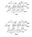
- FIG. 1illustrates one embodiment of the vertical three-level downward twist design to achieve equal bit line lengths on the top and bottom of the design.
- D (digit) line 10also referred to as “plane 10”
- D* (D bar) line 12also referred to as “plane 12”.
- D line 10drops down to a first plane 14 , then to a third plane 16 , and is routed around the D* line 12 and then elevated back up to the first plane 14 .
- D line 10has achieved a twist in the vertical direction or Z-axis.
- a similar vertical rotationoccurs for D* line 12 , except it drops down only one level to plane 18 and proceeds around the third plane 16 location and then elevates to a same plane 12 , and then to plane 22 , where it will remain until the next twist is encountered.
- planes 10 and 22are on the same level, as well as planes 12 and 14 , and planes 16 and 18 , respectively. It also is noted that all of the twisting is relatively in a z direction and that at only two points does the twisting require additional X-Y plane real-estate, that being on levels 18 and 16 .
- Level 4or plane 19
- Level 4could be any material, like substrate implant, polysilicon, metal 1 , etc., the key factor being that planes 19 and 16 don't create a transistor.
- a variation of this designis to have plane 19 arranged like plane 18 in FIG. 1 to avoid a transistor if the material would create such.
- FIG. 3illustrates a three-level twist-up architecture. As illustrated, the two digit lines are on the bottom planes 12 , 14 , 16 and 18 , whereas the twisting takes place on the upper planes 10 and 22 . Again, all the planes are in a vertical orientation to one another. However, planes 10 and 22 do project out into the X-Y planes to accomplish the twist.
- FIG. 4illustrates a four-level downward twist.
- Digit line (D) 30is moved down one level via planes 32 , 34 , and 36 while digit bar (D*) is twisted upward via planes 42 to 40 .
- plane or line 42is the only plane to extend in the X-Y plane, and, in fact, it extends into the vertical plane of an adjoining pair of digit lines.
- the bottom line 48 of D*is moved to a fourth lower level or plane 50 , and then brought back up to line 52 , while digit line 46 has no need to be repositioned since it is elevated above the plane 42 .
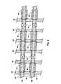
- FIG. 5illustrates a DRAM and an oblique view of two sections of the array utilizing the bi-level twist architecture. It is noted that, although there are two digit line pairs illustrated, they are in fact vertically oriented, one lying on top of the other. Additionally, the X 68 marks illustrate where the twisting takes place. It is noted that each line in each pair will spend 50% of the length located on the bottom of the vertical architecture. For example, upper line 60 switches to lower line 66 and lower line 64 moves up to the upper line 62 . Of course, the appropriate memory cells will be located near the correct bit line sections to receive the information stored in the cells and feed that into the sense amps 70 .
- the row decoders 72attached to the row lines 73 , can be positioned on one side of the array. Additionally, the isolation lines 74 are also symmetrical per array and thus can share a common grounding node 76 located between the two arrays illustrated.
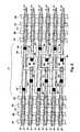
- FIG. 6there is an overview of a DRAM exhibiting eight memory cells 84 and the appropriate lines as illustrated.
- active area 80running the length of bit lines 86 (though one line is shown, both the D and D* lines are vertically oriented).
- Word lines 82will turn on the transistor to access the cells.
- Bit line contacts 81will dump the cell charge onto the lower of the digit lines.
- Isolation gates/lines 83keep the two adjacent memory cells from biasing each other.
- FIG. 7a layout portion of a DRAM array having double-layer twisted digit lines is depicted.
- Six digit line pairs(DP0, DP1, DP2, DP3, DP4 and DP5) are shown in this abbreviated layout. It will be noted that in the depicted portion of the array, only digit line pairs DP0, DP2 and DP4 undergo a twist. Digit line pairs DP1, DP3 and DP5 are untwisted in this portion of the array.
- the alternating twist patternnot only provides for efficient reduction of capacitive coupling between adjacent digit line pairs, but it also provides room for the twisting operation.
- first conductive strip S1 and second conductive strip S2are vertically aligned with portions of adjacent digit line pairs. This is possible because first and second conductive strips S1 and S2 are not on a level with either of the adjacent double-layer digit lines.
- the memory cell layout to the right and left of the twist region 71is similar to that depicted in FIG. 6. Vertical contact vias are represented by the squares marked with an “X”.
- the interconnect patternis similar to that depicted in FIG. 1.
- Level 2the digit lines located on planes 12 and 14 would be used to interconnect the corresponding pairs of adjacent contact vias. For example, for digit line pair DP2, the digit line located on plane 14 would interconnect contact vias CV1 and CV2, while the digit line located on plane 12 would interconnect contact vias CV3 and CV4.
- the signal to noise ratiosare kept acceptably low.
- the vertical arrangement and the crossing digit linesallow for equal top and bottom orientation and access to the appropriate memory cells. Additionally, the adjoining pair of digit lines is also switched appropriately to diminish signal to noise problems.
- this array arrangementallows for the smaller cell sizes, for example, cells possible from the older open bit line architecture or any new six square feature area (6F 2 ) or smaller cell size, thus allowing smaller arrays using six square feature area (6F 2 ) to four square feature area (4F 2 ) cell sizes.
- a still further advantageis the overall arrangement of the cells, bit lines, word lines, and isolation lines. All devices and lines are laid out to be exactly straight. There is no routing around the cells to open the gates like with the eight square feature area (8F 2 ) designs of the folded array structures.
- S-ampsense amp
- twisting locations in the arrayare at quarter marks, either the first and third quarter, or at the halfway mark in the array. This allows for different digit line pair arrangements to be located next to each other.
- this inventionmay work with any positioning of the memory cells. Specifically, the cells may be located between, along side, on top, or underneath the bit lines, thus accommodating for trench, stacked, or elevated designs. One skilled in the art would have little trouble using the vertical bi-level bit line arrangement with these other DRAM designs.
- any layeringcan be used for the bi-level digit lines.
- the bottom layercould be an implant in the substrate, or poly on top of the substrate, or any of the metals over the poly. It all depends on how high the chip design is stacked and where the memory cells are located.
- twisting of the vertical digit linescan be located anywhere in the array, like over ⁇ fraction (1/12) ⁇ of the line. The only requirement is that half of the length of each digit line is located on top and half on the bottom of the vertical arrangement, although it is noted that any increase in the number of twists will increase the size of the array.
Landscapes
- Physics & Mathematics (AREA)
- Condensed Matter Physics & Semiconductors (AREA)
- General Physics & Mathematics (AREA)
- Engineering & Computer Science (AREA)
- Computer Hardware Design (AREA)
- Microelectronics & Electronic Packaging (AREA)
- Power Engineering (AREA)
- Semiconductor Memories (AREA)
- Dram (AREA)
Abstract
Description
- This application is a continuation of application Ser. No. 10/155,132, filed May 23, 2002, pending, which is a continuation of application Ser. No. 09/941,201, filed Aug. 28, 2001, now U.S. Pat. No. 6,456,518 B1, issued Sep. 24, 2002, which is a divisional of application Ser. No. 09/533,353, filed Mar. 23, 2000, now U.S. Pat. No. 6,429,529 B1, issued Aug. 6, 2002, which is a continuation of application Ser. No. 09/211,662, filed Dec. 15, 1998, now U.S. Pat. No. 6,084,307, issued Jul. 4, 2000, which is a continuation of application Ser. No. 08/950,471, filed Oct. 15, 1997, now U.S. Pat. No. 5,864,181, issued Jan. 26, 1999, which is a continuation of application Ser. No. 08/442,264, filed May 15, 1995, abandoned, which is a continuation of application Ser. No. 08/123,027, filed Sep. 15, 1993, abandoned.[0001]
- Field of the Invention: The present invention relates to integrated circuits (ICs). Particularly, there is a RAM device where digit and digit bar, defined as a pair, are laid out vertically (in the z-axis) to each other, whereas the pairs of digit lines are laid out to be parallel (in the x or y axis) to each other. Additionally, the vertically aligned digit line pairs allow usage of memory cells having a six square feature area (6F[0002]2) or less, where F is defined as the minimum realizable photolithographic process dimension feature size.
- Dynamic random access memory (DRAM) production in the early days resulted in large chips. Manufacturing of these chips, at first, was not concerned with shrinking every part down to its smallest size. At this time the open memory array was the standard design: true digit lines on one side and complement digit (also known as digit bar or digit*) lines on the opposite side, with sense amps in the middle. However, once the DRAMS reached the 256K memory density, shrinking of all features became important.[0003]
- However, to push to even higher densities, like a one Megabit density, the open architecture proved to be inadequate because of the poorer signal-to-noise problem. As a result, the folded bit line architecture was developed. Yet, to use this architecture, the original memory cell from the open architecture could not be used. Thus, new cells were designed. There resulted a memory cell with a minimum size of eight square feature area (8F[0004]2). The folded architecture eliminated the signal to noise problems. Thus, further shrinkage of the other components on the DRAM resulted in an overall smaller DRAM package.
- Problem[0005]
- For some time now, there have been many ways developed to shrink the die size. However, a new shrinkage barrier has been reached as designs approach densities of 16 and 64 Meg chips. Every aspect of the die now has to be designed with minimal size. Thus, it is now necessary to shrink the previously acceptable eight square feature area (8F[0006]2) cells. Cell sizes of six square feature area (6F2) to four square feature area (4F2) are now needed. As a result, customers now need memory cells of six square feature area (6F2) or smaller that will also avoid the previous signal to noise ratio problems.
- Note, the above-described problem, as well as other problems, is solved through the subject invention and will become more apparent, to one skilled in the art, from the detailed description of the subject invention.[0007]
- One skilled in the art will appreciate the advantage of the bi-level bit line architecture. Specifically, there is a DRAM memory cell and cell array that allows for six square feature area (6F[0008]2) cell sizes and avoids the signal to noise problems. Uniquely, the digit lines are designed to lay on top of each other like a double decker overpass road. Additionally, this design allows routing of digit lines on both conductor layers, for equal lengths of the array, to provide balanced impedance. Now noise will appear as a common mode noise on both lines, and not as differential mode noise that would degrade the sensing operation. Furthermore, digit to digit coupling is nearly eliminated because of the twist design.
- To achieve the digit line switching, several modes of vertical twisting were developed. For a given section of the array, the twists are alternated between adjacent digit line pairs such that the overall twist resembles the traditional folded digit line twist. This twisting of the lines ensures that the signal to noise ratio of the bi-level digit line architecture can be as good as or may be even better than the folded digit line.[0009]
- Other features and advantages of the present invention may become more clear from the following detailed description of the invention, taken in conjunction with the accompanying drawings and claims, or may be learned by the practice of the invention.[0010]
- FIG. 1 is an illustration of one embodiment of the invention.[0011]
- FIG. 2 is an illustration of one embodiment of the invention.[0012]
- FIG. 3 is an illustration of one embodiment of the invention.[0013]
- FIG. 4 is an illustration of one embodiment of the invention.[0014]
- FIG. 5 is an oblique view of a portion of the memory array showing the location of the twists, sense amps, row decoders, and isolation devices.[0015]
- FIG. 6 is a representation of the layout of the present invention.[0016]
- FIG. 7 is a suggested layout for a portion of a DRAM memory array having twisted double-layer digit line pairs.[0017]
- FIG. 8 is an alternative suggested layout for a portion of a DRAM memory array having twisted double-layer digit line pairs.[0018]
- It is noted that the drawings of the invention are not to scale. The drawings are merely schematic representations, and not intended to portray specific parameters of the invention. The drawings are intended to depict only typical embodiments of the invention and are, therefore, not to be considered limiting of its scope. The invention will be described with additional specificity and detail through the use of the accompanying drawings, specification, and claims. Additionally, like numbering in the drawings represents like elements within and between drawings.[0019]
- Incorporated Material[0020]
- The following U.S. patents are herein incorporated by reference for pertinent and supporting information:[0021]
- U.S. Pat. No. 5,208,180, is a method of forming a capacitor.[0022]
- U.S. Pat. No. 5,206,183, is a method of forming a bit line over a capacitor array of memory cells.[0023]
- U.S. Pat. No. 5,138,412, is a dynamic RAM having an improved large capacitance.[0024]
- U.S. Pat. No. 4,742,018, is a process for producing memory cells having stacked capacitors.[0025]
- U.S. Pat. No. 4,970,564, is a semiconductor memory device having stacked capacitor cells.[0026]
- U.S. Pat. No. 4,536,947, is a CMOS process for fabricating integrated circuits, particularly dynamic memory cells with storage capacitors.[0027]
- General Embodiment[0028]
- One skilled in the DRAM semiconductor memory cell history and art will easily understand the operation of this Bi-Level Digit line design using an open architecture memory cell of six square feature area (6F[0029]2) or smaller feature size and switching of the digit line levels to eliminate the signal to noise ratio problems of the past.
- This invention provides a new architecture for a dynamic random access memory (DRAM). The memory is characterized as having a plurality of digit line pairs, with each digit line pair consisting of both a true digit line and a complement digit line. Both digit lines of each digit line pair are electrically insulated from one another by a dielectric layer and vertically aligned along a major portion of their lengths. At one or more positions along their lengths, their positions with respect to one another are reversed. In other words, if the true digit line is initially on top during a first portion of the full length of the pair, the complement digit line is on the bottom and makes contact to a plurality of cells by means of digit line contacts. Using one of the twisting techniques depicted in FIGS.[0030]1 to4, the complement digit line is brought to the uppermost position while the true digit line is brought to the lowermost position.
- Further illustrated in FIG. 7 are isolation gates/[0031]
lines 83 which keep the two adjacent memory cells from biasing each other. Such isolation gates/lines 83 are grounded and are formed of polysilicon and/or other material, such as an insulator material. By having such isolation gates/lines 83 grounded, the adjacent memory cells may be more effectively prevented from biasing each other during operation while having higher potentials applied thereto. - Referring to drawing FIG. 8, an alternative embodiment of the digit line switching, using vertical twisting, is illustrated. As illustrated, with respect to digit line pair DP0 including upper digit line D* and lower digit line D, both metal digit lines, the right-hand portion of upper digit line D* is connected by means of right[0032]
standard contact 94 topolysilicon area 90 and connected by means of leftstandard contact 94 from thepolysilicon area 90 to the left-hand portion of upper digit line D* while lower digit line D is insulated from thepolysilicon area 90 passing thereabove and thereover. When considering digit line pair DP1, upper digit line D* extends to cross or to overlie a portion of lower digit line D of digit line pair DPO, extends to bitcontact 96, and extends over leftstandard contact 94, being insulated therefrom at the upper level of the digit line pair DP1 of the array while the right-hand portion of lower digit line D of the digit line pair DP1 extends to rightstandard contact 94, in turn, connected to N+active area 92, in turn, being connected by leftstandard contact 94 to the left-hand portion of the lower digit line D of the digit line pair DP1. In each instance, when considering the rightstandard contact 94, prior to such contact, both digit lines D* and D are located vertically with respect to each other prior thereto in the array and when considering the leftstandard contact 94, from thereon both digit lines D* and D are located vertically with respect to each other in the array. Furthermore, the pattern for the arrangement of the digit lines is repeated with respect to digit line pairs DP2, DP3, DP4, and DP5 as described herein. In this manner, the noise is balanced through the use of vertical twists of the digit line pairs and the use of polysilicon areas and active N+ areas of the array. Additionally illustrated and described herein are groundedgate isolation areas 83, word lines82, and bitline contacts 81. - FIG. 1 illustrates one embodiment of the vertical three-level downward twist design to achieve equal bit line lengths on the top and bottom of the design. As illustrated, on the left side of the figure, D (digit) line[0033]10 (also referred to as “
plane 10”) is located directly above D* (D bar) line12 (also referred to as “plane 12”). It is noted thatD line 10 drops down to afirst plane 14, then to athird plane 16, and is routed around the D*line 12 and then elevated back up to thefirst plane 14. At the second level,D line 10 has achieved a twist in the vertical direction or Z-axis. A similar vertical rotation occurs for D*line 12, except it drops down only one level to plane18 and proceeds around thethird plane 16 location and then elevates to asame plane 12, and then to plane22, where it will remain until the next twist is encountered. - It is noted that[0034]
planes planes levels - Review of FIG. 2 shows almost an identical twist. However, there are four levels in this twist.[0035]
Level 4, orplane 19, is located belowlevel 3 andplane 16.Level 4 could be any material, like substrate implant, polysilicon,metal 1, etc., the key factor being thatplanes plane 19 arranged likeplane 18 in FIG. 1 to avoid a transistor if the material would create such. - Review of FIG. 3 illustrates a three-level twist-up architecture. As illustrated, the two digit lines are on the bottom planes[0036]12,14,16 and18, whereas the twisting takes place on the
upper planes - Review of FIG. 4 illustrates a four-level downward twist. Digit line (D)[0037]30 is moved down one level via
planes planes 42 to40. It is noted that plane orline 42 is the only plane to extend in the X-Y plane, and, in fact, it extends into the vertical plane of an adjoining pair of digit lines. To accommodate this extension, thebottom line 48 of D* is moved to a fourth lower level orplane 50, and then brought back up toline 52, whiledigit line 46 has no need to be repositioned since it is elevated above theplane 42. - Review of FIG. 5 illustrates a DRAM and an oblique view of two sections of the array utilizing the bi-level twist architecture. It is noted that, although there are two digit line pairs illustrated, they are in fact vertically oriented, one lying on top of the other. Additionally, the[0038]
X 68 marks illustrate where the twisting takes place. It is noted that each line in each pair will spend 50% of the length located on the bottom of the vertical architecture. For example,upper line 60 switches tolower line 66 andlower line 64 moves up to theupper line 62. Of course, the appropriate memory cells will be located near the correct bit line sections to receive the information stored in the cells and feed that into thesense amps 70. An advantage with this architecture is that therow decoders 72, attached to the row lines73, can be positioned on one side of the array. Additionally, the isolation lines74 are also symmetrical per array and thus can share acommon grounding node 76 located between the two arrays illustrated. - Attending to FIG. 6, there is an overview of a DRAM exhibiting eight[0039]
memory cells 84 and the appropriate lines as illustrated. In particular, there isactive area 80 running the length of bit lines86 (though one line is shown, both the D and D* lines are vertically oriented). Word lines82 will turn on the transistor to access the cells.Bit line contacts 81 will dump the cell charge onto the lower of the digit lines. Isolation gates/lines 83 keep the two adjacent memory cells from biasing each other. - Referring now to FIG. 7, a layout portion of a DRAM array having double-layer twisted digit lines is depicted. Six digit line pairs (DP0, DP1, DP2, DP3, DP4 and DP5) are shown in this abbreviated layout. It will be noted that in the depicted portion of the array, only digit line pairs DP0, DP2 and DP4 undergo a twist. Digit line pairs DP1, DP3 and DP5 are untwisted in this portion of the array. The alternating twist pattern not only provides for efficient reduction of capacitive coupling between adjacent digit line pairs, but it also provides room for the twisting operation. It will be noted that portions of first conductive strip S1 and second conductive strip S2 are vertically aligned with portions of adjacent digit line pairs. This is possible because first and second conductive strips S1 and S2 are not on a level with either of the adjacent double-layer digit lines. The memory cell layout to the right and left of the[0040]
twist region 71 is similar to that depicted in FIG. 6. Vertical contact vias are represented by the squares marked with an “X”. The interconnect pattern is similar to that depicted in FIG. 1. In FIG. 1,Level 2, the digit lines located onplanes plane 14 would interconnect contact vias CV1 and CV2, while the digit line located onplane 12 would interconnect contact vias CV3 and CV4. - Remarks about the Invention[0041]
- It is noted that the signal to noise ratios are kept acceptably low. The vertical arrangement and the crossing digit lines allow for equal top and bottom orientation and access to the appropriate memory cells. Additionally, the adjoining pair of digit lines is also switched appropriately to diminish signal to noise problems.[0042]
- It is further noted that this array arrangement allows for the smaller cell sizes, for example, cells possible from the older open bit line architecture or any new six square feature area (6F[0043]2) or smaller cell size, thus allowing smaller arrays using six square feature area (6F2) to four square feature area (4F2) cell sizes.
- A still further advantage is the overall arrangement of the cells, bit lines, word lines, and isolation lines. All devices and lines are laid out to be exactly straight. There is no routing around the cells to open the gates like with the eight square feature area (8F[0044]2) designs of the folded array structures.
- Additionally, there is one sense amp (S-amp) located on one end of the digit and digit bar lines in an alternating pattern of the S-amp.[0045]
- It is also noted that the twisting locations in the array are at quarter marks, either the first and third quarter, or at the halfway mark in the array. This allows for different digit line pair arrangements to be located next to each other.[0046]
- Variations in the Invention[0047]
- There are several obvious variations to the broad invention which thus come within the scope of the present invention. Uniquely, this invention may work with any positioning of the memory cells. Specifically, the cells may be located between, along side, on top, or underneath the bit lines, thus accommodating for trench, stacked, or elevated designs. One skilled in the art would have little trouble using the vertical bi-level bit line arrangement with these other DRAM designs.[0048]
- Additionally, any layering can be used for the bi-level digit lines. Specifically, the bottom layer could be an implant in the substrate, or poly on top of the substrate, or any of the metals over the poly. It all depends on how high the chip design is stacked and where the memory cells are located.[0049]
- Similarly, the twisting of the vertical digit lines can be located anywhere in the array, like over {fraction (1/12)} of the line. The only requirement is that half of the length of each digit line is located on top and half on the bottom of the vertical arrangement, although it is noted that any increase in the number of twists will increase the size of the array.[0050]
- While the invention has been taught with specific reference to these embodiments, someone skilled in the art will recognize that changes can be made in form and detail without departing from the spirit and the scope of the invention. The described embodiments are to be considered in all respects only as illustrative and not restrictive. The scope of the invention is, therefore, indicated by the appended claims rather than by the foregoing description. All changes which come within the meaning and range of equivalency of the claims are to be embraced within their scope.[0051]
Claims (6)
Priority Applications (1)
| Application Number | Priority Date | Filing Date | Title |
|---|---|---|---|
| US10/440,575US6839265B2 (en) | 1993-09-15 | 2003-05-19 | Bi-level digit line architecture for high density DRAMS |
Applications Claiming Priority (8)
| Application Number | Priority Date | Filing Date | Title |
|---|---|---|---|
| US12302793A | 1993-09-15 | 1993-09-15 | |
| US44226495A | 1995-05-15 | 1995-05-15 | |
| US08/950,471US5864181A (en) | 1993-09-15 | 1997-10-15 | Bi-level digit line architecture for high density DRAMs |
| US09/211,662US6084307A (en) | 1993-09-15 | 1998-12-15 | Bi-level digit line architecture for high density DRAMS |
| US09/533,353US6429529B1 (en) | 1993-09-15 | 2000-03-23 | Bi-level digit line architecture for high density drams |
| US09/941,201US6456518B1 (en) | 1993-09-15 | 2001-08-28 | Bi-level digit line architecture for high density drams |
| US10/155,132US6567288B2 (en) | 1993-09-15 | 2002-05-23 | Methods for bi-level digit line architecture for high density DRAMS |
| US10/440,575US6839265B2 (en) | 1993-09-15 | 2003-05-19 | Bi-level digit line architecture for high density DRAMS |
Related Parent Applications (1)
| Application Number | Title | Priority Date | Filing Date |
|---|---|---|---|
| US10/155,132ContinuationUS6567288B2 (en) | 1993-09-15 | 2002-05-23 | Methods for bi-level digit line architecture for high density DRAMS |
Publications (2)
| Publication Number | Publication Date |
|---|---|
| US20030198073A1true US20030198073A1 (en) | 2003-10-23 |
| US6839265B2 US6839265B2 (en) | 2005-01-04 |
Family
ID=26821147
Family Applications (7)
| Application Number | Title | Priority Date | Filing Date |
|---|---|---|---|
| US08/950,471Expired - LifetimeUS5864181A (en) | 1993-09-15 | 1997-10-15 | Bi-level digit line architecture for high density DRAMs |
| US09/211,662Expired - LifetimeUS6084307A (en) | 1993-09-15 | 1998-12-15 | Bi-level digit line architecture for high density DRAMS |
| US09/533,353Expired - LifetimeUS6429529B1 (en) | 1993-09-15 | 2000-03-23 | Bi-level digit line architecture for high density drams |
| US09/941,201Expired - LifetimeUS6456518B1 (en) | 1993-09-15 | 2001-08-28 | Bi-level digit line architecture for high density drams |
| US10/155,132Expired - LifetimeUS6567288B2 (en) | 1993-09-15 | 2002-05-23 | Methods for bi-level digit line architecture for high density DRAMS |
| US10/212,900Expired - Fee RelatedUS6696762B2 (en) | 1993-09-15 | 2002-08-05 | Bi-level digit line architecture for high density DRAMS |
| US10/440,575Expired - Fee RelatedUS6839265B2 (en) | 1993-09-15 | 2003-05-19 | Bi-level digit line architecture for high density DRAMS |
Family Applications Before (6)
| Application Number | Title | Priority Date | Filing Date |
|---|---|---|---|
| US08/950,471Expired - LifetimeUS5864181A (en) | 1993-09-15 | 1997-10-15 | Bi-level digit line architecture for high density DRAMs |
| US09/211,662Expired - LifetimeUS6084307A (en) | 1993-09-15 | 1998-12-15 | Bi-level digit line architecture for high density DRAMS |
| US09/533,353Expired - LifetimeUS6429529B1 (en) | 1993-09-15 | 2000-03-23 | Bi-level digit line architecture for high density drams |
| US09/941,201Expired - LifetimeUS6456518B1 (en) | 1993-09-15 | 2001-08-28 | Bi-level digit line architecture for high density drams |
| US10/155,132Expired - LifetimeUS6567288B2 (en) | 1993-09-15 | 2002-05-23 | Methods for bi-level digit line architecture for high density DRAMS |
| US10/212,900Expired - Fee RelatedUS6696762B2 (en) | 1993-09-15 | 2002-08-05 | Bi-level digit line architecture for high density DRAMS |
Country Status (1)
| Country | Link |
|---|---|
| US (7) | US5864181A (en) |
Cited By (13)
| Publication number | Priority date | Publication date | Assignee | Title |
|---|---|---|---|---|
| US20040062069A1 (en)* | 1996-01-26 | 2004-04-01 | Brent Keeth | Digit line architecture for dynamic memory |
| US20050045918A1 (en)* | 2003-09-02 | 2005-03-03 | Armin Reith | Hybrid vertical twisted bitline architecture |
| US20090206443A1 (en)* | 2008-02-19 | 2009-08-20 | Micron Technology, Inc. | Devices including fin transistors robust to gate shorts and methods of making the same |
| US20090206400A1 (en)* | 2008-02-19 | 2009-08-20 | Micron Technology, Inc. | Systems and devices including fin transistors and methods of using, making, and operating the same |
| US20090207681A1 (en)* | 2008-02-19 | 2009-08-20 | Micron Technology, Inc. | Systems and devices including local data lines and methods of using, making, and operating the same |
| US20090224357A1 (en)* | 2008-03-06 | 2009-09-10 | Micron Technology, Inc. | Devices with cavity-defined gates and methods of making the same |
| US20090238010A1 (en)* | 2008-03-20 | 2009-09-24 | Micron Technology, Inc. | Systems and devices including multi-transistor cells and methods of using, making, and operating the same |
| US20090238000A1 (en)* | 2008-03-20 | 2009-09-24 | Micron Technology, Inc. | Systems and devices including multi-gate transistors and methods of using, making, and operating the same |
| US20090237996A1 (en)* | 2008-03-20 | 2009-09-24 | Micron Technology, Inc. | Memory structure having volatile and non-volatile memory portions |
| US20090251946A1 (en)* | 2008-04-03 | 2009-10-08 | Micron Technology, Inc. | Data cells with drivers and methods of making and operating the same |
| US20090294842A1 (en)* | 2008-05-30 | 2009-12-03 | Micron Technology, Inc. | Methods of forming data cells and connections to data cells |
| US8148776B2 (en) | 2008-09-15 | 2012-04-03 | Micron Technology, Inc. | Transistor with a passive gate |
| US8810310B2 (en) | 2010-11-19 | 2014-08-19 | Micron Technology, Inc. | Vertically stacked fin transistors and methods of fabricating and operating the same |
Families Citing this family (56)
| Publication number | Priority date | Publication date | Assignee | Title |
|---|---|---|---|---|
| US5864181A (en) | 1993-09-15 | 1999-01-26 | Micron Technology, Inc. | Bi-level digit line architecture for high density DRAMs |
| US6967369B1 (en)* | 1995-09-20 | 2005-11-22 | Micron Technology, Inc. | Semiconductor memory circuitry |
| US7705383B2 (en) | 1995-09-20 | 2010-04-27 | Micron Technology, Inc. | Integrated circuitry for semiconductor memory |
| US6025221A (en)* | 1997-08-22 | 2000-02-15 | Micron Technology, Inc. | Processing methods of forming integrated circuitry memory devices, methods of forming DRAM arrays, and related semiconductor masks |
| US6072699A (en)* | 1998-07-21 | 2000-06-06 | Intel Corporation | Method and apparatus for matching trace lengths of signal lines making 90°/180° turns |
| US6326695B1 (en)* | 1998-09-29 | 2001-12-04 | Texas Instruments Incorporated | Twisted bit line structures and method for making same |
| DE19908428C2 (en)* | 1999-02-26 | 2000-12-07 | Siemens Ag | Semiconductor memory device with bit line twist |
| US6327170B1 (en)* | 1999-09-28 | 2001-12-04 | Infineon Technologies Ag | Reducing impact of coupling noise in multi-level bitline architecture |
| US6188598B1 (en)* | 1999-09-28 | 2001-02-13 | Infineon Technologies North America Corp. | Reducing impact of coupling noise |
| US6504246B2 (en) | 1999-10-12 | 2003-01-07 | Motorola, Inc. | Integrated circuit having a balanced twist for differential signal lines |
| US6255160B1 (en) | 1999-10-29 | 2001-07-03 | Taiwan Semiconductor Manufacturing Company | Cell design and process for making dynamic random access memory (DRAM) having one or more Gigabits of memory cells |
| US7259464B1 (en) | 2000-05-09 | 2007-08-21 | Micron Technology, Inc. | Vertical twist scheme for high-density DRAMs |
| US6947324B1 (en) | 2000-06-28 | 2005-09-20 | Marvell International Ltd. | Logic process DRAM |
| US6570781B1 (en) | 2000-06-28 | 2003-05-27 | Marvell International Ltd. | Logic process DRAM |
| US7184290B1 (en) | 2000-06-28 | 2007-02-27 | Marvell International Ltd. | Logic process DRAM |
| US6317358B1 (en) | 2000-08-03 | 2001-11-13 | Micron Technology, Inc. | Efficient dual port DRAM cell using SOI technology |
| US7118960B2 (en)* | 2000-08-31 | 2006-10-10 | Micron Technology, Inc. | Selective polysilicon stud growth |
| US6380576B1 (en)* | 2000-08-31 | 2002-04-30 | Micron Technology, Inc. | Selective polysilicon stud growth |
| US6686668B2 (en)* | 2001-01-17 | 2004-02-03 | International Business Machines Corporation | Structure and method of forming bitline contacts for a vertical DRAM array using a line bitline contact mask |
| KR100393211B1 (en)* | 2001-02-03 | 2003-07-31 | 삼성전자주식회사 | A method for arranging wiring line including power reinforcing line and semiconductor device having power reinforceing line |
| US6500706B1 (en)* | 2001-03-19 | 2002-12-31 | Taiwan Semiconductor Manufacturing Company | Bit-line interconnection scheme for eliminating coupling noise in stack DRAM cell with capacitor under bit-line (CUB) in stand-alone or embedded DRAM |
| KR100393220B1 (en)* | 2001-03-23 | 2003-07-31 | 삼성전자주식회사 | Semiconductor devices for ESD protection |
| US6711044B2 (en)* | 2001-07-02 | 2004-03-23 | Matsushita Electric Industrial Co., Ltd. | Semiconductor memory device with a countermeasure to a signal delay |
| US6806754B2 (en)* | 2001-07-19 | 2004-10-19 | Micron Technology, Inc. | Method and circuitry for reducing duty cycle distortion in differential delay lines |
| FR2830365B1 (en)* | 2001-09-28 | 2004-12-24 | St Microelectronics Sa | DYNAMIC VIVE MEMORY |
| US6657880B1 (en) | 2002-12-04 | 2003-12-02 | Virtual Silicon Technology, Inc. | SRAM bit line architecture |
| US7332389B2 (en)* | 2003-07-02 | 2008-02-19 | Micron Technology, Inc. | Selective polysilicon stud growth |
| US6975552B2 (en)* | 2003-08-19 | 2005-12-13 | Micron Technology, Inc. | Hybrid open and folded digit line architecture |
| US7067859B2 (en)* | 2003-08-26 | 2006-06-27 | Lsi Logic Corporation | Multi-layer staggered power bus layout design |
| US7474000B2 (en)* | 2003-12-05 | 2009-01-06 | Sandisk 3D Llc | High density contact to relaxed geometry layers |
| JP2005285971A (en)* | 2004-03-29 | 2005-10-13 | Nec Electronics Corp | Semiconductor device |
| US20060278912A1 (en)* | 2004-09-02 | 2006-12-14 | Luan Tran | Selective polysilicon stud growth |
| JP2006128471A (en)* | 2004-10-29 | 2006-05-18 | Toshiba Corp | Semiconductor memory |
| JP5296963B2 (en)* | 2005-12-21 | 2013-09-25 | エルピーダメモリ株式会社 | Multilayer wiring semiconductor integrated circuit, semiconductor device |
| US7382012B2 (en)* | 2006-02-24 | 2008-06-03 | Taiwan Semiconductor Manufacturing Company, Ltd. | Reducing parasitic capacitance of MIM capacitor in integrated circuits by reducing effective dielectric constant of dielectric layer |
| JP4986114B2 (en)* | 2006-04-17 | 2012-07-25 | ルネサスエレクトロニクス株式会社 | Semiconductor integrated circuit and design method of semiconductor integrated circuit |
| JP5137178B2 (en)* | 2007-02-19 | 2013-02-06 | ルネサスエレクトロニクス株式会社 | Semiconductor integrated circuit device and layout method thereof |
| US7688612B2 (en)* | 2007-04-13 | 2010-03-30 | Aplus Flash Technology, Inc. | Bit line structure for a multilevel, dual-sided nonvolatile memory cell array |
| KR100911196B1 (en)* | 2007-12-07 | 2009-08-06 | 주식회사 하이닉스반도체 | Semiconductor memory device |
| US7830221B2 (en)* | 2008-01-25 | 2010-11-09 | Micron Technology, Inc. | Coupling cancellation scheme |
| US20100044093A1 (en)* | 2008-08-25 | 2010-02-25 | Wilinx Corporation | Layout geometries for differential signals |
| US9041203B2 (en)* | 2008-10-10 | 2015-05-26 | Cypress Semiconductor Corporation | System and method for multi-layer global bitlines |
| KR20110056005A (en)* | 2009-11-20 | 2011-05-26 | 삼성전자주식회사 | Wiring Structure of Semiconductor Device |
| US9401363B2 (en)* | 2011-08-23 | 2016-07-26 | Micron Technology, Inc. | Vertical transistor devices, memory arrays, and methods of forming vertical transistor devices |
| US9589962B2 (en) | 2014-06-17 | 2017-03-07 | Micron Technology, Inc. | Array of conductive vias, methods of forming a memory array, and methods of forming conductive vias |
| KR102214506B1 (en) | 2014-08-21 | 2021-02-09 | 삼성전자 주식회사 | Semiconductor device having contact plugs and method for manufacturing the same |
| JP6315112B2 (en)* | 2015-11-27 | 2018-04-25 | 株式会社村田製作所 | Filter device |
| US11211384B2 (en) | 2017-01-12 | 2021-12-28 | Micron Technology, Inc. | Memory cells, arrays of two transistor-one capacitor memory cells, methods of forming an array of two transistor-one capacitor memory cells, and methods used in fabricating integrated circuitry |
| CN110753962A (en)* | 2017-08-29 | 2020-02-04 | 美光科技公司 | memory circuit |
| US10607687B2 (en)* | 2017-12-28 | 2020-03-31 | Micron Technology, Inc. | Apparatuses and methods for sense line architectures for semiconductor memories |
| US10840249B2 (en) | 2018-08-23 | 2020-11-17 | Micron Technology, Inc. | Integrated circuitry constructions |
| US10658590B2 (en) | 2018-09-21 | 2020-05-19 | International Business Machines Corporation | Techniques for forming RRAM cells |
| CN111758171B (en)* | 2020-05-12 | 2024-04-05 | 长江先进存储产业创新中心有限责任公司 | Novel distributed array and contact architecture for 4-stacked 3D PCM memory |
| US11832443B2 (en)* | 2021-08-19 | 2023-11-28 | Micron Technology, Inc. | Apparatuses including contacts in a peripheral region |
| US20230397408A1 (en)* | 2022-06-02 | 2023-12-07 | Micron Technology, Inc. | Apparatuses including semiconductive pillar structures, and related methods, memory devices, and electronic systems |
| US12254947B2 (en)* | 2022-08-23 | 2025-03-18 | Micron Technology, Inc. | Semiconductor memories including edge mats having folded digit lines |
Family Cites Families (43)
| Publication number | Priority date | Publication date | Assignee | Title |
|---|---|---|---|---|
| EP0078338B1 (en) | 1981-10-30 | 1986-02-05 | Ibm Deutschland Gmbh | Fet memory |
| US4536947A (en)* | 1983-07-14 | 1985-08-27 | Intel Corporation | CMOS process for fabricating integrated circuits, particularly dynamic memory cells with storage capacitors |
| JPS6025879A (en)* | 1983-07-20 | 1985-02-08 | Hitachi Zosen Corp | Absorption device for freezing expansion force inside the tank |
| JPS60258795A (en)* | 1984-06-04 | 1985-12-20 | Sharp Corp | Dynamic semiconductor memory device |
| JPH0736437B2 (en)* | 1985-11-29 | 1995-04-19 | 株式会社日立製作所 | Method of manufacturing semiconductor memory |
| CA1305255C (en)* | 1986-08-25 | 1992-07-14 | Joseph Lebowitz | Marching interconnecting lines in semiconductor integrated circuits |
| US5214601A (en) | 1986-12-11 | 1993-05-25 | Mitsubishi Denki Kabushiki Kaisha | Bit line structure for semiconductor memory device including cross-points and multiple interconnect layers |
| JPS63183691A (en) | 1987-01-26 | 1988-07-29 | Mitsubishi Electric Corp | semiconductor storage device |
| JPS63239674A (en)* | 1987-03-27 | 1988-10-05 | Hitachi Ltd | Dynamic RAM |
| JP2590171B2 (en)* | 1988-01-08 | 1997-03-12 | 株式会社日立製作所 | Semiconductor storage device |
| US5014110A (en)* | 1988-06-03 | 1991-05-07 | Mitsubishi Denki Kabushiki Kaisha | Wiring structures for semiconductor memory device |
| JP2681285B2 (en) | 1988-09-19 | 1997-11-26 | 富士通株式会社 | Semiconductor memory device |
| JPH0294471A (en)* | 1988-09-30 | 1990-04-05 | Toshiba Corp | Semiconductor storage device and its manufacturing method |
| JPH03174765A (en)* | 1989-09-19 | 1991-07-29 | Oki Electric Ind Co Ltd | Semiconductor memory device and manufacture thereof |
| US5107459A (en)* | 1990-04-20 | 1992-04-21 | International Business Machines Corporation | Stacked bit-line architecture for high density cross-point memory cell array |
| JPH04271086A (en)* | 1991-02-27 | 1992-09-28 | Nec Corp | Semiconductor integrated circuit |
| US5170243A (en)* | 1991-11-04 | 1992-12-08 | International Business Machines Corporation | Bit line configuration for semiconductor memory |
| DE4139719C1 (en)* | 1991-12-02 | 1993-04-08 | Siemens Ag, 8000 Muenchen, De | |
| US5206183A (en)* | 1992-02-19 | 1993-04-27 | Micron Technology, Inc. | Method of forming a bit line over capacitor array of memory cells |
| US5208180A (en)* | 1992-03-04 | 1993-05-04 | Micron Technology, Inc. | Method of forming a capacitor |
| US5838038A (en) | 1992-09-22 | 1998-11-17 | Kabushiki Kaisha Toshiba | Dynamic random access memory device with the combined open/folded bit-line pair arrangement |
| JP3302796B2 (en)* | 1992-09-22 | 2002-07-15 | 株式会社東芝 | Semiconductor storage device |
| JP3440335B2 (en)* | 1993-08-18 | 2003-08-25 | 日本テキサス・インスツルメンツ株式会社 | Semiconductor memory device |
| US5864181A (en)* | 1993-09-15 | 1999-01-26 | Micron Technology, Inc. | Bi-level digit line architecture for high density DRAMs |
| KR100215595B1 (en) | 1993-09-21 | 1999-08-16 | 니시무로 타이죠 | Dynamic semiconductor memory device |
| US5680347A (en) | 1994-06-29 | 1997-10-21 | Kabushiki Kaisha Toshiba | Nonvolatile semiconductor memory device |
| US5670815A (en)* | 1994-07-05 | 1997-09-23 | Motorola, Inc. | Layout for noise reduction on a reference voltage |
| DE69526006T2 (en)* | 1994-08-15 | 2003-01-02 | International Business Machines Corp., Armonk | Single twist region arrangement and method for paired linear conductors in integrated circuits |
| JP3304635B2 (en) | 1994-09-26 | 2002-07-22 | 三菱電機株式会社 | Semiconductor storage device |
| US5499205A (en)* | 1995-01-31 | 1996-03-12 | Goldstar Electron Co., Ltd. | Bit line structure |
| JP3364549B2 (en) | 1995-02-22 | 2003-01-08 | 三菱電機株式会社 | Semiconductor storage device |
| US5581126A (en)* | 1995-09-14 | 1996-12-03 | Advanced Micro Devices, Inc. | Interlaced layout configuration for differential pairs of interconnect lines |
| US6043562A (en) | 1996-01-26 | 2000-03-28 | Micron Technology, Inc. | Digit line architecture for dynamic memory |
| US6094370A (en) | 1996-06-10 | 2000-07-25 | Kabushiki Kaisha Toshiba | Semiconductor memory device and various systems mounting them |
| JPH10107208A (en) | 1996-09-30 | 1998-04-24 | Toshiba Corp | Semiconductor integrated circuit device |
| US5835038A (en) | 1997-05-08 | 1998-11-10 | Burr-Brown Corporation | DC dither circuitry and method for delta-sigma modulator |
| US5877976A (en) | 1997-10-28 | 1999-03-02 | International Business Machines Corporation | Memory system having a vertical bitline topology and method therefor |
| US6028783A (en) | 1997-11-14 | 2000-02-22 | Ramtron International Corporation | Memory cell configuration for a 1T/1C ferroelectric memory |
| US6034879A (en) | 1998-02-19 | 2000-03-07 | University Of Pittsburgh | Twisted line techniques for multi-gigabit dynamic random access memories |
| US5949698A (en) | 1998-02-20 | 1999-09-07 | Micron Technology, Inc. | Twisted global column decoder |
| JP3174765B2 (en) | 1998-10-23 | 2001-06-11 | 株式会社エイ・ティ・アール人間情報通信研究所 | Evolution system equipment |
| US6188598B1 (en) | 1999-09-28 | 2001-02-13 | Infineon Technologies North America Corp. | Reducing impact of coupling noise |
| US6259621B1 (en)* | 2000-07-06 | 2001-07-10 | Micron Technology, Inc. | Method and apparatus for minimization of data line coupling in a semiconductor memory device |
- 1997
- 1997-10-15USUS08/950,471patent/US5864181A/ennot_activeExpired - Lifetime
- 1998
- 1998-12-15USUS09/211,662patent/US6084307A/ennot_activeExpired - Lifetime
- 2000
- 2000-03-23USUS09/533,353patent/US6429529B1/ennot_activeExpired - Lifetime
- 2001
- 2001-08-28USUS09/941,201patent/US6456518B1/ennot_activeExpired - Lifetime
- 2002
- 2002-05-23USUS10/155,132patent/US6567288B2/ennot_activeExpired - Lifetime
- 2002-08-05USUS10/212,900patent/US6696762B2/ennot_activeExpired - Fee Related
- 2003
- 2003-05-19USUS10/440,575patent/US6839265B2/ennot_activeExpired - Fee Related
Cited By (34)
| Publication number | Priority date | Publication date | Assignee | Title |
|---|---|---|---|---|
| US20040062069A1 (en)* | 1996-01-26 | 2004-04-01 | Brent Keeth | Digit line architecture for dynamic memory |
| US6898102B2 (en)* | 1996-01-26 | 2005-05-24 | Micron Technology, Inc. | Digitline architecture for dynamic memory |
| US20050045918A1 (en)* | 2003-09-02 | 2005-03-03 | Armin Reith | Hybrid vertical twisted bitline architecture |
| US9190494B2 (en) | 2008-02-19 | 2015-11-17 | Micron Technology, Inc. | Systems and devices including fin field-effect transistors each having U-shaped semiconductor fin |
| US20090206400A1 (en)* | 2008-02-19 | 2009-08-20 | Micron Technology, Inc. | Systems and devices including fin transistors and methods of using, making, and operating the same |
| US20090207681A1 (en)* | 2008-02-19 | 2009-08-20 | Micron Technology, Inc. | Systems and devices including local data lines and methods of using, making, and operating the same |
| US20090206443A1 (en)* | 2008-02-19 | 2009-08-20 | Micron Technology, Inc. | Devices including fin transistors robust to gate shorts and methods of making the same |
| US9087721B2 (en) | 2008-02-19 | 2015-07-21 | Micron Technology, Inc. | Devices including fin transistors robust to gate shorts and methods of making the same |
| US8866254B2 (en) | 2008-02-19 | 2014-10-21 | Micron Technology, Inc. | Devices including fin transistors robust to gate shorts and methods of making the same |
| US7742324B2 (en) | 2008-02-19 | 2010-06-22 | Micron Technology, Inc. | Systems and devices including local data lines and methods of using, making, and operating the same |
| US20090224357A1 (en)* | 2008-03-06 | 2009-09-10 | Micron Technology, Inc. | Devices with cavity-defined gates and methods of making the same |
| US9331203B2 (en) | 2008-03-06 | 2016-05-03 | Micron Technology, Inc. | Devices with cavity-defined gates and methods of making the same |
| US7915659B2 (en) | 2008-03-06 | 2011-03-29 | Micron Technology, Inc. | Devices with cavity-defined gates and methods of making the same |
| US20090238000A1 (en)* | 2008-03-20 | 2009-09-24 | Micron Technology, Inc. | Systems and devices including multi-gate transistors and methods of using, making, and operating the same |
| US8450785B2 (en) | 2008-03-20 | 2013-05-28 | Micron Technology, Inc. | Systems and devices including multi-gate transistors and methods of using, making, and operating the same |
| US7898857B2 (en) | 2008-03-20 | 2011-03-01 | Micron Technology, Inc. | Memory structure having volatile and non-volatile memory portions |
| US7808042B2 (en) | 2008-03-20 | 2010-10-05 | Micron Technology, Inc. | Systems and devices including multi-gate transistors and methods of using, making, and operating the same |
| US20090237996A1 (en)* | 2008-03-20 | 2009-09-24 | Micron Technology, Inc. | Memory structure having volatile and non-volatile memory portions |
| US7981736B2 (en) | 2008-03-20 | 2011-07-19 | Micron Technology, Inc. | Systems and devices including multi-gate transistors and methods of using, making, and operating the same |
| US20100323481A1 (en)* | 2008-03-20 | 2010-12-23 | Micron Technology, Inc. | Systems and devices including multi-gate transistors and methods of using, making, and operating the same |
| US9449652B2 (en) | 2008-03-20 | 2016-09-20 | Micron Technology, Inc. | Systems and devices including multi-transistor cells and methods of using, making, and operating the same |
| US8149619B2 (en) | 2008-03-20 | 2012-04-03 | Micron Technology, Inc. | Memory structure having volatile and non-volatile memory portions |
| US20090238010A1 (en)* | 2008-03-20 | 2009-09-24 | Micron Technology, Inc. | Systems and devices including multi-transistor cells and methods of using, making, and operating the same |
| US8759889B2 (en) | 2008-03-20 | 2014-06-24 | Micron Technology, Inc. | Systems and devices including multi-gate transistors and methods of using, making, and operating the same |
| US8546876B2 (en) | 2008-03-20 | 2013-10-01 | Micron Technology, Inc. | Systems and devices including multi-transistor cells and methods of using, making, and operating the same |
| US8537608B2 (en) | 2008-04-03 | 2013-09-17 | Micron Technology, Inc. | Data cells with drivers and methods of making and operating the same |
| US8750025B2 (en) | 2008-04-03 | 2014-06-10 | Micron Technology, Inc. | Data cells with drivers and methods of making and operating the same |
| US8503228B2 (en) | 2008-04-03 | 2013-08-06 | Micron Technology, Inc. | Data cells with drivers and methods of making and operating the same |
| US20090251946A1 (en)* | 2008-04-03 | 2009-10-08 | Micron Technology, Inc. | Data cells with drivers and methods of making and operating the same |
| US7969776B2 (en) | 2008-04-03 | 2011-06-28 | Micron Technology, Inc. | Data cells with drivers and methods of making and operating the same |
| US8076229B2 (en) | 2008-05-30 | 2011-12-13 | Micron Technology, Inc. | Methods of forming data cells and connections to data cells |
| US20090294842A1 (en)* | 2008-05-30 | 2009-12-03 | Micron Technology, Inc. | Methods of forming data cells and connections to data cells |
| US8148776B2 (en) | 2008-09-15 | 2012-04-03 | Micron Technology, Inc. | Transistor with a passive gate |
| US8810310B2 (en) | 2010-11-19 | 2014-08-19 | Micron Technology, Inc. | Vertically stacked fin transistors and methods of fabricating and operating the same |
Also Published As
| Publication number | Publication date |
|---|---|
| US6839265B2 (en) | 2005-01-04 |
| US20020024144A1 (en) | 2002-02-28 |
| US6456518B1 (en) | 2002-09-24 |
| US5864181A (en) | 1999-01-26 |
| US20020185666A1 (en) | 2002-12-12 |
| US6567288B2 (en) | 2003-05-20 |
| US6084307A (en) | 2000-07-04 |
| US20020141220A1 (en) | 2002-10-03 |
| US6696762B2 (en) | 2004-02-24 |
| US6429529B1 (en) | 2002-08-06 |
Similar Documents
| Publication | Publication Date | Title |
|---|---|---|
| US6839265B2 (en) | Bi-level digit line architecture for high density DRAMS | |
| US5332923A (en) | Semiconductor memory | |
| EP0452648B1 (en) | Stacked bit line architecture for high density cross-point memory cell array | |
| US5170243A (en) | Bit line configuration for semiconductor memory | |
| US5747844A (en) | Dynamic semiconductor memory device with higher density bit line/word line layout | |
| EP0169332B1 (en) | High density one device memory | |
| US5691551A (en) | Semiconductor memory device | |
| US5602772A (en) | Dynamic semiconductor memory device | |
| US7655518B2 (en) | On-chip bypass capacitor and method of manufacturing the same | |
| US5812444A (en) | Semiconductor memory device with bit line contact areas and storage capacitor contact areas | |
| US6459113B1 (en) | Semiconductor integrated circuit device and method of manufacturing the same, and cell size calculation method for DRAM memory cells | |
| CA1305255C (en) | Marching interconnecting lines in semiconductor integrated circuits | |
| US20070050743A1 (en) | Vertical Twist Scheme for High Density DRAMs | |
| JPS6278799A (en) | Dynamic random access memory cell | |
| US6388329B1 (en) | Semiconductor integrated circuit having three wiring layers | |
| US6538946B2 (en) | Semiconductor integrated circuit device | |
| US6911687B1 (en) | Buried bit line-field isolation defined active semiconductor areas | |
| US7199471B2 (en) | Method and apparatus for reducing capacitive coupling between lines in an integrated circuit | |
| US6282116B1 (en) | Dynamic random access memory | |
| US6100588A (en) | Multiple level conductor wordline strapping scheme | |
| US5034920A (en) | Cross point array memory device | |
| US6831320B2 (en) | Memory cell configuration for a DRAM memory with a contact bit terminal for two trench capacitors of different rows | |
| US6157561A (en) | Integrated circuit memory with low resistance, segmented power supply lines | |
| JPH0799250A (en) | Semiconductor memory device | |
| GB2312094A (en) | Stacked capacitor type DRAM |
Legal Events
| Date | Code | Title | Description |
|---|---|---|---|
| CC | Certificate of correction | ||
| FEPP | Fee payment procedure | Free format text:PAYOR NUMBER ASSIGNED (ORIGINAL EVENT CODE: ASPN); ENTITY STATUS OF PATENT OWNER: LARGE ENTITY | |
| FPAY | Fee payment | Year of fee payment:4 | |
| FPAY | Fee payment | Year of fee payment:8 | |
| AS | Assignment | Owner name:U.S. BANK NATIONAL ASSOCIATION, AS COLLATERAL AGENT, CALIFORNIA Free format text:SECURITY INTEREST;ASSIGNOR:MICRON TECHNOLOGY, INC.;REEL/FRAME:038669/0001 Effective date:20160426 Owner name:U.S. BANK NATIONAL ASSOCIATION, AS COLLATERAL AGEN Free format text:SECURITY INTEREST;ASSIGNOR:MICRON TECHNOLOGY, INC.;REEL/FRAME:038669/0001 Effective date:20160426 | |
| AS | Assignment | Owner name:MORGAN STANLEY SENIOR FUNDING, INC., AS COLLATERAL AGENT, MARYLAND Free format text:PATENT SECURITY AGREEMENT;ASSIGNOR:MICRON TECHNOLOGY, INC.;REEL/FRAME:038954/0001 Effective date:20160426 Owner name:MORGAN STANLEY SENIOR FUNDING, INC., AS COLLATERAL Free format text:PATENT SECURITY AGREEMENT;ASSIGNOR:MICRON TECHNOLOGY, INC.;REEL/FRAME:038954/0001 Effective date:20160426 | |
| REMI | Maintenance fee reminder mailed | ||
| LAPS | Lapse for failure to pay maintenance fees | ||
| STCH | Information on status: patent discontinuation | Free format text:PATENT EXPIRED DUE TO NONPAYMENT OF MAINTENANCE FEES UNDER 37 CFR 1.362 | |
| FP | Lapsed due to failure to pay maintenance fee | Effective date:20170104 | |
| AS | Assignment | Owner name:U.S. BANK NATIONAL ASSOCIATION, AS COLLATERAL AGENT, CALIFORNIA Free format text:CORRECTIVE ASSIGNMENT TO CORRECT THE REPLACE ERRONEOUSLY FILED PATENT #7358718 WITH THE CORRECT PATENT #7358178 PREVIOUSLY RECORDED ON REEL 038669 FRAME 0001. ASSIGNOR(S) HEREBY CONFIRMS THE SECURITY INTEREST;ASSIGNOR:MICRON TECHNOLOGY, INC.;REEL/FRAME:043079/0001 Effective date:20160426 Owner name:U.S. BANK NATIONAL ASSOCIATION, AS COLLATERAL AGEN Free format text:CORRECTIVE ASSIGNMENT TO CORRECT THE REPLACE ERRONEOUSLY FILED PATENT #7358718 WITH THE CORRECT PATENT #7358178 PREVIOUSLY RECORDED ON REEL 038669 FRAME 0001. ASSIGNOR(S) HEREBY CONFIRMS THE SECURITY INTEREST;ASSIGNOR:MICRON TECHNOLOGY, INC.;REEL/FRAME:043079/0001 Effective date:20160426 | |
| AS | Assignment | Owner name:MICRON TECHNOLOGY, INC., IDAHO Free format text:RELEASE BY SECURED PARTY;ASSIGNOR:U.S. BANK NATIONAL ASSOCIATION, AS COLLATERAL AGENT;REEL/FRAME:047243/0001 Effective date:20180629 | |
| AS | Assignment | Owner name:MICRON TECHNOLOGY, INC., IDAHO Free format text:RELEASE BY SECURED PARTY;ASSIGNOR:MORGAN STANLEY SENIOR FUNDING, INC., AS COLLATERAL AGENT;REEL/FRAME:050937/0001 Effective date:20190731 |