US20030193927A1 - Random access memory architecture and serial interface with continuous packet handling capability - Google Patents
Random access memory architecture and serial interface with continuous packet handling capabilityDownload PDFInfo
- Publication number
- US20030193927A1 US20030193927A1US10/120,648US12064802AUS2003193927A1US 20030193927 A1US20030193927 A1US 20030193927A1US 12064802 AUS12064802 AUS 12064802AUS 2003193927 A1US2003193927 A1US 2003193927A1
- Authority
- US
- United States
- Prior art keywords
- random access
- access memory
- data
- memory device
- read
- Prior art date
- Legal status (The legal status is an assumption and is not a legal conclusion. Google has not performed a legal analysis and makes no representation as to the accuracy of the status listed.)
- Granted
Links
Images


Classifications
- H—ELECTRICITY
- H04—ELECTRIC COMMUNICATION TECHNIQUE
- H04L—TRANSMISSION OF DIGITAL INFORMATION, e.g. TELEGRAPHIC COMMUNICATION
- H04L49/00—Packet switching elements
- H04L49/90—Buffering arrangements
Definitions
- FIG. 1A block diagram of an example of the architecture of a known router system 100 is shown in FIG. 1. Incoming packets can be temporarily stored in a local buffer 102 until one or more network layer processors, shown as application specific integrated circuits (ASICs) 104 and 106 , classifies and determines the forwarding address of the packet. The packets are then routed to the target destination.
- ASICsapplication specific integrated circuits
- Buffer 102includes gigabytes of SRAM arranged in a very wide data bus ( 512 bits or more) 108 to allow several simultaneous search operations.
- Router system 100analyzes the headers of incoming packets for the appropriate types of operations to be performed on the packet. In the case of TCP/IP route look-up, for example, router system 100 matches a combination of source/destination addresses with entries in a routing table for an exact match or a longest prefix match.
- Content addressable memory (CAM) 110offloads ASIC 104 by processing a limited set of lookup instructions. In other applications such as load balancing and URL routing, router system 100 performs more complex search rules and routing data structures.
- a successful searchwill result in router system 100 modifying the header and optionally, the payload, with new information.
- a packet headermay be modified for its output port/queue, output connection, or additional labels for switching, for example.
- the packetsare then queued by priority as well as latency to absorb the time needed to implement the search/modify steps. Output queuing reorders packets in the event multiple packets are searched in parallel.
- data bus 108is a 640 bit bus with a speed of 133 MHz or 167 MHz. Greater efficiency can be achieved with large data packets, while transfers over data bus 108 are very inefficient for small data packets.
- ASICS 104 and 106have a pin count of over 1000 pins. The number of pins cannot be expanded without changing ASICs 104 , 106 . The bandwidth of router system 100 is therefore limited.
- the memory interfacepresents board layout problems, including positioning components to avoid long data bus lines; routing wide data bus lines to memory and processor devices with a large number of pins; and multidrop connections on all busses.
- Other problemsinclude limited bandwidth per pin, and limited memory access time.
- address fan-out problemsarise with increasing address bandwidth and address loading and buffering.
- noise issuesarise with heavy bus loading and heavy bus drivers, line termination, bus contention, and the length of the data bus lines.
- bus arbitrationtransferring small amounts of data on very wide busses, bottlenecks at the memory interface, and bus/clock skew and bit alignment.
- router system 100cannot efficiently be expanded to handle greater packet bandwidth.
- an apparatusmay include a first processing unit operable to receive serial data input, a switch operable to receive data to be transmitted, a first random access memory device coupled to the first processing unit via a write input port, wherein the first processing unit is operable to transmit data packets to the first random access memory device via the write input port, and a second random access memory device coupled to the first random access memory device, the second random access memory device being further coupled to transmit the data to be transmitted to the switch.
- the first and second random access memory devicesmay be configured as described in the embodiments below.
- each of the plurality of random access memory devicesmay be configured according to one of the embodiments described below.
- Each of the plurality of random access memory devicesmay be coupled in series to another of the plurality of random access memory devices.
- a write output port of each of the plurality of random access memory devicesmay be coupled to a write input port of the next of the series of the plurality of random access memory devices.
- a read output port of each of the plurality of random access memory devicesmay be coupled to a read input port of the next of the series of the plurality of random access memory devices.
- each of the random access memory devicesis operable to generate an overflow signal to indicate to the next random access memory device in the series that the data to be written or read is a continuation from the previous random access memory device.
- Each random access memory devicemay be operable to generate a command signal to indicate to the next random access memory device in the series that the continuation of data is to be written or read.
- a random access memory devicecomprises a random access memory module, a write input port coupled to receive packets that include data and command information, a decoder coupled to receive the packets from the write input port, and to access the random access memory module to perform the commands in the packets, a read input port operable to receive bypass data, and a read output port coupled to output the bypass data and data read from the random access memory module.
- the random access memory devicemay also include a write output port coupled to receive the packets from the write input port and to transmit the packets to another random access memory device.
- the random access memory devicemay also comprise a buffer coupled between the write input port and the write output port.
- the random access memory devicemay include a decoder between the write input port and the write output port, and an encoder coupled between the decoder and the write output port.
- the decodermay include a phase lock loop.
- the random access memory devicemay also include a first multiplexer coupled between the read input port and the read output port, operable to output an idle signal when the read input port is not transmitting data to the read output port.
- the random access memory devicemay include a second multiplexer, coupled between the random access memory module and the read output port, where the second multiplexer is coupled to receive the output of the first multiplexer and to output the output of the first multiplexer when read data is not being transmitted from the random access memory module.
- the random access memory devicemay also include an encoder coupled between the random access module and the second multiplexer.
- the random access memory devicemay include a buffer coupled between the second multiplexer and the read output port.
- the random access memory devicemay also include a second decoder coupled between the read input port and the first multiplexer, wherein the second decoder includes a delay lock loop.
- the random access memory devicesare operable to decode data packets and determine whether a data packet includes at least one of: a start of frame field, a control word, an address field, a data field, and an idle indicator.
- the control wordmay include at least one of: a command to be performed, and the random access memory device to perform the command.
- a method for routing dataincludes receiving serial data input in a first processing unit, generating a data packet based on the serial data input, transmitting the data packet to a first random access memory device via a write input port, decoding the data packet, determining whether to perform a command in the first random access memory device based on information in the data packet, and transmitting the data packet to a second random access memory device, wherein a write input port of the second random access memory device is coupled in series to a write output port of the first random access memory device.
- the methodmay further include determining whether to perform a command in the second random access memory device based on the information in the data packet.
- the methodmay further include coupling a plurality of random access memory devices in series between the first random access memory device and the second random access memory device, wherein each of the plurality of random access memory devices includes a write input port, a write output port, a read input port, and a read output port, transmitting the data packet from the first random access memory device to each random access memory device, wherein the write output port of each random access memory device is coupled in series to the write input port of the next random access memory device, and determining whether to perform a command in each random access memory device based on the information in the data packet.
- the methodmay further include generating an overflow signal in one of the plurality of random access memory devices to indicate to the next random access memory device that a write command or read command is being continued from the one of the plurality of random access memory devices.
- the methodmay further include terminating performance of a first write command when a second write command is received, when a read command is received, or when a stop write command is received.
- FIG. 1is a block diagram of an example of components included in a high speed router known in the art.
- FIG. 2is a block diagram of components included in a router according to an embodiment of the present invention.
- FIG. 3 ais a block diagram of an example of a SRAM device that can be utilized in the router of FIG. 2.
- FIG. 3 bis a block diagram of an alternate SRAM device that can be utilized in the router of FIG. 2.
- FIG. 4is a block diagram showing an embodiment of a configuration of the bank of SRAM devices of FIG. 2.
- FIG. 5shows an example of an address and data format for two packets that can be processed by the SRAM devices of FIG. 3 a or 3 b.
- FIG. 6shows an example of a packet write that can be processed by the SRAM devices of FIG. 3 a or 3 b.
- FIG. 7shows an example of a packet write interrupted by a packet read that can be processed by the SRAM devices of FIG. 3 a or 3 b.
- FIG. 8shows an example of a read data that can be output on the read output port of the SRAM devices of FIG. 3 a or 3 b in response to two read requests.
- FIG. 9shows an example of a packet write followed immediately by a packet read of the data that can be processed by the SRAM devices of FIG. 3 a or 3 b.
- FIG. 10 ashows an example of a read request for two minimum sized packets requested through the write input port.
- FIG. 10 bshows the output on the read port resulting from the read commands received in the packets of FIG. 10 a.
- FIG. 11 ashows an example of input and output bandwidths that can be achieved with a known high speed router.
- FIG. 11 bshows an example of input and output bandwidth that can be achieved by a high speed router configured with SRAM devices of FIG. 3 a or 3 b.
- a configuration of static random access memory (SRAM) devices in accordance with an embodiment of the present inventionreplaces the data bus 108 (FIG. 1) with high speed, point-to-point, serial data connections. Accordingly, the pin count on the controlling ASIC 104 (FIG. 1) can be significantly reduced while simultaneously achieving at least an order of magnitude increase in total bandwidth. Further, increasing the memory capacity of SRAM 102 (FIG. 1) adds bus loading on bus 108 and possibly extra pins on ASIC 104 . Further, increasing the size and number of memory storage devices in SRAM 102 creates difficulties in routing bus 108 and address distribution.
- SRAM devicesconfigured in accordance with an embodiment of the present invention allow an increase in the amount of memory without requiring additional pins on an ASIC and can be distributed serially in chains that are connected to the ASIC at both ends. Such a configuration simplifies real estate problems in the vicinity of the ASIC and alleviates problems associated with routing additional bus lines to ASIC 104 . Further, the bandwidth per pin of an ASIC configured in accordance with embodiments of the present invention can be significantly increased, and memory reads and writes can occur simultaneously and continuously as further described hereinbelow.
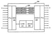
- Router 200includes an ASIC 202 , a CAM 110 , SRAM devices 204 associated with CAM 110 , a bank of SRAM devices 206 , and a switch 208 .
- Each physical inputhas a direct connection to ASIC 202 .
- ASIC 202transmits the header from each packet to CAM 110 for translation, and stores the rest of the packet, also referred to as the payload, in the bank of SRAM devices 206 . The payload remains in the bank of SRAM devices 206 until CAM 110 returns the header with the new routing information for the packet to ASIC 202 .
- ASIC 202retrieves the payload, combines the new header with the corresponding payload, and transmits the packet to switch 208 via the bank of SRAM devices 206 .
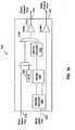
- FIG. 3 ais a block diagram of an embodiment of an SRAM device 300 that can be utilized in the bank of SRAM devices 206 of FIG. 2.
- datais transmitted directly from a write input port 302 to a write output port 304 under all conditions.
- Control data, write data, and read requestsare input to SRAM device 300 through write input port 302 .
- the packetis transmitted to a decoder and phase lock loop (PLL) 306 .
- PLLphase lock loop
- the data and the address where the data will be stored in an SRAM module 308is decoded from the packet and transmitted to SRAM module 308 , which stores the data.
- a read commandis received in write input port 302 , the data is retrieved from SRAM module 308 and transmitted to an encoder 310 , a buffer 312 , and read output port 314 .
- a multiplexer 316suspends transmission of bypass data through read input port 318 until the requested data from SRAM module 308 has been sent.
- bypass datais transmitted directly to read output port 314 via multiplexer 316 and buffer 312 . If a read command is not in progress, and no bypass data is being transmitted (i.e., read input port 318 is not toggling), then an IDLE signal 320 is transmitted to read output port 314 via multiplexer 316 and buffer 312 .
- FIG. 3 bis a block diagram of another embodiment of an SRAM device 330 that can be utilized in the bank of SRAM devices 206 of FIG. 2.
- datais transmitted from write input port 302 to decoder and PLL 306 , encoder 310 , and then to write output port 304 under all conditions.
- Decoder and PLL 306generates clock signals for a decoder and delay lock loop (DLL) 332 to correct the phase of the bypass data.
- the clock signals from decoder and PLL 306are also used to clock the read output port 314 and the write output port 304 , so that data transmitted from write output port 304 is synchronized with data transmitted from read output port 314 .
- DLLdelay lock loop
- the timingis set up to be equal in both read and write paths of SRAM device 330 , so that individual devices in a bank of SRAM devices (such as bank of SRAM devices 206 of FIG. 2) can insert data into the read data stream without interfering with data from other devices.
- a valid write commandis in progress, the data and the address where the data will be stored in SRAM module 308 is transmitted to SRAM module 308 , which stores the data.
- FIG. 4shows a block diagram of an embodiment of system memory architecture for one or more SRAM series 400 , 401 that can be utilized in the bank of SRAM devices 206 of FIG. 2.
- Each SRAM series 400 , 401includes one write input port 402 to receive input from ASIC 202 and one read output port 404 to output read data to switch 208 .
- ASIC 202 and switch 208are shown in the same component in FIG. 4 to illustrate the architecture of the SRAM series 400 , 401 .
- multiple SRAM devices 300FIG. 3 a
- SRAM devices 330FIG. 3 b
- SRAM devices 300being shown as one possible configuration.
- SRAM series 400is dedicated to receiving and storing data from a serial input 406 and supplying the data to switch 208 .
- SRAM series 401is dedicated to receiving and storing data from a serial input 408 and supplying the data to switch 208 .
- Additional SRAM devices 300can be added to a SRAM series 400 , 401 to increase storage capacity without increasing the number of pins on ASIC 202 . Further, additional SRAM series 400 , 401 can be added to handle a corresponding number of additional serial inputs.
- each SRAM device 300is connected to the read input port 318 and write input port 302 , respectively, of the next SRAM device 300 in the SRAM series 400 , 401 .
- SRAM devices 300can be added or removed from the SRAM series 400 , 401 to meet latency requirements. For example, in one embodiment, a series of fifty-two (52) eighteen (18) Megabit SRAM devices 300 is required to reach a latency of 300 milliseconds.
- SRAM devices 300 and 330are configured to manage overflow data. If the amount of data to be written is larger than the amount of memory space available in the SRAM device 300 specified in the CNTL word, the data overflows to the next SRAM 300 in the SRAM series 400 , 401 . In this manner, the data from a packet is stored in a contiguous block that can span portions of one or more SRAM devices 300 . When a read operation, such as the read operation illustrated in FIG. 8, would access the last data word in one of the SRAM devices 300 but the read operation is not halted, an overflow occurs.
- connection 410An overflow signal on a connection such as connection 410 can indicate to the next SRAM device 300 or 330 in the SRAM series 400 , 401 that the read operation should continue in the subsequent device starting at the lowest address.
- connection 410(as an output) indicates that the address at the SRAM is at terminal count.
- Connection 410(as an input) indicates that the SRAM address should be set to zero and incremented from there.
- an overflow signal on a connectioncan indicate that an overflow occurs during a write operation.
- a write operationsuch as the write operation illustrated in FIG. 6, would write to the last data word in an SRAM device 300 , but the write operation is not halted
- the overflow signal on connection 412would indicate to the next SRAM device 300 in the SRAM series 400 , 401 that the write operation should continue in the subsequent device starting at the lowest address.
- connection 412(as an output) would be an indication that the address at the SRAM is at terminal count.
- Connection 412(as an input) would indicate that the SRAM address should be set to zero and incremented from there.
- This method of managing overflowis referred to as cascading first-in-first-out (FIFO).
- FIFOfirst-in-first-out
- the overflow signal on connection 410 or connection 412also indicates that the data should be read from or written to the beginning of the memory in the SRAM device 300 , thereby alleviating the need for ASIC 202 to supply a new address or device selection to the next SRAM device 300 .
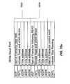
- FIG. 5is an example of an address and data format for a packet 500 that can be processed by the SRAM devices 300 , 330 of FIG. 3 a or 3 b.
- the start of frame (SOF) parameterinitiates a read or write transaction by apportioning the data in one or more frames and synchronizing the serial bit stream.
- the control (CNTL) wordincludes 8 bits that can be set to one of several read or write modes.
- two bitscan be set to command the following read or write modes: 00 READ until stop command 01 WRITE until stop command 10 STOP command (remaining 6 bits in the CNTL word are set to indicate: 000000 Stop Write 100000 Stop Read) 11 READ UNTIL STOP WITH DATA TAGGING command
- the remaining 6 bits in the CNTL wordcan also be used to select a SRAM device 300 (FIG. 3). This allows up to 64 SRAM devices 300 to be cascaded. A greater or lesser number of bits can be included in the CNTL word to accommodate any number of SRAM devices 300 , as required by a particular implementation.
- the address (ADD) fieldincludes 24 bits that are set to indicate the starting location of the data to be read or written when a READ or WRITE command is input.
- a minimum amount of memory spacesuch as 1 byte, can be allocated to each address. Other amounts of minimum memory space and number of bits in the address field can be implemented.
- a number of bits in each DATA fieldcan be used to store the data tag. For example, in one implementation, 16 bits of the DATA field are used to store tag information, such as a sequence number identifying the data to subsequent devices.
- FIG. 6shows an example of a packet write that can be input to write input port 302 and processed by SRAM devices 300 , 330 of FIG. 3 a or 3 b.
- Packet write 600includes the SOF field to indicate the start of a new control word and initiate the transaction by framing the data and synchronizing the serial bit stream.
- the CNTL wordindicates that the WRITE command is to be performed.
- a portion of the CNTL wordcan indicate the SRAM device 300 in the SRAM series 400 , 401 (FIG. 4) into which the data will be written.
- the ADDR fieldsindicate the starting address in the SRAM device 300 in the SRAM series 400 , 401 (FIG. 4) for writing the data. In one embodiment, each address requires a minimum of 32 bytes of address space.
- a variety of different size packetscan be used within the same SRAM series 400 , 401 .
- the STOP WRITE commandis performed when the command is detected in the CNTL word after the SOF field.
- a STOP WRITEcan also be initiated by starting a new WRITE command.
- the WRITE commandterminates all existing writes in all SRAM devices 300 in the SRAM series 400 , 401 (FIG. 4).
- the SRAM device 300 specified in the CNTL wordstarts a new write transaction for the write data in the packet write 600 .
- both read and write operationsmay be performed in a bank of SRAM devices (such as bank of SRAM devices 206 of FIG. 2) at the same time.
- FIG. 7an example of a packet write 702 interrupted by a packet read 704 that can be processed by the SRAM devices 300 , 330 of FIG. 3 a or 3 b is shown.
- the SOF field in packet read 704indicates a new command.
- the first two bits of the CNTL wordindicate a READ command
- the remaining 6 bitsindicate the SRAM device 300 (FIG. 4) from which the data is to be read.
- the address fields following the SOF fieldprovide the address in the selected SRAM device 300 to begin reading the data.
- the SRAM device 300will initiate a READ at the designated address and continue reading and transmitting the data to the READ output port 314 (FIG. 4) until a STOP READ command is received, or a new READ command is received.
- the SRAM device 300resumes the WRITE command where it was interrupted.
- a SOF field and a CNTL word containing bits set to indicate a STOP WRITE commandis included at the end of the packet write 702 to terminate the WRITE command, but the READ command 704 was not terminated and will continue.
- FIG. 8is an example of a read data stream 800 from two consecutive packet reads that can be output on the read output port 314 of the SRAM devices 300 , 330 of FIG. 3 a or 3 b.
- the data from each READ commandis delimited by a SOF field.
- the READ commandcontinues to output data until a new read command interrupts the current read command or a STOP READ command is detected by the SRAM device 300 , 330 .
- the read data stream 800shows data from a first READ command, a SOF field to delimit the data from a second READ command, and an IDLE field at the end of the read data stream 800 to indicate that a STOP READ command was detected by the SRAM device 300 , 330 .
- the read data stream 800does not indicate whether a WRITE command was interrupted to perform the READ commands.
- FIG. 9is an example of a packet write 902 followed immediately by a packet read 904 that can be processed by the SRAM devices 300 , 330 of FIG. 3 a or 3 b.
- Packet write 902includes the SOF field to indicate the start of a new control word and initiate the transaction by framing the data and synchronizing the serial bit stream.
- the CNTL wordindicates that the WRITE command is to be performed and the SRAM device 300 in the SRAM series 400 , 401 (FIG. 4) into which the data will be written.
- the ADDR fieldsindicate the starting address in the specified SRAM device 300 for writing the data.
- the STOP WRITE commandterminates the WRITE command once all of the data has been written to memory.
- the packet read 904begins with the SOF field to indicate a new command. Specifically, the first two bits of the CNTL word indicate a READ command, and the remaining 6 bits indicate the SRAM device 300 (FIG. 4) from which the data is to be read. The address fields following the SOF field provide the address in the selected SRAM device 300 to begin reading the data. The SRAM device 300 completes the READ command and transmits the data to the READ output port 314 (FIG. 3 b ). A SOF field is sent to indicate the start of a new transaction, and a STOP READ command in the CNTL word terminates the previous READ command.
- the minimum READ lengthis 4 bytes.
- Five byte transfersare required to initiate a READ command, (i.e., the SOF field, CNTL word, and address bytes in packet read 904 ).
- the READ output datawill consist of five byte transfers minimum (i.e., the SOF field, and four data bytes), to correspond with the time needed to initiate a new read or a STOP READ command.
- the WRITE commandterminates after the STOP WRITE command is detected, however, the data can be written to memory as the CNTL word in the read packet 904 is parsed.
- the data written by packet write 902can be read by the consecutive packet read 904 .
- Other embodimentsmay require longer or shorter minimum reads, depending upon the number of bytes of address required to complete a READ command, which can vary based on the amount of memory and the address granularity.
- FIG. 10 ashows an example of two minimum-sized sequential read packets 1002 , 1004 to be input to the write input port 302 of the SRAM devices 300 , 330 of FIG. 3 a or 3 b.
- FIG. 10 bshows the output on the read output port 314 resulting from performing the read commands in the packet reads 1002 , 1004 of FIG. 10 a.
- Each packet read 1002 , 1004includes a minimum of four byte transfers (SOF field, CNTL word, and the address from which data is to be read).
- SOF fieldSOF field
- CNTL wordthe address from which data is to be read
- the first READ commandis performed, and the beginning of the second READ command is beginning, as shown in FIG. 10 a.
- the data from the first READ commandbecomes available after the 9th (ninth) frame, as shown in FIG. 10 b.
- This example of sequential read packets 1002 , 1004shows the worst case time delay for the READ command.
- an extra CNTL wordcan be added to the data packet 500 to identify the data read from the SRAM module 308 .
- the extra CNTL wordcan be used to indicate to the SRAM device 300 , 330 that a data identifier is included in the packet, for example, following the read address.
- the identifiercan be returned with the read data, and the amount of packet space allocated for the identifier, such as 16 bits, can be selected to meet the requirements of the system.
- an identifiercan be included in the data and the components of the system can be implemented to recognize the identifier by its format and/or location in the data stream.
- some embodiments of SRAM device 300 , 330can write packets as small as one byte by performing a write request (5 bytes) and supplying one byte of data before the next write request.
- Read requestsoutput a minimum of 5 bytes due to the fact that 5 bytes of address and control information are required to make the request on the write input port 302 .
- Unused datacan be discarded.
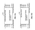
- FIG. 11 ashows an example of a known high speed router 1102 that indicates the input and output bandwidths that can be achieved by router 1102 .
- the router 1102has an internal storage capacity of up to 300 milliseconds, with input and output bandwidths up to 10 gigaHertz for 10 serial input lines at speeds of 1 gigaHertz each.
- FIG. 11 bindicates the input and output bandwidths that can be achieved by a high speed router 1104 configured with SRAM devices 300 , 330 (FIGS. 3 a, 3 b ) in accordance with the present invention.
- the router 1104has an internal storage capacity (in time) similar to router 1102 in FIG. 11 a, however, router 1104 achieves input and output bandwidths up to 100 gigaHertz for 10 serial input lines at speeds of 3.125 gigaHertz each.
- routers 1102 , 1104can store 300 milliseconds of data before they overflow, however, the internal memory storage capacity of router 1104 (FIG. 11 b ) is an order of magnitude larger than router 1102 (FIG. 11 a ).
- SRAM devices 300 , 330 configured in SRAM series 400 , 401can be used to provide cost effective and scalable memory for high-speed routers 100 and other equipment that utilizes SRAM.
- SRAM devices 300 , 330achieve efficient data transfers with even very small data packets (e.g., 4 byte packet read).
- the storage capacity of SRAM series 400 , 401can be increased without requiring an increase in the number of pins on ASIC 202 and switch 208 .
- the ability to scale the memory capacity and bandwidth while using the same ASIC 202 and switch 208alleviates problems associated with integrating new ASICS having an increased number of pins for more bandwidth, as found in the prior art.
- the SRAM series 400 , 401allow additional SRAM devices 300 to be added to SRAM series 400 , 401 without incurring board layout problems. Such problems can include attempting to position components to avoid long data bus lines, routing wide data bus lines to memory and processor devices with a large number of pins, and multidrop connections on all busses.
- SRAM devices 300 , 330 configured in SRAM series 400 , 401also alleviate address fan-out problems because each SRAM series 400 , 401 has only one write input port 402 and one read output port 404 that interfaces with ASIC 202 . Further, SRAM series 400 , 401 alleviate noise issues that arise with heavy bus loading and drivers, line termination, bus contention, and long data bus lines found in the prior art. A further advantage with SRAM series 400 , 401 is that there are no logistical problems with bus arbitration, transferring small amounts of data on very wide busses, bottlenecks at the memory interface, and bus/clock skew and bit alignment.
Landscapes
- Engineering & Computer Science (AREA)
- Computer Networks & Wireless Communication (AREA)
- Signal Processing (AREA)
- Data Exchanges In Wide-Area Networks (AREA)
Abstract
Description
- As the need for bandwidth expands in information and communication networks, bottlenecks develop in the switching hardware due to increases in the number of ports and throughput per port in routing. To handle the increased bandwidth, architectures arose that rely upon increased internal bus widths, increased bandwidths on the busses, and decentralized processing. A block diagram of an example of the architecture of a known[0001]
router system 100 is shown in FIG. 1. Incoming packets can be temporarily stored in alocal buffer 102 until one or more network layer processors, shown as application specific integrated circuits (ASICs)104 and106, classifies and determines the forwarding address of the packet. The packets are then routed to the target destination. - [0002]
Buffer 102 includes gigabytes of SRAM arranged in a very wide data bus (512 bits or more)108 to allow several simultaneous search operations.Router system 100 analyzes the headers of incoming packets for the appropriate types of operations to be performed on the packet. In the case of TCP/IP route look-up, for example,router system 100 matches a combination of source/destination addresses with entries in a routing table for an exact match or a longest prefix match. Content addressable memory (CAM)110offloads ASIC 104 by processing a limited set of lookup instructions. In other applications such as load balancing and URL routing,router system 100 performs more complex search rules and routing data structures. - A successful search will result in[0003]
router system 100 modifying the header and optionally, the payload, with new information. A packet header may be modified for its output port/queue, output connection, or additional labels for switching, for example. The packets are then queued by priority as well as latency to absorb the time needed to implement the search/modify steps. Output queuing reorders packets in the event multiple packets are searched in parallel. - In the example shown in FIG. 1,[0004]
data bus 108 is a 640 bit bus with a speed of 133 MHz or 167 MHz. Greater efficiency can be achieved with large data packets, while transfers overdata bus 108 are very inefficient for small data packets. ASICS104 and106 have a pin count of over 1000 pins. The number of pins cannot be expanded without changingASICs router system 100 is therefore limited. - If an ASIC with an expanded number of pins is used, other problems arise which increase production costs and limit scalability of[0005]
router system 100. For example, the memory interface presents board layout problems, including positioning components to avoid long data bus lines; routing wide data bus lines to memory and processor devices with a large number of pins; and multidrop connections on all busses. Other problems include limited bandwidth per pin, and limited memory access time. Additionally, address fan-out problems arise with increasing address bandwidth and address loading and buffering. Further, noise issues arise with heavy bus loading and heavy bus drivers, line termination, bus contention, and the length of the data bus lines. There are also logistical problems with bus arbitration, transferring small amounts of data on very wide busses, bottlenecks at the memory interface, and bus/clock skew and bit alignment. Numerous memory devices switching on many pins at very high speed also dissipates a large amount of power. Additionally, because increasing bus widths, bus bandwidths, bus loading, ASIC size, and memory depth brings diminishing returns,router system 100 cannot efficiently be expanded to handle greater packet bandwidth. - It is therefore desirable to provide a router that is cost effective and scalable, and alleviates many of the problems listed above.[0006]
- According to an embodiment of the invention, an apparatus may include a first processing unit operable to receive serial data input, a switch operable to receive data to be transmitted, a first random access memory device coupled to the first processing unit via a write input port, wherein the first processing unit is operable to transmit data packets to the first random access memory device via the write input port, and a second random access memory device coupled to the first random access memory device, the second random access memory device being further coupled to transmit the data to be transmitted to the switch. The first and second random access memory devices may be configured as described in the embodiments below.[0007]
- There may be a plurality of random access memory devices coupled between the first random access memory device and the second random access memory device, where each of the plurality of random access memory devices may be configured according to one of the embodiments described below. Each of the plurality of random access memory devices may be coupled in series to another of the plurality of random access memory devices. A write output port of each of the plurality of random access memory devices may be coupled to a write input port of the next of the series of the plurality of random access memory devices. A read output port of each of the plurality of random access memory devices may be coupled to a read input port of the next of the series of the plurality of random access memory devices. In some embodiments, each of the random access memory devices is operable to generate an overflow signal to indicate to the next random access memory device in the series that the data to be written or read is a continuation from the previous random access memory device. Each random access memory device may be operable to generate a command signal to indicate to the next random access memory device in the series that the continuation of data is to be written or read.[0008]
- According to an embodiment of the invention, a random access memory device comprises a random access memory module, a write input port coupled to receive packets that include data and command information, a decoder coupled to receive the packets from the write input port, and to access the random access memory module to perform the commands in the packets, a read input port operable to receive bypass data, and a read output port coupled to output the bypass data and data read from the random access memory module.[0009]
- The random access memory device may also include a write output port coupled to receive the packets from the write input port and to transmit the packets to another random access memory device. The random access memory device may also comprise a buffer coupled between the write input port and the write output port. The random access memory device may include a decoder between the write input port and the write output port, and an encoder coupled between the decoder and the write output port. The decoder may include a phase lock loop.[0010]
- The random access memory device may also include a first multiplexer coupled between the read input port and the read output port, operable to output an idle signal when the read input port is not transmitting data to the read output port. The random access memory device may include a second multiplexer, coupled between the random access memory module and the read output port, where the second multiplexer is coupled to receive the output of the first multiplexer and to output the output of the first multiplexer when read data is not being transmitted from the random access memory module. The random access memory device may also include an encoder coupled between the random access module and the second multiplexer. The random access memory device may include a buffer coupled between the second multiplexer and the read output port. The random access memory device may also include a second decoder coupled between the read input port and the first multiplexer, wherein the second decoder includes a delay lock loop.[0011]
- In some embodiments, the random access memory devices are operable to decode data packets and determine whether a data packet includes at least one of: a start of frame field, a control word, an address field, a data field, and an idle indicator. The control word may include at least one of: a command to be performed, and the random access memory device to perform the command.[0012]
- According to an embodiment of the invention, a method for routing data includes receiving serial data input in a first processing unit, generating a data packet based on the serial data input, transmitting the data packet to a first random access memory device via a write input port, decoding the data packet, determining whether to perform a command in the first random access memory device based on information in the data packet, and transmitting the data packet to a second random access memory device, wherein a write input port of the second random access memory device is coupled in series to a write output port of the first random access memory device. The method may further include determining whether to perform a command in the second random access memory device based on the information in the data packet. The method may further include coupling a plurality of random access memory devices in series between the first random access memory device and the second random access memory device, wherein each of the plurality of random access memory devices includes a write input port, a write output port, a read input port, and a read output port, transmitting the data packet from the first random access memory device to each random access memory device, wherein the write output port of each random access memory device is coupled in series to the write input port of the next random access memory device, and determining whether to perform a command in each random access memory device based on the information in the data packet.[0013]
- The method may further include generating an overflow signal in one of the plurality of random access memory devices to indicate to the next random access memory device that a write command or read command is being continued from the one of the plurality of random access memory devices. The method may further include terminating performance of a first write command when a second write command is received, when a read command is received, or when a stop write command is received.[0014]
- The present invention may be better understood, and its numerous objects, features, and advantages made even more apparent to those skilled in the art by referencing the detailed description and accompanying drawings of the embodiments described below.[0015]
- FIG. 1 is a block diagram of an example of components included in a high speed router known in the art.[0016]
- FIG. 2 is a block diagram of components included in a router according to an embodiment of the present invention.[0017]
- FIG. 3[0018]ais a block diagram of an example of a SRAM device that can be utilized in the router of FIG. 2.
- FIG. 3[0019]bis a block diagram of an alternate SRAM device that can be utilized in the router of FIG. 2.
- FIG. 4 is a block diagram showing an embodiment of a configuration of the bank of SRAM devices of FIG. 2.[0020]
- FIG. 5 shows an example of an address and data format for two packets that can be processed by the SRAM devices of FIG. 3[0021]aor3b.
- FIG. 6 shows an example of a packet write that can be processed by the SRAM devices of FIG. 3[0022]aor3b.
- FIG. 7 shows an example of a packet write interrupted by a packet read that can be processed by the SRAM devices of FIG. 3[0023]aor3b.
- FIG. 8 shows an example of a read data that can be output on the read output port of the SRAM devices of FIG. 3[0024]aor3bin response to two read requests.
- FIG. 9 shows an example of a packet write followed immediately by a packet read of the data that can be processed by the SRAM devices of FIG. 3[0025]aor3b.
- FIG. 10[0026]ashows an example of a read request for two minimum sized packets requested through the write input port.
- FIG. 10[0027]bshows the output on the read port resulting from the read commands received in the packets of FIG. 10a.
- FIG. 11[0028]ashows an example of input and output bandwidths that can be achieved with a known high speed router.
- FIG. 11[0029]bshows an example of input and output bandwidth that can be achieved by a high speed router configured with SRAM devices of FIG. 3aor3b.
- A configuration of static random access memory (SRAM) devices in accordance with an embodiment of the present invention replaces the data bus[0030]108 (FIG. 1) with high speed, point-to-point, serial data connections. Accordingly, the pin count on the controlling ASIC104 (FIG. 1) can be significantly reduced while simultaneously achieving at least an order of magnitude increase in total bandwidth. Further, increasing the memory capacity of SRAM102 (FIG. 1) adds bus loading on
bus 108 and possibly extra pins onASIC 104. Further, increasing the size and number of memory storage devices inSRAM 102 creates difficulties inrouting bus 108 and address distribution. SRAM devices configured in accordance with an embodiment of the present invention allow an increase in the amount of memory without requiring additional pins on an ASIC and can be distributed serially in chains that are connected to the ASIC at both ends. Such a configuration simplifies real estate problems in the vicinity of the ASIC and alleviates problems associated with routing additional bus lines toASIC 104. Further, the bandwidth per pin of an ASIC configured in accordance with embodiments of the present invention can be significantly increased, and memory reads and writes can occur simultaneously and continuously as further described hereinbelow. - Referring now to FIG. 2, a block diagram of components included in a[0031]
router 200 according to an embodiment of the present invention is shown.Router 200 includes anASIC 202, aCAM 110,SRAM devices 204 associated withCAM 110, a bank ofSRAM devices 206, and aswitch 208. Each physical input has a direct connection toASIC 202.ASIC 202 transmits the header from each packet toCAM 110 for translation, and stores the rest of the packet, also referred to as the payload, in the bank ofSRAM devices 206. The payload remains in the bank ofSRAM devices 206 untilCAM 110 returns the header with the new routing information for the packet toASIC 202.ASIC 202 retrieves the payload, combines the new header with the corresponding payload, and transmits the packet to switch208 via the bank ofSRAM devices 206. - FIG. 3[0032]ais a block diagram of an embodiment of an
SRAM device 300 that can be utilized in the bank ofSRAM devices 206 of FIG. 2. In the embodiment shown, data is transmitted directly from awrite input port 302 to awrite output port 304 under all conditions. Control data, write data, and read requests are input toSRAM device 300 throughwrite input port 302. When a valid write command is in progress, the packet is transmitted to a decoder and phase lock loop (PLL)306. The data and the address where the data will be stored in anSRAM module 308 is decoded from the packet and transmitted toSRAM module 308, which stores the data. - When a read command is received in[0033]
write input port 302, the data is retrieved fromSRAM module 308 and transmitted to anencoder 310, abuffer 312, and readoutput port 314. When a read is in progress, amultiplexer 316 suspends transmission of bypass data through readinput port 318 until the requested data fromSRAM module 308 has been sent. When data is not being output on readoutput port 314, then bypass data is transmitted directly to readoutput port 314 viamultiplexer 316 andbuffer 312. If a read command is not in progress, and no bypass data is being transmitted (i.e., readinput port 318 is not toggling), then anIDLE signal 320 is transmitted to readoutput port 314 viamultiplexer 316 andbuffer 312. - FIG. 3[0034]bis a block diagram of another embodiment of an
SRAM device 330 that can be utilized in the bank ofSRAM devices 206 of FIG. 2. In the embodiment ofSRAM device 330 shown in FIG. 3b,data is transmitted fromwrite input port 302 to decoder andPLL 306,encoder 310, and then to writeoutput port 304 under all conditions. Decoder andPLL 306 generates clock signals for a decoder and delay lock loop (DLL)332 to correct the phase of the bypass data. The clock signals from decoder andPLL 306 are also used to clock the readoutput port 314 and thewrite output port 304, so that data transmitted fromwrite output port 304 is synchronized with data transmitted from readoutput port 314. The timing is set up to be equal in both read and write paths ofSRAM device 330, so that individual devices in a bank of SRAM devices (such as bank ofSRAM devices 206 of FIG. 2) can insert data into the read data stream without interfering with data from other devices. When a valid write command is in progress, the data and the address where the data will be stored inSRAM module 308 is transmitted toSRAM module 308, which stores the data. - When a read command is received in[0035]
write input port 302, the data is retrieved fromSRAM module 308 and transmitted to anencoder 334 and readoutput port 314. When a read is in progress,multiplexer 316 suspends transmission of bypass data through readinput port 318 until the requested data fromSRAM module 308 has been sent. When data is not being output on readoutput port 314, then bypass data is transmitted to readoutput port 314 via decoder andDLL 332 andencoder 334. If no read command is in progress, and there is no bypass data being transmitted, then anIDLE signal 320 is transmitted to readoutput port 314 via decoder andDLL 332 andencoder 334. - FIG. 4 shows a block diagram of an embodiment of system memory architecture for one or[0036]
more SRAM series SRAM devices 206 of FIG. 2. EachSRAM series write input port 402 to receive input fromASIC 202 and oneread output port 404 to output read data to switch208. Note thatASIC 202 and switch208 are shown in the same component in FIG. 4 to illustrate the architecture of theSRAM series SRAM series SRAM devices 300 being shown as one possible configuration. - In the architecture shown,[0037]
SRAM series 400 is dedicated to receiving and storing data from aserial input 406 and supplying the data to switch208. Similarly,SRAM series 401 is dedicated to receiving and storing data from aserial input 408 and supplying the data to switch208.Additional SRAM devices 300 can be added to aSRAM series ASIC 202. Further,additional SRAM series - The read[0038]
output ports 314 and thewrite output ports 304 of eachSRAM device 300 are connected to the readinput port 318 and writeinput port 302, respectively, of thenext SRAM device 300 in theSRAM series SRAM devices 300 can be added or removed from theSRAM series Megabit SRAM devices 300 is required to reach a latency of 300 milliseconds. - In some embodiments,[0039]
SRAM devices SRAM device 300 specified in the CNTL word, the data overflows to thenext SRAM 300 in theSRAM series more SRAM devices 300. When a read operation, such as the read operation illustrated in FIG. 8, would access the last data word in one of theSRAM devices 300 but the read operation is not halted, an overflow occurs. An overflow signal on a connection such asconnection 410 can indicate to thenext SRAM device SRAM series SRAM devices - Similarly, an overflow signal on a connection such as[0040]
connection 412 can indicate that an overflow occurs during a write operation. When a write operation, such as the write operation illustrated in FIG. 6, would write to the last data word in anSRAM device 300, but the write operation is not halted, the overflow signal onconnection 412 would indicate to thenext SRAM device 300 in theSRAM series SRAM device connection 410 orconnection 412 also indicates that the data should be read from or written to the beginning of the memory in theSRAM device 300, thereby alleviating the need forASIC 202 to supply a new address or device selection to thenext SRAM device 300. - FIG. 5 is an example of an address and data format for a[0041]
packet 500 that can be processed by theSRAM devices packet 500 is input to thewrite input port 302, the start of frame (SOF) parameter initiates a read or write transaction by apportioning the data in one or more frames and synchronizing the serial bit stream. In one embodiment, the control (CNTL) word includes 8 bits that can be set to one of several read or write modes. For example, two bits can be set to command the following read or write modes:00 READ until stop command 01 WRITE until stop command 10 STOP command (remaining 6 bits in the CNTL word are set to indicate: 000000 Stop Write 100000 Stop Read) 11 READ UNTIL STOP WITH DATA TAGGING command - Note that an address is not required for the STOP command. For the READ and WRITE commands, the remaining 6 bits in the CNTL word can also be used to select a SRAM device[0042]300 (FIG. 3). This allows up to 64
SRAM devices 300 to be cascaded. A greater or lesser number of bits can be included in the CNTL word to accommodate any number ofSRAM devices 300, as required by a particular implementation. - In the embodiment shown, the address (ADD) field includes 24 bits that are set to indicate the starting location of the data to be read or written when a READ or WRITE command is input. A minimum amount of memory space, such as 1 byte, can be allocated to each address. Other amounts of minimum memory space and number of bits in the address field can be implemented.[0043]
- If a ‘READ UNTIL STOP WITH DATA TAGGING’ command is input, a number of bits in each DATA field can be used to store the data tag. For example, in one implementation, 16 bits of the DATA field are used to store tag information, such as a sequence number identifying the data to subsequent devices.[0044]
- When the WRITE command is received, data is written into one or more of the[0045]
SRAM devices 300,330 (FIGS. 3aand3b) until the end of the data is reached. The WRITE command can be suspended when the STOP WRITE command is detected. - FIG. 6 shows an example of a packet write that can be input to write[0046]
input port 302 and processed bySRAM devices Packet write 600 includes the SOF field to indicate the start of a new control word and initiate the transaction by framing the data and synchronizing the serial bit stream. The CNTL word indicates that the WRITE command is to be performed. A portion of the CNTL word can indicate theSRAM device 300 in theSRAM series 400,401 (FIG. 4) into which the data will be written. The ADDR fields indicate the starting address in theSRAM device 300 in theSRAM series 400,401 (FIG. 4) for writing the data. In one embodiment, each address requires a minimum of 32 bytes of address space. A variety of different size packets can be used within thesame SRAM series - In some embodiments, the STOP WRITE command is performed when the command is detected in the CNTL word after the SOF field. A STOP WRITE can also be initiated by starting a new WRITE command. In such an embodiment, the WRITE command terminates all existing writes in all[0047]
SRAM devices 300 in theSRAM series 400,401 (FIG. 4). TheSRAM device 300 specified in the CNTL word starts a new write transaction for the write data in thepacket write 600. - According to some embodiments, both read and write operations may be performed in a bank of SRAM devices (such as bank of[0048]
SRAM devices 206 of FIG. 2) at the same time. Referring now to FIG. 7, an example of apacket write 702 interrupted by a packet read704 that can be processed by theSRAM devices SRAM device 300 to begin reading the data. TheSRAM device 300 will initiate a READ at the designated address and continue reading and transmitting the data to the READ output port314 (FIG. 4) until a STOP READ command is received, or a new READ command is received. TheSRAM device 300 resumes the WRITE command where it was interrupted. A SOF field and a CNTL word containing bits set to indicate a STOP WRITE command is included at the end of thepacket write 702 to terminate the WRITE command, but theREAD command 704 was not terminated and will continue. - FIG. 8 is an example of a[0049]
read data stream 800 from two consecutive packet reads that can be output on the readoutput port 314 of theSRAM devices SRAM device read data stream 800 shows data from a first READ command, a SOF field to delimit the data from a second READ command, and an IDLE field at the end of the readdata stream 800 to indicate that a STOP READ command was detected by theSRAM device read data stream 800 does not indicate whether a WRITE command was interrupted to perform the READ commands. - FIG. 9 is an example of a[0050]
packet write 902 followed immediately by a packet read904 that can be processed by theSRAM devices Packet write 902 includes the SOF field to indicate the start of a new control word and initiate the transaction by framing the data and synchronizing the serial bit stream. The CNTL word indicates that the WRITE command is to be performed and theSRAM device 300 in theSRAM series 400,401 (FIG. 4) into which the data will be written. The ADDR fields indicate the starting address in the specifiedSRAM device 300 for writing the data. The STOP WRITE command terminates the WRITE command once all of the data has been written to memory. - The packet read[0051]904 begins with the SOF field to indicate a new command. Specifically, the first two bits of the CNTL word indicate a READ command, and the remaining 6 bits indicate the SRAM device300 (FIG. 4) from which the data is to be read. The address fields following the SOF field provide the address in the selected
SRAM device 300 to begin reading the data. TheSRAM device 300 completes the READ command and transmits the data to the READ output port314 (FIG. 3b). A SOF field is sent to indicate the start of a new transaction, and a STOP READ command in the CNTL word terminates the previous READ command. - In the example shown in FIG. 9, the minimum READ length is 4 bytes. Five byte transfers are required to initiate a READ command, (i.e., the SOF field, CNTL word, and address bytes in packet read[0052]904). The READ output data will consist of five byte transfers minimum (i.e., the SOF field, and four data bytes), to correspond with the time needed to initiate a new read or a STOP READ command. The WRITE command terminates after the STOP WRITE command is detected, however, the data can be written to memory as the CNTL word in the read
packet 904 is parsed. Notably, the data written bypacket write 902 can be read by the consecutive packet read904. Other embodiments may require longer or shorter minimum reads, depending upon the number of bytes of address required to complete a READ command, which can vary based on the amount of memory and the address granularity. - Referring now to FIGS. 10[0053]aand10b,FIG. 10ashows an example of two minimum-sized
sequential read packets write input port 302 of theSRAM devices output port 314 resulting from performing the read commands in the packet reads1002,1004 of FIG. 10a.Each packet read1002,1004 includes a minimum of four byte transfers (SOF field, CNTL word, and the address from which data is to be read). During frames 1-8, the first READ command is performed, and the beginning of the second READ command is beginning, as shown in FIG. 10a.The data from the first READ command becomes available after the 9th (ninth) frame, as shown in FIG. 10b.This example ofsequential read packets - Referring to FIGS. 3[0054]a,3b,and5, in some embodiments, to provide traceability of the read data, an extra CNTL word can be added to the
data packet 500 to identify the data read from theSRAM module 308. The extra CNTL word can be used to indicate to theSRAM device - Advantageously, some embodiments of[0055]
SRAM device write input port 302. Unused data can be discarded. - Referring to FIGS. 11[0056]aand11b,FIG. 11ashows an example of a known
high speed router 1102 that indicates the input and output bandwidths that can be achieved byrouter 1102. In the example shown, therouter 1102 has an internal storage capacity of up to 300 milliseconds, with input and output bandwidths up to 10 gigaHertz for 10 serial input lines at speeds of 1 gigaHertz each. - FIG. 11[0057]bindicates the input and output bandwidths that can be achieved by a
high speed router 1104 configured withSRAM devices 300,330 (FIGS. 3a,3b) in accordance with the present invention. Therouter 1104 has an internal storage capacity (in time) similar torouter 1102 in FIG. 11a,however,router 1104 achieves input and output bandwidths up to 100 gigaHertz for 10 serial input lines at speeds of 3.125 gigaHertz each. In some embodiments,routers - Referring again to FIGS. 3[0058]a,3b,and4,
SRAM devices SRAM series speed routers 100 and other equipment that utilizes SRAM.SRAM devices SRAM series ASIC 202 andswitch 208. - The ability to scale the memory capacity and bandwidth while using the[0059]
same ASIC 202 and switch208 alleviates problems associated with integrating new ASICS having an increased number of pins for more bandwidth, as found in the prior art. TheSRAM series additional SRAM devices 300 to be added toSRAM series - The requirement of transferring a minimum of five bytes to initiate a READ or a WRITE command allows the internal architecture of[0060]
SRAM devices SRAM devices SRAM devices - [0061]
SRAM devices SRAM series SRAM series write input port 402 and oneread output port 404 that interfaces withASIC 202. Further,SRAM series SRAM series - One skilled in the art will recognize the many teachings of this disclosure and be able to apply these teachings to additional embodiments and, indeed, to other kinds of devices, as well, without departing from the teachings of this disclosure. Consequently, the scope of the invention should not be inferred as being limited by the exemplary embodiments described herein, but rather should be viewed as teaching in the art far greater than just these exemplary embodiments. Accordingly, other embodiments, variations, and improvements not described herein are not necessarily excluded from the scope of the invention.[0062]
Claims (66)
Priority Applications (2)
| Application Number | Priority Date | Filing Date | Title |
|---|---|---|---|
| US10/120,648US7110400B2 (en) | 2002-04-10 | 2002-04-10 | Random access memory architecture and serial interface with continuous packet handling capability |
| US10/865,583US20040233906A1 (en) | 2002-04-10 | 2004-06-09 | Random access memory architecture and serial interface with continuous packet handling capability |
Applications Claiming Priority (1)
| Application Number | Priority Date | Filing Date | Title |
|---|---|---|---|
| US10/120,648US7110400B2 (en) | 2002-04-10 | 2002-04-10 | Random access memory architecture and serial interface with continuous packet handling capability |
Related Child Applications (1)
| Application Number | Title | Priority Date | Filing Date |
|---|---|---|---|
| US10/865,583DivisionUS20040233906A1 (en) | 2002-04-10 | 2004-06-09 | Random access memory architecture and serial interface with continuous packet handling capability |
Publications (2)
| Publication Number | Publication Date |
|---|---|
| US20030193927A1true US20030193927A1 (en) | 2003-10-16 |
| US7110400B2 US7110400B2 (en) | 2006-09-19 |
Family
ID=28790133
Family Applications (2)
| Application Number | Title | Priority Date | Filing Date |
|---|---|---|---|
| US10/120,648Expired - LifetimeUS7110400B2 (en) | 2002-04-10 | 2002-04-10 | Random access memory architecture and serial interface with continuous packet handling capability |
| US10/865,583AbandonedUS20040233906A1 (en) | 2002-04-10 | 2004-06-09 | Random access memory architecture and serial interface with continuous packet handling capability |
Family Applications After (1)
| Application Number | Title | Priority Date | Filing Date |
|---|---|---|---|
| US10/865,583AbandonedUS20040233906A1 (en) | 2002-04-10 | 2004-06-09 | Random access memory architecture and serial interface with continuous packet handling capability |
Country Status (1)
| Country | Link |
|---|---|
| US (2) | US7110400B2 (en) |
Cited By (61)
| Publication number | Priority date | Publication date | Assignee | Title |
|---|---|---|---|---|
| US20030101312A1 (en)* | 2001-11-26 | 2003-05-29 | Doan Trung T. | Machine state storage apparatus and method |
| US20040268081A1 (en)* | 2003-06-30 | 2004-12-30 | Erwin Thalmann | Apparatus and method for storing digital data |
| US20050146943A1 (en)* | 2003-08-28 | 2005-07-07 | Jeddeloh Joseph M. | Memory module and method having on-board data search capabilities and processor-based system using such memory modules |
| US6980042B2 (en) | 2004-04-05 | 2005-12-27 | Micron Technology, Inc. | Delay line synchronizer apparatus and method |
| US7047351B2 (en) | 2002-08-16 | 2006-05-16 | Micron Technology, Inc. | Memory hub bypass circuit and method |
| US20060200602A1 (en)* | 2003-08-20 | 2006-09-07 | Ralph James | Method and system for capturing and bypassing memory transactions in a hub-based memory system |
| US7107415B2 (en) | 2003-06-20 | 2006-09-12 | Micron Technology, Inc. | Posted write buffers and methods of posting write requests in memory modules |
| US7106611B2 (en) | 2002-09-09 | 2006-09-12 | Micron Technology, Inc. | Wavelength division multiplexed memory module, memory system and method |
| US7117316B2 (en) | 2002-08-05 | 2006-10-03 | Micron Technology, Inc. | Memory hub and access method having internal row caching |
| US7120727B2 (en) | 2003-06-19 | 2006-10-10 | Micron Technology, Inc. | Reconfigurable memory module and method |
| US7120743B2 (en) | 2003-10-20 | 2006-10-10 | Micron Technology, Inc. | Arbitration system and method for memory responses in a hub-based memory system |
| US7120723B2 (en) | 2004-03-25 | 2006-10-10 | Micron Technology, Inc. | System and method for memory hub-based expansion bus |
| US7133972B2 (en) | 2002-06-07 | 2006-11-07 | Micron Technology, Inc. | Memory hub with internal cache and/or memory access prediction |
| US7136958B2 (en) | 2003-08-28 | 2006-11-14 | Micron Technology, Inc. | Multiple processor system and method including multiple memory hub modules |
| US7162567B2 (en) | 2004-05-14 | 2007-01-09 | Micron Technology, Inc. | Memory hub and method for memory sequencing |
| US20070028059A1 (en)* | 2005-08-01 | 2007-02-01 | Infineon Technologies Ag | Method of operating a memory device, memory module, and a memory device comprising the memory module |
| US7180522B2 (en) | 2000-06-23 | 2007-02-20 | Micron Technology, Inc. | Apparatus and method for distributed memory control in a graphics processing system |
| US7181584B2 (en) | 2004-02-05 | 2007-02-20 | Micron Technology, Inc. | Dynamic command and/or address mirroring system and method for memory modules |
| US7188219B2 (en) | 2004-01-30 | 2007-03-06 | Micron Technology, Inc. | Buffer control system and method for a memory system having outstanding read and write request buffers |
| US7194593B2 (en) | 2003-09-18 | 2007-03-20 | Micron Technology, Inc. | Memory hub with integrated non-volatile memory |
| US7200024B2 (en) | 2002-08-02 | 2007-04-03 | Micron Technology, Inc. | System and method for optically interconnecting memory devices |
| US7210059B2 (en) | 2003-08-19 | 2007-04-24 | Micron Technology, Inc. | System and method for on-board diagnostics of memory modules |
| US7213082B2 (en) | 2004-03-29 | 2007-05-01 | Micron Technology, Inc. | Memory hub and method for providing memory sequencing hints |
| US20070101087A1 (en)* | 2005-10-31 | 2007-05-03 | Peter Gregorius | Memory module and memory device and method of operating a memory device |
| US7222213B2 (en) | 2004-05-17 | 2007-05-22 | Micron Technology, Inc. | System and method for communicating the synchronization status of memory modules during initialization of the memory modules |
| US7222197B2 (en) | 2003-07-22 | 2007-05-22 | Micron Technology, Inc. | Apparatus and method for direct memory access in a hub-based memory system |
| US7234070B2 (en) | 2003-10-27 | 2007-06-19 | Micron Technology, Inc. | System and method for using a learning sequence to establish communications on a high-speed nonsynchronous interface in the absence of clock forwarding |
| US7242213B2 (en) | 2003-06-11 | 2007-07-10 | Micron Technology, Inc. | Memory module and method having improved signal routing topology |
| US7249236B2 (en) | 2002-08-29 | 2007-07-24 | Micron Technology, Inc. | Method and system for controlling memory accesses to memory modules having a memory hub architecture |
| US7254331B2 (en) | 2002-08-09 | 2007-08-07 | Micron Technology, Inc. | System and method for multiple bit optical data transmission in memory systems |
| US7257683B2 (en) | 2004-03-24 | 2007-08-14 | Micron Technology, Inc. | Memory arbitration system and method having an arbitration packet protocol |
| US7260685B2 (en) | 2003-06-20 | 2007-08-21 | Micron Technology, Inc. | Memory hub and access method having internal prefetch buffers |
| US7310748B2 (en) | 2004-06-04 | 2007-12-18 | Micron Technology, Inc. | Memory hub tester interface and method for use thereof |
| US7310752B2 (en) | 2003-09-12 | 2007-12-18 | Micron Technology, Inc. | System and method for on-board timing margin testing of memory modules |
| US7330992B2 (en) | 2003-12-29 | 2008-02-12 | Micron Technology, Inc. | System and method for read synchronization of memory modules |
| US7363419B2 (en) | 2004-05-28 | 2008-04-22 | Micron Technology, Inc. | Method and system for terminating write commands in a hub-based memory system |
| US7392331B2 (en) | 2004-08-31 | 2008-06-24 | Micron Technology, Inc. | System and method for transmitting data packets in a computer system having a memory hub architecture |
| US7412574B2 (en) | 2004-02-05 | 2008-08-12 | Micron Technology, Inc. | System and method for arbitration of memory responses in a hub-based memory system |
| US7428644B2 (en) | 2003-06-20 | 2008-09-23 | Micron Technology, Inc. | System and method for selective memory module power management |
| US7447240B2 (en) | 2004-03-29 | 2008-11-04 | Micron Technology, Inc. | Method and system for synchronizing communications links in a hub-based memory system |
| US20090070612A1 (en)* | 2005-04-21 | 2009-03-12 | Maxim Adelman | Memory power management |
| US7519788B2 (en) | 2004-06-04 | 2009-04-14 | Micron Technology, Inc. | System and method for an asynchronous data buffer having buffer write and read pointers |
| US7590797B2 (en) | 2004-04-08 | 2009-09-15 | Micron Technology, Inc. | System and method for optimizing interconnections of components in a multichip memory module |
| US7788451B2 (en) | 2004-02-05 | 2010-08-31 | Micron Technology, Inc. | Apparatus and method for data bypass for a bi-directional data bus in a hub-based memory sub-system |
| US7805586B2 (en) | 2002-08-29 | 2010-09-28 | Micron Technology, Inc. | System and method for optimizing interconnections of memory devices in a multichip module |
| US20110153934A1 (en)* | 2009-12-21 | 2011-06-23 | Stmicroelectronics Pvt. Ltd. | Memory card and communication method between a memory card and a host unit |
| US8028186B2 (en) | 2006-10-23 | 2011-09-27 | Violin Memory, Inc. | Skew management in an interconnection system |
| US8112655B2 (en) | 2005-04-21 | 2012-02-07 | Violin Memory, Inc. | Mesosynchronous data bus apparatus and method of data transmission |
| US8452929B2 (en) | 2005-04-21 | 2013-05-28 | Violin Memory Inc. | Method and system for storage of data in non-volatile media |
| US8726064B2 (en) | 2005-04-21 | 2014-05-13 | Violin Memory Inc. | Interconnection system |
| US8775764B2 (en) | 2004-03-08 | 2014-07-08 | Micron Technology, Inc. | Memory hub architecture having programmable lane widths |
| US9286198B2 (en) | 2005-04-21 | 2016-03-15 | Violin Memory | Method and system for storage of data in non-volatile media |
| US9582449B2 (en) | 2005-04-21 | 2017-02-28 | Violin Memory, Inc. | Interconnection system |
| US10372667B2 (en)* | 2015-06-24 | 2019-08-06 | Canon Kabushiki Kaisha | Communication apparatus and control method thereof |
| US10679722B2 (en) | 2016-08-26 | 2020-06-09 | Sandisk Technologies Llc | Storage system with several integrated components and method for use therewith |
| CN115426315A (en)* | 2022-11-07 | 2022-12-02 | 北京数盾信息科技有限公司 | Information processing method, device and equipment |
| US20230022530A1 (en)* | 2021-07-22 | 2023-01-26 | Rambus Inc. | Data buffer for memory devices with unidirectional ports |
| US11580044B2 (en) | 2020-08-31 | 2023-02-14 | Micron Technology, Inc. | Network credit return mechanisms |
| US11588745B2 (en)* | 2020-08-31 | 2023-02-21 | Micron Technology, Inc. | Early credit return for credit-based flow control |
| US11831543B2 (en) | 2020-08-31 | 2023-11-28 | Micron Technology, Inc. | Flow control for a multiple flow control unit interface |
| US12323336B2 (en) | 2020-08-31 | 2025-06-03 | Micron Technology, Inc. | Combined write enable mask and credit return field |
Families Citing this family (16)
| Publication number | Priority date | Publication date | Assignee | Title |
|---|---|---|---|---|
| US7266634B2 (en)* | 2000-01-05 | 2007-09-04 | Rambus Inc. | Configurable width buffered module having flyby elements |
| US7404032B2 (en) | 2000-01-05 | 2008-07-22 | Rambus Inc. | Configurable width buffered module having switch elements |
| US7356639B2 (en)* | 2000-01-05 | 2008-04-08 | Rambus Inc. | Configurable width buffered module having a bypass circuit |
| US20050010737A1 (en)* | 2000-01-05 | 2005-01-13 | Fred Ware | Configurable width buffered module having splitter elements |
| US7363422B2 (en) | 2000-01-05 | 2008-04-22 | Rambus Inc. | Configurable width buffered module |
| US7339943B1 (en) | 2002-05-10 | 2008-03-04 | Altera Corporation | Apparatus and method for queuing flow management between input, intermediate and output queues |
| US7606248B1 (en) | 2002-05-10 | 2009-10-20 | Altera Corporation | Method and apparatus for using multiple network processors to achieve higher performance networking applications |
| US7320037B1 (en)* | 2002-05-10 | 2008-01-15 | Altera Corporation | Method and apparatus for packet segmentation, enqueuing and queue servicing for multiple network processor architecture |
| US7336669B1 (en) | 2002-05-20 | 2008-02-26 | Altera Corporation | Mechanism for distributing statistics across multiple elements |
| US7593334B1 (en) | 2002-05-20 | 2009-09-22 | Altera Corporation | Method of policing network traffic |
| US11328764B2 (en) | 2005-09-26 | 2022-05-10 | Rambus Inc. | Memory system topologies including a memory die stack |
| US7562271B2 (en) | 2005-09-26 | 2009-07-14 | Rambus Inc. | Memory system topologies including a buffer device and an integrated circuit memory device |
| US7464225B2 (en)* | 2005-09-26 | 2008-12-09 | Rambus Inc. | Memory module including a plurality of integrated circuit memory devices and a plurality of buffer devices in a matrix topology |
| US8200925B2 (en)* | 2008-10-31 | 2012-06-12 | Mosaid Technologies Incorporated | Data mirroring in serial-connected memory system |
| US12125556B2 (en) | 2021-09-08 | 2024-10-22 | Rambus Inc. | Data buffer for memory devices with memory address remapping |
| US20250087253A1 (en)* | 2023-09-11 | 2025-03-13 | Macronix International Co., Ltd. | Multi-circuit control system and reading method for status information thereof |
Citations (24)
| Publication number | Priority date | Publication date | Assignee | Title |
|---|---|---|---|---|
| US5249185A (en)* | 1990-08-03 | 1993-09-28 | Nippon Telephone And Telegraph Corporation | Voice packet assembling/disassembling apparatus |
| US5283877A (en)* | 1990-07-17 | 1994-02-01 | Sun Microsystems, Inc. | Single in-line DRAM memory module including a memory controller and cross bar switches |
| US5841773A (en)* | 1995-05-10 | 1998-11-24 | General Datacomm, Inc. | ATM network switch with congestion level signaling for controlling cell buffers |
| US5862128A (en)* | 1995-12-29 | 1999-01-19 | Gte Laboratories Inc | Merged buffer signal switch |
| US5962236A (en)* | 1987-11-06 | 1999-10-05 | Washington Research Foundation | Urinary assay for measuring bone resorption |
| US6276844B1 (en)* | 1993-12-06 | 2001-08-21 | International Business Machines Corporation | Clustered, buffered simms and assemblies thereof |
| US6317352B1 (en)* | 2000-09-18 | 2001-11-13 | Intel Corporation | Apparatus for implementing a buffered daisy chain connection between a memory controller and memory modules |
| US20010049742A1 (en)* | 2000-05-31 | 2001-12-06 | Steely Simon C. | Low order channel flow control for an interleaved multiblock resource |
| US6345321B1 (en)* | 1987-12-14 | 2002-02-05 | Busless Computers Sarl | Multiple-mode memory component |
| US6369605B1 (en)* | 2000-09-18 | 2002-04-09 | Intel Corporation | Self-terminated driver to prevent signal reflections of transmissions between electronic devices |
| US6425064B2 (en)* | 1995-06-09 | 2002-07-23 | Saab Dynamics | Memory structure for storage of memory vectors |
| US6434035B2 (en)* | 1998-08-26 | 2002-08-13 | Infineon Technologies Ag | Memory system |
| US20020112119A1 (en)* | 1998-02-13 | 2002-08-15 | Intel Corporation | Dual-port buffer-to-memory interface |
| US20020117172A1 (en)* | 2001-02-27 | 2002-08-29 | Chin-Chang Chiang | Floating ball of an underwater breathing apparatus for a diver |
| US20020129215A1 (en)* | 2001-03-06 | 2002-09-12 | Samsung Electronics Co., Ltd. | Memory system having point-to-point bus configuration |
| US20020144071A1 (en)* | 2001-03-29 | 2002-10-03 | Williams Michael W. | Method and apparatus for handling memory read return data from different time domains |
| US6480409B2 (en)* | 2000-05-19 | 2002-11-12 | Samsung Electronics Co., Ltd. | Memory modules having integral terminating resistors and computer system boards for use with same |
| US6493250B2 (en)* | 2000-12-28 | 2002-12-10 | Intel Corporation | Multi-tier point-to-point buffered memory interface |
| US6502161B1 (en)* | 2000-01-05 | 2002-12-31 | Rambus Inc. | Memory system including a point-to-point linked memory subsystem |
| US20030012229A1 (en)* | 2001-06-13 | 2003-01-16 | Georg Braun | Transmitting data into a memory cell array |
| US20030074490A1 (en)* | 2000-05-09 | 2003-04-17 | Peter Pochmuller | Configuration for the transmission of signals between a data processing device and a functional unit |
| US6553450B1 (en)* | 2000-09-18 | 2003-04-22 | Intel Corporation | Buffer to multiply memory interface |
| US6625687B1 (en)* | 2000-09-18 | 2003-09-23 | Intel Corporation | Memory module employing a junction circuit for point-to-point connection isolation, voltage translation, data synchronization, and multiplexing/demultiplexing |
| US6643752B1 (en)* | 1999-12-09 | 2003-11-04 | Rambus Inc. | Transceiver with latency alignment circuitry |
Family Cites Families (2)
| Publication number | Priority date | Publication date | Assignee | Title |
|---|---|---|---|---|
| SE505022C2 (en) | 1995-08-08 | 1997-06-16 | Saab Dynamics Ab | Method and apparatus for distribution and synchronization of clock signals in a digital system |
| US6690191B2 (en) | 2001-12-21 | 2004-02-10 | Sun Microsystems, Inc. | Bi-directional output buffer |
- 2002
- 2002-04-10USUS10/120,648patent/US7110400B2/ennot_activeExpired - Lifetime
- 2004
- 2004-06-09USUS10/865,583patent/US20040233906A1/ennot_activeAbandoned
Patent Citations (29)
| Publication number | Priority date | Publication date | Assignee | Title |
|---|---|---|---|---|
| US5962236A (en)* | 1987-11-06 | 1999-10-05 | Washington Research Foundation | Urinary assay for measuring bone resorption |
| US20030120895A1 (en)* | 1987-12-14 | 2003-06-26 | Daniel Litaize | Memory controller for synchronous burst transfers |
| US20020124153A1 (en)* | 1987-12-14 | 2002-09-05 | Daniel Litaize | Memory component with multiple transfer formats |
| US6345321B1 (en)* | 1987-12-14 | 2002-02-05 | Busless Computers Sarl | Multiple-mode memory component |
| US20030018880A1 (en)* | 1987-12-14 | 2003-01-23 | Daniel Litaize | Multiple-mode memory system |
| US5283877A (en)* | 1990-07-17 | 1994-02-01 | Sun Microsystems, Inc. | Single in-line DRAM memory module including a memory controller and cross bar switches |
| US5379293A (en)* | 1990-08-03 | 1995-01-03 | Kanno; Shin | Voice packet assembling/disassembling apparatus |
| US5249185A (en)* | 1990-08-03 | 1993-09-28 | Nippon Telephone And Telegraph Corporation | Voice packet assembling/disassembling apparatus |
| US6276844B1 (en)* | 1993-12-06 | 2001-08-21 | International Business Machines Corporation | Clustered, buffered simms and assemblies thereof |
| US5841773A (en)* | 1995-05-10 | 1998-11-24 | General Datacomm, Inc. | ATM network switch with congestion level signaling for controlling cell buffers |
| US6425064B2 (en)* | 1995-06-09 | 2002-07-23 | Saab Dynamics | Memory structure for storage of memory vectors |
| US5862128A (en)* | 1995-12-29 | 1999-01-19 | Gte Laboratories Inc | Merged buffer signal switch |
| US20020112119A1 (en)* | 1998-02-13 | 2002-08-15 | Intel Corporation | Dual-port buffer-to-memory interface |
| US6434035B2 (en)* | 1998-08-26 | 2002-08-13 | Infineon Technologies Ag | Memory system |
| US6643752B1 (en)* | 1999-12-09 | 2003-11-04 | Rambus Inc. | Transceiver with latency alignment circuitry |
| US6502161B1 (en)* | 2000-01-05 | 2002-12-31 | Rambus Inc. | Memory system including a point-to-point linked memory subsystem |
| US20030061447A1 (en)* | 2000-01-05 | 2003-03-27 | Perego Richard E. | Memory system including a point-to-point linked memory subsystem |
| US20030074490A1 (en)* | 2000-05-09 | 2003-04-17 | Peter Pochmuller | Configuration for the transmission of signals between a data processing device and a functional unit |
| US6480409B2 (en)* | 2000-05-19 | 2002-11-12 | Samsung Electronics Co., Ltd. | Memory modules having integral terminating resistors and computer system boards for use with same |
| US20010049742A1 (en)* | 2000-05-31 | 2001-12-06 | Steely Simon C. | Low order channel flow control for an interleaved multiblock resource |
| US6553450B1 (en)* | 2000-09-18 | 2003-04-22 | Intel Corporation | Buffer to multiply memory interface |
| US6369605B1 (en)* | 2000-09-18 | 2002-04-09 | Intel Corporation | Self-terminated driver to prevent signal reflections of transmissions between electronic devices |
| US6625687B1 (en)* | 2000-09-18 | 2003-09-23 | Intel Corporation | Memory module employing a junction circuit for point-to-point connection isolation, voltage translation, data synchronization, and multiplexing/demultiplexing |
| US6317352B1 (en)* | 2000-09-18 | 2001-11-13 | Intel Corporation | Apparatus for implementing a buffered daisy chain connection between a memory controller and memory modules |
| US6493250B2 (en)* | 2000-12-28 | 2002-12-10 | Intel Corporation | Multi-tier point-to-point buffered memory interface |
| US20020117172A1 (en)* | 2001-02-27 | 2002-08-29 | Chin-Chang Chiang | Floating ball of an underwater breathing apparatus for a diver |
| US20020129215A1 (en)* | 2001-03-06 | 2002-09-12 | Samsung Electronics Co., Ltd. | Memory system having point-to-point bus configuration |
| US20020144071A1 (en)* | 2001-03-29 | 2002-10-03 | Williams Michael W. | Method and apparatus for handling memory read return data from different time domains |
| US20030012229A1 (en)* | 2001-06-13 | 2003-01-16 | Georg Braun | Transmitting data into a memory cell array |
Cited By (161)
| Publication number | Priority date | Publication date | Assignee | Title |
|---|---|---|---|---|
| US7180522B2 (en) | 2000-06-23 | 2007-02-20 | Micron Technology, Inc. | Apparatus and method for distributed memory control in a graphics processing system |
| US20030101312A1 (en)* | 2001-11-26 | 2003-05-29 | Doan Trung T. | Machine state storage apparatus and method |
| US7133972B2 (en) | 2002-06-07 | 2006-11-07 | Micron Technology, Inc. | Memory hub with internal cache and/or memory access prediction |
| US7945737B2 (en) | 2002-06-07 | 2011-05-17 | Round Rock Research, Llc | Memory hub with internal cache and/or memory access prediction |
| US7644253B2 (en) | 2002-06-07 | 2010-01-05 | Micron Technology, Inc. | Memory hub with internal cache and/or memory access prediction |
| US8499127B2 (en) | 2002-06-07 | 2013-07-30 | Round Rock Research, Llc | Memory hub with internal cache and/or memory access prediction |
| US8195918B2 (en) | 2002-06-07 | 2012-06-05 | Round Rock Research, Llc | Memory hub with internal cache and/or memory access prediction |
| US7200024B2 (en) | 2002-08-02 | 2007-04-03 | Micron Technology, Inc. | System and method for optically interconnecting memory devices |
| US7382639B2 (en) | 2002-08-02 | 2008-06-03 | Micron Technology, Inc. | System and method for optically interconnecting memory devices |
| US7411807B2 (en) | 2002-08-02 | 2008-08-12 | Micron Technology, Inc. | System and method for optically interconnecting memory devices |
| US7289347B2 (en) | 2002-08-02 | 2007-10-30 | Micron Technology, Inc. | System and method for optically interconnecting memory devices |
| US8954687B2 (en) | 2002-08-05 | 2015-02-10 | Micron Technology, Inc. | Memory hub and access method having a sequencer and internal row caching |
| US7117316B2 (en) | 2002-08-05 | 2006-10-03 | Micron Technology, Inc. | Memory hub and access method having internal row caching |
| US7489875B2 (en) | 2002-08-09 | 2009-02-10 | Micron Technology, Inc. | System and method for multiple bit optical data transmission in memory systems |
| US7254331B2 (en) | 2002-08-09 | 2007-08-07 | Micron Technology, Inc. | System and method for multiple bit optical data transmission in memory systems |
| US7149874B2 (en) | 2002-08-16 | 2006-12-12 | Micron Technology, Inc. | Memory hub bypass circuit and method |
| US7047351B2 (en) | 2002-08-16 | 2006-05-16 | Micron Technology, Inc. | Memory hub bypass circuit and method |
| US7415567B2 (en) | 2002-08-16 | 2008-08-19 | Micron Technology, Inc. | Memory hub bypass circuit and method |
| US8086815B2 (en) | 2002-08-29 | 2011-12-27 | Round Rock Research, Llc | System for controlling memory accesses to memory modules having a memory hub architecture |
| US8234479B2 (en) | 2002-08-29 | 2012-07-31 | Round Rock Research, Llc | System for controlling memory accesses to memory modules having a memory hub architecture |
| US7836252B2 (en) | 2002-08-29 | 2010-11-16 | Micron Technology, Inc. | System and method for optimizing interconnections of memory devices in a multichip module |
| US7908452B2 (en) | 2002-08-29 | 2011-03-15 | Round Rock Research, Llc | Method and system for controlling memory accesses to memory modules having a memory hub architecture |
| US7716444B2 (en) | 2002-08-29 | 2010-05-11 | Round Rock Research, Llc | Method and system for controlling memory accesses to memory modules having a memory hub architecture |
| US7249236B2 (en) | 2002-08-29 | 2007-07-24 | Micron Technology, Inc. | Method and system for controlling memory accesses to memory modules having a memory hub architecture |
| US8190819B2 (en) | 2002-08-29 | 2012-05-29 | Micron Technology, Inc. | System and method for optimizing interconnections of memory devices in a multichip module |
| US7805586B2 (en) | 2002-08-29 | 2010-09-28 | Micron Technology, Inc. | System and method for optimizing interconnections of memory devices in a multichip module |
| US7106611B2 (en) | 2002-09-09 | 2006-09-12 | Micron Technology, Inc. | Wavelength division multiplexed memory module, memory system and method |
| US7242213B2 (en) | 2003-06-11 | 2007-07-10 | Micron Technology, Inc. | Memory module and method having improved signal routing topology |
| US7746095B2 (en) | 2003-06-11 | 2010-06-29 | Round Rock Research, Llc | Memory module and method having improved signal routing topology |
| US7557601B2 (en) | 2003-06-11 | 2009-07-07 | Micron Technology, Inc. | Memory module and method having improved signal routing topology |
| US7245145B2 (en) | 2003-06-11 | 2007-07-17 | Micron Technology, Inc. | Memory module and method having improved signal routing topology |
| US7282947B2 (en) | 2003-06-11 | 2007-10-16 | Micron Technology, Inc. | Memory module and method having improved signal routing topology |
| US7966444B2 (en) | 2003-06-19 | 2011-06-21 | Round Rock Research, Llc | Reconfigurable memory module and method |
| US8200884B2 (en) | 2003-06-19 | 2012-06-12 | Round Rock Research, Llc | Reconfigurable memory module and method |
| US8732383B2 (en) | 2003-06-19 | 2014-05-20 | Round Rock Research, Llc | Reconfigurable memory module and method |
| US7818712B2 (en) | 2003-06-19 | 2010-10-19 | Round Rock Research, Llc | Reconfigurable memory module and method |
| US7120727B2 (en) | 2003-06-19 | 2006-10-10 | Micron Technology, Inc. | Reconfigurable memory module and method |
| US7529896B2 (en) | 2003-06-20 | 2009-05-05 | Micron Technology, Inc. | Memory modules having a memory hub containing a posted write buffer, a memory device interface and a link interface, and method of posting write requests in memory modules |
| US7428644B2 (en) | 2003-06-20 | 2008-09-23 | Micron Technology, Inc. | System and method for selective memory module power management |
| US7412566B2 (en) | 2003-06-20 | 2008-08-12 | Micron Technology, Inc. | Memory hub and access method having internal prefetch buffers |
| US7107415B2 (en) | 2003-06-20 | 2006-09-12 | Micron Technology, Inc. | Posted write buffers and methods of posting write requests in memory modules |
| US7437579B2 (en) | 2003-06-20 | 2008-10-14 | Micron Technology, Inc. | System and method for selective memory module power management |
| US7260685B2 (en) | 2003-06-20 | 2007-08-21 | Micron Technology, Inc. | Memory hub and access method having internal prefetch buffers |
| US8127081B2 (en) | 2003-06-20 | 2012-02-28 | Round Rock Research, Llc | Memory hub and access method having internal prefetch buffers |
| US20040268081A1 (en)* | 2003-06-30 | 2004-12-30 | Erwin Thalmann | Apparatus and method for storing digital data |
| US8209445B2 (en) | 2003-07-22 | 2012-06-26 | Round Rock Research, Llc | Apparatus and method for direct memory access in a hub-based memory system |
| US7966430B2 (en) | 2003-07-22 | 2011-06-21 | Round Rock Research, Llc | Apparatus and method for direct memory access in a hub-based memory system |
| US7222197B2 (en) | 2003-07-22 | 2007-05-22 | Micron Technology, Inc. | Apparatus and method for direct memory access in a hub-based memory system |
| US7389364B2 (en) | 2003-07-22 | 2008-06-17 | Micron Technology, Inc. | Apparatus and method for direct memory access in a hub-based memory system |
| US7516363B2 (en) | 2003-08-19 | 2009-04-07 | Micron Technology, Inc. | System and method for on-board diagnostics of memory modules |
| US7210059B2 (en) | 2003-08-19 | 2007-04-24 | Micron Technology, Inc. | System and method for on-board diagnostics of memory modules |
| US7913122B2 (en) | 2003-08-19 | 2011-03-22 | Round Rock Research, Llc | System and method for on-board diagnostics of memory modules |
| US7278060B2 (en) | 2003-08-19 | 2007-10-02 | Micron Technology, Inc. | System and method for on-board diagnostics of memory modules |
| US20060200602A1 (en)* | 2003-08-20 | 2006-09-07 | Ralph James | Method and system for capturing and bypassing memory transactions in a hub-based memory system |
| US7133991B2 (en) | 2003-08-20 | 2006-11-07 | Micron Technology, Inc. | Method and system for capturing and bypassing memory transactions in a hub-based memory system |
| US7251714B2 (en) | 2003-08-20 | 2007-07-31 | Micron Technology, Inc. | Method and system for capturing and bypassing memory transactions in a hub-based memory system |
| US7136958B2 (en) | 2003-08-28 | 2006-11-14 | Micron Technology, Inc. | Multiple processor system and method including multiple memory hub modules |
| US7386649B2 (en) | 2003-08-28 | 2008-06-10 | Micron Technology, Inc. | Multiple processor system and method including multiple memory hub modules |
| US20050146943A1 (en)* | 2003-08-28 | 2005-07-07 | Jeddeloh Joseph M. | Memory module and method having on-board data search capabilities and processor-based system using such memory modules |
| US8244952B2 (en) | 2003-08-28 | 2012-08-14 | Round Rock Research, Llc | Multiple processor system and method including multiple memory hub modules |
| US7873775B2 (en) | 2003-08-28 | 2011-01-18 | Round Rock Research, Llc | Multiple processor system and method including multiple memory hub modules |
| US7581055B2 (en) | 2003-08-28 | 2009-08-25 | Micron Technology, Inc. | Multiple processor system and method including multiple memory hub modules |
| US9082461B2 (en) | 2003-08-28 | 2015-07-14 | Round Rock Research, Llc | Multiple processor system and method including multiple memory hub modules |
| US7310752B2 (en) | 2003-09-12 | 2007-12-18 | Micron Technology, Inc. | System and method for on-board timing margin testing of memory modules |
| US7958412B2 (en) | 2003-09-12 | 2011-06-07 | Round Rock Research, Llc | System and method for on-board timing margin testing of memory modules |
| US7689879B2 (en) | 2003-09-12 | 2010-03-30 | Micron Technology, Inc. | System and method for on-board timing margin testing of memory modules |
| US7194593B2 (en) | 2003-09-18 | 2007-03-20 | Micron Technology, Inc. | Memory hub with integrated non-volatile memory |
| US7975122B2 (en) | 2003-09-18 | 2011-07-05 | Round Rock Research, Llc | Memory hub with integrated non-volatile memory |
| US7490211B2 (en) | 2003-09-18 | 2009-02-10 | Micron Technology, Inc. | Memory hub with integrated non-volatile memory |
| US8832404B2 (en) | 2003-09-18 | 2014-09-09 | Round Rock Research, Llc | Memory hub with integrated non-volatile memory |
| US7120743B2 (en) | 2003-10-20 | 2006-10-10 | Micron Technology, Inc. | Arbitration system and method for memory responses in a hub-based memory system |
| US8589643B2 (en) | 2003-10-20 | 2013-11-19 | Round Rock Research, Llc | Arbitration system and method for memory responses in a hub-based memory system |
| US7461286B2 (en) | 2003-10-27 | 2008-12-02 | Micron Technology, Inc. | System and method for using a learning sequence to establish communications on a high-speed nonsynchronous interface in the absence of clock forwarding |
| US7234070B2 (en) | 2003-10-27 | 2007-06-19 | Micron Technology, Inc. | System and method for using a learning sequence to establish communications on a high-speed nonsynchronous interface in the absence of clock forwarding |
| US8880833B2 (en) | 2003-12-29 | 2014-11-04 | Micron Technology, Inc. | System and method for read synchronization of memory modules |
| US7434081B2 (en) | 2003-12-29 | 2008-10-07 | Micron Technology, Inc. | System and method for read synchronization of memory modules |
| US7330992B2 (en) | 2003-12-29 | 2008-02-12 | Micron Technology, Inc. | System and method for read synchronization of memory modules |
| US8392686B2 (en) | 2003-12-29 | 2013-03-05 | Micron Technology, Inc. | System and method for read synchronization of memory modules |
| US8788765B2 (en) | 2004-01-30 | 2014-07-22 | Micron Technology, Inc. | Buffer control system and method for a memory system having outstanding read and write request buffers |
| US7188219B2 (en) | 2004-01-30 | 2007-03-06 | Micron Technology, Inc. | Buffer control system and method for a memory system having outstanding read and write request buffers |
| US8504782B2 (en) | 2004-01-30 | 2013-08-06 | Micron Technology, Inc. | Buffer control system and method for a memory system having outstanding read and write request buffers |
| US8291173B2 (en) | 2004-02-05 | 2012-10-16 | Micron Technology, Inc. | Apparatus and method for data bypass for a bi-directional data bus in a hub-based memory sub-system |
| US7181584B2 (en) | 2004-02-05 | 2007-02-20 | Micron Technology, Inc. | Dynamic command and/or address mirroring system and method for memory modules |
| US7546435B2 (en) | 2004-02-05 | 2009-06-09 | Micron Technology. Inc. | Dynamic command and/or address mirroring system and method for memory modules |
| US8694735B2 (en) | 2004-02-05 | 2014-04-08 | Micron Technology, Inc. | Apparatus and method for data bypass for a bi-directional data bus in a hub-based memory sub-system |
| US7788451B2 (en) | 2004-02-05 | 2010-08-31 | Micron Technology, Inc. | Apparatus and method for data bypass for a bi-directional data bus in a hub-based memory sub-system |
| US7412574B2 (en) | 2004-02-05 | 2008-08-12 | Micron Technology, Inc. | System and method for arbitration of memory responses in a hub-based memory system |
| US9164937B2 (en) | 2004-02-05 | 2015-10-20 | Micron Technology, Inc. | Apparatus and method for data bypass for a bi-directional data bus in a hub-based memory sub-system |
| US8775764B2 (en) | 2004-03-08 | 2014-07-08 | Micron Technology, Inc. | Memory hub architecture having programmable lane widths |
| US9274991B2 (en) | 2004-03-08 | 2016-03-01 | Micron Technology, Inc. | Memory hub architecture having programmable lane widths |
| US7412571B2 (en) | 2004-03-24 | 2008-08-12 | Micron Technology, Inc. | Memory arbitration system and method having an arbitration packet protocol |
| US9032166B2 (en) | 2004-03-24 | 2015-05-12 | Micron Technology, Inc. | Memory arbitration system and method having an arbitration packet protocol |
| US8082404B2 (en) | 2004-03-24 | 2011-12-20 | Micron Technology, Inc. | Memory arbitration system and method having an arbitration packet protocol |
| US8555006B2 (en) | 2004-03-24 | 2013-10-08 | Micron Technology, Inc. | Memory arbitration system and method having an arbitration packet protocol |
| US7257683B2 (en) | 2004-03-24 | 2007-08-14 | Micron Technology, Inc. | Memory arbitration system and method having an arbitration packet protocol |
| US7610430B2 (en) | 2004-03-25 | 2009-10-27 | Micron Technology, Inc. | System and method for memory hub-based expansion bus |
| US7899969B2 (en) | 2004-03-25 | 2011-03-01 | Round Rock Research, Llc | System and method for memory hub-based expansion bus |
| US7370134B2 (en) | 2004-03-25 | 2008-05-06 | Micron Technology, Inc. | System and method for memory hub-based expansion bus |
| US8117371B2 (en) | 2004-03-25 | 2012-02-14 | Round Rock Research, Llc | System and method for memory hub-based expansion bus |
| US7120723B2 (en) | 2004-03-25 | 2006-10-10 | Micron Technology, Inc. | System and method for memory hub-based expansion bus |
| US7222210B2 (en) | 2004-03-25 | 2007-05-22 | Micron Technology, Inc. | System and method for memory hub-based expansion bus |
| US7174409B2 (en) | 2004-03-25 | 2007-02-06 | Micron Technology, Inc. | System and method for memory hub-based expansion bus |
| US7206887B2 (en) | 2004-03-25 | 2007-04-17 | Micron Technology, Inc. | System and method for memory hub-based expansion bus |
| US7529273B2 (en) | 2004-03-29 | 2009-05-05 | Micron Technology, Inc. | Method and system for synchronizing communications links in a hub-based memory system |
| US7213082B2 (en) | 2004-03-29 | 2007-05-01 | Micron Technology, Inc. | Memory hub and method for providing memory sequencing hints |
| US7418526B2 (en) | 2004-03-29 | 2008-08-26 | Micron Technology, Inc. | Memory hub and method for providing memory sequencing hints |
| US7447240B2 (en) | 2004-03-29 | 2008-11-04 | Micron Technology, Inc. | Method and system for synchronizing communications links in a hub-based memory system |
| US8164375B2 (en) | 2004-04-05 | 2012-04-24 | Round Rock Research, Llc | Delay line synchronizer apparatus and method |
| US7605631B2 (en) | 2004-04-05 | 2009-10-20 | Micron Technology, Inc. | Delay line synchronizer apparatus and method |
| US6980042B2 (en) | 2004-04-05 | 2005-12-27 | Micron Technology, Inc. | Delay line synchronizer apparatus and method |
| US7870329B2 (en) | 2004-04-08 | 2011-01-11 | Micron Technology, Inc. | System and method for optimizing interconnections of components in a multichip memory module |
| US7590797B2 (en) | 2004-04-08 | 2009-09-15 | Micron Technology, Inc. | System and method for optimizing interconnections of components in a multichip memory module |
| US8438329B2 (en) | 2004-04-08 | 2013-05-07 | Micron Technology, Inc. | System and method for optimizing interconnections of components in a multichip memory module |
| US7162567B2 (en) | 2004-05-14 | 2007-01-09 | Micron Technology, Inc. | Memory hub and method for memory sequencing |
| US7353320B2 (en) | 2004-05-14 | 2008-04-01 | Micron Technology, Inc. | Memory hub and method for memory sequencing |
| US7562178B2 (en) | 2004-05-14 | 2009-07-14 | Micron Technology, Inc. | Memory hub and method for memory sequencing |
| US7266633B2 (en) | 2004-05-17 | 2007-09-04 | Micron Technology, Inc. | System and method for communicating the synchronization status of memory modules during initialization of the memory modules |
| US7222213B2 (en) | 2004-05-17 | 2007-05-22 | Micron Technology, Inc. | System and method for communicating the synchronization status of memory modules during initialization of the memory modules |
| US7774559B2 (en) | 2004-05-28 | 2010-08-10 | Micron Technology, Inc. | Method and system for terminating write commands in a hub-based memory system |
| US7363419B2 (en) | 2004-05-28 | 2008-04-22 | Micron Technology, Inc. | Method and system for terminating write commands in a hub-based memory system |
| US7594088B2 (en) | 2004-06-04 | 2009-09-22 | Micron Technology, Inc. | System and method for an asynchronous data buffer having buffer write and read pointers |
| US7823024B2 (en) | 2004-06-04 | 2010-10-26 | Micron Technology, Inc. | Memory hub tester interface and method for use thereof |
| US7519788B2 (en) | 2004-06-04 | 2009-04-14 | Micron Technology, Inc. | System and method for an asynchronous data buffer having buffer write and read pointers |
| US7310748B2 (en) | 2004-06-04 | 2007-12-18 | Micron Technology, Inc. | Memory hub tester interface and method for use thereof |
| US8239607B2 (en) | 2004-06-04 | 2012-08-07 | Micron Technology, Inc. | System and method for an asynchronous data buffer having buffer write and read pointers |
| US7949803B2 (en) | 2004-08-31 | 2011-05-24 | Micron Technology, Inc. | System and method for transmitting data packets in a computer system having a memory hub architecture |
| US8346998B2 (en) | 2004-08-31 | 2013-01-01 | Micron Technology, Inc. | System and method for transmitting data packets in a computer system having a memory hub architecture |
| US7392331B2 (en) | 2004-08-31 | 2008-06-24 | Micron Technology, Inc. | System and method for transmitting data packets in a computer system having a memory hub architecture |
| US7596641B2 (en) | 2004-08-31 | 2009-09-29 | Micron Technology, Inc. | System and method for transmitting data packets in a computer system having a memory hub architecture |
| US8726064B2 (en) | 2005-04-21 | 2014-05-13 | Violin Memory Inc. | Interconnection system |
| US9727263B2 (en) | 2005-04-21 | 2017-08-08 | Violin Memory, Inc. | Method and system for storage of data in a non-volatile media |
| US10417159B2 (en) | 2005-04-21 | 2019-09-17 | Violin Systems Llc | Interconnection system |
| US10176861B2 (en) | 2005-04-21 | 2019-01-08 | Violin Systems Llc | RAIDed memory system management |
| US8112655B2 (en) | 2005-04-21 | 2012-02-07 | Violin Memory, Inc. | Mesosynchronous data bus apparatus and method of data transmission |
| US9582449B2 (en) | 2005-04-21 | 2017-02-28 | Violin Memory, Inc. | Interconnection system |
| US9384818B2 (en) | 2005-04-21 | 2016-07-05 | Violin Memory | Memory power management |
| US9286198B2 (en) | 2005-04-21 | 2016-03-15 | Violin Memory | Method and system for storage of data in non-volatile media |
| US8452929B2 (en) | 2005-04-21 | 2013-05-28 | Violin Memory Inc. | Method and system for storage of data in non-volatile media |
| US20090070612A1 (en)* | 2005-04-21 | 2009-03-12 | Maxim Adelman | Memory power management |
| US7404050B2 (en)* | 2005-08-01 | 2008-07-22 | Infineon Technologies Ag | Method of operating a memory device, memory module, and a memory device comprising the memory module |
| US20070028059A1 (en)* | 2005-08-01 | 2007-02-01 | Infineon Technologies Ag | Method of operating a memory device, memory module, and a memory device comprising the memory module |
| US20070101087A1 (en)* | 2005-10-31 | 2007-05-03 | Peter Gregorius | Memory module and memory device and method of operating a memory device |
| US8028186B2 (en) | 2006-10-23 | 2011-09-27 | Violin Memory, Inc. | Skew management in an interconnection system |
| US8090973B2 (en) | 2006-10-23 | 2012-01-03 | Violin Memory, Inc. | Skew management in an interconnection system |
| US8806262B2 (en) | 2006-10-23 | 2014-08-12 | Violin Memory, Inc. | Skew management in an interconnection system |
| US20110153934A1 (en)* | 2009-12-21 | 2011-06-23 | Stmicroelectronics Pvt. Ltd. | Memory card and communication method between a memory card and a host unit |
| US9495629B2 (en)* | 2009-12-21 | 2016-11-15 | Stmicroelectronics International N.V. | Memory card and communication method between a memory card and a host unit |
| US10372667B2 (en)* | 2015-06-24 | 2019-08-06 | Canon Kabushiki Kaisha | Communication apparatus and control method thereof |
| US11211141B2 (en) | 2016-08-26 | 2021-12-28 | Sandisk Technologies Llc | Storage system with multiple components and method for use therewith |
| US10679722B2 (en) | 2016-08-26 | 2020-06-09 | Sandisk Technologies Llc | Storage system with several integrated components and method for use therewith |
| US11610642B2 (en) | 2016-08-26 | 2023-03-21 | Sandisk Technologies Llc | Storage system with multiple components and method for use therewith |
| US11580044B2 (en) | 2020-08-31 | 2023-02-14 | Micron Technology, Inc. | Network credit return mechanisms |
| US11588745B2 (en)* | 2020-08-31 | 2023-02-21 | Micron Technology, Inc. | Early credit return for credit-based flow control |
| US11831543B2 (en) | 2020-08-31 | 2023-11-28 | Micron Technology, Inc. | Flow control for a multiple flow control unit interface |
| US11966345B2 (en) | 2020-08-31 | 2024-04-23 | Micron Technology, Inc. | Network credit return mechanisms |
| US12277081B2 (en) | 2020-08-31 | 2025-04-15 | Micron Technology, Inc. | Network credit return mechanisms |
| US12323336B2 (en) | 2020-08-31 | 2025-06-03 | Micron Technology, Inc. | Combined write enable mask and credit return field |
| US20230022530A1 (en)* | 2021-07-22 | 2023-01-26 | Rambus Inc. | Data buffer for memory devices with unidirectional ports |
| US11914863B2 (en)* | 2021-07-22 | 2024-02-27 | Rambus Inc. | Data buffer for memory devices with unidirectional ports |
| US12340085B2 (en) | 2021-07-22 | 2025-06-24 | Rambus Inc. | Data buffer for memory devices with unidirectional ports |
| CN115426315A (en)* | 2022-11-07 | 2022-12-02 | 北京数盾信息科技有限公司 | Information processing method, device and equipment |
Also Published As
| Publication number | Publication date |
|---|---|
| US7110400B2 (en) | 2006-09-19 |
| US20040233906A1 (en) | 2004-11-25 |
Similar Documents
| Publication | Publication Date | Title |
|---|---|---|
| US7110400B2 (en) | Random access memory architecture and serial interface with continuous packet handling capability | |
| US7609718B2 (en) | Packet data service over hyper transport link(s) | |
| US6032190A (en) | System and method for processing data packets | |
| US7239635B2 (en) | Method and apparatus for implementing alterations on multiple concurrent frames | |
| US9411776B2 (en) | Separation of data and control in a switching device | |
| US5398245A (en) | Packet processing method and apparatus | |
| US6772268B1 (en) | Centralized look up engine architecture and interface | |
| EP0993680B1 (en) | Method and apparatus in a packet routing switch for controlling access at different data rates to a shared memory | |
| US5793953A (en) | Method and apparatus for allowing packet data to be separated over multiple bus targets | |
| US7546399B2 (en) | Store and forward device utilizing cache to store status information for active queues | |
| US6633576B1 (en) | Apparatus and method for interleaved packet storage | |
| US20050232303A1 (en) | Efficient packet processing pipeline device and method | |
| JPH0685842A (en) | Communication equipment | |
| KR100798926B1 (en) | Packet forwarding apparatus and method in packet switch system | |
| US7447230B2 (en) | System for protocol processing engine | |
| US20060050722A1 (en) | Interface circuitry for a receive ring buffer of an as fabric end node device | |
| US6892284B2 (en) | Dynamic memory allocation for assigning partitions to a logical port from two groups of un-assigned partitions based on two threshold values | |
| KR100708425B1 (en) | Apparatus and method for sharing memory using a single ring data bus connection configuration | |
| US8824468B2 (en) | System and method for parsing frames | |
| US6470021B1 (en) | Computer network switch with parallel access shared memory architecture | |
| EP1508225B1 (en) | Method for data storage in external and on-chip memory in a packet switch | |
| AU2003252054A1 (en) | Packet processing engine | |
| US20030210684A1 (en) | Packet transceiving method and device | |
| CN118802816B (en) | Data distribution circuit, method, medium and chip | |
| US7143185B1 (en) | Method and apparatus for accessing external memories |
Legal Events
| Date | Code | Title | Description |
|---|---|---|---|
| AS | Assignment | Owner name:INTEGRATED DEVICES TECHNOLOGY INC, CALIFORNIA Free format text:ASSIGNMENT OF ASSIGNORS INTEREST;ASSIGNOR:HRONIK, STANLEY;REEL/FRAME:012807/0857 Effective date:20020402 Owner name:INTEGRATED DEVICE TECHNOLOGY INC, CALIFORNIA Free format text:ASSIGNMENT OF ASSIGNORS INTEREST;ASSIGNOR:HRONIK, STANLEY;REEL/FRAME:012807/0857 Effective date:20020402 | |
| FEPP | Fee payment procedure | Free format text:PAYOR NUMBER ASSIGNED (ORIGINAL EVENT CODE: ASPN); ENTITY STATUS OF PATENT OWNER: LARGE ENTITY | |
| STCF | Information on status: patent grant | Free format text:PATENTED CASE | |
| FPAY | Fee payment | Year of fee payment:4 | |
| FPAY | Fee payment | Year of fee payment:8 | |
| AS | Assignment | Owner name:JPMORGAN CHASE BANK, N.A., AS COLLATERAL AGENT, NE Free format text:SECURITY AGREEMENT;ASSIGNORS:INTEGRATED DEVICE TECHNOLOGY, INC.;GIGPEAK, INC.;MAGNUM SEMICONDUCTOR, INC.;AND OTHERS;REEL/FRAME:042166/0431 Effective date:20170404 Owner name:JPMORGAN CHASE BANK, N.A., AS COLLATERAL AGENT, NEW YORK Free format text:SECURITY AGREEMENT;ASSIGNORS:INTEGRATED DEVICE TECHNOLOGY, INC.;GIGPEAK, INC.;MAGNUM SEMICONDUCTOR, INC.;AND OTHERS;REEL/FRAME:042166/0431 Effective date:20170404 | |
| MAFP | Maintenance fee payment | Free format text:PAYMENT OF MAINTENANCE FEE, 12TH YEAR, LARGE ENTITY (ORIGINAL EVENT CODE: M1553) Year of fee payment:12 | |
| AS | Assignment | Owner name:ENDWAVE CORPORATION, CALIFORNIA Free format text:RELEASE BY SECURED PARTY;ASSIGNOR:JPMORGAN CHASE BANK, N.A.;REEL/FRAME:048746/0001 Effective date:20190329 Owner name:CHIPX, INCORPORATED, CALIFORNIA Free format text:RELEASE BY SECURED PARTY;ASSIGNOR:JPMORGAN CHASE BANK, N.A.;REEL/FRAME:048746/0001 Effective date:20190329 Owner name:MAGNUM SEMICONDUCTOR, INC., CALIFORNIA Free format text:RELEASE BY SECURED PARTY;ASSIGNOR:JPMORGAN CHASE BANK, N.A.;REEL/FRAME:048746/0001 Effective date:20190329 Owner name:INTEGRATED DEVICE TECHNOLOGY, INC., CALIFORNIA Free format text:RELEASE BY SECURED PARTY;ASSIGNOR:JPMORGAN CHASE BANK, N.A.;REEL/FRAME:048746/0001 Effective date:20190329 Owner name:GIGPEAK, INC., CALIFORNIA Free format text:RELEASE BY SECURED PARTY;ASSIGNOR:JPMORGAN CHASE BANK, N.A.;REEL/FRAME:048746/0001 Effective date:20190329 |