US20030189032A1 - Laser processing - Google Patents
Laser processingDownload PDFInfo
- Publication number
- US20030189032A1 US20030189032A1US10/428,938US42893803AUS2003189032A1US 20030189032 A1US20030189032 A1US 20030189032A1US 42893803 AUS42893803 AUS 42893803AUS 2003189032 A1US2003189032 A1US 2003189032A1
- Authority
- US
- United States
- Prior art keywords
- substrate
- energy
- deposited
- target structure
- laser
- Prior art date
- Legal status (The legal status is an assumption and is not a legal conclusion. Google has not performed a legal analysis and makes no representation as to the accuracy of the status listed.)
- Granted
Links
- 239000000758substrateSubstances0.000claimsabstractdescription74
- 238000000034methodMethods0.000claimsabstractdescription26
- 230000008016vaporizationEffects0.000claimsabstractdescription8
- 238000010521absorption reactionMethods0.000claimsdescription29
- 239000004065semiconductorSubstances0.000claimsdescription17
- 229910052710siliconInorganic materials0.000claimsdescription16
- 239000010703siliconSubstances0.000claimsdescription16
- 229910052782aluminiumInorganic materials0.000claimsdescription14
- XAGFODPZIPBFFR-UHFFFAOYSA-NaluminiumChemical compound[Al]XAGFODPZIPBFFR-UHFFFAOYSA-N0.000claimsdescription14
- 229910052751metalInorganic materials0.000claimsdescription14
- 239000002184metalSubstances0.000claimsdescription14
- RYGMFSIKBFXOCR-UHFFFAOYSA-NCopperChemical compound[Cu]RYGMFSIKBFXOCR-UHFFFAOYSA-N0.000claimsdescription13
- 229910052802copperInorganic materials0.000claimsdescription13
- 239000010949copperSubstances0.000claimsdescription13
- PCHJSUWPFVWCPO-UHFFFAOYSA-NgoldChemical compound[Au]PCHJSUWPFVWCPO-UHFFFAOYSA-N0.000claimsdescription13
- 229910052737goldInorganic materials0.000claimsdescription13
- 239000010931goldSubstances0.000claimsdescription13
- 238000005086pumpingMethods0.000claimsdescription3
- 230000005855radiationEffects0.000claims1
- 230000006870functionEffects0.000description20
- XUIMIQQOPSSXEZ-UHFFFAOYSA-NSiliconChemical compound[Si]XUIMIQQOPSSXEZ-UHFFFAOYSA-N0.000description14
- 239000000463materialSubstances0.000description9
- 230000003287optical effectEffects0.000description7
- VYPSYNLAJGMNEJ-UHFFFAOYSA-NSilicium dioxideChemical compoundO=[Si]=OVYPSYNLAJGMNEJ-UHFFFAOYSA-N0.000description4
- 230000008021depositionEffects0.000description3
- 238000010586diagramMethods0.000description3
- 229910021420polycrystalline siliconInorganic materials0.000description3
- 229920005591polysiliconPolymers0.000description3
- 229910052779NeodymiumInorganic materials0.000description2
- PXHVJJICTQNCMI-UHFFFAOYSA-NNickelChemical compound[Ni]PXHVJJICTQNCMI-UHFFFAOYSA-N0.000description2
- 230000000694effectsEffects0.000description2
- 239000012212insulatorSubstances0.000description2
- QEFYFXOXNSNQGX-UHFFFAOYSA-Nneodymium atomChemical compound[Nd]QEFYFXOXNSNQGX-UHFFFAOYSA-N0.000description2
- BASFCYQUMIYNBI-UHFFFAOYSA-NplatinumChemical compound[Pt]BASFCYQUMIYNBI-UHFFFAOYSA-N0.000description2
- 235000012239silicon dioxideNutrition0.000description2
- 239000000377silicon dioxideSubstances0.000description2
- LSGOVYNHVSXFFJ-UHFFFAOYSA-Nvanadate(3-)Chemical compound[O-][V]([O-])([O-])=OLSGOVYNHVSXFFJ-UHFFFAOYSA-N0.000description2
- 238000009834vaporizationMethods0.000description2
- 238000007664blowingMethods0.000description1
- 239000011248coating agentSubstances0.000description1
- 238000000576coating methodMethods0.000description1
- 239000004020conductorSubstances0.000description1
- 238000010276constructionMethods0.000description1
- 230000002950deficientEffects0.000description1
- 238000010438heat treatmentMethods0.000description1
- 238000004519manufacturing processMethods0.000description1
- 230000008018meltingEffects0.000description1
- 238000002844meltingMethods0.000description1
- 150000002739metalsChemical class0.000description1
- 239000012768molten materialSubstances0.000description1
- 229910052759nickelInorganic materials0.000description1
- 229910052697platinumInorganic materials0.000description1
- 238000002310reflectometryMethods0.000description1
- 229910021332silicideInorganic materials0.000description1
- FVBUAEGBCNSCDD-UHFFFAOYSA-Nsilicide(4-)Chemical compound[Si-4]FVBUAEGBCNSCDD-UHFFFAOYSA-N0.000description1
- 238000001228spectrumMethods0.000description1
- 230000001360synchronised effectEffects0.000description1
- WFKWXMTUELFFGS-UHFFFAOYSA-NtungstenChemical compound[W]WFKWXMTUELFFGS-UHFFFAOYSA-N0.000description1
- 229910052721tungstenInorganic materials0.000description1
- 239000010937tungstenSubstances0.000description1
Images


Classifications
- H—ELECTRICITY
- H01—ELECTRIC ELEMENTS
- H01L—SEMICONDUCTOR DEVICES NOT COVERED BY CLASS H10
- H01L21/00—Processes or apparatus adapted for the manufacture or treatment of semiconductor or solid state devices or of parts thereof
- H01L21/70—Manufacture or treatment of devices consisting of a plurality of solid state components formed in or on a common substrate or of parts thereof; Manufacture of integrated circuit devices or of parts thereof
- H01L21/71—Manufacture of specific parts of devices defined in group H01L21/70
- H01L21/768—Applying interconnections to be used for carrying current between separate components within a device comprising conductors and dielectrics
- H01L21/76838—Applying interconnections to be used for carrying current between separate components within a device comprising conductors and dielectrics characterised by the formation and the after-treatment of the conductors
- H01L21/76886—Modifying permanently or temporarily the pattern or the conductivity of conductive members, e.g. formation of alloys, reduction of contact resistances
- H01L21/76888—By rendering at least a portion of the conductor non conductive, e.g. oxidation
- B—PERFORMING OPERATIONS; TRANSPORTING
- B23—MACHINE TOOLS; METAL-WORKING NOT OTHERWISE PROVIDED FOR
- B23K—SOLDERING OR UNSOLDERING; WELDING; CLADDING OR PLATING BY SOLDERING OR WELDING; CUTTING BY APPLYING HEAT LOCALLY, e.g. FLAME CUTTING; WORKING BY LASER BEAM
- B23K26/00—Working by laser beam, e.g. welding, cutting or boring
- B23K26/02—Positioning or observing the workpiece, e.g. with respect to the point of impact; Aligning, aiming or focusing the laser beam
- B23K26/04—Automatically aligning, aiming or focusing the laser beam, e.g. using the back-scattered light
- B23K26/042—Automatically aligning the laser beam
- B—PERFORMING OPERATIONS; TRANSPORTING
- B23—MACHINE TOOLS; METAL-WORKING NOT OTHERWISE PROVIDED FOR
- B23K—SOLDERING OR UNSOLDERING; WELDING; CLADDING OR PLATING BY SOLDERING OR WELDING; CUTTING BY APPLYING HEAT LOCALLY, e.g. FLAME CUTTING; WORKING BY LASER BEAM
- B23K26/00—Working by laser beam, e.g. welding, cutting or boring
- B23K26/02—Positioning or observing the workpiece, e.g. with respect to the point of impact; Aligning, aiming or focusing the laser beam
- B23K26/06—Shaping the laser beam, e.g. by masks or multi-focusing
- B23K26/062—Shaping the laser beam, e.g. by masks or multi-focusing by direct control of the laser beam
- B23K26/0622—Shaping the laser beam, e.g. by masks or multi-focusing by direct control of the laser beam by shaping pulses
- B—PERFORMING OPERATIONS; TRANSPORTING
- B23—MACHINE TOOLS; METAL-WORKING NOT OTHERWISE PROVIDED FOR
- B23K—SOLDERING OR UNSOLDERING; WELDING; CLADDING OR PLATING BY SOLDERING OR WELDING; CUTTING BY APPLYING HEAT LOCALLY, e.g. FLAME CUTTING; WORKING BY LASER BEAM
- B23K26/00—Working by laser beam, e.g. welding, cutting or boring
- B23K26/08—Devices involving relative movement between laser beam and workpiece
- B23K26/082—Scanning systems, i.e. devices involving movement of the laser beam relative to the laser head
- B—PERFORMING OPERATIONS; TRANSPORTING
- B23—MACHINE TOOLS; METAL-WORKING NOT OTHERWISE PROVIDED FOR
- B23K—SOLDERING OR UNSOLDERING; WELDING; CLADDING OR PLATING BY SOLDERING OR WELDING; CUTTING BY APPLYING HEAT LOCALLY, e.g. FLAME CUTTING; WORKING BY LASER BEAM
- B23K26/00—Working by laser beam, e.g. welding, cutting or boring
- B23K26/08—Devices involving relative movement between laser beam and workpiece
- B23K26/083—Devices involving movement of the workpiece in at least one axial direction
- B23K26/0853—Devices involving movement of the workpiece in at least in two axial directions, e.g. in a plane
- B—PERFORMING OPERATIONS; TRANSPORTING
- B23—MACHINE TOOLS; METAL-WORKING NOT OTHERWISE PROVIDED FOR
- B23K—SOLDERING OR UNSOLDERING; WELDING; CLADDING OR PLATING BY SOLDERING OR WELDING; CUTTING BY APPLYING HEAT LOCALLY, e.g. FLAME CUTTING; WORKING BY LASER BEAM
- B23K26/00—Working by laser beam, e.g. welding, cutting or boring
- B23K26/08—Devices involving relative movement between laser beam and workpiece
- B23K26/10—Devices involving relative movement between laser beam and workpiece using a fixed support, i.e. involving moving the laser beam
- B—PERFORMING OPERATIONS; TRANSPORTING
- B23—MACHINE TOOLS; METAL-WORKING NOT OTHERWISE PROVIDED FOR
- B23K—SOLDERING OR UNSOLDERING; WELDING; CLADDING OR PLATING BY SOLDERING OR WELDING; CUTTING BY APPLYING HEAT LOCALLY, e.g. FLAME CUTTING; WORKING BY LASER BEAM
- B23K26/00—Working by laser beam, e.g. welding, cutting or boring
- B23K26/36—Removing material
- B23K26/361—Removing material for deburring or mechanical trimming
- B—PERFORMING OPERATIONS; TRANSPORTING
- B23—MACHINE TOOLS; METAL-WORKING NOT OTHERWISE PROVIDED FOR
- B23K—SOLDERING OR UNSOLDERING; WELDING; CLADDING OR PLATING BY SOLDERING OR WELDING; CUTTING BY APPLYING HEAT LOCALLY, e.g. FLAME CUTTING; WORKING BY LASER BEAM
- B23K26/00—Working by laser beam, e.g. welding, cutting or boring
- B23K26/36—Removing material
- B23K26/362—Laser etching
- B23K26/364—Laser etching for making a groove or trench, e.g. for scribing a break initiation groove
- B—PERFORMING OPERATIONS; TRANSPORTING
- B23—MACHINE TOOLS; METAL-WORKING NOT OTHERWISE PROVIDED FOR
- B23K—SOLDERING OR UNSOLDERING; WELDING; CLADDING OR PLATING BY SOLDERING OR WELDING; CUTTING BY APPLYING HEAT LOCALLY, e.g. FLAME CUTTING; WORKING BY LASER BEAM
- B23K26/00—Working by laser beam, e.g. welding, cutting or boring
- B23K26/36—Removing material
- B23K26/40—Removing material taking account of the properties of the material involved
- H—ELECTRICITY
- H01—ELECTRIC ELEMENTS
- H01L—SEMICONDUCTOR DEVICES NOT COVERED BY CLASS H10
- H01L23/00—Details of semiconductor or other solid state devices
- H01L23/52—Arrangements for conducting electric current within the device in operation from one component to another, i.e. interconnections, e.g. wires, lead frames
- H01L23/522—Arrangements for conducting electric current within the device in operation from one component to another, i.e. interconnections, e.g. wires, lead frames including external interconnections consisting of a multilayer structure of conductive and insulating layers inseparably formed on the semiconductor body
- H01L23/525—Arrangements for conducting electric current within the device in operation from one component to another, i.e. interconnections, e.g. wires, lead frames including external interconnections consisting of a multilayer structure of conductive and insulating layers inseparably formed on the semiconductor body with adaptable interconnections
- H01L23/5256—Arrangements for conducting electric current within the device in operation from one component to another, i.e. interconnections, e.g. wires, lead frames including external interconnections consisting of a multilayer structure of conductive and insulating layers inseparably formed on the semiconductor body with adaptable interconnections comprising fuses, i.e. connections having their state changed from conductive to non-conductive
- H01L23/5258—Arrangements for conducting electric current within the device in operation from one component to another, i.e. interconnections, e.g. wires, lead frames including external interconnections consisting of a multilayer structure of conductive and insulating layers inseparably formed on the semiconductor body with adaptable interconnections comprising fuses, i.e. connections having their state changed from conductive to non-conductive the change of state resulting from the use of an external beam, e.g. laser beam or ion beam
- B—PERFORMING OPERATIONS; TRANSPORTING
- B23—MACHINE TOOLS; METAL-WORKING NOT OTHERWISE PROVIDED FOR
- B23K—SOLDERING OR UNSOLDERING; WELDING; CLADDING OR PLATING BY SOLDERING OR WELDING; CUTTING BY APPLYING HEAT LOCALLY, e.g. FLAME CUTTING; WORKING BY LASER BEAM
- B23K2101/00—Articles made by soldering, welding or cutting
- B23K2101/36—Electric or electronic devices
- B23K2101/40—Semiconductor devices
- B—PERFORMING OPERATIONS; TRANSPORTING
- B23—MACHINE TOOLS; METAL-WORKING NOT OTHERWISE PROVIDED FOR
- B23K—SOLDERING OR UNSOLDERING; WELDING; CLADDING OR PLATING BY SOLDERING OR WELDING; CUTTING BY APPLYING HEAT LOCALLY, e.g. FLAME CUTTING; WORKING BY LASER BEAM
- B23K2103/00—Materials to be soldered, welded or cut
- B23K2103/08—Non-ferrous metals or alloys
- B23K2103/10—Aluminium or alloys thereof
- B—PERFORMING OPERATIONS; TRANSPORTING
- B23—MACHINE TOOLS; METAL-WORKING NOT OTHERWISE PROVIDED FOR
- B23K—SOLDERING OR UNSOLDERING; WELDING; CLADDING OR PLATING BY SOLDERING OR WELDING; CUTTING BY APPLYING HEAT LOCALLY, e.g. FLAME CUTTING; WORKING BY LASER BEAM
- B23K2103/00—Materials to be soldered, welded or cut
- B23K2103/08—Non-ferrous metals or alloys
- B23K2103/12—Copper or alloys thereof
- B—PERFORMING OPERATIONS; TRANSPORTING
- B23—MACHINE TOOLS; METAL-WORKING NOT OTHERWISE PROVIDED FOR
- B23K—SOLDERING OR UNSOLDERING; WELDING; CLADDING OR PLATING BY SOLDERING OR WELDING; CUTTING BY APPLYING HEAT LOCALLY, e.g. FLAME CUTTING; WORKING BY LASER BEAM
- B23K2103/00—Materials to be soldered, welded or cut
- B23K2103/16—Composite materials, e.g. fibre reinforced
- B23K2103/166—Multilayered materials
- B23K2103/172—Multilayered materials wherein at least one of the layers is non-metallic
- B—PERFORMING OPERATIONS; TRANSPORTING
- B23—MACHINE TOOLS; METAL-WORKING NOT OTHERWISE PROVIDED FOR
- B23K—SOLDERING OR UNSOLDERING; WELDING; CLADDING OR PLATING BY SOLDERING OR WELDING; CUTTING BY APPLYING HEAT LOCALLY, e.g. FLAME CUTTING; WORKING BY LASER BEAM
- B23K2103/00—Materials to be soldered, welded or cut
- B23K2103/50—Inorganic material, e.g. metals, not provided for in B23K2103/02 – B23K2103/26
- H—ELECTRICITY
- H01—ELECTRIC ELEMENTS
- H01L—SEMICONDUCTOR DEVICES NOT COVERED BY CLASS H10
- H01L2924/00—Indexing scheme for arrangements or methods for connecting or disconnecting semiconductor or solid-state bodies as covered by H01L24/00
- H01L2924/0001—Technical content checked by a classifier
- H01L2924/0002—Not covered by any one of groups H01L24/00, H01L24/00 and H01L2224/00
Definitions
- This inventionrelates to laser processing systems and methods, including systems and methods for removing, with high yield, closely-spaced metal link structures or “fuses” on a silicon substrate of an integrated circuit or memory device.
- Laser systemscan be employed to remove fuse structures (“blow links”) in integrated circuits and memory devices such as ASICs, DRAMs, and SRAMs, for purposes such as removing defective elements and replacing them with redundant elements provided for this purpose (“redundant memory repair”), or programming of logic devices.
- Link processing laser systemsinclude the M320 and M325 systems manufactured by General Scanning, Inc, which produce laser outputs over a variety of wavelengths, including 1.047 ⁇ m, 1.064 ⁇ m, and 1.32 ⁇ m.
- semiconductor device partsoften included polysilicon or silicide interconnects.
- poly-based interconnectsare relatively poor conductors, they were easily fabricated using processes available at the time, and were well-suited to the wavelengths generated by the Nd:YAG lasers commonly available at the time.
- the poor conductivity of polysilicon interconnects and link structuresbecame problematic, and some semiconductor manufacturers switched to aluminum. It was found that certain conventional lasers did not cut the aluminum links as well as they had cut polysilicon links, and in particular that damage to the silicon substrate could occur. This situation could be explained by the fact that the reflection in aluminum is very high and the absorption is low. Therefore, increased energy must be used to overcome this low absorption. The higher energy can tend to damage the substrate when too much energy is used.
- the inventionprovides a system and method for vaporizing a target structure on a substrate.
- a calculationis performed, as a function of wavelength, of an incident beam energy necessary to deposit unit energy in the target structure.
- the energy expected to be deposited in the substrateas a function of wavelength is calculated.
- a wavelengthis identified that corresponds to a relatively low value of the energy expected to be deposited in the substrate, the low value being substantially less than a value of the energy expected to be deposited in the substrate at a higher wavelength.
- a laser systemis provided configured to produce a laser output at the wavelength corresponding to the relatively low value of the energy expected to be deposited in the substrate. The laser output is directed at the target structure on the substrate at the wavelength corresponding to the relatively low value of the energy expected to be deposited in the substrate, in order to vaporize the target structure.
- Certain applications of the inventioninvolve selection of a wavelength appropriate for cutting a metal link without producing unacceptable damage to a silicon substrate, where the wavelength is less than, rather than greater than, the conventional wavelengths of 1.047 ⁇ m and 1.064 ⁇ m.
- This method of wavelength selectionis advantageous because the use of shorter wavelengths can result in smaller laser spots, other things being equal, and hence greater ease in hitting only the desired link with the laser spot.
- laser spot sizeis directly proportional to wavelength according to the formula: spot size is proportional to ⁇ f, where ⁇ is the laser wavelength and f is the f-number of the optical system.
- certain applications of the inventioninvolve selection of a wavelength at which a substrate has low absorption but an interconnect material has higher absorption than at conventional wavelengths of 1.047 ⁇ m and 1.064 ⁇ m or higher-than-conventional wavelengths. Because of the reduced reflectivity of the interconnect material, the incident laser energy can be reduced while the interconnect material nevertheless absorbs sufficient energy for the interconnect to be blown without multiple laser pulses (which can impact throughput) or substantial collateral damage due to the laser beam.
- the inventioncan effect high-quality laser link cuts on high-conductivity interconnect materials such as copper, gold, and the like, arranged in closely-spaced patterns, with only a single laser pulse, and without damaging the substrate.
- the inventioncan further allow a smaller laser spot size than would be obtainable at wavelengths of 1.047 ⁇ m, 1.064 ⁇ m, or higher, while still providing acceptable link cuts.
- FIG. 1is a block diagram of a laser system according to the invention for removing a link of a semiconductor device, where the link is manufactured of a material such as copper or gold.
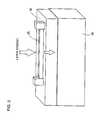
- FIG. 2is a perspective diagrammatic view of a link on a substrate of a semiconductor device.
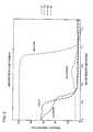
- FIG. 3is plot of absorption of copper, gold, aluminum, and silicon as a function of wavelength.
- FIG. 4is a plot of an substrate absorption function according to the invention, for copper, gold, and aluminum links on a silicon substrate, as a function of wavelength.
- FIG. 5is a plot of the function L ⁇ S for copper, gold, and aluminum links on a silicon substrate, where L is the absorption in the link and S is the absorption in the substrate.
- FIG. 6is a plot of the function (L ⁇ S)/(L+S) for copper, gold, and aluminum links on a silicon substrate, where L is the absorption in the link and S is the absorption in the substrate.
- Laser 10is constructed to operate at a conventional wavelength such as 1.047 ⁇ m. It is aligned to a laser output system that includes a wavelength shifter 12 , such as a frequency doubler or an optical parametric oscillator (OPO), constructed to shift to a wavelength less than 0.55 ⁇ m, in the “green” region of the wavelength spectrum.
- a wavelength shifter 12such as a frequency doubler or an optical parametric oscillator (OPO)
- the beamis then passed through the remainder of the laser output system, including a controlled electro-acousto-optic attenuator 13 , a telescope 14 that expands the beam, and, a scanning head 15 , that scans the beam over a focusing lens 16 by means of two scanner galvanometers, 18 and 20 .
- the spotis focused onto wafer 22 for removing links 24 , under control of computer 33 .
- the laser 10is mounted on a stable platform 11 relative to the galvanometers and the work piece. It is controlled from outside of the laser itself by computer 33 to transmit its beam to the scanner head comprising the accurate X and Y galvanometers 18 and 20 . It is very important, in removing links that the beam be positioned with accuracy of less than ⁇ fraction (3/10) ⁇ of a micron. The timing of the laser pulse to correlate with the position of the continually moving galvanometers is important. The system computer 33 asks for a laser pulse on demand.
- a step and repeat table 34moves the wafer into position to treat each semiconductor device.
- the laser 10is a neodymium vanadate laser, with an overall length L of about 6 inches, and a short cavity length.
- the shifter 12 of this preferred embodimentis external to the cavity, and is about another 4 inches long.
- laser 10can be configured to produce a laser output having an appropriate wavelength, so that no shifter would be required.
- the laseris a Q-switched diode pumped laser, of sufficient length and construction to enable external control of pulse rate with high accuracy by computer 33 .
- the cavity of the laserincludes a partially transmissive mirror 7 , optimized at the wavelength at which the lasing rod 6 of neodymium vanadate is pumped by the diode.
- the partially transmissive output mirror 9is also optimized at this wavelength.
- the pumping diode 4produces between about one and two watts depending on the design. It focuses onto the rear of the laser rod 6 .
- the laser rodis coated, on its pumped end, with a mirror 7 appropriate for the standard laser wavelength of 1.064 ⁇ m or 1.047 ⁇ m.
- the other end of the rodis coated with a dichroic coating.
- an optical Q-switch 8in the form of an acousto-optic modulator. It is used as the shutter for establishing the operating frequency of the laser.
- the output mirror 9is the output mirror 9 .
- a system optical switch 13 in the form of a further acousto-optic attenuatoris positioned beyond the laser cavity, in the laser output beam. Under control of computer 33 , it serves both to prevent the beam from reaching the galvanometers except when desired, and, when the beam is desired at the galvanometers, to controllably reduce the power of the laser beam to the desired power level.
- this power levelmay be as little as 10 percent of the gross laser output, depending upon operating parameters of the system and process.
- the power levelmay be about 0.1 percent of the gross laser output during alignment procedures in which the laser output beam is aligned with the target structure prior to a vaporization procedure.
- the positions of the X, Y galvanometers. 10 and 12are controlled by the computer 33 by galvanometer control G.
- the galvanometersmove at constant speed over the semiconductor device on the silicon wafer.
- the laseris controlled by timing signals based on the timing signals that control the galvanometers.
- the laseroperates at a constant repetition rate and is synchronized to the galvanometers by the system optical switch 13 .
- the laser beamis shown focused upon the wafer.
- the laser beamis seen being focused on a link element 25 of a semiconductor device.
- the metal linkis supported on the silicon substrate 30 by silicon dioxide insulator layer 32 , which may be, e.g., 0.3-0.5 microns thick. Over the link is another layer of silicon dioxide (not shown).
- silicon dioxideover the link is another layer of silicon dioxide (not shown).
- the laser beamimpinges on the link and heats it to the melting point. During the heating the metal is prevented from vaporizing by the confining effect of the overlying layer of oxide. During the duration of the short pulse, the laser beam progressively heats the metal, until the metal so expands that the insulator material ruptures. At this point, the molten material is under such high pressure that it instantly vaporizes and blows cleanly out through the rupture hole.
- the wavelength produced by wavelength shifter 12is arrived at by considering on an equal footing the values of both the interconnect or link to be processed and the substrate, in such a way as to trade-off energy deposition in the substrate, which is undesirable, against energy deposition in the link structure, which is necessary to sever the link.
- the criteria for selecting the wavelengthdo not require the substrate to be very transparent, which is especially important if the wavelength regime in which the substrate is very transparent is much less than optimal for energy deposition in the link structure.
- step (2)Using the incident beam energy computed in step (1), calculate the energy deposited in the substrate. For a well-matched laser spot, this energy will be proportional to the incident energy calculated in step (1), less the energy absorbed by the link structure, multiplied by the absorption of the substrate. In other words, the energy absorbed in the substrate is proportional to (1/L ⁇ 1) ⁇ S (herein, “the substrate absorption function”), where L is the absorption in the link and S is the absorption in the substrate.
- step (3)Look for low values of the substrate absorption function defined in step (2) as a function of laser wavelength.
- FIG. 4illustrates the substrate absorption function for copper, gold, and aluminum links on a silicon substrate, as a function of wavelength in the range of 0.3 to 1.4 ⁇ m.
- the values of the substrate absorption functioncan be derived from the absorption curves illustrated in FIG. 3, using a proportionality constant (see step (2) above) arbitrarily chosen as 0.5 for the sake of specificity (this constant merely changes the vertical scale of FIG. 4, and does not alter any conclusions drawn from it).
- FIGS. 5 and 6illustrate two possible functions representing simple absorption contrast. More specifically, FIG. 5 illustrates the function L ⁇ S, expressed as percentage, and FIG. 6 illustrates the function (L ⁇ S)/(L+S).
- L ⁇ Sthe function of the less-than ⁇ 0.55 ⁇ m wavelength region
- FIGS. 5 and 6illustrate the function (L ⁇ S)/(L+S).
- the less-than ⁇ 0.55 ⁇ m wavelength regionis not found desirable according to FIGS. 5 and 6, even for gold or copper link structures, because the function shown in these figures is less than zero in this region.
- This negative valuereflects the fact that the substrate is more absorptive than the link structure in this wavelength regime, and so, according to these models, this wavelength regime should not be selected.
Landscapes
- Physics & Mathematics (AREA)
- Optics & Photonics (AREA)
- Engineering & Computer Science (AREA)
- Plasma & Fusion (AREA)
- Mechanical Engineering (AREA)
- Computer Hardware Design (AREA)
- General Physics & Mathematics (AREA)
- Condensed Matter Physics & Semiconductors (AREA)
- Microelectronics & Electronic Packaging (AREA)
- Power Engineering (AREA)
- Manufacturing & Machinery (AREA)
- Design And Manufacture Of Integrated Circuits (AREA)
- Internal Circuitry In Semiconductor Integrated Circuit Devices (AREA)
- Lasers (AREA)
- Semiconductor Memories (AREA)
- Laser Beam Processing (AREA)
Abstract
Description
- This invention relates to laser processing systems and methods, including systems and methods for removing, with high yield, closely-spaced metal link structures or “fuses” on a silicon substrate of an integrated circuit or memory device.[0001]
- Laser systems can be employed to remove fuse structures (“blow links”) in integrated circuits and memory devices such as ASICs, DRAMs, and SRAMs, for purposes such as removing defective elements and replacing them with redundant elements provided for this purpose (“redundant memory repair”), or programming of logic devices. Link processing laser systems include the M320 and M325 systems manufactured by General Scanning, Inc, which produce laser outputs over a variety of wavelengths, including 1.047 μm, 1.064 μm, and 1.32 μm.[0002]
- Economic imperatives have led to the development of smaller, more complex, higher-density semiconductor structures. These smaller structures can have the advantage of operation at relatively high speed. Also, because the semiconductor device part can be smaller, a greater number of parts can be included in a single wafer. Because the cost of processing a single wafer in a semiconductor fabrication plant can be almost independent of the number of parts on the wafer, the greater number of parts per wafer can translate into lower cost per part.[0003]
- In the 1980s, semiconductor device parts often included polysilicon or silicide interconnects. Although poly-based interconnects are relatively poor conductors, they were easily fabricated using processes available at the time, and were well-suited to the wavelengths generated by the Nd:YAG lasers commonly available at the time. As geometries shrank, however, the poor conductivity of polysilicon interconnects and link structures became problematic, and some semiconductor manufacturers switched to aluminum. It was found that certain conventional lasers did not cut the aluminum links as well as they had cut polysilicon links, and in particular that damage to the silicon substrate could occur. This situation could be explained by the fact that the reflection in aluminum is very high and the absorption is low. Therefore, increased energy must be used to overcome this low absorption. The higher energy can tend to damage the substrate when too much energy is used.[0004]
- Sun et al., U.S. Pat. No. 5,265,114 advances an “absorption contrast” model for selecting an appropriate laser wavelength to cut aluminum and other metals such as nickel, tungsten, and platinum. In particular, this patent describes selecting a wavelength range in which silicon is almost transparent and in which the optical absorption behavior of the metal link material is sufficient for the link to be processed. The patent states that the 1.2 to 2.0 Am wavelength range provides a high absorption contrast between a silicon substrate and high-conductivity link structures, as compared with laser wavelengths of 1.064 μm and 0.532 μm.[0005]
- The invention provides a system and method for vaporizing a target structure on a substrate. According to the invention, a calculation is performed, as a function of wavelength, of an incident beam energy necessary to deposit unit energy in the target structure. Then, for the incident beam energy, the energy expected to be deposited in the substrate as a function of wavelength is calculated. A wavelength is identified that corresponds to a relatively low value of the energy expected to be deposited in the substrate, the low value being substantially less than a value of the energy expected to be deposited in the substrate at a higher wavelength. A laser system is provided configured to produce a laser output at the wavelength corresponding to the relatively low value of the energy expected to be deposited in the substrate. The laser output is directed at the target structure on the substrate at the wavelength corresponding to the relatively low value of the energy expected to be deposited in the substrate, in order to vaporize the target structure.[0006]
- Certain applications of the invention involve selection of a wavelength appropriate for cutting a metal link without producing unacceptable damage to a silicon substrate, where the wavelength is less than, rather than greater than, the conventional wavelengths of 1.047 μm and 1.064 μm. This method of wavelength selection is advantageous because the use of shorter wavelengths can result in smaller laser spots, other things being equal, and hence greater ease in hitting only the desired link with the laser spot. In particular, other things being equal, laser spot size is directly proportional to wavelength according to the formula: spot size is proportional to λf, where λ is the laser wavelength and f is the f-number of the optical system.[0007]
- Moreover, certain applications of the invention involve selection of a wavelength at which a substrate has low absorption but an interconnect material has higher absorption than at conventional wavelengths of 1.047 μm and 1.064 μm or higher-than-conventional wavelengths. Because of the reduced reflectivity of the interconnect material, the incident laser energy can be reduced while the interconnect material nevertheless absorbs sufficient energy for the interconnect to be blown without multiple laser pulses (which can impact throughput) or substantial collateral damage due to the laser beam.[0008]
- The invention can effect high-quality laser link cuts on high-conductivity interconnect materials such as copper, gold, and the like, arranged in closely-spaced patterns, with only a single laser pulse, and without damaging the substrate. The invention can further allow a smaller laser spot size than would be obtainable at wavelengths of 1.047 μm, 1.064 μm, or higher, while still providing acceptable link cuts.[0009]
- FIG. 1 is a block diagram of a laser system according to the invention for removing a link of a semiconductor device, where the link is manufactured of a material such as copper or gold.[0010]
- FIG. 2 is a perspective diagrammatic view of a link on a substrate of a semiconductor device.[0011]
- FIG. 3 is plot of absorption of copper, gold, aluminum, and silicon as a function of wavelength.[0012]
- FIG. 4 is a plot of an substrate absorption function according to the invention, for copper, gold, and aluminum links on a silicon substrate, as a function of wavelength.[0013]
- FIG. 5 is a plot of the function L−S for copper, gold, and aluminum links on a silicon substrate, where L is the absorption in the link and S is the absorption in the substrate.[0014]
- FIG. 6 is a plot of the function (L−S)/(L+S) for copper, gold, and aluminum links on a silicon substrate, where L is the absorption in the link and S is the absorption in the substrate.[0015]
- In the block diagram of FIG. 1, a system for removing a link of a semiconductor device is shown.[0016]
Laser 10 is constructed to operate at a conventional wavelength such as 1.047 μm. It is aligned to a laser output system that includes awavelength shifter 12, such as a frequency doubler or an optical parametric oscillator (OPO), constructed to shift to a wavelength less than 0.55 μm, in the “green” region of the wavelength spectrum. As is explained in more detail below, the beam is then passed through the remainder of the laser output system, including a controlled electro-acousto-optic attenuator 13, atelescope 14 that expands the beam, and, ascanning head 15, that scans the beam over a focusinglens 16 by means of two scanner galvanometers,18 and20. The spot is focused ontowafer 22 for removinglinks 24, under control ofcomputer 33. - The[0017]
laser 10 is mounted on a stable platform11 relative to the galvanometers and the work piece. It is controlled from outside of the laser itself bycomputer 33 to transmit its beam to the scanner head comprising the accurate X andY galvanometers system computer 33 asks for a laser pulse on demand. - A step and repeat table[0018]34 moves the wafer into position to treat each semiconductor device.
- In one embodiment, the[0019]
laser 10 is a neodymium vanadate laser, with an overall length L of about 6 inches, and a short cavity length. - The[0020]
shifter 12 of this preferred embodiment is external to the cavity, and is about another 4 inches long. In alternative embodiments,laser 10 can be configured to produce a laser output having an appropriate wavelength, so that no shifter would be required. - The laser is a Q-switched diode pumped laser, of sufficient length and construction to enable external control of pulse rate with high accuracy by[0021]
computer 33. - The cavity of the laser includes a partially[0022]
transmissive mirror 7, optimized at the wavelength at which thelasing rod 6 of neodymium vanadate is pumped by the diode. The partiallytransmissive output mirror 9 is also optimized at this wavelength. - The[0023]
pumping diode 4 produces between about one and two watts depending on the design. It focuses onto the rear of thelaser rod 6. As mentioned, the laser rod is coated, on its pumped end, with amirror 7 appropriate for the standard laser wavelength of 1.064 μm or 1.047 μm. The other end of the rod is coated with a dichroic coating. Within the laser cavity is an optical Q-switch 8 in the form of an acousto-optic modulator. It is used as the shutter for establishing the operating frequency of the laser. Beyond the Q-switch is theoutput mirror 9. The two mirrors,7 on the pumped end of the laser rod and9 beyond the acoustic optical Q-switch, comprise the laser cavity. - A system[0024]
optical switch 13 in the form of a further acousto-optic attenuator is positioned beyond the laser cavity, in the laser output beam. Under control ofcomputer 33, it serves both to prevent the beam from reaching the galvanometers except when desired, and, when the beam is desired at the galvanometers, to controllably reduce the power of the laser beam to the desired power level. During vaporization procedures this power level may be as little as 10 percent of the gross laser output, depending upon operating parameters of the system and process. The power level may be about 0.1 percent of the gross laser output during alignment procedures in which the laser output beam is aligned with the target structure prior to a vaporization procedure. - In operation, the positions of the X, Y galvanometers.[0025]10 and12 are controlled by the
computer 33 by galvanometer control G. Typically the galvanometers move at constant speed over the semiconductor device on the silicon wafer. The laser is controlled by timing signals based on the timing signals that control the galvanometers. The laser operates at a constant repetition rate and is synchronized to the galvanometers by the systemoptical switch 13. - In the system block diagram of FIG. 1 the laser beam is shown focused upon the wafer. In the magnified view of FIG. 2, the laser beam is seen being focused on a[0026]
link element 25 of a semiconductor device. - The metal link is supported on the[0027]
silicon substrate 30 by silicondioxide insulator layer 32, which may be, e.g., 0.3-0.5 microns thick. Over the link is another layer of silicon dioxide (not shown). In the link blowing technique the laser beam impinges on the link and heats it to the melting point. During the heating the metal is prevented from vaporizing by the confining effect of the overlying layer of oxide. During the duration of the short pulse, the laser beam progressively heats the metal, until the metal so expands that the insulator material ruptures. At this point, the molten material is under such high pressure that it instantly vaporizes and blows cleanly out through the rupture hole. - The wavelength produced by[0028]
wavelength shifter 12 is arrived at by considering on an equal footing the values of both the interconnect or link to be processed and the substrate, in such a way as to trade-off energy deposition in the substrate, which is undesirable, against energy deposition in the link structure, which is necessary to sever the link. Thus, the criteria for selecting the wavelength do not require the substrate to be very transparent, which is especially important if the wavelength regime in which the substrate is very transparent is much less than optimal for energy deposition in the link structure. - The criteria for selection of the appropriate wavelength are as follows:[0029]
- 1) Calculate the relative incident laser beam energy required to deposit unit energy in the link structure This relative incident laser beam energy is proportional to the inverse of the absorption of the link structure. For example, if the link structure has an absorption of 0.333, it will require three times as much incident laser energy to deposit as much energy in the link structure as it would if the structure had an absorption of 1. FIG. 3 illustrates absorption of copper, gold, aluminum, and silicon as a function of wavelength (copper, gold, and aluminum being possible link structure materials and silicon being a substrate material).[0030]
- 2) Using the incident beam energy computed in step (1), calculate the energy deposited in the substrate. For a well-matched laser spot, this energy will be proportional to the incident energy calculated in step (1), less the energy absorbed by the link structure, multiplied by the absorption of the substrate. In other words, the energy absorbed in the substrate is proportional to (1/L−1)×S (herein, “the substrate absorption function”), where L is the absorption in the link and S is the absorption in the substrate.[0031]
- 3) Look for low values of the substrate absorption function defined in step (2) as a function of laser wavelength.[0032]
- FIG. 4 illustrates the substrate absorption function for copper, gold, and aluminum links on a silicon substrate, as a function of wavelength in the range of 0.3 to 1.4 μm. The values of the substrate absorption function can be derived from the absorption curves illustrated in FIG. 3, using a proportionality constant (see step (2) above) arbitrarily chosen as 0.5 for the sake of specificity (this constant merely changes the vertical scale of FIG. 4, and does not alter any conclusions drawn from it).[0033]
- It can be seen from FIG. 4 that for structures of gold and copper (but not for aluminum) there is a region of wavelength less than roughly 0.55 μm in which the substrate absorption function is comparable to that in the region of wavelength greater than 1.2 μm.[0034]
- It will also be noted that this function is quite different than the ones presented in FIGS. 5 and 6, which illustrate two possible functions representing simple absorption contrast. More specifically, FIG. 5 illustrates the function L−S, expressed as percentage, and FIG. 6 illustrates the function (L−S)/(L+S). In either case, the less-than −0.55 μm wavelength region is not found desirable according to FIGS. 5 and 6, even for gold or copper link structures, because the function shown in these figures is less than zero in this region. This negative value reflects the fact that the substrate is more absorptive than the link structure in this wavelength regime, and so, according to these models, this wavelength regime should not be selected.[0035]
Claims (25)
Priority Applications (3)
| Application Number | Priority Date | Filing Date | Title |
|---|---|---|---|
| US10/428,938US6911622B2 (en) | 1998-12-16 | 2003-05-05 | Laser processing |
| US11/130,232US20050211682A1 (en) | 1998-12-16 | 2005-05-17 | Laser processing |
| US11/440,127US20060283845A1 (en) | 1998-12-16 | 2006-05-24 | Laser processing |
Applications Claiming Priority (3)
| Application Number | Priority Date | Filing Date | Title |
|---|---|---|---|
| US09/212,974US6300590B1 (en) | 1998-12-16 | 1998-12-16 | Laser processing |
| US09/968,541US6559412B2 (en) | 1998-12-16 | 2001-10-02 | Laser processing |
| US10/428,938US6911622B2 (en) | 1998-12-16 | 2003-05-05 | Laser processing |
Related Parent Applications (1)
| Application Number | Title | Priority Date | Filing Date |
|---|---|---|---|
| US09/968,541ContinuationUS6559412B2 (en) | 1998-12-16 | 2001-10-02 | Laser processing |
Related Child Applications (1)
| Application Number | Title | Priority Date | Filing Date |
|---|---|---|---|
| US11/130,232ContinuationUS20050211682A1 (en) | 1998-12-16 | 2005-05-17 | Laser processing |
Publications (2)
| Publication Number | Publication Date |
|---|---|
| US20030189032A1true US20030189032A1 (en) | 2003-10-09 |
| US6911622B2 US6911622B2 (en) | 2005-06-28 |
Family
ID=22793200
Family Applications (5)
| Application Number | Title | Priority Date | Filing Date |
|---|---|---|---|
| US09/212,974Expired - LifetimeUS6300590B1 (en) | 1998-12-16 | 1998-12-16 | Laser processing |
| US09/968,541Expired - LifetimeUS6559412B2 (en) | 1998-12-16 | 2001-10-02 | Laser processing |
| US10/428,938Expired - LifetimeUS6911622B2 (en) | 1998-12-16 | 2003-05-05 | Laser processing |
| US11/130,232AbandonedUS20050211682A1 (en) | 1998-12-16 | 2005-05-17 | Laser processing |
| US11/440,127AbandonedUS20060283845A1 (en) | 1998-12-16 | 2006-05-24 | Laser processing |
Family Applications Before (2)
| Application Number | Title | Priority Date | Filing Date |
|---|---|---|---|
| US09/212,974Expired - LifetimeUS6300590B1 (en) | 1998-12-16 | 1998-12-16 | Laser processing |
| US09/968,541Expired - LifetimeUS6559412B2 (en) | 1998-12-16 | 2001-10-02 | Laser processing |
Family Applications After (2)
| Application Number | Title | Priority Date | Filing Date |
|---|---|---|---|
| US11/130,232AbandonedUS20050211682A1 (en) | 1998-12-16 | 2005-05-17 | Laser processing |
| US11/440,127AbandonedUS20060283845A1 (en) | 1998-12-16 | 2006-05-24 | Laser processing |
Country Status (7)
| Country | Link |
|---|---|
| US (5) | US6300590B1 (en) |
| EP (1) | EP1159103A1 (en) |
| JP (1) | JP4289798B2 (en) |
| KR (1) | KR100699640B1 (en) |
| CN (1) | CN1330580A (en) |
| AU (1) | AU2363800A (en) |
| WO (1) | WO2000035623A1 (en) |
Cited By (3)
| Publication number | Priority date | Publication date | Assignee | Title |
|---|---|---|---|---|
| US20050173385A1 (en)* | 1996-12-24 | 2005-08-11 | Gsi Lumonics Corp., A Michiga Corporation | Laser processing |
| US20050211682A1 (en)* | 1998-12-16 | 2005-09-29 | Gsi Lumonics Corp. | Laser processing |
| US20050218128A1 (en)* | 2004-03-31 | 2005-10-06 | Han You-Hie | Laser processing apparatus with polygon mirror |
Families Citing this family (43)
| Publication number | Priority date | Publication date | Assignee | Title |
|---|---|---|---|---|
| US7723642B2 (en)* | 1999-12-28 | 2010-05-25 | Gsi Group Corporation | Laser-based system for memory link processing with picosecond lasers |
| US20040134894A1 (en)* | 1999-12-28 | 2004-07-15 | Bo Gu | Laser-based system for memory link processing with picosecond lasers |
| US6281471B1 (en) | 1999-12-28 | 2001-08-28 | Gsi Lumonics, Inc. | Energy-efficient, laser-based method and system for processing target material |
| US7838794B2 (en) | 1999-12-28 | 2010-11-23 | Gsi Group Corporation | Laser-based method and system for removing one or more target link structures |
| US7671295B2 (en) | 2000-01-10 | 2010-03-02 | Electro Scientific Industries, Inc. | Processing a memory link with a set of at least two laser pulses |
| US20060141681A1 (en)* | 2000-01-10 | 2006-06-29 | Yunlong Sun | Processing a memory link with a set of at least two laser pulses |
| US20030222324A1 (en)* | 2000-01-10 | 2003-12-04 | Yunlong Sun | Laser systems for passivation or link processing with a set of laser pulses |
| KR100500343B1 (en)* | 2000-08-29 | 2005-07-12 | 미쓰비시덴키 가부시키가이샤 | Laser machining apparatus |
| US8497450B2 (en)* | 2001-02-16 | 2013-07-30 | Electro Scientific Industries, Inc. | On-the fly laser beam path dithering for enhancing throughput |
| US20070173075A1 (en)* | 2001-03-29 | 2007-07-26 | Joohan Lee | Laser-based method and system for processing a multi-material device having conductive link structures |
| US7027155B2 (en)* | 2001-03-29 | 2006-04-11 | Gsi Lumonics Corporation | Methods and systems for precisely relatively positioning a waist of a pulsed laser beam and method and system for controlling energy delivered to a target structure |
| US20030129396A1 (en)* | 2001-12-27 | 2003-07-10 | Gerhard Kiessling | Coating composition for metal conductors and coating process involving the use thereof |
| US6951995B2 (en) | 2002-03-27 | 2005-10-04 | Gsi Lumonics Corp. | Method and system for high-speed, precise micromachining an array of devices |
| JP2003320466A (en)* | 2002-05-07 | 2003-11-11 | Disco Abrasive Syst Ltd | Processing machine using laser beam |
| US7015418B2 (en)* | 2002-05-17 | 2006-03-21 | Gsi Group Corporation | Method and system for calibrating a laser processing system and laser marking system utilizing same |
| JP2006502006A (en)* | 2002-10-04 | 2006-01-19 | エレクトロ サイエンティフィック インダストリーズ インコーポレーテッド | Method for forming precisely sized slots in an elastic mask of a microparts carrier |
| JP2004200221A (en)* | 2002-12-16 | 2004-07-15 | Toray Eng Co Ltd | Laser marking method and device thereof |
| US6947454B2 (en)* | 2003-06-30 | 2005-09-20 | Electro Scientific Industries, Inc. | Laser pulse picking employing controlled AOM loading |
| US7616669B2 (en)* | 2003-06-30 | 2009-11-10 | Electro Scientific Industries, Inc. | High energy pulse suppression method |
| EP1538424B1 (en)* | 2003-12-04 | 2007-09-26 | Festo AG & Co | Microwave based position measurement system for an electrodynamic direct drive |
| US8383982B2 (en)* | 2004-06-18 | 2013-02-26 | Electro Scientific Industries, Inc. | Methods and systems for semiconductor structure processing using multiple laser beam spots |
| US8148211B2 (en)* | 2004-06-18 | 2012-04-03 | Electro Scientific Industries, Inc. | Semiconductor structure processing using multiple laser beam spots spaced on-axis delivered simultaneously |
| US7923306B2 (en)* | 2004-06-18 | 2011-04-12 | Electro Scientific Industries, Inc. | Semiconductor structure processing using multiple laser beam spots |
| US7935941B2 (en)* | 2004-06-18 | 2011-05-03 | Electro Scientific Industries, Inc. | Semiconductor structure processing using multiple laser beam spots spaced on-axis on non-adjacent structures |
| US20060000814A1 (en) | 2004-06-30 | 2006-01-05 | Bo Gu | Laser-based method and system for processing targeted surface material and article produced thereby |
| US7227098B2 (en)* | 2004-08-06 | 2007-06-05 | Electro Scientific Industries, Inc. | Method and system for decreasing the effective pulse repetition frequency of a laser |
| US7372878B2 (en)* | 2004-08-06 | 2008-05-13 | Electro Scientific Industries, Inc. | Method and system for preventing excessive energy build-up in a laser cavity |
| DE102004053298B4 (en)* | 2004-08-26 | 2008-10-09 | ARGES Gesellschaft für Industrieplanung und Lasertechnik m.b.H. | Scan head as part of a laser drilling and cutting device |
| US7378288B2 (en)* | 2005-01-11 | 2008-05-27 | Semileds Corporation | Systems and methods for producing light emitting diode array |
| US8290239B2 (en)* | 2005-10-21 | 2012-10-16 | Orbotech Ltd. | Automatic repair of electric circuits |
| JP5203573B2 (en)* | 2006-03-23 | 2013-06-05 | ミヤチテクノス株式会社 | Laser processing equipment |
| US8198566B2 (en)* | 2006-05-24 | 2012-06-12 | Electro Scientific Industries, Inc. | Laser processing of workpieces containing low-k dielectric material |
| US8084706B2 (en)* | 2006-07-20 | 2011-12-27 | Gsi Group Corporation | System and method for laser processing at non-constant velocities |
| CN101578155B (en)* | 2007-01-05 | 2013-05-01 | 杰斯集团公司 | System and method for multi-pulse laser processing |
| KR101310243B1 (en)* | 2007-09-19 | 2013-09-24 | 지에스아이 그룹 코포레이션 | Link processing with high speed beam deflection |
| US8178818B2 (en)* | 2008-03-31 | 2012-05-15 | Electro Scientific Industries, Inc. | Photonic milling using dynamic beam arrays |
| US7982160B2 (en) | 2008-03-31 | 2011-07-19 | Electro Scientific Industries, Inc. | Photonic clock stabilized laser comb processing |
| GB0900036D0 (en)* | 2009-01-03 | 2009-02-11 | M Solv Ltd | Method and apparatus for forming grooves with complex shape in the surface of apolymer |
| KR20120113245A (en)* | 2009-12-30 | 2012-10-12 | 지에스아이 그룹 코포레이션 | Link processing with high speed beam deflection |
| CN102133687A (en)* | 2010-01-26 | 2011-07-27 | 豪晶科技股份有限公司 | Laser processing apparatus |
| CN102097529A (en)* | 2010-11-05 | 2011-06-15 | 张立国 | Edge cleaning method of ultraviolet laser thin-film solar battery |
| KR102138223B1 (en) | 2011-07-05 | 2020-07-28 | 일렉트로 싸이언티픽 인더스트리이즈 인코포레이티드 | Systems and methods for providing temperature stability of acousto-optic beam deflectors and acousto-optic modulators during use |
| US10562132B2 (en)* | 2013-04-29 | 2020-02-18 | Nuburu, Inc. | Applications, methods and systems for materials processing with visible raman laser |
Citations (23)
| Publication number | Priority date | Publication date | Assignee | Title |
|---|---|---|---|---|
| US3740523A (en)* | 1971-12-30 | 1973-06-19 | Bell Telephone Labor Inc | Encoding of read only memory by laser vaporization |
| US4044222A (en)* | 1976-01-16 | 1977-08-23 | Western Electric Company, Inc. | Method of forming tapered apertures in thin films with an energy beam |
| US4483005A (en)* | 1981-09-24 | 1984-11-13 | Teradyne, Inc. | Affecting laser beam pulse width |
| US4705698A (en)* | 1986-10-27 | 1987-11-10 | Chronar Corporation | Isolation of semiconductor contacts |
| US4752455A (en)* | 1986-05-27 | 1988-06-21 | Kms Fusion, Inc. | Pulsed laser microfabrication |
| US4853758A (en)* | 1987-08-12 | 1989-08-01 | American Telephone And Telegraph Company, At&T Bell Laboratories | Laser-blown links |
| US4970369A (en)* | 1984-06-08 | 1990-11-13 | Semiconductor Energy Laboratory Co., Ltd. | Electronic device manufacturing methods |
| US5022040A (en)* | 1986-05-30 | 1991-06-04 | Hughes Aircraft Company | Upconversion pumped lasers |
| US5235154A (en)* | 1992-04-28 | 1993-08-10 | International Business Machines Corporation | Laser removal of metal interconnects |
| US5265114A (en)* | 1992-09-10 | 1993-11-23 | Electro Scientific Industries, Inc. | System and method for selectively laser processing a target structure of one or more materials of a multimaterial, multilayer device |
| US5336636A (en)* | 1991-03-22 | 1994-08-09 | Siemens Aktiengesellschaft | Method for contacting conductive structures in VLSI circuits |
| US5525831A (en)* | 1993-04-05 | 1996-06-11 | Nippondenso Co., Ltd. | Semiconductor device with thin film resistor having reduced film thickness sensitivity during trimming process |
| US5611946A (en)* | 1994-02-18 | 1997-03-18 | New Wave Research | Multi-wavelength laser system, probe station and laser cutter system using the same |
| US5685995A (en)* | 1994-11-22 | 1997-11-11 | Electro Scientific Industries, Inc. | Method for laser functional trimming of films and devices |
| US5968847A (en)* | 1998-03-13 | 1999-10-19 | Applied Materials, Inc. | Process for copper etch back |
| US5998759A (en)* | 1996-12-24 | 1999-12-07 | General Scanning, Inc. | Laser processing |
| US6025256A (en)* | 1997-01-06 | 2000-02-15 | Electro Scientific Industries, Inc. | Laser based method and system for integrated circuit repair or reconfiguration |
| US6057221A (en)* | 1997-04-03 | 2000-05-02 | Massachusetts Institute Of Technology | Laser-induced cutting of metal interconnect |
| US6057180A (en)* | 1998-06-05 | 2000-05-02 | Electro Scientific Industries, Inc. | Method of severing electrically conductive links with ultraviolet laser output |
| US6144118A (en)* | 1998-09-18 | 2000-11-07 | General Scanning, Inc. | High-speed precision positioning apparatus |
| US6162577A (en)* | 1995-09-21 | 2000-12-19 | Felter; T. E. | Method for extreme ultraviolet lithography |
| US6181728B1 (en)* | 1998-07-02 | 2001-01-30 | General Scanning, Inc. | Controlling laser polarization |
| US6339604B1 (en)* | 1998-06-12 | 2002-01-15 | General Scanning, Inc. | Pulse control in laser systems |
Family Cites Families (37)
| Publication number | Priority date | Publication date | Assignee | Title |
|---|---|---|---|---|
| US487850A (en)* | 1892-12-13 | Shaded lamp-chimney | ||
| BE794202A (en)* | 1972-01-19 | 1973-05-16 | Intel Corp | FUSE LINK FOR INTEGRATED CIRCUIT ON SEMICONDUCTOR SUBSTRATE FOR MEMORIES |
| US3941973A (en)* | 1974-06-26 | 1976-03-02 | Raytheon Company | Laser material removal apparatus |
| US4399345A (en)* | 1981-06-09 | 1983-08-16 | Analog Devices, Inc. | Laser trimming of circuit elements on semiconductive substrates |
| US4535219A (en)* | 1982-10-12 | 1985-08-13 | Xerox Corporation | Interfacial blister bonding for microinterconnections |
| ATE80955T1 (en)* | 1984-06-20 | 1992-10-15 | Gould Inc | LASER PROCESS FOR PHOTOMASK REPAIR. |
| USRE34192E (en)* | 1985-05-01 | 1993-03-09 | Spectra-Physics, Laser Diode Systems, Inc. | Miniaturized Q-switched diode pumped solid state laser |
| JPS6286851A (en) | 1985-10-14 | 1987-04-21 | Nec Corp | Laser trimming apparatus |
| US4823320A (en)* | 1986-05-08 | 1989-04-18 | Texas Instruments Incorporated | Electrically programmable fuse circuit for an integrated-circuit chip |
| US4847850A (en)* | 1986-12-23 | 1989-07-11 | Spectra-Physics, Inc. | Continuum generation with miniaturized Q-switched diode pumped solid state laser |
| US5070392A (en)* | 1988-03-18 | 1991-12-03 | Digital Equipment Corporation | Integrated circuit having laser-alterable metallization layer |
| US5059764A (en)* | 1988-10-31 | 1991-10-22 | Spectra-Physics, Inc. | Diode-pumped, solid state laser-based workstation for precision materials processing and machining |
| US5225924A (en)* | 1989-04-07 | 1993-07-06 | Dainippon Screen Mfg. Co., Ltd. | Optical beam scanning system |
| US5025300A (en)* | 1989-06-30 | 1991-06-18 | At&T Bell Laboratories | Integrated circuits having improved fusible links |
| IL91240A (en)* | 1989-08-07 | 1994-07-31 | Quick Tech Ltd | Pulsed laser apparatus and systems and techniques for its operation |
| US5008512A (en)* | 1989-09-08 | 1991-04-16 | Microelectronics And Computer Technology Corporation | Method of laser bonding electrical members |
| US5021362A (en)* | 1989-12-29 | 1991-06-04 | At&T Bell Laboratories | Laser link blowing in integrateed circuit fabrication |
| US5066291A (en)* | 1990-04-25 | 1991-11-19 | Cincinnati Sub-Zero Products, Inc. | Solid-state laser frequency conversion system |
| US5241212A (en)* | 1990-05-01 | 1993-08-31 | Mitsubishi Denki Kabushiki Kaisha | Semiconductor device having a redundant circuit portion and a manufacturing method of the same |
| JP3150322B2 (en)* | 1990-05-18 | 2001-03-26 | 株式会社日立製作所 | Wiring cutting method by laser and laser processing device |
| US5268911A (en)* | 1991-07-10 | 1993-12-07 | Young Eddie H | X-cut crystal quartz acousto-optic modulator |
| US5293025A (en)* | 1991-08-01 | 1994-03-08 | E. I. Du Pont De Nemours And Company | Method for forming vias in multilayer circuits |
| US5163062A (en)* | 1991-10-16 | 1992-11-10 | The United States Of America As Represented By The Secretary Of The Navy | Method of frequency shifting using a chromium doped laser transmitter |
| US5323053A (en)* | 1992-05-28 | 1994-06-21 | At&T Bell Laboratories | Semiconductor devices using epitaxial silicides on (111) surfaces etched in (100) silicon substrates |
| JPH0714853A (en)* | 1993-06-18 | 1995-01-17 | Fujitsu Ltd | Compound semiconductor device on silicon substrate and manufacturing method thereof |
| US5453594A (en)* | 1993-10-06 | 1995-09-26 | Electro Scientific Industries, Inc. | Radiation beam position and emission coordination system |
| JP2590710B2 (en)* | 1993-11-26 | 1997-03-12 | 日本電気株式会社 | Semiconductor device and manufacturing method thereof |
| US5521932A (en)* | 1994-05-03 | 1996-05-28 | Light Solutions Corporation | Scalable side-pumped solid-state laser |
| US5696778A (en)* | 1995-05-09 | 1997-12-09 | Ophir Corporation | Method of and apparatus for generating intracavity double raman shifted laser pulses |
| US5760674A (en)* | 1995-11-28 | 1998-06-02 | International Business Machines Corporation | Fusible links with improved interconnect structure |
| JP3396356B2 (en)* | 1995-12-11 | 2003-04-14 | 三菱電機株式会社 | Semiconductor device and method of manufacturing the same |
| US6287900B1 (en)* | 1996-08-13 | 2001-09-11 | Semiconductor Energy Laboratory Co., Ltd | Semiconductor device with catalyst addition and removal |
| US6103992A (en)* | 1996-11-08 | 2000-08-15 | W. L. Gore & Associates, Inc. | Multiple frequency processing to minimize manufacturing variability of high aspect ratio micro through-vias |
| KR100228533B1 (en)* | 1997-06-23 | 1999-11-01 | 윤종용 | Fusible fuse in semiconductor integrated circuit and manufacture thereof |
| KR100294346B1 (en)* | 1998-11-07 | 2001-07-12 | 허인구 | Removable Civil Anchor |
| US6300590B1 (en)* | 1998-12-16 | 2001-10-09 | General Scanning, Inc. | Laser processing |
| US6172325B1 (en)* | 1999-02-10 | 2001-01-09 | Electro Scientific Industries, Inc. | Laser processing power output stabilization apparatus and method employing processing position feedback |
- 1998
- 1998-12-16USUS09/212,974patent/US6300590B1/ennot_activeExpired - Lifetime
- 1999
- 1999-12-16CNCN99814447Apatent/CN1330580A/enactivePending
- 1999-12-16WOPCT/US1999/029820patent/WO2000035623A1/enactiveIP Right Grant
- 1999-12-16JPJP2000587922Apatent/JP4289798B2/ennot_activeExpired - Fee Related
- 1999-12-16EPEP99967342Apatent/EP1159103A1/ennot_activeWithdrawn
- 1999-12-16AUAU23638/00Apatent/AU2363800A/ennot_activeAbandoned
- 1999-12-16KRKR1020017007407Apatent/KR100699640B1/ennot_activeExpired - Fee Related
- 2001
- 2001-10-02USUS09/968,541patent/US6559412B2/ennot_activeExpired - Lifetime
- 2003
- 2003-05-05USUS10/428,938patent/US6911622B2/ennot_activeExpired - Lifetime
- 2005
- 2005-05-17USUS11/130,232patent/US20050211682A1/ennot_activeAbandoned
- 2006
- 2006-05-24USUS11/440,127patent/US20060283845A1/ennot_activeAbandoned
Patent Citations (28)
| Publication number | Priority date | Publication date | Assignee | Title |
|---|---|---|---|---|
| US3740523A (en)* | 1971-12-30 | 1973-06-19 | Bell Telephone Labor Inc | Encoding of read only memory by laser vaporization |
| US4044222A (en)* | 1976-01-16 | 1977-08-23 | Western Electric Company, Inc. | Method of forming tapered apertures in thin films with an energy beam |
| US4483005A (en)* | 1981-09-24 | 1984-11-13 | Teradyne, Inc. | Affecting laser beam pulse width |
| US4970369A (en)* | 1984-06-08 | 1990-11-13 | Semiconductor Energy Laboratory Co., Ltd. | Electronic device manufacturing methods |
| US4752455A (en)* | 1986-05-27 | 1988-06-21 | Kms Fusion, Inc. | Pulsed laser microfabrication |
| US5022040A (en)* | 1986-05-30 | 1991-06-04 | Hughes Aircraft Company | Upconversion pumped lasers |
| US4705698A (en)* | 1986-10-27 | 1987-11-10 | Chronar Corporation | Isolation of semiconductor contacts |
| US4853758A (en)* | 1987-08-12 | 1989-08-01 | American Telephone And Telegraph Company, At&T Bell Laboratories | Laser-blown links |
| US5336636A (en)* | 1991-03-22 | 1994-08-09 | Siemens Aktiengesellschaft | Method for contacting conductive structures in VLSI circuits |
| US5235154A (en)* | 1992-04-28 | 1993-08-10 | International Business Machines Corporation | Laser removal of metal interconnects |
| US5265114A (en)* | 1992-09-10 | 1993-11-23 | Electro Scientific Industries, Inc. | System and method for selectively laser processing a target structure of one or more materials of a multimaterial, multilayer device |
| US5473624A (en)* | 1992-09-10 | 1995-12-05 | Electro Scientific Industries, Inc. | Laser system and method for selectively severing links |
| US5569398A (en)* | 1992-09-10 | 1996-10-29 | Electro Scientific Industries, Inc. | Laser system and method for selectively trimming films |
| US5265114C1 (en)* | 1992-09-10 | 2001-08-21 | Electro Scient Ind Inc | System and method for selectively laser processing a target structure of one or more materials of a multimaterial multilayer device |
| US5525831A (en)* | 1993-04-05 | 1996-06-11 | Nippondenso Co., Ltd. | Semiconductor device with thin film resistor having reduced film thickness sensitivity during trimming process |
| US5611946A (en)* | 1994-02-18 | 1997-03-18 | New Wave Research | Multi-wavelength laser system, probe station and laser cutter system using the same |
| US5685995A (en)* | 1994-11-22 | 1997-11-11 | Electro Scientific Industries, Inc. | Method for laser functional trimming of films and devices |
| US6162577A (en)* | 1995-09-21 | 2000-12-19 | Felter; T. E. | Method for extreme ultraviolet lithography |
| US5998759A (en)* | 1996-12-24 | 1999-12-07 | General Scanning, Inc. | Laser processing |
| US6791059B2 (en)* | 1996-12-24 | 2004-09-14 | Gsi Lumonics Corp. | Laser processing |
| US20050011872A1 (en)* | 1996-12-24 | 2005-01-20 | Gsi Lumonics Corp, A Michigan Corporation | Laser processing |
| US6025256A (en)* | 1997-01-06 | 2000-02-15 | Electro Scientific Industries, Inc. | Laser based method and system for integrated circuit repair or reconfiguration |
| US6057221A (en)* | 1997-04-03 | 2000-05-02 | Massachusetts Institute Of Technology | Laser-induced cutting of metal interconnect |
| US5968847A (en)* | 1998-03-13 | 1999-10-19 | Applied Materials, Inc. | Process for copper etch back |
| US6057180A (en)* | 1998-06-05 | 2000-05-02 | Electro Scientific Industries, Inc. | Method of severing electrically conductive links with ultraviolet laser output |
| US6339604B1 (en)* | 1998-06-12 | 2002-01-15 | General Scanning, Inc. | Pulse control in laser systems |
| US6181728B1 (en)* | 1998-07-02 | 2001-01-30 | General Scanning, Inc. | Controlling laser polarization |
| US6144118A (en)* | 1998-09-18 | 2000-11-07 | General Scanning, Inc. | High-speed precision positioning apparatus |
Cited By (5)
| Publication number | Priority date | Publication date | Assignee | Title |
|---|---|---|---|---|
| US20050173385A1 (en)* | 1996-12-24 | 2005-08-11 | Gsi Lumonics Corp., A Michiga Corporation | Laser processing |
| US20050211682A1 (en)* | 1998-12-16 | 2005-09-29 | Gsi Lumonics Corp. | Laser processing |
| US20060283845A1 (en)* | 1998-12-16 | 2006-12-21 | William Lauer | Laser processing |
| US20050218128A1 (en)* | 2004-03-31 | 2005-10-06 | Han You-Hie | Laser processing apparatus with polygon mirror |
| EP1586406A1 (en)* | 2004-03-31 | 2005-10-19 | EO Technics Co.,Ltd. | Laser processing apparatus with polygon mirror |
Also Published As
| Publication number | Publication date |
|---|---|
| EP1159103A1 (en) | 2001-12-05 |
| KR100699640B1 (en) | 2007-03-23 |
| US6300590B1 (en) | 2001-10-09 |
| CN1330580A (en) | 2002-01-09 |
| JP2002532891A (en) | 2002-10-02 |
| AU2363800A (en) | 2000-07-03 |
| US6559412B2 (en) | 2003-05-06 |
| US20050211682A1 (en) | 2005-09-29 |
| WO2000035623A1 (en) | 2000-06-22 |
| KR20010089573A (en) | 2001-10-06 |
| US20060283845A1 (en) | 2006-12-21 |
| US20020017510A1 (en) | 2002-02-14 |
| JP4289798B2 (en) | 2009-07-01 |
| US6911622B2 (en) | 2005-06-28 |
Similar Documents
| Publication | Publication Date | Title |
|---|---|---|
| US6911622B2 (en) | Laser processing | |
| US6791059B2 (en) | Laser processing | |
| US6593542B2 (en) | UV laser system and method for single pulse severing of IC fuses | |
| US7482551B2 (en) | Processing a memory link with a set of at least two laser pulses | |
| US7679030B2 (en) | Energy-efficient, laser-based method and system for processing target material | |
| JP2003519933A (en) | Processing method of memory link using laser system and burst composed of ultrashort pulse laser | |
| US20030222324A1 (en) | Laser systems for passivation or link processing with a set of laser pulses | |
| US20060141681A1 (en) | Processing a memory link with a set of at least two laser pulses |
Legal Events
| Date | Code | Title | Description |
|---|---|---|---|
| AS | Assignment | Owner name:GSI LUMONICS CORPORATION, MICHIGAN Free format text:ASSIGNMENT OF ASSIGNORS INTEREST;ASSIGNOR:GENERAL SCANNING INC.;REEL/FRAME:014261/0750 Effective date:20040116 | |
| STCF | Information on status: patent grant | Free format text:PATENTED CASE | |
| AS | Assignment | Owner name:GSI GROUP CORPORATION, MASSACHUSETTS Free format text:CHANGE OF NAME;ASSIGNOR:GSI LUMONICS CORPORATION;REEL/FRAME:020125/0657 Effective date:20050627 | |
| FPAY | Fee payment | Year of fee payment:4 | |
| AS | Assignment | Owner name:THE BANK OF NEW YORK MELLON TRUST COMPANY, N.A., A Free format text:SECURITY AGREEMENT;ASSIGNORS:GSI GROUP INC.;GSI GROUP CORPORATION;MES INTERNATIONAL INC.;AND OTHERS;REEL/FRAME:024755/0537 Effective date:20100723 | |
| AS | Assignment | Owner name:GSI GROUP CORPORATION, MASSACHUSETTS Free format text:RELEASE;ASSIGNOR:THE BANK OF NEW YORK MELLON TRUST COMPANY, N.A.;REEL/FRAME:027127/0368 Effective date:20111019 Owner name:GSI GROUP INC., MASSACHUSETTS Free format text:RELEASE;ASSIGNOR:THE BANK OF NEW YORK MELLON TRUST COMPANY, N.A.;REEL/FRAME:027127/0368 Effective date:20111019 Owner name:QUANTRONIX CORPORATION, MASSACHUSETTS Free format text:RELEASE;ASSIGNOR:THE BANK OF NEW YORK MELLON TRUST COMPANY, N.A.;REEL/FRAME:027127/0368 Effective date:20111019 Owner name:MES INTERNATIONAL INC., MASSACHUSETTS Free format text:RELEASE;ASSIGNOR:THE BANK OF NEW YORK MELLON TRUST COMPANY, N.A.;REEL/FRAME:027127/0368 Effective date:20111019 Owner name:THE OPTICAL CORPORATION, MASSACHUSETTS Free format text:RELEASE;ASSIGNOR:THE BANK OF NEW YORK MELLON TRUST COMPANY, N.A.;REEL/FRAME:027127/0368 Effective date:20111019 Owner name:EXCEL TECHNOLOGY INC., MASSACHUSETTS Free format text:RELEASE;ASSIGNOR:THE BANK OF NEW YORK MELLON TRUST COMPANY, N.A.;REEL/FRAME:027127/0368 Effective date:20111019 Owner name:CAMBRIDGE TECHNOLOGY INC., MASSACHUSETTS Free format text:RELEASE;ASSIGNOR:THE BANK OF NEW YORK MELLON TRUST COMPANY, N.A.;REEL/FRAME:027127/0368 Effective date:20111019 Owner name:CONTROL LASER CORPORATION (D/B/A BAUBLYS CONTROL L Free format text:RELEASE;ASSIGNOR:THE BANK OF NEW YORK MELLON TRUST COMPANY, N.A.;REEL/FRAME:027127/0368 Effective date:20111019 Owner name:BANK OF AMERICA, N.A., MASSACHUSETTS Free format text:SECURITY AGREEMENT;ASSIGNORS:GSI GROUP INC.;GSI GROUP CORPORATION;REEL/FRAME:027128/0763 Effective date:20111019 Owner name:SYNRAD INC., MASSACHUSETTS Free format text:RELEASE;ASSIGNOR:THE BANK OF NEW YORK MELLON TRUST COMPANY, N.A.;REEL/FRAME:027127/0368 Effective date:20111019 Owner name:PHOTO RESEARCH INC., MASSACHUSETTS Free format text:RELEASE;ASSIGNOR:THE BANK OF NEW YORK MELLON TRUST COMPANY, N.A.;REEL/FRAME:027127/0368 Effective date:20111019 Owner name:CONTINUUM ELECTRO-OPTICS INC., MASSACHUSETTS Free format text:RELEASE;ASSIGNOR:THE BANK OF NEW YORK MELLON TRUST COMPANY, N.A.;REEL/FRAME:027127/0368 Effective date:20111019 Owner name:MICROE SYSTEMS CORP., MASSACHUSETTS Free format text:RELEASE;ASSIGNOR:THE BANK OF NEW YORK MELLON TRUST COMPANY, N.A.;REEL/FRAME:027127/0368 Effective date:20111019 | |
| FPAY | Fee payment | Year of fee payment:8 | |
| AS | Assignment | Owner name:GSI GROUP CORPORATION, MASSACHUSETTS Free format text:RELEASE OF SECURITY INTEREST IN PATENTS RECORDED AT R/F 027128/0763;ASSIGNOR:BANK OF AMERICA, N.A., AS ADMINISTRATIVE AGENT;REEL/FRAME:030341/0956 Effective date:20130503 | |
| AS | Assignment | Owner name:ELECTRO SCIENTIFIC INDUSTRIES, INC., OREGON Free format text:ASSIGNMENT OF ASSIGNORS INTEREST;ASSIGNORS:GSI GROUP CORPORATION;GSI GROUP INC;REEL/FRAME:030582/0160 Effective date:20130503 | |
| FPAY | Fee payment | Year of fee payment:12 | |
| AS | Assignment | Owner name:BARCLAYS BANK PLC, AS COLLATERAL AGENT, NEW YORK Free format text:PATENT SECURITY AGREEMENT (TERM LOAN);ASSIGNORS:ELECTRO SCIENTIFIC INDUSTRIES, INC.;MKS INSTRUMENTS, INC.;NEWPORT CORPORATION;REEL/FRAME:048211/0227 Effective date:20190201 Owner name:BARCLAYS BANK PLC, AS COLLATERAL AGENT, NEW YORK Free format text:PATENT SECURITY AGREEMENT (ABL);ASSIGNORS:ELECTRO SCIENTIFIC INDUSTRIES, INC.;MKS INSTRUMENTS, INC.;NEWPORT CORPORATION;REEL/FRAME:048211/0312 Effective date:20190201 | |
| AS | Assignment | Owner name:ELECTRO SCIENTIFIC INDUSTRIES, INC., OREGON Free format text:CORRECTIVE ASSIGNMENT TO CORRECT THE APPLICATION SERIAL NUMBER 11776904 PREVIOUSLY RECORDED ON REEL 030582 FRAME 0160. ASSIGNOR(S) HEREBY CONFIRMS THE ASSIGNMENT;ASSIGNORS:GSI GROUP CORPORATION;GSI GROUP INC.;REEL/FRAME:056424/0287 Effective date:20130503 | |
| AS | Assignment | Owner name:BARCLAYS BANK PLC, AS COLLATERAL AGENT, NEW YORK Free format text:CORRECTIVE ASSIGNMENT TO CORRECT THE REMOVE U.S. PATENT NO. 7,919,646 PREVIOUSLY RECORDED ON REEL 048211 FRAME 0227. ASSIGNOR(S) HEREBY CONFIRMS THE PATENT SECURITY AGREEMENT (TERM LOAN);ASSIGNORS:ELECTRO SCIENTIFIC INDUSTRIES, INC.;MKS INSTRUMENTS, INC.;NEWPORT CORPORATION;REEL/FRAME:055006/0492 Effective date:20190201 Owner name:BARCLAYS BANK PLC, AS COLLATERAL AGENT, NEW YORK Free format text:CORRECTIVE ASSIGNMENT TO CORRECT THE REMOVE U.S. PATENT NO.7,919,646 PREVIOUSLY RECORDED ON REEL 048211 FRAME 0312. ASSIGNOR(S) HEREBY CONFIRMS THE PATENT SECURITY AGREEMENT (ABL);ASSIGNORS:ELECTRO SCIENTIFIC INDUSTRIES, INC.;MKS INSTRUMENTS, INC.;NEWPORT CORPORATION;REEL/FRAME:055668/0687 Effective date:20190201 | |
| AS | Assignment | Owner name:ELECTRO SCIENTIFIC INDUSTRIES, INC., OREGON Free format text:RELEASE BY SECURED PARTY;ASSIGNOR:BARCLAYS BANK PLC;REEL/FRAME:063009/0001 Effective date:20220817 Owner name:NEWPORT CORPORATION, MASSACHUSETTS Free format text:RELEASE BY SECURED PARTY;ASSIGNOR:BARCLAYS BANK PLC;REEL/FRAME:063009/0001 Effective date:20220817 Owner name:MKS INSTRUMENTS, INC., MASSACHUSETTS Free format text:RELEASE BY SECURED PARTY;ASSIGNOR:BARCLAYS BANK PLC;REEL/FRAME:063009/0001 Effective date:20220817 Owner name:ELECTRO SCIENTIFIC INDUSTRIES, INC., OREGON Free format text:RELEASE BY SECURED PARTY;ASSIGNOR:BARCLAYS BANK PLC;REEL/FRAME:062739/0001 Effective date:20220817 Owner name:NEWPORT CORPORATION, MASSACHUSETTS Free format text:RELEASE BY SECURED PARTY;ASSIGNOR:BARCLAYS BANK PLC;REEL/FRAME:062739/0001 Effective date:20220817 Owner name:MKS INSTRUMENTS, INC., MASSACHUSETTS Free format text:RELEASE BY SECURED PARTY;ASSIGNOR:BARCLAYS BANK PLC;REEL/FRAME:062739/0001 Effective date:20220817 |