US20030183527A1 - Method of direct electroplating on a low conductivity material, and electroplanted metal deposited therewith - Google Patents
Method of direct electroplating on a low conductivity material, and electroplanted metal deposited therewithDownload PDFInfo
- Publication number
- US20030183527A1 US20030183527A1US10/396,341US39634103AUS2003183527A1US 20030183527 A1US20030183527 A1US 20030183527A1US 39634103 AUS39634103 AUS 39634103AUS 2003183527 A1US2003183527 A1US 2003183527A1
- Authority
- US
- United States
- Prior art keywords
- potential
- layer
- reverse
- low conductivity
- waveform
- Prior art date
- Legal status (The legal status is an assumption and is not a legal conclusion. Google has not performed a legal analysis and makes no representation as to the accuracy of the status listed.)
- Granted
Links
Images


Classifications
- H—ELECTRICITY
- H01—ELECTRIC ELEMENTS
- H01L—SEMICONDUCTOR DEVICES NOT COVERED BY CLASS H10
- H01L21/00—Processes or apparatus adapted for the manufacture or treatment of semiconductor or solid state devices or of parts thereof
- H01L21/02—Manufacture or treatment of semiconductor devices or of parts thereof
- H01L21/04—Manufacture or treatment of semiconductor devices or of parts thereof the devices having potential barriers, e.g. a PN junction, depletion layer or carrier concentration layer
- H01L21/18—Manufacture or treatment of semiconductor devices or of parts thereof the devices having potential barriers, e.g. a PN junction, depletion layer or carrier concentration layer the devices having semiconductor bodies comprising elements of Group IV of the Periodic Table or AIIIBV compounds with or without impurities, e.g. doping materials
- H01L21/28—Manufacture of electrodes on semiconductor bodies using processes or apparatus not provided for in groups H01L21/20 - H01L21/268
- H01L21/283—Deposition of conductive or insulating materials for electrodes conducting electric current
- H01L21/288—Deposition of conductive or insulating materials for electrodes conducting electric current from a liquid, e.g. electrolytic deposition
- H01L21/2885—Deposition of conductive or insulating materials for electrodes conducting electric current from a liquid, e.g. electrolytic deposition using an external electrical current, i.e. electro-deposition
- C—CHEMISTRY; METALLURGY
- C25—ELECTROLYTIC OR ELECTROPHORETIC PROCESSES; APPARATUS THEREFOR
- C25D—PROCESSES FOR THE ELECTROLYTIC OR ELECTROPHORETIC PRODUCTION OF COATINGS; ELECTROFORMING; APPARATUS THEREFOR
- C25D17/00—Constructional parts, or assemblies thereof, of cells for electrolytic coating
- C25D17/001—Apparatus specially adapted for electrolytic coating of wafers, e.g. semiconductors or solar cells
- C—CHEMISTRY; METALLURGY
- C25—ELECTROLYTIC OR ELECTROPHORETIC PROCESSES; APPARATUS THEREFOR
- C25D—PROCESSES FOR THE ELECTROLYTIC OR ELECTROPHORETIC PRODUCTION OF COATINGS; ELECTROFORMING; APPARATUS THEREFOR
- C25D3/00—Electroplating: Baths therefor
- C25D3/02—Electroplating: Baths therefor from solutions
- C25D3/38—Electroplating: Baths therefor from solutions of copper
- C—CHEMISTRY; METALLURGY
- C25—ELECTROLYTIC OR ELECTROPHORETIC PROCESSES; APPARATUS THEREFOR
- C25D—PROCESSES FOR THE ELECTROLYTIC OR ELECTROPHORETIC PRODUCTION OF COATINGS; ELECTROFORMING; APPARATUS THEREFOR
- C25D5/00—Electroplating characterised by the process; Pretreatment or after-treatment of workpieces
- C25D5/18—Electroplating using modulated, pulsed or reversing current
- C—CHEMISTRY; METALLURGY
- C25—ELECTROLYTIC OR ELECTROPHORETIC PROCESSES; APPARATUS THEREFOR
- C25D—PROCESSES FOR THE ELECTROLYTIC OR ELECTROPHORETIC PRODUCTION OF COATINGS; ELECTROFORMING; APPARATUS THEREFOR
- C25D7/00—Electroplating characterised by the article coated
- C25D7/12—Semiconductors
- C25D7/123—Semiconductors first coated with a seed layer or a conductive layer
- H—ELECTRICITY
- H01—ELECTRIC ELEMENTS
- H01L—SEMICONDUCTOR DEVICES NOT COVERED BY CLASS H10
- H01L21/00—Processes or apparatus adapted for the manufacture or treatment of semiconductor or solid state devices or of parts thereof
- H01L21/70—Manufacture or treatment of devices consisting of a plurality of solid state components formed in or on a common substrate or of parts thereof; Manufacture of integrated circuit devices or of parts thereof
- H01L21/71—Manufacture of specific parts of devices defined in group H01L21/70
- H01L21/768—Applying interconnections to be used for carrying current between separate components within a device comprising conductors and dielectrics
- H01L21/76838—Applying interconnections to be used for carrying current between separate components within a device comprising conductors and dielectrics characterised by the formation and the after-treatment of the conductors
- H01L21/76877—Filling of holes, grooves or trenches, e.g. vias, with conductive material
- Y—GENERAL TAGGING OF NEW TECHNOLOGICAL DEVELOPMENTS; GENERAL TAGGING OF CROSS-SECTIONAL TECHNOLOGIES SPANNING OVER SEVERAL SECTIONS OF THE IPC; TECHNICAL SUBJECTS COVERED BY FORMER USPC CROSS-REFERENCE ART COLLECTIONS [XRACs] AND DIGESTS
- Y10—TECHNICAL SUBJECTS COVERED BY FORMER USPC
- Y10S—TECHNICAL SUBJECTS COVERED BY FORMER USPC CROSS-REFERENCE ART COLLECTIONS [XRACs] AND DIGESTS
- Y10S205/00—Electrolysis: processes, compositions used therein, and methods of preparing the compositions
- Y10S205/92—Electrolytic coating of circuit board or printed circuit, other than selected area coating
- Y—GENERAL TAGGING OF NEW TECHNOLOGICAL DEVELOPMENTS; GENERAL TAGGING OF CROSS-SECTIONAL TECHNOLOGIES SPANNING OVER SEVERAL SECTIONS OF THE IPC; TECHNICAL SUBJECTS COVERED BY FORMER USPC CROSS-REFERENCE ART COLLECTIONS [XRACs] AND DIGESTS
- Y10—TECHNICAL SUBJECTS COVERED BY FORMER USPC
- Y10T—TECHNICAL SUBJECTS COVERED BY FORMER US CLASSIFICATION
- Y10T428/00—Stock material or miscellaneous articles
- Y10T428/12—All metal or with adjacent metals
- Y10T428/12493—Composite; i.e., plural, adjacent, spatially distinct metal components [e.g., layers, joint, etc.]
- Y10T428/12528—Semiconductor component
- Y—GENERAL TAGGING OF NEW TECHNOLOGICAL DEVELOPMENTS; GENERAL TAGGING OF CROSS-SECTIONAL TECHNOLOGIES SPANNING OVER SEVERAL SECTIONS OF THE IPC; TECHNICAL SUBJECTS COVERED BY FORMER USPC CROSS-REFERENCE ART COLLECTIONS [XRACs] AND DIGESTS
- Y10—TECHNICAL SUBJECTS COVERED BY FORMER USPC
- Y10T—TECHNICAL SUBJECTS COVERED BY FORMER US CLASSIFICATION
- Y10T428/00—Stock material or miscellaneous articles
- Y10T428/12—All metal or with adjacent metals
- Y10T428/12493—Composite; i.e., plural, adjacent, spatially distinct metal components [e.g., layers, joint, etc.]
- Y10T428/12771—Transition metal-base component
- Y10T428/12806—Refractory [Group IVB, VB, or VIB] metal-base component
- Y10T428/12819—Group VB metal-base component
- Y—GENERAL TAGGING OF NEW TECHNOLOGICAL DEVELOPMENTS; GENERAL TAGGING OF CROSS-SECTIONAL TECHNOLOGIES SPANNING OVER SEVERAL SECTIONS OF THE IPC; TECHNICAL SUBJECTS COVERED BY FORMER USPC CROSS-REFERENCE ART COLLECTIONS [XRACs] AND DIGESTS
- Y10—TECHNICAL SUBJECTS COVERED BY FORMER USPC
- Y10T—TECHNICAL SUBJECTS COVERED BY FORMER US CLASSIFICATION
- Y10T428/00—Stock material or miscellaneous articles
- Y10T428/12—All metal or with adjacent metals
- Y10T428/12493—Composite; i.e., plural, adjacent, spatially distinct metal components [e.g., layers, joint, etc.]
- Y10T428/12771—Transition metal-base component
- Y10T428/12861—Group VIII or IB metal-base component
- Y10T428/12882—Cu-base component alternative to Ag-, Au-, or Ni-base component
- Y—GENERAL TAGGING OF NEW TECHNOLOGICAL DEVELOPMENTS; GENERAL TAGGING OF CROSS-SECTIONAL TECHNOLOGIES SPANNING OVER SEVERAL SECTIONS OF THE IPC; TECHNICAL SUBJECTS COVERED BY FORMER USPC CROSS-REFERENCE ART COLLECTIONS [XRACs] AND DIGESTS
- Y10—TECHNICAL SUBJECTS COVERED BY FORMER USPC
- Y10T—TECHNICAL SUBJECTS COVERED BY FORMER US CLASSIFICATION
- Y10T428/00—Stock material or miscellaneous articles
- Y10T428/31504—Composite [nonstructural laminate]
- Y10T428/31678—Of metal
Definitions
- This inventionrelates generally to the field of electroplating.
- the inventionrelates more specifically to a method of electroplating, and a layer of electroplated material deposited therewith, that are suitable for deposition on a low conductivity substrate material.
- Pulse platingsuch as that disclosed in U.S. Pat. No. 5,972,192 to Dubin et al., has historically been employed to plate difficult-to-plate materials or shapes. While conventional pulse plating techniques can enable conformal plating across a surface under certain circumstances, for the following reason these techniques are not always effective for plating a resistive layer.
- the electrical currentis proportional to the voltage applied at a particular point (generally described by the Butler-Volmer Equation) as follows:
- E-E o ′the applied potential
- E o ′the formal potential defining the thermodynamic equilibrium point in a particular electrolyte
- the waveformcreates zones of excess plating toward the outside of the object, optimal growth rate in a finite region of the object, and no plating at the center of the object during the typical waveform (excluding the initial amplitudes).
- the electroplated depositsare typically excessively thick at the edge of an object, such as a wafer, with minimal deposition at the center.
- Typical electroplating for wafersis accomplished with a dielectric material placed between the anode and cathode to modify the electric field.
- a high pulse amplitude techniquehas been employed. While the use of a high pulse amplitude may provide a more uniform deposit, it will also lead to filling problems in the high aspect ratio features common to semiconductor processes.
- the use of a current reversal waveformcan be employed.
- the current reversal waveformcan deplate metal from the regions that are thicker, or deplate the thicker regions more quickly than the thin center portions, and therefore increase the fill of high aspect ratio features.
- U.S. Pat. No. 6,071,398 to Martin et al.discloses a method of pulse plating in which the ratio of peak reverse current density to peak forward current density is varied in periodic cycles. Martin, which focuses on achieving bottom up fill, discloses that the ratio is varied sequentially between first, second, and third values.
- Electroplating a layer of metal on a layer of low conductivity materialpresents another obstacle.
- the IR drop across the surface of the low conductivity materialmeans that the filling is limited to a small portion of the surface where the potential is defined by a narrow window.
- the present inventionprovides a method of electroplating, and a layer of electroplated metal deposited therewith, that are suitable for deposition on a layer of low conductivity material. More specifically, the present invention provides a method of electroplating and the resultant layer of electroplated metal that are characterized by the controlled deposition of a metal layer of desired structure and thickness across the entire surface of the low conductivity layer.
- the present inventionrelates to a method of electroplating metal onto a low conductivity layer that combines a potential or current reversal waveform with variation in the amplitude and duration of the applied potential or current pulse.
- the methodcomprises, over time, varying the duration of the pulse and continuously decreasing the amplitude of both the cathodic and anodic portions of the waveform across the surface of the low conductivity layer as the deposition zone moves from the center of the surface of the low conductivity layer to the outside edge of the surface of the low conductivity layer.
- the methodthus advantageously uses the variable potential associated with the IR differential from the center to the edge of the low conductivity layer.
- the methodfacilitates the filling of structures in the center of the low conductivity layer without overdepositing on the outside edge, thus ensuring a predetermined profile of deposited material across the entire surface of the low conductivity layer.
- FIG. 1is a partial cross-sectional view of a wafer having a metal layer deposited in accordance with the present method of electroplating.
- FIG. 2is a plan view of the wafer depicted in FIG. 1.
- FIG. 3is a partial cross-sectional view of a chip produced from the wafer depicted in FIG. 1.
- FIG. 4illustrates the progressively decreasing waveform associated with the present method of electroplating.
- FIGS. 5 A-Rillustrate details of the method of depositing the metal layer depicted in FIG. 1.
- FIG. 6is a block diagram of a system for depositing the metal layer depicted in FIG. 1.
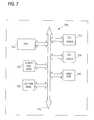
- FIG. 7is a block diagram of a system which employs the chip shown in FIG. 3.
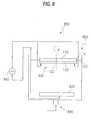
- FIG. 8is a schematic diagram of the electroplating cell employed in the present method.
- the present inventionrelates to a method of electroplating metal onto a layer of low conductivity material.
- the methodis particularly useful for the filling of structures in the center surface of the low conductivity layer without overdepositing on the outside edge, thus ensuring a controlled profile from deposition of the material across the entire surface of the low conductivity layer.
- the methodprovides a structure, such as for example, a semiconductor wafer or a chip produced therefrom, comprising a substrate, a low conductivity layer, and a uniform layer of electroplated metal deposited on the low conductivity layer.
- FIG. 1is a partial cross-sectional view of a semiconductor wafer 100 having a substrate 110 and a metal layer 130 deposited on a low conductivity layer 120 in accordance with the present invention.
- the low conductivity layer 120may be barrier layer, such as for example, a layer of material selected from the group consisting of Ta, W, TaN/Ta, TaN, WN, W/WN, TaSiN, and TiSiN as is typically employed in a semiconductor chip to prevent alloying and copper migration during metallization thermal cycling.
- the low conductivity layer 120may include a high aspect ratio feature, such as a trench, that is an at least partially filled damascene feature 121 .
- Wafer 100may also include fabricated circuit elements in and/or on substrate 110 and beneath the low conductivity layer 120 which are not illustrated for purposes of simplicity.
- FIG. 8is a schematic view of the electroplating cell 800 employed in the present method, the details of the electroplating cell being well known in the art.
- Electroplating cell 800includes generally a voltage source 810 , an anode 820 , i.e., a donor metal (which may be inert and decompose the electrolyte to balance electron transfer), and a cathode 830 which includes the metal upon which the electrodeposition occurs.
- Cathode 830(described above as wafer 100 ) initially includes the substrate 110 and the low conductivity layer 120 .
- Cell 800typically includes a fluid inlet 840 and a fluid outlet 850 to provide for steady state cell operation.
- the electroplating processmay include rotation of the cathode 830 to facilitate the controlled deposition.
- electrical currentis proportional to the voltage applied at a particular point on the surface of the electrode as generally described by the Butler-Volmer equation. Since the current is logarithmic with the applied potential, when a low conductivity material is employed as the material upon which electrodeposition is to occur, the potential needed at the edge of the wafer to plate metal at the center of the low conductivity layer is well above that which is needed at the edge of the wafer for plating at the edge of the low conductivity layer near the contact point.
- a typical conventional waveformwill creates zones of excess plating toward the outside of the object, optimal growth rate in a finite region of the object, and no plating at the center of the object (excluding the initial amplitudes). Therefore, with conventional techniques, the electroplated deposits are typically excessively thick at the edge of an object, with minimal deposition at the center.
- a first embodiment of the present methodutilizes the combination of two elements: a potential reversal waveform, and variation in the amplitude and duration of the applied potential pulse.
- the methodtherefore, advantageously uses the variable potential associated with the IR differential from the center to the edge of the low conductivity layer.
- the first element of the methodincludes applying a pulsed periodic reverse potential comprising a sequential forward to reverse, reverse to forward, continuously repeating pulsing sequence across the electrodes of the electroplating cell.
- the pulsing sequenceutilizes a potential reversal waveform having a peak reverse potential density and a peak forward potential density.
- the second element of the methodincludes varying the amplitude and duration of the voltage applied to the electroplating cell. More specifically, the amplitude-varying feature employs variable amplitude programmed decay.
- FIG. 4illustrates the progressively decreasing waveform associated with the varied amplitude. The amplitude of the cathodic and anodic portions of the potential reversal waveform is continuously decreased with increasing time, i.e., decreased as the electrodeposition proceeds from the time of its initiation to the time of its conclusion.
- the initial high pulse waveform(both plating and deplating) focuses the plating in the center 122 of the low conductivity layer 120 .
- the depositionproceeds outward across the surface of the low conductivity layer 120 , i.e., from the center 122 of the low conductivity layer 120 to the edge 123 of the low conductivity layer 120 in order to deposit the metal layer 130 .
- the unit for the time scale depicted in FIG. 4depends on the frequency of the potential pulse. For example, a waveform at 1 Hz will result in a time scale on FIG. 4 of around 100 seconds. At 1 KHz, the time scale would be only about 1 second on FIG. 4.
- the second element of the methodalso includes varying the duration of the applied potential pulse.
- the duration of the pulsed voltagemay be increased, decreased, or increased and decreased, depending upon the particular application.
- the duration for each portion of the waveformmay be independently controlled.
- a rest period, shown in FIG. 4,may or may not be needed, depending on the resistance of the material and/or the location of the electroplating on the wafer.
- the amplitude of the cathodic and anodic portions of the potential reversal waveformis continuously decreased, and the duration of the pulse is varied, in a manner that can provide a metal layer 130 having a desired structure and thickness across the surface of the low conductivity layer 120 .
- the deposition of metal layer 130proceeds from the center 122 of the low conductivity layer 120 to the outside edge 123 of the low conductivity layer 120 in an approximately concentric ring configuration.
- the metal layer 130has a uniform thickness, from the center 122 of the low conductivity layer 120 to the outside edge 123 of the low conductivity layer 120 , of from about 50 angstroms to about 3000 angstroms.
- FIGS. 5 A-RDetails of the method of depositing a metal layer 538 (analogous to the metal layer 130 depicted in FIG. 1) are illustrated in FIGS. 5 A-R.
- FIGS. 5 A-Rthus provide a “snapshot” view at different times of the ring-type plating that is characteristic of the present method.
- FIGS. 5A, 5C, 5 E, 5 G, 5 I, 5 K, 5 M, 5 O, and 5 Qprovide a partial cross-sectional view of the wafer 100 as the electrodeposition proceeds.
- FIGS. 5A, 5C, 5 E, 5 G, 5 I, 5 K, 5 M, 5 O, and 5 Qprovide a partial cross-sectional view of the wafer 100 as the electrodeposition proceeds.
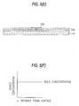
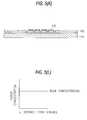
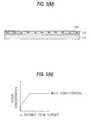
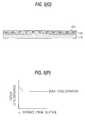
- 5B, 5D, 5 F, 5 H, 5 J, 5 L, 5 N, 5 P, and 5 Rprovide a graphical illustration of the cation concentration versus distance from the surface of low conductivity layer 120 during the stages of deposition represented by FIGS. 5A, 5C, 5 E, 5 G, 5 I, 5 K, 5 M, 5 O, and 5 Q respectively.
- the term “bulk concentration”refers to the nominal concentration of the electroplating solution, i.e., the concentration of copper cations sufficiently far enough away from the electrode surface that the concentration is fixed.
- FIGS. 5 A-Frepresent the initial stage of the electrodeposition process, i.e., that point at which the process focuses the plating in the center 122 of the low conductivity layer 120 .
- FIGS. 5A and 5Bcorrespond to the largest amplitude for the forward voltage pulse.
- FIGS. 5C and 5Dcorrespond to the largest forward and reverse voltage amplitudes during the deplating pulse.
- FIGS. 5E and 5Fcorrespond to the largest amplitude of the forward pulse during the rest period.
- FIGS. 5 G-Lrepresent an intermediate stage of the electrodeposition process, i.e., that point at which the plating is focused at a point intermediate between the center 122 and the edge 123 of the low conductivity layer 120 .
- FIGS. 5G and 5Hcorrespond to a mid-range amplitude for the forward voltage pulse.
- FIGS. 5I and 5Jcorrespond to midrange forward and reverse voltage amplitudes during the deplating pulse.
- FIGS. 5K and 5Lcorrespond to the mid-range forward and reverse voltage amplitudes during the rest period.
- FIGS. 5 M-Rrepresent the final stage of the electrodeposition process, i.e., that point at which the plating is focused at a point near the edge 123 of the low conductivity layer 120 .
- FIGS. 5M and 5Ncorrespond to the smallest amplitude for the forward voltage pulse.
- FIGS. 5O and 5Pcorrespond to the end of the forward and reverse pulses during the deplating step.
- FIGS. 5Q and 5Rcorrespond to the end of the forward and reverse pulses during the rest period.
- the initial high pulse waveform(both plating and deplating) focuses the plating in the center 122 of the low conductivity layer 120 .
- the amplitude of both the cathodic and anodic portion of the waveformis then continuously decreased, and the duration of the pulse varied, in a manner that will provide a predetermined deposition profile across the surface of the low conductivity layer 120 .
- the deposition zoneproceeds to the outside edge in a ring-type configuration (see also FIG. 2).
- the relaxation of the surface from the rest period with a pulse-type waveprovides for more conformal plating at the beginning of the plating process.
- the changing pulse amplitude and durationfacilitates control of the uniformity of deposition and the final fill of structures such as damascene feature 121 .
- the changing of the amplitude of the forward and reverse cyclefacilitates filling structures in the center 122 of the low conductivity layer 120 without overdepositing on the outside edge 123 .
- the methodfacilitates the fill of a trench to provide features such as damascene feature 121 .
- the rest periodkeeps the electrodeposition process at a non-diffusion-limited regime for plating and may allow the organic additives to redistribute onto the appropriate sites.
- the frequency of the voltage pulseis typically from about 1 Hz to about 100 KHz. Use of a higher frequency will typically not allow significant movement of the metal atoms.
- the range of applied potential amplitudes that is employeddepends upon certain variables associated with the electrodeposition process. For example, potentials for electrochemical cells are typically compared using a reference electrode in order to compensate for the resistance drop associated with the cell design. There is also a resistance drop associated with the low conductivity layer 120 , which is a function of both the low conductivity material and its thickness. If the interface of the electrodes results in a drop of more than about 2 volts, the electrolyte will break down with the evolution of hydrogen or oxygen.
- the amplitudecan range from several tenths of a volt for very conductive films with good cell designs, to about 5 volts.
- the potential drop across the surface of the low conductivity layer 120is dependent upon the thickness of the layer 120 . For example, when layer 120 is tungsten, the potential drop is from 3-5 ohms/sq.
- the methodmay further include pretreatment of the low conductivity layer 120 prior to initiating the electroplating process.
- the pretreatmentcould be employed to clean the surface of the low conductivity layer 120 , such as for example, by using ammonium hydroxide or hydrofluoric acid to remove oxide from a tungsten barrier layer.
- the present methodtakes advantage not only of the relaxation (i.e., the mass transport of copper to the surface) of the metal layer 130 , but of the variable potential across the surface of the layer 120 of low conductivity material created by the IR drop of the low conductivity layer. Combining these features allows one to control both the deposition location and the deposition quantity of the metal layer 130 .
- a second embodiment of the present methodutilizes the combination of two elements: a current reversal waveform, and variation in the amplitude and duration of the applied current pulse.
- the first element of the second embodiment of the methodincludes applying a pulsed periodic reverse current comprising a sequential forward to reverse, reverse to forward, continuously repeating pulsing sequence across the electrodes of the electroplating cell.
- the pulsing sequenceutilizes a current reversal waveform having a peak reverse current density and a peak forward current density.
- the second element of the second embodiment of the methodincludes varying the amplitude and duration of the current applied to the electroplating cell.
- the preferred chemistry of the electroplating solutionis a complexed basic bath in which the potential obtained during the cathodic portion of the waveform is capable of reducing oxide on the surface of the barrier without significant metal plating.
- the electrodeposition of metal layer 130is effected in an electroplating cell utilizing a complexed basic solution which comprises an aqueous basic metal electrolyte.
- the metal that is deposited according to the present methodmay be most any metal that can be electrodeposited from aqueous chemistries, such as, for example, Cu, Ni, Au, Cr, Ag, Pt, and Ir. If the electrodeposited metal is copper, for example, the copper electrolyte can be cupric sulfate.
- the electroplating solutionincludes a complexed basic solution comprising cupric sulfate and a solution of ethylenediamine tetraacetic acid (“EDTA”) and tetramethylammonium hydroxide (“TMAH”).
- the bathcomprises a solution of from about 1 to about 10 g/l of CuSO 4 , typically from about 5 to about 6 g/l of CuSO 4 , in from about 35 to about 45 g/l of EDTA, typically from about 40 to about 43 g/l of EDTA.
- the bathalso typically comprises from about 1 to about 5 ml (per liter of electroplating solution) of a surfactant, such as TRITON X-100 (commercially available from Union Carbide), and from about 20 to about 100 ml of 25% TMAH.
- a surfactantsuch as TRITON X-100 (commercially available from Union Carbide)
- the electroplating solutionmay comprise a citric acid solution or other metal complexing acid bath.
- FIG. 3is a partial cross-sectional view of a chip 200 produced from the wafer depicted in FIG. 1.
- Chip 200includes a substrate 210 and a metal layer 230 deposited on a low conductivity layer 220 .
- Chip 200may then be incorporated in any fabricated semiconductor device, including various processor system components, such as for example, a central processing unit (“CPU”) or in any of the various types of memory devices, such as for example, RAM, ROM, and others. It may also be used in any type of integrated circuit controller for a floppy disk, a hard disk, a ZIP, or a CD-ROM disk.
- CPUcentral processing unit
- RAMrandom access memory
- ROMread-only memory
- FIG. 6is a block diagram of a system 600 for depositing the metal layer depicted in FIG. 1.
- the system 600comprises an electroplating cell 610 , and a processor system 620 .
- the processor system 620is capable of operating the electroplating cell 610 so as to provide a layer of electroplated metal 130 having uniform structure and thickness across the surface of the low conductivity layer 120 .
- the variable amplitude programmed decay, and the variation in pulse duration,are effected through control of the power supply associated with the electroplating cell 610 .
- processor system 620 and the associated softwaremay be employed to control the power supply by sending a digital or analog signal to effect a particular rate of decay.
- the decay ratecan be determined by any of various mathematical functions, such as, for example, a linear or exponential decay function, or another function capable of effecting a particular decay rate. Any particular decay rate is dependent upon the material of metal layer 130 , the thickness of the deposited metal layer 130 , the material and thickness of the low conductivity layer 120 , and the chemistry of the electroplating solution.
- FIG. 7is a block diagram of a system 700 utilizing a chip 200 (see FIG. 3) comprising a layer of metal deposited in accordance with the present invention.
- System 700typically comprises a CPU 710 .
- the system 700may be a computer system, a process control system, or any other system employing a processor and associated memory, and may employ one or more buses and/or bridges which allow the CPU 710 to internally communicate with I/O devices 720 , 730 , random access memory (RAM) devices and read-only memory (ROM) devices 740 , and peripheral devices such as a floppy disk drive 750 and a compact disk CD-ROM drive 760 that also communicate with CPU 710 over the bus 770 , as is well known in the art.
- any of the CPU 710 , the memory devices, and controller elements of other illustrated electrical componentsmay include a chip 200 having a layer of electrodeposited metal 230 deposited in accordance with the claimed invention.
- the present inventiontherefore, provides a method of electroplating, and a layer of electroplated metal deposited therewith, that are suitable for deposition on a layer of low conductivity material.
- the methodfacilitates the filling of structures in the center of the low conductivity layer without overdepositing on the outside edge, thus ensuring a controlled deposition of material across the entire surface of the low conductivity layer.
Landscapes
- Chemical & Material Sciences (AREA)
- Engineering & Computer Science (AREA)
- Chemical Kinetics & Catalysis (AREA)
- Electrochemistry (AREA)
- Materials Engineering (AREA)
- Metallurgy (AREA)
- Organic Chemistry (AREA)
- Physics & Mathematics (AREA)
- Condensed Matter Physics & Semiconductors (AREA)
- General Physics & Mathematics (AREA)
- Manufacturing & Machinery (AREA)
- Computer Hardware Design (AREA)
- Microelectronics & Electronic Packaging (AREA)
- Power Engineering (AREA)
- Life Sciences & Earth Sciences (AREA)
- Sustainable Development (AREA)
- Electroplating Methods And Accessories (AREA)
- Electrodes Of Semiconductors (AREA)
Abstract
Description
- 1. Field of the Invention[0001]
- This invention relates generally to the field of electroplating. The invention relates more specifically to a method of electroplating, and a layer of electroplated material deposited therewith, that are suitable for deposition on a low conductivity substrate material.[0002]
- 2. Description of the Related Art[0003]
- Various difficulties are associated with the electroplating of metals such as copper onto low conductivity barrier materials such as Ta and W. In the context of semiconductor fabrication, the major problem associated with plating on such barriers is that of achieving the required adhesion and uniformity of the electroplated layer across the surface of a wafer without the presence of fill defects.[0004]
- Pulse plating, such as that disclosed in U.S. Pat. No. 5,972,192 to Dubin et al., has historically been employed to plate difficult-to-plate materials or shapes. While conventional pulse plating techniques can enable conformal plating across a surface under certain circumstances, for the following reason these techniques are not always effective for plating a resistive layer.[0005]
- The electrical current is proportional to the voltage applied at a particular point (generally described by the Butler-Volmer Equation) as follows:[0006]
- i=nFAko[Co(0, t)e−αnf(E-E
o′) −Cr(0, t)e−(1−α)nf(E-Eo′) ]. - Since the current is logarithmic with the applied potential (typically called overpotential E-E[0007]o′, where E is the applied voltage and Eo′ is the formal potential defining the thermodynamic equilibrium point in a particular electrolyte), the potential needed to be applied to the edge of an object in order to plate metal at the center of the object is well above that which is needed for plating at the edge of the object near the contact point. The waveform creates zones of excess plating toward the outside of the object, optimal growth rate in a finite region of the object, and no plating at the center of the object during the typical waveform (excluding the initial amplitudes). Therefore, with conventional techniques, the electroplated deposits are typically excessively thick at the edge of an object, such as a wafer, with minimal deposition at the center. Typical electroplating for wafers is accomplished with a dielectric material placed between the anode and cathode to modify the electric field.
- In an attempt to overcome the non-uniform deposition, a high pulse amplitude technique has been employed. While the use of a high pulse amplitude may provide a more uniform deposit, it will also lead to filling problems in the high aspect ratio features common to semiconductor processes. To overcome such filling problems, the use of a current reversal waveform can be employed. The current reversal waveform can deplate metal from the regions that are thicker, or deplate the thicker regions more quickly than the thin center portions, and therefore increase the fill of high aspect ratio features. For example, U.S. Pat. No. 6,071,398 to Martin et al. discloses a method of pulse plating in which the ratio of peak reverse current density to peak forward current density is varied in periodic cycles. Martin, which focuses on achieving bottom up fill, discloses that the ratio is varied sequentially between first, second, and third values.[0008]
- Electroplating a layer of metal on a layer of low conductivity material, however, presents another obstacle. With the low conductivity material, the IR drop across the surface of the low conductivity material means that the filling is limited to a small portion of the surface where the potential is defined by a narrow window.[0009]
- Therefore, a need exists for a method of electroplating which not only provides for the uniform filling of high aspect ratio features, but which also provides for the controlled deposition of a layer of desired structure and thickness across the entire surface of a low conductivity material.[0010]
- The present invention provides a method of electroplating, and a layer of electroplated metal deposited therewith, that are suitable for deposition on a layer of low conductivity material. More specifically, the present invention provides a method of electroplating and the resultant layer of electroplated metal that are characterized by the controlled deposition of a metal layer of desired structure and thickness across the entire surface of the low conductivity layer.[0011]
- Accordingly, the present invention relates to a method of electroplating metal onto a low conductivity layer that combines a potential or current reversal waveform with variation in the amplitude and duration of the applied potential or current pulse. The method comprises, over time, varying the duration of the pulse and continuously decreasing the amplitude of both the cathodic and anodic portions of the waveform across the surface of the low conductivity layer as the deposition zone moves from the center of the surface of the low conductivity layer to the outside edge of the surface of the low conductivity layer. The method thus advantageously uses the variable potential associated with the IR differential from the center to the edge of the low conductivity layer.[0012]
- By virtue of the ability to vary the amplitude and duration of the applied potential or current pulse, the method facilitates the filling of structures in the center of the low conductivity layer without overdepositing on the outside edge, thus ensuring a predetermined profile of deposited material across the entire surface of the low conductivity layer.[0013]
- Other features and advantages of the present invention will become more fully apparent from the following detailed description of the exemplary embodiments of the invention which are provided in connection with the accompanying drawings.[0014]
- FIG. 1 is a partial cross-sectional view of a wafer having a metal layer deposited in accordance with the present method of electroplating.[0015]
- FIG. 2 is a plan view of the wafer depicted in FIG. 1.[0016]
- FIG. 3 is a partial cross-sectional view of a chip produced from the wafer depicted in FIG. 1.[0017]
- FIG. 4 illustrates the progressively decreasing waveform associated with the present method of electroplating.[0018]
- FIGS.[0019]5A-R illustrate details of the method of depositing the metal layer depicted in FIG. 1.
- FIG. 6 is a block diagram of a system for depositing the metal layer depicted in FIG. 1.[0020]
- FIG. 7 is a block diagram of a system which employs the chip shown in FIG. 3.[0021]
- FIG. 8 is a schematic diagram of the electroplating cell employed in the present method.[0022]
- The present invention will be understood from the exemplary embodiments described herein.[0023]
- The present invention relates to a method of electroplating metal onto a layer of low conductivity material. The method is particularly useful for the filling of structures in the center surface of the low conductivity layer without overdepositing on the outside edge, thus ensuring a controlled profile from deposition of the material across the entire surface of the low conductivity layer. The method provides a structure, such as for example, a semiconductor wafer or a chip produced therefrom, comprising a substrate, a low conductivity layer, and a uniform layer of electroplated metal deposited on the low conductivity layer.[0024]
- FIG. 1 is a partial cross-sectional view of a[0025]
semiconductor wafer 100 having asubstrate 110 and ametal layer 130 deposited on alow conductivity layer 120 in accordance with the present invention. Thelow conductivity layer 120 may be barrier layer, such as for example, a layer of material selected from the group consisting of Ta, W, TaN/Ta, TaN, WN, W/WN, TaSiN, and TiSiN as is typically employed in a semiconductor chip to prevent alloying and copper migration during metallization thermal cycling. Thelow conductivity layer 120 may include a high aspect ratio feature, such as a trench, that is an at least partially filleddamascene feature 121. Wafer100 may also include fabricated circuit elements in and/or onsubstrate 110 and beneath thelow conductivity layer 120 which are not illustrated for purposes of simplicity. - FIG. 8 is a schematic view of the[0026]
electroplating cell 800 employed in the present method, the details of the electroplating cell being well known in the art.Electroplating cell 800 includes generally avoltage source 810, ananode 820, i.e., a donor metal (which may be inert and decompose the electrolyte to balance electron transfer), and acathode 830 which includes the metal upon which the electrodeposition occurs. Cathode830 (described above as wafer100) initially includes thesubstrate 110 and thelow conductivity layer 120.Cell 800 typically includes afluid inlet 840 and afluid outlet 850 to provide for steady state cell operation. The electroplating process may include rotation of thecathode 830 to facilitate the controlled deposition. - As indicated above in the Background section, electrical current is proportional to the voltage applied at a particular point on the surface of the electrode as generally described by the Butler-Volmer equation. Since the current is logarithmic with the applied potential, when a low conductivity material is employed as the material upon which electrodeposition is to occur, the potential needed at the edge of the wafer to plate metal at the center of the low conductivity layer is well above that which is needed at the edge of the wafer for plating at the edge of the low conductivity layer near the contact point. A typical conventional waveform will creates zones of excess plating toward the outside of the object, optimal growth rate in a finite region of the object, and no plating at the center of the object (excluding the initial amplitudes). Therefore, with conventional techniques, the electroplated deposits are typically excessively thick at the edge of an object, with minimal deposition at the center.[0027]
- To overcome this drawback, a first embodiment of the present method utilizes the combination of two elements: a potential reversal waveform, and variation in the amplitude and duration of the applied potential pulse. The method, therefore, advantageously uses the variable potential associated with the IR differential from the center to the edge of the low conductivity layer. The first element of the method includes applying a pulsed periodic reverse potential comprising a sequential forward to reverse, reverse to forward, continuously repeating pulsing sequence across the electrodes of the electroplating cell. The pulsing sequence utilizes a potential reversal waveform having a peak reverse potential density and a peak forward potential density.[0028]
- The second element of the method includes varying the amplitude and duration of the voltage applied to the electroplating cell. More specifically, the amplitude-varying feature employs variable amplitude programmed decay. FIG. 4 illustrates the progressively decreasing waveform associated with the varied amplitude. The amplitude of the cathodic and anodic portions of the potential reversal waveform is continuously decreased with increasing time, i.e., decreased as the electrodeposition proceeds from the time of its initiation to the time of its conclusion. The initial high pulse waveform (both plating and deplating) focuses the plating in the[0029]
center 122 of thelow conductivity layer 120. With increasing time, the deposition proceeds outward across the surface of thelow conductivity layer 120, i.e., from thecenter 122 of thelow conductivity layer 120 to theedge 123 of thelow conductivity layer 120 in order to deposit themetal layer 130. The unit for the time scale depicted in FIG. 4 depends on the frequency of the potential pulse. For example, a waveform at 1 Hz will result in a time scale on FIG. 4 of around 100 seconds. At 1 KHz, the time scale would be only about 1 second on FIG. 4. - As indicated above, the second element of the method also includes varying the duration of the applied potential pulse. The duration of the pulsed voltage may be increased, decreased, or increased and decreased, depending upon the particular application. The duration for each portion of the waveform may be independently controlled. A rest period, shown in FIG. 4, may or may not be needed, depending on the resistance of the material and/or the location of the electroplating on the wafer.[0030]
- The amplitude of the cathodic and anodic portions of the potential reversal waveform is continuously decreased, and the duration of the pulse is varied, in a manner that can provide a[0031]
metal layer 130 having a desired structure and thickness across the surface of thelow conductivity layer 120. As illustrated in FIG. 2, the deposition ofmetal layer 130 proceeds from thecenter 122 of thelow conductivity layer 120 to theoutside edge 123 of thelow conductivity layer 120 in an approximately concentric ring configuration. In a typical embodiment, themetal layer 130 has a uniform thickness, from thecenter 122 of thelow conductivity layer 120 to theoutside edge 123 of thelow conductivity layer 120, of from about 50 angstroms to about 3000 angstroms. Thus, by virtue of the ability to vary the amplitude and duration in a specific combination, a predetermined profile of depositedmetal layer 130 across the surface oflow conductivity layer 120 can be achieved. - Details of the method of depositing a metal layer[0032]538 (analogous to the
metal layer 130 depicted in FIG. 1) are illustrated in FIGS.5A-R. FIGS.5A-R thus provide a “snapshot” view at different times of the ring-type plating that is characteristic of the present method. FIGS. 5A, 5C,5E,5G,5I,5K,5M,5O, and5Q provide a partial cross-sectional view of thewafer 100 as the electrodeposition proceeds. FIGS. 5B, 5D,5F,5H,5J,5L,5N,5P, and5R provide a graphical illustration of the cation concentration versus distance from the surface oflow conductivity layer 120 during the stages of deposition represented by FIGS. 5A, 5C,5E,5G,5I,5K,5M,5O, and5Q respectively. In FIGS. 5B, 5D,5F,5H,5J,5L,5N,5P, and5R, the term “bulk concentration” refers to the nominal concentration of the electroplating solution, i.e., the concentration of copper cations sufficiently far enough away from the electrode surface that the concentration is fixed. - FIGS.[0033]5A-F represent the initial stage of the electrodeposition process, i.e., that point at which the process focuses the plating in the
center 122 of thelow conductivity layer 120. FIGS. 5A and 5B correspond to the largest amplitude for the forward voltage pulse. FIGS. 5C and 5D correspond to the largest forward and reverse voltage amplitudes during the deplating pulse. FIGS. 5E and 5F correspond to the largest amplitude of the forward pulse during the rest period. - FIGS.[0034]5G-L represent an intermediate stage of the electrodeposition process, i.e., that point at which the plating is focused at a point intermediate between the
center 122 and theedge 123 of thelow conductivity layer 120. FIGS. 5G and 5H correspond to a mid-range amplitude for the forward voltage pulse. FIGS. 5I and 5J correspond to midrange forward and reverse voltage amplitudes during the deplating pulse. FIGS. 5K and 5L correspond to the mid-range forward and reverse voltage amplitudes during the rest period. - FIGS.[0035]5M-R represent the final stage of the electrodeposition process, i.e., that point at which the plating is focused at a point near the
edge 123 of thelow conductivity layer 120. FIGS. 5M and 5N correspond to the smallest amplitude for the forward voltage pulse. FIGS. 5O and 5P correspond to the end of the forward and reverse pulses during the deplating step. FIGS. 5Q and 5R correspond to the end of the forward and reverse pulses during the rest period. - As is evident from FIGS.[0036]5 A-R, the initial high pulse waveform (both plating and deplating) focuses the plating in the
center 122 of thelow conductivity layer 120. The amplitude of both the cathodic and anodic portion of the waveform, however, is then continuously decreased, and the duration of the pulse varied, in a manner that will provide a predetermined deposition profile across the surface of thelow conductivity layer 120. With time, therefore, the deposition zone proceeds to the outside edge in a ring-type configuration (see also FIG. 2). The relaxation of the surface from the rest period with a pulse-type wave provides for more conformal plating at the beginning of the plating process. The changing pulse amplitude and duration facilitates control of the uniformity of deposition and the final fill of structures such asdamascene feature 121. The changing of the amplitude of the forward and reverse cycle facilitates filling structures in thecenter 122 of thelow conductivity layer 120 without overdepositing on theoutside edge 123. - Furthermore, since a pulse reverse type waveform is incorporated into the total waveform, enhanced fill from the bottom up occurs. Thus, for example, the method facilitates the fill of a trench to provide features such as[0037]
damascene feature 121. The rest period keeps the electrodeposition process at a non-diffusion-limited regime for plating and may allow the organic additives to redistribute onto the appropriate sites. - The frequency of the voltage pulse is typically from about 1 Hz to about 100 KHz. Use of a higher frequency will typically not allow significant movement of the metal atoms. The range of applied potential amplitudes that is employed depends upon certain variables associated with the electrodeposition process. For example, potentials for electrochemical cells are typically compared using a reference electrode in order to compensate for the resistance drop associated with the cell design. There is also a resistance drop associated with the[0038]
low conductivity layer 120, which is a function of both the low conductivity material and its thickness. If the interface of the electrodes results in a drop of more than about 2 volts, the electrolyte will break down with the evolution of hydrogen or oxygen. Therefore, in a typical embodiment of the present method, the amplitude can range from several tenths of a volt for very conductive films with good cell designs, to about 5 volts. The potential drop across the surface of thelow conductivity layer 120 is dependent upon the thickness of thelayer 120. For example, whenlayer 120 is tungsten, the potential drop is from 3-5 ohms/sq. - In an optional embodiment, the method may further include pretreatment of the[0039]
low conductivity layer 120 prior to initiating the electroplating process. For example, the pretreatment could be employed to clean the surface of thelow conductivity layer 120, such as for example, by using ammonium hydroxide or hydrofluoric acid to remove oxide from a tungsten barrier layer. - Thus, the present method takes advantage not only of the relaxation (i.e., the mass transport of copper to the surface) of the[0040]
metal layer 130, but of the variable potential across the surface of thelayer 120 of low conductivity material created by the IR drop of the low conductivity layer. Combining these features allows one to control both the deposition location and the deposition quantity of themetal layer 130. - A second embodiment of the present method utilizes the combination of two elements: a current reversal waveform, and variation in the amplitude and duration of the applied current pulse. The first element of the second embodiment of the method includes applying a pulsed periodic reverse current comprising a sequential forward to reverse, reverse to forward, continuously repeating pulsing sequence across the electrodes of the electroplating cell. The pulsing sequence utilizes a current reversal waveform having a peak reverse current density and a peak forward current density. The second element of the second embodiment of the method includes varying the amplitude and duration of the current applied to the electroplating cell.[0041]
- The preferred chemistry of the electroplating solution is a complexed basic bath in which the potential obtained during the cathodic portion of the waveform is capable of reducing oxide on the surface of the barrier without significant metal plating. The electrodeposition of[0042]
metal layer 130 is effected in an electroplating cell utilizing a complexed basic solution which comprises an aqueous basic metal electrolyte. Depending upon the particular structure desired, the metal that is deposited according to the present method may be most any metal that can be electrodeposited from aqueous chemistries, such as, for example, Cu, Ni, Au, Cr, Ag, Pt, and Ir. If the electrodeposited metal is copper, for example, the copper electrolyte can be cupric sulfate. - In one embodiment of the method for the electrodeposition of copper, the electroplating solution (i.e., “bath”) includes a complexed basic solution comprising cupric sulfate and a solution of ethylenediamine tetraacetic acid (“EDTA”) and tetramethylammonium hydroxide (“TMAH”). In this embodiment, the bath comprises a solution of from about 1 to about 10 g/l of CuSO[0043]4, typically from about 5 to about 6 g/l of CuSO4, in from about 35 to about 45 g/l of EDTA, typically from about 40 to about 43 g/l of EDTA. The bath also typically comprises from about 1 to about 5 ml (per liter of electroplating solution) of a surfactant, such as TRITON X-100 (commercially available from Union Carbide), and from about 20 to about 100 ml of 25% TMAH. In an optional embodiment, the electroplating solution may comprise a citric acid solution or other metal complexing acid bath.
- FIG. 3 is a partial cross-sectional view of a[0044]
chip 200 produced from the wafer depicted in FIG. 1.Chip 200 includes asubstrate 210 and ametal layer 230 deposited on alow conductivity layer 220.Chip 200 may then be incorporated in any fabricated semiconductor device, including various processor system components, such as for example, a central processing unit (“CPU”) or in any of the various types of memory devices, such as for example, RAM, ROM, and others. It may also be used in any type of integrated circuit controller for a floppy disk, a hard disk, a ZIP, or a CD-ROM disk. - FIG. 6 is a block diagram of a[0045]
system 600 for depositing the metal layer depicted in FIG. 1. Thesystem 600 comprises anelectroplating cell 610, and aprocessor system 620. Theprocessor system 620 is capable of operating theelectroplating cell 610 so as to provide a layer of electroplatedmetal 130 having uniform structure and thickness across the surface of thelow conductivity layer 120. The variable amplitude programmed decay, and the variation in pulse duration, are effected through control of the power supply associated with theelectroplating cell 610. For example,processor system 620 and the associated software may be employed to control the power supply by sending a digital or analog signal to effect a particular rate of decay. The decay rate can be determined by any of various mathematical functions, such as, for example, a linear or exponential decay function, or another function capable of effecting a particular decay rate. Any particular decay rate is dependent upon the material ofmetal layer 130, the thickness of the depositedmetal layer 130, the material and thickness of thelow conductivity layer 120, and the chemistry of the electroplating solution. - FIG. 7 is a block diagram of a[0046]
system 700 utilizing a chip200 (see FIG. 3) comprising a layer of metal deposited in accordance with the present invention.System 700 typically comprises aCPU 710. Thesystem 700 may be a computer system, a process control system, or any other system employing a processor and associated memory, and may employ one or more buses and/or bridges which allow theCPU 710 to internally communicate with I/O devices devices 740, and peripheral devices such as afloppy disk drive 750 and a compact disk CD-ROM drive 760 that also communicate withCPU 710 over thebus 770, as is well known in the art. As discussed above with respect tochip 200, any of theCPU 710, the memory devices, and controller elements of other illustrated electrical components may include achip 200 having a layer ofelectrodeposited metal 230 deposited in accordance with the claimed invention. - The present invention, therefore, provides a method of electroplating, and a layer of electroplated metal deposited therewith, that are suitable for deposition on a layer of low conductivity material. By virtue of the ability to vary the amplitude and duration of the applied potential or current pulse, the method facilitates the filling of structures in the center of the low conductivity layer without overdepositing on the outside edge, thus ensuring a controlled deposition of material across the entire surface of the low conductivity layer.[0047]
- Although the invention has been described and illustrated as being suitable for use in semiconductor applications, for example, processor systems and memory devices, the invention is not limited to these embodiments. Rather, the invention could be employed in any service requiring controlled uniformity of an electrodeposited metal onto a layer of low conductivity material.[0048]
- Accordingly, the above description and accompanying drawings are only illustrative of exemplary embodiments that can achieve the features and advantages of the present invention. It is not intended that the invention be limited to the embodiments shown and described in detail herein. The invention is limited only by the scope of the following claims.[0049]
Claims (33)
Priority Applications (1)
| Application Number | Priority Date | Filing Date | Title |
|---|---|---|---|
| US10/396,341US7405007B2 (en) | 2001-08-27 | 2003-03-26 | Semiconductor having a substantially uniform layer of electroplated metal |
Applications Claiming Priority (2)
| Application Number | Priority Date | Filing Date | Title |
|---|---|---|---|
| US09/938,645US6723219B2 (en) | 2001-08-27 | 2001-08-27 | Method of direct electroplating on a low conductivity material, and electroplated metal deposited therewith |
| US10/396,341US7405007B2 (en) | 2001-08-27 | 2003-03-26 | Semiconductor having a substantially uniform layer of electroplated metal |
Related Parent Applications (1)
| Application Number | Title | Priority Date | Filing Date |
|---|---|---|---|
| US09/938,645DivisionUS6723219B2 (en) | 2001-08-27 | 2001-08-27 | Method of direct electroplating on a low conductivity material, and electroplated metal deposited therewith |
Publications (2)
| Publication Number | Publication Date |
|---|---|
| US20030183527A1true US20030183527A1 (en) | 2003-10-02 |
| US7405007B2 US7405007B2 (en) | 2008-07-29 |
Family
ID=25471730
Family Applications (3)
| Application Number | Title | Priority Date | Filing Date |
|---|---|---|---|
| US09/938,645Expired - LifetimeUS6723219B2 (en) | 2001-08-27 | 2001-08-27 | Method of direct electroplating on a low conductivity material, and electroplated metal deposited therewith |
| US10/396,369Expired - Fee RelatedUS7001492B2 (en) | 2001-08-27 | 2003-03-26 | Systems for electroplating metal onto a layer of low conductivity material |
| US10/396,341Expired - LifetimeUS7405007B2 (en) | 2001-08-27 | 2003-03-26 | Semiconductor having a substantially uniform layer of electroplated metal |
Family Applications Before (2)
| Application Number | Title | Priority Date | Filing Date |
|---|---|---|---|
| US09/938,645Expired - LifetimeUS6723219B2 (en) | 2001-08-27 | 2001-08-27 | Method of direct electroplating on a low conductivity material, and electroplated metal deposited therewith |
| US10/396,369Expired - Fee RelatedUS7001492B2 (en) | 2001-08-27 | 2003-03-26 | Systems for electroplating metal onto a layer of low conductivity material |
Country Status (1)
| Country | Link |
|---|---|
| US (3) | US6723219B2 (en) |
Cited By (5)
| Publication number | Priority date | Publication date | Assignee | Title |
|---|---|---|---|---|
| US20070272560A1 (en)* | 2006-02-21 | 2007-11-29 | Alchimer | Method and compositions for direct copper plating and filing to form interconnects in the fabrication of semiconductor devices |
| US20100300888A1 (en)* | 2009-05-27 | 2010-12-02 | Ponnuswamy Thomas A | Pulse sequence for plating on thin seed layers |
| US20110042223A1 (en)* | 2009-08-24 | 2011-02-24 | Ezekiel Kruglick | Magnetic Electro-Plating |
| US9385035B2 (en) | 2010-05-24 | 2016-07-05 | Novellus Systems, Inc. | Current ramping and current pulsing entry of substrates for electroplating |
| US12305307B2 (en) | 2020-01-10 | 2025-05-20 | Lam Research Corporation | TSV process window and fill performance enhancement by long pulsing and ramping |
Families Citing this family (18)
| Publication number | Priority date | Publication date | Assignee | Title |
|---|---|---|---|---|
| US6896776B2 (en)* | 2000-12-18 | 2005-05-24 | Applied Materials Inc. | Method and apparatus for electro-chemical processing |
| US6723219B2 (en)* | 2001-08-27 | 2004-04-20 | Micron Technology, Inc. | Method of direct electroplating on a low conductivity material, and electroplated metal deposited therewith |
| US6863794B2 (en)* | 2001-09-21 | 2005-03-08 | Applied Materials, Inc. | Method and apparatus for forming metal layers |
| US6746591B2 (en)* | 2001-10-16 | 2004-06-08 | Applied Materials Inc. | ECP gap fill by modulating the voltate on the seed layer to increase copper concentration inside feature |
| DE10314502B4 (en)* | 2003-03-31 | 2008-06-12 | Advanced Micro Devices, Inc., Sunnyvale | Process for the electrolytic coating of a semiconductor structure |
| US20050284766A1 (en)* | 2004-06-25 | 2005-12-29 | Herdman Roderick D | Pulse reverse electrolysis of acidic copper electroplating solutions |
| US7098128B2 (en) | 2004-09-01 | 2006-08-29 | Micron Technology, Inc. | Method for filling electrically different features |
| US7329334B2 (en)* | 2004-09-16 | 2008-02-12 | Herdman Roderick D | Controlling the hardness of electrodeposited copper coatings by variation of current profile |
| JP2006131926A (en)* | 2004-11-02 | 2006-05-25 | Sharp Corp | Plating method for fine holes, gold bump forming method using the same, semiconductor device manufacturing method, and semiconductor device |
| US7425255B2 (en)* | 2005-06-07 | 2008-09-16 | Massachusetts Institute Of Technology | Method for producing alloy deposits and controlling the nanostructure thereof using negative current pulsing electro-deposition |
| US7521128B2 (en) | 2006-05-18 | 2009-04-21 | Xtalic Corporation | Methods for the implementation of nanocrystalline and amorphous metals and alloys as coatings |
| EP1860210A1 (en)* | 2006-05-22 | 2007-11-28 | Siemens Aktiengesellschaft | Method for electrolytic treatment of a workpiece |
| WO2008070309A2 (en)* | 2006-10-25 | 2008-06-12 | Navatek, Ltd. | Logistics ship with an inclining payload deck |
| US20100096850A1 (en)* | 2006-10-31 | 2010-04-22 | Massachusetts Institute Of Technology | Nanostructured alloy coated threaded metal surfaces and methods of producing same |
| US10030312B2 (en)* | 2009-10-14 | 2018-07-24 | Massachusetts Institute Of Technology | Electrodeposited alloys and methods of making same using power pulses |
| US9435048B2 (en)* | 2013-02-27 | 2016-09-06 | Taiwan Semiconductor Manufacturing Co., Ltd. | Layer by layer electro chemical plating (ECP) process |
| US10480094B2 (en)* | 2016-07-13 | 2019-11-19 | Iontra LLC | Electrochemical methods, devices and compositions |
| CN113629006B (en)* | 2021-07-26 | 2024-04-23 | 长江存储科技有限责任公司 | Method of forming copper structure |
Citations (5)
| Publication number | Priority date | Publication date | Assignee | Title |
|---|---|---|---|---|
| US5972192A (en)* | 1997-07-23 | 1999-10-26 | Advanced Micro Devices, Inc. | Pulse electroplating copper or copper alloys |
| US6071398A (en)* | 1997-10-06 | 2000-06-06 | Learonal, Inc. | Programmed pulse electroplating process |
| US6096648A (en)* | 1999-01-26 | 2000-08-01 | Amd | Copper/low dielectric interconnect formation with reduced electromigration |
| US6197688B1 (en)* | 1998-02-12 | 2001-03-06 | Motorola Inc. | Interconnect structure in a semiconductor device and method of formation |
| US6376374B1 (en)* | 1998-05-12 | 2002-04-23 | Semitool, Inc. | Process and manufacturing tool architecture for use in the manufacturing of one or more protected metallization structures on a workpiece |
Family Cites Families (6)
| Publication number | Priority date | Publication date | Assignee | Title |
|---|---|---|---|---|
| US4666567A (en)* | 1981-07-31 | 1987-05-19 | The Boeing Company | Automated alternating polarity pulse electrolytic processing of electrically conductive substances |
| US20010054557A1 (en)* | 1997-06-09 | 2001-12-27 | E. Jennings Taylor | Electroplating of metals using pulsed reverse current for control of hydrogen evolution |
| US6261433B1 (en)* | 1998-04-21 | 2001-07-17 | Applied Materials, Inc. | Electro-chemical deposition system and method of electroplating on substrates |
| TW539652B (en)* | 2000-09-04 | 2003-07-01 | Tsurumi Soda Kk | Material for copper electroplating, method for manufacturing same and copper electroplating method |
| US6432821B1 (en)* | 2000-12-18 | 2002-08-13 | Intel Corporation | Method of copper electroplating |
| US6723219B2 (en)* | 2001-08-27 | 2004-04-20 | Micron Technology, Inc. | Method of direct electroplating on a low conductivity material, and electroplated metal deposited therewith |
- 2001
- 2001-08-27USUS09/938,645patent/US6723219B2/ennot_activeExpired - Lifetime
- 2003
- 2003-03-26USUS10/396,369patent/US7001492B2/ennot_activeExpired - Fee Related
- 2003-03-26USUS10/396,341patent/US7405007B2/ennot_activeExpired - Lifetime
Patent Citations (5)
| Publication number | Priority date | Publication date | Assignee | Title |
|---|---|---|---|---|
| US5972192A (en)* | 1997-07-23 | 1999-10-26 | Advanced Micro Devices, Inc. | Pulse electroplating copper or copper alloys |
| US6071398A (en)* | 1997-10-06 | 2000-06-06 | Learonal, Inc. | Programmed pulse electroplating process |
| US6197688B1 (en)* | 1998-02-12 | 2001-03-06 | Motorola Inc. | Interconnect structure in a semiconductor device and method of formation |
| US6376374B1 (en)* | 1998-05-12 | 2002-04-23 | Semitool, Inc. | Process and manufacturing tool architecture for use in the manufacturing of one or more protected metallization structures on a workpiece |
| US6096648A (en)* | 1999-01-26 | 2000-08-01 | Amd | Copper/low dielectric interconnect formation with reduced electromigration |
Cited By (10)
| Publication number | Priority date | Publication date | Assignee | Title |
|---|---|---|---|---|
| US20070272560A1 (en)* | 2006-02-21 | 2007-11-29 | Alchimer | Method and compositions for direct copper plating and filing to form interconnects in the fabrication of semiconductor devices |
| US7579274B2 (en) | 2006-02-21 | 2009-08-25 | Alchimer | Method and compositions for direct copper plating and filing to form interconnects in the fabrication of semiconductor devices |
| US20100300888A1 (en)* | 2009-05-27 | 2010-12-02 | Ponnuswamy Thomas A | Pulse sequence for plating on thin seed layers |
| CN102449742A (en)* | 2009-05-27 | 2012-05-09 | 诺发系统有限公司 | Pulse train for electroplating on thin seed layers |
| US8500983B2 (en)* | 2009-05-27 | 2013-08-06 | Novellus Systems, Inc. | Pulse sequence for plating on thin seed layers |
| CN102449742B (en)* | 2009-05-27 | 2015-12-09 | 诺发系统有限公司 | Pulse train for electroplating on thin seed layers |
| US20110042223A1 (en)* | 2009-08-24 | 2011-02-24 | Ezekiel Kruglick | Magnetic Electro-Plating |
| US9797057B2 (en)* | 2009-08-24 | 2017-10-24 | Empire Technology Development Llc | Magnetic electro-plating |
| US9385035B2 (en) | 2010-05-24 | 2016-07-05 | Novellus Systems, Inc. | Current ramping and current pulsing entry of substrates for electroplating |
| US12305307B2 (en) | 2020-01-10 | 2025-05-20 | Lam Research Corporation | TSV process window and fill performance enhancement by long pulsing and ramping |
Also Published As
| Publication number | Publication date |
|---|---|
| US7405007B2 (en) | 2008-07-29 |
| US6723219B2 (en) | 2004-04-20 |
| US7001492B2 (en) | 2006-02-21 |
| US20030038036A1 (en) | 2003-02-27 |
| US20030183528A1 (en) | 2003-10-02 |
Similar Documents
| Publication | Publication Date | Title |
|---|---|---|
| US7001492B2 (en) | Systems for electroplating metal onto a layer of low conductivity material | |
| US6319384B1 (en) | Pulse reverse electrodeposition for metallization and planarization of semiconductor substrates | |
| US7435323B2 (en) | Method for controlling thickness uniformity of electroplated layers | |
| US6881318B2 (en) | Dynamic pulse plating for high aspect ratio features | |
| US6562204B1 (en) | Apparatus for potential controlled electroplating of fine patterns on semiconductor wafers | |
| JP5296043B2 (en) | Method for forming a copper layer on a semiconductor wafer | |
| EP1112125B1 (en) | Metallization structures for microelectronic applications and process for forming the structures | |
| US6878259B2 (en) | Pulse reverse electrodeposition for metallization and planarization of semiconductor substrates | |
| KR20120029468A (en) | Method and apparatus for electroplating | |
| US6808612B2 (en) | Method and apparatus to overcome anomalies in copper seed layers and to tune for feature size and aspect ratio | |
| EP1132500A2 (en) | Method for electrochemical deposition of metal using modulated waveforms | |
| US7195700B2 (en) | Method of electroplating copper layers with flat topography | |
| JP3289459B2 (en) | Plating method and plating equipment | |
| US6344126B1 (en) | Electroplating apparatus and method | |
| US8277619B2 (en) | Apparatus for electrochemical plating semiconductor wafers | |
| US7169700B2 (en) | Metal interconnect features with a doping gradient | |
| US6793792B2 (en) | Electroplating methods including maintaining a determined electroplating voltage and related systems | |
| US4224115A (en) | Process for forming electrode on semiconductor device | |
| US20060213778A1 (en) | Method for electrochemical plating on semiconductor wafers | |
| US9435048B2 (en) | Layer by layer electro chemical plating (ECP) process |
Legal Events
| Date | Code | Title | Description |
|---|---|---|---|
| FEPP | Fee payment procedure | Free format text:PAYOR NUMBER ASSIGNED (ORIGINAL EVENT CODE: ASPN); ENTITY STATUS OF PATENT OWNER: LARGE ENTITY | |
| STCF | Information on status: patent grant | Free format text:PATENTED CASE | |
| FPAY | Fee payment | Year of fee payment:4 | |
| FPAY | Fee payment | Year of fee payment:8 | |
| AS | Assignment | Owner name:U.S. BANK NATIONAL ASSOCIATION, AS COLLATERAL AGENT, CALIFORNIA Free format text:SECURITY INTEREST;ASSIGNOR:MICRON TECHNOLOGY, INC.;REEL/FRAME:038669/0001 Effective date:20160426 Owner name:U.S. BANK NATIONAL ASSOCIATION, AS COLLATERAL AGEN Free format text:SECURITY INTEREST;ASSIGNOR:MICRON TECHNOLOGY, INC.;REEL/FRAME:038669/0001 Effective date:20160426 | |
| AS | Assignment | Owner name:MORGAN STANLEY SENIOR FUNDING, INC., AS COLLATERAL AGENT, MARYLAND Free format text:PATENT SECURITY AGREEMENT;ASSIGNOR:MICRON TECHNOLOGY, INC.;REEL/FRAME:038954/0001 Effective date:20160426 Owner name:MORGAN STANLEY SENIOR FUNDING, INC., AS COLLATERAL Free format text:PATENT SECURITY AGREEMENT;ASSIGNOR:MICRON TECHNOLOGY, INC.;REEL/FRAME:038954/0001 Effective date:20160426 | |
| AS | Assignment | Owner name:U.S. BANK NATIONAL ASSOCIATION, AS COLLATERAL AGENT, CALIFORNIA Free format text:CORRECTIVE ASSIGNMENT TO CORRECT THE REPLACE ERRONEOUSLY FILED PATENT #7358718 WITH THE CORRECT PATENT #7358178 PREVIOUSLY RECORDED ON REEL 038669 FRAME 0001. ASSIGNOR(S) HEREBY CONFIRMS THE SECURITY INTEREST;ASSIGNOR:MICRON TECHNOLOGY, INC.;REEL/FRAME:043079/0001 Effective date:20160426 Owner name:U.S. BANK NATIONAL ASSOCIATION, AS COLLATERAL AGEN Free format text:CORRECTIVE ASSIGNMENT TO CORRECT THE REPLACE ERRONEOUSLY FILED PATENT #7358718 WITH THE CORRECT PATENT #7358178 PREVIOUSLY RECORDED ON REEL 038669 FRAME 0001. ASSIGNOR(S) HEREBY CONFIRMS THE SECURITY INTEREST;ASSIGNOR:MICRON TECHNOLOGY, INC.;REEL/FRAME:043079/0001 Effective date:20160426 | |
| AS | Assignment | Owner name:JPMORGAN CHASE BANK, N.A., AS COLLATERAL AGENT, ILLINOIS Free format text:SECURITY INTEREST;ASSIGNORS:MICRON TECHNOLOGY, INC.;MICRON SEMICONDUCTOR PRODUCTS, INC.;REEL/FRAME:047540/0001 Effective date:20180703 Owner name:JPMORGAN CHASE BANK, N.A., AS COLLATERAL AGENT, IL Free format text:SECURITY INTEREST;ASSIGNORS:MICRON TECHNOLOGY, INC.;MICRON SEMICONDUCTOR PRODUCTS, INC.;REEL/FRAME:047540/0001 Effective date:20180703 | |
| AS | Assignment | Owner name:MICRON TECHNOLOGY, INC., IDAHO Free format text:RELEASE BY SECURED PARTY;ASSIGNOR:U.S. BANK NATIONAL ASSOCIATION, AS COLLATERAL AGENT;REEL/FRAME:047243/0001 Effective date:20180629 | |
| AS | Assignment | Owner name:MICRON TECHNOLOGY, INC., IDAHO Free format text:RELEASE BY SECURED PARTY;ASSIGNOR:MORGAN STANLEY SENIOR FUNDING, INC., AS COLLATERAL AGENT;REEL/FRAME:050937/0001 Effective date:20190731 | |
| AS | Assignment | Owner name:MICRON SEMICONDUCTOR PRODUCTS, INC., IDAHO Free format text:RELEASE BY SECURED PARTY;ASSIGNOR:JPMORGAN CHASE BANK, N.A., AS COLLATERAL AGENT;REEL/FRAME:051028/0001 Effective date:20190731 Owner name:MICRON TECHNOLOGY, INC., IDAHO Free format text:RELEASE BY SECURED PARTY;ASSIGNOR:JPMORGAN CHASE BANK, N.A., AS COLLATERAL AGENT;REEL/FRAME:051028/0001 Effective date:20190731 | |
| MAFP | Maintenance fee payment | Free format text:PAYMENT OF MAINTENANCE FEE, 12TH YEAR, LARGE ENTITY (ORIGINAL EVENT CODE: M1553); ENTITY STATUS OF PATENT OWNER: LARGE ENTITY Year of fee payment:12 |