US20030183244A1 - Method of cleaning a semiconductor processing chamber - Google Patents
Method of cleaning a semiconductor processing chamberDownload PDFInfo
- Publication number
- US20030183244A1 US20030183244A1US10/115,830US11583002AUS2003183244A1US 20030183244 A1US20030183244 A1US 20030183244A1US 11583002 AUS11583002 AUS 11583002AUS 2003183244 A1US2003183244 A1US 2003183244A1
- Authority
- US
- United States
- Prior art keywords
- chamber
- plasma
- cleaning
- cleaning gas
- substrate
- Prior art date
- Legal status (The legal status is an assumption and is not a legal conclusion. Google has not performed a legal analysis and makes no representation as to the accuracy of the status listed.)
- Granted
Links
Images


Classifications
- C—CHEMISTRY; METALLURGY
- C23—COATING METALLIC MATERIAL; COATING MATERIAL WITH METALLIC MATERIAL; CHEMICAL SURFACE TREATMENT; DIFFUSION TREATMENT OF METALLIC MATERIAL; COATING BY VACUUM EVAPORATION, BY SPUTTERING, BY ION IMPLANTATION OR BY CHEMICAL VAPOUR DEPOSITION, IN GENERAL; INHIBITING CORROSION OF METALLIC MATERIAL OR INCRUSTATION IN GENERAL
- C23C—COATING METALLIC MATERIAL; COATING MATERIAL WITH METALLIC MATERIAL; SURFACE TREATMENT OF METALLIC MATERIAL BY DIFFUSION INTO THE SURFACE, BY CHEMICAL CONVERSION OR SUBSTITUTION; COATING BY VACUUM EVAPORATION, BY SPUTTERING, BY ION IMPLANTATION OR BY CHEMICAL VAPOUR DEPOSITION, IN GENERAL
- C23C16/00—Chemical coating by decomposition of gaseous compounds, without leaving reaction products of surface material in the coating, i.e. chemical vapour deposition [CVD] processes
- C23C16/44—Chemical coating by decomposition of gaseous compounds, without leaving reaction products of surface material in the coating, i.e. chemical vapour deposition [CVD] processes characterised by the method of coating
- C23C16/4401—Means for minimising impurities, e.g. dust, moisture or residual gas, in the reaction chamber
- C23C16/4405—Cleaning of reactor or parts inside the reactor by using reactive gases
- B—PERFORMING OPERATIONS; TRANSPORTING
- B08—CLEANING
- B08B—CLEANING IN GENERAL; PREVENTION OF FOULING IN GENERAL
- B08B7/00—Cleaning by methods not provided for in a single other subclass or a single group in this subclass
- B08B7/0035—Cleaning by methods not provided for in a single other subclass or a single group in this subclass by radiant energy, e.g. UV, laser, light beam or the like
- Y—GENERAL TAGGING OF NEW TECHNOLOGICAL DEVELOPMENTS; GENERAL TAGGING OF CROSS-SECTIONAL TECHNOLOGIES SPANNING OVER SEVERAL SECTIONS OF THE IPC; TECHNICAL SUBJECTS COVERED BY FORMER USPC CROSS-REFERENCE ART COLLECTIONS [XRACs] AND DIGESTS
- Y10—TECHNICAL SUBJECTS COVERED BY FORMER USPC
- Y10S—TECHNICAL SUBJECTS COVERED BY FORMER USPC CROSS-REFERENCE ART COLLECTIONS [XRACs] AND DIGESTS
- Y10S134/00—Cleaning and liquid contact with solids
- Y10S134/902—Semiconductor wafer
- Y—GENERAL TAGGING OF NEW TECHNOLOGICAL DEVELOPMENTS; GENERAL TAGGING OF CROSS-SECTIONAL TECHNOLOGIES SPANNING OVER SEVERAL SECTIONS OF THE IPC; TECHNICAL SUBJECTS COVERED BY FORMER USPC CROSS-REFERENCE ART COLLECTIONS [XRACs] AND DIGESTS
- Y10—TECHNICAL SUBJECTS COVERED BY FORMER USPC
- Y10S—TECHNICAL SUBJECTS COVERED BY FORMER USPC CROSS-REFERENCE ART COLLECTIONS [XRACs] AND DIGESTS
- Y10S438/00—Semiconductor device manufacturing: process
- Y10S438/905—Cleaning of reaction chamber
Definitions
- the present inventionrelates to the fabrication of integrated circuits. More specifically, embodiments of the invention pertain to methods of removing residue from the interior surfaces of a substrate processing chamber.
- a layersuch as a silicon oxide layer
- a layercan be deposited by chemical vapor deposition (CVD).
- CVDchemical vapor deposition
- reactive gasesare supplied to the substrate surface where heat-induced chemical reactions take place to form the desired film.
- a controlled plasmais formed using radio frequency (RF) energy or microwave energy to decompose and/or energize reactive species in reactant gases to produce the desired film.
- RFradio frequency
- Unwanted deposition on areas such as the walls of the processing chamberalso occurs during such CVD processes.
- itis common to remove the unwanted deposition material that builds up on the interior of chamber walls with an in situ chamber clean operation.
- Common chamber cleaning techniquesinclude the use of an etchant gas, such as fluorine, to remove the deposited material from the chamber walls and other areas.
- the etchant gasis introduced into the chamber and a plasma is formed within the chamber so that the etchant gas reacts with and removes the deposited material from the chamber walls.
- Such cleaning proceduresare commonly performed between deposition steps for every wafer or every n wafers.
- a remote plasma cleaning proceduremay be employed in which a plasma is generated remote from the substrate processing chamber by a high density plasma source such as a microwave plasma system, toroidal plasma generator or similar device. Dissociated species from the plasma are then transported to the substrate processing chamber where they can react with and etch away the undesired deposition build-up.
- Remote microwave plasma cleaning proceduresare sometimes used by manufacturers because they provide a “softer” etch than in situ plasma clean operations, i.e., there is less ion bombardment and/or physical damage to chamber components because the plasma is not in contact with chamber components.
- wet cleaning operationsrequire the substrate processing tool to be taken offline. This results in a decrease in wafer throughput and a general desire on behalf of the semiconductor manufacturers to use such wet cleaning processes less frequently than dry cleaning processes.
- frequency of useduring the use of one known semiconductor substrate processing tool used to deposit a silicon oxide dielectric layer over a substrate, the chamber is dry cleaned using a remote plasma clean process after every 5th substrate processed in the chamber, while the chamber is cleaned using a wet clean process every 5000 wafers.
- Embodiments of the present inventionpertain to a cleaning process that is used to remove residue remaining within a substrate processing chamber after processing a substantial number of wafers in the chamber and after performing a number of dry cleaning processes.
- one or more substratesare processed in a substrate processing chamber and the chamber is subsequently cleaned using a dry cleaning process.
- This substrate processing and dry cleaning sequenceis then repeated multiple times before the chamber is further cleaned using an extended cleaning process in which a plasma is formed within the chamber and maintained for at least 5 minutes from an appropriate cleaning gas.
- the cleaning gasincludes a hydrogen source and a fluorine source.
- the cleaning gasfurther includes an oxygen source.
- the cleaning gasconsists of argon.
- cleaning gasconsists of argon and a hydrogen source.
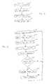
- FIG. 1is a flowchart illustrating the steps according to one embodiment of the present invention
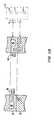
- FIG. 2Ais a simplified, cross-sectional view of an exemplary substrate processing system with which embodiments of the present invention may be used;
- FIG. 2Bis a simplified cross-sectional view of a gas ring that may be used in conjunction with the exemplary CVD processing chamber of FIG. 2A;
- FIG. 3is a flowchart illustrating the steps according to another embodiment of the present invention.
- embodiments of the inventionprovide a method of removing the residue from a substrate processing chamber that builds up and remains after multiple cycles of substrate processing operations and chamber dry cleaning operations.
- a chamber “dry cleaning” operationis any process intended to remove residue from an interior surface of the chamber in the gas phase as opposed to liquid phase.
- the removal of contaminants in a dry cleaning processis driven by either conversion of the contaminant into a volatile compound through a chemical reaction, by knocking the contaminant off the interior surface via a momentum transfer or by lifting the contaminant off the surface during etching of the surface.
- Dry cleaning operationsinclude both in situ and remote plasma cleaning processes as well as thermal gas phase cleaning processes and others.
- Embodiments of the inventionare particularly useful in removing residue build-up from a chemical vapor deposition (CVD) chamber but may also be used to remove residue and other potential sources of contamination from other types of deposition chambers, e.g., physical vapor deposition (PVD) chambers, etching chambers and other types of substrate processing chambers in which a plasma can be formed within the chamber.
- CVDchemical vapor deposition
- PVDphysical vapor deposition
- FIG. 1is a flowchart illustrating the steps according to one embodiment of the present invention.
- the processbegins by sequentially processing n wafers in a substrate processing chamber according to a desired process or recipe (step 2 ).
- the process or recipeis a CVD film deposition step, but in other embodiments the process or recipe in step 2 may be a PVD film deposition step, a film etch step or another appropriate substrate processing operation.
- the number of wafers, n, processed in step 2 before the dry cleaning operation of step 3depends on the type of process employed in step 2 and the thickness of film deposited or amount of film etched. In some embodiments, n is between 1 and 25 but the invention is not limited to any particular value of n.
- the substrate processing chamberis then cleaned using an appropriate dry cleaning process to remove residue that may have accumulated on various interior surfaces of the chamber (step 3 ).
- the type of dry cleaning process used, as well as its frequency,depends on the type of substrate processing operation employed in step 2 . If, for example, step 2 deposits a silica glass layer over each substrate, dry cleaning operation 3 may form a plasma from a fluorocarbon or similar gas in order to remove silica glass deposited over the interior walls of the chamber.
- Steps 2 and 3are then repeated a number of times, m, (step 4 ) until the chamber is ready for an extended cleaning process according to embodiments of the present invention. While the invention is not limited to any particular value of m, typically, the number of wafers processed in step 2 prior to step 5 being run on a chamber (n ⁇ m) is in the range of 500 to 10,000 wafers. Thus, in one embodiment where n equals 5, m equals 100-2000. And in one embodiment where n equals 1, m is between 500-10,000.
- Extended clean step 5is fundamentally different than dry cleaning step 3 in that it is designed to remove residue and contaminants that are not completely removed in step 2 .
- extended clean step 5forms an in situ plasma that is maintained within the chamber for a longer period of time than is practical, e.g., because of throughput concerns, for dry cleaning step 2 .
- the plasmais also formed using relatively high RF power levels. This, combined with the length of time the plasma is maintained within the chamber, results in the plasma heating the interior surfaces of the chamber to temperatures that are often above the temperatures the same surfaces are heated to during dry cleaning step 2 .
- an increased cleaning temperatureis obtained by actively heating the chamber and/or selected components of the chamber, with an appropriate heater.
- a plasmais maintained within the substrate processing chamber for at least 5 minutes and in other embodiment for at least 10 minutes. In one specific embodiment the plasma is maintained for between 10-30 minutes. In contrast, the cleaning plasma in dry cleaning step 2 is typically maintained for less than 5 minutes and is maintained for between 1-4 minutes in some embodiments.
- the cleaning gasincludes a hydrogen source and one or more of a fluorine source or argon.
- the hydrogen sourcecan be H 2 , SiH 4 , air (N 2 /O 2 /H 2 O) or other similar sources.
- Other gasescan be added or removed from the cleaning gas depending on the type of residue that accumulates and remains within the chamber over time after repeated iterations of steps 2 and 3 .
- an oxygen sourcemay be added (e.g., O 2 ) to help remove the carbon.
- fluorineaccumulates within the chamber, however, (e.g., in the form of AlF x ), a fluorine source may not be necessary as the accumulated fluorine will be available to react with the plasma.
- dry cleaning step 2may or may not form an in situ plasma within the chamber. Even in instances where cleaning step 2 employs an in situ plasma, the plasma formed in extended cleaning step 5 is typically different from the step 2 plasma in either or, more typically, both gases and power levels employed.
- using different cleaning gases in steps 2 and 5refers to the clean gases used in steps 2 and 5 having at least one different precursor gas. It does not mean the steps cannot have any gases in common.
- cleaning step 2employs a clean gas of NF 3 and Ar while the cleaning gas used in step 5 includes NF 3 , Ar and H 2 .
- HDP-CVDhigh density plasma CVD
- USGundoped silicate glass
- FIG. 2Aillustrates one embodiment of a high density plasma chemical vapor deposition (HDP-CVD) system 10 in which the method of the present invention may be practiced.
- System 10includes a chamber 13 , a substrate support 18 , a gas delivery system 33 , a remote plasma cleaning system 50 , a vacuum system 70 , a source plasma system 80 A, a bias plasma system 80 B.
- HDP-CVDhigh density plasma chemical vapor deposition
- the upper portion of chamber 13includes a dome 14 , which is made of a ceramic dielectric material, such as aluminum oxide or aluminum nitride. Dome 14 defines an upper boundary of a plasma processing region 16 .
- Plasma processing region 16is bounded on the bottom by the upper surface of a substrate 17 and a substrate support 18 , which is also made from an aluminum oxide or aluminum ceramic material.
- a heater plate 23 and a cold plate 24surmount, and are thermally coupled to, dome 14 .
- Heater plate 23 and cold plate 24allow control of the dome temperature to within about ⁇ 10° C. over a range of about 100° C. to 200° C.
- Substrate support 18includes inner and outer passages (not shown) that can deliver a heat transfer gas (sometimes referred to as a backside cooling gas) to the backside of the substrate.
- a heat transfer gassometimes referred to as a backside cooling gas
- the lower portion of chamber 13includes a body member 22 , which joins the chamber to the vacuum system.
- a base portion 21 of substrate support 18is mounted on, and forms a continuous inner surface with, body member 22 .
- Substratesare transferred into and out of chamber 13 by a robot blade (not shown) through an insertion/removal opening (not shown) in the side of chamber 13 .
- Lift pins(not shown) are raised and then lowered under the control of a motor (also not shown) to move the substrate from the robot blade at an upper loading position 57 to a lower processing position 56 in which the substrate is placed on a substrate receiving portion 19 of substrate support 18 .
- Substrate receiving portion 19includes an electrostatic chuck 20 that can be used to secure the substrate to substrate support 18 during substrate processing.
- Vacuum system 70includes throttle body 25 , which houses twin-blade throttle valve 26 and is attached to gate valve 27 and turbo-molecular pump 28 .
- Gate valve 27can isolate pump 28 from throttle body 25 , and can also control chamber pressure by restricting the exhaust flow capacity when throttle valve 26 is fully open.
- the arrangement of the throttle valve, gate valve, and turbo-molecular pumpallow accurate and stable control of chamber pressures as low as about 1 mTorr.
- Source plasma system 80 Ais coupled to a top coil 29 and side coil 30 , mounted on dome 14 .
- a symmetrical ground shield(not shown) reduces electrical coupling between the coils.
- Top coil 29is powered by top source RF (SRF) generator 31 A
- side coil 30is powered by side SRF generator 31 B, allowing independent power levels and frequencies of operation for each coil.
- the top source RF generator 31 Aprovides up to 2,500 watts of RF power at nominally 2 MHz and the side source RF generator 31 B provides up to 5,000 watts of RF power at nominally 2 MHz.
- the operating frequencies of the top and side RF generatorsmay be offset from the nominal operating frequency (e.g. to 1.7-1.9 MHz and 1.9-2.1 MHz, respectively) to improve plasma-generation efficiency.
- a bias plasma system 80 Bincludes a bias RF (BRF) generator 31 C and a bias matching network 32 C.
- the bias plasma system 80 Bcapacitively couples substrate portion 17 to body member 22 , which act as complimentary electrodes.
- the bias plasma system 80 Bserves to enhance the transport of plasma species (e.g., ions) created by the source plasma system 80 A to the surface of the substrate.
- bias RF generatorprovides up to 5,000 watts of RF power at 13.56 MHz.
- RF generators 31 A and 31 Binclude digitally controlled synthesizers and operate over a frequency range between about 1.8 to about 2.1 MHz. Each generator includes an RF control circuit (not shown) that measures reflected power from the chamber and coil back to the generator and adjusts the frequency of operation to obtain the lowest reflected power, as understood by a person of ordinary skill in the art.
- Matching networks 32 A and 32 Bmatch the output impedance of generators 31 A and 31 B with their respective coils 29 and 30 .
- the RF control circuitmay tune both matching networks by changing the value of capacitors within the matching networks to match the generator to the load as the load changes.
- the RF control circuitmay tune a matching network when the power reflected from the load back to the generator exceeds a certain limit.
- One way to provide a constant match, and effectively disable the RF control circuit from tuning the matching networkis to set the reflected power limit above any expected value of reflected power. This may help stabilize a plasma under some conditions by holding the matching network constant at its most recent condition.
- a gas delivery system 33provides gases from several sources 34 ( a ) . . . 34 ( n ) via gas delivery lines 38 (only some of which are shown).
- gas sources 34 ( a ) . . . 34 ( n )include separate sources for SiH 4 , O 2 , Ar and NF 3 as well as one or more sources for the extended cleaning process.
- the actual sources used for sources 34 ( a ) . . . 34 ( n ) and the actual connection of delivery lines 38 to chamber 13varies depending on the deposition and cleaning processes executed within chamber 13 .
- Gas flow from each source 34 ( a ) . . . 34 ( n )is controlled by one or more mass flow controllers (not shown) as is known to those of skill in the art.
- FIG. 2Bis a simplified, partial cross-sectional view of chamber 13 showing additional details of gas ring 37 .
- one or more gas sourcesprovide gas to ring plenum 36 in gas ring 37 via gas delivery lines 38 (only some of which are shown).
- Gas ring 37has a plurality of gas nozzles 39 (only one of which is shown for purposes of illustration) that provides a uniform flow of gas over the substrate. Nozzle length and nozzle angle may be changed to allow tailoring of the uniformity profile and gas utilization efficiency for a particular process within an individual chamber.
- gas ring 37has 12 gas nozzles 39 made from an aluminum oxide ceramic.
- Gas ring 37also has a plurality of gas nozzles 40 (only one of which is shown), which in a specific embodiment are co-planar with and shorter than source gas nozzles 39 , and in one embodiment receive gas from body plenum 41 .
- Gas nozzles 39 and 40are not fluidly coupled in some embodiments where it is desirable to not mix gases (e.g., SiH 4 and O 2 ) introduced through gas ring 37 before injecting the gases into chamber 13 .
- gasesmay be mixed prior to injecting the gases into chamber 13 by providing apertures (not shown) between body plenum 41 and gas ring plenum 36 . Additional valves, such as 43 B (other valves not shown), may shut off gas from the flow controllers to the chamber.
- valve 43 Bto isolate chamber 13 from a delivery line 38 and to vent delivery line 38 to vacuum foreline 44 , for example.
- valve 43 A and 43 Cmay be incorporated on other gas delivery lines.
- Such 3-way valvesmay be placed as close to chamber 13 and remote plasma source 50 as practical, to minimize the volume of the unvented gas delivery line (between the 3-way valve and the chamber).
- two-way (on-off) valvesmay be placed between a mass flow controller (“MFC”) and the chamber or between a gas source and an MFC.
- MFCmass flow controller
- chamber 13also has top nozzle 45 and top vent 46 .
- Top nozzle 45 and top vent 46allow independent control of top and side flows of the gases, which improves film uniformity and allows fine adjustment of the film's deposition and doping parameters.
- Top vent 46is an annular opening around top nozzle 45 .
- one sourcee.g., SiH 4
- separate MFCsmay be used to control the flow of oxygen to both top vent 46 and gas nozzles 40 from a single source of oxygen.
- top nozzle 45 and top vent 46may be kept separate prior to flowing the gases into chamber 13 , or the gases may be mixed in top plenum 48 before they flow into chamber 13 . In other embodiments, separate sources of the same gas may be used to supply various portions of the chamber.
- a remote microwave-generated plasma cleaning system 50is provided to periodically clean deposition residues from chamber components in a dry cleaning operation.
- the cleaning systemincludes a remote microwave generator 51 that creates a plasma from one or more cleaning gas source in sources 34 ( a ) . . . 34 ( n ) (e.g., molecular fluorine, nitrogen trifluoride, other fluorocarbons or equivalents alone or in combination with another gas such as Argon) in reactor cavity 53 .
- sources 34 ( a ) . . . 34 ( n )e.g., molecular fluorine, nitrogen trifluoride, other fluorocarbons or equivalents alone or in combination with another gas such as Argon
- the reactive species resulting from this plasmaare conveyed to chamber 13 through cleaning gas feed port 54 via applicator tube 55 .
- the materials used to contain the cleaning plasmae.g., cavity 53 and applicator tube 55 ) must be resistant to attack by the plasma.
- reactor cavity 53 and feed port 54should be kept as short as practical, since the concentration of desirable plasma species may decline with distance from reactor cavity 53 .
- Generating the cleaning plasma in a remote cavityallows the use of an efficient microwave generator and does not subject chamber components to the temperature, radiation, or bombardment of the glow discharge that may be present in a plasma formed in situ. Consequently, relatively sensitive components, such as electrostatic chuck 20 , do not need to be covered with a dummy wafer or otherwise protected, as may be required with an in situ plasma cleaning process.
- System controller 60controls the operation of system 10 .
- Controller 60may include, for example, a memory 62 , such as a hard disk drive and/or a floppy disk drive and a card rack coupled to a processor 61 .
- the card rackmay contain a single-board computer (SBC), analog and digital input/output boards, interface boards and stepper motor controller boards.
- SBCsingle-board computer
- System controller 60operates under the control of a computer program stored on the hard disk drive or through other computer programs, such as programs stored on a removable disk.
- the computer programdictates, for example, the timing, mixture of gases, RF power levels and other parameters of a particular process.
- FIG. 3is a flowchart illustrating the operation of chamber 13 according to an exemplary embodiment of the invention implemented in an UltimaTM HDP-CVD chamber manufactured by Applied Materials.
- the process shown in FIG. 3is an extended wafer run in which an 8,000 ⁇ layer of undoped silicate glass (USG) is deposited over multiple semiconductor substrates upon which partially completed integrated circuits are formed.
- USGundoped silicate glass
- the exemplary extended wafer runincludes performing a chamber dry cleaning process (step 220 ) and a chamber seasoning process (deposition of a thin silicon oxide layer over the interior surfaces of the chamber prior to the next deposition step 205 ) (step 225 ) after every three substrates that are processed in chamber 13 to form 8,000 ⁇ USG layers over the substrates (steps 205 , 210 , 215 ).
- Table 1illustrates key parameters of the process used to deposit the 8,000 ⁇ USG layers as well as the key parameters in the chamber dry cleaning process and chamber seasoning operation.
- Gas flow values in Table 1 that include two numbers separated by a “+” signindicate the flow rate through side and top nozzles, respectively, of chamber 13 .
- a pressure level of “TVO”indicates that the throttle valve is fully open setting the chamber pressure to a minimum value (typically in the 1-3 mTorr range) that is determined by the flow rate of the gases introduced into the chamber.
- TVOa pressure level of “TVO” indicates that the throttle valve is fully open setting the chamber pressure to a minimum value (typically in the 1-3 mTorr range) that is determined by the flow rate of the gases introduced into the chamber.
- the deposition, chamber clean sequence illustrated in FIG. 2can be used to process thousands of wafers before an aluminum fluoride residue containing traces of carbon, nitrogen, titanium and other elements accumulates to levels that may adversely affect further substrate processing.
- This undesirable residue that forms on various chamber componentscan be cleaned using wet cleaning techniques such as those described above or the components may be replaced altogether.
- step 235This in situ extended chamber cleaning process is shown in FIG. 3 as step 235 which is typically only executed after some relatively large number of substrates are processed in chamber 13 in multiple iterations of the step 205 - 225 sequence.
- step 235This in situ extended chamber cleaning process is shown in FIG. 3 as step 235 which is typically only executed after some relatively large number of substrates are processed in chamber 13 in multiple iterations of the step 205 - 225 sequence.
- the inventorshave found that for the above USG deposition process and associated clean and seasoning process an extended wafer run of at least 500-2000 wafers can be processed in the step 205 - 225 sequence before extended cleaning step 235 is executed.
- a counter mis used to count the number of wafers processed and step 235 is executed once m reaches the predetermined frequency for the extended clean (step 230 ).
- sensorsare used to monitor contaminant levels within chamber 13 and only when the sensors indicate that contaminant levels have reached a certain level is extended clean step 235 executed. After performing extended clean step 235 , chamber 13 is seasoned (step 240 ) and the chamber is ready for additional deposition steps.
- the extended chamber clean processforms an in situ plasma from a cleaning gas that includes a hydrogen source and argon.
- the hydrogen sourcemay be H 2 or air (N 2 /O 2 /H 2 O).
- Argonwhich is a highly dissociative atom, allows the plasma to be sustained at a very low pressure (e.g., between 0.5-120 mTorr and preferably between 0.5 and 30 mTorr in some embodiments and between 0.5-5 mTorr in other embodiments).
- the in situ plasmais allowed to clean the chamber for at least 5 minutes and more typically for between 10-30 minutes at relatively high RF power levels (e.g., 2500-5000 W for the side coil and 1500-5000 W for the top coil). In one embodiment, RF bias power is not employed. During this time, the source (top and side) RF power levels are left ON.
- the plasmaheats the chamber to temperatures that typically are not reached during a standard dry cleaning operation such as that of steps 220 .
- the temperature of dome 14which is actively cooled by cold plate 24 during the extended cleaning process so that the dome does not crack from the high temperatures, may reach a temperature of between 180-300° C. in some embodiments and more typically between 200-250° C. in other embodiments.
- the temperature of dome 14 during deposition, cleaning and seasoning steps 205 - 225is typically controlled by cold plate 24 at a temperature of about 120° C.
- gas flows used to clean a high density plasma chamber, such as chamber 13 , during dry cleaning step 220are typically above 60 mTorr due to the relatively high flow rate of the fluorine source (e.g., greater than 500 sccm of NF 3 ) employed to etch the relatively large quantities of silicon oxide that have accumulated over the chamber surfaces between dry cleaning processes.
- the RF power levels usedare maximized in order to intentionally sputter the contaminated chamber dome surfaces and heat the dome to desorb the contaminants.
- the inclusion of a fluorine source in dry cleaning step 220typically limits the RF power levels employed during the dry cleaning step. If RF power levels are not limited during such a fluorine-containing clean step, the higher dome temperatures may result in the formation of AlF on the dome surface thereby consuming an outer layer of the ceramic dome and reducing its lifetime.
- a valve in the chamberto let the air in rather than supply air from a dedicated source of clean dry air (CDA).
- CDAclean dry air
- a number of plasma processing chamberssuch as chamber 13 include a residual gas analyzer (RGA) tap area near the foreline for a particle monitor or similar device. In such chambers, opening the valve in the RGA tap area may serve as the source for the air.
- RGAresidual gas analyzer
- the in situ plasma formed within the chamber during extended clean step 235is formed from only argon
- the flow of argonis between 5-100 sccm.
- an argon flow of 15 sccmwas introduced into the chamber and a plasma was formed by applying 4800 W of RF power to the top coil and 1200 W of RF power to the side coil. Chamber pressure was set to 1.2 mTorr and the plasma was maintained for 30 minutes. During this extended clean process, the dome temperature was reached a temperature of 210° C. and was sustained at that temperature throughout the extended clean.
- the inventorimplemented the process in a HDP-CVD tool (UltimaTM chamber manufactured by Applied Materials) where contaminate levels within the chamber due to an extended sequence of film deposition and chamber clean steps resulted in an unacceptably high number of particles (greater than 50 per wafer) greater than 0.2 microns in diameter being added to subsequent deposition processes.
- a HDP-CVD toolUltimaTM chamber manufactured by Applied Materials
- many of the interior ceramic surfaces of the chamber including the chamber dome, nozzles and process kitincluded dark blackish/brown spots indicative of high contaminant levels.
Landscapes
- Chemical & Material Sciences (AREA)
- Physics & Mathematics (AREA)
- Optics & Photonics (AREA)
- General Chemical & Material Sciences (AREA)
- Chemical Kinetics & Catalysis (AREA)
- Engineering & Computer Science (AREA)
- Materials Engineering (AREA)
- Mechanical Engineering (AREA)
- Metallurgy (AREA)
- Organic Chemistry (AREA)
- Chemical Vapour Deposition (AREA)
- Drying Of Semiconductors (AREA)
Abstract
Description
- The present invention relates to the fabrication of integrated circuits. More specifically, embodiments of the invention pertain to methods of removing residue from the interior surfaces of a substrate processing chamber.[0001]
- One of the primary steps in the fabrication of modern semiconductor devices is the formation of a layer, such as a silicon oxide layer, on a substrate or wafer. As is well known, such a layer can be deposited by chemical vapor deposition (CVD). In a conventional thermal CVD process, reactive gases are supplied to the substrate surface where heat-induced chemical reactions take place to form the desired film. In a conventional plasma CVD process, a controlled plasma is formed using radio frequency (RF) energy or microwave energy to decompose and/or energize reactive species in reactant gases to produce the desired film.[0002]
- Unwanted deposition on areas such as the walls of the processing chamber also occurs during such CVD processes. As is known in the industry, it is common to remove the unwanted deposition material that builds up on the interior of chamber walls with an in situ chamber clean operation. Common chamber cleaning techniques include the use of an etchant gas, such as fluorine, to remove the deposited material from the chamber walls and other areas. In some processes, the etchant gas is introduced into the chamber and a plasma is formed within the chamber so that the etchant gas reacts with and removes the deposited material from the chamber walls. Such cleaning procedures are commonly performed between deposition steps for every wafer or every n wafers.[0003]
- Some semiconductor manufactures employ a remote plasma cleaning process as an alternative to an in situ plasma cleaning, a remote plasma cleaning procedure may be employed in which a plasma is generated remote from the substrate processing chamber by a high density plasma source such as a microwave plasma system, toroidal plasma generator or similar device. Dissociated species from the plasma are then transported to the substrate processing chamber where they can react with and etch away the undesired deposition build-up. Remote microwave plasma cleaning procedures are sometimes used by manufacturers because they provide a “softer” etch than in situ plasma clean operations, i.e., there is less ion bombardment and/or physical damage to chamber components because the plasma is not in contact with chamber components.[0004]
- Regardless of whether an in situ or remote cleaning process is employed, over time, residue may build up within the chamber that cannot be removed by standard dry cleaning processes. Accordingly, many semiconductor manufacturers use a wet cleaning process to remove such residue. One commonly used wet clean process includes removing appropriate components of the chamber (e.g., chamber liners, the gas manifold or gas nozzles, and the pedestal) and dipping the components in a bath of hydrofluoric acid (HF). Components that cannot easily be dipped in such a bath, e.g., the interior chamber walls, are instead wiped with an HF or similar solution.[0005]
- As can be appreciated, wet cleaning operations require the substrate processing tool to be taken offline. This results in a decrease in wafer throughput and a general desire on behalf of the semiconductor manufacturers to use such wet cleaning processes less frequently than dry cleaning processes. As an example of frequency of use, during the use of one known semiconductor substrate processing tool used to deposit a silicon oxide dielectric layer over a substrate, the chamber is dry cleaned using a remote plasma clean process after every 5th substrate processed in the chamber, while the chamber is cleaned using a wet clean process every 5000 wafers.[0006]
- While wet clean processes such as the HF clean just described have been used successfully by a number of different semiconductor manufacturers, improved cleaning processes are desirable.[0007]
- Embodiments of the present invention pertain to a cleaning process that is used to remove residue remaining within a substrate processing chamber after processing a substantial number of wafers in the chamber and after performing a number of dry cleaning processes.[0008]
- According to one embodiment of the invention, one or more substrates are processed in a substrate processing chamber and the chamber is subsequently cleaned using a dry cleaning process. This substrate processing and dry cleaning sequence is then repeated multiple times before the chamber is further cleaned using an extended cleaning process in which a plasma is formed within the chamber and maintained for at least 5 minutes from an appropriate cleaning gas. In one embodiment, the cleaning gas includes a hydrogen source and a fluorine source. In another embodiment the cleaning gas further includes an oxygen source. In still another embodiment the cleaning gas consists of argon. And in still another embodiment cleaning gas consists of argon and a hydrogen source.[0009]
- These and other embodiments of the invention along with many of its advantages and features are described in more detail in conjunction with the text below and attached figures.[0010]
- FIG. 1 is a flowchart illustrating the steps according to one embodiment of the present invention;[0011]
- FIG. 2A is a simplified, cross-sectional view of an exemplary substrate processing system with which embodiments of the present invention may be used;[0012]
- FIG. 2B is a simplified cross-sectional view of a gas ring that may be used in conjunction with the exemplary CVD processing chamber of FIG. 2A; and[0013]
- FIG. 3 is a flowchart illustrating the steps according to another embodiment of the present invention.[0014]
- As described above, embodiments of the invention provide a method of removing the residue from a substrate processing chamber that builds up and remains after multiple cycles of substrate processing operations and chamber dry cleaning operations. As used herein a chamber “dry cleaning” operation is any process intended to remove residue from an interior surface of the chamber in the gas phase as opposed to liquid phase. The removal of contaminants in a dry cleaning process is driven by either conversion of the contaminant into a volatile compound through a chemical reaction, by knocking the contaminant off the interior surface via a momentum transfer or by lifting the contaminant off the surface during etching of the surface. Dry cleaning operations include both in situ and remote plasma cleaning processes as well as thermal gas phase cleaning processes and others. Embodiments of the invention are particularly useful in removing residue build-up from a chemical vapor deposition (CVD) chamber but may also be used to remove residue and other potential sources of contamination from other types of deposition chambers, e.g., physical vapor deposition (PVD) chambers, etching chambers and other types of substrate processing chambers in which a plasma can be formed within the chamber.[0015]
- FIG. 1 is a flowchart illustrating the steps according to one embodiment of the present invention. In the embodiment shown in FIG. 1, the process begins by sequentially processing n wafers in a substrate processing chamber according to a desired process or recipe (step[0016]2). In one embodiment the process or recipe is a CVD film deposition step, but in other embodiments the process or recipe in
step 2 may be a PVD film deposition step, a film etch step or another appropriate substrate processing operation. The number of wafers, n, processed instep 2 before the dry cleaning operation ofstep 3 depends on the type of process employed instep 2 and the thickness of film deposited or amount of film etched. In some embodiments, n is between 1 and 25 but the invention is not limited to any particular value of n. - After n wafers have been processed, the substrate processing chamber is then cleaned using an appropriate dry cleaning process to remove residue that may have accumulated on various interior surfaces of the chamber (step[0017]3). The type of dry cleaning process used, as well as its frequency, depends on the type of substrate processing operation employed in
step 2. If, for example,step 2 deposits a silica glass layer over each substrate,dry cleaning operation 3 may form a plasma from a fluorocarbon or similar gas in order to remove silica glass deposited over the interior walls of the chamber. - [0018]
Steps step 2 prior tostep 5 being run on a chamber (n×m) is in the range of 500 to 10,000 wafers. Thus, in one embodiment where n equals 5, m equals 100-2000. And in one embodiment where n equals 1, m is between 500-10,000. - Extended[0019]
clean step 5 is fundamentally different thandry cleaning step 3 in that it is designed to remove residue and contaminants that are not completely removed instep 2. To this end, extendedclean step 5 forms an in situ plasma that is maintained within the chamber for a longer period of time than is practical, e.g., because of throughput concerns, fordry cleaning step 2. In one embodiment the plasma is also formed using relatively high RF power levels. This, combined with the length of time the plasma is maintained within the chamber, results in the plasma heating the interior surfaces of the chamber to temperatures that are often above the temperatures the same surfaces are heated to duringdry cleaning step 2. In other embodiments an increased cleaning temperature is obtained by actively heating the chamber and/or selected components of the chamber, with an appropriate heater. - In some embodiments, a plasma is maintained within the substrate processing chamber for at least 5 minutes and in other embodiment for at least 10 minutes. In one specific embodiment the plasma is maintained for between 10-30 minutes. In contrast, the cleaning plasma in[0020]
dry cleaning step 2 is typically maintained for less than 5 minutes and is maintained for between 1-4 minutes in some embodiments. - Various cleaning gases can be used in extended[0021]
clean step 5. In some embodiments the cleaning gas includes a hydrogen source and one or more of a fluorine source or argon. The hydrogen source can be H2, SiH4, air (N2/O2/H2O) or other similar sources. Other gases can be added or removed from the cleaning gas depending on the type of residue that accumulates and remains within the chamber over time after repeated iterations ofsteps - As previously mentioned,[0022]
dry cleaning step 2 may or may not form an in situ plasma within the chamber. Even in instances where cleaningstep 2 employs an in situ plasma, the plasma formed inextended cleaning step 5 is typically different from thestep 2 plasma in either or, more typically, both gases and power levels employed. As used herein, using different cleaning gases insteps steps steps step 2 employs a clean gas of NF3and Ar while the cleaning gas used instep 5 includes NF3, Ar and H2. - In order to better appreciate and understand the present invention, the invention is illustrated below with reference to a specific example in which a high density plasma CVD (HDP-CVD) chamber is used to deposit undoped silicate glass (USG) layers over a semiconductor substrate. This example is for illustrative purposes only as the present invention can be used to remove residue from other types of substrate processing chambers and from chambers used to deposit materials other than silicate glass, among other possible uses. The example includes some details that are, in part, chamber specific. Thus, before describing the examples, a brief description of the HDP-CVD substrate processing chamber is given.[0023]
- FIG. 2A illustrates one embodiment of a high density plasma chemical vapor deposition (HDP-CVD)[0024]
system 10 in which the method of the present invention may be practiced.System 10 includes achamber 13, asubstrate support 18, agas delivery system 33, a remoteplasma cleaning system 50, avacuum system 70, asource plasma system 80A, abias plasma system 80B. - The upper portion of[0025]
chamber 13 includes adome 14, which is made of a ceramic dielectric material, such as aluminum oxide or aluminum nitride.Dome 14 defines an upper boundary of aplasma processing region 16.Plasma processing region 16 is bounded on the bottom by the upper surface of asubstrate 17 and asubstrate support 18, which is also made from an aluminum oxide or aluminum ceramic material. - A[0026]
heater plate 23 and acold plate 24 surmount, and are thermally coupled to,dome 14.Heater plate 23 andcold plate 24 allow control of the dome temperature to within about ±10° C. over a range of about 100° C. to 200° C. - Generally, exposure to the plasma heats a substrate positioned on[0027]
substrate support 18.Substrate support 18 includes inner and outer passages (not shown) that can deliver a heat transfer gas (sometimes referred to as a backside cooling gas) to the backside of the substrate. - The lower portion of[0028]
chamber 13 includes abody member 22, which joins the chamber to the vacuum system. Abase portion 21 ofsubstrate support 18 is mounted on, and forms a continuous inner surface with,body member 22. Substrates are transferred into and out ofchamber 13 by a robot blade (not shown) through an insertion/removal opening (not shown) in the side ofchamber 13. Lift pins (not shown) are raised and then lowered under the control of a motor (also not shown) to move the substrate from the robot blade at anupper loading position 57 to alower processing position 56 in which the substrate is placed on asubstrate receiving portion 19 ofsubstrate support 18.Substrate receiving portion 19 includes anelectrostatic chuck 20 that can be used to secure the substrate tosubstrate support 18 during substrate processing. - [0029]
Vacuum system 70 includesthrottle body 25, which houses twin-blade throttle valve 26 and is attached togate valve 27 and turbo-molecular pump 28.Gate valve 27 can isolate pump28 fromthrottle body 25, and can also control chamber pressure by restricting the exhaust flow capacity whenthrottle valve 26 is fully open. The arrangement of the throttle valve, gate valve, and turbo-molecular pump allow accurate and stable control of chamber pressures as low as about 1 mTorr. - [0030]
Source plasma system 80A is coupled to atop coil 29 and side coil30, mounted ondome 14. A symmetrical ground shield (not shown) reduces electrical coupling between the coils.Top coil 29 is powered by top source RF (SRF)generator 31A, whereas side coil30 is powered byside SRF generator 31B, allowing independent power levels and frequencies of operation for each coil. In a specific embodiment, the topsource RF generator 31A provides up to 2,500 watts of RF power at nominally 2 MHz and the sidesource RF generator 31B provides up to 5,000 watts of RF power at nominally 2 MHz. The operating frequencies of the top and side RF generators may be offset from the nominal operating frequency (e.g. to 1.7-1.9 MHz and 1.9-2.1 MHz, respectively) to improve plasma-generation efficiency. - A[0031]
bias plasma system 80B includes a bias RF (BRF)generator 31C and abias matching network 32C. Thebias plasma system 80B capacitively couplessubstrate portion 17 tobody member 22, which act as complimentary electrodes. Thebias plasma system 80B serves to enhance the transport of plasma species (e.g., ions) created by thesource plasma system 80A to the surface of the substrate. In a specific embodiment, bias RF generator provides up to 5,000 watts of RF power at 13.56 MHz. - [0032]
RF generators Matching networks generators respective coils 29 and30. The RF control circuit may tune both matching networks by changing the value of capacitors within the matching networks to match the generator to the load as the load changes. The RF control circuit may tune a matching network when the power reflected from the load back to the generator exceeds a certain limit. One way to provide a constant match, and effectively disable the RF control circuit from tuning the matching network, is to set the reflected power limit above any expected value of reflected power. This may help stabilize a plasma under some conditions by holding the matching network constant at its most recent condition. - A[0033]
gas delivery system 33 provides gases from several sources34(a) . . .34(n) via gas delivery lines38 (only some of which are shown). In the particular example illustrated below, gas sources34(a) . . .34(n) include separate sources for SiH4, O2, Ar and NF3as well as one or more sources for the extended cleaning process. As would be understood by a person of skill in the art, the actual sources used for sources34(a) . . .34(n) and the actual connection ofdelivery lines 38 tochamber 13 varies depending on the deposition and cleaning processes executed withinchamber 13. Gas flow from each source34(a) . . .34(n) is controlled by one or more mass flow controllers (not shown) as is known to those of skill in the art. - Gases are introduced into[0034]
chamber 13 through agas ring 37 and/or atop nozzle 45. FIG. 2B is a simplified, partial cross-sectional view ofchamber 13 showing additional details ofgas ring 37. In some embodiments, one or more gas sources provide gas to ringplenum 36 ingas ring 37 via gas delivery lines38 (only some of which are shown).Gas ring 37 has a plurality of gas nozzles39 (only one of which is shown for purposes of illustration) that provides a uniform flow of gas over the substrate. Nozzle length and nozzle angle may be changed to allow tailoring of the uniformity profile and gas utilization efficiency for a particular process within an individual chamber. In one specific embodiment,gas ring 37 has12gas nozzles 39 made from an aluminum oxide ceramic. - [0035]
Gas ring 37 also has a plurality of gas nozzles40 (only one of which is shown), which in a specific embodiment are co-planar with and shorter thansource gas nozzles 39, and in one embodiment receive gas frombody plenum 41.Gas nozzles gas ring 37 before injecting the gases intochamber 13. In other embodiments, gases may be mixed prior to injecting the gases intochamber 13 by providing apertures (not shown) betweenbody plenum 41 andgas ring plenum 36. Additional valves, such as43B (other valves not shown), may shut off gas from the flow controllers to the chamber. - In embodiments where flammable, toxic, or corrosive gases are used, it may be desirable to eliminate gas remaining in the gas delivery lines after a deposition or cleaning process. This may be accomplished using a 3-way valve, such as valve[0036]43B, to isolate
chamber 13 from adelivery line 38 and to ventdelivery line 38 to vacuumforeline 44, for example. As shown in FIG. 2A, other similar valves, such as43A and43C, may be incorporated on other gas delivery lines. Such 3-way valves may be placed as close tochamber 13 andremote plasma source 50 as practical, to minimize the volume of the unvented gas delivery line (between the 3-way valve and the chamber). Additionally, two-way (on-off) valves (not shown) may be placed between a mass flow controller (“MFC”) and the chamber or between a gas source and an MFC. - Referring again to FIG. 2A,[0037]
chamber 13 also hastop nozzle 45 and top vent46.Top nozzle 45 and top vent46 allow independent control of top and side flows of the gases, which improves film uniformity and allows fine adjustment of the film's deposition and doping parameters. Top vent46 is an annular opening aroundtop nozzle 45. In one embodiment, one source, e.g., SiH4, supplies sourcegas nozzles 39 andtop nozzle 45 through separate MFCs (not shown). Similarly, separate MFCs may be used to control the flow of oxygen to both top vent46 andgas nozzles 40 from a single source of oxygen. The gases supplied totop nozzle 45 and top vent46 may be kept separate prior to flowing the gases intochamber 13, or the gases may be mixed intop plenum 48 before they flow intochamber 13. In other embodiments, separate sources of the same gas may be used to supply various portions of the chamber. - A remote microwave-generated[0038]
plasma cleaning system 50 is provided to periodically clean deposition residues from chamber components in a dry cleaning operation. The cleaning system includes aremote microwave generator 51 that creates a plasma from one or more cleaning gas source in sources34(a) . . .34(n) (e.g., molecular fluorine, nitrogen trifluoride, other fluorocarbons or equivalents alone or in combination with another gas such as Argon) inreactor cavity 53. The reactive species resulting from this plasma are conveyed tochamber 13 through cleaninggas feed port 54 viaapplicator tube 55. The materials used to contain the cleaning plasma (e.g.,cavity 53 and applicator tube55) must be resistant to attack by the plasma. The distance betweenreactor cavity 53 and feedport 54 should be kept as short as practical, since the concentration of desirable plasma species may decline with distance fromreactor cavity 53. Generating the cleaning plasma in a remote cavity allows the use of an efficient microwave generator and does not subject chamber components to the temperature, radiation, or bombardment of the glow discharge that may be present in a plasma formed in situ. Consequently, relatively sensitive components, such aselectrostatic chuck 20, do not need to be covered with a dummy wafer or otherwise protected, as may be required with an in situ plasma cleaning process. - [0039]
System controller 60 controls the operation ofsystem 10.Controller 60 may include, for example, amemory 62, such as a hard disk drive and/or a floppy disk drive and a card rack coupled to aprocessor 61. The card rack may contain a single-board computer (SBC), analog and digital input/output boards, interface boards and stepper motor controller boards.System controller 60 operates under the control of a computer program stored on the hard disk drive or through other computer programs, such as programs stored on a removable disk. The computer program dictates, for example, the timing, mixture of gases, RF power levels and other parameters of a particular process. - FIG. 3 is a flowchart illustrating the operation of[0040]
chamber 13 according to an exemplary embodiment of the invention implemented in an Ultima™ HDP-CVD chamber manufactured by Applied Materials. The process shown in FIG. 3 is an extended wafer run in which an 8,000 Å layer of undoped silicate glass (USG) is deposited over multiple semiconductor substrates upon which partially completed integrated circuits are formed. As shown in FIG. 3, the exemplary extended wafer run includes performing a chamber dry cleaning process (step220) and a chamber seasoning process (deposition of a thin silicon oxide layer over the interior surfaces of the chamber prior to the next deposition step205) (step225) after every three substrates that are processed inchamber 13 to form 8,000 Å USG layers over the substrates (steps chamber 13. Also, a pressure level of “TVO” indicates that the throttle valve is fully open setting the chamber pressure to a minimum value (typically in the 1-3 mTorr range) that is determined by the flow rate of the gases introduced into the chamber. As can be seen from Table 1, each of 8,000 Å USG deposition steps205,210,215 takes approximately 90 seconds while cleaningstep 220 takes approximately 180 seconds andseasoning step 225 takes approximately 10 seconds. Various set-up and purge steps may also be included before and after each of steps205-225TABLE 1 USG DEP STEPS CHAMBER CHAMBER PARAMETER 205, 210, 215 CLEAN STEP 220SEASONING STEP 225SiH4 74 + 12.4 sccm — 85 sccm O2 156 sccm — 130 sccm Ar 110 + 16 sccm — 95 + 15 sccm NF3-MW — 1500 sccm — Pressure TVO 3000 mTorr TVO Top RF (2 MHz) 1300 W — 1300 W Side RF (2 MHz) 3100 W — 3100 W Bias RF (13.56 MHz) 3500 W — 0 W MW Power — 3200 W — Time 90 secs 180 secs 10 secs - From previous extended wafer run experiments, the inventors have found that the deposition, chamber clean sequence illustrated in FIG. 2 can be used to process thousands of wafers before an aluminum fluoride residue containing traces of carbon, nitrogen, titanium and other elements accumulates to levels that may adversely affect further substrate processing. This undesirable residue that forms on various chamber components can be cleaned using wet cleaning techniques such as those described above or the components may be replaced altogether.[0041]
- The inventors have determined, however, that such wet cleaning techniques can be replaced with an in situ chamber cleaning process in which a plasma is formed within[0042]
chamber 13 for an extended period of time. This in situ extended chamber cleaning process is shown in FIG. 3 asstep 235 which is typically only executed after some relatively large number of substrates are processed inchamber 13 in multiple iterations of the step205-225 sequence. The inventors have found that for the above USG deposition process and associated clean and seasoning process an extended wafer run of at least 500-2000 wafers can be processed in the step205-225 sequence beforeextended cleaning step 235 is executed. In one embodiment, a counter m is used to count the number of wafers processed and step235 is executed once m reaches the predetermined frequency for the extended clean (step230). In other embodiments, sensors are used to monitor contaminant levels withinchamber 13 and only when the sensors indicate that contaminant levels have reached a certain level is extendedclean step 235 executed. After performing extendedclean step 235,chamber 13 is seasoned (step240) and the chamber is ready for additional deposition steps. - In one embodiment the extended chamber clean process forms an in situ plasma from a cleaning gas that includes a hydrogen source and argon. The hydrogen source may be H[0043]2or air (N2/O2/H2O). Argon, which is a highly dissociative atom, allows the plasma to be sustained at a very low pressure (e.g., between 0.5-120 mTorr and preferably between 0.5 and 30 mTorr in some embodiments and between 0.5-5 mTorr in other embodiments). The in situ plasma is allowed to clean the chamber for at least 5 minutes and more typically for between 10-30 minutes at relatively high RF power levels (e.g., 2500-5000 W for the side coil and 1500-5000 W for the top coil). In one embodiment, RF bias power is not employed. During this time, the source (top and side) RF power levels are left ON.
- Because the in situ plasma formed by this process is maintained for such an extended period at such low pressure levels, the plasma heats the chamber to temperatures that typically are not reached during a standard dry cleaning operation such as that of[0044]
steps 220. For example, the temperature ofdome 14, which is actively cooled bycold plate 24 during the extended cleaning process so that the dome does not crack from the high temperatures, may reach a temperature of between 180-300° C. in some embodiments and more typically between 200-250° C. in other embodiments. - In contrast, the temperature of[0045]
dome 14 during deposition, cleaning and seasoning steps205-225, is typically controlled bycold plate 24 at a temperature of about 120° C. Also, gas flows used to clean a high density plasma chamber, such aschamber 13, duringdry cleaning step 220 are typically above 60 mTorr due to the relatively high flow rate of the fluorine source (e.g., greater than 500 sccm of NF3) employed to etch the relatively large quantities of silicon oxide that have accumulated over the chamber surfaces between dry cleaning processes. - In embodiments where there is no fluorine source used in extended[0046]
clean step 230, the RF power levels used are maximized in order to intentionally sputter the contaminated chamber dome surfaces and heat the dome to desorb the contaminants. In contrast, the inclusion of a fluorine source indry cleaning step 220 typically limits the RF power levels employed during the dry cleaning step. If RF power levels are not limited during such a fluorine-containing clean step, the higher dome temperatures may result in the formation of AlF on the dome surface thereby consuming an outer layer of the ceramic dome and reducing its lifetime. - In some embodiments where air is used as one of the gases in the extended chamber cleaning process, it is possible to open a valve in the chamber to let the air in rather than supply air from a dedicated source of clean dry air (CDA). For example, a number of plasma processing chambers such as[0047]
chamber 13 include a residual gas analyzer (RGA) tap area near the foreline for a particle monitor or similar device. In such chambers, opening the valve in the RGA tap area may serve as the source for the air. - In another embodiment of the invention, the in situ plasma formed within the chamber during extended[0048]
clean step 235 is formed from only argon In one embodiment, the flow of argon is between 5-100 sccm. In one particular embodiment, an argon flow of 15 sccm was introduced into the chamber and a plasma was formed by applying 4800 W of RF power to the top coil and 1200 W of RF power to the side coil. Chamber pressure was set to 1.2 mTorr and the plasma was maintained for 30 minutes. During this extended clean process, the dome temperature was reached a temperature of 210° C. and was sustained at that temperature throughout the extended clean. - In order to test the effectiveness of this argon-only embodiment, the inventor implemented the process in a HDP-CVD tool (Ultima™ chamber manufactured by Applied Materials) where contaminate levels within the chamber due to an extended sequence of film deposition and chamber clean steps resulted in an unacceptably high number of particles (greater than 50 per wafer) greater than 0.2 microns in diameter being added to subsequent deposition processes. Before the argon-only extended clean step was implemented, many of the interior ceramic surfaces of the chamber including the chamber dome, nozzles and process kit included dark blackish/brown spots indicative of high contaminant levels. While not being limited to any particular theory, it is believed that areas of contaminants form a relatively poor interface with silica glass films and thus lead to particles due to flaking and/or delamination of silica glass formed over the surfaces. After running the above argon-only extended clean step, all the interior surfaces of the chamber including the ceramic surfaces mentioned above were clean with no signs of contamination. Also, particle levels for subsequent substrate deposition steps performed in the chamber showed particles levels that were returned to the acceptable, production level requirement (for the particular deposition application) of less than 50 particles of 0.2 micron in diameter or more per wafer.[0049]
- Having fully described several embodiments of the present invention, many other equivalents or alternative embodiments of the present invention will be apparent to those skilled in the art. These equivalents and/or alternatives are intended to be included within the scope of the present invention.[0050]
Claims (31)
1. A method of operating a substrate processing chamber, said method comprising:
(a) processing one or more substrates in said substrate processing chamber;
(b) cleaning said chamber using a dry cleaning process;
(c) repeating steps (a) and (b) one or more times; and
(d) thereafter, performing an extended cleaning process by flowing a cleaning gas into said chamber and forming a plasma within said chamber from said cleaning gas, wherein said plasma is maintained for a total of at least 5 minutes before said chamber is reused to process a substrate.
2. The method ofclaim 1 wherein said cleaning gas comprises a hydrogen source and a fluorine source.
3. The method ofclaim 2 wherein said cleaning gas further comprises an oxygen source.
4. The method ofclaim 2 wherein said fluorine source is NF3.
5. The method ofclaim 1 wherein said cleaning gas consists of argon.
6. The method ofclaim 1 wherein said cleaning gas consists of argon and a hydrogen source.
7. The method ofclaim 6 wherein said hydrogen source is H2.
8. The method ofclaim 6 wherein said plasma is formed at a pressure between 0.5 and 120 mTorr.
9. The method ofclaim 6 wherein said plasma is formed at a pressure between 0.5 and 5 mTorr.
10. The method ofclaim 1 wherein a plasma is maintained in said substrate processing chamber for between a total of between 10 to 30 minutes during said extended cleaning step.
11. The method ofclaim 10 wherein a cleaning plasma is maintained for less then 5 minutes during said dry cleaning process.
12. The method ofclaim 1 wherein said cleaning gas is different in composition from a gas used during said dry cleaning process.
13. A method of operating a substrate processing chamber, said method comprising:
(a) transferring a substrate into said substrate processing chamber having at least one interior chamber surface;
(b) depositing a layer of material over said substrate, wherein said depositing step also results in unwanted deposition of material on said interior chamber surface;
(c) transferring said substrate out of said substrate processing chamber;
(d) optionally, repeating (a)-(c) n times, where n is an integer between1 and25;
(e) thereafter, removing said unwanted deposition build-up from said interior chamber surface by exposing said surface to reactive species from a first cleaning gas;
(f) repeating (a)-(e) m times, where m is an integer greater than 25, wherein after (a)-(e) are repeated m times, unwanted residue has built up on said interior chamber surface;
(g) thereafter, performing an extended cleaning process to remove said unwanted residue from said interior chamber surface by forming a plasma within said chamber from a second cleaning gas, wherein said second cleaning gas is different in composition from said first cleaning gas.
14. The method ofclaim 13 wherein said first cleaning gas comprises a fluorine source.
15. The method ofclaim 14 wherein said second cleaning gas comprises hydrogen and argon.
16. The method ofclaim 15 wherein said second cleaning gas further comprises an oxygen source.
17. The method ofclaim 15 wherein said second cleaning gas further comprises a fluorine source.
18. The method ofclaim 14 wherein said cleaning gas consists of argon.
19. The method ofclaim 14 wherein said cleaning gas consists of hydrogen and argon.
20. The method ofclaim 13 wherein said extended cleaning process forms a plasma within said chamber for at least 5 minutes.
21. The method ofclaim 13 wherein said extended cleaning process forms a plasma within said chamber for at least 10 minutes.
22. The method ofclaim 20 wherein said interior chamber surface is exposed to reactive species during step (e) for less than 5 minutes.
23. A method of operating a high density plasma chemical vapor deposition chamber having a plasma generation system that includes a coil, said method comprising:
(a) transferring a substrate into said chamber, depositing a layer of silica glass over said substrate and transferring said substrate out of said chamber, wherein when said silica glass is deposited over said substrate some deposition also occurs on an interior surface of said chamber;
(b) optionally, repeating (a) n times, where n is an integer between 1 and 10;
(c) thereafter, removing said deposition from said interior surface by exposing said surface to reactive species from a first cleaning gas;
(d) repeating (a)-(c) m times, where m is an integer greater than 100;
(e) thereafter, performing an extended cleaning process by flowing a second cleaning gas into said chamber and applying RF energy to said coil to form a plasma within said chamber from said second cleaning gas, wherein said second cleaning gas is different in composition from said first cleaning gas.
24. The method ofclaim 23 wherein said second cleaning gas comprises a hydrogen source.
25. The method ofclaim 24 wherein said second cleaning gas further comprises a fluorine source.
26. The method ofclaim 25 wherein said second cleaning gas further comprises argon.
27. The method ofclaim 24 wherein said hydrogen source is selected from the group consisting of: air, silane and molecular hydrogen.
28. The method ofclaim 23 wherein said second cleaning gas consists of argon.
29. The method ofclaim 23 wherein said extended cleaning process forms a plasma within said chamber for at least 5 minutes.
30. The method ofclaim 23 wherein said extended cleaning process forms a plasma within said chamber for at least 10 minutes.
31. The method ofclaim 30 wherein said interior chamber surface is exposed to reactive species during step (e) for less than 5 minutes.
Priority Applications (1)
| Application Number | Priority Date | Filing Date | Title |
|---|---|---|---|
| US10/115,830US6843858B2 (en) | 2002-04-02 | 2002-04-02 | Method of cleaning a semiconductor processing chamber |
Applications Claiming Priority (1)
| Application Number | Priority Date | Filing Date | Title |
|---|---|---|---|
| US10/115,830US6843858B2 (en) | 2002-04-02 | 2002-04-02 | Method of cleaning a semiconductor processing chamber |
Publications (2)
| Publication Number | Publication Date |
|---|---|
| US20030183244A1true US20030183244A1 (en) | 2003-10-02 |
| US6843858B2 US6843858B2 (en) | 2005-01-18 |
Family
ID=28453920
Family Applications (1)
| Application Number | Title | Priority Date | Filing Date |
|---|---|---|---|
| US10/115,830Expired - Fee RelatedUS6843858B2 (en) | 2002-04-02 | 2002-04-02 | Method of cleaning a semiconductor processing chamber |
Country Status (1)
| Country | Link |
|---|---|
| US (1) | US6843858B2 (en) |
Cited By (199)
| Publication number | Priority date | Publication date | Assignee | Title |
|---|---|---|---|---|
| US20050161060A1 (en)* | 2004-01-23 | 2005-07-28 | Johnson Andrew D. | Cleaning CVD chambers following deposition of porogen-containing materials |
| US20050241671A1 (en)* | 2004-04-29 | 2005-11-03 | Dong Chun C | Method for removing a substance from a substrate using electron attachment |
| US20060017043A1 (en)* | 2004-07-23 | 2006-01-26 | Dingjun Wu | Method for enhancing fluorine utilization |
| US20060027249A1 (en)* | 2004-07-23 | 2006-02-09 | Johnson Andrew D | Method for removing carbon-containing residues from a substrate |
| US20060086376A1 (en)* | 2004-10-26 | 2006-04-27 | Dimeo Frank Jr | Novel methods for cleaning ion implanter components |
| US20060207630A1 (en)* | 2003-03-14 | 2006-09-21 | Research Inst. Of Innovative Tech. For The Earth | Device for cleaning cvd device and method of cleaning cvd device |
| US7176140B1 (en)* | 2004-07-09 | 2007-02-13 | Novellus Systems, Inc. | Adhesion promotion for etch by-products |
| US20070107749A1 (en)* | 2005-11-14 | 2007-05-17 | Il-Kwon Sin | Process chamber cleaning method |
| US20070190266A1 (en)* | 2006-02-10 | 2007-08-16 | Applied Materials, Inc. | Water vapor passivation of a wall facing a plasma |
| US20080099054A1 (en)* | 2006-11-01 | 2008-05-01 | Felix Rabinovich | Methods and apparatus for cleaning chamber components |
| US20080283087A1 (en)* | 2007-05-15 | 2008-11-20 | Ki-Duck Yoon | Dry cleaning method of semiconductor manufacturing apparatus having multi-lifter |
| US20090075490A1 (en)* | 2007-09-18 | 2009-03-19 | L'air Liquite Societe Anonyme Pour L'etude Et L'exploitation Des Procedes Georges Claude | Method of forming silicon-containing films |
| US20090232985A1 (en)* | 2005-03-17 | 2009-09-17 | Christian Dussarrat | Method of forming silicon oxide containing films |
| WO2009158169A1 (en)* | 2008-06-27 | 2009-12-30 | Applied Materials, Inc. | Superimposition of rapid periodic and extensive post multiple substrate uv-ozone clean sequences for high throughput and stable substrate to substrate performance |
| US7754609B1 (en) | 2003-10-28 | 2010-07-13 | Applied Materials, Inc. | Cleaning processes for silicon carbide materials |
| US20110048453A1 (en)* | 2009-09-03 | 2011-03-03 | Tokyo Electron Limited | Chamber cleaning method |
| US8118946B2 (en) | 2007-11-30 | 2012-02-21 | Wesley George Lau | Cleaning process residues from substrate processing chamber components |
| US8603252B2 (en) | 2006-04-26 | 2013-12-10 | Advanced Technology Materials, Inc. | Cleaning of semiconductor processing systems |
| US8679982B2 (en) | 2011-08-26 | 2014-03-25 | Applied Materials, Inc. | Selective suppression of dry-etch rate of materials containing both silicon and oxygen |
| US8679983B2 (en) | 2011-09-01 | 2014-03-25 | Applied Materials, Inc. | Selective suppression of dry-etch rate of materials containing both silicon and nitrogen |
| US8765574B2 (en) | 2012-11-09 | 2014-07-01 | Applied Materials, Inc. | Dry etch process |
| US8771539B2 (en) | 2011-02-22 | 2014-07-08 | Applied Materials, Inc. | Remotely-excited fluorine and water vapor etch |
| US8801952B1 (en) | 2013-03-07 | 2014-08-12 | Applied Materials, Inc. | Conformal oxide dry etch |
| US8808563B2 (en) | 2011-10-07 | 2014-08-19 | Applied Materials, Inc. | Selective etch of silicon by way of metastable hydrogen termination |
| US8895449B1 (en) | 2013-05-16 | 2014-11-25 | Applied Materials, Inc. | Delicate dry clean |
| US8921234B2 (en) | 2012-12-21 | 2014-12-30 | Applied Materials, Inc. | Selective titanium nitride etching |
| US8927390B2 (en) | 2011-09-26 | 2015-01-06 | Applied Materials, Inc. | Intrench profile |
| US8951429B1 (en) | 2013-10-29 | 2015-02-10 | Applied Materials, Inc. | Tungsten oxide processing |
| US8956980B1 (en) | 2013-09-16 | 2015-02-17 | Applied Materials, Inc. | Selective etch of silicon nitride |
| US8969212B2 (en) | 2012-11-20 | 2015-03-03 | Applied Materials, Inc. | Dry-etch selectivity |
| US8975152B2 (en) | 2011-11-08 | 2015-03-10 | Applied Materials, Inc. | Methods of reducing substrate dislocation during gapfill processing |
| US8980763B2 (en) | 2012-11-30 | 2015-03-17 | Applied Materials, Inc. | Dry-etch for selective tungsten removal |
| US8999856B2 (en) | 2011-03-14 | 2015-04-07 | Applied Materials, Inc. | Methods for etch of sin films |
| US9023732B2 (en) | 2013-03-15 | 2015-05-05 | Applied Materials, Inc. | Processing systems and methods for halide scavenging |
| US9023734B2 (en) | 2012-09-18 | 2015-05-05 | Applied Materials, Inc. | Radical-component oxide etch |
| US9034770B2 (en) | 2012-09-17 | 2015-05-19 | Applied Materials, Inc. | Differential silicon oxide etch |
| US9040422B2 (en) | 2013-03-05 | 2015-05-26 | Applied Materials, Inc. | Selective titanium nitride removal |
| US9064815B2 (en) | 2011-03-14 | 2015-06-23 | Applied Materials, Inc. | Methods for etch of metal and metal-oxide films |
| US9064816B2 (en) | 2012-11-30 | 2015-06-23 | Applied Materials, Inc. | Dry-etch for selective oxidation removal |
| CN104752258A (en)* | 2013-12-30 | 2015-07-01 | 中微半导体设备(上海)有限公司 | Cleaning method for plasma-processing chamber |
| US9111877B2 (en) | 2012-12-18 | 2015-08-18 | Applied Materials, Inc. | Non-local plasma oxide etch |
| US9114438B2 (en) | 2013-05-21 | 2015-08-25 | Applied Materials, Inc. | Copper residue chamber clean |
| US9117855B2 (en) | 2013-12-04 | 2015-08-25 | Applied Materials, Inc. | Polarity control for remote plasma |
| US9136273B1 (en) | 2014-03-21 | 2015-09-15 | Applied Materials, Inc. | Flash gate air gap |
| US9132436B2 (en) | 2012-09-21 | 2015-09-15 | Applied Materials, Inc. | Chemical control features in wafer process equipment |
| US9159606B1 (en) | 2014-07-31 | 2015-10-13 | Applied Materials, Inc. | Metal air gap |
| US9165786B1 (en) | 2014-08-05 | 2015-10-20 | Applied Materials, Inc. | Integrated oxide and nitride recess for better channel contact in 3D architectures |
| US9190293B2 (en) | 2013-12-18 | 2015-11-17 | Applied Materials, Inc. | Even tungsten etch for high aspect ratio trenches |
| US20150345017A1 (en)* | 2014-05-30 | 2015-12-03 | Applied Materials, Inc. | In-situ corrosion resistant substrate support coating |
| US9236266B2 (en) | 2011-08-01 | 2016-01-12 | Applied Materials, Inc. | Dry-etch for silicon-and-carbon-containing films |
| US9236265B2 (en) | 2013-11-04 | 2016-01-12 | Applied Materials, Inc. | Silicon germanium processing |
| US9245762B2 (en) | 2013-12-02 | 2016-01-26 | Applied Materials, Inc. | Procedure for etch rate consistency |
| US9263278B2 (en) | 2013-12-17 | 2016-02-16 | Applied Materials, Inc. | Dopant etch selectivity control |
| US9269590B2 (en) | 2014-04-07 | 2016-02-23 | Applied Materials, Inc. | Spacer formation |
| US9287134B2 (en) | 2014-01-17 | 2016-03-15 | Applied Materials, Inc. | Titanium oxide etch |
| US9287095B2 (en) | 2013-12-17 | 2016-03-15 | Applied Materials, Inc. | Semiconductor system assemblies and methods of operation |
| US9293568B2 (en) | 2014-01-27 | 2016-03-22 | Applied Materials, Inc. | Method of fin patterning |
| US9299538B2 (en) | 2014-03-20 | 2016-03-29 | Applied Materials, Inc. | Radial waveguide systems and methods for post-match control of microwaves |
| US9299537B2 (en) | 2014-03-20 | 2016-03-29 | Applied Materials, Inc. | Radial waveguide systems and methods for post-match control of microwaves |
| US9299583B1 (en) | 2014-12-05 | 2016-03-29 | Applied Materials, Inc. | Aluminum oxide selective etch |
| US9299575B2 (en) | 2014-03-17 | 2016-03-29 | Applied Materials, Inc. | Gas-phase tungsten etch |
| US9309598B2 (en) | 2014-05-28 | 2016-04-12 | Applied Materials, Inc. | Oxide and metal removal |
| US9324576B2 (en) | 2010-05-27 | 2016-04-26 | Applied Materials, Inc. | Selective etch for silicon films |
| US9343272B1 (en) | 2015-01-08 | 2016-05-17 | Applied Materials, Inc. | Self-aligned process |
| US9349605B1 (en) | 2015-08-07 | 2016-05-24 | Applied Materials, Inc. | Oxide etch selectivity systems and methods |
| US9355862B2 (en) | 2014-09-24 | 2016-05-31 | Applied Materials, Inc. | Fluorine-based hardmask removal |
| US9355856B2 (en) | 2014-09-12 | 2016-05-31 | Applied Materials, Inc. | V trench dry etch |
| US9362130B2 (en) | 2013-03-01 | 2016-06-07 | Applied Materials, Inc. | Enhanced etching processes using remote plasma sources |
| US9368364B2 (en) | 2014-09-24 | 2016-06-14 | Applied Materials, Inc. | Silicon etch process with tunable selectivity to SiO2 and other materials |
| US9373522B1 (en) | 2015-01-22 | 2016-06-21 | Applied Mateials, Inc. | Titanium nitride removal |
| US9373517B2 (en) | 2012-08-02 | 2016-06-21 | Applied Materials, Inc. | Semiconductor processing with DC assisted RF power for improved control |
| US9378978B2 (en) | 2014-07-31 | 2016-06-28 | Applied Materials, Inc. | Integrated oxide recess and floating gate fin trimming |
| US9378969B2 (en) | 2014-06-19 | 2016-06-28 | Applied Materials, Inc. | Low temperature gas-phase carbon removal |
| US9385028B2 (en) | 2014-02-03 | 2016-07-05 | Applied Materials, Inc. | Air gap process |
| US9390937B2 (en) | 2012-09-20 | 2016-07-12 | Applied Materials, Inc. | Silicon-carbon-nitride selective etch |
| US9396989B2 (en) | 2014-01-27 | 2016-07-19 | Applied Materials, Inc. | Air gaps between copper lines |
| US9406523B2 (en) | 2014-06-19 | 2016-08-02 | Applied Materials, Inc. | Highly selective doped oxide removal method |
| US9425058B2 (en) | 2014-07-24 | 2016-08-23 | Applied Materials, Inc. | Simplified litho-etch-litho-etch process |
| US9449846B2 (en) | 2015-01-28 | 2016-09-20 | Applied Materials, Inc. | Vertical gate separation |
| US9472417B2 (en) | 2013-11-12 | 2016-10-18 | Applied Materials, Inc. | Plasma-free metal etch |
| US9478432B2 (en) | 2014-09-25 | 2016-10-25 | Applied Materials, Inc. | Silicon oxide selective removal |
| US9493879B2 (en) | 2013-07-12 | 2016-11-15 | Applied Materials, Inc. | Selective sputtering for pattern transfer |
| US9496167B2 (en) | 2014-07-31 | 2016-11-15 | Applied Materials, Inc. | Integrated bit-line airgap formation and gate stack post clean |
| US9499898B2 (en) | 2014-03-03 | 2016-11-22 | Applied Materials, Inc. | Layered thin film heater and method of fabrication |
| US9502258B2 (en) | 2014-12-23 | 2016-11-22 | Applied Materials, Inc. | Anisotropic gap etch |
| US9553102B2 (en) | 2014-08-19 | 2017-01-24 | Applied Materials, Inc. | Tungsten separation |
| US9576809B2 (en) | 2013-11-04 | 2017-02-21 | Applied Materials, Inc. | Etch suppression with germanium |
| US9659753B2 (en) | 2014-08-07 | 2017-05-23 | Applied Materials, Inc. | Grooved insulator to reduce leakage current |
| US9691645B2 (en) | 2015-08-06 | 2017-06-27 | Applied Materials, Inc. | Bolted wafer chuck thermal management systems and methods for wafer processing systems |
| KR20170085986A (en)* | 2016-01-15 | 2017-07-25 | 어플라이드 머티어리얼스, 인코포레이티드 | Rps defect reduction by cyclic clean induced rps cooling |
| US9721789B1 (en) | 2016-10-04 | 2017-08-01 | Applied Materials, Inc. | Saving ion-damaged spacers |
| US9728437B2 (en) | 2015-02-03 | 2017-08-08 | Applied Materials, Inc. | High temperature chuck for plasma processing systems |
| US9741593B2 (en) | 2015-08-06 | 2017-08-22 | Applied Materials, Inc. | Thermal management systems and methods for wafer processing systems |
| US9768034B1 (en) | 2016-11-11 | 2017-09-19 | Applied Materials, Inc. | Removal methods for high aspect ratio structures |
| US9773648B2 (en) | 2013-08-30 | 2017-09-26 | Applied Materials, Inc. | Dual discharge modes operation for remote plasma |
| US9847289B2 (en) | 2014-05-30 | 2017-12-19 | Applied Materials, Inc. | Protective via cap for improved interconnect performance |
| US9865484B1 (en) | 2016-06-29 | 2018-01-09 | Applied Materials, Inc. | Selective etch using material modification and RF pulsing |
| US20180019106A1 (en)* | 2015-01-22 | 2018-01-18 | Chia Sern CHAN | Non-Thermal Soft Plasma Cleaning |
| US9881805B2 (en) | 2015-03-02 | 2018-01-30 | Applied Materials, Inc. | Silicon selective removal |
| US9885117B2 (en) | 2014-03-31 | 2018-02-06 | Applied Materials, Inc. | Conditioned semiconductor system parts |
| US9934942B1 (en) | 2016-10-04 | 2018-04-03 | Applied Materials, Inc. | Chamber with flow-through source |
| US9947549B1 (en) | 2016-10-10 | 2018-04-17 | Applied Materials, Inc. | Cobalt-containing material removal |
| US9991095B2 (en) | 2008-02-11 | 2018-06-05 | Entegris, Inc. | Ion source cleaning in semiconductor processing systems |
| CN108292598A (en)* | 2015-11-30 | 2018-07-17 | 东京毅力科创株式会社 | The chamber cleaning method of substrate board treatment |
| US10026597B2 (en)* | 2016-01-13 | 2018-07-17 | Applied Materials, Inc. | Hydrogen plasma based cleaning process for etch hardware |
| US10026621B2 (en) | 2016-11-14 | 2018-07-17 | Applied Materials, Inc. | SiN spacer profile patterning |
| US10043674B1 (en) | 2017-08-04 | 2018-08-07 | Applied Materials, Inc. | Germanium etching systems and methods |
| US10043684B1 (en) | 2017-02-06 | 2018-08-07 | Applied Materials, Inc. | Self-limiting atomic thermal etching systems and methods |
| US10049891B1 (en) | 2017-05-31 | 2018-08-14 | Applied Materials, Inc. | Selective in situ cobalt residue removal |
| US10062575B2 (en) | 2016-09-09 | 2018-08-28 | Applied Materials, Inc. | Poly directional etch by oxidation |
| US10062587B2 (en) | 2012-07-18 | 2018-08-28 | Applied Materials, Inc. | Pedestal with multi-zone temperature control and multiple purge capabilities |
| US10062579B2 (en) | 2016-10-07 | 2018-08-28 | Applied Materials, Inc. | Selective SiN lateral recess |
| US10062585B2 (en) | 2016-10-04 | 2018-08-28 | Applied Materials, Inc. | Oxygen compatible plasma source |
| US10128086B1 (en) | 2017-10-24 | 2018-11-13 | Applied Materials, Inc. | Silicon pretreatment for nitride removal |
| US10163696B2 (en) | 2016-11-11 | 2018-12-25 | Applied Materials, Inc. | Selective cobalt removal for bottom up gapfill |
| US10170336B1 (en) | 2017-08-04 | 2019-01-01 | Applied Materials, Inc. | Methods for anisotropic control of selective silicon removal |
| US10170282B2 (en) | 2013-03-08 | 2019-01-01 | Applied Materials, Inc. | Insulated semiconductor faceplate designs |
| US10224210B2 (en) | 2014-12-09 | 2019-03-05 | Applied Materials, Inc. | Plasma processing system with direct outlet toroidal plasma source |
| US10242908B2 (en) | 2016-11-14 | 2019-03-26 | Applied Materials, Inc. | Airgap formation with damage-free copper |
| US10256079B2 (en) | 2013-02-08 | 2019-04-09 | Applied Materials, Inc. | Semiconductor processing systems having multiple plasma configurations |
| US10256112B1 (en) | 2017-12-08 | 2019-04-09 | Applied Materials, Inc. | Selective tungsten removal |
| US10283324B1 (en) | 2017-10-24 | 2019-05-07 | Applied Materials, Inc. | Oxygen treatment for nitride etching |
| US10283321B2 (en) | 2011-01-18 | 2019-05-07 | Applied Materials, Inc. | Semiconductor processing system and methods using capacitively coupled plasma |
| US10297458B2 (en) | 2017-08-07 | 2019-05-21 | Applied Materials, Inc. | Process window widening using coated parts in plasma etch processes |
| US10319600B1 (en) | 2018-03-12 | 2019-06-11 | Applied Materials, Inc. | Thermal silicon etch |
| US10319649B2 (en) | 2017-04-11 | 2019-06-11 | Applied Materials, Inc. | Optical emission spectroscopy (OES) for remote plasma monitoring |
| US10319739B2 (en) | 2017-02-08 | 2019-06-11 | Applied Materials, Inc. | Accommodating imperfectly aligned memory holes |
| US10354889B2 (en) | 2017-07-17 | 2019-07-16 | Applied Materials, Inc. | Non-halogen etching of silicon-containing materials |
| US10403507B2 (en) | 2017-02-03 | 2019-09-03 | Applied Materials, Inc. | Shaped etch profile with oxidation |
| US20190295826A1 (en)* | 2010-10-15 | 2019-09-26 | Applied Materials, Inc. | Method and apparatus for reducing particle defects in plasma etch chambers |
| US10431429B2 (en) | 2017-02-03 | 2019-10-01 | Applied Materials, Inc. | Systems and methods for radial and azimuthal control of plasma uniformity |
| CN110310901A (en)* | 2018-03-20 | 2019-10-08 | 台湾积体电路制造股份有限公司 | Methods of cleaning process chambers |
| US10468267B2 (en) | 2017-05-31 | 2019-11-05 | Applied Materials, Inc. | Water-free etching methods |
| US10490418B2 (en) | 2014-10-14 | 2019-11-26 | Applied Materials, Inc. | Systems and methods for internal surface conditioning assessment in plasma processing equipment |
| US10490406B2 (en) | 2018-04-10 | 2019-11-26 | Appled Materials, Inc. | Systems and methods for material breakthrough |
| US10497573B2 (en) | 2018-03-13 | 2019-12-03 | Applied Materials, Inc. | Selective atomic layer etching of semiconductor materials |
| US10504754B2 (en) | 2016-05-19 | 2019-12-10 | Applied Materials, Inc. | Systems and methods for improved semiconductor etching and component protection |
| US10504700B2 (en) | 2015-08-27 | 2019-12-10 | Applied Materials, Inc. | Plasma etching systems and methods with secondary plasma injection |
| US10522371B2 (en) | 2016-05-19 | 2019-12-31 | Applied Materials, Inc. | Systems and methods for improved semiconductor etching and component protection |
| US10541184B2 (en) | 2017-07-11 | 2020-01-21 | Applied Materials, Inc. | Optical emission spectroscopic techniques for monitoring etching |
| US10541246B2 (en) | 2017-06-26 | 2020-01-21 | Applied Materials, Inc. | 3D flash memory cells which discourage cross-cell electrical tunneling |
| US10546729B2 (en) | 2016-10-04 | 2020-01-28 | Applied Materials, Inc. | Dual-channel showerhead with improved profile |
| US10566206B2 (en) | 2016-12-27 | 2020-02-18 | Applied Materials, Inc. | Systems and methods for anisotropic material breakthrough |
| US10573496B2 (en) | 2014-12-09 | 2020-02-25 | Applied Materials, Inc. | Direct outlet toroidal plasma source |
| US10573527B2 (en) | 2018-04-06 | 2020-02-25 | Applied Materials, Inc. | Gas-phase selective etching systems and methods |
| US10593539B2 (en) | 2004-02-26 | 2020-03-17 | Applied Materials, Inc. | Support assembly |
| US10593523B2 (en) | 2014-10-14 | 2020-03-17 | Applied Materials, Inc. | Systems and methods for internal surface conditioning in plasma processing equipment |
| US10593560B2 (en) | 2018-03-01 | 2020-03-17 | Applied Materials, Inc. | Magnetic induction plasma source for semiconductor processes and equipment |
| US10615047B2 (en) | 2018-02-28 | 2020-04-07 | Applied Materials, Inc. | Systems and methods to form airgaps |
| US10629473B2 (en) | 2016-09-09 | 2020-04-21 | Applied Materials, Inc. | Footing removal for nitride spacer |
| US10672642B2 (en) | 2018-07-24 | 2020-06-02 | Applied Materials, Inc. | Systems and methods for pedestal configuration |
| US10679870B2 (en) | 2018-02-15 | 2020-06-09 | Applied Materials, Inc. | Semiconductor processing chamber multistage mixing apparatus |
| US10699879B2 (en) | 2018-04-17 | 2020-06-30 | Applied Materials, Inc. | Two piece electrode assembly with gap for plasma control |
| US10727080B2 (en) | 2017-07-07 | 2020-07-28 | Applied Materials, Inc. | Tantalum-containing material removal |
| US10755941B2 (en) | 2018-07-06 | 2020-08-25 | Applied Materials, Inc. | Self-limiting selective etching systems and methods |
| CN111593327A (en)* | 2020-06-30 | 2020-08-28 | 度亘激光技术(苏州)有限公司 | MOCVD equipment cleaning method |
| US10854426B2 (en) | 2018-01-08 | 2020-12-01 | Applied Materials, Inc. | Metal recess for semiconductor structures |
| CN112063994A (en)* | 2019-06-10 | 2020-12-11 | Asm Ip私人控股有限公司 | Method for cleaning a quartz epitaxy chamber |
| US10872778B2 (en) | 2018-07-06 | 2020-12-22 | Applied Materials, Inc. | Systems and methods utilizing solid-phase etchants |
| WO2020264571A1 (en)* | 2019-06-28 | 2020-12-30 | Lam Research Corporation | Dry chamber clean of photoresist films |
| US10886137B2 (en) | 2018-04-30 | 2021-01-05 | Applied Materials, Inc. | Selective nitride removal |
| US10892198B2 (en) | 2018-09-14 | 2021-01-12 | Applied Materials, Inc. | Systems and methods for improved performance in semiconductor processing |
| US10903054B2 (en) | 2017-12-19 | 2021-01-26 | Applied Materials, Inc. | Multi-zone gas distribution systems and methods |
| US10920320B2 (en) | 2017-06-16 | 2021-02-16 | Applied Materials, Inc. | Plasma health determination in semiconductor substrate processing reactors |
| US10920319B2 (en) | 2019-01-11 | 2021-02-16 | Applied Materials, Inc. | Ceramic showerheads with conductive electrodes |
| US10943834B2 (en) | 2017-03-13 | 2021-03-09 | Applied Materials, Inc. | Replacement contact process |
| US10964512B2 (en) | 2018-02-15 | 2021-03-30 | Applied Materials, Inc. | Semiconductor processing chamber multistage mixing apparatus and methods |
| US11049755B2 (en) | 2018-09-14 | 2021-06-29 | Applied Materials, Inc. | Semiconductor substrate supports with embedded RF shield |
| US11062887B2 (en) | 2018-09-17 | 2021-07-13 | Applied Materials, Inc. | High temperature RF heater pedestals |
| US11121002B2 (en) | 2018-10-24 | 2021-09-14 | Applied Materials, Inc. | Systems and methods for etching metals and metal derivatives |
| CN113481486A (en)* | 2021-01-20 | 2021-10-08 | 宣城睿晖宣晟企业管理中心合伙企业(有限合伙) | Film coating method |
| US11174549B2 (en)* | 2018-11-02 | 2021-11-16 | Samsung Electronics Co., Ltd. | Substrate processing methods |
| US11209729B2 (en) | 2014-01-31 | 2021-12-28 | Lam Research Corporation | Vacuum-integrated hardmask processes and apparatus |
| US11239061B2 (en) | 2014-11-26 | 2022-02-01 | Applied Materials, Inc. | Methods and systems to enhance process uniformity |
| US11257693B2 (en) | 2015-01-09 | 2022-02-22 | Applied Materials, Inc. | Methods and systems to improve pedestal temperature control |
| US11276590B2 (en) | 2017-05-17 | 2022-03-15 | Applied Materials, Inc. | Multi-zone semiconductor substrate supports |
| US11276559B2 (en) | 2017-05-17 | 2022-03-15 | Applied Materials, Inc. | Semiconductor processing chamber for multiple precursor flow |
| US11314168B2 (en) | 2020-01-15 | 2022-04-26 | Lam Research Corporation | Underlayer for photoresist adhesion and dose reduction |
| US11328909B2 (en) | 2017-12-22 | 2022-05-10 | Applied Materials, Inc. | Chamber conditioning and removal processes |
| US11417534B2 (en) | 2018-09-21 | 2022-08-16 | Applied Materials, Inc. | Selective material removal |
| US11437242B2 (en) | 2018-11-27 | 2022-09-06 | Applied Materials, Inc. | Selective removal of silicon-containing materials |
| US20220310364A1 (en)* | 2020-04-13 | 2022-09-29 | Applied Materials, Inc. | Methods and apparatus for processing a substrate |
| US11594428B2 (en) | 2015-02-03 | 2023-02-28 | Applied Materials, Inc. | Low temperature chuck for plasma processing systems |
| US20230061151A1 (en)* | 2021-08-30 | 2023-03-02 | Tokyo Electron Limited | Film forming method and film forming apparatus |
| US20230073011A1 (en)* | 2021-09-03 | 2023-03-09 | Applied Materials, Inc. | Shutter disk for physical vapor deposition (pvd) chamber |
| US11682560B2 (en) | 2018-10-11 | 2023-06-20 | Applied Materials, Inc. | Systems and methods for hafnium-containing film removal |
| US11721527B2 (en) | 2019-01-07 | 2023-08-08 | Applied Materials, Inc. | Processing chamber mixing systems |
| US11921427B2 (en) | 2018-11-14 | 2024-03-05 | Lam Research Corporation | Methods for making hard masks useful in next-generation lithography |
| US12062538B2 (en) | 2019-04-30 | 2024-08-13 | Lam Research Corporation | Atomic layer etch and selective deposition process for extreme ultraviolet lithography resist improvement |
| US12105422B2 (en) | 2019-06-26 | 2024-10-01 | Lam Research Corporation | Photoresist development with halide chemistries |
| US12125711B2 (en) | 2019-03-18 | 2024-10-22 | Lam Research Corporation | Reducing roughness of extreme ultraviolet lithography resists |
| US12183604B2 (en) | 2020-07-07 | 2024-12-31 | Lam Research Corporation | Integrated dry processes for patterning radiation photoresist patterning |
| US12187853B2 (en) | 2020-06-18 | 2025-01-07 | L'Air Liquide, Société Anonyme pour l'Etude et l'Exploitation des Procédés Georges Claude | Silicon-based self-assembling monolayer compositions and surface preparation using the same |
| US12211737B2 (en) | 2021-08-27 | 2025-01-28 | Taiwan Semiconductor Manufacturing Company, Ltd. | Cleaning chamber for metal oxide removal |
| US12211691B2 (en) | 2018-12-20 | 2025-01-28 | Lam Research Corporation | Dry development of resists |
| US12261044B2 (en) | 2020-02-28 | 2025-03-25 | Lam Research Corporation | Multi-layer hardmask for defect reduction in EUV patterning |
| US12315727B2 (en) | 2017-05-16 | 2025-05-27 | Lam Research Corporation | Eliminating yield impact of stochastics in lithography |
| US12340979B2 (en) | 2017-05-17 | 2025-06-24 | Applied Materials, Inc. | Semiconductor processing chamber for improved precursor flow |
| US12346035B2 (en) | 2020-11-13 | 2025-07-01 | Lam Research Corporation | Process tool for dry removal of photoresist |
Families Citing this family (243)
| Publication number | Priority date | Publication date | Assignee | Title |
|---|---|---|---|---|
| KR20040006481A (en)* | 2002-07-12 | 2004-01-24 | 주식회사 하이닉스반도체 | Method for improving reliablity of etching and depositing device |
| JP3946130B2 (en)* | 2002-11-20 | 2007-07-18 | 東京エレクトロン株式会社 | Plasma processing apparatus and plasma processing method |
| JP4272486B2 (en)* | 2003-08-29 | 2009-06-03 | 東京エレクトロン株式会社 | Thin film forming apparatus and thin film forming apparatus cleaning method |
| US7207339B2 (en)* | 2003-12-17 | 2007-04-24 | Taiwan Semiconductor Manufacturing Co., Ltd. | Method for cleaning a plasma enhanced CVD chamber |
| KR100580584B1 (en)* | 2004-05-21 | 2006-05-16 | 삼성전자주식회사 | Surface cleaning method of remote plasma generating tube, substrate processing method and substrate processing apparatus using same |
| US20070235058A1 (en)* | 2006-04-10 | 2007-10-11 | Daniel Harrington | System and method for removing residue from a wafer processing chamber using sound waves |
| US7727906B1 (en)* | 2006-07-26 | 2010-06-01 | Novellus Systems, Inc. | H2-based plasma treatment to eliminate within-batch and batch-to-batch etch drift |
| US20100018548A1 (en)* | 2008-07-23 | 2010-01-28 | Applied Materials, Inc. | Superimposition of rapid periodic and extensive post multiple substrate uv-ozone clean sequences for high throughput and stable substrate to substrate performance |
| US8911559B2 (en)* | 2008-09-22 | 2014-12-16 | Taiwan Semiconductor Manufacturing Company, Ltd. | Method to pre-heat and stabilize etching chamber condition and improve mean time between cleaning |
| US8900471B2 (en)* | 2009-02-27 | 2014-12-02 | Applied Materials, Inc. | In situ plasma clean for removal of residue from pedestal surface without breaking vacuum |
| US20130023129A1 (en) | 2011-07-20 | 2013-01-24 | Asm America, Inc. | Pressure transmitter for a semiconductor processing environment |
| US20130084707A1 (en)* | 2011-09-30 | 2013-04-04 | Tokyo Electron Limited | Dry cleaning method for recovering etch process condition |
| US20160376700A1 (en) | 2013-02-01 | 2016-12-29 | Asm Ip Holding B.V. | System for treatment of deposition reactor |
| US9478408B2 (en) | 2014-06-06 | 2016-10-25 | Lam Research Corporation | Systems and methods for removing particles from a substrate processing chamber using RF plasma cycling and purging |
| US10047438B2 (en) | 2014-06-10 | 2018-08-14 | Lam Research Corporation | Defect control and stability of DC bias in RF plasma-based substrate processing systems using molecular reactive purge gas |
| US10081869B2 (en) | 2014-06-10 | 2018-09-25 | Lam Research Corporation | Defect control in RF plasma substrate processing systems using DC bias voltage during movement of substrates |
| US10941490B2 (en) | 2014-10-07 | 2021-03-09 | Asm Ip Holding B.V. | Multiple temperature range susceptor, assembly, reactor and system including the susceptor, and methods of using the same |
| US10276355B2 (en) | 2015-03-12 | 2019-04-30 | Asm Ip Holding B.V. | Multi-zone reactor, system including the reactor, and method of using the same |
| KR102452593B1 (en) | 2015-04-15 | 2022-10-11 | 삼성전자주식회사 | Method for fabricating semiconductor devices |
| US11139308B2 (en) | 2015-12-29 | 2021-10-05 | Asm Ip Holding B.V. | Atomic layer deposition of III-V compounds to form V-NAND devices |
| US10529554B2 (en) | 2016-02-19 | 2020-01-07 | Asm Ip Holding B.V. | Method for forming silicon nitride film selectively on sidewalls or flat surfaces of trenches |
| US10343920B2 (en) | 2016-03-18 | 2019-07-09 | Asm Ip Holding B.V. | Aligned carbon nanotubes |
| US11453943B2 (en) | 2016-05-25 | 2022-09-27 | Asm Ip Holding B.V. | Method for forming carbon-containing silicon/metal oxide or nitride film by ALD using silicon precursor and hydrocarbon precursor |
| US9859151B1 (en) | 2016-07-08 | 2018-01-02 | Asm Ip Holding B.V. | Selective film deposition method to form air gaps |
| US10612137B2 (en) | 2016-07-08 | 2020-04-07 | Asm Ip Holdings B.V. | Organic reactants for atomic layer deposition |
| US9887082B1 (en) | 2016-07-28 | 2018-02-06 | Asm Ip Holding B.V. | Method and apparatus for filling a gap |
| US9812320B1 (en) | 2016-07-28 | 2017-11-07 | Asm Ip Holding B.V. | Method and apparatus for filling a gap |
| US11532757B2 (en) | 2016-10-27 | 2022-12-20 | Asm Ip Holding B.V. | Deposition of charge trapping layers |
| US10714350B2 (en) | 2016-11-01 | 2020-07-14 | ASM IP Holdings, B.V. | Methods for forming a transition metal niobium nitride film on a substrate by atomic layer deposition and related semiconductor device structures |
| KR102546317B1 (en) | 2016-11-15 | 2023-06-21 | 에이에스엠 아이피 홀딩 비.브이. | Gas supply unit and substrate processing apparatus including the same |
| US11581186B2 (en) | 2016-12-15 | 2023-02-14 | Asm Ip Holding B.V. | Sequential infiltration synthesis apparatus |
| US11447861B2 (en) | 2016-12-15 | 2022-09-20 | Asm Ip Holding B.V. | Sequential infiltration synthesis apparatus and a method of forming a patterned structure |
| US11390950B2 (en) | 2017-01-10 | 2022-07-19 | Asm Ip Holding B.V. | Reactor system and method to reduce residue buildup during a film deposition process |
| US10468261B2 (en) | 2017-02-15 | 2019-11-05 | Asm Ip Holding B.V. | Methods for forming a metallic film on a substrate by cyclical deposition and related semiconductor device structures |
| US10770286B2 (en) | 2017-05-08 | 2020-09-08 | Asm Ip Holdings B.V. | Methods for selectively forming a silicon nitride film on a substrate and related semiconductor device structures |
| US12040200B2 (en) | 2017-06-20 | 2024-07-16 | Asm Ip Holding B.V. | Semiconductor processing apparatus and methods for calibrating a semiconductor processing apparatus |
| US11306395B2 (en) | 2017-06-28 | 2022-04-19 | Asm Ip Holding B.V. | Methods for depositing a transition metal nitride film on a substrate by atomic layer deposition and related deposition apparatus |
| KR20190009245A (en) | 2017-07-18 | 2019-01-28 | 에이에스엠 아이피 홀딩 비.브이. | Methods for forming a semiconductor device structure and related semiconductor device structures |
| US11374112B2 (en) | 2017-07-19 | 2022-06-28 | Asm Ip Holding B.V. | Method for depositing a group IV semiconductor and related semiconductor device structures |
| US10590535B2 (en) | 2017-07-26 | 2020-03-17 | Asm Ip Holdings B.V. | Chemical treatment, deposition and/or infiltration apparatus and method for using the same |
| TWI815813B (en) | 2017-08-04 | 2023-09-21 | 荷蘭商Asm智慧財產控股公司 | Showerhead assembly for distributing a gas within a reaction chamber |
| US10770336B2 (en) | 2017-08-08 | 2020-09-08 | Asm Ip Holding B.V. | Substrate lift mechanism and reactor including same |
| US10692741B2 (en) | 2017-08-08 | 2020-06-23 | Asm Ip Holdings B.V. | Radiation shield |
| US11769682B2 (en) | 2017-08-09 | 2023-09-26 | Asm Ip Holding B.V. | Storage apparatus for storing cassettes for substrates and processing apparatus equipped therewith |
| US11830730B2 (en) | 2017-08-29 | 2023-11-28 | Asm Ip Holding B.V. | Layer forming method and apparatus |
| US11295980B2 (en) | 2017-08-30 | 2022-04-05 | Asm Ip Holding B.V. | Methods for depositing a molybdenum metal film over a dielectric surface of a substrate by a cyclical deposition process and related semiconductor device structures |
| US10658205B2 (en) | 2017-09-28 | 2020-05-19 | Asm Ip Holdings B.V. | Chemical dispensing apparatus and methods for dispensing a chemical to a reaction chamber |
| US10403504B2 (en) | 2017-10-05 | 2019-09-03 | Asm Ip Holding B.V. | Method for selectively depositing a metallic film on a substrate |
| US10923344B2 (en) | 2017-10-30 | 2021-02-16 | Asm Ip Holding B.V. | Methods for forming a semiconductor structure and related semiconductor structures |
| CN111344522B (en) | 2017-11-27 | 2022-04-12 | 阿斯莫Ip控股公司 | Including clean mini-environment device |
| WO2019103613A1 (en) | 2017-11-27 | 2019-05-31 | Asm Ip Holding B.V. | A storage device for storing wafer cassettes for use with a batch furnace |
| US10872771B2 (en) | 2018-01-16 | 2020-12-22 | Asm Ip Holding B. V. | Method for depositing a material film on a substrate within a reaction chamber by a cyclical deposition process and related device structures |
| TWI799494B (en) | 2018-01-19 | 2023-04-21 | 荷蘭商Asm 智慧財產控股公司 | Deposition method |
| KR102695659B1 (en) | 2018-01-19 | 2024-08-14 | 에이에스엠 아이피 홀딩 비.브이. | Method for depositing a gap filling layer by plasma assisted deposition |
| US11081345B2 (en) | 2018-02-06 | 2021-08-03 | Asm Ip Holding B.V. | Method of post-deposition treatment for silicon oxide film |
| US10896820B2 (en) | 2018-02-14 | 2021-01-19 | Asm Ip Holding B.V. | Method for depositing a ruthenium-containing film on a substrate by a cyclical deposition process |
| WO2019158960A1 (en) | 2018-02-14 | 2019-08-22 | Asm Ip Holding B.V. | A method for depositing a ruthenium-containing film on a substrate by a cyclical deposition process |
| US10731249B2 (en) | 2018-02-15 | 2020-08-04 | Asm Ip Holding B.V. | Method of forming a transition metal containing film on a substrate by a cyclical deposition process, a method for supplying a transition metal halide compound to a reaction chamber, and related vapor deposition apparatus |
| KR102636427B1 (en) | 2018-02-20 | 2024-02-13 | 에이에스엠 아이피 홀딩 비.브이. | Substrate processing method and apparatus |
| US10975470B2 (en) | 2018-02-23 | 2021-04-13 | Asm Ip Holding B.V. | Apparatus for detecting or monitoring for a chemical precursor in a high temperature environment |
| US11473195B2 (en) | 2018-03-01 | 2022-10-18 | Asm Ip Holding B.V. | Semiconductor processing apparatus and a method for processing a substrate |
| KR102646467B1 (en) | 2018-03-27 | 2024-03-11 | 에이에스엠 아이피 홀딩 비.브이. | Method of forming an electrode on a substrate and a semiconductor device structure including an electrode |
| KR102600229B1 (en) | 2018-04-09 | 2023-11-10 | 에이에스엠 아이피 홀딩 비.브이. | Substrate supporting device, substrate processing apparatus including the same and substrate processing method |
| US12025484B2 (en) | 2018-05-08 | 2024-07-02 | Asm Ip Holding B.V. | Thin film forming method |
| US12272527B2 (en) | 2018-05-09 | 2025-04-08 | Asm Ip Holding B.V. | Apparatus for use with hydrogen radicals and method of using same |
| KR102596988B1 (en) | 2018-05-28 | 2023-10-31 | 에이에스엠 아이피 홀딩 비.브이. | Method of processing a substrate and a device manufactured by the same |
| US11718913B2 (en) | 2018-06-04 | 2023-08-08 | Asm Ip Holding B.V. | Gas distribution system and reactor system including same |
| KR102568797B1 (en) | 2018-06-21 | 2023-08-21 | 에이에스엠 아이피 홀딩 비.브이. | Substrate processing system |
| US10797133B2 (en) | 2018-06-21 | 2020-10-06 | Asm Ip Holding B.V. | Method for depositing a phosphorus doped silicon arsenide film and related semiconductor device structures |
| TWI873894B (en) | 2018-06-27 | 2025-02-21 | 荷蘭商Asm Ip私人控股有限公司 | Cyclic deposition methods for forming metal-containing material and films and structures including the metal-containing material |
| KR102854019B1 (en) | 2018-06-27 | 2025-09-02 | 에이에스엠 아이피 홀딩 비.브이. | Periodic deposition method for forming a metal-containing material and films and structures comprising the metal-containing material |
| US10755922B2 (en) | 2018-07-03 | 2020-08-25 | Asm Ip Holding B.V. | Method for depositing silicon-free carbon-containing film as gap-fill layer by pulse plasma-assisted deposition |
| US10388513B1 (en) | 2018-07-03 | 2019-08-20 | Asm Ip Holding B.V. | Method for depositing silicon-free carbon-containing film as gap-fill layer by pulse plasma-assisted deposition |
| US11430674B2 (en) | 2018-08-22 | 2022-08-30 | Asm Ip Holding B.V. | Sensor array, apparatus for dispensing a vapor phase reactant to a reaction chamber and related methods |
| KR102707956B1 (en) | 2018-09-11 | 2024-09-19 | 에이에스엠 아이피 홀딩 비.브이. | Method for deposition of a thin film |
| US11024523B2 (en) | 2018-09-11 | 2021-06-01 | Asm Ip Holding B.V. | Substrate processing apparatus and method |
| CN110970344B (en) | 2018-10-01 | 2024-10-25 | Asmip控股有限公司 | Substrate holding apparatus, system comprising the same and method of using the same |
| KR102592699B1 (en) | 2018-10-08 | 2023-10-23 | 에이에스엠 아이피 홀딩 비.브이. | Substrate support unit and apparatuses for depositing thin film and processing the substrate including the same |
| KR102546322B1 (en) | 2018-10-19 | 2023-06-21 | 에이에스엠 아이피 홀딩 비.브이. | Substrate processing apparatus and substrate processing method |
| US12378665B2 (en) | 2018-10-26 | 2025-08-05 | Asm Ip Holding B.V. | High temperature coatings for a preclean and etch apparatus and related methods |
| US11087997B2 (en) | 2018-10-31 | 2021-08-10 | Asm Ip Holding B.V. | Substrate processing apparatus for processing substrates |
| KR102748291B1 (en) | 2018-11-02 | 2024-12-31 | 에이에스엠 아이피 홀딩 비.브이. | Substrate support unit and substrate processing apparatus including the same |
| US11572620B2 (en) | 2018-11-06 | 2023-02-07 | Asm Ip Holding B.V. | Methods for selectively depositing an amorphous silicon film on a substrate |
| US10818758B2 (en) | 2018-11-16 | 2020-10-27 | Asm Ip Holding B.V. | Methods for forming a metal silicate film on a substrate in a reaction chamber and related semiconductor device structures |
| US12040199B2 (en) | 2018-11-28 | 2024-07-16 | Asm Ip Holding B.V. | Substrate processing apparatus for processing substrates |
| KR102636428B1 (en) | 2018-12-04 | 2024-02-13 | 에이에스엠 아이피 홀딩 비.브이. | A method for cleaning a substrate processing apparatus |
| US11158513B2 (en) | 2018-12-13 | 2021-10-26 | Asm Ip Holding B.V. | Methods for forming a rhenium-containing film on a substrate by a cyclical deposition process and related semiconductor device structures |
| TWI874340B (en) | 2018-12-14 | 2025-03-01 | 荷蘭商Asm Ip私人控股有限公司 | Method of forming device structure, structure formed by the method and system for performing the method |
| TWI866480B (en) | 2019-01-17 | 2024-12-11 | 荷蘭商Asm Ip 私人控股有限公司 | Methods of forming a transition metal containing film on a substrate by a cyclical deposition process |
| TWI845607B (en) | 2019-02-20 | 2024-06-21 | 荷蘭商Asm Ip私人控股有限公司 | Cyclical deposition method and apparatus for filling a recess formed within a substrate surface |
| TWI873122B (en) | 2019-02-20 | 2025-02-21 | 荷蘭商Asm Ip私人控股有限公司 | Method of filling a recess formed within a surface of a substrate, semiconductor structure formed according to the method, and semiconductor processing apparatus |
| TWI838458B (en) | 2019-02-20 | 2024-04-11 | 荷蘭商Asm Ip私人控股有限公司 | Apparatus and methods for plug fill deposition in 3-d nand applications |
| TWI842826B (en) | 2019-02-22 | 2024-05-21 | 荷蘭商Asm Ip私人控股有限公司 | Substrate processing apparatus and method for processing substrate |
| US11742198B2 (en) | 2019-03-08 | 2023-08-29 | Asm Ip Holding B.V. | Structure including SiOCN layer and method of forming same |
| KR102858005B1 (en) | 2019-03-08 | 2025-09-09 | 에이에스엠 아이피 홀딩 비.브이. | Method for Selective Deposition of Silicon Nitride Layer and Structure Including Selectively-Deposited Silicon Nitride Layer |
| JP2020167398A (en) | 2019-03-28 | 2020-10-08 | エーエスエム・アイピー・ホールディング・ベー・フェー | Door openers and substrate processing equipment provided with door openers |
| KR102809999B1 (en) | 2019-04-01 | 2025-05-19 | 에이에스엠 아이피 홀딩 비.브이. | Method of manufacturing semiconductor device |
| KR20200123380A (en) | 2019-04-19 | 2020-10-29 | 에이에스엠 아이피 홀딩 비.브이. | Layer forming method and apparatus |
| KR20200125453A (en) | 2019-04-24 | 2020-11-04 | 에이에스엠 아이피 홀딩 비.브이. | Gas-phase reactor system and method of using same |
| KR20200130121A (en) | 2019-05-07 | 2020-11-18 | 에이에스엠 아이피 홀딩 비.브이. | Chemical source vessel with dip tube |
| KR20200130652A (en) | 2019-05-10 | 2020-11-19 | 에이에스엠 아이피 홀딩 비.브이. | Method of depositing material onto a surface and structure formed according to the method |
| JP7612342B2 (en) | 2019-05-16 | 2025-01-14 | エーエスエム・アイピー・ホールディング・ベー・フェー | Wafer boat handling apparatus, vertical batch furnace and method |
| JP7598201B2 (en) | 2019-05-16 | 2024-12-11 | エーエスエム・アイピー・ホールディング・ベー・フェー | Wafer boat handling apparatus, vertical batch furnace and method |
| USD975665S1 (en) | 2019-05-17 | 2023-01-17 | Asm Ip Holding B.V. | Susceptor shaft |
| USD947913S1 (en) | 2019-05-17 | 2022-04-05 | Asm Ip Holding B.V. | Susceptor shaft |
| KR20200141002A (en) | 2019-06-06 | 2020-12-17 | 에이에스엠 아이피 홀딩 비.브이. | Method of using a gas-phase reactor system including analyzing exhausted gas |
| KR20200143254A (en) | 2019-06-11 | 2020-12-23 | 에이에스엠 아이피 홀딩 비.브이. | Method of forming an electronic structure using an reforming gas, system for performing the method, and structure formed using the method |
| KR20210005515A (en) | 2019-07-03 | 2021-01-14 | 에이에스엠 아이피 홀딩 비.브이. | Temperature control assembly for substrate processing apparatus and method of using same |
| JP7499079B2 (en) | 2019-07-09 | 2024-06-13 | エーエスエム・アイピー・ホールディング・ベー・フェー | Plasma device using coaxial waveguide and substrate processing method |
| CN112216646A (en) | 2019-07-10 | 2021-01-12 | Asm Ip私人控股有限公司 | Substrate supporting assembly and substrate processing device comprising same |
| KR20210010307A (en) | 2019-07-16 | 2021-01-27 | 에이에스엠 아이피 홀딩 비.브이. | Substrate processing apparatus |
| KR20210010816A (en) | 2019-07-17 | 2021-01-28 | 에이에스엠 아이피 홀딩 비.브이. | Radical assist ignition plasma system and method |
| KR102860110B1 (en) | 2019-07-17 | 2025-09-16 | 에이에스엠 아이피 홀딩 비.브이. | Methods of forming silicon germanium structures |
| US11643724B2 (en) | 2019-07-18 | 2023-05-09 | Asm Ip Holding B.V. | Method of forming structures using a neutral beam |
| KR20210010817A (en) | 2019-07-19 | 2021-01-28 | 에이에스엠 아이피 홀딩 비.브이. | Method of Forming Topology-Controlled Amorphous Carbon Polymer Film |
| TWI851767B (en) | 2019-07-29 | 2024-08-11 | 荷蘭商Asm Ip私人控股有限公司 | Methods for selective deposition utilizing n-type dopants and/or alternative dopants to achieve high dopant incorporation |
| CN112309900A (en) | 2019-07-30 | 2021-02-02 | Asm Ip私人控股有限公司 | Substrate processing apparatus |
| US12169361B2 (en) | 2019-07-30 | 2024-12-17 | Asm Ip Holding B.V. | Substrate processing apparatus and method |
| CN112309899A (en) | 2019-07-30 | 2021-02-02 | Asm Ip私人控股有限公司 | Substrate processing apparatus |
| US11587815B2 (en) | 2019-07-31 | 2023-02-21 | Asm Ip Holding B.V. | Vertical batch furnace assembly |
| US11227782B2 (en) | 2019-07-31 | 2022-01-18 | Asm Ip Holding B.V. | Vertical batch furnace assembly |
| US11587814B2 (en) | 2019-07-31 | 2023-02-21 | Asm Ip Holding B.V. | Vertical batch furnace assembly |
| CN112323048B (en) | 2019-08-05 | 2024-02-09 | Asm Ip私人控股有限公司 | Liquid level sensor for chemical source container |
| CN112342526A (en) | 2019-08-09 | 2021-02-09 | Asm Ip私人控股有限公司 | Heater assembly including cooling device and method of using same |
| USD965524S1 (en) | 2019-08-19 | 2022-10-04 | Asm Ip Holding B.V. | Susceptor support |
| USD965044S1 (en) | 2019-08-19 | 2022-09-27 | Asm Ip Holding B.V. | Susceptor shaft |
| JP2021031769A (en) | 2019-08-21 | 2021-03-01 | エーエスエム アイピー ホールディング ビー.ブイ. | Production apparatus of mixed gas of film deposition raw material and film deposition apparatus |
| USD979506S1 (en) | 2019-08-22 | 2023-02-28 | Asm Ip Holding B.V. | Insulator |
| KR20210024423A (en) | 2019-08-22 | 2021-03-05 | 에이에스엠 아이피 홀딩 비.브이. | Method for forming a structure with a hole |
| KR20210024420A (en) | 2019-08-23 | 2021-03-05 | 에이에스엠 아이피 홀딩 비.브이. | Method for depositing silicon oxide film having improved quality by peald using bis(diethylamino)silane |
| US11286558B2 (en) | 2019-08-23 | 2022-03-29 | Asm Ip Holding B.V. | Methods for depositing a molybdenum nitride film on a surface of a substrate by a cyclical deposition process and related semiconductor device structures including a molybdenum nitride film |
| KR102806450B1 (en) | 2019-09-04 | 2025-05-12 | 에이에스엠 아이피 홀딩 비.브이. | Methods for selective deposition using a sacrificial capping layer |
| KR102733104B1 (en) | 2019-09-05 | 2024-11-22 | 에이에스엠 아이피 홀딩 비.브이. | Substrate processing apparatus |
| US11562901B2 (en) | 2019-09-25 | 2023-01-24 | Asm Ip Holding B.V. | Substrate processing method |
| CN112593212B (en) | 2019-10-02 | 2023-12-22 | Asm Ip私人控股有限公司 | Method for forming topologically selective silicon oxide film by cyclic plasma enhanced deposition process |
| TWI846953B (en) | 2019-10-08 | 2024-07-01 | 荷蘭商Asm Ip私人控股有限公司 | Substrate processing device |
| KR20210042810A (en) | 2019-10-08 | 2021-04-20 | 에이에스엠 아이피 홀딩 비.브이. | Reactor system including a gas distribution assembly for use with activated species and method of using same |
| TW202128273A (en) | 2019-10-08 | 2021-08-01 | 荷蘭商Asm Ip私人控股有限公司 | Gas injection system, reactor system, and method of depositing material on surface of substratewithin reaction chamber |
| TWI846966B (en) | 2019-10-10 | 2024-07-01 | 荷蘭商Asm Ip私人控股有限公司 | Method of forming a photoresist underlayer and structure including same |
| US12009241B2 (en) | 2019-10-14 | 2024-06-11 | Asm Ip Holding B.V. | Vertical batch furnace assembly with detector to detect cassette |
| TWI834919B (en) | 2019-10-16 | 2024-03-11 | 荷蘭商Asm Ip私人控股有限公司 | Method of topology-selective film formation of silicon oxide |
| US11637014B2 (en) | 2019-10-17 | 2023-04-25 | Asm Ip Holding B.V. | Methods for selective deposition of doped semiconductor material |
| KR102845724B1 (en) | 2019-10-21 | 2025-08-13 | 에이에스엠 아이피 홀딩 비.브이. | Apparatus and methods for selectively etching films |
| KR20210050453A (en) | 2019-10-25 | 2021-05-07 | 에이에스엠 아이피 홀딩 비.브이. | Methods for filling a gap feature on a substrate surface and related semiconductor structures |
| US11646205B2 (en) | 2019-10-29 | 2023-05-09 | Asm Ip Holding B.V. | Methods of selectively forming n-type doped material on a surface, systems for selectively forming n-type doped material, and structures formed using same |
| KR20210054983A (en) | 2019-11-05 | 2021-05-14 | 에이에스엠 아이피 홀딩 비.브이. | Structures with doped semiconductor layers and methods and systems for forming same |
| US11501968B2 (en) | 2019-11-15 | 2022-11-15 | Asm Ip Holding B.V. | Method for providing a semiconductor device with silicon filled gaps |
| KR102861314B1 (en) | 2019-11-20 | 2025-09-17 | 에이에스엠 아이피 홀딩 비.브이. | Method of depositing carbon-containing material on a surface of a substrate, structure formed using the method, and system for forming the structure |
| US11450529B2 (en) | 2019-11-26 | 2022-09-20 | Asm Ip Holding B.V. | Methods for selectively forming a target film on a substrate comprising a first dielectric surface and a second metallic surface |
| CN112951697B (en) | 2019-11-26 | 2025-07-29 | Asmip私人控股有限公司 | Substrate processing apparatus |
| CN112885692B (en) | 2019-11-29 | 2025-08-15 | Asmip私人控股有限公司 | Substrate processing apparatus |
| CN120432376A (en) | 2019-11-29 | 2025-08-05 | Asm Ip私人控股有限公司 | Substrate processing apparatus |
| JP7527928B2 (en) | 2019-12-02 | 2024-08-05 | エーエスエム・アイピー・ホールディング・ベー・フェー | Substrate processing apparatus and substrate processing method |
| KR20210070898A (en) | 2019-12-04 | 2021-06-15 | 에이에스엠 아이피 홀딩 비.브이. | Substrate processing apparatus |
| KR20210078405A (en) | 2019-12-17 | 2021-06-28 | 에이에스엠 아이피 홀딩 비.브이. | Method of forming vanadium nitride layer and structure including the vanadium nitride layer |
| KR20210080214A (en) | 2019-12-19 | 2021-06-30 | 에이에스엠 아이피 홀딩 비.브이. | Methods for filling a gap feature on a substrate and related semiconductor structures |
| JP7730637B2 (en) | 2020-01-06 | 2025-08-28 | エーエスエム・アイピー・ホールディング・ベー・フェー | Gas delivery assembly, components thereof, and reactor system including same |
| JP7636892B2 (en) | 2020-01-06 | 2025-02-27 | エーエスエム・アイピー・ホールディング・ベー・フェー | Channeled Lift Pins |
| US11993847B2 (en) | 2020-01-08 | 2024-05-28 | Asm Ip Holding B.V. | Injector |
| KR20210093163A (en) | 2020-01-16 | 2021-07-27 | 에이에스엠 아이피 홀딩 비.브이. | Method of forming high aspect ratio features |
| KR102675856B1 (en) | 2020-01-20 | 2024-06-17 | 에이에스엠 아이피 홀딩 비.브이. | Method of forming thin film and method of modifying surface of thin film |
| TWI889744B (en) | 2020-01-29 | 2025-07-11 | 荷蘭商Asm Ip私人控股有限公司 | Contaminant trap system, and baffle plate stack |
| TW202513845A (en) | 2020-02-03 | 2025-04-01 | 荷蘭商Asm Ip私人控股有限公司 | Semiconductor structures and methods for forming the same |
| KR20210100010A (en) | 2020-02-04 | 2021-08-13 | 에이에스엠 아이피 홀딩 비.브이. | Method and apparatus for transmittance measurements of large articles |
| US11776846B2 (en) | 2020-02-07 | 2023-10-03 | Asm Ip Holding B.V. | Methods for depositing gap filling fluids and related systems and devices |
| KR20210103956A (en) | 2020-02-13 | 2021-08-24 | 에이에스엠 아이피 홀딩 비.브이. | Substrate processing apparatus including light receiving device and calibration method of light receiving device |
| TW202146691A (en) | 2020-02-13 | 2021-12-16 | 荷蘭商Asm Ip私人控股有限公司 | Gas distribution assembly, shower plate assembly, and method of adjusting conductance of gas to reaction chamber |
| TWI855223B (en) | 2020-02-17 | 2024-09-11 | 荷蘭商Asm Ip私人控股有限公司 | Method for growing phosphorous-doped silicon layer |
| CN113410160A (en) | 2020-02-28 | 2021-09-17 | Asm Ip私人控股有限公司 | System specially used for cleaning parts |
| KR20210113043A (en) | 2020-03-04 | 2021-09-15 | 에이에스엠 아이피 홀딩 비.브이. | Alignment fixture for a reactor system |
| US11876356B2 (en) | 2020-03-11 | 2024-01-16 | Asm Ip Holding B.V. | Lockout tagout assembly and system and method of using same |
| KR20210116240A (en) | 2020-03-11 | 2021-09-27 | 에이에스엠 아이피 홀딩 비.브이. | Substrate handling device with adjustable joints |
| KR102775390B1 (en) | 2020-03-12 | 2025-02-28 | 에이에스엠 아이피 홀딩 비.브이. | Method for Fabricating Layer Structure Having Target Topological Profile |
| US12173404B2 (en) | 2020-03-17 | 2024-12-24 | Asm Ip Holding B.V. | Method of depositing epitaxial material, structure formed using the method, and system for performing the method |
| KR102755229B1 (en) | 2020-04-02 | 2025-01-14 | 에이에스엠 아이피 홀딩 비.브이. | Thin film forming method |
| TWI887376B (en) | 2020-04-03 | 2025-06-21 | 荷蘭商Asm Ip私人控股有限公司 | Method for manufacturing semiconductor device |
| TWI888525B (en) | 2020-04-08 | 2025-07-01 | 荷蘭商Asm Ip私人控股有限公司 | Apparatus and methods for selectively etching silcon oxide films |
| KR20210127620A (en) | 2020-04-13 | 2021-10-22 | 에이에스엠 아이피 홀딩 비.브이. | method of forming a nitrogen-containing carbon film and system for performing the method |
| KR20210128343A (en) | 2020-04-15 | 2021-10-26 | 에이에스엠 아이피 홀딩 비.브이. | Method of forming chromium nitride layer and structure including the chromium nitride layer |
| US11821078B2 (en) | 2020-04-15 | 2023-11-21 | Asm Ip Holding B.V. | Method for forming precoat film and method for forming silicon-containing film |
| US11996289B2 (en) | 2020-04-16 | 2024-05-28 | Asm Ip Holding B.V. | Methods of forming structures including silicon germanium and silicon layers, devices formed using the methods, and systems for performing the methods |
| KR20210130646A (en) | 2020-04-21 | 2021-11-01 | 에이에스엠 아이피 홀딩 비.브이. | Method for processing a substrate |
| KR102866804B1 (en) | 2020-04-24 | 2025-09-30 | 에이에스엠 아이피 홀딩 비.브이. | Vertical batch furnace assembly comprising a cooling gas supply |
| CN113555279A (en) | 2020-04-24 | 2021-10-26 | Asm Ip私人控股有限公司 | Methods of forming vanadium nitride-containing layers and structures comprising the same |
| TW202208671A (en) | 2020-04-24 | 2022-03-01 | 荷蘭商Asm Ip私人控股有限公司 | Methods of forming structures including vanadium boride and vanadium phosphide layers |
| KR20210132612A (en) | 2020-04-24 | 2021-11-04 | 에이에스엠 아이피 홀딩 비.브이. | Methods and apparatus for stabilizing vanadium compounds |
| KR20210132600A (en) | 2020-04-24 | 2021-11-04 | 에이에스엠 아이피 홀딩 비.브이. | Methods and systems for depositing a layer comprising vanadium, nitrogen, and a further element |
| KR102783898B1 (en) | 2020-04-29 | 2025-03-18 | 에이에스엠 아이피 홀딩 비.브이. | Solid source precursor vessel |
| KR20210134869A (en) | 2020-05-01 | 2021-11-11 | 에이에스엠 아이피 홀딩 비.브이. | Fast FOUP swapping with a FOUP handler |
| JP7726664B2 (en) | 2020-05-04 | 2025-08-20 | エーエスエム・アイピー・ホールディング・ベー・フェー | Substrate processing system for processing a substrate |
| KR20210137395A (en) | 2020-05-07 | 2021-11-17 | 에이에스엠 아이피 홀딩 비.브이. | Apparatus and methods for performing an in-situ etch of reaction chambers with fluorine-based radicals |
| KR102788543B1 (en) | 2020-05-13 | 2025-03-27 | 에이에스엠 아이피 홀딩 비.브이. | Laser alignment fixture for a reactor system |
| TW202146699A (en) | 2020-05-15 | 2021-12-16 | 荷蘭商Asm Ip私人控股有限公司 | Method of forming a silicon germanium layer, semiconductor structure, semiconductor device, method of forming a deposition layer, and deposition system |
| KR20210143653A (en) | 2020-05-19 | 2021-11-29 | 에이에스엠 아이피 홀딩 비.브이. | Substrate processing apparatus |
| KR102795476B1 (en) | 2020-05-21 | 2025-04-11 | 에이에스엠 아이피 홀딩 비.브이. | Structures including multiple carbon layers and methods of forming and using same |
| KR20210145079A (en) | 2020-05-21 | 2021-12-01 | 에이에스엠 아이피 홀딩 비.브이. | Flange and apparatus for processing substrates |
| TWI873343B (en) | 2020-05-22 | 2025-02-21 | 荷蘭商Asm Ip私人控股有限公司 | Reaction system for forming thin film on substrate |
| KR20210146802A (en) | 2020-05-26 | 2021-12-06 | 에이에스엠 아이피 홀딩 비.브이. | Method for depositing boron and gallium containing silicon germanium layers |
| TWI876048B (en) | 2020-05-29 | 2025-03-11 | 荷蘭商Asm Ip私人控股有限公司 | Substrate processing device |
| TW202212620A (en) | 2020-06-02 | 2022-04-01 | 荷蘭商Asm Ip私人控股有限公司 | Apparatus for processing substrate, method of forming film, and method of controlling apparatus for processing substrate |
| TW202208659A (en) | 2020-06-16 | 2022-03-01 | 荷蘭商Asm Ip私人控股有限公司 | Method for depositing boron containing silicon germanium layers |
| TW202218133A (en) | 2020-06-24 | 2022-05-01 | 荷蘭商Asm Ip私人控股有限公司 | Method for forming a layer provided with silicon |
| TWI873359B (en) | 2020-06-30 | 2025-02-21 | 荷蘭商Asm Ip私人控股有限公司 | Substrate processing method |
| TW202202649A (en) | 2020-07-08 | 2022-01-16 | 荷蘭商Asm Ip私人控股有限公司 | Substrate processing method |
| KR20220010438A (en) | 2020-07-17 | 2022-01-25 | 에이에스엠 아이피 홀딩 비.브이. | Structures and methods for use in photolithography |
| TWI878570B (en) | 2020-07-20 | 2025-04-01 | 荷蘭商Asm Ip私人控股有限公司 | Method and system for depositing molybdenum layers |
| KR20220011092A (en) | 2020-07-20 | 2022-01-27 | 에이에스엠 아이피 홀딩 비.브이. | Method and system for forming structures including transition metal layers |
| US12322591B2 (en) | 2020-07-27 | 2025-06-03 | Asm Ip Holding B.V. | Thin film deposition process |
| KR20220021863A (en) | 2020-08-14 | 2022-02-22 | 에이에스엠 아이피 홀딩 비.브이. | Method for processing a substrate |
| US12040177B2 (en) | 2020-08-18 | 2024-07-16 | Asm Ip Holding B.V. | Methods for forming a laminate film by cyclical plasma-enhanced deposition processes |
| TW202228863A (en) | 2020-08-25 | 2022-08-01 | 荷蘭商Asm Ip私人控股有限公司 | Method for cleaning a substrate, method for selectively depositing, and reaction system |
| US11725280B2 (en) | 2020-08-26 | 2023-08-15 | Asm Ip Holding B.V. | Method for forming metal silicon oxide and metal silicon oxynitride layers |
| TW202229601A (en) | 2020-08-27 | 2022-08-01 | 荷蘭商Asm Ip私人控股有限公司 | Method of forming patterned structures, method of manipulating mechanical property, device structure, and substrate processing system |
| USD990534S1 (en) | 2020-09-11 | 2023-06-27 | Asm Ip Holding B.V. | Weighted lift pin |
| KR20220036866A (en) | 2020-09-16 | 2022-03-23 | 에이에스엠 아이피 홀딩 비.브이. | Silicon oxide deposition method |
| USD1012873S1 (en) | 2020-09-24 | 2024-01-30 | Asm Ip Holding B.V. | Electrode for semiconductor processing apparatus |
| TWI889903B (en) | 2020-09-25 | 2025-07-11 | 荷蘭商Asm Ip私人控股有限公司 | Semiconductor processing method |
| US12009224B2 (en) | 2020-09-29 | 2024-06-11 | Asm Ip Holding B.V. | Apparatus and method for etching metal nitrides |
| KR20220045900A (en) | 2020-10-06 | 2022-04-13 | 에이에스엠 아이피 홀딩 비.브이. | Deposition method and an apparatus for depositing a silicon-containing material |
| CN114293174A (en) | 2020-10-07 | 2022-04-08 | Asm Ip私人控股有限公司 | Gas supply unit and substrate processing apparatus including the same |
| TW202229613A (en) | 2020-10-14 | 2022-08-01 | 荷蘭商Asm Ip私人控股有限公司 | Method of depositing material on stepped structure |
| TW202232565A (en) | 2020-10-15 | 2022-08-16 | 荷蘭商Asm Ip私人控股有限公司 | Method of manufacturing semiconductor device, and substrate treatment apparatus using ether-cat |
| TW202217037A (en) | 2020-10-22 | 2022-05-01 | 荷蘭商Asm Ip私人控股有限公司 | Method of depositing vanadium metal, structure, device and a deposition assembly |
| TW202223136A (en) | 2020-10-28 | 2022-06-16 | 荷蘭商Asm Ip私人控股有限公司 | Method for forming layer on substrate, and semiconductor processing system |
| TW202229620A (en) | 2020-11-12 | 2022-08-01 | 特文特大學 | Deposition system, method for controlling reaction condition, method for depositing |
| TW202229795A (en) | 2020-11-23 | 2022-08-01 | 荷蘭商Asm Ip私人控股有限公司 | A substrate processing apparatus with an injector |
| TW202235649A (en) | 2020-11-24 | 2022-09-16 | 荷蘭商Asm Ip私人控股有限公司 | Methods for filling a gap and related systems and devices |
| TW202235675A (en) | 2020-11-30 | 2022-09-16 | 荷蘭商Asm Ip私人控股有限公司 | Injector, and substrate processing apparatus |
| US12255053B2 (en) | 2020-12-10 | 2025-03-18 | Asm Ip Holding B.V. | Methods and systems for depositing a layer |
| TW202233884A (en) | 2020-12-14 | 2022-09-01 | 荷蘭商Asm Ip私人控股有限公司 | Method of forming structures for threshold voltage control |
| US11946137B2 (en) | 2020-12-16 | 2024-04-02 | Asm Ip Holding B.V. | Runout and wobble measurement fixtures |
| TW202232639A (en) | 2020-12-18 | 2022-08-16 | 荷蘭商Asm Ip私人控股有限公司 | Wafer processing apparatus with a rotatable table |
| TW202226899A (en) | 2020-12-22 | 2022-07-01 | 荷蘭商Asm Ip私人控股有限公司 | Plasma treatment device having matching box |
| TW202231903A (en) | 2020-12-22 | 2022-08-16 | 荷蘭商Asm Ip私人控股有限公司 | Transition metal deposition method, transition metal layer, and deposition assembly for depositing transition metal on substrate |
| TW202242184A (en) | 2020-12-22 | 2022-11-01 | 荷蘭商Asm Ip私人控股有限公司 | Precursor capsule, precursor vessel, vapor deposition assembly, and method of loading solid precursor into precursor vessel |
| USD980813S1 (en) | 2021-05-11 | 2023-03-14 | Asm Ip Holding B.V. | Gas flow control plate for substrate processing apparatus |
| USD981973S1 (en) | 2021-05-11 | 2023-03-28 | Asm Ip Holding B.V. | Reactor wall for substrate processing apparatus |
| USD1023959S1 (en) | 2021-05-11 | 2024-04-23 | Asm Ip Holding B.V. | Electrode for substrate processing apparatus |
| USD980814S1 (en) | 2021-05-11 | 2023-03-14 | Asm Ip Holding B.V. | Gas distributor for substrate processing apparatus |
| USD990441S1 (en) | 2021-09-07 | 2023-06-27 | Asm Ip Holding B.V. | Gas flow control plate |
| CN115799028A (en)* | 2021-09-10 | 2023-03-14 | 长鑫存储技术有限公司 | Method for preparing semiconductor structure and semiconductor structure |
| US11721525B2 (en) | 2021-11-08 | 2023-08-08 | Applied Materials, Inc. | Sensorless RF impedance matching network |
| USD1060598S1 (en) | 2021-12-03 | 2025-02-04 | Asm Ip Holding B.V. | Split showerhead cover |
Citations (31)
| Publication number | Priority date | Publication date | Assignee | Title |
|---|---|---|---|---|
| US4138306A (en)* | 1976-08-31 | 1979-02-06 | Tokyo Shibaura Electric Co., Ltd. | Apparatus for the treatment of semiconductors |
| US4563367A (en)* | 1984-05-29 | 1986-01-07 | Applied Materials, Inc. | Apparatus and method for high rate deposition and etching |
| US4910042A (en)* | 1987-07-30 | 1990-03-20 | Jiri Hokynar | Apparatus and method for treating material surfaces |
| US4913929A (en)* | 1987-04-21 | 1990-04-03 | The Board Of Trustees Of The Leland Stanford Junior University | Thermal/microwave remote plasma multiprocessing reactor and method of use |
| US4988644A (en)* | 1989-05-23 | 1991-01-29 | Texas Instruments Incorporated | Method for etching semiconductor materials using a remote plasma generator |
| US5000113A (en)* | 1986-12-19 | 1991-03-19 | Applied Materials, Inc. | Thermal CVD/PECVD reactor and use for thermal chemical vapor deposition of silicon dioxide and in-situ multi-step planarized process |
| US5158644A (en)* | 1986-12-19 | 1992-10-27 | Applied Materials, Inc. | Reactor chamber self-cleaning process |
| US5346579A (en)* | 1991-10-17 | 1994-09-13 | Applied Materials, Inc. | Magnetic field enhanced plasma processing chamber |
| US5350480A (en)* | 1993-07-23 | 1994-09-27 | Aspect International, Inc. | Surface cleaning and conditioning using hot neutral gas beam array |
| US5403434A (en)* | 1994-01-06 | 1995-04-04 | Texas Instruments Incorporated | Low-temperature in-situ dry cleaning process for semiconductor wafer |
| US5662770A (en)* | 1993-04-16 | 1997-09-02 | Micron Technology, Inc. | Method and apparatus for improving etch uniformity in remote source plasma reactors with powered wafer chucks |
| US5688357A (en)* | 1995-02-15 | 1997-11-18 | Applied Materials, Inc. | Automatic frequency tuning of an RF power source of an inductively coupled plasma reactor |
| US5770098A (en)* | 1993-03-19 | 1998-06-23 | Tokyo Electron Kabushiki Kaisha | Etching process |
| US5788778A (en)* | 1996-09-16 | 1998-08-04 | Applied Komatsu Technology, Inc. | Deposition chamber cleaning technique using a high power remote excitation source |
| US5792272A (en)* | 1995-07-10 | 1998-08-11 | Watkins-Johnson Company | Plasma enhanced chemical processing reactor and method |
| US5812403A (en)* | 1996-11-13 | 1998-09-22 | Applied Materials, Inc. | Methods and apparatus for cleaning surfaces in a substrate processing system |
| US5844195A (en)* | 1996-11-18 | 1998-12-01 | Applied Materials, Inc. | Remote plasma source |
| US5843239A (en)* | 1997-03-03 | 1998-12-01 | Applied Materials, Inc. | Two-step process for cleaning a substrate processing chamber |
| US5942804A (en)* | 1994-09-26 | 1999-08-24 | Endgate Corporation | Circuit structure having a matrix of active devices |
| US6020035A (en)* | 1996-10-29 | 2000-02-01 | Applied Materials, Inc. | Film to tie up loose fluorine in the chamber after a clean process |
| US6039834A (en)* | 1997-03-05 | 2000-03-21 | Applied Materials, Inc. | Apparatus and methods for upgraded substrate processing system with microwave plasma source |
| US6060397A (en)* | 1995-07-14 | 2000-05-09 | Applied Materials, Inc. | Gas chemistry for improved in-situ cleaning of residue for a CVD apparatus |
| US6060400A (en)* | 1998-03-26 | 2000-05-09 | The Research Foundation Of State University Of New York | Highly selective chemical dry etching of silicon nitride over silicon and silicon dioxide |
| US6079426A (en)* | 1997-07-02 | 2000-06-27 | Applied Materials, Inc. | Method and apparatus for determining the endpoint in a plasma cleaning process |
| US6109206A (en)* | 1997-05-29 | 2000-08-29 | Applied Materials, Inc. | Remote plasma source for chamber cleaning |
| US6125859A (en)* | 1997-03-05 | 2000-10-03 | Applied Materials, Inc. | Method for improved cleaning of substrate processing systems |
| US6148832A (en)* | 1998-09-02 | 2000-11-21 | Advanced Micro Devices, Inc. | Method and apparatus for in-situ cleaning of polysilicon-coated quartz furnaces |
| US6170428B1 (en)* | 1996-07-15 | 2001-01-09 | Applied Materials, Inc. | Symmetric tunable inductively coupled HDP-CVD reactor |
| US6217951B1 (en)* | 1995-10-23 | 2001-04-17 | Matsushita Electric Industrial Co., Ltd. | Impurity introduction method and apparatus thereof and method of manufacturing semiconductor device |
| US6329297B1 (en)* | 2000-04-21 | 2001-12-11 | Applied Materials, Inc. | Dilute remote plasma clean |
| US6387207B1 (en)* | 2000-04-28 | 2002-05-14 | Applied Materials, Inc. | Integration of remote plasma generator with semiconductor processing chamber |
Family Cites Families (7)
| Publication number | Priority date | Publication date | Assignee | Title |
|---|---|---|---|---|
| JPH0732137B2 (en) | 1988-02-29 | 1995-04-10 | 東京エレクトロン東北株式会社 | Heat treatment furnace |
| JPH02125876A (en) | 1988-11-01 | 1990-05-14 | Fujitsu Ltd | Exhaust mechanism of CVD equipment |
| DE4132559A1 (en) | 1991-09-30 | 1993-04-08 | Siemens Ag | Plasma etching in-situ cleaning process for vacuum deposition chambers - with separate plasma discharge excitation of etch gas and admission of activated etch gas to chamber |
| EP0552491B1 (en) | 1992-01-24 | 1998-07-15 | Applied Materials, Inc. | Plasma etch process and plasma processing reactor |
| EP0697467A1 (en) | 1994-07-21 | 1996-02-21 | Applied Materials, Inc. | Method and apparatus for cleaning a deposition chamber |
| TW294820B (en) | 1995-07-10 | 1997-01-01 | Watkins Johnson Co | Gas distribution apparatus |
| US8075789B1 (en) | 1997-07-11 | 2011-12-13 | Applied Materials, Inc. | Remote plasma cleaning source having reduced reactivity with a substrate processing chamber |
- 2002
- 2002-04-02USUS10/115,830patent/US6843858B2/ennot_activeExpired - Fee Related
Patent Citations (33)
| Publication number | Priority date | Publication date | Assignee | Title |
|---|---|---|---|---|
| US4138306A (en)* | 1976-08-31 | 1979-02-06 | Tokyo Shibaura Electric Co., Ltd. | Apparatus for the treatment of semiconductors |
| US4563367A (en)* | 1984-05-29 | 1986-01-07 | Applied Materials, Inc. | Apparatus and method for high rate deposition and etching |
| US5000113A (en)* | 1986-12-19 | 1991-03-19 | Applied Materials, Inc. | Thermal CVD/PECVD reactor and use for thermal chemical vapor deposition of silicon dioxide and in-situ multi-step planarized process |
| US5158644A (en)* | 1986-12-19 | 1992-10-27 | Applied Materials, Inc. | Reactor chamber self-cleaning process |
| US4913929A (en)* | 1987-04-21 | 1990-04-03 | The Board Of Trustees Of The Leland Stanford Junior University | Thermal/microwave remote plasma multiprocessing reactor and method of use |
| US4910042A (en)* | 1987-07-30 | 1990-03-20 | Jiri Hokynar | Apparatus and method for treating material surfaces |
| US4988644A (en)* | 1989-05-23 | 1991-01-29 | Texas Instruments Incorporated | Method for etching semiconductor materials using a remote plasma generator |
| US5346579A (en)* | 1991-10-17 | 1994-09-13 | Applied Materials, Inc. | Magnetic field enhanced plasma processing chamber |
| US5770098A (en)* | 1993-03-19 | 1998-06-23 | Tokyo Electron Kabushiki Kaisha | Etching process |
| US5662770A (en)* | 1993-04-16 | 1997-09-02 | Micron Technology, Inc. | Method and apparatus for improving etch uniformity in remote source plasma reactors with powered wafer chucks |
| US5350480A (en)* | 1993-07-23 | 1994-09-27 | Aspect International, Inc. | Surface cleaning and conditioning using hot neutral gas beam array |
| US5403434A (en)* | 1994-01-06 | 1995-04-04 | Texas Instruments Incorporated | Low-temperature in-situ dry cleaning process for semiconductor wafer |
| US5942804A (en)* | 1994-09-26 | 1999-08-24 | Endgate Corporation | Circuit structure having a matrix of active devices |
| US5688357A (en)* | 1995-02-15 | 1997-11-18 | Applied Materials, Inc. | Automatic frequency tuning of an RF power source of an inductively coupled plasma reactor |
| US5792272A (en)* | 1995-07-10 | 1998-08-11 | Watkins-Johnson Company | Plasma enhanced chemical processing reactor and method |
| US6060397A (en)* | 1995-07-14 | 2000-05-09 | Applied Materials, Inc. | Gas chemistry for improved in-situ cleaning of residue for a CVD apparatus |
| US6217951B1 (en)* | 1995-10-23 | 2001-04-17 | Matsushita Electric Industrial Co., Ltd. | Impurity introduction method and apparatus thereof and method of manufacturing semiconductor device |
| US6170428B1 (en)* | 1996-07-15 | 2001-01-09 | Applied Materials, Inc. | Symmetric tunable inductively coupled HDP-CVD reactor |
| US6182602B1 (en)* | 1996-07-15 | 2001-02-06 | Applied Materials, Inc. | Inductively coupled HDP-CVD reactor |
| US5788778A (en)* | 1996-09-16 | 1998-08-04 | Applied Komatsu Technology, Inc. | Deposition chamber cleaning technique using a high power remote excitation source |
| US6020035A (en)* | 1996-10-29 | 2000-02-01 | Applied Materials, Inc. | Film to tie up loose fluorine in the chamber after a clean process |
| US5812403A (en)* | 1996-11-13 | 1998-09-22 | Applied Materials, Inc. | Methods and apparatus for cleaning surfaces in a substrate processing system |
| US5844195A (en)* | 1996-11-18 | 1998-12-01 | Applied Materials, Inc. | Remote plasma source |
| US6068729A (en)* | 1997-03-03 | 2000-05-30 | Applied Materials, Inc. | Two step process for cleaning a substrate processing chamber |
| US5843239A (en)* | 1997-03-03 | 1998-12-01 | Applied Materials, Inc. | Two-step process for cleaning a substrate processing chamber |
| US6125859A (en)* | 1997-03-05 | 2000-10-03 | Applied Materials, Inc. | Method for improved cleaning of substrate processing systems |
| US6039834A (en)* | 1997-03-05 | 2000-03-21 | Applied Materials, Inc. | Apparatus and methods for upgraded substrate processing system with microwave plasma source |
| US6109206A (en)* | 1997-05-29 | 2000-08-29 | Applied Materials, Inc. | Remote plasma source for chamber cleaning |
| US6079426A (en)* | 1997-07-02 | 2000-06-27 | Applied Materials, Inc. | Method and apparatus for determining the endpoint in a plasma cleaning process |
| US6060400A (en)* | 1998-03-26 | 2000-05-09 | The Research Foundation Of State University Of New York | Highly selective chemical dry etching of silicon nitride over silicon and silicon dioxide |
| US6148832A (en)* | 1998-09-02 | 2000-11-21 | Advanced Micro Devices, Inc. | Method and apparatus for in-situ cleaning of polysilicon-coated quartz furnaces |
| US6329297B1 (en)* | 2000-04-21 | 2001-12-11 | Applied Materials, Inc. | Dilute remote plasma clean |
| US6387207B1 (en)* | 2000-04-28 | 2002-05-14 | Applied Materials, Inc. | Integration of remote plasma generator with semiconductor processing chamber |
Cited By (304)
| Publication number | Priority date | Publication date | Assignee | Title |
|---|---|---|---|---|
| US8043438B2 (en)* | 2003-03-14 | 2011-10-25 | National Institute Of Advanced Industrial Science And Technology | Device for cleaning CVD device and method of cleaning CVD device |
| US20060207630A1 (en)* | 2003-03-14 | 2006-09-21 | Research Inst. Of Innovative Tech. For The Earth | Device for cleaning cvd device and method of cleaning cvd device |
| US7754609B1 (en) | 2003-10-28 | 2010-07-13 | Applied Materials, Inc. | Cleaning processes for silicon carbide materials |
| US20050161060A1 (en)* | 2004-01-23 | 2005-07-28 | Johnson Andrew D. | Cleaning CVD chambers following deposition of porogen-containing materials |
| US10593539B2 (en) | 2004-02-26 | 2020-03-17 | Applied Materials, Inc. | Support assembly |
| US20050241671A1 (en)* | 2004-04-29 | 2005-11-03 | Dong Chun C | Method for removing a substance from a substrate using electron attachment |
| US7176140B1 (en)* | 2004-07-09 | 2007-02-13 | Novellus Systems, Inc. | Adhesion promotion for etch by-products |
| US20060027249A1 (en)* | 2004-07-23 | 2006-02-09 | Johnson Andrew D | Method for removing carbon-containing residues from a substrate |
| US7581549B2 (en) | 2004-07-23 | 2009-09-01 | Air Products And Chemicals, Inc. | Method for removing carbon-containing residues from a substrate |
| US20060017043A1 (en)* | 2004-07-23 | 2006-01-26 | Dingjun Wu | Method for enhancing fluorine utilization |
| US7819981B2 (en) | 2004-10-26 | 2010-10-26 | Advanced Technology Materials, Inc. | Methods for cleaning ion implanter components |
| US20090095713A1 (en)* | 2004-10-26 | 2009-04-16 | Advanced Technology Materials, Inc. | Novel methods for cleaning ion implanter components |
| US20060086376A1 (en)* | 2004-10-26 | 2006-04-27 | Dimeo Frank Jr | Novel methods for cleaning ion implanter components |
| US8227032B2 (en) | 2005-03-17 | 2012-07-24 | L'air Liquide Societe Anonyme Pour L'etude Et L'exploitation Des Procedes Georges Claude | Method of forming silicon oxide containing films |
| US8613976B2 (en) | 2005-03-17 | 2013-12-24 | L'Air Liquide, SociétéAnonyme pour l'Etude et l'Exploitation des Procédés Georges Claude | Method of forming silicon oxide containing films |
| US20090232985A1 (en)* | 2005-03-17 | 2009-09-17 | Christian Dussarrat | Method of forming silicon oxide containing films |
| US20070107749A1 (en)* | 2005-11-14 | 2007-05-17 | Il-Kwon Sin | Process chamber cleaning method |
| US20070190266A1 (en)* | 2006-02-10 | 2007-08-16 | Applied Materials, Inc. | Water vapor passivation of a wall facing a plasma |
| US7695567B2 (en)* | 2006-02-10 | 2010-04-13 | Applied Materials, Inc. | Water vapor passivation of a wall facing a plasma |
| US8603252B2 (en) | 2006-04-26 | 2013-12-10 | Advanced Technology Materials, Inc. | Cleaning of semiconductor processing systems |
| US7789969B2 (en) | 2006-11-01 | 2010-09-07 | Applied Materials, Inc. | Methods and apparatus for cleaning chamber components |
| US20080099054A1 (en)* | 2006-11-01 | 2008-05-01 | Felix Rabinovich | Methods and apparatus for cleaning chamber components |
| TWI381888B (en)* | 2006-11-01 | 2013-01-11 | Quantum Global Tech Llc | Methods and apparatus for cleaning chamber components |
| WO2008057351A3 (en)* | 2006-11-01 | 2008-10-16 | Applied Materials Inc | Methods and apparatus for cleaning chamber components |
| JP2010508145A (en)* | 2006-11-01 | 2010-03-18 | アプライド マテリアルズ インコーポレイテッド | Method and apparatus for cleaning chamber components |
| US20080283087A1 (en)* | 2007-05-15 | 2008-11-20 | Ki-Duck Yoon | Dry cleaning method of semiconductor manufacturing apparatus having multi-lifter |
| US20090075490A1 (en)* | 2007-09-18 | 2009-03-19 | L'air Liquite Societe Anonyme Pour L'etude Et L'exploitation Des Procedes Georges Claude | Method of forming silicon-containing films |
| US8118946B2 (en) | 2007-11-30 | 2012-02-21 | Wesley George Lau | Cleaning process residues from substrate processing chamber components |
| US9991095B2 (en) | 2008-02-11 | 2018-06-05 | Entegris, Inc. | Ion source cleaning in semiconductor processing systems |
| TWI465298B (en)* | 2008-06-27 | 2014-12-21 | Applied Materials Inc | Superimposition of rapid periodic and extensive post multiple substrate uv-ozone clean sequences for high throughput and stable substrate to substrate performance |
| WO2009158169A1 (en)* | 2008-06-27 | 2009-12-30 | Applied Materials, Inc. | Superimposition of rapid periodic and extensive post multiple substrate uv-ozone clean sequences for high throughput and stable substrate to substrate performance |
| US8999068B2 (en)* | 2009-09-03 | 2015-04-07 | Tokyo Electron Limited | Chamber cleaning method |
| US20110048453A1 (en)* | 2009-09-03 | 2011-03-03 | Tokyo Electron Limited | Chamber cleaning method |
| US9324576B2 (en) | 2010-05-27 | 2016-04-26 | Applied Materials, Inc. | Selective etch for silicon films |
| US9754800B2 (en) | 2010-05-27 | 2017-09-05 | Applied Materials, Inc. | Selective etch for silicon films |
| US11488812B2 (en)* | 2010-10-15 | 2022-11-01 | Applied Materials, Inc. | Method and apparatus for reducing particle defects in plasma etch chambers |
| US20190295826A1 (en)* | 2010-10-15 | 2019-09-26 | Applied Materials, Inc. | Method and apparatus for reducing particle defects in plasma etch chambers |
| US10283321B2 (en) | 2011-01-18 | 2019-05-07 | Applied Materials, Inc. | Semiconductor processing system and methods using capacitively coupled plasma |
| US8771539B2 (en) | 2011-02-22 | 2014-07-08 | Applied Materials, Inc. | Remotely-excited fluorine and water vapor etch |
| US9842744B2 (en) | 2011-03-14 | 2017-12-12 | Applied Materials, Inc. | Methods for etch of SiN films |
| US9064815B2 (en) | 2011-03-14 | 2015-06-23 | Applied Materials, Inc. | Methods for etch of metal and metal-oxide films |
| US10062578B2 (en) | 2011-03-14 | 2018-08-28 | Applied Materials, Inc. | Methods for etch of metal and metal-oxide films |
| US8999856B2 (en) | 2011-03-14 | 2015-04-07 | Applied Materials, Inc. | Methods for etch of sin films |
| US9236266B2 (en) | 2011-08-01 | 2016-01-12 | Applied Materials, Inc. | Dry-etch for silicon-and-carbon-containing films |
| US8679982B2 (en) | 2011-08-26 | 2014-03-25 | Applied Materials, Inc. | Selective suppression of dry-etch rate of materials containing both silicon and oxygen |
| US8679983B2 (en) | 2011-09-01 | 2014-03-25 | Applied Materials, Inc. | Selective suppression of dry-etch rate of materials containing both silicon and nitrogen |
| US8927390B2 (en) | 2011-09-26 | 2015-01-06 | Applied Materials, Inc. | Intrench profile |
| US9012302B2 (en) | 2011-09-26 | 2015-04-21 | Applied Materials, Inc. | Intrench profile |
| US8808563B2 (en) | 2011-10-07 | 2014-08-19 | Applied Materials, Inc. | Selective etch of silicon by way of metastable hydrogen termination |
| US9418858B2 (en) | 2011-10-07 | 2016-08-16 | Applied Materials, Inc. | Selective etch of silicon by way of metastable hydrogen termination |
| US8975152B2 (en) | 2011-11-08 | 2015-03-10 | Applied Materials, Inc. | Methods of reducing substrate dislocation during gapfill processing |
| US10062587B2 (en) | 2012-07-18 | 2018-08-28 | Applied Materials, Inc. | Pedestal with multi-zone temperature control and multiple purge capabilities |
| US10032606B2 (en) | 2012-08-02 | 2018-07-24 | Applied Materials, Inc. | Semiconductor processing with DC assisted RF power for improved control |
| US9373517B2 (en) | 2012-08-02 | 2016-06-21 | Applied Materials, Inc. | Semiconductor processing with DC assisted RF power for improved control |
| US9034770B2 (en) | 2012-09-17 | 2015-05-19 | Applied Materials, Inc. | Differential silicon oxide etch |
| US9887096B2 (en) | 2012-09-17 | 2018-02-06 | Applied Materials, Inc. | Differential silicon oxide etch |
| US9023734B2 (en) | 2012-09-18 | 2015-05-05 | Applied Materials, Inc. | Radical-component oxide etch |
| US9437451B2 (en) | 2012-09-18 | 2016-09-06 | Applied Materials, Inc. | Radical-component oxide etch |
| US9390937B2 (en) | 2012-09-20 | 2016-07-12 | Applied Materials, Inc. | Silicon-carbon-nitride selective etch |
| US9132436B2 (en) | 2012-09-21 | 2015-09-15 | Applied Materials, Inc. | Chemical control features in wafer process equipment |
| US9978564B2 (en) | 2012-09-21 | 2018-05-22 | Applied Materials, Inc. | Chemical control features in wafer process equipment |
| US11264213B2 (en) | 2012-09-21 | 2022-03-01 | Applied Materials, Inc. | Chemical control features in wafer process equipment |
| US10354843B2 (en) | 2012-09-21 | 2019-07-16 | Applied Materials, Inc. | Chemical control features in wafer process equipment |
| US8765574B2 (en) | 2012-11-09 | 2014-07-01 | Applied Materials, Inc. | Dry etch process |
| US9384997B2 (en) | 2012-11-20 | 2016-07-05 | Applied Materials, Inc. | Dry-etch selectivity |
| US8969212B2 (en) | 2012-11-20 | 2015-03-03 | Applied Materials, Inc. | Dry-etch selectivity |
| US9412608B2 (en) | 2012-11-30 | 2016-08-09 | Applied Materials, Inc. | Dry-etch for selective tungsten removal |
| US9064816B2 (en) | 2012-11-30 | 2015-06-23 | Applied Materials, Inc. | Dry-etch for selective oxidation removal |
| US8980763B2 (en) | 2012-11-30 | 2015-03-17 | Applied Materials, Inc. | Dry-etch for selective tungsten removal |
| US9111877B2 (en) | 2012-12-18 | 2015-08-18 | Applied Materials, Inc. | Non-local plasma oxide etch |
| US9355863B2 (en) | 2012-12-18 | 2016-05-31 | Applied Materials, Inc. | Non-local plasma oxide etch |
| US8921234B2 (en) | 2012-12-21 | 2014-12-30 | Applied Materials, Inc. | Selective titanium nitride etching |
| US9449845B2 (en) | 2012-12-21 | 2016-09-20 | Applied Materials, Inc. | Selective titanium nitride etching |
| US10256079B2 (en) | 2013-02-08 | 2019-04-09 | Applied Materials, Inc. | Semiconductor processing systems having multiple plasma configurations |
| US11024486B2 (en) | 2013-02-08 | 2021-06-01 | Applied Materials, Inc. | Semiconductor processing systems having multiple plasma configurations |
| US10424485B2 (en) | 2013-03-01 | 2019-09-24 | Applied Materials, Inc. | Enhanced etching processes using remote plasma sources |
| US9362130B2 (en) | 2013-03-01 | 2016-06-07 | Applied Materials, Inc. | Enhanced etching processes using remote plasma sources |
| US9040422B2 (en) | 2013-03-05 | 2015-05-26 | Applied Materials, Inc. | Selective titanium nitride removal |
| US9607856B2 (en) | 2013-03-05 | 2017-03-28 | Applied Materials, Inc. | Selective titanium nitride removal |
| US9093390B2 (en) | 2013-03-07 | 2015-07-28 | Applied Materials, Inc. | Conformal oxide dry etch |
| US8801952B1 (en) | 2013-03-07 | 2014-08-12 | Applied Materials, Inc. | Conformal oxide dry etch |
| US10170282B2 (en) | 2013-03-08 | 2019-01-01 | Applied Materials, Inc. | Insulated semiconductor faceplate designs |
| US9023732B2 (en) | 2013-03-15 | 2015-05-05 | Applied Materials, Inc. | Processing systems and methods for halide scavenging |
| US9449850B2 (en) | 2013-03-15 | 2016-09-20 | Applied Materials, Inc. | Processing systems and methods for halide scavenging |
| US9184055B2 (en) | 2013-03-15 | 2015-11-10 | Applied Materials, Inc. | Processing systems and methods for halide scavenging |
| US9991134B2 (en) | 2013-03-15 | 2018-06-05 | Applied Materials, Inc. | Processing systems and methods for halide scavenging |
| US9153442B2 (en) | 2013-03-15 | 2015-10-06 | Applied Materials, Inc. | Processing systems and methods for halide scavenging |
| US9093371B2 (en) | 2013-03-15 | 2015-07-28 | Applied Materials, Inc. | Processing systems and methods for halide scavenging |
| US9659792B2 (en) | 2013-03-15 | 2017-05-23 | Applied Materials, Inc. | Processing systems and methods for halide scavenging |
| US9704723B2 (en) | 2013-03-15 | 2017-07-11 | Applied Materials, Inc. | Processing systems and methods for halide scavenging |
| US8895449B1 (en) | 2013-05-16 | 2014-11-25 | Applied Materials, Inc. | Delicate dry clean |
| US9114438B2 (en) | 2013-05-21 | 2015-08-25 | Applied Materials, Inc. | Copper residue chamber clean |
| US9493879B2 (en) | 2013-07-12 | 2016-11-15 | Applied Materials, Inc. | Selective sputtering for pattern transfer |
| US9773648B2 (en) | 2013-08-30 | 2017-09-26 | Applied Materials, Inc. | Dual discharge modes operation for remote plasma |
| US9209012B2 (en) | 2013-09-16 | 2015-12-08 | Applied Materials, Inc. | Selective etch of silicon nitride |
| US8956980B1 (en) | 2013-09-16 | 2015-02-17 | Applied Materials, Inc. | Selective etch of silicon nitride |
| US8951429B1 (en) | 2013-10-29 | 2015-02-10 | Applied Materials, Inc. | Tungsten oxide processing |
| US9236265B2 (en) | 2013-11-04 | 2016-01-12 | Applied Materials, Inc. | Silicon germanium processing |
| US9576809B2 (en) | 2013-11-04 | 2017-02-21 | Applied Materials, Inc. | Etch suppression with germanium |
| US9472417B2 (en) | 2013-11-12 | 2016-10-18 | Applied Materials, Inc. | Plasma-free metal etch |
| US9520303B2 (en) | 2013-11-12 | 2016-12-13 | Applied Materials, Inc. | Aluminum selective etch |
| US9711366B2 (en) | 2013-11-12 | 2017-07-18 | Applied Materials, Inc. | Selective etch for metal-containing materials |
| US9245762B2 (en) | 2013-12-02 | 2016-01-26 | Applied Materials, Inc. | Procedure for etch rate consistency |
| US9472412B2 (en) | 2013-12-02 | 2016-10-18 | Applied Materials, Inc. | Procedure for etch rate consistency |
| US9117855B2 (en) | 2013-12-04 | 2015-08-25 | Applied Materials, Inc. | Polarity control for remote plasma |
| US9263278B2 (en) | 2013-12-17 | 2016-02-16 | Applied Materials, Inc. | Dopant etch selectivity control |
| US9287095B2 (en) | 2013-12-17 | 2016-03-15 | Applied Materials, Inc. | Semiconductor system assemblies and methods of operation |
| US9190293B2 (en) | 2013-12-18 | 2015-11-17 | Applied Materials, Inc. | Even tungsten etch for high aspect ratio trenches |
| CN104752258A (en)* | 2013-12-30 | 2015-07-01 | 中微半导体设备(上海)有限公司 | Cleaning method for plasma-processing chamber |
| US9287134B2 (en) | 2014-01-17 | 2016-03-15 | Applied Materials, Inc. | Titanium oxide etch |
| US9396989B2 (en) | 2014-01-27 | 2016-07-19 | Applied Materials, Inc. | Air gaps between copper lines |
| US9293568B2 (en) | 2014-01-27 | 2016-03-22 | Applied Materials, Inc. | Method of fin patterning |
| US11209729B2 (en) | 2014-01-31 | 2021-12-28 | Lam Research Corporation | Vacuum-integrated hardmask processes and apparatus |
| US9385028B2 (en) | 2014-02-03 | 2016-07-05 | Applied Materials, Inc. | Air gap process |
| US9499898B2 (en) | 2014-03-03 | 2016-11-22 | Applied Materials, Inc. | Layered thin film heater and method of fabrication |
| US9299575B2 (en) | 2014-03-17 | 2016-03-29 | Applied Materials, Inc. | Gas-phase tungsten etch |
| US9299538B2 (en) | 2014-03-20 | 2016-03-29 | Applied Materials, Inc. | Radial waveguide systems and methods for post-match control of microwaves |
| US9837249B2 (en) | 2014-03-20 | 2017-12-05 | Applied Materials, Inc. | Radial waveguide systems and methods for post-match control of microwaves |
| US9299537B2 (en) | 2014-03-20 | 2016-03-29 | Applied Materials, Inc. | Radial waveguide systems and methods for post-match control of microwaves |
| US9564296B2 (en) | 2014-03-20 | 2017-02-07 | Applied Materials, Inc. | Radial waveguide systems and methods for post-match control of microwaves |
| US9136273B1 (en) | 2014-03-21 | 2015-09-15 | Applied Materials, Inc. | Flash gate air gap |
| US9903020B2 (en) | 2014-03-31 | 2018-02-27 | Applied Materials, Inc. | Generation of compact alumina passivation layers on aluminum plasma equipment components |
| US9885117B2 (en) | 2014-03-31 | 2018-02-06 | Applied Materials, Inc. | Conditioned semiconductor system parts |
| US9269590B2 (en) | 2014-04-07 | 2016-02-23 | Applied Materials, Inc. | Spacer formation |
| US9309598B2 (en) | 2014-05-28 | 2016-04-12 | Applied Materials, Inc. | Oxide and metal removal |
| US10465294B2 (en) | 2014-05-28 | 2019-11-05 | Applied Materials, Inc. | Oxide and metal removal |
| US9847289B2 (en) | 2014-05-30 | 2017-12-19 | Applied Materials, Inc. | Protective via cap for improved interconnect performance |
| US9551070B2 (en)* | 2014-05-30 | 2017-01-24 | Applied Materials, Inc. | In-situ corrosion resistant substrate support coating |
| US20150345017A1 (en)* | 2014-05-30 | 2015-12-03 | Applied Materials, Inc. | In-situ corrosion resistant substrate support coating |
| US9406523B2 (en) | 2014-06-19 | 2016-08-02 | Applied Materials, Inc. | Highly selective doped oxide removal method |
| US9378969B2 (en) | 2014-06-19 | 2016-06-28 | Applied Materials, Inc. | Low temperature gas-phase carbon removal |
| US9425058B2 (en) | 2014-07-24 | 2016-08-23 | Applied Materials, Inc. | Simplified litho-etch-litho-etch process |
| US9773695B2 (en) | 2014-07-31 | 2017-09-26 | Applied Materials, Inc. | Integrated bit-line airgap formation and gate stack post clean |
| US9159606B1 (en) | 2014-07-31 | 2015-10-13 | Applied Materials, Inc. | Metal air gap |
| US9378978B2 (en) | 2014-07-31 | 2016-06-28 | Applied Materials, Inc. | Integrated oxide recess and floating gate fin trimming |
| US9496167B2 (en) | 2014-07-31 | 2016-11-15 | Applied Materials, Inc. | Integrated bit-line airgap formation and gate stack post clean |
| US9165786B1 (en) | 2014-08-05 | 2015-10-20 | Applied Materials, Inc. | Integrated oxide and nitride recess for better channel contact in 3D architectures |
| US9659753B2 (en) | 2014-08-07 | 2017-05-23 | Applied Materials, Inc. | Grooved insulator to reduce leakage current |
| US9553102B2 (en) | 2014-08-19 | 2017-01-24 | Applied Materials, Inc. | Tungsten separation |
| US9355856B2 (en) | 2014-09-12 | 2016-05-31 | Applied Materials, Inc. | V trench dry etch |
| US9355862B2 (en) | 2014-09-24 | 2016-05-31 | Applied Materials, Inc. | Fluorine-based hardmask removal |
| US9368364B2 (en) | 2014-09-24 | 2016-06-14 | Applied Materials, Inc. | Silicon etch process with tunable selectivity to SiO2 and other materials |
| US9478434B2 (en) | 2014-09-24 | 2016-10-25 | Applied Materials, Inc. | Chlorine-based hardmask removal |
| US9613822B2 (en) | 2014-09-25 | 2017-04-04 | Applied Materials, Inc. | Oxide etch selectivity enhancement |
| US9837284B2 (en) | 2014-09-25 | 2017-12-05 | Applied Materials, Inc. | Oxide etch selectivity enhancement |
| US9478432B2 (en) | 2014-09-25 | 2016-10-25 | Applied Materials, Inc. | Silicon oxide selective removal |
| US10707061B2 (en) | 2014-10-14 | 2020-07-07 | Applied Materials, Inc. | Systems and methods for internal surface conditioning in plasma processing equipment |
| US10796922B2 (en) | 2014-10-14 | 2020-10-06 | Applied Materials, Inc. | Systems and methods for internal surface conditioning assessment in plasma processing equipment |
| US10490418B2 (en) | 2014-10-14 | 2019-11-26 | Applied Materials, Inc. | Systems and methods for internal surface conditioning assessment in plasma processing equipment |
| US10593523B2 (en) | 2014-10-14 | 2020-03-17 | Applied Materials, Inc. | Systems and methods for internal surface conditioning in plasma processing equipment |
| US11239061B2 (en) | 2014-11-26 | 2022-02-01 | Applied Materials, Inc. | Methods and systems to enhance process uniformity |
| US11637002B2 (en) | 2014-11-26 | 2023-04-25 | Applied Materials, Inc. | Methods and systems to enhance process uniformity |
| US9299583B1 (en) | 2014-12-05 | 2016-03-29 | Applied Materials, Inc. | Aluminum oxide selective etch |
| US10573496B2 (en) | 2014-12-09 | 2020-02-25 | Applied Materials, Inc. | Direct outlet toroidal plasma source |
| US10224210B2 (en) | 2014-12-09 | 2019-03-05 | Applied Materials, Inc. | Plasma processing system with direct outlet toroidal plasma source |
| US9502258B2 (en) | 2014-12-23 | 2016-11-22 | Applied Materials, Inc. | Anisotropic gap etch |
| US9343272B1 (en) | 2015-01-08 | 2016-05-17 | Applied Materials, Inc. | Self-aligned process |
| US11257693B2 (en) | 2015-01-09 | 2022-02-22 | Applied Materials, Inc. | Methods and systems to improve pedestal temperature control |
| US10672592B2 (en)* | 2015-01-22 | 2020-06-02 | Chia Sern CHAN | Non-thermal soft plasma cleaning |
| US9373522B1 (en) | 2015-01-22 | 2016-06-21 | Applied Mateials, Inc. | Titanium nitride removal |
| US20180019106A1 (en)* | 2015-01-22 | 2018-01-18 | Chia Sern CHAN | Non-Thermal Soft Plasma Cleaning |
| US9449846B2 (en) | 2015-01-28 | 2016-09-20 | Applied Materials, Inc. | Vertical gate separation |
| US12009228B2 (en) | 2015-02-03 | 2024-06-11 | Applied Materials, Inc. | Low temperature chuck for plasma processing systems |
| US11594428B2 (en) | 2015-02-03 | 2023-02-28 | Applied Materials, Inc. | Low temperature chuck for plasma processing systems |
| US10468285B2 (en) | 2015-02-03 | 2019-11-05 | Applied Materials, Inc. | High temperature chuck for plasma processing systems |
| US9728437B2 (en) | 2015-02-03 | 2017-08-08 | Applied Materials, Inc. | High temperature chuck for plasma processing systems |
| US9881805B2 (en) | 2015-03-02 | 2018-01-30 | Applied Materials, Inc. | Silicon selective removal |
| US11158527B2 (en) | 2015-08-06 | 2021-10-26 | Applied Materials, Inc. | Thermal management systems and methods for wafer processing systems |
| US10468276B2 (en) | 2015-08-06 | 2019-11-05 | Applied Materials, Inc. | Thermal management systems and methods for wafer processing systems |
| US9691645B2 (en) | 2015-08-06 | 2017-06-27 | Applied Materials, Inc. | Bolted wafer chuck thermal management systems and methods for wafer processing systems |
| US10147620B2 (en) | 2015-08-06 | 2018-12-04 | Applied Materials, Inc. | Bolted wafer chuck thermal management systems and methods for wafer processing systems |
| US9741593B2 (en) | 2015-08-06 | 2017-08-22 | Applied Materials, Inc. | Thermal management systems and methods for wafer processing systems |
| US10607867B2 (en) | 2015-08-06 | 2020-03-31 | Applied Materials, Inc. | Bolted wafer chuck thermal management systems and methods for wafer processing systems |
| US9349605B1 (en) | 2015-08-07 | 2016-05-24 | Applied Materials, Inc. | Oxide etch selectivity systems and methods |
| US10424464B2 (en) | 2015-08-07 | 2019-09-24 | Applied Materials, Inc. | Oxide etch selectivity systems and methods |
| US10424463B2 (en) | 2015-08-07 | 2019-09-24 | Applied Materials, Inc. | Oxide etch selectivity systems and methods |
| US10504700B2 (en) | 2015-08-27 | 2019-12-10 | Applied Materials, Inc. | Plasma etching systems and methods with secondary plasma injection |
| US11476093B2 (en) | 2015-08-27 | 2022-10-18 | Applied Materials, Inc. | Plasma etching systems and methods with secondary plasma injection |
| CN108292598A (en)* | 2015-11-30 | 2018-07-17 | 东京毅力科创株式会社 | The chamber cleaning method of substrate board treatment |
| CN108292601A (en)* | 2016-01-13 | 2018-07-17 | 应用材料公司 | Hydrogen plasma-based cleaning process for etching hardware |
| US10026597B2 (en)* | 2016-01-13 | 2018-07-17 | Applied Materials, Inc. | Hydrogen plasma based cleaning process for etch hardware |
| KR102667714B1 (en) | 2016-01-15 | 2024-05-21 | 어플라이드 머티어리얼스, 인코포레이티드 | Rps defect reduction by cyclic clean induced rps cooling |
| KR20170085986A (en)* | 2016-01-15 | 2017-07-25 | 어플라이드 머티어리얼스, 인코포레이티드 | Rps defect reduction by cyclic clean induced rps cooling |
| US10522371B2 (en) | 2016-05-19 | 2019-12-31 | Applied Materials, Inc. | Systems and methods for improved semiconductor etching and component protection |
| US10504754B2 (en) | 2016-05-19 | 2019-12-10 | Applied Materials, Inc. | Systems and methods for improved semiconductor etching and component protection |
| US11735441B2 (en) | 2016-05-19 | 2023-08-22 | Applied Materials, Inc. | Systems and methods for improved semiconductor etching and component protection |
| US12057329B2 (en) | 2016-06-29 | 2024-08-06 | Applied Materials, Inc. | Selective etch using material modification and RF pulsing |
| US9865484B1 (en) | 2016-06-29 | 2018-01-09 | Applied Materials, Inc. | Selective etch using material modification and RF pulsing |
| US10062575B2 (en) | 2016-09-09 | 2018-08-28 | Applied Materials, Inc. | Poly directional etch by oxidation |
| US10629473B2 (en) | 2016-09-09 | 2020-04-21 | Applied Materials, Inc. | Footing removal for nitride spacer |
| US10546729B2 (en) | 2016-10-04 | 2020-01-28 | Applied Materials, Inc. | Dual-channel showerhead with improved profile |
| US10224180B2 (en) | 2016-10-04 | 2019-03-05 | Applied Materials, Inc. | Chamber with flow-through source |
| US9721789B1 (en) | 2016-10-04 | 2017-08-01 | Applied Materials, Inc. | Saving ion-damaged spacers |
| US11049698B2 (en) | 2016-10-04 | 2021-06-29 | Applied Materials, Inc. | Dual-channel showerhead with improved profile |
| US10062585B2 (en) | 2016-10-04 | 2018-08-28 | Applied Materials, Inc. | Oxygen compatible plasma source |
| US10541113B2 (en) | 2016-10-04 | 2020-01-21 | Applied Materials, Inc. | Chamber with flow-through source |
| US9934942B1 (en) | 2016-10-04 | 2018-04-03 | Applied Materials, Inc. | Chamber with flow-through source |
| US10062579B2 (en) | 2016-10-07 | 2018-08-28 | Applied Materials, Inc. | Selective SiN lateral recess |
| US10319603B2 (en) | 2016-10-07 | 2019-06-11 | Applied Materials, Inc. | Selective SiN lateral recess |
| US9947549B1 (en) | 2016-10-10 | 2018-04-17 | Applied Materials, Inc. | Cobalt-containing material removal |
| US10186428B2 (en) | 2016-11-11 | 2019-01-22 | Applied Materials, Inc. | Removal methods for high aspect ratio structures |
| US9768034B1 (en) | 2016-11-11 | 2017-09-19 | Applied Materials, Inc. | Removal methods for high aspect ratio structures |
| US10770346B2 (en) | 2016-11-11 | 2020-09-08 | Applied Materials, Inc. | Selective cobalt removal for bottom up gapfill |
| US10163696B2 (en) | 2016-11-11 | 2018-12-25 | Applied Materials, Inc. | Selective cobalt removal for bottom up gapfill |
| US10026621B2 (en) | 2016-11-14 | 2018-07-17 | Applied Materials, Inc. | SiN spacer profile patterning |
| US10600639B2 (en) | 2016-11-14 | 2020-03-24 | Applied Materials, Inc. | SiN spacer profile patterning |
| US10242908B2 (en) | 2016-11-14 | 2019-03-26 | Applied Materials, Inc. | Airgap formation with damage-free copper |
| US10566206B2 (en) | 2016-12-27 | 2020-02-18 | Applied Materials, Inc. | Systems and methods for anisotropic material breakthrough |
| US10903052B2 (en) | 2017-02-03 | 2021-01-26 | Applied Materials, Inc. | Systems and methods for radial and azimuthal control of plasma uniformity |
| US10403507B2 (en) | 2017-02-03 | 2019-09-03 | Applied Materials, Inc. | Shaped etch profile with oxidation |
| US10431429B2 (en) | 2017-02-03 | 2019-10-01 | Applied Materials, Inc. | Systems and methods for radial and azimuthal control of plasma uniformity |
| US10043684B1 (en) | 2017-02-06 | 2018-08-07 | Applied Materials, Inc. | Self-limiting atomic thermal etching systems and methods |
| US10529737B2 (en) | 2017-02-08 | 2020-01-07 | Applied Materials, Inc. | Accommodating imperfectly aligned memory holes |
| US10319739B2 (en) | 2017-02-08 | 2019-06-11 | Applied Materials, Inc. | Accommodating imperfectly aligned memory holes |
| US10325923B2 (en) | 2017-02-08 | 2019-06-18 | Applied Materials, Inc. | Accommodating imperfectly aligned memory holes |
| US10943834B2 (en) | 2017-03-13 | 2021-03-09 | Applied Materials, Inc. | Replacement contact process |
| US10319649B2 (en) | 2017-04-11 | 2019-06-11 | Applied Materials, Inc. | Optical emission spectroscopy (OES) for remote plasma monitoring |
| US12315727B2 (en) | 2017-05-16 | 2025-05-27 | Lam Research Corporation | Eliminating yield impact of stochastics in lithography |
| US11276559B2 (en) | 2017-05-17 | 2022-03-15 | Applied Materials, Inc. | Semiconductor processing chamber for multiple precursor flow |
| US12340979B2 (en) | 2017-05-17 | 2025-06-24 | Applied Materials, Inc. | Semiconductor processing chamber for improved precursor flow |
| US11276590B2 (en) | 2017-05-17 | 2022-03-15 | Applied Materials, Inc. | Multi-zone semiconductor substrate supports |
| US11361939B2 (en) | 2017-05-17 | 2022-06-14 | Applied Materials, Inc. | Semiconductor processing chamber for multiple precursor flow |
| US11915950B2 (en) | 2017-05-17 | 2024-02-27 | Applied Materials, Inc. | Multi-zone semiconductor substrate supports |
| US10497579B2 (en) | 2017-05-31 | 2019-12-03 | Applied Materials, Inc. | Water-free etching methods |
| US10468267B2 (en) | 2017-05-31 | 2019-11-05 | Applied Materials, Inc. | Water-free etching methods |
| US10049891B1 (en) | 2017-05-31 | 2018-08-14 | Applied Materials, Inc. | Selective in situ cobalt residue removal |
| US10920320B2 (en) | 2017-06-16 | 2021-02-16 | Applied Materials, Inc. | Plasma health determination in semiconductor substrate processing reactors |
| US10541246B2 (en) | 2017-06-26 | 2020-01-21 | Applied Materials, Inc. | 3D flash memory cells which discourage cross-cell electrical tunneling |
| US10727080B2 (en) | 2017-07-07 | 2020-07-28 | Applied Materials, Inc. | Tantalum-containing material removal |
| US10541184B2 (en) | 2017-07-11 | 2020-01-21 | Applied Materials, Inc. | Optical emission spectroscopic techniques for monitoring etching |
| US10354889B2 (en) | 2017-07-17 | 2019-07-16 | Applied Materials, Inc. | Non-halogen etching of silicon-containing materials |
| US10593553B2 (en) | 2017-08-04 | 2020-03-17 | Applied Materials, Inc. | Germanium etching systems and methods |
| US10043674B1 (en) | 2017-08-04 | 2018-08-07 | Applied Materials, Inc. | Germanium etching systems and methods |
| US10170336B1 (en) | 2017-08-04 | 2019-01-01 | Applied Materials, Inc. | Methods for anisotropic control of selective silicon removal |
| US10297458B2 (en) | 2017-08-07 | 2019-05-21 | Applied Materials, Inc. | Process window widening using coated parts in plasma etch processes |
| US11101136B2 (en) | 2017-08-07 | 2021-08-24 | Applied Materials, Inc. | Process window widening using coated parts in plasma etch processes |
| US10283324B1 (en) | 2017-10-24 | 2019-05-07 | Applied Materials, Inc. | Oxygen treatment for nitride etching |
| US10128086B1 (en) | 2017-10-24 | 2018-11-13 | Applied Materials, Inc. | Silicon pretreatment for nitride removal |
| US10256112B1 (en) | 2017-12-08 | 2019-04-09 | Applied Materials, Inc. | Selective tungsten removal |
| US12148597B2 (en) | 2017-12-19 | 2024-11-19 | Applied Materials, Inc. | Multi-zone gas distribution systems and methods |
| US10903054B2 (en) | 2017-12-19 | 2021-01-26 | Applied Materials, Inc. | Multi-zone gas distribution systems and methods |
| US11328909B2 (en) | 2017-12-22 | 2022-05-10 | Applied Materials, Inc. | Chamber conditioning and removal processes |
| US10861676B2 (en) | 2018-01-08 | 2020-12-08 | Applied Materials, Inc. | Metal recess for semiconductor structures |
| US10854426B2 (en) | 2018-01-08 | 2020-12-01 | Applied Materials, Inc. | Metal recess for semiconductor structures |
| US10699921B2 (en) | 2018-02-15 | 2020-06-30 | Applied Materials, Inc. | Semiconductor processing chamber multistage mixing apparatus |
| US10964512B2 (en) | 2018-02-15 | 2021-03-30 | Applied Materials, Inc. | Semiconductor processing chamber multistage mixing apparatus and methods |
| US10679870B2 (en) | 2018-02-15 | 2020-06-09 | Applied Materials, Inc. | Semiconductor processing chamber multistage mixing apparatus |
| US10615047B2 (en) | 2018-02-28 | 2020-04-07 | Applied Materials, Inc. | Systems and methods to form airgaps |
| US10593560B2 (en) | 2018-03-01 | 2020-03-17 | Applied Materials, Inc. | Magnetic induction plasma source for semiconductor processes and equipment |
| US11004689B2 (en) | 2018-03-12 | 2021-05-11 | Applied Materials, Inc. | Thermal silicon etch |
| US10319600B1 (en) | 2018-03-12 | 2019-06-11 | Applied Materials, Inc. | Thermal silicon etch |
| US10497573B2 (en) | 2018-03-13 | 2019-12-03 | Applied Materials, Inc. | Selective atomic layer etching of semiconductor materials |
| CN110310901A (en)* | 2018-03-20 | 2019-10-08 | 台湾积体电路制造股份有限公司 | Methods of cleaning process chambers |
| US10573527B2 (en) | 2018-04-06 | 2020-02-25 | Applied Materials, Inc. | Gas-phase selective etching systems and methods |
| US10490406B2 (en) | 2018-04-10 | 2019-11-26 | Appled Materials, Inc. | Systems and methods for material breakthrough |
| US10699879B2 (en) | 2018-04-17 | 2020-06-30 | Applied Materials, Inc. | Two piece electrode assembly with gap for plasma control |
| US10886137B2 (en) | 2018-04-30 | 2021-01-05 | Applied Materials, Inc. | Selective nitride removal |
| US10755941B2 (en) | 2018-07-06 | 2020-08-25 | Applied Materials, Inc. | Self-limiting selective etching systems and methods |
| US10872778B2 (en) | 2018-07-06 | 2020-12-22 | Applied Materials, Inc. | Systems and methods utilizing solid-phase etchants |
| US10672642B2 (en) | 2018-07-24 | 2020-06-02 | Applied Materials, Inc. | Systems and methods for pedestal configuration |
| US10892198B2 (en) | 2018-09-14 | 2021-01-12 | Applied Materials, Inc. | Systems and methods for improved performance in semiconductor processing |
| US11049755B2 (en) | 2018-09-14 | 2021-06-29 | Applied Materials, Inc. | Semiconductor substrate supports with embedded RF shield |
| US11062887B2 (en) | 2018-09-17 | 2021-07-13 | Applied Materials, Inc. | High temperature RF heater pedestals |
| US11417534B2 (en) | 2018-09-21 | 2022-08-16 | Applied Materials, Inc. | Selective material removal |
| US11682560B2 (en) | 2018-10-11 | 2023-06-20 | Applied Materials, Inc. | Systems and methods for hafnium-containing film removal |
| US11121002B2 (en) | 2018-10-24 | 2021-09-14 | Applied Materials, Inc. | Systems and methods for etching metals and metal derivatives |
| US11174549B2 (en)* | 2018-11-02 | 2021-11-16 | Samsung Electronics Co., Ltd. | Substrate processing methods |
| US11921427B2 (en) | 2018-11-14 | 2024-03-05 | Lam Research Corporation | Methods for making hard masks useful in next-generation lithography |
| US11437242B2 (en) | 2018-11-27 | 2022-09-06 | Applied Materials, Inc. | Selective removal of silicon-containing materials |
| US12211691B2 (en) | 2018-12-20 | 2025-01-28 | Lam Research Corporation | Dry development of resists |
| US11721527B2 (en) | 2019-01-07 | 2023-08-08 | Applied Materials, Inc. | Processing chamber mixing systems |
| US10920319B2 (en) | 2019-01-11 | 2021-02-16 | Applied Materials, Inc. | Ceramic showerheads with conductive electrodes |
| US12125711B2 (en) | 2019-03-18 | 2024-10-22 | Lam Research Corporation | Reducing roughness of extreme ultraviolet lithography resists |
| US12062538B2 (en) | 2019-04-30 | 2024-08-13 | Lam Research Corporation | Atomic layer etch and selective deposition process for extreme ultraviolet lithography resist improvement |
| CN112063994A (en)* | 2019-06-10 | 2020-12-11 | Asm Ip私人控股有限公司 | Method for cleaning a quartz epitaxy chamber |
| US12252785B2 (en) | 2019-06-10 | 2025-03-18 | Asm Ip Holding B.V. | Method for cleaning quartz epitaxial chambers |
| US12105422B2 (en) | 2019-06-26 | 2024-10-01 | Lam Research Corporation | Photoresist development with halide chemistries |
| TWI849159B (en)* | 2019-06-28 | 2024-07-21 | 美商蘭姆研究公司 | Dry chamber clean of photoresist films |
| JP2022538554A (en)* | 2019-06-28 | 2022-09-05 | ラム リサーチ コーポレーション | Chamber dry cleaning of photoresist film |
| US20220344136A1 (en)* | 2019-06-28 | 2022-10-27 | Lam Research Corporation | Dry chamber clean of photoresist films |
| WO2020264571A1 (en)* | 2019-06-28 | 2020-12-30 | Lam Research Corporation | Dry chamber clean of photoresist films |
| TWI884003B (en)* | 2019-06-28 | 2025-05-11 | 美商蘭姆研究公司 | Methods of cleaning a development chamber, a bake chamber, bevel edge and backside on a semiconductor substrate |
| JP7553489B2 (en) | 2019-06-28 | 2024-09-18 | ラム リサーチ コーポレーション | Chamber dry cleaning of photoresist film |
| CN114631062A (en)* | 2019-06-28 | 2022-06-14 | 朗姆研究公司 | Dry chamber cleaning of photoresist films |
| US11988965B2 (en) | 2020-01-15 | 2024-05-21 | Lam Research Corporation | Underlayer for photoresist adhesion and dose reduction |
| US11314168B2 (en) | 2020-01-15 | 2022-04-26 | Lam Research Corporation | Underlayer for photoresist adhesion and dose reduction |
| US12261044B2 (en) | 2020-02-28 | 2025-03-25 | Lam Research Corporation | Multi-layer hardmask for defect reduction in EUV patterning |
| US20220310364A1 (en)* | 2020-04-13 | 2022-09-29 | Applied Materials, Inc. | Methods and apparatus for processing a substrate |
| US12187853B2 (en) | 2020-06-18 | 2025-01-07 | L'Air Liquide, Société Anonyme pour l'Etude et l'Exploitation des Procédés Georges Claude | Silicon-based self-assembling monolayer compositions and surface preparation using the same |
| CN111593327B (en)* | 2020-06-30 | 2022-08-19 | 度亘激光技术(苏州)有限公司 | MOCVD equipment cleaning method |
| CN111593327A (en)* | 2020-06-30 | 2020-08-28 | 度亘激光技术(苏州)有限公司 | MOCVD equipment cleaning method |
| US12278125B2 (en) | 2020-07-07 | 2025-04-15 | Lam Research Corporation | Integrated dry processes for patterning radiation photoresist patterning |
| US12183604B2 (en) | 2020-07-07 | 2024-12-31 | Lam Research Corporation | Integrated dry processes for patterning radiation photoresist patterning |
| US12346035B2 (en) | 2020-11-13 | 2025-07-01 | Lam Research Corporation | Process tool for dry removal of photoresist |
| CN113481486A (en)* | 2021-01-20 | 2021-10-08 | 宣城睿晖宣晟企业管理中心合伙企业(有限合伙) | Film coating method |
| US12211737B2 (en) | 2021-08-27 | 2025-01-28 | Taiwan Semiconductor Manufacturing Company, Ltd. | Cleaning chamber for metal oxide removal |
| US20230061151A1 (en)* | 2021-08-30 | 2023-03-02 | Tokyo Electron Limited | Film forming method and film forming apparatus |
| KR20230032914A (en)* | 2021-08-30 | 2023-03-07 | 도쿄엘렉트론가부시키가이샤 | Film forming method and film forming apparatus |
| US12077865B2 (en)* | 2021-08-30 | 2024-09-03 | Tokyo Electron Limited | Film forming method and film forming apparatus |
| KR102771260B1 (en)* | 2021-08-30 | 2025-02-24 | 도쿄엘렉트론가부시키가이샤 | Film forming method and film forming apparatus |
| JP2023033720A (en)* | 2021-08-30 | 2023-03-13 | 東京エレクトロン株式会社 | Deposition method and deposition device |
| JP7724661B2 (en) | 2021-08-30 | 2025-08-18 | 東京エレクトロン株式会社 | Film formation method and film formation apparatus |
| US20230073011A1 (en)* | 2021-09-03 | 2023-03-09 | Applied Materials, Inc. | Shutter disk for physical vapor deposition (pvd) chamber |
| US12338527B2 (en)* | 2021-09-03 | 2025-06-24 | Applied Materials, Inc. | Shutter disk for physical vapor deposition (PVD) chamber |
Also Published As
| Publication number | Publication date |
|---|---|
| US6843858B2 (en) | 2005-01-18 |
Similar Documents
| Publication | Publication Date | Title |
|---|---|---|
| US6843858B2 (en) | Method of cleaning a semiconductor processing chamber | |
| US7159597B2 (en) | Multistep remote plasma clean process | |
| KR102158307B1 (en) | Plasma treatment process to improve in-situ chamber cleaning efficiency in plasma processing chamber | |
| US7588036B2 (en) | Chamber clean method using remote and in situ plasma cleaning systems | |
| US7109114B2 (en) | HDP-CVD seasoning process for high power HDP-CVD gapfil to improve particle performance | |
| US7498268B2 (en) | Gas delivery system for semiconductor processing | |
| US6589868B2 (en) | Si seasoning to reduce particles, extend clean frequency, block mobile ions and increase chamber throughput | |
| KR100697512B1 (en) | Cleaning Method of Substrate Processing Equipment | |
| US10214815B2 (en) | Surface treated aluminum nitride baffle | |
| US7510624B2 (en) | Self-cooling gas delivery apparatus under high vacuum for high density plasma applications | |
| KR100870852B1 (en) | In situ wafer heat for reduced backside contamination | |
| US7967913B2 (en) | Remote plasma clean process with cycled high and low pressure clean steps | |
| US20060093756A1 (en) | High-power dielectric seasoning for stable wafer-to-wafer thickness uniformity of dielectric CVD films | |
| US20050155625A1 (en) | Chamber cleaning method | |
| KR20010085502A (en) | A Thin-film Forming Apparatus having an Automatic Cleaning Function for Cleaning the Inside | |
| EP0464696B1 (en) | Two-step reactor chamber self cleaning process | |
| US20070261639A1 (en) | Semiconductor manufacturing apparatus | |
| US7268089B2 (en) | Method for forming PE-TEOS layer of semiconductor integrated circuit device | |
| US20230274942A1 (en) | Method for manufacturing semiconductor device | |
| US20240379343A1 (en) | Mitigation of first wafer effect |
Legal Events
| Date | Code | Title | Description |
|---|---|---|---|
| AS | Assignment | Owner name:APPLIED MATERIALS, INC., CALIFORNIA Free format text:ASSIGNMENT OF ASSIGNORS INTEREST;ASSIGNOR:ROSSMAN, KENT;REEL/FRAME:012776/0987 Effective date:20020326 | |
| FPAY | Fee payment | Year of fee payment:4 | |
| FPAY | Fee payment | Year of fee payment:8 | |
| REMI | Maintenance fee reminder mailed | ||
| LAPS | Lapse for failure to pay maintenance fees | ||
| STCH | Information on status: patent discontinuation | Free format text:PATENT EXPIRED DUE TO NONPAYMENT OF MAINTENANCE FEES UNDER 37 CFR 1.362 | |
| FP | Lapsed due to failure to pay maintenance fee | Effective date:20170118 |