US20030183019A1 - Slim type fingerprint recognition device using contact light emitting device and thin film transistor fingerprint input device - Google Patents
Slim type fingerprint recognition device using contact light emitting device and thin film transistor fingerprint input deviceDownload PDFInfo
- Publication number
- US20030183019A1 US20030183019A1US10/195,443US19544302AUS2003183019A1US 20030183019 A1US20030183019 A1US 20030183019A1US 19544302 AUS19544302 AUS 19544302AUS 2003183019 A1US2003183019 A1US 2003183019A1
- Authority
- US
- United States
- Prior art keywords
- layer
- light
- input device
- light emitting
- fingerprint input
- Prior art date
- Legal status (The legal status is an assumption and is not a legal conclusion. Google has not performed a legal analysis and makes no representation as to the accuracy of the status listed.)
- Granted
Links
Images


Classifications
- G—PHYSICS
- G06—COMPUTING OR CALCULATING; COUNTING
- G06V—IMAGE OR VIDEO RECOGNITION OR UNDERSTANDING
- G06V40/00—Recognition of biometric, human-related or animal-related patterns in image or video data
- G06V40/10—Human or animal bodies, e.g. vehicle occupants or pedestrians; Body parts, e.g. hands
- G06V40/12—Fingerprints or palmprints
- G06V40/13—Sensors therefor
- G06V40/1318—Sensors therefor using electro-optical elements or layers, e.g. electroluminescent sensing
- G—PHYSICS
- G07—CHECKING-DEVICES
- G07C—TIME OR ATTENDANCE REGISTERS; REGISTERING OR INDICATING THE WORKING OF MACHINES; GENERATING RANDOM NUMBERS; VOTING OR LOTTERY APPARATUS; ARRANGEMENTS, SYSTEMS OR APPARATUS FOR CHECKING NOT PROVIDED FOR ELSEWHERE
- G07C9/00—Individual registration on entry or exit
- G07C9/20—Individual registration on entry or exit involving the use of a pass
- G07C9/22—Individual registration on entry or exit involving the use of a pass in combination with an identity check of the pass holder
- G07C9/24—Individual registration on entry or exit involving the use of a pass in combination with an identity check of the pass holder by means of a handwritten signature
- G07C9/247—Individual registration on entry or exit involving the use of a pass in combination with an identity check of the pass holder by means of a handwritten signature electronically, e.g. by comparing signal of hand-writing with a reference signal from the pass
- H—ELECTRICITY
- H10—SEMICONDUCTOR DEVICES; ELECTRIC SOLID-STATE DEVICES NOT OTHERWISE PROVIDED FOR
- H10D—INORGANIC ELECTRIC SEMICONDUCTOR DEVICES
- H10D30/00—Field-effect transistors [FET]
- H10D30/60—Insulated-gate field-effect transistors [IGFET]
- H10D30/67—Thin-film transistors [TFT]
- H10D30/6704—Thin-film transistors [TFT] having supplementary regions or layers in the thin films or in the insulated bulk substrates for controlling properties of the device
- H10D30/6723—Thin-film transistors [TFT] having supplementary regions or layers in the thin films or in the insulated bulk substrates for controlling properties of the device having light shields
- H—ELECTRICITY
- H10—SEMICONDUCTOR DEVICES; ELECTRIC SOLID-STATE DEVICES NOT OTHERWISE PROVIDED FOR
- H10D—INORGANIC ELECTRIC SEMICONDUCTOR DEVICES
- H10D86/00—Integrated devices formed in or on insulating or conducting substrates, e.g. formed in silicon-on-insulator [SOI] substrates or on stainless steel or glass substrates
- H—ELECTRICITY
- H10—SEMICONDUCTOR DEVICES; ELECTRIC SOLID-STATE DEVICES NOT OTHERWISE PROVIDED FOR
- H10F—INORGANIC SEMICONDUCTOR DEVICES SENSITIVE TO INFRARED RADIATION, LIGHT, ELECTROMAGNETIC RADIATION OF SHORTER WAVELENGTH OR CORPUSCULAR RADIATION
- H10F39/00—Integrated devices, or assemblies of multiple devices, comprising at least one element covered by group H10F30/00, e.g. radiation detectors comprising photodiode arrays
- H10F39/10—Integrated devices
- H10F39/12—Image sensors
- H10F39/18—Complementary metal-oxide-semiconductor [CMOS] image sensors; Photodiode array image sensors
- H—ELECTRICITY
- H10—SEMICONDUCTOR DEVICES; ELECTRIC SOLID-STATE DEVICES NOT OTHERWISE PROVIDED FOR
- H10F—INORGANIC SEMICONDUCTOR DEVICES SENSITIVE TO INFRARED RADIATION, LIGHT, ELECTROMAGNETIC RADIATION OF SHORTER WAVELENGTH OR CORPUSCULAR RADIATION
- H10F39/00—Integrated devices, or assemblies of multiple devices, comprising at least one element covered by group H10F30/00, e.g. radiation detectors comprising photodiode arrays
- H10F39/10—Integrated devices
- H10F39/12—Image sensors
- H10F39/198—Contact-type image sensors [CIS]
Definitions
- the present inventionrelates to a slim type fingerprint recognition device using a contact light emitting device and a thin film transistor (TFT) fingerprint input device.
- TFTthin film transistor
- a general fingerprint recognition deviceis roughly classified into an optical type using a lens or prism and a chip-based sensor using a semiconductor application technology, but the chip-based sensor gets an advantage over the other sensors.
- an authentication sensorneeds to be slim and simple. Accordingly, the present invention suggests a slim type fingerprint recognition device by using a contact light emitting device and an amorphous image sensor.
- CMOScomplementary metal-oxide semiconductor
- a-Si:Hphotosensitivity of amorphous silicon
- a method for forming a touch pad by using a TFT fingerprint input device and a touch pad having a fingerprint input functionhave been applied for registration in order to solve structural problems of a portable computer by integrating a fingerprint input device of FIG. 2 a discussed later and a conventional touch pad and LCD display window (Korean Patent Unexamined Laid-open Publication No. 2001-0083355, Sep. 1, 2001).
- the aforementioned technologyprovides a touch pad function to the conventional fingerprint recognition device, but does not mention improvement in fingerprint recognition performance of the fingerprint recognition device.
- FIGS. 1 a and 1 bare views illustrating the construction of the fingerprint input device using the CMOS and the contact light emitting device
- FIG. 2 ais a cross-sectional view illustrating a basic TFT fingerprint input device
- FIG. 2 bis a cross-sectional view illustrating a light sensing unit of the TFT fingerprint input device.
- FIGS. 1 a and 1 bwhen a user contacts his/her fingerprint to the contact light emitting device 1 , a fingerprint image emits light on a contact surface.
- the fingerprint imageis collected through a lens 2 and transmitted to a CMOS image sensor 3 for recognition.
- a TFT-array substrate of a lower plate and a back-lightare used except for an upper plate which is a color filter portion.
- the devicesenses light reflected by a fingerprint and recognizes an image by using a photo-current, instead of using the optical system of FIG. 1 a .
- a photoresist layer 9 csuch as a-Si:H is formed between a drain electrode 9 a and a source electrode 9 b of the light sensing unit 9 .
- the drain electrode 9 a and the source electrode 9 bare electrically connected. Therefore, when the fingerprint touches the TFT fingerprint input device 5 , light generated from the back light below a transparent substrate 6 is reflected in fingerprint patterns, and received by the photoresist layer 9 c of the light sensing unit 9 , thereby electrically connecting the light sensing unit 9 .
- Reference numeral 9 ddenotes a gate electrode of the light sensing unit 9 .
- a switching unit 8is switched in every frame set up to scan fingerprints according to a gate control signal applied to a gate electrode 8 d , for forming the fingerprint image inputted to the TFT fingerprint input device 5 as the frame scanned in each aligned light sensing unit 9 .
- a light shielding layer 8 ccovers a drain electrode 8 a and a source electrode 8 b to protect the switching unit 8 from external light.
- an effective sensing area of the photoresist layer 9 c of the light sensing unit 9is as large as an area of the photoresist layer 9 c exposed between the drain electrode 9 a and the source electrode 9 b.
- a real incidence area of the fingerprint reflection light incident on the light incidence layeris much wider than that. That is, the light reflected by the fingerprint reaches the photoresist layer 9 c after dispersion, and thus is incident at a wide angle.
- resolution of the fingerprint patternis deteriorated.
- the non-lens TFTwhich is the plane fingerprint recognition device cannot easily reduce the real incidence area through the lens 2 or prism.
- Another object of the present inventionis to provide a fingerprint recognition device which can reduce a real incidence area to be equalized to an effective sensing area by using a contact light emitting device of a TFT fingerprint input device and the TFT fingerprint input device.
- a slim type fingerprint recognition deviceincluding: a TFT fingerprint input device having a structure where a plurality of unit cells including an light sensing unit and a switching unit are aligned; and a contact light emitting device being installed on the TFT fingerprint input device, the TFT fingerprint input device and the contact light emitting device being adhered to each other by an adhesive layer, one alternating current terminal being connected to a transparent electrode layer of the contact type light emitting device.
- a slim type fingerprint recognition device using a contact type light emitting device and a TFT fingerprint input deviceincluding: the TFT fingerprint input device (amorphous image sensor) having a structure where a plurality of unit cells including an light sensing unit and a switching unit are aligned; and the contact light emitting device installed on the TFT fingerprint input device, wherein the contact light emitting device includes: a transparent electrode layer directly deposited on the TFT fingerprint input device in a thin film type, one alternating current terminal being connected to the transparent electrode layer; a light emitting layer formed on the transparent electrode layer; a light shielding layer formed on the light emitting layer; a dielectric layer formed on the light shielding layer; and a water repellent layer (abrasion-resistant film) formed on the dielectric layer.
- the contact light emitting deviceincludes: a transparent electrode layer directly deposited on the TFT fingerprint input device in a thin film type, one alternating current terminal being connected to the transparent electrode layer; a light emitting layer formed on the transparent electrode layer; a light shielding layer
- FIG. 1 ais a view illustrating a construction of a conventional fingerprint input device using a CMOS image sensor
- FIG. 1 bis a detailed cross-sectional view illustrating a contact light emitting device of FIG. 1 a;
- FIG. 2 ais a cross-sectional view illustrating a conventional basic TFT fingerprint input device
- FIG. 2 bis a detailed cross-sectional view illustrating an light sensing unit of FIG. 2 a;
- FIG. 3 ais a cross-sectional view illustrating a fingerprint input device in accordance with a first embodiment of the present invention
- FIG. 3 bis a detailed cross-sectional view illustrating an light sensing unit of FIG. 3 a;
- FIG. 3 cis a cross-sectional view illustrating an adhesive layer formed between a contact light emitting device and a TFT fingerprint input device
- FIG. 3 dis a view illustrating a percentage of a sample of the adhesive layer of FIG. 3 c;
- FIG. 4is a cross-sectional view illustrating a fingerprint input device in accordance with a second embodiment of the present invention.
- FIG. 5is a cross-sectional view illustrating a fingerprint input device in accordance with a third embodiment of the present invention.
- FIG. 6is a cross-sectional view illustrating a fingerprint input device in accordance with a fourth embodiment of the present invention.
- FIG. 7is a cross-sectional view illustrating a fingerprint input device in accordance with a fifth embodiment of the present invention.
- FIG. 8is a cross-sectional view illustrating a fingerprint input device in accordance with a sixth embodiment of the present invention.
- FIG. 9is a cross-sectional view illustrating a fingerprint input device in accordance with a seventh embodiment of the present invention.
- FIG. 10is a cross-sectional view illustrating a fingerprint input device in accordance with an eighth embodiment of the present invention.
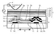
- FIG. 3 ais a cross-sectional view illustrating a fingerprint input device in accordance with a first embodiment of the present invention
- FIG. 3 bis a detailed cross-sectional view illustrating an light sensing unit of FIG. 3 a.
- the slim type fingerprint recognition deviceincludes: a contact type light emitting device 1 having a transparent electrode layer 1 e directly deposited on a transparent substrate 1 f in a thin film type, a light emitting layer 1 d for generating an optical image on the transparent electrode layer 1 e, a light shielding layer 1 c formed on the light emitting layer 1 d, a dielectric layer 1 b formed on the light shielding layer 1 c, and a water repellent layer 1 a formed on the dielectric layer 1 b ; and a TFT fingerprint input device 5 .
- an adhesive layer 5 ais uniformly formed on the TFT fingerprint input device 5 according to epoxy group spraying or screen printing.
- the adhesive layer 5 ais prepared by mixing 55 to 60 wt % of epoxy adhesive (Araldite), 5 to 10 wt % of polyvinyl butyral paste, 1 to 5 wt % of ethylene glycol monoethyl ether acetate, 1 to 5 wt % of n-butyl glycidyl ether, 1 to 5 wt % of defoamer, and 1 to 4 wt % of retardant.
- the adhesive layer 5 amust be transparent and maintain a pore-removed state.
- the contact light emitting device 1 and the TFT fingerprint input device 5are directly adhered to each other by the adhesive layer 5 a . Accordingly, the light emitting image is transmitted directly to an light sensing unit of the TFT fingerprint input device 5 , thereby reducing an interval (W) between the light sensing unit and a switching unit.
- the contact light emitting device 1is used in this embodiment, the back light 7 of FIG. 2 a does not required.
- FIG. 4is a cross-sectional view illustrating a fingerprint input device in accordance with a second embodiment of the present invention.
- the fingerprint input deviceis extremely similar to the fingerprint input device of the first embodiment, but the difference thereof exists in the structure of the contact light emitting device. That is, the contact light emitting device 1 does not have the transparent substrate 1 f.
- the transparent electrode layer 1 eis deposited on the TFT fingerprint input device 5 , and the light emitting layer 1 d, the light shielding layer 1 c , the dielectric layer 1 b and the water repellent layer (abrasion-resistant film) 1 a are sequentially stacked thereon.
- the contact light emitting device 1is formed on the TFT fingerprint input device 5 without using the transparent substrate 1 f, a thickness of the contact light emitting device 1 is decreased.
- FIG. 5is a cross-sectional view illustrating a fingerprint input device in accordance with a third embodiment of the present invention.
- the fingerprint input devicehas a similar structure to the fingerprint input device of the second embodiment, and thus the difference thereof will now be explained.
- a polarizing layer 12is positioned between the contact light emitting device and the top surface of the TFT fingerprint input device. That is, the polarizing layer 12 is deposited on the TFT fingerprint input device, and the transparent electrode layer 1 e, the light emitting layer 1 d, the light shielding layer 1 c , the dielectric layer 1 b and the water repellent layer (abrasion-resistant film) 1 a are sequentially stacked thereon.
- the polarizing layer 12passes vertical incident light and absorbs other elements.
- FIG. 6is a cross-sectional view illustrating a fingerprint input device in accordance with a fourth embodiment of the present invention.
- the fingerprint input deviceis similar to the fingerprint input device of the first embodiment, but the difference thereof exists in a connection structure of the contact light emitting device and the TFT fingerprint input device. That is, the polarizing layer 12 is positioned between the transparent substrate 1 f of the contact light emitting device 1 and the top surface of the TFT fingerprint input device 5 .
- the polarizing layer 12is adhered to the top surface of the TFT fingerprint input device 5 by an adhesive unit such as the adhesive layer of the first embodiment.
- the top surface of the polarizing layer 12is adhered to the bottom surface of the transparent substrate 1 f of the contact light emitting device 1 by the adhesive unit such as the adhesive layer of the first embodiment.
- FIG. 7is a cross-sectional view illustrating a fingerprint input device in accordance with a fifth embodiment of the present invention.
- the fingerprint input deviceis similar to the fingerprint input device of the fourth embodiment, but the difference thereof exists in a connection structure of the contact light emitting device and the TFT fingerprint input device.
- a light shielding pattern film 13is positioned between the transparent substrate 1 f of the contact light emitting device 1 and the top surface of the TFT fingerprint input device 5 , instead of the polarizing layer 12 .
- the light shielding pattern film 13is deposited on the top surface of the TFT fingerprint input device 5 .
- the light shielding pattern film 13is a black film pattern formed in an array shape of the light sensing unit of the TFT fingerprint input device 5 , and includes an opening unit 13 a for only opening a light incidence layer.
- the light shielding pattern film 13is adhered to the contact light emitting device 1 by the adhesive unit such as the adhesive layer of the first embodiment.
- FIG. 8is a cross-sectional view illustrating a fingerprint input device in accordance with a sixth embodiment of the present invention.
- the fingerprint input deviceis similar to the fingerprint input device of the third embodiment of FIG. 5, and thus the difference thereof will now be explained.
- the light shielding pattern film 13is positioned between the contact light emitting device and the top surface of the TFT fingerprint input device.
- the light shielding pattern film 13is deposited on the TFT fingerprint input device 5 .
- the light shielding pattern film 13is a black film pattern formed in an array shape of the light sensing unit of the TFT fingerprint input device 5 , and includes an opening unit 13 a for opening the light incidence layer.
- the transparent electrode layer 1 e, the light emitting layer 1 d, the light shielding layer 1 c, the dielectric layer 1 b and the water repellent layer (abrasion-resistant film) 1 aare sequentially stacked on the light shielding pattern film 13 .
- FIG. 9is a cross-sectional view illustrating a fingerprint input device in accordance with a seventh embodiment of the present invention.
- the fingerprint input devicehas a similar structure to the fingerprint input device of the first embodiment, but the difference thereof exists in a structure of the TFT fingerprint input device.
- a light shielding layer 14covers the whole area except for the opening unit 13 a of the light sensing unit receiving light.
- FIG. 10is a cross-sectional view illustrating a fingerprint input device in accordance with an eighth embodiment of the present invention.
- the fingerprint input deviceis similar to the fingerprint input device of the seventh embodiment, but the difference thereof exists in a structure of the contact light emitting device. That is, the transparent electrode layer 1 e is deposited on the TFT fingerprint input device 5 , and the light emitting layer 1 d, the light shielding layer 1 c, the dielectric layer 1 b and the water repellent layer (abrasion-resistant film) 1 a are sequentially stacked thereon.
- the slim type fingerprint input devicecan be used in various application fields.
- the real incidence areais reduced to be equalized to the effective sensing area, to obtain high quality fingerprint images.
- the interval (W) between the TFT light sensing unit and the switching unitis decreased, thereby obtaining fingerprint images of high resolution.
Landscapes
- Engineering & Computer Science (AREA)
- Physics & Mathematics (AREA)
- General Physics & Mathematics (AREA)
- Human Computer Interaction (AREA)
- Multimedia (AREA)
- Theoretical Computer Science (AREA)
- Image Input (AREA)
- Measurement Of The Respiration, Hearing Ability, Form, And Blood Characteristics Of Living Organisms (AREA)
Abstract
Description
- 1. Field of the Invention[0001]
- The present invention relates to a slim type fingerprint recognition device using a contact light emitting device and a thin film transistor (TFT) fingerprint input device.[0002]
- 2. Description of the Background Art[0003]
- A general fingerprint recognition device is roughly classified into an optical type using a lens or prism and a chip-based sensor using a semiconductor application technology, but the chip-based sensor gets an advantage over the other sensors. In a forthcoming mobile commerce era, an authentication sensor needs to be slim and simple. Accordingly, the present invention suggests a slim type fingerprint recognition device by using a contact light emitting device and an amorphous image sensor.[0004]
- A fingerprint recognition device using a contact light emitting device and a complementary metal-oxide semiconductor (CMOS) and a plane TFT fingerprint recognition device using photosensitivity of amorphous silicon (a-Si:H) are explained as conventional arts of the present invention.[0005]
- Although not illustrated, a method for forming a touch pad by using a TFT fingerprint input device and a touch pad having a fingerprint input function have been applied for registration in order to solve structural problems of a portable computer by integrating a fingerprint input device of FIG. 2[0006]adiscussed later and a conventional touch pad and LCD display window (Korean Patent Unexamined Laid-open Publication No. 2001-0083355, Sep. 1, 2001). However, the aforementioned technology provides a touch pad function to the conventional fingerprint recognition device, but does not mention improvement in fingerprint recognition performance of the fingerprint recognition device.
- On the other hand, FIGS. 1[0007]aand1bare views illustrating the construction of the fingerprint input device using the CMOS and the contact light emitting device, FIG. 2ais a cross-sectional view illustrating a basic TFT fingerprint input device, and FIG. 2bis a cross-sectional view illustrating a light sensing unit of the TFT fingerprint input device.
- The operation of the conventional fingerprint input device will now be explained with reference to the accompanying drawings. As illustrated in FIGS. 1[0008]aand1b, when a user contacts his/her fingerprint to the contact
light emitting device 1, a fingerprint image emits light on a contact surface. The fingerprint image is collected through alens 2 and transmitted to aCMOS image sensor 3 for recognition. - Referring to FIGS. 2[0009]aand2b,in an LCD panel produced by TFT-LCD companies, a TFT-array substrate of a lower plate and a back-light are used except for an upper plate which is a color filter portion. Here, the device senses light reflected by a fingerprint and recognizes an image by using a photo-current, instead of using the optical system of FIG. 1a.
- A[0010]
photoresist layer 9csuch as a-Si:H is formed between adrain electrode 9aand asource electrode 9bof thelight sensing unit 9. When light is incident on thephotoresist layer 9cover a predetermined light amount, thedrain electrode 9aand thesource electrode 9bare electrically connected. Therefore, when the fingerprint touches the TFTfingerprint input device 5, light generated from the back light below atransparent substrate 6 is reflected in fingerprint patterns, and received by thephotoresist layer 9cof thelight sensing unit 9, thereby electrically connecting thelight sensing unit 9.Reference numeral 9ddenotes a gate electrode of thelight sensing unit 9. - On the other hand, a[0011]
switching unit 8 is switched in every frame set up to scan fingerprints according to a gate control signal applied to agate electrode 8d, for forming the fingerprint image inputted to the TFTfingerprint input device 5 as the frame scanned in each alignedlight sensing unit 9. Accordingly, alight shielding layer 8ccovers adrain electrode 8aand asource electrode 8bto protect theswitching unit 8 from external light. - As described above, as shown in FIG. 1[0012]a,when the fingerprint input device is embodied in a bulk type by using the
CMOS image sensor 3, not the TFT, a price and size of the device are increased. - In addition, also referring to FIG. 1[0013]a,light generated by the contact
light emitting device 1 is separated from theCMOS image sensor 3, and thus the optical image of the fingerprint becomes dim in the sensor due to light loss, thus reducing image quality. - In the conventional TFT fingerprint input device, an effective sensing area of the[0014]
photoresist layer 9cof thelight sensing unit 9 is as large as an area of thephotoresist layer 9cexposed between thedrain electrode 9aand thesource electrode 9b.However, a real incidence area of the fingerprint reflection light incident on the light incidence layer is much wider than that. That is, the light reflected by the fingerprint reaches thephotoresist layer 9cafter dispersion, and thus is incident at a wide angle. Especially in a structure where a plurality oflight sensing units 9 are aligned, when the fingerprint is inputted to the real incidence area positioned between the adjacentlight sensing units 9, resolution of the fingerprint pattern is deteriorated. - Differently from the optical type using the[0015]
lens 2 and prism, the non-lens TFT which is the plane fingerprint recognition device cannot easily reduce the real incidence area through thelens 2 or prism. - Accordingly, it is a primary object of the present invention to provide a slim type fingerprint recognition device by using a contact light emitting device and a TFT fingerprint input device.[0016]
- Another object of the present invention is to provide a fingerprint recognition device which can reduce a real incidence area to be equalized to an effective sensing area by using a contact light emitting device of a TFT fingerprint input device and the TFT fingerprint input device.[0017]
- In one aspect of the present invention, to achieve the above-described objects of the invention, there is provided a slim type fingerprint recognition device including: a TFT fingerprint input device having a structure where a plurality of unit cells including an light sensing unit and a switching unit are aligned; and a contact light emitting device being installed on the TFT fingerprint input device, the TFT fingerprint input device and the contact light emitting device being adhered to each other by an adhesive layer, one alternating current terminal being connected to a transparent electrode layer of the contact type light emitting device.[0018]
- In another aspect of the present invention, there is provided a slim type fingerprint recognition device using a contact type light emitting device and a TFT fingerprint input device, including: the TFT fingerprint input device (amorphous image sensor) having a structure where a plurality of unit cells including an light sensing unit and a switching unit are aligned; and the contact light emitting device installed on the TFT fingerprint input device, wherein the contact light emitting device includes: a transparent electrode layer directly deposited on the TFT fingerprint input device in a thin film type, one alternating current terminal being connected to the transparent electrode layer; a light emitting layer formed on the transparent electrode layer; a light shielding layer formed on the light emitting layer; a dielectric layer formed on the light shielding layer; and a water repellent layer (abrasion-resistant film) formed on the dielectric layer.[0019]
- The present invention will become better understood with reference to the accompanying drawings which are given only by way of illustration and thus are not limitative of the present invention, wherein:[0020]
- FIG. 1[0021]ais a view illustrating a construction of a conventional fingerprint input device using a CMOS image sensor;
- FIG. 1[0022]bis a detailed cross-sectional view illustrating a contact light emitting device of FIG. 1a;
- FIG. 2[0023]ais a cross-sectional view illustrating a conventional basic TFT fingerprint input device;
- FIG. 2[0024]bis a detailed cross-sectional view illustrating an light sensing unit of FIG. 2a;
- FIG. 3[0025]ais a cross-sectional view illustrating a fingerprint input device in accordance with a first embodiment of the present invention;
- FIG. 3[0026]bis a detailed cross-sectional view illustrating an light sensing unit of FIG. 3a;
- FIG. 3[0027]cis a cross-sectional view illustrating an adhesive layer formed between a contact light emitting device and a TFT fingerprint input device;
- FIG. 3[0028]dis a view illustrating a percentage of a sample of the adhesive layer of FIG. 3c;
- FIG. 4 is a cross-sectional view illustrating a fingerprint input device in accordance with a second embodiment of the present invention;[0029]
- FIG. 5 is a cross-sectional view illustrating a fingerprint input device in accordance with a third embodiment of the present invention;[0030]
- FIG. 6 is a cross-sectional view illustrating a fingerprint input device in accordance with a fourth embodiment of the present invention;[0031]
- FIG. 7 is a cross-sectional view illustrating a fingerprint input device in accordance with a fifth embodiment of the present invention;[0032]
- FIG. 8 is a cross-sectional view illustrating a fingerprint input device in accordance with a sixth embodiment of the present invention;[0033]
- FIG. 9 is a cross-sectional view illustrating a fingerprint input device in accordance with a seventh embodiment of the present invention; and[0034]
- FIG. 10 is a cross-sectional view illustrating a fingerprint input device in accordance with an eighth embodiment of the present invention.[0035]
- A fingerprint recognition device in accordance with preferred embodiments of the present invention will now be described in detail with reference to the accompanying drawings. In the following description, same drawing reference numerals are used for the same elements even in different drawings.[0036]
- FIG. 3[0037]ais a cross-sectional view illustrating a fingerprint input device in accordance with a first embodiment of the present invention, and FIG. 3bis a detailed cross-sectional view illustrating an light sensing unit of FIG. 3a.Referring to FIG. 3a,the slim type fingerprint recognition device includes: a contact type
light emitting device 1 having atransparent electrode layer 1edirectly deposited on atransparent substrate 1fin a thin film type, alight emitting layer 1dfor generating an optical image on thetransparent electrode layer 1e,alight shielding layer 1cformed on thelight emitting layer 1d,adielectric layer 1bformed on thelight shielding layer 1c,and awater repellent layer 1aformed on thedielectric layer 1b; and a TFTfingerprint input device 5. When alternating current power is applied to thetransparent electrode layer 1eand aground frame 4, and when a fingerprint touches the surface of the contactlight emitting device 1 and theground frame 4 at the same time, an optical image of the fingerprint is generated by the contactlight emitting device 1, and transmitted directly to aphotoresist layer 9cof the TFTfingerprint input device 5 to input the fingerprint. As depicted in FIG. 3c,anadhesive layer 5ais uniformly formed on the TFTfingerprint input device 5 according to epoxy group spraying or screen printing. - As shown in FIG. 3[0038]d,the
adhesive layer 5ais prepared by mixing 55 to 60 wt % of epoxy adhesive (Araldite), 5 to 10 wt % of polyvinyl butyral paste, 1 to 5 wt % of ethylene glycol monoethyl ether acetate, 1 to 5 wt % of n-butyl glycidyl ether, 1 to 5 wt % of defoamer, and 1 to 4 wt % of retardant. In addition, theadhesive layer 5amust be transparent and maintain a pore-removed state. In this embodiment, the contactlight emitting device 1 and the TFTfingerprint input device 5 are directly adhered to each other by theadhesive layer 5a. Accordingly, the light emitting image is transmitted directly to an light sensing unit of the TFTfingerprint input device 5, thereby reducing an interval (W) between the light sensing unit and a switching unit. - Since the contact[0039]
light emitting device 1 is used in this embodiment, theback light 7 of FIG. 2adoes not required. - FIG. 4 is a cross-sectional view illustrating a fingerprint input device in accordance with a second embodiment of the present invention. Referring to FIG. 4, the fingerprint input device is extremely similar to the fingerprint input device of the first embodiment, but the difference thereof exists in the structure of the contact light emitting device. That is, the contact[0040]
light emitting device 1 does not have thetransparent substrate 1f.Thetransparent electrode layer 1eis deposited on the TFTfingerprint input device 5, and thelight emitting layer 1d,thelight shielding layer 1c, thedielectric layer 1band the water repellent layer (abrasion-resistant film)1aare sequentially stacked thereon. - Since the contact[0041]
light emitting device 1 is formed on the TFTfingerprint input device 5 without using thetransparent substrate 1f,a thickness of the contactlight emitting device 1 is decreased. - FIG. 5 is a cross-sectional view illustrating a fingerprint input device in accordance with a third embodiment of the present invention. As shown in FIG. 5, the fingerprint input device has a similar structure to the fingerprint input device of the second embodiment, and thus the difference thereof will now be explained. Here, a[0042]
polarizing layer 12 is positioned between the contact light emitting device and the top surface of the TFT fingerprint input device. That is, thepolarizing layer 12 is deposited on the TFT fingerprint input device, and thetransparent electrode layer 1e,thelight emitting layer 1d,thelight shielding layer 1c, thedielectric layer 1band the water repellent layer (abrasion-resistant film)1aare sequentially stacked thereon. - The[0043]
polarizing layer 12 passes vertical incident light and absorbs other elements. - FIG. 6 is a cross-sectional view illustrating a fingerprint input device in accordance with a fourth embodiment of the present invention. As depicted in FIG. 6, the fingerprint input device is similar to the fingerprint input device of the first embodiment, but the difference thereof exists in a connection structure of the contact light emitting device and the TFT fingerprint input device. That is, the[0044]
polarizing layer 12 is positioned between thetransparent substrate 1fof the contactlight emitting device 1 and the top surface of the TFTfingerprint input device 5. Thepolarizing layer 12 is adhered to the top surface of the TFTfingerprint input device 5 by an adhesive unit such as the adhesive layer of the first embodiment. In addition, the top surface of thepolarizing layer 12 is adhered to the bottom surface of thetransparent substrate 1fof the contactlight emitting device 1 by the adhesive unit such as the adhesive layer of the first embodiment. - FIG. 7 is a cross-sectional view illustrating a fingerprint input device in accordance with a fifth embodiment of the present invention. Referring to FIG. 7, the fingerprint input device is similar to the fingerprint input device of the fourth embodiment, but the difference thereof exists in a connection structure of the contact light emitting device and the TFT fingerprint input device. As compared with the fourth embodiment, a light[0045]
shielding pattern film 13 is positioned between thetransparent substrate 1fof the contactlight emitting device 1 and the top surface of the TFTfingerprint input device 5, instead of thepolarizing layer 12. The lightshielding pattern film 13 is deposited on the top surface of the TFTfingerprint input device 5. Here, the lightshielding pattern film 13 is a black film pattern formed in an array shape of the light sensing unit of the TFTfingerprint input device 5, and includes anopening unit 13afor only opening a light incidence layer. The lightshielding pattern film 13 is adhered to the contactlight emitting device 1 by the adhesive unit such as the adhesive layer of the first embodiment. - FIG. 8 is a cross-sectional view illustrating a fingerprint input device in accordance with a sixth embodiment of the present invention. As shown in FIG. 8, the fingerprint input device is similar to the fingerprint input device of the third embodiment of FIG. 5, and thus the difference thereof will now be explained. The light[0046]
shielding pattern film 13 is positioned between the contact light emitting device and the top surface of the TFT fingerprint input device. The lightshielding pattern film 13 is deposited on the TFTfingerprint input device 5. Here, the lightshielding pattern film 13 is a black film pattern formed in an array shape of the light sensing unit of the TFTfingerprint input device 5, and includes anopening unit 13afor opening the light incidence layer. In addition, thetransparent electrode layer 1e,thelight emitting layer 1d,thelight shielding layer 1c,thedielectric layer 1band the water repellent layer (abrasion-resistant film)1aare sequentially stacked on the lightshielding pattern film 13. - FIG. 9 is a cross-sectional view illustrating a fingerprint input device in accordance with a seventh embodiment of the present invention. As illustrated in FIG. 9, the fingerprint input device has a similar structure to the fingerprint input device of the first embodiment, but the difference thereof exists in a structure of the TFT fingerprint input device. In the TFT fingerprint input device, a[0047]
light shielding layer 14 covers the whole area except for theopening unit 13aof the light sensing unit receiving light. - FIG. 10 is a cross-sectional view illustrating a fingerprint input device in accordance with an eighth embodiment of the present invention. As depicted in FIG. 10, the fingerprint input device is similar to the fingerprint input device of the seventh embodiment, but the difference thereof exists in a structure of the contact light emitting device. That is, the[0048]
transparent electrode layer 1eis deposited on the TFTfingerprint input device 5, and thelight emitting layer 1d,thelight shielding layer 1c,thedielectric layer 1band the water repellent layer (abrasion-resistant film)1aare sequentially stacked thereon. - As discussed earlier, in accordance with the present invention, the slim type fingerprint input device can be used in various application fields. As compared with the general TFT fingerprint input device, the real incidence area is reduced to be equalized to the effective sensing area, to obtain high quality fingerprint images.[0049]
- In addition, since the light emitting image is directly transmitted to the TFT light sensing unit by using the contact light emitting device and the TFT fingerprint input device, the interval (W) between the TFT light sensing unit and the switching unit is decreased, thereby obtaining fingerprint images of high resolution.[0050]
- As the present invention may be embodied in several forms without departing from the spirit or essential characteristics thereof, it should also be understood that the above-described embodiments are not limited by any of the details of the foregoing description, unless otherwise specified, but rather should be construed broadly within its spirit and scope as defined in the appended claims, and therefore all changes and modifications that fall within the metes and bounds of the claims, or equivalences of such metes and bounds are therefore intended to be embraced by the appended claims.[0051]
Claims (11)
Applications Claiming Priority (2)
| Application Number | Priority Date | Filing Date | Title |
|---|---|---|---|
| KR2002-17381 | 2002-03-29 | ||
| KR10-2002-0017381AKR100436376B1 (en) | 2002-03-29 | 2002-03-29 | Slim Type Fingerprint Recognition Device Using Contact Light Emitting Device And TFT Fingerprint Input Device |
Publications (2)
| Publication Number | Publication Date |
|---|---|
| US20030183019A1true US20030183019A1 (en) | 2003-10-02 |
| US6688186B2 US6688186B2 (en) | 2004-02-10 |
Family
ID=28450104
Family Applications (1)
| Application Number | Title | Priority Date | Filing Date |
|---|---|---|---|
| US10/195,443Expired - LifetimeUS6688186B2 (en) | 2002-03-29 | 2002-07-16 | Slim type fingerprint recognition device using contact light emitting device and thin film transistor fingerprint input device |
Country Status (4)
| Country | Link |
|---|---|
| US (1) | US6688186B2 (en) |
| JP (1) | JP2003296714A (en) |
| KR (1) | KR100436376B1 (en) |
| TW (1) | TWI228239B (en) |
Cited By (52)
| Publication number | Priority date | Publication date | Assignee | Title |
|---|---|---|---|---|
| US20030016024A1 (en)* | 2001-07-12 | 2003-01-23 | Sharp Kabushiki Kaisha | Uneven pattern detector and uneven pattern detecting method |
| US20060113894A1 (en)* | 2004-11-26 | 2006-06-01 | Semiconductor Energy Laboratory Co., Ltd. | Semiconductor device, display device and method for manufacturing thereof, and television device |
| US20060139334A1 (en)* | 2003-02-13 | 2006-06-29 | Van Delden Martinus H W | Interactive display system |
| US20080245561A1 (en)* | 2005-12-21 | 2008-10-09 | Rohde & Schwarz Gmbh & Co. Kg | Housing for Shielding from Electromagnetic Interference |
| CN100483724C (en)* | 2006-01-18 | 2009-04-29 | 瀚宇彩晶股份有限公司 | Input type display |
| US7830461B2 (en) | 2002-05-23 | 2010-11-09 | Apple Inc. | Light sensitive display |
| US7872641B2 (en) | 2002-02-20 | 2011-01-18 | Apple Inc. | Light sensitive display |
| US20120014569A1 (en)* | 2010-07-16 | 2012-01-19 | Ib Korea Ltd. | Method and apparatus for slim type fingerprint recognition device |
| US8207946B2 (en) | 2003-02-20 | 2012-06-26 | Apple Inc. | Light sensitive display |
| US8289429B2 (en) | 2004-04-16 | 2012-10-16 | Apple Inc. | Image sensor with photosensitive thin film transistors and dark current compensation |
| US8441422B2 (en) | 2002-02-20 | 2013-05-14 | Apple Inc. | Light sensitive display with object detection calibration |
| US8638320B2 (en) | 2011-06-22 | 2014-01-28 | Apple Inc. | Stylus orientation detection |
| US8928635B2 (en) | 2011-06-22 | 2015-01-06 | Apple Inc. | Active stylus |
| US9176604B2 (en) | 2012-07-27 | 2015-11-03 | Apple Inc. | Stylus device |
| US9228824B2 (en) | 2013-05-10 | 2016-01-05 | Ib Korea Ltd. | Combined sensor arrays for relief print imaging |
| US9262666B2 (en) | 2012-10-04 | 2016-02-16 | Ib Korea Ltd. | Anti-shock relief print scanning |
| US9310923B2 (en) | 2010-12-03 | 2016-04-12 | Apple Inc. | Input device for touch sensitive devices |
| US9329703B2 (en) | 2011-06-22 | 2016-05-03 | Apple Inc. | Intelligent stylus |
| CN106022324A (en)* | 2016-08-04 | 2016-10-12 | 京东方科技集团股份有限公司 | Line recognition and display device |
| US9501631B2 (en) | 2014-04-10 | 2016-11-22 | Ib Korea Ltd. | Biometric sensor for touch-enabled device |
| US9536129B2 (en)* | 2011-05-17 | 2017-01-03 | Cross Match Technologies, Inc. | Fingerprint sensors |
| US9557845B2 (en) | 2012-07-27 | 2017-01-31 | Apple Inc. | Input device for and method of communication with capacitive devices through frequency variation |
| US9652090B2 (en) | 2012-07-27 | 2017-05-16 | Apple Inc. | Device for digital communication through capacitive coupling |
| CN106773229A (en)* | 2017-03-10 | 2017-05-31 | 京东方科技集团股份有限公司 | A kind of fingerprint recognition display device and its driving method |
| US20170161541A1 (en)* | 2015-07-29 | 2017-06-08 | Boe Technology Group Co., Ltd | Touch sensing pattern recognition array substrate, sensing unit, sensor, apparatus, and fabricating method thereof |
| US20170228580A1 (en)* | 2015-08-28 | 2017-08-10 | Boe Technology Group Co., Ltd. | Display panel, electronic apparatus having the same, and driving method thereof |
| CN107275376A (en)* | 2017-06-27 | 2017-10-20 | 上海天马微电子有限公司 | Display panel and display device |
| CN107481374A (en)* | 2017-08-18 | 2017-12-15 | 深圳市益鑫智能科技有限公司 | A kind of intelligent terminal unlocked by fingerprint door opener |
| WO2018006478A1 (en)* | 2016-07-08 | 2018-01-11 | 上海箩箕技术有限公司 | Optical fingerprint sensor module |
| WO2018018996A1 (en)* | 2016-07-26 | 2018-02-01 | 京东方科技集团股份有限公司 | Fingerprint recognizer, manufacturing method therefor, and display device |
| US9893102B2 (en) | 2011-11-12 | 2018-02-13 | Cross Match Technologies, Inc. | Ambient light illumination for non-imaging contact sensors |
| US9939935B2 (en) | 2013-07-31 | 2018-04-10 | Apple Inc. | Scan engine for touch controller architecture |
| CN108090480A (en)* | 2018-02-01 | 2018-05-29 | 上海天马有机发光显示技术有限公司 | The production method of display panel, display device and display panel |
| US10024655B2 (en) | 2011-11-11 | 2018-07-17 | Cross Match Technologies, Inc. | Ambient light rejection for non-imaging contact sensors |
| CN108334841A (en)* | 2018-02-01 | 2018-07-27 | 上海天马有机发光显示技术有限公司 | The production method of display panel, display device and display panel |
| US10048775B2 (en) | 2013-03-14 | 2018-08-14 | Apple Inc. | Stylus detection and demodulation |
| CN108416248A (en)* | 2017-02-09 | 2018-08-17 | 上海箩箕技术有限公司 | Display module |
| US10061449B2 (en) | 2014-12-04 | 2018-08-28 | Apple Inc. | Coarse scan and targeted active mode scan for touch and stylus |
| US20180299725A1 (en)* | 2017-01-06 | 2018-10-18 | Wuhan China Star Optoelectronics Technology Co., Ltd. | Display screen and electronic device |
| CN109031825A (en)* | 2018-07-31 | 2018-12-18 | Oppo广东移动通信有限公司 | Array substrate, display screen and electronic equipment |
| CN110210364A (en)* | 2019-05-27 | 2019-09-06 | Oppo广东移动通信有限公司 | Control method, terminal and computer storage medium |
| US10431701B2 (en)* | 2017-03-13 | 2019-10-01 | Boe Technology Group Co., Ltd. | Semiconductor device, array substrate and method for fabricating semiconductor device |
| US10474277B2 (en) | 2016-05-31 | 2019-11-12 | Apple Inc. | Position-based stylus communication |
| US10504922B2 (en)* | 2016-05-24 | 2019-12-10 | Boe Technology Group Co., Ltd. | Array substrate, display panel and display device capable of synchronizing image display and fingerprint identification |
| CN110751128A (en)* | 2019-10-30 | 2020-02-04 | 厦门天马微电子有限公司 | Display module and display device |
| US10572711B2 (en)* | 2016-08-08 | 2020-02-25 | Boe Technology Group Co., Ltd. | Fingerprint identification module and manufacturing method thereof, display device |
| CN111095281A (en)* | 2019-08-06 | 2020-05-01 | 深圳市汇顶科技股份有限公司 | Fingerprint detection device and electronic equipment |
| CN111781760A (en)* | 2015-10-09 | 2020-10-16 | 株式会社日本显示器 | Sensor and display device with sensor |
| US11176348B2 (en) | 2019-08-06 | 2021-11-16 | Shenzhen GOODIX Technology Co., Ltd. | Optical fingerprint apparatus and electronic device |
| US20230034080A1 (en)* | 2021-07-27 | 2023-02-02 | Hannstouch Solution Incorporated | Light sensing unit of light sensing device |
| US12153764B1 (en) | 2020-09-25 | 2024-11-26 | Apple Inc. | Stylus with receive architecture for position determination |
| US12266210B2 (en)* | 2009-10-26 | 2025-04-01 | Nec Corporation | Fake finger determination apparatus and fake finger determination method |
Families Citing this family (32)
| Publication number | Priority date | Publication date | Assignee | Title |
|---|---|---|---|---|
| KR100378994B1 (en)* | 2000-11-07 | 2003-04-07 | 테스텍 주식회사 | Fingerprint Recognizing Device Having Patterned Floating Electrodes and Fabricating Method therefore |
| US7151532B2 (en)* | 2002-08-09 | 2006-12-19 | 3M Innovative Properties Company | Multifunctional multilayer optical film |
| JP2004109066A (en)* | 2002-09-20 | 2004-04-08 | Sanyo Electric Co Ltd | Pressure pattern sensor and its operation control method |
| US20050219200A1 (en)* | 2004-03-31 | 2005-10-06 | Weng Chien-Sen | Fingerprint sensing pixel with a larger aperture |
| KR100683398B1 (en)* | 2005-03-25 | 2007-02-15 | 매그나칩 반도체 유한회사 | Fingerprint sensor with direct contact between the pixel array of the image sensor and the contact light emitting sensor |
| US8264466B2 (en)* | 2006-03-31 | 2012-09-11 | 3M Innovative Properties Company | Touch screen having reduced visibility transparent conductor pattern |
| JP4258532B2 (en)* | 2006-06-30 | 2009-04-30 | カシオ計算機株式会社 | Thin film device substrate and manufacturing method thereof |
| JP5029048B2 (en)* | 2007-02-08 | 2012-09-19 | カシオ計算機株式会社 | Photoelectric conversion device and display panel having the same |
| TWI372277B (en)* | 2008-09-04 | 2012-09-11 | Au Optronics Corp | Display module |
| US20130287272A1 (en)* | 2012-04-29 | 2013-10-31 | Yang Lu | Methods and Apparatus of Integrating Fingerprint Imagers with Touch Panels and Displays |
| US8824792B2 (en) | 2012-07-25 | 2014-09-02 | Ib Korea Ltd. | Image element brightness adjustment |
| TWI530883B (en)* | 2012-12-19 | 2016-04-21 | 茂丞科技股份有限公司 | Stray-light-coupled biometrics sensing module and electronic apparatus using the same |
| JP6424456B2 (en) | 2013-07-17 | 2018-11-21 | セイコーエプソン株式会社 | Light emitting device, method of manufacturing light emitting device, light emitting and receiving device, electronic device |
| CN105336752B (en)* | 2014-06-23 | 2018-08-21 | 上海箩箕技术有限公司 | Area array sensor device and forming method thereof |
| WO2016064222A1 (en)* | 2014-10-24 | 2016-04-28 | 주식회사 비욘드아이즈 | Unit pixel and el fingerprint recognition sensor |
| KR101967403B1 (en)* | 2014-10-24 | 2019-04-10 | 주식회사 비욘드아이즈 | Electro-luminescence Image Sensor for finger-print |
| KR101967400B1 (en)* | 2015-07-01 | 2019-04-10 | 주식회사 비욘드아이즈 | Electro-luminescence Image Sensor for finger-print |
| KR101687490B1 (en) | 2015-06-29 | 2016-12-16 | 경희대학교 산학협력단 | System and method for controlling vehicle |
| WO2016171369A1 (en)* | 2015-04-24 | 2016-10-27 | 경희대학교산학협력단 | Photoreactive sensor including optical amplifying phototransistor, display panel including photoreactive sensor, and vehicle control system |
| KR101728943B1 (en) | 2015-04-24 | 2017-04-20 | 경희대학교 산학협력단 | Sensor for recognizing touch |
| TW201640418A (en)* | 2015-05-04 | 2016-11-16 | 曦威科技股份有限公司 | Fingerprint detecting device, mobile device using the same, and manufacturing method thereof |
| CN106326814A (en)* | 2015-07-01 | 2017-01-11 | 宇龙计算机通信科技(深圳)有限公司 | Fingerprint acquisition and identification method and device, and terminal |
| TWI601301B (en)* | 2015-07-31 | 2017-10-01 | 友達光電股份有限公司 | Optical detecting device and manufacturing method thereof |
| DE102016209414A1 (en) | 2016-05-31 | 2017-11-30 | Hyundai Motor Company | Composite sheet metal component and body panel |
| TWI584201B (en)* | 2016-07-17 | 2017-05-21 | 金佶科技股份有限公司 | Identification apparatus and identification method |
| KR102675011B1 (en) | 2016-11-28 | 2024-06-17 | 삼성디스플레이 주식회사 | Display device |
| KR102599536B1 (en)* | 2017-01-26 | 2023-11-08 | 삼성전자 주식회사 | Electronic device having a biometric sensor |
| US10656764B2 (en)* | 2017-02-23 | 2020-05-19 | Boe Technology Group Co., Ltd. | Touch device and display device |
| KR102509439B1 (en)* | 2018-03-06 | 2023-03-13 | 삼성디스플레이 주식회사 | Fingerprint sensor package and display device including the same |
| CN108878467A (en)* | 2018-06-27 | 2018-11-23 | 马远博 | A kind of Autoluminescence living things feature recognition imaging sensor and preparation method thereof |
| CN111611916B (en)* | 2020-05-20 | 2023-09-22 | 上海思立微电子科技有限公司 | Thin optical fingerprint chip module, manufacturing method thereof and electronic equipment |
| CN117083717A (en) | 2022-03-16 | 2023-11-17 | 京东方科技集团股份有限公司 | Fingerprint sensor and electronic device |
Citations (3)
| Publication number | Priority date | Publication date | Assignee | Title |
|---|---|---|---|---|
| US5325442A (en)* | 1990-05-18 | 1994-06-28 | U.S. Philips Corporation | Fingerprint sensing device and recognition system having predetermined electrode activation |
| US5974162A (en)* | 1994-02-18 | 1999-10-26 | Imedge Technology, Inc. | Device for forming and detecting fingerprint images with valley and ridge structure |
| US6401551B1 (en)* | 1999-08-09 | 2002-06-11 | Seiko Instruments Inc. | Fingerprint reading device |
Family Cites Families (6)
| Publication number | Priority date | Publication date | Assignee | Title |
|---|---|---|---|---|
| US4740781A (en) | 1985-02-08 | 1988-04-26 | Itt Gilfillan | Touch panel data entry device for thin film electroluminescent panels |
| JPH05243547A (en)* | 1992-03-02 | 1993-09-21 | Hitachi Ltd | Thin film optical sensor |
| JP4479024B2 (en)* | 1999-10-19 | 2010-06-09 | カシオ計算機株式会社 | Imaging device |
| KR100381048B1 (en)* | 2000-06-23 | 2003-04-18 | 엘지.필립스 엘시디 주식회사 | Thin Film Transistor Type Finger Print Sensor |
| JP4154874B2 (en)* | 2001-07-30 | 2008-09-24 | カシオ計算機株式会社 | Fingerprint reader and fingerprint reading method |
| KR100464175B1 (en)* | 2002-03-18 | 2005-01-03 | (주) 제이.에스.씨.앤.아이 | Finger print recognition sensor and method for manufacturing the same |
- 2002
- 2002-03-29KRKR10-2002-0017381Apatent/KR100436376B1/ennot_activeExpired - Lifetime
- 2002-07-16USUS10/195,443patent/US6688186B2/ennot_activeExpired - Lifetime
- 2002-07-17TWTW091115941Apatent/TWI228239B/ennot_activeIP Right Cessation
- 2002-07-22JPJP2002212747Apatent/JP2003296714A/ennot_activeWithdrawn
Patent Citations (3)
| Publication number | Priority date | Publication date | Assignee | Title |
|---|---|---|---|---|
| US5325442A (en)* | 1990-05-18 | 1994-06-28 | U.S. Philips Corporation | Fingerprint sensing device and recognition system having predetermined electrode activation |
| US5974162A (en)* | 1994-02-18 | 1999-10-26 | Imedge Technology, Inc. | Device for forming and detecting fingerprint images with valley and ridge structure |
| US6401551B1 (en)* | 1999-08-09 | 2002-06-11 | Seiko Instruments Inc. | Fingerprint reading device |
Cited By (85)
| Publication number | Priority date | Publication date | Assignee | Title |
|---|---|---|---|---|
| US20030016024A1 (en)* | 2001-07-12 | 2003-01-23 | Sharp Kabushiki Kaisha | Uneven pattern detector and uneven pattern detecting method |
| US6980008B2 (en)* | 2001-07-12 | 2005-12-27 | Sharp Kabushiki Kaisha | Uneven pattern detector and uneven pattern detecting method |
| US7872641B2 (en) | 2002-02-20 | 2011-01-18 | Apple Inc. | Light sensitive display |
| US9971456B2 (en) | 2002-02-20 | 2018-05-15 | Apple Inc. | Light sensitive display with switchable detection modes for detecting a fingerprint |
| US9411470B2 (en) | 2002-02-20 | 2016-08-09 | Apple Inc. | Light sensitive display with multiple data set object detection |
| US9134851B2 (en)* | 2002-02-20 | 2015-09-15 | Apple Inc. | Light sensitive display |
| US8570449B2 (en) | 2002-02-20 | 2013-10-29 | Apple Inc. | Light sensitive display with pressure sensor |
| US8441422B2 (en) | 2002-02-20 | 2013-05-14 | Apple Inc. | Light sensitive display with object detection calibration |
| US11073926B2 (en) | 2002-02-20 | 2021-07-27 | Apple Inc. | Light sensitive display |
| US9354735B2 (en) | 2002-05-23 | 2016-05-31 | Apple Inc. | Light sensitive display |
| US7880819B2 (en) | 2002-05-23 | 2011-02-01 | Apple Inc. | Light sensitive display |
| US8044930B2 (en) | 2002-05-23 | 2011-10-25 | Apple Inc. | Light sensitive display |
| US7880733B2 (en) | 2002-05-23 | 2011-02-01 | Apple Inc. | Light sensitive display |
| US7830461B2 (en) | 2002-05-23 | 2010-11-09 | Apple Inc. | Light sensitive display |
| US20060139334A1 (en)* | 2003-02-13 | 2006-06-29 | Van Delden Martinus H W | Interactive display system |
| US8207946B2 (en) | 2003-02-20 | 2012-06-26 | Apple Inc. | Light sensitive display |
| US8289429B2 (en) | 2004-04-16 | 2012-10-16 | Apple Inc. | Image sensor with photosensitive thin film transistors and dark current compensation |
| US7582904B2 (en)* | 2004-11-26 | 2009-09-01 | Semiconductor Energy Laboratory Co., Ltd. | Semiconductor device, display device and method for manufacturing thereof, and television device |
| US20060113894A1 (en)* | 2004-11-26 | 2006-06-01 | Semiconductor Energy Laboratory Co., Ltd. | Semiconductor device, display device and method for manufacturing thereof, and television device |
| US20080245561A1 (en)* | 2005-12-21 | 2008-10-09 | Rohde & Schwarz Gmbh & Co. Kg | Housing for Shielding from Electromagnetic Interference |
| CN100483724C (en)* | 2006-01-18 | 2009-04-29 | 瀚宇彩晶股份有限公司 | Input type display |
| US12266210B2 (en)* | 2009-10-26 | 2025-04-01 | Nec Corporation | Fake finger determination apparatus and fake finger determination method |
| US20120014569A1 (en)* | 2010-07-16 | 2012-01-19 | Ib Korea Ltd. | Method and apparatus for slim type fingerprint recognition device |
| US9310923B2 (en) | 2010-12-03 | 2016-04-12 | Apple Inc. | Input device for touch sensitive devices |
| US9536129B2 (en)* | 2011-05-17 | 2017-01-03 | Cross Match Technologies, Inc. | Fingerprint sensors |
| US9519361B2 (en) | 2011-06-22 | 2016-12-13 | Apple Inc. | Active stylus |
| US9329703B2 (en) | 2011-06-22 | 2016-05-03 | Apple Inc. | Intelligent stylus |
| US8638320B2 (en) | 2011-06-22 | 2014-01-28 | Apple Inc. | Stylus orientation detection |
| US9921684B2 (en) | 2011-06-22 | 2018-03-20 | Apple Inc. | Intelligent stylus |
| US8928635B2 (en) | 2011-06-22 | 2015-01-06 | Apple Inc. | Active stylus |
| US10024655B2 (en) | 2011-11-11 | 2018-07-17 | Cross Match Technologies, Inc. | Ambient light rejection for non-imaging contact sensors |
| US9893102B2 (en) | 2011-11-12 | 2018-02-13 | Cross Match Technologies, Inc. | Ambient light illumination for non-imaging contact sensors |
| US9557845B2 (en) | 2012-07-27 | 2017-01-31 | Apple Inc. | Input device for and method of communication with capacitive devices through frequency variation |
| US9582105B2 (en) | 2012-07-27 | 2017-02-28 | Apple Inc. | Input device for touch sensitive devices |
| US9652090B2 (en) | 2012-07-27 | 2017-05-16 | Apple Inc. | Device for digital communication through capacitive coupling |
| US9176604B2 (en) | 2012-07-27 | 2015-11-03 | Apple Inc. | Stylus device |
| US9262666B2 (en) | 2012-10-04 | 2016-02-16 | Ib Korea Ltd. | Anti-shock relief print scanning |
| US9449213B2 (en) | 2012-10-04 | 2016-09-20 | Ib Korea Ltd. | Anti-shock relief print scanning |
| US10048775B2 (en) | 2013-03-14 | 2018-08-14 | Apple Inc. | Stylus detection and demodulation |
| US9563801B2 (en) | 2013-05-10 | 2017-02-07 | Ib Korea Ltd. | Combined sensor arrays for relief print imaging |
| US9228824B2 (en) | 2013-05-10 | 2016-01-05 | Ib Korea Ltd. | Combined sensor arrays for relief print imaging |
| US12340048B2 (en) | 2013-07-31 | 2025-06-24 | Apple Inc. | Touch controller architecture |
| US9939935B2 (en) | 2013-07-31 | 2018-04-10 | Apple Inc. | Scan engine for touch controller architecture |
| US10845901B2 (en) | 2013-07-31 | 2020-11-24 | Apple Inc. | Touch controller architecture |
| US11687192B2 (en) | 2013-07-31 | 2023-06-27 | Apple Inc. | Touch controller architecture |
| US10067580B2 (en) | 2013-07-31 | 2018-09-04 | Apple Inc. | Active stylus for use with touch controller architecture |
| US9501631B2 (en) | 2014-04-10 | 2016-11-22 | Ib Korea Ltd. | Biometric sensor for touch-enabled device |
| US10061449B2 (en) | 2014-12-04 | 2018-08-28 | Apple Inc. | Coarse scan and targeted active mode scan for touch and stylus |
| US10664113B2 (en) | 2014-12-04 | 2020-05-26 | Apple Inc. | Coarse scan and targeted active mode scan for touch and stylus |
| US10061450B2 (en) | 2014-12-04 | 2018-08-28 | Apple Inc. | Coarse scan and targeted active mode scan for touch |
| US10067618B2 (en) | 2014-12-04 | 2018-09-04 | Apple Inc. | Coarse scan and targeted active mode scan for touch |
| US20170161541A1 (en)* | 2015-07-29 | 2017-06-08 | Boe Technology Group Co., Ltd | Touch sensing pattern recognition array substrate, sensing unit, sensor, apparatus, and fabricating method thereof |
| US10558839B2 (en)* | 2015-07-29 | 2020-02-11 | Boe Technology Group Co., Ltd. | Reduced thickness touch sensing pattern recognition array substrate, sensing unit, sensor, apparatus, and fabricating method thereof |
| US20170228580A1 (en)* | 2015-08-28 | 2017-08-10 | Boe Technology Group Co., Ltd. | Display panel, electronic apparatus having the same, and driving method thereof |
| US9892303B2 (en)* | 2015-08-28 | 2018-02-13 | Boe Technology Group Co., Ltd. | Display panel, electronic apparatus having the same, and driving method thereof |
| CN111781760A (en)* | 2015-10-09 | 2020-10-16 | 株式会社日本显示器 | Sensor and display device with sensor |
| US10504922B2 (en)* | 2016-05-24 | 2019-12-10 | Boe Technology Group Co., Ltd. | Array substrate, display panel and display device capable of synchronizing image display and fingerprint identification |
| US10474277B2 (en) | 2016-05-31 | 2019-11-12 | Apple Inc. | Position-based stylus communication |
| WO2018006478A1 (en)* | 2016-07-08 | 2018-01-11 | 上海箩箕技术有限公司 | Optical fingerprint sensor module |
| WO2018018996A1 (en)* | 2016-07-26 | 2018-02-01 | 京东方科技集团股份有限公司 | Fingerprint recognizer, manufacturing method therefor, and display device |
| US10489628B2 (en) | 2016-07-26 | 2019-11-26 | Boe Technology Group Co., Ltd. | Fingerprint recognition device, method for fabricating the same and display device |
| WO2018024117A1 (en)* | 2016-08-04 | 2018-02-08 | 京东方科技集团股份有限公司 | Display device for surface texture recognition |
| CN106022324A (en)* | 2016-08-04 | 2016-10-12 | 京东方科技集团股份有限公司 | Line recognition and display device |
| US10438044B2 (en) | 2016-08-04 | 2019-10-08 | Boe Technology Group Co., Ltd. | Surface texture identification display device |
| US10572711B2 (en)* | 2016-08-08 | 2020-02-25 | Boe Technology Group Co., Ltd. | Fingerprint identification module and manufacturing method thereof, display device |
| US10353235B2 (en)* | 2017-01-06 | 2019-07-16 | Wuhan China Star Optoelectronics Co., Ltd. | Display screen and electronic device |
| US20180299725A1 (en)* | 2017-01-06 | 2018-10-18 | Wuhan China Star Optoelectronics Technology Co., Ltd. | Display screen and electronic device |
| CN108416248A (en)* | 2017-02-09 | 2018-08-17 | 上海箩箕技术有限公司 | Display module |
| CN106773229A (en)* | 2017-03-10 | 2017-05-31 | 京东方科技集团股份有限公司 | A kind of fingerprint recognition display device and its driving method |
| WO2018161541A1 (en)* | 2017-03-10 | 2018-09-13 | 京东方科技集团股份有限公司 | Fingerprint recognition display device and drive method thereof |
| US10969613B1 (en) | 2017-03-10 | 2021-04-06 | Boe Technology Group Co., Ltd. | Fingerprint identification display device and driving method thereof |
| US10431701B2 (en)* | 2017-03-13 | 2019-10-01 | Boe Technology Group Co., Ltd. | Semiconductor device, array substrate and method for fabricating semiconductor device |
| CN107275376A (en)* | 2017-06-27 | 2017-10-20 | 上海天马微电子有限公司 | Display panel and display device |
| US10691913B2 (en) | 2017-06-27 | 2020-06-23 | Shanghai Tianma Micro-electronics Co., Ltd. | Display panel and display apparatus |
| CN107481374A (en)* | 2017-08-18 | 2017-12-15 | 深圳市益鑫智能科技有限公司 | A kind of intelligent terminal unlocked by fingerprint door opener |
| CN108334841A (en)* | 2018-02-01 | 2018-07-27 | 上海天马有机发光显示技术有限公司 | The production method of display panel, display device and display panel |
| CN108090480A (en)* | 2018-02-01 | 2018-05-29 | 上海天马有机发光显示技术有限公司 | The production method of display panel, display device and display panel |
| CN109031825A (en)* | 2018-07-31 | 2018-12-18 | Oppo广东移动通信有限公司 | Array substrate, display screen and electronic equipment |
| CN110210364A (en)* | 2019-05-27 | 2019-09-06 | Oppo广东移动通信有限公司 | Control method, terminal and computer storage medium |
| US11176348B2 (en) | 2019-08-06 | 2021-11-16 | Shenzhen GOODIX Technology Co., Ltd. | Optical fingerprint apparatus and electronic device |
| CN111095281A (en)* | 2019-08-06 | 2020-05-01 | 深圳市汇顶科技股份有限公司 | Fingerprint detection device and electronic equipment |
| CN110751128A (en)* | 2019-10-30 | 2020-02-04 | 厦门天马微电子有限公司 | Display module and display device |
| US12153764B1 (en) | 2020-09-25 | 2024-11-26 | Apple Inc. | Stylus with receive architecture for position determination |
| US20230034080A1 (en)* | 2021-07-27 | 2023-02-02 | Hannstouch Solution Incorporated | Light sensing unit of light sensing device |
| US12046688B2 (en)* | 2021-07-27 | 2024-07-23 | HannsTouch Holdings Company | Light sensing unit of light sensing device |
Also Published As
| Publication number | Publication date |
|---|---|
| KR20030078371A (en) | 2003-10-08 |
| KR100436376B1 (en) | 2004-06-19 |
| US6688186B2 (en) | 2004-02-10 |
| TWI228239B (en) | 2005-02-21 |
| JP2003296714A (en) | 2003-10-17 |
Similar Documents
| Publication | Publication Date | Title |
|---|---|---|
| US6688186B2 (en) | Slim type fingerprint recognition device using contact light emitting device and thin film transistor fingerprint input device | |
| KR100873497B1 (en) | Integrated LCD with Fingerprint Recognition Device and Manufacturing Method Thereof | |
| CN105336751B (en) | photoelectric sensor and its manufacturing method | |
| US20020030768A1 (en) | Integrated high resolution image sensor and display on an active matrix array with micro-lens | |
| JP4044187B2 (en) | Active matrix display device and manufacturing method thereof | |
| US7235814B2 (en) | Active matrix display device and method of manufacturing the same | |
| US20070229479A1 (en) | Panel assembly | |
| JP4523327B2 (en) | Image recognition device and liquid crystal display device having the same | |
| US20020163601A1 (en) | Liquid crystal display and fingerprint capture panel | |
| JPH11326954A (en) | Semiconductor device | |
| US7999259B2 (en) | Display device having a photodiode whose p region has an edge width different than that of the n region | |
| CN112596294B (en) | Display device, display panel and manufacturing method thereof | |
| US7369690B2 (en) | Apparatus for recognizing an image | |
| CN102023440A (en) | Structure of touch screen and manufacturing method thereof | |
| CN109804307A (en) | Liquid crystal display device and projection display device | |
| WO2020103090A1 (en) | Optical fingerprint identification device, array substrate and display device | |
| KR20030058719A (en) | Apparatus for thin film transistor liquid crystal display equipped with light sensor | |
| US20220140006A1 (en) | Image-sensor matrix-array device comprising thin-film transistors and organic photodiodes | |
| KR100560347B1 (en) | Method for manufacturing TFT fingerprint input device of fingerprint recognition device | |
| US20240210243A1 (en) | Electronic device | |
| KR100911460B1 (en) | Fingerprint recognition device and manufacturing method thereof | |
| TWI409533B (en) | Touch display panel | |
| JPH05121715A (en) | Close contact type two-dimensional photosensor and manufacture thereof | |
| US11067865B1 (en) | Display apparatus | |
| CN112666734B (en) | Liquid crystal display panel and display device |
Legal Events
| Date | Code | Title | Description |
|---|---|---|---|
| AS | Assignment | Owner name:TESTECH INC., KOREA, REPUBLIC OF Free format text:ASSIGNMENT OF ASSIGNORS INTEREST;ASSIGNOR:CHAE, SANG HOON;REEL/FRAME:013112/0186 Effective date:20020704 | |
| STCF | Information on status: patent grant | Free format text:PATENTED CASE | |
| FEPP | Fee payment procedure | Free format text:PAT HOLDER CLAIMS SMALL ENTITY STATUS, ENTITY STATUS SET TO SMALL (ORIGINAL EVENT CODE: LTOS); ENTITY STATUS OF PATENT OWNER: LARGE ENTITY | |
| FPAY | Fee payment | Year of fee payment:4 | |
| AS | Assignment | Owner name:IB KOREA LTD., KOREA, REPUBLIC OF Free format text:ASSIGNMENT OF ASSIGNORS INTEREST;ASSIGNOR:TESTECH INC.;REEL/FRAME:022320/0984 Effective date:20090223 | |
| FPAY | Fee payment | Year of fee payment:8 | |
| AS | Assignment | Owner name:IB KOREA LTD., KOREA, REPUBLIC OF Free format text:CHANGE OF ADDRESS FOR ASSIGNEE;ASSIGNOR:IB KOREA LTD.;REEL/FRAME:031815/0047 Effective date:20131113 | |
| FEPP | Fee payment procedure | Free format text:PAT HOLDER NO LONGER CLAIMS SMALL ENTITY STATUS, ENTITY STATUS SET TO UNDISCOUNTED (ORIGINAL EVENT CODE: STOL); ENTITY STATUS OF PATENT OWNER: LARGE ENTITY | |
| FPAY | Fee payment | Year of fee payment:12 | |
| AS | Assignment | Owner name:PARTNERS FOR GROWTH V, L.P., CALIFORNIA Free format text:SECURITY INTEREST;ASSIGNOR:IB KOREA, LIMITED;REEL/FRAME:050453/0224 Effective date:20190905 | |
| AS | Assignment | Owner name:IB KOREA, LIMITED, KOREA, REPUBLIC OF Free format text:RELEASE BY SECURED PARTY;ASSIGNOR:PARTNERS FOR GROWTH V, L.P.;REEL/FRAME:071764/0322 Effective date:20250715 |