US20030182517A1 - Method and system for buffering multiple requests from multiple devices to a memory - Google Patents
Method and system for buffering multiple requests from multiple devices to a memoryDownload PDFInfo
- Publication number
- US20030182517A1 US20030182517A1US10/102,990US10299002AUS2003182517A1US 20030182517 A1US20030182517 A1US 20030182517A1US 10299002 AUS10299002 AUS 10299002AUS 2003182517 A1US2003182517 A1US 2003182517A1
- Authority
- US
- United States
- Prior art keywords
- memory
- request
- write
- requests
- coupled
- Prior art date
- Legal status (The legal status is an assumption and is not a legal conclusion. Google has not performed a legal analysis and makes no representation as to the accuracy of the status listed.)
- Granted
Links
Images


Classifications
- G—PHYSICS
- G06—COMPUTING OR CALCULATING; COUNTING
- G06F—ELECTRIC DIGITAL DATA PROCESSING
- G06F13/00—Interconnection of, or transfer of information or other signals between, memories, input/output devices or central processing units
- G06F13/14—Handling requests for interconnection or transfer
- G06F13/16—Handling requests for interconnection or transfer for access to memory bus
- G06F13/1668—Details of memory controller
- G06F13/1673—Details of memory controller using buffers
Definitions
- the present inventionpertains to the field of digital systems. More particularly, the present invention relates to the optimization of access to a shared computational resource by multiple devices operating in parallel with each other.
- Digital electronic devicesoften rely on shared access to a single computational resource, for example a mathematical calculation unit (e.g. to calculate trigonometric functions, perform fast multiplication, etc.), a search algorithm (e.g. a special purpose hash function, a binary tree search, etc.), and the like.
- a mathematical calculation unite.g. to calculate trigonometric functions, perform fast multiplication, etc.
- a search algorithme.g. a special purpose hash function, a binary tree search, etc.
- coherency issuesespecially if multiple devices attempt to update a resource at the same time (e.g. deadlock issues, stale data, etc.).
- Some digital electronic devicesinclude multiple digital components which require fast efficient access to a shared resource.
- the standard prior art bus protocol schemesare often inadequate. Such schemes typically prioritize requests and make one or more devices wait until a first access is completed by a first device.
- One prior art solution to the problemis to implement a buffer, for example a FIFO, on the input to the shared resource such that requests are temporarily held until they can be processed.
- a bufferfor example a FIFO
- the systemis still forced to use an arbitration process and an acknowledgement protocol from the resource to each requester, which may again result in the stalling of requesters until the request can be stored in the buffer.
- This solutionalso adds additional complexity to each requester.
- a method and system for buffering multiple requests from multiple devices to a memory in a single clock cycleincludes a memory having a first write port and a second write port.
- a first request inputis coupled to the first write port.
- a second request inputis coupled to the second write port.
- a controlleris coupled to the memory. The controller is configured to control the memory to store a first request into the memory via the first write port and a second request into the memory via the second write port.
- the first and second requestsare received via the first and second request inputs.
- the first and second requestsare stored into the memory in one clock cycle.
- FIG. 1shows a multiple request buffering system in accordance with one embodiment of the present invention.
- FIG. 2shows one implementation of the multiple request buffering logic and buffer memory shown in FIG. 1.
- FIG. 3shows a generalized pseudo-code representation of a multiple request buffering process as implemented by the control logic shown in FIG. 2.
- FIG. 4shows a flow chart of the steps of a multiple request buffering process in accordance with one embodiment of the present invention.
- FIG. 5shows a second implementation of the multiple request buffering logic and buffer memory shown in FIG. 1.
- FIG. 6shows the components of a FIFO element in accordance with one embodiment of the present invention.
- FIG. 7shows a pseudo-code representation of the multiple request buffering process as implemented by the control logic of the system of FIG. 5.
- a method and system for buffering multiple requests from multiple devices to a shared buffer memorye.g. a multi-write port RAM or FIFO
- the present inventionis implemented as a system including a multi-port memory having at least two write ports (e.g., a first write port and a second write port).
- a first request inputis coupled to the first write port.
- a second request inputis coupled to the second write port.
- a controlleris coupled to the buffer memory and is configured to store a first request into the buffer memory via the first write port and a second request into the buffer memory via the second write port, such that the first and second requests are stored in one clock cycle.
- the systemcan buffer multiple requests from multiple devices to the buffer memory in a single clock cycle, thereby providing access to a shared resource without constraints such as arbitration or bus limitations. Additionally, the system can implement multiple requests in parallel, as in a case where parallel execution units require access to a shared resource. Also embodiments of the present invention are flexible in that they permit many different combinations of multiple requests and/or multiple devices (e.g., device 1 may be capable of generating only a single request, device 2 may be capable of generating 2 simultaneous requests, etc.).
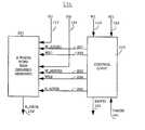
- FIG. 1shows a system 100 in accordance with one embodiment of the present invention.
- system 100includes a first device 110 and a second device 120 , both requiring access to a shared resource 140 .
- the request buffering logic and buffer memory 130acts as an interface between the multiple devices 110 and 120 and the shared computational resource 140 .
- Each devicehas a data bus and write signal (e.g. D 1 111 and W 1 112 for device 110 , and D 2 121 and W 2 122 for device 120 ) to transfer the data for a request.
- the EMPTY signal 131indicates that no requests are currently queued. If a request is available, it is passed to the shared computation resource 140 via the request databus R_DATA 132 .
- the shared resource 140generates a TAKEN signal 141 to indicate that it has taken the current request data from the request buffering logic and buffer memory 130 , and is ready for the next request data.
- system 100 of the present embodimentfunctions by buffering multiple requests from multiple devices to access a shared resource 140 in a single clock cycle.
- FIG. 2shows a system 200 in accordance with one embodiment of the request buffering logic and buffer memory 130 of FIG. 1.
- system 200includes a 2-write port RAM 201 coupled to a controller 210 .
- the RAMincludes first and second write address lines 221 - 222 and first and second write enable lines 223 - 224 coupled to the controller 210 .
- a first write portis shown as D 1 111 and a second write port is shown as D 2 121 .
- Write assert lines W 1 112 and W 2 122are shown connected to the control logic 210 .
- System 200 of the present embodimentfunctions by buffering multiple requests from multiple devices to access a shared resource in a single clock cycle.
- RAM 201has two write ports operating in conjunction with the address lines 221 - 222 and the write enable lines 223 - 224 .
- a first request input, in this case D 1 111receives requests from, for example, a first device.
- a second request input, in this case D 2 121receives requests from, for example, a second device.
- the request inputsare buffered by storing them into the RAM 201 . In accordance with present invention, this is accomplished during a single clock cycle.
- the control logic 210is coupled to receive the write assertions 112 and 122 .
- the controllermanages the RAM 201 to store the multiple requests into their proper locations within the RAM 201 .
- system 200 of the present embodimentcan buffer multiple requests from multiple devices to the memory 201 in a single clock cycle, thereby implementing access to a shared resource without being constrained by arbitration or bus limitations. It should be noted that the access is provided without requiring one request or the other to be temporarily held (e.g., wait state, etc.). Even though two requests may arrive in a single clock cycle, both requests can be buffered simultaneously by being stored within the RAM 201 . In this manner, system 200 prevents the stalling of requesters. By allowing the RAM 201 to accept multiple requests in a single clock cycle, system 200 obviates the need for any acknowledgement protocol.
- FIG. 3shows a generalized pseudo-code representation 300 of a multiple request buffering process as implemented by the control logic 210 of system 200 .
- Representation 300shows a case where two requesting devices have their respective requests buffered within a shared memory 201 .
- the pseudo-code representation 300begins with the initialization of the write enable lines (e.g., shown as WEl and VvE 2 ) to zero.
- the bracket 301shows the determination of whether the RAM 201 is storing any requests. This is achieved by comparing the current value of the write pointer W_ptr with that of the read pointer R_ptr. If the two pointers are equal, then there are no requests stored in the RAM and hence the EMPTY signal is set to 1, otherwise it is set to 0.
- the bracket 302shows a case where a request is received from a first device and not from a second device.
- the write address for the first deviceW_ADDR 1
- W_ADDR 2the write address for the second device
- W_ADDR 2the write address for the second device
- the write address for the first deviceis assigned to be the write pointer, the request is written, the write address for the second device is assigned to be the write pointer plus one, the request is written, and then the write pointer is subsequently incremented by two.
- the read pointer R_ptris incremented whenever a request is taken by the shared resource and the buffer memory is not empty, as shown in bracket 305 .
- the read address to the buffer memory R_ADDRis always identical to the read pointer R_ptr. It should be noted that process 300 will complete within a single clock cycle.
- the pseudo-code representation 300shows a case where the data for the two requests are inserted into respective memory locations within the buffer memory 201 .
- the pseudo-code representation 300shows the first request of a first device (e.g., WE 1 ) being written into a memory location before the second request from the second device (e.g., WE 2 ).
- WE 1a first device
- WE 2the second device
- the order in which requests are written into the buffer memory 201can also be based on some form of prioritization, for example, as required by some particular need of the user.
- this prioritizationcan also occur dynamically, for example by having each requesting device supply a priority to the controller with each request that is generated.
- controller 210is configured to implement simultaneous access to the memory 201 by utilizing a single write pointer W_PTR.
- W_PTRwrite pointer
- pseudo-code representation 300requires control logic to examine the input write enable signals and generate the appropriate write control signals for the memory.
- configuration of the control logicdepends on the particular structure of the memory implemented (e.g. number of write ports, different latencies, etc.).
- Process 400shows the basic steps involved in managing a write pointer to control address locations of the memory used to store the request data.
- Process 400begins in step 401 , wherein the buffer memory (e.g., memory 201 shown in FIG. 2) is initialized for storing requests from multiple devices.
- the buffer memorye.g., memory 201 shown in FIG. 2
- step 402when request(s) are received, a determination is made whether a single request or multiple requests are received. If a single request is received, process 400 proceeds to step 403 . If multiple requests are received, process 400 proceeds to step 404 .
- step 403in response to a single request, the request is written to the memory in accordance with the address indicated by the write pointer. The write pointer is subsequently incremented by one, in accordance with the single request.
- step 405the address of the next free location in the buffer memory is located in accordance with the write pointer.
- step 404in response to multiple requests being received, the multiple requests are written to the memory in parallel and in accordance with the write pointer. As the multiple requests are written, the write pointer is incremented in accordance there with. For example, if two requests are received, the write pointer is incremented by two.
- step 405the address of the next free location in the buffer memory is located in accordance with the write pointer.
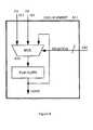
- FIG. 5shows a system 500 in accordance with a second embodiment of the present invention.
- System 500utilizes a FIFO structure 510 implemented with a plurality of FIFO elements 511 - 514 , as opposed to a multi-port RAM integrated circuit as used in system 200 of FIG. 2.
- the FIFO elements 511 - 514are implemented using conventional flip-flops, wherein each element of each of the FIFO elements 511 - 514 utilizes multiplexing to select which data word will be written to each location (shown in FIG. 6).
- the SELECT signals 521 - 524are each 2 bits. For example, in the present embodiment, 00 selects D 1 , 01 selects D 2 , and 11 selects DOUT (which effectively preserves the original data).
- System 500implements two write ports coupled to the two request inputs D 1 111 and D 2 121 . Each of the FIFO elements 511 - 514 is coupled to the two request inputs 501 - 502 .
- FIG. 6shows the components of one of the FIFO elements 511 - 514 in accordance with one embodiment of the present invention.
- FIG. 6shows the components of FIFO element 511 .
- the FIFO elements 511 - 514each utilize multiplexing to select which data word will be written to each location.
- the 2-bit select line 521couples to a multiplexer 610 .
- the inputs of the multiplexer 610are inputs D 1 and D 2 , and DOUT.
- the particular inputis selected via the 2-bit select signal, for example, where 00 selects D 1 , 01 selects D 2 , and 11 selects DOUT (which effectively preserves the original data).
- FIG. 7shows a pseudo-code representation 700 of a multiple request buffering process as implemented by the control logic 520 of system 500 .
- the particular inputis selected via the 2-bit select signal, for example, where 00 selects D 1 , 01 selects D 2 , and 11 selects DOUT (which preserves the original data).
- the write pointeris incremented accordingly (e.g., by two).
Landscapes
- Engineering & Computer Science (AREA)
- Theoretical Computer Science (AREA)
- Physics & Mathematics (AREA)
- General Engineering & Computer Science (AREA)
- General Physics & Mathematics (AREA)
- Information Transfer Systems (AREA)
Abstract
Description
- The present invention pertains to the field of digital systems. More particularly, the present invention relates to the optimization of access to a shared computational resource by multiple devices operating in parallel with each other.[0001]
- Digital electronic devices often rely on shared access to a single computational resource, for example a mathematical calculation unit (e.g. to calculate trigonometric functions, perform fast multiplication, etc.), a search algorithm (e.g. a special purpose hash function, a binary tree search, etc.), and the like. The main reasons for relying on a shared resource are that it is generally too expensive to duplicate a complex resource, and even if such duplication is possible this may in itself cause coherency issues, especially if multiple devices attempt to update a resource at the same time (e.g. deadlock issues, stale data, etc.).[0002]
- In a typical digital electronic device, access to a shared resource is via a common bus, which is managed by a set of bus protocols. These protocols regulate when data (in the form of a service request) can be written to the resource, and provide an acknowledgement of the request once it has been accepted. There exists a problem however, when multiple devices require very fast access to a single computational resource.[0003]
- Some digital electronic devices include multiple digital components which require fast efficient access to a shared resource. In this situation, the standard prior art bus protocol schemes are often inadequate. Such schemes typically prioritize requests and make one or more devices wait until a first access is completed by a first device.[0004]
- Other digital electronic devices are specifically designed to perform digital processing operations in parallel by using parallel execution units. In many instances, it is advantageous that such units share a single resource in order to access a common function, operation or data structure. Prior art protocol schemes would defeat the objective of performing digital processing operations in parallel. Prior art bus protocol and access schemes to a shared resource would have access by the requesters to the shared resource occur serially, with one access blocking other accesses until it completes.[0005]
- Thus, there exists a problem with respect to the sharing of a single resource between multiple accessers (or requesters). Provided the shared resource has sufficient bandwidth to handle multiple requests from multiple devices within a given time frame, it is desirable that requesters are not stalled waiting for the single resource to fulfill a request. The reason for this is that it is likely that the requesters have other operations to perform, and it is inefficient to stall a requester while it waits for its request to be accepted (which may take a number of clock cycles, depending on the number of other instantaneous requesters). It is even more inefficient to stall a requester while it waits for a result from the resource (which may take many clock cycles). These conditions regularly arise when the requesters are asynchronous, such that each requester can generate a request at any time.[0006]
- One prior art solution to the problem is to implement a buffer, for example a FIFO, on the input to the shared resource such that requests are temporarily held until they can be processed. However, if the buffer can only accept one request per clock cycle, then the system is still forced to use an arbitration process and an acknowledgement protocol from the resource to each requester, which may again result in the stalling of requesters until the request can be stored in the buffer. This solution also adds additional complexity to each requester.[0007]
- Thus the prior art is problematic in that systems are often constrained in situations where parallel execution units require access to a shared resource. Additionally, the prior art is problematic in that even when requests from multiple devices are buffered, such requests can only be buffered one at a time, still forcing the multiple devices to wait their turn as requests from other devices are buffered. Both of these situations act to unnecessarily stall requesters, thus causing system inefficiencies.[0008]
- A method and system for buffering multiple requests from multiple devices to a memory in a single clock cycle is disclosed. The system includes a memory having a first write port and a second write port. A first request input is coupled to the first write port. A second request input is coupled to the second write port. A controller is coupled to the memory. The controller is configured to control the memory to store a first request into the memory via the first write port and a second request into the memory via the second write port. The first and second requests are received via the first and second request inputs. The first and second requests are stored into the memory in one clock cycle.[0009]
- The accompanying drawings, which are incorporated in and form a part of this specification, illustrate embodiments of the invention and, together with the description, serve to explain the principles of the invention:[0010]
- FIG. 1 shows a multiple request buffering system in accordance with one embodiment of the present invention.[0011]
- FIG. 2 shows one implementation of the multiple request buffering logic and buffer memory shown in FIG. 1.[0012]
- FIG. 3 shows a generalized pseudo-code representation of a multiple request buffering process as implemented by the control logic shown in FIG. 2.[0013]
- FIG. 4 shows a flow chart of the steps of a multiple request buffering process in accordance with one embodiment of the present invention.[0014]
- FIG. 5 shows a second implementation of the multiple request buffering logic and buffer memory shown in FIG. 1.[0015]
- FIG. 6 shows the components of a FIFO element in accordance with one embodiment of the present invention.[0016]
- FIG. 7 shows a pseudo-code representation of the multiple request buffering process as implemented by the control logic of the system of FIG. 5.[0017]
- A method and system for buffering multiple requests from multiple devices to a shared buffer memory (e.g. a multi-write port RAM or FIFO) in a single clock cycle is disclosed. In one embodiment, the present invention is implemented as a system including a multi-port memory having at least two write ports (e.g., a first write port and a second write port). A first request input is coupled to the first write port. A second request input is coupled to the second write port. A controller is coupled to the buffer memory and is configured to store a first request into the buffer memory via the first write port and a second request into the buffer memory via the second write port, such that the first and second requests are stored in one clock cycle. In so doing, the system can buffer multiple requests from multiple devices to the buffer memory in a single clock cycle, thereby providing access to a shared resource without constraints such as arbitration or bus limitations. Additionally, the system can implement multiple requests in parallel, as in a case where parallel execution units require access to a shared resource. Also embodiments of the present invention are flexible in that they permit many different combinations of multiple requests and/or multiple devices (e.g.,[0018]
device 1 may be capable of generating only a single request,device 2 may be capable of generating2 simultaneous requests, etc.). - FIG. 1 shows a[0019]
system 100 in accordance with one embodiment of the present invention. As depicted in FIG. 1,system 100 includes afirst device 110 and asecond device 120, both requiring access to a sharedresource 140. The request buffering logic andbuffer memory 130 acts as an interface between themultiple devices computational resource 140. Each device has a data bus and write signal (e.g. D1 111 andW1 112 fordevice 110, andD2 121 andW2 122 for device120) to transfer the data for a request. TheEMPTY signal 131 indicates that no requests are currently queued. If a request is available, it is passed to the sharedcomputation resource 140 via the request databus R_DATA132. The sharedresource 140 generates aTAKEN signal 141 to indicate that it has taken the current request data from the request buffering logic andbuffer memory 130, and is ready for the next request data. Thussystem 100 of the present embodiment functions by buffering multiple requests from multiple devices to access a sharedresource 140 in a single clock cycle. - FIG. 2 shows a[0020]
system 200 in accordance with one embodiment of the request buffering logic andbuffer memory 130 of FIG. 1. As depicted in FIG. 2,system 200 includes a 2-writeport RAM 201 coupled to acontroller 210. The RAM includes first and second write address lines221-222 and first and second write enable lines223-224 coupled to thecontroller 210. A first write port is shown asD1 111 and a second write port is shown asD2 121. Write assert lines W1112 andW2 122 are shown connected to thecontrol logic 210. - [0021]
System 200 of the present embodiment functions by buffering multiple requests from multiple devices to access a shared resource in a single clock cycle. To accommodate two simultaneous requests,RAM 201 has two write ports operating in conjunction with the address lines221-222 and the write enable lines223-224. A first request input, in thiscase D1 111, receives requests from, for example, a first device. Similarly, a second request input, in thiscase D2 121, receives requests from, for example, a second device. The request inputs are buffered by storing them into theRAM 201. In accordance with present invention, this is accomplished during a single clock cycle. - The[0022]
control logic 210 is coupled to receive thewrite assertions RAM 201 to store the multiple requests into their proper locations within theRAM 201. - Thus,[0023]
system 200 of the present embodiment can buffer multiple requests from multiple devices to thememory 201 in a single clock cycle, thereby implementing access to a shared resource without being constrained by arbitration or bus limitations. It should be noted that the access is provided without requiring one request or the other to be temporarily held (e.g., wait state, etc.). Even though two requests may arrive in a single clock cycle, both requests can be buffered simultaneously by being stored within theRAM 201. In this manner,system 200 prevents the stalling of requesters. By allowing theRAM 201 to accept multiple requests in a single clock cycle,system 200 obviates the need for any acknowledgement protocol. - FIG. 3 shows a generalized[0024]
pseudo-code representation 300 of a multiple request buffering process as implemented by thecontrol logic 210 ofsystem 200.Representation 300 shows a case where two requesting devices have their respective requests buffered within a sharedmemory 201. - The[0025]
pseudo-code representation 300 begins with the initialization of the write enable lines (e.g., shown as WEl and VvE2) to zero. Thebracket 301 shows the determination of whether theRAM 201 is storing any requests. This is achieved by comparing the current value of the write pointer W_ptr with that of the read pointer R_ptr. If the two pointers are equal, then there are no requests stored in the RAM and hence the EMPTY signal is set to 1, otherwise it is set to 0. Thebracket 302 shows a case where a request is received from a first device and not from a second device. In this case, the write address for the first device, W_ADDR1, is assigned to be the write pointer, the request is written to the memory, and the write pointer is incremented by one. Thebracket 303 shows a case where the request is received from the second device and not from the first device. In this case, the write address for the second device, W_ADDR2, is assigned to be the write pointer, the request is written to the memory, and the write pointer is incremented by one. Thebracket 304 shows a case where the requests are received from both the first device and the second device. In this case, the write address for the first device is assigned to be the write pointer, the request is written, the write address for the second device is assigned to be the write pointer plus one, the request is written, and then the write pointer is subsequently incremented by two. The read pointer R_ptr is incremented whenever a request is taken by the shared resource and the buffer memory is not empty, as shown inbracket 305. The read address to the buffer memory R_ADDR is always identical to the read pointer R_ptr. It should be noted thatprocess 300 will complete within a single clock cycle. - Thus, the[0026]
pseudo-code representation 300 shows a case where the data for the two requests are inserted into respective memory locations within thebuffer memory 201. In this case, where both requests are active in the same clock cycle, thepseudo-code representation 300 shows the first request of a first device (e.g., WE1) being written into a memory location before the second request from the second device (e.g., WE2). It should be noted however that the order can be reversed. The order in which requests are written into thebuffer memory 201 can also be based on some form of prioritization, for example, as required by some particular need of the user. In addition, this prioritization can also occur dynamically, for example by having each requesting device supply a priority to the controller with each request that is generated. - Referring still to the pseudo-code of FIG. 3,[0027]
controller 210 is configured to implement simultaneous access to thememory 201 by utilizing a single write pointer W_PTR. Such a solution may not be adequate with either a very fast or verydeep memory 201, in which case it is desirable to implement one write pointer for each device that can write a request to the buffer memory. In this situation, multiple write pointers would be maintained that are offset by 1 from each other, e.g. W_ptr_plus_one=W_ptr+ 1, W_ptr_plus_two=W_ptr+ 2, etc. This allows higher speed operation by removing the pointer addition operation from the critical path of generating the write addresses (e.g. W_ADDR1, W_ADDR2, etc) to thememory 201. - It should be noted that in general, a hardware implementation of the[0028]
pseudo-code representation 300 requires control logic to examine the input write enable signals and generate the appropriate write control signals for the memory. As such, the configuration of the control logic depends on the particular structure of the memory implemented (e.g. number of write ports, different latencies, etc.). - Referring now to FIG. 4, a flowchart of the steps of a multiple[0029]
request buffering process 400 in accordance with one embodiment of the present invention is shown.Process 400 shows the basic steps involved in managing a write pointer to control address locations of the memory used to store the request data. - [0030]
Process 400 begins instep 401, wherein the buffer memory (e.g.,memory 201 shown in FIG. 2) is initialized for storing requests from multiple devices. In step402, when request(s) are received, a determination is made whether a single request or multiple requests are received. If a single request is received,process 400 proceeds to step403. If multiple requests are received,process 400 proceeds to step404. Instep 403, in response to a single request, the request is written to the memory in accordance with the address indicated by the write pointer. The write pointer is subsequently incremented by one, in accordance with the single request. Subsequently, instep 405, the address of the next free location in the buffer memory is located in accordance with the write pointer. Instep 404, in response to multiple requests being received, the multiple requests are written to the memory in parallel and in accordance with the write pointer. As the multiple requests are written, the write pointer is incremented in accordance there with. For example, if two requests are received, the write pointer is incremented by two. Subsequently, instep 405, the address of the next free location in the buffer memory is located in accordance with the write pointer. - FIG. 5 shows a[0031]
system 500 in accordance with a second embodiment of the present invention.System 500 utilizes a FIFO structure510 implemented with a plurality of FIFO elements511-514, as opposed to a multi-port RAM integrated circuit as used insystem 200 of FIG. 2. - In the present embodiment, the FIFO elements[0032]511-514 are implemented using conventional flip-flops, wherein each element of each of the FIFO elements511-514 utilizes multiplexing to select which data word will be written to each location (shown in FIG. 6). In this embodiment, the SELECT signals521-524 are each 2 bits. For example, in the present embodiment, 00 selects D1, 01 selects D2, and 11 selects DOUT (which effectively preserves the original data).
System 500 implements two write ports coupled to the tworequest inputs D1 111 andD2 121. Each of the FIFO elements511-514 is coupled to the two request inputs501-502. - FIG. 6 shows the components of one of the FIFO elements[0033]511-514 in accordance with one embodiment of the present invention. In this case, FIG. 6 shows the components of
FIFO element 511. As described above, the FIFO elements511-514 each utilize multiplexing to select which data word will be written to each location. Accordingly, the 2-bitselect line 521 couples to amultiplexer 610. The inputs of themultiplexer 610 are inputs D1 and D2, and DOUT. The particular input is selected via the 2-bit select signal, for example, where 00 selects D1, 01 selects D2, and 11 selects DOUT (which effectively preserves the original data). - FIG. 7 shows a pseudo-code representation[0034]700 of a multiple request buffering process as implemented by the
control logic 520 ofsystem 500. As described above, the particular input is selected via the 2-bit select signal, for example, where 00 selects D1, 01 selects D2, and 11 selects DOUT (which preserves the original data). As with thepseudo-code representation 300 of FIG. 3, when two requests are received simultaneously, the write pointer is incremented accordingly (e.g., by two). - Thus, a method and system for buffering multiple requests from multiple devices to a buffer memory in a single clock cycle has been described. The foregoing descriptions of specific embodiments of the present invention have been presented for purposes of illustration and description. They are not intended to be exhaustive or to limit the invention to the precise forms disclosed, and many modifications and variations are possible in light of the above teaching. The embodiments were chosen and described in order best to explain the principles of the invention and its practical application, thereby to enable others skilled in the art best to use the invention and various embodiments with various modifications as are suited to the particular use contemplated. It is intended that the scope of the invention be defined by the claims appended hereto and their equivalents.[0035]
Claims (21)
Priority Applications (1)
| Application Number | Priority Date | Filing Date | Title |
|---|---|---|---|
| US10/102,990US7206904B2 (en) | 2002-03-20 | 2002-03-20 | Method and system for buffering multiple requests from multiple devices to a memory |
Applications Claiming Priority (1)
| Application Number | Priority Date | Filing Date | Title |
|---|---|---|---|
| US10/102,990US7206904B2 (en) | 2002-03-20 | 2002-03-20 | Method and system for buffering multiple requests from multiple devices to a memory |
Publications (2)
| Publication Number | Publication Date |
|---|---|
| US20030182517A1true US20030182517A1 (en) | 2003-09-25 |
| US7206904B2 US7206904B2 (en) | 2007-04-17 |
Family
ID=28040284
Family Applications (1)
| Application Number | Title | Priority Date | Filing Date |
|---|---|---|---|
| US10/102,990Expired - LifetimeUS7206904B2 (en) | 2002-03-20 | 2002-03-20 | Method and system for buffering multiple requests from multiple devices to a memory |
Country Status (1)
| Country | Link |
|---|---|
| US (1) | US7206904B2 (en) |
Cited By (8)
| Publication number | Priority date | Publication date | Assignee | Title |
|---|---|---|---|---|
| US20040136259A1 (en)* | 2002-09-10 | 2004-07-15 | Nokia Corporation | Memory structure, a system, and an electronic device, as well as a method in connection with a memory circuit |
| US20080235462A1 (en)* | 2005-09-20 | 2008-09-25 | Freescale Semiconductor, Inc. | Device Having a Low Latency Single Port Memory Unit and a Method for Writing Multiple Data Segments to a Single Port Memory Unit |
| US20080240324A1 (en)* | 2007-03-27 | 2008-10-02 | Microsoft Corporation | Independent Dispatch of Multiple Streaming Queues Via Reserved Time Slots |
| CN102918515A (en)* | 2010-05-28 | 2013-02-06 | 惠普发展公司,有限责任合伙企业 | Storing data in any of a plurality of buffers in a memory controller |
| EP2538342A3 (en)* | 2011-06-20 | 2014-04-30 | Intel Corporation | Configurable buffer allocation for multi-format video processing |
| WO2017100748A1 (en)* | 2015-12-11 | 2017-06-15 | Vivante Corporation | Software defined fifo buffer for multithreaded access |
| US11310164B1 (en)* | 2018-07-31 | 2022-04-19 | Marvell Israel (M.I.S.L) Ltd. | Method and apparatus for resource allocation |
| US20230325111A1 (en)* | 2020-10-30 | 2023-10-12 | SK Hynix Inc. | Memory comprising memory controller configured to determine a logical address of a target zone system and method of operating the memory controller |
Families Citing this family (1)
| Publication number | Priority date | Publication date | Assignee | Title |
|---|---|---|---|---|
| US7032082B1 (en)* | 2001-08-31 | 2006-04-18 | Juniper Networks, Inc. | Centralized memory allocation with write pointer drift correction |
Citations (12)
| Publication number | Priority date | Publication date | Assignee | Title |
|---|---|---|---|---|
| US4866609A (en)* | 1988-06-22 | 1989-09-12 | International Business Machines Corporation | Byte count handling in serial channel extender with buffering for data pre-fetch |
| US5203002A (en)* | 1989-12-27 | 1993-04-13 | Wetzel Glen F | System with a multiport memory and N processing units for concurrently/individually executing 2N-multi-instruction-words at first/second transitions of a single clock cycle |
| US5202856A (en)* | 1990-04-05 | 1993-04-13 | Micro Technology, Inc. | Method and apparatus for simultaneous, interleaved access of multiple memories by multiple ports |
| US5375215A (en)* | 1990-11-09 | 1994-12-20 | Hitachi, Ltd. | Multiprocessor system having shared memory divided into a plurality of banks with access queues corresponding to each bank |
| US5608891A (en)* | 1992-10-06 | 1997-03-04 | Mitsubishi Denki Kabushiki Kaisha | Recording system having a redundant array of storage devices and having read and write circuits with memory buffers |
| US5835962A (en)* | 1995-03-03 | 1998-11-10 | Fujitsu Limited | Parallel access micro-TLB to speed up address translation |
| US5978897A (en)* | 1992-06-02 | 1999-11-02 | Mitsubishi Denki Kabushiki Kaisha | Sequence operation processor employing multi-port RAMs for simultaneously reading and writing |
| US6282505B1 (en)* | 1996-02-16 | 2001-08-28 | Hitachi, Ltd. | Multi-port memory and a data processor accessing the same |
| US6282144B1 (en)* | 2000-03-13 | 2001-08-28 | International Business Machines Corporation | Multi-ported memory with asynchronous and synchronous protocol |
| US6321284B1 (en)* | 1998-07-27 | 2001-11-20 | Fujitsu Limited | Multiprocessor system with multiple memory buses for access to shared memories |
| US20010044882A1 (en)* | 2000-03-20 | 2001-11-22 | International Business Machines Corporation | Multiple port memory apparatus |
| US6654308B1 (en)* | 2002-12-23 | 2003-11-25 | Hewlett-Packard Development Company, Lp. | Memory having multiple write ports and multiple control memory units, and method of operation |
- 2002
- 2002-03-20USUS10/102,990patent/US7206904B2/ennot_activeExpired - Lifetime
Patent Citations (12)
| Publication number | Priority date | Publication date | Assignee | Title |
|---|---|---|---|---|
| US4866609A (en)* | 1988-06-22 | 1989-09-12 | International Business Machines Corporation | Byte count handling in serial channel extender with buffering for data pre-fetch |
| US5203002A (en)* | 1989-12-27 | 1993-04-13 | Wetzel Glen F | System with a multiport memory and N processing units for concurrently/individually executing 2N-multi-instruction-words at first/second transitions of a single clock cycle |
| US5202856A (en)* | 1990-04-05 | 1993-04-13 | Micro Technology, Inc. | Method and apparatus for simultaneous, interleaved access of multiple memories by multiple ports |
| US5375215A (en)* | 1990-11-09 | 1994-12-20 | Hitachi, Ltd. | Multiprocessor system having shared memory divided into a plurality of banks with access queues corresponding to each bank |
| US5978897A (en)* | 1992-06-02 | 1999-11-02 | Mitsubishi Denki Kabushiki Kaisha | Sequence operation processor employing multi-port RAMs for simultaneously reading and writing |
| US5608891A (en)* | 1992-10-06 | 1997-03-04 | Mitsubishi Denki Kabushiki Kaisha | Recording system having a redundant array of storage devices and having read and write circuits with memory buffers |
| US5835962A (en)* | 1995-03-03 | 1998-11-10 | Fujitsu Limited | Parallel access micro-TLB to speed up address translation |
| US6282505B1 (en)* | 1996-02-16 | 2001-08-28 | Hitachi, Ltd. | Multi-port memory and a data processor accessing the same |
| US6321284B1 (en)* | 1998-07-27 | 2001-11-20 | Fujitsu Limited | Multiprocessor system with multiple memory buses for access to shared memories |
| US6282144B1 (en)* | 2000-03-13 | 2001-08-28 | International Business Machines Corporation | Multi-ported memory with asynchronous and synchronous protocol |
| US20010044882A1 (en)* | 2000-03-20 | 2001-11-22 | International Business Machines Corporation | Multiple port memory apparatus |
| US6654308B1 (en)* | 2002-12-23 | 2003-11-25 | Hewlett-Packard Development Company, Lp. | Memory having multiple write ports and multiple control memory units, and method of operation |
Cited By (19)
| Publication number | Priority date | Publication date | Assignee | Title |
|---|---|---|---|---|
| US20040136259A1 (en)* | 2002-09-10 | 2004-07-15 | Nokia Corporation | Memory structure, a system, and an electronic device, as well as a method in connection with a memory circuit |
| US7057911B2 (en)* | 2002-09-10 | 2006-06-06 | Nokia Corporation | Memory structure, a system, and an electronic device, as well as a method in connection with a memory circuit |
| US20080235462A1 (en)* | 2005-09-20 | 2008-09-25 | Freescale Semiconductor, Inc. | Device Having a Low Latency Single Port Memory Unit and a Method for Writing Multiple Data Segments to a Single Port Memory Unit |
| US20080240324A1 (en)* | 2007-03-27 | 2008-10-02 | Microsoft Corporation | Independent Dispatch of Multiple Streaming Queues Via Reserved Time Slots |
| US9213545B2 (en)* | 2010-05-28 | 2015-12-15 | Hewlett-Packard Development Company, L.P. | Storing data in any of a plurality of buffers in a memory controller |
| US20130046933A1 (en)* | 2010-05-28 | 2013-02-21 | Robert L. Noonan | Storing data in any of a plurality of buffers in a memory controller |
| CN102918515A (en)* | 2010-05-28 | 2013-02-06 | 惠普发展公司,有限责任合伙企业 | Storing data in any of a plurality of buffers in a memory controller |
| EP2538342A3 (en)* | 2011-06-20 | 2014-04-30 | Intel Corporation | Configurable buffer allocation for multi-format video processing |
| US9037761B2 (en) | 2011-06-20 | 2015-05-19 | Intel Corporation | Configurable buffer allocation for multi-format video processing |
| CN108292162A (en)* | 2015-12-11 | 2018-07-17 | 图芯芯片技术有限公司 | Software definition fifo buffer for multi-thread access |
| US20170168755A1 (en)* | 2015-12-11 | 2017-06-15 | Vivante Corporation | Software defined fifo buffer for multithreaded access |
| WO2017100748A1 (en)* | 2015-12-11 | 2017-06-15 | Vivante Corporation | Software defined fifo buffer for multithreaded access |
| KR20180107091A (en)* | 2015-12-11 | 2018-10-01 | 비반테 코포레이션 | Software-Limited FIFO Buffer for Multithreaded Access |
| EP3387513A4 (en)* | 2015-12-11 | 2019-07-10 | Vivante Corporation | BUFFER MEMORY PEPS DEFINED BY SOFTWARE FOR MULTIFIL ACCESS |
| US10585623B2 (en)* | 2015-12-11 | 2020-03-10 | Vivante Corporation | Software defined FIFO buffer for multithreaded access |
| KR102683211B1 (en)* | 2015-12-11 | 2024-07-08 | 비반테 코포레이션 | Software-limited FIFO buffer for multithreaded access |
| US11310164B1 (en)* | 2018-07-31 | 2022-04-19 | Marvell Israel (M.I.S.L) Ltd. | Method and apparatus for resource allocation |
| US20230325111A1 (en)* | 2020-10-30 | 2023-10-12 | SK Hynix Inc. | Memory comprising memory controller configured to determine a logical address of a target zone system and method of operating the memory controller |
| US12124733B2 (en)* | 2020-10-30 | 2024-10-22 | SK Hynix Inc. | Memory comprising memory controller configured to determine a logical address of a target zone system and method of operating the memory controller |
Also Published As
| Publication number | Publication date |
|---|---|
| US7206904B2 (en) | 2007-04-17 |
Similar Documents
| Publication | Publication Date | Title |
|---|---|---|
| US6584522B1 (en) | Communication between processors | |
| US7047370B1 (en) | Full access to memory interfaces via remote request | |
| US5586299A (en) | Systems and methods for accessing multi-port memories | |
| US6895457B2 (en) | Bus interface with a first-in-first-out memory | |
| EP1573559B1 (en) | Method, system, and program for handling input/output commands | |
| US20020013888A1 (en) | System and method of processing memory requests in a pipelined memory controller | |
| US5907485A (en) | Method and apparatus for flow control in packet-switched computer system | |
| US20020184453A1 (en) | Data bus system including posted reads and writes | |
| CN113900974B (en) | Storage device, data storage method and related equipment | |
| US20170147517A1 (en) | Direct memory access system using available descriptor mechanism and/or pre-fetch mechanism and associated direct memory access method | |
| US20050210221A1 (en) | Microcomputer and microcomputer system | |
| US7206904B2 (en) | Method and system for buffering multiple requests from multiple devices to a memory | |
| JP2004508634A (en) | Intermediate buffer control to improve split transaction interconnect throughput | |
| CN118152310A (en) | PCIe AXI bridge-based write data storage, search and transmission processing method and system | |
| JPH05274252A (en) | Transaction execution method for computer system | |
| US6976110B2 (en) | Method and apparatus for reducing interrupt latency by dynamic buffer sizing | |
| US6567908B1 (en) | Method of and apparatus for processing information, and providing medium | |
| JP2591502B2 (en) | Information processing system and its bus arbitration system | |
| US20030196004A1 (en) | Buffering and presenting chunks | |
| US5717931A (en) | Method and apparatus for communicating between master and slave electronic devices where the slave device may be hazardous | |
| CN109271333B (en) | SRAM control method, controller and control system | |
| US6654861B2 (en) | Method to manage multiple communication queues in an 8-bit microcontroller | |
| US20050223129A1 (en) | Arbitration of data transfer requests | |
| US6976141B2 (en) | Pipelined multi-access memory apparatus and method | |
| US6581145B1 (en) | Multiple source generic memory access interface providing significant design flexibility among devices requiring access to memory |
Legal Events
| Date | Code | Title | Description |
|---|---|---|---|
| AS | Assignment | Owner name:HEWLETT-PACKARD COMPANY, COLORADO Free format text:ASSIGNMENT OF ASSIGNORS INTEREST;ASSIGNOR:GOOCH, MARK;REEL/FRAME:013291/0390 Effective date:20020320 | |
| AS | Assignment | Owner name:HEWLETT-PACKARD DEVELOPMENT COMPANY L.P., TEXAS Free format text:ASSIGNMENT OF ASSIGNORS INTEREST;ASSIGNOR:HEWLETT-PACKARD COMPANY;REEL/FRAME:014061/0492 Effective date:20030926 Owner name:HEWLETT-PACKARD DEVELOPMENT COMPANY L.P.,TEXAS Free format text:ASSIGNMENT OF ASSIGNORS INTEREST;ASSIGNOR:HEWLETT-PACKARD COMPANY;REEL/FRAME:014061/0492 Effective date:20030926 | |
| FPAY | Fee payment | Year of fee payment:4 | |
| AS | Assignment | Owner name:SK HYNIX INC., KOREA, REPUBLIC OF Free format text:ASSIGNMENT OF ASSIGNORS INTEREST;ASSIGNORS:HEWLETT-PACKARD DEVELOPMENT COMPANY, L.P.;HEWLETT-PACKARD COMPANY;REEL/FRAME:034073/0910 Effective date:20141017 | |
| REMI | Maintenance fee reminder mailed | ||
| FEPP | Fee payment procedure | Free format text:PETITION RELATED TO MAINTENANCE FEES FILED (ORIGINAL EVENT CODE: PMFP); ENTITY STATUS OF PATENT OWNER: LARGE ENTITY Free format text:PETITION RELATED TO MAINTENANCE FEES GRANTED (ORIGINAL EVENT CODE: PMFG); ENTITY STATUS OF PATENT OWNER: LARGE ENTITY | |
| FEPP | Fee payment procedure | Free format text:PAYOR NUMBER ASSIGNED (ORIGINAL EVENT CODE: ASPN); ENTITY STATUS OF PATENT OWNER: LARGE ENTITY Free format text:PAYER NUMBER DE-ASSIGNED (ORIGINAL EVENT CODE: RMPN); ENTITY STATUS OF PATENT OWNER: LARGE ENTITY | |
| LAPS | Lapse for failure to pay maintenance fees | ||
| REIN | Reinstatement after maintenance fee payment confirmed | ||
| PRDP | Patent reinstated due to the acceptance of a late maintenance fee | Effective date:20150526 | |
| FPAY | Fee payment | Year of fee payment:8 | |
| STCF | Information on status: patent grant | Free format text:PATENTED CASE | |
| SULP | Surcharge for late payment | ||
| FP | Lapsed due to failure to pay maintenance fee | Effective date:20150417 | |
| MAFP | Maintenance fee payment | Free format text:PAYMENT OF MAINTENANCE FEE, 12TH YEAR, LARGE ENTITY (ORIGINAL EVENT CODE: M1553) Year of fee payment:12 |