US20030181065A1 - Low contamination components for semiconductor processing apparatus and methods for making components - Google Patents
Low contamination components for semiconductor processing apparatus and methods for making componentsDownload PDFInfo
- Publication number
- US20030181065A1 US20030181065A1US10/101,701US10170102AUS2003181065A1US 20030181065 A1US20030181065 A1US 20030181065A1US 10170102 AUS10170102 AUS 10170102AUS 2003181065 A1US2003181065 A1US 2003181065A1
- Authority
- US
- United States
- Prior art keywords
- component
- ceramic material
- hafnium
- coating
- substrate
- Prior art date
- Legal status (The legal status is an assumption and is not a legal conclusion. Google has not performed a legal analysis and makes no representation as to the accuracy of the status listed.)
- Granted
Links
- 238000012545processingMethods0.000titleclaimsabstractdescription59
- 239000004065semiconductorSubstances0.000titleclaimsabstractdescription42
- 238000000034methodMethods0.000titleclaimsdescription60
- 238000011109contaminationMethods0.000titledescription19
- 229910010293ceramic materialInorganic materials0.000claimsabstractdescription134
- 238000000576coating methodMethods0.000claimsabstractdescription99
- 239000000758substrateSubstances0.000claimsabstractdescription80
- 229910052712strontiumInorganic materials0.000claimsabstractdescription59
- 229910052735hafniumInorganic materials0.000claimsabstractdescription58
- 229910052692DysprosiumInorganic materials0.000claimsabstractdescription56
- KBQHZAAAGSGFKK-UHFFFAOYSA-Ndysprosium atomChemical compound[Dy]KBQHZAAAGSGFKK-UHFFFAOYSA-N0.000claimsabstractdescription56
- CIOAGBVUUVVLOB-UHFFFAOYSA-Nstrontium atomChemical compound[Sr]CIOAGBVUUVVLOB-UHFFFAOYSA-N0.000claimsabstractdescription56
- MRELNEQAGSRDBK-UHFFFAOYSA-Nlanthanum(3+);oxygen(2-)Chemical compound[O-2].[O-2].[O-2].[La+3].[La+3]MRELNEQAGSRDBK-UHFFFAOYSA-N0.000claimsabstractdescription34
- 150000004767nitridesChemical class0.000claimsabstractdescription27
- 239000002131composite materialSubstances0.000claimsabstract4
- 239000011248coating agentSubstances0.000claimsdescription78
- 239000000463materialSubstances0.000claimsdescription55
- 229910052746lanthanumInorganic materials0.000claimsdescription54
- FZLIPJUXYLNCLC-UHFFFAOYSA-Nlanthanum atomChemical compound[La]FZLIPJUXYLNCLC-UHFFFAOYSA-N0.000claimsdescription54
- 230000008569processEffects0.000claimsdescription42
- IATRAKWUXMZMIY-UHFFFAOYSA-Nstrontium oxideChemical compound[O-2].[Sr+2]IATRAKWUXMZMIY-UHFFFAOYSA-N0.000claimsdescription34
- -1hafnium nitrideChemical class0.000claimsdescription31
- 238000009826distributionMethods0.000claimsdescription28
- 239000000470constituentSubstances0.000claimsdescription21
- 229910000449hafnium oxideInorganic materials0.000claimsdescription20
- WIHZLLGSGQNAGK-UHFFFAOYSA-Nhafnium(4+);oxygen(2-)Chemical compound[O-2].[O-2].[Hf+4]WIHZLLGSGQNAGK-UHFFFAOYSA-N0.000claimsdescription20
- 229910003440dysprosium oxideInorganic materials0.000claimsdescription17
- NLQFUUYNQFMIJW-UHFFFAOYSA-Ndysprosium(iii) oxideChemical compoundO=[Dy]O[Dy]=ONLQFUUYNQFMIJW-UHFFFAOYSA-N0.000claimsdescription17
- 230000000737periodic effectEffects0.000claimsdescription14
- 150000002222fluorine compoundsChemical class0.000claimsdescription12
- 150000001247metal acetylidesChemical class0.000claimsdescription12
- 229910052768actinideInorganic materials0.000claimsdescription10
- 150000001255actinidesChemical class0.000claimsdescription10
- 229910052751metalInorganic materials0.000claimsdescription10
- 239000002184metalSubstances0.000claimsdescription10
- 239000002002slurrySubstances0.000claimsdescription9
- 238000007751thermal sprayingMethods0.000claimsdescription9
- LRTTZMZPZHBOPO-UHFFFAOYSA-N[B].[B].[Hf]Chemical compound[B].[B].[Hf]LRTTZMZPZHBOPO-UHFFFAOYSA-N0.000claimsdescription8
- QHEDSQMUHIMDOL-UHFFFAOYSA-Jhafnium(4+);tetrafluorideChemical compoundF[Hf](F)(F)FQHEDSQMUHIMDOL-UHFFFAOYSA-J0.000claimsdescription8
- WHJFNYXPKGDKBB-UHFFFAOYSA-Nhafnium;methaneChemical compoundC.[Hf]WHJFNYXPKGDKBB-UHFFFAOYSA-N0.000claimsdescription8
- 238000005245sinteringMethods0.000claimsdescription6
- 238000004519manufacturing processMethods0.000claimsdescription5
- 238000007788rougheningMethods0.000claimsdescription4
- IBIOTXDDKRNYMC-UHFFFAOYSA-NazanylidynedysprosiumChemical compound[Dy]#NIBIOTXDDKRNYMC-UHFFFAOYSA-N0.000claimsdescription3
- QCLQZCOGUCNIOC-UHFFFAOYSA-NazanylidynelanthanumChemical compound[La]#NQCLQZCOGUCNIOC-UHFFFAOYSA-N0.000claimsdescription3
- ZKEYULQFFYBZBG-UHFFFAOYSA-Nlanthanum carbideChemical compound[La].[C-]#[C]ZKEYULQFFYBZBG-UHFFFAOYSA-N0.000claimsdescription3
- FVRNDBHWWSPNOM-UHFFFAOYSA-Lstrontium fluorideChemical compound[F-].[F-].[Sr+2]FVRNDBHWWSPNOM-UHFFFAOYSA-L0.000claimsdescription3
- 229910001637strontium fluorideInorganic materials0.000claimsdescription3
- FWQVINSGEXZQHB-UHFFFAOYSA-KtrifluorodysprosiumChemical compoundF[Dy](F)FFWQVINSGEXZQHB-UHFFFAOYSA-K0.000claimsdescription3
- BYMUNNMMXKDFEZ-UHFFFAOYSA-KtrifluorolanthanumChemical compoundF[La](F)FBYMUNNMMXKDFEZ-UHFFFAOYSA-K0.000claimsdescription3
- NJPPVKZQTLUDBO-UHFFFAOYSA-NnovaluronChemical compoundC1=C(Cl)C(OC(F)(F)C(OC(F)(F)F)F)=CC=C1NC(=O)NC(=O)C1=C(F)C=CC=C1FNJPPVKZQTLUDBO-UHFFFAOYSA-N0.000claims4
- VBJZVLUMGGDVMO-UHFFFAOYSA-Nhafnium atomChemical compound[Hf]VBJZVLUMGGDVMO-UHFFFAOYSA-N0.000abstractdescription50
- 230000003628erosive effectEffects0.000abstractdescription23
- KRHYYFGTRYWZRS-UHFFFAOYSA-MFluoride anionChemical compound[F-]KRHYYFGTRYWZRS-UHFFFAOYSA-M0.000abstractdescription19
- 238000005260corrosionMethods0.000abstractdescription17
- 230000007797corrosionEffects0.000abstractdescription16
- 239000000126substanceSubstances0.000abstractdescription7
- 210000002381plasmaAnatomy0.000description72
- 239000007789gasSubstances0.000description71
- 229910052782aluminiumInorganic materials0.000description11
- XAGFODPZIPBFFR-UHFFFAOYSA-NaluminiumChemical compound[Al]XAGFODPZIPBFFR-UHFFFAOYSA-N0.000description11
- 239000000919ceramicSubstances0.000description9
- 238000009616inductively coupled plasmaMethods0.000description8
- 239000000203mixtureSubstances0.000description8
- 235000012431wafersNutrition0.000description8
- PNEYBMLMFCGWSK-UHFFFAOYSA-Naluminium oxideInorganic materials[O-2].[O-2].[O-2].[Al+3].[Al+3]PNEYBMLMFCGWSK-UHFFFAOYSA-N0.000description7
- 238000005524ceramic coatingMethods0.000description7
- 238000005530etchingMethods0.000description7
- 238000005229chemical vapour depositionMethods0.000description6
- 238000000151depositionMethods0.000description6
- 239000002245particleSubstances0.000description6
- 238000007750plasma sprayingMethods0.000description6
- 239000007921spraySubstances0.000description6
- 229910052734heliumInorganic materials0.000description5
- 230000007246mechanismEffects0.000description5
- 239000000843powderSubstances0.000description5
- 239000001307heliumSubstances0.000description4
- SWQJXJOGLNCZEY-UHFFFAOYSA-Nhelium atomChemical compound[He]SWQJXJOGLNCZEY-UHFFFAOYSA-N0.000description4
- 150000002500ionsChemical class0.000description4
- VYPSYNLAJGMNEJ-UHFFFAOYSA-Nsilicon dioxideInorganic materialsO=[Si]=OVYPSYNLAJGMNEJ-UHFFFAOYSA-N0.000description4
- 238000004544sputter depositionMethods0.000description4
- 238000012546transferMethods0.000description4
- KZBUYRJDOAKODT-UHFFFAOYSA-NChlorineChemical compoundClClKZBUYRJDOAKODT-UHFFFAOYSA-N0.000description3
- 229910052581Si3N4Inorganic materials0.000description3
- 238000005266castingMethods0.000description3
- 238000009694cold isostatic pressingMethods0.000description3
- 238000000748compression mouldingMethods0.000description3
- 230000008021depositionEffects0.000description3
- RWRIWBAIICGTTQ-UHFFFAOYSA-NdifluoromethaneChemical compoundFCFRWRIWBAIICGTTQ-UHFFFAOYSA-N0.000description3
- 238000010438heat treatmentMethods0.000description3
- 238000001513hot isostatic pressingMethods0.000description3
- 238000007654immersionMethods0.000description3
- 238000010849ion bombardmentMethods0.000description3
- 239000007769metal materialSubstances0.000description3
- GVGCUCJTUSOZKP-UHFFFAOYSA-Nnitrogen trifluorideChemical compoundFN(F)FGVGCUCJTUSOZKP-UHFFFAOYSA-N0.000description3
- TWNQGVIAIRXVLR-UHFFFAOYSA-Noxo(oxoalumanyloxy)alumaneChemical compoundO=[Al]O[Al]=OTWNQGVIAIRXVLR-UHFFFAOYSA-N0.000description3
- 238000005240physical vapour depositionMethods0.000description3
- 229910021420polycrystalline siliconInorganic materials0.000description3
- 229920005591polysiliconPolymers0.000description3
- 230000001681protective effectEffects0.000description3
- 238000011160researchMethods0.000description3
- 235000012239silicon dioxideNutrition0.000description3
- HQVNEWCFYHHQES-UHFFFAOYSA-Nsilicon nitrideChemical compoundN12[Si]34N5[Si]62N3[Si]51N64HQVNEWCFYHHQES-UHFFFAOYSA-N0.000description3
- SFZCNBIFKDRMGX-UHFFFAOYSA-Nsulfur hexafluorideChemical compoundFS(F)(F)(F)(F)FSFZCNBIFKDRMGX-UHFFFAOYSA-N0.000description3
- TXEYQDLBPFQVAA-UHFFFAOYSA-NtetrafluoromethaneChemical compoundFC(F)(F)FTXEYQDLBPFQVAA-UHFFFAOYSA-N0.000description3
- XLYOFNOQVPJJNP-UHFFFAOYSA-NwaterChemical compoundOXLYOFNOQVPJJNP-UHFFFAOYSA-N0.000description3
- 2299100007556061-T6 aluminium alloyInorganic materials0.000description2
- 229910000838Al alloyInorganic materials0.000description2
- XKRFYHLGVUSROY-UHFFFAOYSA-NArgonChemical compound[Ar]XKRFYHLGVUSROY-UHFFFAOYSA-N0.000description2
- IJGRMHOSHXDMSA-UHFFFAOYSA-NAtomic nitrogenChemical compoundN#NIJGRMHOSHXDMSA-UHFFFAOYSA-N0.000description2
- WKBOTKDWSSQWDR-UHFFFAOYSA-NBromine atomChemical compound[Br]WKBOTKDWSSQWDR-UHFFFAOYSA-N0.000description2
- CPELXLSAUQHCOX-UHFFFAOYSA-NHydrogen bromideChemical compoundBrCPELXLSAUQHCOX-UHFFFAOYSA-N0.000description2
- GWEVSGVZZGPLCZ-UHFFFAOYSA-NTitan oxideChemical compoundO=[Ti]=OGWEVSGVZZGPLCZ-UHFFFAOYSA-N0.000description2
- MCMNRKCIXSYSNV-UHFFFAOYSA-NZirconium dioxideChemical compoundO=[Zr]=OMCMNRKCIXSYSNV-UHFFFAOYSA-N0.000description2
- 229910052786argonInorganic materials0.000description2
- 125000004429atomChemical group0.000description2
- QVGXLLKOCUKJST-UHFFFAOYSA-Natomic oxygenChemical compound[O]QVGXLLKOCUKJST-UHFFFAOYSA-N0.000description2
- 230000008901benefitEffects0.000description2
- 238000005422blastingMethods0.000description2
- GDTBXPJZTBHREO-UHFFFAOYSA-NbromineSubstancesBrBrGDTBXPJZTBHREO-UHFFFAOYSA-N0.000description2
- 229910052794bromiumInorganic materials0.000description2
- 238000004140cleaningMethods0.000description2
- 238000009833condensationMethods0.000description2
- 230000005494condensationEffects0.000description2
- 229910052593corundumInorganic materials0.000description2
- 230000001965increasing effectEffects0.000description2
- 230000001939inductive effectEffects0.000description2
- 150000002739metalsChemical class0.000description2
- 239000001301oxygenSubstances0.000description2
- 229910052760oxygenInorganic materials0.000description2
- 229920000642polymerPolymers0.000description2
- 238000005086pumpingMethods0.000description2
- 239000010453quartzSubstances0.000description2
- 239000003870refractory metalSubstances0.000description2
- HBMJWWWQQXIZIP-UHFFFAOYSA-Nsilicon carbideChemical compound[Si+]#[C-]HBMJWWWQQXIZIP-UHFFFAOYSA-N0.000description2
- 238000005507sprayingMethods0.000description2
- 229910001220stainless steelInorganic materials0.000description2
- 229910052723transition metalInorganic materials0.000description2
- 150000003624transition metalsChemical class0.000description2
- 230000007723transport mechanismEffects0.000description2
- 229910001868waterInorganic materials0.000description2
- 229910001845yogo sapphireInorganic materials0.000description2
- 229910015844BCl3Inorganic materials0.000description1
- PZNSFCLAULLKQX-UHFFFAOYSA-NBoron nitrideChemical compoundN#BPZNSFCLAULLKQX-UHFFFAOYSA-N0.000description1
- ZAMOUSCENKQFHK-UHFFFAOYSA-NChlorine atomChemical compound[Cl]ZAMOUSCENKQFHK-UHFFFAOYSA-N0.000description1
- YCKRFDGAMUMZLT-UHFFFAOYSA-NFluorine atomChemical compound[F]YCKRFDGAMUMZLT-UHFFFAOYSA-N0.000description1
- XPDWGBQVDMORPB-UHFFFAOYSA-NFluoroformChemical compoundFC(F)FXPDWGBQVDMORPB-UHFFFAOYSA-N0.000description1
- 241000588731HafniaSpecies0.000description1
- VEXZGXHMUGYJMC-UHFFFAOYSA-NHydrochloric acidChemical compoundClVEXZGXHMUGYJMC-UHFFFAOYSA-N0.000description1
- 239000004642PolyimideSubstances0.000description1
- 238000007792additionMethods0.000description1
- 238000004026adhesive bondingMethods0.000description1
- 229910052783alkali metalInorganic materials0.000description1
- 150000001340alkali metalsChemical class0.000description1
- 238000005275alloyingMethods0.000description1
- 230000004888barrier functionEffects0.000description1
- 230000015572biosynthetic processEffects0.000description1
- 238000007664blowingMethods0.000description1
- 238000009835boilingMethods0.000description1
- INAHAJYZKVIDIZ-UHFFFAOYSA-Nboron carbideChemical compoundB12B3B4C32B41INAHAJYZKVIDIZ-UHFFFAOYSA-N0.000description1
- 239000006227byproductSubstances0.000description1
- 230000015556catabolic processEffects0.000description1
- 238000004814ceramic processingMethods0.000description1
- CETPSERCERDGAM-UHFFFAOYSA-Nceric oxideChemical compoundO=[Ce]=OCETPSERCERDGAM-UHFFFAOYSA-N0.000description1
- 229910000420cerium oxideInorganic materials0.000description1
- 229910000422cerium(IV) oxideInorganic materials0.000description1
- 239000000460chlorineSubstances0.000description1
- 229910052801chlorineInorganic materials0.000description1
- 238000005056compactionMethods0.000description1
- 230000006835compressionEffects0.000description1
- 238000007906compressionMethods0.000description1
- 238000007796conventional methodMethods0.000description1
- 238000001816coolingMethods0.000description1
- 239000012809cooling fluidSubstances0.000description1
- 230000008878couplingEffects0.000description1
- 238000010168coupling processMethods0.000description1
- 238000005859coupling reactionMethods0.000description1
- 239000008367deionised waterSubstances0.000description1
- 229910021641deionized waterInorganic materials0.000description1
- 239000003989dielectric materialSubstances0.000description1
- GEZAXHSNIQTPMM-UHFFFAOYSA-Ndysprosium(3+);oxygen(2-)Chemical compound[O-2].[O-2].[O-2].[Dy+3].[Dy+3]GEZAXHSNIQTPMM-UHFFFAOYSA-N0.000description1
- 238000010891electric arcMethods0.000description1
- 238000007772electroless platingMethods0.000description1
- 238000005566electron beam evaporationMethods0.000description1
- 239000012776electronic materialSubstances0.000description1
- 238000001652electrophoretic depositionMethods0.000description1
- 238000009713electroplatingMethods0.000description1
- 238000001704evaporationMethods0.000description1
- 230000008020evaporationEffects0.000description1
- 239000012530fluidSubstances0.000description1
- 229910052731fluorineInorganic materials0.000description1
- 239000011737fluorineSubstances0.000description1
- NBVXSUQYWXRMNV-UHFFFAOYSA-NfluoromethaneChemical compoundFCNBVXSUQYWXRMNV-UHFFFAOYSA-N0.000description1
- 229920002313fluoropolymerPolymers0.000description1
- 239000004811fluoropolymerSubstances0.000description1
- 239000004519greaseSubstances0.000description1
- CJNBYAVZURUTKZ-UHFFFAOYSA-Nhafnium(IV) oxideInorganic materialsO=[Hf]=OCJNBYAVZURUTKZ-UHFFFAOYSA-N0.000description1
- 239000001257hydrogenSubstances0.000description1
- 229910052739hydrogenInorganic materials0.000description1
- 125000004435hydrogen atomChemical class[H]*0.000description1
- 239000012535impuritySubstances0.000description1
- 230000000873masking effectEffects0.000description1
- 238000012986modificationMethods0.000description1
- 230000004048modificationEffects0.000description1
- 230000007935neutral effectEffects0.000description1
- 229910052757nitrogenInorganic materials0.000description1
- BMMGVYCKOGBVEV-UHFFFAOYSA-Noxo(oxoceriooxy)ceriumChemical compound[Ce]=O.O=[Ce]=OBMMGVYCKOGBVEV-UHFFFAOYSA-N0.000description1
- SIWVEOZUMHYXCS-UHFFFAOYSA-Noxo(oxoyttriooxy)yttriumChemical compoundO=[Y]O[Y]=OSIWVEOZUMHYXCS-UHFFFAOYSA-N0.000description1
- RVTZCBVAJQQJTK-UHFFFAOYSA-Noxygen(2-);zirconium(4+)Chemical compound[O-2].[O-2].[Zr+4]RVTZCBVAJQQJTK-UHFFFAOYSA-N0.000description1
- 229920002120photoresistant polymerPolymers0.000description1
- 230000037074physically activeEffects0.000description1
- 238000001020plasma etchingMethods0.000description1
- 238000007747platingMethods0.000description1
- 229920001721polyimidePolymers0.000description1
- 239000002861polymer materialSubstances0.000description1
- 229920001343polytetrafluoroethylenePolymers0.000description1
- 239000004810polytetrafluoroethyleneSubstances0.000description1
- 239000000047productSubstances0.000description1
- 230000009467reductionEffects0.000description1
- 238000007789sealingMethods0.000description1
- 229910010271silicon carbideInorganic materials0.000description1
- 239000000377silicon dioxideSubstances0.000description1
- 238000000992sputter etchingMethods0.000description1
- 230000003746surface roughnessEffects0.000description1
- 238000005382thermal cyclingMethods0.000description1
- FAQYAMRNWDIXMY-UHFFFAOYSA-NtrichloroboraneChemical compoundClB(Cl)ClFAQYAMRNWDIXMY-UHFFFAOYSA-N0.000description1
- RUDFQVOCFDJEEF-UHFFFAOYSA-Nyttrium(III) oxideInorganic materials[O-2].[O-2].[O-2].[Y+3].[Y+3]RUDFQVOCFDJEEF-UHFFFAOYSA-N0.000description1
- 229910001928zirconium oxideInorganic materials0.000description1
Images


Classifications
- H—ELECTRICITY
- H01—ELECTRIC ELEMENTS
- H01J—ELECTRIC DISCHARGE TUBES OR DISCHARGE LAMPS
- H01J37/00—Discharge tubes with provision for introducing objects or material to be exposed to the discharge, e.g. for the purpose of examination or processing thereof
- H01J37/32—Gas-filled discharge tubes
- H01J37/32431—Constructional details of the reactor
- H01J37/32458—Vessel
- H01J37/32477—Vessel characterised by the means for protecting vessels or internal parts, e.g. coatings
- H01J37/32495—Means for protecting the vessel against plasma
- C—CHEMISTRY; METALLURGY
- C23—COATING METALLIC MATERIAL; COATING MATERIAL WITH METALLIC MATERIAL; CHEMICAL SURFACE TREATMENT; DIFFUSION TREATMENT OF METALLIC MATERIAL; COATING BY VACUUM EVAPORATION, BY SPUTTERING, BY ION IMPLANTATION OR BY CHEMICAL VAPOUR DEPOSITION, IN GENERAL; INHIBITING CORROSION OF METALLIC MATERIAL OR INCRUSTATION IN GENERAL
- C23C—COATING METALLIC MATERIAL; COATING MATERIAL WITH METALLIC MATERIAL; SURFACE TREATMENT OF METALLIC MATERIAL BY DIFFUSION INTO THE SURFACE, BY CHEMICAL CONVERSION OR SUBSTITUTION; COATING BY VACUUM EVAPORATION, BY SPUTTERING, BY ION IMPLANTATION OR BY CHEMICAL VAPOUR DEPOSITION, IN GENERAL
- C23C16/00—Chemical coating by decomposition of gaseous compounds, without leaving reaction products of surface material in the coating, i.e. chemical vapour deposition [CVD] processes
- C23C16/44—Chemical coating by decomposition of gaseous compounds, without leaving reaction products of surface material in the coating, i.e. chemical vapour deposition [CVD] processes characterised by the method of coating
- C—CHEMISTRY; METALLURGY
- C23—COATING METALLIC MATERIAL; COATING MATERIAL WITH METALLIC MATERIAL; CHEMICAL SURFACE TREATMENT; DIFFUSION TREATMENT OF METALLIC MATERIAL; COATING BY VACUUM EVAPORATION, BY SPUTTERING, BY ION IMPLANTATION OR BY CHEMICAL VAPOUR DEPOSITION, IN GENERAL; INHIBITING CORROSION OF METALLIC MATERIAL OR INCRUSTATION IN GENERAL
- C23C—COATING METALLIC MATERIAL; COATING MATERIAL WITH METALLIC MATERIAL; SURFACE TREATMENT OF METALLIC MATERIAL BY DIFFUSION INTO THE SURFACE, BY CHEMICAL CONVERSION OR SUBSTITUTION; COATING BY VACUUM EVAPORATION, BY SPUTTERING, BY ION IMPLANTATION OR BY CHEMICAL VAPOUR DEPOSITION, IN GENERAL
- C23C14/00—Coating by vacuum evaporation, by sputtering or by ion implantation of the coating forming material
- C23C14/22—Coating by vacuum evaporation, by sputtering or by ion implantation of the coating forming material characterised by the process of coating
- C23C14/56—Apparatus specially adapted for continuous coating; Arrangements for maintaining the vacuum, e.g. vacuum locks
- C23C14/564—Means for minimising impurities in the coating chamber such as dust, moisture, residual gases
- C—CHEMISTRY; METALLURGY
- C23—COATING METALLIC MATERIAL; COATING MATERIAL WITH METALLIC MATERIAL; CHEMICAL SURFACE TREATMENT; DIFFUSION TREATMENT OF METALLIC MATERIAL; COATING BY VACUUM EVAPORATION, BY SPUTTERING, BY ION IMPLANTATION OR BY CHEMICAL VAPOUR DEPOSITION, IN GENERAL; INHIBITING CORROSION OF METALLIC MATERIAL OR INCRUSTATION IN GENERAL
- C23C—COATING METALLIC MATERIAL; COATING MATERIAL WITH METALLIC MATERIAL; SURFACE TREATMENT OF METALLIC MATERIAL BY DIFFUSION INTO THE SURFACE, BY CHEMICAL CONVERSION OR SUBSTITUTION; COATING BY VACUUM EVAPORATION, BY SPUTTERING, BY ION IMPLANTATION OR BY CHEMICAL VAPOUR DEPOSITION, IN GENERAL
- C23C16/00—Chemical coating by decomposition of gaseous compounds, without leaving reaction products of surface material in the coating, i.e. chemical vapour deposition [CVD] processes
- C23C16/44—Chemical coating by decomposition of gaseous compounds, without leaving reaction products of surface material in the coating, i.e. chemical vapour deposition [CVD] processes characterised by the method of coating
- C23C16/4401—Means for minimising impurities, e.g. dust, moisture or residual gas, in the reaction chamber
- C23C16/4404—Coatings or surface treatment on the inside of the reaction chamber or on parts thereof
- C—CHEMISTRY; METALLURGY
- C23—COATING METALLIC MATERIAL; COATING MATERIAL WITH METALLIC MATERIAL; CHEMICAL SURFACE TREATMENT; DIFFUSION TREATMENT OF METALLIC MATERIAL; COATING BY VACUUM EVAPORATION, BY SPUTTERING, BY ION IMPLANTATION OR BY CHEMICAL VAPOUR DEPOSITION, IN GENERAL; INHIBITING CORROSION OF METALLIC MATERIAL OR INCRUSTATION IN GENERAL
- C23C—COATING METALLIC MATERIAL; COATING MATERIAL WITH METALLIC MATERIAL; SURFACE TREATMENT OF METALLIC MATERIAL BY DIFFUSION INTO THE SURFACE, BY CHEMICAL CONVERSION OR SUBSTITUTION; COATING BY VACUUM EVAPORATION, BY SPUTTERING, BY ION IMPLANTATION OR BY CHEMICAL VAPOUR DEPOSITION, IN GENERAL
- C23C28/00—Coating for obtaining at least two superposed coatings either by methods not provided for in a single one of groups C23C2/00 - C23C26/00 or by combinations of methods provided for in subclasses C23C and C25C or C25D
- C23C28/04—Coating for obtaining at least two superposed coatings either by methods not provided for in a single one of groups C23C2/00 - C23C26/00 or by combinations of methods provided for in subclasses C23C and C25C or C25D only coatings of inorganic non-metallic material
- C23C28/042—Coating for obtaining at least two superposed coatings either by methods not provided for in a single one of groups C23C2/00 - C23C26/00 or by combinations of methods provided for in subclasses C23C and C25C or C25D only coatings of inorganic non-metallic material including a refractory ceramic layer, e.g. refractory metal oxides, ZrO2, rare earth oxides
- C—CHEMISTRY; METALLURGY
- C23—COATING METALLIC MATERIAL; COATING MATERIAL WITH METALLIC MATERIAL; CHEMICAL SURFACE TREATMENT; DIFFUSION TREATMENT OF METALLIC MATERIAL; COATING BY VACUUM EVAPORATION, BY SPUTTERING, BY ION IMPLANTATION OR BY CHEMICAL VAPOUR DEPOSITION, IN GENERAL; INHIBITING CORROSION OF METALLIC MATERIAL OR INCRUSTATION IN GENERAL
- C23C—COATING METALLIC MATERIAL; COATING MATERIAL WITH METALLIC MATERIAL; SURFACE TREATMENT OF METALLIC MATERIAL BY DIFFUSION INTO THE SURFACE, BY CHEMICAL CONVERSION OR SUBSTITUTION; COATING BY VACUUM EVAPORATION, BY SPUTTERING, BY ION IMPLANTATION OR BY CHEMICAL VAPOUR DEPOSITION, IN GENERAL
- C23C28/00—Coating for obtaining at least two superposed coatings either by methods not provided for in a single one of groups C23C2/00 - C23C26/00 or by combinations of methods provided for in subclasses C23C and C25C or C25D
- C23C28/04—Coating for obtaining at least two superposed coatings either by methods not provided for in a single one of groups C23C2/00 - C23C26/00 or by combinations of methods provided for in subclasses C23C and C25C or C25D only coatings of inorganic non-metallic material
- C23C28/044—Coating for obtaining at least two superposed coatings either by methods not provided for in a single one of groups C23C2/00 - C23C26/00 or by combinations of methods provided for in subclasses C23C and C25C or C25D only coatings of inorganic non-metallic material coatings specially adapted for cutting tools or wear applications
- C—CHEMISTRY; METALLURGY
- C23—COATING METALLIC MATERIAL; COATING MATERIAL WITH METALLIC MATERIAL; CHEMICAL SURFACE TREATMENT; DIFFUSION TREATMENT OF METALLIC MATERIAL; COATING BY VACUUM EVAPORATION, BY SPUTTERING, BY ION IMPLANTATION OR BY CHEMICAL VAPOUR DEPOSITION, IN GENERAL; INHIBITING CORROSION OF METALLIC MATERIAL OR INCRUSTATION IN GENERAL
- C23C—COATING METALLIC MATERIAL; COATING MATERIAL WITH METALLIC MATERIAL; SURFACE TREATMENT OF METALLIC MATERIAL BY DIFFUSION INTO THE SURFACE, BY CHEMICAL CONVERSION OR SUBSTITUTION; COATING BY VACUUM EVAPORATION, BY SPUTTERING, BY ION IMPLANTATION OR BY CHEMICAL VAPOUR DEPOSITION, IN GENERAL
- C23C28/00—Coating for obtaining at least two superposed coatings either by methods not provided for in a single one of groups C23C2/00 - C23C26/00 or by combinations of methods provided for in subclasses C23C and C25C or C25D
- C23C28/30—Coatings combining at least one metallic layer and at least one inorganic non-metallic layer
- C23C28/32—Coatings combining at least one metallic layer and at least one inorganic non-metallic layer including at least one pure metallic layer
- C23C28/322—Coatings combining at least one metallic layer and at least one inorganic non-metallic layer including at least one pure metallic layer only coatings of metal elements only
- C—CHEMISTRY; METALLURGY
- C23—COATING METALLIC MATERIAL; COATING MATERIAL WITH METALLIC MATERIAL; CHEMICAL SURFACE TREATMENT; DIFFUSION TREATMENT OF METALLIC MATERIAL; COATING BY VACUUM EVAPORATION, BY SPUTTERING, BY ION IMPLANTATION OR BY CHEMICAL VAPOUR DEPOSITION, IN GENERAL; INHIBITING CORROSION OF METALLIC MATERIAL OR INCRUSTATION IN GENERAL
- C23C—COATING METALLIC MATERIAL; COATING MATERIAL WITH METALLIC MATERIAL; SURFACE TREATMENT OF METALLIC MATERIAL BY DIFFUSION INTO THE SURFACE, BY CHEMICAL CONVERSION OR SUBSTITUTION; COATING BY VACUUM EVAPORATION, BY SPUTTERING, BY ION IMPLANTATION OR BY CHEMICAL VAPOUR DEPOSITION, IN GENERAL
- C23C28/00—Coating for obtaining at least two superposed coatings either by methods not provided for in a single one of groups C23C2/00 - C23C26/00 or by combinations of methods provided for in subclasses C23C and C25C or C25D
- C23C28/30—Coatings combining at least one metallic layer and at least one inorganic non-metallic layer
- C23C28/34—Coatings combining at least one metallic layer and at least one inorganic non-metallic layer including at least one inorganic non-metallic material layer, e.g. metal carbide, nitride, boride, silicide layer and their mixtures, enamels, phosphates and sulphates
- C23C28/341—Coatings combining at least one metallic layer and at least one inorganic non-metallic layer including at least one inorganic non-metallic material layer, e.g. metal carbide, nitride, boride, silicide layer and their mixtures, enamels, phosphates and sulphates with at least one carbide layer
- C—CHEMISTRY; METALLURGY
- C23—COATING METALLIC MATERIAL; COATING MATERIAL WITH METALLIC MATERIAL; CHEMICAL SURFACE TREATMENT; DIFFUSION TREATMENT OF METALLIC MATERIAL; COATING BY VACUUM EVAPORATION, BY SPUTTERING, BY ION IMPLANTATION OR BY CHEMICAL VAPOUR DEPOSITION, IN GENERAL; INHIBITING CORROSION OF METALLIC MATERIAL OR INCRUSTATION IN GENERAL
- C23C—COATING METALLIC MATERIAL; COATING MATERIAL WITH METALLIC MATERIAL; SURFACE TREATMENT OF METALLIC MATERIAL BY DIFFUSION INTO THE SURFACE, BY CHEMICAL CONVERSION OR SUBSTITUTION; COATING BY VACUUM EVAPORATION, BY SPUTTERING, BY ION IMPLANTATION OR BY CHEMICAL VAPOUR DEPOSITION, IN GENERAL
- C23C28/00—Coating for obtaining at least two superposed coatings either by methods not provided for in a single one of groups C23C2/00 - C23C26/00 or by combinations of methods provided for in subclasses C23C and C25C or C25D
- C23C28/30—Coatings combining at least one metallic layer and at least one inorganic non-metallic layer
- C23C28/34—Coatings combining at least one metallic layer and at least one inorganic non-metallic layer including at least one inorganic non-metallic material layer, e.g. metal carbide, nitride, boride, silicide layer and their mixtures, enamels, phosphates and sulphates
- C23C28/345—Coatings combining at least one metallic layer and at least one inorganic non-metallic layer including at least one inorganic non-metallic material layer, e.g. metal carbide, nitride, boride, silicide layer and their mixtures, enamels, phosphates and sulphates with at least one oxide layer
- C23C28/3455—Coatings combining at least one metallic layer and at least one inorganic non-metallic layer including at least one inorganic non-metallic material layer, e.g. metal carbide, nitride, boride, silicide layer and their mixtures, enamels, phosphates and sulphates with at least one oxide layer with a refractory ceramic layer, e.g. refractory metal oxide, ZrO2, rare earth oxides or a thermal barrier system comprising at least one refractory oxide layer
- C—CHEMISTRY; METALLURGY
- C23—COATING METALLIC MATERIAL; COATING MATERIAL WITH METALLIC MATERIAL; CHEMICAL SURFACE TREATMENT; DIFFUSION TREATMENT OF METALLIC MATERIAL; COATING BY VACUUM EVAPORATION, BY SPUTTERING, BY ION IMPLANTATION OR BY CHEMICAL VAPOUR DEPOSITION, IN GENERAL; INHIBITING CORROSION OF METALLIC MATERIAL OR INCRUSTATION IN GENERAL
- C23C—COATING METALLIC MATERIAL; COATING MATERIAL WITH METALLIC MATERIAL; SURFACE TREATMENT OF METALLIC MATERIAL BY DIFFUSION INTO THE SURFACE, BY CHEMICAL CONVERSION OR SUBSTITUTION; COATING BY VACUUM EVAPORATION, BY SPUTTERING, BY ION IMPLANTATION OR BY CHEMICAL VAPOUR DEPOSITION, IN GENERAL
- C23C28/00—Coating for obtaining at least two superposed coatings either by methods not provided for in a single one of groups C23C2/00 - C23C26/00 or by combinations of methods provided for in subclasses C23C and C25C or C25D
- C23C28/30—Coatings combining at least one metallic layer and at least one inorganic non-metallic layer
- C23C28/34—Coatings combining at least one metallic layer and at least one inorganic non-metallic layer including at least one inorganic non-metallic material layer, e.g. metal carbide, nitride, boride, silicide layer and their mixtures, enamels, phosphates and sulphates
- C23C28/347—Coatings combining at least one metallic layer and at least one inorganic non-metallic layer including at least one inorganic non-metallic material layer, e.g. metal carbide, nitride, boride, silicide layer and their mixtures, enamels, phosphates and sulphates with layers adapted for cutting tools or wear applications
- C—CHEMISTRY; METALLURGY
- C23—COATING METALLIC MATERIAL; COATING MATERIAL WITH METALLIC MATERIAL; CHEMICAL SURFACE TREATMENT; DIFFUSION TREATMENT OF METALLIC MATERIAL; COATING BY VACUUM EVAPORATION, BY SPUTTERING, BY ION IMPLANTATION OR BY CHEMICAL VAPOUR DEPOSITION, IN GENERAL; INHIBITING CORROSION OF METALLIC MATERIAL OR INCRUSTATION IN GENERAL
- C23C—COATING METALLIC MATERIAL; COATING MATERIAL WITH METALLIC MATERIAL; SURFACE TREATMENT OF METALLIC MATERIAL BY DIFFUSION INTO THE SURFACE, BY CHEMICAL CONVERSION OR SUBSTITUTION; COATING BY VACUUM EVAPORATION, BY SPUTTERING, BY ION IMPLANTATION OR BY CHEMICAL VAPOUR DEPOSITION, IN GENERAL
- C23C30/00—Coating with metallic material characterised only by the composition of the metallic material, i.e. not characterised by the coating process
- C—CHEMISTRY; METALLURGY
- C23—COATING METALLIC MATERIAL; COATING MATERIAL WITH METALLIC MATERIAL; CHEMICAL SURFACE TREATMENT; DIFFUSION TREATMENT OF METALLIC MATERIAL; COATING BY VACUUM EVAPORATION, BY SPUTTERING, BY ION IMPLANTATION OR BY CHEMICAL VAPOUR DEPOSITION, IN GENERAL; INHIBITING CORROSION OF METALLIC MATERIAL OR INCRUSTATION IN GENERAL
- C23C—COATING METALLIC MATERIAL; COATING MATERIAL WITH METALLIC MATERIAL; SURFACE TREATMENT OF METALLIC MATERIAL BY DIFFUSION INTO THE SURFACE, BY CHEMICAL CONVERSION OR SUBSTITUTION; COATING BY VACUUM EVAPORATION, BY SPUTTERING, BY ION IMPLANTATION OR BY CHEMICAL VAPOUR DEPOSITION, IN GENERAL
- C23C4/00—Coating by spraying the coating material in the molten state, e.g. by flame, plasma or electric discharge
- C23C4/02—Pretreatment of the material to be coated, e.g. for coating on selected surface areas
- C—CHEMISTRY; METALLURGY
- C23—COATING METALLIC MATERIAL; COATING MATERIAL WITH METALLIC MATERIAL; CHEMICAL SURFACE TREATMENT; DIFFUSION TREATMENT OF METALLIC MATERIAL; COATING BY VACUUM EVAPORATION, BY SPUTTERING, BY ION IMPLANTATION OR BY CHEMICAL VAPOUR DEPOSITION, IN GENERAL; INHIBITING CORROSION OF METALLIC MATERIAL OR INCRUSTATION IN GENERAL
- C23C—COATING METALLIC MATERIAL; COATING MATERIAL WITH METALLIC MATERIAL; SURFACE TREATMENT OF METALLIC MATERIAL BY DIFFUSION INTO THE SURFACE, BY CHEMICAL CONVERSION OR SUBSTITUTION; COATING BY VACUUM EVAPORATION, BY SPUTTERING, BY ION IMPLANTATION OR BY CHEMICAL VAPOUR DEPOSITION, IN GENERAL
- C23C4/00—Coating by spraying the coating material in the molten state, e.g. by flame, plasma or electric discharge
- C23C4/04—Coating by spraying the coating material in the molten state, e.g. by flame, plasma or electric discharge characterised by the coating material
- C23C4/10—Oxides, borides, carbides, nitrides or silicides; Mixtures thereof
- H—ELECTRICITY
- H01—ELECTRIC ELEMENTS
- H01J—ELECTRIC DISCHARGE TUBES OR DISCHARGE LAMPS
- H01J37/00—Discharge tubes with provision for introducing objects or material to be exposed to the discharge, e.g. for the purpose of examination or processing thereof
- H01J37/32—Gas-filled discharge tubes
- Y—GENERAL TAGGING OF NEW TECHNOLOGICAL DEVELOPMENTS; GENERAL TAGGING OF CROSS-SECTIONAL TECHNOLOGIES SPANNING OVER SEVERAL SECTIONS OF THE IPC; TECHNICAL SUBJECTS COVERED BY FORMER USPC CROSS-REFERENCE ART COLLECTIONS [XRACs] AND DIGESTS
- Y10—TECHNICAL SUBJECTS COVERED BY FORMER USPC
- Y10T—TECHNICAL SUBJECTS COVERED BY FORMER US CLASSIFICATION
- Y10T428/00—Stock material or miscellaneous articles
- Y10T428/26—Web or sheet containing structurally defined element or component, the element or component having a specified physical dimension
- Y10T428/263—Coating layer not in excess of 5 mils thick or equivalent
- Y10T428/264—Up to 3 mils
- Y10T428/265—1 mil or less
Definitions
- the inventionrelates to components for semiconductor material processing equipment.
- the componentsare formed of materials that can reduce contamination during semiconductor material processing.
- the inventionalso relates to methods of making the components.
- vacuum processing chambersare used for etching and chemical vapor deposition (CVD) of materials on substrates.
- Process gasesare flowed into the processing chamber while a radio frequency (RF) field is applied to the process gases to generate a plasma of the process gases.
- RFradio frequency
- the plasmaperforms the desired etching or deposition of selected materials on wafers.
- parallel plate, transformer coupled plasma (TCPTM), which is also called inductively coupled plasma (ICP), and electron-cyclotron resonance (ECR) reactors and components thereofare disclosed in commonly owned U.S. Pat. Nos. 4,340,462; 4,948,458; 5,200,232 and 5,820,723.
- the substratesare typically held in place within the vacuum chamber by substrate holders, as disclosed, for example, in U.S. Pat. Nos. 5,262,029 and 5,838,529.
- Process gascan be supplied to the chamber by various gas supply systems.
- other equipment used in processing semiconductor substratesincludes transport mechanisms, liners, lift mechanisms, load locks, door mechanisms, robotic arms, fasteners, and the like.
- Plasmasare used to remove materials by etching or for deposition of materials on substrates.
- the plasma etch conditionscreate significant ion bombardment of the surfaces of the processing chamber that are exposed to the plasma.
- This ion bombardmentcombined with plasma chemistries and/or etch byproducts, can produce significant erosion, corrosion and corrosion-erosion of the plasma-exposed surfaces of the processing chamber.
- the surface materialsare removed by physical and/or chemical attack, including erosion, corrosion and/or corrosion-erosion. This attack causes problems including short part lifetimes, increased consumable costs, particulate contamination, on-wafer transition metal contamination and process drift.
- plasma processing chambershave been designed to include parts, such as, disks, rings, and cylinders, that confine the plasma over the wafer being processed.
- partssuch as, disks, rings, and cylinders, that confine the plasma over the wafer being processed.
- these partsare continuously attacked by the plasma and, consequently, ultimately erode or accumulate polymer buildup.
- Those parts with relatively short lifetimesare commonly referred to as “consumables.” If the consumable part's lifetime is short, then the cost of ownership is high. Erosion of consumables and other parts generates contamination in plasma processing chambers.
- the inventioncan satisfy the above-described needs, as well as other needs, by providing components of semiconductor processing apparatus composed of ceramic materials that provide improved wear resistance to erosion, corrosion and/or corrosion-erosion in plasma processing environments.
- the componentscan provide low contamination with respect to metals and particulate.
- the ceramic materialscan be applied as coatings on surfaces of substrates, in components utilized in semiconductor material processing equipment.
- the componentscan be used in plasma processing chambers.
- the coated componentscan provide improved resistance to erosion, corrosion and/or corrosion-erosion when exposed to plasmas during processing.
- such componentscan be bulk parts formed entirely of the protective materials. That is, the components can be monolithic.
- An exemplary embodiment of a process of making a component of a semiconductor processing apparatuscomprises forming at least a portion of a component of such equipment from a ceramic material.
- the portioncomprises an outermost surface of the component.
- the ceramic materialcomprises (i) at least one oxide, nitride, boride, carbide and/or fluoride of (ii) strontium, lanthanum and dysprosium, and/or at least one nitride, boride, carbide and/or fluoride of hafnium.
- the ceramic materialcomprises one of strontium oxide, dysprosium oxide and lanthanum oxide as the single largest constituent of the ceramic material coating.
- the ceramic materialcan be applied as a coating, or it can be formed into a monolithic body.
- Another exemplary embodiment of the inventioncomprises applying a coating of a ceramic material over a metal containing or polymeric surface of a component of a semiconductor processing apparatus.
- the ceramic materialcomprises hafnium oxide, hafnium nitride, hafnium boride, hafnium carbide or hafnium fluoride as the single largest constituent of the ceramic material coating.
- Other exemplary embodiment of methods according to the inventioncomprise forming a component of a semiconductor processing apparatus in the form of a monolithic body.
- the componentcomprises hafnium oxide, hafnium nitride, hafnium boride, hafnium carbide or hafnium fluoride as the single largest constituent.
- An exemplary embodiment of a process of making a component of a semiconductor processing apparatuscomprises preparing a slurry comprising as the single largest constituent (i) at least one oxide, nitride, boride, carbide and/or fluoride of (ii) strontium, lanthanum and dysprosium, and/or at least one nitride, boride, carbide and/or fluoride of hafnium; forming a green compact from the slurry in the desired shape; and sintering the green compact to form a component.
- the ceramic materialpreferably comprises at the least one of hafnium oxide, strontium oxide, dysprosium oxide and lanthanum oxide as the single largest constituent thereof.
- An exemplary embodiment of a component of a semiconductor processing apparatuscomprises at least a portion comprising a ceramic material.
- the portioncomprises an outermost surface of the component.
- the ceramic materialcomprises as the single largest constituent (i) at least one oxide, nitride, boride, carbide and/or fluoride of (ii) strontium, lanthanum and dysprosium, and/or at least one nitride, boride, carbide and/or fluoride of hafnium.
- Another exemplary embodiment of a component of a semiconductor processing apparatuscomprises a substrate having a metal containing or polymeric surface; and a coating of a ceramic material over the surface, where the ceramic material comprises hafnium oxide, hafnium nitride, hafnium boride, hafnium carbide or hafnium fluoride as the single largest constituent of the ceramic material coating.
- Another exemplary embodiment of a component of a semiconductor processing apparatuscomprises a monolithic body, which comprises hafnium oxide, hafnium nitride, hafnium boride, hafnium carbide or hafnium fluoride as the single largest constituent.
- the inventionalso provides semiconductor processing apparatus that includes at least one of above-described components to provide wear resistance.
- FIG. 1illustrates a conventional plasma spray process.
- FIG. 2shows a cross-sectional view of a gas ring for a plasma etching apparatus according to an exemplary embodiment of the invention.
- FIG. 3shows an etch chamber containing exemplary embodiments of components according to the invention.
- FIG. 4shows another etch chamber containing exemplary embodiments of components according to the invention.
- FIG. 5shows an exemplary embodiment of a protective ceramic coating according to the invention.
- FIG. 6shows another exemplary embodiment of a protective ceramic coating according to the invention.
- FIG. 7shows an exemplary embodiment of a monolithic component according to the invention.
- the inventionprovides components that have wear resistance with respect to physical and chemical attack by plasmas generated in semiconductor material processing apparatuses.
- wear resistantincludes, but is not limited to, erosion, corrosion and/or corrosion-erosion resistance.
- the componentsare composed of wear resistant ceramic materials.
- the componentsinclude coatings composed of erosion resistant ceramic materials formed on substrates.
- the componentscan include substrates and one or more erosion resistant ceramic coatings formed on the substrates.
- the coatingsresist erosion and, being non-metallic materials, are also resistant to corrosion and/or corrosion-erosion.
- the componentscan consist essentially of wear resistant ceramic materials.
- the componentscan be bulk parts of a semiconductor material processing apparatus.
- the components composed of the wear resistant ceramic materialscan be components of apparatuses for processing semiconductors.
- the inventionalso provides semiconductor processing apparatuses that include one or more of the components composed, at least partially, of a wear resistant material.
- the inventionprovides methods of making components, at least in part, of the wear resistant materials.
- the inventionis applicable to any suitable type of component.
- the inventionprovides effective wear resistance to the surfaces of components of semiconductor material processing apparatuses.
- the wear resistant materials according to the inventioncan be applied to different processing apparatuses useful for processing different semiconductor materials.
- the wear resistant materialscan be applied to different components in the processing apparatuses.
- Such exemplary componentsinclude, but are not limited to, parts of a plasma and/or vacuum chamber, such as, for example, chamber walls, substrate supports, gas distribution systems including showerheads, baffles, rings, nozzles, etc., fasteners, heating elements, plasma screens, liners, transport module components, such as robotic arms, fasteners, inner and outer chamber walls, and the like.
- the wear resistant materialscan comprise at least one of hafnium, strontium, dysprosium and lanthanum. These elements have a relatively large molecular mass and are relatively inert with respect to typical etching chemicals, which are believed to provide a reduced erosion rate in plasma environments.
- the wear resistant materialscomprise one of hafnium oxide, strontium oxide, dysprosium oxide or lanthanum oxide as the single largest constituent of the ceramic material. Exemplary embodiments of the ceramic materials can comprise any one or more of these oxides. Other constituents that can be included in the ceramic materials are described in detail below.
- the hafnium containing ceramic materials according to the inventionpreferably contain hafnium oxide (hafnia) as the single largest constituent.
- the hafnium containing ceramic materialscan consist essentially of hafnium oxide.
- the hafnium containing ceramic materialscan also contain other hafnium containing ceramic materials other than oxides, including, but not limited to, at least one hafnium boride, hafnium fluoride, hafnium nitride and/or hafnium carbide, or mixtures thereof.
- the hafnium containing ceramic materialscan contain other ceramic materials other than, or in addition to, the above-described hafnium oxide, boride, fluoride and carbide materials.
- These other ceramic materialscan include, but are not limited to, at least one oxide, nitride, boride, fluoride and/or carbide of elements selected from Groups IIA, IIIA, IVA, VA, VIA, VIIA, VIIIA, IB, IIB, IIIB, IVB and VB of the periodic table; and/or one or more oxide, nitride, boride, fluoride or carbide of any element of the actinide series (i.e., elements having an atomic number of 58-71).
- hafnium containing ceramic materialscan be mixed with yttrium oxide (yttria), zirconium oxide (zirconia), aluminum oxide (alumina) and/or cerium oxide (ceria).
- yttriayttrium oxide
- zirconium oxidezirconia
- aluminum oxidealumina
- cerium oxideceria
- the strontium containing ceramic materials according to the inventionpreferably contain strontium oxide (strontia) as the single largest constituent.
- the strontium containing ceramic materialscan consist essentially of strontium oxide.
- the strontium containing ceramic materialscan also contain other strontium containing ceramic materials other than oxides, including, but not limited to, at least one strontium boride, strontium fluoride, strontium nitride, strontium carbide, or mixtures thereof.
- the strontium containing ceramic materialscan contain other ceramic materials other than, or in addition to, the above-described strontium oxide, boride, fluoride and carbide materials.
- These other ceramic materialscan include, but are not limited to, one or more oxides, nitrides, borides, fluorides and carbides of elements selected from Groups IIA, IIIA, IVA, VA, VIA, VIIA, VIIIA, IB, IIB, IIIB, IVB, and VB of the periodic table; and/or one or more oxide, nitride, boride, fluoride or carbide of any element of the actinide series, as described above.
- the dysprosium containing ceramic materials according to the inventionpreferably contain dysprosium oxide (dysprosia) as the single largest constituent.
- the dysprosium containing ceramic materialscan consist essentially of dysprosium oxide.
- the dysprosium containing ceramic materialscan also contain other dysprosium containing ceramic materials other than oxides, including, but not limited to, at least one dysprosium boride, dysprosium fluoride, dysprosium nitride, dysprosium carbide, or mixtures thereof.
- the dysprosium containing ceramic materialscan contain other ceramic materials other than, or in addition to, the above-described dysprosium oxide, boride, fluoride and carbide materials.
- These other ceramic materialscan include, but are not limited to, at least one oxide, nitride, boride, fluoride and/or carbide of elements selected from Groups IIA, IIIA, IVA, VA, VIA, VIIA, VIIIA, IB, IIB, IIIB, IVB and VB of the periodic table; and/or one or more oxide, nitride, boride, fluoride or carbide of any element of the actinide series, as described above.
- the lanthanum containing ceramic materials according to the inventionpreferably contain lanthanum oxide (lanthana) as the single largest constituent.
- the lanthanum containing ceramic materialscan consist essentially of lanthanum oxide.
- the lanthanum containing ceramic materialscan also contain other lanthanum containing ceramic materials other than oxides, including, but not limited to, at least one lanthanum boride, lanthanum fluoride, lanthanum nitride and/or lanthanum carbide, or mixtures thereof.
- the lanthanum containing ceramic materialscan contain other ceramic materials other than, or in addition to, the above-described lanthanum oxide, boride, fluoride and carbide materials.
- These other ceramic materialscan include, but are not limited to, at least one oxide, nitride, boride, fluoride and/or carbide of elements selected from Groups IIA, IIIA, IVA, VA, VIA, VIIA, VIIIA, IB, IIB, IIIB, IVB, and VB of the periodic table; and/or at least one oxide, nitride, boride, fluoride and/or carbide of any element of the actinide series, as described above.
- the ceramic materialscan comprise mixtures of the above-described hafnium, strontium, dysprosium and lanthanum containing materials.
- the ceramic materialscan comprise mixtures of hafnium, strontium, dysprosium and/or lanthanum containing materials, and additional materials, including, but not limited to, one or more oxides, nitrides, borides, fluorides and carbides of elements selected from Groups IIA, IIIA, IVA, VA, VIA, VIIA, VIIIA, IB, IIB, IIIB, IVB, and VB; and/or one or more oxide, nitride, boride, fluoride or carbide of any element of the actinide series, as described above.
- the ceramic materialsIn order to try to minimize the contamination of electronic materials processed in equipment incorporating one or more hafnium, strontium, dysprosium and/or lanthanum containing components according to the invention, it is desirable for the ceramic materials to be as pure as possible, e.g., include minimal amounts of potentially contaminating elements, such as transition metals, alkali metals or the like.
- the hafnium, strontium, dysprosium and lanthanum containing ceramic materialscan be sufficiently pure to avoid on-wafer contamination of 10 10 atoms/cm 2 or higher, preferably 10 5 atoms/cm 2 or higher.
- these ceramic materialsPreferably, these ceramic materials have a purity of at least about 99%, and more preferably from about 99.99% to about 100%.
- the hafnium, strontium, dysprosium and lanthanum containing ceramic materials according to the inventionhave a smooth surface finish.
- these materials, applied as coatings or formed into monolithic componentshave a surface roughness (RA) of from about 5 to about 400 ⁇ inch, and more preferably less than about 200 ⁇ inch.
- the hafnium, strontium, dysprosium and lanthanum containing ceramic materials according to the inventioncan also provide a high bond strength to the underlying substrate.
- these materials applied as coatingshave a tensile bond strength of from about 2000 psi to about 7000 psi.
- the hafnium, strontium, dysprosium and lanthanum containing ceramic materials according to the inventioncan provide low porosity levels, which is advantageous to minimize contact of aggressive atmospheres (e.g., HCl containing atmospheres) with the underlying substrate, and thus subsequent corrosion, erosion and/or corrosion-erosion of the substrate by the aggressive atmosphere.
- aggressive atmospherese.g., HCl containing atmospheres
- the ceramic materialshave a porosity of less than 15% by volume, and more preferably less than about 3% by volume.
- the hafnium, strontium, dysprosium and lanthanum containing ceramic materials according to the inventioncan provide a high hardness to resist erosion.
- the ceramic materialshave a hardness (HVO 3 ) of from about 200 to about 800.
- hafnium, strontium, dysprosium and lanthanum containing ceramic materialscan provide surfaces that can reduce ion induced erosion and associated levels of particulate contamination in plasma reactor chambers.
- Hafnium, strontium, dysprosium and lanthanum containing ceramic materialscan also protect underlying substrates against both physical attack and chemical attack by plasmas.
- the wear resistant ceramic materials according to the inventioncan be used in various different plasma atmospheres for etching and deposition applications, as well as other uses.
- typical etch chemistriesinclude, for example, chlorine containing gases including, but not limited to, Cl 2 , HCl and BCl 3 ; bromine containing gases including, but not limited to, bromine and HBr; oxygen containing gases including, but not limited to, O 2 , H 2 O and SO 2 ; fluorine containing gases including, but not limited to, CF 4 , CH 2 F 2 , NF 3 , CH 3 F, CHF 3 and SF 6 ; and inert and other gases including, but not limited to He, Ar and N 2 .
- Exemplary plasma reactor etching operating conditionsare as follows: temperature of from about 25° C. to about 90° C.; pressure of from about 0 mTorr to about 100 mTorr; gas flow rate of from about 10 sccm to about 1000 sccm; and plasma power of from about 0 Watts to about 1500 Watts.
- the hafnium, strontium, dysprosium and lanthanum containing ceramic materialsare provided as a coating on a substrate.
- These coatingscan be applied by methods known in the art.
- a preferred coating methodis thermal spraying (e.g., plasma spraying).
- plasma sprayinge.g., plasma spraying
- ceramic powderis melted and incorporated in a gas stream, which is directed at the component being spray coated.
- thermal spraying techniquesis that the component is coated only on the sides facing the thermal spray gun, and masking can be used to protect other areas.
- Conventional thermal spraying techniques, including plasma sprayingare described in The Science and Engineering of Thermal Spray Coating by Pawlowski (John Wiley, 1995). This description is hereby incorporated by reference in its entirety.
- a particularly preferred thermal spraying methodis plasma spraying.
- Plasma sprayingcan be used to coat even intricate interior surfaces of chambers and other chamber components.
- FIG. 1illustrates a typical plasma spraying process.
- the coating materialusually in the form of a powder 112 , is injected into a high temperature plasma flame 114 usually via an external powder port 132
- the powderis rapidly heated and accelerated to a high velocity.
- the hot materialimpacts on the substrate surface 116 and rapidly cools to form a coating 118 .
- the plasma spray gun 120comprises an anode 122 and a cathode 124 , both of which are water cooled.
- Plasma gas 126e.g., argon, nitrogen, hydrogen, helium
- the plasmais initiated by a high voltage discharge, which causes localized ionization and a conductive path for a DC arc to form between the cathode 124 and the anode 122 . Resistance heating from the arc causes the gas to form a plasma.
- the plasmaexits the anode nozzle portion as a free or neutral plasma flame (plasma which does not carry electric current).
- the electric arcextends down the nozzle.
- the powder 112is so rapidly heated and accelerated that the spray distance 136 between the nozzle tip and the substrate surface can be on the order of 125 to 150 mm.
- Plasma sprayed coatingsare produced by molten or heat-softened particles caused to impact on the substrate surface 116 .
- surface treating techniquessuch as cleaning and particle blasting can be used to provide a more chemically and physically active surface for bonding.
- the surface of the substratePrior to coating, the surface of the substrate is preferably thoroughly cleaned to remove undesirable surface material, such as oxides or grease.
- the surfacecan also be roughened by any suitable method, such as grit blasting, prior to coating. This roughening increases the surface area available for bonding, which increases the coating bond strength.
- the rough surface profilecan also promote mechanical keying or interlocking of the coating with the substrate.
- the anodized layerprovides an additional barrier, i.e. in addition to protection provided by the coating, against corrosive attack of the underlying aluminum.
- the anodized aluminum layer formed on aluminum substrates, such as 6061-T6 aluminumcan have any suitable thickness.
- the thicknesscan be typically be from about 2 mil to about 10 mil.
- the anodized surfacecan have any suitable finish.
- the surface finishcan have an RA value of about 20 ⁇ inch to about 100 ⁇ inch.
- the anodized layercan be sealed by any suitable technique, such as by using boiling deionized water.
- Hafnium oxide, strontium oxide, dysprosium oxide and/or lanthanum oxide containing ceramic materials according to the inventionare preferably applied using a plasma spray process.
- any other coating method suitable for use with ceramic materialsmay also be employed.
- the hafnium oxide, strontium oxide, dysprosium oxide and/or lanthanum oxide containing ceramic coatingscan also be applied by sputtering, sputter deposition, immersion coating, chemical vapor deposition, evaporation and condensation (including electron beam evaporation and condensation), physical vapor deposition, hot isostatic pressing, cold isostatic pressing, compression molding, casting, compacting and sintering, and thermal spraying.
- the hafnium, strontium, dysprosium and/or lanthanum containing ceramic componentsare used in a high-density plasma reactor.
- An exemplary reactor of this typeis the TCP 9400TM plasma etch reactor available from Lam Research Corporation of Fremont, Calif.
- processing gasessuch as Cl 2 , HBr, CF 4 , CH 2 F 2 , O 2 , N 2 , Ar, SF 6 and NF 3
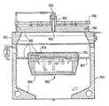
- FIG. 2shows a gas ring for a TCP 9400TM etch reactor.
- the main body of the gas ring 40surrounds a substrate support 44 .
- the bottom surface of the gas ring 40contains a ring-shaped gas-guiding trench 60 .
- the aforementioned gas holes 50extend into the gas-guiding trench 60 .
- the gas ring 40is typically composed of aluminum. Upper surfaces of the gas ring are directly exposed to the plasma and thus subject to erosion, corrosion and corrosion-erosion. To protect these surfaces, the gas ring is typically covered with an aluminum oxide layer. This layer is, however, relatively brittle and can crack during repeated thermal cycling of the reactor during use. Cracks that form in the anodized layer can allow the corrosive process gases to attack the underlying aluminum layer, reducing part life and contributing to metallic and particle contamination of processed substrates, such as wafers, flat panel display substrates and the like.
- the exposed surfaces of the gas ringcan be covered with a coating 42 of a hafnium, strontium, dysprosium and/or lanthanum containing ceramic material.
- the ceramic materialscan be coated on a bare (with or without a native oxide surface film) aluminum layer or on an aluminum oxide layer (e.g., aluminum having an anodized surface).
- the coatingcan be allowed to partially penetrate into the gas holes to coat and protect the inside walls thereof, but without obstructing the openings.
- the gas holescan be plugged or masked during the coating process.
- TCP 9400TM etch reactorthat can be exposed to the plasma during processing can also be coated with a hafnium, strontium, dysprosium and/or lanthanum containing ceramic material according to the invention.
- these componentsinclude, for example, chamber walls, chamber liners, chucking devices and the dielectric window opposite the substrate.
- Providing a coating according to the invention on the upper surface of a chucking device, such as an electrostatic chuck,provides additional protection to the chuck during cleaning cycles in which a wafer is not present and the upper surface of the chuck is thus directly exposed to the plasma.
- FIG. 3Another exemplary polysilicon etch reactor that can include the hafnium, strontium, dysprosium and/or lanthanum containing ceramic materials according to the invention is the VersysTM Polysilicon Etcher or 2300TM etcher also available from Lam Research Corporation of Fremont, Calif., as shown in FIG. 3.
- the reactorcomprises a reactor chamber 150 that includes a substrate support 152 including an electrostatic chuck 154 , which provides a clamping force to a substrate (not shown) mounted thereon.
- a focus ring 170is mounted on the substrate support 152 around the electrostatic chuck 154 .
- the substrate support 152can also be used to apply an RF bias to the substrate.
- the substratecan also be back-cooled using a heat transfer gas such as helium.
- processing gasese.g., Cl 2 , HBr, CF 4 , CH 2 F 2 , O 2 , N 2 , Ar, SF 6 or NF 3
- gasese.g., Cl 2 , HBr, CF 4 , CH 2 F 2 , O 2 , N 2 , Ar, SF 6 or NF 3
- the gas injector 168is typically made of quartz or a ceramic material such as alumina.
- an inductive coil 158can be powered by a suitable RF source (not shown) to provide a high density (e.g., 10 11 -10 12 ions/cm 3 ) plasma.
- the inductive coil 158couples RF energy through dielectric window 160 into the interior of chamber 150 .
- the dielectric window 160is typically made of quartz or alumina.
- the dielectric window 160is shown mounted on an annular member 162 .
- the annular member 162spaces dielectric window 160 from the top of chamber 150 and is referred to as a “gas distribution plate”.
- a chamber liner 164surrounds the substrate support 152 .
- the chamber 150can also include suitable vacuum pumping apparatus (not shown) for maintaining the interior of the chamber at a desired pressure.
- reactor componentssuch as the annular member 162 , dielectric window 160 , substrate support 152 , chamber liner 164 , gas injector 168 , focus ring 170 and the electrostatic chuck 154 , are shown coated with a coating 166 of a hafnium, strontium, dysprosium and/or lanthanum containing ceramic material according to the invention.
- selected interior surfaces of the chamber 150 and substrate support 152 below the chamber liner 164can also be provided with a coating 166 of a hafnium, strontium, dysprosium and/or lanthanum containing ceramic material according to the invention.
- any or all of these surfaces, as well as any other internal reactor surface,can be provided with a coating according to the invention.
- any or all of these componentscan alternatively be manufactured from monolithic bodies of a hafnium, strontium, dysprosium and/or lanthanum containing ceramic material according to the invention.
- the componentscan be used in a high-density oxide etch process.
- An exemplary oxide etch reactoris the TCP 9100TM plasma etch reactor available from Lam Research Corporation of Fremont, Calif.
- the gas distribution plateis a circular plate situated directly below the TCPTM window, which is also the vacuum sealing surface at the top of the reactor in a plane above and parallel to a semiconductor wafer.
- the gas distribution plateis sealed to a gas distribution ring located at the periphery of the gas distribution plate.
- the gas distribution ringfeeds gas from a source into the volume defined by the gas distribution plate, an inside surface of a window underlying an antenna in the form of a flat spiral coil supplying RF energy into the reactor, and the gas distribution ring.
- the gas distribution platecontains holes of a specified diameter, which extend through the plate.
- the spatial distribution of the holes through the gas distribution platecan be varied to optimize etch uniformity of the layers to be etched, e.g., a photoresist layer, a silicon dioxide layer and an underlayer material on the wafer.
- the cross-sectional shape of the gas distribution platecan be varied to manipulate the distribution of RF power into the plasma in the reactor.
- the gas distribution plateis a dielectric material to enable coupling of this RF power through the gas distribution plate into the reactor. Further, it is desirable for the material of the gas distribution plate to be highly resistant to chemical sputter-etching in environments, such as oxygen or a hydro-fluorocarbon gas plasma, to avoid breakdown and the resultant particle generation associated therewith
- FIG. 4illustrates a plasma reactor of the aforementioned type.
- the reactorcomprises a reactor chamber 10 .
- a substrate holder 12includes an electrostatic chuck 34 , which provides a clamping force and an RF bias to a substrate 13 .
- the substratecan be back-cooled using a heat transfer gas such as helium.
- a focus ring 14confines plasma in a region above the substrate.
- the reactor chamberincludes a vacuum pumping apparatus for maintaining the interior of the chamber at a desired pressure (e.g., below 50 mTorr, typically 1-20 mTorr).
- a substantially planar dielectric window 20is provided between the antenna 18 and the interior of the processing chamber 10 and forms the vacuum wall at the top of the processing chamber 10 .
- a gas distribution plate 22is provided beneath window 20 and includes openings for delivering process gas from the gas supply 23 to the chamber 10 .
- a conical liner 30extends from the gas distribution plate 22 and surrounds the substrate holder 12 .
- the antenna 18can be provided with a channel 24 through which a temperature control fluid is flowed via inlet and outlet conduit 25 , 26 .
- the antenna 18 and/or window 20need not be cooled, or could be cooled by other suitable technique, such as by blowing gas over the antenna and window, passing a cooling fluid through or in heat transfer contact with the window and/or gas distribution plate, etc.
- a substratesuch as a semiconductor wafer
- an electrostatic chuck 34Other clamping means, however, such as a mechanical clamping mechanism can also be used. Additionally, helium back-cooling can be employed to improve heat transfer between the substrate and chuck.
- Process gasis then supplied to the vacuum processing chamber 10 by passing the process gas through a gap between the window 20 and the gas distribution plate 22 .
- Suitable gas distribution plate arrangementsi.e., showerhead
- a high density plasmais ignited in the space between the substrate and the window by supplying suitable RF power to the antenna 18 .
- the internal surfaces of reactor componentssuch as the gas distribution plate 22 , the chamber liner 30 , the electrostatic chuck 34 , and the focus ring 14 are coated with a coating 32 of a hafnium, strontium, dysprosium and/or lanthanum containing ceramic material according to the invention.
- a coating 32 of a hafnium, strontium, dysprosium and/or lanthanum containing ceramic material according to the inventioncan be coated with a hafnium, strontium, dysprosium and/or lanthanum containing ceramic material according to the invention.
- etch reactorsthat can incorporate components according to the invention.
- Components containing hafnium, strontium, dysprosium and/or lanthanum containing ceramic materials according to the inventioncan be used in any etch reactor (e.g., a metal etch reactor) or other type of semiconductor processing apparatus where the reduction of plasma induced erosion, corrosion and/or corrosion-erosion and associated contamination is desired.
- other components that can be provided with a coating of a hafnium, strontium, dysprosium and/or lanthanum containing ceramic material according to the inventioninclude, but are not limited to, chamber walls, substrate holders, fasteners, etc. These parts are typically made from metal (e.g., aluminum) or ceramic (e.g., alumina). These metallic plasma reactor components are typically exposed to plasma and often show signs of erosion, corrosion and/or corrosion-erosion. Other parts that can be coated in accordance with the invention need not be directly exposed to plasma, but may instead be exposed to corrosive gases, such as gases emitted from processed wafers or the like.
- equipment used in processing semiconductor substratescan also be provided with hafnium, strontium, dysprosium and/or lanthanum containing ceramic material surfaces and coatings according to the invention.
- Such equipmentcan include transport mechanisms, gas supply systems, liners, lift mechanisms, load locks, door mechanisms, robotic arms, fasteners, and the like.
- Examples of metallic materials that can be coated with a hafnium, strontium, dysprosium and/or lanthanum containing ceramic material according to the inventioninclude aluminum and aluminum alloys, stainless steels and refractory metals, e.g., 6061-T6 aluminum and 304 and 316 stainless steels. Because the hafnium, strontium, dysprosium and/or lanthanum containing ceramic materials form a wear resistant coating over the component, the underlying component is protected from direct exposure to the plasma. Accordingly, the metallic substrate can be protected against erosion, corrosion and/or corrosion-erosion attack by the plasma. As a result, metallic materials, such as aluminum alloys, can be used without regard to alloying additions, grain structure or surface conditions.
- various ceramic or polymeric materialscan also be coated with a hafnium, strontium, dysprosium and/or lanthanum containing ceramic material according to the invention.
- the reactor componentscan be made from ceramic materials, including, but not limited to, alumina (Al 2 O 3 ), silicon carbide (SiC), silicon nitride (Si 3 N 4 ), boron carbide (B 4 C) and/or boron nitride (BN).
- Polymeric materials that can be coatedare preferably those that can withstand high temperature conditions present in plasma reactors.
- FIG. 5shows a coated component according to an exemplary preferred embodiment of the invention.
- a first intermediate coating 80is optionally coated on a substrate 70 by a conventional technique.
- the optional first intermediate coating 80is sufficiently thick to adhere to the substrate and to further allow it to be processed prior to forming an optional second intermediate coating 90 , or the hafnium, strontium, dysprosium and/or lanthanum containing ceramic material coating 100 .
- the first intermediate coating 80 and the second intermediate coating 90can have any suitable thickness that provides these desired properties. These coatings can have a thickness of at least about 0.001 inches, preferably from about 0.001 to about 0.25 inches, more preferably from about 0.001 to about 0.15 inches, and most preferably from about 0.001 inches to about 0.05 inches.
- the first intermediate coating 80can be treated, such as by roughening using any suitable technique, and then coated with the optional second intermediate coating 90 , or with the hafnium, strontium, dysprosium and/or lanthanum containing ceramic material coating 100 .
- a roughened first intermediate coating 80provides a particularly good bond to subsequently applied coatings.
- the second intermediate coating 90imparts a high mechanical compression strength to the first intermediate coating 80 and reduces formation of fissures in the second intermediate coating 90 .
- the second intermediate coating 90is sufficiently thick to adhere to the first intermediate coating 80 and to allow it to be processed prior to forming any additional intermediate coatings, or the outer hafnium, strontium, dysprosium and/or lanthanum containing ceramic material coating 100 .
- the second intermediate coating 90also can be treated, such as by roughening.
- the second intermediate coating 90can have any suitable thickness that provides these desired properties, such as a thickness of at least about 0.001 inches, preferably from about 0.001 to about 0.25 inches, more preferably from about 0.001 and about 0.15 inches, and most preferably from about 0.001 inches to about 0.05 inches.
- the first and second intermediate coatingscan be made of any metallic, ceramic and polymer materials that are suitable for use in semiconductor plasma processing chambers.
- Particularly desirable metals that can be usedinclude, but are not limited to, refractory metals, which can withstand high processing temperatures.
- Preferred ceramicsinclude, but are not limited to, Al 2 O 3 , SiC, Si 3 N 4 , BC, AlN, TiO 2 and mixtures thereof.
- Preferred polymersinclude, but are not limited to, fluoropolymers, such as polytetrafluoroethylene and polyimides.
- the intermediate coatingscan be applied by any suitable deposition technique such as plating (e.g., electroless plating or electroplating), sputtering, immersion coating, chemical vapor deposition, physical vapor deposition, electrophoretic deposition, hot isostatic pressing, cold isostatic pressing, compression molding, casting, compacting and sintering, and thermal spraying (e.g., plasma spraying).
- platinge.g., electroless plating or electroplating
- sputteringimmersion coating
- chemical vapor depositione.g., physical vapor deposition
- electrophoretic depositione.g., hot isostatic pressing, cold isostatic pressing, compression molding, casting, compacting and sintering
- thermal sprayinge.g., plasma spraying
- the optional first intermediate coating 80 and second intermediate coating 90can have the same or different compositions from each other, depending on their desired properties. Additional intermediate coatings such as a third, fourth or fifth intermediate coating of the same or different materials can also be provided between the coating and the substrate if desired.
- FIG. 6shows another exemplary embodiment of the hafnium, strontium, dysprosium and/or lanthanum containing ceramic material coatings according to the invention.
- the coating 100can be deposited directly onto a substrate, which is an outer surface of the component 70 .
- the coatingcan be have any suitable thickness that provides the desired level of wear resistance to the component.
- the coating 100can have a thickness in the range of about 0.001 inches to about 1 inch, preferably from about 0.001 inches to about 0.5 inch, and most preferably from about 0.001 inches to about 0.05 inches.
- the thickness of the ceramic layercan be selected to be compatible with the plasma environment to be encountered in the reactor (e.g., etching, CVD, etc.).
- thermal sprayingis a preferred method of providing components having coating surfaces according to the invention.
- other coating methodscan also be used including, for example, other deposition techniques, such as sputtering, immersion coating, chemical vapor deposition and physical vapor deposition; hot isostatic pressing; cold isostatic pressing; compression molding; casting; and compaction and sintering techniques.
- components of semiconductor processing apparatuscan also be manufactured as monolithic bodies from hafnium, strontium, dysprosium and/or lanthanum containing ceramic material.
- These monolithic bodiescan be separate bodies or coverings for other components.
- the hafnium, strontium, dysprosium and/or lanthanum containing ceramic materials according to the inventioncan be formed into coverings, such as liners, constructed to cover exposed surfaces of reactor components.
- These coveringscan be attached to surfaces in reactor chambers by any suitable fastening technique, including, for example, adhesive bonding or by mechanical fasteners.
- the fasteners themselves, if exposed to the plasmashould preferably also be made from an erosion resistant material to enhance their service life.
- hafnium, strontium, dysprosium and/or lanthanum containing ceramic material coveringsmay be constructed to interlock with the underlying reactor component.
- Monolithic coveringscan be provided over any suitable substrate, such as, for example, over walls and other surfaces.
- An exemplary method of manufacturing monolithic bodies from hafnium, strontium, dysprosium and/or lanthanum containing ceramic materialsmay include preparing a slurry containing, for example, hafnium oxide, strontium oxide, dysprosium oxide and/or lanthanum oxide; forming a green compact in a desired shape and size from the slurry; and sintering the compact to form a sintered body.
- the green compactcan be formed in the shape of any desired plasma reactor component. Details of ceramic processing techniques are given in Introduction to Ceramics, 2 nd Edition, by W. D. Kingery, H. K. Bowen, and D. R. Uhlnann (J. Wiley & Sons, 1976). This description is incorporated herein by reference in its entirety.
- the monolithic componentsare preferably plasma-exposed components of plasma reactors.
- Suitable componentscan include, for example, chamber walls, substrate supports, gas distribution systems including showerheads, baffles, rings, nozzles, fasteners, heating elements, plasma screens, liners, transport module components, such as robotic arms, fasteners, inner and outer chamber walls, etc., and the like.
- a specific example of such a componentis the reactor component 110 shown in FIG. 7.
- the reactor component 110is a monolithic body manufactured from a hafnium oxide, strontium oxide, dysprosium oxide and/or lanthanum oxide containing ceramic material.
- the hafnium oxide, strontium oxide, dysprosium oxide and/or lanthanum containing ceramic materialcan be provided on all or part of the reactor chamber and components.
- the coating or monolithic bodyis provided on the regions of the reactor chamber that are exposed to the plasma environment, such as those parts in direct contact with the plasma, or parts located behind chamber components (e.g., liners).
- the hafnium oxide, strontium oxide, dysprosium oxide and/or lanthanum containing coating or monolithic bodybe provided at regions of the reactor chamber that are subjected to relatively high bias voltages (i.e. relatively high sputter ion energies).
- hafnium, strontium, dysprosium and/or lanthanum containing ceramic coating or coveringBy either applying a hafnium, strontium, dysprosium and/or lanthanum containing ceramic coating or covering, or by constructing a monolithic hafnium, strontium, dysprosium and/or lanthanum containing ceramic component, in accordance with the invention, advantages are realized. Namely, lower erosion rates are achievable in plasma reactors. As a result, the hafnium, strontium, dysprosium and/or lanthanum containing ceramic coatings, coverings and components according to the invention can decrease levels of metal and particulate contamination, lower costs by increasing the lifetime of consumables, decrease process drifts and reduce the levels of corrosion of chamber parts and substrates.
- the hafnium, strontium, dysprosium and/or lanthanum containing ceramic coatings and components according to the inventioncan provide an extremely hard, wear resistant surface.
- Such coating or componentis desirably free of materials that react with processing chamber gases, and is chemically inert such that there is low or no particle contamination, little or no corrosion, little or no metal contamination and/or little or no volatile etch products.
Landscapes
- Chemical & Material Sciences (AREA)
- Engineering & Computer Science (AREA)
- Chemical Kinetics & Catalysis (AREA)
- Materials Engineering (AREA)
- Mechanical Engineering (AREA)
- Metallurgy (AREA)
- Organic Chemistry (AREA)
- Inorganic Chemistry (AREA)
- Physics & Mathematics (AREA)
- Plasma & Fusion (AREA)
- Ceramic Engineering (AREA)
- Analytical Chemistry (AREA)
- General Chemical & Material Sciences (AREA)
- Drying Of Semiconductors (AREA)
- Coating By Spraying Or Casting (AREA)
- Plasma Technology (AREA)
- Container, Conveyance, Adherence, Positioning, Of Wafer (AREA)
Abstract
Description
- 1. Field of the Invention[0001]
- The invention relates to components for semiconductor material processing equipment. The components are formed of materials that can reduce contamination during semiconductor material processing. The invention also relates to methods of making the components.[0002]
- 2. Description of the Related Art[0003]
- In the field of semiconductor material processing, vacuum processing chambers are used for etching and chemical vapor deposition (CVD) of materials on substrates. Process gases are flowed into the processing chamber while a radio frequency (RF) field is applied to the process gases to generate a plasma of the process gases. The plasma performs the desired etching or deposition of selected materials on wafers. Examples of parallel plate, transformer coupled plasma (TCP™), which is also called inductively coupled plasma (ICP), and electron-cyclotron resonance (ECR) reactors and components thereof are disclosed in commonly owned U.S. Pat. Nos. 4,340,462; 4,948,458; 5,200,232 and 5,820,723.[0004]
- During processing of semiconductor substrates, the substrates are typically held in place within the vacuum chamber by substrate holders, as disclosed, for example, in U.S. Pat. Nos. 5,262,029 and 5,838,529. Process gas can be supplied to the chamber by various gas supply systems.[0005]
- In addition to the plasma chamber equipment, other equipment used in processing semiconductor substrates includes transport mechanisms, liners, lift mechanisms, load locks, door mechanisms, robotic arms, fasteners, and the like.[0006]
- Plasmas are used to remove materials by etching or for deposition of materials on substrates. The plasma etch conditions create significant ion bombardment of the surfaces of the processing chamber that are exposed to the plasma. This ion bombardment, combined with plasma chemistries and/or etch byproducts, can produce significant erosion, corrosion and corrosion-erosion of the plasma-exposed surfaces of the processing chamber. As a result, the surface materials are removed by physical and/or chemical attack, including erosion, corrosion and/or corrosion-erosion. This attack causes problems including short part lifetimes, increased consumable costs, particulate contamination, on-wafer transition metal contamination and process drift.[0007]
- In light of these problems, plasma processing chambers have been designed to include parts, such as, disks, rings, and cylinders, that confine the plasma over the wafer being processed. However, these parts are continuously attacked by the plasma and, consequently, ultimately erode or accumulate polymer buildup. Eventually, these parts suffer such wear that they are no longer usable. Those parts with relatively short lifetimes are commonly referred to as “consumables.” If the consumable part's lifetime is short, then the cost of ownership is high. Erosion of consumables and other parts generates contamination in plasma processing chambers.[0008]
- Because of the erosive and corrosive nature of the plasma environment in such reactors, and the need to minimize particle and/or metal contamination, it is desirable for components of such equipment, including consumables and other parts, to have suitably high erosion and corrosion resistance. Known parts have been formed of aluminum-based materials. However, the high ion bombardment by the plasma can erode and corrode these materials, producing unsatisfactory levels of contamination (e.g., particulate contamination and metallic impurity contamination).[0009]
- In view of the high purity requirements for processing semiconductor materials there is a need for components of semiconductor processing apparatus composed of materials that provide improved resistance to physical and chemical attack, including erosion, corrosion and/or erosion-corrosion, to minimize the associated contamination of semiconductor materials during their processing. Materials that can increase the service life of components of the equipment and thus reduce the down time of the apparatus, would contribute to reducing the cost of processing semiconductor materials.[0010]
- The invention can satisfy the above-described needs, as well as other needs, by providing components of semiconductor processing apparatus composed of ceramic materials that provide improved wear resistance to erosion, corrosion and/or corrosion-erosion in plasma processing environments. The components can provide low contamination with respect to metals and particulate.[0011]
- In accordance with exemplary embodiments of the invention, the ceramic materials can be applied as coatings on surfaces of substrates, in components utilized in semiconductor material processing equipment. For example, the components can be used in plasma processing chambers. The coated components can provide improved resistance to erosion, corrosion and/or corrosion-erosion when exposed to plasmas during processing.[0012]
- In accordance with other exemplary embodiments of the invention, such components can be bulk parts formed entirely of the protective materials. That is, the components can be monolithic.[0013]
- An exemplary embodiment of a process of making a component of a semiconductor processing apparatus according to the invention comprises forming at least a portion of a component of such equipment from a ceramic material. The portion comprises an outermost surface of the component. The ceramic material comprises (i) at least one oxide, nitride, boride, carbide and/or fluoride of (ii) strontium, lanthanum and dysprosium, and/or at least one nitride, boride, carbide and/or fluoride of hafnium. Preferably, the ceramic material comprises one of strontium oxide, dysprosium oxide and lanthanum oxide as the single largest constituent of the ceramic material coating. The ceramic material can be applied as a coating, or it can be formed into a monolithic body.[0014]
- Another exemplary embodiment of the invention comprises applying a coating of a ceramic material over a metal containing or polymeric surface of a component of a semiconductor processing apparatus. The ceramic material comprises hafnium oxide, hafnium nitride, hafnium boride, hafnium carbide or hafnium fluoride as the single largest constituent of the ceramic material coating.[0015]
- Other exemplary embodiment of methods according to the invention comprise forming a component of a semiconductor processing apparatus in the form of a monolithic body. The component comprises hafnium oxide, hafnium nitride, hafnium boride, hafnium carbide or hafnium fluoride as the single largest constituent.[0016]
- An exemplary embodiment of a process of making a component of a semiconductor processing apparatus according to the invention comprises preparing a slurry comprising as the single largest constituent (i) at least one oxide, nitride, boride, carbide and/or fluoride of (ii) strontium, lanthanum and dysprosium, and/or at least one nitride, boride, carbide and/or fluoride of hafnium; forming a green compact from the slurry in the desired shape; and sintering the green compact to form a component. The ceramic material preferably comprises at the least one of hafnium oxide, strontium oxide, dysprosium oxide and lanthanum oxide as the single largest constituent thereof. These processes can be used to form monolithic components.[0017]
- An exemplary embodiment of a component of a semiconductor processing apparatus according to the invention comprises at least a portion comprising a ceramic material. The portion comprises an outermost surface of the component. The ceramic material comprises as the single largest constituent (i) at least one oxide, nitride, boride, carbide and/or fluoride of (ii) strontium, lanthanum and dysprosium, and/or at least one nitride, boride, carbide and/or fluoride of hafnium.[0018]
- Another exemplary embodiment of a component of a semiconductor processing apparatus according to the invention comprises a substrate having a metal containing or polymeric surface; and a coating of a ceramic material over the surface, where the ceramic material comprises hafnium oxide, hafnium nitride, hafnium boride, hafnium carbide or hafnium fluoride as the single largest constituent of the ceramic material coating.[0019]
- Another exemplary embodiment of a component of a semiconductor processing apparatus according to the invention comprises a monolithic body, which comprises hafnium oxide, hafnium nitride, hafnium boride, hafnium carbide or hafnium fluoride as the single largest constituent.[0020]
- The invention also provides semiconductor processing apparatus that includes at least one of above-described components to provide wear resistance.[0021]
- The invention will be readily understood by the following detailed description in conjunction with the accompanying drawings.[0022]
- FIG. 1 illustrates a conventional plasma spray process.[0023]
- FIG. 2 shows a cross-sectional view of a gas ring for a plasma etching apparatus according to an exemplary embodiment of the invention.[0024]
- FIG. 3 shows an etch chamber containing exemplary embodiments of components according to the invention.[0025]
- FIG. 4 shows another etch chamber containing exemplary embodiments of components according to the invention.[0026]
- FIG. 5 shows an exemplary embodiment of a protective ceramic coating according to the invention.[0027]
- FIG. 6 shows another exemplary embodiment of a protective ceramic coating according to the invention.[0028]
- FIG. 7 shows an exemplary embodiment of a monolithic component according to the invention.[0029]
- The invention provides components that have wear resistance with respect to physical and chemical attack by plasmas generated in semiconductor material processing apparatuses. As used herein, the term “wear resistant” includes, but is not limited to, erosion, corrosion and/or corrosion-erosion resistance. The components are composed of wear resistant ceramic materials.[0030]
- In some exemplary embodiments, the components include coatings composed of erosion resistant ceramic materials formed on substrates. For example, the components can include substrates and one or more erosion resistant ceramic coatings formed on the substrates. The coatings resist erosion and, being non-metallic materials, are also resistant to corrosion and/or corrosion-erosion.[0031]
- In other exemplary embodiments of the invention, the components can consist essentially of wear resistant ceramic materials. For example, the components can be bulk parts of a semiconductor material processing apparatus.[0032]
- According to the invention, the components composed of the wear resistant ceramic materials can be components of apparatuses for processing semiconductors.[0033]
- The invention also provides semiconductor processing apparatuses that include one or more of the components composed, at least partially, of a wear resistant material.[0034]
- In addition, the invention provides methods of making components, at least in part, of the wear resistant materials.[0035]
- As stated above, the invention is applicable to any suitable type of component. The invention provides effective wear resistance to the surfaces of components of semiconductor material processing apparatuses. Those skilled in the art will appreciate that the wear resistant materials according to the invention can be applied to different processing apparatuses useful for processing different semiconductor materials. In addition, the wear resistant materials can be applied to different components in the processing apparatuses. Such exemplary components include, but are not limited to, parts of a plasma and/or vacuum chamber, such as, for example, chamber walls, substrate supports, gas distribution systems including showerheads, baffles, rings, nozzles, etc., fasteners, heating elements, plasma screens, liners, transport module components, such as robotic arms, fasteners, inner and outer chamber walls, and the like.[0036]
- According to the invention, the wear resistant materials can comprise at least one of hafnium, strontium, dysprosium and lanthanum. These elements have a relatively large molecular mass and are relatively inert with respect to typical etching chemicals, which are believed to provide a reduced erosion rate in plasma environments. Preferably, the wear resistant materials comprise one of hafnium oxide, strontium oxide, dysprosium oxide or lanthanum oxide as the single largest constituent of the ceramic material. Exemplary embodiments of the ceramic materials can comprise any one or more of these oxides. Other constituents that can be included in the ceramic materials are described in detail below.[0037]
- The hafnium containing ceramic materials according to the invention preferably contain hafnium oxide (hafnia) as the single largest constituent. In some embodiments, the hafnium containing ceramic materials can consist essentially of hafnium oxide. The hafnium containing ceramic materials can also contain other hafnium containing ceramic materials other than oxides, including, but not limited to, at least one hafnium boride, hafnium fluoride, hafnium nitride and/or hafnium carbide, or mixtures thereof.[0038]
- According to the invention, the hafnium containing ceramic materials can contain other ceramic materials other than, or in addition to, the above-described hafnium oxide, boride, fluoride and carbide materials. These other ceramic materials can include, but are not limited to, at least one oxide, nitride, boride, fluoride and/or carbide of elements selected from Groups IIA, IIIA, IVA, VA, VIA, VIIA, VIIIA, IB, IIB, IIIB, IVB and VB of the periodic table; and/or one or more oxide, nitride, boride, fluoride or carbide of any element of the actinide series (i.e., elements having an atomic number of 58-71). For example, hafnium containing ceramic materials (and also strontium containing, dysprosium containing and lanthanum containing materials described below) can be mixed with yttrium oxide (yttria), zirconium oxide (zirconia), aluminum oxide (alumina) and/or cerium oxide (ceria).[0039]
- The strontium containing ceramic materials according to the invention preferably contain strontium oxide (strontia) as the single largest constituent. In some embodiments, the strontium containing ceramic materials can consist essentially of strontium oxide. The strontium containing ceramic materials can also contain other strontium containing ceramic materials other than oxides, including, but not limited to, at least one strontium boride, strontium fluoride, strontium nitride, strontium carbide, or mixtures thereof.[0040]
- According to the invention, the strontium containing ceramic materials can contain other ceramic materials other than, or in addition to, the above-described strontium oxide, boride, fluoride and carbide materials. These other ceramic materials can include, but are not limited to, one or more oxides, nitrides, borides, fluorides and carbides of elements selected from Groups IIA, IIIA, IVA, VA, VIA, VIIA, VIIIA, IB, IIB, IIIB, IVB, and VB of the periodic table; and/or one or more oxide, nitride, boride, fluoride or carbide of any element of the actinide series, as described above.[0041]
- The dysprosium containing ceramic materials according to the invention preferably contain dysprosium oxide (dysprosia) as the single largest constituent. In some embodiments, the dysprosium containing ceramic materials can consist essentially of dysprosium oxide. The dysprosium containing ceramic materials can also contain other dysprosium containing ceramic materials other than oxides, including, but not limited to, at least one dysprosium boride, dysprosium fluoride, dysprosium nitride, dysprosium carbide, or mixtures thereof.[0042]
- According to the invention, the dysprosium containing ceramic materials can contain other ceramic materials other than, or in addition to, the above-described dysprosium oxide, boride, fluoride and carbide materials. These other ceramic materials can include, but are not limited to, at least one oxide, nitride, boride, fluoride and/or carbide of elements selected from Groups IIA, IIIA, IVA, VA, VIA, VIIA, VIIIA, IB, IIB, IIIB, IVB and VB of the periodic table; and/or one or more oxide, nitride, boride, fluoride or carbide of any element of the actinide series, as described above.[0043]
- The lanthanum containing ceramic materials according to the invention preferably contain lanthanum oxide (lanthana) as the single largest constituent. In some embodiments, the lanthanum containing ceramic materials can consist essentially of lanthanum oxide. The lanthanum containing ceramic materials can also contain other lanthanum containing ceramic materials other than oxides, including, but not limited to, at least one lanthanum boride, lanthanum fluoride, lanthanum nitride and/or lanthanum carbide, or mixtures thereof.[0044]
- According to the invention, the lanthanum containing ceramic materials can contain other ceramic materials other than, or in addition to, the above-described lanthanum oxide, boride, fluoride and carbide materials. These other ceramic materials can include, but are not limited to, at least one oxide, nitride, boride, fluoride and/or carbide of elements selected from Groups IIA, IIIA, IVA, VA, VIA, VIIA, VIIIA, IB, IIB, IIIB, IVB, and VB of the periodic table; and/or at least one oxide, nitride, boride, fluoride and/or carbide of any element of the actinide series, as described above.[0045]
- According to the invention, the ceramic materials can comprise mixtures of the above-described hafnium, strontium, dysprosium and lanthanum containing materials. In addition, the ceramic materials can comprise mixtures of hafnium, strontium, dysprosium and/or lanthanum containing materials, and additional materials, including, but not limited to, one or more oxides, nitrides, borides, fluorides and carbides of elements selected from Groups IIA, IIIA, IVA, VA, VIA, VIIA, VIIIA, IB, IIB, IIIB, IVB, and VB; and/or one or more oxide, nitride, boride, fluoride or carbide of any element of the actinide series, as described above.[0046]
- In order to try to minimize the contamination of electronic materials processed in equipment incorporating one or more hafnium, strontium, dysprosium and/or lanthanum containing components according to the invention, it is desirable for the ceramic materials to be as pure as possible, e.g., include minimal amounts of potentially contaminating elements, such as transition metals, alkali metals or the like. For example, the hafnium, strontium, dysprosium and lanthanum containing ceramic materials can be sufficiently pure to avoid on-wafer contamination of 10[0047]10atoms/cm2or higher, preferably 105atoms/cm2or higher. Preferably, these ceramic materials have a purity of at least about 99%, and more preferably from about 99.99% to about 100%.
- In addition, the hafnium, strontium, dysprosium and lanthanum containing ceramic materials according to the invention have a smooth surface finish. Preferably, these materials, applied as coatings or formed into monolithic components, have a surface roughness (RA) of from about 5 to about 400 μinch, and more preferably less than about 200 μinch.[0048]
- The hafnium, strontium, dysprosium and lanthanum containing ceramic materials according to the invention can also provide a high bond strength to the underlying substrate. Preferably, these materials applied as coatings have a tensile bond strength of from about 2000 psi to about 7000 psi.[0049]
- Also, the hafnium, strontium, dysprosium and lanthanum containing ceramic materials according to the invention can provide low porosity levels, which is advantageous to minimize contact of aggressive atmospheres (e.g., HCl containing atmospheres) with the underlying substrate, and thus subsequent corrosion, erosion and/or corrosion-erosion of the substrate by the aggressive atmosphere. Preferably, the ceramic materials have a porosity of less than 15% by volume, and more preferably less than about 3% by volume.[0050]
- In addition, the hafnium, strontium, dysprosium and lanthanum containing ceramic materials according to the invention can provide a high hardness to resist erosion. Preferably, the ceramic materials have a hardness (HVO[0051]3) of from about 200 to about 800.
- The above-described ceramic materials can provide desirable wear resistance properties for use in semiconductor processing apparatus, such as, for example, plasma etch chambers. In particular, hafnium, strontium, dysprosium and lanthanum containing ceramic materials can provide surfaces that can reduce ion induced erosion and associated levels of particulate contamination in plasma reactor chambers. Hafnium, strontium, dysprosium and lanthanum containing ceramic materials can also protect underlying substrates against both physical attack and chemical attack by plasmas.[0052]
- The wear resistant ceramic materials according to the invention can be used in various different plasma atmospheres for etching and deposition applications, as well as other uses. For example, typical etch chemistries include, for example, chlorine containing gases including, but not limited to, Cl[0053]2, HCl and BCl3; bromine containing gases including, but not limited to, bromine and HBr; oxygen containing gases including, but not limited to, O2, H2O and SO2; fluorine containing gases including, but not limited to, CF4, CH2F2, NF3, CH3F, CHF3and SF6; and inert and other gases including, but not limited to He, Ar and N2. These and other gases may be used in any suitable combination, depending on the desired plasma. Exemplary plasma reactor etching operating conditions are as follows: temperature of from about 25° C. to about 90° C.; pressure of from about 0 mTorr to about 100 mTorr; gas flow rate of from about 10 sccm to about 1000 sccm; and plasma power of from about 0 Watts to about 1500 Watts.
- In an exemplary preferred embodiment of the invention, the hafnium, strontium, dysprosium and lanthanum containing ceramic materials are provided as a coating on a substrate. These coatings can be applied by methods known in the art. A preferred coating method is thermal spraying (e.g., plasma spraying). In this method, ceramic powder is melted and incorporated in a gas stream, which is directed at the component being spray coated. An advantage of thermal spraying techniques is that the component is coated only on the sides facing the thermal spray gun, and masking can be used to protect other areas. Conventional thermal spraying techniques, including plasma spraying, are described in[0054]The Science and Engineering of Thermal Spray Coatingby Pawlowski (John Wiley, 1995). This description is hereby incorporated by reference in its entirety.
- A particularly preferred thermal spraying method is plasma spraying. Plasma spraying can be used to coat even intricate interior surfaces of chambers and other chamber components. FIG. 1 illustrates a typical plasma spraying process. The coating material, usually in the form of a[0055]
powder 112, is injected into a hightemperature plasma flame 114 usually via anexternal powder port 132 The powder is rapidly heated and accelerated to a high velocity. The hot material impacts on thesubstrate surface 116 and rapidly cools to form acoating 118. - The[0056]
plasma spray gun 120 comprises ananode 122 and a cathode124, both of which are water cooled. Plasma gas126 (e.g., argon, nitrogen, hydrogen, helium) flows around the cathode in the direction generally indicated byarrow 128 and through a constricting nozzle of the anode. The plasma is initiated by a high voltage discharge, which causes localized ionization and a conductive path for a DC arc to form between the cathode124 and theanode 122. Resistance heating from the arc causes the gas to form a plasma. The plasma exits the anode nozzle portion as a free or neutral plasma flame (plasma which does not carry electric current). When the plasma is stabilized ready for spraying, the electric arc extends down the nozzle. Thepowder 112 is so rapidly heated and accelerated that thespray distance 136 between the nozzle tip and the substrate surface can be on the order of 125 to 150 mm. Plasma sprayed coatings are produced by molten or heat-softened particles caused to impact on thesubstrate surface 116. - According to the invention, surface treating techniques, such as cleaning and particle blasting can be used to provide a more chemically and physically active surface for bonding. Prior to coating, the surface of the substrate is preferably thoroughly cleaned to remove undesirable surface material, such as oxides or grease. The surface can also be roughened by any suitable method, such as grit blasting, prior to coating. This roughening increases the surface area available for bonding, which increases the coating bond strength. The rough surface profile can also promote mechanical keying or interlocking of the coating with the substrate.[0057]
- For aluminum reactor components, it is preferable to anodize the surface of the component that is to be coated prior to coating, but not roughen the anodized surface. The anodized layer provides an additional barrier, i.e. in addition to protection provided by the coating, against corrosive attack of the underlying aluminum. The anodized aluminum layer formed on aluminum substrates, such as 6061-T6 aluminum, can have any suitable thickness. For example, the thickness can be typically be from about 2 mil to about 10 mil. The anodized surface can have any suitable finish. For example, the surface finish can have an RA value of about 20 μinch to about 100 μinch. The anodized layer can be sealed by any suitable technique, such as by using boiling deionized water.[0058]
- Hafnium oxide, strontium oxide, dysprosium oxide and/or lanthanum oxide containing ceramic materials according to the invention are preferably applied using a plasma spray process. However, any other coating method suitable for use with ceramic materials may also be employed. For example, the hafnium oxide, strontium oxide, dysprosium oxide and/or lanthanum oxide containing ceramic coatings can also be applied by sputtering, sputter deposition, immersion coating, chemical vapor deposition, evaporation and condensation (including electron beam evaporation and condensation), physical vapor deposition, hot isostatic pressing, cold isostatic pressing, compression molding, casting, compacting and sintering, and thermal spraying.[0059]
- In some preferred embodiments of the invention, the hafnium, strontium, dysprosium and/or lanthanum containing ceramic components are used in a high-density plasma reactor. An exemplary reactor of this type is the TCP 9400™ plasma etch reactor available from Lam Research Corporation of Fremont, Calif. In the TCP 9400™ reactor, processing gases (such as Cl[0060]2, HBr, CF4, CH2F2, O2, N2, Ar, SF6and NF3) are conducted into a gas ring located at the bottom of the etch chamber and are then guided through gas holes into the reactor chamber. FIG. 2 shows a gas ring for a TCP 9400™ etch reactor. As shown in FIG. 2, the main body of the
gas ring 40 surrounds asubstrate support 44. The bottom surface of thegas ring 40 contains a ring-shaped gas-guidingtrench 60. The aforementioned gas holes50 extend into the gas-guidingtrench 60. - The[0061]
gas ring 40 is typically composed of aluminum. Upper surfaces of the gas ring are directly exposed to the plasma and thus subject to erosion, corrosion and corrosion-erosion. To protect these surfaces, the gas ring is typically covered with an aluminum oxide layer. This layer is, however, relatively brittle and can crack during repeated thermal cycling of the reactor during use. Cracks that form in the anodized layer can allow the corrosive process gases to attack the underlying aluminum layer, reducing part life and contributing to metallic and particle contamination of processed substrates, such as wafers, flat panel display substrates and the like. - According to exemplary embodiments of the invention, the exposed surfaces of the gas ring can be covered with a[0062]
coating 42 of a hafnium, strontium, dysprosium and/or lanthanum containing ceramic material. The ceramic materials can be coated on a bare (with or without a native oxide surface film) aluminum layer or on an aluminum oxide layer (e.g., aluminum having an anodized surface). When coating the gas ring, the coating can be allowed to partially penetrate into the gas holes to coat and protect the inside walls thereof, but without obstructing the openings. For example, the gas holes can be plugged or masked during the coating process. - Other components of the TCP 9400™ etch reactor that can be exposed to the plasma during processing can also be coated with a hafnium, strontium, dysprosium and/or lanthanum containing ceramic material according to the invention. These components include, for example, chamber walls, chamber liners, chucking devices and the dielectric window opposite the substrate. Providing a coating according to the invention on the upper surface of a chucking device, such as an electrostatic chuck, provides additional protection to the chuck during cleaning cycles in which a wafer is not present and the upper surface of the chuck is thus directly exposed to the plasma.[0063]
- Another exemplary polysilicon etch reactor that can include the hafnium, strontium, dysprosium and/or lanthanum containing ceramic materials according to the invention is the Versys™ Polysilicon Etcher or 2300™ etcher also available from Lam Research Corporation of Fremont, Calif., as shown in FIG. 3. The reactor comprises a[0064]
reactor chamber 150 that includes asubstrate support 152 including anelectrostatic chuck 154, which provides a clamping force to a substrate (not shown) mounted thereon. Afocus ring 170 is mounted on thesubstrate support 152 around theelectrostatic chuck 154. Thesubstrate support 152 can also be used to apply an RF bias to the substrate. The substrate can also be back-cooled using a heat transfer gas such as helium. In the 2300™ etcher, processing gases (e.g., Cl2, HBr, CF4, CH2F2, O2, N2, Ar, SF6or NF3) are introduced into thechamber 150 via agas injector 168 located on the top ofchamber 150 and connected to agas feed 156. Thegas injector 168 is typically made of quartz or a ceramic material such as alumina. As shown, aninductive coil 158 can be powered by a suitable RF source (not shown) to provide a high density (e.g., 1011-1012ions/cm3) plasma. Theinductive coil 158 couples RF energy throughdielectric window 160 into the interior ofchamber 150. Thedielectric window 160 is typically made of quartz or alumina. Thedielectric window 160 is shown mounted on anannular member 162. Theannular member 162 spacesdielectric window 160 from the top ofchamber 150 and is referred to as a “gas distribution plate”. Achamber liner 164 surrounds thesubstrate support 152. Thechamber 150 can also include suitable vacuum pumping apparatus (not shown) for maintaining the interior of the chamber at a desired pressure. - In FIG. 3, selected internal surfaces of reactor components, such as the[0065]
annular member 162,dielectric window 160,substrate support 152,chamber liner 164,gas injector 168,focus ring 170 and theelectrostatic chuck 154, are shown coated with acoating 166 of a hafnium, strontium, dysprosium and/or lanthanum containing ceramic material according to the invention. As shown in FIG. 3, selected interior surfaces of thechamber 150 andsubstrate support 152 below thechamber liner 164 can also be provided with acoating 166 of a hafnium, strontium, dysprosium and/or lanthanum containing ceramic material according to the invention. Any or all of these surfaces, as well as any other internal reactor surface, can be provided with a coating according to the invention. As described below, any or all of these components can alternatively be manufactured from monolithic bodies of a hafnium, strontium, dysprosium and/or lanthanum containing ceramic material according to the invention. - According to the invention, the components can be used in a high-density oxide etch process. An exemplary oxide etch reactor is the TCP 9100™ plasma etch reactor available from Lam Research Corporation of Fremont, Calif. In the TCP 9100™ reactor, the gas distribution plate is a circular plate situated directly below the TCP™ window, which is also the vacuum sealing surface at the top of the reactor in a plane above and parallel to a semiconductor wafer. The gas distribution plate is sealed to a gas distribution ring located at the periphery of the gas distribution plate. The gas distribution ring feeds gas from a source into the volume defined by the gas distribution plate, an inside surface of a window underlying an antenna in the form of a flat spiral coil supplying RF energy into the reactor, and the gas distribution ring. The gas distribution plate contains holes of a specified diameter, which extend through the plate. The spatial distribution of the holes through the gas distribution plate can be varied to optimize etch uniformity of the layers to be etched, e.g., a photoresist layer, a silicon dioxide layer and an underlayer material on the wafer. The cross-sectional shape of the gas distribution plate can be varied to manipulate the distribution of RF power into the plasma in the reactor. The gas distribution plate is a dielectric material to enable coupling of this RF power through the gas distribution plate into the reactor. Further, it is desirable for the material of the gas distribution plate to be highly resistant to chemical sputter-etching in environments, such as oxygen or a hydro-fluorocarbon gas plasma, to avoid breakdown and the resultant particle generation associated therewith.[0066]
- FIG. 4 illustrates a plasma reactor of the aforementioned type. The reactor comprises a[0067]
reactor chamber 10. Asubstrate holder 12 includes anelectrostatic chuck 34, which provides a clamping force and an RF bias to asubstrate 13. The substrate can be back-cooled using a heat transfer gas such as helium. Afocus ring 14 confines plasma in a region above the substrate. A source of energy for maintaining a high density (e.g., 1010-1012ions/cm3) plasma in the chamber, such as anantenna 18 powered by a suitable RF source to provide a high density plasma, is disposed at the top of thereactor chamber 10. The reactor chamber includes a vacuum pumping apparatus for maintaining the interior of the chamber at a desired pressure (e.g., below 50 mTorr, typically 1-20 mTorr). - A substantially planar[0068]
dielectric window 20 is provided between theantenna 18 and the interior of theprocessing chamber 10 and forms the vacuum wall at the top of theprocessing chamber 10. Agas distribution plate 22 is provided beneathwindow 20 and includes openings for delivering process gas from thegas supply 23 to thechamber 10. Aconical liner 30 extends from thegas distribution plate 22 and surrounds thesubstrate holder 12. Theantenna 18 can be provided with achannel 24 through which a temperature control fluid is flowed via inlet andoutlet conduit antenna 18 and/orwindow 20 need not be cooled, or could be cooled by other suitable technique, such as by blowing gas over the antenna and window, passing a cooling fluid through or in heat transfer contact with the window and/or gas distribution plate, etc. - In operation, a substrate, such as a semiconductor wafer, is positioned on the[0069]
substrate holder 12 and held in place by anelectrostatic chuck 34. Other clamping means, however, such as a mechanical clamping mechanism can also be used. Additionally, helium back-cooling can be employed to improve heat transfer between the substrate and chuck. Process gas is then supplied to thevacuum processing chamber 10 by passing the process gas through a gap between thewindow 20 and thegas distribution plate 22. Suitable gas distribution plate arrangements (i.e., showerhead) arrangements are disclosed in commonly owned U.S. Pat. Nos. 5,824,605; 6,048,798; and 5,863,376, each of which is incorporated herein by reference in its entirety. A high density plasma is ignited in the space between the substrate and the window by supplying suitable RF power to theantenna 18. - In FIG. 4, the internal surfaces of reactor components, such as the[0070]
gas distribution plate 22, thechamber liner 30, theelectrostatic chuck 34, and thefocus ring 14 are coated with acoating 32 of a hafnium, strontium, dysprosium and/or lanthanum containing ceramic material according to the invention. However, only selected ones of these surfaces, and/or other surfaces, can be coated with a hafnium, strontium, dysprosium and/or lanthanum containing ceramic material according to the invention. - Those skilled in the art will appreciate that the high density polysilicon and dielectric etch chambers described above are only exemplary embodiments of plasma etch reactors that can incorporate components according to the invention. Components containing hafnium, strontium, dysprosium and/or lanthanum containing ceramic materials according to the invention can be used in any etch reactor (e.g., a metal etch reactor) or other type of semiconductor processing apparatus where the reduction of plasma induced erosion, corrosion and/or corrosion-erosion and associated contamination is desired.[0071]
- For example, other components that can be provided with a coating of a hafnium, strontium, dysprosium and/or lanthanum containing ceramic material according to the invention include, but are not limited to, chamber walls, substrate holders, fasteners, etc. These parts are typically made from metal (e.g., aluminum) or ceramic (e.g., alumina). These metallic plasma reactor components are typically exposed to plasma and often show signs of erosion, corrosion and/or corrosion-erosion. Other parts that can be coated in accordance with the invention need not be directly exposed to plasma, but may instead be exposed to corrosive gases, such as gases emitted from processed wafers or the like. Therefore, other equipment used in processing semiconductor substrates can also be provided with hafnium, strontium, dysprosium and/or lanthanum containing ceramic material surfaces and coatings according to the invention. Such equipment can include transport mechanisms, gas supply systems, liners, lift mechanisms, load locks, door mechanisms, robotic arms, fasteners, and the like.[0072]
- Examples of metallic materials that can be coated with a hafnium, strontium, dysprosium and/or lanthanum containing ceramic material according to the invention include aluminum and aluminum alloys, stainless steels and refractory metals, e.g., 6061-T6 aluminum and 304 and 316 stainless steels. Because the hafnium, strontium, dysprosium and/or lanthanum containing ceramic materials form a wear resistant coating over the component, the underlying component is protected from direct exposure to the plasma. Accordingly, the metallic substrate can be protected against erosion, corrosion and/or corrosion-erosion attack by the plasma. As a result, metallic materials, such as aluminum alloys, can be used without regard to alloying additions, grain structure or surface conditions.[0073]
- In addition, various ceramic or polymeric materials can also be coated with a hafnium, strontium, dysprosium and/or lanthanum containing ceramic material according to the invention. In particular, the reactor components can be made from ceramic materials, including, but not limited to, alumina (Al[0074]2O3), silicon carbide (SiC), silicon nitride (Si3N4), boron carbide (B4C) and/or boron nitride (BN). Polymeric materials that can be coated are preferably those that can withstand high temperature conditions present in plasma reactors.
- If desired, one or more intermediate layers of material can be provided between the surface of the substrate that is coated and the hafnium, strontium, dysprosium and/or lanthanum containing ceramic material coating. FIG. 5 shows a coated component according to an exemplary preferred embodiment of the invention. A first[0075]
intermediate coating 80 is optionally coated on asubstrate 70 by a conventional technique. The optional firstintermediate coating 80 is sufficiently thick to adhere to the substrate and to further allow it to be processed prior to forming an optional secondintermediate coating 90, or the hafnium, strontium, dysprosium and/or lanthanum containingceramic material coating 100. The firstintermediate coating 80 and the secondintermediate coating 90 can have any suitable thickness that provides these desired properties. These coatings can have a thickness of at least about 0.001 inches, preferably from about 0.001 to about 0.25 inches, more preferably from about 0.001 to about 0.15 inches, and most preferably from about 0.001 inches to about 0.05 inches. - After depositing the optional first[0076]
intermediate coating 80 onto thereactor component 70, the first intermediate coating can be treated, such as by roughening using any suitable technique, and then coated with the optional secondintermediate coating 90, or with the hafnium, strontium, dysprosium and/or lanthanum containingceramic material coating 100. A roughened firstintermediate coating 80 provides a particularly good bond to subsequently applied coatings. Desirably, the secondintermediate coating 90 imparts a high mechanical compression strength to the firstintermediate coating 80 and reduces formation of fissures in the secondintermediate coating 90. - The second[0077]
intermediate coating 90 is sufficiently thick to adhere to the firstintermediate coating 80 and to allow it to be processed prior to forming any additional intermediate coatings, or the outer hafnium, strontium, dysprosium and/or lanthanum containingceramic material coating 100. The secondintermediate coating 90 also can be treated, such as by roughening. The secondintermediate coating 90 can have any suitable thickness that provides these desired properties, such as a thickness of at least about 0.001 inches, preferably from about 0.001 to about 0.25 inches, more preferably from about 0.001 and about 0.15 inches, and most preferably from about 0.001 inches to about 0.05 inches. - The first and second intermediate coatings can be made of any metallic, ceramic and polymer materials that are suitable for use in semiconductor plasma processing chambers. Particularly desirable metals that can be used include, but are not limited to, refractory metals, which can withstand high processing temperatures. Preferred ceramics include, but are not limited to, Al[0078]2O3, SiC, Si3N4, BC, AlN, TiO2and mixtures thereof. Preferred polymers include, but are not limited to, fluoropolymers, such as polytetrafluoroethylene and polyimides.
- The intermediate coatings can be applied by any suitable deposition technique such as plating (e.g., electroless plating or electroplating), sputtering, immersion coating, chemical vapor deposition, physical vapor deposition, electrophoretic deposition, hot isostatic pressing, cold isostatic pressing, compression molding, casting, compacting and sintering, and thermal spraying (e.g., plasma spraying).[0079]
- The optional first[0080]
intermediate coating 80 and secondintermediate coating 90 can have the same or different compositions from each other, depending on their desired properties. Additional intermediate coatings such as a third, fourth or fifth intermediate coating of the same or different materials can also be provided between the coating and the substrate if desired. - FIG. 6 shows another exemplary embodiment of the hafnium, strontium, dysprosium and/or lanthanum containing ceramic material coatings according to the invention. The[0081]
coating 100 can be deposited directly onto a substrate, which is an outer surface of thecomponent 70. The coating can be have any suitable thickness that provides the desired level of wear resistance to the component. Particularly, thecoating 100 can have a thickness in the range of about 0.001 inches to about 1 inch, preferably from about 0.001 inches to about 0.5 inch, and most preferably from about 0.001 inches to about 0.05 inches. The thickness of the ceramic layer can be selected to be compatible with the plasma environment to be encountered in the reactor (e.g., etching, CVD, etc.). - As discussed above, thermal spraying is a preferred method of providing components having coating surfaces according to the invention. However, other coating methods can also be used including, for example, other deposition techniques, such as sputtering, immersion coating, chemical vapor deposition and physical vapor deposition; hot isostatic pressing; cold isostatic pressing; compression molding; casting; and compaction and sintering techniques.[0082]
- As mentioned above, components of semiconductor processing apparatus can also be manufactured as monolithic bodies from hafnium, strontium, dysprosium and/or lanthanum containing ceramic material. These monolithic bodies can be separate bodies or coverings for other components. For example, the hafnium, strontium, dysprosium and/or lanthanum containing ceramic materials according to the invention can be formed into coverings, such as liners, constructed to cover exposed surfaces of reactor components. These coverings can be attached to surfaces in reactor chambers by any suitable fastening technique, including, for example, adhesive bonding or by mechanical fasteners. When fasteners are used, the fasteners themselves, if exposed to the plasma, should preferably also be made from an erosion resistant material to enhance their service life. Additionally, the hafnium, strontium, dysprosium and/or lanthanum containing ceramic material coverings may be constructed to interlock with the underlying reactor component. Monolithic coverings can be provided over any suitable substrate, such as, for example, over walls and other surfaces.[0083]
- An exemplary method of manufacturing monolithic bodies from hafnium, strontium, dysprosium and/or lanthanum containing ceramic materials may include preparing a slurry containing, for example, hafnium oxide, strontium oxide, dysprosium oxide and/or lanthanum oxide; forming a green compact in a desired shape and size from the slurry; and sintering the compact to form a sintered body. The green compact can be formed in the shape of any desired plasma reactor component. Details of ceramic processing techniques are given in[0084]Introduction to Ceramics,2ndEdition,by W. D. Kingery, H. K. Bowen, and D. R. Uhlnann (J. Wiley & Sons, 1976). This description is incorporated herein by reference in its entirety.
- The monolithic components are preferably plasma-exposed components of plasma reactors. Suitable components can include, for example, chamber walls, substrate supports, gas distribution systems including showerheads, baffles, rings, nozzles, fasteners, heating elements, plasma screens, liners, transport module components, such as robotic arms, fasteners, inner and outer chamber walls, etc., and the like. A specific example of such a component is the[0085]
reactor component 110 shown in FIG. 7. Thereactor component 110 is a monolithic body manufactured from a hafnium oxide, strontium oxide, dysprosium oxide and/or lanthanum oxide containing ceramic material. - The hafnium oxide, strontium oxide, dysprosium oxide and/or lanthanum containing ceramic material can be provided on all or part of the reactor chamber and components. In a preferred embodiment, the coating or monolithic body is provided on the regions of the reactor chamber that are exposed to the plasma environment, such as those parts in direct contact with the plasma, or parts located behind chamber components (e.g., liners). Additionally, it is preferred that the hafnium oxide, strontium oxide, dysprosium oxide and/or lanthanum containing coating or monolithic body be provided at regions of the reactor chamber that are subjected to relatively high bias voltages (i.e. relatively high sputter ion energies).[0086]
- By either applying a hafnium, strontium, dysprosium and/or lanthanum containing ceramic coating or covering, or by constructing a monolithic hafnium, strontium, dysprosium and/or lanthanum containing ceramic component, in accordance with the invention, advantages are realized. Namely, lower erosion rates are achievable in plasma reactors. As a result, the hafnium, strontium, dysprosium and/or lanthanum containing ceramic coatings, coverings and components according to the invention can decrease levels of metal and particulate contamination, lower costs by increasing the lifetime of consumables, decrease process drifts and reduce the levels of corrosion of chamber parts and substrates.[0087]
- The hafnium, strontium, dysprosium and/or lanthanum containing ceramic coatings and components according to the invention can provide an extremely hard, wear resistant surface. Such coating or component is desirably free of materials that react with processing chamber gases, and is chemically inert such that there is low or no particle contamination, little or no corrosion, little or no metal contamination and/or little or no volatile etch products.[0088]
- While the invention has been described in detail with reference to specific embodiments thereof, it will be apparent to those skilled in the art that various changes and modifications can be made, and equivalents employed, without departing from the scope of the appended claims.[0089]
Claims (40)
1. A component of a semiconductor processing apparatus, comprising at least a portion comprising a ceramic material, the portion comprising an outermost surface of the component, and the ceramic material comprising a material selected from the group consisting of hafnium nitride, hafnium boride, hafnium carbide, hafnium fluoride, strontium oxide, strontium nitride, strontium boride, strontium carbide, strontium fluoride, lanthanum oxide, lanthanum nitride, lanthanum boride, lanthanum carbide, lanthanum fluoride, dysprosium oxide, dysprosium nitride, dysprosium boride, dysprosium carbide and dysprosium fluoride as a single largest constituent of the ceramic material coating.
2. The component ofclaim 1 , wherein the ceramic material comprises one of strontium oxide, lanthanum oxide and dysprosium oxide as the single largest constituent.
3. The component ofclaim 1 , wherein the component comprises a substrate, and ceramic material is a coating over the substrate.
4. The component ofclaim 3 , wherein the coating has a thickness of from about 0.001 in. to about 0.050 in.
5. The component ofclaim 3 , wherein the coating consists essentially of the ceramic material.
6. The component ofclaim 3 , further comprising:
at least one intermediate layer on the substrate;
wherein the coating is over the at least one intermediate layer.
7. The component ofclaim 1 , wherein the ceramic material further comprises at least one material selected from the group consisting of (i) oxides, nitrides, borides, fluorides and carbides of the elements of Groups IIA, IIIA, IVA, VA, VIA, VIIA, VIIIA, IB, IIB, IIIB, IVB, and VB of the periodic table, and (ii) oxides, nitrides, borides, fluorides and carbides of the elements of the actinide series of the periodic table.
8. The component ofclaim 1 , which is selected from the group consisting of a chamber wall, a chamber liner, a gas distribution plate, a gas ring, a pedestal, a dielectric window, an electrostatic chuck and a plasma focus ring.
9. A plasma etch reactor comprising at least one component according toclaim 1 .
10. A process of manufacturing a component of a semiconductor processing apparatus according toclaim 1 , comprising applying the ceramic material as a coating over a substrate, the coating comprising an outermost surface of the component.
11. The process ofclaim 10 , wherein the ceramic material comprises one of strontium oxide, dysprosium oxide and lanthanum oxide as the single largest constituent.
12. The process ofclaim 10 , further comprising roughening a surface of the substrate, and applying the ceramic material on the roughened surface to enhance adhesion of the ceramic material on the substrate.
13. The process ofclaim 10 , wherein the coating consists essentially of the ceramic material.
14. The process ofclaim 10 , further comprising:
applying at least one intermediate layer on the substrate; and
applying the coating on the at least one intermediate layer.
15. The process ofclaim 14 , further comprising at least one of:
treating the substrate before applying the at least one intermediate layer to enhance adhesion of the at least one intermediate layer on the substrate; and
treating the at least one intermediate layer before applying the ceramic material to enhance adhesion of the ceramic material on the at least one intermediate layer.
16. The process ofclaim 10 , wherein the ceramic material is applied on the substrate by thermal spraying.
17. The process ofclaim 10 , wherein the ceramic material further comprises at least one material selected from the group consisting of (i) oxides, nitrides, borides, fluorides and carbides of the elements of Groups IIA, IIIA, IVA, VA, VIA, VIIA, VIIIA, IB, IIB, IIIB, IVB, and VB of the periodic table, and (ii) oxides, nitrides, borides, fluorides and carbides of the elements of the actinide series of the periodic table.
18. A process of manufacturing a component of a semiconductor processing apparatus according toclaim 1 , comprising forming the component as a monolithic part which consists essentially of the ceramic material.
19. A component of a semiconductor processing apparatus, comprising:
(a) a monolithic part composed entirely of a ceramic material comprising one of hafnium oxide, hafnium nitride, hafnium boride, hafnium carbide and hafnium fluoride as a single largest constituent of the ceramic material; or
(b) a composite part comprising a metal containing or polymeric substrate and a coating of the ceramic material over the substrate, the coating forming an outermost surface of the component.
20. The component ofclaim 19 , wherein the ceramic material consists essentially of hafnium oxide.
21. The component ofclaim 19 , wherein the ceramic material further comprises at least one material selected from the group consisting of (i) oxides, nitrides, borides, fluorides and carbides of the elements of Groups IIA, IIIA, IVA, VA, VIA, VIIA, VIIIA, IB, IIB, IIIB, IVB, and VB of the periodic table, and (ii) oxides, nitrides, borides, fluorides and carbides of the elements of the actinide series of the periodic table.
22. The component ofclaim 19 , wherein the composite part further comprises:
at least one intermediate layer on the substrate; and
the ceramic material coating on the at least one intermediate layer.
23. The component ofclaim 19 , which is selected from the group consisting of a chamber wall, a chamber liner, a gas distribution plate, a gas ring, a pedestal, a dielectric window, an electrostatic chuck and a plasma focus ring.
24. The component ofclaim 19 , wherein the monolithic part and the coating consist essentially of the ceramic material.
25. A semiconductor processing apparatus comprising at least one component according toclaim 19 .
26. A process of manufacturing a component of a semiconductor processing apparatus according toclaim 19 , comprising:
(a) forming the monolithic part entirely of the ceramic material; or
(b) applying the coating of the ceramic material over the substrate such that the coating forms the outermost surface of the composite part.
27. The process ofclaim 26 , wherein the coating has a thickness of from about 0.001 in. to about 0.050 in.
28. The process ofclaim 26 , further comprising:
applying at least one intermediate layer on the substrate; and
applying the coating on the at least one intermediate coating.
29. The process ofclaim 28 , wherein:
the substrate is a metallic substrate; and
the process further comprises at least one of:
treating the substrate before applying the at least one intermediate layer to enhance adhesion of the at least one intermediate layer on the substrate; and
treating the at least one intermediate layer before applying the ceramic material to enhance adhesion of the ceramic material on the at least one intermediate layer.
30. The process ofclaim 26 , wherein:
the substrate is a metallic substrate; and
the coating is applied over the substrate by thermal spraying.
31. The process ofclaim 26 , wherein the ceramic material further comprises at least one material selected from the group consisting of (i) oxides, nitrides, borides, fluorides and carbides of the elements of Groups IIA, IIIA, IVA, VA, VIA, VIIA, VIIIA, IB, IIB, IIIB, IVB, and VB of the periodic table, and (ii) oxides, nitrides, borides, fluorides and carbides of the elements of the actinide series of the periodic table.
32. The process ofclaim 26 , wherein the component is selected from the group consisting of a chamber wall, a chamber liner, a gas distribution plate, a gas ring, a pedestal, a dielectric window, an electrostatic chuck and a plasma focus ring.
33. A component of a plasma reactor manufactured by the process ofclaim 26 .
34. A process of manufacturing a component of a semiconductor processing apparatus, comprising:
preparing a slurry comprising at least one ceramic material selected from the group consisting of hafnium oxide, hafnium nitride, hafnium boride, hafnium carbide, hafnium fluoride, strontium oxide, strontium nitride, strontium boride, strontium carbide, strontium fluoride, lanthanum oxide, lanthanum nitride, lanthanum boride, lanthanum carbide, lanthanum fluoride, dysprosium oxide, dysprosium nitride, dysprosium boride, dysprosium carbide and dysprosium fluoride as a single largest constituent of the slurry;
forming a green compact from the slurry; and
sintering the green compact to form the component.
35. The process ofclaim 34 , wherein the slurry comprises one of hafnium oxide, strontium oxide, lanthanum oxide and dysprosium oxide as the single largest constituent of the slurry.
36. The process ofclaim 34 , wherein the component consists essentially of the at least one ceramic material.
37. The process ofclaim 34 , wherein the component comprises hafnium oxide as the single largest constituent.
38. The process ofclaim 34 , wherein the ceramic material further comprises at least one material selected from the group consisting of (i) oxides, nitrides, borides, fluorides and carbides of the elements of Groups IIA, IIIA, IVA, VA, VIA, VIIA, VIIIA, IB, IIB, IIIB, IVB, and VB of the periodic table, and (ii) oxides, nitrides, borides, fluorides and carbides of the elements of the actinide series of the periodic table.
39. The process ofclaim 34 , wherein the component is selected from the group consisting of a chamber wall, a chamber liner, a gas distribution plate, a gas ring, a pedestal, a dielectric window, an electrostatic chuck and a plasma focus ring.
40. A component of a plasma etch reactor manufactured by the process ofclaim 34.
Priority Applications (16)
| Application Number | Priority Date | Filing Date | Title |
|---|---|---|---|
| US10/101,701US6780787B2 (en) | 2002-03-21 | 2002-03-21 | Low contamination components for semiconductor processing apparatus and methods for making components |
| PCT/US2003/004061WO2003080892A1 (en) | 2002-03-21 | 2003-02-12 | Low contamination components for semiconductor processing apparatus and methods for making components |
| EP03745076AEP1495155A1 (en) | 2002-03-21 | 2003-02-12 | Low contamination components for semiconductor processing apparatus and methods for making components |
| KR1020047014822AKR101024514B1 (en) | 2002-03-21 | 2003-02-12 | Low pollution components of semiconductor processing equipment and manufacturing method of components |
| CNB038065916ACN100357489C (en) | 2002-03-21 | 2003-02-12 | Low-contamination component for use in semiconductor process equipment and method of manufacturing the same |
| JP2003578613AJP2005521250A (en) | 2002-03-21 | 2003-02-12 | Low contamination component for semiconductor processing equipment and method of manufacturing the same |
| AU2003210966AAU2003210966A1 (en) | 2002-03-21 | 2003-02-12 | Low contamination components for semiconductor processing apparatus and methods for making components |
| TW092104675ATWI299182B (en) | 2002-03-21 | 2003-03-05 | Low contamination components for semiconductor processing apparatus and method for making components |
| TW096122584ATWI300587B (en) | 2002-03-21 | 2003-03-05 | Low contamination components for semiconductor processing apparatus and methods for making components |
| US10/837,575US20050003240A1 (en) | 2002-03-21 | 2004-05-04 | Low contamination components for semiconductor processing apparatus and methods for making components |
| IL163917AIL163917A (en) | 2002-03-21 | 2004-09-06 | Low contamination components for semiconductor processing apparatus and methods for making components |
| US12/230,413US20090068845A1 (en) | 2002-03-21 | 2008-08-28 | Low contamination components for semiconductor processing apparatus and methods for making components |
| US12/349,949US8935990B2 (en) | 2002-03-21 | 2009-01-07 | Low contamination components for semiconductor processing apparatus and methods for making components |
| US12/349,966US8318327B2 (en) | 2002-03-21 | 2009-01-07 | Low contamination components for semiconductor processing apparatus and methods for making components |
| JP2010014638AJP2010153881A (en) | 2002-03-21 | 2010-01-26 | Low contamination component for semiconductor processing apparatus and method for making the same |
| US13/667,911US20130059071A1 (en) | 2002-03-21 | 2012-11-02 | Low contamination components for semiconductor processsing apparatus and methods for making components |
Applications Claiming Priority (1)
| Application Number | Priority Date | Filing Date | Title |
|---|---|---|---|
| US10/101,701US6780787B2 (en) | 2002-03-21 | 2002-03-21 | Low contamination components for semiconductor processing apparatus and methods for making components |
Related Child Applications (1)
| Application Number | Title | Priority Date | Filing Date |
|---|---|---|---|
| US10/837,575DivisionUS20050003240A1 (en) | 2002-03-21 | 2004-05-04 | Low contamination components for semiconductor processing apparatus and methods for making components |
Publications (2)
| Publication Number | Publication Date |
|---|---|
| US20030181065A1true US20030181065A1 (en) | 2003-09-25 |
| US6780787B2 US6780787B2 (en) | 2004-08-24 |
Family
ID=28040059
Family Applications (6)
| Application Number | Title | Priority Date | Filing Date |
|---|---|---|---|
| US10/101,701Expired - LifetimeUS6780787B2 (en) | 2002-03-21 | 2002-03-21 | Low contamination components for semiconductor processing apparatus and methods for making components |
| US10/837,575AbandonedUS20050003240A1 (en) | 2002-03-21 | 2004-05-04 | Low contamination components for semiconductor processing apparatus and methods for making components |
| US12/230,413AbandonedUS20090068845A1 (en) | 2002-03-21 | 2008-08-28 | Low contamination components for semiconductor processing apparatus and methods for making components |
| US12/349,966Expired - Fee RelatedUS8318327B2 (en) | 2002-03-21 | 2009-01-07 | Low contamination components for semiconductor processing apparatus and methods for making components |
| US12/349,949Expired - Fee RelatedUS8935990B2 (en) | 2002-03-21 | 2009-01-07 | Low contamination components for semiconductor processing apparatus and methods for making components |
| US13/667,911AbandonedUS20130059071A1 (en) | 2002-03-21 | 2012-11-02 | Low contamination components for semiconductor processsing apparatus and methods for making components |
Family Applications After (5)
| Application Number | Title | Priority Date | Filing Date |
|---|---|---|---|
| US10/837,575AbandonedUS20050003240A1 (en) | 2002-03-21 | 2004-05-04 | Low contamination components for semiconductor processing apparatus and methods for making components |
| US12/230,413AbandonedUS20090068845A1 (en) | 2002-03-21 | 2008-08-28 | Low contamination components for semiconductor processing apparatus and methods for making components |
| US12/349,966Expired - Fee RelatedUS8318327B2 (en) | 2002-03-21 | 2009-01-07 | Low contamination components for semiconductor processing apparatus and methods for making components |
| US12/349,949Expired - Fee RelatedUS8935990B2 (en) | 2002-03-21 | 2009-01-07 | Low contamination components for semiconductor processing apparatus and methods for making components |
| US13/667,911AbandonedUS20130059071A1 (en) | 2002-03-21 | 2012-11-02 | Low contamination components for semiconductor processsing apparatus and methods for making components |
Country Status (9)
| Country | Link |
|---|---|
| US (6) | US6780787B2 (en) |
| EP (1) | EP1495155A1 (en) |
| JP (2) | JP2005521250A (en) |
| KR (1) | KR101024514B1 (en) |
| CN (1) | CN100357489C (en) |
| AU (1) | AU2003210966A1 (en) |
| IL (1) | IL163917A (en) |
| TW (2) | TWI300587B (en) |
| WO (1) | WO2003080892A1 (en) |
Cited By (244)
| Publication number | Priority date | Publication date | Assignee | Title |
|---|---|---|---|---|
| US20040185279A1 (en)* | 2003-01-27 | 2004-09-23 | Tokyo Electron Limited | Method and apparatus for improved fastening hardware |
| US20060213617A1 (en)* | 2005-03-25 | 2006-09-28 | Fink Steven T | Load bearing insulator in vacuum etch chambers |
| US20060244143A1 (en)* | 2004-08-09 | 2006-11-02 | Tania Bhatia | Coating process to enable electrophoretic deposition |
| EP1777731A1 (en)* | 2005-10-21 | 2007-04-25 | Shin-Etsu Chemical Co., Ltd. | Corrosion resistant multilayer member |
| JP2007516921A (en)* | 2003-12-18 | 2007-06-28 | ラム リサーチ コーポレーション | Ceramic part coated with yttria in a semiconductor material processing apparatus and method for manufacturing the part |
| CN103794458A (en)* | 2012-10-29 | 2014-05-14 | 中微半导体设备(上海)有限公司 | Component used in plasma processing chamber and manufacturing method |
| US20140345526A1 (en)* | 2013-05-23 | 2014-11-27 | Applied Materials, Inc. | Coated liner assembly for a semiconductor processing chamber |
| US20150184290A1 (en)* | 2013-12-30 | 2015-07-02 | Gtat Corporation | Radiation shielding for a cvd reactor |
| US20150202739A1 (en)* | 2012-07-27 | 2015-07-23 | Applied Materials, Inc. | Roughened substrate support |
| US20160379807A1 (en)* | 2015-06-26 | 2016-12-29 | Spts Technologies Limited | Plasma etching apparatus |
| US10544500B2 (en)* | 2014-04-25 | 2020-01-28 | Applied Materials, Inc. | Ion assisted deposition top coat of rare-earth oxide |
| US20210358721A1 (en)* | 2018-03-16 | 2021-11-18 | Asm Ip Holding B.V. | Reactor, system including the reactor, and methods of manufacturing and using same |
| CN114068276A (en)* | 2020-08-05 | 2022-02-18 | 中微半导体设备(上海)股份有限公司 | Semiconductor component, plasma reaction apparatus, and coating formation method |
| US11274369B2 (en) | 2018-09-11 | 2022-03-15 | Asm Ip Holding B.V. | Thin film deposition method |
| US11286558B2 (en) | 2019-08-23 | 2022-03-29 | Asm Ip Holding B.V. | Methods for depositing a molybdenum nitride film on a surface of a substrate by a cyclical deposition process and related semiconductor device structures including a molybdenum nitride film |
| US11296189B2 (en) | 2018-06-21 | 2022-04-05 | Asm Ip Holding B.V. | Method for depositing a phosphorus doped silicon arsenide film and related semiconductor device structures |
| US11295980B2 (en) | 2017-08-30 | 2022-04-05 | Asm Ip Holding B.V. | Methods for depositing a molybdenum metal film over a dielectric surface of a substrate by a cyclical deposition process and related semiconductor device structures |
| USD947913S1 (en) | 2019-05-17 | 2022-04-05 | Asm Ip Holding B.V. | Susceptor shaft |
| CN114308900A (en)* | 2021-12-22 | 2022-04-12 | 深圳泰德半导体装备有限公司 | Plasma cleaning machine |
| US11306395B2 (en) | 2017-06-28 | 2022-04-19 | Asm Ip Holding B.V. | Methods for depositing a transition metal nitride film on a substrate by atomic layer deposition and related deposition apparatus |
| US11315794B2 (en) | 2019-10-21 | 2022-04-26 | Asm Ip Holding B.V. | Apparatus and methods for selectively etching films |
| US11339476B2 (en) | 2019-10-08 | 2022-05-24 | Asm Ip Holding B.V. | Substrate processing device having connection plates, substrate processing method |
| US11342216B2 (en) | 2019-02-20 | 2022-05-24 | Asm Ip Holding B.V. | Cyclical deposition method and apparatus for filling a recess formed within a substrate surface |
| US11345999B2 (en) | 2019-06-06 | 2022-05-31 | Asm Ip Holding B.V. | Method of using a gas-phase reactor system including analyzing exhausted gas |
| US11355338B2 (en) | 2019-05-10 | 2022-06-07 | Asm Ip Holding B.V. | Method of depositing material onto a surface and structure formed according to the method |
| US11361990B2 (en) | 2018-05-28 | 2022-06-14 | Asm Ip Holding B.V. | Substrate processing method and device manufactured by using the same |
| US11378337B2 (en) | 2019-03-28 | 2022-07-05 | Asm Ip Holding B.V. | Door opener and substrate processing apparatus provided therewith |
| US11387106B2 (en) | 2018-02-14 | 2022-07-12 | Asm Ip Holding B.V. | Method for depositing a ruthenium-containing film on a substrate by a cyclical deposition process |
| US11387120B2 (en) | 2017-09-28 | 2022-07-12 | Asm Ip Holding B.V. | Chemical dispensing apparatus and methods for dispensing a chemical to a reaction chamber |
| US11390946B2 (en) | 2019-01-17 | 2022-07-19 | Asm Ip Holding B.V. | Methods of forming a transition metal containing film on a substrate by a cyclical deposition process |
| US11390950B2 (en) | 2017-01-10 | 2022-07-19 | Asm Ip Holding B.V. | Reactor system and method to reduce residue buildup during a film deposition process |
| US11393690B2 (en) | 2018-01-19 | 2022-07-19 | Asm Ip Holding B.V. | Deposition method |
| US11390945B2 (en) | 2019-07-03 | 2022-07-19 | Asm Ip Holding B.V. | Temperature control assembly for substrate processing apparatus and method of using same |
| US11398382B2 (en) | 2018-03-27 | 2022-07-26 | Asm Ip Holding B.V. | Method of forming an electrode on a substrate and a semiconductor device structure including an electrode |
| US11396702B2 (en) | 2016-11-15 | 2022-07-26 | Asm Ip Holding B.V. | Gas supply unit and substrate processing apparatus including the gas supply unit |
| US11401605B2 (en) | 2019-11-26 | 2022-08-02 | Asm Ip Holding B.V. | Substrate processing apparatus |
| US11411088B2 (en) | 2018-11-16 | 2022-08-09 | Asm Ip Holding B.V. | Methods for forming a metal silicate film on a substrate in a reaction chamber and related semiconductor device structures |
| US11410851B2 (en) | 2017-02-15 | 2022-08-09 | Asm Ip Holding B.V. | Methods for forming a metallic film on a substrate by cyclical deposition and related semiconductor device structures |
| US11417545B2 (en) | 2017-08-08 | 2022-08-16 | Asm Ip Holding B.V. | Radiation shield |
| US11414760B2 (en) | 2018-10-08 | 2022-08-16 | Asm Ip Holding B.V. | Substrate support unit, thin film deposition apparatus including the same, and substrate processing apparatus including the same |
| US11424119B2 (en) | 2019-03-08 | 2022-08-23 | Asm Ip Holding B.V. | Method for selective deposition of silicon nitride layer and structure including selectively-deposited silicon nitride layer |
| US11430640B2 (en) | 2019-07-30 | 2022-08-30 | Asm Ip Holding B.V. | Substrate processing apparatus |
| US11430674B2 (en) | 2018-08-22 | 2022-08-30 | Asm Ip Holding B.V. | Sensor array, apparatus for dispensing a vapor phase reactant to a reaction chamber and related methods |
| US11437241B2 (en) | 2020-04-08 | 2022-09-06 | Asm Ip Holding B.V. | Apparatus and methods for selectively etching silicon oxide films |
| US11443926B2 (en) | 2019-07-30 | 2022-09-13 | Asm Ip Holding B.V. | Substrate processing apparatus |
| US11447861B2 (en) | 2016-12-15 | 2022-09-20 | Asm Ip Holding B.V. | Sequential infiltration synthesis apparatus and a method of forming a patterned structure |
| US11450529B2 (en) | 2019-11-26 | 2022-09-20 | Asm Ip Holding B.V. | Methods for selectively forming a target film on a substrate comprising a first dielectric surface and a second metallic surface |
| US11447864B2 (en) | 2019-04-19 | 2022-09-20 | Asm Ip Holding B.V. | Layer forming method and apparatus |
| US11453943B2 (en) | 2016-05-25 | 2022-09-27 | Asm Ip Holding B.V. | Method for forming carbon-containing silicon/metal oxide or nitride film by ALD using silicon precursor and hydrocarbon precursor |
| USD965044S1 (en) | 2019-08-19 | 2022-09-27 | Asm Ip Holding B.V. | Susceptor shaft |
| USD965524S1 (en) | 2019-08-19 | 2022-10-04 | Asm Ip Holding B.V. | Susceptor support |
| US11473195B2 (en) | 2018-03-01 | 2022-10-18 | Asm Ip Holding B.V. | Semiconductor processing apparatus and a method for processing a substrate |
| US11476109B2 (en) | 2019-06-11 | 2022-10-18 | Asm Ip Holding B.V. | Method of forming an electronic structure using reforming gas, system for performing the method, and structure formed using the method |
| US11482533B2 (en) | 2019-02-20 | 2022-10-25 | Asm Ip Holding B.V. | Apparatus and methods for plug fill deposition in 3-D NAND applications |
| US11482412B2 (en) | 2018-01-19 | 2022-10-25 | Asm Ip Holding B.V. | Method for depositing a gap-fill layer by plasma-assisted deposition |
| US11482418B2 (en) | 2018-02-20 | 2022-10-25 | Asm Ip Holding B.V. | Substrate processing method and apparatus |
| US11488854B2 (en) | 2020-03-11 | 2022-11-01 | Asm Ip Holding B.V. | Substrate handling device with adjustable joints |
| US11488819B2 (en) | 2018-12-04 | 2022-11-01 | Asm Ip Holding B.V. | Method of cleaning substrate processing apparatus |
| US11495459B2 (en) | 2019-09-04 | 2022-11-08 | Asm Ip Holding B.V. | Methods for selective deposition using a sacrificial capping layer |
| US11492703B2 (en) | 2018-06-27 | 2022-11-08 | Asm Ip Holding B.V. | Cyclic deposition methods for forming metal-containing material and films and structures including the metal-containing material |
| US11499222B2 (en) | 2018-06-27 | 2022-11-15 | Asm Ip Holding B.V. | Cyclic deposition methods for forming metal-containing material and films and structures including the metal-containing material |
| US11501968B2 (en) | 2019-11-15 | 2022-11-15 | Asm Ip Holding B.V. | Method for providing a semiconductor device with silicon filled gaps |
| US11499226B2 (en) | 2018-11-02 | 2022-11-15 | Asm Ip Holding B.V. | Substrate supporting unit and a substrate processing device including the same |
| US11501973B2 (en) | 2018-01-16 | 2022-11-15 | Asm Ip Holding B.V. | Method for depositing a material film on a substrate within a reaction chamber by a cyclical deposition process and related device structures |
| US11515187B2 (en) | 2020-05-01 | 2022-11-29 | Asm Ip Holding B.V. | Fast FOUP swapping with a FOUP handler |
| US11515188B2 (en) | 2019-05-16 | 2022-11-29 | Asm Ip Holding B.V. | Wafer boat handling device, vertical batch furnace and method |
| US11521851B2 (en) | 2020-02-03 | 2022-12-06 | Asm Ip Holding B.V. | Method of forming structures including a vanadium or indium layer |
| US20220389584A1 (en)* | 2021-06-02 | 2022-12-08 | Tokyo Electron Limited | Shower head, electrode unit, gas supply unit, substrate processing apparatus, and substrate processing system |
| US11527403B2 (en) | 2019-12-19 | 2022-12-13 | Asm Ip Holding B.V. | Methods for filling a gap feature on a substrate surface and related semiconductor structures |
| US11530483B2 (en) | 2018-06-21 | 2022-12-20 | Asm Ip Holding B.V. | Substrate processing system |
| US11532757B2 (en) | 2016-10-27 | 2022-12-20 | Asm Ip Holding B.V. | Deposition of charge trapping layers |
| US11530876B2 (en) | 2020-04-24 | 2022-12-20 | Asm Ip Holding B.V. | Vertical batch furnace assembly comprising a cooling gas supply |
| US11551925B2 (en) | 2019-04-01 | 2023-01-10 | Asm Ip Holding B.V. | Method for manufacturing a semiconductor device |
| US11551912B2 (en) | 2020-01-20 | 2023-01-10 | Asm Ip Holding B.V. | Method of forming thin film and method of modifying surface of thin film |
| US11557474B2 (en) | 2019-07-29 | 2023-01-17 | Asm Ip Holding B.V. | Methods for selective deposition utilizing n-type dopants and/or alternative dopants to achieve high dopant incorporation |
| USD975665S1 (en) | 2019-05-17 | 2023-01-17 | Asm Ip Holding B.V. | Susceptor shaft |
| US11562901B2 (en) | 2019-09-25 | 2023-01-24 | Asm Ip Holding B.V. | Substrate processing method |
| US11572620B2 (en) | 2018-11-06 | 2023-02-07 | Asm Ip Holding B.V. | Methods for selectively depositing an amorphous silicon film on a substrate |
| US11581186B2 (en) | 2016-12-15 | 2023-02-14 | Asm Ip Holding B.V. | Sequential infiltration synthesis apparatus |
| US11587821B2 (en) | 2017-08-08 | 2023-02-21 | Asm Ip Holding B.V. | Substrate lift mechanism and reactor including same |
| US11587815B2 (en) | 2019-07-31 | 2023-02-21 | Asm Ip Holding B.V. | Vertical batch furnace assembly |
| US11587814B2 (en) | 2019-07-31 | 2023-02-21 | Asm Ip Holding B.V. | Vertical batch furnace assembly |
| USD979506S1 (en) | 2019-08-22 | 2023-02-28 | Asm Ip Holding B.V. | Insulator |
| US11594450B2 (en) | 2019-08-22 | 2023-02-28 | Asm Ip Holding B.V. | Method for forming a structure with a hole |
| US11594600B2 (en) | 2019-11-05 | 2023-02-28 | Asm Ip Holding B.V. | Structures with doped semiconductor layers and methods and systems for forming same |
| US11605528B2 (en) | 2019-07-09 | 2023-03-14 | Asm Ip Holding B.V. | Plasma device using coaxial waveguide, and substrate treatment method |
| USD980814S1 (en) | 2021-05-11 | 2023-03-14 | Asm Ip Holding B.V. | Gas distributor for substrate processing apparatus |
| USD980813S1 (en) | 2021-05-11 | 2023-03-14 | Asm Ip Holding B.V. | Gas flow control plate for substrate processing apparatus |
| US11610774B2 (en) | 2019-10-02 | 2023-03-21 | Asm Ip Holding B.V. | Methods for forming a topographically selective silicon oxide film by a cyclical plasma-enhanced deposition process |
| US11610775B2 (en) | 2016-07-28 | 2023-03-21 | Asm Ip Holding B.V. | Method and apparatus for filling a gap |
| US11615980B2 (en) | 2019-02-20 | 2023-03-28 | Asm Ip Holding B.V. | Method and apparatus for filling a recess formed within a substrate surface |
| US11615970B2 (en) | 2019-07-17 | 2023-03-28 | Asm Ip Holding B.V. | Radical assist ignition plasma system and method |
| USD981973S1 (en) | 2021-05-11 | 2023-03-28 | Asm Ip Holding B.V. | Reactor wall for substrate processing apparatus |
| US11626316B2 (en) | 2019-11-20 | 2023-04-11 | Asm Ip Holding B.V. | Method of depositing carbon-containing material on a surface of a substrate, structure formed using the method, and system for forming the structure |
| US11626308B2 (en) | 2020-05-13 | 2023-04-11 | Asm Ip Holding B.V. | Laser alignment fixture for a reactor system |
| US20230114319A1 (en)* | 2020-03-05 | 2023-04-13 | Mitsubishi Materials Corporation | Member for plasma processing apparatus, method for manufacturing same, and plasma processing apparatus |
| US11629407B2 (en) | 2019-02-22 | 2023-04-18 | Asm Ip Holding B.V. | Substrate processing apparatus and method for processing substrates |
| US11637014B2 (en) | 2019-10-17 | 2023-04-25 | Asm Ip Holding B.V. | Methods for selective deposition of doped semiconductor material |
| US11637011B2 (en) | 2019-10-16 | 2023-04-25 | Asm Ip Holding B.V. | Method of topology-selective film formation of silicon oxide |
| US11639811B2 (en) | 2017-11-27 | 2023-05-02 | Asm Ip Holding B.V. | Apparatus including a clean mini environment |
| US11639548B2 (en) | 2019-08-21 | 2023-05-02 | Asm Ip Holding B.V. | Film-forming material mixed-gas forming device and film forming device |
| US11646204B2 (en) | 2020-06-24 | 2023-05-09 | Asm Ip Holding B.V. | Method for forming a layer provided with silicon |
| US11646197B2 (en) | 2018-07-03 | 2023-05-09 | Asm Ip Holding B.V. | Method for depositing silicon-free carbon-containing film as gap-fill layer by pulse plasma-assisted deposition |
| US11646205B2 (en) | 2019-10-29 | 2023-05-09 | Asm Ip Holding B.V. | Methods of selectively forming n-type doped material on a surface, systems for selectively forming n-type doped material, and structures formed using same |
| US11644758B2 (en) | 2020-07-17 | 2023-05-09 | Asm Ip Holding B.V. | Structures and methods for use in photolithography |
| US11646184B2 (en) | 2019-11-29 | 2023-05-09 | Asm Ip Holding B.V. | Substrate processing apparatus |
| US11643724B2 (en) | 2019-07-18 | 2023-05-09 | Asm Ip Holding B.V. | Method of forming structures using a neutral beam |
| US11649546B2 (en) | 2016-07-08 | 2023-05-16 | Asm Ip Holding B.V. | Organic reactants for atomic layer deposition |
| US11658029B2 (en) | 2018-12-14 | 2023-05-23 | Asm Ip Holding B.V. | Method of forming a device structure using selective deposition of gallium nitride and system for same |
| US11658035B2 (en) | 2020-06-30 | 2023-05-23 | Asm Ip Holding B.V. | Substrate processing method |
| US11664267B2 (en) | 2019-07-10 | 2023-05-30 | Asm Ip Holding B.V. | Substrate support assembly and substrate processing device including the same |
| US11664199B2 (en) | 2018-10-19 | 2023-05-30 | Asm Ip Holding B.V. | Substrate processing apparatus and substrate processing method |
| US11664245B2 (en) | 2019-07-16 | 2023-05-30 | Asm Ip Holding B.V. | Substrate processing device |
| US11676812B2 (en) | 2016-02-19 | 2023-06-13 | Asm Ip Holding B.V. | Method for forming silicon nitride film selectively on top/bottom portions |
| US11674220B2 (en) | 2020-07-20 | 2023-06-13 | Asm Ip Holding B.V. | Method for depositing molybdenum layers using an underlayer |
| US11682572B2 (en) | 2017-11-27 | 2023-06-20 | Asm Ip Holdings B.V. | Storage device for storing wafer cassettes for use with a batch furnace |
| US11680839B2 (en) | 2019-08-05 | 2023-06-20 | Asm Ip Holding B.V. | Liquid level sensor for a chemical source vessel |
| US11688603B2 (en) | 2019-07-17 | 2023-06-27 | Asm Ip Holding B.V. | Methods of forming silicon germanium structures |
| US11685991B2 (en) | 2018-02-14 | 2023-06-27 | Asm Ip Holding B.V. | Method for depositing a ruthenium-containing film on a substrate by a cyclical deposition process |
| USD990441S1 (en) | 2021-09-07 | 2023-06-27 | Asm Ip Holding B.V. | Gas flow control plate |
| USD990534S1 (en) | 2020-09-11 | 2023-06-27 | Asm Ip Holding B.V. | Weighted lift pin |
| US11694892B2 (en) | 2016-07-28 | 2023-07-04 | Asm Ip Holding B.V. | Method and apparatus for filling a gap |
| US11695054B2 (en) | 2017-07-18 | 2023-07-04 | Asm Ip Holding B.V. | Methods for forming a semiconductor device structure and related semiconductor device structures |
| US11705333B2 (en) | 2020-05-21 | 2023-07-18 | Asm Ip Holding B.V. | Structures including multiple carbon layers and methods of forming and using same |
| US11718913B2 (en) | 2018-06-04 | 2023-08-08 | Asm Ip Holding B.V. | Gas distribution system and reactor system including same |
| US11725277B2 (en) | 2011-07-20 | 2023-08-15 | Asm Ip Holding B.V. | Pressure transmitter for a semiconductor processing environment |
| US11725280B2 (en) | 2020-08-26 | 2023-08-15 | Asm Ip Holding B.V. | Method for forming metal silicon oxide and metal silicon oxynitride layers |
| US11735445B2 (en) | 2018-10-31 | 2023-08-22 | Asm Ip Holding B.V. | Substrate processing apparatus for processing substrates |
| US11735422B2 (en) | 2019-10-10 | 2023-08-22 | Asm Ip Holding B.V. | Method of forming a photoresist underlayer and structure including same |
| US11735414B2 (en) | 2018-02-06 | 2023-08-22 | Asm Ip Holding B.V. | Method of post-deposition treatment for silicon oxide film |
| US11742189B2 (en) | 2015-03-12 | 2023-08-29 | Asm Ip Holding B.V. | Multi-zone reactor, system including the reactor, and method of using the same |
| US11742198B2 (en) | 2019-03-08 | 2023-08-29 | Asm Ip Holding B.V. | Structure including SiOCN layer and method of forming same |
| US11749562B2 (en) | 2016-07-08 | 2023-09-05 | Asm Ip Holding B.V. | Selective deposition method to form air gaps |
| US11769682B2 (en) | 2017-08-09 | 2023-09-26 | Asm Ip Holding B.V. | Storage apparatus for storing cassettes for substrates and processing apparatus equipped therewith |
| US11769670B2 (en) | 2018-12-13 | 2023-09-26 | Asm Ip Holding B.V. | Methods for forming a rhenium-containing film on a substrate by a cyclical deposition process and related semiconductor device structures |
| US11767589B2 (en) | 2020-05-29 | 2023-09-26 | Asm Ip Holding B.V. | Substrate processing device |
| US11776846B2 (en) | 2020-02-07 | 2023-10-03 | Asm Ip Holding B.V. | Methods for depositing gap filling fluids and related systems and devices |
| US11781243B2 (en) | 2020-02-17 | 2023-10-10 | Asm Ip Holding B.V. | Method for depositing low temperature phosphorous-doped silicon |
| US11781221B2 (en) | 2019-05-07 | 2023-10-10 | Asm Ip Holding B.V. | Chemical source vessel with dip tube |
| US11795545B2 (en) | 2014-10-07 | 2023-10-24 | Asm Ip Holding B.V. | Multiple temperature range susceptor, assembly, reactor and system including the susceptor, and methods of using the same |
| US11804364B2 (en) | 2020-05-19 | 2023-10-31 | Asm Ip Holding B.V. | Substrate processing apparatus |
| US11804388B2 (en) | 2018-09-11 | 2023-10-31 | Asm Ip Holding B.V. | Substrate processing apparatus and method |
| US11802338B2 (en) | 2017-07-26 | 2023-10-31 | Asm Ip Holding B.V. | Chemical treatment, deposition and/or infiltration apparatus and method for using the same |
| US11810788B2 (en) | 2016-11-01 | 2023-11-07 | Asm Ip Holding B.V. | Methods for forming a transition metal niobium nitride film on a substrate by atomic layer deposition and related semiconductor device structures |
| US11814747B2 (en) | 2019-04-24 | 2023-11-14 | Asm Ip Holding B.V. | Gas-phase reactor system-with a reaction chamber, a solid precursor source vessel, a gas distribution system, and a flange assembly |
| US11821078B2 (en) | 2020-04-15 | 2023-11-21 | Asm Ip Holding B.V. | Method for forming precoat film and method for forming silicon-containing film |
| US11823866B2 (en) | 2020-04-02 | 2023-11-21 | Asm Ip Holding B.V. | Thin film forming method |
| US11823876B2 (en) | 2019-09-05 | 2023-11-21 | Asm Ip Holding B.V. | Substrate processing apparatus |
| US11830738B2 (en) | 2020-04-03 | 2023-11-28 | Asm Ip Holding B.V. | Method for forming barrier layer and method for manufacturing semiconductor device |
| US11827981B2 (en) | 2020-10-14 | 2023-11-28 | Asm Ip Holding B.V. | Method of depositing material on stepped structure |
| US11828707B2 (en) | 2020-02-04 | 2023-11-28 | Asm Ip Holding B.V. | Method and apparatus for transmittance measurements of large articles |
| US11830730B2 (en) | 2017-08-29 | 2023-11-28 | Asm Ip Holding B.V. | Layer forming method and apparatus |
| US11840761B2 (en) | 2019-12-04 | 2023-12-12 | Asm Ip Holding B.V. | Substrate processing apparatus |
| US11848200B2 (en) | 2017-05-08 | 2023-12-19 | Asm Ip Holding B.V. | Methods for selectively forming a silicon nitride film on a substrate and related semiconductor device structures |
| US11873557B2 (en) | 2020-10-22 | 2024-01-16 | Asm Ip Holding B.V. | Method of depositing vanadium metal |
| US11876356B2 (en) | 2020-03-11 | 2024-01-16 | Asm Ip Holding B.V. | Lockout tagout assembly and system and method of using same |
| US11876008B2 (en) | 2019-07-31 | 2024-01-16 | Asm Ip Holding B.V. | Vertical batch furnace assembly |
| US11885020B2 (en) | 2020-12-22 | 2024-01-30 | Asm Ip Holding B.V. | Transition metal deposition method |
| US11887857B2 (en) | 2020-04-24 | 2024-01-30 | Asm Ip Holding B.V. | Methods and systems for depositing a layer comprising vanadium, nitrogen, and a further element |
| USD1012873S1 (en) | 2020-09-24 | 2024-01-30 | Asm Ip Holding B.V. | Electrode for semiconductor processing apparatus |
| US11885013B2 (en) | 2019-12-17 | 2024-01-30 | Asm Ip Holding B.V. | Method of forming vanadium nitride layer and structure including the vanadium nitride layer |
| US11885023B2 (en) | 2018-10-01 | 2024-01-30 | Asm Ip Holding B.V. | Substrate retaining apparatus, system including the apparatus, and method of using same |
| US11891696B2 (en) | 2020-11-30 | 2024-02-06 | Asm Ip Holding B.V. | Injector configured for arrangement within a reaction chamber of a substrate processing apparatus |
| US11898243B2 (en) | 2020-04-24 | 2024-02-13 | Asm Ip Holding B.V. | Method of forming vanadium nitride-containing layer |
| US11901179B2 (en) | 2020-10-28 | 2024-02-13 | Asm Ip Holding B.V. | Method and device for depositing silicon onto substrates |
| US11923190B2 (en) | 2018-07-03 | 2024-03-05 | Asm Ip Holding B.V. | Method for depositing silicon-free carbon-containing film as gap-fill layer by pulse plasma-assisted deposition |
| US11923181B2 (en) | 2019-11-29 | 2024-03-05 | Asm Ip Holding B.V. | Substrate processing apparatus for minimizing the effect of a filling gas during substrate processing |
| US11929251B2 (en) | 2019-12-02 | 2024-03-12 | Asm Ip Holding B.V. | Substrate processing apparatus having electrostatic chuck and substrate processing method |
| US11939673B2 (en) | 2018-02-23 | 2024-03-26 | Asm Ip Holding B.V. | Apparatus for detecting or monitoring for a chemical precursor in a high temperature environment |
| US11946137B2 (en) | 2020-12-16 | 2024-04-02 | Asm Ip Holding B.V. | Runout and wobble measurement fixtures |
| US11956977B2 (en) | 2015-12-29 | 2024-04-09 | Asm Ip Holding B.V. | Atomic layer deposition of III-V compounds to form V-NAND devices |
| US11959168B2 (en) | 2020-04-29 | 2024-04-16 | Asm Ip Holding B.V. | Solid source precursor vessel |
| US11961741B2 (en) | 2020-03-12 | 2024-04-16 | Asm Ip Holding B.V. | Method for fabricating layer structure having target topological profile |
| USD1023959S1 (en) | 2021-05-11 | 2024-04-23 | Asm Ip Holding B.V. | Electrode for substrate processing apparatus |
| US11967488B2 (en) | 2013-02-01 | 2024-04-23 | Asm Ip Holding B.V. | Method for treatment of deposition reactor |
| US11976359B2 (en) | 2020-01-06 | 2024-05-07 | Asm Ip Holding B.V. | Gas supply assembly, components thereof, and reactor system including same |
| US11987881B2 (en) | 2020-05-22 | 2024-05-21 | Asm Ip Holding B.V. | Apparatus for depositing thin films using hydrogen peroxide |
| US11986868B2 (en) | 2020-02-28 | 2024-05-21 | Asm Ip Holding B.V. | System dedicated for parts cleaning |
| US11996292B2 (en) | 2019-10-25 | 2024-05-28 | Asm Ip Holding B.V. | Methods for filling a gap feature on a substrate surface and related semiconductor structures |
| US11996309B2 (en) | 2019-05-16 | 2024-05-28 | Asm Ip Holding B.V. | Wafer boat handling device, vertical batch furnace and method |
| US11993847B2 (en) | 2020-01-08 | 2024-05-28 | Asm Ip Holding B.V. | Injector |
| US11996289B2 (en) | 2020-04-16 | 2024-05-28 | Asm Ip Holding B.V. | Methods of forming structures including silicon germanium and silicon layers, devices formed using the methods, and systems for performing the methods |
| US12006572B2 (en) | 2019-10-08 | 2024-06-11 | Asm Ip Holding B.V. | Reactor system including a gas distribution assembly for use with activated species and method of using same |
| US12009241B2 (en) | 2019-10-14 | 2024-06-11 | Asm Ip Holding B.V. | Vertical batch furnace assembly with detector to detect cassette |
| US12009224B2 (en) | 2020-09-29 | 2024-06-11 | Asm Ip Holding B.V. | Apparatus and method for etching metal nitrides |
| US12020934B2 (en) | 2020-07-08 | 2024-06-25 | Asm Ip Holding B.V. | Substrate processing method |
| US12027365B2 (en) | 2020-11-24 | 2024-07-02 | Asm Ip Holding B.V. | Methods for filling a gap and related systems and devices |
| US12025484B2 (en) | 2018-05-08 | 2024-07-02 | Asm Ip Holding B.V. | Thin film forming method |
| US12033861B2 (en) | 2017-10-05 | 2024-07-09 | Asm Ip Holding B.V. | Method for selectively depositing a metallic film on a substrate |
| US12033849B2 (en) | 2019-08-23 | 2024-07-09 | Asm Ip Holding B.V. | Method for depositing silicon oxide film having improved quality by PEALD using bis(diethylamino)silane |
| US12033885B2 (en) | 2020-01-06 | 2024-07-09 | Asm Ip Holding B.V. | Channeled lift pin |
| US12040177B2 (en) | 2020-08-18 | 2024-07-16 | Asm Ip Holding B.V. | Methods for forming a laminate film by cyclical plasma-enhanced deposition processes |
| US12040200B2 (en) | 2017-06-20 | 2024-07-16 | Asm Ip Holding B.V. | Semiconductor processing apparatus and methods for calibrating a semiconductor processing apparatus |
| US12040184B2 (en) | 2017-10-30 | 2024-07-16 | Asm Ip Holding B.V. | Methods for forming a semiconductor structure and related semiconductor structures |
| US12040199B2 (en) | 2018-11-28 | 2024-07-16 | Asm Ip Holding B.V. | Substrate processing apparatus for processing substrates |
| US12051602B2 (en) | 2020-05-04 | 2024-07-30 | Asm Ip Holding B.V. | Substrate processing system for processing substrates with an electronics module located behind a door in a front wall of the substrate processing system |
| US12051567B2 (en) | 2020-10-07 | 2024-07-30 | Asm Ip Holding B.V. | Gas supply unit and substrate processing apparatus including gas supply unit |
| US12057314B2 (en) | 2020-05-15 | 2024-08-06 | Asm Ip Holding B.V. | Methods for silicon germanium uniformity control using multiple precursors |
| US12068154B2 (en) | 2020-04-13 | 2024-08-20 | Asm Ip Holding B.V. | Method of forming a nitrogen-containing carbon film and system for performing the method |
| US12074022B2 (en) | 2020-08-27 | 2024-08-27 | Asm Ip Holding B.V. | Method and system for forming patterned structures using multiple patterning process |
| US12087586B2 (en) | 2020-04-15 | 2024-09-10 | Asm Ip Holding B.V. | Method of forming chromium nitride layer and structure including the chromium nitride layer |
| US12107005B2 (en) | 2020-10-06 | 2024-10-01 | Asm Ip Holding B.V. | Deposition method and an apparatus for depositing a silicon-containing material |
| US12106944B2 (en) | 2020-06-02 | 2024-10-01 | Asm Ip Holding B.V. | Rotating substrate support |
| US12112940B2 (en) | 2019-07-19 | 2024-10-08 | Asm Ip Holding B.V. | Method of forming topology-controlled amorphous carbon polymer film |
| US12125700B2 (en) | 2020-01-16 | 2024-10-22 | Asm Ip Holding B.V. | Method of forming high aspect ratio features |
| US12129545B2 (en) | 2020-12-22 | 2024-10-29 | Asm Ip Holding B.V. | Precursor capsule, a vessel and a method |
| US12131885B2 (en) | 2020-12-22 | 2024-10-29 | Asm Ip Holding B.V. | Plasma treatment device having matching box |
| US12148609B2 (en) | 2020-09-16 | 2024-11-19 | Asm Ip Holding B.V. | Silicon oxide deposition method |
| US12154824B2 (en) | 2020-08-14 | 2024-11-26 | Asm Ip Holding B.V. | Substrate processing method |
| US12159788B2 (en) | 2020-12-14 | 2024-12-03 | Asm Ip Holding B.V. | Method of forming structures for threshold voltage control |
| US12169361B2 (en) | 2019-07-30 | 2024-12-17 | Asm Ip Holding B.V. | Substrate processing apparatus and method |
| US12173404B2 (en) | 2020-03-17 | 2024-12-24 | Asm Ip Holding B.V. | Method of depositing epitaxial material, structure formed using the method, and system for performing the method |
| US12173402B2 (en) | 2018-02-15 | 2024-12-24 | Asm Ip Holding B.V. | Method of forming a transition metal containing film on a substrate by a cyclical deposition process, a method for supplying a transition metal halide compound to a reaction chamber, and related vapor deposition apparatus |
| US12195852B2 (en) | 2020-11-23 | 2025-01-14 | Asm Ip Holding B.V. | Substrate processing apparatus with an injector |
| US12203166B2 (en) | 2020-05-07 | 2025-01-21 | Asm Ip Holding B.V. | Apparatus and methods for performing an in-situ etch of reaction chambers with fluorine-based radicals |
| US12209308B2 (en) | 2020-11-12 | 2025-01-28 | Asm Ip Holding B.V. | Reactor and related methods |
| US12218000B2 (en) | 2020-09-25 | 2025-02-04 | Asm Ip Holding B.V. | Semiconductor processing method |
| US12217946B2 (en) | 2020-10-15 | 2025-02-04 | Asm Ip Holding B.V. | Method of manufacturing semiconductor device, and substrate treatment apparatus using ether-CAT |
| US12218269B2 (en) | 2020-02-13 | 2025-02-04 | Asm Ip Holding B.V. | Substrate processing apparatus including light receiving device and calibration method of light receiving device |
| US12217954B2 (en) | 2020-08-25 | 2025-02-04 | Asm Ip Holding B.V. | Method of cleaning a surface |
| USD1060598S1 (en) | 2021-12-03 | 2025-02-04 | Asm Ip Holding B.V. | Split showerhead cover |
| US12221357B2 (en) | 2020-04-24 | 2025-02-11 | Asm Ip Holding B.V. | Methods and apparatus for stabilizing vanadium compounds |
| US12230531B2 (en) | 2018-04-09 | 2025-02-18 | Asm Ip Holding B.V. | Substrate supporting apparatus, substrate processing apparatus including the same, and substrate processing method |
| US12241158B2 (en) | 2020-07-20 | 2025-03-04 | Asm Ip Holding B.V. | Method for forming structures including transition metal layers |
| US12243757B2 (en) | 2020-05-21 | 2025-03-04 | Asm Ip Holding B.V. | Flange and apparatus for processing substrates |
| US12240760B2 (en) | 2016-03-18 | 2025-03-04 | Asm Ip Holding B.V. | Aligned carbon nanotubes |
| US12243742B2 (en) | 2020-04-21 | 2025-03-04 | Asm Ip Holding B.V. | Method for processing a substrate |
| US12243747B2 (en) | 2020-04-24 | 2025-03-04 | Asm Ip Holding B.V. | Methods of forming structures including vanadium boride and vanadium phosphide layers |
| US12247286B2 (en) | 2019-08-09 | 2025-03-11 | Asm Ip Holding B.V. | Heater assembly including cooling apparatus and method of using same |
| US12255053B2 (en) | 2020-12-10 | 2025-03-18 | Asm Ip Holding B.V. | Methods and systems for depositing a layer |
| US12252785B2 (en) | 2019-06-10 | 2025-03-18 | Asm Ip Holding B.V. | Method for cleaning quartz epitaxial chambers |
| US12266524B2 (en) | 2020-06-16 | 2025-04-01 | Asm Ip Holding B.V. | Method for depositing boron containing silicon germanium layers |
| US12272527B2 (en) | 2018-05-09 | 2025-04-08 | Asm Ip Holding B.V. | Apparatus for use with hydrogen radicals and method of using same |
| US12278129B2 (en) | 2020-03-04 | 2025-04-15 | Asm Ip Holding B.V. | Alignment fixture for a reactor system |
| US12276023B2 (en) | 2017-08-04 | 2025-04-15 | Asm Ip Holding B.V. | Showerhead assembly for distributing a gas within a reaction chamber |
| US12288710B2 (en) | 2020-12-18 | 2025-04-29 | Asm Ip Holding B.V. | Wafer processing apparatus with a rotatable table |
| US12322591B2 (en) | 2020-07-27 | 2025-06-03 | Asm Ip Holding B.V. | Thin film deposition process |
| US12363960B2 (en) | 2017-07-19 | 2025-07-15 | Asm Ip Holding B.V. | Method for depositing a Group IV semiconductor and related semiconductor device structures |
| US12378665B2 (en) | 2018-10-26 | 2025-08-05 | Asm Ip Holding B.V. | High temperature coatings for a preclean and etch apparatus and related methods |
| US12406846B2 (en) | 2020-05-26 | 2025-09-02 | Asm Ip Holding B.V. | Method for depositing boron and gallium containing silicon germanium layers |
| US12410515B2 (en) | 2020-01-29 | 2025-09-09 | Asm Ip Holding B.V. | Contaminant trap system for a reactor system |
| US12428726B2 (en) | 2019-10-08 | 2025-09-30 | Asm Ip Holding B.V. | Gas injection system and reactor system including same |
| US12431334B2 (en) | 2020-02-13 | 2025-09-30 | Asm Ip Holding B.V. | Gas distribution assembly |
| US12444599B2 (en) | 2021-12-08 | 2025-10-14 | Asm Ip Holding B.V. | Method for forming an ultraviolet radiation responsive metal oxide-containing film |
Families Citing this family (135)
| Publication number | Priority date | Publication date | Assignee | Title |
|---|---|---|---|---|
| US20080264564A1 (en) | 2007-04-27 | 2008-10-30 | Applied Materials, Inc. | Method of reducing the erosion rate of semiconductor processing apparatus exposed to halogen-containing plasmas |
| US8067067B2 (en)* | 2002-02-14 | 2011-11-29 | Applied Materials, Inc. | Clean, dense yttrium oxide coating protecting semiconductor processing apparatus |
| US20080213496A1 (en)* | 2002-02-14 | 2008-09-04 | Applied Materials, Inc. | Method of coating semiconductor processing apparatus with protective yttrium-containing coatings |
| US6780787B2 (en)* | 2002-03-21 | 2004-08-24 | Lam Research Corporation | Low contamination components for semiconductor processing apparatus and methods for making components |
| DE10229379A1 (en)* | 2002-06-26 | 2004-01-29 | Schering Ag | Treatment and prevention of endometrial disease, e.g. endometriosis or carcinoma, by inhibiting endocrine gland vascular endothelial growth factor, also diagnosis |
| US20040182315A1 (en)* | 2003-03-17 | 2004-09-23 | Tokyo Electron Limited | Reduced maintenance chemical oxide removal (COR) processing system |
| US7119032B2 (en) | 2004-08-23 | 2006-10-10 | Air Products And Chemicals, Inc. | Method to protect internal components of semiconductor processing equipment using layered superlattice materials |
| JP2006186306A (en)* | 2004-09-30 | 2006-07-13 | Toshiba Ceramics Co Ltd | Gas diffusion plate and manufacturing method thereof |
| US7480974B2 (en)* | 2005-02-15 | 2009-01-27 | Lam Research Corporation | Methods of making gas distribution members for plasma processing apparatuses |
| US20060180569A1 (en)* | 2005-02-15 | 2006-08-17 | Chang Hsi-Ming | Method of manufacturing step contact window of flat display panel |
| US7972703B2 (en) | 2005-03-03 | 2011-07-05 | Ferrotec (Usa) Corporation | Baffle wafers and randomly oriented polycrystalline silicon used therefor |
| US8124240B2 (en) | 2005-06-17 | 2012-02-28 | Tohoku University | Protective film structure of metal member, metal component employing protective film structure, and equipment for producing semiconductor or flat-plate display employing protective film structure |
| JP5028755B2 (en)* | 2005-06-23 | 2012-09-19 | 東京エレクトロン株式会社 | Surface treatment method for semiconductor processing equipment |
| JP2007036197A (en)* | 2005-06-23 | 2007-02-08 | Tokyo Electron Ltd | Constitutional member of semiconductor manufacturing apparatus and semiconductor manufacturing apparatus |
| JP5040119B2 (en)* | 2006-02-22 | 2012-10-03 | 東京エレクトロン株式会社 | Environmentally resistant member, semiconductor manufacturing apparatus, and environmentally resistant member manufacturing method |
| JP4818659B2 (en)* | 2005-08-08 | 2011-11-16 | いすゞ自動車株式会社 | Sliding member for combustion chamber of internal combustion engine and method for manufacturing the same |
| US20070079936A1 (en)* | 2005-09-29 | 2007-04-12 | Applied Materials, Inc. | Bonded multi-layer RF window |
| JP5065660B2 (en)* | 2005-12-02 | 2012-11-07 | ローム・アンド・ハース・エレクトロニック・マテリアルズ,エル.エル.シー. | Semiconductor processing |
| KR100792365B1 (en)* | 2006-06-30 | 2008-01-09 | 주식회사 하이닉스반도체 | Method of manufacturing recess gate of semiconductor device |
| US20080029032A1 (en)* | 2006-08-01 | 2008-02-07 | Sun Jennifer Y | Substrate support with protective layer for plasma resistance |
| US7696117B2 (en)* | 2007-04-27 | 2010-04-13 | Applied Materials, Inc. | Method and apparatus which reduce the erosion rate of surfaces exposed to halogen-containing plasmas |
| US10242888B2 (en) | 2007-04-27 | 2019-03-26 | Applied Materials, Inc. | Semiconductor processing apparatus with a ceramic-comprising surface which exhibits fracture toughness and halogen plasma resistance |
| US10622194B2 (en) | 2007-04-27 | 2020-04-14 | Applied Materials, Inc. | Bulk sintered solid solution ceramic which exhibits fracture toughness and halogen plasma resistance |
| US8367227B2 (en)* | 2007-08-02 | 2013-02-05 | Applied Materials, Inc. | Plasma-resistant ceramics with controlled electrical resistivity |
| CN101889329B (en)* | 2007-10-31 | 2012-07-04 | 朗姆研究公司 | High lifetime consumable silicon nitride-silicon dioxide plasma processing components |
| KR20090093819A (en)* | 2008-02-28 | 2009-09-02 | 코바렌트 마테리얼 가부시키가이샤 | Sintered body and member used in plasma treatment device |
| KR101060606B1 (en) | 2008-08-21 | 2011-08-31 | 서울대학교산학협력단 | Thin film deposition method |
| JP5235596B2 (en)* | 2008-10-15 | 2013-07-10 | 東京エレクトロン株式会社 | Si etching method |
| US8206829B2 (en)* | 2008-11-10 | 2012-06-26 | Applied Materials, Inc. | Plasma resistant coatings for plasma chamber components |
| US9394608B2 (en) | 2009-04-06 | 2016-07-19 | Asm America, Inc. | Semiconductor processing reactor and components thereof |
| WO2011066314A1 (en)* | 2009-11-25 | 2011-06-03 | Green, Tweed Of Delaware, Inc. | Methods of coating substrate with plasma resistant coatings and related coated substrates |
| US20110220285A1 (en)* | 2010-02-12 | 2011-09-15 | Morgan Advanced Ceramics, Inc. | Methods and systems for texturing ceramic components |
| US20120177908A1 (en)* | 2010-07-14 | 2012-07-12 | Christopher Petorak | Thermal spray coatings for semiconductor applications |
| US20120196139A1 (en)* | 2010-07-14 | 2012-08-02 | Christopher Petorak | Thermal spray composite coatings for semiconductor applications |
| CN102260856A (en)* | 2011-07-26 | 2011-11-30 | 中微半导体设备(上海)有限公司 | Anti-etching layer, semiconductor processing equipment and manufacture method of semiconductor processing equipment |
| US10276410B2 (en)* | 2011-11-25 | 2019-04-30 | Nhk Spring Co., Ltd. | Substrate support device |
| JP6034156B2 (en)* | 2011-12-05 | 2016-11-30 | 東京エレクトロン株式会社 | Plasma processing apparatus and plasma processing method |
| US10714315B2 (en) | 2012-10-12 | 2020-07-14 | Asm Ip Holdings B.V. | Semiconductor reaction chamber showerhead |
| US9916998B2 (en) | 2012-12-04 | 2018-03-13 | Applied Materials, Inc. | Substrate support assembly having a plasma resistant protective layer |
| US9685356B2 (en) | 2012-12-11 | 2017-06-20 | Applied Materials, Inc. | Substrate support assembly having metal bonded protective layer |
| JP6071514B2 (en)* | 2012-12-12 | 2017-02-01 | 東京エレクトロン株式会社 | Electrostatic chuck reforming method and plasma processing apparatus |
| US10177014B2 (en) | 2012-12-14 | 2019-01-08 | Applied Materials, Inc. | Thermal radiation barrier for substrate processing chamber components |
| US9385018B2 (en) | 2013-01-07 | 2016-07-05 | Samsung Austin Semiconductor, L.P. | Semiconductor manufacturing equipment with trace elements for improved defect tracing and methods of manufacture |
| US9449797B2 (en) | 2013-05-07 | 2016-09-20 | Lam Research Corporation | Component of a plasma processing apparatus having a protective in situ formed layer on a plasma exposed surface |
| US20140357092A1 (en)* | 2013-06-04 | 2014-12-04 | Lam Research Corporation | Chamber wall of a plasma processing apparatus including a flowing protective liquid layer |
| WO2015061616A1 (en) | 2013-10-24 | 2015-04-30 | Surmet Corporation | High purity polycrystalline aluminum oxynitride bodies |
| US9657397B2 (en)* | 2013-12-31 | 2017-05-23 | Lam Research Ag | Apparatus for treating surfaces of wafer-shaped articles |
| US11015245B2 (en) | 2014-03-19 | 2021-05-25 | Asm Ip Holding B.V. | Gas-phase reactor and system having exhaust plenum and components thereof |
| US9580360B2 (en)* | 2014-04-07 | 2017-02-28 | Lam Research Corporation | Monolithic ceramic component of gas delivery system and method of making and use thereof |
| CN105304519A (en)* | 2014-07-11 | 2016-02-03 | 北京北方微电子基地设备工艺研究中心有限责任公司 | Lining, lining preparation method and reaction chamber |
| US10858737B2 (en) | 2014-07-28 | 2020-12-08 | Asm Ip Holding B.V. | Showerhead assembly and components thereof |
| KR101465640B1 (en)* | 2014-08-08 | 2014-11-28 | 주식회사 펨빅스 | CVD Process Chamber Components with Anti-AlF3 Coating Layer |
| CN109023303A (en) | 2015-02-13 | 2018-12-18 | 恩特格里斯公司 | Composite atomic layer deposition ALD coating on a substrate portion and method of forming a patterned ALD coating on a substrate portion |
| US20160358749A1 (en)* | 2015-06-04 | 2016-12-08 | Lam Research Corporation | Plasma etching device with plasma etch resistant coating |
| US10458018B2 (en) | 2015-06-26 | 2019-10-29 | Asm Ip Holding B.V. | Structures including metal carbide material, devices including the structures, and methods of forming same |
| US20170040146A1 (en)* | 2015-08-03 | 2017-02-09 | Lam Research Corporation | Plasma etching device with plasma etch resistant coating |
| US10211308B2 (en) | 2015-10-21 | 2019-02-19 | Asm Ip Holding B.V. | NbMC layers |
| US10020218B2 (en) | 2015-11-17 | 2018-07-10 | Applied Materials, Inc. | Substrate support assembly with deposited surface features |
| US10388492B2 (en) | 2016-04-14 | 2019-08-20 | Fm Industries, Inc. | Coated semiconductor processing members having chlorine and fluorine plasma erosion resistance and complex oxide coatings therefor |
| US10190213B2 (en) | 2016-04-21 | 2019-01-29 | Asm Ip Holding B.V. | Deposition of metal borides |
| US10367080B2 (en) | 2016-05-02 | 2019-07-30 | Asm Ip Holding B.V. | Method of forming a germanium oxynitride film |
| KR102532607B1 (en) | 2016-07-28 | 2023-05-15 | 에이에스엠 아이피 홀딩 비.브이. | Substrate processing apparatus and method of operating the same |
| US10643826B2 (en) | 2016-10-26 | 2020-05-05 | Asm Ip Holdings B.V. | Methods for thermally calibrating reaction chambers |
| KR102762543B1 (en) | 2016-12-14 | 2025-02-05 | 에이에스엠 아이피 홀딩 비.브이. | Substrate processing apparatus |
| KR102700194B1 (en) | 2016-12-19 | 2024-08-28 | 에이에스엠 아이피 홀딩 비.브이. | Substrate processing apparatus |
| US11034622B2 (en)* | 2016-12-20 | 2021-06-15 | Mitsui Mining & Smelting Co., Ltd. | Rare earth oxyfluoride sintered body and method for producing same |
| US10269558B2 (en) | 2016-12-22 | 2019-04-23 | Asm Ip Holding B.V. | Method of forming a structure on a substrate |
| US10867788B2 (en) | 2016-12-28 | 2020-12-15 | Asm Ip Holding B.V. | Method of forming a structure on a substrate |
| KR20180093814A (en)* | 2017-02-14 | 2018-08-22 | 에스케이씨솔믹스 주식회사 | Plasma processing apparatus having boron carbide and method of manufacturing the apparatus |
| US10529563B2 (en) | 2017-03-29 | 2020-01-07 | Asm Ip Holdings B.V. | Method for forming doped metal oxide films on a substrate by cyclical deposition and related semiconductor device structures |
| KR102457289B1 (en) | 2017-04-25 | 2022-10-21 | 에이에스엠 아이피 홀딩 비.브이. | Method for depositing a thin film and manufacturing a semiconductor device |
| US10892156B2 (en) | 2017-05-08 | 2021-01-12 | Asm Ip Holding B.V. | Methods for forming a silicon nitride film on a substrate and related semiconductor device structures |
| US10886123B2 (en) | 2017-06-02 | 2021-01-05 | Asm Ip Holding B.V. | Methods for forming low temperature semiconductor layers and related semiconductor device structures |
| US11018002B2 (en) | 2017-07-19 | 2021-05-25 | Asm Ip Holding B.V. | Method for selectively depositing a Group IV semiconductor and related semiconductor device structures |
| US10541333B2 (en) | 2017-07-19 | 2020-01-21 | Asm Ip Holding B.V. | Method for depositing a group IV semiconductor and related semiconductor device structures |
| US11139191B2 (en) | 2017-08-09 | 2021-10-05 | Asm Ip Holding B.V. | Storage apparatus for storing cassettes for substrates and processing apparatus equipped therewith |
| CN109423606A (en)* | 2017-08-24 | 2019-03-05 | 中微半导体设备(上海)有限公司 | Focusing ring and its corrosion-resistant means of defence |
| KR102491945B1 (en) | 2017-08-30 | 2023-01-26 | 에이에스엠 아이피 홀딩 비.브이. | Substrate processing apparatus |
| US11056344B2 (en) | 2017-08-30 | 2021-07-06 | Asm Ip Holding B.V. | Layer forming method |
| KR102401446B1 (en) | 2017-08-31 | 2022-05-24 | 에이에스엠 아이피 홀딩 비.브이. | Substrate processing apparatus |
| KR102630301B1 (en) | 2017-09-21 | 2024-01-29 | 에이에스엠 아이피 홀딩 비.브이. | Method of sequential infiltration synthesis treatment of infiltrateable material and structures and devices formed using same |
| US10844484B2 (en) | 2017-09-22 | 2020-11-24 | Asm Ip Holding B.V. | Apparatus for dispensing a vapor phase reactant to a reaction chamber and related methods |
| CN111405980A (en)* | 2017-09-28 | 2020-07-10 | 麦克斯特里尔有限公司 | Article including surface coating and method for producing the same |
| US10910262B2 (en) | 2017-11-16 | 2021-02-02 | Asm Ip Holding B.V. | Method of selectively depositing a capping layer structure on a semiconductor device structure |
| WO2019104040A1 (en) | 2017-11-21 | 2019-05-31 | Watlow Electric Manufacturing Company | Dual-purpose vias for use in ceramic pedestals |
| US11022879B2 (en) | 2017-11-24 | 2021-06-01 | Asm Ip Holding B.V. | Method of forming an enhanced unexposed photoresist layer |
| SG11202005688TA (en)* | 2018-01-08 | 2020-07-29 | Lam Res Corp | Components and processes for managing plasma process byproduct materials |
| US11018047B2 (en) | 2018-01-25 | 2021-05-25 | Asm Ip Holding B.V. | Hybrid lift pin |
| USD880437S1 (en) | 2018-02-01 | 2020-04-07 | Asm Ip Holding B.V. | Gas supply plate for semiconductor manufacturing apparatus |
| US11629406B2 (en) | 2018-03-09 | 2023-04-18 | Asm Ip Holding B.V. | Semiconductor processing apparatus comprising one or more pyrometers for measuring a temperature of a substrate during transfer of the substrate |
| US11230766B2 (en) | 2018-03-29 | 2022-01-25 | Asm Ip Holding B.V. | Substrate processing apparatus and method |
| US11088002B2 (en) | 2018-03-29 | 2021-08-10 | Asm Ip Holding B.V. | Substrate rack and a substrate processing system and method |
| KR102501472B1 (en) | 2018-03-30 | 2023-02-20 | 에이에스엠 아이피 홀딩 비.브이. | Substrate processing method |
| TWI811348B (en) | 2018-05-08 | 2023-08-11 | 荷蘭商Asm 智慧財產控股公司 | Methods for depositing an oxide film on a substrate by a cyclical deposition process and related device structures |
| KR20190129718A (en) | 2018-05-11 | 2019-11-20 | 에이에스엠 아이피 홀딩 비.브이. | Methods for forming a doped metal carbide film on a substrate and related semiconductor device structures |
| CN110540424B (en)* | 2018-05-29 | 2021-12-21 | 山东工业陶瓷研究设计院有限公司 | Feed for zirconia ceramic injection molding and preparation method thereof |
| TWI840362B (en) | 2018-06-04 | 2024-05-01 | 荷蘭商Asm Ip私人控股有限公司 | Wafer handling chamber with moisture reduction |
| US11286562B2 (en) | 2018-06-08 | 2022-03-29 | Asm Ip Holding B.V. | Gas-phase chemical reactor and method of using same |
| KR102828235B1 (en)* | 2018-06-14 | 2025-07-03 | 어플라이드 머티어리얼스, 인코포레이티드 | Process chamber process kit with protective coating |
| US10612136B2 (en) | 2018-06-29 | 2020-04-07 | ASM IP Holding, B.V. | Temperature-controlled flange and reactor system including same |
| KR102686758B1 (en) | 2018-06-29 | 2024-07-18 | 에이에스엠 아이피 홀딩 비.브이. | Method for depositing a thin film and manufacturing a semiconductor device |
| US20200024735A1 (en)* | 2018-07-18 | 2020-01-23 | Applied Materials, Inc. | Erosion resistant metal fluoride coatings deposited by atomic layer deposition |
| US11667575B2 (en)* | 2018-07-18 | 2023-06-06 | Applied Materials, Inc. | Erosion resistant metal oxide coatings |
| US11053591B2 (en) | 2018-08-06 | 2021-07-06 | Asm Ip Holding B.V. | Multi-port gas injection system and reactor system including same |
| US10883175B2 (en) | 2018-08-09 | 2021-01-05 | Asm Ip Holding B.V. | Vertical furnace for processing substrates and a liner for use therein |
| US11049751B2 (en) | 2018-09-14 | 2021-06-29 | Asm Ip Holding B.V. | Cassette supply system to store and handle cassettes and processing apparatus equipped therewith |
| US11232963B2 (en) | 2018-10-03 | 2022-01-25 | Asm Ip Holding B.V. | Substrate processing apparatus and method |
| KR102605121B1 (en) | 2018-10-19 | 2023-11-23 | 에이에스엠 아이피 홀딩 비.브이. | Substrate processing apparatus and substrate processing method |
| USD948463S1 (en) | 2018-10-24 | 2022-04-12 | Asm Ip Holding B.V. | Susceptor for semiconductor substrate supporting apparatus |
| US11031242B2 (en) | 2018-11-07 | 2021-06-08 | Asm Ip Holding B.V. | Methods for depositing a boron doped silicon germanium film |
| US10847366B2 (en) | 2018-11-16 | 2020-11-24 | Asm Ip Holding B.V. | Methods for depositing a transition metal chalcogenide film on a substrate by a cyclical deposition process |
| US11217444B2 (en) | 2018-11-30 | 2022-01-04 | Asm Ip Holding B.V. | Method for forming an ultraviolet radiation responsive metal oxide-containing film |
| CN111326470A (en)* | 2018-12-17 | 2020-06-23 | 夏泰鑫半导体(青岛)有限公司 | Electrostatic chuck and semiconductor device |
| KR102727227B1 (en) | 2019-01-22 | 2024-11-07 | 에이에스엠 아이피 홀딩 비.브이. | Semiconductor processing device |
| CN111524788B (en) | 2019-02-01 | 2023-11-24 | Asm Ip私人控股有限公司 | Method for forming topologically selective films of silicon oxide |
| KR102626263B1 (en) | 2019-02-20 | 2024-01-16 | 에이에스엠 아이피 홀딩 비.브이. | Cyclical deposition method including treatment step and apparatus for same |
| KR102782593B1 (en) | 2019-03-08 | 2025-03-14 | 에이에스엠 아이피 홀딩 비.브이. | Structure Including SiOC Layer and Method of Forming Same |
| WO2020214607A1 (en) | 2019-04-15 | 2020-10-22 | Applied Materials, Inc. | Electrostatic chucking process |
| US11289326B2 (en) | 2019-05-07 | 2022-03-29 | Asm Ip Holding B.V. | Method for reforming amorphous carbon polymer film |
| USD935572S1 (en) | 2019-05-24 | 2021-11-09 | Asm Ip Holding B.V. | Gas channel plate |
| USD922229S1 (en) | 2019-06-05 | 2021-06-15 | Asm Ip Holding B.V. | Device for controlling a temperature of a gas supply unit |
| USD944946S1 (en) | 2019-06-14 | 2022-03-01 | Asm Ip Holding B.V. | Shower plate |
| USD931978S1 (en) | 2019-06-27 | 2021-09-28 | Asm Ip Holding B.V. | Showerhead vacuum transport |
| TWI839544B (en) | 2019-07-19 | 2024-04-21 | 荷蘭商Asm Ip私人控股有限公司 | Method of forming topology-controlled amorphous carbon polymer film |
| USD949319S1 (en) | 2019-08-22 | 2022-04-19 | Asm Ip Holding B.V. | Exhaust duct |
| USD930782S1 (en) | 2019-08-22 | 2021-09-14 | Asm Ip Holding B.V. | Gas distributor |
| USD940837S1 (en) | 2019-08-22 | 2022-01-11 | Asm Ip Holding B.V. | Electrode |
| US12431354B2 (en) | 2020-07-01 | 2025-09-30 | Asm Ip Holding B.V. | Silicon nitride and silicon oxide deposition methods using fluorine inhibitor |
| JP7382512B2 (en) | 2020-07-07 | 2023-11-16 | ラム リサーチ コーポレーション | Integrated dry process for irradiated photoresist patterning |
| TW202217045A (en) | 2020-09-10 | 2022-05-01 | 荷蘭商Asm Ip私人控股有限公司 | Methods for depositing gap filing fluids and related systems and devices |
| JP7108983B1 (en)* | 2021-04-21 | 2022-07-29 | Toto株式会社 | Components for semiconductor manufacturing equipment and semiconductor manufacturing equipment |
| KR102419533B1 (en)* | 2021-11-25 | 2022-07-11 | 비씨엔씨 주식회사 | Edge ring for semiconductor manufacturing process with dense boron carbide layer advantageous for minimizing particle generation, and the manufacturing method for the same |
| CN116791086A (en)* | 2022-03-17 | 2023-09-22 | 中微半导体设备(上海)股份有限公司 | Plasma corrosion-resistant coating structure and preparation method thereof |
| WO2023192402A1 (en)* | 2022-03-31 | 2023-10-05 | Lam Research Corporation | Radiative heat windows and wafer support pads in vapor etch reactors |
| CN116532258A (en)* | 2023-06-16 | 2023-08-04 | 大连薪腾科技有限公司 | Blowing device for thermal spraying gun |
Citations (6)
| Publication number | Priority date | Publication date | Assignee | Title |
|---|---|---|---|---|
| US3630770A (en)* | 1969-04-30 | 1971-12-28 | Gen Electric | Method for fabricating lanthanum boride cathodes |
| US5810936A (en)* | 1994-07-06 | 1998-09-22 | Applied Materials, Inc. | Plasma-inert cover and plasma cleaning process and apparatus employing same |
| US5837057A (en)* | 1992-12-21 | 1998-11-17 | Canon Kabushiki Kaisha | Film forming apparatus with particle prevention plate |
| US5964947A (en)* | 1996-07-12 | 1999-10-12 | Applied Materials, Inc. | Removable pumping channel liners within a chemical vapor deposition chamber |
| US6033741A (en)* | 1992-11-30 | 2000-03-07 | Mitsubishi Denki Kabushiki Kaisha | Thin film forming apparatus using laser |
| US6123791A (en)* | 1998-07-29 | 2000-09-26 | Applied Materials, Inc. | Ceramic composition for an apparatus and method for processing a substrate |
Family Cites Families (48)
| Publication number | Priority date | Publication date | Assignee | Title |
|---|---|---|---|---|
| US2964947A (en)* | 1958-09-08 | 1960-12-20 | Springfield Greene Ind Inc | Thermometer |
| US4340462A (en) | 1981-02-13 | 1982-07-20 | Lam Research Corporation | Adjustable electrode plasma processing chamber |
| JPS63100065A (en) | 1986-10-14 | 1988-05-02 | セイコーエプソン株式会社 | Method for manufacturing nitride sintered body |
| JPS63206397A (en)* | 1987-02-20 | 1988-08-25 | Nec Corp | Crucible for growth of gaas crystal |
| US5262029A (en) | 1988-05-23 | 1993-11-16 | Lam Research | Method and system for clamping semiconductor wafers |
| US5089746A (en)* | 1989-02-14 | 1992-02-18 | Varian Associates, Inc. | Production of ion beams by chemically enhanced sputtering of solids |
| US4948458A (en) | 1989-08-14 | 1990-08-14 | Lam Research Corporation | Method and apparatus for producing magnetically-coupled planar plasma |
| JP3009177B2 (en)* | 1990-04-06 | 2000-02-14 | 東芝タンガロイ株式会社 | Coated ceramic sintered body with excellent adhesion |
| CA2082819C (en) | 1990-05-18 | 2001-10-02 | Bp Chemicals (Hitco) Inc. | Materials for chemical vapor deposition processes |
| JP3017528B2 (en) | 1990-11-27 | 2000-03-13 | アプライドマテリアルズジャパン株式会社 | Plasma processing equipment |
| US5200232A (en) | 1990-12-11 | 1993-04-06 | Lam Research Corporation | Reaction chamber design and method to minimize particle generation in chemical vapor deposition reactors |
| US5443686A (en) | 1992-01-15 | 1995-08-22 | International Business Machines Corporation Inc. | Plasma CVD apparatus and processes |
| US5824605A (en) | 1995-07-31 | 1998-10-20 | Lam Research Corporation | Gas dispersion window for plasma apparatus and method of use thereof |
| US5838529A (en) | 1995-12-22 | 1998-11-17 | Lam Research Corporation | Low voltage electrostatic clamp for substrates such as dielectric substrates |
| JP3659435B2 (en) | 1996-02-29 | 2005-06-15 | 京セラ株式会社 | Corrosion resistant member, plasma processing apparatus, semiconductor manufacturing apparatus, liquid crystal manufacturing apparatus, and discharge vessel. |
| US6071627A (en)* | 1996-03-29 | 2000-06-06 | Kabushiki Kaisha Toshiba | Heat-resistant member and a method for evaluating quality of a heat-resistant member |
| AU2543397A (en)* | 1996-03-29 | 1997-10-22 | Garth W. Billings | Refractory nitride, carbide, ternary oxide, nitride/oxide, oxide/carbide, oxycarbide, and oxynitride materials and articles |
| US5820723A (en) | 1996-06-05 | 1998-10-13 | Lam Research Corporation | Universal vacuum chamber including equipment modules such as a plasma generating source, vacuum pumping arrangement and/or cantilevered substrate support |
| US5863376A (en) | 1996-06-05 | 1999-01-26 | Lam Research Corporation | Temperature controlling method and apparatus for a plasma processing chamber |
| US6048798A (en) | 1996-06-05 | 2000-04-11 | Lam Research Corporation | Apparatus for reducing process drift in inductive coupled plasma etching such as oxide layer |
| JPH104083A (en)* | 1996-06-17 | 1998-01-06 | Kyocera Corp | Corrosion resistant materials for semiconductor manufacturing |
| JP3619330B2 (en)* | 1996-07-31 | 2005-02-09 | 京セラ株式会社 | Components for plasma process equipment |
| JP3623054B2 (en) | 1996-08-28 | 2005-02-23 | 京セラ株式会社 | Components for plasma process equipment |
| US6217715B1 (en) | 1997-02-06 | 2001-04-17 | Applied Materials, Inc. | Coating of vacuum chambers to reduce pump down time and base pressure |
| US6447937B1 (en)* | 1997-02-26 | 2002-09-10 | Kyocera Corporation | Ceramic materials resistant to halogen plasma and components using the same |
| US6231969B1 (en)* | 1997-08-11 | 2001-05-15 | Drexel University | Corrosion, oxidation and/or wear-resistant coatings |
| JPH11219937A (en) | 1998-01-30 | 1999-08-10 | Toshiba Corp | Process equipment |
| US6129808A (en) | 1998-03-31 | 2000-10-10 | Lam Research Corporation | Low contamination high density plasma etch chambers and methods for making the same |
| JP3618048B2 (en)* | 1998-09-14 | 2005-02-09 | 京セラ株式会社 | Components for semiconductor manufacturing equipment |
| JP2000114189A (en) | 1998-10-06 | 2000-04-21 | Toshiba Corp | Vacuum processing equipment |
| JP4194143B2 (en)* | 1998-10-09 | 2008-12-10 | 株式会社神戸製鋼所 | Aluminum alloy material with excellent gas and plasma corrosion resistance |
| EP1013623B1 (en)* | 1998-12-21 | 2004-09-15 | Shin-Etsu Chemical Co., Ltd. | Corrosion-resistant composite oxide material |
| JP2000302553A (en) | 1999-04-14 | 2000-10-31 | Taiheiyo Cement Corp | Corrosion resistant fluoride based combined ceramics sintered compact |
| JP3732966B2 (en) | 1999-04-28 | 2006-01-11 | 京セラ株式会社 | Corrosion resistant material |
| JP3510993B2 (en)* | 1999-12-10 | 2004-03-29 | トーカロ株式会社 | Plasma processing container inner member and method for manufacturing the same |
| KR20010062209A (en)* | 1999-12-10 | 2001-07-07 | 히가시 데쓰로 | Processing apparatus with a chamber having therein a high-etching resistant sprayed film |
| JP2001237140A (en)* | 1999-12-13 | 2001-08-31 | Murata Mfg Co Ltd | Laminated ceramic electronic component and its manufacturing method and ceramic paste and its manufacturing method |
| JP2001207275A (en) | 2000-01-25 | 2001-07-31 | Kyocera Corp | Corrosion resistant member and chamber constituent member |
| JP2001240482A (en)* | 2000-02-29 | 2001-09-04 | Kyocera Corp | Plasma-resistant member, high-frequency transmission member, and plasma device |
| JP2001284328A (en)* | 2000-03-31 | 2001-10-12 | Taiheiyo Cement Corp | Ceramic part |
| JP2001295075A (en)* | 2000-04-12 | 2001-10-26 | Toshiba Corp | Corrosion-resistant ceramic coating member on metal substrate, method of manufacturing the same, and component constituted by the member |
| TW503449B (en)* | 2000-04-18 | 2002-09-21 | Ngk Insulators Ltd | Halogen gas plasma-resistive members and method for producing the same, laminates, and corrosion-resistant members |
| EP1167565B1 (en)* | 2000-06-29 | 2007-03-07 | Shin-Etsu Chemical Co., Ltd. | Method for thermal spray coating and rare earth oxide powder used therefor |
| JP2002037683A (en)* | 2000-07-24 | 2002-02-06 | Toshiba Ceramics Co Ltd | Plasma resistant member and method of manufacturing the same |
| US6479108B2 (en)* | 2000-11-15 | 2002-11-12 | G.T. Equipment Technologies, Inc. | Protective layer for quartz crucibles used for silicon crystallization |
| US6613442B2 (en)* | 2000-12-29 | 2003-09-02 | Lam Research Corporation | Boron nitride/yttria composite components of semiconductor processing equipment and method of manufacturing thereof |
| US6777045B2 (en)* | 2001-06-27 | 2004-08-17 | Applied Materials Inc. | Chamber components having textured surfaces and method of manufacture |
| US6780787B2 (en)* | 2002-03-21 | 2004-08-24 | Lam Research Corporation | Low contamination components for semiconductor processing apparatus and methods for making components |
- 2002
- 2002-03-21USUS10/101,701patent/US6780787B2/ennot_activeExpired - Lifetime
- 2003
- 2003-02-12AUAU2003210966Apatent/AU2003210966A1/ennot_activeAbandoned
- 2003-02-12EPEP03745076Apatent/EP1495155A1/ennot_activeCeased
- 2003-02-12KRKR1020047014822Apatent/KR101024514B1/ennot_activeExpired - Lifetime
- 2003-02-12WOPCT/US2003/004061patent/WO2003080892A1/enactiveApplication Filing
- 2003-02-12CNCNB038065916Apatent/CN100357489C/ennot_activeExpired - Lifetime
- 2003-02-12JPJP2003578613Apatent/JP2005521250A/enactivePending
- 2003-03-05TWTW096122584Apatent/TWI300587B/ennot_activeIP Right Cessation
- 2003-03-05TWTW092104675Apatent/TWI299182B/ennot_activeIP Right Cessation
- 2004
- 2004-05-04USUS10/837,575patent/US20050003240A1/ennot_activeAbandoned
- 2004-09-06ILIL163917Apatent/IL163917A/ennot_activeIP Right Cessation
- 2008
- 2008-08-28USUS12/230,413patent/US20090068845A1/ennot_activeAbandoned
- 2009
- 2009-01-07USUS12/349,966patent/US8318327B2/ennot_activeExpired - Fee Related
- 2009-01-07USUS12/349,949patent/US8935990B2/ennot_activeExpired - Fee Related
- 2010
- 2010-01-26JPJP2010014638Apatent/JP2010153881A/ennot_activeWithdrawn
- 2012
- 2012-11-02USUS13/667,911patent/US20130059071A1/ennot_activeAbandoned
Patent Citations (7)
| Publication number | Priority date | Publication date | Assignee | Title |
|---|---|---|---|---|
| US3630770A (en)* | 1969-04-30 | 1971-12-28 | Gen Electric | Method for fabricating lanthanum boride cathodes |
| US6033741A (en)* | 1992-11-30 | 2000-03-07 | Mitsubishi Denki Kabushiki Kaisha | Thin film forming apparatus using laser |
| US5837057A (en)* | 1992-12-21 | 1998-11-17 | Canon Kabushiki Kaisha | Film forming apparatus with particle prevention plate |
| US5810936A (en)* | 1994-07-06 | 1998-09-22 | Applied Materials, Inc. | Plasma-inert cover and plasma cleaning process and apparatus employing same |
| US5964947A (en)* | 1996-07-12 | 1999-10-12 | Applied Materials, Inc. | Removable pumping channel liners within a chemical vapor deposition chamber |
| US6123791A (en)* | 1998-07-29 | 2000-09-26 | Applied Materials, Inc. | Ceramic composition for an apparatus and method for processing a substrate |
| US6352611B1 (en)* | 1998-07-29 | 2002-03-05 | Applied Materials, Inc. | Ceramic composition for an apparatus and method for processing a substrate |
Cited By (295)
| Publication number | Priority date | Publication date | Assignee | Title |
|---|---|---|---|---|
| US20040185279A1 (en)* | 2003-01-27 | 2004-09-23 | Tokyo Electron Limited | Method and apparatus for improved fastening hardware |
| JP2007516921A (en)* | 2003-12-18 | 2007-06-28 | ラム リサーチ コーポレーション | Ceramic part coated with yttria in a semiconductor material processing apparatus and method for manufacturing the part |
| US20060244143A1 (en)* | 2004-08-09 | 2006-11-02 | Tania Bhatia | Coating process to enable electrophoretic deposition |
| US7538045B2 (en)* | 2004-08-09 | 2009-05-26 | United Technologies Corporation | Coating process to enable electrophoretic deposition |
| US20060213617A1 (en)* | 2005-03-25 | 2006-09-28 | Fink Steven T | Load bearing insulator in vacuum etch chambers |
| WO2006104687A1 (en)* | 2005-03-25 | 2006-10-05 | Tokyo Electron Limited | Load bearing insulator in vacuum etch chamber |
| EP1777731A1 (en)* | 2005-10-21 | 2007-04-25 | Shin-Etsu Chemical Co., Ltd. | Corrosion resistant multilayer member |
| US20070111030A1 (en)* | 2005-10-21 | 2007-05-17 | Shin-Etsu Chemical Co., Ltd. | Corrosion resistant multilayer member |
| US7968205B2 (en) | 2005-10-21 | 2011-06-28 | Shin-Etsu Chemical Co., Ltd. | Corrosion resistant multilayer member |
| US11725277B2 (en) | 2011-07-20 | 2023-08-15 | Asm Ip Holding B.V. | Pressure transmitter for a semiconductor processing environment |
| US20150202739A1 (en)* | 2012-07-27 | 2015-07-23 | Applied Materials, Inc. | Roughened substrate support |
| US10434629B2 (en)* | 2012-07-27 | 2019-10-08 | Applied Materials, Inc. | Roughened substrate support |
| CN103794458A (en)* | 2012-10-29 | 2014-05-14 | 中微半导体设备(上海)有限公司 | Component used in plasma processing chamber and manufacturing method |
| US9617633B2 (en) | 2012-10-29 | 2017-04-11 | Advanced Micro-Fabrication Equipment Inc, Shanghai | Coating packaged chamber parts for semiconductor plasma apparatus |
| US11967488B2 (en) | 2013-02-01 | 2024-04-23 | Asm Ip Holding B.V. | Method for treatment of deposition reactor |
| US20140345526A1 (en)* | 2013-05-23 | 2014-11-27 | Applied Materials, Inc. | Coated liner assembly for a semiconductor processing chamber |
| US11015244B2 (en)* | 2013-12-30 | 2021-05-25 | Advanced Material Solutions, Llc | Radiation shielding for a CVD reactor |
| US20150184290A1 (en)* | 2013-12-30 | 2015-07-02 | Gtat Corporation | Radiation shielding for a cvd reactor |
| US10544500B2 (en)* | 2014-04-25 | 2020-01-28 | Applied Materials, Inc. | Ion assisted deposition top coat of rare-earth oxide |
| US10563297B2 (en) | 2014-04-25 | 2020-02-18 | Applied Materials, Inc. | Ion assisted deposition top coat of rare-earth oxide |
| US11795545B2 (en) | 2014-10-07 | 2023-10-24 | Asm Ip Holding B.V. | Multiple temperature range susceptor, assembly, reactor and system including the susceptor, and methods of using the same |
| US11742189B2 (en) | 2015-03-12 | 2023-08-29 | Asm Ip Holding B.V. | Multi-zone reactor, system including the reactor, and method of using the same |
| TWI704615B (en)* | 2015-06-26 | 2020-09-11 | 英商Spts科技公司 | Plasma etching apparatus |
| US10153135B2 (en)* | 2015-06-26 | 2018-12-11 | Spts Technologies Limited | Plasma etching apparatus |
| US20160379807A1 (en)* | 2015-06-26 | 2016-12-29 | Spts Technologies Limited | Plasma etching apparatus |
| KR20170001665A (en)* | 2015-06-26 | 2017-01-04 | 에스피티에스 테크놀러지스 리미티드 | Plasma Etching Apparatus |
| KR102613743B1 (en)* | 2015-06-26 | 2023-12-13 | 에스피티에스 테크놀러지스 리미티드 | Plasma Etching Apparatus |
| US11956977B2 (en) | 2015-12-29 | 2024-04-09 | Asm Ip Holding B.V. | Atomic layer deposition of III-V compounds to form V-NAND devices |
| US11676812B2 (en) | 2016-02-19 | 2023-06-13 | Asm Ip Holding B.V. | Method for forming silicon nitride film selectively on top/bottom portions |
| US12240760B2 (en) | 2016-03-18 | 2025-03-04 | Asm Ip Holding B.V. | Aligned carbon nanotubes |
| US11453943B2 (en) | 2016-05-25 | 2022-09-27 | Asm Ip Holding B.V. | Method for forming carbon-containing silicon/metal oxide or nitride film by ALD using silicon precursor and hydrocarbon precursor |
| US11749562B2 (en) | 2016-07-08 | 2023-09-05 | Asm Ip Holding B.V. | Selective deposition method to form air gaps |
| US11649546B2 (en) | 2016-07-08 | 2023-05-16 | Asm Ip Holding B.V. | Organic reactants for atomic layer deposition |
| US11610775B2 (en) | 2016-07-28 | 2023-03-21 | Asm Ip Holding B.V. | Method and apparatus for filling a gap |
| US11694892B2 (en) | 2016-07-28 | 2023-07-04 | Asm Ip Holding B.V. | Method and apparatus for filling a gap |
| US11532757B2 (en) | 2016-10-27 | 2022-12-20 | Asm Ip Holding B.V. | Deposition of charge trapping layers |
| US11810788B2 (en) | 2016-11-01 | 2023-11-07 | Asm Ip Holding B.V. | Methods for forming a transition metal niobium nitride film on a substrate by atomic layer deposition and related semiconductor device structures |
| US11396702B2 (en) | 2016-11-15 | 2022-07-26 | Asm Ip Holding B.V. | Gas supply unit and substrate processing apparatus including the gas supply unit |
| US11447861B2 (en) | 2016-12-15 | 2022-09-20 | Asm Ip Holding B.V. | Sequential infiltration synthesis apparatus and a method of forming a patterned structure |
| US11581186B2 (en) | 2016-12-15 | 2023-02-14 | Asm Ip Holding B.V. | Sequential infiltration synthesis apparatus |
| US11851755B2 (en) | 2016-12-15 | 2023-12-26 | Asm Ip Holding B.V. | Sequential infiltration synthesis apparatus and a method of forming a patterned structure |
| US11970766B2 (en) | 2016-12-15 | 2024-04-30 | Asm Ip Holding B.V. | Sequential infiltration synthesis apparatus |
| US12000042B2 (en) | 2016-12-15 | 2024-06-04 | Asm Ip Holding B.V. | Sequential infiltration synthesis apparatus and a method of forming a patterned structure |
| US11390950B2 (en) | 2017-01-10 | 2022-07-19 | Asm Ip Holding B.V. | Reactor system and method to reduce residue buildup during a film deposition process |
| US12043899B2 (en) | 2017-01-10 | 2024-07-23 | Asm Ip Holding B.V. | Reactor system and method to reduce residue buildup during a film deposition process |
| US12106965B2 (en) | 2017-02-15 | 2024-10-01 | Asm Ip Holding B.V. | Methods for forming a metallic film on a substrate by cyclical deposition and related semiconductor device structures |
| US11410851B2 (en) | 2017-02-15 | 2022-08-09 | Asm Ip Holding B.V. | Methods for forming a metallic film on a substrate by cyclical deposition and related semiconductor device structures |
| US11848200B2 (en) | 2017-05-08 | 2023-12-19 | Asm Ip Holding B.V. | Methods for selectively forming a silicon nitride film on a substrate and related semiconductor device structures |
| US12040200B2 (en) | 2017-06-20 | 2024-07-16 | Asm Ip Holding B.V. | Semiconductor processing apparatus and methods for calibrating a semiconductor processing apparatus |
| US11976361B2 (en) | 2017-06-28 | 2024-05-07 | Asm Ip Holding B.V. | Methods for depositing a transition metal nitride film on a substrate by atomic layer deposition and related deposition apparatus |
| US11306395B2 (en) | 2017-06-28 | 2022-04-19 | Asm Ip Holding B.V. | Methods for depositing a transition metal nitride film on a substrate by atomic layer deposition and related deposition apparatus |
| US11695054B2 (en) | 2017-07-18 | 2023-07-04 | Asm Ip Holding B.V. | Methods for forming a semiconductor device structure and related semiconductor device structures |
| US12363960B2 (en) | 2017-07-19 | 2025-07-15 | Asm Ip Holding B.V. | Method for depositing a Group IV semiconductor and related semiconductor device structures |
| US11802338B2 (en) | 2017-07-26 | 2023-10-31 | Asm Ip Holding B.V. | Chemical treatment, deposition and/or infiltration apparatus and method for using the same |
| US12276023B2 (en) | 2017-08-04 | 2025-04-15 | Asm Ip Holding B.V. | Showerhead assembly for distributing a gas within a reaction chamber |
| US11587821B2 (en) | 2017-08-08 | 2023-02-21 | Asm Ip Holding B.V. | Substrate lift mechanism and reactor including same |
| US11417545B2 (en) | 2017-08-08 | 2022-08-16 | Asm Ip Holding B.V. | Radiation shield |
| US11769682B2 (en) | 2017-08-09 | 2023-09-26 | Asm Ip Holding B.V. | Storage apparatus for storing cassettes for substrates and processing apparatus equipped therewith |
| US11830730B2 (en) | 2017-08-29 | 2023-11-28 | Asm Ip Holding B.V. | Layer forming method and apparatus |
| US11295980B2 (en) | 2017-08-30 | 2022-04-05 | Asm Ip Holding B.V. | Methods for depositing a molybdenum metal film over a dielectric surface of a substrate by a cyclical deposition process and related semiconductor device structures |
| US11581220B2 (en) | 2017-08-30 | 2023-02-14 | Asm Ip Holding B.V. | Methods for depositing a molybdenum metal film over a dielectric surface of a substrate by a cyclical deposition process and related semiconductor device structures |
| US11387120B2 (en) | 2017-09-28 | 2022-07-12 | Asm Ip Holding B.V. | Chemical dispensing apparatus and methods for dispensing a chemical to a reaction chamber |
| US12033861B2 (en) | 2017-10-05 | 2024-07-09 | Asm Ip Holding B.V. | Method for selectively depositing a metallic film on a substrate |
| US12040184B2 (en) | 2017-10-30 | 2024-07-16 | Asm Ip Holding B.V. | Methods for forming a semiconductor structure and related semiconductor structures |
| US11682572B2 (en) | 2017-11-27 | 2023-06-20 | Asm Ip Holdings B.V. | Storage device for storing wafer cassettes for use with a batch furnace |
| US11639811B2 (en) | 2017-11-27 | 2023-05-02 | Asm Ip Holding B.V. | Apparatus including a clean mini environment |
| US11501973B2 (en) | 2018-01-16 | 2022-11-15 | Asm Ip Holding B.V. | Method for depositing a material film on a substrate within a reaction chamber by a cyclical deposition process and related device structures |
| US11972944B2 (en) | 2018-01-19 | 2024-04-30 | Asm Ip Holding B.V. | Method for depositing a gap-fill layer by plasma-assisted deposition |
| US11482412B2 (en) | 2018-01-19 | 2022-10-25 | Asm Ip Holding B.V. | Method for depositing a gap-fill layer by plasma-assisted deposition |
| US12119228B2 (en) | 2018-01-19 | 2024-10-15 | Asm Ip Holding B.V. | Deposition method |
| US11393690B2 (en) | 2018-01-19 | 2022-07-19 | Asm Ip Holding B.V. | Deposition method |
| US11735414B2 (en) | 2018-02-06 | 2023-08-22 | Asm Ip Holding B.V. | Method of post-deposition treatment for silicon oxide film |
| US11685991B2 (en) | 2018-02-14 | 2023-06-27 | Asm Ip Holding B.V. | Method for depositing a ruthenium-containing film on a substrate by a cyclical deposition process |
| US11387106B2 (en) | 2018-02-14 | 2022-07-12 | Asm Ip Holding B.V. | Method for depositing a ruthenium-containing film on a substrate by a cyclical deposition process |
| US12173402B2 (en) | 2018-02-15 | 2024-12-24 | Asm Ip Holding B.V. | Method of forming a transition metal containing film on a substrate by a cyclical deposition process, a method for supplying a transition metal halide compound to a reaction chamber, and related vapor deposition apparatus |
| US11482418B2 (en) | 2018-02-20 | 2022-10-25 | Asm Ip Holding B.V. | Substrate processing method and apparatus |
| US11939673B2 (en) | 2018-02-23 | 2024-03-26 | Asm Ip Holding B.V. | Apparatus for detecting or monitoring for a chemical precursor in a high temperature environment |
| US11473195B2 (en) | 2018-03-01 | 2022-10-18 | Asm Ip Holding B.V. | Semiconductor processing apparatus and a method for processing a substrate |
| US20210358721A1 (en)* | 2018-03-16 | 2021-11-18 | Asm Ip Holding B.V. | Reactor, system including the reactor, and methods of manufacturing and using same |
| US12020938B2 (en) | 2018-03-27 | 2024-06-25 | Asm Ip Holding B.V. | Method of forming an electrode on a substrate and a semiconductor device structure including an electrode |
| US11398382B2 (en) | 2018-03-27 | 2022-07-26 | Asm Ip Holding B.V. | Method of forming an electrode on a substrate and a semiconductor device structure including an electrode |
| US12230531B2 (en) | 2018-04-09 | 2025-02-18 | Asm Ip Holding B.V. | Substrate supporting apparatus, substrate processing apparatus including the same, and substrate processing method |
| US12025484B2 (en) | 2018-05-08 | 2024-07-02 | Asm Ip Holding B.V. | Thin film forming method |
| US12272527B2 (en) | 2018-05-09 | 2025-04-08 | Asm Ip Holding B.V. | Apparatus for use with hydrogen radicals and method of using same |
| US11361990B2 (en) | 2018-05-28 | 2022-06-14 | Asm Ip Holding B.V. | Substrate processing method and device manufactured by using the same |
| US11908733B2 (en) | 2018-05-28 | 2024-02-20 | Asm Ip Holding B.V. | Substrate processing method and device manufactured by using the same |
| US11718913B2 (en) | 2018-06-04 | 2023-08-08 | Asm Ip Holding B.V. | Gas distribution system and reactor system including same |
| US11530483B2 (en) | 2018-06-21 | 2022-12-20 | Asm Ip Holding B.V. | Substrate processing system |
| US11296189B2 (en) | 2018-06-21 | 2022-04-05 | Asm Ip Holding B.V. | Method for depositing a phosphorus doped silicon arsenide film and related semiconductor device structures |
| US11499222B2 (en) | 2018-06-27 | 2022-11-15 | Asm Ip Holding B.V. | Cyclic deposition methods for forming metal-containing material and films and structures including the metal-containing material |
| US11952658B2 (en) | 2018-06-27 | 2024-04-09 | Asm Ip Holding B.V. | Cyclic deposition methods for forming metal-containing material and films and structures including the metal-containing material |
| US11492703B2 (en) | 2018-06-27 | 2022-11-08 | Asm Ip Holding B.V. | Cyclic deposition methods for forming metal-containing material and films and structures including the metal-containing material |
| US11814715B2 (en) | 2018-06-27 | 2023-11-14 | Asm Ip Holding B.V. | Cyclic deposition methods for forming metal-containing material and films and structures including the metal-containing material |
| US11923190B2 (en) | 2018-07-03 | 2024-03-05 | Asm Ip Holding B.V. | Method for depositing silicon-free carbon-containing film as gap-fill layer by pulse plasma-assisted deposition |
| US11646197B2 (en) | 2018-07-03 | 2023-05-09 | Asm Ip Holding B.V. | Method for depositing silicon-free carbon-containing film as gap-fill layer by pulse plasma-assisted deposition |
| US11430674B2 (en) | 2018-08-22 | 2022-08-30 | Asm Ip Holding B.V. | Sensor array, apparatus for dispensing a vapor phase reactant to a reaction chamber and related methods |
| US11804388B2 (en) | 2018-09-11 | 2023-10-31 | Asm Ip Holding B.V. | Substrate processing apparatus and method |
| US11274369B2 (en) | 2018-09-11 | 2022-03-15 | Asm Ip Holding B.V. | Thin film deposition method |
| US11885023B2 (en) | 2018-10-01 | 2024-01-30 | Asm Ip Holding B.V. | Substrate retaining apparatus, system including the apparatus, and method of using same |
| US11414760B2 (en) | 2018-10-08 | 2022-08-16 | Asm Ip Holding B.V. | Substrate support unit, thin film deposition apparatus including the same, and substrate processing apparatus including the same |
| US11664199B2 (en) | 2018-10-19 | 2023-05-30 | Asm Ip Holding B.V. | Substrate processing apparatus and substrate processing method |
| US12378665B2 (en) | 2018-10-26 | 2025-08-05 | Asm Ip Holding B.V. | High temperature coatings for a preclean and etch apparatus and related methods |
| US11735445B2 (en) | 2018-10-31 | 2023-08-22 | Asm Ip Holding B.V. | Substrate processing apparatus for processing substrates |
| US11499226B2 (en) | 2018-11-02 | 2022-11-15 | Asm Ip Holding B.V. | Substrate supporting unit and a substrate processing device including the same |
| US11866823B2 (en) | 2018-11-02 | 2024-01-09 | Asm Ip Holding B.V. | Substrate supporting unit and a substrate processing device including the same |
| US11572620B2 (en) | 2018-11-06 | 2023-02-07 | Asm Ip Holding B.V. | Methods for selectively depositing an amorphous silicon film on a substrate |
| US11798999B2 (en) | 2018-11-16 | 2023-10-24 | Asm Ip Holding B.V. | Methods for forming a metal silicate film on a substrate in a reaction chamber and related semiconductor device structures |
| US11411088B2 (en) | 2018-11-16 | 2022-08-09 | Asm Ip Holding B.V. | Methods for forming a metal silicate film on a substrate in a reaction chamber and related semiconductor device structures |
| US12040199B2 (en) | 2018-11-28 | 2024-07-16 | Asm Ip Holding B.V. | Substrate processing apparatus for processing substrates |
| US11488819B2 (en) | 2018-12-04 | 2022-11-01 | Asm Ip Holding B.V. | Method of cleaning substrate processing apparatus |
| US11769670B2 (en) | 2018-12-13 | 2023-09-26 | Asm Ip Holding B.V. | Methods for forming a rhenium-containing film on a substrate by a cyclical deposition process and related semiconductor device structures |
| US11658029B2 (en) | 2018-12-14 | 2023-05-23 | Asm Ip Holding B.V. | Method of forming a device structure using selective deposition of gallium nitride and system for same |
| US11959171B2 (en) | 2019-01-17 | 2024-04-16 | Asm Ip Holding B.V. | Methods of forming a transition metal containing film on a substrate by a cyclical deposition process |
| US11390946B2 (en) | 2019-01-17 | 2022-07-19 | Asm Ip Holding B.V. | Methods of forming a transition metal containing film on a substrate by a cyclical deposition process |
| US11482533B2 (en) | 2019-02-20 | 2022-10-25 | Asm Ip Holding B.V. | Apparatus and methods for plug fill deposition in 3-D NAND applications |
| US12176243B2 (en) | 2019-02-20 | 2024-12-24 | Asm Ip Holding B.V. | Method and apparatus for filling a recess formed within a substrate surface |
| US11798834B2 (en) | 2019-02-20 | 2023-10-24 | Asm Ip Holding B.V. | Cyclical deposition method and apparatus for filling a recess formed within a substrate surface |
| US11342216B2 (en) | 2019-02-20 | 2022-05-24 | Asm Ip Holding B.V. | Cyclical deposition method and apparatus for filling a recess formed within a substrate surface |
| US11615980B2 (en) | 2019-02-20 | 2023-03-28 | Asm Ip Holding B.V. | Method and apparatus for filling a recess formed within a substrate surface |
| US11629407B2 (en) | 2019-02-22 | 2023-04-18 | Asm Ip Holding B.V. | Substrate processing apparatus and method for processing substrates |
| US12410522B2 (en) | 2019-02-22 | 2025-09-09 | Asm Ip Holding B.V. | Substrate processing apparatus and method for processing substrates |
| US11742198B2 (en) | 2019-03-08 | 2023-08-29 | Asm Ip Holding B.V. | Structure including SiOCN layer and method of forming same |
| US11424119B2 (en) | 2019-03-08 | 2022-08-23 | Asm Ip Holding B.V. | Method for selective deposition of silicon nitride layer and structure including selectively-deposited silicon nitride layer |
| US11901175B2 (en) | 2019-03-08 | 2024-02-13 | Asm Ip Holding B.V. | Method for selective deposition of silicon nitride layer and structure including selectively-deposited silicon nitride layer |
| US11378337B2 (en) | 2019-03-28 | 2022-07-05 | Asm Ip Holding B.V. | Door opener and substrate processing apparatus provided therewith |
| US11551925B2 (en) | 2019-04-01 | 2023-01-10 | Asm Ip Holding B.V. | Method for manufacturing a semiconductor device |
| US11447864B2 (en) | 2019-04-19 | 2022-09-20 | Asm Ip Holding B.V. | Layer forming method and apparatus |
| US11814747B2 (en) | 2019-04-24 | 2023-11-14 | Asm Ip Holding B.V. | Gas-phase reactor system-with a reaction chamber, a solid precursor source vessel, a gas distribution system, and a flange assembly |
| US11781221B2 (en) | 2019-05-07 | 2023-10-10 | Asm Ip Holding B.V. | Chemical source vessel with dip tube |
| US11355338B2 (en) | 2019-05-10 | 2022-06-07 | Asm Ip Holding B.V. | Method of depositing material onto a surface and structure formed according to the method |
| US11515188B2 (en) | 2019-05-16 | 2022-11-29 | Asm Ip Holding B.V. | Wafer boat handling device, vertical batch furnace and method |
| US11996309B2 (en) | 2019-05-16 | 2024-05-28 | Asm Ip Holding B.V. | Wafer boat handling device, vertical batch furnace and method |
| USD975665S1 (en) | 2019-05-17 | 2023-01-17 | Asm Ip Holding B.V. | Susceptor shaft |
| USD947913S1 (en) | 2019-05-17 | 2022-04-05 | Asm Ip Holding B.V. | Susceptor shaft |
| US11453946B2 (en) | 2019-06-06 | 2022-09-27 | Asm Ip Holding B.V. | Gas-phase reactor system including a gas detector |
| US12195855B2 (en) | 2019-06-06 | 2025-01-14 | Asm Ip Holding B.V. | Gas-phase reactor system including a gas detector |
| US11345999B2 (en) | 2019-06-06 | 2022-05-31 | Asm Ip Holding B.V. | Method of using a gas-phase reactor system including analyzing exhausted gas |
| US12252785B2 (en) | 2019-06-10 | 2025-03-18 | Asm Ip Holding B.V. | Method for cleaning quartz epitaxial chambers |
| US11908684B2 (en) | 2019-06-11 | 2024-02-20 | Asm Ip Holding B.V. | Method of forming an electronic structure using reforming gas, system for performing the method, and structure formed using the method |
| US11476109B2 (en) | 2019-06-11 | 2022-10-18 | Asm Ip Holding B.V. | Method of forming an electronic structure using reforming gas, system for performing the method, and structure formed using the method |
| US11746414B2 (en) | 2019-07-03 | 2023-09-05 | Asm Ip Holding B.V. | Temperature control assembly for substrate processing apparatus and method of using same |
| US11390945B2 (en) | 2019-07-03 | 2022-07-19 | Asm Ip Holding B.V. | Temperature control assembly for substrate processing apparatus and method of using same |
| US11605528B2 (en) | 2019-07-09 | 2023-03-14 | Asm Ip Holding B.V. | Plasma device using coaxial waveguide, and substrate treatment method |
| US11664267B2 (en) | 2019-07-10 | 2023-05-30 | Asm Ip Holding B.V. | Substrate support assembly and substrate processing device including the same |
| US12107000B2 (en) | 2019-07-10 | 2024-10-01 | Asm Ip Holding B.V. | Substrate support assembly and substrate processing device including the same |
| US11996304B2 (en) | 2019-07-16 | 2024-05-28 | Asm Ip Holding B.V. | Substrate processing device |
| US11664245B2 (en) | 2019-07-16 | 2023-05-30 | Asm Ip Holding B.V. | Substrate processing device |
| US11615970B2 (en) | 2019-07-17 | 2023-03-28 | Asm Ip Holding B.V. | Radical assist ignition plasma system and method |
| US11688603B2 (en) | 2019-07-17 | 2023-06-27 | Asm Ip Holding B.V. | Methods of forming silicon germanium structures |
| US12129548B2 (en) | 2019-07-18 | 2024-10-29 | Asm Ip Holding B.V. | Method of forming structures using a neutral beam |
| US11643724B2 (en) | 2019-07-18 | 2023-05-09 | Asm Ip Holding B.V. | Method of forming structures using a neutral beam |
| US12112940B2 (en) | 2019-07-19 | 2024-10-08 | Asm Ip Holding B.V. | Method of forming topology-controlled amorphous carbon polymer film |
| US11557474B2 (en) | 2019-07-29 | 2023-01-17 | Asm Ip Holding B.V. | Methods for selective deposition utilizing n-type dopants and/or alternative dopants to achieve high dopant incorporation |
| US11443926B2 (en) | 2019-07-30 | 2022-09-13 | Asm Ip Holding B.V. | Substrate processing apparatus |
| US11430640B2 (en) | 2019-07-30 | 2022-08-30 | Asm Ip Holding B.V. | Substrate processing apparatus |
| US12169361B2 (en) | 2019-07-30 | 2024-12-17 | Asm Ip Holding B.V. | Substrate processing apparatus and method |
| US11587814B2 (en) | 2019-07-31 | 2023-02-21 | Asm Ip Holding B.V. | Vertical batch furnace assembly |
| US11876008B2 (en) | 2019-07-31 | 2024-01-16 | Asm Ip Holding B.V. | Vertical batch furnace assembly |
| US11587815B2 (en) | 2019-07-31 | 2023-02-21 | Asm Ip Holding B.V. | Vertical batch furnace assembly |
| US11680839B2 (en) | 2019-08-05 | 2023-06-20 | Asm Ip Holding B.V. | Liquid level sensor for a chemical source vessel |
| US12247286B2 (en) | 2019-08-09 | 2025-03-11 | Asm Ip Holding B.V. | Heater assembly including cooling apparatus and method of using same |
| USD965044S1 (en) | 2019-08-19 | 2022-09-27 | Asm Ip Holding B.V. | Susceptor shaft |
| USD965524S1 (en) | 2019-08-19 | 2022-10-04 | Asm Ip Holding B.V. | Susceptor support |
| US11639548B2 (en) | 2019-08-21 | 2023-05-02 | Asm Ip Holding B.V. | Film-forming material mixed-gas forming device and film forming device |
| US11594450B2 (en) | 2019-08-22 | 2023-02-28 | Asm Ip Holding B.V. | Method for forming a structure with a hole |
| USD979506S1 (en) | 2019-08-22 | 2023-02-28 | Asm Ip Holding B.V. | Insulator |
| US12040229B2 (en) | 2019-08-22 | 2024-07-16 | Asm Ip Holding B.V. | Method for forming a structure with a hole |
| US11286558B2 (en) | 2019-08-23 | 2022-03-29 | Asm Ip Holding B.V. | Methods for depositing a molybdenum nitride film on a surface of a substrate by a cyclical deposition process and related semiconductor device structures including a molybdenum nitride film |
| US11827978B2 (en) | 2019-08-23 | 2023-11-28 | Asm Ip Holding B.V. | Methods for depositing a molybdenum nitride film on a surface of a substrate by a cyclical deposition process and related semiconductor device structures including a molybdenum nitride film |
| US11898242B2 (en) | 2019-08-23 | 2024-02-13 | Asm Ip Holding B.V. | Methods for forming a polycrystalline molybdenum film over a surface of a substrate and related structures including a polycrystalline molybdenum film |
| US12033849B2 (en) | 2019-08-23 | 2024-07-09 | Asm Ip Holding B.V. | Method for depositing silicon oxide film having improved quality by PEALD using bis(diethylamino)silane |
| US11495459B2 (en) | 2019-09-04 | 2022-11-08 | Asm Ip Holding B.V. | Methods for selective deposition using a sacrificial capping layer |
| US11823876B2 (en) | 2019-09-05 | 2023-11-21 | Asm Ip Holding B.V. | Substrate processing apparatus |
| US11562901B2 (en) | 2019-09-25 | 2023-01-24 | Asm Ip Holding B.V. | Substrate processing method |
| US12230497B2 (en) | 2019-10-02 | 2025-02-18 | Asm Ip Holding B.V. | Methods for forming a topographically selective silicon oxide film by a cyclical plasma-enhanced deposition process |
| US11610774B2 (en) | 2019-10-02 | 2023-03-21 | Asm Ip Holding B.V. | Methods for forming a topographically selective silicon oxide film by a cyclical plasma-enhanced deposition process |
| US12428726B2 (en) | 2019-10-08 | 2025-09-30 | Asm Ip Holding B.V. | Gas injection system and reactor system including same |
| US12006572B2 (en) | 2019-10-08 | 2024-06-11 | Asm Ip Holding B.V. | Reactor system including a gas distribution assembly for use with activated species and method of using same |
| US11339476B2 (en) | 2019-10-08 | 2022-05-24 | Asm Ip Holding B.V. | Substrate processing device having connection plates, substrate processing method |
| US11735422B2 (en) | 2019-10-10 | 2023-08-22 | Asm Ip Holding B.V. | Method of forming a photoresist underlayer and structure including same |
| US12009241B2 (en) | 2019-10-14 | 2024-06-11 | Asm Ip Holding B.V. | Vertical batch furnace assembly with detector to detect cassette |
| US11637011B2 (en) | 2019-10-16 | 2023-04-25 | Asm Ip Holding B.V. | Method of topology-selective film formation of silicon oxide |
| US11637014B2 (en) | 2019-10-17 | 2023-04-25 | Asm Ip Holding B.V. | Methods for selective deposition of doped semiconductor material |
| US11315794B2 (en) | 2019-10-21 | 2022-04-26 | Asm Ip Holding B.V. | Apparatus and methods for selectively etching films |
| US11996292B2 (en) | 2019-10-25 | 2024-05-28 | Asm Ip Holding B.V. | Methods for filling a gap feature on a substrate surface and related semiconductor structures |
| US11646205B2 (en) | 2019-10-29 | 2023-05-09 | Asm Ip Holding B.V. | Methods of selectively forming n-type doped material on a surface, systems for selectively forming n-type doped material, and structures formed using same |
| US11594600B2 (en) | 2019-11-05 | 2023-02-28 | Asm Ip Holding B.V. | Structures with doped semiconductor layers and methods and systems for forming same |
| US12266695B2 (en) | 2019-11-05 | 2025-04-01 | Asm Ip Holding B.V. | Structures with doped semiconductor layers and methods and systems for forming same |
| US11501968B2 (en) | 2019-11-15 | 2022-11-15 | Asm Ip Holding B.V. | Method for providing a semiconductor device with silicon filled gaps |
| US11626316B2 (en) | 2019-11-20 | 2023-04-11 | Asm Ip Holding B.V. | Method of depositing carbon-containing material on a surface of a substrate, structure formed using the method, and system for forming the structure |
| US11401605B2 (en) | 2019-11-26 | 2022-08-02 | Asm Ip Holding B.V. | Substrate processing apparatus |
| US11450529B2 (en) | 2019-11-26 | 2022-09-20 | Asm Ip Holding B.V. | Methods for selectively forming a target film on a substrate comprising a first dielectric surface and a second metallic surface |
| US11915929B2 (en) | 2019-11-26 | 2024-02-27 | Asm Ip Holding B.V. | Methods for selectively forming a target film on a substrate comprising a first dielectric surface and a second metallic surface |
| US11923181B2 (en) | 2019-11-29 | 2024-03-05 | Asm Ip Holding B.V. | Substrate processing apparatus for minimizing the effect of a filling gas during substrate processing |
| US11646184B2 (en) | 2019-11-29 | 2023-05-09 | Asm Ip Holding B.V. | Substrate processing apparatus |
| US11929251B2 (en) | 2019-12-02 | 2024-03-12 | Asm Ip Holding B.V. | Substrate processing apparatus having electrostatic chuck and substrate processing method |
| US11840761B2 (en) | 2019-12-04 | 2023-12-12 | Asm Ip Holding B.V. | Substrate processing apparatus |
| US11885013B2 (en) | 2019-12-17 | 2024-01-30 | Asm Ip Holding B.V. | Method of forming vanadium nitride layer and structure including the vanadium nitride layer |
| US11527403B2 (en) | 2019-12-19 | 2022-12-13 | Asm Ip Holding B.V. | Methods for filling a gap feature on a substrate surface and related semiconductor structures |
| US12119220B2 (en) | 2019-12-19 | 2024-10-15 | Asm Ip Holding B.V. | Methods for filling a gap feature on a substrate surface and related semiconductor structures |
| US12033885B2 (en) | 2020-01-06 | 2024-07-09 | Asm Ip Holding B.V. | Channeled lift pin |
| US11976359B2 (en) | 2020-01-06 | 2024-05-07 | Asm Ip Holding B.V. | Gas supply assembly, components thereof, and reactor system including same |
| US11993847B2 (en) | 2020-01-08 | 2024-05-28 | Asm Ip Holding B.V. | Injector |
| US12125700B2 (en) | 2020-01-16 | 2024-10-22 | Asm Ip Holding B.V. | Method of forming high aspect ratio features |
| US11551912B2 (en) | 2020-01-20 | 2023-01-10 | Asm Ip Holding B.V. | Method of forming thin film and method of modifying surface of thin film |
| US12410515B2 (en) | 2020-01-29 | 2025-09-09 | Asm Ip Holding B.V. | Contaminant trap system for a reactor system |
| US11521851B2 (en) | 2020-02-03 | 2022-12-06 | Asm Ip Holding B.V. | Method of forming structures including a vanadium or indium layer |
| US11828707B2 (en) | 2020-02-04 | 2023-11-28 | Asm Ip Holding B.V. | Method and apparatus for transmittance measurements of large articles |
| US11776846B2 (en) | 2020-02-07 | 2023-10-03 | Asm Ip Holding B.V. | Methods for depositing gap filling fluids and related systems and devices |
| US12218269B2 (en) | 2020-02-13 | 2025-02-04 | Asm Ip Holding B.V. | Substrate processing apparatus including light receiving device and calibration method of light receiving device |
| US12431334B2 (en) | 2020-02-13 | 2025-09-30 | Asm Ip Holding B.V. | Gas distribution assembly |
| US11781243B2 (en) | 2020-02-17 | 2023-10-10 | Asm Ip Holding B.V. | Method for depositing low temperature phosphorous-doped silicon |
| US11986868B2 (en) | 2020-02-28 | 2024-05-21 | Asm Ip Holding B.V. | System dedicated for parts cleaning |
| US12278129B2 (en) | 2020-03-04 | 2025-04-15 | Asm Ip Holding B.V. | Alignment fixture for a reactor system |
| US20230114319A1 (en)* | 2020-03-05 | 2023-04-13 | Mitsubishi Materials Corporation | Member for plasma processing apparatus, method for manufacturing same, and plasma processing apparatus |
| US11488854B2 (en) | 2020-03-11 | 2022-11-01 | Asm Ip Holding B.V. | Substrate handling device with adjustable joints |
| US11837494B2 (en) | 2020-03-11 | 2023-12-05 | Asm Ip Holding B.V. | Substrate handling device with adjustable joints |
| US11876356B2 (en) | 2020-03-11 | 2024-01-16 | Asm Ip Holding B.V. | Lockout tagout assembly and system and method of using same |
| US11961741B2 (en) | 2020-03-12 | 2024-04-16 | Asm Ip Holding B.V. | Method for fabricating layer structure having target topological profile |
| US12173404B2 (en) | 2020-03-17 | 2024-12-24 | Asm Ip Holding B.V. | Method of depositing epitaxial material, structure formed using the method, and system for performing the method |
| US11823866B2 (en) | 2020-04-02 | 2023-11-21 | Asm Ip Holding B.V. | Thin film forming method |
| US11830738B2 (en) | 2020-04-03 | 2023-11-28 | Asm Ip Holding B.V. | Method for forming barrier layer and method for manufacturing semiconductor device |
| US11437241B2 (en) | 2020-04-08 | 2022-09-06 | Asm Ip Holding B.V. | Apparatus and methods for selectively etching silicon oxide films |
| US12068154B2 (en) | 2020-04-13 | 2024-08-20 | Asm Ip Holding B.V. | Method of forming a nitrogen-containing carbon film and system for performing the method |
| US11821078B2 (en) | 2020-04-15 | 2023-11-21 | Asm Ip Holding B.V. | Method for forming precoat film and method for forming silicon-containing film |
| US12087586B2 (en) | 2020-04-15 | 2024-09-10 | Asm Ip Holding B.V. | Method of forming chromium nitride layer and structure including the chromium nitride layer |
| US11996289B2 (en) | 2020-04-16 | 2024-05-28 | Asm Ip Holding B.V. | Methods of forming structures including silicon germanium and silicon layers, devices formed using the methods, and systems for performing the methods |
| US12243742B2 (en) | 2020-04-21 | 2025-03-04 | Asm Ip Holding B.V. | Method for processing a substrate |
| US12221357B2 (en) | 2020-04-24 | 2025-02-11 | Asm Ip Holding B.V. | Methods and apparatus for stabilizing vanadium compounds |
| US12243747B2 (en) | 2020-04-24 | 2025-03-04 | Asm Ip Holding B.V. | Methods of forming structures including vanadium boride and vanadium phosphide layers |
| US11887857B2 (en) | 2020-04-24 | 2024-01-30 | Asm Ip Holding B.V. | Methods and systems for depositing a layer comprising vanadium, nitrogen, and a further element |
| US11898243B2 (en) | 2020-04-24 | 2024-02-13 | Asm Ip Holding B.V. | Method of forming vanadium nitride-containing layer |
| US12130084B2 (en) | 2020-04-24 | 2024-10-29 | Asm Ip Holding B.V. | Vertical batch furnace assembly comprising a cooling gas supply |
| US11530876B2 (en) | 2020-04-24 | 2022-12-20 | Asm Ip Holding B.V. | Vertical batch furnace assembly comprising a cooling gas supply |
| US11959168B2 (en) | 2020-04-29 | 2024-04-16 | Asm Ip Holding B.V. | Solid source precursor vessel |
| US11515187B2 (en) | 2020-05-01 | 2022-11-29 | Asm Ip Holding B.V. | Fast FOUP swapping with a FOUP handler |
| US11798830B2 (en) | 2020-05-01 | 2023-10-24 | Asm Ip Holding B.V. | Fast FOUP swapping with a FOUP handler |
| US12051602B2 (en) | 2020-05-04 | 2024-07-30 | Asm Ip Holding B.V. | Substrate processing system for processing substrates with an electronics module located behind a door in a front wall of the substrate processing system |
| US12203166B2 (en) | 2020-05-07 | 2025-01-21 | Asm Ip Holding B.V. | Apparatus and methods for performing an in-situ etch of reaction chambers with fluorine-based radicals |
| US11626308B2 (en) | 2020-05-13 | 2023-04-11 | Asm Ip Holding B.V. | Laser alignment fixture for a reactor system |
| US12057314B2 (en) | 2020-05-15 | 2024-08-06 | Asm Ip Holding B.V. | Methods for silicon germanium uniformity control using multiple precursors |
| US11804364B2 (en) | 2020-05-19 | 2023-10-31 | Asm Ip Holding B.V. | Substrate processing apparatus |
| US11705333B2 (en) | 2020-05-21 | 2023-07-18 | Asm Ip Holding B.V. | Structures including multiple carbon layers and methods of forming and using same |
| US12243757B2 (en) | 2020-05-21 | 2025-03-04 | Asm Ip Holding B.V. | Flange and apparatus for processing substrates |
| US11987881B2 (en) | 2020-05-22 | 2024-05-21 | Asm Ip Holding B.V. | Apparatus for depositing thin films using hydrogen peroxide |
| US12406846B2 (en) | 2020-05-26 | 2025-09-02 | Asm Ip Holding B.V. | Method for depositing boron and gallium containing silicon germanium layers |
| US11767589B2 (en) | 2020-05-29 | 2023-09-26 | Asm Ip Holding B.V. | Substrate processing device |
| US12106944B2 (en) | 2020-06-02 | 2024-10-01 | Asm Ip Holding B.V. | Rotating substrate support |
| US12266524B2 (en) | 2020-06-16 | 2025-04-01 | Asm Ip Holding B.V. | Method for depositing boron containing silicon germanium layers |
| US11646204B2 (en) | 2020-06-24 | 2023-05-09 | Asm Ip Holding B.V. | Method for forming a layer provided with silicon |
| US11658035B2 (en) | 2020-06-30 | 2023-05-23 | Asm Ip Holding B.V. | Substrate processing method |
| US12020934B2 (en) | 2020-07-08 | 2024-06-25 | Asm Ip Holding B.V. | Substrate processing method |
| US12055863B2 (en) | 2020-07-17 | 2024-08-06 | Asm Ip Holding B.V. | Structures and methods for use in photolithography |
| US11644758B2 (en) | 2020-07-17 | 2023-05-09 | Asm Ip Holding B.V. | Structures and methods for use in photolithography |
| US12241158B2 (en) | 2020-07-20 | 2025-03-04 | Asm Ip Holding B.V. | Method for forming structures including transition metal layers |
| US11674220B2 (en) | 2020-07-20 | 2023-06-13 | Asm Ip Holding B.V. | Method for depositing molybdenum layers using an underlayer |
| US12322591B2 (en) | 2020-07-27 | 2025-06-03 | Asm Ip Holding B.V. | Thin film deposition process |
| CN114068276A (en)* | 2020-08-05 | 2022-02-18 | 中微半导体设备(上海)股份有限公司 | Semiconductor component, plasma reaction apparatus, and coating formation method |
| US12154824B2 (en) | 2020-08-14 | 2024-11-26 | Asm Ip Holding B.V. | Substrate processing method |
| US12040177B2 (en) | 2020-08-18 | 2024-07-16 | Asm Ip Holding B.V. | Methods for forming a laminate film by cyclical plasma-enhanced deposition processes |
| US12217954B2 (en) | 2020-08-25 | 2025-02-04 | Asm Ip Holding B.V. | Method of cleaning a surface |
| US11725280B2 (en) | 2020-08-26 | 2023-08-15 | Asm Ip Holding B.V. | Method for forming metal silicon oxide and metal silicon oxynitride layers |
| US12074022B2 (en) | 2020-08-27 | 2024-08-27 | Asm Ip Holding B.V. | Method and system for forming patterned structures using multiple patterning process |
| USD990534S1 (en) | 2020-09-11 | 2023-06-27 | Asm Ip Holding B.V. | Weighted lift pin |
| US12148609B2 (en) | 2020-09-16 | 2024-11-19 | Asm Ip Holding B.V. | Silicon oxide deposition method |
| USD1012873S1 (en) | 2020-09-24 | 2024-01-30 | Asm Ip Holding B.V. | Electrode for semiconductor processing apparatus |
| US12218000B2 (en) | 2020-09-25 | 2025-02-04 | Asm Ip Holding B.V. | Semiconductor processing method |
| US12009224B2 (en) | 2020-09-29 | 2024-06-11 | Asm Ip Holding B.V. | Apparatus and method for etching metal nitrides |
| US12107005B2 (en) | 2020-10-06 | 2024-10-01 | Asm Ip Holding B.V. | Deposition method and an apparatus for depositing a silicon-containing material |
| US12051567B2 (en) | 2020-10-07 | 2024-07-30 | Asm Ip Holding B.V. | Gas supply unit and substrate processing apparatus including gas supply unit |
| US11827981B2 (en) | 2020-10-14 | 2023-11-28 | Asm Ip Holding B.V. | Method of depositing material on stepped structure |
| US12217946B2 (en) | 2020-10-15 | 2025-02-04 | Asm Ip Holding B.V. | Method of manufacturing semiconductor device, and substrate treatment apparatus using ether-CAT |
| US11873557B2 (en) | 2020-10-22 | 2024-01-16 | Asm Ip Holding B.V. | Method of depositing vanadium metal |
| US11901179B2 (en) | 2020-10-28 | 2024-02-13 | Asm Ip Holding B.V. | Method and device for depositing silicon onto substrates |
| US12209308B2 (en) | 2020-11-12 | 2025-01-28 | Asm Ip Holding B.V. | Reactor and related methods |
| US12195852B2 (en) | 2020-11-23 | 2025-01-14 | Asm Ip Holding B.V. | Substrate processing apparatus with an injector |
| US12027365B2 (en) | 2020-11-24 | 2024-07-02 | Asm Ip Holding B.V. | Methods for filling a gap and related systems and devices |
| US11891696B2 (en) | 2020-11-30 | 2024-02-06 | Asm Ip Holding B.V. | Injector configured for arrangement within a reaction chamber of a substrate processing apparatus |
| US12255053B2 (en) | 2020-12-10 | 2025-03-18 | Asm Ip Holding B.V. | Methods and systems for depositing a layer |
| US12159788B2 (en) | 2020-12-14 | 2024-12-03 | Asm Ip Holding B.V. | Method of forming structures for threshold voltage control |
| US11946137B2 (en) | 2020-12-16 | 2024-04-02 | Asm Ip Holding B.V. | Runout and wobble measurement fixtures |
| US12288710B2 (en) | 2020-12-18 | 2025-04-29 | Asm Ip Holding B.V. | Wafer processing apparatus with a rotatable table |
| US12129545B2 (en) | 2020-12-22 | 2024-10-29 | Asm Ip Holding B.V. | Precursor capsule, a vessel and a method |
| US11885020B2 (en) | 2020-12-22 | 2024-01-30 | Asm Ip Holding B.V. | Transition metal deposition method |
| US12131885B2 (en) | 2020-12-22 | 2024-10-29 | Asm Ip Holding B.V. | Plasma treatment device having matching box |
| US12442082B2 (en) | 2021-05-04 | 2025-10-14 | Asm Ip Holding B.V. | Reactor system comprising a tuning circuit |
| USD981973S1 (en) | 2021-05-11 | 2023-03-28 | Asm Ip Holding B.V. | Reactor wall for substrate processing apparatus |
| USD980813S1 (en) | 2021-05-11 | 2023-03-14 | Asm Ip Holding B.V. | Gas flow control plate for substrate processing apparatus |
| USD1023959S1 (en) | 2021-05-11 | 2024-04-23 | Asm Ip Holding B.V. | Electrode for substrate processing apparatus |
| USD980814S1 (en) | 2021-05-11 | 2023-03-14 | Asm Ip Holding B.V. | Gas distributor for substrate processing apparatus |
| US20220389584A1 (en)* | 2021-06-02 | 2022-12-08 | Tokyo Electron Limited | Shower head, electrode unit, gas supply unit, substrate processing apparatus, and substrate processing system |
| USD990441S1 (en) | 2021-09-07 | 2023-06-27 | Asm Ip Holding B.V. | Gas flow control plate |
| USD1060598S1 (en) | 2021-12-03 | 2025-02-04 | Asm Ip Holding B.V. | Split showerhead cover |
| US12444599B2 (en) | 2021-12-08 | 2025-10-14 | Asm Ip Holding B.V. | Method for forming an ultraviolet radiation responsive metal oxide-containing film |
| CN114308900A (en)* | 2021-12-22 | 2022-04-12 | 深圳泰德半导体装备有限公司 | Plasma cleaning machine |
Also Published As
| Publication number | Publication date |
|---|---|
| TW200802545A (en) | 2008-01-01 |
| US20130059071A1 (en) | 2013-03-07 |
| JP2005521250A (en) | 2005-07-14 |
| EP1495155A1 (en) | 2005-01-12 |
| US20050003240A1 (en) | 2005-01-06 |
| AU2003210966A1 (en) | 2003-10-08 |
| US20090123735A1 (en) | 2009-05-14 |
| US8318327B2 (en) | 2012-11-27 |
| TWI300587B (en) | 2008-09-01 |
| IL163917A (en) | 2009-11-18 |
| CN1643178A (en) | 2005-07-20 |
| KR20040101330A (en) | 2004-12-02 |
| WO2003080892A1 (en) | 2003-10-02 |
| CN100357489C (en) | 2007-12-26 |
| TW200305198A (en) | 2003-10-16 |
| TWI299182B (en) | 2008-07-21 |
| JP2010153881A (en) | 2010-07-08 |
| KR101024514B1 (en) | 2011-03-31 |
| US20090120790A1 (en) | 2009-05-14 |
| US8935990B2 (en) | 2015-01-20 |
| US20090068845A1 (en) | 2009-03-12 |
| US6780787B2 (en) | 2004-08-24 |
Similar Documents
| Publication | Publication Date | Title |
|---|---|---|
| US6780787B2 (en) | Low contamination components for semiconductor processing apparatus and methods for making components | |
| US6830622B2 (en) | Cerium oxide containing ceramic components and coatings in semiconductor processing equipment and methods of manufacture thereof | |
| US7255898B2 (en) | Zirconia toughened ceramic components and coatings in semiconductor processing equipment and method of manufacture thereof | |
| US7311797B2 (en) | Productivity enhancing thermal sprayed yttria-containing coating for plasma reactor | |
| US7128804B2 (en) | Corrosion resistant component of semiconductor processing equipment and method of manufacture thereof |
Legal Events
| Date | Code | Title | Description |
|---|---|---|---|
| AS | Assignment | Owner name:LAM RESEARCH CORPORATION, CALIFORNIA Free format text:ASSIGNMENT OF ASSIGNORS INTEREST;ASSIGNOR:O'DONNELL, ROBERT J.;REEL/FRAME:012860/0343 Effective date:20020327 | |
| FEPP | Fee payment procedure | Free format text:PAYOR NUMBER ASSIGNED (ORIGINAL EVENT CODE: ASPN); ENTITY STATUS OF PATENT OWNER: LARGE ENTITY | |
| STCF | Information on status: patent grant | Free format text:PATENTED CASE | |
| FPAY | Fee payment | Year of fee payment:4 | |
| REMI | Maintenance fee reminder mailed | ||
| FPAY | Fee payment | Year of fee payment:8 | |
| FPAY | Fee payment | Year of fee payment:12 |