US20030181005A1 - Semiconductor device and a method of manufacturing the same - Google Patents
Semiconductor device and a method of manufacturing the sameDownload PDFInfo
- Publication number
- US20030181005A1 US20030181005A1US10/331,883US33188302AUS2003181005A1US 20030181005 A1US20030181005 A1US 20030181005A1US 33188302 AUS33188302 AUS 33188302AUS 2003181005 A1US2003181005 A1US 2003181005A1
- Authority
- US
- United States
- Prior art keywords
- conductivity type
- field effect
- insulating film
- effect transistor
- type field
- Prior art date
- Legal status (The legal status is an assumption and is not a legal conclusion. Google has not performed a legal analysis and makes no representation as to the accuracy of the status listed.)
- Granted
Links
Images


Classifications
- H—ELECTRICITY
- H10—SEMICONDUCTOR DEVICES; ELECTRIC SOLID-STATE DEVICES NOT OTHERWISE PROVIDED FOR
- H10D—INORGANIC ELECTRIC SEMICONDUCTOR DEVICES
- H10D84/00—Integrated devices formed in or on semiconductor substrates that comprise only semiconducting layers, e.g. on Si wafers or on GaAs-on-Si wafers
- H10D84/01—Manufacture or treatment
- H10D84/0123—Integrating together multiple components covered by H10D12/00 or H10D30/00, e.g. integrating multiple IGBTs
- H10D84/0126—Integrating together multiple components covered by H10D12/00 or H10D30/00, e.g. integrating multiple IGBTs the components including insulated gates, e.g. IGFETs
- H—ELECTRICITY
- H10—SEMICONDUCTOR DEVICES; ELECTRIC SOLID-STATE DEVICES NOT OTHERWISE PROVIDED FOR
- H10D—INORGANIC ELECTRIC SEMICONDUCTOR DEVICES
- H10D30/00—Field-effect transistors [FET]
- H10D30/60—Insulated-gate field-effect transistors [IGFET]
- H10D30/791—Arrangements for exerting mechanical stress on the crystal lattice of the channel regions
- H10D30/792—Arrangements for exerting mechanical stress on the crystal lattice of the channel regions comprising applied insulating layers, e.g. stress liners
- H—ELECTRICITY
- H10—SEMICONDUCTOR DEVICES; ELECTRIC SOLID-STATE DEVICES NOT OTHERWISE PROVIDED FOR
- H10D—INORGANIC ELECTRIC SEMICONDUCTOR DEVICES
- H10D84/00—Integrated devices formed in or on semiconductor substrates that comprise only semiconducting layers, e.g. on Si wafers or on GaAs-on-Si wafers
- H10D84/01—Manufacture or treatment
- H10D84/0123—Integrating together multiple components covered by H10D12/00 or H10D30/00, e.g. integrating multiple IGBTs
- H10D84/0126—Integrating together multiple components covered by H10D12/00 or H10D30/00, e.g. integrating multiple IGBTs the components including insulated gates, e.g. IGFETs
- H10D84/0165—Integrating together multiple components covered by H10D12/00 or H10D30/00, e.g. integrating multiple IGBTs the components including insulated gates, e.g. IGFETs the components including complementary IGFETs, e.g. CMOS devices
- H10D84/0167—Manufacturing their channels
- H—ELECTRICITY
- H10—SEMICONDUCTOR DEVICES; ELECTRIC SOLID-STATE DEVICES NOT OTHERWISE PROVIDED FOR
- H10D—INORGANIC ELECTRIC SEMICONDUCTOR DEVICES
- H10D84/00—Integrated devices formed in or on semiconductor substrates that comprise only semiconducting layers, e.g. on Si wafers or on GaAs-on-Si wafers
- H10D84/01—Manufacture or treatment
- H10D84/0123—Integrating together multiple components covered by H10D12/00 or H10D30/00, e.g. integrating multiple IGBTs
- H10D84/0126—Integrating together multiple components covered by H10D12/00 or H10D30/00, e.g. integrating multiple IGBTs the components including insulated gates, e.g. IGFETs
- H10D84/0165—Integrating together multiple components covered by H10D12/00 or H10D30/00, e.g. integrating multiple IGBTs the components including insulated gates, e.g. IGFETs the components including complementary IGFETs, e.g. CMOS devices
- H10D84/0172—Manufacturing their gate conductors
- H—ELECTRICITY
- H10—SEMICONDUCTOR DEVICES; ELECTRIC SOLID-STATE DEVICES NOT OTHERWISE PROVIDED FOR
- H10D—INORGANIC ELECTRIC SEMICONDUCTOR DEVICES
- H10D84/00—Integrated devices formed in or on semiconductor substrates that comprise only semiconducting layers, e.g. on Si wafers or on GaAs-on-Si wafers
- H10D84/01—Manufacture or treatment
- H10D84/02—Manufacture or treatment characterised by using material-based technologies
- H10D84/03—Manufacture or treatment characterised by using material-based technologies using Group IV technology, e.g. silicon technology or silicon-carbide [SiC] technology
- H10D84/038—Manufacture or treatment characterised by using material-based technologies using Group IV technology, e.g. silicon technology or silicon-carbide [SiC] technology using silicon technology, e.g. SiGe
- H—ELECTRICITY
- H10—SEMICONDUCTOR DEVICES; ELECTRIC SOLID-STATE DEVICES NOT OTHERWISE PROVIDED FOR
- H10D—INORGANIC ELECTRIC SEMICONDUCTOR DEVICES
- H10D30/00—Field-effect transistors [FET]
- H10D30/01—Manufacture or treatment
- H10D30/021—Manufacture or treatment of FETs having insulated gates [IGFET]
- H10D30/0212—Manufacture or treatment of FETs having insulated gates [IGFET] using self-aligned silicidation
- H—ELECTRICITY
- H10—SEMICONDUCTOR DEVICES; ELECTRIC SOLID-STATE DEVICES NOT OTHERWISE PROVIDED FOR
- H10D—INORGANIC ELECTRIC SEMICONDUCTOR DEVICES
- H10D30/00—Field-effect transistors [FET]
- H10D30/60—Insulated-gate field-effect transistors [IGFET]
- H10D30/62—Fin field-effect transistors [FinFET]
- H—ELECTRICITY
- H10—SEMICONDUCTOR DEVICES; ELECTRIC SOLID-STATE DEVICES NOT OTHERWISE PROVIDED FOR
- H10D—INORGANIC ELECTRIC SEMICONDUCTOR DEVICES
- H10D30/00—Field-effect transistors [FET]
- H10D30/60—Insulated-gate field-effect transistors [IGFET]
- H10D30/67—Thin-film transistors [TFT]
- H10D30/6728—Vertical TFTs
- H—ELECTRICITY
- H10—SEMICONDUCTOR DEVICES; ELECTRIC SOLID-STATE DEVICES NOT OTHERWISE PROVIDED FOR
- H10D—INORGANIC ELECTRIC SEMICONDUCTOR DEVICES
- H10D30/00—Field-effect transistors [FET]
- H10D30/60—Insulated-gate field-effect transistors [IGFET]
- H10D30/67—Thin-film transistors [TFT]
- H10D30/6729—Thin-film transistors [TFT] characterised by the electrodes
- H10D30/673—Thin-film transistors [TFT] characterised by the electrodes characterised by the shapes, relative sizes or dispositions of the gate electrodes
- H10D30/6733—Multi-gate TFTs
Definitions
- the present inventionrelates to a semiconductor device and a manufacturing method thereof, particularly, to a semiconductor device having, on the same substrate thereof, both an n-channel conductivity type field effect transistor and a p-channel conductivity type field effect transistor, and a technique effective when adapted to a manufacturing technique of the device.
- MISFETMetal Insulator Semiconductor Field Effect Transistor
- MISFETusually has a channel formation region, a gate insulating film, a gate electrode, a source region and a drain region.
- the gate insulating filmis disposed in an element formation region on the circuit formation surface (on main surface) of a semiconductor substrate and it is formed, for example, of a silicon oxide film.
- the gate electrodeis disposed over the element formation region of the circuit formation surface of the semiconductor substrate via the gate insulating film, and it is formed, for example, of a polycrystalline film having a resistance reducing impurity introduced therein.
- the channel formation regionis disposed in a region (just below the gate electrode) of the semiconductor substrate opposite to the gate electrode.
- the source and drain regionsare formed in semiconductor regions (impurity diffused regions) which are disposed on both sides of the channel formation region in the channel length direction.
- MISFETMetal Oxide Semiconductor Field Effect Transistor
- channel formation regionmeans a region in which a current passage (channel) connecting the source region and drain region is to be formed.
- MISFET permitting a current flow in the thickness direction (depth direction) of the semiconductor substrateis called “vertical type”, while MISFET permitting a current flow in the plane direction (surface direction) is called “horizontal type”.
- MISFETpermitting formation of a channel of electrons (conduction path) in the channel formation region between the source region and drain region (below the gate electrode) is called n-type (or n-channel conductivity type), while that permitting formation of a channel of an electron hole is called p-type (or p-channel conductivity type).
- a plasma CVD nitride film(a nitride film formed by plasma CVD) for self aligning contact, which film also serves as an interlayer insulating film, is formed under conditions varied after the formation of MISFET
- the stress in the filmshows a change from a compressive direction toward a tensile direction, leading to a great change in the transistor characteristics of MISFET.
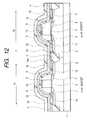
- This changeis shown in FIG. 2 as dependence of drain current variation (%) on film stress.
- the value of the stress in the drawingis not an internal stress of the channel formation region of MISFET but is the value of the interlayer insulating film itself found in terms of the warpage of the wafer after covered with the interlayer insulating film.
- the drain current of the n-type conductivity type MISFET and that of the p-type conductivity type MISFETexhibit opposite movements each other. A simultaneous improvement in the drain currents of both elements cannot be accomplished.
- An object of the present inventionis therefore to provide a technique capable of increasing the drain current of each of the n-channel conductivity type MISFET and p-channel conductivity type MISFET (increasing the current driving capacity).
- Another object of the present inventionis to provide a technique enabling free setting of a drain current ratio between the n-channel conductivity type MISFET to that of the p-channel conductivity type MISFET.
- the gist of the present inventionresides in the control, by the stress of the film, of a stress working on the channel formation region of each of the n-channel conductivity type MISFET and the p-channel conductivity type MISFET so as to increase their drain current.
- a drain currentincreases in the n-channel conductivity type field effect transistor.
- a compressive stressworks in the p-channel conductivity type field effect transistor, along the flow direction of a drain current (gate length direction), on the channel formation region, a drain current increases.
- the stress of a filmis utilized to control a tensile stress in the drain current direction to work on the channel formation region of the n-channel conductivity type field effect transistor, and a compressive stress in the drain current direction to work on the channel formation region of the p-channel conductivity type field effect transistor. It can be attained, for example, by the below-described method or device.
- a method of manufacturing a semiconductor device having an n-channel conductivity type field effect transistor and a p-channel conductivity type field effect transistor each formed over a semiconductor substratewhich comprises:
- a method of manufacturing a semiconductor device having an n-channel conductivity type field effect transistor and a p-channel conductivity type field effect transistor each formed over a semiconductor substratewhich comprises:
- the insulating film covering the semiconductor regionincludes sidewall spacers formed on the sidewalls of each of the gate electrodes and a deposited film formed to cover the sidewall spacers.
- the insulating film covering the semiconductor regionincludes sidewall spacers formed on the sidewalls of each of the gate electrodes and a deposited film formed to cover the sidewall spacers;
- a metal-semiconductor reacted layer formed in alignment with the sidewall spacersis disposed.
- the insulating film covering the semiconductor regionincludes sidewall spacers formed on the sidewalls of each of the gate electrodes and a thermally oxidized film formed between the sidewall spacers and the element isolation region.
- the insulating film covering the semiconductor regionincludes sidewall spacers formed on the sidewalls of each of the gate electrodes and a thermally oxidized film formed between the sidewall spacers and the element isolation region;
- a metal-semiconductor reacted layer formed in alignment with the sidewall spacersis disposed.
- the first and second insulating filmsare each a silicon nitride film formed by the LP-CVD (Low Pressure-Chemical Vapor Deposition) method, plasma CVD method, or single-wafer thermal CVD method.
- LP-CVDLow Pressure-Chemical Vapor Deposition
- plasma CVD methodplasma CVD method
- single-wafer thermal CVD methodsingle-wafer thermal CVD method.
- a method of manufacturing a semiconductor device having an n-channel conductivity type field effect transistor and a p-channel conductivity type field effect transistor each formed over a semiconductor substratewhich comprises:
- a method of manufacturing a semiconductor device having an n-channel conductivity type field effect transistor and a p-channel conductivity type field effect transistor, each formed over a semiconductor substratewhich comprises:
- the first and second insulating filmsare each a silicon nitride film formed by the LP-CVD method, plasma CVD method, or single-wafer thermal CVD method.
- a method of manufacturing a semiconductor device having an n-channel conductivity type field effect transistor and a p-channel conductivity type field effect transistor, each formed over a semiconductor substratewhich comprises:
- the compressive stress of the second insulating filmis at least twice as much as the tensile stress of the first insulating film.
- the first and second insulating filmsare each a silicon nitride film formed by the LP-CVD method, plasma CVD method, or single-wafer thermal CVD method.
- a method of manufacturing a semiconductor device having an n-channel conductivity type field effect transistor and a p-channel conductivity type field effect transistor, each formed over a semiconductor substratewhich comprises:
- the tensile stress of the second insulating filmis at least twice as much as the compressive stress of the first insulating film.
- the first and second insulating filmsare each a silicon nitride film formed by the LP-CVD method, plasma CVD method, or single-wafer thermal CVD method.
- a first insulating film having a tensile stressand being formed over the n-channel conductivity type field effect transistor and p-channel conductivity type field effect transistor so as to cover the gate electrodes of the transistors, and
- a second insulating filmhaving a compressive stress greater in terms of absolute value than a tensile stress of the first insulating film and being formed over the p-channel conductivity type field effect transistor so as to selectively cover the gate electrode thereof.
- the tensile stress of the second insulating filmis at least twice as much as the compressive stress of the first insulating film.
- the first and second insulating filmsare each a silicon nitride film formed by the LP-CVD method, plasma CVD method, or single-wafer thermal CVD method.
- a first insulating filmhaving a compressive stress and being formed over the n-channel conductivity type field effect transistor and p-channel conductivity type field effect transistor so as to cover the gate electrodes of the transistors, and
- the tensile stress of the second insulating filmis at least twice as much as the compressive stress of the first insulating film.
- the first and second insulating filmsare each a silicon nitride film formed by the LP-CVD method, plasma CVD method, or single-wafer thermal CVD method.
- a method of manufacturing a semiconductor device having an n-channel conductivity type field effect transistor and a p-channel conductivity type field effect transistor each formed over a semiconductor substratewhich comprises:
- the elementis same with an element contained in the insulating film.
- the introduction of the elementis conducted by ion implantation of the element perpendicularly to the substrate or ion implantation of the element obliquely to the substrate.
- the insulating filmis a silicon nitride film formed by the LP-CVD method, plasma CVD method, or single-wafer thermal CVD method.
- a semiconductor device having an n-channel conductivity type field effect transistor and a p-channel conductivity type field effect transistor each formed over a semiconductor substratewhich comprises:
- the filmhaving a first portion having a film stress for generating a tensile stress in the channel formation region of the n-channel conductivity type field effect and a second portion having a film stress for generating a compressive stress in the channel formation region of the p-channel conductivity type field effect transistor.
- the second portion of the filmhas a higher element concentration than the first portion.
- the filmis a silicon nitride film formed by the LP-CVD method, plasma CVD method, or single-wafer thermal CVD method.
- a tensile stress and a compressive stressare applied to the channel formation regions of the n-channel conductivity type field effect transistor and p-channel conductivity type field effect transistor, respectively, resulting in an increase in a drain current of each of the n-channel conductivity type field effect transistor and p-channel conductivity type field effect transistor, depending on the intensity of the stress working on each of the channel formation regions of the n-channel conductivity type field effect transistor and p-channel conductivity type field effect transistor, as illustrated in FIG. 2.
- the above-described filmis an insulating film made of a silicon nitride film for self-aligning contact (SAC).
- a semiconductor devicewhich comprises:
- a first field effect transistorformed over a semiconductor substrate and having a silicide layer over a semiconductor region between sidewall spacers disposed on the sidewalls of the gate electrode of said first transistor and an element isolation region of said semiconductor substrate;
- a second field effect transistorformed over said semiconductor substrate and having no silicide layer over a semiconductor region between sidewall spacers disposed on the sidewalls of the gate electrode of said second transistor and an element isolation region of said semiconductor substrate,
- a second insulating filmfor generating a stress in the channel formation region of said second field effect transistor and formed over said second field effect transistor so as to cover the gate electrode thereof, wherein:
- a third insulating filmis disposed between the semiconductor region of said second field effect transistor and said second insulating film.
- said third insulating filmis not disposed.
- tensile stress working on the channel formation region of a field effect transistormeans a stress at which the lattice constant of Si exceeds its equilibrium in the case where the channel formation region is silicon (Si).
- compressive stress working on the channel formation region of a field effect transistormeans a stress at which the lattice constant of Si becomes below its equilibrium in the case where the channel formation region is silicon (Si).
- tensile stress of a filmmeans a stress which generates a tensile stress in the channel formation region of a field effect transistor.
- compressive stress of a filmmeans a stress which generates a compressive stress in the channel formation region of a field effect transistor.
- the gist of the present inventiontherefore resides in that the interatomic distance of silicon atoms in the channel formation region differs between the n-channel conductivity type field effect transistor and the p-channel conductivity type field effect transistor, in other words, they are different in the size of distortion; and that the interatomic distance of silicon atoms is greater in the channel formation region of the n-channel conductivity type field effect transistor than in the channel formation region of the p-channel conductivity type field effect transistor.
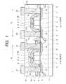
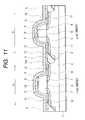
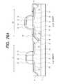
- FIG. 1is a schematic cross-sectional view illustrating the rough constitution of a semiconductor device according to Embodiment 1 of the present invention
- FIG. 2is a characteristic chart showing dependence, on film stress, of a percent variation in drain current
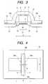
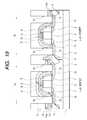
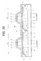
- FIG. 3is a schematic cross-sectional view illustrating the relationship between a current direction and a film stress direction
- FIG. 4is a schematic plane view illustrating the relationship between a current direction and a film stress direction
- FIG. 5is a schematic cross-sectional view of a semiconductor device of Embodiment 1 of the present invention at a manufacturing step thereof;
- FIG. 6is a schematic cross-sectional view of the semiconductor device at a manufacturing step following that of FIG. 5;
- FIG. 7is a schematic cross-sectional view of the semiconductor device at a manufacturing step following that of FIG. 6,
- FIG. 8is a schematic cross-sectional view of the semiconductor device at a manufacturing step following that of FIG. 7;
- FIG. 9is a schematic cross-sectional view of the semiconductor device at a manufacturing step following that of FIG. 8;
- FIG. 10is a schematic cross-sectional view of the semiconductor device at a manufacturing step following that of FIG. 9;
- FIG. 11is a schematic cross-sectional view of the semiconductor device at a manufacturing step following that of FIG. 10;
- FIG. 12is a schematic cross-sectional view of the semiconductor device at a manufacturing step following that of FIG. 11;
- FIG. 13is a schematic cross-sectional view of the semiconductor device at a manufacturing step following that of FIG. 12;
- FIG. 14is a schematic cross-sectional view of the semiconductor device at a manufacturing step following that of FIG. 13;
- FIG. 15is a schematic cross-sectional view of the semiconductor device at a manufacturing step following that of FIG. 14;
- FIG. 16is a schematic cross-sectional view of the semiconductor device at a manufacturing step following that of FIG. 15;
- FIG. 17is a schematic cross-sectional view of the semiconductor device at a manufacturing step following that of FIG. 16;
- FIG. 18is a schematic cross-sectional view of the semiconductor device at a manufacturing step following that of FIG. 17;
- FIG. 19is a schematic cross-sectional view of the semiconductor device at a manufacturing step following that of FIG. 18;
- FIG. 20is a schematic cross-sectional view for explaining a problem found by the present inventors during the development of the present invention.
- FIG. 21is a schematic cross-sectional view for explaining another problem found by the present inventors during the development of the present invention.
- FIG. 22is a schematic cross-sectional view for explaining a further problem found by the present inventors during the development of the present invention.
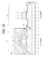
- FIG. 23is a schematic cross-sectional view for explaining a still further problems found by the present inventors during the development of the present invention.
- FIG. 24is a schematic cross-sectional view illustrating a modification example of Embodiment 1 of the present invention.
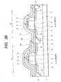
- FIG. 25is a schematic cross-sectional view illustrating the rough constitution of a semiconductor device according to Embodiment 2 of the present invention.
- FIGS. 26A and 26Bare each a schematic cross-sectional view illustrating the semiconductor device of Embodiment 2 at a manufacturing step thereof;
- FIG. 27is a schematic cross-sectional view illustrating the semiconductor device of Embodiment 2 at another manufacturing step thereof;
- FIG. 28is a schematic cross-sectional view of a semiconductor device according to Embodiment 3 of the present invention at a manufacturing step thereof;
- FIG. 29is a schematic cross-sectional view of a semiconductor device according to Embodiment 4 of the present invention at a manufacturing step thereof;
- FIGS. 30A and 30Bare each a schematic cross-sectional view illustrating the rough constitution of a semiconductor device according to Embodiment 5 of the present invention.
- FIG. 31is a schematic cross-sectional view illustrating the rough constitution of a semiconductor device according to Embodiment 6 of the present invention.
- FIG. 32is a schematic cross-sectional view illustrating the semiconductor device according to Embodiment 6 of the present invention at a manufacturing step thereof;
- FIG. 33is a schematic cross-sectional view of the semiconductor device at a manufacturing step following that of FIG. 32;
- FIG. 34is a schematic cross-sectional view of the semiconductor device at a manufacturing step following that of FIG. 33;
- FIG. 35is a schematic cross-sectional view of the semiconductor device at a manufacturing step following that of FIG. 34;
- FIG. 36is a schematic cross-sectional view illustrating a modification example of Embodiment 6 of the present invention.
- FIG. 37is a schematic cross-sectional view illustrating the rough constitution of a semiconductor device according to Embodiment 7 of the present invention.
- FIG. 38is a schematic cross-sectional view of the semiconductor device according to Embodiment 7 of the present invention at a manufacturing step thereof;
- FIG. 39is a schematic cross-sectional view of the semiconductor device at a manufacturing step following FIG. 38;
- FIG. 40is a schematic cross-sectional view illustrating a modification example of Embodiment 7 of the present invention.
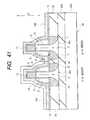
- FIG. 41is a schematic cross-sectional view illustrating the rough constitution of a semiconductor device according to Embodiment 8 of the present invention.
- FIG. 42is a schematic plane view illustrating the rough constitution of a semiconductor device according to Embodiment 9 of the present invention.
- FIG. 43is a schematic cross-sectional view taken along a line A-A of FIG. 42.
- FIG. 44is a schematic cross-sectional view illustrating the rough constitution of a semiconductor device according to Embodiment 10 of the present invention.
- Embodiment 1application of the present invention to a semiconductor device having a complementary MISFET having a power-supply voltage of from 1 to 1.5V and a gate length of from 0.1 to 0.14 ⁇ m will be described.
- FIG. 1is a schematic cross-sectional view illustrating the rough constitution of a semiconductor device according to Embodiment 1 of the present invention
- FIG. 2is a characteristic chart showing dependence, on film stress, of a percent variation in drain current
- FIGS. 3 and 4are schematic plane view and schematic cross-sectional view illustrating the relationship between a current direction and a film stress direction, respectively;
- FIGS. 5 to 19are each a schematic cross-sectional view of a semiconductor device of FIG. 1 during at manufacturing steps thereof, and
- FIGS. 20 to 23are each a schematic cross-sectional view for explaining the problem found by the present inventors during the development of the present invention.
- an n channel conductivity type MISFET(n-type MISFET) is illustrated on the left side, while a p channel conductivity type MISFET (p-type MISFET) is illustrated on the right side.
- the semiconductor devicehas a semiconductor substrate composed mainly of a p type silicon substrate (which will hereinafter be called “p type substrate” simply) made of, for example, single crystal silicon.
- the circuit formation surface (one main surface) of the p type substrate 1has, thereon, an nMIS formation region (first element formation region) in and a pMIS formation region (second element formation region) 1p and the nMIS formation region in is separated from the pMIS formation region 1p by an element isolation region such as an shallow groove isolation (SGI) region 4 .
- SGIshallow groove isolation
- n-type MISFETn channel conductivity type MISFET
- p-type MISFETn channel conductivity type MISFET
- the shallow groove isolation region 4is formed by making a shallow groove in the circuit formation surface of the p type substrate 1 and then selectively embedding inside of the shallow groove with an insulating film (for example, a silicon oxide film).
- the n-type and p-type MISFETS of this Embodimenteach has a horizontal structure permitting flow of an electric current in the plane direction of the p type substrate 1 .
- the n-type MISFEThas mainly a channel formation region, a gate insulating film 5 , a gate electrode 6 , sidewall spacers 9 , a source region and a drain region.
- the source and drain regionshave n type semiconductor regions (extension regions) 7 and n type semiconductor regions 10 .
- the n type semiconductor regions 7are formed in self alignment with the gate electrode 6
- the n type semiconductor regions 10are formed in self alignment with the sidewall spacers 9 disposed on the sidewalls of the gate electrode 6 .
- the n type semiconductor regions 10are formed to have a higher impurity concentration than the n type semiconductor regions 7 .
- the p-type MISFEThas mainly a channel formation region, a gate insulating film 5 , a gate electrode 6 , sidewall spacers 9 , a source region and a drain region.
- the source and drain regionshave p type semiconductor regions (extension regions) 8 and p type semiconductor regions 11 .
- the p type semiconductor regions 8are formed in self alignment with the gate electrode 6
- the p type semiconductor regions 11are formed in self alignment with sidewall spacers 9 disposed on the sidewalls of the gate electrode 6 .
- the p type semiconductor regions 11are formed to have a higher impurity concentration than the p type semiconductor regions 8 .
- a silicide layer (metal.semiconductor reaction layer) 12is formed in order to lower the resistance.
- the silicide layer 12 disposed over the surface of the gate electrode 6 , the silicide layer disposed on the surface of each of the n type semiconductor regions 10 and p type semiconductor regions 11is formed in self alignment with the sidewall spacers 9 disposed over the sidewalls of the gate electrode 6 .
- These silicide layers 12are formed, for example, by the salicide (Self Aligned Silicide) technique.
- the n-type and p-type MISFETS of this Embodimenteach has a salicide structure.
- an interlayer insulating film 16is formed, for example, from a silicon oxide film. This interlayer insulating film 16 is formed to cover the circuit formation surface of the p type substrate 1 . Between the n-type MISFET and interlayer insulating film 16 , formed is, for example, a silicon nitride film 14 a which is a first nitride film serving to generate a tensile stress on the circuit formation surface of the p type substrate 1 .
- a silicon nitride film 14 bwhich is a second nitride film serving to generate a compressive stress on the circuit formation surface of the p type substrate 1 .
- the silicon nitride film 14 ais selectively formed over the n-type MISFET to cover its gate electrode 6
- the silicon nitride film 14 bis selectively formed over the p-type MISFET to cover its gate electrode 6 .
- an insulating film 13 made of, for example, a silicon oxide filmis formed between the n-type MISFET and silicon nitride film 14 a , and between the p-type MISFET and silicon nitride film 14 b .
- This insulating film 13is formed on the circuit formation surface of the p type substrate 1 to cover each of the n-type and p-type MISFETs.
- an insulating film 15 made of, for example, a silicon oxide filmis formed between the silicon nitride film 14 a and the interlayer insulating film 16 .
- This insulating film 15is formed over the silicon nitride film 14 a selectively to cover this silicon nitride film 14 a.
- n type semiconductor regions 10 and p type semiconductor regions 11Over the n type semiconductor regions 10 and p type semiconductor regions 11 , contact holes 18 for source-drain extending from the surface of the interlayer insulating film 16 to the silicide layer 12 are formed. Inside of these contact holes 18 for source-drain, a conductive plug 19 is embedded. The n type semiconductor regions 10 and p type semiconductor regions 11 are each electrically connected, via the silicide layer 12 and conductive plug 19 , to an interconnect 20 which extends over the interlayer insulating film 16 .
- a contact hole for gatewhich hole extends from the surface of the interlayer insulating film 16 to the silicide layer 12 is formed over the gate electrode 6 .
- a conductive plug 19is embedded inside of this gate contact hole.
- the gate electrode 6is electrically connected, via the silicide layer 12 and the conductive plug 19 inside of the gate contact hole, to an interconnect 20 extending over the interlayer insulating film 16 .
- the source-drain contact hole 18 and gate contact holeare each formed by the SAC (Self Aligned Contact Hole) technique using the silicon nitride films 14 a , 14 b as an etching stopper.
- the silicon nitride films 14 a , 14 bserve as an insulating film for self aligned contact.
- These silicon nitride films 14 a , 14 bare formed, for example, by the plasma CVD (Chemical Vapor Deposition) method.
- the stress to be generated on the circuit formation surface of the p type substrate 1can be controlled by changing the forming conditions of these silicon nitride films 14 a , 14 b (reactive gas, pressure, temperature, RF power, etc.).
- a stress generated on the circuit formation surface of the p type substrate 1is controlled toward a tensile stress by forming the silicon nitride film 14 a under the conditions of an RF power lowered to a range of from 300 to 400 W.
- a stress generated on the circuit formation surface of the p type substrate 1is controlled toward a compressive stress by forming the silicon nitride film 14 b under the conditions of an RF power heightened to a range of from 600 to 700W.
- a tensile stress of from about +700 to +800 Mpaexists inn the silicon nitride film 14 a and a compressive stress of from about ⁇ 900 to ⁇ 1000 Mpa exists in the silicon nitride film 14 a , each formed in the above-described manner, so that a tensile stress appears in the channel formation region of the n-type MISFET and a compressive stress appears in the channel formation region of the p-type MISFET, resulting in a 10 to 15% improvement in the drain current of the n-type MISFET and a 15 to 20% improvement in the drain current of the p-type MISFET compared with the case not covered with the silicon nitride films 14 a , 14 b .
- these stressesare applied to a direction similar to that of the drain current (Id) flowing through the channel formation region (that is, gate length direction).
- FIGS. 3 and 4has a silicide structure similar to that of this Embodiment.
- Indicated at numeral 30is the channel formation region of MISFET, 31 is the direction of a drain current flowing through the channel formation region 30 , 32 is a semiconductor region formed in alignment with the gate electrode 6 , 33 is a semiconductor region formed in alignment with the sidewall spacer 9 , 34 is a film for generating a stress in the channel formation region 30 , and 35 a and 35 b are each a step portion.
- MISFEThas sidewall spacers 9 disposed over the sidewalls of the gate electrode 6 to surround the gate electrode 6 .
- the gate electrode 6 and sidewall spacers 9protrude from the substrate so that step portions ( 35 a , 35 b ) resulting from them appear.
- the stressconcentrates on the foot of the step portion 35 a existing in the gate length direction X and the foot of the step portion 35 b existing in the gate width direction Y so that the film stress in the gate length direction which stress starts from the foot of the step portion 35 a existing in the gate length direction X acts on the channel formation region 30 and at the same time, the film stress in the gate width direction which stress starts from the foot of the step portion 35 b existing in the gate width direction Y acts on the channel formation region 30 .
- the stress by the film 34when the stress by the film 34 is a tensile stress, the tensile stress appears in the channel formation region 30 in the gate length direction and gate width direction, while when the stress by the film 34 is a compressive stress, the compressive stress appears in the channel formation region 30 in the gate length direction and gate width direction.
- the length of the gate electrode 6 in the gate length direction Xis by far smaller than its length in the gate width direction Y, so that tensile stress or compressive stress in the gate width direction which stress appears in the channel formation region 30 by a tensile stress or a compressive stress focused on the foot of the step portion 35 b in the gate width direction Y is markedly small. Accordingly, the stress appearing in the channel formation region 30 by the film 34 can be regarded substantially as only a tensile stress or compressive stress in the gate length direction, in other words, as a tensile stress or compressive stress along the drain current direction 31 .
- a p type substrate 1 made of single crystal silicon having a specific resistance of 10 106 cmis prepared and on the circuit formation surface of the p type substrate 1 , a p type well region 2 and an n type well region 3 are formed selectively as illustrated in FIG. 5.
- a shallow groove isolation region 4is formed on the circuit formation surface of the p type substrate 1 as an element isolation region for separating an nMIS formation region (first element formation region) 1n from a PMIS formation region (second element formation region) 1p.
- This shallow groove isolation region 4is formed by forming a shallow groove (for example, a groove of about 300 [nm] deep) on the circuit formation surface of the p type substrate 1 , forming, for example, a silicon oxide film as an insulating film over the circuit formation surface of the p type substrate 1 by CVD, and then planarizing the insulating film to leave it only inside of the shallow groove by CMP (Chemical Mechanical Polishing).
- CMPChemical Mechanical Polishing
- a gate insulating film 5 made of, for example, a silicon oxide film of about 2 to 3 nm thickis formed by heat treatment in the nMIS formation region in and PMIS formation region 1p on the circuit formation surface of the p type substrate 1 .
- a polycrystalline silicon film of about 150 to 200 nm thickis formed all over the circuit formation surface of the p type substrate 1 by CVD, followed by the formation of a gate electrode 6 by patterning of the polycrystalline silicon film.
- an impurity to reduce a resistanceis introduced therein.
- a pair of n type semiconductor regions (extension regions) 7are formed by selectively introducing, by ion implantation, an impurity such as arsenic (As) into an area of the p type well region 2 free of the gate electrode 6 , followed by the formation of a pair of p type semiconductor regions (extension regions) 8 by selectively introducing, by ion implantation, an impurity such as boron difluoride (BF 2 ) into an area of the n type well region 3 free of the gate electrode 6 .
- an impuritysuch as arsenic (As)
- n type semiconductor regions 7are formed while the pMIS formation region 1p is covered with a photoresist mask, while the p type semiconductor regions 8 are formed while the nMIS formation region 1 n is covered with a photoresist mask.
- Arsenicis introduced under the conditions of an acceleration energy of 1 to 5 KeV and dose of 1 to 2 ⁇ 10 15 /cm 2 .
- Boron difluorideis introduced under the conditions of an acceleration energy of 1 to 5 KeV and dose of 1 to 2 ⁇ 10 15 /cm 2 .
- the n type semiconductor regions 7 and p type semiconductor regions 8are each formed in alignment with the gate electrode 6 .
- sidewall spacers 9having, for example, a thickness in the gate length direction of about 50 to 70 nm thick are formed on the sidewalls of the gate electrode 6 .
- These sidewall spacers 9are formed by forming an insulating film made of, for example, silicon oxide film or silicon nitride film by CVD all over the circuit formation surface of the p type substrate 1 and then subjecting the insulating film to anisotropic etching such as RIE (Reactive Ion etching). These sidewall spacers 9 are formed in alignment with the gate electrode 6 .
- a pair of n type semiconductor regions 10are formed by selectively introducing, by ion implantation, an impurity such as arsenic (As) into an area of the p type well region 2 free of the gate electrode 6 and sidewall spacers 9 , followed by the formation of a pair of p type semiconductor regions 11 by selectively introducing, by ion implantation, an impurity such as boron difluoride (BF 2 ) into an area of the n type well region 3 free of the gate electrode 6 and the sidewall spacers 9 .
- an impuritysuch as arsenic (As)
- BF 2boron difluoride
- n type semiconductor regions 10are formed while the PMIS formation region 1p is covered with a photoresist mask, while the p type semiconductor regions 11 are formed while the nMIS formation region 1 n is covered with a photoresist mask.
- Arsenicis introduced under the conditions of an acceleration energy of 35 to 45 KeV and dose of 2 to 4 ⁇ 10 15 /cm 2 .
- Boron difluorideis introduced under the conditions of an acceleration energy of 40 to 50 KeV and dose of 2 to 4 ⁇ 10 15 /cm 2 .
- the n type semiconductor regions 10 and p type semiconductor regions 11are each formed in alignment with the sidewall spacers 9 .
- a source region and a drain region having the n type semiconductor regions 7 formed in alignment with the gate electrode 6 and the n type semiconductor regions 10 formed in alignment with the sidwall spacers 9are formed; and a source region and a drain region having the p type semiconductor regions 8 formed in alignment with the gate electrode 6 and the p type semiconductor regions 11 formed in alignment with the sidwall spacers 9 are formed.
- horizontal n-type and p-type MISFETsare formed.
- heat treatmentis conducted to react silicon (Si) of the gate electrode 6 with Co of the cobalt film 12 , thereby forming a silicide (CoSi x ) layer 12 as a metal.semiconductor reacted layer on the surface of the gate electrode 6 ; and at the same time, to react Si of the semiconductor regions ( 10 , 11 ) with Co of the cobalt film 12 a to form a silicide (CoSi x ) layer 12 on the surface of the semiconductor regions ( 10 , 11 ).
- an unreacted portion of the cobalt film 12 ais selectively removed from a region in which no silicide layer 12 is formed, followed by activation of the silicide layer 12 by heat treatment.
- the silicide layer 12 disposed over the surface of the gate electrode 6 and the silicide layer 12 disposed over the surface of the semiconductor regions ( 10 , 11 )are formed in alignment with the sidewall spacers 9 .
- n-type and p-type MISFETs having a salicide structureare formed.
- an insulating film 13 made of, for example, a silicon oxide film of about 5 to 10 nm thickis formed by CVD all over the circuit formation surface of the p type substrate 1 including the n-type and p-type MISFETs.
- the silicide layer 12 of the gate electrode 6 , the silicide layer 12 of the semiconductor regions ( 10 , 11 ) and sidewall spacers 9are covered with the insulating film 13 .
- a silicon nitride film 14 a of about 100 to 120 nm thickis formed by plasma CVD as an insulating film all over the circuit formation surface of the p type substrate 1 including the n-type and p-type MISFETs.
- This silicon nitride film 14 ais formed under the condition of, for example, RF power of 350 to 400 W or chamber inner pressure of 300 to 350 Torr.
- the n-type and p-type MISFETsare covered with the silicon nitride film 14 a , while the silicide layer 12 of the gate electrode 6 , the semiconductor regions ( 10 , 11 ) and sidewall spacers 9 are covered with the silicon nitride film 14 a via the insulating film 13 .
- an insulating film 15 made of, for example, a silicon oxide film of about 50 nm thickis formed by CVD all over the circuit formation surface of the p type substrate 1 including the upper surfaces of the n-type and p-type MISFETs. By this step, the silicon nitride film 14 a is covered with the insulating film 15 .
- a photoresist mask RM 1selectively covering the upper surface of the nMIS formation region in (n-type MISFET) is formed over the insulating film 15 .
- the insulating film 15 and silicon nitride film 14 aare successively removed by etching from the upper surface of the pMIS formation region 1p (the upper surface of p-type MISFET).
- wet etching and isotropic dry etchingare employed, respectively.
- the silicon nitride film 14 ais selectively formed over the n-type MISFET so as to cover its gate electrode 6 . Owing to the silicon nitride film 14 a selectively formed in the above-described manner, a tensile stress is generated selectively in the channel formation region of the n-type MISFET.
- a silicon nitride film 14 b of about 100 nm thickis formed, as an insulating film, by plasma CVD all over the circuit formation surface of the p-type substrate 1 including the upper surface of the insulating film 15 .
- This silicon nitride film 14 bis formed, for example, under the condition of RF power of 600 to 700 W or chamber inner pressure of 5 to 10 Torr.
- the n-type and p-type MISFETSare covered with the silicon nitride film 14 b , while the silicon nitride film 14 a over the n-type MISFET is covered with the silicon nitride film 14 b via the insulating film 15 .
- a photoresist mask RM 2 for selectively covering the upper surface of the PMIS formation region 1p(p-type MISFET) is formed over the silicon nitride film 14 b.
- the silicon nitride film 14 bis removed by etching as illustrated in FIG. 17 from the upper surface of the nMIS formation region In (upper surface of the n-type MISFET).
- the silicon nitride film 14 bis removed by isotropic dry etching.
- the silicon nitride film 14 bis selectively formed over the p-type MISFET so as to cover its gate electrode 6 . Owing to the silicon nitride film 14 b selectively formed in such a manner, a compressive stress is generated selectively in the channel formation region of the p-type MISFET.
- the silicon nitride film 14 a over the n-type MISFETis covered with the insulating film 15 , an inconvenience of removal of the silicon nitride film 14 a by overetching upon removal of the silicon nitride film 14 b can be suppressed.
- the insulating film 15plays a role of an etching stopper upon removal of the silicon nitride film 14 b.
- an interlayer insulating film 16 made of, for example, a silicon oxide filmis formed by plasma CVD all over the circuit formation surface of the p type substrate 1 including the upper surfaces of the n-type and p-type MISFETS as illustrated in FIG. 18, followed by planarization of the surface of the interlayer insulating film 16 by CMP.
- an impurity 17such as Ar, Ge, Si, As, Sb, In or BF 2 is introduced into the interlayer insulating film 16 to destroy the crystallinity in the interlayer insulating film 16 .
- the stress of the interlayer insulating film 16is relaxed so that the influence of the stress of the interlayer insulating film 16 on the channel formation region of MISFET can be suppressed.
- the mark of the destructionremains clearly.
- source-drain contact holes 18extending from the surface of the interlayer insulating film 16 to the silicide layer 12 are then formed over the semiconductor regions ( 11 , 12 ).
- These source-drain contact holes 18are formed by the SAC technique using silicon nitride films ( 14 a , 14 b ) as an etching stopper. Described specifically, photoresist masks having opening patterns for the contact holes are formed over the interlayer insulating film 16 at positions opposite to the semiconductor regions ( 10 , 11 ).
- the interlayer insulating film 16 , insulating film 15 , silicon nitride films ( 14 a , 14 b ) and insulating film 13are etched successively by anisotropic etching.
- the etching of the interlayer insulating film 16 and insulating film 15is conducted under conditions permitting them to have an etching selectivity over the silicon nitride films ( 14 a , 14 b ).
- the silicon nitride films ( 14 a , 14 b )are etched under conditions permitting these films to have an etching selectivity over the insulating film 13 .
- the insulating film 13is etched under the conditions permitting it to have an etching selectivity over the silicide layer 12 and p type substrate 1 .
- the insulating film 13may be etched by the overetching upon removal of the silicon nitride films ( 14 a , 14 b ).
- a gate contact hole extending from the surface of the interlayer insulating film 16 to the silicide layer 12is formed over the gate electrode 6 , which is not however illustrated.
- a conductive plug 19is then formed by embedding a conductive substance inside of the source-drain contact hole 18 and inside of the gate contact hole, followed by the formation of an interconnect 20 over the interlayer insulating film 16 , whereby a structure as illustrated in FIG. 1 can be formed.
- the stress of the silicon nitride film 14 bconcentrates on the foot of the step portion 35 a formed by the gate electrode 6 , sidewall spacers 9 and the portion of the silicon nitride film 14 a as illustrated in FIG.
- a fluoride gassuch as CF 4 or CF 6 is usually employed.
- the silicon nitride filmhas an etching selectivity over a silicon oxide film or silicide layer, but does not have over silicon.
- the silicon nitride film 14 aUpon isotropic plasma etching of the silicon nitride film 14 a , the silicon nitride film 14 a has an etching selectivity over sidewall spacers 9 made of a silicon oxide film, but they are etched a little by overetching upon removal of the silicon nitride film 14 a , whereby the whole film thickness of the sidewall spacers 9 decreases towards the gate electrode 6 .
- the silicide layer 12 on the surface of the p type semiconductor regions 11are formed in alignment with the sidewall spacers 9 .
- the silicon nitride film 14 aUpon isotropic plasma etching, the silicon nitride film 14 a has an etching selectivity over the silicide layer 12 , but the silicide layer 12 is etched a little by the overetching upon removal of the silicon nitride film 14 a and the thickness of the silicide layer 12 decreases.
- the silicide layer 12is disposed on the surface of the gate electrode 6 or on the surfaces of the p type semiconductor regions 11 in order to suppress an increase in gate resistance or an increase in a source-drain current due to miniaturization of MISFET.
- the silicide layer 12serves as an etching stopper, the polycrystalline silicon film below the silicide layer 12 of the gate electrode 6 , and the p type semiconductor region 11 below the silicide layer 12 of the source-drain regions are not etched by overetching upon removal of the silicon nitride film 14 a .
- the polycrystalline silicon film of the gate electrode 6 and the p type semiconductor region 11 of the source-drain regionsare reduced in film thickness owing to etching, leading to an increase in the gate resistance and source-drain resistance.
- An increase in the gate resistancecauses lowering in switching speed, while an increase in the source-drain resistance causes a deterioration in current driving capacity.
- isotropic dry etchingwhich does not form an etching remnant at the step portion is effective, but the above-described problem must be resolved in order to remove the silicon nitride film 14 a by isotropic dry etching.
- the problem relating to etching of the silicide layer 12can be overcome by, prior to the formation of the silicon nitride film 14 a over the n-type and p-type MISFETs so as to cover their gate electrodes 6 , covering the whole surface of the silicide layer 12 with an insulating film capable of serving as an etching stopper.
- the problem relating to a structure having no silicide layer 12can be overcome by, prior to the formation of the silicon nitride film 14 a over the n-type and p-type MISFETs so as to cover their gate electrodes 6 , covering the surface of the gate electrode 6 and the surface of the p type semiconductor regions 11 with an insulating film capable of serving as an etching stopper.
- a film over which the silicon nitride film 14 a has an etching selectivity upon isotropic plasma etching thereof, for example, a silicon oxide filmis desired.
- the insulating film 13 made of a silicon oxide filmis formed by CVD prior to the formation of the silicon nitride film 14 a .
- the insulating film 13is formed by CVD, that is, deposition method, the silicide layer 12 on the surface of the gate electrode 6 , the silicide layer 12 on the surface of the p type semiconductor regions 11 , the end portion of the silicide layer 12 on the surface of the p type semiconductor regions 11 , said end portion existing on the side of the sidewall spacers 9 , and the sidewall spacers 9 can be covered with the insulating film 13 .
- the silicon nitride film 14 bis removed from the p-type MISFET while covering the silicide layer 12 on the surface of the gate electrodes 6 , the silicide layer 12 on the surface of the p type semiconductor regions 11 , the end portion of the silicide layer 12 on the surface of the p type semiconductor regions 11 , said end portion existing on the side of the sidewall spacers 9 , and the sidewall spacers 9 with the insulating film 13 , so that the problems relating to the retreat in the thickness of the sidewall spacers 9 and etching of the silicide layer 12 can be overcome at the same time.
- a tensile stress and a compressive stressare applied to the channel formation region of the n-type MISFET and the channel formation region of the p-type MISFET, respectively, resulting in an increase in the drain current in both the n-type MISFET and p-type MISFET according to the intensity of the stress working on the channel formation region of each of the n-type MISFET and p-type MISFET.
- the stresses working on the channel formation regions of the n-type MISFET and p-type MISFETcan be controlled respectively so that a ratio of the drain current between the n-type MISFET and the p-type MISFET can be controlled freely.
- the drain current of the n-type MISFET and that of the p-type MISFETcan be increased simultaneously, making it possible to attain speed up of a semiconductor device having n-type and p-type MISFETs.
- any one of the below-described methods, as well as a method of changing an RF power,can be adopted.
- the film formation temperatureis changed.
- the temperature upon formation of the silicon nitride film 14 ais set higher than that of the silicon nitride film 14 b.
- any two or three of the above-described methodsmay be used in combination. What is important is to adjust the stress of the silicon nitride film 14 a toward the side of a tensile stress and the stress of the silicon nitride film 14 b toward the side of a compressive stress.
- FIG. 24is a schematic cross-sectional view of a semiconductor device, at a manufacturing step thereof, which is a modification example of Embodiment 1 of the present invention.
- the n-type MISFETis illustrated on the left side, while the p-type MISFET is illustrated on the right side.
- the silicon nitride film 14 awas formed prior to the silicon nitride film 14 b , but as illustrated in FIG. 24, the silicon nitride film 14 b may be formed prior to the silicon nitride film 14 a . Also in such a case, a tensile stress and a compressive stress can be applied respectively to the channel formation regions of the n-type MISFET and p-type MISFET so that the drain currents of the n-type MISFET and p-type MISFET can be increased simultaneously.
- the silicon nitride film 14 bcan be removed from the upper surface of the n-type MTSFET without causing problems relating to the retreat in the thickness of the sidewall spacers 9 or etching of the silicide layer 12 .
- the insulating film 13 made of a silicon oxide filmwas used as an etching stopper upon removal of the silicon nitride film 14 a , but not only it but also another insulating film may be used insofar as it is a film over which the silicon nitride film 14 a has an etching selectivity upon isotropic etching.
- FIG. 25is a schematic cross-sectional view illustrating the rough constitution of a semiconductor device according to Embodiment 2 of the present invention.
- FIGS. 26A, 26B and 27are each a schematic cross-sectional view of the semiconductor device, at a manufacturing step thereof, according to Embodiment 2 of the present invention.
- an n-type MISFETis illustrated on the lift side, while a p-type MISFET is illustrated on the right side.
- the semiconductor device of Embodiment 2is similar to that of Embodiment 1 except that the insulating film 13 serving as an etching stopper is removed.
- the stress of the silicon nitride films ( 14 a , 14 b )concentrates on the foot of the step portion 35 a defined by the gate electrode 6 , sidewall spacers 9 and insulating film 13 and the starting point of the stress of the silicon nitride films ( 14 a , 14 b ) departs from the channel formation region of MISFET by the insulating film 13 remaining on the sidewall of the sidewall spacers 9 , resulting in a decrease in the effect of the stress of the silicon nitride films ( 14 a , 14 b ) for generating a stress in the channel formation region. It is therefore desired to removed the insulating film 13 if possible.
- the insulating film 13is necessary in the step of removing the silicon nitride film 14 a on the p-type MISFET.
- the insulating film 13is necessary in the step of removing the silicon nitride film 14 b from the upper surface of the n-type MISFET. The insulating film 13 is therefore removed in consideration of these steps.
- the insulating film 13is removed from the upper surface of the n-type MISFET prior to the step of forming the silicon nitride film 14 a as illustrated in FIG. 26A, and it is removed from the upper surface of the p-type MISFET after the removal of the silicon nitride film 14 a from the upper surface of the p-type MISFET as illustrated in FIG. 26B, which corresponds to FIG. 13, and FIG. 27.
- the insulating film 13 on the p-type MISFETis removed after removal of the insulating film 15 and silicon nitride film 14 a from the upper surface of the p-type MISFET.
- the insulating film 13is removed from the upper surface of the p-type MISFET prior to the step of forming the silicon nitride film 14 b , and the insulating film 13 is removed from the upper surface of the n-type MISFET after removal of the silicon nitride film 14 b from the upper surface of the n-type MISFET.
- the removal of the insulating film 13 on the n-type MISFETis performed while covering the upper surface of the p-type MISFET with, for example, a photoresist mask, while the removal of the insulating film 13 on the p-type MISFET is performed while covering the upper surface of the n-type MISFET with, for example, a photoresist mask.
- isotropic dry etchingwhich does not leave any remnant on the step portion, for the removal of the insulating film from the upper surface of the n-type MISFET or p-type MISFET.
- isotropic dry etching of the insulating film 13 made of a silicon oxide filmisotropic plasma etching using a CF 3 gas or a mixed gas of CF 4 with H 2 is usually employed.
- the insulating film 13has a sufficient etching selectivity over silicon or a silicide layer so that the p type substrate 1 , silicide layer 12 , sidewall spacers 9 and the like are not etched excessively.
- the insulating film 13was removed from the upper surface of each of the n-type MISFET and p-type MISFET, but it is possible to leave the insulating film 13 on either one of them.
- FIG. 28is a schematic cross-sectional view of a semiconductor device, at a manufacturing step thereof, according to Embodiment 3 of the present invention.
- illustrated on the left sideis an n-type MISFET, while illustrated on the right side is a p-type MISFET.
- the insulating film 13 made of a silicon oxide film formed by the deposition methodwas used as an etching stopper upon removal of the silicon nitride film 14 a .
- an insulating film 21 made of a silicon oxide film formed by the thermal oxidation methodis used as an etching stopper upon removal of the silicon nitride film 14 a .
- the formation of the insulating film 21 by the thermal oxidation methodis conducted after the step of forming the n-type and p-type MISFETs having a salicide structure but before the step of forming the silicon nitride films 14 a , 14 b.
- the insulating film 21can be formed selectively so as to cover therewith the silicide layer 12 on the surface of the gate electrode 6 , and the silicide layer 12 on the surface of the semiconductor regions ( 10 , 11 ).
- This insulating film 21can therefore suppress an inconvenience which will otherwise occur upon removal of the silicon nitride films ( 14 a , 14 b ) by isotropic dry etching even if the silicon nitride film 14 a is formed prior to the silicon nitride film 14 b as in Embodiment 1 or the silicon nitride film 14 b is formed prior to the silicon nitride film 14 a as in the modification example of Embodiment 1.
- FIG. 29is a schematic cross-sectional view of a semiconductor device, at a manufacturing step thereof, according to Embodiment 4 of the present invention.
- illustrated on the left sideis an n-type MISFET, while illustrated on the right side is a p-type MISFET.
- Embodiment 1the insulating film 13 made of a silicon oxide film formed by the deposition method was used as an etching stopper upon removal of the silicon nitride film 14 a .
- Embodiment 4on the other hand, sidewall spacers 22 formed on the side walls of the sidewall spacers 9 using a silicon oxide film are employed as an etching stopper upon removal of the silicon nitride film 14 a .
- the sidewall spacers 22are formed after the formation of the n-type and p-type MISFETs having a salicide structure but before the formation of the silicon nitride films 14 a , 14 b . Sidewall spacers 22 are formed in a similar manner to that employed for the formation of the sidewall spacers 9 .
- the sidewall spacers 22 made of a silicon oxide filmon the sidewalls of the sidewall spacers 9 , the end portion of the silicide layer 12 on the surface of the semiconductor regions ( 10 , 11 ), said end portion being on the side of the sidewall spacers 9 , and the sidewall spacers 9 can be covered with the sidewall spacers 22 so that an inconvenience which otherwise occur upon removal of the silicon nitride films ( 14 a , 14 b ) by isotropic dry etching, particularly an inconvenience relating to the retreat in the thickness of the sidewall spacers can be suppressed even if the silicon nitride film 14 a is formed prior to the silicon nitride film 14 b as in Embodiment 1 or the silicon nitride film 14 b is formed prior to the silicon nitride film 14 a as in the modification example of
- the sidewall spacers 22 made of a silicon oxide filmwere used as an etching stopper upon removal of the silicon nitride films ( 14 a , 14 b ). Not only them but also another insulating film may be employed insofar as it is a film over which the silicon nitride films ( 14 a , 14 b ) have a sufficient etching selectivity.
- FIGS. 30A and 30Bare each a schematic cross-sectional view illustrating the rough constitution of a semiconductor device according to Embodiment 5 of the present invention.
- illustrated on the left sideis an n-type MISFET, while illustrated on the right side is a p-type MISFET.
- Embodiment 1the present invention was applied to a semiconductor device having a complementary MISFET having a salicide structure.
- this Embodiment 5the present invention is applied to a semiconductor device having a complementary MISFET without a silicide layer.
- the semiconductor device of Embodiment 5is similar to that of Embodiment 1 except for the structure of the n-type and p-type MISFETs. Described specifically, the n-type and p-type MISFETS of Embodiment 5 have a structure free of a silicide layer on the surface of the gate electrode and on the surface of the semiconductor regions ( 10 , 11 ).
- the semiconductor device of Embodiment 5is formed in a similar manner to that employed in Embodiment 1 except for the step of forming a silicide layer.
- the silicide layer 12serves as an etching stopper when the p-type MISFET has a salicide structure as in Embodiment 1, making it possible to avoid etching of the polycrystalline silicon film below the silicide layer 12 of the gate electrode 6 or etching of the p-type semiconductor regions 11 below the silicide layer 12 in the source-drain regions owing to overetching.
- the p-type MISFEThas a structure free of the silicide layer 12 on the surface of the gate electrode 6 or on the surface of the p type semiconductor regions, the polycrystalline silicon film of the gate electrode 6 or the p type semiconductor regions 11 in the source-drain regions are etched inevitably as illustrated in FIG. 23.
- Such a problemcan be overcome by covering, prior to the formation of the silicon nitride film 14 a , the upper surfaces of the gate electrode 6 and the p type semiconductor regions 11 with the insulating film 13 serving as an etching stopper.
- the insulating film 13is employed as an etching stopper.
- This insulating film 13is formed by the deposition method.
- the deposition methodis capable of covering the upper surfaces of the gate electrode 6 and p type semiconductor regions 11 simultaneously with the insulating film 13 , making it possible to suppress etching of the gate electrode 6 and p type semiconductor regions 11 at the same time.
- the silicon nitride film 14 awas formed prior to the silicon nitride film 14 b . Similar effects are available even if the silicon nitride film 14 b is formed prior to the silicon nitride film 14 a.
- the insulating film 13was employed as an etching stopper, but similar effects are available even if an insulating film 21 formed by the thermal oxidation method is used as an etching stopper. Also in this Embodiment 5, the insulating film 13 serving as an etching stopper was not removed, but it may be removed as in Embodiment 2 as illustrated in FIG. 30B.
- the MISFET of Embodiment 5 having no silicide layeris, for example, formed, together with MISFET of any one of Embodiments 1 to 4 having a silicide layer, on one substrate, thereby constituting an MISFET and circuit which need a reduction in (junction) leakage current between the source region or drain region and the substrate. Described specifically, MISFET which needs a reduction in junction leakage current is constituted of MISFET of Embodiment 5 having no silicide layer, while MISFET which needs high-speed operation is constituted of MISFET of any one of Embodiments 1 to 4 having a silicide layer, whereby a decrease in power consumption and high-speed operation can be accomplished.
- the insulating film 13can be deposited in one step over MISFET having no silicide layer and MISFET having a silicide layer, making it possible to fabricate a semiconductor device featuring low power consumption and high-speed operation without increasing the number of the manufacturing steps.
- the former MISFETmay be free of the insulating film 13 serving as an etching stopper as illustrated in FIG. 25, while the latter MISFET may have the insulating film 13 serving as an etching stopper as illustrated in FIG. 30A.
- the time when the insulating film 13 is removed from the upper surface of the MISFET having a silicide layervaries depending on which film is formed first, a first film for generating a stress in the channel formation region of MISFET having a silicide layer or a second film for generating a stress in the channel formation region of the MISFET free of the silicide layer.
- the MISFET having a silicide layeris an n-type type and the MISFET having no silicide layer is a p-type type
- the insulating film 13 over the MISFET having a silicide layeris removed selectively prior to the formation of the silicon nitride film 14 a as illustrated in FIG. 26 (refer to this drawing after the p-type MISFET on the right side is substituted with a p-type MISFET having no silicide layer).
- the insulating film 13 over the MISFET having a silicide layeris removed selectively after selective removal of the silicon nitride film 14 b from the upper surface of the MISFET having a silicide layer but prior to the formation of the silicon nitride film 14 a .
- the MISFET having a silicide layeris a p-type type and the MISFET having no silicide layer is an n-type type
- the insulating film 13is selectively removed from the upper surface of the MISFET having a silicide layer in a similar manner.
- an insulating film serving as an etching stoppermay be omitted as illustrated in FIG. 25 in the case of MISFET having a silicide layer and as illustrated in FIG. 30B in the case of MISFET free of a silicide layer.
- FIG. 31is a schematic cross-sectional view illustrating the rough constitution of a semiconductor device according to Embodiment 6 of the present invention.
- FIGS. 32 to 35are each schematic cross-sectional view of the semiconductor device, at a manufacturing step thereof, according to Embodiment 6 of the present invention.
- illustrated on the left sideis the n-type MISFET, while illustrated on the right side is the p-type MISFET.
- a film for generating a compressive strength in the channel formation region of the p-type MISFETis stacked over a film for generating a tensile strength in the channel formation region of the n-type MISFET, thereby increasing a drain current of each of the n-type and p-type MISFETs.
- the n-type and p-type MISFETsare each covered with the silicon nitride film 14 a , while the p-type MISFET is covered with the silicon nitride film 14 b .
- the silicon nitride film 14 aexists on the n-type MISFET, while the silicon nitride films 14 a , 14 b exist on the p-type MISFET.
- the silicon nitride film 14 b having a compressive stressis formed above the silicon nitride film 14 a having a tensile stress so that the starting point of the film stress to the channel formation region of the p-type MISFET becomes farther in the silicon nitride film 14 a than in the silicon nitride film 14 a .
- n-type and p-type MISFETS having a salicide structureare formed in a similar manner to that employed in Embodiment 1.
- a silicon nitride film 14 a of about 100 to 120 nm thickis then formed by plasma CVD all over the circuit formation surface of a p type substrate 1 including the upper surfaces of n-type and p-type MISFETs.
- This silicon nitride film 14 ais formed, for example, under the condition of an RF power ranging from 350 to 400 W.
- an insulating film 15 made of, for example, a silicon oxide film of about 50 nm thickis formed by CVD all over the surface of the p type substrate 1 including the upper surfaces of the n-type and p-type MISFETS, followed by the formation of a silicon nitride film 14 b of about 100 to 200 nm thick by plasma CVD all over the surface of the p type substrate 1 including the upper surfaces of the n-type and p-type MISFETs.
- the silicon nitride film 14 bis formed, for example, under the condition of an RF power ranging from 600 to 700 W.
- the silicon nitride film 14 b having a compressive stress at least greater in terms of absolute value than a tensile stress of the silicon nitride film 14 ais formed so as to generate a compressive stress in the channel formation region of the p-type MISFET.
- the silicon nitride film 14 bwas formed to have at least twice, in terms of absolute value, as much as that of a tensile stress of the silicon nitride film 14 a.
- a photoresist mask RM 3is formed to selectively cover therewith the upper surface of the p-type MISFET, followed by etching with the photoresist mask RM 3 as an etching mask to remove the silicon nitride film 14 b over the n-type MISFET as illustrated in FIG. 35.
- the silicon nitride film 14 bis removed by isotropic dry etching.
- the photoresist mask RM 3is then removed to give the structure as illustrated in FIG. 31.
- a compressive stresscan be generated in the channel formation region of the p-type MISFET by forming the silicon nitride film 14 a over the n-type and p-type MISFETs and then selectively forming the silicon nitride film 14 b having a compressive stress greater in terms of absolute value than a tensile stress of the silicon nitride film 14 a over the p-type MISFET.
- Embodiment 6since the silicon nitride film 14 a over the p-type MISFET is not removed, formation of the insulating film 13 serving as an etching stopper as in Embodiment 1 is not necessary. Compared with Embodiment 1, the number of manufacturing steps can therefore be reduced.
- the formation of the silicon nitride film 14 a covering the n-type and p-type MISFETswas followed by the formation of the silicon nitride film 14 b covering only the upper surface of the p-type MISFET.
- the silicon nitride film 14 b covering only upper surface of the p-type MISFETmay be formed prior to the formation of the silicon nitride film 14 a covering the upper surface of the n-type and p-type MISFETs. In this case, however, an insulating film serving as an etching stopper becomes necessary upon removal of the silicon nitride film 14 b as in Embodiment 1.
- FIG. 36is a schematic cross-sectional view illustrating the rough constitution of a semiconductor device which is a modification example of Embodiment 6 of the present invention.
- the n-type MISFETis illustrated on the left side, while the p-type MISFET is illustrated on the right side.
- the drain currents of the n-type and p-type MISFETswere increased simultaneously by forming over the n-type and p-type MISFETs the silicon nitride film 14 a having a tensile stress, and then selectively forming, over the p-type MISFET, the silicon nitride film 14 b having a compressive stress greater in terms of absolute value than a tensile stress of the silicon nitride film 14 a . As illustrated in FIG.
- the silicon nitride film 14 a having a tensile stress greater in terms of absolute value than a compressive stress of the silicon nitride film 14 bmay be selectively formed over the n-type MISFET. In this case, the drain currents of the n-type MISFET and p-type MISFET can be increased simultaneously.
- the formation of the silicon nitride film 14 b covering the upper surfaces of the n-type and p-type MISFETswas followed by the formation of the silicon nitride film 14 a covering only the upper surface of the n-type MISFET.
- the silicon nitride film 14 a covering only the upper surface of the n-type MISFETmay be formed prior to the formation of the silicon nitirde film 14 b covering the upper surfaces of the n-type and p-type MISFETs. In this case, however, an insulating film serving as an etching stopper upon removal of the silicon nitride film 14 b becomes necessary as in Embodiment 1.
- FIG. 37is a schematic cross-sectional view illustrating the rough constitution of a semiconductor device according to Embodiment 7 of the present invention.
- FIGS. 38 and 39are each a schematic cross-sectional view of the semiconductor device, at a manufacturing step thereof, according to Embodiment 7 of the present invention.
- a n-type MISFETis illustrated on the left side, while a p-type MISFET is illustrated on the right side.
- This Embodiment 7aims at an increase in the drain currents of the n-type and p-type MISFETs by the use of one silicon nitride film.
- the n-type and p-type MISFETsare covered with a silicon nitride film 24 .
- This silicon nitride film 24has two portions, that is, a first portion 24 a for generating a tensile stress in the channel formation region of the n-type MISFET and a second portion 24 b for generating a compressive stress in the channel formation region of the p-type MISFET.
- the first portion 24 ais formed over the n-type MISFET to cover its gate electrode 6
- the second portion 24 bis formed over the p-type MISFET to cover its gate electrode 6 .
- the second portion 24 bis higher than the first portion 24 a in the concentrations of Si and N.
- a silicon nitride film 24 for generating a tensile stress in the channel formation region of the n-type MISFETis formed, as illustrated in FIG. 38, by plasma CVD all over the circuit formation surface of the p type substrate 1 including the upper surfaces of the n-type and p-type MISFETS.
- the silicon nitride film 24is formed, for example, under the condition of an RF power ranging from 350 to 400 W.
- a photoresist mask RM 4 covering the n-type MISFET and having an opening over the p-type MISFETis formed over the silicon nitride film 24 .
- Si and Nare introduced, as illustrated in FIG. 39 by the ion implantation method, into the silicon nitride film 24 (into the silicon nitride film 24 over the p-type MISFET) exposed from the photoresist mask RM 4 .
- this ion implantationis conducted under the conditions of an acceleration energy permitting the peak value (Rp) of the element concentration in the depth direction to be about half of the film thickness and a dose of 1 ⁇ 10 15 /cm 2 .
- the silicon nitride film 24 having the first portion 24 a , and the second portion 24 b higher in element concentration than the first portion 24 ais formed.
- the second portion 24 b of the silicon nitride film 24is activated by heat treatment.
- the second portion 24 b of the silicon nitride film 24undergoes volume expansion and is converted into a film generating a compressive stress in the channel formation region of the p-type MISFET.
- the silicon nitride film 24has the first portion 24 a for generating a tensile stress in the channel formation region of the n-type MISFET and a second portion 24 b for generating a compressive stress in the channel formation region of the p-type MISFET.
- the drain currents of the n-type MISFET and p-type MISFETcan be increased simultaneously also in Embodiment 7.
- Embodiment 7the silicon nitride film 24 over the p-type MISFET is not removed so that the formation of the insulating film 13 serving as an etching stopper as in Embodiment 1 is not necessary. The number of the manufacturing steps can therefore be decreased compared with that of Embodiment 1.
- the drain currents of the n-type and p-type MISFETscan be controlled simultaneously to show an increase by one silicon nitride film 24 so that it is necessary to carry out a covering step with a silicon nitride film only once.
- the covering step with a silicon nitride film and its removal stepcan be omitted, leading to simplification of the manufacturing steps.
- FIG. 40is a schematic cross-sectional view of a semiconductor device, at a manufacturing step thereof, according to a modification example of Embodiment 7 of the present invention.
- elementsthat is, Si and N were introduced perpendicularly to the p type substrate 1 . As illustrated in FIG. 40, they may be introduced obliquely to the p type substrate 1 . In this case, elements can be introduced also into the gate sidewall portion (step portion) of the silicon nitride film 24 covering the sidewalls of the sidewall spacers 9 , which brings about an improvement in the compressive stress generating effect.
- FIG. 41is a schematic cross-sectional view illustrating the rough constitution of a semiconductor device according to Embodiment 8 of the present invention.
- Embodiment 8the present invention is applied to a semiconductor device having a complementary MISFET of a vertical double gate structure.
- the semiconductor device of Embodiment 8is composed mainly of a semiconductor substrate (which will hereinafter be called “substrate”, simply) having an SOI (Silicon On Insulator) structure.
- the substrate 40has, for example, a semiconductor layer 40 a , an insulating layer 40 b disposed over the semiconductor layer 40 a , and a semiconductor layer 40 c disposed over the insulating layer 40 b .
- the semiconductor layers 40 a and 40 care each made of, for example, single crystal silicon, while the insulating layer 40 b is made of, for example, silicon oxide.
- the semiconductor layer 40 cis divided into a plurality of element formation portions. Each element formation portion has either an n-type MISFET or p-type MISFET. In the semiconductor layer 40 c on which the n-type MISFET is to be formed, a p type well region 2 is disposed, while the semiconductor layer 40 c on which the p-type MISFET is to be formed, an n type well region 8 is disposed. Each of the semiconductor layers 40 c is encompassed with an insulating film 41 disposed over the insulating film 40 b , whereby they are separated and electrically isolated.
- the n-type and p-type MISFETs of this Embodiment 8have a double gate structure in which the semiconductor layer 40 c to be used as a channel formation region is sandwiched, in the plane direction (surface direction) of the substrate 40 , by two gate electrodes 6 .
- the n-type and p-type MISFETShave a vertical structure permitting flow of a drain current in the thickness direction of the substrate 40 .
- the silicon nitride film 14 a for generating a tensile stress in the channel formation region of the n-type MISFETis formed over the n-type MISFET to cover these two gate electrodes, 6
- the silicon nitride film 14 b for generating a compressive stress in the channel formation region of the p-type MISFETis formed over the p-type MISFET to cover the two gate electrodes 6 .
- the n-type and p-type MISFETshave a double gate structure in which the semiconductor layer 40 c used as a channel formation region is sandwiched, in the plane direction of the substrate 40 , by two gate electrodes 6 , which doubles the influence of the stress caused by the silicon nitride film and heightens a drain current increasing ratio compared with the conventional type having a single gate structure.
- FIG. 42is a schematic plane view illustrating the rough constitution of a semiconductor device according to Embodiment 9 of the present invention
- FIG. 43is a schematic cross-sectional view taken along a line A-A of FIG. 42.
- Embodiment 9the present invention is applied to a semiconductor device having a complementary MISFET of a horizontal double gate structure.
- n-type and p-type MISFETs of this Embodiment 9have a double gate structure in which a semiconductor layer 40 c to be used as a channel formation region is sandwiched, in the plane direction of a substrate 40 , by two gate electrodes 6 .
- the n-type and p-type MISFETshave a horizontal structure permitting flow of a drain current in the plane direction of the semiconductor substrate 40 .
- the silicon nitride film 14 a for generating a tensile stress in the channel formation region of the n-type MISFETis formed over the n-type MISFET to cover two gate electrodes 6 thereof, while the silicon nitride film 14 b for generating a compressive stress in the channel formation region of the p-type MISFET is formed over the p-type MISFET to cover two gate electrodes 6 thereof.
- Embodiment 9the double gate structure of the n-type and p-type MISFETs in which the semiconductor layer 40 c to be used as a channel formation region is sandwiched, in the plane direction of the substrate 40 , by two gate electrodes 6 doubles the influence of the stress caused by the silicon nitride film and heightens a drain current increasing ratio compared with the conventional type having a single gate structure.
- FIG. 44is a schematic cross-sectional view illustrating the rough constitution of a semiconductor device according to Embodiment 10 of the present invention.
- Embodiment 10the present invention is applied to a semiconductor device having a complementary MISFET of a horizontal double gate structure.
- the semiconductor device according to Embodiment 10is composed mainly of a p type substrate 1 .
- a semiconductor layer 42is disposed over the main surface of the p type substrate 1 .
- This semiconductor layer 42is divided into a plurality of element formation portions and each portion has either an n-type MISFET or p-type MISFET.
- a p type well region 2is disposed, while in the semiconductor layer 42 on which the p-type MISFET is to be formed, an n-type well region 3 is disposed.
- the semiconductor layers 42are each encompassed by an insulating film 41 disposed over the p type substrate 1 and they are separated and electrically isolated.
- the n-type and p-type MISFETs of this Embodiment 10have a double gate structure in which the semiconductor layer 42 to be used as a channel formation region is sandwiched by two gate electrodes 6 in the thickness direction of the p type substrate 1 .
- the n-type and p-type MISFETshave a horizontal structure permitting flow of a drain current in the plane direction of the substrate 40 .
- the n-type MISFETis sandwiched, in the thickness direction of the p type substrate 1 , by two silicon nitride films 14 a for generating a tensile stress in its channel formation region.
- One of the silicon nitride films 14 ais disposed between the p type substrate 1 and the n-type MISFET, while the other one is disposed to cover therewith the upper surface of the n-type MISFET.
- the p-type MISFETis sandwiched, in the thickness direction of the p type substrate 1 , by two silicon nitride films 14 b for generating a compressive stress in its channel formation region.
- One of the silicon nitride films 14 bis disposed between the p type substrate 1 and the p-type MISFET, while the other one is disposed to cover therewith the upper surface of the p-type MISFET.
- the n-type and p-type MISFEThave a double gate structure in which the semiconductor layer 40 c to be used as a channel formation region is sandwiched two gate electrodes 6 in the depth direction of the substrate 40 .
- covering with two silicon nitride filmsdoubles the influence of the stress caused by the silicon nitride film and heightens a drain current increasing ratio compared with the conventional type having a single gate structure.
- the present inventionmakes it possible to increase a drain current (to improve a current driving capacity) of an n-channel conductivity type electric field transistor and a p-channel conductivity type electric field transistor.
- the present inventionmakes it possible to freely set a drain current ratio between an n-channel conductivity type electric field transistor and a p-channel conductivity type electric field transistor.
Landscapes
- Metal-Oxide And Bipolar Metal-Oxide Semiconductor Integrated Circuits (AREA)
- Insulated Gate Type Field-Effect Transistor (AREA)
- Thin Film Transistor (AREA)
Abstract
Description
- The present invention relates to a semiconductor device and a manufacturing method thereof, particularly, to a semiconductor device having, on the same substrate thereof, both an n-channel conductivity type field effect transistor and a p-channel conductivity type field effect transistor, and a technique effective when adapted to a manufacturing technique of the device.[0001]
- As a field effect transistor installed on a semiconductor device, an insulated gate field effect transistor called “MISFET” (Metal Insulator Semiconductor Field Effect Transistor) is known. Owing to the feature of this MISFET that it readily enables high integration, it is used widely as a circuit element constituting an integrated circuit.[0002]
- Irrespective of an n-channel conductivity type or p-channel conductivity type, MISFET usually has a channel formation region, a gate insulating film, a gate electrode, a source region and a drain region. The gate insulating film is disposed in an element formation region on the circuit formation surface (on main surface) of a semiconductor substrate and it is formed, for example, of a silicon oxide film. The gate electrode is disposed over the element formation region of the circuit formation surface of the semiconductor substrate via the gate insulating film, and it is formed, for example, of a polycrystalline film having a resistance reducing impurity introduced therein. The channel formation region is disposed in a region (just below the gate electrode) of the semiconductor substrate opposite to the gate electrode. The source and drain regions are formed in semiconductor regions (impurity diffused regions) which are disposed on both sides of the channel formation region in the channel length direction.[0003]
- MISFET having, as a gate insulating film, a silicon oxide film is usually called “MOSFET” (Metal Oxide Semiconductor Field Effect Transistor). The term “channel formation region” means a region in which a current passage (channel) connecting the source region and drain region is to be formed. MISFET permitting a current flow in the thickness direction (depth direction) of the semiconductor substrate is called “vertical type”, while MISFET permitting a current flow in the plane direction (surface direction) is called “horizontal type”. MISFET permitting formation of a channel of electrons (conduction path) in the channel formation region between the source region and drain region (below the gate electrode) is called n-type (or n-channel conductivity type), while that permitting formation of a channel of an electron hole is called p-type (or p-channel conductivity type).[0004]
- In the ultrafine CMIS (Complementary MIS) process in the 0.1 micron generation, temperature has come to be set lower because of the introduction of a new material and suppression of a short channel effect of MISFET. This tends to leave a process-induced residual strain in the element. The process-induced residual stress works on the surface layer portion of the circuit formation surface of a semiconductor substrate, that is, the channel formation region of MISFET.[0005]
- In the ordinarily employed CMIS (complementary MIS) process, a material used for the formation of an interlayer insulating film over the circuit formation surface of a semiconductor substrate is not made different between the n-channel conductivity type MISFET and p-channel conductivity type MISFET. As a result, their stresses working on the channel formation region are substantially equal in one chip. It is the common practice to make a process-wise device in order to reduce the stress working on the channel formation regions of the n-channel conductivity type MISFET and p-channel conductivity type MISFET.[0006]
- With regards to a change in the transistor characteristics depending on the stress of a channel formation region, when the stress is applied in a direction similar to that of the flow of a drain current (Id) (gate length direction), it is known that:[0007]
- (1) the drain current of an n-channel conductivity type MISFET decreases owing to a compressive stress, while increases owing a tensile stress, and[0008]
- (2) the drain current of a p-channel conductivity type MISFET increases by a compressive stress, while decreases by a tensile stress.[0009]
- The change was however only several % or less (refer to the literature: IEEE TRANSACTIONS ON ELECTRON DEVICES, 38(4) APRIL, p898-900(1991)). In the process generation of a gate length size of 1 μm, such a small percentage partly owes to sufficient annealing at high temperatures for long hours.[0010]
- The investigation by the present inventors have revealed that when the gate length of MISFET is miniaturized as small as 0.1 μm or so and the process is conducted at low temperatures, the residual stress heightens and the stress in the channel formation region has a large influence on the characteristics of a transistor.[0011]
- For example, when a plasma CVD nitride film (a nitride film formed by plasma CVD) for self aligning contact, which film also serves as an interlayer insulating film, is formed under conditions varied after the formation of MISFET, the stress in the film shows a change from a compressive direction toward a tensile direction, leading to a great change in the transistor characteristics of MISFET. This change is shown in FIG. 2 as dependence of drain current variation (%) on film stress. The value of the stress in the drawing is not an internal stress of the channel formation region of MISFET but is the value of the interlayer insulating film itself found in terms of the warpage of the wafer after covered with the interlayer insulating film.[0012]
- The influence of the stress shows a similar tendency to that in the above-described literature, but the percent variation of a drain current is ±10 to 20%, a single digit increase. Depending on the stress of a film, the drain current of the n-channel conductivity type MISFET and that of the p-channel conductivity type MISFET show opposite tendencies. In short, when the former increases, the latter decreases, and vice versa.[0013]
- Accordingly, as the intensity of the internal stress changes with the forming conditions of an interlayer insulating film, the drain current of the n-type conductivity type MISFET and that of the p-type conductivity type MISFET exhibit opposite movements each other. A simultaneous improvement in the drain currents of both elements cannot be accomplished.[0014]
- On and after the 0.1 micron generation, a variation percentage in the drain current due to this tress reaches ±10 to 20% or greater, causing a change in the balance of the drain currents of the n-channel conductivity type MISFET and p-channel conductivity type MISFET.[0015]
- An object of the present invention is therefore to provide a technique capable of increasing the drain current of each of the n-channel conductivity type MISFET and p-channel conductivity type MISFET (increasing the current driving capacity).[0016]
- Another object of the present invention is to provide a technique enabling free setting of a drain current ratio between the n-channel conductivity type MISFET to that of the p-channel conductivity type MISFET.[0017]
- Of the inventions disclosed by the present application, the outline of a typical one will next be descried briefly.[0018]
- The gist of the present invention resides in the control, by the stress of the film, of a stress working on the channel formation region of each of the n-channel conductivity type MISFET and the p-channel conductivity type MISFET so as to increase their drain current. In the n-channel conductivity type field effect transistor, when a tensile stress works, along the flow direction of a drain current (gate length direction), on the channel formation region, a drain current increases. In the p-channel conductivity type field effect transistor, when a compressive stress works, along the flow direction of a drain current (gate length direction), on the channel formation region, a drain current increases. In other words, the stress of a film is utilized to control a tensile stress in the drain current direction to work on the channel formation region of the n-channel conductivity type field effect transistor, and a compressive stress in the drain current direction to work on the channel formation region of the p-channel conductivity type field effect transistor. It can be attained, for example, by the below-described method or device.[0019]
- (1) A method of manufacturing a semiconductor device having an n-channel conductivity type field effect transistor and a p-channel conductivity type field effect transistor each formed over a semiconductor substrate, which comprises:[0020]
- (a) forming, over the n-channel conductivity type field effect transistor and p-channel conductivity type field effect transistor, a first insulating film for generating a tensile stress in the channel formation region of the n-channel conductivity type field effect transistor so as to cover gate electrodes of these transistors, while covering, with an insulating film, a semiconductor region between the gate electrode of the p-channel conductivity type field effect transistor and an element isolation region of the semiconductor substrate;[0021]
- (b) selectively removing the first insulating film over the p-channel conductivity type field effect transistor by etching;[0022]
- (c) forming, over the n-channel conductivity type field effect transistor and the p-channel conductivity type field effect transistor, a second insulating film for generating a compressive stress in the channel formation region of the p-channel conductivity type field effect transistor so as to cover the gate electrodes of the transistors; and[0023]
- (d) selectively removing the second insulating film over the n-channel conductivity type field effect transistor.[0024]
- (2) A method of manufacturing a semiconductor device having an n-channel conductivity type field effect transistor and a p-channel conductivity type field effect transistor each formed over a semiconductor substrate, which comprises:[0025]
- (a) forming, over the n-channel conductivity type field effect transistor and p-channel conductivity type field effect transistor, a first insulating film for generating a compressive stress in the channel formation region of the p-channel conductivity type field effect transistor so as to cover gate electrodes of the transistors, while covering, with an insulating film, a semiconductor region between the gate electrode of the n-channel conductivity type field effect transistor and an element isolation region of the semiconductor substrate;[0026]
- (b) selectively removing the first insulating film over the n-channel conductivity type field effect transistor by etching;[0027]
- (c) selectively forming, over the n-channel conductivity type field effect transistor and the p-channel conductivity type field effect transistor, a second insulating film for generating a tensile stress in the channel formation region of the n-channel conductivity type field effect transistor so as to cover the gate electrodes of the transistors; and[0028]
- (d) selectively removing the second insulating film over the p-channel conductivity type field effect transistor.[0029]
- (3) The method described above in (1) or (2) wherein:[0030]
- the insulating film covering the semiconductor region includes sidewall spacers formed on the sidewalls of each of the gate electrodes and a deposited film formed to cover the sidewall spacers.[0031]
- (4) The method described above in (1) or (2) wherein:[0032]
- the insulating film covering the semiconductor region includes sidewall spacers formed on the sidewalls of each of the gate electrodes and a deposited film formed to cover the sidewall spacers; and[0033]
- over the surface of the semiconductor region, a metal-semiconductor reacted layer formed in alignment with the sidewall spacers is disposed.[0034]
- (5) The method described above in (1) or (2) wherein:[0035]
- the insulating film covering the semiconductor region includes sidewall spacers formed on the sidewalls of each of the gate electrodes and a thermally oxidized film formed between the sidewall spacers and the element isolation region.[0036]
- (6) The method described above in (1) or (2) wherein:[0037]
- the insulating film covering the semiconductor region includes sidewall spacers formed on the sidewalls of each of the gate electrodes and a thermally oxidized film formed between the sidewall spacers and the element isolation region; and[0038]
- over the surface of the semiconductor region, a metal-semiconductor reacted layer formed in alignment with the sidewall spacers is disposed.[0039]
- (7) The method described above in (1) or (2) wherein:[0040]
- the first and second insulating films are each a silicon nitride film formed by the LP-CVD (Low Pressure-Chemical Vapor Deposition) method, plasma CVD method, or single-wafer thermal CVD method.[0041]
- (8) A method of manufacturing a semiconductor device having an n-channel conductivity type field effect transistor and a p-channel conductivity type field effect transistor each formed over a semiconductor substrate, which comprises:[0042]
- (a) forming first sidewall spacers over a semiconductor region between each of gate electrodes of the n channel conductivity type and p channel conductivity type field effect transistors and an element isolation region of the semiconductor substrate;[0043]
- (b) forming, over the surface of the semiconductor region, a metal-semiconductor reacted layer in alignment with the first sidewall spacers;[0044]
- (c) forming second sidewall spacers over the metal-semicondutor reacted layer in alignment with the first sidewall spacers,[0045]
- (d) forming, over the n-channel conductivity type and p-channel conductivity type field effect transistors, a first insulating film for generating a tensile stress in the channel formation region of the n-channel conductivity type field effect transistor so as to cover the gate electrodes of the transistors;[0046]
- (e) selectively removing the first insulating film over the p-channel conductivity type field effect transistor by etching;[0047]
- (f) forming, over the n-channel conductivity type field effect transistor and the p-channel conductivity type field effect transistor, a second insulating film for generating a compressive stress in the channel formation region of the p-channel conductivity type field effect transistor so as to cover the gate electrodes of the transistors; and[0048]
- (g) selectively removing the second insulating film over the n-channel conductivity type field effect transistor.[0049]
- (9) A method of manufacturing a semiconductor device having an n-channel conductivity type field effect transistor and a p-channel conductivity type field effect transistor, each formed over a semiconductor substrate, which comprises:[0050]
- (a) forming first sidewall spacers over a semiconductor region between each of gate electrodes of the n channel conductivity type and p channel conductivity type field effect transistors and an element isolation region of the semiconductor substrate;[0051]
- (b) forming, over the surface of the semiconductor region, a metal-semiconductor reacted layer in alignment with the first sidewall spacers;[0052]
- (c) forming second sidewall spacers over the metal-semicondutor reacted layer in alignment with the first sidewall spacers,[0053]
- (d) forming, over the n-channel conductivity type and p-channel conductivity type field effect transistors, a first insulating film for generating a compressive stress in the channel formation region of the p-channel conductivity type field effect transistor so as to cover gate electrodes of the transistors;[0054]
- (e) selectively removing the first insulating film over the n-channel conductivity type field effect transistor by etching;[0055]
- (f) forming, over the n-channel conductivity type field effect transistor and the p-channel conductivity type field effect transistor, a second insulating film for generating a tensile stress in the channel formation region of the n-channel conductivity type field effect transistor so as to cover the gate electrodes of the transistors; and[0056]
- (g) selectively removing the second insulating film over the p-channel conductivity type field effect transistor.[0057]
- (10) The method described above in (8) or (9) wherein:[0058]
- the first and second insulating films are each a silicon nitride film formed by the LP-CVD method, plasma CVD method, or single-wafer thermal CVD method.[0059]
- (11) A method of manufacturing a semiconductor device having an n-channel conductivity type field effect transistor and a p-channel conductivity type field effect transistor, each formed over a semiconductor substrate, which comprises:[0060]
- (a) forming a first insulating film having a tensile stress over the n-channel conductivity type field effect transistor and the p-channel conductivity type field effect transistor so as to cover the gate electrode of each of the transistors,[0061]
- (b) forming a second insulating film having a compressive stress greater in terms of absolute value than a tensile stress of the first insulating film over the n-channel conductivity type field effect transistor and the p-channel conductivity type field effect transistor so as to cover the gate electrode of each of the transistors; and[0062]
- (c) selectively removing the second insulating film over the n-channel conductivity type field effect transistor by etching.[0063]
- The compressive stress of the second insulating film is at least twice as much as the tensile stress of the first insulating film.[0064]
- The first and second insulating films are each a silicon nitride film formed by the LP-CVD method, plasma CVD method, or single-wafer thermal CVD method.[0065]
- (12) A method of manufacturing a semiconductor device having an n-channel conductivity type field effect transistor and a p-channel conductivity type field effect transistor, each formed over a semiconductor substrate, which comprises:[0066]
- (a) forming a first insulating film having a compressive stress over the n-channel conductivity type field effect transistor and the p-channel conductivity type field effect transistor so as to cover the gate electrode of each of the transistors,[0067]
- (b) forming a second insulating film having a tensile stress greater in terms of absolute value than a compressive stress of the first insulating film over the n-channel conductivity type field effect transistor and p-channel conductivity type field effect transistor so as to cover the gate electrode of each of the transistors; and[0068]
- (c) selectively removing the second insulating film over the p-channel conductivity type field effect transistor by etching.[0069]
- The tensile stress of the second insulating film is at least twice as much as the compressive stress of the first insulating film.[0070]
- The first and second insulating films are each a silicon nitride film formed by the LP-CVD method, plasma CVD method, or single-wafer thermal CVD method.[0071]
- (13) A semiconductor device having an n-channel conductivity type field effect transistor and a p-channel conductivity type field effect transistor, each formed over a semiconductor substrate, which comprises:[0072]
- a first insulating film having a tensile stress and being formed over the n-channel conductivity type field effect transistor and p-channel conductivity type field effect transistor so as to cover the gate electrodes of the transistors, and[0073]
- a second insulating film having a compressive stress greater in terms of absolute value than a tensile stress of the first insulating film and being formed over the p-channel conductivity type field effect transistor so as to selectively cover the gate electrode thereof.[0074]
- The tensile stress of the second insulating film is at least twice as much as the compressive stress of the first insulating film.[0075]
- The first and second insulating films are each a silicon nitride film formed by the LP-CVD method, plasma CVD method, or single-wafer thermal CVD method.[0076]
- (14) A semiconductor device having an n-channel conductivity type field effect transistor and a p-channel conductivity type field effect transistor, each formed over a semiconductor substrate, which comprises:[0077]
- a first insulating film having a compressive stress and being formed over the n-channel conductivity type field effect transistor and p-channel conductivity type field effect transistor so as to cover the gate electrodes of the transistors, and[0078]
- a second insulating film having a tensile stress greater in terms of absolute value than the compressive of the first insulating film and being formed over the n-channel conductivity type field effect transistor so as to selectively cover the gate electrode thereof.[0079]
- The tensile stress of the second insulating film is at least twice as much as the compressive stress of the first insulating film.[0080]
- The first and second insulating films are each a silicon nitride film formed by the LP-CVD method, plasma CVD method, or single-wafer thermal CVD method.[0081]
- (15) A method of manufacturing a semiconductor device having an n-channel conductivity type field effect transistor and a p-channel conductivity type field effect transistor each formed over a semiconductor substrate, which comprises:[0082]
- forming an insulating film having a tensile stress over the n-channel conductivity type field effect transistor and p-channel conductivity type field effect transistor so as to cover the gate electrodes of the transistors, and[0083]
- introducing an element into the insulating film over the p-channel conductivity type field effect transistor, thereby converting the insulating film into a film capable of generating a compressive stress in the channel formation region of the p-channel conductivity type field effect transistor.[0084]
- The element is same with an element contained in the insulating film.[0085]
- The introduction of the element is conducted by ion implantation of the element perpendicularly to the substrate or ion implantation of the element obliquely to the substrate.[0086]
- The insulating film is a silicon nitride film formed by the LP-CVD method, plasma CVD method, or single-wafer thermal CVD method.[0087]
- (16) A semiconductor device having an n-channel conductivity type field effect transistor and a p-channel conductivity type field effect transistor each formed over a semiconductor substrate, which comprises:[0088]
- a film formed over the n-channel conductivity type and p-channel conductivity type field effect transistors so as to cover the gate electrode thereof,[0089]
- the film having a first portion having a film stress for generating a tensile stress in the channel formation region of the n-channel conductivity type field effect and a second portion having a film stress for generating a compressive stress in the channel formation region of the p-channel conductivity type field effect transistor.[0090]
- The second portion of the film has a higher element concentration than the first portion.[0091]
- The film is a silicon nitride film formed by the LP-CVD method, plasma CVD method, or single-wafer thermal CVD method.[0092]
- According to the above-described methods, a tensile stress and a compressive stress are applied to the channel formation regions of the n-channel conductivity type field effect transistor and p-channel conductivity type field effect transistor, respectively, resulting in an increase in a drain current of each of the n-channel conductivity type field effect transistor and p-channel conductivity type field effect transistor, depending on the intensity of the stress working on each of the channel formation regions of the n-channel conductivity type field effect transistor and p-channel conductivity type field effect transistor, as illustrated in FIG. 2.[0093]
- The stresses working on the channel formation regions of the n-channel conductivity type field effect transistor and p-channel conductivity type field effect transistor respectively, making it possible to freely control a drain current ratio of the n-channel conductivity type field effect transistor to the p-channel conductivity type field effect transistor.[0094]
- The above-described film is an insulating film made of a silicon nitride film for self-aligning contact (SAC).[0095]
- (17) A semiconductor device, which comprises:[0096]
- a first field effect transistor formed over a semiconductor substrate and having a silicide layer over a semiconductor region between sidewall spacers disposed on the sidewalls of the gate electrode of said first transistor and an element isolation region of said semiconductor substrate;[0097]
- a second field effect transistor formed over said semiconductor substrate and having no silicide layer over a semiconductor region between sidewall spacers disposed on the sidewalls of the gate electrode of said second transistor and an element isolation region of said semiconductor substrate,[0098]
- a first insulating film for generating a stress in the channel formation region of said first field effect transistor and formed over said first field effect transistor so as to cover the gate electrode thereof, and[0099]
- a second insulating film for generating a stress in the channel formation region of said second field effect transistor and formed over said second field effect transistor so as to cover the gate electrode thereof, wherein:[0100]
- between the semiconductor region of said second field effect transistor and said second insulating film, a third insulating film is disposed; and[0101]
- between the silicide layer of said first field effect transistor and said first insulating film, said third insulating film is not disposed.[0102]
- The followings are definitions of some terms used herein.[0103]
- The term “tensile stress working on the channel formation region of a field effect transistor” means a stress at which the lattice constant of Si exceeds its equilibrium in the case where the channel formation region is silicon (Si).[0104]
- The term “compressive stress working on the channel formation region of a field effect transistor” means a stress at which the lattice constant of Si becomes below its equilibrium in the case where the channel formation region is silicon (Si).[0105]
- The term “tensile stress of a film” means a stress which generates a tensile stress in the channel formation region of a field effect transistor.[0106]
- The term “compressive stress of a film” means a stress which generates a compressive stress in the channel formation region of a field effect transistor.[0107]
- The gist of the present invention therefore resides in that the interatomic distance of silicon atoms in the channel formation region differs between the n-channel conductivity type field effect transistor and the p-channel conductivity type field effect transistor, in other words, they are different in the size of distortion; and that the interatomic distance of silicon atoms is greater in the channel formation region of the n-channel conductivity type field effect transistor than in the channel formation region of the p-channel conductivity type field effect transistor.[0108]
- The above-described objects, the other objects and novel features of the present invention will be apparent from the description herein and accompanying drawings.[0109]
- The present inventors have found novel problems during the development of the present invention. These problems will be described later together with Embodiments to which the present invention is applied.[0110]
- FIG. 1 is a schematic cross-sectional view illustrating the rough constitution of a semiconductor device according to[0111]
Embodiment 1 of the present invention; - FIG. 2 is a characteristic chart showing dependence, on film stress, of a percent variation in drain current,[0112]
- FIG. 3 is a schematic cross-sectional view illustrating the relationship between a current direction and a film stress direction;[0113]
- FIG. 4 is a schematic plane view illustrating the relationship between a current direction and a film stress direction;[0114]
- FIG. 5 is a schematic cross-sectional view of a semiconductor device of[0115]
Embodiment 1 of the present invention at a manufacturing step thereof; - FIG. 6 is a schematic cross-sectional view of the semiconductor device at a manufacturing step following that of FIG. 5;[0116]
- FIG. 7 is a schematic cross-sectional view of the semiconductor device at a manufacturing step following that of FIG. 6,[0117]
- FIG. 8 is a schematic cross-sectional view of the semiconductor device at a manufacturing step following that of FIG. 7;[0118]
- FIG. 9 is a schematic cross-sectional view of the semiconductor device at a manufacturing step following that of FIG. 8;[0119]
- FIG. 10 is a schematic cross-sectional view of the semiconductor device at a manufacturing step following that of FIG. 9;[0120]
- FIG. 11 is a schematic cross-sectional view of the semiconductor device at a manufacturing step following that of FIG. 10;[0121]
- FIG. 12 is a schematic cross-sectional view of the semiconductor device at a manufacturing step following that of FIG. 11;[0122]
- FIG. 13 is a schematic cross-sectional view of the semiconductor device at a manufacturing step following that of FIG. 12;[0123]
- FIG. 14 is a schematic cross-sectional view of the semiconductor device at a manufacturing step following that of FIG. 13;[0124]
- FIG. 15 is a schematic cross-sectional view of the semiconductor device at a manufacturing step following that of FIG. 14;[0125]
- FIG. 16 is a schematic cross-sectional view of the semiconductor device at a manufacturing step following that of FIG. 15;[0126]
- FIG. 17 is a schematic cross-sectional view of the semiconductor device at a manufacturing step following that of FIG. 16;[0127]
- FIG. 18 is a schematic cross-sectional view of the semiconductor device at a manufacturing step following that of FIG. 17;[0128]
- FIG. 19 is a schematic cross-sectional view of the semiconductor device at a manufacturing step following that of FIG. 18;[0129]
- FIG. 20 is a schematic cross-sectional view for explaining a problem found by the present inventors during the development of the present invention;[0130]
- FIG. 21 is a schematic cross-sectional view for explaining another problem found by the present inventors during the development of the present invention;[0131]
- FIG. 22 is a schematic cross-sectional view for explaining a further problem found by the present inventors during the development of the present invention;[0132]
- FIG. 23 is a schematic cross-sectional view for explaining a still further problems found by the present inventors during the development of the present invention;[0133]
- FIG. 24 is a schematic cross-sectional view illustrating a modification example of[0134]
Embodiment 1 of the present invention; - FIG. 25 is a schematic cross-sectional view illustrating the rough constitution of a semiconductor device according to[0135]
Embodiment 2 of the present invention; - FIGS. 26A and 26B are each a schematic cross-sectional view illustrating the semiconductor device of[0136]
Embodiment 2 at a manufacturing step thereof; - FIG. 27 is a schematic cross-sectional view illustrating the semiconductor device of[0137]
Embodiment 2 at another manufacturing step thereof; - FIG. 28 is a schematic cross-sectional view of a semiconductor device according to[0138]
Embodiment 3 of the present invention at a manufacturing step thereof; - FIG. 29 is a schematic cross-sectional view of a semiconductor device according to[0139]
Embodiment 4 of the present invention at a manufacturing step thereof; - FIGS. 30A and 30B are each a schematic cross-sectional view illustrating the rough constitution of a semiconductor device according to[0140]
Embodiment 5 of the present invention; - FIG. 31 is a schematic cross-sectional view illustrating the rough constitution of a semiconductor device according to[0141]
Embodiment 6 of the present invention; - FIG. 32 is a schematic cross-sectional view illustrating the semiconductor device according to[0142]
Embodiment 6 of the present invention at a manufacturing step thereof; - FIG. 33 is a schematic cross-sectional view of the semiconductor device at a manufacturing step following that of FIG. 32;[0143]
- FIG. 34 is a schematic cross-sectional view of the semiconductor device at a manufacturing step following that of FIG. 33;[0144]
- FIG. 35 is a schematic cross-sectional view of the semiconductor device at a manufacturing step following that of FIG. 34;[0145]
- FIG. 36 is a schematic cross-sectional view illustrating a modification example of[0146]
Embodiment 6 of the present invention; - FIG. 37 is a schematic cross-sectional view illustrating the rough constitution of a semiconductor device according to[0147]
Embodiment 7 of the present invention; - FIG. 38 is a schematic cross-sectional view of the semiconductor device according to[0148]
Embodiment 7 of the present invention at a manufacturing step thereof; - FIG. 39 is a schematic cross-sectional view of the semiconductor device at a manufacturing step following FIG. 38;[0149]
- FIG. 40 is a schematic cross-sectional view illustrating a modification example of[0150]
Embodiment 7 of the present invention; - FIG. 41 is a schematic cross-sectional view illustrating the rough constitution of a semiconductor device according to[0151]
Embodiment 8 of the present invention; - FIG. 42 is a schematic plane view illustrating the rough constitution of a semiconductor device according to[0152]
Embodiment 9 of the present invention; - FIG. 43 is a schematic cross-sectional view taken along a line A-A of FIG. 42; and[0153]
- FIG. 44 is a schematic cross-sectional view illustrating the rough constitution of a semiconductor device according to[0154]
Embodiment 10 of the present invention. - Embodiments of the present invention will next be described in details based on accompanying drawings. In all the drawings for describing the embodiments, like members of a function will be identified by like reference numerals and overlapping descriptions will be omitted. In order to facilitate understanding of the drawing, some cross-sections are not hatched.[0155]
- (Embodiment 1)[0156]
- In[0157]
Embodiment 1, application of the present invention to a semiconductor device having a complementary MISFET having a power-supply voltage of from 1 to 1.5V and a gate length of from 0.1 to 0.14 μm will be described. - FIG. 1 is a schematic cross-sectional view illustrating the rough constitution of a semiconductor device according to[0158]
Embodiment 1 of the present invention, - FIG. 2 is a characteristic chart showing dependence, on film stress, of a percent variation in drain current,[0159]
- FIGS. 3 and 4 are schematic plane view and schematic cross-sectional view illustrating the relationship between a current direction and a film stress direction, respectively;[0160]
- FIGS.[0161]5 to19 are each a schematic cross-sectional view of a semiconductor device of FIG. 1 during at manufacturing steps thereof, and
- FIGS.[0162]20 to23 are each a schematic cross-sectional view for explaining the problem found by the present inventors during the development of the present invention.
- In FIG. 1 and FIGS.[0163]5 to19, an n channel conductivity type MISFET (n-type MISFET) is illustrated on the left side, while a p channel conductivity type MISFET (p-type MISFET) is illustrated on the right side.
- As illustrated in FIG. 1, the semiconductor device according to this Embodiment has a semiconductor substrate composed mainly of a p type silicon substrate (which will hereinafter be called “p type substrate” simply) made of, for example, single crystal silicon. The circuit formation surface (one main surface) of the[0164]
p type substrate 1 has, thereon, an nMIS formation region (first element formation region) in and a pMIS formation region (second element formation region) 1p and the nMIS formation region in is separated from thepMIS formation region 1p by an element isolation region such as an shallow groove isolation (SGI)region 4. In the nMIS formation region in, a p type well2 and an n channel conductivity type MISFET (Which will hereinafter be called “n-type MISFET”, simply) are formed, while in thepMIS formation region 1p, an ntype well region 3 and a p channel conductivity type MISFET (which will hereinafter be called “p-type MISFET”, simply) are formed. The shallowgroove isolation region 4 is formed by making a shallow groove in the circuit formation surface of thep type substrate 1 and then selectively embedding inside of the shallow groove with an insulating film (for example, a silicon oxide film). The n-type and p-type MISFETS of this Embodiment each has a horizontal structure permitting flow of an electric current in the plane direction of thep type substrate 1. - The n-type MISFET has mainly a channel formation region, a[0165]
gate insulating film 5, agate electrode 6,sidewall spacers 9, a source region and a drain region. The source and drain regions have n type semiconductor regions (extension regions)7 and ntype semiconductor regions 10. The ntype semiconductor regions 7 are formed in self alignment with thegate electrode 6, while the ntype semiconductor regions 10 are formed in self alignment with thesidewall spacers 9 disposed on the sidewalls of thegate electrode 6. The ntype semiconductor regions 10 are formed to have a higher impurity concentration than the ntype semiconductor regions 7. - The p-type MISFET has mainly a channel formation region, a[0166]
gate insulating film 5, agate electrode 6,sidewall spacers 9, a source region and a drain region. The source and drain regions have p type semiconductor regions (extension regions)8 and ptype semiconductor regions 11. The ptype semiconductor regions 8 are formed in self alignment with thegate electrode 6, while the ptype semiconductor regions 11 are formed in self alignment withsidewall spacers 9 disposed on the sidewalls of thegate electrode 6. The ptype semiconductor regions 11 are formed to have a higher impurity concentration than the ptype semiconductor regions 8. - Over the surface of each of the[0167]
gate electrode 6, ntype semiconductor regions 10 and ptype semiconductor regions 11, a silicide layer (metal.semiconductor reaction layer)12 is formed in order to lower the resistance. Thesilicide layer 12 disposed over the surface of thegate electrode 6, the silicide layer disposed on the surface of each of the ntype semiconductor regions 10 and ptype semiconductor regions 11 is formed in self alignment with thesidewall spacers 9 disposed over the sidewalls of thegate electrode 6. These silicide layers12 are formed, for example, by the salicide (Self Aligned Silicide) technique. The n-type and p-type MISFETS of this Embodiment each has a salicide structure. - Over the circuit formation surface of the[0168]
p type substrate 1, aninterlayer insulating film 16 is formed, for example, from a silicon oxide film. Thisinterlayer insulating film 16 is formed to cover the circuit formation surface of thep type substrate 1. Between the n-type MISFET and interlayer insulatingfilm 16, formed is, for example, asilicon nitride film 14awhich is a first nitride film serving to generate a tensile stress on the circuit formation surface of thep type substrate 1. Between the p type MISFET and interlayer insulatingfilm 16, formed is, for example, asilicon nitride film 14bwhich is a second nitride film serving to generate a compressive stress on the circuit formation surface of thep type substrate 1. In this Embodiment, thesilicon nitride film 14ais selectively formed over the n-type MISFET to cover itsgate electrode 6, while thesilicon nitride film 14bis selectively formed over the p-type MISFET to cover itsgate electrode 6. - Between the n-type MISFET and[0169]
silicon nitride film 14a, and between the p-type MISFET andsilicon nitride film 14b, an insulatingfilm 13 made of, for example, a silicon oxide film is formed. This insulatingfilm 13 is formed on the circuit formation surface of thep type substrate 1 to cover each of the n-type and p-type MISFETs. - Between the[0170]
silicon nitride film 14aand theinterlayer insulating film 16, an insulatingfilm 15 made of, for example, a silicon oxide film is formed. This insulatingfilm 15 is formed over thesilicon nitride film 14aselectively to cover thissilicon nitride film 14a. - Over the n[0171]
type semiconductor regions 10 and ptype semiconductor regions 11, contact holes18 for source-drain extending from the surface of theinterlayer insulating film 16 to thesilicide layer 12 are formed. Inside of these contact holes18 for source-drain, aconductive plug 19 is embedded. The ntype semiconductor regions 10 and ptype semiconductor regions 11 are each electrically connected, via thesilicide layer 12 andconductive plug 19, to aninterconnect 20 which extends over theinterlayer insulating film 16. - Although not illustrated, a contact hole for gate which hole extends from the surface of the[0172]
interlayer insulating film 16 to thesilicide layer 12 is formed over thegate electrode 6. Aconductive plug 19 is embedded inside of this gate contact hole. Thegate electrode 6 is electrically connected, via thesilicide layer 12 and theconductive plug 19 inside of the gate contact hole, to aninterconnect 20 extending over theinterlayer insulating film 16. - The source-[0173]
drain contact hole 18 and gate contact hole are each formed by the SAC (Self Aligned Contact Hole) technique using thesilicon nitride films silicon nitride films - These[0174]
silicon nitride films p type substrate 1 can be controlled by changing the forming conditions of thesesilicon nitride films p type substrate 1 is controlled toward a tensile stress by forming thesilicon nitride film 14aunder the conditions of an RF power lowered to a range of from 300 to 400 W. On the other hand, a stress generated on the circuit formation surface of thep type substrate 1 is controlled toward a compressive stress by forming thesilicon nitride film 14bunder the conditions of an RF power heightened to a range of from 600 to 700W. - A tensile stress of from about +700 to +800 Mpa exists inn the[0175]
silicon nitride film 14aand a compressive stress of from about −900 to −1000 Mpa exists in thesilicon nitride film 14a, each formed in the above-described manner, so that a tensile stress appears in the channel formation region of the n-type MISFET and a compressive stress appears in the channel formation region of the p-type MISFET, resulting in a 10 to 15% improvement in the drain current of the n-type MISFET and a 15 to 20% improvement in the drain current of the p-type MISFET compared with the case not covered with thesilicon nitride films - A stress appearing in the channel formation region of MISFET will next be described using a simplified drawing and reference numerals a little different from those of this Embodiment. The MISFET as illustrated in FIGS. 3 and 4 has a silicide structure similar to that of this Embodiment. Indicated at[0176]
numeral 30 is the channel formation region of MISFET,31 is the direction of a drain current flowing through thechannel formation region gate electrode sidewall spacer channel formation region - As illustrated in FIGS. 3 and 4, MISFET has[0177]
sidewall spacers 9 disposed over the sidewalls of thegate electrode 6 to surround thegate electrode 6. Thegate electrode 6 andsidewall spacers 9 protrude from the substrate so that step portions (35a,35b) resulting from them appear. When afilm 34 is formed over the MISFET of such a structure to cover thegate electrode 6 in order to generate a stress (tensile stress or compressive stress) in thechannel formation region 30, the stress concentrates on the foot of thestep portion 35aexisting in the gate length direction X and the foot of thestep portion 35bexisting in the gate width direction Y so that the film stress in the gate length direction which stress starts from the foot of thestep portion 35aexisting in the gate length direction X acts on thechannel formation region 30 and at the same time, the film stress in the gate width direction which stress starts from the foot of thestep portion 35b existing in the gate width direction Y acts on thechannel formation region 30. In other words, when the stress by thefilm 34 is a tensile stress, the tensile stress appears in thechannel formation region 30 in the gate length direction and gate width direction, while when the stress by thefilm 34 is a compressive stress, the compressive stress appears in thechannel formation region 30 in the gate length direction and gate width direction. - The length of the[0178]
gate electrode 6 in the gate length direction X is by far smaller than its length in the gate width direction Y, so that tensile stress or compressive stress in the gate width direction which stress appears in thechannel formation region 30 by a tensile stress or a compressive stress focused on the foot of thestep portion 35bin the gate width direction Y is markedly small. Accordingly, the stress appearing in thechannel formation region 30 by thefilm 34 can be regarded substantially as only a tensile stress or compressive stress in the gate length direction, in other words, as a tensile stress or compressive stress along the draincurrent direction 31. - It is reported that in the p type MISFET, a decrease in the drain current occurs when a compressive stress in the gate width direction is applied on the[0179]
channel formation region 30. With regards to the control, by thefilm 34, of a stress on thechannel formation region 30, the drain current of the p-type MISFET can be increased efficiently, because as described above, the compressive stress in the gate width direction, which stress appears in thechannel formation region 30, is markedly small. Stress control of thechannel formation region 30 by thefilm 34 is therefore particularly effective for the p-type electric field transistor. - Since the stress caused in the[0180]
channel formation region 30 by the stress of thefilm 34 decreases as the starting point of the film stress departs from thechannel formation region 30, it is desired to place the starting point of the film stress close as possible to thechannel formation region 30. In the above description, stress starts from the foot of the step portions (35a,35b) resulting from thegate electrode 6 andsidewall spacers 9. In the case of MISFET withoutsidewall spacers 9, the foot of each of the sidewalls of thegate electrode 6 becomes a starting point of film stress. - The fabrication of the semiconductor device of[0181]
Embodiment 1 will next be described based on FIGS.5 to19. - First,[0182]
a p type substrate 1 made of single crystal silicon having a specific resistance of 10106 cm is prepared and on the circuit formation surface of thep type substrate 1, a ptype well region 2 and an ntype well region 3 are formed selectively as illustrated in FIG. 5. - Then, as illustrated in FIG. 5, a shallow[0183]
groove isolation region 4 is formed on the circuit formation surface of thep type substrate 1 as an element isolation region for separating an nMIS formation region (first element formation region) 1n from a PMIS formation region (second element formation region) 1p. This shallowgroove isolation region 4 is formed by forming a shallow groove (for example, a groove of about 300 [nm] deep) on the circuit formation surface of thep type substrate 1, forming, for example, a silicon oxide film as an insulating film over the circuit formation surface of thep type substrate 1 by CVD, and then planarizing the insulating film to leave it only inside of the shallow groove by CMP (Chemical Mechanical Polishing). - As illustrated in FIG. 6, a[0184]
gate insulating film 5 made of, for example, a silicon oxide film of about 2 to 3 nm thick is formed by heat treatment in the nMIS formation region in andPMIS formation region 1p on the circuit formation surface of thep type substrate 1. Then, a polycrystalline silicon film of about 150 to 200 nm thick is formed all over the circuit formation surface of thep type substrate 1 by CVD, followed by the formation of agate electrode 6 by patterning of the polycrystalline silicon film. During or after deposition of the polycrystalline silicon film, an impurity to reduce a resistance is introduced therein. - As illustrated in FIG. 6, a pair of n type semiconductor regions (extension regions)[0185]7 are formed by selectively introducing, by ion implantation, an impurity such as arsenic (As) into an area of the p
type well region 2 free of thegate electrode 6, followed by the formation of a pair of p type semiconductor regions (extension regions)8 by selectively introducing, by ion implantation, an impurity such as boron difluoride (BF2) into an area of the ntype well region 3 free of thegate electrode 6. The ntype semiconductor regions 7 are formed while thepMIS formation region 1p is covered with a photoresist mask, while the ptype semiconductor regions 8 are formed while thenMIS formation region 1n is covered with a photoresist mask. Arsenic is introduced under the conditions of an acceleration energy of 1 to 5 KeV and dose of 1 to 2×10¹⁵/cm2. Boron difluoride is introduced under the conditions of an acceleration energy of 1 to 5 KeV and dose of 1 to 2×10¹⁵/cm2. The ntype semiconductor regions 7 and ptype semiconductor regions 8 are each formed in alignment with thegate electrode 6. - After introduction of an impurity to form the semiconductor regions ([0186]7,8), these semiconductor regions (7,8) are activated by heat treatment.
- As illustrated in FIG. 6,[0187]
sidewall spacers 9 having, for example, a thickness in the gate length direction of about 50 to 70 nm thick are formed on the sidewalls of thegate electrode 6. Thesesidewall spacers 9 are formed by forming an insulating film made of, for example, silicon oxide film or silicon nitride film by CVD all over the circuit formation surface of thep type substrate 1 and then subjecting the insulating film to anisotropic etching such as RIE (Reactive Ion etching). Thesesidewall spacers 9 are formed in alignment with thegate electrode 6. - As illustrated in FIG. 6, a pair of n[0188]
type semiconductor regions 10 are formed by selectively introducing, by ion implantation, an impurity such as arsenic (As) into an area of the ptype well region 2 free of thegate electrode 6 andsidewall spacers 9, followed by the formation of a pair of ptype semiconductor regions 11 by selectively introducing, by ion implantation, an impurity such as boron difluoride (BF2) into an area of the ntype well region 3 free of thegate electrode 6 and thesidewall spacers 9. The ntype semiconductor regions 10 are formed while thePMIS formation region 1p is covered with a photoresist mask, while the ptype semiconductor regions 11 are formed while thenMIS formation region 1n is covered with a photoresist mask. Arsenic is introduced under the conditions of an acceleration energy of 35 to 45 KeV and dose of 2 to 4×10¹⁵/cm2. Boron difluoride is introduced under the conditions of an acceleration energy of 40 to 50 KeV and dose of 2 to 4×10¹⁵/cm2. The ntype semiconductor regions 10 and ptype semiconductor regions 11 are each formed in alignment with thesidewall spacers 9. - After introduction of an impurity to form the semiconductor regions ([0189]10,11), these semiconductor regions (10,11) are activated by heat treatment.
- By the above-described steps, a source region and a drain region having the n[0190]
type semiconductor regions 7 formed in alignment with thegate electrode 6 and the ntype semiconductor regions 10 formed in alignment with thesidwall spacers 9 are formed; and a source region and a drain region having the ptype semiconductor regions 8 formed in alignment with thegate electrode 6 and the ptype semiconductor regions 11 formed in alignment with thesidwall spacers 9 are formed. Thus, horizontal n-type and p-type MISFETs are formed. - After the surfaces of the[0191]
gate electrode 6 and semiconductor regions (10,11) are exposed by removing a natural oxidation film, sputtering is conducted to form a cobalt (Co)film 12aas a refractory metal film all over the circuit formation surface of thep type substrate 1 including these surfaces, as illustrated in FIG. 7. Then, as illustrated in FIG. 8, heat treatment is conducted to react silicon (Si) of thegate electrode 6 with Co of thecobalt film 12, thereby forming a silicide (CoSix)layer 12 as a metal.semiconductor reacted layer on the surface of thegate electrode 6; and at the same time, to react Si of the semiconductor regions (10,11) with Co of thecobalt film 12ato form a silicide (CoSix)layer 12 on the surface of the semiconductor regions (10,11). As illustrated in FIG. 9, an unreacted portion of thecobalt film 12ais selectively removed from a region in which nosilicide layer 12 is formed, followed by activation of thesilicide layer 12 by heat treatment. - By the above-described steps, the[0192]
silicide layer 12 disposed over the surface of thegate electrode 6 and thesilicide layer 12 disposed over the surface of the semiconductor regions (10,11) are formed in alignment with thesidewall spacers 9. Thus, n-type and p-type MISFETs having a salicide structure are formed. - As illustrated in FIG. 10, an insulating[0193]
film 13 made of, for example, a silicon oxide film of about 5 to 10 nm thick is formed by CVD all over the circuit formation surface of thep type substrate 1 including the n-type and p-type MISFETs. By this step, thesilicide layer 12 of thegate electrode 6, thesilicide layer 12 of the semiconductor regions (10,11) andsidewall spacers 9 are covered with the insulatingfilm 13. - As illustrated in FIG. 11, a[0194]
silicon nitride film 14aof about 100 to 120 nm thick is formed by plasma CVD as an insulating film all over the circuit formation surface of thep type substrate 1 including the n-type and p-type MISFETs. Thissilicon nitride film 14ais formed under the condition of, for example, RF power of 350 to 400 W or chamber inner pressure of 300 to 350 Torr. - By the above-described step, the n-type and p-type MISFETs are covered with the[0195]
silicon nitride film 14a, while thesilicide layer 12 of thegate electrode 6, the semiconductor regions (10,11) andsidewall spacers 9 are covered with thesilicon nitride film 14avia the insulatingfilm 13. - As illustrated in FIG. 12, an insulating[0196]
film 15 made of, for example, a silicon oxide film of about 50 nm thick is formed by CVD all over the circuit formation surface of thep type substrate 1 including the upper surfaces of the n-type and p-type MISFETs. By this step, thesilicon nitride film 14ais covered with the insulatingfilm 15. - As illustrated in FIG. 13, a photoresist mask RM[0197]1 selectively covering the upper surface of the nMIS formation region in (n-type MISFET) is formed over the insulating
film 15. - With this photoresist mask RM[0198]1 as an etching mask, the insulating
film 15 andsilicon nitride film 14aare successively removed by etching from the upper surface of thepMIS formation region 1p (the upper surface of p-type MISFET). For the removal of the insulatingfilm 15 and thesilicon nitride film 14a, wet etching and isotropic dry etching are employed, respectively. - By the above-described step, the[0199]
silicon nitride film 14ais selectively formed over the n-type MISFET so as to cover itsgate electrode 6. Owing to thesilicon nitride film 14aselectively formed in the above-described manner, a tensile stress is generated selectively in the channel formation region of the n-type MISFET. - Also by this step, an inconvenience of inevitable etching of the[0200]
silicide layer 12 over the surface of thegate electrode 6, thesilicide layer 12 over the surface of the ptype semiconductor region 11 andsidewall spacers 9 owing to the overetching upon removal can be suppressed because thesesilicide layers 12 andsidewall spacers 9 are covered with the insulatingfilm 13. Tn short, the insulatingfilm 13 plays a role of an etching stopper upon removal of thesilicon nitride film 14a. - Without the insulating[0201]
film 13 in this step, a trouble happens owing to the overetching of thesilicon nitride film 14aupon removal. A detailed description will be made of this trouble later. - As illustrated in FIG. 15, after removal of the photoresist mask RMT, a[0202]
silicon nitride film 14bof about 100 nm thick is formed, as an insulating film, by plasma CVD all over the circuit formation surface of the p-type substrate 1 including the upper surface of the insulatingfilm 15. Thissilicon nitride film 14bis formed, for example, under the condition of RF power of 600 to 700 W or chamber inner pressure of 5 to 10 Torr. - By this step, the n-type and p-type MISFETS are covered with the[0203]
silicon nitride film 14b, while thesilicon nitride film 14aover the n-type MISFET is covered with thesilicon nitride film 14bvia the insulatingfilm 15. - As illustrated in FIG. 16, a photoresist mask RM[0204]2 for selectively covering the upper surface of the
PMIS formation region 1p (p-type MISFET) is formed over thesilicon nitride film 14b. - With this photoresist mask RM[0205]2 as an etching mask, the
silicon nitride film 14bis removed by etching as illustrated in FIG. 17 from the upper surface of the nMIS formation region In (upper surface of the n-type MISFET). Thesilicon nitride film 14bis removed by isotropic dry etching. - By this step, the[0206]
silicon nitride film 14bis selectively formed over the p-type MISFET so as to cover itsgate electrode 6. Owing to thesilicon nitride film 14bselectively formed in such a manner, a compressive stress is generated selectively in the channel formation region of the p-type MISFET. - In this step, since the[0207]
silicon nitride film 14aover the n-type MISFET is covered with the insulatingfilm 15, an inconvenience of removal of thesilicon nitride film 14aby overetching upon removal of thesilicon nitride film 14bcan be suppressed. In short, the insulatingfilm 15 plays a role of an etching stopper upon removal of thesilicon nitride film 14b. - After removal of the photoresist mask RM[0208]2, an
interlayer insulating film 16 made of, for example, a silicon oxide film is formed by plasma CVD all over the circuit formation surface of thep type substrate 1 including the upper surfaces of the n-type and p-type MISFETS as illustrated in FIG. 18, followed by planarization of the surface of theinterlayer insulating film 16 by CMP. - As illustrated in FIG. 18, an[0209]
impurity 17 such as Ar, Ge, Si, As, Sb, In or BF2is introduced into theinterlayer insulating film 16 to destroy the crystallinity in theinterlayer insulating film 16. In this step, the stress of theinterlayer insulating film 16 is relaxed so that the influence of the stress of theinterlayer insulating film 16 on the channel formation region of MISFET can be suppressed. When the cross-section of theinterlayer insulating film 16 is observed, the mark of the destruction remains clearly. - As illustrated in FIG. 19, source-drain contact holes[0210]18 extending from the surface of the
interlayer insulating film 16 to thesilicide layer 12 are then formed over the semiconductor regions (11,12). These source-drain contact holes18 are formed by the SAC technique using silicon nitride films (14a,14b) as an etching stopper. Described specifically, photoresist masks having opening patterns for the contact holes are formed over theinterlayer insulating film 16 at positions opposite to the semiconductor regions (10,11). With the photoresist masks as an etching mask, theinterlayer insulating film 16, insulatingfilm 15, silicon nitride films (14a,14b) and insulatingfilm 13 are etched successively by anisotropic etching. The etching of theinterlayer insulating film 16 and insulatingfilm 15 is conducted under conditions permitting them to have an etching selectivity over the silicon nitride films (14a,14b). The silicon nitride films (14a,14b) are etched under conditions permitting these films to have an etching selectivity over the insulatingfilm 13. The insulatingfilm 13 is etched under the conditions permitting it to have an etching selectivity over thesilicide layer 12 andp type substrate 1. The insulatingfilm 13 may be etched by the overetching upon removal of the silicon nitride films (14a,14b). - In a similar manner to that employed for the formation of the source-drain contact holes[0211]18, a gate contact hole extending from the surface of the
interlayer insulating film 16 to thesilicide layer 12 is formed over thegate electrode 6, which is not however illustrated. - A[0212]
conductive plug 19 is then formed by embedding a conductive substance inside of the source-drain contact hole 18 and inside of the gate contact hole, followed by the formation of aninterconnect 20 over theinterlayer insulating film 16, whereby a structure as illustrated in FIG. 1 can be formed. - In the next place, the present invention will be described together with the problems found by the present inventors during development of the present invention.[0213]
- Upon removal of the[0214]
silicon nitride film 14aover the p-type MISFET by anisotropic dry etching, a portion of thesilicon nitride film 14aremains on the sidewall of thesidewall spacers 9 as illustrated in FIG. 20, because thesilicon nitride film 14aextending along the sidewall of thesidewall spacers 9 seems substantially thick upon execution of the anisotropic dry etching. If thesilicon nitride film 14bis formed over the pMISFET without removing the portion of thesilicon nitride film 14a, the stress of thesilicon nitride film 14bconcentrates on the foot of thestep portion 35aformed by thegate electrode 6,sidewall spacers 9 and the portion of thesilicon nitride film 14aas illustrated in FIG. 21, making the starting point of the stress of thesilicon nitride film 14bapart from the channel formation region of the p-type MISFET owing to thesilicon nitride film 14aremaining on the sidewall of thesidewall spacers 9, thereby reducing an effect of the stress of thesilicon nitride film 14bfor generating a compressive stress in the channel formation. In addition, thesilicon nitride film 14ahaving a reverse stress action remains on the sidewall of thesidewall spacers 9 so that the effect of thesilicon nitride film 14bfor generating a compressive stress in the channel formation region is reduced further. It is therefore effective to remove thesilicon nitride film 14afrom the p-type MISFET by isotropic dry etching which is free from the formation of an etching remnant at the step portion. - Isotropic dry etching of the[0215]
silicon nitride film 14afrom the upper portion of the p-type MISFET is however accompanied with another problem. - For isotropic etching of a silicon nitride film, a fluoride gas such as CF[0216]4or CF6is usually employed. Upon this isotropic etching, the silicon nitride film has an etching selectivity over a silicon oxide film or silicide layer, but does not have over silicon.
- Upon isotropic plasma etching of the[0217]
silicon nitride film 14a, thesilicon nitride film 14ahas an etching selectivity oversidewall spacers 9 made of a silicon oxide film, but they are etched a little by overetching upon removal of thesilicon nitride film 14a, whereby the whole film thickness of thesidewall spacers 9 decreases towards thegate electrode 6. Thesilicide layer 12 on the surface of the ptype semiconductor regions 11 are formed in alignment with thesidewall spacers 9. By a retreat in the film thickness of the sidewall spacers due to overetching upon removal of thesilicon nitride film 14a, an exposed portion a1 of silicon is inevitably formed between thesidewall spacers 9 and thesilicide layer 12. Upon isotropic plasma etching of the silicon nitride film, it has no etching selectivity over silicon so that thep type substrate 1 is etched from the exposed portion1aby overetching upon removal of thesilicon nitride film 14a, causing an inconvenience such as peeling of thegate electrode 6. - Upon isotropic plasma etching, the[0218]
silicon nitride film 14ahas an etching selectivity over thesilicide layer 12, but thesilicide layer 12 is etched a little by the overetching upon removal of thesilicon nitride film 14aand the thickness of thesilicide layer 12 decreases. Thesilicide layer 12 is disposed on the surface of thegate electrode 6 or on the surfaces of the ptype semiconductor regions 11 in order to suppress an increase in gate resistance or an increase in a source-drain current due to miniaturization of MISFET. An effect of suppressing an increase in gate resistance or in a source-drain current caused by miniaturization of MISFET lowers inevitably when the thickness of thesilicide layer 12 decreases owing to overetching upon removal of thesilicon nitride film 14a. - In the case of the p-type MISFET having a salicide structure, since the[0219]
silicide layer 12 serves as an etching stopper, the polycrystalline silicon film below thesilicide layer 12 of thegate electrode 6, and the ptype semiconductor region 11 below thesilicide layer 12 of the source-drain regions are not etched by overetching upon removal of thesilicon nitride film 14a. In the case of a structure free from thesilicide layer 12 on the surface of thegate electrode 6 or on the surface of the ptype semiconductor regions 11, on the other hand, the polycrystalline silicon film of thegate electrode 6 and the ptype semiconductor region 11 of the source-drain regions are reduced in film thickness owing to etching, leading to an increase in the gate resistance and source-drain resistance. An increase in the gate resistance causes lowering in switching speed, while an increase in the source-drain resistance causes a deterioration in current driving capacity. - For the removal of the[0220]
silicon nitride film 14afrom the upper surface of the p-type MISFET, isotropic dry etching which does not form an etching remnant at the step portion is effective, but the above-described problem must be resolved in order to remove thesilicon nitride film 14aby isotropic dry etching. - The investigation by the present inventors has. revealed that the problem relating to the retreat in the thickness of the[0221]
sidewall spacers 9 can be overcome by, prior to formation of thesilicon nitride film 14aover the n-type and p-type MISFETs so as to cover theirgate electrodes 6, covering at least the upper surface of the end portion of thesilicide layer 12, on the side of the sidewall spacers, of the ptype semiconductor regions 11 with an insulating film capable of serving as an etching stopper. - The problem relating to etching of the[0222]
silicide layer 12 can be overcome by, prior to the formation of thesilicon nitride film 14aover the n-type and p-type MISFETs so as to cover theirgate electrodes 6, covering the whole surface of thesilicide layer 12 with an insulating film capable of serving as an etching stopper. - The problem relating to a structure having no[0223]
silicide layer 12 can be overcome by, prior to the formation of thesilicon nitride film 14aover the n-type and p-type MISFETs so as to cover theirgate electrodes 6, covering the surface of thegate electrode 6 and the surface of the ptype semiconductor regions 11 with an insulating film capable of serving as an etching stopper. - As the insulating film, a film over which the[0224]
silicon nitride film 14ahas an etching selectivity upon isotropic plasma etching thereof, for example, a silicon oxide film is desired. - In the above-described[0225]
Embodiment 1, as illustrated in FIGS. 10 and 11, the insulatingfilm 13 made of a silicon oxide film is formed by CVD prior to the formation of thesilicon nitride film 14a. When the insulatingfilm 13 is formed by CVD, that is, deposition method, thesilicide layer 12 on the surface of thegate electrode 6, thesilicide layer 12 on the surface of the ptype semiconductor regions 11, the end portion of thesilicide layer 12 on the surface of the ptype semiconductor regions 11, said end portion existing on the side of thesidewall spacers 9, and thesidewall spacers 9 can be covered with the insulatingfilm 13. - Accordingly, the[0226]
silicon nitride film 14bis removed from the p-type MISFET while covering thesilicide layer 12 on the surface of thegate electrodes 6, thesilicide layer 12 on the surface of the ptype semiconductor regions 11, the end portion of thesilicide layer 12 on the surface of the ptype semiconductor regions 11, said end portion existing on the side of thesidewall spacers 9, and thesidewall spacers 9 with the insulatingfilm 13, so that the problems relating to the retreat in the thickness of thesidewall spacers 9 and etching of thesilicide layer 12 can be overcome at the same time. - As described above, a tensile stress and a compressive stress are applied to the channel formation region of the n-type MISFET and the channel formation region of the p-type MISFET, respectively, resulting in an increase in the drain current in both the n-type MISFET and p-type MISFET according to the intensity of the stress working on the channel formation region of each of the n-type MISFET and p-type MISFET.[0227]
- The stresses working on the channel formation regions of the n-type MISFET and p-type MISFET can be controlled respectively so that a ratio of the drain current between the n-type MISFET and the p-type MISFET can be controlled freely.[0228]
- The drain current of the n-type MISFET and that of the p-type MISFET can be increased simultaneously, making it possible to attain speed up of a semiconductor device having n-type and p-type MISFETs.[0229]
- The problems relating to the retreat in the thickness of the[0230]
sidewall spacers 9 or etching of thesilicide layer 12, which will otherwise occur upon removal of thesilicon nitride film 14afrom the upper surface of the p-type MISFET by isotropic dry etching, can be overcome, making it possible to provide a semiconductor device having a high production yield and high reliability. - In order to change a film stress by changing the method of forming the silicon nitride film, any one of the below-described methods, as well as a method of changing an RF power, can be adopted.[0231]
- (1) The raw material gas is changed. For the formation of the[0232]
silicon nitride film 14a, SiH4, NH3and N2are used, while for the formation of thesilicon nitride film 14b, only SiH4and N2are used. - (2) The film formation temperature is changed. The temperature upon formation of the[0233]
silicon nitride film 14ais set higher than that of thesilicon nitride film 14b. - ([0234]3) The pressure is changed. The pressure upon formation of the
silicon nitride film 14ais set higher than that of thesilicon nitride film 14b. - Any two or three of the above-described methods may be used in combination. What is important is to adjust the stress of the[0235]
silicon nitride film 14atoward the side of a tensile stress and the stress of thesilicon nitride film 14btoward the side of a compressive stress. - When a single-wafer thermal CVD method is used for the formation of a silicon nitride film, the lower the pressure upon film formation or the higher the temperature upon film formation, the film stress can be leaned toward the side of a tensile stress. Such conditions are therefore suited for the formation of the[0236]
silicon nitride film 14a. - FIG. 24 is a schematic cross-sectional view of a semiconductor device, at a manufacturing step thereof, which is a modification example of[0237]
Embodiment 1 of the present invention. In FIG. 24, the n-type MISFET is illustrated on the left side, while the p-type MISFET is illustrated on the right side. - In the description of[0238]
Embodiment 1, thesilicon nitride film 14awas formed prior to thesilicon nitride film 14b, but as illustrated in FIG. 24, thesilicon nitride film 14bmay be formed prior to thesilicon nitride film 14a. Also in such a case, a tensile stress and a compressive stress can be applied respectively to the channel formation regions of the n-type MISFET and p-type MISFET so that the drain currents of the n-type MISFET and p-type MISFET can be increased simultaneously. - By isotropic plasma etching while covering the[0239]
silicide layer 12 on the surface of thegate electrode 6, the silicide layer on the surface of the n-type semiconductor regions 10, the end portion of thesilicide layer 12 on the surface of the ntype semiconductor regions 10, said end portion being on the side of thesidewall spacers 9, and thesidewall spacers 9 with the insulatingfilm 13, thesilicon nitride film 14bcan be removed from the upper surface of the n-type MTSFET without causing problems relating to the retreat in the thickness of thesidewall spacers 9 or etching of thesilicide layer 12. - In[0240]
Embodiment 1 and modification example of it, the insulatingfilm 13 made of a silicon oxide film was used as an etching stopper upon removal of thesilicon nitride film 14a, but not only it but also another insulating film may be used insofar as it is a film over which thesilicon nitride film 14ahas an etching selectivity upon isotropic etching. - (Embodiment 2)[0241]
- FIG. 25 is a schematic cross-sectional view illustrating the rough constitution of a semiconductor device according to[0242]
Embodiment 2 of the present invention. - FIGS. 26A, 26B and[0243]27 are each a schematic cross-sectional view of the semiconductor device, at a manufacturing step thereof, according to
Embodiment 2 of the present invention. In FIGS.25 to27, an n-type MISFET is illustrated on the lift side, while a p-type MISFET is illustrated on the right side. - As illustrated in FIG. 25, the semiconductor device of[0244]
Embodiment 2 is similar to that ofEmbodiment 1 except that the insulatingfilm 13 serving as an etching stopper is removed. - When the insulating[0245]
film 13 is left as in Embodiment1 (refer to FIG. 18), the stress of the silicon nitride films (14a,14b) concentrates on the foot of thestep portion 35adefined by thegate electrode 6,sidewall spacers 9 and insulatingfilm 13 and the starting point of the stress of the silicon nitride films (14a,14b) departs from the channel formation region of MISFET by the insulatingfilm 13 remaining on the sidewall of thesidewall spacers 9, resulting in a decrease in the effect of the stress of the silicon nitride films (14a,14b) for generating a stress in the channel formation region. It is therefore desired to removed the insulatingfilm 13 if possible. - When the[0246]
silicon nitride film 14ais formed prior to thesilicon nitride film 14bas inEmbodiment 1, the insulatingfilm 13 is necessary in the step of removing thesilicon nitride film 14aon the p-type MISFET. When thesilicon nitride film 14bis formed prior to thesilicon nitride film 14aas in the modification example ofEmbodiment 1, the insulatingfilm 13 is necessary in the step of removing thesilicon nitride film 14bfrom the upper surface of the n-type MISFET. The insulatingfilm 13 is therefore removed in consideration of these steps. - Upon formation of the[0247]
silicon nitride film 14aprior to thesilicon nitride film 14b, the insulatingfilm 13 is removed from the upper surface of the n-type MISFET prior to the step of forming thesilicon nitride film 14aas illustrated in FIG. 26A, and it is removed from the upper surface of the p-type MISFET after the removal of thesilicon nitride film 14afrom the upper surface of the p-type MISFET as illustrated in FIG. 26B, which corresponds to FIG. 13, and FIG. 27. In other words, as illustrated in FIGS. 26B and 27, the insulatingfilm 13 on the p-type MISFET is removed after removal of the insulatingfilm 15 andsilicon nitride film 14afrom the upper surface of the p-type MISFET. - Upon formation of the[0248]
silicon nitride film 14bprior to thesilicon nitride film 14a, the insulatingfilm 13 is removed from the upper surface of the p-type MISFET prior to the step of forming thesilicon nitride film 14b, and the insulatingfilm 13 is removed from the upper surface of the n-type MISFET after removal of thesilicon nitride film 14bfrom the upper surface of the n-type MISFET. The removal of the insulatingfilm 13 on the n-type MISFET is performed while covering the upper surface of the p-type MISFET with, for example, a photoresist mask, while the removal of the insulatingfilm 13 on the p-type MISFET is performed while covering the upper surface of the n-type MISFET with, for example, a photoresist mask. - It is desired to employ isotropic dry etching, which does not leave any remnant on the step portion, for the removal of the insulating film from the upper surface of the n-type MISFET or p-type MISFET. As isotropic dry etching of the insulating[0249]
film 13 made of a silicon oxide film, isotropic plasma etching using a CF3gas or a mixed gas of CF4with H2is usually employed. In this isotropic plasma etching, the insulatingfilm 13 has a sufficient etching selectivity over silicon or a silicide layer so that thep type substrate 1,silicide layer 12,sidewall spacers 9 and the like are not etched excessively. - In[0250]
Embodiment 2, the insulatingfilm 13 was removed from the upper surface of each of the n-type MISFET and p-type MISFET, but it is possible to leave the insulatingfilm 13 on either one of them. - (Embodiment 3)[0251]
- FIG. 28 is a schematic cross-sectional view of a semiconductor device, at a manufacturing step thereof, according to[0252]
Embodiment 3 of the present invention. In FIG. 28, illustrated on the left side is an n-type MISFET, while illustrated on the right side is a p-type MISFET. - In[0253]
Embodiment 1, the insulatingfilm 13 made of a silicon oxide film formed by the deposition method was used as an etching stopper upon removal of thesilicon nitride film 14a. InEmbodiment 3, on the other hand, an insulatingfilm 21 made of a silicon oxide film formed by the thermal oxidation method is used as an etching stopper upon removal of thesilicon nitride film 14a. The formation of the insulatingfilm 21 by the thermal oxidation method is conducted after the step of forming the n-type and p-type MISFETs having a salicide structure but before the step of forming thesilicon nitride films - By the thermal oxidation method, the insulating[0254]
film 21 can be formed selectively so as to cover therewith thesilicide layer 12 on the surface of thegate electrode 6, and thesilicide layer 12 on the surface of the semiconductor regions (10,11). This insulatingfilm 21 can therefore suppress an inconvenience which will otherwise occur upon removal of the silicon nitride films (14a,14b) by isotropic dry etching even if thesilicon nitride film 14ais formed prior to thesilicon nitride film 14bas inEmbodiment 1 or thesilicon nitride film 14bis formed prior to thesilicon nitride film 14aas in the modification example ofEmbodiment 1. - (Embodiment 4)[0255]
- FIG. 29 is a schematic cross-sectional view of a semiconductor device, at a manufacturing step thereof, according to[0256]
Embodiment 4 of the present invention. In FIG.29, illustrated on the left side is an n-type MISFET, while illustrated on the right side is a p-type MISFET. - In[0257]
Embodiment 1, the insulatingfilm 13 made of a silicon oxide film formed by the deposition method was used as an etching stopper upon removal of thesilicon nitride film 14a. In thisEmbodiment 4, on the other hand,sidewall spacers 22 formed on the side walls of thesidewall spacers 9 using a silicon oxide film are employed as an etching stopper upon removal of thesilicon nitride film 14a. The sidewall spacers22 are formed after the formation of the n-type and p-type MISFETs having a salicide structure but before the formation of thesilicon nitride films Sidewall spacers 22 are formed in a similar manner to that employed for the formation of thesidewall spacers 9. - By forming the[0258]
sidewall spacers 22 made of a silicon oxide film on the sidewalls of thesidewall spacers 9, the end portion of thesilicide layer 12 on the surface of the semiconductor regions (10,11), said end portion being on the side of thesidewall spacers 9, and thesidewall spacers 9 can be covered with thesidewall spacers 22 so that an inconvenience which otherwise occur upon removal of the silicon nitride films (14a,14b) by isotropic dry etching, particularly an inconvenience relating to the retreat in the thickness of the sidewall spacers can be suppressed even if thesilicon nitride film 14ais formed prior to thesilicon nitride film 14bas inEmbodiment 1 or thesilicon nitride film 14bis formed prior to thesilicon nitride film 14aas in the modification example of - [0259]
Embodiment 1. - In this[0260]
Embodiment 4, thesidewall spacers 22 made of a silicon oxide film were used as an etching stopper upon removal of the silicon nitride films (14a,14b). Not only them but also another insulating film may be employed insofar as it is a film over which the silicon nitride films (14a,14b) have a sufficient etching selectivity. - (Embodiment 5)[0261]
- FIGS. 30A and 30B are each a schematic cross-sectional view illustrating the rough constitution of a semiconductor device according to[0262]
Embodiment 5 of the present invention. In FIGS. 30A and 30B, illustrated on the left side is an n-type MISFET, while illustrated on the right side is a p-type MISFET. - In[0263]
Embodiment 1, the present invention was applied to a semiconductor device having a complementary MISFET having a salicide structure. In thisEmbodiment 5, on the other hand, the present invention is applied to a semiconductor device having a complementary MISFET without a silicide layer. - As illustrated in FIG. 30A, the semiconductor device of[0264]
Embodiment 5 is similar to that ofEmbodiment 1 except for the structure of the n-type and p-type MISFETs. Described specifically, the n-type and p-type MISFETS ofEmbodiment 5 have a structure free of a silicide layer on the surface of the gate electrode and on the surface of the semiconductor regions (10,11). - The semiconductor device of[0265]
Embodiment 5 is formed in a similar manner to that employed inEmbodiment 1 except for the step of forming a silicide layer. - Upon removal of the[0266]
silicon nitride film 14afrom the upper surface of the p-type MISFET by isotropic dry etching, thesilicide layer 12 serves as an etching stopper when the p-type MISFET has a salicide structure as inEmbodiment 1, making it possible to avoid etching of the polycrystalline silicon film below thesilicide layer 12 of thegate electrode 6 or etching of the p-type semiconductor regions 11 below thesilicide layer 12 in the source-drain regions owing to overetching. When the p-type MISFET has a structure free of thesilicide layer 12 on the surface of thegate electrode 6 or on the surface of the p type semiconductor regions, the polycrystalline silicon film of thegate electrode 6 or the ptype semiconductor regions 11 in the source-drain regions are etched inevitably as illustrated in FIG. 23. - Such a problem can be overcome by covering, prior to the formation of the[0267]
silicon nitride film 14a, the upper surfaces of thegate electrode 6 and the ptype semiconductor regions 11 with the insulatingfilm 13 serving as an etching stopper. - In this[0268]
Embodiment 5, the insulatingfilm 13 is employed as an etching stopper. This insulatingfilm 13 is formed by the deposition method. The deposition method is capable of covering the upper surfaces of thegate electrode 6 and ptype semiconductor regions 11 simultaneously with the insulatingfilm 13, making it possible to suppress etching of thegate electrode 6 and ptype semiconductor regions 11 at the same time. - In this[0269]
Embodiment 5, the silicon nitride film14awas formed prior to thesilicon nitride film 14b. Similar effects are available even if thesilicon nitride film 14bis formed prior to thesilicon nitride film 14a. - In this[0270]
Embodiment 5, the insulatingfilm 13 was employed as an etching stopper, but similar effects are available even if an insulatingfilm 21 formed by the thermal oxidation method is used as an etching stopper. Also in thisEmbodiment 5, the insulatingfilm 13 serving as an etching stopper was not removed, but it may be removed as inEmbodiment 2 as illustrated in FIG. 30B. - The MISFET of[0271]
Embodiment 5 having no silicide layer is, for example, formed, together with MISFET of any one ofEmbodiments 1 to 4 having a silicide layer, on one substrate, thereby constituting an MISFET and circuit which need a reduction in (junction) leakage current between the source region or drain region and the substrate. Described specifically, MISFET which needs a reduction in junction leakage current is constituted of MISFET ofEmbodiment 5 having no silicide layer, while MISFET which needs high-speed operation is constituted of MISFET of any one ofEmbodiments 1 to 4 having a silicide layer, whereby a decrease in power consumption and high-speed operation can be accomplished. - The insulating[0272]
film 13 can be deposited in one step over MISFET having no silicide layer and MISFET having a silicide layer, making it possible to fabricate a semiconductor device featuring low power consumption and high-speed operation without increasing the number of the manufacturing steps. - When MISFET having a silicide layer and MISFET having no silicide layer are formed on one substrate, the former MISFET may be free of the insulating[0273]
film 13 serving as an etching stopper as illustrated in FIG. 25, while the latter MISFET may have the insulatingfilm 13 serving as an etching stopper as illustrated in FIG. 30A. - In the above-described case, the time when the insulating[0274]
film 13 is removed from the upper surface of the MISFET having a silicide layer varies depending on which film is formed first, a first film for generating a stress in the channel formation region of MISFET having a silicide layer or a second film for generating a stress in the channel formation region of the MISFET free of the silicide layer. For example, supposing that the MISFET having a silicide layer is an n-type type and the MISFET having no silicide layer is a p-type type, when the first film (silicon nitride film 14a) is formed first, the insulatingfilm 13 over the MISFET having a silicide layer is removed selectively prior to the formation of thesilicon nitride film 14aas illustrated in FIG. 26 (refer to this drawing after the p-type MISFET on the right side is substituted with a p-type MISFET having no silicide layer). When the second film (silicon nitride film 14b) is formed first, on the other hand, the insulatingfilm 13 over the MISFET having a silicide layer is removed selectively after selective removal of thesilicon nitride film 14bfrom the upper surface of the MISFET having a silicide layer but prior to the formation of thesilicon nitride film 14a. When the MISFET having a silicide layer is a p-type type and the MISFET having no silicide layer is an n-type type, the insulatingfilm 13 is selectively removed from the upper surface of the MISFET having a silicide layer in a similar manner. When the MISFET having a silicide layer and MISFET free of a silicide layer are formed on the same substrate, an insulating film serving as an etching stopper may be omitted as illustrated in FIG. 25 in the case of MISFET having a silicide layer and as illustrated in FIG. 30B in the case of MISFET free of a silicide layer. By making a step of removing the insulatingfilm 13 common to the MISFET having a silicide layer and MISFET free of a silicide layer, the removal of the insulating film can be carried out by the same number of steps as shown inEmbodiment 2 so that the number of manufacturing steps can be reduced. - (Embodiment 6)[0275]
- FIG. 31 is a schematic cross-sectional view illustrating the rough constitution of a semiconductor device according to[0276]
Embodiment 6 of the present invention. FIGS.32 to35 are each schematic cross-sectional view of the semiconductor device, at a manufacturing step thereof, according toEmbodiment 6 of the present invention. In FIGS.31 to35, illustrated on the left side is the n-type MISFET, while illustrated on the right side is the p-type MISFET. - In[0277]
Embodiment 6, a film for generating a compressive strength in the channel formation region of the p-type MISFET is stacked over a film for generating a tensile strength in the channel formation region of the n-type MISFET, thereby increasing a drain current of each of the n-type and p-type MISFETs. - As illustrated in FIG. 31, the n-type and p-type MISFETs are each covered with the[0278]
silicon nitride film 14a, while the p-type MISFET is covered with thesilicon nitride film 14b. In other words, only thesilicon nitride film 14aexists on the n-type MISFET, while thesilicon nitride films - Since only the[0279]
silicon nitride film 14aexists on the n-type MISFET, only a tensile stress of thesilicon nitride film 14ais applied to the channel formation region of the n-type MISFET, while both a tensile stress of thesilicon nitride film 14aand compressive stress of thesilicon nitride film 14aare applied to the channel formation region of the p-type ISFET because thesilicon nitride films silicon nitride film 14bhaving a compressive stress larger in terms of an absolute value than tensile stress of thesilicon nitride film 14a. - In[0280]
Embodiment 6, thesilicon nitride film 14bhaving a compressive stress is formed above thesilicon nitride film 14ahaving a tensile stress so that the starting point of the film stress to the channel formation region of the p-type MISFET becomes farther in thesilicon nitride film 14athan in thesilicon nitride film 14a. In such a case, it is therefore desired to use thesilicon nitride film 14bhaving at least twice as much as a tensile stress, in terms of absolute value, of thesilicon nitride film 14a. - The manufacturing process of the semiconductor device according to[0281]
Embodiment 6 will next be described based on FIGS.32 to35. - As illustrated in FIG. 32, n-type and p-type MISFETS having a salicide structure are formed in a similar manner to that employed in[0282]
Embodiment 1. - As illustrated in FIG. 33, a[0283]
silicon nitride film 14aof about 100 to 120 nm thick is then formed by plasma CVD all over the circuit formation surface ofa p type substrate 1 including the upper surfaces of n-type and p-type MISFETs. Thissilicon nitride film 14ais formed, for example, under the condition of an RF power ranging from 350 to 400 W. - As illustrated in FIG. 34, an insulating[0284]
film 15 made of, for example, a silicon oxide film of about 50 nm thick is formed by CVD all over the surface of thep type substrate 1 including the upper surfaces of the n-type and p-type MISFETS, followed by the formation of asilicon nitride film 14bof about 100 to 200 nm thick by plasma CVD all over the surface of thep type substrate 1 including the upper surfaces of the n-type and p-type MISFETs. Thesilicon nitride film 14bis formed, for example, under the condition of an RF power ranging from 600 to 700 W. - In the above-described step, the[0285]
silicon nitride film 14bhaving a compressive stress at least greater in terms of absolute value than a tensile stress of thesilicon nitride film 14ais formed so as to generate a compressive stress in the channel formation region of the p-type MISFET. In this Embodiment, thesilicon nitride film 14bwas formed to have at least twice, in terms of absolute value, as much as that of a tensile stress of thesilicon nitride film 14a. - Over the[0286]
silicon nitride film 14b, a photoresist mask RM3 is formed to selectively cover therewith the upper surface of the p-type MISFET, followed by etching with the photoresist mask RM3 as an etching mask to remove thesilicon nitride film 14bover the n-type MISFET as illustrated in FIG. 35. Thesilicon nitride film 14bis removed by isotropic dry etching. - The photoresist mask RM[0287]3 is then removed to give the structure as illustrated in FIG. 31.
- As described above, a compressive stress can be generated in the channel formation region of the p-type MISFET by forming the[0288]
silicon nitride film 14aover the n-type and p-type MISFETs and then selectively forming thesilicon nitride film 14bhaving a compressive stress greater in terms of absolute value than a tensile stress of thesilicon nitride film 14aover the p-type MISFET. In this Embodiment, it is therefore possible to increase drain currents of the n-type MISFET and the p-type MISFET simultaneously. - In this[0289]
Embodiment 6, since thesilicon nitride film 14aover the p-type MISFET is not removed, formation of the insulatingfilm 13 serving as an etching stopper as inEmbodiment 1 is not necessary. Compared withEmbodiment 1, the number of manufacturing steps can therefore be reduced. - In this[0290]
Embodiment 6, the formation of thesilicon nitride film 14acovering the n-type and p-type MISFETs was followed by the formation of thesilicon nitride film 14bcovering only the upper surface of the p-type MISFET. Thesilicon nitride film 14bcovering only upper surface of the p-type MISFET may be formed prior to the formation of thesilicon nitride film 14acovering the upper surface of the n-type and p-type MISFETs. In this case, however, an insulating film serving as an etching stopper becomes necessary upon removal of thesilicon nitride film 14bas inEmbodiment 1. - FIG. 36 is a schematic cross-sectional view illustrating the rough constitution of a semiconductor device which is a modification example of[0291]
Embodiment 6 of the present invention. In FIG. 36, the n-type MISFET is illustrated on the left side, while the p-type MISFET is illustrated on the right side. - In[0292]
Embodiment 6, the drain currents of the n-type and p-type MISFETs were increased simultaneously by forming over the n-type and p-type MISFETs thesilicon nitride film 14ahaving a tensile stress, and then selectively forming, over the p-type MISFET, thesilicon nitride film 14bhaving a compressive stress greater in terms of absolute value than a tensile stress of thesilicon nitride film 14a. As illustrated in FIG. 36, after formation of thesilicon nitride film 14bhaving a compressive stress over the n-type and p-type MISFETs, thesilicon nitride film 14ahaving a tensile stress greater in terms of absolute value than a compressive stress of thesilicon nitride film 14bmay be selectively formed over the n-type MISFET. In this case, the drain currents of the n-type MISFET and p-type MISFET can be increased simultaneously. - In FIG. 36, the formation of the[0293]
silicon nitride film 14bcovering the upper surfaces of the n-type and p-type MISFETs was followed by the formation of thesilicon nitride film 14acovering only the upper surface of the n-type MISFET. Thesilicon nitride film 14acovering only the upper surface of the n-type MISFET may be formed prior to the formation of thesilicon nitirde film 14bcovering the upper surfaces of the n-type and p-type MISFETs. In this case, however, an insulating film serving as an etching stopper upon removal of thesilicon nitride film 14bbecomes necessary as inEmbodiment 1. - (Embodiment 7)[0294]
- FIG. 37 is a schematic cross-sectional view illustrating the rough constitution of a semiconductor device according to[0295]
Embodiment 7 of the present invention. FIGS. 38 and 39 are each a schematic cross-sectional view of the semiconductor device, at a manufacturing step thereof, according toEmbodiment 7 of the present invention. In FIGS.37 to39, a n-type MISFET is illustrated on the left side, while a p-type MISFET is illustrated on the right side. - This[0296]
Embodiment 7 aims at an increase in the drain currents of the n-type and p-type MISFETs by the use of one silicon nitride film. - As illustrated in FIG. 37, the n-type and p-type MISFETs are covered with a[0297]
silicon nitride film 24. Thissilicon nitride film 24 has two portions, that is, afirst portion 24afor generating a tensile stress in the channel formation region of the n-type MISFET and asecond portion 24bfor generating a compressive stress in the channel formation region of the p-type MISFET. Thefirst portion 24ais formed over the n-type MISFET to cover itsgate electrode 6, while thesecond portion 24bis formed over the p-type MISFET to cover itsgate electrode 6. Thesecond portion 24bis higher than thefirst portion 24ain the concentrations of Si and N. The manufacturing process of the semiconductor device of thisEmbodiment 7 will next be described based on FIGS. 38 and 37. - After formation of the n-type and p-type MISFETS having a salicide structure in a similar manner to[0298]
Embodiment 1, asilicon nitride film 24 for generating a tensile stress in the channel formation region of the n-type MISFET is formed, as illustrated in FIG. 38, by plasma CVD all over the circuit formation surface of thep type substrate 1 including the upper surfaces of the n-type and p-type MISFETS. Thesilicon nitride film 24 is formed, for example, under the condition of an RF power ranging from 350 to 400 W. - A photoresist mask RM[0299]4 covering the n-type MISFET and having an opening over the p-type MISFET is formed over the
silicon nitride film 24. With the photoresist mask RM4 as a mask, Si and N are introduced, as illustrated in FIG. 39 by the ion implantation method, into the silicon nitride film24 (into thesilicon nitride film 24 over the p-type MISFET) exposed from the photoresist mask RM4. To attain introduction of these elements uniformly in the film depth direction, this ion implantation is conducted under the conditions of an acceleration energy permitting the peak value (Rp) of the element concentration in the depth direction to be about half of the film thickness and a dose of 1×10¹⁵/cm2. - By the above-described step, the[0300]
silicon nitride film 24 having thefirst portion 24a, and thesecond portion 24bhigher in element concentration than thefirst portion 24ais formed. - After removal of the photoresist mask RM[0301]4, the
second portion 24bof thesilicon nitride film 24 is activated by heat treatment. - By this step, the[0302]
second portion 24bof thesilicon nitride film 24 undergoes volume expansion and is converted into a film generating a compressive stress in the channel formation region of the p-type MISFET. As a result, as illustrated in FIG. 37, thesilicon nitride film 24 has thefirst portion 24afor generating a tensile stress in the channel formation region of the n-type MISFET and asecond portion 24bfor generating a compressive stress in the channel formation region of the p-type MISFET. - By forming the[0303]
silicon nitride film 24 to have the above-described structure, the drain currents of the n-type MISFET and p-type MISFET can be increased simultaneously also inEmbodiment 7. - Moreover, in[0304]
Embodiment 7, thesilicon nitride film 24 over the p-type MISFET is not removed so that the formation of the insulatingfilm 13 serving as an etching stopper as inEmbodiment 1 is not necessary. The number of the manufacturing steps can therefore be decreased compared with that ofEmbodiment 1. - Furthermore, in[0305]
Embodiment 7, the drain currents of the n-type and p-type MISFETs can be controlled simultaneously to show an increase by onesilicon nitride film 24 so that it is necessary to carry out a covering step with a silicon nitride film only once. Compared withEmbodiment 1, the covering step with a silicon nitride film and its removal step can be omitted, leading to simplification of the manufacturing steps. - FIG. 40 is a schematic cross-sectional view of a semiconductor device, at a manufacturing step thereof, according to a modification example of[0306]
Embodiment 7 of the present invention. - In[0307]
Embodiment 7, elements, that is, Si and N were introduced perpendicularly to thep type substrate 1. As illustrated in FIG. 40, they may be introduced obliquely to thep type substrate 1. In this case, elements can be introduced also into the gate sidewall portion (step portion) of thesilicon nitride film 24 covering the sidewalls of thesidewall spacers 9, which brings about an improvement in the compressive stress generating effect. - (Embodiment 8)[0308]
- FIG. 41 is a schematic cross-sectional view illustrating the rough constitution of a semiconductor device according to[0309]
Embodiment 8 of the present invention. - In[0310]
Embodiment 8, the present invention is applied to a semiconductor device having a complementary MISFET of a vertical double gate structure. - As illustrated in FIG. 41, the semiconductor device of[0311]
Embodiment 8 is composed mainly of a semiconductor substrate (which will hereinafter be called “substrate”, simply) having an SOI (Silicon On Insulator) structure. Thesubstrate 40 has, for example, asemiconductor layer 40a, an insulatinglayer 40bdisposed over thesemiconductor layer 40a, and asemiconductor layer 40cdisposed over the insulatinglayer 40b. The semiconductor layers40aand40care each made of, for example, single crystal silicon, while the insulatinglayer 40bis made of, for example, silicon oxide. - The[0312]
semiconductor layer 40cis divided into a plurality of element formation portions. Each element formation portion has either an n-type MISFET or p-type MISFET. In thesemiconductor layer 40con which the n-type MISFET is to be formed, a ptype well region 2 is disposed, while thesemiconductor layer 40con which the p-type MISFET is to be formed, an ntype well region 8 is disposed. Each of the semiconductor layers40cis encompassed with an insulatingfilm 41 disposed over the insulatingfilm 40b, whereby they are separated and electrically isolated. - The n-type and p-type MISFETs of this[0313]
Embodiment 8 have a double gate structure in which thesemiconductor layer 40cto be used as a channel formation region is sandwiched, in the plane direction (surface direction) of thesubstrate 40, by twogate electrodes 6. In addition, the n-type and p-type MISFETS have a vertical structure permitting flow of a drain current in the thickness direction of thesubstrate 40. - The[0314]
silicon nitride film 14afor generating a tensile stress in the channel formation region of the n-type MISFET is formed over the n-type MISFET to cover these two gate electrodes,6, while thesilicon nitride film 14bfor generating a compressive stress in the channel formation region of the p-type MISFET is formed over the p-type MISFET to cover the twogate electrodes 6. - In[0315]
Embodiment 8, the n-type and p-type MISFETs have a double gate structure in which thesemiconductor layer 40cused as a channel formation region is sandwiched, in the plane direction of thesubstrate 40, by twogate electrodes 6, which doubles the influence of the stress caused by the silicon nitride film and heightens a drain current increasing ratio compared with the conventional type having a single gate structure. - (Embodiment 9)[0316]
- FIG. 42 is a schematic plane view illustrating the rough constitution of a semiconductor device according to[0317]
Embodiment 9 of the present invention, and FIG. 43 is a schematic cross-sectional view taken along a line A-A of FIG. 42. - In[0318]
Embodiment 9, the present invention is applied to a semiconductor device having a complementary MISFET of a horizontal double gate structure. - As illustrated in FIGS.[0319]42 to43, n-type and p-type MISFETs of this
Embodiment 9 have a double gate structure in which asemiconductor layer 40cto be used as a channel formation region is sandwiched, in the plane direction of asubstrate 40, by twogate electrodes 6. The n-type and p-type MISFETs have a horizontal structure permitting flow of a drain current in the plane direction of thesemiconductor substrate 40. - The[0320]
silicon nitride film 14afor generating a tensile stress in the channel formation region of the n-type MISFET is formed over the n-type MISFET to cover twogate electrodes 6 thereof, while thesilicon nitride film 14bfor generating a compressive stress in the channel formation region of the p-type MISFET is formed over the p-type MISFET to cover twogate electrodes 6 thereof. - In[0321]
Embodiment 9, the double gate structure of the n-type and p-type MISFETs in which thesemiconductor layer 40cto be used as a channel formation region is sandwiched, in the plane direction of thesubstrate 40, by twogate electrodes 6 doubles the influence of the stress caused by the silicon nitride film and heightens a drain current increasing ratio compared with the conventional type having a single gate structure. - (Embodiment 10)[0322]
- FIG. 44 is a schematic cross-sectional view illustrating the rough constitution of a semiconductor device according to[0323]
Embodiment 10 of the present invention. - In[0324]
Embodiment 10, the present invention is applied to a semiconductor device having a complementary MISFET of a horizontal double gate structure. - As illustrated in FIG. 44, the semiconductor device according to[0325]
Embodiment 10 is composed mainly ofa p type substrate 1. Over the main surface of thep type substrate 1, asemiconductor layer 42 is disposed. Thissemiconductor layer 42 is divided into a plurality of element formation portions and each portion has either an n-type MISFET or p-type MISFET. In thesemiconductor layer 42 on which the n-type MISFET is to be formed, a ptype well region 2 is disposed, while in thesemiconductor layer 42 on which the p-type MISFET is to be formed, an n-type well region 3 is disposed. The semiconductor layers42 are each encompassed by an insulatingfilm 41 disposed over thep type substrate 1 and they are separated and electrically isolated. - The n-type and p-type MISFETs of this[0326]
Embodiment 10 have a double gate structure in which thesemiconductor layer 42 to be used as a channel formation region is sandwiched by twogate electrodes 6 in the thickness direction of thep type substrate 1. In addition, the n-type and p-type MISFETs have a horizontal structure permitting flow of a drain current in the plane direction of thesubstrate 40. - The n-type MISFET is sandwiched, in the thickness direction of the[0327]
p type substrate 1, by twosilicon nitride films 14afor generating a tensile stress in its channel formation region. One of thesilicon nitride films 14ais disposed between thep type substrate 1 and the n-type MISFET, while the other one is disposed to cover therewith the upper surface of the n-type MISFET. - The p-type MISFET is sandwiched, in the thickness direction of the[0328]
p type substrate 1, by twosilicon nitride films 14bfor generating a compressive stress in its channel formation region. One of thesilicon nitride films 14bis disposed between thep type substrate 1 and the p-type MISFET, while the other one is disposed to cover therewith the upper surface of the p-type MISFET. - In[0329]
Embodiment 10, the n-type and p-type MISFET have a double gate structure in which thesemiconductor layer 40cto be used as a channel formation region is sandwiched twogate electrodes 6 in the depth direction of thesubstrate 40. In addition, covering with two silicon nitride films doubles the influence of the stress caused by the silicon nitride film and heightens a drain current increasing ratio compared with the conventional type having a single gate structure. - The invention made by the present inventors were described specifically based on Embodiments. It is needless to say the present invention is not limited to or by these Embodiments and it can be changed within a range not departing from the gist of the invention.[0330]
- For example, application of the structure of the present invention to the peripheral circuit or logic circuit of at least the memory system of the products having a memory system such as SRAM (Static Random Access Memory), DRAM (Dynamic Random Access Memory) and flash memory, higher-performance memory products are available.[0331]
- Advantages available by the typical inventions disclosed by the present application will next be described.[0332]
- The present invention makes it possible to increase a drain current (to improve a current driving capacity) of an n-channel conductivity type electric field transistor and a p-channel conductivity type electric field transistor.[0333]
- The present invention makes it possible to freely set a drain current ratio between an n-channel conductivity type electric field transistor and a p-channel conductivity type electric field transistor.[0334]
Claims (37)
Applications Claiming Priority (2)
| Application Number | Priority Date | Filing Date | Title |
|---|---|---|---|
| JP2002-076182 | 2002-03-19 | ||
| JP2002076182AJP4173672B2 (en) | 2002-03-19 | 2002-03-19 | Semiconductor device and manufacturing method thereof |
Publications (2)
| Publication Number | Publication Date |
|---|---|
| US20030181005A1true US20030181005A1 (en) | 2003-09-25 |
| US7105394B2 US7105394B2 (en) | 2006-09-12 |
Family
ID=28035421
Family Applications (1)
| Application Number | Title | Priority Date | Filing Date |
|---|---|---|---|
| US10/331,883Expired - LifetimeUS7105394B2 (en) | 2002-03-19 | 2002-12-31 | Semiconductor device and a method of manufacturing the same |
Country Status (5)
| Country | Link |
|---|---|
| US (1) | US7105394B2 (en) |
| JP (1) | JP4173672B2 (en) |
| KR (1) | KR101025249B1 (en) |
| CN (1) | CN100362648C (en) |
| TW (1) | TWI272680B (en) |
Cited By (166)
| Publication number | Priority date | Publication date | Assignee | Title |
|---|---|---|---|---|
| US20030183898A1 (en)* | 2002-03-26 | 2003-10-02 | Fujitsu Limited | Semiconductor device and method for manufacturing the same |
| US20040155271A1 (en)* | 1998-12-15 | 2004-08-12 | Kabushiki Kaisha Toshiba | Reliable semiconductor device and method of manufacturing the same |
| US20040262784A1 (en)* | 2003-06-30 | 2004-12-30 | International Business Machines Corporation | High performance cmos device structures and method of manufacture |
| US20050014352A1 (en)* | 2003-07-16 | 2005-01-20 | Semiconductor Leading Edge Technologies, Inc. | Semiconductor device and method for manufacturing semiconductor device |
| US20050093030A1 (en)* | 2003-10-30 | 2005-05-05 | Doris Bruce B. | Structure and method to enhance both nFET and pFET performance using different kinds of stressed layers |
| US20050145897A1 (en)* | 2003-12-10 | 2005-07-07 | Shuji Matsuo | Manufacturing method of semiconductor device |
| US20050156208A1 (en)* | 2003-09-30 | 2005-07-21 | Taiwan Semiconductor Manufacturing Company, Ltd. | Device having multiple silicide types and a method for its fabrication |
| US20050156199A1 (en)* | 2004-01-20 | 2005-07-21 | Samsung Electronics Co., Ltd. | Method of forming a CMOS device |
| US20050199945A1 (en)* | 2004-03-09 | 2005-09-15 | Nec Electronics Corporation | Nonvolatile memory and nonvolatile memory manufacturing method |
| US20050214998A1 (en)* | 2004-03-26 | 2005-09-29 | Taiwan Semiconductor Manufacturing Co., Ltd. | Local stress control for CMOS performance enhancement |
| US20050218455A1 (en)* | 2004-03-30 | 2005-10-06 | Samsung Electronics Co., Ltd. | Low noise and high performance LSI device, layout and manufacturing method |
| US20050247986A1 (en)* | 2004-05-06 | 2005-11-10 | Taiwan Semiconductor Manufacturing Co., Ltd. | Offset spacer formation for strained channel CMOS transistor |
| US20050255659A1 (en)* | 2004-05-13 | 2005-11-17 | Zhiqiang Wu | CMOS transistor using high stress liner layer |
| US20050260810A1 (en)* | 2004-05-21 | 2005-11-24 | Taiwan Semiconductor Manufacturing Co., Ltd. | Method for selectively forming strained etch stop layers to improve FET charge carrier mobility |
| US20050263825A1 (en)* | 2004-05-28 | 2005-12-01 | Kai Frohberg | Technique for creating different mechanical stress in different channel regions by forming an etch stop layer having differently modified intrinsic stress |
| WO2005119760A1 (en)* | 2004-05-28 | 2005-12-15 | Advanced Micro Devices, Inc. | Technique for creating different mechanical stress in different channel regions by forming an etch stop layer having differently modified intrinsic stress |
| US20050285192A1 (en)* | 2004-06-29 | 2005-12-29 | International Business Machines Corporation | Structures and methods for manufacturing p-type mosfet withgraded embedded silicon-germanium source-drain and/or extension |
| US20050285202A1 (en)* | 2004-06-24 | 2005-12-29 | International Business Machines Corporation | Structure and method to improve sram stability without increasing cell area or off current |
| US20060046400A1 (en)* | 2004-08-31 | 2006-03-02 | Gert Burbach | Method of forming a semiconductor structure comprising transistor elements with differently stressed channel regions |
| US20060073650A1 (en)* | 2004-09-24 | 2006-04-06 | Seetharaman Sridhar | Method to selectively strain NMOS devices using a cap poly layer |
| US20060079046A1 (en)* | 2004-10-12 | 2006-04-13 | International Business Machines Corporation | Method and structure for improving cmos device reliability using combinations of insulating materials |
| US20060099729A1 (en)* | 2004-11-04 | 2006-05-11 | International Business Machines Corporation | Structure and method of making a semiconductor integrated circuit tolerant of mis-alignment of a metal contact pattern |
| US20060113568A1 (en)* | 2004-11-30 | 2006-06-01 | International Business Machines Corporation | Structure and method of applying stresses to pfet and nfet transistor channels for improved performance |
| US20060113641A1 (en)* | 2004-11-30 | 2006-06-01 | Joerg Hohage | Method of forming a field effect transistor having a stressed channel region |
| US7060549B1 (en)* | 2005-07-01 | 2006-06-13 | Advanced Micro Devices, Inc. | SRAM devices utilizing tensile-stressed strain films and methods for fabricating the same |
| US20060125028A1 (en)* | 2004-12-15 | 2006-06-15 | Chien-Hao Chen | MOSFET device with localized stressor |
| US20060189167A1 (en)* | 2005-02-18 | 2006-08-24 | Hsiang-Ying Wang | Method for fabricating silicon nitride film |
| US20060197161A1 (en)* | 2003-12-25 | 2006-09-07 | Fujitsu Limited | Semiconductor device and semiconductor integrated circuit device |
| US20060228836A1 (en)* | 2005-04-12 | 2006-10-12 | International Business Machines Corporation | Method and structure for forming strained devices |
| US20060228848A1 (en)* | 2005-03-31 | 2006-10-12 | International Business Machines Corporation | Dual-hybrid liner formation without exposing silicide layer to photoresist stripping chemicals |
| US20060281240A1 (en)* | 2005-06-09 | 2006-12-14 | Grudowski Paul A | Method of forming an interlayer dielectric |
| DE102005030583A1 (en)* | 2005-06-30 | 2007-01-04 | Advanced Micro Devices, Inc., Sunnyvale | Technique for the production of contact insulation layers and silicide areas with different properties |
| US20070020838A1 (en)* | 2005-07-21 | 2007-01-25 | International Business Machines Corporation | Undercut and residual spacer prevention fordual stressed layers |
| US20070026595A1 (en)* | 2005-07-26 | 2007-02-01 | Fujitsu Limited | Method for fabricating semiconductor device and method for designing semiconductor device |
| US20070023845A1 (en)* | 2005-07-26 | 2007-02-01 | Fujitsu Limited | Semiconductor device and method for fabricating the same |
| US20070040199A1 (en)* | 2005-08-22 | 2007-02-22 | Naoki Kotani | Semiconductor device and method for manufacturing the same |
| FR2890782A1 (en)* | 2005-09-14 | 2007-03-16 | St Microelectronics Crolles 2 | SEMICONDUCTOR DEVICE COMPRISING AT LEAST ONE MOS TRANSISTOR COMPRISING AN ETCH STOPPING LAYER AND CORRESPONDING FABRICATION METHOD. |
| US20070077708A1 (en)* | 2005-09-30 | 2007-04-05 | Kai Frohberg | Technique for creating different mechanical strain by forming a contact etch stop layer stack having differently modified intrinsic stress |
| US20070077741A1 (en)* | 2005-09-30 | 2007-04-05 | Kai Frohberg | Technique for creating different mechanical strain by a contact etch stop layer stack with an intermediate etch stop layer |
| US20070085151A1 (en)* | 2005-10-14 | 2007-04-19 | Naoki Kotani | Semiconductor device and method for fabricating the same |
| US20070096195A1 (en)* | 2005-10-31 | 2007-05-03 | Jan Hoentschel | Technique for providing multiple stress sources in nmos and pmos transistors |
| US20070099126A1 (en)* | 2005-11-03 | 2007-05-03 | Samsung Electronics Co., Ltd. | Methods of fabricating integrated circuit transistors by simultaneously removing a photoresist layer and a carbon-containing layer on different active areas |
| US20070105368A1 (en)* | 2005-11-07 | 2007-05-10 | Texas Instruments Inc. | Method of fabricating a microelectronic device using electron beam treatment to induce stress |
| US20070108532A1 (en)* | 2005-11-16 | 2007-05-17 | Matsushita Electric Industrial Co., Ltd. | Semiconductor device |
| US20070108530A1 (en)* | 2005-11-15 | 2007-05-17 | Hisashi Ogawa | Semiconductor device and method for manufacturing the same |
| US20070111420A1 (en)* | 2005-11-16 | 2007-05-17 | Pei-Yu Chou | Cmos and mos device |
| US20070108525A1 (en)* | 2005-11-14 | 2007-05-17 | International Business Machines Corporation | Structure and method to increase strain enhancement with spacerless fet and dual liner process |
| US20070108471A1 (en)* | 2005-11-11 | 2007-05-17 | Kabushiki Kaisha Toshiba | Semiconductor device |
| US20070132054A1 (en)* | 2005-12-13 | 2007-06-14 | Applied Materials | Memory cell having stressed layers |
| US20070138564A1 (en)* | 2005-12-15 | 2007-06-21 | Chartered Semiconductor Mfg, Ltd | Double anneal with improved reliability for dual contact etch stop liner scheme |
| US20070158743A1 (en)* | 2006-01-11 | 2007-07-12 | International Business Machines Corporation | Thin silicon single diffusion field effect transistor for enhanced drive performance with stress film liners |
| US20070181951A1 (en)* | 2006-02-08 | 2007-08-09 | Taiwan Semiconductor Manufacturing Company, Ltd. | Selective CESL structure for CMOS application |
| US20070200179A1 (en)* | 2006-02-24 | 2007-08-30 | Taiwan Semiconductor Manufacturing Co., Ltd. | Strain enhanced CMOS architecture with amorphous carbon film and fabrication method of forming the same |
| US20070218618A1 (en)* | 2005-04-06 | 2007-09-20 | Freescale Semiconductor, Inc. | Interlayer dielectric under stress for an integrated circuit |
| US20070228483A1 (en)* | 2006-03-31 | 2007-10-04 | Takashi Yuda | Semiconductor device and Manufacturing method thereof |
| US20070249113A1 (en)* | 2006-04-21 | 2007-10-25 | Freescale Semiconductor, Inc. | Stressor integration and method thereof |
| US20070259513A1 (en)* | 2006-05-02 | 2007-11-08 | Wu David D | Methods of forming contact openings |
| US20070269942A1 (en)* | 2006-05-16 | 2007-11-22 | International Business Machines Corporation | Dual stress liner |
| US20070284617A1 (en)* | 2006-06-13 | 2007-12-13 | International Business Machines Corporation | High performance CMOS devices comprising gapped dual stressors with dielectric gap fillers, and methods of fabricating the same |
| US20080003734A1 (en)* | 2006-06-29 | 2008-01-03 | Harry Chuang | Selective formation of stress memorization layer |
| US20080026523A1 (en)* | 2006-07-28 | 2008-01-31 | Chartered Semiconductor Manufacturing, Ltd And International Business Machines Corporation (Ibm) | Structure and method to implement dual stressor layers with improved silicide control |
| US20080050869A1 (en)* | 2006-07-05 | 2008-02-28 | Toshiba America Electronic Components, Inc. | Dual stress liner device and method |
| US20080064157A1 (en)* | 2004-03-30 | 2008-03-13 | Samsung Electronics Co., Ltd. | Low noise and high performance LSI device, layout and manufacturing method |
| US20080070357A1 (en)* | 2005-01-19 | 2008-03-20 | International Business Machines Corporation | STRUCTURE AND METHOD TO OPTIMIZE STRAIN IN CMOSFETs |
| US20080073724A1 (en)* | 2006-09-22 | 2008-03-27 | Taiwan Semiconductor Manufacturing Co., Ltd. | Double layer etch stop layer structure for advanced semiconductor processing technology |
| US20080087943A1 (en)* | 2006-10-16 | 2008-04-17 | Kabushiki Kaisha Toshiba | Nonvolatile semiconductor memory device and method of fabricating the same |
| US20080093673A1 (en)* | 2006-10-20 | 2008-04-24 | Nobuyuki Tamura | Semiconductor device and fabrication method thereof |
| US20080128831A1 (en)* | 2005-11-16 | 2008-06-05 | United Microelectronics Corp. | Cmos and mos device |
| US20080164531A1 (en)* | 2007-01-04 | 2008-07-10 | Freescale Semiconductor, Inc. | Dual interlayer dielectric stressor integration with a sacrificial underlayer film stack |
| US20080169484A1 (en)* | 2007-01-16 | 2008-07-17 | Harry Chuang | Strained Transistor with Optimized Drive Current and Method of Forming |
| US20080179638A1 (en)* | 2007-01-31 | 2008-07-31 | International Business Machines Corporation | Gap fill for underlapped dual stress liners |
| US20080185661A1 (en)* | 2007-02-01 | 2008-08-07 | Shinji Takeoka | Semiconductor device and method for fabricating the same |
| US20080191287A1 (en)* | 2007-02-13 | 2008-08-14 | Pei-Yu Chou | Method for fabricating strained-silicon cmos transistor |
| US20080237658A1 (en)* | 2007-03-26 | 2008-10-02 | United Microelectronics Corp. | Semiconductor device and method of fabricating the same |
| US20080237734A1 (en)* | 2007-03-29 | 2008-10-02 | United Microelectronics Corp. | Complementary metal-oxide-semiconductor transistor and method of fabricating the same |
| US20080237720A1 (en)* | 2003-11-06 | 2008-10-02 | International Business Machines Corporation | High mobility cmos circuits |
| CN100428491C (en)* | 2005-01-12 | 2008-10-22 | 国际商业机器公司 | Integrated circuit and its manufacturing method |
| US20080293195A1 (en)* | 2007-05-24 | 2008-11-27 | Advanced Micro Devices, Inc. | Gate straining in a semiconductor device |
| US20080315316A1 (en)* | 2005-08-30 | 2008-12-25 | Kabushiki Kaisha Toshiba | Semiconductor device that is advantageous in operational environment at high temperatures |
| US20090001476A1 (en)* | 2006-08-11 | 2009-01-01 | Advanced Micro Devices, Inc. | Stress enhanced mos circuits |
| US20090008718A1 (en)* | 2006-09-18 | 2009-01-08 | Advanced Micro Devices, Inc. | Stress enhanced cmos circuits |
| US20090020822A1 (en)* | 2007-07-18 | 2009-01-22 | Kentaro Nakanishi | Semiconductor device and method for fabricating the same |
| US20090020833A1 (en)* | 2007-07-18 | 2009-01-22 | Jin-Ha Park | Semiconductor device and method of fabricating the same |
| CN100461409C (en)* | 2004-09-30 | 2009-02-11 | 台湾积体电路制造股份有限公司 | Semiconductor device and method for manufacturing the same |
| US20090085120A1 (en)* | 2007-09-28 | 2009-04-02 | Texas Instruments Incorporated | Method for Reduction of Resist Poisoning in Via-First Trench-Last Dual Damascene Process |
| US20090101945A1 (en)* | 2007-10-16 | 2009-04-23 | Kabushiki Kaisha Toshiba | Semiconductor device |
| EP1815506A4 (en)* | 2004-11-11 | 2009-06-10 | Ibm | METHOD FOR IMPROVING CMOS TRANSISTOR PERFORMANCE BY INTRODUCING LINE IN GATE AND CHANNEL |
| US20090146146A1 (en)* | 2005-07-13 | 2009-06-11 | Roman Knoefler | Semiconductor Device formed in a Recrystallized Layer |
| US20090224293A1 (en)* | 2008-03-07 | 2009-09-10 | Sony Corporation | Semiconductor device and method for manufacturing same |
| US20090283834A1 (en)* | 2008-05-14 | 2009-11-19 | Hideki Inokuma | Semiconductor device and manufacturing method thereof |
| DE102004052578B4 (en)* | 2004-10-29 | 2009-11-26 | Advanced Micro Devices, Inc., Sunnyvale | A method of creating a different mechanical strain in different channel regions by forming an etch stop layer stack having differently modified internal stress |
| US20090305474A1 (en)* | 2004-06-24 | 2009-12-10 | International Business Machines Corporation | Strained-silicon cmos device and method |
| US20100012992A1 (en)* | 2007-03-27 | 2010-01-21 | Fujitsu Microelectronics Limited | Method of manufacturing semiconductor device |
| US20100019351A1 (en)* | 2008-07-28 | 2010-01-28 | Albert Ratnakumar | Varactors with enhanced tuning ranges |
| US20100047978A1 (en)* | 2007-05-14 | 2010-02-25 | Fujitsu Microelectronics Limited | Manufacture of semiconductor device with stress structure |
| US20100127331A1 (en)* | 2008-11-26 | 2010-05-27 | Albert Ratnakumar | Asymmetric metal-oxide-semiconductor transistors |
| US20100127332A1 (en)* | 2008-11-26 | 2010-05-27 | Jun Liu | Integrated circuit transistors |
| US7790540B2 (en) | 2006-08-25 | 2010-09-07 | International Business Machines Corporation | Structure and method to use low k stress liner to reduce parasitic capacitance |
| EP2226840A1 (en)* | 2009-03-04 | 2010-09-08 | Sony Corporation | Solid-state image device, manufacturing method thereof, and image capturing apparatus |
| US20100276790A1 (en)* | 2007-12-31 | 2010-11-04 | Globalfoundries Inc. | Interlayer dielectric material in a semiconductor device comprising stressed layers with an intermediate buffer material |
| US20100327362A1 (en)* | 2009-06-30 | 2010-12-30 | Ralf Richter | Non-insulating stressed material layers in a contact level of semiconductor devices |
| US20110027956A1 (en)* | 2009-07-29 | 2011-02-03 | International Business Machines Corporation | Method of Fabricating a Device Using Low Temperature Anneal Processes, a Device and Design Structure |
| US7935993B2 (en) | 2006-01-10 | 2011-05-03 | International Business Machines Corporation | Semiconductor device structure having enhanced performance FET device |
| US7960801B2 (en) | 2005-11-03 | 2011-06-14 | International Business Machines Corporation | Gate electrode stress control for finFET performance enhancement description |
| US20110230030A1 (en)* | 2010-03-16 | 2011-09-22 | International Business Machines Corporation | Strain-preserving ion implantation methods |
| KR101134157B1 (en)* | 2004-05-28 | 2012-04-09 | 어드밴스드 마이크로 디바이시즈, 인코포레이티드 | Technique for creating different mechanical stress in different channel regions by forming an etch stop layer having differently modified intrinsic stress |
| CN102420231A (en)* | 2011-04-29 | 2012-04-18 | 上海华力微电子有限公司 | SRAM unit structure based on pseudo through hole etching stop layer technology and preparation method thereof |
| CN102610503A (en)* | 2012-03-31 | 2012-07-25 | 上海华力微电子有限公司 | Method for improving reading redundancy rate of random access memory |
| CN102623390A (en)* | 2011-01-26 | 2012-08-01 | 格罗方德半导体公司 | Method of fabricating a semiconductor device with local contacts |
| US8324059B2 (en) | 2011-04-25 | 2012-12-04 | United Microelectronics Corp. | Method of fabricating a semiconductor structure |
| US8389316B2 (en) | 2008-03-13 | 2013-03-05 | Taiwan Semiconductor Manufacturing Company, Ltd. | Strain bars in stressed layers of MOS devices |
| US8426284B2 (en) | 2011-05-11 | 2013-04-23 | United Microelectronics Corp. | Manufacturing method for semiconductor structure |
| US8431460B2 (en) | 2011-05-27 | 2013-04-30 | United Microelectronics Corp. | Method for fabricating semiconductor device |
| US8445363B2 (en) | 2011-04-21 | 2013-05-21 | United Microelectronics Corp. | Method of fabricating an epitaxial layer |
| US8466502B2 (en) | 2011-03-24 | 2013-06-18 | United Microelectronics Corp. | Metal-gate CMOS device |
| US20130161759A1 (en)* | 2010-11-03 | 2013-06-27 | GlobalFoundries, Inc. | Method for growing strain-inducing materials in cmos circuits in a gate first flow |
| US8476169B2 (en) | 2011-10-17 | 2013-07-02 | United Microelectronics Corp. | Method of making strained silicon channel semiconductor structure |
| US8482963B1 (en) | 2009-12-02 | 2013-07-09 | Altera Corporation | Integrated circuits with asymmetric and stacked transistors |
| US8481391B2 (en) | 2011-05-18 | 2013-07-09 | United Microelectronics Corp. | Process for manufacturing stress-providing structure and semiconductor device with such stress-providing structure |
| TWI411100B (en)* | 2004-05-05 | 2013-10-01 | Advanced Micro Devices Inc | Si-Ge based semiconductor device with high stress lining for improving channel carrier mobility |
| US8575043B2 (en) | 2011-07-26 | 2013-11-05 | United Microelectronics Corp. | Semiconductor device and manufacturing method thereof |
| US8609533B2 (en)* | 2012-03-30 | 2013-12-17 | GlobalFoundries, Inc. | Methods for fabricating integrated circuits having substrate contacts and integrated circuits having substrate contacts |
| US8629501B2 (en) | 2007-09-25 | 2014-01-14 | International Business Machines Corporation | Stress-generating structure for semiconductor-on-insulator devices |
| US20140024224A1 (en)* | 2007-03-30 | 2014-01-23 | Fujitsu Semiconductor Limited | Method of manufacturing semiconductor integrated circuit device |
| US8638594B1 (en) | 2009-12-02 | 2014-01-28 | Altera Corporation | Integrated circuits with asymmetric transistors |
| US8647953B2 (en) | 2011-11-17 | 2014-02-11 | United Microelectronics Corp. | Method for fabricating first and second epitaxial cap layers |
| US8647941B2 (en) | 2011-08-17 | 2014-02-11 | United Microelectronics Corp. | Method of forming semiconductor device |
| US8664069B2 (en) | 2012-04-05 | 2014-03-04 | United Microelectronics Corp. | Semiconductor structure and process thereof |
| US8674433B2 (en) | 2011-08-24 | 2014-03-18 | United Microelectronics Corp. | Semiconductor process |
| US8680623B2 (en) | 2007-10-30 | 2014-03-25 | International Business Machines Corporation | Techniques for enabling multiple Vt devices using high-K metal gate stacks |
| US8691659B2 (en) | 2011-10-26 | 2014-04-08 | United Microelectronics Corp. | Method for forming void-free dielectric layer |
| US8710632B2 (en) | 2012-09-07 | 2014-04-29 | United Microelectronics Corp. | Compound semiconductor epitaxial structure and method for fabricating the same |
| US8709930B2 (en) | 2011-11-25 | 2014-04-29 | United Microelectronics Corp. | Semiconductor process |
| US8716750B2 (en) | 2011-07-25 | 2014-05-06 | United Microelectronics Corp. | Semiconductor device having epitaxial structures |
| US8728905B2 (en) | 2007-11-15 | 2014-05-20 | International Business Machines Corporation | Stress-generating shallow trench isolation structure having dual composition |
| US8754448B2 (en) | 2011-11-01 | 2014-06-17 | United Microelectronics Corp. | Semiconductor device having epitaxial layer |
| US8753902B1 (en) | 2013-03-13 | 2014-06-17 | United Microelectronics Corp. | Method of controlling etching process for forming epitaxial structure |
| US8765546B1 (en) | 2013-06-24 | 2014-07-01 | United Microelectronics Corp. | Method for fabricating fin-shaped field-effect transistor |
| US8796695B2 (en) | 2012-06-22 | 2014-08-05 | United Microelectronics Corp. | Multi-gate field-effect transistor and process thereof |
| US8835243B2 (en) | 2012-05-04 | 2014-09-16 | United Microelectronics Corp. | Semiconductor process |
| US8853060B1 (en) | 2013-05-27 | 2014-10-07 | United Microelectronics Corp. | Epitaxial process |
| US8866230B2 (en) | 2012-04-26 | 2014-10-21 | United Microelectronics Corp. | Semiconductor devices |
| US8895396B1 (en) | 2013-07-11 | 2014-11-25 | United Microelectronics Corp. | Epitaxial Process of forming stress inducing epitaxial layers in source and drain regions of PMOS and NMOS structures |
| US20140370682A1 (en)* | 2010-05-27 | 2014-12-18 | Ps4 Luxco S.A.R.L. | Method of manufacturing semiconductor device |
| US8921170B1 (en) | 2010-05-28 | 2014-12-30 | Altera Corporation | Integrated circuits with asymmetric pass transistors |
| US8951876B2 (en) | 2012-06-20 | 2015-02-10 | United Microelectronics Corp. | Semiconductor device and manufacturing method thereof |
| US8975928B1 (en) | 2013-04-26 | 2015-03-10 | Altera Corporation | Input-output buffer circuitry with increased drive strength |
| US8981487B2 (en) | 2013-07-31 | 2015-03-17 | United Microelectronics Corp. | Fin-shaped field-effect transistor (FinFET) |
| US9034705B2 (en) | 2013-03-26 | 2015-05-19 | United Microelectronics Corp. | Method of forming semiconductor device |
| US9064893B2 (en) | 2013-05-13 | 2015-06-23 | United Microelectronics Corp. | Gradient dopant of strained substrate manufacturing method of semiconductor device |
| US9076652B2 (en) | 2013-05-27 | 2015-07-07 | United Microelectronics Corp. | Semiconductor process for modifying shape of recess |
| US20150236156A1 (en)* | 2006-06-08 | 2015-08-20 | Renesas Electronics Corporation | Semiconductor device |
| US9117925B2 (en) | 2013-01-31 | 2015-08-25 | United Microelectronics Corp. | Epitaxial process |
| US9136348B2 (en) | 2012-03-12 | 2015-09-15 | United Microelectronics Corp. | Semiconductor structure and fabrication method thereof |
| US9202914B2 (en) | 2012-03-14 | 2015-12-01 | United Microelectronics Corporation | Semiconductor device and method for fabricating the same |
| US9209298B2 (en) | 2013-03-08 | 2015-12-08 | Taiwan Semiconductor Manufacturing Company, Ltd. | Metal-oxide-semiconductor field-effect transistor with extended gate dielectric layer |
| US9496268B2 (en) | 2009-12-02 | 2016-11-15 | Altera Corporation | Integrated circuits with asymmetric and stacked transistors |
| US9831321B2 (en)* | 2013-12-04 | 2017-11-28 | Taiwan Semiconductor Manufacturing Company, Ltd. | Semiconductor device with strained layer |
| US9847416B1 (en)* | 2016-11-15 | 2017-12-19 | Globalfoundries Inc. | Performance-enhanced vertical device and method of forming thereof |
| US20180040517A1 (en)* | 2015-06-09 | 2018-02-08 | International Business Machines Corporation | Self-aligned hard mask for epitaxy protection |
| CN109994419A (en)* | 2017-11-27 | 2019-07-09 | 瑞萨电子株式会社 | Method of manufacturing semiconductor device |
| US10522661B2 (en) | 2016-05-06 | 2019-12-31 | International Business Machines Corporation | Integrated strained stacked nanosheet FET |
| US20200027968A1 (en)* | 2018-07-18 | 2020-01-23 | Super Group Semiconductor Co., Ltd. | Semiconductor power device and manufacturing method thereof |
| US11011518B2 (en)* | 2007-03-20 | 2021-05-18 | Sony Corporation | Semiconductor device and method of manufacturing the same |
| US20220155367A1 (en)* | 2020-11-18 | 2022-05-19 | Msscorps Co., Ltd. | Method of preparing a semiconductor specimen for failure analysis |
| US12362280B2 (en)* | 2010-06-14 | 2025-07-15 | Renesas Electronics Corporation | Semiconductor device and method of manufacturing the same |
Families Citing this family (91)
| Publication number | Priority date | Publication date | Assignee | Title |
|---|---|---|---|---|
| US7388259B2 (en) | 2002-11-25 | 2008-06-17 | International Business Machines Corporation | Strained finFET CMOS device structures |
| AU2002368388A1 (en)* | 2002-11-25 | 2004-06-18 | International Business Machines Corporation | Strained finfet cmos device structures |
| US6949443B2 (en)* | 2003-10-10 | 2005-09-27 | Taiwan Semiconductor Manufacturing Company | High performance semiconductor devices fabricated with strain-induced processes and methods for making same |
| US7303949B2 (en) | 2003-10-20 | 2007-12-04 | International Business Machines Corporation | High performance stress-enhanced MOSFETs using Si:C and SiGe epitaxial source/drain and method of manufacture |
| US7101765B2 (en)* | 2004-03-31 | 2006-09-05 | Intel Corporation | Enhancing strained device performance by use of multi narrow section layout |
| JP4994581B2 (en) | 2004-06-29 | 2012-08-08 | 富士通セミコンダクター株式会社 | Semiconductor device |
| JP4444027B2 (en)* | 2004-07-08 | 2010-03-31 | 富士通マイクロエレクトロニクス株式会社 | N-channel MOS transistor and CMOS integrated circuit device |
| US7402535B2 (en)* | 2004-07-28 | 2008-07-22 | Texas Instruments Incorporated | Method of incorporating stress into a transistor channel by use of a backside layer |
| JP4163164B2 (en)* | 2004-09-07 | 2008-10-08 | 株式会社ルネサステクノロジ | Semiconductor device and manufacturing method thereof |
| US7306997B2 (en)* | 2004-11-10 | 2007-12-11 | Advanced Micro Devices, Inc. | Strained fully depleted silicon on insulator semiconductor device and manufacturing method therefor |
| US7348635B2 (en)* | 2004-12-10 | 2008-03-25 | International Business Machines Corporation | Device having enhanced stress state and related methods |
| JP5002891B2 (en)* | 2004-12-17 | 2012-08-15 | 富士通セミコンダクター株式会社 | Manufacturing method of semiconductor device |
| KR100702006B1 (en) | 2005-01-03 | 2007-03-30 | 삼성전자주식회사 | Method of manufacturing semiconductor device with improved carrier mobility |
| US20060160317A1 (en)* | 2005-01-18 | 2006-07-20 | International Business Machines Corporation | Structure and method to enhance stress in a channel of cmos devices using a thin gate |
| JP2008108753A (en)* | 2005-02-10 | 2008-05-08 | Az Electronic Materials Kk | Semiconductor device having silicon nitride film derived from polysilazane and method for manufacturing the same |
| JP2006228950A (en)* | 2005-02-17 | 2006-08-31 | Sony Corp | Semiconductor device and manufacturing method thereof |
| KR100585180B1 (en)* | 2005-02-21 | 2006-05-30 | 삼성전자주식회사 | Semiconductor memory device with improved operating current and manufacturing method thereof |
| JP4453572B2 (en) | 2005-02-22 | 2010-04-21 | ソニー株式会社 | Manufacturing method of semiconductor integrated circuit |
| JP4361886B2 (en)* | 2005-02-24 | 2009-11-11 | 富士通マイクロエレクトロニクス株式会社 | Semiconductor integrated circuit device and manufacturing method thereof |
| US7288451B2 (en)* | 2005-03-01 | 2007-10-30 | International Business Machines Corporation | Method and structure for forming self-aligned, dual stress liner for CMOS devices |
| US7101744B1 (en)* | 2005-03-01 | 2006-09-05 | International Business Machines Corporation | Method for forming self-aligned, dual silicon nitride liner for CMOS devices |
| US7585704B2 (en)* | 2005-04-01 | 2009-09-08 | International Business Machines Corporation | Method of producing highly strained PECVD silicon nitride thin films at low temperature |
| US7445978B2 (en)* | 2005-05-04 | 2008-11-04 | Chartered Semiconductor Manufacturing, Ltd | Method to remove spacer after salicidation to enhance contact etch stop liner stress on MOS |
| JP2006339398A (en)* | 2005-06-02 | 2006-12-14 | Sony Corp | Manufacturing method of semiconductor device |
| KR100638749B1 (en) | 2005-06-09 | 2006-10-30 | 주식회사 하이닉스반도체 | Manufacturing Method of Semiconductor Device |
| JP4701850B2 (en)* | 2005-06-14 | 2011-06-15 | ソニー株式会社 | Semiconductor device and manufacturing method thereof |
| JP2007027194A (en)* | 2005-07-12 | 2007-02-01 | Renesas Technology Corp | Semiconductor device |
| US7514752B2 (en)* | 2005-08-26 | 2009-04-07 | Toshiba America Electronic Components, Inc. | Reduction of short-circuiting between contacts at or near a tensile-compressive boundary |
| JP4880958B2 (en)* | 2005-09-16 | 2012-02-22 | 株式会社東芝 | Semiconductor device and manufacturing method thereof |
| JP4546371B2 (en) | 2005-09-20 | 2010-09-15 | パナソニック株式会社 | Semiconductor device and manufacturing method thereof |
| US7651935B2 (en)* | 2005-09-27 | 2010-01-26 | Freescale Semiconductor, Inc. | Process of forming an electronic device including active regions and gate electrodes of different compositions overlying the active regions |
| US7504289B2 (en)* | 2005-10-26 | 2009-03-17 | Freescale Semiconductor, Inc. | Process for forming an electronic device including transistor structures with sidewall spacers |
| CN1956223A (en) | 2005-10-26 | 2007-05-02 | 松下电器产业株式会社 | Semiconductor device and manufacturing method thereof |
| US7670892B2 (en)* | 2005-11-07 | 2010-03-02 | Texas Instruments Incorporated | Nitrogen based implants for defect reduction in strained silicon |
| US7420202B2 (en)* | 2005-11-08 | 2008-09-02 | Freescale Semiconductor, Inc. | Electronic device including a transistor structure having an active region adjacent to a stressor layer and a process for forming the electronic device |
| JP2007141903A (en)* | 2005-11-15 | 2007-06-07 | Renesas Technology Corp | Semiconductor device and manufacturing method thereof |
| US7601587B2 (en) | 2005-11-16 | 2009-10-13 | United Microelectronics Corp. | Fabricating method of CMOS |
| US7511360B2 (en)* | 2005-12-14 | 2009-03-31 | Freescale Semiconductor, Inc. | Semiconductor device having stressors and method for forming |
| US7776695B2 (en)* | 2006-01-09 | 2010-08-17 | International Business Machines Corporation | Semiconductor device structure having low and high performance devices of same conductive type on same substrate |
| JP2007201370A (en)* | 2006-01-30 | 2007-08-09 | Nec Electronics Corp | Semiconductor device and manufacturing method thereof |
| KR100714479B1 (en) | 2006-02-13 | 2007-05-04 | 삼성전자주식회사 | Semiconductor integrated circuit device and manufacturing method thereof |
| JP5076119B2 (en) | 2006-02-22 | 2012-11-21 | 富士通セミコンダクター株式会社 | Semiconductor device and manufacturing method thereof |
| JP4899085B2 (en) | 2006-03-03 | 2012-03-21 | 富士通セミコンダクター株式会社 | Semiconductor device and manufacturing method thereof |
| JP4467628B2 (en)* | 2006-03-08 | 2010-05-26 | シャープ株式会社 | Manufacturing method of semiconductor device |
| US7521307B2 (en)* | 2006-04-28 | 2009-04-21 | International Business Machines Corporation | CMOS structures and methods using self-aligned dual stressed layers |
| DE102006041006B4 (en)* | 2006-08-31 | 2018-05-03 | Advanced Micro Devices, Inc. | A method of patterning contact etch stop layers using a planarization process |
| US20080064173A1 (en)* | 2006-09-08 | 2008-03-13 | United Microelectronics Corp. | Semiconductor device, cmos device and fabricating methods of the same |
| US7629273B2 (en)* | 2006-09-19 | 2009-12-08 | Taiwan Semiconductor Manufacturing Company, Ltd. | Method for modulating stresses of a contact etch stop layer |
| KR100809335B1 (en) | 2006-09-28 | 2008-03-05 | 삼성전자주식회사 | Semiconductor device and manufacturing method thereof |
| KR100772901B1 (en) | 2006-09-28 | 2007-11-05 | 삼성전자주식회사 | Semiconductor device and manufacturing method thereof |
| KR100807597B1 (en)* | 2006-09-28 | 2008-02-28 | 주식회사 하이닉스반도체 | Manufacturing Method of Semiconductor Device |
| JP2008091536A (en) | 2006-09-29 | 2008-04-17 | Toshiba Corp | Semiconductor device and manufacturing method thereof |
| US7651915B2 (en)* | 2006-10-12 | 2010-01-26 | Infineon Technologies Ag | Strained semiconductor device and method of making same |
| US20080116521A1 (en) | 2006-11-16 | 2008-05-22 | Samsung Electronics Co., Ltd | CMOS Integrated Circuits that Utilize Insulating Layers with High Stress Characteristics to Improve NMOS and PMOS Transistor Carrier Mobilities and Methods of Forming Same |
| US7388267B1 (en)* | 2006-12-19 | 2008-06-17 | International Business Machines Corporation | Selective stress engineering for SRAM stability improvement |
| US8569858B2 (en) | 2006-12-20 | 2013-10-29 | Freescale Semiconductor, Inc. | Semiconductor device including an active region and two layers having different stress characteristics |
| US7700499B2 (en) | 2007-01-19 | 2010-04-20 | Freescale Semiconductor, Inc. | Multilayer silicon nitride deposition for a semiconductor device |
| US7843011B2 (en)* | 2007-01-31 | 2010-11-30 | Freescale Semiconductor, Inc. | Electronic device including insulating layers having different strains |
| CN101256982B (en)* | 2007-02-28 | 2011-04-06 | 联华电子股份有限公司 | Method for fabricating strained silicon complementary metal-oxide-semiconductor transistors |
| US7935588B2 (en)* | 2007-03-06 | 2011-05-03 | International Business Machines Corporation | Enhanced transistor performance by non-conformal stressed layers |
| US7534678B2 (en) | 2007-03-27 | 2009-05-19 | Samsung Electronics Co., Ltd. | Methods of forming CMOS integrated circuit devices having stressed NMOS and PMOS channel regions therein and circuits formed thereby |
| US7834399B2 (en) | 2007-06-05 | 2010-11-16 | International Business Machines Corporation | Dual stress memorization technique for CMOS application |
| JP2009016754A (en)* | 2007-07-09 | 2009-01-22 | Toshiba Corp | Semiconductor device and manufacturing method thereof |
| JP2009026955A (en)* | 2007-07-19 | 2009-02-05 | Panasonic Corp | Semiconductor device and manufacturing method thereof |
| JP2009027008A (en)* | 2007-07-20 | 2009-02-05 | Panasonic Corp | Semiconductor device and manufacturing method thereof |
| JP2009038103A (en)* | 2007-07-31 | 2009-02-19 | Fujitsu Microelectronics Ltd | Semiconductor device manufacturing method and semiconductor device |
| US7880243B2 (en)* | 2007-08-07 | 2011-02-01 | International Business Machines Corporation | Simple low power circuit structure with metal gate and high-k dielectric |
| US20090039436A1 (en)* | 2007-08-07 | 2009-02-12 | Doris Bruce B | High Performance Metal Gate CMOS with High-K Gate Dielectric |
| US7723798B2 (en)* | 2007-08-07 | 2010-05-25 | International Business Machines Corporation | Low power circuit structure with metal gate and high-k dielectric |
| JP2009076879A (en) | 2007-08-24 | 2009-04-09 | Semiconductor Energy Lab Co Ltd | Semiconductor device |
| US7902082B2 (en) | 2007-09-20 | 2011-03-08 | Samsung Electronics Co., Ltd. | Method of forming field effect transistors using diluted hydrofluoric acid to remove sacrificial nitride spacers |
| US8232598B2 (en) | 2007-09-20 | 2012-07-31 | Semiconductor Energy Laboratory Co., Ltd. | Display device and method for manufacturing the same |
| US8044464B2 (en) | 2007-09-21 | 2011-10-25 | Semiconductor Energy Laboratory Co., Ltd. | Semiconductor device |
| US7982250B2 (en)* | 2007-09-21 | 2011-07-19 | Semiconductor Energy Laboratory Co., Ltd. | Semiconductor device |
| US7923365B2 (en) | 2007-10-17 | 2011-04-12 | Samsung Electronics Co., Ltd. | Methods of forming field effect transistors having stress-inducing sidewall insulating spacers thereon |
| JP2009147199A (en)* | 2007-12-17 | 2009-07-02 | Renesas Technology Corp | Semiconductor device, and manufacturing method of semiconductor device |
| JP5559385B2 (en)* | 2008-01-29 | 2014-07-23 | ユニサンティス エレクトロニクス シンガポール プライベート リミテッド | Semiconductor device and manufacturing method thereof |
| JP2009200155A (en)* | 2008-02-20 | 2009-09-03 | Nec Electronics Corp | Semiconductor device and method for manufacturing the same |
| KR101561862B1 (en)* | 2008-12-26 | 2015-10-21 | 삼성전자 주식회사 | Method for manufacturing semiconductor integrated circuit device |
| JP2010212388A (en)* | 2009-03-10 | 2010-09-24 | Renesas Electronics Corp | Semiconductor device, and method of manufacturing the same |
| US8232603B2 (en)* | 2009-03-19 | 2012-07-31 | International Business Machines Corporation | Gated diode structure and method including relaxed liner |
| JP5499641B2 (en) | 2009-11-04 | 2014-05-21 | 富士通セミコンダクター株式会社 | Semiconductor device, method for designing the same, and method for manufacturing the semiconductor device |
| CN102194750A (en)* | 2010-03-11 | 2011-09-21 | 中芯国际集成电路制造(上海)有限公司 | Method for manufacturing complementary metal oxide semiconductor device |
| CN102194736B (en)* | 2010-03-15 | 2014-01-01 | 中芯国际集成电路制造(上海)有限公司 | Making method of semiconductor device |
| US8765600B2 (en)* | 2010-10-28 | 2014-07-01 | Taiwan Semiconductor Manufacturing Company, Ltd. | Contact structure for reducing gate resistance and method of making the same |
| CN102487048B (en)* | 2010-12-03 | 2013-10-09 | 中芯国际集成电路制造(上海)有限公司 | Method for forming semiconductor device |
| CN102683281B (en)* | 2011-03-07 | 2015-07-08 | 中国科学院微电子研究所 | Semiconductor structure and manufacturing method thereof |
| KR20150020848A (en)* | 2013-08-19 | 2015-02-27 | 에스케이하이닉스 주식회사 | PMOS Transistor Improved Current-drivability With Vertical Channel, Variable Resistive Memory Device Including the same And Method of Manufacturing PMOS Transistor |
| KR102292812B1 (en) | 2015-08-18 | 2021-08-23 | 삼성전자주식회사 | Semiconductor device |
| JP6658441B2 (en)* | 2016-10-06 | 2020-03-04 | 三菱電機株式会社 | Semiconductor device |
| CN110739351A (en)* | 2018-07-18 | 2020-01-31 | 帅群微电子股份有限公司 | Semiconductor power element and method for manufacturing the same |
Citations (11)
| Publication number | Priority date | Publication date | Assignee | Title |
|---|---|---|---|---|
| US5464783A (en)* | 1993-03-24 | 1995-11-07 | At&T Corp. | Oxynitride-dioxide composite gate dielectric process for MOS manufacture |
| US5677249A (en)* | 1995-03-08 | 1997-10-14 | Matsushita Electric Industrial Co., Ltd. | Semiconductor apparatus and production method for the same |
| US6057241A (en)* | 1997-04-30 | 2000-05-02 | Hitachi, Ltd. | Method of manufacturing a semiconductor integrated circuit device |
| US20020081794A1 (en)* | 2000-12-26 | 2002-06-27 | Nec Corporation | Enhanced deposition control in fabricating devices in a semiconductor wafer |
| US6559012B2 (en)* | 1997-12-09 | 2003-05-06 | Hitachi, Ltd. | Method for manufacturing semiconductor integrated circuit device having floating gate and deposited film |
| US20030139025A1 (en)* | 2002-01-22 | 2003-07-24 | Tong-Hsin Lee | Method of forming a MOS transistor with improved threshold voltage stability |
| US6661096B1 (en)* | 1999-06-29 | 2003-12-09 | Semiconductor Energy Laboratory Co., Ltd. | Wiring material semiconductor device provided with a wiring using the wiring material and method of manufacturing thereof |
| US6727187B2 (en)* | 2000-04-27 | 2004-04-27 | Renesas Technology Corp. | Fabrication method for semiconductor device |
| US20040090838A1 (en)* | 1990-07-12 | 2004-05-13 | Kenichi Kuroda | Semiconductor integrated circuit device |
| US6809399B2 (en)* | 1994-05-27 | 2004-10-26 | Renesas Technology Corp. | Semiconductor integrated circuit device and process for manufacturing the same |
| US6808951B2 (en)* | 2000-11-20 | 2004-10-26 | Renesas Technology Corp. | Semiconductor integrated circuit device and manufacturing method thereof |
Family Cites Families (6)
| Publication number | Priority date | Publication date | Assignee | Title |
|---|---|---|---|---|
| JP2583521B2 (en)* | 1987-08-28 | 1997-02-19 | 株式会社東芝 | Semiconductor integrated circuit |
| JPH06232170A (en)* | 1993-01-29 | 1994-08-19 | Mitsubishi Electric Corp | Field effect transistor and its manufacture |
| US5633202A (en)* | 1994-09-30 | 1997-05-27 | Intel Corporation | High tensile nitride layer |
| US5552332A (en)* | 1995-06-02 | 1996-09-03 | Motorola, Inc. | Process for fabricating a MOSFET device having reduced reverse short channel effects |
| JP3050193B2 (en)* | 1997-11-12 | 2000-06-12 | 日本電気株式会社 | Semiconductor device and manufacturing method thereof |
| KR100296130B1 (en)* | 1998-06-29 | 2001-08-07 | 박종섭 | Manufacturing Method of Metal-Oxide-Semiconductor Field Effect Transistor Using Double-Layer Silicon Wafer |
- 2002
- 2002-03-19JPJP2002076182Apatent/JP4173672B2/ennot_activeExpired - Fee Related
- 2002-12-31USUS10/331,883patent/US7105394B2/ennot_activeExpired - Lifetime
- 2002-12-31TWTW091138088Apatent/TWI272680B/ennot_activeIP Right Cessation
- 2003
- 2003-03-13CNCNB031205313Apatent/CN100362648C/ennot_activeExpired - Fee Related
- 2003-03-19KRKR1020030016974Apatent/KR101025249B1/ennot_activeExpired - Fee Related
Patent Citations (12)
| Publication number | Priority date | Publication date | Assignee | Title |
|---|---|---|---|---|
| US20040090838A1 (en)* | 1990-07-12 | 2004-05-13 | Kenichi Kuroda | Semiconductor integrated circuit device |
| US5464783A (en)* | 1993-03-24 | 1995-11-07 | At&T Corp. | Oxynitride-dioxide composite gate dielectric process for MOS manufacture |
| US6809399B2 (en)* | 1994-05-27 | 2004-10-26 | Renesas Technology Corp. | Semiconductor integrated circuit device and process for manufacturing the same |
| US5677249A (en)* | 1995-03-08 | 1997-10-14 | Matsushita Electric Industrial Co., Ltd. | Semiconductor apparatus and production method for the same |
| US6057241A (en)* | 1997-04-30 | 2000-05-02 | Hitachi, Ltd. | Method of manufacturing a semiconductor integrated circuit device |
| US6559012B2 (en)* | 1997-12-09 | 2003-05-06 | Hitachi, Ltd. | Method for manufacturing semiconductor integrated circuit device having floating gate and deposited film |
| US6646313B2 (en)* | 1997-12-09 | 2003-11-11 | Hitachi, Ltd | Semiconductor integrated circuit device and having deposited layer for gate insulation |
| US6661096B1 (en)* | 1999-06-29 | 2003-12-09 | Semiconductor Energy Laboratory Co., Ltd. | Wiring material semiconductor device provided with a wiring using the wiring material and method of manufacturing thereof |
| US6727187B2 (en)* | 2000-04-27 | 2004-04-27 | Renesas Technology Corp. | Fabrication method for semiconductor device |
| US6808951B2 (en)* | 2000-11-20 | 2004-10-26 | Renesas Technology Corp. | Semiconductor integrated circuit device and manufacturing method thereof |
| US20020081794A1 (en)* | 2000-12-26 | 2002-06-27 | Nec Corporation | Enhanced deposition control in fabricating devices in a semiconductor wafer |
| US20030139025A1 (en)* | 2002-01-22 | 2003-07-24 | Tong-Hsin Lee | Method of forming a MOS transistor with improved threshold voltage stability |
Cited By (331)
| Publication number | Priority date | Publication date | Assignee | Title |
|---|---|---|---|---|
| US6929991B2 (en)* | 1998-12-15 | 2005-08-16 | Kabushiki Kaisha Toshiba | Reliable semiconductor device and method of manufacturing the same |
| US20040155271A1 (en)* | 1998-12-15 | 2004-08-12 | Kabushiki Kaisha Toshiba | Reliable semiconductor device and method of manufacturing the same |
| US20030183898A1 (en)* | 2002-03-26 | 2003-10-02 | Fujitsu Limited | Semiconductor device and method for manufacturing the same |
| US7320917B2 (en)* | 2002-03-26 | 2008-01-22 | Fujitsu Limited | Semiconductor device and method for manufacturing the same |
| US7279746B2 (en)* | 2003-06-30 | 2007-10-09 | International Business Machines Corporation | High performance CMOS device structures and method of manufacture |
| US7436029B2 (en) | 2003-06-30 | 2008-10-14 | International Business Machines Corporation | High performance CMOS device structures and method of manufacture |
| US20040262784A1 (en)* | 2003-06-30 | 2004-12-30 | International Business Machines Corporation | High performance cmos device structures and method of manufacture |
| US20050014352A1 (en)* | 2003-07-16 | 2005-01-20 | Semiconductor Leading Edge Technologies, Inc. | Semiconductor device and method for manufacturing semiconductor device |
| US6881657B2 (en)* | 2003-07-16 | 2005-04-19 | Semiconductor Leading Edge Technologies, Inc. | Semiconductor device and method for manufacturing semiconductor device |
| US20050156208A1 (en)* | 2003-09-30 | 2005-07-21 | Taiwan Semiconductor Manufacturing Company, Ltd. | Device having multiple silicide types and a method for its fabrication |
| US8497168B2 (en)* | 2003-10-30 | 2013-07-30 | International Business Machines Corporation | Structure and method to enhance both NFET and PFET performance using different kinds of stressed layers |
| US8008724B2 (en)* | 2003-10-30 | 2011-08-30 | International Business Machines Corporation | Structure and method to enhance both nFET and pFET performance using different kinds of stressed layers |
| US20050093030A1 (en)* | 2003-10-30 | 2005-05-05 | Doris Bruce B. | Structure and method to enhance both nFET and pFET performance using different kinds of stressed layers |
| US20110195581A1 (en)* | 2003-10-30 | 2011-08-11 | Doris Bruce B | Structure and method to enhance both nfet and pfet performance using different kinds of stressed layers |
| US20080237720A1 (en)* | 2003-11-06 | 2008-10-02 | International Business Machines Corporation | High mobility cmos circuits |
| US8013392B2 (en)* | 2003-11-06 | 2011-09-06 | International Business Machines Corporation | High mobility CMOS circuits |
| US20050145897A1 (en)* | 2003-12-10 | 2005-07-07 | Shuji Matsuo | Manufacturing method of semiconductor device |
| US7348230B2 (en) | 2003-12-10 | 2008-03-25 | Renesas Technology Corp. | Manufacturing method of semiconductor device |
| US7666728B2 (en) | 2003-12-10 | 2010-02-23 | Renesas Technology Corp. | Manufacturing method of semiconductor device |
| US7470973B2 (en)* | 2003-12-25 | 2008-12-30 | Fujitsu Limited | Semiconductor device and semiconductor integrated circuit device |
| US20060197161A1 (en)* | 2003-12-25 | 2006-09-07 | Fujitsu Limited | Semiconductor device and semiconductor integrated circuit device |
| US20050156199A1 (en)* | 2004-01-20 | 2005-07-21 | Samsung Electronics Co., Ltd. | Method of forming a CMOS device |
| US20050199945A1 (en)* | 2004-03-09 | 2005-09-15 | Nec Electronics Corporation | Nonvolatile memory and nonvolatile memory manufacturing method |
| US7064382B2 (en)* | 2004-03-09 | 2006-06-20 | Nec Electronics Corporation | Nonvolatile memory and nonvolatile memory manufacturing method |
| US20050214998A1 (en)* | 2004-03-26 | 2005-09-29 | Taiwan Semiconductor Manufacturing Co., Ltd. | Local stress control for CMOS performance enhancement |
| US7545002B2 (en) | 2004-03-30 | 2009-06-09 | Samsung Electronics Co., Ltd. | Low noise and high performance LSI device, layout and manufacturing method |
| US9425182B2 (en)* | 2004-03-30 | 2016-08-23 | Samsung Electronics Co., Ltd. | Low noise and high performance LSI device |
| US20110147852A1 (en)* | 2004-03-30 | 2011-06-23 | Samsung Electronics Co., Ltd. | Low noise and high performance lsi device, layout and manufacturing method |
| US7956420B2 (en) | 2004-03-30 | 2011-06-07 | Samsung Electronics Co., Ltd. | Low noise and high performance LSI device, layout and manufacturing method |
| US9899386B2 (en)* | 2004-03-30 | 2018-02-20 | Samsung Electronics Co., Ltd. | Low noise and high performance LSI device |
| US20080099786A1 (en)* | 2004-03-30 | 2008-05-01 | Samsung Electronics Co., Ltd. | Low noise and high performance LSI device, layout and manufacturing method |
| US9093306B2 (en) | 2004-03-30 | 2015-07-28 | Samsung Electronics Co., Ltd. | Low noise and high performance LSI device |
| US20080064157A1 (en)* | 2004-03-30 | 2008-03-13 | Samsung Electronics Co., Ltd. | Low noise and high performance LSI device, layout and manufacturing method |
| US7964454B2 (en) | 2004-03-30 | 2011-06-21 | Samsung Electronics Co., Ltd. | Low noise and high performance LSI device, layout and manufacturing method |
| US8816440B2 (en) | 2004-03-30 | 2014-08-26 | Samsung Electronics Co., Ltd. | Low noise and high performance LSI device |
| US20050218455A1 (en)* | 2004-03-30 | 2005-10-06 | Samsung Electronics Co., Ltd. | Low noise and high performance LSI device, layout and manufacturing method |
| TWI411100B (en)* | 2004-05-05 | 2013-10-01 | Advanced Micro Devices Inc | Si-Ge based semiconductor device with high stress lining for improving channel carrier mobility |
| US20050247986A1 (en)* | 2004-05-06 | 2005-11-10 | Taiwan Semiconductor Manufacturing Co., Ltd. | Offset spacer formation for strained channel CMOS transistor |
| US7321155B2 (en)* | 2004-05-06 | 2008-01-22 | Taiwan Semiconductor Manufacturing Co., Ltd. | Offset spacer formation for strained channel CMOS transistor |
| US20050255659A1 (en)* | 2004-05-13 | 2005-11-17 | Zhiqiang Wu | CMOS transistor using high stress liner layer |
| WO2005112104A3 (en)* | 2004-05-13 | 2006-10-05 | Texas Instruments Inc | Cmos transistor using high stress liner layer |
| US7429517B2 (en)* | 2004-05-13 | 2008-09-30 | Texas Instruments Incorporated | CMOS transistor using high stress liner layer |
| US7220630B2 (en)* | 2004-05-21 | 2007-05-22 | Taiwan Semiconductor Manufacturing Co., Ltd. | Method for selectively forming strained etch stop layers to improve FET charge carrier mobility |
| US20050260810A1 (en)* | 2004-05-21 | 2005-11-24 | Taiwan Semiconductor Manufacturing Co., Ltd. | Method for selectively forming strained etch stop layers to improve FET charge carrier mobility |
| KR101134157B1 (en)* | 2004-05-28 | 2012-04-09 | 어드밴스드 마이크로 디바이시즈, 인코포레이티드 | Technique for creating different mechanical stress in different channel regions by forming an etch stop layer having differently modified intrinsic stress |
| DE102004026149B4 (en)* | 2004-05-28 | 2008-06-26 | Advanced Micro Devices, Inc., Sunnyvale | A method of producing a semiconductor device having transistor elements with voltage-inducing etch stop layers |
| US7517816B2 (en)* | 2004-05-28 | 2009-04-14 | Advanced Micro Devices, Inc. | Technique for creating different mechanical stress in different channel regions by forming an etch stop layer having differently modified intrinsic stress |
| WO2005119760A1 (en)* | 2004-05-28 | 2005-12-15 | Advanced Micro Devices, Inc. | Technique for creating different mechanical stress in different channel regions by forming an etch stop layer having differently modified intrinsic stress |
| US20050263825A1 (en)* | 2004-05-28 | 2005-12-01 | Kai Frohberg | Technique for creating different mechanical stress in different channel regions by forming an etch stop layer having differently modified intrinsic stress |
| TWI405304B (en)* | 2004-05-28 | 2013-08-11 | Advanced Micro Devices Inc | Method for creating different mechanical stresses in different channel regions by forming etch barrier layers having different modified self-stresses |
| GB2442995A (en)* | 2004-05-28 | 2008-04-23 | Advanced Micro Devices Inc | Technique for creating different mechanical stress in different channel regions by forming an etch stop layer having differently modified intrinsic stress |
| GB2442995B (en)* | 2004-05-28 | 2010-06-30 | Advanced Micro Devices Inc | Technique for creating different mechanical stress in different channel regions by forming an etch stop layer having differently modified intrinsic stress |
| US6984564B1 (en)* | 2004-06-24 | 2006-01-10 | International Business Machines Corporation | Structure and method to improve SRAM stability without increasing cell area or off current |
| US20050285202A1 (en)* | 2004-06-24 | 2005-12-29 | International Business Machines Corporation | Structure and method to improve sram stability without increasing cell area or off current |
| US20090305474A1 (en)* | 2004-06-24 | 2009-12-10 | International Business Machines Corporation | Strained-silicon cmos device and method |
| US20050285192A1 (en)* | 2004-06-29 | 2005-12-29 | International Business Machines Corporation | Structures and methods for manufacturing p-type mosfet withgraded embedded silicon-germanium source-drain and/or extension |
| US7288443B2 (en)* | 2004-06-29 | 2007-10-30 | International Business Machines Corporation | Structures and methods for manufacturing p-type MOSFET with graded embedded silicon-germanium source-drain and/or extension |
| US7238578B2 (en)* | 2004-08-31 | 2007-07-03 | Advanced Micro Devices, Inc. | Method of forming a semiconductor structure comprising transistor elements with differently stressed channel regions |
| US20070207583A1 (en)* | 2004-08-31 | 2007-09-06 | Advanced Micro Devices, Inc. | Method of forming a semiconductor structure comprising transistor elements with differently stressed channel regions |
| US20060046400A1 (en)* | 2004-08-31 | 2006-03-02 | Gert Burbach | Method of forming a semiconductor structure comprising transistor elements with differently stressed channel regions |
| US20060073650A1 (en)* | 2004-09-24 | 2006-04-06 | Seetharaman Sridhar | Method to selectively strain NMOS devices using a cap poly layer |
| US7172936B2 (en)* | 2004-09-24 | 2007-02-06 | Texas Instruments Incorporated | Method to selectively strain NMOS devices using a cap poly layer |
| CN100461409C (en)* | 2004-09-30 | 2009-02-11 | 台湾积体电路制造股份有限公司 | Semiconductor device and method for manufacturing the same |
| US20060079046A1 (en)* | 2004-10-12 | 2006-04-13 | International Business Machines Corporation | Method and structure for improving cmos device reliability using combinations of insulating materials |
| DE102004052578B4 (en)* | 2004-10-29 | 2009-11-26 | Advanced Micro Devices, Inc., Sunnyvale | A method of creating a different mechanical strain in different channel regions by forming an etch stop layer stack having differently modified internal stress |
| US7217647B2 (en)* | 2004-11-04 | 2007-05-15 | International Business Machines Corporation | Structure and method of making a semiconductor integrated circuit tolerant of mis-alignment of a metal contact pattern |
| US20060099729A1 (en)* | 2004-11-04 | 2006-05-11 | International Business Machines Corporation | Structure and method of making a semiconductor integrated circuit tolerant of mis-alignment of a metal contact pattern |
| US20080246093A1 (en)* | 2004-11-04 | 2008-10-09 | International Business Machines Corporation | Structure and method of making a semiconductor integrated circuit tolerant of mis-alignment of a metal contact pattern |
| EP1815506A4 (en)* | 2004-11-11 | 2009-06-10 | Ibm | METHOD FOR IMPROVING CMOS TRANSISTOR PERFORMANCE BY INTRODUCING LINE IN GATE AND CHANNEL |
| US20070122982A1 (en)* | 2004-11-30 | 2007-05-31 | Chan Victor W C | Method of applying stresses to PFET and NFET transistor channels for improved performance |
| US20060113568A1 (en)* | 2004-11-30 | 2006-06-01 | International Business Machines Corporation | Structure and method of applying stresses to pfet and nfet transistor channels for improved performance |
| DE102004057762B4 (en)* | 2004-11-30 | 2010-11-11 | Advanced Micro Devices Inc., Sunnyvale | A method of fabricating a semiconductor structure comprising forming a field effect transistor having a strained channel region |
| US20060113641A1 (en)* | 2004-11-30 | 2006-06-01 | Joerg Hohage | Method of forming a field effect transistor having a stressed channel region |
| DE102004057762A1 (en)* | 2004-11-30 | 2006-06-08 | Advanced Micro Devices Inc., Sunnyvale | A method of forming a field effect transistor having a strained channel region |
| US7193254B2 (en)* | 2004-11-30 | 2007-03-20 | International Business Machines Corporation | Structure and method of applying stresses to PFET and NFET transistor channels for improved performance |
| US7341903B2 (en) | 2004-11-30 | 2008-03-11 | Advanced Micro Devices, Inc. | Method of forming a field effect transistor having a stressed channel region |
| US7442611B2 (en)* | 2004-11-30 | 2008-10-28 | International Busines Machines Corporation | Method of applying stresses to PFET and NFET transistor channels for improved performance |
| US20060125028A1 (en)* | 2004-12-15 | 2006-06-15 | Chien-Hao Chen | MOSFET device with localized stressor |
| US20080128765A1 (en)* | 2004-12-15 | 2008-06-05 | Chien-Hao Chen | MOSFET Device With Localized Stressor |
| US7335544B2 (en)* | 2004-12-15 | 2008-02-26 | Taiwan Semiconductor Manufacturing Company, Ltd. | Method of making MOSFET device with localized stressor |
| CN100428491C (en)* | 2005-01-12 | 2008-10-22 | 国际商业机器公司 | Integrated circuit and its manufacturing method |
| US20080070357A1 (en)* | 2005-01-19 | 2008-03-20 | International Business Machines Corporation | STRUCTURE AND METHOD TO OPTIMIZE STRAIN IN CMOSFETs |
| US20060189167A1 (en)* | 2005-02-18 | 2006-08-24 | Hsiang-Ying Wang | Method for fabricating silicon nitride film |
| US7396724B2 (en)* | 2005-03-31 | 2008-07-08 | International Business Machines Corporation | Dual-hybrid liner formation without exposing silicide layer to photoresist stripping chemicals |
| US20060228848A1 (en)* | 2005-03-31 | 2006-10-12 | International Business Machines Corporation | Dual-hybrid liner formation without exposing silicide layer to photoresist stripping chemicals |
| US20070218618A1 (en)* | 2005-04-06 | 2007-09-20 | Freescale Semiconductor, Inc. | Interlayer dielectric under stress for an integrated circuit |
| US7718485B2 (en)* | 2005-04-06 | 2010-05-18 | Freescale Semiconductor, Inc, | Interlayer dielectric under stress for an integrated circuit |
| US20100190354A1 (en)* | 2005-04-06 | 2010-07-29 | Freescale Semiconductor, Inc. | Interlayer dielectric under stress for an integrated circuit |
| US7545004B2 (en) | 2005-04-12 | 2009-06-09 | International Business Machines Corporation | Method and structure for forming strained devices |
| US20060228836A1 (en)* | 2005-04-12 | 2006-10-12 | International Business Machines Corporation | Method and structure for forming strained devices |
| WO2006135548A3 (en)* | 2005-06-09 | 2007-11-22 | Freescale Semiconductor Inc | Method of forming an interlayer dielectric |
| US20060281240A1 (en)* | 2005-06-09 | 2006-12-14 | Grudowski Paul A | Method of forming an interlayer dielectric |
| US7442598B2 (en)* | 2005-06-09 | 2008-10-28 | Freescale Semiconductor, Inc. | Method of forming an interlayer dielectric |
| US7838359B2 (en) | 2005-06-30 | 2010-11-23 | Advanced Micro Devices, Inc. | Technique for forming contact insulation layers and silicide regions with different characteristics |
| DE102005030583B4 (en)* | 2005-06-30 | 2010-09-30 | Advanced Micro Devices, Inc., Sunnyvale | Method for producing contact insulation layers and silicide regions having different properties of a semiconductor device and semiconductor device |
| US20070001233A1 (en)* | 2005-06-30 | 2007-01-04 | Christoph Schwan | Technique for forming contact insulation layers and silicide regions with different characteristics |
| DE102005030583A1 (en)* | 2005-06-30 | 2007-01-04 | Advanced Micro Devices, Inc., Sunnyvale | Technique for the production of contact insulation layers and silicide areas with different properties |
| US7060549B1 (en)* | 2005-07-01 | 2006-06-13 | Advanced Micro Devices, Inc. | SRAM devices utilizing tensile-stressed strain films and methods for fabricating the same |
| TWI396262B (en)* | 2005-07-01 | 2013-05-11 | Globalfoundries Us Inc | SRAM device using tensile stress strain film and method of manufacturing the same |
| DE102006030647B4 (en)* | 2005-07-13 | 2011-11-10 | Infineon Technologies Ag | Method for producing a semiconductor component |
| US7858964B2 (en) | 2005-07-13 | 2010-12-28 | Infineon Technologies Ag | Semiconductor device formed in a recrystallized layer |
| US20090146146A1 (en)* | 2005-07-13 | 2009-06-11 | Roman Knoefler | Semiconductor Device formed in a Recrystallized Layer |
| US7244644B2 (en)* | 2005-07-21 | 2007-07-17 | International Business Machines Corporation | Undercut and residual spacer prevention for dual stressed layers |
| US20070020838A1 (en)* | 2005-07-21 | 2007-01-25 | International Business Machines Corporation | Undercut and residual spacer prevention fordual stressed layers |
| US7977194B2 (en)* | 2005-07-26 | 2011-07-12 | Fujitsu Semiconductor Limited | Method for fabricating semiconductor device with fully silicided gate electrode |
| US8324040B2 (en) | 2005-07-26 | 2012-12-04 | Fujitsu Semiconductor Limited | Semiconductor device and method for fabricating the same |
| US20070026595A1 (en)* | 2005-07-26 | 2007-02-01 | Fujitsu Limited | Method for fabricating semiconductor device and method for designing semiconductor device |
| US20070023845A1 (en)* | 2005-07-26 | 2007-02-01 | Fujitsu Limited | Semiconductor device and method for fabricating the same |
| US20100233860A1 (en)* | 2005-07-26 | 2010-09-16 | Fujitsu Semiconductor Limited | Semiconductor device and method for fabricating the same |
| US20070040199A1 (en)* | 2005-08-22 | 2007-02-22 | Naoki Kotani | Semiconductor device and method for manufacturing the same |
| US7821072B2 (en)* | 2005-08-22 | 2010-10-26 | Panasonic Corporation | Semiconductor device comprising a stress applying insulating film |
| US20080315316A1 (en)* | 2005-08-30 | 2008-12-25 | Kabushiki Kaisha Toshiba | Semiconductor device that is advantageous in operational environment at high temperatures |
| US8045379B2 (en) | 2005-08-30 | 2011-10-25 | Kabushiki Kaisha Toshiba | Semiconductor device that is advantageous in operational environment at high temperatures |
| FR2890782A1 (en)* | 2005-09-14 | 2007-03-16 | St Microelectronics Crolles 2 | SEMICONDUCTOR DEVICE COMPRISING AT LEAST ONE MOS TRANSISTOR COMPRISING AN ETCH STOPPING LAYER AND CORRESPONDING FABRICATION METHOD. |
| US7528030B2 (en) | 2005-09-14 | 2009-05-05 | Stmicroelectronics (Crolles 2) Sas | Semiconductor device comprising at least one MOS transistor having an etch stop layer, and corresponding fabrication process |
| US20070069256A1 (en)* | 2005-09-14 | 2007-03-29 | Stmicroelectronics (Crolles 2) Sas | Semiconductor device comprising at least one MOS transistor having an etch stop layer, and corresponding fabrication process |
| US7482219B2 (en) | 2005-09-30 | 2009-01-27 | Advanced Micro Devices, Inc. | Technique for creating different mechanical strain by a contact etch stop layer stack with an intermediate etch stop layer |
| US20070077708A1 (en)* | 2005-09-30 | 2007-04-05 | Kai Frohberg | Technique for creating different mechanical strain by forming a contact etch stop layer stack having differently modified intrinsic stress |
| US20070077741A1 (en)* | 2005-09-30 | 2007-04-05 | Kai Frohberg | Technique for creating different mechanical strain by a contact etch stop layer stack with an intermediate etch stop layer |
| DE102005046977B4 (en)* | 2005-09-30 | 2015-02-05 | Advanced Micro Devices, Inc. | A method of producing a different mechanical deformation by means of a contact etch stop layer stack with an etch stop layer therebetween |
| DE102005046978A1 (en)* | 2005-09-30 | 2007-04-05 | Advanced Micro Devices, Inc., Sunnyvale | Production of a semiconductor component used in the production of integrated circuits comprises selectively forming a first etch stop layer over a first or second transistor element and forming a second contact etch stop layer |
| DE102005046978B4 (en)* | 2005-09-30 | 2007-10-04 | Advanced Micro Devices, Inc., Sunnyvale | A technique for creating a different mechanical deformation by forming a contact etch stop layer stack with differently modified internal stress |
| US7608501B2 (en) | 2005-09-30 | 2009-10-27 | Advanced Micro Devices, Inc. | Technique for creating different mechanical strain by forming a contact etch stop layer stack having differently modified intrinsic stress |
| DE102005046977A1 (en)* | 2005-09-30 | 2007-04-12 | Advanced Micro Devices, Inc., Sunnyvale | A technique for creating a different mechanical strain by means of a contact etch stop layer stack with an etch stop layer therebetween |
| US20070085151A1 (en)* | 2005-10-14 | 2007-04-19 | Naoki Kotani | Semiconductor device and method for fabricating the same |
| US7829956B2 (en)* | 2005-10-14 | 2010-11-09 | Panasonic Corporation | SRAM semiconductor device with a compressive stress-inducing insulating film and a tensile stress-inducing insulating film |
| US20070096195A1 (en)* | 2005-10-31 | 2007-05-03 | Jan Hoentschel | Technique for providing multiple stress sources in nmos and pmos transistors |
| DE102005052054A1 (en)* | 2005-10-31 | 2007-05-10 | Advanced Micro Devices, Inc., Sunnyvale | Technique for providing multiple sources of mechanical stress in NMOS and PMOS transistors |
| US7329571B2 (en) | 2005-10-31 | 2008-02-12 | Advanced Micro Devices, Inc. | Technique for providing multiple stress sources in NMOS and PMOS transistors |
| DE102005052054B4 (en)* | 2005-10-31 | 2010-08-19 | Advanced Micro Devices, Inc., Sunnyvale | Semiconductor device with shaped channel region transistors and method of making the same |
| US20070099126A1 (en)* | 2005-11-03 | 2007-05-03 | Samsung Electronics Co., Ltd. | Methods of fabricating integrated circuit transistors by simultaneously removing a photoresist layer and a carbon-containing layer on different active areas |
| US7960801B2 (en) | 2005-11-03 | 2011-06-14 | International Business Machines Corporation | Gate electrode stress control for finFET performance enhancement description |
| US7541234B2 (en)* | 2005-11-03 | 2009-06-02 | Samsung Electronics Co., Ltd. | Methods of fabricating integrated circuit transistors by simultaneously removing a photoresist layer and a carbon-containing layer on different active areas |
| US20070105368A1 (en)* | 2005-11-07 | 2007-05-10 | Texas Instruments Inc. | Method of fabricating a microelectronic device using electron beam treatment to induce stress |
| US20070108471A1 (en)* | 2005-11-11 | 2007-05-17 | Kabushiki Kaisha Toshiba | Semiconductor device |
| US7915688B2 (en) | 2005-11-11 | 2011-03-29 | Kabushiki Kaisha Toshiba | Semiconductor device with MISFET |
| US7514756B2 (en)* | 2005-11-11 | 2009-04-07 | Kabushiki Kaisha Toshiba | Semiconductor device with MISFET |
| US20090159979A1 (en)* | 2005-11-11 | 2009-06-25 | Kabushiki Kaisha Toshiba | Semiconductor device with misfet |
| WO2007054403A1 (en) | 2005-11-14 | 2007-05-18 | International Business Machines Corporation | Structure and method to increase strain enhancement with spacerless fet and dual liner process |
| US20100187636A1 (en)* | 2005-11-14 | 2010-07-29 | International Business Machines Corporation | Method to increase strain enhancement with spacerless fet and dual liner process |
| US7709317B2 (en)* | 2005-11-14 | 2010-05-04 | International Business Machines Corporation | Method to increase strain enhancement with spacerless FET and dual liner process |
| US20070108525A1 (en)* | 2005-11-14 | 2007-05-17 | International Business Machines Corporation | Structure and method to increase strain enhancement with spacerless fet and dual liner process |
| US20070108530A1 (en)* | 2005-11-15 | 2007-05-17 | Hisashi Ogawa | Semiconductor device and method for manufacturing the same |
| US20070111452A1 (en)* | 2005-11-16 | 2007-05-17 | Pei-Yu Chou | fabricating method of cmos and mos device |
| US20070111420A1 (en)* | 2005-11-16 | 2007-05-17 | Pei-Yu Chou | Cmos and mos device |
| US8686544B2 (en)* | 2005-11-16 | 2014-04-01 | Panasonic Corporation | Semiconductor device |
| US20080128831A1 (en)* | 2005-11-16 | 2008-06-05 | United Microelectronics Corp. | Cmos and mos device |
| US7303962B2 (en)* | 2005-11-16 | 2007-12-04 | United Microelectronics Corp. | Fabricating method of CMOS and MOS device |
| US20070108532A1 (en)* | 2005-11-16 | 2007-05-17 | Matsushita Electric Industrial Co., Ltd. | Semiconductor device |
| WO2007070664A3 (en)* | 2005-12-13 | 2007-08-02 | Applied Materials Inc | Memory cell having stressed layers |
| US7678662B2 (en) | 2005-12-13 | 2010-03-16 | Applied Materials, Inc. | Memory cell having stressed layers |
| US20070132054A1 (en)* | 2005-12-13 | 2007-06-14 | Applied Materials | Memory cell having stressed layers |
| US8148221B2 (en) | 2005-12-15 | 2012-04-03 | International Business Machines Corporation | Double anneal with improved reliability for dual contact etch stop liner scheme |
| US20070138564A1 (en)* | 2005-12-15 | 2007-06-21 | Chartered Semiconductor Mfg, Ltd | Double anneal with improved reliability for dual contact etch stop liner scheme |
| US7615433B2 (en) | 2005-12-15 | 2009-11-10 | Chartered Semiconductor Manufacturing, Ltd. | Double anneal with improved reliability for dual contact etch stop liner scheme |
| US20100041242A1 (en)* | 2005-12-15 | 2010-02-18 | International Business Machines Corporation | Double Anneal with Improved Reliability for Dual Contact Etch Stop Liner Scheme |
| US7935993B2 (en) | 2006-01-10 | 2011-05-03 | International Business Machines Corporation | Semiconductor device structure having enhanced performance FET device |
| US20090305471A1 (en)* | 2006-01-11 | 2009-12-10 | International Business Machines Corporation | Thin silicon single diffusion field effect transistor for enhanced drive performance with stress film liners |
| US20070158743A1 (en)* | 2006-01-11 | 2007-07-12 | International Business Machines Corporation | Thin silicon single diffusion field effect transistor for enhanced drive performance with stress film liners |
| US7696578B2 (en)* | 2006-02-08 | 2010-04-13 | Taiwan Semiconductor Manufacturing Company, Ltd. | Selective CESL structure for CMOS application |
| US20070181951A1 (en)* | 2006-02-08 | 2007-08-09 | Taiwan Semiconductor Manufacturing Company, Ltd. | Selective CESL structure for CMOS application |
| US20070200179A1 (en)* | 2006-02-24 | 2007-08-30 | Taiwan Semiconductor Manufacturing Co., Ltd. | Strain enhanced CMOS architecture with amorphous carbon film and fabrication method of forming the same |
| US7812399B2 (en)* | 2006-03-31 | 2010-10-12 | Oki Semiconductor Co., Ltd. | Semiconductor device comprising multi-layer rectangular gate electrode surrounded on four sides by sidewall spacer and implantation regions |
| US20070228483A1 (en)* | 2006-03-31 | 2007-10-04 | Takashi Yuda | Semiconductor device and Manufacturing method thereof |
| WO2007124209A3 (en)* | 2006-04-21 | 2008-09-04 | Freescale Semiconductor Inc | Stressor integration and method thereof |
| US7528029B2 (en)* | 2006-04-21 | 2009-05-05 | Freescale Semiconductor, Inc. | Stressor integration and method thereof |
| EP2013903A4 (en)* | 2006-04-21 | 2009-12-16 | Freescale Semiconductor Inc | STRESSOR INTEGRATION AND METHOD THEREFOR |
| US20070249113A1 (en)* | 2006-04-21 | 2007-10-25 | Freescale Semiconductor, Inc. | Stressor integration and method thereof |
| WO2007133342A1 (en)* | 2006-05-02 | 2007-11-22 | Advanced Micro Devices, Inc. | Methods of forming contact openings |
| US7670938B2 (en)* | 2006-05-02 | 2010-03-02 | GlobalFoundries, Inc. | Methods of forming contact openings |
| US20070259513A1 (en)* | 2006-05-02 | 2007-11-08 | Wu David D | Methods of forming contact openings |
| US7361539B2 (en)* | 2006-05-16 | 2008-04-22 | International Business Machines Corporation | Dual stress liner |
| US20080185657A1 (en)* | 2006-05-16 | 2008-08-07 | Xiangdong Chen | Dual stress liner |
| TWI382533B (en)* | 2006-05-16 | 2013-01-11 | Ibm | Improved double stress liner |
| US7943454B2 (en) | 2006-05-16 | 2011-05-17 | International Business Machines Corporation | Method for dual stress liner |
| US20070269942A1 (en)* | 2006-05-16 | 2007-11-22 | International Business Machines Corporation | Dual stress liner |
| US20150236156A1 (en)* | 2006-06-08 | 2015-08-20 | Renesas Electronics Corporation | Semiconductor device |
| US9577095B2 (en)* | 2006-06-08 | 2017-02-21 | Renesas Electronics Corporation | Semiconductor device |
| US20070284617A1 (en)* | 2006-06-13 | 2007-12-13 | International Business Machines Corporation | High performance CMOS devices comprising gapped dual stressors with dielectric gap fillers, and methods of fabricating the same |
| US7847357B2 (en) | 2006-06-13 | 2010-12-07 | International Business Machines Corporation | High performance CMOS devices comprising gapped dual stressors with dielectric gap fillers, and methods of fabricating the same |
| US7598540B2 (en)* | 2006-06-13 | 2009-10-06 | International Business Machines Corporation | High performance CMOS devices comprising gapped dual stressors with dielectric gap fillers, and methods of fabricating the same |
| US20090321847A1 (en)* | 2006-06-13 | 2009-12-31 | International Business Machines Corporation | High performance cmos devices comprising gapped dual stressors with dielectric gap fillers, and methods of fabricating the same |
| US7678636B2 (en) | 2006-06-29 | 2010-03-16 | Taiwan Semiconductor Manufacturing Company, Ltd. | Selective formation of stress memorization layer |
| US20080003734A1 (en)* | 2006-06-29 | 2008-01-03 | Harry Chuang | Selective formation of stress memorization layer |
| US20080050869A1 (en)* | 2006-07-05 | 2008-02-28 | Toshiba America Electronic Components, Inc. | Dual stress liner device and method |
| US7585720B2 (en)* | 2006-07-05 | 2009-09-08 | Toshiba America Electronic Components, Inc. | Dual stress liner device and method |
| US20090289375A1 (en)* | 2006-07-05 | 2009-11-26 | Toshiba America Electronic Components, Inc. | Dual Stress Liner Device and Method |
| US8004035B2 (en) | 2006-07-05 | 2011-08-23 | Kabushiki Kaisha Toshiba | Dual stress liner device and method |
| US20080026523A1 (en)* | 2006-07-28 | 2008-01-31 | Chartered Semiconductor Manufacturing, Ltd And International Business Machines Corporation (Ibm) | Structure and method to implement dual stressor layers with improved silicide control |
| US7943999B2 (en) | 2006-08-11 | 2011-05-17 | Global Foundries Inc. | Stress enhanced MOS circuits |
| US20090001476A1 (en)* | 2006-08-11 | 2009-01-01 | Advanced Micro Devices, Inc. | Stress enhanced mos circuits |
| US7790540B2 (en) | 2006-08-25 | 2010-09-07 | International Business Machines Corporation | Structure and method to use low k stress liner to reduce parasitic capacitance |
| US20090008718A1 (en)* | 2006-09-18 | 2009-01-08 | Advanced Micro Devices, Inc. | Stress enhanced cmos circuits |
| US9373548B2 (en)* | 2006-09-18 | 2016-06-21 | Advanced Micro Devices, Inc. | CMOS circuit having a tensile stress layer overlying an NMOS transistor and overlapping a portion of compressive stress layer |
| US20080073724A1 (en)* | 2006-09-22 | 2008-03-27 | Taiwan Semiconductor Manufacturing Co., Ltd. | Double layer etch stop layer structure for advanced semiconductor processing technology |
| US8207560B2 (en)* | 2006-10-16 | 2012-06-26 | Kabushiki Kaisha Toshiba | Nonvolatile semiconductor memory device and method of fabricating the same |
| US20080087943A1 (en)* | 2006-10-16 | 2008-04-17 | Kabushiki Kaisha Toshiba | Nonvolatile semiconductor memory device and method of fabricating the same |
| US20080093673A1 (en)* | 2006-10-20 | 2008-04-24 | Nobuyuki Tamura | Semiconductor device and fabrication method thereof |
| US7812374B2 (en)* | 2006-10-20 | 2010-10-12 | Panasonic Corporation | Semiconductor device and fabrication method thereof |
| US20080164531A1 (en)* | 2007-01-04 | 2008-07-10 | Freescale Semiconductor, Inc. | Dual interlayer dielectric stressor integration with a sacrificial underlayer film stack |
| US8247850B2 (en)* | 2007-01-04 | 2012-08-21 | Freescale Semiconductor, Inc. | Dual interlayer dielectric stressor integration with a sacrificial underlayer film stack |
| US20080169484A1 (en)* | 2007-01-16 | 2008-07-17 | Harry Chuang | Strained Transistor with Optimized Drive Current and Method of Forming |
| US8558278B2 (en)* | 2007-01-16 | 2013-10-15 | Taiwan Semiconductor Manufacturing Company, Ltd. | Strained transistor with optimized drive current and method of forming |
| US20080179638A1 (en)* | 2007-01-31 | 2008-07-31 | International Business Machines Corporation | Gap fill for underlapped dual stress liners |
| US20080185661A1 (en)* | 2007-02-01 | 2008-08-07 | Shinji Takeoka | Semiconductor device and method for fabricating the same |
| US20110076814A1 (en)* | 2007-02-13 | 2011-03-31 | Pei-Yu Chou | Method for fabricating strained-silicon cmos transistor |
| US20110068408A1 (en)* | 2007-02-13 | 2011-03-24 | Pei-Yu Chou | Strained-silicon cmos transistor |
| US8828815B2 (en) | 2007-02-13 | 2014-09-09 | United Microelectronics Corp. | Method for fabricating strained-silicon CMOS transistor |
| US20080191287A1 (en)* | 2007-02-13 | 2008-08-14 | Pei-Yu Chou | Method for fabricating strained-silicon cmos transistor |
| US7868390B2 (en)* | 2007-02-13 | 2011-01-11 | United Microelectronics Corp. | Method for fabricating strained-silicon CMOS transistor |
| US12342615B2 (en) | 2007-03-20 | 2025-06-24 | Sony Group Corporation | Semiconductor device and method of manufacturing the same |
| US11664376B2 (en) | 2007-03-20 | 2023-05-30 | Sony Group Corporation | Semiconductor device and method of manufacturing the same |
| US11011518B2 (en)* | 2007-03-20 | 2021-05-18 | Sony Corporation | Semiconductor device and method of manufacturing the same |
| US20080237658A1 (en)* | 2007-03-26 | 2008-10-02 | United Microelectronics Corp. | Semiconductor device and method of fabricating the same |
| US20080237662A1 (en)* | 2007-03-26 | 2008-10-02 | United Microelectronics Corp. | Semiconductor device and method of fabricating the same |
| US20100012992A1 (en)* | 2007-03-27 | 2010-01-21 | Fujitsu Microelectronics Limited | Method of manufacturing semiconductor device |
| US20080237734A1 (en)* | 2007-03-29 | 2008-10-02 | United Microelectronics Corp. | Complementary metal-oxide-semiconductor transistor and method of fabricating the same |
| US8790974B2 (en)* | 2007-03-30 | 2014-07-29 | Fujitsu Semiconductor Limited | Method of manufacturing semiconductor integrated circuit device |
| US20140024224A1 (en)* | 2007-03-30 | 2014-01-23 | Fujitsu Semiconductor Limited | Method of manufacturing semiconductor integrated circuit device |
| US20100047978A1 (en)* | 2007-05-14 | 2010-02-25 | Fujitsu Microelectronics Limited | Manufacture of semiconductor device with stress structure |
| US8247283B2 (en) | 2007-05-14 | 2012-08-21 | Fujitsu Semiconductor Limited | Manufacture of semiconductor device with stress structure |
| US8071435B2 (en) | 2007-05-14 | 2011-12-06 | Fujitsu Semiconductor Limited | Manufacture of semiconductor device with stress structure |
| US8247284B2 (en) | 2007-05-14 | 2012-08-21 | Fujitsu Semiconductor Limited | Manufacture of semiconductor device with stress structure |
| US7611935B2 (en)* | 2007-05-24 | 2009-11-03 | Advanced Micro Devices, Inc. | Gate straining in a semiconductor device |
| US20080293195A1 (en)* | 2007-05-24 | 2008-11-27 | Advanced Micro Devices, Inc. | Gate straining in a semiconductor device |
| US8178929B2 (en)* | 2007-07-18 | 2012-05-15 | Panasonic Corporation | Semiconductor device and method for fabricating the same |
| US7932141B2 (en)* | 2007-07-18 | 2011-04-26 | Panasonic Corporation | Semiconductor device and method for fabricating the same |
| US20090020822A1 (en)* | 2007-07-18 | 2009-01-22 | Kentaro Nakanishi | Semiconductor device and method for fabricating the same |
| US20110163388A1 (en)* | 2007-07-18 | 2011-07-07 | Panasonic Corporation | Semiconductor device and method for fabricating the same |
| US20090020833A1 (en)* | 2007-07-18 | 2009-01-22 | Jin-Ha Park | Semiconductor device and method of fabricating the same |
| US9305999B2 (en) | 2007-09-25 | 2016-04-05 | Globalfoundries Inc. | Stress-generating structure for semiconductor-on-insulator devices |
| US8629501B2 (en) | 2007-09-25 | 2014-01-14 | International Business Machines Corporation | Stress-generating structure for semiconductor-on-insulator devices |
| US20090085120A1 (en)* | 2007-09-28 | 2009-04-02 | Texas Instruments Incorporated | Method for Reduction of Resist Poisoning in Via-First Trench-Last Dual Damascene Process |
| US20090101945A1 (en)* | 2007-10-16 | 2009-04-23 | Kabushiki Kaisha Toshiba | Semiconductor device |
| US8680623B2 (en) | 2007-10-30 | 2014-03-25 | International Business Machines Corporation | Techniques for enabling multiple Vt devices using high-K metal gate stacks |
| US9013001B2 (en) | 2007-11-15 | 2015-04-21 | International Business Machines Corporation | Stress-generating shallow trench isolation structure having dual composition |
| US8728905B2 (en) | 2007-11-15 | 2014-05-20 | International Business Machines Corporation | Stress-generating shallow trench isolation structure having dual composition |
| US20100276790A1 (en)* | 2007-12-31 | 2010-11-04 | Globalfoundries Inc. | Interlayer dielectric material in a semiconductor device comprising stressed layers with an intermediate buffer material |
| US8546274B2 (en)* | 2007-12-31 | 2013-10-01 | Globalfoundries Inc. | Interlayer dielectric material in a semiconductor device comprising stressed layers with an intermediate buffer material |
| US9799768B2 (en) | 2008-03-07 | 2017-10-24 | Sony Corporation | Semiconductor device and method for manufacturing same |
| US20090224293A1 (en)* | 2008-03-07 | 2009-09-10 | Sony Corporation | Semiconductor device and method for manufacturing same |
| US9761718B2 (en)* | 2008-03-07 | 2017-09-12 | Sony Corporation | Semiconductor device and method for manufacturing same |
| US11450771B2 (en) | 2008-03-07 | 2022-09-20 | Sony Group Corporation | Semiconductor device and method for manufacturing same |
| US10541332B2 (en) | 2008-03-07 | 2020-01-21 | Sony Corporation | Semiconductor device and method for manufacturing same |
| US8389316B2 (en) | 2008-03-13 | 2013-03-05 | Taiwan Semiconductor Manufacturing Company, Ltd. | Strain bars in stressed layers of MOS devices |
| US20090283834A1 (en)* | 2008-05-14 | 2009-11-19 | Hideki Inokuma | Semiconductor device and manufacturing method thereof |
| US20100019351A1 (en)* | 2008-07-28 | 2010-01-28 | Albert Ratnakumar | Varactors with enhanced tuning ranges |
| US20100127331A1 (en)* | 2008-11-26 | 2010-05-27 | Albert Ratnakumar | Asymmetric metal-oxide-semiconductor transistors |
| US20100127332A1 (en)* | 2008-11-26 | 2010-05-27 | Jun Liu | Integrated circuit transistors |
| US9190332B1 (en) | 2008-11-26 | 2015-11-17 | Altera Corporation | Method of fabricating integrated circuit transistors with multipart gate conductors |
| US8735983B2 (en) | 2008-11-26 | 2014-05-27 | Altera Corporation | Integrated circuit transistors with multipart gate conductors |
| EP2226840A1 (en)* | 2009-03-04 | 2010-09-08 | Sony Corporation | Solid-state image device, manufacturing method thereof, and image capturing apparatus |
| US8614412B2 (en) | 2009-03-04 | 2013-12-24 | Sony Corporation | Solid-state image device, manufacturing method thereof, and image capturing apparatus |
| US8354631B2 (en) | 2009-03-04 | 2013-01-15 | Sony Corporation | Solid-state image device manufacturing method thereof, and image capturing apparatus with first and second stress liner films |
| US20100327362A1 (en)* | 2009-06-30 | 2010-12-30 | Ralf Richter | Non-insulating stressed material layers in a contact level of semiconductor devices |
| US8450172B2 (en)* | 2009-06-30 | 2013-05-28 | Globalfoundries Inc. | Non-insulating stressed material layers in a contact level of semiconductor devices |
| US8236709B2 (en)* | 2009-07-29 | 2012-08-07 | International Business Machines Corporation | Method of fabricating a device using low temperature anneal processes, a device and design structure |
| US20110027956A1 (en)* | 2009-07-29 | 2011-02-03 | International Business Machines Corporation | Method of Fabricating a Device Using Low Temperature Anneal Processes, a Device and Design Structure |
| US8490029B2 (en) | 2009-07-29 | 2013-07-16 | International Business Machines Corporation | Method of fabricating a device using low temperature anneal processes, a device and design structure |
| US9496268B2 (en) | 2009-12-02 | 2016-11-15 | Altera Corporation | Integrated circuits with asymmetric and stacked transistors |
| US8638594B1 (en) | 2009-12-02 | 2014-01-28 | Altera Corporation | Integrated circuits with asymmetric transistors |
| US8995177B1 (en) | 2009-12-02 | 2015-03-31 | Altera Corporation | Integrated circuits with asymmetric transistors |
| US8750026B1 (en) | 2009-12-02 | 2014-06-10 | Altera Corporation | Integrated circuits with asymmetric and stacked transistors |
| US8482963B1 (en) | 2009-12-02 | 2013-07-09 | Altera Corporation | Integrated circuits with asymmetric and stacked transistors |
| US8598006B2 (en) | 2010-03-16 | 2013-12-03 | International Business Machines Corporation | Strain preserving ion implantation methods |
| US20110230030A1 (en)* | 2010-03-16 | 2011-09-22 | International Business Machines Corporation | Strain-preserving ion implantation methods |
| US20140370682A1 (en)* | 2010-05-27 | 2014-12-18 | Ps4 Luxco S.A.R.L. | Method of manufacturing semiconductor device |
| US8921170B1 (en) | 2010-05-28 | 2014-12-30 | Altera Corporation | Integrated circuits with asymmetric pass transistors |
| US12362280B2 (en)* | 2010-06-14 | 2025-07-15 | Renesas Electronics Corporation | Semiconductor device and method of manufacturing the same |
| US20130161759A1 (en)* | 2010-11-03 | 2013-06-27 | GlobalFoundries, Inc. | Method for growing strain-inducing materials in cmos circuits in a gate first flow |
| US8779525B2 (en)* | 2010-11-03 | 2014-07-15 | International Business Machines Corporation | Method for growing strain-inducing materials in CMOS circuits in a gate first flow |
| CN102623390A (en)* | 2011-01-26 | 2012-08-01 | 格罗方德半导体公司 | Method of fabricating a semiconductor device with local contacts |
| TWI511187B (en)* | 2011-01-26 | 2015-12-01 | Globalfoundries Us Inc | Method of fabricating a semiconductor device having a local contact |
| US8466502B2 (en) | 2011-03-24 | 2013-06-18 | United Microelectronics Corp. | Metal-gate CMOS device |
| US8592271B2 (en) | 2011-03-24 | 2013-11-26 | United Microelectronics Corp. | Metal-gate CMOS device and fabrication method thereof |
| US8445363B2 (en) | 2011-04-21 | 2013-05-21 | United Microelectronics Corp. | Method of fabricating an epitaxial layer |
| US8324059B2 (en) | 2011-04-25 | 2012-12-04 | United Microelectronics Corp. | Method of fabricating a semiconductor structure |
| CN102420231A (en)* | 2011-04-29 | 2012-04-18 | 上海华力微电子有限公司 | SRAM unit structure based on pseudo through hole etching stop layer technology and preparation method thereof |
| US8426284B2 (en) | 2011-05-11 | 2013-04-23 | United Microelectronics Corp. | Manufacturing method for semiconductor structure |
| US8481391B2 (en) | 2011-05-18 | 2013-07-09 | United Microelectronics Corp. | Process for manufacturing stress-providing structure and semiconductor device with such stress-providing structure |
| US8431460B2 (en) | 2011-05-27 | 2013-04-30 | United Microelectronics Corp. | Method for fabricating semiconductor device |
| US8716750B2 (en) | 2011-07-25 | 2014-05-06 | United Microelectronics Corp. | Semiconductor device having epitaxial structures |
| US8575043B2 (en) | 2011-07-26 | 2013-11-05 | United Microelectronics Corp. | Semiconductor device and manufacturing method thereof |
| US8647941B2 (en) | 2011-08-17 | 2014-02-11 | United Microelectronics Corp. | Method of forming semiconductor device |
| US8674433B2 (en) | 2011-08-24 | 2014-03-18 | United Microelectronics Corp. | Semiconductor process |
| US8853740B2 (en) | 2011-10-17 | 2014-10-07 | United Microelectronics Corp. | Strained silicon channel semiconductor structure |
| US8476169B2 (en) | 2011-10-17 | 2013-07-02 | United Microelectronics Corp. | Method of making strained silicon channel semiconductor structure |
| US8691659B2 (en) | 2011-10-26 | 2014-04-08 | United Microelectronics Corp. | Method for forming void-free dielectric layer |
| US8927376B2 (en) | 2011-11-01 | 2015-01-06 | United Microelectronics Corp. | Semiconductor device and method of forming epitaxial layer |
| US8754448B2 (en) | 2011-11-01 | 2014-06-17 | United Microelectronics Corp. | Semiconductor device having epitaxial layer |
| US8647953B2 (en) | 2011-11-17 | 2014-02-11 | United Microelectronics Corp. | Method for fabricating first and second epitaxial cap layers |
| US8709930B2 (en) | 2011-11-25 | 2014-04-29 | United Microelectronics Corp. | Semiconductor process |
| US9312359B2 (en) | 2012-03-12 | 2016-04-12 | United Microelectronics Corp. | Semiconductor structure and fabrication method thereof |
| US9136348B2 (en) | 2012-03-12 | 2015-09-15 | United Microelectronics Corp. | Semiconductor structure and fabrication method thereof |
| US9443970B2 (en) | 2012-03-14 | 2016-09-13 | United Microelectronics Corporation | Semiconductor device with epitaxial structures and method for fabricating the same |
| US9202914B2 (en) | 2012-03-14 | 2015-12-01 | United Microelectronics Corporation | Semiconductor device and method for fabricating the same |
| US8609533B2 (en)* | 2012-03-30 | 2013-12-17 | GlobalFoundries, Inc. | Methods for fabricating integrated circuits having substrate contacts and integrated circuits having substrate contacts |
| CN102610503A (en)* | 2012-03-31 | 2012-07-25 | 上海华力微电子有限公司 | Method for improving reading redundancy rate of random access memory |
| US8884346B2 (en) | 2012-04-05 | 2014-11-11 | United Microelectronics Corp. | Semiconductor structure |
| US8664069B2 (en) | 2012-04-05 | 2014-03-04 | United Microelectronics Corp. | Semiconductor structure and process thereof |
| US8866230B2 (en) | 2012-04-26 | 2014-10-21 | United Microelectronics Corp. | Semiconductor devices |
| US8835243B2 (en) | 2012-05-04 | 2014-09-16 | United Microelectronics Corp. | Semiconductor process |
| US8951876B2 (en) | 2012-06-20 | 2015-02-10 | United Microelectronics Corp. | Semiconductor device and manufacturing method thereof |
| US9269811B2 (en) | 2012-06-20 | 2016-02-23 | United Microelectronics Corp. | Spacer scheme for semiconductor device |
| US8999793B2 (en) | 2012-06-22 | 2015-04-07 | United Microelectronics Corp. | Multi-gate field-effect transistor process |
| US8796695B2 (en) | 2012-06-22 | 2014-08-05 | United Microelectronics Corp. | Multi-gate field-effect transistor and process thereof |
| US8710632B2 (en) | 2012-09-07 | 2014-04-29 | United Microelectronics Corp. | Compound semiconductor epitaxial structure and method for fabricating the same |
| US9117925B2 (en) | 2013-01-31 | 2015-08-25 | United Microelectronics Corp. | Epitaxial process |
| US9209298B2 (en) | 2013-03-08 | 2015-12-08 | Taiwan Semiconductor Manufacturing Company, Ltd. | Metal-oxide-semiconductor field-effect transistor with extended gate dielectric layer |
| US9997601B2 (en) | 2013-03-08 | 2018-06-12 | Taiwan Semiconductor Manufacturing Company, Ltd. | Metal-oxide-semiconductor field-effect transistor with extended gate dielectric layer |
| US8753902B1 (en) | 2013-03-13 | 2014-06-17 | United Microelectronics Corp. | Method of controlling etching process for forming epitaxial structure |
| US9034705B2 (en) | 2013-03-26 | 2015-05-19 | United Microelectronics Corp. | Method of forming semiconductor device |
| US8975928B1 (en) | 2013-04-26 | 2015-03-10 | Altera Corporation | Input-output buffer circuitry with increased drive strength |
| US9064893B2 (en) | 2013-05-13 | 2015-06-23 | United Microelectronics Corp. | Gradient dopant of strained substrate manufacturing method of semiconductor device |
| US8853060B1 (en) | 2013-05-27 | 2014-10-07 | United Microelectronics Corp. | Epitaxial process |
| US9263579B2 (en) | 2013-05-27 | 2016-02-16 | United Microelectronics Corp. | Semiconductor process for modifying shape of recess |
| US9076652B2 (en) | 2013-05-27 | 2015-07-07 | United Microelectronics Corp. | Semiconductor process for modifying shape of recess |
| US8765546B1 (en) | 2013-06-24 | 2014-07-01 | United Microelectronics Corp. | Method for fabricating fin-shaped field-effect transistor |
| US8895396B1 (en) | 2013-07-11 | 2014-11-25 | United Microelectronics Corp. | Epitaxial Process of forming stress inducing epitaxial layers in source and drain regions of PMOS and NMOS structures |
| US8981487B2 (en) | 2013-07-31 | 2015-03-17 | United Microelectronics Corp. | Fin-shaped field-effect transistor (FinFET) |
| US9831321B2 (en)* | 2013-12-04 | 2017-11-28 | Taiwan Semiconductor Manufacturing Company, Ltd. | Semiconductor device with strained layer |
| US10784169B2 (en)* | 2015-06-09 | 2020-09-22 | International Business Machines Corporation | Self-aligned hard mask for epitaxy protection |
| US20180040517A1 (en)* | 2015-06-09 | 2018-02-08 | International Business Machines Corporation | Self-aligned hard mask for epitaxy protection |
| US10522661B2 (en) | 2016-05-06 | 2019-12-31 | International Business Machines Corporation | Integrated strained stacked nanosheet FET |
| US9847416B1 (en)* | 2016-11-15 | 2017-12-19 | Globalfoundries Inc. | Performance-enhanced vertical device and method of forming thereof |
| TWI615967B (en)* | 2016-11-15 | 2018-02-21 | 格羅方德半導體公司 | Vertical device for improving performance and forming method thereof |
| CN109994419A (en)* | 2017-11-27 | 2019-07-09 | 瑞萨电子株式会社 | Method of manufacturing semiconductor device |
| US20200027968A1 (en)* | 2018-07-18 | 2020-01-23 | Super Group Semiconductor Co., Ltd. | Semiconductor power device and manufacturing method thereof |
| US11049958B2 (en)* | 2018-07-18 | 2021-06-29 | Super Group Semiconductor Co., Ltd. | Semiconductor power device and manufacturing method thereof |
| US11828800B2 (en)* | 2020-11-18 | 2023-11-28 | Msscorps Co., Ltd. | Method of preparing a semiconductor specimen for failure analysis |
| US20220155367A1 (en)* | 2020-11-18 | 2022-05-19 | Msscorps Co., Ltd. | Method of preparing a semiconductor specimen for failure analysis |
Also Published As
| Publication number | Publication date |
|---|---|
| TWI272680B (en) | 2007-02-01 |
| CN1445838A (en) | 2003-10-01 |
| KR101025249B1 (en) | 2011-03-29 |
| KR20030076354A (en) | 2003-09-26 |
| TW200304680A (en) | 2003-10-01 |
| JP4173672B2 (en) | 2008-10-29 |
| CN100362648C (en) | 2008-01-16 |
| US7105394B2 (en) | 2006-09-12 |
| JP2003273240A (en) | 2003-09-26 |
Similar Documents
| Publication | Publication Date | Title |
|---|---|---|
| US7105394B2 (en) | Semiconductor device and a method of manufacturing the same | |
| JP4932795B2 (en) | Semiconductor device and manufacturing method thereof | |
| US6879009B2 (en) | Integrated circuit with MOSFETS having bi-layer metal gate electrodes | |
| TWI413216B (en) | Method for manufacturing a stressed MOS device | |
| JP5661445B2 (en) | Semiconductor integrated circuit device and manufacturing method thereof | |
| JP5000057B2 (en) | Semiconductor device and manufacturing method thereof | |
| TWI483315B (en) | Method for manufacturing a stressed MOS device | |
| JP2003060076A (en) | Semiconductor device and manufacturing method thereof | |
| US8901668B2 (en) | Semiconductor device having insulating film with different stress levels in adjacent regions and manufacturing method thereof | |
| JP4134001B2 (en) | Manufacturing method of semiconductor device | |
| JP4859884B2 (en) | Semiconductor device and manufacturing method thereof | |
| JP2007180390A (en) | Semiconductor device and manufacturing method thereof | |
| JP2008235796A (en) | Semiconductor device and its manufacturing method | |
| JPH09246397A (en) | Method of manufacturing semiconductor integrated circuit device and semiconductor integrated circuit device |
Legal Events
| Date | Code | Title | Description |
|---|---|---|---|
| AS | Assignment | Owner name:HITACHI, LTD., JAPAN Free format text:ASSIGNMENT OF ASSIGNORS INTEREST;ASSIGNORS:HACHIMINE, KIYOTA;SHIMIZU, AKIHIRO;OOKI, NAGATOSHI;AND OTHERS;REEL/FRAME:013629/0156;SIGNING DATES FROM 20021017 TO 20021030 Owner name:HITACHI ULSI SYSTEMS CO., LTD., JAPAN Free format text:ASSIGNMENT OF ASSIGNORS INTEREST;ASSIGNORS:HACHIMINE, KIYOTA;SHIMIZU, AKIHIRO;OOKI, NAGATOSHI;AND OTHERS;REEL/FRAME:013629/0156;SIGNING DATES FROM 20021017 TO 20021030 | |
| AS | Assignment | Owner name:RENESAS TECHNOLOGY CORPORATION, JAPAN Free format text:ASSIGNMENT OF ASSIGNORS INTEREST;ASSIGNOR:HITACHI, LTD.;REEL/FRAME:014570/0380 Effective date:20030912 | |
| STCF | Information on status: patent grant | Free format text:PATENTED CASE | |
| FEPP | Fee payment procedure | Free format text:PAYOR NUMBER ASSIGNED (ORIGINAL EVENT CODE: ASPN); ENTITY STATUS OF PATENT OWNER: LARGE ENTITY | |
| FPAY | Fee payment | Year of fee payment:4 | |
| AS | Assignment | Owner name:RENESAS ELECTRONICS CORPORATION, JAPAN Free format text:MERGER;ASSIGNOR:RENESAS TECHNOLOGY CORP.;REEL/FRAME:025204/0512 Effective date:20100401 | |
| FPAY | Fee payment | Year of fee payment:8 | |
| AS | Assignment | Owner name:RENESAS ELECTRONICS CORPORATION, JAPAN Free format text:ASSIGNMENT OF ASSIGNORS INTEREST;ASSIGNOR:HITACHI ULSI SYSTEMS CO., LTD.;REEL/FRAME:032859/0252 Effective date:20140326 | |
| AS | Assignment | Owner name:RENESAS ELECTRONICS CORPORATION, JAPAN Free format text:CHANGE OF ADDRESS;ASSIGNOR:RENESAS ELECTRONICS CORPORATION;REEL/FRAME:044928/0001 Effective date:20150806 | |
| MAFP | Maintenance fee payment | Free format text:PAYMENT OF MAINTENANCE FEE, 12TH YEAR, LARGE ENTITY (ORIGINAL EVENT CODE: M1553) Year of fee payment:12 |