US20030179559A1 - Electronic component comprising an electrically conductive connection consisting of carbon nanotubes and a method for producing the same - Google Patents
Electronic component comprising an electrically conductive connection consisting of carbon nanotubes and a method for producing the sameDownload PDFInfo
- Publication number
- US20030179559A1 US20030179559A1US10/204,180US20418002AUS2003179559A1US 20030179559 A1US20030179559 A1US 20030179559A1US 20418002 AUS20418002 AUS 20418002AUS 2003179559 A1US2003179559 A1US 2003179559A1
- Authority
- US
- United States
- Prior art keywords
- conductive layer
- layer
- electronic component
- nanotube
- hole
- Prior art date
- Legal status (The legal status is an assumption and is not a legal conclusion. Google has not performed a legal analysis and makes no representation as to the accuracy of the status listed.)
- Granted
Links
Images


Classifications
- H—ELECTRICITY
- H01—ELECTRIC ELEMENTS
- H01L—SEMICONDUCTOR DEVICES NOT COVERED BY CLASS H10
- H01L21/00—Processes or apparatus adapted for the manufacture or treatment of semiconductor or solid state devices or of parts thereof
- H01L21/02—Manufacture or treatment of semiconductor devices or of parts thereof
- H01L21/04—Manufacture or treatment of semiconductor devices or of parts thereof the devices having potential barriers, e.g. a PN junction, depletion layer or carrier concentration layer
- H01L21/18—Manufacture or treatment of semiconductor devices or of parts thereof the devices having potential barriers, e.g. a PN junction, depletion layer or carrier concentration layer the devices having semiconductor bodies comprising elements of Group IV of the Periodic Table or AIIIBV compounds with or without impurities, e.g. doping materials
- H01L21/28—Manufacture of electrodes on semiconductor bodies using processes or apparatus not provided for in groups H01L21/20 - H01L21/268
- H—ELECTRICITY
- H01—ELECTRIC ELEMENTS
- H01L—SEMICONDUCTOR DEVICES NOT COVERED BY CLASS H10
- H01L21/00—Processes or apparatus adapted for the manufacture or treatment of semiconductor or solid state devices or of parts thereof
- H01L21/70—Manufacture or treatment of devices consisting of a plurality of solid state components formed in or on a common substrate or of parts thereof; Manufacture of integrated circuit devices or of parts thereof
- H01L21/71—Manufacture of specific parts of devices defined in group H01L21/70
- H01L21/768—Applying interconnections to be used for carrying current between separate components within a device comprising conductors and dielectrics
- H01L21/76838—Applying interconnections to be used for carrying current between separate components within a device comprising conductors and dielectrics characterised by the formation and the after-treatment of the conductors
- H01L21/76841—Barrier, adhesion or liner layers
- H01L21/76843—Barrier, adhesion or liner layers formed in openings in a dielectric
- B—PERFORMING OPERATIONS; TRANSPORTING
- B82—NANOTECHNOLOGY
- B82Y—SPECIFIC USES OR APPLICATIONS OF NANOSTRUCTURES; MEASUREMENT OR ANALYSIS OF NANOSTRUCTURES; MANUFACTURE OR TREATMENT OF NANOSTRUCTURES
- B82Y10/00—Nanotechnology for information processing, storage or transmission, e.g. quantum computing or single electron logic
- B—PERFORMING OPERATIONS; TRANSPORTING
- B82—NANOTECHNOLOGY
- B82Y—SPECIFIC USES OR APPLICATIONS OF NANOSTRUCTURES; MEASUREMENT OR ANALYSIS OF NANOSTRUCTURES; MANUFACTURE OR TREATMENT OF NANOSTRUCTURES
- B82Y30/00—Nanotechnology for materials or surface science, e.g. nanocomposites
- H—ELECTRICITY
- H01—ELECTRIC ELEMENTS
- H01L—SEMICONDUCTOR DEVICES NOT COVERED BY CLASS H10
- H01L21/00—Processes or apparatus adapted for the manufacture or treatment of semiconductor or solid state devices or of parts thereof
- H01L21/70—Manufacture or treatment of devices consisting of a plurality of solid state components formed in or on a common substrate or of parts thereof; Manufacture of integrated circuit devices or of parts thereof
- H01L21/71—Manufacture of specific parts of devices defined in group H01L21/70
- H01L21/768—Applying interconnections to be used for carrying current between separate components within a device comprising conductors and dielectrics
- H01L21/76838—Applying interconnections to be used for carrying current between separate components within a device comprising conductors and dielectrics characterised by the formation and the after-treatment of the conductors
- H01L21/76841—Barrier, adhesion or liner layers
- H01L21/76871—Layers specifically deposited to enhance or enable the nucleation of further layers, i.e. seed layers
- H01L21/76876—Layers specifically deposited to enhance or enable the nucleation of further layers, i.e. seed layers for deposition from the gas phase, e.g. CVD
- H—ELECTRICITY
- H01—ELECTRIC ELEMENTS
- H01L—SEMICONDUCTOR DEVICES NOT COVERED BY CLASS H10
- H01L21/00—Processes or apparatus adapted for the manufacture or treatment of semiconductor or solid state devices or of parts thereof
- H01L21/70—Manufacture or treatment of devices consisting of a plurality of solid state components formed in or on a common substrate or of parts thereof; Manufacture of integrated circuit devices or of parts thereof
- H01L21/71—Manufacture of specific parts of devices defined in group H01L21/70
- H01L21/768—Applying interconnections to be used for carrying current between separate components within a device comprising conductors and dielectrics
- H01L21/76838—Applying interconnections to be used for carrying current between separate components within a device comprising conductors and dielectrics characterised by the formation and the after-treatment of the conductors
- H01L21/76877—Filling of holes, grooves or trenches, e.g. vias, with conductive material
- H—ELECTRICITY
- H01—ELECTRIC ELEMENTS
- H01L—SEMICONDUCTOR DEVICES NOT COVERED BY CLASS H10
- H01L23/00—Details of semiconductor or other solid state devices
- H01L23/52—Arrangements for conducting electric current within the device in operation from one component to another, i.e. interconnections, e.g. wires, lead frames
- H01L23/522—Arrangements for conducting electric current within the device in operation from one component to another, i.e. interconnections, e.g. wires, lead frames including external interconnections consisting of a multilayer structure of conductive and insulating layers inseparably formed on the semiconductor body
- H01L23/5226—Via connections in a multilevel interconnection structure
- H—ELECTRICITY
- H01—ELECTRIC ELEMENTS
- H01L—SEMICONDUCTOR DEVICES NOT COVERED BY CLASS H10
- H01L23/00—Details of semiconductor or other solid state devices
- H01L23/52—Arrangements for conducting electric current within the device in operation from one component to another, i.e. interconnections, e.g. wires, lead frames
- H01L23/522—Arrangements for conducting electric current within the device in operation from one component to another, i.e. interconnections, e.g. wires, lead frames including external interconnections consisting of a multilayer structure of conductive and insulating layers inseparably formed on the semiconductor body
- H01L23/532—Arrangements for conducting electric current within the device in operation from one component to another, i.e. interconnections, e.g. wires, lead frames including external interconnections consisting of a multilayer structure of conductive and insulating layers inseparably formed on the semiconductor body characterised by the materials
- H01L23/53204—Conductive materials
- H01L23/53276—Conductive materials containing carbon, e.g. fullerenes
- B—PERFORMING OPERATIONS; TRANSPORTING
- B82—NANOTECHNOLOGY
- B82Y—SPECIFIC USES OR APPLICATIONS OF NANOSTRUCTURES; MEASUREMENT OR ANALYSIS OF NANOSTRUCTURES; MANUFACTURE OR TREATMENT OF NANOSTRUCTURES
- B82Y40/00—Manufacture or treatment of nanostructures
- H—ELECTRICITY
- H01—ELECTRIC ELEMENTS
- H01L—SEMICONDUCTOR DEVICES NOT COVERED BY CLASS H10
- H01L2221/00—Processes or apparatus adapted for the manufacture or treatment of semiconductor or solid state devices or of parts thereof covered by H01L21/00
- H01L2221/10—Applying interconnections to be used for carrying current between separate components within a device
- H01L2221/1068—Formation and after-treatment of conductors
- H01L2221/1094—Conducting structures comprising nanotubes or nanowires
- H—ELECTRICITY
- H01—ELECTRIC ELEMENTS
- H01L—SEMICONDUCTOR DEVICES NOT COVERED BY CLASS H10
- H01L2924/00—Indexing scheme for arrangements or methods for connecting or disconnecting semiconductor or solid-state bodies as covered by H01L24/00
- H01L2924/0001—Technical content checked by a classifier
- H01L2924/0002—Not covered by any one of groups H01L24/00, H01L24/00 and H01L2224/00
- H—ELECTRICITY
- H05—ELECTRIC TECHNIQUES NOT OTHERWISE PROVIDED FOR
- H05K—PRINTED CIRCUITS; CASINGS OR CONSTRUCTIONAL DETAILS OF ELECTRIC APPARATUS; MANUFACTURE OF ASSEMBLAGES OF ELECTRICAL COMPONENTS
- H05K3/00—Apparatus or processes for manufacturing printed circuits
- H05K3/40—Forming printed elements for providing electric connections to or between printed circuits
- H05K3/4038—Through-connections; Vertical interconnect access [VIA] connections
- H05K3/4076—Through-connections; Vertical interconnect access [VIA] connections by thin-film techniques
Definitions
- the inventionrelates to an electronic component, to a method for producing a conductive connection in an electronic component and to a method for producing an electronic component.
- a drawback of this procedureis that, particularly as the lateral dimensions decrease, i.e. as the diameter of a contact hole through the nonconductive layer decreases and the vertical extent increases, or at least with an increasing aspect ratio, filling the contact hole with metal causes problems and is prone to defects.
- the deposited metaloften causes a blockage in the upper region of the contact hole, preventing the entire contact hole from being filled with metal. Therefore, it is often impossible to produce an electrically conductive connection between the two conductive layers.
- an incompletely filled contact holeleads to reliability problems.
- a further drawback of the known procedureis that in the case of a contact hole with a very low aspect ratio, the conductivity of the metallic contact decreases considerably, i.e. the metallic contact represents an element which imposes considerable limitations with regard to the scaling of a metallization system and therefore an integrated circuit, in which it is necessary for a plurality of conductive layers to be electrically conductively connected to one another through nonconductive layers in the vertical direction of an electronic component.
- [0005]Furthermore, [1] has disclosed basic principles of what are known as carbon nanotubes as a highly conductive material whose conductivity greatly exceeds the conductivity of metal of the same dimensions.
- [0006]has disclosed a process for growing carbon nanotubes in a perforated dialuminum trioxide matrix (Al 2 O 3 matrix) in a self-aligned manner.
- the inventionis based on the problem of providing a conductive connection in an electronic component and of proving an electronic component having a conductive connection between two conductive layers which are insulated from one another by a nonconductive layer, in which it is possible to produce a conductive connection even with holes with a very high aspect ratio.
- An electronic componentincludes a first conductive layer, a conductive layer on the first conductive layer and a second conductive layer on the nonconductive layer. At least one hole which passes all the way through the nonconductive layer is provided in the nonconductive layer. The hole holds at least one nanotube, by which the first conductive layer is conductively connected to the second conductive layer.
- a nonconductive layeris deposited above a first conductive layer.
- a holeis produced through the nonconductive layer, and at least one nanotube is grown in the holes.
- a second conductive layeris deposited, in such a manner that the first conductive layer is conductively connected to the second conductive layer by the nanotube.
- a first conductive layeris provided in a first step.
- a nonconductive layeris deposited above the first conductive layer, and a hole is produced through the nonconductive layer, for example by etching.
- At least one nanotubeis grown in the hole, and a second conductive layer is deposited in such a manner that the first conductive layer is conductively connected to the second conductive layer by the nanotube.
- the inventionmakes it possible to create a reliable, electrically conductive connection between two conductive layers even in the case of contact holes with a very small diameter and a high aspect ratio.
- the conductive layersmay, for example, be any metallic conductive material, such as for example copper, aluminum, silver, etc., it usually being possible for the conductive layers to include a bonding, diffusion and anti-reflection layer, including, for example, Ti, TiN, Ta, TaN, and/or a combination of these materials.
- the electrically non-conductive layermay be an intermetal dielectric, such as for example silicon oxide or silicon nitride, or another insulating layer made from inorganic material, such as for example polyimide or any desired combination thereof.
- the electrically conductive connection by means of at least one nanotubeis limited only by the diameter of a nanotube of this type, which in the case of a carbon nanotube is approximately 1.5 nm.
- the production methodis distinguished by its simplicity and robustness, i.e. by a low susceptibility to faults, and by the fact that an electrically conductive connection is produced reliably.
- the electronic componentscan be produced easily and inexpensively even with very fine structures, i.e. with a small contact hole diameter.
- the nanotubeis a carbon nanotube.
- a carbon nanotube of this typecan be produced in self-aligned fashion very easily and reliably even in a contact hole of small diameter.
- the carbon nanotubehas a very high conductivity, which considerably exceeds the conductivity of even the best metallic conductors, such as for example, copper or silver, for the same dimensions.
- a plurality of nanotubesin principle any desired number of nanotubes, may be present in a contact hole of this type, in order for the two conductive layers to be electrically connected to one another.
- a nucleation layerwhich preferably has metal particles which are catalytically active for a growing nanotube, for example metal particles comprising nickel and/or iron, and/or yttrium, and/or cobalt and/or platinum, is provided in the contact hole above the first conductive layer in order to accelerate the growth of the nanotube.
- the holecan be etched through the nonconductive layer.
- the exemplary embodiments which are described beloweach describe a semiconductor element, it should be noted that the invention is in no way restricted to a semiconductor element, but rather can be used in any electronic component in which two conductive layers which are electrically isolated by a nonconductive layer are to be conductively connected to one another, irrespective of whether or not a layer is a semiconductor layer. In particular, the invention is suitable for use in the context of an integrated circuit.
- FIG. 1shows a cross section through a semiconductor element in accordance with a first exemplary embodiment
- FIGS. 2 a to 2 dshow cross sections through a semiconductor element, on the basis of which the individual method steps involved in the production of the semiconductor element illustrated in FIG. 1 is explained;
- FIG. 3shows a cross section through a semiconductor element in accordance with a second exemplary embodiment
- FIGS. 4 a to 4 cshow cross sections through a semiconductor element which are used to explain the individual methods steps involved in the production of the semiconductor element illustrated in FIG. 3;
- FIG. 5shows a cross section through a semiconductor element in accordance with a third exemplary embodiment of the invention.
- FIGS. 6 a to 6 eshow cross sections through a semiconductor element which are used to explain individual method steps involved in the production of the semiconductor element illustrated in FIG. 5.
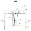
- FIG. 1shows a first semiconductor element 100 in accordance with a first exemplary embodiment.
- the first semiconductor element 100has a first conductive layer 101 comprising copper or aluminum, with a bonding, diffusion and anti-reflection layer, including, for example, Ti, TiN, Ta, TaN, and/or a combination of these materials.
- a contact hole 103is etched into the nonconductive layer 102 , and a nucleation layer 104 is deposited at the bottom of the contact hole, i.e. on top of the fist conductive layer 101 .
- the nucleation layer 104is a layer of catalytically active metal particles, for example comprising nickel, iron, yttrium, cobalt and/or platinum.
- the nucleation layer 104has a catalytic effect for the growth of a carbon nanotube.
- any desired number of carbon nanotubes 105has been grown on top of the nucleation layer 104 .
- a second conductive layer 106comprising a sequence of Ti, TiN, Ta, TaN and/or copper and/or aluminum is deposited above the nonconductive layer 102 , in such a manner that the carbon nanotubes 105 are electrically conductively connected to the second conductive layer 106 .
- the nonconductive layer 102is deposited on the first conductive layer 101 , for example by means of a vapor deposition process (Chemical Vapor Deposition process, CVD process) (cf. FIG. 2 a ).
- a vapor deposition processChemical Vapor Deposition process, CVD process
- the hole (contact hole) 103is etched through the nonconductive layer 102 down to the surface of the first conductive layer 101 (cf. FIG.2 b ).
- the nucleation layer 104is deposited in the hole 103 by means of a suitable process (cf. FIG. 2 c ), for example using a CVD process.
- the nucleation layer 104has a thickness of 0.1 nm to 50 nm.
- the nucleation layer 104 in accordance with the first exemplary embodimentis formed from nickel metal particles.
- carbon nanotubes 105are grown on the nucleation layer 104 in the hole 103 using the process described in [2] (cf. FIG. 2 d ).
- the length of the carbon nanotubes 105is dependent on the time over which the carbon nanotubes are grown on the nucleation layer 104 .
- the carbon nanotubes 105are grown until they project beyond the upper end of the nonconductive layer 102 .
- the second conductive layer 106is deposited on the nonconductive layer 102 by means of a CVD process or a sputtering process or a physical vapor deposition process.
- the carbon nanotubes 105project beyond the nonconductive layer 102 , they project directly into the second nonconductive layer 106 .
- Final chemical mechanical polishing (CMP process) or ion-beam etchingremoves the second conductive layer 106 down to a desired thickness.
- the carbon nanotubes 105create an electrically conductive connection between the first conductive layer 101 and the second conductive layer 106 via the nucleation layer 104 , which itself also contains conductive metal particles.
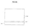
- FIG. 3shows a cross section through a second semiconductor element 300 in accordance with a second exemplary embodiment.
- the second semiconductor element 300has basically the same structure as the first semiconductor element 100 , except that the nucleation layer 301 in accordance with the second exemplary embodiment extends not only over the base of the hole 103 , but also over the entire first conductive layer 101 .
- the individual layers in accordance with the second exemplary embodimentcomprise the same materials as the corresponding layers in accordance with the first exemplary embodiment.
- a nucleation layer 301comprising metal particles (nickel, iron, yttrium, and/or cobalt) is deposited on the first conductive layer 101 .
- the nucleation layer 301is deposited over the entire surface of the first conductive layer 101 by means of a suitable CVD process, sputtering process or physical vapor deposition process.
- the nucleation layer 301has a thickness of 0.1 nm to 50 nm.
- the nonconductive layer 102is deposited on the nucleation layer 301 , for example by means of a CVD process (cf. FIG. 4 a ).
- the carbon nanotubes 105are grown on the nucleation layer 301 using the process described in [2].
- the second conductive layer 106is deposited on the nonconductive layer 102 by means of a CVD process.
- the resultis a semiconductor element with an electrically conductive connection produced by means of carbon nanotubes between two conductive layers through a contact hole.
- FIG. 5shows a third semiconductor element 500 in accordance with a third exemplary embodiment.
- the third semiconductor element 500differs from the second semiconductor 300 substantially only in that a trench 501 is etched into the nonconductive layer 102 , and therefore the carbon nanotubes 105 do not project above the surface of the nonconductive layer 102 , but rather only above the base of the trench 501 , into the nonconductive layer 102 .
- the individual layers of the third semiconductor element 500comprise the same materials as the first semiconductor element 100 and the second semiconductor element 300 .
- the nucleation layer 301is deposited over the first conductive layer 101 in a thickness of 0.1 nm to 50 nm by means of a suitable CVD process, sputtering process or physical vapor deposition process.
- the nonconductive layer 102is deposited on the nucleation layer 301 by means of a CVD process.
- the hole 103is etched into the nonconductive layer 102 down to the surface of the nucleation layer 301 (cf. FIG. 6 b ).
- a trench 501is etched into the nonconductive layer 102 by means of dry-etching or wet-etching (cf. FIG. 6 c ).
- the carbon nanotubes 102are grown on the nucleation layer 301 up to a length which is such that the carbon nanotubes 102 project above the lower surface of the trench 501 but not above the nonconductive layer 102 as a whole (cf. FIG. 6 d ).
- the second conductive layer 106is deposited in the trench 501 and on top of the nonconductive layer 102 by means of a CVD process.
- the second conductive layer 106is reduced to a desired thickness by means of a suitable etching process, a chemical mechanical polishing process or by means of ion beam etching, so that the surface of the second conductive layer 106 is planar with the surface of the nonconductive layer 102 .
- the CVD process usedmay be a CVD process using carbon monoxide CO, methane CH 4 or acetylene C 2 H 2 , or a plasma-enhanced CVD process.
- the carbon nanotubes 105can be brought to the required length by chemical mechanical polishing or ion beam etching at an inclined angle (so that the ions cannot penetrate significantly into the contact hole during the ion beam etching), i.e. can be brought to a length which is such that the carbon nanotubes 105 come into contact with at least the second conductive layer 106 .
- sections of the carbon nanotubes 105project beyond the second conductive layer, they can be removed by means of an ashing process, which is required in any case when using a resist mask for the metal etching.
- the carbon nanotubesmay also be brought to the required length by means of an anisotropic plasma etching process, as used, for example, for patterning organic materials.
- the inventionis not restricted to a three-layer structure.
- the semiconductor elementcan be used in any desired semiconductor structure, i.e. it may form a partial semiconductor element of a semiconductor element which comprises a very large number of layers, in order to make contact between two conductive layers in the semiconductor element.
- the inventionis to be regarded as residing in the fact that two electrically conductive layers which are electrically decoupled from one another in a semiconductor element by a nonconductive layer are electrically conductively connected to one another through a contact hole by means of carbon nanotubes.
- the contact made through contact holesmakes it possible to achieve high aspect ratios of up to approximately 1000.
Landscapes
- Engineering & Computer Science (AREA)
- Physics & Mathematics (AREA)
- Condensed Matter Physics & Semiconductors (AREA)
- General Physics & Mathematics (AREA)
- Computer Hardware Design (AREA)
- Microelectronics & Electronic Packaging (AREA)
- Power Engineering (AREA)
- Chemical & Material Sciences (AREA)
- Nanotechnology (AREA)
- Manufacturing & Machinery (AREA)
- Crystallography & Structural Chemistry (AREA)
- Composite Materials (AREA)
- Materials Engineering (AREA)
- Mathematical Physics (AREA)
- Theoretical Computer Science (AREA)
- Internal Circuitry In Semiconductor Integrated Circuit Devices (AREA)
- Carbon And Carbon Compounds (AREA)
Abstract
Description
- The invention relates to an electronic component, to a method for producing a conductive connection in an electronic component and to a method for producing an electronic component.[0001]
- In an electronic component which is of integrated design, it is customary for two conductive layers which are electrically insulated by a conductive layer to be connected to one another in an electrically conductive manner by etching a hole through the nonconductive layer. The hole is filled with metal, resulting in a metallic contact which connects the two conductive layers to one another in an electrically conductive manner.[0002]
- A drawback of this procedure is that, particularly as the lateral dimensions decrease, i.e. as the diameter of a contact hole through the nonconductive layer decreases and the vertical extent increases, or at least with an increasing aspect ratio, filling the contact hole with metal causes problems and is prone to defects. In particular, the deposited metal often causes a blockage in the upper region of the contact hole, preventing the entire contact hole from being filled with metal. Therefore, it is often impossible to produce an electrically conductive connection between the two conductive layers. Moreover, an incompletely filled contact hole leads to reliability problems.[0003]
- A further drawback of the known procedure is that in the case of a contact hole with a very low aspect ratio, the conductivity of the metallic contact decreases considerably, i.e. the metallic contact represents an element which imposes considerable limitations with regard to the scaling of a metallization system and therefore an integrated circuit, in which it is necessary for a plurality of conductive layers to be electrically conductively connected to one another through nonconductive layers in the vertical direction of an electronic component.[0004]
- Furthermore, [1] has disclosed basic principles of what are known as carbon nanotubes as a highly conductive material whose conductivity greatly exceeds the conductivity of metal of the same dimensions.[0005]
- [2] has disclosed a process for growing carbon nanotubes in a perforated dialuminum trioxide matrix (Al[0006]2O3matrix) in a self-aligned manner.
- Therefore, the invention is based on the problem of providing a conductive connection in an electronic component and of proving an electronic component having a conductive connection between two conductive layers which are insulated from one another by a nonconductive layer, in which it is possible to produce a conductive connection even with holes with a very high aspect ratio.[0007]
- The problem is solved by an electronic component, by a method for producing a conductive connection in an electronic component and by a method for producing an electronic component having the features described in the independent patent claims.[0008]
- An electronic component includes a first conductive layer, a conductive layer on the first conductive layer and a second conductive layer on the nonconductive layer. At least one hole which passes all the way through the nonconductive layer is provided in the nonconductive layer. The hole holds at least one nanotube, by which the first conductive layer is conductively connected to the second conductive layer.[0009]
- In a method for producing a conductive connection in an electronic component, a nonconductive layer is deposited above a first conductive layer. A hole is produced through the nonconductive layer, and at least one nanotube is grown in the holes. Then, a second conductive layer is deposited, in such a manner that the first conductive layer is conductively connected to the second conductive layer by the nanotube.[0010]
- In a method for producing an electronic component, in a first step a first conductive layer is provided. A nonconductive layer is deposited above the first conductive layer, and a hole is produced through the nonconductive layer, for example by etching. At least one nanotube is grown in the hole, and a second conductive layer is deposited in such a manner that the first conductive layer is conductively connected to the second conductive layer by the nanotube.[0011]
- The invention makes it possible to create a reliable, electrically conductive connection between two conductive layers even in the case of contact holes with a very small diameter and a high aspect ratio. The conductive layers may, for example, be any metallic conductive material, such as for example copper, aluminum, silver, etc., it usually being possible for the conductive layers to include a bonding, diffusion and anti-reflection layer, including, for example, Ti, TiN, Ta, TaN, and/or a combination of these materials. The electrically non-conductive layer may be an intermetal dielectric, such as for example silicon oxide or silicon nitride, or another insulating layer made from inorganic material, such as for example polyimide or any desired combination thereof. The electrically conductive connection by means of at least one nanotube is limited only by the diameter of a nanotube of this type, which in the case of a carbon nanotube is approximately 1.5 nm.[0012]
- The production method is distinguished by its simplicity and robustness, i.e. by a low susceptibility to faults, and by the fact that an electrically conductive connection is produced reliably.[0013]
- Therefore, the electronic components can be produced easily and inexpensively even with very fine structures, i.e. with a small contact hole diameter.[0014]
- Preferred refinements of the invention will emerge from the dependent claims.[0015]
- According to a preferred configuration of the invention, the nanotube is a carbon nanotube.[0016]
- A carbon nanotube of this type can be produced in self-aligned fashion very easily and reliably even in a contact hole of small diameter.[0017]
- Furthermore, the carbon nanotube has a very high conductivity, which considerably exceeds the conductivity of even the best metallic conductors, such as for example, copper or silver, for the same dimensions.[0018]
- A plurality of nanotubes, in principle any desired number of nanotubes, may be present in a contact hole of this type, in order for the two conductive layers to be electrically connected to one another.[0019]
- According to one configuration of the invention, a nucleation layer, which preferably has metal particles which are catalytically active for a growing nanotube, for example metal particles comprising nickel and/or iron, and/or yttrium, and/or cobalt and/or platinum, is provided in the contact hole above the first conductive layer in order to accelerate the growth of the nanotube.[0020]
- The hole can be etched through the nonconductive layer.[0021]
- Although the exemplary embodiments which are described below each describe a semiconductor element, it should be noted that the invention is in no way restricted to a semiconductor element, but rather can be used in any electronic component in which two conductive layers which are electrically isolated by a nonconductive layer are to be conductively connected to one another, irrespective of whether or not a layer is a semiconductor layer. In particular, the invention is suitable for use in the context of an integrated circuit.[0022]
- Exemplary embodiments of the invention are illustrated in the figures and are explained in more detail below. In the drawing:[0023]
- FIG. 1 shows a cross section through a semiconductor element in accordance with a first exemplary embodiment;[0024]
- FIGS. 2[0025]ato2dshow cross sections through a semiconductor element, on the basis of which the individual method steps involved in the production of the semiconductor element illustrated in FIG. 1 is explained;
- FIG. 3 shows a cross section through a semiconductor element in accordance with a second exemplary embodiment; FIGS. 4[0026]ato4cshow cross sections through a semiconductor element which are used to explain the individual methods steps involved in the production of the semiconductor element illustrated in FIG. 3;
- FIG. 5 shows a cross section through a semiconductor element in accordance with a third exemplary embodiment of the invention;[0027]
- FIGS. 6[0028]ato6eshow cross sections through a semiconductor element which are used to explain individual method steps involved in the production of the semiconductor element illustrated in FIG. 5.
- Exemplary Embodiment 1[0029]
- FIG. 1 shows a[0030]
first semiconductor element 100 in accordance with a first exemplary embodiment. - The[0031]
first semiconductor element 100 has a firstconductive layer 101 comprising copper or aluminum, with a bonding, diffusion and anti-reflection layer, including, for example, Ti, TiN, Ta, TaN, and/or a combination of these materials. Anonconductive layer 102 comprising an intermetal dielectric, according to the first exemplary embodiment comprising silicon dioxide, is deposited on the firstconductive layer 101. - A[0032]
contact hole 103 is etched into thenonconductive layer 102, and anucleation layer 104 is deposited at the bottom of the contact hole, i.e. on top of the fistconductive layer 101. - The[0033]
nucleation layer 104 is a layer of catalytically active metal particles, for example comprising nickel, iron, yttrium, cobalt and/or platinum. Thenucleation layer 104 has a catalytic effect for the growth of a carbon nanotube. - In principle any desired number of[0034]
carbon nanotubes 105 has been grown on top of thenucleation layer 104. - A second[0035]
conductive layer 106, comprising a sequence of Ti, TiN, Ta, TaN and/or copper and/or aluminum is deposited above thenonconductive layer 102, in such a manner that thecarbon nanotubes 105 are electrically conductively connected to the secondconductive layer 106. - The individual method steps involved in the production of the[0036]
first semiconductor element 100 are explained in more detail with reference to FIG. 2ato FIG. 2d. - In a first step, the[0037]
nonconductive layer 102 is deposited on the firstconductive layer 101, for example by means of a vapor deposition process (Chemical Vapor Deposition process, CVD process) (cf. FIG. 2a). - By suitable masking of the[0038]
nonconductive layer 102 and wet-etching or dry-etching of thenonconductive layer 102, the hole (contact hole)103 is etched through thenonconductive layer 102 down to the surface of the first conductive layer101 (cf. FIG.2b). - The[0039]
nucleation layer 104 is deposited in thehole 103 by means of a suitable process (cf. FIG. 2c), for example using a CVD process. Thenucleation layer 104 has a thickness of 0.1 nm to 50 nm. - The[0040]
nucleation layer 104 in accordance with the first exemplary embodiment is formed from nickel metal particles. - In a further step,[0041]
carbon nanotubes 105 are grown on thenucleation layer 104 in thehole 103 using the process described in [2] (cf. FIG. 2d). - The length of the[0042]
carbon nanotubes 105 is dependent on the time over which the carbon nanotubes are grown on thenucleation layer 104. - The[0043]
carbon nanotubes 105 are grown until they project beyond the upper end of thenonconductive layer 102. - When this is the case, in a further step the second[0044]
conductive layer 106 is deposited on thenonconductive layer 102 by means of a CVD process or a sputtering process or a physical vapor deposition process. - Since the[0045]
carbon nanotubes 105 project beyond thenonconductive layer 102, they project directly into the secondnonconductive layer 106. Final chemical mechanical polishing (CMP process) or ion-beam etching removes the secondconductive layer 106 down to a desired thickness. - In this way, the[0046]
carbon nanotubes 105 create an electrically conductive connection between the firstconductive layer 101 and the secondconductive layer 106 via thenucleation layer 104, which itself also contains conductive metal particles. - Exemplary Embodiment 2[0047]
- FIG. 3 shows a cross section through a[0048]
second semiconductor element 300 in accordance with a second exemplary embodiment. - Identical elements in the figures are provided with the same reference symbols in the second exemplary embodiment as the elements in the first exemplary embodiment.[0049]
- The[0050]
second semiconductor element 300 has basically the same structure as thefirst semiconductor element 100, except that thenucleation layer 301 in accordance with the second exemplary embodiment extends not only over the base of thehole 103, but also over the entire firstconductive layer 101. - The individual layers in accordance with the second exemplary embodiment comprise the same materials as the corresponding layers in accordance with the first exemplary embodiment.[0051]
- Referring to FIG. 4[0052]ato FIG. 4c, the individual method steps involved in the production of the
second semiconductor element 300 are explained in more detail below. - First of all, a[0053]
nucleation layer 301 comprising metal particles (nickel, iron, yttrium, and/or cobalt) is deposited on the firstconductive layer 101. Thenucleation layer 301 is deposited over the entire surface of the firstconductive layer 101 by means of a suitable CVD process, sputtering process or physical vapor deposition process. Thenucleation layer 301 has a thickness of 0.1 nm to 50 nm. - The[0054]
nonconductive layer 102 is deposited on thenucleation layer 301, for example by means of a CVD process (cf. FIG. 4a). - After the[0055]
hole 103 has been etched into thenonconductive layer 102 down to the surface of thenucleation layer 301, as shown in FIG. 4b, thecarbon nanotubes 105 are grown on thenucleation layer 301 using the process described in [2]. - The growth is continued until the length of the[0056]
carbon nanotubes 105 is sufficient for them to project above the surface of the nonconductive layer102 (cf. FIG. 4c). - In a further step, the second[0057]
conductive layer 106 is deposited on thenonconductive layer 102 by means of a CVD process. - Once again, the result is a semiconductor element with an electrically conductive connection produced by means of carbon nanotubes between two conductive layers through a contact hole.[0058]
- Exemplary Embodiment 3[0059]
- FIG. 5 shows a[0060]
third semiconductor element 500 in accordance with a third exemplary embodiment. - Identical elements of the semiconductor element are once again provided with the same reference symbols.[0061]
- The[0062]
third semiconductor element 500 differs from thesecond semiconductor 300 substantially only in that atrench 501 is etched into thenonconductive layer 102, and therefore thecarbon nanotubes 105 do not project above the surface of thenonconductive layer 102, but rather only above the base of thetrench 501, into thenonconductive layer 102. - The individual layers of the[0063]
third semiconductor element 500 comprise the same materials as thefirst semiconductor element 100 and thesecond semiconductor element 300. - The method used to produce the[0064]
third semiconductor element 500 is explained in detail with reference to FIG. 6ato FIG. 6e. - As illustrated in FIG. 6[0065]a, the
nucleation layer 301 is deposited over the firstconductive layer 101 in a thickness of 0.1 nm to 50 nm by means of a suitable CVD process, sputtering process or physical vapor deposition process. Thenonconductive layer 102 is deposited on thenucleation layer 301 by means of a CVD process. - The[0066]
hole 103 is etched into thenonconductive layer 102 down to the surface of the nucleation layer301 (cf. FIG. 6b). - Furthermore, a[0067]
trench 501 is etched into thenonconductive layer 102 by means of dry-etching or wet-etching (cf. FIG. 6c). - In a further step, the[0068]
carbon nanotubes 102 are grown on thenucleation layer 301 up to a length which is such that thecarbon nanotubes 102 project above the lower surface of thetrench 501 but not above thenonconductive layer 102 as a whole (cf. FIG. 6d). - As illustrated in FIG. 6[0069]e, in a further method step the second
conductive layer 106 is deposited in thetrench 501 and on top of thenonconductive layer 102 by means of a CVD process. - The second[0070]
conductive layer 106 is reduced to a desired thickness by means of a suitable etching process, a chemical mechanical polishing process or by means of ion beam etching, so that the surface of the secondconductive layer 106 is planar with the surface of thenonconductive layer 102. - A number of alternatives to the exemplary embodiment presented above are explained below:[0071]
- The CVD process used may be a CVD process using carbon monoxide CO, methane CH[0072]4or acetylene C2H2, or a plasma-enhanced CVD process.
- Furthermore, it is not necessary for the[0073]
carbon nanotubes 105 to project above the surface of the nonconductive layer or above the surface of the lower surface of thetrench 501. Alternatively, thecarbon nanotube 105 can be brought to the required length by chemical mechanical polishing or ion beam etching at an inclined angle (so that the ions cannot penetrate significantly into the contact hole during the ion beam etching), i.e. can be brought to a length which is such that thecarbon nanotubes 105 come into contact with at least the secondconductive layer 106. - If sections of the[0074]
carbon nanotubes 105 project beyond the second conductive layer, they can be removed by means of an ashing process, which is required in any case when using a resist mask for the metal etching. The carbon nanotubes may also be brought to the required length by means of an anisotropic plasma etching process, as used, for example, for patterning organic materials. - The invention is not restricted to a three-layer structure. The semiconductor element can be used in any desired semiconductor structure, i.e. it may form a partial semiconductor element of a semiconductor element which comprises a very large number of layers, in order to make contact between two conductive layers in the semiconductor element.[0075]
- Obviously, the invention is to be regarded as residing in the fact that two electrically conductive layers which are electrically decoupled from one another in a semiconductor element by a nonconductive layer are electrically conductively connected to one another through a contact hole by means of carbon nanotubes.[0076]
- In this way, a high degree of stability of the semiconductor element is achieved with a minimal deviation from standard production processes for a semiconductor element which are already known.[0077]
- Moreover, the contact made through contact holes makes it possible to achieve high aspect ratios of up to approximately 1000.[0078]
- As an alternative, within the context of the invention it is also readily possible for a sputtering process or a physical vapor deposition process to be used instead of the CVD process.[0079]
- The following publications are cited in this document:[0080]
- [1] C. Dekker, Carbon Nanotubes as Molecular Quantum Wires, Physics Today, pp. 22-28, May 1999[0081]
- [2] Jung Sang Suh and Jin Seung Lee, Highly Ordered Two-Dimensional Carbon Nanotubes Areas, Applied Physics Letters, Vol. 75, No. 14, pp. 2047-2049, October 1999[0082]
Claims (21)
Applications Claiming Priority (4)
| Application Number | Priority Date | Filing Date | Title |
|---|---|---|---|
| DE10006964.9 | 2000-02-16 | ||
| DE10006964 | 2000-02-16 | ||
| DE10006964ADE10006964C2 (en) | 2000-02-16 | 2000-02-16 | Electronic component with a conductive connection between two conductive layers and method for producing an electronic component |
| PCT/DE2001/000419WO2001061753A1 (en) | 2000-02-16 | 2001-02-02 | Electronic component comprising an electrically conductive connection consisting of carbon nanotubes and a method for producing the same |
Publications (2)
| Publication Number | Publication Date |
|---|---|
| US20030179559A1true US20030179559A1 (en) | 2003-09-25 |
| US7321097B2 US7321097B2 (en) | 2008-01-22 |
Family
ID=7631134
Family Applications (1)
| Application Number | Title | Priority Date | Filing Date |
|---|---|---|---|
| US10/204,180Expired - Fee RelatedUS7321097B2 (en) | 2000-02-16 | 2001-02-02 | Electronic component comprising an electrically conductive connection consisting of carbon nanotubes and a method for producing the same |
Country Status (7)
| Country | Link |
|---|---|
| US (1) | US7321097B2 (en) |
| EP (1) | EP1264344A1 (en) |
| JP (1) | JP4549002B2 (en) |
| KR (1) | KR100494248B1 (en) |
| DE (1) | DE10006964C2 (en) |
| TW (1) | TW503482B (en) |
| WO (1) | WO2001061753A1 (en) |
Cited By (75)
| Publication number | Priority date | Publication date | Assignee | Title |
|---|---|---|---|---|
| US20020163079A1 (en)* | 2001-05-02 | 2002-11-07 | Fujitsu Limited | Integrated circuit device and method of producing the same |
| US20030111333A1 (en)* | 2001-12-17 | 2003-06-19 | Intel Corporation | Method and apparatus for producing aligned carbon nanotube thermal interface structure |
| US20030231471A1 (en)* | 2002-06-12 | 2003-12-18 | Intel Corporation | Increasing thermal conductivity of thermal interface using carbon nanotubes and cvd |
| US20040137730A1 (en)* | 2002-10-11 | 2004-07-15 | Sang-Gook Kim | Method of making packets of nanostructures |
| US20040261987A1 (en)* | 2003-06-30 | 2004-12-30 | Yuegang Zhang | Thermal interface apparatus, systems, and methods |
| US20050118342A1 (en)* | 2003-11-03 | 2005-06-02 | Manfred Engelhardt | Process for depositing a catalyst |
| US20050127030A1 (en)* | 2003-07-24 | 2005-06-16 | Fuji Xerox Co., Ltd. | Carbon nanotube structure, method of manufacturing the same, carbon nanotube transfer body, and liquid solution |
| US20050142933A1 (en)* | 2003-12-17 | 2005-06-30 | Gottfried Beer | Flexible rewiring plate for semiconductor components, and process for producing it |
| WO2005069372A1 (en)* | 2003-12-18 | 2005-07-28 | International Business Machines Corporation | Carbon nanotube conductor for trench capacitors |
| US20050189655A1 (en)* | 2004-02-26 | 2005-09-01 | International Business Machines Corporation | Integrated circuit chip utilizing carbon nanotube composite interconnection vias |
| WO2006000175A1 (en)* | 2004-06-28 | 2006-01-05 | Infineon Technologies Ag | Electric circuit comprising a carbon conductor structure, and method for the production of a carbon conductor structure of an electric circuit |
| US20060046445A1 (en)* | 2003-05-01 | 2006-03-02 | Samsung Electronics Co., Ltd. | Method of forming a conductive line for a semiconductor device using a carbon nanotube and semiconductor device manufactured using the method |
| US20060071334A1 (en)* | 2004-10-05 | 2006-04-06 | Fujitsu Limited | Carbon nanotube structure, a semiconductor device, a semiconductor package and a manufacturing method of a semiconductor device |
| US20060071344A1 (en)* | 2004-10-01 | 2006-04-06 | Fujitsu Limited | Wiring connection structure and method for forming the same |
| US20060086958A1 (en)* | 2004-10-22 | 2006-04-27 | Renesas Technology Corp. | Wire structure, semiconductor device, MRAM, and manufacturing method of semiconductor device |
| US20060263289A1 (en)* | 2005-05-23 | 2006-11-23 | Samsung Electronics Co., Ltd. | Metal oxide resistive memory and method of fabricating the same |
| US20060278901A1 (en)* | 2003-01-24 | 2006-12-14 | Carlos Dangelo | In-chip structures and methods for removing heat from integrated circuits |
| WO2006133318A1 (en)* | 2005-06-08 | 2006-12-14 | Intel Corporation | Carbon nanotube interconnect contacts |
| US20060286851A1 (en)* | 2005-06-06 | 2006-12-21 | Fujitsu Limited | Electrical connection structure, manufacturing method thereof and semiconductor integrated circuit device |
| US20070001220A1 (en)* | 2004-09-16 | 2007-01-04 | Atomate Corporation | Nanotube Transistor and Rectifying Devices |
| US20070012986A1 (en)* | 2005-05-07 | 2007-01-18 | Choi Chel-Jong | Phase-change memory device including nanowires and method of manufacturing the same |
| US20070158584A1 (en)* | 2005-11-11 | 2007-07-12 | Hon Hai Precision Industry Co., Ltd. | Heat sink with carbon nanotubes and method for manufacturing the same |
| US20070164430A1 (en)* | 2005-11-28 | 2007-07-19 | Megica Corporation | Carbon nanotube circuit component structure |
| US20070237705A1 (en)* | 2006-03-31 | 2007-10-11 | Fujitsu Limited | Carbon nanotube chain and production process for the same, target detector, and target detection method |
| CN101097946A (en)* | 2006-06-30 | 2008-01-02 | Lg.菲利浦Lcd株式会社 | Organic light emitting display device and manufacturing method thereof |
| US20080003801A1 (en)* | 2003-02-03 | 2008-01-03 | Dubin Valery M | Packaging of integrated circuits with carbon nano-tube arrays to enhance heat dissipation through a thermal interface |
| KR100822799B1 (en) | 2006-04-25 | 2008-04-17 | 삼성전자주식회사 | Selective Catalyst Formation Method for Nanosized Conductive Structures and Selective Methods for Forming Nanoscale Conductive Structures |
| US20080135908A1 (en)* | 2006-12-06 | 2008-06-12 | Samsung Electronics Co., Ltd. | Semiconductor device and method of manufacturing the same |
| US20080236804A1 (en)* | 2006-10-17 | 2008-10-02 | Cola Baratunde A | Electrothermal interface material enhancer |
| US20080246149A1 (en)* | 2007-04-06 | 2008-10-09 | Hynix Semiconductor Inc. | Semiconductor device and method for forming device isolation film of semiconductor device |
| US20080272361A1 (en)* | 2007-05-02 | 2008-11-06 | Atomate Corporation | High Density Nanotube Devices |
| US7462890B1 (en) | 2004-09-16 | 2008-12-09 | Atomate Corporation | Nanotube transistor integrated circuit layout |
| EP2006901A2 (en) | 2007-06-22 | 2008-12-24 | Commissariat à l'Energie Atomique | Method of producing an electric connection based on carbon nanotubes |
| EP2017885A2 (en) | 2007-07-17 | 2009-01-21 | Commissariat A L'energie Atomique | Method of producing an electric connection using nanotubes and having air gaps |
| US7504711B2 (en) | 2004-07-21 | 2009-03-17 | Infineon Technologies Ag | Semiconductor substrate with strip conductors formed of carbon nanotubes and production thereof |
| US20090075430A1 (en)* | 2003-12-30 | 2009-03-19 | White Bryan M | Thermal intermediate apparatus, systems, and methods |
| US20090098671A1 (en)* | 2004-09-10 | 2009-04-16 | Dong-Wook Kim | Nanotube assembly including protective layer and method for making the same |
| US20090121298A1 (en)* | 2005-04-06 | 2009-05-14 | Toshiharu Furukawa | Field effect transistor |
| US20090159985A1 (en)* | 2007-12-21 | 2009-06-25 | Advanced Micro Devices, Inc. | Integrated circuit system with contact integration |
| US20090166686A1 (en)* | 2007-12-31 | 2009-07-02 | Atomate Corporation | Edge-Contacted Vertical Carbon Nanotube Transistor |
| US20090197484A1 (en)* | 2007-10-13 | 2009-08-06 | Formfactor, Inc. | Carbon nanotube spring contact structures with mechanical and electrical components |
| US20090256132A1 (en)* | 2008-04-11 | 2009-10-15 | Sandisk 3D Llc | Memory cell that includes a carbon-based memory element and methods of forming the same |
| EP2138457A1 (en)* | 2008-06-27 | 2009-12-30 | Commissariat à l'Energie Atomique | Method for obtaining a carpet of carbon nanotubes on a conductor or semi-conductor substrate |
| US20090325377A1 (en)* | 2008-06-27 | 2009-12-31 | Commissariat A L'energie Atomique | Procedure for Obtaining Nanotube Layers of Carbon with Conductor or Semiconductor Substrate |
| US20090321892A1 (en)* | 2008-06-30 | 2009-12-31 | Han Jun Bae | Semiconductor package using through-electrodes having voids |
| US20100022083A1 (en)* | 2005-12-30 | 2010-01-28 | Intel Corporation | Carbon nanotube interconnect structures |
| US20100032639A1 (en)* | 2008-08-07 | 2010-02-11 | Sandisk 3D Llc | Memory cell that includes a carbon-based memory element and methods of forming the same |
| US20100065820A1 (en)* | 2005-02-14 | 2010-03-18 | Atomate Corporation | Nanotube Device Having Nanotubes with Multiple Characteristics |
| US7692218B2 (en) | 2002-11-19 | 2010-04-06 | William Marsh Rice University | Method for creating a functional interface between a nanoparticle, nanotube or nanowire, and a biological molecule or system |
| US20100083489A1 (en)* | 2006-10-16 | 2010-04-08 | Formfactor, Inc. | Carbon nanotube columns and methods of making and using carbon nanotube columns as probes |
| US20100132080A1 (en)* | 2008-11-24 | 2010-05-27 | Massachusetts Institute Of Technology | Method of making and assembling capsulated nanostructures |
| US20100163846A1 (en)* | 2008-12-31 | 2010-07-01 | Hamza Yilmaz | Nano-tube mosfet technology and devices |
| US20100173478A1 (en)* | 2004-09-16 | 2010-07-08 | Atomate Corporation | Concentric gate nanotube transistor devices |
| US20100200208A1 (en)* | 2007-10-17 | 2010-08-12 | Cola Baratunde A | Methods for attaching carbon nanotubes to a carbon substrate |
| US20100253375A1 (en)* | 2009-04-03 | 2010-10-07 | Formfactor, Inc. | Anchoring carbon nanotube columns |
| US20100252317A1 (en)* | 2009-04-03 | 2010-10-07 | Formfactor, Inc. | Carbon nanotube contact structures for use with semiconductor dies and other electronic devices |
| US20100264544A1 (en)* | 2006-01-20 | 2010-10-21 | Jang-Eun Heo | Device including contact structure and method of forming the same |
| US20100314659A1 (en)* | 2009-06-12 | 2010-12-16 | Alpha & Omega Semiconductor, Inc. | Nanotube Semiconductor Devices |
| US20110020539A1 (en)* | 2009-03-06 | 2011-01-27 | Purdue Research Foundation | Palladium thiolate bonding of carbon nanotubes |
| US7892924B1 (en)* | 2009-12-02 | 2011-02-22 | Alpha And Omega Semiconductor, Inc. | Method for making a charge balanced multi-nano shell drift region for superjunction semiconductor device |
| US20110081770A1 (en)* | 2004-09-16 | 2011-04-07 | Atomate Corporation | Removing undesirable nanotubes during nanotube device fabrication |
| US20110089477A1 (en)* | 2008-06-13 | 2011-04-21 | Qunano Ab | Nanostructured mos capacitor |
| US20110140167A1 (en)* | 2009-06-12 | 2011-06-16 | Alpha & Omega Semiconductor, Inc. | Nanotube Semiconductor Devices |
| US20110168763A1 (en)* | 2003-12-30 | 2011-07-14 | Intel Corporation | Nanotube modified solder thermal intermediate structure, systems, and methods |
| US8130007B2 (en) | 2006-10-16 | 2012-03-06 | Formfactor, Inc. | Probe card assembly with carbon nanotube probes having a spring mechanism therein |
| US8168495B1 (en) | 2006-12-29 | 2012-05-01 | Etamota Corporation | Carbon nanotube high frequency transistor technology |
| CN102468220A (en)* | 2010-11-08 | 2012-05-23 | 中国科学院微电子研究所 | Metal interconnection structure and forming method thereof |
| US8638113B2 (en) | 2005-06-24 | 2014-01-28 | Formfactor, Inc. | Temporary planar electrical contact device and method using vertically-compressible nanotube contact structures |
| US20140252615A1 (en)* | 2013-03-08 | 2014-09-11 | Kabushiki Kaisha Toshiba | Semiconductor device using carbon nanotube, and manufacturing method thereof |
| US8872176B2 (en) | 2010-10-06 | 2014-10-28 | Formfactor, Inc. | Elastic encapsulated carbon nanotube based electrical contacts |
| US20150235958A1 (en)* | 2014-02-14 | 2015-08-20 | Taiwan Semiconductor Manufacturing Company Limited | Method for producing salicide and a carbon nanotube metal contact |
| US9406888B2 (en)* | 2013-08-07 | 2016-08-02 | GlobalFoundries, Inc. | Carbon nanotube device |
| US9508805B2 (en) | 2008-12-31 | 2016-11-29 | Alpha And Omega Semiconductor Incorporated | Termination design for nanotube MOSFET |
| US20170069732A1 (en)* | 2008-06-18 | 2017-03-09 | Micron Technology, Inc. | Methods of Forming Diodes |
| US20180301409A1 (en)* | 2014-10-27 | 2018-10-18 | Taiwan Semiconductor Manufacturing Co., Ltd. | Semiconductor device structure and method for forming the same |
Families Citing this family (25)
| Publication number | Priority date | Publication date | Assignee | Title |
|---|---|---|---|---|
| JP2002341060A (en)* | 2001-05-11 | 2002-11-27 | Seiko Instruments Inc | Composite electric component, main plate structure body and electronic timepiece using it |
| US6919592B2 (en) | 2001-07-25 | 2005-07-19 | Nantero, Inc. | Electromechanical memory array using nanotube ribbons and method for making same |
| DE10144704B4 (en)* | 2001-09-11 | 2007-10-04 | Infineon Technologies Ag | Method for connecting a component to a carrier |
| WO2003043934A1 (en)* | 2001-11-20 | 2003-05-30 | Wm. Marsh Rice University | Coated fullerenes, composites and dielectrics made therefrom |
| SE0200868D0 (en)* | 2002-03-20 | 2002-03-20 | Chalmers Technology Licensing | Theoretical model for a nanorelay and same relay |
| DE10220194A1 (en)* | 2002-05-06 | 2003-11-27 | Infineon Technologies Ag | Contacting of nanotubes |
| US20030211724A1 (en)* | 2002-05-10 | 2003-11-13 | Texas Instruments Incorporated | Providing electrical conductivity between an active region and a conductive layer in a semiconductor device using carbon nanotubes |
| DE10250868B8 (en)* | 2002-10-31 | 2008-06-26 | Qimonda Ag | Vertically integrated field effect transistor, field effect transistor arrangement and method for producing a vertically integrated field effect transistor |
| AU2003295721A1 (en) | 2002-11-19 | 2004-06-15 | William Marsh Rice University | Fabrication of light emitting film coated fullerenes and their application for in-vivo light emission |
| US7518247B2 (en)* | 2002-11-29 | 2009-04-14 | Nec Corporation | Semiconductor device and its manufacturing method |
| CA2515724A1 (en)* | 2003-02-12 | 2004-08-26 | Nantero, Inc | Devices having vertically-disposed nanofabric articles and methods of making the same |
| DE10307815B3 (en) | 2003-02-24 | 2004-11-11 | Infineon Technologies Ag | Integrated electronic component with specifically created nanotubes in vertical structures and its manufacturing process |
| JP4454242B2 (en)* | 2003-03-25 | 2010-04-21 | 株式会社ルネサステクノロジ | Semiconductor device and manufacturing method thereof |
| DE10324377A1 (en)* | 2003-05-28 | 2005-01-05 | Infineon Technologies Ag | Heat extraction device has nanotube arrangement with nanotubes as material for heat extraction and embedded in embedding material, especially adhesive material |
| JP4689218B2 (en)* | 2003-09-12 | 2011-05-25 | 株式会社半導体エネルギー研究所 | Method for manufacturing semiconductor device |
| US20060086994A1 (en) | 2004-05-14 | 2006-04-27 | Susanne Viefers | Nanoelectromechanical components |
| KR100689813B1 (en) | 2004-09-08 | 2007-03-08 | 삼성전자주식회사 | Semiconductor memory device having carbon nanotubes and method for manufacturing the same |
| JP2006120730A (en)* | 2004-10-19 | 2006-05-11 | Fujitsu Ltd | Wiring structure using multi-walled carbon nanotubes for interlayer wiring and manufacturing method thereof |
| US20070105356A1 (en)* | 2005-11-10 | 2007-05-10 | Wei Wu | Method of controlling nanowire growth and device with controlled-growth nanowire |
| FR2910706B1 (en) | 2006-12-21 | 2009-03-20 | Commissariat Energie Atomique | INTERCONNECTION ELEMENT BASED ON CARBON NANOTUBES |
| DE102007006175A1 (en) | 2007-02-07 | 2008-08-14 | Osram Opto Semiconductors Gmbh | Heat conducting layer for use with optoelectronic arrangement, has two main surfaces and multiple heat conducting elements that are arranged on former main surface and has preferred directions, which cuts former main surface |
| JP5423029B2 (en)* | 2009-02-12 | 2014-02-19 | 富士通セミコンダクター株式会社 | Manufacturing method of semiconductor device |
| KR101015507B1 (en)* | 2010-01-25 | 2011-02-22 | 삼성전자주식회사 | Method of forming conductive line of semiconductor device using carbon nanotube and semiconductor device manufactured by the method |
| US8946903B2 (en)* | 2010-07-09 | 2015-02-03 | Micron Technology, Inc. | Electrically conductive laminate structure containing graphene region |
| KR101728986B1 (en) | 2016-07-18 | 2017-04-20 | 박달수 | Preparation of food for liver with Chinese (herb) medicine extracts |
Citations (7)
| Publication number | Priority date | Publication date | Assignee | Title |
|---|---|---|---|---|
| US5192835A (en)* | 1990-10-09 | 1993-03-09 | Eastman Kodak Company | Bonding of solid state device to terminal board |
| US5712607A (en)* | 1996-04-12 | 1998-01-27 | Dittmer; Timothy W. | Air-dielectric stripline |
| US5818700A (en)* | 1996-09-24 | 1998-10-06 | Texas Instruments Incorporated | Microelectronic assemblies including Z-axis conductive films |
| US6019656A (en)* | 1997-11-29 | 2000-02-01 | Electronics And Telecommunications Research Institute | Method of fabricating a field emission device by using carbon nano-tubes |
| US6242808B1 (en)* | 1998-04-09 | 2001-06-05 | Fujitsu Limited | Semiconductor device with copper wiring and semiconductor device manufacturing method |
| US20010023986A1 (en)* | 2000-02-07 | 2001-09-27 | Vladimir Mancevski | System and method for fabricating logic devices comprising carbon nanotube transistors |
| US6297063B1 (en)* | 1999-10-25 | 2001-10-02 | Agere Systems Guardian Corp. | In-situ nano-interconnected circuit devices and method for making the same |
Family Cites Families (5)
| Publication number | Priority date | Publication date | Assignee | Title |
|---|---|---|---|---|
| US5698496A (en) | 1995-02-10 | 1997-12-16 | Lucent Technologies Inc. | Method for making an anisotropically conductive composite medium |
| JP3740295B2 (en) | 1997-10-30 | 2006-02-01 | キヤノン株式会社 | Carbon nanotube device, manufacturing method thereof, and electron-emitting device |
| JP3363759B2 (en) | 1997-11-07 | 2003-01-08 | キヤノン株式会社 | Carbon nanotube device and method of manufacturing the same |
| US6730541B2 (en) | 1997-11-20 | 2004-05-04 | Texas Instruments Incorporated | Wafer-scale assembly of chip-size packages |
| US6870263B1 (en) | 1998-03-31 | 2005-03-22 | Infineon Technologies Ag | Device interconnection |
- 2000
- 2000-02-16DEDE10006964Apatent/DE10006964C2/ennot_activeExpired - Fee Related
- 2001
- 2001-02-02USUS10/204,180patent/US7321097B2/ennot_activeExpired - Fee Related
- 2001-02-02JPJP2001560448Apatent/JP4549002B2/ennot_activeExpired - Fee Related
- 2001-02-02KRKR10-2002-7010550Apatent/KR100494248B1/ennot_activeExpired - Fee Related
- 2001-02-02EPEP01909557Apatent/EP1264344A1/ennot_activeCeased
- 2001-02-02WOPCT/DE2001/000419patent/WO2001061753A1/enactiveIP Right Grant
- 2001-02-15TWTW090103370Apatent/TW503482B/ennot_activeIP Right Cessation
Patent Citations (7)
| Publication number | Priority date | Publication date | Assignee | Title |
|---|---|---|---|---|
| US5192835A (en)* | 1990-10-09 | 1993-03-09 | Eastman Kodak Company | Bonding of solid state device to terminal board |
| US5712607A (en)* | 1996-04-12 | 1998-01-27 | Dittmer; Timothy W. | Air-dielectric stripline |
| US5818700A (en)* | 1996-09-24 | 1998-10-06 | Texas Instruments Incorporated | Microelectronic assemblies including Z-axis conductive films |
| US6019656A (en)* | 1997-11-29 | 2000-02-01 | Electronics And Telecommunications Research Institute | Method of fabricating a field emission device by using carbon nano-tubes |
| US6242808B1 (en)* | 1998-04-09 | 2001-06-05 | Fujitsu Limited | Semiconductor device with copper wiring and semiconductor device manufacturing method |
| US6297063B1 (en)* | 1999-10-25 | 2001-10-02 | Agere Systems Guardian Corp. | In-situ nano-interconnected circuit devices and method for making the same |
| US20010023986A1 (en)* | 2000-02-07 | 2001-09-27 | Vladimir Mancevski | System and method for fabricating logic devices comprising carbon nanotube transistors |
Cited By (159)
| Publication number | Priority date | Publication date | Assignee | Title |
|---|---|---|---|---|
| US20020163079A1 (en)* | 2001-05-02 | 2002-11-07 | Fujitsu Limited | Integrated circuit device and method of producing the same |
| US7923283B2 (en) | 2001-05-02 | 2011-04-12 | Fujitsu Limited | Integrated circuit device and method of producing the same |
| US20060226551A1 (en)* | 2001-05-02 | 2006-10-12 | Fujitsu Limited | Integrated circuit device and method of producing the same |
| US7332810B2 (en) | 2001-05-02 | 2008-02-19 | Fujitsu Limited | Integrated circuit device and method of producing the same |
| US7084507B2 (en) | 2001-05-02 | 2006-08-01 | Fujitsu Limited | Integrated circuit device and method of producing the same |
| US20080111164A1 (en)* | 2001-05-02 | 2008-05-15 | Fujitsu Limited | Integrated circuit device and method of producing the same |
| US20030111333A1 (en)* | 2001-12-17 | 2003-06-19 | Intel Corporation | Method and apparatus for producing aligned carbon nanotube thermal interface structure |
| US7704462B2 (en) | 2001-12-17 | 2010-04-27 | Intel Corporation | Method and apparatus for producing aligned carbon nanotube thermal interface structure |
| US20060054490A1 (en)* | 2001-12-17 | 2006-03-16 | Intel Corporation | Method and apparatus for producing aligned carbon nanotube thermal interface structure |
| US6921462B2 (en) | 2001-12-17 | 2005-07-26 | Intel Corporation | Method and apparatus for producing aligned carbon nanotube thermal interface structure |
| US6891724B2 (en) | 2002-06-12 | 2005-05-10 | Intel Corporation | Increasing thermal conductivity of thermal interface using carbon nanotubes and CVD |
| US20030231471A1 (en)* | 2002-06-12 | 2003-12-18 | Intel Corporation | Increasing thermal conductivity of thermal interface using carbon nanotubes and cvd |
| US7507987B2 (en)* | 2002-10-11 | 2009-03-24 | Massachusetts Institute Of Technology | Method of making packets of nanostructures |
| US20040137730A1 (en)* | 2002-10-11 | 2004-07-15 | Sang-Gook Kim | Method of making packets of nanostructures |
| US7692218B2 (en) | 2002-11-19 | 2010-04-06 | William Marsh Rice University | Method for creating a functional interface between a nanoparticle, nanotube or nanowire, and a biological molecule or system |
| US7656027B2 (en)* | 2003-01-24 | 2010-02-02 | Nanoconduction, Inc. | In-chip structures and methods for removing heat from integrated circuits |
| US20060278901A1 (en)* | 2003-01-24 | 2006-12-14 | Carlos Dangelo | In-chip structures and methods for removing heat from integrated circuits |
| US7704791B2 (en) | 2003-02-03 | 2010-04-27 | Intel Corporation | Packaging of integrated circuits with carbon nano-tube arrays to enhance heat dissipation through a thermal interface |
| US20080003801A1 (en)* | 2003-02-03 | 2008-01-03 | Dubin Valery M | Packaging of integrated circuits with carbon nano-tube arrays to enhance heat dissipation through a thermal interface |
| US7847394B2 (en) | 2003-02-03 | 2010-12-07 | Intel Corporation | Packaging of integrated circuits with carbon nanotube arrays to enhance heat dissipation through a thermal interface |
| US7247897B2 (en) | 2003-05-01 | 2007-07-24 | Samsung Electronics Co., Ltd. | Conductive line for a semiconductor device using a carbon nanotube including a memory thin film and semiconductor device manufactured |
| US20060046445A1 (en)* | 2003-05-01 | 2006-03-02 | Samsung Electronics Co., Ltd. | Method of forming a conductive line for a semiconductor device using a carbon nanotube and semiconductor device manufactured using the method |
| US7168484B2 (en)* | 2003-06-30 | 2007-01-30 | Intel Corporation | Thermal interface apparatus, systems, and methods |
| US20070119582A1 (en)* | 2003-06-30 | 2007-05-31 | Intel Corporation | Thermal interface apparatus, systems, and methods |
| US20040261987A1 (en)* | 2003-06-30 | 2004-12-30 | Yuegang Zhang | Thermal interface apparatus, systems, and methods |
| US20050127030A1 (en)* | 2003-07-24 | 2005-06-16 | Fuji Xerox Co., Ltd. | Carbon nanotube structure, method of manufacturing the same, carbon nanotube transfer body, and liquid solution |
| US20050118342A1 (en)* | 2003-11-03 | 2005-06-02 | Manfred Engelhardt | Process for depositing a catalyst |
| US7268423B2 (en) | 2003-12-17 | 2007-09-11 | Infineon Technologies Ag | Flexible rewiring plate for semiconductor components, and process for producing it |
| US20050142933A1 (en)* | 2003-12-17 | 2005-06-30 | Gottfried Beer | Flexible rewiring plate for semiconductor components, and process for producing it |
| US7932549B2 (en) | 2003-12-18 | 2011-04-26 | International Business Machines Corporation | Carbon nanotube conductor for trench capacitors |
| WO2005069372A1 (en)* | 2003-12-18 | 2005-07-28 | International Business Machines Corporation | Carbon nanotube conductor for trench capacitors |
| US8129223B2 (en) | 2003-12-30 | 2012-03-06 | Intel Corporation | Nanotube modified solder thermal intermediate structure, systems, and methods |
| US7985627B2 (en) | 2003-12-30 | 2011-07-26 | Intel Corporation | Thermal intermediate apparatus, systems, and methods |
| US20090075430A1 (en)* | 2003-12-30 | 2009-03-19 | White Bryan M | Thermal intermediate apparatus, systems, and methods |
| US20110168763A1 (en)* | 2003-12-30 | 2011-07-14 | Intel Corporation | Nanotube modified solder thermal intermediate structure, systems, and methods |
| US20050189655A1 (en)* | 2004-02-26 | 2005-09-01 | International Business Machines Corporation | Integrated circuit chip utilizing carbon nanotube composite interconnection vias |
| WO2005083776A1 (en) | 2004-02-26 | 2005-09-09 | International Business Machines Corporation | Integrated circuit chips utilizing carbon nanotube composite interconnection vias |
| US20060292861A1 (en)* | 2004-02-26 | 2006-12-28 | International Business Machines Corporation | Method for making integrated circuit chip having carbon nanotube composite interconnection vias |
| US7135773B2 (en)* | 2004-02-26 | 2006-11-14 | International Business Machines Corporation | Integrated circuit chip utilizing carbon nanotube composite interconnection vias |
| US7473633B2 (en) | 2004-02-26 | 2009-01-06 | International Business Machines Corporation | Method for making integrated circuit chip having carbon nanotube composite interconnection vias |
| WO2006000175A1 (en)* | 2004-06-28 | 2006-01-05 | Infineon Technologies Ag | Electric circuit comprising a carbon conductor structure, and method for the production of a carbon conductor structure of an electric circuit |
| US7504711B2 (en) | 2004-07-21 | 2009-03-17 | Infineon Technologies Ag | Semiconductor substrate with strip conductors formed of carbon nanotubes and production thereof |
| US20090098671A1 (en)* | 2004-09-10 | 2009-04-16 | Dong-Wook Kim | Nanotube assembly including protective layer and method for making the same |
| US20100059736A1 (en)* | 2004-09-16 | 2010-03-11 | Atomate Corporation | Heterostructure Nanotube Devices |
| US7345296B2 (en) | 2004-09-16 | 2008-03-18 | Atomate Corporation | Nanotube transistor and rectifying devices |
| US20070001220A1 (en)* | 2004-09-16 | 2007-01-04 | Atomate Corporation | Nanotube Transistor and Rectifying Devices |
| US20080206964A1 (en)* | 2004-09-16 | 2008-08-28 | Atomate Corporation | Carbon Nanotube Transistor Process with Transferred Carbon Nanotubes |
| US20110217827A1 (en)* | 2004-09-16 | 2011-09-08 | Etamota Corporation | Removing Undesirable Nanotubes During Nanotube Device Fabrication |
| US7622732B1 (en) | 2004-09-16 | 2009-11-24 | Atomate Corporation | Heterostructure nanotube devices |
| US7732290B2 (en) | 2004-09-16 | 2010-06-08 | Etamota Corporation | Carbon nanotube transistor process with transferred carbon nanotubes |
| US20080299710A1 (en)* | 2004-09-16 | 2008-12-04 | Atomate Corporation | Carbon Nanotube Transistor Fabrication |
| US7462890B1 (en) | 2004-09-16 | 2008-12-09 | Atomate Corporation | Nanotube transistor integrated circuit layout |
| US7736943B2 (en) | 2004-09-16 | 2010-06-15 | Etamota Corporation | Carbon nanotube transistor fabrication |
| US20100173478A1 (en)* | 2004-09-16 | 2010-07-08 | Atomate Corporation | Concentric gate nanotube transistor devices |
| US20090001421A1 (en)* | 2004-09-16 | 2009-01-01 | Atomate Corporation | Nanotube transistor integrated circuit layout |
| US7943418B2 (en) | 2004-09-16 | 2011-05-17 | Etamota Corporation | Removing undesirable nanotubes during nanotube device fabrication |
| US20100171099A1 (en)* | 2004-09-16 | 2010-07-08 | Atomate Corporation | Carbon Nanotube Transistor Structure |
| US20110081770A1 (en)* | 2004-09-16 | 2011-04-07 | Atomate Corporation | Removing undesirable nanotubes during nanotube device fabrication |
| US7776307B2 (en) | 2004-09-16 | 2010-08-17 | Etamota Corporation | Concentric gate nanotube transistor devices |
| US20100270536A1 (en)* | 2004-09-16 | 2010-10-28 | Etamota Corporation | Concentric Gate Nanotube Transistor Devices |
| US7301191B1 (en) | 2004-09-16 | 2007-11-27 | Atomate Corporation | Fabricating carbon nanotube transistor devices |
| US20060071344A1 (en)* | 2004-10-01 | 2006-04-06 | Fujitsu Limited | Wiring connection structure and method for forming the same |
| US7948081B2 (en)* | 2004-10-05 | 2011-05-24 | Fujitsu Limited | Carbon nanotube structure, a semiconductor device, a semiconductor package and a manufacturing method of a semiconductor device |
| US20060071334A1 (en)* | 2004-10-05 | 2006-04-06 | Fujitsu Limited | Carbon nanotube structure, a semiconductor device, a semiconductor package and a manufacturing method of a semiconductor device |
| US20060086958A1 (en)* | 2004-10-22 | 2006-04-27 | Renesas Technology Corp. | Wire structure, semiconductor device, MRAM, and manufacturing method of semiconductor device |
| US20100065820A1 (en)* | 2005-02-14 | 2010-03-18 | Atomate Corporation | Nanotube Device Having Nanotubes with Multiple Characteristics |
| US8541823B2 (en) | 2005-04-06 | 2013-09-24 | International Business Machines Corporation | Field effect transistor |
| US20090121298A1 (en)* | 2005-04-06 | 2009-05-14 | Toshiharu Furukawa | Field effect transistor |
| US8004024B2 (en)* | 2005-04-06 | 2011-08-23 | International Business Machines Corporation | Field effect transistor |
| US7569846B2 (en)* | 2005-05-07 | 2009-08-04 | Samsung Electronics Co., Ltd. | Phase-change memory device including nanowires and method of manufacturing the same |
| US20070012986A1 (en)* | 2005-05-07 | 2007-01-18 | Choi Chel-Jong | Phase-change memory device including nanowires and method of manufacturing the same |
| US20060263289A1 (en)* | 2005-05-23 | 2006-11-23 | Samsung Electronics Co., Ltd. | Metal oxide resistive memory and method of fabricating the same |
| US8338822B2 (en)* | 2005-06-06 | 2012-12-25 | Fujitsu Limited | Electrical connection structure having elongated carbon structures with fine catalyst particle layer |
| US20060286851A1 (en)* | 2005-06-06 | 2006-12-21 | Fujitsu Limited | Electrical connection structure, manufacturing method thereof and semiconductor integrated circuit device |
| WO2006133318A1 (en)* | 2005-06-08 | 2006-12-14 | Intel Corporation | Carbon nanotube interconnect contacts |
| DE112006001397B4 (en)* | 2005-06-08 | 2012-10-18 | Intel Corporation | Carbon nanotube wiring contacts and methods of making same |
| US20060281306A1 (en)* | 2005-06-08 | 2006-12-14 | Florian Gstrein | Carbon nanotube interconnect contacts |
| GB2442634A (en)* | 2005-06-08 | 2008-04-09 | Intel Corp | Carbon nanotube interconnect contacts |
| US8638113B2 (en) | 2005-06-24 | 2014-01-28 | Formfactor, Inc. | Temporary planar electrical contact device and method using vertically-compressible nanotube contact structures |
| US20070158584A1 (en)* | 2005-11-11 | 2007-07-12 | Hon Hai Precision Industry Co., Ltd. | Heat sink with carbon nanotubes and method for manufacturing the same |
| US8692374B2 (en) | 2005-11-28 | 2014-04-08 | Megit Acquisition Corp. | Carbon nanotube circuit component structure |
| US20070164430A1 (en)* | 2005-11-28 | 2007-07-19 | Megica Corporation | Carbon nanotube circuit component structure |
| US7990037B2 (en)* | 2005-11-28 | 2011-08-02 | Megica Corporation | Carbon nanotube circuit component structure |
| US20100022083A1 (en)* | 2005-12-30 | 2010-01-28 | Intel Corporation | Carbon nanotube interconnect structures |
| US7982318B2 (en) | 2006-01-20 | 2011-07-19 | Samsung Electronics Co., Ltd. | Device including contact structure and method of forming the same |
| US20100264544A1 (en)* | 2006-01-20 | 2010-10-21 | Jang-Eun Heo | Device including contact structure and method of forming the same |
| US20070237705A1 (en)* | 2006-03-31 | 2007-10-11 | Fujitsu Limited | Carbon nanotube chain and production process for the same, target detector, and target detection method |
| KR100822799B1 (en) | 2006-04-25 | 2008-04-17 | 삼성전자주식회사 | Selective Catalyst Formation Method for Nanosized Conductive Structures and Selective Methods for Forming Nanoscale Conductive Structures |
| US7659624B2 (en) | 2006-04-25 | 2010-02-09 | Samsung Electronics Co,., Ltd. | Semiconductor device having a nanoscale conductive structure |
| CN101097946A (en)* | 2006-06-30 | 2008-01-02 | Lg.菲利浦Lcd株式会社 | Organic light emitting display device and manufacturing method thereof |
| US8130007B2 (en) | 2006-10-16 | 2012-03-06 | Formfactor, Inc. | Probe card assembly with carbon nanotube probes having a spring mechanism therein |
| US8354855B2 (en) | 2006-10-16 | 2013-01-15 | Formfactor, Inc. | Carbon nanotube columns and methods of making and using carbon nanotube columns as probes |
| US20100083489A1 (en)* | 2006-10-16 | 2010-04-08 | Formfactor, Inc. | Carbon nanotube columns and methods of making and using carbon nanotube columns as probes |
| US20080236804A1 (en)* | 2006-10-17 | 2008-10-02 | Cola Baratunde A | Electrothermal interface material enhancer |
| US8220530B2 (en)* | 2006-10-17 | 2012-07-17 | Purdue Research Foundation | Electrothermal interface material enhancer |
| US7799633B2 (en)* | 2006-12-06 | 2010-09-21 | Samsung Electronics Co., Ltd. | Semiconductor device and method of manufacturing the same |
| US20100308388A1 (en)* | 2006-12-06 | 2010-12-09 | Young-Moon Choi | Semiconductor device and method of manufacturing the same |
| US7875920B2 (en) | 2006-12-06 | 2011-01-25 | Samsung Electronics Co., Ltd. | Semiconductor device and method of manufacturing the same |
| US20080135908A1 (en)* | 2006-12-06 | 2008-06-12 | Samsung Electronics Co., Ltd. | Semiconductor device and method of manufacturing the same |
| US8168495B1 (en) | 2006-12-29 | 2012-05-01 | Etamota Corporation | Carbon nanotube high frequency transistor technology |
| US20080246149A1 (en)* | 2007-04-06 | 2008-10-09 | Hynix Semiconductor Inc. | Semiconductor device and method for forming device isolation film of semiconductor device |
| US20080272361A1 (en)* | 2007-05-02 | 2008-11-06 | Atomate Corporation | High Density Nanotube Devices |
| EP2006901A2 (en) | 2007-06-22 | 2008-12-24 | Commissariat à l'Energie Atomique | Method of producing an electric connection based on carbon nanotubes |
| US20080317947A1 (en)* | 2007-06-22 | 2008-12-25 | Commissariat A L'energie Atomique | Method for making a carbon nanotube-based electrical connection |
| US20090019690A1 (en)* | 2007-07-17 | 2009-01-22 | Commissariat A L'energie Atomique | Fabrication method of a nanotube-based electric connection having air gaps |
| EP2017885A2 (en) | 2007-07-17 | 2009-01-21 | Commissariat A L'energie Atomique | Method of producing an electric connection using nanotubes and having air gaps |
| US8011091B2 (en)* | 2007-07-17 | 2011-09-06 | Commissariat à l'Energie Atomique | Fabrication method of a nanotube-based electric connection having air gaps |
| US20090197484A1 (en)* | 2007-10-13 | 2009-08-06 | Formfactor, Inc. | Carbon nanotube spring contact structures with mechanical and electrical components |
| US8149007B2 (en) | 2007-10-13 | 2012-04-03 | Formfactor, Inc. | Carbon nanotube spring contact structures with mechanical and electrical components |
| US20100200208A1 (en)* | 2007-10-17 | 2010-08-12 | Cola Baratunde A | Methods for attaching carbon nanotubes to a carbon substrate |
| US8919428B2 (en) | 2007-10-17 | 2014-12-30 | Purdue Research Foundation | Methods for attaching carbon nanotubes to a carbon substrate |
| WO2009082431A3 (en)* | 2007-12-21 | 2009-08-27 | Advanced Micro Devices, Inc. | Integrated circuit system with contact integration |
| US8283786B2 (en) | 2007-12-21 | 2012-10-09 | Advanced Micro Devices, Inc. | Integrated circuit system with contact integration |
| US20090159985A1 (en)* | 2007-12-21 | 2009-06-25 | Advanced Micro Devices, Inc. | Integrated circuit system with contact integration |
| US7960713B2 (en) | 2007-12-31 | 2011-06-14 | Etamota Corporation | Edge-contacted vertical carbon nanotube transistor |
| US20090166686A1 (en)* | 2007-12-31 | 2009-07-02 | Atomate Corporation | Edge-Contacted Vertical Carbon Nanotube Transistor |
| US8536015B2 (en) | 2008-04-11 | 2013-09-17 | Sandisk 3D Llc | Memory cell that includes a carbon-based memory element and methods of forming the same |
| US20090256132A1 (en)* | 2008-04-11 | 2009-10-15 | Sandisk 3D Llc | Memory cell that includes a carbon-based memory element and methods of forming the same |
| US8110476B2 (en) | 2008-04-11 | 2012-02-07 | Sandisk 3D Llc | Memory cell that includes a carbon-based memory element and methods of forming the same |
| US20110089477A1 (en)* | 2008-06-13 | 2011-04-21 | Qunano Ab | Nanostructured mos capacitor |
| US11916129B2 (en) | 2008-06-18 | 2024-02-27 | Micron Technology, Inc. | Methods of forming diodes |
| US20170069732A1 (en)* | 2008-06-18 | 2017-03-09 | Micron Technology, Inc. | Methods of Forming Diodes |
| US20090325377A1 (en)* | 2008-06-27 | 2009-12-31 | Commissariat A L'energie Atomique | Procedure for Obtaining Nanotube Layers of Carbon with Conductor or Semiconductor Substrate |
| EP2138457A1 (en)* | 2008-06-27 | 2009-12-30 | Commissariat à l'Energie Atomique | Method for obtaining a carpet of carbon nanotubes on a conductor or semi-conductor substrate |
| US8039380B2 (en) | 2008-06-27 | 2011-10-18 | Commissariat A L'energie Atomique | Procedure for obtaining nanotube layers of carbon with conductor or semiconductor substrate |
| US20090321892A1 (en)* | 2008-06-30 | 2009-12-31 | Han Jun Bae | Semiconductor package using through-electrodes having voids |
| US8618637B2 (en)* | 2008-06-30 | 2013-12-31 | Hynix Semiconductor Inc. | Semiconductor package using through-electrodes having voids |
| US20100032639A1 (en)* | 2008-08-07 | 2010-02-11 | Sandisk 3D Llc | Memory cell that includes a carbon-based memory element and methods of forming the same |
| US8557685B2 (en) | 2008-08-07 | 2013-10-15 | Sandisk 3D Llc | Memory cell that includes a carbon-based memory element and methods of forming the same |
| US9494615B2 (en) | 2008-11-24 | 2016-11-15 | Massachusetts Institute Of Technology | Method of making and assembling capsulated nanostructures |
| US20100132080A1 (en)* | 2008-11-24 | 2010-05-27 | Massachusetts Institute Of Technology | Method of making and assembling capsulated nanostructures |
| US20100163846A1 (en)* | 2008-12-31 | 2010-07-01 | Hamza Yilmaz | Nano-tube mosfet technology and devices |
| US9508805B2 (en) | 2008-12-31 | 2016-11-29 | Alpha And Omega Semiconductor Incorporated | Termination design for nanotube MOSFET |
| US7943989B2 (en) | 2008-12-31 | 2011-05-17 | Alpha And Omega Semiconductor Incorporated | Nano-tube MOSFET technology and devices |
| US8541058B2 (en) | 2009-03-06 | 2013-09-24 | Timothy S. Fisher | Palladium thiolate bonding of carbon nanotubes |
| US20110020539A1 (en)* | 2009-03-06 | 2011-01-27 | Purdue Research Foundation | Palladium thiolate bonding of carbon nanotubes |
| US20100253375A1 (en)* | 2009-04-03 | 2010-10-07 | Formfactor, Inc. | Anchoring carbon nanotube columns |
| US20100252317A1 (en)* | 2009-04-03 | 2010-10-07 | Formfactor, Inc. | Carbon nanotube contact structures for use with semiconductor dies and other electronic devices |
| US8272124B2 (en) | 2009-04-03 | 2012-09-25 | Formfactor, Inc. | Anchoring carbon nanotube columns |
| US20100314659A1 (en)* | 2009-06-12 | 2010-12-16 | Alpha & Omega Semiconductor, Inc. | Nanotube Semiconductor Devices |
| US8598623B2 (en) | 2009-06-12 | 2013-12-03 | Alpha And Omega Semiconductor Incorporated | Nanotube semiconductor devices and nanotube termination structures |
| US10593759B2 (en) | 2009-06-12 | 2020-03-17 | Alpha & Omega Semiconductor, Inc. | Nanotube semiconductor devices |
| US10396158B2 (en) | 2009-06-12 | 2019-08-27 | Alpha And Omega Semiconductor Incorporated | Termination structure for nanotube semiconductor devices |
| US8299494B2 (en) | 2009-06-12 | 2012-10-30 | Alpha & Omega Semiconductor, Inc. | Nanotube semiconductor devices |
| US10062755B2 (en) | 2009-06-12 | 2018-08-28 | Alpha And Omega Semiconductor Incorporated | Nanotube termination structure for power semiconductor devices |
| US9899474B2 (en) | 2009-06-12 | 2018-02-20 | Alpha And Omega Semiconductor, Inc. | Nanotube semiconductor devices |
| US20110140167A1 (en)* | 2009-06-12 | 2011-06-16 | Alpha & Omega Semiconductor, Inc. | Nanotube Semiconductor Devices |
| US8247329B2 (en) | 2009-06-12 | 2012-08-21 | Alpha & Omega Semiconductor, Inc. | Nanotube semiconductor devices |
| US7892924B1 (en)* | 2009-12-02 | 2011-02-22 | Alpha And Omega Semiconductor, Inc. | Method for making a charge balanced multi-nano shell drift region for superjunction semiconductor device |
| US8872176B2 (en) | 2010-10-06 | 2014-10-28 | Formfactor, Inc. | Elastic encapsulated carbon nanotube based electrical contacts |
| CN102468220A (en)* | 2010-11-08 | 2012-05-23 | 中国科学院微电子研究所 | Metal interconnection structure and forming method thereof |
| US9076794B2 (en)* | 2013-03-08 | 2015-07-07 | Kabushiki Kaisha Toshiba | Semiconductor device using carbon nanotube, and manufacturing method thereof |
| US20140252615A1 (en)* | 2013-03-08 | 2014-09-11 | Kabushiki Kaisha Toshiba | Semiconductor device using carbon nanotube, and manufacturing method thereof |
| US9406888B2 (en)* | 2013-08-07 | 2016-08-02 | GlobalFoundries, Inc. | Carbon nanotube device |
| US9640765B2 (en) | 2013-08-07 | 2017-05-02 | Globalfoundries Inc. | Carbon nanotube device |
| US9391023B2 (en)* | 2014-02-14 | 2016-07-12 | Taiwan Semiconductor Manufacturing Company Limited | Method for producing salicide and a carbon nanotube metal contact |
| US20150235958A1 (en)* | 2014-02-14 | 2015-08-20 | Taiwan Semiconductor Manufacturing Company Limited | Method for producing salicide and a carbon nanotube metal contact |
| US20180301409A1 (en)* | 2014-10-27 | 2018-10-18 | Taiwan Semiconductor Manufacturing Co., Ltd. | Semiconductor device structure and method for forming the same |
| US10867906B2 (en)* | 2014-10-27 | 2020-12-15 | Taiwan Semiconductor Manufacturing Co., Ltd. | Conductive structures in semiconductor devices |
Also Published As
| Publication number | Publication date |
|---|---|
| DE10006964A1 (en) | 2001-09-13 |
| JP4549002B2 (en) | 2010-09-22 |
| JP2003523608A (en) | 2003-08-05 |
| TW503482B (en) | 2002-09-21 |
| KR100494248B1 (en) | 2005-06-13 |
| DE10006964C2 (en) | 2002-01-31 |
| WO2001061753A1 (en) | 2001-08-23 |
| KR20020079854A (en) | 2002-10-19 |
| US7321097B2 (en) | 2008-01-22 |
| EP1264344A1 (en) | 2002-12-11 |
Similar Documents
| Publication | Publication Date | Title |
|---|---|---|
| US7321097B2 (en) | Electronic component comprising an electrically conductive connection consisting of carbon nanotubes and a method for producing the same | |
| KR101638463B1 (en) | Deposition and Selective Removal of Conducting Helplayer for Nanostructure Processing | |
| US7094692B2 (en) | Semiconductor device and method of manufacturing the same | |
| US7982318B2 (en) | Device including contact structure and method of forming the same | |
| JP5511746B2 (en) | Method for forming vertical nanotube semiconductor device structure | |
| US7575693B2 (en) | Method of aligning nanotubes and wires with an etched feature | |
| US7592248B2 (en) | Method of forming semiconductor device having nanotube structures | |
| KR100827524B1 (en) | Manufacturing Method of Semiconductor Device | |
| KR101577959B1 (en) | Method for forming electric wiring using electroless plating method for preventing void formation | |
| US8598708B2 (en) | Carbon nanotube-based interconnection element | |
| US7989286B2 (en) | Electronic devices using carbon nanotubes having vertical structure and the manufacturing method thereof | |
| US6909188B2 (en) | Semiconductor device and manufacturing method thereof | |
| US7638423B2 (en) | Semiconductor device and method of forming wires of semiconductor device | |
| US7326465B2 (en) | Integrated electronic component | |
| US6376357B1 (en) | Method for manufacturing a semiconductor device with voids in the insulation film between wirings | |
| US6475913B1 (en) | Method for forming damascene type of metal wires in semiconductor devices | |
| JP3542326B2 (en) | Method for manufacturing multilayer wiring structure | |
| US20090019690A1 (en) | Fabrication method of a nanotube-based electric connection having air gaps | |
| KR19990024420A (en) | Planarization method of semiconductor device | |
| KR100247644B1 (en) | Method for forming metal interconnection layer of semiconductor device | |
| KR100396687B1 (en) | Metal wiring formation method of semiconductor device | |
| JPS628542A (en) | Manufacturing method of semiconductor device | |
| KR19980038428A (en) | Wiring Formation Method of Semiconductor Device |
Legal Events
| Date | Code | Title | Description |
|---|---|---|---|
| AS | Assignment | Owner name:INFINEON TECHNOLOGIES AG, GERMANY Free format text:ASSIGNMENT OF ASSIGNORS INTEREST;ASSIGNORS:ENGELHARDT, MANFRED;HONLEIN, WOLFGANG;KREUPL, FRANZ;REEL/FRAME:013481/0607;SIGNING DATES FROM 20021021 TO 20021023 | |
| FEPP | Fee payment procedure | Free format text:PAYOR NUMBER ASSIGNED (ORIGINAL EVENT CODE: ASPN); ENTITY STATUS OF PATENT OWNER: LARGE ENTITY | |
| STCF | Information on status: patent grant | Free format text:PATENTED CASE | |
| AS | Assignment | Owner name:QIMONDA AG,GERMANY Free format text:ASSIGNMENT OF ASSIGNORS INTEREST;ASSIGNOR:INFINEON TECHNOLOGIES AG;REEL/FRAME:023768/0001 Effective date:20060425 Owner name:QIMONDA AG, GERMANY Free format text:ASSIGNMENT OF ASSIGNORS INTEREST;ASSIGNOR:INFINEON TECHNOLOGIES AG;REEL/FRAME:023768/0001 Effective date:20060425 | |
| FPAY | Fee payment | Year of fee payment:4 | |
| AS | Assignment | Owner name:INFINEON TECHNOLOGIES AG, GERMANY Free format text:ASSIGNMENT OF ASSIGNORS INTEREST;ASSIGNOR:QIMONDA AG;REEL/FRAME:035623/0001 Effective date:20141009 | |
| FPAY | Fee payment | Year of fee payment:8 | |
| AS | Assignment | Owner name:POLARIS INNOVATIONS LIMITED, IRELAND Free format text:ASSIGNMENT OF ASSIGNORS INTEREST;ASSIGNOR:INFINEON TECHNOLOGIES AG;REEL/FRAME:036539/0196 Effective date:20150708 | |
| FEPP | Fee payment procedure | Free format text:MAINTENANCE FEE REMINDER MAILED (ORIGINAL EVENT CODE: REM.); ENTITY STATUS OF PATENT OWNER: LARGE ENTITY | |
| LAPS | Lapse for failure to pay maintenance fees | Free format text:PATENT EXPIRED FOR FAILURE TO PAY MAINTENANCE FEES (ORIGINAL EVENT CODE: EXP.); ENTITY STATUS OF PATENT OWNER: LARGE ENTITY | |
| STCH | Information on status: patent discontinuation | Free format text:PATENT EXPIRED DUE TO NONPAYMENT OF MAINTENANCE FEES UNDER 37 CFR 1.362 | |
| FP | Lapsed due to failure to pay maintenance fee | Effective date:20200122 |