US20030178673A1 - Structures of and methods of fabricating trench-gated MIS devices - Google Patents
Structures of and methods of fabricating trench-gated MIS devicesDownload PDFInfo
- Publication number
- US20030178673A1 US20030178673A1US10/104,811US10481102AUS2003178673A1US 20030178673 A1US20030178673 A1US 20030178673A1US 10481102 AUS10481102 AUS 10481102AUS 2003178673 A1US2003178673 A1US 2003178673A1
- Authority
- US
- United States
- Prior art keywords
- trench
- gate
- layer
- mask
- contact
- Prior art date
- Legal status (The legal status is an assumption and is not a legal conclusion. Google has not performed a legal analysis and makes no representation as to the accuracy of the status listed.)
- Granted
Links
- 238000000034methodMethods0.000titleclaimsdescription105
- 229910052751metalInorganic materials0.000claimsabstractdescription129
- 239000002184metalSubstances0.000claimsabstractdescription129
- 229910021420polycrystalline siliconInorganic materials0.000claimsabstractdescription123
- 229920005591polysiliconPolymers0.000claimsabstractdescription123
- 239000000463materialSubstances0.000claimsabstractdescription91
- 230000008569processEffects0.000claimsdescription98
- 239000000758substrateSubstances0.000claimsdescription80
- 239000002019doping agentSubstances0.000claimsdescription48
- 238000005530etchingMethods0.000claimsdescription32
- 239000004065semiconductorSubstances0.000claimsdescription24
- 238000000151depositionMethods0.000claimsdescription21
- 230000001681protective effectEffects0.000claimsdescription8
- 230000002829reductive effectEffects0.000claimsdescription7
- 210000000746body regionAnatomy0.000claimsdescription3
- 239000011810insulating materialSubstances0.000claimsdescription2
- 229910052710siliconInorganic materials0.000abstractdescription14
- 239000010703siliconSubstances0.000abstractdescription14
- 238000004519manufacturing processMethods0.000abstractdescription4
- 239000005380borophosphosilicate glassSubstances0.000description39
- 229920002120photoresistant polymerPolymers0.000description20
- 230000015556catabolic processEffects0.000description19
- 239000007943implantSubstances0.000description18
- XUIMIQQOPSSXEZ-UHFFFAOYSA-NSiliconChemical compound[Si]XUIMIQQOPSSXEZ-UHFFFAOYSA-N0.000description9
- 239000013078crystalSubstances0.000description6
- 238000007254oxidation reactionMethods0.000description6
- 238000002161passivationMethods0.000description6
- 239000004020conductorSubstances0.000description5
- 238000012876topographyMethods0.000description5
- 230000005689Fowler Nordheim tunnelingEffects0.000description4
- 230000004888barrier functionEffects0.000description4
- 239000003990capacitorSubstances0.000description4
- 230000007547defectEffects0.000description4
- 238000001459lithographyMethods0.000description4
- 230000000873masking effectEffects0.000description4
- 238000000206photolithographyMethods0.000description4
- 230000008901benefitEffects0.000description3
- 238000009792diffusion processMethods0.000description3
- 150000002500ionsChemical class0.000description3
- 230000003647oxidationEffects0.000description3
- 238000000059patterningMethods0.000description3
- 230000005684electric fieldEffects0.000description2
- 238000000227grindingMethods0.000description2
- 238000010438heat treatmentMethods0.000description2
- 230000035515penetrationEffects0.000description2
- XHXFXVLFKHQFAL-UHFFFAOYSA-Nphosphoryl trichlorideChemical compoundClP(Cl)(Cl)=OXHXFXVLFKHQFAL-UHFFFAOYSA-N0.000description2
- 229910019213POCl3Inorganic materials0.000description1
- 230000002411adverseEffects0.000description1
- 230000005669field effectEffects0.000description1
- 230000008570general processEffects0.000description1
- 238000002513implantationMethods0.000description1
- 238000009413insulationMethods0.000description1
- 230000010354integrationEffects0.000description1
- 230000000670limiting effectEffects0.000description1
- 238000001465metallisationMethods0.000description1
- 230000036961partial effectEffects0.000description1
- 239000011295pitchSubstances0.000description1
- 238000001020plasma etchingMethods0.000description1
- 229910021341titanium silicideInorganic materials0.000description1
- WFKWXMTUELFFGS-UHFFFAOYSA-NtungstenChemical compound[W]WFKWXMTUELFFGS-UHFFFAOYSA-N0.000description1
- 239000010937tungstenSubstances0.000description1
- 229910021342tungsten silicideInorganic materials0.000description1
- 230000005641tunnelingEffects0.000description1
Images


Classifications
- H—ELECTRICITY
- H10—SEMICONDUCTOR DEVICES; ELECTRIC SOLID-STATE DEVICES NOT OTHERWISE PROVIDED FOR
- H10D—INORGANIC ELECTRIC SEMICONDUCTOR DEVICES
- H10D30/00—Field-effect transistors [FET]
- H10D30/60—Insulated-gate field-effect transistors [IGFET]
- H10D30/64—Double-diffused metal-oxide semiconductor [DMOS] FETs
- H10D30/66—Vertical DMOS [VDMOS] FETs
- H10D30/668—Vertical DMOS [VDMOS] FETs having trench gate electrodes, e.g. UMOS transistors
- H—ELECTRICITY
- H10—SEMICONDUCTOR DEVICES; ELECTRIC SOLID-STATE DEVICES NOT OTHERWISE PROVIDED FOR
- H10D—INORGANIC ELECTRIC SEMICONDUCTOR DEVICES
- H10D30/00—Field-effect transistors [FET]
- H10D30/01—Manufacture or treatment
- H10D30/021—Manufacture or treatment of FETs having insulated gates [IGFET]
- H10D30/028—Manufacture or treatment of FETs having insulated gates [IGFET] of double-diffused metal oxide semiconductor [DMOS] FETs
- H10D30/0291—Manufacture or treatment of FETs having insulated gates [IGFET] of double-diffused metal oxide semiconductor [DMOS] FETs of vertical DMOS [VDMOS] FETs
- H10D30/0297—Manufacture or treatment of FETs having insulated gates [IGFET] of double-diffused metal oxide semiconductor [DMOS] FETs of vertical DMOS [VDMOS] FETs using recessing of the gate electrodes, e.g. to form trench gate electrodes
- H—ELECTRICITY
- H10—SEMICONDUCTOR DEVICES; ELECTRIC SOLID-STATE DEVICES NOT OTHERWISE PROVIDED FOR
- H10D—INORGANIC ELECTRIC SEMICONDUCTOR DEVICES
- H10D30/00—Field-effect transistors [FET]
- H10D30/60—Insulated-gate field-effect transistors [IGFET]
- H10D30/64—Double-diffused metal-oxide semiconductor [DMOS] FETs
- H10D30/66—Vertical DMOS [VDMOS] FETs
- H10D30/665—Vertical DMOS [VDMOS] FETs having edge termination structures
- H—ELECTRICITY
- H10—SEMICONDUCTOR DEVICES; ELECTRIC SOLID-STATE DEVICES NOT OTHERWISE PROVIDED FOR
- H10D—INORGANIC ELECTRIC SEMICONDUCTOR DEVICES
- H10D64/00—Electrodes of devices having potential barriers
- H10D64/20—Electrodes characterised by their shapes, relative sizes or dispositions
- H10D64/27—Electrodes not carrying the current to be rectified, amplified, oscillated or switched, e.g. gates
- H10D64/311—Gate electrodes for field-effect devices
- H10D64/411—Gate electrodes for field-effect devices for FETs
- H10D64/511—Gate electrodes for field-effect devices for FETs for IGFETs
- H10D64/512—Disposition of the gate electrodes, e.g. buried gates
- H10D64/513—Disposition of the gate electrodes, e.g. buried gates within recesses in the substrate, e.g. trench gates, groove gates or buried gates
- H—ELECTRICITY
- H10—SEMICONDUCTOR DEVICES; ELECTRIC SOLID-STATE DEVICES NOT OTHERWISE PROVIDED FOR
- H10D—INORGANIC ELECTRIC SEMICONDUCTOR DEVICES
- H10D64/00—Electrodes of devices having potential barriers
- H10D64/20—Electrodes characterised by their shapes, relative sizes or dispositions
- H10D64/27—Electrodes not carrying the current to be rectified, amplified, oscillated or switched, e.g. gates
- H10D64/311—Gate electrodes for field-effect devices
- H10D64/411—Gate electrodes for field-effect devices for FETs
- H10D64/511—Gate electrodes for field-effect devices for FETs for IGFETs
- H10D64/517—Gate electrodes for field-effect devices for FETs for IGFETs characterised by the conducting layers
- H10D64/519—Gate electrodes for field-effect devices for FETs for IGFETs characterised by the conducting layers characterised by their top-view geometrical layouts
- H—ELECTRICITY
- H10—SEMICONDUCTOR DEVICES; ELECTRIC SOLID-STATE DEVICES NOT OTHERWISE PROVIDED FOR
- H10D—INORGANIC ELECTRIC SEMICONDUCTOR DEVICES
- H10D84/00—Integrated devices formed in or on semiconductor substrates that comprise only semiconducting layers, e.g. on Si wafers or on GaAs-on-Si wafers
- H10D84/01—Manufacture or treatment
- H10D84/0123—Integrating together multiple components covered by H10D12/00 or H10D30/00, e.g. integrating multiple IGBTs
- H10D84/0126—Integrating together multiple components covered by H10D12/00 or H10D30/00, e.g. integrating multiple IGBTs the components including insulated gates, e.g. IGFETs
- H10D84/016—Integrating together multiple components covered by H10D12/00 or H10D30/00, e.g. integrating multiple IGBTs the components including insulated gates, e.g. IGFETs the components including vertical IGFETs
- H—ELECTRICITY
- H10—SEMICONDUCTOR DEVICES; ELECTRIC SOLID-STATE DEVICES NOT OTHERWISE PROVIDED FOR
- H10D—INORGANIC ELECTRIC SEMICONDUCTOR DEVICES
- H10D84/00—Integrated devices formed in or on semiconductor substrates that comprise only semiconducting layers, e.g. on Si wafers or on GaAs-on-Si wafers
- H10D84/01—Manufacture or treatment
- H10D84/02—Manufacture or treatment characterised by using material-based technologies
- H10D84/03—Manufacture or treatment characterised by using material-based technologies using Group IV technology, e.g. silicon technology or silicon-carbide [SiC] technology
- H10D84/038—Manufacture or treatment characterised by using material-based technologies using Group IV technology, e.g. silicon technology or silicon-carbide [SiC] technology using silicon technology, e.g. SiGe
- H—ELECTRICITY
- H10—SEMICONDUCTOR DEVICES; ELECTRIC SOLID-STATE DEVICES NOT OTHERWISE PROVIDED FOR
- H10D—INORGANIC ELECTRIC SEMICONDUCTOR DEVICES
- H10D84/00—Integrated devices formed in or on semiconductor substrates that comprise only semiconducting layers, e.g. on Si wafers or on GaAs-on-Si wafers
- H10D84/80—Integrated devices formed in or on semiconductor substrates that comprise only semiconducting layers, e.g. on Si wafers or on GaAs-on-Si wafers characterised by the integration of at least one component covered by groups H10D12/00 or H10D30/00, e.g. integration of IGFETs
- H10D84/82—Integrated devices formed in or on semiconductor substrates that comprise only semiconducting layers, e.g. on Si wafers or on GaAs-on-Si wafers characterised by the integration of at least one component covered by groups H10D12/00 or H10D30/00, e.g. integration of IGFETs of only field-effect components
- H10D84/83—Integrated devices formed in or on semiconductor substrates that comprise only semiconducting layers, e.g. on Si wafers or on GaAs-on-Si wafers characterised by the integration of at least one component covered by groups H10D12/00 or H10D30/00, e.g. integration of IGFETs of only field-effect components of only insulated-gate FETs [IGFET]
- H—ELECTRICITY
- H01—ELECTRIC ELEMENTS
- H01L—SEMICONDUCTOR DEVICES NOT COVERED BY CLASS H10
- H01L2924/00—Indexing scheme for arrangements or methods for connecting or disconnecting semiconductor or solid-state bodies as covered by H01L24/00
- H01L2924/0001—Technical content checked by a classifier
- H01L2924/0002—Not covered by any one of groups H01L24/00, H01L24/00 and H01L2224/00
- H—ELECTRICITY
- H10—SEMICONDUCTOR DEVICES; ELECTRIC SOLID-STATE DEVICES NOT OTHERWISE PROVIDED FOR
- H10D—INORGANIC ELECTRIC SEMICONDUCTOR DEVICES
- H10D62/00—Semiconductor bodies, or regions thereof, of devices having potential barriers
- H10D62/10—Shapes, relative sizes or dispositions of the regions of the semiconductor bodies; Shapes of the semiconductor bodies
- H10D62/102—Constructional design considerations for preventing surface leakage or controlling electric field concentration
- H10D62/103—Constructional design considerations for preventing surface leakage or controlling electric field concentration for increasing or controlling the breakdown voltage of reverse-biased devices
- H10D62/104—Constructional design considerations for preventing surface leakage or controlling electric field concentration for increasing or controlling the breakdown voltage of reverse-biased devices having particular shapes of the bodies at or near reverse-biased junctions, e.g. having bevels or moats
- H—ELECTRICITY
- H10—SEMICONDUCTOR DEVICES; ELECTRIC SOLID-STATE DEVICES NOT OTHERWISE PROVIDED FOR
- H10D—INORGANIC ELECTRIC SEMICONDUCTOR DEVICES
- H10D62/00—Semiconductor bodies, or regions thereof, of devices having potential barriers
- H10D62/10—Shapes, relative sizes or dispositions of the regions of the semiconductor bodies; Shapes of the semiconductor bodies
- H10D62/17—Semiconductor regions connected to electrodes not carrying current to be rectified, amplified or switched, e.g. channel regions
- H10D62/393—Body regions of DMOS transistors or IGBTs
- H—ELECTRICITY
- H10—SEMICONDUCTOR DEVICES; ELECTRIC SOLID-STATE DEVICES NOT OTHERWISE PROVIDED FOR
- H10D—INORGANIC ELECTRIC SEMICONDUCTOR DEVICES
- H10D64/00—Electrodes of devices having potential barriers
- H10D64/111—Field plates
- H—ELECTRICITY
- H10—SEMICONDUCTOR DEVICES; ELECTRIC SOLID-STATE DEVICES NOT OTHERWISE PROVIDED FOR
- H10D—INORGANIC ELECTRIC SEMICONDUCTOR DEVICES
- H10D64/00—Electrodes of devices having potential barriers
- H10D64/111—Field plates
- H10D64/117—Recessed field plates, e.g. trench field plates or buried field plates
- H—ELECTRICITY
- H10—SEMICONDUCTOR DEVICES; ELECTRIC SOLID-STATE DEVICES NOT OTHERWISE PROVIDED FOR
- H10D—INORGANIC ELECTRIC SEMICONDUCTOR DEVICES
- H10D8/00—Diodes
- H10D8/60—Schottky-barrier diodes
- H10D8/605—Schottky-barrier diodes of the trench conductor-insulator-semiconductor barrier type, e.g. trench MOS barrier Schottky rectifiers [TMBS]
- H—ELECTRICITY
- H10—SEMICONDUCTOR DEVICES; ELECTRIC SOLID-STATE DEVICES NOT OTHERWISE PROVIDED FOR
- H10D—INORGANIC ELECTRIC SEMICONDUCTOR DEVICES
- H10D84/00—Integrated devices formed in or on semiconductor substrates that comprise only semiconducting layers, e.g. on Si wafers or on GaAs-on-Si wafers
- H10D84/101—Integrated devices comprising main components and built-in components, e.g. IGBT having built-in freewheel diode
- H10D84/141—VDMOS having built-in components
- H10D84/143—VDMOS having built-in components the built-in components being PN junction diodes
- H—ELECTRICITY
- H10—SEMICONDUCTOR DEVICES; ELECTRIC SOLID-STATE DEVICES NOT OTHERWISE PROVIDED FOR
- H10D—INORGANIC ELECTRIC SEMICONDUCTOR DEVICES
- H10D84/00—Integrated devices formed in or on semiconductor substrates that comprise only semiconducting layers, e.g. on Si wafers or on GaAs-on-Si wafers
- H10D84/101—Integrated devices comprising main components and built-in components, e.g. IGBT having built-in freewheel diode
- H10D84/141—VDMOS having built-in components
- H10D84/146—VDMOS having built-in components the built-in components being Schottky barrier diodes
- Y—GENERAL TAGGING OF NEW TECHNOLOGICAL DEVELOPMENTS; GENERAL TAGGING OF CROSS-SECTIONAL TECHNOLOGIES SPANNING OVER SEVERAL SECTIONS OF THE IPC; TECHNICAL SUBJECTS COVERED BY FORMER USPC CROSS-REFERENCE ART COLLECTIONS [XRACs] AND DIGESTS
- Y10—TECHNICAL SUBJECTS COVERED BY FORMER USPC
- Y10S—TECHNICAL SUBJECTS COVERED BY FORMER USPC CROSS-REFERENCE ART COLLECTIONS [XRACs] AND DIGESTS
- Y10S257/00—Active solid-state devices, e.g. transistors, solid-state diodes
- Y10S257/905—Plural dram cells share common contact or common trench
Definitions
- This inventionrelates to metal-insulator-silicon semiconductor devices and in particular to such devices in which the gate is formed in a trench.
- MISmetal-insulator-silicon
- IGBTinsulated gate bipolar transistor
- MOS-gated thyristorsCross-sectional views of a single gate trench in a MOSFET, an IGBT and a MOS-gated thyristor are shown in FIGS. 1, 2 and 3 , respectively.
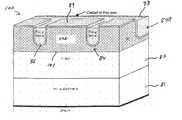
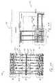
- the gate materialIn such devices the gate material, often polysilicon, must be connected to the leads of the device package and to external circuitry by means of a conductive pad, typically metal. To accomplish this, the trench is filled to overflowing with the gate material and the gate material is patterned using lithography and etching. Following the patterning, the gate material normally is restricted to the inside of the trench in the active areas of the device, as shown in FIGS. 1, 2 and 3 . In the areas where the contact is to be made to the gate material, however, the gate material extends outside of the trench and overlies the surface of the silicon. This is shown in the three-dimensional cutaway view of a conventional MIS device 40 in FIG.
- a polysilicon layer 42extends outside the trenches 44 and overlies the epitaxial silicon layer 46 .
- Trenches 44are lined with a gate oxide layer 47 which insulates the polysilicon layer 42 from the epitaxial layer 46 .
- the ends of the trenchesare designated 43 .
- a portion of the polysilicon layer 42overlies a thick field oxide region 48 .
- the area of contact between a subsequent gate metal layer and polysilicon layer 42is designated 45 .
- FIG. 5Ais a top view of the gate metal area 41 of the same device.
- FIG. 5Bis a cross-sectional view of the same device taken at cross-section 5 B- 5 B (drawn to a different scale from FIG. 5A).
- the MIS cells 54 in the active area 56are square.
- Polysilicon layer 42 and the area of contact 45 between gate metal 49 and polysilicon layer 42are shown.
- FIG. 6is a similar top view taken in the gate pad edge and termination region of the device.
- FIG. 7is a detailed cross-sectional view taken near the end of one of trenches 44 .
- the upper trench corners, represented by 52typically oxidize in a manner that leads to local thinning of the oxide and a lower breakdown voltage across the oxide. The sharper the corner, the more serious this problem becomes.
- the electric fieldreaches a maximum at the trench corners as a result of field crowding.
- FIGS. 8 A- 8 Iillustrate the steps of a conventional process performed on an N+ silicon substrate 802 .
- the processbegins with a first photoresist mask A 1 which is formed over an oxide layer 804 and patterned, using normal photolithographic processes, to define the areas where P-tubs will be formed (FIG. 8A).
- the P-tubsare used to reduce the strength of the electric field at the corners of the trenches.
- P-type dopantis implant through openings in mask A 1 to form P-tubs 806 , and mask A 1 is removed.
- a second mask A 2is deposited and patterned to define the active region 808 of the device, the oxide layer 804 , which has become a field oxide layer, remaining in a termination region 810 of the device (FIG. 8C).
- Trenches 812are then etched, typically using a reactive ion etch (RIE) process (FIG. 8D). Trenches 812 A and 812 B are interconnected (in the third dimension outside the plane of the paper) and trench 812 C is an optional “channel stopper” trench which is located on the outer edge of the termination area.
- RIEreactive ion etch
- a polysilicon layer 814is deposited and doped, filling trenches 812 and overflowing onto the surface of the silicon.
- a fourth, polysilicon mask A 4is deposited on polysilicon layer 814 and patterned (FIG. 8E). Polysilicon layer 814 is etched back into the trenches 812 , except for a portion that is allowed to extend from trench 812 B onto the field oxide layer 804 in the gate bus area. It is through this extension of the polysilicon layer 814 that electrical contact with the portion of polysilicon layer 814 in the trenches 812 is made.
- P-type dopantis implanted and driven in to form P-body regions 816 (FIG. 8F). While this dopant also gets into the polysilicon layer 814 , its concentration is too low to create any problems there.
- a fifth mask A 5is deposited and patterned to define areas where N-type dopant is to be implanted to form N+ source regions 818 (FIG. 8G).
- a borophosphosilicate glass (BPSG) layer 820is deposited and reflowed.
- a sixth mask A 6is formed and patterned to define where contact to the substrate (P-body regions 816 and N+ source regions 818 ) and to the gate (polysilicon layer 814 ) is to be made (FIG. 8H).
- P-type dopantis implanted to form P+ body contact regions 821 and then a metal layer 822 is deposited.
- a seventh mask(not shown) is formed over metal layer 822 and patterned. Metal layer 822 is etched through the seventh mask to form a source metal 822 A and a gate bus 822 B (FIG. 8I). Optionally, a passivation layer is deposited, and if so an eighth mask (not shown) is formed and patterned to define the source and gate pads, where external contact to the MOSFET will be made.
- a trench-gated MIS deviceis formed in a semiconductor chip which comprises an active area containing transistor cells, a gate metal area containing no transistor cells; and a gate metal layer.
- a trenchis formed in a pattern on a surface of the semiconductor chip, the trench extending from the active area into the gate metal area, the trench having walls lined with a layer of an insulating material.
- a conductive gate materialnormally polysilicon, is disposed in the trench, a top surface of the gate material being at a level lower than a top surface of the semiconductor chip.
- a nonconductive layeroverlies the active and gate metal areas, and an aperture is formed in the nonconductive layer over a portion of the trench in the gate metal area.
- the apertureis filled with a conductive material, often referred to as a “gate metal”, such that the gate metal contacts the conductive gate material in an area of contact that is within the trench.
- the gate materialdoes not overflow the trench onto the surface of the semiconductor chip, the gate material does not extend around the upper corners of the trench. This avoids the stress that occurs when a voltage difference is created between the gate material and the semiconductor material.
- a width of the trench at the area of contact between the gate contact material and the gate materialmay be greater than a width of the trench in the active area.
- the gate metalmay contact the conductive gate material in a first gate finger, the first gate finger being perpendicular to a second gate finger, the second gate finger extending from the active area into the gate metal area and intersecting the first gate finger.
- Another aspect of this inventionrelates to a process of fabricating an MIS device.
- the processrequires fewer masking steps than conventional processes and yields a device with a relatively flat topography which is more amenable to very fine photolithographic processing.
- the processcomprises forming a trench mask over the surface of a semiconductor substrate, the trench mask having an aperture defining the location of a trench; etching through the aperture in the trench mask to form a trench in the substrate; removing the trench mask; forming a first nonconductive layer on a wall of the trench; depositing a layer of a conductive gate material such that the gate material overflows onto the surface of the substrate outside the trench; etching the gate material without a mask such that a top surface of the gate material is reduced to a level below the surface of the substrate; depositing a second nonconductive layer over the surface of the substrate, forming a contact mask over the second nonconductive layer, the contact mask having an aperture; etching through the aperture in the contact mask to form a gate contact aperture in the second non
- etching through the contact maskmay form a substrate contact aperture in the second nonconductive layer, and the second conductive layer may extend through the substrate contact aperture to make contact with the substrate, and the process may include forming a metal mask over the second conductive layer, the metal mask having an aperture; and etching the second conductive layer through the aperture in the metal mask.
- the processdoes not include a mask for etching a portion of the gate contact material and may not include a mask for etching a portion of an oxide layer to form a field oxide region.
- the processcan be used to fabricate a variety of MIS devices, including MOSFETS, IGBTs, MOS-gated thyristors.
- the processcan also be used to fabricate a MOSFET with integrated Schottky or polysilicon diodes.
- the inventionalso includes an MIS device having a relatively flat topography.
- the gate busdoes not overlie a thick field oxide region.
- a nonconductive layere.g., BPSG
- a conductive layertypically metal
- the nonconductive layercontains apertures through which the metal layer makes electrical contact with the substrate in the active region of the MIS device (e.g., the source and body in a MOSFET).
- a gate busalso overlies the same nonconductive layer.
- the thickness of the nonconductive layer under the gate busis substantially the same as the thickness of the nonconductive layer in the active region of the device.
- a gate contact trench filled with a conductive gate materialis formed in the substrate below the gate bus, and the gate bus is electrically connected to the gate material through an aperture in the nonconductive layer.
- two or more protective trenchesare formed on the opposite sides of the gate contact trench. This allows the gate contact trench to be made wider and deeper than the trenches in the active region of the device without adversely affecting the breakdown voltage at the bottom of the gate contact trench.
- FIG. 1is a cross-sectional view of a single gate trench in a MOSFET.
- FIG. 2is a cross-sectional view of a single gate trench in an IGBT.
- FIG. 3is a cross-sectional view of a single gate trench in a MOS-gated thyristor.
- FIG. 4is a three-dimensional cutaway view showing how the gate is contacted in a conventional MIS device.
- FIG. 5Ais a top view and FIG. 5B is a cross-sectional view of the gate metal area of the MIS device shown in FIG. 4.
- FIG. 6is a top view taken in the gate pad edge and termination region of the MIS device.
- FIG. 7is a detailed view of a gate trench, showing the areas of stress at the upper corners of the trench.
- FIGS. 8 A- 8 Ishow the steps of a conventional process for forming a trench-gated MOSFET.
- FIG. 9is a three-dimensional cutaway view of an MIS device in accordance with the invention.
- FIG. 10is a three-dimensional cutaway view of an MIS device in accordance with the invention which contains a P-tub in the mesas.
- FIG. 11is a three-dimensional cutaway view of an MIS device in accordance with the invention which contains a P-tub which extends underneath the trench.
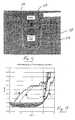
- FIG. 12is a cross-sectional view made by a scanning electron microscope (SEM) a MOS capacitor fabricated in accordance with this invention.
- SEMscanning electron microscope
- FIG. 13is a graph showing the Fowler-Nordheim tunneling current as a function of the voltage between the gate and the silicon for various types of MOS capacitors.
- FIG. 14is an overall top view of an MIS chip showing how the active regions, the gate pad regions, the termination regions, and the gate metal regions might be configured.
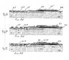
- FIG. 15Ais a top view of the gate metal and active regions of an MIS device in accordance with a first embodiment of the invention.
- FIG. 15Bis a top view of the edge termination and gate pad regions of the first embodiment.
- FIG. 15Cis a cross-sectional view of the gate contact area in the first embodiment.
- FIG. 16Ais a top view of the gate metal and active regions of an MIS device in accordance with a second embodiment of the invention.
- FIG. 16Bis a top view of the edge termination and gate pad regions of the second embodiment.
- FIG. 16Cis a cross-sectional view of the gate contact area in the second embodiment.
- FIG. 16Dis a detailed top view of the intersection between a gate finger and the gate finger in which contact between the gate metal and polysilicon is made in the second embodiment.
- FIG. 16Eis a cross-sectional view of the trench in the second embodiment.
- FIG. 16Fis a cross-sectional view of the intersection between a gate finger and the gate finger in which contact between the gate metal and polysilicon is made in the second embodiment.
- FIG. 17Ais a top view of the gate metal and active regions of an MIS device in accordance with a third embodiment of the invention.
- FIG. 17Bis a top view of the edge termination and gate pad regions of the third embodiment.
- FIG. 18is a top view of the gate metal and active regions of an MIS device in accordance with a fourth embodiment of the invention.
- FIG. 19is a top view of the gate metal and active regions of an MIS device in accordance with a fifth embodiment of the invention.
- FIGS. 20 A- 20 Fillustrate the steps of a process of fabricating a contact between the gate polysilicon and gate metal in an MIS device in accordance with this invention.
- FIGS. 21 A- 21 Iillustrate the steps of a process in accordance with the invention for fabricating a trench MOSFET.
- FIGS. 22 A- 22 Iillustrate the steps of a process for forming a trench MOSFET with an integrated Schottky diode.
- FIGS. 23 A- 23 Jillustrate the steps of a conventional process for forming a trench MOSFET with integrated polysilicon diodes.
- FIGS. 24 A- 24 Iillustrate the steps of a process in accordance with the invention for forming a trench MOSFET with integrated polysilicon diodes.
- FIGS. 25 A- 25 Fillustrate the steps of a process in accordance with this invention for fabricating a MOSFET by growing the body region epitaxially.
- FIG. 26Ashows a cross-sectional view of a conventional gate contact trench.
- FIG. 26Bshows a cross-sectional view of a gate contact trench and a pair of protective trenches in accordance with the invention.
- FIG. 27Ashows a polysilicon MOSFET that can be fabricated using the process shown in FIGS. 24 A- 24 I.
- FIGS. 27B and 27Cshow top and cross-sectional views, respectively, for a particular embodiment of a polysilicon MOSFET.
- the polysilicon or other material used to fill the trenches in a trench-gated MIS deviceis etched back or otherwise held back within the trench such that contact between the gate filling material and the gate metal is made within the trench.
- the gate filling materialdoes not overlap the upper corners of the trench, thereby eliminating the problems that arise from the stress at the upper corners of the trench.
- polysilicondesignates whatever conductive material is deposited in the trench as a gate material, it being understood that in some embodiments metal or other conductive materials may be used instead of polysilicon as the gate material; similarly, “gate metal” is used to designate the conductive material that is used to form a contact with the gate material within the trench, it being understood that in some embodiments polysilicon or other conductive materials may be used instead of metal as the “gate metal”.
- FIG. 9shows a partial view of a trench-gated MIS device 80 formed in an N-epitaxial (epi) layer 82 which is grown on an N+ substrate 81 .
- a P-body region 83is shown in N-epi layer 82 .
- a gate trench 84is lined by a gate oxide layer 85 which connects with an oxide layer 89 on the top surface of N-epi layer 82 .
- Trench 84is partially filled with a polysilicon gate 86 having a top surface 87 which is within trench 84 (i.e., below the top surface of N-epi layer 82 ).
- trench 84includes a somewhat wider transverse portion 84 A.
- a portion 88 of the top surface 87 in transverse portion 84 Aindicates where contact will later be made between polysilicon gate 86 and a gate metal layer (not shown).
- the polysilicon within trench 84does not extend around the upper corners of the trench in the manner of polysilicon layer 42 . This avoids the stress problems described above.
- FIG. 10shows an MIS device 90 which is similar to MIS device 80 except that a P-tub 91 is formed in N-epi layer 82 in the mesa between the trench segments to shield the gate trench 84 .
- P-tub 101extends into the area directly below the trench 84 .
- MIS devices 90 and 100are designed to have high breakdown voltages.
- FIG. 12is a cross-sectional view made by a scanning electron microscope (SEM) of a MOS capacitor fabricated in accordance with this invention.
- the polysilicon gateis shown as 110 and the gate metal as 112 .
- a BPSG dielectric layer 116overlies the mesas between the segments of trench 114 and provides insulation between the gate metal 112 and the upper corners of trench 114 .
- FIG. 13is a graph showing the Fowler-Nordheim tunneling current as a function of the voltage between the gate and the silicon for various types of MOS capacitors.
- Curves A-Eare for the following devices: TABLE 1 Curve Type of Device A Conventional Planar Device B Device According to Invention with Square Cells C Device According to Invention with Stripe Cells D Conventional Device with Square Cells E Conventional Device with Stripe Cells
- FIGS. 15 A- 15 C, 16 A- 16 F, 17 A, 17 B, 18 and 19show a series of parallel “gate fingers” which leave the the active area of an MIS device and enter a gate metal region of a termination or gate pad region.
- the term “gate finger”refers to an extension of the gate trench into a region outside the active region of the MIS device, e.g., sometimes referred to as the “gate metal” or “gate bus” region or the “termination” or “edge termination” region.
- FIG. 14is an overall top view of an MIS chip showing illustratively how the active, gate pad and the edge termination regions might be configured. It will be appreciated by those skilled in the art that numerous alternative configurations are possible.
- FIG. 15Ashows a first embodiment of the invention.
- a square-celled MOSFET 140includes an active region 141 and a gate metal region 142 .
- a series of parallel gate fingers 143extend from active region 141 into gate metal region 142 .
- the edges of the source metalare designated 144 ; the edges of the gate metal are designated 145 .
- Areas 146designate the areas of contact between the polysilicon within gate fingers 143 and gate metal 145 . It will be noted that gate fingers 143 expand into wide portions 147 to accommodate areas of contact 146 . This allows for a good electrical contact to be made in the trench, spaced from the upper corners of the trench, even though the dimensions of the active cells become very small.
- FIG. 15Cshows a cross-sectional view of one of the areas of contact 146 at cross-section 15 C- 15 C, showing a gate metal 148 and a BPSG layer 149 .
- FIG. 15Bshows a top view of a portion of MOSFET 140 that adjoins a termination region 150 and a gate pad 151 .
- FIG. 16Ashows a second embodiment of the invention.
- MOSFET 160contains an active region 161 and a gate metal region 162 .
- the edge of the source metalis shown as 164 and the edge of gate metal 168 is shown as 165 .
- a series of parallel gate fingers 163extend from active region 161 into gate metal region 162 .
- An area of contact 166 between the gate polysilicon and gate metal 168is made in a gate finger 167 which extends perpendicular to gate fingers 163 .
- gate finger 167is wider than gate fingers 163 , but this need not be the case.
- FIG. 16Cshows a detailed cross-sectional view taken at cross-section 16 C- 16 C in FIG. 16A.
- FIG. 16Bis a top view of MOSFET 160 in the vicinity of a termination region 170 and a gate pad 171 .
- FIG. 16Cis a detailed top view of the an intersection between one of gate fingers 163 and gate finger 167 .
- MOSFET 180is similar to MOSFET 160 shown in FIGS. 16A and 16B, except that gate fingers 183 are more widely spaced than gate fingers 163 , and gate finger 187 becomes narrower at the intersections with gate fingers 183 . Areas of contact 186 between the gate polysilicon and the gate metal do not extend into the areas where gate fingers 183 and 187 intersect. Thus the possible problem caused by the width of gate finger 187 at the intersections with gate fingers 183 is avoided. Of course, the spacing between gate fingers 183 is variable and need not be greater than the spacing between gate fingers 163 in MOSFET 160 .
- FIG. 17Bis a top view of MOSFET 180 in the vicinity of termination region 190 and gate pad 191 .
- a fourth embodiment, shown in FIG. 18,represents another way of overcoming the possible trench filling problem described above.
- MOSFET 200is somewhat similar to MOSFET 160 shown in FIG. 16A, in the sense that parallel gate fingers 203 running from active region 201 to gate metal region 202 intersect gate finger 207 at right angles, but in MOSFET 200 the intersections between gate finger 207 and gate fingers 203 coming from opposite sides of gate finger 207 are offset, resulting in “T” interesections. As a result, the filling of the trench at the intersections is improved as compared with the configuration shown in FIG. 16A. Contact between the polysilicon gate and gate metal is made in an area of contact 206 which runs longitudinally along gate finger 207 .
- a fifth embodiment, shown in FIG. 19,is like MOSFET 140 shown in FIG. 15A in that gate fingers 223 include wide portions 227 where contact between the gate polysilicon and the gate metal is made.
- the wide portions 227are offset from each other in the longitudinal direction of gate fingers 223 , thereby allowing the distance between gate fingers 223 to be reduced beyond what would otherwise be possible.
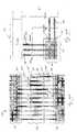
- FIGS. 20 A- 20 FA process for making a gate contact within the trench is shown in FIGS. 20 A- 20 F.
- the processbegins with a semiconductor chip which includes an N-epitaxial layer 301 grown in an N+ substrate 300 using a known process.
- a photoresist trench mask 302is formed in the surface of N-epi layer 301 , as shown in FIG. 20A.
- a trench 303shown in FIG. 20B, is formed by reactive ion etching (RIE) through the opening in trench mask 302 .
- RIEreactive ion etching
- a sacrificial oxide layer(not shown) is formed on the walls of the trench to repair crystal damage done during the RIE etch, and the sacrificial oxide is then removed.
- a gate oxide layer 304is thermally grown on the walls of the trench.
- a polysilicon layer 305is deposited over the top surface of N-epi layer 301 , filling the trench 303 , yielding the structure shown in FIG. 20B.
- Polysilicon layer 305is then etched back, as shown in FIG. 20C, until a top surface 306 of polysilicon layer 305 is below a top surface 307 of N-epi layer 301 . It is important that the polysilicon layer 305 be etched back far enough that it no longer overlaps the upper corners of trench 303 . Surface 306 of polysilicon layer 305 can be just below top surface 307 of N-epi layer 301 . Note that, since the polysilicon is etched back uniformly throughout the chip, this process step can normally be performed without a mask, thereby reducing the costs of fabrication.
- a borophosphosilicate glass (BPSG) layer 308is deposited over the top surface of the structure, and masked with a photoresist layer 309 .
- An opening 310 in the photoresist maskis formed over the central portion of the trench 303 . such that the edges of opening 310 are spaced laterally inward from the walls of the trench 303 .
- the resulting structureis shown in FIG. 20D.
- BPSG layer 308is etched through the opening 310 in photoresist layer 309 , producing a gate contact opening 311 which is generally coincident with opening 310 and which extends to the surface 306 of polysilicon 305 .
- Photoresist layer 309is then removed, yielding the structure shown in FIG. 20E.
- a metal layer 312is deposited. Since contact between metal layer 312 and polysilicon 305 occurs entirely within a central region of the trench 303 , and since the width of the gate contact opening 311 is less than the width of the top surface 306 of polysilicon layer 305 , proximity between the polysilicon layer 305 and the N-epi layer 301 at the upper corners of trench 303 is avoided. It is this proximity that creates the stress problems described above.
- the conventional process for forming a trench-gated MOSFETrequires numerous mask steps (eight in the example shown in FIGS. 8 A- 8 I) and leaves a ridge in the area of the gate bus which makes photolithography at small dimensions difficult.
- Another aspect of this inventionis an improved process which avoids these problems.
- FIGS. 21 A- 21 Iillustrate the steps of a process in accordance with this invention.
- the processstarts with an N-layer 402 , which could be an epi layer overlying an N+ substrate.
- a thin oxide layer 404may be formed on the surface of layer 402 for adhesion of the photoresist mask or to provide a hard mask for resist etch selectivity reasons or to avoid later oxidation.
- a first photoresist mask B 1is formed and patterned to define the locations of the trenches. Since the layer 402 is very flat, mask B 1 may be thinner than the masks required in the prior art (e.g., mask A 3 shown in FIG. 8D), and smaller features (trenches) may therefore be defined.
- Trenches 406are etched through mask B 1 using RIE. Trenches 406 include trenches 406 A in an active area 407 , a gate bus contact trench 406 B in a termination area 409 , and an optional channel stopper trench 406 C in a channel stopper area 411 (FIG. 21A). Trenches 406 A and 406 B are connected together in the third dimension.
- trenches 406have been etched, mask B 1 is stripped, and a sacrificial oxide layer (not shown) is grown on the walls of trenches 406 and etched to remove crystal defects caused by the RIE process.
- a gate oxide layer 408is grown on the walls of trenches 406 .
- a polysilicon layer 410is deposited, doped and etched back until polysilicon layer 410 remains only inside the trenches 406 (FIG. 21B). Note that unlike the process described in FIGS. 8 A- 8 I, this process requires no polysilicon mask to pattern polysilicon layer 410 .
- a re-oxidationmay be performed if a thicker oxide layer is needed over the mesa and termination areas.
- a second mask B 2is deposited and patterned to define the regions where the body implant is to be introduced into layer 402 .
- a P-type dopantis implanted through openings in mask B 2 and driven in to form P-body regions 412 (FIG. 21C). Unlike the process described in FIGS. 8 A- 8 I, this process requires no mask to define the active area (see, e.g., mask A 2 in FIG. 8C). If the designer wishes to pattern the body within the mesa region to achieve a “split-well” structure, as described in J. Zeng et al., ISPSD 2000, pp 145-148, the fact that the surface of the layer 402 is very flat makes small feature lithography easier.
- the implant energy of the P-type dopantis selected such that the dopant penetrates the oxide layer 408 but not the mask B 2 . If oxide layer 408 is too thick, it may be etched back to facilitate penetration by the implant.
- the mask B 2is then stripped, the structure is cleaned and the P-type dopant is annealed and diffused to achieve the desired junction depth within the N-type layer.
- a third mask B 3is deposited and patterned to define the locations of the source regions.
- N-type dopantis implanted through opening in mask B 3 to form N+ source regions 414 (FIG. 21D). Note that the N-type dopant is kept out of the termination area and the periphery of the active area but is allowed into the region near the “channel stopper” trench 406 C, forming N+ regions 415 , which prevent a surface inversion layer from forming. The surface of the structure is still very flat, making photolithography relatively easy.
- the oxide layer 408may need to be etched down with mask B 3 in place, depending on the ion species to be implanted through the oxide layer 408 .
- a layer 416 of a dielectric such as BPSGis deposited and densified if necessary.
- a fourth mask B 4is deposited over BPSG layer 416 and patterned to define the contact openings (FIG. 21E). Since the structure is still quite flat, this lithography step may be performed with a thinner layer of photoresist than, for example, mask A 6 shown in FIG. 8H.
- BPSG layer 416is etched through openings in mask B 4
- mask B 4is removed and P-type dopant is implanted to form P-type contact regions 418 (FIG. 21F).
- This implantreduces the resistance between the metal layer to be deposited and the body, and it may also be used to shift avalanche breakdown from the region adjacent to the trenches to the central region of the mesas between the trenches, as described in U.S. Pat. No. 5,072,266 to Bulucea et al. If this technique is hampered because the body junction is too deep, a series of distributed avalanche clamps can be created by patterning regions where the body implant is blocked, creating curved junctions where the dopant diffuses laterally. The spacing between the curved junctions can be controlled to set the breakdown voltage to be lower than that of the active trenches. The source contact must be interrupted in these regions. Alternatively, the breakdown voltage can be set by designing the breakdown voltage in the termination area 409 to be lower than the breakdown voltage in the active area 407 .
- the contactis made to the gate within trench 406 B, thereby eliminating the need for a polysilicon mask.
- the flatness of the layer 402makes it easier to define a small contact opening in the BPSG layer 416 .
- two separate maskscan be used to form the contact openings through BPSG layer 416 to the polysilicon layer 410 in gate bus contact trench 406 B and to N-layer 402 , respectively, instead of using a single mask B 4 .
- the structureis now subjected to a high temperature anneal in the range of 750° C. to 950° C. This activates the P+ contact implant, activates the N+ source implant (if it has not already been activated) and densities and smoothes the BPSG layer 416 .
- a metal layer 419is deposited, and a fifth mask B 5 is deposited over metal layer 419 and patterned (FIG. 21G). Metal layer 419 is etched through openings in mask B 5 into a source metal portion 419 S, a gate metal portion 419 G, a field plate 41 F, and an edge termination 419 E.
- a passivation layer 420is deposited over metal layer 419 , and a sixth mask B 6 is deposited and patterned (FIG. 21H). Passivation layer 420 is etched through openings in mask B 6 to expose source metal portion 419 S (FIG. 21I). Next, the wafer can be thinned by grinding it from the back side, and a layer of back side metal can be applied as is customary to form the drain contact.
- FIGS. 21 A- 21 Ioffers a number of advantages over prior art processes such as the one shown in FIGS. 8 A- 8 I.
- the process of this inventionhas fewer steps and is less costly. For example, six masking steps are required instead of eight.
- a high degree of silicon flatnessis maintained throughout the process until metal deposition, and this helps in the photolithographic delineation of small features and the fabrication of small cell pitches. All contact to the gate is made within the trenches, thus avoiding the current leakage problems that occur as a result of Fowler-Nordheim tunneling through the gate oxide at the upper corners of the trenches when the polysilicon gate material extends out of the trenches and onto the top surfaces of the mesas.
- the area around the “channel-stopper” trench 406 Cis free of P-type diffusions and may be provided with a field plate that is coupled to the drain via trench 404 C as shown in FIG. 21I.
- the N+ regions 415 at the peripherytrack the drain potential because the sawed edge of the chip behaves as a resistive short to the drain. This structure improves the reliability of higher voltage terminations by terminating any inversion layer that may form as a result of charges over the terminations or hot carrier aided walk-out.
- FIGS. 21 A- 21 Imay be adapted simply to provide a trench MOSFET with an integrated Schottky diode, such as a Trench-MOS Barrier Schottky (TMBS) device.
- FIGS. 22 A- 22 Iillustrate the steps of an alternative process for forming a trench MOSFET with a Trench-MOS Barrier Schottky device. The process includes one additional mask compared with the process shown in FIGS. 21 A- 21 I.
- N-silicon layer 502which again could overlie a heavily-doped substrate.
- a thin oxide layer 504may be formed on the surface of layer 502 for adhesion of the photoresist mask or to provide a hard mask for resist etch selectivity reasons or to avoid later oxidation.
- a first photoresist mask C 1is formed and patterned to define the locations of the trenches. Since the surface of layer 502 is very flat, mask C 1 may be thinner than the masks required in the prior art (e.g., mask A 3 shown in FIG. 8D), and smaller features (trenches) may therefore be defined.
- Trenches 506are etched through mask C 1 using RIE.
- Trenches 506include trenches 506 A in an active area 507 , a gate bus contact trench 506 B in a termination area 509 , an optional channel stopper trench 506 C in a channel stopper area 511 , and trenches 506 D in a Schottky diode area 513 (FIG. 22A). Trenches 506 A and 506 B (and optionally trenches 506 D) are connected together in the third dimension.
- trenches 506After trenches 506 have been etched, mask C 1 is stripped, and a sacrificial oxide layer is grown on the walls of trenches 506 and etched to remove crystal defects caused by the RIE process.
- a gate oxide layer 508is grown on the walls of trenches 506 .
- a polysilicon layer 510is deposited, doped and etched back until polysilicon layer 510 remains only inside the trenches 506 (FIG. 22B). Like the process described in FIGS. 21 A- 21 I, this process requires no polysilicon mask to pattern polysilicon layer 510 .
- a re-oxidationmay be performed if a thicker oxide layer is needed over the mesa and termination areas.
- a second mask C 2is deposited and patterned to define the regions where the body implant is to be introduced into layer 502 .
- a P-type dopantis implanted through openings in mask C 2 and driven in to form P-body regions 512 (FIG. 22C). Like the process described in FIGS. 21 A- 21 I, this process requires no mask to define the active area (see, e.g., mask A 2 in FIG. 8C).
- the implant energy of the P-type dopantis selected such that the dopant penetrates the oxide layer 508 but not the mask C 2 . If oxide layer 508 is too thick, it may be etched back to facilitate penetration by the implant.
- the mask C 2is then stripped, the structure is cleaned and the P-type dopant is annealed and diffused to achieve the desired junction depth with the N-type layer 502 .
- a third mask C 3is deposited and patterned to define the locations of the source regions.
- N-type dopantis implanted through opening in mask C 3 to form N+ source regions 514 (FIG. 22D). Note that the N-type dopant is kept out of the termination area and the periphery of the active area but is allowed into the region near the “channel stopper” trench 506 C, forming N+ regions 515 .
- the surface of the structureis still very flat, making photolithography relatively easy.
- the oxide layer 508may need to be etched down with mask C 3 in place, depending on the ion species to be implanted through the oxide layer 508 .
- a layer 516 of a dielectric such as BPSGis deposited and densified if necessary.
- a fourth mask C 4is deposited over BPSG layer 516 and patterned to define the contact openings (FIG. 22E). Since the structure is still quite flat, this lithography step may be performed with a thinner layer of photoresist than, for example, mask A 6 shown in FIG. 8H.
- BPSG layer 516is etched through openings in mask C 4 , mask C 4 is removed.
- An additional fifth mask (contact block) C 5is deposited and patterned to cover the Schottky diode area 513 and a portion of the channel stopper area 511 .
- P-type dopantis implanted to form P-type contact regions 518 , with mask C 5 preventing the dopant from getting into the Schottky diode area 513 (FIG. 22F).
- This implantreduces the resistance between the metal layer to be deposited and the body, and it may also be used to shift avalanche breakdown from the region adjacent to the trenches to the central region of the mesas between the trenches, as described in U.S. Pat. No. 5,072,266 to Bulucea et al. If this technique is hampered because the body junction is too deep, a series of distributed avalanche clamps can be created by patterning regions where the body implant is blocked, creating curved junctions where the dopant diffuses laterally.
- the spacing between the curved junctionscan be controlled to set the breakdown voltage to be lower than that of the active trenches.
- the source contactmust be interrupted in these regions.
- the breakdown voltagecan be set by designing the breakdown voltage in the termination area 509 to be lower than the breakdown voltage in the active area 507 .
- the structureis now subjected to a high temperature in the range of 750° C. to 950° C. This activates the P+ contact implant, activates the N+ source implant (if it has not already been activated) and drives it to a lower junction depth, and densifies and smoothes the BPSG layer 516 .
- a metal layer 519is deposited, making contact in particular with the N+ source regions 514 and P-body regions 518 in the active area 507 , and with the surface of the layer 502 in the Schottky diode area 513 .
- a sixth mask C 6is deposited over metal layer 519 and patterned (FIG. 22G). Metal layer 519 is etched through openings in mask C 6 and divided into a source metal portion 519 S in Schottky diode area 513 and active area 505 , a gate metal portion 519 G, a field plate 519 F, and an edge termination 519 E.
- a passivation layer 520is deposited over metal layer 519 , and a seventh mask C 7 is deposited and patterned (FIG. 22H).
- Passivation layer 520is etched through openings in mask C 7 to expose source metal portion 519 S (FIG. 221). Next, the wafer can be thinned by grinding it from the back side, and a layer of back side metal can be applied as is customary to form the drain contact.
- the availability of the fifth mask C 5allows the fourth mask C 4 to be held back from the trench 506 C, creating an opening in BPSG layer 516 that exposes N+ regions 515 and allows metal layer to make contact with N+ regions 515 as well as the polysilicon in trench 506 A. This provides better contact between the field plate edge termination and the drain.
- a trench-MOS barrier Schottky(TMBS), an MPS rectifier, or a junction barrier Schottky (JBS) may be formed within the same general process flow.
- the Schottky diodesmay be interspersed among the MOSFET cells in the active area or may be grouped in a separate part of the chip, as shown in FIGS. 22 A- 22 I.
- the process of FIGS. 22 A- 22 Iprovides a cost-effective method of replacing the conventional MOSFET-Schottky combination, currently available in a two-chip form.
- a contact block mask(mask C 5 in FIG. 22F) needs to be added.
- FIGS. 8 A- 8 Iincluding Schottky diodes would raise the mask count by two (a body block mask and a contact block mask), resulting in a total of ten masks.
- FIGS. 24 A- 24 Iillustrate the steps of such a process which involves the addition of one mask.
- FIGS. 23 A- 23 JThe conventional process is illustrated in FIGS. 23 A- 23 J, requiring 9 masks.
- An oxide layer 604 and a first photoresist mask D 1are deposited on an N+ silicon layer 602 and are patterned with openings in the areas were P-type tubs are to be formed (FIG. 23A).
- a P-type dopantis implanted through the openings in mask D 1 and driven in, forming P-type tubs 606 (FIG. 23B).
- a second photoresist mask D 2is formed with an opening defining the location of an active area 608 .
- Oxide layer 604is etched through the opening in mask D 2 (FIG. 23C), and mask D 2 is removed.
- a third photoresist mask D 3is formed, defining the locations of the trenches.
- Layer 602is etched to form trenches 610 in active area 608 and a trench 612 in the channel stopper area (FIG. 23D).
- a sacrificial oxide layeris formed and removed from the walls of trenches 610 , 612 , and a gate oxide layer is formed on the walls of the trenches.
- a polysilicon layer 614is deposited and an N-type background dopant is implanted into polysilicon layer 614 .
- a low temperature oxide (LTO) layer 611is deposited.
- a fourth photoresist mask D 4is deposited over the region of polysilicon layer 614 where the diodes are to be formed. Using photoresist mask D 4 , LTO 611 layer is etched to form a mask (FIG. 25E), and photoresist mask D 4 is removed.
- Polysilicon layer 614is then doped with POCl 3 , using LTO layer 611 as a mask.
- a fifth mask D 5is deposited, and polysilicon layer 614 is etched back into the trenches 610 except in region 616 , where a portion of the polysilicon is allowed to overlap the edge of the trench and extend over the oxide layer 604 (FIG. 23F). Mask D 5 is removed.
- a P-type dopantis implanted in the vicinity of trenches 610 and driven in to form P-body region 618 (FIG. 23G).
- a sixth N+ block mask D 6is deposited and patterned. N-type dopant is implanted to form N+ source regions adjacent to trenches 610 . The N-type dopant also enters portions of polysilicon layer 614 , where it forms diodes 622 and 624 at junctions with the N-type background-doped regions of polysilicon layer 614 (FIG. 23H). Mask D 6 is removed.
- a BPSG layer 626is deposited and a seventh contact mask D 7 is deposited and patterned over BPSG layer 626 . Openings in mask D 7 define where contact will be made to various areas of the device.
- BPSG layer 626is etched through the openings in mask D 7 , and P-type dopant is implanted through the openings in BPSG layer 626 to form P+ contact regions 625 (FIG. 231).
- Mask D 7is removed.
- a metal layer 628is deposited, metal layer 628 making contact with the device through the openings in BPSG layer 626 .
- An eighth mask(not shown) is formed over metal layer 628 .
- Metal layer 628is etched through openings in the eighth mask to form a portion 628 A which contacts the anode of diode 622 , a portion 628 B which contacts the cathode of diode 622 and the source-body regions of the MOSFETs in the active area, and a portion 628 C which contacts the cathode of diode 624 (FIG. 23J).
- Another section of metal layer 628contacts the polysilicon gate (which is also the anode of diode 624 ) in the third dimension.
- Portion 628 A of metal layer 628is connected to the polysilicon gate, and portion 628 C of metal layer 628 is connected to the drain of the device (both in the third dimension).
- diode 622connects the source-body and the gate and diode 624 connects the drain and the gate.
- to fabricate the devicerequires nine masking steps if a final passivation and pad mask are implemented.
- N-layer 702which could be an epi layer overlying an N+ substrate.
- a thin oxide layer 704may be formed on the surface of layer 702 for adhesion of the photoresist mask or to provide a hard mask for resist etch selectivity reasons or to avoid later oxidation.
- a first photoresist mask E 1is formed and patterned to define the locations of the trenches. Since the surface of layer 702 is very flat, mask E 1 may be thinner than the masks required in the prior art (e.g., mask A 3 shown in FIG. 8D), and smaller features (trenches) may therefore be defined. Trenches 706 are etched through mask E 1 using RIE.
- Trenches 706include trenches 706 A in an active area 707 , a gate bus contact trench 706 B in a termination area 709 , and an optional channel stopper trench 706 C in a channel stopper area 711 (FIG. 24A). Trenches 706 A and 706 B are connected together in the third dimension.
- trenches 706After trenches 706 have been etched, mask E 1 is stripped, and a sacrificial oxide layer is grown on the walls of trenches 706 and etched to remove crystal defects caused by the RIE process. A gate oxide layer 708 is grown on the walls of trenches 706 . A polysilicon layer 710 is deposited, doped and etched back until polysilicon layer 710 remains only inside the trenches 706 (FIG. 24B). A re-oxidation may be performed if a thicker oxide layer is needed over the mesa and termination areas.
- a second mask E 2is deposited and patterned to define the regions where the body implant is to be introduced into layer 702 .
- a P-type dopantis implanted through openings in mask E 2 and driven in to form P-body regions 712 (FIG. 24C).
- Mask E 2is removed.
- a low temperature oxide (LTO) layer 714is deposited over the surface of layer 702 to a thickness of, for example 2000 ⁇ , and a second polysilicon layer 716 is deposited over layer 714 .
- a blanket implant of polysilicon layer 716 with P-type dopantis performed.
- a third mask E 3is deposited over layer 702 and patterned to define the location of a polysilicon diode (FIG. 24D).
- Polysilicon layer 716 and LTO layer 714are etched through the openings in mask E 3 , defining the polysilicon diode, and mask E 3 is removed.
- a fourth mask E 4is deposited, and N-type dopant is implanted through the openings in mask E 4 , simultaneously forming N+ source regions 718 and the cathode of a diode 720 (FIG. 24E).
- Mask E 4is removed.
- BPSG layer 722is deposited and a fifth mask E 5 is deposited over BPSG layer 722 and patterned (FIG. 24F).
- BPSG layer 722is etched through openings in mask E 5 to create contact openings in BPSG layer 722 , and mask E 5 is removed.
- P-type dopantis implanted through the openings in BPSG layer 722 to form contact regions 724 (FIG. 24G).
- BPSG layer 722is reflowed by heating.
- a metal layer 726is deposited over BPSG layer 722 , establishing electrical contact with the device through the openings in BPSG layer 722 .
- a sixth mask E 6is deposited over metal layer 726 and is patterned (FIG. 24H).
- Metal layer 726is etched through openings in mask E 6 to separate metal layer 726 into a portion 726 A that contacts the source-body terminals of the MOSFETs and the anode of diode 720 , a portion 726 B that contacts the cathode of diode 720 and the polysilicon in trench 706 B in the gate bus area of the device, a portion 726 C that forms a field plate in the termination area of the device, and a portion 726 D that contacts the polysilicon in trench 706 C in the channel stopper area of the device.
- FIGS. 24 A- 24 Ican also be used to fabricate a polysilicon MOSFET 730 , shown in FIGS. 27 A- 27 C.
- a trench 706 Dis etched through the mask E 1 .
- Gate oxide layer 708is grown and polysilicon layer 710 is deposited as described above (see FIG. 24B).
- Mask E 2is deposited and P-type dopant is implanted through openings in mask E 2 to form a P-type region 740 in N-epi layer 702 .
- LTO layer 714is deposited over the surface of layer 702
- the second polysilicon layer 716is deposited over LTO layer 714 (see FIG. 24D).
- a blanket P-type implant of polysilicon layer 716is performed.
- Polysilicon MOSFET 730can be formed in numerous geographies.
- the source/drain regionsmay be interdigitated as shown in the top view of FIG. 27B.
- FIG. 27Cis a cross-sectional view of the structure shown in FIG. 27B taken at section 27 C- 27 C.
- Mask E 3is used to pattern polysilicon layer 716 and LTO layer 714 as shown in FIG. 27A. At the same time mask E 3 is used to form an opening through polysilicon layer 716 and LTO layer 714 to a gate contact region 748 on polysilicon layer 710 .
- mask E 4is deposited and patterned such that the subsequent implantation of N-type dopant through openings in mask E 4 forms an N+ source region 742 and an N+ drain region 744 in polysilicon layer 716 .
- N+ regions 742 and 744are formed at the same time as the cathode of diode 720 (see FIG. 24E). Source region 742 and drain region 744 are separated by a P-body region 746 that is located directly over trench 706 D.
- BPSG layer 722is deposited and openings in mask E 5 are used to etch through BPSG layer 722 to a source contact 750 , a drain contact 752 and a body contact 754 .
- the openings in BPSG layer 722are filled with metal layer 726 , and mask E 6 is used to separate metal layer 726 into source, drain, body and gate segments (not shown).
- the source and body segments of metal layer 726are shorted together or are part of a single source-body segment of metal layer 726 .
- FIGS. 25 A- 25 FAnother variation of the process can be used to fabricate a MOSFET by growing the body region of the device epitaxially. This process is shown in FIGS. 25 A- 25 F.
- a P-type epitaxial (epi) layer 904is grown on the surface of an N-type layer 902 .
- a first mask F 1is then deposited on the surface of epi layer 904 and patterned.
- Trenches 906are etched through openings in mask F 1 , with trenches 906 A in an active region 907 , trench 906 B in a termination region 909 , trench 906 C in a channel stopper region 911 , and a wide trench 906 D in termination region 909 (FIG. 25A).
- a sacrificial oxide layer(not shown) is grown on the walls of the trenches 906 to repair crystal damage caused by the etching.
- a gate oxide layer 908is grown on the walls of the trenches 906 .
- a polysilicon layer 910is then deposited over the surface of the device, doped and etched back so that it remains in the trenches 906 A, 906 B and 906 C (FIG. 25B). Because trench 906 D is very wide, polysilicon layer 910 is removed from trench 906 D.
- a second mask F 2is deposited and patterned and N-type dopant is implanted through openings in mask F 2 to form N+ source regions 914 and an N+ region 915 around trench 906 C (FIG. 25C). Mask F 2 is removed.
- a BPSG layer 922is deposited, and a third mask F 3 is deposited over BPSG layer 922 and patterned (FIG. 25D).
- BPSG layer 922is etched through mask F 3 , and mask F 3 is removed.
- P-type dopantis implanted to form P+ contact regions 918 (FIG. 25E).
- the doping concentration of the P-type dopantis not high enough to significantly affect the doping of polysilicon layer 910 in trench 906 B.
- a metal layer 926is deposited and a fourth mask F 4 is deposited over metal layer 926 and patterned. Metal layer 926 is etched through openings in mask F 4 to separate metal layer 926 in to a portion 926 A that contacts the source-body regions of the MOSFETs and a portion 926 B that contacts the polysilicon in trench 906 A (FIG. 25F). Mask F 4 is then removed.
- FIG. 26Ashows a gate contact trench 950 positioned between two MOSFET trenches 952 .
- the increased depth of trench 950would be of no consequence if the bottom of the trench were covered or shielded by a deep diffusion of the same polarity as the body. Absent such a deep diffusion, however, the breakdown voltage will be lower under gate contact trench 950 than under active MOSFET trenches 952 .
- the potential contours, represented by the dashed line in FIG. 25A,are curved under trench 950 , indicating that the breakdown voltage is less in that location than under trenches 952 .
- shielding trenches 954can be the same size as active MOSFET trenches 952 , but this need not be the case. Shielding trenches 954 should be positioned close to gate contact trench 950 . Preferably the spacing between shielding trenches 954 and gate contact trench 950 is less than the thickness of the N-epi layer, e.g., the same as the width of the mesas between the trenches in the active area of the device. The mesas between shielding trenches 954 and gate contact trench 950 may be allowed to float.
- shielding trenchesimprove the breakdown of the gate contact trench because the limited charge available between the shielding trenches and the gate contact trench flattens out the potential contours, as shown by the dashed line in FIG. 25B.
Landscapes
- Electrodes Of Semiconductors (AREA)
- Metal-Oxide And Bipolar Metal-Oxide Semiconductor Integrated Circuits (AREA)
- Internal Circuitry In Semiconductor Integrated Circuit Devices (AREA)
- Insulated Gate Type Field-Effect Transistor (AREA)
Abstract
Description
- This invention relates to metal-insulator-silicon semiconductor devices and in particular to such devices in which the gate is formed in a trench.[0001]
- There is a class of metal-insulator-silicon (MIS) devices in which the gate is formed in a trench that extends downward from the surface of the silicon or other semiconductor material. The current flow in such devices is primarily vertical and as a result the cells can be more densely packed. All else being equal, this increases the current carrying capability and reduces the on-resistance of the device. Devices that fit into the general catagory of MIS devices include metal-oxide-silicon field-effect transistors (MOSFETs), insulated gate bipolar transistors (IGBTs) and MOS-gated thyristors. Cross-sectional views of a single gate trench in a MOSFET, an IGBT and a MOS-gated thyristor are shown in FIGS. 1, 2 and[0002]3, respectively.
- In such devices the gate material, often polysilicon, must be connected to the leads of the device package and to external circuitry by means of a conductive pad, typically metal. To accomplish this, the trench is filled to overflowing with the gate material and the gate material is patterned using lithography and etching. Following the patterning, the gate material normally is restricted to the inside of the trench in the active areas of the device, as shown in FIGS. 1, 2 and[0003]3. In the areas where the contact is to be made to the gate material, however, the gate material extends outside of the trench and overlies the surface of the silicon. This is shown in the three-dimensional cutaway view of a
conventional MIS device 40 in FIG. 4, wherein in an inactive gate metal area41 apolysilicon layer 42 extends outside thetrenches 44 and overlies theepitaxial silicon layer 46.Trenches 44 are lined with agate oxide layer 47 which insulates thepolysilicon layer 42 from theepitaxial layer 46. The ends of the trenches are designated43. A portion of thepolysilicon layer 42 overlies a thickfield oxide region 48. The area of contact between a subsequent gate metal layer andpolysilicon layer 42 is designated45. - FIG. 5A is a top view of the[0004]
gate metal area 41 of the same device. FIG. 5B is a cross-sectional view of the same device taken at cross-section5B-5B (drawn to a different scale from FIG. 5A). In this embodiment theMIS cells 54 in theactive area 56 are square.Polysilicon layer 42 and the area ofcontact 45 betweengate metal 49 andpolysilicon layer 42 are shown. FIG. 6 is a similar top view taken in the gate pad edge and termination region of the device. - The corners of the trenches are known to be sources of stress, leading to defect-related problems in devices. This is shown in FIG. 7, which is a detailed cross-sectional view taken near the end of one of[0005]
trenches 44. The upper trench corners, represented by52, typically oxidize in a manner that leads to local thinning of the oxide and a lower breakdown voltage across the oxide. The sharper the corner, the more serious this problem becomes. Moreover, when a voltage difference is applied between the gate and the adjacent semiconductor material (P-body in FIG. 7, which in a MOSFET is normally shorted to the source), the electric field reaches a maximum at the trench corners as a result of field crowding. This leads to leakage currents from Fowler-Nordheim tunneling through the gate oxide and limits the maximum usable gate voltage of the device. The field-crowding problem is present even if the gate oxide layer is perfectly uniform, and it becomes worse as the trench corner becomes sharper. - For these reasons, many manufacturers use various techniques for rounding the trench corners. It is difficult, however, to round the upper trench corners sufficiently to avoid the problem of an excessive gate leakage current, and it is likely to become more difficult to do so as cell densities increase.[0006]
- Furthermore, the process used to fabricate trench-gated MOSFETs normally involves many mask steps and yields an uneven topography that hinders the definition of very small features. FIGS.[0007]8A-8I illustrate the steps of a conventional process performed on an
N+ silicon substrate 802. The process begins with a first photoresist mask A1 which is formed over anoxide layer 804 and patterned, using normal photolithographic processes, to define the areas where P-tubs will be formed (FIG. 8A). The P-tubs are used to reduce the strength of the electric field at the corners of the trenches. P-type dopant is implant through openings in mask A1 to form P-tubs 806, and mask A1 is removed. After P-tubs 806 are driven in by heating, which thickens oxide layer804 (FIG. 8B), a second mask A2 is deposited and patterned to define the active region808 of the device, theoxide layer 804, which has become a field oxide layer, remaining in atermination region 810 of the device (FIG. 8C). - Mask A[0008]2 is removed, and a third, trench mask A3 is formed and patterned to define where the trenches will be located. Trenches812 are then etched, typically using a reactive ion etch (RIE) process (FIG. 8D). Trenches812A and812B are interconnected (in the third dimension outside the plane of the paper) and trench812C is an optional “channel stopper” trench which is located on the outer edge of the termination area. After the trenches have been etched and mask A3 has been removed, a sacrificial oxide layer is formed and removed to repair any crystal damage that occurred during the RIE process. A gate oxide layer813 is formed on the walls of the trenches812.
- A[0009]
polysilicon layer 814 is deposited and doped, filling trenches812 and overflowing onto the surface of the silicon. A fourth, polysilicon mask A4 is deposited onpolysilicon layer 814 and patterned (FIG. 8E). Polysiliconlayer 814 is etched back into the trenches812, except for a portion that is allowed to extend from trench812B onto thefield oxide layer 804 in the gate bus area. It is through this extension of thepolysilicon layer 814 that electrical contact with the portion ofpolysilicon layer 814 in the trenches812 is made. - Mask A[0010]4 is then removed, and P-type dopant is implanted and driven in to form P-body regions816 (FIG. 8F). While this dopant also gets into the
polysilicon layer 814, its concentration is too low to create any problems there. - A fifth mask A[0011]5 is deposited and patterned to define areas where N-type dopant is to be implanted to form N+ source regions818 (FIG. 8G). After
N+ source regions 818 have been formed and mask A5 has been removed, a borophosphosilicate glass (BPSG)layer 820 is deposited and reflowed. A sixth mask A6 is formed and patterned to define where contact to the substrate (P-body regions816 and N+ source regions818) and to the gate (polysilicon layer814) is to be made (FIG. 8H). P-type dopant is implanted to form P+body contact regions 821 and then a metal layer822 is deposited. A seventh mask (not shown) is formed over metal layer822 and patterned. Metal layer822 is etched through the seventh mask to form asource metal 822A and a gate bus822B (FIG. 8I). Optionally, a passivation layer is deposited, and if so an eighth mask (not shown) is formed and patterned to define the source and gate pads, where external contact to the MOSFET will be made. - There are several disadvantages with this process. First, eight masks are required and this leads to considerable complexity and expense. Second, the presence of the[0012]
field oxide layer 804 and the extension of thepolysilicon layer 814 outside the trenches yields a raised topography in the area of the gate bus822B. This raised area creates problems in photolithography, particularly as the dimensions of these devices extend further into the submicron range. Third, breakdown may occur across the gate oxide at the upper corners of trench812 B polysilicon layer 814 andsubstrate 802. - Therefore, what is needed is a process that is simpler, yields a flatter topography and avoids the breakdown problem at the upper corners of the trenches.[0013]
- This invention provides a structure and technique for avoiding the problem of voltage breakdown at the upper corners of the trenches in a trench-gated MIS device. A trench-gated MIS device is formed in a semiconductor chip which comprises an active area containing transistor cells, a gate metal area containing no transistor cells; and a gate metal layer. A trench is formed in a pattern on a surface of the semiconductor chip, the trench extending from the active area into the gate metal area, the trench having walls lined with a layer of an insulating material. A conductive gate material, normally polysilicon, is disposed in the trench, a top surface of the gate material being at a level lower than a top surface of the semiconductor chip. A nonconductive layer overlies the active and gate metal areas, and an aperture is formed in the nonconductive layer over a portion of the trench in the gate metal area. The aperture is filled with a conductive material, often referred to as a “gate metal”, such that the gate metal contacts the conductive gate material in an area of contact that is within the trench.[0014]
- Since the gate material does not overflow the trench onto the surface of the semiconductor chip, the gate material does not extend around the upper corners of the trench. This avoids the stress that occurs when a voltage difference is created between the gate material and the semiconductor material.[0015]
- Numerous embodiments according to this invention are possible. For example, to create a good electrical contact between the gate material and the gate metal, a width of the trench at the area of contact between the gate contact material and the gate material may be greater than a width of the trench in the active area. The gate metal may contact the conductive gate material in a first gate finger, the first gate finger being perpendicular to a second gate finger, the second gate finger extending from the active area into the gate metal area and intersecting the first gate finger.[0016]
- Another aspect of this invention relates to a process of fabricating an MIS device. The process requires fewer masking steps than conventional processes and yields a device with a relatively flat topography which is more amenable to very fine photolithographic processing. The process comprises forming a trench mask over the surface of a semiconductor substrate, the trench mask having an aperture defining the location of a trench; etching through the aperture in the trench mask to form a trench in the substrate; removing the trench mask; forming a first nonconductive layer on a wall of the trench; depositing a layer of a conductive gate material such that the gate material overflows onto the surface of the substrate outside the trench; etching the gate material without a mask such that a top surface of the gate material is reduced to a level below the surface of the substrate; depositing a second nonconductive layer over the surface of the substrate, forming a contact mask over the second nonconductive layer, the contact mask having an aperture; etching through the aperture in the contact mask to form a gate contact aperture in the second nonconductive layer; removing the contact mask; and depositing a second conductive layer over the second nonconductive layer, the second conductive layer extending through the gate contact aperture to make contact with the gate material. Optionally, etching through the contact mask may form a substrate contact aperture in the second nonconductive layer, and the second conductive layer may extend through the substrate contact aperture to make contact with the substrate, and the process may include forming a metal mask over the second conductive layer, the metal mask having an aperture; and etching the second conductive layer through the aperture in the metal mask. The process does not include a mask for etching a portion of the gate contact material and may not include a mask for etching a portion of an oxide layer to form a field oxide region.[0017]
- Many variations of the process are possible, and the process can be used to fabricate a variety of MIS devices, including MOSFETS, IGBTs, MOS-gated thyristors. The process can also be used to fabricate a MOSFET with integrated Schottky or polysilicon diodes.[0018]
- The invention also includes an MIS device having a relatively flat topography. In particular, the gate bus does not overlie a thick field oxide region. Rather, a nonconductive layer (e.g., BPSG) overlies the top surface of the semiconductor substrate. A conductive layer, typically metal, overlies the nonconductive layer. The nonconductive layer contains apertures through which the metal layer makes electrical contact with the substrate in the active region of the MIS device (e.g., the source and body in a MOSFET). A gate bus also overlies the same nonconductive layer. The thickness of the nonconductive layer under the gate bus is substantially the same as the thickness of the nonconductive layer in the active region of the device. In some embodiments, a gate contact trench filled with a conductive gate material is formed in the substrate below the gate bus, and the gate bus is electrically connected to the gate material through an aperture in the nonconductive layer.[0019]
- In accordance with another aspect of the invention, two or more protective trenches are formed on the opposite sides of the gate contact trench. This allows the gate contact trench to be made wider and deeper than the trenches in the active region of the device without adversely affecting the breakdown voltage at the bottom of the gate contact trench.[0020]
- FIG. 1 is a cross-sectional view of a single gate trench in a MOSFET.[0021]
- FIG. 2 is a cross-sectional view of a single gate trench in an IGBT.[0022]
- FIG. 3 is a cross-sectional view of a single gate trench in a MOS-gated thyristor.[0023]
- FIG. 4 is a three-dimensional cutaway view showing how the gate is contacted in a conventional MIS device.[0024]
- FIG. 5A is a top view and FIG. 5B is a cross-sectional view of the gate metal area of the MIS device shown in FIG. 4.[0025]
- FIG. 6 is a top view taken in the gate pad edge and termination region of the MIS device.[0026]
- FIG. 7 is a detailed view of a gate trench, showing the areas of stress at the upper corners of the trench.[0027]
- FIGS.[0028]8A-8I show the steps of a conventional process for forming a trench-gated MOSFET.
- FIG. 9 is a three-dimensional cutaway view of an MIS device in accordance with the invention.[0029]
- FIG. 10 is a three-dimensional cutaway view of an MIS device in accordance with the invention which contains a P-tub in the mesas.[0030]
- FIG. 11 is a three-dimensional cutaway view of an MIS device in accordance with the invention which contains a P-tub which extends underneath the trench.[0031]
- FIG. 12 is a cross-sectional view made by a scanning electron microscope (SEM) a MOS capacitor fabricated in accordance with this invention.[0032]
- FIG. 13 is a graph showing the Fowler-Nordheim tunneling current as a function of the voltage between the gate and the silicon for various types of MOS capacitors.[0033]
- FIG. 14 is an overall top view of an MIS chip showing how the active regions, the gate pad regions, the termination regions, and the gate metal regions might be configured.[0034]
- FIG. 15A is a top view of the gate metal and active regions of an MIS device in accordance with a first embodiment of the invention.[0035]
- FIG. 15B is a top view of the edge termination and gate pad regions of the first embodiment.[0036]
- FIG. 15C is a cross-sectional view of the gate contact area in the first embodiment.[0037]
- FIG. 16A is a top view of the gate metal and active regions of an MIS device in accordance with a second embodiment of the invention.[0038]
- FIG. 16B is a top view of the edge termination and gate pad regions of the second embodiment.[0039]
- FIG. 16C is a cross-sectional view of the gate contact area in the second embodiment.[0040]
- FIG. 16D is a detailed top view of the intersection between a gate finger and the gate finger in which contact between the gate metal and polysilicon is made in the second embodiment.[0041]
- FIG. 16E is a cross-sectional view of the trench in the second embodiment.[0042]
- FIG. 16F is a cross-sectional view of the intersection between a gate finger and the gate finger in which contact between the gate metal and polysilicon is made in the second embodiment.[0043]
- FIG. 17A is a top view of the gate metal and active regions of an MIS device in accordance with a third embodiment of the invention.[0044]
- FIG. 17B is a top view of the edge termination and gate pad regions of the third embodiment.[0045]
- FIG. 18 is a top view of the gate metal and active regions of an MIS device in accordance with a fourth embodiment of the invention.[0046]
- FIG. 19 is a top view of the gate metal and active regions of an MIS device in accordance with a fifth embodiment of the invention.[0047]
- FIGS.[0048]20A-20F illustrate the steps of a process of fabricating a contact between the gate polysilicon and gate metal in an MIS device in accordance with this invention.
- FIGS.[0049]21A-21I illustrate the steps of a process in accordance with the invention for fabricating a trench MOSFET.
- FIGS.[0050]22A-22I illustrate the steps of a process for forming a trench MOSFET with an integrated Schottky diode.
- FIGS.[0051]23A-23J illustrate the steps of a conventional process for forming a trench MOSFET with integrated polysilicon diodes.
- FIGS.[0052]24A-24I illustrate the steps of a process in accordance with the invention for forming a trench MOSFET with integrated polysilicon diodes.
- FIGS.[0053]25A-25F illustrate the steps of a process in accordance with this invention for fabricating a MOSFET by growing the body region epitaxially.
- FIG. 26A shows a cross-sectional view of a conventional gate contact trench.[0054]
- FIG. 26B shows a cross-sectional view of a gate contact trench and a pair of protective trenches in accordance with the invention.[0055]
- FIG. 27A shows a polysilicon MOSFET that can be fabricated using the process shown in FIGS.[0056]24A-24I.
- FIGS. 27B and 27C show top and cross-sectional views, respectively, for a particular embodiment of a polysilicon MOSFET.[0057]
- According to this invention, the polysilicon or other material used to fill the trenches in a trench-gated MIS device is etched back or otherwise held back within the trench such that contact between the gate filling material and the gate metal is made within the trench. The gate filling material does not overlap the upper corners of the trench, thereby eliminating the problems that arise from the stress at the upper corners of the trench. (Note: As used herein, “polysilicon” designates whatever conductive material is deposited in the trench as a gate material, it being understood that in some embodiments metal or other conductive materials may be used instead of polysilicon as the gate material; similarly, “gate metal” is used to designate the conductive material that is used to form a contact with the gate material within the trench, it being understood that in some embodiments polysilicon or other conductive materials may be used instead of metal as the “gate metal”.)[0058]
- FIG. 9 shows a partial view of a trench-gated[0059]
MIS device 80 formed in an N-epitaxial (epi)layer 82 which is grown on anN+ substrate 81. A P-body region 83 is shown in N-epi layer 82. Agate trench 84 is lined by agate oxide layer 85 which connects with anoxide layer 89 on the top surface of N-epi layer 82.Trench 84 is partially filled with apolysilicon gate 86 having atop surface 87 which is within trench84 (i.e., below the top surface of N-epi layer82). In thisembodiment trench 84 includes a somewhat widertransverse portion 84A. Aportion 88 of thetop surface 87 intransverse portion 84A indicates where contact will later be made betweenpolysilicon gate 86 and a gate metal layer (not shown). - In contrast with the[0060]
similar MIS device 40 shown in FIG. 4, the polysilicon withintrench 84 does not extend around the upper corners of the trench in the manner ofpolysilicon layer 42. This avoids the stress problems described above. - FIG. 10 shows an[0061]
MIS device 90 which is similar toMIS device 80 except that a P-tub 91 is formed in N-epi layer 82 in the mesa between the trench segments to shield thegate trench 84. In theMIS device 100 shown in FIG. 11, P-tub101 extends into the area directly below thetrench 84.MIS devices - FIG. 12 is a cross-sectional view made by a scanning electron microscope (SEM) of a MOS capacitor fabricated in accordance with this invention. The polysilicon gate is shown as[0062]110 and the gate metal as112. A
BPSG dielectric layer 116 overlies the mesas between the segments oftrench 114 and provides insulation between thegate metal 112 and the upper corners oftrench 114. - FIG. 13 is a graph showing the Fowler-Nordheim tunneling current as a function of the voltage between the gate and the silicon for various types of MOS capacitors. Curves A-E are for the following devices:[0063]
TABLE 1 Curve Type of Device A Conventional Planar Device B Device According to Invention with Square Cells C Device According to Invention with Stripe Cells D Conventional Device with Square Cells E Conventional Device with Stripe Cells - According to FIG. 13, in the range from about 25V to 50V the FN tunneling currents are much lower for devices according to the invention than for conventional trench-gated devices and in fact they are quite similar to the currents for conventional planar devices.[0064]
- The principles of this invention can be applied to a wide variety of cofigurations. Several examples, by no means exhaustive, are shown in FIGS.[0065]15A-15C,16A-16F,17A,17B,18 and19. All of these examples show a series of parallel “gate fingers” which leave the the active area of an MIS device and enter a gate metal region of a termination or gate pad region. As used herein, the term “gate finger” refers to an extension of the gate trench into a region outside the active region of the MIS device, e.g., sometimes referred to as the “gate metal” or “gate bus” region or the “termination” or “edge termination” region. FIG. 14 is an overall top view of an MIS chip showing illustratively how the active, gate pad and the edge termination regions might be configured. It will be appreciated by those skilled in the art that numerous alternative configurations are possible.
- FIG. 15A shows a first embodiment of the invention. A square-[0066]
celled MOSFET 140 includes anactive region 141 and agate metal region 142. A series ofparallel gate fingers 143 extend fromactive region 141 intogate metal region 142. The edges of the source metal are designated144; the edges of the gate metal are designated145.Areas 146 designate the areas of contact between the polysilicon withingate fingers 143 andgate metal 145. It will be noted thatgate fingers 143 expand intowide portions 147 to accommodate areas ofcontact 146. This allows for a good electrical contact to be made in the trench, spaced from the upper corners of the trench, even though the dimensions of the active cells become very small. FIG. 15C shows a cross-sectional view of one of the areas ofcontact 146 at cross-section15C-15C, showing agate metal 148 and aBPSG layer 149. FIG. 15B shows a top view of a portion ofMOSFET 140 that adjoins atermination region 150 and a gate pad151. - FIG. 16A shows a second embodiment of the invention.[0067]
MOSFET 160 contains anactive region 161 and agate metal region 162. The edge of the source metal is shown as164 and the edge ofgate metal 168 is shown as165. A series ofparallel gate fingers 163 extend fromactive region 161 intogate metal region 162. An area ofcontact 166 between the gate polysilicon andgate metal 168 is made in agate finger 167 which extends perpendicular togate fingers 163. In this embodiment,gate finger 167 is wider thangate fingers 163, but this need not be the case. FIG. 16C shows a detailed cross-sectional view taken at cross-section16C-16C in FIG. 16A. FIG. 16B is a top view ofMOSFET 160 in the vicinity of atermination region 170 and agate pad 171. - There could be problems in filling the trench at the intersections between[0068]
gate fingers 163 andgate finger 167, inasmuch asgate finger 167 is wider thangate fingers 163. This possible problem is illustrated in FIGS.16C-16F. FIG. 16C is a detailed top view of the an intersection between one ofgate fingers 163 andgate finger 167. The view atcross-section 16E-16E, shown in FIG. 16E, shows a section of the trench filled with polysilicon173, whereas at the intersection betweengate finger 163 andgate finger 167, represented as cross-section16F-16F and shown in FIG. 16F, polysilicon173 does not fill the trench completely. - This problem can be overcome in the third embodiment, shown in FIGS. 17A and 17B.[0069]
MOSFET 180 is similar toMOSFET 160 shown in FIGS. 16A and 16B, except thatgate fingers 183 are more widely spaced thangate fingers 163, andgate finger 187 becomes narrower at the intersections withgate fingers 183. Areas ofcontact 186 between the gate polysilicon and the gate metal do not extend into the areas wheregate fingers gate finger 187 at the intersections withgate fingers 183 is avoided. Of course, the spacing betweengate fingers 183 is variable and need not be greater than the spacing betweengate fingers 163 inMOSFET 160. FIG. 17B is a top view ofMOSFET 180 in the vicinity oftermination region 190 andgate pad 191. - A fourth embodiment, shown in FIG. 18, represents another way of overcoming the possible trench filling problem described above.[0070]
MOSFET 200 is somewhat similar toMOSFET 160 shown in FIG. 16A, in the sense thatparallel gate fingers 203 running fromactive region 201 togate metal region 202 intersectgate finger 207 at right angles, but inMOSFET 200 the intersections betweengate finger 207 andgate fingers 203 coming from opposite sides ofgate finger 207 are offset, resulting in “T” interesections. As a result, the filling of the trench at the intersections is improved as compared with the configuration shown in FIG. 16A. Contact between the polysilicon gate and gate metal is made in an area ofcontact 206 which runs longitudinally alonggate finger 207. - A fifth embodiment, shown in FIG. 19, is like[0071]
MOSFET 140 shown in FIG. 15A in thatgate fingers 223 includewide portions 227 where contact between the gate polysilicon and the gate metal is made. InMOSFET 220, however, thewide portions 227 are offset from each other in the longitudinal direction ofgate fingers 223, thereby allowing the distance betweengate fingers 223 to be reduced beyond what would otherwise be possible. - A process for making a gate contact within the trench is shown in FIGS.[0072]20A-20F. The process begins with a semiconductor chip which includes an N-
epitaxial layer 301 grown in anN+ substrate 300 using a known process. Aphotoresist trench mask 302 is formed in the surface of N-epi layer 301, as shown in FIG. 20A. Atrench 303, shown in FIG. 20B, is formed by reactive ion etching (RIE) through the opening intrench mask 302. In embodiments where certain portions of the trench are widened to allow for the gate contact (see FIGS. 15A, 16A and17), this is accomplished by adjusting the width of the opening in the trench mask.Trench mask 302 is then removed - Typically, a sacrificial oxide layer (not shown) is formed on the walls of the trench to repair crystal damage done during the RIE etch, and the sacrificial oxide is then removed. A[0073]
gate oxide layer 304 is thermally grown on the walls of the trench. Apolysilicon layer 305 is deposited over the top surface of N-epi layer 301, filling thetrench 303, yielding the structure shown in FIG. 20B. - [0074]
Polysilicon layer 305 is then etched back, as shown in FIG. 20C, until atop surface 306 ofpolysilicon layer 305 is below atop surface 307 of N-epi layer 301. It is important that thepolysilicon layer 305 be etched back far enough that it no longer overlaps the upper corners oftrench 303.Surface 306 ofpolysilicon layer 305 can be just belowtop surface 307 of N-epi layer 301. Note that, since the polysilicon is etched back uniformly throughout the chip, this process step can normally be performed without a mask, thereby reducing the costs of fabrication. - Next, a borophosphosilicate glass (BPSG)[0075]
layer 308 is deposited over the top surface of the structure, and masked with aphotoresist layer 309. Anopening 310 in the photoresist mask is formed over the central portion of thetrench 303. such that the edges of opening310 are spaced laterally inward from the walls of thetrench 303. The resulting structure is shown in FIG. 20D. - [0076]
BPSG layer 308 is etched through theopening 310 inphotoresist layer 309, producing a gate contact opening311 which is generally coincident withopening 310 and which extends to thesurface 306 ofpolysilicon 305.Photoresist layer 309 is then removed, yielding the structure shown in FIG. 20E. - As shown in FIG. 20F, a[0077]
metal layer 312 is deposited. Since contact betweenmetal layer 312 andpolysilicon 305 occurs entirely within a central region of thetrench 303, and since the width of thegate contact opening 311 is less than the width of thetop surface 306 ofpolysilicon layer 305, proximity between thepolysilicon layer 305 and the N-epi layer 301 at the upper corners oftrench 303 is avoided. It is this proximity that creates the stress problems described above. - As described above, the conventional process for forming a trench-gated MOSFET requires numerous mask steps (eight in the example shown in FIGS.[0078]8A-8I) and leaves a ridge in the area of the gate bus which makes photolithography at small dimensions difficult. Another aspect of this invention is an improved process which avoids these problems.
- FIGS.[0079]21A-21I illustrate the steps of a process in accordance with this invention. The process starts with an N-
layer 402, which could be an epi layer overlying an N+ substrate. Optionally, athin oxide layer 404 may be formed on the surface oflayer 402 for adhesion of the photoresist mask or to provide a hard mask for resist etch selectivity reasons or to avoid later oxidation. Next, a first photoresist mask B1 is formed and patterned to define the locations of the trenches. Since thelayer 402 is very flat, mask B1 may be thinner than the masks required in the prior art (e.g., mask A3 shown in FIG. 8D), and smaller features (trenches) may therefore be defined. Trenches406 are etched through mask B1 using RIE. Trenches406 includetrenches 406A in anactive area 407, a gatebus contact trench 406B in a termination area409, and an optional channel stopper trench406C in a channel stopper area411 (FIG. 21A).Trenches - After trenches[0080]406 have been etched, mask B1 is stripped, and a sacrificial oxide layer (not shown) is grown on the walls of trenches406 and etched to remove crystal defects caused by the RIE process. A
gate oxide layer 408 is grown on the walls of trenches406. Apolysilicon layer 410 is deposited, doped and etched back untilpolysilicon layer 410 remains only inside the trenches406 (FIG. 21B). Note that unlike the process described in FIGS.8A-8I, this process requires no polysilicon mask topattern polysilicon layer 410. A re-oxidation may be performed if a thicker oxide layer is needed over the mesa and termination areas. - A second mask B[0081]2 is deposited and patterned to define the regions where the body implant is to be introduced into
layer 402. A P-type dopant is implanted through openings in mask B2 and driven in to form P-body regions412 (FIG. 21C). Unlike the process described in FIGS.8A-8I, this process requires no mask to define the active area (see, e.g., mask A2 in FIG. 8C). If the designer wishes to pattern the body within the mesa region to achieve a “split-well” structure, as described in J. Zeng et al., ISPSD 2000, pp 145-148, the fact that the surface of thelayer 402 is very flat makes small feature lithography easier. The implant energy of the P-type dopant is selected such that the dopant penetrates theoxide layer 408 but not the mask B2. Ifoxide layer 408 is too thick, it may be etched back to facilitate penetration by the implant. - The mask B[0082]2 is then stripped, the structure is cleaned and the P-type dopant is annealed and diffused to achieve the desired junction depth within the N-type layer.
- A third mask B[0083]3 is deposited and patterned to define the locations of the source regions. N-type dopant is implanted through opening in mask B3 to form N+ source regions414 (FIG. 21D). Note that the N-type dopant is kept out of the termination area and the periphery of the active area but is allowed into the region near the “channel stopper” trench406C, forming
N+ regions 415, which prevent a surface inversion layer from forming. The surface of the structure is still very flat, making photolithography relatively easy. Theoxide layer 408 may need to be etched down with mask B3 in place, depending on the ion species to be implanted through theoxide layer 408. - Mask B[0084]3 is stripped and the structure is cleaned again.
- A[0085]
layer 416 of a dielectric such as BPSG is deposited and densified if necessary. A fourth mask B4 is deposited overBPSG layer 416 and patterned to define the contact openings (FIG. 21E). Since the structure is still quite flat, this lithography step may be performed with a thinner layer of photoresist than, for example, mask A6 shown in FIG. 8H. AfterBPSG layer 416 is etched through openings in mask B4, mask B4 is removed and P-type dopant is implanted to form P-type contact regions418 (FIG. 21F). This implant reduces the resistance between the metal layer to be deposited and the body, and it may also be used to shift avalanche breakdown from the region adjacent to the trenches to the central region of the mesas between the trenches, as described in U.S. Pat. No. 5,072,266 to Bulucea et al. If this technique is hampered because the body junction is too deep, a series of distributed avalanche clamps can be created by patterning regions where the body implant is blocked, creating curved junctions where the dopant diffuses laterally. The spacing between the curved junctions can be controlled to set the breakdown voltage to be lower than that of the active trenches. The source contact must be interrupted in these regions. Alternatively, the breakdown voltage can be set by designing the breakdown voltage in the termination area409 to be lower than the breakdown voltage in theactive area 407. - Note that the contact is made to the gate within[0086]
trench 406B, thereby eliminating the need for a polysilicon mask. The flatness of thelayer 402 makes it easier to define a small contact opening in theBPSG layer 416. - Alternatively, two separate masks can be used to form the contact openings through[0087]
BPSG layer 416 to thepolysilicon layer 410 in gatebus contact trench 406B and to N-layer 402, respectively, instead of using a single mask B4. - The structure is now subjected to a high temperature anneal in the range of 750° C. to 950° C. This activates the P+ contact implant, activates the N+ source implant (if it has not already been activated) and densities and smoothes the[0088]
BPSG layer 416. - A[0089]
metal layer 419 is deposited, and a fifth mask B5 is deposited overmetal layer 419 and patterned (FIG. 21G).Metal layer 419 is etched through openings in mask B5 into a source metal portion419S, a gate metal portion419G, a field plate41F, and an edge termination419E. Apassivation layer 420 is deposited overmetal layer 419, and a sixth mask B6 is deposited and patterned (FIG. 21H).Passivation layer 420 is etched through openings in mask B6 to expose source metal portion419S (FIG. 21I). Next, the wafer can be thinned by grinding it from the back side, and a layer of back side metal can be applied as is customary to form the drain contact. - The process illustrated in FIGS.[0090]21A-21I offers a number of advantages over prior art processes such as the one shown in FIGS.8A-8I. The process of this invention has fewer steps and is less costly. For example, six masking steps are required instead of eight. A high degree of silicon flatness is maintained throughout the process until metal deposition, and this helps in the photolithographic delineation of small features and the fabrication of small cell pitches. All contact to the gate is made within the trenches, thus avoiding the current leakage problems that occur as a result of Fowler-Nordheim tunneling through the gate oxide at the upper corners of the trenches when the polysilicon gate material extends out of the trenches and onto the top surfaces of the mesas.
- In addition, the area around the “channel-stopper” trench[0091]406C is free of P-type diffusions and may be provided with a field plate that is coupled to the drain via trench404C as shown in FIG. 21I. The
N+ regions 415 at the periphery track the drain potential because the sawed edge of the chip behaves as a resistive short to the drain. This structure improves the reliability of higher voltage terminations by terminating any inversion layer that may form as a result of charges over the terminations or hot carrier aided walk-out. - The process shown in FIGS.[0092]21A-21I may be adapted simply to provide a trench MOSFET with an integrated Schottky diode, such as a Trench-MOS Barrier Schottky (TMBS) device. FIGS.22A-22I illustrate the steps of an alternative process for forming a trench MOSFET with a Trench-MOS Barrier Schottky device. The process includes one additional mask compared with the process shown in FIGS.21A-21I.
- The process starts with an N-[0093]
silicon layer 502, which again could overlie a heavily-doped substrate. Optionally, athin oxide layer 504 may be formed on the surface oflayer 502 for adhesion of the photoresist mask or to provide a hard mask for resist etch selectivity reasons or to avoid later oxidation. Next, a first photoresist mask C1 is formed and patterned to define the locations of the trenches. Since the surface oflayer 502 is very flat, mask C1 may be thinner than the masks required in the prior art (e.g., mask A3 shown in FIG. 8D), and smaller features (trenches) may therefore be defined. Trenches506 are etched through mask C1 using RIE. Trenches506 includetrenches 506A in anactive area 507, a gatebus contact trench 506B in atermination area 509, an optional channel stopper trench506C in achannel stopper area 511, and trenches506D in a Schottky diode area513 (FIG. 22A).Trenches - After trenches[0094]506 have been etched, mask C1 is stripped, and a sacrificial oxide layer is grown on the walls of trenches506 and etched to remove crystal defects caused by the RIE process. A
gate oxide layer 508 is grown on the walls of trenches506. Apolysilicon layer 510 is deposited, doped and etched back untilpolysilicon layer 510 remains only inside the trenches506 (FIG. 22B). Like the process described in FIGS.21A-21I, this process requires no polysilicon mask topattern polysilicon layer 510. A re-oxidation may be performed if a thicker oxide layer is needed over the mesa and termination areas. - A second mask C[0095]2 is deposited and patterned to define the regions where the body implant is to be introduced into
layer 502. A P-type dopant is implanted through openings in mask C2 and driven in to form P-body regions512 (FIG. 22C). Like the process described in FIGS.21A-21I, this process requires no mask to define the active area (see, e.g., mask A2 in FIG. 8C). The implant energy of the P-type dopant is selected such that the dopant penetrates theoxide layer 508 but not the mask C2. Ifoxide layer 508 is too thick, it may be etched back to facilitate penetration by the implant. - The mask C[0096]2 is then stripped, the structure is cleaned and the P-type dopant is annealed and diffused to achieve the desired junction depth with the N-
type layer 502. - A third mask C[0097]3 is deposited and patterned to define the locations of the source regions. N-type dopant is implanted through opening in mask C3 to form N+ source regions514 (FIG. 22D). Note that the N-type dopant is kept out of the termination area and the periphery of the active area but is allowed into the region near the “channel stopper” trench506C, forming N+ regions515. The surface of the structure is still very flat, making photolithography relatively easy. The
oxide layer 508 may need to be etched down with mask C3 in place, depending on the ion species to be implanted through theoxide layer 508. - Mask C[0098]3 is stripped and the structure is cleaned again.
- A[0099]
layer 516 of a dielectric such as BPSG is deposited and densified if necessary. A fourth mask C4 is deposited overBPSG layer 516 and patterned to define the contact openings (FIG. 22E). Since the structure is still quite flat, this lithography step may be performed with a thinner layer of photoresist than, for example, mask A6 shown in FIG. 8H. AfterBPSG layer 516 is etched through openings in mask C4, mask C4 is removed. An additional fifth mask (contact block) C5 is deposited and patterned to cover theSchottky diode area 513 and a portion of thechannel stopper area 511. P-type dopant is implanted to form P-type contact regions 518, with mask C5 preventing the dopant from getting into the Schottky diode area513 (FIG. 22F). This implant reduces the resistance between the metal layer to be deposited and the body, and it may also be used to shift avalanche breakdown from the region adjacent to the trenches to the central region of the mesas between the trenches, as described in U.S. Pat. No. 5,072,266 to Bulucea et al. If this technique is hampered because the body junction is too deep, a series of distributed avalanche clamps can be created by patterning regions where the body implant is blocked, creating curved junctions where the dopant diffuses laterally. The spacing between the curved junctions can be controlled to set the breakdown voltage to be lower than that of the active trenches. The source contact must be interrupted in these regions. Alternatively, the breakdown voltage can be set by designing the breakdown voltage in thetermination area 509 to be lower than the breakdown voltage in theactive area 507. - Note that the contact is made to the gate within[0100]
trench 506B, thereby eliminating the need for a polysilicon mask. The flatness of the layer makes it easier to define a small contact opening in theBPSG layer 516. - The structure is now subjected to a high temperature in the range of 750° C. to 950° C. This activates the P+ contact implant, activates the N+ source implant (if it has not already been activated) and drives it to a lower junction depth, and densifies and smoothes the[0101]
BPSG layer 516. - A[0102]
metal layer 519 is deposited, making contact in particular with theN+ source regions 514 and P-body regions 518 in theactive area 507, and with the surface of thelayer 502 in theSchottky diode area 513. A sixth mask C6 is deposited overmetal layer 519 and patterned (FIG. 22G).Metal layer 519 is etched through openings in mask C6 and divided into a source metal portion519S inSchottky diode area 513 and active area505, a gate metal portion519G, afield plate 519F, and anedge termination 519E. Apassivation layer 520 is deposited overmetal layer 519, and a seventh mask C7 is deposited and patterned (FIG. 22H).Passivation layer 520 is etched through openings in mask C7 to expose source metal portion519S (FIG. 221). Next, the wafer can be thinned by grinding it from the back side, and a layer of back side metal can be applied as is customary to form the drain contact. - Note also that the availability of the fifth mask C[0103]5 allows the fourth mask C4 to be held back from the trench506C, creating an opening in
BPSG layer 516 that exposes N+ regions515 and allows metal layer to make contact with N+ regions515 as well as the polysilicon intrench 506A. This provides better contact between the field plate edge termination and the drain. - Alternatively, a trench-MOS barrier Schottky (TMBS), an MPS rectifier, or a junction barrier Schottky (JBS) may be formed within the same general process flow. The Schottky diodes may be interspersed among the MOSFET cells in the active area or may be grouped in a separate part of the chip, as shown in FIGS.[0104]22A-22I. The process of FIGS.22A-22I provides a cost-effective method of replacing the conventional MOSFET-Schottky combination, currently available in a two-chip form. As compared with the basic process shown in FIGS.21A-21I, only a contact block mask (mask C5 in FIG. 22F) needs to be added. In the eight-mask prior art process shown in FIGS.8A-8I, including Schottky diodes would raise the mask count by two (a body block mask and a contact block mask), resulting in a total of ten masks.
- Another alternative of the basic process allows the integration of polysilicon diodes into the device. FIGS.[0105]24A-24I illustrate the steps of such a process which involves the addition of one mask.
- The conventional process is illustrated in FIGS.[0106]23A-23J, requiring9 masks. An
oxide layer 604 and a first photoresist mask D1 are deposited on anN+ silicon layer 602 and are patterned with openings in the areas were P-type tubs are to be formed (FIG. 23A). - A P-type dopant is implanted through the openings in mask D[0107]1 and driven in, forming P-type tubs606 (FIG. 23B). After mask D1 has been removed, a second photoresist mask D2 is formed with an opening defining the location of an active area608.
Oxide layer 604 is etched through the opening in mask D2 (FIG. 23C), and mask D2 is removed. A third photoresist mask D3 is formed, defining the locations of the trenches.Layer 602 is etched to formtrenches 610 in active area608 and atrench 612 in the channel stopper area (FIG. 23D). - A sacrificial oxide layer is formed and removed from the walls of[0108]
trenches polysilicon layer 614 is deposited and an N-type background dopant is implanted intopolysilicon layer 614. A low temperature oxide (LTO)layer 611 is deposited. A fourth photoresist mask D4 is deposited over the region ofpolysilicon layer 614 where the diodes are to be formed. Using photoresist mask D4,LTO 611 layer is etched to form a mask (FIG. 25E), and photoresist mask D4 is removed.Polysilicon layer 614 is then doped with POCl3, usingLTO layer 611 as a mask. - A fifth mask D[0109]5 is deposited, and
polysilicon layer 614 is etched back into thetrenches 610 except inregion 616, where a portion of the polysilicon is allowed to overlap the edge of the trench and extend over the oxide layer604 (FIG. 23F). Mask D5 is removed. - A P-type dopant is implanted in the vicinity of[0110]
trenches 610 and driven in to form P-body region618 (FIG. 23G). - A sixth N+ block mask D[0111]6 is deposited and patterned. N-type dopant is implanted to form N+ source regions adjacent to
trenches 610. The N-type dopant also enters portions ofpolysilicon layer 614, where it formsdiodes - A[0112]
BPSG layer 626 is deposited and a seventh contact mask D7 is deposited and patterned overBPSG layer 626. Openings in mask D7 define where contact will be made to various areas of the device.BPSG layer 626 is etched through the openings in mask D7, and P-type dopant is implanted through the openings inBPSG layer 626 to form P+ contact regions625 (FIG. 231). Mask D7 is removed. - A metal layer[0113]628 is deposited, metal layer628 making contact with the device through the openings in
BPSG layer 626. An eighth mask (not shown) is formed over metal layer628. Metal layer628 is etched through openings in the eighth mask to form a portion628A which contacts the anode ofdiode 622, a portion628B which contacts the cathode ofdiode 622 and the source-body regions of the MOSFETs in the active area, and a portion628C which contacts the cathode of diode624 (FIG. 23J). Another section of metal layer628 (not shown) contacts the polysilicon gate (which is also the anode of diode624) in the third dimension. - Portion[0114]628A of metal layer628 is connected to the polysilicon gate, and portion628C of metal layer628 is connected to the drain of the device (both in the third dimension). Thus
diode 622 connects the source-body and the gate anddiode 624 connects the drain and the gate. However, to fabricate the device requires nine masking steps if a final passivation and pad mask are implemented. - The foregoing prior art process can be contrasted with the process shown in FIGS.[0115]24A-24I, wherein the number of masking steps is reduced to seven.
- The process starts with an N-[0116]
layer 702, which could be an epi layer overlying an N+ substrate. Optionally, athin oxide layer 704 may be formed on the surface oflayer 702 for adhesion of the photoresist mask or to provide a hard mask for resist etch selectivity reasons or to avoid later oxidation. Next, a first photoresist mask E1 is formed and patterned to define the locations of the trenches. Since the surface oflayer 702 is very flat, mask E1 may be thinner than the masks required in the prior art (e.g., mask A3 shown in FIG. 8D), and smaller features (trenches) may therefore be defined.Trenches 706 are etched through mask E1 using RIE.Trenches 706 includetrenches 706A in anactive area 707, a gate bus contact trench706B in atermination area 709, and an optional channel stopper trench706C in a channel stopper area711 (FIG. 24A).Trenches 706A and706B are connected together in the third dimension. - After[0117]
trenches 706 have been etched, mask E1 is stripped, and a sacrificial oxide layer is grown on the walls oftrenches 706 and etched to remove crystal defects caused by the RIE process. Agate oxide layer 708 is grown on the walls oftrenches 706. Apolysilicon layer 710 is deposited, doped and etched back untilpolysilicon layer 710 remains only inside the trenches706 (FIG. 24B). A re-oxidation may be performed if a thicker oxide layer is needed over the mesa and termination areas. - A second mask E[0118]2 is deposited and patterned to define the regions where the body implant is to be introduced into
layer 702. A P-type dopant is implanted through openings in mask E2 and driven in to form P-body regions712 (FIG. 24C). Mask E2 is removed. - A low temperature oxide (LTO)[0119]
layer 714 is deposited over the surface oflayer 702 to a thickness of, for example 2000 Å, and asecond polysilicon layer 716 is deposited overlayer 714. A blanket implant ofpolysilicon layer 716 with P-type dopant is performed. A third mask E3 is deposited overlayer 702 and patterned to define the location of a polysilicon diode (FIG. 24D). - [0120]
Polysilicon layer 716 andLTO layer 714 are etched through the openings in mask E3, defining the polysilicon diode, and mask E3 is removed. A fourth mask E4 is deposited, and N-type dopant is implanted through the openings in mask E4, simultaneously forming N+ source regions718 and the cathode of a diode720 (FIG. 24E). Mask E4 is removed. - Next a[0121]
BPSG layer 722 is deposited and a fifth mask E5 is deposited overBPSG layer 722 and patterned (FIG. 24F).BPSG layer 722 is etched through openings in mask E5 to create contact openings inBPSG layer 722, and mask E5 is removed. P-type dopant is implanted through the openings inBPSG layer 722 to form contact regions724 (FIG. 24G).BPSG layer 722 is reflowed by heating. - A[0122]
metal layer 726 is deposited overBPSG layer 722, establishing electrical contact with the device through the openings inBPSG layer 722. A sixth mask E6 is deposited overmetal layer 726 and is patterned (FIG. 24H).Metal layer 726 is etched through openings in mask E6 to separatemetal layer 726 into aportion 726A that contacts the source-body terminals of the MOSFETs and the anode ofdiode 720, a portion726B that contacts the cathode ofdiode 720 and the polysilicon in trench706B in the gate bus area of the device, a portion726C that forms a field plate in the termination area of the device, and a portion726D that contacts the polysilicon in trench706C in the channel stopper area of the device. - The process described in FIGS.[0123]24A-24I can also be used to fabricate a
polysilicon MOSFET 730, shown in FIGS.27A-27C. Atrench 706D is etched through the mask E1.Gate oxide layer 708 is grown andpolysilicon layer 710 is deposited as described above (see FIG. 24B). Mask E2 is deposited and P-type dopant is implanted through openings in mask E2 to form a P-type region 740 in N-epi layer 702. Then, after mask E2 is removed,LTO layer 714 is deposited over the surface oflayer 702, and thesecond polysilicon layer 716 is deposited over LTO layer714 (see FIG. 24D). A blanket P-type implant ofpolysilicon layer 716 is performed. - [0124]
Polysilicon MOSFET 730 can be formed in numerous geographies. For example, the source/drain regions may be interdigitated as shown in the top view of FIG. 27B. FIG. 27C is a cross-sectional view of the structure shown in FIG. 27B taken at section27C-27C. - Mask E[0125]3 is used to
pattern polysilicon layer 716 andLTO layer 714 as shown in FIG. 27A. At the same time mask E3 is used to form an opening throughpolysilicon layer 716 andLTO layer 714 to agate contact region 748 onpolysilicon layer 710. After mask E3 has been removed, mask E4 is deposited and patterned such that the subsequent implantation of N-type dopant through openings in mask E4 forms anN+ source region 742 and anN+ drain region 744 inpolysilicon layer 716.N+ regions Source region 742 and drainregion 744 are separated by a P-body region 746 that is located directly overtrench 706D. - [0126]
BPSG layer 722 is deposited and openings in mask E5 are used to etch throughBPSG layer 722 to asource contact 750, adrain contact 752 and abody contact 754. The openings inBPSG layer 722 are filled withmetal layer 726, and mask E6 is used to separatemetal layer 726 into source, drain, body and gate segments (not shown). In many embodiments the source and body segments ofmetal layer 726 are shorted together or are part of a single source-body segment ofmetal layer 726. - Another variation of the process can be used to fabricate a MOSFET by growing the body region of the device epitaxially. This process is shown in FIGS.[0127]25A-25F.
- Initially, a P-type epitaxial (epi)[0128]
layer 904 is grown on the surface of an N-type layer 902. A first mask F1 is then deposited on the surface ofepi layer 904 and patterned.Trenches 906 are etched through openings in mask F1, withtrenches 906A in anactive region 907,trench 906B in atermination region 909, trench906C in achannel stopper region 911, and awide trench 906D in termination region909 (FIG. 25A). A sacrificial oxide layer (not shown) is grown on the walls of thetrenches 906 to repair crystal damage caused by the etching. The sacrificial oxide layer is removed, and agate oxide layer 908 is grown on the walls of thetrenches 906. Apolysilicon layer 910 is then deposited over the surface of the device, doped and etched back so that it remains in thetrenches trench 906D is very wide,polysilicon layer 910 is removed fromtrench 906D. - A second mask F[0129]2 is deposited and patterned and N-type dopant is implanted through openings in mask F2 to form
N+ source regions 914 and anN+ region 915 around trench906C (FIG. 25C). Mask F2 is removed. - A[0130]
BPSG layer 922 is deposited, and a third mask F3 is deposited overBPSG layer 922 and patterned (FIG. 25D).BPSG layer 922 is etched through mask F3, and mask F3 is removed. P-type dopant is implanted to form P+ contact regions918 (FIG. 25E). The doping concentration of the P-type dopant is not high enough to significantly affect the doping ofpolysilicon layer 910 intrench 906B. - A metal layer[0131]926 is deposited and a fourth mask F4 is deposited over metal layer926 and patterned. Metal layer926 is etched through openings in mask F4 to separate metal layer926 in to a
portion 926A that contacts the source-body regions of the MOSFETs and aportion 926B that contacts the polysilicon intrench 906A (FIG. 25F). Mask F4 is then removed. - There are several advantages to this process. The number of masks required is further reduced to only four. It is a low thermal budget process, since the P-type body dopant, being grown epitaxially rather than implanted, does not need to be activated and driven in. This is of great benefit in the manufacture of shallow trench, low threshold voltage, and P-channel devices. (Of course, the body dopant would be N-type for P-channel devices.) Since the temperature does not have to exceed about 900° C. after the trenches are filled, materials such as tungsten and titanium silicide can be used in place of polysilicon to fill the trenches. The process can be adapted as shown in FIGS.[0132]24A-24I to fabricate polysilicon diodes and MOSFETs in the same device.
- It may be desirable to make the gate contact trench wider than the trenches in the active area of the device, as shown in FIGS.[0133]15-19. When this is done, unless special precautions are taken in the etching process, the gate contact trench will also be deeper than the trenches in the active area. This is illustrated in FIG. 26A, which shows a
gate contact trench 950 positioned between twoMOSFET trenches 952. The increased depth oftrench 950 would be of no consequence if the bottom of the trench were covered or shielded by a deep diffusion of the same polarity as the body. Absent such a deep diffusion, however, the breakdown voltage will be lower undergate contact trench 950 than underactive MOSFET trenches 952. The potential contours, represented by the dashed line in FIG. 25A, are curved undertrench 950, indicating that the breakdown voltage is less in that location than undertrenches 952. - This problem can be alleviated or overcome by placing shielding trenches on the opposite sides of[0134]
trench 950, as illustrated by shieldingtrenches 954 in FIG. 25B. Shieldingtrenches 954 can be the same size asactive MOSFET trenches 952, but this need not be the case. Shieldingtrenches 954 should be positioned close togate contact trench 950. Preferably the spacing between shieldingtrenches 954 andgate contact trench 950 is less than the thickness of the N-epi layer, e.g., the same as the width of the mesas between the trenches in the active area of the device. The mesas between shieldingtrenches 954 andgate contact trench 950 may be allowed to float. In some cases, it may be desirable to form two or more shielding trenches on each side of the gate contact trench. The shielding trenches improve the breakdown of the gate contact trench because the limited charge available between the shielding trenches and the gate contact trench flattens out the potential contours, as shown by the dashed line in FIG. 25B. - It will be understood by those skilled in the art that the broad principles of this invention can be used to fabricate many embodiments in addition to those specifically described herein. Accordingly, the embodiments described herein are to be regarded as illustrative and not limiting.[0135]
Claims (48)
Priority Applications (13)
| Application Number | Priority Date | Filing Date | Title |
|---|---|---|---|
| US10/104,811US6838722B2 (en) | 2002-03-22 | 2002-03-22 | Structures of and methods of fabricating trench-gated MIS devices |
| EP12176149.8AEP2511955B1 (en) | 2002-03-22 | 2003-03-21 | Mis device having a trench gate |
| EP03006486.9AEP1351313B1 (en) | 2002-03-22 | 2003-03-21 | Trench-gated MIS device |
| CNB031076610ACN100433366C (en) | 2002-03-22 | 2003-03-24 | Structure and manufacturing method of MIS device with trench-shaped grid |
| CN2010102700109ACN101980356B (en) | 2002-03-22 | 2003-03-24 | Structures of and methods of fabricating trench-gated mis devices |
| CN2008101492031ACN101369532B (en) | 2002-03-22 | 2003-03-24 | Structure and Fabrication Method of Metal-Insulator-Silicon Device with Trench Gate |
| JP2003079667AJP5379339B2 (en) | 2002-03-22 | 2003-03-24 | Structure and manufacturing method of trench gate MIS device |
| US10/668,866US20040113201A1 (en) | 2002-03-22 | 2003-09-22 | Structures of and methods of fabricating trench-gated MIS devices |
| US10/832,776US7005347B1 (en) | 2002-03-22 | 2004-04-27 | Structures of and methods of fabricating trench-gated MIS devices |
| US10/898,431US7335946B1 (en) | 2002-03-22 | 2004-07-22 | Structures of and methods of fabricating trench-gated MIS devices |
| US11/982,906US7868381B1 (en) | 2002-03-22 | 2007-11-05 | Structures of and methods of fabricating trench-gated MIS devices |
| US12/917,378US9324858B2 (en) | 2002-03-22 | 2010-11-01 | Trench-gated MIS devices |
| JP2011247832AJP5651097B2 (en) | 2002-03-22 | 2011-11-11 | Structure and manufacturing method of trench gate MIS device |
Applications Claiming Priority (1)
| Application Number | Priority Date | Filing Date | Title |
|---|---|---|---|
| US10/104,811US6838722B2 (en) | 2002-03-22 | 2002-03-22 | Structures of and methods of fabricating trench-gated MIS devices |
Related Child Applications (3)
| Application Number | Title | Priority Date | Filing Date |
|---|---|---|---|
| US10/668,866DivisionUS20040113201A1 (en) | 2002-03-22 | 2003-09-22 | Structures of and methods of fabricating trench-gated MIS devices |
| US10/832,776DivisionUS7005347B1 (en) | 2002-03-22 | 2004-04-27 | Structures of and methods of fabricating trench-gated MIS devices |
| US10/898,431DivisionUS7335946B1 (en) | 2002-03-22 | 2004-07-22 | Structures of and methods of fabricating trench-gated MIS devices |
Publications (2)
| Publication Number | Publication Date |
|---|---|
| US20030178673A1true US20030178673A1 (en) | 2003-09-25 |
| US6838722B2 US6838722B2 (en) | 2005-01-04 |
Family
ID=28040697
Family Applications (6)
| Application Number | Title | Priority Date | Filing Date |
|---|---|---|---|
| US10/104,811Expired - LifetimeUS6838722B2 (en) | 2002-03-22 | 2002-03-22 | Structures of and methods of fabricating trench-gated MIS devices |
| US10/668,866AbandonedUS20040113201A1 (en) | 2002-03-22 | 2003-09-22 | Structures of and methods of fabricating trench-gated MIS devices |
| US10/832,776Expired - LifetimeUS7005347B1 (en) | 2002-03-22 | 2004-04-27 | Structures of and methods of fabricating trench-gated MIS devices |
| US10/898,431Expired - LifetimeUS7335946B1 (en) | 2002-03-22 | 2004-07-22 | Structures of and methods of fabricating trench-gated MIS devices |
| US11/982,906Expired - LifetimeUS7868381B1 (en) | 2002-03-22 | 2007-11-05 | Structures of and methods of fabricating trench-gated MIS devices |
| US12/917,378Expired - LifetimeUS9324858B2 (en) | 2002-03-22 | 2010-11-01 | Trench-gated MIS devices |
Family Applications After (5)
| Application Number | Title | Priority Date | Filing Date |
|---|---|---|---|
| US10/668,866AbandonedUS20040113201A1 (en) | 2002-03-22 | 2003-09-22 | Structures of and methods of fabricating trench-gated MIS devices |
| US10/832,776Expired - LifetimeUS7005347B1 (en) | 2002-03-22 | 2004-04-27 | Structures of and methods of fabricating trench-gated MIS devices |
| US10/898,431Expired - LifetimeUS7335946B1 (en) | 2002-03-22 | 2004-07-22 | Structures of and methods of fabricating trench-gated MIS devices |
| US11/982,906Expired - LifetimeUS7868381B1 (en) | 2002-03-22 | 2007-11-05 | Structures of and methods of fabricating trench-gated MIS devices |
| US12/917,378Expired - LifetimeUS9324858B2 (en) | 2002-03-22 | 2010-11-01 | Trench-gated MIS devices |
Country Status (4)
| Country | Link |
|---|---|
| US (6) | US6838722B2 (en) |
| EP (2) | EP1351313B1 (en) |
| JP (2) | JP5379339B2 (en) |
| CN (3) | CN100433366C (en) |
Cited By (31)
| Publication number | Priority date | Publication date | Assignee | Title |
|---|---|---|---|---|
| US20040173844A1 (en)* | 2003-03-05 | 2004-09-09 | Advanced Analogic Technologies, Inc. Advanced Analogic Technologies (Hongkong) Limited | Trench power MOSFET with planarized gate bus |
| US20050009255A1 (en)* | 2003-07-10 | 2005-01-13 | International Rectifier Corp. | Process for forming thick oxides on Si or SiC for semiconductor devices |
| US20050116282A1 (en)* | 2003-12-02 | 2005-06-02 | Vishay-Siliconix | Closed cell trench metal-oxide-semiconductor field effect transistor |
| US20070105357A1 (en)* | 2005-09-01 | 2007-05-10 | Micron Technology, Inc. | Silicided recessed silicon |
| US20070228463A1 (en)* | 2006-04-03 | 2007-10-04 | Jun Cai | Self-aligned complementary ldmos |
| US20070284754A1 (en)* | 2006-05-12 | 2007-12-13 | Ronald Wong | Power MOSFET contact metallization |
| US20080211017A1 (en)* | 2004-09-29 | 2008-09-04 | Matsushita Electric Industrial Co., Ltd. | Semiconductor Device |
| US20080258212A1 (en)* | 2007-04-19 | 2008-10-23 | Vishay-Siliconix | Trench metal oxide semiconductor with recessed trench material and remote contacts |
| US20090008706A1 (en)* | 2003-05-20 | 2009-01-08 | Yedinak Joseph A | Power Semiconductor Devices with Shield and Gate Contacts and Methods of Manufacture |
| US20090050960A1 (en)* | 2004-05-13 | 2009-02-26 | Vishay-Siliconix | Stacked Trench Metal-Oxide-Semiconductor Field Effect Transistor Device |
| US20090236670A1 (en)* | 2008-03-21 | 2009-09-24 | Himax Analogic, Inc. | Semiconductor Device and a Manufacturing Process Thereof |
| US20100035394A1 (en)* | 2004-07-15 | 2010-02-11 | Jiang Yan | Formation of Active Area Using Semiconductor Growth Process without STI Integration |
| US20100327288A1 (en)* | 2009-06-26 | 2010-12-30 | Pfc Device Corporation | Trench schottky diode and method for manufacturing the same |
| US20110101525A1 (en)* | 2009-10-30 | 2011-05-05 | Vishay-Siliconix | Semiconductor device with trench-like feed-throughs |
| CN102299103A (en)* | 2010-06-25 | 2011-12-28 | 茂达电子股份有限公司 | Method for manufacturing semiconductor component |
| US20130075814A1 (en)* | 2011-09-23 | 2013-03-28 | Infineon Technologies Ag | Semiconductor device with a semiconductor via |
| US8592895B2 (en) | 2005-06-10 | 2013-11-26 | Fairchild Semiconductor Corporation | Field effect transistor with source, heavy body region and shielded gate |
| US8604525B2 (en) | 2009-11-02 | 2013-12-10 | Vishay-Siliconix | Transistor structure with feed-through source-to-substrate contact |
| US20140091387A1 (en)* | 2012-09-28 | 2014-04-03 | Seiko Instruments Inc. | Semiconductor device |
| US9324829B2 (en) | 2011-09-23 | 2016-04-26 | Infineon Technologies Ag | Method of forming a trench electrode device with wider and narrower regions |
| US9425304B2 (en) | 2014-08-21 | 2016-08-23 | Vishay-Siliconix | Transistor structure with improved unclamped inductive switching immunity |
| US9590061B2 (en) | 2013-03-05 | 2017-03-07 | Rohm Co., Ltd. | Semiconductor device with voltage resistant structure |
| US9601589B2 (en) | 2013-03-05 | 2017-03-21 | Rohm Co., Ltd. | Semiconductor device with surface insulating film |
| US10103140B2 (en) | 2016-10-14 | 2018-10-16 | Alpha And Omega Semiconductor Incorporated | Switch circuit with controllable phase node ringing |
| CN108962874A (en)* | 2017-05-19 | 2018-12-07 | 力祥半导体股份有限公司 | Semiconductor structure and manufacturing method thereof and terminal region structure of semiconductor element |
| US10453953B2 (en) | 2010-03-02 | 2019-10-22 | Vishay-Siliconix | Structures and methods of fabricating dual gate devices |
| US10515801B2 (en) | 2007-06-04 | 2019-12-24 | Micron Technology, Inc. | Pitch multiplication using self-assembling materials |
| CN113314589A (en)* | 2021-05-17 | 2021-08-27 | 无锡新洁能股份有限公司 | Trench type power semiconductor device and method of manufacturing the same |
| US11552002B2 (en) | 2020-07-10 | 2023-01-10 | Mitsubishi Electric Corporation | Semiconductor device |
| CN117894684A (en)* | 2024-03-18 | 2024-04-16 | 泰科天润半导体科技(北京)有限公司 | A method for manufacturing a low on-resistance three-gate vertical silicon carbide MOSFET |
| CN119300377A (en)* | 2024-10-15 | 2025-01-10 | 上海积塔半导体有限公司 | IGBT device structure and preparation method thereof |
Families Citing this family (120)
| Publication number | Priority date | Publication date | Assignee | Title |
|---|---|---|---|---|
| US6838722B2 (en)* | 2002-03-22 | 2005-01-04 | Siliconix Incorporated | Structures of and methods of fabricating trench-gated MIS devices |
| US8080459B2 (en) | 2002-09-24 | 2011-12-20 | Vishay-Siliconix | Self aligned contact in a semiconductor device and method of fabricating the same |
| US8629019B2 (en) | 2002-09-24 | 2014-01-14 | Vishay-Siliconix | Method of forming self aligned contacts for a power MOSFET |
| US7186446B2 (en)* | 2003-10-31 | 2007-03-06 | International Business Machines Corporation | Plasma enhanced ALD of tantalum nitride and bilayer |
| US20050112957A1 (en)* | 2003-11-26 | 2005-05-26 | International Business Machines Corporation | Partial inter-locking metal contact structure for semiconductor devices and method of manufacture |
| JP3917144B2 (en)* | 2004-04-09 | 2007-05-23 | 株式会社東芝 | Semiconductor device |
| US7268395B2 (en)* | 2004-06-04 | 2007-09-11 | International Rectifier Corporation | Deep trench super switch device |
| US7453119B2 (en)* | 2005-02-11 | 2008-11-18 | Alphs & Omega Semiconductor, Ltd. | Shielded gate trench (SGT) MOSFET cells implemented with a schottky source contact |
| US8283723B2 (en)* | 2005-02-11 | 2012-10-09 | Alpha & Omega Semiconductor Limited | MOS device with low injection diode |
| US7948029B2 (en)* | 2005-02-11 | 2011-05-24 | Alpha And Omega Semiconductor Incorporated | MOS device with varying trench depth |
| US8093651B2 (en)* | 2005-02-11 | 2012-01-10 | Alpha & Omega Semiconductor Limited | MOS device with integrated schottky diode in active region contact trench |
| US7285822B2 (en)* | 2005-02-11 | 2007-10-23 | Alpha & Omega Semiconductor, Inc. | Power MOS device |
| US8362547B2 (en) | 2005-02-11 | 2013-01-29 | Alpha & Omega Semiconductor Limited | MOS device with Schottky barrier controlling layer |
| US20070004116A1 (en)* | 2005-06-06 | 2007-01-04 | M-Mos Semiconductor Sdn. Bhd. | Trenched MOSFET termination with tungsten plug structures |
| JP2007048769A (en)* | 2005-08-05 | 2007-02-22 | Matsushita Electric Ind Co Ltd | Semiconductor device and manufacturing method thereof |
| US7943990B2 (en) | 2005-08-17 | 2011-05-17 | International Rectifier Corporation | Power semiconductor device with interconnected gate trenches |
| WO2007022316A2 (en)* | 2005-08-17 | 2007-02-22 | International Rectifier Corporation | Power semiconductor device with interconnected gate trenches |
| US7524726B2 (en)* | 2005-08-17 | 2009-04-28 | International Rectifier Corporation | Method for fabricating a semiconductor device |
| KR20070046666A (en)* | 2005-10-31 | 2007-05-03 | 삼성에스디아이 주식회사 | Spacer and electron emission display device having the same |
| US7544545B2 (en) | 2005-12-28 | 2009-06-09 | Vishay-Siliconix | Trench polysilicon diode |
| US7449354B2 (en) | 2006-01-05 | 2008-11-11 | Fairchild Semiconductor Corporation | Trench-gated FET for power device with active gate trenches and gate runner trench utilizing one-mask etch |
| CN101361193B (en) | 2006-01-18 | 2013-07-10 | 维西埃-硅化物公司 | Floating gate structure with high electrostatic discharge performance |
| US7358172B2 (en)* | 2006-02-21 | 2008-04-15 | International Business Machines Corporation | Poly filled substrate contact on SOI structure |
| US7422960B2 (en) | 2006-05-17 | 2008-09-09 | Micron Technology, Inc. | Method of forming gate arrays on a partial SOI substrate |
| US7759731B2 (en)* | 2006-08-28 | 2010-07-20 | Advanced Analogic Technologies, Inc. | Lateral trench MOSFET with direct trench polysilicon contact and method of forming the same |
| US7537994B2 (en)* | 2006-08-28 | 2009-05-26 | Micron Technology, Inc. | Methods of forming semiconductor devices, assemblies and constructions |
| US7791160B2 (en) | 2006-10-19 | 2010-09-07 | International Business Machines Corporation | High-performance FET device layout |
| US7689946B2 (en)* | 2006-10-19 | 2010-03-30 | International Business Machines Corporation | High-performance FET device layout |
| US7705426B2 (en)* | 2006-11-10 | 2010-04-27 | International Business Machines Corporation | Integration of a SiGe- or SiGeC-based HBT with a SiGe- or SiGeC-strapped semiconductor device |
| US9437729B2 (en) | 2007-01-08 | 2016-09-06 | Vishay-Siliconix | High-density power MOSFET with planarized metalization |
| US7800185B2 (en)* | 2007-01-28 | 2010-09-21 | Force-Mos Technology Corp. | Closed trench MOSFET with floating trench rings as termination |
| US8384181B2 (en)* | 2007-02-09 | 2013-02-26 | Cree, Inc. | Schottky diode structure with silicon mesa and junction barrier Schottky wells |
| US9947770B2 (en) | 2007-04-03 | 2018-04-17 | Vishay-Siliconix | Self-aligned trench MOSFET and method of manufacture |
| KR101630734B1 (en) | 2007-09-21 | 2016-06-16 | 페어차일드 세미컨덕터 코포레이션 | Power device |
| US9484451B2 (en)* | 2007-10-05 | 2016-11-01 | Vishay-Siliconix | MOSFET active area and edge termination area charge balance |
| DE102007061191B4 (en)* | 2007-12-17 | 2012-04-05 | Infineon Technologies Austria Ag | Semiconductor device with a semiconductor body |
| JP2009188294A (en)* | 2008-02-08 | 2009-08-20 | Nec Electronics Corp | Power MOSFET |
| US10600902B2 (en) | 2008-02-13 | 2020-03-24 | Vishay SIliconix, LLC | Self-repairing field effect transisitor |
| TWI384625B (en)* | 2008-06-30 | 2013-02-01 | Alpha & Omega Semiconductor | Device layout and method for improving the breakdown voltage of Schottky without affecting the MOS-Schottky integrated device |
| US7816229B2 (en)* | 2008-09-30 | 2010-10-19 | Infineon Technologies Austria Ag | Semiconductor device with channel stop trench and method |
| US7897462B2 (en)* | 2008-11-14 | 2011-03-01 | Semiconductor Components Industries, L.L.C. | Method of manufacturing semiconductor component with gate and shield electrodes in trenches |
| US8415739B2 (en)* | 2008-11-14 | 2013-04-09 | Semiconductor Components Industries, Llc | Semiconductor component and method of manufacture |
| US7915672B2 (en)* | 2008-11-14 | 2011-03-29 | Semiconductor Components Industries, L.L.C. | Semiconductor device having trench shield electrode structure |
| US8362548B2 (en)* | 2008-11-14 | 2013-01-29 | Semiconductor Components Industries, Llc | Contact structure for semiconductor device having trench shield electrode and method |
| US20100123193A1 (en)* | 2008-11-14 | 2010-05-20 | Burke Peter A | Semiconductor component and method of manufacture |
| US8552535B2 (en) | 2008-11-14 | 2013-10-08 | Semiconductor Components Industries, Llc | Trench shielding structure for semiconductor device and method |
| US8174067B2 (en)* | 2008-12-08 | 2012-05-08 | Fairchild Semiconductor Corporation | Trench-based power semiconductor devices with increased breakdown voltage characteristics |
| US8304829B2 (en) | 2008-12-08 | 2012-11-06 | Fairchild Semiconductor Corporation | Trench-based power semiconductor devices with increased breakdown voltage characteristics |
| US8664713B2 (en) | 2008-12-31 | 2014-03-04 | Stmicroelectronics S.R.L. | Integrated power device on a semiconductor substrate having an improved trench gate structure |
| US8227855B2 (en)* | 2009-02-09 | 2012-07-24 | Fairchild Semiconductor Corporation | Semiconductor devices with stable and controlled avalanche characteristics and methods of fabricating the same |
| US8148749B2 (en)* | 2009-02-19 | 2012-04-03 | Fairchild Semiconductor Corporation | Trench-shielded semiconductor device |
| US8049276B2 (en) | 2009-06-12 | 2011-11-01 | Fairchild Semiconductor Corporation | Reduced process sensitivity of electrode-semiconductor rectifiers |
| US9443974B2 (en) | 2009-08-27 | 2016-09-13 | Vishay-Siliconix | Super junction trench power MOSFET device fabrication |
| US9230810B2 (en) | 2009-09-03 | 2016-01-05 | Vishay-Siliconix | System and method for substrate wafer back side and edge cross section seals |
| US9425305B2 (en) | 2009-10-20 | 2016-08-23 | Vishay-Siliconix | Structures of and methods of fabricating split gate MIS devices |
| US9419129B2 (en) | 2009-10-21 | 2016-08-16 | Vishay-Siliconix | Split gate semiconductor device with curved gate oxide profile |
| US8247296B2 (en)* | 2009-12-09 | 2012-08-21 | Semiconductor Components Industries, Llc | Method of forming an insulated gate field effect transistor device having a shield electrode structure |
| US8021947B2 (en)* | 2009-12-09 | 2011-09-20 | Semiconductor Components Industries, Llc | Method of forming an insulated gate field effect transistor device having a shield electrode structure |
| US8476698B2 (en)* | 2010-02-19 | 2013-07-02 | Alpha And Omega Semiconductor Incorporated | Corner layout for superjunction device |
| TWI438901B (en) | 2010-05-27 | 2014-05-21 | Sinopower Semiconductor Inc | Power semiconductor component with low gate input resistance and manufacturing method thereof |
| US8432000B2 (en) | 2010-06-18 | 2013-04-30 | Fairchild Semiconductor Corporation | Trench MOS barrier schottky rectifier with a planar surface using CMP techniques |
| JP5654818B2 (en)* | 2010-09-27 | 2015-01-14 | ルネサスエレクトロニクス株式会社 | Method for manufacturing power semiconductor device |
| CN102569384B (en)* | 2010-12-17 | 2015-07-01 | 无锡华润上华半导体有限公司 | Groove MOSFET (metal-oxide-semiconductor field-effect transistor) device and manufacturing method thereof |
| US8502346B2 (en)* | 2010-12-23 | 2013-08-06 | Alpha And Omega Semiconductor Incorporated | Monolithic IGBT and diode structure for quasi-resonant converters |
| US8431470B2 (en) | 2011-04-04 | 2013-04-30 | Alpha And Omega Semiconductor Incorporated | Approach to integrate Schottky in MOSFET |
| CN102184957B (en)* | 2011-04-22 | 2016-05-11 | 上海华虹宏力半导体制造有限公司 | Umos transistor and forming method thereof |
| US8502302B2 (en) | 2011-05-02 | 2013-08-06 | Alpha And Omega Semiconductor Incorporated | Integrating Schottky diode into power MOSFET |
| DE112012002136B4 (en) | 2011-05-18 | 2025-03-27 | Vishay-Siliconix | Semiconductor devices |
| US8507978B2 (en) | 2011-06-16 | 2013-08-13 | Alpha And Omega Semiconductor Incorporated | Split-gate structure in trench-based silicon carbide power device |
| JP6072799B2 (en)* | 2011-09-09 | 2017-02-01 | クリー インコーポレイテッドCree Inc. | Semiconductor device including non-injection barrier region and method of manufacturing the same |
| US8536646B2 (en)* | 2011-09-21 | 2013-09-17 | Sinopower Semiconductor Inc. | Trench type power transistor device |
| US8872278B2 (en) | 2011-10-25 | 2014-10-28 | Fairchild Semiconductor Corporation | Integrated gate runner and field implant termination for trench devices |
| US9431249B2 (en) | 2011-12-01 | 2016-08-30 | Vishay-Siliconix | Edge termination for super junction MOSFET devices |
| US9614043B2 (en) | 2012-02-09 | 2017-04-04 | Vishay-Siliconix | MOSFET termination trench |
| JP2013232533A (en)* | 2012-04-27 | 2013-11-14 | Rohm Co Ltd | Semiconductor device and semiconductor device manufacturing method |
| US9842911B2 (en) | 2012-05-30 | 2017-12-12 | Vishay-Siliconix | Adaptive charge balanced edge termination |
| CN103633135B (en)* | 2012-08-15 | 2016-04-13 | 上海华虹宏力半导体制造有限公司 | A kind of contact hole domain of groove type double-layer grid power MOS device |
| CN103854964B (en)* | 2012-11-30 | 2016-08-17 | 上海华虹宏力半导体制造有限公司 | The method improving trench gate discrete power device wafers internal stress |
| ITMI20122226A1 (en) | 2012-12-21 | 2014-06-22 | St Microelectronics Srl | REALIZATION OF ELECTRONIC DEVICES IN A WAFER IN SEMICONDUCTOR MATERIAL WITH TRINCEE HAVING DIFFERENT DIRECTIONS |
| JP6135181B2 (en)* | 2013-02-26 | 2017-05-31 | サンケン電気株式会社 | Semiconductor device |
| US9263455B2 (en) | 2013-07-23 | 2016-02-16 | Micron Technology, Inc. | Methods of forming an array of conductive lines and methods of forming an array of recessed access gate lines |
| DE102013108518B4 (en) | 2013-08-07 | 2016-11-24 | Infineon Technologies Ag | SEMICONDUCTOR DEVICE AND METHOD FOR MANUFACTURING THE SAME |
| US9299776B2 (en) | 2013-10-21 | 2016-03-29 | Semiconductor Components Industries, Llc | Method of forming a semiconductor device including trench termination and trench structure therefor |
| CN103839801B (en)* | 2014-03-17 | 2017-06-16 | 上海华虹宏力半导体制造有限公司 | Schottky diode and preparation method thereof |
| US9508596B2 (en) | 2014-06-20 | 2016-11-29 | Vishay-Siliconix | Processes used in fabricating a metal-insulator-semiconductor field effect transistor |
| US9887259B2 (en) | 2014-06-23 | 2018-02-06 | Vishay-Siliconix | Modulated super junction power MOSFET devices |
| US10234486B2 (en) | 2014-08-19 | 2019-03-19 | Vishay/Siliconix | Vertical sense devices in vertical trench MOSFET |
| US9882044B2 (en) | 2014-08-19 | 2018-01-30 | Vishay-Siliconix | Edge termination for super-junction MOSFETs |
| CN104409503B (en)* | 2014-11-21 | 2017-05-17 | 中国科学院上海微系统与信息技术研究所 | Layout design of MOSFET with multiple interdigital grid electrode structures |
| DE102014119466A1 (en) | 2014-12-22 | 2016-06-23 | Infineon Technologies Ag | SEMICONDUCTOR DEVICE WITH STRIPULAR TRENCHGATE STRUCTURES AND GATE CONNECTOR STRUCTURE |
| US20160247879A1 (en)* | 2015-02-23 | 2016-08-25 | Polar Semiconductor, Llc | Trench semiconductor device layout configurations |
| JP6600475B2 (en) | 2015-03-27 | 2019-10-30 | ローム株式会社 | Semiconductor device |
| US10388781B2 (en) | 2016-05-20 | 2019-08-20 | Alpha And Omega Semiconductor Incorporated | Device structure having inter-digitated back to back MOSFETs |
| US10446545B2 (en) | 2016-06-30 | 2019-10-15 | Alpha And Omega Semiconductor Incorporated | Bidirectional switch having back to back field effect transistors |
| US9812580B1 (en) | 2016-09-06 | 2017-11-07 | Qualcomm Incorporated | Deep trench active device with backside body contact |
| US10056461B2 (en) | 2016-09-30 | 2018-08-21 | Alpha And Omega Semiconductor Incorporated | Composite masking self-aligned trench MOSFET |
| JP2018074126A (en) | 2016-11-04 | 2018-05-10 | トヨタ自動車株式会社 | Semiconductor device |
| US10199492B2 (en) | 2016-11-30 | 2019-02-05 | Alpha And Omega Semiconductor Incorporated | Folded channel trench MOSFET |
| US10103258B2 (en)* | 2016-12-29 | 2018-10-16 | Texas Instruments Incorporated | Laterally diffused metal oxide semiconductor with gate poly contact within source window |
| JP6726112B2 (en)* | 2017-01-19 | 2020-07-22 | 株式会社 日立パワーデバイス | Semiconductor device and power converter |
| US10263070B2 (en) | 2017-06-12 | 2019-04-16 | Alpha And Omega Semiconductor (Cayman) Ltd. | Method of manufacturing LV/MV super junction trench power MOSFETs |
| US11081554B2 (en)* | 2017-10-12 | 2021-08-03 | Semiconductor Components Industries, Llc | Insulated gate semiconductor device having trench termination structure and method |
| JP6925236B2 (en)* | 2017-10-30 | 2021-08-25 | ルネサスエレクトロニクス株式会社 | Semiconductor devices and their manufacturing methods |
| US10438813B2 (en) | 2017-11-13 | 2019-10-08 | Alpha And Omega Semiconductor (Cayman) Ltd. | Semiconductor device having one or more titanium interlayers and method of making the same |
| CN108321193B (en)* | 2018-02-05 | 2019-12-10 | 电子科技大学 | A trench gate charge storage type IGBT and its manufacturing method |
| US11404567B2 (en) | 2018-07-23 | 2022-08-02 | Stmicroelectronics S.R.L. | Trench-gate field effect transistor with improved electrical performances and corresponding manufacturing process |
| JP7036001B2 (en)* | 2018-12-28 | 2022-03-15 | 三菱電機株式会社 | Manufacturing method of semiconductor device |
| US11362209B2 (en) | 2019-04-16 | 2022-06-14 | Semiconductor Components Industries, Llc | Gate polysilicon feed structures for trench devices |
| US11217541B2 (en) | 2019-05-08 | 2022-01-04 | Vishay-Siliconix, LLC | Transistors with electrically active chip seal ring and methods of manufacture |
| US11218144B2 (en) | 2019-09-12 | 2022-01-04 | Vishay-Siliconix, LLC | Semiconductor device with multiple independent gates |
| JP7390868B2 (en)* | 2019-11-18 | 2023-12-04 | ルネサスエレクトロニクス株式会社 | semiconductor equipment |
| CN112992682A (en)* | 2019-12-13 | 2021-06-18 | 华润微电子(重庆)有限公司 | Groove type field effect transistor structure and preparation method thereof |
| EP3863065B1 (en) | 2020-02-04 | 2025-05-21 | Infineon Technologies Austria AG | Semiconductor die and method of manufacturing the same |
| JP7048659B2 (en)* | 2020-04-07 | 2022-04-05 | ローム株式会社 | Semiconductor device |
| US11581215B2 (en)* | 2020-07-14 | 2023-02-14 | Newport Fab, Llc | Body-source-tied semiconductor-on-insulator (SOI) transistor |
| CN116325175B (en)* | 2020-09-30 | 2024-12-03 | 三菱电机株式会社 | Semiconductor device and method for manufacturing semiconductor device |
| US11776994B2 (en) | 2021-02-16 | 2023-10-03 | Alpha And Omega Semiconductor International Lp | SiC MOSFET with reduced channel length and high Vth |
| JP7605050B2 (en)* | 2021-07-06 | 2024-12-24 | 株式会社デンソー | Semiconductor device and manufacturing method thereof |
| CN114783999B (en)* | 2022-06-20 | 2022-09-30 | 深圳芯能半导体技术有限公司 | IGBT device with built-in temperature sensor and preparation method thereof |
| CN116884947B (en)* | 2023-09-05 | 2024-01-23 | 长电集成电路(绍兴)有限公司 | Semiconductor packaging structure and preparation method thereof |
Citations (3)
| Publication number | Priority date | Publication date | Assignee | Title |
|---|---|---|---|---|
| US4881105A (en)* | 1988-06-13 | 1989-11-14 | International Business Machines Corporation | Integrated trench-transistor structure and fabrication process |
| US5614751A (en)* | 1995-01-10 | 1997-03-25 | Siliconix Incorporated | Edge termination structure for power MOSFET |
| US6707128B2 (en)* | 2001-06-13 | 2004-03-16 | Kabushiki Kaisha Toshiba | Vertical MISFET transistor surrounded by a Schottky barrier diode with a common source and anode electrode |
Family Cites Families (88)
| Publication number | Priority date | Publication date | Assignee | Title |
|---|---|---|---|---|
| JPS6070766A (en) | 1983-09-26 | 1985-04-22 | Mitsubishi Electric Corp | Mos type semiconductor device |
| JP2570742B2 (en) | 1987-05-27 | 1997-01-16 | ソニー株式会社 | Semiconductor device |
| US5283201A (en) | 1988-05-17 | 1994-02-01 | Advanced Power Technology, Inc. | High density power device fabrication process |
| US5072266A (en) | 1988-12-27 | 1991-12-10 | Siliconix Incorporated | Trench DMOS power transistor with field-shaping body profile and three-dimensional geometry |
| JPH03211885A (en) | 1990-01-17 | 1991-09-17 | Matsushita Electron Corp | Semiconductor device and manufacture thereof |
| US5726463A (en) | 1992-08-07 | 1998-03-10 | General Electric Company | Silicon carbide MOSFET having self-aligned gate structure |
| JP3167457B2 (en) | 1992-10-22 | 2001-05-21 | 株式会社東芝 | Semiconductor device |
| JP3311070B2 (en) | 1993-03-15 | 2002-08-05 | 株式会社東芝 | Semiconductor device |
| JP3082522B2 (en)* | 1993-07-27 | 2000-08-28 | 日産自動車株式会社 | Insulated electrode and method of manufacturing the same |
| JP3481287B2 (en) | 1994-02-24 | 2003-12-22 | 三菱電機株式会社 | Manufacturing method of semiconductor device |
| JP3307785B2 (en)* | 1994-12-13 | 2002-07-24 | 三菱電機株式会社 | Insulated gate semiconductor device |
| JPH09102602A (en)* | 1995-10-05 | 1997-04-15 | Nippon Telegr & Teleph Corp <Ntt> | MOSFET |
| US5637898A (en) | 1995-12-22 | 1997-06-10 | North Carolina State University | Vertical field effect transistors having improved breakdown voltage capability and low on-state resistance |
| JP3141769B2 (en) | 1996-02-13 | 2001-03-05 | 富士電機株式会社 | Insulated gate thyristor and manufacturing method thereof |
| US5763915A (en) | 1996-02-27 | 1998-06-09 | Magemos Corporation | DMOS transistors having trenched gate oxide |
| US5668026A (en)* | 1996-03-06 | 1997-09-16 | Megamos Corporation | DMOS fabrication process implemented with reduced number of masks |
| JPH10173175A (en) | 1996-12-09 | 1998-06-26 | Toshiba Corp | Semiconductor device and method of manufacturing semiconductor device |
| US5877528A (en) | 1997-03-03 | 1999-03-02 | Megamos Corporation | Structure to provide effective channel-stop in termination areas for trenched power transistors |
| JPH1168102A (en) | 1997-08-21 | 1999-03-09 | Toshiba Corp | Method for manufacturing semiconductor device |
| JP3431467B2 (en)* | 1997-09-17 | 2003-07-28 | 株式会社東芝 | High voltage semiconductor device |
| JPH1197689A (en)* | 1997-09-17 | 1999-04-09 | Nec Corp | Semiconductor device |
| JPH11121741A (en)* | 1997-10-14 | 1999-04-30 | Toshiba Corp | Semiconductor device |
| US6031265A (en)* | 1997-10-16 | 2000-02-29 | Magepower Semiconductor Corp. | Enhancing DMOS device ruggedness by reducing transistor parasitic resistance and by inducing breakdown near gate runners and termination area |
| US6242775B1 (en)* | 1998-02-24 | 2001-06-05 | Micron Technology, Inc. | Circuits and methods using vertical complementary transistors |
| KR100295063B1 (en)* | 1998-06-30 | 2001-08-07 | 김덕중 | Power semiconductor device having trench gate structure and method for fabricating thereof |
| FR2785090B1 (en) | 1998-10-23 | 2001-01-19 | St Microelectronics Sa | POWER COMPONENT CARRYING INTERCONNECTIONS |
| US5998833A (en) | 1998-10-26 | 1999-12-07 | North Carolina State University | Power semiconductor devices having improved high frequency switching and breakdown characteristics |
| US6084264A (en) | 1998-11-25 | 2000-07-04 | Siliconix Incorporated | Trench MOSFET having improved breakdown and on-resistance characteristics |
| US6255683B1 (en) | 1998-12-29 | 2001-07-03 | Infineon Technologies Ag | Dynamic random access memory |
| JP3851776B2 (en)* | 1999-01-11 | 2006-11-29 | フラウンホーファー−ゲゼルシャフト・ツール・フェルデルング・デル・アンゲヴァンテン・フォルシュング・アインゲトラーゲネル・フェライン | Power MOS device and method for manufacturing MOS device |
| JP2000223705A (en)* | 1999-01-29 | 2000-08-11 | Nissan Motor Co Ltd | Semiconductor device |
| US6351018B1 (en)* | 1999-02-26 | 2002-02-26 | Fairchild Semiconductor Corporation | Monolithically integrated trench MOSFET and Schottky diode |
| US6404007B1 (en) | 1999-04-05 | 2002-06-11 | Fairchild Semiconductor Corporation | Trench transistor with superior gate dielectric |
| US6413822B2 (en)* | 1999-04-22 | 2002-07-02 | Advanced Analogic Technologies, Inc. | Super-self-aligned fabrication process of trench-gate DMOS with overlying device layer |
| GB9917099D0 (en)* | 1999-07-22 | 1999-09-22 | Koninkl Philips Electronics Nv | Cellular trench-gate field-effect transistors |
| US6518621B1 (en)* | 1999-09-14 | 2003-02-11 | General Semiconductor, Inc. | Trench DMOS transistor having reduced punch-through |
| JP4091242B2 (en)* | 1999-10-18 | 2008-05-28 | セイコーインスツル株式会社 | Vertical MOS transistor and manufacturing method thereof |
| US6548860B1 (en) | 2000-02-29 | 2003-04-15 | General Semiconductor, Inc. | DMOS transistor structure having improved performance |
| JP3949869B2 (en)* | 2000-03-22 | 2007-07-25 | セイコーインスツル株式会社 | Vertical MOS transistor and manufacturing method thereof |
| JP4581179B2 (en) | 2000-04-26 | 2010-11-17 | 富士電機システムズ株式会社 | Insulated gate semiconductor device |
| JP2002043574A (en)* | 2000-07-27 | 2002-02-08 | Sanyo Electric Co Ltd | MOSFET protection device and method of manufacturing the same |
| US6309929B1 (en)* | 2000-09-22 | 2001-10-30 | Industrial Technology Research Institute And Genetal Semiconductor Of Taiwan, Ltd. | Method of forming trench MOS device and termination structure |
| US7132712B2 (en) | 2002-11-05 | 2006-11-07 | Fairchild Semiconductor Corporation | Trench structure having one or more diodes embedded therein adjacent a PN junction |
| US6870220B2 (en) | 2002-08-23 | 2005-03-22 | Fairchild Semiconductor Corporation | Method and apparatus for improved MOS gating to reduce miller capacitance and switching losses |
| US7345342B2 (en) | 2001-01-30 | 2008-03-18 | Fairchild Semiconductor Corporation | Power semiconductor devices and methods of manufacture |
| US6710403B2 (en) | 2002-07-30 | 2004-03-23 | Fairchild Semiconductor Corporation | Dual trench power MOSFET |
| US6683346B2 (en)* | 2001-03-09 | 2004-01-27 | Fairchild Semiconductor Corporation | Ultra dense trench-gated power-device with the reduced drain-source feedback capacitance and Miller charge |
| TW484213B (en) | 2001-04-24 | 2002-04-21 | Ememory Technology Inc | Forming method and operation method of trench type separation gate nonvolatile flash memory cell structure |
| JP4823435B2 (en)* | 2001-05-29 | 2011-11-24 | 三菱電機株式会社 | Semiconductor device and manufacturing method thereof |
| US7009247B2 (en)* | 2001-07-03 | 2006-03-07 | Siliconix Incorporated | Trench MIS device with thick oxide layer in bottom of gate contact trench |
| US6882000B2 (en) | 2001-08-10 | 2005-04-19 | Siliconix Incorporated | Trench MIS device with reduced gate-to-drain capacitance |
| US6489204B1 (en)* | 2001-08-20 | 2002-12-03 | Episil Technologies, Inc. | Save MOS device |
| US6621107B2 (en)* | 2001-08-23 | 2003-09-16 | General Semiconductor, Inc. | Trench DMOS transistor with embedded trench schottky rectifier |
| US6573142B1 (en) | 2002-02-26 | 2003-06-03 | Taiwan Semiconductor Manufacturing Company | Method to fabricate self-aligned source and drain in split gate flash |
| DE10212149B4 (en) | 2002-03-19 | 2007-10-04 | Infineon Technologies Ag | Transistor arrangement with shield electrode outside of an active cell array and reduced gate-drain capacitance |
| US6838722B2 (en)* | 2002-03-22 | 2005-01-04 | Siliconix Incorporated | Structures of and methods of fabricating trench-gated MIS devices |
| US6858494B2 (en) | 2002-08-20 | 2005-02-22 | Taiwan Semiconductor Manufacturing Company | Structure and fabricating method with self-aligned bit line contact to word line in split gate flash |
| US7576388B1 (en) | 2002-10-03 | 2009-08-18 | Fairchild Semiconductor Corporation | Trench-gate LDMOS structures |
| US7652326B2 (en) | 2003-05-20 | 2010-01-26 | Fairchild Semiconductor Corporation | Power semiconductor devices and methods of manufacture |
| DE10339455B3 (en) | 2003-08-27 | 2005-05-04 | Infineon Technologies Ag | Vertical semiconductor device having a field electrode drift zone and method for making such a drift zone |
| GB0327793D0 (en) | 2003-11-29 | 2003-12-31 | Koninkl Philips Electronics Nv | Trench mosfet |
| GB0327791D0 (en) | 2003-11-29 | 2003-12-31 | Koninkl Philips Electronics Nv | Trench insulated gate field effect transistor |
| JP4903055B2 (en) | 2003-12-30 | 2012-03-21 | フェアチャイルド・セミコンダクター・コーポレーション | Power semiconductor device and manufacturing method thereof |
| US6906380B1 (en) | 2004-05-13 | 2005-06-14 | Vishay-Siliconix | Drain side gate trench metal-oxide-semiconductor field effect transistor |
| DE102004029435B4 (en) | 2004-06-18 | 2017-02-16 | Infineon Technologies Ag | Field plate trench transistor |
| US7453119B2 (en) | 2005-02-11 | 2008-11-18 | Alphs & Omega Semiconductor, Ltd. | Shielded gate trench (SGT) MOSFET cells implemented with a schottky source contact |
| US7494876B1 (en) | 2005-04-21 | 2009-02-24 | Vishay Siliconix | Trench-gated MIS device having thick polysilicon insulation layer at trench bottom and method of fabricating the same |
| WO2006127914A2 (en) | 2005-05-26 | 2006-11-30 | Fairchild Semiconductor Corporation | Trench-gate field effect transistors and methods of forming the same |
| US20070004116A1 (en) | 2005-06-06 | 2007-01-04 | M-Mos Semiconductor Sdn. Bhd. | Trenched MOSFET termination with tungsten plug structures |
| KR101296984B1 (en) | 2005-06-10 | 2013-08-14 | 페어차일드 세미컨덕터 코포레이션 | Charge balance field effect transistor |
| US7385248B2 (en) | 2005-08-09 | 2008-06-10 | Fairchild Semiconductor Corporation | Shielded gate field effect transistor with improved inter-poly dielectric |
| US7446374B2 (en) | 2006-03-24 | 2008-11-04 | Fairchild Semiconductor Corporation | High density trench FET with integrated Schottky diode and method of manufacture |
| US7544571B2 (en) | 2006-09-20 | 2009-06-09 | Fairchild Semiconductor Corporation | Trench gate FET with self-aligned features |
| US7750398B2 (en) | 2006-09-26 | 2010-07-06 | Force-Mos Technology Corporation | Trench MOSFET with trench termination and manufacture thereof |
| DE102006045441B4 (en) | 2006-09-26 | 2008-09-25 | Infineon Technologies Austria Ag | A method of manufacturing a semiconductor device device having a trench transistor structure |
| US7732842B2 (en) | 2006-12-06 | 2010-06-08 | Fairchild Semiconductor Corporation | Structure and method for forming a planar schottky contact |
| US7964913B2 (en) | 2007-01-09 | 2011-06-21 | Maxpower Semiconductor, Inc. | Power MOS transistor incorporating fixed charges that balance the charge in the drift region |
| US8035159B2 (en) | 2007-04-30 | 2011-10-11 | Alpha & Omega Semiconductor, Ltd. | Device structure and manufacturing method using HDP deposited source-body implant block |
| US8497549B2 (en) | 2007-08-21 | 2013-07-30 | Fairchild Semiconductor Corporation | Method and structure for shielded gate trench FET |
| US8686493B2 (en) | 2007-10-04 | 2014-04-01 | Fairchild Semiconductor Corporation | High density FET with integrated Schottky |
| KR101396124B1 (en) | 2007-12-21 | 2014-05-19 | 삼성전자주식회사 | Method of forming a trench and method of manufacturing a semiconductor device using the same |
| WO2009151657A1 (en) | 2008-06-11 | 2009-12-17 | Maxpower Semiconductor Inc. | Super self-aligned trench mosfet devices, methods and systems |
| WO2010120704A2 (en) | 2009-04-13 | 2010-10-21 | Maxpower Semiconductor Inc. | Power semiconductor devices, methods, and structures with embedded dielectric layers containing permanent charges |
| US9419129B2 (en) | 2009-10-21 | 2016-08-16 | Vishay-Siliconix | Split gate semiconductor device with curved gate oxide profile |
| US8354711B2 (en) | 2010-01-11 | 2013-01-15 | Maxpower Semiconductor, Inc. | Power MOSFET and its edge termination |
| JP5580150B2 (en) | 2010-09-09 | 2014-08-27 | 株式会社東芝 | Semiconductor device |
| US8587059B2 (en) | 2011-04-22 | 2013-11-19 | Infineon Technologies Austria Ag | Transistor arrangement with a MOSFET |
| US9385132B2 (en) | 2011-08-25 | 2016-07-05 | Micron Technology, Inc. | Arrays of recessed access devices, methods of forming recessed access gate constructions, and methods of forming isolation gate constructions in the fabrication of recessed access devices |
- 2002
- 2002-03-22USUS10/104,811patent/US6838722B2/ennot_activeExpired - Lifetime
- 2003
- 2003-03-21EPEP03006486.9Apatent/EP1351313B1/ennot_activeExpired - Lifetime
- 2003-03-21EPEP12176149.8Apatent/EP2511955B1/ennot_activeExpired - Lifetime
- 2003-03-24CNCNB031076610Apatent/CN100433366C/ennot_activeExpired - Lifetime
- 2003-03-24CNCN2010102700109Apatent/CN101980356B/ennot_activeExpired - Lifetime
- 2003-03-24JPJP2003079667Apatent/JP5379339B2/ennot_activeExpired - Lifetime
- 2003-03-24CNCN2008101492031Apatent/CN101369532B/ennot_activeExpired - Lifetime
- 2003-09-22USUS10/668,866patent/US20040113201A1/ennot_activeAbandoned
- 2004
- 2004-04-27USUS10/832,776patent/US7005347B1/ennot_activeExpired - Lifetime
- 2004-07-22USUS10/898,431patent/US7335946B1/ennot_activeExpired - Lifetime
- 2007
- 2007-11-05USUS11/982,906patent/US7868381B1/ennot_activeExpired - Lifetime
- 2010
- 2010-11-01USUS12/917,378patent/US9324858B2/ennot_activeExpired - Lifetime
- 2011
- 2011-11-11JPJP2011247832Apatent/JP5651097B2/ennot_activeExpired - Lifetime
Patent Citations (3)
| Publication number | Priority date | Publication date | Assignee | Title |
|---|---|---|---|---|
| US4881105A (en)* | 1988-06-13 | 1989-11-14 | International Business Machines Corporation | Integrated trench-transistor structure and fabrication process |
| US5614751A (en)* | 1995-01-10 | 1997-03-25 | Siliconix Incorporated | Edge termination structure for power MOSFET |
| US6707128B2 (en)* | 2001-06-13 | 2004-03-16 | Kabushiki Kaisha Toshiba | Vertical MISFET transistor surrounded by a Schottky barrier diode with a common source and anode electrode |
Cited By (89)
| Publication number | Priority date | Publication date | Assignee | Title |
|---|---|---|---|---|
| US6969888B2 (en)* | 2003-03-05 | 2005-11-29 | Advanced Analogic Technologies, Inc. | Planarized and silicided trench contact |
| US20040183136A1 (en)* | 2003-03-05 | 2004-09-23 | Williams Richard K. | Planarized and silicided trench contact |
| US20040183129A1 (en)* | 2003-03-05 | 2004-09-23 | Williams Richard K. | Poly-sealed silicide trench gate |
| US20040173844A1 (en)* | 2003-03-05 | 2004-09-09 | Advanced Analogic Technologies, Inc. Advanced Analogic Technologies (Hongkong) Limited | Trench power MOSFET with planarized gate bus |
| US6861701B2 (en)* | 2003-03-05 | 2005-03-01 | Advanced Analogic Technologies, Inc. | Trench power MOSFET with planarized gate bus |
| US7419878B2 (en) | 2003-03-05 | 2008-09-02 | Advanced Analogic Technologies, Inc. | Planarized and silicided trench contact |
| US20060014349A1 (en)* | 2003-03-05 | 2006-01-19 | Williams Richard K | Planarized and silicided trench contact |
| WO2004079794A3 (en)* | 2003-03-05 | 2005-09-09 | Advanced Analogic Tech Inc | Trench power mosfet with planarized gate bus |
| US8786045B2 (en) | 2003-05-20 | 2014-07-22 | Fairchild Semiconductor Corporation | Power semiconductor devices having termination structures |
| US7638841B2 (en) | 2003-05-20 | 2009-12-29 | Fairchild Semiconductor Corporation | Power semiconductor devices and methods of manufacture |
| US8143123B2 (en) | 2003-05-20 | 2012-03-27 | Fairchild Semiconductor Corporation | Methods of forming inter-poly dielectric (IPD) layers in power semiconductor devices |
| US8013387B2 (en) | 2003-05-20 | 2011-09-06 | Fairchild Semiconductor Corporation | Power semiconductor devices with shield and gate contacts and methods of manufacture |
| US8013391B2 (en) | 2003-05-20 | 2011-09-06 | Fairchild Semiconductor Corporation | Power semiconductor devices with trenched shielded split gate transistor and methods of manufacture |
| US7982265B2 (en) | 2003-05-20 | 2011-07-19 | Fairchild Semiconductor Corporation | Trenched shield gate power semiconductor devices and methods of manufacture |
| US7855415B2 (en) | 2003-05-20 | 2010-12-21 | Fairchild Semiconductor Corporation | Power semiconductor devices having termination structures and methods of manufacture |
| US7652326B2 (en) | 2003-05-20 | 2010-01-26 | Fairchild Semiconductor Corporation | Power semiconductor devices and methods of manufacture |
| US8143124B2 (en) | 2003-05-20 | 2012-03-27 | Fairchild Semiconductor Corporation | Methods of making power semiconductor devices with thick bottom oxide layer |
| US20090008706A1 (en)* | 2003-05-20 | 2009-01-08 | Yedinak Joseph A | Power Semiconductor Devices with Shield and Gate Contacts and Methods of Manufacture |
| US20050009255A1 (en)* | 2003-07-10 | 2005-01-13 | International Rectifier Corp. | Process for forming thick oxides on Si or SiC for semiconductor devices |
| US7754550B2 (en)* | 2003-07-10 | 2010-07-13 | International Rectifier Corporation | Process for forming thick oxides on Si or SiC for semiconductor devices |
| US20050116282A1 (en)* | 2003-12-02 | 2005-06-02 | Vishay-Siliconix | Closed cell trench metal-oxide-semiconductor field effect transistor |
| US20050148128A1 (en)* | 2003-12-02 | 2005-07-07 | Pattanayak Deva N. | Method of manufacturing a closed cell trench MOSFET |
| US7833863B1 (en) | 2003-12-02 | 2010-11-16 | Vishay-Siliconix | Method of manufacturing a closed cell trench MOSFET |
| US7361558B2 (en) | 2003-12-02 | 2008-04-22 | Vishay-Siliconix | Method of manufacturing a closed cell trench MOSFET |
| US7279743B2 (en)* | 2003-12-02 | 2007-10-09 | Vishay-Siliconix | Closed cell trench metal-oxide-semiconductor field effect transistor |
| US20090050960A1 (en)* | 2004-05-13 | 2009-02-26 | Vishay-Siliconix | Stacked Trench Metal-Oxide-Semiconductor Field Effect Transistor Device |
| US8183629B2 (en) | 2004-05-13 | 2012-05-22 | Vishay-Siliconix | Stacked trench metal-oxide-semiconductor field effect transistor device |
| US7985642B2 (en)* | 2004-07-15 | 2011-07-26 | Infineon Technologies Ag | Formation of active area using semiconductor growth process without STI integration |
| US8173502B2 (en) | 2004-07-15 | 2012-05-08 | Infineon Technologies Ag | Formation of active area using semiconductor growth process without STI integration |
| US20100035394A1 (en)* | 2004-07-15 | 2010-02-11 | Jiang Yan | Formation of Active Area Using Semiconductor Growth Process without STI Integration |
| US20110237035A1 (en)* | 2004-07-15 | 2011-09-29 | Jiang Yan | Formation of Active Area Using Semiconductor Growth Process without STI Integration |
| US7709888B2 (en)* | 2004-09-29 | 2010-05-04 | Panasonic Corporation | Semiconductor device |
| US20080211017A1 (en)* | 2004-09-29 | 2008-09-04 | Matsushita Electric Industrial Co., Ltd. | Semiconductor Device |
| US8592895B2 (en) | 2005-06-10 | 2013-11-26 | Fairchild Semiconductor Corporation | Field effect transistor with source, heavy body region and shielded gate |
| US9076888B2 (en)* | 2005-09-01 | 2015-07-07 | Micron Technology, Inc. | Silicided recessed silicon |
| US20070105357A1 (en)* | 2005-09-01 | 2007-05-10 | Micron Technology, Inc. | Silicided recessed silicon |
| WO2007118060A3 (en)* | 2006-04-03 | 2008-04-03 | Fairchild Semiconductor | Self-aligned complementary ldmos |
| US20070228463A1 (en)* | 2006-04-03 | 2007-10-04 | Jun Cai | Self-aligned complementary ldmos |
| US8471390B2 (en) | 2006-05-12 | 2013-06-25 | Vishay-Siliconix | Power MOSFET contact metallization |
| US8697571B2 (en) | 2006-05-12 | 2014-04-15 | Vishay-Siliconix | Power MOSFET contact metallization |
| US20070284754A1 (en)* | 2006-05-12 | 2007-12-13 | Ronald Wong | Power MOSFET contact metallization |
| US8368126B2 (en)* | 2007-04-19 | 2013-02-05 | Vishay-Siliconix | Trench metal oxide semiconductor with recessed trench material and remote contacts |
| US8883580B2 (en) | 2007-04-19 | 2014-11-11 | Vishay-Siliconix | Trench metal oxide semiconductor with recessed trench material and remote contacts |
| US20080258212A1 (en)* | 2007-04-19 | 2008-10-23 | Vishay-Siliconix | Trench metal oxide semiconductor with recessed trench material and remote contacts |
| US10515801B2 (en) | 2007-06-04 | 2019-12-24 | Micron Technology, Inc. | Pitch multiplication using self-assembling materials |
| US20090236670A1 (en)* | 2008-03-21 | 2009-09-24 | Himax Analogic, Inc. | Semiconductor Device and a Manufacturing Process Thereof |
| US20100327288A1 (en)* | 2009-06-26 | 2010-12-30 | Pfc Device Corporation | Trench schottky diode and method for manufacturing the same |
| US8927401B2 (en) | 2009-06-26 | 2015-01-06 | Pfc Device Corp. | Trench Schottky diode and method for manufacturing the same |
| US8405184B2 (en)* | 2009-06-26 | 2013-03-26 | Pfc Device Corporation | Trench schottky diode and method for manufacturing the same |
| US20110101525A1 (en)* | 2009-10-30 | 2011-05-05 | Vishay-Siliconix | Semiconductor device with trench-like feed-throughs |
| US10032901B2 (en) | 2009-10-30 | 2018-07-24 | Vishay-Siliconix | Semiconductor device with trench-like feed-throughs |
| US9306056B2 (en) | 2009-10-30 | 2016-04-05 | Vishay-Siliconix | Semiconductor device with trench-like feed-throughs |
| US8604525B2 (en) | 2009-11-02 | 2013-12-10 | Vishay-Siliconix | Transistor structure with feed-through source-to-substrate contact |
| US9064896B2 (en) | 2009-11-02 | 2015-06-23 | Vishay-Siliconix | Transistor structure with feed-through source-to-substrate contact |
| US9443959B2 (en) | 2009-11-02 | 2016-09-13 | Vishay-Siliconix | Transistor structure with feed-through source-to-substrate contact |
| US10453953B2 (en) | 2010-03-02 | 2019-10-22 | Vishay-Siliconix | Structures and methods of fabricating dual gate devices |
| CN102299103A (en)* | 2010-06-25 | 2011-12-28 | 茂达电子股份有限公司 | Method for manufacturing semiconductor component |
| US20130075814A1 (en)* | 2011-09-23 | 2013-03-28 | Infineon Technologies Ag | Semiconductor device with a semiconductor via |
| US9324829B2 (en) | 2011-09-23 | 2016-04-26 | Infineon Technologies Ag | Method of forming a trench electrode device with wider and narrower regions |
| US10032878B2 (en)* | 2011-09-23 | 2018-07-24 | Infineon Technologies Ag | Semiconductor device with a semiconductor via and laterally connected electrode |
| US9306062B2 (en)* | 2012-09-28 | 2016-04-05 | Seiko Instruments Inc. | Semiconductor device |
| US20140091387A1 (en)* | 2012-09-28 | 2014-04-03 | Seiko Instruments Inc. | Semiconductor device |
| US9905635B2 (en) | 2013-03-05 | 2018-02-27 | Rohm Co., Ltd. | Semiconductor device with voltage resistant structure |
| US11257901B2 (en) | 2013-03-05 | 2022-02-22 | Rohm Co., Ltd. | Semiconductor device with voltage resistant structure |
| US12439655B2 (en) | 2013-03-05 | 2025-10-07 | Rohm Co., Ltd. | Semiconductor device with voltage resistant structure |
| US9601589B2 (en) | 2013-03-05 | 2017-03-21 | Rohm Co., Ltd. | Semiconductor device with surface insulating film |
| US11967627B2 (en) | 2013-03-05 | 2024-04-23 | Rohm Co, Ltd. | Wide band gap semiconductor device with surface insulating film |
| US11929394B2 (en) | 2013-03-05 | 2024-03-12 | Rohm Co., Ltd. | Semiconductor device with voltage resistant structure |
| US11417743B2 (en) | 2013-03-05 | 2022-08-16 | Rohm Co., Ltd. | Semiconductor device with surface insulating film |
| US9923073B2 (en) | 2013-03-05 | 2018-03-20 | Rohm Co., Ltd. | Semiconductor device with surface insulating film |
| US10804356B2 (en) | 2013-03-05 | 2020-10-13 | Rohm Co., Ltd. | Semiconductor device with voltage resistant structure |
| US10256313B2 (en) | 2013-03-05 | 2019-04-09 | Rohm Co., Ltd. | Semiconductor device with surface insulating film |
| US9590061B2 (en) | 2013-03-05 | 2017-03-07 | Rohm Co., Ltd. | Semiconductor device with voltage resistant structure |
| US10790371B2 (en) | 2013-03-05 | 2020-09-29 | Rohm Co., Ltd. | Semiconductor device with surface insulating film |
| US10546921B2 (en) | 2013-03-05 | 2020-01-28 | Rohm Co., Ltd. | Semiconductor device with voltage resistant structure |
| US10559668B2 (en) | 2013-03-05 | 2020-02-11 | Rohm Co., Ltd. | Semiconductor device with surface insulating film |
| US10181523B2 (en) | 2014-08-21 | 2019-01-15 | Vishay-Siliconix | Transistor structure with improved unclamped inductive switching immunity |
| US9716166B2 (en) | 2014-08-21 | 2017-07-25 | Vishay-Siliconix | Transistor structure with improved unclamped inductive switching immunity |
| US9425304B2 (en) | 2014-08-21 | 2016-08-23 | Vishay-Siliconix | Transistor structure with improved unclamped inductive switching immunity |
| US10256236B2 (en) | 2016-10-14 | 2019-04-09 | Alpha And Omega Semiconductor Incorporated | Forming switch circuit with controllable phase node ringing |
| US10103140B2 (en) | 2016-10-14 | 2018-10-16 | Alpha And Omega Semiconductor Incorporated | Switch circuit with controllable phase node ringing |
| CN108962874B (en)* | 2017-05-19 | 2021-08-10 | 力智电子股份有限公司 | Semiconductor structure and manufacturing method thereof and terminal region structure of semiconductor element |
| US10243036B2 (en)* | 2017-05-19 | 2019-03-26 | Ubiq Semiconductor Corp. | Semiconductor structure and manufacturing method thereof and terminal area structure of semiconductor device |
| CN108962874A (en)* | 2017-05-19 | 2018-12-07 | 力祥半导体股份有限公司 | Semiconductor structure and manufacturing method thereof and terminal region structure of semiconductor element |
| TWI708342B (en)* | 2017-05-19 | 2020-10-21 | 力智電子股份有限公司 | Semiconductor structure and manufacturing method thereof and terminal area structure of semiconductor device |
| US11552002B2 (en) | 2020-07-10 | 2023-01-10 | Mitsubishi Electric Corporation | Semiconductor device |
| CN113314589A (en)* | 2021-05-17 | 2021-08-27 | 无锡新洁能股份有限公司 | Trench type power semiconductor device and method of manufacturing the same |
| CN117894684A (en)* | 2024-03-18 | 2024-04-16 | 泰科天润半导体科技(北京)有限公司 | A method for manufacturing a low on-resistance three-gate vertical silicon carbide MOSFET |
| CN119300377A (en)* | 2024-10-15 | 2025-01-10 | 上海积塔半导体有限公司 | IGBT device structure and preparation method thereof |
Also Published As
| Publication number | Publication date |
|---|---|
| JP2003309263A (en) | 2003-10-31 |
| JP5379339B2 (en) | 2013-12-25 |
| CN101980356A (en) | 2011-02-23 |
| CN100433366C (en) | 2008-11-12 |
| JP2012060147A (en) | 2012-03-22 |
| US7005347B1 (en) | 2006-02-28 |
| CN101369532A (en) | 2009-02-18 |
| CN101980356B (en) | 2013-04-03 |
| US20040113201A1 (en) | 2004-06-17 |
| US20110042742A1 (en) | 2011-02-24 |
| US7335946B1 (en) | 2008-02-26 |
| EP1351313A3 (en) | 2007-12-26 |
| CN1455459A (en) | 2003-11-12 |
| EP2511955A3 (en) | 2013-07-03 |
| EP2511955B1 (en) | 2017-07-05 |
| CN101369532B (en) | 2010-10-27 |
| US6838722B2 (en) | 2005-01-04 |
| EP2511955A2 (en) | 2012-10-17 |
| EP1351313A2 (en) | 2003-10-08 |
| US9324858B2 (en) | 2016-04-26 |
| JP5651097B2 (en) | 2015-01-07 |
| EP1351313B1 (en) | 2016-01-20 |
| US7868381B1 (en) | 2011-01-11 |
Similar Documents
| Publication | Publication Date | Title |
|---|---|---|
| US7005347B1 (en) | Structures of and methods of fabricating trench-gated MIS devices | |
| US6825105B2 (en) | Manufacture of semiconductor devices with Schottky barriers | |
| US7649223B2 (en) | Semiconductor device having superjunction structure and method for manufacturing the same | |
| KR101051507B1 (en) | Trench gate MOSF and its manufacturing method | |
| US10861965B2 (en) | Power MOSFET with an integrated pseudo-Schottky diode in source contact trench | |
| US7323386B2 (en) | Method of fabricating semiconductor device containing dielectrically isolated PN junction for enhanced breakdown characteristics | |
| US5468982A (en) | Trenched DMOS transistor with channel block at cell trench corners | |
| US5589405A (en) | Method for fabricating VDMOS transistor with improved breakdown characteristics | |
| US8445958B2 (en) | Power semiconductor device with trench bottom polysilicon and fabrication method thereof | |
| JPH08264787A (en) | Power MOSFET edge termination method and structure | |
| US7102182B2 (en) | Semiconductor device | |
| US8017494B2 (en) | Termination trench structure for mosgated device and process for its manufacture | |
| JP2002164541A (en) | Semiconductor device and manufacturing method thereof | |
| EP1162665A2 (en) | Trench gate MIS device and method of fabricating the same | |
| EP0961325B1 (en) | High integration density MOS technology power device | |
| US11004839B1 (en) | Trench power MOSFET with integrated-schottky in non-active area | |
| WO2025026567A1 (en) | Vertical semiconductor power device and method for producing the device |
Legal Events
| Date | Code | Title | Description |
|---|---|---|---|
| AS | Assignment | Owner name:SILICONIX INCORPORATED, CALIFORNIA Free format text:ASSIGNMENT OF ASSIGNORS INTEREST;ASSIGNORS:BHALLA, ANUP;PITZER, DORMAN;KOREK, JACEK;AND OTHERS;REEL/FRAME:012736/0154;SIGNING DATES FROM 20011217 TO 20020304 | |
| STCF | Information on status: patent grant | Free format text:PATENTED CASE | |
| FPAY | Fee payment | Year of fee payment:4 | |
| REMI | Maintenance fee reminder mailed | ||
| AS | Assignment | Owner name:COMERICA BANK, AS AGENT,MICHIGAN Free format text:SECURITY AGREEMENT;ASSIGNORS:VISHAY SPRAGUE, INC., SUCCESSOR IN INTEREST TO VISHAY EFI, INC. AND VISHAY THIN FILM, LLC;VISHAY DALE ELECTRONICS, INC.;VISHAY INTERTECHNOLOGY, INC.;AND OTHERS;REEL/FRAME:024006/0515 Effective date:20100212 Owner name:COMERICA BANK, AS AGENT, MICHIGAN Free format text:SECURITY AGREEMENT;ASSIGNORS:VISHAY SPRAGUE, INC., SUCCESSOR IN INTEREST TO VISHAY EFI, INC. AND VISHAY THIN FILM, LLC;VISHAY DALE ELECTRONICS, INC.;VISHAY INTERTECHNOLOGY, INC.;AND OTHERS;REEL/FRAME:024006/0515 Effective date:20100212 | |
| AS | Assignment | Owner name:VISHAY INTERTECHNOLOGY, INC., A DELAWARE CORPORATI Free format text:RELEASE BY SECURED PARTY;ASSIGNOR:COMERICA BANK, AS AGENT, A TEXAS BANKING ASSOCIATION (FORMERLY A MICHIGAN BANKING CORPORATION);REEL/FRAME:025489/0184 Effective date:20101201 Owner name:YOSEMITE INVESTMENT, INC., AN INDIANA CORPORATION, Free format text:RELEASE BY SECURED PARTY;ASSIGNOR:COMERICA BANK, AS AGENT, A TEXAS BANKING ASSOCIATION (FORMERLY A MICHIGAN BANKING CORPORATION);REEL/FRAME:025489/0184 Effective date:20101201 Owner name:SILICONIX INCORPORATED, A DELAWARE CORPORATION, PE Free format text:RELEASE BY SECURED PARTY;ASSIGNOR:COMERICA BANK, AS AGENT, A TEXAS BANKING ASSOCIATION (FORMERLY A MICHIGAN BANKING CORPORATION);REEL/FRAME:025489/0184 Effective date:20101201 Owner name:VISHAY VITRAMON, INCORPORATED, A DELAWARE CORPORAT Free format text:RELEASE BY SECURED PARTY;ASSIGNOR:COMERICA BANK, AS AGENT, A TEXAS BANKING ASSOCIATION (FORMERLY A MICHIGAN BANKING CORPORATION);REEL/FRAME:025489/0184 Effective date:20101201 Owner name:VISHAY DALE ELECTRONICS, INC., A DELAWARE CORPORAT Free format text:RELEASE BY SECURED PARTY;ASSIGNOR:COMERICA BANK, AS AGENT, A TEXAS BANKING ASSOCIATION (FORMERLY A MICHIGAN BANKING CORPORATION);REEL/FRAME:025489/0184 Effective date:20101201 Owner name:VISHAY MEASUREMENTS GROUP, INC., A DELAWARE CORPOR Free format text:RELEASE BY SECURED PARTY;ASSIGNOR:COMERICA BANK, AS AGENT, A TEXAS BANKING ASSOCIATION (FORMERLY A MICHIGAN BANKING CORPORATION);REEL/FRAME:025489/0184 Effective date:20101201 Owner name:VISHAY GENERAL SEMICONDUCTOR, LLC, F/K/A GENERAL S Free format text:RELEASE BY SECURED PARTY;ASSIGNOR:COMERICA BANK, AS AGENT, A TEXAS BANKING ASSOCIATION (FORMERLY A MICHIGAN BANKING CORPORATION);REEL/FRAME:025489/0184 Effective date:20101201 Owner name:VISHAY SPRAGUE, INC., SUCCESSOR-IN-INTEREST TO VIS Free format text:RELEASE BY SECURED PARTY;ASSIGNOR:COMERICA BANK, AS AGENT, A TEXAS BANKING ASSOCIATION (FORMERLY A MICHIGAN BANKING CORPORATION);REEL/FRAME:025489/0184 Effective date:20101201 | |
| AS | Assignment | Owner name:JPMORGAN CHASE BANK, N.A., AS ADMINISTRATIVE AGENT, TEXAS Free format text:SECURITY AGREEMENT;ASSIGNORS:VISHAY INTERTECHNOLOGY, INC.;VISHAY DALE ELECTRONICS, INC.;SILICONIX INCORPORATED;AND OTHERS;REEL/FRAME:025675/0001 Effective date:20101201 Owner name:JPMORGAN CHASE BANK, N.A., AS ADMINISTRATIVE AGENT Free format text:SECURITY AGREEMENT;ASSIGNORS:VISHAY INTERTECHNOLOGY, INC.;VISHAY DALE ELECTRONICS, INC.;SILICONIX INCORPORATED;AND OTHERS;REEL/FRAME:025675/0001 Effective date:20101201 | |
| FPAY | Fee payment | Year of fee payment:8 | |
| FPAY | Fee payment | Year of fee payment:12 | |
| AS | Assignment | Owner name:JPMORGAN CHASE BANK, N.A., AS ADMINISTRATIVE AGENT Free format text:SECURITY INTEREST;ASSIGNORS:VISHAY DALE ELECTRONICS, INC.;DALE ELECTRONICS, INC.;VISHAY DALE ELECTRONICS, LLC;AND OTHERS;REEL/FRAME:049440/0876 Effective date:20190605 Owner name:JPMORGAN CHASE BANK, N.A., AS ADMINISTRATIVE AGENT, ILLINOIS Free format text:SECURITY INTEREST;ASSIGNORS:VISHAY DALE ELECTRONICS, INC.;DALE ELECTRONICS, INC.;VISHAY DALE ELECTRONICS, LLC;AND OTHERS;REEL/FRAME:049440/0876 Effective date:20190605 | |
| AS | Assignment | Owner name:VISHAY TECHNO COMPONENTS, LLC, VERMONT Free format text:RELEASE BY SECURED PARTY;ASSIGNOR:JPMORGAN CHASE BANK, N.A., AS ADMINISTRATIVE AGENT;REEL/FRAME:049826/0312 Effective date:20190716 Owner name:VISHAY SPRAGUE, INC., VERMONT Free format text:RELEASE BY SECURED PARTY;ASSIGNOR:JPMORGAN CHASE BANK, N.A., AS ADMINISTRATIVE AGENT;REEL/FRAME:049826/0312 Effective date:20190716 Owner name:VISHAY VITRAMON, INC., VERMONT Free format text:RELEASE BY SECURED PARTY;ASSIGNOR:JPMORGAN CHASE BANK, N.A., AS ADMINISTRATIVE AGENT;REEL/FRAME:049826/0312 Effective date:20190716 Owner name:SILICONIX INCORPORATED, CALIFORNIA Free format text:RELEASE BY SECURED PARTY;ASSIGNOR:JPMORGAN CHASE BANK, N.A., AS ADMINISTRATIVE AGENT;REEL/FRAME:049826/0312 Effective date:20190716 Owner name:DALE ELECTRONICS, INC., NEBRASKA Free format text:RELEASE BY SECURED PARTY;ASSIGNOR:JPMORGAN CHASE BANK, N.A., AS ADMINISTRATIVE AGENT;REEL/FRAME:049826/0312 Effective date:20190716 Owner name:SPRAGUE ELECTRIC COMPANY, VERMONT Free format text:RELEASE BY SECURED PARTY;ASSIGNOR:JPMORGAN CHASE BANK, N.A., AS ADMINISTRATIVE AGENT;REEL/FRAME:049826/0312 Effective date:20190716 Owner name:VISHAY INTERTECHNOLOGY, INC., PENNSYLVANIA Free format text:RELEASE BY SECURED PARTY;ASSIGNOR:JPMORGAN CHASE BANK, N.A., AS ADMINISTRATIVE AGENT;REEL/FRAME:049826/0312 Effective date:20190716 Owner name:VISHAY DALE ELECTRONICS, INC., NEBRASKA Free format text:RELEASE BY SECURED PARTY;ASSIGNOR:JPMORGAN CHASE BANK, N.A., AS ADMINISTRATIVE AGENT;REEL/FRAME:049826/0312 Effective date:20190716 Owner name:VISHAY EFI, INC., VERMONT Free format text:RELEASE BY SECURED PARTY;ASSIGNOR:JPMORGAN CHASE BANK, N.A., AS ADMINISTRATIVE AGENT;REEL/FRAME:049826/0312 Effective date:20190716 |