US20030178617A1 - Self-aligned nanotube field effect transistor and method of fabricating same - Google Patents
Self-aligned nanotube field effect transistor and method of fabricating sameDownload PDFInfo
- Publication number
- US20030178617A1 US20030178617A1US10/102,365US10236502AUS2003178617A1US 20030178617 A1US20030178617 A1US 20030178617A1US 10236502 AUS10236502 AUS 10236502AUS 2003178617 A1US2003178617 A1US 2003178617A1
- Authority
- US
- United States
- Prior art keywords
- nanotube
- carbon
- gate
- forming
- over
- Prior art date
- Legal status (The legal status is an assumption and is not a legal conclusion. Google has not performed a legal analysis and makes no representation as to the accuracy of the status listed.)
- Granted
Links
- 230000005669field effectEffects0.000titleclaimsabstractdescription35
- 239000002071nanotubeSubstances0.000titleclaimsdescription81
- 238000004519manufacturing processMethods0.000titledescription2
- OKTJSMMVPCPJKN-UHFFFAOYSA-NCarbonChemical compound[C]OKTJSMMVPCPJKN-UHFFFAOYSA-N0.000claimsabstractdescription80
- 239000002041carbon nanotubeSubstances0.000claimsabstractdescription74
- 229910021393carbon nanotubeInorganic materials0.000claimsabstractdescription74
- 239000000758substrateSubstances0.000claimsabstractdescription29
- 239000004065semiconductorSubstances0.000claimsabstractdescription27
- 229910052751metalInorganic materials0.000claimsdescription89
- 239000002184metalSubstances0.000claimsdescription89
- 238000000034methodMethods0.000claimsdescription38
- 238000000151depositionMethods0.000claimsdescription37
- 229910021417amorphous siliconInorganic materials0.000claimsdescription33
- 239000003054catalystSubstances0.000claimsdescription31
- 150000004767nitridesChemical class0.000claimsdescription31
- 238000002161passivationMethods0.000claimsdescription17
- XUIMIQQOPSSXEZ-UHFFFAOYSA-NSiliconChemical compound[Si]XUIMIQQOPSSXEZ-UHFFFAOYSA-N0.000claimsdescription13
- 229910052710siliconInorganic materials0.000claimsdescription10
- 239000010703siliconSubstances0.000claimsdescription10
- 238000005229chemical vapour depositionMethods0.000claimsdescription9
- 229920002120photoresistant polymerPolymers0.000claimsdescription7
- 239000003989dielectric materialSubstances0.000claimsdescription6
- 125000006850spacer groupChemical group0.000claimsdescription5
- 238000005530etchingMethods0.000claimsdescription4
- 239000002109single walled nanotubeSubstances0.000claimsdescription3
- 230000001590oxidative effectEffects0.000claimsdescription2
- VYPSYNLAJGMNEJ-UHFFFAOYSA-NSilicium dioxideChemical compoundO=[Si]=OVYPSYNLAJGMNEJ-UHFFFAOYSA-N0.000description10
- 230000008021depositionEffects0.000description8
- 239000000377silicon dioxideSubstances0.000description5
- PXHVJJICTQNCMI-UHFFFAOYSA-NNickelChemical compound[Ni]PXHVJJICTQNCMI-UHFFFAOYSA-N0.000description4
- 239000000463materialSubstances0.000description4
- 125000003636chemical groupChemical group0.000description3
- 239000010941cobaltSubstances0.000description3
- 229910017052cobaltInorganic materials0.000description3
- GUTLYIVDDKVIGB-UHFFFAOYSA-Ncobalt atomChemical compound[Co]GUTLYIVDDKVIGB-UHFFFAOYSA-N0.000description3
- 229910052681coesiteInorganic materials0.000description3
- 230000008878couplingEffects0.000description3
- 238000010168coupling processMethods0.000description3
- 238000005859coupling reactionMethods0.000description3
- 229910052906cristobaliteInorganic materials0.000description3
- 229910052682stishoviteInorganic materials0.000description3
- 239000010936titaniumSubstances0.000description3
- 229910052905tridymiteInorganic materials0.000description3
- XKRFYHLGVUSROY-UHFFFAOYSA-NArgonChemical compound[Ar]XKRFYHLGVUSROY-UHFFFAOYSA-N0.000description2
- 108020004414DNAProteins0.000description2
- 102000053602DNAHuman genes0.000description2
- RTAQQCXQSZGOHL-UHFFFAOYSA-NTitaniumChemical compound[Ti]RTAQQCXQSZGOHL-UHFFFAOYSA-N0.000description2
- PNEYBMLMFCGWSK-UHFFFAOYSA-Naluminium oxideInorganic materials[O-2].[O-2].[O-2].[Al+3].[Al+3]PNEYBMLMFCGWSK-UHFFFAOYSA-N0.000description2
- 238000000137annealingMethods0.000description2
- 229910052593corundumInorganic materials0.000description2
- -1e.g.Substances0.000description2
- PCHJSUWPFVWCPO-UHFFFAOYSA-NgoldChemical compound[Au]PCHJSUWPFVWCPO-UHFFFAOYSA-N0.000description2
- 239000010931goldSubstances0.000description2
- 229910052737goldInorganic materials0.000description2
- 229910000449hafnium oxideInorganic materials0.000description2
- 150000002500ionsChemical class0.000description2
- 229910052742ironInorganic materials0.000description2
- 239000002923metal particleSubstances0.000description2
- 229910052759nickelInorganic materials0.000description2
- 239000002245particleSubstances0.000description2
- 238000000206photolithographyMethods0.000description2
- 239000011148porous materialSubstances0.000description2
- 230000008569processEffects0.000description2
- 230000009467reductionEffects0.000description2
- 235000012239silicon dioxideNutrition0.000description2
- 125000003396thiol groupChemical group[H]S*0.000description2
- 229910052719titaniumInorganic materials0.000description2
- WFKWXMTUELFFGS-UHFFFAOYSA-NtungstenChemical compound[W]WFKWXMTUELFFGS-UHFFFAOYSA-N0.000description2
- 229910052721tungstenInorganic materials0.000description2
- 239000010937tungstenSubstances0.000description2
- 229910001845yogo sapphireInorganic materials0.000description2
- 108020004635Complementary DNAProteins0.000description1
- ZOKXTWBITQBERF-UHFFFAOYSA-NMolybdenumChemical compound[Mo]ZOKXTWBITQBERF-UHFFFAOYSA-N0.000description1
- 229910052782aluminiumInorganic materials0.000description1
- 229910052786argonInorganic materials0.000description1
- 238000003491arrayMethods0.000description1
- 230000006399behaviorEffects0.000description1
- 230000008901benefitEffects0.000description1
- 238000010804cDNA synthesisMethods0.000description1
- 229910052799carbonInorganic materials0.000description1
- 230000008859changeEffects0.000description1
- 238000003486chemical etchingMethods0.000description1
- 230000000295complement effectEffects0.000description1
- 239000002299complementary DNASubstances0.000description1
- 239000004020conductorSubstances0.000description1
- 238000005516engineering processMethods0.000description1
- 230000001747exhibiting effectEffects0.000description1
- 229910002804graphiteInorganic materials0.000description1
- 239000010439graphiteSubstances0.000description1
- CJNBYAVZURUTKZ-UHFFFAOYSA-Nhafnium(iv) oxideChemical compoundO=[Hf]=OCJNBYAVZURUTKZ-UHFFFAOYSA-N0.000description1
- 238000011065in-situ storageMethods0.000description1
- 239000011261inert gasSubstances0.000description1
- 239000012212insulatorSubstances0.000description1
- 238000012986modificationMethods0.000description1
- 230000004048modificationEffects0.000description1
- 229910052750molybdenumInorganic materials0.000description1
- 239000011733molybdenumSubstances0.000description1
- TWNQGVIAIRXVLR-UHFFFAOYSA-Noxo(oxoalumanyloxy)alumaneChemical compoundO=[Al]O[Al]=OTWNQGVIAIRXVLR-UHFFFAOYSA-N0.000description1
- 230000000704physical effectEffects0.000description1
- 238000004335scaling lawMethods0.000description1
- 239000002002slurrySubstances0.000description1
- 239000000126substanceSubstances0.000description1
Images


Classifications
- H—ELECTRICITY
- H10—SEMICONDUCTOR DEVICES; ELECTRIC SOLID-STATE DEVICES NOT OTHERWISE PROVIDED FOR
- H10D—INORGANIC ELECTRIC SEMICONDUCTOR DEVICES
- H10D62/00—Semiconductor bodies, or regions thereof, of devices having potential barriers
- H10D62/10—Shapes, relative sizes or dispositions of the regions of the semiconductor bodies; Shapes of the semiconductor bodies
- H10D62/117—Shapes of semiconductor bodies
- H10D62/118—Nanostructure semiconductor bodies
- B—PERFORMING OPERATIONS; TRANSPORTING
- B82—NANOTECHNOLOGY
- B82Y—SPECIFIC USES OR APPLICATIONS OF NANOSTRUCTURES; MEASUREMENT OR ANALYSIS OF NANOSTRUCTURES; MANUFACTURE OR TREATMENT OF NANOSTRUCTURES
- B82Y10/00—Nanotechnology for information processing, storage or transmission, e.g. quantum computing or single electron logic
- H—ELECTRICITY
- H10—SEMICONDUCTOR DEVICES; ELECTRIC SOLID-STATE DEVICES NOT OTHERWISE PROVIDED FOR
- H10D—INORGANIC ELECTRIC SEMICONDUCTOR DEVICES
- H10D62/00—Semiconductor bodies, or regions thereof, of devices having potential barriers
- H10D62/10—Shapes, relative sizes or dispositions of the regions of the semiconductor bodies; Shapes of the semiconductor bodies
- H10D62/117—Shapes of semiconductor bodies
- H10D62/118—Nanostructure semiconductor bodies
- H10D62/119—Nanowire, nanosheet or nanotube semiconductor bodies
- H10D62/121—Nanowire, nanosheet or nanotube semiconductor bodies oriented parallel to substrates
- H—ELECTRICITY
- H10—SEMICONDUCTOR DEVICES; ELECTRIC SOLID-STATE DEVICES NOT OTHERWISE PROVIDED FOR
- H10D—INORGANIC ELECTRIC SEMICONDUCTOR DEVICES
- H10D62/00—Semiconductor bodies, or regions thereof, of devices having potential barriers
- H10D62/10—Shapes, relative sizes or dispositions of the regions of the semiconductor bodies; Shapes of the semiconductor bodies
- H10D62/117—Shapes of semiconductor bodies
- H10D62/118—Nanostructure semiconductor bodies
- H10D62/119—Nanowire, nanosheet or nanotube semiconductor bodies
- H10D62/122—Nanowire, nanosheet or nanotube semiconductor bodies oriented at angles to substrates, e.g. perpendicular to substrates
- H—ELECTRICITY
- H10—SEMICONDUCTOR DEVICES; ELECTRIC SOLID-STATE DEVICES NOT OTHERWISE PROVIDED FOR
- H10D—INORGANIC ELECTRIC SEMICONDUCTOR DEVICES
- H10D64/00—Electrodes of devices having potential barriers
- H10D64/20—Electrodes characterised by their shapes, relative sizes or dispositions
- H10D64/27—Electrodes not carrying the current to be rectified, amplified, oscillated or switched, e.g. gates
- H10D64/311—Gate electrodes for field-effect devices
- H10D64/411—Gate electrodes for field-effect devices for FETs
- H10D64/511—Gate electrodes for field-effect devices for FETs for IGFETs
- H—ELECTRICITY
- H10—SEMICONDUCTOR DEVICES; ELECTRIC SOLID-STATE DEVICES NOT OTHERWISE PROVIDED FOR
- H10K—ORGANIC ELECTRIC SOLID-STATE DEVICES
- H10K10/00—Organic devices specially adapted for rectifying, amplifying, oscillating or switching; Organic capacitors or resistors having potential barriers
- H10K10/40—Organic transistors
- H10K10/46—Field-effect transistors, e.g. organic thin-film transistors [OTFT]
- H10K10/462—Insulated gate field-effect transistors [IGFETs]
- H10K10/466—Lateral bottom-gate IGFETs comprising only a single gate
- H—ELECTRICITY
- H10—SEMICONDUCTOR DEVICES; ELECTRIC SOLID-STATE DEVICES NOT OTHERWISE PROVIDED FOR
- H10K—ORGANIC ELECTRIC SOLID-STATE DEVICES
- H10K10/00—Organic devices specially adapted for rectifying, amplifying, oscillating or switching; Organic capacitors or resistors having potential barriers
- H10K10/40—Organic transistors
- H10K10/46—Field-effect transistors, e.g. organic thin-film transistors [OTFT]
- H10K10/462—Insulated gate field-effect transistors [IGFETs]
- H10K10/468—Insulated gate field-effect transistors [IGFETs] characterised by the gate dielectrics
- H—ELECTRICITY
- H10—SEMICONDUCTOR DEVICES; ELECTRIC SOLID-STATE DEVICES NOT OTHERWISE PROVIDED FOR
- H10K—ORGANIC ELECTRIC SOLID-STATE DEVICES
- H10K85/00—Organic materials used in the body or electrodes of devices covered by this subclass
- H10K85/20—Carbon compounds, e.g. carbon nanotubes or fullerenes
- H10K85/221—Carbon nanotubes
- H—ELECTRICITY
- H10—SEMICONDUCTOR DEVICES; ELECTRIC SOLID-STATE DEVICES NOT OTHERWISE PROVIDED FOR
- H10K—ORGANIC ELECTRIC SOLID-STATE DEVICES
- H10K85/00—Organic materials used in the body or electrodes of devices covered by this subclass
- H10K85/60—Organic compounds having low molecular weight
- H10K85/615—Polycyclic condensed aromatic hydrocarbons, e.g. anthracene
- Y—GENERAL TAGGING OF NEW TECHNOLOGICAL DEVELOPMENTS; GENERAL TAGGING OF CROSS-SECTIONAL TECHNOLOGIES SPANNING OVER SEVERAL SECTIONS OF THE IPC; TECHNICAL SUBJECTS COVERED BY FORMER USPC CROSS-REFERENCE ART COLLECTIONS [XRACs] AND DIGESTS
- Y10—TECHNICAL SUBJECTS COVERED BY FORMER USPC
- Y10S—TECHNICAL SUBJECTS COVERED BY FORMER USPC CROSS-REFERENCE ART COLLECTIONS [XRACs] AND DIGESTS
- Y10S977/00—Nanotechnology
- Y10S977/84—Manufacture, treatment, or detection of nanostructure
- Y10S977/842—Manufacture, treatment, or detection of nanostructure for carbon nanotubes or fullerenes
- Y—GENERAL TAGGING OF NEW TECHNOLOGICAL DEVELOPMENTS; GENERAL TAGGING OF CROSS-SECTIONAL TECHNOLOGIES SPANNING OVER SEVERAL SECTIONS OF THE IPC; TECHNICAL SUBJECTS COVERED BY FORMER USPC CROSS-REFERENCE ART COLLECTIONS [XRACs] AND DIGESTS
- Y10—TECHNICAL SUBJECTS COVERED BY FORMER USPC
- Y10S—TECHNICAL SUBJECTS COVERED BY FORMER USPC CROSS-REFERENCE ART COLLECTIONS [XRACs] AND DIGESTS
- Y10S977/00—Nanotechnology
- Y10S977/902—Specified use of nanostructure
- Y10S977/932—Specified use of nanostructure for electronic or optoelectronic application
- Y10S977/936—Specified use of nanostructure for electronic or optoelectronic application in a transistor or 3-terminal device
- Y10S977/938—Field effect transistors, FETS, with nanowire- or nanotube-channel region
- Y—GENERAL TAGGING OF NEW TECHNOLOGICAL DEVELOPMENTS; GENERAL TAGGING OF CROSS-SECTIONAL TECHNOLOGIES SPANNING OVER SEVERAL SECTIONS OF THE IPC; TECHNICAL SUBJECTS COVERED BY FORMER USPC CROSS-REFERENCE ART COLLECTIONS [XRACs] AND DIGESTS
- Y10—TECHNICAL SUBJECTS COVERED BY FORMER USPC
- Y10S—TECHNICAL SUBJECTS COVERED BY FORMER USPC CROSS-REFERENCE ART COLLECTIONS [XRACs] AND DIGESTS
- Y10S977/00—Nanotechnology
- Y10S977/902—Specified use of nanostructure
- Y10S977/932—Specified use of nanostructure for electronic or optoelectronic application
- Y10S977/94—Specified use of nanostructure for electronic or optoelectronic application in a logic circuit
Definitions
- the present inventionrelates to field effect transistors, and more particularly, to carbon-nanotube field effect transistors.
- NanotubesIn the field of molecular nanoelectronics, few materials show as much promise as nanotubes, and in particular carbon nanotubes, which comprise hollow cylinders of graphite, angstroms in diameter. Nanotubes can be implemented in electronic devices such as diodes and transistors, depending on the nanotube's electrical characteristics. Nanotubes are unique for their size, shape, and physical properties. Structurally a carbon-nanotube resembles a hexagonal lattice of carbon rolled into a cylinder.
- nanotubesexhibit at least two important characteristics: a nanotube can be either metallic or semiconductor depending on its chirality (i.e., conformational geometry). Metallic nanotubes can carry extremely large current densities with constant resistivity. Semiconducting nanotubes can be electrically switched on and off as field-effect transistors (FETs). The two types may be covalently joined (sharing electrons). These characteristics point to nanotubes as excellent materials for making nanometer-sized semiconductor circuits.
- FETsfield-effect transistors
- carbon nanotubesare one-dimensional electrical conductors, meaning that only one-dimensional quantum mechanical mode carries the current. This can be a significant advantage with respect to the device performance of a carbon-nanotube based transistor since scattering in the material is significantly suppressed. Less scattering means a better performance of the device.
- a gate(the third terminal) needs to be isolated from the electrically active channel region as well as a source and a drain.
- a dielectric materiale.g., silicon dioxide can be used.
- the thickness of this layercan be reduced. This reduction increases the gate capacitance and improves the gate-to-channel coupling.
- the gate capacitancescales inversely proportional to the dielectric film thickness.
- the SiO 2 thicknessis less than 4 nm. Significantly, further reduction can be difficult to achieve since gate leakage through the dielectric film increases exponentially for an oxide thickness below 4 nm.
- the gate capacitance for a carbon-nanotube transistordoes not scale inversely proportional with the dielectric film thickness. Instead, carbon-nanotubes follow a logarithmic scaling law. In comparison with a standard silicon field-effect transistor, the gate capacitance for a carbon-nanotube transistor can be larger because of the cylindrical geometry of these objects.
- a self-aligned carbon-nanotube field effect transistor semiconductor devicecomprises a carbon-nanotube deposited on a substrate, a source and a drain formed at a first end and a second end of the carbon-nanotube, respectively, and a gate formed substantially over a portion of the carbon-nanotube, separated from the carbon-nanotube by a dielectric film.
- the substratecomprises a thermal oxide deposited over a silicon substrate.
- the thermal oxideis about 150 nanometers thick.
- the gateis further separated from the carbon-nanotube by an oxide layer. A portion of the gate is separated from the source and the drain by a nitride spacer.
- the devicefurther comprises a passivation dielectric layer over the device.
- the devicecomprises an alignment mark in the substrate to which the source and the drain are aligned.
- the gatewraps around the dielectric film and the carbon-nanotube to contact a back side of the carbon-nanotube.
- a carbon-nanotube field effect transistor semiconductor devicecomprises a vertical carbon-nanotube wrapped in a dielectric material, a source and a drain formed on a first side and a second side of the carbon-nanotube, respectively, a bilayer nitride complex through which a band strap of each of the source and the drain is formed connecting the carbon-nanotube wrapped in the dielectric material to the source and the drain, and a gate formed substantially over a portion of the carbon-nanotube.
- the devicecomprises a metal catalyst at a base of the carbon-nanotube.
- a methodfor forming a self-aligned carbon-nanotube field effect transistor semiconductor device.
- the methodcomprises depositing a nanotube on a thermal oxide substrate, wherein the substrate includes an alignment mark, forming a metal contact at each end of the nanotube, wherein a first metal contact is a source and a second metal contact is a drain, and depositing an amorphous silicon layer over the device.
- the methodfurther comprises forming nitride spacers on opposing sides of each metal contact, depositing a high k dielectric film over the device, oxidizing the amorphous silicon, and forming a gate substantially between the source and the drain, and over the nanotube.
- the methodcomprises depositing a passivation dielectric over the device.
- the nanotubeis a single-walled nanotube.
- the metal contactsare formed using a photoresist.
- a methodfor forming a self-aligned carbon-nanotube field effect transistor semiconductor device.
- the methodcomprises depositing a nanotube on a thermal oxide substrate, wherein the substrate includes an alignment mark, forming a metal contact by reactive ion etch at each end of the nanotube, wherein a first metal contact is a source and a second metal contact is a drain, and forming nitride spacers on opposing sides of each metal contact.
- the methodfurther comprises depositing a high k dielectric film over the device, and forming a gate substantially between the source and the drain and over the nanotube.
- the methodcomprises depositing a passivation dielectric over the device.
- a methodfor forming a self-aligned carbon-nanotube field effect transistor semiconductor device.
- the methodcomprises depositing a nanotube on a thermal oxide substrate, wherein the substrate includes an alignment mark, and forming an amorphous silicon pillar over each end of the nanotube.
- the methodfurther comprises isolating the amorphous silicon pillars with a layer of oxide, forming a gate dielectric layer between amorphous silicon pillars, and forming a gate substantially between the amorphous silicon pillars and over the nanotube.
- the methodcomprises forming a nitride layer over the gate, forming oxide spacers on each side of the gate, replacing the amorphous silicon with metal contacts, wherein a first metal contact is a source and a second metal contact is a drain, anddepositing a passivation dielectric over the device.
- a methodfor forming a self-aligned carbon-nanotube field effect transistor semiconductor device.
- the methodcomprises depositing a metal catalyst on a thermal oxide substrate, depositing a low temperature oxide layer over the device, etching a trench through the oxide, the metal catalyst and into a thermal oxide underlying the metal catalyst, and etching the low temperature oxide layer to form oxide islands.
- the methodfurther comprises stripping exposed metal catalyst, growing a nanotube between metal catalyst beneath the oxide islands, and wrapping the nanotube in a gate dielectric.
- the methodcomprises forming nitride spacers on the opposing surfaces of the oxide islands, forming a gate substantially between the oxide islands by chemical vapor deposition and over the nanotube, and depositing a passivation dielectric over the device.
- a methodfor forming a self-aligned carbon-nanotube field effect transistor semiconductor device.
- the methodcomprises growing a nanotube vertically from a metal catalyst forming on a surface of the semiconductor device, forming a nitride block structure, and wrapping the nanotube in a gate dielectric.
- the methodcomprises depositing a gate metal separated from the metal catalyst by the dielectric layer, depositing a nitride layer, and forming gate metal pillars capped with the nitride layer.
- the methodforms nitride spacers around the pillars, deposits a drain metal substantially between the pillars separated from the gate metal by the dielectric layer, and deposits a passivation dielectric over the device.
- FIGS. 1 a - iillustrate a source/drain first carbon-nanotube field effect transistor according to an embodiment of the present invention
- FIGS. 2 a - billustrate another source/drain first carbon-nanotube field effect transistor according to an embodiment of the present invention
- FIGS. 3 a - gillustrate a gate first carbon-nanotube field effect transistor according to an embodiment of the present invention
- FIGS. 4 a - dillustrate a carbon-nanotube field effect transistor comprising a nanotube grown in place according to an embodiment of the present invention
- FIGS. 5 a - nillustrate a carbon-nanotube field effect transistor comprising a nanotube grown in place vertically according to an embodiment of the present invention.
- FIGS. 6 a - billustrate directed assembly of nanotubes according to an embodiment of the present invention.
- a gate, a source and a drain of a field effect transistorare self-aligned, thereby reducing overlap capacitances.
- a carbon-nanotube FETcan be fabricated using a pattern transfer by lift-off etch, wherein the source and the drain are formed before the gate.
- an alignment mark 101is formed in a thermal oxide 102 and silicon substrate 103 .
- the alignment mark 101is a high precision feature that can be used as a reference when positioning patterns.
- the thermal oxide 102is deposited over the silicon 103 .
- the siliconcan be, for example, P+doped (0.01 ⁇ -cm, about 3 ⁇ 10 18 cm ⁇ 3 ).
- a nanotube 104can be deposited on the thermal oxide 102 and a photoresist 105 can be positioned by photolithography.
- the nanotubecan be deposited in the form of a slurry, where nanotube deposition is random.
- the nanotubecan be deposited by directed assembly, as described below.
- the photoresistexposes the ends of the nanotube.
- Metal contacts 106 - 107are formed in the trenches that expose the nanotube ends.
- the metalcan be, for example, Cobalt (Co), Nickel (Ni), Tungsten (W), or Titanium (Ti).
- the metalcan be deposited over the device, filling the trenches exposing the ends of the nanotube 104 .
- the photoresist 105can be stripped.
- the metal deposited in the trenchesform source/drain contacts 106 - 107 .
- An amorphous Silicon (a-Si) 108can be deposited over the device.
- a Nitride layer 109can be deposited over the a-Si layer.
- the Nitridecan be etched to form spacers, e.g., 110 on the sides of the metal contacts 106 - 107 .
- the amorphous silicon 108can be selectively removed or wet chemically oxidized.
- a gate dielectric film 111can be deposited over the device.
- the dielectriccan be silicon dioxide as well as any other high-k dielectric material, for example, HfO 2 .
- a gate 112can be formed substantially between the metal contacts 106 - 107 forming the source and drain, for example by CVD and etching.
- a passivation dielectric layer 113is deposited over the device. The source, drain and gate 112 are self-aligned to the alignment mark 101 .
- the source/draincan be formed before the gate with a reactive ion etch (RIE).
- RIEreactive ion etch
- a methodforms the source/drain, 106 - 107 , first using RIE to define the source/drain metal.
- the RIEneeds to be isolated from the carbon-nanotube 104 .
- a nitride layer 201can be deposited over the device and etched from the areas surrounding the metal contact.
- Nitride spacers, e.g., 202can be formed on the sides of the metal contacts.
- a gate dielectric 203is deposited over the device.
- the gate metal 204is formed substantially between the source and the drain, 106 - 107 .
- a passivation dielectric 205can be deposited over the device.
- the thermal oxidecan be approximately 150 nm thick.
- the gatecan be formed before the source/drain.
- Amorphous silicon 301can be deposited over the ends of the nanotube 104 .
- the a-Sican be covered with an oxide layer 302 .
- a gate dielectric 303can be deposited between the a-Si, e.g., 301 .
- a gate 304can be formed substantially between the a-Si pillars, e.g., 301 .
- a nitride layer 305can be formed over the gate metal 304 .
- Oxide spacers, e.g., 306can be formed on the ends of the gate metal 304 .
- Metal contacts 307 - 308can be deposited in the area previously occupied by the a-Si.
- the metal contacts 307 - 308are connected to the nanotube 104 that runs beneath the gate dielectric 303 and gate metal 304 .
- the metal contacts 307 - 308form the source and the drain of the device.
- the metal contacts 307 - 308can be aligned to the alignment mark 101 deposited in the thermal oxide 102 and silicon 103 substrate.
- a passivation dielectric 309can be deposited over the device.
- a carbon-nanotube FETcan be grown in place.
- the source/draincan be formed before the gate.
- An amorphous silicon layer 401is deposited over the thermal oxide layer 102 .
- a low temperature oxide (LTO) layer 402can be deposited over the metal catalyst.
- a trenchcan be etched from the oxide 402 , amorphous silicon 401 and thermal oxide 102 .
- the amorphous silicon 401can be partially under cut from below the oxide 402 .
- a metal catalyst 401 Bfor example, Fe, Co, Ni or Fe/Mo can be self-assembled on the edges of the undercut amorphous silicon film 401 .
- the carbon-nanotube 403can be grown between the remaining portions of the metal catalyst 401 B, wherein a portion of the nanotube is suspended over the thermal oxide 102 .
- a gate dielectric film 404can be deposited by chemical vapor deposition (CVD), wrapping the nanotube 403 .
- the nanotube 403can be completely covered with the gate dielectric, e.g., SiO 2 .
- Spacers, e.g., 405can be formed on the sides of the oxide, e.g., 402 .
- a gate 406can be formed substantially between the oxide, e.g., 402 . If the etch in the thermal oxide 102 is sufficiently deep, the gate metal 406 can surround the whole nanotube 403 and the dielectric film 404 stack.
- the gate metalcan be deposited by means of chemical vapor deposition to cover the back side of the nanotube/dielectric film stack.
- the wrapped around configurationoffers a good gate-to-nanotube coupling.
- a passivation dielectric 406can be deposited over the surface of the device.
- a carbon-nanotubecan be grown in place vertically.
- the nanotubecan be grown vertically from, for example, a metal source at the base or a metal particle catalyst.
- a metal catalyst 501can be formed on the silicon substrate 502 .
- a first layer of Nitride 503can be deposited over the device.
- An oxide layer 504can be deposited over the first layer of Nitride 503 .
- a second layer of Nitride 505can be deposited over the oxide 504 .
- a photoresist, e.g., 506can be formed on the device by photolithography, wherein the metal catalyst 501 is exposed.
- a plurality of second metal catalystsare deposited over the device.
- the photoresist, e.g., 506can stripped, such that the second catalyst, e.g., 507 , formed on the first metal catalyst 501 remain.
- a nanotube, e.g., 508can be grown vertically.
- two-dimensional and three-dimensional arrays of nanotubescan be formed.
- An amorphous Silicon layer 509can be deposited over the device.
- the devicecan be planarized down to the-second Nitride layer 505 .
- a portion of the Nitride-Oxide-Nitride layering, 503 - 505can be removed from the device.
- a pillar surrounding the nanotubes, e.g., 508 , and metal catalyst, 501 and 507remains.
- a sacrificial layer 510can be formed over the Nitride layer 505 the nanotubes 508 and the a-Si 509 .
- the contact layercan be, for example, titanium or tungsten.
- the oxide layer 504can be removed from between the layers of Nitride, 503 and 505 .
- the a-Si 509can be etched simultaneously with the oxide layer 504 from around the nanotubes, e.g., 508 .
- the a-So 509can be removed after the oxide layer 504 has been removed.
- a gate dielectric, e.g., 511can be formed around the nanotubes, e.g., 508 , over the metal catalyst 501 and under the sacrificial layer 510 .
- the gate dielectric 511can be deposited between the nanotubes.
- the sacrificial layer 510can be removed, for example, by an etch.
- the gate metal 512can be deposited over the surface of the device.
- a third Nitride layer 513can be deposited over the gate metal 512 . Portions of the gate metal 512 and the third nitride layer 513 can be removed. Pillars of gate metal and nitride spacers, e.g., 512 and 513 , remain around the metal catalyst-nanotube structure. Nitride spacers, e.g., 514 , are formed around each pillar. A drain 515 can be formed over the metal catalyst-nanotube structure, forming a FET. The passivation dielectric 516 can be deposited between FETS.
- nanotubescan be put in place by a method of directed assembly rather than deposited or grown as described above.
- Directed assemblycan be used for horizontal and vertical deposition of a nanotube using selective deposition driven by a chemical or a physical process.
- the selective depositioncan include forming an adhesion layer or chemical groups acting as receptors to favor a desired deposition of tubes in a given position.
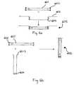
- FIGS. 6 a and 6 bshow methods for horizontal and vertical directed assembly, respectively.
- a nanotube 601can be prepared comprising predetermined chemical groups 602 , for example, a DNA strand or a thiol group, at each end.
- the nanotube 601can be brought into the proximity of a substrate 603 comprising receptors 604 , for example, where DNA is implemented, a complementary DNA strand can be used. Where a thiol group is used, gold particles or a contact shape comprising gold, can be designed to bond with the chemical groups 602 of the nanotube 601 .
- the nanotube 601can thus be placed on the substrate 603 according to directed assembly.
- high-K dielectric filmsthose having a high dielectric constant, can be used as gate insulators.
- the capacitance of a carbon-nanotube FETdoes not significantly change as a function of the thickness of the dielectric film, thus, it can be difficult to achieve the desired capacitance, even with thin gate dielectric films.
- CVD-aluminumcan be oxidized to generate a high-K gate dielectric or CVD-Al 2 O 3 (HfO 2 can be deposited directly.
- these materialsincrease the gate capacitance by a factor of up to five, and can have a larger impact on the device performance than reducing the dielectric film thickness.
- nanotubesare pFETs in an air environment and become nFETs in vacuum and inert gases like Argon (Ar) after annealing, the device can be annealed before the deposition of the dielectric film is added. This converts the tubes into nFETs. Capping them in situ with the dielectric also prevents tubes from becoming pFETs again.
- the dielectric film on FETswhich should be turned into pFETs, can be locally removed also allowing the FETs to be doped.
- a CVD deposition at low temperaturecoats these devices again (without an extra annealing step before).
Landscapes
- Engineering & Computer Science (AREA)
- Chemical & Material Sciences (AREA)
- Nanotechnology (AREA)
- Materials Engineering (AREA)
- Physics & Mathematics (AREA)
- Mathematical Physics (AREA)
- Theoretical Computer Science (AREA)
- Crystallography & Structural Chemistry (AREA)
- Spectroscopy & Molecular Physics (AREA)
- Thin Film Transistor (AREA)
- Bipolar Transistors (AREA)
- Electrodes Of Semiconductors (AREA)
Abstract
Description
- 1. Field of the Invention[0001]
- The present invention relates to field effect transistors, and more particularly, to carbon-nanotube field effect transistors.[0002]
- 2. Discussion of the Related Art[0003]
- In the field of molecular nanoelectronics, few materials show as much promise as nanotubes, and in particular carbon nanotubes, which comprise hollow cylinders of graphite, angstroms in diameter. Nanotubes can be implemented in electronic devices such as diodes and transistors, depending on the nanotube's electrical characteristics. Nanotubes are unique for their size, shape, and physical properties. Structurally a carbon-nanotube resembles a hexagonal lattice of carbon rolled into a cylinder.[0004]
- Besides exhibiting intriguing quantum behaviors at low temperature, carbon nanotubes exhibit at least two important characteristics: a nanotube can be either metallic or semiconductor depending on its chirality (i.e., conformational geometry). Metallic nanotubes can carry extremely large current densities with constant resistivity. Semiconducting nanotubes can be electrically switched on and off as field-effect transistors (FETs). The two types may be covalently joined (sharing electrons). These characteristics point to nanotubes as excellent materials for making nanometer-sized semiconductor circuits.[0005]
- In addition, carbon nanotubes are one-dimensional electrical conductors, meaning that only one-dimensional quantum mechanical mode carries the current. This can be a significant advantage with respect to the device performance of a carbon-nanotube based transistor since scattering in the material is significantly suppressed. Less scattering means a better performance of the device.[0006]
- For a three terminal device, such as an FET, a gate (the third terminal) needs to be isolated from the electrically active channel region as well as a source and a drain. For this purpose a dielectric material, e.g., silicon dioxide can be used. To improve device characteristics in silicon devices, the thickness of this layer can be reduced. This reduction increases the gate capacitance and improves the gate-to-channel coupling. For standard silicon field-effect devices the gate capacitance scales inversely proportional to the dielectric film thickness. For currently manufactured high-performance processors, the SiO[0007]2thickness is less than 4 nm. Significantly, further reduction can be difficult to achieve since gate leakage through the dielectric film increases exponentially for an oxide thickness below 4 nm.
- However, the gate capacitance for a carbon-nanotube transistor does not scale inversely proportional with the dielectric film thickness. Instead, carbon-nanotubes follow a logarithmic scaling law. In comparison with a standard silicon field-effect transistor, the gate capacitance for a carbon-nanotube transistor can be larger because of the cylindrical geometry of these objects.[0008]
- No known system or method has implemented a nanotube to achieve performance and smaller size in an FET. Therefore, a need exists for a system and method of preparing nanotube based FETs.[0009]
- According to an embodiment of the present invention, a self-aligned carbon-nanotube field effect transistor semiconductor device is provided. The device comprises a carbon-nanotube deposited on a substrate, a source and a drain formed at a first end and a second end of the carbon-nanotube, respectively, and a gate formed substantially over a portion of the carbon-nanotube, separated from the carbon-nanotube by a dielectric film.[0010]
- The substrate comprises a thermal oxide deposited over a silicon substrate. The thermal oxide is about 150 nanometers thick.[0011]
- The gate is further separated from the carbon-nanotube by an oxide layer. A portion of the gate is separated from the source and the drain by a nitride spacer.[0012]
- The device further comprises a passivation dielectric layer over the device.[0013]
- The device comprises an alignment mark in the substrate to which the source and the drain are aligned.[0014]
- The gate wraps around the dielectric film and the carbon-nanotube to contact a back side of the carbon-nanotube.[0015]
- According to an embodiment of the present invention, a carbon-nanotube field effect transistor semiconductor device is provided. The device comprises a vertical carbon-nanotube wrapped in a dielectric material, a source and a drain formed on a first side and a second side of the carbon-nanotube, respectively, a bilayer nitride complex through which a band strap of each of the source and the drain is formed connecting the carbon-nanotube wrapped in the dielectric material to the source and the drain, and a gate formed substantially over a portion of the carbon-nanotube.[0016]
- The device comprises a metal catalyst at a base of the carbon-nanotube.[0017]
- According to one embodiment of the present invention, a method is provided for forming a self-aligned carbon-nanotube field effect transistor semiconductor device. The method comprises depositing a nanotube on a thermal oxide substrate, wherein the substrate includes an alignment mark, forming a metal contact at each end of the nanotube, wherein a first metal contact is a source and a second metal contact is a drain, and depositing an amorphous silicon layer over the device. The method further comprises forming nitride spacers on opposing sides of each metal contact, depositing a high k dielectric film over the device, oxidizing the amorphous silicon, and forming a gate substantially between the source and the drain, and over the nanotube.[0018]
- The method comprises depositing a passivation dielectric over the device.[0019]
- The nanotube is a single-walled nanotube. The metal contacts are formed using a photoresist.[0020]
- According to an embodiment of the present invention, a method is provided for forming a self-aligned carbon-nanotube field effect transistor semiconductor device. The method comprises depositing a nanotube on a thermal oxide substrate, wherein the substrate includes an alignment mark, forming a metal contact by reactive ion etch at each end of the nanotube, wherein a first metal contact is a source and a second metal contact is a drain, and forming nitride spacers on opposing sides of each metal contact. The method further comprises depositing a high k dielectric film over the device, and forming a gate substantially between the source and the drain and over the nanotube.[0021]
- The method comprises depositing a passivation dielectric over the device.[0022]
- According to an embodiment of the present invention, a method is provided for forming a self-aligned carbon-nanotube field effect transistor semiconductor device. The method comprises depositing a nanotube on a thermal oxide substrate, wherein the substrate includes an alignment mark, and forming an amorphous silicon pillar over each end of the nanotube. The method further comprises isolating the amorphous silicon pillars with a layer of oxide, forming a gate dielectric layer between amorphous silicon pillars, and forming a gate substantially between the amorphous silicon pillars and over the nanotube. The method comprises forming a nitride layer over the gate, forming oxide spacers on each side of the gate, replacing the amorphous silicon with metal contacts, wherein a first metal contact is a source and a second metal contact is a drain, anddepositing a passivation dielectric over the device.[0023]
- According to another embodiment of the present invention, a method is provided for forming a self-aligned carbon-nanotube field effect transistor semiconductor device. The method comprises depositing a metal catalyst on a thermal oxide substrate, depositing a low temperature oxide layer over the device, etching a trench through the oxide, the metal catalyst and into a thermal oxide underlying the metal catalyst, and etching the low temperature oxide layer to form oxide islands. The method further comprises stripping exposed metal catalyst, growing a nanotube between metal catalyst beneath the oxide islands, and wrapping the nanotube in a gate dielectric. The method comprises forming nitride spacers on the opposing surfaces of the oxide islands, forming a gate substantially between the oxide islands by chemical vapor deposition and over the nanotube, and depositing a passivation dielectric over the device.[0024]
- According to an embodiment of the present invention, a method is provided for forming a self-aligned carbon-nanotube field effect transistor semiconductor device. The method comprises growing a nanotube vertically from a metal catalyst forming on a surface of the semiconductor device, forming a nitride block structure, and wrapping the nanotube in a gate dielectric. The method comprises depositing a gate metal separated from the metal catalyst by the dielectric layer, depositing a nitride layer, and forming gate metal pillars capped with the nitride layer. The method forms nitride spacers around the pillars, deposits a drain metal substantially between the pillars separated from the gate metal by the dielectric layer, and deposits a passivation dielectric over the device.[0025]
- Preferred embodiments of the present invention will be described below in more detail, with reference to the accompanying drawings:[0026]
- FIGS. 1[0027]a-iillustrate a source/drain first carbon-nanotube field effect transistor according to an embodiment of the present invention;
- FIGS. 2[0028]a-billustrate another source/drain first carbon-nanotube field effect transistor according to an embodiment of the present invention;
- FIGS. 3[0029]a-gillustrate a gate first carbon-nanotube field effect transistor according to an embodiment of the present invention;
- FIGS. 4[0030]a-dillustrate a carbon-nanotube field effect transistor comprising a nanotube grown in place according to an embodiment of the present invention;
- FIGS. 5[0031]a-nillustrate a carbon-nanotube field effect transistor comprising a nanotube grown in place vertically according to an embodiment of the present invention; and
- FIGS. 6[0032]a-billustrate directed assembly of nanotubes according to an embodiment of the present invention.
- According to an embodiment of the present invention, a gate, a source and a drain of a field effect transistor (FET) are self-aligned, thereby reducing overlap capacitances.[0033]
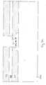
- According to an embodiment of the present invention, a carbon-nanotube FET can be fabricated using a pattern transfer by lift-off etch, wherein the source and the drain are formed before the gate. Referring to FIGS. 1[0034]a-i,an
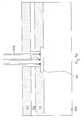
alignment mark 101 is formed in athermal oxide 102 andsilicon substrate 103. Thealignment mark 101 is a high precision feature that can be used as a reference when positioning patterns. Thethermal oxide 102 is deposited over thesilicon 103. The silicon can be, for example, P+doped (0.01Ω-cm, about 3×1018cm−3). Ananotube 104 can be deposited on thethermal oxide 102 and aphotoresist 105 can be positioned by photolithography. The nanotube can be deposited in the form of a slurry, where nanotube deposition is random. The nanotube can be deposited by directed assembly, as described below. The photoresist exposes the ends of the nanotube. Metal contacts106-107 are formed in the trenches that expose the nanotube ends. The metal can be, for example, Cobalt (Co), Nickel (Ni), Tungsten (W), or Titanium (Ti). The metal can be deposited over the device, filling the trenches exposing the ends of thenanotube 104. Thephotoresist 105 can be stripped. The metal deposited in the trenches form source/drain contacts106-107. An amorphous Silicon (a-Si)108 can be deposited over the device. ANitride layer 109 can be deposited over the a-Si layer. The Nitride can be etched to form spacers, e.g.,110 on the sides of the metal contacts106-107. Theamorphous silicon 108 can be selectively removed or wet chemically oxidized. A gate dielectric film111 can be deposited over the device. Here as in the following methods, the dielectric can be silicon dioxide as well as any other high-k dielectric material, for example, HfO2. Agate 112 can be formed substantially between the metal contacts106-107 forming the source and drain, for example by CVD and etching. Apassivation dielectric layer 113 is deposited over the device. The source, drain andgate 112 are self-aligned to thealignment mark 101. - Alternatively, the source/drain can be formed before the gate with a reactive ion etch (RIE). Referring to FIGS. 2[0035]a-b,a method forms the source/drain,106-107, first using RIE to define the source/drain metal. The RIE needs to be isolated from the carbon-
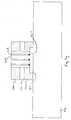
nanotube 104. Anitride layer 201 can be deposited over the device and etched from the areas surrounding the metal contact. Nitride spacers, e.g.,202, can be formed on the sides of the metal contacts. Agate dielectric 203 is deposited over the device. Thegate metal 204 is formed substantially between the source and the drain,106-107. Apassivation dielectric 205 can be deposited over the device. The thermal oxide can be approximately 150 nm thick. - According to another embodiment of the present invention, the gate can be formed before the source/drain.[0036]
Amorphous silicon 301 can be deposited over the ends of thenanotube 104. The a-Si can be covered with anoxide layer 302. Agate dielectric 303 can be deposited between the a-Si, e.g.,301. Agate 304 can be formed substantially between the a-Si pillars, e.g.,301. Anitride layer 305 can be formed over thegate metal 304. Oxide spacers, e.g.,306 can be formed on the ends of thegate metal 304. The exposed corners of the a-Si/oxide can be stripped, exposing the a-Si. The remaining a-Si surrounding the gate metal can be removed by RIE. Metal contacts307-308 can be deposited in the area previously occupied by the a-Si. The metal contacts307-308 are connected to thenanotube 104 that runs beneath thegate dielectric 303 andgate metal 304. The metal contacts307-308 form the source and the drain of the device. The metal contacts307-308 can be aligned to thealignment mark 101 deposited in thethermal oxide 102 andsilicon 103 substrate. Apassivation dielectric 309 can be deposited over the device. - According to an embodiment of the present invention, a carbon-nanotube FET can be grown in place. The source/drain can be formed before the gate. An[0037]
amorphous silicon layer 401 is deposited over thethermal oxide layer 102. A low temperature oxide (LTO)layer 402 can be deposited over the metal catalyst. A trench can be etched from theoxide 402,amorphous silicon 401 andthermal oxide 102. Theamorphous silicon 401 can be partially under cut from below theoxide 402. Ametal catalyst 401B, for example, Fe, Co, Ni or Fe/Mo can be self-assembled on the edges of the undercutamorphous silicon film 401. The carbon-nanotube 403 can be grown between the remaining portions of themetal catalyst 401B, wherein a portion of the nanotube is suspended over thethermal oxide 102. Agate dielectric film 404 can be deposited by chemical vapor deposition (CVD), wrapping thenanotube 403. Thus, thenanotube 403 can be completely covered with the gate dielectric, e.g., SiO2. Spacers, e.g.,405, can be formed on the sides of the oxide, e.g.,402. A gate406 can be formed substantially between the oxide, e.g.,402. If the etch in thethermal oxide 102 is sufficiently deep, the gate metal406 can surround thewhole nanotube 403 and thedielectric film 404 stack. For this purpose the gate metal can be deposited by means of chemical vapor deposition to cover the back side of the nanotube/dielectric film stack. The wrapped around configuration offers a good gate-to-nanotube coupling. A passivation dielectric406 can be deposited over the surface of the device. - According to another embodiment of the present invention, a carbon-nanotube can be grown in place vertically. The nanotube can be grown vertically from, for example, a metal source at the base or a metal particle catalyst. Referring to FIGS. 5[0038]a-n,a
metal catalyst 501 can be formed on thesilicon substrate 502. A first layer ofNitride 503 can be deposited over the device. Anoxide layer 504 can be deposited over the first layer ofNitride 503. A second layer ofNitride 505 can be deposited over theoxide 504. A photoresist, e.g.,506, can be formed on the device by photolithography, wherein themetal catalyst 501 is exposed. A plurality of second metal catalysts, e.g.,507, are deposited over the device. The photoresist, e.g.,506, can stripped, such that the second catalyst, e.g.,507, formed on thefirst metal catalyst 501 remain. From each second metal catalyst, e.g.,507, a nanotube, e.g.,508, can be grown vertically. Thus, two-dimensional and three-dimensional arrays of nanotubes can be formed. - Vertical growth of the nanotubes occurs when the metal particle catalyst is placed in a pore aligned vertically to the substrate. In this case, the space for the growth is confined and forces the growth of the tube to follow the vertical direction. In principle, vertical pores such as in FIG. 5[0039]bcan be made using the resists and pattern transfer.
- An[0040]
amorphous Silicon layer 509 can be deposited over the device. The device can be planarized down to the-second Nitride layer 505. A portion of the Nitride-Oxide-Nitride layering,503-505, can be removed from the device. A pillar surrounding the nanotubes, e.g.,508, and metal catalyst,501 and507, remains. Asacrificial layer 510 can be formed over theNitride layer 505 thenanotubes 508 and thea-Si 509. The contact layer can be, for example, titanium or tungsten. Theoxide layer 504 can be removed from between the layers of Nitride,503 and505. The a-Si509 can be etched simultaneously with theoxide layer 504 from around the nanotubes, e.g.,508. Alternatively, the a-So509 can be removed after theoxide layer 504 has been removed. A gate dielectric, e.g.,511, can be formed around the nanotubes, e.g.,508, over themetal catalyst 501 and under thesacrificial layer 510. Alternatively, for a two-dimensional array of nanotubes, thegate dielectric 511 can be deposited between the nanotubes. Thesacrificial layer 510 can be removed, for example, by an etch. Thegate metal 512 can be deposited over the surface of the device. Athird Nitride layer 513 can be deposited over thegate metal 512. Portions of thegate metal 512 and thethird nitride layer 513 can be removed. Pillars of gate metal and nitride spacers, e.g.,512 and513, remain around the metal catalyst-nanotube structure. Nitride spacers, e.g.,514, are formed around each pillar. Adrain 515 can be formed over the metal catalyst-nanotube structure, forming a FET. Thepassivation dielectric 516 can be deposited between FETS. - It should be noted that the exact mechanics of nanotube growth from a metal catalyst are not known. However, the process of growing a single-walled nanotube from a metal catalyst, for example, Cobalt (CO) over alumina-supported Molybdenum (Mo) particles, can be implemented in a number of ways.[0041]
- According to an embodiment of the present invention, nanotubes can be put in place by a method of directed assembly rather than deposited or grown as described above. Directed assembly can be used for horizontal and vertical deposition of a nanotube using selective deposition driven by a chemical or a physical process. The selective deposition can include forming an adhesion layer or chemical groups acting as receptors to favor a desired deposition of tubes in a given position. FIGS. 6[0042]aand6bshow methods for horizontal and vertical directed assembly, respectively. A
nanotube 601 can be prepared comprising predeterminedchemical groups 602, for example, a DNA strand or a thiol group, at each end. Thenanotube 601 can be brought into the proximity of asubstrate 603 comprisingreceptors 604, for example, where DNA is implemented, a complementary DNA strand can be used. Where a thiol group is used, gold particles or a contact shape comprising gold, can be designed to bond with thechemical groups 602 of thenanotube 601. Thenanotube 601 can thus be placed on thesubstrate 603 according to directed assembly. - For improved performance high-K dielectric films, those having a high dielectric constant, can be used as gate insulators. The capacitance of a carbon-nanotube FET does not significantly change as a function of the thickness of the dielectric film, thus, it can be difficult to achieve the desired capacitance, even with thin gate dielectric films. Aluminum oxide Al[0043]2O3(k=9) as well as Hafnium oxide (HfO2) (k=20) are promising candidates in this context. CVD-aluminum can be oxidized to generate a high-K gate dielectric or CVD-Al2O3(HfO2can be deposited directly. Compared with SiO2, these materials increase the gate capacitance by a factor of up to five, and can have a larger impact on the device performance than reducing the dielectric film thickness. Since nanotubes are pFETs in an air environment and become nFETs in vacuum and inert gases like Argon (Ar) after annealing, the device can be annealed before the deposition of the dielectric film is added. This converts the tubes into nFETs. Capping them in situ with the dielectric also prevents tubes from becoming pFETs again. For a complementary technology the dielectric film on FETs, which should be turned into pFETs, can be locally removed also allowing the FETs to be doped. A CVD deposition at low temperature coats these devices again (without an extra annealing step before).
- Since all structures (pFETs and nFETs) are covered with oxide (or any other suitable dielectric film) no short is generated when the gate electrode is fabricated. CVD can be used for the deposition of the gate. Using chemical vapor deposition for fabrication schemes as described in FIGS. 4 and 5 can ensure that nanotubes that are already wrapped in a dielectric film become completely surrounded by the metal gate. This can be important for good gate-to-nanotube coupling. The gate metal can be patterned and removed where desired. Source and drain electrodes can be opened for electrical access.[0044]
- Having described preferred embodiments for carbon-nanotube FETs and methods of making same, it is noted that modifications and variations can be made by persons skilled in the art in light of the above teachings. It is therefore to be understood that changes may be made in the particular embodiments of the invention disclosed which are within the scope and spirit of the invention as defined by the appended claims. Having thus described the invention with the details and particularity required by the patent laws, what is claimed and desired protected by Letters Patent is set forth in the appended claims.[0045]
Claims (19)
Priority Applications (25)
| Application Number | Priority Date | Filing Date | Title |
|---|---|---|---|
| US10/102,365US6891227B2 (en) | 2002-03-20 | 2002-03-20 | Self-aligned nanotube field effect transistor and method of fabricating same |
| EP03721349AEP1485958B1 (en) | 2002-03-20 | 2003-02-19 | Self-aligned nanotube field effect transistor and method of fabricating same |
| IL16406603AIL164066A0 (en) | 2002-03-20 | 2003-02-19 | Self-aligned nanotube field effect transistor and method of fabricating same |
| PCT/US2003/007269WO2003081687A2 (en) | 2002-03-20 | 2003-02-19 | Self-aligned nanotube field effect transistor and method of fabricating same |
| MXPA04008984AMXPA04008984A (en) | 2002-03-20 | 2003-02-19 | NANOTUBE FIELD EFFECT TRANSISTOR, SELF-ALIGNED, AND METHOD TO MANUFACTURE THE SAME. |
| CA2695715ACA2695715C (en) | 2002-03-20 | 2003-02-19 | Self-aligned nanotube field effect transistor and method of fabricating same |
| CA2479024ACA2479024C (en) | 2002-03-20 | 2003-02-19 | Self-aligned nanotube field effect transistor and method of fabricating same |
| CA2659479ACA2659479C (en) | 2002-03-20 | 2003-02-19 | Self-aligned nanotube field effect transistor and method of fabricating same |
| AT03721349TATE551734T1 (en) | 2002-03-20 | 2003-02-19 | SELF-ALIGINATED NANOTUBE FIELD EFFECT TRANSISTOR AND METHOD FOR THE PRODUCTION THEREOF |
| CN038062925ACN1669160B (en) | 2002-03-20 | 2003-02-19 | Self-aligned nanotube field effect transistor and method of manufacturing the same |
| EP06120727AEP1748503B1 (en) | 2002-03-20 | 2003-02-19 | Carbon nanotube field effect transistor and method of fabricating a self-aligned carbon nanotube field effect transistor |
| PL03373571APL373571A1 (en) | 2002-03-20 | 2003-02-19 | Self-aligned nanotube field effect transistor and method of fabricating same |
| KR1020047013701AKR100714932B1 (en) | 2002-03-20 | 2003-02-19 | Self-aligned Nanotube Field Effect Transistors and Manufacturing Method Thereof |
| AU2003224668AAU2003224668A1 (en) | 2002-03-20 | 2003-02-19 | Self-aligned nanotube field effect transistor and method of fabricating same |
| AT06120727TATE516600T1 (en) | 2002-03-20 | 2003-02-19 | CARBON NANOTUBE TRANSISTOR AND METHOD FOR PRODUCING A SELF-ALIGNED CARBON NANOTUBE TRANSISTOR |
| JP2003579292AJP4493344B2 (en) | 2002-03-20 | 2003-02-19 | Carbon nanotube field effect transistor semiconductor device and manufacturing method thereof |
| BRPI0308569-4ABR0308569A (en) | 2002-03-20 | 2003-02-19 | self-aligned nanotube field effect transistor and manufacturing method |
| CN2010101262554ACN101807668B (en) | 2002-03-20 | 2003-02-19 | Carbon nanotube field effect transistor and method of fabricating same |
| TW092104050ATW586165B (en) | 2002-03-20 | 2003-02-26 | Self-aligned nanotube field effect transistor and method of fabricating same |
| IL164066AIL164066A (en) | 2002-03-20 | 2004-09-14 | Self-aligned nanotube field effect transistor and method of fabricating same |
| US10/956,851US7253065B2 (en) | 2002-03-20 | 2004-10-01 | Self-aligned nanotube field effect transistor and method of fabricating same |
| US11/835,167US7635856B2 (en) | 2002-03-20 | 2007-08-07 | Vertical nanotube field effect transistor |
| US12/544,436US8138491B2 (en) | 2002-03-20 | 2009-08-20 | Self-aligned nanotube field effect transistor |
| US12/544,412US7897960B2 (en) | 2002-03-20 | 2009-08-20 | Self-aligned nanotube field effect transistor |
| US13/368,901US8637374B2 (en) | 2002-03-20 | 2012-02-08 | Method of fabricating self-aligned nanotube field effect transistor |
Applications Claiming Priority (1)
| Application Number | Priority Date | Filing Date | Title |
|---|---|---|---|
| US10/102,365US6891227B2 (en) | 2002-03-20 | 2002-03-20 | Self-aligned nanotube field effect transistor and method of fabricating same |
Related Child Applications (1)
| Application Number | Title | Priority Date | Filing Date |
|---|---|---|---|
| US10/956,851DivisionUS7253065B2 (en) | 2002-03-20 | 2004-10-01 | Self-aligned nanotube field effect transistor and method of fabricating same |
Publications (2)
| Publication Number | Publication Date |
|---|---|
| US20030178617A1true US20030178617A1 (en) | 2003-09-25 |
| US6891227B2 US6891227B2 (en) | 2005-05-10 |
Family
ID=28040198
Family Applications (6)
| Application Number | Title | Priority Date | Filing Date |
|---|---|---|---|
| US10/102,365Expired - LifetimeUS6891227B2 (en) | 2002-03-20 | 2002-03-20 | Self-aligned nanotube field effect transistor and method of fabricating same |
| US10/956,851Expired - LifetimeUS7253065B2 (en) | 2002-03-20 | 2004-10-01 | Self-aligned nanotube field effect transistor and method of fabricating same |
| US11/835,167Expired - LifetimeUS7635856B2 (en) | 2002-03-20 | 2007-08-07 | Vertical nanotube field effect transistor |
| US12/544,436Expired - Fee RelatedUS8138491B2 (en) | 2002-03-20 | 2009-08-20 | Self-aligned nanotube field effect transistor |
| US12/544,412Expired - Fee RelatedUS7897960B2 (en) | 2002-03-20 | 2009-08-20 | Self-aligned nanotube field effect transistor |
| US13/368,901Expired - LifetimeUS8637374B2 (en) | 2002-03-20 | 2012-02-08 | Method of fabricating self-aligned nanotube field effect transistor |
Family Applications After (5)
| Application Number | Title | Priority Date | Filing Date |
|---|---|---|---|
| US10/956,851Expired - LifetimeUS7253065B2 (en) | 2002-03-20 | 2004-10-01 | Self-aligned nanotube field effect transistor and method of fabricating same |
| US11/835,167Expired - LifetimeUS7635856B2 (en) | 2002-03-20 | 2007-08-07 | Vertical nanotube field effect transistor |
| US12/544,436Expired - Fee RelatedUS8138491B2 (en) | 2002-03-20 | 2009-08-20 | Self-aligned nanotube field effect transistor |
| US12/544,412Expired - Fee RelatedUS7897960B2 (en) | 2002-03-20 | 2009-08-20 | Self-aligned nanotube field effect transistor |
| US13/368,901Expired - LifetimeUS8637374B2 (en) | 2002-03-20 | 2012-02-08 | Method of fabricating self-aligned nanotube field effect transistor |
Country Status (14)
| Country | Link |
|---|---|
| US (6) | US6891227B2 (en) |
| EP (2) | EP1485958B1 (en) |
| JP (1) | JP4493344B2 (en) |
| KR (1) | KR100714932B1 (en) |
| CN (2) | CN1669160B (en) |
| AT (2) | ATE551734T1 (en) |
| AU (1) | AU2003224668A1 (en) |
| BR (1) | BR0308569A (en) |
| CA (3) | CA2659479C (en) |
| IL (2) | IL164066A0 (en) |
| MX (1) | MXPA04008984A (en) |
| PL (1) | PL373571A1 (en) |
| TW (1) | TW586165B (en) |
| WO (1) | WO2003081687A2 (en) |
Cited By (149)
| Publication number | Priority date | Publication date | Assignee | Title |
|---|---|---|---|---|
| US20040137730A1 (en)* | 2002-10-11 | 2004-07-15 | Sang-Gook Kim | Method of making packets of nanostructures |
| US20040185627A1 (en)* | 2003-03-18 | 2004-09-23 | Brask Justin K. | Method for making a semiconductor device having a high-k gate dielectric |
| US6821911B1 (en)* | 2003-08-20 | 2004-11-23 | Industrial Technology Research Institute | Manufacturing method of carbon nanotube transistors |
| US20050130341A1 (en)* | 2003-12-11 | 2005-06-16 | International Business Machines Corporation | Selective synthesis of semiconducting carbon nanotubes |
| WO2005067075A1 (en)* | 2004-01-08 | 2005-07-21 | Qimonda Ag | Method for the production a nanoelement field effect transistor, nanoelement-field effect transistor and surrounded gate structure |
| US20050167655A1 (en)* | 2004-01-29 | 2005-08-04 | International Business Machines Corporation | Vertical nanotube semiconductor device structures and methods of forming the same |
| WO2005071754A1 (en)* | 2004-01-22 | 2005-08-04 | Infineon Technologies Ag | Semi-conductor circuit and suitable production method therefor |
| US20050167740A1 (en)* | 2004-01-29 | 2005-08-04 | International Business Machines Corporation | Vertical field effect transistors incorporating semiconducting nanotubes grown in a spacer-defined passage |
| US20050179029A1 (en)* | 2004-02-12 | 2005-08-18 | International Business Machines Corporation | Methods of fabricating vertical carbon nanotube field effect transistors for arrangement in arrays and field effect transistors and arrays formed thereby |
| US20050181409A1 (en)* | 2004-02-14 | 2005-08-18 | Young-Jun Park | Biochip and biomolecular detection system using the same |
| US20050218397A1 (en)* | 2004-04-06 | 2005-10-06 | Availableip.Com | NANO-electronics for programmable array IC |
| US20050218398A1 (en)* | 2004-04-06 | 2005-10-06 | Availableip.Com | NANO-electronics |
| US20050230822A1 (en)* | 2004-04-06 | 2005-10-20 | Availableip.Com | NANO IC packaging |
| US20050231855A1 (en)* | 2004-04-06 | 2005-10-20 | Availableip.Com | NANO-electronic memory array |
| US20050229328A1 (en)* | 2004-04-06 | 2005-10-20 | Availableip.Com | Nano-particles on fabric or textile |
| US20050263830A1 (en)* | 2004-05-28 | 2005-12-01 | Chih-Hao Wang | Partial replacement silicide gate |
| WO2006010684A1 (en)* | 2004-07-29 | 2006-02-02 | International Business Machines Corporation | Integrated circuit chip utilizing oriented carbon nanotube conductive layers |
| US20060063318A1 (en)* | 2004-09-10 | 2006-03-23 | Suman Datta | Reducing ambipolar conduction in carbon nanotube transistors |
| WO2006072538A1 (en) | 2005-01-07 | 2006-07-13 | International Business Machines Corporation | Self-aligned process for nanotube/nanowire fets |
| US20060169972A1 (en)* | 2005-01-31 | 2006-08-03 | International Business Machines Corporation | Vertical carbon nanotube transistor integration |
| US20060180859A1 (en)* | 2005-02-16 | 2006-08-17 | Marko Radosavljevic | Metal gate carbon nanotube transistor |
| US20060183278A1 (en)* | 2005-01-14 | 2006-08-17 | Nantero, Inc. | Field effect device having a channel of nanofabric and methods of making same |
| US20060198209A1 (en)* | 2005-02-23 | 2006-09-07 | Tran Bao Q | Nano memory, light, energy, antenna and strand-based systems and methods |
| US7109546B2 (en) | 2004-06-29 | 2006-09-19 | International Business Machines Corporation | Horizontal memory gain cells |
| US20060228835A1 (en)* | 2005-04-06 | 2006-10-12 | International Business Machines Corporation | Method of doping a gate electrode of a field effect transistor |
| US20060237857A1 (en)* | 2005-01-14 | 2006-10-26 | Nantero, Inc. | Hybrid carbon nanotube FET(CNFET)-FET static RAM (SRAM) and method of making same |
| US20060255414A1 (en)* | 2005-05-16 | 2006-11-16 | Joerg Appenzeller | Method and apparatus for fabricating a carbon nanotube transistor having unipolar characteristics |
| US20070001220A1 (en)* | 2004-09-16 | 2007-01-04 | Atomate Corporation | Nanotube Transistor and Rectifying Devices |
| US20070021293A1 (en)* | 2005-07-25 | 2007-01-25 | International Business Machines Corporation | Shared gate for conventional planar device and horizontal cnt |
| US20070031318A1 (en)* | 2005-08-03 | 2007-02-08 | Jie Liu | Methods of chemically treating an electrically conductive layer having nanotubes therein with diazonium reagent |
| US20070102747A1 (en)* | 2005-11-10 | 2007-05-10 | International Business Machines Corporation | Complementary carbon nanotube triple gate technology |
| US20070111460A1 (en)* | 2005-03-24 | 2007-05-17 | Mosley Larry E | Capacitor with carbon nanotubes |
| US20070123028A1 (en)* | 2004-10-04 | 2007-05-31 | International Business Machines Corporation ("Ibm") | Methods of forming low-k dielectric layers containing carbon nanostructures |
| US20070183189A1 (en)* | 2006-02-08 | 2007-08-09 | Thomas Nirschl | Memory having nanotube transistor access device |
| US20070192911A1 (en)* | 2006-02-14 | 2007-08-16 | Hao Xin | Particle encapsulated nanoswitch |
| FR2897978A1 (en)* | 2006-08-03 | 2007-08-31 | Commissariat Energie Atomique | Memory cell for storing e.g. binary information, has field effect memory and access transistors including respective source and drain, where source and drain form additional electrode that is connected to additional control line |
| US20070228439A1 (en)* | 2002-09-30 | 2007-10-04 | Nanosys, Inc. | Large-Area Nanoenabled Macroelectronic Substrates and Uses Therefor |
| US20070262344A1 (en)* | 2005-08-18 | 2007-11-15 | Anwar A F M | Insulated gate silicon nanowire transistor and method of manufacture |
| WO2007092770A3 (en)* | 2006-02-02 | 2008-01-03 | Univ Rice William M | Fabrication de dispositifs electriques par façonnage de nanotubes |
| US20080105648A1 (en)* | 2004-12-16 | 2008-05-08 | William Marsh Rice University | Carbon nanotube substrates and catalyzed hot stamp for polishing and patterning the substrates |
| US7374793B2 (en) | 2003-12-11 | 2008-05-20 | International Business Machines Corporation | Methods and structures for promoting stable synthesis of carbon nanotubes |
| US20080121996A1 (en)* | 2004-09-13 | 2008-05-29 | Park Wan-Jun | Transistor with carbon nanotube channel and method of manufacturing the same |
| US7393699B2 (en) | 2006-06-12 | 2008-07-01 | Tran Bao Q | NANO-electronics |
| CN100420033C (en)* | 2004-10-28 | 2008-09-17 | 鸿富锦精密工业(深圳)有限公司 | Field effect transistor and method of manufacturing the same |
| US20080303029A1 (en)* | 2005-02-10 | 2008-12-11 | Takahiro Kawashima | Structure, Semiconductor Device, Tft Driving Circuit, Panel, Display and Sensor for Maintaining Microstructure, Methods for Fabricating the Structure, the Semiconductor Device, the Tft Driving Circuit, the Panel, the Display and the Sensor |
| CN100456496C (en)* | 2005-05-23 | 2009-01-28 | 国际商业机器公司 | Semiconductor structure and method of forming same |
| US20090032804A1 (en)* | 2007-07-31 | 2009-02-05 | Kalburge Amol M | Self-Aligned T-Gate Carbon Nanotube Field Effect Transistor Devices and Method for Forming the Same |
| US20100038730A1 (en)* | 2008-08-13 | 2010-02-18 | Micron Technology, Inc. | Semiconductor structures including a movable switching element, systems including same and methods of forming same |
| US20100065820A1 (en)* | 2005-02-14 | 2010-03-18 | Atomate Corporation | Nanotube Device Having Nanotubes with Multiple Characteristics |
| US7714386B2 (en) | 2006-06-09 | 2010-05-11 | Northrop Grumman Systems Corporation | Carbon nanotube field effect transistor |
| US20100132080A1 (en)* | 2008-11-24 | 2010-05-27 | Massachusetts Institute Of Technology | Method of making and assembling capsulated nanostructures |
| US20100140588A1 (en)* | 2002-08-02 | 2010-06-10 | Nec Corporation | Catalyst support substrate, method for growing carbon nanotubes using the same, and transistor using carbon nanotubes |
| US7776307B2 (en) | 2004-09-16 | 2010-08-17 | Etamota Corporation | Concentric gate nanotube transistor devices |
| US20100316075A1 (en)* | 2009-04-13 | 2010-12-16 | Kaai, Inc. | Optical Device Structure Using GaN Substrates for Laser Applications |
| US20110027491A1 (en)* | 2009-07-31 | 2011-02-03 | Nantero, Inc. | Anisotropic nanotube fabric layers and films and methods of forming same |
| US20110027497A1 (en)* | 2009-07-31 | 2011-02-03 | Nantero, Inc. | Anisotropic nanotube fabric layers and films and methods of forming same |
| US20110037124A1 (en)* | 2009-08-14 | 2011-02-17 | Tsinghua University | Thin film transistor |
| US20110045660A1 (en)* | 2002-09-30 | 2011-02-24 | Nanosys, Inc. | Large-Area Nanoenabled Macroelectronic Substrates and Uses Therefor |
| US7943418B2 (en) | 2004-09-16 | 2011-05-17 | Etamota Corporation | Removing undesirable nanotubes during nanotube device fabrication |
| US20110127493A1 (en)* | 2009-11-30 | 2011-06-02 | International Business Machines Corporation | Self aligned carbide source/drain fet |
| WO2011064074A1 (en)* | 2009-11-30 | 2011-06-03 | International Business Machines Corporation | Field effect transistor having nanostructure channel |
| US20110220859A1 (en)* | 2005-05-09 | 2011-09-15 | Nantero, Inc. | Two-Terminal Nanotube Devices And Systems And Methods Of Making Same |
| US8168495B1 (en) | 2006-12-29 | 2012-05-01 | Etamota Corporation | Carbon nanotube high frequency transistor technology |
| US20120178198A1 (en)* | 2008-07-14 | 2012-07-12 | Soraa, Inc. | Self-Aligned Multi-Dielectric-Layer Lift Off Process for Laser Diode Stripes |
| WO2012158996A1 (en)* | 2011-05-19 | 2012-11-22 | International Business Machines Corporation | Self-aligned carbon electronics with embedded gate electrode |
| US20120326127A1 (en)* | 2011-06-27 | 2012-12-27 | International Business Machines Corporation | Collapsable gate for deposited nanostructures |
| CN102983176A (en)* | 2011-08-03 | 2013-03-20 | 伊格尼斯创新公司 | Thin film transistor including a nanoconductor layer |
| US20130069665A1 (en)* | 2011-09-19 | 2013-03-21 | California Institute Of Technology | Using a field effect device for identifying translocating charge-tagged molecules in a nanopore sequencing device |
| US20130087767A1 (en)* | 2011-10-11 | 2013-04-11 | International Business Machines Corporation | Patterning contacts in carbon nanotube devices |
| US8494017B2 (en) | 2008-08-04 | 2013-07-23 | Soraa, Inc. | Solid state laser device using a selected crystal orientation in non-polar or semi-polar GaN containing materials and methods |
| US8509275B1 (en) | 2009-05-29 | 2013-08-13 | Soraa, Inc. | Gallium nitride based laser dazzling device and method |
| US8513099B2 (en) | 2010-06-17 | 2013-08-20 | International Business Machines Corporation | Epitaxial source/drain contacts self-aligned to gates for deposited FET channels |
| US8524578B1 (en) | 2009-05-29 | 2013-09-03 | Soraa, Inc. | Method and surface morphology of non-polar gallium nitride containing substrates |
| US8558265B2 (en) | 2008-08-04 | 2013-10-15 | Soraa, Inc. | White light devices using non-polar or semipolar gallium containing materials and phosphors |
| US8582038B1 (en) | 2009-05-29 | 2013-11-12 | Soraa, Inc. | Laser based display method and system |
| US8580586B2 (en) | 2005-05-09 | 2013-11-12 | Nantero Inc. | Memory arrays using nanotube articles with reprogrammable resistance |
| US8597967B1 (en) | 2010-11-17 | 2013-12-03 | Soraa, Inc. | Method and system for dicing substrates containing gallium and nitrogen material |
| EP2674996A1 (en)* | 2012-06-15 | 2013-12-18 | Imec VZW | Method for growing nanostructures in recessed structures |
| US8638828B1 (en) | 2010-05-17 | 2014-01-28 | Soraa, Inc. | Method and system for providing directional light sources with broad spectrum |
| US8735869B2 (en)* | 2012-09-27 | 2014-05-27 | Intel Corporation | Strained gate-all-around semiconductor devices formed on globally or locally isolated substrates |
| US8750342B1 (en) | 2011-09-09 | 2014-06-10 | Soraa Laser Diode, Inc. | Laser diodes with scribe structures |
| US8767787B1 (en) | 2008-07-14 | 2014-07-01 | Soraa Laser Diode, Inc. | Integrated laser diodes with quality facets on GaN substrates |
| US8805134B1 (en) | 2012-02-17 | 2014-08-12 | Soraa Laser Diode, Inc. | Methods and apparatus for photonic integration in non-polar and semi-polar oriented wave-guided optical devices |
| US8816319B1 (en) | 2010-11-05 | 2014-08-26 | Soraa Laser Diode, Inc. | Method of strain engineering and related optical device using a gallium and nitrogen containing active region |
| US8823059B2 (en)* | 2012-09-27 | 2014-09-02 | Intel Corporation | Non-planar semiconductor device having group III-V material active region with multi-dielectric gate stack |
| US8837545B2 (en) | 2009-04-13 | 2014-09-16 | Soraa Laser Diode, Inc. | Optical device structure using GaN substrates and growth structures for laser applications |
| US8847249B2 (en) | 2008-06-16 | 2014-09-30 | Soraa, Inc. | Solid-state optical device having enhanced indium content in active regions |
| US20140312298A1 (en)* | 2011-11-01 | 2014-10-23 | International Business Machines Corporation | Graphene and Nanotube/Nanowire Transistor with a Self-Aligned Gate Structure on Transparent Substrates and Method of Making Same |
| US8905588B2 (en) | 2010-02-03 | 2014-12-09 | Sorra, Inc. | System and method for providing color light sources in proximity to predetermined wavelength conversion structures |
| US8912025B2 (en) | 2011-11-23 | 2014-12-16 | Soraa, Inc. | Method for manufacture of bright GaN LEDs using a selective removal process |
| US8971370B1 (en) | 2011-10-13 | 2015-03-03 | Soraa Laser Diode, Inc. | Laser devices using a semipolar plane |
| US9020003B1 (en) | 2012-03-14 | 2015-04-28 | Soraa Laser Diode, Inc. | Group III-nitride laser diode grown on a semi-polar orientation of gallium and nitrogen containing substrates |
| US9025635B2 (en) | 2011-01-24 | 2015-05-05 | Soraa Laser Diode, Inc. | Laser package having multiple emitters configured on a support member |
| US9048170B2 (en) | 2010-11-09 | 2015-06-02 | Soraa Laser Diode, Inc. | Method of fabricating optical devices using laser treatment |
| US9071039B2 (en) | 2009-04-13 | 2015-06-30 | Soraa Laser Diode, Inc. | Optical device structure using GaN substrates for laser applications |
| US9076926B2 (en) | 2011-08-22 | 2015-07-07 | Soraa, Inc. | Gallium and nitrogen containing trilateral configuration for optical devices |
| US9093820B1 (en) | 2011-01-25 | 2015-07-28 | Soraa Laser Diode, Inc. | Method and structure for laser devices using optical blocking regions |
| US9105806B2 (en) | 2009-03-09 | 2015-08-11 | Soraa, Inc. | Polarization direction of optical devices using selected spatial configurations |
| US9250044B1 (en) | 2009-05-29 | 2016-02-02 | Soraa Laser Diode, Inc. | Gallium and nitrogen containing laser diode dazzling devices and methods of use |
| US9287684B2 (en) | 2011-04-04 | 2016-03-15 | Soraa Laser Diode, Inc. | Laser package having multiple emitters with color wheel |
| US9343871B1 (en) | 2012-04-05 | 2016-05-17 | Soraa Laser Diode, Inc. | Facet on a gallium and nitrogen containing laser diode |
| US9419189B1 (en) | 2013-11-04 | 2016-08-16 | Soraa, Inc. | Small LED source with high brightness and high efficiency |
| US9450143B2 (en) | 2010-06-18 | 2016-09-20 | Soraa, Inc. | Gallium and nitrogen containing triangular or diamond-shaped configuration for optical devices |
| US9502673B2 (en)* | 2015-03-31 | 2016-11-22 | International Business Machines Corporation | Transistor devices with tapered suspended vertical arrays of carbon nanotubes |
| US9543738B2 (en) | 2009-09-17 | 2017-01-10 | Soraa Laser Diode, Inc. | Low voltage laser diodes on {20-21} gallium and nitrogen containing substrates |
| US9559211B2 (en) | 2010-07-30 | 2017-01-31 | Semiconductor Energy Laboratory Co., Ltd. | Semiconductor device and manufacturing method thereof |
| US9583678B2 (en) | 2009-09-18 | 2017-02-28 | Soraa, Inc. | High-performance LED fabrication |
| US20170069732A1 (en)* | 2008-06-18 | 2017-03-09 | Micron Technology, Inc. | Methods of Forming Diodes |
| US9595813B2 (en) | 2011-01-24 | 2017-03-14 | Soraa Laser Diode, Inc. | Laser package having multiple emitters configured on a substrate member |
| US20170125709A1 (en)* | 2015-10-30 | 2017-05-04 | International Business Machines Corporation | Carbon nanotube field-effect transistor with sidewall-protected metal contacts |
| US9728135B2 (en) | 2005-01-28 | 2017-08-08 | Ignis Innovation Inc. | Voltage programmed pixel circuit, display system and driving method thereof |
| US9787963B2 (en) | 2015-10-08 | 2017-10-10 | Soraa Laser Diode, Inc. | Laser lighting having selective resolution |
| US9800017B1 (en) | 2009-05-29 | 2017-10-24 | Soraa Laser Diode, Inc. | Laser device and method for a vehicle |
| US9818806B2 (en) | 2011-11-29 | 2017-11-14 | Ignis Innovation Inc. | Multi-functional active matrix organic light-emitting diode display |
| US9829780B2 (en) | 2009-05-29 | 2017-11-28 | Soraa Laser Diode, Inc. | Laser light source for a vehicle |
| US9842889B2 (en) | 2014-11-28 | 2017-12-12 | Ignis Innovation Inc. | High pixel density array architecture |
| US20180047743A1 (en)* | 2016-08-13 | 2018-02-15 | Applied Materials, Inc. | 3d ctf integration using hybrid charge trap layer of sin and self aligned sige nanodot |
| CN107819037A (en)* | 2017-12-07 | 2018-03-20 | 苏州大学 | Using the fin field effect pipe of CNT as conductive trench and preparation method thereof |
| US9934725B2 (en) | 2013-03-08 | 2018-04-03 | Ignis Innovation Inc. | Pixel circuits for AMOLED displays |
| GB2554362A (en)* | 2016-09-21 | 2018-04-04 | Pragmatic Printing Ltd | Transistor and its method of manufacture |
| US9978904B2 (en) | 2012-10-16 | 2018-05-22 | Soraa, Inc. | Indium gallium nitride light emitting devices |
| US10108079B2 (en) | 2009-05-29 | 2018-10-23 | Soraa Laser Diode, Inc. | Laser light source for a vehicle |
| CN108695243A (en)* | 2017-03-31 | 2018-10-23 | 英特尔公司 | System in package framework including the structure in die back side |
| US10147850B1 (en) | 2010-02-03 | 2018-12-04 | Soraa, Inc. | System and method for providing color light sources in proximity to predetermined wavelength conversion structures |
| US10163996B2 (en) | 2003-02-24 | 2018-12-25 | Ignis Innovation Inc. | Pixel having an organic light emitting diode and method of fabricating the pixel |
| US10204540B2 (en) | 2015-10-26 | 2019-02-12 | Ignis Innovation Inc. | High density pixel pattern |
| US10222474B1 (en) | 2017-12-13 | 2019-03-05 | Soraa Laser Diode, Inc. | Lidar systems including a gallium and nitrogen containing laser light source |
| US10249237B2 (en) | 2011-05-17 | 2019-04-02 | Ignis Innovation Inc. | Systems and methods for display systems with dynamic power control |
| US10373554B2 (en) | 2015-07-24 | 2019-08-06 | Ignis Innovation Inc. | Pixels and reference circuits and timing techniques |
| US10410579B2 (en) | 2015-07-24 | 2019-09-10 | Ignis Innovation Inc. | Systems and methods of hybrid calibration of bias current |
| CN110364438A (en)* | 2019-05-29 | 2019-10-22 | 北京华碳元芯电子科技有限责任公司 | Transistor and its manufacturing method |
| CN110571333A (en)* | 2019-08-13 | 2019-12-13 | 北京元芯碳基集成电路研究院 | Manufacturing method of undoped transistor device |
| US10551728B1 (en) | 2018-04-10 | 2020-02-04 | Soraa Laser Diode, Inc. | Structured phosphors for dynamic lighting |
| US10586491B2 (en) | 2016-12-06 | 2020-03-10 | Ignis Innovation Inc. | Pixel circuits for mitigation of hysteresis |
| US10657895B2 (en) | 2015-07-24 | 2020-05-19 | Ignis Innovation Inc. | Pixels and reference circuits and timing techniques |
| US10714018B2 (en) | 2017-05-17 | 2020-07-14 | Ignis Innovation Inc. | System and method for loading image correction data for displays |
| US10771155B2 (en) | 2017-09-28 | 2020-09-08 | Soraa Laser Diode, Inc. | Intelligent visible light with a gallium and nitrogen containing laser source |
| US20200358040A1 (en)* | 2019-05-10 | 2020-11-12 | Samsung Display Co., Ltd. | Method of manufacturing thin film transistor, method of manufacturing display apparatus and thin film transistor substrate |
| US10971078B2 (en) | 2018-02-12 | 2021-04-06 | Ignis Innovation Inc. | Pixel measurement through data line |
| US11025899B2 (en) | 2017-08-11 | 2021-06-01 | Ignis Innovation Inc. | Optical correction systems and methods for correcting non-uniformity of emissive display devices |
| CN113644112A (en)* | 2020-05-11 | 2021-11-12 | 北京华碳元芯电子科技有限责任公司 | Transistor and method of making the same |
| US11239637B2 (en) | 2018-12-21 | 2022-02-01 | Kyocera Sld Laser, Inc. | Fiber delivered laser induced white light system |
| US11421843B2 (en) | 2018-12-21 | 2022-08-23 | Kyocera Sld Laser, Inc. | Fiber-delivered laser-induced dynamic light system |
| CN116194404A (en)* | 2020-08-17 | 2023-05-30 | 株式会社村田制作所 | semiconductor sensor |
| US11884202B2 (en) | 2019-01-18 | 2024-01-30 | Kyocera Sld Laser, Inc. | Laser-based fiber-coupled white light system |
| US12000552B2 (en) | 2019-01-18 | 2024-06-04 | Kyocera Sld Laser, Inc. | Laser-based fiber-coupled white light system for a vehicle |
| CN118191022A (en)* | 2024-03-20 | 2024-06-14 | 北京大学 | Preparation method of suspended array carbon nanotube field effect transistor biosensor |
| US12152742B2 (en) | 2019-01-18 | 2024-11-26 | Kyocera Sld Laser, Inc. | Laser-based light guide-coupled wide-spectrum light system |
| US12218477B2 (en) | 2015-08-19 | 2025-02-04 | Kyocera Sld Laser, Inc. | High-luminous flux laser-based white light source |
Families Citing this family (125)
| Publication number | Priority date | Publication date | Assignee | Title |
|---|---|---|---|---|
| US7563711B1 (en)* | 2001-07-25 | 2009-07-21 | Nantero, Inc. | Method of forming a carbon nanotube-based contact to semiconductor |
| US20040253741A1 (en)* | 2003-02-06 | 2004-12-16 | Alexander Star | Analyte detection in liquids with carbon nanotube field effect transistor devices |
| US20060228723A1 (en)* | 2002-01-16 | 2006-10-12 | Keith Bradley | System and method for electronic sensing of biomolecules |
| US20070178477A1 (en)* | 2002-01-16 | 2007-08-02 | Nanomix, Inc. | Nanotube sensor devices for DNA detection |
| US6891227B2 (en)* | 2002-03-20 | 2005-05-10 | International Business Machines Corporation | Self-aligned nanotube field effect transistor and method of fabricating same |
| US7253434B2 (en)* | 2002-10-29 | 2007-08-07 | President And Fellows Of Harvard College | Suspended carbon nanotube field effect transistor |
| WO2005000739A1 (en)* | 2002-10-29 | 2005-01-06 | President And Fellows Of Harvard College | Carbon nanotube device fabrication |
| JP4501339B2 (en)* | 2002-11-29 | 2010-07-14 | ソニー株式会社 | Method for manufacturing pn junction element |
| US6933222B2 (en)* | 2003-01-02 | 2005-08-23 | Intel Corporation | Microcircuit fabrication and interconnection |
| US20100244262A1 (en) | 2003-06-30 | 2010-09-30 | Fujitsu Limited | Deposition method and a deposition apparatus of fine particles, a forming method and a forming apparatus of carbon nanotubes, and a semiconductor device and a manufacturing method of the same |
| EP1660403B1 (en)* | 2003-08-20 | 2018-10-10 | Qucor Pty Ltd | Fabricating nanoscale and atomic scale devices |
| DE10340926A1 (en)* | 2003-09-03 | 2005-03-31 | Technische Universität Ilmenau Abteilung Forschungsförderung und Technologietransfer | Process for the production of electronic components |
| US7105851B2 (en)* | 2003-09-24 | 2006-09-12 | Intel Corporation | Nanotubes for integrated circuits |
| JP5250615B2 (en)* | 2003-10-28 | 2013-07-31 | 株式会社半導体エネルギー研究所 | Semiconductor device |
| CN1906529B (en)* | 2003-11-18 | 2010-05-12 | 尼康股份有限公司 | Display device manufacturing method and display device |
| US7253431B2 (en)* | 2004-03-02 | 2007-08-07 | International Business Machines Corporation | Method and apparatus for solution processed doping of carbon nanotube |
| US7462890B1 (en) | 2004-09-16 | 2008-12-09 | Atomate Corporation | Nanotube transistor integrated circuit layout |
| US20070246784A1 (en)* | 2004-10-13 | 2007-10-25 | Samsung Electronics Co., Ltd. | Unipolar nanotube transistor using a carrier-trapping material |
| US7226818B2 (en) | 2004-10-15 | 2007-06-05 | General Electric Company | High performance field effect transistors comprising carbon nanotubes fabricated using solution based processing |
| US7582534B2 (en)* | 2004-11-18 | 2009-09-01 | International Business Machines Corporation | Chemical doping of nano-components |
| US7405129B2 (en)* | 2004-11-18 | 2008-07-29 | International Business Machines Corporation | Device comprising doped nano-component and method of forming the device |
| US7202173B2 (en)* | 2004-12-20 | 2007-04-10 | Palo Alto Research Corporation Incorporated | Systems and methods for electrical contacts to arrays of vertically aligned nanorods |
| WO2007084163A2 (en)* | 2005-04-06 | 2007-07-26 | President And Fellows Of Harvard College | Molecular characterization with carbon nanotube control |
| KR101109623B1 (en)* | 2005-04-07 | 2012-01-31 | 엘지디스플레이 주식회사 | Thin film transistor and its manufacturing method. |
| KR101145146B1 (en)* | 2005-04-07 | 2012-05-14 | 엘지디스플레이 주식회사 | TFT and method of fabricating of the same |
| US7371677B2 (en)* | 2005-09-30 | 2008-05-13 | Freescale Semiconductor, Inc. | Laterally grown nanotubes and method of formation |
| KR100792402B1 (en) | 2005-12-28 | 2008-01-09 | 주식회사 하이닉스반도체 | Method for manufacturing a semiconductor device having a dual poly gate |
| KR100668355B1 (en)* | 2006-02-16 | 2007-01-12 | 삼성전자주식회사 | Unipolar Carbon Nanotubes and Unipolar Field Effect Transistors with Carrier Trapping Materials |
| WO2008054839A2 (en)* | 2006-03-03 | 2008-05-08 | William Marsh Rice University | Carbon nanotube diameter selection by pretreatment of metal catalysts on surfaces |
| KR100777265B1 (en)* | 2006-03-30 | 2007-11-20 | 고려대학교 산학협력단 | Front gate thin film transistor using nanoparticles and its manufacturing method |
| US8785058B2 (en) | 2006-04-07 | 2014-07-22 | New Jersey Institute Of Technology | Integrated biofuel cell with aligned nanotube electrodes and method of use thereof |
| US7626190B2 (en) | 2006-06-02 | 2009-12-01 | Infineon Technologies Ag | Memory device, in particular phase change random access memory device with transistor, and method for fabricating a memory device |
| DE102006026949A1 (en)* | 2006-06-09 | 2007-12-13 | Infineon Technologies Ag | Resistive switching memory e.g. phase change random access memory, component, has nano wire transistor or nano tube- or nano fiber-access-transistor, having transistor-gate-area, which is part of word-line |
| US20070290394A1 (en)* | 2006-06-20 | 2007-12-20 | International Business Machines Corporation | Method and structure for forming self-planarizing wiring layers in multilevel electronic devices |
| US20080135892A1 (en)* | 2006-07-25 | 2008-06-12 | Paul Finnie | Carbon nanotube field effect transistor and method of making thereof |
| JP5168888B2 (en)* | 2006-11-20 | 2013-03-27 | 日本電気株式会社 | Semiconductor device and manufacturing method thereof |
| KR100912111B1 (en)* | 2006-12-04 | 2009-08-13 | 한국전자통신연구원 | Schottky barrier nanowire field effect transistor and method for fabricating the same |
| US9806273B2 (en)* | 2007-01-03 | 2017-10-31 | The United States Of America As Represented By The Secretary Of The Army | Field effect transistor array using single wall carbon nano-tubes |
| DE102007001130B4 (en)* | 2007-01-04 | 2014-07-03 | Qimonda Ag | Method for producing a through-connection in a layer and arrangement with a layer with through-connection |
| US7511344B2 (en)* | 2007-01-17 | 2009-03-31 | International Business Machines Corporation | Field effect transistor |
| US8039870B2 (en)* | 2008-01-28 | 2011-10-18 | Rf Nano Corporation | Multifinger carbon nanotube field-effect transistor |
| US8569834B2 (en)* | 2007-04-12 | 2013-10-29 | The Penn State Research Foundation | Accumulation field effect microelectronic device and process for the formation thereof |
| US9209246B2 (en) | 2007-04-12 | 2015-12-08 | The Penn State University | Accumulation field effect microelectronic device and process for the formation thereof |
| US20080272361A1 (en)* | 2007-05-02 | 2008-11-06 | Atomate Corporation | High Density Nanotube Devices |
| US8546027B2 (en) | 2007-06-20 | 2013-10-01 | New Jersey Institute Of Technology | System and method for directed self-assembly technique for the creation of carbon nanotube sensors and bio-fuel cells on single plane |
| US7964143B2 (en) | 2007-06-20 | 2011-06-21 | New Jersey Institute Of Technology | Nanotube device and method of fabrication |
| US7736979B2 (en) | 2007-06-20 | 2010-06-15 | New Jersey Institute Of Technology | Method of forming nanotube vertical field effect transistor |
| CN101442105B (en)* | 2007-11-21 | 2010-06-09 | 中国科学院化学研究所 | An organic field effect transistor, its special source and drain electrodes and its preparation method |
| KR20100110853A (en)* | 2007-12-31 | 2010-10-13 | 아토메이트 코포레이션 | Edge-contacted vertical carbon nanotube transistor |
| KR100930997B1 (en)* | 2008-01-22 | 2009-12-10 | 한국화학연구원 | Carbon Nanotube Transistor Manufacturing Method and Carbon Nanotube Transistor |
| US7893492B2 (en)* | 2009-02-17 | 2011-02-22 | International Business Machines Corporation | Nanowire mesh device and method of fabricating same |
| US8895352B2 (en) | 2009-06-02 | 2014-11-25 | International Business Machines Corporation | Method to improve nucleation of materials on graphene and carbon nanotubes |
| US8173993B2 (en)* | 2009-12-04 | 2012-05-08 | International Business Machines Corporation | Gate-all-around nanowire tunnel field effect transistors |
| US8455334B2 (en) | 2009-12-04 | 2013-06-04 | International Business Machines Corporation | Planar and nanowire field effect transistors |
| US8143113B2 (en)* | 2009-12-04 | 2012-03-27 | International Business Machines Corporation | Omega shaped nanowire tunnel field effect transistors fabrication |
| US8129247B2 (en) | 2009-12-04 | 2012-03-06 | International Business Machines Corporation | Omega shaped nanowire field effect transistors |
| US8384065B2 (en)* | 2009-12-04 | 2013-02-26 | International Business Machines Corporation | Gate-all-around nanowire field effect transistors |
| US8097515B2 (en)* | 2009-12-04 | 2012-01-17 | International Business Machines Corporation | Self-aligned contacts for nanowire field effect transistors |
| WO2011068028A1 (en)* | 2009-12-04 | 2011-06-09 | Semiconductor Energy Laboratory Co., Ltd. | Semiconductor element, semiconductor device, and method for manufacturing the same |
| US20120248417A1 (en)* | 2009-12-21 | 2012-10-04 | Imec | Double gate nanostructure fet |
| KR102111309B1 (en)* | 2009-12-25 | 2020-05-15 | 가부시키가이샤 한도오따이 에네루기 켄큐쇼 | Method for manufacturing semiconductor device |
| US8101474B2 (en)* | 2010-01-06 | 2012-01-24 | International Business Machines Corporation | Structure and method of forming buried-channel graphene field effect device |
| US8722492B2 (en) | 2010-01-08 | 2014-05-13 | International Business Machines Corporation | Nanowire pin tunnel field effect devices |
| US8436403B2 (en)* | 2010-02-05 | 2013-05-07 | Semiconductor Energy Laboratory Co., Ltd. | Semiconductor device including transistor provided with sidewall and electronic appliance |
| JP5601848B2 (en) | 2010-02-09 | 2014-10-08 | 三菱電機株式会社 | Method for manufacturing SiC semiconductor device |
| US9362390B2 (en) | 2010-02-22 | 2016-06-07 | Nantero, Inc. | Logic elements comprising carbon nanotube field effect transistor (CNTFET) devices and methods of making same |
| KR101780841B1 (en)* | 2010-02-26 | 2017-09-21 | 가부시키가이샤 한도오따이 에네루기 켄큐쇼 | Semiconductor device |
| US20110233513A1 (en)* | 2010-03-29 | 2011-09-29 | International Business Machines Corporation | Enhanced bonding interfaces on carbon-based materials for nanoelectronic devices |
| US8324940B2 (en) | 2010-04-13 | 2012-12-04 | International Business Machines Corporation | Nanowire circuits in matched devices |
| US8361907B2 (en) | 2010-05-10 | 2013-01-29 | International Business Machines Corporation | Directionally etched nanowire field effect transistors |
| US8324030B2 (en) | 2010-05-12 | 2012-12-04 | International Business Machines Corporation | Nanowire tunnel field effect transistors |
| US8404539B2 (en) | 2010-07-08 | 2013-03-26 | International Business Machines Corporation | Self-aligned contacts in carbon devices |
| US8835231B2 (en) | 2010-08-16 | 2014-09-16 | International Business Machines Corporation | Methods of forming contacts for nanowire field effect transistors |
| US8536563B2 (en) | 2010-09-17 | 2013-09-17 | International Business Machines Corporation | Nanowire field effect transistors |
| US8471249B2 (en) | 2011-05-10 | 2013-06-25 | International Business Machines Corporation | Carbon field effect transistors having charged monolayers to reduce parasitic resistance |
| US8486778B2 (en) | 2011-07-15 | 2013-07-16 | International Business Machines Corporation | Low resistance source and drain extensions for ETSOI |
| US8629010B2 (en) | 2011-10-21 | 2014-01-14 | International Business Machines Corporation | Carbon nanotube transistor employing embedded electrodes |
| US8772782B2 (en) | 2011-11-23 | 2014-07-08 | International Business Machines Corporation | Transistor employing vertically stacked self-aligned carbon nanotubes |
| JP5887881B2 (en)* | 2011-11-28 | 2016-03-16 | 株式会社リコー | Wiring formation method |
| US8895417B2 (en) | 2011-11-29 | 2014-11-25 | International Business Machines Corporation | Reducing contact resistance for field-effect transistor devices |
| US8772910B2 (en) | 2011-11-29 | 2014-07-08 | International Business Machines Corporation | Doping carbon nanotubes and graphene for improving electronic mobility |
| US8642432B2 (en) | 2011-12-01 | 2014-02-04 | International Business Machines Corporation | N-dopant for carbon nanotubes and graphene |
| US9663369B2 (en) | 2011-12-16 | 2017-05-30 | International Business Machines Corporation | Cerium (IV) salts as effective dopant for carbon nanotubes and graphene |
| WO2013100906A1 (en)* | 2011-12-27 | 2013-07-04 | Intel Corporation | Carbon nanotube semiconductor devices and deterministic nanofabrication methods |
| US10224413B1 (en)* | 2012-01-30 | 2019-03-05 | Northrop Grumman Systems Corporation | Radio-frequency carbon-nanotube field effect transistor devices with local backgates and methods for making same |
| JP2013179274A (en)* | 2012-02-09 | 2013-09-09 | Nippon Telegr & Teleph Corp <Ntt> | Field effect transistor and manufacturing method of the same |
| US8741756B2 (en) | 2012-08-13 | 2014-06-03 | International Business Machines Corporation | Contacts-first self-aligned carbon nanotube transistor with gate-all-around |
| US8786018B2 (en) | 2012-09-11 | 2014-07-22 | International Business Machines Corporation | Self-aligned carbon nanostructure field effect transistors using selective dielectric deposition |
| US8796096B2 (en) | 2012-12-04 | 2014-08-05 | International Business Machines Corporation | Self-aligned double-gate graphene transistor |
| US8609481B1 (en) | 2012-12-05 | 2013-12-17 | International Business Machines Corporation | Gate-all-around carbon nanotube transistor with selectively doped spacers |
| US8900975B2 (en) | 2013-01-03 | 2014-12-02 | International Business Machines Corporation | Nanopore sensor device |
| JP5637231B2 (en)* | 2013-03-04 | 2014-12-10 | 富士通株式会社 | Method for manufacturing field effect transistor |
| JP6376788B2 (en) | 2013-03-26 | 2018-08-22 | 株式会社半導体エネルギー研究所 | Semiconductor device and manufacturing method thereof |
| US9048216B2 (en) | 2013-04-17 | 2015-06-02 | International Business Machines Corporation | Self aligned embedded gate carbon transistors |
| US9193585B2 (en) | 2013-06-07 | 2015-11-24 | International Business Machines Corporation | Surface modification using functional carbon nanotubes |
| US8841189B1 (en)* | 2013-06-14 | 2014-09-23 | International Business Machines Corporation | Transistor having all-around source/drain metal contact channel stressor and method to fabricate same |
| JP2015032662A (en)* | 2013-08-01 | 2015-02-16 | 株式会社東芝 | Semiconductor device and manufacturing method of the same |
| US9406888B2 (en)* | 2013-08-07 | 2016-08-02 | GlobalFoundries, Inc. | Carbon nanotube device |
| CN104576324A (en)* | 2013-12-21 | 2015-04-29 | 上海大学 | Carbon-based electron manufacture and interconnection method |
| CA2971589C (en) | 2014-12-18 | 2021-09-28 | Edico Genome Corporation | Chemically-sensitive field effect transistor |
| US9859394B2 (en) | 2014-12-18 | 2018-01-02 | Agilome, Inc. | Graphene FET devices, systems, and methods of using the same for sequencing nucleic acids |
| US10020300B2 (en) | 2014-12-18 | 2018-07-10 | Agilome, Inc. | Graphene FET devices, systems, and methods of using the same for sequencing nucleic acids |
| US9857328B2 (en) | 2014-12-18 | 2018-01-02 | Agilome, Inc. | Chemically-sensitive field effect transistors, systems and methods for manufacturing and using the same |
| US9618474B2 (en) | 2014-12-18 | 2017-04-11 | Edico Genome, Inc. | Graphene FET devices, systems, and methods of using the same for sequencing nucleic acids |
| US10006910B2 (en) | 2014-12-18 | 2018-06-26 | Agilome, Inc. | Chemically-sensitive field effect transistors, systems, and methods for manufacturing and using the same |
| US10217819B2 (en)* | 2015-05-20 | 2019-02-26 | Samsung Electronics Co., Ltd. | Semiconductor device including metal-2 dimensional material-semiconductor contact |
| JP6851166B2 (en) | 2015-10-12 | 2021-03-31 | 株式会社半導体エネルギー研究所 | Manufacturing method of semiconductor device |
| US10276698B2 (en) | 2015-10-21 | 2019-04-30 | International Business Machines Corporation | Scalable process for the formation of self aligned, planar electrodes for devices employing one or two dimensional lattice structures |
| US9837394B2 (en) | 2015-12-02 | 2017-12-05 | International Business Machines Corporation | Self-aligned three dimensional chip stack and method for making the same |
| US10396300B2 (en) | 2015-12-03 | 2019-08-27 | International Business Machines Corporation | Carbon nanotube device with N-type end-bonded metal contacts |
| US10811539B2 (en) | 2016-05-16 | 2020-10-20 | Nanomedical Diagnostics, Inc. | Graphene FET devices, systems, and methods of using the same for sequencing nucleic acids |
| US10665798B2 (en)* | 2016-07-14 | 2020-05-26 | International Business Machines Corporation | Carbon nanotube transistor and logic with end-bonded metal contacts |
| US10665799B2 (en)* | 2016-07-14 | 2020-05-26 | International Business Machines Corporation | N-type end-bonded metal contacts for carbon nanotube transistors |
| CN106229348A (en)* | 2016-09-22 | 2016-12-14 | 京东方科技集团股份有限公司 | Thin film transistor (TFT) and manufacture method, array base palte, display device |
| US11004982B2 (en)* | 2017-03-31 | 2021-05-11 | Intel Corporation | Gate for a transistor |
| US10141528B1 (en)* | 2017-05-23 | 2018-11-27 | International Business Machines Corporation | Enhancing drive current and increasing device yield in n-type carbon nanotube field effect transistors |
| US10193090B2 (en)* | 2017-06-20 | 2019-01-29 | Taiwan Semiconductor Manufacturing Co., Ltd. | Method of manufacturing a semiconductor device and a semiconductor device |
| JP7118973B2 (en) | 2017-08-04 | 2022-08-16 | 株式会社半導体エネルギー研究所 | semiconductor equipment |
| CN107706307B (en)* | 2017-10-13 | 2020-05-19 | 深圳市华星光电半导体显示技术有限公司 | Carbon nanotube thin film transistor and manufacturing method thereof |
| US10333088B1 (en) | 2017-12-12 | 2019-06-25 | International Business Machines Corporation | Carbon nanotube transistor with carrier blocking using thin dielectric under contact |
| CN109560125B (en)* | 2018-11-27 | 2022-03-11 | 湖南工业大学 | Metal stacked source-drain electrode field effect transistor and manufacturing method thereof |
| US11417729B2 (en) | 2019-08-29 | 2022-08-16 | Taiwan Semiconductor Manufacturing Company, Ltd. | Transistors with channels formed of low-dimensional materials and method forming same |
| DE102020109756A1 (en)* | 2019-08-29 | 2021-03-04 | Taiwan Semiconductor Manufacturing Co., Ltd. | TRANSISTORS WITH CHANNELS FORMED FROM LOW DIMENSIONAL MATERIALS AND METHOD OF FORMING THE SAME |
| WO2023097120A1 (en)* | 2021-11-29 | 2023-06-01 | Duke University | Metallic single-walled carbon nanotube hybrid assemblies and superstructures |
| US12346021B2 (en) | 2022-01-21 | 2025-07-01 | Taiwan Semiconductor Manufacturing Co., Ltd. | Simultaneous carbon nanotube growth, catalyst removal, boron nitride nanotube shell formation method for EUV pellicles |
Citations (7)
| Publication number | Priority date | Publication date | Assignee | Title |
|---|---|---|---|---|
| US4581076A (en)* | 1983-04-05 | 1986-04-08 | Itt Industries, Inc. | Selectively implanting GaAs semiconductor substrates through a metallic layer |
| US6025235A (en)* | 1997-07-09 | 2000-02-15 | Advanced Micro Devices, Inc. | Short channel transistor having resistive gate extensions |
| US20010023986A1 (en)* | 2000-02-07 | 2001-09-27 | Vladimir Mancevski | System and method for fabricating logic devices comprising carbon nanotube transistors |
| US20020001905A1 (en)* | 2000-06-27 | 2002-01-03 | Choi Won-Bong | Vertical nano-size transistor using carbon nanotubes and manufacturing method thereof |
| US20020130333A1 (en)* | 2001-03-16 | 2002-09-19 | Fuji Xerox Co., Ltd. | Transistor |
| US6515339B2 (en)* | 2000-07-18 | 2003-02-04 | Lg Electronics Inc. | Method of horizontally growing carbon nanotubes and field effect transistor using the carbon nanotubes grown by the method |
| US6524920B1 (en)* | 2001-02-09 | 2003-02-25 | Advanced Micro Devices, Inc. | Low temperature process for a transistor with elevated source and drain |
Family Cites Families (26)
| Publication number | Priority date | Publication date | Assignee | Title |
|---|---|---|---|---|
| CA1308496C (en)* | 1988-02-18 | 1992-10-06 | Rajiv V. Joshi | Deposition of tungsten on silicon in a non-self-limiting cvd process |
| JPH02206130A (en)* | 1989-02-06 | 1990-08-15 | Nec Corp | Manufacture of mos-type field-effect transistor |
| JP2717234B2 (en)* | 1991-05-11 | 1998-02-18 | 株式会社 半導体エネルギー研究所 | Insulated gate field effect semiconductor device and method of manufacturing the same |
| JP3403231B2 (en)* | 1993-05-12 | 2003-05-06 | 三菱電機株式会社 | Semiconductor device and manufacturing method thereof |
| JP3460863B2 (en)* | 1993-09-17 | 2003-10-27 | 三菱電機株式会社 | Method for manufacturing semiconductor device |
| JP3393237B2 (en)* | 1994-10-04 | 2003-04-07 | ソニー株式会社 | Method for manufacturing semiconductor device |
| JP2002528413A (en)* | 1998-10-23 | 2002-09-03 | メルク フロスト カナダ アンド カンパニー | Combination comprising type E prostaglandin ligand and COX-2 selective inhibitor and method of use |
| US6022771A (en)* | 1999-01-25 | 2000-02-08 | International Business Machines Corporation | Fabrication of semiconductor device having shallow junctions and sidewall spacers creating taper-shaped isolation where the source and drain regions meet the gate regions |
| DE60044238D1 (en)* | 1999-02-22 | 2010-06-02 | Clawson Joseph E | ELECTRONIC COMPONENT BASED ON NANOSTRUCTURES |
| JP2000275678A (en)* | 1999-03-26 | 2000-10-06 | Matsushita Electric Ind Co Ltd | Thin film semiconductor device and method of manufacturing the same |
| SE517833C2 (en) | 1999-11-26 | 2002-07-23 | Ericsson Telefon Ab L M | Method of manufacturing a bipolar silicon transistor to form base regions and open an emitter window as well as bipolar silicon transistor made according to the method |
| US6407435B1 (en) | 2000-02-11 | 2002-06-18 | Sharp Laboratories Of America, Inc. | Multilayer dielectric stack and method |
| KR100327496B1 (en)* | 2000-06-27 | 2002-03-15 | 윤종용 | Vertical nano-size transistor using carbon nanotubes and manufacturing method thereof |
| EP1299914B1 (en) | 2000-07-04 | 2008-04-02 | Qimonda AG | Field effect transistor |
| KR100350794B1 (en)* | 2000-11-20 | 2002-09-05 | 엘지전자 주식회사 | Spin valve SET using a carbon nanotube |
| DE10036897C1 (en)* | 2000-07-28 | 2002-01-03 | Infineon Technologies Ag | Field effect transistor used in a switching arrangement comprises a gate region between a source region and a drain region |
| US6664143B2 (en)* | 2000-11-22 | 2003-12-16 | North Carolina State University | Methods of fabricating vertical field effect transistors by conformal channel layer deposition on sidewalls |
| US6423583B1 (en)* | 2001-01-03 | 2002-07-23 | International Business Machines Corporation | Methodology for electrically induced selective breakdown of nanotubes |
| US7084507B2 (en)* | 2001-05-02 | 2006-08-01 | Fujitsu Limited | Integrated circuit device and method of producing the same |
| JP4225716B2 (en)* | 2001-09-11 | 2009-02-18 | 富士通株式会社 | Semiconductor device with cylindrical multilayer structure |
| WO2003010837A1 (en) | 2001-07-26 | 2003-02-06 | Technische Universiteit Delft | Electronic device using carbon nanotubes |
| US6515325B1 (en)* | 2002-03-06 | 2003-02-04 | Micron Technology, Inc. | Nanotube semiconductor devices and methods for making the same |
| US6891227B2 (en)* | 2002-03-20 | 2005-05-10 | International Business Machines Corporation | Self-aligned nanotube field effect transistor and method of fabricating same |
| TWI220269B (en)* | 2002-07-31 | 2004-08-11 | Ind Tech Res Inst | Method for fabricating n-type carbon nanotube device |
| US20040144972A1 (en)* | 2002-10-04 | 2004-07-29 | Hongjie Dai | Carbon nanotube circuits with high-kappa dielectrics |
| MY134672A (en) | 2004-05-20 | 2007-12-31 | Japan Tobacco Inc | Stable crystal of 4-oxoquinoline compound |
- 2002
- 2002-03-20USUS10/102,365patent/US6891227B2/ennot_activeExpired - Lifetime
- 2003
- 2003-02-19CNCN038062925Apatent/CN1669160B/ennot_activeExpired - Lifetime
- 2003-02-19MXMXPA04008984Apatent/MXPA04008984A/enactiveIP Right Grant
- 2003-02-19WOPCT/US2003/007269patent/WO2003081687A2/enactiveApplication Filing
- 2003-02-19CACA2659479Apatent/CA2659479C/ennot_activeExpired - Fee Related
- 2003-02-19ATAT03721349Tpatent/ATE551734T1/enactive
- 2003-02-19CACA2695715Apatent/CA2695715C/ennot_activeExpired - Fee Related
- 2003-02-19EPEP03721349Apatent/EP1485958B1/ennot_activeExpired - Lifetime
- 2003-02-19JPJP2003579292Apatent/JP4493344B2/ennot_activeExpired - Fee Related
- 2003-02-19ATAT06120727Tpatent/ATE516600T1/ennot_activeIP Right Cessation
- 2003-02-19KRKR1020047013701Apatent/KR100714932B1/ennot_activeExpired - Fee Related
- 2003-02-19BRBRPI0308569-4Apatent/BR0308569A/ennot_activeApplication Discontinuation
- 2003-02-19ILIL16406603Apatent/IL164066A0/enunknown
- 2003-02-19PLPL03373571Apatent/PL373571A1/ennot_activeIP Right Cessation
- 2003-02-19CACA2479024Apatent/CA2479024C/ennot_activeExpired - Fee Related
- 2003-02-19AUAU2003224668Apatent/AU2003224668A1/ennot_activeAbandoned
- 2003-02-19CNCN2010101262554Apatent/CN101807668B/ennot_activeExpired - Lifetime
- 2003-02-19EPEP06120727Apatent/EP1748503B1/ennot_activeExpired - Lifetime
- 2003-02-26TWTW092104050Apatent/TW586165B/ennot_activeIP Right Cessation
- 2004
- 2004-09-14ILIL164066Apatent/IL164066A/ennot_activeIP Right Cessation
- 2004-10-01USUS10/956,851patent/US7253065B2/ennot_activeExpired - Lifetime
- 2007
- 2007-08-07USUS11/835,167patent/US7635856B2/ennot_activeExpired - Lifetime
- 2009
- 2009-08-20USUS12/544,436patent/US8138491B2/ennot_activeExpired - Fee Related
- 2009-08-20USUS12/544,412patent/US7897960B2/ennot_activeExpired - Fee Related
- 2012
- 2012-02-08USUS13/368,901patent/US8637374B2/ennot_activeExpired - Lifetime
Patent Citations (7)
| Publication number | Priority date | Publication date | Assignee | Title |
|---|---|---|---|---|
| US4581076A (en)* | 1983-04-05 | 1986-04-08 | Itt Industries, Inc. | Selectively implanting GaAs semiconductor substrates through a metallic layer |
| US6025235A (en)* | 1997-07-09 | 2000-02-15 | Advanced Micro Devices, Inc. | Short channel transistor having resistive gate extensions |
| US20010023986A1 (en)* | 2000-02-07 | 2001-09-27 | Vladimir Mancevski | System and method for fabricating logic devices comprising carbon nanotube transistors |
| US20020001905A1 (en)* | 2000-06-27 | 2002-01-03 | Choi Won-Bong | Vertical nano-size transistor using carbon nanotubes and manufacturing method thereof |
| US6515339B2 (en)* | 2000-07-18 | 2003-02-04 | Lg Electronics Inc. | Method of horizontally growing carbon nanotubes and field effect transistor using the carbon nanotubes grown by the method |
| US6524920B1 (en)* | 2001-02-09 | 2003-02-25 | Advanced Micro Devices, Inc. | Low temperature process for a transistor with elevated source and drain |
| US20020130333A1 (en)* | 2001-03-16 | 2002-09-19 | Fuji Xerox Co., Ltd. | Transistor |
Cited By (375)
| Publication number | Priority date | Publication date | Assignee | Title |
|---|---|---|---|---|
| US20100140588A1 (en)* | 2002-08-02 | 2010-06-10 | Nec Corporation | Catalyst support substrate, method for growing carbon nanotubes using the same, and transistor using carbon nanotubes |
| US7932511B2 (en) | 2002-09-30 | 2011-04-26 | Nanosys, Inc. | Large-area nanoenabled macroelectronic substrates and uses therefor |
| US7851841B2 (en)* | 2002-09-30 | 2010-12-14 | Nanosys, Inc. | Large-area nanoenabled macroelectronic substrates and uses therefor |
| US20110045660A1 (en)* | 2002-09-30 | 2011-02-24 | Nanosys, Inc. | Large-Area Nanoenabled Macroelectronic Substrates and Uses Therefor |
| US20070228439A1 (en)* | 2002-09-30 | 2007-10-04 | Nanosys, Inc. | Large-Area Nanoenabled Macroelectronic Substrates and Uses Therefor |
| US20100155696A1 (en)* | 2002-09-30 | 2010-06-24 | Nanosys, Inc. | Large-Area Nanoenabled Macroelectronic Substrates and Uses Therefor |
| US8030186B2 (en) | 2002-09-30 | 2011-10-04 | Nanosys, Inc. | Large-area nanoenabled macroelectronic substrates and uses therefor |
| US8293624B2 (en) | 2002-09-30 | 2012-10-23 | Nanosys, Inc. | Large area nanoenabled macroelectronic substrates and uses therefor |
| US20040137730A1 (en)* | 2002-10-11 | 2004-07-15 | Sang-Gook Kim | Method of making packets of nanostructures |
| US7507987B2 (en)* | 2002-10-11 | 2009-03-24 | Massachusetts Institute Of Technology | Method of making packets of nanostructures |
| US10163996B2 (en) | 2003-02-24 | 2018-12-25 | Ignis Innovation Inc. | Pixel having an organic light emitting diode and method of fabricating the pixel |
| US6897134B2 (en)* | 2003-03-18 | 2005-05-24 | Intel Corporation | Method for making a semiconductor device having a high-k gate dielectric |
| US20040185627A1 (en)* | 2003-03-18 | 2004-09-23 | Brask Justin K. | Method for making a semiconductor device having a high-k gate dielectric |
| US6821911B1 (en)* | 2003-08-20 | 2004-11-23 | Industrial Technology Research Institute | Manufacturing method of carbon nanotube transistors |
| US7374793B2 (en) | 2003-12-11 | 2008-05-20 | International Business Machines Corporation | Methods and structures for promoting stable synthesis of carbon nanotubes |
| US20080160312A1 (en)* | 2003-12-11 | 2008-07-03 | International Business Machines Corporation | Methods and structures for promoting stable synthesis of carbon nanotubes |
| US20050130341A1 (en)* | 2003-12-11 | 2005-06-16 | International Business Machines Corporation | Selective synthesis of semiconducting carbon nanotubes |
| US7851064B2 (en) | 2003-12-11 | 2010-12-14 | International Business Machines Corporation | Methods and structures for promoting stable synthesis of carbon nanotubes |
| US7038299B2 (en) | 2003-12-11 | 2006-05-02 | International Business Machines Corporation | Selective synthesis of semiconducting carbon nanotubes |
| US7646045B2 (en) | 2004-01-08 | 2010-01-12 | Qimonda Ag | Method for fabricating a nanoelement field effect transistor with surrounded gate structure |
| US7425487B2 (en) | 2004-01-08 | 2008-09-16 | Qimonda Ag | Method for fabricating a nanoelement field effect transistor with surrounded gate structure |
| WO2005067075A1 (en)* | 2004-01-08 | 2005-07-21 | Qimonda Ag | Method for the production a nanoelement field effect transistor, nanoelement-field effect transistor and surrounded gate structure |
| US20060261419A1 (en)* | 2004-01-08 | 2006-11-23 | Franz Kreupl | Method for fabricating a nanoelement field effect transistor with surrounded gate structure |
| US20080296559A1 (en)* | 2004-01-08 | 2008-12-04 | Franz Kreupl | Method for Fabricating a Nanoelement Field Effect Transistor with Surrounded Gate Structure |
| WO2005071754A1 (en)* | 2004-01-22 | 2005-08-04 | Infineon Technologies Ag | Semi-conductor circuit and suitable production method therefor |
| US8319259B2 (en) | 2004-01-22 | 2012-11-27 | Infineon Technologies Ag | Semiconductor power switch having nanowires |
| US20080296557A1 (en)* | 2004-01-22 | 2008-12-04 | Franz Kreupl | Semiconductor Power Switch and Method for Producing a Semiconductor Power Switch |
| JP2007520072A (en)* | 2004-01-29 | 2007-07-19 | インターナショナル・ビジネス・マシーンズ・コーポレーション | Vertical nanotube semiconductor device structure and method for forming the same |
| WO2005076381A1 (en) | 2004-01-29 | 2005-08-18 | International Business Machines Corporation | Vertical nanotube semiconducteur device structures and methods of forming the same |
| US20050167740A1 (en)* | 2004-01-29 | 2005-08-04 | International Business Machines Corporation | Vertical field effect transistors incorporating semiconducting nanotubes grown in a spacer-defined passage |
| US20050167655A1 (en)* | 2004-01-29 | 2005-08-04 | International Business Machines Corporation | Vertical nanotube semiconductor device structures and methods of forming the same |
| US7329567B2 (en) | 2004-01-29 | 2008-02-12 | International Business Machines Corporation | Vertical field effect transistors incorporating semiconducting nanotubes grown in a spacer-defined passage |
| CN100580971C (en)* | 2004-01-29 | 2010-01-13 | 国际商业机器公司 | Vertical nanotube semiconductor device structure and method of forming the same |
| US7211844B2 (en) | 2004-01-29 | 2007-05-01 | International Business Machines Corporation | Vertical field effect transistors incorporating semiconducting nanotubes grown in a spacer-defined passage |
| US20050179029A1 (en)* | 2004-02-12 | 2005-08-18 | International Business Machines Corporation | Methods of fabricating vertical carbon nanotube field effect transistors for arrangement in arrays and field effect transistors and arrays formed thereby |
| KR100992296B1 (en)* | 2004-02-12 | 2010-11-08 | 인터내셔널 비지네스 머신즈 코포레이션 | Method for manufacturing vertical carbon nanotube field effect transistor in array array and field effect transistor and array formed thereby |
| WO2005078819A1 (en) | 2004-02-12 | 2005-08-25 | International Business Machines Corporation | Methods of fabricating vertical carbon nanotube field effect transistors for arrangement in arrays and field effect transistors and arrays formed thereby |
| US7829883B2 (en) | 2004-02-12 | 2010-11-09 | International Business Machines Corporation | Vertical carbon nanotube field effect transistors and arrays |
| US20050181409A1 (en)* | 2004-02-14 | 2005-08-18 | Young-Jun Park | Biochip and biomolecular detection system using the same |
| US7709243B2 (en)* | 2004-02-14 | 2010-05-04 | Samsung Sdi Co., Ltd. | Biochip and biomolecular detection system using the same |
| US7330369B2 (en) | 2004-04-06 | 2008-02-12 | Bao Tran | NANO-electronic memory array |
| US20050229328A1 (en)* | 2004-04-06 | 2005-10-20 | Availableip.Com | Nano-particles on fabric or textile |
| US7864560B2 (en) | 2004-04-06 | 2011-01-04 | Bao Tran | Nano-electronic array |
| US7862624B2 (en) | 2004-04-06 | 2011-01-04 | Bao Tran | Nano-particles on fabric or textile |
| US20050218397A1 (en)* | 2004-04-06 | 2005-10-06 | Availableip.Com | NANO-electronics for programmable array IC |
| US20050218398A1 (en)* | 2004-04-06 | 2005-10-06 | Availableip.Com | NANO-electronics |
| US20050230822A1 (en)* | 2004-04-06 | 2005-10-20 | Availableip.Com | NANO IC packaging |
| US7019391B2 (en) | 2004-04-06 | 2006-03-28 | Bao Tran | NANO IC packaging |
| US20050231855A1 (en)* | 2004-04-06 | 2005-10-20 | Availableip.Com | NANO-electronic memory array |
| US20080239791A1 (en)* | 2004-04-06 | 2008-10-02 | Bao Tran | Nano-Electronic Memory Array |
| US20050263830A1 (en)* | 2004-05-28 | 2005-12-01 | Chih-Hao Wang | Partial replacement silicide gate |
| US7498641B2 (en)* | 2004-05-28 | 2009-03-03 | Taiwan Semiconductor Manufacturing Company, Ltd. | Partial replacement silicide gate |
| CN100433332C (en)* | 2004-06-29 | 2008-11-12 | 国际商业机器公司 | Memory gain cells and method for producing the same |
| US7109546B2 (en) | 2004-06-29 | 2006-09-19 | International Business Machines Corporation | Horizontal memory gain cells |
| US20060022221A1 (en)* | 2004-07-29 | 2006-02-02 | International Business Machines Corporation | Integrated circuit chip utilizing oriented carbon nanotube conductive layers |
| US20100273298A1 (en)* | 2004-07-29 | 2010-10-28 | International Business Machines Corporation | Method of Making Integrated Circuit Chip Utilizing Oriented Carbon Nanotube Conductive Layers |
| US7786583B2 (en) | 2004-07-29 | 2010-08-31 | International Business Machines Corporation | Integrated circuit chip utilizing oriented carbon nanotube conductive layers |
| US7129097B2 (en) | 2004-07-29 | 2006-10-31 | International Business Machines Corporation | Integrated circuit chip utilizing oriented carbon nanotube conductive layers |
| US7989222B2 (en) | 2004-07-29 | 2011-08-02 | International Business Machines Corporation | Method of making integrated circuit chip utilizing oriented carbon nanotube conductive layers |
| US20070048879A1 (en)* | 2004-07-29 | 2007-03-01 | International Business Machines Corporation | Integrated Circuit Chip Utilizing Oriented Carbon Nanotube Conductive Layers |
| US20080042287A1 (en)* | 2004-07-29 | 2008-02-21 | International Business Machines Corporation | Integrated Circuit Chip Utilizing Oriented Carbon Nanotube Conductive Layers |
| US7439081B2 (en) | 2004-07-29 | 2008-10-21 | International Business Machines Corporation | Method for making integrated circuit chip utilizing oriented carbon nanotube conductive layers |
| WO2006010684A1 (en)* | 2004-07-29 | 2006-02-02 | International Business Machines Corporation | Integrated circuit chip utilizing oriented carbon nanotube conductive layers |
| US20060063318A1 (en)* | 2004-09-10 | 2006-03-23 | Suman Datta | Reducing ambipolar conduction in carbon nanotube transistors |
| US20080121996A1 (en)* | 2004-09-13 | 2008-05-29 | Park Wan-Jun | Transistor with carbon nanotube channel and method of manufacturing the same |
| US7736943B2 (en) | 2004-09-16 | 2010-06-15 | Etamota Corporation | Carbon nanotube transistor fabrication |
| US7943418B2 (en) | 2004-09-16 | 2011-05-17 | Etamota Corporation | Removing undesirable nanotubes during nanotube device fabrication |
| US7732290B2 (en) | 2004-09-16 | 2010-06-08 | Etamota Corporation | Carbon nanotube transistor process with transferred carbon nanotubes |
| US20070001220A1 (en)* | 2004-09-16 | 2007-01-04 | Atomate Corporation | Nanotube Transistor and Rectifying Devices |
| US20110217827A1 (en)* | 2004-09-16 | 2011-09-08 | Etamota Corporation | Removing Undesirable Nanotubes During Nanotube Device Fabrication |
| US7622732B1 (en) | 2004-09-16 | 2009-11-24 | Atomate Corporation | Heterostructure nanotube devices |
| US7776307B2 (en) | 2004-09-16 | 2010-08-17 | Etamota Corporation | Concentric gate nanotube transistor devices |
| US7345296B2 (en) | 2004-09-16 | 2008-03-18 | Atomate Corporation | Nanotube transistor and rectifying devices |
| US7233071B2 (en) | 2004-10-04 | 2007-06-19 | International Business Machines Corporation | Low-k dielectric layer based upon carbon nanostructures |
| US20070123028A1 (en)* | 2004-10-04 | 2007-05-31 | International Business Machines Corporation ("Ibm") | Methods of forming low-k dielectric layers containing carbon nanostructures |
| US7579272B2 (en) | 2004-10-04 | 2009-08-25 | International Business Machines Corporation | Methods of forming low-k dielectric layers containing carbon nanostructures |
| CN100420033C (en)* | 2004-10-28 | 2008-09-17 | 鸿富锦精密工业(深圳)有限公司 | Field effect transistor and method of manufacturing the same |
| US20080105648A1 (en)* | 2004-12-16 | 2008-05-08 | William Marsh Rice University | Carbon nanotube substrates and catalyzed hot stamp for polishing and patterning the substrates |
| US7585420B2 (en)* | 2004-12-16 | 2009-09-08 | William Marsh Rice University | Carbon nanotube substrates and catalyzed hot stamp for polishing and patterning the substrates |
| US8003453B2 (en) | 2005-01-07 | 2011-08-23 | International Business Machines Corporation | Self-aligned process for nanotube/nanowire FETs |
| US20060151844A1 (en)* | 2005-01-07 | 2006-07-13 | International Business Machines Corporation | Self-aligned process for nanotube/nanowire FETs |
| US20080026534A1 (en)* | 2005-01-07 | 2008-01-31 | International Business Machines Corporation | SELF-ALIGNED PROCESS FOR NANOTUBE/NANOWIRE FETs |
| WO2006072538A1 (en) | 2005-01-07 | 2006-07-13 | International Business Machines Corporation | Self-aligned process for nanotube/nanowire fets |
| US20080227259A1 (en)* | 2005-01-07 | 2008-09-18 | International Business Machines Corporation | SELF-ALIGNED PROCESS FOR NANOTUBE/NANOWIRE FETs |
| US8119466B2 (en) | 2005-01-07 | 2012-02-21 | International Business Machines Corporation | Self-aligned process for nanotube/nanowire FETs |
| US7598516B2 (en)* | 2005-01-07 | 2009-10-06 | International Business Machines Corporation | Self-aligned process for nanotube/nanowire FETs |
| US7598544B2 (en) | 2005-01-14 | 2009-10-06 | Nanotero, Inc. | Hybrid carbon nanotude FET(CNFET)-FET static RAM (SRAM) and method of making same |
| US20060237857A1 (en)* | 2005-01-14 | 2006-10-26 | Nantero, Inc. | Hybrid carbon nanotube FET(CNFET)-FET static RAM (SRAM) and method of making same |
| US20060183278A1 (en)* | 2005-01-14 | 2006-08-17 | Nantero, Inc. | Field effect device having a channel of nanofabric and methods of making same |
| US8362525B2 (en) | 2005-01-14 | 2013-01-29 | Nantero Inc. | Field effect device having a channel of nanofabric and methods of making same |
| US9728135B2 (en) | 2005-01-28 | 2017-08-08 | Ignis Innovation Inc. | Voltage programmed pixel circuit, display system and driving method thereof |
| US7535016B2 (en) | 2005-01-31 | 2009-05-19 | International Business Machines Corporation | Vertical carbon nanotube transistor integration |
| US20060169972A1 (en)* | 2005-01-31 | 2006-08-03 | International Business Machines Corporation | Vertical carbon nanotube transistor integration |
| US7772125B2 (en)* | 2005-02-10 | 2010-08-10 | Panasonic Corporation | Structure in which cylindrical microstructure is maintained in anisotropic groove, method for fabricating the same, and semiconductor device, TFT driving circuit, panel, display and sensor using the structure in which cylindrical microstructure is maintained in anisotropic groove |
| US20080303029A1 (en)* | 2005-02-10 | 2008-12-11 | Takahiro Kawashima | Structure, Semiconductor Device, Tft Driving Circuit, Panel, Display and Sensor for Maintaining Microstructure, Methods for Fabricating the Structure, the Semiconductor Device, the Tft Driving Circuit, the Panel, the Display and the Sensor |
| US20100065820A1 (en)* | 2005-02-14 | 2010-03-18 | Atomate Corporation | Nanotube Device Having Nanotubes with Multiple Characteristics |
| US20060180859A1 (en)* | 2005-02-16 | 2006-08-17 | Marko Radosavljevic | Metal gate carbon nanotube transistor |
| US20060198209A1 (en)* | 2005-02-23 | 2006-09-07 | Tran Bao Q | Nano memory, light, energy, antenna and strand-based systems and methods |
| US7671398B2 (en) | 2005-02-23 | 2010-03-02 | Tran Bao Q | Nano memory, light, energy, antenna and strand-based systems and methods |
| US20070111460A1 (en)* | 2005-03-24 | 2007-05-17 | Mosley Larry E | Capacitor with carbon nanotubes |
| US20090121298A1 (en)* | 2005-04-06 | 2009-05-14 | Toshiharu Furukawa | Field effect transistor |
| US20060228835A1 (en)* | 2005-04-06 | 2006-10-12 | International Business Machines Corporation | Method of doping a gate electrode of a field effect transistor |
| US7491631B2 (en) | 2005-04-06 | 2009-02-17 | International Business Machines Corporation | Method of doping a gate electrode of a field effect transistor |
| US8541823B2 (en) | 2005-04-06 | 2013-09-24 | International Business Machines Corporation | Field effect transistor |
| US20070228429A1 (en)* | 2005-04-06 | 2007-10-04 | Toshiharu Furukawa | Method of doping a gate electrode of a field effect transistor |
| US8004024B2 (en) | 2005-04-06 | 2011-08-23 | International Business Machines Corporation | Field effect transistor |
| US7271079B2 (en) | 2005-04-06 | 2007-09-18 | International Business Machines Corporation | Method of doping a gate electrode of a field effect transistor |
| US9601498B2 (en)* | 2005-05-09 | 2017-03-21 | Nantero Inc. | Two-terminal nanotube devices and systems and methods of making same |
| US20110220859A1 (en)* | 2005-05-09 | 2011-09-15 | Nantero, Inc. | Two-Terminal Nanotube Devices And Systems And Methods Of Making Same |
| US8580586B2 (en) | 2005-05-09 | 2013-11-12 | Nantero Inc. | Memory arrays using nanotube articles with reprogrammable resistance |
| US7482232B2 (en)* | 2005-05-16 | 2009-01-27 | International Business Machines Corporation | Method for fabricating a nanotube field effect transistor |
| US7955931B2 (en) | 2005-05-16 | 2011-06-07 | International Business Machines Corporation | Method and apparatus for fabricating a carbon nanotube transistor |
| US20100173462A1 (en)* | 2005-05-16 | 2010-07-08 | International Business Machines Corporation | Method and apparatus for fabricating a carbon nanotube transistor |
| US20060255414A1 (en)* | 2005-05-16 | 2006-11-16 | Joerg Appenzeller | Method and apparatus for fabricating a carbon nanotube transistor having unipolar characteristics |
| US7141727B1 (en)* | 2005-05-16 | 2006-11-28 | International Business Machines Corporation | Method and apparatus for fabricating a carbon nanotube transistor having unipolar characteristics |
| US20070048908A1 (en)* | 2005-05-16 | 2007-03-01 | Joerg Appenzeller | Method and apparatus for fabricating a carbon nanotube transistor |
| CN100456496C (en)* | 2005-05-23 | 2009-01-28 | 国际商业机器公司 | Semiconductor structure and method of forming same |
| US20070021293A1 (en)* | 2005-07-25 | 2007-01-25 | International Business Machines Corporation | Shared gate for conventional planar device and horizontal cnt |
| US20110027951A1 (en)* | 2005-07-25 | 2011-02-03 | International Business Machines Corporation | Shared gate for conventional planar device and horizontal cnt |
| US7838943B2 (en) | 2005-07-25 | 2010-11-23 | International Business Machines Corporation | Shared gate for conventional planar device and horizontal CNT |
| US8039334B2 (en)* | 2005-07-25 | 2011-10-18 | International Business Machines Corporation | Shared gate for conventional planar device and horizontal CNT |
| US20070031318A1 (en)* | 2005-08-03 | 2007-02-08 | Jie Liu | Methods of chemically treating an electrically conductive layer having nanotubes therein with diazonium reagent |
| US7485908B2 (en)* | 2005-08-18 | 2009-02-03 | United States Of America As Represented By The Secretary Of The Air Force | Insulated gate silicon nanowire transistor and method of manufacture |
| US20070262344A1 (en)* | 2005-08-18 | 2007-11-15 | Anwar A F M | Insulated gate silicon nanowire transistor and method of manufacture |
| US7492015B2 (en)* | 2005-11-10 | 2009-02-17 | International Business Machines Corporation | Complementary carbon nanotube triple gate technology |
| US20070102747A1 (en)* | 2005-11-10 | 2007-05-10 | International Business Machines Corporation | Complementary carbon nanotube triple gate technology |
| US20100140591A1 (en)* | 2006-02-02 | 2010-06-10 | William Marsh Rice University | Electrical device fabrication from nanotube formations |
| WO2007092770A3 (en)* | 2006-02-02 | 2008-01-03 | Univ Rice William M | Fabrication de dispositifs electriques par façonnage de nanotubes |
| US8394664B2 (en) | 2006-02-02 | 2013-03-12 | William Marsh Rice University | Electrical device fabrication from nanotube formations |
| US20070183189A1 (en)* | 2006-02-08 | 2007-08-09 | Thomas Nirschl | Memory having nanotube transistor access device |
| US8759811B2 (en)* | 2006-02-14 | 2014-06-24 | Raytheon Company | Particle encapsulated nanoswitch |
| US20070192911A1 (en)* | 2006-02-14 | 2007-08-16 | Hao Xin | Particle encapsulated nanoswitch |
| US7714386B2 (en) | 2006-06-09 | 2010-05-11 | Northrop Grumman Systems Corporation | Carbon nanotube field effect transistor |
| US7393699B2 (en) | 2006-06-12 | 2008-07-01 | Tran Bao Q | NANO-electronics |
| FR2897978A1 (en)* | 2006-08-03 | 2007-08-31 | Commissariat Energie Atomique | Memory cell for storing e.g. binary information, has field effect memory and access transistors including respective source and drain, where source and drain form additional electrode that is connected to additional control line |
| US20080031034A1 (en)* | 2006-08-03 | 2008-02-07 | Commissariat A L'energie Atomique | Memory cell comprising a molecular transistor, device comprising a plurality of such cells and method for using same |
| US7593251B2 (en) | 2006-08-03 | 2009-09-22 | Commissariat A L'energie Atomique | Memory cell comprising a molecular transistor, device comprising a plurality of such cells and method for using same |
| US8168495B1 (en) | 2006-12-29 | 2012-05-01 | Etamota Corporation | Carbon nanotube high frequency transistor technology |
| US7858454B2 (en)* | 2007-07-31 | 2010-12-28 | Rf Nano Corporation | Self-aligned T-gate carbon nanotube field effect transistor devices and method for forming the same |
| US20090032804A1 (en)* | 2007-07-31 | 2009-02-05 | Kalburge Amol M | Self-Aligned T-Gate Carbon Nanotube Field Effect Transistor Devices and Method for Forming the Same |
| US8847249B2 (en) | 2008-06-16 | 2014-09-30 | Soraa, Inc. | Solid-state optical device having enhanced indium content in active regions |
| US20170069732A1 (en)* | 2008-06-18 | 2017-03-09 | Micron Technology, Inc. | Methods of Forming Diodes |
| US11916129B2 (en) | 2008-06-18 | 2024-02-27 | Micron Technology, Inc. | Methods of forming diodes |
| US9711941B1 (en) | 2008-07-14 | 2017-07-18 | Soraa Laser Diode, Inc. | Methods and apparatus for photonic integration in non-polar and semi-polar oriented wave-guided optical devices |
| US8728842B2 (en)* | 2008-07-14 | 2014-05-20 | Soraa Laser Diode, Inc. | Self-aligned multi-dielectric-layer lift off process for laser diode stripes |
| US8767787B1 (en) | 2008-07-14 | 2014-07-01 | Soraa Laser Diode, Inc. | Integrated laser diodes with quality facets on GaN substrates |
| US20120178198A1 (en)* | 2008-07-14 | 2012-07-12 | Soraa, Inc. | Self-Aligned Multi-Dielectric-Layer Lift Off Process for Laser Diode Stripes |
| US9239427B1 (en) | 2008-07-14 | 2016-01-19 | Soraa Laser Diode, Inc. | Methods and apparatus for photonic integration in non-polar and semi-polar oriented wave-guided optical devices |
| US8494017B2 (en) | 2008-08-04 | 2013-07-23 | Soraa, Inc. | Solid state laser device using a selected crystal orientation in non-polar or semi-polar GaN containing materials and methods |
| USRE47711E1 (en) | 2008-08-04 | 2019-11-05 | Soraa, Inc. | White light devices using non-polar or semipolar gallium containing materials and phosphors |
| US8956894B2 (en) | 2008-08-04 | 2015-02-17 | Soraa, Inc. | White light devices using non-polar or semipolar gallium containing materials and phosphors |
| US8558265B2 (en) | 2008-08-04 | 2013-10-15 | Soraa, Inc. | White light devices using non-polar or semipolar gallium containing materials and phosphors |
| US8063454B2 (en) | 2008-08-13 | 2011-11-22 | Micron Technology, Inc. | Semiconductor structures including a movable switching element and systems including same |
| US8551800B2 (en) | 2008-08-13 | 2013-10-08 | Micron Technology, Inc. | Methods of forming semiconductor structures including a movable switching element |
| US20100038730A1 (en)* | 2008-08-13 | 2010-02-18 | Micron Technology, Inc. | Semiconductor structures including a movable switching element, systems including same and methods of forming same |
| US20100132080A1 (en)* | 2008-11-24 | 2010-05-27 | Massachusetts Institute Of Technology | Method of making and assembling capsulated nanostructures |
| US9494615B2 (en) | 2008-11-24 | 2016-11-15 | Massachusetts Institute Of Technology | Method of making and assembling capsulated nanostructures |
| US9105806B2 (en) | 2009-03-09 | 2015-08-11 | Soraa, Inc. | Polarization direction of optical devices using selected spatial configurations |
| US10862273B1 (en) | 2009-04-13 | 2020-12-08 | Soraa Laser Diode, Inc. | Optical device structure using GaN substrates and growth structures for laser applications |
| US9071039B2 (en) | 2009-04-13 | 2015-06-30 | Soraa Laser Diode, Inc. | Optical device structure using GaN substrates for laser applications |
| US9356430B2 (en) | 2009-04-13 | 2016-05-31 | Soraa Laser Diode, Inc. | Optical device structure using GaN substrates and growth structures for laser applications |
| US9531164B2 (en) | 2009-04-13 | 2016-12-27 | Soraa Laser Diode, Inc. | Optical device structure using GaN substrates for laser applications |
| US9553426B1 (en) | 2009-04-13 | 2017-01-24 | Soraa Laser Diode, Inc. | Optical device structure using GaN substrates and growth structures for laser applications |
| US20100316075A1 (en)* | 2009-04-13 | 2010-12-16 | Kaai, Inc. | Optical Device Structure Using GaN Substrates for Laser Applications |
| US9099844B2 (en) | 2009-04-13 | 2015-08-04 | Soraa Laser Diode, Inc. | Optical device structure using GaN substrates and growth structures for laser applications |
| US11862937B1 (en) | 2009-04-13 | 2024-01-02 | Kyocera Sld Laser, Inc. | Optical device structure using GaN substrates and growth structures for laser applications |
| US8969113B2 (en) | 2009-04-13 | 2015-03-03 | Soraa Laser Diode, Inc. | Optical device structure using GaN substrates and growth structures for laser applications |
| US10862274B1 (en) | 2009-04-13 | 2020-12-08 | Soraa Laser Diode, Inc. | Optical device structure using GaN substrates and growth structures for laser applications |
| US9735547B1 (en) | 2009-04-13 | 2017-08-15 | Soraa Laser Diode, Inc. | Optical device structure using GaN substrates and growth structures for laser applications |
| US9722398B2 (en) | 2009-04-13 | 2017-08-01 | Soraa Laser Diode, Inc. | Optical device structure using GaN substrates for laser applications |
| US10374392B1 (en) | 2009-04-13 | 2019-08-06 | Soraa Laser Diode, Inc. | Optical device structure using GaN substrates and growth structures for laser applications |
| US8837545B2 (en) | 2009-04-13 | 2014-09-16 | Soraa Laser Diode, Inc. | Optical device structure using GaN substrates and growth structures for laser applications |
| US9941665B1 (en) | 2009-04-13 | 2018-04-10 | Soraa Laser Diode, Inc. | Optical device structure using GaN substrates and growth structures for laser applications |
| US8908731B1 (en) | 2009-05-29 | 2014-12-09 | Soraa Laser Diode, Inc. | Gallium nitride based laser dazzling device and method |
| US10297977B1 (en) | 2009-05-29 | 2019-05-21 | Soraa Laser Diode, Inc. | Laser device and method for a vehicle |
| US8773598B2 (en) | 2009-05-29 | 2014-07-08 | Soraa Laser Diode, Inc. | Laser based display method and system |
| US8582038B1 (en) | 2009-05-29 | 2013-11-12 | Soraa, Inc. | Laser based display method and system |
| US8575728B1 (en) | 2009-05-29 | 2013-11-05 | Soraa, Inc. | Method and surface morphology of non-polar gallium nitride containing substrates |
| US11817675B1 (en) | 2009-05-29 | 2023-11-14 | Kyocera Sld Laser, Inc. | Laser device for white light |
| US11796903B2 (en) | 2009-05-29 | 2023-10-24 | Kyocera Sld Laser, Inc. | Laser based display system |
| US11619871B2 (en) | 2009-05-29 | 2023-04-04 | Kyocera Sld Laser, Inc. | Laser based display system |
| US11101618B1 (en) | 2009-05-29 | 2021-08-24 | Kyocera Sld Laser, Inc. | Laser device for dynamic white light |
| US8837546B1 (en) | 2009-05-29 | 2014-09-16 | Soraa Laser Diode, Inc. | Gallium nitride based laser dazzling device and method |
| US11088507B1 (en) | 2009-05-29 | 2021-08-10 | Kyocera Sld Laser, Inc. | Laser source apparatus |
| US11016378B2 (en) | 2009-05-29 | 2021-05-25 | Kyocera Sld Laser, Inc. | Laser light source |
| US10904506B1 (en) | 2009-05-29 | 2021-01-26 | Soraa Laser Diode, Inc. | Laser device for white light |
| US9250044B1 (en) | 2009-05-29 | 2016-02-02 | Soraa Laser Diode, Inc. | Gallium and nitrogen containing laser diode dazzling devices and methods of use |
| US8524578B1 (en) | 2009-05-29 | 2013-09-03 | Soraa, Inc. | Method and surface morphology of non-polar gallium nitride containing substrates |
| US9100590B2 (en) | 2009-05-29 | 2015-08-04 | Soraa Laser Diode, Inc. | Laser based display method and system |
| US10205300B1 (en) | 2009-05-29 | 2019-02-12 | Soraa Laser Diode, Inc. | Gallium and nitrogen containing laser diode dazzling devices and methods of use |
| US8509275B1 (en) | 2009-05-29 | 2013-08-13 | Soraa, Inc. | Gallium nitride based laser dazzling device and method |
| US10108079B2 (en) | 2009-05-29 | 2018-10-23 | Soraa Laser Diode, Inc. | Laser light source for a vehicle |
| US10084281B1 (en) | 2009-05-29 | 2018-09-25 | Soraa Laser Diode, Inc. | Laser device and method for a vehicle |
| US9013638B2 (en) | 2009-05-29 | 2015-04-21 | Soraa Laser Diode, Inc. | Laser based display method and system |
| US9014229B1 (en) | 2009-05-29 | 2015-04-21 | Soraa Laser Diode, Inc. | Gallium nitride based laser dazzling method |
| US9829778B2 (en) | 2009-05-29 | 2017-11-28 | Soraa Laser Diode, Inc. | Laser light source |
| US9829780B2 (en) | 2009-05-29 | 2017-11-28 | Soraa Laser Diode, Inc. | Laser light source for a vehicle |
| US9019437B2 (en) | 2009-05-29 | 2015-04-28 | Soraa Laser Diode, Inc. | Laser based display method and system |
| US9800017B1 (en) | 2009-05-29 | 2017-10-24 | Soraa Laser Diode, Inc. | Laser device and method for a vehicle |
| US8128993B2 (en)* | 2009-07-31 | 2012-03-06 | Nantero Inc. | Anisotropic nanotube fabric layers and films and methods of forming same |
| US8574673B2 (en) | 2009-07-31 | 2013-11-05 | Nantero Inc. | Anisotropic nanotube fabric layers and films and methods of forming same |
| US20110027497A1 (en)* | 2009-07-31 | 2011-02-03 | Nantero, Inc. | Anisotropic nanotube fabric layers and films and methods of forming same |
| US20110027491A1 (en)* | 2009-07-31 | 2011-02-03 | Nantero, Inc. | Anisotropic nanotube fabric layers and films and methods of forming same |
| US8227799B2 (en) | 2009-08-14 | 2012-07-24 | Tsinghua University | Thin film transistor |
| US20110037124A1 (en)* | 2009-08-14 | 2011-02-17 | Tsinghua University | Thin film transistor |
| US11070031B2 (en) | 2009-09-17 | 2021-07-20 | Kyocera Sld Laser, Inc. | Low voltage laser diodes on {20-21} gallium and nitrogen containing surfaces |
| US10090644B2 (en) | 2009-09-17 | 2018-10-02 | Soraa Laser Diode, Inc. | Low voltage laser diodes on {20-21} gallium and nitrogen containing substrates |
| US9853420B2 (en) | 2009-09-17 | 2017-12-26 | Soraa Laser Diode, Inc. | Low voltage laser diodes on {20-21} gallium and nitrogen containing substrates |
| US10424900B2 (en) | 2009-09-17 | 2019-09-24 | Soraa Laser Diode, Inc. | Low voltage laser diodes on {20-21} gallium and nitrogen containing substrates |
| US9142935B2 (en) | 2009-09-17 | 2015-09-22 | Soraa Laser Diode, Inc. | Laser diodes with scribe structures |
| US9543738B2 (en) | 2009-09-17 | 2017-01-10 | Soraa Laser Diode, Inc. | Low voltage laser diodes on {20-21} gallium and nitrogen containing substrates |
| US12327984B2 (en) | 2009-09-17 | 2025-06-10 | Kyocera Sld Laser, Inc. | Low voltage laser diodes on {20-21} gallium and nitrogen containing surfaces |
| US9583678B2 (en) | 2009-09-18 | 2017-02-28 | Soraa, Inc. | High-performance LED fabrication |
| US10693041B2 (en) | 2009-09-18 | 2020-06-23 | Soraa, Inc. | High-performance LED fabrication |
| US20110127493A1 (en)* | 2009-11-30 | 2011-06-02 | International Business Machines Corporation | Self aligned carbide source/drain fet |
| US8841652B2 (en) | 2009-11-30 | 2014-09-23 | International Business Machines Corporation | Self aligned carbide source/drain FET |
| GB2487846A (en)* | 2009-11-30 | 2012-08-08 | Ibm | Field effect transistor having nanostructure channel |
| GB2487846B (en)* | 2009-11-30 | 2013-12-18 | Ibm | Field effect transistor having nanostructure channel |
| WO2011064074A1 (en)* | 2009-11-30 | 2011-06-03 | International Business Machines Corporation | Field effect transistor having nanostructure channel |
| US10147850B1 (en) | 2010-02-03 | 2018-12-04 | Soraa, Inc. | System and method for providing color light sources in proximity to predetermined wavelength conversion structures |
| US12369438B2 (en) | 2010-02-03 | 2025-07-22 | Korrus, Inc. | System and method for providing color light sources in proximity to predetermined wavelength conversion structures |
| US8905588B2 (en) | 2010-02-03 | 2014-12-09 | Sorra, Inc. | System and method for providing color light sources in proximity to predetermined wavelength conversion structures |
| US10923878B1 (en) | 2010-05-17 | 2021-02-16 | Soraa Laser Diode, Inc. | Method and system for providing directional light sources with broad spectrum |
| US9106049B1 (en) | 2010-05-17 | 2015-08-11 | Soraa Laser Diode, Inc. | Method and system for providing directional light sources with broad spectrum |
| US9837790B1 (en) | 2010-05-17 | 2017-12-05 | Soraa Laser Diode, Inc. | Method and system for providing directional light sources with broad spectrum |
| US10122148B1 (en) | 2010-05-17 | 2018-11-06 | Soraa Laser Diodide, Inc. | Method and system for providing directional light sources with broad spectrum |
| US8638828B1 (en) | 2010-05-17 | 2014-01-28 | Soraa, Inc. | Method and system for providing directional light sources with broad spectrum |
| US10505344B1 (en) | 2010-05-17 | 2019-12-10 | Soraa Laser Diode, Inc. | Method and system for providing directional light sources with broad spectrum |
| US8848755B1 (en) | 2010-05-17 | 2014-09-30 | Soraa Laser Diode, Inc. | Method and system for providing directional light sources with broad spectrum |
| US9362720B1 (en) | 2010-05-17 | 2016-06-07 | Soraa Laser Diode, Inc. | Method and system for providing directional light sources with broad spectrum |
| US11791606B1 (en) | 2010-05-17 | 2023-10-17 | Kyocera Sld Laser, Inc. | Method and system for providing directional light sources with broad spectrum |
| US8754403B2 (en) | 2010-06-17 | 2014-06-17 | International Business Machines Corporation | Epitaxial source/drain contacts self-aligned to gates for deposited FET channels |
| US8513099B2 (en) | 2010-06-17 | 2013-08-20 | International Business Machines Corporation | Epitaxial source/drain contacts self-aligned to gates for deposited FET channels |
| US9450143B2 (en) | 2010-06-18 | 2016-09-20 | Soraa, Inc. | Gallium and nitrogen containing triangular or diamond-shaped configuration for optical devices |
| US9559211B2 (en) | 2010-07-30 | 2017-01-31 | Semiconductor Energy Laboratory Co., Ltd. | Semiconductor device and manufacturing method thereof |
| US9570888B1 (en) | 2010-11-05 | 2017-02-14 | Soraa Laser Diode, Inc. | Method of strain engineering and related optical device using a gallium and nitrogen containing active region |
| US10637210B1 (en) | 2010-11-05 | 2020-04-28 | Soraa Laser Diode, Inc. | Strained and strain control regions in optical devices |
| US11152765B1 (en) | 2010-11-05 | 2021-10-19 | Kyocera Sld Laser, Inc. | Strained and strain control regions in optical devices |
| US8816319B1 (en) | 2010-11-05 | 2014-08-26 | Soraa Laser Diode, Inc. | Method of strain engineering and related optical device using a gallium and nitrogen containing active region |
| US11715931B1 (en) | 2010-11-05 | 2023-08-01 | Kyocera Sld Laser, Inc. | Strained and strain control regions in optical devices |
| US9379522B1 (en) | 2010-11-05 | 2016-06-28 | Soraa Laser Diode, Inc. | Method of strain engineering and related optical device using a gallium and nitrogen containing active region |
| US10283938B1 (en) | 2010-11-05 | 2019-05-07 | Soraa Laser Diode, Inc. | Method of strain engineering and related optical device using a gallium and nitrogen containing active region |
| US9048170B2 (en) | 2010-11-09 | 2015-06-02 | Soraa Laser Diode, Inc. | Method of fabricating optical devices using laser treatment |
| US9786810B2 (en) | 2010-11-09 | 2017-10-10 | Soraa Laser Diode, Inc. | Method of fabricating optical devices using laser treatment |
| US8597967B1 (en) | 2010-11-17 | 2013-12-03 | Soraa, Inc. | Method and system for dicing substrates containing gallium and nitrogen material |
| US9371970B2 (en) | 2011-01-24 | 2016-06-21 | Soraa Laser Diode, Inc. | Laser package having multiple emitters configured on a support member |
| US10655800B2 (en) | 2011-01-24 | 2020-05-19 | Soraa Laser Diode, Inc. | Laser package having multiple emitters configured on a support member |
| US9810383B2 (en) | 2011-01-24 | 2017-11-07 | Soraa Laser Diode, Inc. | Laser package having multiple emitters configured on a support member |
| US11573374B2 (en) | 2011-01-24 | 2023-02-07 | Kyocera Sld Laser, Inc. | Gallium and nitrogen containing laser module configured for phosphor pumping |
| US10247366B2 (en) | 2011-01-24 | 2019-04-02 | Soraa Laser Diode, Inc. | Laser package having multiple emitters configured on a support member |
| US11543590B2 (en) | 2011-01-24 | 2023-01-03 | Kyocera Sld Laser, Inc. | Optical module having multiple laser diode devices and a support member |
| US9025635B2 (en) | 2011-01-24 | 2015-05-05 | Soraa Laser Diode, Inc. | Laser package having multiple emitters configured on a support member |
| US9595813B2 (en) | 2011-01-24 | 2017-03-14 | Soraa Laser Diode, Inc. | Laser package having multiple emitters configured on a substrate member |
| US9835296B2 (en) | 2011-01-24 | 2017-12-05 | Soraa Laser Diode, Inc. | Laser package having multiple emitters configured on a support member |
| US9093820B1 (en) | 2011-01-25 | 2015-07-28 | Soraa Laser Diode, Inc. | Method and structure for laser devices using optical blocking regions |
| US9716369B1 (en) | 2011-04-04 | 2017-07-25 | Soraa Laser Diode, Inc. | Laser package having multiple emitters with color wheel |
| US10050415B1 (en) | 2011-04-04 | 2018-08-14 | Soraa Laser Diode, Inc. | Laser device having multiple emitters |
| US10587097B1 (en) | 2011-04-04 | 2020-03-10 | Soraa Laser Diode, Inc. | Laser bar device having multiple emitters |
| US11742634B1 (en) | 2011-04-04 | 2023-08-29 | Kyocera Sld Laser, Inc. | Laser bar device having multiple emitters |
| US9287684B2 (en) | 2011-04-04 | 2016-03-15 | Soraa Laser Diode, Inc. | Laser package having multiple emitters with color wheel |
| US11005234B1 (en) | 2011-04-04 | 2021-05-11 | Kyocera Sld Laser, Inc. | Laser bar device having multiple emitters |
| US10249237B2 (en) | 2011-05-17 | 2019-04-02 | Ignis Innovation Inc. | Systems and methods for display systems with dynamic power control |
| GB2504434A (en)* | 2011-05-19 | 2014-01-29 | Ibm | Self-aligned carbon electronics with embedded gate electrode |
| WO2012158996A1 (en)* | 2011-05-19 | 2012-11-22 | International Business Machines Corporation | Self-aligned carbon electronics with embedded gate electrode |
| GB2504434B (en)* | 2011-05-19 | 2015-07-22 | Ibm | Self-aligned carbon electronics with embedded gate electrode |
| US8492748B2 (en)* | 2011-06-27 | 2013-07-23 | International Business Machines Corporation | Collapsable gate for deposited nanostructures |
| US8779414B2 (en) | 2011-06-27 | 2014-07-15 | International Business Machines Corporation | Collapsable gate for deposited nanostructures |
| US20120326127A1 (en)* | 2011-06-27 | 2012-12-27 | International Business Machines Corporation | Collapsable gate for deposited nanostructures |
| CN102983176A (en)* | 2011-08-03 | 2013-03-20 | 伊格尼斯创新公司 | Thin film transistor including a nanoconductor layer |
| US9076926B2 (en) | 2011-08-22 | 2015-07-07 | Soraa, Inc. | Gallium and nitrogen containing trilateral configuration for optical devices |
| US8750342B1 (en) | 2011-09-09 | 2014-06-10 | Soraa Laser Diode, Inc. | Laser diodes with scribe structures |
| US20130069665A1 (en)* | 2011-09-19 | 2013-03-21 | California Institute Of Technology | Using a field effect device for identifying translocating charge-tagged molecules in a nanopore sequencing device |
| US9234882B2 (en) | 2011-09-19 | 2016-01-12 | California Institute Of Technology | Translocation and nucleotide reading mechanisms for sequencing nanodevices |
| US9090936B2 (en)* | 2011-09-19 | 2015-07-28 | California Institute Of Technology | Using a field effect device for identifying translocating charge-tagged molecules in a nanopore sequencing device |
| US8803129B2 (en)* | 2011-10-11 | 2014-08-12 | International Business Machines Corporation | Patterning contacts in carbon nanotube devices |
| US20130087767A1 (en)* | 2011-10-11 | 2013-04-11 | International Business Machines Corporation | Patterning contacts in carbon nanotube devices |
| US8971370B1 (en) | 2011-10-13 | 2015-03-03 | Soraa Laser Diode, Inc. | Laser devices using a semipolar plane |
| US9064748B2 (en)* | 2011-11-01 | 2015-06-23 | International Business Machines Corporation | Graphene and nanotube/nanowire transistor with a self-aligned gate structure on transparent substrates and method of making same |
| US20140312298A1 (en)* | 2011-11-01 | 2014-10-23 | International Business Machines Corporation | Graphene and Nanotube/Nanowire Transistor with a Self-Aligned Gate Structure on Transparent Substrates and Method of Making Same |
| US8912025B2 (en) | 2011-11-23 | 2014-12-16 | Soraa, Inc. | Method for manufacture of bright GaN LEDs using a selective removal process |
| US10453904B2 (en) | 2011-11-29 | 2019-10-22 | Ignis Innovation Inc. | Multi-functional active matrix organic light-emitting diode display |
| US9818806B2 (en) | 2011-11-29 | 2017-11-14 | Ignis Innovation Inc. | Multi-functional active matrix organic light-emitting diode display |
| US10079269B2 (en) | 2011-11-29 | 2018-09-18 | Ignis Innovation Inc. | Multi-functional active matrix organic light-emitting diode display |
| US11677213B1 (en) | 2012-02-17 | 2023-06-13 | Kyocera Sld Laser, Inc. | Systems for photonic integration in non-polar and semi-polar oriented wave-guided optical devices |
| US10630050B1 (en) | 2012-02-17 | 2020-04-21 | Soraa Laser Diode, Inc. | Methods for photonic integration in non-polar and semi-polar oriented wave-guided optical devices |
| US10090638B1 (en) | 2012-02-17 | 2018-10-02 | Soraa Laser Diode, Inc. | Methods and apparatus for photonic integration in non-polar and semi-polar oriented wave-guided optical devices |
| US11201452B1 (en) | 2012-02-17 | 2021-12-14 | Kyocera Sld Laser, Inc. | Systems for photonic integration in non-polar and semi-polar oriented wave-guided optical devices |
| US8805134B1 (en) | 2012-02-17 | 2014-08-12 | Soraa Laser Diode, Inc. | Methods and apparatus for photonic integration in non-polar and semi-polar oriented wave-guided optical devices |
| US9020003B1 (en) | 2012-03-14 | 2015-04-28 | Soraa Laser Diode, Inc. | Group III-nitride laser diode grown on a semi-polar orientation of gallium and nitrogen containing substrates |
| US9343871B1 (en) | 2012-04-05 | 2016-05-17 | Soraa Laser Diode, Inc. | Facet on a gallium and nitrogen containing laser diode |
| EP2674996A1 (en)* | 2012-06-15 | 2013-12-18 | Imec VZW | Method for growing nanostructures in recessed structures |
| US8735869B2 (en)* | 2012-09-27 | 2014-05-27 | Intel Corporation | Strained gate-all-around semiconductor devices formed on globally or locally isolated substrates |
| US9018680B2 (en) | 2012-09-27 | 2015-04-28 | Intel Corporation | Non-planar semiconductor device having active region with multi-dielectric gate stack |
| US10847631B2 (en) | 2012-09-27 | 2020-11-24 | Intel Corporation | Gate-all-around (GAA) transistors with nanowires on an isolation pedestal |
| US9484272B2 (en) | 2012-09-27 | 2016-11-01 | Intel Corporation | Methods for fabricating strained gate-all-around semiconductor devices by fin oxidation using an undercut etch-stop layer |
| US9653548B2 (en) | 2012-09-27 | 2017-05-16 | Intel Corporation | Non-planar semiconductor device having group III-V material active region with multi-dielectric gate stack |
| US9343574B2 (en) | 2012-09-27 | 2016-05-17 | Intel Corporation | Non-planar semiconductor device having group III-V material active region with multi-dielectric gate stack |
| US10074718B2 (en) | 2012-09-27 | 2018-09-11 | Intel Corporation | Non-planar semiconductor device having group III-V material active region with multi-dielectric gate stack |
| US8823059B2 (en)* | 2012-09-27 | 2014-09-02 | Intel Corporation | Non-planar semiconductor device having group III-V material active region with multi-dielectric gate stack |
| US10229981B2 (en) | 2012-09-27 | 2019-03-12 | Intel Corporation | Gate-all-around (GAA) transistor with stacked nanowires on locally isolated substrate |
| US9978904B2 (en) | 2012-10-16 | 2018-05-22 | Soraa, Inc. | Indium gallium nitride light emitting devices |
| US9934725B2 (en) | 2013-03-08 | 2018-04-03 | Ignis Innovation Inc. | Pixel circuits for AMOLED displays |
| US10529902B2 (en) | 2013-11-04 | 2020-01-07 | Soraa, Inc. | Small LED source with high brightness and high efficiency |
| US9419189B1 (en) | 2013-11-04 | 2016-08-16 | Soraa, Inc. | Small LED source with high brightness and high efficiency |
| US9842889B2 (en) | 2014-11-28 | 2017-12-12 | Ignis Innovation Inc. | High pixel density array architecture |
| US10170522B2 (en) | 2014-11-28 | 2019-01-01 | Ignis Innovations Inc. | High pixel density array architecture |
| US9502673B2 (en)* | 2015-03-31 | 2016-11-22 | International Business Machines Corporation | Transistor devices with tapered suspended vertical arrays of carbon nanotubes |
| US9653695B2 (en)* | 2015-03-31 | 2017-05-16 | International Business Machines Corporation | Transistor device with vertical carbon nanotube (CNT) arrays or non-vertical tapered CNT arrays |
| US20170207404A1 (en)* | 2015-03-31 | 2017-07-20 | International Business Machines Corporation | Transistor device with vertical carbon nanotube (cnt) arrays or non-vertical tapered cnt arrays |
| US10079354B2 (en)* | 2015-03-31 | 2018-09-18 | International Business Machines Corporation | Vertically aligned carbon nanotube trapezoid FIN structure |
| US10410579B2 (en) | 2015-07-24 | 2019-09-10 | Ignis Innovation Inc. | Systems and methods of hybrid calibration of bias current |
| US10373554B2 (en) | 2015-07-24 | 2019-08-06 | Ignis Innovation Inc. | Pixels and reference circuits and timing techniques |
| US10657895B2 (en) | 2015-07-24 | 2020-05-19 | Ignis Innovation Inc. | Pixels and reference circuits and timing techniques |
| US12218477B2 (en) | 2015-08-19 | 2025-02-04 | Kyocera Sld Laser, Inc. | High-luminous flux laser-based white light source |
| US10075688B2 (en) | 2015-10-08 | 2018-09-11 | Soraa Laser Diode, Inc. | Laser lighting having selective resolution |
| US10506210B2 (en) | 2015-10-08 | 2019-12-10 | Soraa Laser Diode, Inc. | Laser lighting having selective resolution |
| US11172182B2 (en) | 2015-10-08 | 2021-11-09 | Kyocera Sld Laser, Inc. | Laser lighting having selective resolution |
| US9787963B2 (en) | 2015-10-08 | 2017-10-10 | Soraa Laser Diode, Inc. | Laser lighting having selective resolution |
| US11800077B2 (en) | 2015-10-08 | 2023-10-24 | Kyocera Sld Laser, Inc. | Laser lighting having selective resolution |
| US10204540B2 (en) | 2015-10-26 | 2019-02-12 | Ignis Innovation Inc. | High density pixel pattern |
| US10381586B2 (en) | 2015-10-30 | 2019-08-13 | International Business Machines Corporation | Carbon nanotube field-effect transistor with sidewall-protected metal contacts |
| US20170125709A1 (en)* | 2015-10-30 | 2017-05-04 | International Business Machines Corporation | Carbon nanotube field-effect transistor with sidewall-protected metal contacts |
| US10367158B2 (en)* | 2015-10-30 | 2019-07-30 | International Business Machines Corporation | Carbon nanotube field-effect transistor with sidewall-protected metal contacts |
| US10825681B2 (en)* | 2016-08-13 | 2020-11-03 | Applied Materials, Inc. | 3D CTF integration using hybrid charge trap layer of sin and self aligned SiGe nanodot |
| US20180047743A1 (en)* | 2016-08-13 | 2018-02-15 | Applied Materials, Inc. | 3d ctf integration using hybrid charge trap layer of sin and self aligned sige nanodot |
| GB2554362A (en)* | 2016-09-21 | 2018-04-04 | Pragmatic Printing Ltd | Transistor and its method of manufacture |
| GB2554362B (en)* | 2016-09-21 | 2020-11-11 | Pragmatic Printing Ltd | Transistor and its method of manufacture |
| US12349405B2 (en) | 2016-09-21 | 2025-07-01 | Pragmatic Semiconductor Limited | Transistor and its method of manufacture |
| US10586491B2 (en) | 2016-12-06 | 2020-03-10 | Ignis Innovation Inc. | Pixel circuits for mitigation of hysteresis |
| CN108695243A (en)* | 2017-03-31 | 2018-10-23 | 英特尔公司 | System in package framework including the structure in die back side |
| US10714018B2 (en) | 2017-05-17 | 2020-07-14 | Ignis Innovation Inc. | System and method for loading image correction data for displays |
| US11792387B2 (en) | 2017-08-11 | 2023-10-17 | Ignis Innovation Inc. | Optical correction systems and methods for correcting non-uniformity of emissive display devices |
| US11025899B2 (en) | 2017-08-11 | 2021-06-01 | Ignis Innovation Inc. | Optical correction systems and methods for correcting non-uniformity of emissive display devices |
| US11502753B2 (en) | 2017-09-28 | 2022-11-15 | Kyocera Sld Laser, Inc. | Intelligent visible light with a gallium and nitrogen containing laser source |
| US11153011B2 (en) | 2017-09-28 | 2021-10-19 | Kyocera Sld Laser, Inc. | Intelligent visible light with a gallium and nitrogen containing laser source |
| US10771155B2 (en) | 2017-09-28 | 2020-09-08 | Soraa Laser Diode, Inc. | Intelligent visible light with a gallium and nitrogen containing laser source |
| US10880005B2 (en) | 2017-09-28 | 2020-12-29 | Soraa Laser Diode, Inc. | Laser based white light source configured for communication |
| US10873395B2 (en) | 2017-09-28 | 2020-12-22 | Soraa Laser Diode, Inc. | Smart laser light for communication |
| US11121772B2 (en) | 2017-09-28 | 2021-09-14 | Kyocera Sld Laser, Inc. | Smart laser light for a vehicle |
| US11277204B2 (en) | 2017-09-28 | 2022-03-15 | Kyocera Sld Laser, Inc. | Laser based white light source configured for communication |
| US11677468B2 (en) | 2017-09-28 | 2023-06-13 | Kyocera Sld Laser, Inc. | Laser based white light source configured for communication |
| US10784960B2 (en) | 2017-09-28 | 2020-09-22 | Soraa Laser Diode, Inc. | Fiber delivered laser based white light source configured for communication |
| US11870495B2 (en) | 2017-09-28 | 2024-01-09 | Kyocera Sld Laser, Inc. | Intelligent visible light with a gallium and nitrogen containing laser source |
| CN107819037A (en)* | 2017-12-07 | 2018-03-20 | 苏州大学 | Using the fin field effect pipe of CNT as conductive trench and preparation method thereof |
| US10338220B1 (en) | 2017-12-13 | 2019-07-02 | Soraa Laser Diode, Inc. | Integrated lighting and LIDAR system |
| US11841429B2 (en) | 2017-12-13 | 2023-12-12 | Kyocera Sld Laser, Inc. | Distance detecting systems for use in mobile machine applications |
| US10345446B2 (en) | 2017-12-13 | 2019-07-09 | Soraa Laser Diode, Inc. | Integrated laser lighting and LIDAR system |
| US11867813B2 (en) | 2017-12-13 | 2024-01-09 | Kyocera Sld Laser, Inc. | Distance detecting systems for use in mobile machines including gallium and nitrogen containing laser diodes |
| US10649086B2 (en) | 2017-12-13 | 2020-05-12 | Soraa Laser Diode, Inc. | Lidar systems including a gallium and nitrogen containing laser light source |
| US11287527B2 (en) | 2017-12-13 | 2022-03-29 | Kyocera Sld Laser, Inc. | Distance detecting systems for use in mobile machines including gallium and nitrogen containing laser diodes |
| US10222474B1 (en) | 2017-12-13 | 2019-03-05 | Soraa Laser Diode, Inc. | Lidar systems including a gallium and nitrogen containing laser light source |
| US11249189B2 (en) | 2017-12-13 | 2022-02-15 | Kyocera Sld Laser, Inc. | Distance detecting systems for use in mobile machines including gallium and nitrogen containing laser diodes |
| US11231499B2 (en) | 2017-12-13 | 2022-01-25 | Kyocera Sld Laser, Inc. | Distance detecting systems for use in automotive applications including gallium and nitrogen containing laser diodes |
| US11199628B2 (en) | 2017-12-13 | 2021-12-14 | Kyocera Sld Laser, Inc. | Distance detecting systems including gallium and nitrogen containing laser diodes |
| US11847976B2 (en) | 2018-02-12 | 2023-12-19 | Ignis Innovation Inc. | Pixel measurement through data line |
| US10971078B2 (en) | 2018-02-12 | 2021-04-06 | Ignis Innovation Inc. | Pixel measurement through data line |
| US11811189B1 (en) | 2018-04-10 | 2023-11-07 | Kyocera Sld Laser, Inc. | Structured phosphors for dynamic lighting |
| US10551728B1 (en) | 2018-04-10 | 2020-02-04 | Soraa Laser Diode, Inc. | Structured phosphors for dynamic lighting |
| US10809606B1 (en) | 2018-04-10 | 2020-10-20 | Soraa Laser Diode, Inc. | Structured phosphors for dynamic lighting |
| US11294267B1 (en) | 2018-04-10 | 2022-04-05 | Kyocera Sld Laser, Inc. | Structured phosphors for dynamic lighting |
| US11788699B2 (en) | 2018-12-21 | 2023-10-17 | Kyocera Sld Laser, Inc. | Fiber-delivered laser-induced dynamic light system |
| US11594862B2 (en) | 2018-12-21 | 2023-02-28 | Kyocera Sld Laser, Inc. | Fiber delivered laser induced white light system |
| US11421843B2 (en) | 2018-12-21 | 2022-08-23 | Kyocera Sld Laser, Inc. | Fiber-delivered laser-induced dynamic light system |
| US11239637B2 (en) | 2018-12-21 | 2022-02-01 | Kyocera Sld Laser, Inc. | Fiber delivered laser induced white light system |
| US12152742B2 (en) | 2019-01-18 | 2024-11-26 | Kyocera Sld Laser, Inc. | Laser-based light guide-coupled wide-spectrum light system |
| US11884202B2 (en) | 2019-01-18 | 2024-01-30 | Kyocera Sld Laser, Inc. | Laser-based fiber-coupled white light system |
| US12000552B2 (en) | 2019-01-18 | 2024-06-04 | Kyocera Sld Laser, Inc. | Laser-based fiber-coupled white light system for a vehicle |
| US20200358040A1 (en)* | 2019-05-10 | 2020-11-12 | Samsung Display Co., Ltd. | Method of manufacturing thin film transistor, method of manufacturing display apparatus and thin film transistor substrate |
| US11980083B2 (en)* | 2019-05-10 | 2024-05-07 | Samsung Display Co., Ltd. | Method of manufacturing thin film transistor, method of manufacturing display apparatus and thin film transistor substrate |
| CN110364438A (en)* | 2019-05-29 | 2019-10-22 | 北京华碳元芯电子科技有限责任公司 | Transistor and its manufacturing method |
| CN110571333A (en)* | 2019-08-13 | 2019-12-13 | 北京元芯碳基集成电路研究院 | Manufacturing method of undoped transistor device |
| WO2021227296A1 (en)* | 2020-05-11 | 2021-11-18 | Beijing Hua Tan Yuan Xin Electronics Technology Co., Ltd. | Transistor and method for fabricating the same |
| CN113644112A (en)* | 2020-05-11 | 2021-11-12 | 北京华碳元芯电子科技有限责任公司 | Transistor and method of making the same |
| CN116194404A (en)* | 2020-08-17 | 2023-05-30 | 株式会社村田制作所 | semiconductor sensor |
| CN118191022A (en)* | 2024-03-20 | 2024-06-14 | 北京大学 | Preparation method of suspended array carbon nanotube field effect transistor biosensor |
Also Published As
Similar Documents
| Publication | Publication Date | Title |
|---|---|---|
| US7253065B2 (en) | Self-aligned nanotube field effect transistor and method of fabricating same | |
| US7892956B2 (en) | Methods of manufacture of vertical nanowire FET devices | |
| KR101033445B1 (en) | Self Alignment Process of Nanotube / Nanowire Field Effect Transistors | |
| US20120286244A1 (en) | Carbon field effect transistors having charged monolayers to reduce parasitic resistance | |
| US20120108024A1 (en) | Field effect transistor having nanostructure channel |
Legal Events
| Date | Code | Title | Description |
|---|---|---|---|
| AS | Assignment | Owner name:INTERNATIONAL BUSINESS MACHINES CORPORATION, NEW Y Free format text:ASSIGNMENT OF ASSIGNORS INTEREST;ASSIGNORS:APPENZELLER, JOERG;AVOURIS, PHAEDON;CHAN, KEVIN K.;AND OTHERS;REEL/FRAME:012724/0786;SIGNING DATES FROM 20020123 TO 20020129 | |
| AS | Assignment | Owner name:INTERNATIONAL BUSINESS MACHINES CORPORATION, NEW Y Free format text:CORRECTIVE ASSIGNMENT TO ADD THE NAME OF THE ASSIGNOR, FILED ON 03-20-02, RECORDED ON REEL 012724 FRAME 0786;ASSIGNORS:APPENZELLER, JOERG;AVOURIS, PHAEDON;CHAN, KEVIN K.;AND OTHERS;REEL/FRAME:013325/0188;SIGNING DATES FROM 20020423 TO 20020520 | |
| FEPP | Fee payment procedure | Free format text:PAYOR NUMBER ASSIGNED (ORIGINAL EVENT CODE: ASPN); ENTITY STATUS OF PATENT OWNER: LARGE ENTITY | |
| STCF | Information on status: patent grant | Free format text:PATENTED CASE | |
| FPAY | Fee payment | Year of fee payment:4 | |
| REMI | Maintenance fee reminder mailed | ||
| FPAY | Fee payment | Year of fee payment:8 | |
| SULP | Surcharge for late payment | Year of fee payment:7 | |
| AS | Assignment | Owner name:GLOBALFOUNDRIES U.S. 2 LLC, NEW YORK Free format text:ASSIGNMENT OF ASSIGNORS INTEREST;ASSIGNOR:INTERNATIONAL BUSINESS MACHINES CORPORATION;REEL/FRAME:036550/0001 Effective date:20150629 | |
| AS | Assignment | Owner name:GLOBALFOUNDRIES INC., CAYMAN ISLANDS Free format text:ASSIGNMENT OF ASSIGNORS INTEREST;ASSIGNORS:GLOBALFOUNDRIES U.S. 2 LLC;GLOBALFOUNDRIES U.S. INC.;REEL/FRAME:036779/0001 Effective date:20150910 | |
| FPAY | Fee payment | Year of fee payment:12 | |
| AS | Assignment | Owner name:WILMINGTON TRUST, NATIONAL ASSOCIATION, DELAWARE Free format text:SECURITY AGREEMENT;ASSIGNOR:GLOBALFOUNDRIES INC.;REEL/FRAME:049490/0001 Effective date:20181127 | |
| AS | Assignment | Owner name:GLOBALFOUNDRIES U.S. INC., CALIFORNIA Free format text:ASSIGNMENT OF ASSIGNORS INTEREST;ASSIGNOR:GLOBALFOUNDRIES INC.;REEL/FRAME:054633/0001 Effective date:20201022 | |
| AS | Assignment | Owner name:GLOBALFOUNDRIES INC., CAYMAN ISLANDS Free format text:RELEASE BY SECURED PARTY;ASSIGNOR:WILMINGTON TRUST, NATIONAL ASSOCIATION;REEL/FRAME:054636/0001 Effective date:20201117 | |
| AS | Assignment | Owner name:GLOBALFOUNDRIES U.S. INC., NEW YORK Free format text:RELEASE BY SECURED PARTY;ASSIGNOR:WILMINGTON TRUST, NATIONAL ASSOCIATION;REEL/FRAME:056987/0001 Effective date:20201117 |