US20030178316A1 - Electric microcontact printing method and apparatus - Google Patents
Electric microcontact printing method and apparatusDownload PDFInfo
- Publication number
- US20030178316A1 US20030178316A1US10/316,997US31699702AUS2003178316A1US 20030178316 A1US20030178316 A1US 20030178316A1US 31699702 AUS31699702 AUS 31699702AUS 2003178316 A1US2003178316 A1US 2003178316A1
- Authority
- US
- United States
- Prior art keywords
- stamp
- article
- substrate
- regions
- charged
- Prior art date
- Legal status (The legal status is an assumption and is not a legal conclusion. Google has not performed a legal analysis and makes no representation as to the accuracy of the status listed.)
- Granted
Links
- 238000000034methodMethods0.000titleclaimsabstractdescription66
- 238000000813microcontact printingMethods0.000titleabstractdescription8
- 239000000758substrateSubstances0.000claimsabstractdescription80
- 238000013500data storageMethods0.000claimsabstractdescription19
- 239000000463materialSubstances0.000claimsdescription36
- 229920003229poly(methyl methacrylate)Polymers0.000claimsdescription20
- 239000004926polymethyl methacrylateSubstances0.000claimsdescription20
- 238000000576coating methodMethods0.000claimsdescription18
- XUIMIQQOPSSXEZ-UHFFFAOYSA-NSiliconChemical compound[Si]XUIMIQQOPSSXEZ-UHFFFAOYSA-N0.000claimsdescription17
- 239000011248coating agentSubstances0.000claimsdescription17
- 229910052710siliconInorganic materials0.000claimsdescription17
- 239000010703siliconSubstances0.000claimsdescription17
- 238000007373indentationMethods0.000claimsdescription16
- 229920000435poly(dimethylsiloxane)Polymers0.000claimsdescription15
- 239000004205dimethyl polysiloxaneSubstances0.000claimsdescription14
- -1polydimethylsiloxanePolymers0.000claimsdescription9
- 150000001875compoundsChemical class0.000claimsdescription4
- 239000002245particleSubstances0.000claimsdescription3
- 238000007639printingMethods0.000claimsdescription3
- 230000003647oxidationEffects0.000claimsdescription2
- 238000007254oxidation reactionMethods0.000claimsdescription2
- 230000008569processEffects0.000claimsdescription2
- 239000013536elastomeric materialSubstances0.000claims2
- 230000001590oxidative effectEffects0.000claims1
- 238000012546transferMethods0.000abstractdescription6
- 230000003287optical effectEffects0.000description13
- 239000010931goldSubstances0.000description9
- 238000004654kelvin probe force microscopyMethods0.000description8
- 229920000642polymerPolymers0.000description8
- PCHJSUWPFVWCPO-UHFFFAOYSA-NgoldChemical compound[Au]PCHJSUWPFVWCPO-UHFFFAOYSA-N0.000description7
- 229910052737goldInorganic materials0.000description7
- 238000004519manufacturing processMethods0.000description7
- 238000000059patterningMethods0.000description7
- 239000002184metalSubstances0.000description6
- 229910052751metalInorganic materials0.000description6
- 239000013545self-assembled monolayerSubstances0.000description6
- 238000003860storageMethods0.000description6
- 239000012530fluidSubstances0.000description5
- 239000010410layerSubstances0.000description5
- 238000012876topographyMethods0.000description5
- 239000011651chromiumSubstances0.000description4
- 238000009826distributionMethods0.000description4
- 239000002094self assembled monolayerSubstances0.000description4
- 239000004020conductorSubstances0.000description3
- 230000005684electric fieldEffects0.000description3
- 239000000203mixtureSubstances0.000description3
- 238000000879optical micrographMethods0.000description3
- 238000007747platingMethods0.000description3
- 239000000523sampleSubstances0.000description3
- 229920002379silicone rubberPolymers0.000description3
- 241000894007speciesSpecies0.000description3
- VYZAMTAEIAYCRO-UHFFFAOYSA-NChromiumChemical compound[Cr]VYZAMTAEIAYCRO-UHFFFAOYSA-N0.000description2
- 239000004593EpoxySubstances0.000description2
- VYPSYNLAJGMNEJ-UHFFFAOYSA-NSilicium dioxideChemical compoundO=[Si]=OVYPSYNLAJGMNEJ-UHFFFAOYSA-N0.000description2
- 238000004630atomic force microscopyMethods0.000description2
- 230000015572biosynthetic processEffects0.000description2
- IISBACLAFKSPIT-UHFFFAOYSA-Nbisphenol AChemical compoundC=1C=C(O)C=CC=1C(C)(C)C1=CC=C(O)C=C1IISBACLAFKSPIT-UHFFFAOYSA-N0.000description2
- 239000013626chemical specieSubstances0.000description2
- 239000003795chemical substances by applicationSubstances0.000description2
- 229910052804chromiumInorganic materials0.000description2
- 238000000151depositionMethods0.000description2
- 238000003384imaging methodMethods0.000description2
- 239000012535impuritySubstances0.000description2
- 238000004377microelectronicMethods0.000description2
- 238000012986modificationMethods0.000description2
- 230000004048modificationEffects0.000description2
- 229920002120photoresistant polymerPolymers0.000description2
- 230000010076replicationEffects0.000description2
- 238000001878scanning electron micrographMethods0.000description2
- 238000000682scanning probe acoustic microscopyMethods0.000description2
- 238000000263scanning probe lithographyMethods0.000description2
- 239000000126substanceSubstances0.000description2
- 238000001771vacuum depositionMethods0.000description2
- JYEUMXHLPRZUAT-UHFFFAOYSA-N1,2,3-triazineChemical compoundC1=CN=NN=C1JYEUMXHLPRZUAT-UHFFFAOYSA-N0.000description1
- 238000012935AveragingMethods0.000description1
- ZOXJGFHDIHLPTG-UHFFFAOYSA-NBoronChemical compound[B]ZOXJGFHDIHLPTG-UHFFFAOYSA-N0.000description1
- OKTJSMMVPCPJKN-UHFFFAOYSA-NCarbonChemical compound[C]OKTJSMMVPCPJKN-UHFFFAOYSA-N0.000description1
- 239000005046ChlorosilaneSubstances0.000description1
- MYMOFIZGZYHOMD-UHFFFAOYSA-NDioxygenChemical compoundO=OMYMOFIZGZYHOMD-UHFFFAOYSA-N0.000description1
- IAYPIBMASNFSPL-UHFFFAOYSA-NEthylene oxideChemical compoundC1CO1IAYPIBMASNFSPL-UHFFFAOYSA-N0.000description1
- 230000004913activationEffects0.000description1
- 230000002411adverseEffects0.000description1
- 150000004982aromatic aminesChemical class0.000description1
- 238000003491arrayMethods0.000description1
- 230000008901benefitEffects0.000description1
- 229910052796boronInorganic materials0.000description1
- 229910052799carbonInorganic materials0.000description1
- 239000003054catalystSubstances0.000description1
- 230000021164cell adhesionEffects0.000description1
- 230000008859changeEffects0.000description1
- 239000003153chemical reaction reagentSubstances0.000description1
- VNJCDDZVNHPVNM-UHFFFAOYSA-Nchloro(ethyl)silaneChemical classCC[SiH2]ClVNJCDDZVNHPVNM-UHFFFAOYSA-N0.000description1
- YGZSVWMBUCGDCV-UHFFFAOYSA-Nchloro(methyl)silaneChemical classC[SiH2]ClYGZSVWMBUCGDCV-UHFFFAOYSA-N0.000description1
- NBWIIOQJUKRLKW-UHFFFAOYSA-Nchloro(phenyl)silaneChemical classCl[SiH2]C1=CC=CC=C1NBWIIOQJUKRLKW-UHFFFAOYSA-N0.000description1
- KOPOQZFJUQMUML-UHFFFAOYSA-NchlorosilaneChemical classCl[SiH3]KOPOQZFJUQMUML-UHFFFAOYSA-N0.000description1
- 229910052681coesiteInorganic materials0.000description1
- 239000002131composite materialSubstances0.000description1
- 238000004590computer programMethods0.000description1
- 229920001940conductive polymerPolymers0.000description1
- 238000011109contaminationMethods0.000description1
- 238000001816coolingMethods0.000description1
- 229910052906cristobaliteInorganic materials0.000description1
- 150000004292cyclic ethersChemical group0.000description1
- 230000007547defectEffects0.000description1
- 230000008021depositionEffects0.000description1
- 238000009792diffusion processMethods0.000description1
- GYZLOYUZLJXAJU-UHFFFAOYSA-Ndiglycidyl etherChemical classC1OC1COCC1CO1GYZLOYUZLJXAJU-UHFFFAOYSA-N0.000description1
- 229910001882dioxygenInorganic materials0.000description1
- 230000000694effectsEffects0.000description1
- 229920001971elastomerPolymers0.000description1
- 239000000806elastomerSubstances0.000description1
- 239000012799electrically-conductive coatingSubstances0.000description1
- 230000005518electrochemistryEffects0.000description1
- 230000005670electromagnetic radiationEffects0.000description1
- 238000001493electron microscopyMethods0.000description1
- 125000003700epoxy groupChemical group0.000description1
- 238000005530etchingMethods0.000description1
- 238000011156evaluationMethods0.000description1
- 238000002474experimental methodMethods0.000description1
- 239000011521glassSubstances0.000description1
- 230000001678irradiating effectEffects0.000description1
- 239000007788liquidSubstances0.000description1
- 239000011159matrix materialSubstances0.000description1
- 239000007769metal materialSubstances0.000description1
- 150000002739metalsChemical class0.000description1
- 238000001000micrographMethods0.000description1
- 238000005459micromachiningMethods0.000description1
- 238000012544monitoring processMethods0.000description1
- 230000000877morphologic effectEffects0.000description1
- 229920003986novolacPolymers0.000description1
- 230000006911nucleationEffects0.000description1
- 238000000206photolithographyMethods0.000description1
- 238000006303photolysis reactionMethods0.000description1
- 230000015843photosynthesis, light reactionEffects0.000description1
- 229920000058polyacrylatePolymers0.000description1
- 239000002243precursorSubstances0.000description1
- 239000000376reactantSubstances0.000description1
- 230000004044responseEffects0.000description1
- 238000001338self-assemblyMethods0.000description1
- 238000010942self-nucleationMethods0.000description1
- 239000000377silicon dioxideSubstances0.000description1
- 235000012239silicon dioxideNutrition0.000description1
- 229920005573silicon-containing polymerPolymers0.000description1
- 238000009987spinningMethods0.000description1
- 229910052682stishoviteInorganic materials0.000description1
- 230000003746surface roughnessEffects0.000description1
- 238000002207thermal evaporationMethods0.000description1
- 229910052905tridymiteInorganic materials0.000description1
Images


Classifications
- G—PHYSICS
- G03—PHOTOGRAPHY; CINEMATOGRAPHY; ANALOGOUS TECHNIQUES USING WAVES OTHER THAN OPTICAL WAVES; ELECTROGRAPHY; HOLOGRAPHY
- G03G—ELECTROGRAPHY; ELECTROPHOTOGRAPHY; MAGNETOGRAPHY
- G03G5/00—Recording members for original recording by exposure, e.g. to light, to heat, to electrons; Manufacture thereof; Selection of materials therefor
- G03G5/02—Charge-receiving layers
- B—PERFORMING OPERATIONS; TRANSPORTING
- B82—NANOTECHNOLOGY
- B82Y—SPECIFIC USES OR APPLICATIONS OF NANOSTRUCTURES; MEASUREMENT OR ANALYSIS OF NANOSTRUCTURES; MANUFACTURE OR TREATMENT OF NANOSTRUCTURES
- B82Y10/00—Nanotechnology for information processing, storage or transmission, e.g. quantum computing or single electron logic
- B—PERFORMING OPERATIONS; TRANSPORTING
- B82—NANOTECHNOLOGY
- B82Y—SPECIFIC USES OR APPLICATIONS OF NANOSTRUCTURES; MEASUREMENT OR ANALYSIS OF NANOSTRUCTURES; MANUFACTURE OR TREATMENT OF NANOSTRUCTURES
- B82Y40/00—Manufacture or treatment of nanostructures
- G—PHYSICS
- G03—PHOTOGRAPHY; CINEMATOGRAPHY; ANALOGOUS TECHNIQUES USING WAVES OTHER THAN OPTICAL WAVES; ELECTROGRAPHY; HOLOGRAPHY
- G03F—PHOTOMECHANICAL PRODUCTION OF TEXTURED OR PATTERNED SURFACES, e.g. FOR PRINTING, FOR PROCESSING OF SEMICONDUCTOR DEVICES; MATERIALS THEREFOR; ORIGINALS THEREFOR; APPARATUS SPECIALLY ADAPTED THEREFOR
- G03F7/00—Photomechanical, e.g. photolithographic, production of textured or patterned surfaces, e.g. printing surfaces; Materials therefor, e.g. comprising photoresists; Apparatus specially adapted therefor
- G03F7/0002—Lithographic processes using patterning methods other than those involving the exposure to radiation, e.g. by stamping
- B—PERFORMING OPERATIONS; TRANSPORTING
- B82—NANOTECHNOLOGY
- B82Y—SPECIFIC USES OR APPLICATIONS OF NANOSTRUCTURES; MEASUREMENT OR ANALYSIS OF NANOSTRUCTURES; MANUFACTURE OR TREATMENT OF NANOSTRUCTURES
- B82Y30/00—Nanotechnology for materials or surface science, e.g. nanocomposites
Definitions
- This inventionrelates to a method and apparatus for electric microcontact printing. Methods and devices for forming discrete areas of electrically and/or chemically altered material on a substrate are provided.
- Microcontact printingis a technique that can provide for the patterning of a material surface with an elastomeric stamp that has a surface coated with a self-assembled monolayer (SAM) forming molecular species.
- SAMself-assembled monolayer
- the stamping surfaceis placed against a surface of material and is removed to leave a self-assembled monolayer on the surface of the material according to a pattern on the stamping surface.
- These transferred chemical speciescan be used for a variety of purposes including cell adhesion, etch resists, patterning for plating and for the formation of microcircuits.
- Microcontact printinghas also been used to apply other chemical species to surfaces in precise patterns, including electroless deposition catalysts and SAMs serving as optical masks (International Patent Application WO97/34025 and U.S. Pat. No. 5,951,881).
- Electronic data storageinvolves the transfer of data, for example, computer programs, from one medium to another.
- Data storage methodsare evaluated by a number of criteria, including storage density, which is a measure of the amount of data stored over a given area. The speed with which data can be transferred from one medium to another provides another method of evaluation.
- Common methods of data storageinclude electrical, magnetic and optical techniques.
- optical storage devicessuch as compact discs and DVDs are capable of storing millions of bits on a single medium.
- Scanning probe lithographyusing one or multiple probes, provides a method of sequentially patterning a surface with electrical charges at a resolution of as low as about 100 nm.
- the inventionprovides an apparatus and method for transferring high resolution patterns from a stamp to a surface.
- a methodin which an electric potential is applied simultaneously to at least 5,000 discrete regions on a substrate while leaving intervening regions substantially free of applied potential.
- an articlecomprising a stamping surface that includes at least one protrusion that is contiguous with at least one indentation and a stamping surface including a pattern, the pattern having at least one feature having a lateral dimension of less than 100 microns. A portion of this stamping surface is electrically conductive.
- an articlecomprising a flexible stamp wherein at least a portion of the surface of the flexible stamp is electrically conductive.
- a methodin another embodiment includes the steps of contacting a substrate with flexible stamp, applying an electric potential between the substrate and the stamp and forming discrete features on a coating on the substrate.
- a data storage devicewherein the data storage device is fabricated by first contacting a substrate with a flexible stamp having a plurality of protrusions on its surface. A charge is then transferred between the stamp and the substrate and a plurality of discrete charged regions are formed on the substrate.
- a method of printing a surfaceincludes the steps of simultaneously forming a plurality of trapped charges on at least a portion of the surface wherein the trapped charges have a dimension of less than 1 micron.
- FIGS. 1 A- 1 Cprovide schematic illustrations of a process of the invention that can be used to apply a pattern of trapped charges to a rigid support;
- FIG. 2Ais a photocopy of an optical micrograph that shows an optical interference pattern between a rigid stamp and a rigid surface at a load of 2 N;
- FIG. 2Bis a photocopy of an optical micrograph that illustrates a lack of optical interference when a flexible stamp contacts a rigid surface
- FIG. 2Cprovides a photocopy of an SEM image of a flexible stamp/rigid surface contact illustrating contact areas that are about 1 micron in diameter with spacing of less than 10 nm;
- FIGS. 3 A- 3 Hprovide photocopies of Kelvin probe force microscopy images showing topographical and positive and negative charge patterns of different sizes and shapes;
- FIG. 3Aprovides a photocopy of micrograph showing the surface topography of a surface that has been electrically microcontact printed
- FIG. 3Bprovides a surface potential distribution of pattern charges for the surface of FIG. 3A and illustrates high density storage data with less than 150 nm sized bits (FWHM);
- FIG. 3Cillustrates a photocopy of a Kelvin probe force microscopy image illustrating surface potential images of ring type charge patterns of 340 nm in diameter (FWHM) with approximately 130 nm sized features;
- FIG. 3Dillustrates the surface potential images of ring type charges having a 622 nm diameter (FWHM) with approximately 130 nm sized features
- FIG. 3Eprovides a photocopy of microscopic image of positively charged dots having a diameter of approximately 900 nm (recorded three weeks after generating charge pattern);
- FIG. 3Fprovides a photocopy of microscopic image showing positively charged parallel lines approximately 10 microns in width
- FIG. 3Gprovides a photocopy of a microscopic image of negatively charged dots of varying size (FWHM: 122 nm, 274 nm, 330 nm);
- FIG. 3Hprovides a photocopy of a microscopic image showing negatively charged dots of approximately 2.45 microns in diameter (FWHM);
- FIG. 4provides a graph showing the step response (s(x)) and transfer function (f(x)) of the Kelvin probe.
- the inventionprovides an apparatus and method for applying pattern charges to a substrate.
- Electric microcontact printingas disclosed herein, allows for a fast replication of trapped charges at high resolution ( ⁇ 150 nm), over large areas (>1 cm 2 ), and at high speed ( ⁇ 20 s).
- Such a replication techniqueis amenable to charge based data storage as it can allow for mass production of data patterns from a single master.
- high density data storageother aspects are also provided.
- trapped chargescan act as templates for self-assembly, and nucleation sites for molecules and small particles and the present invention may provide a technique for providing the large quantities of charge patterns that are traditionally difficult to obtain.
- this techniqueis amenable to, for example, high resolution ‘Xerographic’ printing technique on a sub mm-scale.
- Discrete areas of chargecan be formed in an electret, such as polymethyl methacrylate (PMMA), due to volume traps and dipole orientation.
- Activation energies for traps and dipole orientation in PMMAare about ⁇ 2 eV.
- the trapped chargesare located at atomic sites on the molecular chain, at defects of monomeric units, and at impurities, whereas dipole orientation occurs due to the reorientation of side groups and main chains inside the polymeric film.
- a stamppreferably flexible, includes a surface that is electrically conductive. Molded onto a surface of the stamp is a pattern of indentations and/or protrusions. The protrusions may be plateau-like areas that extend outwardly from the surface of the stamp.
- the stampis contacted with a substrate and a potential is applied between the substrate and the stamp. The electrical potential is applied for a time that is adequate to produce charged areas of the desired voltage on an electret coated substrate. For example, 20 seconds has been found adequate to provide charged areas of +1 volt on a silicon wafer coated with PMMA.
- the required amount of contact timemay be less than 20 seconds, 10 seconds or 1 second.
- Numerous isolated regions of chargemay be applied to a substrate simultaneously.
- a single stampmay include more than 5000 isolated protrusions, and preferably includes more than 10 6 isolated protrusions. Most preferably, more than 10 9 protrusions may be included on a single stamp.
- a stamp patternis provided by a combination of at least one protrusion and at least one indentation.
- multiple protrusionsare provided and the protrusions may be of varying shapes and sizes.
- the patternmay be transferred, for example, electrically, to the substrate after bringing the stamp surface into contact with the substrate surface.
- Contactmeans that the protrusions are placed adjacent to the substrate surface, or are close enough to the substrate surface that an electric current can pass between the protrusion and the substrate.
- the protrusions and the surface, or surface coatingare contiguous.
- a patternmay be a single continuous protrusion of a particular shape or may be a series of protrusions, the shapes of the surfaces of which may be, for example, round, oval, square or rectangular.
- the protrusionsmay be placed on the stamping surface in a pattern that is capable of conveying information, for example, a data or instruction set.
- Protrusions making up a patternmay be of similar or varied shapes and different stamps may be used on a single substrate in order to apply different patterns to the substrate surface or to result in a single composite pattern.
- stampsmay be used sequentially so that one pattern may be applied over a previously applied pattern. In this way, portions of a pattern may be altered or erased after the pattern, for example, a pattern of electric charges, has been applied to the substrate surface.
- a coatingmay be disposed on the substrate surface to receive the stamp surface.
- the coatingmay be any material that can be disposed on the substrate surface that is capable of receiving a pattern from a stamp.
- the coatingmay be an electret capable of receiving and holding an electric charge, a chemical layer capable of changing oxidation state, or any other material that is capable of receiving and retaining the transfer of a pattern or portion of a pattern from a stamp surface.
- Discrete regionsare those regions on the substrate surface that may be individually identified as being affected by the stamp pattern.
- a discrete regionmay correspond to a point of contact with a protrusion from the stamp's surface, the protrusion extending from a surrounding indentation, and the protrusion having affected the substrate surface in a region with which it has made contact, or near contact.
- the discrete regionmay be positively charged, negatively charged or oxidized while the area surrounding the discrete region is not as charged or oxidized.
- the surrounding areais uncharged or unoxidized.
- the stampmay be flexible, that is, capable of deformation when minimal force is applied to the stamp in contact with a substrate surface.
- the stampshould be flexible enough to conform to the surface of an adjoining substrate despite surface deformities or impurities, on or in the adjoining substrate, that would result in optical interference, if a rigid stamp were used.
- the stampmay be made out of a material that will deform upon receiving a force of 0.01, 0.1, 1 or 5 lb. per square inch.
- Discrete regions of small sizemay be electrically addressed on a substrate.
- each regionmay be less than 100 microns in size, less than 1 micron in size, or less than about 150 nm in size.
- discrete regions averaging less than 150 nm in sizeare provided at a density of 5 Gbits/cm 2 .
- a flexible stamp including multiple protrusionsmay be contacted with a substrate including a surface of oxidizable material. Current may be passed through the points of contact at a rate and time adequate to produce discrete areas of oxidized material while leaving non-contacted areas unoxidated, or less oxidated.
- a stamp having an electrically conductive surfacemay also be used to produce isolated regions of trapped charges or to affect discrete regions of a resist, in order to expose either the substrate in contact with stamp protrusions or the substrate that is not in contact with stamp protrusions.
- a stampmay have at least one protrusion that defines a pattern on the stamp, and at least one feature in the pattern may have a lateral dimension of less than 100 microns.
- the patternincludes a feature having a lateral dimension of less than 10 microns and most preferably less than 1 micron. Examples of patterns that may be used include a series of parallel lines, circles, and matrix arrays of individually discernable discrete regions.
- the material used as a stampis preferably flexible, most preferably elastomeric such as poly(dimethylsiloxane) (PDMS).
- PDMSpoly(dimethylsiloxane)
- the stampscan be prepared using procedures described below. In one experiment, the PDMS stamps were ⁇ 0.5 cm thick and supported by a glass slide. To make the surface electrically conducting, 7 nm of chromium and 80 nm of gold were thermally evaporated onto the stamp.
- a stamping surfacecan be created by a method involving the steps of fabricating a mold surface including at least one protrusion or indentation, contacting the mold surface with a hardenable fluid, hardening the fluid to form a stamp including a surface contacting the mold surface, and removing the stamp from the mold surface. Fabrication of the mold surface may be affected by patterning resist materials with electromagnetic radiation, by micromachining small dimensional features in a mold surface, by etching, plating, or the like.
- Material selected for use in fabrication of the stampis advantageously selected so as not to undergo substantial shape changes when the stamp is formed. For example, when a hardenable fluid is brought into contact with a mold surface and is hardened, it is preferred that little or no shape change should take place upon such hardening.
- the stampis formed from a polymeric material.
- Polymeric materials suitable for use in fabrication of the stampmay have linear or branched backbones, and may be crosslinked or noncrosslinked, depending upon the particular polymer and the degree of formability desired of the stamp.
- a variety of elastomeric polymeric materialsare suitable for such fabrication, especially polymers of the general classes of silicone polymers, epoxy polymers, and acrylate polymers.
- Epoxy polymersare characterized by the presence of a three-member cyclic ether group commonly referred to as an epoxy group, 1,2-epoxide, or oxirane.
- diglycidyl ethers of bisphenol Amay be used, in addition to compounds based on aromatic amine, triazine, and cycloaliphatic backbones.
- Another exampleincludes the well-known Novolac polymers.
- silicone elastomers suitable for use as a stampinclude those formed from precursors including the chlorosilanes such as methylchlorosilanes, ethylchlorosilanes, and phenylchlorosilanes, and the like.
- a particularly preferred silicone elastomeris polydimethylsiloxane.
- Exemplary polydimethylsiloxane polymersinclude those sold under the trademark SYLGARDTM by the Dow Chemical Company, Midland Mich., and particularly SYLGARDTM 182, SYLGARDTM 184, and SYLGARDTM 186.
- a stampincludes a stamping surface having a variety of features defined therein by indentations or protrusions.
- the stamping surfacemay include features having a variety of lateral dimensions. According to some embodiments of the invention, however, it is preferred to fabricate the stamping surface so as to have at least one feature with a lateral dimension of less than about 100 microns. According to other embodiments, the stamping surface may include at least one feature with a lateral dimension of less than about 50 microns, less than about 10 microns, less than about 5 microns, or less than about 1 micron. According to a particularly preferred embodiment, the stamping surface includes at least one feature with a lateral dimension of less than 0.25 microns.
- the features included in the stamping surfaceare advantageously created in a way that the aspect ratio of any individual feature is greater than 0.2, preferably from about 0.5 to about 2.0.
- the aspect ratiois defined as the ratio of minimum lateral dimension of any stamping surface feature to indentation depth.
- the width of any indentationshould not be large enough such that “bowing” of the stamping surface occurs and any portion of the indentation of the stamping surface contacts the material surface to be patterned. Such bowing is generally avoided if the ratio of indentation width (dimension c) to indentation depth (dimension x) is less than about 10.
- a photolytic methodis included in the present invention.
- a maskmay be positioned between a surface of a stamp and a source of irradiation, and the surface irradiated through the mask for a predetermined period of time. Portions of surface may be degraded by such irradiation, forming indentations in the surface upon removal of such degraded portions, and defining the stamping surface. According to this method, a variety of patterns may be very conveniently formed in a stamp according to a variety of available masks.
- the photolytic methodmay be used in combination with the above-described methods involving hardening a hardenable fluid on a mold surface.
- a hardenable fluidmay be brought into contact with a mold surface and allowed to harden to form a stamp having a first predetermined stamping surface, and the first predetermined stamping surface can be irradiated through a mask to create additional features in the stamping surface.
- photoresistmay be used as the stamp material itself.
- the mold surfacemay comprise any surface having morphological features that may desirably serve as a template for the formation of a stamp, hence the patterning of protrusions or indentations on a surface.
- a microelectronic devicesuch as a chip may serve as a template, as may any other corrugated or indented surface.
- a mold surfacemay be formed according to a variety of ways.
- the mold surfaceis micromachined from a material such as metal.
- the mold surfaceis formed lithographically by providing a substrate, depositing a film of material onto the substrate, coating an exposed surface of the material with resist, irradiating the resist according to a predetermined pattern, removing irradiated portions of the resist from the material surface, contacting the material surface with a reactant selected to react chemically therewith and selected to be chemically inert with respect to the resist such that portions of the material according to the predetermined pattern are degraded, removing the degraded portions, and removing the resist to uncover portions of the material formed according to the predetermined pattern to form the mold surface.
- Negative or positive resistmay be used, and the procedure adjusted accordingly.
- a substratemay be provided, and coated with resist. Then portions of the resist may be irradiated according to a particular predetermined pattern. Irradiated portions of the resist may then be removed from the substrate to expose portions of the substrate surface according to the predetermined pattern, and the substrate may be contacted with a plating reagent such that exposed portions according to the predetermined pattern are plated. Then, the resist may be removed to uncover portions of the exposed substrate according to the predetermined pattern bordered by plated portions of the substrate to form the mold surface.
- a mold according to one embodiment of the present inventionmay be fabricated as follows.
- a templateconsisting of an exposed and developed photoresist pattern on silicon is prepared (This type of fabrication is described in any conventional photolithography text, such as Introduction to Microelectronic Fabrication , by Richard C. Jaeger, Gerold W. Neudeck and Robert F. Pierret, eds., Addison-Wesley, 1989). Templates such as electron microscopy grids or other corrugated materials may also be used.
- the templateis placed in a container such as a petri dish.
- a 10:1 (w:w or v:v) mixture of PDMS-Sylgard Silicone Elastomer 184 and Sylgard Curing Agent 184(Dow Corning Corp., Midland, Mich.) is poured into the petri dish. It is not necessary to put the mixture of PDMS-elastomer and curing agent under vacuum to remove dissolved dioxygen.
- the PDMSis cured at room temperature in the laboratory ambient for 30 to 60 min. This cure is followed by additional curing at 65° C. for approximately one hour or until the polymer is rigid. After cooling to room temperature, the PDMS-stamp is carefully peeled from the template.
- a flexible stampwhere at least a portion of a surface of the stamp is electrically conductive.
- the stamp or stamp surfacemay be coated with an electrically conductive coating or, alternatively, the material of which the stamp, or a portion of the stamp, is made, may also be conductive.
- a surface of the stampmay be coated with a layer of gold to provide electrical conductance.
- the goldmay be applied to the surface in a variety of ways, such as by vacuum deposition or thermal evaporation.
- a layer of chromiumfor example of about 7 nm thickness, is first applied to the surface and then followed by a gold coating of about 80 nm thickness.
- conductive coatingsare not limited to metals, but may also include other conductive materials, such as conductive polymers.
- the stamp materialitself may be conductive.
- an elastomeric compound containing conductive materials dispersed therein, such as carbon particles,may be used.
- the stamp materialcan be supplied as a liquid to a mold and can then be hardened into a polymeric material that can be separated from the mold while retaining a mold impression that may include individual protrusions or patterns having a dimension of one micron, 500 nm or as small as 100 nm.
- the surface of the stampcan be electrically conductive, meaning that it is capable of transferring electrons to a substrate surface with which it comes into contact.
- the entire stampcan be made of conductive material, or a portion of the stamp may be nonconductive and a conductive coating can be applied to the surface.
- a metallic materialmay be applied to the surface of the stamp by vacuum deposition or thermoevaporation.
- a conductive layeris applied at a thickness that provides adequate conductivity to conduct charge but is thin enough to not alter the pattern that may be molded into the stamp surface.
- the conductive layerdoes not adversely affect the flexibility of the stamp surface.
- the stampmay be placed on top of the substrate or the substrate may be placed on top of the stamp. Adequate contact may be achieved with a flexible stamp with no additional force other than the weight of the stamp. If the substrate, for instance, a silicon chip, which may be extremely light weight, is applied to the top of the stamp, it may be preferred that slight additional pressure be applied in order to obtain a preferred level of contact with the stamping surface.
- a silicon chipwhich may be extremely light weight
- a data storage devicein another aspect, is provided.
- a substrate capable of holding discretely charged regionsis contacted with a flexible stamp having a plurality of protrusions.
- the substratemay be any material capable of holding a charge and in one embodiment is a silicon wafer coated with polymethylmethacrylate.
- the flexible stamphas numerous protrusions, each of which may correspond to a bit.
- the flexible stampmay be contacted with a substrate and a potential may be applied. After an adequate amount of time, those regions in contact with the protrusions on the flexible stamp will develop a charge.
- the charged areas on the substrateare stable and the discrete areas of charge may be detectable after extended storage.
- a stamp made of polydimethylsiloxane (PDMS) and coated with goldmay be contacted with a silicon wafer.
- a voltage from about 15 to 25 voltsmay be preferred with the current being preferred in a range between about 10 and 100 mA/cm 2 .
- the stampmay then be lifted from the substrate and individual trapped charges of approximately 1 volt may be detected on the silicon surface. In this manner, high density data storage of more than about 5 Gbits/cm 3 may be obtained.
- the discrete regionsmay be either positively or negatively charged.
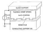
- a stamp having an electrically conducting, flexible stamping surface(FIG. 1) is brought into contact with a material (electret) that can hold electrical charges.
- the predefined surface areascan then be exposed to electrons and electric fields. This exposure generates a pattern of, for example, trapped charge that can be detected using Kelvin Probe Force Microscopy.
- Kelvin Probe Force Microscopyis known to those skilled in the art and is an imaging mode for Atomic Force Microscopy that measures both the topography and electric surface potential of a substrate surface.
- Electric fieldsmay be applied between the stamp and a substrate to affect discrete regions on the substrate in a number of ways.
- an applied electric fieldmay be used to orient dipoles in a material or to locally oxidize discrete regions on the surface.
- localized electrochemistrymay be performed and resists, such as electron sensitive resist and optical sensitive resist may be exposed.
- resistssuch as electron sensitive resist and optical sensitive resist may be exposed.
- the use of a flexible stamp to effect these changes at high densityallows for multiple impressions by using the same stamp on a series of substrates.
- a single moldmay be used to produce multiple stamps having identical morphology. Thus, with a single mold, multiple stamps may each be used to treat multiple substrates making it possible to produce vast numbers of substrates, for example, data storage devices, having identical or near identical patterns developed thereon.
- the charge storing mediumcan be fabricated by spinning poly(methylmethacrylate) (PMMA), a commercially available electret material with good charge storage capabilities, onto a boron doped silicon wafer (resistivity 10 ⁇ cm) at 5000 rpm; the thickness of the PMMA film may be about 80 nm.
- PMMApoly(methylmethacrylate)
- This techniquecan provide a surface with, for example, an area of ⁇ 1 cm 2 with multiple features from 110 nm-100 ⁇ m in size in less than 20 s. Patterns of trapped charge can serve as digital storage, and have the advantage that single bits can be erased and rewritten. By simultaneously forming or removing one, thousands, millions, or billions of charges, digital information can be written, re-written or erased from the electret.
- Procedures for writing trapped charge employing scanning probe lithographymay achieve a writing rate of 100 kbits/s at an area density of up to 7 Gbits/cm 2 ; ⁇ 140 times the area density of optical compact discs. It takes, however, about 1 day to write 7 Gbits onto an area of 1 cm 2 using this technique.
- the present inventioncan achieve the same density in ⁇ 20 s (an increase of >103 in writing speed).
- One way the writing speed is increasedis by the ability to write thousands, or millions, of bits in parallel, or simultaneously.
- Charged regions on a surfaceare those regions that exhibit an electrical charge that is distinguishable from an adjoining region of lesser charge.
- charged regionsare produced by applying either a positive or negative electric potential at the point of contact between the protrusions of an adjoining stamp surface and an electret coating on a silicon chip. Areas of lesser charge, or those that define an intervening lack of charge between charged regions, correspond to indentations on the stamping surface that transfer a lesser charge, or no charge at all, to the corresponding regions on the substrate surface.
- the voltage difference between the discrete charged regions and the adjoining regions of lower chargemay be for example, 0.1 volt, 1 volt, 10 volts or 100 volts.
- Charged regionsmay be of any dimension and can be measured by full width at half maximum (FWHM). Charged regions may be individual points, lines or other geometric shapes such as circles, ellipses or individually designed shapes.
- a pattern of charge on a substrate surfacemay be made from any pattern or combinations of patterns that can be formed on the adjoining stamp.
- the potentialmay be over the range of 1 mV to more than a kV. The range of about 100 millivolts to 20 volts has been shown to be useful to expose films having a thickness of up to 200 nm.
- a higher potentialcan be applied to achieve desired exposure. The potential applied for some films may exceed 1 kV.
- the substrate surfaceis flexible and the stamp is rigid.
- the flexible substratemay be, for example, a thin wafer of silicon with an electret coating that is flexible enough to conform to the surface of a rigid stamp.
- the stamp and/or the stamping surfacemay be of rigid material.
- a metal-coated PDMS stamp(as provided above) was placed on top of a PMMA coated chip and a voltage pulse was applied between the gold on the PDMS and the silicon of 15-25 V, while monitoring the current (typically: 10-100 mA/cm 2 ), and the total charge transferred(0.01-1 C/cm 2 , 624-62400 electrons/nm 2 ).
- the PDMS stampwas removed by hand and the charge patterns were characterized using Kelvin Probe Force Microscopy (KFM).
- KFMKelvin Probe Force Microscopy is an imaging mode for Atomic Force Microscopy that measures the distribution of both topography and electric surface potential, and is known to those of skill in the art.
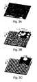
- FIGS. 2 a and 2 bshow two optical microscope images of the optical interference pattern occurring at the interface between the stamp and the substrate.
- the rigid pattern transfer elementSi/SiO2/Cr/Au
- This interferencemay have been due to non-uniform spacing between the substrate and the patterning element, which, with exceptions, is on the order of the optical wavelength.
- Significant pressurewas required at a point to get small ( ⁇ 500 ⁇ m in diameter) areas that showed no optical interference phenomena, and where the substrate and patterning element seemed to be in contact.
- the electric contact resistance of such contactsdepended, however, strongly on the applied pressure, the rigidity of both surfaces, and the amount and type of contamination at the interface.
- FIG. 2 cshows an SEM image of the interface of such contacts (obtained by placing a flexible stamp on top of a rigid silicon substrate, see inset). No spacing ( ⁇ 10 nm) can be detected between the silicon substrate and the stamp. This observation reveals that close contacts were established over large areas. For such micro/nano contacts, the local uniformity is defined predominantly by the local surface roughness of the flexible stamp and of the PMMA coating (in both cases, ⁇ 5 nm).
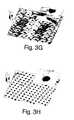
- FIG. 3shows patterns of localized charge in PMMA generated by the electric micro-contact printing of the invention. All images were recorded by KFM.
- FIG. 3 ashows the measured topography
- the resistwas locally exposed with a current density of 20 mA/cm 2 (18 V) for 10 s by applying a positive potential between the metal-coated stamp and the silicon wafer coated with PMMA.
- FIGS. 3 c and 3 dshow ring type charge patterns with ⁇ 140 nm sized features; FIGS. 3 e and 3 f show positively charged dots (900 nm diameter) and lines (10 mm wide). Furthermore, the generated charge patterns appear consistent and similar over large areas.
- a negative stamp potentialFor the patterns illustrated in FIGS. 2 g and 2 h , a ⁇ 20 V voltage pulse of 15 s duration was applied to the stamp.
- the imagewas evaluated over time to assess the time stability of the charge pattern.
- the image in FIG. 3 ewas recorded three weeks after generating the charge pattern; the similarity of the images indicates that no significant diffusion of the charges trapped in PMMA occurred over this interval.
- Charged areasas small as about 150 nm wide were generated.
- the transfer-function (FIG. 4) of the Kelvin probemay be the limiting factor as these dimensions are close to the resolution limit of the instrument. Taking this analytical resolution into account, the actual surface potential distribution may have sharper edges than imaged by the instrument.
Landscapes
- Engineering & Computer Science (AREA)
- Chemical & Material Sciences (AREA)
- Nanotechnology (AREA)
- Physics & Mathematics (AREA)
- General Physics & Mathematics (AREA)
- Crystallography & Structural Chemistry (AREA)
- Manufacturing & Machinery (AREA)
- Condensed Matter Physics & Semiconductors (AREA)
- Mathematical Physics (AREA)
- Theoretical Computer Science (AREA)
- Exposure Of Semiconductors, Excluding Electron Or Ion Beam Exposure (AREA)
- Shaping Of Tube Ends By Bending Or Straightening (AREA)
- Printing Methods (AREA)
Abstract
Description
- This application is a continuation of PCT International Application No. PCT/US01/21151 filed Jul. 2, 2001, which was published under PCT Article 21(2) in English, and claims priority via PCT/US01/21151 to U.S. Provisional Application Serial No. 60/215,682, filed on Jun. 30, 2000. Both applications are hereby incorporated by reference.[0001]
- This invention relates to a method and apparatus for electric microcontact printing. Methods and devices for forming discrete areas of electrically and/or chemically altered material on a substrate are provided.[0002]
- Microcontact printing is a technique that can provide for the patterning of a material surface with an elastomeric stamp that has a surface coated with a self-assembled monolayer (SAM) forming molecular species. The stamping surface is placed against a surface of material and is removed to leave a self-assembled monolayer on the surface of the material according to a pattern on the stamping surface. These transferred chemical species can be used for a variety of purposes including cell adhesion, etch resists, patterning for plating and for the formation of microcircuits.[0003]
- For example, techniques used to form microstamped patterns on surfaces using an elastomeric stamp are disclosed in U.S. Pat. No. 5,512,131, which is hereby incorporated by reference herein. Several techniques are described in which an elastomeric stamping surface, for example, polydimethylsiloxane, is coated with a molecular species capable of forming a SAM. The surface of the stamp may include a plurality of very small protrusions and dispersed with indentations and when this surface is brought into contact with an appropriate surface, for example, a gold coated chip, the molecular species may be transferred to the other surface in a pre-determined pattern resulting in a pattern including discrete regions of SAMs. Similar techniques are also described in U.S. Pat. Nos. 5,776,748 and 5,976,826, each of which is incorporated by reference herein.[0004]
- Microcontact printing has also been used to apply other chemical species to surfaces in precise patterns, including electroless deposition catalysts and SAMs serving as optical masks (International Patent Application WO97/34025 and U.S. Pat. No. 5,951,881).[0005]
- Electronic data storage involves the transfer of data, for example, computer programs, from one medium to another. Data storage methods are evaluated by a number of criteria, including storage density, which is a measure of the amount of data stored over a given area. The speed with which data can be transferred from one medium to another provides another method of evaluation. Common methods of data storage include electrical, magnetic and optical techniques. For example, optical storage devices such as compact discs and DVDs are capable of storing millions of bits on a single medium. Scanning probe lithography, using one or multiple probes, provides a method of sequentially patterning a surface with electrical charges at a resolution of as low as about 100 nm.[0006]
- The invention provides an apparatus and method for transferring high resolution patterns from a stamp to a surface.[0007]
- According to one aspect of the invention, a method is provided in which an electric potential is applied simultaneously to at least 5,000 discrete regions on a substrate while leaving intervening regions substantially free of applied potential.[0008]
- In another aspect, an article is provided comprising a stamping surface that includes at least one protrusion that is contiguous with at least one indentation and a stamping surface including a pattern, the pattern having at least one feature having a lateral dimension of less than 100 microns. A portion of this stamping surface is electrically conductive.[0009]
- In another embodiment an article comprising a flexible stamp is provided wherein at least a portion of the surface of the flexible stamp is electrically conductive.[0010]
- In another embodiment a method is provided that includes the steps of contacting a substrate with flexible stamp, applying an electric potential between the substrate and the stamp and forming discrete features on a coating on the substrate.[0011]
- In another embodiment, a data storage device is provided wherein the data storage device is fabricated by first contacting a substrate with a flexible stamp having a plurality of protrusions on its surface. A charge is then transferred between the stamp and the substrate and a plurality of discrete charged regions are formed on the substrate.[0012]
- In another embodiment, a method of printing a surface is provided. The method includes the steps of simultaneously forming a plurality of trapped charges on at least a portion of the surface wherein the trapped charges have a dimension of less than 1 micron.[0013]
- FIGS.[0014]1A-1C provide schematic illustrations of a process of the invention that can be used to apply a pattern of trapped charges to a rigid support;
- FIG. 2A is a photocopy of an optical micrograph that shows an optical interference pattern between a rigid stamp and a rigid surface at a load of 2 N;[0015]
- FIG. 2B is a photocopy of an optical micrograph that illustrates a lack of optical interference when a flexible stamp contacts a rigid surface;[0016]
- FIG. 2C provides a photocopy of an SEM image of a flexible stamp/rigid surface contact illustrating contact areas that are about 1 micron in diameter with spacing of less than 10 nm;[0017]
- FIGS.[0018]3A-3H provide photocopies of Kelvin probe force microscopy images showing topographical and positive and negative charge patterns of different sizes and shapes;
- FIG. 3A provides a photocopy of micrograph showing the surface topography of a surface that has been electrically microcontact printed;[0019]
- FIG. 3B provides a surface potential distribution of pattern charges for the surface of FIG. 3A and illustrates high density storage data with less than 150 nm sized bits (FWHM);[0020]
- FIG. 3C illustrates a photocopy of a Kelvin probe force microscopy image illustrating surface potential images of ring type charge patterns of 340 nm in diameter (FWHM) with approximately 130 nm sized features;[0021]
- FIG. 3D illustrates the surface potential images of ring type charges having a 622 nm diameter (FWHM) with approximately 130 nm sized features;[0022]
- FIG. 3E provides a photocopy of microscopic image of positively charged dots having a diameter of approximately 900 nm (recorded three weeks after generating charge pattern);[0023]
- FIG. 3F provides a photocopy of microscopic image showing positively charged parallel lines approximately 10 microns in width;[0024]
- FIG. 3G provides a photocopy of a microscopic image of negatively charged dots of varying size (FWHM: 122 nm, 274 nm, 330 nm);[0025]
- FIG. 3H provides a photocopy of a microscopic image showing negatively charged dots of approximately 2.45 microns in diameter (FWHM);[0026]
- FIG. 4 provides a graph showing the step response (s(x)) and transfer function (f(x)) of the Kelvin probe.[0027]
- The invention provides an apparatus and method for applying pattern charges to a substrate. Electric microcontact printing, as disclosed herein, allows for a fast replication of trapped charges at high resolution (<150 nm), over large areas (>1 cm[0028]2), and at high speed (<20 s). Such a replication technique is amenable to charge based data storage as it can allow for mass production of data patterns from a single master. Besides high density data storage, other aspects are also provided. For example, trapped charges can act as templates for self-assembly, and nucleation sites for molecules and small particles and the present invention may provide a technique for providing the large quantities of charge patterns that are traditionally difficult to obtain. Therefore, this technique is amenable to, for example, high resolution ‘Xerographic’ printing technique on a sub mm-scale. Discrete areas of charge can be formed in an electret, such as polymethyl methacrylate (PMMA), due to volume traps and dipole orientation. Activation energies for traps and dipole orientation in PMMA are about ˜2 eV. The trapped charges are located at atomic sites on the molecular chain, at defects of monomeric units, and at impurities, whereas dipole orientation occurs due to the reorientation of side groups and main chains inside the polymeric film.
- In one aspect of the invention, a method of quickly applying discrete charged regions on a substrate is provided. A stamp, preferably flexible, includes a surface that is electrically conductive. Molded onto a surface of the stamp is a pattern of indentations and/or protrusions. The protrusions may be plateau-like areas that extend outwardly from the surface of the stamp. The stamp is contacted with a substrate and a potential is applied between the substrate and the stamp. The electrical potential is applied for a time that is adequate to produce charged areas of the desired voltage on an electret coated substrate. For example, 20 seconds has been found adequate to provide charged areas of +1 volt on a silicon wafer coated with PMMA. By varying factors such as the composition of the substrate, the potential applied, and the desired amount of charge, the required amount of contact time may be less than 20 seconds, 10 seconds or 1 second. Numerous isolated regions of charge may be applied to a substrate simultaneously. For example, a single stamp may include more than 5000 isolated protrusions, and preferably includes more than 10[0029]6isolated protrusions. Most preferably, more than 109protrusions may be included on a single stamp.
- A stamp pattern is provided by a combination of at least one protrusion and at least one indentation. Preferably, multiple protrusions are provided and the protrusions may be of varying shapes and sizes. The pattern may be transferred, for example, electrically, to the substrate after bringing the stamp surface into contact with the substrate surface. “Contact” means that the protrusions are placed adjacent to the substrate surface, or are close enough to the substrate surface that an electric current can pass between the protrusion and the substrate. Preferably, the protrusions and the surface, or surface coating, are contiguous. A pattern may be a single continuous protrusion of a particular shape or may be a series of protrusions, the shapes of the surfaces of which may be, for example, round, oval, square or rectangular. The protrusions may be placed on the stamping surface in a pattern that is capable of conveying information, for example, a data or instruction set. Protrusions making up a pattern may be of similar or varied shapes and different stamps may be used on a single substrate in order to apply different patterns to the substrate surface or to result in a single composite pattern. Furthermore, stamps may be used sequentially so that one pattern may be applied over a previously applied pattern. In this way, portions of a pattern may be altered or erased after the pattern, for example, a pattern of electric charges, has been applied to the substrate surface.[0030]
- A coating may be disposed on the substrate surface to receive the stamp surface. The coating may be any material that can be disposed on the substrate surface that is capable of receiving a pattern from a stamp. For example, the coating may be an electret capable of receiving and holding an electric charge, a chemical layer capable of changing oxidation state, or any other material that is capable of receiving and retaining the transfer of a pattern or portion of a pattern from a stamp surface.[0031]
- “Discrete regions” are those regions on the substrate surface that may be individually identified as being affected by the stamp pattern. For example, a discrete region may correspond to a point of contact with a protrusion from the stamp's surface, the protrusion extending from a surrounding indentation, and the protrusion having affected the substrate surface in a region with which it has made contact, or near contact. For instance, the discrete region may be positively charged, negatively charged or oxidized while the area surrounding the discrete region is not as charged or oxidized. Preferably, the surrounding area is uncharged or unoxidized. The stamp may be flexible, that is, capable of deformation when minimal force is applied to the stamp in contact with a substrate surface. For example, it is preferred that some deformation of the stamp surface takes place when a coated silicon chip is brought into contact with the stamp. The stamp should be flexible enough to conform to the surface of an adjoining substrate despite surface deformities or impurities, on or in the adjoining substrate, that would result in optical interference, if a rigid stamp were used. For example, the stamp may be made out of a material that will deform upon receiving a force of 0.01, 0.1, 1 or 5 lb. per square inch.[0032]
- Discrete regions of small size may be electrically addressed on a substrate. For example, each region may be less than 100 microns in size, less than 1 micron in size, or less than about 150 nm in size. In one embodiment, discrete regions averaging less than 150 nm in size are provided at a density of 5 Gbits/cm[0033]2.
- In addition, multiple individual discrete regions of oxides may be produced. For example, a flexible stamp including multiple protrusions may be contacted with a substrate including a surface of oxidizable material. Current may be passed through the points of contact at a rate and time adequate to produce discrete areas of oxidized material while leaving non-contacted areas unoxidated, or less oxidated.[0034]
- A stamp having an electrically conductive surface may also be used to produce isolated regions of trapped charges or to affect discrete regions of a resist, in order to expose either the substrate in contact with stamp protrusions or the substrate that is not in contact with stamp protrusions.[0035]
- A stamp may have at least one protrusion that defines a pattern on the stamp, and at least one feature in the pattern may have a lateral dimension of less than 100 microns. Preferably the pattern includes a feature having a lateral dimension of less than 10 microns and most preferably less than 1 micron. Examples of patterns that may be used include a series of parallel lines, circles, and matrix arrays of individually discernable discrete regions.[0036]
- The material used as a stamp is preferably flexible, most preferably elastomeric such as poly(dimethylsiloxane) (PDMS). The stamps can be prepared using procedures described below. In one experiment, the PDMS stamps were ˜0.5 cm thick and supported by a glass slide. To make the surface electrically conducting, 7 nm of chromium and 80 nm of gold were thermally evaporated onto the stamp.[0037]
- A stamping surface can be created by a method involving the steps of fabricating a mold surface including at least one protrusion or indentation, contacting the mold surface with a hardenable fluid, hardening the fluid to form a stamp including a surface contacting the mold surface, and removing the stamp from the mold surface. Fabrication of the mold surface may be affected by patterning resist materials with electromagnetic radiation, by micromachining small dimensional features in a mold surface, by etching, plating, or the like.[0038]
- Material selected for use in fabrication of the stamp is advantageously selected so as not to undergo substantial shape changes when the stamp is formed. For example, when a hardenable fluid is brought into contact with a mold surface and is hardened, it is preferred that little or no shape change should take place upon such hardening.[0039]
- According to a preferred embodiment, the stamp is formed from a polymeric material. Polymeric materials suitable for use in fabrication of the stamp may have linear or branched backbones, and may be crosslinked or noncrosslinked, depending upon the particular polymer and the degree of formability desired of the stamp. A variety of elastomeric polymeric materials are suitable for such fabrication, especially polymers of the general classes of silicone polymers, epoxy polymers, and acrylate polymers. Epoxy polymers are characterized by the presence of a three-member cyclic ether group commonly referred to as an epoxy group, 1,2-epoxide, or oxirane. For example, diglycidyl ethers of bisphenol A may be used, in addition to compounds based on aromatic amine, triazine, and cycloaliphatic backbones. Another example includes the well-known Novolac polymers.[0040]
- Examples of silicone elastomers suitable for use as a stamp include those formed from precursors including the chlorosilanes such as methylchlorosilanes, ethylchlorosilanes, and phenylchlorosilanes, and the like. A particularly preferred silicone elastomer is polydimethylsiloxane. Exemplary polydimethylsiloxane polymers include those sold under the trademark SYLGARD™ by the Dow Chemical Company, Midland Mich., and particularly SYLGARD™ 182, SYLGARD™ 184, and SYLGARD™ 186.[0041]
- A stamp includes a stamping surface having a variety of features defined therein by indentations or protrusions. According to the invention, the stamping surface may include features having a variety of lateral dimensions. According to some embodiments of the invention, however, it is preferred to fabricate the stamping surface so as to have at least one feature with a lateral dimension of less than about 100 microns. According to other embodiments, the stamping surface may include at least one feature with a lateral dimension of less than about 50 microns, less than about 10 microns, less than about 5 microns, or less than about 1 micron. According to a particularly preferred embodiment, the stamping surface includes at least one feature with a lateral dimension of less than 0.25 microns.[0042]
- The features included in the stamping surface are advantageously created in a way that the aspect ratio of any individual feature is greater than 0.2, preferably from about 0.5 to about 2.0. The aspect ratio is defined as the ratio of minimum lateral dimension of any stamping surface feature to indentation depth. In addition to the aspect ratio, the width of any indentation should not be large enough such that “bowing” of the stamping surface occurs and any portion of the indentation of the stamping surface contacts the material surface to be patterned. Such bowing is generally avoided if the ratio of indentation width (dimension c) to indentation depth (dimension x) is less than about 10.[0043]
- In addition to the above-described methods for forming a stamp, a photolytic method is included in the present invention. For example, a mask may be positioned between a surface of a stamp and a source of irradiation, and the surface irradiated through the mask for a predetermined period of time. Portions of surface may be degraded by such irradiation, forming indentations in the surface upon removal of such degraded portions, and defining the stamping surface. According to this method, a variety of patterns may be very conveniently formed in a stamp according to a variety of available masks. In addition, the photolytic method may be used in combination with the above-described methods involving hardening a hardenable fluid on a mold surface. For example, a hardenable fluid may be brought into contact with a mold surface and allowed to harden to form a stamp having a first predetermined stamping surface, and the first predetermined stamping surface can be irradiated through a mask to create additional features in the stamping surface. According to this method, photoresist may be used as the stamp material itself. Particular types of polymers which may be patterned using the above-described photolytic method, preferred wavelengths for photopatterning, and lengths of time of photolysis are known in the art. In its broadest sense, the mold surface may comprise any surface having morphological features that may desirably serve as a template for the formation of a stamp, hence the patterning of protrusions or indentations on a surface. For example, a microelectronic device such as a chip may serve as a template, as may any other corrugated or indented surface.[0044]
- A mold surface may be formed according to a variety of ways. According to one, the mold surface is micromachined from a material such as metal. According to another, the mold surface is formed lithographically by providing a substrate, depositing a film of material onto the substrate, coating an exposed surface of the material with resist, irradiating the resist according to a predetermined pattern, removing irradiated portions of the resist from the material surface, contacting the material surface with a reactant selected to react chemically therewith and selected to be chemically inert with respect to the resist such that portions of the material according to the predetermined pattern are degraded, removing the degraded portions, and removing the resist to uncover portions of the material formed according to the predetermined pattern to form the mold surface. Negative or positive resist may be used, and the procedure adjusted accordingly. According to another method of forming a mold surface, a substrate may be provided, and coated with resist. Then portions of the resist may be irradiated according to a particular predetermined pattern. Irradiated portions of the resist may then be removed from the substrate to expose portions of the substrate surface according to the predetermined pattern, and the substrate may be contacted with a plating reagent such that exposed portions according to the predetermined pattern are plated. Then, the resist may be removed to uncover portions of the exposed substrate according to the predetermined pattern bordered by plated portions of the substrate to form the mold surface.[0045]
- A mold according to one embodiment of the present invention may be fabricated as follows. A template consisting of an exposed and developed photoresist pattern on silicon is prepared (This type of fabrication is described in any conventional photolithography text, such as[0046]Introduction to Microelectronic Fabrication, by Richard C. Jaeger, Gerold W. Neudeck and Robert F. Pierret, eds., Addison-Wesley, 1989). Templates such as electron microscopy grids or other corrugated materials may also be used. The template is placed in a container such as a petri dish. A 10:1 (w:w or v:v) mixture of PDMS-Sylgard Silicone Elastomer 184 and Sylgard Curing Agent 184 (Dow Corning Corp., Midland, Mich.) is poured into the petri dish. It is not necessary to put the mixture of PDMS-elastomer and curing agent under vacuum to remove dissolved dioxygen. The PDMS is cured at room temperature in the laboratory ambient for 30 to 60 min. This cure is followed by additional curing at 65° C. for approximately one hour or until the polymer is rigid. After cooling to room temperature, the PDMS-stamp is carefully peeled from the template.
- In another embodiment, a flexible stamp is provided where at least a portion of a surface of the stamp is electrically conductive. The stamp or stamp surface may be coated with an electrically conductive coating or, alternatively, the material of which the stamp, or a portion of the stamp, is made, may also be conductive. For example, a surface of the stamp may be coated with a layer of gold to provide electrical conductance. The gold may be applied to the surface in a variety of ways, such as by vacuum deposition or thermal evaporation. In one embodiment, a layer of chromium, for example of about 7 nm thickness, is first applied to the surface and then followed by a gold coating of about 80 nm thickness. Of course, conductive coatings are not limited to metals, but may also include other conductive materials, such as conductive polymers.[0047]
- Alternatively, the stamp material itself may be conductive. For example, an elastomeric compound containing conductive materials dispersed therein, such as carbon particles, may be used.[0048]
- Preferably, the stamp material can be supplied as a liquid to a mold and can then be hardened into a polymeric material that can be separated from the mold while retaining a mold impression that may include individual protrusions or patterns having a dimension of one micron, 500 nm or as small as 100 nm. The surface of the stamp can be electrically conductive, meaning that it is capable of transferring electrons to a substrate surface with which it comes into contact. The entire stamp can be made of conductive material, or a portion of the stamp may be nonconductive and a conductive coating can be applied to the surface. For example, a metallic material may be applied to the surface of the stamp by vacuum deposition or thermoevaporation. Preferably, a conductive layer is applied at a thickness that provides adequate conductivity to conduct charge but is thin enough to not alter the pattern that may be molded into the stamp surface. Preferably, the conductive layer does not adversely affect the flexibility of the stamp surface.[0049]
- The stamp may be placed on top of the substrate or the substrate may be placed on top of the stamp. Adequate contact may be achieved with a flexible stamp with no additional force other than the weight of the stamp. If the substrate, for instance, a silicon chip, which may be extremely light weight, is applied to the top of the stamp, it may be preferred that slight additional pressure be applied in order to obtain a preferred level of contact with the stamping surface.[0050]
- In another aspect, a data storage device is provided. In one embodiment, a substrate capable of holding discretely charged regions is contacted with a flexible stamp having a plurality of protrusions. The substrate may be any material capable of holding a charge and in one embodiment is a silicon wafer coated with polymethylmethacrylate. The flexible stamp has numerous protrusions, each of which may correspond to a bit. The flexible stamp may be contacted with a substrate and a potential may be applied. After an adequate amount of time, those regions in contact with the protrusions on the flexible stamp will develop a charge. Preferably, the charged areas on the substrate are stable and the discrete areas of charge may be detectable after extended storage. For example, a stamp made of polydimethylsiloxane (PDMS) and coated with gold may be contacted with a silicon wafer. A voltage from about 15 to 25 volts may be preferred with the current being preferred in a range between about 10 and 100 mA/cm[0051]2. The stamp may then be lifted from the substrate and individual trapped charges of approximately 1 volt may be detected on the silicon surface. In this manner, high density data storage of more than about 5 Gbits/cm3may be obtained. The discrete regions may be either positively or negatively charged.
- A stamp having an electrically conducting, flexible stamping surface (FIG. 1) is brought into contact with a material (electret) that can hold electrical charges. The predefined surface areas can then be exposed to electrons and electric fields. This exposure generates a pattern of, for example, trapped charge that can be detected using Kelvin Probe Force Microscopy. Kelvin Probe Force Microscopy is known to those skilled in the art and is an imaging mode for Atomic Force Microscopy that measures both the topography and electric surface potential of a substrate surface.[0052]
- Electric fields may be applied between the stamp and a substrate to affect discrete regions on the substrate in a number of ways. For example, an applied electric field may be used to orient dipoles in a material or to locally oxidize discrete regions on the surface. In addition, localized electrochemistry may be performed and resists, such as electron sensitive resist and optical sensitive resist may be exposed. The use of a flexible stamp to effect these changes at high density allows for multiple impressions by using the same stamp on a series of substrates. In addition, a single mold may be used to produce multiple stamps having identical morphology. Thus, with a single mold, multiple stamps may each be used to treat multiple substrates making it possible to produce vast numbers of substrates, for example, data storage devices, having identical or near identical patterns developed thereon.[0053]
- The charge storing medium can be fabricated by spinning poly(methylmethacrylate) (PMMA), a commercially available electret material with good charge storage capabilities, onto a boron doped silicon wafer ([0054]
resistivity 10 Ωcm) at 5000 rpm; the thickness of the PMMA film may be about 80 nm. - This technique can provide a surface with, for example, an area of ˜1 cm[0055]2with multiple features from 110 nm-100 μm in size in less than 20 s. Patterns of trapped charge can serve as digital storage, and have the advantage that single bits can be erased and rewritten. By simultaneously forming or removing one, thousands, millions, or billions of charges, digital information can be written, re-written or erased from the electret.
- Procedures for writing trapped charge employing scanning probe lithography may achieve a writing rate of 100 kbits/s at an area density of up to 7 Gbits/cm[0056]2;˜140 times the area density of optical compact discs. It takes, however, about 1 day to write 7 Gbits onto an area of 1 cm2using this technique. The present invention, can achieve the same density in <20 s (an increase of >103 in writing speed). One way the writing speed is increased is by the ability to write thousands, or millions, of bits in parallel, or simultaneously.
- Charged regions on a surface are those regions that exhibit an electrical charge that is distinguishable from an adjoining region of lesser charge. In one embodiment, charged regions are produced by applying either a positive or negative electric potential at the point of contact between the protrusions of an adjoining stamp surface and an electret coating on a silicon chip. Areas of lesser charge, or those that define an intervening lack of charge between charged regions, correspond to indentations on the stamping surface that transfer a lesser charge, or no charge at all, to the corresponding regions on the substrate surface. The voltage difference between the discrete charged regions and the adjoining regions of lower charge may be for example, 0.1 volt, 1 volt, 10 volts or 100 volts. Charged regions may be of any dimension and can be measured by full width at half maximum (FWHM). Charged regions may be individual points, lines or other geometric shapes such as circles, ellipses or individually designed shapes.[0057]
- A pattern of charge on a substrate surface may be made from any pattern or combinations of patterns that can be formed on the adjoining stamp. Depending on the materials used, the potential may be over the range of 1 mV to more than a kV. The range of about 100 millivolts to 20 volts has been shown to be useful to expose films having a thickness of up to 200 nm. Preferably, if thicker films are used, for example films of 1 micron, 10 microns, 100 microns or 1 millimeter in thickness, a higher potential can be applied to achieve desired exposure. The potential applied for some films may exceed 1 kV.[0058]
- In an alternative embodiment, the substrate surface is flexible and the stamp is rigid. The flexible substrate may be, for example, a thin wafer of silicon with an electret coating that is flexible enough to conform to the surface of a rigid stamp. In this case, the stamp and/or the stamping surface may be of rigid material.[0059]
- To generate a pattern of trapped charge, a metal-coated PDMS stamp (as provided above) was placed on top of a PMMA coated chip and a voltage pulse was applied between the gold on the PDMS and the silicon of 15-25 V, while monitoring the current (typically: 10-100 mA/cm[0060]2), and the total charge transferred(0.01-1 C/cm2, 624-62400 electrons/nm2). After the PMMA had been exposed, the PDMS stamp was removed by hand and the charge patterns were characterized using Kelvin Probe Force Microscopy (KFM). KFM is an imaging mode for Atomic Force Microscopy that measures the distribution of both topography and electric surface potential, and is known to those of skill in the art.
- Two different systems were evaluated to determine the level of contact attainable between the stamp and the PMMA surface. The systems were: (i) a rigid electrode (a silicon wafer supporting a pattern in metal, 7 nm of Cr, and 80 nm of Au, thermally evaporated), and (ii) a flexible, metal-coated stamp of PDMS. FIGS. 2[0061]aand2bshow two optical microscope images of the optical interference pattern occurring at the interface between the stamp and the substrate. With the rigid pattern transfer element (Si/SiO2/Cr/Au), there was always optical interference at the interface as shown in FIG. 2a. This interference may have been due to non-uniform spacing between the substrate and the patterning element, which, with exceptions, is on the order of the optical wavelength. Significant pressure was required at a point to get small (<500 μm in diameter) areas that showed no optical interference phenomena, and where the substrate and patterning element seemed to be in contact. The electric contact resistance of such contacts depended, however, strongly on the applied pressure, the rigidity of both surfaces, and the amount and type of contamination at the interface.
- On the contrary, the flexible stamp ([0062]2b) gave large contact regime without applied pressure and without optical interference patterns.
- FIG. 2[0063]cshows an SEM image of the interface of such contacts (obtained by placing a flexible stamp on top of a rigid silicon substrate, see inset). No spacing (<10 nm) can be detected between the silicon substrate and the stamp. This observation reveals that close contacts were established over large areas. For such micro/nano contacts, the local uniformity is defined predominantly by the local surface roughness of the flexible stamp and of the PMMA coating (in both cases, <5 nm).
- FIG. 3 shows patterns of localized charge in PMMA generated by the electric micro-contact printing of the invention. All images were recorded by KFM. FIG. 3[0064]ashows the measured topography and FIG. 3bshows the measured surface potential distribution of a surface patterned in a way that simulates the pattern required for high density data storage (<150 nm sized bits; full width at half maximum, FWHM; density=5 Gbits/cm2). To write this charge pattern, the resist was locally exposed with a current density of 20 mA/cm2(18 V) for 10 s by applying a positive potential between the metal-coated stamp and the silicon wafer coated with PMMA. The trapped charges changed the local surface potential (3b) by about ˜1 V whereas the PMMA topography (3a) does not seem to be affected. By using another pattern on the stamp, other types of charge patterns can be generated. For example, FIGS. 3cand3dshow ring type charge patterns with ˜140 nm sized features; FIGS. 3eand3fshow positively charged dots (900 nm diameter) and lines (10 mm wide). Furthermore, the generated charge patterns appear consistent and similar over large areas. To pattern negative charges in the PMMA the surface was exposed with a negative stamp potential. For the patterns illustrated in FIGS. 2gand2h, a −20 V voltage pulse of 15 s duration was applied to the stamp.
- The image was evaluated over time to assess the time stability of the charge pattern. The image in FIG. 3[0065]ewas recorded three weeks after generating the charge pattern; the similarity of the images indicates that no significant diffusion of the charges trapped in PMMA occurred over this interval. Charged areas as small as about 150 nm wide were generated. At such a small scale, the transfer-function (FIG. 4) of the Kelvin probe may be the limiting factor as these dimensions are close to the resolution limit of the instrument. Taking this analytical resolution into account, the actual surface potential distribution may have sharper edges than imaged by the instrument.
- Further modifications and equivalents of the invention herein disclosed will occur to persons skilled in the art using no more than routine experimentation, and all such modifications and equivalents are believed to be within the spirit and scope of the invention as defined by the following claims.[0066]
Claims (53)
Priority Applications (1)
| Application Number | Priority Date | Filing Date | Title |
|---|---|---|---|
| US10/316,997US7771647B2 (en) | 2000-06-30 | 2002-12-11 | Electric microcontact printing method and apparatus |
Applications Claiming Priority (3)
| Application Number | Priority Date | Filing Date | Title |
|---|---|---|---|
| US21568200P | 2000-06-30 | 2000-06-30 | |
| PCT/US2001/021151WO2002003142A2 (en) | 2000-06-30 | 2001-07-02 | Electric microcontact printing method and apparatus |
| US10/316,997US7771647B2 (en) | 2000-06-30 | 2002-12-11 | Electric microcontact printing method and apparatus |
Related Parent Applications (1)
| Application Number | Title | Priority Date | Filing Date |
|---|---|---|---|
| PCT/US2001/021151ContinuationWO2002003142A2 (en) | 2000-06-30 | 2001-07-02 | Electric microcontact printing method and apparatus |
Publications (2)
| Publication Number | Publication Date |
|---|---|
| US20030178316A1true US20030178316A1 (en) | 2003-09-25 |
| US7771647B2 US7771647B2 (en) | 2010-08-10 |
Family
ID=22803931
Family Applications (1)
| Application Number | Title | Priority Date | Filing Date |
|---|---|---|---|
| US10/316,997Expired - Fee RelatedUS7771647B2 (en) | 2000-06-30 | 2002-12-11 | Electric microcontact printing method and apparatus |
Country Status (4)
| Country | Link |
|---|---|
| US (1) | US7771647B2 (en) |
| EP (1) | EP1297387A2 (en) |
| AU (1) | AU2001271799A1 (en) |
| WO (1) | WO2002003142A2 (en) |
Cited By (55)
| Publication number | Priority date | Publication date | Assignee | Title |
|---|---|---|---|---|
| US20030102444A1 (en)* | 2000-05-04 | 2003-06-05 | Deppert Knut Wilfried | Nanostructures |
| US20040003734A1 (en)* | 2002-07-02 | 2004-01-08 | Shively J. Thomas | Method and apparatus for printing using an electrically conductive ink |
| US6808646B1 (en)* | 2003-04-29 | 2004-10-26 | Hewlett-Packard Development Company, L.P. | Method of replicating a high resolution three-dimensional imprint pattern on a compliant media of arbitrary size |
| WO2005040037A1 (en)* | 2003-10-20 | 2005-05-06 | Consejo Superior De Investigaciones Cientificas | Large area fabrication method based on the local oxidation of silicon and/or different materials on micro- and nano-scale |
| US20050098537A1 (en)* | 2003-11-06 | 2005-05-12 | Palo Alto Research Center, Inc. | Method for large-area patterning dissolved polymers by making use of an active stamp |
| US20050123687A1 (en)* | 2003-11-04 | 2005-06-09 | Jacobs Heiko O. | Method and apparatus for depositing charge and/or nanoparticles |
| WO2005061237A1 (en)* | 2003-12-24 | 2005-07-07 | Axela Biosensors Inc. | Method and apparatus for micro-contact printing |
| US20050236738A1 (en)* | 2002-09-12 | 2005-10-27 | Harper Bruce M | Disk alignment apparatus and method for patterned media production |
| US20050238967A1 (en)* | 2004-04-27 | 2005-10-27 | The Board Of Trustees Of The University Of Illinois | Composite patterning devices for soft lithography |
| US20060286785A1 (en)* | 2004-06-04 | 2006-12-21 | The Board Of Trustees Of The University Of Illinois | A Stretchable Form of Single Crystal Silicon for High Performance Electronics on Rubber Substrates |
| US20080055581A1 (en)* | 2004-04-27 | 2008-03-06 | Rogers John A | Devices and methods for pattern generation by ink lithography |
| WO2008012734A3 (en)* | 2006-07-28 | 2008-04-03 | Ibm | Device and method for patterning a surface of a polymer layer |
| US20080157235A1 (en)* | 2004-06-04 | 2008-07-03 | Rogers John A | Controlled buckling structures in semiconductor interconnects and nanomembranes for stretchable electronics |
| US20080160780A1 (en)* | 2003-11-04 | 2008-07-03 | Jacobs Heiko O | Method and apparatus for depositing charge and/or nanoparticles |
| US20080220175A1 (en)* | 2007-01-22 | 2008-09-11 | Lorenzo Mangolini | Nanoparticles wtih grafted organic molecules |
| EP1972996A1 (en) | 2007-03-21 | 2008-09-24 | Erich Dipl.-Ing. Thallner | Method and device for generating a nanostructured disc |
| US7557367B2 (en) | 2004-06-04 | 2009-07-07 | The Board Of Trustees Of The University Of Illinois | Stretchable semiconductor elements and stretchable electrical circuits |
| US20090199960A1 (en)* | 2004-06-04 | 2009-08-13 | Nuzzo Ralph G | Pattern Transfer Printing by Kinetic Control of Adhesion to an Elastomeric Stamp |
| US20090214838A1 (en)* | 2008-02-25 | 2009-08-27 | Sony Corporation | Method of applying a pattern of metal, metal oxide and/or semiconductor material on a substrate |
| US20100052112A1 (en)* | 2008-04-03 | 2010-03-04 | Rogers John A | Printable, Flexible and Stretchable Diamond for Thermal Management |
| US7799699B2 (en) | 2004-06-04 | 2010-09-21 | The Board Of Trustees Of The University Of Illinois | Printable semiconductor structures and related methods of making and assembling |
| US20100294741A1 (en)* | 2009-05-19 | 2010-11-25 | Korea University Research And Business Foundation | Nano structure fabrication |
| US20110147715A1 (en)* | 2008-06-16 | 2011-06-23 | Purdue Research Foundation | Medium Scale Carbon Nanotube Thin Film Integrated Circuits on Flexible Plastic Substrates |
| US7972875B2 (en) | 2007-01-17 | 2011-07-05 | The Board Of Trustees Of The University Of Illinois | Optical systems fabricated by printing-based assembly |
| WO2011138540A1 (en)* | 2010-05-07 | 2011-11-10 | Institut National Des Sciences Appliquees De Toulouse | Method of topographical and electrical nanostructuration of a thin film of electret polymer and thin film of electret polymer obtained |
| US8097926B2 (en) | 2008-10-07 | 2012-01-17 | Mc10, Inc. | Systems, methods, and devices having stretchable integrated circuitry for sensing and delivering therapy |
| WO2012135768A1 (en)* | 2011-03-30 | 2012-10-04 | Rolandi Marco | Inorganic nanostructure reactive direct-write and growth |
| US8367035B2 (en) | 2006-03-03 | 2013-02-05 | The Board Of Trustees Of The University Of Illinois | Methods of making spatially aligned nanotubes and nanotube arrays |
| US8372726B2 (en) | 2008-10-07 | 2013-02-12 | Mc10, Inc. | Methods and applications of non-planar imaging arrays |
| US8389862B2 (en) | 2008-10-07 | 2013-03-05 | Mc10, Inc. | Extremely stretchable electronics |
| US8552299B2 (en) | 2008-03-05 | 2013-10-08 | The Board Of Trustees Of The University Of Illinois | Stretchable and foldable electronic devices |
| US8666471B2 (en) | 2010-03-17 | 2014-03-04 | The Board Of Trustees Of The University Of Illinois | Implantable biomedical devices on bioresorbable substrates |
| JP2014082491A (en)* | 2012-10-15 | 2014-05-08 | Palo Alto Research Center Inc | Microchip charge patterning |
| KR101413233B1 (en) | 2007-09-14 | 2014-06-30 | 삼성전자 주식회사 | Nano-imprint lithography process |
| US8865489B2 (en) | 2009-05-12 | 2014-10-21 | The Board Of Trustees Of The University Of Illinois | Printed assemblies of ultrathin, microscale inorganic light emitting diodes for deformable and semitransparent displays |
| US8886334B2 (en) | 2008-10-07 | 2014-11-11 | Mc10, Inc. | Systems, methods, and devices using stretchable or flexible electronics for medical applications |
| WO2014202145A1 (en)* | 2013-06-20 | 2014-12-24 | Ev Group E. Thallner Gmbh | Mould with a mould pattern, and device and method for producing same |
| US8934965B2 (en) | 2011-06-03 | 2015-01-13 | The Board Of Trustees Of The University Of Illinois | Conformable actively multiplexed high-density surface electrode array for brain interfacing |
| US9159635B2 (en) | 2011-05-27 | 2015-10-13 | Mc10, Inc. | Flexible electronic structure |
| US9171794B2 (en) | 2012-10-09 | 2015-10-27 | Mc10, Inc. | Embedding thin chips in polymer |
| US20150370161A1 (en)* | 2013-09-26 | 2015-12-24 | Shanghai Integrated Circuit Research And Development Development Center Co., Ltd. | Device and method for nano-imprint lithography |
| US9289132B2 (en) | 2008-10-07 | 2016-03-22 | Mc10, Inc. | Catheter balloon having stretchable integrated circuitry and sensor array |
| US9442285B2 (en) | 2011-01-14 | 2016-09-13 | The Board Of Trustees Of The University Of Illinois | Optical component array having adjustable curvature |
| US9554484B2 (en) | 2012-03-30 | 2017-01-24 | The Board Of Trustees Of The University Of Illinois | Appendage mountable electronic devices conformable to surfaces |
| US9691873B2 (en) | 2011-12-01 | 2017-06-27 | The Board Of Trustees Of The University Of Illinois | Transient devices designed to undergo programmable transformations |
| US9723122B2 (en) | 2009-10-01 | 2017-08-01 | Mc10, Inc. | Protective cases with integrated electronics |
| US9765934B2 (en) | 2011-05-16 | 2017-09-19 | The Board Of Trustees Of The University Of Illinois | Thermally managed LED arrays assembled by printing |
| US9936574B2 (en) | 2009-12-16 | 2018-04-03 | The Board Of Trustees Of The University Of Illinois | Waterproof stretchable optoelectronics |
| CN109188862A (en)* | 2018-10-11 | 2019-01-11 | 京东方科技集团股份有限公司 | Stamping structure and its manufacturing method, impression block |
| CN110182757A (en)* | 2019-05-31 | 2019-08-30 | 南京大学 | A kind of manufacturing method of nanostructure |
| US10441185B2 (en) | 2009-12-16 | 2019-10-15 | The Board Of Trustees Of The University Of Illinois | Flexible and stretchable electronic systems for epidermal electronics |
| US10918298B2 (en) | 2009-12-16 | 2021-02-16 | The Board Of Trustees Of The University Of Illinois | High-speed, high-resolution electrophysiology in-vivo using conformal electronics |
| US10925543B2 (en) | 2015-11-11 | 2021-02-23 | The Board Of Trustees Of The University Of Illinois | Bioresorbable silicon electronics for transient implants |
| US11029198B2 (en) | 2015-06-01 | 2021-06-08 | The Board Of Trustees Of The University Of Illinois | Alternative approach for UV sensing |
| US11118965B2 (en) | 2015-06-01 | 2021-09-14 | The Board Of Trustees Of The University Of Illinois | Miniaturized electronic systems with wireless power and near-field communication capabilities |
Families Citing this family (9)
| Publication number | Priority date | Publication date | Assignee | Title |
|---|---|---|---|---|
| AU2003291443A1 (en)* | 2002-11-12 | 2004-06-03 | Princeton University | Compositions and processes for nanoimprinting |
| KR101265321B1 (en) | 2005-11-14 | 2013-05-20 | 엘지디스플레이 주식회사 | fabrication method of stamp, fabrication method of thin film transistor and liquid crystal display device by using it |
| DE102005054495A1 (en) | 2005-11-16 | 2007-05-24 | Mivitec Gmbh | Distributed sensor and reference spots for chemo- and biosensors |
| WO2008060592A2 (en) | 2006-11-15 | 2008-05-22 | Board Of Trustees Of Michigan State University | Micropatterning of conductive graphite particles using microcontact printing |
| WO2009129430A2 (en)* | 2008-04-18 | 2009-10-22 | University Of Massachusetts Lowell | Methods for forming metal-polymer hybrid tooling for forming parts having micro features |
| AU2009286690A1 (en) | 2008-08-27 | 2010-03-04 | Amo Gmbh | Improved nanoimprint method |
| JP2013518740A (en)* | 2010-02-05 | 2013-05-23 | オブダカット・アーベー | Methods and processes for metal stamp replication for large area nanopatterns |
| US8475869B2 (en) | 2010-04-02 | 2013-07-02 | Rhodia Operations | Selective nanoparticle assembly systems and methods |
| EP2560191A4 (en)* | 2011-06-22 | 2013-09-25 | Panasonic Corp | SEMICONDUCTOR SUBSTRATE WITH POINT MARKINGS AND METHOD FOR THE PRODUCTION THEREOF |
Citations (17)
| Publication number | Priority date | Publication date | Assignee | Title |
|---|---|---|---|---|
| US3144650A (en)* | 1962-06-28 | 1964-08-11 | Boris Haskell | Electrical process |
| US3276031A (en)* | 1963-01-14 | 1966-09-27 | Gen Electric | Thermoplastic information recording utilizing electrets |
| US3790645A (en)* | 1970-08-20 | 1974-02-05 | Kureha Chemical Ind Co Ltd | Method for producing polyvinylidene fluoride polymethylmethacrylate compositions |
| US3794986A (en)* | 1971-04-08 | 1974-02-26 | Kureha Chemical Ind Co Ltd | Pyroelectric element of polymer film |
| US4149095A (en)* | 1975-04-11 | 1979-04-10 | Thomson-Csf | Monolithic structure for storing electrical charges |
| US4308223A (en)* | 1980-03-24 | 1981-12-29 | Albany International Corp. | Method for producing electret fibers for enhancement of submicron aerosol filtration |
| US4327306A (en)* | 1979-11-27 | 1982-04-27 | The United States Of America As Represented By The Secretary Of The Air Force | Face plate for cathode ray tube |
| US4503329A (en)* | 1981-09-30 | 1985-03-05 | Hitachi, Ltd. | Ion beam processing apparatus and method of correcting mask defects |
| US4522671A (en)* | 1981-11-17 | 1985-06-11 | Robert Bosch Gmbh | Method of applying an electrical conductor pattern on an apertured substrate |
| US4566086A (en)* | 1983-06-13 | 1986-01-21 | Ncr Corporation | Information storage system utilizing electrets |
| US4656772A (en)* | 1986-10-10 | 1987-04-14 | Manuel Lopez | Fishing device |
| US4672578A (en)* | 1980-09-19 | 1987-06-09 | Hitachi, Ltd. | Method of information recording on a semiconductor wafer |
| US4735143A (en)* | 1986-09-19 | 1988-04-05 | Phoenix Endeavour, Inc. | Adjustable stamping device |
| US5009708A (en)* | 1981-11-17 | 1991-04-23 | Robert Bosch Gmbh | Printing paste and method of applying said paste |
| US5363021A (en)* | 1993-07-12 | 1994-11-08 | Cornell Research Foundation, Inc. | Massively parallel array cathode |
| US5666190A (en)* | 1994-04-12 | 1997-09-09 | The Board Of Trustees Of The Leland Stanford, Jr. University | Method of performing lithography using cantilever array |
| US6210551B1 (en)* | 1995-08-01 | 2001-04-03 | Australian Membrane And Biotechnology Research Institute | Composite membrane sensor |
Family Cites Families (5)
| Publication number | Priority date | Publication date | Assignee | Title |
|---|---|---|---|---|
| EP0107913B1 (en)* | 1982-09-29 | 1988-06-22 | Kabushiki Kaisha Toshiba | Radiation-sensitive carrier body utilized as stamper structure |
| US5066512A (en)* | 1989-12-08 | 1991-11-19 | International Business Machines Corporation | Electrostatic deposition of lcd color filters |
| US5047649A (en)* | 1990-10-09 | 1991-09-10 | International Business Machines Corporation | Method and apparatus for writing or etching narrow linewidth patterns on insulating materials |
| US6048623A (en)* | 1996-12-18 | 2000-04-11 | Kimberly-Clark Worldwide, Inc. | Method of contact printing on gold coated films |
| AU784574B2 (en)* | 2000-05-04 | 2006-05-04 | Qunano Ab | Nanostructures |
- 2001
- 2001-07-02WOPCT/US2001/021151patent/WO2002003142A2/enactiveApplication Filing
- 2001-07-02EPEP01950841Apatent/EP1297387A2/ennot_activeWithdrawn
- 2001-07-02AUAU2001271799Apatent/AU2001271799A1/ennot_activeAbandoned
- 2002
- 2002-12-11USUS10/316,997patent/US7771647B2/ennot_activeExpired - Fee Related
Patent Citations (17)
| Publication number | Priority date | Publication date | Assignee | Title |
|---|---|---|---|---|
| US3144650A (en)* | 1962-06-28 | 1964-08-11 | Boris Haskell | Electrical process |
| US3276031A (en)* | 1963-01-14 | 1966-09-27 | Gen Electric | Thermoplastic information recording utilizing electrets |
| US3790645A (en)* | 1970-08-20 | 1974-02-05 | Kureha Chemical Ind Co Ltd | Method for producing polyvinylidene fluoride polymethylmethacrylate compositions |
| US3794986A (en)* | 1971-04-08 | 1974-02-26 | Kureha Chemical Ind Co Ltd | Pyroelectric element of polymer film |
| US4149095A (en)* | 1975-04-11 | 1979-04-10 | Thomson-Csf | Monolithic structure for storing electrical charges |
| US4327306A (en)* | 1979-11-27 | 1982-04-27 | The United States Of America As Represented By The Secretary Of The Air Force | Face plate for cathode ray tube |
| US4308223A (en)* | 1980-03-24 | 1981-12-29 | Albany International Corp. | Method for producing electret fibers for enhancement of submicron aerosol filtration |
| US4672578A (en)* | 1980-09-19 | 1987-06-09 | Hitachi, Ltd. | Method of information recording on a semiconductor wafer |
| US4503329A (en)* | 1981-09-30 | 1985-03-05 | Hitachi, Ltd. | Ion beam processing apparatus and method of correcting mask defects |
| US4522671A (en)* | 1981-11-17 | 1985-06-11 | Robert Bosch Gmbh | Method of applying an electrical conductor pattern on an apertured substrate |
| US5009708A (en)* | 1981-11-17 | 1991-04-23 | Robert Bosch Gmbh | Printing paste and method of applying said paste |
| US4566086A (en)* | 1983-06-13 | 1986-01-21 | Ncr Corporation | Information storage system utilizing electrets |
| US4735143A (en)* | 1986-09-19 | 1988-04-05 | Phoenix Endeavour, Inc. | Adjustable stamping device |
| US4656772A (en)* | 1986-10-10 | 1987-04-14 | Manuel Lopez | Fishing device |
| US5363021A (en)* | 1993-07-12 | 1994-11-08 | Cornell Research Foundation, Inc. | Massively parallel array cathode |
| US5666190A (en)* | 1994-04-12 | 1997-09-09 | The Board Of Trustees Of The Leland Stanford, Jr. University | Method of performing lithography using cantilever array |
| US6210551B1 (en)* | 1995-08-01 | 2001-04-03 | Australian Membrane And Biotechnology Research Institute | Composite membrane sensor |
Cited By (131)
| Publication number | Priority date | Publication date | Assignee | Title |
|---|---|---|---|---|
| US20030102444A1 (en)* | 2000-05-04 | 2003-06-05 | Deppert Knut Wilfried | Nanostructures |
| US7223444B2 (en) | 2000-05-04 | 2007-05-29 | Qunano Ab | Particle deposition apparatus and methods for forming nanostructures |
| US20040003734A1 (en)* | 2002-07-02 | 2004-01-08 | Shively J. Thomas | Method and apparatus for printing using an electrically conductive ink |
| US20050236738A1 (en)* | 2002-09-12 | 2005-10-27 | Harper Bruce M | Disk alignment apparatus and method for patterned media production |
| US7682546B2 (en) | 2002-09-12 | 2010-03-23 | Wd Media, Inc. | Disk alignment apparatus and method for patterned media production |
| US6808646B1 (en)* | 2003-04-29 | 2004-10-26 | Hewlett-Packard Development Company, L.P. | Method of replicating a high resolution three-dimensional imprint pattern on a compliant media of arbitrary size |
| US20040217085A1 (en)* | 2003-04-29 | 2004-11-04 | Jeans Albert H | Method of replicating a high resolution three-dimensional imprint pattern on a compliant media of arbitrary size |
| WO2005040037A1 (en)* | 2003-10-20 | 2005-05-06 | Consejo Superior De Investigaciones Cientificas | Large area fabrication method based on the local oxidation of silicon and/or different materials on micro- and nano-scale |
| US20050123687A1 (en)* | 2003-11-04 | 2005-06-09 | Jacobs Heiko O. | Method and apparatus for depositing charge and/or nanoparticles |
| US7592269B2 (en) | 2003-11-04 | 2009-09-22 | Regents Of The University Of Minnesota | Method and apparatus for depositing charge and/or nanoparticles |
| US20080160780A1 (en)* | 2003-11-04 | 2008-07-03 | Jacobs Heiko O | Method and apparatus for depositing charge and/or nanoparticles |
| US7232771B2 (en) | 2003-11-04 | 2007-06-19 | Regents Of The University Of Minnesota | Method and apparatus for depositing charge and/or nanoparticles |
| US20050098537A1 (en)* | 2003-11-06 | 2005-05-12 | Palo Alto Research Center, Inc. | Method for large-area patterning dissolved polymers by making use of an active stamp |
| US7114448B2 (en)* | 2003-11-06 | 2006-10-03 | Palo Alto Research Center, Incorporated | Method for large-area patterning dissolved polymers by making use of an active stamp |
| US6981445B2 (en) | 2003-12-24 | 2006-01-03 | Axela Biosensors Inc. | Method and apparatus for micro-contact printing |
| WO2005061237A1 (en)* | 2003-12-24 | 2005-07-07 | Axela Biosensors Inc. | Method and apparatus for micro-contact printing |
| US7195733B2 (en) | 2004-04-27 | 2007-03-27 | The Board Of Trustees Of The University Of Illinois | Composite patterning devices for soft lithography |
| US20080055581A1 (en)* | 2004-04-27 | 2008-03-06 | Rogers John A | Devices and methods for pattern generation by ink lithography |
| US20050238967A1 (en)* | 2004-04-27 | 2005-10-27 | The Board Of Trustees Of The University Of Illinois | Composite patterning devices for soft lithography |
| US8217381B2 (en) | 2004-06-04 | 2012-07-10 | The Board Of Trustees Of The University Of Illinois | Controlled buckling structures in semiconductor interconnects and nanomembranes for stretchable electronics |
| US7943491B2 (en) | 2004-06-04 | 2011-05-17 | The Board Of Trustees Of The University Of Illinois | Pattern transfer printing by kinetic control of adhesion to an elastomeric stamp |
| US20060286785A1 (en)* | 2004-06-04 | 2006-12-21 | The Board Of Trustees Of The University Of Illinois | A Stretchable Form of Single Crystal Silicon for High Performance Electronics on Rubber Substrates |
| US9515025B2 (en) | 2004-06-04 | 2016-12-06 | The Board Of Trustees Of The University Of Illinois | Stretchable form of single crystal silicon for high performance electronics on rubber substrates |
| US7521292B2 (en) | 2004-06-04 | 2009-04-21 | The Board Of Trustees Of The University Of Illinois | Stretchable form of single crystal silicon for high performance electronics on rubber substrates |
| US7557367B2 (en) | 2004-06-04 | 2009-07-07 | The Board Of Trustees Of The University Of Illinois | Stretchable semiconductor elements and stretchable electrical circuits |
| US20090199960A1 (en)* | 2004-06-04 | 2009-08-13 | Nuzzo Ralph G | Pattern Transfer Printing by Kinetic Control of Adhesion to an Elastomeric Stamp |
| US9450043B2 (en) | 2004-06-04 | 2016-09-20 | The Board Of Trustees Of The University Of Illinois | Methods and devices for fabricating and assembling printable semiconductor elements |
| US20080157235A1 (en)* | 2004-06-04 | 2008-07-03 | Rogers John A | Controlled buckling structures in semiconductor interconnects and nanomembranes for stretchable electronics |
| US7622367B1 (en) | 2004-06-04 | 2009-11-24 | The Board Of Trustees Of The University Of Illinois | Methods and devices for fabricating and assembling printable semiconductor elements |
| US20090294803A1 (en)* | 2004-06-04 | 2009-12-03 | The Board Of Trustees Of The University Of Illinois | Methods and devices for fabricating and assembling printable semiconductor elements |
| US11088268B2 (en) | 2004-06-04 | 2021-08-10 | The Board Of Trustees Of The University Of Illinois | Methods and devices for fabricating and assembling printable semiconductor elements |
| US9761444B2 (en) | 2004-06-04 | 2017-09-12 | The Board Of Trustees Of The University Of Illinois | Methods and devices for fabricating and assembling printable semiconductor elements |
| US8440546B2 (en) | 2004-06-04 | 2013-05-14 | The Board Of Trustees Of The University Of Illinois | Methods and devices for fabricating and assembling printable semiconductor elements |
| US11456258B2 (en) | 2004-06-04 | 2022-09-27 | The Board Of Trustees Of The University Of Illinois | Stretchable form of single crystal silicon for high performance electronics on rubber substrates |
| US7799699B2 (en) | 2004-06-04 | 2010-09-21 | The Board Of Trustees Of The University Of Illinois | Printable semiconductor structures and related methods of making and assembling |
| US9768086B2 (en) | 2004-06-04 | 2017-09-19 | The Board Of Trustees Of The University Of Illinois | Methods and devices for fabricating and assembling printable semiconductor elements |
| US8394706B2 (en) | 2004-06-04 | 2013-03-12 | The Board Of Trustees Of The University Of Illinois | Printable semiconductor structures and related methods of making and assembling |
| US9324733B2 (en) | 2004-06-04 | 2016-04-26 | The Board Of Trustees Of The University Of Illinois | Controlled buckling structures in semiconductor interconnects and nanomembranes for stretchable electronics |
| US10204864B2 (en) | 2004-06-04 | 2019-02-12 | The Board Of Trustees Of The University Of Illinois | Stretchable form of single crystal silicon for high performance electronics on rubber substrates |
| US7982296B2 (en) | 2004-06-04 | 2011-07-19 | The Board Of Trustees Of The University Of Illinois | Methods and devices for fabricating and assembling printable semiconductor elements |
| US8039847B2 (en) | 2004-06-04 | 2011-10-18 | The Board Of Trustees Of The University Of Illinois | Printable semiconductor structures and related methods of making and assembling |
| US10355113B2 (en) | 2004-06-04 | 2019-07-16 | The Board Of Trustees Of The University Of Illinois | Controlled buckling structures in semiconductor interconnects and nanomembranes for stretchable electronics |
| US12074213B2 (en) | 2004-06-04 | 2024-08-27 | The Board Of Trustees Of The University Of Illinois | Methods and devices for fabricating and assembling printable semiconductor elements |
| US9105555B2 (en) | 2004-06-04 | 2015-08-11 | The Board Of Trustees Of The University Of Illinois | Stretchable form of single crystal silicon for high performance electronics on rubber substrates |
| US10374072B2 (en) | 2004-06-04 | 2019-08-06 | The Board Of Trustees Of The University Of Illinois | Methods and devices for fabricating and assembling printable semiconductor elements |
| US8754396B2 (en) | 2004-06-04 | 2014-06-17 | The Board Of Trustees Of The University Of Illinois | Stretchable form of single crystal silicon for high performance electronics on rubber substrates |
| US8198621B2 (en) | 2004-06-04 | 2012-06-12 | The Board Of Trustees Of The University Of Illinois | Stretchable form of single crystal silicon for high performance electronics on rubber substrates |
| US8729524B2 (en) | 2004-06-04 | 2014-05-20 | The Board Of Trustees Of The University Of Illinois | Controlled buckling structures in semiconductor interconnects and nanomembranes for stretchable electronics |
| US8664699B2 (en) | 2004-06-04 | 2014-03-04 | The Board Of Trustees Of The University Of Illinois | Methods and devices for fabricating and assembling printable semiconductor elements |
| US8367035B2 (en) | 2006-03-03 | 2013-02-05 | The Board Of Trustees Of The University Of Illinois | Methods of making spatially aligned nanotubes and nanotube arrays |
| WO2008012734A3 (en)* | 2006-07-28 | 2008-04-03 | Ibm | Device and method for patterning a surface of a polymer layer |
| US20100059383A1 (en)* | 2006-07-28 | 2010-03-11 | International Business Machines Corporation | Device and method for patterning a surface of a polymer layer |
| JP2009544498A (en)* | 2006-07-28 | 2009-12-17 | インターナショナル・ビジネス・マシーンズ・コーポレーション | Apparatus and method for patterning the surface of a polymer layer |
| US7972875B2 (en) | 2007-01-17 | 2011-07-05 | The Board Of Trustees Of The University Of Illinois | Optical systems fabricated by printing-based assembly |
| US10504882B2 (en) | 2007-01-17 | 2019-12-10 | The Board Of Trustees Of The University Of Illinois | Optical systems fabricated by printing-based assembly |
| US11309305B2 (en) | 2007-01-17 | 2022-04-19 | The Board Of Trustees Of The University Of Illinois | Optical systems fabricated by printing-based assembly |
| US9601671B2 (en) | 2007-01-17 | 2017-03-21 | The Board Of Trustees Of The University Of Illinois | Optical systems fabricated by printing-based assembly |
| US12136620B2 (en) | 2007-01-17 | 2024-11-05 | The Board Of Trustees Of The University Of Illinois | Optical systems fabricated by printing-based assembly |
| US9117940B2 (en) | 2007-01-17 | 2015-08-25 | The Board Of Trustees Of The University Of Illinois | Optical systems fabricated by printing-based assembly |
| US10361180B2 (en) | 2007-01-17 | 2019-07-23 | The Board Of Trustees Of The University Of Illinois | Optical systems fabricated by printing-based assembly |
| US8722458B2 (en) | 2007-01-17 | 2014-05-13 | The Board Of Trustees Of The University Of Illinois | Optical systems fabricated by printing-based assembly |
| US10424572B2 (en) | 2007-01-17 | 2019-09-24 | The Board Of Trustees Of The University Of Illinois | Optical systems fabricated by printing-based assembly |
| US20080220175A1 (en)* | 2007-01-22 | 2008-09-11 | Lorenzo Mangolini | Nanoparticles wtih grafted organic molecules |
| US8945673B2 (en) | 2007-01-22 | 2015-02-03 | Regents Of The University Of Minnesota | Nanoparticles with grafted organic molecules |
| US20080233331A1 (en)* | 2007-03-21 | 2008-09-25 | Erich Thallner | Method and device for producing a nanopatterned disc |
| US8591794B2 (en) | 2007-03-21 | 2013-11-26 | Erich Thallner | Method and device for producing a nanopatterned disc |
| EP1972996A1 (en) | 2007-03-21 | 2008-09-24 | Erich Dipl.-Ing. Thallner | Method and device for generating a nanostructured disc |
| US8142701B2 (en) | 2007-03-21 | 2012-03-27 | Erich Thallner | Method and device for producing a nanopatterned disc |
| KR101413233B1 (en) | 2007-09-14 | 2014-06-30 | 삼성전자 주식회사 | Nano-imprint lithography process |
| US8177991B2 (en)* | 2008-02-25 | 2012-05-15 | Sony Corporation | Method of applying a pattern of metal, metal oxide and/or semiconductor material on a substrate |
| US20090214838A1 (en)* | 2008-02-25 | 2009-08-27 | Sony Corporation | Method of applying a pattern of metal, metal oxide and/or semiconductor material on a substrate |
| US8905772B2 (en) | 2008-03-05 | 2014-12-09 | The Board Of Trustees Of The University Of Illinois | Stretchable and foldable electronic devices |
| US8552299B2 (en) | 2008-03-05 | 2013-10-08 | The Board Of Trustees Of The University Of Illinois | Stretchable and foldable electronic devices |
| US10064269B2 (en) | 2008-03-05 | 2018-08-28 | The Board Of Trustees Of The University Of Illinois | Stretchable and foldable electronic devices |
| US10292261B2 (en) | 2008-03-05 | 2019-05-14 | The Board Of Trustees Of The University Of Illinois | Stretchable and foldable electronic devices |
| US8470701B2 (en) | 2008-04-03 | 2013-06-25 | Advanced Diamond Technologies, Inc. | Printable, flexible and stretchable diamond for thermal management |
| US20100052112A1 (en)* | 2008-04-03 | 2010-03-04 | Rogers John A | Printable, Flexible and Stretchable Diamond for Thermal Management |
| US8946683B2 (en) | 2008-06-16 | 2015-02-03 | The Board Of Trustees Of The University Of Illinois | Medium scale carbon nanotube thin film integrated circuits on flexible plastic substrates |
| US20110147715A1 (en)* | 2008-06-16 | 2011-06-23 | Purdue Research Foundation | Medium Scale Carbon Nanotube Thin Film Integrated Circuits on Flexible Plastic Substrates |
| US8097926B2 (en) | 2008-10-07 | 2012-01-17 | Mc10, Inc. | Systems, methods, and devices having stretchable integrated circuitry for sensing and delivering therapy |
| US9516758B2 (en) | 2008-10-07 | 2016-12-06 | Mc10, Inc. | Extremely stretchable electronics |
| US8389862B2 (en) | 2008-10-07 | 2013-03-05 | Mc10, Inc. | Extremely stretchable electronics |
| US8372726B2 (en) | 2008-10-07 | 2013-02-12 | Mc10, Inc. | Methods and applications of non-planar imaging arrays |
| US9289132B2 (en) | 2008-10-07 | 2016-03-22 | Mc10, Inc. | Catheter balloon having stretchable integrated circuitry and sensor array |
| US9012784B2 (en) | 2008-10-07 | 2015-04-21 | Mc10, Inc. | Extremely stretchable electronics |
| US8536667B2 (en) | 2008-10-07 | 2013-09-17 | Mc10, Inc. | Systems, methods, and devices having stretchable integrated circuitry for sensing and delivering therapy |
| US8886334B2 (en) | 2008-10-07 | 2014-11-11 | Mc10, Inc. | Systems, methods, and devices using stretchable or flexible electronics for medical applications |
| US10546841B2 (en) | 2009-05-12 | 2020-01-28 | The Board Of Trustees Of The University Of Illinois | Printed assemblies of ultrathin, microscale inorganic light emitting diodes for deformable and semitransparent displays |
| US9647171B2 (en) | 2009-05-12 | 2017-05-09 | The Board Of Trustees Of The University Of Illinois | Printed assemblies of ultrathin, microscale inorganic light emitting diodes for deformable and semitransparent displays |
| US8865489B2 (en) | 2009-05-12 | 2014-10-21 | The Board Of Trustees Of The University Of Illinois | Printed assemblies of ultrathin, microscale inorganic light emitting diodes for deformable and semitransparent displays |
| US8252189B2 (en)* | 2009-05-19 | 2012-08-28 | Korea University Research And Business Foundation | Nano structure fabrication |
| US20100294741A1 (en)* | 2009-05-19 | 2010-11-25 | Korea University Research And Business Foundation | Nano structure fabrication |
| US9168680B2 (en) | 2009-05-19 | 2015-10-27 | Korea University Research And Business Foundation | Apparatus for nano structure fabrication |
| US9723122B2 (en) | 2009-10-01 | 2017-08-01 | Mc10, Inc. | Protective cases with integrated electronics |
| US9936574B2 (en) | 2009-12-16 | 2018-04-03 | The Board Of Trustees Of The University Of Illinois | Waterproof stretchable optoelectronics |
| US10918298B2 (en) | 2009-12-16 | 2021-02-16 | The Board Of Trustees Of The University Of Illinois | High-speed, high-resolution electrophysiology in-vivo using conformal electronics |
| US10441185B2 (en) | 2009-12-16 | 2019-10-15 | The Board Of Trustees Of The University Of Illinois | Flexible and stretchable electronic systems for epidermal electronics |
| US11057991B2 (en) | 2009-12-16 | 2021-07-06 | The Board Of Trustees Of The University Of Illinois | Waterproof stretchable optoelectronics |
| US8666471B2 (en) | 2010-03-17 | 2014-03-04 | The Board Of Trustees Of The University Of Illinois | Implantable biomedical devices on bioresorbable substrates |
| US9986924B2 (en) | 2010-03-17 | 2018-06-05 | The Board Of Trustees Of The University Of Illinois | Implantable biomedical devices on bioresorbable substrates |
| WO2011138540A1 (en)* | 2010-05-07 | 2011-11-10 | Institut National Des Sciences Appliquees De Toulouse | Method of topographical and electrical nanostructuration of a thin film of electret polymer and thin film of electret polymer obtained |
| FR2959833A1 (en)* | 2010-05-07 | 2011-11-11 | Inst Nat Sciences Appliq | METHOD FOR TOPOGRAPHIC AND ELECTRIC NANO-STRUCTURE OF ELECTRONIC POLYMER THIN FILM AND ELECTRONIC POLYMER THIN FILM OBTAINED |
| CN102939564A (en)* | 2010-05-07 | 2013-02-20 | 图卢兹国立应用科学学院 | Topological and electrical nanostructuring methods of polymer electret films and obtained polymer electret films |
| JP2013530066A (en)* | 2010-05-07 | 2013-07-25 | アンスティチュ ナショナル デ シアンス アプリケ トゥールーズ | Topographic and electrical nanostructuring method of electret polymer thin film and resulting electret polymer thin film |
| US20130106201A1 (en)* | 2010-05-07 | 2013-05-02 | Centre National De La Recherche Scientifique (C.N.R.S.) | Method of topographical and electrical nanostructuration of a thin film of electret polymer and thin film of electret polymer obtained |
| US9442285B2 (en) | 2011-01-14 | 2016-09-13 | The Board Of Trustees Of The University Of Illinois | Optical component array having adjustable curvature |
| WO2012135768A1 (en)* | 2011-03-30 | 2012-10-04 | Rolandi Marco | Inorganic nanostructure reactive direct-write and growth |
| US9153437B2 (en) | 2011-03-30 | 2015-10-06 | University Of Washington Through Its Center For Commercialization | Inorganic nanostructure reactive direct-write and growth |
| US9765934B2 (en) | 2011-05-16 | 2017-09-19 | The Board Of Trustees Of The University Of Illinois | Thermally managed LED arrays assembled by printing |
| US9159635B2 (en) | 2011-05-27 | 2015-10-13 | Mc10, Inc. | Flexible electronic structure |
| US8934965B2 (en) | 2011-06-03 | 2015-01-13 | The Board Of Trustees Of The University Of Illinois | Conformable actively multiplexed high-density surface electrode array for brain interfacing |
| US10349860B2 (en) | 2011-06-03 | 2019-07-16 | The Board Of Trustees Of The University Of Illinois | Conformable actively multiplexed high-density surface electrode array for brain interfacing |
| US10396173B2 (en) | 2011-12-01 | 2019-08-27 | The Board Of Trustees Of The University Of Illinois | Transient devices designed to undergo programmable transformations |
| US9691873B2 (en) | 2011-12-01 | 2017-06-27 | The Board Of Trustees Of The University Of Illinois | Transient devices designed to undergo programmable transformations |
| US10357201B2 (en) | 2012-03-30 | 2019-07-23 | The Board Of Trustees Of The University Of Illinois | Appendage mountable electronic devices conformable to surfaces |
| US10052066B2 (en) | 2012-03-30 | 2018-08-21 | The Board Of Trustees Of The University Of Illinois | Appendage mountable electronic devices conformable to surfaces |
| US9554484B2 (en) | 2012-03-30 | 2017-01-24 | The Board Of Trustees Of The University Of Illinois | Appendage mountable electronic devices conformable to surfaces |
| US9171794B2 (en) | 2012-10-09 | 2015-10-27 | Mc10, Inc. | Embedding thin chips in polymer |
| JP2014082491A (en)* | 2012-10-15 | 2014-05-08 | Palo Alto Research Center Inc | Microchip charge patterning |
| EP3401731A1 (en)* | 2013-06-20 | 2018-11-14 | EV Group E. Thallner GmbH | Stamp with a stamp structure and device and method for the production of same |
| CN110579942A (en)* | 2013-06-20 | 2019-12-17 | Ev 集团 E·索尔纳有限责任公司 | Stamp having stamp structure and manufacturing apparatus and method thereof |
| US11131021B2 (en) | 2013-06-20 | 2021-09-28 | Ev Group E. Thallner Gmbh | Mould with a mould pattern, and device and method for producing same |
| WO2014202145A1 (en)* | 2013-06-20 | 2014-12-24 | Ev Group E. Thallner Gmbh | Mould with a mould pattern, and device and method for producing same |
| JP2016523449A (en)* | 2013-06-20 | 2016-08-08 | エーファウ・グループ・エー・タルナー・ゲーエムベーハー | MOLD HAVING MOLD STRUCTURE AND APPARATUS AND METHOD FOR MANUFACTURING THE SAME |
| US20150370161A1 (en)* | 2013-09-26 | 2015-12-24 | Shanghai Integrated Circuit Research And Development Development Center Co., Ltd. | Device and method for nano-imprint lithography |
| US11029198B2 (en) | 2015-06-01 | 2021-06-08 | The Board Of Trustees Of The University Of Illinois | Alternative approach for UV sensing |
| US11118965B2 (en) | 2015-06-01 | 2021-09-14 | The Board Of Trustees Of The University Of Illinois | Miniaturized electronic systems with wireless power and near-field communication capabilities |
| US10925543B2 (en) | 2015-11-11 | 2021-02-23 | The Board Of Trustees Of The University Of Illinois | Bioresorbable silicon electronics for transient implants |
| US11420361B2 (en) | 2018-10-11 | 2022-08-23 | Boe Technology Group Co., Ltd. | Imprint template, method of fabricating imprint template, apparatus for performing method of fabricating imprint template, imprint mold for fabricating an imprint template |
| CN109188862A (en)* | 2018-10-11 | 2019-01-11 | 京东方科技集团股份有限公司 | Stamping structure and its manufacturing method, impression block |
| CN110182757A (en)* | 2019-05-31 | 2019-08-30 | 南京大学 | A kind of manufacturing method of nanostructure |
Also Published As
| Publication number | Publication date |
|---|---|
| WO2002003142A2 (en) | 2002-01-10 |
| EP1297387A2 (en) | 2003-04-02 |
| AU2001271799A1 (en) | 2002-01-14 |
| US7771647B2 (en) | 2010-08-10 |
| WO2002003142A9 (en) | 2003-01-30 |
| WO2002003142A3 (en) | 2002-08-08 |
Similar Documents
| Publication | Publication Date | Title |
|---|---|---|
| US7771647B2 (en) | Electric microcontact printing method and apparatus | |
| Gates et al. | Unconventional nanofabrication | |
| Wilbur et al. | Microcontact printing of self-assembled monolayers: applications in microfabrication | |
| US6143412A (en) | Fabrication of carbon microstructures | |
| US5512131A (en) | Formation of microstamped patterns on surfaces and derivative articles | |
| Geissler et al. | Microcontact-printing chemical patterns with flat stamps | |
| Lipomi et al. | 7.11 Soft Lithographic Approaches to Nanofabrication | |
| US6776094B1 (en) | Kit For Microcontact Printing | |
| Xia et al. | Soft lithography | |
| Kumar et al. | Patterning self-assembled monolayers: applications in materials science | |
| US20120225251A1 (en) | Etching and hole arrays | |
| US8529784B2 (en) | Electrically-conductive and semi-conductive films | |
| CN1434930A (en) | About the manufacturing method of formwork and the formwork produced | |
| Van Kan et al. | Proton beam writing: a progress review | |
| Lin et al. | Multilength-scale chemical patterning of self-assembled monolayers by spatially controlled plasma exposure: nanometer to centimeter range | |
| US20070170064A1 (en) | Method of electrolytically depositing materials in a pattern directed by surfactant distribution | |
| Xia | Soft lithography: micro-and nanofabrication based on microcontact printing and replica molding | |
| Mirkin et al. | Liquid masks for microfabrication processes | |
| Gubbi et al. | Nanomanufacturing technologies: development strategies and future prospects | |
| Golnabi | Tools and Methods for High-Throughput Materials Synthesis Using Cantilever-Free Scanning Probe Lithography | |
| EP2466377A1 (en) | Method for the creation of complex structures on a micrometric or nanometric scale, and the complex structure thus obtained | |
| Beh et al. | The Fabrication of PDMS mould for Microelectrode Array Biochip using NIL | |
| Taniguchi | DIAMOND AND THREE DIMENSIONAL | |
| Lääniläinen | of thesis: Soft Lithography for Surface Micropatterning | |
| Lääniläinen | Pehmeä litografia pinnan mikrokuvioinnissa |
Legal Events
| Date | Code | Title | Description |
|---|---|---|---|
| AS | Assignment | Owner name:PRESIDENT AND FELLOWS OF HARVARD COLLEGE, MASSACHU Free format text:ASSIGNMENT OF ASSIGNORS INTEREST;ASSIGNORS:JACOBS, HEIKO O.;WHITESIDES, GEORGE M.;REEL/FRAME:014034/0034 Effective date:20001208 | |
| AS | Assignment | Owner name:PRESIDENT AND FELLOWS OF HARVARD COLLEGE, MASSACHU Free format text:ASSIGNMENT OF ASSIGNORS INTEREST;ASSIGNORS:JACOBS, HEIKO O.;WHITESIDES, GEORGE M.;REEL/FRAME:015332/0864;SIGNING DATES FROM 20040325 TO 20041026 Owner name:PRESIDENT AND FELLOWS OF HARVARD COLLEGE, MASSACHU Free format text:ASSIGNMENT OF ASSIGNORS INTEREST;ASSIGNORS:JACOBS, HEIKO O.;WHITESIDES, GEORGE M.;SIGNING DATES FROM 20040325 TO 20041026;REEL/FRAME:015332/0864 | |
| AS | Assignment | Owner name:PRESIDENT AND FELLOWS OF HARVARD COLLEGE, MASSACHU Free format text:ASSIGNMENT OF ASSIGNORS INTEREST;ASSIGNORS:JACOBS, HEIKO O.;WHITESIDES, GEORGE M.;REEL/FRAME:015413/0806;SIGNING DATES FROM 20040325 TO 20041117 Owner name:PRESIDENT AND FELLOWS OF HARVARD COLLEGE, MASSACHU Free format text:ASSIGNMENT OF ASSIGNORS INTEREST;ASSIGNORS:JACOBS, HEIKO O.;WHITESIDES, GEORGE M.;SIGNING DATES FROM 20040325 TO 20041117;REEL/FRAME:015413/0806 | |
| STCF | Information on status: patent grant | Free format text:PATENTED CASE | |
| FEPP | Fee payment procedure | Free format text:PAYOR NUMBER ASSIGNED (ORIGINAL EVENT CODE: ASPN); ENTITY STATUS OF PATENT OWNER: LARGE ENTITY | |
| FPAY | Fee payment | Year of fee payment:4 | |
| MAFP | Maintenance fee payment | Free format text:PAYMENT OF MAINTENANCE FEE, 8TH YEAR, LARGE ENTITY (ORIGINAL EVENT CODE: M1552) Year of fee payment:8 | |
| FEPP | Fee payment procedure | Free format text:MAINTENANCE FEE REMINDER MAILED (ORIGINAL EVENT CODE: REM.); ENTITY STATUS OF PATENT OWNER: LARGE ENTITY | |
| LAPS | Lapse for failure to pay maintenance fees | Free format text:PATENT EXPIRED FOR FAILURE TO PAY MAINTENANCE FEES (ORIGINAL EVENT CODE: EXP.); ENTITY STATUS OF PATENT OWNER: LARGE ENTITY | |
| STCH | Information on status: patent discontinuation | Free format text:PATENT EXPIRED DUE TO NONPAYMENT OF MAINTENANCE FEES UNDER 37 CFR 1.362 | |
| FP | Lapsed due to failure to pay maintenance fee | Effective date:20220810 |